WO2021230060A1 - Method for manufacturing barrier metal-free metal wiring structure, and barrier metal-free metal wiring structure - Google Patents
Method for manufacturing barrier metal-free metal wiring structure, and barrier metal-free metal wiring structureDownload PDFInfo
- Publication number
- WO2021230060A1 WO2021230060A1PCT/JP2021/016602JP2021016602WWO2021230060A1WO 2021230060 A1WO2021230060 A1WO 2021230060A1JP 2021016602 WJP2021016602 WJP 2021016602WWO 2021230060 A1WO2021230060 A1WO 2021230060A1
- Authority
- WO
- WIPO (PCT)
- Prior art keywords
- intermetallic compound
- metal
- removal rate
- polishing
- insulating layer
- Prior art date
- Legal status (The legal status is an assumption and is not a legal conclusion. Google has not performed a legal analysis and makes no representation as to the accuracy of the status listed.)
- Ceased
Links
Images


Classifications
- H—ELECTRICITY
- H01—ELECTRIC ELEMENTS
- H01L—SEMICONDUCTOR DEVICES NOT COVERED BY CLASS H10
- H01L21/00—Processes or apparatus adapted for the manufacture or treatment of semiconductor or solid state devices or of parts thereof
- H01L21/70—Manufacture or treatment of devices consisting of a plurality of solid state components formed in or on a common substrate or of parts thereof; Manufacture of integrated circuit devices or of parts thereof
- H01L21/71—Manufacture of specific parts of devices defined in group H01L21/70
- H01L21/768—Applying interconnections to be used for carrying current between separate components within a device comprising conductors and dielectrics
- H01L21/76838—Applying interconnections to be used for carrying current between separate components within a device comprising conductors and dielectrics characterised by the formation and the after-treatment of the conductors
- H01L21/7684—Smoothing; Planarisation
- H—ELECTRICITY
- H01—ELECTRIC ELEMENTS
- H01L—SEMICONDUCTOR DEVICES NOT COVERED BY CLASS H10
- H01L21/00—Processes or apparatus adapted for the manufacture or treatment of semiconductor or solid state devices or of parts thereof
- H01L21/02—Manufacture or treatment of semiconductor devices or of parts thereof
- H01L21/04—Manufacture or treatment of semiconductor devices or of parts thereof the devices having potential barriers, e.g. a PN junction, depletion layer or carrier concentration layer
- H01L21/18—Manufacture or treatment of semiconductor devices or of parts thereof the devices having potential barriers, e.g. a PN junction, depletion layer or carrier concentration layer the devices having semiconductor bodies comprising elements of Group IV of the Periodic Table or AIIIBV compounds with or without impurities, e.g. doping materials
- H01L21/30—Treatment of semiconductor bodies using processes or apparatus not provided for in groups H01L21/20 - H01L21/26
- H01L21/31—Treatment of semiconductor bodies using processes or apparatus not provided for in groups H01L21/20 - H01L21/26 to form insulating layers thereon, e.g. for masking or by using photolithographic techniques; After treatment of these layers; Selection of materials for these layers
- H01L21/3205—Deposition of non-insulating-, e.g. conductive- or resistive-, layers on insulating layers; After-treatment of these layers
- H01L21/321—After treatment
- H01L21/32115—Planarisation
- H01L21/3212—Planarisation by chemical mechanical polishing [CMP]
- H—ELECTRICITY
- H01—ELECTRIC ELEMENTS
- H01L—SEMICONDUCTOR DEVICES NOT COVERED BY CLASS H10
- H01L21/00—Processes or apparatus adapted for the manufacture or treatment of semiconductor or solid state devices or of parts thereof
- H01L21/70—Manufacture or treatment of devices consisting of a plurality of solid state components formed in or on a common substrate or of parts thereof; Manufacture of integrated circuit devices or of parts thereof
- H01L21/71—Manufacture of specific parts of devices defined in group H01L21/70
- H01L21/768—Applying interconnections to be used for carrying current between separate components within a device comprising conductors and dielectrics
- H01L21/76801—Applying interconnections to be used for carrying current between separate components within a device comprising conductors and dielectrics characterised by the formation and the after-treatment of the dielectrics, e.g. smoothing
- H01L21/76802—Applying interconnections to be used for carrying current between separate components within a device comprising conductors and dielectrics characterised by the formation and the after-treatment of the dielectrics, e.g. smoothing by forming openings in dielectrics
- H01L21/76816—Aspects relating to the layout of the pattern or to the size of vias or trenches
- H—ELECTRICITY
- H01—ELECTRIC ELEMENTS
- H01L—SEMICONDUCTOR DEVICES NOT COVERED BY CLASS H10
- H01L21/00—Processes or apparatus adapted for the manufacture or treatment of semiconductor or solid state devices or of parts thereof
- H01L21/70—Manufacture or treatment of devices consisting of a plurality of solid state components formed in or on a common substrate or of parts thereof; Manufacture of integrated circuit devices or of parts thereof
- H01L21/71—Manufacture of specific parts of devices defined in group H01L21/70
- H01L21/768—Applying interconnections to be used for carrying current between separate components within a device comprising conductors and dielectrics
- H01L21/76838—Applying interconnections to be used for carrying current between separate components within a device comprising conductors and dielectrics characterised by the formation and the after-treatment of the conductors
- H01L21/76841—Barrier, adhesion or liner layers
- H01L21/76871—Layers specifically deposited to enhance or enable the nucleation of further layers, i.e. seed layers
- H01L21/76873—Layers specifically deposited to enhance or enable the nucleation of further layers, i.e. seed layers for electroplating
- H—ELECTRICITY
- H01—ELECTRIC ELEMENTS
- H01L—SEMICONDUCTOR DEVICES NOT COVERED BY CLASS H10
- H01L21/00—Processes or apparatus adapted for the manufacture or treatment of semiconductor or solid state devices or of parts thereof
- H01L21/70—Manufacture or treatment of devices consisting of a plurality of solid state components formed in or on a common substrate or of parts thereof; Manufacture of integrated circuit devices or of parts thereof
- H01L21/71—Manufacture of specific parts of devices defined in group H01L21/70
- H01L21/768—Applying interconnections to be used for carrying current between separate components within a device comprising conductors and dielectrics
- H01L21/76838—Applying interconnections to be used for carrying current between separate components within a device comprising conductors and dielectrics characterised by the formation and the after-treatment of the conductors
- H01L21/76877—Filling of holes, grooves or trenches, e.g. vias, with conductive material
- H—ELECTRICITY
- H01—ELECTRIC ELEMENTS
- H01L—SEMICONDUCTOR DEVICES NOT COVERED BY CLASS H10
- H01L23/00—Details of semiconductor or other solid state devices
- H01L23/52—Arrangements for conducting electric current within the device in operation from one component to another, i.e. interconnections, e.g. wires, lead frames
- H01L23/522—Arrangements for conducting electric current within the device in operation from one component to another, i.e. interconnections, e.g. wires, lead frames including external interconnections consisting of a multilayer structure of conductive and insulating layers inseparably formed on the semiconductor body
- H01L23/532—Arrangements for conducting electric current within the device in operation from one component to another, i.e. interconnections, e.g. wires, lead frames including external interconnections consisting of a multilayer structure of conductive and insulating layers inseparably formed on the semiconductor body characterised by the materials
- H01L23/53204—Conductive materials
- H01L23/53209—Conductive materials based on metals, e.g. alloys, metal silicides
- H01L23/53228—Conductive materials based on metals, e.g. alloys, metal silicides the principal metal being copper
- H01L23/53238—Additional layers associated with copper layers, e.g. adhesion, barrier, cladding layers
Definitions
- the present inventionrelates to a metal wiring structure such as a semiconductor device and a manufacturing method thereof, and particularly to a metal wiring structure containing no barrier metal and a manufacturing method thereof.
- Copperis generally used as a wiring material. Copper is embedded in wiring grooves formed in an insulating layer such as an oxide film by plating to form copper wiring. If copper is deposited directly on the insulating layer, the copper will diffuse into the insulating layer. Therefore, in order to prevent the diffusion of copper, a barrier metal layer is formed on the insulating layer, and copper is deposited on the barrier metal layer.
- FIG. 11A and 11Bare cross-sectional views showing an example of a conventional wiring structure.
- the barrier metal 205is deposited on the insulating layer (for example, a silicon oxide film) 201 on which the wiring groove 200 is formed.
- the seed layer 207 that functions as a plating electrodeis formed on the barrier metal 205.
- copper 208is deposited on the seed layer 207 by plating. A part of the copper 208 is embedded in the wiring groove 200. After that, the excess copper 208, the seed layer 207, and a part of the insulating layer 201 are removed by CMP (Chemical Mechanical Polishing), and a wiring composed of the copper 208 and the seed layer 207 is formed as shown in FIG. 11B.
- CMPChemical Mechanical Polishing
- FIG. 12A and 12Bare cross-sectional views showing another example of the conventional wiring structure.
- the barrier metal 205is deposited on the insulating layer (for example, a silicon oxide film) 201 on which the wiring groove 200 is formed.
- the seed layer 207is deposited on the barrier metal 205, and the wiring groove 200 is filled with the seed layer 207.
- Further copper 208is deposited on the seed layer 207. After that, the excess copper 208, the seed layer 207, and a part of the insulating layer 201 are removed by CMP (Chemical Mechanical Polishing), and a wiring composed of the seed layer 207 is formed as shown in FIG. 12B.
- CMPChemical Mechanical Polishing
- the present inventionprovides a method for manufacturing a barrier metal-free metal wiring structure having low resistance.
- the present inventionalso provides such a barrier metal-free metal wiring structure.
- itis a method of manufacturing a barrier metal-free metal wiring structure, in which an intermetallic compound is formed on an insulating layer in which a first wiring groove and a second wiring groove wider than the first wiring groove are formed.
- an intermetallic compoundis formed on an insulating layer in which a first wiring groove and a second wiring groove wider than the first wiring groove are formed.
- a flattening step of polishing the intermetallic compounduntil the insulating layer is exposed, and then the metal in the first wiring groove is performed.
- a methodis provided in which a height adjusting step of polishing the intermetallic compound and the insulating layer is performed until the height of the intermetallic compound reaches a predetermined height.
- the intermetallic compoundis deposited on the insulating layer to fill the first wiring groove and the second wiring groove with the intermetallic compound.
- the flattening stepis performed using a first polishing liquid having a removal rate selectivity in which the removal rate of the intermetallic compound is higher than the removal rate of the insulating layer, and the height adjusting step is performed.
- the removal rate of the intermetallic compoundis the same as or lower than the removal rate of the insulating layer, using a second polishing liquid having a removal rate selectivity.
- the methodafter the first wiring groove is filled with the intermetallic compound, a second metal different from the intermetallic compound is deposited on the intermetallic compound to form the second wiring groove.
- the step of filling with the second metalis further included.
- the flattening stepis a step of polishing the second metal and the intermetallic compound until the insulating layer is exposed
- the height adjusting stepis a step of polishing the intermetallic compound in the first wiring groove. This is a step of polishing the second metal, the intermetallic compound, and the insulating layer until the height of the compound reaches the predetermined height.
- the flattening stepis performed using a first polishing liquid having a removal rate selectivity in which the removal rate of the second metal and the intermetallic compound is higher than the removal rate of the insulating layer.
- the height adjusting stepis performed using a second polishing liquid having a removal rate selectivity at which the removal rate of the second metal and the intermetallic compound is the same as or lower than the removal rate of the insulating layer. ..
- the flattening stepincludes a first flattening step of polishing the second metal until the intermetallic compound is exposed, and a polishing of the second metal and the intermetallic compound until the insulating layer is exposed.
- the second flattening stepis included.
- the first flattening stepis performed using a first polishing liquid having a removal rate selectivity in which the removal rate of the second metal is higher than the removal rate of the intermetallic compound, the second.
- the flattening stepis performed using a second polishing liquid having a removal rate selectivity in which the removal rate of the second metal and the intermetallic compound is higher than the removal rate of the insulating layer, and the height adjustment step is performed.
- the removal rate of the second metal and the intermetallic compoundis the same as or lower than the removal rate of the insulating layer, using a third polishing solution.
- the methodafter the first wiring groove is filled with the intermetallic compound, a seed layer is formed on the intermetallic compound, and a second method different from the intermetallic compound is formed on the seed layer. Further including a step of depositing a metal and filling the second wiring groove with the second metal.
- the flattening stepis a step of polishing the second metal, the seed layer, and the intermetallic compound until the insulating layer is exposed
- the height adjusting stepis the step of polishing the first wiring groove. This is a step of polishing the second metal, the seed layer, the intermetallic compound, and the insulating layer until the height of the intermetallic compound in the metal reaches the predetermined height.
- the flattening stepuses a first polishing solution having a removal rate selectivity in which the removal rate of the second metal, the seed layer, and the intermetallic compound is higher than the removal rate of the insulating layer.
- the height adjusting stephas a removal rate selectivity in which the removal rate of the second metal, the seed layer, and the intermetallic compound is the same as or lower than the removal rate of the insulating layer. This is done using a second polishing solution.
- the flattening stepcomprises a first flattening step of polishing the second metal and the seed layer until the intermetallic compound is exposed, and the second metal, the seed, until the insulating layer is exposed. It comprises a second flattening step of polishing the layer and the intermetallic compound.
- the first flattening stepis performed using a first polishing liquid having a removal rate selectivity in which the removal rate of the second metal and the seed layer is higher than the removal rate of the intermetallic compound.
- a second polishing liquid having a removal rate selectivity in which the removal rate of the second metal, the seed layer, and the intermetallic compound is higher than the removal rate of the insulating layeris used.
- the height adjustment stepis performed and the removal rate of the second metal, the seed layer, and the intermetallic compound has a removal rate selectivity equal to or lower than the removal rate of the insulating layer. 3 Performed using a polishing solution.
- the intermetallic compoundis CuAl 2 or NiAl.
- barrier metal-freecomprising a first wiring groove, an insulating layer in which a second wiring groove wider than the first wiring groove is formed, and an intermetallic compound that fills the first wiring groove.
- a metal wiring structureis provided.
- the barrier metal-free metal wiring structurefurther comprises an intermetallic compound that fills the second wiring groove. In one aspect, the barrier metal-free metal wiring structure further comprises an intermetallic compound and a second metal that fill the second wiring groove. In one aspect, the second metal is copper, titanium, or titanium nitride. In one aspect, the width of the first wiring groove is smaller than 7 nm. In one aspect, the intermetallic compound that fills the first wiring groove is CuAl 2 or NiAl.
- the narrow first wiring grooveis filled with the intermetallic compound, and the barrier metal does not exist in the first wiring groove. Therefore, a low resistance wiring made of an intermetallic compound in the first wiring groove can be realized.
- FIG. 1Ais a diagram illustrating an embodiment of a method for manufacturing a barrier metal-free metal wiring structure.
- FIG. 1Bis a diagram illustrating an embodiment of a method for manufacturing a barrier metal-free metal wiring structure.
- FIG. 1Cis a diagram illustrating an embodiment of a method for manufacturing a barrier metal-free metal wiring structure.
- FIG. 1Dis a diagram illustrating an embodiment of a method for manufacturing a barrier metal-free metal wiring structure. It is a graph which shows the relationship between the electrical resistivity and the wiring width.
- FIG. 3Ais a diagram illustrating another embodiment of a method for manufacturing a barrier metal-free metal wiring structure.
- FIG. 3Bis a diagram illustrating another embodiment of the method of manufacturing a barrier metal-free metal wiring structure.
- FIG. 3Ais a diagram illustrating another embodiment of a method for manufacturing a barrier metal-free metal wiring structure.
- FIG. 3Bis a diagram illustrating another embodiment of the method of manufacturing a barrier metal-free metal wiring structure
- FIG. 3Cis a diagram illustrating another embodiment of the method of manufacturing a barrier metal-free metal wiring structure.
- FIG. 3Dis a diagram illustrating another embodiment of a method of manufacturing a barrier metal-free metal wiring structure.
- FIG. 3Eis a diagram illustrating another embodiment of a method of manufacturing a barrier metal-free metal wiring structure.
- FIG. 4Ais a diagram illustrating still another embodiment of the method of manufacturing a barrier metal-free metal wiring structure.
- FIG. 4Bis a diagram illustrating still another embodiment of the method of manufacturing a barrier metal-free metal wiring structure.
- FIG. 4Cis a diagram illustrating still another embodiment of the method of manufacturing a barrier metal-free metal wiring structure.
- FIG. 4Ais a diagram illustrating still another embodiment of the method of manufacturing a barrier metal-free metal wiring structure.
- FIG. 4Bis a diagram illustrating still another embodiment of the method of manufacturing a barrier metal-free metal wiring structure.
- FIG. 4Cis a diagram illustrating still another embodiment of the
- FIG. 4Dis a diagram illustrating still another embodiment of the method of manufacturing a barrier metal-free metal wiring structure.
- FIG. 4Eis a diagram illustrating still another embodiment of the method of manufacturing a barrier metal-free metal wiring structure.
- FIG. 4Fis a diagram illustrating still another embodiment of the method for manufacturing a barrier metal-free metal wiring structure.
- FIG. 5Ais a diagram illustrating still another embodiment of the method of manufacturing a barrier metal-free metal wiring structure.
- FIG. 5Bis a diagram illustrating still another embodiment of the method of manufacturing a barrier metal-free metal wiring structure.
- FIG. 5Cis a diagram illustrating still another embodiment of the method of manufacturing a barrier metal-free metal wiring structure.
- FIG. 5Ais a diagram illustrating still another embodiment of the method of manufacturing a barrier metal-free metal wiring structure.
- FIG. 5Bis a diagram illustrating still another embodiment of the method of manufacturing a barrier metal-free metal wiring structure.
- FIG. 5Cis a diagram illustrating still another embodiment of
- FIG. 5Dis a diagram illustrating still another embodiment of the method of manufacturing a barrier metal-free metal wiring structure.
- FIG. 6Ais a diagram further illustrating the embodiments shown in FIGS. 5A to 5D.
- FIG. 6Bis a diagram further illustrating the embodiments shown in FIGS. 5A to 5D.
- FIG. 7Ais a diagram illustrating still another embodiment of the method of manufacturing a barrier metal-free metal wiring structure.
- FIG. 7Bis a diagram illustrating still another embodiment of the method of manufacturing a barrier metal-free metal wiring structure.
- FIG. 7Cis a diagram illustrating still another embodiment of the method of manufacturing a barrier metal-free metal wiring structure.
- FIG. 7Dis a diagram illustrating still another embodiment of the method of manufacturing a barrier metal-free metal wiring structure.
- FIG. 7Ais a diagram illustrating still another embodiment of the method of manufacturing a barrier metal-free metal wiring structure.
- FIG. 7Bis a diagram illustrating still another embodiment of the method of manufacturing a
- FIGS. 7A to 7Dis a diagram further illustrating the embodiments shown in FIGS. 7A to 7D.
- FIG. 8Bis a diagram further illustrating the embodiments shown in FIGS. 7A to 7D.
- FIG. 8Cis a diagram further illustrating the embodiments shown in FIGS. 7A to 7D.
- Itis a schematic diagram which shows the manufacturing system for manufacturing the barrier metal-free metal wiring structure. It is a perspective view which shows typically the 1st CMP apparatus shown in FIG.
- FIG. 11Ais a cross-sectional view showing an example of a conventional wiring structure.
- FIG. 11Bis a cross-sectional view showing an example of a conventional wiring structure.
- FIG. 12Ais a cross-sectional view showing another example of the conventional wiring structure.
- FIG. 12Bis a cross-sectional view showing another example of the conventional wiring structure.
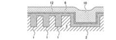
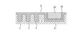
- FIG. 1A to 1Dare diagrams illustrating an embodiment of a method for manufacturing a barrier metal-free metal wiring structure.
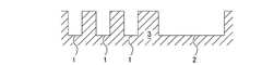
- the insulating layer 3 in which the first wiring groove 1 and the second wiring groove 2 are formedis prepared.
- the insulating layer 3is formed on a workpiece such as a wafer, a substrate, or a panel.
- the material constituting the insulating layer 3is, for example, silicon dioxide (SiO 2 ), and the insulating layer 3 is, for example, a silicon oxide film.
- the width W1 of the first wiring groove 1is narrower than the width W2 of the second wiring groove 2, and in one embodiment, the width W1 of the first wiring groove 1 is smaller than 7 nm.
- the intermetallic compound 6is deposited on the insulating layer 3.
- the entire first wiring groove 1 and the second wiring groove 2are filled with the intermetallic compound 6.
- the method for depositing the intermetallic compound 6is not particularly limited, but in this embodiment, sputtering is used.
- Specific examples of the intermetallic compound 6include CuAl 2 and NiAl.
- one embodiment of the method of forming CuAl 2 by sputteringis between a target made of copper (Cu) and aluminum (Al) and a workpiece while flowing an inert gas (typically argon gas). By applying a voltage, CuAl 2 is deposited on the insulating layer 3.
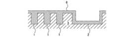
- a flattening step of polishing the intermetallic compound 6is performed until the insulating layer 3 is exposed.
- This flattening stepis a CMP (Chemical Mechanical Polishing) step and is performed by a CMP apparatus. More specifically, the intermetallic compound 6 is brought into sliding contact with the first polishing pad while supplying the first polishing liquid onto the first polishing pad (not shown). The intermetallic compound 6 is flattened by the chemical action of the first polishing liquid and the mechanical action of the abrasive grains and / or the first polishing pad contained in the first polishing liquid.
- the first polishing liquidhas a removal rate selectivity in which the removal rate of the intermetallic compound 6 is higher than the removal rate of the insulating layer 3.
- the removal rateis the rate of material thickness that decreases per unit time.
- the exposed surface of the insulating layer 3functions as a polishing stopper. Therefore, when the insulating layer 3 is exposed, the polishing of the intermetallic compound 6 can be substantially stopped.
- the flattening stepmay be executed while measuring the thickness of the intermetallic compound 6 with a film thickness sensor. The time point at which the insulating layer 3 is exposed can be estimated based on the measured value of the thickness of the intermetallic compound 6.
- the configuration of the film thickness sensoris not particularly limited, but for example, an eddy current sensor can be used for the film thickness sensor.
- This height adjustment stepis also a CMP (Chemical Mechanical Polishing) step and is executed by a CMP apparatus. More specifically, the intermetallic compound 6 and the insulating layer 3 are brought into sliding contact with the second polishing pad while supplying the second polishing liquid onto the second polishing pad (not shown). The intermetallic compound 6 and the insulating layer 3 are polished by the chemical action of the second polishing liquid and the mechanical action of the abrasive grains and / or the second polishing pad contained in the second polishing liquid.
- the height adjusting stepis performed using a second polishing liquid having a removal rate selectivity at which the removal rate of the intermetallic compound 6 is the same as or lower than the removal rate of the insulating layer 3.
- a second polishing liquid having a removal rate selectivityat which the removal rate of the intermetallic compound 6 is the same as or lower than the removal rate of the insulating layer 3.
- the height adjusting stepis performed while measuring the height (that is, the wiring height) of the intermetallic compound 6 in the first wiring groove 1 by the film thickness sensor.
- the height adjusting stepis stopped. In this way, a barrier metal-free metal wiring structure is manufactured.
- the barrier metal-free metal wiring structure manufactured according to the above methodincludes an insulating layer 3 in which the first wiring groove 1 and the second wiring groove 2 are formed, and the first wiring groove 1 and the second.
- the intermetallic compound 6 that fills the wiring groove 2is provided.
- the narrow first wiring groove 1is filled with the intermetallic compound 6, and the barrier metal is not present in the first wiring groove 1. Therefore, low resistance wiring made of the intermetallic compound 6 in the first wiring groove 1 can be realized.
- the intermetallic compound 6 used in this embodimentis CuAl 2 .
- FIG. 2is a graph showing the relationship between the electrical resistivity and the wiring width. As shown in FIG. 2, when the wiring width is small to some extent, the electrical resistivity of the intermetallic compound 6 is smaller than the electrical resistivity of the combination of copper and the barrier metal layer, which are conventional wiring materials. In the graph shown in FIG. 2, when the wiring width is smaller than 7 nm , the electrical resistivity of the intermetallic compound 6 made of CuAl 2 is smaller than the electrical resistivity of the combination of copper and the barrier metal layer. Therefore, when the width of the first wiring groove 1 is smaller than 7 nm, the wiring made of the intermetallic compound 6 exhibits lower electrical efficiency than the conventional wiring made of copper and a barrier metal layer. From such a viewpoint, the width of the first wiring groove 1 of the present embodiment is set to less than 7 nm.
- the width of the second wiring groove 2is 7 nm or more.
- the second wiring groove 2may be 0.1 ⁇ m or more, or may be 1 ⁇ m or more.
- the wiring widthis 7 nm or more, the electrical resistivity of CuAl 2 is larger than the electrical resistivity of the combination of copper and the barrier metal layer, but the cross-sectional area of the wiring is large. , Electrical resistance is small. Therefore, the wiring in the second wiring groove 2 can also have a low resistance like the wiring in the first wiring groove 1.
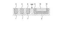
- 3A to 3Eare diagrams illustrating other embodiments of a method for manufacturing a barrier metal-free metal wiring structure.
- the configuration and process of the present embodiment, which are not particularly described,are the same as those of the embodiments described with reference to FIGS. 1A to 1D, and thus the overlapping description thereof will be omitted.
- the insulating layer 3 in which the first wiring groove 1 and the second wiring groove 2 are formedis prepared.
- the intermetallic compound 6is deposited on the insulating layer 3.
- the entire first wiring groove 1is filled with the intermetallic compound 6, and a film of the intermetallic compound 6 is formed in the second wiring groove 2.
- the surface of the insulating layer 3 constituting the second wiring groove 2is covered with the intermetallic compound 6, but the entire second wiring groove 2 is not filled with the intermetallic compound 6.
- a second metal 10 different from the intermetallic compound 6is deposited on the intermetallic compound 6, and the second wiring groove 2 is the second. 2 Filled with 10 metals.
- the second metal 10include copper, titanium, titanium nitride and the like.
- the method for depositing the second metal 10is not particularly limited, and for example, electrolytic plating can be used.
- a flattening step of polishing the second metal 10 and the intermetallic compound 6is performed until the insulating layer 3 is exposed.
- This flattening stepis a CMP (Chemical Mechanical Polishing) step and is performed by a CMP apparatus. More specifically, the second metal 10 and the intermetallic compound 6 are brought into sliding contact with the first polishing pad while supplying the first polishing liquid onto the first polishing pad. The second metal 10 and the intermetallic compound 6 are flattened by the chemical action of the first polishing liquid and the mechanical action of the abrasive grains and / or the first polishing pad contained in the first polishing liquid.
- the first polishing liquidhas a removal rate selectivity in which the removal rate of the second metal 10 and the intermetallic compound 6 is higher than the removal rate of the insulating layer 3.
- the second metal 10, the intermetallic compound 6, and the insulating layer 3are formed until the height of the intermetallic compound 6 in the first wiring groove 1 reaches a predetermined height.
- a height adjustment process for polishingis performed.
- This height adjustment stepis also a CMP (Chemical Mechanical Polishing) step and is executed by a CMP apparatus. More specifically, the second metal 10, the intermetallic compound 6, and the insulating layer 3 are brought into sliding contact with the second polishing pad while supplying the second polishing liquid onto the second polishing pad. The second metal 10, the intermetallic compound 6, and the insulating layer 3 are polished by the chemical action of the second polishing liquid and the mechanical action of the abrasive grains and / or the second polishing pad contained in the second polishing liquid. NS.
- the height adjustment stepis performed using a second polishing liquid having a removal rate selectivity of the second metal 10 and the intermetallic compound 6 equal to or lower than the removal rate of the insulating layer 3. ..
- a second polishing liquid having a removal rate selectivity of the second metal 10 and the intermetallic compound 6equal to or lower than the removal rate of the insulating layer 3. ..
- the second metal 10 and the intermetallic compound 6may be used.
- a second polishing liquid having a removal rate selectivity lower than that of the insulating layer 3is used.
- the removal rate of the second metal 10 and the intermetallic compound 6will be set.
- a second polishing liquid having the same removal rate selectivity as the removal rate of the insulating layer 3is used.
- the height adjusting stepis performed while measuring the height (that is, the wiring height) of the intermetallic compound 6 in the first wiring groove 1 by the film thickness sensor.
- the height adjusting stepis stopped. In this way, a barrier metal-free metal wiring structure is manufactured.
- the narrow first wiring groove 1is filled with the intermetallic compound 6, and the barrier metal is not present in the first wiring groove 1. Therefore, low resistance wiring made of the intermetallic compound 6 in the first wiring groove 1 can be realized.
- the second wiring groove 2is filled with the intermetallic compound 6 and the second metal 10, which form a wide wiring.
- FIGS. 3A to 3Fare diagrams illustrating still another embodiment of the method for manufacturing a barrier metal-free metal wiring structure.
- the configuration and process of the present embodiment, which are not particularly described,are the same as those of the embodiments described with reference to FIGS. 3A to 3E, and thus the overlapping description thereof will be omitted.
- a first flattening stepis performed in which the second metal 10 is polished until the intermetallic compound 6 is exposed. More specifically, the second metal 10 is brought into sliding contact with the first polishing pad while supplying the first polishing liquid onto the first polishing pad. The second metal 10 is flattened by the chemical action of the first polishing liquid and the mechanical action of the abrasive grains and / or the first polishing pad contained in the first polishing liquid.
- the first polishing liquidhas a removal rate selectivity in which the removal rate of the second metal 10 is higher than the removal rate of the intermetallic compound 6. Therefore, the intermetallic compound 6 functions as a polishing stopper.
- the second flattening stepis performed after the first flattening step.
- This second flattening stepis a step of polishing the second metal 10 and the intermetallic compound 6 until the insulating layer 3 is exposed. More specifically, the second metal 10 and the intermetallic compound 6 are brought into sliding contact with the second polishing pad while supplying the second polishing liquid onto the second polishing pad.
- the second metal 10 and the intermetallic compound 6are flattened by the chemical action of the second polishing liquid and the mechanical action of the abrasive grains and / or the second polishing pad contained in the second polishing liquid.
- the second polishing liquidhas a removal rate selectivity in which the removal rate of the second metal 10 and the intermetallic compound 6 is higher than the removal rate of the insulating layer 3. Therefore, the insulating layer 3 functions as a polishing stopper.
- the second metal 10, the intermetallic compound 6, and the insulating layeruntil the height of the intermetallic compound 6 in the first wiring groove 1 reaches a predetermined height.
- a height adjusting step of polishing 3is performed. More specifically, the second metal 10, the intermetallic compound 6, and the insulating layer 3 are brought into sliding contact with the third polishing pad while supplying the third polishing liquid onto the third polishing pad. The second metal 10, the intermetallic compound 6, and the insulating layer 3 are polished by the chemical action of the third polishing liquid and the mechanical action of the abrasive grains and / or the third polishing pad contained in the third polishing liquid. NS.
- the height adjustment stepis performed using a third polishing liquid having a removal rate selectivity of the second metal 10 and the intermetallic compound 6 equal to or lower than the removal rate of the insulating layer 3. ..
- a third polishing liquid having a removal rate selectivity of the second metal 10 and the intermetallic compound 6equal to or lower than the removal rate of the insulating layer 3. ..
- the second metal 10 and the intermetallic compound 6may be used.
- a third polishing liquid having a removal rate selectivity lower than that of the insulating layer 3is used.
- the removal rate of the second metal 10 and the intermetallic compound 6will be set.
- a third polishing liquid having the same removal rate selectivity as the removal rate of the insulating layer 3is used.
- FIGS. 1A to 1Dare diagrams illustrating still another embodiment of the method of manufacturing a barrier metal-free metal wiring structure.
- the configuration and process of the present embodimentwhich are not particularly described, are the same as those of the embodiments described with reference to FIGS. 1A to 1D, and thus the overlapping description thereof will be omitted.
- the insulating layer 3 in which the first wiring groove 1 and the second wiring groove 2 are formedis prepared.
- the intermetallic compound 6is deposited on the insulating layer 3.
- the entire first wiring groove 1is filled with the intermetallic compound 6, and a film of the intermetallic compound 6 is formed in the second wiring groove 2.
- the surface of the insulating layer 3 constituting the second wiring groove 2is covered with the intermetallic compound 6, but the entire second wiring groove 2 is not filled with the intermetallic compound 6.
- the seed layer 12is formed on the intermetallic compound 6 as shown in FIG. 5C.
- the seed layer 12functions as an electrode for subsequent electrolytic plating.
- the seed layer 12is made of, for example, copper.
- the seed layer 12can be formed by electroless plating, sputtering, or the like.
- a second metal 10 different from the intermetallic compound 6is deposited on the seed layer 12, and the second wiring groove 2 is filled with the second metal 10.
- the second metal 10include copper, titanium, titanium nitride and the like. In this embodiment, copper is used as the second metal 10, and electrolytic plating is used as a method for forming the second metal 10.
- a flattening step of polishing the second metal 10, the seed layer 12, and the intermetallic compound 6is performed until the insulating layer 3 is exposed.
- This flattening stepis a CMP (Chemical Mechanical Polishing) step and is performed by a CMP apparatus. More specifically, the second metal 10, the seed layer 12, and the intermetallic compound 6 are slidably contacted with the first polishing pad while supplying the first polishing liquid onto the first polishing pad. The second metal 10, the seed layer 12, and the intermetallic compound 6 are flattened by the chemical action of the first polishing liquid and the mechanical action of the abrasive grains and / or the first polishing pad contained in the first polishing liquid. Will be done.
- the first polishing liquidhas a removal rate selectivity in which the removal rate of the second metal 10, the seed layer 12, and the intermetallic compound 6 is higher than the removal rate of the insulating layer 3. Therefore, the insulating layer 3 functions as a polishing stopper.
- the second metal 10As shown in FIG. 6B, after the flattening step, the second metal 10, the seed layer 12, the intermetallic compound 6 and the intermetallic compound 6 until the height of the intermetallic compound 6 in the first wiring groove 1 reaches a predetermined height.
- a height adjusting step of polishing the insulating layer 3is performed. This height adjustment step is also a CMP (Chemical Mechanical Polishing) step and is executed by a CMP apparatus. More specifically, the second metal 10, the seed layer 12, the intermetallic compound 6, and the insulating layer 3 are brought into sliding contact with the second polishing pad while supplying the second polishing liquid onto the second polishing pad.
- CMPChemical Mechanical Polishing
- the second metal 10, the seed layer 12, the intermetallic compound 6, and the insulating layer 3have the chemical action of the second polishing liquid and the mechanical action of the abrasive grains and / or the second polishing pad contained in the second polishing liquid. Is polished by.
- a second polishing liquid having a removal rate selectivity in which the removal rate of the second metal 10, the seed layer 12, and the intermetallic compound 6 is the same as or lower than the removal rate of the insulating layer 3is used. Made using. Specifically, if it is expected that dishing will occur while polishing the second metal 10, the seed layer 12, and the intermetallic compound 6 in the second wiring groove 2, the second metal 10, A second polishing liquid having a removal rate selectivity in which the removal rate of the seed layer 12 and the intermetallic compound 6 is lower than the removal rate of the insulating layer 3 is used.
- the height adjusting stepis performed while measuring the height (that is, the wiring height) of the intermetallic compound 6 in the first wiring groove 1 by the film thickness sensor.
- the height adjusting stepis stopped. In this way, a barrier metal-free metal wiring structure is manufactured.
- the narrow first wiring groove 1is filled with the intermetallic compound 6, and the barrier metal is not present in the first wiring groove 1. Therefore, low resistance wiring made of the intermetallic compound 6 in the first wiring groove 1 can be realized.
- the second wiring groove 2is filled with the intermetallic compound 6, the second metal 10, and the seed layer 12, which form a wide wiring.
- FIGS. 8A to 8Care diagrams illustrating still another embodiment of the method for manufacturing a barrier metal-free metal wiring structure.
- the configurations and steps of the present embodiment, which are not particularly described,are the same as those of the embodiments described with reference to FIGS. 5A to 5D and FIGS. 6A and 6B, and thus the overlapping description thereof will be omitted.
- a first flattening stepis performed in which the second metal 10 and the seed layer 12 are polished until the intermetallic compound 6 is exposed. More specifically, the second metal 10 and the seed layer 12 are brought into sliding contact with the first polishing pad while supplying the first polishing liquid onto the first polishing pad. The second metal 10 and the seed layer 12 are flattened by the chemical action of the first polishing liquid and the mechanical action of the abrasive grains and / or the first polishing pad contained in the first polishing liquid.
- the first polishing liquidhas a removal rate selectivity in which the removal rate of the second metal 10 and the seed layer 12 is higher than the removal rate of the intermetallic compound 6. Therefore, the intermetallic compound 6 functions as a polishing stopper.
- the second flattening stepis performed after the first flattening step.
- This second flattening stepis a step of polishing the second metal 10, the seed layer 12, and the intermetallic compound 6 until the insulating layer 3 is exposed. More specifically, the second metal 10, the seed layer 12, and the intermetallic compound 6 are slidably contacted with the second polishing pad while supplying the second polishing liquid onto the second polishing pad.
- the second metal 10, the seed layer 12, and the intermetallic compound 6are flattened by the chemical action of the second polishing liquid and the mechanical action of the abrasive grains and / or the second polishing pad contained in the second polishing liquid. Will be done.
- the second polishing liquidhas a removal rate selectivity in which the removal rate of the second metal 10, the seed layer 12, and the intermetallic compound 6 is higher than the removal rate of the insulating layer 3. Therefore, the insulating layer 3 functions as a polishing stopper.
- the second metal 10, the seed layer 12, and the intermetallic compound 6until the height of the intermetallic compound 6 in the first wiring groove 1 reaches a predetermined height.
- a height adjusting step of polishing the insulating layer 3is performed. More specifically, the second metal 10, the seed layer 12, the intermetallic compound 6, and the insulating layer 3 are slidably contacted with the third polishing pad while supplying the third polishing liquid onto the third polishing pad.
- the second metal 10, the seed layer 12, the intermetallic compound 6, and the insulating layer 3have the chemical action of the third polishing liquid and the mechanical action of the abrasive grains and / or the third polishing pad contained in the third polishing liquid. Is polished by.
- a third polishing liquid having a removal rate selectivity at which the removal rate of the second metal 10, the seed layer 12, and the intermetallic compound 6 is the same as or lower than the removal rate of the insulating layer 3is used. Made using. Specifically, if it is expected that dishing will occur while polishing the second metal 10, the seed layer 12, and the intermetallic compound 6 in the second wiring groove 2, the second metal 10, A third polishing liquid having a removal rate selectivity in which the removal rate of the seed layer 12 and the intermetallic compound 6 is lower than the removal rate of the insulating layer 3 is used.
- the wiring in the narrow first wiring groove 1is composed of only the intermetallic compound 6. Therefore, a barrier metal-free metal wiring structure can be realized.
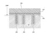
- FIG. 9is a schematic diagram showing a manufacturing system for manufacturing the above-mentioned barrier metal-free metal wiring structure.
- the manufacturing systemincludes a sputtering device 20 for forming the intermetal compound 6, a plating device 22 for forming the second metal 10, a film forming device 23 for forming the seed layer 12, and a plurality of CMP devices. (Chemical mechanical polishing apparatus) 24, 25, 26, a cleaning device 31 for cleaning the polished workpiece, a drying apparatus 33 for drying the cleaned workpiece, and a transport device 35 for transporting the workpiece.
- CMP devicesChemical mechanical polishing apparatus
- Metal wiring structuresare formed on workpieces such as wafers, substrates and panels.
- the configuration of the manufacturing system shown in FIG. 9is an example, and can be appropriately changed based on the metal wiring structure to be manufactured.
- the second metal 10 and the seed layer 12may not be formed.
- the plating apparatus 22 and the film forming apparatus 23may be omitted.
- the manufacturing system shown in FIG. 9includes three CMP devices 24, 25, 26, but if only two types of polishing liquids are used, only two CMP devices 24, 25 may be provided. ..
- the first CMP device 24includes a first polishing table 41 that supports the first polishing pad 40, a first polishing head 42 that presses the workpiece W against the first polishing pad 40, and a first polishing table.
- a first table motor 44 for rotating 41 and a first polishing liquid supply nozzle 45 for supplying the first polishing liquid on the first polishing pad 40are provided.
- the upper surface of the first polishing pad 40constitutes a polishing surface 40a for polishing the workpiece W.
- the first polishing head 42is connected to the head shaft 48, and the head shaft 48 is connected to the first polishing head motor (not shown).
- the first polishing head motorrotates the first polishing head 42 together with the head shaft 48 in the direction indicated by the arrow.
- the first polishing table 41is connected to the first table motor 44, and the first table motor 44 is configured to rotate the first polishing table 41 and the first polishing pad 40 in the direction indicated by the arrow.
- Workpiece Wis polished as follows. While rotating the first polishing table 41 and the first polishing head 42 in the direction indicated by the arrow in FIG. 10, the first polishing liquid is transferred from the first polishing liquid supply nozzle 45 to the first polishing pad 40 on the first polishing table 41. It is supplied to the polished surface 40a. While the workpiece W is rotated by the first polishing head 42, the workpiece W is moved to the polishing surface 40a of the first polishing pad 40 by the first polishing head 42 in a state where the first polishing liquid is present on the first polishing pad 40. Be pressed. The metal wiring structure formed on the workpiece W is polished by the chemical action of the first polishing liquid and the mechanical action of the abrasive grains and / or the first polishing pad 40 contained in the first polishing liquid.
- the first CMP device 24includes a first film thickness sensor 50 that measures the film thickness of the metal wiring structure formed on the workpiece W.
- the configuration of the first film thickness sensor 50is not particularly limited, but an eddy current sensor is used in this embodiment.
- the first film thickness sensor 50is attached to the first polishing table 41 and rotates integrally with the first polishing table 41 and the first polishing pad 40.
- the position of the first film thickness sensor 50is a position across the surface of the workpiece W on the first polishing pad 40 each time the first polishing table 41 and the first polishing pad 40 make one rotation.
- the thickness of the intermetallic compound 6 formed on the workpiece Wis measured by the first film thickness sensor 50.
- the second CMP device 25includes a second polishing table that supports the second polishing pad, a second polishing head that presses the workpiece W against the second polishing pad, and a second table motor that rotates the second polishing table.
- a second polishing liquid supply nozzle for supplying the second polishing liquid on the second polishing pad, and a second film thickness sensor for measuring the film thickness of the workpiece Ware provided.
- the third CMP device 26includes a third polishing table that supports the third polishing pad, a third polishing head that presses the workpiece W against the third polishing pad, and a third table motor that rotates the third polishing table.
- a third polishing liquid supply nozzle for supplying the third polishing liquid on the third polishing pad, and a third film thickness sensor for measuring the film thickness of the workpiece Ware provided.
- the third CMP device 26may not be provided.
- the cleaning device 31is configured to clean the workpiece W polished by the CMP devices 24, 25, 26.
- the cleaning device 31is a roll cleaning machine that scrubs both sides of the workpiece W with a roll scrubber while supplying the cleaning liquid to the workpiece W.
- the cleaning device 31may be a pen sponge cleaning machine that scrubs one surface of the work piece W with a pen sponge while supplying the cleaning liquid to the workpiece W.
- the drying device 33is configured to dry the workpiece W washed by the washing device 31.
- the drying device 33is an IPA drying device that supplies isopropyl alcohol to the workpiece W while rotating the workpiece W.
- the drying device 33may be a spin drying device that rotates the workpiece W at a high speed.
- the transport device 35is configured to transport the workpiece between the CMP devices 24, 25, 26, the cleaning device 31, and the drying device 33.
- the film forming apparatus 23 for forming the seed layer 12is composed of a sputtering apparatus, an electroless plating apparatus, a PVD apparatus, a CVD apparatus and the like. When manufacturing a metal wiring structure having no seed layer 12, the film forming apparatus 23 may be omitted.
- the present inventioncan be used for a metal wiring structure such as a semiconductor device and a manufacturing method thereof, and particularly can be used for a metal wiring structure containing no barrier metal and a manufacturing method thereof.
Landscapes
- Engineering & Computer Science (AREA)
- Physics & Mathematics (AREA)
- Condensed Matter Physics & Semiconductors (AREA)
- General Physics & Mathematics (AREA)
- Computer Hardware Design (AREA)
- Microelectronics & Electronic Packaging (AREA)
- Power Engineering (AREA)
- Manufacturing & Machinery (AREA)
- Internal Circuitry In Semiconductor Integrated Circuit Devices (AREA)
- Mechanical Treatment Of Semiconductor (AREA)
Abstract
Description
Translated fromJapanese本発明は、半導体デバイスなどの金属配線構造およびその製造方法に関し、特にバリアメタルを含まない金属配線構造およびその製造方法に関する。The present invention relates to a metal wiring structure such as a semiconductor device and a manufacturing method thereof, and particularly to a metal wiring structure containing no barrier metal and a manufacturing method thereof.
銅(Cu)は、配線材料として一般に使用されている。銅は、酸化膜などの絶縁層に形成された配線溝にめっきによって埋め込まれ、銅配線を形成する。銅を絶縁層上に直接堆積させると、銅は絶縁層中に拡散してしまう。そこで、銅の拡散を防ぐために、絶縁層上にバリアメタル層が形成され、銅はバリアメタル層上に堆積される。Copper (Cu) is generally used as a wiring material. Copper is embedded in wiring grooves formed in an insulating layer such as an oxide film by plating to form copper wiring. If copper is deposited directly on the insulating layer, the copper will diffuse into the insulating layer. Therefore, in order to prevent the diffusion of copper, a barrier metal layer is formed on the insulating layer, and copper is deposited on the barrier metal layer.
図11Aおよび図11Bは、従来の配線構造の一例を示す断面図である。図11Aに示すように、配線溝200が形成された絶縁層(例えば、シリコン酸化膜)201上にバリアメタル205が堆積される。めっき電極として機能するシード層207は、バリアメタル205の上に形成される。さらに銅208がめっきによりシード層207上に堆積される。銅208の一部は、配線溝200内に埋め込まれる。その後、CMP(化学機械研磨)により余剰の銅208およびシード層207、および絶縁層201の一部が除去され、図11Bに示すように、銅208およびシード層207からなる配線が形成される。11A and 11B are cross-sectional views showing an example of a conventional wiring structure. As shown in FIG. 11A, the
図12Aおよび図12Bは、従来の配線構造の他の例を示す断面図である。図12Aに示すように、配線溝200が形成された絶縁層(例えば、シリコン酸化膜)201上にバリアメタル205が堆積される。シード層207は、バリアメタル205の上に堆積され、配線溝200はシード層207で満たされる。さらに銅208がシード層207上に堆積される。その後、CMP(化学機械研磨)により余剰の銅208およびシード層207、および絶縁層201の一部が除去され、図12Bに示すように、シード層207からなる配線が形成される。12A and 12B are cross-sectional views showing another example of the conventional wiring structure. As shown in FIG. 12A, the
しかしながら、図11および図12から分かるように、配線幅が狭くなるにつれて、配線金属に占めるバリアメタルの比率が高くなる。バリアメタルの電気抵抗率は銅よりもかなり高いため、配線全体の抵抗が上昇する。このような理由から、低抵抗の微細配線を実現することが難しかった。However, as can be seen from FIGS. 11 and 12, as the wiring width becomes narrower, the ratio of the barrier metal to the wiring metal increases. Since the electrical resistivity of the barrier metal is much higher than that of copper, the resistance of the entire wiring increases. For this reason, it has been difficult to realize low-resistance fine wiring.
そこで、本発明は、低抵抗のバリアメタルフリー金属配線構造の製造方法を提供する。また、本発明はそのようなバリアメタルフリー金属配線構造を提供する。Therefore, the present invention provides a method for manufacturing a barrier metal-free metal wiring structure having low resistance. The present invention also provides such a barrier metal-free metal wiring structure.
一態様では、バリアメタルフリー金属配線構造を製造する方法であって、第1配線溝と、前記第1配線溝よりも幅の広い第2配線溝が形成された絶縁層上に金属間化合物を堆積させることで、少なくとも前記第1配線溝を前記金属間化合物で満たし、前記絶縁層が露出するまで前記金属間化合物を研磨する平坦化工程を行い、その後、前記第1配線溝内の前記金属間化合物の高さが所定の高さに達するまで前記金属間化合物および前記絶縁層を研磨する高さ調整工程を行う、方法が提供される。In one aspect, it is a method of manufacturing a barrier metal-free metal wiring structure, in which an intermetallic compound is formed on an insulating layer in which a first wiring groove and a second wiring groove wider than the first wiring groove are formed. By depositing, at least the first wiring groove is filled with the intermetallic compound, a flattening step of polishing the intermetallic compound until the insulating layer is exposed, and then the metal in the first wiring groove is performed. A method is provided in which a height adjusting step of polishing the intermetallic compound and the insulating layer is performed until the height of the intermetallic compound reaches a predetermined height.
一態様では、前記絶縁層上に前記金属間化合物を堆積させることで、前記第1配線溝および前記第2配線溝を前記金属間化合物で満たす。
一態様では、前記平坦化工程は、前記金属間化合物の除去レートが前記絶縁層の除去レートよりも高い除去レート選択比を持つ第1研磨液を使用して行われ、前記高さ調整工程は、前記金属間化合物の除去レートが前記絶縁層の除去レートと同じか、またはそれよりも低い除去レート選択比を持つ第2研磨液を使用して行われる。In one aspect, the intermetallic compound is deposited on the insulating layer to fill the first wiring groove and the second wiring groove with the intermetallic compound.
In one aspect, the flattening step is performed using a first polishing liquid having a removal rate selectivity in which the removal rate of the intermetallic compound is higher than the removal rate of the insulating layer, and the height adjusting step is performed. , The removal rate of the intermetallic compound is the same as or lower than the removal rate of the insulating layer, using a second polishing liquid having a removal rate selectivity.
一態様では、前記方法は、前記第1配線溝を前記金属間化合物で満たした後、前記金属間化合物とは異なる第2金属を前記金属間化合物上に堆積させて、前記第2配線溝を前記第2金属で満たす工程をさらに含む。
一態様では、前記平坦化工程は、前記絶縁層が露出するまで前記第2金属および前記金属間化合物を研磨する工程であり、前記高さ調整工程は、前記第1配線溝内の前記金属間化合物の高さが前記所定の高さに達するまで前記第2金属、前記金属間化合物、および前記絶縁層を研磨する工程である。
一態様では、前記平坦化工程は、前記第2金属および前記金属間化合物の除去レートが前記絶縁層の除去レートよりも高い除去レート選択比を持つ第1研磨液を使用して行われ、前記高さ調整工程は、前記第2金属および前記金属間化合物の除去レートが前記絶縁層の除去レートと同じか、またはそれよりも低い除去レート選択比を持つ第2研磨液を使用して行われる。In one aspect, in the method, after the first wiring groove is filled with the intermetallic compound, a second metal different from the intermetallic compound is deposited on the intermetallic compound to form the second wiring groove. The step of filling with the second metal is further included.
In one aspect, the flattening step is a step of polishing the second metal and the intermetallic compound until the insulating layer is exposed, and the height adjusting step is a step of polishing the intermetallic compound in the first wiring groove. This is a step of polishing the second metal, the intermetallic compound, and the insulating layer until the height of the compound reaches the predetermined height.
In one aspect, the flattening step is performed using a first polishing liquid having a removal rate selectivity in which the removal rate of the second metal and the intermetallic compound is higher than the removal rate of the insulating layer. The height adjusting step is performed using a second polishing liquid having a removal rate selectivity at which the removal rate of the second metal and the intermetallic compound is the same as or lower than the removal rate of the insulating layer. ..
一態様では、前記平坦化工程は、前記金属間化合物が露出するまで前記第2金属を研磨する第1平坦化工程と、前記絶縁層が露出するまで前記第2金属および前記金属間化合物を研磨する第2平坦化工程を含む。
一態様では、前記第1平坦化工程は、前記第2金属の除去レートが前記金属間化合物の除去レートよりも高い除去レート選択比を持つ第1研磨液を使用して行われ、前記第2平坦化工程は、前記第2金属および前記金属間化合物の除去レートが前記絶縁層の除去レートよりも高い除去レート選択比を持つ第2研磨液を使用して行われ、前記高さ調整工程は、前記第2金属および前記金属間化合物の除去レートが前記絶縁層の除去レートと同じか、またはそれよりも低い除去レート選択比を持つ第3研磨液を使用して行われる。In one aspect, the flattening step includes a first flattening step of polishing the second metal until the intermetallic compound is exposed, and a polishing of the second metal and the intermetallic compound until the insulating layer is exposed. The second flattening step is included.
In one aspect, the first flattening step is performed using a first polishing liquid having a removal rate selectivity in which the removal rate of the second metal is higher than the removal rate of the intermetallic compound, the second. The flattening step is performed using a second polishing liquid having a removal rate selectivity in which the removal rate of the second metal and the intermetallic compound is higher than the removal rate of the insulating layer, and the height adjustment step is performed. , The removal rate of the second metal and the intermetallic compound is the same as or lower than the removal rate of the insulating layer, using a third polishing solution.
一態様では、前記方法は、前記第1配線溝を前記金属間化合物で満たした後、前記金属間化合物の上にシード層を形成し、前記シード層上に前記金属間化合物とは異なる第2金属を堆積させて、前記第2配線溝を前記第2金属で満たす工程をさらに含む。
一態様では、前記平坦化工程は、前記絶縁層が露出するまで前記第2金属、前記シード層、および前記金属間化合物を研磨する工程であり、前記高さ調整工程は、前記第1配線溝内の前記金属間化合物の高さが前記所定の高さに達するまで前記第2金属、前記シード層、前記金属間化合物、および前記絶縁層を研磨する工程である。
一態様では、前記平坦化工程は、前記第2金属、前記シード層、および前記金属間化合物の除去レートが前記絶縁層の除去レートよりも高い除去レート選択比を持つ第1研磨液を使用して行われ、前記高さ調整工程は、前記第2金属、前記シード層、および前記金属間化合物の除去レートが前記絶縁層の除去レートと同じか、またはそれよりも低い除去レート選択比を持つ第2研磨液を使用して行われる。In one aspect, in the method, after the first wiring groove is filled with the intermetallic compound, a seed layer is formed on the intermetallic compound, and a second method different from the intermetallic compound is formed on the seed layer. Further including a step of depositing a metal and filling the second wiring groove with the second metal.
In one aspect, the flattening step is a step of polishing the second metal, the seed layer, and the intermetallic compound until the insulating layer is exposed, and the height adjusting step is the step of polishing the first wiring groove. This is a step of polishing the second metal, the seed layer, the intermetallic compound, and the insulating layer until the height of the intermetallic compound in the metal reaches the predetermined height.
In one aspect, the flattening step uses a first polishing solution having a removal rate selectivity in which the removal rate of the second metal, the seed layer, and the intermetallic compound is higher than the removal rate of the insulating layer. The height adjusting step has a removal rate selectivity in which the removal rate of the second metal, the seed layer, and the intermetallic compound is the same as or lower than the removal rate of the insulating layer. This is done using a second polishing solution.
一態様では、前記平坦化工程は、前記金属間化合物が露出するまで前記第2金属および前記シード層を研磨する第1平坦化工程と、前記絶縁層が露出するまで前記第2金属、前記シード層、および前記金属間化合物を研磨する第2平坦化工程を含む。
一態様では、前記第1平坦化工程は、前記第2金属および前記シード層の除去レートが前記金属間化合物の除去レートよりも高い除去レート選択比を持つ第1研磨液を使用して行われ、前記第2平坦化工程は、前記第2金属、前記シード層、および前記金属間化合物の除去レートが前記絶縁層の除去レートよりも高い除去レート選択比を持つ第2研磨液を使用して行われ、前記高さ調整工程は、前記第2金属、前記シード層、および前記金属間化合物の除去レートが前記絶縁層の除去レートと同じか、またはそれよりも低い除去レート選択比を持つ第3研磨液を使用して行われる。
一態様では、前記金属間化合物は、CuAl2またはNiAlである。In one aspect, the flattening step comprises a first flattening step of polishing the second metal and the seed layer until the intermetallic compound is exposed, and the second metal, the seed, until the insulating layer is exposed. It comprises a second flattening step of polishing the layer and the intermetallic compound.
In one aspect, the first flattening step is performed using a first polishing liquid having a removal rate selectivity in which the removal rate of the second metal and the seed layer is higher than the removal rate of the intermetallic compound. In the second flattening step, a second polishing liquid having a removal rate selectivity in which the removal rate of the second metal, the seed layer, and the intermetallic compound is higher than the removal rate of the insulating layer is used. The height adjustment step is performed and the removal rate of the second metal, the seed layer, and the intermetallic compound has a removal rate selectivity equal to or lower than the removal rate of the insulating layer. 3 Performed using a polishing solution.
In one aspect, the intermetallic compound is CuAl2 or NiAl.
一態様では、第1配線溝と、前記第1配線溝よりも幅の広い第2配線溝が形成された絶縁層と、前記第1配線溝を満たす金属間化合物を備えている、バリアメタルフリー金属配線構造が提供される。In one aspect, it is barrier metal-free, comprising a first wiring groove, an insulating layer in which a second wiring groove wider than the first wiring groove is formed, and an intermetallic compound that fills the first wiring groove. A metal wiring structure is provided.
一態様では、前記バリアメタルフリー金属配線構造は、前記第2配線溝を満たす金属間化合物をさらに備えている。
一態様では、前記バリアメタルフリー金属配線構造は、前記第2配線溝内を満たす金属間化合物および第2金属をさらに備えている。
一態様では、前記第2金属は、銅、チタン、またはチタンナイトライドである。
一態様では、前記第1配線溝の幅は、7nmよりも小さい。
一態様では、前記第1配線溝を満たす前記金属間化合物は、CuAl2またはNiAlである。In one aspect, the barrier metal-free metal wiring structure further comprises an intermetallic compound that fills the second wiring groove.
In one aspect, the barrier metal-free metal wiring structure further comprises an intermetallic compound and a second metal that fill the second wiring groove.
In one aspect, the second metal is copper, titanium, or titanium nitride.
In one aspect, the width of the first wiring groove is smaller than 7 nm.
In one aspect, the intermetallic compound that fills the first wiring groove is CuAl2 or NiAl.
本発明によれば、幅の狭い第1配線溝は金属間化合物によって満たされ、バリアメタルは第1配線溝内には存在しない。したがって、第1配線溝内の金属間化合物からなる低抵抗配線が実現できる。According to the present invention, the narrow first wiring groove is filled with the intermetallic compound, and the barrier metal does not exist in the first wiring groove. Therefore, a low resistance wiring made of an intermetallic compound in the first wiring groove can be realized.
以下、本発明の実施形態について図面を参照して説明する。
図1A乃至図1Dは、バリアメタルフリー金属配線構造を製造する方法の一実施形態を説明する図である。図1Aに示すように、第1配線溝1と第2配線溝2が形成された絶縁層3が用意される。絶縁層3は、ウェーハ、基板、パネルなどのワークピースに形成されている。絶縁層3を構成する材料は、例えば、二酸化ケイ素(SiO2)であり、絶縁層3は、例えば、シリコン酸化膜である。第1配線溝1の幅W1は、第2配線溝2の幅W2よりも狭く、一実施形態では、第1配線溝1の幅W1は、7nmよりも小さい。Hereinafter, embodiments of the present invention will be described with reference to the drawings.
1A to 1D are diagrams illustrating an embodiment of a method for manufacturing a barrier metal-free metal wiring structure. As shown in FIG. 1A, the insulating
図1Bに示すように、金属間化合物6が絶縁層3上に堆積される。第1配線溝1および第2配線溝2の全体は、金属間化合物6で満たされる。金属間化合物6を堆積する方法は特に限定されないが、本実施形態では、スパッタリングが用いられている。金属間化合物6の具体例としては、CuAl2、NiAlなどが挙げられる。例えば、CuAl2をスパッタリングで形成する方法の一実施形態は、不活性ガス(典型的にはアルゴンガス)を流しながら、銅(Cu)とアルミニウム(Al)からなるターゲットとワークピースとの間に電圧を印加することで、CuAl2を絶縁層3上に堆積させる。As shown in FIG. 1B, the
図1Cに示すように、絶縁層3が露出するまで金属間化合物6を研磨する平坦化工程が行われる。この平坦化工程は、CMP(化学機械研磨)工程であり、CMP装置によって実行される。より具体的には、第1研磨パッド(図示せず)上に第1研磨液を供給しながら、金属間化合物6を第1研磨パッドに摺接させる。金属間化合物6は、第1研磨液の化学的作用と、第1研磨液に含まれる砥粒および/または第1研磨パッドの機械的作用により、平坦化される。As shown in FIG. 1C, a flattening step of polishing the
第1研磨液は、金属間化合物6の除去レートが絶縁層3の除去レートよりも高い除去レート選択比を有している。除去レートは、単位時間当たりに減少する材料の厚さの率である。このような除去レート選択比を持つ第1研磨液を用いると、絶縁層3の露出面は研磨ストッパとして機能する。したがって、絶縁層3が露出したときに、金属間化合物6の研磨を実質的に停止させることができる。金属間化合物6の厚さを膜厚センサで測定しながら、平坦化工程を実行してもよい。金属間化合物6の厚さの測定値に基づいて、絶縁層3が露出する時点を推定することができる。膜厚センサの構成は特に限定されないが、例えば、渦電流センサを膜厚センサに使用することができる。The first polishing liquid has a removal rate selectivity in which the removal rate of the
図1Dに示すように、平坦化工程の後、第1配線溝1内の金属間化合物6の高さが所定の高さに達するまで金属間化合物6および絶縁層3を研磨する高さ調整工程が行われる。この高さ調整工程も、CMP(化学機械研磨)工程であり、CMP装置によって実行される。より具体的には、第2研磨パッド(図示せず)上に第2研磨液を供給しながら、金属間化合物6および絶縁層3を第2研磨パッドに摺接させる。金属間化合物6および絶縁層3は、第2研磨液の化学的作用と、第2研磨液に含まれる砥粒および/または第2研磨パッドの機械的作用により、研磨される。As shown in FIG. 1D, after the flattening step, the height adjusting step of polishing the
高さ調整工程は、金属間化合物6の除去レートが絶縁層3の除去レートと同じか、またはそれよりも低い除去レート選択比を持つ第2研磨液を使用して行われる。具体的には、第2配線溝2内の金属間化合物6を研磨しているときにディッシングが起こることが予想される場合には、金属間化合物6の除去レートが絶縁層3の除去レートよりも低い除去レート選択比を持つ第2研磨液が使用される。一方、第2配線溝2内の金属間化合物6を研磨しているときにディッシングが起こらないと予想される場合には、金属間化合物6の除去レートが絶縁層3の除去レートと同じ除去レート選択比を持つ第2研磨液が使用される。The height adjusting step is performed using a second polishing liquid having a removal rate selectivity at which the removal rate of the
高さ調整工程は、上記膜厚センサによって第1配線溝1内の金属間化合物6の高さ(すなわち配線高さ)を測定しながら行われる。膜厚センサによって測定された第1配線溝1内の金属間化合物6の高さが所定の高さに達したときに、高さ調整工程が停止される。このようにして、バリアメタルフリー金属配線構造が製造される。The height adjusting step is performed while measuring the height (that is, the wiring height) of the
図1Dに示すように、上述した方法に従って製造されたバリアメタルフリー金属配線構造は、第1配線溝1および第2配線溝2が形成された絶縁層3と、第1配線溝1および第2配線溝2を満たす金属間化合物6を備えている。幅の小さい第1配線溝1は金属間化合物6によって満たされ、バリアメタルは第1配線溝1内には存在しない。したがって、第1配線溝1内の金属間化合物6からなる低抵抗配線が実現できる。As shown in FIG. 1D, the barrier metal-free metal wiring structure manufactured according to the above method includes an insulating
本実施形態で使用されている金属間化合物6は、CuAl2である。図2は、電気抵抗率と配線幅との関係を示すグラフである。図2に示すように、配線幅がある程度小さいとき、金属間化合物6の電気抵抗率は、従来の配線材料である銅とバリアメタル層との組み合わせの電気抵抗率よりも小さい。図2に示すグラフでは、配線幅が7nmよりも小さいとき、CuAl2からなる金属間化合物6の電気抵抗率は、銅とバリアメタル層との組み合わせの電気抵抗率よりも小さい。したがって、第1配線溝1の幅が7nmよりも小さいとき、金属間化合物6からなる配線は、銅とバリアメタル層からなる従来の配線よりも低い電気的効率を示す。このような観点から、本実施形態の第1配線溝1の幅は、7nm未満とされる。The
一方、第2配線溝2の幅は、7nm以上である。一実施形態では、第2配線溝2は、0.1μm以上であってもよく、あるいは1μm以上であってもよい。図2に示すグラフによれば、配線幅が7nm以上であるとき、CuAl2の電気抵抗率は、銅とバリアメタル層との組み合わせの電気抵抗率よりも大きいが、配線の断面積が大きいので、電気抵抗は小さい。よって、第2配線溝2内の配線も、第1配線溝1内の配線と同様に、低抵抗とすることができる。On the other hand, the width of the
図3A乃至図3Eは、バリアメタルフリー金属配線構造を製造する方法の他の実施形態を説明する図である。特に説明しない本実施形態の構成および工程は、図1A乃至図1Dを参照して説明した実施形態と同じであるので、その重複する説明を省略する。3A to 3E are diagrams illustrating other embodiments of a method for manufacturing a barrier metal-free metal wiring structure. The configuration and process of the present embodiment, which are not particularly described, are the same as those of the embodiments described with reference to FIGS. 1A to 1D, and thus the overlapping description thereof will be omitted.
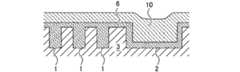
図3Aに示すように、第1配線溝1と第2配線溝2が形成された絶縁層3が用意される。次に、図3Bに示すように、金属間化合物6が絶縁層3上に堆積される。第1配線溝1の全体は、金属間化合物6で満たされ、第2配線溝2内には金属間化合物6の膜が形成される。第2配線溝2を構成する絶縁層3の表面は金属間化合物6で覆われるが、第2配線溝2の全体は金属間化合物6で満たされない。As shown in FIG. 3A, the insulating
第1配線溝1を金属間化合物6で満たした後、図3Cに示すように、金属間化合物6とは異なる第2金属10が金属間化合物6上に堆積され、第2配線溝2は第2金属10で満たされる。第2金属10の例としては、銅、チタン、チタンナイトライド等が挙げられる。第2金属10を堆積させる方法は特に限定されないが、例えば電解めっきが使用できる。After filling the
図3Dに示すように、絶縁層3が露出するまで第2金属10および金属間化合物6を研磨する平坦化工程が行われる。この平坦化工程は、CMP(化学機械研磨)工程であり、CMP装置によって実行される。より具体的には、第1研磨パッド上に第1研磨液を供給しながら、第2金属10および金属間化合物6を第1研磨パッドに摺接させる。第2金属10および金属間化合物6は、第1研磨液の化学的作用と、第1研磨液に含まれる砥粒および/または第1研磨パッドの機械的作用により、平坦化される。第1研磨液は、第2金属10および金属間化合物6の除去レートが絶縁層3の除去レートよりも高い除去レート選択比を有している。As shown in FIG. 3D, a flattening step of polishing the
図3Eに示すように、平坦化工程の後、第1配線溝1内の金属間化合物6の高さが所定の高さに達するまで第2金属10、金属間化合物6、および絶縁層3を研磨する高さ調整工程が行われる。この高さ調整工程も、CMP(化学機械研磨)工程であり、CMP装置によって実行される。より具体的には、第2研磨パッド上に第2研磨液を供給しながら、第2金属10、金属間化合物6、および絶縁層3を第2研磨パッドに摺接させる。第2金属10、金属間化合物6、および絶縁層3は、第2研磨液の化学的作用と、第2研磨液に含まれる砥粒および/または第2研磨パッドの機械的作用により、研磨される。As shown in FIG. 3E, after the flattening step, the
高さ調整工程は、第2金属10および金属間化合物6の除去レートが絶縁層3の除去レートと同じか、またはそれよりも低い除去レート選択比を持つ第2研磨液を使用して行われる。具体的には、第2配線溝2内の第2金属10および金属間化合物6を研磨しているときにディッシングが起こることが予想される場合には、第2金属10および金属間化合物6の除去レートが絶縁層3の除去レートよりも低い除去レート選択比を持つ第2研磨液が使用される。一方、第2配線溝2内の第2金属10および金属間化合物6を研磨しているときにディッシングが起こらないと予想される場合には、第2金属10および金属間化合物6の除去レートが絶縁層3の除去レートと同じ除去レート選択比を持つ第2研磨液が使用される。The height adjustment step is performed using a second polishing liquid having a removal rate selectivity of the
高さ調整工程は、上記膜厚センサによって第1配線溝1内の金属間化合物6の高さ(すなわち配線高さ)を測定しながら行われる。膜厚センサによって測定された第1配線溝1内の金属間化合物6の高さが所定の高さに達したときに、高さ調整工程が停止される。このようにして、バリアメタルフリー金属配線構造が製造される。幅の小さい第1配線溝1は金属間化合物6によって満たされ、バリアメタルは第1配線溝1内には存在しない。したがって、第1配線溝1内の金属間化合物6からなる低抵抗配線が実現できる。第2配線溝2は、金属間化合物6および第2金属10で満たされ、これらは幅の広い配線を形成する。The height adjusting step is performed while measuring the height (that is, the wiring height) of the
図4A乃至図4Fは、バリアメタルフリー金属配線構造を製造する方法のさらに他の実施形態を説明する図である。特に説明しない本実施形態の構成および工程は、図3A乃至図3Eを参照して説明した実施形態と同じであるので、その重複する説明を省略する。4A to 4F are diagrams illustrating still another embodiment of the method for manufacturing a barrier metal-free metal wiring structure. The configuration and process of the present embodiment, which are not particularly described, are the same as those of the embodiments described with reference to FIGS. 3A to 3E, and thus the overlapping description thereof will be omitted.
図4A乃至図4Cに示す工程は、図3A乃至図3Cに示す工程と同じである。図4Dに示すように、金属間化合物6が露出するまで第2金属10を研磨する第1平坦化工程が行われる。より具体的には、第1研磨パッド上に第1研磨液を供給しながら、第2金属10を第1研磨パッドに摺接させる。第2金属10は、第1研磨液の化学的作用と、第1研磨液に含まれる砥粒および/または第1研磨パッドの機械的作用により、平坦化される。第1研磨液は、第2金属10の除去レートが金属間化合物6の除去レートよりも高い除去レート選択比を有している。したがって、金属間化合物6は研磨ストッパとして機能する。The steps shown in FIGS. 4A to 4C are the same as the steps shown in FIGS. 3A to 3C. As shown in FIG. 4D, a first flattening step is performed in which the
図4Eに示すように、第1平坦化工程の後、第2平坦化工程が行われる。この第2平坦化工程は、絶縁層3が露出するまで、第2金属10および金属間化合物6を研磨する工程である。より具体的には、第2研磨パッド上に第2研磨液を供給しながら、第2金属10および金属間化合物6を第2研磨パッドに摺接させる。第2金属10および金属間化合物6は、第2研磨液の化学的作用と、第2研磨液に含まれる砥粒および/または第2研磨パッドの機械的作用により、平坦化される。第2研磨液は、第2金属10および金属間化合物6の除去レートが絶縁層3の除去レートよりも高い除去レート選択比を有している。したがって、絶縁層3は研磨ストッパとして機能する。As shown in FIG. 4E, the second flattening step is performed after the first flattening step. This second flattening step is a step of polishing the
図4Fに示すように、第2平坦化工程の後、第1配線溝1内の金属間化合物6の高さが所定の高さに達するまで第2金属10、金属間化合物6、および絶縁層3を研磨する高さ調整工程が行われる。より具体的には、第3研磨パッド上に第3研磨液を供給しながら、第2金属10、金属間化合物6、および絶縁層3を第3研磨パッドに摺接させる。第2金属10、金属間化合物6、および絶縁層3は、第3研磨液の化学的作用と、第3研磨液に含まれる砥粒および/または第3研磨パッドの機械的作用により、研磨される。As shown in FIG. 4F, after the second flattening step, the
高さ調整工程は、第2金属10および金属間化合物6の除去レートが絶縁層3の除去レートと同じか、またはそれよりも低い除去レート選択比を持つ第3研磨液を使用して行われる。具体的には、第2配線溝2内の第2金属10および金属間化合物6を研磨しているときにディッシングが起こることが予想される場合には、第2金属10および金属間化合物6の除去レートが絶縁層3の除去レートよりも低い除去レート選択比を持つ第3研磨液が使用される。一方、第2配線溝2内の第2金属10および金属間化合物6を研磨しているときにディッシングが起こらないと予想される場合には、第2金属10および金属間化合物6の除去レートが絶縁層3の除去レートと同じ除去レート選択比を持つ第3研磨液が使用される。The height adjustment step is performed using a third polishing liquid having a removal rate selectivity of the
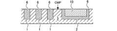
図5A乃至図5D、および図6Aおよび図6Bは、バリアメタルフリー金属配線構造を製造する方法のさらに他の実施形態を説明する図である。特に説明しない本実施形態の構成および工程は、図1A乃至図1Dを参照して説明した実施形態と同じであるので、その重複する説明を省略する。5A-5D, and 6A and 6B are diagrams illustrating still another embodiment of the method of manufacturing a barrier metal-free metal wiring structure. The configuration and process of the present embodiment, which are not particularly described, are the same as those of the embodiments described with reference to FIGS. 1A to 1D, and thus the overlapping description thereof will be omitted.
図5Aに示すように、第1配線溝1と第2配線溝2が形成された絶縁層3が用意される。次に、図5Bに示すように、金属間化合物6が絶縁層3上に堆積される。第1配線溝1の全体は、金属間化合物6で満たされ、第2配線溝2内には金属間化合物6の膜が形成される。第2配線溝2を構成する絶縁層3の表面は金属間化合物6で覆われるが、第2配線溝2の全体は金属間化合物6で満たされない。As shown in FIG. 5A, the insulating
第1配線溝1を金属間化合物6で満たした後、図5Cに示すように、シード層12が金属間化合物6上に形成される。シード層12は、その後に続く電解めっきの電極として機能する。シード層12は、例えば、銅から構成されている。シード層12は、無電解めっき、またはスパッタリングなどにより形成することができる。After the
図5Dに示すように、金属間化合物6とは異なる第2金属10がシード層12上に堆積され、第2配線溝2は第2金属10で満たされる。第2金属10の例としては、銅、チタン、チタンナイトライド等が挙げられる。本実施形態では、第2金属10として銅が使用され、第2金属10を形成する方法には電解めっきが使用されている。As shown in FIG. 5D, a
図6Aに示すように、絶縁層3が露出するまで第2金属10、シード層12、および金属間化合物6を研磨する平坦化工程が行われる。この平坦化工程は、CMP(化学機械研磨)工程であり、CMP装置によって実行される。より具体的には、第1研磨パッド上に第1研磨液を供給しながら、第2金属10、シード層12、および金属間化合物6を第1研磨パッドに摺接させる。第2金属10、シード層12、および金属間化合物6は、第1研磨液の化学的作用と、第1研磨液に含まれる砥粒および/または第1研磨パッドの機械的作用により、平坦化される。第1研磨液は、第2金属10、シード層12、および金属間化合物6の除去レートが絶縁層3の除去レートよりも高い除去レート選択比を有している。したがって、絶縁層3は研磨ストッパとして機能する。As shown in FIG. 6A, a flattening step of polishing the
図6Bに示すように、平坦化工程の後、第1配線溝1内の金属間化合物6の高さが所定の高さに達するまで第2金属10、シード層12、金属間化合物6、および絶縁層3を研磨する高さ調整工程が行われる。この高さ調整工程も、CMP(化学機械研磨)工程であり、CMP装置によって実行される。より具体的には、第2研磨パッド上に第2研磨液を供給しながら、第2金属10、シード層12、金属間化合物6、および絶縁層3を第2研磨パッドに摺接させる。第2金属10、シード層12、金属間化合物6、および絶縁層3は、第2研磨液の化学的作用と、第2研磨液に含まれる砥粒および/または第2研磨パッドの機械的作用により、研磨される。As shown in FIG. 6B, after the flattening step, the
高さ調整工程は、第2金属10、シード層12、および金属間化合物6の除去レートが絶縁層3の除去レートと同じか、またはそれよりも低い除去レート選択比を持つ第2研磨液を使用して行われる。具体的には、第2配線溝2内の第2金属10、シード層12、および金属間化合物6を研磨しているときにディッシングが起こることが予想される場合には、第2金属10、シード層12、および金属間化合物6の除去レートが絶縁層3の除去レートよりも低い除去レート選択比を持つ第2研磨液が使用される。一方、第2配線溝2内の第2金属10、シード層12、および金属間化合物6を研磨しているときにディッシングが起こらないと予想される場合には、第2金属10、シード層12、および金属間化合物6の除去レートが絶縁層3の除去レートと同じ除去レート選択比を持つ第2研磨液が使用される。In the height adjusting step, a second polishing liquid having a removal rate selectivity in which the removal rate of the
高さ調整工程は、上記膜厚センサによって第1配線溝1内の金属間化合物6の高さ(すなわち配線高さ)を測定しながら行われる。膜厚センサによって測定された第1配線溝1内の金属間化合物6の高さが所定の高さに達したときに、高さ調整工程が停止される。このようにして、バリアメタルフリー金属配線構造が製造される。幅の小さい第1配線溝1は金属間化合物6によって満たされ、バリアメタルは第1配線溝1内には存在しない。したがって、第1配線溝1内の金属間化合物6からなる低抵抗配線が実現できる。第2配線溝2は、金属間化合物6、第2金属10、およびシード層12で満たされ、これらは幅の広い配線を形成する。The height adjusting step is performed while measuring the height (that is, the wiring height) of the
図7A乃至図7D、および図8A乃至図8Cは、バリアメタルフリー金属配線構造を製造する方法のさらに他の実施形態を説明する図である。特に説明しない本実施形態の構成および工程は、図5A乃至図5Dおよび図6Aおよび図6Bを参照して説明した実施形態と同じであるので、その重複する説明を省略する。7A to 7D and FIGS. 8A to 8C are diagrams illustrating still another embodiment of the method for manufacturing a barrier metal-free metal wiring structure. The configurations and steps of the present embodiment, which are not particularly described, are the same as those of the embodiments described with reference to FIGS. 5A to 5D and FIGS. 6A and 6B, and thus the overlapping description thereof will be omitted.
図7A乃至図7Dは、図5A乃至図5Dと同様にして実行される。図8Aに示すように、金属間化合物6が露出するまで第2金属10およびシード層12を研磨する第1平坦化工程が行われる。より具体的には、第1研磨パッド上に第1研磨液を供給しながら、第2金属10およびシード層12を第1研磨パッドに摺接させる。第2金属10およびシード層12は、第1研磨液の化学的作用と、第1研磨液に含まれる砥粒および/または第1研磨パッドの機械的作用により、平坦化される。第1研磨液は、第2金属10およびシード層12の除去レートが金属間化合物6の除去レートよりも高い除去レート選択比を有している。したがって、金属間化合物6は研磨ストッパとして機能する。7A to 7D are executed in the same manner as in FIGS. 5A to 5D. As shown in FIG. 8A, a first flattening step is performed in which the
図8Bに示すように、第1平坦化工程の後、第2平坦化工程が行われる。この第2平坦化工程は、絶縁層3が露出するまで、第2金属10、シード層12、および金属間化合物6を研磨する工程である。より具体的には、第2研磨パッド上に第2研磨液を供給しながら、第2金属10、シード層12、および金属間化合物6を第2研磨パッドに摺接させる。第2金属10、シード層12、および金属間化合物6は、第2研磨液の化学的作用と、第2研磨液に含まれる砥粒および/または第2研磨パッドの機械的作用により、平坦化される。第2研磨液は、第2金属10、シード層12、および金属間化合物6の除去レートが絶縁層3の除去レートよりも高い除去レート選択比を有している。したがって、絶縁層3は研磨ストッパとして機能する。As shown in FIG. 8B, the second flattening step is performed after the first flattening step. This second flattening step is a step of polishing the
図8Cに示すように、第2平坦化工程の後、第1配線溝1内の金属間化合物6の高さが所定の高さに達するまで第2金属10、シード層12、金属間化合物6、および絶縁層3を研磨する高さ調整工程が行われる。より具体的には、第3研磨パッド上に第3研磨液を供給しながら、第2金属10、シード層12、金属間化合物6、および絶縁層3を第3研磨パッドに摺接させる。第2金属10、シード層12、金属間化合物6、および絶縁層3は、第3研磨液の化学的作用と、第3研磨液に含まれる砥粒および/または第3研磨パッドの機械的作用により、研磨される。As shown in FIG. 8C, after the second flattening step, the
高さ調整工程は、第2金属10、シード層12、および金属間化合物6の除去レートが絶縁層3の除去レートと同じか、またはそれよりも低い除去レート選択比を持つ第3研磨液を使用して行われる。具体的には、第2配線溝2内の第2金属10、シード層12、および金属間化合物6を研磨しているときにディッシングが起こることが予想される場合には、第2金属10、シード層12、および金属間化合物6の除去レートが絶縁層3の除去レートよりも低い除去レート選択比を持つ第3研磨液が使用される。一方、第2配線溝2内の第2金属10、シード層12、および金属間化合物6を研磨しているときにディッシングが起こらないと予想される場合には、第2金属10、シード層12、および金属間化合物6の除去レートが絶縁層3の除去レートと同じ除去レート選択比を持つ第3研磨液が使用される。In the height adjusting step, a third polishing liquid having a removal rate selectivity at which the removal rate of the
上述した各実施形態によれば、幅の狭い第1配線溝1内の配線は、金属間化合物6のみから構成される。したがって、バリアメタルフリーの金属配線構造が実現できる。According to each of the above-described embodiments, the wiring in the narrow
図9は、上述したバリアメタルフリー金属配線構造を製造するための製造システムを示す模式図である。製造システムは、金属間化合物6を形成するためのスパッタリング装置20と、第2金属10を形成するためのめっき装置22と、シード層12を形成するための成膜装置23と、複数のCMP装置(化学機械研磨装置)24,25,26と、研磨されたワークピースを洗浄する洗浄装置31と、洗浄されたワークピースを乾燥させる乾燥装置33と、ワークピースを搬送する搬送装置35を備えている。金属配線構造は、ウェーハ、基板、パネルなどのワークピースに形成される。FIG. 9 is a schematic diagram showing a manufacturing system for manufacturing the above-mentioned barrier metal-free metal wiring structure. The manufacturing system includes a sputtering
図9に示す製造システムの構成は一例であり、製造すべき金属配線構造に基づいて適宜変更されうる。例えば、図1A乃至図1Dを参照して説明した実施形態では、第2金属10およびシード層12は形成されないこともある。そのような場合には、めっき装置22および成膜装置23は省略してもよい。図9に示す製造システムは、3つのCMP装置24,25,26を備えているが、2種類の研磨液のみが使用される場合には、2つのCMP装置24,25のみを備えてもよい。The configuration of the manufacturing system shown in FIG. 9 is an example, and can be appropriately changed based on the metal wiring structure to be manufactured. For example, in the embodiments described with reference to FIGS. 1A to 1D, the
第1CMP装置24、第2CMP装置25、および第3CMP装置26は、基本的に同じ構成を有している。したがって、以下に図10を参照して第1CMP装置24について説明する。図10に示すように、第1CMP装置24は、第1研磨パッド40を支持する第1研磨テーブル41と、ワークピースWを第1研磨パッド40に押し付ける第1研磨ヘッド42と、第1研磨テーブル41を回転させる第1テーブルモータ44と、第1研磨パッド40上に第1研磨液を供給するための第1研磨液供給ノズル45を備えている。第1研磨パッド40の上面は、ワークピースWを研磨する研磨面40aを構成する。The
第1研磨ヘッド42はヘッドシャフト48に連結されており、ヘッドシャフト48は図示しない第1研磨ヘッドモータに連結されている。第1研磨ヘッドモータは、第1研磨ヘッド42をヘッドシャフト48とともに矢印で示す方向に回転させる。第1研磨テーブル41は第1テーブルモータ44に連結されており、第1テーブルモータ44は第1研磨テーブル41および第1研磨パッド40を矢印で示す方向に回転させるように構成されている。The
ワークピースWは次のようにして研磨される。第1研磨テーブル41および第1研磨ヘッド42を図10の矢印で示す方向に回転させながら、第1研磨液供給ノズル45から第1研磨液が第1研磨テーブル41上の第1研磨パッド40の研磨面40aに供給される。ワークピースWは第1研磨ヘッド42によって回転されながら、第1研磨パッド40上に第1研磨液が存在した状態でワークピースWは第1研磨ヘッド42によって第1研磨パッド40の研磨面40aに押し付けられる。ワークピースWに形成されている金属配線構造は、第1研磨液の化学的作用と、第1研磨液に含まれる砥粒および/または第1研磨パッド40の機械的作用により研磨される。Workpiece W is polished as follows. While rotating the first polishing table 41 and the
第1CMP装置24は、ワークピースWに形成されている金属配線構造の膜厚を測定する第1膜厚センサ50を備えている。第1膜厚センサ50の構成は特に限定されないが、本実施形態では渦電流センサが使用されている。第1膜厚センサ50は第1研磨テーブル41に取り付けられており、第1研磨テーブル41および第1研磨パッド40とともに一体に回転する。第1膜厚センサ50の位置は、第1研磨テーブル41および第1研磨パッド40が一回転するたびに第1研磨パッド40上のワークピースWの表面を横切る位置である。ワークピースWに形成されている金属間化合物6の厚さは、第1膜厚センサ50によって測定される。The
図示しないが、第2CMP装置25は、第2研磨パッドを支持する第2研磨テーブルと、ワークピースWを第2研磨パッドに押し付ける第2研磨ヘッドと、第2研磨テーブルを回転させる第2テーブルモータと、第2研磨パッド上に第2研磨液を供給するための第2研磨液供給ノズルと、ワークピースWの膜厚を測定する第2膜厚センサを備えている。同様に、第3CMP装置26は、第3研磨パッドを支持する第3研磨テーブルと、ワークピースWを第3研磨パッドに押し付ける第3研磨ヘッドと、第3研磨テーブルを回転させる第3テーブルモータと、第3研磨パッド上に第3研磨液を供給するための第3研磨液供給ノズル、ワークピースWの膜厚を測定する第3膜厚センサを備えている。第3CMP装置26は設けられない場合もある。Although not shown, the
洗浄装置31は、CMP装置24,25,26によって研磨されたワークピースWを洗浄するように構成されている。本実施形態では、洗浄装置31は、ワークピースWに洗浄液を供給しながら、ワークピースWの両面をロールスクラバーで擦り洗いするロール洗浄機である。一実施形態では、洗浄装置31は、ワークピースWに洗浄液を供給しながら、ワークピースWの一面をペンスポンジで擦り洗いするペンスポンジ洗浄機でもよい。The
乾燥装置33は、洗浄装置31によって洗浄されたワークピースWを乾燥するように構成されている。本実施形態では、乾燥装置33は、ワークピースWを回転させながら、ワークピースWにイソプロピルアルコールを供給するIPA乾燥装置である。一実施形態では、乾燥装置33は、ワークピースWを高速で回転させるスピン乾燥装置であってもよい。The drying
搬送装置35は、CMP装置24,25,26、洗浄装置31、乾燥装置33の間でワークピースを搬送するように構成されている。The
シード層12を形成するための成膜装置23は、スパッタリング装置、無電解めっき装置、PVD装置、またはCVD装置などから構成される。シード層12を持たない金属配線構造を製造する場合は、成膜装置23は省略してもよい。The
上述した実施形態は、本発明が属する技術分野における通常の知識を有する者が本発明を実施できることを目的として記載されたものである。上記実施形態の種々の変形例は、当業者であれば当然になしうることであり、本発明の技術的思想は他の実施形態にも適用しうる。したがって、本発明は、記載された実施形態に限定されることはなく、特許請求の範囲によって定義される技術的思想に従った最も広い範囲に解釈されるものである。The above-described embodiment is described for the purpose of allowing a person having ordinary knowledge in the technical field to which the present invention belongs to carry out the present invention. Various modifications of the above embodiment can be naturally made by those skilled in the art, and the technical idea of the present invention can be applied to other embodiments. Accordingly, the invention is not limited to the described embodiments, but is to be construed in the broadest range in accordance with the technical ideas defined by the claims.
本発明は、半導体デバイスなどの金属配線構造およびその製造方法に利用可能であり、特にバリアメタルを含まない金属配線構造およびその製造方法に利用可能である。The present invention can be used for a metal wiring structure such as a semiconductor device and a manufacturing method thereof, and particularly can be used for a metal wiring structure containing no barrier metal and a manufacturing method thereof.
1 第1配線溝
2 第2配線溝
3 絶縁層
6 金属間化合物
10 第2金属
12 シード層
20 スパッタリング装置
22 めっき装置
23 成膜装置
24,25,26 CMP装置(化学機械研磨装置)
31 洗浄装置
33 乾燥装置
35 搬送装置
40 第1研磨パッド
41 第1研磨テーブル
42 第1研磨ヘッド
44 第1テーブルモータ
45 第1研磨液供給ノズル
48 ヘッドシャフト
50 第1膜厚センサ1
31
Claims (20)
Translated fromJapanese第1配線溝と、前記第1配線溝よりも幅の広い第2配線溝が形成された絶縁層上に金属間化合物を堆積させることで、少なくとも前記第1配線溝を前記金属間化合物で満たし、
前記絶縁層が露出するまで前記金属間化合物を研磨する平坦化工程を行い、その後、
前記第1配線溝内の前記金属間化合物の高さが所定の高さに達するまで前記金属間化合物および前記絶縁層を研磨する高さ調整工程を行う、方法。A method of manufacturing barrier metal-free metal wiring structures,
By depositing the intermetallic compound on the insulating layer in which the first wiring groove and the second wiring groove wider than the first wiring groove are formed, at least the first wiring groove is filled with the intermetallic compound. ,
A flattening step of polishing the intermetallic compound is performed until the insulating layer is exposed, and then
A method of performing a height adjusting step of polishing the intermetallic compound and the insulating layer until the height of the intermetallic compound in the first wiring groove reaches a predetermined height.
前記高さ調整工程は、前記金属間化合物の除去レートが前記絶縁層の除去レートと同じか、またはそれよりも低い除去レート選択比を持つ第2研磨液を使用して行われる、請求項2に記載の方法。The flattening step is performed using a first polishing liquid having a removal rate selectivity in which the removal rate of the intermetallic compound is higher than the removal rate of the insulating layer.
2. The height adjusting step is performed using a second polishing liquid having a removal rate selectivity at which the removal rate of the intermetallic compound is the same as or lower than the removal rate of the insulating layer. The method described in.
前記高さ調整工程は、前記第1配線溝内の前記金属間化合物の高さが前記所定の高さに達するまで前記第2金属、前記金属間化合物、および前記絶縁層を研磨する工程である、請求項4に記載の方法。The flattening step is a step of polishing the second metal and the intermetallic compound until the insulating layer is exposed.
The height adjusting step is a step of polishing the second metal, the intermetallic compound, and the insulating layer until the height of the intermetallic compound in the first wiring groove reaches the predetermined height. , The method according to claim 4.
前記高さ調整工程は、前記第2金属および前記金属間化合物の除去レートが前記絶縁層の除去レートと同じか、またはそれよりも低い除去レート選択比を持つ第2研磨液を使用して行われる、請求項5に記載の方法。The flattening step is performed using a first polishing liquid having a removal rate selectivity in which the removal rate of the second metal and the intermetallic compound is higher than the removal rate of the insulating layer.
The height adjustment step is performed using a second polishing liquid having a removal rate selectivity at which the removal rate of the second metal and the intermetallic compound is the same as or lower than the removal rate of the insulating layer. The method according to claim 5.
前記金属間化合物が露出するまで前記第2金属を研磨する第1平坦化工程と、
前記絶縁層が露出するまで前記第2金属および前記金属間化合物を研磨する第2平坦化工程を含む、請求項4に記載の方法。The flattening step is
A first flattening step of polishing the second metal until the intermetallic compound is exposed,
The method of claim 4, comprising a second flattening step of polishing the second metal and the intermetallic compound until the insulating layer is exposed.
前記第2平坦化工程は、前記第2金属および前記金属間化合物の除去レートが前記絶縁層の除去レートよりも高い除去レート選択比を持つ第2研磨液を使用して行われ、
前記高さ調整工程は、前記第2金属および前記金属間化合物の除去レートが前記絶縁層の除去レートと同じか、またはそれよりも低い除去レート選択比を持つ第3研磨液を使用して行われる、請求項7に記載の方法。The first flattening step is performed using a first polishing liquid having a removal rate selectivity in which the removal rate of the second metal is higher than the removal rate of the intermetallic compound.
The second flattening step is performed using a second polishing liquid having a removal rate selectivity in which the removal rate of the second metal and the intermetallic compound is higher than the removal rate of the insulating layer.
The height adjusting step is performed using a third polishing liquid having a removal rate selectivity at which the removal rate of the second metal and the intermetallic compound is the same as or lower than the removal rate of the insulating layer. The method according to claim 7.
前記シード層上に前記金属間化合物とは異なる第2金属を堆積させて、前記第2配線溝を前記第2金属で満たす工程をさらに含む、請求項1に記載の方法。After filling the first wiring groove with the intermetallic compound, a seed layer is formed on the intermetallic compound.
The method according to claim 1, further comprising a step of depositing a second metal different from the intermetallic compound on the seed layer and filling the second wiring groove with the second metal.
前記高さ調整工程は、前記第1配線溝内の前記金属間化合物の高さが前記所定の高さに達するまで前記第2金属、前記シード層、前記金属間化合物、および前記絶縁層を研磨する工程である、請求項9に記載の方法。The flattening step is a step of polishing the second metal, the seed layer, and the intermetallic compound until the insulating layer is exposed.
In the height adjusting step, the second metal, the seed layer, the intermetallic compound, and the insulating layer are polished until the height of the intermetallic compound in the first wiring groove reaches the predetermined height. The method according to claim 9, which is a step of performing the process.
前記高さ調整工程は、前記第2金属、前記シード層、および前記金属間化合物の除去レートが前記絶縁層の除去レートと同じか、またはそれよりも低い除去レート選択比を持つ第2研磨液を使用して行われる、請求項5に記載の方法。The flattening step is performed using a first polishing liquid having a removal rate selectivity in which the removal rate of the second metal, the seed layer, and the intermetallic compound is higher than the removal rate of the insulating layer.
In the height adjusting step, the second polishing liquid has a removal rate selectivity in which the removal rates of the second metal, the seed layer, and the intermetallic compound are the same as or lower than the removal rate of the insulating layer. 5. The method of claim 5, wherein the method is performed using.
前記金属間化合物が露出するまで前記第2金属および前記シード層を研磨する第1平坦化工程と、
前記絶縁層が露出するまで前記第2金属、前記シード層、および前記金属間化合物を研磨する第2平坦化工程を含む、請求項9に記載の方法。The flattening step is
A first flattening step of polishing the second metal and the seed layer until the intermetallic compound is exposed.
9. The method of claim 9, comprising a second flattening step of polishing the second metal, the seed layer, and the intermetallic compound until the insulating layer is exposed.
前記第2平坦化工程は、前記第2金属、前記シード層、および前記金属間化合物の除去レートが前記絶縁層の除去レートよりも高い除去レート選択比を持つ第2研磨液を使用して行われ、
前記高さ調整工程は、前記第2金属、前記シード層、および前記金属間化合物の除去レートが前記絶縁層の除去レートと同じか、またはそれよりも低い除去レート選択比を持つ第3研磨液を使用して行われる、請求項12に記載の方法。The first flattening step is performed using a first polishing liquid having a removal rate selectivity in which the removal rate of the second metal and the seed layer is higher than the removal rate of the intermetallic compound.
The second flattening step is performed using a second polishing liquid having a removal rate selectivity in which the removal rate of the second metal, the seed layer, and the intermetallic compound is higher than the removal rate of the insulating layer. I,
In the height adjusting step, the third polishing liquid has a removal rate selectivity in which the removal rates of the second metal, the seed layer, and the intermetallic compound are the same as or lower than the removal rate of the insulating layer. 12. The method of claim 12, wherein the method is performed using.
前記第1配線溝を満たす金属間化合物を備えている、バリアメタルフリー金属配線構造。A first wiring groove and an insulating layer in which a second wiring groove wider than the first wiring groove is formed,
A barrier metal-free metal wiring structure comprising an intermetallic compound that fills the first wiring groove.
Priority Applications (3)
| Application Number | Priority Date | Filing Date | Title |
|---|---|---|---|
| KR1020227043085AKR20230010680A (en) | 2020-05-14 | 2021-04-26 | Manufacturing method of barrier metal-free metal wiring structure and barrier metal-free metal wiring structure |
| US17/998,191US20230230878A1 (en) | 2020-05-14 | 2021-04-26 | Method of manufacturing barrier-metal-free metal interconnect structure, and barrier-metal-free metal interconnect structure |
| CN202180034939.8ACN115668467A (en) | 2020-05-14 | 2021-04-26 | Metal wiring structure of non-blocking metal and manufacturing method thereof |
Applications Claiming Priority (2)
| Application Number | Priority Date | Filing Date | Title |
|---|---|---|---|
| JP2020-085049 | 2020-05-14 | ||
| JP2020085049AJP7572795B2 (en) | 2020-05-14 | 2020-05-14 | Method for manufacturing barrier-metal-free metal wiring structure, and barrier-metal-free metal wiring structure |
Publications (1)
| Publication Number | Publication Date |
|---|---|
| WO2021230060A1true WO2021230060A1 (en) | 2021-11-18 |
Family
ID=78510426
Family Applications (1)
| Application Number | Title | Priority Date | Filing Date |
|---|---|---|---|
| PCT/JP2021/016602CeasedWO2021230060A1 (en) | 2020-05-14 | 2021-04-26 | Method for manufacturing barrier metal-free metal wiring structure, and barrier metal-free metal wiring structure |
Country Status (6)
| Country | Link |
|---|---|
| US (1) | US20230230878A1 (en) |
| JP (1) | JP7572795B2 (en) |
| KR (1) | KR20230010680A (en) |
| CN (1) | CN115668467A (en) |
| TW (1) | TW202201540A (en) |
| WO (1) | WO2021230060A1 (en) |
Citations (4)
| Publication number | Priority date | Publication date | Assignee | Title |
|---|---|---|---|---|
| JP2007081113A (en)* | 2005-09-14 | 2007-03-29 | Sony Corp | Method for manufacturing semiconductor device |
| JP2008270545A (en)* | 2007-04-20 | 2008-11-06 | Denso Corp | Wiring of semiconductor device, and method of forming wiring of semiconductor device |
| JP2012253121A (en)* | 2011-06-01 | 2012-12-20 | Elpida Memory Inc | Method of manufacturing semiconductor device |
| JP2019212892A (en)* | 2018-06-04 | 2019-12-12 | 株式会社マテリアル・コンセプト | Wiring structure and semiconductor device |
Family Cites Families (7)
| Publication number | Priority date | Publication date | Assignee | Title |
|---|---|---|---|---|
| US6387806B1 (en)* | 2000-09-06 | 2002-05-14 | Advanced Micro Devices, Inc. | Filling an interconnect opening with different types of alloys to enhance interconnect reliability |
| US6433402B1 (en)* | 2000-11-16 | 2002-08-13 | Advanced Micro Devices, Inc. | Selective copper alloy deposition |
| US20090032958A1 (en) | 2007-08-03 | 2009-02-05 | Micron Technology, Inc. | Intermetallic conductors |
| KR20170017335A (en)* | 2015-08-06 | 2017-02-15 | 삼성전자주식회사 | Method of forming a plug, method of manufacturing a semiconductor device using the same, polishing chamber used for manufacturing the semiconductor device, and semiconductor device |
| US9805976B2 (en)* | 2016-01-08 | 2017-10-31 | Applied Materials, Inc. | Co or Ni and Cu integration for small and large features in integrated circuits |
| CN110556355A (en)* | 2018-06-04 | 2019-12-10 | 材料概念有限公司 | Wiring structure and semiconductor device |
| US20230197510A1 (en)* | 2021-12-20 | 2023-06-22 | International Business Machines Corporation | Hybrid metal interconnects |
- 2020
- 2020-05-14JPJP2020085049Apatent/JP7572795B2/enactiveActive
- 2021
- 2021-04-26KRKR1020227043085Apatent/KR20230010680A/enactivePending
- 2021-04-26CNCN202180034939.8Apatent/CN115668467A/enactivePending
- 2021-04-26WOPCT/JP2021/016602patent/WO2021230060A1/ennot_activeCeased
- 2021-04-26USUS17/998,191patent/US20230230878A1/enactivePending
- 2021-05-11TWTW110116937Apatent/TW202201540A/enunknown
Patent Citations (4)
| Publication number | Priority date | Publication date | Assignee | Title |
|---|---|---|---|---|
| JP2007081113A (en)* | 2005-09-14 | 2007-03-29 | Sony Corp | Method for manufacturing semiconductor device |
| JP2008270545A (en)* | 2007-04-20 | 2008-11-06 | Denso Corp | Wiring of semiconductor device, and method of forming wiring of semiconductor device |
| JP2012253121A (en)* | 2011-06-01 | 2012-12-20 | Elpida Memory Inc | Method of manufacturing semiconductor device |
| JP2019212892A (en)* | 2018-06-04 | 2019-12-12 | 株式会社マテリアル・コンセプト | Wiring structure and semiconductor device |
Also Published As
| Publication number | Publication date |
|---|---|
| KR20230010680A (en) | 2023-01-19 |
| JP7572795B2 (en) | 2024-10-24 |
| TW202201540A (en) | 2022-01-01 |
| US20230230878A1 (en) | 2023-07-20 |
| CN115668467A (en) | 2023-01-31 |
| JP2021180264A (en) | 2021-11-18 |
Similar Documents
| Publication | Publication Date | Title |
|---|---|---|
| US6821902B2 (en) | Electroless plating liquid and semiconductor device | |
| US7494931B2 (en) | Method for fabricating semiconductor device and polishing method | |
| TWI252534B (en) | Copper CMP defect reduction by extra slurry polish | |
| JP2003115474A (en) | Substrate processor and processing method | |
| WO2000035627A2 (en) | Multi-step chemical mechanical polishing | |
| JP2000183003A (en) | Polishing composition for copper-based metal and method for manufacturing semiconductor device | |
| JP3206578B2 (en) | Method of manufacturing semiconductor device having multilayer wiring structure | |
| US20050282378A1 (en) | Interconnects forming method and interconnects forming apparatus | |
| US20060003570A1 (en) | Method and apparatus for electroless capping with vapor drying | |
| US20040235237A1 (en) | Semiconductor device and method for manufacturing the same | |
| US7361582B2 (en) | Method of forming a damascene structure with integrated planar dielectric layers | |
| US7682975B2 (en) | Semiconductor device fabrication method | |
| US20040170766A1 (en) | Electroless plating method and device, and substrate processing method and apparatus | |
| CN101009240A (en) | Semiconductor device fabrication method and polishing apparatus | |
| KR20040008205A (en) | Electroless-plating solution and semiconductor device | |
| WO2021230060A1 (en) | Method for manufacturing barrier metal-free metal wiring structure, and barrier metal-free metal wiring structure | |
| US20120070979A1 (en) | Method of electrolytic plating and semiconductor device fabrication | |
| US6908860B2 (en) | Method for manufacturing semiconductor device and apparatus for manufacturing thereof | |
| JP2004022855A (en) | Method for manufacturing semiconductor device | |
| US20030134576A1 (en) | Method for polishing copper on a workpiece surface | |
| JP2006120664A (en) | Method for manufacturing semiconductor device | |
| US20050026425A1 (en) | Semiconductor device manufacturing method | |
| TW592890B (en) | Copper process chemical mechanical polishing method | |
| US20070251832A1 (en) | Method and apparatus for electrochemical mechanical polishing of cu with higher liner velocity for better surface finish and higher removal rate during clearance | |
| JP2005340602A (en) | Semiconductor device and its fabrication process |
Legal Events
| Date | Code | Title | Description |
|---|---|---|---|
| 121 | Ep: the epo has been informed by wipo that ep was designated in this application | Ref document number:21804827 Country of ref document:EP Kind code of ref document:A1 | |
| ENP | Entry into the national phase | Ref document number:20227043085 Country of ref document:KR Kind code of ref document:A | |
| NENP | Non-entry into the national phase | Ref country code:DE | |
| 122 | Ep: pct application non-entry in european phase | Ref document number:21804827 Country of ref document:EP Kind code of ref document:A1 |