WO2021223286A1 - Transparent led circuit board, and method for preparing transparent led display screen - Google Patents
Transparent led circuit board, and method for preparing transparent led display screenDownload PDFInfo
- Publication number
- WO2021223286A1 WO2021223286A1PCT/CN2020/095088CN2020095088WWO2021223286A1WO 2021223286 A1WO2021223286 A1WO 2021223286A1CN 2020095088 WCN2020095088 WCN 2020095088WWO 2021223286 A1WO2021223286 A1WO 2021223286A1
- Authority
- WO
- WIPO (PCT)
- Prior art keywords
- copper foil
- transparent
- transparent substrate
- circuit board
- preparing
- Prior art date
- Legal status (The legal status is an assumption and is not a legal conclusion. Google has not performed a legal analysis and makes no representation as to the accuracy of the status listed.)
- Ceased
Links
Images


Classifications
- H—ELECTRICITY
- H05—ELECTRIC TECHNIQUES NOT OTHERWISE PROVIDED FOR
- H05K—PRINTED CIRCUITS; CASINGS OR CONSTRUCTIONAL DETAILS OF ELECTRIC APPARATUS; MANUFACTURE OF ASSEMBLAGES OF ELECTRICAL COMPONENTS
- H05K3/00—Apparatus or processes for manufacturing printed circuits
- H05K3/38—Improvement of the adhesion between the insulating substrate and the metal
- G—PHYSICS
- G09—EDUCATION; CRYPTOGRAPHY; DISPLAY; ADVERTISING; SEALS
- G09F—DISPLAYING; ADVERTISING; SIGNS; LABELS OR NAME-PLATES; SEALS
- G09F9/00—Indicating arrangements for variable information in which the information is built-up on a support by selection or combination of individual elements
- G09F9/30—Indicating arrangements for variable information in which the information is built-up on a support by selection or combination of individual elements in which the desired character or characters are formed by combining individual elements
- G09F9/33—Indicating arrangements for variable information in which the information is built-up on a support by selection or combination of individual elements in which the desired character or characters are formed by combining individual elements being semiconductor devices, e.g. diodes
- H—ELECTRICITY
- H05—ELECTRIC TECHNIQUES NOT OTHERWISE PROVIDED FOR
- H05K—PRINTED CIRCUITS; CASINGS OR CONSTRUCTIONAL DETAILS OF ELECTRIC APPARATUS; MANUFACTURE OF ASSEMBLAGES OF ELECTRICAL COMPONENTS
- H05K3/00—Apparatus or processes for manufacturing printed circuits
- H—ELECTRICITY
- H05—ELECTRIC TECHNIQUES NOT OTHERWISE PROVIDED FOR
- H05K—PRINTED CIRCUITS; CASINGS OR CONSTRUCTIONAL DETAILS OF ELECTRIC APPARATUS; MANUFACTURE OF ASSEMBLAGES OF ELECTRICAL COMPONENTS
- H05K3/00—Apparatus or processes for manufacturing printed circuits
- H05K3/0073—Masks not provided for in groups H05K3/02 - H05K3/46, e.g. for photomechanical production of patterned surfaces
- H05K3/0082—Masks not provided for in groups H05K3/02 - H05K3/46, e.g. for photomechanical production of patterned surfaces characterised by the exposure method of radiation-sensitive masks
- H—ELECTRICITY
- H05—ELECTRIC TECHNIQUES NOT OTHERWISE PROVIDED FOR
- H05K—PRINTED CIRCUITS; CASINGS OR CONSTRUCTIONAL DETAILS OF ELECTRIC APPARATUS; MANUFACTURE OF ASSEMBLAGES OF ELECTRICAL COMPONENTS
- H05K3/00—Apparatus or processes for manufacturing printed circuits
- H05K3/22—Secondary treatment of printed circuits
- H05K3/227—Drying of printed circuits
- H—ELECTRICITY
- H05—ELECTRIC TECHNIQUES NOT OTHERWISE PROVIDED FOR
- H05K—PRINTED CIRCUITS; CASINGS OR CONSTRUCTIONAL DETAILS OF ELECTRIC APPARATUS; MANUFACTURE OF ASSEMBLAGES OF ELECTRICAL COMPONENTS
- H05K3/00—Apparatus or processes for manufacturing printed circuits
- H05K3/22—Secondary treatment of printed circuits
- H05K3/26—Cleaning or polishing of the conductive pattern
Definitions
- This applicationrelates to the technical field of using a printed circuit board with a transparent substrate as a transparent LED display.
- the printed circuit of the transparent substrateis generally used in the field of LCD display screens.
- This kind of circuitis formed into a metal conductive layer on a transparent substrate such as glass by magnetron sputtering, which is usually a copper plating layer, and then is etched on the transparent substrate.
- the upper lineforms a circuit pattern.
- the thickness of this conductive layeris generally on the nanometer level, and the conductive current is very small.
- conductive materialssuch as ITO, nano silver, and metal grids to form transparent circuit patterns on glass substrates.
- the square resistance of these circuit patternsis very large, and the conductive current is also very small. Used on the product.
- the LED lamp mounted on the glass substratehas a greater demand for current, and an LED lamp needs about 3-15mA (milliampere) driving current, which is about 1 square meter.
- 3-15mAmilliampere
- the technology of using the above-mentioned materials as the circuit patternis difficult to meet the large current conductive demand, and the manufacturing cost is relatively high, and the process is relatively complicated.
- the new processroughly includes the following steps: bonding copper foil on a glass substrate with glue, then etching the copper foil to form a circuit pattern, and removing excess glue from the place where the copper foil is etched away by laser carbonization.
- This methodis difficult to effectively bond the copper foil and the glass plate, because the circuit pattern on the final circuit pattern is very narrow (0.1-0.5mm line width), and the high temperature of 260 is required during SMT (surface mount) processing.
- glueit is difficult for glue to ensure the effective adhesion of copper foil and glass.
- the time and conditions for the effective bonding of the glue and the glass substrateare also difficult to grasp.
- this applicationprovides a method for preparing a transparent LED circuit board and a transparent LED display screen.
- One aspect of this applicationprovides a method for preparing a transparent LED circuit board, which includes the following steps:
- the adhesiveis UV glue; put the copper foil on top of the UV glue, and apply pressure on the copper foil, Pre-pressing the copper foil on the transparent substrate; using ultraviolet rays to irradiate the UV glue from the back of the transparent substrate, curing the UV glue, and curing and bonding the copper foil and the transparent substrate;
- the method for preparing a transparent LED circuit boardcan form a circuit pattern using copper as a conductive material on a transparent transparent substrate, which can meet the conductivity requirements of higher-power electronic components, and at the same time ensure that the finished product has a higher Transparency, so it can meet the needs of transparent LED display.
- the circuit pattern formed by this methodnot only allows the copper foil and the transparent substrate to be firmly bonded, but also can withstand the reflow temperature during the SMT processing of electronic components. After high temperature reflow, the adhesion between the circuit pattern and the transparent substrate is still very good. It is stable, does not deform or fall off.
- the transparent substrate and copper foilare bonded by UV glue, and the manufacturing process can be carried out at room temperature.
- Carrying out at room temperaturecan effectively simplify the process, have low requirements on the processing environment, reduce energy consumption, and reduce costs.
- the UV gluecan be quickly bonded under the conditions of ultraviolet radiation, the bonding reliability is easy to judge, and the processing efficiency is high.
- the "removing excess adhesive on the circuit pattern”specifically includes the following steps:
- the transparent substrate with the circuit pattern attached to itSoak the transparent substrate with the circuit pattern attached to it in a softening solution, and gradually dissolve and soften the remaining adhesive on the area where the copper foil is etched away, and can be separated from the transparent substrate; then remove the area where the copper foil is etched away and soften it Residual binder.
- the softening solutionis used to dissolve and soften the excess UV glue and can be separated from the transparent substrate, and then remove the excess UV glue, which makes the UV glue treatment cleaner and more efficient.
- step of "cleaning and drying the transparent substrate”specifically includes the following steps:
- the transparent substrateis cleaned by one or more of acid washing, alkali washing, and water washing, and then the cleaned transparent substrate is dried in a dust-free state.
- the "place the copper foil above the UV glue, apply pressure on the copper foil, and pre-press the copper foil on the transparent substrate”specifically includes the following steps:
- the "exposing the copper foil to exposure, developing and etching to form a circuit pattern”specifically includes the following steps:
- the “removing the softened residual adhesive on the area where the copper foil is etched away”specifically includes the following steps:
- a scraping methodis used to remove the softened residual adhesive on the copper foil area; or a washing device is used to rinse the softened residual adhesive on the copper foil area.
- the thickness of the copper foilis 6-105 microns.
- the transparent substrateis a tempered glass or a transparent plastic substrate with a thickness of 2-10 mm.
- the circuit patternincludes power supply pads, signal pads, and lamp bead welding areas for mounting LED lamp beads arranged in an array;
- Each of the lamp bead welding areasis provided with a pin pad corresponding to the pin of the LED lamp; the pin pad includes a signal pin pad and an electrode pin pad;
- a signal line for signal transmissionis provided between the signal pad and the signal pin pad in the lamp bead welding area, and between the signal pin pads in the same or the same row of adjacent lamp bead welding areas;
- the control signal for each LED lamp bead to turn on and offcan be transmitted sequentially through each LED lamp bead after being input from the signal pad;
- the electrode pin pads on the lamp bead welding areaare electrically connected to the power supply pads of the same polarity through a power supply line.
- a second aspect of the present applicationprovides a method for preparing a transparent LED display screen, which includes the following steps: preparing a transparent LED circuit board; mounting an LED lamp on the transparent LED circuit board, and then packaging;
- the method for preparing a transparent LED circuit boardis the above-mentioned method for preparing a transparent LED circuit board.
- the method for preparing a transparent LED display screencan form a circuit pattern using copper as a conductive material on a transparent transparent substrate when preparing a transparent LED circuit board, which can meet the conductive requirements of higher-power electronic components, and at the same time It can also ensure that the finished product has high transparency, so it can meet the needs of transparent LED display.
- the circuit pattern formed by this methodnot only allows the copper foil to be firmly bonded to the transparent substrate, but also can withstand the reflow temperature during the SMT processing of electronic components. After high temperature reflow, the adhesion between the circuit pattern and the transparent substrate is still very good. It is stable, does not deform or fall off.
- the transparent substrate and copper foilare bonded by UV glue, and the manufacturing process can be carried out at room temperature.
- Carrying out at room temperaturecan effectively simplify the process, have low requirements on the processing environment, reduce energy consumption, and reduce costs.
- the UV gluecan be quickly bonded under the conditions of ultraviolet radiation, the bonding reliability is easy to judge, and the processing efficiency is high.
- FIG. 1is a preparation flow chart of the transparent LED circuit board provided in the specific embodiment of the present application.
- FIG. 2is an optimization flowchart of step S2 in FIG. 1;
- Fig. 3is a schematic diagram of coating an adhesive on a transparent substrate provided in a specific embodiment of the present application
- FIG. 4is a schematic diagram of pressing copper foil on a transparent substrate through a roller and curing by ultraviolet light provided in the specific embodiment of the present application;
- FIG. 5is a schematic diagram of removing residual binder provided in a specific embodiment of the present application.
- FIG. 6is a schematic top view of the primary transparent circuit board after softening the residual adhesive provided in the specific embodiment of the present application;
- FIG. 7is a schematic top view of the transparent LED circuit board after removing the softened residual adhesive provided in the specific embodiment of the present application;
- Fig. 8is an enlarged schematic diagram of A in Fig. 7.
- 30apin pad
- 30bpower pad
- 30csignal pad
- 30dpower line
- 30efirst signal line
- 30fsecond signal line.
- connectionshould be understood in a broad sense, unless otherwise clearly specified and limited.
- itcan be a fixed connection or a detachable connection.
- Connected or integrally connectedit can be a mechanical connection or an electrical connection; it can be directly connected or indirectly connected through an intermediate medium, and it can be the internal communication between two components.
- the specific meanings of the above terms in this applicationcan be understood under specific circumstances.
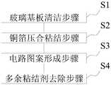
- Step S1transparent substrate cleaning step: cleaning and drying the transparent substrate 1;
- Step S2copper foil pressing and bonding step: coating adhesive 2 on the cleaned and dried transparent substrate 1; then pressing and bonding the copper foil 3 on the transparent substrate 1; preferably the copper
- the thickness of the foil 3is 6-105 microns.
- Step S3a circuit pattern forming step: the copper foil 3 is exposed, developed and etched to form a circuit pattern 30;
- Step S4the step of removing excess adhesive: removing the excess adhesive 2 on the circuit pattern 30.
- the cleaning of the transparent substrate 1needs to be completed.
- the transparent substrate 1can be purchased with a customized transparent substrate 1 of a specific specification, or a large transparent substrate 1 can be purchased, and then prepared by cutting, edging and other processes.
- the transparent substrate 1 of a specific specificationwhen cleaning and drying, the transparent substrate 1 can be cleaned by one or more of acid washing, alkali washing, and water washing, and then the cleaned transparent substrate 1 can be cleaned in a dust-free state dry.
- cleaningfor example, it can be washed by pickling or alkaline washing first, and then washed with pure water.
- fan or high-pressure gascan be used for purging during drying, and low-temperature heating and drying can also be used.
- step S2the copper foil 3 and the transparent substrate 1 need to be bonded by using an adhesive 2.
- the adhesiveis UV glue, which is also called shadowless glue, photosensitive glue, ultraviolet curing glue, etc.
- UVis the abbreviation of Ultraviolet Rays in English, that is, ultraviolet rays.
- the curing principle of the shadowless adhesiveis that the photoinitiator (or photosensitizer) in the UV curing material absorbs ultraviolet light and generates active free radicals or cations, which initiates monomer polymerization and cross-linking chemical reactions, so that the adhesive is Change from liquid to solid within a few seconds.
- UV gluewill be used as an example to introduce how to bond the copper foil 3 and the transparent substrate 1 and how to remove the excess adhesive 2 in the subsequent steps.
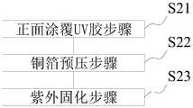
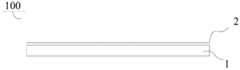
- Step S21the step of applying UV glue on the front side: as shown in FIG. 3, the adhesive 2 is UV glue, and the UV glue is coated on the front side of the transparent substrate 1 after cleaning and drying; in this example "Front" and “Back” are relative concepts.
- the front sideis coated with UV glue to bond the copper foil 3.
- the back sideWhen UV light is irradiated, the back side must be irradiated.
- the transparent substrate 1 after the UV glue is bondedis referred to as the glue-coated substrate 100;
- Step S22copper foil pre-pressing step: placing the copper foil 3 above the UV glue, and applying pressure on the copper foil 3 to pre-press the copper foil 3 on the transparent substrate 1;
- Step S23ultraviolet curing step: irradiate the UV glue from the back of the transparent substrate 1 with ultraviolet rays to cure the UV glue, and cure and bond the copper foil 3 and the transparent substrate 1.
- the transparent substrate 1 and the copper foil 3are bonded by UV glue, and the manufacturing process can be carried out at room temperature. Carrying out at room temperature can effectively simplify the process, have low requirements on the processing environment, reduce energy consumption, and reduce costs.
- this step S22is realized by placing the copper foil 3 on top of the UV glue, using a flat plate 4 in the direction indicated by the arrow in the figure, and then the copper foil 3 Pressure is applied from above to pre-press the copper foil 3 on the transparent substrate 1.
- the intermediateis named copper-clad substrate 200; in this example, as a preferred method,
- the ultraviolet light device 5emits ultraviolet rays to irradiate the UV glue from the back of the transparent substrate 1 until the UV glue is cured, and the copper foil 3 and the transparent substrate 1 are cured and bonded.
- step S23 and step S22are performed simultaneously, of course, step S22 and step S23 can also be performed sequentially.
- step S22 and step S23can also be performed sequentially.
- Step S3Regarding the formation method of the circuit pattern 30, it is a common method for forming a printed circuit board. It is known to the public and does not need to be specially introduced. It usually includes the following steps: covering the copper foil 3 of the copper-clad substrate 200 The photosensitive film is covered with a film film with circuit patterns on the photosensitive film, and then exposed, and then the unnecessary part of the copper foil is etched away by the solution, leaving the required circuit pattern 30.
- the transparent substrate 1that is, including the transparent substrate 1, the adhesive 2, and the circuit pattern 30
- the primary transparent circuit board 300the transparent substrate 1 (that is, including the transparent substrate 1, the adhesive 2, and the circuit pattern 30) after the circuit pattern 30 is formed is named the primary transparent circuit board 300.
- a softening solution 60is prepared in a softening tank 6.
- the softening solutioncan be a weak acid solution (but not limited to a weak acid solution). Soak in a weak acid solution for 35-50 minutes, and immerse the transparent substrate 1 (that is, the primary transparent circuit board 300) attached to form the circuit pattern 30 in the softening solution 60, and the adhesive will remain on the area where the copper foil 3 is etched away 20 gradually dissolves and softens and can be separated from the transparent substrate 1 (refer to FIG. 6 for this state); then a washing device 7 is used to rinse off the softened residual adhesive 20 on the area of the copper foil 3 to obtain a transparent LED circuit board 400. Alternatively, it is also conceivable to etch away the residual adhesive 20 after softening on the area of the copper foil 3 by scraping.
- UV glueis cleaner and more efficient. This method is suitable for large-number, large-area circuit panel operations, which improves production efficiency and requires lower equipment costs. At the same time, it also makes the size of the transparent panel that can be formed at one time larger, and is not limited by the machine stroke .
- the transparent substrate 1is tempered glass with a thickness of 2-10 mm.
- the circuit pattern 30can adopt methods known to those skilled in the art.
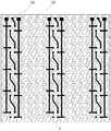
- the circuit pattern 30includes power supply pads 30b, signal pads 30c, and arrays. Arranged the lamp bead welding area where the LED lamp bead is installed;
- Each of the lamp bead welding areasis provided with a pin pad 30a corresponding to the pin of the LED lamp;
- the pin pad 30aincludes a signal pin pad and an electrode pin pad;
- Signal lines for signal transmissionare provided between the signal pad 30c and the signal pin pads in the lamp bead welding area, and between the signal pin pads in the adjacent lamp bead welding areas of the same row or the same column;
- the signal line between the signal pad 30c and the signal pin pad in the lamp bead welding areais marked as the first signal line 30e; among the signal pin pads in the adjacent lamp bead welding area in the same row or in the same column
- the signal line used for signal transmission in betweenis marked as the second signal line 30f; the control signal that controls the on and off of each LED lamp bead can be input from the signal pad 30c and then transmitted through each LED lamp bead in turn;
- the electrode pin pads on the lamp bead welding areaare electrically connected to the power supply pads 30b of the same polarity through the power supply line 30d.
- the method for preparing a transparent LED circuit boardcan form a circuit pattern 30 using copper as a conductive material on the transparent transparent substrate 1, which can meet the conductive requirements of higher-power electronic components, and at the same time ensure that the finished product has a better quality. High transparency, so it can meet the needs of transparent LED display.
- the circuit pattern 30 formed by this methodnot only allows the copper foil 3 and the transparent substrate 1 to be firmly bonded, but also can withstand the reflow temperature during the SMT processing of electronic components. After the high temperature reflow, the circuit pattern 30 and the transparent substrate 1 The adhesive force is still very stable and will not deform or fall off.
- the transparent substrate 1 and the copper foil 3are bonded by UV glue, and the manufacturing process can be carried out at room temperature.
- Carrying out at room temperaturecan effectively simplify the process, have low requirements on the processing environment, reduce energy consumption, and reduce costs.
- the UV gluecan be quickly bonded under the conditions of ultraviolet radiation, the bonding reliability is easy to judge, and the processing efficiency is high.
- This examplewill specifically explain the method for preparing the transparent LED display screen provided by the present application, including the following steps: preparing a transparent LED circuit board 400; installing LED lights on the transparent LED circuit board 400, and then packaging;
- the method for preparing the transparent LED circuit board 400is the method for preparing the transparent LED circuit board provided in Embodiment 1 above.
- the above-mentioned installation of the LED lampadopts the method of surface mount (English full name: Surface Mounted Technology; English abbreviation: SMT), and the reflow soldering temperature during the SMT process is limited to about 260 degrees, and the LED lamp is installed on the lamp bead soldering area. . Then, a waterproof protective layer can be formed on the transparent LED circuit board 400 after the LED is installed by potting and packaging, and then a protective cover plate is used for protection on the upper side.
- SMTSurface Mounted Technology
- a waterproof protective layercan be formed on the transparent LED circuit board 400 after the LED is installed by potting and packaging, and then a protective cover plate is used for protection on the upper side.
- the core pointlies in the preparation method of the transparent LED circuit board 400, and the rest of the subsequent packaging processes are known to the public, and the preparation method of the above-mentioned transparent LED circuit board 400 has been explained in the first embodiment. Therefore, I will not repeat it.
- a circuit pattern 30 using copper as a conductive materialcan be formed on the transparent transparent substrate 1, which can meet the requirements for the conductivity of relatively high-power electronic components. At the same time, it can also ensure that the finished product has high transparency, so it can meet the needs of transparent LED display.
- the circuit pattern 30 formed by this methodnot only allows the copper foil 3 and the transparent substrate 1 to be firmly bonded, but also can withstand the reflow temperature during the SMT processing of electronic components. After high temperature reflow, the circuit pattern 30 and the transparent substrate 1 The adhesive force is still very stable and will not deform or fall off. And the production process of this method can be carried out at room temperature.
- the transparent substrate 1 and the copper foil 3are bonded by UV glue, and the manufacturing process can be carried out at room temperature. Carrying out at room temperature can effectively simplify the process, have low requirements on the processing environment, reduce energy consumption, and reduce costs. At the same time, because the UV glue can be quickly bonded under the conditions of ultraviolet radiation, the bonding reliability is easy to judge, and the processing efficiency is high.
Landscapes
- Engineering & Computer Science (AREA)
- Manufacturing & Machinery (AREA)
- Microelectronics & Electronic Packaging (AREA)
- Physics & Mathematics (AREA)
- General Physics & Mathematics (AREA)
- Theoretical Computer Science (AREA)
- Manufacturing Of Printed Circuit Boards (AREA)
- Devices For Indicating Variable Information By Combining Individual Elements (AREA)
Abstract
Description
Translated fromChinese本申请以2020年5月7日提交的申请号为202010378108.X,名称为“一种透明LED电路板及透明LED显示屏的制备方法”的中国发明专利申请为基础,并要求其优先权。This application is based on the Chinese invention patent application filed on May 7, 2020 with the application number 202010378108.X, titled "A method for preparing a transparent LED circuit board and a transparent LED display screen", and claims its priority.
本申请涉及透明基板的印制电路板作为LED透明显示屏的技术领域。This application relates to the technical field of using a printed circuit board with a transparent substrate as a transparent LED display.
透明基板的印制电路一般应用在LCD显示屏领域,这种电路通过磁控溅射的方式在玻璃等透明基板上行成金属导电层,常见为镀铜层,然后再通过蚀刻的方式在透明基板上行成电路图案,这种导电层的厚度一般在纳米级别,导电电流很小。此外,还有使用ITO、纳米银、金属网格等导电材料、在玻璃基板上形成透明电路图案的方案,但这些电路图案的方阻很大,导电电流也很小,难以在电流需求很大的产品上使用。The printed circuit of the transparent substrate is generally used in the field of LCD display screens. This kind of circuit is formed into a metal conductive layer on a transparent substrate such as glass by magnetron sputtering, which is usually a copper plating layer, and then is etched on the transparent substrate. The upper line forms a circuit pattern. The thickness of this conductive layer is generally on the nanometer level, and the conductive current is very small. In addition, there are also plans to use conductive materials such as ITO, nano silver, and metal grids to form transparent circuit patterns on glass substrates. However, the square resistance of these circuit patterns is very large, and the conductive current is also very small. Used on the product.
比如,以透明玻璃为基板的透明LED电路板为例,安装在玻璃基板上的LED灯对电流的需求较大,一颗LED灯大约需要3~15mA(毫安)的驱动电流,一平米的LED显示屏上安装有1000~20000颗不等的LED灯,电流需求非常大,使用上述材料作为电路图案的技术难以满足这种大电流的导电需求,且制造成本较高,工艺较复杂。For example, taking the transparent LED circuit board with transparent glass as the substrate as an example, the LED lamp mounted on the glass substrate has a greater demand for current, and an LED lamp needs about 3-15mA (milliampere) driving current, which is about 1 square meter. There are 1000 to 20000 LED lights installed on the LED display screen, and the current demand is very large. The technology of using the above-mentioned materials as the circuit pattern is difficult to meet the large current conductive demand, and the manufacturing cost is relatively high, and the process is relatively complicated.
作为改进,有人提出了新的玻璃基板覆铜工艺,在玻璃基板上形成10-70微米厚度的覆铜层,以此来满足透明LED电路板的应用需求。该新工艺大致包括如下步骤:在玻璃基板上通过胶水粘接铜箔,然后蚀刻铜箔形成电路图案,对蚀刻掉铜箔的地方通过激光碳化的方式去除多余的胶水。该种方法很难让铜箔和玻璃板有效粘合,因为最终的电路图案上的线路很窄(0.1-0.5mm线宽),再加上SMT(表面贴装)加工期间需要加到高温260度左右,胶水很难保证铜箔和玻璃的有效粘合。同时,胶水与玻璃基板有效粘合的时间和条件也难以把握。As an improvement, some people have proposed a new glass substrate copper-clad process to form a 10-70 micron copper-clad layer on the glass substrate to meet the application requirements of transparent LED circuit boards. The new process roughly includes the following steps: bonding copper foil on a glass substrate with glue, then etching the copper foil to form a circuit pattern, and removing excess glue from the place where the copper foil is etched away by laser carbonization. This method is difficult to effectively bond the copper foil and the glass plate, because the circuit pattern on the final circuit pattern is very narrow (0.1-0.5mm line width), and the high temperature of 260 is required during SMT (surface mount) processing. It is difficult for glue to ensure the effective adhesion of copper foil and glass. At the same time, the time and conditions for the effective bonding of the glue and the glass substrate are also difficult to grasp.
发明内容Summary of the invention
为克服现有技术中的透明LED电路板制备方法存在的铜箔形成的电路图案与透明基板的粘合度差,容易从透明基板上脱落,胶水与玻璃基板有效粘合的时间和条件也难以把握的问题,本申请提供了一种透明LED电路板及透明LED显示屏的制备方法。In order to overcome the poor adhesion between the circuit pattern formed by the copper foil and the transparent substrate in the preparation method of the transparent LED circuit board in the prior art, it is easy to fall off from the transparent substrate, and the time and conditions for the effective adhesion of the glue and the glass substrate are also difficult. To grasp the problem, this application provides a method for preparing a transparent LED circuit board and a transparent LED display screen.
本申请一方面提供一种透明LED电路板制备方法,包括如下步骤:One aspect of this application provides a method for preparing a transparent LED circuit board, which includes the following steps:
清洁及干燥透明基板;Clean and dry the transparent substrate;
在清洁及干燥后的所述透明基板的正面上涂覆粘结剂,所述粘结剂为UV胶;将所述铜箔置于所述UV胶的上方,并在铜箔上施加压力,将铜箔预压在所述透明基板上;使用紫外线从透明基板的背面照射UV胶,使所述UV胶固化,将所述铜箔和所述透明基板固化粘接;Coat the cleaned and dried front surface of the transparent substrate with an adhesive, the adhesive is UV glue; put the copper foil on top of the UV glue, and apply pressure on the copper foil, Pre-pressing the copper foil on the transparent substrate; using ultraviolet rays to irradiate the UV glue from the back of the transparent substrate, curing the UV glue, and curing and bonding the copper foil and the transparent substrate;
将所述铜箔进行曝光显影蚀刻,形成电路图案;Exposing, developing and etching the copper foil to form a circuit pattern;
去除所述电路图案上多余的粘结剂。Remove excess adhesive on the circuit pattern.
本申请提供的透明LED电路板制备方法,可以在透明的透明基板上形成以铜为导电材料的电路图案,可以满足较大功率的电子元器件的导电需求,同时还能保证成品有较高的透明度,因此可满足透明LED显示屏的使用需求。本方法形成的电路图案,不仅让铜箔和透明基板粘合稳固,还能耐受电子元器件SMT加工过程中的回流焊温度,经过高温回流焊之后电路图案与透明基板的粘合力仍然非常稳固,不变形不脱落。采用UV胶黏结透明基板和铜箔,其制作过程在常温下就可以进行。常温下进行可以有效简化工艺,对加工环境要求不高,减少能耗,降低成本。同时,因为UV胶在紫外线的照射条件下能够迅速粘合,粘合可靠度容易判断,加工效率很高。The method for preparing a transparent LED circuit board provided by the present application can form a circuit pattern using copper as a conductive material on a transparent transparent substrate, which can meet the conductivity requirements of higher-power electronic components, and at the same time ensure that the finished product has a higher Transparency, so it can meet the needs of transparent LED display. The circuit pattern formed by this method not only allows the copper foil and the transparent substrate to be firmly bonded, but also can withstand the reflow temperature during the SMT processing of electronic components. After high temperature reflow, the adhesion between the circuit pattern and the transparent substrate is still very good. It is stable, does not deform or fall off. The transparent substrate and copper foil are bonded by UV glue, and the manufacturing process can be carried out at room temperature. Carrying out at room temperature can effectively simplify the process, have low requirements on the processing environment, reduce energy consumption, and reduce costs. At the same time, because the UV glue can be quickly bonded under the conditions of ultraviolet radiation, the bonding reliability is easy to judge, and the processing efficiency is high.
进一步地,所述“去除所述电路图案上多余的粘结剂”具体包括如下步骤:Further, the "removing excess adhesive on the circuit pattern" specifically includes the following steps:
将附着形成电路图案的透明基板浸泡在软化液中,将蚀刻掉所述铜箔的区域上残留粘结剂逐渐溶解软化并可脱离透明基板;然后去除蚀刻掉所述铜箔的区域上软化以后的残留粘结剂。采用软化液对多余的UV胶进行溶解软化并可脱离透明基板,然后再去除多余UV胶,其处理UV胶更加干净,效率更高。Soak the transparent substrate with the circuit pattern attached to it in a softening solution, and gradually dissolve and soften the remaining adhesive on the area where the copper foil is etched away, and can be separated from the transparent substrate; then remove the area where the copper foil is etched away and soften it Residual binder. The softening solution is used to dissolve and soften the excess UV glue and can be separated from the transparent substrate, and then remove the excess UV glue, which makes the UV glue treatment cleaner and more efficient.
进一步地,所述“清洁及干燥透明基板”步骤具体包括如下步骤:Further, the step of "cleaning and drying the transparent substrate" specifically includes the following steps:
将所述透明基板通过酸洗、碱洗、水洗中的一种或多种进行清洁,然后将清洁后的透明基板在无尘状态下进行干燥。The transparent substrate is cleaned by one or more of acid washing, alkali washing, and water washing, and then the cleaned transparent substrate is dried in a dust-free state.
进一步地,所述“将所述铜箔置于所述UV胶的上方,并在铜箔上施加压力,将铜箔预压在所述透明基板上”具体包括如下步骤:Further, the "place the copper foil above the UV glue, apply pressure on the copper foil, and pre-press the copper foil on the transparent substrate" specifically includes the following steps:
将所述铜箔置于所述UV胶的上方,在铜箔上方使用平板重物进行压合,将铜箔预压在所述透明基板上。Place the copper foil on top of the UV glue, use a flat plate weight to press the copper foil on top of the copper foil, and pre-press the copper foil on the transparent substrate.
进一步地,所述“将所述铜箔进行曝光显影蚀刻,形成电路图案”具体包括如下步骤:Further, the "exposing the copper foil to exposure, developing and etching to form a circuit pattern" specifically includes the following steps:
在所述铜箔上覆盖感光膜,再将有电路图形的菲林胶片覆盖在所述感光膜上,再进行曝光,然后再进行蚀刻处理,通过溶液蚀刻掉铜箔不需要的部分,留下所需要的电路图案。Cover the photosensitive film on the copper foil, and then cover the film film with circuit patterns on the photosensitive film, and then expose, and then perform an etching process. The unnecessary part of the copper foil is etched by the solution, leaving all The required circuit pattern.
进一步地,所述“去除蚀刻掉所述铜箔的区域上软化以后的残留粘结剂”具体为如下步骤:Further, the “removing the softened residual adhesive on the area where the copper foil is etched away” specifically includes the following steps:
采用刮除的方式去掉所述铜箔的区域上软化以后的残留粘结剂;或者采用冲洗装置冲洗掉所述铜箔的区域上软化以后的残留粘结剂。A scraping method is used to remove the softened residual adhesive on the copper foil area; or a washing device is used to rinse the softened residual adhesive on the copper foil area.
进一步地,所述铜箔厚度为6-105微米。Further, the thickness of the copper foil is 6-105 microns.
进一步地,所述透明基板为钢化玻璃或者透明塑料基板,其厚度为2-10mm。Further, the transparent substrate is a tempered glass or a transparent plastic substrate with a thickness of 2-10 mm.
进一步地,所述电路图案包括电源焊盘、信号焊盘及成阵列布置的安装LED灯珠的灯珠焊区;Further, the circuit pattern includes power supply pads, signal pads, and lamp bead welding areas for mounting LED lamp beads arranged in an array;
每个所述灯珠焊区上设有与LED灯的引脚相对应的引脚焊盘;所述引脚焊盘包括信号引脚焊盘和电极引脚焊盘;Each of the lamp bead welding areas is provided with a pin pad corresponding to the pin of the LED lamp; the pin pad includes a signal pin pad and an electrode pin pad;
所述信号焊盘与灯珠焊区内信号引脚焊盘之间、及同行或者同列的相邻灯珠焊区内的信号引脚焊盘之间设置有用于信号传输的信号线;使得控制各LED灯珠亮灭的控制信号可以从信号焊盘输入后经各LED灯珠依次传输;A signal line for signal transmission is provided between the signal pad and the signal pin pad in the lamp bead welding area, and between the signal pin pads in the same or the same row of adjacent lamp bead welding areas; The control signal for each LED lamp bead to turn on and off can be transmitted sequentially through each LED lamp bead after being input from the signal pad;
将所述灯珠焊区上的所述电极引脚焊盘与同极性的电源焊盘通过电源线电连接。The electrode pin pads on the lamp bead welding area are electrically connected to the power supply pads of the same polarity through a power supply line.
本申请第二方面提供一种透明LED显示屏制备方法,包括如下步骤:制备透明LED电路板;在所述透明LED电路板上安装LED灯,然后进行封装;A second aspect of the present application provides a method for preparing a transparent LED display screen, which includes the following steps: preparing a transparent LED circuit board; mounting an LED lamp on the transparent LED circuit board, and then packaging;
其中,所述制备透明LED电路板的方法上述的透明LED电路板制备方法。Wherein, the method for preparing a transparent LED circuit board is the above-mentioned method for preparing a transparent LED circuit board.
本申请提供的透明LED显示屏制备方法,其制备透明LED电路板时,可以在透明的透明基板上形成以铜为导电材料的电路图案,可以满足较大功率的电子元器件的导电需求,同时还能保证成品有较高的透明度,因此可满足透明LED显示屏的使用需求。本方法形成的电路图案,不仅让铜箔和透明基板粘合稳固, 还能耐受电子元器件SMT加工过程中的回流焊温度,经过高温回流焊之后电路图案与透明基板的粘合力仍然非常稳固,不变形不脱落。采用UV胶黏结透明基板和铜箔,其制作过程在常温下就可以进行。常温下进行可以有效简化工艺,对加工环境要求不高,减少能耗,降低成本。同时,因为UV胶在紫外线的照射条件下能够迅速粘合,粘合可靠度容易判断,加工效率很高。The method for preparing a transparent LED display screen provided by the present application can form a circuit pattern using copper as a conductive material on a transparent transparent substrate when preparing a transparent LED circuit board, which can meet the conductive requirements of higher-power electronic components, and at the same time It can also ensure that the finished product has high transparency, so it can meet the needs of transparent LED display. The circuit pattern formed by this method not only allows the copper foil to be firmly bonded to the transparent substrate, but also can withstand the reflow temperature during the SMT processing of electronic components. After high temperature reflow, the adhesion between the circuit pattern and the transparent substrate is still very good. It is stable, does not deform or fall off. The transparent substrate and copper foil are bonded by UV glue, and the manufacturing process can be carried out at room temperature. Carrying out at room temperature can effectively simplify the process, have low requirements on the processing environment, reduce energy consumption, and reduce costs. At the same time, because the UV glue can be quickly bonded under the conditions of ultraviolet radiation, the bonding reliability is easy to judge, and the processing efficiency is high.
图1是本申请具体实施方式中提供的透明LED电路板制备流程图;FIG. 1 is a preparation flow chart of the transparent LED circuit board provided in the specific embodiment of the present application;
图2是图1中步骤S2的优化流程图;FIG. 2 is an optimization flowchart of step S2 in FIG. 1;
图3是本申请具体实施方式中提供的在透明基板上涂覆粘结剂的示意图;Fig. 3 is a schematic diagram of coating an adhesive on a transparent substrate provided in a specific embodiment of the present application;
图4是本申请具体实施方式中提供的将铜箔通过辊轮压合在透明基板上并通过紫外光固化的示意图;4 is a schematic diagram of pressing copper foil on a transparent substrate through a roller and curing by ultraviolet light provided in the specific embodiment of the present application;
图5是本申请具体实施方式中提供的去除残留粘结剂的示意图;FIG. 5 is a schematic diagram of removing residual binder provided in a specific embodiment of the present application;
图6是本申请具体实施方式中提供的软化残留粘结剂后的初级透明电路板的俯视示意图;6 is a schematic top view of the primary transparent circuit board after softening the residual adhesive provided in the specific embodiment of the present application;
图7是本申请具体实施方式中提供的去除软化残留粘结剂后的透明LED电路板的俯视示意图;7 is a schematic top view of the transparent LED circuit board after removing the softened residual adhesive provided in the specific embodiment of the present application;
图8为图7中A处放大示意图。Fig. 8 is an enlarged schematic diagram of A in Fig. 7.
其中,1、透明基板;2、粘结剂;3、铜箔;4、平板;5、紫外光照装置;6、软化箱;7、冲洗装置;Among them, 1. Transparent substrate; 2. Adhesive; 3. Copper foil; 4. Plate; 5. Ultraviolet light device; 6. Softening box; 7. Washing device;
20、残留粘结剂;30、电路图案;60、软化液;20. Residual adhesive; 30. Circuit pattern; 60. Softening fluid;
100、涂胶基板;200、覆铜基板;300、初级透明电路板;400、透明LED电路板;100. Glue-coated substrate; 200. Copper-clad substrate; 300. Primary transparent circuit board; 400. Transparent LED circuit board;
30a、引脚焊盘;30b、电源焊盘;30c、信号焊盘;30d、电源线;30e、第一信号线;30f、第二信号线。30a, pin pad; 30b, power pad; 30c, signal pad; 30d, power line; 30e, first signal line; 30f, second signal line.
为了使本申请所解决的技术问题、技术方案及有益效果更加清楚明白,以下结合附图及实施例,对本申请进行进一步详细说明。应当理解,此处所描述的具体实施例仅仅用以解释本申请,并不用于限定本申请。In order to make the technical problems, technical solutions, and beneficial effects solved by the present application clearer, the following further describes the present application in detail with reference to the accompanying drawings and embodiments. It should be understood that the specific embodiments described here are only used to explain the present application, and are not used to limit the present application.
在本申请的描述中,需要理解的是,术语“纵向”、“径向”、“长度”、“宽 度”、“厚度”、“上”、“下”、“前”、“后”、“左”、“右”、“竖直”、“水平”、“顶”、“底”“内”、“外”等指示的方位或位置关系为基于附图所示的方位或位置关系,仅是为了便于描述本申请和简化描述,而不是指示或暗示所指的装置或元件必须具有特定的方位、以特定的方位构造和操作,因此不能理解为对本申请的限制。在本申请的描述中,除非另有说明,“多个”的含义是两个或两个以上。In the description of this application, it should be understood that the terms "longitudinal", "radial", "length", "width", "thickness", "upper", "lower", "front", "rear", The orientation or positional relationship indicated by "left", "right", "vertical", "horizontal", "top", "bottom", "inner", "outer", etc. are based on the orientation or positional relationship shown in the drawings, It is only for the convenience of describing the application and simplifying the description, rather than indicating or implying that the device or element referred to must have a specific orientation, be constructed and operated in a specific orientation, and therefore cannot be construed as a limitation of the application. In the description of this application, unless otherwise specified, "plurality" means two or more.
在本申请的描述中,需要说明的是,除非另有明确的规定和限定,术语“安装”、“相连”、“连接”应做广义理解,例如,可以是固定连接,也可以是可拆卸连接,或一体地连接;可以是机械连接,也可以是电连接;可以是直接相连,也可以通过中间媒介间接相连,可以是两个元件内部的连通。对于本领域的普通技术人员而言,可以具体情况理解上述术语在本申请中的具体含义。In the description of this application, it should be noted that the terms "installation", "connection", and "connection" should be understood in a broad sense, unless otherwise clearly specified and limited. For example, it can be a fixed connection or a detachable connection. Connected or integrally connected; it can be a mechanical connection or an electrical connection; it can be directly connected or indirectly connected through an intermediate medium, and it can be the internal communication between two components. For those of ordinary skill in the art, the specific meanings of the above terms in this application can be understood under specific circumstances.
实施例1Example 1
本例将对本申请提供的透明LED电路板制备方法进行具体解释说明,如图1所示,包括如下步骤:This example will specifically explain the method for preparing the transparent LED circuit board provided by this application, as shown in Figure 1, including the following steps:
步骤S1、透明基板清洁步骤:清洁及干燥透明基板1;Step S1, transparent substrate cleaning step: cleaning and drying the
步骤S2、铜箔压合粘结步骤:在清洁及干燥后的所述透明基板1上涂覆粘结剂2;然后将铜箔3压合粘结在所述透明基板1上;优选该铜箔3的厚度为6-105微米。Step S2, copper foil pressing and bonding step: coating adhesive 2 on the cleaned and dried
步骤S3、电路图案形成步骤:将所述铜箔3进行曝光显影蚀刻,形成电路图案30;Step S3, a circuit pattern forming step: the
步骤S4、多余粘结剂去除步骤:去除所述电路图案30上多余的粘结剂2。Step S4, the step of removing excess adhesive: removing the
下边一一对各步骤进行具体解释说明。A detailed explanation of each step is given below.
在步骤S1中,需要完成对透明基板1的清洗,通常透明基板1可以采购定制特定规格的透明基板1,或者可以采购到大块的透明基板1后,再经切割、磨边等工序制备获得特定规格的透明基板1;清洗干燥时,可以将所述透明基板1通过酸洗、碱洗、水洗中的一种或多种进行清洁,然后将清洁后的透明基板1在无尘状态下进行干燥。清洗时,比如可以先采用酸洗、碱洗洗过后,再经纯净水进行水洗,作为优选的方式,干燥时一方面可以采用风扇或者高压气体进行吹扫,还可以进行低温加热烘干等。In step S1, the cleaning of the
步骤S2中,需要通过使用粘结剂2将铜箔3和透明基板1进行粘接,粘接剂为UV胶,UV胶又称无影胶、光敏胶、紫外光固化胶等,是一种必须通过 紫外光线照射才能固化的一类胶粘剂,它可以作为粘接剂使用,也可作为油漆、涂料、油墨等的胶料使用。UV是英文Ultraviolet Rays的缩写,即紫外光线。无影胶固化原理是UV固化材料中的光引发剂(或光敏剂)在紫外线的照射下吸收紫外光后产生活性自由基或阳离子,引发单体聚合、交联化学反应,使粘合剂在数秒钟内由液态转化为固态。本例中将以UV胶为例,介绍如何将铜箔3和透明基板1进行粘接,以及在后续步骤中如何去除多余的粘结剂2。In step S2, the
如图2所示,具体包括如下步骤:As shown in Figure 2, it specifically includes the following steps:
步骤S21、正面涂覆UV胶步骤:如图3所示,所述粘结剂2为UV胶,在清洁及干燥后的所述透明基板1的正面上涂覆所述UV胶;本例中的“正面”、“背面”是相对的概念,正面涂覆UV胶用来粘接铜箔3,则在进行紫外光线照射时,必须从其背面进行照射。如图中所示,将粘接UV胶后的透明基板1称为涂胶基板100;Step S21, the step of applying UV glue on the front side: as shown in FIG. 3, the adhesive 2 is UV glue, and the UV glue is coated on the front side of the
步骤S22、铜箔预压步骤:将所述铜箔3置于所述UV胶的上方,并在铜箔3上施加压力,将铜箔3预压在所述透明基板1上;Step S22, copper foil pre-pressing step: placing the
步骤S23、紫外固化步骤:使用紫外线从透明基板1的背面照射UV胶,使所述UV胶固化,将所述铜箔3和所述透明基板1固化粘接。Step S23, ultraviolet curing step: irradiate the UV glue from the back of the
采用UV胶黏结透明基板1和铜箔3,其制作过程在常温下就可以进行。常温下进行可以有效简化工艺,对加工环境要求不高,减少能耗,降低成本。The
本例中,如图4所示,该步骤S22通过如下方式实现,将所述铜箔3置于所述UV胶的上方,使用平板4在如图中箭头所示方向再所述铜箔3上方施加压力,将铜箔3预压在所述透明基板1上。得到如图示中标记的包含有铜箔3、UV胶和透明基板1的中间体,为区别起见,将该中间体命名为覆铜基板200;本例中,作为优选的方式,在压合的同时,通过紫外光照装置5发射紫外线从所述透明基板1的背面照射UV胶直到UV胶固化,将所述铜箔3和所述透明基板1固化粘接。也即步骤S23与步骤S22同时进行,当然步骤S22和步骤S23也可先后进行。为了让压合后避免在铜箔3和透明基板1之间产生气泡,将压合工艺放在真空环境下进行效果更佳。In this example, as shown in FIG. 4, this step S22 is realized by placing the
步骤S3关于电路图案30的形成方法,为常见印制电路板的形成方法,其为公众所知,无需做特别介绍,其通常包括如下步骤:在所述覆铜基板200的铜箔3上覆盖感光膜,再将有电路图形的菲林胶片覆盖在所述感光膜上,再进行曝光,然后通过溶液蚀刻掉铜箔不需要的部分,留下所需要的电路图案30。 为区别起见,形成电路图案30后的透明基板1(即包括透明基板1、粘结剂2、电路图案30)命名为初级透明电路板300。Step S3 Regarding the formation method of the
步骤S4中进行多余粘结剂2去除的方法如图5中所示,首先,在一软化箱6中准备软化液60,软化液可以为弱酸性溶液(但并不限定弱酸性溶液),使用弱酸性溶液浸泡35-50分钟,将附着形成电路图案30的透明基板1(也即初级透明电路板300)浸泡在软化液60中,将蚀刻掉所述铜箔3的区域上残留粘结剂20逐渐溶解软化并可脱离透明基板1(此种状态可参考图6);然后采用冲洗装置7进行冲洗掉所述铜箔3的区域上软化以后的残留粘结剂20,得到透明LED电路板400。或者,也可考虑用刮除蚀刻掉所述铜箔3的区域上软化以后的残留粘结剂20。The method for removing the
申请人也曾尝试是否可以直接采用激光高温碳化的方式对多余的粘结剂2进行去除,但结果发现该种方式存在较多的问题:1、需要全面积激光扫描,效率低。2、激光设备照射范围有限制,很难大面积扫射;3、激光在碳化胶水的同时也容易将胶固化在玻璃上,难以清除。因此该种方式不可取。采用本申请中提到的通过软化液进行软化后,其结果如图6中的状态一样,容易起皮脱离透明基板1,此时再通过刮除或者冲洗等方式,再进行多余的残留粘结剂20进行去除时,就很容易去除多余的残留粘结剂。其处理UV胶更加干净,效率更高。此方法适合多数量、大面积线路面板作业,提高了生产效率,所需的设备成本更低,同时,也使得所制作的可一次性成形的透明面板尺寸更大,不受机台行程的限制。The applicant has also tried whether it is possible to directly use laser high-temperature carbonization to remove the
本例中,所述透明基板1为钢化玻璃,其厚度为2-10mm。In this example, the
本例中,电路图案30可以采用本领域技术人员所公知的方式,比如,作为举例,如图6-图8所示,所述电路图案30包括电源焊盘30b、信号焊盘30c及成阵列布置的安装LED灯珠的灯珠焊区;In this example, the
每个所述灯珠焊区上设有与LED灯的引脚相对应的引脚焊盘30a;所述引脚焊盘30a包括信号引脚焊盘和电极引脚焊盘;Each of the lamp bead welding areas is provided with a
所述信号焊盘30c与灯珠焊区内信号引脚焊盘之间、及同行或者同列的相邻灯珠焊区内的信号引脚焊盘之间设置有用于信号传输的信号线;为区别起见,将信号焊盘30c与灯珠焊区内信号引脚焊盘之间的信号线标记为第一信号线30e;同行或者同列的相邻灯珠焊区内的信号引脚焊盘之间用于信号传输的信号线标记为第二信号线30f;将使得控制各LED灯珠亮灭的控制信号可以从信号 焊盘30c输入后经各LED灯珠依次传输;Signal lines for signal transmission are provided between the
将所述灯珠焊区上的所述电极引脚焊盘与同极性的电源焊盘30b通过电源线30d电连接。The electrode pin pads on the lamp bead welding area are electrically connected to the
本申请提供的透明LED电路板制备方法,可以在透明的透明基板1上形成以铜为导电材料的电路图案30,可以满足较大功率的电子元器件的导电需求,同时还能保证成品有较高的透明度,因此可满足透明LED显示屏的使用需求。本方法形成的电路图案30,不仅让铜箔3和透明基板1粘合稳固,还能耐受电子元器件SMT加工过程中的回流焊温度,经过高温回流焊之后电路图案30与透明基板1的粘合力仍然非常稳固,不变形不脱落。采用UV胶黏结透明基板1和铜箔3,其制作过程在常温下就可以进行。常温下进行可以有效简化工艺,对加工环境要求不高,减少能耗,降低成本。同时,因为UV胶在紫外线的照射条件下能够迅速粘合,粘合可靠度容易判断,加工效率很高。The method for preparing a transparent LED circuit board provided in the present application can form a
实施例2Example 2
本例将对本申请提供的透明LED显示屏制备方法进行具体解释说明,包括如下步骤:制备透明LED电路板400;在所述透明LED电路板400上安装LED灯,然后进行封装;This example will specifically explain the method for preparing the transparent LED display screen provided by the present application, including the following steps: preparing a transparent
其中,所述制备透明LED电路板400的方法为上述实施例1中提供的透明LED电路板制备方法。Wherein, the method for preparing the transparent
上述安装LED灯通过采用表面贴装(英文全称:Surface Mounted Technology;英文简写:SMT)的方法,在SMT加工过程中的回流焊温度限定在约260度,将LED灯安装在灯珠焊区上。然后还可通过灌胶封装,在安装LED后的透明LED电路板400上形成防水保护层,再在上方采用保护盖板进行保护。The above-mentioned installation of the LED lamp adopts the method of surface mount (English full name: Surface Mounted Technology; English abbreviation: SMT), and the reflow soldering temperature during the SMT process is limited to about 260 degrees, and the LED lamp is installed on the lamp bead soldering area. . Then, a waterproof protective layer can be formed on the transparent
因本例中,其核心要点在于透明LED电路板400的制备方法,其余后续封装工艺等均为公众所知,且上述透明LED电路板400的制备方法已在实施例1中进行解释说明。因此,不再赘述。Because in this example, the core point lies in the preparation method of the transparent
本申请提供的透明LED显示屏制备方法,其制备透明LED电路板400时,可以在透明的透明基板1上形成以铜为导电材料的电路图案30,可以满足较大功率的电子元器件的导电需求,同时还能保证成品有较高的透明度,因此可满足透明LED显示屏的使用需求。本方法形成的电路图案30,不仅让铜箔3和透明基板1粘合稳固,还能耐受电子元器件SMT加工过程中的回流焊温度,经过 高温回流焊之后电路图案30与透明基板1的粘合力仍然非常稳固,不变形不脱落。且本方法的制作过程在常温下就可以进行。采用UV胶黏结透明基板1和铜箔3,其制作过程在常温下就可以进行。常温下进行可以有效简化工艺,对加工环境要求不高,减少能耗,降低成本。同时,因为UV胶在紫外线的照射条件下能够迅速粘合,粘合可靠度容易判断,加工效率很高。The method for preparing a transparent LED display screen provided in the present application, when preparing a transparent
以上所述仅为本申请的较佳实施例而已,并不用以限制本申请,凡在本申请的精神和原则之内所作的任何修改、等同替换和改进等,均应包含在本申请的保护范围之内。The above descriptions are only the preferred embodiments of this application and are not intended to limit this application. Any modification, equivalent replacement and improvement made within the spirit and principle of this application shall be included in the protection of this application. Within range.
Claims (10)
Translated fromChineseApplications Claiming Priority (2)
| Application Number | Priority Date | Filing Date | Title |
|---|---|---|---|
| CN202010378108.X | 2020-05-07 | ||
| CN202010378108.XACN113630982A (en) | 2020-05-07 | 2020-05-07 | Transparent LED circuit board and preparation method of transparent LED display screen |
Publications (1)
| Publication Number | Publication Date |
|---|---|
| WO2021223286A1true WO2021223286A1 (en) | 2021-11-11 |
Family
ID=78376877
Family Applications (1)
| Application Number | Title | Priority Date | Filing Date |
|---|---|---|---|
| PCT/CN2020/095088CeasedWO2021223286A1 (en) | 2020-05-07 | 2020-06-09 | Transparent led circuit board, and method for preparing transparent led display screen |
Country Status (2)
| Country | Link |
|---|---|
| CN (1) | CN113630982A (en) |
| WO (1) | WO2021223286A1 (en) |
Cited By (4)
| Publication number | Priority date | Publication date | Assignee | Title |
|---|---|---|---|---|
| CN114566397A (en)* | 2022-03-16 | 2022-05-31 | 立胜汽车科技(苏州)有限公司 | Method for eliminating assembly error of travel switch |
| CN115209634A (en)* | 2022-07-01 | 2022-10-18 | 上海太古达视光电科技有限公司 | High-stability ultra-soft transparent display screen and production process |
| CN115287028A (en)* | 2022-07-04 | 2022-11-04 | 李小源 | Pressure-sensitive UV (ultraviolet) insulating glue solution and preparation method and application thereof |
| CN115568102A (en)* | 2022-10-26 | 2023-01-03 | 广东省晶虹达科技有限公司 | Transparent circuit board and manufacturing method thereof |
Families Citing this family (1)
| Publication number | Priority date | Publication date | Assignee | Title |
|---|---|---|---|---|
| CN114639309A (en)* | 2021-12-23 | 2022-06-17 | 蚌埠晶显科技有限公司 | Flexible transparent display screen and manufacturing method thereof |
Citations (9)
| Publication number | Priority date | Publication date | Assignee | Title |
|---|---|---|---|---|
| CN103582285A (en)* | 2012-07-31 | 2014-02-12 | 厦门中天启航电子科技有限公司 | ITO electric conducting film current converging electrode and manufacturing method thereof |
| CN104244599A (en)* | 2013-06-24 | 2014-12-24 | 吴晓琴 | Manufacturing method for printed circuit board |
| CN104411103A (en)* | 2014-05-31 | 2015-03-11 | 福州大学 | Manufacturing method of graphical thick film silver paste conducting layer |
| CN109661101A (en)* | 2019-01-29 | 2019-04-19 | 深圳市鑫世佳电子科技有限公司 | A kind of opaque line plate and preparation method thereof |
| CN110012610A (en)* | 2019-03-14 | 2019-07-12 | 华东师范大学 | A kind of preparation method of flexible transparent circuit board |
| CN110225664A (en)* | 2019-05-09 | 2019-09-10 | 深圳市昱谷科技有限公司 | A kind of glass base heat conducting circuit board |
| JP6620464B2 (en)* | 2015-08-26 | 2019-12-18 | 大日本印刷株式会社 | Flexible transparent substrate and see-through type LED display device using the same |
| CN110637345A (en)* | 2017-09-19 | 2019-12-31 | 株式会社Lg化学 | Electrode substrate for transparent light-emitting device display and manufacturing method thereof |
| CN110798968A (en)* | 2019-12-06 | 2020-02-14 | 北京万物皆媒科技有限公司 | Transparent circuit board and manufacturing method |
Family Cites Families (3)
| Publication number | Priority date | Publication date | Assignee | Title |
|---|---|---|---|---|
| US8205327B2 (en)* | 2005-11-21 | 2012-06-26 | Panasonic Corporation | Method for manufacturing circuit board on which electronic component is mounted |
| AT14563U1 (en)* | 2014-03-31 | 2016-01-15 | At&S Austria Technologie & Systemtechnik Ag | Method for producing a printed circuit board with at least one optoelectronic component |
| CN109327973A (en)* | 2018-11-19 | 2019-02-12 | 广东合通建业科技股份有限公司 | UV membrane system is removed to silk screen printing circuit board |
- 2020
- 2020-05-07CNCN202010378108.XApatent/CN113630982A/enactivePending
- 2020-06-09WOPCT/CN2020/095088patent/WO2021223286A1/ennot_activeCeased
Patent Citations (9)
| Publication number | Priority date | Publication date | Assignee | Title |
|---|---|---|---|---|
| CN103582285A (en)* | 2012-07-31 | 2014-02-12 | 厦门中天启航电子科技有限公司 | ITO electric conducting film current converging electrode and manufacturing method thereof |
| CN104244599A (en)* | 2013-06-24 | 2014-12-24 | 吴晓琴 | Manufacturing method for printed circuit board |
| CN104411103A (en)* | 2014-05-31 | 2015-03-11 | 福州大学 | Manufacturing method of graphical thick film silver paste conducting layer |
| JP6620464B2 (en)* | 2015-08-26 | 2019-12-18 | 大日本印刷株式会社 | Flexible transparent substrate and see-through type LED display device using the same |
| CN110637345A (en)* | 2017-09-19 | 2019-12-31 | 株式会社Lg化学 | Electrode substrate for transparent light-emitting device display and manufacturing method thereof |
| CN109661101A (en)* | 2019-01-29 | 2019-04-19 | 深圳市鑫世佳电子科技有限公司 | A kind of opaque line plate and preparation method thereof |
| CN110012610A (en)* | 2019-03-14 | 2019-07-12 | 华东师范大学 | A kind of preparation method of flexible transparent circuit board |
| CN110225664A (en)* | 2019-05-09 | 2019-09-10 | 深圳市昱谷科技有限公司 | A kind of glass base heat conducting circuit board |
| CN110798968A (en)* | 2019-12-06 | 2020-02-14 | 北京万物皆媒科技有限公司 | Transparent circuit board and manufacturing method |
Cited By (5)
| Publication number | Priority date | Publication date | Assignee | Title |
|---|---|---|---|---|
| CN114566397A (en)* | 2022-03-16 | 2022-05-31 | 立胜汽车科技(苏州)有限公司 | Method for eliminating assembly error of travel switch |
| CN115209634A (en)* | 2022-07-01 | 2022-10-18 | 上海太古达视光电科技有限公司 | High-stability ultra-soft transparent display screen and production process |
| CN115287028A (en)* | 2022-07-04 | 2022-11-04 | 李小源 | Pressure-sensitive UV (ultraviolet) insulating glue solution and preparation method and application thereof |
| CN115287028B (en)* | 2022-07-04 | 2024-08-02 | 李小源 | Pressure-sensitive UV insulation glue solution and preparation method and application thereof |
| CN115568102A (en)* | 2022-10-26 | 2023-01-03 | 广东省晶虹达科技有限公司 | Transparent circuit board and manufacturing method thereof |
Also Published As
| Publication number | Publication date |
|---|---|
| CN113630982A (en) | 2021-11-09 |
Similar Documents
| Publication | Publication Date | Title |
|---|---|---|
| WO2021223286A1 (en) | Transparent led circuit board, and method for preparing transparent led display screen | |
| JP2665134B2 (en) | Flexible circuit board and method of manufacturing the same | |
| CN106201041A (en) | A kind of touch screen preparation method | |
| TWI538590B (en) | Printed circuit board and method for manufacturing same | |
| JP2004326108A (en) | Electromagnetic wave shielding filter for plasma display panel and method of manufacturing the same | |
| JP4650812B2 (en) | Display filter, method for manufacturing the same, and method for manufacturing the display | |
| WO2015018101A1 (en) | Method and device for stripping photoresist layer | |
| CN102880370A (en) | Touch inductor for capacitive touch screen with film structure and manufacturing method thereof | |
| CN111739902B (en) | A transfer device and transfer method for micro light-emitting unit | |
| CN104090392B (en) | A kind of manufacture method of the ITO heating plates for large area LCD screen | |
| WO2025055248A1 (en) | Micro-led chip and integration method therefor | |
| CN117572701A (en) | Display module and manufacturing method thereof | |
| CN111526669B (en) | Transparent circuit board and manufacturing method of transparent LED display screen | |
| JP2009038057A5 (en) | ||
| KR101325086B1 (en) | Light emitting diode module and anufacturing method thereof | |
| CN112752413B (en) | Transparent LED circuit board and preparation method of transparent LED display screen | |
| CN113437053A (en) | A kind of LED display module and its manufacturing method | |
| CN104023480A (en) | Processing method for shortening PCB plating process | |
| TWI548587B (en) | a method for patterning a nanowire, a patterned nanowire electrode prepared by the method, and a transistor component comprising the patterned nanowire electrode as a material | |
| CN101925257B (en) | Copper window manufacturing method of printed circuit board | |
| KR100632066B1 (en) | Printed Circuit Board Lamination Method | |
| WO2023019628A1 (en) | Backlight module and manufacturing method therefor, and display panel | |
| KR102539797B1 (en) | Transparent glass display substrate manufacturing method and transparent glass display substrate manufactured therefrom | |
| CN221381250U (en) | Transparent circuit board manufactured by using photoresist | |
| CN100362613C (en) | A method for manufacturing a plasma display panel bus electrode |
Legal Events
| Date | Code | Title | Description |
|---|---|---|---|
| 121 | Ep: the epo has been informed by wipo that ep was designated in this application | Ref document number:20934256 Country of ref document:EP Kind code of ref document:A1 | |
| NENP | Non-entry into the national phase | Ref country code:DE | |
| 122 | Ep: pct application non-entry in european phase | Ref document number:20934256 Country of ref document:EP Kind code of ref document:A1 | |
| 122 | Ep: pct application non-entry in european phase | Ref document number:20934256 Country of ref document:EP Kind code of ref document:A1 |