WO2021217448A1 - Inductor and production process - Google Patents
Inductor and production processDownload PDFInfo
- Publication number
- WO2021217448A1 WO2021217448A1PCT/CN2020/087579CN2020087579WWO2021217448A1WO 2021217448 A1WO2021217448 A1WO 2021217448A1CN 2020087579 WCN2020087579 WCN 2020087579WWO 2021217448 A1WO2021217448 A1WO 2021217448A1
- Authority
- WO
- WIPO (PCT)
- Prior art keywords
- inductor
- main body
- wire
- magnetic powder
- shaped
- Prior art date
- Legal status (The legal status is an assumption and is not a legal conclusion. Google has not performed a legal analysis and makes no representation as to the accuracy of the status listed.)
- Ceased
Links
Images


Classifications
- H—ELECTRICITY
- H01—ELECTRIC ELEMENTS
- H01F—MAGNETS; INDUCTANCES; TRANSFORMERS; SELECTION OF MATERIALS FOR THEIR MAGNETIC PROPERTIES
- H01F27/00—Details of transformers or inductances, in general
- H01F27/28—Coils; Windings; Conductive connections
- H01F27/29—Terminals; Tapping arrangements for signal inductances
Definitions
- This applicationrelates to the technical field of electronic components, such as an inductor and a production process.
- Inductorwith a bent foot process.
- the insulating magnetic powder blockis wrapped with an inductor wire or coil, and
- the electrode pins connected by spot welding of the inductance wireextend out of the left and right sides of the insulating magnetic powder block, and are formed on the surface of the insulating magnetic powder block after bending.
- This kind of common inductorshave electrode mounting surfaces on the side, which leads to the expansion of the tin on both sides of the electrodes when the circuit board is soldered, so that the length and width dimensions become longer and the solder area increases, which reduces the effective use of the product volume.
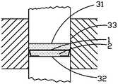
- the other typeis the electroplated integrated inductor. After the inductor wire is drawn from both ends of the magnet, it is then subjected to electrode treatment of copper plating 31, terminal silver 32, nickel plating 33, and tin plating 34.
- the side of this kind of electroplated electrode inductoris also the electroplated metal surface with electrodes, which causes the tin on both sides of the electrode to expand outward when the circuit board is soldered, so that the length and width dimensions are increased, the solder area is increased, and the effective use volume of the product is reduced.
- the present applicationprovides an inductor and its production process, which can reduce the volume of the circuit board occupied by the inductor.
- the embodiment of the present applicationprovides an inductor, which includes an inductor main body and an insulating magnetic powder block;
- the inductor main bodyincludes an integrated U-shaped inductor wire main body and two inductor pins, the U-shaped inductor wire main body includes a horizontal portion and two bent portions, each inductor pin and the horizontal portion extend in the same direction and are connected A bending portion, the length of the bending portion is less than half of the length of the horizontal portion;
- the insulating magnetic powder blockwraps the U-shaped inductor wire main body and exposes the two inductor pins.
- the surface of the insulating magnetic powder blockis plated with an insulating coating.
- the insulating coatingis a high temperature resistant inorganic coating or organic resin.
- the material of the main body of the U-shaped inductor wireis copper or silver.
- the main body of the U-shaped inductor wireis a coil-shaped wire.
- the main body of the U-shaped inductor wireis flat and has a thickness greater than or equal to 0.03 mm.
- the main body of the U-shaped inductor wireis circular, with a diameter greater than or equal to 0.06 mm.
- each inductor pinincludes an inward bend toward the horizontal portion.
- the embodiment of the present applicationprovides an inductor production process, which is performed by a press mold.
- the moldincludes an upper pressure surface, a lower pressure surface, and a pressure wall.
- the upper pressure surface, the lower pressure surface and the pressure wallare combined to form a mold cavity ,include:
- the U-shaped inductor wire main bodyPlace the U-shaped inductor wire main body on the lower pressing surface, wherein the U-shaped inductor wire main body includes an integrally formed horizontal part and two bent parts, and the length of each bent part is less than the length of the horizontal part.
- the two bending partsextend in the same direction and the angle between each bending part and the horizontal part is less than ninety degrees, and the free ends of the two bending parts serve as the main body of the U-shaped inductor wire
- the upper pressing surface and the lower pressing surface of the press diesqueeze the insulating magnetic powder and the U-shaped inductor wire body, so that the free ends of the two bending parts slide and bend along the lower pressing surface to form a horizontal part
- Two inductance pins extending in the same direction, the two inductance pinsare exposed to the outside of the extruded insulating magnetic powder.
- the insulating magnetic powderhas a preset compression ratio, and there is a preset value of the included angle between the bent portion and the horizontal portion, then the inductor main body is placed vertically on the mold Before the cavity, it also includes:
- each bending portionincludes an inner bending extending along the pressing surface.
- the leads of the inductor wireare exposed on the surface of the insulating magnetic powder block without protruding, so that the area occupied by the inductor on the circuit board is reduced.
- FIG. 1is a schematic diagram of the inductor structure in Embodiment 1 of the present application.
- FIG. 2is a partial enlarged view of the inductor structure according to the first embodiment of the present application.
- FIG. 3is a bottom view of an inductor manufactured using a process in the related art according to the first embodiment of the present application.
- Fig. 4is a bottom view of the inductor in the first embodiment of the present application.
- Fig. 5is a diagram of the initial state of the inductor wire placed in the press mold in the second embodiment of the present application.
- FIG. 6is a schematic diagram of the inductor wire structure before extrusion in the second embodiment of the present application.
- Fig. 7is a schematic diagram showing the structure of filling magnetic powder in the press mold in the second embodiment of the present application.
- Fig. 8is a schematic structural diagram of the completion of compression of the mold of the press in the second embodiment of the present application.
- Fig. 9is a manufacturing process flow chart of the second embodiment of the present application.
- Fig. 10is a manufacturing process flow chart of an alternative embodiment of the second embodiment of the present application.
- Insulating magnetic powder block 2Insulating magnetic powder block 2
- This embodimentprovides an inductor, which is used in the assembly and manufacturing of computer motherboards, graphics cards, servers, routing switches, and mobile phones.
- the unit mmrefers to millimeters
- mm 2refers to square millimeters
- mm 3refers to cubic millimeters.
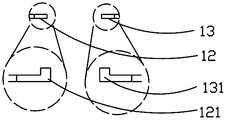
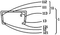
- the inductor in this embodimentincludes an inductor body 1 and an insulating magnetic powder block 2.
- the inductor body 1includes an integrated U-shaped inductor wire body 11 and two inductor pins.
- the two inductor pinsare respectively It is the first inductance pin 12 and the second inductance pin 13.
- the U-shaped inductor wire main body 11includes a horizontal portion 111 and two bending portions.
- the two bending portionsare a first bending portion 112 and a second bending portion 113, a first inductance pin 12 and a horizontal portion 111.
- Extending in the same direction and connected to the first bending portion 112, the second inductance pin 13 and the horizontal portion 111extend in the same direction and connected to the second bending portion 113, the first bending portion 112 and the second bending portion 113
- the lengthis less than one-half of the length of the horizontal portion 111; as shown in FIG. 2, the ends of the first inductance pin 12 and the end of the second inductance pin 13 each include a first inward curve toward the horizontal portion 111.
- the first inner bend and the second inner bendmay also be omitted.
- the first inductance pin 12 and the second inductance pin 13are the metal end points at both ends of the U-shaped inductor wire main body 11, and are integrally formed with the U-shaped inductor wire main body 11 to avoid the original lead of the electrode.
- the process of spot welding connection between the foot and the metal coilsaves production time, reduces resistance, and eliminates safety hazards such as false welding, missing welding, and poor contact.
- the insulating magnetic powder block 2wraps the U-shaped inductor wire main body 11 and exposes the first inductor pin 12 and the second inductor pin 13.
- the insulating magnetic powder block 2is a closed square formed by die-casting alloy or carbon-based powder that has undergone insulation treatment. With this structure, the volume of the bottom surface of the insulating magnetic powder block 2 is the volume of the inductive welding on the PCB board.
- the surface of the insulating magnetic powder block 2is plated with an insulating coating 3, and the insulating coating is any one of a high-temperature resistant inorganic coating or an organic resin.
- the structure of the inductorcan be applied to any type of inductor with a circular, elliptical, square or special-shaped structure.
- the inductoris a square inductor.
- the area S occupied by the inductance of the PCBis determined by the length ⁇ width.
- Figure 3shows a bottom view of an inductor manufactured using a process in the related technology, and the parameters are as follows:
- Fig. 4shows a bottom view of the inductor according to this embodiment, and the parameters are as follows:
- Fig. 4shows a bottom view of the inductor according to this embodiment, and the parameters are as follows:
- the area S2 of the PCB circuit board occupied by the inductor described in the present applicationis smaller than the area S1 of the inductor manufactured by the process in the related art.
- the material of the U-shaped inductor wire main body 11is any one of copper, silver, or iron-nickel alloy.
- the U-shaped inductor wire main body 11is a straight wire.
- the U-shaped inductor wire main body 11is flat, and optionally, the thickness is greater than or equal to 0.03 mm.
- the U-shaped inductor wire main body 11is circular, and optionally, the diameter is greater than or equal to 0.06 mm.
- the U-shaped inductor wire main body 11is a coil-shaped wire, and the winding shape of the coil-shaped wire is linear or non-linear.
- the inductor wiresare embedded in the magnetic powder block, and the inductor pins are embedded on the surface of the magnetic powder block, so that inductors of the same size occupy a smaller area of the circuit board.
- This embodimentprovides a manufacturing process for inductors.
- This embodimentis implemented by the press mold 3, as shown in FIG. 5, the press mold 3 includes an upper pressing surface 31, a lower pressing surface 32, and a pressing wall 33.
- the walls 33enclose a mold cavity 34. As shown in Figure 9, it includes the following steps:
- U-shaped inductor wire main bodyplaced on the lower pressing surface, wherein the U-shaped inductor wire main body includes an integrally formed horizontal portion and two bent portions, and the length of each bent portion is smaller than the horizontal portion Half of the length, the two bent parts extend in the same direction and the angle between each bent part and the horizontal part is less than ninety degrees, and the free ends of the two bent parts serve as U-shaped inductors
- the main body of the wireis placed on the two supporting points of the lower pressing surface.
- the U-shaped inductor wire main bodyincludes a horizontal portion 111 and two bending portions.
- the two bending portionsare respectively the first A bending portion 112 and a second bending portion 113, the lengths of the first bending portion 112 and the second bending portion 113 are both less than half of the length of the horizontal portion, the first bending portion 112 and the second bending portion 113
- the bent portions 113extend in the same direction, and the angle ⁇ between each bent portion and the horizontal portion 111 is less than ninety degrees.
- the free ends of the two bent portionsare placed on the lower pressing surface as the main body of the U-shaped inductor wire Two supporting points.
- the main body of the U-shaped inductor wirefurther includes a first inner bend 121 and a second inner bend 131.
- the included angle ⁇is less than ninety degrees and the function of the inward bending is to make the supporting points of the two bending parts of the U-shaped inductor wire body easier to fold inward during extrusion.
- the insulating magnetic powder 4is filled into the cavity 33.
- the insulating magnetic powder 4needs to be submerged over the highest point of the inductance wire.
- the upper pressing surface and the lower pressing surface of the press diesqueeze the insulating magnetic powder and the U-shaped inductor wire body, so that the free ends of the two bending parts slide and bend toward each other along the lower pressing surface to form Two inductance pins extending in the same direction as the horizontal part are exposed to the outside of the extruded insulating magnetic powder.
- the insulating magnetic powder 4is compressed to form an insulating magnetic powder block 2.
- the completed inductor structureis shown in FIG. 1 and will not be repeated here.
- the function of the first inner bend 121 and the second inner bend 131is to reduce the resistance during the compression process of the first bending portion 112 and the second bending portion 113 of the inductor wire main body as shown in the figure.
- the bending partis kept parallel to the horizontal part 111 after being compressed, and the bending part is not subject to excessive longitudinal pressure to cause bending.
- the first bent part 112 and the second bent part 113can keep out of contact with the horizontal part 111 to avoid short circuits. .
- the length ratio of the horizontal part 111 and the first bent part 112 and the second bent part 113 in the main body of the U-shaped inductor wireis calculated, and the length ratio between the bent part and the horizontal part 111 is insulated
- the compression ratio and the included angle ⁇ of the magnetic powder 4are determined, and before the step S101, as shown in FIG. 10, the method further includes:
- the main body of the inductor wireis embedded in the insulating magnetic powder during the manufacturing process, and the inductor pin is embedded on the surface of the magnetic powder block, so that the inductor of the same size occupies a smaller area of the circuit board.
- the above-mentioned productcan execute the method provided in any embodiment of the present application, and has corresponding functional modules and beneficial effects for the execution method.
Landscapes
- Engineering & Computer Science (AREA)
- Power Engineering (AREA)
- Coils Or Transformers For Communication (AREA)
Abstract
Description
Translated fromChinese本申请涉及电子元器件技术领域,例如涉及一种电感及生产工艺。This application relates to the technical field of electronic components, such as an inductor and a production process.
随着电子科技的发展,各类电子元器件得到了更广泛的应用,普通的一体电感分为两类,一类弯脚工艺的一种电感,绝缘磁粉块内部包裹着电感线或线圈,与电感线点焊连接的电极脚伸出绝缘磁粉块的左右两侧,经过弯折成型位于绝缘磁粉块的表面。这类普通电感的侧面有电极安装面,导致在电路板焊锡时两侧电极的锡往外扩使长度和宽度尺寸变长焊锡面积增大,即减少了产品的有效利用体积。另一类是电镀型一体电感,电感线从磁体两端引出后,再进行镀铜31,端银32,镀镍33,镀锡34的电极处理。With the development of electronic technology, various electronic components have been more widely used. Common integrated inductors are divided into two categories. One type is an inductor with a bent foot process. The insulating magnetic powder block is wrapped with an inductor wire or coil, and The electrode pins connected by spot welding of the inductance wire extend out of the left and right sides of the insulating magnetic powder block, and are formed on the surface of the insulating magnetic powder block after bending. This kind of common inductors have electrode mounting surfaces on the side, which leads to the expansion of the tin on both sides of the electrodes when the circuit board is soldered, so that the length and width dimensions become longer and the solder area increases, which reduces the effective use of the product volume. The other type is the electroplated integrated inductor. After the inductor wire is drawn from both ends of the magnet, it is then subjected to electrode treatment of copper plating 31,
这类电镀电极电感的侧面也是有电极的电镀金属面,导致在电路板焊锡时两侧电极的锡往外扩使长度及宽度尺寸变长,焊锡面积增大,减少了产品的有效利用体积。The side of this kind of electroplated electrode inductor is also the electroplated metal surface with electrodes, which causes the tin on both sides of the electrode to expand outward when the circuit board is soldered, so that the length and width dimensions are increased, the solder area is increased, and the effective use volume of the product is reduced.
发明内容Summary of the invention
本申请提供了一种电感及其生产工艺,能够减小电感占据电路板的体积。The present application provides an inductor and its production process, which can reduce the volume of the circuit board occupied by the inductor.
本申请实施例提供一种电感,包括电感主体和绝缘磁粉块;The embodiment of the present application provides an inductor, which includes an inductor main body and an insulating magnetic powder block;
所述电感主体包括一体成型的U型电感线主体和两个电感引脚,所述U型电感线主体包括水平部和两个弯折部,每个电感引脚和水平部同方向延伸并连接一个弯折部,所述弯折部的长度小于所述水平部长度的二分之一;The inductor main body includes an integrated U-shaped inductor wire main body and two inductor pins, the U-shaped inductor wire main body includes a horizontal portion and two bent portions, each inductor pin and the horizontal portion extend in the same direction and are connected A bending portion, the length of the bending portion is less than half of the length of the horizontal portion;
所述绝缘磁粉块包裹所述U型电感线主体并暴露所述两个电感引脚。The insulating magnetic powder block wraps the U-shaped inductor wire main body and exposes the two inductor pins.
可选地,所述绝缘磁粉块的表面镀有绝缘涂层。Optionally, the surface of the insulating magnetic powder block is plated with an insulating coating.
可选地,所述绝缘涂层为耐高温无机涂层或有机树脂。Optionally, the insulating coating is a high temperature resistant inorganic coating or organic resin.
可选地,所述U型电感线主体的材质为铜或银。Optionally, the material of the main body of the U-shaped inductor wire is copper or silver.
可选地,所述U型电感线主体为线圈型导线。Optionally, the main body of the U-shaped inductor wire is a coil-shaped wire.
可选地,所述U型电感线主体为扁平形,厚度大于或等于0.03毫米。Optionally, the main body of the U-shaped inductor wire is flat and has a thickness greater than or equal to 0.03 mm.
可选地,所述U型电感线主体为圆形,直径大于或等于0.06毫米。Optionally, the main body of the U-shaped inductor wire is circular, with a diameter greater than or equal to 0.06 mm.
可选地,每个电感引脚的端部包括朝向水平部的内弯折。Optionally, the end of each inductor pin includes an inward bend toward the horizontal portion.
本申请实施例提供一种电感的生产工艺,通过压机模具执行,所述模具包括上压面、下压面和压壁,所述上压面、下压面和压壁合围成模具空腔,包括:The embodiment of the present application provides an inductor production process, which is performed by a press mold. The mold includes an upper pressure surface, a lower pressure surface, and a pressure wall. The upper pressure surface, the lower pressure surface and the pressure wall are combined to form a mold cavity ,include:
将U型电感线主体放置于所述下压面,其中,所述U型电感线主体包括一体成型的水平部和两个弯折部,每个弯折部的长度小于所述水平部长度的二分之一,所述两个弯折部同向延伸且每个弯折部和水平部之间的夹角小于九十度,所述两个弯折部的自由端作为U型电感线主体放置在下压面的两个支撑点;Place the U-shaped inductor wire main body on the lower pressing surface, wherein the U-shaped inductor wire main body includes an integrally formed horizontal part and two bent parts, and the length of each bent part is less than the length of the horizontal part. One half, the two bending parts extend in the same direction and the angle between each bending part and the horizontal part is less than ninety degrees, and the free ends of the two bending parts serve as the main body of the U-shaped inductor wire Two supporting points placed on the lower pressure surface;
向所述空腔中填入绝缘磁粉,所述电感线的水平部被所述绝缘磁粉包裹;Filling the cavity with insulating magnetic powder, and the horizontal part of the inductor wire is wrapped by the insulating magnetic powder;
所述压机模具的上压面和下压面对绝缘磁粉和U型电感线主体进行挤压,以使两个弯折部的自由端沿下压面滑动并弯折,以形成和水平部同方向延伸的两个电感引脚,所述两个电感引脚暴露于挤压后的绝缘磁粉外部。The upper pressing surface and the lower pressing surface of the press die squeeze the insulating magnetic powder and the U-shaped inductor wire body, so that the free ends of the two bending parts slide and bend along the lower pressing surface to form a horizontal part Two inductance pins extending in the same direction, the two inductance pins are exposed to the outside of the extruded insulating magnetic powder.
可选地,所述绝缘磁粉具有预设的压缩比,所述弯折部和水平部之间具有预设数值的所述夹角,则所述将所述电感主体竖直放置于所述模具空腔中之前,还包括:Optionally, the insulating magnetic powder has a preset compression ratio, and there is a preset value of the included angle between the bent portion and the horizontal portion, then the inductor main body is placed vertically on the mold Before the cavity, it also includes:
基于所述预设的压缩比和所述预设数值的所述夹角,确定所述水平部和所述弯折部的长度比例。Determine the length ratio of the horizontal portion and the bent portion based on the included angle of the preset compression ratio and the preset value.
可选地,每个弯折部包括沿下压面延伸的内弯折。Optionally, each bending portion includes an inner bending extending along the pressing surface.
本申请通过设计一种电感和电感的生产工艺,使电感线的引脚暴露在所述绝缘磁粉块的表面且不凸出,使电感在电路板上的占据面积减小。In this application, by designing an inductor and an inductor production process, the leads of the inductor wire are exposed on the surface of the insulating magnetic powder block without protruding, so that the area occupied by the inductor on the circuit board is reduced.
图1是本申请实施例一中的电感结构示意图。FIG. 1 is a schematic diagram of the inductor structure in
图2是本申请实施例一的电感结构局部放大图。FIG. 2 is a partial enlarged view of the inductor structure according to the first embodiment of the present application.
图3是本申请实施例一的使用相关技术中的工艺制造的电感的底视图。FIG. 3 is a bottom view of an inductor manufactured using a process in the related art according to the first embodiment of the present application.
图4是本申请实施例一中电感的底视图。Fig. 4 is a bottom view of the inductor in the first embodiment of the present application.
图5是本申请实施例二中电感线放置于压机模具的初始状态图。Fig. 5 is a diagram of the initial state of the inductor wire placed in the press mold in the second embodiment of the present application.
图6是本申请实施例二中的挤压之前的电感线结构示意图。FIG. 6 is a schematic diagram of the inductor wire structure before extrusion in the second embodiment of the present application.
图7是本申请实施例二中在压机模具中填入磁粉的结构示意图。Fig. 7 is a schematic diagram showing the structure of filling magnetic powder in the press mold in the second embodiment of the present application.
图8是本申请实施例二中压机模具完成压缩的结构示意图。Fig. 8 is a schematic structural diagram of the completion of compression of the mold of the press in the second embodiment of the present application.
图9是本申请实施例二的制造工艺流程图。Fig. 9 is a manufacturing process flow chart of the second embodiment of the present application.
图10是本申请实施例二替代实施例的制造工艺流程图。Fig. 10 is a manufacturing process flow chart of an alternative embodiment of the second embodiment of the present application.
附图及标号如下:The drawings and reference numbers are as follows:
电感主体1
U型电感线主体11U-shaped inductor line
水平部111
第一弯折部112The
第二弯折部113Second bending
第一电感引脚12The
第二电感引脚13
第一内弯折121The first
第二内弯折131Second
绝缘磁粉块2Insulating
压机模具3Press
上压面31
下压面32
压壁33Press
模具空腔34Mold
绝缘磁粉4Insulating
夹角αAngle α
下面结合附图和实施例对本申请作进一步的详细说明。可以理解的是,此处所描述的具体实施例仅仅用于解释本申请,而非对本申请的限定。另外还需要说明的是,为了便于描述,附图中仅示出了与本申请相关的部分而非全部结构。The application will be further described in detail below with reference to the drawings and embodiments. It can be understood that the specific embodiments described here are only used to explain the application, but not to limit the application. In addition, it should be noted that, for ease of description, the drawings only show a part of the structure related to the present application instead of all of the structure.
除非另有定义,本文所使用的所有的技术和科学术语与属于本申请的技术领域的技术人员通常理解的含义相同。本文中在本申请的说明书中使用的术语只是为了描述具体的实施方式的目的,不是旨在于限制本申请。本文所使用的术语“和/或”包括一个或多个相关的所列项目的任意的和所有的组合。Unless otherwise defined, all technical and scientific terms used herein have the same meaning as commonly understood by those skilled in the technical field of this application. The terminology used in the specification of the application herein is only for the purpose of describing specific embodiments, and is not intended to limit the application. The term "and/or" as used herein includes any and all combinations of one or more related listed items.
实施例一Example one
本实施例提供一种电感,用于电脑主板、显卡、服务器、路由交换机及手机等的装配制造。本实施例及下述实施例提及的单位mm指毫米,mm2指平方毫米, mm3指立方毫米。This embodiment provides an inductor, which is used in the assembly and manufacturing of computer motherboards, graphics cards, servers, routing switches, and mobile phones. In this embodiment and the following embodiments, the unit mm refers to millimeters, mm2 refers to square millimeters, and mm3 refers to cubic millimeters.
如图1所示,本实施例所述电感包括电感主体1和绝缘磁粉块2,所述电感主体1包括一体成型的U型电感线主体11和两个电感引脚,两个电感引脚分别为第一电感引脚12和第二电感引脚13。As shown in FIG. 1, the inductor in this embodiment includes an
所述U型电感线主体11包括水平部111和两个弯折部,两个弯折部分别为第一弯折部112和第二弯折部113,第一电感引脚12和水平部111同方向延伸并连接第一弯折部112,第二电感引脚13和水平部111同方向延伸并连接第二弯折部113,所述第一弯折部112和第二弯折部113的长度都小于所述水平部111长度的二分之一;如图2所示,其中,第一电感引脚12和第二电感引脚13的端部均包括朝向水平部111的第一内弯折121和第二内弯折131,在如图2所示的替代实施例中,第一内弯折和第二内弯折也可以省略。The U-shaped inductor wire
该步骤中,第一电感引脚12和第二电感引脚13为所述U型电感线主体11的两端的金属端点,与所述U型电感线主体11一体成型,避免了原来将电极引脚与金属线圈点焊连接的工艺,节约了生产时间,减少了电阻,同时也消除了虚焊、漏焊、接触不良等安全隐患。In this step, the
如图1所示,所述绝缘磁粉块2包裹所述U型电感线主体11并暴露所述第一电感引脚12和第二电感引脚13。绝缘磁粉块2为经过绝缘处理的合金或碳基粉末通过压铸方式形成的闭合方块。该结构使绝缘磁粉块2的底面体积即为电感焊接在PCB板上的体积。在替代实施例中,所述绝缘磁粉块2的表面镀有绝缘涂层3,所述绝缘涂层为耐高温无机涂层或有机树脂的任意一种。As shown in FIG. 1, the insulating
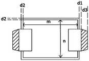
所述电感的结构可适用于圆形、椭圆形、方形或异型结构的任意一种电感,示例性地,电感为方形电感,本实施主体部分的绝缘磁粉块的长m=2mm,宽n=1.2mm,高h=1mm。电感占据PCB板的面积S由长×宽确定。The structure of the inductor can be applied to any type of inductor with a circular, elliptical, square or special-shaped structure. Illustratively, the inductor is a square inductor. The length of the insulating magnetic powder block of the main part of this embodiment is m=2mm, and the width n= 1.2mm, height h=1mm. The area S occupied by the inductance of the PCB is determined by the length × width.
电感线使用扁平线,厚度d1=0.1mm,绝缘涂层厚d2=0.1mm,焊锡后单边锡熔化后漫延d3=0.3mm。The inductor wire uses a flat wire with a thickness d1 = 0.1mm, and an insulating coating thickness d2 = 0.1mm. After soldering, the tin on one side melts and spreads d3 = 0.3mm.
如图3所示为使用相关技术中的工艺制造的电感的底视图,各参数如下:Figure 3 shows a bottom view of an inductor manufactured using a process in the related technology, and the parameters are as follows:
占PCB电路板上的尺寸S1=长×宽=(m+2d2+2d3)×(n+2d2)=(2+0.2+0.6)mm×(1.2+0.2)mm=3.92mm2。The size S1 occupied on the PCB circuit board=length×width=(m+2d2+2d3)×(n+2d2)=(2+0.2+0.6)mm×(1.2+0.2)mm=3.92mm2 .
如图4所示为本实施例所述的电感的底视图,各参数如下:Fig. 4 shows a bottom view of the inductor according to this embodiment, and the parameters are as follows:
如图4所示为本实施例所述的电感的底视图,各参数如下:Fig. 4 shows a bottom view of the inductor according to this embodiment, and the parameters are as follows:
占PCB电路板上的尺寸S2=长×宽=(m+2d2)×(n+2d2)=(2+0.2)×(1.2+0.2) =3.08mm2。The size S2 occupied on the PCB circuit board=length×width=(m+2d2)×(n+2d2)=(2+0.2)×(1.2+0.2)=3.08mm2 .
因此,本申请所述电感占PCB电路板的面积S2较相关技术中的工艺制造的电感的S1,占PCB板的面积变小。Therefore, the area S2 of the PCB circuit board occupied by the inductor described in the present application is smaller than the area S1 of the inductor manufactured by the process in the related art.
可选地,所述U型电感线主体11的材质为铜、银或铁镍合金中的任意一种。Optionally, the material of the U-shaped inductor wire
在一种替代实施例中,所述U型电感线主体11为直导线。示例性地,所述U型电感线主体11为扁平形,可选地,厚度大于或等于0.03毫米。示例性地,所述U型电感线主体11为圆形,可选地,直径大于或等于0.06毫米。In an alternative embodiment, the U-shaped inductor wire
在一种替代实施例中,所述U型电感线主体11为线圈型导线,所述线圈型导线的绕制形状为直线型或非直线型。In an alternative embodiment, the U-shaped inductor wire
本实施例通过将电感线镶嵌于磁粉块内部,电感引脚嵌于磁粉块表面,使相同尺寸的电感占电路板的面积更小。In this embodiment, the inductor wires are embedded in the magnetic powder block, and the inductor pins are embedded on the surface of the magnetic powder block, so that inductors of the same size occupy a smaller area of the circuit board.
实施例二Example two
本实施例提供一种电感的生产工艺。本实施例由压机模具3执行,如图5所示,所述压机模具3包括上压面31、下压面32和压壁33,所述上压面31、下压面32和压壁33合围成模具空腔34。如图9所示,包括如下步骤:This embodiment provides a manufacturing process for inductors. This embodiment is implemented by the
S101、将U型电感线主体放置于所述下压面,其中,所述U型电感线主体包括一体成型的水平部和两个弯折部,每个弯折部的长度小于所述水平部长度的二分之一,所述两个弯折部同向延伸且每个弯折部和水平部之间的夹角小于九十度,所述两个弯折部的自由端作为U型电感线主体放置在下压面的两个支撑点。S101. Place a U-shaped inductor wire main body on the lower pressing surface, wherein the U-shaped inductor wire main body includes an integrally formed horizontal portion and two bent portions, and the length of each bent portion is smaller than the horizontal portion Half of the length, the two bent parts extend in the same direction and the angle between each bent part and the horizontal part is less than ninety degrees, and the free ends of the two bent parts serve as U-shaped inductors The main body of the wire is placed on the two supporting points of the lower pressing surface.
本实施例中,如图6所示为经过挤压之前的电感线结构,示例性地,所述U型电感线主体包括水平部111和两个弯折部,两个弯折部分别为第一弯折部112和第二弯折部113,第一弯折部112和第二弯折部113的长度均小于所述水平部长度的二分之一,第一弯折部112和第二弯折部113同向延伸,且每个折弯部和水平部111之间的夹角α小于九十度,所述两个弯折部的自由端作为U型电感线主体放置在下压面的两个支撑点。In this embodiment, as shown in FIG. 6 is the inductor wire structure before being squeezed. Illustratively, the U-shaped inductor wire main body includes a
该步骤中,U型电感线主体还包括第一内弯折121和第二内弯折131。夹角α小于九十度以及内弯折的作用是使挤压时所述U型电感线主体的两个弯折部的支撑点更容易向内折叠。In this step, the main body of the U-shaped inductor wire further includes a first
S102、向所述空腔中填入绝缘磁粉,所述电感线的水平部被所述绝缘磁粉包裹。S102. Fill the cavity with insulating magnetic powder, and the horizontal part of the inductor wire is wrapped by the insulating magnetic powder.
如图7所示,将绝缘磁粉4填入空腔33中,为避免电感线暴露在外,需要将绝缘磁粉4淹没过所述电感线的最高点。As shown in FIG. 7, the insulating
S103、所述压机模具的上压面和下压面对绝缘磁粉和U型电感线主体进行挤压,以使两个弯折部的自由端沿下压面相向滑动并弯折,以形成和水平部同方向延伸的两个电感引脚,所述两个电感引脚暴露于挤压后的绝缘磁粉外部。S103. The upper pressing surface and the lower pressing surface of the press die squeeze the insulating magnetic powder and the U-shaped inductor wire body, so that the free ends of the two bending parts slide and bend toward each other along the lower pressing surface to form Two inductance pins extending in the same direction as the horizontal part are exposed to the outside of the extruded insulating magnetic powder.
如图8所示,绝缘磁粉4压缩后形成绝缘磁粉块2,制作完成后的电感结构如图1所示,此处不再赘述。本步骤中,第一内弯折121和第二内弯折131的作用是使如图所述的电感线主体的第一弯折部112和第二弯折部113在压缩过程中减小阻力,使弯折部压缩后保持与所述水平部111平行,而不会使弯折部受到纵向压力过大导致弯曲。As shown in FIG. 8, the insulating
在压缩过程中,由于弯折部与水平部111之间注入了绝缘磁粉4,因此压缩结束后,第一弯折部112和第二弯折部113能够与水平部111保持不接触,避免短路。During the compression process, since the insulating
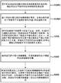
在替代实施例中,U型电感线主体中水平部111和第一弯折部112和第二弯折部113的长度比例的计算方法,弯折部与所述水平部111的长度比例通过绝缘磁粉4的压缩比和夹角α确定,则在所述步骤S101之前,如图10所示,还包括:In an alternative embodiment, the length ratio of the
S1041、基于所述预设的压缩比和所述预设数值的所述夹角,确定所述水平部和所述弯折部的长度比例。S1041, based on the preset compression ratio and the included angle of the preset value, determine the length ratio of the horizontal portion and the bent portion.
S1042、基于所述长度比例对电感线进行弯折,生成包括所述水平部和两个所述弯折部的所述U型电感线主体。S1042, bend the inductor wire based on the length ratio, and generate the U-shaped inductor wire main body including the horizontal portion and the two bent portions.
本实施例的制作方案在制作过程将电感线主体内嵌于所述绝缘磁粉内部,电感引脚嵌于磁粉块表面,使相同尺寸的电感占电路板的面积更小。In the manufacturing scheme of this embodiment, the main body of the inductor wire is embedded in the insulating magnetic powder during the manufacturing process, and the inductor pin is embedded on the surface of the magnetic powder block, so that the inductor of the same size occupies a smaller area of the circuit board.
上述产品可执行本申请任意实施例所提供的方法,具备执行方法相应的功能模块和有益效果。The above-mentioned product can execute the method provided in any embodiment of the present application, and has corresponding functional modules and beneficial effects for the execution method.
Claims (11)
Translated fromChinesePriority Applications (1)
| Application Number | Priority Date | Filing Date | Title |
|---|---|---|---|
| PCT/CN2020/087579WO2021217448A1 (en) | 2020-04-28 | 2020-04-28 | Inductor and production process |
Applications Claiming Priority (1)
| Application Number | Priority Date | Filing Date | Title |
|---|---|---|---|
| PCT/CN2020/087579WO2021217448A1 (en) | 2020-04-28 | 2020-04-28 | Inductor and production process |
Publications (1)
| Publication Number | Publication Date |
|---|---|
| WO2021217448A1true WO2021217448A1 (en) | 2021-11-04 |
Family
ID=78331690
Family Applications (1)
| Application Number | Title | Priority Date | Filing Date |
|---|---|---|---|
| PCT/CN2020/087579CeasedWO2021217448A1 (en) | 2020-04-28 | 2020-04-28 | Inductor and production process |
Country Status (1)
| Country | Link |
|---|---|
| WO (1) | WO2021217448A1 (en) |
Citations (4)
| Publication number | Priority date | Publication date | Assignee | Title |
|---|---|---|---|---|
| US6356179B1 (en)* | 1999-06-03 | 2002-03-12 | Sumida Technologies Incorporated | Inductance device |
| CN208970347U (en)* | 2018-12-03 | 2019-06-11 | 东莞市高东电子科技有限公司 | An integrated inductor |
| CN110517859A (en)* | 2019-07-25 | 2019-11-29 | 深圳顺络电子股份有限公司 | A kind of inductance component and preparation method thereof |
| KR102098623B1 (en)* | 2019-04-17 | 2020-04-08 | 주식회사 미래전자부품산업 | Molded Inductor and manufacturing method thereof |
- 2020
- 2020-04-28WOPCT/CN2020/087579patent/WO2021217448A1/ennot_activeCeased
Patent Citations (4)
| Publication number | Priority date | Publication date | Assignee | Title |
|---|---|---|---|---|
| US6356179B1 (en)* | 1999-06-03 | 2002-03-12 | Sumida Technologies Incorporated | Inductance device |
| CN208970347U (en)* | 2018-12-03 | 2019-06-11 | 东莞市高东电子科技有限公司 | An integrated inductor |
| KR102098623B1 (en)* | 2019-04-17 | 2020-04-08 | 주식회사 미래전자부품산업 | Molded Inductor and manufacturing method thereof |
| CN110517859A (en)* | 2019-07-25 | 2019-11-29 | 深圳顺络电子股份有限公司 | A kind of inductance component and preparation method thereof |
Similar Documents
| Publication | Publication Date | Title |
|---|---|---|
| CN101853826B (en) | Connection member and printed circuit board unit | |
| CN1767104B (en) | Surface-mount capacitor and method of producing the same | |
| CN107393680B (en) | Electrode structure, electronic component and inductor | |
| CN106449014A (en) | Magnetic element, manufacturing method thereof and lead frame for magnetic element | |
| US6891716B2 (en) | Capacitor | |
| JP6357657B2 (en) | Inductor and manufacturing method thereof | |
| WO2021217448A1 (en) | Inductor and production process | |
| US20060273873A1 (en) | Wire wound choke coil | |
| CN211980324U (en) | Inductor | |
| US12387866B2 (en) | Inductor with special-shaped structure and manufacturing method thereof | |
| CN111430132A (en) | Inductor and production process | |
| CN111354535A (en) | Inductor, electronic device and preparation method thereof | |
| WO2024000984A1 (en) | Inductor element and manufacturing method therefor | |
| CN205542250U (en) | Inductor structure | |
| CN211670063U (en) | Forming structure of surface-mounted inductor | |
| WO2019095648A1 (en) | Switching power supply module and packaging method therefor | |
| CN203774291U (en) | Metal connecting piece and power semiconductor module | |
| CN223218096U (en) | Integrated single-piece all-in-one inductor | |
| CN222580940U (en) | An inductor that is useful for saving assembly space | |
| CN111899970A (en) | Inductor preparation method | |
| CN110797165A (en) | Forming structure of surface mount inductor and method thereof | |
| CN223378004U (en) | Molded Inductors | |
| TWI299504B (en) | ||
| CN118919241A (en) | Integrally formed single-piece all-in-one inductor and manufacturing method thereof | |
| CN119446711A (en) | A highly sealed integrated chip power inductor |
Legal Events
| Date | Code | Title | Description |
|---|---|---|---|
| 121 | Ep: the epo has been informed by wipo that ep was designated in this application | Ref document number:20933936 Country of ref document:EP Kind code of ref document:A1 | |
| NENP | Non-entry into the national phase | Ref country code:DE | |
| 122 | Ep: pct application non-entry in european phase | Ref document number:20933936 Country of ref document:EP Kind code of ref document:A1 | |
| 122 | Ep: pct application non-entry in european phase | Ref document number:20933936 Country of ref document:EP Kind code of ref document:A1 |