WO2021197348A1 - Communication method for global system for mobile communications (gsm) data, and related device - Google Patents
Communication method for global system for mobile communications (gsm) data, and related deviceDownload PDFInfo
- Publication number
- WO2021197348A1 WO2021197348A1PCT/CN2021/084121CN2021084121WWO2021197348A1WO 2021197348 A1WO2021197348 A1WO 2021197348A1CN 2021084121 WCN2021084121 WCN 2021084121WWO 2021197348 A1WO2021197348 A1WO 2021197348A1
- Authority
- WO
- WIPO (PCT)
- Prior art keywords
- data
- gsm
- baseband
- sampling rate
- base station
- Prior art date
- Legal status (The legal status is an assumption and is not a legal conclusion. Google has not performed a legal analysis and makes no representation as to the accuracy of the status listed.)
- Ceased
Links
Images


Classifications
- H—ELECTRICITY
- H04—ELECTRIC COMMUNICATION TECHNIQUE
- H04W—WIRELESS COMMUNICATION NETWORKS
- H04W28/00—Network traffic management; Network resource management
- H04W28/16—Central resource management; Negotiation of resources or communication parameters, e.g. negotiating bandwidth or QoS [Quality of Service]
- H04W28/18—Negotiating wireless communication parameters
- H04W28/20—Negotiating bandwidth
- H—ELECTRICITY
- H04—ELECTRIC COMMUNICATION TECHNIQUE
- H04B—TRANSMISSION
- H04B1/00—Details of transmission systems, not covered by a single one of groups H04B3/00 - H04B13/00; Details of transmission systems not characterised by the medium used for transmission
- H04B1/38—Transceivers, i.e. devices in which transmitter and receiver form a structural unit and in which at least one part is used for functions of transmitting and receiving
- H04B1/40—Circuits
- H—ELECTRICITY
- H04—ELECTRIC COMMUNICATION TECHNIQUE
- H04W—WIRELESS COMMUNICATION NETWORKS
- H04W28/00—Network traffic management; Network resource management
- H04W28/16—Central resource management; Negotiation of resources or communication parameters, e.g. negotiating bandwidth or QoS [Quality of Service]
- H04W28/18—Negotiating wireless communication parameters
- H04W28/22—Negotiating communication rate
- H—ELECTRICITY
- H04—ELECTRIC COMMUNICATION TECHNIQUE
- H04W—WIRELESS COMMUNICATION NETWORKS
- H04W88/00—Devices specially adapted for wireless communication networks, e.g. terminals, base stations or access point devices
- H04W88/08—Access point devices
- H—ELECTRICITY
- H04—ELECTRIC COMMUNICATION TECHNIQUE
- H04W—WIRELESS COMMUNICATION NETWORKS
- H04W88/00—Devices specially adapted for wireless communication networks, e.g. terminals, base stations or access point devices
- H04W88/08—Access point devices
- H04W88/10—Access point devices adapted for operation in multiple networks, e.g. multi-mode access points
Definitions
- This applicationrelates to the field of communication technology, and in particular, to a method and related device for communication of global system for mobile communications (GSM) data.
- GSMglobal system for mobile communications
- wireless backhaul integrated base stationsmostly adopt application-specific integrated circuit (ASIC) system-on-a-chip (SOC) chip design.
- the chipcan integrate processing functions such as long term evolution (LTE) and wireless backhaul (Relay) technology.
- LTElong term evolution
- Relaywireless backhaul
- the Relay technologyis also implemented based on the LTE standard. It can be seen that in the prior art, the integrated wireless backhaul base station has a high degree of integration, and usually only supports the LTE standard, and it is difficult to implement one wireless communication standard on the basis of another wireless communication standard. Therefore, the existing integrated wireless backhaul base stations have poor scalability and are difficult to support multiple standards.
- the present applicationprovides a method and related device for the GSM data communication of the Global System for Mobile Communications to solve the problem that the existing integrated wireless backhaul base station only supports the LTE standard, has poor scalability, and is difficult to support multiple standards.
- the present applicationprovides a communication device, the device includes a base station processing chip and a sampling rate bandwidth adjustment device, wherein the base station processing chip is used to transmit the first global movement to the sampling rate bandwidth adjustment device Communication system GSM downlink data or first GSM uplink data; the sampling rate bandwidth adjustment device is used to send second GSM downlink data or second GSM uplink data to the base station processing chip, and the second GSM downlink data is The sampling rate and bandwidth of the first GSM downlink data are determined after adjustment, and the second GSM uplink data is determined after adjusting the sampling rate and bandwidth of the first GSM uplink data.
- the base station processing chipis used to transmit the first global movement to the sampling rate bandwidth adjustment device Communication system GSM downlink data or first GSM uplink data
- the sampling rate bandwidth adjustment deviceis used to send second GSM downlink data or second GSM uplink data to the base station processing chip
- the second GSM downlink datais The sampling rate and bandwidth of the first GSM downlink data are determined after adjustment, and the second GSM uplink data is determined after
- the sampling rate and bandwidth of the second GSM downlink datameets the sampling rate and bandwidth of Long Term Evolution LTE downlink data
- the sampling rate and bandwidth of the second GSM uplink datameets Sampling rate and bandwidth of LTE uplink data.
- the sampling rate bandwidth adjustment deviceincludes a field programmable gate array FPGA device and a global system for mobile communication GSM baseband processing device, and the second GSM is sent to the base station processing chip.
- Downlink datawhere,
- the FPGA deviceis configured to frame the first GSM downlink data to obtain third GSM downlink data, and transmit the third GSM downlink data to the GSM baseband processing device;
- the GSM baseband processing deviceis configured to perform L1 baseband processing on the third GSM downlink data to obtain two orthogonal first baseband IQ data, and transmit the first baseband IQ data to the FPGA device;
- the FPGA deviceis further configured to transmit second GSM downlink data to the base station processing chip, where the second GSM downlink data is determined after adjusting the sampling rate and bandwidth of the first baseband IQ data.
- the FPGA devicebefore the transmission of the second GSM downlink data to the base station processing chip, is specifically configured to expand the bit width of the first baseband IQ data to obtain Second baseband IQ data, the bit width of the second baseband IQ data is higher than the bit width of the first baseband IQ data; performing digital interpolation filtering on the second baseband IQ data to obtain the third baseband IQ data, The sampling rate of the third baseband IQ data is higher than the sampling rate of the second baseband IQ data; sampling rate conversion is performed on the third baseband IQ data to obtain the second GSM downlink data.
- the devicefurther includes a radio frequency integrated device,
- the base station processing chipis further configured to perform intermediate frequency conversion processing on the second GSM downlink data to obtain fourth GSM downlink data;
- the radio frequency integration deviceis configured to perform radio frequency modulation and amplification processing on the fourth GSM downlink data, and transmit the amplified fourth GSM downlink data.
- the sampling rate bandwidth adjustment deviceincludes a field programmable gate array FPGA device and a global system for mobile communication GSM baseband processing device, and sends second GSM uplink data to the base station processing chip Before, among them,
- the FPGA deviceis configured to transmit third GSM uplink data to the GSM baseband processing device, where the third GSM uplink data is determined after adjusting the rate and bandwidth of the second GSM uplink data;
- the GSM baseband processing deviceis configured to perform L1 baseband processing on the third GSM uplink data to obtain two orthogonal fifth baseband IQ data, and transmit the fifth baseband IQ data to the FPGA device;
- the FPGA deviceis also used to deframe the fifth baseband IQ data to obtain the second GSM uplink data.
- the FPGA devicebefore the third GSM uplink data is transmitted to the GSM baseband processing device, the FPGA device is specifically configured to perform sampling rate conversion on the fifth baseband IQ data And bit width expansion to obtain sixth baseband IQ data, the bit width of the sixth baseband IQ data is higher than the bit width of the fifth baseband IQ data, and the sampling rate of the sixth baseband IQ data is higher than that of the first The sampling rate of five baseband IQ data; data extraction and filtering are performed on the sixth baseband IQ data to obtain seventh baseband IQ data, and the sampling rate of the seventh baseband IQ data is lower than the sampling rate of the sixth baseband IQ data Rate; normalized gain adjustment is performed on the seventh baseband IQ data to obtain eighth baseband IQ data; the bit width of the eighth baseband IQ data is reduced and the power of the eighth baseband IQ data is adjusted to obtain the The sixth baseband IQ data, the bit width of the sixth baseband IQ data is lower than the bit width of the eighth baseband IQ data
- the devicefurther includes a baseband processing unit,
- the base station processing chipis also used for transmitting the second GSM uplink data to the baseband processing unit;
- the baseband processing unitis configured to transmit the second GSM uplink data to the base station control subsystem.
- the present applicationprovides a method for communicating GSM data of the Global System for Mobile Communications, which is applied to a communication device, and the communication device includes a base station processing chip and a sampling rate bandwidth adjustment device, wherein:
- the sampling rate bandwidth adjustment devicesends second GSM downlink data or second GSM uplink data to the base station processing chip, where the second GSM downlink data is after adjusting the sampling rate and bandwidth of the first GSM downlink data It is determined that the second GSM uplink data is determined after adjusting the sampling rate and bandwidth of the first GSM uplink data.
- the base station processing chiptransmits GSM downlink data or GSM uplink data to the sampling rate bandwidth adjustment device, so that the sampling rate bandwidth adjustment device can adjust the sampling rate and bandwidth of GSM downlink data or GSM uplink data. So that the base station processing chip that only supports LTE standard can support the processing of GSM downlink data or GSM uplink data, and it also solves the problem that the existing wireless backhaul integrated base station only supports LTE standard, has poor scalability, and is difficult to support multiple standards. .
- the sampling rate and bandwidth of the second GSM downlink datameets the sampling rate and bandwidth of Long Term Evolution LTE downlink data
- the sampling rate and bandwidth of the second GSM uplink datameets Sampling rate and bandwidth of LTE uplink data.
- the sampling rate and bandwidth of the second GSM downlink datameet the sampling rate and bandwidth of the Long Term Evolution LTE downlink data, or the sampling rate and bandwidth of the second GSM uplink data meet the requirements of the LTE uplink data.
- the sampling rate and bandwidthenable the base station processing chip that only supports the LTE standard to support the processing of GSM downlink data or GSM uplink data, which solves the problem that the existing wireless backhaul integrated base station only supports the LTE standard, which has poor scalability and is difficult to support. A question of format. At the same time, hardware costs are saved.
- the sampling rate bandwidth adjustment deviceincludes a field programmable gate array FPGA device and a global system for mobile communication GSM baseband processing device,
- the sending second GSM downlink data to the base station processing chipthe method further includes:
- the FPGA deviceframes the first GSM downlink data to obtain third GSM downlink data, and transmits the third GSM downlink data to the GSM baseband processing device;
- the GSM baseband processing deviceperforms L1 baseband processing on the third GSM downlink data to obtain two orthogonal first baseband IQ data, and transmits the first baseband IQ data to the FPGA device;
- the FPGA devicetransmits second GSM downlink data to the base station processing chip, and the second GSM downlink data is determined after adjusting the sampling rate and bandwidth of the first baseband IQ data.
- the sampling rate and bandwidth adjustment devicecan adjust the sampling rate and bandwidth of the GSM downlink data, so that the base station processing chip that only supports the LTE standard can support the processing of the GSM downlink data, which also solves the problem.
- Some integrated wireless backhaul base stationsonly support the LTE standard, which has poor scalability and is difficult to support multiple standards.
- the methodbefore the transmitting the second GSM downlink data to the base station processing chip, the method further includes:
- the FPGA deviceexpands the bit width of the first baseband IQ data to obtain second baseband IQ data, and the bit width of the second baseband IQ data is higher than the bit width of the first baseband IQ data;
- the FPGA deviceperforms digital interpolation filtering on the second baseband IQ data to obtain third baseband IQ data, where the sampling rate of the third baseband IQ data is higher than the sampling rate of the second baseband IQ data;
- the FPGA deviceperforms sampling rate conversion on the third baseband IQ data to obtain the second GSM downlink data.
- the sampling rate and bandwidth of the GSM downlink dataare adjusted, so that the base station processing chip that only supports the LTE standard can support the processing of the GSM downlink data, and also solves the existing wireless
- the backhaul integrated base stationonly supports the LTE standard, has poor scalability, and is difficult to support multiple standards.
- the communication devicefurther includes a radio frequency integrated device
- the methodfurther includes:
- the base station processing chipperforms intermediate frequency conversion processing on the second GSM downlink data to obtain fourth GSM downlink data;
- the radio frequency integration deviceperforms radio frequency modulation and amplification processing on the fourth GSM downlink data, and transmits the amplified fourth GSM downlink data.
- the base station processing chip that only supports the LTE standardcan support the processing of GSM downlink data, and realizes the transmission of GSM downlink data.
- the sampling rate bandwidth adjustment deviceincludes a field programmable gate array FPGA device and a global system for mobile communication GSM baseband processing device, and the second GSM is sent to the base station processing chip.
- the methodfurther includes:
- the FPGA devicetransmits third GSM uplink data to the GSM baseband processing device, where the third GSM uplink data is determined after adjusting the rate and bandwidth of the second GSM uplink data;
- the GSM baseband processing deviceperforms L1 baseband processing on the third GSM uplink data to obtain two orthogonal fifth baseband IQ data, and transmits the fifth baseband IQ data to the FPGA device;
- the FPGA devicedeframes the fifth baseband IQ data to obtain the second GSM uplink data.
- the sampling rate bandwidth adjustment devicecan adjust the sampling rate and bandwidth of the GSM uplink data, so that the base station processing chip that only supports the LTE standard can support the processing of the GSM uplink data, which also solves the problem.
- Some integrated wireless backhaul base stationsonly support the LTE standard, which has poor scalability and is difficult to support multiple standards.
- the methodbefore the transmitting the third GSM uplink data to the GSM baseband processing apparatus, the method further includes:
- the FPGA deviceperforms sampling rate conversion and bit width expansion on the second GSM uplink data to obtain sixth baseband IQ data, the bit width of the sixth baseband IQ data is higher than the bit width of the second GSM uplink data , The sampling rate of the sixth baseband IQ data is lower than the sampling rate of the second GSM uplink data;
- the FPGA deviceperforms data extraction and filtering on the sixth baseband IQ data to obtain seventh baseband IQ data, and the sampling rate of the seventh baseband IQ data is lower than the sampling rate of the sixth baseband IQ data;
- the FPGA deviceperforms normalized gain adjustment on the seventh baseband IQ data to obtain eighth baseband IQ data;
- the FPGA devicereduces the bit width of the eighth baseband IQ data and adjusts the power of the eighth baseband IQ data to obtain the third GSM uplink data, and the bit width of the third GSM uplink data is lower than the bit width of the third GSM uplink data.
- the bit width of the eighth baseband IQ datais lower than the bit width of the third GSM uplink data.
- the sampling rate and bandwidth of the GSM uplink dataare adjusted, so that the base station processing chip that only supports the LTE standard can support the processing of the GSM uplink data in the future, and also solves the existing wireless
- the backhaul integrated base stationonly supports the LTE standard, has poor scalability, and is difficult to support multiple standards.
- the communication devicefurther includes a baseband processing unit, and the method further includes:
- the baseband processing unittransmits the second GSM uplink data to the base station control subsystem.
- the base station processing chip that only supports the LTE standardcan support the processing of GSM uplink data, and the transmission of the GSM uplink data to the base station control subsystem is realized.
- the present applicationprovides a communication system, the system includes a base station processing chip and a sampling rate bandwidth adjustment device, wherein:
- the base station processing chipis configured to transmit the first global system for mobile communication GSM downlink data or the first GSM uplink data to the sampling rate bandwidth adjustment device;
- the sampling rate bandwidth adjustment deviceis configured to send second GSM downlink data or second GSM uplink data to the base station processing chip, where the second GSM downlink data is a sampling rate and bandwidth of the first GSM downlink data Determined after adjustment, the second GSM uplink data is determined after adjusting the sampling rate and bandwidth of the first GSM uplink data.
- the sampling rate and bandwidth of the second GSM downlink datameets the sampling rate and bandwidth of Long Term Evolution LTE downlink data
- the sampling rate and bandwidth of the second GSM uplink datameets Sampling rate and bandwidth of LTE uplink data.
- the sampling rate bandwidth adjustment deviceincludes a field programmable gate array FPGA device and a global system for mobile communication GSM baseband processing device, and the second GSM is sent to the base station processing chip.
- Downlink datawhere,
- the FPGA deviceis configured to frame the first GSM downlink data to obtain third GSM downlink data, and transmit the third GSM downlink data to the GSM baseband processing device;
- the GSM baseband processing deviceis configured to perform L1 baseband processing on the third GSM downlink data to obtain two orthogonal first baseband IQ data, and transmit the first baseband IQ data to the FPGA device;
- the FPGA deviceis further configured to transmit second GSM downlink data to the base station processing chip, where the second GSM downlink data is determined after adjusting the sampling rate and bandwidth of the first baseband IQ data.
- the FPGA devicebefore the transmission of the second GSM downlink data to the base station processing chip, is specifically configured to expand the bit width of the first baseband IQ data to obtain Second baseband IQ data, the bit width of the second baseband IQ data is higher than the bit width of the first baseband IQ data; performing digital interpolation filtering on the second baseband IQ data to obtain the third baseband IQ data, The sampling rate of the third baseband IQ data is higher than the sampling rate of the second baseband IQ data; sampling rate conversion is performed on the third baseband IQ data to obtain the second GSM downlink data.
- the systemfurther includes a radio frequency integrated device,
- the base station processing chipis further configured to perform intermediate frequency conversion processing on the second GSM downlink data to obtain fourth GSM downlink data;
- the radio frequency integration deviceis configured to perform radio frequency modulation and amplification processing on the fourth GSM downlink data, and transmit the amplified fourth GSM downlink data.
- the sampling rate bandwidth adjustment deviceincludes a field programmable gate array FPGA device and a global system for mobile communication GSM baseband processing device, and sends second GSM uplink data to the base station processing chip Before, among them,
- the FPGA deviceis configured to transmit third GSM uplink data to the GSM baseband processing device, where the third GSM uplink data is determined after adjusting the rate and bandwidth of the second GSM uplink data;
- the GSM baseband processing deviceis configured to perform L1 baseband processing on the third GSM uplink data to obtain two orthogonal fifth baseband IQ data, and transmit the fifth baseband IQ data to the FPGA device;
- the FPGA deviceis also used to deframe the fifth baseband IQ data to obtain the second GSM uplink data.
- the FPGA devicebefore the third GSM uplink data is transmitted to the GSM baseband processing device, the FPGA device is specifically configured to perform sampling rate conversion on the second GSM uplink data And bit width expansion to obtain sixth baseband IQ data, the bit width of the sixth baseband IQ data is higher than the bit width of the second GSM uplink data, and the sampling rate of the sixth baseband IQ data is lower than that of the first 2.
- Sampling rate of GSM uplink datadata extraction and filtering are performed on the sixth baseband IQ data to obtain seventh baseband IQ data, the sampling rate of the seventh baseband IQ data is lower than the sampling rate of the sixth baseband IQ data Rate; normalized gain adjustment is performed on the seventh baseband IQ data to obtain eighth baseband IQ data; the bit width of the eighth baseband IQ data is reduced and the power of the eighth baseband IQ data is adjusted to obtain the For the third GSM uplink data, the bit width of the third GSM uplink data is lower than the bit width of the eighth baseband IQ data.
- the systemfurther includes a baseband processing unit,
- the base station processing chipis also used for transmitting the second GSM uplink data to the baseband processing unit;
- the baseband processing unitis configured to transmit the second GSM uplink data to the base station control subsystem.
- the present applicationalso provides a communication device.
- the deviceincludes a memory, a plurality of processors, and a plurality of panels, each of the processors corresponds to one panel, and the memory stores computer instructions;
- the processorexecutes the computer instructions stored in the memory, so that the device executes the Global System for Mobile Communications GSM data communication method according to any embodiment of the second aspect.
- the present applicationalso provides a computer-readable storage medium for storing executable program code.
- the program codeWhen executed by a device, it is used to implement any implementation of the second aspect.
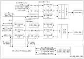
- FIG. 1is a schematic diagram of an integrated wireless backhaul base station provided by an embodiment of the present application
- FIG. 2is a schematic diagram of the base station processing chip 1012 in FIG. 1 processing Relay data, UMTS data, and LTE data;
- FIG. 3is a schematic diagram of a communication device provided by an embodiment of the present application.
- FIG. 4is a schematic diagram of the processing of Relay data, UMTS data, and LTE data by the base station processing chip 3012 and the sampling rate bandwidth adjustment device 303 in FIG. 3;
- FIG. 5is a schematic diagram of processing the first GSM downlink data by the FPGA device 3031 in FIG. 3;
- FIG. 6is a schematic diagram of processing the second GSM downlink data by the FPGA device 3031 in FIG. 3.
- Fig. 1is a schematic diagram of a wireless backhaul integrated base station provided by an embodiment of the present application.
- the integrated wireless backhaul base station 100includes a system on chip 101 and a radio frequency integrated device 102.
- the system on chip 101includes a main control and transmission 1011 and a base station processing chip 1012.
- the main control and transmission 1011may include a baseband unit (BBU), clock distribution, power distribution, and air interface.
- the base station processing chip 1012may be, for example, an application-specific integrated circuit (ASIC).
- ASICapplication-specific integrated circuit
- the system-on-chip 101can support master control, transmission, the 3rd generation mobile communication technology (3G), the 4th generation mobile communication technology (4G), and wireless backhaul.
- Technology (Relay)L1, L2, L3 baseband processing and digital intermediate frequency processing, etc.
- L1 baseband processingis mainly about physical layer (port physical layer, PHY) processing
- L2 baseband processingis mainly about media access control (MAC) or radio link control (RLC).
- Processing and L3 baseband processingare mainly related to radio resource control (RRC).
- RRCradio resource control
- Relayis also generally implemented based on the LTE standard.
- the radio frequency integrated device 102may include a radio frequency integrated chip 1021 and a transceiver device 1022.
- the radio frequency integrated chip 1021may integrate a radio frequency integrated circuit (RFIC), a radio frequency local oscillator, a transmit (TX) DAC, a receive (receive, RX) ADC, and so on.
- the radio frequency integrated chip 1021can support a transceiver unit (transmission receiver unit, TRX) and the like.
- the radio frequency integrated chip 1021mainly adopts a zero intermediate frequency (ZIF) architecture, which can support TX channels, RX channels, and feedback (faceback, FB) channels.
- the transceiver device 1022may include a relay transceiver radio frequency link 1022a, an LTE or UMTS transceiver radio frequency link 1022b, a relay antenna, and an LTE antenna.
- FIG. 2is a schematic diagram of the base station processing chip 1012 in FIG. 1 processing Relay data, universal mobile telecommunications system (UMTS) data, and LTE data.
- Relay datamay include Relay downlink data and Relay uplink data.
- the relay downlink datamay be downlink data transmitted by the relay
- the relay uplink datamay be uplink data transmitted by the relay.
- UMTS datamay include UMTS downlink data and UMTS uplink data. It is understandable that the UMTS downlink data may be downlink data transmitted using UMTS, and the UMTS uplink data may be uplink data transmitted using UMTS.
- LTE datamay include LTE downlink data and LTE uplink data.
- LTE downlink datamay be downlink data transmitted using LTE
- LTE uplink datamay be uplink data transmitted using LTE
- the base station processing chip 1012may include digital automatic gain control (DAGC), sample rate converter (SRC), and digitally controlled oscillator (DAGC). NCO), digital pre-distortion (digital pre-distortion, DPD), automatic gain control (analog auto gain control, AAGC), analog-to-digital converter (ADC) and digital-to-analog converter, DAC) and so on.
- DAGCdigital automatic gain control
- SRCsample rate converter
- DAGCdigitally controlled oscillator
- NCOdigital pre-distortion
- DPDdigital pre-distortion
- AAGCautomatic gain control
- ADCanalog-to-digital converter
- DACdigital-to-analog converter
- Relay downlink dataUMTS downlink data, and LTE downlink data
- SRC, NCOcombining, clipping, DPD, DAC and other processing are required.
- Relay uplink dataUMTS uplink data, and LTE uplink data
- NCOis equivalent to the local oscillator in traditional IF modulation and demodulation. Clipping can smoothly suppress the peak of the data to protect the power amplifier.
- DPDguarantees the linearity of the power amplifier.
- AAGCis used to perform power statistics on the data processed by the ADC. According to the threshold of the dynamic range, the calculated attenuation value is adjusted by an analog attenuator.
- the wireless backhaul integrated base stationmostly adopts application-specific integrated circuit (ASIC) system-on-a-chip (SOC) chip design.
- the chipcan integrate processing functions such as long term evolution (LTE) and wireless backhaul (Relay) technology.
- LTElong term evolution
- Relaywireless backhaul
- the Relay technologyis also implemented based on the LTE standard.
- the integrated wireless backhaul base stationhas a high degree of integration, and usually only supports the LTE standard, and it is difficult to implement one wireless communication standard on the basis of another wireless communication standard. Therefore, the existing integrated wireless backhaul base stations have poor scalability and are difficult to support multiple standards.
- an embodiment of the present applicationproposes a communication device to solve the above-mentioned problem.
- the followingdescribes the embodiment of the present application in detail.
- the communication device 300includes a system on chip 301, a radio frequency integration device 302, and a sampling rate bandwidth adjustment device 303.
- the system on chip 301includes a main control and transmission 3011, a base station processing chip 3012.
- the main control and transmission 3011refer to the main control and transmission 1011 in FIG. 1
- the base station processing chip 3012refer to the base station processing chip 1012 in FIG. 1
- the system on chip 301refer to the system on chip 101 in FIG.
- the radio frequency integrated device 302may include a radio frequency integrated chip 3021 and a transceiver device 3022.
- the sampling rate bandwidth adjustment device 303may include a field-programmable gate array (FPGA) device 3031 and a GSM baseband processing device 3032. It can be understood that the communication device 300 may be an integrated wireless backhaul base station.
- FPGAfield-programmable gate array
- the base station processing chip 3012is used to transmit the first GSM downlink data to the sampling rate bandwidth adjustment device 303.
- the first GSM downlink datamay be downlink data transmitted using GSM. That is, further, the first GSM downlink data may be main control data, and the main control data may include service data, control plane signaling data, and frequency hopping management data, and the service data may be voice data, for example.
- the base station processing chip 3012can transmit to the sampling rate bandwidth adjustment device 303 through the peripheral component interconnect express (PCIE) interface or the serial gigabit media independent interface (SGMII).
- PCIEperipheral component interconnect express
- SGMIIserial gigabit media independent interface
- the base station processing chip 3012transmits the first GSM downlink data to the sampling rate bandwidth adjustment device 303 through the PCIE interface, then the first GSM downlink data is a transaction layer packet (TLP) including master control data. If the base station processing chip 3012 transmits the first GSM downlink data to the sampling rate bandwidth adjustment device 303 through the SGMII interface, then the first GSM downlink data is an internet protocol (IP) packet including master control data.
- TLPtransaction layer packet
- IPinternet protocol
- sampling rate bandwidth adjusting device 303is configured to send second GSM downlink data to the base station processing chip 3012, and the second GSM downlink data is determined after adjusting the sampling rate and bandwidth of the first GSM downlink data.
- sampling rate bandwidth adjustment device 303may send the second GSM downlink data to the base station processing chip 3012 through a similar/simple common public radio interface (CPRI).
- CPRIcommon public radio interface
- the sampling rate and bandwidth of the second GSM downlink datacan meet the sampling rate and bandwidth of LTE downlink data, can also meet the sampling rate and bandwidth of UMTS downlink data, and can also meet the requirements of (new radio nodeB, gNB) transmission
- the sampling rate and bandwidth of the downstream dataare not limited here.
- the sampling rate of the second GSM downlink datais 650 megabits/second (million bits per second, Mbps), and the bandwidth of the second GSM downlink data is 5 megahertz (MHz).
- the base station processing chiptransmits GSM downlink data to the sampling rate and bandwidth adjustment device, so that the sampling rate and bandwidth adjustment device can adjust the sampling rate and bandwidth of the GSM downlink data, so that the base station that only supports the LTE standard
- the processing chipcan support the processing of GSM downlink data, and also solves the problem that the existing wireless backhaul integrated base station only supports the LTE standard, has poor scalability, and is difficult to support multiple standards. At the same time, hardware costs are saved.
- FIG. 4is a schematic diagram of the processing of Relay data, UMTS data, LTE data, and GSM data by the base station processing chip 3012 and the sampling rate bandwidth adjustment device 303 in FIG. 3. It can be understood that, for the base station processing chip 3012, reference may be made to the base station processing chip 1012 in FIG. 2. In addition, for Relay data, UMTS data, and LTE data, reference may also be made to the contents of Relay data, UMTS data, and LTE data in FIG. 2.
- the first GSM downlink dataneeds to be transmitted to the FPGA device 3031 in the sampling rate bandwidth adjustment device 303, and then transmitted to the GSM baseband processing device 3032.
- the GSM baseband processing device 3032completes the L1 baseband processing After that, it is transmitted to the FPGA device 3031, and finally returned to the base station processing chip 3012.
- the first GSM downlink dataneeds to be processed according to the transmission path 401a to 404a in FIG.
- the base station processing chip 3012needs to first transmit the first GSM downlink data to the FPGA device 3031 for processing to obtain the third GSM downlink data; the FPGA device 3031 then transmits the third GSM downlink data to the GSM baseband processing device 3032; GSM baseband The processing device 3032 can perform L1 baseband processing on the third GSM downlink data to obtain the first baseband IQ data; the GSM baseband processing device 3032 then transmits the first baseband IQ data to the FPGA device 3031 for processing, and obtains the second GSM downlink data; The FPGA device 3031 then transmits the second GSM downlink data to the base station processing chip 3012; the base station processing chip 3012 then performs SRC, NCO, combining, clipping, DPD, DAC and other processing on the second GSM downlink data.
- the second GSM downlink datais sent to the base station processing chip 3012, and the FPGA device 3031 is used to frame the first GSM downlink data to obtain the third GSM downlink data, and transmit the third GSM downlink data to the GSM baseband processing device 3032.
- the GSM baseband processing device 3032is used to perform L1 baseband processing on the third GSM downlink data to obtain two orthogonal first baseband IQ data, and transmit the first baseband IQ data to the FPGA device 3031; the FPGA device 3031 is also used for
- the second GSM downlink datais transmitted to the base station processing chip, and the second GSM downlink data is transmitted to the base station processing chip 3012.
- the bit width of the first baseband IQ datawhen the bit width of the first baseband IQ data is expanded, the low bits of the first baseband IQ data are generally filled with zeros.
- 6-fold interpolation filteringcan be used.
- the FPGA device 3031is also used to correspond to the third baseband IQ data in the ramp-up (RAMP) area of the current time slot.
- the poweris processed to realize that the power corresponding to the third baseband IQ data in the ramp-up (RAMP) region of the current time slot meets the preset power, and the transmit power corresponding to the third baseband IQ data is adjusted.
- FIG. 5is a schematic diagram of processing the first GSM downlink data by the FPGA device 3031 in FIG. 3.
- the FPGA device 3031may include a bandwidth processing module 501, a first variable rate module 502, a ramp gain module 503, a transmit power gain module 504, and a second variable rate module 505.
- the GSM baseband processing device 3032can transmit the first baseband IQ data to the FPGA device 3031, the bit width of the first baseband IQ data can be 14, and the sampling rate can be 1.0833 Mbps.
- the bandwidth processing module 501can expand the bit width of the first baseband IQ data to obtain the second baseband IQ data.
- the bit width of the second baseband IQ datacan be 16, and the sampling rate can be 1.0833 Mbps.
- the first variable rate module 502may perform digital interpolation filtering on the second baseband IQ data to obtain the third baseband IQ data.
- the bit width of the third baseband IQ datamay be 16, and the sampling rate may be 6.5 Mbps.
- the ramp gain module 503can process the power corresponding to the third baseband IQ data in the ramp (RAMP) area of the current time slot, so as to realize the third baseband IQ data in the ramp (RAMP) area of the current time slot. The corresponding power meets the preset power.
- the transmit power gain module 504can adjust the transmit power corresponding to the third baseband IQ data.
- the second variable rate module 505may perform sampling rate conversion on the third baseband IQ data to obtain second GSM downlink data.
- the bit width of the second GSM downlink datamay be 16, and the sampling rate may be 6.5 Mbps.
- the FPGA device 3031can transmit the second GSM downlink data to the base station processing chip 3012.
- the bit widthis 16, and the sampling rate is 6.5 Mbps.
- the FPGA device 3031is specifically used to expand the bit width of the first baseband IQ data to obtain the second baseband IQ data, and the bit width of the second baseband IQ data is higher than The bit width of the first baseband IQ data; digital interpolation filtering is performed on the second baseband IQ data to obtain the third baseband IQ data, the sampling rate of the third baseband IQ data is higher than the sampling rate of the second baseband IQ data; The baseband IQ data undergoes sampling rate conversion to obtain the second GSM downlink data.
- the sampling rate and bandwidth of the GSM downlink dataare adjusted, so that the base station processing chip that only supports the LTE standard can support the processing of the GSM downlink data, and also solves the existing wireless
- the backhaul integrated base stationonly supports the LTE standard, has poor scalability, and is difficult to support multiple standards.
- the devicefurther includes a radio frequency integration device 302, a base station processing chip 3012, and is also used to perform intermediate frequency conversion processing on the second GSM downlink data to obtain fourth GSM downlink data;
- the device 302is configured to perform radio frequency modulation and amplification processing on the fourth GSM downlink data, and transmit the amplified fourth GSM downlink data.
- the second GSM downlink datais subjected to intermediate frequency conversion processing, that is, SRC, NCO, combined, clipping, DPD, DAC, and the like are processed on the second GSM downlink data.
- the base station processing chip that only supports the LTE standardcan support the processing of GSM uplink data, and the transmission of the GSM uplink data to the base station control subsystem is realized.
- the base station processing chip 3012is used to transmit the first GSM uplink data to the sampling rate bandwidth adjustment device 303.
- the first GSM uplink datamay be uplink data transmitted using GSM.
- the first GSM uplink datamay be a kind of baseband IQ data.
- the base station processing chip 3012may transmit the first GSM uplink data to the sampling rate bandwidth adjustment device 303 through PCIE.
- the base station processing chip 3012transmits the first GSM uplink data to the sampling rate bandwidth adjustment device 303 through the PCIE interface
- the first GSM uplink datais a TLP packet including the intermediate frequency IQ data.
- the sampling rate bandwidth adjusting device 303is configured to send second GSM uplink data to the base station processing chip 3012, and the second GSM uplink data is determined after adjusting the sampling rate and bandwidth of the first GSM uplink data.
- sampling rate bandwidth adjustment device 303may send the second GSM uplink data to the base station processing chip 3012 through a common public radio interface (CPRI).
- CPRIcommon public radio interface
- the base station processing chiptransmits GSM uplink data to the sampling rate bandwidth adjustment device, so that the sampling rate bandwidth adjustment device can adjust the sampling rate and bandwidth of the GSM uplink data, so that the base station that only supports the LTE standard
- the processing chipcan support the processing of GSM uplink data, and also solves the problem that the existing wireless backhaul integrated base station only supports the LTE standard, has poor scalability, and is difficult to support multiple standards.
- the sampling rate and bandwidth of the second GSM uplink datacan meet the sampling rate and bandwidth of LTE uplink data, can also meet the sampling rate and bandwidth of UMTS uplink data, and can also meet the requirements of (new radio nodeB, gNB) transmission
- the sampling rate and bandwidth of the upstream dataare not limited here.
- the sampling rate of the second GSM uplink datais 650 kilobit per second (kbps), and the bandwidth of the second GSM uplink data is 200 kHz.
- the base station processing chiptransmits GSM uplink data to the sampling rate bandwidth adjustment device, so that the sampling rate bandwidth adjustment device can adjust the sampling rate and bandwidth of the GSM uplink data, so that the base station that only supports the LTE standard
- the processing chipcan support the processing of GSM uplink data, and also solves the problem that the existing wireless backhaul integrated base station only supports the LTE standard, has poor scalability, and is difficult to support multiple standards. At the same time, hardware costs are saved.
- the first GSM uplink dataneeds to be transmitted to the FPGA device 3031 in the sampling rate bandwidth adjustment device 303, and then transmitted to the GSM baseband processing device 3032.
- the GSM baseband processing device 3032completes the L1 baseband processing After that, it is transmitted to the FPGA device 3031, and finally returned to the base station processing chip 3012.
- the first GSM uplink datafirst needs to be processed according to the transmission path 401b to 404b in FIG. 4, and then returned to the base station processing chip 3012. That is, the first GSM uplink data is data processed by the base station processing chip 3012 through the sampling rate converter.
- the base station processing chip 3012may first transmit the first GSM uplink data to the FPGA device 3031 for processing to obtain the third GSM uplink data; then the FPGA device 3031 transmits the third GSM uplink data to the GSM baseband processing device 3032; GSM baseband After the processing device 3032 completes the L1 baseband processing of the third GSM uplink data, it obtains the fifth baseband IQ data, and transmits the fifth baseband IQ data to the FPGA device 3031; the FPGA device 3031 deframes the fifth baseband IQ data to obtain the first Two GSM uplink data; finally, the second GSM uplink data is returned to the base station processing chip 3012.
- the FPGA device 3031is used to transmit the third GSM uplink data to the GSM baseband processing device 3032, and the third GSM uplink data is for the second GSM uplink
- the data rate and bandwidthare adjusted and determined
- the GSM baseband processing device 3032is used to perform L1 baseband processing on the third GSM uplink data to obtain two orthogonal fifth baseband IQ data, and transmit the fifth baseband IQ data to FPGA device 3031
- FPGA device 3031which is also used to deframe the fifth baseband IQ data to obtain the second GSM uplink data.
- FIG. 6is a schematic diagram of processing the second GSM downlink data by the FPGA device 3031 in FIG. 3.
- the FPGA device 3031may include a variable rate module 601, a data extraction module 602, a gain module 603, and a bit width processing module 604.
- the base station processing chip 3012can transmit the second GSM downlink data to the FPGA device 3031, the bit width of the second GSM downlink data is 16, and the sampling rate is 7.68 Mbps.
- the variable rate module 601can perform sampling rate conversion and bit width expansion on the second GSM uplink data to obtain sixth baseband IQ data.
- the bit width of the sixth baseband IQ datais 20 and the sampling rate is 1.3 Mbps.
- the data extraction module 602can perform data extraction and filtering on the sixth baseband IQ data to obtain the seventh baseband IQ data.
- the bit width of the seventh baseband IQ datais 20 and the sampling rate is 650 kbps.
- the gain module 603can perform normalized gain adjustment on the seventh baseband IQ data to obtain the eighth baseband IQ data.
- the eighth baseband IQ datahas a bit width of 20 and a sampling rate of 650 kbps.
- the bit width processing module 604can reduce the bit width of the eighth baseband IQ data and adjust the power of the eighth baseband IQ data to obtain the third GSM uplink data.
- the bit width of the third GSM uplink datais 14, and the sampling rate is 650kbps. .
- the FPGA device 3031is specifically configured to perform sampling rate conversion and bit width expansion on the second GSM uplink data to obtain the sixth baseband IQ data, and the sixth baseband IQ
- the bit width of the datais higher than the bit width of the second GSM uplink data, and the sampling rate of the sixth baseband IQ data is lower than the sampling rate of the second GSM uplink data; data extraction and filtering are performed on the sixth baseband IQ data to obtain the seventh baseband IQ data, the sampling rate of the seventh baseband IQ data is lower than the sampling rate of the sixth baseband IQ data; normalize the gain adjustment of the seventh baseband IQ data to obtain the eighth baseband IQ data; reduce the bit of the eighth baseband IQ data And adjust the power of the eighth baseband IQ data to obtain the third GSM uplink data.
- the bit width of the third GSM uplink datais lower than the bit width of the eighth baseband IQ data.
- the FPGA device 3031may use double decimation. The truncation of the eighth baseband IQ data is saturated.
- the sampling rate bandwidth adjustment devicecan adjust the sampling rate and bandwidth of the GSM uplink data, so that the base station processing chip that only supports the LTE standard can support the processing of the GSM uplink data, which also solves the problem.
- Some integrated wireless backhaul base stationsonly support the LTE standard, which has poor scalability and is difficult to support multiple standards.
- This applicationprovides a communication method for GSM data of the Global System for Mobile Communications.
- the GSM data communication methodplease refer to the specific description of the base station processing chip and the sampling rate bandwidth adjustment device in FIG. 3 and the correlation of FIGS. 4 to 6 describe.
- the methodis applied to a communication device, and the communication device includes a base station processing chip and a sampling rate bandwidth adjustment device, wherein,
- the base station processing chiptransmits the first GSM downlink data or the first GSM uplink data to the sampling rate bandwidth adjustment device;
- the sampling rate bandwidth adjustment devicesends second GSM downlink data or second GSM uplink data to the base station processing chip.
- the second GSM downlink datais determined after adjusting the sampling rate and bandwidth of the first GSM downlink data
- the second GSM uplink dataIt is determined after adjusting the sampling rate and bandwidth of the first GSM uplink data.
- the base station processing chiptransmits GSM downlink data or GSM uplink data to the sampling rate bandwidth adjustment device, so that the sampling rate bandwidth adjustment device can adjust the sampling rate and bandwidth of GSM downlink data or GSM uplink data. So that the base station processing chip that only supports LTE standard can support the processing of GSM downlink data or GSM uplink data, and it also solves the problem that the existing wireless backhaul integrated base station only supports LTE standard, has poor scalability, and is difficult to support multiple standards. .
- the sampling rate and bandwidth of the second GSM downlink datameets the sampling rate and bandwidth of the Long Term Evolution LTE downlink data
- the sampling rate and bandwidth of the second GSM uplink datameets the sampling rate and bandwidth of the LTE uplink data. Sampling rate and bandwidth.
- the sampling rate and bandwidth of the second GSM downlink datameet the sampling rate and bandwidth of the Long Term Evolution LTE downlink data, or the sampling rate and bandwidth of the second GSM uplink data meet the requirements of the LTE uplink data.
- the sampling rate and bandwidthenable the base station processing chip that only supports the LTE standard to support the processing of GSM downlink data or GSM uplink data, which solves the problem that the existing wireless backhaul integrated base station only supports the LTE standard, which has poor scalability and is difficult to support. A question of format. At the same time, hardware costs are saved.
- the sampling rate bandwidth adjustment deviceincludes a field programmable gate array FPGA device and a global system for mobile communication GSM baseband processing device, and sends the second GSM downlink data to the base station processing chip.
- the methodalso include:
- the FPGA deviceframes the first GSM downlink data to obtain the third GSM downlink data, and transmits the third GSM downlink data to the GSM baseband processing device;
- the GSM baseband processing deviceperforms L1 baseband processing on the third GSM downlink data to obtain two orthogonal first baseband IQ data, and transmits the first baseband IQ data to the FPGA device;
- the FPGA devicetransmits the second GSM downlink data to the base station processing chip, and the second GSM downlink data is determined after adjusting the sampling rate and bandwidth of the first baseband IQ data.
- the sampling rate and bandwidth adjustment devicecan adjust the sampling rate and bandwidth of the GSM downlink data, so that the base station processing chip that only supports the LTE standard can support the processing of the GSM downlink data, which also solves the problem.
- Some integrated wireless backhaul base stationsonly support the LTE standard, which has poor scalability and is difficult to support multiple standards.
- the methodbefore transmitting the second GSM downlink data to the base station processing chip, the method further includes:
- the FPGA deviceexpands the bit width of the first baseband IQ data to obtain the second baseband IQ data, and the bit width of the second baseband IQ data is higher than the bit width of the first baseband IQ data;
- the FPGA deviceperforms digital interpolation filtering on the second baseband IQ data to obtain third baseband IQ data, the sampling rate of the third baseband IQ data is higher than the sampling rate of the second baseband IQ data;
- the FPGA deviceperforms sampling rate conversion on the third baseband IQ data to obtain the second GSM downlink data.
- the sampling rate and bandwidth of the GSM downlink dataare adjusted, so that the base station processing chip that only supports the LTE standard can support the processing of the GSM downlink data, and also solves the existing wireless
- the backhaul integrated base stationonly supports the LTE standard, has poor scalability, and is difficult to support multiple standards.
- the communication devicefurther includes a radio frequency integration device
- the methodfurther includes:
- the base station processing chipperforms intermediate frequency conversion processing on the second GSM downlink data to obtain the fourth GSM downlink data;
- the radio frequency integration deviceperforms radio frequency modulation and amplification processing on the fourth GSM downlink data, and transmits the amplified fourth GSM downlink data.
- the base station processing chip that only supports the LTE standardcan support the processing of GSM downlink data, and realizes the transmission of GSM downlink data.
- the sampling rate bandwidth adjustment deviceincludes a field programmable gate array FPGA device and a global system for mobile communication GSM baseband processing device.
- the methodBefore sending the second GSM uplink data to the base station processing chip, the method also includes:
- the FPGA devicetransmits the third GSM uplink data to the GSM baseband processing device, and the third GSM uplink data is determined after adjusting the rate and bandwidth of the second GSM uplink data;
- the GSM baseband processing deviceperforms L1 baseband processing on the third GSM uplink data to obtain two orthogonal fifth baseband IQ data, and transmits the fifth baseband IQ data to the FPGA device;
- the FPGA devicedeframes the fifth baseband IQ data to obtain the second GSM uplink data.
- the sampling rate bandwidth adjustment devicecan adjust the sampling rate and bandwidth of the GSM uplink data, so that the base station processing chip that only supports the LTE standard can support the processing of the GSM uplink data, which also solves the problem.
- Some integrated wireless backhaul base stationsonly support the LTE standard, which has poor scalability and is difficult to support multiple standards.
- the methodbefore transmitting the third GSM uplink data to the GSM baseband processing device, the method further includes:
- the FPGA deviceperforms sampling rate conversion and bit width expansion on the second GSM uplink data to obtain sixth baseband IQ data, the bit width of the sixth baseband IQ data is higher than the bit width of the second GSM uplink data, and the sixth baseband IQ data is sampled The rate is lower than the sampling rate of the second GSM uplink data;
- the FPGA deviceperforms data extraction and filtering on the sixth baseband IQ data to obtain seventh baseband IQ data, and the sampling rate of the seventh baseband IQ data is lower than the sampling rate of the sixth baseband IQ data;
- the FPGA deviceperforms normalized gain adjustment on the seventh baseband IQ data to obtain the eighth baseband IQ data;
- the FPGA devicereduces the bit width of the eighth baseband IQ data and adjusts the power of the eighth baseband IQ data to obtain the third GSM uplink data.
- the bit width of the third GSM uplink datais lower than the bit width of the eighth baseband IQ data.
- the sampling rate and bandwidth of the GSM uplink dataare adjusted, so that the base station processing chip that only supports the LTE standard can support the processing of the GSM uplink data in the future, and also solves the existing wireless
- the backhaul integrated base stationonly supports the LTE standard, has poor scalability, and is difficult to support multiple standards.
- the communication devicefurther includes a baseband processing unit, and the method further includes:
- the base station processing chiptransmits the second GSM uplink data to the baseband processing unit;
- the baseband processing unittransmits the second GSM uplink data to the base station control subsystem.
- the base station processing chip that only supports the LTE standardcan support the processing of GSM uplink data, and the transmission of the GSM uplink data to the base station control subsystem is realized.
- This applicationprovides a communication system, which includes a base station processing chip and a sampling rate bandwidth adjustment device, wherein:
- the base station processing chipis used to transmit the first global system for mobile communication GSM downlink data or the first GSM uplink data to the sampling rate bandwidth adjustment device;
- the sampling rate bandwidth adjustment deviceis used to send second GSM downlink data or second GSM uplink data to the base station processing chip, where the second GSM downlink data is determined after adjusting the sampling rate and bandwidth of the first GSM downlink data Yes, the second GSM uplink data is determined after adjusting the sampling rate and bandwidth of the first GSM uplink data.
- the base station processing chiptransmits GSM downlink data or GSM uplink data to the sampling rate bandwidth adjustment device, so that the sampling rate bandwidth adjustment device can adjust the sampling rate and bandwidth of GSM downlink data or GSM uplink data. So that the base station processing chip that only supports LTE standard can support the processing of GSM downlink data or GSM uplink data, and it also solves the problem that the existing wireless backhaul integrated base station only supports LTE standard, has poor scalability, and is difficult to support multiple standards. .
- the sampling rate and bandwidth of the second GSM downlink datameets the sampling rate and bandwidth of Long Term Evolution LTE downlink data
- the sampling rate and bandwidth of the second GSM uplink datameets the LTE uplink data sampling rate and bandwidth.
- the sampling rate and bandwidth of the datais not limited to Long Term Evolution LTE downlink data
- the sampling rate and bandwidth of the second GSM downlink datameet the sampling rate and bandwidth of the Long Term Evolution LTE downlink data, or the sampling rate and bandwidth of the second GSM uplink data meet the requirements of the LTE uplink data.
- the sampling rate and bandwidthenable the base station processing chip that only supports the LTE standard to support the processing of GSM downlink data or GSM uplink data, which solves the problem that the existing wireless backhaul integrated base station only supports the LTE standard, which has poor scalability and is difficult to support. A question of format. At the same time, hardware costs are saved.
- the sampling rate bandwidth adjustment deviceincludes a field programmable gate array FPGA device and a global system for mobile communication GSM baseband processing device, which sends the second GSM downlink data to the base station processing chip, in,
- the FPGA deviceis used to frame the first GSM downlink data to obtain third GSM downlink data, and transmit the third GSM downlink data to the GSM baseband processing device;
- the GSM baseband processing deviceis configured to perform L1 baseband processing on the third GSM downlink data to obtain two orthogonal first baseband IQ data, and transmit the first baseband IQ data to the FPGA device;
- the FPGA deviceis also used to transmit second GSM downlink data to the base station processing chip.
- the second GSM downlink datais determined after adjusting the sampling rate and bandwidth of the first baseband IQ data.
- the sampling rate and bandwidth adjustment devicecan adjust the sampling rate and bandwidth of the GSM downlink data, so that the base station processing chip that only supports the LTE standard can support the processing of the GSM downlink data, which also solves the problem.
- Some integrated wireless backhaul base stationsonly support the LTE standard, which has poor scalability and is difficult to support multiple standards.
- the FPGA devicebefore the second GSM downlink data is transmitted to the base station processing chip, the FPGA device is specifically used to expand the bit width of the first baseband IQ data to obtain the second baseband IQ Data, the bit width of the second baseband IQ data is higher than the bit width of the first baseband IQ data; performing digital interpolation filtering on the second baseband IQ data to obtain the third baseband IQ data, the third baseband IQ data
- the sampling rateis higher than the sampling rate of the second baseband IQ data; sampling rate conversion is performed on the third baseband IQ data to obtain the second GSM downlink data.
- the sampling rate and bandwidth of the GSM downlink dataare adjusted, so that the base station processing chip that only supports the LTE standard can support the processing of the GSM downlink data, and also solves the existing wireless
- the backhaul integrated base stationonly supports the LTE standard, has poor scalability, and is difficult to support multiple standards.
- the systemfurther includes a radio frequency integrated device,
- the base station processing chipis also used to perform intermediate frequency conversion processing on the second GSM downlink data to obtain fourth GSM downlink data;
- the radio frequency integrated deviceis used to perform radio frequency modulation and amplification processing on the fourth GSM downlink data, and transmit the amplified fourth GSM downlink data.
- the base station processing chip that only supports the LTE standardcan support the processing of GSM downlink data, and realizes the transmission of GSM downlink data.
- the sampling rate bandwidth adjustment deviceincludes a field programmable gate array FPGA device and a Global System for Mobile Communications GSM baseband processing device.
- the FPGA deviceis configured to transmit third GSM uplink data to the GSM baseband processing device, where the third GSM uplink data is determined after adjusting the rate and bandwidth of the second GSM uplink data;
- the GSM baseband processing deviceis configured to perform L1 baseband processing on the third GSM uplink data to obtain two orthogonal fifth baseband IQ data, and transmit the fifth baseband IQ data to the FPGA device;
- the FPGA deviceis also used to deframe the fifth baseband IQ data to obtain the second GSM uplink data.
- the sampling rate bandwidth adjustment devicecan adjust the sampling rate and bandwidth of the GSM uplink data, so that the base station processing chip that only supports the LTE standard can support the processing of the GSM uplink data, which also solves the problem.
- Some integrated wireless backhaul base stationsonly support the LTE standard, which has poor scalability and is difficult to support multiple standards.
- the FPGA devicebefore transmitting the third GSM uplink data to the GSM baseband processing device, is specifically configured to perform sampling rate conversion and bit width expansion on the second GSM uplink data , Obtain sixth baseband IQ data, the bit width of the sixth baseband IQ data is higher than the bit width of the second GSM uplink data, and the sampling rate of the sixth baseband IQ data is lower than the sampling rate of the second GSM uplink data; Data extraction and filtering are performed on the sixth baseband IQ data to obtain seventh baseband IQ data, the sampling rate of the seventh baseband IQ data is lower than the sampling rate of the sixth baseband IQ data; the seventh baseband IQ data is normalized Gain adjustment to obtain the eighth baseband IQ data; reduce the bit width of the eighth baseband IQ data and adjust the power of the eighth baseband IQ data to obtain the third GSM uplink data and the bit width of the third GSM uplink data It is lower than the bit width of the eighth baseband IQ data.
- the sampling rate and bandwidth of the GSM uplink dataare adjusted, so that the base station processing chip that only supports the LTE standard can support the processing of the GSM uplink data in the future, and also solves the existing wireless
- the backhaul integrated base stationonly supports the LTE standard, has poor scalability, and is difficult to support multiple standards.
- the systemfurther includes a baseband processing unit,
- the base station processing chipis also used to transmit the second GSM uplink data to the baseband processing unit;
- the baseband processing unitis used to transmit the second GSM uplink data to the base station control subsystem.
- the base station processing chip that only supports the LTE standardcan support the processing of GSM uplink data, and the transmission of the GSM uplink data to the base station control subsystem is realized.
- the embodiment of the present applicationalso provides a communication device, which is used to execute the above-mentioned GSM data communication method. Part or all of the above communication can be implemented by hardware or software.
- the communication devicemay be a chip or an integrated circuit during specific implementation.
- the communication devicewhen part or all of the GSM data communication method in the foregoing embodiment is implemented by software, the communication device includes: at least one processor for executing a program, and when the program is executed, the communication device can implement In the GSM data communication method provided in the above embodiment, the communication device may also include a memory for storing necessary programs. These related programs can be loaded and re-stored in the memory when the communication device leaves the factory, or when needed later. Then load into memory.
- the foregoing memorymay be a physically independent unit, or may be integrated with the processor.
- the communication devicemay also only include at least one processor.
- the memory for storing the programis located outside the communication device, and the processor is connected to the memory through a circuit/wire for reading and executing the program stored in the memory.
- Each processormay be a central processing unit (CPU), a network processor (NP), or a combination of a CPU and an NP.
- CPUcentral processing unit
- NPnetwork processor
- each processormay include a hardware chip.
- the above-mentioned hardware chipmay be an application-specific integrated circuit (ASIC), a programmable logic device (PLD) or a combination thereof.
- the above-mentioned PLDmay be a complex programmable logic device (CPLD), a field-programmable gate array (FPGA), a generic array logic (GAL) or any combination thereof.
- the memorymay include volatile memory (volatile memory), such as random-access memory (RAM); the memory may also include non-volatile memory (non-volatile memory), such as flash memory (flash memory) , A hard disk drive (HDD) or a solid-state drive (solid-state drive, SSD); the memory may also include a combination of the foregoing types of memory.
- volatile memorysuch as random-access memory (RAM)
- non-volatile memorysuch as flash memory (flash memory)
- flash memoryflash memory
- HDDhard disk drive
- solid-state drivesolid-state drive
Landscapes
- Engineering & Computer Science (AREA)
- Computer Networks & Wireless Communication (AREA)
- Signal Processing (AREA)
- Quality & Reliability (AREA)
- Mobile Radio Communication Systems (AREA)
Abstract
Description
Translated fromChinese本申请要求于2020年03月31日提交中国知识产权局、申请号为2020102461309、申请名称为“一种全球移动通信系统GSM数据的通信方法和相关装置”的中国专利申请的优先权,其全部内容通过引用结合在本申请中。This application claims the priority of a Chinese patent application filed with the China Intellectual Property Office, the application number is 2020102461309, and the application name is "A method and related device for communication of GSM data in the Global System for Mobile Communications" on March 31, 2020, all of which The content is incorporated in this application by reference.
本申请涉及通信技术领域,尤其涉及一种全球移动通信系统(global system for mobile communications,GSM)数据的通信方法和相关装置。This application relates to the field of communication technology, and in particular, to a method and related device for communication of global system for mobile communications (GSM) data.
目前,无线回传一体化基站多采用专用集成电路(application-specific integrated circuit,ASIC)片上系统(system-on-a-chip,SOC)芯片设计。通常来说,该芯片可以集成长期演进(long termrvolution,LTE)和无线回传(Relay)技术等处理功能,另外,Relay技术也是基于LTE制式实现的。可以看出,现有技术中,无线回传一体化基站的集成度高,通常只支持LTE制式,很难在一种无线通信制式的基础上实现另一种无线通信制式。因此,现有的无线回传一体化基站扩展性差,难以支持多种制式。Currently, wireless backhaul integrated base stations mostly adopt application-specific integrated circuit (ASIC) system-on-a-chip (SOC) chip design. Generally speaking, the chip can integrate processing functions such as long term evolution (LTE) and wireless backhaul (Relay) technology. In addition, the Relay technology is also implemented based on the LTE standard. It can be seen that in the prior art, the integrated wireless backhaul base station has a high degree of integration, and usually only supports the LTE standard, and it is difficult to implement one wireless communication standard on the basis of another wireless communication standard. Therefore, the existing integrated wireless backhaul base stations have poor scalability and are difficult to support multiple standards.
发明内容Summary of the invention
本申请提供了一种全球移动通信系统GSM数据的通信方法和相关装置,以解决了现有的无线回传一体化基站只支持LTE制式、扩展性差、难以支持多种制式的问题。The present application provides a method and related device for the GSM data communication of the Global System for Mobile Communications to solve the problem that the existing integrated wireless backhaul base station only supports the LTE standard, has poor scalability, and is difficult to support multiple standards.
第一方面,本申请提供了一种通信装置,所述装置包括基站处理芯片和采样速率带宽调整装置,其中,所述基站处理芯片,用于向所述采样速率带宽调整装置传输第一全球移动通信系统GSM下行数据或第一GSM上行数据;所述采样速率带宽调整装置,用于向所述基站处理芯片发送第二GSM下行数据或第二GSM上行数据,所述第二GSM下行数据是对所述第一GSM下行数据的采样速率和带宽进行调整后确定的,所述第二GSM上行数据是对所述第一GSM上行数据的采样速率和带宽进行调整后确定的。In the first aspect, the present application provides a communication device, the device includes a base station processing chip and a sampling rate bandwidth adjustment device, wherein the base station processing chip is used to transmit the first global movement to the sampling rate bandwidth adjustment device Communication system GSM downlink data or first GSM uplink data; the sampling rate bandwidth adjustment device is used to send second GSM downlink data or second GSM uplink data to the base station processing chip, and the second GSM downlink data is The sampling rate and bandwidth of the first GSM downlink data are determined after adjustment, and the second GSM uplink data is determined after adjusting the sampling rate and bandwidth of the first GSM uplink data.
可选的,在一种可能的实施方式中,所述第二GSM下行数据的采样速率和带宽满足长期演进LTE下行数据的采样速率和带宽,所述第二GSM上行数据的采样速率和带宽满足LTE上行数据的采样速率和带宽。Optionally, in a possible implementation manner, the sampling rate and bandwidth of the second GSM downlink data meets the sampling rate and bandwidth of Long Term Evolution LTE downlink data, and the sampling rate and bandwidth of the second GSM uplink data meets Sampling rate and bandwidth of LTE uplink data.
可选的,在一种可能的实施方式中,所述采样速率带宽调整装置包括现场可编程门阵列FPGA装置和全球移动通信系统GSM基带处理装置,所述向所述基站处理芯片发送第二GSM下行数据,其中,Optionally, in a possible implementation manner, the sampling rate bandwidth adjustment device includes a field programmable gate array FPGA device and a global system for mobile communication GSM baseband processing device, and the second GSM is sent to the base station processing chip. Downlink data, where,
所述FPGA装置,用于对所述第一GSM下行数据进行组帧,得到第三GSM下行数据,将所述第三GSM下行数据传输至所述GSM基带处理装置;The FPGA device is configured to frame the first GSM downlink data to obtain third GSM downlink data, and transmit the third GSM downlink data to the GSM baseband processing device;
所述GSM基带处理装置,用于对所述第三GSM下行数据进行L1基带处理,得到两路正交的第一基带IQ数据,将所述第一基带IQ数据传输至所述FPGA装置;The GSM baseband processing device is configured to perform L1 baseband processing on the third GSM downlink data to obtain two orthogonal first baseband IQ data, and transmit the first baseband IQ data to the FPGA device;
所述FPGA装置,还用于向所述基站处理芯片传输第二GSM下行数据,所述第二GSM下行数据是对所述第一基带IQ数据的采样速率和带宽进行调整后确定的。The FPGA device is further configured to transmit second GSM downlink data to the base station processing chip, where the second GSM downlink data is determined after adjusting the sampling rate and bandwidth of the first baseband IQ data.
可选的,在一种可能的实施方式中,所述向所述基站处理芯片传输第二GSM下行数 据之前,所述FPGA装置,具体用于拓展所述第一基带IQ数据的位宽,得到第二基带IQ数据,所述第二基带IQ数据的位宽高于所述第一基带IQ数据的位宽;对所述第二基带IQ数据进行数字内插滤波,得到第三基带IQ数据,所述第三基带IQ数据的采样速率高于所述第二基带IQ数据的采样速率;对所述第三基带IQ数据进行采样速率变换,得到所述第二GSM下行数据。Optionally, in a possible implementation manner, before the transmission of the second GSM downlink data to the base station processing chip, the FPGA device is specifically configured to expand the bit width of the first baseband IQ data to obtain Second baseband IQ data, the bit width of the second baseband IQ data is higher than the bit width of the first baseband IQ data; performing digital interpolation filtering on the second baseband IQ data to obtain the third baseband IQ data, The sampling rate of the third baseband IQ data is higher than the sampling rate of the second baseband IQ data; sampling rate conversion is performed on the third baseband IQ data to obtain the second GSM downlink data.
可选的,在一种可能的实施方式中,所述装置还包括射频集成装置,Optionally, in a possible implementation manner, the device further includes a radio frequency integrated device,
所述基站处理芯片,还用于对所述第二GSM下行数据进行中频变频处理,得到第四GSM下行数据;The base station processing chip is further configured to perform intermediate frequency conversion processing on the second GSM downlink data to obtain fourth GSM downlink data;
所述射频集成装置,用于对所述第四GSM下行数据进行射频调制和放大处理,并发射放大处理后的第四GSM下行数据。The radio frequency integration device is configured to perform radio frequency modulation and amplification processing on the fourth GSM downlink data, and transmit the amplified fourth GSM downlink data.
可选的,在一种可能的实施方式中,所述采样速率带宽调整装置包括现场可编程门阵列FPGA装置和全球移动通信系统GSM基带处理装置,向所述基站处理芯片发送第二GSM上行数据之前,其中,Optionally, in a possible implementation manner, the sampling rate bandwidth adjustment device includes a field programmable gate array FPGA device and a global system for mobile communication GSM baseband processing device, and sends second GSM uplink data to the base station processing chip Before, among them,
所述FPGA装置,用于向所述GSM基带处理装置传输第三GSM上行数据,所述第三GSM上行数据是对所述第二GSM上行数据的速率和带宽进行调整后确定的;The FPGA device is configured to transmit third GSM uplink data to the GSM baseband processing device, where the third GSM uplink data is determined after adjusting the rate and bandwidth of the second GSM uplink data;
所述GSM基带处理装置,用于对所述第三GSM上行数据进行L1基带处理,得到两路正交的第五基带IQ数据,将所述第五基带IQ数据传输至所述FPGA装置;The GSM baseband processing device is configured to perform L1 baseband processing on the third GSM uplink data to obtain two orthogonal fifth baseband IQ data, and transmit the fifth baseband IQ data to the FPGA device;
所述FPGA装置,还用于对所述第五基带IQ数据进行解帧,得到所述第二GSM上行数据。The FPGA device is also used to deframe the fifth baseband IQ data to obtain the second GSM uplink data.
可选的,在一种可能的实施方式中,所述向所述GSM基带处理装置传输第三GSM上行数据之前,所述FPGA装置,具体用于对所述第五基带IQ数据进行采样速率变换以及位宽拓展,得到第六基带IQ数据,所述第六基带IQ数据的位宽高于所述第五基带IQ数据的位宽,所述第六基带IQ数据的采样速率高于所述第五基带IQ数据的采样速率;对所述第六基带IQ数据进行数据抽取和滤波,得到第七基带IQ数据,所述第七基带IQ数据的采样速率低于所述第六基带IQ数据的采样速率;对所述第七基带IQ数据进行归一化增益调节,得到第八基带IQ数据;降低所述第八基带IQ数据的位宽以及调整所述第八基带IQ数据的功率,得到所述第六基带IQ数据,所述第六基带IQ数据的位宽低于所述第八基带IQ数据的位宽。Optionally, in a possible implementation manner, before the third GSM uplink data is transmitted to the GSM baseband processing device, the FPGA device is specifically configured to perform sampling rate conversion on the fifth baseband IQ data And bit width expansion to obtain sixth baseband IQ data, the bit width of the sixth baseband IQ data is higher than the bit width of the fifth baseband IQ data, and the sampling rate of the sixth baseband IQ data is higher than that of the first The sampling rate of five baseband IQ data; data extraction and filtering are performed on the sixth baseband IQ data to obtain seventh baseband IQ data, and the sampling rate of the seventh baseband IQ data is lower than the sampling rate of the sixth baseband IQ data Rate; normalized gain adjustment is performed on the seventh baseband IQ data to obtain eighth baseband IQ data; the bit width of the eighth baseband IQ data is reduced and the power of the eighth baseband IQ data is adjusted to obtain the The sixth baseband IQ data, the bit width of the sixth baseband IQ data is lower than the bit width of the eighth baseband IQ data.
可选的,在一种可能的实施方式中,所述装置还包括基带处理单元,Optionally, in a possible implementation manner, the device further includes a baseband processing unit,
所述基站处理芯片,还用于所述第二GSM上行数据传输至所述基带处理单元;The base station processing chip is also used for transmitting the second GSM uplink data to the baseband processing unit;
所述基带处理单元,用于将所述第二GSM上行数据传输至基站控制子系统。The baseband processing unit is configured to transmit the second GSM uplink data to the base station control subsystem.
第二方面,本申请提供一种全球移动通信系统GSM数据的通信方法,所述方法应用于通信装置,所述通信装置包括基站处理芯片和采样速率带宽调整装置,其中,In the second aspect, the present application provides a method for communicating GSM data of the Global System for Mobile Communications, which is applied to a communication device, and the communication device includes a base station processing chip and a sampling rate bandwidth adjustment device, wherein:
所述基站处理芯片向所述采样速率带宽调整装置传输第一GSM下行数据或第一GSM上行数据;Transmitting, by the base station processing chip, the first GSM downlink data or the first GSM uplink data to the sampling rate bandwidth adjustment device;
所述采样速率带宽调整装置向所述基站处理芯片发送第二GSM下行数据或第二GSM上行数据,所述第二GSM下行数据是对所述第一GSM下行数据的采样速率和带宽进行调整后确定的,所述第二GSM上行数据是对所述第一GSM上行数据的采样速率和带宽进行调整后确定的。The sampling rate bandwidth adjustment device sends second GSM downlink data or second GSM uplink data to the base station processing chip, where the second GSM downlink data is after adjusting the sampling rate and bandwidth of the first GSM downlink data It is determined that the second GSM uplink data is determined after adjusting the sampling rate and bandwidth of the first GSM uplink data.
可以看出,上述技术方案中,基站处理芯片向采样速率带宽调整装置传输GSM下行数据或GSM上行数据,实现让采样速率带宽调整装置对GSM下行数据或GSM上行数据的采样速率和带宽进行调节,从而让只支持LTE制式的基站处理芯片可以支持对GSM下行数据或GSM上行数据的处理,也解决了现有的无线回传一体化基站只支持LTE制式、扩展性差、难以支持多种制式的问题。It can be seen that in the above technical solution, the base station processing chip transmits GSM downlink data or GSM uplink data to the sampling rate bandwidth adjustment device, so that the sampling rate bandwidth adjustment device can adjust the sampling rate and bandwidth of GSM downlink data or GSM uplink data. So that the base station processing chip that only supports LTE standard can support the processing of GSM downlink data or GSM uplink data, and it also solves the problem that the existing wireless backhaul integrated base station only supports LTE standard, has poor scalability, and is difficult to support multiple standards. .
可选的,在一种可能的实施方式中,所述第二GSM下行数据的采样速率和带宽满足长期演进LTE下行数据的采样速率和带宽,所述第二GSM上行数据的采样速率和带宽满足LTE上行数据的采样速率和带宽。Optionally, in a possible implementation manner, the sampling rate and bandwidth of the second GSM downlink data meets the sampling rate and bandwidth of Long Term Evolution LTE downlink data, and the sampling rate and bandwidth of the second GSM uplink data meets Sampling rate and bandwidth of LTE uplink data.
可以看出,上述技术方案中,通过让第二GSM下行数据的采样速率和带宽满足长期演进LTE下行数据的采样速率和带宽,或者让第二GSM上行数据的采样速率和带宽满足LTE上行数据的采样速率和带宽,实现让只支持LTE制式的基站处理芯片可以支持对GSM下行数据或GSM上行数据的处理,解决了现有的无线回传一体化基站只支持LTE制式、扩展性差、难以支持多种制式的问题。同时,节省了硬件成本。It can be seen that in the above technical solution, the sampling rate and bandwidth of the second GSM downlink data meet the sampling rate and bandwidth of the Long Term Evolution LTE downlink data, or the sampling rate and bandwidth of the second GSM uplink data meet the requirements of the LTE uplink data. The sampling rate and bandwidth enable the base station processing chip that only supports the LTE standard to support the processing of GSM downlink data or GSM uplink data, which solves the problem that the existing wireless backhaul integrated base station only supports the LTE standard, which has poor scalability and is difficult to support. A question of format. At the same time, hardware costs are saved.
可选的,在一种可能的实施方式中,所述采样速率带宽调整装置包括现场可编程门阵列FPGA装置和全球移动通信系统GSM基带处理装置,Optionally, in a possible implementation manner, the sampling rate bandwidth adjustment device includes a field programmable gate array FPGA device and a global system for mobile communication GSM baseband processing device,
所述向所述基站处理芯片发送第二GSM下行数据,所述方法还包括:The sending second GSM downlink data to the base station processing chip, the method further includes:
所述FPGA装置对所述第一GSM下行数据进行组帧,得到第三GSM下行数据,将所述第三GSM下行数据传输至所述GSM基带处理装置;The FPGA device frames the first GSM downlink data to obtain third GSM downlink data, and transmits the third GSM downlink data to the GSM baseband processing device;
所述GSM基带处理装置对所述第三GSM下行数据进行L1基带处理,得到两路正交的第一基带IQ数据,将所述第一基带IQ数据传输至所述FPGA装置;The GSM baseband processing device performs L1 baseband processing on the third GSM downlink data to obtain two orthogonal first baseband IQ data, and transmits the first baseband IQ data to the FPGA device;
所述FPGA装置向所述基站处理芯片传输第二GSM下行数据,所述第二GSM下行数据是对所述第一基带IQ数据的采样速率和带宽进行调整后确定的。The FPGA device transmits second GSM downlink data to the base station processing chip, and the second GSM downlink data is determined after adjusting the sampling rate and bandwidth of the first baseband IQ data.
可以看出,上述技术方案中,实现让采样速率带宽调整装置对GSM下行数据采样速率和带宽进行调节,从而让只支持LTE制式的基站处理芯片可以支持对GSM下行数据的处理,也解决了现有的无线回传一体化基站只支持LTE制式、扩展性差、难以支持多种制式的问题。It can be seen that in the above technical solution, the sampling rate and bandwidth adjustment device can adjust the sampling rate and bandwidth of the GSM downlink data, so that the base station processing chip that only supports the LTE standard can support the processing of the GSM downlink data, which also solves the problem. Some integrated wireless backhaul base stations only support the LTE standard, which has poor scalability and is difficult to support multiple standards.
可选的,在一种可能的实施方式中,所述向所述基站处理芯片传输第二GSM下行数据之前,所述方法还包括:Optionally, in a possible implementation manner, before the transmitting the second GSM downlink data to the base station processing chip, the method further includes:
所述FPGA装置拓展所述第一基带IQ数据的位宽,得到第二基带IQ数据,所述第二基带IQ数据的位宽高于所述第一基带IQ数据的位宽;The FPGA device expands the bit width of the first baseband IQ data to obtain second baseband IQ data, and the bit width of the second baseband IQ data is higher than the bit width of the first baseband IQ data;
所述FPGA装置对所述第二基带IQ数据进行数字内插滤波,得到第三基带IQ数据,所述第三基带IQ数据的采样速率高于所述第二基带IQ数据的采样速率;The FPGA device performs digital interpolation filtering on the second baseband IQ data to obtain third baseband IQ data, where the sampling rate of the third baseband IQ data is higher than the sampling rate of the second baseband IQ data;
所述FPGA装置对所述第三基带IQ数据进行采样速率变换,得到所述第二GSM下行数据。The FPGA device performs sampling rate conversion on the third baseband IQ data to obtain the second GSM downlink data.
可以看出,上述技术方案中,实现了对GSM下行数据的采样速率和带宽的调节,为后续让只支持LTE制式的基站处理芯片可以支持对GSM下行数据的处理,也解决了现有的无线回传一体化基站只支持LTE制式、扩展性差、难以支持多种制式的问题。It can be seen that in the above technical solution, the sampling rate and bandwidth of the GSM downlink data are adjusted, so that the base station processing chip that only supports the LTE standard can support the processing of the GSM downlink data, and also solves the existing wireless The backhaul integrated base station only supports the LTE standard, has poor scalability, and is difficult to support multiple standards.
可选的,在一种可能的实施方式中,所述通信装置还包括射频集成装置,所述方法还包括:Optionally, in a possible implementation manner, the communication device further includes a radio frequency integrated device, and the method further includes:
所述基站处理芯片对所述第二GSM下行数据进行中频变频处理,得到第四GSM下行 数据;The base station processing chip performs intermediate frequency conversion processing on the second GSM downlink data to obtain fourth GSM downlink data;
所述射频集成装置对所述第四GSM下行数据进行射频调制和放大处理,并发射放大处理后的第四GSM下行数据。The radio frequency integration device performs radio frequency modulation and amplification processing on the fourth GSM downlink data, and transmits the amplified fourth GSM downlink data.
可以看出,上述技术方案中,实现了让只支持LTE制式的基站处理芯片可以支持对GSM下行数据的处理,并实现了GSM下行数据的发射。It can be seen that in the above technical solution, the base station processing chip that only supports the LTE standard can support the processing of GSM downlink data, and realizes the transmission of GSM downlink data.
可选的,在一种可能的实施方式中,所述采样速率带宽调整装置包括现场可编程门阵列FPGA装置和全球移动通信系统GSM基带处理装置,所述向所述基站处理芯片发送第二GSM上行数据之前,所述方法还包括:Optionally, in a possible implementation manner, the sampling rate bandwidth adjustment device includes a field programmable gate array FPGA device and a global system for mobile communication GSM baseband processing device, and the second GSM is sent to the base station processing chip. Before the uplink data, the method further includes:
所述FPGA装置向所述GSM基带处理装置传输第三GSM上行数据,所述第三GSM上行数据是对所述第二GSM上行数据的速率和带宽进行调整后确定的;The FPGA device transmits third GSM uplink data to the GSM baseband processing device, where the third GSM uplink data is determined after adjusting the rate and bandwidth of the second GSM uplink data;
所述GSM基带处理装置对所述第三GSM上行数据进行L1基带处理,得到两路正交的第五基带IQ数据,将所述第五基带IQ数据传输至所述FPGA装置;The GSM baseband processing device performs L1 baseband processing on the third GSM uplink data to obtain two orthogonal fifth baseband IQ data, and transmits the fifth baseband IQ data to the FPGA device;
所述FPGA装置对所述第五基带IQ数据进行解帧,得到所述第二GSM上行数据。The FPGA device deframes the fifth baseband IQ data to obtain the second GSM uplink data.
可以看出,上述技术方案中,实现让采样速率带宽调整装置对GSM上行数据采样速率和带宽进行调节,从而让只支持LTE制式的基站处理芯片可以支持对GSM上行数据的处理,也解决了现有的无线回传一体化基站只支持LTE制式、扩展性差、难以支持多种制式的问题。It can be seen that in the above technical solution, the sampling rate bandwidth adjustment device can adjust the sampling rate and bandwidth of the GSM uplink data, so that the base station processing chip that only supports the LTE standard can support the processing of the GSM uplink data, which also solves the problem. Some integrated wireless backhaul base stations only support the LTE standard, which has poor scalability and is difficult to support multiple standards.
可选的,在一种可能的实施方式中,所述向所述GSM基带处理装置传输第三GSM上行数据之前,所述方法还包括:Optionally, in a possible implementation manner, before the transmitting the third GSM uplink data to the GSM baseband processing apparatus, the method further includes:
所述FPGA装置对所述第二GSM上行数据进行采样速率变换以及位宽拓展,得到第六基带IQ数据,所述第六基带IQ数据的位宽高于所述第二GSM上行数据的位宽,所述第六基带IQ数据的采样速率低于所述第二GSM上行数据的采样速率;The FPGA device performs sampling rate conversion and bit width expansion on the second GSM uplink data to obtain sixth baseband IQ data, the bit width of the sixth baseband IQ data is higher than the bit width of the second GSM uplink data , The sampling rate of the sixth baseband IQ data is lower than the sampling rate of the second GSM uplink data;
所述FPGA装置对所述第六基带IQ数据进行数据抽取和滤波,得到第七基带IQ数据,所述第七基带IQ数据的采样速率低于所述第六基带IQ数据的采样速率;The FPGA device performs data extraction and filtering on the sixth baseband IQ data to obtain seventh baseband IQ data, and the sampling rate of the seventh baseband IQ data is lower than the sampling rate of the sixth baseband IQ data;
所述FPGA装置对所述第七基带IQ数据进行归一化增益调节,得到第八基带IQ数据;The FPGA device performs normalized gain adjustment on the seventh baseband IQ data to obtain eighth baseband IQ data;
所述FPGA装置降低所述第八基带IQ数据的位宽以及调整所述第八基带IQ数据的功率,得到所述第三GSM上行数据,所述第三GSM上行数据的位宽低于所述第八基带IQ数据的位宽。The FPGA device reduces the bit width of the eighth baseband IQ data and adjusts the power of the eighth baseband IQ data to obtain the third GSM uplink data, and the bit width of the third GSM uplink data is lower than the bit width of the third GSM uplink data. The bit width of the eighth baseband IQ data.
可以看出,上述技术方案中,实现了对GSM上行数据的采样速率和带宽的调节,为后续让只支持LTE制式的基站处理芯片可以支持对GSM上行数据的处理,也解决了现有的无线回传一体化基站只支持LTE制式、扩展性差、难以支持多种制式的问题。It can be seen that in the above technical solution, the sampling rate and bandwidth of the GSM uplink data are adjusted, so that the base station processing chip that only supports the LTE standard can support the processing of the GSM uplink data in the future, and also solves the existing wireless The backhaul integrated base station only supports the LTE standard, has poor scalability, and is difficult to support multiple standards.
可选的,在一种可能的实施方式中,所述通信装置还包括基带处理单元,所述方法还包括:Optionally, in a possible implementation manner, the communication device further includes a baseband processing unit, and the method further includes:
所述基站处理芯片所述第二GSM上行数据传输至所述基带处理单元;Transmitting, by the base station processing chip, the second GSM uplink data to the baseband processing unit;
所述基带处理单元将所述第二GSM上行数据传输至基站控制子系统。The baseband processing unit transmits the second GSM uplink data to the base station control subsystem.
可以看出,上述技术方案中,实现了让只支持LTE制式的基站处理芯片可以支持对GSM上行数据的处理,并实现了将GSM上行数据发送至基站控制子系统。It can be seen that in the above technical solution, the base station processing chip that only supports the LTE standard can support the processing of GSM uplink data, and the transmission of the GSM uplink data to the base station control subsystem is realized.
第三方面,本申请提供一种通信系统,所述系统包括基站处理芯片和采样速率带宽调整装置,其中,In a third aspect, the present application provides a communication system, the system includes a base station processing chip and a sampling rate bandwidth adjustment device, wherein:
所述基站处理芯片,用于向所述采样速率带宽调整装置传输第一全球移动通信系统GSM下行数据或第一GSM上行数据;The base station processing chip is configured to transmit the first global system for mobile communication GSM downlink data or the first GSM uplink data to the sampling rate bandwidth adjustment device;
所述采样速率带宽调整装置,用于向所述基站处理芯片发送第二GSM下行数据或第二GSM上行数据,所述第二GSM下行数据是对所述第一GSM下行数据的采样速率和带宽进行调整后确定的,所述第二GSM上行数据是对所述第一GSM上行数据的采样速率和带宽进行调整后确定的。The sampling rate bandwidth adjustment device is configured to send second GSM downlink data or second GSM uplink data to the base station processing chip, where the second GSM downlink data is a sampling rate and bandwidth of the first GSM downlink data Determined after adjustment, the second GSM uplink data is determined after adjusting the sampling rate and bandwidth of the first GSM uplink data.
可选的,在一种可能的实施方式中,所述第二GSM下行数据的采样速率和带宽满足长期演进LTE下行数据的采样速率和带宽,所述第二GSM上行数据的采样速率和带宽满足LTE上行数据的采样速率和带宽。Optionally, in a possible implementation manner, the sampling rate and bandwidth of the second GSM downlink data meets the sampling rate and bandwidth of Long Term Evolution LTE downlink data, and the sampling rate and bandwidth of the second GSM uplink data meets Sampling rate and bandwidth of LTE uplink data.
可选的,在一种可能的实施方式中,所述采样速率带宽调整装置包括现场可编程门阵列FPGA装置和全球移动通信系统GSM基带处理装置,所述向所述基站处理芯片发送第二GSM下行数据,其中,Optionally, in a possible implementation manner, the sampling rate bandwidth adjustment device includes a field programmable gate array FPGA device and a global system for mobile communication GSM baseband processing device, and the second GSM is sent to the base station processing chip. Downlink data, where,
所述FPGA装置,用于对所述第一GSM下行数据进行组帧,得到第三GSM下行数据,将所述第三GSM下行数据传输至所述GSM基带处理装置;The FPGA device is configured to frame the first GSM downlink data to obtain third GSM downlink data, and transmit the third GSM downlink data to the GSM baseband processing device;
所述GSM基带处理装置,用于对所述第三GSM下行数据进行L1基带处理,得到两路正交的第一基带IQ数据,将所述第一基带IQ数据传输至所述FPGA装置;The GSM baseband processing device is configured to perform L1 baseband processing on the third GSM downlink data to obtain two orthogonal first baseband IQ data, and transmit the first baseband IQ data to the FPGA device;
所述FPGA装置,还用于向所述基站处理芯片传输第二GSM下行数据,所述第二GSM下行数据是对所述第一基带IQ数据的采样速率和带宽进行调整后确定的。The FPGA device is further configured to transmit second GSM downlink data to the base station processing chip, where the second GSM downlink data is determined after adjusting the sampling rate and bandwidth of the first baseband IQ data.
可选的,在一种可能的实施方式中,所述向所述基站处理芯片传输第二GSM下行数据之前,所述FPGA装置,具体用于拓展所述第一基带IQ数据的位宽,得到第二基带IQ数据,所述第二基带IQ数据的位宽高于所述第一基带IQ数据的位宽;对所述第二基带IQ数据进行数字内插滤波,得到第三基带IQ数据,所述第三基带IQ数据的采样速率高于所述第二基带IQ数据的采样速率;对所述第三基带IQ数据进行采样速率变换,得到所述第二GSM下行数据。Optionally, in a possible implementation manner, before the transmission of the second GSM downlink data to the base station processing chip, the FPGA device is specifically configured to expand the bit width of the first baseband IQ data to obtain Second baseband IQ data, the bit width of the second baseband IQ data is higher than the bit width of the first baseband IQ data; performing digital interpolation filtering on the second baseband IQ data to obtain the third baseband IQ data, The sampling rate of the third baseband IQ data is higher than the sampling rate of the second baseband IQ data; sampling rate conversion is performed on the third baseband IQ data to obtain the second GSM downlink data.
可选的,在一种可能的实施方式中,所述系统还包括射频集成装置,Optionally, in a possible implementation manner, the system further includes a radio frequency integrated device,
所述基站处理芯片,还用于对所述第二GSM下行数据进行中频变频处理,得到第四GSM下行数据;The base station processing chip is further configured to perform intermediate frequency conversion processing on the second GSM downlink data to obtain fourth GSM downlink data;
所述射频集成装置,用于对所述第四GSM下行数据进行射频调制和放大处理,并发射放大处理后的第四GSM下行数据。The radio frequency integration device is configured to perform radio frequency modulation and amplification processing on the fourth GSM downlink data, and transmit the amplified fourth GSM downlink data.
可选的,在一种可能的实施方式中,所述采样速率带宽调整装置包括现场可编程门阵列FPGA装置和全球移动通信系统GSM基带处理装置,向所述基站处理芯片发送第二GSM上行数据之前,其中,Optionally, in a possible implementation manner, the sampling rate bandwidth adjustment device includes a field programmable gate array FPGA device and a global system for mobile communication GSM baseband processing device, and sends second GSM uplink data to the base station processing chip Before, among them,
所述FPGA装置,用于向所述GSM基带处理装置传输第三GSM上行数据,所述第三GSM上行数据是对所述第二GSM上行数据的速率和带宽进行调整后确定的;The FPGA device is configured to transmit third GSM uplink data to the GSM baseband processing device, where the third GSM uplink data is determined after adjusting the rate and bandwidth of the second GSM uplink data;
所述GSM基带处理装置,用于对所述第三GSM上行数据进行L1基带处理,得到两路正交的第五基带IQ数据,将所述第五基带IQ数据传输至所述FPGA装置;The GSM baseband processing device is configured to perform L1 baseband processing on the third GSM uplink data to obtain two orthogonal fifth baseband IQ data, and transmit the fifth baseband IQ data to the FPGA device;
所述FPGA装置,还用于对所述第五基带IQ数据进行解帧,得到所述第二GSM上行数据。The FPGA device is also used to deframe the fifth baseband IQ data to obtain the second GSM uplink data.
可选的,在一种可能的实施方式中,所述向所述GSM基带处理装置传输第三GSM上行数据之前,所述FPGA装置,具体用于对所述第二GSM上行数据进行采样速率变换以 及位宽拓展,得到第六基带IQ数据,所述第六基带IQ数据的位宽高于所述第二GSM上行数据的位宽,所述第六基带IQ数据的采样速率低于所述第二GSM上行数据的采样速率;对所述第六基带IQ数据进行数据抽取和滤波,得到第七基带IQ数据,所述第七基带IQ数据的采样速率低于所述第六基带IQ数据的采样速率;对所述第七基带IQ数据进行归一化增益调节,得到第八基带IQ数据;降低所述第八基带IQ数据的位宽以及调整所述第八基带IQ数据的功率,得到所述第三GSM上行数据,所述第三GSM上行数据的位宽低于所述第八基带IQ数据的位宽。Optionally, in a possible implementation manner, before the third GSM uplink data is transmitted to the GSM baseband processing device, the FPGA device is specifically configured to perform sampling rate conversion on the second GSM uplink data And bit width expansion to obtain sixth baseband IQ data, the bit width of the sixth baseband IQ data is higher than the bit width of the second GSM uplink data, and the sampling rate of the sixth baseband IQ data is lower than that of the first 2. Sampling rate of GSM uplink data; data extraction and filtering are performed on the sixth baseband IQ data to obtain seventh baseband IQ data, the sampling rate of the seventh baseband IQ data is lower than the sampling rate of the sixth baseband IQ data Rate; normalized gain adjustment is performed on the seventh baseband IQ data to obtain eighth baseband IQ data; the bit width of the eighth baseband IQ data is reduced and the power of the eighth baseband IQ data is adjusted to obtain the For the third GSM uplink data, the bit width of the third GSM uplink data is lower than the bit width of the eighth baseband IQ data.
可选的,在一种可能的实施方式中,所述系统还包括基带处理单元,Optionally, in a possible implementation manner, the system further includes a baseband processing unit,
所述基站处理芯片,还用于所述第二GSM上行数据传输至所述基带处理单元;The base station processing chip is also used for transmitting the second GSM uplink data to the baseband processing unit;
所述基带处理单元,用于将所述第二GSM上行数据传输至基站控制子系统。The baseband processing unit is configured to transmit the second GSM uplink data to the base station control subsystem.
第四方面,本申请还提供一种通信装置,所述装置包括存储器、多个处理器和多个面板,每个所述处理器对应一个所述面板,所述存储器存储计算机指令;指示一个所述处理器执行所述存储器存储的计算机指令,使得所述装置执行第二方面任意实施方式所述的全球移动通信系统GSM数据的通信方法。In a fourth aspect, the present application also provides a communication device. The device includes a memory, a plurality of processors, and a plurality of panels, each of the processors corresponds to one panel, and the memory stores computer instructions; The processor executes the computer instructions stored in the memory, so that the device executes the Global System for Mobile Communications GSM data communication method according to any embodiment of the second aspect.
第五方面,本申请还提供一种计算机可读存储介质,所述计算机可读存储介质用于存储可执行的程序代码,所述程序代码被设备执行时,用于实现执行第二方面任意实施方式所述的全球移动通信系统GSM数据的通信方法。In a fifth aspect, the present application also provides a computer-readable storage medium for storing executable program code. When the program code is executed by a device, it is used to implement any implementation of the second aspect. The method of communication of GSM data in the Global System for Mobile Communications.
下面将对实施例或现有技术描述中所需要使用的附图作简单地介绍。The following will briefly introduce the drawings that need to be used in the description of the embodiments or the prior art.
其中:in:
图1是本申请实施例提供的一种无线回传一体化基站的示意图;FIG. 1 is a schematic diagram of an integrated wireless backhaul base station provided by an embodiment of the present application;
图2是图1中基站处理芯片1012对Relay数据、UMTS数据、LTE数据处理的示意图;2 is a schematic diagram of the base station processing chip 1012 in FIG. 1 processing Relay data, UMTS data, and LTE data;
图3是本申请实施例提供的一种通信装置的示意图;FIG. 3 is a schematic diagram of a communication device provided by an embodiment of the present application;
图4是图3中通过基站处理芯片3012、采样速率带宽调整装置303对Relay数据、UMTS数据、LTE数据处理的示意图;4 is a schematic diagram of the processing of Relay data, UMTS data, and LTE data by the base station processing chip 3012 and the sampling rate bandwidth adjustment device 303 in FIG. 3;
图5是图3中通过FPGA装置3031对第一GSM下行数据处理的示意图;FIG. 5 is a schematic diagram of processing the first GSM downlink data by the FPGA device 3031 in FIG. 3;
图6是图3中通过FPGA装置3031对第二GSM下行数据处理的示意图。FIG. 6 is a schematic diagram of processing the second GSM downlink data by the FPGA device 3031 in FIG. 3.
下面将结合本申请实施例中的附图,对本申请实施例中的技术方案进行描述。The technical solutions in the embodiments of the present application will be described below in conjunction with the drawings in the embodiments of the present application.
首先,参见图1,图1是本申请实施例提供的一种无线回传一体化基站的示意图。如图1所示,可以看出,该无线回传一体化基站100包括片上系统101和射频集成装置102。其中,片上系统101包括主控和传输1011、基站处理芯片1012。一般来说,主控和传输1011可以包括基带处理单元(base band unite,BBU)、时钟分发、电源分发和空中接口等。基站处理芯片1012例如可以为专用集成电路(application-specific integrated circuit,ASIC)。可以看出,片上系统101可以支持主控、传输、第三代移动通信技术(the 3rdgeneration mobile communication technology,3G)、第四代移动通信技术(the 4th generation mobile communication technology,4G)、无线回传技术(Relay)的L1、L2、L3基带处理和数字中频处理等。其中,L1基带处理主要是关于物理层(port physical layer,PHY)的处理,L2基带处理主要是关于媒体接入控制(media access control,MAC)或无线链路控制(radio link control,RLC)的处理、L3基带处理主要是关于无线资源控制(radio resource control,RRC)。Relay一般也基于LTE制式实现。射频集成装置102可以包括射频集成芯片1021和收发机装置1022。其中,射频集成芯片1021可以集成射频集成电路(radio frequency integrated circuit,RFIC)、射频本振、发送(transmit,TX)DAC、接收(receive,RX)ADC等。另外,射频集成芯片1021可以支持收发信机单元(transmission receiver unit,TRX)等。射频集成芯片1021主要采用零中频(zero intermediate frequency,ZIF)架构,可以支持TX通道、RX通道以及反馈(faceback,FB)通道等。收发机装置1022可以包括Relay收发机射频链路1022a、LTE或UMTS收发机射频链路1022b、Relay天线和LTE天线。First, referring to Fig. 1, Fig. 1 is a schematic diagram of a wireless backhaul integrated base station provided by an embodiment of the present application. As shown in FIG. 1, it can be seen that the integrated wireless backhaul base station 100 includes a system on chip 101 and a radio frequency integrated device 102. Among them, the system on chip 101 includes a main control and transmission 1011 and a base station processing chip 1012. Generally speaking, the main control and transmission 1011 may include a baseband unit (BBU), clock distribution, power distribution, and air interface. The base station processing chip 1012 may be, for example, an application-specific integrated circuit (ASIC). It can be seen that the system-on-chip 101 can support master control, transmission, the 3rd generation mobile communication technology (3G), the 4th generation mobile communication technology (4G), and wireless backhaul. Technology (Relay) L1, L2, L3 baseband processing and digital intermediate frequency processing, etc. Among them, L1 baseband processing is mainly about physical layer (port physical layer, PHY) processing, and L2 baseband processing is mainly about media access control (MAC) or radio link control (RLC). Processing and L3 baseband processing are mainly related to radio resource control (RRC). Relay is also generally implemented based on the LTE standard. The radio frequency integrated device 102 may include a radio frequency integrated chip 1021 and a transceiver device 1022. Among them, the radio frequency integrated chip 1021 may integrate a radio frequency integrated circuit (RFIC), a radio frequency local oscillator, a transmit (TX) DAC, a receive (receive, RX) ADC, and so on. In addition, the radio frequency integrated chip 1021 can support a transceiver unit (transmission receiver unit, TRX) and the like. The radio frequency integrated chip 1021 mainly adopts a zero intermediate frequency (ZIF) architecture, which can support TX channels, RX channels, and feedback (faceback, FB) channels. The transceiver device 1022 may include a relay transceiver radio frequency link 1022a, an LTE or UMTS transceiver radio frequency link 1022b, a relay antenna, and an LTE antenna.
进一步的,结合图1,参见图2,图2是图1中基站处理芯片1012对Relay数据、通用移动通信系统(universal mobile telecommunications system,UMTS)数据、LTE数据处理的示意图。其中,Relay数据可以包括Relay下行数据和Relay上行数据。可以理解的,Relay下行数据可以为利用Relay传输的下行数据,Relay上行数据可以为利用Relay传输的上行数据。UMTS数据可以包括UMTS下行数据和UMTS上行数据。可以理解的,UMTS下行数据可以为利用UMTS传输的下行数据,UMTS上行数据可以为利用UMTS传输的上行数据。LTE数据可以包括LTE下行数据和LTE上行数据。可以理解的,LTE下行数据可以为利用LTE传输的下行数据,LTE上行数据可以为利用LTE传输的上行数据。如图2所示,可以看出,基站处理芯片1012可以包括数字自动增益控制(digital automatic gain control,DAGC)、采样率转换器(sample rate converter,SRC)、数字控制振荡器(numerically controlled oscillator,NCO)、数字预失真(digital pre-distortion,DPD)、自动增益控制(analog auto gain control,AAGC)、模数转换器(analog-to-digital converter,ADC)和数模转换器(digital to analog converter,DAC)等。另外,针对Relay下行数据、UMTS下行数据和LTE下行数据,需要经过SRC、NCO、合路、削波、DPD、DAC等处理。针对Relay上行数据、UMTS上行数据和LTE上行数据,需要经过ADC、AAGC、分路、NCO、SRC等处理。其中,NCO相当于传统中频调制解调中的本振。削波可以对数据峰值进行平滑抑制处理,保护功放。DPD保证功放的线性,AAGC用于对ADC处理后的数据进行功率统计,根据动态范围的门限,计算衰减值通过模拟衰减器进行调整。Further, referring to FIG. 1 and FIG. 2, FIG. 2 is a schematic diagram of the base station processing chip 1012 in FIG. 1 processing Relay data, universal mobile telecommunications system (UMTS) data, and LTE data. Among them, Relay data may include Relay downlink data and Relay uplink data. It can be understood that the relay downlink data may be downlink data transmitted by the relay, and the relay uplink data may be uplink data transmitted by the relay. UMTS data may include UMTS downlink data and UMTS uplink data. It is understandable that the UMTS downlink data may be downlink data transmitted using UMTS, and the UMTS uplink data may be uplink data transmitted using UMTS. LTE data may include LTE downlink data and LTE uplink data. It is understandable that LTE downlink data may be downlink data transmitted using LTE, and LTE uplink data may be uplink data transmitted using LTE. As shown in Figure 2, it can be seen that the base station processing chip 1012 may include digital automatic gain control (DAGC), sample rate converter (SRC), and digitally controlled oscillator (DAGC). NCO), digital pre-distortion (digital pre-distortion, DPD), automatic gain control (analog auto gain control, AAGC), analog-to-digital converter (ADC) and digital-to-analog converter, DAC) and so on. In addition, for Relay downlink data, UMTS downlink data, and LTE downlink data, SRC, NCO, combining, clipping, DPD, DAC and other processing are required. For Relay uplink data, UMTS uplink data, and LTE uplink data, it needs to be processed by ADC, AAGC, branch, NCO, SRC, etc. Among them, NCO is equivalent to the local oscillator in traditional IF modulation and demodulation. Clipping can smoothly suppress the peak of the data to protect the power amplifier. DPD guarantees the linearity of the power amplifier. AAGC is used to perform power statistics on the data processed by the ADC. According to the threshold of the dynamic range, the calculated attenuation value is adjusted by an analog attenuator.
结合图1和图2,可以看出,目前,无线回传一体化基站多采用专用集成电路(application-specific integrated circuit,ASIC)片上系统(system-on-a-chip,SOC)芯片设计。通常来说,该芯片可以集成长期演进(long termrvolution,LTE)和无线回传(Relay)技术等处理功能,另外,Relay技术也是基于LTE制式实现的。可以看出,现有技术中,无线回传一体化基站的集成度高,通常只支持LTE制式,很难在一种无线通信制式的基础上实现另一种无线通信制式。因此,现有的无线回传一体化基站扩展性差,难以支持多种制式。Combining Fig. 1 and Fig. 2, it can be seen that, currently, the wireless backhaul integrated base station mostly adopts application-specific integrated circuit (ASIC) system-on-a-chip (SOC) chip design. Generally speaking, the chip can integrate processing functions such as long term evolution (LTE) and wireless backhaul (Relay) technology. In addition, the Relay technology is also implemented based on the LTE standard. It can be seen that in the prior art, the integrated wireless backhaul base station has a high degree of integration, and usually only supports the LTE standard, and it is difficult to implement one wireless communication standard on the basis of another wireless communication standard. Therefore, the existing integrated wireless backhaul base stations have poor scalability and are difficult to support multiple standards.
基于此,本申请实施例提出一种通信装置以解决上述问题,下面对本申请实施例进行详细介绍。Based on this, an embodiment of the present application proposes a communication device to solve the above-mentioned problem. The following describes the embodiment of the present application in detail.
参见图3,图3是本申请实施例提供的一种通信装置的示意图。如图3所示,该通信 装置300包括片上系统301、射频集成装置302和采样速率带宽调整装置303。其中,片上系统301包括主控和传输3011、基站处理芯片3012。关于主控和传输3011可以参考图1中的主控和传输1011,关于基站处理芯片3012可以参考图1中的基站处理芯片1012,关于片上系统301也可以参考图1中的片上系统101。射频集成装置302可以包括射频集成芯片3021和收发机装置3022。关于射频集成芯片3021可以参考图1中的射频集成芯片1021,关于收发机装置3022可以参考图1中的收发机装置1022。采样速率带宽调整装置303可以包括现场可编程门阵列(field-programmable gate array,FPGA)装置3031和GSM基带处理装置3032。可以理解的,该通信装置300可以为无线回传一体化基站。Refer to FIG. 3, which is a schematic diagram of a communication device provided by an embodiment of the present application. As shown in FIG. 3, the communication device 300 includes a system on chip 301, a radio frequency integration device 302, and a sampling rate bandwidth adjustment device 303. Among them, the system on chip 301 includes a main control and transmission 3011, a base station processing chip 3012. For the main control and transmission 3011, refer to the main control and transmission 1011 in FIG. 1, for the base station processing chip 3012, refer to the base station processing chip 1012 in FIG. 1, and for the system on chip 301, refer to the system on chip 101 in FIG. The radio frequency integrated device 302 may include a radio frequency integrated chip 3021 and a transceiver device 3022. For the radio frequency integrated chip 3021, refer to the radio frequency integrated chip 1021 in FIG. 1, and for the transceiver device 3022, refer to the transceiver device 1022 in FIG. 1. The sampling rate bandwidth adjustment device 303 may include a field-programmable gate array (FPGA) device 3031 and a GSM baseband processing device 3032. It can be understood that the communication device 300 may be an integrated wireless backhaul base station.
进一步的,该基站处理芯片3012,用于向采样速率带宽调整装置303传输第一GSM下行数据。可以理解的,第一GSM下行数据可以为利用GSM传输的下行数据。即进一步的,第一GSM下行数据可以为主控数据,该主控数据可以包括业务数据、控制面信令数据和跳频管理数据,业务数据例如可以为语音数据。Further, the base station processing chip 3012 is used to transmit the first GSM downlink data to the sampling rate bandwidth adjustment device 303. It can be understood that the first GSM downlink data may be downlink data transmitted using GSM. That is, further, the first GSM downlink data may be main control data, and the main control data may include service data, control plane signaling data, and frequency hopping management data, and the service data may be voice data, for example.
需要说明的,基站处理芯片3012可以通过周边装置互连高速(peripheral component interconnect express,PCIE)接口或串行千兆位媒质独立接口(serial gigabit media independent interface,SGMII)向采样速率带宽调整装置303传输第一GSM下行数据。It should be noted that the base station processing chip 3012 can transmit to the sampling rate bandwidth adjustment device 303 through the peripheral component interconnect express (PCIE) interface or the serial gigabit media independent interface (SGMII). The first GSM downlink data.
其中,若基站处理芯片3012通过PCIE接口向采样速率带宽调整装置303传输第一GSM下行数据,那么,第一GSM下行数据为包括主控数据的事务层报文(transaction layer packet,TLP)。若基站处理芯片3012通过SGMII接口向采样速率带宽调整装置303传输第一GSM下行数据,那么,第一GSM下行数据为包括主控数据的网际互连协议(internet protocol,IP)报文。Wherein, if the base station processing chip 3012 transmits the first GSM downlink data to the sampling rate bandwidth adjustment device 303 through the PCIE interface, then the first GSM downlink data is a transaction layer packet (TLP) including master control data. If the base station processing chip 3012 transmits the first GSM downlink data to the sampling rate bandwidth adjustment device 303 through the SGMII interface, then the first GSM downlink data is an internet protocol (IP) packet including master control data.
进一步的,该采样速率带宽调整装置303,用于向基站处理芯片3012发送第二GSM下行数据,该第二GSM下行数据是对第一GSM下行数据的采样速率和带宽进行调整后确定的。Further, the sampling rate bandwidth adjusting device 303 is configured to send second GSM downlink data to the base station processing chip 3012, and the second GSM downlink data is determined after adjusting the sampling rate and bandwidth of the first GSM downlink data.
需要说明的,采样速率带宽调整装置303可以通过类通用公共无线电接口(similar/simplecommon public radio interface,CPRI)向基站处理芯片3012发送第二GSM下行数据。It should be noted that the sampling rate bandwidth adjustment device 303 may send the second GSM downlink data to the base station processing chip 3012 through a similar/simple common public radio interface (CPRI).
可选的,该第二GSM下行数据的采样速率和带宽可以满足LTE下行数据的采样速率和带宽,也可以满足UMTS下行数据的采样速率和带宽,还可以满足通过(new radio nodeB,gNB)传输的下行数据的采样速率和带宽,在此不做限制。Optionally, the sampling rate and bandwidth of the second GSM downlink data can meet the sampling rate and bandwidth of LTE downlink data, can also meet the sampling rate and bandwidth of UMTS downlink data, and can also meet the requirements of (new radio nodeB, gNB) transmission The sampling rate and bandwidth of the downstream data are not limited here.
举例来说,第二GSM下行数据的采样速率为650兆位/秒(million bits per second,Mbps),第二GSM下行数据的带宽为5兆赫(mega hertz,MHz)。For example, the sampling rate of the second GSM downlink data is 650 megabits/second (million bits per second, Mbps), and the bandwidth of the second GSM downlink data is 5 megahertz (MHz).
可以看出,上述技术方案中,基站处理芯片向采样速率带宽调整装置传输GSM下行数据,实现让采样速率带宽调整装置对GSM下行数据的采样速率和带宽进行调节,从而让只支持LTE制式的基站处理芯片可以支持对GSM下行数据的处理,也解决了现有的无线回传一体化基站只支持LTE制式、扩展性差、难以支持多种制式的问题。同时,节省了硬件成本。It can be seen that in the above technical solution, the base station processing chip transmits GSM downlink data to the sampling rate and bandwidth adjustment device, so that the sampling rate and bandwidth adjustment device can adjust the sampling rate and bandwidth of the GSM downlink data, so that the base station that only supports the LTE standard The processing chip can support the processing of GSM downlink data, and also solves the problem that the existing wireless backhaul integrated base station only supports the LTE standard, has poor scalability, and is difficult to support multiple standards. At the same time, hardware costs are saved.
参见图4,图4是图3中通过基站处理芯片3012、采样速率带宽调整装置303对Relay数据、UMTS数据、LTE数据、GSM数据处理的示意图。可以理解的,关于基站处理芯片3012可以参考图2中的基站处理芯片1012。另外,针对Relay数据、UMTS数据、LTE数据,也可以参考图2中关于Relay数据、UMTS数据、LTE数据的内容。Referring to FIG. 4, FIG. 4 is a schematic diagram of the processing of Relay data, UMTS data, LTE data, and GSM data by the base station processing chip 3012 and the sampling rate bandwidth adjustment device 303 in FIG. 3. It can be understood that, for the base station processing chip 3012, reference may be made to the base station processing chip 1012 in FIG. 2. In addition, for Relay data, UMTS data, and LTE data, reference may also be made to the contents of Relay data, UMTS data, and LTE data in FIG. 2.
结合图4,可以看出,针对第一GSM下行数据,需要先传输至采样速率带宽调整装置303中的FPGA装置3031,再传输至GSM基带处理装置3032,当GSM基带处理装置3032完成L1基带处理之后,再传输至FPGA装置3031,最后再返回至基站处理芯片3012。具体的,结合图4,可以理解的,第一GSM下行数据需要先按照图4中401a至404a的传输路径进行处理后,再经过SRC、NCO、合路、削波、DPD、DAC等处理。即,基站处理芯片3012需要先将第一GSM下行数据传输至FPGA装置3031中进行处理,得到第三GSM下行数据;FPGA装置3031再将第三GSM下行数据传输至GSM基带处理装置3032;GSM基带处理装置3032可以对第三GSM下行数据完成L1基带处理,得到第一基带IQ数据;GSM基带处理装置3032再将第一基带IQ数据传输至FPGA装置3031进行处理后,得到第二GSM下行数据;FPGA装置3031接着将第二GSM下行数据传输至基站处理芯片3012;基站处理芯片3012再对第二GSM下行数据进行SRC、NCO、合路、削波、DPD、DAC等处理。4, it can be seen that the first GSM downlink data needs to be transmitted to the FPGA device 3031 in the sampling rate bandwidth adjustment device 303, and then transmitted to the GSM baseband processing device 3032. When the GSM baseband processing device 3032 completes the L1 baseband processing After that, it is transmitted to the FPGA device 3031, and finally returned to the base station processing chip 3012. Specifically, in conjunction with FIG. 4, it can be understood that the first GSM downlink data needs to be processed according to the
具体的,向基站处理芯片3012发送第二GSM下行数据,FPGA装置3031,用于对第一GSM下行数据进行组帧,得到第三GSM下行数据,将第三GSM下行数据传输至GSM基带处理装置3032。GSM基带处理装置3032,用于对第三GSM下行数据进行L1基带处理,得到两路正交的第一基带IQ数据,将第一基带IQ数据传输至FPGA装置3031;FPGA装置3031,还用于向基站处理芯片传输第二GSM下行数据,以及将第二GSM下行数据传输至基站处理芯片3012。Specifically, the second GSM downlink data is sent to the base station processing chip 3012, and the FPGA device 3031 is used to frame the first GSM downlink data to obtain the third GSM downlink data, and transmit the third GSM downlink data to the GSM baseband processing device 3032. The GSM baseband processing device 3032 is used to perform L1 baseband processing on the third GSM downlink data to obtain two orthogonal first baseband IQ data, and transmit the first baseband IQ data to the FPGA device 3031; the FPGA device 3031 is also used for The second GSM downlink data is transmitted to the base station processing chip, and the second GSM downlink data is transmitted to the base station processing chip 3012.
其中,在拓展第一基带IQ数据的位宽时,一般对第一基带IQ数据的低位补零。在对第二基带IQ数据进行数字内插滤波时,可以采用6倍内插滤波。Wherein, when the bit width of the first baseband IQ data is expanded, the low bits of the first baseband IQ data are generally filled with zeros. When performing digital interpolation filtering on the second baseband IQ data, 6-fold interpolation filtering can be used.
可选的,在对第三基带IQ数据进行采样速率变换,得到第二基带IQ数据之前,FPGA装置3031,还用于在当前时隙的爬坡(RAMP)区域对第三基带IQ数据对应的功率进行处理,以实现在当前时隙的爬坡(RAMP)区域第三基带IQ数据对应的功率满足预设功率,并调整第三基带IQ数据对应的发射功率。Optionally, before the sampling rate conversion is performed on the third baseband IQ data to obtain the second baseband IQ data, the FPGA device 3031 is also used to correspond to the third baseband IQ data in the ramp-up (RAMP) area of the current time slot. The power is processed to realize that the power corresponding to the third baseband IQ data in the ramp-up (RAMP) region of the current time slot meets the preset power, and the transmit power corresponding to the third baseband IQ data is adjusted.
参见图5,图5是图3中通过FPGA装置3031对第一GSM下行数据处理的示意图。如图5所示,可以看出,FPGA装置3031可以包括带宽处理模块501、第一变速率模块502、爬坡增益模块503、发射功率增益模块504和第二变速率模块505。可以理解的,GSM基带处理装置3032可以将第一基带IQ数据传输至FPGA装置3031,该第一基带IQ数据的位宽可以为14,采样速率可以为1.0833Mbps。进一步的,带宽处理模块501可以拓展第一基带IQ数据的位宽,得到第二基带IQ数据,第二基带IQ数据的位宽可以为16,采样速率可以为1.0833Mbps。进一步的,第一变速率模块502可以对第二基带IQ数据进行数字内插滤波,得到第三基带IQ数据,第三基带IQ数据的位宽可以为16,采样速率可以为6.5Mbps。进一步的,爬坡增益模块503可以在当前时隙的爬坡(RAMP)区域对第三基带IQ数据对应的功率进行处理,以实现在当前时隙的爬坡(RAMP)区域第三基带IQ数据对应的功率满足预设功率。进一步的,发射功率增益模块504可以调整第三基带IQ数据对应的发射功率。进一步的,第二变速率模块505可以对第三基带IQ数据进行采样速率变换,得到第二GSM下行数据,第二GSM下行数据的位宽可以为16,采样速率可以为6.5Mbps。最后,FPGA装置3031可以将第二GSM下行数据传输至基站处理芯片3012。另外,爬坡增益模块503或发射功率增益模块504对第三基带IQ数据进行处理后,其位宽为16,采样速率为6.5Mbps。Referring to FIG. 5, FIG. 5 is a schematic diagram of processing the first GSM downlink data by the FPGA device 3031 in FIG. 3. As shown in FIG. 5, it can be seen that the FPGA device 3031 may include a bandwidth processing module 501, a first variable rate module 502, a ramp gain module 503, a transmit power gain module 504, and a second variable rate module 505. It is understandable that the GSM baseband processing device 3032 can transmit the first baseband IQ data to the FPGA device 3031, the bit width of the first baseband IQ data can be 14, and the sampling rate can be 1.0833 Mbps. Further, the bandwidth processing module 501 can expand the bit width of the first baseband IQ data to obtain the second baseband IQ data. The bit width of the second baseband IQ data can be 16, and the sampling rate can be 1.0833 Mbps. Further, the first variable rate module 502 may perform digital interpolation filtering on the second baseband IQ data to obtain the third baseband IQ data. The bit width of the third baseband IQ data may be 16, and the sampling rate may be 6.5 Mbps. Further, the ramp gain module 503 can process the power corresponding to the third baseband IQ data in the ramp (RAMP) area of the current time slot, so as to realize the third baseband IQ data in the ramp (RAMP) area of the current time slot. The corresponding power meets the preset power. Further, the transmit power gain module 504 can adjust the transmit power corresponding to the third baseband IQ data. Further, the second variable rate module 505 may perform sampling rate conversion on the third baseband IQ data to obtain second GSM downlink data. The bit width of the second GSM downlink data may be 16, and the sampling rate may be 6.5 Mbps. Finally, the FPGA device 3031 can transmit the second GSM downlink data to the base station processing chip 3012. In addition, after the ramp gain module 503 or the transmit power gain module 504 processes the third baseband IQ data, the bit width is 16, and the sampling rate is 6.5 Mbps.
具体的,向基站处理芯片3012传输第二GSM下行数据之前,FPGA装置3031,具体用于拓展第一基带IQ数据的位宽,得到第二基带IQ数据,第二基带IQ数据的位宽高于第一基带IQ数据的位宽;对第二基带IQ数据进行数字内插滤波,得到第三基带IQ数据,第三基带IQ数据的采样速率高于第二基带IQ数据的采样速率;对第三基带IQ数据进行采样速率变换,得到第二GSM下行数据。Specifically, before transmitting the second GSM downlink data to the base station processing chip 3012, the FPGA device 3031 is specifically used to expand the bit width of the first baseband IQ data to obtain the second baseband IQ data, and the bit width of the second baseband IQ data is higher than The bit width of the first baseband IQ data; digital interpolation filtering is performed on the second baseband IQ data to obtain the third baseband IQ data, the sampling rate of the third baseband IQ data is higher than the sampling rate of the second baseband IQ data; The baseband IQ data undergoes sampling rate conversion to obtain the second GSM downlink data.
可以看出,上述技术方案中,实现了对GSM下行数据的采样速率和带宽的调节,为后续让只支持LTE制式的基站处理芯片可以支持对GSM下行数据的处理,也解决了现有的无线回传一体化基站只支持LTE制式、扩展性差、难以支持多种制式的问题。It can be seen that in the above technical solution, the sampling rate and bandwidth of the GSM downlink data are adjusted, so that the base station processing chip that only supports the LTE standard can support the processing of the GSM downlink data, and also solves the existing wireless The backhaul integrated base station only supports the LTE standard, has poor scalability, and is difficult to support multiple standards.
可选的,在一种可能的实施方式中,该装置还包括射频集成装置302,基站处理芯片3012,还用于对第二GSM下行数据进行中频变频处理,得到第四GSM下行数据;射频集成装置302,用于对第四GSM下行数据进行射频调制和放大处理,并发射放大处理后的第四GSM下行数据。其中,对第二GSM下行数据进行中频变频处理,即对第二GSM下行数据进行SRC、NCO、合路、削波、DPD、DAC等处理。Optionally, in a possible implementation manner, the device further includes a radio frequency integration device 302, a base station processing chip 3012, and is also used to perform intermediate frequency conversion processing on the second GSM downlink data to obtain fourth GSM downlink data; The device 302 is configured to perform radio frequency modulation and amplification processing on the fourth GSM downlink data, and transmit the amplified fourth GSM downlink data. Among them, the second GSM downlink data is subjected to intermediate frequency conversion processing, that is, SRC, NCO, combined, clipping, DPD, DAC, and the like are processed on the second GSM downlink data.
可以看出,上述技术方案中,实现了让只支持LTE制式的基站处理芯片可以支持对GSM上行数据的处理,并实现了将GSM上行数据发送至基站控制子系统。It can be seen that in the above technical solution, the base station processing chip that only supports the LTE standard can support the processing of GSM uplink data, and the transmission of the GSM uplink data to the base station control subsystem is realized.
结合图3,该基站处理芯片3012,用于向采样速率带宽调整装置303传输第一GSM上行数据。可以理解的,第一GSM上行数据可以为利用GSM传输的上行数据。第一GSM上行数据可以为一种基带IQ数据。With reference to FIG. 3, the base station processing chip 3012 is used to transmit the first GSM uplink data to the sampling rate bandwidth adjustment device 303. It can be understood that the first GSM uplink data may be uplink data transmitted using GSM. The first GSM uplink data may be a kind of baseband IQ data.
需要说明的,基站处理芯片3012可以通过PCIE向采样速率带宽调整装置303传输第一GSM上行数据。在基站处理芯片3012通过PCIE接口向采样速率带宽调整装置303传输第一GSM上行数据时,第一GSM上行数据为包括该中频IQ数据的TLP报文。It should be noted that the base station processing chip 3012 may transmit the first GSM uplink data to the sampling rate bandwidth adjustment device 303 through PCIE. When the base station processing chip 3012 transmits the first GSM uplink data to the sampling rate bandwidth adjustment device 303 through the PCIE interface, the first GSM uplink data is a TLP packet including the intermediate frequency IQ data.
该采样速率带宽调整装置303,用于向基站处理芯片3012发送第二GSM上行数据,该第二GSM上行数据是对第一GSM上行数据的采样速率和带宽进行调整后确定的。The sampling rate bandwidth adjusting device 303 is configured to send second GSM uplink data to the base station processing chip 3012, and the second GSM uplink data is determined after adjusting the sampling rate and bandwidth of the first GSM uplink data.
需要说明的,采样速率带宽调整装置303可以通过通用公共无线电接口(common public radio interface,CPRI)向基站处理芯片3012发送第二GSM上行数据。It should be noted that the sampling rate bandwidth adjustment device 303 may send the second GSM uplink data to the base station processing chip 3012 through a common public radio interface (CPRI).
可以看出,上述技术方案中,基站处理芯片向采样速率带宽调整装置传输GSM上行数据,实现让采样速率带宽调整装置对GSM上行数据的采样速率和带宽进行调节,从而让只支持LTE制式的基站处理芯片可以支持对GSM上行数据的处理,也解决了现有的无线回传一体化基站只支持LTE制式、扩展性差、难以支持多种制式的问题。It can be seen that in the above technical solution, the base station processing chip transmits GSM uplink data to the sampling rate bandwidth adjustment device, so that the sampling rate bandwidth adjustment device can adjust the sampling rate and bandwidth of the GSM uplink data, so that the base station that only supports the LTE standard The processing chip can support the processing of GSM uplink data, and also solves the problem that the existing wireless backhaul integrated base station only supports the LTE standard, has poor scalability, and is difficult to support multiple standards.
可选的,该第二GSM上行数据的采样速率和带宽可以满足LTE上行数据的采样速率和带宽,也可以满足UMTS上行数据的采样速率和带宽,还可以满足通过(new radio nodeB,gNB)传输的上行数据的采样速率和带宽,在此不做限制。Optionally, the sampling rate and bandwidth of the second GSM uplink data can meet the sampling rate and bandwidth of LTE uplink data, can also meet the sampling rate and bandwidth of UMTS uplink data, and can also meet the requirements of (new radio nodeB, gNB) transmission The sampling rate and bandwidth of the upstream data are not limited here.
举例来说,第二GSM上行数据的采样速率为650千比特每秒(kilobit per second,kbps),第二GSM上行数据的带宽为200千赫兹。For example, the sampling rate of the second GSM uplink data is 650 kilobit per second (kbps), and the bandwidth of the second GSM uplink data is 200 kHz.
可以看出,上述技术方案中,基站处理芯片向采样速率带宽调整装置传输GSM上行数据,实现让采样速率带宽调整装置对GSM上行数据的采样速率和带宽进行调节,从而让只支持LTE制式的基站处理芯片可以支持对GSM上行数据的处理,也解决了现有的无线回传一体化基站只支持LTE制式、扩展性差、难以支持多种制式的问题。同时,节省了硬件成本。It can be seen that in the above technical solution, the base station processing chip transmits GSM uplink data to the sampling rate bandwidth adjustment device, so that the sampling rate bandwidth adjustment device can adjust the sampling rate and bandwidth of the GSM uplink data, so that the base station that only supports the LTE standard The processing chip can support the processing of GSM uplink data, and also solves the problem that the existing wireless backhaul integrated base station only supports the LTE standard, has poor scalability, and is difficult to support multiple standards. At the same time, hardware costs are saved.
结合图4,可以看出,针对第一GSM上行数据,需要先传输至采样速率带宽调整装置303中的FPGA装置3031,再传输至GSM基带处理装置3032,当GSM基带处理装置3032完成L1基带处理之后,再传输至FPGA装置3031,最后再返回至基站处理芯片3012。具体的,如图4所示,第一GSM上行数据先需要按照图4中401b至404b的传输路径进行处理后,再返回至基站处理芯片3012。即,第一GSM上行数据为基站处理芯片3012通过采样率转换器进行处理后的数据。进一步的,基站处理芯片3012可以先将第一GSM上行数据传输至FPGA装置3031进行处理,得到第三GSM上行数据;然后FPGA装置3031将第三GSM上行数据传输至GSM基带处理装置3032;GSM基带处理装置3032对第三GSM上行数据完成L1基带处理后,得到第五基带IQ数据,并将第五基带IQ数据传输至FPGA装置3031;FPGA装置3031对第五基带IQ数据进行解帧,得到第二GSM上行数据;最后将第二GSM上行数据返回至基站处理芯片3012。With reference to Figure 4, it can be seen that the first GSM uplink data needs to be transmitted to the FPGA device 3031 in the sampling rate bandwidth adjustment device 303, and then transmitted to the GSM baseband processing device 3032. When the GSM baseband processing device 3032 completes the L1 baseband processing After that, it is transmitted to the FPGA device 3031, and finally returned to the base station processing chip 3012. Specifically, as shown in FIG. 4, the first GSM uplink data first needs to be processed according to the transmission path 401b to 404b in FIG. 4, and then returned to the base station processing chip 3012. That is, the first GSM uplink data is data processed by the base station processing chip 3012 through the sampling rate converter. Further, the base station processing chip 3012 may first transmit the first GSM uplink data to the FPGA device 3031 for processing to obtain the third GSM uplink data; then the FPGA device 3031 transmits the third GSM uplink data to the GSM baseband processing device 3032; GSM baseband After the processing device 3032 completes the L1 baseband processing of the third GSM uplink data, it obtains the fifth baseband IQ data, and transmits the fifth baseband IQ data to the FPGA device 3031; the FPGA device 3031 deframes the fifth baseband IQ data to obtain the first Two GSM uplink data; finally, the second GSM uplink data is returned to the base station processing chip 3012.
具体的,向基站处理芯片3012发送第二GSM上行数据之前,其中,FPGA装置3031,用于向所述GSM基带处理装置3032传输第三GSM上行数据,第三GSM上行数据是对第二GSM上行数据的速率和带宽进行调整后确定的;GSM基带处理装置3032,用于对第三GSM上行数据进行L1基带处理,得到两路正交的第五基带IQ数据,将第五基带IQ数据传输至FPGA装置3031;FPGA装置3031,还用于对第五基带IQ数据进行解帧,得到第二GSM上行数据。Specifically, before sending the second GSM uplink data to the base station processing chip 3012, the FPGA device 3031 is used to transmit the third GSM uplink data to the GSM baseband processing device 3032, and the third GSM uplink data is for the second GSM uplink The data rate and bandwidth are adjusted and determined; the GSM baseband processing device 3032 is used to perform L1 baseband processing on the third GSM uplink data to obtain two orthogonal fifth baseband IQ data, and transmit the fifth baseband IQ data to FPGA device 3031; FPGA device 3031, which is also used to deframe the fifth baseband IQ data to obtain the second GSM uplink data.
参见图6,图6是图3中通过FPGA装置3031对第二GSM下行数据处理的示意图。如图6所示,可以看出,FPGA装置3031可以包括变速率模块601、数据抽取模块602、增益模块603和位宽处理模块604。可以理解的,基站处理芯片3012可以将第二GSM下行数据传输至FPGA装置3031,该第二GSM下行数据的位宽为16,采样速率为7.68Mbps。进一步的,变速率模块601可以对第二GSM上行数据进行采样速率变换以及位宽拓展,得到第六基带IQ数据,第六基带IQ数据的位宽为20,采样速率为1.3Mbps。进一步的,数据抽取模块602可以对第六基带IQ数据进行数据抽取和滤波,得到第七基带IQ数据,第七基带IQ数据的位宽为20,采样速率为650kbps。进一步的,增益模块603可以对第七基带IQ数据进行归一化增益调节,得到第八基带IQ数据,第八基带IQ数据的位宽为20,采样速率为650kbps。进一步的,位宽处理模块604可以降低第八基带IQ数据的位宽以及调整第八基带IQ数据的功率,得到第三GSM上行数据,第三GSM上行数据的位宽为14,采样速率为650kbps。Referring to FIG. 6, FIG. 6 is a schematic diagram of processing the second GSM downlink data by the FPGA device 3031 in FIG. 3. As shown in FIG. 6, it can be seen that the FPGA device 3031 may include a variable rate module 601, a data extraction module 602, a gain module 603, and a bit width processing module 604. It is understandable that the base station processing chip 3012 can transmit the second GSM downlink data to the FPGA device 3031, the bit width of the second GSM downlink data is 16, and the sampling rate is 7.68 Mbps. Further, the variable rate module 601 can perform sampling rate conversion and bit width expansion on the second GSM uplink data to obtain sixth baseband IQ data. The bit width of the sixth baseband IQ data is 20 and the sampling rate is 1.3 Mbps. Further, the data extraction module 602 can perform data extraction and filtering on the sixth baseband IQ data to obtain the seventh baseband IQ data. The bit width of the seventh baseband IQ data is 20 and the sampling rate is 650 kbps. Further, the gain module 603 can perform normalized gain adjustment on the seventh baseband IQ data to obtain the eighth baseband IQ data. The eighth baseband IQ data has a bit width of 20 and a sampling rate of 650 kbps. Further, the bit width processing module 604 can reduce the bit width of the eighth baseband IQ data and adjust the power of the eighth baseband IQ data to obtain the third GSM uplink data. The bit width of the third GSM uplink data is 14, and the sampling rate is 650kbps. .
具体的,向GSM基带处理装置3032传输第三GSM上行数据之前,FPGA装置3031,具体用于对第二GSM上行数据进行采样速率变换以及位宽拓展,得到第六基带IQ数据,第六基带IQ数据的位宽高于第二GSM上行数据的位宽,第六基带IQ数据的采样速率低于第二GSM上行数据的采样速率;对第六基带IQ数据进行数据抽取和滤波,得到第七基带IQ数据,第七基带IQ数据的采样速率低于第六基带IQ数据的采样速率;对第七基带IQ数据进行归一化增益调节,得到第八基带IQ数据;降低第八基带IQ数据的位宽以及调整第八基带IQ数据的功率,得到第三GSM上行数据,第三GSM上行数据的位宽低于第八基带IQ数据的位宽。Specifically, before transmitting the third GSM uplink data to the GSM baseband processing device 3032, the FPGA device 3031 is specifically configured to perform sampling rate conversion and bit width expansion on the second GSM uplink data to obtain the sixth baseband IQ data, and the sixth baseband IQ The bit width of the data is higher than the bit width of the second GSM uplink data, and the sampling rate of the sixth baseband IQ data is lower than the sampling rate of the second GSM uplink data; data extraction and filtering are performed on the sixth baseband IQ data to obtain the seventh baseband IQ data, the sampling rate of the seventh baseband IQ data is lower than the sampling rate of the sixth baseband IQ data; normalize the gain adjustment of the seventh baseband IQ data to obtain the eighth baseband IQ data; reduce the bit of the eighth baseband IQ data And adjust the power of the eighth baseband IQ data to obtain the third GSM uplink data. The bit width of the third GSM uplink data is lower than the bit width of the eighth baseband IQ data.
其中,在对第六基带IQ数据进行数据抽取时,FPGA装置3031可以采用2倍抽取。第八基带IQ数据的截位饱和。Wherein, when data extraction is performed on the sixth baseband IQ data, the FPGA device 3031 may use double decimation. The truncation of the eighth baseband IQ data is saturated.
可以看出,上述技术方案中,实现让采样速率带宽调整装置对GSM上行数据采样速率和带宽进行调节,从而让只支持LTE制式的基站处理芯片可以支持对GSM上行数据的处理,也解决了现有的无线回传一体化基站只支持LTE制式、扩展性差、难以支持多种制式的问题。It can be seen that in the above technical solution, the sampling rate bandwidth adjustment device can adjust the sampling rate and bandwidth of the GSM uplink data, so that the base station processing chip that only supports the LTE standard can support the processing of the GSM uplink data, which also solves the problem. Some integrated wireless backhaul base stations only support the LTE standard, which has poor scalability and is difficult to support multiple standards.
本申请提供一种全球移动通信系统GSM数据的通信方法,该GSM数据的通信方法具体的实现过程可以参考图3中基站处理芯片、采样速率带宽调整装置的具体描述以及图4至图6的相关描述。进一步的,该方法应用于通信装置,通信装置包括基站处理芯片和采样速率带宽调整装置,其中,This application provides a communication method for GSM data of the Global System for Mobile Communications. For the specific implementation process of the GSM data communication method, please refer to the specific description of the base station processing chip and the sampling rate bandwidth adjustment device in FIG. 3 and the correlation of FIGS. 4 to 6 describe. Further, the method is applied to a communication device, and the communication device includes a base station processing chip and a sampling rate bandwidth adjustment device, wherein,
基站处理芯片向采样速率带宽调整装置传输第一GSM下行数据或第一GSM上行数据;The base station processing chip transmits the first GSM downlink data or the first GSM uplink data to the sampling rate bandwidth adjustment device;
采样速率带宽调整装置向基站处理芯片发送第二GSM下行数据或第二GSM上行数据,第二GSM下行数据是对第一GSM下行数据的采样速率和带宽进行调整后确定的,第二GSM上行数据是对第一GSM上行数据的采样速率和带宽进行调整后确定的。The sampling rate bandwidth adjustment device sends second GSM downlink data or second GSM uplink data to the base station processing chip. The second GSM downlink data is determined after adjusting the sampling rate and bandwidth of the first GSM downlink data, and the second GSM uplink data It is determined after adjusting the sampling rate and bandwidth of the first GSM uplink data.
可以看出,上述技术方案中,基站处理芯片向采样速率带宽调整装置传输GSM下行数据或GSM上行数据,实现让采样速率带宽调整装置对GSM下行数据或GSM上行数据的采样速率和带宽进行调节,从而让只支持LTE制式的基站处理芯片可以支持对GSM下行数据或GSM上行数据的处理,也解决了现有的无线回传一体化基站只支持LTE制式、扩展性差、难以支持多种制式的问题。It can be seen that in the above technical solution, the base station processing chip transmits GSM downlink data or GSM uplink data to the sampling rate bandwidth adjustment device, so that the sampling rate bandwidth adjustment device can adjust the sampling rate and bandwidth of GSM downlink data or GSM uplink data. So that the base station processing chip that only supports LTE standard can support the processing of GSM downlink data or GSM uplink data, and it also solves the problem that the existing wireless backhaul integrated base station only supports LTE standard, has poor scalability, and is difficult to support multiple standards. .
可选的,在一种可能的实施方式中,第二GSM下行数据的采样速率和带宽满足长期演进LTE下行数据的采样速率和带宽,第二GSM上行数据的采样速率和带宽满足LTE上行数据的采样速率和带宽。Optionally, in a possible implementation manner, the sampling rate and bandwidth of the second GSM downlink data meets the sampling rate and bandwidth of the Long Term Evolution LTE downlink data, and the sampling rate and bandwidth of the second GSM uplink data meets the sampling rate and bandwidth of the LTE uplink data. Sampling rate and bandwidth.
可以看出,上述技术方案中,通过让第二GSM下行数据的采样速率和带宽满足长期演进LTE下行数据的采样速率和带宽,或者让第二GSM上行数据的采样速率和带宽满足LTE上行数据的采样速率和带宽,实现让只支持LTE制式的基站处理芯片可以支持对GSM下行数据或GSM上行数据的处理,解决了现有的无线回传一体化基站只支持LTE制式、扩展性差、难以支持多种制式的问题。同时,节省了硬件成本。It can be seen that in the above technical solution, the sampling rate and bandwidth of the second GSM downlink data meet the sampling rate and bandwidth of the Long Term Evolution LTE downlink data, or the sampling rate and bandwidth of the second GSM uplink data meet the requirements of the LTE uplink data. The sampling rate and bandwidth enable the base station processing chip that only supports the LTE standard to support the processing of GSM downlink data or GSM uplink data, which solves the problem that the existing wireless backhaul integrated base station only supports the LTE standard, which has poor scalability and is difficult to support. A question of format. At the same time, hardware costs are saved.
可选的,在一种可能的实施方式中,采样速率带宽调整装置包括现场可编程门阵列FPGA装置和全球移动通信系统GSM基带处理装置,向基站处理芯片发送第二GSM下行数据,该方法还包括:Optionally, in a possible implementation manner, the sampling rate bandwidth adjustment device includes a field programmable gate array FPGA device and a global system for mobile communication GSM baseband processing device, and sends the second GSM downlink data to the base station processing chip. The method also include:
FPGA装置对第一GSM下行数据进行组帧,得到第三GSM下行数据,将第三GSM下行数据传输至GSM基带处理装置;The FPGA device frames the first GSM downlink data to obtain the third GSM downlink data, and transmits the third GSM downlink data to the GSM baseband processing device;
GSM基带处理装置对第三GSM下行数据进行L1基带处理,得到两路正交的第一基带IQ数据,将第一基带IQ数据传输至FPGA装置;The GSM baseband processing device performs L1 baseband processing on the third GSM downlink data to obtain two orthogonal first baseband IQ data, and transmits the first baseband IQ data to the FPGA device;
FPGA装置向基站处理芯片传输第二GSM下行数据,第二GSM下行数据是对第一基带IQ数据的采样速率和带宽进行调整后确定的。The FPGA device transmits the second GSM downlink data to the base station processing chip, and the second GSM downlink data is determined after adjusting the sampling rate and bandwidth of the first baseband IQ data.
可以看出,上述技术方案中,实现让采样速率带宽调整装置对GSM下行数据采样速率和带宽进行调节,从而让只支持LTE制式的基站处理芯片可以支持对GSM下行数据的处理,也解决了现有的无线回传一体化基站只支持LTE制式、扩展性差、难以支持多种制式的问题。It can be seen that in the above technical solution, the sampling rate and bandwidth adjustment device can adjust the sampling rate and bandwidth of the GSM downlink data, so that the base station processing chip that only supports the LTE standard can support the processing of the GSM downlink data, which also solves the problem. Some integrated wireless backhaul base stations only support the LTE standard, which has poor scalability and is difficult to support multiple standards.
可选的,在一种可能的实施方式中,向基站处理芯片传输第二GSM下行数据之前, 该方法还包括:Optionally, in a possible implementation manner, before transmitting the second GSM downlink data to the base station processing chip, the method further includes:
FPGA装置拓展第一基带IQ数据的位宽,得到第二基带IQ数据,第二基带IQ数据的位宽高于第一基带IQ数据的位宽;The FPGA device expands the bit width of the first baseband IQ data to obtain the second baseband IQ data, and the bit width of the second baseband IQ data is higher than the bit width of the first baseband IQ data;
所述FPGA装置对第二基带IQ数据进行数字内插滤波,得到第三基带IQ数据,第三基带IQ数据的采样速率高于第二基带IQ数据的采样速率;The FPGA device performs digital interpolation filtering on the second baseband IQ data to obtain third baseband IQ data, the sampling rate of the third baseband IQ data is higher than the sampling rate of the second baseband IQ data;
FPGA装置对第三基带IQ数据进行采样速率变换,得到第二GSM下行数据。The FPGA device performs sampling rate conversion on the third baseband IQ data to obtain the second GSM downlink data.
可以看出,上述技术方案中,实现了对GSM下行数据的采样速率和带宽的调节,为后续让只支持LTE制式的基站处理芯片可以支持对GSM下行数据的处理,也解决了现有的无线回传一体化基站只支持LTE制式、扩展性差、难以支持多种制式的问题。It can be seen that in the above technical solution, the sampling rate and bandwidth of the GSM downlink data are adjusted, so that the base station processing chip that only supports the LTE standard can support the processing of the GSM downlink data, and also solves the existing wireless The backhaul integrated base station only supports the LTE standard, has poor scalability, and is difficult to support multiple standards.
可选的,在一种可能的实施方式中,通信装置还包括射频集成装置,该方法还包括:Optionally, in a possible implementation manner, the communication device further includes a radio frequency integration device, and the method further includes:
基站处理芯片对第二GSM下行数据进行中频变频处理,得到第四GSM下行数据;The base station processing chip performs intermediate frequency conversion processing on the second GSM downlink data to obtain the fourth GSM downlink data;
射频集成装置对第四GSM下行数据进行射频调制和放大处理,并发射放大处理后的第四GSM下行数据。The radio frequency integration device performs radio frequency modulation and amplification processing on the fourth GSM downlink data, and transmits the amplified fourth GSM downlink data.
可以看出,上述技术方案中,实现了让只支持LTE制式的基站处理芯片可以支持对GSM下行数据的处理,并实现了GSM下行数据的发射。It can be seen that in the above technical solution, the base station processing chip that only supports the LTE standard can support the processing of GSM downlink data, and realizes the transmission of GSM downlink data.
可选的,在一种可能的实施方式中,采样速率带宽调整装置包括现场可编程门阵列FPGA装置和全球移动通信系统GSM基带处理装置,向基站处理芯片发送第二GSM上行数据之前,该方法还包括:Optionally, in a possible implementation manner, the sampling rate bandwidth adjustment device includes a field programmable gate array FPGA device and a global system for mobile communication GSM baseband processing device. Before sending the second GSM uplink data to the base station processing chip, the method Also includes:
FPGA装置向GSM基带处理装置传输第三GSM上行数据,第三GSM上行数据是对第二GSM上行数据的速率和带宽进行调整后确定的;The FPGA device transmits the third GSM uplink data to the GSM baseband processing device, and the third GSM uplink data is determined after adjusting the rate and bandwidth of the second GSM uplink data;
GSM基带处理装置对第三GSM上行数据进行L1基带处理,得到两路正交的第五基带IQ数据,将第五基带IQ数据传输至FPGA装置;The GSM baseband processing device performs L1 baseband processing on the third GSM uplink data to obtain two orthogonal fifth baseband IQ data, and transmits the fifth baseband IQ data to the FPGA device;
FPGA装置对第五基带IQ数据进行解帧,得到第二GSM上行数据。The FPGA device deframes the fifth baseband IQ data to obtain the second GSM uplink data.
可以看出,上述技术方案中,实现让采样速率带宽调整装置对GSM上行数据采样速率和带宽进行调节,从而让只支持LTE制式的基站处理芯片可以支持对GSM上行数据的处理,也解决了现有的无线回传一体化基站只支持LTE制式、扩展性差、难以支持多种制式的问题。It can be seen that in the above technical solution, the sampling rate bandwidth adjustment device can adjust the sampling rate and bandwidth of the GSM uplink data, so that the base station processing chip that only supports the LTE standard can support the processing of the GSM uplink data, which also solves the problem. Some integrated wireless backhaul base stations only support the LTE standard, which has poor scalability and is difficult to support multiple standards.
可选的,在一种可能的实施方式中,向GSM基带处理装置传输第三GSM上行数据之前,该方法还包括:Optionally, in a possible implementation manner, before transmitting the third GSM uplink data to the GSM baseband processing device, the method further includes:
FPGA装置对第二GSM上行数据进行采样速率变换以及位宽拓展,得到第六基带IQ数据,第六基带IQ数据的位宽高于第二GSM上行数据的位宽,第六基带IQ数据的采样速率低于第二GSM上行数据的采样速率;The FPGA device performs sampling rate conversion and bit width expansion on the second GSM uplink data to obtain sixth baseband IQ data, the bit width of the sixth baseband IQ data is higher than the bit width of the second GSM uplink data, and the sixth baseband IQ data is sampled The rate is lower than the sampling rate of the second GSM uplink data;
FPGA装置对第六基带IQ数据进行数据抽取和滤波,得到第七基带IQ数据,第七基带IQ数据的采样速率低于第六基带IQ数据的采样速率;The FPGA device performs data extraction and filtering on the sixth baseband IQ data to obtain seventh baseband IQ data, and the sampling rate of the seventh baseband IQ data is lower than the sampling rate of the sixth baseband IQ data;
FPGA装置对第七基带IQ数据进行归一化增益调节,得到第八基带IQ数据;The FPGA device performs normalized gain adjustment on the seventh baseband IQ data to obtain the eighth baseband IQ data;
FPGA装置降低第八基带IQ数据的位宽以及调整第八基带IQ数据的功率,得到第三GSM上行数据,第三GSM上行数据的位宽低于第八基带IQ数据的位宽。The FPGA device reduces the bit width of the eighth baseband IQ data and adjusts the power of the eighth baseband IQ data to obtain the third GSM uplink data. The bit width of the third GSM uplink data is lower than the bit width of the eighth baseband IQ data.
可以看出,上述技术方案中,实现了对GSM上行数据的采样速率和带宽的调节,为后续让只支持LTE制式的基站处理芯片可以支持对GSM上行数据的处理,也解决了现有的无线回传一体化基站只支持LTE制式、扩展性差、难以支持多种制式的问题。It can be seen that in the above technical solution, the sampling rate and bandwidth of the GSM uplink data are adjusted, so that the base station processing chip that only supports the LTE standard can support the processing of the GSM uplink data in the future, and also solves the existing wireless The backhaul integrated base station only supports the LTE standard, has poor scalability, and is difficult to support multiple standards.
可选的,在一种可能的实施方式中,通信装置还包括基带处理单元,该方法还包括:Optionally, in a possible implementation manner, the communication device further includes a baseband processing unit, and the method further includes:
基站处理芯片第二GSM上行数据传输至基带处理单元;The base station processing chip transmits the second GSM uplink data to the baseband processing unit;
基带处理单元将第二GSM上行数据传输至基站控制子系统。The baseband processing unit transmits the second GSM uplink data to the base station control subsystem.
可以看出,上述技术方案中,实现了让只支持LTE制式的基站处理芯片可以支持对GSM上行数据的处理,并实现了将GSM上行数据发送至基站控制子系统。It can be seen that in the above technical solution, the base station processing chip that only supports the LTE standard can support the processing of GSM uplink data, and the transmission of the GSM uplink data to the base station control subsystem is realized.
本申请提供一种通信系统,该系统包括基站处理芯片和采样速率带宽调整装置,其中,This application provides a communication system, which includes a base station processing chip and a sampling rate bandwidth adjustment device, wherein:
该基站处理芯片,用于向该采样速率带宽调整装置传输第一全球移动通信系统GSM下行数据或第一GSM上行数据;The base station processing chip is used to transmit the first global system for mobile communication GSM downlink data or the first GSM uplink data to the sampling rate bandwidth adjustment device;
该采样速率带宽调整装置,用于向该基站处理芯片发送第二GSM下行数据或第二GSM上行数据,该第二GSM下行数据是对该第一GSM下行数据的采样速率和带宽进行调整后确定的,该第二GSM上行数据是对该第一GSM上行数据的采样速率和带宽进行调整后确定的。The sampling rate bandwidth adjustment device is used to send second GSM downlink data or second GSM uplink data to the base station processing chip, where the second GSM downlink data is determined after adjusting the sampling rate and bandwidth of the first GSM downlink data Yes, the second GSM uplink data is determined after adjusting the sampling rate and bandwidth of the first GSM uplink data.
可以看出,上述技术方案中,基站处理芯片向采样速率带宽调整装置传输GSM下行数据或GSM上行数据,实现让采样速率带宽调整装置对GSM下行数据或GSM上行数据的采样速率和带宽进行调节,从而让只支持LTE制式的基站处理芯片可以支持对GSM下行数据或GSM上行数据的处理,也解决了现有的无线回传一体化基站只支持LTE制式、扩展性差、难以支持多种制式的问题。It can be seen that in the above technical solution, the base station processing chip transmits GSM downlink data or GSM uplink data to the sampling rate bandwidth adjustment device, so that the sampling rate bandwidth adjustment device can adjust the sampling rate and bandwidth of GSM downlink data or GSM uplink data. So that the base station processing chip that only supports LTE standard can support the processing of GSM downlink data or GSM uplink data, and it also solves the problem that the existing wireless backhaul integrated base station only supports LTE standard, has poor scalability, and is difficult to support multiple standards. .
可选的,在一种可能的实施方式中,该第二GSM下行数据的采样速率和带宽满足长期演进LTE下行数据的采样速率和带宽,该第二GSM上行数据的采样速率和带宽满足LTE上行数据的采样速率和带宽。Optionally, in a possible implementation manner, the sampling rate and bandwidth of the second GSM downlink data meets the sampling rate and bandwidth of Long Term Evolution LTE downlink data, and the sampling rate and bandwidth of the second GSM uplink data meets the LTE uplink data sampling rate and bandwidth. The sampling rate and bandwidth of the data.
可以看出,上述技术方案中,通过让第二GSM下行数据的采样速率和带宽满足长期演进LTE下行数据的采样速率和带宽,或者让第二GSM上行数据的采样速率和带宽满足LTE上行数据的采样速率和带宽,实现让只支持LTE制式的基站处理芯片可以支持对GSM下行数据或GSM上行数据的处理,解决了现有的无线回传一体化基站只支持LTE制式、扩展性差、难以支持多种制式的问题。同时,节省了硬件成本。It can be seen that in the above technical solution, the sampling rate and bandwidth of the second GSM downlink data meet the sampling rate and bandwidth of the Long Term Evolution LTE downlink data, or the sampling rate and bandwidth of the second GSM uplink data meet the requirements of the LTE uplink data. The sampling rate and bandwidth enable the base station processing chip that only supports the LTE standard to support the processing of GSM downlink data or GSM uplink data, which solves the problem that the existing wireless backhaul integrated base station only supports the LTE standard, which has poor scalability and is difficult to support. A question of format. At the same time, hardware costs are saved.
可选的,在一种可能的实施方式中,该采样速率带宽调整装置包括现场可编程门阵列FPGA装置和全球移动通信系统GSM基带处理装置,该向该基站处理芯片发送第二GSM下行数据,其中,Optionally, in a possible implementation manner, the sampling rate bandwidth adjustment device includes a field programmable gate array FPGA device and a global system for mobile communication GSM baseband processing device, which sends the second GSM downlink data to the base station processing chip, in,
该FPGA装置,用于对该第一GSM下行数据进行组帧,得到第三GSM下行数据,将该第三GSM下行数据传输至该GSM基带处理装置;The FPGA device is used to frame the first GSM downlink data to obtain third GSM downlink data, and transmit the third GSM downlink data to the GSM baseband processing device;
该GSM基带处理装置,用于对该第三GSM下行数据进行L1基带处理,得到两路正交的第一基带IQ数据,将该第一基带IQ数据传输至该FPGA装置;The GSM baseband processing device is configured to perform L1 baseband processing on the third GSM downlink data to obtain two orthogonal first baseband IQ data, and transmit the first baseband IQ data to the FPGA device;
该FPGA装置,还用于向该基站处理芯片传输第二GSM下行数据,该第二GSM下行数据是对该第一基带IQ数据的采样速率和带宽进行调整后确定的。The FPGA device is also used to transmit second GSM downlink data to the base station processing chip. The second GSM downlink data is determined after adjusting the sampling rate and bandwidth of the first baseband IQ data.
可以看出,上述技术方案中,实现让采样速率带宽调整装置对GSM下行数据采样速率和带宽进行调节,从而让只支持LTE制式的基站处理芯片可以支持对GSM下行数据的处理,也解决了现有的无线回传一体化基站只支持LTE制式、扩展性差、难以支持多种制式的问题。It can be seen that in the above technical solution, the sampling rate and bandwidth adjustment device can adjust the sampling rate and bandwidth of the GSM downlink data, so that the base station processing chip that only supports the LTE standard can support the processing of the GSM downlink data, which also solves the problem. Some integrated wireless backhaul base stations only support the LTE standard, which has poor scalability and is difficult to support multiple standards.
可选的,在一种可能的实施方式中,该向该基站处理芯片传输第二GSM下行数据之 前,该FPGA装置,具体用于拓展该第一基带IQ数据的位宽,得到第二基带IQ数据,该第二基带IQ数据的位宽高于该第一基带IQ数据的位宽;对该第二基带IQ数据进行数字内插滤波,得到第三基带IQ数据,该第三基带IQ数据的采样速率高于该第二基带IQ数据的采样速率;对该第三基带IQ数据进行采样速率变换,得到该第二GSM下行数据。Optionally, in a possible implementation manner, before the second GSM downlink data is transmitted to the base station processing chip, the FPGA device is specifically used to expand the bit width of the first baseband IQ data to obtain the second baseband IQ Data, the bit width of the second baseband IQ data is higher than the bit width of the first baseband IQ data; performing digital interpolation filtering on the second baseband IQ data to obtain the third baseband IQ data, the third baseband IQ data The sampling rate is higher than the sampling rate of the second baseband IQ data; sampling rate conversion is performed on the third baseband IQ data to obtain the second GSM downlink data.
可以看出,上述技术方案中,实现了对GSM下行数据的采样速率和带宽的调节,为后续让只支持LTE制式的基站处理芯片可以支持对GSM下行数据的处理,也解决了现有的无线回传一体化基站只支持LTE制式、扩展性差、难以支持多种制式的问题。It can be seen that in the above technical solution, the sampling rate and bandwidth of the GSM downlink data are adjusted, so that the base station processing chip that only supports the LTE standard can support the processing of the GSM downlink data, and also solves the existing wireless The backhaul integrated base station only supports the LTE standard, has poor scalability, and is difficult to support multiple standards.
可选的,在一种可能的实施方式中,该系统还包括射频集成装置,Optionally, in a possible implementation manner, the system further includes a radio frequency integrated device,
该基站处理芯片,还用于对该第二GSM下行数据进行中频变频处理,得到第四GSM下行数据;The base station processing chip is also used to perform intermediate frequency conversion processing on the second GSM downlink data to obtain fourth GSM downlink data;
该射频集成装置,用于对该第四GSM下行数据进行射频调制和放大处理,并发射放大处理后的第四GSM下行数据。The radio frequency integrated device is used to perform radio frequency modulation and amplification processing on the fourth GSM downlink data, and transmit the amplified fourth GSM downlink data.
可以看出,上述技术方案中,实现了让只支持LTE制式的基站处理芯片可以支持对GSM下行数据的处理,并实现了GSM下行数据的发射。It can be seen that in the above technical solution, the base station processing chip that only supports the LTE standard can support the processing of GSM downlink data, and realizes the transmission of GSM downlink data.
可选的,在一种可能的实施方式中,该采样速率带宽调整装置包括现场可编程门阵列FPGA装置和全球移动通信系统GSM基带处理装置,向该基站处理芯片发送第二GSM上行数据之前,其中,Optionally, in a possible implementation manner, the sampling rate bandwidth adjustment device includes a field programmable gate array FPGA device and a Global System for Mobile Communications GSM baseband processing device. Before sending the second GSM uplink data to the base station processing chip, in,
该FPGA装置,用于向该GSM基带处理装置传输第三GSM上行数据,该第三GSM上行数据是对该第二GSM上行数据的速率和带宽进行调整后确定的;The FPGA device is configured to transmit third GSM uplink data to the GSM baseband processing device, where the third GSM uplink data is determined after adjusting the rate and bandwidth of the second GSM uplink data;
该GSM基带处理装置,用于对该第三GSM上行数据进行L1基带处理,得到两路正交的第五基带IQ数据,将该第五基带IQ数据传输至该FPGA装置;The GSM baseband processing device is configured to perform L1 baseband processing on the third GSM uplink data to obtain two orthogonal fifth baseband IQ data, and transmit the fifth baseband IQ data to the FPGA device;
该FPGA装置,还用于对该第五基带IQ数据进行解帧,得到该第二GSM上行数据。The FPGA device is also used to deframe the fifth baseband IQ data to obtain the second GSM uplink data.
可以看出,上述技术方案中,实现让采样速率带宽调整装置对GSM上行数据采样速率和带宽进行调节,从而让只支持LTE制式的基站处理芯片可以支持对GSM上行数据的处理,也解决了现有的无线回传一体化基站只支持LTE制式、扩展性差、难以支持多种制式的问题。It can be seen that in the above technical solution, the sampling rate bandwidth adjustment device can adjust the sampling rate and bandwidth of the GSM uplink data, so that the base station processing chip that only supports the LTE standard can support the processing of the GSM uplink data, which also solves the problem. Some integrated wireless backhaul base stations only support the LTE standard, which has poor scalability and is difficult to support multiple standards.
可选的,在一种可能的实施方式中,该向该GSM基带处理装置传输第三GSM上行数据之前,该FPGA装置,具体用于对该第二GSM上行数据进行采样速率变换以及位宽拓展,得到第六基带IQ数据,该第六基带IQ数据的位宽高于该第二GSM上行数据的位宽,该第六基带IQ数据的采样速率低于该第二GSM上行数据的采样速率;对该第六基带IQ数据进行数据抽取和滤波,得到第七基带IQ数据,该第七基带IQ数据的采样速率低于该第六基带IQ数据的采样速率;对该第七基带IQ数据进行归一化增益调节,得到第八基带IQ数据;降低该第八基带IQ数据的位宽以及调整该第八基带IQ数据的功率,得到该第三GSM上行数据,该第三GSM上行数据的位宽低于该第八基带IQ数据的位宽。Optionally, in a possible implementation manner, before transmitting the third GSM uplink data to the GSM baseband processing device, the FPGA device is specifically configured to perform sampling rate conversion and bit width expansion on the second GSM uplink data , Obtain sixth baseband IQ data, the bit width of the sixth baseband IQ data is higher than the bit width of the second GSM uplink data, and the sampling rate of the sixth baseband IQ data is lower than the sampling rate of the second GSM uplink data; Data extraction and filtering are performed on the sixth baseband IQ data to obtain seventh baseband IQ data, the sampling rate of the seventh baseband IQ data is lower than the sampling rate of the sixth baseband IQ data; the seventh baseband IQ data is normalized Gain adjustment to obtain the eighth baseband IQ data; reduce the bit width of the eighth baseband IQ data and adjust the power of the eighth baseband IQ data to obtain the third GSM uplink data and the bit width of the third GSM uplink data It is lower than the bit width of the eighth baseband IQ data.
可以看出,上述技术方案中,实现了对GSM上行数据的采样速率和带宽的调节,为后续让只支持LTE制式的基站处理芯片可以支持对GSM上行数据的处理,也解决了现有的无线回传一体化基站只支持LTE制式、扩展性差、难以支持多种制式的问题。It can be seen that in the above technical solution, the sampling rate and bandwidth of the GSM uplink data are adjusted, so that the base station processing chip that only supports the LTE standard can support the processing of the GSM uplink data in the future, and also solves the existing wireless The backhaul integrated base station only supports the LTE standard, has poor scalability, and is difficult to support multiple standards.
可选的,在一种可能的实施方式中,该系统还包括基带处理单元,Optionally, in a possible implementation manner, the system further includes a baseband processing unit,
该基站处理芯片,还用于该第二GSM上行数据传输至该基带处理单元;The base station processing chip is also used to transmit the second GSM uplink data to the baseband processing unit;
该基带处理单元,用于将该第二GSM上行数据传输至基站控制子系统。The baseband processing unit is used to transmit the second GSM uplink data to the base station control subsystem.
可以看出,上述技术方案中,实现了让只支持LTE制式的基站处理芯片可以支持对GSM上行数据的处理,并实现了将GSM上行数据发送至基站控制子系统。It can be seen that in the above technical solution, the base station processing chip that only supports the LTE standard can support the processing of GSM uplink data, and the transmission of the GSM uplink data to the base station control subsystem is realized.
本申请实施例还提供一种通信装置,该通信装置用于执行上述GSM数据的通信方法。上述通信中的部分或全部可以通过硬件来实现也可以通过软件来实现。The embodiment of the present application also provides a communication device, which is used to execute the above-mentioned GSM data communication method. Part or all of the above communication can be implemented by hardware or software.
可选的,该通信装置在具体实现时可以是芯片或者集成电路。Optionally, the communication device may be a chip or an integrated circuit during specific implementation.
可选的,当上述实施例的GSM数据的通信方法中的部分或全部通过软件来实现时,通信装置包括:至少一个处理器,用于执行程序,当程序被执行时,使得通信装置可以实现上述实施例提供的GSM数据的通信方法,该通信装置还可以包括存储器,用于存储必要的程序,这些涉及的程序可以在该通信装置出厂时即装载再存储器中,也可以在后期需要的时候再装载入存储器。Optionally, when part or all of the GSM data communication method in the foregoing embodiment is implemented by software, the communication device includes: at least one processor for executing a program, and when the program is executed, the communication device can implement In the GSM data communication method provided in the above embodiment, the communication device may also include a memory for storing necessary programs. These related programs can be loaded and re-stored in the memory when the communication device leaves the factory, or when needed later. Then load into memory.
可选的,上述存储器可以是物理上独立的单元,也可以与处理器集成在一起。Optionally, the foregoing memory may be a physically independent unit, or may be integrated with the processor.
可选的,当上述实施例的GSM数据的通信方法中的部分或全部通过软件实现时,通信装置也可以只包括至少一个处理器。用于存储程序的存储器位于通信装置之外,处理器通过电路/电线与存储器连接,用于读取并执行存储器中存储的程序。Optionally, when part or all of the GSM data communication method in the foregoing embodiment is implemented by software, the communication device may also only include at least one processor. The memory for storing the program is located outside the communication device, and the processor is connected to the memory through a circuit/wire for reading and executing the program stored in the memory.
每个处理器可以是中央处理器(central processing unit,CPU),网络处理器(network processor,NP)或者CPU和NP的组合。Each processor may be a central processing unit (CPU), a network processor (NP), or a combination of a CPU and an NP.
可选的,每个处理器可以包括硬件芯片。上述硬件芯片可以是专用集成电路(application-specific integrated circuit,ASIC),可编程逻辑器件(programmable logic device,PLD)或其组合。上述PLD可以是复杂可编程逻辑器件(complex programmable logic device,CPLD),现场可编程逻辑门阵列(field-programmable gate array,FPGA),通用阵列逻辑(generic array logic,GAL)或其任意组合。Optionally, each processor may include a hardware chip. The above-mentioned hardware chip may be an application-specific integrated circuit (ASIC), a programmable logic device (PLD) or a combination thereof. The above-mentioned PLD may be a complex programmable logic device (CPLD), a field-programmable gate array (FPGA), a generic array logic (GAL) or any combination thereof.
存储器可以包括易失性存储器(volatile memory),例如随机存取存储器(random-access memory,RAM);存储器也可以包括非易失性存储器(non-volatile memory),例如快闪存储器(flash memory),硬盘(hard disk drive,HDD)或固态硬盘(solid-state drive,SSD);存储器还可以包括上述种类的存储器的组合。The memory may include volatile memory (volatile memory), such as random-access memory (RAM); the memory may also include non-volatile memory (non-volatile memory), such as flash memory (flash memory) , A hard disk drive (HDD) or a solid-state drive (solid-state drive, SSD); the memory may also include a combination of the foregoing types of memory.
以上所述的具体实施方式,对本申请的目的、技术方案和有益效果进行了进一步详细说明,所应理解的是,以上所述仅为本申请的具体实施方式而已,并不用于限定本申请的保护范围,凡在本申请的技术方案的基础之上,所做的任何修改、等同替换、改进等,均应包括在本申请的保护范围之内。The specific implementations described above further describe the purpose, technical solutions and beneficial effects of this application in detail. It should be understood that the above are only specific implementations of this application and are not intended to limit the scope of this application. The scope of protection, any modification, equivalent replacement, improvement, etc. made on the basis of the technical solution of this application shall be included in the scope of protection of this application.
Claims (19)
Translated fromChineseApplications Claiming Priority (2)
| Application Number | Priority Date | Filing Date | Title |
|---|---|---|---|
| CN202010246130.9ACN113543224B (en) | 2020-03-31 | 2020-03-31 | Global system for mobile communication (GSM) data communication method and related device |
| CN202010246130.9 | 2020-03-31 |
Publications (1)
| Publication Number | Publication Date |
|---|---|
| WO2021197348A1true WO2021197348A1 (en) | 2021-10-07 |
Family
ID=77928136
Family Applications (1)
| Application Number | Title | Priority Date | Filing Date |
|---|---|---|---|
| PCT/CN2021/084121CeasedWO2021197348A1 (en) | 2020-03-31 | 2021-03-30 | Communication method for global system for mobile communications (gsm) data, and related device |
Country Status (2)
| Country | Link |
|---|---|
| CN (1) | CN113543224B (en) |
| WO (1) | WO2021197348A1 (en) |
Cited By (1)
| Publication number | Priority date | Publication date | Assignee | Title |
|---|---|---|---|---|
| CN117833996A (en)* | 2024-02-28 | 2024-04-05 | 长光卫星技术股份有限公司 | Relay measurement and control transponder master control system, method, equipment and medium based on SOC FPGA |
Citations (5)
| Publication number | Priority date | Publication date | Assignee | Title |
|---|---|---|---|---|
| US20100056201A1 (en)* | 2008-08-29 | 2010-03-04 | Renesas Technology Corp. | Semiconductor integrated circuit and circuit operation method |
| CN102891662A (en)* | 2011-07-22 | 2013-01-23 | 中兴通讯股份有限公司 | Universal device and method for down conversion and up conversion of rate |
| CN103313315A (en)* | 2012-03-14 | 2013-09-18 | 华为技术有限公司 | Rate conversion device and method thereof, and base station equipment |
| CN104618917A (en)* | 2015-02-09 | 2015-05-13 | 京信通信技术(广州)有限公司 | Indoor covering device and multi-system covering system |
| CN107360142A (en)* | 2017-06-26 | 2017-11-17 | 京信通信系统(中国)有限公司 | Multi-standard mixed networking Transmission system and transmission method based on CPRI frameworks |
Family Cites Families (2)
| Publication number | Priority date | Publication date | Assignee | Title |
|---|---|---|---|---|
| GB201005983D0 (en)* | 2010-04-09 | 2010-05-26 | Icera Inc | Method and device for sending signals between a radio frequency circuit and a baseband circuit |
| US10153812B2 (en)* | 2015-02-10 | 2018-12-11 | Qualcomm Incorporated | Techniques for supporting multiple bandwidth modes |
- 2020
- 2020-03-31CNCN202010246130.9Apatent/CN113543224B/enactiveActive
- 2021
- 2021-03-30WOPCT/CN2021/084121patent/WO2021197348A1/ennot_activeCeased
Patent Citations (5)
| Publication number | Priority date | Publication date | Assignee | Title |
|---|---|---|---|---|
| US20100056201A1 (en)* | 2008-08-29 | 2010-03-04 | Renesas Technology Corp. | Semiconductor integrated circuit and circuit operation method |
| CN102891662A (en)* | 2011-07-22 | 2013-01-23 | 中兴通讯股份有限公司 | Universal device and method for down conversion and up conversion of rate |
| CN103313315A (en)* | 2012-03-14 | 2013-09-18 | 华为技术有限公司 | Rate conversion device and method thereof, and base station equipment |
| CN104618917A (en)* | 2015-02-09 | 2015-05-13 | 京信通信技术(广州)有限公司 | Indoor covering device and multi-system covering system |
| CN107360142A (en)* | 2017-06-26 | 2017-11-17 | 京信通信系统(中国)有限公司 | Multi-standard mixed networking Transmission system and transmission method based on CPRI frameworks |
Non-Patent Citations (1)
| Title |
|---|
| BAO XIAOYUN: "Studies on the Conversion between Sampling Frequencies of Modern Base-Station", CHINESE DOCTORAL DISSERTATIONS & MASTER'S THESES FULL-TEXT DATABASE, GRADUATE SCHOOL OF PEKING UNION MEDICAL COLLEGE, CN, 15 February 2002 (2002-02-15), CN, XP055854366, ISSN: 1671-6779* |
Cited By (2)
| Publication number | Priority date | Publication date | Assignee | Title |
|---|---|---|---|---|
| CN117833996A (en)* | 2024-02-28 | 2024-04-05 | 长光卫星技术股份有限公司 | Relay measurement and control transponder master control system, method, equipment and medium based on SOC FPGA |
| CN117833996B (en)* | 2024-02-28 | 2024-05-31 | 长光卫星技术股份有限公司 | Relay measurement and control transponder master control system, method, equipment and medium based on SOC FPGA |
Also Published As
| Publication number | Publication date |
|---|---|
| CN113543224B (en) | 2024-10-29 |
| CN113543224A (en) | 2021-10-22 |
Similar Documents
| Publication | Publication Date | Title |
|---|---|---|
| US11888627B2 (en) | Configuration and/or activation method for duplication transmission, method for duplication transmission and apparatuses thereof | |
| US10498429B2 (en) | Systems and methods for a fronthaul network | |
| US10333591B2 (en) | Bitrate efficient transport through distributed antenna systems | |
| CN112714467B (en) | Communication processing method and communication device applied to distributed cellular system | |
| WO2018145570A1 (en) | Data compression method and device | |
| US20190379519A1 (en) | Confirmation apparatus for activation command, report apparatus for data transmission mode and methods thereof | |
| WO2021104169A1 (en) | Zero intermediate frequency hardware platform system suitable for 5g and radio remote unit | |
| CN104661233A (en) | Equipment for extending wireless network coverage, communication system and communication processing method | |
| US9924374B2 (en) | Method and apparatus for transmitting data | |
| WO2013170622A1 (en) | Radio-frequency signal control method and device | |
| CN115835198B (en) | Method and device for controlling safety function, network equipment and terminal equipment | |
| WO2021197348A1 (en) | Communication method for global system for mobile communications (gsm) data, and related device | |
| US20240179597A1 (en) | Electronic device, wireless communication method, and computer readable storage medium | |
| US12052645B2 (en) | Non-Terrestrial Network round trip delay mitigation with predictive blind link adaptation | |
| CN116235538B (en) | A cell switching method and device | |
| US9887714B2 (en) | Remote radio head and associated method | |
| EP4297495A1 (en) | Communication method and communication apparatus | |
| WO2023282888A1 (en) | Latency-driven data activity scheme for layer 2 power optimization | |
| WO2023003543A1 (en) | Apparatus and method of power optimized hybrid parallel/pipelined layer 2 processing for packets of different throughput types | |
| CN112640509B (en) | Data copying and transmitting processing method, terminal equipment and network equipment | |
| WO2022000341A1 (en) | Signal processing method and apparatus | |
| US20250267571A1 (en) | Energy saving method and related device | |
| US12356342B2 (en) | Modem performance enhancement via smart transmission power distribution | |
| EP4576862A1 (en) | Communication method and related device | |
| Yoshida et al. | Effective throughput 1Gbps wireless system by single-carrier 64QAM for millimeter-wave applications |
Legal Events
| Date | Code | Title | Description |
|---|---|---|---|
| 121 | Ep: the epo has been informed by wipo that ep was designated in this application | Ref document number:21779788 Country of ref document:EP Kind code of ref document:A1 | |
| NENP | Non-entry into the national phase | Ref country code:DE | |
| 122 | Ep: pct application non-entry in european phase | Ref document number:21779788 Country of ref document:EP Kind code of ref document:A1 |