WO2021177195A1 - Light detection device and light detection method - Google Patents
Light detection device and light detection methodDownload PDFInfo
- Publication number
- WO2021177195A1 WO2021177195A1PCT/JP2021/007554JP2021007554WWO2021177195A1WO 2021177195 A1WO2021177195 A1WO 2021177195A1JP 2021007554 WJP2021007554 WJP 2021007554WWO 2021177195 A1WO2021177195 A1WO 2021177195A1
- Authority
- WO
- WIPO (PCT)
- Prior art keywords
- light
- probe
- modulation
- probe light
- signal
- Prior art date
- Legal status (The legal status is an assumption and is not a legal conclusion. Google has not performed a legal analysis and makes no representation as to the accuracy of the status listed.)
- Ceased
Links
Images


Classifications
- G—PHYSICS
- G01—MEASURING; TESTING
- G01N—INVESTIGATING OR ANALYSING MATERIALS BY DETERMINING THEIR CHEMICAL OR PHYSICAL PROPERTIES
- G01N21/00—Investigating or analysing materials by the use of optical means, i.e. using sub-millimetre waves, infrared, visible or ultraviolet light
- G01N21/62—Systems in which the material investigated is excited whereby it emits light or causes a change in wavelength of the incident light
- G01N21/63—Systems in which the material investigated is excited whereby it emits light or causes a change in wavelength of the incident light optically excited
- G01N21/65—Raman scattering
- G—PHYSICS
- G02—OPTICS
- G02B—OPTICAL ELEMENTS, SYSTEMS OR APPARATUS
- G02B27/00—Optical systems or apparatus not provided for by any of the groups G02B1/00 - G02B26/00, G02B30/00
- G02B27/10—Beam splitting or combining systems
- G02B27/1006—Beam splitting or combining systems for splitting or combining different wavelengths
- H—ELECTRICITY
- H01—ELECTRIC ELEMENTS
- H01S—DEVICES USING THE PROCESS OF LIGHT AMPLIFICATION BY STIMULATED EMISSION OF RADIATION [LASER] TO AMPLIFY OR GENERATE LIGHT; DEVICES USING STIMULATED EMISSION OF ELECTROMAGNETIC RADIATION IN WAVE RANGES OTHER THAN OPTICAL
- H01S3/00—Lasers, i.e. devices using stimulated emission of electromagnetic radiation in the infrared, visible or ultraviolet wave range
- H01S3/005—Optical devices external to the laser cavity, specially adapted for lasers, e.g. for homogenisation of the beam or for manipulating laser pulses, e.g. pulse shaping
- H01S3/0085—Modulating the output, i.e. the laser beam is modulated outside the laser cavity
- H—ELECTRICITY
- H01—ELECTRIC ELEMENTS
- H01S—DEVICES USING THE PROCESS OF LIGHT AMPLIFICATION BY STIMULATED EMISSION OF RADIATION [LASER] TO AMPLIFY OR GENERATE LIGHT; DEVICES USING STIMULATED EMISSION OF ELECTROMAGNETIC RADIATION IN WAVE RANGES OTHER THAN OPTICAL
- H01S3/00—Lasers, i.e. devices using stimulated emission of electromagnetic radiation in the infrared, visible or ultraviolet wave range
- H01S3/30—Lasers, i.e. devices using stimulated emission of electromagnetic radiation in the infrared, visible or ultraviolet wave range using scattering effects, e.g. stimulated Brillouin or Raman effects
- G—PHYSICS
- G01—MEASURING; TESTING
- G01N—INVESTIGATING OR ANALYSING MATERIALS BY DETERMINING THEIR CHEMICAL OR PHYSICAL PROPERTIES
- G01N21/00—Investigating or analysing materials by the use of optical means, i.e. using sub-millimetre waves, infrared, visible or ultraviolet light
- G01N21/62—Systems in which the material investigated is excited whereby it emits light or causes a change in wavelength of the incident light
- G01N21/63—Systems in which the material investigated is excited whereby it emits light or causes a change in wavelength of the incident light optically excited
- G01N21/65—Raman scattering
- G01N2021/653—Coherent methods [CARS]
- G01N2021/655—Stimulated Raman
- G—PHYSICS
- G01—MEASURING; TESTING
- G01N—INVESTIGATING OR ANALYSING MATERIALS BY DETERMINING THEIR CHEMICAL OR PHYSICAL PROPERTIES
- G01N21/00—Investigating or analysing materials by the use of optical means, i.e. using sub-millimetre waves, infrared, visible or ultraviolet light
- G01N21/62—Systems in which the material investigated is excited whereby it emits light or causes a change in wavelength of the incident light
- G01N21/63—Systems in which the material investigated is excited whereby it emits light or causes a change in wavelength of the incident light optically excited
- G01N21/636—Systems in which the material investigated is excited whereby it emits light or causes a change in wavelength of the incident light optically excited using an arrangement of pump beam and probe beam; using the measurement of optical non-linear properties
Definitions
- the present disclosurerelates to a photodetector for detecting Raman scattering and a photodetection method.
- a coherent Raman scattering microscopeis known as a photodetector for detecting Raman scattering.
- the coherent Raman scattering microscopeis a device that analyzes a substance in a sample by irradiating the sample with two or more pulsed laser beams and observing the Raman scattered light emitted from the sample as a result.
- time-resolved coherent Raman scattering microscopesimage signals of small molecule drugs with specific molecular vibrations with high contrast while avoiding backgrounds derived from cells and biological tissues without using labels. It is possible to do.
- Such techniquesare generally collectively referred to as Raman spectroscopy techniques, and detection of trace substances by Raman spectroscopy is of high importance as a basic technique in an analyzer, and many technological developments have been carried out.
- application of trace substance detection technology to medical diagnosis technologyis being attempted, and further improvement of detection sensitivity of trace substances is required in the field of the medical diagnosis technology. It has become to.
- a coherent Raman scattering microscopemodulates the amplitude of incident laser light used for observation and causes it to enter a sample, detects transmitted light or reflected scattered light with respect to the incident light with an optical detector, and demodulates the Raman signal.
- An amplitude-modulated coherent Raman scattering microscope that detects lightis common.
- morphological information of cells and tissuescan be imaged at high speed by detecting a strong Raman signal having a short duration of molecular vibration contained in the living body itself such as water and lipid.
- a microscopic imaging system disclosed in Japanese Patent Application Laid-Open No. 2010-408805is known.
- the microscopic imaging system according to Japanese Patent Application Laid-Open No. 2010-408805is a photodetector using induced Raman scattering (SRS) known as one of the coherent Raman effects.
- the microscopic imaging system 10 according to Japanese Patent Application Laid-Open No. 2010-408805is a laser pulse train 20 having a center frequency ⁇ 1 used as a pump (excitation) beam and a laser pulse train 16 having a center frequency ⁇ 2 used as a Stokes beam. Two laser pulse trains are used.
- the Stokes beamis amplitude-modulated by the modulator, and the excitation beam and the Stokes beam are coupled by the coupler 25 and then irradiated to the sample 22.
- the transmitted light transmitted through the sample 22is sent to the photodetector 36, and an image based on the induced Raman scattering is acquired by detecting the amplitude modulation component from the detection signal from the photodetector 36.
- the problem with conventional coherent Raman scattering microscopes using pump light and probe lightis the generation of non-resonant background signals caused by non-linear four-wave mixing between the pump pulse and the probe pulse.
- the background (non-resonant background) due to the nonlinear optical effect that has nothing to do with the molecular vibrationis a signal.
- the concentration of the detectable sampleis limited because it is superimposed on the sample. For example, when detecting a small molecule coherent traman signal distributed in a biological sample, a non-resonant background signal generated from a large amount of water or lipid contained in the living body itself may cause a significant decrease in the detection limit. ..
- the latter method of shaping the probe pulse waveformfocuses on the fact that the non-resonant background signal is generated only when the pump pulse and the probe pulse overlap in time, and the pump pulse and the probe pulse overlap in time.
- the non-resonant background signalis reduced by minimizing the above.
- the signal strength from the target small moleculeis also lowered, so that the contrast ratio of the SRS signal to the non-resonant background signal is limited. Therefore, it has been desired to remove the non-resonant background signal by a new principle.
- the embodiment of the present disclosurehas been made in view of the above background, and provides a photodetector capable of effectively reducing a non-resonant background signal with a simple configuration, and a photodetector method.
- the purposeis.
- the light detection devicebranches a laser light source that generates light source pulsed light and the light source pulsed light into excitation light, first probe light, and second probe light.
- a branching portiona first modulation section that performs optical path length modulation that modulates the relative optical path length difference between the excitation light, the first probe light, and the second probe light, and the above-mentioned
- the delay time between the first probe light and the second probe lightis a fixed value in the photodetector according to the first aspect.
- the photodetector according to the third aspectis the photodetector according to the first or second aspect, wherein the first modulation unit is the excitation light, the first probe light, and the second.
- the optical path length modulationis performed with an integral multiple of the length corresponding to any unit wavelength of the probe light.
- the photodetector according to the fourth aspectfurther includes a mirror that folds the excitation light in the optical axis direction in the photodetector according to any one of the first to third aspects, and the optical path length modulation is performed.
- the mirroris reciprocated in the direction of the optical axis with a predetermined amplitude.
- the modulation waveform of the optical path length modulationhas a serrated shape in which the falling time is shorter than the rising time. It is a waveform.
- the light detection deviceis the light detection device according to any one of the first to fifth aspects, and the detection unit is based on the first probe light and the second probe light.
- the first probe lightis phase-modulated, and as a result, the amplitude-modulated signal is sampled as a signal corresponding to the induced Raman scattered signal by heterodyne interference with the induced Raman signal appearing at the frequency of the second probe light.
- the induced Raman scattered signalis detected by the lock-in detection, and the modulation frequency of the optical path length modulation is higher than the sampling frequency of the sampling.
- the guided Raman generated by irradiating the sample with the combined wave light in which the excitation light, the first probe light and the second probe light are combinedis irradiated.
- a light detection method for detecting scattered signalsin which the first probe light is phase-modulated, and the relative optical path length between the excitation light and the first probe light and the second probe light. The difference is modulated to detect the induced Raman scattered signal.
- the light detection device and the light detection method according to the present disclosureare applied to the light detection device and the light detection method using a phase modulation type coherent Raman scattering microscope that uses phase modulation as a detection means for induced Raman scattering. Will be illustrated and described.
- the phase-modulated coherent traman scattering microscopedivides the output of the pulsed laser light source into three parts: pump light, phase-modulated probe light, and reference probe light.
- phase-modulated coherent Raman scattering microscopesmall molecules having a relatively long duration of molecular vibration can be selectively detected with high contrast by utilizing the relative time difference between the pump light and the probe light.
- the usefulness of a coherent Raman scattering microscope that visualizes the concentration distribution of a biological sample while identifying the molecular species without labelingcan be dramatically enhanced.
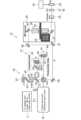
- the light detection device 10includes a light source 11, a waveform shaping unit 12, a PBS (Polarizing Beam Splitter) 13, an excitation pulse light adjustment unit 40, a reference probe pulse light adjustment unit 41, and a phase modulation. It includes a probe pulse light adjusting unit 42, a microscope 25, a light receiving unit 43, and a control unit 44.
- the light source 11is a laser light source that generates excitation light Le and probe light (reference probe light Lr and phase-modulated probe light Lp) for generating an SRS signal.
- pulsed excitation lightexcitation pulsed light Pe
- probe lightreference probe pulsed light Pr and phase-modulated probe pulsed light Pp
- the light source 11is the source of these pulsed lights.
- Light source pulsed light Psis generated. Therefore, the laser light from the light source 11 is divided into three parts: an excitation light Le, a reference probe light Lr, and a phase modulation probe light Lp.
- the light source pulsed light Ps and the excitation pulsed light Pe according to the present embodimentare ultrashort pulsed light (femtosecond pulsed light).
- the center wavelength of the light source pulsed light Ps according to the present embodimentis 790 nm as an example, and the pulse repetition frequency is 80 MHz as an example.
- the excitation pulse light adjustment unit 40is a part that adjusts the incident excitation pulse light Pe
- the reference probe pulse light adjustment unit 41is a part that adjusts the incident reference probe pulse light Pr, and the phase modulation probe pulse light adjustment.
- the part 42is a part for adjusting the incident phase-modulated probe pulsed light Pp.
- the microscope 25is a portion where the sample is irradiated with the excitation light and the probe light.
- the light receiving unit 43receives the Raman signal light generated in the sample, and the control unit 44 controls the entire photodetector 10.
- an ultrashort pulse laser that generates a wide band light source pulsed light Psis used as the light source 11.
- a near-infrared wideband femtosecond laseris used as an example of the light source 11. More specifically, as shown in FIG. 1, as an example of the light source 11, a titanium sapphire laser having a center wavelength of 790 nm is used, and the pulse width is set to 15 fs (femtosecond) or less.
- the wavelength and pulse width of the light source 11are not limited to this, and may be set to appropriate values according to the design content of the photodetector 10.
- the light source pulsed light Ps emitted from the light source 11is linearly polarized light in a predetermined direction.
- the polarization mode of the light source pulsed light Psis not limited to this, and may be, for example, circularly polarized light, elliptically polarized light, or the like.
- the waveform shaping unit 12is a portion that compensates the light source pulsed light Ps to satisfy desired characteristics. That is, the waveform shaping unit 12 is configured to include an adaptive optics element (not shown), an SLM (Spatial Light Modulator), and the like, which are not shown as an example, and the pulse width of the irradiation light under the objective lens 32, which will be described later, is large. As an example, dispersion compensation is appropriately performed so as to be 15 fs.
- the dispersion-compensated optical elementa chirped mirror that provides high reflectance and negative second-order dispersion compensation by a dielectric multilayer film is used, and as an example of SLM, a liquid crystal spatial light modulator is used. There is.
- PBS 13is an optical element that divides the laser light generated by the light source 11 into excitation light Le and probe light (reference probe light Lr, phase modulation probe light Lp).
- the excitation pulse light adjustment unit 40includes a ⁇ / 4 wave plate 14 and an end mirror 15.
- the optical path of the excitation light Leis as follows: light source 11 ⁇ waveform shaping unit 12 ⁇ PBS 13 ⁇ 1/4 wave plate 14 ⁇ end mirror 15 ⁇ 1/4 wave plate 14 ⁇ PBS 13 ⁇ mirror 29.
- the 1/4 wave plate 14is reflected by PBS 13 by once converting the excitation light Le into circularly polarized light and making the polarization direction after being reflected by the end mirror 15 different from the polarization direction of the light source pulsed light Ps. I am trying to do it.
- the end mirror 15is movable in the optical axis direction of the excitation light Le, adjusts the delay time given to the excitation pulse light Pe, and sets the time difference from the probe pulse light.
- a piezo element(not shown) is further attached to the end mirror 15 according to the present embodiment, and the piezo element is configured to allow minute fluctuations in the optical axis direction. The details of this minute fluctuation will be described later.
- the reference probe pulse light adjusting unit 41includes a dispersion compensator 36 and a wavelength scanning unit 24, and the wavelength scanning unit 24 includes a bandpass filter 18, a 1/4 wave plate 19, and an end mirror 20. ..
- the optical path of the reference probe light Lris as follows: light source 11 ⁇ waveform shaping unit 12 ⁇ PBS 13 ⁇ bandpass filter 16 (denoted as “DM” in FIG. 1) ⁇ dispersion compensator 36 ⁇ bandpass filter 18 ⁇ 1/4 wave plate 19 ⁇ End mirror 20 ⁇ 1/4 wave plate 19 ⁇ Bandpass filter 18 ⁇ Dispersion compensator 36 ⁇ Bandpass filter 16 ⁇ PBS 13 ⁇ Mirror 29.
- the bandpass filter 18is a tunable filter that sets the center frequency of the reference probe pulsed light Pr, which is rotatable about a predetermined rotation axis.
- the variable range of the bandpass filter 18is configured so that the center wavelength of the reference probe pulsed light Pr can be selected in the range of 790 nm to 870 nm as an example.
- the end mirror 20mainly compensates for fluctuations in the delay of the reference probe pulsed light Pr due to the rotation of the bandpass filter 18.
- the wavelength scanning unit 24is connected to a control unit 44 described later, and the bandpass filter 18 and the end mirror 20 are controlled by the control unit 44.
- the dispersion compensator 36is an optical element that gives the reference probe pulsed light Pr a dispersion corresponding to the dispersion of the light modulator 21 described later.
- the phase modulation probe pulse optical adjustment unit 42includes an optical modulator 21 (denoted as “EOM1” in FIG. 1), a bandpass filter 35 (denoted as “BPF” in FIG. 1), a 1/4 wave plate 22, and a bandpass filter 35. It is configured to include an end mirror 23.
- the optical path of the phase modulation probe light Lpis as follows: light source 11 ⁇ waveform shaping unit 12 ⁇ PBS 13 ⁇ bandpass filter 16 ⁇ optical modulator 21 ⁇ bandpass filter 35 ⁇ 1/4 wave plate 22 ⁇ end mirror 23 ⁇ 1/4 wave plate. 22 ⁇ bandpass filter 35 ⁇ optical modulator 21 ⁇ bandpass filter 16 ⁇ PBS 13 ⁇ mirror 29.
- the excitation light Le and the probe lightare branched by the PBS 13, and the reference probe light Lr and the phase modulation probe light Lp are branched by the bandpass filter 16. Will be done.
- the optical modulator 21is a phase modulator that phase-modulates the phase modulation probe light Lp, and in the present embodiment, EOM (Electro Optic Modulator) is used as an example.
- the light modulator 21is connected to a drive circuit (not shown), and the drive circuit is connected to the control unit 44.
- the phase modulation by the light modulator 21is performed by a modulated signal of a sawtooth waveform (sawtooth wave) of 65 kHz as an example.
- the bandpass filter 35is a tunable filter that sets the center frequency of the phase modulation probe pulsed light Pp.
- the wavelength of the phase modulation probe light Lpis set to 758 nm as an example.
- the function of the 1/4 wave plate 22is the same as that of the 1/4 wave plate 14. Further, the end mirror 23 adjusts the temporal arrangement relationship between the reference probe pulse light Pr and the phase modulation probe pulse light Pp. In the present embodiment, a mode in which the delay is adjusted by the end mirrors 15, 20, and 23 will be described as an example. A form using a line or the like may be used.
- the reference probe pulse light Pr and the phase modulation probe pulse light Pphave an asymmetric waveform with a fast rise and a slow fall, and are arranged so as to be delayed by a predetermined time from the excitation pulse light Pe (). FIG. 2A).
- the reference probe pulsed light Pr and the phase-modulated probe pulsed light Pphave substantially the same waveform (waveforms close to each other) having different center wavelengths, and are superimposed in time.
- the above-mentioned excitation light Le, reference probe light Lr, and phase modulation probe light Lpare folded back by the mirror 29 and then coaxially combined to form a combined wave light Lg. Through, it is introduced into the microscope 25. At this time, the relative delay time between the excitation pulse light Pe and the probe pulse light can be adjusted by the position in the optical axis direction of the end mirror 15 of the excitation pulse light adjustment unit 40.
- the mirrors 29, 37, and 38are elements for converting an optical path, and are not limited to the configuration shown in FIG.
- the microscope 25is an optical microscope, and includes an objective lens 32, a stage 34, and folding mirrors 30 and 31.
- the sample 33is placed on the stage 34, and the combined wave light Lg incident on the objective lens 32 irradiates the sample 33.
- Sample 33is, for example, a living cell in which a drug has been infiltrated.
- an SRS signalis generated based on the SRS process, for example, due to the molecular vibration of the drug molecule.
- the light receiving unit 43includes a polarizer (polarizer) 26, a long pass filter 27, and a light receiver 28.
- the polarizer 26has a polarization axis in a direction different from the polarization direction of the excitation light Le (for example, a direction orthogonal to each other), and removes the excitation light Le from the combined light Lg.
- the long-pass filter 27is a filter from which the excitation light Le is removed and the phase-modulated probe light Lp is removed from the combined light Lg including the reference probe light Lr and the phase-modulated probe light Lp. This is because the wavelength of the reference probe light Lr is set longer than the wavelength of the phase modulation probe light Lp in the present embodiment.
- the receiver 28receives the reference probe light Lr and converts it into an electric signal. For the receiver 28, for example, a silicon photodiode is used.
- the light receiving device 28is connected to the control unit 44, and the light receiving signal in the light receiving device 28 is sent to the control unit 44.
- the reason why the long pass filter 27 is used in this embodimentis that the wavelength of the reference probe light Lr is set longer than the wavelength of the phase modulation probe light Lp as described above. Since the relationship between the wavelength of the reference probe light Lr and the wavelength of the phase-modulated probe light Lp is not particularly limited, when the wavelength of the reference probe light Lr is set shorter than the wavelength of the phase-modulated probe light Lp, the long-pass filter 27 is used instead. A short path filter may be used.
- the excitation pulse light Peis the polarizer 26 and the phase modulation probe pulse light Pp.
- the light intensity of the reference probe pulsed light Pris converted into a current by a photodetector, and the light intensity modulation component superimposed on the reference probe pulsed light Pr is detected by the lock-in amplifier.
- the light intensity modulation component detected by the lock-in amplifieris a signal component derived from Raman scattering in the sample 33, that is, an SRS signal.
- the SRS signalis a signal proportional to the concentration of the sample (in this embodiment, a drug as an example).
- a mode in which the polarizer 26 and the long-pass filter 27 are arranged in this orderhas been illustrated and described, but the order may be reversed.
- the lock-in amplifieris composed of a control unit 44.
- the control unit 44is a part that controls the photodetector 10 in an integrated manner, and includes a CPU (Central Processing Unit), a ROM (Read Only Memory), a RAM (Random Access Memory), and the like (not shown).
- the control unit 44also performs a photodetection process for extracting the frequency component of the SRS light from the reference probe light Lr containing the SRS light generated in the sample 33.
- the control unit 44further executes the non-resonant background signal reduction process according to the present embodiment described later.
- the control unit 44is further connected to a drive circuit (including a signal generator; not shown) of the light modulator 21, a receiver 28, a wavelength scanning unit 24, and the like.
- a signal generator (signal generator) or a high-voltage amplifier that generates an electric signal for changing the drive voltage of the optical modulator 21 to perform phase modulationmay be provided inside or externally to the control unit 44. .. In this case, the control unit 44 controls the signal generator to control the waveform of the drive voltage for modulating the light modulator 21.
- the control unit 44can be configured by using a general personal computer or the like.
- the control unit 44drives the optical modulator 21 via a drive circuit, receives an amplitude-modulated signal from the receiver 28 to form a lock-in amplifier, and forms an SRS signal from the reference probe pulsed light Pr, which is amplitude-modulated by heterodyne interference. Is extracted. More specifically, as a result of heterodyne interference by the reference probe light Lr and the phase modulation probe light Lp, the amplitude modulation signal applied to the reference probe pulse light Pr is locked-in detected as a signal corresponding to the SRS signal.
- a wavelength scanning unit 24is further connected to the control unit 44, and the control unit 44 controls the rotation of the bandpass filter 18 included in the wavelength scanning unit 24 and the movement of the end mirror 20. Further, the control unit 44 is connected to a piezo element attached to the end mirror 15 and drives the piezo element to cause the end mirror 15 to fluctuate minutely in the optical axis direction.
- the probe light in which the substance response (instantaneous change in refractive index) generated by the molecular vibration excited by the excitation light Leis delayed for a time.
- the light intensity modulation component converted to intensity modulation and synchronized with the modulation frequencyis detected using a demodulator such as a lock-in amplifier.
- FIG. 2Ais a diagram for explaining the characteristics of the pulsed light on the time axis in the photodetector 10
- FIG. 2Bis a diagram for explaining the characteristics on the frequency axis.
- 3A to 3Dare diagrams for explaining the principle of reducing the non-resonant background signal in the photodetector 10.
- the light detection device 10reduces the non-resonant background signal by modulating the relative delay between the excitation light and the probe light with an amplitude of about a time corresponding to the wavelength of the light. Therefore, in the photodetector 10, the end mirror 15 is driven by a piezo element attached to the end mirror 15 to periodically change the optical path length of the excitation light Le.
- the modulationis performed with a sawtooth wave having a frequency of, for example, about 300 Hz.
- the modulation amplitude of the optical path lengthis set to, for example, a movement amount corresponding to a delay of one wavelength of the phase modulation probe light Lp (for example, a wavelength of 758 nm).
- optical path length modulationchanging the relative optical path lengths of the excitation light Le and the probe light.
- the piezo elementwill be described as an example of the mechanism for performing the optical path length modulation, but the present invention is not limited to this, and for example, a mirror holding mechanism equipped with a stepping motor may be used, or a plurality of light deflections may be used. It may be in the form of a mechanism in which elements (galvano mirrors) are interlocked and driven.
- the modulation waveform of the optical path length modulationis not limited to the sawtooth wave, and may be a periodic waveform, for example, a sine wave. However, since the sawtooth wave can be configured so that the phase difference at the discontinuity is 2 ⁇ , it is preferable to use the sawtooth wave from this viewpoint.
- a mode in which the modulation frequency of the optical path length modulation is set to about 300 Hzwill be described as an example, but a modulation frequency of several kHz or more is more preferable.
- the modulation frequency of the optical path length modulationis preferably equal to or lower than the modulation frequency of the phase modulation by the optical modulator 21.
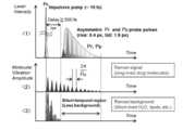
- FIG. 2Ashows the relationship between the time waveform of each pulse and the molecular vibration amplitude
- FIG. 2A ⁇ 1>shows the temporal relationship between the excitation pulse light Pe, the reference probe pulse light Pr, and the phase modulation probe pulse light Pp, that is, the incident timing. Is shown.
- the reference probe pulse light Pr and phase modulated probe pulse light Ppoverlap in time, delayed by a delay time tau pr from the excitation pulse light Pe. That is, in the present embodiment, a plurality of molecular vibrations are excited by the excitation light Le having a short pulse width, and the vibrations are heterodyne-detected by using two probe lights.
- the delay time ⁇ pris set to 500 fs as an example.
- the delay time tau pris not limited to 500 fs, it may be appropriately set according to the detection target or the like.
- the excitation pulse light Pe and the probe pulse lightare drawn so as to be sufficiently separated in time for convenience, but in reality, the excitation pulse light Pe and each probe pulse light are drawn.
- a non-resonant background signalis generated in the region where the hem overlaps with each other.
- each envelopeindicates the reference probe pulse light Pr and the phase modulation probe pulse light Pp.
- the pulsed waveform shown inside the envelopeconceptually represents the beat signal due to the frequency difference between the reference probe pulse light Pr and the phase modulation probe pulse light Pp.
- a temporally asymmetric waveformis used as the reference probe pulse light Pr and the phase modulation probe pulse light Pp, and the reference probe pulse light Pr and the phase modulation probe pulse are used.
- the rise time of the optical Ppis 0.4 ps as an example, and the fall time is 1.9 ps as an example.
- FIGS. 2A ⁇ 2> and ⁇ 3>show the molecular vibration amplitude
- FIG. 2A ⁇ 2>shows the molecular vibration of the sample (in this embodiment, a drug is used as an example).
- >Indicates background molecular vibrations, respectively.
- the vibration of the sampleis a relatively long-life vibration that starts from the position of the excitation pulse light Pe and continues to the position where the probe pulse light almost ends.
- the background molecular vibrationhas a shorter life than the molecular vibration of the sample, and almost disappears near the rising position of the probe pulse light.
- the delay time ⁇ pr between the excitation pulse light Pe and the probe pulse lightis set so that the probe pulse light rises when the background molecular vibration subsides.
- 2B ⁇ 1>shows the optical output frequency characteristics of the excitation pulsed light Pe
- ⁇ 2>shows the optical output frequency characteristics of the reference probe pulsed light Pr and the phase-modulated probe pulsed light Pp
- ⁇ 3>shows the optical output frequency characteristics of the reference probe pulsed light Pr.
- the scales of the horizontal axes (angular frequency ⁇ ) in FIGS. 2B ⁇ 1> to ⁇ 3>are the same.
- the excited pulsed light Pehas a wide bandwidth.
- the central wavelength of the excitation pulsed light Peis about 790 nm, and the pulse width is about 15 fs.
- the reference probe pulsed light Pris cut out by the bandpass filter 18, and the phase-modulated probe pulsed light Pp is cut out by the bandpass filter 16 to partially cut out the band characteristics of the excited pulsed light Pe.
- the optical output frequency characteristic of the phase-modulated probe pulsed light Ppis band-limited as shown in FIG. 2B ⁇ 2>.
- the center wavelength of the reference probe pulsed light Pr according to the present embodimentis, for example, 790 nm to 870 nm, the bandwidth is about 20 nm, the center wavelength of the phase-modulated probe pulsed light Pp is, for example, about 758 nm, and the bandwidth is about 18 nm. Has been done.
- the bandwidth of the reference probe pulsed light Pr and the bandwidth of the phase-modulated probe pulsed light Ppare set to be substantially equal to each other.
- the difference between the center wavelength range of 790 nm to 870 nm of the reference probe pulsed light Pr and the center wavelength of 758 nm of the phase-modulated probe pulsed light Ppis the wavelength scanning range, which corresponds to the detection range of the molecular vibration of the sample.
- the photodetector 10 according to this embodimenthas a wavelength scanning (spectral scanning) range of 80 nm.
- center wavelength and wavelength scanning range of the reference probe pulsed light Pr and the phase-modulated probe pulsed light Ppare examples, and may be set to appropriate values according to the design conditions of the photodetector 10.
- the scanning of the center wavelength of the reference probe pulsed light Pris performed by rotating the bandpass filter 18 as described above.
- the delay frequency characteristic of the reference probe pulse light Pr and phase modulated probe pulse light Ppcommonly given fixed delay time tau pr between the excitation pulse light Pe Be done.
- non-linear chirps due to the passage of the bandpass filters 18 and 16, respectivelyare applied to the reference probe pulsed light Pr and the phase-modulated probe pulsed light Pp, respectively.
- the shape of the non-linear chirp of the reference probe pulsed light Pr and the shape of the non-linear chirp of the phase modulation probe pulsed light Ppare set to be substantially the same shape.
- the center frequency of the reference probe pulsed light Pr and the center frequency of the phase-modulated probe pulsed light Ppare different.
- the difference between the center frequency of the reference probe pulsed light Pr and the center frequency of the phase-modulated probe pulsed light Ppis referred to as “frequency difference ⁇ R ”.
- each of the reference probe pulsed light Pr and the phase-modulated probe pulsed light Pphas a time-extended asymmetric waveform as shown in FIG. 2A ⁇ 1>.
- the difference frequency of the time-spreading asymmetric pulsesbecomes a constant frequency over time. This difference frequency is equal to the difference in the center frequencies of the probe lights, that is, the frequency difference ⁇ R.
- the vibration components corresponding to this constant frequency difference ⁇ Rare converted into the light intensity modulation of the probe light.
- the sample 33is irradiated with three pulse laser beams of the excitation pulse light Pe, the reference probe pulse light Pr, and the phase modulation probe pulse light Pp, first, a plurality of molecular vibrations are simultaneously excited by the excitation pulse light Pe. After that, energy is transferred between the probe lights by an induced Raman scattering process by the reference probe pulsed light Pr and the phase-modulated probe pulsed light Pp. At this time, the phase modulation applied to the phase modulation probe pulse light Pp is converted into the light intensity modulation of the reference probe pulse light Pr (and the phase modulation probe pulse light Pp).
- the detected frequencyis determined by the frequency difference ⁇ R between the reference probe pulsed light Pr and the phase modulation probe pulsed light Pp. On the other hand, since the frequency resolution is determined by the reciprocal of the pulse width, the ability to discriminate molecules is improved by applying a strong chirp.
- Equation 1the electric field E pump of the excitation pulsed light Pe is shown below (Equation 1)
- the electric field E PM of the phase-modulated probe pulsed light Ppis shown below (Equation 2)
- the electric field E LO of the reference probe pulsed light Pris shown below. It is represented by (Equation 3) shown below.
- Equation 1 to (Equation 3)⁇ indicates the frequency and ⁇ indicates the phase.
- italic characters in mathematical expressionsare expressed as non-italic characters.
- the non-resonant background signal A NRis expressed by the following (Equation 4) at ⁇ pr >> t.
- ⁇ (3)represents a third-order nonlinear susceptibility.
- the product of the frequency ⁇ PM and the delay time ⁇ prremains in the phase term of the non-resonant background signal A NR. Since the response time of the photodetector is slow, the dependence of t is time-averaged and does not appear in the equation.
- the coherent traman signal A sigis expressed by the following (Equation 6).
- ⁇ R⁇ PM - ⁇ LO Is.
- the product of the difference frequency ( ⁇ PM - ⁇ LO ) of the probe light and the delay time ⁇ prremains in the phase term of the coherent Raman signal A sig.
- the phase sensitivity of the output signal to the change of the delay time ⁇ pris ⁇ PM in the case of the non-resonant background signal A NR and in the case of the coherent traman signal A sig ( ⁇ PM - ⁇ LO).
- ⁇ PMis a sufficiently large value, for example, an order of magnitude larger than that of ( ⁇ PM - ⁇ LO ), on the delay time ( ⁇ pr ) axis, for example, one wavelength of probe pulsed light.
- FIG. 3Ashows the modulation waveform ⁇ Z (t) of the optical path length modulation. That is, FIG. 3A shows the change in the position Z (t) of the end mirror 15 (the folded mirror of the excitation light Le) due to the drive of the piezo element.
- the photodetector 10performs optical path length modulation using a modulation waveform of a sawtooth wave whose falling time is shorter than the rising time.
- the modulation frequency f Z of the optical path length modulationis set to about 300 Hz, or a frequency of several kHz or more is not limited thereto.
- the frequency f Z of the optical path length modulationis preferably not more than the modulation frequency of the phase modulation by the optical modulator 21.
- the modulation waveform of the optical path length modulationis not limited to the sawtooth wave, and may be, for example, a sine wave.
- Equation 8the relationship between the relative delay change amount ⁇ pr , which is the change amount of the delay time ⁇ pr , and the displacement ⁇ Z of the end mirror 15 is expressed by the following (Equation 8).
- ⁇ pr2 ⁇ Z / c ⁇ ⁇ ⁇ (Equation 8)
- cis the speed of light.
- the optical path length modulationi.e., modulation of the optical path length of the excitation light Le
- the wavelength of the light used as the reference for the optical path length modulationis preferably the wavelength of the phase modulation probe pulsed light Pp because ⁇ PM ⁇ pr is canceled.
- FIG. 3Bshows the phase modulation waveform ⁇ PM (t) of the light modulator 21.
- the phase modulation waveform ⁇ PM (t)is a sawtooth wave having a frequency f PM of about 100 kHz.
- FIG. 3Bexemplifies a sawtooth wave having a rising time faster than a rising time, but conversely, a sawtooth wave having a rising time faster than a falling time (for example, the waveform shown in FIG. 3B). It may be a line-symmetrical waveform).
- FIG. 3Cshows the light intensity variation of the coherent Raman signal A sig.
- the waveform of the coherent traman signal A sigreciprocates between the solid line and the broken line due to the optical path length modulation.
- the phase difference between the solid line and the broken line ⁇ Ramanis proportional to the molecular vibration frequency ⁇ Raman. That is, the following (Equation 11) is established.
- ⁇ Raman( ⁇ Raman ⁇ pr ) / 2 ⁇ ⁇ ⁇ ⁇ (Equation 11) That is, it can be seen that the waveform of the coherent Raman signal A sig is slightly out of phase due to the optical path length modulation of the excitation light Le, but hardly changes.
- FIG. 3Dshows the light intensity variation of the non-resonant background signal ANR.
- the waveform of the non-resonant background signal ANRreciprocates between the solid line and the broken line due to the optical path length modulation.
- the phase difference ⁇ NR between the solid line and the broken lineis proportional to the frequency ⁇ PM of the phase modulation probe light Lp. That is, the following (Equation 12) is established.
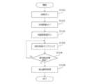
- FIG. 4is a flowchart showing a processing flow of the non-resonant background signal reduction processing program.
- This non-resonant background signal reduction processing programis stored in a storage device such as a ROM (not shown), which is read from the ROM or the like by the CPU, expanded into the RAM or the like, and executed.
- step S100the power of the light source 11 is turned on and the light source 11 is turned on.
- step S101the drive circuit of the light modulator 21 (not shown) is operated to turn on the phase modulation by the light modulator 21.
- step S102the drive circuit (not shown) of the piezo element attached to the end mirror 15 is operated to turn on the optical path length modulation.
- the drive circuit(not shown) of the piezo element attached to the end mirror 15 is operated to turn on the optical path length modulation.
- step S103sampling of the coherence traman signal (SRS signal) based on the lock-in detection is performed.
- step S104it is determined whether the signal detection time has elapsed (whether sampling at all sampling points has been completed), and if the determination is negative, the process returns to step S103 and sampling is continued. On the other hand, if a positive determination is made, the process proceeds to step S105.
- step S105signal processing is performed using the detection signals sampled so far, and the spectrum of the coherent traman signal A sig is calculated. After that, the non-resonant background signal reduction processing program is terminated.
- the time series output signalis Fourier transformed after the signal is acquired, and filtering is performed to remove the component of the optical path length modulation frequency.
- the signal outputmay be detected as it is.
- the frequency setting in any casemay be used, but the setting in case 2 is preferable from the viewpoint of simplifying signal processing.
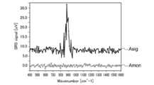
- FIGS. 5A and 5Bare a spectrum of coherent Raman signals A sig (SRS signal) and the monitor output when not performing optical path length modulation
- the spectra ofare shown respectively.
- phase modulationis performed by the optical modulator 21.
- the monitor outputis an output for measuring noise of the light source laser, and is a baseline determined by the noise of the light source 11.
- the implementation conditions of this embodimentare as follows. -Sample: Acetic acid (Raman peak: 893 cm -1 ) -Phase modulation Modulation waveform: sawtooth wave, modulation frequency: 65 kHz -Optical path length modulation Modulation waveform: sine wave, modulation frequency: 300 Hz, modulation amplitude: length corresponding to a delay of one wavelength of the phase-modulated probe light Lp (actually, the spectrum of the excitation light Le and the phase-modulated probe light Lp). Monitor the interference and set the optimum value of the amplitude of the piezo element input voltage.) ⁇ Lock-in amplifier integration time: 300ms, sampling frequency: 3.3Hz ⁇ Delay time ⁇ pr : 1.2 ps
- the peak of the coherent traman signal A sigcorresponds to the Raman peak of acetic acid (893 cm -1).
- the baselinefloats uniformly by about 8 ⁇ V due to the non-resonant background signal A NR. Since the coherent traman signal A sig having an amplitude of about 24 ⁇ V is superimposed on the baseline, a deterioration in the ratio of the SRS signal to the background signal can be seen.
- the floating of the baseline due to the non-resonant background signal A NRis almost completely eliminated. As a result, it can be seen that the ratio of the SRS signal to the background signal is remarkably improved even if the coherent traman signal A sig is the same, about 24 ⁇ V.
- the optical detection device and the optical detection method according to the present embodimenthave a relative time difference (delay) between the excitation pulse light and the detection pulse light (probe pulse light) in addition to the phase modulation. It has a configuration in which it is repeatedly changed for a time corresponding to the optical path length (or an integral multiple thereof) for one wavelength of light.
- delay time modulationoptical path length modulation
- only the complex amplitude of the non-resonant background signalcan be selectively smoothed to approach zero without attenuating the molecular vibration signal (coherence traman signal). ..
- the influence of the non-resonant background signal including the influence of the birefringence of the samplecan be reduced, and for example, it is possible to detect a low-concentration drug having a concentration of less than mM (millimeter), which has been extremely difficult in the past.
- the embodiment using one excitation pulsed light Pehas been described as an example, but the present invention is not limited to this, and a plurality of excitation pulsed light Pes may be used.
- the excitation power for the samplecan be gradually increased.
- Photodetector 11Light source 12 Waveform shaping unit 13 PBS 14 1/4 frequency plate 15 end mirror 16 band pass filter 18 band pass filter 19 1/4 wavelength plate 20 end mirror 21 optical modulator 22 1/4 wavelength plate 23 end mirror 24 wavelength scanning unit 25 microscope 26 polarizer 27 long pass Filter 28 Receiver 29, 30, 31 Mirror 32 Objective lens 33 Sample 34 Stage 35 Band pass filter 36 Dispersion compensator 37, 38 Mirror 40 Excitation pulse light adjustment unit 41 Reference probe Pulse light adjustment unit 42 Phase modulation probe Pulse light adjustment unit 43 Light receiving unit 44 Control unit Le Excitation light Lr Reference probe light Lp Phase modulation probe light Lg Combined light Pr Reference probe Pulse light Pp Phase modulation probe Pulse light Ps Source pulse light Pe Excitation pulse light Pp Phase modulation probe Pulse light Pr Reference probe pulse Optical ⁇ pr Delay time ⁇ R Frequency difference
Landscapes
- Physics & Mathematics (AREA)
- Electromagnetism (AREA)
- Health & Medical Sciences (AREA)
- Optics & Photonics (AREA)
- General Physics & Mathematics (AREA)
- Engineering & Computer Science (AREA)
- Plasma & Fusion (AREA)
- Analytical Chemistry (AREA)
- Biochemistry (AREA)
- General Health & Medical Sciences (AREA)
- Chemical & Material Sciences (AREA)
- Immunology (AREA)
- Pathology (AREA)
- Life Sciences & Earth Sciences (AREA)
- Nuclear Medicine, Radiotherapy & Molecular Imaging (AREA)
- Investigating, Analyzing Materials By Fluorescence Or Luminescence (AREA)
Abstract
Description
Translated fromJapanese本開示は、ラマン散乱を検出する光検出装置、および光検出方法に関する。The present disclosure relates to a photodetector for detecting Raman scattering and a photodetection method.
ラマン散乱を検出する光検出装置として、コヒーレントラマン散乱顕微鏡が知られている。コヒーレントラマン散乱顕微鏡とは、2つ以上のパルスレーザ光を試料に照射し、その結果試料から発せられるラマン散乱光を観察することにより、試料内の物質を分析する装置である。特に、時間分解型のコヒーレントラマン散乱顕微鏡は、標識を用いずに、細胞や生体組織由来のバックグラウンドを回避しながら、特異的な分子振動を持つ小分子薬剤などの信号を高いコントラストで画像化することが可能である。このような技術は一般に、ラマン分光技術と総称され、ラマン分光技術による微量物質の検出は、分析装置における基本技術としての重要性が高く、多くの技術開発が行われてきた。一方、昨今の医療技術の進歩と共に、微量物質検出技術の医療診断技術への応用が試みられており、当該医療診断技術の分野においてもより一層の微量物質の検出感度の向上が求められるようになってきている。A coherent Raman scattering microscope is known as a photodetector for detecting Raman scattering. The coherent Raman scattering microscope is a device that analyzes a substance in a sample by irradiating the sample with two or more pulsed laser beams and observing the Raman scattered light emitted from the sample as a result. In particular, time-resolved coherent Raman scattering microscopes image signals of small molecule drugs with specific molecular vibrations with high contrast while avoiding backgrounds derived from cells and biological tissues without using labels. It is possible to do. Such techniques are generally collectively referred to as Raman spectroscopy techniques, and detection of trace substances by Raman spectroscopy is of high importance as a basic technique in an analyzer, and many technological developments have been carried out. On the other hand, with the recent progress of medical technology, application of trace substance detection technology to medical diagnosis technology is being attempted, and further improvement of detection sensitivity of trace substances is required in the field of the medical diagnosis technology. It has become to.
従来、コヒーレントラマン散乱顕微鏡は、観察に用いる入射レーザ光の振幅を変調して試料に入射させ、入射光に対する透過光または反射散乱光を光検出器で検出し、それを復調することでラマン信号を検出する振幅変調型コヒーレントラマン散乱顕微鏡が一般的である。この振幅変調型コヒーレントラマン散乱顕微鏡では、水や脂質などの生体自身に含まれる分子振動持続時間の短い、強いラマン信号を検出することで、細胞や組織の形態情報を高速に画像化できる。Conventionally, a coherent Raman scattering microscope modulates the amplitude of incident laser light used for observation and causes it to enter a sample, detects transmitted light or reflected scattered light with respect to the incident light with an optical detector, and demodulates the Raman signal. An amplitude-modulated coherent Raman scattering microscope that detects light is common. In this amplitude-modulated coherent Raman scattering microscope, morphological information of cells and tissues can be imaged at high speed by detecting a strong Raman signal having a short duration of molecular vibration contained in the living body itself such as water and lipid.
振幅変調型コヒーレントラマン散乱顕微鏡に関連する従来技術として、例えば特開2010-048805号公報に開示された顕微撮像システムが知られている。特開2010-048805号公報に係る顕微撮像システムは、コヒーレントラマン効果のひとつとして知られる誘導ラマン散乱(Stimulated Raman Scattering:SRS)を用いた光検出装置である。特開2010-048805号公報に係る顕微撮像システム10は、ポンプ(励起)ビームとして使用される中心周波数ω1のレーザパルス列20と、ストークスビームとして使用される中心周波数ω2のレーザパルス列16の2つのレーザパルス列を用いている。ストークスビームは変調器で振幅変調され、励起ビームとストークスビームは結合器25で結合された後、サンプル22に照射される。サンプル22を透過した透過光は光検知器36に送られ、光検知器36からの検知信号から振幅変調成分を検知することによって、誘導ラマン散乱に基づく画像を取得する。As a prior art related to an amplitude-modulated coherent Raman scattering microscope, for example, a microscopic imaging system disclosed in Japanese Patent Application Laid-Open No. 2010-408805 is known. The microscopic imaging system according to Japanese Patent Application Laid-Open No. 2010-408805 is a photodetector using induced Raman scattering (SRS) known as one of the coherent Raman effects. The
従来のポンプ光およびプローブ光を用いたコヒーレントラマン散乱顕微鏡の問題点は、ポンプパルスとプローブパルスとの間の非線形四光波混合によって引き起こされる非共鳴背景信号の発生である。つまり、分子振動を励起する光パルスとそれを検出するための光パルスが時間的に重なっている場合には、分子振動とは関係のない非線形光学効果によるバックグラウンド(非共鳴バックグラウンド)が信号に重畳されてしまうため、検出可能な試料の濃度が制限されてしまうという問題である。例えば、生体試料中に分布する低分子のコヒーレントラマン信号を検出する際には、生体自身に多量に含まれる水や脂質などから生じる非共鳴背景信号が検出限界の著しい低下を招く場合があった。The problem with conventional coherent Raman scattering microscopes using pump light and probe light is the generation of non-resonant background signals caused by non-linear four-wave mixing between the pump pulse and the probe pulse. In other words, when the optical pulse that excites the molecular vibration and the optical pulse for detecting it overlap in time, the background (non-resonant background) due to the nonlinear optical effect that has nothing to do with the molecular vibration is a signal. This is a problem that the concentration of the detectable sample is limited because it is superimposed on the sample. For example, when detecting a small molecule coherent traman signal distributed in a biological sample, a non-resonant background signal generated from a large amount of water or lipid contained in the living body itself may cause a significant decrease in the detection limit. ..
上記問題を回避するため、従来、ポンプパルスの偏光とプローブパルスの偏光とを直交させる方法、波形整形技術でプローブパルスの立ち上がり時間を速くする方法等の手法が用いられていた。しかしながら、前者の偏光の直交性を利用したバックグラウンド低減法は、生体試料自体で発生する複屈折や偏光解消の影響を受けやすく、それによって実質的な検出限界が制限されていた。In order to avoid the above problem, conventionally, a method of orthogonalizing the polarization of the pump pulse and the polarization of the probe pulse, a method of increasing the rise time of the probe pulse by the waveform shaping technique, and the like have been used. However, the former background reduction method utilizing the orthogonality of polarized light is susceptible to the birefringence and depolarization that occur in the biological sample itself, thereby limiting the substantial detection limit.
また、後者のプローブパルスの波形を整形する方法は、非共鳴背景信号がポンプパルスとプローブパルスが時間的に重なっている時だけ発生することに着目し、ポンプパルスとプローブパルスの時間的な重なりを最小限にすることにより非共鳴背景信号の低減を図ったものである。しかしながら、ポンプパルスとプローブパルスの時間的な重なりを小さくすることにより、目的の低分子からの信号強度の低下も招くため、SRS信号対非共鳴背景信号のコントラスト比には限界があった。そのため、新たな原理による非共鳴背景信号の除去が望まれていた。The latter method of shaping the probe pulse waveform focuses on the fact that the non-resonant background signal is generated only when the pump pulse and the probe pulse overlap in time, and the pump pulse and the probe pulse overlap in time. The non-resonant background signal is reduced by minimizing the above. However, by reducing the temporal overlap of the pump pulse and the probe pulse, the signal strength from the target small molecule is also lowered, so that the contrast ratio of the SRS signal to the non-resonant background signal is limited. Therefore, it has been desired to remove the non-resonant background signal by a new principle.
本開示の実施形態は、以上のような背景に鑑みてなされたものであり、簡易な構成により非共鳴背景信号を効果的に低減することが可能な光検出装置、および光検出方法を提供することを目的とする。The embodiment of the present disclosure has been made in view of the above background, and provides a photodetector capable of effectively reducing a non-resonant background signal with a simple configuration, and a photodetector method. The purpose is.
上記目的を達成するために、第1態様に係る光検出装置は、光源パルス光を発生するレーザ光源と、前記光源パルス光を励起光、第1のプローブ光、および第2のプローブ光に分岐する分岐部と、前記励起光と、前記第1のプローブ光および前記第2のプローブ光との間の相対的な光路長差を変調する光路長変調を実行する第1の変調部と、前記第1のプローブ光を位相変調する第2の変調部と、前記励起光、前記第1のプローブ光および前記第2のプローブ光が合波された合波光を試料に照射して、発生した誘導ラマン散乱信号を検出する検出部と、を含むものである。In order to achieve the above object, the light detection device according to the first aspect branches a laser light source that generates light source pulsed light and the light source pulsed light into excitation light, first probe light, and second probe light. A branching portion, a first modulation section that performs optical path length modulation that modulates the relative optical path length difference between the excitation light, the first probe light, and the second probe light, and the above-mentioned The induction generated by irradiating the sample with a second modulation unit that phase-modulates the first probe light and a combined wave light in which the excitation light, the first probe light, and the second probe light are combined. It includes a detection unit that detects a Raman scattered signal.
また、第2態様に係る光検出装置は、第1態様に係る光検出装置において、前記第1のプローブ光と前記第2のプローブ光との間の遅延時間が固定値であるものである。Further, in the photodetector according to the second aspect, the delay time between the first probe light and the second probe light is a fixed value in the photodetector according to the first aspect.
また、第3態様に係る光検出装置は、第1態様または第2態様に係る光検出装置において、前記第1の変調部は、前記励起光、前記第1のプローブ光、および前記第2のプローブ光のいずれかの単位波長に相当する長さの整数倍で前記光路長変調を実行するものである。Further, the photodetector according to the third aspect is the photodetector according to the first or second aspect, wherein the first modulation unit is the excitation light, the first probe light, and the second. The optical path length modulation is performed with an integral multiple of the length corresponding to any unit wavelength of the probe light.
また、第4態様に係る光検出装置は、第1態様から第3態様のいずれかの態様に係る光検出装置において、前記励起光を光軸方向に折り返すミラーをさらに含み、前記光路長変調は、前記ミラーを光軸方向に予め定められた振幅で往復移動させて行うものである。Further, the photodetector according to the fourth aspect further includes a mirror that folds the excitation light in the optical axis direction in the photodetector according to any one of the first to third aspects, and the optical path length modulation is performed. , The mirror is reciprocated in the direction of the optical axis with a predetermined amplitude.
また、第5態様に係る光検出装置は、第1態様から第4態様のいずれかの態様に係る光検出装置において、前記光路長変調の変調波形が、立ち上がり時間より立ち下り時間の短い鋸歯状波形であるものである。Further, in the optical detection device according to the fifth aspect, in the optical detection device according to any one of the first to fourth aspects, the modulation waveform of the optical path length modulation has a serrated shape in which the falling time is shorter than the rising time. It is a waveform.
また、第6態様に係る光検出装置は、第1態様から第5態様のいずれかの態様に係る光検出装置において、前記検出部は、前記第1のプローブ光および前記第2のプローブ光によるヘテロダイン干渉の結果、前記第1のプローブ光を位相変調の結果、前記第2のプローブ光の波長に現れる誘導ラマン信号とのヘテロダイン干渉により振幅変調信号を誘導ラマン散乱信号に対応する信号としてサンプリングしつつロックイン検出することにより誘導ラマン散乱信号を検出し、前記光路長変調の変調周波数は、前記サンプリングのサンプリング周波数より高い周波数であるものである。Further, the light detection device according to the sixth aspect is the light detection device according to any one of the first to fifth aspects, and the detection unit is based on the first probe light and the second probe light. As a result of heterodyne interference, the first probe light is phase-modulated, and as a result, the amplitude-modulated signal is sampled as a signal corresponding to the induced Raman scattered signal by heterodyne interference with the induced Raman signal appearing at the frequency of the second probe light. The induced Raman scattered signal is detected by the lock-in detection, and the modulation frequency of the optical path length modulation is higher than the sampling frequency of the sampling.
上記目的を達成するために、第7態様に係る光検出方法は、励起光、第1のプローブ光および第2のプローブ光が合波された合波光を試料に照射して、発生した誘導ラマン散乱信号を検出する光検出方法であって、前記第1のプローブ光を位相変調し、前記励起光と、前記第1のプローブ光および前記第2のプローブ光との間の相対的な光路長差を変調して前記誘導ラマン散乱信号を検出するものである。In order to achieve the above object, in the light detection method according to the seventh aspect, the guided Raman generated by irradiating the sample with the combined wave light in which the excitation light, the first probe light and the second probe light are combined is irradiated. A light detection method for detecting scattered signals, in which the first probe light is phase-modulated, and the relative optical path length between the excitation light and the first probe light and the second probe light. The difference is modulated to detect the induced Raman scattered signal.
本開示の実施形態によれば、簡易な構成により非共鳴背景信号を効果的に低減することが可能な光検出装置、および光検出方法を提供することが可能となる。According to the embodiment of the present disclosure, it is possible to provide a photodetector and a photodetection method capable of effectively reducing a non-resonant background signal with a simple configuration.
以下、図面を参照して、本開示を実施するための形態について詳細に説明する。以下では、本開示に係る光検出装置、および光検出方法を、誘導ラマン散乱の検知手段として位相変調を用いる位相変調型コヒーレントラマン散乱顕微鏡を用いた光検出装置、および光検出方法に適用した形態を例示して説明する。位相変調型コヒーレントラマン散乱顕微鏡は、パルスレーザ光源の出力をポンプ光と位相変調プローブ光およびリファレンスプローブ光の3つに分け、時間的に先に入射するポンプ光と、その後に続く時間的に重なった位相変調プローブ光とリファレンスプローブ光との間の相対位相を変調する。その結果生じたラマン信号光とリファレンスプローブ光との干渉による光強度の変調を光検出器で検出して復調する。この位相変調型コヒーレントラマン散乱顕微鏡では、ポンプ光とプローブ光の相対的な時間差を利用することにより、分子振動の持続時間が比較的長い低分子を高いコントラストで選択的に検出できる。その結果、例えば生体試料を対象に、無標識で分子種を同定しながら濃度分布を可視化するコヒーレントラマン散乱顕微鏡の有用性を飛躍的に高めることができる。Hereinafter, the mode for carrying out the present disclosure will be described in detail with reference to the drawings. In the following, the light detection device and the light detection method according to the present disclosure are applied to the light detection device and the light detection method using a phase modulation type coherent Raman scattering microscope that uses phase modulation as a detection means for induced Raman scattering. Will be illustrated and described. The phase-modulated coherent traman scattering microscope divides the output of the pulsed laser light source into three parts: pump light, phase-modulated probe light, and reference probe light. Phase modulation Modulates the relative phase between the probe light and the reference probe light. The resulting modulation of the light intensity due to the interference between the Raman signal light and the reference probe light is detected by the photodetector and demodulated. In this phase-modulated coherent Raman scattering microscope, small molecules having a relatively long duration of molecular vibration can be selectively detected with high contrast by utilizing the relative time difference between the pump light and the probe light. As a result, for example, the usefulness of a coherent Raman scattering microscope that visualizes the concentration distribution of a biological sample while identifying the molecular species without labeling can be dramatically enhanced.
図1を参照して、本実施の形態に係る光検出装置10について説明する。図1に示すように、光検出装置10は、光源11、波形整形部12、PBS(Polarizing Beam Splitter:偏光ビームスプリッタ)13、励起パルス光調整部40、リファレンスプローブパルス光調整部41、位相変調プローブパルス光調整部42、顕微鏡25、受光部43、および制御部44を含んで構成されている。The
光源11は、SRS信号を生成させるための励起光Leとプローブ光(リファレンスプローブ光Lr、および位相変調プローブ光Lp)を発生するレーザ光源である。本実施の形態では、パルス状の励起光(励起パルス光Pe)、およびプローブ光(リファレンスプローブパルス光Pr、および位相変調プローブパルス光Pp)を用いており、光源11はこれらのパルス光の元となる光源パルス光Psを発生する。そのため、光源11からのレーザ光は、励起光Le、リファレンスプローブ光Lr、および位相変調プローブ光Lpの3つに分割される。本実施の形態に係る光源パルス光Ps、そして励起パルス光Peは超短パルス光(フェムト秒パルス光)とされている。本実施の形態に係る光源パルス光Psの、中心波長は一例として790nm、パルス繰り返し周波数は一例として80MHzとされている。The
励起パルス光調整部40は、入射された励起パルス光Peの調整を行う部位、リファレンスプローブパルス光調整部41は、入射されたリファレンスプローブパルス光Prの調整を行う部位、位相変調プローブパルス光調整部42は、入射された位相変調プローブパルス光Ppの調整を行う部位である。顕微鏡25は、励起光およびプローブ光を試料に照射させる部位である。受光部43は、試料で発生したラマン信号光を受光し、制御部44は光検出装置10の全体を統括制御する。以下、各々の部位について詳細に説明する。The excitation pulse
本実施の形態に係る光検出装置10では、光源11に広帯域の光源パルス光Psを発生する超短パルスレーザを用いている。本実施の形態では光源11の一例として、近赤外の広帯域フェムト秒レーザを用いている。より具体的には、図1に示すように、光源11の一例として、中心波長が790nmのチタンサファイアレーザを用い、パルス幅を15fs(femtosecond)以下としている。ただし、光源11の波長、パルス幅はこれに限定されるものではなく、光検出装置10の設計内容等に応じて適切な値に設定してよい。なお、本実施の形態では、光源11から出射される光源パルス光Psを予め定められた方向の直線偏光としている。しかしながら、光源パルス光Psの偏光態様はこれに限られず、例えば円偏光、楕円偏光等であってもよい。In the
波形整形部12は、光源パルス光Psを補償して所望の特性を満たすようにする部位である。すなわち波形整形部12は、一例として図示を省略する分散補償光学素子、SLM(Spatial Light Modulator:空間光変調器)等を含んで構成され、後述する対物レンズ32下での照射光のパルス幅が一例として15fsになるように適切に分散補償される。なお、本実施の形態では、分散補償光学素子の一例として、誘電体多層膜により高い反射率と負の2次分散補償を与えるチャープミラーを用い、SLMの一例として液晶空間光変調器を用いている。The
PBS13は、光源11で発生したレーザ光を励起光Leとプローブ光(リファレンスプローブ光Lr、位相変調プローブ光Lp)に2分割する光学素子である。
励起パルス光調整部40は、λ/4波長板14、およびエンドミラー15を備えている。図1において、励起光Leの光路は、光源11→波形整形部12→PBS13→1/4波長板14→エンドミラー15→1/4波長板14→PBS13→ミラー29となっている。1/4波長板14は、励起光Leを一旦円偏光に変換し、エンドミラー15で反射させた後の偏光方向を光源パルス光Psの偏光方向とは異なる方向とすることによりPBS13で反射されるようにしている。エンドミラー15は励起光Leの光軸方向に可動とされ、励起パルス光Peに与える遅延時間を調整し、プローブパルス光との間の時間差を設定する。本実施の形態に係るエンドミラー15にはさらにピエゾ素子(図示省略)が取り付けられており、該ピエゾ素子によって光軸方向に微小変動が可能なように構成されている。この微小変動の詳細については後述する。The excitation pulse
リファレンスプローブパルス光調整部41は、分散補償器36、および波長走査部24を備え、波長走査部24はバンドパスフィルタ18、1/4波長板19、およびエンドミラー20を含んで構成されている。リファレンスプローブ光Lrの光路は、光源11→波形整形部12→PBS13→バンドパスフィルタ16(図1では、「DM」と表記)→分散補償器36→バンドパスフィルタ18→1/4波長板19→エンドミラー20→1/4波長板19→バンドパスフィルタ18→分散補償器36→バンドパスフィルタ16→PBS13→ミラー29となっている。The reference probe pulse
1/4波長板19の機能は1/4波長板14と同様である。図1に示すように、バンドパスフィルタ18は予め定められた回転軸を中心に回転可能とされた、リファレンスプローブパルス光Prの中心周波数を設定するチューナブルフィルタである。本実施の形態では、バンドパスフィルタ18の可変範囲を、リファレンスプローブパルス光Prの中心波長を、一例として790nmから870nmの範囲で選択可能なように構成している。エンドミラー20は、主として、バンドパスフィルタ18の回転に伴うリファレンスプローブパルス光Prの遅延の変動を補償する。波長走査部24は、後述する制御部44に接続され、バンドパスフィルタ18、およびエンドミラー20は制御部44によって制御される。分散補償器36は、後述の光変調器21の分散に相当する分散をリファレンスプローブパルス光Prに与える光学素子である。The function of the 1/4 wave plate 19 is the same as that of the 1/4
位相変調プローブパルス光調整部42は、光変調器21(図1では、「EOM1」と表記)、バンドパスフィルタ35(図1では、「BPF」と表記)、1/4波長板22、およびエンドミラー23を含んで構成されている。位相変調プローブ光Lpの光路は、光源11→波形整形部12→PBS13→バンドパスフィルタ16→光変調器21→バンドパスフィルタ35→1/4波長板22→エンドミラー23→1/4波長板22→バンドパスフィルタ35→光変調器21→バンドパスフィルタ16→PBS13→ミラー29となっている。すなわち、本実施の形態では、PBS13により励起光Leとプローブ光(リファレンスプローブ光Lr、位相変調プローブ光Lp)に分岐され、バンドパスフィルタ16によりリファレンスプローブ光Lrと位相変調プローブ光Lpとに分岐される。The phase modulation probe pulse
光変調器21は、位相変調プローブ光Lpを位相変調する位相変調器であり、本実施の形態では、一例としてEOM(Electro Optic Modulator)を用いている。光変調器21は図示を省略する駆動回路に接続され、該駆動回路は制御部44に接続されている。本実施の形態では、光変調器21による位相変調を、一例として65kHzの鋸歯状波形(のこぎり波)の変調信号によって行っている。バンドパスフィルタ35は、位相変調プローブパルス光Ppの中心周波数を設定するチューナブルフィルタである。本実施の形態では、位相変調プローブ光Lpの波長を、一例として758nmとしている。1/4波長板22の機能は1/4波長板14と同様である。また、エンドミラー23は、リファレンスプローブパルス光Prと位相変調プローブパルス光Ppとの間の時間的な配置関係を調整する。なお、本実施の形態ではエンドミラー15、20、23によって遅延を調整する形態を例示して説明するが、これに限られず光学遅延を可変にできる機構であれば他の光学素子、例えば光遅延線等を用いた形態としてもよい。The
ここで、リファレンスプローブパルス光Pr、および位相変調プローブパルス光Ppは、立ち上がりが速く立下りが遅い非対称の波形とされ、励起パルス光Peから予め定められた時間だけ遅延するように配置される(図2A)。本実施の形態では、リファレンスプローブパルス光Prと位相変調プローブパルス光Ppとは中心波長が異なる略同一の波形(互いに近似した波形)とされた上で、時間的に重畳されている。Here, the reference probe pulse light Pr and the phase modulation probe pulse light Pp have an asymmetric waveform with a fast rise and a slow fall, and are arranged so as to be delayed by a predetermined time from the excitation pulse light Pe (). FIG. 2A). In the present embodiment, the reference probe pulsed light Pr and the phase-modulated probe pulsed light Pp have substantially the same waveform (waveforms close to each other) having different center wavelengths, and are superimposed in time.
図1に示すように、上述の励起光Le、リファレンスプローブ光Lr、および位相変調プローブ光Lpはミラー29で折り返された後同軸状に合波されて合波光Lgとされ、ミラー37、38を介して、顕微鏡25に導入される。この際、励起パルス光Peとプローブパルス光の相対遅延時間は、励起パルス光調整部40のエンドミラー15の光軸方向位置により調整が可能である。ここで、ミラー29、37、および38は光路を変換するための素子であり、図1に示す構成に限定されるものではない。As shown in FIG. 1, the above-mentioned excitation light Le, reference probe light Lr, and phase modulation probe light Lp are folded back by the
顕微鏡25は光学顕微鏡であり、対物レンズ32、ステージ34、および折り返し用のミラー30、31を含んで構成されている。ステージ34には試料33が載置され、対物レンズ32に入射された合波光Lgが試料33に照射される。試料33は例えば薬剤が浸透された生体細胞である。試料33に合波光Lgが照射されると、SRS過程に基づいて、例えば薬剤分子の分子振動に起因するSRS信号が生成される。The
受光部43は、偏光子(ポラライザ)26、ロングパスフィルタ27、受光器28を含んで構成されている。The
偏光子26は励起光Leの偏光方向と異なる方向(例えば、直交する方向)の偏光軸を有し、合波光Lgから励起光Leを除去する。ロングパスフィルタ27は、励起光Leが除去され、リファレンスプローブ光Lr、位相変調プローブ光Lpを含む合波光Lgから位相変調プローブ光Lpを除去するフィルタである。これは、本実施の形態ではリファレンスプローブ光Lrの波長の方が位相変調プローブ光Lpの波長よりも長く設定されていることによる。受光器28はリファレンスプローブ光Lrを受光して電気信号に変換する。受光器28には、例えばシリコンフォトダイオードが用いられる。受光器28は制御部44に接続されており、受光器28における受光信号は制御部44に送られる。なお、本実施の形態でロングパスフィルタ27を用いるのは、上記のようにリファレンスプローブ光Lrの波長を位相変調プローブ光Lpの波長より長く設定しているからである。リファレンスプローブ光Lrの波長と位相変調プローブ光Lpの波長の関係に特に制限はないので、リファレンスプローブ光Lrの波長を位相変調プローブ光Lpの波長より短く設定した場合にはロングパスフィルタ27の代わりにショートパスフィルタを用いればよい。The
すなわち、顕微鏡25を通過した後は、励起パルス光Pe、リファレンスプローブパルス光Pr、および位相変調プローブパルス光Ppのレーザパルスのうち、励起パルス光Peは偏光子26で、位相変調プローブパルス光Ppはロングパスフィルタ27で各々ブロックされ、リファレンスプローブパルス光Prだけが受光器28まで通過する。リファレンスプローブパルス光Prの光強度は光検出器で電流に変換され、リファレンスプローブパルス光Prに重畳された光強度変調成分がロックインアンプで検出される。ロックインアンプで検出された光強度変調成分が試料33におけるラマン散乱に由来する信号成分、すなわちSRS信号である。SRS信号はサンプル(本実施の形態では、一例として薬剤)の濃度に比例した信号となる。なお、図1では偏光子26、ロングパスフィルタ27の順で配置する形態を例示して説明したが、この順序は逆であってもよい。なお、ロックインアンプは制御部44によって構成される。That is, after passing through the
制御部44は光検出装置10を統括制御する部位であり、図示を省略するCPU(Central Processing Unit)、ROM(Read Only Memory)、RAM(Random Access Memory)等を含んで構成されている。制御部44はまた、試料33において発生したSRS光を含むリファレンスプローブ光Lrから、SRS光の周波数成分を抽出する光検出処理を行う。制御部44はさらに、後述する本実施の形態に係る非共鳴背景信号低減処理を実行する。The
制御部44は、さらに、光変調器21の駆動回路(信号発生器を含む。図示省略)、受光器28、および波長走査部24等に接続されている。制御部44の内部に、あるいは外付けで、光変調器21の駆動電圧を変えて位相変調を行うための電気信号を発生する信号発生器(シグナルジェネレータ)や高電圧アンプが設けられる場合もある。この場合制御部44は、当該信号発生器を制御して、光変調器21を変調するための駆動電圧の波形制御等を行う。制御部44は、一般的なパーソナル・コンピュータ等を用いて構成することができる。The
制御部44は駆動回路を介して光変調器21を駆動するとともに受光器28からの振幅変調信号を受けてロックインアンプを構成し、ヘテロダイン干渉により振幅変調されたリファレンスプローブパルス光PrからSRS信号を抽出する。より具体的には、リファレンスプローブ光Lrおよび位相変調プローブ光Lpによるヘテロダイン干渉の結果、リファレンスプローブパルス光Prに施された振幅変調信号をSRS信号に対応する信号としてロックイン検出する。The
制御部44にはさらに波長走査部24が接続され、制御部44は波長走査部24に含まれるバンドパスフィルタ18の回転、およびエンドミラー20の移動を制御している。また、制御部44はエンドミラー15に取り付けられたピエゾ素子に接続され、当該ピエゾ素子を駆動してエンドミラー15を光軸方向に微小変動させる。A
以上のように、本実施の形態に係る光検出装置、および光検出方法では、励起光Leによって励起された分子振動により発生する物質応答(瞬時的な屈折率変化)を時間遅延したプローブ光の強度変調に変換し、変調周波数に同期した光強度変調成分をロックインアンプなどの復調器を用いて検出している。As described above, in the light detection device and the light detection method according to the present embodiment, the probe light in which the substance response (instantaneous change in refractive index) generated by the molecular vibration excited by the excitation light Le is delayed for a time. The light intensity modulation component converted to intensity modulation and synchronized with the modulation frequency is detected using a demodulator such as a lock-in amplifier.
次に、図2Aから図2B、および図3Aから図3Dを参照して、本実施の形態に係る光検出装置、および光検出方法における、非共鳴背景信号の低減方法について説明する。図2Aは光検出装置10におけるパルス光の時間軸上の特徴を説明するための図、図2Bは周波数軸上の特徴を説明するための図である。図3Aから図3Dは、光検出装置10における非共鳴背景信号低減の原理を説明する図である。Next, with reference to FIGS. 2A to 2B and FIGS. 3A to 3D, the photodetector according to the present embodiment and the method for reducing the non-resonant background signal in the photodetection method will be described. FIG. 2A is a diagram for explaining the characteristics of the pulsed light on the time axis in the
光検出装置10では、励起光とプローブ光の相対遅延を、光の波長に相当する時間程度の振幅で変調することにより、非共鳴背景信号を低減する。そのため、光検出装置10では、エンドミラー15をエンドミラー15に取り付けられたピエゾ素子で駆動し、励起光Leの光路長を周期的に変動させる。当該変調は、例えば300Hz程度の周波数ののこぎり波で行う。光路長の変調振幅は、例えば位相変調プローブ光Lp(一例として、波長758nm)の1波長分の遅延に相当する移動量に設定する。The
ここで、本実施の形態では、エンドミラー15の光軸方向の位置を周期的に変動させて励起光Leの光路長を変化させる形態を例示して説明するが、励起光Leとプローブパルス光の相対的な光路長(遅延時間)が変化すればよいので、励起光Le側の光路長を固定し、プローブ光側の光路長を変化させてもよい。以下、以下励起光Leとプローブ光の相対的な光路長を変化させることを「光路長変調」という。なお、本実施の形態では、光路長変調を行う機構としてピエゾ素子を例示して説明するが、これに限られず、例えばステッピングモータを搭載したミラー保持機構の形態としてもよいし、複数の光偏向素子(ガルバノミラー)を連動させて駆動する機構の形態としてもよい。また、光路長変調の変調波形は、のこぎり波に限られず、周期的な波形であればよいので、例えば正弦波でもよい。しかしながら、のこぎり波は不連続点での位相差が2πとなるように構成することができるので、この観点からはのこぎり波を用いることが好ましい。また、本実施の形態では、光路長変調の変調周波数を約300Hzとする形態を例示して説明するが、数kHz以上の変調周波数であればより好ましい。ただし、光路長変調の変調周波数は、光変調器21による位相変調の変調周波数以下であることが好ましい。Here, in the present embodiment, a mode in which the position of the
図2Aは各パルスの時間波形と分子振動振幅の関係を示しており、図2A<1>は励起パルス光Peとリファレンスプローブパルス光Pr、位相変調プローブパルス光Ppの時間的関係、すなわち入射タイミングを示している。図2A<1>に示すように、リファレンスプローブパルス光Prと位相変調プローブパルス光Ppとは時間的に重複し、励起パルス光Peから遅延時間τprだけ遅れている。つまり、本実施の形態では、パルス幅の短い励起光Leで複数の分子振動を励起し、2つのプローブ光を用いてその振動をヘテロダイン検出している。なお、本実施の形態では、遅延時間τprを一例として500fsとしている。しかしながら遅延時間τprは500fsに限られず、検出対象等に応じて適宜に設定してよい。FIG. 2A shows the relationship between the time waveform of each pulse and the molecular vibration amplitude, and FIG. 2A <1> shows the temporal relationship between the excitation pulse light Pe, the reference probe pulse light Pr, and the phase modulation probe pulse light Pp, that is, the incident timing. Is shown. As shown in FIG. 2A <1>, and the reference probe pulse light Pr and phase modulated probe pulse light Pp overlap in time, delayed by a delay time taupr from the excitation pulse light Pe. That is, in the present embodiment, a plurality of molecular vibrations are excited by the excitation light Le having a short pulse width, and the vibrations are heterodyne-detected by using two probe lights. In the present embodiment, the delay time τpr is set to 500 fs as an example. However the delay time taupr is not limited to 500 fs, it may be appropriately set according to the detection target or the like.
ここで、図2A<1>では、便宜的に励起パルス光Peとプローブパルス光が時間的に十分離れているように描いているが、実際は励起パルス光Peと各プローブパルス光は裾を引いており、その裾同士が重なっている領域で非共鳴背景信号が発生する。Here, in FIG. 2A <1>, the excitation pulse light Pe and the probe pulse light are drawn so as to be sufficiently separated in time for convenience, but in reality, the excitation pulse light Pe and each probe pulse light are drawn. A non-resonant background signal is generated in the region where the hem overlaps with each other.
なお、図2A<1>に示すリファレンスプローブパルス光Prと位相変調プローブパルス光Ppにおいて、各々の包絡線(エンベロープ)がリファレンスプローブパルス光Prと位相変調プローブパルス光Ppを示している。一方包絡線の内部に示されたパルス状の波形は、リファレンスプローブパルス光Prと位相変調プローブパルス光Ppとの周波数差によるビート信号を概念的に表している。図2A<1>に示すように、本実施の形態では、リファレンスプローブパルス光Prおよび位相変調プローブパルス光Ppとして時間的に非対称な波形を用いており、リファレンスプローブパルス光Prおよび位相変調プローブパルス光Ppの立ち上がり時間は一例として0.4ps、立下り時間は一例として1.9psとされている。In the reference probe pulse light Pr and the phase modulation probe pulse light Pp shown in FIG. 2A <1>, each envelope indicates the reference probe pulse light Pr and the phase modulation probe pulse light Pp. On the other hand, the pulsed waveform shown inside the envelope conceptually represents the beat signal due to the frequency difference between the reference probe pulse light Pr and the phase modulation probe pulse light Pp. As shown in FIG. 2A <1>, in the present embodiment, a temporally asymmetric waveform is used as the reference probe pulse light Pr and the phase modulation probe pulse light Pp, and the reference probe pulse light Pr and the phase modulation probe pulse are used. The rise time of the optical Pp is 0.4 ps as an example, and the fall time is 1.9 ps as an example.
一方、図2A<2>、<3>は分子振動振幅を示しおり、図2A<2>は試料(本実施の形態では、一例として薬剤を用いている)の分子振動を、図2A<3>は背景分子振動を各々示している。図2A<2>に示すように、試料の振動は励起パルス光Peの位置から始まってプローブパルス光のほぼ終了の位置まで継続する比較的長寿命の振動となっている。これに対し、図2A<3>に示すように背景分子振動は、試料の分子振動と比較して短寿命であり、プローブパルス光の立ち上がり位置付近においてほぼ消滅している。換言すると、励起パルス光Peとプローブパルス光との遅延時間τprは、背景分子振動が収まるころにプローブパルス光が立ち上がるように設定されている。On the other hand, FIGS. 2A <2> and <3> show the molecular vibration amplitude, and FIG. 2A <2> shows the molecular vibration of the sample (in this embodiment, a drug is used as an example). > Indicates background molecular vibrations, respectively. As shown in FIG. 2A <2>, the vibration of the sample is a relatively long-life vibration that starts from the position of the excitation pulse light Pe and continues to the position where the probe pulse light almost ends. On the other hand, as shown in FIG. 2A <3>, the background molecular vibration has a shorter life than the molecular vibration of the sample, and almost disappears near the rising position of the probe pulse light.In other words, the delay time τpr between the excitation pulse light Pe and the probe pulse light is set so that the probe pulse light rises when the background molecular vibration subsides.
次に、図2Bを参照して、励起パルス光Pe、リファレンスプローブパルス光Pr、および位相変調プローブパルス光Ppの周波数(波長)特性について説明する。図2B<1>は励起パルス光Peの光出力周波数特性を、<2>はリファレンスプローブパルス光Pr、および位相変調プローブパルス光Ppの光出力周波数特性を、<3>はリファレンスプローブパルス光Pr、および位相変調プローブパルス光Ppの群遅延周波数特性を、各々示している。なお、図2B<1>~<3>の横軸(角周波数ω)のスケールは一致している。Next, with reference to FIG. 2B, the frequency (wavelength) characteristics of the excitation pulse light Pe, the reference probe pulse light Pr, and the phase modulation probe pulse light Pp will be described. 2B <1> shows the optical output frequency characteristics of the excitation pulsed light Pe, <2> shows the optical output frequency characteristics of the reference probe pulsed light Pr and the phase-modulated probe pulsed light Pp, and <3> shows the optical output frequency characteristics of the reference probe pulsed light Pr. , And the group delay frequency characteristics of the phase-modulated probe pulsed light Pp are shown, respectively. The scales of the horizontal axes (angular frequency ω) in FIGS. 2B <1> to <3> are the same.
図2B<1>に示すように、本実施の形態では励起パルス光Peとして超短パルス光を用いているので、励起パルス光Peは広い帯域幅を有する。先述したように、励起パルス光Peの中心波長は約790nm、パルス幅は約15fsである。As shown in FIG. 2B <1>, since the ultrashort pulsed light is used as the excited pulsed light Pe in the present embodiment, the excited pulsed light Pe has a wide bandwidth. As described above, the central wavelength of the excitation pulsed light Pe is about 790 nm, and the pulse width is about 15 fs.
これに対しリファレンスプローブパルス光Prはバンドパスフィルタ18によって、位相変調プローブパルス光Ppはバンドパスフィルタ16によって、励起パルス光Peの帯域特性の一部が切り取られることにより、リファレンスプローブパルス光Prおよび位相変調プローブパルス光Ppの光出力周波数特性は、図2B<2>に示すように帯域制限を受けている。本実施の形態に係るリファレンスプローブパルス光Prの中心波長は、一例として790nm~870nm、帯域幅は約20nm、位相変調プローブパルス光Ppの中心波長は、一例として約758nm、帯域幅は約18nmとされている。すなわち、本実施の形態ではリファレンスプローブパルス光Prの帯域幅と位相変調プローブパルス光Ppの帯域幅とを略等しくなるように設定している。ここで、リファレンスプローブパルス光Prの中心波長範囲である790nm~870nmと、位相変調プローブパルス光Ppの中心波長758nmの差分が波長走査範囲となり、試料の分子振動の検出範囲に対応する。換言すると、本実施の形態に係る光検出装置10では80nmの波長走査(分光スキャン)範囲を有する。むろんリファレンスプローブパルス光Prおよびの位相変調プローブパルス光Ppの中心波長、波長走査範囲は一例であって、光検出装置10の設計条件等に応じて適切な値に設定してよい。なお、リファレンスプローブパルス光Prの中心波長の走査は、上述したように、バンドパスフィルタ18の回転によって行われる。On the other hand, the reference probe pulsed light Pr is cut out by the
一方、図2B<3>に示すように、リファレンスプローブパルス光Prおよび位相変調プローブパルス光Ppの遅延周波数特性には、励起パルス光Peとの間の固定的な遅延時間τprが共通に与えられる。本実施の形態ではさらに、各々バンドパスフィルタ18、16の通過に起因する非線形チャープが、各々リファレンスプローブパルス光Prおよび位相変調プローブパルス光Ppに付与されている。本実施の形態では、リファレンスプローブパルス光Prの非線形チャープの形状と位相変調プローブパルス光Ppの非線形チャープの形状とが略同じ形状となるように設定する。On the other hand, as shown in FIG. 2B <3>, the delay frequency characteristic of the reference probe pulse light Pr and phase modulated probe pulse light Pp, commonly given fixed delay time taupr between the excitation pulse light Pe Be done. Further, in the present embodiment, non-linear chirps due to the passage of the bandpass filters 18 and 16, respectively, are applied to the reference probe pulsed light Pr and the phase-modulated probe pulsed light Pp, respectively. In the present embodiment, the shape of the non-linear chirp of the reference probe pulsed light Pr and the shape of the non-linear chirp of the phase modulation probe pulsed light Pp are set to be substantially the same shape.
ここで、上述したように、リファレンスプローブパルス光Prの中心周波数と位相変調プローブパルス光Ppの中心周波数とは異なる。以下、リファレンスプローブパルス光Prの中心周波数と位相変調プローブパルス光Ppの中心周波数との間の差分を「周波数差ΩR」という。Here, as described above, the center frequency of the reference probe pulsed light Pr and the center frequency of the phase-modulated probe pulsed light Pp are different. Hereinafter, the difference between the center frequency of the reference probe pulsed light Pr and the center frequency of the phase-modulated probe pulsed light Pp is referred to as “frequency difference ΩR ”.
上記構成により、リファレンスプローブパルス光Prおよび位相変調プローブパルス光Ppの各々は、図2A<1>に示すように、時間的に伸長された非対称な波形となる。略等しい帯域幅のパルスに略等しい量のチャープが与えられると、時間的に広がった非対称パルスの差周波は時間にかかわらず一定の周波数になる。この差周波はプローブ光の中心周波数の差、すなわち周波数差ΩRに等しくなる。励起光Leで励起された分子振動のうち、この一定の周波数差ΩRに一致した振動成分だけが、プローブ光の光強度変調に変換される。With the above configuration, each of the reference probe pulsed light Pr and the phase-modulated probe pulsed light Pp has a time-extended asymmetric waveform as shown in FIG. 2A <1>. Given approximately equal amounts of chirp to pulses of approximately equal bandwidth, the difference frequency of the time-spreading asymmetric pulses becomes a constant frequency over time. This difference frequency is equal to the difference in the center frequencies of the probe lights, that is, the frequency difference ΩR. Of the molecular vibrations excited by the excitation light Le,only the vibration components corresponding to this constant frequency difference Ω R are converted into the light intensity modulation of the probe light.
すなわち、励起パルス光Pe、リファレンスプローブパルス光Pr、および位相変調プローブパルス光Ppの3つのパルスレーザ光が試料33に照射されると、まず励起パルス光Peで複数の分子振動が同時に励起され、その後リファレンスプローブパルス光Pr、および位相変調プローブパルス光Ppによる誘導ラマン散乱過程によりプローブ光間のエネルギーの授受が行われる。この際、位相変調プローブパルス光Ppにかけた位相変調がリファレンスプローブパルス光Pr(と位相変調プローブパルス光Pp)の光強度変調に変換される。検出される周波数は、リファレンスプローブパルス光Prと位相変調プローブパルス光Ppとの周波数差ΩRで決まる。一方、周波数分解能はパルス幅の逆数で決まるため、チャープを強くかけた方がより分子の識別能は向上することになる。That is, when the
次に、光検出装置10における非共鳴背景信号低減の原理について説明する。以下の説明では、励起パルス光Peとプローブパルス光の相対的な遅延時間τprに対する出力応答の違いに注目する。なお、励起パルス光Peの遅延は0とする。Next, the principle of reducing the non-resonant background signal in the
まず、励起パルス光Peの電場Epumpは以下に示す(式1)で、位相変調プローブパルス光Ppの電場EPMは以下に示す(式2)で、リファレンスプローブパルス光Prの電場ELOは以下に示す(式3)で各々表される。ここで、(式1)から(式3)において、ωは周波数を、φは位相を、各々示している。なお、以下の説明では、数式における斜体の文字を斜体でない文字で表記する。


First, the electric field Epump of the excitation pulsed light Pe is shown below (Equation 1), the electric field EPM of the phase-modulated probe pulsed light Pp is shown below (Equation 2), and the electric field ELO of the reference probe pulsed light Pr is shown below. It is represented by (Equation 3) shown below. Here, in (Equation 1) to (Equation 3), ω indicates the frequency and φ indicates the phase. In the following description, italic characters in mathematical expressions are expressed as non-italic characters.
このとき、非共鳴背景信号ANRは、τpr>>tにおいて、以下に示す(式4)で表現される。
ただし、
ここで、χ(3)は、3次の非線形感受率を表している。
(式4)に示すように、非共鳴背景信号ANRの位相項には周波数ωPMと遅延時間τprの積が残る。tの依存性は光検出器の応答時間が遅いことから時間平均されて式には現れない。At this time, the non-resonant background signal ANR is expressed by the following (Equation 4) atτ pr >> t.
However,
Here, χ(3) represents a third-order nonlinear susceptibility.
As shown in (Equation 4), the product of the frequency ωPM and the delay time τprremains in the phase term of the non-resonant background signal A NR. Since the response time of the photodetector is slow, the dependence of t is time-averaged and does not appear in the equation.
一方、コヒーレントラマン信号Asigは、以下に示す(式6)で表現される。
ただし、
ΩR=ωPM-ωLO
である。
(式6)に示すように、コヒーレントラマン信号Asigの位相項にはプローブ光の差周波数(ωPM-ωLO)と遅延時間τprの積が残る。On the other hand, the coherent traman signal Asig is expressed by the following (Equation 6).
However,
ΩR = ωPM -ωLO
Is.
As shown in (Equation 6), the product of the difference frequency (ωPM -ωLO ) of the probe light and the delay time τprremains in the phase term of the coherent Raman signal A sig.
以上から、遅延時間τprの変化に対する出力信号の位相の感度は、非共鳴背景信号ANRの場合ωPM、コヒーレントラマン信号Asigの場合(ωPM-ωLO)となることがわかる。ここで、ωPMは(ωPM-ωLO)と比較して十分大きな値、例えば1桁大きい値となることに着目し、遅延時間(τpr)軸上で、例えばプローブパルス光の1波長分ずらすような移動平均をとることで、コヒーレントラマン信号Asigの強度の低下を抑制しつつ、非共鳴背景信号ANRの成分を大きく低減することが可能となる。From the above, it can be seen that the phase sensitivity of the output signal to the change ofthe delay time τ pris ω PMin the case of the non-resonant background signal A NR and in the case of the coherent traman signal Asig (ωPM -ωLO). Here,paying attention to the fact that ω PM is a sufficiently large value, for example, an order of magnitude larger than that of (ωPM -ωLO), on the delay time (τ pr ) axis, for example, one wavelength of probe pulsed light. By taking a moving average that is staggered, it is possible to significantly reduce the component of thenon-resonant background signal ANR while suppressing the decrease in the intensity of thecoherent traman signal A sig.
つまり、遅延時間軸上でプローブ光の1波長分ずらすような移動平均をとることで、ωPMτprの依存性をもつ非共鳴背景信号ANRは、ωPMτpr=±πの範囲(すなわち、値としては±1の範囲)の全域で変動することになり、変調周期にわたって平均をとれば平滑化されて非共鳴背景信号ANRはゼロレベルまでキャンセルすることが可能となる。一方、目的とするコヒーレントラマン信号Asigは、(ωPM-ωLO)τpr=±π/10程度の範囲での変動となって光路長変調による信号強度の変動は微小なものとなっている。したがって、光路長変調を行った場合のコヒーレントラマン信号Asigは、光路長変調を行わない場合コヒーレントラマン信号Asigと大差のない大きさとなる。That is, by taking a moving average that shifts one wavelength of the probe light on the delay axis, nonresonant background signal ANR with dependence of omegaPM taupr is the ωPM τpr = ± π range ( That is, the value fluctuates over the entire range of ± 1), and if averaged over the modulation period, it is smoothed and the non-resonant background signal ANR can be canceled to the zero level. On the other hand, the target coherence traman signal Asig fluctuates in the range of (ωPM -ωLO ) τpr = ± π / 10, and the fluctuation of the signal intensity due to the optical path length modulation becomes minute. There is. Therefore, the coherent traman signal Asig when the optical path length modulation is performed is not much different from thecoherent traman signal A sig when the optical path length modulation is not performed.
図3Aから図3Dを参照して、上記非共鳴背景信号低減の原理についてより詳細に説明する。The principle of reducing the non-resonant background signal will be described in more detail with reference to FIGS. 3A to 3D.
図3Aは、光路長変調の変調波形ΔZ(t)を示している。すなわち、図3Aは、ピエゾ素子の駆動によるエンドミラー15(励起光Leの折返しミラー)の位置Z(t)の変化を示している。図3Aに示すように、光検出装置10では、立ち上がり時間より立ち下り時間の短いのこぎり波の変調波形を用いて光路長変調を行っている。本実施の形態では、光路長変調の変調周波数fZを約300Hzとしているが、これに限られず数kHz以上の周波数としてもよい。ただし、光路長変調の周波数fZは、光変調器21による位相変調の変調周波数以下とするのが好ましい。なお、光路長変調の変調波形はのこぎり波に限られず、例えば正弦波でもよい。FIG. 3A shows the modulation waveform ΔZ (t) of the optical path length modulation. That is, FIG. 3A shows the change in the position Z (t) of the end mirror 15 (the folded mirror of the excitation light Le) due to the drive of the piezo element. As shown in FIG. 3A, the
ここで、遅延時間τprの変化量である相対遅延変化量Δτprと、エンドミラー15の変位ΔZとの関係は、以下に示す(式8)で表される。
Δτpr=2ΔZ/c ・・・ (式8)
ただし、cは光速である。
このとき、非共鳴背景信号ANRの位相項が2πの整数倍になるように、光路長変調(すなわち、励起光Leの光路長の変調)を行うことを考える。このとき、(式8)を用いると、ωPMΔτprについて、以下に示す(式9)が成立する。
ωPMΔτpr=2πc/λPM・2ΔZ/c=2πn ・・・ (式9)
ただし、記号「・」は乗算を示し、λPMは位相変調プローブ光Lpの波長、nは整数である。
(式9)から、以下に示す(式10)を満たすように光路長変調を行い、時間平均をとれば、非共鳴背景信号ANRをキャンセルすることができる。
2ΔZ=nλPM ・・・ (式10)Here, the relationship between the relative delay change amount Δτpr , which is the change amount of the delay time τpr , and the displacement ΔZ of the
Δτpr = 2ΔZ / c ・ ・ ・ (Equation 8)
However, c is the speed of light.
At this time, as the phase terms of the non-resonant background signal ANR is an integral multiple of 2 [pi, the optical path length modulation (i.e., modulation of the optical path length of the excitation light Le) considering that perform. At this time, when (Equation 8) is used, the following (Equation 9) is established forω PM Δτpr.
ωPM Δτpr = 2πc / λPM · 2ΔZ / c = 2πn ・ ・ ・ (Equation 9)
However, the symbol “·” indicates multiplication, λPM is the wavelength of the phase modulation probe light Lp, and n is an integer.
From (Equation 9), the non-resonant background signal A NR can be canceled by performing optical path length modulation so as to satisfy the following (Equation 10) and taking the time average.
2ΔZ = nλPM ... (Equation 10)
図3Bから図3Dを参照し、光路長変調を実行した場合の、コヒーレントラマン信号Asig、および非共鳴背景信号ANRの波形を用いて、非共鳴背景信号ANRの発生が抑制される理由について説明する。同図では、光路長変調の変調全幅を、位相変調プローブ光Lpの半波長の整数倍(同図では、理解のしやすさからn=1としている)として光路長変調を行っている。なお、光路長変調の基準とする光の波長は、ωPMΔτprをキャンセルしたので位相変調プローブパルス光Ppの波長であることが望ましい。The reason why the generation of the non-resonant background signal ANRis suppressed by using the waveforms of the coherent traman signal A sig and the non-resonant background signal ANR when the optical path length modulation is performed with reference to FIGS. 3B to 3D. Will be described. In the figure, the optical path length modulation is performed by setting the total modulation width of the optical path length modulation as an integral multiple of the half wavelength of the phase modulation probe light Lp (in the figure, n = 1 for ease of understanding). The wavelength of the light used as the reference for the optical path length modulation is preferably the wavelength of the phase modulation probe pulsed light Pp becauseω PM Δτpr is canceled.
図3Bは、光変調器21の位相変調波形φPM(t)を示している。図3Bに示すように、本実施の形態では位相変調波形φPM(t)を、周波数fPMが約100kHzののこぎり波としている。なお、図3Bでは立ち上がり時間より立ち下り時間の方が速いのこぎり波を例示しているが、これとは逆に立ち下り時間より立ち上がり時間の方が速いのこぎり波(例えば、図3Bに示す波形と線対称の波形)であってもよい。FIG. 3B shows the phase modulation waveform φPM (t) of the
図3Cは、コヒーレントラマン信号Asigの光強度変動を示している。図3Cに示すように、光路長変調によってコヒーレントラマン信号Asigの波形は実線と破線の間を往復する。実線と破線の位相差ΔφRamanは、分子振動周波数ΩRamanに比例する。すなわち、以下に示す(式11)が成立する。
ΔφRaman=(ΩRamanΔτpr)/2<π ・・・(式11)
つまり、励起光Leの光路長変調によってコヒーレントラマン信号Asigの波形は若干位相がずれるが、ほとんど変化しないことがわかる。FIG. 3C shows the light intensity variation of the coherent Raman signal Asig. As shown in FIG. 3C,the waveform of the coherent traman signal A sig reciprocates between the solid line and the broken line due to the optical path length modulation. The phase difference between the solid line and the broken line ΔφRaman is proportional to the molecular vibration frequency ΩRaman. That is, the following (Equation 11) is established.
ΔφRaman = (ΩRaman Δτpr ) / 2 <π ・ ・ ・ (Equation 11)
That is, it can be seen that the waveform of thecoherent Raman signal A sig is slightly out of phase due to the optical path length modulation of the excitation light Le, but hardly changes.
図3Dは、非共鳴背景信号ANRの光強度変動を示している。図3Dに示すように、光路長変調によって非共鳴背景信号ANRの波形は実線と破線の間を往復する。実線と破線の位相差ΔφNRは、位相変調プローブ光Lpの周波数ωPMに比例する。すなわち、以下に示す(式12)が成立する。
ΔφNR=(ωPMΔτpr)/2=π ・・・(式12)
すなわち、励起光Leの光路長変調によって非共鳴背景信号ANRの波形は位相が逆転し、キャンセルされる。FIG. 3D shows the light intensity variation of the non-resonant background signalANR. As shown in FIG. 3D,the waveform of the non-resonant background signal ANR reciprocates between the solid line and the broken line due to the optical path length modulation.The phase difference Δφ NR between the solid line and the broken line is proportional tothe frequency ω PM of the phase modulation probe light Lp. That is, the following (Equation 12) is established.
ΔφNR = (ωPM Δτpr ) / 2 = π ・ ・ ・ (Equation 12)
That is, the waveform of the non-resonant background signal ANR is out of phase and canceled by the optical path length modulation of the excitation light Le.
次に、図4を参照して、光検出装置10の制御部44によって実行される非共鳴背景信号低減処理について説明する。図4は、非共鳴背景信号低減処理プログラムの処理の流れを示すフローチャートである。本非共鳴背景信号低減処理プログラムは、図示を省略するROM等の記憶装置に記憶されており、CPUが該ROM等から読み出し、RAM等に展開して実行する。Next, with reference to FIG. 4, the non-resonant background signal reduction process executed by the
ステップS100で、光源11の電源を投入して光源11をオンとする。In step S100, the power of the
ステップS101で、光変調器21の駆動回路(図示省略)を動作させ、光変調器21による位相変調をオンとする。In step S101, the drive circuit of the light modulator 21 (not shown) is operated to turn on the phase modulation by the
ステップS102で、エンドミラー15に取り付けられているピエゾ素子の駆動回路(図示省略)を動作させ、光路長変調をオンとする。なお、本実施の形態では位相変調、光路長変調の順でオンさせる形態を例示して説明するが、この順序は逆であってもよい。In step S102, the drive circuit (not shown) of the piezo element attached to the
ステップS103で、ロックイン検出に基づくコヒーレントラマン信号(SRS信号)のサンプリングを行う。In step S103, sampling of the coherence traman signal (SRS signal) based on the lock-in detection is performed.
ステップS104で、信号検出時間が経過したか(すべてのサンプリングポイントでのサンプリングが完了したか)を判定し、当該判定が否定判定となった場合にはステップS103に戻りサンプリングを継続する。一方、肯定判定となった場合にはステップS105に移行する。In step S104, it is determined whether the signal detection time has elapsed (whether sampling at all sampling points has been completed), and if the determination is negative, the process returns to step S103 and sampling is continued. On the other hand, if a positive determination is made, the process proceeds to step S105.
ステップS105で、それまでにサンプリングした検出信号を用いて信号処理を行い、コヒーレントラマン信号Asigのスペクトラムを算出する。その後、本非共鳴背景信号低減処理プログラムを終了する。In step S105, signal processing is performed using the detection signals sampled so far, and the spectrum of thecoherent traman signal A sig is calculated. After that, the non-resonant background signal reduction processing program is terminated.
ここで、ロックインアンプによる信号検出のサンプリング周波数fsam(つまり、1サンプル当たりの信号積算時間の逆数)、光変調器21による位相変調の周波数fPM、光路長変調の周波数fZの関係について説明する。これらの周波数の設定方法には、以下の2つのケースが想定される。
<ケース1>
fsam>fZ
<ケース2>
fZ>fsamHere, regarding the relationship betweenthe sampling frequency f sam of signal detection by the lock-in amplifier (that is, the inverse of the signal integration time per sample), the frequency fPM of phase modulation by the
<
fsam > fZ
<
fZ > fsam
ケース1の場合は、非共鳴背景信号の光路長変調成分が信号出力に重畳されるため、信号取得後に時系列の出力信号をフーリエ変換し、光路長変調周波数の成分を除去するフィルタリングを行う。一方、ケース2の場合は、ロックインアンプの積算時間内に非共鳴背景信号の平滑化が行われるため、信号出力をそのまま検出すれば良い。光検出装置10では、いずれのケースの周波数設定を用いてもよいが、信号処理の簡素化という観点からはケース2による設定が好ましい。In the case of
次に、図5Aおよび図5Bを参照して、本実施の形態に係る光検出装置、および光検出方法の実施例について説明する。図5Aは光路長変調を実行しない場合のコヒーレントラマン信号Asig(SRS信号)とモニタ出力のスペクトルを、図5Bは光路長変調を実行した場合のコヒーレントラマン信号Asig(SRS信号)とモニタ出力のスペクトルを、各々示している。いずれの場合も、光変調器21による位相変調を行っている。なお、モニタ出力とは、光源レーザのノイズ計測用の出力で、光源11のノイズで決まるベースラインである。Next, an example of the photodetector and the photodetection method according to the present embodiment will be described with reference to FIGS. 5A and 5B. Figure 5A is a spectrum of coherent Raman signals Asig (SRS signal) and the monitor output when not performing optical path length modulation, FIG. 5B coherent Raman signal Asig (SRS signal) in the case of performing optical path length modulation and monitor output The spectra of are shown respectively. In either case, phase modulation is performed by the
本実施例の実施条件は以下の通りである。
・試料:酢酸(ラマンピーク:893cm-1)
・位相変調
変調波形:のこぎり波、変調周波数:65kHz
・光路長変調
変調波形:正弦波、変調周波数:300Hz、変調振幅:位相変調プローブ光Lpの1波長分の遅延に相当する長さ
(実際上は、励起光Leと位相変調プローブ光Lpのスペクトル干渉をモニタして、ピエゾ素子入力電圧の振幅の最適値を設定する。)
・ロックインアンプ
積算時間:300ms、サンプリング周波数:3.3Hz
・遅延時間τpr:1.2psThe implementation conditions of this embodiment are as follows.
-Sample: Acetic acid (Raman peak: 893 cm-1 )
-Phase modulation Modulation waveform: sawtooth wave, modulation frequency: 65 kHz
-Optical path length modulation Modulation waveform: sine wave, modulation frequency: 300 Hz, modulation amplitude: length corresponding to a delay of one wavelength of the phase-modulated probe light Lp (actually, the spectrum of the excitation light Le and the phase-modulated probe light Lp). Monitor the interference and set the optimum value of the amplitude of the piezo element input voltage.)
・ Lock-in amplifier integration time: 300ms, sampling frequency: 3.3Hz
・ Delay time τpr : 1.2 ps
図5Aおよび図5Bにおいて、コヒーレントラマン信号Asigのピークが酢酸のラマンピーク(893cm-1)に対応している。図5Aに示す光路長変調なしの場合は、非共鳴背景信号ANRのためにベースラインが、約8μV一様に浮いている。そのベースラインに、振幅が約24μVのコヒーレントラマン信号Asigが重畳しているので、SRS信号対背景信号の比の劣化が見られる。一方、図5Bに示す光路変調ありの場合は、非共鳴背景信号ANRに起因するベースラインの浮きがほぼ完全に除去されている。その結果、コヒーレントラマン信号Asigが同じ24μV程度であっても、SRS信号対背景信号の比が著しく向上していることがわかる。In FIGS. 5A and 5B,the peak of the coherent traman signal A sig corresponds to the Raman peak of acetic acid (893 cm-1). In the case of no optical path length modulation shown in FIG. 5A, the baseline floats uniformly by about 8 μV due tothe non-resonant background signal A NR. Since the coherent traman signal Asig having an amplitude of about 24 μV is superimposed on the baseline, a deterioration in the ratio of the SRS signal to the background signal can be seen. On the other hand, in the case of the optical path modulation shown in FIG. 5B, the floating of the baseline due tothe non-resonant background signal A NR is almost completely eliminated. As a result, it can be seen that the ratio of the SRS signal to the background signal is remarkably improved even ifthe coherent traman signal A sig is the same, about 24 μV.
以上詳述したように、本実施の形態に係る光検出装置、および光検出方法は、位相変調に加えて、励起パルス光と検出パルス光(プローブパルス光)の相対的な時間差(遅延)を光の1波長分の光路長(またはその整数倍)に相当する時間だけ繰り返し変化させる構成を備えている。この遅延時間の変調(光路長の変調)により、分子振動の信号(コヒーレントラマン信号)はほぼ減衰させることなく、非共鳴背景信号の複素振幅だけを選択的に平滑化してゼロに近づけることができる。その結果、より低い濃度まで分子濃度を定量することが可能となる。すなわち、試料の複屈折の影響を含む非共鳴背景信号の影響を低減させ、例えば、従来極めて困難であったmM(ミリモーラー)未満の低濃度薬剤の検出が可能となっている。As described in detail above, the optical detection device and the optical detection method according to the present embodiment have a relative time difference (delay) between the excitation pulse light and the detection pulse light (probe pulse light) in addition to the phase modulation. It has a configuration in which it is repeatedly changed for a time corresponding to the optical path length (or an integral multiple thereof) for one wavelength of light. By this delay time modulation (optical path length modulation), only the complex amplitude of the non-resonant background signal can be selectively smoothed to approach zero without attenuating the molecular vibration signal (coherence traman signal). .. As a result, it becomes possible to quantify the molecular concentration to a lower concentration. That is, the influence of the non-resonant background signal including the influence of the birefringence of the sample can be reduced, and for example, it is possible to detect a low-concentration drug having a concentration of less than mM (millimeter), which has been extremely difficult in the past.
なお、上記実施の形態では、1つの励起パルス光Peを用いる形態を例示して説明したが、これに限られず複数の励起パルス光Peを用いる形態としてもよい。励起パルス光Peを複数用いると、試料に対する励起パワーを徐々に高くすることができる。In the above embodiment, the embodiment using one excitation pulsed light Pe has been described as an example, but the present invention is not limited to this, and a plurality of excitation pulsed light Pes may be used. When a plurality of excitation pulsed light Pes are used, the excitation power for the sample can be gradually increased.
2020年3月2日に出願された日本国特許出願2020-035276号の開示は、その全体が参照により本明細書に取り込まれる。The entire disclosure of Japanese Patent Application No. 2020-03527r filed on March 2, 2020 is incorporated herein by reference in its entirety.
本明細書に記載された全ての文献、特許出願、および技術規格は、個々の文献、特許出願、および技術規格が参照により取り込まれることが具体的かつ個々に記された場合と同程度に、本明細書中に参照により取り込まれる。All documents, patent applications, and technical standards described herein are to the same extent as if the individual documents, patent applications, and technical standards were specifically and individually stated to be incorporated by reference. Incorporated herein by reference.
10 光検出装置
11 光源
12 波形整形部
13 PBS
14 1/4波長板
15 エンドミラー
16 バンドパスフィルタ
18 バンドパスフィルタ
19 1/4波長板
20 エンドミラー
21 光変調器
22 1/4波長板
23 エンドミラー
24 波長走査部
25 顕微鏡
26 偏光子
27 ロングパスフィルタ
28 受光器
29、30、31 ミラー
32 対物レンズ
33 試料
34 ステージ
35 バンドパスフィルタ
36 分散補償器
37、38 ミラー
40 励起パルス光調整部
41 リファレンスプローブパルス光調整部
42 位相変調プローブパルス光調整部
43 受光部
44 制御部
Le 励起光
Lr リファレンスプローブ光
Lp 位相変調プローブ光
Lg 合波光
Pr リファレンスプローブパルス光
Pp 位相変調プローブパルス光
Ps 光源パルス光
Pe 励起パルス光
Pp 位相変調プローブパルス光
Pr リファレンスプローブパルス光
τpr 遅延時間
ΩR 周波数差10
14 1/4
Claims (7)
Translated fromJapanese前記光源パルス光を励起光、第1のプローブ光、および第2のプローブ光に分岐する分岐部と、
前記励起光と、前記第1のプローブ光および前記第2のプローブ光との間の相対的な光路長差を変調する光路長変調を実行する第1の変調部と、
前記第1のプローブ光を位相変調する第2の変調部と、
前記励起光、前記第1のプローブ光および前記第2のプローブ光が合波された合波光を試料に照射して、発生した誘導ラマン散乱信号を検出する検出部と、
を含む光検出装置。Light source A laser light source that generates pulsed light and
A branch portion that branches the light source pulsed light into an excitation light, a first probe light, and a second probe light.
A first modulation unit that performs optical path length modulation that modulates the relative optical path length difference between the excitation light, the first probe light, and the second probe light.
A second modulation section that phase-modulates the first probe light,
A detection unit that detects the generated induced Raman scattering signal by irradiating the sample with the combined light of the excitation light, the first probe light, and the second probe light.
Photodetector including.
請求項1に記載の光検出装置。The photodetector according to claim 1, wherein the delay time between the first probe light and the second probe light is a fixed value.
請求項1または請求項2に記載の光検出装置。The first modulation unit performs the optical path length modulation with an integral multiple of a length corresponding to a unit wavelength of any one of the excitation light, the first probe light, and the second probe light. 1 or the light detection device according to claim 2.
前記光路長変調は、前記ミラーを光軸方向に予め定められた振幅で往復移動させて行う 請求項1から請求項3のいずれか1項に記載の光検出装置。Further including a mirror that folds the excitation light in the optical axis direction,
The photodetector according to any one of claims 1 to 3, wherein the optical path length modulation is performed by reciprocating the mirror in the optical axis direction with a predetermined amplitude.
請求項1から請求項4のいずれか1項に記載の光検出装置。The photodetector according to any one of claims 1 to 4, wherein the modulated waveform of the optical path length modulation is a serrated waveform having a falling time shorter than a rising time.
前記光路長変調の変調周波数は、前記サンプリングのサンプリング周波数より高い周波数である
請求項1から請求項5のいずれか1項に記載の光検出装置。The detection unit uses the induced Raman signal appearing at the wavelength of the second probe light as a result of phase modulation of the first probe light as a result of heterodyne interference by the first probe light and the second probe light. The induced Raman scattering signal is detected by locking-in detection while sampling the amplitude-modulated signal as a signal corresponding to the induced Raman scattering signal by heterodyne interference.
The optical detection device according to any one of claims 1 to 5, wherein the modulation frequency of the optical path length modulation is a frequency higher than the sampling frequency of the sampling.
前記第1のプローブ光を位相変調し、
前記励起光と、前記第1のプローブ光および前記第2のプローブ光との間の相対的な光路長差を変調して前記誘導ラマン散乱信号を検出する
光検出方法。It is a photodetection method that detects an induced Raman scattered signal generated by irradiating a sample with a combined wave light in which an excitation light, a first probe light, and a second probe light are combined.
The first probe light is phase-modulated and
A light detection method for detecting the induced Raman scattering signal by modulating the relative optical path length difference between the excitation light, the first probe light, and the second probe light.
Priority Applications (3)
| Application Number | Priority Date | Filing Date | Title |
|---|---|---|---|
| US17/908,466US12360045B2 (en) | 2020-03-02 | 2021-02-26 | Light detecting device and light detecting method |
| EP21765039.9AEP4105645B1 (en) | 2020-03-02 | 2021-02-26 | Light detection device and light detection method |
| JP2022505193AJP7478479B2 (en) | 2020-03-02 | 2021-02-26 | Light detection device and light detection method |
Applications Claiming Priority (2)
| Application Number | Priority Date | Filing Date | Title |
|---|---|---|---|
| JP2020-035276 | 2020-03-02 | ||
| JP2020035276 | 2020-03-02 |
Publications (1)
| Publication Number | Publication Date |
|---|---|
| WO2021177195A1true WO2021177195A1 (en) | 2021-09-10 |
Family
ID=77613399
Family Applications (1)
| Application Number | Title | Priority Date | Filing Date |
|---|---|---|---|
| PCT/JP2021/007554CeasedWO2021177195A1 (en) | 2020-03-02 | 2021-02-26 | Light detection device and light detection method |
Country Status (4)
| Country | Link |
|---|---|
| US (1) | US12360045B2 (en) |
| EP (1) | EP4105645B1 (en) |
| JP (1) | JP7478479B2 (en) |
| WO (1) | WO2021177195A1 (en) |
Cited By (1)
| Publication number | Priority date | Publication date | Assignee | Title |
|---|---|---|---|---|
| WO2025159128A1 (en)* | 2024-01-25 | 2025-07-31 | 国立大学法人東京農工大学 | Light detection device, light detection method, density estimation system, and density estimation method |
Families Citing this family (1)
| Publication number | Priority date | Publication date | Assignee | Title |
|---|---|---|---|---|
| TWI872538B (en)* | 2023-05-11 | 2025-02-11 | 國立中央大學 | Linear polarization component detection system and method |
Citations (9)
| Publication number | Priority date | Publication date | Assignee | Title |
|---|---|---|---|---|
| JPS6235221A (en)* | 1985-08-08 | 1987-02-16 | Japan Aviation Electronics Ind Ltd | Optical interference angular velocity meter |
| JP2008139028A (en)* | 2006-11-29 | 2008-06-19 | Japan Science & Technology Agency | Pump probe measuring apparatus and scanning probe microscope apparatus using the same |
| JP2010048805A (en) | 2008-08-22 | 2010-03-04 | President & Fellows Of Harvard College | Microscopy imaging system and method employing stimulated raman spectroscopy as contrast mechanism |
| JP2013032993A (en)* | 2011-08-02 | 2013-02-14 | Japan Science & Technology Agency | Pump probe measuring device |
| WO2013161860A1 (en)* | 2012-04-24 | 2013-10-31 | 国立大学法人岡山大学 | Semiconductor non-destructive inspection device and semiconductor non-destructive inspection method |
| JP2018091833A (en)* | 2016-11-29 | 2018-06-14 | キヤノン株式会社 | Noise reduction device and detector having the same |
| WO2019220863A1 (en)* | 2018-05-14 | 2019-11-21 | 国立大学法人東京農工大学 | Optical pulse pair generation device, light detection device, and light detection method |
| US20190360937A1 (en)* | 2016-12-19 | 2019-11-28 | Chien-Sheng Liao | Stimulated raman spectroscopic microscope by resonant delay-line tuning |
| JP2020035276A (en) | 2018-08-31 | 2020-03-05 | 株式会社 ハンモック | Information processing apparatus and information processing method |
Family Cites Families (3)
| Publication number | Priority date | Publication date | Assignee | Title |
|---|---|---|---|---|
| WO2011062842A1 (en)* | 2009-11-18 | 2011-05-26 | The Regents Of The University Of California | Apparatus and method for multiple-pulse impulsive stimulated raman spectroscopy |
| JP6117093B2 (en)* | 2013-12-20 | 2017-04-19 | アズビル株式会社 | Particle detection apparatus and particle detection method |
| US10132681B2 (en) | 2016-11-29 | 2018-11-20 | Canon Kabushiki Kaisha | Noise reduction apparatus and detection apparatus including the same |
- 2021
- 2021-02-26EPEP21765039.9Apatent/EP4105645B1/enactiveActive
- 2021-02-26JPJP2022505193Apatent/JP7478479B2/enactiveActive
- 2021-02-26USUS17/908,466patent/US12360045B2/enactiveActive
- 2021-02-26WOPCT/JP2021/007554patent/WO2021177195A1/ennot_activeCeased
Patent Citations (9)
| Publication number | Priority date | Publication date | Assignee | Title |
|---|---|---|---|---|
| JPS6235221A (en)* | 1985-08-08 | 1987-02-16 | Japan Aviation Electronics Ind Ltd | Optical interference angular velocity meter |
| JP2008139028A (en)* | 2006-11-29 | 2008-06-19 | Japan Science & Technology Agency | Pump probe measuring apparatus and scanning probe microscope apparatus using the same |
| JP2010048805A (en) | 2008-08-22 | 2010-03-04 | President & Fellows Of Harvard College | Microscopy imaging system and method employing stimulated raman spectroscopy as contrast mechanism |
| JP2013032993A (en)* | 2011-08-02 | 2013-02-14 | Japan Science & Technology Agency | Pump probe measuring device |
| WO2013161860A1 (en)* | 2012-04-24 | 2013-10-31 | 国立大学法人岡山大学 | Semiconductor non-destructive inspection device and semiconductor non-destructive inspection method |
| JP2018091833A (en)* | 2016-11-29 | 2018-06-14 | キヤノン株式会社 | Noise reduction device and detector having the same |
| US20190360937A1 (en)* | 2016-12-19 | 2019-11-28 | Chien-Sheng Liao | Stimulated raman spectroscopic microscope by resonant delay-line tuning |
| WO2019220863A1 (en)* | 2018-05-14 | 2019-11-21 | 国立大学法人東京農工大学 | Optical pulse pair generation device, light detection device, and light detection method |
| JP2020035276A (en) | 2018-08-31 | 2020-03-05 | 株式会社 ハンモック | Information processing apparatus and information processing method |
Non-Patent Citations (1)
| Title |
|---|
| See also references ofEP4105645A4 |
Cited By (1)
| Publication number | Priority date | Publication date | Assignee | Title |
|---|---|---|---|---|
| WO2025159128A1 (en)* | 2024-01-25 | 2025-07-31 | 国立大学法人東京農工大学 | Light detection device, light detection method, density estimation system, and density estimation method |
Also Published As
| Publication number | Publication date |
|---|---|
| EP4105645A4 (en) | 2023-05-24 |
| US20230100591A1 (en) | 2023-03-30 |
| EP4105645A1 (en) | 2022-12-21 |
| EP4105645B1 (en) | 2024-03-27 |
| US12360045B2 (en) | 2025-07-15 |
| JP7478479B2 (en) | 2024-05-07 |
| JPWO2021177195A1 (en) | 2021-09-10 |
Similar Documents
| Publication | Publication Date | Title |
|---|---|---|
| JP4499091B2 (en) | Single-pulse anti-Stokes Raman scattering microscopy and spectroscopy | |
| EP3796068B1 (en) | Optical pulse pair generation device, light detection device, and light detection method | |
| DK2979080T3 (en) | Device and method for stimulated raman detection | |
| JP4860705B2 (en) | System and method for highly sensitive vibrational imaging by frequency modulation coherent anti-Stokes Raman scattering analysis | |
| JP5501360B2 (en) | Optical microscope and control method thereof | |
| WO2014125729A1 (en) | Measuring device and measuring method | |
| US11041760B2 (en) | Optical measurement device and optical measurement method | |
| EP4089400B1 (en) | Light detection device, and light detection method | |
| WO2021177195A1 (en) | Light detection device and light detection method | |
| JP2007278768A (en) | Microscope equipment | |
| JP6453487B2 (en) | Optical measuring device and optical measuring method | |
| JP2015197513A (en) | Light source device and information acquisition device using the same | |
| JP7648264B2 (en) | Method and system for acquiring CARS spectra | |
| WO2025159128A1 (en) | Light detection device, light detection method, density estimation system, and density estimation method | |
| Cui et al. | Interferometric Fourier transform coherent anti-Stokes Raman microscopy |
Legal Events
| Date | Code | Title | Description |
|---|---|---|---|
| 121 | Ep: the epo has been informed by wipo that ep was designated in this application | Ref document number:21765039 Country of ref document:EP Kind code of ref document:A1 | |
| ENP | Entry into the national phase | Ref document number:2022505193 Country of ref document:JP Kind code of ref document:A | |
| NENP | Non-entry into the national phase | Ref country code:DE | |
| ENP | Entry into the national phase | Ref document number:2021765039 Country of ref document:EP Effective date:20221004 | |
| WWG | Wipo information: grant in national office | Ref document number:17908466 Country of ref document:US |