WO2021169198A1 - Shielding film, coil assembly and wireless charging device - Google Patents
Shielding film, coil assembly and wireless charging deviceDownload PDFInfo
- Publication number
- WO2021169198A1 WO2021169198A1PCT/CN2020/109649CN2020109649WWO2021169198A1WO 2021169198 A1WO2021169198 A1WO 2021169198A1CN 2020109649 WCN2020109649 WCN 2020109649WWO 2021169198 A1WO2021169198 A1WO 2021169198A1
- Authority
- WO
- WIPO (PCT)
- Prior art keywords
- film layer
- insulating
- conductive
- shielding film
- film
- Prior art date
- Legal status (The legal status is an assumption and is not a legal conclusion. Google has not performed a legal analysis and makes no representation as to the accuracy of the status listed.)
- Ceased
Links
Images


Classifications
- H—ELECTRICITY
- H02—GENERATION; CONVERSION OR DISTRIBUTION OF ELECTRIC POWER
- H02J—CIRCUIT ARRANGEMENTS OR SYSTEMS FOR SUPPLYING OR DISTRIBUTING ELECTRIC POWER; SYSTEMS FOR STORING ELECTRIC ENERGY
- H02J50/00—Circuit arrangements or systems for wireless supply or distribution of electric power
- H02J50/70—Circuit arrangements or systems for wireless supply or distribution of electric power involving the reduction of electric, magnetic or electromagnetic leakage fields
- H—ELECTRICITY
- H01—ELECTRIC ELEMENTS
- H01F—MAGNETS; INDUCTANCES; TRANSFORMERS; SELECTION OF MATERIALS FOR THEIR MAGNETIC PROPERTIES
- H01F27/00—Details of transformers or inductances, in general
- H01F27/28—Coils; Windings; Conductive connections
- H—ELECTRICITY
- H01—ELECTRIC ELEMENTS
- H01F—MAGNETS; INDUCTANCES; TRANSFORMERS; SELECTION OF MATERIALS FOR THEIR MAGNETIC PROPERTIES
- H01F27/00—Details of transformers or inductances, in general
- H01F27/28—Coils; Windings; Conductive connections
- H01F27/288—Shielding
- H01F27/2885—Shielding with shields or electrodes
- H—ELECTRICITY
- H01—ELECTRIC ELEMENTS
- H01F—MAGNETS; INDUCTANCES; TRANSFORMERS; SELECTION OF MATERIALS FOR THEIR MAGNETIC PROPERTIES
- H01F27/00—Details of transformers or inductances, in general
- H01F27/34—Special means for preventing or reducing unwanted electric or magnetic effects, e.g. no-load losses, reactive currents, harmonics, oscillations, leakage fields
- H01F27/36—Electric or magnetic shields or screens
- H01F27/363—Electric or magnetic shields or screens made of electrically conductive material
- H—ELECTRICITY
- H01—ELECTRIC ELEMENTS
- H01F—MAGNETS; INDUCTANCES; TRANSFORMERS; SELECTION OF MATERIALS FOR THEIR MAGNETIC PROPERTIES
- H01F38/00—Adaptations of transformers or inductances for specific applications or functions
- H01F38/14—Inductive couplings
- H—ELECTRICITY
- H02—GENERATION; CONVERSION OR DISTRIBUTION OF ELECTRIC POWER
- H02J—CIRCUIT ARRANGEMENTS OR SYSTEMS FOR SUPPLYING OR DISTRIBUTING ELECTRIC POWER; SYSTEMS FOR STORING ELECTRIC ENERGY
- H02J50/00—Circuit arrangements or systems for wireless supply or distribution of electric power
- H02J50/005—Mechanical details of housing or structure aiming to accommodate the power transfer means, e.g. mechanical integration of coils, antennas or transducers into emitting or receiving devices
- H—ELECTRICITY
- H02—GENERATION; CONVERSION OR DISTRIBUTION OF ELECTRIC POWER
- H02J—CIRCUIT ARRANGEMENTS OR SYSTEMS FOR SUPPLYING OR DISTRIBUTING ELECTRIC POWER; SYSTEMS FOR STORING ELECTRIC ENERGY
- H02J50/00—Circuit arrangements or systems for wireless supply or distribution of electric power
- H02J50/10—Circuit arrangements or systems for wireless supply or distribution of electric power using inductive coupling
- H—ELECTRICITY
- H02—GENERATION; CONVERSION OR DISTRIBUTION OF ELECTRIC POWER
- H02J—CIRCUIT ARRANGEMENTS OR SYSTEMS FOR SUPPLYING OR DISTRIBUTING ELECTRIC POWER; SYSTEMS FOR STORING ELECTRIC ENERGY
- H02J7/00—Circuit arrangements for charging or depolarising batteries or for supplying loads from batteries
- H02J7/0042—Circuit arrangements for charging or depolarising batteries or for supplying loads from batteries characterised by the mechanical construction
Definitions
- This applicationrelates to the technical field of electromagnetic equipment, and in particular to a shielding film, a coil assembly and a wireless charging device.
- wireless charging technologyis mainly divided into three categories: magnetic induction wireless charging, magnetic resonance wireless charging and radio frequency wireless charging.
- the wireless charging technology based on magnetic induction wireless charging technologyhas a higher share; with wireless charging
- many products using magnetic induction wireless charging technologyhave emerged on the market; for example, magnetic induction wireless charging technology has been widely used in electronic devices such as wireless chargers and mobile phones for charging, but the charging time (rate) of mobile phones has always been the user The key issue of experience. If you want to increase the charging rate of your mobile phone, you can increase the output power of the wireless charger. However, as the output power increases, the electromagnetic radiation will increase significantly, thereby reducing the safety of the electronic device itself.
- the present applicationprovides a shielding film, a coil assembly and a wireless charging device that can effectively shield high-frequency electromagnetic signals and effectively conduct low-frequency electromagnetic signals.
- an embodiment of the present applicationprovides a shielding film, which includes a first film layer, the first film layer includes a first conductive portion and a first insulating portion, and the first insulating portion penetrates through the first film layer in the thickness direction of the first film layer.
- the conductive part or the first conductive partpenetrates the first insulating part; wherein, when subjected to the magnetic field of the first electromagnetic field, a first eddy current is formed in the first film layer, and the loop of the first eddy current is located in the first conductive part, So that the first eddy current has a greater current intensity; when subjected to the magnetic field of the second electromagnetic field, a second eddy current is formed in the first film, and the loop of the second eddy current passes through the first insulating part, so that it can Reduce the current intensity of the second eddy current; when the frequency of the first electromagnetic field is greater than the frequency of the second electromagnetic field, the loop area of the first eddy current will be smaller than the loop area of the second eddy current.
- this applicationimplements
- the shielding film provided by the examplecan effectively absorb and shield high-frequency electromagnetic fields, but will not attenuate low-frequency electromagnetic fields, so as to achieve the effect of blocking high-frequency electromagnetic fields and passing low-frequency electromagnetic fields.
- the shielding filmWhen the shielding film is subjected to the magnetic field of the electromagnetic field (for example, when there is an electromagnetic coil that generates the electromagnetic field on one side of the shielding film), eddy currents are generated in the shielding film.
- the electromagnetic field generated by the electromagnetic coilwill contain a higher frequency electromagnetic field and a lower frequency electromagnetic field.
- the size of the eddy current loop formed in the shielding filmIn the electromagnetic field of different frequencies, the size of the eddy current loop formed in the shielding film is different. Specifically, in a higher frequency electromagnetic field, the loop path of the eddy current formed in the shielding film is small. In a lower frequency electromagnetic field, the loop path of the eddy current formed in the shielding film is larger.
- the material of the first conductive partmay be multiple, for example, it may include metals or alloys such as copper, aluminum, etc., and may also include graphene, carbon fiber, and the like.
- the material of the first insulating partmay also be multiple, for example, it may include air, polyamide, polycarbonate, tetrafluoroethylene, polytetrafluoroethylene, etc., or a mixture of multiple insulating materials.
- the number of the first conductive portion and the second conductive portion, the structure of the first film layer, and the manner in which the conductive unit is formedare also diverse.
- the first conductive portionmay be a whole, and the first insulating portion may be a structure of multiple through holes opened on the first conductive portion.
- carbon fiber felt, metal film, conductive paper, etc.can be used as the substrate, and then needle punching, laser etching and other processes are used to open the through hole structure in the metal film, so as to realize the preparation of the first film layer.
- the smallest area enclosed by the partmay be used as a conductive unit; for example, a plurality of first insulating parts may be uniformly distributed in the first conductive part in a matrix, and every four first insulating parts may form a conductive unit.
- the first insulating partmay also be a whole, and the first conductive part may be a conductor distributed in the first insulating part.
- multiple first insulating portionsmay be provided, and multiple first conductive portions may also be provided.
- the first insulating portionmay be an insulating material with relatively good structural stability, or, in some embodiments, an insulating layer may also be provided on the surface of the first film layer.
- the first insulating portionmay include an insulating material with good thermal conductivity, or, in some embodiments, an insulating and thermally conductive layer may also be provided on the surface of the first film layer.
- a weaving processcan also be used; specifically, metal wires can be selected as the weaving material, and the metal wires can be woven into a net-like structure or a line-width structure.
- the hollow part of the net-like structurecan be As the first insulating part, the metal wires around each first insulating part may enclose a conductive unit.
- the mesh structure(or hollow portion) may be a rectangular structure, a rhombus structure, etc., which is not specifically limited in this application.
- insulating materials, insulating and thermally conductive materials, etc.may also be coated on the surface of the mesh structure to improve the structural strength or heat dissipation performance of the first film layer.
- a metal wire wrapped with an insulating layer or an insulating thermally conductive layercan also be selected as the braided material, and an insulating wire wrapped with a conductive layer can also be selected as the braided material, which is not specifically limited in this application.
- the shielding filmmay also include a multilayer film structure.
- the shielding filmmay include a first film layer and a second film layer that are stacked.
- the specific structure or production method of the second film layermay be the same as or different from the structure of the first film layer described above.
- the relative positional relationship between the first film layer and the second film layermay be various.
- the structure of the first film layer and the second film layercan be the same, the first conductive part in the first film layer can be alternately arranged with the second conductive part in the second film layer, and the first insulating part in the first film layer The part can be arranged alternately with the second insulating part in the second film layer; it can also be understood that the projection of the first conductive part in the first film layer on the second film layer does not overlap with the second conductive part, and the first film The projection of the first insulating part on the second film layer in the layer does not overlap with the second insulating part.
- the first conductive part in the first film layermay also be arranged corresponding to the second insulating part in the second film layer, and the first insulating part in the first film layer may be the same as the second insulating part in the second film layer.
- the second conductive partsare correspondingly arranged, that is, the first film layer is complementary to the second film layer.
- the first insulating partis a plurality of through holes opened on the first conductive part
- the second conductive partmay be distributed on the second insulating part.
- the contour of the second conductive portion in the second film layermay be smaller than, equal to, or greater than the contour of the first insulating portion in the first film layer.
- the first insulating portionmay be a circular hole structure
- the second conductive portionmay be a circular electrical conductor
- the diameter of the first insulating portionmay be smaller than, equal to, or greater than the diameter of the second conductive portion.
- the contour of the first insulating partmay not be larger than the contour of the second conductive part, or the projection of the second conductive part on the first film layer may cover the first insulating part.
- the shielding filmmay further include more stacked first film layers or second film layers, and the structures of the multiple film layers may be the same or different, which will not be repeated here.
- an embodiment of the present applicationalso provides a coil assembly, including an inductor coil and any one of the above-mentioned shielding films.
- the shielding filmcan be grounded and arranged on at least one side of the inductor coil to protect electromagnetic signals generated by the inductor coil. Process or filter, or process or filter the electromagnetic signal in the external environment to prevent the electromagnetic signal in the external environment from affecting the inductance coil.
- the coil assemblycan be used in power supply equipment or in power receiving equipment.
- the coil componentwhen the coil component is used in a power supply device (such as a wireless charger), the coil component may also include a power supply circuit.
- the power supply in the power supply deviceis electrically connected to the inductor coil through the power supply circuit to provide alternating current to the inductor coil.
- the inductance coilgenerates an alternating magnetic field (or electromagnetic signal), thereby converting electrical energy into electromagnetic energy to achieve wireless transmission of electrical energy.
- the shielding filmcan be set on one side of the inductor coil to filter the high-frequency electromagnetic signals generated by the inductor coil, and the low-frequency signal generated by the inductor coil can be transmitted through the shielding film, so that the power receiving device can accept the coil assembly (Power supply equipment) electromagnetic energy generated.
- the coil componentWhen the coil component is used in a power receiving device (such as a mobile phone), the coil component may also include a power receiving circuit.
- the power supply (such as a lithium battery) in the power receiving devicecan be electrically connected to the inductance coil through the power receiving circuit, and the inductance coil receives When electromagnetic energy is reached, the electromagnetic energy can be converted into electrical energy, and the electrical energy can flow into the power supply through the power receiving circuit for storage.
- the shielding filmcan also be used alone in an electronic device.
- a shielding filmcan be provided on part of the periphery of the electrical components to filter high-frequency electromagnetic signals generated by the electrical components, or Filter external high-frequency electromagnetic signals to avoid affecting electrical components.
- the electrical componentmay be a processor, a memory, etc.
- the shielding filmmay be only provided on a part of the periphery of the electrical component, or may be wrapped around the periphery of the electrical component.
- the electronic devicemay be a mobile phone, a smart watch, a power adapter, etc., which is not specifically limited in this application.
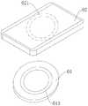
- FIG. 1is a schematic structural diagram of a wireless charger and a mobile phone provided by an embodiment of the application
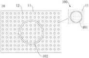
- FIG. 2is a schematic structural diagram of a shielding film provided by an embodiment of the application.
- FIG. 3is a schematic diagram of a cross-sectional structure of a shielding film provided by an embodiment of the application.
- FIG. 4is a schematic cross-sectional structure diagram of another shielding film provided by an embodiment of the application.
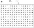
- FIG. 5is a schematic structural diagram of another shielding film provided by an embodiment of the application.
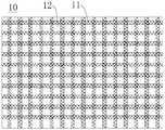
- FIG. 6is a schematic structural diagram of yet another shielding film provided by an embodiment of the application.
- FIG. 7is a schematic cross-sectional structure diagram of another shielding film provided by an embodiment of the application.
- FIG. 8is a schematic cross-sectional structure diagram of another shielding film provided by an embodiment of the application.
- FIG. 9is a schematic cross-sectional structure diagram of another shielding film provided by an embodiment of the application.
- FIG. 10is a schematic structural diagram of a coil assembly provided by an embodiment of the application.
- FIG. 11is a schematic cross-sectional structure diagram of a coil assembly provided by an embodiment of the application.
- FIG. 12is a schematic cross-sectional structure diagram of a wireless charging device provided by an embodiment of the application.
- the shielding film provided by the embodiment of the present applicationcan be applied to a variety of devices that need to selectively shield electromagnetic signals.
- wireless charging technologymainly relies on the principle of electromagnetic induction to realize the transmission of electric energy.
- the wireless charger 01can be used as the transmitting end, and the mobile phone 02 can be used as the receiving end; the wireless charger 01 can be provided with a power supply coil 011
- the power receiving coil 021can be set in the mobile phone 02, the alternating current is connected to the power supply coil 011, and the power supply coil 011 sends an electromagnetic signal to the outside through electromagnetic induction. After receiving the electromagnetic signal, the power receiving coil 021 transmits the electromagnetic signal through electromagnetic induction Converted into electric current, so as to achieve the purpose of wireless charging.
- the electromagnetic signals generated by the transmitterusually include high-frequency electromagnetic signals (such as electromagnetic signals with a frequency greater than 100kHz) and low-frequency electromagnetic signals (such as electromagnetic signals with a frequency not greater than 100kHz).
- high-frequency electromagnetic signalssuch as electromagnetic signals with a frequency greater than 100kHz
- low-frequency electromagnetic signalssuch as electromagnetic signals with a frequency not greater than 100kHz.
- the main Relying on low-frequency electromagnetic signals to realize the transmission of electric energywhile high-frequency electromagnetic signals make less contribution to the transmission of electric energy.
- due to the high-frequency electromagnetic signals in some frequency bandsit will also have adverse effects on electrical components (such as processors, etc.) or the human body. Therefore, it is necessary to suppress high-frequency electromagnetic signals.
- a power filterin order to suppress high-frequency signals, can be set at the transmitting end to filter out high-frequency alternating currents, thereby suppressing high-frequency electromagnetic signals.
- the high-frequency electromagnetic signal generated by the power supply coilis generated by the high-frequency alternating current. Therefore, in order to reduce the high-frequency electromagnetic signal generated by the power supply coil, the high-frequency electromagnetic signal can be The high-frequency current in the alternating current is filtered out, thereby suppressing the high-frequency electromagnetic signal; but this method introduces a power filter, so it will increase the volume of the transmitting end, which is not conducive to the miniaturization and thinning of the transmitting end. , It will also increase production costs.
- in order to increase the charging rateit can be achieved by increasing the power level of the high-frequency alternating current emitted by the transmitting end.
- the power supply filterdue to the resistance of the power supply filter, it will produce obvious electrical signals flowing through it. Inhibition, serious energy attenuation, greatly reducing the efficiency of electromagnetic energy conversion, which is not conducive to increasing the charging rate.
- the embodiments of the present applicationprovide a shielding film that is beneficial to increase the charging rate, can effectively filter high-frequency electromagnetic signals, has low production cost, and is convenient for miniaturization, lightweight, and thin production, as well as a coil assembly and a coil assembly using the shielding film.
- Wireless charging equipment
- references described in this specification to "one embodiment” or “some embodiments”, etc.mean that one or more embodiments of the present application include a specific feature, structure, or characteristic described in combination with the embodiment. Therefore, the sentences “in one embodiment”, “in some embodiments”, “in some other embodiments”, “in some other embodiments”, etc. appearing in different places in this specification are not necessarily All refer to the same embodiment, but mean “one or more but not all embodiments” unless it is specifically emphasized otherwise.
- the terms “including”, “including”, “having” and their variationsall mean “including but not limited to”, unless otherwise specifically emphasized.
- the shielding film 10includes a conductive portion 11 and an insulating portion 12; please refer to FIG. 3 in combination, the insulating portion 12 penetrates the conductive portion 11 in the thickness direction of the shielding film 10;
- the shielding film 10is subjected to the magnetic field of the electromagnetic field (for example, when there is an electromagnetic coil that generates the electromagnetic field on one side of the shielding film 10)
- an eddy currentwill be generated in the shielding film 10.
- an induced currentwill be generated in the shielding film. This induced current forms a loop in the shielding film.
- the path of the loopis similar to a vortex, this current is called vortex.
- Electric current(referred to as eddy current).
- the electromagnetic field generated by the electromagnetic coilwill contain a higher frequency electromagnetic field and a lower frequency electromagnetic field.
- the size of the eddy current loop formed in the shielding filmis different. Specifically, in an electromagnetic field with a higher frequency, the loop path of the eddy current formed in the shielding film 10 is small. In an electromagnetic field with a relatively low frequency, the loop path of the eddy current formed in the shielding film 10 is relatively large.
- the shielding film 10can effectively absorb and shield the electromagnetic field with a higher frequency, and can conduct a good conduction effect on the electromagnetic field with a lower frequency.
- a higher frequency electromagnetic fieldfirst electromagnetic field
- a first eddy current 101is formed in the shielding film 10
- the loop of the first eddy current 101is located in the conductive portion 11.
- the loop impedanceis relatively high. Low, high eddy current loss, which can effectively absorb and shield the first electromagnetic field.
- second electromagnetic fielda second eddy current 102 is formed in the shielding film 10, and the loop of the second eddy current 102 passes through the insulating portion 12. At this time, the loop impedance is higher and the eddy current loss is higher. Low, so that it will not form a significant shielding effect on the lower frequency electromagnetic field.
- the conductive portion 11may be made of multiple materials, for example, it may include metals or alloys such as copper, aluminum, etc., and may also include graphene, carbon fiber, and the like.
- the insulating portion 12may also be made of multiple materials, for example, it may include air, polyamide, polycarbonate, tetrafluoroethylene, polytetrafluoroethylene, etc., or a mixture of multiple insulating materials.
- the number of conductive portions 11 and insulating portions 12, the structure of the shielding film 10, and the manner in which conductive units are formedare also diverse.
- the conductive portion 11may be a whole, and the insulating portion 12 may be a structure of multiple through holes opened on the conductive portion 11.
- metal film, conductive paper or carbon fiber feltcan be selected as the substrate, and then needle punching, laser etching and other processes are used to open a through hole structure in the substrate, so as to realize the preparation of the shielding film 10, and the multiple insulating parts
- the smallest area enclosed by 12can be used as the conductive unit 100 (only one is shown in FIG.
- a plurality of insulating portions 12can be uniformly distributed in the shielding film 10 (conductive portion 11) in a matrix, and every four insulating portions 12 can form a conductive unit 100.
- the through holescan be circular holes, elliptical holes, or other polygonal hole structures; in addition, the number, size, distribution density, interval and other parameters of the insulating portion 12 (through holes) can be adjusted according to actual conditions. Adaptive adjustment; for example, when the frequency of the electromagnetic field to be shielded is high, the distribution density of the insulating portion 12 can be appropriately increased, or the size of the insulating portion 12 can be appropriately reduced, which is not specifically limited in this application.
- an insulating materialmay also be added to the through hole to improve the structural stability and force performance of the shielding film 10.
- insulating glue or other insulating materialscan be filled in the through holes.
- an insulating layer 13may also be provided on the surface of the shielding film 10 to improve the stress performance of the shielding film 10; in specific implementations, the insulating layer 13 may be provided on the surface of the shielding film 10.
- the lower surfacemay also be provided on the upper surface of the shielding film 10, or may be provided on both the upper and lower surfaces of the shielding film 10.
- the conductive unit 100will generate heat when there is an eddy current in the conductive unit 100.
- the insulating portion 12can be made of materials with higher heat resistance. It is prevented that when the temperature is high, the insulation performance of the insulating portion 12 is reduced, or the physical performance is changed (such as melting) and other undesirable conditions are prevented, so that the normal shielding performance and structural stability of the shielding film 10 can be ensured.
- an insulating and thermally conductive layermay be provided on the surface of the shielding film 10.
- the material of the insulating and thermally conductive layermay include thermally conductive silica gel, thermally conductive silica gel, and the like.
- the conductive portion 11 in the shielding film 10may also be a plurality of mutually independent structures.
- the shielding film 10may include an insulating part 12 and a plurality of conductive parts 11, and the plurality of conductive parts 11 are dispersed in the insulating part 12, each conductive Section 11 can be used as a conductive unit.
- a plurality of conductive parts 11can be placed on the platform, and then the insulating paint can be sprayed directly on the platform by a spraying process, so as to achieve the combination of the conductive part 11 and the insulating part 12; Ultraviolet curing (UV) and other processes are used to cure and shape the insulating portion 12 to complete the preparation of the shielding film 10.
- UVUltraviolet curing
- the size and distribution density of the conductive portion 11can be adjusted adaptively according to actual conditions; for example, when the frequency of the electromagnetic field to be shielded is high, the distribution density of the conductive portion 11 can be appropriately increased. The application does not make specific restrictions on this.
- the shielding film 10can also be made by a weaving process.
- metal wirescan be woven into a net-like structure
- the hollow part of the net-like structurecan be used as the insulating portion 12
- the metal wires around each insulating portion 12can enclose a conductive unit.
- the mesh structure (or hollow portion)may be a rectangular structure, a rhombus structure, etc., which is not specifically limited in this application.
- insulating materials, insulating and thermally conductive materials, etc.may also be coated on the surface of the mesh structure to improve the structural strength or heat dissipation performance of the shielding film 10.
- a metal wire wrapped with an insulating layer or an insulating thermally conductive layercan also be selected as the braided material, and an insulating wire wrapped with a conductive layer can also be selected as the braided material, which is not specifically limited in this application.
- the shielding film 10may also be a multilayer shielding structure, or a plurality of shielding films 10 may be stacked to form the shielding film 10 of a multilayer shielding structure.
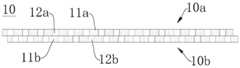
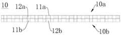
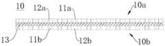
- the shielding film 10includes two layers of shielding structures; specifically, the shielding film 10 may include a first film layer 10a and a second film layer 10 ⁇ 10b.
- the first film layer 10amay include a first conductive portion 11a and a first insulating portion 12a.
- the first insulating portion 12apenetrates the first conductive portion 11a in the thickness direction of the first film layer 10a;
- the second film layer 10bmay include a second conductive portion 11a.
- the portion 11b and the second insulating portion 12b, and the second insulating portion 12bpenetrates the second conductive portion 11b in the thickness direction of the second film layer 10b.
- the specific structure or manufacturing method of the first film layer 10amay be the same as or different from the structure of the shielding film 10 of the single-layer shielding structure in the foregoing embodiment, and the specific structure or manufacturing method of the second film layer 10b may be the same as The structure of the shielding film 10 of the single-layer shielding structure in the above-mentioned embodiment is the same or different, and will not be repeated here.
- the relative positional relationship between the first film layer 10a and the second film layer 10bmay be various.
- the structure of the first film layer 10a and the second film layer 10bmay be the same, and the first conductive portion 11a in the first film layer 10a may be the same as the second conductive portion 11b in the second film layer 10b.
- the first insulating portion 12a in the first film layer 10acan be staggered with the second insulating portion 12b in the second film layer 10b; it can also be understood that the first conductive portion 11a in the first film layer 10a is The projection on the second film layer 10b does not overlap with the second conductive portion 11b, and the projection on the second film layer 10b of the first insulating portion 12a in the first film layer 10a does not overlap with the second insulating portion 12b.
- the first conductive portion 11a in the first film layer 10amay also be provided corresponding to the second insulating portion 12b in the second film layer 10b, and the first conductive portion 11a in the first film layer 10a
- An insulating portion 12amay be provided corresponding to the second conductive portion 11b in the second film layer 10b, that is, the first film layer 10a and the second film layer 10b may be complementary.
- the first insulating portion 12ais a plurality of through holes opened on the first conductive portion 11a
- the second conductive portion 11bmay be distributed on the first conductive portion 11a.
- the first insulating portion 12amay have a circular hole structure
- the second conductive portion 11bmay be a circular conductor
- the diameter of the first insulating portion 12amay be smaller than, equal to, or larger than the diameter of the second conductive portion 11b.
- the contour of the first insulating portion 12amay not be larger than the contour of the second conductive portion 11b.
- the shielding film 10realizes the shielding function, a part of the high-frequency electromagnetic signal will pass through the first conductive portion 11a in the first film layer 10a, thereby forming a diamagnetic field to effectively absorb the part of the high-frequency electromagnetic signal.
- an insulating layer 13may be provided between the first film layer 10a and the second film layer 10b.
- an insulating and thermally conductive layermay also be provided between the first film layer 10a and the second film layer 10b, or on the upper surface of the first film layer 10a and the second film layer 10b. The lower surface of the two film layers 10b are both provided with an insulating and heat-conducting layer.
- the shielding film 10can be conveniently and efficiently applied in a variety of environments where high-frequency electromagnetic signals (electromagnetic fields) need to be shielded and low-frequency electromagnetic signals (electromagnetic fields) need to be effectively transmitted.
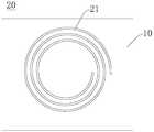
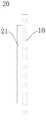
- an embodiment of the present applicationalso provides a coil assembly 20, which includes an inductance coil 21 and a shielding film 10 of any one of the foregoing embodiments.
- the shielding film 10may be disposed on at least one of the inductance coils 21.
- the coil assembly 20may also include a power supply circuit, which is electrically connected to the inductance coil 21, and is used to provide an alternating current to the inductance coil 21, so that the inductance coil 21 generates an alternating magnetic field (or electromagnetic signal), thereby Convert electrical energy into electromagnetic energy for wireless transmission.
- the shielding film 10may be arranged on one side of the inductor coil 21 to filter the high-frequency electromagnetic signals generated by the inductor coil 21.
- the positional relationship between the shielding film 10 and the inductor coil 21can be various.
- the shielding film 10may be disposed on the right side of the inductor coil 21.
- the shielding film 10may also be wrapped around the left and right sides or the periphery of the inductance coil 21.
- the coil assembly 21may be provided in a power supply device or a power receiving device.
- the power supply devicemay be a wireless charger, and the coil assembly 21 may be electrically connected with a power supply circuit in the power supply device to convert electrical energy into electromagnetic energy for wireless transmission.
- the power receiving devicemay be a mobile phone, a smart watch, a tablet computer, etc., and the coil assembly 21 may be electrically connected with a power receiving circuit in the power receiving device to convert electromagnetic energy into electric energy for storage or use.
- the shielding film 10can also be used alone in an electronic device.
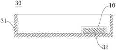
- a wireless charging deviceprovided by the present application, it includes a housing 31 and at least one electrical component 32 located in the housing 31 (only one electrical component 32 is shown in FIG. 12).
- the membrane 10can be arranged on at least part of the periphery of the electrical component 32 to filter the high-frequency electromagnetic signal generated by the electrical component 32, or filter the external high-frequency electromagnetic signal, so as to prevent the high-frequency electromagnetic signal generated from the outside from affecting the electrical Element 32 has an impact.
- the electrical component 32may be a processor, a memory, etc.
- the shielding film 10may be only provided on a part of the periphery of the electrical component 32, or may be wrapped around the entire periphery of the electrical component 32.
- the wireless charging devicemay be a mobile phone, a smart watch, a power adapter, etc., which is not specifically limited in this application.
Landscapes
- Engineering & Computer Science (AREA)
- Power Engineering (AREA)
- Computer Networks & Wireless Communication (AREA)
- Physics & Mathematics (AREA)
- Electromagnetism (AREA)
- Shielding Devices Or Components To Electric Or Magnetic Fields (AREA)
Abstract
Description
Translated fromChinese相关申请的交叉引用Cross-references to related applications
本申请要求在2020年02月28日提交中国专利局、申请号为202010128231.6、申请名称为“一种屏蔽膜、线圈组件和无线充电设备”的中国专利申请的优先权,其全部内容通过引用结合在本申请中。This application claims the priority of a Chinese patent application filed with the Chinese Patent Office, the application number is 202010128231.6, and the application name is "a shielding film, coil assembly and wireless charging device" on February 28, 2020, the entire content of which is incorporated by reference In this application.
本申请涉及电磁设备技术领域,尤其涉及一种屏蔽膜、线圈组件和无线充电设备。This application relates to the technical field of electromagnetic equipment, and in particular to a shielding film, a coil assembly and a wireless charging device.
目前,无线充电技术主要分为磁感应无线充电、磁共振无线充电和射频技术的无线充电三大类,现有市场中,以磁感应无线充电技术为主的无线充电占有率较高;随着无线充电技术的普及,市场上涌现出许多应用磁感应无线充电技术的产品;例如,在无线充电器、手机等电子设备中开始广泛采用磁感应无线充电技术进行充电,但是手机的充电时间(速率)一直是用户体验的关键问题,若想提高手机的充电速率,可以通过提升无线充电器输出功率的手段来实现,但是,随着输出功率的增加,电磁辐射会明显增强,从而降低了电子设备自身的安全性和用户的使用安全性,也会影响产品通过法规认证;另外,由于无线充电技术依靠电磁场来传递能量,且传统的电磁屏蔽技术会完全阻断电磁场能量的传递,因此,传统的电磁屏蔽技术会影响无线充电产品中电磁能量的正常传输。At present, wireless charging technology is mainly divided into three categories: magnetic induction wireless charging, magnetic resonance wireless charging and radio frequency wireless charging. In the existing market, the wireless charging technology based on magnetic induction wireless charging technology has a higher share; with wireless charging With the popularization of technology, many products using magnetic induction wireless charging technology have emerged on the market; for example, magnetic induction wireless charging technology has been widely used in electronic devices such as wireless chargers and mobile phones for charging, but the charging time (rate) of mobile phones has always been the user The key issue of experience. If you want to increase the charging rate of your mobile phone, you can increase the output power of the wireless charger. However, as the output power increases, the electromagnetic radiation will increase significantly, thereby reducing the safety of the electronic device itself. The safety of use and the user’s use will also affect the product’s passing of regulatory certification. In addition, because wireless charging technology relies on electromagnetic fields to transmit energy, and traditional electromagnetic shielding technology will completely block the transmission of electromagnetic field energy, traditional electromagnetic shielding technology will Affect the normal transmission of electromagnetic energy in wireless charging products.
发明内容Summary of the invention
本申请提供了一种能够对高频电磁信号进行有效屏蔽、对低频电磁信号进行有效导通的屏蔽膜、线圈组件和无线充电设备。The present application provides a shielding film, a coil assembly and a wireless charging device that can effectively shield high-frequency electromagnetic signals and effectively conduct low-frequency electromagnetic signals.
一方面,本申请实施例提供了一种屏蔽膜,包括第一膜层,第一膜层包括第一导电部和第一绝缘部,在第一膜层的厚度方向第一绝缘部贯穿第一导电部或第一导电部贯穿第一绝缘部;其中,当受到第一电磁场的磁场作用时,第一膜层中形成有第一涡电流,第一涡电流的环路位于第一导电部内,从而使得第一涡电流具备较大的电流强度;当受到第二电磁场的磁场作用时,第一膜层中形成有第二涡电流,第二涡电流的环路经过第一绝缘部,从而能够降低第二涡电流的电流强度;当第一电磁场的频率大于第二电磁场的频率时,第一涡电流的环路面积会小于第二涡电流的环路面积,通过涡流损耗效应,本申请实施例提供的屏蔽膜能够对高频电磁场进行有效吸收和屏蔽,对低频电磁场则不会产生衰减,从而实现阻高频电磁场、通低频电磁场的效果。On one hand, an embodiment of the present application provides a shielding film, which includes a first film layer, the first film layer includes a first conductive portion and a first insulating portion, and the first insulating portion penetrates through the first film layer in the thickness direction of the first film layer. The conductive part or the first conductive part penetrates the first insulating part; wherein, when subjected to the magnetic field of the first electromagnetic field, a first eddy current is formed in the first film layer, and the loop of the first eddy current is located in the first conductive part, So that the first eddy current has a greater current intensity; when subjected to the magnetic field of the second electromagnetic field, a second eddy current is formed in the first film, and the loop of the second eddy current passes through the first insulating part, so that it can Reduce the current intensity of the second eddy current; when the frequency of the first electromagnetic field is greater than the frequency of the second electromagnetic field, the loop area of the first eddy current will be smaller than the loop area of the second eddy current. Through the eddy current loss effect, this application implements The shielding film provided by the example can effectively absorb and shield high-frequency electromagnetic fields, but will not attenuate low-frequency electromagnetic fields, so as to achieve the effect of blocking high-frequency electromagnetic fields and passing low-frequency electromagnetic fields.
当屏蔽膜受到电磁场的磁场作用时(如屏蔽膜的一侧存在产生电磁场的电磁线圈时),屏蔽膜中会产生涡电流。通常情况下电磁线圈所产生的电磁场中会包含频率较高的电磁场和频率较低的电磁场,在不同频率的电磁场中,屏蔽膜内所形成的涡流环路大小有所不同。具体来说,在频率较高的电磁场中,屏蔽膜内所形成的涡电流的环路路径较小。在频率较低的电磁场中,屏蔽膜内所形成的涡电流的环路路径较大。基于上述特性,本申请实施例 提供的屏蔽膜能够对频率较高的电磁场进行有效的吸收、屏蔽作用,能够对频率较低的电磁场进行良好的导通作用。When the shielding film is subjected to the magnetic field of the electromagnetic field (for example, when there is an electromagnetic coil that generates the electromagnetic field on one side of the shielding film), eddy currents are generated in the shielding film. Under normal circumstances, the electromagnetic field generated by the electromagnetic coil will contain a higher frequency electromagnetic field and a lower frequency electromagnetic field. In the electromagnetic field of different frequencies, the size of the eddy current loop formed in the shielding film is different. Specifically, in a higher frequency electromagnetic field, the loop path of the eddy current formed in the shielding film is small. In a lower frequency electromagnetic field, the loop path of the eddy current formed in the shielding film is larger. Based on the above characteristics, the shielding film provided by the embodiment of the present application can effectively absorb and shield the electromagnetic field with a higher frequency, and can conduct a good conduction effect on the electromagnetic field with a lower frequency.
在具体实施时,第一导电部的材质可以为多种,例如,可以包括铜、铝等金属或合金,也可以包括石墨烯、碳纤维等。第一绝缘部的材质也可以为多种,例如,可以包括空气、聚酰胺、聚碳酸酯、四氟乙烯、聚四氟乙烯等,或者多种绝缘材料的混合物。In a specific implementation, the material of the first conductive part may be multiple, for example, it may include metals or alloys such as copper, aluminum, etc., and may also include graphene, carbon fiber, and the like. The material of the first insulating part may also be multiple, for example, it may include air, polyamide, polycarbonate, tetrafluoroethylene, polytetrafluoroethylene, etc., or a mixture of multiple insulating materials.
另外,第一导电部、第二导电部的数量,第一膜层的结构形式以及导电单元所形成的方式也是多样的。In addition, the number of the first conductive portion and the second conductive portion, the structure of the first film layer, and the manner in which the conductive unit is formed are also diverse.
例如,第一导电部可以为一个整体,第一绝缘部可以为多个开设在第一导电部上的通孔结构。在进行制作时,可以选用碳纤维毡、金属薄膜、导电纸等作为基材,然后采用针刺、激光蚀刻等工艺在金属薄膜中开设通孔结构,从而实现第一膜层的制备,多个绝缘部所围成的最小区域可以作为导电单元;例如,多个第一绝缘部可以矩阵式均匀分布在第一导电部中,每四个第一绝缘部可以围成一个导电单元。For example, the first conductive portion may be a whole, and the first insulating portion may be a structure of multiple through holes opened on the first conductive portion. During the production, carbon fiber felt, metal film, conductive paper, etc. can be used as the substrate, and then needle punching, laser etching and other processes are used to open the through hole structure in the metal film, so as to realize the preparation of the first film layer. The smallest area enclosed by the part may be used as a conductive unit; for example, a plurality of first insulating parts may be uniformly distributed in the first conductive part in a matrix, and every four first insulating parts may form a conductive unit.
另外,在一些实施方式中,第一绝缘部也可以为一个整体,第一导电部可以是分布在第一绝缘部内的导电体。或者,在一些实施方式中,第一绝缘部也可以设置多个,第一导电部也可以设置多个。In addition, in some embodiments, the first insulating part may also be a whole, and the first conductive part may be a conductor distributed in the first insulating part. Alternatively, in some embodiments, multiple first insulating portions may be provided, and multiple first conductive portions may also be provided.
另外,为了提升第一膜层的结构强度,第一绝缘部可以是结构稳定性较为良好的绝缘材料,或者,在一些实施方式中,也可以在第一膜层的表面设置绝缘层。In addition, in order to improve the structural strength of the first film layer, the first insulating portion may be an insulating material with relatively good structural stability, or, in some embodiments, an insulating layer may also be provided on the surface of the first film layer.
由于屏蔽膜在实现屏蔽功能时,第一导电部内会有电流,因此会使第一导电部的温度升高。在具体实施时,为了提升屏蔽膜的散热性,第一绝缘部中可以包括导热性良好的绝缘材料,或者,在一些实施方式中,也可以在第一膜层的表面设置绝缘导热层。When the shielding film realizes the shielding function, there will be current in the first conductive part, which will increase the temperature of the first conductive part. In a specific implementation, in order to improve the heat dissipation of the shielding film, the first insulating portion may include an insulating material with good thermal conductivity, or, in some embodiments, an insulating and thermally conductive layer may also be provided on the surface of the first film layer.
另外,在对第一膜层进行制作时,还可以采用编织工艺;具体来说,可以选用金属丝作为编织材料,将金属丝编织成网状结构或线宽结构,网状结构的镂空部位可以作为第一绝缘部,每个第一绝缘部四周的金属丝可以围成一个导电单元。在具体实施时,网状结构(或镂空部)可以是矩形结构、菱形结构等,本申请对此不作具体限定。另外,在一些实施方式中,也可以在网状结构的表面涂覆绝缘材料、绝缘导热材料等,以提升第一膜层的结构强度或散热性能。另外,在一些实施方式中,也可以选用外表包裹有绝缘层或绝缘导热层的金属丝作为编织材料,也可以选用外表包裹有导电层的绝缘丝作为编织材料,本申请对此不作具体限定。In addition, when the first film layer is made, a weaving process can also be used; specifically, metal wires can be selected as the weaving material, and the metal wires can be woven into a net-like structure or a line-width structure. The hollow part of the net-like structure can be As the first insulating part, the metal wires around each first insulating part may enclose a conductive unit. In specific implementation, the mesh structure (or hollow portion) may be a rectangular structure, a rhombus structure, etc., which is not specifically limited in this application. In addition, in some embodiments, insulating materials, insulating and thermally conductive materials, etc. may also be coated on the surface of the mesh structure to improve the structural strength or heat dissipation performance of the first film layer. In addition, in some embodiments, a metal wire wrapped with an insulating layer or an insulating thermally conductive layer can also be selected as the braided material, and an insulating wire wrapped with a conductive layer can also be selected as the braided material, which is not specifically limited in this application.
另外,在一些实施方式中,屏蔽膜中也可以包括多层膜结构。例如,屏蔽膜中可以包括层叠设置的第一膜层和第二膜层。在具体实施时,第二膜层的具体结构或制作方式可以与上述第一膜层的结构相同或不同。In addition, in some embodiments, the shielding film may also include a multilayer film structure. For example, the shielding film may include a first film layer and a second film layer that are stacked. In specific implementation, the specific structure or production method of the second film layer may be the same as or different from the structure of the first film layer described above.
在一些实施方式中,第一膜层和第二膜层之间的相对位置关系可以是多样的。例如,第一膜层和第二膜层的结构可以相同,第一膜层中的第一导电部可以与第二膜层中的第二导电部交错设置,第一膜层中的第一绝缘部可以与第二膜层中的第二绝缘部交错设置;也可以理解为,第一膜层中的第一导电部在第二膜层上的投影与第二导电部不重合,第一膜层中的第一绝缘部在第二膜层上的投影与第二绝缘部不重合。In some embodiments, the relative positional relationship between the first film layer and the second film layer may be various. For example, the structure of the first film layer and the second film layer can be the same, the first conductive part in the first film layer can be alternately arranged with the second conductive part in the second film layer, and the first insulating part in the first film layer The part can be arranged alternately with the second insulating part in the second film layer; it can also be understood that the projection of the first conductive part in the first film layer on the second film layer does not overlap with the second conductive part, and the first film The projection of the first insulating part on the second film layer in the layer does not overlap with the second insulating part.
在一些实施方式中,第一膜层中的第一导电部还可以与第二膜层中的第二绝缘部对应设置,第一膜层中的第一绝缘部可以与第二膜层中的第二导电部对应设置,即第一膜层与第二膜层互补。例如,在第一膜层中,当第一绝缘部为开设在第一导电部上的多个通孔时,在第二膜层中,第二导电部可以为分布在第二绝缘部上的多个导电体;在具体实施时,第 二膜层中第二导电部的轮廓可以小于、等于、大于第一膜层中第一绝缘部的轮廓。例如,第一绝缘部可以为圆形孔结构,第二导电部可以为圆形导电体,第一绝缘部的直径可以小于、等于、大于第二导电部的直径。In some embodiments, the first conductive part in the first film layer may also be arranged corresponding to the second insulating part in the second film layer, and the first insulating part in the first film layer may be the same as the second insulating part in the second film layer. The second conductive parts are correspondingly arranged, that is, the first film layer is complementary to the second film layer. For example, in the first film layer, when the first insulating part is a plurality of through holes opened on the first conductive part, in the second film layer, the second conductive part may be distributed on the second insulating part. Multiple conductors; in specific implementation, the contour of the second conductive portion in the second film layer may be smaller than, equal to, or greater than the contour of the first insulating portion in the first film layer. For example, the first insulating portion may be a circular hole structure, the second conductive portion may be a circular electrical conductor, and the diameter of the first insulating portion may be smaller than, equal to, or greater than the diameter of the second conductive portion.
在具体实施时,为了提升屏蔽膜的屏蔽性能,第一绝缘部的轮廓可以不大于第二导电部的轮廓,或者,第二导电部在第一膜层上的投影可以覆盖第一绝缘部。In specific implementation, in order to improve the shielding performance of the shielding film, the contour of the first insulating part may not be larger than the contour of the second conductive part, or the projection of the second conductive part on the first film layer may cover the first insulating part.
在一些实施方式中,屏蔽膜中还可以包括更多个层叠设置的第一膜层或第二膜层,多个膜层的结构可以相同也可以不同,在此不作赘述。In some embodiments, the shielding film may further include more stacked first film layers or second film layers, and the structures of the multiple film layers may be the same or different, which will not be repeated here.
另一方面,本申请实施例还提供了一种线圈组件,包括电感线圈和上述任意一种的屏蔽膜,屏蔽膜可以接地并设置在电感线圈的至少一侧以对电感线圈所产生的电磁信号进行处理或过滤,或者对外界环境中的电磁信号进行处理或过滤,以防止外界环境中的电磁信号对电感线圈产生影响。On the other hand, an embodiment of the present application also provides a coil assembly, including an inductor coil and any one of the above-mentioned shielding films. The shielding film can be grounded and arranged on at least one side of the inductor coil to protect electromagnetic signals generated by the inductor coil. Process or filter, or process or filter the electromagnetic signal in the external environment to prevent the electromagnetic signal in the external environment from affecting the inductance coil.
在具体应用时,线圈组件可以应用在供电设备中,也可以应用在受电设备中。In specific applications, the coil assembly can be used in power supply equipment or in power receiving equipment.
例如,当线圈组件应用在供电设备(如无线充电器)中时,线圈组件中还可以包括供电电路,供电设备中的电源通过供电电路与电感线圈电连接,用于向电感线圈提供交变电流,以使电感线圈产生交变磁场(或电磁信号),从而将电能转化为电磁能实现电能的无线传输。屏蔽膜可以设置在电感线圈的一侧,以对电感线圈所产生的高频电磁信号进行过滤,电感线圈所产生的低频信号则可以透过屏蔽膜进行传输,以使受电设备能够接受线圈组件(供电设备)所产生的电磁能。For example, when the coil component is used in a power supply device (such as a wireless charger), the coil component may also include a power supply circuit. The power supply in the power supply device is electrically connected to the inductor coil through the power supply circuit to provide alternating current to the inductor coil. , So that the inductance coil generates an alternating magnetic field (or electromagnetic signal), thereby converting electrical energy into electromagnetic energy to achieve wireless transmission of electrical energy. The shielding film can be set on one side of the inductor coil to filter the high-frequency electromagnetic signals generated by the inductor coil, and the low-frequency signal generated by the inductor coil can be transmitted through the shielding film, so that the power receiving device can accept the coil assembly (Power supply equipment) electromagnetic energy generated.
当线圈组件应用在受电设备(如手机)中时,线圈组件中还可以包括受电电路,受电设备中的电源(如锂电池)可以通过受电电路与电感线圈电连接,电感线圈接收到电磁能时,可将电磁能转化为电能,电能便可通过受电电路流入电源中进行储存。When the coil component is used in a power receiving device (such as a mobile phone), the coil component may also include a power receiving circuit. The power supply (such as a lithium battery) in the power receiving device can be electrically connected to the inductance coil through the power receiving circuit, and the inductance coil receives When electromagnetic energy is reached, the electromagnetic energy can be converted into electrical energy, and the electrical energy can flow into the power supply through the power receiving circuit for storage.
在一些实施方式中,屏蔽膜也可以单独应用在电子设备中。例如,在本申请提供的一种电子设备中,包括壳体和位于壳体内的电器元件,屏蔽膜可以设置在电器元件的部分外围,以对电器元件所产生的高频电磁信号进行过滤,或者对外界的高频电磁信号进行过滤,以避免对电器元件产生影响。在具体实施时,电器元件可以是处理器、存储器等,屏蔽膜可以仅设置在电器元件的部分外围,也可以包裹在电器元件的外围。另外,电子设备可以是手机、智能手表、电源适配器等,本申请对此不作具体限定。In some embodiments, the shielding film can also be used alone in an electronic device. For example, in an electronic device provided by the present application, including a housing and electrical components located in the housing, a shielding film can be provided on part of the periphery of the electrical components to filter high-frequency electromagnetic signals generated by the electrical components, or Filter external high-frequency electromagnetic signals to avoid affecting electrical components. In a specific implementation, the electrical component may be a processor, a memory, etc., and the shielding film may be only provided on a part of the periphery of the electrical component, or may be wrapped around the periphery of the electrical component. In addition, the electronic device may be a mobile phone, a smart watch, a power adapter, etc., which is not specifically limited in this application.
图1为本申请实施例提供的一种无线充电器和手机的结构示意图;FIG. 1 is a schematic structural diagram of a wireless charger and a mobile phone provided by an embodiment of the application;
图2为本申请实施例提供的一种屏蔽膜的结构示意图;FIG. 2 is a schematic structural diagram of a shielding film provided by an embodiment of the application;
图3为本申请实施例提供的一种屏蔽膜的剖面结构示意图;3 is a schematic diagram of a cross-sectional structure of a shielding film provided by an embodiment of the application;
图4为本申请实施例提供的另一种屏蔽膜的剖面结构示意图;4 is a schematic cross-sectional structure diagram of another shielding film provided by an embodiment of the application;
图5为本申请实施例提供的另一种屏蔽膜的结构示意图;FIG. 5 is a schematic structural diagram of another shielding film provided by an embodiment of the application;
图6为本申请实施例提供的又一种屏蔽膜的结构示意图;FIG. 6 is a schematic structural diagram of yet another shielding film provided by an embodiment of the application;
图7为本申请实施例提供的另一种屏蔽膜的剖面结构示意图;7 is a schematic cross-sectional structure diagram of another shielding film provided by an embodiment of the application;
图8为本申请实施例提供的另一种屏蔽膜的剖面结构示意图;8 is a schematic cross-sectional structure diagram of another shielding film provided by an embodiment of the application;
图9为本申请实施例提供的又一种屏蔽膜的剖面结构示意图;9 is a schematic cross-sectional structure diagram of another shielding film provided by an embodiment of the application;
图10为本申请实施例提供的一种线圈组件的结构示意图;FIG. 10 is a schematic structural diagram of a coil assembly provided by an embodiment of the application;
图11为本申请实施例提供的一种线圈组件的剖面结构示意图;11 is a schematic cross-sectional structure diagram of a coil assembly provided by an embodiment of the application;
图12为本申请实施例提供的一种无线充电设备的剖面结构示意图。FIG. 12 is a schematic cross-sectional structure diagram of a wireless charging device provided by an embodiment of the application.
为了使本申请的目的、技术方案和优点更加清楚,下面将结合附图对本申请作进一步地详细描述。In order to make the purpose, technical solutions, and advantages of the present application clearer, the present application will be further described in detail below with reference to the accompanying drawings.
为了方便理解本申请实施例提供的屏蔽膜,下面首先介绍一下其应用场景。In order to facilitate the understanding of the shielding film provided in the embodiments of the present application, the following first introduces its application scenarios.
本申请实施例提供的屏蔽膜可应用在多种需要对电磁信号进行选择性屏蔽的设备中。例如,随着无线充电技术的发展,越来越多的电子产品(如手机、智能手表等)开始使用无线充电技术实现电力传输。无线充电技术的实现主要依靠电磁感应原理来实现电能的传输,例如,如图1所示,无线充电器01可以作为发送端,手机02可以作为接收端;无线充电器01中可以设置供电线圈011,手机02中可以设置受电线圈021,在供电线圈011中接通交变电流,通过电磁感应使供电线圈011向外界发出电磁信号,受电线圈021接收到电磁信号后通过电磁感应将电磁信号转变为电流,从而达到无线充电的目的。The shielding film provided by the embodiment of the present application can be applied to a variety of devices that need to selectively shield electromagnetic signals. For example, with the development of wireless charging technology, more and more electronic products (such as mobile phones, smart watches, etc.) have begun to use wireless charging technology for power transmission. The realization of wireless charging technology mainly relies on the principle of electromagnetic induction to realize the transmission of electric energy. For example, as shown in Figure 1, the
在实际应用中,发送端所产生的电磁信号中通常包括高频电磁信号(如频率大于100kHz的电磁信号)和低频电磁信号(如频率不大于100kHz的电磁信号),在无线充电系统中,主要依靠低频电磁信号实现电能的传输,而高频电磁信号对于电能传输所做的贡献较少,另外,由于一些频段的高频电磁信号还会对电器元件(如处理器等)或人体产生不良影响,因此,需要对高频电磁信号进行抑制。In practical applications, the electromagnetic signals generated by the transmitter usually include high-frequency electromagnetic signals (such as electromagnetic signals with a frequency greater than 100kHz) and low-frequency electromagnetic signals (such as electromagnetic signals with a frequency not greater than 100kHz). In a wireless charging system, the main Relying on low-frequency electromagnetic signals to realize the transmission of electric energy, while high-frequency electromagnetic signals make less contribution to the transmission of electric energy. In addition, due to the high-frequency electromagnetic signals in some frequency bands, it will also have adverse effects on electrical components (such as processors, etc.) or the human body. Therefore, it is necessary to suppress high-frequency electromagnetic signals.
在一些无线充电系统中,为了对高频信号进行抑制,可以在发送端设置电源滤波器以对高频交变电流进行滤除,从而对高频电磁信号进行抑制。具体来说,在发送端,供电线圈所产生的高频电磁信号是由高频交变电流所产生的,因此,为了减少供电线圈所产生的高频电磁信号,可以通过电源滤波器对高频交变电流中的高频电流进行滤除,从而对高频电磁信号进行抑制;但是这种方式由于引入了电源滤波器,因此,会增加发射端的体积,不利于发射端的小型化、轻薄化设计,同时也会增加制作成本。In some wireless charging systems, in order to suppress high-frequency signals, a power filter can be set at the transmitting end to filter out high-frequency alternating currents, thereby suppressing high-frequency electromagnetic signals. Specifically, at the transmitting end, the high-frequency electromagnetic signal generated by the power supply coil is generated by the high-frequency alternating current. Therefore, in order to reduce the high-frequency electromagnetic signal generated by the power supply coil, the high-frequency electromagnetic signal can be The high-frequency current in the alternating current is filtered out, thereby suppressing the high-frequency electromagnetic signal; but this method introduces a power filter, so it will increase the volume of the transmitting end, which is not conducive to the miniaturization and thinning of the transmitting end. , It will also increase production costs.
另外,在一些实施方式中,为了提升充电速率,可以通过增加发送端发射高频交变电流的功率大小来实现,但是,由于电源滤波器存在电阻,会对其流过的电信号产生明显的抑制作用,能量衰减严重,极大的降低了电磁能量转换效率,从而不利于提升充电速率。In addition, in some embodiments, in order to increase the charging rate, it can be achieved by increasing the power level of the high-frequency alternating current emitted by the transmitting end. However, due to the resistance of the power supply filter, it will produce obvious electrical signals flowing through it. Inhibition, serious energy attenuation, greatly reducing the efficiency of electromagnetic energy conversion, which is not conducive to increasing the charging rate.
基于上述问题,本申请实施例提供了一种利于提升充电速率,能够对高频电磁信号进行有效过滤、制作成本低、便于小型化轻薄化制作的屏蔽膜,以及应用该屏蔽膜的线圈组件和无线充电设备。Based on the above problems, the embodiments of the present application provide a shielding film that is beneficial to increase the charging rate, can effectively filter high-frequency electromagnetic signals, has low production cost, and is convenient for miniaturization, lightweight, and thin production, as well as a coil assembly and a coil assembly using the shielding film. Wireless charging equipment.
为了便于理解本申请技术方案,下面将结合附图和具体实施方式对本申请所提供的屏蔽膜进行具体说明。In order to facilitate the understanding of the technical solutions of the present application, the shielding film provided in the present application will be described in detail below in conjunction with the drawings and specific implementations.
以下实施例中所使用的术语只是为了描述特定实施例的目的,而并非旨在作为对本申请的限制。如在本申请的说明书和所附权利要求书中所使用的那样,单数表达形式“一个”、“一种”、“上述”、“该”和“这一”旨在也包括例如“一个或多个”这种表达形式,除非其上下文中明确地有相反指示。还应当理解,在本申请以下各实施例中,“至少一个”、“一个或多个”是指一个、两个或两个以上。术语“和/或”,用于描述关联对象的关联关系,表示可以存在三种关系;例如,A和/或B,可以表示:单独存在A,同时存在A和B,单独存在B的情况,其中A、B可以是单数或者复数。字符“/”一般表示前后关联对象是一种“或”的关系。The terms used in the following embodiments are only for the purpose of describing specific embodiments, and are not intended to limit the application. As used in the specification and appended claims of this application, the singular expressions "a", "an", "above", "the" and "this" are intended to also include, for example, "a or The expression "multiple", unless the context clearly indicates to the contrary. It should also be understood that in the following embodiments of the present application, "at least one" and "one or more" refer to one, two, or more than two. The term "and/or" is used to describe the association relationship of associated objects, indicating that there can be three types of relationships; for example, A and/or B can mean: A alone exists, A and B exist at the same time, and B exists alone. Among them, A and B can be singular or plural. The character "/" generally indicates that the associated objects before and after are in an "or" relationship.
在本说明书中描述的参考“一个实施例”或“一些实施例”等意味着在本申请的一个或多个实施例中包括结合该实施例描述的特定特征、结构或特点。由此,在本说明书中的不同之处出现的语句“在一个实施例中”、“在一些实施例中”、“在其他一些实施例中”、“在另外一些实施例中”等不是必然都参考相同的实施例,而是意味着“一个或多个但不是所有的实施例”,除非是以其他方式另外特别强调。术语“包括”、“包含”、“具有”及它们的变形都意味着“包括但不限于”,除非是以其他方式另外特别强调。References described in this specification to "one embodiment" or "some embodiments", etc. mean that one or more embodiments of the present application include a specific feature, structure, or characteristic described in combination with the embodiment. Therefore, the sentences "in one embodiment", "in some embodiments", "in some other embodiments", "in some other embodiments", etc. appearing in different places in this specification are not necessarily All refer to the same embodiment, but mean "one or more but not all embodiments" unless it is specifically emphasized otherwise. The terms "including", "including", "having" and their variations all mean "including but not limited to", unless otherwise specifically emphasized.
如图2所示,在本申请提供的一个实施例中,屏蔽膜10中包括导电部11和绝缘部12;请结合参阅图3,在屏蔽膜10的厚度方向绝缘部12贯穿导电部11;其中,当屏蔽膜10受到电磁场的磁场作用时(如屏蔽膜10的一侧存在产生电磁场的电磁线圈时),屏蔽膜10中会产生涡电流。具体来说,当把屏蔽膜10放在电磁场中后,屏蔽膜内将产生感应电流,这种感应电流在屏蔽膜内自成回路,由于回路路径类似于旋涡状,因此这种电流称作涡电流(简称涡流)。通常情况下电磁线圈所产生的电磁场中会包含频率较高的电磁场和频率较低的电磁场,在不同频率的电磁场中,屏蔽膜内所形成的涡流环路大小有所不同。具体来说,在频率较高的电磁场中,屏蔽膜10内所形成的涡电流的环路路径较小。在频率较低的电磁场中,屏蔽膜10内所形成的涡电流的环路路径较大。基于上述特性,本申请实施例提供的屏蔽膜10能够对频率较高的电磁场进行有效的吸收、屏蔽作用,能够对频率较低的电磁场进行良好的导通作用。具体来说,在频率较高的电磁场(第一电磁场)中,屏蔽膜10中形成有第一涡电流101,第一涡电流101的环路位于导电部11内,此时,环路阻抗较低,涡流损耗高,从而能够对第一电磁场进行有效的吸收和屏蔽。在频率较低的电磁场(第二电磁场)中,屏蔽膜10中形成有第二涡电流102,第二涡电流102的环路经过绝缘部12,此时,环路阻抗较高,涡流损耗较低,从而不会对频率较低的电磁场形成明显的屏蔽作用。As shown in FIG. 2, in an embodiment provided by the present application, the shielding
在具体实施时,导电部11的材质可以为多种,例如,可以包括铜、铝等金属或合金,也可以包括石墨烯、碳纤维等。绝缘部12的材质也可以为多种,例如,可以包括空气、聚酰胺、聚碳酸酯、四氟乙烯、聚四氟乙烯等,或者多种绝缘材料的混合物。In a specific implementation, the
另外,在具体实施时,导电部11、绝缘部12的数量,屏蔽膜10的结构形式以及导电单元所形成的方式也是多样的。In addition, in specific implementation, the number of
例如,如图2和图3所示,在本申请提供的一个实施例中,导电部11可以为一个整体,绝缘部12可以为多个开设在导电部11上的通孔结构。在进行制作时,可以选用金属薄膜、导电纸或碳纤维毡等作为基材,然后采用针刺、激光蚀刻等工艺在基材中开设通孔结构,从而实现屏蔽膜10的制备,多个绝缘部12所围成的最小区域可以作为导电单元100(图2中仅标示出一个);例如,多个绝缘部12可以矩阵式均匀分布在屏蔽膜10(导电部11)中,每四个绝缘部12可以围成一个导电单元100。在具体实施时,通孔可以是圆形孔、椭圆形孔,也可以其他的多边形孔结构;另外,绝缘部12(通孔)的数量、尺寸、分布密度、间隔等参数可以根据实际情况作适应性调整;例如,当所需屏蔽的电磁场的频率较高时,可以适当增加绝缘部12的分布密度,也可以适当缩减绝缘部12的大小等,本申请对此不作具体限定。For example, as shown in FIGS. 2 and 3, in an embodiment provided by the present application, the
另外,在一些实施方式中,通孔中也可以添加绝缘材料,以提升屏蔽膜10的结构稳定性和受力性能。例如,可以在通孔内填充绝缘胶或其他绝缘材料。In addition, in some embodiments, an insulating material may also be added to the through hole to improve the structural stability and force performance of the shielding
在另一些实施方式中,如图4所示,屏蔽膜10的表面也可以设置绝缘层13,以提升 屏蔽膜10的受力性能;在具体实施时,绝缘层13可以设置在屏蔽膜10的下表面,也可以设置在屏蔽膜10的上表面,也可以在屏蔽膜10的上、下表面均设置。In other embodiments, as shown in FIG. 4, an insulating
或者,在一些实施方式中,由于导电单元100中有涡电流时,会使导电单元100发热,为了保证屏蔽膜10的正常工作性能,绝缘部12可以选用具备较高耐热性的材料,以防止当温度较高时,引起绝缘部12绝缘性能的下降,或者物理性能的改变(如融化)等不良情况,从而能保证屏蔽膜10的正常屏蔽性能和结构稳定性。Or, in some embodiments, the
在一些实施方式中,为了提升屏蔽膜10的散热性能,可以在屏蔽膜10的表面设置绝缘导热层,在具体实施时,绝缘导热层的材料可以包括导热硅胶、导热矽胶等。In some embodiments, in order to improve the heat dissipation performance of the shielding
另外,在一些实施方式中,屏蔽膜10中的导电部11也可以为多个相互独立的结构。例如,如图5所示,在本申请提供的一个实施例中,屏蔽膜10中可以包括一个绝缘部12和多个导电部11,多个导电部11分散在绝缘部12中,每个导电部11可以作为一个导电单元。In addition, in some embodiments, the
在进行制作时,可以将多个导电部11(如金属块)放置在平台上,然后采用喷涂工艺将绝缘涂料直接喷涂在平台上,从而实现导电部11和绝缘部12的结合;然后可以采用紫外固化(Ultraviolet curing,UV)等工艺对绝缘部12进行固化成型,从而完成屏蔽膜10的制备。在具体实施时,导电部11的大小、分布密度等参数可以根据实际情况作适应性调整;例如,当所需屏蔽的电磁场的频率较高时,可以适当增加导电部11的分布密度等,本申请对此不作具体限定。During production, a plurality of conductive parts 11 (such as metal blocks) can be placed on the platform, and then the insulating paint can be sprayed directly on the platform by a spraying process, so as to achieve the combination of the
在一些实施方式中,屏蔽膜10也可以采用编织工艺进行制作。例如,如图6所示,可以将金属丝编织成网状结构,网状结构的镂空部位可以作为绝缘部12,每个绝缘部12四周的金属丝可以围成一个导电单元。在具体实施时,网状结构(或镂空部)可以是矩形结构、菱形结构等,本申请对此不作具体限定。In some embodiments, the shielding
另外,在一些实施方式中,也可以在网状结构的表面涂覆绝缘材料、绝缘导热材料等,以提升屏蔽膜10的结构强度或散热性能。另外,在一些实施方式中,也可以选用外表包裹有绝缘层或绝缘导热层的金属丝作为编织材料,也可以选用外表包裹有导电层的绝缘丝作为编织材料,本申请对此不作具体限定。In addition, in some embodiments, insulating materials, insulating and thermally conductive materials, etc. may also be coated on the surface of the mesh structure to improve the structural strength or heat dissipation performance of the shielding
另外,在一些实施方式中,屏蔽膜10也可以是多层屏蔽结构,或者将多个屏蔽膜10层叠设置以形成多层屏蔽结构的屏蔽膜10。In addition, in some embodiments, the shielding
例如,如图7所示,在本申请提供的一个实施例中,屏蔽膜10中包括两层屏蔽结构;具体来说,屏蔽膜10中可以包括层叠设置的第一膜层10a和第二膜层10b。第一膜层10a可以包括第一导电部11a和第一绝缘部12a,在第一膜层10a的厚度方向第一绝缘部12a贯穿第一导电部11a;第二膜层10b可以包括第二导电部11b和第二绝缘部12b,在第二膜层10b的厚度方向第二绝缘部12b贯穿第二导电部11b。在具体实施时,第一膜层10a的具体结构或制作方式可以与上述实施例中的单层屏蔽结构的屏蔽膜10的结构相同或不同,第二膜层10b的具体结构或制作方式可以与上述实施例中的单层屏蔽结构的屏蔽膜10的结构相同或不同,在此不作赘述。For example, as shown in FIG. 7, in an embodiment provided in the present application, the shielding
在一些实施方式中,第一膜层10a和第二膜层10b之间的相对位置关系可以是多样的。In some embodiments, the relative positional relationship between the
例如,如图7所示,第一膜层10a和第二膜层10b的结构可以相同,第一膜层10a中的第一导电部11a可以与第二膜层中10b的第二导电部11b交错设置,第一膜层10a中的第一绝缘部12a可以与第二膜层10b中的第二绝缘部12b交错设置;也可以理解为,第一 膜层10a中的第一导电部11a在第二膜层10b上的投影与第二导电部11b不重合,第一膜层10a中的第一绝缘部12a在第二膜层10b上的投影与第二绝缘部12b不重合。For example, as shown in FIG. 7, the structure of the
如图8所示,在一些实施方式中,第一膜层10a中的第一导电部11a还可以与第二膜层10b中的第二绝缘部12b对应设置,第一膜层10a中的第一绝缘部12a可以与第二膜层10b中的第二导电部11b对应设置,即第一膜层10a与第二膜层10b可以互补。例如,在第一膜层10a中,当第一绝缘部12a为开设在第一导电部11a上的多个通孔时,在第二膜层10b中,第二导电部11b可以为分布在第二绝缘部12b上的多个导电体;在具体实施时,第二膜层10b中第二导电部11b的轮廓可以小于、等于或者大于第一膜层10a中第一绝缘部12a的轮廓。例如,第一绝缘部12a可以为圆形孔结构,第二导电部11b可以为圆形导电体,第一绝缘部12a的直径可以小于、等于或者大于第二导电部11b的直径。As shown in FIG. 8, in some embodiments, the first
在具体实施时,为了提升屏蔽膜10的屏蔽性能,第一绝缘部12a的轮廓可以不大于第二导电部11b的轮廓。具体来说,屏蔽膜10在实现屏蔽功能时,一部分高频电磁信号会穿过第一膜层10a中的第一导电部11a,从而形成反磁场,以对该部分高频电磁信号进行有效吸收和屏蔽;另一部分高频电磁信号会由第一膜层10a中的第一绝缘部12a穿出,该部分高频电磁信号穿过第二膜层10b中的第二导电部11b时,会形成反磁场,以对该部分高频电磁信号进行有效吸收和屏蔽,从而能够使屏蔽膜10具备良好的屏蔽功能。In specific implementation, in order to improve the shielding performance of the shielding
另外,在具体实施时,为了防止第一膜层10a中的第一导电部11a与第二膜层10b中的第二导电部11b电连接,而影响低频电磁信号的透出,如图9所示,在一些实施方式中第一膜层10a与第二膜层10b之间可以设置绝缘层13。另外,在一些实施方式中,为了提升屏蔽膜10的散热性能,第一膜层10a和第二膜层10b之间也可以设置绝缘导热层,或者,在第一膜层10a的上表面以及第二膜层10b的下表面均设置绝缘导热层。In addition, during specific implementation, in order to prevent the first
在实际应用时,屏蔽膜10可以方便、高效的应用在多种需要对高频电磁信号(电磁场)进行屏蔽、对低频电磁信号(电磁场)进行有效透出的环境中。In practical applications, the shielding
例如,如图10所示,本申请实施例还提供了一种线圈组件20,包括电感线圈21和上述实施例中任意一种的屏蔽膜10,屏蔽膜10可以设置在电感线圈21的至少一侧,以对电感线圈21所产生的电磁信号进行处理或过滤。具体来说,线圈组件20中还可以包括供电电路,供电电路与电感线圈21电连接,用于向电感线圈21提供交变电流,以使电感线圈21产生交变磁场(或电磁信号),从而将电能转化为电磁能进行无线传输。屏蔽膜10可以设置在电感线圈21的一侧,以对电感线圈21所产生的高频电磁信号进行过滤。For example, as shown in FIG. 10, an embodiment of the present application also provides a
在具体实施时,屏蔽膜10与电感线圈21之间的位置关系可以是多样的。In specific implementation, the positional relationship between the shielding
例如,如图11所示,当电感线圈21的右端作为输出端时,可以将屏蔽膜10设置在电感线圈21的右侧。在一些实施方式中,也可以将屏蔽膜10包覆设置电感线圈21的左右两侧或外围。For example, as shown in FIG. 11, when the right end of the
在具体应用时,线圈组件21可以设置在供电设备中也可以设置在受电设备中。In a specific application, the
例如,供电设备可以是无线充电器,线圈组件21可以与供电设备中的供电电路进行电连接,以将电能转化为电磁能进行无线传输。受电设备可以是手机、智能手表、平板电脑等,线圈组件21可以与受电设备中的受电电路进行电连接,以将电磁能转化为电能进行储存或使用。For example, the power supply device may be a wireless charger, and the
另外,在一些实施方式中,屏蔽膜10也可以单独应用在电子设备中。例如,如图12所示,在本申请提供的一种无线充电设备中,包括壳体31和位于壳体31内的至少一个电 器元件32(图12中仅示出一个电器元件32),屏蔽膜10可以设置在电器元件32的至少部分外围,以对电器元件32所产生的高频电磁信号进行过滤,或者对外界的高频电磁信号进行过滤,以避免外界产生的高频电磁信号对电器元件32产生影响。In addition, in some embodiments, the shielding
在具体实施时,电器元件32可以是处理器、存储器等,屏蔽膜10可以仅设置在电器元件32的部分外围,也可以包裹在电器元件32的整个外围。另外,无线充电设备可以是手机、智能手表、电源适配器等,本申请对此不作具体限定。In a specific implementation, the
以上,仅为本申请的具体实施方式,但本申请的保护范围并不局限于此,任何熟悉本技术领域的技术人员在本申请揭露的技术范围内,可轻易想到变化或替换,都应涵盖在本申请的保护范围之内。因此,本申请的保护范围应以权利要求的保护范围为准。The above are only specific implementations of this application, but the scope of protection of this application is not limited to this. Any person skilled in the art can easily conceive of changes or substitutions within the technical scope disclosed in this application, which shall cover Within the scope of protection of this application. Therefore, the protection scope of this application shall be subject to the protection scope of the claims.
Claims (12)
Translated fromChinesePriority Applications (2)
| Application Number | Priority Date | Filing Date | Title |
|---|---|---|---|
| EP20921137.4AEP3930145B1 (en) | 2020-02-28 | 2020-08-17 | Shielding film, coil assembly, electronic device and wireless charging device |
| US17/490,150US12142949B2 (en) | 2020-02-28 | 2021-09-30 | Shielding film, coil assembly, and wireless charging device |
Applications Claiming Priority (2)
| Application Number | Priority Date | Filing Date | Title |
|---|---|---|---|
| CN202010128231.6 | 2020-02-28 | ||
| CN202010128231.6ACN111277053A (en) | 2020-02-28 | 2020-02-28 | A shielding film, coil assembly and wireless charging device |
Related Child Applications (1)
| Application Number | Title | Priority Date | Filing Date |
|---|---|---|---|
| US17/490,150ContinuationUS12142949B2 (en) | 2020-02-28 | 2021-09-30 | Shielding film, coil assembly, and wireless charging device |
Publications (1)
| Publication Number | Publication Date |
|---|---|
| WO2021169198A1true WO2021169198A1 (en) | 2021-09-02 |
Family
ID=71000477
Family Applications (1)
| Application Number | Title | Priority Date | Filing Date |
|---|---|---|---|
| PCT/CN2020/109649CeasedWO2021169198A1 (en) | 2020-02-28 | 2020-08-17 | Shielding film, coil assembly and wireless charging device |
Country Status (4)
| Country | Link |
|---|---|
| US (1) | US12142949B2 (en) |
| EP (1) | EP3930145B1 (en) |
| CN (1) | CN111277053A (en) |
| WO (1) | WO2021169198A1 (en) |
Families Citing this family (3)
| Publication number | Priority date | Publication date | Assignee | Title |
|---|---|---|---|---|
| CN111277053A (en)* | 2020-02-28 | 2020-06-12 | 华为技术有限公司 | A shielding film, coil assembly and wireless charging device |
| CN113452160B (en)* | 2020-03-26 | 2024-03-29 | 华为技术有限公司 | A terminal device and wireless charging component |
| CN114256211B (en) | 2020-09-25 | 2022-10-18 | 荣耀终端有限公司 | Package, preparation method thereof, terminal and electronic equipment |
Citations (6)
| Publication number | Priority date | Publication date | Assignee | Title |
|---|---|---|---|---|
| US20150102892A1 (en)* | 2013-10-14 | 2015-04-16 | Samsung Electro-Mechanics Co., Ltd. | Magnetic sheet, wireless charging sheet and method for manufacturing magnetic sheet |
| CN106170196A (en)* | 2015-05-22 | 2016-11-30 | 三星电机株式会社 | For shielding sheet material and the wireless charging device of electromagnetic wave |
| CN108370085A (en)* | 2015-12-08 | 2018-08-03 | 3M创新有限公司 | Magnetic isolation device, its production method and the device for including the Magnetic isolation device |
| CN110112840A (en)* | 2019-06-14 | 2019-08-09 | 青岛大学 | A kind of wireless power transmission magnetic coupler constituted based on composite shielding layer |
| CN209516750U (en)* | 2018-11-06 | 2019-10-18 | 信维通信(江苏)有限公司 | Shielding piece with air gap |
| CN111277053A (en)* | 2020-02-28 | 2020-06-12 | 华为技术有限公司 | A shielding film, coil assembly and wireless charging device |
Family Cites Families (7)
| Publication number | Priority date | Publication date | Assignee | Title |
|---|---|---|---|---|
| US9955614B2 (en)* | 2015-05-22 | 2018-04-24 | Samsung Electro-Mechanics Co., Ltd. | Sheet for shielding against electromagnetic waves and wireless power charging device |
| JP6571282B2 (en)* | 2015-11-23 | 2019-09-04 | アモセンス・カンパニー・リミテッドAmosense Co., Ltd. | Magnetic shielding unit and multi-function composite module including the same |
| CN106061218A (en)* | 2016-06-14 | 2016-10-26 | 苏州大学 | Electromagnetic shielding film and manufacturing method of electromagnetic shielding window |
| KR101727159B1 (en)* | 2016-07-27 | 2017-05-04 | 주식회사 이녹스 | Composite sheet of using wierless charging and fabricationg method the same |
| JP6778269B2 (en)* | 2016-09-23 | 2020-10-28 | アップル インコーポレイテッドApple Inc. | Electromagnetic shield for wireless power transfer systems |
| CN106602735B (en)* | 2016-10-27 | 2019-08-02 | 深圳市元征科技股份有限公司 | Shell and preparation method thereof, electronic device |
| CN108430204B (en)* | 2018-05-11 | 2020-05-12 | 常州格优微磁磁材有限责任公司 | Magnetic isolation material and preparation method and application thereof |
- 2020
- 2020-02-28CNCN202010128231.6Apatent/CN111277053A/enactivePending
- 2020-08-17WOPCT/CN2020/109649patent/WO2021169198A1/ennot_activeCeased
- 2020-08-17EPEP20921137.4Apatent/EP3930145B1/enactiveActive
- 2021
- 2021-09-30USUS17/490,150patent/US12142949B2/enactiveActive
Patent Citations (6)
| Publication number | Priority date | Publication date | Assignee | Title |
|---|---|---|---|---|
| US20150102892A1 (en)* | 2013-10-14 | 2015-04-16 | Samsung Electro-Mechanics Co., Ltd. | Magnetic sheet, wireless charging sheet and method for manufacturing magnetic sheet |
| CN106170196A (en)* | 2015-05-22 | 2016-11-30 | 三星电机株式会社 | For shielding sheet material and the wireless charging device of electromagnetic wave |
| CN108370085A (en)* | 2015-12-08 | 2018-08-03 | 3M创新有限公司 | Magnetic isolation device, its production method and the device for including the Magnetic isolation device |
| CN209516750U (en)* | 2018-11-06 | 2019-10-18 | 信维通信(江苏)有限公司 | Shielding piece with air gap |
| CN110112840A (en)* | 2019-06-14 | 2019-08-09 | 青岛大学 | A kind of wireless power transmission magnetic coupler constituted based on composite shielding layer |
| CN111277053A (en)* | 2020-02-28 | 2020-06-12 | 华为技术有限公司 | A shielding film, coil assembly and wireless charging device |
Non-Patent Citations (1)
| Title |
|---|
| See also references ofEP3930145A4* |
Also Published As
| Publication number | Publication date |
|---|---|
| US20220021246A1 (en) | 2022-01-20 |
| EP3930145A4 (en) | 2022-05-18 |
| EP3930145B1 (en) | 2025-01-01 |
| EP3930145A1 (en) | 2021-12-29 |
| US12142949B2 (en) | 2024-11-12 |
| CN111277053A (en) | 2020-06-12 |
Similar Documents
| Publication | Publication Date | Title |
|---|---|---|
| US12142949B2 (en) | Shielding film, coil assembly, and wireless charging device | |
| JP5771250B2 (en) | Wireless charger electric field shield | |
| JP5877355B2 (en) | Wireless power transmission system and power transmission / reception device with heat dissipation structure | |
| JP5688549B2 (en) | Coil module and electronic device | |
| CN109327786B (en) | Hearing aids with near-field resonant parasitic elements | |
| KR20120057153A (en) | Direct feeding apparatus for impedance matching of wireless power transmission device and transmitter/receiver for the same | |
| KR102359198B1 (en) | noise suppression assembly | |
| US20180295756A1 (en) | Electromagnetic wave absorber and electronic device | |
| CN213586258U (en) | Circuit structure, electro-acoustic components and audio equipment | |
| JP2019512197A5 (en) | ||
| JP2001266659A (en) | Transmission cable and apparatus using the same | |
| KR20140035196A (en) | Coil and wireless power device and terminal | |
| CN210744833U (en) | Wireless charger and auxiliary charging device thereof | |
| CN108599396B (en) | Ultra-thin wide-frequency medium-and-long-distance wireless power transmission coil | |
| CN205566584U (en) | Be applied to bluetooth headset's antenna circuitry and bluetooth headset thereof | |
| KR102063754B1 (en) | Wireless power transfer system comprising wireless power transfer transformer and the method thereof | |
| KR20150065428A (en) | Apparatus for transmitting wireless power | |
| CN111900808A (en) | wireless charging device | |
| CN209659611U (en) | A kind of loudspeaker, loudspeaker assembly and mobile terminal | |
| Liu et al. | An improved partially overlapped transmitting array for enhancement of wireless power transmission efficiency | |
| CN220383470U (en) | Shielding device | |
| CN220292476U (en) | Heat radiation structure for magnetic wireless charging module | |
| CN109148110A (en) | A kind of reduction AC resistance FPC structure | |
| Fomundam et al. | Design of miniaturized high frequency printed coils for wireless power transfer to biomedical implants | |
| CN117133531B (en) | Charging coil and electronic device |
Legal Events
| Date | Code | Title | Description |
|---|---|---|---|
| ENP | Entry into the national phase | Ref document number:2020921137 Country of ref document:EP Effective date:20210920 | |
| 121 | Ep: the epo has been informed by wipo that ep was designated in this application | Ref document number:20921137 Country of ref document:EP Kind code of ref document:A1 | |
| NENP | Non-entry into the national phase | Ref country code:DE |