WO2021140405A1 - Electronic device and program - Google Patents
Electronic device and programDownload PDFInfo
- Publication number
- WO2021140405A1 WO2021140405A1PCT/IB2020/062465IB2020062465WWO2021140405A1WO 2021140405 A1WO2021140405 A1WO 2021140405A1IB 2020062465 WIB2020062465 WIB 2020062465WWO 2021140405 A1WO2021140405 A1WO 2021140405A1
- Authority
- WO
- WIPO (PCT)
- Prior art keywords
- light
- information
- layer
- light emitting
- finger
- Prior art date
- Legal status (The legal status is an assumption and is not a legal conclusion. Google has not performed a legal analysis and makes no representation as to the accuracy of the status listed.)
- Ceased
Links
Images


Classifications
- G—PHYSICS
- G06—COMPUTING OR CALCULATING; COUNTING
- G06V—IMAGE OR VIDEO RECOGNITION OR UNDERSTANDING
- G06V40/00—Recognition of biometric, human-related or animal-related patterns in image or video data
- G06V40/10—Human or animal bodies, e.g. vehicle occupants or pedestrians; Body parts, e.g. hands
- G06V40/12—Fingerprints or palmprints
- G06V40/1365—Matching; Classification
- G—PHYSICS
- G06—COMPUTING OR CALCULATING; COUNTING
- G06F—ELECTRIC DIGITAL DATA PROCESSING
- G06F1/00—Details not covered by groups G06F3/00 - G06F13/00 and G06F21/00
- G06F1/16—Constructional details or arrangements
- G06F1/1613—Constructional details or arrangements for portable computers
- G06F1/1626—Constructional details or arrangements for portable computers with a single-body enclosure integrating a flat display, e.g. Personal Digital Assistants [PDAs]
- G—PHYSICS
- G06—COMPUTING OR CALCULATING; COUNTING
- G06F—ELECTRIC DIGITAL DATA PROCESSING
- G06F1/00—Details not covered by groups G06F3/00 - G06F13/00 and G06F21/00
- G06F1/16—Constructional details or arrangements
- G06F1/1613—Constructional details or arrangements for portable computers
- G06F1/163—Wearable computers, e.g. on a belt
- G—PHYSICS
- G06—COMPUTING OR CALCULATING; COUNTING
- G06F—ELECTRIC DIGITAL DATA PROCESSING
- G06F1/00—Details not covered by groups G06F3/00 - G06F13/00 and G06F21/00
- G06F1/16—Constructional details or arrangements
- G06F1/1613—Constructional details or arrangements for portable computers
- G06F1/1633—Constructional details or arrangements of portable computers not specific to the type of enclosures covered by groups G06F1/1615 - G06F1/1626
- G06F1/1637—Details related to the display arrangement, including those related to the mounting of the display in the housing
- G06F1/1643—Details related to the display arrangement, including those related to the mounting of the display in the housing the display being associated to a digitizer, e.g. laptops that can be used as penpads
- G—PHYSICS
- G06—COMPUTING OR CALCULATING; COUNTING
- G06F—ELECTRIC DIGITAL DATA PROCESSING
- G06F1/00—Details not covered by groups G06F3/00 - G06F13/00 and G06F21/00
- G06F1/16—Constructional details or arrangements
- G06F1/1613—Constructional details or arrangements for portable computers
- G06F1/1633—Constructional details or arrangements of portable computers not specific to the type of enclosures covered by groups G06F1/1615 - G06F1/1626
- G06F1/1684—Constructional details or arrangements related to integrated I/O peripherals not covered by groups G06F1/1635 - G06F1/1675
- G—PHYSICS
- G06—COMPUTING OR CALCULATING; COUNTING
- G06F—ELECTRIC DIGITAL DATA PROCESSING
- G06F21/00—Security arrangements for protecting computers, components thereof, programs or data against unauthorised activity
- G06F21/30—Authentication, i.e. establishing the identity or authorisation of security principals
- G06F21/31—User authentication
- G06F21/32—User authentication using biometric data, e.g. fingerprints, iris scans or voiceprints
- G—PHYSICS
- G06—COMPUTING OR CALCULATING; COUNTING
- G06F—ELECTRIC DIGITAL DATA PROCESSING
- G06F3/00—Input arrangements for transferring data to be processed into a form capable of being handled by the computer; Output arrangements for transferring data from processing unit to output unit, e.g. interface arrangements
- G06F3/01—Input arrangements or combined input and output arrangements for interaction between user and computer
- G06F3/048—Interaction techniques based on graphical user interfaces [GUI]
- G06F3/0487—Interaction techniques based on graphical user interfaces [GUI] using specific features provided by the input device, e.g. functions controlled by the rotation of a mouse with dual sensing arrangements, or of the nature of the input device, e.g. tap gestures based on pressure sensed by a digitiser
- G06F3/0488—Interaction techniques based on graphical user interfaces [GUI] using specific features provided by the input device, e.g. functions controlled by the rotation of a mouse with dual sensing arrangements, or of the nature of the input device, e.g. tap gestures based on pressure sensed by a digitiser using a touch-screen or digitiser, e.g. input of commands through traced gestures
- G06F3/04883—Interaction techniques based on graphical user interfaces [GUI] using specific features provided by the input device, e.g. functions controlled by the rotation of a mouse with dual sensing arrangements, or of the nature of the input device, e.g. tap gestures based on pressure sensed by a digitiser using a touch-screen or digitiser, e.g. input of commands through traced gestures for inputting data by handwriting, e.g. gesture or text
- G—PHYSICS
- G06—COMPUTING OR CALCULATING; COUNTING
- G06F—ELECTRIC DIGITAL DATA PROCESSING
- G06F3/00—Input arrangements for transferring data to be processed into a form capable of being handled by the computer; Output arrangements for transferring data from processing unit to output unit, e.g. interface arrangements
- G06F3/01—Input arrangements or combined input and output arrangements for interaction between user and computer
- G06F3/048—Interaction techniques based on graphical user interfaces [GUI]
- G06F3/0487—Interaction techniques based on graphical user interfaces [GUI] using specific features provided by the input device, e.g. functions controlled by the rotation of a mouse with dual sensing arrangements, or of the nature of the input device, e.g. tap gestures based on pressure sensed by a digitiser
- G06F3/0488—Interaction techniques based on graphical user interfaces [GUI] using specific features provided by the input device, e.g. functions controlled by the rotation of a mouse with dual sensing arrangements, or of the nature of the input device, e.g. tap gestures based on pressure sensed by a digitiser using a touch-screen or digitiser, e.g. input of commands through traced gestures
- G06F3/04886—Interaction techniques based on graphical user interfaces [GUI] using specific features provided by the input device, e.g. functions controlled by the rotation of a mouse with dual sensing arrangements, or of the nature of the input device, e.g. tap gestures based on pressure sensed by a digitiser using a touch-screen or digitiser, e.g. input of commands through traced gestures by partitioning the display area of the touch-screen or the surface of the digitising tablet into independently controllable areas, e.g. virtual keyboards or menus
- G—PHYSICS
- G06—COMPUTING OR CALCULATING; COUNTING
- G06V—IMAGE OR VIDEO RECOGNITION OR UNDERSTANDING
- G06V40/00—Recognition of biometric, human-related or animal-related patterns in image or video data
- G06V40/10—Human or animal bodies, e.g. vehicle occupants or pedestrians; Body parts, e.g. hands
- G06V40/12—Fingerprints or palmprints
- G06V40/13—Sensors therefor
- G—PHYSICS
- G06—COMPUTING OR CALCULATING; COUNTING
- G06F—ELECTRIC DIGITAL DATA PROCESSING
- G06F2203/00—Indexing scheme relating to G06F3/00 - G06F3/048
- G06F2203/048—Indexing scheme relating to G06F3/048
- G06F2203/04808—Several contacts: gestures triggering a specific function, e.g. scrolling, zooming, right-click, when the user establishes several contacts with the surface simultaneously; e.g. using several fingers or a combination of fingers and pen
Definitions
- One aspect of the present inventionrelates to an electronic device.
- One aspect of the present inventionrelates to an authentication method.
- One aspect of the present inventionrelates to a display device.
- One aspect of the inventionrelates to a program.
- one aspect of the present inventionis not limited to the above technical fields.
- the technical fields of one aspect of the present inventioninclude semiconductor devices, display devices, light emitting devices, power storage devices, storage devices, electronic devices, lighting devices, input devices (for example, touch sensors), input / output devices (for example, touch panels, etc.). ), Their driving method, or their manufacturing method can be given as an example.
- Patent Document 1discloses an electronic device having a fingerprint sensor in a push button switch section.
- One aspect of the present inventionis to provide an electronic device with high security.
- one of the issuesis to provide an electronic device capable of suitably suppressing unauthorized use.
- Another issueis to provide an electronic device capable of suitably suppressing erroneous operation.
- one of the issuesis to provide new electronic devices.
- One aspect of the present inventionis an electronic device having a detection unit, a storage unit, and a control unit.
- the detection unithas a function of detecting a touch operation and a function of acquiring information on the first finger of the touched finger.
- the storage unithas a function of holding information of the second finger registered in advance.
- the control unithas a function of collating the information of the first finger acquired by the detection unit with the information of the second finger, and when they match and authenticates the user, executes a predetermined process.
- the information of the first fingerhas the first fingerprint information and the first position information
- the information of the second fingerhas the second fingerprint information and the second position information.
- another aspect of the present inventionis an electronic device having a control unit, a display unit, and a storage unit.
- the display unithas a function of displaying an image on the screen and a function of acquiring information on the first finger on the screen.
- the storage unithas a function of holding information of the second finger registered in advance.
- the control unithas a function of collating the information of the first finger with the information of the second finger and executing a predetermined process when they match.
- the information of the first fingerhas the first fingerprint information and the first position information
- the information of the second fingerhas the second fingerprint information and the second position information. It is preferable that the display unit further has a function of detecting a touch operation.
- the position informationis preferably one or both of the finger orientation information and the finger position information.
- Another aspect of the present inventionis to perform a touch operation on an electronic device having a detection unit, a control unit, and a storage unit having a function of detecting a touch operation and a function of acquiring finger information.
- Thisis a program for executing a step of executing a process corresponding to a touch operation on the control unit when the finger information and the second finger information match.
- the information of the first fingerhas the first fingerprint information and the first position information.
- the second finger informationhas a second fingerprint information and a second position information.
- another aspect of the present inventionis to touch an electronic device having a detection unit having a function of detecting a touch operation and a function of acquiring finger information, a control unit, and a storage unit with the detection unit.
- the step of acquiring the information of a plurality of first fingers, the information of the plurality of first fingers in the control unit, and the information of the plurality of second fingers held by the storage unitare obtained.
- the information of the first fingerhas the first fingerprint information and the first position information.
- the second finger informationhas a second fingerprint information and a second position information.
- another aspect of the present inventionis to touch an electronic device having a detection unit having a function of detecting a touch operation and a function of acquiring finger information, a control unit, and a storage unit with the detection unit.
- the step of acquiring the information of the first fingermultiple times and the control unit collate the information of the plurality of first fingers with the information of the second finger held by the storage unit.
- Thisis a program for executing a step of executing a process corresponding to a touch operation in the control unit when the information of a plurality of first fingers and the information of the second finger match. ..
- the information of the first fingerhas the first fingerprint information and the first position information.
- the second finger informationincludes a plurality of second fingerprint information and touch operation order information.
- the information of the second fingermay further have a plurality of second position information.
- the display unithas a plurality of pixels.
- the pixelhas a light emitting element and a light receiving element, and the light emitting element and the light receiving element are provided on the same surface.
- an electronic devicewith high security.
- an electronic devicecapable of suitably suppressing unauthorized use.
- an electronic devicecapable of suitably suppressing erroneous operation.
- new electronic devicescan be provided.
- FIG. 1is a diagram illustrating a configuration example of an electronic device.
- FIG. 2is a flowchart illustrating an operation method of the electronic device.
- 3A to 3Dare diagrams for explaining the operation method of the electronic device.
- 4A to 4Dare diagrams for explaining the operation method of the electronic device.
- 5A to 5Eare diagrams for explaining the operation method of the electronic device.
- FIG. 6is a flowchart illustrating an operation method of the electronic device.
- 7A to 7Dare diagrams for explaining the operation method of the electronic device.
- 8A to 8Care diagrams for explaining the operation method of the electronic device.
- 9A to 9Eare diagrams for explaining the operation method of the electronic device.
- 10A and 10Bare diagrams for explaining a configuration example of an electronic device.
- 11A to 11D and 11Fare cross-sectional views showing an example of a display device.
- 11E and 11Gare diagrams showing an example of an image captured by the display device.
- 11H and 11J to 11Lare top views showing an example of pixels.
- 12A to 12Gare top views showing an example of pixels.
- 13A and 13Bare cross-sectional views showing an example of a display device.
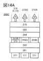
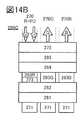
- 14A and 14Bare cross-sectional views showing an example of a display device.
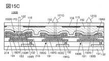
- 15A to 15Care cross-sectional views showing an example of a display device.
- FIG. 16Ais a cross-sectional view showing an example of the display device.
- 16B and 16Care views showing an example of the upper surface layout of the resin layer.
- FIG. 17is a perspective view showing an example of the display device.
- FIG. 18is a cross-sectional view showing an example of the display device.
- FIG. 19is a cross-sectional view showing an example of the display device.
- FIG. 20Ais a cross-sectional view showing an example of the display device.
- FIG. 20Bis a cross-sectional view showing an example of a transistor.
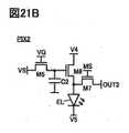
- 21A and 21Bare circuit diagrams showing an example of a pixel circuit.
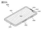
- 22A and 22Bare diagrams showing an example of an electronic device.
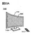
- 23A to 23Dare diagrams showing an example of an electronic device.
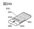
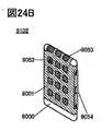
- 24A to 24Fare diagrams showing an example of an electronic device.
- membraneand the word “layer” can be interchanged with each other in some cases or depending on the situation.
- conductive layercan be changed to the term “conductive layer”.
- insulating filmcan be changed to the term “insulating layer”.
- the electronic device of one aspect of the present inventionhas a function of acquiring fingerprint information and at least one kind of position information as finger information that touches an input means such as a display unit or a touch pad.
- the position informationincludes the position where the finger is touched, the direction of the finger touched, the order in which the finger is touched, and the like.
- the electronic device of one aspect of the present inventionhas a function of executing a user authentication process using the information of the finger. When the user operates the electronic device, the authentication process can be executed using both the fingerprint information and the position information, so that it is possible to provide the electronic device with extremely high security.
- the information of the finger touching the input meanscan be acquired and the authentication process can be executed. Therefore, it is possible to prevent a process requiring high security from being executed even when the electronic device is unlocked or the various systems are logged in by an unauthorized method. For example, it is possible to prevent unauthorized execution of processes that require high security, such as access to highly confidential information, purchase settlement, email transmission, and file deletion.
- the information of the finger touching the input meanscan be acquired and the authentication process can be executed. Therefore, it is possible to prevent another person from unlocking the electronic device or logging in to various systems by an unauthorized method.
- the fingerprint information of the user who inputs information such as a password, a passcode, or a graphic patternis acquired, and the user authentication process is performed using both the input information and the fingerprint information. Has a function to perform. As a result, security can be strengthened and the operation of the electronic device by a malicious user can be prevented.
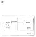
- FIG. 1shows a block diagram of an electronic device 10 according to an aspect of the present invention.
- the electronic device 10includes a control unit 30, a display unit 32, and a storage unit 31.
- the display unit 32has a detection unit 33.
- the electronic device 10can be used as, for example, an information terminal device.
- the display unit 32has a function of displaying an image, a function of detecting a touch operation, and a function of acquiring finger information.
- the finger informationincludes fingerprint information and at least one kind of position information.
- the detection unit 33is a part of the above-mentioned functions of the display unit 32 that has a function of detecting a touch operation and a function of acquiring finger information.
- the display unit 32can also be referred to as a touch panel with a fingerprint information acquisition function.
- a display device described in detail in the second embodimentcan be used for the display unit 32.
- the touch operationincludes contact and may include proximity. Further, the touch operation can also be referred to as a touch input operation or a touch input.
- the detection unit 33has a function of outputting the information of the finger touching the screen to the control unit 30. Specifically, the detection unit 33 has a function of capturing an image of a finger touching the screen and outputting the image information to the control unit 30.
- the display unit 32can acquire the information of the touched finger at any position on the screen. That is, it is preferable that the range in which the touch sensor functions on the screen and the range in which finger information can be acquired coincide with or substantially match.
- the storage unit 31has a function of holding information on a user's finger registered in advance.
- the storage unit 31can output the finger information to the control unit 30 in response to a request from the control unit 30.
- the storage unit 31holds fingerprint information of all fingers used by the user to operate the screen. For example, it is possible to hold two fingerprint information of the index finger of the user's right hand and the index finger of the left hand. In addition to this, it is preferable to retain one or more fingerprint information of the middle finger, ring finger, little finger, and thumb.
- the fingerprint informationincludes a ridge pattern on the abdomen of the finger. Further, as the fingerprint information, the pattern of the ridge on the side surface of the finger may be acquired.
- the fingerprint informationis acquired at least once for each finger. It is preferable to acquire the fingerprint information a plurality of times for each finger because the accuracy of authentication can be improved. It is preferable that the fingerprint information is acquired, for example, twice or more and five times or less per finger.
- the storage unit 31holds a combination of fingerprint information and position information as authentication information. For example, as a condition for authentication, information such as when fingerprint A is detected at position B, fingerprint A in orientation C is detected, or fingerprint A in orientation C is detected at position B is retained. Will be done.
- the combinationmay be individually set by an application in the electronic device or the like.
- control unit 30has a function of requesting the detection unit 33 to acquire finger information when the detection unit 33 detects a touch operation. Then, the control unit 30 has a function of collating the fingerprint information and the position information included in the obtained finger information with the authentication information (combination of the fingerprint information and the position information) registered in advance.
- the control unit 30determines that the fingerprint information and the position information match, the control unit 30 executes a predetermined process according to the touch operation of the user. On the other hand, when it is determined that at least one of the fingerprint information and the position information does not match, the control unit 30 does not execute the predetermined process.
- a method of collating fingerprint information and position information executed by the control unit 30for example, a method such as a template matching method for comparing two images and evaluating their similarity, or a pattern matching method may be used. it can.
- the fingerprint information and the position informationmay be collated independently or collectively. For example, when the similarity value is equal to or more than a predetermined value, it can be determined that the two fingerprint information or the two position information match. Further, one or both of the fingerprint information and the position information may be collated by inference using machine learning. At this time, it is particularly preferable to perform inference using a neural network.
- control unit 30can function as, for example, a central processing unit (CPU: Central Processing Unit).
- CPUCentral Processing Unit
- the control unit 30performs various data processing and program control by interpreting and executing instructions from various programs by the processor.
- the program that can be executed by the processormay be stored in the memory area of the processor or may be stored in the storage unit 31.
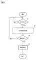
- FIG. 2is a flowchart relating to the operation of the electronic device 10.
- the flowchart shown in FIG. 2has steps S1 to S4.
- step S1the detection unit 33 detects the touch operation by the user. If a touch operation is detected, the process proceeds to step S2. If the touch operation is not performed, the process waits until the touch operation is performed (the process proceeds to step S1 again).
- step S2the detection unit 33 acquires finger information.
- the detection unit 33acquires finger information by capturing an image of the finger.
- step S3the control unit 30 executes the finger authentication process. Specifically, the finger information stored in the storage unit 31 and the finger information acquired by the detection unit 33 are collated, and it is determined whether or not they match. When the authentication is performed (when it is determined that the information of the two fingers matches), the process proceeds to step S4 and the process is executed. On the other hand, if the authentication is not performed (when it is determined that the information of the two fingers does not match), the control unit 30 does not execute the process and returns to step S1 again.
- step S4the control unit 30 executes the process based on the touch operation detected in step S2.
- Touch operationsinclude tap, long tap, flick, drag, multi-touch, swipe, pinch-in, and pinch-out.
- step S4After executing the process in step S4, the process proceeds to step S1 and waits until the touch operation is performed again.
- a program in which a processing method, an operation method, an operation method, a display method, etc. executed by the electronic device 10 or the like exemplified above is describedmay be a non-temporary computer-readable recording medium (also simply a recording medium or a storage medium). It is stored in the electronic device 10 and can be read and executed by an arithmetic unit or the like included in the control unit 30 of the electronic device 10. That is, a program for executing the operation method and the like illustrated above by hardware and a non-temporary computer-readable recording medium in which the program is stored are one aspect of the present invention.
- a hard disk drive(Hard Disk Drive: HDD), a solid state drive (Solid State Drive: SSD), a flash memory, a Blu-ray disc, a DVD, or the like can be used.
- HDDHard Disk Drive
- SSDSolid State Drive
- flash memorya Blu-ray disc, a DVD, or the like
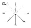
- information on the direction of the touched fingerwill be used as a material for authentication judgment.
- FIG. 3Ashows an example in which the direction of the finger operating the electronic device 10 is authenticated by dividing it into five stages (14a to 14e).
- FIG. 3Ashows an example in which the angle between the two orientations is 45 degrees.
- the direction of the fingercan be determined in two or more steps, and the angle between the two directions can be set as appropriate.
- FIG. 3Ashows an example in which a range of 180 degrees from the orientation of 14d to the orientation of 14e is used for authentication, but the present invention is not limited to this. For example, a 360 degree range may be used for authentication (see dashed line in FIG. 3A).
- FIG. 3Bshows the fingerprint information 22 acquired by the display unit 11 and the fingerprint information 23 of the user registered in advance in the electronic device 10.
- the ridge of the fingerprintis shown by a black line, but in reality, the ridge of the fingerprint may be shown by a line of another color such as white.
- the fingerprint imagecan be acquired by a single color image.
- the fingerprintmay be captured by full-color imaging.
- finger color informationmay be acquired in addition to the fingerprint.
- the fingerprintcan be imaged by changing the emission color according to the color of the finger. As a result, the accuracy of fingerprint imaging can be improved.
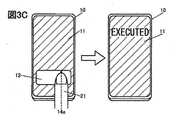
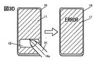
- 3C and 3Dschematically show the electronic device 10 and the index finger 21 of the right hand that operates the electronic device 10.
- the electronic device 10has a display unit 11.
- An icon 12 for executing a desired processis displayed on the display unit 11.
- the electronic device 10is a portable information terminal device that functions as, for example, a smartphone.
- the index finger 21has the fingerprint information 22 shown in FIG. 3B.
- the fingertip of the index finger 21 of the user's right handtouches the display unit 11.
- the display unit 11can acquire finger information about the index finger 21.
- the finger having the fingerprint information 23is registered in the electronic device 10 in advance so that the desired process is executed only when the finger touches the icon 12 in the direction of 14a shown in FIG. 3A.
- the index finger 21 having the fingerprint information 22touches the icon 12 in the direction of 14a, which matches the authentication information registered in the electronic device 10, so that a desired process is executed (EXECUTED).
- FIG. 3Dshows how the index finger 21 is touching the icon 12 in the direction of 14c.
- the orientation 14c of the index finger 21 and the orientation 14a of the pre-registered fingerdo not match, so that the user is not authenticated (ERROR).
- FIG. 4Ashows an example in which the display unit 11 of the electronic device 10 is divided into eight regions from the region 11a to the region 11h for authentication.
- a boundary line (broken line in the figure) or the likemay be displayed so that the user can visually recognize the area, and the boundary line or the like may not be displayed so that the user cannot identify the area.
- the display unit 11can be divided into two or more areas, and the method of division is not limited to equal division.
- the area used for authenticationmay be a part or the whole of the display unit 11.
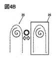
- FIG. 4Bshows the fingerprint information 25 acquired by the display unit 11 and the fingerprint information 26 of the user registered in advance in the electronic device 10. In FIG. 4B, it is determined that the fingerprint information 25 and the fingerprint information 26 match.
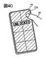
- FIG. 4C and 4Dschematically show the electronic device 10 and the thumb 24 of the user's right hand operating the electronic device 10.
- the thumb 24has the fingerprint information 25 shown in FIG. 4B.
- the fingertip of the thumb 24 of the user's right handtouches the display unit 11. At this time, the display unit 11 can acquire finger information about the thumb 24.
- the thumb 24 of the user's right hand having the fingerprint information 25touches the area 11b of the display unit 11, the user is authenticated, and the lock is released (UNLOCKED).
- the thumb 24touches the area 11h of the display unit 11.
- the useris not authenticated (LOCKED) because the area actually touched by the finger and the area registered in advance do not match.
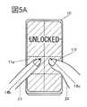
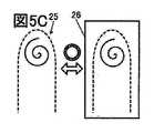
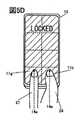
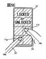
- 5A, 5D, and 5Eschematically show the electronic device 10, the thumb 24 of the user's right hand operating the electronic device 10, and the index finger 27 of the user's left hand.
- the index finger 27has the fingerprint information 28 shown in FIG. 5B.
- the thumb 24has the fingerprint information 25 shown in FIG. 5C.
- FIG. 5Bshows the fingerprint information 28 acquired by the display unit 11 and the fingerprint information 29 of the user registered in advance in the electronic device 10. In FIG. 5B, it is determined that the fingerprint information 28 and the fingerprint information 29 match.
- FIG. 5Cshows the fingerprint information 25 acquired by the display unit 11 and the fingerprint information 26 of the user registered in advance in the electronic device 10. In FIG. 5C, it is determined that the fingerprint information 25 and the fingerprint information 26 match.
- the thumb 24 of the user's right hand and the index finger 27 of the left handtouch the display unit 11.
- the display unit 11can acquire finger information about the thumb 24 and the index finger 27.
- the index finger 27 of the user's left handtouches the display area 11g in the direction of 14a
- the thumb 24 of the user's right handtouches the display area 11h in the direction of 14a.
- the useris not authenticated because the combination of the finger actually touched and its direction and the touched area does not match the combination of the pre-registered finger and its direction and the touched area. ..
- the index finger 27 of the user's left handtouches the display area 11g in the direction of 14b
- the thumb 24 of the user's right handtouches the display area 11f in the direction of 14c.
- the combination of finger orientations touching the screenmatches the combination of finger orientations registered in advance in the electronic device 10, but the combination of regions touched by each finger does not match. It is possible for the user to set whether to perform authentication only when the finger orientation and the area touched by the finger match, or to perform authentication when either one of them matches. If both the finger orientation and the area touched by the finger are used for authentication, the user is not authenticated (LOCKED). When the direction of the finger is used for authentication and the touched area does not matter, the user is authenticated even in the state shown in FIG. 5E (UNLOCKED).
- FIG. 6is a flowchart relating to the operation of the electronic device 10.
- the flowchart shown in FIG. 6has steps S11 to S18.
- the number of times of acquisition of finger information(W times; W is an integer of 2 or more) required for authentication is registered in the electronic device in advance. Further, the number of times the finger information is acquired is set to i times (i is an integer of 1 or more and W or less), and the information of each finger is referred to as "information of the i-th finger" according to the number of times.
- step S14the detection unit 33 acquires the information of the i-th finger.
- the time required from the acquisition of the information of the first finger to the acquisition of the information of the Wth fingermay be predetermined or arbitrarily set by the user.
- step S16the control unit 30 executes the finger authentication process. Specifically, the finger information stored in the storage unit 31 is collated with the finger information acquired by the detection unit 33 i times, and it is determined whether or not all of them match. If authenticated, the process proceeds to step S17 and the process is executed. On the other hand, if the authentication is not performed (when it is determined that the information of one or more fingers does not match the information of the finger registered in advance among the information of the fingers for i times), the control unit 30 processes. Do not execute. FIG. 6 shows an example in which the process proceeds to step S18 and an error is displayed.
- step S17the control unit 30 executes the process based on the touch operation detected in step S11.
- Touch operationsinclude tap, long tap, flick, drag, multi-touch, swipe, pinch-in, and pinch-out.
- step S17After executing the process in step S17, the process proceeds to step S11 and waits until the touch operation is performed again.
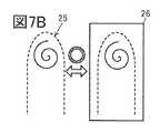
- FIG. 7Ashows the fingerprint information 22 acquired by the display unit 11 and the fingerprint information 23 of the user registered in advance in the electronic device 10. In FIG. 7A, it is determined that the fingerprint information 22 and the fingerprint information 23 match.
- FIG. 7Bshows the fingerprint information 25 acquired by the display unit 11 and the fingerprint information 26 of the user registered in advance in the electronic device 10. In FIG. 7B, it is determined that the fingerprint information 25 and the fingerprint information 26 match.
- FIG. 7C and 7Dshow the electronic device 10, the thumb 24 of the right hand operating the electronic device 10, and the index finger 21 of the right hand.
- the index finger 21has the fingerprint information 22 shown in FIG. 7A.
- the thumb 24has the fingerprint information 25 shown in FIG. 7B.
- an icon 12 for executing a desired processis displayed on the display unit 11.
- the icon 12is first touched by the thumb 24 of the right hand of the user having the fingerprint information 25, and then the icon 12 is touched by the index finger 21 of the right hand of the user having the fingerprint information 22, and is registered in the electronic device 10. It is determined that it matches the authentication information. Therefore, the desired process is being executed.
- the icon 12is first touched with the fingertip of the index finger 21 of the right hand, and then the icon 12 is touched with the thumb 24 of the right hand.
- the useris not authenticated because the order of the fingers touching the icon and the order of the fingers registered in advance do not match.
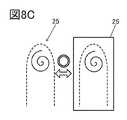
- FIG. 8A and 8Bschematically show an electronic device 10 and a thumb 24 for operating the electronic device.
- the thumb 24has the fingerprint information 25 shown in FIG. 8C.
- FIG. 8Cshows the fingerprint information 25 acquired by the display unit 11 and the fingerprint information 26 of the user registered in advance in the electronic device 10. In FIG. 8C, it is determined that the fingerprint information 25 and the fingerprint information 26 match.
- the thumb 24 of the user's right hand having the fingerprint information 25touches the display unit three times in the order of the area 11b, the area 11d, and the area 11h, and it is determined that the thumb 24 matches the authentication information registered in the electronic device 10. Has been done. Therefore, the user is authenticated.
- the thumb 24 of the right handtouches the display unit three times in the order of region 11b, region 11h, and region 11d. Since the order in which the finger actually touches each area does not match the pre-registered order, the user is not authenticated.
- input informationsuch as a password, passcode, and graphic pattern may be used as a material for authentication judgment.
- the input informationcan also be regarded as equivalent to the order of the places where the fingers touch. For example, if the correct password is entered, it corresponds to the order of the places where the fingers touch. Therefore, the user can be authenticated when the correct information is input and it is determined that the fingerprint information of the finger matches the fingerprint information registered in advance. As a result, the operation performed by the user is the same as when using an electronic device that uses an authentication method using only input information such as a password, passcode, or graphic pattern, but the security of the electronic device can be further enhanced. ..
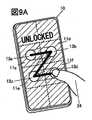
- FIG. 9A, 9D, and 9Eschematically show the electronic device 10, the thumb 24 of the user who operates the electronic device, and the index finger 40 of a person who is different from the user who operates the electronic device. ..
- the thumb 24has the fingerprint information 25 shown in FIG. 9C.
- the index finger 40has the fingerprint information 41 shown in FIG. 9B.
- icons 13a to 13dwhich serve as markers for inputting graphic patterns, are displayed in the areas 11c, 11d, 11e, and 11f of the display unit 11, respectively. ing.
- FIG. 9Bshows the fingerprint information 41 acquired by the display unit 11 and the fingerprint information 26 of the user registered in advance in the electronic device 10. In FIG. 9B, it is determined that the fingerprint information 41 and the fingerprint information 26 do not match.
- the thumb 24 of the user having the fingerprint information 25slides his / her finger in the order of the icon 13a, the icon 13b, the icon 13c, and the icon 13d, inputs the Z-shaped graphic pattern of the alphabet, and authenticates the user. It has been unlocked (UNLOCKED).
- the index finger 40 of the right hand of a person other than the user having the fingerprint information 41slides the finger in the order of the icon 13a, the icon 13b, the icon 13c, and the icon 13d, and inputs the Z-shaped graphic pattern of the alphabet. ..
- the fingerprint information 41 acquired by the display unit 11 and the fingerprint information 26 registered in advancedo not match.
- the input graphic patternmatches the pre-registered graphic pattern, but the fingerprint information does not match, so the user is not authenticated (LOCKED).
- FIG. 9Cshows the fingerprint information 25 acquired by the display unit 11 and the fingerprint information 26 of the user registered in advance in the electronic device 10. In FIG. 9C, it is determined that the fingerprint information 25 and the fingerprint information 26 match.
- the thumb 24 of the user having the fingerprint information 25slides his / her finger in the order of the icon 13a, the icon 13c, the icon 13d, and the icon 13b, and inputs the U-shaped graphic pattern of the alphabet.
- the fingerprint information 25 acquired by the display unit 11 and the fingerprint information 26 registered in advancematch, but the input graphic pattern is a graphic registered in advance.
- the useris not authenticated (LOCKED) because it does not match the pattern.
- the display unit 32includes the detection unit 33, but these may be provided separately.
- the electronic device 10A shown in FIG. 10Ashows an example in which the detection unit 33 is not included in the display unit 32.
- Examples of the detection unit 33 of the electronic device 10Ainclude a touch pad having no image display function.
- a detection unit used for detecting the touch operation and a detection unit used for acquiring finger informationmay be provided separately.
- the electronic device 10B shown in FIG. 10Bshows an example in which a detection unit 33A for acquiring finger information is included in the display unit 32, and a detection unit 33B for detecting a touch operation is independently provided.
- a display device described in detail in the second embodimentmay be used for the display unit 32, and a capacitive touch sensor may be used for the detection unit 33B.
- the display unit 32may include the detection unit 33B for detecting the touch operation, and the detection unit 33A for acquiring the finger information is independently provided. There may be.
- the display device of the present embodimentcan be suitably used for the display unit of the electronic device described in the first embodiment.
- the display unit of the display devicehas a function of displaying an image using a light emitting element (also referred to as a light emitting device). Further, the display unit has one or both of an imaging function and a sensing function.
- a light emitting elementalso referred to as a light emitting device
- the display device of one aspect of the present inventionhas a light receiving element (also referred to as a light receiving device) and a light emitting element.
- the display device of one aspect of the present inventionhas a light receiving / emitting element (also referred to as a light receiving / emitting device) and a light emitting element.
- the display devicehas a light receiving element and a light emitting element in the display unit.
- light emitting elementsare arranged in a matrix on the display unit, and an image can be displayed on the display unit.
- light receiving elementsare arranged in a matrix on the display unit, and the display unit has one or both of an imaging function and a sensing function.
- the display unitcan be used for an image sensor or a touch sensor. That is, by detecting the light on the display unit, it is possible to capture an image and detect a touch operation of an object (finger, pen, etc.).
- the light emitting elementcan be used as a light source of the sensor. Therefore, it is not necessary to provide a light receiving unit and a light source separately from the display device, and the number of parts of the electronic device can be reduced.
- the light receiving elementwhen the object reflects (or scatters) the light emitted by the light emitting element of the display unit, the light receiving element can detect the reflected light (or scattered light), so that the place is dark.
- the light receiving elementcan detect the reflected light (or scattered light), so that the place is dark.
- the display device of one aspect of the present inventionhas a function of displaying an image by using a light emitting element. That is, the light emitting element functions as a display element (also referred to as a display device).
- an EL elementalso referred to as an EL device
- an OLEDOrganic Light Emitting Diode
- QLEDQuadantum-dot Light Emitting Diode
- the light emitting substances of the EL elementinclude fluorescent substances (fluorescent materials), phosphorescent substances (phosphorescent materials), inorganic compounds (quantum dot materials, etc.), and substances showing thermal activated delayed fluorescence (thermally activated delayed fluorescence). (Thermally Activated Fluorescence: TADF) material) and the like.
- an LEDsuch as a micro LED (Light Emitting Diode) can also be used.
- the display device of one aspect of the present inventionhas a function of detecting light by using a light receiving element.
- the display devicecan capture an image by using the light receiving element.
- the display device of this embodimentcan be used as a scanner.
- an image sensorcan be used to acquire data related to biological information such as fingerprints and palm prints.
- the display devicecan incorporate a biometric authentication sensor.
- a biometric authentication sensorBy incorporating a biometric authentication sensor in the display device, the number of parts of the electronic device can be reduced, and the size and weight of the electronic device can be reduced as compared with the case where the biometric authentication sensor is provided separately from the display device. ..
- the display devicecan detect the touch operation of the object by using the light receiving element.
- the light receiving elementfor example, a pn type or pin type photodiode can be used.
- the light receiving elementfunctions as a photoelectric conversion element (also referred to as a photoelectric conversion device) that detects light incident on the light receiving element and generates an electric charge.
- the amount of charge generated from the light receiving elementis determined based on the amount of light incident on the light receiving element.
- organic photodiodehaving a layer containing an organic compound as the light receiving element.
- Organic photodiodescan be easily made thinner, lighter, and larger in area, and have a high degree of freedom in shape and design, so that they can be applied to various display devices.
- an organic EL element(also referred to as an organic EL device) is used as a light emitting element, and an organic photodiode is used as a light receiving element.
- the organic EL element and the organic photodiodecan be formed on the same substrate. Therefore, the organic photodiode can be built in the display device using the organic EL element.
- the number of film forming stepsbecomes very large. Since many organic photodiodes have layers that can have the same configuration as the organic EL element, it is possible to suppress an increase in the film forming process by forming the layers that can have the same configuration in a batch.
- one of the pair of electrodescan be a common layer for the light receiving element and the light emitting element.
- the light receiving element and the light emitting elementmay have the same configuration except that the light receiving element has an active layer and the light emitting element has a light emitting layer. That is, the light receiving element can be manufactured only by replacing the light emitting layer of the light emitting element with the active layer.
- a display device having a light receiving elementcan be manufactured by using the existing manufacturing device and manufacturing method of the display device.
- the layer that the light receiving element and the light emitting element have in commonmay have different functions in the light emitting element and those in the light receiving element.
- the componentsare referred to based on the function in the light emitting element.
- the hole injection layerfunctions as a hole injection layer in the light emitting element and as a hole transport layer in the light receiving element.
- the electron injection layerfunctions as an electron injection layer in the light emitting element and as an electron transport layer in the light receiving element.
- the layer that the light receiving element and the light emitting element have in commonmay have the same function in the light emitting element and the function in the light receiving element.
- the hole transport layerfunctions as a hole transport layer in both the light emitting element and the light receiving element
- the electron transport layerfunctions as an electron transport layer in both the light emitting element and the light receiving element.
- the sub-pixel exhibiting any colorhas a light emitting / receiving element instead of the light emitting element, and the sub pixel exhibiting the other color has a light emitting element.
- the light receiving / receiving elementhas both a function of emitting light (light emitting function) and a function of receiving light (light receiving function). For example, when a pixel has three sub-pixels of a red sub-pixel, a green sub-pixel, and a blue sub-pixel, at least one sub-pixel has a light-receiving element and the other sub-pixel has a light-emitting element. It is configured. Therefore, the display unit of the display device according to one aspect of the present invention has a function of displaying an image by using both the light emitting / receiving element and the light emitting element.
- the light receiving / receiving elementalso serves as a light emitting element and a light receiving element, it is possible to impart a light receiving function to the pixels without increasing the number of sub-pixels included in the pixels.
- one or both of the imaging function and the sensing functioncan be added to the display unit of the display device while maintaining the aperture ratio of the pixels (aperture ratio of each sub-pixel) and the fineness of the display device. .. Therefore, in the display device of one aspect of the present invention, the aperture ratio of the pixels can be increased and the definition can be easily increased as compared with the case where the sub-pixels having a light receiving element are provided separately from the sub-pixels having a light emitting element. is there.
- a light emitting / receiving element and a light emitting elementare arranged in a matrix on the display unit, and an image can be displayed on the display unit.
- the display unitcan be used for an image sensor or a touch sensor.
- the light emitting elementcan be used as a light source of the sensor. Therefore, it is not necessary to provide a light receiving unit and a light source separately from the display device, and the number of parts of the electronic device can be reduced.
- the light receiving and emitting elementcan detect the reflected light (or scattered light), so that it is dark. It is possible to capture images and detect touch operations even in places.
- the light receiving / receiving elementcan be manufactured by combining an organic EL element and an organic photodiode.
- a light emitting / receiving elementcan be manufactured by adding an active layer of an organic photodiode to a laminated structure of an organic EL element.
- an increase in the film forming processcan be suppressed by collectively forming a layer having a structure common to that of the organic EL element.
- one of the pair of electrodescan be a common layer for the light emitting / receiving element and the light emitting element.
- it is preferable that at least one of the hole injection layer, the hole transport layer, the electron transport layer, and the electron injection layeris a common layer for the light emitting / receiving element and the light emitting element.
- the light receiving element and the light emitting elementmay have the same configuration except for the presence or absence of the active layer of the light receiving element. That is, a light emitting / receiving element can be manufactured only by adding the active layer of the light receiving element to the light emitting element.
- a display device having a light receiving / receiving elementcan be manufactured by using the existing manufacturing device and manufacturing method of the display device.
- the layer of the light emitting / receiving elementmay have different functions depending on whether the light receiving / receiving element functions as a light receiving element or a light emitting element.
- the componentsare referred to based on the function when the light emitting / receiving element functions as a light emitting element.
- the hole injection layerfunctions as a hole injection layer when the light receiving / receiving element functions as a light emitting element, and functions as a hole transporting layer when the light receiving / receiving element functions as a light receiving element.
- the electron injection layerfunctions as an electron injection layer when the light receiving / receiving element functions as a light emitting element, and functions as an electron transporting layer when the light receiving / receiving element functions as a light receiving element.
- the layer included in the light emitting / receiving elementmay have the same function depending on whether the light receiving / receiving element functions as a light receiving element or a light emitting element.
- the hole transport layerfunctions as a hole transport layer regardless of whether it functions as a light emitting element or a light receiving element, and the electron transport layer functions as either a light emitting element or a light receiving element. Functions as.
- the display device of the present embodimenthas a function of displaying an image by using a light emitting element and a light receiving / receiving element. That is, the light emitting element and the light receiving / receiving element function as display elements.
- the display device of the present embodimenthas a function of detecting light by using a light receiving / receiving element.
- the light receiving / receiving elementcan detect light having a shorter wavelength than the light emitted by the light receiving / emitting element itself.
- the display device of the present embodimentcan capture an image by using the light receiving / receiving element.
- the display device of this embodimentcan be used as a scanner.
- the display device of the present embodimentcan detect the touch operation of the object by using the light receiving / receiving element.
- the light receiving / receiving elementfunctions as a photoelectric conversion element that detects light incident on the light receiving / emitting element and generates an electric charge.
- the amount of electric charge generated from the light receiving and emitting elementis determined based on the amount of light incident on the light receiving and emitting element.
- the light emitting / receiving elementcan be manufactured by adding an active layer of the light receiving element to the configuration of the light emitting element.
- a pn type or pin type photodiode structurecan be applied to the light receiving / receiving element.
- Organic photodiodescan be easily made thinner, lighter, and larger in area, and have a high degree of freedom in shape and design, so that they can be applied to various display devices.
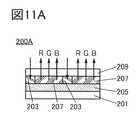
- Display device 11A to 11D and 11Fshow cross-sectional views of the display device according to one aspect of the present invention.
- the display device 200A shown in FIG. 11Ahas a layer 203 having a light receiving element, a functional layer 205, and a layer 207 having a light emitting element between the substrate 201 and the substrate 209.
- the display device 200Ahas a configuration in which red (R), green (G), and blue (B) lights are emitted from the layer 207 having a light emitting element.
- the light receiving element included in the layer 203 having the light receiving elementcan detect the light incident from the outside of the display device 200A.
- the display device 200B shown in FIG. 11Bhas a layer 204 having a light emitting / receiving element, a functional layer 205, and a layer 207 having a light emitting element between the substrate 201 and the substrate 209.
- the display device 200Bhas a configuration in which green (G) light and blue (B) light are emitted from the layer 207 having a light emitting element, and red (R) light is emitted from the layer 204 having a light emitting / receiving element. is there.
- the color of the light emitted by the layer 204 having the light emitting / receiving elementis not limited to red.
- the color of the light emitted by the layer 207 having the light emitting elementis not limited to the combination of green and blue.
- the light emitting / receiving element included in the layer 204 having the light receiving / receiving elementcan detect the light incident from the outside of the display device 200B.
- the light receiving / receiving elementcan detect, for example, one or both of green (G) light and blue (B) light.
- the functional layer 205has a circuit for driving a light receiving element or a light emitting and receiving element, and a circuit for driving the light emitting element.
- the functional layer 205may be provided with switches, transistors, capacitances, resistors, wirings, terminals and the like. When the light emitting element and the light receiving element are driven by the passive matrix method, a switch or a transistor may not be provided.
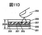
- the display device of one aspect of the present inventionmay have a function (function as a touch panel) of detecting an object such as a finger touching the display device. For example, as shown in FIG. 11C, when the light emitted by the light emitting element in the layer 207 having the light emitting element is reflected by the finger 202 touching the display device 200A, the light receiving element in the layer 203 having the light receiving element reflects the light. Detect light. Thereby, it is possible to detect that the finger 202 touches the display device 200A.
- the light emitted by the light emitting element in the layer 207 having the light emitting elementis reflected by the finger touching the display device 200B, so that the light receiving element in the layer 204 having the light receiving element reflects the reflected light. Can be detected.
- the case where the light emitted from the light emitting element is reflected by the objectwill be described as an example, but the light may be scattered by the object.
- the display device of one aspect of the present inventionmay have a function of detecting or imaging an object that is close to (not in contact with) the display device.
- the display device of one aspect of the present inventionmay have a function of detecting the fingerprint of the finger 202.
- FIG. 11Eshows an image diagram of an image captured by the display device of one aspect of the present invention.
- the outline of the finger 202is shown by a broken line and the outline of the contact portion 261 is shown by a dashed-dotted line within the imaging range 263.
- An image of a high-contrast fingerprint 262can be captured by the difference in the amount of light incident on the light receiving element (or the light receiving / emitting element) in the contact portion 261.
- the display device of one aspect of the present inventioncan also function as a pen tablet.
- FIG. 11Fshows a state in which the tip of the stylus 208 is slid in the direction of the broken line arrow while touching the substrate 209.
- the scattered light scattered at the tip of the stylus 208 and the contact surface of the substrate 209is incident on the light receiving element (or light emitting / receiving element) located at the portion overlapping the contact surface, so that the stylus is stylus.
- the position of the tip of 208can be detected with high accuracy.
- FIG. 11Gshows an example of the locus 266 of the stylus 208 detected by the display device of one aspect of the present invention. Since the display device of one aspect of the present invention can detect the position of the object to be detected such as the stylus 208 with high position accuracy, it is also possible to perform high-definition drawing in a drawing application or the like. Further, unlike the case where a capacitance type touch sensor or an electromagnetic induction type touch pen is used, the position can be detected even with a highly insulating object to be detected, so that the tip of the stylus 208 can be detected. Any material can be used, and various writing instruments (for example, a brush, a glass pen, a quill pen, etc.) can be used.
- various writing instrumentsfor example, a brush, a glass pen, a quill pen, etc.
- the display device of one aspect of the present inventionhas a plurality of pixels arranged in a matrix.
- One pixelhas a plurality of sub-pixels.
- One sub-pixelhas one light emitting element, one light receiving element, or one light receiving element.
- Each of the plurality of pixelshas one or more of a sub-pixel having a light emitting element, a sub pixel having a light receiving element, and a sub pixel having a light receiving element.
- the pixelhas a plurality of sub-pixels having a light emitting element (for example, three or four) and one sub pixel having a light receiving element.
- a light emitting elementfor example, three or four
- a light receiving elementfor example, three or four
- the light receiving elementmay be provided on all pixels or may be provided on some pixels. Further, one pixel may have a plurality of light receiving elements. Further, one light receiving element may be provided over a plurality of pixels. The definition of the light receiving element and the definition of the light emitting element may be different from each other.
- the three sub-pixelsinclude sub-pixels of three colors R, G, and B, yellow (Y), cyan (C), and magenta (M). Examples include three-color sub-pixels.
- the four sub-pixelsinclude four sub-pixels of R, G, B, and white (W), and four colors of R, G, B, and Y. Sub-pixels and the like can be mentioned.
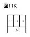
- 11H, 11 (J), 11 (K), and 11 (L)show an example of a pixel having a plurality of sub-pixels having a light emitting element and one sub-pixel having a light receiving element.
- the arrangement of the sub-pixels shown in the present embodimentis not limited to the order shown.
- the positions of the sub-pixel (B) and the sub-pixel (G)may be reversed.
- the pixels shown in FIGS. 11H, 11 (J), and 11 (K)are sub-pixels (PD) having a light receiving function, sub-pixels (R) exhibiting red light, and sub-pixels exhibiting green light. It has (G) and a sub-pixel (B) that exhibits blue light.
- a matrix arrayis applied to the pixels shown in FIG. 11H, and a stripe array is applied to the pixels shown in FIG. 11 (J).
- a sub-pixel (R) exhibiting red light, a sub-pixel (G) exhibiting green light, and a sub-pixel (B) exhibiting blue lightare arranged in a horizontal row.
- a sub-pixel (PD) having a light receiving functionis arranged below the sub-pixel (PD). That is, in FIG. 11 (K), the sub-pixel (R), the sub-pixel (G), and the sub-pixel (B) are arranged in the same row as each other, and are arranged in a row different from the sub-pixel (PD).
- the pixel shown in FIG. 11 (L)has a sub-pixel (X) that exhibits light other than R, G, and B, in addition to the pixel configuration shown in FIG. 11 (K).
- Examples of light other than R, G, and Binclude light such as white (W), yellow (Y), cyan (C), magenta (M), and infrared light (IR).
- the sub-pixel (PD) having a light receiving functionhas a function of detecting infrared light.
- the sub-pixel (PD) having a light receiving functionmay have a function of detecting both visible light and infrared light.
- the wavelength of light detected by the light receiving elementcan be determined according to the application of the sensor.
- the pixelhas a plurality of sub-pixels having a light emitting element and one sub pixel having a light emitting / receiving element.
- one or both of the imaging function and the sensing functionare displayed in the display unit without reducing the aperture ratio and the definition. Can be added.
- the light receiving / receiving elementmay be provided in all the pixels or may be provided in some of the pixels. Further, one pixel may have a plurality of light receiving / receiving elements.
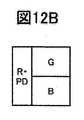
- 12A to 12Dshow an example of a pixel having a plurality of sub-pixels having a light emitting element and one sub-pixel having a light emitting / receiving element.
- the pixels shown in FIG. 12Ahave a stripe arrangement applied to them, and emit red light and a sub-pixel (R / PD) having a light receiving function, sub-pixels (G) exhibiting green light, and blue light. It has a sub-pixel (B) to be presented.
- R / PDsub-pixel
- Gsub-pixel
- Bsub-pixel
- a display device having a light receiving function in the pixelcan be manufactured by replacing the light emitting element used for the sub pixel of R with a light receiving element. it can.
- the pixels shown in FIG. 12Bare a sub-pixel (R / PD) that exhibits red light and has a light receiving function, a sub-pixel (G) that exhibits green light, and a sub-pixel (B) that exhibits blue light.
- the sub-pixels (R / PD)are arranged in different columns from the sub-pixel (G) and the sub-pixel (B).
- Sub-pixels (G) and sub-pixels (B)are alternately arranged in the same column, one in odd rows and the other in even rows.
- the sub-pixels arranged in a row different from the sub-pixels of other colorsare not limited to red (R), and may be green (G) or blue (B).
- a matrix arrangementis applied, and sub-pixels (R / PD) having a light receiving function, sub-pixels (R / PD) exhibiting red light, sub-pixels (G) exhibiting green light, and sub-pixels exhibiting blue light. It has a pixel (B) and a sub-pixel (X) that exhibits light other than R, G, and B. Even in a display device in which the pixels are composed of four sub-pixels of R, G, B, and X, a display device having a light receiving function in the pixels is manufactured by replacing the light emitting element used for the sub pixel of R with a light receiving element. can do.
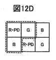
- FIG. 12Dshows two pixels, and one pixel is composed of three sub-pixels surrounded by a dotted line.
- the pixels shown in FIG. 12Dare a sub-pixel (R / PD) that exhibits red light and has a light receiving function, a sub-pixel (G) that exhibits green light, and a sub-pixel (B) that exhibits blue light.
- R / PDsub-pixel
- Gsub-pixel
- Bsub-pixel
- the sub-pixel (G)is arranged in the same row as the sub-pixel (R / PD), and the sub-pixel (B) is arranged in the same column as the sub-pixel (G).
- the sub-pixels (R / PD), sub-pixels (G), and sub-pixels (B)are repeatedly arranged in both the odd-numbered rows and the even-numbered rows, and in each column.
- Sub-pixels of different colorsare arranged in the odd-numbered rows and the even-numbered rows.
- FIG. 12Eshows four pixels to which the pentile arrangement is applied, and the two adjacent pixels have sub-pixels that exhibit two colors of light in different combinations.
- the shape of the sub-pixel shown in FIG. 12Eindicates the shape of the upper surface of the light emitting element or the light emitting / receiving element of the sub pixel.
- FIG. 12Fis a modification of the pixel array shown in FIG. 12E.
- the upper left pixel and the lower right pixel shown in FIG. 12Ehave a sub-pixel (RPD) that exhibits red light and has a light receiving function, and a sub-pixel (G) that exhibits green light.
- the lower left pixel and the upper right pixel shown in FIG. 12Ehave a sub-pixel (G) exhibiting green light and a sub-pixel (B) exhibiting blue light.
- the upper left pixel and the lower right pixel shown in FIG. 12Fhave a sub-pixel (RPD) that exhibits red light and has a light receiving function, and a sub-pixel (G) that exhibits green light.
- the lower left pixel and the upper right pixel shown in FIG. 12Fhave a sub-pixel (R / PD) that exhibits red light and has a light receiving function, and a sub-pixel (B) that exhibits blue light.
- each pixelis provided with a sub-pixel (G) that exhibits green light.
- sub-pixels (R / PD) that exhibit red light and have a light receiving functionare provided for each pixel. Since each pixel is provided with a sub-pixel having a light receiving function, the configuration shown in FIG. 12F can perform imaging with a higher definition than the configuration shown in FIG. 12E. Thereby, for example, the accuracy of biometric authentication can be improved.
- the upper surface shapes of the light emitting element and the light receiving / receiving elementare not particularly limited, and may be a circle, an ellipse, a polygon, a polygon with rounded corners, or the like.
- FIG. 12Eshows an example of being circular
- FIG. 12Fshows an example of being square.
- the upper surface shapes of the light emitting element and the light receiving / receiving element of each colormay be different from each other, or may be the same for some or all colors.
- the aperture ratios of the sub-pixels of each colormay be different from each other, and may be the same for some or all colors.
- the aperture ratio of the sub-pixels (sub-pixels (G) in FIG. 12E and sub-pixels (R / PD) in FIG. 12F) provided for each pixelis made smaller than the aperture ratios of the sub-pixels of other colors. May be good.
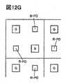
- FIG. 12Gis a modified example of the pixel array shown in FIG. 12F. Specifically, the configuration of FIG. 12G is obtained by rotating the configuration of FIG. 12F by 45 °. In FIG. 12F, it has been described that one pixel is composed of two sub-pixels, but as shown in FIG. 12G, it can be considered that one pixel is composed of four sub-pixels.
- one pixelis composed of four sub-pixels surrounded by a dotted line.
- One pixelhas two sub-pixels (R / PD), one sub-pixel (G), and one sub-pixel (B).
- R / PDsub-pixels
- Gsub-pixel
- Bsub-pixel
- the definition of imagingcan be double the route of definition of display.
- pis an integer of 2 or more) first light emitting elements and q (q is an integer of 2 or more) second light emitting elements.
- ris an integer larger than p and larger than q).
- One of the first light emitting element and the second light emitting elementemits green light, and the other emits blue light.
- the light receiving / receiving elementemits red light and has a light receiving function.
- the light emitted from the light sourceis hard to be visually recognized by the user. Since blue light has lower visibility than green light, it is preferable to use a light emitting element that emits blue light as a light source. Therefore, it is preferable that the light receiving / receiving element has a function of receiving blue light.
- pixels of various arrangementscan be applied to the display device of the present embodiment.
- the display device of one aspect of the present inventionis a top emission type that emits light in the direction opposite to the substrate on which the light emitting element is formed, a bottom emission type that emits light on the substrate side on which the light emitting element is formed, and both sides. It may be any of the dual emission type that emits light to the light.
- a top emission type display devicewill be described as an example.
- the display device 280A shown in FIG. 13Aincludes a light receiving element 270PD, a light emitting element 270R that emits red (R) light, a light emitting element 270G that emits green (G) light, and a light emitting element 270B that emits blue (B) light.
- a light receiving element 270PDincludes a light receiving element 270PD, a light emitting element 270R that emits red (R) light, a light emitting element 270G that emits green (G) light, and a light emitting element 270B that emits blue (B) light.
- Each light emitting elementhas a pixel electrode 271, a hole injection layer 281, a hole transport layer 282, a light emitting layer, an electron transport layer 284, an electron injection layer 285, and a common electrode 275 stacked in this order.
- the light emitting element 270Rhas a light emitting layer 283R
- the light emitting element 270Ghas a light emitting layer 283G
- the light emitting element 270Bhas a light emitting layer 283B.
- the light emitting layer 283Rhas a light emitting substance that emits red light
- the light emitting layer 283Ghas a light emitting substance that emits green light
- the light emitting layer 283Bhas a light emitting substance that emits blue light.
- the light emitting elementis an electroluminescent element that emits light to the common electrode 275 side by applying a voltage between the pixel electrode 271 and the common electrode 275.
- the light receiving element 270PDhas a pixel electrode 271, a hole injection layer 281, a hole transport layer 282, an active layer 273, an electron transport layer 284, an electron injection layer 285, and a common electrode 275 stacked in this order.
- the light receiving element 270PDis a photoelectric conversion element that receives light incident from the outside of the display device 280A and converts it into an electric signal.
- the pixel electrode 271functions as an anode and the common electrode 275 functions as a cathode in both the light emitting element and the light receiving element. That is, the light receiving element can detect the light incident on the light receiving element, generate an electric charge, and take it out as an electric current by driving the light receiving element by applying a reverse bias between the pixel electrode 271 and the common electrode 275.
- an organic compoundis used for the active layer 273 of the light receiving element 270PD.
- the light receiving element 270PDcan have a layer other than the active layer 273 having the same configuration as the light emitting element. Therefore, the light receiving element 270PD can be formed in parallel with the formation of the light emitting element only by adding the step of forming the active layer 273 to the manufacturing process of the light emitting element. Further, the light emitting element and the light receiving element 270PD can be formed on the same substrate. Therefore, the light receiving element 270PD can be built in the display device without significantly increasing the manufacturing process.
- the display device 280Ashows an example in which the light receiving element 270PD and the light emitting element have a common configuration except that the active layer 273 of the light receiving element 270PD and the light emitting layer 283 of the light emitting element are separately formed.
- the configuration of the light receiving element 270PD and the light emitting elementis not limited to this.
- the light receiving element 270PD and the light emitting elementmay have layers that are separated from each other.
- the light receiving element 270PD and the light emitting elementpreferably have one or more layers (common layers) that are commonly used. As a result, the light receiving element 270PD can be incorporated in the display device without significantly increasing the manufacturing process.
- a conductive film that transmits visible lightis used as the electrode on the side that extracts light. Further, it is preferable to use a conductive film that reflects visible light for the electrode on the side that does not take out light.
- a micro-optical resonator (microcavity) structureis applied to the light emitting element of the display device of the present embodiment. Therefore, one of the pair of electrodes of the light emitting element preferably has an electrode having transparency and reflection to visible light (semi-transmissive / semi-reflective electrode), and the other has an electrode having reflection to visible light (semi-transmissive / semi-reflective electrode). It is preferable to have a reflective electrode).
- the light emitting elementhas a microcavity structure, the light emitted from the light emitting layer can be resonated between both electrodes, and the light emitted from the light emitting element can be strengthened.
- the semi-transmissive / semi-reflective electrodecan have a laminated structure of a reflective electrode and an electrode having transparency to visible light (also referred to as a transparent electrode).
- the light transmittance of the transparent electrodeshall be 40% or more.
- the reflectance of visible light of the semi-transmissive / semi-reflective electrodeis 10% or more and 95% or less, preferably 30% or more and 80% or less.
- the reflectance of visible light of the reflecting electrodeis 40% or more and 100% or less, preferably 70% or more and 100% or less.
- the resistivity of these electrodesis preferably 1 ⁇ 10 -2 ⁇ cm or less.
- the transmittance or reflectance of the near-infrared light of these electrodesis the same as the transmittance or reflectance of visible light. It is preferable to satisfy the above numerical range.
- the light emitting elementhas at least a light emitting layer 283.
- the light emitting deviceincludes a substance having a high hole injection property, a substance having a high hole transport property, a hole blocking material, a substance having a high electron transport property, a substance having a high electron transfer property, or a bipolar property. It may further have a layer containing the substance (substance having high electron transport property and hole transport property) and the like.
- the light emitting element and the light receiving elementmay have one or more of the hole injection layer, the hole transport layer, the electron transport layer, and the electron injection layer having a common configuration. Further, the light emitting element and the light receiving element can form one or more of the hole injection layer, the hole transport layer, the electron transport layer, and the electron injection layer.
- the hole injection layeris a layer that injects holes from the anode into the hole transport layer, and is a layer that contains a material having high hole injection properties.
- a material having high hole injectabilityan aromatic amine compound or a composite material containing a hole transporting material and an acceptor material (electron acceptor material) can be used.
- the hole transport layeris a layer that transports holes injected from the anode to the light emitting layer by the hole injection layer.
- the hole transport layeris a layer that transports holes generated based on the light incident in the active layer to the anode.
- the hole transport layeris a layer containing a hole transport material.
- the hole transporting materiala substance having a hole mobility of 10-6 cm 2 / Vs or more is preferable. In addition, any substance other than these can be used as long as it is a substance having a higher hole transport property than electrons.
- the hole-transporting materialexamples include materials having high hole-transporting properties such as ⁇ -electron-rich heterocyclic compounds (for example, carbazole derivatives, thiophene derivatives, furan derivatives, etc.) and aromatic amines (compounds having an aromatic amine skeleton). Is preferable.
- materials having high hole-transporting propertiessuch as ⁇ -electron-rich heterocyclic compounds (for example, carbazole derivatives, thiophene derivatives, furan derivatives, etc.) and aromatic amines (compounds having an aromatic amine skeleton). Is preferable.
- the electron transport layeris a layer that transports electrons injected from the cathode to the light emitting layer by the electron injection layer.
- the electron transport layeris a layer that transports electrons generated based on the light incident on the active layer to the cathode.
- the electron transport layeris a layer containing an electron transport material.
- the electron transporting materiala substance having an electron mobility of 1 ⁇ 10 -6 cm 2 / Vs or more is preferable. In addition, any substance other than these can be used as long as it is a substance having a higher electron transport property than holes.
- Examples of the electron-transporting materialinclude a metal complex having a quinoline skeleton, a metal complex having a benzoquinoline skeleton, a metal complex having an oxazole skeleton, a metal complex having a thiazole skeleton, and the like, as well as oxadiazole derivatives, triazole derivatives, and imidazole derivatives.
- ⁇ electron deficiencyincluding oxazole derivative, thiazole derivative, phenanthroline derivative, quinoline derivative having quinoline ligand, benzoquinoline derivative, quinoxalin derivative, dibenzoquinoxalin derivative, pyridine derivative, bipyridine derivative, pyrimidine derivative, and other nitrogen-containing heteroaromatic compounds
- a material having high electron transport propertysuch as a type heteroaromatic compound can be used.
- the electron injection layeris a layer for injecting electrons from the cathode into the electron transport layer, and is a layer containing a material having high electron injectability.
- a material having high electron injection propertyan alkali metal, an alkaline earth metal, or a compound thereof can be used.
- a composite material containing an electron transporting material and a donor material (electron donating material)can also be used.
- the light emitting layer 283is a layer containing a light emitting substance.
- the light emitting layer 283can have one or more kinds of light emitting substances.
- a substance exhibiting a luminescent colorsuch as blue, purple, bluish purple, green, yellowish green, yellow, orange, and red is appropriately used. Further, as the luminescent substance, a substance that emits near-infrared light can also be used.
- luminescent substancesinclude fluorescent materials, phosphorescent materials, TADF materials, quantum dot materials, and the like.
- fluorescent materialexamples include pyrene derivative, anthracene derivative, triphenylene derivative, fluorene derivative, carbazole derivative, dibenzothiophene derivative, dibenzofuran derivative, dibenzoquinoxaline derivative, quinoxaline derivative, pyridine derivative, pyrimidine derivative, phenanthrene derivative, naphthalene derivative and the like. Be done.
- an organic metal complex having a 4H-triazole skeleton, a 1H-triazole skeleton, an imidazole skeleton, a pyrimidine skeleton, a pyrazine skeleton, or a pyridine skeleton (particularly an iridium complex), or a phenylpyridine derivative having an electron-withdrawing groupis arranged.
- examples thereofinclude an organic metal complex (particularly an iridium complex), a platinum complex, and a rare earth metal complex as a ligand.
- the light emitting layer 283may have one or more kinds of organic compounds (host material, assist material, etc.) in addition to the light emitting substance (guest material).
- organic compoundshost material, assist material, etc.
- guest materialAs one or more kinds of organic compounds, one or both of a hole transporting material and an electron transporting material can be used. Further, a bipolar material or a TADF material may be used as one or more kinds of organic compounds.
- the light emitting layer 283preferably has, for example, a phosphorescent material and a hole transporting material and an electron transporting material which are combinations that easily form an excitation complex.
- ExTETExciplex-Triplet Energy Transfer
- a combination that forms an excitation complex that emits light that overlaps the wavelength of the absorption band on the lowest energy side of the luminescent substanceenergy transfer becomes smooth and light emission can be obtained efficiently.
- high efficiency, low voltage drive, and long life of the light emitting elementcan be realized at the same time.
- the HOMO level (maximum occupied orbital level) of the hole transporting materialis equal to or higher than the HOMO level of the electron transporting material.
- the LUMO level (lowest unoccupied molecular orbital level) of the hole transporting materialis equal to or higher than the LUMO level of the electron transporting material.
- the LUMO and HOMO levels of the materialcan be derived from the electrochemical properties (reduction potential and oxidation potential) of the material as measured by cyclic voltammetry (CV) measurements.
- the emission spectrum of the hole transporting material, the emission spectrum of the electron transporting material, and the emission spectrum of the mixed film in which these materials are mixedare compared, and the emission spectrum of the mixed film is the emission spectrum of each material. It can be confirmed by observing the phenomenon of shifting the wavelength longer than the spectrum (or having a new peak on the long wavelength side).
- the transient photoluminescence (PL) of the hole-transporting material, the transient PL of the electron-transporting material, and the transient PL of the mixed membrane in which these materials are mixedare compared, and the transient PL lifetime of the mixed membrane is the transient of each material.
- transient PLmay be read as transient electroluminescence (EL). That is, the formation of the excited complex is confirmed by comparing the transient EL of the hole-transporting material, the transient EL of the material having electron-transporting property, and the transient EL of the mixed membrane of these, and observing the difference in the transient response. can do.
- ELtransient electroluminescence
- the active layer 273includes a semiconductor.
- the semiconductorinclude an inorganic semiconductor such as silicon and an organic semiconductor containing an organic compound.
- an organic semiconductoris used as the semiconductor included in the active layer 273 is shown.
- the light emitting layer 283 and the active layer 273can be formed by the same method (for example, a vacuum vapor deposition method), and the manufacturing apparatus can be shared, which is preferable.
- n-type semiconductor material contained in the active layer 273examples include electron-accepting organic semiconductor materials such as fullerenes (for example, C 60 , C 70, etc.) and fullerene derivatives.
- Fullereneshave a soccer ball-like shape, and the shape is energetically stable.
- Fullereneshave deep (low) both HOMO and LUMO levels. Since fullerenes have a deep LUMO level, they have extremely high electron acceptor properties. Normally, when ⁇ -electron conjugation (resonance) spreads in a plane like benzene, the electron donating property (donor property) increases, but since fullerenes have a spherical shape, ⁇ -electrons spread widely.
- Both C 60 and C 70have a wide absorption band in the visible light region, and C 70 is particularly preferable because it has a larger ⁇ -electron conjugated system than C 60 and also has a wide absorption band in the long wavelength region.
- a metal complex having a quinoline skeletonAs the material of the n-type semiconductor, a metal complex having a quinoline skeleton, a metal complex having a benzoquinolin skeleton, a metal complex having an oxazole skeleton, a metal complex having a thiazole skeleton, an oxaziazole derivative, a triazole derivative, an imidazole derivative, etc.
- Examples of the material of the p-type semiconductor contained in the active layer 273include copper (II) phthalocyanine (Coper (II) phthalocyanine; CuPc), tetraphenyldibenzoperichanine (DBP), zinc phthalocyanine (Zinc Phthalocyanine; Zinc Phthalocyanine). Examples thereof include electron-donating organic semiconductor materials such as phthalocyanine (SnPc) and quinacridone.
- Examples of the material for the p-type semiconductorinclude a carbazole derivative, a thiophene derivative, a furan derivative, a compound having an aromatic amine skeleton, and the like. Further, as the material of the p-type semiconductor, naphthalene derivative, anthracene derivative, pyrene derivative, triphenylene derivative, fluorene derivative, pyrrole derivative, benzofuran derivative, benzothiophene derivative, indole derivative, dibenzofuran derivative, dibenzothiophene derivative, indolocarbazole derivative, Examples thereof include porphyrin derivatives, phthalocyanine derivatives, naphthalocyanine derivatives, quinacridone derivatives, polyphenylene vinylene derivatives, polyparaphenylene derivatives, polyfluorene derivatives, polyvinylcarbazole derivatives, and polythiophene derivatives.
- the HOMO level of the electron-donating organic semiconductor materialis preferably shallower (higher) than the HOMO level of the electron-accepting organic semiconductor material.
- the LUMO level of the electron-donating organic semiconductor materialis preferably shallower (higher) than the LUMO level of the electron-accepting organic semiconductor material.
- spherical fullerenesas the electron-accepting organic semiconductor material and to use an organic semiconductor material having a shape close to a flat surface as the electron-donating organic semiconductor material. Molecules with similar shapes tend to gather together, and when molecules of the same type aggregate, the energy levels of the molecular orbitals are close, so carrier transportability can be improved.
- the active layer 273is preferably formed by co-depositing an n-type semiconductor and a p-type semiconductor.
- Either a low molecular weight compound or a high molecular weight compoundcan be used for the light emitting element and the light receiving element, and may contain an inorganic compound.
- the layers constituting the light emitting element and the light receiving elementcan be formed by a method such as a thin-film deposition method (including a vacuum vapor deposition method), a transfer method, a printing method, an inkjet method, or a coating method, respectively.
- the display device 280B shown in FIG. 13Bis different from the display device 280A in that the light receiving element 270PD and the light emitting element 270R have the same configuration.
- the light receiving element 270PD and the light emitting element 270Rhave an active layer 273 and a light emitting layer 283R in common.
- the light receiving element 270PDhas the same configuration as the light emitting element that emits light having a wavelength longer than the light to be detected.
- the light receiving element 270PD having a configuration for detecting blue lightcan have the same configuration as one or both of the light emitting element 270R and the light emitting element 270G.
- the light receiving element 270PD having a structure for detecting green lightcan have the same structure as the light emitting element 270R.
- the number of film forming steps and the number of masksare compared with the configuration in which the light receiving element 270PD and the light emitting element 270R have layers that are separately formed from each other. Can be reduced. Therefore, the manufacturing process and manufacturing cost of the display device can be reduced.
- the margin for misalignmentcan be narrowed as compared with the configuration in which the light receiving element 270PD and the light emitting element 270R have layers that are separately formed from each other. ..
- the aperture ratio of the pixelscan be increased, and the light extraction efficiency of the display device can be increased.
- the life of the light emitting elementcan be extended.
- the display devicecan express high brightness. It is also possible to increase the definition of the display device.
- the light emitting layer 283Rhas a light emitting material that emits red light.
- the active layer 273has an organic compound that absorbs light having a wavelength shorter than red (for example, one or both of green light and blue light).
- the active layer 273preferably has an organic compound that does not easily absorb red light and absorbs light having a wavelength shorter than that of red. As a result, red light is efficiently extracted from the light emitting element 270R, and the light receiving element 270PD can detect light having a wavelength shorter than that of red with high accuracy.
- the display device 280Ban example in which the light emitting element 270R and the light receiving element 270PD have the same configuration is shown, but the light emitting element 270R and the light receiving element 270PD may have optical adjustment layers having different thicknesses.
- the display device 280C shown in FIGS. 14A and 14Bhas a light emitting / receiving element 270R / PD that emits red (R) light and has a light receiving function, a light emitting element 270G that emits green (G) light, and blue ( It has a light emitting element 270B that emits the light of B).
- Each light emitting elementhas a pixel electrode 271, a hole injection layer 281, a hole transport layer 282, a light emitting layer, an electron transport layer 284, an electron injection layer 285, and a common electrode 275 stacked in this order.
- the light emitting element 270Ghas a light emitting layer 283G
- the light emitting element 270Bhas a light emitting layer 283B.
- the light emitting layer 283Ghas a light emitting substance that emits green light
- the light emitting layer 283Bhas a light emitting substance that emits blue light.
- the light emitting / receiving element 270R / PDincludes a pixel electrode 271, a hole injection layer 281, a hole transport layer 282, an active layer 273, a light emitting layer 283R, an electron transport layer 284, an electron injection layer 285, and a common electrode 275 in this order. It has a stack.
- the light emitting / receiving element 270R / PD of the display device 280Chas the same configuration as the light emitting element 270R and the light receiving element 270PD of the display device 280B. Further, the light emitting elements 270G and 270B of the display device 280C have the same configuration as the light emitting elements 270G and 270B of the display device 280B.
- FIG. 14Ashows a case where the light emitting / receiving element 270R / PD functions as a light emitting element.
- FIG. 14Ashows an example in which the light emitting element 270B emits blue light, the light emitting element 270G emits green light, and the light emitting / receiving element 270R / PD emits red light.
- FIG. 14Bshows a case where the light emitting / receiving element 270R / PD functions as a light receiving element.
- FIG. 14Bshows an example in which the light emitting / receiving element 270R / PD detects the blue light emitted by the light emitting element 270B and the green light emitted by the light emitting element 270G.
- the light emitting element 270B, the light emitting element 270G, and the light emitting / receiving element 270R / PDhave a pixel electrode 271 and a common electrode 275, respectively.
- a case where the pixel electrode 271 functions as an anode and the common electrode 275 functions as a cathodewill be described as an example.
- the pixel electrode 271functions as an anode and the common electrode 275 functions as a cathode. That is, the light emitting / receiving element 270R / PD is driven by applying a reverse bias between the pixel electrode 271 and the common electrode 275 to detect the light incident on the light emitting / receiving element 270R / PD and generate an electric charge. It can be taken out as an electric current.
- the light emitting / receiving elements 270R / PD shown in FIGS. 14A and 14Bcan be said to have a configuration in which an active layer 273 is added to the light emitting element. That is, the light emitting / receiving element 270R / PD can be formed in parallel with the formation of the light emitting element only by adding the step of forming the active layer 273 to the manufacturing process of the light emitting element. Further, the light emitting element and the light receiving / receiving element can be formed on the same substrate. Therefore, one or both of the imaging function and the sensing function can be provided to the display unit without significantly increasing the manufacturing process.
- the stacking order of the light emitting layer 283R and the active layer 273is not limited. 14A and 14B show an example in which the active layer 273 is provided on the hole transport layer 282 and the light emitting layer 283R is provided on the active layer 273.
- the light emitting layer 283Rmay be provided on the hole transport layer 282, and the active layer 273 may be provided on the light emitting layer 283R.
- the active layer 273 and the light emitting layer 283Rmay be in contact with each other. Further, a buffer layer may be sandwiched between the active layer 273 and the light emitting layer 283R.
- a buffer layerat least one of a hole injection layer, a hole transport layer, an electron transport layer, an electron injection layer, a hole block layer, an electron block layer and the like can be used.
- the optical path length (cavity length) of the microcavity structurecan be adjusted by using the buffer layer. Therefore, high luminous efficiency can be obtained from a light receiving / receiving element having a buffer layer between the active layer 273 and the light emitting layer 283R.
- the light receiving / receiving elementdoes not have to have at least one of the hole injection layer 281, the hole transport layer 282, the electron transport layer 284, and the electron injection layer 285. Further, the light receiving / receiving element may have other functional layers such as a hole block layer and an electron block layer.
- the light emitting / receiving elementmay not have the active layer 273 and the light emitting layer 283R, but may have a layer that also serves as a light emitting layer and an active layer.
- the layer that serves as both the light emitting layer and the active layerinclude an n-type semiconductor that can be used for the active layer 273, a p-type semiconductor that can be used for the active layer 273, and a light emitting substance that can be used for the light emitting layer 283R.
- a layer containing the three materials of,can be used.
- the absorption band on the lowest energy side of the absorption spectrum of the mixed material of the n-type semiconductor and the p-type semiconductor and the maximum peak of the emission spectrum (PL spectrum) of the luminescent materialdo not overlap each other, which is sufficient. It is more preferable that they are separated.
- a conductive film that transmits visible lightis used for the electrode on the side that extracts light. Further, it is preferable to use a conductive film that reflects visible light for the electrode on the side that does not take out light.
- each layer constituting the light emitting / receiving elementSince the functions and materials of each layer constituting the light emitting / receiving element are the same as the functions and materials of each layer constituting the light emitting element and the light receiving element, detailed description thereof will be omitted.
- FIG. 15Ashows a cross-sectional view of the display device 100A.
- the display device 100Ahas a light receiving element 110 and a light emitting element 190.
- the light emitting element 190has a pixel electrode 191 and a buffer layer 192, a light emitting layer 193, a buffer layer 194, and a common electrode 115 stacked in this order.
- the buffer layer 192can have one or both of the hole injection layer and the hole transport layer.
- the light emitting layer 193has an organic compound.
- the buffer layer 194can have one or both of an electron injection layer and an electron transport layer.
- the light emitting element 190has a function of emitting visible light 121.
- the display device 100Amay further have a light emitting element having a function of emitting infrared light.
- the light receiving element 110has a pixel electrode 191, a buffer layer 182, an active layer 183, a buffer layer 184, and a common electrode 115 stacked in this order.
- the buffer layer 182can have a hole transport layer.
- the active layer 183has an organic compound.
- the buffer layer 184can have an electron transport layer.
- the light receiving element 110has a function of detecting visible light.
- the light receiving element 110may further have a function of detecting infrared light.
- the pixel electrode 191functions as an anode and the common electrode 115 functions as a cathode. That is, by driving the light receiving element 110 by applying a reverse bias between the pixel electrode 191 and the common electrode 115, the display device 100A detects the light incident on the light receiving element 110, generates an electric charge, and causes a current. Can be taken out as.
- the pixel electrode 191 and the buffer layer 182, the buffer layer 192, the active layer 183, the light emitting layer 193, the buffer layer 184, the buffer layer 194, and the common electrode 115may each have a single layer structure or a laminated structure. May be good.
- the pixel electrode 191is located on the insulating layer 214. Each pixel electrode 191 can be formed of the same material and in the same process. The end of the pixel electrode 191 is covered with a partition wall 216. The two pixel electrodes 191 adjacent to each other are electrically isolated from each other by the partition wall 216 (also referred to as being electrically separated).
- An organic insulating filmis suitable as the partition wall 216.
- Examples of the material that can be used for the organic insulating filminclude acrylic resin, polyimide resin, epoxy resin, polyamide resin, polyimideamide resin, siloxane resin, benzocyclobutene resin, phenol resin, and precursors of these resins. ..
- the partition wall 216is a layer that transmits visible light. Instead of the partition wall 216, a partition wall that blocks visible light may be provided.
- the common electrode 115is a layer commonly used for the light receiving element 110 and the light emitting element 190.
- the material and film thickness of the pair of electrodes included in the light receiving element 110 and the light emitting element 190can be made equal. This makes it possible to reduce the manufacturing cost of the display device and simplify the manufacturing process.
- the display device 100Ahas a light receiving element 110, a light emitting element 190, a transistor 131, a transistor 132, and the like between a pair of substrates (a substrate 151 and a substrate 152).
- the buffer layer 182, the active layer 183, and the buffer layer 184 located between the pixel electrode 191 and the common electrode 115can also be referred to as an organic layer (a layer containing an organic compound).
- the pixel electrode 191preferably has a function of reflecting visible light.
- the common electrode 115has a function of transmitting visible light.
- the common electrode 115has a function of transmitting infrared light.
- the pixel electrode 191preferably has a function of reflecting infrared light.
- the light receiving element 110has a function of detecting light.
- the light receiving element 110is a photoelectric conversion element that receives light 122 incident from the outside of the display device 100A and converts it into an electric signal.
- the light 122can also be said to be light reflected by an object from the light emitted by the light emitting element 190. Further, the light 122 may enter the light receiving element 110 via a lens or the like provided in the display device 100A.
- the buffer layer 192, the light emitting layer 193, and the buffer layer 194 located between the pixel electrode 191 and the common electrode 115can be collectively referred to as an EL layer.
- the EL layerhas at least a light emitting layer 193.
- the pixel electrode 191preferably has a function of reflecting visible light.
- the common electrode 115has a function of transmitting visible light.
- the display device 100Ahas a light emitting element that emits infrared light
- the common electrode 115has a function of transmitting infrared light.
- the pixel electrode 191preferably has a function of reflecting infrared light.
- micro-optical resonatormicrocavity
- the buffer layer 192 or the buffer layer 194may have a function as an optical adjustment layer. By making the film thickness of the buffer layer 192 or the buffer layer 194 different, it is possible to intensify and extract light of a specific color in each light emitting element.
- the light emitting element 190has a function of emitting visible light.
- the light emitting element 190is an electroluminescent element that emits light toward the substrate 152 by applying a voltage between the pixel electrode 191 and the common electrode 115 (see visible light 121).
- the pixel electrode 191 of the light receiving element 110is electrically connected to the source or drain of the transistor 131 through an opening provided in the insulating layer 214.
- the pixel electrode 191 of the light emitting element 190is electrically connected to the source or drain of the transistor 132 through an opening provided in the insulating layer 214.
- the transistor 131 and the transistor 132are in contact with each other on the same layer (the substrate 151 in FIG. 15A).
- At least a part of the circuit electrically connected to the light receiving element 110is formed of the same material and the same process as the circuit electrically connected to the light emitting element 190.
- the thickness of the display devicecan be reduced and the manufacturing process can be simplified as compared with the case where the two circuits are formed separately.
- the light receiving element 110 and the light emitting element 190are each covered with a protective layer 116.
- the protective layer 116is provided in contact with the common electrode 115.
- impuritiessuch as water can be suppressed from entering the light receiving element 110 and the light emitting element 190, and the reliability of the light receiving element 110 and the light emitting element 190 can be improved.
- the protective layer 116 and the substrate 152are bonded to each other by the adhesive layer 142.
- a light-shielding layer 158is provided on the surface of the substrate 152 on the substrate 151 side.
- the light-shielding layer 158has openings at positions that overlap with the light-emitting element 190 and at positions that overlap with the light-receiving element 110.
- the light receiving element 110detects the light emitted by the light emitting element 190 reflected by the object.
- the light emitted from the light emitting element 190may be reflected in the display device 100A and may be incident on the light receiving element 110 without passing through the object.
- the light-shielding layer 158can suppress the influence of such stray light.
- the light shielding layer 158is not provided, the light 123 emitted by the light emitting element 190 may be reflected by the substrate 152, and the reflected light 124 may be incident on the light receiving element 110.
- the light-shielding layer 158it is possible to prevent the reflected light 124 from being incident on the light receiving element 110. As a result, noise can be reduced and the sensitivity of the sensor using the light receiving element 110 can be increased.
- the light-shielding layer 158a material that blocks light emission from the light-emitting element can be used.
- the light-shielding layer 158preferably absorbs visible light.
- a metal material or a resin material containing a pigment (carbon black or the like) or a dyecan be used to form a black matrix.
- the light-shielding layer 158may have a laminated structure of a red color filter, a green color filter, and a blue color filter.
- Display device 100B] 15B and 15Cshow a cross-sectional view of the display device 100B.
- the description of the same configuration as the display device described abovemay be omitted.
- the display device 100Bincludes a light emitting element 190B, a light emitting element 190G, and a light receiving / receiving element 190R / PD.
- the light emitting element 190Bhas a pixel electrode 191 and a buffer layer 192B, a light emitting layer 193B, a buffer layer 194B, and a common electrode 115 stacked in this order.
- the light emitting element 190Bhas a function of emitting blue light 121B.
- the light emitting element 190Ghas a pixel electrode 191 and a buffer layer 192G, a light emitting layer 193G, a buffer layer 194G, and a common electrode 115 stacked in this order.
- the light emitting element 190Ghas a function of emitting green light 121G.
- the light emitting / receiving element 190R / PDhas a pixel electrode 191 and a buffer layer 192R, an active layer 183, a light emitting layer 193R, a buffer layer 194R, and a common electrode 115 stacked in this order.
- the light emitting / receiving elements 190R / PDhave a function of emitting red light 121R and a function of detecting light 122.
- FIG. 15Bshows a case where the light emitting / receiving element 190R / PD functions as a light emitting element.
- FIG. 15Bshows an example in which the light emitting element 190B emits blue light, the light emitting element 190G emits green light, and the light emitting / receiving element 190R / PD emits red light.
- FIG. 15Cshows a case where the light emitting / receiving element 190R / PD functions as a light receiving element.
- FIG. 15Cshows an example in which the light emitting / receiving element 190R / PD detects the blue light emitted by the light emitting element 190B and the green light emitted by the light emitting element 190G.
- the display device 100Bhas a light emitting / receiving element 190R / PD, a light emitting element 190G, a light emitting element 190B, a transistor 132, and the like between a pair of substrates (the substrate 151 and the substrate 152).
- the pixel electrode 191is located on the insulating layer 214. Two pixel electrodes 191 adjacent to each other are electrically insulated from each other by a partition wall 216. The pixel electrode 191 is electrically connected to the source or drain of the transistor 132 through an opening provided in the insulating layer 214.
- the light emitting / receiving element and the light emitting elementare each covered with the protective layer 116. Further, the protective layer 116 and the substrate 152 are bonded to each other by the adhesive layer 142. A light-shielding layer 158 is provided on the surface of the substrate 152 on the substrate 151 side.
- FIG. 16Ashows a cross-sectional view of the display device 100C.
- the display device 100Chas a light receiving element 110 and a light emitting element 190.
- the light emitting element 190has a pixel electrode 191 and a common layer 112, a light emitting layer 193, a common layer 114, and a common electrode 115 in this order.
- the common layer 112can have one or both of the hole injecting layer and the hole transporting layer.
- the light emitting layer 193has an organic compound.
- the common layer 114can have one or both of an electron injecting layer and an electron transporting layer.
- the light emitting element 190has a function of emitting visible light.
- the display device 100Cmay further have a light emitting element having a function of emitting infrared light.
- the light receiving element 110has a pixel electrode 191 and a common layer 112, an active layer 183, a common layer 114, and a common electrode 115 stacked in this order.
- the active layer 183has an organic compound.
- the light receiving element 110has a function of detecting visible light.
- the light receiving element 110may further have a function of detecting infrared light.
- the pixel electrode 191 and the common layer 112, the active layer 183, the light emitting layer 193, the common layer 114, and the common electrode 115may each have a single layer structure or a laminated structure.
- the pixel electrode 191is located on the insulating layer 214. Two pixel electrodes 191 adjacent to each other are electrically insulated from each other by a partition wall 216. The pixel electrode 191 is electrically connected to the source or drain of the transistor 132 through an opening provided in the insulating layer 214.
- the common layer 112, the common layer 114, and the common electrode 115are layers commonly used for the light receiving element 110 and the light emitting element 190. It is preferable that at least a part of the layers constituting the light receiving element 110 and the light emitting element 190 have a common configuration, because the manufacturing process of the display device can be reduced.
- the display device 100Chas a light receiving element 110, a light emitting element 190, a transistor 131, a transistor 132, and the like between a pair of substrates (a substrate 151 and a substrate 152).
- the light receiving element 110 and the light emitting element 190are each covered with a protective layer 116. Further, the protective layer 116 and the substrate 152 are bonded to each other by the adhesive layer 142.
- a resin layer 159is provided on the surface of the substrate 152 on the substrate 151 side.
- the resin layer 159is provided at a position where it overlaps with the light emitting element 190, and is not provided at a position where it overlaps with the light receiving element 110.
- the resin layer 159can be provided at a position where it overlaps with the light emitting element 190 and has an opening 159p at a position where it overlaps with the light receiving element 110.
- the resin layer 159may be provided in an island shape at a position where it overlaps with the light emitting element 190, and may not be provided at a position where it overlaps with the light receiving element 110.
- a light-shielding layer 158is provided on the surface of the substrate 152 on the substrate 151 side and the surface of the resin layer 159 on the substrate 151 side.
- the light-shielding layer 158has openings at positions that overlap with the light-emitting element 190 and at positions that overlap with the light-receiving element 110.
- the light receiving element 110detects the light emitted by the light emitting element 190 reflected by the object.
- the light emitted from the light emitting element 190may be reflected in the display device 100C and may be incident on the light receiving element 110 without passing through the object.
- the light-shielding layer 158can absorb such stray light and reduce the stray light incident on the light receiving element 110.
- the light-shielding layer 158can absorb the stray light 123a that has passed through the resin layer 159 and is reflected by the surface of the substrate 152 on the substrate 151 side. Further, the light-shielding layer 158 can absorb the stray light 123b before reaching the resin layer 159.
- the stray light incident on the light receiving element 110can be reduced. Therefore, it is possible to reduce noise and increase the sensitivity of the sensor using the light receiving element 110.
- the light-shielding layer 158is located close to the light emitting element 190 because stray light can be further reduced. Further, when the light-shielding layer 158 is located close to the light emitting element 190, the dependence on the viewing angle of the display can be suppressed, which is preferable from the viewpoint of improving the display quality.
- the range in which the light receiving element 110 detects lightcan be controlled.
- the imaging rangeis narrowed and the imaging resolution can be increased.
- the light-shielding layer 158preferably covers at least a part of the opening and at least a part of the side surface of the resin layer 159 exposed at the opening.
- the light-shielding layer 158preferably covers at least a part of the side surface of the resin layer 159.
- the distance from the light-shielding layer 158 to the light-emitting element 190(specifically, the light-emitting region of the light-emitting element 190) is received from the light-shielding layer 158. It is shorter than the distance to the element 110 (specifically, the light receiving region of the light receiving element 110).
- the noise of the sensorit is possible to reduce the noise of the sensor, increase the resolution of imaging, and suppress the viewing angle dependence of the display. Therefore, both the display quality and the image quality of the display device can be improved.
- the resin layer 159is a layer that transmits the light emitted from the light emitting element 190.
- the material of the resin layer 159include acrylic resin, polyimide resin, epoxy resin, polyamide resin, polyimideamide resin, siloxane resin, benzocyclobutene resin, phenol resin, and precursors of these resins.
- the structure provided between the substrate 152 and the light-shielding layer 158is not limited to the resin layer, and an inorganic insulating film or the like may be used. The thicker the structure, the greater the difference between the distance from the light-shielding layer to the light-receiving element and the distance from the light-shielding layer to the light-emitting element. Since an organic insulating film such as a resin can be easily formed to be thick, it is suitable as the structure.
- the shortest distance from the end of the light-shielding layer 158 on the light-receiving element 110 side to the common electrode 115For example, the shortest distance from the end of the light-shielding layer 158 on the light-receiving element 110 side to the common electrode 115.
- a distance L1 and a shortest distance L2 from the end of the light-shielding layer 158 on the light emitting element 190 side to the common electrode 115can be used. Since the shortest distance L2 is shorter than the shortest distance L1, it is possible to suppress stray light from the light emitting element 190 and increase the sensitivity of the sensor using the light receiving element 110. In addition, the viewing angle dependence of the display can be suppressed. Since the shortest distance L1 is longer than the shortest distance L2, the imaging range of the light receiving element 110 can be narrowed, and the imaging resolution can be increased.
- the distance from the light shielding layer 158 to the light receiving element 110 and the distance from the light shielding layer 158 to the light emitting element 190can be obtained. Can make a difference with the distance to.
- FIG. 17shows a perspective view of the display device 100D
- FIG. 18shows a cross-sectional view of the display device 100D.
- the display device 100Dhas a configuration in which the substrate 152 and the substrate 151 are bonded together.
- the substrate 152is clearly indicated by a broken line.
- the display device 100Dhas a display unit 162, a circuit 164, wiring 165, and the like.
- FIG. 17shows an example in which IC173 and FPC172 are mounted on the display device 100D. Therefore, the configuration shown in FIG. 17 can be said to be a display module having a display device 100D, an IC (integrated circuit), and an FPC (flexible printed circuit board, Flexible Printed Circuit).
- a scanning line drive circuitcan be used.
- the wiring 165has a function of supplying signals and electric power to the display unit 162 and the circuit 164.
- the signal and powerare input to the wiring 165 from the outside via the FPC 172 or from the IC 173.
- FIG. 17shows an example in which the IC173 is provided on the substrate 151 by the COG (Chip On Glass) method, the COF (Chip On Film) method, or the like.
- the IC 173an IC having, for example, a scanning line drive circuit or a signal line drive circuit can be applied.
- the display device 100D and the display modulemay be configured not to be provided with an IC. Further, the IC may be mounted on the FPC by the COF method or the like.
- FIG. 18shows a part of the area including the FPC 172, a part of the area including the circuit 164, a part of the area including the display unit 162, and one of the areas including the end portion of the display device 100D shown in FIG. An example of the cross section when each part is cut is shown.
- the display device 100D shown in FIG. 18has a transistor 241, a transistor 245, a transistor 246, a transistor 247, a light emitting element 190B, a light emitting element 190G, a light emitting and receiving element 190R / PD, and the like between the substrate 151 and the substrate 152.
- the substrate 152 and the protective layer 116are bonded by an adhesive layer 142.
- a solid sealing structure, a hollow sealing structure, or the likecan be applied to seal the light emitting element 190B, the light emitting element 190G, and the light emitting / receiving element 190R / PD.
- FIG. 18the space surrounded by the substrate 152, the adhesive layer 142, and the insulating layer 214 is sealed by the adhesive layer 142, and a solid sealing structure is applied.
- the light emitting element 190Bhas a laminated structure in which the pixel electrode 191 and the common layer 112, the light emitting layer 193B, the common layer 114, and the common electrode 115 are laminated in this order from the insulating layer 214 side.
- the pixel electrode 191is connected to the conductive layer 222b of the transistor 247 via an opening provided in the insulating layer 214.
- the transistor 247has a function of controlling the drive of the light emitting element 190B.
- the end of the pixel electrode 191is covered with a partition wall 216.
- the pixel electrode 191contains a material that reflects visible light
- the common electrode 115contains a material that transmits visible light.
- the light emitting element 190Ghas a laminated structure in which the pixel electrode 191 and the common layer 112, the light emitting layer 193G, the common layer 114, and the common electrode 115 are laminated in this order from the insulating layer 214 side.
- the pixel electrode 191is connected to the conductive layer 222b of the transistor 246 via an opening provided in the insulating layer 214.
- the transistor 246has a function of controlling the drive of the light emitting element 190G.
- the light emitting / receiving element 190R / PDhas a laminated structure in which the pixel electrode 191 and the common layer 112, the active layer 183, the light emitting layer 193R, the common layer 114, and the common electrode 115 are laminated in this order from the insulating layer 214 side.
- the pixel electrode 191is electrically connected to the conductive layer 222b of the transistor 245 via an opening provided in the insulating layer 214.
- the transistor 245has a function of controlling the drive of the light emitting / receiving element 190R / PD.
- the light emitted by the light emitting element 190B, the light emitting element 190G, and the light emitting / receiving element 190R / PDis emitted to the substrate 152 side. Further, light is incident on the light emitting / receiving element 190R / PD via the substrate 152 and the adhesive layer 142. It is preferable to use a material having high transparency to visible light for the substrate 152 and the adhesive layer 142.
- the pixel electrode 191 included in the light emitting element 190B, the light emitting element 190G, and the light emitting / receiving element 190R / PDcan be manufactured by the same material and the same process.
- the common layer 112, the common layer 114, and the common electrode 115are commonly used in the light emitting element 190B, the light emitting element 190G, and the light emitting / receiving element 190R / PD.
- the light emitting / receiving element 190R / PDhas a structure in which an active layer 183 is added to the structure of a light emitting element that exhibits red light.
- the light emitting element 190B, the light emitting element 190G, and the light emitting / receiving element 190R / PDcan all have the same configuration except that the configurations of the active layer 183 and the light emitting layer 193 of each color are different. Thereby, the light receiving function can be added to the display unit 162 of the display device 100D without significantly increasing the manufacturing process.
- a light-shielding layer 158is provided on the surface of the substrate 152 on the substrate 151 side.
- the light-shielding layer 158has openings at positions overlapping each of the light-emitting element 190B, the light-emitting element 190G, and the light-receiving element 190R / PD.
- By providing the light-shielding layer 158it is possible to control the range in which the light-receiving element 190R / PD detects light. As described above, it is preferable to control the light incident on the light emitting / receiving element by adjusting the position of the opening of the light shielding layer provided at the position overlapping with the light receiving / emitting element 190R / PD.
- the light-shielding layer 158it is possible to suppress the direct incident of light from the light-emitting element 190 to the light-receiving element 190R / PD without the intervention of an object. Therefore, it is possible to realize a sensor with low noise and high sensitivity.
- the transistor 241 and the transistor 245, the transistor 246, and the transistor 247are all formed on the substrate 151. These transistors can be manufactured by the same material and the same process.
- An insulating layer 211, an insulating layer 213, an insulating layer 215, and an insulating layer 214are provided on the substrate 151 in this order.
- a part of the insulating layer 211functions as a gate insulating layer of each transistor.
- a part of the insulating layer 213functions as a gate insulating layer of each transistor.
- the insulating layer 215is provided so as to cover the transistor.
- the insulating layer 214is provided so as to cover the transistor and has a function as a flattening layer.
- the number of gate insulating layers and the number of insulating layers covering the transistorsare not limited, and may be a single layer or two or more layers, respectively.
- the insulating layercan function as a barrier layer.
- an inorganic insulating filmas the insulating layer 211, the insulating layer 213, and the insulating layer 215, respectively.
- the inorganic insulating filmfor example, a silicon nitride film, a silicon nitride film, a silicon oxide film, a silicon nitride film, an aluminum oxide film, an aluminum nitride film, or the like can be used.
- two or more of the above-mentioned insulating filmsmay be laminated and used.
- a base filmmay be provided between the substrate 151 and the transistor.
- the above-mentioned inorganic insulating filmcan also be used for the base film.
- the organic insulating filmoften has a lower barrier property than the inorganic insulating film. Therefore, the organic insulating film preferably has an opening near the end of the display device 100D. As a result, it is possible to prevent impurities from entering from the end of the display device 100D via the organic insulating film.
- the organic insulating filmmay be formed so that the end portion of the organic insulating film is inside the end portion of the display device 100D so that the organic insulating film is not exposed at the end portion of the display device 100D.
- An organic insulating filmis suitable for the insulating layer 214 that functions as a flattening layer.
- the material that can be used for the organic insulating filminclude acrylic resin, polyimide resin, epoxy resin, polyamide resin, polyimideamide resin, siloxane resin, benzocyclobutene resin, phenol resin, and precursors of these resins. ..
- the protective layer 116that covers the light emitting element 190B, the light emitting element 190G, and the light emitting / receiving element 190R / PD, impurities such as water are suppressed from entering the light emitting element 190B, the light emitting element 190G, and the light emitting / receiving element 190R / PD.
- the reliability of the light emitting element 190B, the light emitting element 190G, and the light emitting / receiving element 190R / PDcan be improved.
- an openingis formed in the insulating layer 214.
- an organic insulating filmis used for the insulating layer 214, it is possible to prevent impurities from entering the display unit 162 from the outside via the insulating layer 214. Therefore, the reliability of the display device 100D can be improved.
- the insulating layer 215 and the protective layer 116are in contact with each other through the opening of the insulating layer 214.
- the inorganic insulating film of the insulating layer 215 and the inorganic insulating film of the protective layer 116are in contact with each other.
- the protective layer 116may be a single layer or a laminated structure.
- the protective layer 116may have a laminated structure of an organic insulating film and an inorganic insulating film. At this time, it is preferable that the end portion of the inorganic insulating film extends outward rather than the end portion of the organic insulating film.
- the transistors 241 and 245, the transistor 246, and the transistor 247include a conductive layer 221 that functions as a gate, an insulating layer 211 that functions as a gate insulating layer, a conductive layer 222a and a conductive layer 222b that function as a source and a drain, and a semiconductor layer 231. It has an insulating layer 213 that functions as a gate insulating layer and a conductive layer 223 that functions as a gate.
- the same hatching patternis attached to a plurality of layers obtained by processing the same conductive film.
- the insulating layer 211is located between the conductive layer 221 and the semiconductor layer 231.
- the insulating layer 213is located between the conductive layer 223 and the semiconductor layer 231.
- the structure of the transistor included in the display device of this embodimentis not particularly limited.
- a planar type transistor, a stagger type transistor, an inverted stagger type transistor and the likecan be used.
- a top gate type or a bottom gate type transistor structuremay be used.
- gatesmay be provided above and below the semiconductor layer on which the channel is formed.
- a configuration in which a semiconductor layer on which a channel is formed is sandwiched between two gatesis applied to the transistor 241, the transistor 245, the transistor 246, and the transistor 247.
- the transistormay be driven by connecting two gates and supplying the same signal to them.
- the threshold voltage of the transistormay be controlled by giving a potential for controlling the threshold voltage to one of the two gates and giving a potential for driving to the other.
- the crystallinity of the semiconductor material used for the transistoris also not particularly limited, and either an amorphous semiconductor or a semiconductor having crystallinity (microcrystalline semiconductor, polycrystalline semiconductor, single crystal semiconductor, or semiconductor having a partially crystalline region). May be used. It is preferable to use a semiconductor having crystallinity because deterioration of transistor characteristics can be suppressed.
- the semiconductor layer of the transistorpreferably has a metal oxide (also referred to as an oxide semiconductor).
- the semiconductor layer of the transistormay have silicon. Examples of silicon include amorphous silicon and crystalline silicon (low temperature polysilicon, single crystal silicon, etc.).
- the semiconductor layersinclude, for example, indium and M (M is gallium, aluminum, silicon, boron, ittrium, tin, copper, vanadium, beryllium, titanium, iron, nickel, germanium, zirconium, molybdenum, lantern, cerium, neodymium, etc. It is preferable to have one or more selected from hafnium, tantalum, tungsten, and gallium) and zinc.
- Mis preferably one or more selected from aluminum, gallium, yttrium, and tin.
- an oxide containing indium (In), gallium (Ga), and zinc (Zn)also referred to as IGZO
- IGZOoxide containing indium (In), gallium (Ga), and zinc (Zn)
- the atomic number ratio of In in the In-M-Zn oxideis preferably equal to or higher than the atomic number ratio of M.
- the atomic number ratio of Inis 4
- the atomic number ratio of Gais 1 or more and 3 or less.
- the atomic number ratio of Gais larger than 0.1 when the atomic number ratio of In is 5. This includes the case where the number of atoms is 2 or less and the atomic number ratio of Zn is 5 or more and 7 or less.
- the atomic number ratio of Gais larger than 0.1 when the atomic number ratio of In is 1. This includes the case where it is 2 or less and the atomic number ratio of Zn is larger than 0.1 and 2 or less.
- the transistor included in the circuit 164 and the transistor included in the display unit 162may have the same structure or different structures.
- the structures of the plurality of transistors included in the circuit 164may all be the same, or there may be two or more types.
- the structures of the plurality of transistors included in the display unit 162may all be the same, or there may be two or more types.
- connection portion 244is provided in a region of the substrate 151 where the substrates 152 do not overlap.
- the wiring 165is electrically connected to the FPC 172 via the conductive layer 166 and the connection layer 242.
- a conductive layer 166 obtained by processing the same conductive film as the pixel electrode 191is exposed on the upper surface of the connecting portion 244. As a result, the connection portion 244 and the FPC 172 can be electrically connected via the connection layer 242.
- optical memberscan be arranged on the outside of the substrate 152.
- the optical memberinclude a polarizing plate, a retardation plate, a light diffusing layer (diffusing film, etc.), an antireflection layer, a condensing film, and the like.
- an antistatic film for suppressing the adhesion of dusta water-repellent film for preventing the adhesion of dirt, a hard coat film for suppressing the occurrence of scratches due to use, a shock absorbing layer and the like are arranged. You may.
- Glass, quartz, ceramic, sapphire, resin and the likecan be used for the substrate 151 and the substrate 152, respectively.
- the flexibility of the display devicecan be increased.
- various curable adhesivessuch as a photocurable adhesive such as an ultraviolet curable type, a reaction curable type adhesive, a thermosetting type adhesive, and an anaerobic type adhesive can be used.
- these adhesivesinclude epoxy resin, acrylic resin, silicone resin, phenol resin, polyimide resin, imide resin, PVC (polyvinyl chloride) resin, PVB (polyvinyl butyral) resin, EVA (ethylene vinyl acetate) resin and the like.
- a material having low moisture permeabilitysuch as epoxy resin is preferable.
- a two-component mixed type resinmay be used.
- an anisotropic conductive film(ACF: Anisotropic Conductive Film), an anisotropic conductive paste (ACP: Anisotropic Connective Paste), or the like can be used.
- ACFAnisotropic Conductive Film
- ACPAnisotropic Connective Paste
- Materials that can be used for conductive layerssuch as transistor gates, sources and drains, as well as various wiring and electrodes that make up display devices include aluminum, titanium, chromium, nickel, copper, yttrium, zirconium, molybdenum, and silver. Examples thereof include metals such as titanium and tungsten, and alloys containing the metal as a main component. A film containing these materials can be used as a single layer or as a laminated structure.
- conductive oxidessuch as indium oxide, indium tin oxide, indium zinc oxide, zinc oxide, and zinc oxide containing gallium or graphene can be used.
- metal materialssuch as gold, silver, platinum, magnesium, nickel, tungsten, chromium, molybdenum, iron, cobalt, copper, palladium, and titanium, and alloy materials containing the metal materials can be used.
- a nitride of the metal materialfor example, titanium nitride
- Examples of the insulating material that can be used for each insulating layerinclude resins such as acrylic resin and epoxy resin, and inorganic insulating materials such as silicon oxide, silicon oxide, silicon nitride, silicon nitride, and aluminum oxide.
- Display device 100E] 19 and 20Ashow a cross-sectional view of the display device 100E.
- the perspective view of the display device 100Eis the same as that of the display device 100D (FIG. 14).
- FIG. 19shows an example of a cross section of the display device 100E when a part of the region including the FPC 172, a part of the circuit 164, and a part of the display unit 162 are cut.
- FIG. 20Ashows an example of a cross section of the display device 100E when a part of the display unit 162 is cut.
- FIG. 19shows an example of a cross section of the display unit 162 when a region including the light receiving element 110 and the light emitting element 190R that emits red light is cut.
- FIG. 20Ashows an example of a cross section of the display unit 162 when a region including a light emitting element 190G that emits green light and a light emitting element 190B that emits blue light is cut.
- the display device 100E shown in FIGS. 19 and 20Ahas a transistor 243, a transistor 248, a transistor 249, a transistor 240, a light emitting element 190R, a light emitting element 190G, a light emitting element 190B, a light receiving element 110, and the like between the substrates 153 and the substrate 154.
- a transistor 243a transistor 248, a transistor 249, a transistor 240, a light emitting element 190R, a light emitting element 190G, a light emitting element 190B, a light receiving element 110, and the like between the substrates 153 and the substrate 154.
- the resin layer 159 and the common electrode 115are adhered to each other via an adhesive layer 142, and a solid sealing structure is applied to the display device 100E.
- the substrate 153 and the insulating layer 212are bonded to each other by an adhesive layer 155.
- the substrate 154 and the insulating layer 157are bonded to each other by an adhesive layer 156.
- a first manufacturing substrateprovided with an insulating layer 212, each transistor, a light receiving element 110, each light emitting element, etc., an insulating layer 157, a resin layer 159, a light shielding layer 158, etc. Is attached to the second production substrate provided with the above by the adhesive layer 142.
- the substrate 153is attached to the exposed surface by peeling off the first production substrate
- the substrate 154is attached to the exposed surface by peeling off the second production substrate, whereby the substrate is attached on the first production substrate and the second production substrate.
- Each of the components formed aboveis transposed onto the substrate 153 and the substrate 154. It is preferable that the substrate 153 and the substrate 154 have flexibility, respectively. Thereby, the flexibility of the display device 100E can be increased.
- an inorganic insulating film that can be used for the insulating layer 211, the insulating layer 213, and the insulating layer 215can be used, respectively.
- the light emitting element 190Rhas a laminated structure in which the pixel electrode 191 and the common layer 112, the light emitting layer 193R, the common layer 114, and the common electrode 115 are laminated in this order from the insulating layer 214b side.
- the pixel electrode 191is connected to the conductive layer 169 via an opening provided in the insulating layer 214b.
- the conductive layer 169is connected to the conductive layer 222b of the transistor 248 via an opening provided in the insulating layer 214a.
- the conductive layer 222bis connected to the low resistance region 231n through an opening provided in the insulating layer 215. That is, the pixel electrode 191 is electrically connected to the transistor 248.
- the transistor 248has a function of controlling the drive of the light emitting element 190R.
- the light emitting element 190Ghas a laminated structure in which the pixel electrode 191 and the common layer 112, the light emitting layer 193G, the common layer 114, and the common electrode 115 are laminated in this order from the insulating layer 214b side.
- the pixel electrode 191is electrically connected to the low resistance region 231n of the transistor 249 via the conductive layer 169 and the conductive layer 222b of the transistor 249. That is, the pixel electrode 191 is electrically connected to the transistor 249.
- the transistor 249has a function of controlling the drive of the light emitting element 190G.
- the light emitting element 190Bhas a laminated structure in which the pixel electrode 191 and the common layer 112, the light emitting layer 193B, the common layer 114, and the common electrode 115 are laminated in this order from the insulating layer 214b side.
- the pixel electrode 191is electrically connected to the low resistance region 231n of the transistor 240 via the conductive layer 169 and the conductive layer 222b of the transistor 240. That is, the pixel electrode 191 is electrically connected to the transistor 240.
- the transistor 240has a function of controlling the drive of the light emitting element 190B.
- the light receiving element 110has a laminated structure in which the pixel electrode 191 and the common layer 112, the active layer 183, the common layer 114, and the common electrode 115 are laminated in this order from the insulating layer 214b side.
- the end of the pixel electrode 191is covered with a partition wall 216.
- the pixel electrode 191contains a material that reflects visible light
- the common electrode 115contains a material that transmits visible light.
- the light emitted by the light emitting elements 190R, 190G, 190Bis emitted to the substrate 154 side. Further, light is incident on the light receiving element 110 via the substrate 154 and the adhesive layer 142. It is preferable to use a material having high transparency to visible light for the substrate 154.
- Each pixel electrode 191can be manufactured by the same material and the same process.
- the common layer 112, the common layer 114, and the common electrode 115are commonly used for the light receiving element 110 and the light emitting elements 190R, 190G, and 190B.
- the light receiving element 110 and the light emitting element of each colorcan all have the same configuration except that the configurations of the active layer 183 and the light emitting layer are different. As a result, the light receiving element 110 can be incorporated in the display device 100E without significantly increasing the manufacturing process.
- a resin layer 159 and a light-shielding layer 158are provided on the surface of the insulating layer 157 on the substrate 153 side.
- the resin layer 159is provided at a position where it overlaps with the light emitting elements 190R, 190G, and 190B, and is not provided at a position where it overlaps with the light receiving element 110.
- the light-shielding layer 158is provided so as to cover the surface of the insulating layer 157 on the substrate 153 side, the side surface of the resin layer 159, and the surface of the resin layer 159 on the substrate 153 side.
- the light-shielding layer 158has openings at positions that overlap with the light-receiving element 110 and at positions that overlap with each of the light-emitting elements 190R, 190G, and 190B.
- the range in which the light receiving element 110 detects lightcan be controlled.
- the distance from the light-shielding layer 158 to the light-emitting element of each coloris shorter than the distance from the light-shielding layer 158 to the light-receiving element 110. Therefore, both the display quality and the image quality can be improved.
- the partition wall 216has an opening between the light receiving element 110 and the light emitting element 190R.
- a light-shielding layer 219ais provided so as to fill the opening.
- the light-shielding layer 219ais located between the light-receiving element 110 and the light-emitting element 190R.
- the light-shielding layer 219aabsorbs the light emitted by the light emitting element 190R. As a result, the stray light incident on the light receiving element 110 can be suppressed.
- the spacer 219bis provided on the partition wall 216 and is located between the light emitting element 190G and the light emitting element 190B.
- the upper surface of the spacer 219bis preferably closer to the light-shielding layer 158 than the upper surface of the light-shielding layer 219a.
- the sum of the height (thickness) of the partition wall 216 and the height (thickness) of the spacer 219bis preferably larger than the height (thickness) of the light-shielding layer 219a. This makes it easy to fill the adhesive layer 142.
- the light-shielding layer 158may be in contact with the common electrode 115 (or the protective layer) at the portion where the spacer 219b and the light-shielding layer 158 overlap.
- connection portion 244is provided in a region of the substrate 153 where the substrates 154 do not overlap.
- the wiring 165is electrically connected to the FPC 172 via the conductive layer 167, the conductive layer 166, and the connecting layer 242.
- the conductive layer 167can be obtained by processing the same conductive film as the conductive layer 169.
- a conductive layer 166 obtained by processing the same conductive film as the pixel electrode 191is exposed on the upper surface of the connecting portion 244.
- the connection portion 244 and the FPC 172can be electrically connected via the connection layer 242.
- the transistor 243, the transistor 248, the transistor 249, and the transistor 240are a pair of semiconductor layers having a conductive layer 221 that functions as a gate, an insulating layer 211 that functions as a gate insulating layer, a channel forming region 231i, and a pair of low resistance regions 231n.
- the insulating layer 211is located between the conductive layer 221 and the channel forming region 231i.
- the insulating layer 225is located between the conductive layer 223 and the channel forming region 231i.
- the conductive layer 222a and the conductive layer 222bare each connected to the low resistance region 231n via an opening provided in the insulating layer 215.
- the conductive layer 222a and the conductive layer 222bone functions as a source and the other functions as a drain.
- the insulating layer 225overlaps the channel forming region 231i of the semiconductor layer 231 and does not overlap the low resistance region 231n.
- the insulating layer 215is provided so as to cover the insulating layer 225 and the conductive layer 223, and the conductive layer 222a and the conductive layer 222b are connected to the low resistance region 231n, respectively, through the opening of the insulating layer 215.
- an insulating layer covering the transistormay be provided on the conductive layer 222a and the conductive layer 222b. [A insulating layer covering the 0 transistor may be provided.
- the insulating layer 225covers the upper surface and the side surface of the semiconductor layer.
- the conductive layer 222a and the conductive layer 222bare connected to the low resistance region 231n via openings provided in the insulating layer 225 and the insulating layer 215, respectively.
- the display device of one aspect of the present inventionincludes the difference in distance between the light receiving elements (or light receiving and emitting elements) of the two light emitting elements and the light receiving elements (or light receiving and emitting elements) of the two light emitting elements.
- the difference in distance to the openings of the overlapping light-shielding layersis different from each other.
- the light receiving element or the light receiving / receiving elementcan receive more light derived from one of the two light emitting elements than the light derived from the other. Therefore, for example, in the display device of one aspect of the present invention, a large amount of light derived from the light emitting element used as a light source can be incident on the light receiving element or the light receiving / receiving element.
- the display device of one aspect of the present inventionhas a first pixel circuit having a light receiving element and a second pixel circuit having a light emitting element in the display unit.
- the first pixel circuit and the second pixel circuitare arranged in a matrix, respectively.
- FIG. 21Ashows an example of a first pixel circuit having a light receiving element
- FIG. 21Bshows an example of a second pixel circuit having a light emitting element.
- the pixel circuit PIX1 shown in FIG. 21Ahas a light receiving element PD, a transistor M1, a transistor M2, a transistor M3, a transistor M4, and a capacitance C1.
- a photodiodeis used as the light receiving element PD.
- the cathodeis electrically connected to the wiring V1 and the anode is electrically connected to one of the source and drain of the transistor M1.
- the gateis electrically connected to the wiring TX, and the other of the source or drain is electrically connected to one electrode of the capacitance C1, one of the source or drain of the transistor M2, and the gate of the transistor M3.
- the gateis electrically connected to the wiring RES, and the other of the source or drain is electrically connected to the wiring V2.
- one of the source and the drainis electrically connected to the wiring V3, and the other of the source and the drain is electrically connected to one of the source and the drain of the transistor M4.
- the gateis electrically connected to the wiring SE, and the other of the source and drain is electrically connected to the wiring OUT1.
- a constant potentialis supplied to the wiring V1, the wiring V2, and the wiring V3, respectively.
- the transistor M2is controlled by a signal supplied to the wiring RES, and has a function of resetting the potential of the node connected to the gate of the transistor M3 to the potential supplied to the wiring V2.
- the transistor M1is controlled by a signal supplied to the wiring TX, and has a function of controlling the timing at which the potential of the node changes according to the current flowing through the light receiving element PD.
- the transistor M3functions as an amplification transistor that outputs an output according to the potential of the node.
- the transistor M4is controlled by a signal supplied to the wiring SE, and functions as a selection transistor for reading an output corresponding to the potential of the node by an external circuit connected to the wiring OUT1.
- the pixel circuit PIX2 shown in FIG. 21Bhas a light emitting element EL, a transistor M5, a transistor M6, a transistor M7, and a capacitance C2.
- a light emitting diodeis used as the light emitting element EL.
- the gateis electrically connected to the wiring VG, one of the source or the drain is electrically connected to the wiring VS, and the other of the source or the drain is the one electrode of the capacitance C2 and the gate of the transistor M6. Connect electrically.
- One of the source or drain of the transistor M6is electrically connected to the wiring V4, and the other is electrically connected to the anode of the light emitting element EL and one of the source or drain of the transistor M7.
- the gateis electrically connected to the wiring MS, and the other of the source and drain is electrically connected to the wiring OUT2.
- the cathode of the light emitting element ELis electrically connected to the wiring V5.
- a constant potentialis supplied to the wiring V4 and the wiring V5, respectively.
- the anode side of the light emitting element ELcan have a high potential, and the cathode side can have a lower potential than the anode side.
- the transistor M5is controlled by a signal supplied to the wiring VG, and functions as a selection transistor for controlling the selection state of the pixel circuit PIX2. Further, the transistor M6 functions as a drive transistor that controls the current flowing through the light emitting element EL according to the potential supplied to the gate. When the transistor M5 is in the conductive state, the potential supplied to the wiring VS is supplied to the gate of the transistor M6, and the emission brightness of the light emitting element EL can be controlled according to the potential.
- the transistor M7is controlled by a signal supplied to the wiring MS, and has a function of outputting the potential between the transistor M6 and the light emitting element EL to the outside via the wiring OUT2.
- the wiring V1 to which the cathode of the light receiving element PD is electrically connected and the wiring V5 to which the cathode of the light emitting element EL is electrically connectedcan have the same layer and the same potential.
- all the transistors included in the pixel circuit PIX1 and the pixel circuit PIX2have a metal oxide (also referred to as an oxide semiconductor) in the semiconductor layer on which a channel is formed (hereinafter, OS). It is preferable to use a transistor).
- the OS transistorhas an extremely small off current, and can retain the electric charge accumulated in the capacitance connected in series with the transistor for a long period of time. Further, by using the OS transistor, the power consumption of the display device can be reduced.
- a transistor having silicon in the semiconductor layer on which the channel is formedmay be used for all the transistors included in the pixel circuit PIX1 and the pixel circuit PIX2.
- siliconexamples include single crystal silicon, polycrystalline silicon, amorphous silicon and the like.
- LTPSLow Temperature Poly-Silicon
- the LTPS transistorhas high field-effect mobility and is capable of high-speed operation.
- the external circuit mounted on the display devicecan be simplified, and the component cost and the mounting cost can be reduced.
- the pixel circuit PIX1preferably includes an OS transistor and an LTPS transistor.
- the OS transistor and the LTPS transistormay be used for the pixel circuit PIX2, or both may be used.
- CMOS circuitscan be built on the same substrate as the display unit. It will be easy. As a result, the external circuit mounted on the display device can be simplified, and the component cost and the mounting cost can be reduced.
- a transistor using a metal oxide having a wider bandgap and a smaller carrier density than siliconcan realize an extremely small off-current. Therefore, due to the small off-current, it is possible to retain the electric charge accumulated in the capacitance connected in series with the transistor for a long period of time. Therefore, it is particularly preferable to use an OS transistor for the transistor M1, the transistor M2, and the transistor M5 connected in series with the capacitance C1 or the capacitance C2.
- the reading operation of the imaging datacan be performed at high speed.
- a display device having a first pixel circuit having a light receiving element and a second pixel circuit having a light emitting element in the display unitincludes a mode for displaying an image, a mode for performing image imaging, and an image display and imaging. Can be driven in any of the modes in which In the image display mode, for example, a full-color image can be displayed using a light emitting element. Further, in the mode of performing imaging, for example, an image for imaging (for example, monochromatic green, monochromatic blue, etc.) can be displayed using a light emitting element, and imaging can be performed using a light receiving element. In the imaging mode, for example, fingerprint authentication can be performed.
- some pixelsdisplay an image for imaging using a light emitting element, and a light receiving element is used for imaging, and the remaining pixels emit light.
- a full-color imagecan be displayed using the element.
- the transistoris shown as an n-channel type transistor in FIGS. 21A and 21B, a p-channel type transistor can also be used. Further, the transistor is not limited to a single gate, and may further have a back gate.
- the metal oxidepreferably contains at least indium or zinc. In particular, it preferably contains indium and zinc. In addition to them, it is preferable that aluminum, gallium, yttrium, tin and the like are contained. It may also contain one or more selected from boron, silicon, titanium, iron, nickel, germanium, zirconium, molybdenum, lanthanum, cerium, neodymium, hafnium, tantalum, tungsten, magnesium, cobalt and the like. ..
- the metal oxidecan be subjected to a chemical vapor deposition (CVD) method such as a sputtering method, a metalorganic chemical vapor deposition (MOCVD) method, or an atomic layer deposition (ALD). It can be formed by the Deposition) method or the like.
- CVDchemical vapor deposition
- MOCVDmetalorganic chemical vapor deposition
- ALDatomic layer deposition
- the crystal structure of the oxide semiconductorincludes amorphous (including compactly atomous), CAAC (c-axis-aligned crystalline), nc (nanocrystalline), CAC (crowd-aligned crystal), single crystal (single crystal), and single crystal. (Poly crystal) and the like.
- the crystal structure of the film or substratecan be evaluated using an X-ray diffraction (XRD: X-Ray Diffraction) spectrum.
- XRDX-Ray Diffraction
- itcan be evaluated using the XRD spectrum obtained by GIXD (Glazing-Incidence XRD) measurement.
- GIXDGazing-Incidence XRD
- the GIXD methodis also referred to as a thin film method or a Seemann-Bohlin method.
- the shape of the peak of the XRD spectrumis almost symmetrical.
- the shape of the peak of the XRD spectrumis asymmetrical.
- the asymmetrical shape of the peaks in the XRD spectrumclearly indicates the presence of crystals in the film or substrate. In other words, the film or substrate cannot be said to be in an amorphous state unless the shape of the peak of the XRD spectrum is symmetrical.
- the crystal structure of the film or substratecan be evaluated by a diffraction pattern (also referred to as a microelectron diffraction pattern) observed by a micro electron diffraction method (NBED: Nano Beam Electron Diffraction).
- a diffraction patternalso referred to as a microelectron diffraction pattern
- NBEDNano Beam Electron Diffraction
- halosare observed, and it can be confirmed that the quartz glass is in an amorphous state.
- a spot-like patternis observed instead of a halo. Therefore, it is presumed that the IGZO film formed at room temperature is neither in a crystalline state nor in an amorphous state, is in an intermediate state, and cannot be concluded to be in an amorphous state.
- oxide semiconductorsmay be classified differently from the above.
- oxide semiconductorsare divided into single crystal oxide semiconductors and other non-single crystal oxide semiconductors.
- the non-single crystal oxide semiconductorinclude the above-mentioned CAAC-OS and nc-OS.
- the non-single crystal oxide semiconductorincludes a polycrystalline oxide semiconductor, a pseudo-amorphous oxide semiconductor (a-like OS: amorphous-like oxide semiconductor), an amorphous oxide semiconductor, and the like.
- CAAC-OSCAAC-OS
- nc-OSnc-OS
- a-like OSthe details of the above-mentioned CAAC-OS, nc-OS, and a-like OS will be described.
- CAAC-OSis an oxide semiconductor having a plurality of crystal regions, and the plurality of crystal regions are oriented in a specific direction on the c-axis.
- the specific directionis the thickness direction of the CAAC-OS film, the normal direction of the surface to be formed of the CAAC-OS film, or the normal direction of the surface of the CAAC-OS film.
- the crystal regionis a region having periodicity in the atomic arrangement. When the atomic arrangement is regarded as a lattice arrangement, the crystal region is also a region in which the lattice arrangement is aligned. Further, the CAAC-OS has a region in which a plurality of crystal regions are connected in the ab plane direction, and the region may have distortion.
- the strainrefers to a region in which a plurality of crystal regions are connected in which the orientation of the lattice arrangement changes between a region in which the lattice arrangement is aligned and a region in which another grid arrangement is aligned. That is, CAAC-OS is an oxide semiconductor that is c-axis oriented and not clearly oriented in the ab plane direction.
- Each of the plurality of crystal regionsis composed of one or a plurality of minute crystals (crystals having a maximum diameter of less than 10 nm).
- the maximum diameter of the crystal regionis less than 10 nm.
- the size of the crystal regionmay be about several tens of nm.
- CAAC-OShas indium (In) and oxygen. It tends to have a layered crystal structure (also referred to as a layered structure) in which a layer (hereinafter, In layer) and a layer having elements M, zinc (Zn), and oxygen (hereinafter, (M, Zn) layer) are laminated. There is. Indium and element M can be replaced with each other. Therefore, the (M, Zn) layer may contain indium. In addition, the In layer may contain the element M. The In layer may contain Zn.
- the layered structureis observed as a lattice image in, for example, a high-resolution TEM (Transmission Electron Microscope) image.
- the position of the peak indicating the c-axis orientationmay vary depending on the type and composition of the metal elements constituting CAAC-OS.
- a plurality of bright spotsare observed in the electron diffraction pattern of the CAAC-OS film.
- a certain spot and another spotare observed at point-symmetrical positions with the spot of the incident electron beam passing through the sample (also referred to as a direct spot) as the center of symmetry.
- the lattice arrangement in the crystal regionis based on a hexagonal lattice, but the unit lattice is not limited to a regular hexagon and may be a non-regular hexagon. Further, in the above strain, it may have a lattice arrangement such as a pentagon or a heptagon.
- a clear grain boundarycannot be confirmed even in the vicinity of strain. That is, it can be seen that the formation of grain boundaries is suppressed by the distortion of the lattice arrangement. This is because CAAC-OS can tolerate distortion because the arrangement of oxygen atoms is not dense in the ab plane direction and the bond distance between atoms changes due to substitution of metal atoms. It is thought that this is the reason.
- CAAC-OSfor which no clear crystal grain boundary is confirmed, is one of the crystalline oxides having a crystal structure suitable for the semiconductor layer of the transistor.
- a configuration having Znis preferable.
- In-Zn oxide and In-Ga-Zn oxideare more suitable than In oxide because they can suppress the generation of grain boundaries.
- CAAC-OSis an oxide semiconductor that has high crystallinity and no clear grain boundary is confirmed. Therefore, it can be said that CAAC-OS is unlikely to cause a decrease in electron mobility due to grain boundaries. Further, since the crystallinity of the oxide semiconductor may be lowered due to the mixing of impurities or the generation of defects, CAAC-OS can be said to be an oxide semiconductor having few impurities and defects (oxygen deficiency, etc.). Therefore, the oxide semiconductor having CAAC-OS has stable physical properties. Therefore, the oxide semiconductor having CAAC-OS is resistant to heat and has high reliability. CAAC-OS is also stable against high temperatures (so-called thermal budgets) in the manufacturing process. Therefore, when CAAC-OS is used for the OS transistor, the degree of freedom in the manufacturing process can be expanded.
- nc-OShas periodicity in the atomic arrangement in a minute region (for example, a region of 1 nm or more and 10 nm or less, particularly a region of 1 nm or more and 3 nm or less).
- nc-OShas tiny crystals. Since the size of the minute crystal is, for example, 1 nm or more and 10 nm or less, particularly 1 nm or more and 3 nm or less, the minute crystal is also referred to as a nanocrystal.
- nc-OSdoes not show regularity in crystal orientation between different nanocrystals. Therefore, no orientation is observed in the entire film.
- the nc-OSmay be indistinguishable from the a-like OS and the amorphous oxide semiconductor depending on the analysis method. For example, when a structural analysis is performed on an nc-OS film using an XRD apparatus, a peak indicating crystallinity is not detected in the Out-of-plane XRD measurement using a ⁇ / 2 ⁇ scan. Further, when electron beam diffraction (also referred to as selected area electron diffraction) using an electron beam having a probe diameter larger than that of nanocrystals (for example, 50 nm or more) is performed on the nc-OS film, a diffraction pattern such as a halo pattern is performed. Is observed.
- electron beam diffractionalso referred to as selected area electron diffraction
- nanocrystalsfor example, 50 nm or more
- electron diffractionalso referred to as nanobeam electron diffraction
- an electron beam having a probe diameterfor example, 1 nm or more and 30 nm or less
- An electron diffraction pattern in which a plurality of spots are observed in a ring-shaped region centered on a direct spotmay be acquired.
- the a-like OSis an oxide semiconductor having a structure between nc-OS and an amorphous oxide semiconductor.
- the a-like OShas a void or low density region. That is, a-like OS has lower crystallinity than nc-OS and CAAC-OS. In addition, a-like OS has a higher hydrogen concentration in the membrane than nc-OS and CAAC-OS.
- CAC-OSrelates to the material composition.
- CAC-OSis, for example, a composition of a material in which the elements constituting the metal oxide are unevenly distributed in a size of 0.5 nm or more and 10 nm or less, preferably 1 nm or more and 3 nm or less, or a size close thereto.
- the metal oxideone or more metal elements are unevenly distributed, and the region having the metal element has a size of 0.5 nm or more and 10 nm or less, preferably 1 nm or more and 3 nm or less, or a size close thereto.
- the mixed stateis also called a mosaic shape or a patch shape.
- CAC-OShas a structure in which the material is separated into a first region and a second region to form a mosaic shape, and the first region is distributed in the membrane (hereinafter, also referred to as a cloud shape). It says.). That is, CAC-OS is a composite metal oxide having a structure in which the first region and the second region are mixed.
- the atomic number ratios of In, Ga, and Zn to the metal elements constituting CAC-OS in the In-Ga-Zn oxideare expressed as [In], [Ga], and [Zn], respectively.
- the first regionis a region in which [In] is larger than [In] in the composition of the CAC-OS film.
- the second regionis a region in which [Ga] is larger than [Ga] in the composition of the CAC-OS film.
- the first regionis a region in which [In] is larger than [In] in the second region and [Ga] is smaller than [Ga] in the second region.
- the second regionis a region in which [Ga] is larger than [Ga] in the first region and [In] is smaller than [In] in the first region.
- the first regionis a region in which indium oxide, indium zinc oxide, or the like is the main component.
- the second regionis a region in which gallium oxide, gallium zinc oxide, or the like is the main component. That is, the first region can be rephrased as a region containing In as a main component. Further, the second region can be rephrased as a region containing Ga as a main component.
- CAC-OS in In-Ga-Zn oxideis a region containing Ga as a main component and a part of In as a main component in a material composition containing In, Ga, Zn, and O. Each of the regions is mosaic, and these regions are randomly present. Therefore, it is presumed that CAC-OS has a structure in which metal elements are non-uniformly distributed.
- CAC-OScan be formed by a sputtering method, for example, under the condition that the substrate is not heated.
- a sputtering methodone or more selected from an inert gas (typically argon), an oxygen gas, and a nitrogen gas may be used as the film forming gas.
- an inert gastypically argon
- an oxygen gastypically a nitrogen gas
- a nitrogen gasmay be used as the film forming gas.
- the flow rate ratio of the oxygen gas to the total flow rate of the film-forming gas at the time of film formationis preferably 0% or more and less than 30%. Is preferably 0% or more and 10% or less.
- EDXEnergy Dispersive X-ray spectroscopy
- the first regionis a region having higher conductivity than the second region. That is, when the carrier flows through the first region, the conductivity as a metal oxide is exhibited. Therefore, high field effect mobility ( ⁇ ) can be realized by distributing the first region in the metal oxide in a cloud shape.
- the second regionis a region having higher insulating properties than the first region. That is, the leakage current can be suppressed by distributing the second region in the metal oxide.
- CAC-OSwhen used for a transistor, the conductivity caused by the first region and the insulating property caused by the second region act in a complementary manner to cause a switching function (On / Off). Function) can be added to CAC-OS. That is, the CAC-OS has a conductive function in a part of the material and an insulating function in a part of the material, and has a function as a semiconductor in the whole material. By separating the conductive function and the insulating function, both functions can be maximized. Therefore, by using CAC-OS for the transistor, high on-current ( Ion ), high field effect mobility ( ⁇ ), and good switching operation can be realized.
- Ionon-current
- ⁇high field effect mobility
- CAC-OSis most suitable for various semiconductor devices including display devices.
- Oxide semiconductorshave various structures, and each has different characteristics.
- the oxide semiconductor of one aspect of the present inventionhas two or more of amorphous oxide semiconductor, polycrystalline oxide semiconductor, a-like OS, CAC-OS, nc-OS, and CAAC-OS. You may.
- the oxide semiconductoras a transistor, a transistor with high field effect mobility can be realized. Moreover, a highly reliable transistor can be realized.
- the carrier concentration of the oxide semiconductoris 1 ⁇ 10 17 cm -3 or less, preferably 1 ⁇ 10 15 cm -3 or less, more preferably 1 ⁇ 10 13 cm -3 or less, more preferably 1 ⁇ 10 11 cm ⁇ . It is 3 or less, more preferably less than 1 ⁇ 10 10 cm -3 , and more than 1 ⁇ 10 -9 cm -3.
- the impurity concentration in the oxide semiconductor filmmay be lowered to lower the defect level density.
- a low impurity concentration and a low defect level densityis referred to as high-purity intrinsic or substantially high-purity intrinsic.
- An oxide semiconductor having a low carrier concentrationmay be referred to as a high-purity intrinsic or substantially high-purity intrinsic oxide semiconductor.
- the trap level densitymay also be low.
- the charge captured at the trap level of the oxide semiconductortakes a long time to disappear, and may behave as if it were a fixed charge. Therefore, a transistor in which a channel formation region is formed in an oxide semiconductor having a high trap level density may have unstable electrical characteristics.
- Impuritiesinclude hydrogen, nitrogen, alkali metals, alkaline earth metals, iron, nickel, silicon and the like.
- the concentration of silicon and carbon in the oxide semiconductor and the concentration of silicon and carbon near the interface with the oxide semiconductorare 2 ⁇ 10 18 atoms / cm 3 or less, preferably 2 ⁇ 10 17 atoms / cm 3 or less.
- the oxide semiconductorcontains an alkali metal or an alkaline earth metal
- a defect levelmay be formed and carriers may be generated. Therefore, a transistor using an oxide semiconductor containing an alkali metal or an alkaline earth metal tends to have a normally-on characteristic. Therefore, the concentration of the alkali metal or alkaline earth metal in the oxide semiconductor obtained by SIMS is set to 1 ⁇ 10 18 atoms / cm 3 or less, preferably 2 ⁇ 10 16 atoms / cm 3 or less.
- the nitrogen concentration in the oxide semiconductor obtained by SIMSis less than 5 ⁇ 10 19 atoms / cm 3 , preferably 5 ⁇ 10 18 atoms / cm 3 or less, and more preferably 1 ⁇ 10 18 atoms / cm 3 or less. , More preferably 5 ⁇ 10 17 atoms / cm 3 or less.
- hydrogen contained in an oxide semiconductorreacts with oxygen bonded to a metal atom to become water, which may form an oxygen deficiency.
- oxygen deficiencyWhen hydrogen enters the oxygen deficiency, electrons that are carriers may be generated.
- a part of hydrogenmay be combined with oxygen that is bonded to a metal atom to generate an electron as a carrier. Therefore, a transistor using an oxide semiconductor containing hydrogen tends to have a normally-on characteristic. Therefore, it is preferable that hydrogen in the oxide semiconductor is reduced as much as possible.
- the hydrogen concentration obtained by SIMSis less than 1 ⁇ 10 20 atoms / cm 3 , preferably less than 1 ⁇ 10 19 atoms / cm 3 , and more preferably 5 ⁇ 10 18 atoms / cm. Less than 3 , more preferably less than 1 ⁇ 10 18 atoms / cm 3 .
- the electronic device of one aspect of the present inventioncan perform imaging on the display unit and detect a touch operation. As a result, the functionality and convenience of the electronic device can be enhanced.
- the electronic device of one aspect of the present inventionincludes, for example, a television device, a desktop or notebook personal computer, a monitor for a computer, a digital signage, a large game machine such as a pachinko machine, or the like, and a relatively large screen.
- a television devicefor example, a television device, a desktop or notebook personal computer, a monitor for a computer, a digital signage, a large game machine such as a pachinko machine, or the like, and a relatively large screen.
- digital cameras, digital video cameras, digital photo frames, mobile phones, portable game machines, mobile information terminals, sound reproduction devices, and the likecan be mentioned.
- the electronic device of one aspect of the present inventionincludes sensors (force, displacement, position, velocity, acceleration, angular velocity, rotation speed, distance, light, liquid, magnetism, temperature, chemical substance, voice, time, hardness, electric field, current, It may have the ability to measure voltage, power, radiation, flow rate, humidity, gradient, vibration, odor or infrared rays).
- the electronic device of one aspect of the present inventioncan have various functions. For example, a function to display various information (still images, moving images, text images, etc.) on the display unit, a touch panel function, a function to display a calendar, date or time, a function to execute various software (programs), wireless communication. It can have a function, a function of reading a program or data recorded on a recording medium, and the like.
- the electronic device 6500 shown in FIG. 22Ais a portable information terminal that can be used as a smartphone.
- the electronic device 6500includes a housing 6501, a display unit 6502, a power button 6503, a button 6504, a speaker 6505, a microphone 6506, a camera 6507, a light source 6508, and the like.
- the display unit 6502has a touch panel function.
- the display device shown in the second embodimentcan be applied to the display unit 6502.
- FIG. 22Bis a schematic cross-sectional view including the end portion of the housing 6501 on the microphone 6506 side.
- a translucent protective member 6510is provided on the display surface side of the housing 6501, and the display panel 6511, the optical member 6512, the touch sensor panel 6513, and the printed circuit board are provided in the space surrounded by the housing 6501 and the protective member 6510.
- a substrate 6517, a battery 6518, and the likeare arranged.
- a display panel 6511, an optical member 6512, and a touch sensor panel 6513are fixed to the protective member 6510 by an adhesive layer (not shown).
- a part of the display panel 6511is folded back in the area outside the display unit 6502, and the FPC 6515 is connected to the folded back part.
- IC6516is mounted on FPC6515.
- the FPC6515is connected to a terminal provided on the printed circuit board 6517.
- a flexible display according to one aspect of the present inventioncan be applied to the display panel 6511. Therefore, an extremely lightweight electronic device can be realized. Further, since the display panel 6511 is extremely thin, it is possible to mount a large-capacity battery 6518 while suppressing the thickness of the electronic device. Further, by folding back a part of the display panel 6511 and arranging the connection portion with the FPC 6515 on the back side of the pixel portion, an electronic device having a narrow frame can be realized.
- the display unit 6502can perform imaging.
- the display panel 6511can capture a fingerprint and perform fingerprint authentication.
- the display unit 6502can be provided with a touch panel function.
- the touch sensor panel 6513various methods such as a capacitance method, a resistance film method, a surface acoustic wave method, an infrared method, an optical method, and a pressure sensitive method can be used.
- the display panel 6511may function as a touch sensor, in which case the touch sensor panel 6513 may not be provided.
- FIG. 23Ashows an example of a television device.
- the display unit 7000is incorporated in the housing 7101.
- a configuration in which the housing 7101 is supported by the stand 7103is shown.
- the display device shown in the second embodimentcan be applied to the display unit 7000.
- the operation of the television device 7100 shown in FIG. 23Acan be performed by the operation switch provided in the housing 7101 or the separate remote control operation machine 7111.
- the display unit 7000may be provided with a touch sensor, and the television device 7100 may be operated by touching the display unit 7000 with a finger or the like.
- the remote controller 7111may have a display unit that displays information output from the remote controller 7111.
- the channel and volumecan be operated by the operation keys or the touch panel provided on the remote controller 7111, and the image displayed on the display unit 7000 can be operated.
- the television device 7100is configured to include a receiver, a modem, and the like.
- the receivercan receive general television broadcasts.
- information communicationis performed in one direction (from sender to receiver) or in two directions (between sender and receiver, or between recipients, etc.). It is also possible.
- FIG. 23Bshows an example of a notebook personal computer.
- the notebook personal computer 7200has a housing 7211, a keyboard 7212, a pointing device 7213, an external connection port 7214, and the like.
- a display unit 7000is incorporated in the housing 7211.
- the display device shown in the second embodimentcan be applied to the display unit 7000.
- FIGS. 23C and 23DAn example of digital signage is shown in FIGS. 23C and 23D.
- the digital signage 7300 shown in FIG. 23Chas a housing 7301, a display unit 7000, a speaker 7303, and the like. Further, it may have an LED lamp, an operation key (including a power switch or an operation switch), a connection terminal, various sensors, a microphone, and the like.
- FIG. 23Dis a digital signage 7400 attached to a columnar pillar 7401.
- the digital signage 7400has a display unit 7000 provided along the curved surface of the pillar 7401.
- the wider the display unit 7000the more information can be provided at one time. Further, the wider the display unit 7000 is, the easier it is for people to see, and for example, the advertising effect of the advertisement can be enhanced.
- the touch panelBy applying the touch panel to the display unit 7000, not only the image or moving image can be displayed on the display unit 7000, but also the user can operate it intuitively, which is preferable. Further, when it is used for providing information such as route information or traffic information, usability can be improved by intuitive operation.
- the digital signage 7300 or the digital signage 7400can be linked with the information terminal 7311 such as a smartphone or the information terminal 7411 owned by the user by wireless communication.
- the information of the advertisement displayed on the display unit 7000can be displayed on the screen of the information terminal 7311 or the information terminal 7411. Further, by operating the information terminal 7311 or the information terminal 7411, the display of the display unit 7000 can be switched.
- the display device shown in the second embodimentcan be applied to the display unit of the information terminal 7311 or the information terminal 7411.
- the digital signage 7300 or the digital signage 7400can be made to execute a game using the screen of the information terminal 7311 or the information terminal 7411 as an operation means (controller). As a result, an unspecified number of users can participate in and enjoy the game at the same time.
- the electronic devices shown in FIGS. 24A to 24Finclude a housing 9000, a display unit 9001, a speaker 9003, an operation key 9005 (including a power switch or an operation switch), a connection terminal 9006, and a sensor 9007 (force, displacement, position, speed). , Acceleration, angular velocity, rotation speed, distance, light, liquid, magnetism, temperature, chemical substance, voice, time, hardness, electric field, current, voltage, power, radiation, flow rate, humidity, gradient, vibration, smell or infrared (Including the function of), microphone 9008, and the like.
- the electronic devices shown in FIGS. 24A to 24Fhave various functions. For example, a function to display various information (still images, moving images, text images, etc.) on the display unit, a touch panel function, a function to display a calendar, date or time, etc., a function to control processing by various software (programs), It can have a wireless communication function, a function of reading and processing a program or data recorded on a recording medium, and the like.
- the functions of electronic devicesare not limited to these, and can have various functions.
- the electronic devicemay have a plurality of display units.
- the electronic deviceeven if the electronic device is provided with a camera or the like, it has a function of shooting a still image or a moving image and saving it on a recording medium (external or built in the camera), a function of displaying the shot image on a display unit, and the like. Good.
- FIGS. 24A to 24FThe details of the electronic devices shown in FIGS. 24A to 24F will be described below.
- FIG. 24Ais a perspective view showing a mobile information terminal 9101.
- the mobile information terminal 9101can be used as, for example, a smartphone.
- the mobile information terminal 9101may be provided with a speaker 9003, a connection terminal 9006, a sensor 9007, and the like. Further, the mobile information terminal 9101 can display character and image information on a plurality of surfaces thereof.
- FIG. 24Ashows an example in which three icons 9050 are displayed. Further, the information 9051 indicated by the broken line rectangle can be displayed on another surface of the display unit 9001. Examples of information 9051 include notification of incoming calls such as e-mail, SNS, and telephone, titles such as e-mail and SNS, sender name, date and time, time, remaining battery level, and antenna reception strength. Alternatively, an icon 9050 or the like may be displayed at the position where the information 9051 is displayed.
- FIG. 24Bis a perspective view showing a mobile information terminal 9102.
- the mobile information terminal 9102has a function of displaying information on three or more surfaces of the display unit 9001.
- information 9052, information 9053, and information 9054are displayed on different surfaces.
- the usercan check the information 9053 displayed at a position that can be observed from above the mobile information terminal 9102 with the mobile information terminal 9102 stored in the chest pocket of the clothes. The user can check the display without taking out the mobile information terminal 9102 from the pocket, and can determine, for example, whether or not to receive a call.
- FIG. 24Cis a perspective view showing a wristwatch-type mobile information terminal 9200.
- the mobile information terminal 9200can be used as, for example, a smart watch.
- the display unit 9001is provided with a curved display surface, and can display along the curved display surface.
- the mobile information terminal 9200can also make a hands-free call by, for example, intercommunication with a headset capable of wireless communication.
- the mobile information terminal 9200can also perform data transmission and charge with other information terminals by means of the connection terminal 9006.
- the charging operationmay be performed by wireless power supply.
- FIG. 24D to 24Fare perspective views showing a foldable mobile information terminal 9201. Further, FIG. 24D is a perspective view of the mobile information terminal 9201 in an unfolded state, FIG. 24F is a folded state, and FIG. 24E is a perspective view of a state in which one of FIGS. 24D and 24F is in the process of changing to the other.
- the mobile information terminal 9201is excellent in portability in the folded state, and is excellent in display listability due to a wide seamless display area in the unfolded state.
- the display unit 9001 included in the personal digital assistant terminal 9201is supported by three housings 9000 connected by a hinge 9055. For example, the display unit 9001 can be bent with a radius of curvature of 0.1 mm or more and 150 mm or less.
Landscapes
- Engineering & Computer Science (AREA)
- Theoretical Computer Science (AREA)
- General Engineering & Computer Science (AREA)
- Physics & Mathematics (AREA)
- General Physics & Mathematics (AREA)
- Computer Hardware Design (AREA)
- Human Computer Interaction (AREA)
- Computer Security & Cryptography (AREA)
- Software Systems (AREA)
- Multimedia (AREA)
- Collating Specific Patterns (AREA)
- User Interface Of Digital Computer (AREA)
- Telephone Function (AREA)
Abstract
Description
Translated fromJapanese本発明の一態様は、電子機器に関する。本発明の一態様は、認証方法に関する。本発明の一態様は、表示装置に関する。本発明の一態様は、プログラムに関する。One aspect of the present invention relates to an electronic device. One aspect of the present invention relates to an authentication method. One aspect of the present invention relates to a display device. One aspect of the invention relates to a program.
なお、本発明の一態様は、上記の技術分野に限定されない。本発明の一態様の技術分野としては、半導体装置、表示装置、発光装置、蓄電装置、記憶装置、電子機器、照明装置、入力装置(例えば、タッチセンサなど)、入出力装置(例えば、タッチパネルなど)、それらの駆動方法、又はそれらの製造方法を一例として挙げることができる。Note that one aspect of the present invention is not limited to the above technical fields. The technical fields of one aspect of the present invention include semiconductor devices, display devices, light emitting devices, power storage devices, storage devices, electronic devices, lighting devices, input devices (for example, touch sensors), input / output devices (for example, touch panels, etc.). ), Their driving method, or their manufacturing method can be given as an example.
近年、スマートフォンなどの携帯電話、タブレット型情報端末などの情報端末機器が広く普及している。このような情報端末機器は、個人情報などが含まれることが多く、不正な利用を防止するための様々な認証技術が開発されている。また、様々な手続きや購入決済など、高度なセキュリティが要求される用途が増加している。In recent years, mobile phones such as smartphones and information terminal devices such as tablet-type information terminals have become widespread. Such information terminal devices often include personal information and the like, and various authentication technologies have been developed to prevent unauthorized use. In addition, applications that require a high degree of security, such as various procedures and purchase settlements, are increasing.
例えば、特許文献1には、プッシュボタンスイッチ部に、指紋センサを備える電子機器が開示されている。For example,
本発明の一態様は、セキュリティの高い電子機器を提供することを課題の一とする。または、不正利用を好適に抑制可能な電子機器を提供することを課題の一とする。または、誤操作を好適に抑制可能な電子機器を提供することを課題の一とする。または、新規な電子機器を提供することを課題の一とする。One aspect of the present invention is to provide an electronic device with high security. Alternatively, one of the issues is to provide an electronic device capable of suitably suppressing unauthorized use. Another issue is to provide an electronic device capable of suitably suppressing erroneous operation. Alternatively, one of the issues is to provide new electronic devices.
なお、これらの課題の記載は、他の課題の存在を妨げるものではない。本発明の一態様は、必ずしも、これらの課題の全てを解決する必要はないものとする。明細書、図面、請求項の記載から、これら以外の課題を抽出することが可能である。The description of these issues does not prevent the existence of other issues. One aspect of the present invention does not necessarily have to solve all of these problems. It is possible to extract problems other than these from the description, drawings, and claims.
本発明の一態様は、検出部と、記憶部と、制御部と、を有する電子機器である。検出部は、タッチ操作を検出する機能と、触れた指について、第1の指の情報を取得する機能と、を有する。記憶部は、あらかじめ登録された第2の指の情報を保持する機能を有する。制御部は、検出部により取得された第1の指の情報と、第2の指の情報とを照合し、これらが一致しユーザーを認証した際に、所定の処理を実行する機能を有する。第1の指の情報は、第1の指紋情報及び第1のポジション情報を有し、第2の指の情報は、第2の指紋情報及び第2のポジション情報を有する。One aspect of the present invention is an electronic device having a detection unit, a storage unit, and a control unit. The detection unit has a function of detecting a touch operation and a function of acquiring information on the first finger of the touched finger. The storage unit has a function of holding information of the second finger registered in advance. The control unit has a function of collating the information of the first finger acquired by the detection unit with the information of the second finger, and when they match and authenticates the user, executes a predetermined process. The information of the first finger has the first fingerprint information and the first position information, and the information of the second finger has the second fingerprint information and the second position information.
また、本発明の他の一態様は、制御部と、表示部と、記憶部と、を有する電子機器である。表示部は、画面に画像を表示する機能と、画面で第1の指の情報を取得する機能と、を有する。記憶部は、あらかじめ登録された第2の指の情報を保持する機能を有する。制御部は、第1の指の情報と、第2の指の情報とを照合し、これらが一致した場合に、所定の処理を実行する機能を有する。第1の指の情報は、第1の指紋情報及び第1のポジション情報を有し、第2の指の情報は、第2の指紋情報及び第2のポジション情報を有する。表示部は、さらに、タッチ操作を検出する機能を有することが好ましい。Further, another aspect of the present invention is an electronic device having a control unit, a display unit, and a storage unit. The display unit has a function of displaying an image on the screen and a function of acquiring information on the first finger on the screen. The storage unit has a function of holding information of the second finger registered in advance. The control unit has a function of collating the information of the first finger with the information of the second finger and executing a predetermined process when they match. The information of the first finger has the first fingerprint information and the first position information, and the information of the second finger has the second fingerprint information and the second position information. It is preferable that the display unit further has a function of detecting a touch operation.
また、ポジション情報とは、指の向きの情報及び指の位置の情報の一方または双方であることが好ましい。Further, the position information is preferably one or both of the finger orientation information and the finger position information.
本発明の他の一態様は、タッチ操作を検出する機能及び指の情報を取得する機能を有する検出部と、制御部と、記憶部と、を有する電子機器に、検出部で、タッチ操作を検出した際に、第1の指の情報を取得するステップと、制御部で、第1の指の情報と、記憶部が保持する第2の指の情報とを照合するステップと、第1の指の情報と第2の指の情報が一致した場合に、制御部で、タッチ操作に応じた処理を実行するステップと、を実行させるためのプログラムである。第1の指の情報は、第1の指紋情報及び第1のポジション情報を有する。第2の指の情報は、第2の指紋情報及び第2のポジション情報を有する。Another aspect of the present invention is to perform a touch operation on an electronic device having a detection unit, a control unit, and a storage unit having a function of detecting a touch operation and a function of acquiring finger information. The step of acquiring the information of the first finger when it is detected, the step of collating the information of the first finger with the information of the second finger held by the storage unit in the control unit, and the first step. This is a program for executing a step of executing a process corresponding to a touch operation on the control unit when the finger information and the second finger information match. The information of the first finger has the first fingerprint information and the first position information. The second finger information has a second fingerprint information and a second position information.
また、本発明の他の一態様は、タッチ操作を検出する機能及び指の情報を取得する機能を有する検出部と、制御部と、記憶部と、を有する電子機器に、検出部で、タッチ操作を検出した際に、複数の第1の指の情報を取得するステップと、制御部で、複数の第1の指の情報と、記憶部が保持する複数の第2の指の情報とを照合するステップと、複数の第1の指の情報のそれぞれが、複数の第2の指の情報のいずれかと一致した場合に、制御部が、タッチ操作に応じた処理を実行するステップと、を実行させるためのプログラムである。第1の指の情報は、第1の指紋情報及び第1のポジション情報を有する。第2の指の情報は、第2の指紋情報及び第2のポジション情報を有する。Further, another aspect of the present invention is to touch an electronic device having a detection unit having a function of detecting a touch operation and a function of acquiring finger information, a control unit, and a storage unit with the detection unit. When the operation is detected, the step of acquiring the information of a plurality of first fingers, the information of the plurality of first fingers in the control unit, and the information of the plurality of second fingers held by the storage unit are obtained. A step of collating and a step of the control unit executing a process corresponding to a touch operation when each of the information of the plurality of first fingers matches any of the information of the plurality of second fingers. It is a program to be executed. The information of the first finger has the first fingerprint information and the first position information. The second finger information has a second fingerprint information and a second position information.
また、本発明の他の一態様は、タッチ操作を検出する機能及び指の情報を取得する機能を有する検出部と、制御部と、記憶部と、を有する電子機器に、検出部で、タッチ操作を検出した際に、複数回にわたって第1の指の情報を取得するステップと、制御部で、複数の第1の指の情報と、記憶部が保持する第2の指の情報とを照合するステップと、複数の第1の指の情報と第2の指の情報とが一致した場合に、制御部で、タッチ操作に応じた処理を実行するステップと、を実行させるためのプログラムである。第1の指の情報は、第1の指紋情報及び第1のポジション情報を有する。第2の指の情報は、複数の第2の指紋情報、及び、タッチ操作の順序情報を有する。Further, another aspect of the present invention is to touch an electronic device having a detection unit having a function of detecting a touch operation and a function of acquiring finger information, a control unit, and a storage unit with the detection unit. When the operation is detected, the step of acquiring the information of the first finger multiple times and the control unit collate the information of the plurality of first fingers with the information of the second finger held by the storage unit. This is a program for executing a step of executing a process corresponding to a touch operation in the control unit when the information of a plurality of first fingers and the information of the second finger match. .. The information of the first finger has the first fingerprint information and the first position information. The second finger information includes a plurality of second fingerprint information and touch operation order information.
また、第2の指の情報は、さらに、複数の第2のポジション情報を有していてもよい。Further, the information of the second finger may further have a plurality of second position information.
また、上記において、表示部は、複数の画素を有することが好ましい。このとき、画素は、発光素子と、受光素子と、を有し、発光素子と、受光素子とは、同一面上に設けられることが好ましい。Further, in the above, it is preferable that the display unit has a plurality of pixels. At this time, it is preferable that the pixel has a light emitting element and a light receiving element, and the light emitting element and the light receiving element are provided on the same surface.
本発明の一態様によれば、セキュリティの高い電子機器を提供できる。または、不正使用を好適に抑制可能な電子機器を提供できる。または、誤操作を好適に抑制可能な電子機器を提供できる。または、新規な電子機器を提供できる。According to one aspect of the present invention, it is possible to provide an electronic device with high security. Alternatively, it is possible to provide an electronic device capable of suitably suppressing unauthorized use. Alternatively, it is possible to provide an electronic device capable of suitably suppressing erroneous operation. Alternatively, new electronic devices can be provided.
なお、これらの効果の記載は、他の効果の存在を妨げるものではない。本発明の一態様は、必ずしも、これらの効果の全てを有する必要はない。明細書、図面、請求項の記載から、これら以外の効果を抽出することが可能である。The description of these effects does not prevent the existence of other effects. One aspect of the present invention does not necessarily have all of these effects. It is possible to extract effects other than these from the description, drawings, and claims.
図1は、電子機器の構成例を説明する図である。
図2は、電子機器の動作方法を説明するフローチャートである。
図3A~図3Dは、電子機器の動作方法を説明する図である。
図4A~図4Dは、電子機器の動作方法を説明する図である。
図5A~図5Eは、電子機器の動作方法を説明する図である。
図6は、電子機器の動作方法を説明するフローチャートである。
図7A~図7Dは、電子機器の動作方法を説明する図である。
図8A~図8Cは、電子機器の動作方法を説明する図である。
図9A~図9Eは、電子機器の動作方法を説明する図である。
図10A、図10Bは、電子機器の構成例を説明する図である。
図11A~図11D、図11Fは、表示装置の一例を示す断面図である。図11E、図11Gは、表示装置が撮像した画像の例を示す図である。図11H、図11J~図11Lは、画素の一例を示す上面図である。
図12A~図12Gは、画素の一例を示す上面図である。
図13A、図13Bは、表示装置の一例を示す断面図である。
図14A、図14Bは、表示装置の一例を示す断面図である。
図15A~図15Cは、表示装置の一例を示す断面図である。
図16Aは、表示装置の一例を示す断面図である。図16B、図16Cは、樹脂層の上面レイアウトの一例を示す図である。
図17は、表示装置の一例を示す斜視図である。
図18は、表示装置の一例を示す断面図である。
図19は、表示装置の一例を示す断面図である。
図20Aは、表示装置の一例を示す断面図である。図20Bは、トランジスタの一例を示す断面図である。
図21A、図21Bは、画素回路の一例を示す回路図である。
図22A、図22Bは、電子機器の一例を示す図である。
図23A~図23Dは、電子機器の一例を示す図である。
図24A~図24Fは、電子機器の一例を示す図である。FIG. 1 is a diagram illustrating a configuration example of an electronic device.
FIG. 2 is a flowchart illustrating an operation method of the electronic device.
3A to 3D are diagrams for explaining the operation method of the electronic device.
4A to 4D are diagrams for explaining the operation method of the electronic device.
5A to 5E are diagrams for explaining the operation method of the electronic device.
FIG. 6 is a flowchart illustrating an operation method of the electronic device.
7A to 7D are diagrams for explaining the operation method of the electronic device.
8A to 8C are diagrams for explaining the operation method of the electronic device.
9A to 9E are diagrams for explaining the operation method of the electronic device.
10A and 10B are diagrams for explaining a configuration example of an electronic device.
11A to 11D and 11F are cross-sectional views showing an example of a display device. 11E and 11G are diagrams showing an example of an image captured by the display device. 11H and 11J to 11L are top views showing an example of pixels.
12A to 12G are top views showing an example of pixels.
13A and 13B are cross-sectional views showing an example of a display device.
14A and 14B are cross-sectional views showing an example of a display device.
15A to 15C are cross-sectional views showing an example of a display device.
FIG. 16A is a cross-sectional view showing an example of the display device. 16B and 16C are views showing an example of the upper surface layout of the resin layer.
FIG. 17 is a perspective view showing an example of the display device.
FIG. 18 is a cross-sectional view showing an example of the display device.
FIG. 19 is a cross-sectional view showing an example of the display device.
FIG. 20A is a cross-sectional view showing an example of the display device. FIG. 20B is a cross-sectional view showing an example of a transistor.
21A and 21B are circuit diagrams showing an example of a pixel circuit.
22A and 22B are diagrams showing an example of an electronic device.
23A to 23D are diagrams showing an example of an electronic device.
24A to 24F are diagrams showing an example of an electronic device.
実施の形態について、図面を用いて詳細に説明する。但し、本発明は以下の説明に限定されず、本発明の趣旨及びその範囲から逸脱することなくその形態及び詳細を様々に変更し得ることは当業者であれば容易に理解される。従って、本発明は以下に示す実施の形態の記載内容に限定して解釈されるものではない。The embodiment will be described in detail with reference to the drawings. However, the present invention is not limited to the following description, and it is easily understood by those skilled in the art that the form and details of the present invention can be variously changed without departing from the spirit and scope of the present invention. Therefore, the present invention is not construed as being limited to the description of the embodiments shown below.
なお、以下に説明する発明の構成において、同一部分又は同様な機能を有する部分には同一の符号を異なる図面間で共通して用い、その繰り返しの説明は省略する。また、同様の機能を指す場合には、ハッチパターンを同じくし、特に符号を付さない場合がある。In the configuration of the invention described below, the same reference numerals are commonly used between different drawings for the same parts or parts having similar functions, and the repeated description thereof will be omitted. Further, when referring to the same function, the hatch pattern may be the same and no particular sign may be added.
また、図面において示す各構成の、位置、大きさ、範囲などは、理解を簡単にするため、実際の位置、大きさ、範囲などを表していない場合がある。このため、開示する発明は、必ずしも、図面に開示された位置、大きさ、範囲などに限定されない。In addition, the position, size, range, etc. of each configuration shown in the drawing may not represent the actual position, size, range, etc. for ease of understanding. Therefore, the disclosed invention is not necessarily limited to the position, size, range, etc. disclosed in the drawings.
なお、「膜」という言葉と、「層」という言葉とは、場合によっては、又は、状況に応じて、互いに入れ替えることが可能である。例えば、「導電層」という用語を、「導電膜」という用語に変更することが可能である。または、例えば、「絶縁膜」という用語を、「絶縁層」という用語に変更することが可能である。Note that the word "membrane" and the word "layer" can be interchanged with each other in some cases or depending on the situation. For example, the term "conductive layer" can be changed to the term "conductive layer". Alternatively, for example, the term "insulating film" can be changed to the term "insulating layer".
(実施の形態1)
本実施の形態では、本発明の一態様の電子機器、および電子機器の動作方法について説明する。(Embodiment 1)
In the present embodiment, the electronic device of one aspect of the present invention and the operation method of the electronic device will be described.
なお、本明細書に添付した図面では、構成要素を機能ごとに分類し、互いに独立したブロックとしてブロック図に示しているが、実際の構成要素は機能ごとに完全に切り分けることが難しく、一つの構成要素が複数の機能に係わることや、一つの機能を複数の構成要素で実現することもあり得る。In the drawings attached to this specification, the components are classified according to their functions and shown in the block diagram as blocks independent of each other. However, it is difficult to completely separate the actual components for each function, and one component is used. It is possible that a component is involved in a plurality of functions, or that one function is realized by a plurality of components.
本発明の一態様の電子機器は、表示部やタッチパッドなどの入力手段に触れる指の情報として、指紋の情報と、少なくとも一種のポジション情報と、を取得する機能を有する。ポジション情報としては、指の触れた位置、触れた指の向き、及び指の触れた順序などが挙げられる。本発明の一態様の電子機器は、当該指の情報を用いてユーザー認証処理を実行する機能を有する。ユーザーが電子機器を操作する際に、指紋情報及びポジション情報の双方を用いて認証処理を実行することができるため、極めてセキュリティの高い電子機器を提供することができる。The electronic device of one aspect of the present invention has a function of acquiring fingerprint information and at least one kind of position information as finger information that touches an input means such as a display unit or a touch pad. The position information includes the position where the finger is touched, the direction of the finger touched, the order in which the finger is touched, and the like. The electronic device of one aspect of the present invention has a function of executing a user authentication process using the information of the finger. When the user operates the electronic device, the authentication process can be executed using both the fingerprint information and the position information, so that it is possible to provide the electronic device with extremely high security.
例えば、ユーザーが高いセキュリティが求められる処理を行おうとした際、入力手段に触れた指の情報を取得し、認証処理を実行することができる。したがって、他者により、不正な方法で電子機器のロックの解除や、各種システムのログインがなされた場合であっても、高いセキュリティが求められる処理が実行されることを防止することができる。例えば、機密性の高い情報へのアクセス、購入決済、メール送信、ファイル削除など、高いセキュリティが求められる処理について、不正な実行を防止することができる。For example, when a user tries to perform a process that requires high security, the information of the finger touching the input means can be acquired and the authentication process can be executed. Therefore, it is possible to prevent a process requiring high security from being executed even when the electronic device is unlocked or the various systems are logged in by an unauthorized method. For example, it is possible to prevent unauthorized execution of processes that require high security, such as access to highly confidential information, purchase settlement, email transmission, and file deletion.
または、電子機器のロックの解除や、各種システムのログインの際に、入力手段に触れた指の情報を取得し、認証処理を実行することができる。したがって、他者により、不正な方法で電子機器のロックの解除や、各種システムのログインがなされることを防止することができる。Alternatively, when unlocking an electronic device or logging in to various systems, the information of the finger touching the input means can be acquired and the authentication process can be executed. Therefore, it is possible to prevent another person from unlocking the electronic device or logging in to various systems by an unauthorized method.
また、例えば、パスワード、パスコード、図形パターンなどを用いた認証方法のみを用いる場合、パスワードなどが不正に取得されると、悪意のあるユーザーに電子機器が不正利用されてしまう恐れがある。また、指紋認証や顔認証といった生体認証のみを用いた場合でも、真のユーザーが寝ているときなどに、気づかれることなく電子機器のロックを解除することができるといった問題がある。Also, for example, when only an authentication method using a password, passcode, graphic pattern, etc. is used, if the password or the like is illegally obtained, there is a risk that the electronic device may be illegally used by a malicious user. Further, even when only biometric authentication such as fingerprint authentication or face authentication is used, there is a problem that the lock of the electronic device can be unlocked without being noticed when the true user is sleeping.
本発明の一態様の電子機器では、パスワード、パスコード、または図形パターンなどの情報を入力するユーザーの指紋情報を取得し、入力された情報及び指紋情報の双方を用いて、ユーザーの認証処理を行う機能を有する。これにより、セキュリティを強化し、悪意のあるユーザーによる電子機器の操作を防止することができる。In the electronic device of one aspect of the present invention, the fingerprint information of the user who inputs information such as a password, a passcode, or a graphic pattern is acquired, and the user authentication process is performed using both the input information and the fingerprint information. Has a function to perform. As a result, security can be strengthened and the operation of the electronic device by a malicious user can be prevented.
また、本発明の一態様の電子機器で所望の操作を実行するためには、指紋だけでなく、指の位置、向き、または操作順序などが、あらかじめ登録された条件と一致する必要がある。そのため、所望の処理を実行するためにユーザーが行う操作が複雑となり、ユーザーによる誤操作を防止することができる。例えば、意図せず、購入決済、メール送信、またはファイル削除などを実行することを抑制できる。Further, in order to perform a desired operation with the electronic device of one aspect of the present invention, it is necessary that not only the fingerprint but also the position, orientation, operation order, etc. of the finger match the pre-registered conditions. Therefore, the operation performed by the user in order to execute the desired process becomes complicated, and it is possible to prevent an erroneous operation by the user. For example, it is possible to suppress unintentional execution of purchase settlement, e-mail transmission, file deletion, and the like.
以下では、本発明の一態様の電子機器のより具体的な構成例について、図面を参照して説明する。Hereinafter, a more specific configuration example of the electronic device according to one aspect of the present invention will be described with reference to the drawings.
[電子機器の構成例1]
図1に、本発明の一態様の電子機器10のブロック図を示す。電子機器10は、制御部30と、表示部32と、記憶部31と、を有する。表示部32は、検出部33を有する。電子機器10は、例えば情報端末機器などとして用いることができる。[Configuration example 1 of electronic device]
FIG. 1 shows a block diagram of an
表示部32は、画像を表示する機能と、タッチ操作を検出する機能と、指の情報を取得する機能を有する。指の情報は、指紋情報と、少なくとも一種のポジション情報と、を有する。ここでは、表示部32が、検出部33を有する例を示している。検出部33は、表示部32の上記機能のうち、タッチ操作を検出する機能、並びに、指の情報を取得する機能を担う部分である。表示部32は、指紋情報取得機能付きタッチパネルともいうことができる。例えば、表示部32には、実施の形態2で詳述する表示装置を用いることができる。なお、タッチ操作としては、接触が挙げられ、近接を含んでいてもよい。また、タッチ操作とは、タッチによる入力操作、タッチ入力ということもできる。The display unit 32 has a function of displaying an image, a function of detecting a touch operation, and a function of acquiring finger information. The finger information includes fingerprint information and at least one kind of position information. Here, an example is shown in which the display unit 32 has the detection unit 33. The detection unit 33 is a part of the above-mentioned functions of the display unit 32 that has a function of detecting a touch operation and a function of acquiring finger information. The display unit 32 can also be referred to as a touch panel with a fingerprint information acquisition function. For example, a display device described in detail in the second embodiment can be used for the display unit 32. The touch operation includes contact and may include proximity. Further, the touch operation can also be referred to as a touch input operation or a touch input.
検出部33は、画面に触れた指の情報を制御部30に出力する機能を有する。具体的には、検出部33は、画面に触れた指の画像を撮像し、その画像情報を制御部30に出力する機能を有する。The detection unit 33 has a function of outputting the information of the finger touching the screen to the control unit 30. Specifically, the detection unit 33 has a function of capturing an image of a finger touching the screen and outputting the image information to the control unit 30.
表示部32は、画面上のどの位置であっても、触れた指の情報を取得することができることが好ましい。すなわち、画面上におけるタッチセンサが機能する範囲と、指の情報の取得が可能な範囲とが、一致または概略一致することが好ましい。It is preferable that the display unit 32 can acquire the information of the touched finger at any position on the screen. That is, it is preferable that the range in which the touch sensor functions on the screen and the range in which finger information can be acquired coincide with or substantially match.
記憶部31は、あらかじめ登録されたユーザーの指の情報を保持する機能を有する。記憶部31は、制御部30の要求に応じて、当該指の情報を制御部30に出力することができる。The storage unit 31 has a function of holding information on a user's finger registered in advance. The storage unit 31 can output the finger information to the control unit 30 in response to a request from the control unit 30.
記憶部31には、ユーザーが画面の操作に用いる全ての指の指紋情報が保持されていることが好ましい。例えば、ユーザーの右手の人差し指と、左手の人差し指の2つの指紋情報を保持することができる。また、これに加えて、中指、薬指、小指、親指のうち、1つ以上の指紋情報を保持することが好ましい。指紋情報としては、指の腹部の隆線の紋様が挙げられる。さらに、指紋情報として、指の側面の隆線の紋様を取得してもよい。It is preferable that the storage unit 31 holds fingerprint information of all fingers used by the user to operate the screen. For example, it is possible to hold two fingerprint information of the index finger of the user's right hand and the index finger of the left hand. In addition to this, it is preferable to retain one or more fingerprint information of the middle finger, ring finger, little finger, and thumb. The fingerprint information includes a ridge pattern on the abdomen of the finger. Further, as the fingerprint information, the pattern of the ridge on the side surface of the finger may be acquired.
本発明の一態様の電子機器において、事前にユーザーの指紋情報を登録する際には、指紋情報の取得を指1本につき1回以上行う。指紋情報の取得を、指1本につき、複数回行うと、認証の精度を高めることができ、好ましい。指紋情報の取得は、例えば、指1本につき、2回以上5回以下行うことが好ましい。In the electronic device of one aspect of the present invention, when the user's fingerprint information is registered in advance, the fingerprint information is acquired at least once for each finger. It is preferable to acquire the fingerprint information a plurality of times for each finger because the accuracy of authentication can be improved. It is preferable that the fingerprint information is acquired, for example, twice or more and five times or less per finger.
記憶部31には、認証情報として、指紋情報とポジション情報との組み合わせが保持されている。例えば、認証する条件として、指紋Aが位置Bで検出された場合、向きCの指紋Aが検出された場合、または、向きCの指紋Aが位置Bで検出された場合、などの情報が保持される。なお、当該組み合わせは、電子機器内のアプリケーションなどによって個別に設定されていてもよい。The storage unit 31 holds a combination of fingerprint information and position information as authentication information. For example, as a condition for authentication, information such as when fingerprint A is detected at position B, fingerprint A in orientation C is detected, or fingerprint A in orientation C is detected at position B is retained. Will be done. The combination may be individually set by an application in the electronic device or the like.
また、制御部30は、検出部33がタッチ操作を検出した際に、検出部33に対して指の情報の取得を要求する機能を有する。そして、制御部30は、得られた指の情報に含まれる指紋情報及びポジション情報と、あらかじめ登録された認証情報(指紋情報とポジション情報との組み合わせ)と、を照合する機能を有する。制御部30は、これら指紋情報及びポジション情報が一致すると判断した場合には、ユーザーのタッチ操作に応じた所定の処理を実行する。一方、制御部30は、指紋情報及びポジション情報の少なくとも一方が一致しないと判断した場合には、当該所定の処理を実行しない。Further, the control unit 30 has a function of requesting the detection unit 33 to acquire finger information when the detection unit 33 detects a touch operation. Then, the control unit 30 has a function of collating the fingerprint information and the position information included in the obtained finger information with the authentication information (combination of the fingerprint information and the position information) registered in advance. When the control unit 30 determines that the fingerprint information and the position information match, the control unit 30 executes a predetermined process according to the touch operation of the user. On the other hand, when it is determined that at least one of the fingerprint information and the position information does not match, the control unit 30 does not execute the predetermined process.
制御部30によって実行される、指紋情報及びポジション情報の照合方法としては、例えば、2つの画像を比較して、その類似度を評価するテンプレートマッチング法、またはパターンマッチング法などの手法を用いることができる。指紋情報及びポジション情報の照合は、それぞれ独立に行ってもよく、一括で行ってもよい。例えば、類似度の値が所定の値以上の場合に、2つの指紋情報または2つのポジション情報が一致すると判断することができる。また、機械学習を用いた推論により、指紋情報及びポジション情報の一方または双方を照合してもよい。このとき、特にニューラルネットワークを用いた推論により行われることが好ましい。As a method of collating fingerprint information and position information executed by the control unit 30, for example, a method such as a template matching method for comparing two images and evaluating their similarity, or a pattern matching method may be used. it can. The fingerprint information and the position information may be collated independently or collectively. For example, when the similarity value is equal to or more than a predetermined value, it can be determined that the two fingerprint information or the two position information match. Further, one or both of the fingerprint information and the position information may be collated by inference using machine learning. At this time, it is particularly preferable to perform inference using a neural network.
また、制御部30は、例えば中央演算装置(CPU:Central Processing Unit)として機能することができる。制御部30は、プロセッサにより種々のプログラムからの命令を解釈し実行することで、各種のデータ処理やプログラム制御を行う。プロセッサにより実行しうるプログラムは、プロセッサが有するメモリ領域に格納されていてもよいし、記憶部31に格納されていてもよい。Further, the control unit 30 can function as, for example, a central processing unit (CPU: Central Processing Unit). The control unit 30 performs various data processing and program control by interpreting and executing instructions from various programs by the processor. The program that can be executed by the processor may be stored in the memory area of the processor or may be stored in the storage unit 31.
[電子機器10の動作例1]
以下では、上記電子機器10の動作の一例について説明する。図2は、電子機器10の動作に係るフローチャートである。図2に示すフローチャートは、ステップS1~ステップS4を有する。[Operation example 1 of electronic device 10]
Hereinafter, an example of the operation of the
まず、ステップS1において、検出部33によって、ユーザーによるタッチ操作が検出される。タッチ操作が検出された場合には、ステップS2に移行する。タッチ操作が行われない場合には、タッチ操作が行われるまで待機する(再度ステップS1に移行する)。First, in step S1, the detection unit 33 detects the touch operation by the user. If a touch operation is detected, the process proceeds to step S2. If the touch operation is not performed, the process waits until the touch operation is performed (the process proceeds to step S1 again).
ステップS2において、検出部33によって、指の情報の取得が行われる。検出部33は、指の画像を撮像することで、指の情報を取得する。In step S2, the detection unit 33 acquires finger information. The detection unit 33 acquires finger information by capturing an image of the finger.
ステップS3において、制御部30は、指の認証処理を実行する。具体的には、記憶部31に保存された指の情報と、検出部33で取得した指の情報とを照合し、これらが一致するか否かを判定する。認証した場合(2つの指の情報が一致すると判断した場合)には、ステップS4に移行し、処理が実行される。一方、認証されなかった場合(2つの指の情報が一致しないと判断した場合)には、制御部30は、処理を実行せず、再度ステップS1に戻る。In step S3, the control unit 30 executes the finger authentication process. Specifically, the finger information stored in the storage unit 31 and the finger information acquired by the detection unit 33 are collated, and it is determined whether or not they match. When the authentication is performed (when it is determined that the information of the two fingers matches), the process proceeds to step S4 and the process is executed. On the other hand, if the authentication is not performed (when it is determined that the information of the two fingers does not match), the control unit 30 does not execute the process and returns to step S1 again.
ステップS4において、制御部30は、ステップS2で検出したタッチ操作に基づいて、処理を実行する。タッチ操作としては、タップ、ロングタップ、フリック、ドラッグ、マルチタッチ、スワイプ、ピンチイン、ピンチアウトなどの操作がある。In step S4, the control unit 30 executes the process based on the touch operation detected in step S2. Touch operations include tap, long tap, flick, drag, multi-touch, swipe, pinch-in, and pinch-out.
ステップS4で処理を実行したのち、ステップS1に移行し、タッチ操作が再度行われるまで待機する。After executing the process in step S4, the process proceeds to step S1 and waits until the touch operation is performed again.
以上が、図2に示すフローチャートの説明である。The above is the explanation of the flowchart shown in FIG.
なお、本発明の一態様の電子機器により実行される処理方法、操作方法、動作方法、または表示方法等は、例えばプログラムとして記述されうる。例えば、上記で例示した電子機器10等により実行される処理方法、操作方法、動作方法、または表示方法等が記述されたプログラムは、非一時的コンピュータ可読記録媒体(単に記録媒体、または記憶媒体ともいう)に格納され、電子機器10の制御部30が有する演算装置等により読み出され、実行することができる。すなわち、上記で例示した動作方法等を、ハードウェアにより実行させるためのプログラム、及び当該プログラムが格納された非一時的コンピュータ可読記録媒体は、本発明の一態様である。Note that the processing method, operation method, operation method, display method, etc. executed by the electronic device of one aspect of the present invention can be described as, for example, a program. For example, a program in which a processing method, an operation method, an operation method, a display method, etc. executed by the
非一時的コンピュータ可読記録媒体としては、ハードディスクドライブ(Hard Disc Drive:HDD)やソリッドステートドライブ(Solid State Drive:SSD)、フラッシュメモリ、ブルーレイディスク、DVDなどを用いることができる。As a non-temporary computer-readable recording medium, a hard disk drive (Hard Disk Drive: HDD), a solid state drive (Solid State Drive: SSD), a flash memory, a Blu-ray disc, a DVD, or the like can be used.
[具体例1]
以下では、本発明の一態様の電子機器の具体的な例について説明する。[Specific example 1]
Hereinafter, a specific example of the electronic device according to one aspect of the present invention will be described.
ここでは、指紋の情報に加え、触れた指の向きの情報も認証判断の材料として用いる例を説明する。Here, in addition to fingerprint information, information on the direction of the touched finger will be used as a material for authentication judgment.
図3Aに、電子機器10を操作する指の向きを5段階(14a~14e)に分けて認証する例を示す。図3Aでは、2つの向きの間の角度を45度とした例を示す。指の向きは2段階以上に分けて判断することができ、2つの向きの間の角度も適宜設定することができる。また、図3Aでは、14dの向きから14eの向きまでの180度の範囲を認証に用いる例を示すが、これに限定されない。例えば、360度の範囲を認証に用いてもよい(図3Aに示す破線参照)。FIG. 3A shows an example in which the direction of the finger operating the
図3Bに、表示部11にて取得された指紋情報22と、電子機器10にあらかじめ登録されたユーザーの指紋情報23とを示している。図3Bでは、指紋情報22と指紋情報23が一致すると判断されている。図3B等では指紋の隆線を黒線で示すが、実際は指紋の隆線が白色などの他の色の線で示されてもよい。FIG. 3B shows the
ここで、指紋の撮像は、単色の撮像により取得することができる。または、指紋の撮像は、フルカラーの撮像により取得してもよい。フルカラーで撮像する場合、指紋に加えて、指の色の情報を取得してもよい。例えば、表示部11に、実施の形態2で示す表示装置を用いる場合、指の色に応じて、発光色を変えて指紋の撮像を行うことができる。これにより、指紋の撮像の精度を高めることができる。Here, the fingerprint image can be acquired by a single color image. Alternatively, the fingerprint may be captured by full-color imaging. In the case of full-color imaging, finger color information may be acquired in addition to the fingerprint. For example, when the display device shown in the second embodiment is used for the
図3C、図3Dでは、電子機器10と、電子機器10を操作する右手の人差し指21を模式的に示している。電子機器10は、表示部11を有する。表示部11には、所望の処理を実行するためのアイコン12が表示されている。電子機器10は、例えばスマートフォンとして機能する携帯情報端末機器である。人差し指21は、図3Bに示す指紋情報22を有する。3C and 3D schematically show the
図3C、図3Dでは、ユーザーの右手の人差し指21の指先が表示部11に触れている。このとき、表示部11によって、人差し指21についての指の情報を取得することができる。In FIGS. 3C and 3D, the fingertip of the
ここでは、指紋情報23を有する指が、図3Aに示す14aの向きでアイコン12に触れたときにのみ所望の処理が実行されるよう、あらかじめ電子機器10に登録されているものとする。Here, it is assumed that the finger having the
図3Cでは、指紋情報22を有する人差し指21が14aの向きで、アイコン12に触れており、電子機器10に登録された認証情報と一致するため、所望の処理が実行されている(EXECUTED)。In FIG. 3C, the
一方、図3Dには、人差し指21が、14cの向きでアイコン12に触れている様子を示している。図3Dに示すように、人差し指21の向き14cと、あらかじめ登録された指の向き14aとが一致しないため、ユーザーの認証は行われない(ERROR)。On the other hand, FIG. 3D shows how the
次に、指紋の情報に加え、表示部11のどこで認証を行ったか、指の触れた場所の情報も認証判断の材料として用いる例を説明する。Next, in addition to the fingerprint information, an example will be described in which information on where the authentication was performed on the
図4Aに、電子機器10の表示部11を領域11aから領域11hまでの8つの領域に分けて認証する例を示す。なお、ユーザーが領域を視認できるように境界線(図中の破線)などが表示されていてもよく、ユーザーに領域が識別されないよう境界線などを表示しなくてもよい。また、表示部11は、2つ以上の領域に分割することができ、分割の仕方は等分に限られない。また、認証に用いる領域は表示部11の一部であっても全部であってもよい。FIG. 4A shows an example in which the
図4Bに、表示部11にて取得された指紋情報25と、電子機器10にあらかじめ登録されたユーザーの指紋情報26とを示している。図4Bでは、指紋情報25と指紋情報26が一致すると判断されている。FIG. 4B shows the
図4C、図4Dでは、電子機器10と、電子機器10を操作するユーザーの右手の親指24を模式的に示している。親指24は、図4Bに示す指紋情報25を有する。4C and 4D schematically show the
図4C,図4Dでは、ユーザーの右手の親指24の指先が表示部11に触れている。このとき、表示部11によって、親指24についての指の情報を取得することができる。In FIGS. 4C and 4D, the fingertip of the
ここでは、指紋情報26を有する指が図4Aに示す領域11bに触れたときにのみ電子機器10のロックが解除されるよう、あらかじめ電子機器10に登録されているものとする。Here, it is assumed that the
図4Cでは、指紋情報25を有するユーザーの右手の親指24が表示部11の領域11bに触れ、ユーザーの認証が行われ、ロックが解除されている(UNLOCKED)。In FIG. 4C, the
図4Dでは、親指24が表示部11の領域11hに触れている。図4Dに示すように、実際に指が触れている領域と、あらかじめ登録された領域とが一致しないため、ユーザーの認証は行われない(LOCKED)。In FIG. 4D, the
次に、二本以上の指で同時に認証を行い、指紋の情報に加え、それらの指の位置や向きの関係も認証判断の材料として用いる例を説明する。Next, an example will be described in which authentication is performed with two or more fingers at the same time, and in addition to fingerprint information, the relationship between the positions and orientations of those fingers is also used as a material for authentication judgment.
図5A、図5D、図5Eには、電子機器10、電子機器10を操作するユーザーの右手の親指24、及び、ユーザーの左手の人差し指27を模式的に示している。人差し指27は、図5Bに示す指紋情報28を有する。親指24は、図5Cに示す指紋情報25を有する。5A, 5D, and 5E schematically show the
図5Bに、表示部11にて取得された指紋情報28と、電子機器10にあらかじめ登録されたユーザーの指紋情報29とを示している。図5Bでは、指紋情報28と指紋情報29が一致すると判断されている。FIG. 5B shows the
図5Cに、表示部11にて取得された指紋情報25と、電子機器10にあらかじめ登録されたユーザーの指紋情報26とを示している。図5Cでは、指紋情報25と指紋情報26が一致すると判断されている。FIG. 5C shows the
図5A、図5D、図5Eでは、ユーザーの右手の親指24及び左手の人差し指27が表示部11に触れている。このとき、表示部11によって、親指24及び人差し指27についての指の情報を取得することができる。In FIGS. 5A, 5D, and 5E, the
図5Aでは、指紋情報28を有するユーザーの左手の人差し指27が14bの向きで表示部の領域11eに、指紋情報25を有するユーザーの右手の親指24が14cの向きで表示部の領域11fに触れており、電子機器10に登録された認証情報と一致すると判断されている。そのため、ユーザーの認証が行われている。In FIG. 5A, the
図5Dでは、ユーザーの左手の人差し指27が、14aの向きで表示部の領域11gに、ユーザーの右手の親指24が、14aの向きで表示部の領域11hに触れている。この場合、実際に触れている指とその向き、及び触れている領域の組み合わせと、あらかじめ登録された指とその向き、及び触れている領域の組み合わせが一致しないため、ユーザーの認証は行われない。In FIG. 5D, the
図5Eでは、ユーザーの左手の人差し指27が、14bの向きで表示部の領域11gに、ユーザーの右手の親指24が、14cの向きで表示部の領域11fに触れている。この場合、画面に触れている指の向きの組み合わせは、あらかじめ電子機器10に登録された指の向きの組み合わせと一致するが、それぞれの指が触れている領域の組み合わせは一致しない。指の向き、指の触れた領域がいずれも一致している場合のみ認証を実施するのか、いずれか一方が一致している場合にも認証を実施するかは、ユーザーにより設定できるものとする。指の向きと指が触れている領域の双方を認証に用いる場合は、ユーザーの認証は行われない(LOCKED)。指の向きを認証に用い、触れている領域は問わない場合は、図5Eに示す状態でもユーザーの認証が行われる(UNLOCKED)。In FIG. 5E, the
以上が具体例1についての説明である。The above is the explanation of Specific Example 1.
[電子機器10の動作例2]
以下では、上記電子機器10の動作の一例について説明する。図6は、電子機器10の動作に係るフローチャートである。図6に示すフローチャートは、ステップS11~ステップS18を有する。[Operation example 2 of electronic device 10]
Hereinafter, an example of the operation of the
ここでは、ユーザーが複数回に渡って表示部に触れ、認証を行う動作の例を示す。認証を行うために必要な指の情報の取得回数(W回とする。Wは2以上の整数である。)が、あらかじめ電子機器に登録されているものとする。また、指の情報を取得した回数をi回(iは1以上W以下の整数)とし、その回次に応じて、各指の情報を“第iの指の情報”と呼ぶ。Here, an example of the operation in which the user touches the display unit multiple times to perform authentication is shown. It is assumed that the number of times of acquisition of finger information (W times; W is an integer of 2 or more) required for authentication is registered in the electronic device in advance. Further, the number of times the finger information is acquired is set to i times (i is an integer of 1 or more and W or less), and the information of each finger is referred to as "information of the i-th finger" according to the number of times.
まず、ステップS11において、検出部33によって、ユーザーによるタッチ操作が検出される。タッチ操作が検出された場合には、ステップS12に移行する。タッチ操作が行われない場合には、タッチ操作が行われるまで待機する(再度ステップS11に移行する)。First, in step S11, the detection unit 33 detects the touch operation by the user. When the touch operation is detected, the process proceeds to step S12. If the touch operation is not performed, the process waits until the touch operation is performed (the process proceeds to step S11 again).
ステップS12において、検出部33によって、指の情報の取得が行われる。ステップS12は、1回目の指の情報の取得であるため、i=1である。In step S12, the detection unit 33 acquires finger information. Since step S12 is the first acquisition of finger information, i = 1.
ステップS13において、制御部により、iに1が足される(i=i+1)。In step S13, 1 is added to i by the control unit (i = i + 1).
ステップS14において、検出部33によって、第iの指の情報の取得が行われる。In step S14, the detection unit 33 acquires the information of the i-th finger.
ステップS15において、制御部30により、あらかじめ電子機器10に登録されていた所定の回数分だけ指の情報を取得したか(i=Wかどうか)が確認される。所定の回数分だけ情報が取得されていた場合は、ステップS16に移行する。所定の回数分、情報が取得されていなかった場合は、再度ステップS13に戻る。そして、i=Wとなるまで、ステップS13からステップS15を繰り返し行う。なお、電子機器10において、第1の指の情報の取得から第Wの指の情報の取得までの所要時間は、あらかじめ決定されていてもよく、ユーザーが任意に設定してもよい。In step S15, the control unit 30 confirms whether or not the finger information has been acquired (whether or not i = W) for a predetermined number of times registered in the
ステップS16において、制御部30は、指の認証処理を実行する。具体的には、記憶部31に保存された指の情報と、検出部33でi回に渡って取得した指の情報とを照合し、これらが全て一致するか否かを判定する。認証した場合には、ステップS17に移行し、処理が実行される。一方、認証されなかった場合(i回分の指の情報のうち、1つ以上の指の情報があらかじめ登録されていた指の情報と一致しないと判断した場合)には、制御部30は、処理を実行しない。図6では、ステップS18に移行し、エラーである旨を表示する例を示す。In step S16, the control unit 30 executes the finger authentication process. Specifically, the finger information stored in the storage unit 31 is collated with the finger information acquired by the detection unit 33 i times, and it is determined whether or not all of them match. If authenticated, the process proceeds to step S17 and the process is executed. On the other hand, if the authentication is not performed (when it is determined that the information of one or more fingers does not match the information of the finger registered in advance among the information of the fingers for i times), the control unit 30 processes. Do not execute. FIG. 6 shows an example in which the process proceeds to step S18 and an error is displayed.
ステップS17において、制御部30は、ステップS11で検出したタッチ操作に基づいて、処理を実行する。タッチ操作としては、タップ、ロングタップ、フリック、ドラッグ、マルチタッチ、スワイプ、ピンチイン、ピンチアウトなどの操作がある。In step S17, the control unit 30 executes the process based on the touch operation detected in step S11. Touch operations include tap, long tap, flick, drag, multi-touch, swipe, pinch-in, and pinch-out.
ステップS17で処理を実行したのち、ステップS11に移行し、タッチ操作が再度行われるまで待機する。After executing the process in step S17, the process proceeds to step S11 and waits until the touch operation is performed again.
以上が、図6に示すフローチャートの説明である。The above is the explanation of the flowchart shown in FIG.
[具体例2]
ここでは、複数の指で認証を実施し、指紋の情報に加え、触れた指の順序も認証判断の材料として用いる例を説明する。[Specific example 2]
Here, an example will be described in which authentication is performed with a plurality of fingers, and in addition to fingerprint information, the order of touched fingers is also used as a material for authentication determination.
図7Aに、表示部11にて取得された指紋情報22と、電子機器10にあらかじめ登録されたユーザーの指紋情報23とを示している。図7Aでは、指紋情報22と指紋情報23が一致すると判断されている。FIG. 7A shows the
図7Bに、表示部11にて取得された指紋情報25と、電子機器10にあらかじめ登録されたユーザーの指紋情報26とを示している。図7Bでは、指紋情報25と指紋情報26が一致すると判断されている。FIG. 7B shows the
図7C、図7Dには、電子機器10、電子機器10を操作する右手の親指24および右手の人差し指21を示している。人差し指21は、図7Aに示す指紋情報22を有する。親指24は、図7Bに示す指紋情報25を有する。7C and 7D show the
図7C、図7Dに示すように、表示部11には、所望の処理を実行するためのアイコン12が表示されている。As shown in FIGS. 7C and 7D, an
図7Cでは、まず指紋情報25を有するユーザーの右手の親指24でアイコン12に触れたあと、指紋情報22を有するユーザーの右手の人差し指21でアイコン12に触れており、電子機器10に登録された認証情報と一致すると判断されている。そのため、所望の処理が実行されている。In FIG. 7C, the
図7Dでは、図7Cとは異なり、まず右手の人差し指21の指先でアイコン12に触れたあと、右手の親指24でアイコン12に触れている。図7Dに示すように、アイコンに触れる指の順序と、あらかじめ登録された指の順序とが一致しないため、ユーザーの認証は行われない。In FIG. 7D, unlike FIG. 7C, the
次に、指が触れた場所に基づいて認証判断を行う処理を複数回実施し、指紋の情報に加え、各指の触れた場所の順序も認証判断の材料として用いる例を説明する。Next, an example will be described in which the process of performing the authentication judgment based on the place touched by the finger is performed a plurality of times, and the order of the places touched by each finger is used as the material for the authentication judgment in addition to the fingerprint information.
図8A、図8Bには、電子機器10と、電子機器を操作する親指24と、を模式的に示している。親指24は、図8Cに示す指紋情報25を有する。8A and 8B schematically show an
図8Cに、表示部11にて取得された指紋情報25と、電子機器10にあらかじめ登録されたユーザーの指紋情報26とを示している。図8Cでは、指紋情報25と指紋情報26が一致すると判断されている。FIG. 8C shows the
図8Aでは、指紋情報25を有するユーザーの右手の親指24が領域11b、領域11d、領域11hの順序で3度にわたって表示部に触れており、電子機器10に登録された認証情報と一致すると判断されている。そのため、ユーザーの認証が行われている。In FIG. 8A, the
図8Bでは、右手の親指24が領域11b、領域11h、領域11dの順序で3度にわたって表示部に触れている。各領域に実際に指が触れた順序と、あらかじめ登録されていた順序が一致しないため、ユーザーの認証は行われない。In FIG. 8B, the
なお、指紋の情報に加え、パスワード、パスコード、図形パターンなどの入力情報を、認証判断の材料として用いてもよい。当該入力情報は、指の触れる場所の順序と同等とみなすこともできる。例えば、正しいパスワードが入力された場合、指の触れる場所の順序があっていることに相当する。したがって、正しい情報が入力され、かつ、当該指の指紋情報があらかじめ登録されている指紋情報と一致すると判断された場合に、ユーザーを認証することができる。これによりユーザーが行う操作は、パスワード、パスコード、または図形パターンなどの入力情報のみによる認証方法が用いられた電子機器を使用する際と同じでありながら、電子機器のセキュリティをより高めることができる。In addition to the fingerprint information, input information such as a password, passcode, and graphic pattern may be used as a material for authentication judgment. The input information can also be regarded as equivalent to the order of the places where the fingers touch. For example, if the correct password is entered, it corresponds to the order of the places where the fingers touch. Therefore, the user can be authenticated when the correct information is input and it is determined that the fingerprint information of the finger matches the fingerprint information registered in advance. As a result, the operation performed by the user is the same as when using an electronic device that uses an authentication method using only input information such as a password, passcode, or graphic pattern, but the security of the electronic device can be further enhanced. ..
以下では、指紋の情報に加え、ユーザーが入力した図形パターンも認証判断の材料として用いる例を説明する。Below, in addition to the fingerprint information, an example in which the graphic pattern input by the user is also used as a material for authentication judgment will be described.
図9A、図9D、および図9Eには、電子機器10と、電子機器を操作するユーザーの親指24と、電子機器を操作するユーザーとは異なる人物の人差し指40と、を模式的に示している。親指24は、図9Cに示す指紋情報25を有する。人差し指40は、図9Bに示す指紋情報41を有する。9A, 9D, and 9E schematically show the
図9A、図9D、および図9Eに示すように、表示部11の領域11c、領域11d、領域11e、領域11fには、図形パターンを入力する際の目印となるアイコン13a~13dがそれぞれ表示されている。As shown in FIGS. 9A, 9D, and 9E,
図9Bに、表示部11にて取得された指紋情報41と、電子機器10にあらかじめ登録されたユーザーの指紋情報26とを示している。図9Bでは、指紋情報41と指紋情報26が一致しないと判断されている。FIG. 9B shows the
ここでは、指紋情報26を有する指が、図9Aに示すように、アイコン13a、アイコン13b、アイコン13c、アイコン13dの順で指を滑らせ、アルファベットのZ状の図形パターンを入力したときにのみ電子機器10のロックが解除されるよう、あらかじめ電子機器10に登録されているものとする。Here, only when the finger having the
図9Aでは、指紋情報25を有するユーザーの親指24が、アイコン13a、アイコン13b、アイコン13c、アイコン13dの順で指を滑らせ、アルファベットのZ状の図形パターンを入力し、ユーザーの認証が行われ、ロックが解除されている(UNLOCKED)。In FIG. 9A, the
図9Dでは、指紋情報41を有するユーザー以外の人物の右手の人差し指40がアイコン13a、アイコン13b、アイコン13c、アイコン13dの順序で指を滑らせ、アルファベットのZ状の図形パターンを入力している。このとき、図9Bに示すように、表示部11にて取得された指紋情報41と、あらかじめ登録された指紋情報26とが一致しないと判断されている。入力された図形パターンはあらかじめ登録された図形パターンと一致するが、指紋情報が一致しないため、ユーザーの認証は行われない(LOCKED)。In FIG. 9D, the
次に、図9Cに、表示部11にて取得された指紋情報25と、電子機器10にあらかじめ登録されたユーザーの指紋情報26とを示している。図9Cでは、指紋情報25と指紋情報26が一致すると判断されている。Next, FIG. 9C shows the
図9Eでは、指紋情報25を有するユーザーの親指24がアイコン13a、アイコン13c、アイコン13d、アイコン13bの順序で指を滑らせ、アルファベットのU状の図形パターンを入力している。このとき、図9Cに示すように、表示部11にて取得された指紋情報25と、あらかじめ登録された指紋情報26が一致すると判断されているが、入力された図形パターンがあらかじめ登録された図形パターンと一致しないため、ユーザーの認証は行われない(LOCKED)。In FIG. 9E, the
以上が、具体例2についての説明である。The above is the explanation of Specific Example 2.
[変形例]
上記では、表示部32が、検出部33を含む例を示したが、これらが別々に設けられていてもよい。図10Aに示す電子機器10Aは、検出部33が表示部32に含まれない例を示している。[Modification example]
In the above, the display unit 32 includes the detection unit 33, but these may be provided separately. The electronic device 10A shown in FIG. 10A shows an example in which the detection unit 33 is not included in the display unit 32.
電子機器10Aの検出部33としては、例えば画像表示機能を有さないタッチパッドなどが挙げられる。Examples of the detection unit 33 of the electronic device 10A include a touch pad having no image display function.
または、タッチ操作の検出に用いる検出部と、指の情報の取得に用いる検出部と、が別々に設けられていてもよい。図10Bに示す電子機器10Bは、指の情報の取得を行う検出部33Aが表示部32に含まれ、タッチ操作の検出を行う検出部33Bが独立して設けられている例を示している。例えば、表示部32に、実施の形態2で詳述する表示装置を用い、検出部33Bに、静電容量式のタッチセンサを用いてもよい。Alternatively, a detection unit used for detecting the touch operation and a detection unit used for acquiring finger information may be provided separately. The electronic device 10B shown in FIG. 10B shows an example in which a detection unit 33A for acquiring finger information is included in the display unit 32, and a detection unit 33B for detecting a touch operation is independently provided. For example, a display device described in detail in the second embodiment may be used for the display unit 32, and a capacitive touch sensor may be used for the detection unit 33B.
なお、電子機器10Bにおいて、表示部32に含まれるのが、タッチ操作の検出を行う検出部33Bであってもよく、独立して設けられるのが、指の情報の取得を行う検出部33Aであってもよい。In the electronic device 10B, the display unit 32 may include the detection unit 33B for detecting the touch operation, and the detection unit 33A for acquiring the finger information is independently provided. There may be.
本実施の形態は、他の実施の形態と適宜組み合わせることができる。また、本明細書において、1つの実施の形態の中に、複数の構成例が示される場合は、構成例を適宜組み合わせることが可能である。This embodiment can be appropriately combined with other embodiments. Further, in the present specification, when a plurality of configuration examples are shown in one embodiment, the configuration examples can be appropriately combined.
(実施の形態2)
本実施の形態では、本発明の一態様の表示装置について図11~図20を用いて説明する。(Embodiment 2)
In the present embodiment, the display device of one aspect of the present invention will be described with reference to FIGS. 11 to 20.
本実施の形態の表示装置は、実施の形態1で説明した電子機器の表示部に好適に用いることができる。The display device of the present embodiment can be suitably used for the display unit of the electronic device described in the first embodiment.
本発明の一態様の表示装置の表示部は、発光素子(発光デバイスともいう)を用いて画像を表示する機能を有する。さらに、当該表示部は、撮像機能及びセンシング機能の一方または双方も有する。The display unit of the display device according to one aspect of the present invention has a function of displaying an image using a light emitting element (also referred to as a light emitting device). Further, the display unit has one or both of an imaging function and a sensing function.
本発明の一態様の表示装置は、受光素子(受光デバイスともいう)と発光素子とを有する。または、本発明の一態様の表示装置は、受発光素子(受発光デバイスともいう)と発光素子とを有する。The display device of one aspect of the present invention has a light receiving element (also referred to as a light receiving device) and a light emitting element. Alternatively, the display device of one aspect of the present invention has a light receiving / emitting element (also referred to as a light receiving / emitting device) and a light emitting element.
まず、受光素子と発光素子とを有する表示装置について説明する。First, a display device having a light receiving element and a light emitting element will be described.
本発明の一態様の表示装置は、表示部に、受光素子と発光素子とを有する。本発明の一態様の表示装置は、表示部に、発光素子がマトリクス状に配置されており、当該表示部で画像を表示することができる。また、当該表示部には、受光素子がマトリクス状に配置されており、表示部は、撮像機能及びセンシング機能の一方または双方も有する。表示部は、イメージセンサやタッチセンサに用いることができる。つまり、表示部で光を検出することで、画像を撮像することや、対象物(指やペンなど)のタッチ操作を検出することができる。さらに、本発明の一態様の表示装置は、発光素子をセンサの光源として利用することができる。したがって、表示装置と別に受光部及び光源を設けなくてよく、電子機器の部品点数を削減することができる。The display device according to one aspect of the present invention has a light receiving element and a light emitting element in the display unit. In the display device of one aspect of the present invention, light emitting elements are arranged in a matrix on the display unit, and an image can be displayed on the display unit. In addition, light receiving elements are arranged in a matrix on the display unit, and the display unit has one or both of an imaging function and a sensing function. The display unit can be used for an image sensor or a touch sensor. That is, by detecting the light on the display unit, it is possible to capture an image and detect a touch operation of an object (finger, pen, etc.). Further, in the display device of one aspect of the present invention, the light emitting element can be used as a light source of the sensor. Therefore, it is not necessary to provide a light receiving unit and a light source separately from the display device, and the number of parts of the electronic device can be reduced.
本発明の一態様の表示装置では、表示部が有する発光素子が発した光を対象物が反射(または散乱)した際、受光素子がその反射光(または散乱光)を検出できるため、暗い場所でも、撮像やタッチ操作の検出が可能である。In the display device of one aspect of the present invention, when the object reflects (or scatters) the light emitted by the light emitting element of the display unit, the light receiving element can detect the reflected light (or scattered light), so that the place is dark. However, it is possible to detect imaging and touch operations.
本発明の一態様の表示装置は、発光素子を用いて、画像を表示する機能を有する。つまり、発光素子は、表示素子(表示デバイスともいう)として機能する。The display device of one aspect of the present invention has a function of displaying an image by using a light emitting element. That is, the light emitting element functions as a display element (also referred to as a display device).
発光素子としては、OLED(Organic Light Emitting Diode)やQLED(Quantum−dot Light Emitting Diode)などのEL素子(ELデバイスともいう)を用いることが好ましい。EL素子が有する発光物質としては、蛍光を発する物質(蛍光材料)、燐光を発する物質(燐光材料)、無機化合物(量子ドット材料など)、熱活性化遅延蛍光を示す物質(熱活性化遅延蛍光(Thermally Activated Delayed Fluorescence:TADF)材料)などが挙げられる。また、発光素子として、マイクロLED(Light Emitting Diode)などのLEDを用いることもできる。As the light emitting element, it is preferable to use an EL element (also referred to as an EL device) such as an OLED (Organic Light Emitting Diode) or a QLED (Quantum-dot Light Emitting Diode). The light emitting substances of the EL element include fluorescent substances (fluorescent materials), phosphorescent substances (phosphorescent materials), inorganic compounds (quantum dot materials, etc.), and substances showing thermal activated delayed fluorescence (thermally activated delayed fluorescence). (Thermally Activated Fluorescence: TADF) material) and the like. Further, as the light emitting element, an LED such as a micro LED (Light Emitting Diode) can also be used.
本発明の一態様の表示装置は、受光素子を用いて、光を検出する機能を有する。The display device of one aspect of the present invention has a function of detecting light by using a light receiving element.
受光素子をイメージセンサに用いる場合、表示装置は、受光素子を用いて、画像を撮像することができる。例えば、本実施の形態の表示装置は、スキャナとして用いることができる。When the light receiving element is used for the image sensor, the display device can capture an image by using the light receiving element. For example, the display device of this embodiment can be used as a scanner.
例えば、イメージセンサを用いて、指紋、掌紋などの生体情報に係るデータを取得することができる。つまり、表示装置に、生体認証用センサを内蔵させることができる。表示装置が生体認証用センサを内蔵することで、表示装置とは別に生体認証用センサを設ける場合に比べて、電子機器の部品点数を少なくでき、電子機器の小型化及び軽量化が可能である。For example, an image sensor can be used to acquire data related to biological information such as fingerprints and palm prints. That is, the display device can incorporate a biometric authentication sensor. By incorporating a biometric authentication sensor in the display device, the number of parts of the electronic device can be reduced, and the size and weight of the electronic device can be reduced as compared with the case where the biometric authentication sensor is provided separately from the display device. ..
また、受光素子をタッチセンサに用いる場合、表示装置は、受光素子を用いて、対象物のタッチ操作を検出することができる。Further, when the light receiving element is used for the touch sensor, the display device can detect the touch operation of the object by using the light receiving element.
受光素子としては、例えば、pn型またはpin型のフォトダイオードを用いることができる。受光素子は、受光素子に入射する光を検出し電荷を発生させる光電変換素子(光電変換デバイスともいう)として機能する。受光素子に入射する光量に基づき、受光素子から発生する電荷量が決まる。As the light receiving element, for example, a pn type or pin type photodiode can be used. The light receiving element functions as a photoelectric conversion element (also referred to as a photoelectric conversion device) that detects light incident on the light receiving element and generates an electric charge. The amount of charge generated from the light receiving element is determined based on the amount of light incident on the light receiving element.
特に、受光素子として、有機化合物を含む層を有する有機フォトダイオードを用いることが好ましい。有機フォトダイオードは、薄型化、軽量化、及び大面積化が容易であり、また、形状及びデザインの自由度が高いため、様々な表示装置に適用できる。In particular, it is preferable to use an organic photodiode having a layer containing an organic compound as the light receiving element. Organic photodiodes can be easily made thinner, lighter, and larger in area, and have a high degree of freedom in shape and design, so that they can be applied to various display devices.
本発明の一態様では、発光素子として有機EL素子(有機ELデバイスともいう)を用い、受光素子として有機フォトダイオードを用いる。有機EL素子及び有機フォトダイオードは、同一基板上に形成することができる。したがって、有機EL素子を用いた表示装置に有機フォトダイオードを内蔵することができる。In one aspect of the present invention, an organic EL element (also referred to as an organic EL device) is used as a light emitting element, and an organic photodiode is used as a light receiving element. The organic EL element and the organic photodiode can be formed on the same substrate. Therefore, the organic photodiode can be built in the display device using the organic EL element.
有機EL素子及び有機フォトダイオードを構成する全ての層を作り分けようとすると、成膜工程が非常に多くなる。有機フォトダイオードは、有機EL素子と共通の構成にできる層が多いため、共通の構成にできる層は一括で成膜することで、成膜工程の増加を抑制することができる。If all the layers constituting the organic EL element and the organic photodiode are to be made separately, the number of film forming steps becomes very large. Since many organic photodiodes have layers that can have the same configuration as the organic EL element, it is possible to suppress an increase in the film forming process by forming the layers that can have the same configuration in a batch.
例えば、一対の電極のうち一方(共通電極)を、受光素子及び発光素子で共通の層とすることができる。また、例えば、正孔注入層、正孔輸送層、電子輸送層、及び電子注入層の少なくとも1つを、受光素子及び発光素子で共通の層とすることが好ましい。また、例えば、受光素子が活性層を有し、発光素子が発光層を有する以外は、受光素子と発光素子とで同一の構成にすることもできる。つまり、発光素子の発光層を、活性層に置き換えるのみで、受光素子を作製することもできる。このように、受光素子及び発光素子が共通の層を有することで、成膜回数及びマスクの数を減らすことができ、表示装置の作製工程及び作製コストを削減することができる。また、表示装置の既存の製造装置及び製造方法を用いて、受光素子を有する表示装置を作製することができる。For example, one of the pair of electrodes (common electrode) can be a common layer for the light receiving element and the light emitting element. Further, for example, it is preferable that at least one of the hole injection layer, the hole transport layer, the electron transport layer, and the electron injection layer is a common layer for the light receiving element and the light emitting element. Further, for example, the light receiving element and the light emitting element may have the same configuration except that the light receiving element has an active layer and the light emitting element has a light emitting layer. That is, the light receiving element can be manufactured only by replacing the light emitting layer of the light emitting element with the active layer. By having the light receiving element and the light emitting element having a common layer in this way, the number of film formations and the number of masks can be reduced, and the manufacturing process and manufacturing cost of the display device can be reduced. In addition, a display device having a light receiving element can be manufactured by using the existing manufacturing device and manufacturing method of the display device.
なお、受光素子と発光素子が共通で有する層は、発光素子における機能と受光素子における機能とが異なる場合がある。本明細書中では、発光素子における機能に基づいて構成要素を呼称する。例えば、正孔注入層は、発光素子において正孔注入層として機能し、受光素子において正孔輸送層として機能する。同様に、電子注入層は、発光素子において電子注入層として機能し、受光素子において電子輸送層として機能する。また、受光素子と発光素子が共通で有する層は、発光素子における機能と受光素子における機能とが同一である場合もある。正孔輸送層は、発光素子及び受光素子のいずれにおいても、正孔輸送層として機能し、電子輸送層は、発光素子及び受光素子のいずれにおいても、電子輸送層として機能する。Note that the layer that the light receiving element and the light emitting element have in common may have different functions in the light emitting element and those in the light receiving element. In the present specification, the components are referred to based on the function in the light emitting element. For example, the hole injection layer functions as a hole injection layer in the light emitting element and as a hole transport layer in the light receiving element. Similarly, the electron injection layer functions as an electron injection layer in the light emitting element and as an electron transport layer in the light receiving element. Further, the layer that the light receiving element and the light emitting element have in common may have the same function in the light emitting element and the function in the light receiving element. The hole transport layer functions as a hole transport layer in both the light emitting element and the light receiving element, and the electron transport layer functions as an electron transport layer in both the light emitting element and the light receiving element.
次に、受発光素子と発光素子とを有する表示装置について説明する。Next, a display device having a light emitting / receiving element and a light emitting element will be described.
本発明の一態様の表示装置において、いずれかの色を呈する副画素は、発光素子の代わりとして、受発光素子を有し、その他の色を呈する副画素は、発光素子を有する。受発光素子は、光を発する機能(発光機能)と、受光する機能(受光機能)と、の双方を有する。例えば、画素が、赤色の副画素、緑色の副画素、青色の副画素の3つの副画素を有する場合、少なくとも1つの副画素が受発光素子を有し、他の副画素は発光素子を有する構成とする。したがって、本発明の一態様の表示装置の表示部は、受発光素子と発光素子との双方を用いて画像を表示する機能を有する。In the display device of one aspect of the present invention, the sub-pixel exhibiting any color has a light emitting / receiving element instead of the light emitting element, and the sub pixel exhibiting the other color has a light emitting element. The light receiving / receiving element has both a function of emitting light (light emitting function) and a function of receiving light (light receiving function). For example, when a pixel has three sub-pixels of a red sub-pixel, a green sub-pixel, and a blue sub-pixel, at least one sub-pixel has a light-receiving element and the other sub-pixel has a light-emitting element. It is configured. Therefore, the display unit of the display device according to one aspect of the present invention has a function of displaying an image by using both the light emitting / receiving element and the light emitting element.
受発光素子が、発光素子と受光素子とを兼ねることで、画素に含まれる副画素の数を増やさずに、画素に受光機能を付与することができる。これにより、画素の開口率(各副画素の開口率)、及び、表示装置の精細度を維持したまま、表示装置の表示部に、撮像機能及びセンシング機能の一方または双方を付加することができる。したがって、本発明の一態様の表示装置は、発光素子を有する副画素とは別に、受光素子を有する副画素を設ける場合に比べ、画素の開口率を高くでき、また、高精細化が容易である。Since the light receiving / receiving element also serves as a light emitting element and a light receiving element, it is possible to impart a light receiving function to the pixels without increasing the number of sub-pixels included in the pixels. As a result, one or both of the imaging function and the sensing function can be added to the display unit of the display device while maintaining the aperture ratio of the pixels (aperture ratio of each sub-pixel) and the fineness of the display device. .. Therefore, in the display device of one aspect of the present invention, the aperture ratio of the pixels can be increased and the definition can be easily increased as compared with the case where the sub-pixels having a light receiving element are provided separately from the sub-pixels having a light emitting element. is there.
本発明の一態様の表示装置は、表示部に、受発光素子と発光素子がマトリクス状に配置されており、当該表示部で画像を表示することができる。また、表示部は、イメージセンサやタッチセンサに用いることができる。本発明の一態様の表示装置は、発光素子をセンサの光源として利用することができる。したがって、表示装置と別に受光部及び光源を設けなくてよく、電子機器の部品点数を削減することができる。In the display device of one aspect of the present invention, a light emitting / receiving element and a light emitting element are arranged in a matrix on the display unit, and an image can be displayed on the display unit. Further, the display unit can be used for an image sensor or a touch sensor. In the display device of one aspect of the present invention, the light emitting element can be used as a light source of the sensor. Therefore, it is not necessary to provide a light receiving unit and a light source separately from the display device, and the number of parts of the electronic device can be reduced.
本発明の一態様の表示装置では、表示部が有する発光素子が発した光を対象物が反射(または散乱)した際、受発光素子がその反射光(または散乱光)を検出できるため、暗い場所でも、撮像やタッチ操作の検出が可能である。In the display device of one aspect of the present invention, when the object reflects (or scatters) the light emitted by the light emitting element of the display unit, the light receiving and emitting element can detect the reflected light (or scattered light), so that it is dark. It is possible to capture images and detect touch operations even in places.
受発光素子は、有機EL素子と有機フォトダイオードを組み合わせて作製することができる。例えば、有機EL素子の積層構造に、有機フォトダイオードの活性層を追加することで、受発光素子を作製することができる。さらに、有機EL素子と有機フォトダイオードを組み合わせて作製する受発光素子は、有機EL素子と共通の構成にできる層を一括で成膜することで、成膜工程の増加を抑制することができる。The light receiving / receiving element can be manufactured by combining an organic EL element and an organic photodiode. For example, a light emitting / receiving element can be manufactured by adding an active layer of an organic photodiode to a laminated structure of an organic EL element. Further, in a light emitting / receiving element manufactured by combining an organic EL element and an organic photodiode, an increase in the film forming process can be suppressed by collectively forming a layer having a structure common to that of the organic EL element.
例えば、一対の電極のうち一方(共通電極)を、受発光素子及び発光素子で共通の層とすることができる。また、例えば、正孔注入層、正孔輸送層、電子輸送層、及び電子注入層の少なくとも1つを、受発光素子及び発光素子で共通の層とすることが好ましい。また、例えば、受光素子の活性層の有無以外は、受発光素子と発光素子とで同一の構成にすることもできる。つまり、発光素子に、受光素子の活性層を加えるのみで、受発光素子を作製することもできる。このように、受発光素子及び発光素子が共通の層を有することで、成膜回数及びマスクの数を減らすことができ、表示装置の作製工程及び作製コストを削減することができる。また、表示装置の既存の製造装置及び製造方法を用いて、受発光素子を有する表示装置を作製することができる。For example, one of the pair of electrodes (common electrode) can be a common layer for the light emitting / receiving element and the light emitting element. Further, for example, it is preferable that at least one of the hole injection layer, the hole transport layer, the electron transport layer, and the electron injection layer is a common layer for the light emitting / receiving element and the light emitting element. Further, for example, the light receiving element and the light emitting element may have the same configuration except for the presence or absence of the active layer of the light receiving element. That is, a light emitting / receiving element can be manufactured only by adding the active layer of the light receiving element to the light emitting element. As described above, by having the light emitting / receiving element and the light emitting element have a common layer, the number of film formations and the number of masks can be reduced, and the manufacturing process and manufacturing cost of the display device can be reduced. In addition, a display device having a light receiving / receiving element can be manufactured by using the existing manufacturing device and manufacturing method of the display device.
なお、受発光素子が有する層は、受発光素子が、受光素子として機能する場合と、発光素子として機能する場合と、で、機能が異なることがある。本明細書中では、受発光素子が発光素子として機能する場合における機能に基づいて構成要素を呼称する。例えば、正孔注入層は、受発光素子が発光素子として機能する際には、正孔注入層として機能し、受発光素子が受光素子として機能する際には、正孔輸送層として機能する。同様に、電子注入層は、受発光素子が発光素子として機能する際には、電子注入層として機能し、受発光素子が受光素子として機能する際には、電子輸送層として機能する。また、受発光素子が有する層は、受発光素子が、受光素子として機能する場合と、発光素子として機能する場合と、で、機能が同一であることもある。正孔輸送層は、発光素子及び受光素子のいずれとして機能する場合においても、正孔輸送層として機能し、電子輸送層は、発光素子及び受光素子のいずれとして機能する場合においても、電子輸送層として機能する。The layer of the light emitting / receiving element may have different functions depending on whether the light receiving / receiving element functions as a light receiving element or a light emitting element. In the present specification, the components are referred to based on the function when the light emitting / receiving element functions as a light emitting element. For example, the hole injection layer functions as a hole injection layer when the light receiving / receiving element functions as a light emitting element, and functions as a hole transporting layer when the light receiving / receiving element functions as a light receiving element. Similarly, the electron injection layer functions as an electron injection layer when the light receiving / receiving element functions as a light emitting element, and functions as an electron transporting layer when the light receiving / receiving element functions as a light receiving element. Further, the layer included in the light emitting / receiving element may have the same function depending on whether the light receiving / receiving element functions as a light receiving element or a light emitting element. The hole transport layer functions as a hole transport layer regardless of whether it functions as a light emitting element or a light receiving element, and the electron transport layer functions as either a light emitting element or a light receiving element. Functions as.
本実施の形態の表示装置は、発光素子及び受発光素子を用いて、画像を表示する機能を有する。つまり、発光素子及び受発光素子は、表示素子として機能する。The display device of the present embodiment has a function of displaying an image by using a light emitting element and a light receiving / receiving element. That is, the light emitting element and the light receiving / receiving element function as display elements.
本実施の形態の表示装置は、受発光素子を用いて、光を検出する機能を有する。受発光素子は、受発光素子自身が発する光よりも短波長の光を検出することができる。The display device of the present embodiment has a function of detecting light by using a light receiving / receiving element. The light receiving / receiving element can detect light having a shorter wavelength than the light emitted by the light receiving / emitting element itself.
受発光素子をイメージセンサに用いる場合、本実施の形態の表示装置は、受発光素子を用いて、画像を撮像することができる。例えば、本実施の形態の表示装置は、スキャナとして用いることができる。When the light receiving / receiving element is used as an image sensor, the display device of the present embodiment can capture an image by using the light receiving / receiving element. For example, the display device of this embodiment can be used as a scanner.
また、受発光素子をタッチセンサに用いる場合、本実施の形態の表示装置は、受発光素子を用いて、対象物のタッチ操作を検出することができる。Further, when the light receiving / receiving element is used for the touch sensor, the display device of the present embodiment can detect the touch operation of the object by using the light receiving / receiving element.
受発光素子は、受発光素子に入射する光を検出し電荷を発生させる光電変換素子として機能する。受発光素子に入射する光量に基づき、受発光素子から発生する電荷量が決まる。The light receiving / receiving element functions as a photoelectric conversion element that detects light incident on the light receiving / emitting element and generates an electric charge. The amount of electric charge generated from the light receiving and emitting element is determined based on the amount of light incident on the light receiving and emitting element.
受発光素子は、上記発光素子の構成に、受光素子の活性層を追加することで作製することができる。The light emitting / receiving element can be manufactured by adding an active layer of the light receiving element to the configuration of the light emitting element.
受発光素子には、例えば、pn型またはpin型のフォトダイオード構造を適用することができる。For example, a pn type or pin type photodiode structure can be applied to the light receiving / receiving element.
特に、受発光素子には、有機化合物を含む層を有する有機フォトダイオードの活性層を用いることが好ましい。有機フォトダイオードは、薄型化、軽量化、及び大面積化が容易であり、また、形状及びデザインの自由度が高いため、様々な表示装置に適用できる。In particular, it is preferable to use an active layer of an organic photodiode having a layer containing an organic compound for the light receiving / receiving element. Organic photodiodes can be easily made thinner, lighter, and larger in area, and have a high degree of freedom in shape and design, so that they can be applied to various display devices.
以下では、本発明の一態様の表示装置について、図面を用いてより具体的に説明する。Hereinafter, the display device of one aspect of the present invention will be described more specifically with reference to the drawings.
[表示装置]
図11A~図11D及び図11Fに、本発明の一態様の表示装置の断面図を示す。[Display device]
11A to 11D and 11F show cross-sectional views of the display device according to one aspect of the present invention.
図11Aに示す表示装置200Aは、基板201と基板209との間に、受光素子を有する層203、機能層205、及び、発光素子を有する層207を有する。The
表示装置200Aは、発光素子を有する層207から、赤色(R)、緑色(G)、及び青色(B)の光が射出される構成である。The
受光素子を有する層203に含まれる受光素子は、表示装置200Aの外部から入射した光を検出することができる。The light receiving element included in the
図11Bに示す表示装置200Bは、基板201と基板209との間に、受発光素子を有する層204、機能層205、及び、発光素子を有する層207を有する。The
表示装置200Bは、発光素子を有する層207から、緑色(G)の光及び青色(B)の光が射出され、受発光素子を有する層204から赤色(R)の光が射出される構成である。なお、本発明の一態様の表示装置において、受発光素子を有する層204が発する光の色は、赤色に限定されない。また、発光素子を有する層207が発する光の色も、緑色と青色の組み合わせに限定されない。The
受発光素子を有する層204に含まれる受発光素子は、表示装置200Bの外部から入射した光を検出することができる。当該受発光素子は、例えば、緑色(G)の光及び青色(B)の光のうち一方または双方を検出することができる。The light emitting / receiving element included in the
機能層205は、受光素子または受発光素子を駆動する回路、及び、発光素子を駆動する回路を有する。機能層205には、スイッチ、トランジスタ、容量、抵抗、配線、端子などを設けることができる。なお、発光素子及び受光素子をパッシブマトリクス方式で駆動させる場合には、スイッチやトランジスタを設けない構成としてもよい。The
本発明の一態様の表示装置は、表示装置に触れている指などの対象物を検出する機能(タッチパネルとしての機能)を有していてもよい。例えば、図11Cに示すように、発光素子を有する層207において発光素子が発した光を、表示装置200Aに触れた指202が反射することで、受光素子を有する層203における受光素子がその反射光を検出する。これにより、表示装置200Aに指202が触れたことを検出することができる。また、表示装置200Bでは、発光素子を有する層207において発光素子が発した光を、表示装置200Bに触れた指が反射することで、受発光素子を有する層204における受発光素子がその反射光を検出することができる。なお、以下では、発光素子の発光が対象物により反射される場合を例に挙げて説明するが、光は対象物により散乱される場合もある。The display device of one aspect of the present invention may have a function (function as a touch panel) of detecting an object such as a finger touching the display device. For example, as shown in FIG. 11C, when the light emitted by the light emitting element in the
本発明の一態様の表示装置は、図11Dに示すように、表示装置に近接している(接触していない)対象物を検出または撮像する機能を有していてもよい。As shown in FIG. 11D, the display device of one aspect of the present invention may have a function of detecting or imaging an object that is close to (not in contact with) the display device.
本発明の一態様の表示装置は、指202の指紋を検出する機能を有していてもよい。図11Eに、本発明の一態様の表示装置で撮像した画像のイメージ図を示す。図11Eには、撮像範囲263内に、指202の輪郭を破線で、接触部261の輪郭を一点鎖線で示している。接触部261内において、受光素子(または受発光素子)に入射する光量の違いによって、コントラストの高い指紋262の画像を撮像することができる。The display device of one aspect of the present invention may have a function of detecting the fingerprint of the
本発明の一態様の表示装置は、ペンタブレットとしても機能させることができる。図11Fには、スタイラス208の先端を基板209に触れた状態で、破線矢印の方向に滑らせている様子を示している。The display device of one aspect of the present invention can also function as a pen tablet. FIG. 11F shows a state in which the tip of the
図11Fに示すように、スタイラス208の先端と、基板209の接触面で散乱される散乱光が、当該接触面と重なる部分に位置する受光素子(または受発光素子)に入射することで、スタイラス208の先端の位置を高精度に検出することができる。As shown in FIG. 11F, the scattered light scattered at the tip of the
図11Gに、本発明の一態様の表示装置で検出したスタイラス208の軌跡266の例を示している。本発明の一態様の表示装置は、高い位置精度でスタイラス208等の被検出体の位置検出が可能であるため、描画アプリケーション等において、高精細な描画を行うことも可能である。また、静電容量式のタッチセンサや、電磁誘導型のタッチペン等を用いた場合とは異なり、絶縁性の高い被検出体であっても位置検出が可能であるため、スタイラス208の先端部の材料は問われず、様々な筆記用具(例えば筆、ガラスペン、羽ペンなど)を用いることもできる。FIG. 11G shows an example of the locus 266 of the
[画素]
本発明の一態様の表示装置は、マトリクス状に配置された複数の画素を有する。1つの画素は、複数の副画素を有する。1つの副画素は、1つの発光素子、1つの受発光素子、または1つの受光素子を有する。[Pixel]
The display device of one aspect of the present invention has a plurality of pixels arranged in a matrix. One pixel has a plurality of sub-pixels. One sub-pixel has one light emitting element, one light receiving element, or one light receiving element.
複数の画素は、それぞれ、発光素子を有する副画素、受光素子を有する副画素、及び、受発光素子を有する副画素のうち1つまたは複数を有する。Each of the plurality of pixels has one or more of a sub-pixel having a light emitting element, a sub pixel having a light receiving element, and a sub pixel having a light receiving element.
例えば、画素は、発光素子を有する副画素を複数(例えば、3つまたは4つ)有し、受光素子を有する副画素を1つ有する。For example, the pixel has a plurality of sub-pixels having a light emitting element (for example, three or four) and one sub pixel having a light receiving element.
なお、受光素子は、全ての画素に設けられていてもよく、一部の画素に設けられていてもよい。また、1つの画素が複数の受光素子を有していてもよい。また、1つの受光素子が複数の画素にわたって設けられていてもよい。受光素子の精細度と発光素子の精細度は互いに異なっていてもよい。Note that the light receiving element may be provided on all pixels or may be provided on some pixels. Further, one pixel may have a plurality of light receiving elements. Further, one light receiving element may be provided over a plurality of pixels. The definition of the light receiving element and the definition of the light emitting element may be different from each other.
画素が発光素子を有する副画素を3つ有する場合、当該3つの副画素としては、R、G、Bの3色の副画素、黄色(Y)、シアン(C)、及びマゼンタ(M)の3色の副画素などが挙げられる。画素が発光素子を有する副画素を4つ有する場合、当該4つの副画素としては、R、G、B、白色(W)の4色の副画素、R、G、B、Yの4色の副画素などが挙げられる。When the pixel has three sub-pixels having a light emitting element, the three sub-pixels include sub-pixels of three colors R, G, and B, yellow (Y), cyan (C), and magenta (M). Examples include three-color sub-pixels. When the pixel has four sub-pixels having a light emitting element, the four sub-pixels include four sub-pixels of R, G, B, and white (W), and four colors of R, G, B, and Y. Sub-pixels and the like can be mentioned.
図11H、図11(J)、図11(K)、図11(L)に、発光素子を有する副画素を複数有し、受光素子を有する副画素を1つ有する画素の一例を示す。なお、本実施の形態で示す副画素の配列は図示した順序に限定されない。例えば、副画素(B)と副画素(G)の位置を逆にしても構わない。11H, 11 (J), 11 (K), and 11 (L) show an example of a pixel having a plurality of sub-pixels having a light emitting element and one sub-pixel having a light receiving element. The arrangement of the sub-pixels shown in the present embodiment is not limited to the order shown. For example, the positions of the sub-pixel (B) and the sub-pixel (G) may be reversed.
図11H、図11(J)、図11(K)に示す画素は、いずれも、受光機能を有する副画素(PD)、赤色の光を呈する副画素(R)、緑色の光を呈する副画素(G)、及び、青色の光を呈する副画素(B)を有する。The pixels shown in FIGS. 11H, 11 (J), and 11 (K) are sub-pixels (PD) having a light receiving function, sub-pixels (R) exhibiting red light, and sub-pixels exhibiting green light. It has (G) and a sub-pixel (B) that exhibits blue light.
図11Hに示す画素には、マトリクス配列が適用されており、図11(J)に示す画素には、ストライプ配列が適用されている。また、図11(K)は、横1列に、赤色の光を呈する副画素(R)、緑色の光を呈する副画素(G)、及び、青色の光を呈する副画素(B)が配置され、その下に受光機能を有する副画素(PD)が配置されている例である。つまり、図11(K)において、副画素(R)、副画素(G)、及び副画素(B)は互いに同じ行に配置され、副画素(PD)とは異なる行に配置される。A matrix array is applied to the pixels shown in FIG. 11H, and a stripe array is applied to the pixels shown in FIG. 11 (J). Further, in FIG. 11 (K), a sub-pixel (R) exhibiting red light, a sub-pixel (G) exhibiting green light, and a sub-pixel (B) exhibiting blue light are arranged in a horizontal row. This is an example in which a sub-pixel (PD) having a light receiving function is arranged below the sub-pixel (PD). That is, in FIG. 11 (K), the sub-pixel (R), the sub-pixel (G), and the sub-pixel (B) are arranged in the same row as each other, and are arranged in a row different from the sub-pixel (PD).
図11(L)に示す画素は、図11(K)に示す画素の構成に加えて、R、G、B以外の光を呈する副画素(X)を有する。R、G、B以外の光としては、白色(W)、黄色(Y)、シアン(C)、マゼンタ(M)、赤外光(IR)等の光が挙げられる。副画素(X)が赤外光を呈する場合、受光機能を有する副画素(PD)は、赤外光を検出する機能を有することが好ましい。受光機能を有する副画素(PD)は、可視光及び赤外光の双方を検出する機能を有していてもよい。センサの用途に応じて、受光素子が検出する光の波長を決定することができる。The pixel shown in FIG. 11 (L) has a sub-pixel (X) that exhibits light other than R, G, and B, in addition to the pixel configuration shown in FIG. 11 (K). Examples of light other than R, G, and B include light such as white (W), yellow (Y), cyan (C), magenta (M), and infrared light (IR). When the sub-pixel (X) exhibits infrared light, it is preferable that the sub-pixel (PD) having a light receiving function has a function of detecting infrared light. The sub-pixel (PD) having a light receiving function may have a function of detecting both visible light and infrared light. The wavelength of light detected by the light receiving element can be determined according to the application of the sensor.
または、例えば、画素は、発光素子を有する副画素を複数有し、受発光素子を有する副画素を1つ有する。Or, for example, the pixel has a plurality of sub-pixels having a light emitting element and one sub pixel having a light emitting / receiving element.
受発光素子を有する表示装置は、画素に受光機能を組み込むために画素配列を変更する必要がないため、開口率及び精細度を低減させずに、表示部に撮像機能及びセンシング機能の一方または双方を付加することができる。Since it is not necessary to change the pixel arrangement in the display device having the light receiving / receiving element in order to incorporate the light receiving function into the pixels, one or both of the imaging function and the sensing function are displayed in the display unit without reducing the aperture ratio and the definition. Can be added.
なお、受発光素子は、全ての画素に設けられていてもよく、一部の画素に設けられていてもよい。また、1つの画素が複数の受発光素子を有していてもよい。Note that the light receiving / receiving element may be provided in all the pixels or may be provided in some of the pixels. Further, one pixel may have a plurality of light receiving / receiving elements.
図12A~図12Dに、発光素子を有する副画素を複数有し、受発光素子を有する副画素を1つ有する画素の一例を示す。12A to 12D show an example of a pixel having a plurality of sub-pixels having a light emitting element and one sub-pixel having a light emitting / receiving element.
図12Aに示す画素は、ストライプ配列が適用され、赤色の光を呈し、かつ、受光機能を有する副画素(R・PD)、緑色の光を呈する副画素(G)、及び、青色の光を呈する副画素(B)を有する。画素が、R、G、Bの3つの副画素からなる表示装置において、Rの副画素に用いる発光素子を、受発光素子に置き換えることで、画素に受光機能を有する表示装置を作製することができる。The pixels shown in FIG. 12A have a stripe arrangement applied to them, and emit red light and a sub-pixel (R / PD) having a light receiving function, sub-pixels (G) exhibiting green light, and blue light. It has a sub-pixel (B) to be presented. In a display device in which a pixel is composed of three sub-pixels of R, G, and B, a display device having a light receiving function in the pixel can be manufactured by replacing the light emitting element used for the sub pixel of R with a light receiving element. it can.
図12Bに示す画素は、赤色の光を呈し、かつ、受光機能を有する副画素(R・PD)、緑色の光を呈する副画素(G)、及び、青色の光を呈する副画素(B)を有する。副画素(R・PD)は、副画素(G)と副画素(B)とは異なる列に配置される。副画素(G)と副画素(B)とは、同じ列に交互に配置され、一方が奇数行に設けられ、他方が偶数行に設けられる。なお、他の色の副画素と異なる列に配置される副画素は、赤色(R)に限られず、緑色(G)または青色(B)であってもよい。The pixels shown in FIG. 12B are a sub-pixel (R / PD) that exhibits red light and has a light receiving function, a sub-pixel (G) that exhibits green light, and a sub-pixel (B) that exhibits blue light. Has. The sub-pixels (R / PD) are arranged in different columns from the sub-pixel (G) and the sub-pixel (B). Sub-pixels (G) and sub-pixels (B) are alternately arranged in the same column, one in odd rows and the other in even rows. The sub-pixels arranged in a row different from the sub-pixels of other colors are not limited to red (R), and may be green (G) or blue (B).
図12Cに示す画素は、マトリクス配列が適用され、赤色の光を呈し、かつ、受光機能を有する副画素(R・PD)、緑色の光を呈する副画素(G)、青色の光を呈する副画素(B)、及び、R、G、B以外の光を呈する副画素(X)を有する。画素が、R、G、B、Xの4つの副画素からなる表示装置においても、Rの副画素に用いる発光素子を、受発光素子に置き換えることで、画素に受光機能を有する表示装置を作製することができる。To the pixels shown in FIG. 12C, a matrix arrangement is applied, and sub-pixels (R / PD) having a light receiving function, sub-pixels (R / PD) exhibiting red light, sub-pixels (G) exhibiting green light, and sub-pixels exhibiting blue light. It has a pixel (B) and a sub-pixel (X) that exhibits light other than R, G, and B. Even in a display device in which the pixels are composed of four sub-pixels of R, G, B, and X, a display device having a light receiving function in the pixels is manufactured by replacing the light emitting element used for the sub pixel of R with a light receiving element. can do.
図12Dには、2つの画素を示しており、点線で囲まれた3つの副画素により1つの画素が構成されている。図12Dに示す画素は、赤色の光を呈し、かつ、受光機能を有する副画素(R・PD)、緑色の光を呈する副画素(G)、及び、青色の光を呈する副画素(B)を有する。図12Dに示す左の画素では、副画素(R・PD)と同じ行に副画素(G)が配置され、副画素(R・PD)と同じ列に副画素(B)が配置されている。図12Dに示す右の画素では、副画素(R・PD)と同じ行に副画素(G)が配置され、副画素(G)と同じ列に副画素(B)が配置されている。図12Dに示す画素レイアウトでは、奇数行と偶数行のいずれにおいても、副画素(R・PD)、副画素(G)、及び副画素(B)が繰り返し配置されており、かつ、各列において、奇数行と偶数行では互いに異なる色の副画素が配置される。FIG. 12D shows two pixels, and one pixel is composed of three sub-pixels surrounded by a dotted line. The pixels shown in FIG. 12D are a sub-pixel (R / PD) that exhibits red light and has a light receiving function, a sub-pixel (G) that exhibits green light, and a sub-pixel (B) that exhibits blue light. Has. In the left pixel shown in FIG. 12D, the sub-pixel (G) is arranged in the same row as the sub-pixel (R / PD), and the sub-pixel (B) is arranged in the same column as the sub-pixel (R / PD). .. In the right pixel shown in FIG. 12D, the sub-pixel (G) is arranged in the same row as the sub-pixel (R / PD), and the sub-pixel (B) is arranged in the same column as the sub-pixel (G). In the pixel layout shown in FIG. 12D, the sub-pixels (R / PD), sub-pixels (G), and sub-pixels (B) are repeatedly arranged in both the odd-numbered rows and the even-numbered rows, and in each column. , Sub-pixels of different colors are arranged in the odd-numbered rows and the even-numbered rows.
図12Eには、ペンタイル配列が適用された4つの画素を示しており、隣接する2つの画素は組み合わせの異なる2色の光を呈する副画素を有する。なお、図12Eに示す副画素の形状は、当該副画素が有する発光素子または受発光素子の上面形状を示している。図12Fは、図12Eに示す画素配列の変形例である。FIG. 12E shows four pixels to which the pentile arrangement is applied, and the two adjacent pixels have sub-pixels that exhibit two colors of light in different combinations. The shape of the sub-pixel shown in FIG. 12E indicates the shape of the upper surface of the light emitting element or the light emitting / receiving element of the sub pixel. FIG. 12F is a modification of the pixel array shown in FIG. 12E.
図12Eに示す左上の画素と右下の画素は、赤色の光を呈し、かつ、受光機能を有する副画素(R・PD)、及び、緑色の光を呈する副画素(G)を有する。図12Eに示す左下の画素と右上の画素は、緑色の光を呈する副画素(G)、及び、青色の光を呈する副画素(B)を有する。The upper left pixel and the lower right pixel shown in FIG. 12E have a sub-pixel (RPD) that exhibits red light and has a light receiving function, and a sub-pixel (G) that exhibits green light. The lower left pixel and the upper right pixel shown in FIG. 12E have a sub-pixel (G) exhibiting green light and a sub-pixel (B) exhibiting blue light.
図12Fに示す左上の画素と右下の画素は、赤色の光を呈し、かつ、受光機能を有する副画素(R・PD)、及び、緑色の光を呈する副画素(G)を有する。図12Fに示す左下の画素と右上の画素は、赤色の光を呈し、かつ、受光機能を有する副画素(R・PD)、及び、青色の光を呈する副画素(B)を有する。The upper left pixel and the lower right pixel shown in FIG. 12F have a sub-pixel (RPD) that exhibits red light and has a light receiving function, and a sub-pixel (G) that exhibits green light. The lower left pixel and the upper right pixel shown in FIG. 12F have a sub-pixel (R / PD) that exhibits red light and has a light receiving function, and a sub-pixel (B) that exhibits blue light.
図12Eでは、各画素に緑色の光を呈する副画素(G)が設けられている。一方、図12Fでは、各画素に赤色の光を呈し、かつ、受光機能を有する副画素(R・PD)が設けられている。各画素に受光機能を有する副画素が設けられているため、図12Fに示す構成では、図12Eに示す構成に比べて、高い精細度で撮像を行うことができる。これにより、例えば、生体認証の精度を高めることができる。In FIG. 12E, each pixel is provided with a sub-pixel (G) that exhibits green light. On the other hand, in FIG. 12F, sub-pixels (R / PD) that exhibit red light and have a light receiving function are provided for each pixel. Since each pixel is provided with a sub-pixel having a light receiving function, the configuration shown in FIG. 12F can perform imaging with a higher definition than the configuration shown in FIG. 12E. Thereby, for example, the accuracy of biometric authentication can be improved.
また、発光素子及び受発光素子の上面形状は特に限定されず、円、楕円、多角形、角の丸い多角形等とすることができる。副画素(G)が有する発光素子の上面形状について、図12Eでは円形である例を示し、図12Fでは正方形である例を示している。各色の発光素子及び受発光素子の上面形状は、互いに異なっていてもよく、一部または全ての色で同じであってもよい。The upper surface shapes of the light emitting element and the light receiving / receiving element are not particularly limited, and may be a circle, an ellipse, a polygon, a polygon with rounded corners, or the like. Regarding the upper surface shape of the light emitting element included in the sub-pixel (G), FIG. 12E shows an example of being circular, and FIG. 12F shows an example of being square. The upper surface shapes of the light emitting element and the light receiving / receiving element of each color may be different from each other, or may be the same for some or all colors.
また、各色の副画素の開口率は、互いに異なっていてもよく、一部または全ての色で同じであってもよい。例えば、各画素に設けられる副画素(図12Eでは副画素(G)、図12Fでは副画素(R・PD))の開口率を、他の色の副画素の開口率に比べて小さくしてもよい。Further, the aperture ratios of the sub-pixels of each color may be different from each other, and may be the same for some or all colors. For example, the aperture ratio of the sub-pixels (sub-pixels (G) in FIG. 12E and sub-pixels (R / PD) in FIG. 12F) provided for each pixel is made smaller than the aperture ratios of the sub-pixels of other colors. May be good.
図12Gは、図12Fに示す画素配列の変形例である。具体的には、図12Gの構成は、図12Fの構成を45°回転させることで得られる。図12Fでは、2つの副画素により1つの画素が構成されることとして説明したが、図12Gに示すように、4つの副画素により1つの画素が構成されていると捉えることもできる。FIG. 12G is a modified example of the pixel array shown in FIG. 12F. Specifically, the configuration of FIG. 12G is obtained by rotating the configuration of FIG. 12F by 45 °. In FIG. 12F, it has been described that one pixel is composed of two sub-pixels, but as shown in FIG. 12G, it can be considered that one pixel is composed of four sub-pixels.
図12Gでは、点線で囲まれた4つの副画素により1つの画素が構成されることとして説明を行う。1つの画素は、2つの副画素(R・PD)と、1つの副画素(G)と、1つの副画素(B)と、を有する。このように、1つの画素が、受光機能を有する副画素を複数有することで、高い精細度で撮像を行うことができる。したがって、生体認証の精度を高めることができる。例えば、撮像の精細度を、表示の精細度のルート2倍とすることができる。In FIG. 12G, it will be described that one pixel is composed of four sub-pixels surrounded by a dotted line. One pixel has two sub-pixels (R / PD), one sub-pixel (G), and one sub-pixel (B). As described above, by having a plurality of sub-pixels having a light receiving function in one pixel, it is possible to perform imaging with high definition. Therefore, the accuracy of biometric authentication can be improved. For example, the definition of imaging can be double the route of definition of display.
図12Fまたは図12Gに示す構成が適用された表示装置は、p個(pは2以上の整数)の第1の発光素子と、q個(qは2以上の整数)の第2の発光素子と、r個(rはpより大きく、qより大きい整数)の受発光素子と、を有する。pとrはr=2pを満たす。また、p、q、rはr=p+qを満たす。第1の発光素子と第2の発光素子のうち一方が緑色の光を発し、他方が青色の光を発する。受発光素子は、赤色の光を発し、かつ、受光機能を有する。In the display device to which the configuration shown in FIG. 12F or FIG. 12G is applied, p (p is an integer of 2 or more) first light emitting elements and q (q is an integer of 2 or more) second light emitting elements. And r (r is an integer larger than p and larger than q). p and r satisfy r = 2p. Further, p, q, and r satisfy r = p + q. One of the first light emitting element and the second light emitting element emits green light, and the other emits blue light. The light receiving / receiving element emits red light and has a light receiving function.
例えば、受発光素子を用いて、タッチ操作の検出を行う場合、光源からの発光がユーザーに視認されにくいことが好ましい。青色の光は、緑色の光よりも視認性が低いため、青色の光を発する発光素子を光源とすることが好ましい。したがって、受発光素子は、青色の光を受光する機能を有することが好ましい。For example, when detecting a touch operation using a light receiving / receiving element, it is preferable that the light emitted from the light source is hard to be visually recognized by the user. Since blue light has lower visibility than green light, it is preferable to use a light emitting element that emits blue light as a light source. Therefore, it is preferable that the light receiving / receiving element has a function of receiving blue light.
以上のように、本実施の形態の表示装置には、様々な配列の画素を適用することができる。As described above, pixels of various arrangements can be applied to the display device of the present embodiment.
[デバイス構造]
次に、本発明の一態様の表示装置に用いることができる、発光素子、受光素子、及び受発光素子の詳細な構成について説明する。[Device structure]
Next, a detailed configuration of a light emitting element, a light receiving element, and a light receiving and receiving element that can be used in the display device of one aspect of the present invention will be described.
本発明の一態様の表示装置は、発光素子が形成されている基板とは反対方向に光を射出するトップエミッション型、発光素子が形成されている基板側に光を射出するボトムエミッション型、両面に光を射出するデュアルエミッション型のいずれであってもよい。The display device of one aspect of the present invention is a top emission type that emits light in the direction opposite to the substrate on which the light emitting element is formed, a bottom emission type that emits light on the substrate side on which the light emitting element is formed, and both sides. It may be any of the dual emission type that emits light to the light.
本実施の形態では、トップエミッション型の表示装置を例に挙げて説明する。In this embodiment, a top emission type display device will be described as an example.
なお、本明細書等において、特に説明のない限り、要素(発光素子、発光層など)を複数有する構成を説明する場合であっても、各々の要素に共通する事項を説明する場合には、アルファベットを省略して説明する。例えば、発光層283R及び発光層283G等に共通する事項を説明する場合に、発光層283と記す場合がある。In the present specification and the like, unless otherwise specified, even when a configuration having a plurality of elements (light emitting element, light emitting layer, etc.) is described, when explaining matters common to each element, the case is described. The alphabet will be omitted for explanation. For example, when the matters common to the
図13Aに示す表示装置280Aは、受光素子270PD、赤色(R)の光を発する発光素子270R、緑色(G)の光を発する発光素子270G、及び、青色(B)の光を発する発光素子270Bを有する。The
各発光素子は、画素電極271、正孔注入層281、正孔輸送層282、発光層、電子輸送層284、電子注入層285、及び共通電極275をこの順で積層して有する。発光素子270Rは、発光層283Rを有し、発光素子270Gは、発光層283Gを有し、発光素子270Bは、発光層283Bを有する。発光層283Rは、赤色の光を発する発光物質を有し、発光層283Gは、緑色の光を発する発光物質を有し、発光層283Bは、青色の光を発する発光物質を有する。Each light emitting element has a
発光素子は、画素電極271と共通電極275との間に電圧を印加することで、共通電極275側に光を射出する電界発光素子である。The light emitting element is an electroluminescent element that emits light to the
受光素子270PDは、画素電極271、正孔注入層281、正孔輸送層282、活性層273、電子輸送層284、電子注入層285、及び共通電極275をこの順で積層して有する。The light receiving element 270PD has a
受光素子270PDは、表示装置280Aの外部から入射される光を受光し、電気信号に変換する、光電変換素子である。The light receiving element 270PD is a photoelectric conversion element that receives light incident from the outside of the
本実施の形態では、発光素子及び受光素子のいずれにおいても、画素電極271が陽極として機能し、共通電極275が陰極として機能するものとして説明する。つまり、受光素子は、画素電極271と共通電極275との間に逆バイアスをかけて駆動することで、受光素子に入射する光を検出し、電荷を発生させ、電流として取り出すことができる。In the present embodiment, the
本実施の形態の表示装置では、受光素子270PDの活性層273に有機化合物を用いる。受光素子270PDは、活性層273以外の層を、発光素子と共通の構成にすることができる。そのため、発光素子の作製工程に、活性層273を成膜する工程を追加するのみで、発光素子の形成と並行して受光素子270PDを形成することができる。また、発光素子と受光素子270PDとを同一基板上に形成することができる。したがって、作製工程を大幅に増やすことなく、表示装置に受光素子270PDを内蔵することができる。In the display device of this embodiment, an organic compound is used for the
表示装置280Aでは、受光素子270PDの活性層273と、発光素子の発光層283と、を作り分ける以外は、受光素子270PDと発光素子が共通の構成である例を示す。ただし、受光素子270PDと発光素子の構成はこれに限定されない。受光素子270PDと発光素子は、活性層273と発光層283のほかにも、互いに作り分ける層を有していてもよい。受光素子270PDと発光素子は、共通で用いられる層(共通層)を1層以上有することが好ましい。これにより、作製工程を大幅に増やすことなく、表示装置に受光素子270PDを内蔵することができる。The
画素電極271と共通電極275のうち、光を取り出す側の電極には、可視光を透過する導電膜を用いる。また、光を取り出さない側の電極には、可視光を反射する導電膜を用いることが好ましい。Of the
本実施の形態の表示装置が有する発光素子には、微小光共振器(マイクロキャビティ)構造が適用されていることが好ましい。したがって、発光素子が有する一対の電極の一方は、可視光に対する透過性及び反射性を有する電極(半透過・半反射電極)を有することが好ましく、他方は、可視光に対する反射性を有する電極(反射電極)を有することが好ましい。発光素子がマイクロキャビティ構造を有することで、発光層から得られる発光を両電極間で共振させ、発光素子から射出される光を強めることができる。It is preferable that a micro-optical resonator (microcavity) structure is applied to the light emitting element of the display device of the present embodiment. Therefore, one of the pair of electrodes of the light emitting element preferably has an electrode having transparency and reflection to visible light (semi-transmissive / semi-reflective electrode), and the other has an electrode having reflection to visible light (semi-transmissive / semi-reflective electrode). It is preferable to have a reflective electrode). When the light emitting element has a microcavity structure, the light emitted from the light emitting layer can be resonated between both electrodes, and the light emitted from the light emitting element can be strengthened.
なお、半透過・半反射電極は、反射電極と可視光に対する透過性を有する電極(透明電極ともいう)との積層構造とすることができる。The semi-transmissive / semi-reflective electrode can have a laminated structure of a reflective electrode and an electrode having transparency to visible light (also referred to as a transparent electrode).
透明電極の光の透過率は、40%以上とする。例えば、発光素子には、可視光(波長400nm以上750nm未満の光)の透過率が40%以上である電極を用いることが好ましい。半透過・半反射電極の可視光の反射率は、10%以上95%以下、好ましくは30%以上80%以下とする。反射電極の可視光の反射率は、40%以上100%以下、好ましくは70%以上100%以下とする。また、これらの電極の抵抗率は、1×10⁻²Ωcm以下が好ましい。なお、発光素子が近赤外光(波長750nm以上1300nm以下の光)を発する場合、これらの電極の近赤外光の透過率または反射率は、可視光の透過率または反射率と同様に、上記の数値範囲を満たすことが好ましい。The light transmittance of the transparent electrode shall be 40% or more. For example, it is preferable to use an electrode having a transmittance of visible light (light having a wavelength of 400 nm or more and less than 750 nm) of 40% or more as the light emitting element. The reflectance of visible light of the semi-transmissive / semi-reflective electrode is 10% or more and 95% or less, preferably 30% or more and 80% or less. The reflectance of visible light of the reflecting electrode is 40% or more and 100% or less, preferably 70% or more and 100% or less. The resistivity of these electrodesis preferably 1 × 10 -2 Ωcm or less. When the light emitting element emits near-infrared light (light having a wavelength of 750 nm or more and 1300 nm or less), the transmittance or reflectance of the near-infrared light of these electrodes is the same as the transmittance or reflectance of visible light. It is preferable to satisfy the above numerical range.
発光素子は少なくとも発光層283を有する。発光素子は、発光層283以外の層として、正孔注入性の高い物質、正孔輸送性の高い物質、正孔ブロック材料、電子輸送性の高い物質、電子注入性の高い物質、またはバイポーラ性の物質(電子輸送性及び正孔輸送性が高い物質)等を含む層をさらに有していてもよい。The light emitting element has at least a light emitting layer 283. As a layer other than the light emitting layer 283, the light emitting device includes a substance having a high hole injection property, a substance having a high hole transport property, a hole blocking material, a substance having a high electron transport property, a substance having a high electron transfer property, or a bipolar property. It may further have a layer containing the substance (substance having high electron transport property and hole transport property) and the like.
例えば、発光素子及び受光素子は、正孔注入層、正孔輸送層、電子輸送層、及び電子注入層のうち1層以上を共通の構成とすることができる。また、発光素子及び受光素子は、正孔注入層、正孔輸送層、電子輸送層、及び電子注入層のうち1層以上を互いに作り分けることができる。For example, the light emitting element and the light receiving element may have one or more of the hole injection layer, the hole transport layer, the electron transport layer, and the electron injection layer having a common configuration. Further, the light emitting element and the light receiving element can form one or more of the hole injection layer, the hole transport layer, the electron transport layer, and the electron injection layer.
正孔注入層は、陽極から正孔輸送層に正孔を注入する層であり、正孔注入性の高い材料を含む層である。正孔注入性の高い材料としては、芳香族アミン化合物や、正孔輸送性材料とアクセプター性材料(電子受容性材料)とを含む複合材料を用いることができる。The hole injection layer is a layer that injects holes from the anode into the hole transport layer, and is a layer that contains a material having high hole injection properties. As the material having high hole injectability, an aromatic amine compound or a composite material containing a hole transporting material and an acceptor material (electron acceptor material) can be used.
発光素子において、正孔輸送層は、正孔注入層によって、陽極から注入された正孔を発光層に輸送する層である。受光素子において、正孔輸送層は、活性層において入射した光に基づき発生した正孔を陽極に輸送する層である。正孔輸送層は、正孔輸送性材料を含む層である。正孔輸送性材料としては、10−6cm2/Vs以上の正孔移動度を有する物質が好ましい。なお、電子よりも正孔の輸送性の高い物質であれば、これら以外のものも用いることができる。正孔輸送性材料としては、π電子過剰型複素芳香族化合物(例えばカルバゾール誘導体、チオフェン誘導体、フラン誘導体など)や芳香族アミン(芳香族アミン骨格を有する化合物)等の正孔輸送性の高い材料が好ましい。In the light emitting device, the hole transport layer is a layer that transports holes injected from the anode to the light emitting layer by the hole injection layer. In the light receiving element, the hole transport layer is a layer that transports holes generated based on the light incident in the active layer to the anode. The hole transport layer is a layer containing a hole transport material. As the hole transporting material, a substance having a hole mobility of10-6 cm2 / Vs or more is preferable. In addition, any substance other than these can be used as long as it is a substance having a higher hole transport property than electrons. Examples of the hole-transporting material include materials having high hole-transporting properties such as π-electron-rich heterocyclic compounds (for example, carbazole derivatives, thiophene derivatives, furan derivatives, etc.) and aromatic amines (compounds having an aromatic amine skeleton). Is preferable.
発光素子において、電子輸送層は、電子注入層によって、陰極から注入された電子を発光層に輸送する層である。受光素子において、電子輸送層は、活性層において入射した光に基づき発生した電子を陰極に輸送する層である。電子輸送層は、電子輸送性材料を含む層である。電子輸送性材料としては、1×10⁻⁶cm2/Vs以上の電子移動度を有する物質が好ましい。なお、正孔よりも電子の輸送性の高い物質であれば、これら以外のものも用いることができる。電子輸送性材料としては、キノリン骨格を有する金属錯体、ベンゾキノリン骨格を有する金属錯体、オキサゾール骨格を有する金属錯体、チアゾール骨格を有する金属錯体等の他、オキサジアゾール誘導体、トリアゾール誘導体、イミダゾール誘導体、オキサゾール誘導体、チアゾール誘導体、フェナントロリン誘導体、キノリン配位子を有するキノリン誘導体、ベンゾキノリン誘導体、キノキサリン誘導体、ジベンゾキノキサリン誘導体、ピリジン誘導体、ビピリジン誘導体、ピリミジン誘導体、その他含窒素複素芳香族化合物を含むπ電子不足型複素芳香族化合物等の電子輸送性の高い材料を用いることができる。In the light emitting device, the electron transport layer is a layer that transports electrons injected from the cathode to the light emitting layer by the electron injection layer. In the light receiving element, the electron transport layer is a layer that transports electrons generated based on the light incident on the active layer to the cathode. The electron transport layer is a layer containing an electron transport material. As the electron transporting material, a substance having an electron mobility of1 × 10 -6 cm2 / Vs or more is preferable. In addition, any substance other than these can be used as long as it is a substance having a higher electron transport property than holes. Examples of the electron-transporting material include a metal complex having a quinoline skeleton, a metal complex having a benzoquinoline skeleton, a metal complex having an oxazole skeleton, a metal complex having a thiazole skeleton, and the like, as well as oxadiazole derivatives, triazole derivatives, and imidazole derivatives. Π electron deficiency including oxazole derivative, thiazole derivative, phenanthroline derivative, quinoline derivative having quinoline ligand, benzoquinoline derivative, quinoxalin derivative, dibenzoquinoxalin derivative, pyridine derivative, bipyridine derivative, pyrimidine derivative, and other nitrogen-containing heteroaromatic compounds A material having high electron transport property such as a type heteroaromatic compound can be used.
電子注入層は、陰極から電子輸送層に電子を注入する層であり、電子注入性の高い材料を含む層である。電子注入性の高い材料としては、アルカリ金属、アルカリ土類金属、またはそれらの化合物を用いることができる。電子注入性の高い材料としては、電子輸送性材料とドナー性材料(電子供与性材料)とを含む複合材料を用いることもできる。The electron injection layer is a layer for injecting electrons from the cathode into the electron transport layer, and is a layer containing a material having high electron injectability. As a material having high electron injection property, an alkali metal, an alkaline earth metal, or a compound thereof can be used. As the material having high electron injectability, a composite material containing an electron transporting material and a donor material (electron donating material) can also be used.
発光層283は、発光物質を含む層である。発光層283は、1種または複数種の発光物質を有することができる。発光物質としては、青色、紫色、青紫色、緑色、黄緑色、黄色、橙色、赤色などの発光色を呈する物質を適宜用いる。また、発光物質として、近赤外光を発する物質を用いることもできる。The light emitting layer 283 is a layer containing a light emitting substance. The light emitting layer 283 can have one or more kinds of light emitting substances. As the luminescent substance, a substance exhibiting a luminescent color such as blue, purple, bluish purple, green, yellowish green, yellow, orange, and red is appropriately used. Further, as the luminescent substance, a substance that emits near-infrared light can also be used.
発光物質としては、蛍光材料、燐光材料、TADF材料、量子ドット材料などが挙げられる。Examples of luminescent substances include fluorescent materials, phosphorescent materials, TADF materials, quantum dot materials, and the like.
蛍光材料としては、例えば、ピレン誘導体、アントラセン誘導体、トリフェニレン誘導体、フルオレン誘導体、カルバゾール誘導体、ジベンゾチオフェン誘導体、ジベンゾフラン誘導体、ジベンゾキノキサリン誘導体、キノキサリン誘導体、ピリジン誘導体、ピリミジン誘導体、フェナントレン誘導体、ナフタレン誘導体などが挙げられる。Examples of the fluorescent material include pyrene derivative, anthracene derivative, triphenylene derivative, fluorene derivative, carbazole derivative, dibenzothiophene derivative, dibenzofuran derivative, dibenzoquinoxaline derivative, quinoxaline derivative, pyridine derivative, pyrimidine derivative, phenanthrene derivative, naphthalene derivative and the like. Be done.
燐光材料としては、例えば、4H−トリアゾール骨格、1H−トリアゾール骨格、イミダゾール骨格、ピリミジン骨格、ピラジン骨格、またはピリジン骨格を有する有機金属錯体(特にイリジウム錯体)、電子吸引基を有するフェニルピリジン誘導体を配位子とする有機金属錯体(特にイリジウム錯体)、白金錯体、希土類金属錯体等が挙げられる。As the phosphorescent material, for example, an organic metal complex having a 4H-triazole skeleton, a 1H-triazole skeleton, an imidazole skeleton, a pyrimidine skeleton, a pyrazine skeleton, or a pyridine skeleton (particularly an iridium complex), or a phenylpyridine derivative having an electron-withdrawing group is arranged. Examples thereof include an organic metal complex (particularly an iridium complex), a platinum complex, and a rare earth metal complex as a ligand.
発光層283は、発光物質(ゲスト材料)に加えて、1種または複数種の有機化合物(ホスト材料、アシスト材料等)を有していてもよい。1種または複数種の有機化合物としては、正孔輸送性材料及び電子輸送性材料の一方または双方を用いることができる。また、1種または複数種の有機化合物として、バイポーラ性材料、またはTADF材料を用いてもよい。The light emitting layer 283 may have one or more kinds of organic compounds (host material, assist material, etc.) in addition to the light emitting substance (guest material). As one or more kinds of organic compounds, one or both of a hole transporting material and an electron transporting material can be used. Further, a bipolar material or a TADF material may be used as one or more kinds of organic compounds.
発光層283は、例えば、燐光材料と、励起錯体を形成しやすい組み合わせである正孔輸送性材料及び電子輸送性材料と、を有することが好ましい。このような構成とすることにより、励起錯体から発光物質(燐光材料)へのエネルギー移動であるExTET(Exciplex−Triplet Energy Transfer)を用いた発光を効率よく得ることができる。発光物質の最も低エネルギー側の吸収帯の波長と重なるような発光を呈する励起錯体を形成するような組み合わせを選択することで、エネルギー移動がスムーズとなり、効率よく発光を得ることができる。この構成により、発光素子の高効率、低電圧駆動、長寿命を同時に実現できる。The light emitting layer 283 preferably has, for example, a phosphorescent material and a hole transporting material and an electron transporting material which are combinations that easily form an excitation complex. With such a configuration, it is possible to efficiently obtain light emission using ExTET (Exciplex-Triplet Energy Transfer), which is an energy transfer from an excited complex to a luminescent substance (phosphorescent material). By selecting a combination that forms an excitation complex that emits light that overlaps the wavelength of the absorption band on the lowest energy side of the luminescent substance, energy transfer becomes smooth and light emission can be obtained efficiently. With this configuration, high efficiency, low voltage drive, and long life of the light emitting element can be realized at the same time.
励起錯体を形成する材料の組み合わせとしては、正孔輸送性材料のHOMO準位(最高被占有軌道準位)が電子輸送性材料のHOMO準位以上の値であると好ましい。正孔輸送性材料のLUMO準位(最低空軌道準位)が電子輸送性材料のLUMO準位以上の値であると好ましい。材料のLUMO準位及びHOMO準位は、サイクリックボルタンメトリ(CV)測定によって測定される材料の電気化学特性(還元電位及び酸化電位)から導出することができる。As a combination of materials forming an excitation complex, it is preferable that the HOMO level (maximum occupied orbital level) of the hole transporting material is equal to or higher than the HOMO level of the electron transporting material. It is preferable that the LUMO level (lowest unoccupied molecular orbital level) of the hole transporting material is equal to or higher than the LUMO level of the electron transporting material. The LUMO and HOMO levels of the material can be derived from the electrochemical properties (reduction potential and oxidation potential) of the material as measured by cyclic voltammetry (CV) measurements.
励起錯体の形成は、例えば正孔輸送性材料の発光スペクトル、電子輸送性材料の発光スペクトル、及びこれら材料を混合した混合膜の発光スペクトルを比較し、混合膜の発光スペクトルが、各材料の発光スペクトルよりも長波長シフトする(または長波長側に新たなピークを持つ)現象を観測することにより確認することができる。または、正孔輸送性材料の過渡フォトルミネッセンス(PL)、電子輸送性材料の過渡PL、及びこれら材料を混合した混合膜の過渡PLを比較し、混合膜の過渡PL寿命が、各材料の過渡PL寿命よりも長寿命成分を有する、または遅延成分の割合が大きくなるなどの過渡応答の違いを観測することにより、確認することができる。また、上述の過渡PLは過渡エレクトロルミネッセンス(EL)と読み替えても構わない。すなわち、正孔輸送性材料の過渡EL、電子輸送性を有する材料の過渡EL、及びこれらの混合膜の過渡ELを比較し、過渡応答の違いを観測することによっても、励起錯体の形成を確認することができる。For the formation of the excitation complex, for example, the emission spectrum of the hole transporting material, the emission spectrum of the electron transporting material, and the emission spectrum of the mixed film in which these materials are mixed are compared, and the emission spectrum of the mixed film is the emission spectrum of each material. It can be confirmed by observing the phenomenon of shifting the wavelength longer than the spectrum (or having a new peak on the long wavelength side). Alternatively, the transient photoluminescence (PL) of the hole-transporting material, the transient PL of the electron-transporting material, and the transient PL of the mixed membrane in which these materials are mixed are compared, and the transient PL lifetime of the mixed membrane is the transient of each material. It can be confirmed by observing the difference in transient response such as having a longer life component than the PL life or a larger proportion of the delayed component. Further, the above-mentioned transient PL may be read as transient electroluminescence (EL). That is, the formation of the excited complex is confirmed by comparing the transient EL of the hole-transporting material, the transient EL of the material having electron-transporting property, and the transient EL of the mixed membrane of these, and observing the difference in the transient response. can do.
活性層273は、半導体を含む。当該半導体としては、シリコンなどの無機半導体、及び、有機化合物を含む有機半導体が挙げられる。本実施の形態では、活性層273が有する半導体として、有機半導体を用いる例を示す。有機半導体を用いることで、発光層283と、活性層273と、を同じ方法(例えば、真空蒸着法)で形成することができ、製造装置を共通化できるため好ましい。The
活性層273が有するn型半導体の材料としては、フラーレン(例えばC60、C70等)、フラーレン誘導体等の電子受容性の有機半導体材料が挙げられる。フラーレンは、サッカーボールのような形状を有し、当該形状はエネルギー的に安定である。フラーレンは、HOMO準位及びLUMO準位の双方が深い(低い)。フラーレンは、LUMO準位が深いため、電子受容性(アクセプター性)が極めて高い。通常、ベンゼンのように、平面にπ電子共役(共鳴)が広がると、電子供与性(ドナー性)が高くなるが、フラーレンは球体形状であるため、π電子が大きく広がっているにも関わらず、電子受容性が高くなる。電子受容性が高いと、電荷分離を高速に効率よく起こすため、受光素子として有益である。C60、C70ともに可視光領域に広い吸収帯を有しており、特にC70はC60に比べてπ電子共役系が大きく、長波長領域にも広い吸収帯を有するため好ましい。Examples of the n-type semiconductor material contained in the
また、n型半導体の材料としては、キノリン骨格を有する金属錯体、ベンゾキノリン骨格を有する金属錯体、オキサゾール骨格を有する金属錯体、チアゾール骨格を有する金属錯体、オキサジアゾール誘導体、トリアゾール誘導体、イミダゾール誘導体、オキサゾール誘導体、チアゾール誘導体、フェナントロリン誘導体、キノリン誘導体、ベンゾキノリン誘導体、キノキサリン誘導体、ジベンゾキノキサリン誘導体、ピリジン誘導体、ビピリジン誘導体、ピリミジン誘導体、ナフタレン誘導体、アントラセン誘導体、クマリン誘導体、ローダミン誘導体、トリアジン誘導体、キノン誘導体等が挙げられる。Further, as the material of the n-type semiconductor, a metal complex having a quinoline skeleton, a metal complex having a benzoquinolin skeleton, a metal complex having an oxazole skeleton, a metal complex having a thiazole skeleton, an oxaziazole derivative, a triazole derivative, an imidazole derivative, etc. Oxazole derivative, thiazole derivative, phenanthroline derivative, quinoline derivative, benzoquinolin derivative, quinoxalin derivative, dibenzoquinoxaline derivative, pyridine derivative, bipyridine derivative, pyrimidine derivative, naphthalene derivative, anthracene derivative, coumarin derivative, rhodamine derivative, triazine derivative, quinone derivative, etc. Can be mentioned.
活性層273が有するp型半導体の材料としては、銅(II)フタロシアニン(Copper(II) phthalocyanine;CuPc)、テトラフェニルジベンゾペリフランテン(Tetraphenyldibenzoperiflanthene;DBP)、亜鉛フタロシアニン(Zinc Phthalocyanine;ZnPc)、スズフタロシアニン(SnPc)、キナクリドン等の電子供与性の有機半導体材料が挙げられる。Examples of the material of the p-type semiconductor contained in the
また、p型半導体の材料としては、カルバゾール誘導体、チオフェン誘導体、フラン誘導体、芳香族アミン骨格を有する化合物等が挙げられる。さらに、p型半導体の材料としては、ナフタレン誘導体、アントラセン誘導体、ピレン誘導体、トリフェニレン誘導体、フルオレン誘導体、ピロール誘導体、ベンゾフラン誘導体、ベンゾチオフェン誘導体、インドール誘導体、ジベンゾフラン誘導体、ジベンゾチオフェン誘導体、インドロカルバゾール誘導体、ポルフィリン誘導体、フタロシアニン誘導体、ナフタロシアニン誘導体、キナクリドン誘導体、ポリフェニレンビニレン誘導体、ポリパラフェニレン誘導体、ポリフルオレン誘導体、ポリビニルカルバゾール誘導体、ポリチオフェン誘導体等が挙げられる。Examples of the material for the p-type semiconductor include a carbazole derivative, a thiophene derivative, a furan derivative, a compound having an aromatic amine skeleton, and the like. Further, as the material of the p-type semiconductor, naphthalene derivative, anthracene derivative, pyrene derivative, triphenylene derivative, fluorene derivative, pyrrole derivative, benzofuran derivative, benzothiophene derivative, indole derivative, dibenzofuran derivative, dibenzothiophene derivative, indolocarbazole derivative, Examples thereof include porphyrin derivatives, phthalocyanine derivatives, naphthalocyanine derivatives, quinacridone derivatives, polyphenylene vinylene derivatives, polyparaphenylene derivatives, polyfluorene derivatives, polyvinylcarbazole derivatives, and polythiophene derivatives.
電子供与性の有機半導体材料のHOMO準位は、電子受容性の有機半導体材料のHOMO準位よりも浅い(高い)ことが好ましい。電子供与性の有機半導体材料のLUMO準位は、電子受容性の有機半導体材料のLUMO準位よりも浅い(高い)ことが好ましい。The HOMO level of the electron-donating organic semiconductor material is preferably shallower (higher) than the HOMO level of the electron-accepting organic semiconductor material. The LUMO level of the electron-donating organic semiconductor material is preferably shallower (higher) than the LUMO level of the electron-accepting organic semiconductor material.
電子受容性の有機半導体材料として、球状のフラーレンを用い、電子供与性の有機半導体材料として、平面に近い形状の有機半導体材料を用いることが好ましい。似た形状の分子同士は集まりやすい傾向にあり、同種の分子が凝集すると、分子軌道のエネルギー準位が近いため、キャリア輸送性を高めることができる。It is preferable to use spherical fullerenes as the electron-accepting organic semiconductor material and to use an organic semiconductor material having a shape close to a flat surface as the electron-donating organic semiconductor material. Molecules with similar shapes tend to gather together, and when molecules of the same type aggregate, the energy levels of the molecular orbitals are close, so carrier transportability can be improved.
例えば、活性層273は、n型半導体とp型半導体と共蒸着して形成することが好ましい。For example, the
発光素子及び受光素子には低分子系化合物及び高分子系化合物のいずれを用いることもでき、無機化合物を含んでいてもよい。発光素子及び受光素子を構成する層は、それぞれ、蒸着法(真空蒸着法を含む)、転写法、印刷法、インクジェット法、塗布法等の方法で形成することができる。Either a low molecular weight compound or a high molecular weight compound can be used for the light emitting element and the light receiving element, and may contain an inorganic compound. The layers constituting the light emitting element and the light receiving element can be formed by a method such as a thin-film deposition method (including a vacuum vapor deposition method), a transfer method, a printing method, an inkjet method, or a coating method, respectively.
図13Bに示す表示装置280Bは、受光素子270PDと発光素子270Rが同一の構成である点で、表示装置280Aと異なる。The
受光素子270PDと発光素子270Rは、活性層273と発光層283Rを共通して有する。The light receiving element 270PD and the
ここで、受光素子270PDは、検出したい光よりも長波長の光を発する発光素子と共通の構成にすることが好ましい。例えば、青色の光を検出する構成の受光素子270PDは、発光素子270R及び発光素子270Gの一方または双方と同様の構成にすることができる。例えば、緑色の光を検出する構成の受光素子270PDは、発光素子270Rと同様の構成にすることができる。Here, it is preferable that the light receiving element 270PD has the same configuration as the light emitting element that emits light having a wavelength longer than the light to be detected. For example, the light receiving element 270PD having a configuration for detecting blue light can have the same configuration as one or both of the
受光素子270PDと、発光素子270Rと、を共通の構成にすることで、受光素子270PDと、発光素子270Rと、が互いに作り分ける層を有する構成に比べて、成膜工程の数及びマスクの数を削減することができる。したがって、表示装置の作製工程及び作製コストを削減することができる。By making the light receiving element 270PD and the
また、受光素子270PDと、発光素子270Rと、を共通の構成にすることで、受光素子270PDと、発光素子270Rと、が互いに作り分ける層を有する構成に比べて、位置ずれに対するマージンを狭くできる。これにより、画素の開口率を高めることができ、表示装置の光取り出し効率を高めることができる。これにより、発光素子の寿命を延ばすことができる。また、表示装置は、高い輝度を表現することができる。また、表示装置の高精細度化も可能である。Further, by making the light receiving element 270PD and the
発光層283Rは、赤色の光を発する発光材料を有する。活性層273は、赤色よりも短波長の光(例えば、緑色の光及び青色の光の一方または双方)を吸収する有機化合物を有する。活性層273は、赤色の光を吸収しにくく、かつ、赤色よりも短波長の光を吸収する有機化合物を有することが好ましい。これにより、発光素子270Rからは赤色の光が効率よく取り出され、受光素子270PDは、高い精度で赤色よりも短波長の光を検出することができる。The
また、表示装置280Bでは、発光素子270R及び受光素子270PDが同一の構成である例を示すが、発光素子270R及び受光素子270PDは、それぞれ異なる厚さの光学調整層を有していてもよい。Further, in the
図14A、図14Bに示す表示装置280Cは、赤色(R)の光を発し、かつ、受光機能を有する受発光素子270R・PD、緑色(G)の光を発する発光素子270G、及び、青色(B)の光を発する発光素子270Bを有する。The
各発光素子は、画素電極271、正孔注入層281、正孔輸送層282、発光層、電子輸送層284、電子注入層285、及び共通電極275をこの順で積層して有する。発光素子270Gは、発光層283Gを有し、発光素子270Bは、発光層283Bを有する。発光層283Gは、緑色の光を発する発光物質を有し、発光層283Bは、青色の光を発する発光物質を有する。Each light emitting element has a
受発光素子270R・PDは、画素電極271、正孔注入層281、正孔輸送層282、活性層273、発光層283R、電子輸送層284、電子注入層285、及び共通電極275をこの順で積層して有する。The light emitting / receiving
なお、表示装置280Cが有する受発光素子270R・PDは、表示装置280Bが有する発光素子270R及び受光素子270PDと同一の構成である。また、表示装置280Cが有する発光素子270G、270Bについても、表示装置280Bが有する発光素子270G、270Bと同一の構成である。The light emitting / receiving
図14Aでは、受発光素子270R・PDが発光素子として機能する場合を示す。図14Aでは、発光素子270Bが青色の光を発し、発光素子270Gが緑色の光を発し、受発光素子270R・PDが赤色の光を発している例を示す。FIG. 14A shows a case where the light emitting / receiving
図14Bでは、受発光素子270R・PDが受光素子として機能する場合を示す。図14Bでは、発光素子270Bが発する青色の光と、発光素子270Gが発する緑色の光と、を、受発光素子270R・PDが検出している例を示す。FIG. 14B shows a case where the light emitting / receiving
発光素子270B、発光素子270G、及び受発光素子270R・PDは、それぞれ、画素電極271及び共通電極275を有する。本実施の形態では、画素電極271が陽極として機能し、共通電極275が陰極として機能する場合を例に挙げて説明する。The
本実施の形態では、発光素子と同様に、受発光素子270R・PDにおいても、画素電極271が陽極として機能し、共通電極275が陰極として機能するものとして説明する。つまり、受発光素子270R・PDは、画素電極271と共通電極275との間に逆バイアスをかけて駆動することで、受発光素子270R・PDに入射する光を検出し、電荷を発生させ、電流として取り出すことができる。In the present embodiment, similarly to the light emitting element, in the light emitting / receiving
なお、図14A、図14Bに示す受発光素子270R・PDは、発光素子に、活性層273を追加した構成ということができる。つまり、発光素子の作製工程に、活性層273を成膜する工程を追加するのみで、発光素子の形成と並行して受発光素子270R・PDを形成することができる。また、発光素子と受発光素子とを同一基板上に形成することができる。したがって、作製工程を大幅に増やすことなく、表示部に撮像機能及びセンシング機能の一方または双方を付与することができる。The light emitting / receiving
なお、発光層283Rと活性層273との積層順は限定されない。図14A、図14Bでは、正孔輸送層282上に活性層273が設けられ、活性層273上に発光層283Rが設けられている例を示す。正孔輸送層282上に発光層283Rが設けられ、発光層283R上に活性層273が設けられていてもよい。The stacking order of the
図14A、図14Bに示すように、活性層273と発光層283Rとは、互いに接していてもよい。また、活性層273と発光層283Rとの間にバッファ層が挟まれていてもよい。バッファ層としては、正孔注入層、正孔輸送層、電子輸送層、電子注入層、正孔ブロック層、及び電子ブロック層等のうち少なくとも1層を用いることができる。As shown in FIGS. 14A and 14B, the
活性層273と発光層283Rとの間にバッファ層を設けることで、発光層283Rから活性層273に励起エネルギーが移動することを抑制できる。また、バッファ層を用いて、マイクロキャビティ構造の光路長(キャビティ長)を調整することもできる。したがって、活性層273と発光層283Rとの間にバッファ層を有する受発光素子からは、高い発光効率を得ることができる。By providing a buffer layer between the
また、受発光素子は、正孔注入層281、正孔輸送層282、電子輸送層284、及び電子注入層285のうち少なくとも1層を有していなくてもよい。また、受発光素子は、正孔ブロック層、電子ブロック層など、他の機能層を有していてもよい。Further, the light receiving / receiving element does not have to have at least one of the
また、受発光素子は、活性層273及び発光層283Rを有さず、発光層と活性層を兼ねる層を有していてもよい。発光層と活性層を兼ねる層としては、例えば、活性層273に用いることができるn型半導体と、活性層273に用いることができるp型半導体と、発光層283Rに用いることができる発光物質と、の3つの材料を含む層を用いることができる。Further, the light emitting / receiving element may not have the
なお、n型半導体とp型半導体との混合材料の吸収スペクトルの最も低エネルギー側の吸収帯と、発光物質の発光スペクトル(PLスペクトル)の最大ピークと、は互いに重ならないことが好ましく、十分に離れていることがより好ましい。It is preferable that the absorption band on the lowest energy side of the absorption spectrum of the mixed material of the n-type semiconductor and the p-type semiconductor and the maximum peak of the emission spectrum (PL spectrum) of the luminescent material do not overlap each other, which is sufficient. It is more preferable that they are separated.
受発光素子において、光を取り出す側の電極には、可視光を透過する導電膜を用いる。また、光を取り出さない側の電極には、可視光を反射する導電膜を用いることが好ましい。In the light receiving / receiving element, a conductive film that transmits visible light is used for the electrode on the side that extracts light. Further, it is preferable to use a conductive film that reflects visible light for the electrode on the side that does not take out light.
受発光素子を構成する各層の機能及び材料は、発光素子及び受光素子を構成する各層の機能及び材料と同様であるため、詳細な説明は省略する。Since the functions and materials of each layer constituting the light emitting / receiving element are the same as the functions and materials of each layer constituting the light emitting element and the light receiving element, detailed description thereof will be omitted.
以下では、図15、図16を用いて、本発明の一態様の表示装置の詳細な構成について説明する。Hereinafter, the detailed configuration of the display device according to one aspect of the present invention will be described with reference to FIGS. 15 and 16.
[表示装置100A]
図15Aに表示装置100Aの断面図を示す。[
FIG. 15A shows a cross-sectional view of the
表示装置100Aは、受光素子110及び発光素子190を有する。The
発光素子190は、画素電極191、バッファ層192、発光層193、バッファ層194、及び共通電極115をこの順で積層して有する。バッファ層192は、正孔注入層及び正孔輸送層の一方または双方を有することができる。発光層193は、有機化合物を有する。バッファ層194は、電子注入層及び電子輸送層の一方または双方を有することができる。発光素子190は、可視光121を発する機能を有する。なお、表示装置100Aは、さらに、赤外光を発する機能を有する発光素子を有していてもよい。The
受光素子110は、画素電極191、バッファ層182、活性層183、バッファ層184、及び共通電極115をこの順で積層して有する。バッファ層182は、正孔輸送層を有することができる。活性層183は、有機化合物を有する。バッファ層184は、電子輸送層を有することができる。受光素子110は、可視光を検出する機能を有する。なお、受光素子110は、さらに、赤外光を検出する機能を有していてもよい。The
本実施の形態では、発光素子190及び受光素子110のいずれにおいても、画素電極191が陽極として機能し、共通電極115が陰極として機能するものとして説明する。つまり、受光素子110を、画素電極191と共通電極115との間に逆バイアスをかけて駆動することで、表示装置100Aは、受光素子110に入射する光を検出し、電荷を発生させ、電流として取り出すことができる。In the present embodiment, in both the
画素電極191、バッファ層182、バッファ層192、活性層183、発光層193、バッファ層184、バッファ層194、及び共通電極115は、それぞれ、単層構造であってもよく、積層構造であってもよい。The
画素電極191は、絶縁層214上に位置する。各画素電極191は、同一の材料及び同一の工程で形成することができる。画素電極191の端部は、隔壁216によって覆われている。互いに隣り合う2つの画素電極191は隔壁216によって互いに電気的に絶縁されている(電気的に分離されている、ともいう)。The
隔壁216としては、有機絶縁膜が好適である。有機絶縁膜に用いることができる材料としては、アクリル樹脂、ポリイミド樹脂、エポキシ樹脂、ポリアミド樹脂、ポリイミドアミド樹脂、シロキサン樹脂、ベンゾシクロブテン系樹脂、フェノール樹脂、及びこれら樹脂の前駆体等が挙げられる。隔壁216は、可視光を透過する層である。隔壁216のかわりに、可視光を遮る隔壁を設けてもよい。An organic insulating film is suitable as the
共通電極115は、受光素子110と発光素子190に共通で用いられる層である。The
受光素子110及び発光素子190が有する一対の電極の材料及び膜厚等は等しくすることができる。これにより、表示装置の作製コストの削減及び作製工程の簡略化ができる。The material and film thickness of the pair of electrodes included in the
表示装置100Aは、一対の基板(基板151及び基板152)間に、受光素子110、発光素子190、トランジスタ131、及びトランジスタ132等を有する。The
受光素子110において、それぞれ画素電極191及び共通電極115の間に位置するバッファ層182、活性層183、及びバッファ層184は、有機層(有機化合物を含む層)ということもできる。画素電極191は可視光を反射する機能を有することが好ましい。共通電極115は可視光を透過する機能を有する。なお、受光素子110が赤外光を検出する構成である場合、共通電極115は赤外光を透過する機能を有する。さらに、画素電極191は赤外光を反射する機能を有することが好ましい。In the
受光素子110は、光を検出する機能を有する。具体的には、受光素子110は、表示装置100Aの外部から入射される光122を受光し、電気信号に変換する、光電変換素子である。光122は、発光素子190の発光を対象物が反射した光ということもできる。また、光122は、表示装置100Aに設けられたレンズなどを介して受光素子110に入射してもよい。The
発光素子190において、それぞれ画素電極191及び共通電極115の間に位置するバッファ層192、発光層193、及びバッファ層194は、まとめてEL層ということもできる。なお、EL層は、少なくとも発光層193を有する。上述の通り、画素電極191は可視光を反射する機能を有することが好ましい。また、共通電極115は可視光を透過する機能を有する。なお、表示装置100Aが、赤外光を発する発光素子を有する構成である場合、共通電極115は赤外光を透過する機能を有する。さらに、画素電極191は赤外光を反射する機能を有することが好ましい。In the
本実施の形態の表示装置が有する発光素子には、微小光共振器(マイクロキャビティ)構造が適用されていることが好ましい。It is preferable that a micro-optical resonator (microcavity) structure is applied to the light emitting element of the display device of the present embodiment.
バッファ層192またはバッファ層194は、光学調整層としての機能を有していてもよい。バッファ層192またはバッファ層194の膜厚を異ならせることで、各発光素子において、特定の色の光を強めて取り出すことができる。The
発光素子190は、可視光を発する機能を有する。具体的には、発光素子190は、画素電極191と共通電極115との間に電圧を印加することで、基板152側に光を射出する電界発光素子である(可視光121参照)。The
受光素子110が有する画素電極191は、絶縁層214に設けられた開口を介して、トランジスタ131が有するソースまたはドレインと電気的に接続される。The
発光素子190が有する画素電極191は、絶縁層214に設けられた開口を介して、トランジスタ132が有するソースまたはドレインと電気的に接続される。The
トランジスタ131とトランジスタ132とは、同一の層(図15Aでは基板151)上に接している。The
受光素子110と電気的に接続される回路の少なくとも一部は、発光素子190と電気的に接続される回路と同一の材料及び同一の工程で形成されることが好ましい。これにより、2つの回路を別々に形成する場合に比べて、表示装置の厚さを薄くすることができ、また、作製工程を簡略化できる。It is preferable that at least a part of the circuit electrically connected to the
受光素子110及び発光素子190は、それぞれ、保護層116に覆われていることが好ましい。図15Aでは、保護層116が、共通電極115上に接して設けられている。保護層116を設けることで、受光素子110及び発光素子190に水などの不純物が入り込むことを抑制し、受光素子110及び発光素子190の信頼性を高めることができる。また、接着層142によって、保護層116と基板152とが貼り合わされている。It is preferable that the
基板152の基板151側の面には、遮光層158が設けられている。遮光層158は、発光素子190と重なる位置、及び、受光素子110と重なる位置に開口を有する。A light-
ここで、発光素子190の発光が対象物によって反射された光を受光素子110は検出する。しかし、発光素子190の発光が、表示装置100A内で反射され、対象物を介さずに、受光素子110に入射されてしまう場合がある。遮光層158は、このような迷光の影響を抑制することができる。例えば、遮光層158が設けられていない場合、発光素子190が発した光123は、基板152で反射され、反射光124が受光素子110に入射することがある。遮光層158を設けることで、反射光124が受光素子110に入射することを抑制できる。これにより、ノイズを低減し、受光素子110を用いたセンサの感度を高めることができる。Here, the
遮光層158としては、発光素子からの発光を遮る材料を用いることができる。遮光層158は、可視光を吸収することが好ましい。遮光層158として、例えば、金属材料、又は、顔料(カーボンブラックなど)もしくは染料を含む樹脂材料等を用いてブラックマトリクスを形成することができる。遮光層158は、赤色のカラーフィルタ、緑色のカラーフィルタ、及び青色のカラーフィルタの積層構造であってもよい。As the light-
[表示装置100B]
図15B、図15Cに表示装置100Bの断面図を示す。なお、以降の表示装置の説明において、先に説明した表示装置と同様の構成については、説明を省略することがある。[
15B and 15C show a cross-sectional view of the
表示装置100Bは、発光素子190B、発光素子190G、及び受発光素子190R・PDを有する。The
発光素子190Bは、画素電極191、バッファ層192B、発光層193B、バッファ層194B、及び共通電極115をこの順で積層して有する。発光素子190Bは、青色の光121Bを発する機能を有する。The
発光素子190Gは、画素電極191、バッファ層192G、発光層193G、バッファ層194G、及び共通電極115をこの順で積層して有する。発光素子190Gは、緑色の光121Gを発する機能を有する。The
受発光素子190R・PDは、画素電極191、バッファ層192R、活性層183、発光層193R、バッファ層194R、及び共通電極115をこの順で積層して有する。受発光素子190R・PDは、赤色の光121Rを発する機能と、光122を検出する機能と、を有する。The light emitting / receiving
図15Bでは、受発光素子190R・PDが発光素子として機能する場合を示す。図15Bでは、発光素子190Bが青色の光を発し、発光素子190Gが緑色の光を発し、受発光素子190R・PDが赤色の光を発している例を示す。FIG. 15B shows a case where the light emitting / receiving
図15Cでは、受発光素子190R・PDが受光素子として機能する場合を示す。図15Cでは、発光素子190Bが発する青色の光と、発光素子190Gが発する緑色の光と、を、受発光素子190R・PDが検出している例を示す。FIG. 15C shows a case where the light emitting / receiving
表示装置100Bは、一対の基板(基板151及び基板152)間に、受発光素子190R・PD、発光素子190G、発光素子190B、及びトランジスタ132等を有する。The
画素電極191は、絶縁層214上に位置する。互いに隣り合う2つの画素電極191は隔壁216によって互いに電気的に絶縁されている。画素電極191は、絶縁層214に設けられた開口を介して、トランジスタ132が有するソースまたはドレインと電気的に接続される。The
受発光素子及び発光素子は、それぞれ、保護層116に覆われていることが好ましい。また、接着層142によって、保護層116と基板152とが貼り合わされている。基板152の基板151側の面には、遮光層158が設けられている。It is preferable that the light emitting / receiving element and the light emitting element are each covered with the
[表示装置100C]
図16Aに表示装置100Cの断面図を示す。[Display device 100C]
FIG. 16A shows a cross-sectional view of the display device 100C.
表示装置100Cは、受光素子110及び発光素子190を有する。The display device 100C has a
発光素子190は、画素電極191、共通層112、発光層193、共通層114、及び共通電極115をこの順で有する。共通層112は、正孔注入層及び正孔輸送層の一方または双方を有することができる。発光層193は、有機化合物を有する。共通層114は、電子注入層及び電子輸送層の一方または双方を有することができる。発光素子190は、可視光を発する機能を有する。なお、表示装置100Cは、さらに、赤外光を発する機能を有する発光素子を有していてもよい。The
受光素子110は、画素電極191、共通層112、活性層183、共通層114、及び共通電極115をこの順で積層して有する。活性層183は、有機化合物を有する。受光素子110は、可視光を検出する機能を有する。なお、受光素子110は、さらに、赤外光を検出する機能を有していてもよい。The
画素電極191、共通層112、活性層183、発光層193、共通層114、及び共通電極115は、それぞれ、単層構造であってもよく、積層構造であってもよい。The
画素電極191は、絶縁層214上に位置する。互いに隣り合う2つの画素電極191は隔壁216によって互いに電気的に絶縁されている。画素電極191は、絶縁層214に設けられた開口を介して、トランジスタ132が有するソースまたはドレインと電気的に接続される。The
共通層112、共通層114、及び共通電極115は、受光素子110と発光素子190に共通で用いられる層である。受光素子110と発光素子190を構成する層の少なくとも一部を共通の構成とすることで、表示装置の作製工程を削減でき、好ましい。The
表示装置100Cは、一対の基板(基板151及び基板152)間に、受光素子110、発光素子190、トランジスタ131、及びトランジスタ132等を有する。The display device 100C has a
受光素子110及び発光素子190は、それぞれ、保護層116に覆われていることが好ましい。また、接着層142によって、保護層116と基板152とが貼り合わされている。It is preferable that the
基板152の基板151側の面には、樹脂層159が設けられている。樹脂層159は、発光素子190と重なる位置に設けられ、受光素子110と重なる位置には設けられない。A
樹脂層159は、例えば、図16Bに示すように、発光素子190と重なる位置に設けられ、かつ、受光素子110と重なる位置に開口159pを有する構成とすることができる。または、樹脂層159は、例えば、図16Cに示すように、発光素子190と重なる位置に島状に設けられ、かつ、受光素子110と重なる位置には設けられない構成とすることができる。As shown in FIG. 16B, the
基板152の基板151側の面及び樹脂層159の基板151側の面には、遮光層158が設けられている。遮光層158は、発光素子190と重なる位置、及び、受光素子110と重なる位置に開口を有する。A light-
ここで、発光素子190の発光が対象物によって反射された光を受光素子110は検出する。しかし、発光素子190の発光が、表示装置100C内で反射され、対象物を介さずに、受光素子110に入射されてしまう場合がある。遮光層158は、このような迷光を吸収し、受光素子110に入射する迷光を低減することができる。例えば、遮光層158は、樹脂層159を通過し基板152の基板151側の面で反射した迷光123aを吸収することができる。また、遮光層158は、樹脂層159に届く前に迷光123bを吸収することができる。これにより、受光素子110に入射する迷光を低減することができる。したがって、ノイズを低減し、受光素子110を用いたセンサの感度を高めることができる。特に、遮光層158が発光素子190から近い位置にあると、迷光をより低減できるため好ましい。また、遮光層158が発光素子190から近い位置にあると、表示の視野角依存性を抑制できるため、表示品位の向上の観点からも好ましい。Here, the
また、遮光層158を設けることで、受光素子110が光を検出する範囲を制御することができる。遮光層158が受光素子110から離れた位置にあると、撮像範囲が狭くなり、撮像の解像度を高めることができる。Further, by providing the light-
樹脂層159が開口を有する場合、遮光層158は、当該開口の少なくとも一部、及び当該開口にて露出している樹脂層159の側面の少なくとも一部を覆うことが好ましい。When the
樹脂層159が島状に設けられている場合、遮光層158は、樹脂層159の側面の少なくとも一部を覆うことが好ましい。When the
このように、樹脂層159の形状に沿って遮光層158が設けられるため、遮光層158から発光素子190(具体的には、発光素子190の発光領域)までの距離は、遮光層158から受光素子110(具体的には、受光素子110の受光領域)までの距離に比べて短くなる。これにより、センサのノイズを低減しつつ、撮像の解像度を高め、かつ、表示の視野角依存性を抑制することができる。したがって、表示装置における表示品位と撮像品位との双方を高めることができる。In this way, since the light-
樹脂層159は、発光素子190の発光を透過する層である。樹脂層159の材料としては、アクリル樹脂、ポリイミド樹脂、エポキシ樹脂、ポリアミド樹脂、ポリイミドアミド樹脂、シロキサン樹脂、ベンゾシクロブテン系樹脂、フェノール樹脂、及びこれら樹脂の前駆体等が挙げられる。なお、基板152と遮光層158との間に設ける構造物は、樹脂層に限定されず、無機絶縁膜などを用いてもよい。当該構造物の厚さが厚いほど、遮光層から受光素子までの距離と、遮光層から発光素子までの距離と、に差が生じる。樹脂などの有機絶縁膜は厚く形成することが容易であるため、当該構造物として好適である。The
遮光層158から受光素子110までの距離と、遮光層158から発光素子190までの距離と、を比較するために、例えば、遮光層158の受光素子110側の端部から共通電極115までの最短距離L1と、遮光層158の発光素子190側の端部から共通電極115までの最短距離L2と、を用いることができる。最短距離L1に比べて、最短距離L2が短いことで、発光素子190からの迷光を抑制し、受光素子110を用いたセンサの感度を高めることができる。また、表示の視野角依存性を抑制することができる。最短距離L2に比べて、最短距離L1が長いことで、受光素子110の撮像範囲を狭くすることができ、撮像の解像度を高めることができる。In order to compare the distance from the light-
また、接着層142における、発光素子190と重なる部分に比べて、受光素子110と重なる部分が厚い構成とすることでも、遮光層158から受光素子110までの距離と、遮光層158から発光素子190までの距離と、に差を生じさせることができる。Further, even if the portion of the
以下では、図17~図20を用いて、本発明の一態様の表示装置の、より詳細な構成について説明する。Hereinafter, a more detailed configuration of the display device according to one aspect of the present invention will be described with reference to FIGS. 17 to 20.
[表示装置100D]
図17に表示装置100Dの斜視図を示し、図18に、表示装置100Dの断面図を示す。[
FIG. 17 shows a perspective view of the
表示装置100Dは、基板152と基板151とが貼り合わされた構成を有する。図17では、基板152を破線で明示している。The
表示装置100Dは、表示部162、回路164、配線165等を有する。図17では表示装置100DにIC173及びFPC172が実装されている例を示している。そのため、図17に示す構成は、表示装置100D、IC(集積回路)、及びFPC(フレキシブルプリント回路基板、Flexible Printed Circuit)を有する表示モジュールということもできる。The
回路164としては、例えば走査線駆動回路を用いることができる。As the
配線165は、表示部162及び回路164に信号及び電力を供給する機能を有する。当該信号及び電力は、FPC172を介して外部から、またはIC173から配線165に入力される。The
図17では、COG(Chip On Glass)方式またはCOF(Chip On Film)方式等により、基板151にIC173が設けられている例を示す。IC173は、例えば走査線駆動回路または信号線駆動回路などを有するICを適用できる。なお、表示装置100D及び表示モジュールは、ICを設けない構成としてもよい。また、ICを、COF方式等により、FPCに実装してもよい。FIG. 17 shows an example in which the IC173 is provided on the
図18に、図17で示した表示装置100Dの、FPC172を含む領域の一部、回路164を含む領域の一部、表示部162を含む領域の一部、及び、端部を含む領域の一部をそれぞれ切断したときの断面の一例を示す。FIG. 18 shows a part of the area including the
図18に示す表示装置100Dは、基板151と基板152の間に、トランジスタ241、トランジスタ245、トランジスタ246、トランジスタ247、発光素子190B、発光素子190G、受発光素子190R・PD等を有する。The
基板152と保護層116は接着層142によって貼り合わされている。発光素子190B、発光素子190G、受発光素子190R・PDの封止には、固体封止構造または中空封止構造などが適用できる。図18では、基板152、接着層142、及び絶縁層214に囲まれた空間が、接着層142によって封止されているおり、固体封止構造が適用されている。The
発光素子190Bは、絶縁層214側から画素電極191、共通層112、発光層193B、共通層114、及び共通電極115の順に積層された積層構造を有する。画素電極191は、絶縁層214に設けられた開口を介して、トランジスタ247が有する導電層222bと接続されている。トランジスタ247は、発光素子190Bの駆動を制御する機能を有する。画素電極191の端部は、隔壁216によって覆われている。画素電極191は可視光を反射する材料を含み、共通電極115は可視光を透過する材料を含む。The
発光素子190Gは、絶縁層214側から画素電極191、共通層112、発光層193G、共通層114、及び共通電極115の順に積層された積層構造を有する。画素電極191は、絶縁層214に設けられた開口を介して、トランジスタ246が有する導電層222bと接続されている。トランジスタ246は、発光素子190Gの駆動を制御する機能を有する。The
受発光素子190R・PDは、絶縁層214側から画素電極191、共通層112、活性層183、発光層193R、共通層114、及び共通電極115の順に積層された積層構造を有する。画素電極191は、絶縁層214に設けられた開口を介して、トランジスタ245が有する導電層222bと電気的に接続されている。トランジスタ245は、受発光素子190R・PDの駆動を制御する機能を有する。The light emitting / receiving
発光素子190B、発光素子190G、受発光素子190R・PDが発する光は、基板152側に射出される。また、受発光素子190R・PDには、基板152及び接着層142を介して、光が入射する。基板152及び接着層142には、可視光に対する透過性が高い材料を用いることが好ましい。The light emitted by the
発光素子190B、発光素子190G、受発光素子190R・PDが有する画素電極191は同一の材料及び同一の工程で作製することができる。共通層112、共通層114、及び共通電極115は、発光素子190B、発光素子190G、受発光素子190R・PDに共通して用いられる。受発光素子190R・PDは、赤色の光を呈する発光素子の構成に活性層183を追加した構成である。また、発光素子190B、発光素子190G、受発光素子190R・PDは、活性層183と各色の発光層193の構成が異なる以外は全て共通の構成とすることができる。これにより、作製工程を大幅に増やすことなく、表示装置100Dの表示部162に受光機能を付加することができる。The
基板152の基板151側の面には、遮光層158が設けられている。遮光層158は、発光素子190B、発光素子190G、受発光素子190R・PDのそれぞれと重なる位置に開口を有する。遮光層158を設けることで、受発光素子190R・PDが光を検出する範囲を制御することができる。上述の通り、受発光素子190R・PDと重なる位置に設けられる遮光層の開口の位置を調整することで、受発光素子に入射する光を制御することが好ましい。また、遮光層158を有することで、対象物を介さずに、発光素子190から受発光素子190R・PDに光が直接入射することを抑制できる。したがって、ノイズが少なく感度の高いセンサを実現できる。A light-
トランジスタ241、トランジスタ245、トランジスタ246、及びトランジスタ247は、いずれも基板151上に形成されている。これらのトランジスタは、同一の材料及び同一の工程により作製することができる。The
基板151上には、絶縁層211、絶縁層213、絶縁層215、及び絶縁層214がこの順で設けられている。絶縁層211は、その一部が各トランジスタのゲート絶縁層として機能する。絶縁層213は、その一部が各トランジスタのゲート絶縁層として機能する。絶縁層215は、トランジスタを覆って設けられる。絶縁層214は、トランジスタを覆って設けられ、平坦化層としての機能を有する。なお、ゲート絶縁層の数及びトランジスタを覆う絶縁層の数は限定されず、それぞれ単層であっても2層以上であってもよい。An insulating
トランジスタを覆う絶縁層の少なくとも一層に、水や水素などの不純物が拡散しにくい材料を用いることが好ましい。これにより、絶縁層をバリア層として機能させることができる。このような構成とすることで、トランジスタに外部から不純物が拡散することを効果的に抑制でき、表示装置の信頼性を高めることができる。It is preferable to use a material in which impurities such as water and hydrogen do not easily diffuse into at least one layer of the insulating layer covering the transistor. Thereby, the insulating layer can function as a barrier layer. With such a configuration, it is possible to effectively suppress the diffusion of impurities from the outside into the transistor, and it is possible to improve the reliability of the display device.
絶縁層211、絶縁層213、及び絶縁層215としては、それぞれ、無機絶縁膜を用いることが好ましい。無機絶縁膜としては、例えば、窒化シリコン膜、酸化窒化シリコン膜、酸化シリコン膜、窒化酸化シリコン膜、酸化アルミニウム膜、窒化アルミニウム膜などを用いることができる。また、酸化ハフニウム膜、酸化窒化ハフニウム膜、窒化酸化ハフニウム膜、酸化イットリウム膜、酸化ジルコニウム膜、酸化ガリウム膜、酸化タンタル膜、酸化マグネシウム膜、酸化ランタン膜、酸化セリウム膜、及び酸化ネオジム膜等を用いてもよい。また、上述の絶縁膜を2以上積層して用いてもよい。なお、基板151とトランジスタとの間に下地膜を設けてもよい。当該下地膜にも上記の無機絶縁膜を用いることができる。It is preferable to use an inorganic insulating film as the insulating
ここで、有機絶縁膜は、無機絶縁膜に比べてバリア性が低いことが多い。そのため、有機絶縁膜は、表示装置100Dの端部近傍に開口を有することが好ましい。これにより、表示装置100Dの端部から有機絶縁膜を介して不純物が入り込むことを抑制することができる。または、有機絶縁膜の端部が表示装置100Dの端部よりも内側にくるように有機絶縁膜を形成し、表示装置100Dの端部に有機絶縁膜が露出しないようにしてもよい。Here, the organic insulating film often has a lower barrier property than the inorganic insulating film. Therefore, the organic insulating film preferably has an opening near the end of the
平坦化層として機能する絶縁層214には、有機絶縁膜が好適である。有機絶縁膜に用いることができる材料としては、アクリル樹脂、ポリイミド樹脂、エポキシ樹脂、ポリアミド樹脂、ポリイミドアミド樹脂、シロキサン樹脂、ベンゾシクロブテン系樹脂、フェノール樹脂、及びこれら樹脂の前駆体等が挙げられる。An organic insulating film is suitable for the insulating
発光素子190B、発光素子190G、受発光素子190R・PDを覆う保護層116を設けることで、発光素子190B、発光素子190G、受発光素子190R・PDに水などの不純物が入り込むことを抑制し、発光素子190B、発光素子190G、受発光素子190R・PDの信頼性を高めることができる。By providing the
図18に示す領域228では、絶縁層214に開口が形成されている。これにより、絶縁層214に有機絶縁膜を用いる場合であっても、絶縁層214を介して外部から表示部162に不純物が入り込むことを抑制できる。したがって、表示装置100Dの信頼性を高めることができる。In the
表示装置100Dの端部近傍の領域228において、絶縁層214の開口を介して、絶縁層215と保護層116とが互いに接することが好ましい。特に、絶縁層215が有する無機絶縁膜と保護層116が有する無機絶縁膜とが互いに接することが好ましい。これにより、有機絶縁膜を介して外部から表示部162に不純物が入り込むことを抑制することができる。したがって、表示装置100Dの信頼性を高めることができる。In the
保護層116は単層であっても積層構造であってもよい。例えば、保護層116は、有機絶縁膜と無機絶縁膜との積層構造であってもよい。このとき、有機絶縁膜の端部よりも無機絶縁膜の端部を外側に延在させることが好ましい。The
トランジスタ241、トランジスタ245、トランジスタ246、及びトランジスタ247は、ゲートとして機能する導電層221、ゲート絶縁層として機能する絶縁層211、ソース及びドレインとして機能する導電層222a及び導電層222b、半導体層231、ゲート絶縁層として機能する絶縁層213、並びに、ゲートとして機能する導電層223を有する。ここでは、同一の導電膜を加工して得られる複数の層に、同じハッチングパターンを付している。絶縁層211は、導電層221と半導体層231との間に位置する。絶縁層213は、導電層223と半導体層231との間に位置する。The
本実施の形態の表示装置が有するトランジスタの構造は特に限定されない。例えば、プレーナ型のトランジスタ、スタガ型のトランジスタ、逆スタガ型のトランジスタ等を用いることができる。また、トップゲート型またはボトムゲート型のいずれのトランジスタ構造としてもよい。または、チャネルが形成される半導体層の上下にゲートが設けられていてもよい。The structure of the transistor included in the display device of this embodiment is not particularly limited. For example, a planar type transistor, a stagger type transistor, an inverted stagger type transistor and the like can be used. Further, either a top gate type or a bottom gate type transistor structure may be used. Alternatively, gates may be provided above and below the semiconductor layer on which the channel is formed.
トランジスタ241、トランジスタ245、トランジスタ246、及びトランジスタ247には、チャネルが形成される半導体層を2つのゲートで挟持する構成が適用されている。2つのゲートを接続し、これらに同一の信号を供給することによりトランジスタを駆動してもよい。または、2つのゲートのうち、一方に閾値電圧を制御するための電位を与え、他方に駆動のための電位を与えることで、トランジスタの閾値電圧を制御してもよい。A configuration in which a semiconductor layer on which a channel is formed is sandwiched between two gates is applied to the
トランジスタに用いる半導体材料の結晶性についても特に限定されず、非晶質半導体、結晶性を有する半導体(微結晶半導体、多結晶半導体、単結晶半導体、または一部に結晶領域を有する半導体)のいずれを用いてもよい。結晶性を有する半導体を用いると、トランジスタ特性の劣化を抑制できるため好ましい。The crystallinity of the semiconductor material used for the transistor is also not particularly limited, and either an amorphous semiconductor or a semiconductor having crystallinity (microcrystalline semiconductor, polycrystalline semiconductor, single crystal semiconductor, or semiconductor having a partially crystalline region). May be used. It is preferable to use a semiconductor having crystallinity because deterioration of transistor characteristics can be suppressed.
トランジスタの半導体層は、金属酸化物(酸化物半導体ともいう)を有することが好ましい。または、トランジスタの半導体層は、シリコンを有していてもよい。シリコンとしては、アモルファスシリコン、結晶性のシリコン(低温ポリシリコン、単結晶シリコンなど)などが挙げられる。The semiconductor layer of the transistor preferably has a metal oxide (also referred to as an oxide semiconductor). Alternatively, the semiconductor layer of the transistor may have silicon. Examples of silicon include amorphous silicon and crystalline silicon (low temperature polysilicon, single crystal silicon, etc.).
半導体層は、例えば、インジウムと、M(Mは、ガリウム、アルミニウム、シリコン、ホウ素、イットリウム、スズ、銅、バナジウム、ベリリウム、チタン、鉄、ニッケル、ゲルマニウム、ジルコニウム、モリブデン、ランタン、セリウム、ネオジム、ハフニウム、タンタル、タングステン、及びマグネシウムから選ばれた一種または複数種)と、亜鉛と、を有することが好ましい。特に、Mは、アルミニウム、ガリウム、イットリウム、及びスズから選ばれた一種または複数種であることが好ましい。The semiconductor layers include, for example, indium and M (M is gallium, aluminum, silicon, boron, ittrium, tin, copper, vanadium, beryllium, titanium, iron, nickel, germanium, zirconium, molybdenum, lantern, cerium, neodymium, etc. It is preferable to have one or more selected from hafnium, tantalum, tungsten, and gallium) and zinc. In particular, M is preferably one or more selected from aluminum, gallium, yttrium, and tin.
特に、半導体層として、インジウム(In)、ガリウム(Ga)、及び亜鉛(Zn)を含む酸化物(IGZOとも記す)を用いることが好ましい。In particular, it is preferable to use an oxide containing indium (In), gallium (Ga), and zinc (Zn) (also referred to as IGZO) as the semiconductor layer.
半導体層がIn−M−Zn酸化物の場合、当該In−M−Zn酸化物におけるInの原子数比はMの原子数比以上であることが好ましい。このようなIn−M−Zn酸化物の金属元素の原子数比として、In:M:Zn=1:1:1またはその近傍の組成、In:M:Zn=1:1:1.2またはその近傍の組成、In:M:Zn=2:1:3またはその近傍の組成、In:M:Zn=3:1:2またはその近傍の組成、In:M:Zn=4:2:3またはその近傍の組成、In:M:Zn=4:2:4.1またはその近傍の組成、In:M:Zn=5:1:3またはその近傍の組成、In:M:Zn=5:1:6またはその近傍の組成、In:M:Zn=5:1:7またはその近傍の組成、In:M:Zn=5:1:8またはその近傍の組成、In:M:Zn=6:1:6またはその近傍の組成、In:M:Zn=5:2:5またはその近傍の組成、等が挙げられる。なお、近傍の組成とは、所望の原子数比の±30%の範囲を含む。When the semiconductor layer is an In-M-Zn oxide, the atomic number ratio of In in the In-M-Zn oxide is preferably equal to or higher than the atomic number ratio of M. As the atomic number ratio of the metal element of such In—M—Zn oxide, the composition of In: M: Zn = 1: 1: 1 or its vicinity, In: M: Zn = 1: 1: 1.2 or Composition in the vicinity, In: M: Zn = 2: 1: 3 or its vicinity, In: M: Zn = 3: 1: 2 or its vicinity, In: M: Zn = 4: 2: 3 Or its vicinity, In: M: Zn = 4: 2: 4.1 or its vicinity, In: M: Zn = 5: 1: 3 or its vicinity, In: M: Zn = 5: Composition of 1: 6 or its vicinity, In: M: Zn = 5: 1: 7 or its vicinity, In: M: Zn = 5: 1: 8 or its vicinity, In: M: Zn = 6 Examples include a composition of 1: 6 or its vicinity, a composition of In: M: Zn = 5: 2: 5 or its vicinity, and the like. The composition in the vicinity includes a range of ± 30% of the desired atomic number ratio.
例えば、原子数比がIn:Ga:Zn=4:2:3またはその近傍の組成と記載する場合、Inの原子数比を4としたとき、Gaの原子数比が1以上3以下であり、Znの原子数比が2以上4以下である場合を含む。また、原子数比がIn:Ga:Zn=5:1:6またはその近傍の組成と記載する場合、Inの原子数比を5としたときに、Gaの原子数比が0.1より大きく2以下であり、Znの原子数比が5以上7以下である場合を含む。また、原子数比がIn:Ga:Zn=1:1:1またはその近傍の組成と記載する場合、Inの原子数比を1としたときに、Gaの原子数比が0.1より大きく2以下であり、Znの原子数比が0.1より大きく2以下である場合を含む。For example, when the atomic number ratio is described as In: Ga: Zn = 4: 2: 3 or a composition in the vicinity thereof, when the atomic number ratio of In is 4, the atomic number ratio of Ga is 1 or more and 3 or less. , The case where the atomic number ratio of Zn is 2 or more and 4 or less is included. Further, when the atomic number ratio is described as In: Ga: Zn = 5: 1: 6 or a composition in the vicinity thereof, the atomic number ratio of Ga is larger than 0.1 when the atomic number ratio of In is 5. This includes the case where the number of atoms is 2 or less and the atomic number ratio of Zn is 5 or more and 7 or less. Further, when the atomic number ratio is described as In: Ga: Zn = 1: 1: 1 or a composition in the vicinity thereof, the atomic number ratio of Ga is larger than 0.1 when the atomic number ratio of In is 1. This includes the case where it is 2 or less and the atomic number ratio of Zn is larger than 0.1 and 2 or less.
回路164が有するトランジスタと、表示部162が有するトランジスタは、同じ構造であってもよく、異なる構造であってもよい。回路164が有する複数のトランジスタの構造は、全て同じであってもよく、2種類以上あってもよい。同様に、表示部162が有する複数のトランジスタの構造は、全て同じであってもよく、2種類以上あってもよい。The transistor included in the
基板151の、基板152が重ならない領域には、接続部244が設けられている。接続部244では、配線165が導電層166及び接続層242を介してFPC172と電気的に接続されている。接続部244の上面は、画素電極191と同一の導電膜を加工して得られた導電層166が露出している。これにより、接続部244とFPC172とを接続層242を介して電気的に接続することができる。A
基板152の外側には各種光学部材を配置することができる。光学部材としては、偏光板、位相差板、光拡散層(拡散フィルムなど)、反射防止層、及び集光フィルム等が挙げられる。また、基板152の外側には、ゴミの付着を抑制する帯電防止膜、汚れを付着しにくくする撥水性の膜、使用に伴う傷の発生を抑制するハードコート膜、衝撃吸収層等を配置してもよい。Various optical members can be arranged on the outside of the
基板151及び基板152には、それぞれ、ガラス、石英、セラミック、サファイア、樹脂などを用いることができる。基板151及び基板152に可撓性を有する材料を用いると、表示装置の可撓性を高めることができる。Glass, quartz, ceramic, sapphire, resin and the like can be used for the
接着層としては、紫外線硬化型等の光硬化型接着剤、反応硬化型接着剤、熱硬化型接着剤、嫌気型接着剤などの各種硬化型接着剤を用いることができる。これら接着剤としてはエポキシ樹脂、アクリル樹脂、シリコーン樹脂、フェノール樹脂、ポリイミド樹脂、イミド樹脂、PVC(ポリビニルクロライド)樹脂、PVB(ポリビニルブチラル)樹脂、EVA(エチレンビニルアセテート)樹脂等が挙げられる。特に、エポキシ樹脂等の透湿性が低い材料が好ましい。また、二液混合型の樹脂を用いてもよい。また、接着シート等を用いてもよい。As the adhesive layer, various curable adhesives such as a photocurable adhesive such as an ultraviolet curable type, a reaction curable type adhesive, a thermosetting type adhesive, and an anaerobic type adhesive can be used. Examples of these adhesives include epoxy resin, acrylic resin, silicone resin, phenol resin, polyimide resin, imide resin, PVC (polyvinyl chloride) resin, PVB (polyvinyl butyral) resin, EVA (ethylene vinyl acetate) resin and the like. In particular, a material having low moisture permeability such as epoxy resin is preferable. Further, a two-component mixed type resin may be used. Moreover, you may use an adhesive sheet or the like.
接続層としては、異方性導電フィルム(ACF:Anisotropic Conductive Film)、異方性導電ペースト(ACP:Anisotropic Conductive Paste)などを用いることができる。As the connecting layer, an anisotropic conductive film (ACF: Anisotropic Conductive Film), an anisotropic conductive paste (ACP: Anisotropic Connective Paste), or the like can be used.
発光素子190G、190B、及び受発光素子190R・PDの構成及び材料などは、上述の記載を参照できる。For the configurations and materials of the
トランジスタのゲート、ソース及びドレインのほか、表示装置を構成する各種配線及び電極などの導電層に用いることのできる材料としては、アルミニウム、チタン、クロム、ニッケル、銅、イットリウム、ジルコニウム、モリブデン、銀、タンタル、及びタングステンなどの金属、並びに、当該金属を主成分とする合金などが挙げられる。これらの材料を含む膜を単層で、または積層構造として用いることができる。Materials that can be used for conductive layers such as transistor gates, sources and drains, as well as various wiring and electrodes that make up display devices include aluminum, titanium, chromium, nickel, copper, yttrium, zirconium, molybdenum, and silver. Examples thereof include metals such as titanium and tungsten, and alloys containing the metal as a main component. A film containing these materials can be used as a single layer or as a laminated structure.
また、透光性を有する導電材料としては、酸化インジウム、インジウム錫酸化物、インジウム亜鉛酸化物、酸化亜鉛、ガリウムを含む酸化亜鉛などの導電性酸化物またはグラフェンを用いることができる。または、金、銀、白金、マグネシウム、ニッケル、タングステン、クロム、モリブデン、鉄、コバルト、銅、パラジウム、及びチタンなどの金属材料や、該金属材料を含む合金材料を用いることができる。または、該金属材料の窒化物(例えば、窒化チタン)などを用いてもよい。なお、金属材料、合金材料(またはそれらの窒化物)を用いる場合には、透光性を有する程度に薄くすることが好ましい。また、上記材料の積層膜を導電層として用いることができる。例えば、銀とマグネシウムの合金とインジウムスズ酸化物の積層膜などを用いると、導電性を高めることができるため好ましい。これらは、表示装置を構成する各種配線及び電極などの導電層や、発光素子及び受光素子(または受発光素子)が有する導電層(画素電極や共通電極として機能する導電層)にも用いることができる。Further, as the translucent conductive material, conductive oxides such as indium oxide, indium tin oxide, indium zinc oxide, zinc oxide, and zinc oxide containing gallium or graphene can be used. Alternatively, metal materials such as gold, silver, platinum, magnesium, nickel, tungsten, chromium, molybdenum, iron, cobalt, copper, palladium, and titanium, and alloy materials containing the metal materials can be used. Alternatively, a nitride of the metal material (for example, titanium nitride) or the like may be used. When a metal material or an alloy material (or a nitride thereof) is used, it is preferable to make it thin enough to have translucency. Further, the laminated film of the above material can be used as the conductive layer. For example, it is preferable to use a laminated film of an alloy of silver and magnesium and an indium tin oxide because the conductivity can be enhanced. These can also be used for conductive layers such as various wirings and electrodes constituting a display device, and conductive layers (conductive layers that function as pixel electrodes and common electrodes) of light emitting elements and light receiving elements (or light receiving and emitting elements). it can.
各絶縁層に用いることのできる絶縁材料としては、例えば、アクリル樹脂、エポキシ樹脂などの樹脂、酸化シリコン、酸化窒化シリコン、窒化酸化シリコン、窒化シリコン、酸化アルミニウムなどの無機絶縁材料が挙げられる。Examples of the insulating material that can be used for each insulating layer include resins such as acrylic resin and epoxy resin, and inorganic insulating materials such as silicon oxide, silicon oxide, silicon nitride, silicon nitride, and aluminum oxide.
[表示装置100E]
図19及び図20Aに、表示装置100Eの断面図を示す。表示装置100Eの斜視図は表示装置100D(図14)と同様である。図19には、表示装置100Eの、FPC172を含む領域の一部、回路164の一部、及び、表示部162の一部をそれぞれ切断したときの断面の一例を示す。図20Aには、表示装置100Eの、表示部162の一部を切断したときの断面の一例を示す。図19では、表示部162のうち、特に、受光素子110と赤色の光を発する発光素子190Rを含む領域を切断したときの断面の一例を示す。図20Aでは、表示部162のうち、特に、緑色の光を発する発光素子190Gと青色の光を発する発光素子190Bを含む領域を切断したときの断面の一例を示す。[
19 and 20A show a cross-sectional view of the
図19及び図20Aに示す表示装置100Eは、基板153と基板154の間に、トランジスタ243、トランジスタ248、トランジスタ249、トランジスタ240、発光素子190R、発光素子190G、発光素子190B、及び受光素子110等を有する。The
樹脂層159と共通電極115とは接着層142を介して接着されており、表示装置100Eには、固体封止構造が適用されている。The
基板153と絶縁層212とは接着層155によって貼り合わされている。基板154と絶縁層157とは接着層156によって貼り合わされている。The
表示装置100Eの作製方法としては、まず、絶縁層212、各トランジスタ、受光素子110、各発光素子等が設けられた第1の作製基板と、絶縁層157、樹脂層159、及び遮光層158等が設けられた第2の作製基板と、を接着層142によって貼り合わせる。そして、第1の作製基板を剥離し露出した面に基板153を貼り、第2の作製基板を剥離し露出した面に基板154を貼ることで、第1の作製基板上及び第2の作製基板上に形成した各構成要素を、基板153及び基板154に転置する。基板153及び基板154は、それぞれ、可撓性を有することが好ましい。これにより、表示装置100Eの可撓性を高めることができる。As a method for manufacturing the
絶縁層212及び絶縁層157には、それぞれ、絶縁層211、絶縁層213、及び絶縁層215に用いることができる無機絶縁膜を用いることができる。For the insulating
発光素子190Rは、絶縁層214b側から画素電極191、共通層112、発光層193R、共通層114、及び共通電極115の順に積層された積層構造を有する。画素電極191は、絶縁層214bに設けられた開口を介して、導電層169と接続されている。導電層169は、絶縁層214aに設けられた開口を介して、トランジスタ248が有する導電層222bと接続されている。導電層222bは、絶縁層215に設けられた開口を介して、低抵抗領域231nと接続される。つまり、画素電極191は、トランジスタ248と電気的に接続されている。トランジスタ248は、発光素子190Rの駆動を制御する機能を有する。The
同様に、発光素子190Gは、絶縁層214b側から画素電極191、共通層112、発光層193G、共通層114、及び共通電極115の順に積層された積層構造を有する。画素電極191は、導電層169及びトランジスタ249の導電層222bを介して、トランジスタ249の低抵抗領域231nと電気的に接続される。つまり、画素電極191は、トランジスタ249と電気的に接続されている。トランジスタ249は、発光素子190Gの駆動を制御する機能を有する。Similarly, the
そして、発光素子190Bは、絶縁層214b側から画素電極191、共通層112、発光層193B、共通層114、及び共通電極115の順に積層された積層構造を有する。画素電極191は、導電層169及びトランジスタ240の導電層222bを介して、トランジスタ240の低抵抗領域231nと電気的に接続される。つまり、画素電極191は、トランジスタ240と電気的に接続されている。トランジスタ240は、発光素子190Bの駆動を制御する機能を有する。The
受光素子110は、絶縁層214b側から画素電極191、共通層112、活性層183、共通層114、及び共通電極115の順に積層された積層構造を有する。The
画素電極191の端部は、隔壁216によって覆われている。画素電極191は可視光を反射する材料を含み、共通電極115は可視光を透過する材料を含む。The end of the
発光素子190R、190G、190Bが発する光は、基板154側に射出される。また、受光素子110には、基板154及び接着層142を介して、光が入射する。基板154には、可視光に対する透過性が高い材料を用いることが好ましい。The light emitted by the
各画素電極191は同一の材料及び同一の工程で作製することができる。共通層112、共通層114、及び共通電極115は、受光素子110及び発光素子190R、190G、190Bに共通して用いられる。受光素子110と各色の発光素子とは、活性層183と発光層の構成が異なる以外は全て共通の構成とすることができる。これにより、作製工程を大幅に増やすことなく、表示装置100Eに受光素子110を内蔵することができる。Each
絶縁層157の基板153側の面には、樹脂層159及び遮光層158が設けられている。樹脂層159は、発光素子190R、190G、190Bと重なる位置に設けられ、受光素子110と重なる位置には設けられない。遮光層158は、絶縁層157の基板153側の面、樹脂層159の側面、及び樹脂層159の基板153側の面を覆って設けられる。遮光層158は、受光素子110と重なる位置及び発光素子190R、190G、190Bのそれぞれと重なる位置に開口を有する。遮光層158を設けることで、受光素子110が光を検出する範囲を制御することができる。また、遮光層158を有することで、対象物を介さずに、発光素子190R、190G、190Bから受光素子110に光が直接入射することを抑制できる。したがって、ノイズが少なく感度の高いセンサを実現できる。樹脂層159が設けられていることで、遮光層158から各色の発光素子までの距離は、遮光層158から受光素子110までの距離に比べて短い。これにより、センサのノイズを低減しつつ、表示の視野角依存性を抑制することができる。したがって、表示品位と撮像品位との双方を高めることができる。A
図19に示すように、隔壁216は、受光素子110と発光素子190Rとの間に開口を有する。当該開口を埋めるように、遮光層219aが設けられている。遮光層219aは、受光素子110と発光素子190Rとの間に位置する。遮光層219aは、発光素子190Rが発した光を吸収する。これにより、受光素子110に入射する迷光を抑制することができる。As shown in FIG. 19, the
スペーサ219bは、隔壁216上に設けられ、発光素子190Gと発光素子190Bとの間に位置する。スペーサ219bの上面は、遮光層219aの上面よりも遮光層158に近いことが好ましい。例えば、隔壁216の高さ(厚さ)とスペーサ219bの高さ(厚さ)の和は、遮光層219aの高さ(厚さ)よりも大きいことが好ましい。これにより、接着層142を充填することが容易となる。図20Aに示すように、スペーサ219bと遮光層158とが重なる部分において、遮光層158は共通電極115(または保護層)と接していてもよい。The
基板153の、基板154が重ならない領域には、接続部244が設けられている。接続部244では、配線165が導電層167、導電層166、及び接続層242を介してFPC172と電気的に接続されている。導電層167は、導電層169と同一の導電膜を加工して得ることができる。接続部244の上面は、画素電極191と同一の導電膜を加工して得られた導電層166が露出している。これにより、接続部244とFPC172とを接続層242を介して電気的に接続することができる。A
トランジスタ243、トランジスタ248、トランジスタ249、及びトランジスタ240は、ゲートとして機能する導電層221、ゲート絶縁層として機能する絶縁層211、チャネル形成領域231i及び一対の低抵抗領域231nを有する半導体層、一対の低抵抗領域231nの一方と接続する導電層222a、一対の低抵抗領域231nの他方と接続する導電層222b、ゲート絶縁層として機能する絶縁層225、ゲートとして機能する導電層223、並びに、導電層223を覆う絶縁層215を有する。絶縁層211は、導電層221とチャネル形成領域231iとの間に位置する。絶縁層225は、導電層223とチャネル形成領域231iとの間に位置する。The
導電層222a及び導電層222bは、それぞれ、絶縁層215に設けられた開口を介して低抵抗領域231nと接続される。導電層222a及び導電層222bのうち、一方はソースとして機能し、他方はドレインとして機能する。The
図19及び図20Aにおいて、絶縁層225は、半導体層231のチャネル形成領域231iと重なり、低抵抗領域231nとは重ならない。例えば、導電層223をマスクに用いて絶縁層225を加工することで、図19及び図20Aに示す構造を作製できる。図19及び図20Aでは、絶縁層225及び導電層223を覆って絶縁層215が設けられ、絶縁層215の開口を介して、導電層222a及び導電層222bがそれぞれ低抵抗領域231nと接続されている。さらに、導電層222a及び導電層222b上に、トランジスタを覆う絶縁層を設けてもよい。
[0トランジスタを覆う絶縁層を設けてもよい。In FIGS. 19 and 20A, the insulating
[A insulating layer covering the 0 transistor may be provided.
一方、図20Bに示すトランジスタ252では、絶縁層225が半導体層の上面及び側面を覆う例を示す。導電層222a及び導電層222bは、それぞれ、絶縁層225及び絶縁層215に設けられた開口を介して低抵抗領域231nと接続される。On the other hand, in the
以上のように、本発明の一態様の表示装置は、2つの発光素子の受光素子(または受発光素子)までの距離の差と、当該2つの発光素子の受光素子(または受発光素子)と重なる遮光層の開口までの距離の差とが互いに異なる。このような構成とすることで、受光素子または受発光素子は、2つの発光素子の一方に由来する光を、他方に由来する光に比べて多く受光することができる。したがって、例えば、本発明の一態様の表示装置では、受光素子または受発光素子に、光源として用いる発光素子に由来する光を多く入射させることができる。As described above, the display device of one aspect of the present invention includes the difference in distance between the light receiving elements (or light receiving and emitting elements) of the two light emitting elements and the light receiving elements (or light receiving and emitting elements) of the two light emitting elements. The difference in distance to the openings of the overlapping light-shielding layers is different from each other. With such a configuration, the light receiving element or the light receiving / receiving element can receive more light derived from one of the two light emitting elements than the light derived from the other. Therefore, for example, in the display device of one aspect of the present invention, a large amount of light derived from the light emitting element used as a light source can be incident on the light receiving element or the light receiving / receiving element.
[画素回路の例]
本発明の一態様の表示装置は、表示部に、受光素子を有する第1の画素回路と、発光素子を有する第2の画素回路と、を有する。第1の画素回路と第2の画素回路は、それぞれ、マトリクス状に配置される。[Example of pixel circuit]
The display device of one aspect of the present invention has a first pixel circuit having a light receiving element and a second pixel circuit having a light emitting element in the display unit. The first pixel circuit and the second pixel circuit are arranged in a matrix, respectively.
図21Aに、受光素子を有する第1の画素回路の一例を示し、図21Bに、発光素子を有する第2の画素回路の一例を示す。FIG. 21A shows an example of a first pixel circuit having a light receiving element, and FIG. 21B shows an example of a second pixel circuit having a light emitting element.
図21Aに示す画素回路PIX1は、受光素子PD、トランジスタM1、トランジスタM2、トランジスタM3、トランジスタM4、及び容量C1を有する。ここでは、受光素子PDとして、フォトダイオードを用いた例を示している。The pixel circuit PIX1 shown in FIG. 21A has a light receiving element PD, a transistor M1, a transistor M2, a transistor M3, a transistor M4, and a capacitance C1. Here, an example in which a photodiode is used as the light receiving element PD is shown.
受光素子PDは、カソードが配線V1と電気的に接続し、アノードがトランジスタM1のソースまたはドレインの一方と電気的に接続する。トランジスタM1は、ゲートが配線TXと電気的に接続し、ソースまたはドレインの他方が容量C1の一方の電極、トランジスタM2のソースまたはドレインの一方、及びトランジスタM3のゲートと電気的に接続する。トランジスタM2は、ゲートが配線RESと電気的に接続し、ソースまたはドレインの他方が配線V2と電気的に接続する。トランジスタM3は、ソースまたはドレインの一方が配線V3と電気的に接続し、ソースまたはドレインの他方がトランジスタM4のソースまたはドレインの一方と電気的に接続する。トランジスタM4は、ゲートが配線SEと電気的に接続し、ソースまたはドレインの他方が配線OUT1と電気的に接続する。In the light receiving element PD, the cathode is electrically connected to the wiring V1 and the anode is electrically connected to one of the source and drain of the transistor M1. In the transistor M1, the gate is electrically connected to the wiring TX, and the other of the source or drain is electrically connected to one electrode of the capacitance C1, one of the source or drain of the transistor M2, and the gate of the transistor M3. In the transistor M2, the gate is electrically connected to the wiring RES, and the other of the source or drain is electrically connected to the wiring V2. In the transistor M3, one of the source and the drain is electrically connected to the wiring V3, and the other of the source and the drain is electrically connected to one of the source and the drain of the transistor M4. In the transistor M4, the gate is electrically connected to the wiring SE, and the other of the source and drain is electrically connected to the wiring OUT1.
配線V1、配線V2、及び配線V3には、それぞれ定電位が供給される。受光素子PDを逆バイアスで駆動させる場合には、配線V2に、配線V1の電位よりも低い電位を供給する。トランジスタM2は、配線RESに供給される信号により制御され、トランジスタM3のゲートに接続するノードの電位を、配線V2に供給される電位にリセットする機能を有する。トランジスタM1は、配線TXに供給される信号により制御され、受光素子PDに流れる電流に応じて上記ノードの電位が変化するタイミングを制御する機能を有する。トランジスタM3は、上記ノードの電位に応じた出力を行う増幅トランジスタとして機能する。トランジスタM4は、配線SEに供給される信号により制御され、上記ノードの電位に応じた出力を配線OUT1に接続する外部回路で読み出すための選択トランジスタとして機能する。A constant potential is supplied to the wiring V1, the wiring V2, and the wiring V3, respectively. When the light receiving element PD is driven by the reverse bias, a potential lower than the potential of the wiring V1 is supplied to the wiring V2. The transistor M2 is controlled by a signal supplied to the wiring RES, and has a function of resetting the potential of the node connected to the gate of the transistor M3 to the potential supplied to the wiring V2. The transistor M1 is controlled by a signal supplied to the wiring TX, and has a function of controlling the timing at which the potential of the node changes according to the current flowing through the light receiving element PD. The transistor M3 functions as an amplification transistor that outputs an output according to the potential of the node. The transistor M4 is controlled by a signal supplied to the wiring SE, and functions as a selection transistor for reading an output corresponding to the potential of the node by an external circuit connected to the wiring OUT1.
図21Bに示す画素回路PIX2は、発光素子EL、トランジスタM5、トランジスタM6、トランジスタM7、及び容量C2を有する。ここでは、発光素子ELとして、発光ダイオードを用いた例を示している。特に、発光素子ELとして、有機EL素子を用いることが好ましい。The pixel circuit PIX2 shown in FIG. 21B has a light emitting element EL, a transistor M5, a transistor M6, a transistor M7, and a capacitance C2. Here, an example in which a light emitting diode is used as the light emitting element EL is shown. In particular, it is preferable to use an organic EL element as the light emitting element EL.
トランジスタM5は、ゲートが配線VGと電気的に接続し、ソースまたはドレインの一方が配線VSと電気的に接続し、ソースまたはドレインの他方が、容量C2の一方の電極、及びトランジスタM6のゲートと電気的に接続する。トランジスタM6のソースまたはドレインの一方は配線V4と電気的に接続し、他方は、発光素子ELのアノード、及びトランジスタM7のソースまたはドレインの一方と電気的に接続する。トランジスタM7は、ゲートが配線MSと電気的に接続し、ソースまたはドレインの他方が配線OUT2と電気的に接続する。発光素子ELのカソードは、配線V5と電気的に接続する。In the transistor M5, the gate is electrically connected to the wiring VG, one of the source or the drain is electrically connected to the wiring VS, and the other of the source or the drain is the one electrode of the capacitance C2 and the gate of the transistor M6. Connect electrically. One of the source or drain of the transistor M6 is electrically connected to the wiring V4, and the other is electrically connected to the anode of the light emitting element EL and one of the source or drain of the transistor M7. In the transistor M7, the gate is electrically connected to the wiring MS, and the other of the source and drain is electrically connected to the wiring OUT2. The cathode of the light emitting element EL is electrically connected to the wiring V5.
配線V4及び配線V5には、それぞれ定電位が供給される。発光素子ELのアノード側を高電位に、カソード側をアノード側よりも低電位にすることができる。トランジスタM5は、配線VGに供給される信号により制御され、画素回路PIX2の選択状態を制御するための選択トランジスタとして機能する。また、トランジスタM6は、ゲートに供給される電位に応じて発光素子ELに流れる電流を制御する駆動トランジスタとして機能する。トランジスタM5が導通状態のとき、配線VSに供給される電位がトランジスタM6のゲートに供給され、その電位に応じて発光素子ELの発光輝度を制御することができる。トランジスタM7は配線MSに供給される信号により制御され、トランジスタM6と発光素子ELとの間の電位を、配線OUT2を介して外部に出力する機能を有する。A constant potential is supplied to the wiring V4 and the wiring V5, respectively. The anode side of the light emitting element EL can have a high potential, and the cathode side can have a lower potential than the anode side. The transistor M5 is controlled by a signal supplied to the wiring VG, and functions as a selection transistor for controlling the selection state of the pixel circuit PIX2. Further, the transistor M6 functions as a drive transistor that controls the current flowing through the light emitting element EL according to the potential supplied to the gate. When the transistor M5 is in the conductive state, the potential supplied to the wiring VS is supplied to the gate of the transistor M6, and the emission brightness of the light emitting element EL can be controlled according to the potential. The transistor M7 is controlled by a signal supplied to the wiring MS, and has a function of outputting the potential between the transistor M6 and the light emitting element EL to the outside via the wiring OUT2.
受光素子PDのカソードが電気的に接続される配線V1と、発光素子ELのカソードが電気的に接続される配線V5は、同一の層、同一の電位とすることができる。The wiring V1 to which the cathode of the light receiving element PD is electrically connected and the wiring V5 to which the cathode of the light emitting element EL is electrically connected can have the same layer and the same potential.
本発明の一態様の表示装置では、画素回路PIX1及び画素回路PIX2に含まれるトランジスタの全てに、チャネルが形成される半導体層に金属酸化物(酸化物半導体ともいう)を有するトランジスタ(以下、OSトランジスタともいう)を用いることが好ましい。OSトランジスタは、オフ電流が極めて小さく、当該トランジスタと直列に接続された容量に蓄積した電荷を長期間に亘って保持することが可能である。また、OSトランジスタを用いることで、表示装置の消費電力を低減することができる。In the display device of one aspect of the present invention, all the transistors included in the pixel circuit PIX1 and the pixel circuit PIX2 have a metal oxide (also referred to as an oxide semiconductor) in the semiconductor layer on which a channel is formed (hereinafter, OS). It is preferable to use a transistor). The OS transistor has an extremely small off current, and can retain the electric charge accumulated in the capacitance connected in series with the transistor for a long period of time. Further, by using the OS transistor, the power consumption of the display device can be reduced.
または、本発明の一態様の表示装置では、画素回路PIX1及び画素回路PIX2に含まれるトランジスタ全てに、チャネルが形成される半導体層にシリコンを有するトランジスタ(以下、Siトランジスタともいう)を用いることが好ましい。シリコンとしては、単結晶シリコン、多結晶シリコン、非晶質シリコン等が挙げられる。特に、半導体層に低温ポリシリコン(LTPS(Low Temperature Poly−Silicon))を有するトランジスタ(以下、LTPSトランジスタともいう)を用いることが好ましい。LTPSトランジスタは、電界効果移動度が高く高速動作が可能である。Alternatively, in the display device of one aspect of the present invention, a transistor having silicon in the semiconductor layer on which the channel is formed (hereinafter, also referred to as a Si transistor) may be used for all the transistors included in the pixel circuit PIX1 and the pixel circuit PIX2. preferable. Examples of silicon include single crystal silicon, polycrystalline silicon, amorphous silicon and the like. In particular, it is preferable to use a transistor having low-temperature polysilicon (LTPS (Low Temperature Poly-Silicon)) in the semiconductor layer (hereinafter, also referred to as a LTPS transistor). The LTPS transistor has high field-effect mobility and is capable of high-speed operation.
さらに、LTPSトランジスタなどのSiトランジスタを用いることで、CMOS回路で構成される各種回路を、表示部と同一基板に作りこむことが容易となる。これにより、表示装置に実装される外部回路を簡略化することができ、部品コスト、実装コストを削減することができる。Furthermore, by using a Si transistor such as an LTPS transistor, it becomes easy to build various circuits composed of CMOS circuits on the same substrate as the display unit. As a result, the external circuit mounted on the display device can be simplified, and the component cost and the mounting cost can be reduced.
または、本発明の一態様の表示装置では、画素回路PIX1に、2種類のトランジスタを用いることが好ましい。具体的には、画素回路PIX1は、OSトランジスタと、LTPSトランジスタと、を有することが好ましい。トランジスタに求められる機能に応じて、半導体層の材料を変えることで、画素回路PIX1の品質を高め、センシングや撮像の精度を高めることができる。このとき、画素回路PIX2には、OSトランジスタ及びLTPSトランジスタのうち一方を用いてもよく、双方を用いてもよい。Alternatively, in the display device of one aspect of the present invention, it is preferable to use two types of transistors in the pixel circuit PIX1. Specifically, the pixel circuit PIX1 preferably includes an OS transistor and an LTPS transistor. By changing the material of the semiconductor layer according to the function required for the transistor, the quality of the pixel circuit PIX1 can be improved, and the accuracy of sensing and imaging can be improved. At this time, one of the OS transistor and the LTPS transistor may be used for the pixel circuit PIX2, or both may be used.
さらに、画素に2種類のトランジスタ(例えば、OSトランジスタとLTPSトランジスタ)を用いた場合でも、LTPSトランジスタを用いることで、CMOS回路で構成される各種回路を、表示部と同一基板に作りこむことが容易となる。これにより、表示装置に実装される外部回路を簡略化することができ、部品コスト、実装コストを削減することができる。Further, even when two types of transistors (for example, an OS transistor and an LTPS transistor) are used for the pixels, by using the LTPS transistor, various circuits composed of CMOS circuits can be built on the same substrate as the display unit. It will be easy. As a result, the external circuit mounted on the display device can be simplified, and the component cost and the mounting cost can be reduced.
シリコンよりもバンドギャップが広く、かつキャリア密度の小さい金属酸化物を用いたトランジスタは、極めて小さいオフ電流を実現することができる。そのため、その小さいオフ電流により、トランジスタと直列に接続された容量に蓄積した電荷を長期間に亘って保持することが可能である。そのため、特に容量C1または容量C2に直列に接続されるトランジスタM1、トランジスタM2、及びトランジスタM5には、OSトランジスタを用いることが好ましい。A transistor using a metal oxide having a wider bandgap and a smaller carrier density than silicon can realize an extremely small off-current. Therefore, due to the small off-current, it is possible to retain the electric charge accumulated in the capacitance connected in series with the transistor for a long period of time. Therefore, it is particularly preferable to use an OS transistor for the transistor M1, the transistor M2, and the transistor M5 connected in series with the capacitance C1 or the capacitance C2.
また、トランジスタM3には、Siトランジスタを用いることが好ましい。これにより、撮像データの読み出し動作を高速に行うことができる。Further, it is preferable to use a Si transistor for the transistor M3. As a result, the reading operation of the imaging data can be performed at high speed.
なお、表示部に、受光素子を有する第1の画素回路と、発光素子を有する第2の画素回路と、を有する表示装置は、画像表示を行うモード、撮像を行うモード、画像表示と撮像とを同時に行うモードのいずれでも駆動することができる。画像表示を行うモードでは、例えば、発光素子を用いてフルカラーの画像を表示することができる。また、撮像を行うモードでは、例えば、発光素子を用いて撮像用画像(例えば、緑単色、青単色など)を表示し、受光素子を用いて撮像を行うことができる。撮像を行うモードでは、例えば、指紋認証などを行うことができる。また、画像表示と撮像とを同時に行うモードでは、例えば、一部の画素では、発光素子を用いて撮像用画像を表示し、かつ、受光素子を用いて撮像を行い、残りの画素では、発光素子を用いて、フルカラーの画像を表示することができる。A display device having a first pixel circuit having a light receiving element and a second pixel circuit having a light emitting element in the display unit includes a mode for displaying an image, a mode for performing image imaging, and an image display and imaging. Can be driven in any of the modes in which In the image display mode, for example, a full-color image can be displayed using a light emitting element. Further, in the mode of performing imaging, for example, an image for imaging (for example, monochromatic green, monochromatic blue, etc.) can be displayed using a light emitting element, and imaging can be performed using a light receiving element. In the imaging mode, for example, fingerprint authentication can be performed. Further, in a mode in which image display and imaging are performed at the same time, for example, some pixels display an image for imaging using a light emitting element, and a light receiving element is used for imaging, and the remaining pixels emit light. A full-color image can be displayed using the element.
なお、図21A、図21Bにおいて、トランジスタをnチャネル型のトランジスタとして表記しているが、pチャネル型のトランジスタを用いることもできる。また、トランジスタは、シングルゲートに限らず、さらに、バックゲートを有していてもよい。Although the transistor is shown as an n-channel type transistor in FIGS. 21A and 21B, a p-channel type transistor can also be used. Further, the transistor is not limited to a single gate, and may further have a back gate.
受光素子PD、または発光素子ELと重なる位置に、トランジスタ及び容量の一方又は双方を有する層を1つまたは複数設けることが好ましい。これにより、各画素回路の実効的な占有面積を小さくでき、高精細な表示部を実現できる。It is preferable to provide one or a plurality of layers having one or both of a transistor and a capacitance at a position overlapping the light receiving element PD or the light emitting element EL. As a result, the effective occupied area of each pixel circuit can be reduced, and a high-definition display unit can be realized.
本実施の形態は、他の実施の形態と適宜組み合わせることができる。This embodiment can be appropriately combined with other embodiments.
(実施の形態3)
本実施の形態では、上記の実施の形態で説明したOSトランジスタに用いることができる金属酸化物(酸化物半導体ともいう)について説明する。(Embodiment 3)
In this embodiment, a metal oxide (also referred to as an oxide semiconductor) that can be used in the OS transistor described in the above embodiment will be described.
金属酸化物は、少なくともインジウムまたは亜鉛を含むことが好ましい。特にインジウム及び亜鉛を含むことが好ましい。また、それらに加えて、アルミニウム、ガリウム、イットリウム、スズなどが含まれていることが好ましい。また、ホウ素、シリコン、チタン、鉄、ニッケル、ゲルマニウム、ジルコニウム、モリブデン、ランタン、セリウム、ネオジム、ハフニウム、タンタル、タングステン、マグネシウム、コバルトなどから選ばれた一種、または複数種が含まれていてもよい。The metal oxide preferably contains at least indium or zinc. In particular, it preferably contains indium and zinc. In addition to them, it is preferable that aluminum, gallium, yttrium, tin and the like are contained. It may also contain one or more selected from boron, silicon, titanium, iron, nickel, germanium, zirconium, molybdenum, lanthanum, cerium, neodymium, hafnium, tantalum, tungsten, magnesium, cobalt and the like. ..
また、金属酸化物は、スパッタリング法、有機金属化学気相成長(MOCVD:Metal Organic Chemical Vapor Deposition)法などの化学気相成長(CVD:Chemical Vapor Deposition)法や、原子層堆積(ALD:Atomic Layer Deposition)法などにより形成することができる。Further, the metal oxide can be subjected to a chemical vapor deposition (CVD) method such as a sputtering method, a metalorganic chemical vapor deposition (MOCVD) method, or an atomic layer deposition (ALD). It can be formed by the Deposition) method or the like.
<結晶構造の分類>
酸化物半導体の結晶構造としては、アモルファス(completely amorphousを含む)、CAAC(c−axis−aligned crystalline)、nc(nanocrystalline)、CAC(cloud−aligned composite)、単結晶(single crystal)、及び多結晶(poly crystal)等が挙げられる。<Crystal structure classification>
The crystal structure of the oxide semiconductor includes amorphous (including compactly atomous), CAAC (c-axis-aligned crystalline), nc (nanocrystalline), CAC (crowd-aligned crystal), single crystal (single crystal), and single crystal. (Poly crystal) and the like.
なお、膜または基板の結晶構造は、X線回折(XRD:X−Ray Diffraction)スペクトルを用いて評価することができる。例えば、GIXD(Grazing−Incidence XRD)測定で得られるXRDスペクトルを用いて評価することができる。なお、GIXD法は、薄膜法またはSeemann−Bohlin法ともいう。The crystal structure of the film or substrate can be evaluated using an X-ray diffraction (XRD: X-Ray Diffraction) spectrum. For example, it can be evaluated using the XRD spectrum obtained by GIXD (Glazing-Incidence XRD) measurement. The GIXD method is also referred to as a thin film method or a Seemann-Bohlin method.
例えば、石英ガラス基板では、XRDスペクトルのピークの形状がほぼ左右対称である。一方で、結晶構造を有するIGZO膜では、XRDスペクトルのピークの形状が左右非対称である。XRDスペクトルのピークの形状が左右非対称であることは、膜中または基板中の結晶の存在を明示している。別言すると、XRDスペクトルのピークの形状で左右対称でないと、膜または基板は非晶質状態であるとは言えない。For example, in a quartz glass substrate, the shape of the peak of the XRD spectrum is almost symmetrical. On the other hand, in the IGZO film having a crystal structure, the shape of the peak of the XRD spectrum is asymmetrical. The asymmetrical shape of the peaks in the XRD spectrum clearly indicates the presence of crystals in the film or substrate. In other words, the film or substrate cannot be said to be in an amorphous state unless the shape of the peak of the XRD spectrum is symmetrical.
また、膜または基板の結晶構造は、極微電子線回折法(NBED:Nano Beam Electron Diffraction)によって観察される回折パターン(極微電子線回折パターンともいう)にて評価することができる。例えば、石英ガラス基板の回折パターンでは、ハローが観察され、石英ガラスは、非晶質状態であることが確認できる。また、室温成膜したIGZO膜の回折パターンでは、ハローではなく、スポット状のパターンが観察される。このため、室温成膜したIGZO膜は、結晶状態でもなく、非晶質状態でもない、中間状態であり、非晶質状態であると結論することはできないと推定される。Further, the crystal structure of the film or substrate can be evaluated by a diffraction pattern (also referred to as a microelectron diffraction pattern) observed by a micro electron diffraction method (NBED: Nano Beam Electron Diffraction). For example, in the diffraction pattern of the quartz glass substrate, halos are observed, and it can be confirmed that the quartz glass is in an amorphous state. Further, in the diffraction pattern of the IGZO film formed at room temperature, a spot-like pattern is observed instead of a halo. Therefore, it is presumed that the IGZO film formed at room temperature is neither in a crystalline state nor in an amorphous state, is in an intermediate state, and cannot be concluded to be in an amorphous state.
<<酸化物半導体の構造>>
なお、酸化物半導体は、構造に着目した場合、上記とは異なる分類となる場合がある。例えば、酸化物半導体は、単結晶酸化物半導体と、それ以外の非単結晶酸化物半導体と、に分けられる。非単結晶酸化物半導体としては、例えば、上述のCAAC−OS、及びnc−OSがある。また、非単結晶酸化物半導体には、多結晶酸化物半導体、擬似非晶質酸化物半導体(a−like OS:amorphous−like oxide semiconductor)、非晶質酸化物半導体、などが含まれる。<< Structure of oxide semiconductor >>
When focusing on the structure, oxide semiconductors may be classified differently from the above. For example, oxide semiconductors are divided into single crystal oxide semiconductors and other non-single crystal oxide semiconductors. Examples of the non-single crystal oxide semiconductor include the above-mentioned CAAC-OS and nc-OS. Further, the non-single crystal oxide semiconductor includes a polycrystalline oxide semiconductor, a pseudo-amorphous oxide semiconductor (a-like OS: amorphous-like oxide semiconductor), an amorphous oxide semiconductor, and the like.
ここで、上述のCAAC−OS、nc−OS、及びa−like OSの詳細について、説明を行う。Here, the details of the above-mentioned CAAC-OS, nc-OS, and a-like OS will be described.
[CAAC−OS]
CAAC−OSは、複数の結晶領域を有し、当該複数の結晶領域はc軸が特定の方向に配向している酸化物半導体である。なお、特定の方向とは、CAAC−OS膜の厚さ方向、CAAC−OS膜の被形成面の法線方向、またはCAAC−OS膜の表面の法線方向である。また、結晶領域とは、原子配列に周期性を有する領域である。なお、原子配列を格子配列とみなすと、結晶領域とは、格子配列の揃った領域でもある。さらに、CAAC−OSは、a−b面方向において複数の結晶領域が連結する領域を有し、当該領域は歪みを有する場合がある。なお、歪みとは、複数の結晶領域が連結する領域において、格子配列の揃った領域と、別の格子配列の揃った領域と、の間で格子配列の向きが変化している箇所を指す。つまり、CAAC−OSは、c軸配向し、a−b面方向には明らかな配向をしていない酸化物半導体である。[CAAC-OS]
CAAC-OS is an oxide semiconductor having a plurality of crystal regions, and the plurality of crystal regions are oriented in a specific direction on the c-axis. The specific direction is the thickness direction of the CAAC-OS film, the normal direction of the surface to be formed of the CAAC-OS film, or the normal direction of the surface of the CAAC-OS film. The crystal region is a region having periodicity in the atomic arrangement. When the atomic arrangement is regarded as a lattice arrangement, the crystal region is also a region in which the lattice arrangement is aligned. Further, the CAAC-OS has a region in which a plurality of crystal regions are connected in the ab plane direction, and the region may have distortion. The strain refers to a region in which a plurality of crystal regions are connected in which the orientation of the lattice arrangement changes between a region in which the lattice arrangement is aligned and a region in which another grid arrangement is aligned. That is, CAAC-OS is an oxide semiconductor that is c-axis oriented and not clearly oriented in the ab plane direction.
なお、上記複数の結晶領域のそれぞれは、1つまたは複数の微小な結晶(最大径が10nm未満である結晶)で構成される。結晶領域が1つの微小な結晶で構成されている場合、当該結晶領域の最大径は10nm未満となる。また、結晶領域が多数の微小な結晶で構成されている場合、当該結晶領域の大きさは、数十nm程度となる場合がある。Each of the plurality of crystal regions is composed of one or a plurality of minute crystals (crystals having a maximum diameter of less than 10 nm). When the crystal region is composed of one minute crystal, the maximum diameter of the crystal region is less than 10 nm. Further, when the crystal region is composed of a large number of minute crystals, the size of the crystal region may be about several tens of nm.
また、In−M−Zn酸化物(元素Mは、アルミニウム、ガリウム、イットリウム、スズ、チタンなどから選ばれた一種、または複数種)において、CAAC−OSは、インジウム(In)、及び酸素を有する層(以下、In層)と、元素M、亜鉛(Zn)、及び酸素を有する層(以下、(M,Zn)層)とが積層した、層状の結晶構造(層状構造ともいう)を有する傾向がある。なお、インジウムと元素Mは、互いに置換可能である。よって、(M,Zn)層にはインジウムが含まれる場合がある。また、In層には元素Mが含まれる場合がある。なお、In層にはZnが含まれる場合もある。当該層状構造は、例えば、高分解能TEM(Transmission Electron Microscope)像において、格子像として観察される。Further, in In-M-Zn oxide (element M is one or more selected from aluminum, gallium, yttrium, tin, titanium and the like), CAAC-OS has indium (In) and oxygen. It tends to have a layered crystal structure (also referred to as a layered structure) in which a layer (hereinafter, In layer) and a layer having elements M, zinc (Zn), and oxygen (hereinafter, (M, Zn) layer) are laminated. There is. Indium and element M can be replaced with each other. Therefore, the (M, Zn) layer may contain indium. In addition, the In layer may contain the element M. The In layer may contain Zn. The layered structure is observed as a lattice image in, for example, a high-resolution TEM (Transmission Electron Microscope) image.
CAAC−OS膜に対し、例えば、XRD装置を用いて構造解析を行うと、θ/2θスキャンを用いたOut−of−plane XRD測定では、c軸配向を示すピークが2θ=31°またはその近傍に検出される。なお、c軸配向を示すピークの位置(2θの値)は、CAAC−OSを構成する金属元素の種類、組成などにより変動する場合がある。When structural analysis is performed on the CAAC-OS film using, for example, an XRD device, in the Out-of-plane XRD measurement using the θ / 2θ scan, the peak showing the c-axis orientation is 2θ = 31 ° or its vicinity. Is detected. The position of the peak indicating the c-axis orientation (value of 2θ) may vary depending on the type and composition of the metal elements constituting CAAC-OS.
また、例えば、CAAC−OS膜の電子線回折パターンにおいて、複数の輝点(スポット)が観測される。なお、あるスポットと別のスポットとは、試料を透過した入射電子線のスポット(ダイレクトスポットともいう)を対称中心として、点対称の位置に観測される。Further, for example, a plurality of bright spots are observed in the electron diffraction pattern of the CAAC-OS film. A certain spot and another spot are observed at point-symmetrical positions with the spot of the incident electron beam passing through the sample (also referred to as a direct spot) as the center of symmetry.
上記特定の方向から結晶領域を観察した場合、当該結晶領域内の格子配列は、六方格子を基本とするが、単位格子は正六角形とは限らず、非正六角形である場合がある。また、上記歪みにおいて、五角形、七角形などの格子配列を有する場合がある。なお、CAAC−OSにおいて、歪み近傍においても、明確な結晶粒界(グレインバウンダリー)を確認することはできない。即ち、格子配列の歪みによって、結晶粒界の形成が抑制されていることがわかる。これは、CAAC−OSが、a−b面方向において酸素原子の配列が稠密でないことや、金属原子が置換することで原子間の結合距離が変化することなどによって、歪みを許容することができるためと考えられる。When observing the crystal region from the above specific direction, the lattice arrangement in the crystal region is based on a hexagonal lattice, but the unit lattice is not limited to a regular hexagon and may be a non-regular hexagon. Further, in the above strain, it may have a lattice arrangement such as a pentagon or a heptagon. In CAAC-OS, a clear grain boundary cannot be confirmed even in the vicinity of strain. That is, it can be seen that the formation of grain boundaries is suppressed by the distortion of the lattice arrangement. This is because CAAC-OS can tolerate distortion because the arrangement of oxygen atoms is not dense in the ab plane direction and the bond distance between atoms changes due to substitution of metal atoms. It is thought that this is the reason.
なお、明確な結晶粒界が確認される結晶構造は、いわゆる多結晶(polycrystal)と呼ばれる。結晶粒界は、再結合中心となり、キャリアが捕獲されトランジスタのオン電流の低下、電界効果移動度の低下などを引き起こす可能性が高い。よって、明確な結晶粒界が確認されないCAAC−OSは、トランジスタの半導体層に好適な結晶構造を有する結晶性の酸化物の一つである。なお、CAAC−OSを構成するには、Znを有する構成が好ましい。例えば、In−Zn酸化物、及びIn−Ga−Zn酸化物は、In酸化物よりも結晶粒界の発生を抑制できるため好適である。The crystal structure in which a clear grain boundary is confirmed is so-called polycrystal. The grain boundaries become the center of recombination, and there is a high possibility that carriers will be captured, causing a decrease in the on-current of the transistor, a decrease in the field effect mobility, and the like. Therefore, CAAC-OS, for which no clear crystal grain boundary is confirmed, is one of the crystalline oxides having a crystal structure suitable for the semiconductor layer of the transistor. In addition, in order to configure CAAC-OS, a configuration having Zn is preferable. For example, In-Zn oxide and In-Ga-Zn oxide are more suitable than In oxide because they can suppress the generation of grain boundaries.
CAAC−OSは、結晶性が高く、明確な結晶粒界が確認されない酸化物半導体である。よって、CAAC−OSは、結晶粒界に起因する電子移動度の低下が起こりにくいといえる。また、酸化物半導体の結晶性は不純物の混入や欠陥の生成などによって低下する場合があるため、CAAC−OSは不純物や欠陥(酸素欠損など)の少ない酸化物半導体ともいえる。従って、CAAC−OSを有する酸化物半導体は、物理的性質が安定する。そのため、CAAC−OSを有する酸化物半導体は熱に強く、信頼性が高い。また、CAAC−OSは、製造工程における高い温度(所謂サーマルバジェット)に対しても安定である。従って、OSトランジスタにCAAC−OSを用いると、製造工程の自由度を広げることが可能となる。CAAC-OS is an oxide semiconductor that has high crystallinity and no clear grain boundary is confirmed. Therefore, it can be said that CAAC-OS is unlikely to cause a decrease in electron mobility due to grain boundaries. Further, since the crystallinity of the oxide semiconductor may be lowered due to the mixing of impurities or the generation of defects, CAAC-OS can be said to be an oxide semiconductor having few impurities and defects (oxygen deficiency, etc.). Therefore, the oxide semiconductor having CAAC-OS has stable physical properties. Therefore, the oxide semiconductor having CAAC-OS is resistant to heat and has high reliability. CAAC-OS is also stable against high temperatures (so-called thermal budgets) in the manufacturing process. Therefore, when CAAC-OS is used for the OS transistor, the degree of freedom in the manufacturing process can be expanded.
[nc−OS]
nc−OSは、微小な領域(例えば、1nm以上10nm以下の領域、特に1nm以上3nm以下の領域)において原子配列に周期性を有する。別言すると、nc−OSは、微小な結晶を有する。なお、当該微小な結晶の大きさは、例えば、1nm以上10nm以下、特に1nm以上3nm以下であることから、当該微小な結晶をナノ結晶ともいう。また、nc−OSは、異なるナノ結晶間で結晶方位に規則性が見られない。そのため、膜全体で配向性が見られない。従って、nc−OSは、分析方法によっては、a−like OSや非晶質酸化物半導体と区別が付かない場合がある。例えば、nc−OS膜に対し、XRD装置を用いて構造解析を行うと、θ/2θスキャンを用いたOut−of−plane XRD測定では、結晶性を示すピークが検出されない。また、nc−OS膜に対し、ナノ結晶よりも大きいプローブ径(例えば50nm以上)の電子線を用いる電子線回折(制限視野電子線回折ともいう。)を行うと、ハローパターンのような回折パターンが観測される。一方、nc−OS膜に対し、ナノ結晶の大きさと近いかナノ結晶より小さいプローブ径(例えば1nm以上30nm以下)の電子線を用いる電子線回折(ナノビーム電子線回折ともいう。)を行うと、ダイレクトスポットを中心とするリング状の領域内に複数のスポットが観測される電子線回折パターンが取得される場合がある。[Nc-OS]
The nc-OS has periodicity in the atomic arrangement in a minute region (for example, a region of 1 nm or more and 10 nm or less, particularly a region of 1 nm or more and 3 nm or less). In other words, nc-OS has tiny crystals. Since the size of the minute crystal is, for example, 1 nm or more and 10 nm or less, particularly 1 nm or more and 3 nm or less, the minute crystal is also referred to as a nanocrystal. In addition, nc-OS does not show regularity in crystal orientation between different nanocrystals. Therefore, no orientation is observed in the entire film. Therefore, the nc-OS may be indistinguishable from the a-like OS and the amorphous oxide semiconductor depending on the analysis method. For example, when a structural analysis is performed on an nc-OS film using an XRD apparatus, a peak indicating crystallinity is not detected in the Out-of-plane XRD measurement using a θ / 2θ scan. Further, when electron beam diffraction (also referred to as selected area electron diffraction) using an electron beam having a probe diameter larger than that of nanocrystals (for example, 50 nm or more) is performed on the nc-OS film, a diffraction pattern such as a halo pattern is performed. Is observed. On the other hand, when electron diffraction (also referred to as nanobeam electron diffraction) is performed on the nc-OS film using an electron beam having a probe diameter (for example, 1 nm or more and 30 nm or less) that is close to the size of the nanocrystal or smaller than the nanocrystal. An electron diffraction pattern in which a plurality of spots are observed in a ring-shaped region centered on a direct spot may be acquired.
[a−like OS]
a−like OSは、nc−OSと非晶質酸化物半導体との間の構造を有する酸化物半導体である。a−like OSは、鬆または低密度領域を有する。即ち、a−like OSは、nc−OS及びCAAC−OSと比べて、結晶性が低い。また、a−like OSは、nc−OS及びCAAC−OSと比べて、膜中の水素濃度が高い。[A-like OS]
The a-like OS is an oxide semiconductor having a structure between nc-OS and an amorphous oxide semiconductor. The a-like OS has a void or low density region. That is, a-like OS has lower crystallinity than nc-OS and CAAC-OS. In addition, a-like OS has a higher hydrogen concentration in the membrane than nc-OS and CAAC-OS.
<<酸化物半導体の構成>>
次に、上述のCAC−OSの詳細について、説明を行う。なお、CAC−OSは材料構成に関する。<< Composition of oxide semiconductor >>
Next, the details of the above-mentioned CAC-OS will be described. The CAC-OS relates to the material composition.
[CAC−OS]
CAC−OSとは、例えば、金属酸化物を構成する元素が、0.5nm以上10nm以下、好ましくは、1nm以上3nm以下、またはその近傍のサイズで偏在した材料の一構成である。なお、以下では、金属酸化物において、一つまたは複数の金属元素が偏在し、該金属元素を有する領域が、0.5nm以上10nm以下、好ましくは、1nm以上3nm以下、またはその近傍のサイズで混合した状態をモザイク状、またはパッチ状ともいう。[CAC-OS]
The CAC-OS is, for example, a composition of a material in which the elements constituting the metal oxide are unevenly distributed in a size of 0.5 nm or more and 10 nm or less, preferably 1 nm or more and 3 nm or less, or a size close thereto. In the following, in the metal oxide, one or more metal elements are unevenly distributed, and the region having the metal element has a size of 0.5 nm or more and 10 nm or less, preferably 1 nm or more and 3 nm or less, or a size close thereto. The mixed state is also called a mosaic shape or a patch shape.
さらに、CAC−OSとは、第1の領域と、第2の領域と、に材料が分離することでモザイク状となり、当該第1の領域が、膜中に分布した構成(以下、クラウド状ともいう。)である。つまり、CAC−OSは、当該第1の領域と、当該第2の領域とが、混合している構成を有する複合金属酸化物である。Further, the CAC-OS has a structure in which the material is separated into a first region and a second region to form a mosaic shape, and the first region is distributed in the membrane (hereinafter, also referred to as a cloud shape). It says.). That is, CAC-OS is a composite metal oxide having a structure in which the first region and the second region are mixed.
ここで、In−Ga−Zn酸化物におけるCAC−OSを構成する金属元素に対するIn、Ga、及びZnの原子数比のそれぞれを、[In]、[Ga]、及び[Zn]と表記する。例えば、In−Ga−Zn酸化物におけるCAC−OSにおいて、第1の領域は、[In]が、CAC−OS膜の組成における[In]よりも大きい領域である。また、第2の領域は、[Ga]が、CAC−OS膜の組成における[Ga]よりも大きい領域である。または、例えば、第1の領域は、[In]が、第2の領域における[In]よりも大きく、且つ、[Ga]が、第2の領域における[Ga]よりも小さい領域である。また、第2の領域は、[Ga]が、第1の領域における[Ga]よりも大きく、且つ、[In]が、第1の領域における[In]よりも小さい領域である。Here, the atomic number ratios of In, Ga, and Zn to the metal elements constituting CAC-OS in the In-Ga-Zn oxide are expressed as [In], [Ga], and [Zn], respectively. For example, in CAC-OS in In-Ga-Zn oxide, the first region is a region in which [In] is larger than [In] in the composition of the CAC-OS film. The second region is a region in which [Ga] is larger than [Ga] in the composition of the CAC-OS film. Alternatively, for example, the first region is a region in which [In] is larger than [In] in the second region and [Ga] is smaller than [Ga] in the second region. Further, the second region is a region in which [Ga] is larger than [Ga] in the first region and [In] is smaller than [In] in the first region.
具体的には、上記第1の領域は、インジウム酸化物、インジウム亜鉛酸化物などが主成分である領域である。また、上記第2の領域は、ガリウム酸化物、ガリウム亜鉛酸化物などが主成分である領域である。つまり、上記第1の領域を、Inを主成分とする領域と言い換えることができる。また、上記第2の領域を、Gaを主成分とする領域と言い換えることができる。Specifically, the first region is a region in which indium oxide, indium zinc oxide, or the like is the main component. The second region is a region in which gallium oxide, gallium zinc oxide, or the like is the main component. That is, the first region can be rephrased as a region containing In as a main component. Further, the second region can be rephrased as a region containing Ga as a main component.
なお、上記第1の領域と、上記第2の領域とは、明確な境界が観察できない場合がある。Note that a clear boundary may not be observed between the first region and the second region.
また、In−Ga−Zn酸化物におけるCAC−OSとは、In、Ga、Zn、及びOを含む材料構成において、一部にGaを主成分とする領域と、一部にInを主成分とする領域とが、それぞれモザイク状であり、これらの領域がランダムに存在している構成をいう。よって、CAC−OSは、金属元素が不均一に分布した構造を有していると推測される。Further, CAC-OS in In-Ga-Zn oxide is a region containing Ga as a main component and a part of In as a main component in a material composition containing In, Ga, Zn, and O. Each of the regions is mosaic, and these regions are randomly present. Therefore, it is presumed that CAC-OS has a structure in which metal elements are non-uniformly distributed.
CAC−OSは、例えば基板を加熱しない条件で、スパッタリング法により形成することができる。また、CAC−OSをスパッタリング法で形成する場合、成膜ガスとして、不活性ガス(代表的にはアルゴン)、酸素ガス、及び窒素ガスの中から選ばれたいずれか一つまたは複数を用いればよい。また、成膜時の成膜ガスの総流量に対する酸素ガスの流量比は低いほど好ましく、例えば、成膜時の成膜ガスの総流量に対する酸素ガスの流量比を0%以上30%未満、好ましくは0%以上10%以下とすることが好ましい。CAC-OS can be formed by a sputtering method, for example, under the condition that the substrate is not heated. When CAC-OS is formed by a sputtering method, one or more selected from an inert gas (typically argon), an oxygen gas, and a nitrogen gas may be used as the film forming gas. Good. Further, the lower the flow rate ratio of the oxygen gas to the total flow rate of the film-forming gas at the time of film formation is preferable. For example, the flow rate ratio of the oxygen gas to the total flow rate of the film-forming gas at the time of film formation is preferably 0% or more and less than 30%. Is preferably 0% or more and 10% or less.
また、例えば、In−Ga−Zn酸化物におけるCAC−OSでは、エネルギー分散型X線分光法(EDX:Energy Dispersive X−ray spectroscopy)を用いて取得したEDXマッピングにより、Inを主成分とする領域(第1の領域)と、Gaを主成分とする領域(第2の領域)とが、偏在し、混合している構造を有することが確認できる。Further, for example, in CAC-OS in In-Ga-Zn oxide, a region containing In as a main component by EDX mapping acquired by using energy dispersive X-ray spectroscopy (EDX: Energy Dispersive X-ray spectroscopy). It can be confirmed that the (first region) and the region containing Ga as a main component (second region) have a structure in which they are unevenly distributed and mixed.
ここで、第1の領域は、第2の領域と比較して、導電性が高い領域である。つまり、第1の領域を、キャリアが流れることにより、金属酸化物としての導電性が発現する。従って、第1の領域が、金属酸化物中にクラウド状に分布することで、高い電界効果移動度(μ)が実現できる。Here, the first region is a region having higher conductivity than the second region. That is, when the carrier flows through the first region, the conductivity as a metal oxide is exhibited. Therefore, high field effect mobility (μ) can be realized by distributing the first region in the metal oxide in a cloud shape.
一方、第2の領域は、第1の領域と比較して、絶縁性が高い領域である。つまり、第2の領域が、金属酸化物中に分布することで、リーク電流を抑制することができる。On the other hand, the second region is a region having higher insulating properties than the first region. That is, the leakage current can be suppressed by distributing the second region in the metal oxide.
従って、CAC−OSをトランジスタに用いる場合、第1の領域に起因する導電性と、第2の領域に起因する絶縁性とが、相補的に作用することにより、スイッチングさせる機能(On/Offさせる機能)をCAC−OSに付与することができる。つまり、CAC−OSとは、材料の一部では導電性の機能と、材料の一部では絶縁性の機能とを有し、材料の全体では半導体としての機能を有する。導電性の機能と絶縁性の機能とを分離させることで、双方の機能を最大限に高めることができる。よって、CAC−OSをトランジスタに用いることで、高いオン電流(Ion)、高い電界効果移動度(μ)、及び良好なスイッチング動作を実現することができる。Therefore, when the CAC-OS is used for a transistor, the conductivity caused by the first region and the insulating property caused by the second region act in a complementary manner to cause a switching function (On / Off). Function) can be added to CAC-OS. That is, the CAC-OS has a conductive function in a part of the material and an insulating function in a part of the material, and has a function as a semiconductor in the whole material. By separating the conductive function and the insulating function, both functions can be maximized. Therefore, by using CAC-OS for the transistor, high on-current (Ion ), high field effect mobility (μ), and good switching operation can be realized.
また、CAC−OSを用いたトランジスタは、信頼性が高い。従って、CAC−OSは、表示装置をはじめとするさまざまな半導体装置に最適である。In addition, the transistor using CAC-OS has high reliability. Therefore, CAC-OS is most suitable for various semiconductor devices including display devices.
酸化物半導体は、多様な構造をとり、それぞれが異なる特性を有する。本発明の一態様の酸化物半導体は、非晶質酸化物半導体、多結晶酸化物半導体、a−like OS、CAC−OS、nc−OS、CAAC−OSのうち、二種以上を有していてもよい。Oxide semiconductors have various structures, and each has different characteristics. The oxide semiconductor of one aspect of the present invention has two or more of amorphous oxide semiconductor, polycrystalline oxide semiconductor, a-like OS, CAC-OS, nc-OS, and CAAC-OS. You may.
<酸化物半導体を有するトランジスタ>
続いて、上記酸化物半導体をトランジスタに用いる場合について説明する。<Transistor with oxide semiconductor>
Subsequently, a case where the oxide semiconductor is used for a transistor will be described.
上記酸化物半導体をトランジスタに用いることで、高い電界効果移動度のトランジスタを実現することができる。また、信頼性の高いトランジスタを実現することができる。By using the oxide semiconductor as a transistor, a transistor with high field effect mobility can be realized. Moreover, a highly reliable transistor can be realized.
トランジスタには、キャリア濃度の低い酸化物半導体を用いることが好ましい。例えば、酸化物半導体のキャリア濃度は1×1017cm−3以下、好ましくは1×1015cm−3以下、さらに好ましくは1×1013cm−3以下、より好ましくは1×1011cm−3以下、さらに好ましくは1×1010cm−3未満であり、1×10⁻⁹cm−3以上である。なお、酸化物半導体膜のキャリア濃度を低くする場合においては、酸化物半導体膜中の不純物濃度を低くし、欠陥準位密度を低くすればよい。本明細書等において、不純物濃度が低く、欠陥準位密度の低いことを高純度真性または実質的に高純度真性と言う。なお、キャリア濃度の低い酸化物半導体を、高純度真性または実質的に高純度真性な酸化物半導体と呼ぶ場合がある。It is preferable to use an oxide semiconductor having a low carrier concentration for the transistor. For example, the carrier concentration of the oxide semiconductor is 1 × 1017 cm-3 or less, preferably 1 × 1015 cm-3 or less, more preferably 1 × 1013 cm-3 or less, more preferably 1 × 1011 cm−. It is 3 or less, more preferablyless than 1 × 10 10 cm-3 , and more than 1 × 10⁻⁹ cm-3. When lowering the carrier concentration of the oxide semiconductor film, the impurity concentration in the oxide semiconductor film may be lowered to lower the defect level density. In the present specification and the like, a low impurity concentration and a low defect level density is referred to as high-purity intrinsic or substantially high-purity intrinsic. An oxide semiconductor having a low carrier concentration may be referred to as a high-purity intrinsic or substantially high-purity intrinsic oxide semiconductor.
また、高純度真性または実質的に高純度真性である酸化物半導体膜は、欠陥準位密度が低いため、トラップ準位密度も低くなる場合がある。Further, since the oxide semiconductor film having high purity intrinsicity or substantially high purity intrinsicity has a low defect level density, the trap level density may also be low.
また、酸化物半導体のトラップ準位に捕獲された電荷は、消失するまでに要する時間が長く、あたかも固定電荷のように振る舞うことがある。そのため、トラップ準位密度の高い酸化物半導体にチャネル形成領域が形成されるトランジスタは、電気特性が不安定となる場合がある。In addition, the charge captured at the trap level of the oxide semiconductor takes a long time to disappear, and may behave as if it were a fixed charge. Therefore, a transistor in which a channel formation region is formed in an oxide semiconductor having a high trap level density may have unstable electrical characteristics.
従って、トランジスタの電気特性を安定にするためには、酸化物半導体中の不純物濃度を低減することが有効である。また、酸化物半導体中の不純物濃度を低減するためには、近接する膜中の不純物濃度も低減することが好ましい。不純物としては、水素、窒素、アルカリ金属、アルカリ土類金属、鉄、ニッケル、シリコン等がある。Therefore, in order to stabilize the electrical characteristics of the transistor, it is effective to reduce the impurity concentration in the oxide semiconductor. Further, in order to reduce the impurity concentration in the oxide semiconductor, it is preferable to reduce the impurity concentration in the adjacent film. Impurities include hydrogen, nitrogen, alkali metals, alkaline earth metals, iron, nickel, silicon and the like.
<不純物>
ここで、酸化物半導体中における各不純物の影響について説明する。<Impurities>
Here, the influence of each impurity in the oxide semiconductor will be described.
酸化物半導体において、第14族元素の一つであるシリコンや炭素が含まれると、酸化物半導体において欠陥準位が形成される。このため、酸化物半導体におけるシリコンや炭素の濃度と、酸化物半導体との界面近傍のシリコンや炭素の濃度(二次イオン質量分析法(SIMS:Secondary Ion Mass Spectrometry)により得られる濃度)を、2×10¹⁸atoms/cm3以下、好ましくは2×1017atoms/cm3以下とする。When silicon or carbon, which is one of the
また、酸化物半導体にアルカリ金属またはアルカリ土類金属が含まれると、欠陥準位を形成し、キャリアを生成する場合がある。従って、アルカリ金属またはアルカリ土類金属が含まれている酸化物半導体を用いたトランジスタはノーマリーオン特性となりやすい。このため、SIMSにより得られる酸化物半導体中のアルカリ金属またはアルカリ土類金属の濃度を、1×10¹⁸atoms/cm3以下、好ましくは2×1016atoms/cm3以下にする。Further, when the oxide semiconductor contains an alkali metal or an alkaline earth metal, a defect level may be formed and carriers may be generated. Therefore, a transistor using an oxide semiconductor containing an alkali metal or an alkaline earth metal tends to have a normally-on characteristic. Therefore, the concentration of the alkali metal or alkaline earth metal in the oxide semiconductor obtained by SIMS is set to 1 × 10¹⁸ atoms / cm3 or less, preferably 2 × 10¹⁶ atoms / cm3 or less.
また、酸化物半導体において、窒素が含まれると、キャリアである電子が生じ、キャリア濃度が増加し、n型化しやすい。この結果、窒素が含まれている酸化物半導体を半導体に用いたトランジスタはノーマリーオン特性となりやすい。または、酸化物半導体において、窒素が含まれると、トラップ準位が形成される場合がある。この結果、トランジスタの電気特性が不安定となる場合がある。このため、SIMSにより得られる酸化物半導体中の窒素濃度を、5×10¹⁹atoms/cm3未満、好ましくは5×1018atoms/cm3以下、より好ましくは1×1018atoms/cm3以下、さらに好ましくは5×1017atoms/cm3以下にする。Further, in an oxide semiconductor, when nitrogen is contained, electrons as carriers are generated, the carrier concentration is increased, and the n-type is easily formed. As a result, a transistor using an oxide semiconductor containing nitrogen as a semiconductor tends to have a normally-on characteristic. Alternatively, in an oxide semiconductor, when nitrogen is contained, a trap level may be formed. As a result, the electrical characteristics of the transistor may become unstable. Therefore, the nitrogen concentration in the oxide semiconductor obtained by SIMSis less than 5 × 10 19 atoms / cm3 , preferably 5 × 10¹⁸ atoms / cm3 or less, and more preferably 1 × 10¹⁸ atoms / cm3 or less. , More preferably 5 × 10¹⁷ atoms / cm3 or less.
また、酸化物半導体に含まれる水素は、金属原子と結合する酸素と反応して水になるため、酸素欠損を形成する場合がある。該酸素欠損に水素が入ることで、キャリアである電子が生成される場合がある。また、水素の一部が金属原子と結合する酸素と結合して、キャリアである電子を生成することがある。従って、水素が含まれている酸化物半導体を用いたトランジスタはノーマリーオン特性となりやすい。このため、酸化物半導体中の水素はできる限り低減されていることが好ましい。具体的には、酸化物半導体において、SIMSにより得られる水素濃度を、1×10²⁰atoms/cm3未満、好ましくは1×1019atoms/cm3未満、より好ましくは5×1018atoms/cm3未満、さらに好ましくは1×1018atoms/cm3未満にする。Further, hydrogen contained in an oxide semiconductor reacts with oxygen bonded to a metal atom to become water, which may form an oxygen deficiency. When hydrogen enters the oxygen deficiency, electrons that are carriers may be generated. In addition, a part of hydrogen may be combined with oxygen that is bonded to a metal atom to generate an electron as a carrier. Therefore, a transistor using an oxide semiconductor containing hydrogen tends to have a normally-on characteristic. Therefore, it is preferable that hydrogen in the oxide semiconductor is reduced as much as possible. Specifically, in an oxide semiconductor, the hydrogen concentration obtained by SIMSis less than 1 × 10 20 atoms / cm3 , preferably less than 1 × 10¹⁹ atoms / cm3 , and more preferably 5 × 10¹⁸ atoms / cm.Less than 3 , more preferably less than 1 × 10¹⁸ atoms / cm3 .
不純物が十分に低減された酸化物半導体をトランジスタのチャネル形成領域に用いることで、安定した電気特性を付与することができる。By using an oxide semiconductor with sufficiently reduced impurities in the channel formation region of the transistor, stable electrical characteristics can be imparted.
本実施の形態は、他の実施の形態と適宜組み合わせることができる。This embodiment can be appropriately combined with other embodiments.
(実施の形態4)
本実施の形態では、本発明の一態様の電子機器について、図22~図24を用いて説明する。(Embodiment 4)
In the present embodiment, the electronic device of one aspect of the present invention will be described with reference to FIGS. 22 to 24.
本発明の一態様の電子機器は、表示部で撮像を行うことや、タッチ操作を検出することができる。これにより、電子機器の機能性や利便性などを高めることができる。The electronic device of one aspect of the present invention can perform imaging on the display unit and detect a touch operation. As a result, the functionality and convenience of the electronic device can be enhanced.
本発明の一態様の電子機器としては、例えば、テレビジョン装置、デスクトップ型もしくはノート型のパーソナルコンピュータ、コンピュータ用などのモニタ、デジタルサイネージ、パチンコ機などの大型ゲーム機などの比較的大きな画面を備える電子機器の他、デジタルカメラ、デジタルビデオカメラ、デジタルフォトフレーム、携帯電話機、携帯型ゲーム機、携帯情報端末、音響再生装置、などが挙げられる。The electronic device of one aspect of the present invention includes, for example, a television device, a desktop or notebook personal computer, a monitor for a computer, a digital signage, a large game machine such as a pachinko machine, or the like, and a relatively large screen. In addition to electronic devices, digital cameras, digital video cameras, digital photo frames, mobile phones, portable game machines, mobile information terminals, sound reproduction devices, and the like can be mentioned.
本発明の一態様の電子機器は、センサ(力、変位、位置、速度、加速度、角速度、回転数、距離、光、液、磁気、温度、化学物質、音声、時間、硬度、電場、電流、電圧、電力、放射線、流量、湿度、傾度、振動、においまたは赤外線を測定する機能を含むもの)を有していてもよい。The electronic device of one aspect of the present invention includes sensors (force, displacement, position, velocity, acceleration, angular velocity, rotation speed, distance, light, liquid, magnetism, temperature, chemical substance, voice, time, hardness, electric field, current, It may have the ability to measure voltage, power, radiation, flow rate, humidity, gradient, vibration, odor or infrared rays).
本発明の一態様の電子機器は、様々な機能を有することができる。例えば、様々な情報(静止画、動画、テキスト画像など)を表示部に表示する機能、タッチパネル機能、カレンダー、日付または時刻などを表示する機能、様々なソフトウェア(プログラム)を実行する機能、無線通信機能、記録媒体に記録されているプログラムまたはデータを読み出す機能等を有することができる。The electronic device of one aspect of the present invention can have various functions. For example, a function to display various information (still images, moving images, text images, etc.) on the display unit, a touch panel function, a function to display a calendar, date or time, a function to execute various software (programs), wireless communication. It can have a function, a function of reading a program or data recorded on a recording medium, and the like.
図22Aに示す電子機器6500は、スマートフォンとして用いることのできる携帯情報端末機である。The
電子機器6500は、筐体6501、表示部6502、電源ボタン6503、ボタン6504、スピーカ6505、マイク6506、カメラ6507、及び光源6508等を有する。表示部6502はタッチパネル機能を備える。The
表示部6502に、実施の形態2で示した表示装置を適用することができる。The display device shown in the second embodiment can be applied to the
図22Bは、筐体6501のマイク6506側の端部を含む断面概略図である。FIG. 22B is a schematic cross-sectional view including the end portion of the
筐体6501の表示面側には透光性を有する保護部材6510が設けられ、筐体6501と保護部材6510に囲まれた空間内に、表示パネル6511、光学部材6512、タッチセンサパネル6513、プリント基板6517、バッテリ6518等が配置されている。A translucent
保護部材6510には、表示パネル6511、光学部材6512、及びタッチセンサパネル6513が接着層(図示しない)により固定されている。A
表示部6502よりも外側の領域において、表示パネル6511の一部が折り返されており、当該折り返された部分にFPC6515が接続されている。FPC6515には、IC6516が実装されている。FPC6515は、プリント基板6517に設けられた端子に接続されている。A part of the
表示パネル6511には本発明の一態様のフレキシブルディスプレイを適用することができる。そのため、極めて軽量な電子機器を実現できる。また、表示パネル6511が極めて薄いため、電子機器の厚さを抑えつつ、大容量のバッテリ6518を搭載することもできる。また、表示パネル6511の一部を折り返して、画素部の裏側にFPC6515との接続部を配置することにより、狭額縁の電子機器を実現できる。A flexible display according to one aspect of the present invention can be applied to the
表示パネル6511に、実施の形態2で示した表示装置を用いることで、表示部6502で撮像を行うことができる。例えば、表示パネル6511で指紋を撮像し、指紋認証を行うことができる。By using the display device shown in the second embodiment on the
表示部6502が、さらに、タッチセンサパネル6513を有することで、表示部6502に、タッチパネル機能を付与することができる。タッチセンサパネル6513としては、静電容量方式、抵抗膜方式、表面弾性波方式、赤外線方式、光学方式、感圧方式など様々な方式を用いることができる。または、表示パネル6511を、タッチセンサとして機能させてもよく、その場合、タッチセンサパネル6513を設けなくてもよい。Since the
図23Aにテレビジョン装置の一例を示す。テレビジョン装置7100は、筐体7101に表示部7000が組み込まれている。ここでは、スタンド7103により筐体7101を支持した構成を示している。FIG. 23A shows an example of a television device. In the
表示部7000に、実施の形態2で示した表示装置を適用することができる。The display device shown in the second embodiment can be applied to the
図23Aに示すテレビジョン装置7100の操作は、筐体7101が備える操作スイッチや、別体のリモコン操作機7111により行うことができる。または、表示部7000にタッチセンサを備えていてもよく、指等で表示部7000に触れることでテレビジョン装置7100を操作してもよい。リモコン操作機7111は、当該リモコン操作機7111から出力する情報を表示する表示部を有していてもよい。リモコン操作機7111が備える操作キーまたはタッチパネルにより、チャンネル及び音量の操作を行うことができ、表示部7000に表示される映像を操作することができる。The operation of the
なお、テレビジョン装置7100は、受信機及びモデムなどを備えた構成とする。受信機により一般のテレビ放送の受信を行うことができる。また、モデムを介して有線または無線による通信ネットワークに接続することにより、一方向(送信者から受信者)または双方向(送信者と受信者間、あるいは受信者間同士など)の情報通信を行うことも可能である。The
図23Bに、ノート型パーソナルコンピュータの一例を示す。ノート型パーソナルコンピュータ7200は、筐体7211、キーボード7212、ポインティングデバイス7213、外部接続ポート7214等を有する。筐体7211に、表示部7000が組み込まれている。FIG. 23B shows an example of a notebook personal computer. The notebook personal computer 7200 has a
表示部7000に、実施の形態2で示した表示装置を適用することができる。The display device shown in the second embodiment can be applied to the
図23C、図23Dに、デジタルサイネージの一例を示す。An example of digital signage is shown in FIGS. 23C and 23D.
図23Cに示すデジタルサイネージ7300は、筐体7301、表示部7000、及びスピーカ7303等を有する。さらに、LEDランプ、操作キー(電源スイッチ、または操作スイッチを含む)、接続端子、各種センサ、マイクロフォン等を有することができる。The
図23Dは円柱状の柱7401に取り付けられたデジタルサイネージ7400である。デジタルサイネージ7400は、柱7401の曲面に沿って設けられた表示部7000を有する。FIG. 23D is a digital signage 7400 attached to a
表示部7000が広いほど、一度に提供できる情報量を増やすことができる。また、表示部7000が広いほど、人の目につきやすく、例えば、広告の宣伝効果を高めることができる。The wider the
表示部7000にタッチパネルを適用することで、表示部7000に画像または動画を表示するだけでなく、ユーザーが直感的に操作することができ、好ましい。また、路線情報もしくは交通情報などの情報を提供するための用途に用いる場合には、直感的な操作によりユーザビリティを高めることができる。By applying the touch panel to the
また、図23C、図23Dに示すように、デジタルサイネージ7300またはデジタルサイネージ7400は、ユーザーが所持するスマートフォン等の情報端末機7311または情報端末機7411と無線通信により連携可能であることが好ましい。例えば、表示部7000に表示される広告の情報を、情報端末機7311または情報端末機7411の画面に表示させることができる。また、情報端末機7311または情報端末機7411を操作することで、表示部7000の表示を切り替えることができる。Further, as shown in FIGS. 23C and 23D, it is preferable that the
図23C、図23Dにおいて、情報端末機7311または情報端末機7411の表示部に、実施の形態2で示した表示装置を適用することができる。In FIGS. 23C and 23D, the display device shown in the second embodiment can be applied to the display unit of the
また、デジタルサイネージ7300またはデジタルサイネージ7400に、情報端末機7311または情報端末機7411の画面を操作手段(コントローラ)としたゲームを実行させることもできる。これにより、不特定多数のユーザーが同時にゲームに参加し、楽しむことができる。Further, the
図24A~図24Fに示す電子機器は、筐体9000、表示部9001、スピーカ9003、操作キー9005(電源スイッチ、または操作スイッチを含む)、接続端子9006、センサ9007(力、変位、位置、速度、加速度、角速度、回転数、距離、光、液、磁気、温度、化学物質、音声、時間、硬度、電場、電流、電圧、電力、放射線、流量、湿度、傾度、振動、においまたは赤外線を測定する機能を含むもの)、マイクロフォン9008、等を有する。The electronic devices shown in FIGS. 24A to 24F include a
図24A~図24Fに示す電子機器は、様々な機能を有する。例えば、様々な情報(静止画、動画、テキスト画像など)を表示部に表示する機能、タッチパネル機能、カレンダー、日付または時刻などを表示する機能、様々なソフトウェア(プログラム)によって処理を制御する機能、無線通信機能、記録媒体に記録されているプログラムまたはデータを読み出して処理する機能、等を有することができる。なお、電子機器の機能はこれらに限られず、様々な機能を有することができる。電子機器は、複数の表示部を有していてもよい。また、電子機器にカメラ等を設け、静止画や動画を撮影し、記録媒体(外部またはカメラに内蔵)に保存する機能、撮影した画像を表示部に表示する機能、等を有していてもよい。The electronic devices shown in FIGS. 24A to 24F have various functions. For example, a function to display various information (still images, moving images, text images, etc.) on the display unit, a touch panel function, a function to display a calendar, date or time, etc., a function to control processing by various software (programs), It can have a wireless communication function, a function of reading and processing a program or data recorded on a recording medium, and the like. The functions of electronic devices are not limited to these, and can have various functions. The electronic device may have a plurality of display units. In addition, even if the electronic device is provided with a camera or the like, it has a function of shooting a still image or a moving image and saving it on a recording medium (external or built in the camera), a function of displaying the shot image on a display unit, and the like. Good.
図24A~図24Fに示す電子機器の詳細について、以下説明を行う。The details of the electronic devices shown in FIGS. 24A to 24F will be described below.
図24Aは、携帯情報端末9101を示す斜視図である。携帯情報端末9101は、例えばスマートフォンとして用いることができる。なお、携帯情報端末9101は、スピーカ9003、接続端子9006、センサ9007等を設けてもよい。また、携帯情報端末9101は、文字や画像情報をその複数の面に表示することができる。図24Aでは3つのアイコン9050を表示した例を示している。また、破線の矩形で示す情報9051を表示部9001の他の面に表示することもできる。情報9051の一例としては、電子メール、SNS、電話などの着信の通知、電子メールやSNSなどの題名、送信者名、日時、時刻、バッテリの残量、アンテナ受信の強度などがある。または、情報9051が表示されている位置にはアイコン9050などを表示してもよい。FIG. 24A is a perspective view showing a
図24Bは、携帯情報端末9102を示す斜視図である。携帯情報端末9102は、表示部9001の3面以上に情報を表示する機能を有する。ここでは、情報9052、情報9053、情報9054がそれぞれ異なる面に表示されている例を示す。例えばユーザーは、洋服の胸ポケットに携帯情報端末9102を収納した状態で、携帯情報端末9102の上方から観察できる位置に表示された情報9053を確認することもできる。ユーザーは、携帯情報端末9102をポケットから取り出すことなく表示を確認し、例えば電話を受けるか否かを判断できる。FIG. 24B is a perspective view showing a
図24Cは、腕時計型の携帯情報端末9200を示す斜視図である。携帯情報端末9200は、例えばスマートウォッチとして用いることができる。また、表示部9001はその表示面が湾曲して設けられ、湾曲した表示面に沿って表示を行うことができる。また、携帯情報端末9200は、例えば無線通信可能なヘッドセットと相互通信することによって、ハンズフリーで通話することもできる。また、携帯情報端末9200は、接続端子9006により、他の情報端末と相互にデータ伝送を行うことや、充電を行うこともできる。なお、充電動作は無線給電により行ってもよい。FIG. 24C is a perspective view showing a wristwatch-type mobile information terminal 9200. The mobile information terminal 9200 can be used as, for example, a smart watch. Further, the
図24D~図24Fは、折り畳み可能な携帯情報端末9201を示す斜視図である。また、図24Dは携帯情報端末9201を展開した状態、図24Fは折り畳んだ状態、図24Eは図24Dと図24Fの一方から他方に変化する途中の状態の斜視図である。携帯情報端末9201は、折り畳んだ状態では可搬性に優れ、展開した状態では継ぎ目のない広い表示領域により表示の一覧性に優れる。携帯情報端末9201が有する表示部9001は、ヒンジ9055によって連結された3つの筐体9000に支持されている。例えば、表示部9001は、曲率半径0.1mm以上150mm以下で曲げることができる。24D to 24F are perspective views showing a foldable
本実施の形態は、他の実施の形態と適宜組み合わせることができる。This embodiment can be appropriately combined with other embodiments.
EL:発光素子、MS:配線、PD:受光素子、RES:配線、SE:配線、TX:配線、VG:配線、VS:配線、10:電子機器、10A:電子機器、10B:電子機器、11a:領域、11b:領域、11c:領域、11d:領域、11e:領域、11f:領域、11h:領域、11:表示部、12:アイコン、13a:アイコン、13b:アイコン、13c:アイコン、13d:アイコン、21:人差し指、22:指紋情報、23:指紋情報、24:親指、25:指紋情報、26:指紋情報、27:人差し指、28:指紋情報、29:指紋情報、30:制御部、31:記憶部、32:表示部、33:検出部、33A:検出部、33B:検出部、40:人差し指、41:指紋情報、100A:表示装置、100B:表示装置、100C:表示装置、100D:表示装置、100E:表示装置、110:受光素子、112:共通層、114:共通層、115:共通電極、116:保護層、121B:光、121G:光、121R:光、121:可視光、122:光、123a:迷光、123b:迷光、123:光、124:反射光、131:トランジスタ、132:トランジスタ、142:接着層、151:基板、152:基板、153:基板、154:基板、155:接着層、156:接着層、157:絶縁層、158:遮光層、159p:開口、159:樹脂層、162:表示部、164:回路、165:配線、166:導電層、167:導電層、169:導電層、172:FPC、173:IC、182:バッファ層、183:活性層、184:バッファ層、190B:発光素子、190G:発光素子、190R:発光素子、190:発光素子、191:画素電極、192B:バッファ層、192G:バッファ層、192R:バッファ層、192:バッファ層、193B:発光層、193G:発光層、193R:発光層、193:発光層、194B:バッファ層、194G:バッファ層、194R:バッファ層、194:バッファ層、200A:表示装置、200B:表示装置、201:基板、202:指、203:受光素子を有する層、204:受発光素子を有する層、205:機能層、207:発光素子を有する層、208:スタイラス、209:基板、211:絶縁層、212:絶縁層、213:絶縁層、214a:絶縁層、214b:絶縁層、214:絶縁層、215:絶縁層、216:隔壁、219a:遮光層、219b:スペーサ、221:導電層、222a:導電層、222b:導電層、223:導電層、225:絶縁層、228:領域、231i:チャネル形成領域、231n:低抵抗領域、231:半導体層、240:トランジスタ、241:トランジスタ、242:接続層、243:トランジスタ、244:接続部、245:トランジスタ、246:トランジスタ、247:トランジスタ、248:トランジスタ、249:トランジスタ、252:トランジスタ、261:接触部、262:指紋、266:軌跡、270B:発光素子、270G:発光素子、270PD:受光素子、270R:発光素子、271:画素電極、273:活性層、275:共通電極、280A:表示装置、280B:表示装置、280C:表示装置、281:正孔注入層、282:正孔輸送層、283B:発光層、283G:発光層、283R:発光層、283:発光層、284:電子輸送層、285:電子注入層、6500:電子機器、6501:筐体、6502:表示部、6503:電源ボタン、6504:ボタン、6505:スピーカ、6506:マイク、6507:カメラ、6508:光源、6510:保護部材、6511:表示パネル、6512:光学部材、6513:タッチセンサパネル、6515:FPC、6516:IC、6517:プリント基板、6518:バッテリ、7000:表示部、7100:テレビジョン装置、7101:筐体、7103:スタンド、7111:リモコン操作機、7200:ノート型パーソナルコンピュータ、7211:筐体、7212:キーボード、7213:ポインティングデバイス、7214:外部接続ポート、7300:デジタルサイネージ、7301:筐体、7303:スピーカ、7311:情報端末機、7400:デジタルサイネージ、7401:柱、7411:情報端末機、9000:筐体、9001:表示部、9003:スピーカ、9005:操作キー、9006:接続端子、9007:センサ、9008:マイクロフォン、9050:アイコン、9051:情報、9052:情報、9053:情報、9054:情報、9055:ヒンジ、9101:携帯情報端末、9102:携帯情報端末、9200:携帯情報端末、9201:携帯情報端末EL: light emitting element, MS: wiring, PD: light receiving element, RES: wiring, SE: wiring, TX: wiring, VG: wiring, VS: wiring, 10: electronic device, 10A: electronic device, 10B: electronic device, 11a : Area, 11b: Area, 11c: Area, 11d: Area, 11e: Area, 11f: Area, 11h: Area, 11: Display, 12: Icon, 13a: Icon, 13b: Icon, 13c: Icon, 13d: Icon, 21: index finger, 22: fingerprint information, 23: fingerprint information, 24: thumb, 25: fingerprint information, 26: fingerprint information, 27: index finger, 28: fingerprint information, 29: fingerprint information, 30: control unit, 31 : Storage unit, 32: Display unit, 33: Detection unit, 33A: Detection unit, 33B: Detection unit, 40: Index finger, 41: Fingerprint information, 100A: Display device, 100B: Display device, 100C: Display device, 100D: Display device, 100E: Display device, 110: Light receiving element, 112: Common layer, 114: Common layer, 115: Common electrode, 116: Protective layer, 121B: Light, 121G: Light, 121R: Light, 121: Visible light, 122: light, 123a: stray light, 123b: stray light, 123: light, 124: reflected light, 131: transistor, 132: transistor, 142: adhesive layer, 151: substrate, 152: substrate, 153: substrate, 154: substrate, 155: Adhesive layer, 156: Adhesive layer, 157: Insulation layer, 158: Light-shielding layer, 159p: Opening, 159: Resin layer, 162: Display unit, 164: Circuit, 165: Wiring, 166: Conductive layer, 167: Conductive Layer 169: Conductive layer, 172: FPC, 173: IC, 182: Buffer layer, 183: Active layer, 184: Buffer layer, 190B: Light emitting element, 190G: Light emitting element, 190R: Light emitting element, 190: Light emitting element, 1911: pixel electrode, 192B: buffer layer, 192G: buffer layer, 192R: buffer layer, 192: buffer layer, 193B: light emitting layer, 193G: light emitting layer, 193R: light emitting layer, 193: light emitting layer, 194B: buffer layer, 194G: buffer layer, 194R: buffer layer, 194: buffer layer, 200A: display device, 200B: display device, 201: substrate, 202: finger, 203: layer having a light receiving element, 204: layer having a light receiving element, 205: Functional layer, 207: Layer having a light emitting element, 208: Stylus, 209: Substrate, 211: Insulation layer, 212: Insulation layer, 213: Insulation layer, 214a: Insulation layer, 214b: Insulation layer, 214: Insulation layer , 215: Insulation layer, 216: Partition, 219a : Light-shielding layer, 219b: Spacer, 221: Conductive layer, 222a: Conductive layer, 222b: Conductive layer, 223: Conductive layer, 225: Insulation layer, 228: Region, 231i: Channel formation region, 231n: Low resistance region, 231 : Semiconductor layer, 240: Transistor, 241: Transistor, 242: Connection layer, 243: Transistor, 244: Connection part, 245: Transistor, 246: Transistor, 247: Transistor, 248: Transistor, 249: Transistor, 252: Transistor, 261: Contact part, 262: Fingerprint, 266: Trajectory, 270B: Light emitting element, 270G: Light emitting element, 270PD: Light receiving element, 270R: Light emitting element, 271: Pixel electrode, 273: Active layer, 275: Common electrode, 280A: Display device, 280B: Display device, 280C: Display device, 281: Hole injection layer, 282: Hole transport layer, 283B: Light emitting layer, 283G: Light emitting layer, 283R: Light emitting layer, 283: Light emitting layer, 284: Electron Transport layer, 285: electron injection layer, 6500: electronic device, 6501: housing, 6502: display, 6503: power button, 6504: button, 6505: speaker, 6506: microphone, 6507: camera, 6508: light source, 6510 : Protective member, 6511: Display panel, 6512: Optical member, 6513: Touch sensor panel, 6515: FPC, 6516: IC, 6517: Printed substrate, 6518: Battery, 7000: Display unit, 7100: Television device, 7101: Housing, 7103: Stand, 7111: Remote control controller, 7200: Notebook personal computer, 7211: Housing, 7212: Keyboard, 7213: Pointing device, 7214: External connection port, 7300: Digital signage, 7301: Housing, 7303: Speaker, 7311: Information terminal, 7400: Digital signage, 7401: Column, 7411: Information terminal, 9000: Case, 9001: Display, 9003: Speaker, 9005: Operation key, 9006: Connection terminal, 9007 : Sensor, 9008: Microphone, 9050: Icon, 9051: Information, 9052: Information, 9053: Information, 9054: Information, 9055: Hinge, 9101: Mobile information terminal, 9102: Mobile information terminal, 9200: Mobile information terminal, 9201 : Mobile information terminal
Claims (8)
Translated fromJapanese前記検出部は、タッチ操作を検出する機能と、触れた指について、第1の指の情報を取得する機能と、を有し、
前記記憶部は、あらかじめ登録された第2の指の情報を保持する機能を有し、
前記制御部は、前記第1の指の情報と、前記第2の指の情報とを照合し、これらが一致した場合に、所定の処理を実行する機能を有し、
前記第1の指の情報は、第1の指紋情報及び第1のポジション情報を有し、
前記第2の指の情報は、第2の指紋情報及び第2のポジション情報を有する、
電子機器。An electronic device having a control unit, a detection unit, and a storage unit.
The detection unit has a function of detecting a touch operation and a function of acquiring information on the first finger of the touched finger.
The storage unit has a function of holding information of a second finger registered in advance, and has a function of holding information.
The control unit has a function of collating the information of the first finger with the information of the second finger and executing a predetermined process when they match.
The information of the first finger has the first fingerprint information and the first position information.
The second finger information has a second fingerprint information and a second position information.
Electronics.
前記表示部は、画面に画像を表示する機能と、前記画面で第1の指の情報を取得する機能と、を有し、
前記記憶部は、あらかじめ登録された第2の指の情報を保持する機能を有し、
前記制御部は、前記第1の指の情報と、前記第2の指の情報とを照合し、これらが一致した場合に、所定の処理を実行する機能を有し、
前記第1の指の情報は、第1の指紋情報及び第1のポジション情報を有し、
前記第2の指の情報は、第2の指紋情報及び第2のポジション情報を有する、
電子機器。An electronic device having a control unit, a display unit, and a storage unit.
The display unit has a function of displaying an image on the screen and a function of acquiring information on the first finger on the screen.
The storage unit has a function of holding information of a second finger registered in advance, and has a function of holding information.
The control unit has a function of collating the information of the first finger with the information of the second finger and executing a predetermined process when they match.
The information of the first finger has the first fingerprint information and the first position information.
The second finger information has a second fingerprint information and a second position information.
Electronics.
前記表示部は、さらに、タッチ操作を検出する機能を有する、電子機器。In claim 2,
The display unit is an electronic device having a function of detecting a touch operation.
前記第1のポジション情報は、第1の指の向きの情報及び第1の指の位置の情報の一方または双方である、電子機器。In any one of claims 1 to 3,
The first position information is an electronic device, which is one or both of information on the orientation of the first finger and information on the position of the first finger.
前記検出部で、前記タッチ操作を検出した際に、第1の指の情報を取得するステップと、
前記制御部で、前記第1の指の情報と、前記記憶部が保持する第2の指の情報とを照合するステップと、
前記第1の指の情報と前記第2の指の情報とが一致した場合に、前記制御部で、前記タッチ操作に応じた処理を実行するステップと、を実行させるためのプログラムであり、
前記第1の指の情報は、第1の指紋情報及び第1のポジション情報を有し、
前記第2の指の情報は、第2の指紋情報及び第2のポジション情報を有する、
プログラム。An electronic device having a detection unit, a control unit, and a storage unit having a function of detecting a touch operation and a function of acquiring finger information.
When the detection unit detects the touch operation, the step of acquiring the information of the first finger and
A step of collating the information of the first finger with the information of the second finger held by the storage unit in the control unit.
It is a program for executing a step of executing a process corresponding to the touch operation in the control unit when the information of the first finger and the information of the second finger match.
The information of the first finger has the first fingerprint information and the first position information.
The second finger information has a second fingerprint information and a second position information.
program.
前記検出部で、前記タッチ操作を検出した際に、複数の第1の指の情報を取得するステップと、
前記制御部で、前記複数の第1の指の情報と、前記記憶部が保持する複数の第2の指の情報とを照合するステップと、
前記複数の第1の指の情報のそれぞれが、前記複数の第2の指の情報のいずれかと一致した場合に、前記制御部で、前記タッチ操作に応じた処理を実行するステップと、を実行させるためのプログラムであり、
前記第1の指の情報は、第1の指紋情報及び第1のポジション情報を有し、
前記第2の指の情報は、第2の指紋情報及び第2のポジション情報を有する、
プログラム。An electronic device having a detection unit, a control unit, and a storage unit having a function of detecting a touch operation and a function of acquiring finger information.
A step of acquiring information on a plurality of first fingers when the touch operation is detected by the detection unit, and
A step of collating the information of the plurality of first fingers with the information of the plurality of second fingers held by the storage unit in the control unit.
When each of the information of the plurality of first fingers matches any of the information of the plurality of second fingers, the control unit executes a step of executing a process corresponding to the touch operation. It is a program to make
The information of the first finger has the first fingerprint information and the first position information.
The second finger information has a second fingerprint information and a second position information.
program.
前記検出部で、前記タッチ操作を検出した際に、複数回、第1の指の情報を取得するステップと、
前記制御部で、複数の前記第1の指の情報と、前記記憶部が保持する第2の指の情報とを照合するステップと、
前記複数の第1の指の情報と前記第2の指の情報とが一致した場合に、前記制御部で、前記タッチ操作に応じた処理を実行するステップと、を実行させるためのプログラムであり、
前記第1の指の情報は、第1の指紋情報及び第1のポジション情報を有し、
前記第2の指の情報は、複数の第2の指紋情報、及び、前記タッチ操作の順序情報を有する、
プログラム。An electronic device having a detection unit, a control unit, and a storage unit having a function of detecting a touch operation and a function of acquiring finger information.
When the detection unit detects the touch operation, the step of acquiring the information of the first finger a plurality of times, and
A step of collating the information of the plurality of first fingers with the information of the second finger held by the storage unit in the control unit.
It is a program for executing a step of executing a process corresponding to the touch operation in the control unit when the information of the plurality of first fingers and the information of the second finger match. ,
The information of the first finger has the first fingerprint information and the first position information.
The second finger information includes a plurality of second fingerprint information and order information of the touch operation.
program.
前記第2の指の情報は、さらに、複数の第2のポジション情報を有する、
プログラム。In claim 7,
The second finger information further has a plurality of second position information.
program.
Priority Applications (5)
| Application Number | Priority Date | Filing Date | Title |
|---|---|---|---|
| US17/788,322US12019727B2 (en) | 2020-01-10 | 2020-12-28 | Electronic device and program |
| JP2021569601AJPWO2021140405A5 (en) | 2020-12-28 | Electronics | |
| CN202080093838.3ACN114981806A (en) | 2020-01-10 | 2020-12-28 | Electronic device and program |
| US18/743,432US20240330427A1 (en) | 2020-01-10 | 2024-06-14 | Electronic device and program |
| JP2025065290AJP2025100704A (en) | 2020-01-10 | 2025-04-10 | electronic equipment |
Applications Claiming Priority (2)
| Application Number | Priority Date | Filing Date | Title |
|---|---|---|---|
| JP2020003148 | 2020-01-10 | ||
| JP2020-003148 | 2020-01-10 |
Related Child Applications (2)
| Application Number | Title | Priority Date | Filing Date |
|---|---|---|---|
| US17/788,322A-371-Of-InternationalUS12019727B2 (en) | 2020-01-10 | 2020-12-28 | Electronic device and program |
| US18/743,432ContinuationUS20240330427A1 (en) | 2020-01-10 | 2024-06-14 | Electronic device and program |
Publications (1)
| Publication Number | Publication Date |
|---|---|
| WO2021140405A1true WO2021140405A1 (en) | 2021-07-15 |
Family
ID=76788511
Family Applications (1)
| Application Number | Title | Priority Date | Filing Date |
|---|---|---|---|
| PCT/IB2020/062465CeasedWO2021140405A1 (en) | 2020-01-10 | 2020-12-28 | Electronic device and program |
Country Status (4)
| Country | Link |
|---|---|
| US (2) | US12019727B2 (en) |
| JP (1) | JP2025100704A (en) |
| CN (1) | CN114981806A (en) |
| WO (1) | WO2021140405A1 (en) |
Families Citing this family (1)
| Publication number | Priority date | Publication date | Assignee | Title |
|---|---|---|---|---|
| WO2020040908A2 (en)* | 2018-07-17 | 2020-02-27 | Certainteed Ceilings Corporation | Acoustic panels and methods for preparing them |
Citations (2)
| Publication number | Priority date | Publication date | Assignee | Title |
|---|---|---|---|---|
| JP2000293253A (en)* | 1999-04-05 | 2000-10-20 | Sharp Corp | Information processing device |
| JP2001005969A (en)* | 1999-06-24 | 2001-01-12 | Nec Corp | Fingerprint collating system and fingerprint collating method |
Family Cites Families (17)
| Publication number | Priority date | Publication date | Assignee | Title |
|---|---|---|---|---|
| JPH07308308A (en) | 1994-05-17 | 1995-11-28 | Matsumura Electron:Kk | Personal identification matching method and device using fingerprint |
| US5828773A (en) | 1996-01-26 | 1998-10-27 | Harris Corporation | Fingerprint sensing method with finger position indication |
| US7116805B2 (en) | 2003-01-07 | 2006-10-03 | Avagotechnologies Ecbu Ip (Singapore) Pte. Ltd. | Fingerprint verification device |
| JP2007133528A (en) | 2005-11-09 | 2007-05-31 | Hitachi Systems & Services Ltd | Transaction system |
| JP2007304646A (en) | 2006-05-08 | 2007-11-22 | Sharp Corp | Finger motion detection control electronics |
| US8736587B2 (en) | 2008-07-10 | 2014-05-27 | Semiconductor Energy Laboratory Co., Ltd. | Semiconductor device |
| US9436864B2 (en) | 2012-08-23 | 2016-09-06 | Apple Inc. | Electronic device performing finger biometric pre-matching and related methods |
| KR102264808B1 (en)* | 2014-06-23 | 2021-06-14 | 삼성전자주식회사 | Method for processing fingerprint and electronic device thereof |
| US9582102B2 (en) | 2015-01-27 | 2017-02-28 | Apple Inc. | Electronic device including finger biometric sensor carried by a touch display and related methods |
| JP6904685B2 (en) | 2016-11-08 | 2021-07-21 | 株式会社半導体エネルギー研究所 | Document management system |
| KR102586734B1 (en)* | 2017-02-03 | 2023-10-10 | 삼성전자 주식회사 | Method for displaying graphic object for inputting fingerprint and electronic device |
| JP6792481B2 (en) | 2017-02-21 | 2020-11-25 | シャープ株式会社 | Menu device, input device, menu provision method and menu program |
| KR20200015710A (en) | 2017-07-06 | 2020-02-12 | 후아웨이 테크놀러지 컴퍼니 리미티드 | Electronics |
| US11328166B2 (en)* | 2018-02-16 | 2022-05-10 | Fingerprint Cards Anacatum Ip Ab | Authentication method for an electronic device |
| WO2019231380A1 (en) | 2018-05-28 | 2019-12-05 | Fingerprint Cards Ab | Method for determining a finger motion on a fingerprint sensor |
| US12048227B2 (en) | 2019-02-15 | 2024-07-23 | Semiconductor Energy Laboratory Co., Ltd. | Display device, display module, and electronic device |
| US12061681B2 (en)* | 2020-12-07 | 2024-08-13 | Google Llc | Fingerprint-based authentication using touch inputs |
- 2020
- 2020-12-28WOPCT/IB2020/062465patent/WO2021140405A1/ennot_activeCeased
- 2020-12-28USUS17/788,322patent/US12019727B2/enactiveActive
- 2020-12-28CNCN202080093838.3Apatent/CN114981806A/enactivePending
- 2024
- 2024-06-14USUS18/743,432patent/US20240330427A1/enactivePending
- 2025
- 2025-04-10JPJP2025065290Apatent/JP2025100704A/enactivePending
Patent Citations (2)
| Publication number | Priority date | Publication date | Assignee | Title |
|---|---|---|---|---|
| JP2000293253A (en)* | 1999-04-05 | 2000-10-20 | Sharp Corp | Information processing device |
| JP2001005969A (en)* | 1999-06-24 | 2001-01-12 | Nec Corp | Fingerprint collating system and fingerprint collating method |
Also Published As
| Publication number | Publication date |
|---|---|
| US20240330427A1 (en) | 2024-10-03 |
| US12019727B2 (en) | 2024-06-25 |
| US20230031064A1 (en) | 2023-02-02 |
| CN114981806A (en) | 2022-08-30 |
| JPWO2021140405A1 (en) | 2021-07-15 |
| JP2025100704A (en) | 2025-07-03 |
Similar Documents
| Publication | Publication Date | Title |
|---|---|---|
| JP7650822B2 (en) | Display device, display module and electronic device | |
| WO2021074738A1 (en) | Display device, display module, and electronic equipment | |
| JP7558925B2 (en) | Electronics | |
| JP7618566B2 (en) | Electronics | |
| WO2022003504A1 (en) | Display device, display module, and electronic apparatus | |
| JP7510432B2 (en) | Display device, display module, and electronic device | |
| WO2021152418A1 (en) | Display device, display module, and electronic instrument | |
| JP2022094304A (en) | Semiconductor equipment | |
| WO2021250507A1 (en) | Drive method for display device | |
| JP7658951B2 (en) | Display device | |
| JP2025100704A (en) | electronic equipment | |
| JP2025133799A (en) | electronic equipment | |
| JP2025084835A (en) | display device | |
| WO2021240297A1 (en) | Electronic device and electronic device authentication method | |
| WO2021165788A1 (en) | Semiconductor device | |
| JP7711051B2 (en) | Display device, display module, and electronic device |
Legal Events
| Date | Code | Title | Description |
|---|---|---|---|
| 121 | Ep: the epo has been informed by wipo that ep was designated in this application | Ref document number:20913001 Country of ref document:EP Kind code of ref document:A1 | |
| ENP | Entry into the national phase | Ref document number:2021569601 Country of ref document:JP Kind code of ref document:A | |
| NENP | Non-entry into the national phase | Ref country code:DE | |
| 122 | Ep: pct application non-entry in european phase | Ref document number:20913001 Country of ref document:EP Kind code of ref document:A1 |