WO2021112086A1 - Module substrate antenna and module substrate using same - Google Patents
Module substrate antenna and module substrate using sameDownload PDFInfo
- Publication number
- WO2021112086A1 WO2021112086A1PCT/JP2020/044698JP2020044698WWO2021112086A1WO 2021112086 A1WO2021112086 A1WO 2021112086A1JP 2020044698 WJP2020044698 WJP 2020044698WWO 2021112086 A1WO2021112086 A1WO 2021112086A1
- Authority
- WO
- WIPO (PCT)
- Prior art keywords
- antenna coil
- coil pattern
- antenna
- pattern
- patterns
- Prior art date
- Legal status (The legal status is an assumption and is not a legal conclusion. Google has not performed a legal analysis and makes no representation as to the accuracy of the status listed.)
- Ceased
Links
Images


Classifications
- H—ELECTRICITY
- H01—ELECTRIC ELEMENTS
- H01Q—ANTENNAS, i.e. RADIO AERIALS
- H01Q7/00—Loop antennas with a substantially uniform current distribution around the loop and having a directional radiation pattern in a plane perpendicular to the plane of the loop
- G—PHYSICS
- G06—COMPUTING OR CALCULATING; COUNTING
- G06K—GRAPHICAL DATA READING; PRESENTATION OF DATA; RECORD CARRIERS; HANDLING RECORD CARRIERS
- G06K19/00—Record carriers for use with machines and with at least a part designed to carry digital markings
- G06K19/06—Record carriers for use with machines and with at least a part designed to carry digital markings characterised by the kind of the digital marking, e.g. shape, nature, code
- G06K19/067—Record carriers with conductive marks, printed circuits or semiconductor circuit elements, e.g. credit or identity cards also with resonating or responding marks without active components
- G06K19/07—Record carriers with conductive marks, printed circuits or semiconductor circuit elements, e.g. credit or identity cards also with resonating or responding marks without active components with integrated circuit chips
- G06K19/077—Constructional details, e.g. mounting of circuits in the carrier
- G06K19/07749—Constructional details, e.g. mounting of circuits in the carrier the record carrier being capable of non-contact communication, e.g. constructional details of the antenna of a non-contact smart card
- G06K19/07773—Antenna details
- G06K19/07777—Antenna details the antenna being of the inductive type
- G06K19/07779—Antenna details the antenna being of the inductive type the inductive antenna being a coil
- G06K19/07783—Antenna details the antenna being of the inductive type the inductive antenna being a coil the coil being planar
- G—PHYSICS
- G06—COMPUTING OR CALCULATING; COUNTING
- G06K—GRAPHICAL DATA READING; PRESENTATION OF DATA; RECORD CARRIERS; HANDLING RECORD CARRIERS
- G06K19/00—Record carriers for use with machines and with at least a part designed to carry digital markings
- G06K19/06—Record carriers for use with machines and with at least a part designed to carry digital markings characterised by the kind of the digital marking, e.g. shape, nature, code
- G06K19/067—Record carriers with conductive marks, printed circuits or semiconductor circuit elements, e.g. credit or identity cards also with resonating or responding marks without active components
- G06K19/07—Record carriers with conductive marks, printed circuits or semiconductor circuit elements, e.g. credit or identity cards also with resonating or responding marks without active components with integrated circuit chips
- G06K19/077—Constructional details, e.g. mounting of circuits in the carrier
- G06K19/07749—Constructional details, e.g. mounting of circuits in the carrier the record carrier being capable of non-contact communication, e.g. constructional details of the antenna of a non-contact smart card
- G06K19/07773—Antenna details
- G06K19/07777—Antenna details the antenna being of the inductive type
- G06K19/07784—Antenna details the antenna being of the inductive type the inductive antenna consisting of a plurality of coils stacked on top of one another
- H—ELECTRICITY
- H05—ELECTRIC TECHNIQUES NOT OTHERWISE PROVIDED FOR
- H05K—PRINTED CIRCUITS; CASINGS OR CONSTRUCTIONAL DETAILS OF ELECTRIC APPARATUS; MANUFACTURE OF ASSEMBLAGES OF ELECTRICAL COMPONENTS
- H05K1/00—Printed circuits
- H05K1/02—Details
- H05K1/0213—Electrical arrangements not otherwise provided for
- H05K1/0237—High frequency adaptations
- H05K1/0243—Printed circuits associated with mounted high frequency components
- H—ELECTRICITY
- H05—ELECTRIC TECHNIQUES NOT OTHERWISE PROVIDED FOR
- H05K—PRINTED CIRCUITS; CASINGS OR CONSTRUCTIONAL DETAILS OF ELECTRIC APPARATUS; MANUFACTURE OF ASSEMBLAGES OF ELECTRICAL COMPONENTS
- H05K1/00—Printed circuits
- H05K1/16—Printed circuits incorporating printed electric components, e.g. printed resistor, capacitor, inductor
- H05K1/165—Printed circuits incorporating printed electric components, e.g. printed resistor, capacitor, inductor incorporating printed inductors
- H—ELECTRICITY
- H01—ELECTRIC ELEMENTS
- H01Q—ANTENNAS, i.e. RADIO AERIALS
- H01Q1/00—Details of, or arrangements associated with, antennas
- H01Q1/12—Supports; Mounting means
- H01Q1/22—Supports; Mounting means by structural association with other equipment or articles
- H01Q1/2208—Supports; Mounting means by structural association with other equipment or articles associated with components used in interrogation type services, i.e. in systems for information exchange between an interrogator/reader and a tag/transponder, e.g. in Radio Frequency Identification [RFID] systems
- H—ELECTRICITY
- H05—ELECTRIC TECHNIQUES NOT OTHERWISE PROVIDED FOR
- H05K—PRINTED CIRCUITS; CASINGS OR CONSTRUCTIONAL DETAILS OF ELECTRIC APPARATUS; MANUFACTURE OF ASSEMBLAGES OF ELECTRICAL COMPONENTS
- H05K2201/00—Indexing scheme relating to printed circuits covered by H05K1/00
- H05K2201/10—Details of components or other objects attached to or integrated in a printed circuit board
- H05K2201/10007—Types of components
- H05K2201/10098—Components for radio transmission, e.g. radio frequency identification [RFID] tag, printed or non-printed antennas
Definitions
- the present inventionrelates to an antenna for a module board on which an IC chip or the like is mounted and functions as a module for wireless communication, and a module board using the antenna.
- This IC moduleincludes wiring for an antenna in which conductor wiring is formed on the surface of an insulating substrate, and signals can be sent and received in a non-contact manner by the antenna wiring.
- a module substrate antennain which three coils having different sizes (outer dimensions in a plan view) are provided inside an insulating substrate and these three coils are arranged so as to overlap each other in the stacking direction of the insulating layer is provided. It is disclosed (see, for example, Patent Document 1).
- an object of the present inventionis to provide an antenna for a module substrate capable of further increasing the combined inductance of the coil by suppressing the parasitic capacitance of the antenna coil in addition to the above-mentioned problems.
- the module substrate antenna of the present inventionincludes first and second coils connected in parallel, and the first coil has a spiral first antenna coil pattern and a second antenna coil pattern.
- the second coilis composed of a spiral third antenna coil pattern and the fourth antenna coil pattern are interconnected in series, and the first antenna coil pattern and the third antenna are configured.
- the coil pattern, the second antenna coil pattern, and the fourth antenna coil patternare arranged in this order, and the first to fourth antenna coil patterns are arranged so that the direction of the current flowing through the first to fourth antenna coil patterns is relative to the coil axis.
- the coilis wound so that the directions of the currents of the first and third antenna coil patterns are the same as the radial direction of the coil, and the second and fourth antenna coils are wound in the same direction. It is characterized in that the coil is wound so that the direction of the current of the pattern is opposite to that of the first and third antenna coil patterns.
- the parasitic capacitance of the antenna coilcan be suppressed and the combined inductance of the coil can be increased.
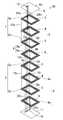
- FIG. 1is an exploded perspective view of the module substrate according to the present embodiment
- FIG. 2is a plan view for explaining an antenna pattern constituting the module substrate according to the present embodiment.
- the module substrate 1is equipped with a laminated body 2 in which a plurality of (four layers in the present embodiment) insulating layers 3 to 6 are laminated, and an IC provided on the uppermost layer side of the laminated body 2.
- An insulating layer 9 for use and an insulating layer 11 provided on the lowermost layer side of the laminated body 2are provided.
- the insulating layers 3 to 6are formed of, for example, a non-magnetic material made of non-magnetic ferrite, and the laminated body 2 is formed by laminating these insulating layers 3 to 6.
- the main component of the non-magnetic ferritefor example, Zn-based ferrite powder can be used, and the composition ratio of these components is 40.0 to 50.0 mol% for Fe 2 O 3 and 35 for Zn O. It is preferably 0.0 to 50.0 mol% and CuO is 5 to 20 mol%.
- each of the insulating layers 3 to 6is not particularly limited, but is preferably 20 ⁇ m to 100 ⁇ m when the laminated ceramic method using a green sheet is performed.
- an insulating layer 9 for mounting an ICis provided on the IC mounting surface side of the uppermost insulating layer 3 in the laminated body 2, and an IC is provided on the outer surface 9a of the insulating layer 9.
- a mounting electrode 12is provided.
- the insulating layer 9can be formed of, for example, a non-magnetic material made of non-magnetic ferrite, similarly to the above-mentioned insulating layers 3 to 6.
- the first antenna coil pattern 3a, the second antenna coil pattern 5a, the third antenna coil pattern 4a, and the fourth antenna coil pattern 6aare formed on the surfaces of the plurality of insulating layers 3 to 6. Is provided.
- the first to fourth antenna coil patterns 3a to 6aare formed of a conductive material, and are formed by an antenna pattern swirled in a rectangular shape.
- the first coil 7is configured by the first antenna coil pattern 3a and the second antenna coil pattern 5a, and the first antenna coil pattern 3a and the second antenna coil pattern 5a are interconnected in series. Has been done.
- the second coil 8is configured by the third antenna coil pattern 4a and the fourth antenna coil pattern 6a, and the third antenna coil pattern 4a and the fourth antenna coil pattern 6a are interconnected in series.
- the first coil 7 and the second coil 8are connected in parallel.
- the first to fourth antenna coil patterns 3a to 6aare the first antenna coil pattern 3a, the third antenna coil pattern 4a, and the second antenna coil pattern 3a.
- the featureis that the antenna coil pattern 5a and the fourth antenna coil pattern 6a are arranged in this order.
- the third antenna coil pattern 4ais arranged between the first antenna coil pattern 3a and the second antenna coil pattern 5a, and the second antenna coil pattern 5a is arranged between the third antenna coil pattern 4a and the fourth antenna coil pattern 6a.
- the parasitic capacitance of one series coilcan be halved, so that the combined inductance of the first and second coils 7 and 8 connected in parallel can be increased.
- an insulating layer 11 for routing and wiringis provided on the insulating layer 6 side of the lowermost layer of the laminated body 2, and the end of the first coil 7 is provided on the surface of the insulating layer 11. And the ends of the second coil 8 are connected in parallel, and a routing wiring 16 for connecting the first coil 7 and the second coil 8 to the IC mounting electrode 12 is provided via a through hole.
- the insulating layer 11can be formed of, for example, a non-magnetic material made of non-magnetic ferrite, similarly to the above-mentioned insulating layers 3 to 6.
- the material for forming the routing wiring 16is not particularly limited, and for example, a conductive material for forming the above-mentioned antenna coil patterns 3a to 6a can be used.
- the insulating layers 3 to 6are provided with interlayer connecting conductors 12a and 12b penetrating the insulating layers 3 to 6 in the thickness direction, and the first antenna coil pattern 3a and the second antenna coil pattern 5a are interlayer connecting conductors.
- the third antenna coil pattern 4a and the fourth antenna coil pattern 6aare electrically connected via the interlayer connection conductor 12b while being electrically connected via the 12a.
- the insulating layers 3 to 6 and the insulating layers 9 and 11are provided with an interlayer connecting conductor 22a penetrating the insulating layers 3 to 6 and the insulating layers 9 and 11 in the thickness direction. It is electrically connected to the IC mounting electrode 12 via the interlayer connection conductor 22a. Further, the first antenna coil pattern 3a and the third antenna coil pattern 4a are electrically connected to the IC mounting electrode 12 via the interlayer connecting conductor 22b, and the second antenna coil pattern 5a and the fourth antenna coil pattern 4a are connected. 6a is electrically connected to the routing wiring 16 via the interlayer connection conductors 22c to 22d.
- the materials for forming the first to fourth antenna coil patterns 3a to 6a and the interlayer connection conductors 12a to 12b and 20a to 20dare not particularly limited, and for example, silver, copper, or the like can be used.
- the first antenna coil pattern 3a and the second antenna coil pattern 5aare interconnected in series, and the third antenna coil pattern 4a and the fourth antenna coil pattern 6a are interconnected in series.
- the end layers of each series coilthat is, the first antenna coil pattern 3a and the third antenna coil pattern 4a, and the second antenna coil pattern 5a and the fourth antenna coil pattern 6a
- the routing wiring 16 for connecting the first coil 7 and the second coil 8 in parallelcan be shortened. Therefore, it is possible to suppress the parasitic capacitance generated in the connection wiring.
- the directions of the currents flowing through the first to fourth antenna coil patterns 3a to 6aare all the same with respect to the coil axes (that is, all clockwise directions).
- the current directions of the first and third antenna coil patterns 3a and 4aare in the same direction (that is, a plane) with respect to the radial direction of the coil.
- the coilis wound so as to be from the inside to the outside, and the direction of the current of the second and fourth antenna coil patterns 5a and 6a is opposite to that of the first and third antenna coil patterns 3a and 4a (that is, a flat surface). It is wound so that it is visible from the outside to the inside).
- the inductancedoes not decrease and the communication sensitivity of the antenna can be increased.
- FIG. 3is an exploded perspective view of the module substrate according to the second embodiment of the present invention.
- the same components as those in the first embodimentare designated by the same reference numerals, and the description thereof will be omitted.
- the first antenna coil pattern 3a, the third antenna coil pattern 4a, the second antenna coil pattern 5a, and the fourth antenna coil pattern 6aare described in this order. It is characterized in that a plurality of first and second coils 7 and 8 configured by being arranged (two each in the present embodiment) are provided.
- the first antenna coil pattern 3a and the second antenna coil pattern 5a in which the first coil 7 is interconnected in seriesare repeated, and the third antenna coil pattern 4a and the third antenna coil pattern 4a in which the second coil 8 is interconnected in series are repeated. Since the 4 antenna coil pattern 6a is repeated, as shown in FIG. 3, the winding start 3b of the first antenna coil pattern 3a and the winding end 5b of the second antenna coil pattern 5a can be aligned, and the third antenna coil can be aligned. The winding start 4b of the pattern 4a and the winding end 6b of the fourth antenna coil pattern 6a can be aligned.
- the wiringable rangecan be utilized to the maximum, so that the number of turns of the first to fourth antenna coil patterns 3a to 6a can be increased, and as a result, they are connected in parallel. It is possible to increase the combined inductance of the first and second coils 7 and 8 formed.
- the winding start 3b of the first antenna coil pattern 3a and the winding end 5b of the second antenna coil pattern 5acan be aligned
- the winding start 4b of the third antenna coil pattern 4a and the winding end of the fourth antenna coil pattern 6acan be aligned. Since 6b can be aligned, the interlayer connection conductors 12a to 12b can be shortened. As a result, it becomes possible to suppress the parasitic capacitance generated in the interlayer connection conductors 12a to 12b.
- the winding start 3b of the first antenna coil pattern 3a and the winding end 5b of the second antenna coil pattern 5a are alignedmeans that the winding start of the first antenna coil pattern 3a is aligned in the plan view shown in FIGS. A state in which a part of the region 3c and a part of the winding end region 5c of the second antenna coil pattern 5a overlap each other. In a plan view, the winding start 3b of the first antenna coil pattern 3a and the winding of the second antenna coil pattern 5a are wound. The state is not limited to the state in which the end 5b is superimposed.
- the length of the winding start region 3c and the winding end region 5c on the shaft of the coilis not particularly limited, but is preferably 1/4 or less of the length of one circumference of the coil.
- the winding start 4b of the third antenna coil pattern 4a and the winding end 6b of the fourth antenna coil pattern 6aare aligned
- the above-mentioned “winding start 3b of the first antenna coil pattern 3a and the second antenna coil pattern 5a”are also described.
- the winding end 5b of the third antenna coil pattern 4ais aligned
- itmeans a state in which a part of the winding start region of the third antenna coil pattern 4a and a part of the winding end region of the fourth antenna coil pattern 6a are overlapped with each other.
- the winding start 4b of the third antenna coil pattern 4a and the winding end 6b of the fourth antenna coil pattern 6aare not limited to the overlapping state.
- FIG. 6is an exploded perspective view of the module substrate according to the third embodiment of the present invention.
- the same components as those in the above embodimentare designated by the same reference numerals, and the description thereof will be omitted.
- the fifth antenna coil pattern 13a and the sixth antenna coil pattern A third coil 15 composed of 14ais provided.
- the insulating layer 13is provided between the insulating layers 4 and 5, and the fifth antenna coil pattern 13a is provided on the surface of the insulating layer 13. Further, an insulating layer 14 is provided between the insulating layer 6 and the insulating layer 11, and a sixth antenna coil pattern 14a is provided on the surface of the insulating layer 14.
- the insulating layers 13 and 14are formed of, for example, the above-mentioned non-magnetic material made of non-magnetic ferrite.
- the 5th to 6th antenna coil patterns 13a to 14aare formed of a conductive material like the above-mentioned 1st to 4th antenna coil patterns 3a to 6a, and are formed by a rectangular spiral antenna pattern. It is formed.
- the module substrate 30includes a laminate 2 in which a plurality of (six layers in the present embodiment) insulating layers 3 to 6, 13 to 14 are laminated, and the third coil 15 is the first and second coils. It is connected in parallel to the coils 7 and 8.
- the first antenna coil pattern 3ain the laminated body 2, the first antenna coil pattern 3a, the third antenna coil pattern 4a, the fifth antenna coil pattern 13a, the second antenna coil pattern 5a, and the second
- the four antenna coil patterns 6a and the sixth antenna coil pattern 14aare arranged in this order.
- the third antenna coil pattern 4a and the fifth antenna coil pattern 13aare arranged between the first antenna coil pattern 3a and the second antenna coil pattern 5a, and between the third antenna coil pattern 4a and the fourth antenna coil pattern 6a.
- the fifth antenna coil pattern 13a and the second antenna coil pattern 5aare arranged there, and the second antenna coil pattern 5a and the fourth antenna coil pattern 6a are arranged between the fifth antenna coil pattern 13a and the sixth antenna coil pattern 14a.
- Another layer of the series coilwill be sandwiched between the layers of the series coil. Therefore, since the layers of the series coils can be made three times wider, the parasitic capacitance of one series coil can be reduced to one-third. As a result, the combined inductance of the first, second, and third coils 7, 8 and 15 connected in parallel can be increased.
- the laminate 2is provided with an interlayer connecting conductor 12c, and the fifth antenna coil pattern 13a and the sixth antenna coil pattern 14a are electrically connected via the interlayer connecting conductor 12c.
- module substrate 30is provided with an interlayer connection conductor 22e, and the sixth antenna coil pattern 14a is electrically connected to the routing wiring 16 via the interlayer connection conductor 22e.
- the materials for forming the antenna coil patterns 13a to 14a and the interlayer connection conductors 22d and 22eare not particularly limited, and for example, silver, copper, or the like can be used.
- the first antenna coil pattern 3a and the second antenna coil pattern 5aare interconnected in series, and the third antenna coil pattern 4a and the fourth antenna coil pattern 6a are interconnected in series.
- the fifth antenna coil pattern 13a and the sixth antenna coil pattern 14aare interconnected in series, but the end layers of the series coils (that is, the first antenna coil pattern 3a, the third antenna coil pattern 4a, and the third one). Since the 5 antenna coil pattern 13a, the 2nd antenna coil pattern 5a, the 4th antenna coil pattern 6a, and the 6th antenna coil pattern 14a) are close to each other, the 1st coil 7 and the 2nd coil are as shown in FIG.
- the routing wiring 16 for connecting the 8 and the 3rd coil 15 in parallelcan be shortened. Therefore, it is possible to suppress the parasitic capacitance generated in the connection wiring.
- the directions of the currents flowing through the first to sixth antenna coil patterns 3a to 6a, 13a, 14aare all the same with respect to the coil axes.
- the first to sixth antenna coil patterns 3a to 6a, 13a, 14aare wound so as to be oriented (that is, all clockwise), and the first, third, and fifth antenna coil patterns are wound in the radial direction of the coil.
- the currents of the 3a, 4a, and 13aare wound so that the directions of the currents are the same (that is, from the inside to the outside in a plan view), and the currents of the second, fourth, and sixth antenna coil patterns 5a, 6a, and 14a are used.
- the coilis wound so that the direction of the coil is opposite to that of the first, third, and fifth antenna coil patterns 3a, 4a, and 13a (that is, from the outside to the inside in a plan view).
- the inductancedoes not decrease and the communication sensitivity of the antenna can be increased.
- FIG. 8is an exploded perspective view of the module substrate according to the fourth embodiment of the present invention.
- the same components as those in the above embodimentare designated by the same reference numerals, and the description thereof will be omitted.
- the seventh antenna coil pattern 17a and the eighth antenna A fourth coil 19 configured by the coil pattern 18ais provided.
- an insulating layer 17is provided between the insulating layers 13 and 5, and a seventh antenna coil pattern 17a is provided on the surface of the insulating layer 17. Further, an insulating layer 18 is provided between the insulating layer 14 and the insulating layer 11, and an eighth antenna coil pattern 18a is provided on the surface of the insulating layer 18.
- the insulating layers 17 and 18are formed of, for example, the above-mentioned non-magnetic material made of non-magnetic ferrite.
- the 7th to 8th antenna coil patterns 17a to 18aare formed of a conductive material and are swirled in a rectangular shape, similarly to the above-mentioned 1st to 6th antenna coil patterns 3a to 6a, 13a, 14a. It is formed by an antenna pattern.
- the module substrate 50includes a laminated body 2 in which a plurality of (8 layers in the present embodiment) insulating layers 3 to 6, 13 to 14, 17 to 18 are laminated, and the fourth coil 19 is a first. It is connected in parallel to the first, second coils 7, 8 and the third coil 15.
- the first antenna coil pattern 3ain the laminated body 2, the first antenna coil pattern 3a, the third antenna coil pattern 4a, the fifth antenna coil pattern 13a, the seventh antenna coil pattern 17a, and the seventh antenna coil pattern 17a.
- the featureis that the two antenna coil patterns 5a, the fourth antenna coil pattern 6a, the sixth antenna coil pattern 14a, and the eighth antenna coil pattern 18a are arranged in this order.
- the third antenna coil pattern 4a, the fifth antenna coil pattern 13a, and the seventh antenna coil pattern 17aare arranged between the first antenna coil pattern 3a and the second antenna coil pattern 5a, and the third antenna coil pattern 4a and the third antenna coil pattern 4a are arranged.
- the fifth antenna coil pattern 13a, the seventh antenna coil pattern 17a, and the second antenna coil pattern 5aare arranged between the four antenna coil patterns 6a, and the seventh antenna coil pattern 13a and the sixth antenna coil pattern 14a are arranged between the fifth antenna coil pattern 13a and the sixth antenna coil pattern 14a.
- the antenna coil pattern 17a, the second antenna coil pattern 5a, and the fourth antenna coil pattern 6aare arranged, and the second antenna coil pattern 5a and the fourth antenna coil pattern are arranged between the seventh antenna coil pattern 17a and the eighth antenna coil pattern 18a.
- 6a and the sixth antenna coil pattern 14aare arranged, and another layer of the series coil is sandwiched between the layers of the series coil. Therefore, since the layers of the series coils can be widened four times, the parasitic capacitance of one series coil can be reduced to one-fourth. As a result, the combined inductance of the first, second, third, and fourth coils 7, 8, 15, and 19 connected in parallel can be increased.
- the laminate 2is provided with an interlayer connecting conductor 12d, and the 7th antenna coil pattern 17a and the 8th antenna coil pattern 18a are electrically connected via the interlayer connecting conductor 12d.
- the eighth antenna coil pattern 18ais electrically connected to the routing wiring 16 via the interlayer connecting conductor 22e.
- the material for forming the antenna coil patterns 17a to 18ais not particularly limited, and for example, silver, copper, or the like can be used.
- the first antenna coil pattern 3a and the second antenna coil pattern 5aare interconnected in series
- the third antenna coil pattern 4a and the fourth antenna coil pattern 6aare interconnected in series
- the fifth antenna coil pattern 13a and the sixth antenna coil pattern 14aare interconnected in series
- the seventh antenna coil pattern 17a and the eighth antenna coil pattern 18aare interconnected in series, but the ends of the series coils are connected. (That is, the first antenna coil pattern 3a, the third antenna coil pattern 4a, the fifth antenna coil pattern 13a, the seventh antenna coil pattern 17a, and the second antenna coil pattern 5a, the fourth antenna coil pattern 6a, and the sixth layer.
- the routing wiring 16 for this purposecan be shortened. Therefore, it is possible to suppress the parasitic capacitance generated in the connection wiring.
- the direction of the current flowing through the first to eighth antenna coil patterns 3a to 6a, 13a, 14a, 17a, and 18ais the coil.
- the first to eighth antenna coil patterns 3a to 6a, 13a, 14a, 17a, 18aare wound so as to be all in the same direction (that is, all clockwise) with respect to the axis of the coil, with respect to the radial direction of the coil.
- the first, third, fifth, and seventh antenna coil patterns 3a, 4a, 13a, and 17aare wound so that the directions of the currents are in the same direction (that is, from the inside to the outside in a plan view), and the second , 4th, 6th, 8th antenna coil patterns 5a, 6a, 14a, 18a have current directions opposite to those of the 1st, 3rd, 3rd, 5th, and 7th antenna coil patterns 3a, 4a, 13a, 17a (that is, , In a plan view, it is wound so as to be from the outside to the inside).
- the inductancedoes not decrease and the communication sensitivity of the antenna can be increased.
- a plurality of first and second coils 7 and 8are provided, but the module shown in FIG. 3 is similar to the module substrate 40 shown in FIG.
- the substrate 20may be configured by removing the two layers (insulating layers 5 and 6) on the insulating layer 11 side. Even in such a configuration, the same effect as that of the module substrate 20 described above can be obtained.
- the antenna for the module substrate provided with the first to fourth coilsis mentioned, but in the antenna for the module substrate of the present invention, the number of coils is not particularly limited, and five or more coils are used. May be connected in parallel.
- a plurality of first to third coils 7, 8 and 15 configured by arranging the sixth antenna coil pattern 14a in this ordermay be provided.
- the first antenna coil pattern 3a, the third antenna coil pattern 4a, the fifth antenna coil pattern 13a, the seventh antenna coil pattern 17a, the second antenna coil pattern 5a, and the fourth antenna coil patternare shown.
- a plurality of first to fourth coils 7, 8, 15, and 19 configured by arranging 6a, the sixth antenna coil pattern 14a, and the eighth antenna coil pattern 18a in this ordermay be provided.
- the module board of the present inventioncan be effectively used as a module board on which an IC chip or the like is mounted and a laminated coil component (dynamic tag) that functions as an antenna for wireless communication is built.
- a laminated coil componentdynamic tag
- Module board 2Laminated body 3a 1st antenna coil pattern 4a 3rd antenna coil pattern 5a 2nd antenna coil pattern 6a 4th antenna coil pattern 7 1st coil 8 2nd coil 12 IC mounting electrode 13a 5th antenna coil pattern 14a 6th antenna coil pattern 15 3rd coil 16 routing wiring 17a 7th antenna coil pattern 18a 8th antenna coil pattern 19 4th coil 20 module board 30 module board 40 module board 50 module board
Landscapes
- Engineering & Computer Science (AREA)
- Microelectronics & Electronic Packaging (AREA)
- Computer Networks & Wireless Communication (AREA)
- Computer Hardware Design (AREA)
- Physics & Mathematics (AREA)
- General Physics & Mathematics (AREA)
- Theoretical Computer Science (AREA)
- Details Of Aerials (AREA)
- Production Of Multi-Layered Print Wiring Board (AREA)
- Support Of Aerials (AREA)
Abstract
Description
Translated fromJapanese本発明は、ICチップ等が実装され、無線通信用モジュールとして機能するモジュール基板用アンテナ、及びそれを用いたモジュール基板に関する。The present invention relates to an antenna for a module board on which an IC chip or the like is mounted and functions as a module for wireless communication, and a module board using the antenna.
近年、非接触で信号の授受を行うICモジュール(非接触型のICタグやICカード)が普及し始めている。このICモジュールは、絶縁性基板の表面に導体配線が形成されたアンテナ用の配線を備えており、このアンテナ配線により、非接触による信号の授受を行うことができる。In recent years, IC modules (non-contact type IC tags and IC cards) that send and receive signals in a non-contact manner have begun to spread. This IC module includes wiring for an antenna in which conductor wiring is formed on the surface of an insulating substrate, and signals can be sent and received in a non-contact manner by the antenna wiring.
例えば、それぞれ大きさ(平面視の外寸)の異なる3つのコイルが絶縁基板の内部に設けられ、これらの3つのコイルが絶縁層の積層方向において互いに重なるように配置されたモジュール基板用アンテナが開示されている(例えば、特許文献1参照)。For example, a module substrate antenna in which three coils having different sizes (outer dimensions in a plan view) are provided inside an insulating substrate and these three coils are arranged so as to overlap each other in the stacking direction of the insulating layer is provided. It is disclosed (see, for example, Patent Document 1).
しかし、上記特許文献1に記載のモジュール基板用アンテナにおいては、各コイルを大きさの異なるものにする必要があり、コイルパターンの巻回数や面積に制約があるため、全てのコイルのインダクタンスを最大限に大きくすることができず、結果として、コイルの合成インダクタンスを大きくすることが困難であった。However, in the antenna for the module substrate described in
そこで、本発明は、上述の問題に加え、アンテナコイルの寄生容量を抑制することにより、さらにコイルの合成インダクタンスを大きくすることができるモジュール基板用アンテナを提供することを目的とする。Therefore, an object of the present invention is to provide an antenna for a module substrate capable of further increasing the combined inductance of the coil by suppressing the parasitic capacitance of the antenna coil in addition to the above-mentioned problems.
上記目的を達成するために、本発明のモジュール基板用アンテナは、並列に接続された第1、第2コイルを備え、第1コイルを渦巻状の第1アンテナコイルパターンおよび第2アンテナコイルパターンが直列に層間接続されたパターンで構成し、第2コイルを渦巻状の第3アンテナコイルパターンおよび第4アンテナコイルパターンが直列に層間接続されたパターンで構成し、第1アンテナコイルパターン、第3アンテナコイルパターン、第2アンテナコイルパターン、及び第4アンテナコイルパターンの順に配置し、第1~第4アンテナコイルパターンを、第1~第4アンテナコイルパターンを流れる電流の向きが、コイルの軸に対して全て同じ向きとなるよう回巻し、コイルの径方向に対して、第1,第3アンテナコイルパターンの電流の向きが同一方向となるように回巻するとともに、第2,第4アンテナコイルパターンの電流の向きが第1,第3アンテナコイルパターンと逆方向となるように回巻したことを特徴とする。In order to achieve the above object, the module substrate antenna of the present invention includes first and second coils connected in parallel, and the first coil has a spiral first antenna coil pattern and a second antenna coil pattern. The second coil is composed of a spiral third antenna coil pattern and the fourth antenna coil pattern are interconnected in series, and the first antenna coil pattern and the third antenna are configured. The coil pattern, the second antenna coil pattern, and the fourth antenna coil pattern are arranged in this order, and the first to fourth antenna coil patterns are arranged so that the direction of the current flowing through the first to fourth antenna coil patterns is relative to the coil axis. The coil is wound so that the directions of the currents of the first and third antenna coil patterns are the same as the radial direction of the coil, and the second and fourth antenna coils are wound in the same direction. It is characterized in that the coil is wound so that the direction of the current of the pattern is opposite to that of the first and third antenna coil patterns.
本発明のモジュール基板用アンテナによれば、アンテナコイルの寄生容量を抑制して、コイルの合成インダクタンスを大きくすることができる。According to the module substrate antenna of the present invention, the parasitic capacitance of the antenna coil can be suppressed and the combined inductance of the coil can be increased.
以下、本発明の実施形態を図面に基づいて詳細に説明する。Hereinafter, embodiments of the present invention will be described in detail with reference to the drawings.
(第1の実施形態)
図1は、本実施形態に係るモジュール基板の分解斜視図であり、図2は、本実施形態に係るモジュール基板を構成するアンテナパターンを説明するための平面図である。(First Embodiment)
FIG. 1 is an exploded perspective view of the module substrate according to the present embodiment, and FIG. 2 is a plan view for explaining an antenna pattern constituting the module substrate according to the present embodiment.
図1に示すように、モジュール基板1は、複数(本実施形態においては4層)の絶縁層3~6が積層された積層体2と、積層体2における最上層側に設けられたIC搭載用の絶縁層9と、積層体2における最下層側に設けられた絶縁層11とを備えている。As shown in FIG. 1, the
絶縁層3~6は、例えば、非磁性体フェライトからなる非磁性体材料により形成されており、これらの絶縁層3~6が積層されることにより、積層体2が形成されている。The
非磁性体フェライトの主成分としては、例えば、Zn系フェライトの粉体を用いることができ、これらの成分の組成比は、Fe2O3が40.0~50.0モル%、ZnOが35.0~50.0モル%、及びCuOが5~20モル%であることが好ましい。As the main component of the non-magnetic ferrite, for example, Zn-based ferrite powder can be used, and the composition ratio of these components is 40.0 to 50.0 mol% forFe 2 O3 and 35 for Zn O. It is preferably 0.0 to 50.0 mol% and CuO is 5 to 20 mol%.
また、各絶縁層3~6の厚みは、特に限定されないが、グリーンシートによる積層セラミック工法を行う場合には、20μm~100μmが好ましい。The thickness of each of the
また、図1に示すように、積層体2における最上層の絶縁層3のIC搭載面側には、IC搭載用の絶縁層9が設けられており、この絶縁層9の外表面9aにIC搭載用電極12が設けられている。なお、絶縁層9は、上述の絶縁層3~6と同様に、例えば、非磁性体フェライトからなる非磁性体材料により形成することができる。Further, as shown in FIG. 1, an
また、図1に示すように、複数の絶縁層3~6の各々の表面には第1アンテナコイルパターン3a、第2アンテナコイルパターン5a、第3アンテナコイルパターン4a、及び第4アンテナコイルパターン6aが設けられている。この第1~第4アンテナコイルパターン3a~6aは、導電性材料により形成されており、矩形状に渦巻きされたアンテナパターンにより形成されている。Further, as shown in FIG. 1, the first
また、図1に示すように、第1アンテナコイルパターン3aと第2アンテナコイルパターン5aにより第1コイル7が構成され、第1アンテナコイルパターン3aと第2アンテナコイルパターン5aは、直列に層間接続されている。Further, as shown in FIG. 1, the
また、同様に、第3アンテナコイルパターン4aと第4アンテナコイルパターン6aにより第2コイル8構成され、第3アンテナコイルパターン4aと第4アンテナコイルパターン6aは、直列に層間接続されている。Similarly, the
また、図1に示すように、第1コイル7と第2コイル8は並列に接続される構成となっている。Further, as shown in FIG. 1, the
ここで、本実施形態においては、図1に示すように、積層体2において、第1~第4アンテナコイルパターン3a~6aが、第1アンテナコイルパターン3a、第3アンテナコイルパターン4a、第2アンテナコイルパターン5a、及び第4アンテナコイルパターン6aの順に配置されている点に特徴がある。Here, in the present embodiment, as shown in FIG. 1, in the laminated
従って、第1アンテナコイルパターン3aと第2アンテナコイルパターン5aの間に第3アンテナコイルパターン4aが配置され、第3アンテナコイルパターン4aと第4アンテナコイルパターン6aの間に第2アンテナコイルパターン5aが配置されることになり、直列コイルの層間に別の直列コイルの層が挟まれることになるため、直列コイルの層間を2倍に広くすることができる。その結果、1つの直列コイルの寄生容量を1/2にすることができるため、並列に接続された第1、第2コイル7,8の合成インダクタンスを大きくすることができる。Therefore, the third
また、図1に示すように、積層体2における最下層の絶縁層6側には、取り回し配線用の絶縁層11が設けられており、この絶縁層11の表面に、第1コイル7の端と第2コイル8の端を並列に接続するとともに、スルーホールを経由して、第1コイル7と第2コイル8をIC搭載用電極12に接続するための取り回し配線16が設けられている。Further, as shown in FIG. 1, an
絶縁層11は、上述の絶縁層3~6と同様に、例えば、非磁性体フェライトからなる非磁性体材料により形成することができる。また、取り回し配線16を形成する材料は、特に限定されず、例えば、上述のアンテナコイルパターン3a~6aを形成する導電材料を使用することができる。The insulating
また、絶縁層3~6には、絶縁層3~6を厚み方向に貫通する層間接続導体12a,12bが設けられており、第1アンテナコイルパターン3aと第2アンテナコイルパターン5aが層間接続導体12aを介して電気的に接続されるとともに、第3アンテナコイルパターン4aと第4アンテナコイルパターン6aが層間接続導体12bを介して電気的に接続されている。Further, the
また、絶縁層3~6、及び絶縁層9,11には、絶縁層3~6、及び絶縁層9,11を厚み方向に貫通する層間接続導体22aが設けられており、取り回し配線16は、層間接続導体22aを介して、IC搭載用電極12に電気的に接続されている。また、第1アンテナコイルパターン3aと第3アンテナコイルパターン4aは層間接続導体22bを介して、IC搭載用電極12に電気的に接続されており、第2アンテナコイルパターン5aと第4アンテナコイルパターン6aは層間接続導体22c~22dを介して、取り回し配線16に電気的に接続されている。Further, the
なお、第1~第4アンテナコイルパターン3a~6a、及び層間接続導体12a~12b,20a~20dを形成する材料は、特に限定されず、例えば、銀、銅等を使用することができる。The materials for forming the first to fourth
そして、本実施形態においては、上述のごとく、第1アンテナコイルパターン3aと第2アンテナコイルパターン5aが直列に層間接続され、第3アンテナコイルパターン4aと第4アンテナコイルパターン6aが直列に層間接続されているが、各直列コイルの端の層(即ち、第1アンテナコイルパターン3aと第3アンテナコイルパターン4a、及び第2アンテナコイルパターン5aと第4アンテナコイルパターン6a)が近接しているため、図1に示すように、第1コイル7と第2コイル8を並列に接続するための取り回し配線16を短くすることができる。従って、接続配線に生じる寄生容量を抑制することができる。Then, in the present embodiment, as described above, the first
また、図2に示すように、第1~第4アンテナコイルパターン3a~6aを流れる電流の向き(図中の矢印の向き)が、コイルの軸に対して全て同じ向き(即ち、全て時計回り)となるように第1~第4アンテナコイルパターン3a~6aを回巻し、コイルの径方向に対して第1,第3アンテナコイルパターン3a,4aの電流の向きが同一方向(即ち、平面視において、内側から外側)となるように回巻するとともに、第2,第4アンテナコイルパターン5a,6aの電流の向きが第1,第3アンテナコイルパターン3a,4aと逆方向(即ち、平面視において、外側から内側)となるように回巻している。Further, as shown in FIG. 2, the directions of the currents flowing through the first to fourth
従って、それぞれのコイルパターンから発生する磁界が互いに干渉しないため、インダクタンスが低下することがなく、アンテナの交信感度を高くすることができる。Therefore, since the magnetic fields generated from the respective coil patterns do not interfere with each other, the inductance does not decrease and the communication sensitivity of the antenna can be increased.
(第2の実施形態)
次に、本発明の第2の実施形態について説明する。図3は、本発明の第2の実施形態に係るモジュール基板の分解斜視図である。なお、上記第1実施形態と同様の構成部分については同一の符号を付してその説明を省略する。(Second Embodiment)
Next, a second embodiment of the present invention will be described. FIG. 3 is an exploded perspective view of the module substrate according to the second embodiment of the present invention. The same components as those in the first embodiment are designated by the same reference numerals, and the description thereof will be omitted.
図3に示すように、本実施形態のモジュール基板20においては、上述の、第1アンテナコイルパターン3a、第3アンテナコイルパターン4a、第2アンテナコイルパターン5a、及び第4アンテナコイルパターン6aの順に配置されることにより構成された第1、第2コイル7,8が複数(本実施形態においては各2個)設けられている点に特徴がある。As shown in FIG. 3, in the
そして、このような構成により、上述の第1の実施形態において説明した効果に加えて、以下の効果を得ることができる。Then, with such a configuration, the following effects can be obtained in addition to the effects described in the first embodiment described above.
即ち、第1コイル7が直列に層間接続された第1アンテナコイルパターン3aと第2アンテナコイルパターン5aの繰り返しであり、第2コイル8が直列に層間接続された第3アンテナコイルパターン4aと第4アンテナコイルパターン6aの繰り返しであるため、図3に示すように、第1アンテナコイルパターン3aの巻き始め3bと第2アンテナコイルパターン5aの巻き終わり5bを揃えることができるとともに、第3アンテナコイルパターン4aの巻き始め4bと第4アンテナコイルパターン6aの巻き終わり6bを揃えることができる。That is, the first
従って、絶縁層3~6において、配線可能な範囲を最大限利用することができるため、第1~第4アンテナコイルパターン3a~6aの巻き数を多くすることができ、結果として、並列に接続された第1,第2コイル7,8の合成インダクタンスを大きくすることが可能になる。Therefore, in the insulating
また、第1アンテナコイルパターン3aの巻き始め3bと第2アンテナコイルパターン5aの巻き終わり5bを揃えることができるとともに、第3アンテナコイルパターン4aの巻き始め4bと第4アンテナコイルパターン6aの巻き終わり6bを揃えることができるため、層間接続導体12a~12bを短くすることができる。その結果、層間接続導体12a~12bに生じる寄生容量を抑止することが可能になる。Further, the winding
なお、「第1アンテナコイルパターン3aの巻き始め3bと第2アンテナコイルパターン5aの巻き終わり5bが揃う」とは、図4、図5に示す平面視において、第1アンテナコイルパターン3aの巻き始め領域3cの一部と第2アンテナコイルパターン5aの巻き終わり領域5cの一部が重畳する状態を言い、平面視において、第1アンテナコイルパターン3aの巻き始め3bと第2アンテナコイルパターン5aの巻き終わり5bが重畳している状態に限られない。In addition, "the winding
コイルの軸における巻き始め領域3cと巻き終わり領域5cの長さは特に限定されないが、コイルの一周分の長さの4分の1以下が好ましい。The length of the winding
また、「第3アンテナコイルパターン4aの巻き始め4bと第4アンテナコイルパターン6aの巻き終わり6bが揃う」についても、上述の「第1アンテナコイルパターン3aの巻き始め3bと第2アンテナコイルパターン5aの巻き終わり5bが揃う」と同様に、平面視において、第3アンテナコイルパターン4aの巻き始め領域の一部と第4アンテナコイルパターン6aの巻き終わり領域の一部が重畳する状態を言い、平面視において、第3アンテナコイルパターン4aの巻き始め4bと第4アンテナコイルパターン6aの巻き終わり6bが重畳している状態に限られない。Further, regarding "the winding
(第3の実施形態)
次に、本発明の第3の実施形態について説明する。図6は、本発明の第3の実施形態に係るモジュール基板の分解斜視図である。なお、上記実施形態と同様の構成部分については同一の符号を付してその説明を省略する。(Third Embodiment)
Next, a third embodiment of the present invention will be described. FIG. 6 is an exploded perspective view of the module substrate according to the third embodiment of the present invention. The same components as those in the above embodiment are designated by the same reference numerals, and the description thereof will be omitted.
図6に示すように、本実施形態のモジュール基板30においては、上述の第1の実施形態における第1コイル7と第2コイル8に加えて、第5アンテナコイルパターン13aと第6アンテナコイルパターン14aにより構成された第3コイル15が設けられている。As shown in FIG. 6, in the module substrate 30 of the present embodiment, in addition to the
より具体的には、絶縁層4,5の間に絶縁層13が設けられ、当該絶縁層13の表面に第5アンテナコイルパターン13aが設けられている。また、絶縁層6と絶縁層11との間に絶縁層14が設けられ、当該絶縁層14の表面に第6アンテナコイルパターン14aが設けられている。More specifically, the insulating
絶縁層13,14は、例えば、上述の非磁性体フェライトからなる非磁性体材料により形成されている。The insulating layers 13 and 14 are formed of, for example, the above-mentioned non-magnetic material made of non-magnetic ferrite.
また、第5~第6アンテナコイルパターン13a~14aは、上述の第1~第4アンテナコイルパターン3a~6aと同様に、導電性材料により形成されており、矩形状に渦巻きされたアンテナパターンにより形成されている。Further, the 5th to 6th
そして、モジュール基板30は、複数(本実施形態においては6層)の絶縁層3~6,13~14が積層された積層体2を備えており、第3コイル15は、第1、第2コイル7,8に並列に接続されている。The module substrate 30 includes a
ここで、本実施形態においては、図6に示すように、積層体2において、第1アンテナコイルパターン3a、第3アンテナコイルパターン4a、第5アンテナコイルパターン13a、第2アンテナコイルパターン5a、第4アンテナコイルパターン6a、及び第6アンテナコイルパターン14aの順に配置されている点に特徴がある。Here, in the present embodiment, as shown in FIG. 6, in the
従って、第1アンテナコイルパターン3aと第2アンテナコイルパターン5aの間に第3アンテナコイルパターン4aと第5アンテナコイルパターン13aが配置され、第3アンテナコイルパターン4aと第4アンテナコイルパターン6aの間に第5アンテナコイルパターン13aと第2アンテナコイルパターン5aが配置され、第5アンテナコイルパターン13aと第6アンテナコイルパターン14aの間に第2アンテナコイルパターン5aと第4アンテナコイルパターン6aが配置され、直列コイルの層間に別の直列コイルの層を挟むことになる。従って、直列コイルの層間を3倍広くすることができるため、1つの直列コイルの寄生容量を1/3にすることができる。その結果、並列に接続された第1,第2,第3コイル7,8,15の合成インダクタンスを大きくすることができる。Therefore, the third
また、積層体2には、層間接続導体12cが設けられており、第5アンテナコイルパターン13aと第6アンテナコイルパターン14aは、層間接続導体12cを介して電気的に接続されている。Further, the
また、モジュール基板30には、層間接続導体22eが設けられており、第6アンテナコイルパターン14aは層間接続導体22eを介して、取り回し配線16に電気的に接続されている。Further, the module substrate 30 is provided with an
なお、アンテナコイルパターン13a~14a、及び層間接続導体22d,22eを形成する材料は、特に限定されず、例えば、銀、銅等を使用することができる。The materials for forming the
そして、本実施形態においては、上述のごとく、第1アンテナコイルパターン3aと第2アンテナコイルパターン5aが直列に層間接続され、第3アンテナコイルパターン4aと第4アンテナコイルパターン6aが直列に層間接続され、第5アンテナコイルパターン13aと第6アンテナコイルパターン14aが直列に層間接続されているが、各直列コイルの端の層(即ち、第1アンテナコイルパターン3aと第3アンテナコイルパターン4aと第5アンテナコイルパターン13a、及び第2アンテナコイルパターン5aと第4アンテナコイルパターン6aと第6アンテナコイルパターン14a)が近接しているため、図6に示すように、第1コイル7と第2コイル8と第3コイル15を並列に接続するための取り回し配線16を短くすることができる。従って、接続配線に生じる寄生容量を抑制することができる。Then, in the present embodiment, as described above, the first
また、図2、図7に示すように、第1~第6アンテナコイルパターン3a~6a,13a,14aを流れる電流の向き(図中の矢印の向き)が、コイルの軸に対して全て同じ向き(即ち、全て時計回り)となるように第1~第6アンテナコイルパターン3a~6a,13a,14aを回巻し、コイルの径方向に対して第1,第3,第5アンテナコイルパターン3a,4a,13aの電流の向きが同一方向(即ち、平面視において、内側から外側)となるように回巻するとともに、第2,第4,第6アンテナコイルパターン5a,6a,14aの電流の向きが第1,第3,第5アンテナコイルパターン3a,4a,13aと逆方向(即ち、平面視において、外側から内側)となるように回巻している。Further, as shown in FIGS. 2 and 7, the directions of the currents flowing through the first to sixth
従って、それぞれのコイルパターンから発生する磁界が互いに干渉しないため、インダクタンスが低下することがなく、アンテナの交信感度を高くすることができる。Therefore, since the magnetic fields generated from the respective coil patterns do not interfere with each other, the inductance does not decrease and the communication sensitivity of the antenna can be increased.
(第4の実施形態)
次に、本発明の第4の実施形態について説明する。図8は、本発明の第4の実施形態に係るモジュール基板の分解斜視図である。なお、上記実施形態と同様の構成部分については同一の符号を付してその説明を省略する。(Fourth Embodiment)
Next, a fourth embodiment of the present invention will be described. FIG. 8 is an exploded perspective view of the module substrate according to the fourth embodiment of the present invention. The same components as those in the above embodiment are designated by the same reference numerals, and the description thereof will be omitted.
図8に示すように、本実施形態のモジュール基板50においては、上述の第3の実施形態における第1~第3コイル7,8,15に加えて、第7アンテナコイルパターン17aと第8アンテナコイルパターン18aにより構成された第4コイル19が設けられている。As shown in FIG. 8, in the
より具体的には、絶縁層13,5の間に絶縁層17が設けられ、当該絶縁層17の表面に第7アンテナコイルパターン17aが設けられている。また、絶縁層14と絶縁層11との間に絶縁層18が設けられ、当該絶縁層18の表面に第8アンテナコイルパターン18aが設けられている。More specifically, an insulating
絶縁層17,18は、例えば、上述の非磁性体フェライトからなる非磁性体材料により形成されている。The insulating layers 17 and 18 are formed of, for example, the above-mentioned non-magnetic material made of non-magnetic ferrite.
また、第7~第8アンテナコイルパターン17a~18aは、上述の第1~第6アンテナコイルパターン3a~6a,13a,14aと同様に、導電性材料により形成されており、矩形状に渦巻きされたアンテナパターンにより形成されている。Further, the 7th to 8th
そして、モジュール基板50は、複数(本実施形態においては8層)の絶縁層3~6,13~14,17~18が積層された積層体2を備えており、第4コイル19は、第1、第2コイル7,8、及び第3コイル15に並列に接続されている。The
ここで、本実施形態においては、図8に示すように、積層体2において、第1アンテナコイルパターン3a、第3アンテナコイルパターン4a、第5アンテナコイルパターン13a、第7アンテナコイルパターン17a、第2アンテナコイルパターン5a、第4アンテナコイルパターン6a、第6アンテナコイルパターン14a、及び第8アンテナコイルパターン18aの順に配置されている点に特徴がある。Here, in the present embodiment, as shown in FIG. 8, in the
従って、第1アンテナコイルパターン3aと第2アンテナコイルパターン5aの間に第3アンテナコイルパターン4aと第5アンテナコイルパターン13aと第7アンテナコイルパターン17aが配置され、第3アンテナコイルパターン4aと第4アンテナコイルパターン6aの間に第5アンテナコイルパターン13aと第7アンテナコイルパターン17aと第2アンテナコイルパターン5aが配置され、第5アンテナコイルパターン13aと第6アンテナコイルパターン14aの間に第7アンテナコイルパターン17aと第2アンテナコイルパターン5aと第4アンテナコイルパターン6aが配置され、第7アンテナコイルパターン17aと第8アンテナコイルパターン18aの間に第2アンテナコイルパターン5aと第4アンテナコイルパターン6aと第6アンテナコイルパターン14aが配置され、直列コイルの層間に別の直列コイルの層を挟むことになる。従って、直列コイルの層間を4倍広くすることができるため、1つの直列コイルの寄生容量を1/4にすることができる。その結果、並列に接続された第1,第2,第3,第4コイル7,8,15,19の合成インダクタンスを大きくすることができる。Therefore, the third
また、積層体2には、層間接続導体12dが設けられており、第7アンテナコイルパターン17aと第8アンテナコイルパターン18aは、層間接続導体12dを介して電気的に接続されている。Further, the
また、第8アンテナコイルパターン18aは層間接続導体22eを介して、取り回し配線16に電気的に接続されている。Further, the eighth
なお、アンテナコイルパターン17a~18aを形成する材料は、特に限定されず、例えば、銀、銅等を使用することができる。The material for forming the
そして、本実施形態においては、上述のごとく、第1アンテナコイルパターン3aと第2アンテナコイルパターン5aが直列に層間接続され、第3アンテナコイルパターン4aと第4アンテナコイルパターン6aが直列に層間接続され、第5アンテナコイルパターン13aと第6アンテナコイルパターン14aが直列に層間接続され、第7アンテナコイルパターン17aと第8アンテナコイルパターン18aが直列に層間接続されているが、各直列コイルの端の層(即ち、第1アンテナコイルパターン3aと第3アンテナコイルパターン4aと第5アンテナコイルパターン13aと第7アンテナコイルパターン17a、及び第2アンテナコイルパターン5aと第4アンテナコイルパターン6aと第6アンテナコイルパターン14aと第8アンテナコイルパターン18a)が近接しているため、図8に示すように、第1コイル7と第2コイル8と第3コイル15と第4コイル19を並列に接続するための取り回し配線16を短くすることができる。従って、接続配線に生じる寄生容量を抑制することができる。Then, in the present embodiment, as described above, the first
また、図2、図7、図9に示すように、第1~第8アンテナコイルパターン3a~6a,13a,14a,17a,18aを流れる電流の向き(図中の矢印の向き)が、コイルの軸に対して全て同じ向き(即ち、全て時計回り)となるように第1~第8アンテナコイルパターン3a~6a,13a,14a,17a,18aを回巻し、コイルの径方向に対して第1,第3,第5,第7アンテナコイルパターン3a,4a,13a,17aの電流の向きが同一方向(即ち、平面視において、内側から外側)となるように回巻するとともに、第2,第4,第6,第8アンテナコイルパターン5a,6a,14a,18aの電流の向きが第1,第3,第5,第7アンテナコイルパターン3a,4a,13a,17aと逆方向(即ち、平面視において、外側から内側)となるように回巻している。Further, as shown in FIGS. 2, 7, and 9, the direction of the current flowing through the first to eighth
従って、それぞれのコイルパターンから発生する磁界が互いに干渉しないため、インダクタンスが低下することがなく、アンテナの交信感度を高くすることができる。Therefore, since the magnetic fields generated from the respective coil patterns do not interfere with each other, the inductance does not decrease and the communication sensitivity of the antenna can be increased.
なお、上記実施形態は、以下のように変形してもよい。The above embodiment may be modified as follows.
上記第2の実施形態(図3)においては、第1、第2コイル7,8を複数(各2個)設ける構成としたが、図10に示すモジュール基板40ように、図3に示すモジュール基板20から、絶縁層11側の2層(絶縁層5,6)を取り除いた構成としてもよい。この様な構成においても、上述のモジュール基板20と同様の効果を得ることができる。In the second embodiment (FIG. 3), a plurality of first and
また、上記実施形態においては、第1~第4コイルを備えたモジュール基板用アンテナを挙げたが、本発明のモジュール基板用アンテナにおいては、コイルの数は特に限定されず、5つ以上のコイルが並列に接続されているものであってもよい。Further, in the above embodiment, the antenna for the module substrate provided with the first to fourth coils is mentioned, but in the antenna for the module substrate of the present invention, the number of coils is not particularly limited, and five or more coils are used. May be connected in parallel.
また、図3の場合と同様に、図6に示す、第1アンテナコイルパターン3a、第3アンテナコイルパターン4a、第5アンテナコイルパターン13a、第2アンテナコイルパターン5a、第4アンテナコイルパターン6a、及び第6アンテナコイルパターン14aの順に配置されることにより構成された第1~第3コイル7,8,15を複数設ける構成としてもよい。Further, as in the case of FIG. 3, the first
また、同様に、図8に示す、第1アンテナコイルパターン3a、第3アンテナコイルパターン4a、第5アンテナコイルパターン13a、第7アンテナコイルパターン17a、第2アンテナコイルパターン5a、第4アンテナコイルパターン6a、第6アンテナコイルパターン14a、及び第8アンテナコイルパターン18aの順に配置されることにより構成された第1~第4コイル7,8,15,19を複数設ける構成としてもよい。Similarly, as shown in FIG. 8, the first
このような構成により、第1、第2コイル7,8が複数設けられた、図3に示すモジュール基板20と同様の効果を得ることができる。With such a configuration, it is possible to obtain the same effect as the
本発明のモジュール基板は、ICチップ等が実装され、無線通信用のアンテナとして機能する積層型コイル部品(ダイナミックタグ)を内蔵するモジュール基板として有効に利用できる。The module board of the present invention can be effectively used as a module board on which an IC chip or the like is mounted and a laminated coil component (dynamic tag) that functions as an antenna for wireless communication is built.
1 モジュール基板
2 積層体
3a 第1アンテナコイルパターン
4a 第3アンテナコイルパターン
5a 第2アンテナコイルパターン
6a 第4アンテナコイルパターン
7 第1コイル
8 第2コイル
12 IC搭載用電極
13a 第5アンテナコイルパターン
14a 第6アンテナコイルパターン
15 第3コイル
16 取り回し配線
17a 第7アンテナコイルパターン
18a 第8アンテナコイルパターン
19 第4コイル
20 モジュール基板
30 モジュール基板
40 モジュール基板
50 モジュール基板1
40
Claims (7)
Translated fromJapanese前記第1コイルを渦巻状の第1アンテナコイルパターンおよび第2アンテナコイルパターンが直列に層間接続されたパターンで構成し、
前記第2コイルを渦巻状の第3アンテナコイルパターンおよび第4アンテナコイルパターンが直列に層間接続されたパターンで構成し、
前記第1アンテナコイルパターン、前記第3アンテナコイルパターン、前記第2アンテナコイルパターン、及び前記第4アンテナコイルパターンの順に配置し、
前記第1~第4アンテナコイルパターンを、該第1~第4アンテナコイルパターンを流れる電流の向きが、コイルの軸に対して全て同じ向きとなるよう回巻し、コイルの径方向に対して、前記第1,第3アンテナコイルパターンの電流の向きが同一方向となるように回巻するとともに、前記第2,第4アンテナコイルパターンの電流の向きが第1,第3アンテナコイルパターンと逆方向となるように回巻したことを特徴とするモジュール基板用アンテナ。Equipped with first and second coils connected in parallel,
The first coil is composed of a spiral first antenna coil pattern and a second antenna coil pattern in which the second antenna coil pattern is interconnected in series.
The second coil is composed of a spiral third antenna coil pattern and a fourth antenna coil pattern in which the third antenna coil pattern and the fourth antenna coil pattern are interconnected in series.
The first antenna coil pattern, the third antenna coil pattern, the second antenna coil pattern, and the fourth antenna coil pattern are arranged in this order.
The first to fourth antenna coil patterns are wound so that the directions of the currents flowing through the first to fourth antenna coil patterns are all the same with respect to the axis of the coil, with respect to the radial direction of the coil. The first and third antenna coil patterns are wound so that the current directions are the same, and the current directions of the second and fourth antenna coil patterns are opposite to those of the first and third antenna coil patterns. An antenna for a module board, which is characterized by being wound in a direction.
前記第3コイルを渦巻状の第5アンテナコイルパターンおよび第6アンテナコイルパターンが直列に層間接続されたパターンで構成し、
前記第1アンテナコイルパターン、前記第3アンテナコイルパターン、前記第5アンテナコイルパターン、前記第2アンテナコイルパターン、前記第4アンテナコイルパターン、及び前記第6アンテナコイルパターンの順に配置し、
前記第1~第6アンテナコイルパターンを、該第1~第6アンテナコイルパターンを流れる電流の向きが、コイルの軸に対して全て同じ向きとなるよう回巻し、コイルの径方向に対して、前記第1,第3,第5アンテナコイルパターンの電流の向きが同一方向となるように回巻するとともに、前記第2,第4,第6アンテナコイルパターンの電流の向きが前記第1,第3,第5アンテナコイルパターンと逆方向になるように回巻したことを特徴とする請求項1に記載のモジュール基板用アンテナ。A third coil connected in parallel to the first and second coils is further provided.
The third coil is composed of a spiral fifth antenna coil pattern and a sixth antenna coil pattern in which the sixth antenna coil pattern is interconnected in series.
The first antenna coil pattern, the third antenna coil pattern, the fifth antenna coil pattern, the second antenna coil pattern, the fourth antenna coil pattern, and the sixth antenna coil pattern are arranged in this order.
The first to sixth antenna coil patterns are wound so that the directions of the currents flowing through the first to sixth antenna coil patterns are all the same with respect to the axis of the coil, with respect to the radial direction of the coil. , The first, third, and fifth antenna coil patterns are wound so that the current directions are the same, and the current directions of the second, fourth, and sixth antenna coil patterns are the first and first. The antenna for a module board according to claim 1, wherein the coil is wound in the direction opposite to that of the third and fifth antenna coil patterns.
前記第4コイルを渦巻状の第7アンテナコイルパターンおよび第8アンテナコイルパターンが直列に層間接続されたパターンで構成し、
前記第1アンテナコイルパターン、前記第3アンテナコイルパターン、前記第5アンテナコイルパターン、前記第7アンテナコイルパターン、前記第2アンテナコイルパターン、前記第4アンテナコイルパターン、前記第6アンテナコイルパターン、及び前記第8アンテナコイルパターンの順に配置し、
前記第1~第8アンテナコイルパターンを、該第1~第8アンテナコイルパターンを流れる電流の向きが、コイルの軸に対して全て同じ向きとなるよう回巻し、コイルの径方向に対して、前記第1,第3,第5,第7アンテナコイルパターンの電流の向きが同一方向となるように回巻するとともに、前記第2,第4,第6,第8アンテナコイルパターンの電流の向きが前記第1,第3,第5,第7アンテナコイルパターンと逆方向になるように回巻したことを特徴とする請求項3に記載のモジュール基板用アンテナ。A fourth coil connected in parallel to the first to third coils is further provided.
The fourth coil is composed of a spiral seventh antenna coil pattern and an eighth antenna coil pattern in which the eighth antenna coil pattern is interconnected in series.
The first antenna coil pattern, the third antenna coil pattern, the fifth antenna coil pattern, the seventh antenna coil pattern, the second antenna coil pattern, the fourth antenna coil pattern, the sixth antenna coil pattern, and the like. Arranged in the order of the 8th antenna coil pattern,
The first to eighth antenna coil patterns are wound so that the directions of the currents flowing through the first to eighth antenna coil patterns are all the same with respect to the axis of the coil, with respect to the radial direction of the coil. , The first, third, fifth, and seventh antenna coil patterns are wound so that the current directions are the same, and the currents of the second, fourth, sixth, and eighth antenna coil patterns are used. The module substrate antenna according to claim 3, wherein the coil is wound so that the direction is opposite to that of the first, third, fifth, and seventh antenna coil patterns.
A module board comprising the antenna for a module board according to any one of claims 1 to 6.
Priority Applications (2)
| Application Number | Priority Date | Filing Date | Title |
|---|---|---|---|
| JP2021562660AJP7528956B2 (en) | 2019-12-03 | 2020-12-01 | Antenna for module board and module board using same |
| US17/756,369US11942701B2 (en) | 2019-12-03 | 2020-12-01 | Module substrate antenna and module substrate using same |
Applications Claiming Priority (2)
| Application Number | Priority Date | Filing Date | Title |
|---|---|---|---|
| JP2019-219050 | 2019-12-03 | ||
| JP2019219050 | 2019-12-03 |
Publications (1)
| Publication Number | Publication Date |
|---|---|
| WO2021112086A1true WO2021112086A1 (en) | 2021-06-10 |
Family
ID=76221659
Family Applications (1)
| Application Number | Title | Priority Date | Filing Date |
|---|---|---|---|
| PCT/JP2020/044698CeasedWO2021112086A1 (en) | 2019-12-03 | 2020-12-01 | Module substrate antenna and module substrate using same |
Country Status (4)
| Country | Link |
|---|---|
| US (1) | US11942701B2 (en) |
| JP (1) | JP7528956B2 (en) |
| TW (1) | TWI868264B (en) |
| WO (1) | WO2021112086A1 (en) |
Families Citing this family (4)
| Publication number | Priority date | Publication date | Assignee | Title |
|---|---|---|---|---|
| WO2021112086A1 (en)* | 2019-12-03 | 2021-06-10 | 戸田工業株式会社 | Module substrate antenna and module substrate using same |
| USD1003282S1 (en)* | 2022-01-27 | 2023-10-31 | Avery Dennison Retail Information Services Llc | Antenna |
| USD1008235S1 (en)* | 2022-03-24 | 2023-12-19 | Avery Dennison Retail Information Services Llc | Antenna with EAS |
| USD1025033S1 (en)* | 2022-03-31 | 2024-04-30 | Avery Dennison Retail Information Services Llc | Antenna |
Citations (3)
| Publication number | Priority date | Publication date | Assignee | Title |
|---|---|---|---|---|
| JP2015159617A (en)* | 2012-06-04 | 2015-09-03 | 株式会社村田製作所 | Antenna device and wireless communication device |
| JP2016034153A (en)* | 2013-07-16 | 2016-03-10 | 株式会社村田製作所 | Antenna device and communication apparatus |
| JP2019180021A (en)* | 2018-03-30 | 2019-10-17 | 戸田工業株式会社 | Antenna for module substrate and module substrate using the same |
Family Cites Families (17)
| Publication number | Priority date | Publication date | Assignee | Title |
|---|---|---|---|---|
| EP0704928A3 (en)* | 1994-09-30 | 1998-08-05 | HID Corporation | RF transponder system with parallel resonant interrogation and series resonant response |
| CN101390176B (en)* | 2006-01-31 | 2012-06-13 | 日立金属株式会社 | Laminated component and module using same |
| EP2284949B1 (en)* | 2008-05-21 | 2016-08-03 | Murata Manufacturing Co. Ltd. | Wireless ic device |
| TWI466375B (en)* | 2010-01-19 | 2014-12-21 | Murata Manufacturing Co | An antenna device and a communication terminal device |
| WO2012050037A1 (en)* | 2010-10-12 | 2012-04-19 | 株式会社村田製作所 | Antenna apparatus and communication terminal apparatus |
| EP2523255B1 (en)* | 2011-02-15 | 2014-12-31 | Murata Manufacturing Co., Ltd. | Antenna device and communication terminal device |
| CN103518325B (en)* | 2011-05-09 | 2016-08-24 | 株式会社村田制作所 | Impedance matching switching circuit, antenna device, high frequency power amplifier and communication terminal device |
| JP5459301B2 (en)* | 2011-12-19 | 2014-04-02 | 株式会社村田製作所 | High frequency transformer, high frequency component and communication terminal device |
| JP5761463B2 (en)* | 2012-08-09 | 2015-08-12 | 株式会社村田製作所 | ANTENNA DEVICE AND WIRELESS COMMUNICATION DEVICE |
| WO2014088028A1 (en)* | 2012-12-07 | 2014-06-12 | 株式会社村田製作所 | Antenna module |
| JP6110656B2 (en)* | 2012-12-21 | 2017-04-05 | デクセリアルズ株式会社 | Wireless communication system, antenna module, and electronic device |
| JP6888999B2 (en)* | 2017-03-28 | 2021-06-18 | 京セラ株式会社 | RFID board and RFID tag |
| TWI647620B (en)* | 2017-06-22 | 2019-01-11 | 恩旭有限公司 | Miniaturized radio frequency identification tag |
| FR3071988B1 (en)* | 2017-10-03 | 2020-11-06 | Continental Automotive France | NEAR FIELD COMMUNICATION DEVICE |
| JP6904497B2 (en)* | 2019-02-22 | 2021-07-14 | 株式会社村田製作所 | Coil device, phase shift circuit and communication device |
| EP4053742A4 (en)* | 2019-10-28 | 2023-11-22 | Kyocera Corporation | SUBSTRATE FOR RFID LABELS, RFID LABEL AND RFID SYSTEM |
| WO2021112086A1 (en)* | 2019-12-03 | 2021-06-10 | 戸田工業株式会社 | Module substrate antenna and module substrate using same |
- 2020
- 2020-12-01WOPCT/JP2020/044698patent/WO2021112086A1/ennot_activeCeased
- 2020-12-01USUS17/756,369patent/US11942701B2/enactiveActive
- 2020-12-01JPJP2021562660Apatent/JP7528956B2/enactiveActive
- 2020-12-02TWTW109142325Apatent/TWI868264B/enactive
Patent Citations (3)
| Publication number | Priority date | Publication date | Assignee | Title |
|---|---|---|---|---|
| JP2015159617A (en)* | 2012-06-04 | 2015-09-03 | 株式会社村田製作所 | Antenna device and wireless communication device |
| JP2016034153A (en)* | 2013-07-16 | 2016-03-10 | 株式会社村田製作所 | Antenna device and communication apparatus |
| JP2019180021A (en)* | 2018-03-30 | 2019-10-17 | 戸田工業株式会社 | Antenna for module substrate and module substrate using the same |
Also Published As
| Publication number | Publication date |
|---|---|
| TWI868264B (en) | 2025-01-01 |
| US20230006352A1 (en) | 2023-01-05 |
| US11942701B2 (en) | 2024-03-26 |
| TW202139516A (en) | 2021-10-16 |
| JP7528956B2 (en) | 2024-08-06 |
| JPWO2021112086A1 (en) | 2021-06-10 |
Similar Documents
| Publication | Publication Date | Title |
|---|---|---|
| WO2021112086A1 (en) | Module substrate antenna and module substrate using same | |
| JP5928640B2 (en) | ANTENNA DEVICE AND WIRELESS COMMUNICATION DEVICE | |
| JP6070895B2 (en) | Multilayer coil element, antenna module, and wireless communication module | |
| JP5459301B2 (en) | High frequency transformer, high frequency component and communication terminal device | |
| WO2008066143A1 (en) | Transformer device | |
| JPWO2012032974A1 (en) | RFID module and RFID device | |
| WO2015147132A1 (en) | Antenna device and communications apparatus | |
| US20180062237A1 (en) | Directional coupler and wireless communication device using the same | |
| WO2018051798A1 (en) | Common mode noise filter | |
| JPWO2019176637A1 (en) | Antenna device, communication system, and electronic device | |
| US9892841B2 (en) | Inductor | |
| JP6048593B2 (en) | Impedance conversion ratio setting method | |
| WO2015122421A1 (en) | Antenna device and radio communication apparatus | |
| JP2012182285A (en) | Coil component | |
| KR102030086B1 (en) | Stacked inductor | |
| JP5884538B2 (en) | Surface mount antenna | |
| JP2012182286A (en) | Coil component | |
| WO2012077315A1 (en) | Laminated inductor | |
| WO2023145106A1 (en) | Coil component and circuit board provided with same | |
| JP7013716B2 (en) | RFID tag and articles equipped with it | |
| WO2015129598A1 (en) | Laminated coil element and wireless communication module | |
| JPWO2017209195A1 (en) | Antenna device and IC tag using the same | |
| JP7107250B2 (en) | Laminated coil parts | |
| JP4904503B2 (en) | Coil device | |
| JP3048593B2 (en) | Hybrid integrated circuit components |
Legal Events
| Date | Code | Title | Description |
|---|---|---|---|
| 121 | Ep: the epo has been informed by wipo that ep was designated in this application | Ref document number:20897496 Country of ref document:EP Kind code of ref document:A1 | |
| ENP | Entry into the national phase | Ref document number:2021562660 Country of ref document:JP Kind code of ref document:A | |
| NENP | Non-entry into the national phase | Ref country code:DE | |
| 122 | Ep: pct application non-entry in european phase | Ref document number:20897496 Country of ref document:EP Kind code of ref document:A1 |