WO2021090516A1 - Etching method - Google Patents
Etching methodDownload PDFInfo
- Publication number
- WO2021090516A1 WO2021090516A1PCT/JP2020/005847JP2020005847WWO2021090516A1WO 2021090516 A1WO2021090516 A1WO 2021090516A1JP 2020005847 WJP2020005847 WJP 2020005847WWO 2021090516 A1WO2021090516 A1WO 2021090516A1
- Authority
- WO
- WIPO (PCT)
- Prior art keywords
- etching method
- silicon
- gas
- etching
- film
- Prior art date
- Legal status (The legal status is an assumption and is not a legal conclusion. Google has not performed a legal analysis and makes no representation as to the accuracy of the status listed.)
- Ceased
Links
Images


Classifications
- H—ELECTRICITY
- H01—ELECTRIC ELEMENTS
- H01J—ELECTRIC DISCHARGE TUBES OR DISCHARGE LAMPS
- H01J37/00—Discharge tubes with provision for introducing objects or material to be exposed to the discharge, e.g. for the purpose of examination or processing thereof
- H01J37/32—Gas-filled discharge tubes
- H01J37/32009—Arrangements for generation of plasma specially adapted for examination or treatment of objects, e.g. plasma sources
- H01J37/32082—Radio frequency generated discharge
- H—ELECTRICITY
- H01—ELECTRIC ELEMENTS
- H01J—ELECTRIC DISCHARGE TUBES OR DISCHARGE LAMPS
- H01J37/00—Discharge tubes with provision for introducing objects or material to be exposed to the discharge, e.g. for the purpose of examination or processing thereof
- H01J37/02—Details
- H01J37/20—Means for supporting or positioning the object or the material; Means for adjusting diaphragms or lenses associated with the support
- H—ELECTRICITY
- H01—ELECTRIC ELEMENTS
- H01J—ELECTRIC DISCHARGE TUBES OR DISCHARGE LAMPS
- H01J37/00—Discharge tubes with provision for introducing objects or material to be exposed to the discharge, e.g. for the purpose of examination or processing thereof
- H01J37/32—Gas-filled discharge tubes
- H—ELECTRICITY
- H01—ELECTRIC ELEMENTS
- H01J—ELECTRIC DISCHARGE TUBES OR DISCHARGE LAMPS
- H01J37/00—Discharge tubes with provision for introducing objects or material to be exposed to the discharge, e.g. for the purpose of examination or processing thereof
- H01J37/32—Gas-filled discharge tubes
- H01J37/32009—Arrangements for generation of plasma specially adapted for examination or treatment of objects, e.g. plasma sources
- H01J37/32082—Radio frequency generated discharge
- H01J37/32174—Circuits specially adapted for controlling the RF discharge
- H—ELECTRICITY
- H01—ELECTRIC ELEMENTS
- H01J—ELECTRIC DISCHARGE TUBES OR DISCHARGE LAMPS
- H01J37/00—Discharge tubes with provision for introducing objects or material to be exposed to the discharge, e.g. for the purpose of examination or processing thereof
- H01J37/32—Gas-filled discharge tubes
- H01J37/32431—Constructional details of the reactor
- H01J37/3244—Gas supply means
- H01J37/32449—Gas control, e.g. control of the gas flow
- H—ELECTRICITY
- H01—ELECTRIC ELEMENTS
- H01L—SEMICONDUCTOR DEVICES NOT COVERED BY CLASS H10
- H01L21/00—Processes or apparatus adapted for the manufacture or treatment of semiconductor or solid state devices or of parts thereof
- H01L21/02—Manufacture or treatment of semiconductor devices or of parts thereof
- H01L21/02104—Forming layers
- H01L21/02107—Forming insulating materials on a substrate
- H01L21/02109—Forming insulating materials on a substrate characterised by the type of layer, e.g. type of material, porous/non-porous, pre-cursors, mixtures or laminates
- H01L21/02112—Forming insulating materials on a substrate characterised by the type of layer, e.g. type of material, porous/non-porous, pre-cursors, mixtures or laminates characterised by the material of the layer
- H01L21/02123—Forming insulating materials on a substrate characterised by the type of layer, e.g. type of material, porous/non-porous, pre-cursors, mixtures or laminates characterised by the material of the layer the material containing silicon
- H01L21/02164—Forming insulating materials on a substrate characterised by the type of layer, e.g. type of material, porous/non-porous, pre-cursors, mixtures or laminates characterised by the material of the layer the material containing silicon the material being a silicon oxide, e.g. SiO2
- H—ELECTRICITY
- H01—ELECTRIC ELEMENTS
- H01L—SEMICONDUCTOR DEVICES NOT COVERED BY CLASS H10
- H01L21/00—Processes or apparatus adapted for the manufacture or treatment of semiconductor or solid state devices or of parts thereof
- H01L21/02—Manufacture or treatment of semiconductor devices or of parts thereof
- H01L21/02104—Forming layers
- H01L21/02107—Forming insulating materials on a substrate
- H01L21/02109—Forming insulating materials on a substrate characterised by the type of layer, e.g. type of material, porous/non-porous, pre-cursors, mixtures or laminates
- H01L21/02112—Forming insulating materials on a substrate characterised by the type of layer, e.g. type of material, porous/non-porous, pre-cursors, mixtures or laminates characterised by the material of the layer
- H01L21/02123—Forming insulating materials on a substrate characterised by the type of layer, e.g. type of material, porous/non-porous, pre-cursors, mixtures or laminates characterised by the material of the layer the material containing silicon
- H01L21/0217—Forming insulating materials on a substrate characterised by the type of layer, e.g. type of material, porous/non-porous, pre-cursors, mixtures or laminates characterised by the material of the layer the material containing silicon the material being a silicon nitride not containing oxygen, e.g. SixNy or SixByNz
- H—ELECTRICITY
- H01—ELECTRIC ELEMENTS
- H01L—SEMICONDUCTOR DEVICES NOT COVERED BY CLASS H10
- H01L21/00—Processes or apparatus adapted for the manufacture or treatment of semiconductor or solid state devices or of parts thereof
- H01L21/02—Manufacture or treatment of semiconductor devices or of parts thereof
- H01L21/04—Manufacture or treatment of semiconductor devices or of parts thereof the devices having potential barriers, e.g. a PN junction, depletion layer or carrier concentration layer
- H01L21/18—Manufacture or treatment of semiconductor devices or of parts thereof the devices having potential barriers, e.g. a PN junction, depletion layer or carrier concentration layer the devices having semiconductor bodies comprising elements of Group IV of the Periodic Table or AIIIBV compounds with or without impurities, e.g. doping materials
- H01L21/30—Treatment of semiconductor bodies using processes or apparatus not provided for in groups H01L21/20 - H01L21/26
- H01L21/302—Treatment of semiconductor bodies using processes or apparatus not provided for in groups H01L21/20 - H01L21/26 to change their surface-physical characteristics or shape, e.g. etching, polishing, cutting
- H01L21/306—Chemical or electrical treatment, e.g. electrolytic etching
- H01L21/3065—Plasma etching; Reactive-ion etching
- H—ELECTRICITY
- H01—ELECTRIC ELEMENTS
- H01L—SEMICONDUCTOR DEVICES NOT COVERED BY CLASS H10
- H01L21/00—Processes or apparatus adapted for the manufacture or treatment of semiconductor or solid state devices or of parts thereof
- H01L21/02—Manufacture or treatment of semiconductor devices or of parts thereof
- H01L21/04—Manufacture or treatment of semiconductor devices or of parts thereof the devices having potential barriers, e.g. a PN junction, depletion layer or carrier concentration layer
- H01L21/18—Manufacture or treatment of semiconductor devices or of parts thereof the devices having potential barriers, e.g. a PN junction, depletion layer or carrier concentration layer the devices having semiconductor bodies comprising elements of Group IV of the Periodic Table or AIIIBV compounds with or without impurities, e.g. doping materials
- H01L21/30—Treatment of semiconductor bodies using processes or apparatus not provided for in groups H01L21/20 - H01L21/26
- H01L21/31—Treatment of semiconductor bodies using processes or apparatus not provided for in groups H01L21/20 - H01L21/26 to form insulating layers thereon, e.g. for masking or by using photolithographic techniques; After treatment of these layers; Selection of materials for these layers
- H01L21/3105—After-treatment
- H01L21/311—Etching the insulating layers by chemical or physical means
- H01L21/31105—Etching inorganic layers
- H01L21/31111—Etching inorganic layers by chemical means
- H01L21/31116—Etching inorganic layers by chemical means by dry-etching
- H—ELECTRICITY
- H01—ELECTRIC ELEMENTS
- H01L—SEMICONDUCTOR DEVICES NOT COVERED BY CLASS H10
- H01L21/00—Processes or apparatus adapted for the manufacture or treatment of semiconductor or solid state devices or of parts thereof
- H01L21/02—Manufacture or treatment of semiconductor devices or of parts thereof
- H01L21/04—Manufacture or treatment of semiconductor devices or of parts thereof the devices having potential barriers, e.g. a PN junction, depletion layer or carrier concentration layer
- H01L21/18—Manufacture or treatment of semiconductor devices or of parts thereof the devices having potential barriers, e.g. a PN junction, depletion layer or carrier concentration layer the devices having semiconductor bodies comprising elements of Group IV of the Periodic Table or AIIIBV compounds with or without impurities, e.g. doping materials
- H01L21/30—Treatment of semiconductor bodies using processes or apparatus not provided for in groups H01L21/20 - H01L21/26
- H01L21/31—Treatment of semiconductor bodies using processes or apparatus not provided for in groups H01L21/20 - H01L21/26 to form insulating layers thereon, e.g. for masking or by using photolithographic techniques; After treatment of these layers; Selection of materials for these layers
- H01L21/3105—After-treatment
- H01L21/311—Etching the insulating layers by chemical or physical means
- H01L21/31144—Etching the insulating layers by chemical or physical means using masks
- H—ELECTRICITY
- H01—ELECTRIC ELEMENTS
- H01L—SEMICONDUCTOR DEVICES NOT COVERED BY CLASS H10
- H01L21/00—Processes or apparatus adapted for the manufacture or treatment of semiconductor or solid state devices or of parts thereof
- H01L21/02—Manufacture or treatment of semiconductor devices or of parts thereof
- H01L21/04—Manufacture or treatment of semiconductor devices or of parts thereof the devices having potential barriers, e.g. a PN junction, depletion layer or carrier concentration layer
- H01L21/18—Manufacture or treatment of semiconductor devices or of parts thereof the devices having potential barriers, e.g. a PN junction, depletion layer or carrier concentration layer the devices having semiconductor bodies comprising elements of Group IV of the Periodic Table or AIIIBV compounds with or without impurities, e.g. doping materials
- H01L21/30—Treatment of semiconductor bodies using processes or apparatus not provided for in groups H01L21/20 - H01L21/26
- H01L21/31—Treatment of semiconductor bodies using processes or apparatus not provided for in groups H01L21/20 - H01L21/26 to form insulating layers thereon, e.g. for masking or by using photolithographic techniques; After treatment of these layers; Selection of materials for these layers
- H01L21/3205—Deposition of non-insulating-, e.g. conductive- or resistive-, layers on insulating layers; After-treatment of these layers
- H01L21/32055—Deposition of semiconductive layers, e.g. poly - or amorphous silicon layers
- H—ELECTRICITY
- H01—ELECTRIC ELEMENTS
- H01L—SEMICONDUCTOR DEVICES NOT COVERED BY CLASS H10
- H01L21/00—Processes or apparatus adapted for the manufacture or treatment of semiconductor or solid state devices or of parts thereof
- H01L21/02—Manufacture or treatment of semiconductor devices or of parts thereof
- H01L21/04—Manufacture or treatment of semiconductor devices or of parts thereof the devices having potential barriers, e.g. a PN junction, depletion layer or carrier concentration layer
- H01L21/18—Manufacture or treatment of semiconductor devices or of parts thereof the devices having potential barriers, e.g. a PN junction, depletion layer or carrier concentration layer the devices having semiconductor bodies comprising elements of Group IV of the Periodic Table or AIIIBV compounds with or without impurities, e.g. doping materials
- H01L21/30—Treatment of semiconductor bodies using processes or apparatus not provided for in groups H01L21/20 - H01L21/26
- H01L21/31—Treatment of semiconductor bodies using processes or apparatus not provided for in groups H01L21/20 - H01L21/26 to form insulating layers thereon, e.g. for masking or by using photolithographic techniques; After treatment of these layers; Selection of materials for these layers
- H01L21/3205—Deposition of non-insulating-, e.g. conductive- or resistive-, layers on insulating layers; After-treatment of these layers
- H01L21/321—After treatment
- H01L21/3213—Physical or chemical etching of the layers, e.g. to produce a patterned layer from a pre-deposited extensive layer
- H01L21/32133—Physical or chemical etching of the layers, e.g. to produce a patterned layer from a pre-deposited extensive layer by chemical means only
- H01L21/32135—Physical or chemical etching of the layers, e.g. to produce a patterned layer from a pre-deposited extensive layer by chemical means only by vapour etching only
- H01L21/32136—Physical or chemical etching of the layers, e.g. to produce a patterned layer from a pre-deposited extensive layer by chemical means only by vapour etching only using plasmas
- H01L21/32137—Physical or chemical etching of the layers, e.g. to produce a patterned layer from a pre-deposited extensive layer by chemical means only by vapour etching only using plasmas of silicon-containing layers
- H—ELECTRICITY
- H01—ELECTRIC ELEMENTS
- H01L—SEMICONDUCTOR DEVICES NOT COVERED BY CLASS H10
- H01L21/00—Processes or apparatus adapted for the manufacture or treatment of semiconductor or solid state devices or of parts thereof
- H01L21/02—Manufacture or treatment of semiconductor devices or of parts thereof
- H01L21/04—Manufacture or treatment of semiconductor devices or of parts thereof the devices having potential barriers, e.g. a PN junction, depletion layer or carrier concentration layer
- H01L21/18—Manufacture or treatment of semiconductor devices or of parts thereof the devices having potential barriers, e.g. a PN junction, depletion layer or carrier concentration layer the devices having semiconductor bodies comprising elements of Group IV of the Periodic Table or AIIIBV compounds with or without impurities, e.g. doping materials
- H01L21/30—Treatment of semiconductor bodies using processes or apparatus not provided for in groups H01L21/20 - H01L21/26
- H01L21/31—Treatment of semiconductor bodies using processes or apparatus not provided for in groups H01L21/20 - H01L21/26 to form insulating layers thereon, e.g. for masking or by using photolithographic techniques; After treatment of these layers; Selection of materials for these layers
- H01L21/3205—Deposition of non-insulating-, e.g. conductive- or resistive-, layers on insulating layers; After-treatment of these layers
- H01L21/321—After treatment
- H01L21/3213—Physical or chemical etching of the layers, e.g. to produce a patterned layer from a pre-deposited extensive layer
- H01L21/32139—Physical or chemical etching of the layers, e.g. to produce a patterned layer from a pre-deposited extensive layer using masks
- H—ELECTRICITY
- H01—ELECTRIC ELEMENTS
- H01L—SEMICONDUCTOR DEVICES NOT COVERED BY CLASS H10
- H01L21/00—Processes or apparatus adapted for the manufacture or treatment of semiconductor or solid state devices or of parts thereof
- H01L21/67—Apparatus specially adapted for handling semiconductor or electric solid state devices during manufacture or treatment thereof; Apparatus specially adapted for handling wafers during manufacture or treatment of semiconductor or electric solid state devices or components ; Apparatus not specifically provided for elsewhere
- H01L21/67005—Apparatus not specifically provided for elsewhere
- H01L21/67011—Apparatus for manufacture or treatment
- H01L21/67017—Apparatus for fluid treatment
- H01L21/67063—Apparatus for fluid treatment for etching
- H01L21/67069—Apparatus for fluid treatment for etching for drying etching
- H—ELECTRICITY
- H05—ELECTRIC TECHNIQUES NOT OTHERWISE PROVIDED FOR
- H05H—PLASMA TECHNIQUE; PRODUCTION OF ACCELERATED ELECTRICALLY-CHARGED PARTICLES OR OF NEUTRONS; PRODUCTION OR ACCELERATION OF NEUTRAL MOLECULAR OR ATOMIC BEAMS
- H05H1/00—Generating plasma; Handling plasma
- H05H1/24—Generating plasma
- H05H1/46—Generating plasma using applied electromagnetic fields, e.g. high frequency or microwave energy
- H—ELECTRICITY
- H01—ELECTRIC ELEMENTS
- H01J—ELECTRIC DISCHARGE TUBES OR DISCHARGE LAMPS
- H01J2237/00—Discharge tubes exposing object to beam, e.g. for analysis treatment, etching, imaging
- H01J2237/32—Processing objects by plasma generation
- H01J2237/33—Processing objects by plasma generation characterised by the type of processing
- H01J2237/334—Etching
Definitions
- An exemplary embodiment of the present disclosurerelates to an etching method.
- plasma etching of the silicon-containing film on the substrateis performed.
- a processing gas containing a fluorocarbon gasis used. Such plasma etching is described in Patent Document 1 below.
- the present disclosureprovides a technique for suppressing lateral etching in plasma etching of a silicon-containing film.
- an etching methodincludes a step of preparing a substrate in a chamber of a plasma processing apparatus.
- the substratecontains a silicon-containing film.
- the etching methodfurther includes the step of etching the silicon-containing film with a chemical species from the plasma formed from the processing gas in the chamber.
- the processing gascontains a halogen element and phosphorus.
- FIG. 5is a partially enlarged cross-sectional view of an example substrate to which the etching method shown in FIG. 1 can be applied. It is a figure which shows typically the plasma processing apparatus which concerns on one exemplary embodiment.
- FIG. 4Ais a partially enlarged cross-sectional view of an example substrate to which the etching method shown in FIG. 1 is applied, and FIG. 4B is etching by plasma formed from a phosphorus-free processing gas. It is a partially enlarged cross-sectional view of the substrate of one example. It is an example timing chart regarding the etching method according to one exemplary embodiment.
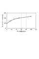
- 6 (a) and 6 (b)are diagrams showing the results of XPS analysis on the protective film PF formed in the experimental example in which the silicon oxide film and the silicon nitride film were etched in the step STP, respectively. It is a timing chart of another example concerning the etching method which concerns on one example embodiment. Determined by experiments, it is a graph showing a relationship between the etching rate of the flow rate and the silicon oxide film PF 3 gas in the process gas. Determined by experiments, it is a graph showing the relationship between the maximum width of the opening formed in the flow rate and the silicon oxide film PF 3 gas in the process gas. Determined by experiments, it is a graph showing a relationship between a selected ratio and flow rate of the PF 3 gas in the process gas.
- an etching methodincludes a step of preparing a substrate in a chamber of a plasma processing apparatus.
- the substratecontains a silicon-containing film.
- the etching methodfurther includes the step of etching the silicon-containing film with a chemical species from the plasma formed from the processing gas in the chamber.
- the processing gascontains a halogen element and phosphorus.
- a protective film containing silicon and phosphorus contained in the processing gasis formed on the side wall surface defining the openings formed in the silicon-containing film by etching.
- the silicon-containing filmis etched while the side wall surface is protected by this protective film. Therefore, in plasma etching of the silicon-containing film, it is possible to suppress etching in the lateral direction.
- the etching methodmay further include the step of forming a protective film on the side wall surface that defines the openings formed by the etching.
- This protective filmcontains phosphorus contained in the processing gas.
- the etching step and the protective film forming stepmay occur at the same time.
- the treatment gascomprises at least one of PF 3 , PCl 3 , PF 5 , PCL 5 , POCl 3 , PH 3 , PBr 3 , or PBr 5 as a phosphorus-containing molecule. May be good.
- the treatment gasmay further contain carbon and hydrogen.
- the treatment gasmay contain at least one of H 2 , HF, C x Hy , CH x F y , or NH 3 as a hydrogen-containing molecule.
- each of x and yis a natural number.
- the halogen elementmay be fluorine.
- the processing gasmay further contain oxygen.
- the silicon-containing filmmay be a silicon-containing dielectric film.
- the silicon-containing filmmay include at least one film of a silicon oxide film, a silicon nitride film, or a silicon film.
- the silicon-containing filmmay include two or more silicon-containing films having different film types from each other.
- the two or more silicon-containing filmsmay include a silicon oxide film and a silicon nitride film.
- the two or more silicon-containing filmsmay include a silicon oxide film and a silicon film.
- the two or more silicon-containing filmsmay include a silicon oxide film, a silicon nitride film, and a silicon film.
- the substratemay further have a mask provided on the silicon-containing film.
- the temperature of the substratemay be set to a temperature of 0 ° C. or lower at the start of the etching process.
- a plasma processing apparatusin another exemplary embodiment, includes a chamber, a substrate support, a gas supply unit, and a high frequency power supply.
- the substrate supportis configured to support the substrate in the chamber.
- the gas supply unitis configured to supply a processing gas for etching the silicon-containing film into the chamber.
- the processing gascontains a halogen element and phosphorus.
- the high frequency power supplyis configured to generate high frequency power to generate plasma from the processing gas in the chamber.
- FIG. 1is a flow chart of an etching method according to one exemplary embodiment.
- the etching method shown in FIG. 1(hereinafter referred to as “method MT”) is applied to a substrate having a silicon-containing film.
- the silicon-containing filmis etched.
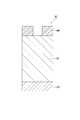
- FIG. 2is a partially enlarged cross-sectional view of an example substrate to which the etching method shown in FIG. 1 can be applied.
- the substrate W shown in FIG. 2can be used in the manufacture of devices such as DRAM and 3D-NAND.
- the substrate Whas a silicon-containing film SF.
- the substrate Wmay further have a base region UR.
- the silicon-containing film SFcan be provided on the base region UR.
- the silicon-containing film SFcan be a silicon-containing dielectric film.
- the silicon-containing dielectric filmmay include a silicon oxide film or a silicon nitride film.
- the silicon-containing dielectric filmmay be a film having another film type as long as it is a film containing silicon.
- the silicon-containing film SFmay include a silicon film (for example, a polycrystalline silicon film). Further, the silicon-containing film SF may include two or more silicon-containing films having different film types from each other. The two or more silicon-containing films may include a silicon oxide film and a silicon nitride film. The silicon-containing film SF may be, for example, a multilayer film including one or more silicon oxide films and one or more silicon nitride films laminated alternately. The silicon-containing film SF may be a multilayer film including a plurality of alternately laminated silicon oxide films and a plurality of silicon nitride films. Alternatively, the two or more silicon-containing films may include a silicon oxide film and a silicon film.
- the silicon-containing film SFmay be, for example, a multilayer film containing one or more silicon oxide films and one or more silicon films laminated alternately.
- the silicon-containing film SFmay be a multilayer film including a plurality of alternately laminated silicon oxide films and a plurality of polysilicon films.
- the two or more silicon-containing filmsmay include a silicon oxide film, a silicon nitride film, and a silicon film.
- the substrate Wmay further have a mask MK.
- the mask MKis provided on the silicon-containing film SF.
- the mask MKis formed from a material having an etching rate lower than the etching rate of the silicon-containing film SF in step ST2.
- the mask MKcan be formed from an organic material.
- the mask MKcan be formed from, for example, an amorphous carbon film, a photoresist film, or a spin-on carbon film (SOC film).
- the mask MKmay be a metal-containing mask formed from a metal-containing material such as titanium nitride, tungsten, or tungsten carbide.
- the mask MKcan have a thickness of 3 ⁇ m or more.
- the mask MKis patterned. That is, the mask MK has a pattern transferred to the silicon-containing film SF in step ST2.
- the pattern of the mask MKis transferred to the silicon-containing film SF, an opening such as a hole or a trench is formed in the silicon-containing film SF.
- the aspect ratio of the openings formed in the silicon-containing film SF in step ST2may be 20 or more, and may be 30, 40 or more, or 50 or more.
- FIG. 3is a diagram schematically showing a plasma processing apparatus according to one exemplary embodiment.
- the plasma processing apparatus 1 shown in FIG. 3includes a chamber 10.
- the chamber 10provides an internal space 10s therein.
- the chamber 10includes a chamber body 12.
- the chamber body 12has a substantially cylindrical shape.
- the chamber body 12is made of, for example, aluminum.
- a corrosion-resistant filmis provided on the inner wall surface of the chamber body 12.
- the corrosion resistant filmcan be formed from ceramics such as aluminum oxide and yttrium oxide.
- a passage 12pis formed on the side wall of the chamber body 12.
- the substrate Wis conveyed between the internal space 10s and the outside of the chamber 10 through the passage 12p.
- the passage 12pis opened and closed by the gate valve 12g.
- the gate valve 12gis provided along the side wall of the chamber body 12.
- a support portion 13is provided on the bottom of the chamber body 12.
- the support portion 13is formed of an insulating material.
- the support portion 13has a substantially cylindrical shape.
- the support portion 13extends upward from the bottom of the chamber body 12 in the internal space 10s.
- the support portion 13supports the substrate support 14.
- the substrate support 14is configured to support the substrate W in the internal space 10s.
- the substrate support 14has a lower electrode 18 and an electrostatic chuck 20.
- the substrate support 14may further include an electrode plate 16.
- the electrode plate 16is formed of a conductor such as aluminum and has a substantially disk shape.
- the lower electrode 18is provided on the electrode plate 16.
- the lower electrode 18is formed of a conductor such as aluminum and has a substantially disk shape.
- the lower electrode 18is electrically connected to the electrode plate 16.
- the electrostatic chuck 20is provided on the lower electrode 18.
- the substrate Wis placed on the upper surface of the electrostatic chuck 20.
- the electrostatic chuck 20has a main body and electrodes.
- the main body of the electrostatic chuck 20has a substantially disk shape and is formed of a dielectric material.
- the electrode of the electrostatic chuck 20is a film-like electrode, and is provided in the main body of the electrostatic chuck 20.
- the electrodes of the electrostatic chuck 20are connected to the DC power supply 20p via the switch 20s. When a voltage from the DC power supply 20p is applied to the electrodes of the electrostatic chuck 20, an electrostatic attractive force is generated between the electrostatic chuck 20 and the substrate W.
- the substrate Wis attracted to the electrostatic chuck 20 by its electrostatic attraction and is held by the electrostatic chuck 20.
- An edge ring 25is arranged on the substrate support 14.
- the edge ring 25is a ring-shaped member.
- the edge ring 25can be formed of silicon, silicon carbide, quartz, or the like.
- the substrate Wis arranged on the electrostatic chuck 20 and in the region surrounded by the edge ring 25.
- a flow path 18fis provided inside the lower electrode 18.
- a heat exchange mediumfor example, a refrigerant
- the heat exchange medium supplied to the flow path 18fis returned to the chiller unit via the pipe 22b.
- the temperature of the substrate W placed on the electrostatic chuck 20is adjusted by heat exchange between the heat exchange medium and the lower electrode 18.
- the plasma processing device 1is provided with a gas supply line 24.
- the gas supply line 24supplies heat transfer gas (for example, He gas) from the heat transfer gas supply mechanism to the gap between the upper surface of the electrostatic chuck 20 and the back surface of the substrate W.
- heat transfer gasfor example, He gas
- the plasma processing device 1further includes an upper electrode 30.
- the upper electrode 30is provided above the substrate support 14.
- the upper electrode 30is supported on the upper part of the chamber body 12 via the member 32.
- the member 32is formed of an insulating material. The upper electrode 30 and the member 32 close the upper opening of the chamber body 12.
- the upper electrode 30may include a top plate 34 and a support 36.
- the lower surface of the top plate 34is the lower surface on the side of the internal space 10s, and defines the internal space 10s.
- the top plate 34can be formed of a low resistance conductor or semiconductor that generates less Joule heat.
- the top plate 34has a plurality of gas discharge holes 34a that penetrate the top plate 34 in the plate thickness direction.
- the support 36supports the top plate 34 in a detachable manner.
- the support 36is formed of a conductive material such as aluminum.
- a gas diffusion chamber 36ais provided inside the support 36.
- the support 36has a plurality of gas holes 36b extending downward from the gas diffusion chamber 36a.
- the plurality of gas holes 36bcommunicate with each of the plurality of gas discharge holes 34a.
- a gas introduction port 36cis formed in the support 36.
- the gas introduction port 36cis connected to the gas diffusion chamber 36a.
- a gas supply pipe 38is connected to the gas introduction port 36c.
- the gas source group 40is connected to the gas supply pipe 38 via the flow rate controller group 41 and the valve group 42.
- the flow rate controller group 41 and the valve group 42form a gas supply unit.
- the gas supply unitmay further include the gas source group 40.
- the gas source group 40includes a plurality of gas sources.
- the plurality of gas sourcesinclude the source of the processing gas used in the method MT.
- the flow rate controller group 41includes a plurality of flow rate controllers. Each of the plurality of flow rate controllers in the flow rate controller group 41 is a mass flow controller or a pressure-controlled flow rate controller.
- the valve group 42includes a plurality of on-off valves.
- Each of the plurality of gas sources of the gas source group 40is connected to the gas supply pipe 38 via the corresponding flow rate controller of the flow rate controller group 41 and the corresponding opening / closing valve of the valve group 42.
- a shield 46is detachably provided along the inner wall surface of the chamber body 12 and the outer circumference of the support portion 13.
- the shield 46prevents reaction by-products from adhering to the chamber body 12.
- the shield 46is constructed, for example, by forming a corrosion-resistant film on the surface of a base material made of aluminum.
- the corrosion resistant filmcan be formed from a ceramic such as yttrium oxide.
- a baffle plate 48is provided between the support portion 13 and the side wall of the chamber body 12.
- the baffle plate 48is formed, for example, by forming a corrosion-resistant film (a film such as yttrium oxide) on the surface of a member made of aluminum.
- a plurality of through holesare formed in the baffle plate 48.
- An exhaust port 12eis provided below the baffle plate 48 and at the bottom of the chamber body 12.
- An exhaust device 50is connected to the exhaust port 12e via an exhaust pipe 52.
- the exhaust device 50includes a pressure regulating valve and a vacuum pump such as a turbo molecular pump.
- the plasma processing device 1includes a high frequency power supply 62 and a bias power supply 64.
- the high frequency power supply 62is a power supply that generates high frequency power HF.
- the high frequency power HFhas a first frequency suitable for plasma generation.
- the first frequencyis, for example, a frequency in the range of 27 MHz to 100 MHz.
- the high frequency power supply 62is connected to the lower electrode 18 via the matching unit 66 and the electrode plate 16.
- the matching device 66has a circuit for matching the output impedance of the high frequency power supply 62 with the impedance on the load side (lower electrode 18 side).
- the high frequency power supply 62may be connected to the upper electrode 30 via the matching device 66.
- the high frequency power supply 62constitutes an example plasma generation unit.
- the bias power supply 64is a power supply that generates an electric bias.
- the bias power supply 64is electrically connected to the lower electrode 18.
- the electrical biashas a second frequency.
- the second frequencyis lower than the first frequency.
- the second frequencyis, for example, a frequency in the range of 400 kHz to 13.56 MHz.
- the electrical biasis applied to the lower electrode 18 to draw ions into the substrate W when used with the high frequency power HF.
- an electric biasis applied to the lower electrode 18, the potential of the substrate W mounted on the substrate support 14 fluctuates within a period defined by the second frequency.
- the electrical biasmay be a high frequency power LF having a second frequency.
- the high frequency power LFis used as a high frequency bias power for drawing ions into the substrate W.
- the bias power supply 64 configured to generate the high frequency power LFis connected to the lower electrode 18 via the matching unit 68 and the electrode plate 16.
- the matching device 68has a circuit for matching the output impedance of the bias power supply 64 with the impedance on the load side (lower electrode 18 side).
- the plasmamay be generated by using the high frequency power LF without using the high frequency power HF, that is, by using only a single high frequency power.
- the frequency of the high frequency power LFmay be a frequency larger than 13.56 MHz, for example, 40 MHz.
- the plasma processing device 1does not have to include the high frequency power supply 62 and the matching device 66.
- the bias power supply 64constitutes an example plasma generation unit.
- the electrical biasmay be a pulse wave of a negative DC voltage.
- the negative electrode DC voltage pulse waveis periodically generated and given to the lower electrode 18.
- the period of the pulse wave of the negative DC voltageis defined by the second frequency.
- the period of the pulse wave of the negative DC voltageincludes two periods.
- the negative DC voltage level (ie, absolute value) in one of the two periodsis higher than the negative DC voltage level (ie, absolute value) in the other of the two periods.
- the level of the negative DC voltage in the other periodmay be greater than zero or may be zero.
- the bias power supply 64is connected to the lower electrode 18 via a low-pass filter and an electrode plate 16.
- the bias power supply 64may apply a continuous wave of electrical bias to the lower electrode 18. That is, the bias power supply 64 may continuously apply an electric bias to the lower electrode 18.
- a continuous wave of electrical biascan be applied to the lower electrode 18 during the period during which step STP or steps ST2 and ST3 of Method MT are being performed.
- the bias power supply 64may apply an electrical bias pulse wave to the lower electrode 18.
- the pulse wave of the electric biascan be periodically applied to the lower electrode 18.
- the period of the electrical bias pulse waveis defined by a third frequency.
- the third frequencyis lower than the second frequency.
- the third frequencyis, for example, 5 Hz or more and 100 kHz or less.
- the period of the pulse wave of the electric biasincludes two periods, that is, the H period and the L period.
- the level of electrical bias during the H periodis higher than the level of electrical bias during the L period. That is, the pulse wave of the electric bias may be applied to the lower electrode 18 by increasing or decreasing the level of the electric bias.
- the level of electrical bias during the L periodmay be greater than zero. Alternatively, the level of electrical bias during the L period may be zero. That is, the pulse wave of the electric bias may be given to the lower electrode 18 by alternately switching between supplying and stopping the supply of the electric bias to the lower electrode 18.
- the level of the electric biasis the power level of the high frequency power LF.
- the level of the electrical biasis the effective value of the absolute value of the negative DC voltage.
- the duty ratio of the electric bias pulse wavethat is, the ratio occupied by the H period in the period of the electric bias pulse wave is, for example, 1% or more and 80% or less.
- a pulse wave of electrical biascan be applied to the lower electrode 18 to perform steps ST2 and ST3 of Method MT.
- the high frequency power supply 62may supply a continuous wave of high frequency power HF. That is, the high frequency power supply 62 may continuously supply the high frequency power HF.
- the continuous wave of high frequency power HFcan be supplied during the period during which process STP or process ST2 and step ST3 of the method MT are being executed.
- the high frequency power supply 62may supply a pulse wave of the high frequency power HF.
- the pulse wave of the high frequency power HFcan be supplied periodically.
- the period of the pulse wave of the high frequency power HFis defined by the fourth frequency.
- the fourth frequencyis lower than the second frequency.
- the fourth frequencyis the same as the third frequency.
- the period of the pulse wave of the high frequency power HFincludes two periods, that is, the H period and the L period.
- the power level of the high frequency power HF in the H periodis higher than the power level of the high frequency power HF in the L period of the two periods.
- the power level of the high frequency power HF in the L periodmay be greater than zero or may be zero.
- the period of the pulse wave of the high frequency power HFmay be synchronized with the period of the pulse wave of the electric bias.
- the H period in the pulse wave period of the high frequency power HFmay be synchronized with the H period in the pulse wave period of the electric bias.
- the H period in the pulse wave period of the high frequency power HFmay not be synchronized with the H period in the pulse wave period of the electric bias.
- the time length of the H period in the pulse wave period of the high frequency power HFmay be the same as or different from the time length of the H period in the pulse wave period of the electric bias.
- gasis supplied from the gas supply unit to the internal space 10s. Further, by supplying the high frequency power HF and / or the high frequency power LF, a high frequency electric field is generated between the upper electrode 30 and the lower electrode 18. The generated high-frequency electric field generates plasma from the gas in the internal space 10s.
- the plasma processing device 1may further include a control unit 80.
- the control unit 80may be a computer including a processor, a storage unit such as a memory, an input device, a display device, a signal input / output interface, and the like.
- the control unit 80controls each unit of the plasma processing device 1.
- the operatorcan perform a command input operation or the like in order to manage the plasma processing device 1 by using the input device.
- the control unit 80can visualize and display the operating status of the plasma processing device 1 by the display device.
- the control program and the recipe dataare stored in the storage unit.
- the control programis executed by the processor in order to execute various processes in the plasma processing device 1.
- the processorexecutes a control program and controls each part of the plasma processing device 1 according to the recipe data.
- the method MTwill be described by taking the case where it is applied to the substrate W shown in FIG. 2 by using the plasma processing apparatus 1 as an example.
- the method MTcan be executed in the plasma processing device 1 by the control of each part of the plasma processing device 1 by the control unit 80.
- control of each part of the plasma processing apparatus 1 by the control unit 80 for executing the method MTwill also be described.
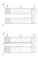
- FIG. 4Ais a partially enlarged cross-sectional view of an example substrate to which the etching method shown in FIG. 1 is applied
- FIG. 4Bis etching by plasma formed from a phosphorus-free processing gas. It is a partially enlarged cross-sectional view of the substrate of one example.
- FIG. 5is an example timing chart relating to the etching method according to one exemplary embodiment. In FIG. 5, the horizontal axis represents time. In FIG. 5, the vertical axis shows the power level of the high-frequency power HF, the level of the electric bias, and the supply state of the processing gas.
- the “L” level of the high frequency power HFindicates that the high frequency power HF is not supplied or the power level of the high frequency power HF is lower than the power level indicated by "H".
- An “L” level of electrical biasindicates that no electrical bias is applied to the lower electrode 18 or that the level of electrical bias is lower than the level indicated by "H”.
- "ON” in the processing gas supply stateindicates that the processing gas is supplied into the chamber 10
- "OFF" in the processing gas supply stateindicates that the processing gas is supplied into the chamber 10. Indicates that is stopped.
- step ST1the substrate W is prepared in the chamber 10.
- the substrate Wis placed on the electrostatic chuck 20 in the chamber 10 and held by the electrostatic chuck 20.
- the process STPis then executed.
- plasma processing on the substrate Wis executed.
- plasmais generated from the processing gas in the chamber 10.
- Method MTincludes step ST2.
- Step ST2is performed during execution of step STP.
- Method MTmay further include step ST3.
- Step ST3is performed during execution of step STP. Steps ST2 and ST3 may occur at the same time, or may be performed independently of each other.
- step ST2the silicon-containing film SF is etched by the chemical species from the plasma generated from the processing gas in the chamber 10 in step STP.
- step ST3the protective film PF is formed on the substrate W by the chemical species from the plasma generated from the processing gas in the chamber 10 in step STP.
- the protective film PFis formed on the side wall surface that defines the opening formed in the silicon-containing film SF.
- the processing gas used in the process STPcontains a halogen element and phosphorus.
- the halogen element contained in the processing gascan be fluorine.
- the treatment gasmay contain at least one halogen-containing molecule.
- the treatment gasmay contain at least one of fluorocarbons or hydrofluorocarbons as at least one halogen-containing molecule. Fluorocarbons are, for example, at least one of CF 4 , C 3 F 8 , C 4 F 6 , or C 4 F 8.
- the hydrofluorocarbonis, for example, at least one of CH 2 F 2 , CHF 3 , or CH 3 F.
- the treatment gasmay contain at least one phosphorus-containing molecule.
- the phosphorus-containing moleculemay be an oxide such as tetraphosphorus pentoxide (P 4 O 10 ), tetraphosphorus octoxide (P 4 O 8 ), tetraphosphorus hexaoxide (P 4 O 6 ).
- Ten oxide tetraphosphateis sometimes referred to as diphosphorus pentaoxide (P 2 O 5).
- Phosphorus-containing moleculesare phosphorus trifluoride (PF 3 ), phosphorus pentafluorine (PF 5 ), phosphorus trichloride (PCl 3 ), phosphorus pentachloride (PCl 5 ), phosphorus tribrominated (PBr 3 ), and pentaodor. It may be a halide such as phosphorus carbonate (PBr 5 ) or phosphorus iodide (PI 3).
- the phosphorus-containing moleculemay be a halogenated phosphoryl such as phosphoryl chloride (POF 3 ), phosphoryl chloride (POCl 3 ), phosphoryl bromide (POBr 3).
- Phosphine-containing moleculesinclude phosphine (PH 3 ), calcium phosphide (Ca 3 P 2, etc.), phosphoric acid (H 3 PO 4 ), sodium phosphate (Na 3 PO 4 ), hexafluorophosphoric acid (HPF 6 ), etc. It may be.
- the treatment gasmay contain one or more phosphorus-containing molecules among the above-mentioned phosphorus-containing molecules as at least one phosphorus-containing molecule.
- the treatment gasmay contain at least one of PF 3 , PCl 3 , PF 5 , PCL 5 , POCl 3 , PH 3 , PBr 3 , or PBr 5 as at least one phosphorus-containing molecule.
- each phosphorus-containing molecule contained in the processing gasis a liquid or a solid, it can be vaporized by heating or the like and supplied into the chamber 10.
- the processing gas used in the process STPmay further contain carbon and hydrogen.
- the treatment gasmay contain at least one of H 2 , hydrogen fluoride (HF), hydrocarbon (C x Hy ), hydrofluorocarbon (CH x F y ), or NH 3 as a hydrogen-containing molecule. Good. Hydrocarbons are, for example, CH 4 or C 3 H 6 . Here, each of x and y is a natural number.
- the treatment gasmay contain fluorocarbons or hydrocarbons (for example, CH 4 ) as carbon-containing molecules.
- the processing gasmay further contain oxygen.
- the processing gasmay contain, for example, O 2. Alternatively, the processing gas does not have to contain oxygen.
- the processing gasmay include a first gas and a second gas.
- the first gasis a phosphorus-free gas.
- the first gasmay contain halogen elements.
- the first gasmay include the gas of at least one halogen-containing molecule described above.
- the first gasmay further contain carbon and hydrogen.
- the first gasmay further contain the above-mentioned hydrogen-containing molecular gas and / or carbon-containing molecular gas.
- the first gasmay further contain oxygen.
- the first gasmay contain O 2 gas. Alternatively, the first gas does not have to contain oxygen.
- the second gasis a gas containing phosphorus.
- the second gasmay contain the gas of at least one phosphorus-containing molecule described above.
- the flow rate ratiowhich is the ratio of the flow rate of the second gas to the flow rate of the first gas, may be set to be larger than 0 and 0.5 or less.
- the flow rate ratiomay be set to 0.075 or more and 0.3 or less.
- the flow rate ratiomay be set to 0.1 or more and 0.25 or less.
- the processing gasis supplied into the chamber 10.
- the pressure of the gas in the chamber 10is set to the specified pressure.
- the pressure of the gas in the chamber 10can be set to a pressure of 10 mTorr (1.3 Pa) or more and 100 mTorr (13.3 Pa) or less.
- high frequency power HFis supplied in order to generate plasma from the processing gas in the chamber 10.
- a continuous wave of high frequency power HFmay be supplied in the process STP.
- the high frequency power LFmay be used instead of the high frequency power HF.
- both the high frequency power HF and the electric biasmay be supplied. As shown by the solid line in FIG. 5, in the step STP, a continuous wave of electric bias may be applied to the lower electrode 18.
- the power level of the high frequency power HFcan be set to a level of 2 kW or more and 10 kW or less.
- the power level of the high frequency power LFcan be set to a level of 2 kW or more.
- the power level of the high frequency power LFmay be set to a level of 10 kW or more.
- the control unit 80controls the gas supply unit so as to supply the processing gas into the chamber 10. Further, the control unit 80 controls the exhaust device 50 so as to set the pressure of the gas in the chamber 10 to a designated pressure. Further, the control unit 80 controls the high frequency power supply 62 and the bias power supply 64 so as to supply the high frequency power HF, the high frequency power LF, or the high frequency power HF and the electric bias.
- control unit 80controls the gas supply unit so as to supply the processing gas into the chamber 10. Further, the control unit 80 controls the exhaust device 50 so as to set the pressure of the gas in the chamber 10 to a designated pressure. Further, the control unit 80 controls the high frequency power supply 62 and the bias power supply 64 so as to supply the high frequency power HF, the high frequency power LF, or the high frequency power HF and the electric bias.
- the temperature of the substrate W at the start of step ST2may be set to a temperature of 0 ° C. or lower.
- the etching rate of the silicon-containing film SF in the step ST2becomes high.
- the control unit 80may control the chiller unit to set the temperature of the substrate W at the start of step ST2.
- the temperature of the substrate W during execution of step ST2may be 200 ° C. or lower. If the temperature of the substrate W during the execution of step ST2 (or step STP) is 200 ° C. or lower, the phosphorus chemical species that are etchants are sufficiently supplied to the bottom of the opening formed in the silicon-containing film SF. Can be done.
- the method MTmay further include a step STT.
- the process STTis performed before the process ST2 (or process STP).
- the temperature of the substrate Wis set to a temperature of 0 ° C. or lower in the process STT.
- the temperature of the substrate W at the start of step ST2is set in step STT.
- the control unit 80may control the chiller unit in order to set the temperature of the substrate W in the process STT.
- step ST2the silicon-containing film SF is etched by the halogen species from the plasma generated from the processing gas.
- the portion of the entire region of the silicon-containing film SF exposed from the mask MKis etched (see FIG. 4A).
- the treatment gascontains a molecule containing phosphorus and a halogen element as a phosphorus-containing molecule such as PF 3
- the halogen chemical species derived from such a moleculecontributes to the etching of the silicon-containing film SF. Therefore, a phosphorus-containing molecule containing phosphorus and a halogen element, such as PF 3 , increases the etching rate of the silicon-containing film SF in step ST2.
- the protective film PFis formed on the side wall surface defining the opening formed in the silicon-containing film SF by the etching of the step ST2 (see (a) of FIG. 4).
- the protective film PFis formed by chemical species from the plasma generated from the processing gas in the chamber 10 in the step STP.
- Step ST3can proceed at the same time as step ST2.
- the protective film PFmay be formed so that its thickness decreases along the depth direction of the opening formed in the silicon-containing film SF. ..
- the protective film PFcontains silicon and phosphorus contained in the processing gas used in the process STP. In one embodiment, the protective film PF may further contain carbon and / or hydrogen contained in the processing gas. In one embodiment, the protective film PF may further contain oxygen contained in the processing gas or contained in the silicon-containing film SF. In one embodiment, the protective film PF may contain a bond of phosphorus and oxygen.
- FIG. 6 (a) and 6 (b)are diagrams showing the results of XPS analysis on the protective film PF formed in the experimental example in which the silicon oxide film and the silicon nitride film were etched in the step STP, respectively.
- FIG. 6A and FIG. 6Bshows a P2p spectrum. The conditions of the process STP of the experimental example are shown below.
- the Si—O bond peak and the PO bond peakwere observed.
- the Si-P bond peak and the PN bond peakwere observed.
- the silicon-containing film SFis also etched in the lateral direction as shown in FIG. 4 (b). As a result, the width of the opening formed in the silicon-containing film SF is partially widened. For example, the width of the opening formed in the silicon-containing film SF is partially widened in the vicinity of the mask MK.
- the protective film PFis formed on the side wall surface that defines the opening formed in the silicon-containing film SF by etching.
- the silicon-containing film SFis etched while the side wall surface is protected by the protective film PF. Therefore, according to the method MT, it is possible to suppress the etching in the lateral direction in the plasma etching of the silicon-containing film SF.
- one or more cycles each containing step ST2 and step ST3are sequentially executed during the period during which step STP is continued, that is, during the period during which plasma is generated from the processing gas in step STP. You may. In the process STP, two or more cycles may be executed in sequence.
- the above-mentioned electric bias pulse wavemay be applied from the bias power supply 64 to the lower electrode 18 in the process STP. That is, when the plasma generated from the processing gas is present in the chamber 10, an electric bias pulse wave may be applied from the bias power supply 64 to the lower electrode 18.
- the etching of the silicon-containing film SF in step ST2occurs mainly in the H period within the period of the pulse wave of the electric bias.
- the formation of the protective film PF in step ST3mainly occurs in the L period within the period of the pulse wave of the electric bias.
- the power level of the high frequency power LFcan be set to a level of 2 kW or more in the H period within the period of the pulse wave of the electric bias.
- the power level of the high frequency power LFmay be set to a level of 10 kW or more in the H period within the period of the pulse wave of the electric bias.
- the pulse wave of the high frequency power HF described abovemay be supplied in the process STP.
- the power level of the high frequency power HFcan be set to a level of 1 kW or more and 10 kW or less.
- the period of the pulse wave of the high frequency power HFmay be synchronized with the period of the pulse wave of the electric bias.
- the H period in the pulse wave period of the high-frequency power HFmay be synchronized with the H period in the pulse wave period of the electric bias.
- the H period in the pulse wave period of the high frequency power HFmay not be synchronized with the H period in the pulse wave period of the electric bias.
- the time length of the H period in the pulse wave period of the high frequency power HFmay be the same as or different from the time length of the H period in the pulse wave period of the electric bias.
- FIG. 7is a timing chart of another example relating to the etching method according to one exemplary embodiment.
- the horizontal axisrepresents time.
- the vertical axisshows the power level of the high-frequency power HF, the level of the electric bias, the supply state of the first gas, and the supply state of the second gas.
- the "L" level of the high frequency power HFindicates that the high frequency power HF is not supplied or the power level of the high frequency power HF is lower than the power level indicated by "H”.
- An “L" level of electrical biasindicates that no electrical bias is applied to the lower electrode 18 or that the level of electrical bias is lower than the level indicated by "H".
- the first gas and the second gasmay be alternately supplied into the chamber 10.
- Etching of the silicon-containing film SF in step ST2occurs mainly during the period when the first gas is supplied into the chamber 10.
- the formation of the protective film PF in step ST3occurs mainly during the period when the second gas is supplied into the chamber 10.
- a continuous wave of high frequency power HFmay be supplied in the process STP.
- the pulse wave of the high frequency power HFmay be supplied in the process STP in the same manner as the pulse wave of the high frequency power HF shown in FIG.
- the pulse wave of the high frequency power HFis shown by a broken line in FIG.
- the H period within the pulse wave period of the high frequency power HFis synchronized with or partially overlaps with the period during which the first gas is supplied into the chamber 10.
- the L period within the pulse wave period of the high frequency power HFis synchronized with or partially overlaps with the period during which the second gas is supplied into the chamber 10.
- a continuous wave of electric biasmay be applied to the lower electrode 18 in the step STP.
- the pulse wave of the electric biasmay be applied to the lower electrode 18 in the same manner as the pulse wave of the electric bias shown in FIG.
- the pulse wave of the electric biasis shown by a broken line in FIG.
- the H period within the period of the electric bias pulse waveis synchronized with or partially overlaps with the period during which the first gas is supplied into the chamber 10.
- the L period within the period of the electrical bias pulse waveis synchronized with or partially overlaps with the period during which the second gas is supplied into the chamber 10.
- each of the plurality of sample substrateshad a silicon oxide film and a mask provided on the silicon oxide film.
- the maskwas a mask formed from an amorphous carbon film.
- the process STP of Method MTwas applied to a plurality of sample substrates.
- the processing gas used for each of the plurality of sample substratescontained PF 3 gas having different flow rates from each other. Other conditions in the process STP are shown below.
- the flow rates of the PF 3 gaswere 0 sccm, 15 sccm, 30 sccm, 50 sccm, and 100 sccm, respectively.
- the maximum width of the openings formed in the silicon oxide film, the etching rate of the silicon oxide film, and the selection ratiowere determined for each of the plurality of sample substrates.
- the selection ratiois a value obtained by dividing the etching rate of the silicon oxide film by the etching rate of the mask. Then, the relationship between the flow rate of the PF 3 gas in the processing gas used in the step STP and the etching rate of the silicon oxide film was determined. Further, the relationship between the flow rate of the PF 3 gas in the processing gas used in the step STP and the maximum width of the opening formed in the silicon oxide film was determined. In addition, the relationship between the flow rate of the PF 3 gas in the processing gas used in the process STP and the selection ratio was determined. FIG.
- FIG. 8shows the relationship between the flow rate of the PF 3 gas in the processing gas and the etching rate of the silicon oxide film. Further, FIG. 9 shows the relationship between the flow rate of the PF 3 gas in the processing gas and the maximum width of the openings formed in the silicon oxide film. Further, FIG. 10 shows the relationship between the flow rate of the PF 3 gas in the processing gas and the selection ratio.
- the etching rate and selection ratio of the silicon oxide filmare high when the processing gas contains phosphorus, that is, when the flow rate ratio is larger than 0. Further, as shown in FIG. 10, it was confirmed that a considerably high selectivity can be obtained when the flow rate of the PF 3 gas in the processing gas is 15 sccm or more, 60 sccm or 50 sccm or less. That is, it was confirmed that a considerably high selection ratio can be obtained when the flow rate ratio is 0.075 or more, 0.3 or 0.25 or less. Further, as shown in FIG.
- the processing gascontains phosphorus, it is possible to prevent the maximum width of the opening of the silicon oxide film from becoming small, that is, the width of the opening of the silicon oxide film from being partially widened. It was confirmed that it was possible. In particular, it was confirmed that when the flow rate of the PF 3 gas in the processing gas is 50 sccm or more, the widening of the opening width of the silicon oxide film can be suppressed more remarkably.
- the plasma processing apparatus used in the method MTmay be a capacitively coupled plasma processing apparatus other than the plasma processing apparatus 1.
- the plasma processing apparatus used in the method MTis an inductively coupled plasma processing apparatus, an ECR (electron cyclotron resonance) plasma processing apparatus, a plasma processing apparatus that generates plasma using a surface wave such as a microwave, or the like. May be good.
- the plasma processing apparatusincludes, in addition to the bias power supply 64 that supplies the high-frequency power LF to the lower electrode 18, another bias power supply configured to give a pulse wave of a negative DC voltage to the lower electrode 18. You may.
- Plasma processing device10 ... Chamber, W ... Substrate, SF ... Silicon-containing film.
Landscapes
- Engineering & Computer Science (AREA)
- Physics & Mathematics (AREA)
- Condensed Matter Physics & Semiconductors (AREA)
- General Physics & Mathematics (AREA)
- Manufacturing & Machinery (AREA)
- Computer Hardware Design (AREA)
- Microelectronics & Electronic Packaging (AREA)
- Power Engineering (AREA)
- Chemical & Material Sciences (AREA)
- Plasma & Fusion (AREA)
- Analytical Chemistry (AREA)
- Chemical Kinetics & Catalysis (AREA)
- General Chemical & Material Sciences (AREA)
- Inorganic Chemistry (AREA)
- Electromagnetism (AREA)
- Spectroscopy & Molecular Physics (AREA)
- Drying Of Semiconductors (AREA)
- Plasma Technology (AREA)
Abstract
Description
Translated fromJapanese本開示の例示的実施形態は、エッチング方法に関するものである。An exemplary embodiment of the present disclosure relates to an etching method.
電子デバイスの製造においては、基板のシリコン含有膜のプラズマエッチングが行われている。シリコン含有膜のプラズマエッチングにおいては、フルオロカーボンガスを含む処理ガスが用いられている。このようなプラズマエッチングについては、下記の特許文献1に記載されている。In the manufacture of electronic devices, plasma etching of the silicon-containing film on the substrate is performed. In plasma etching of a silicon-containing film, a processing gas containing a fluorocarbon gas is used. Such plasma etching is described in
本開示は、シリコン含有膜のプラズマエッチングにおいて、横方向のエッチングを抑制する技術を提供する。The present disclosure provides a technique for suppressing lateral etching in plasma etching of a silicon-containing film.
一つの例示的実施形態において、エッチング方法が提供される。エッチング方法は、プラズマ処理装置のチャンバ内に基板を準備する工程を含む。基板は、シリコン含有膜を含む。エッチング方法は、チャンバ内で処理ガスから形成されたプラズマからの化学種によりシリコン含有膜をエッチングする工程を更に含む。処理ガスは、ハロゲン元素及びリンを含む。In one exemplary embodiment, an etching method is provided. The etching method includes a step of preparing a substrate in a chamber of a plasma processing apparatus. The substrate contains a silicon-containing film. The etching method further includes the step of etching the silicon-containing film with a chemical species from the plasma formed from the processing gas in the chamber. The processing gas contains a halogen element and phosphorus.
一つの例示的実施形態によれば、シリコン含有膜のプラズマエッチングにおいて横方向のエッチングを抑制することが可能となる。According to one exemplary embodiment, it is possible to suppress lateral etching in plasma etching of a silicon-containing film.
以下、種々の例示的実施形態について説明する。Hereinafter, various exemplary embodiments will be described.
一つの例示的実施形態において、エッチング方法が提供される。エッチング方法は、プラズマ処理装置のチャンバ内に基板を準備する工程を含む。基板は、シリコン含有膜を含む。エッチング方法は、チャンバ内で処理ガスから形成されたプラズマからの化学種によりシリコン含有膜をエッチングする工程を更に含む。処理ガスは、ハロゲン元素及びリンを含む。In one exemplary embodiment, an etching method is provided. The etching method includes a step of preparing a substrate in a chamber of a plasma processing apparatus. The substrate contains a silicon-containing film. The etching method further includes the step of etching the silicon-containing film with a chemical species from the plasma formed from the processing gas in the chamber. The processing gas contains a halogen element and phosphorus.
上記実施形態によれば、シリコンと処理ガスに含まれるリンを含む保護膜が、エッチングによってシリコン含有膜に形成された開口を画成する側壁面上に形成される。この保護膜により側壁面が保護されつつ、シリコン含有膜がエッチングされる。したがって、シリコン含有膜のプラズマエッチングにおいて、横方向のエッチングを抑制することが可能となる。According to the above embodiment, a protective film containing silicon and phosphorus contained in the processing gas is formed on the side wall surface defining the openings formed in the silicon-containing film by etching. The silicon-containing film is etched while the side wall surface is protected by this protective film. Therefore, in plasma etching of the silicon-containing film, it is possible to suppress etching in the lateral direction.
一つの例示的実施形態において、エッチング方法は、エッチングによって形成された開口を画成する側壁面上に保護膜を形成する工程を更に含んでいてもよい。この保護膜は処理ガスに含まれるリンを含む。In one exemplary embodiment, the etching method may further include the step of forming a protective film on the side wall surface that defines the openings formed by the etching. This protective film contains phosphorus contained in the processing gas.
一つの例示的実施形態において、エッチングする工程と保護膜を形成する工程が同時に発生してもよい。In one exemplary embodiment, the etching step and the protective film forming step may occur at the same time.
一つの例示的実施形態において、処理ガスは、リンを含む分子として、PF3、PCl3、PF5,PCl5,POCl3、PH3、PBr3、又はPBr5の少なくとも一つを含んでいてもよい。In one exemplary embodiment, the treatment gas comprises at least one ofPF 3 , PCl3 , PF5 , PCL5 , POCl3 , PH3 , PBr3 , or PBr5 as a phosphorus-containing molecule. May be good.
一つの例示的実施形態において、処理ガスは炭素及び水素を更に含んでいてもよい。In one exemplary embodiment, the treatment gas may further contain carbon and hydrogen.
一つの例示的実施形態において、処理ガスは、水素を含む分子として、H2、HF、CxHy、CHxFy、又はNH3の少なくとも一つを含んでいてもよい。ここで、x及びyの各々は自然数である。In one exemplary embodiment, the treatment gas may contain at least one ofH 2 , HF, CxHy , CHx Fy , or NH3 as a hydrogen-containing molecule. Here, each of x and y is a natural number.
一つの例示的実施形態において、ハロゲン元素はフッ素であってもよい。In one exemplary embodiment, the halogen element may be fluorine.
一つの例示的実施形態において、処理ガスは酸素を更に含んでいてもよい。In one exemplary embodiment, the processing gas may further contain oxygen.
一つの例示的実施形態において、シリコン含有膜はシリコン含有誘電体膜であってもよい。In one exemplary embodiment, the silicon-containing film may be a silicon-containing dielectric film.
一つの例示的実施形態において、シリコン含有膜は、シリコン酸化膜、シリコン窒化膜、又はシリコン膜の少なくとも一つの膜を含んでいてもよい。In one exemplary embodiment, the silicon-containing film may include at least one film of a silicon oxide film, a silicon nitride film, or a silicon film.
一つの例示的実施形態において、シリコン含有膜は、互いに異なる膜種を有する二つ以上のシリコン含有膜を含んでいてもよい。In one exemplary embodiment, the silicon-containing film may include two or more silicon-containing films having different film types from each other.
一つの例示的実施形態において、二つ以上のシリコン含有膜は、シリコン酸化膜及びシリコン窒化膜を含んでいてもよい。或いは、二つ以上のシリコン含有膜は、シリコン酸化膜及びシリコン膜を含んでいてもよい。或いは、二つ以上のシリコン含有膜は、シリコン酸化膜、シリコン窒化膜、及びシリコン膜を含んでいてもよい。In one exemplary embodiment, the two or more silicon-containing films may include a silicon oxide film and a silicon nitride film. Alternatively, the two or more silicon-containing films may include a silicon oxide film and a silicon film. Alternatively, the two or more silicon-containing films may include a silicon oxide film, a silicon nitride film, and a silicon film.
一つの例示的実施形態において、基板は、シリコン含有膜上に設けられたマスクを更に有していてもよい。In one exemplary embodiment, the substrate may further have a mask provided on the silicon-containing film.
一つの例示的実施形態では、エッチングする工程の開始時において基板の温度が0℃以下の温度に設定されてもよい。In one exemplary embodiment, the temperature of the substrate may be set to a temperature of 0 ° C. or lower at the start of the etching process.
別の例示的実施形態においては、プラズマ処理装置が提供される。プラズマ処理装置は、チャンバ、基板支持器、ガス供給部、及び高周波電源を備える。基板支持器は、チャンバ内において基板を支持するように構成されている。ガス供給部は、シリコン含有膜をエッチングするための処理ガスをチャンバ内に供給するように構成されている。処理ガスは、ハロゲン元素及びリンを含む。高周波電源は、チャンバ内で処理ガスからプラズマを生成するために高周波電力を発生するように構成されている。In another exemplary embodiment, a plasma processing apparatus is provided. The plasma processing apparatus includes a chamber, a substrate support, a gas supply unit, and a high frequency power supply. The substrate support is configured to support the substrate in the chamber. The gas supply unit is configured to supply a processing gas for etching the silicon-containing film into the chamber. The processing gas contains a halogen element and phosphorus. The high frequency power supply is configured to generate high frequency power to generate plasma from the processing gas in the chamber.
以下、図面を参照して種々の例示的実施形態について詳細に説明する。なお、各図面において同一又は相当の部分に対しては同一の符号を附すこととする。Hereinafter, various exemplary embodiments will be described in detail with reference to the drawings. In addition, the same reference numerals are given to the same or corresponding parts in each drawing.
図1は、一つの例示的実施形態に係るエッチング方法の流れ図である。図1に示すエッチング方法(以下、「方法MT」という)は、シリコン含有膜を有する基板に適用される。方法MTでは、シリコン含有膜がエッチングされる。FIG. 1 is a flow chart of an etching method according to one exemplary embodiment. The etching method shown in FIG. 1 (hereinafter referred to as “method MT”) is applied to a substrate having a silicon-containing film. In the method MT, the silicon-containing film is etched.
図2は、図1に示すエッチング方法が適用され得る一例の基板の部分拡大断面図である。図2に示す基板Wは、DRAM、3D-NANDのようなデバイスの製造に用いられ得る。基板Wは、シリコン含有膜SFを有する。基板Wは、下地領域URを更に有していてもよい。シリコン含有膜SFは、下地領域UR上に設けられ得る。シリコン含有膜SFは、シリコン含有誘電体膜であり得る。シリコン含有誘電体膜は、シリコン酸化膜又はシリコン窒化膜を含み得る。シリコン含有誘電体膜は、シリコンを含有する膜であれば、他の膜種を有する膜であってもよい。また、シリコン含有膜SFは、シリコン膜(例えば多結晶シリコン膜)を含んでいてもよい。また、シリコン含有膜SFは、互いに異なる膜種を有する二つ以上のシリコン含有膜を含んでいてもよい。二つ以上のシリコン含有膜は、シリコン酸化膜及びシリコン窒化膜を含んでいてもよい。シリコン含有膜SFは、例えば、交互に積層された一つ以上のシリコン酸化膜及び一つ以上のシリコン窒化膜を含む多層膜であってもよい。シリコン含有膜SFは、交互に積層された複数のシリコン酸化膜及び複数のシリコン窒化膜を含む多層膜であってもよい。或いは、二つ以上のシリコン含有膜は、シリコン酸化膜及びシリコン膜を含んでいてもよい。シリコン含有膜SFは、例えば、交互に積層された一つ以上のシリコン酸化膜及び一つ以上のシリコン膜を含む多層膜であってもよい。シリコン含有膜SFは、交互に積層された複数のシリコン酸化膜及び複数のポリシリコン膜を含む多層膜であってもよい。或いは、二つ以上のシリコン含有膜は、シリコン酸化膜、シリコン窒化膜、及びシリコン膜を含んでいてもよい。FIG. 2 is a partially enlarged cross-sectional view of an example substrate to which the etching method shown in FIG. 1 can be applied. The substrate W shown in FIG. 2 can be used in the manufacture of devices such as DRAM and 3D-NAND. The substrate W has a silicon-containing film SF. The substrate W may further have a base region UR. The silicon-containing film SF can be provided on the base region UR. The silicon-containing film SF can be a silicon-containing dielectric film. The silicon-containing dielectric film may include a silicon oxide film or a silicon nitride film. The silicon-containing dielectric film may be a film having another film type as long as it is a film containing silicon. Further, the silicon-containing film SF may include a silicon film (for example, a polycrystalline silicon film). Further, the silicon-containing film SF may include two or more silicon-containing films having different film types from each other. The two or more silicon-containing films may include a silicon oxide film and a silicon nitride film. The silicon-containing film SF may be, for example, a multilayer film including one or more silicon oxide films and one or more silicon nitride films laminated alternately. The silicon-containing film SF may be a multilayer film including a plurality of alternately laminated silicon oxide films and a plurality of silicon nitride films. Alternatively, the two or more silicon-containing films may include a silicon oxide film and a silicon film. The silicon-containing film SF may be, for example, a multilayer film containing one or more silicon oxide films and one or more silicon films laminated alternately. The silicon-containing film SF may be a multilayer film including a plurality of alternately laminated silicon oxide films and a plurality of polysilicon films. Alternatively, the two or more silicon-containing films may include a silicon oxide film, a silicon nitride film, and a silicon film.
基板Wは、マスクMKを更に有していてもよい。マスクMKは、シリコン含有膜SF上に設けられている。マスクMKは、工程ST2においてシリコン含有膜SFのエッチングレートよりも低いエッチングレートを有する材料から形成される。マスクMKは、有機材料から形成され得る。マスクMKは、例えば、アモルファスカーボン膜、フォトレジスト膜、又はスピンオンカーボン膜(SOC膜)から形成され得る。或いは、マスクMKは、窒化チタン、タングステン、炭化タングステンのような金属含有材料から形成された金属含有マスクであってもよい。マスクMKは、3μm以上の厚みを有し得る。The substrate W may further have a mask MK. The mask MK is provided on the silicon-containing film SF. The mask MK is formed from a material having an etching rate lower than the etching rate of the silicon-containing film SF in step ST2. The mask MK can be formed from an organic material. The mask MK can be formed from, for example, an amorphous carbon film, a photoresist film, or a spin-on carbon film (SOC film). Alternatively, the mask MK may be a metal-containing mask formed from a metal-containing material such as titanium nitride, tungsten, or tungsten carbide. The mask MK can have a thickness of 3 μm or more.
マスクMKは、パターニングされている。即ち、マスクMKは、工程ST2においてシリコン含有膜SFに転写されるパターンを有している。マスクMKのパターンがシリコン含有膜SFに転写されると、シリコン含有膜SFにはホール又はトレンチのような開口が形成される。工程ST2においてシリコン含有膜SFに形成される開口のアスペクト比は20以上であってよく、30以上、40以上、又は50以上であってもよい。The mask MK is patterned. That is, the mask MK has a pattern transferred to the silicon-containing film SF in step ST2. When the pattern of the mask MK is transferred to the silicon-containing film SF, an opening such as a hole or a trench is formed in the silicon-containing film SF. The aspect ratio of the openings formed in the silicon-containing film SF in step ST2 may be 20 or more, and may be 30, 40 or more, or 50 or more.
方法MTでは、シリコン含有膜SFのエッチングのためにプラズマ処理装置が用いられる。図3は、一つの例示的実施形態に係るプラズマ処理装置を概略的に示す図である。図3に示すプラズマ処理装置1は、チャンバ10を備える。チャンバ10は、その中に内部空間10sを提供する。チャンバ10はチャンバ本体12を含む。チャンバ本体12は、略円筒形状を有する。チャンバ本体12は、例えばアルミニウムから形成される。チャンバ本体12の内壁面上には、耐腐食性を有する膜が設けられている。耐腐食性を有する膜は、酸化アルミニウム、酸化イットリウムなどのセラミックから形成され得る。In the method MT, a plasma processing device is used for etching the silicon-containing film SF. FIG. 3 is a diagram schematically showing a plasma processing apparatus according to one exemplary embodiment. The
チャンバ本体12の側壁には、通路12pが形成されている。基板Wは、通路12pを通して内部空間10sとチャンバ10の外部との間で搬送される。通路12pは、ゲートバルブ12gにより開閉される。ゲートバルブ12gは、チャンバ本体12の側壁に沿って設けられる。A
チャンバ本体12の底部上には、支持部13が設けられている。支持部13は、絶縁材料から形成される。支持部13は、略円筒形状を有する。支持部13は、内部空間10sの中で、チャンバ本体12の底部から上方に延在している。支持部13は、基板支持器14を支持している。基板支持器14は、内部空間10sの中で基板Wを支持するように構成されている。A
基板支持器14は、下部電極18及び静電チャック20を有する。基板支持器14は、電極プレート16を更に有し得る。電極プレート16は、アルミニウムなどの導体から形成されており、略円盤形状を有する。下部電極18は、電極プレート16上に設けられている。下部電極18は、アルミニウムなどの導体から形成されており、略円盤形状を有する。下部電極18は、電極プレート16に電気的に接続されている。The
静電チャック20は、下部電極18上に設けられている。基板Wは、静電チャック20の上面の上に載置される。静電チャック20は、本体及び電極を有する。静電チャック20の本体は、略円盤形状を有し、誘電体から形成される。静電チャック20の電極は、膜状の電極であり、静電チャック20の本体内に設けられている。静電チャック20の電極は、スイッチ20sを介して直流電源20pに接続されている。静電チャック20の電極に直流電源20pからの電圧が印加されると、静電チャック20と基板Wとの間に静電引力が発生する。基板Wは、その静電引力によって静電チャック20に引き付けられて、静電チャック20によって保持される。The
基板支持器14上には、エッジリング25が配置される。エッジリング25は、リング状の部材である。エッジリング25は、シリコン、炭化シリコン、又は石英などから形成され得る。基板Wは、静電チャック20上、且つ、エッジリング25によって囲まれた領域内に配置される。An
下部電極18の内部には、流路18fが設けられている。流路18fには、チャンバ10の外部に設けられているチラーユニットから配管22aを介して熱交換媒体(例えば冷媒)が供給される。流路18fに供給された熱交換媒体は、配管22bを介してチラーユニットに戻される。プラズマ処理装置1では、静電チャック20上に載置された基板Wの温度が、熱交換媒体と下部電極18との熱交換により、調整される。A
プラズマ処理装置1には、ガス供給ライン24が設けられている。ガス供給ライン24は、伝熱ガス供給機構からの伝熱ガス(例えばHeガス)を、静電チャック20の上面と基板Wの裏面との間の間隙に供給する。The
プラズマ処理装置1は、上部電極30を更に備える。上部電極30は、基板支持器14の上方に設けられている。上部電極30は、部材32を介して、チャンバ本体12の上部に支持されている。部材32は、絶縁性を有する材料から形成される。上部電極30と部材32は、チャンバ本体12の上部開口を閉じている。The
上部電極30は、天板34及び支持体36を含み得る。天板34の下面は、内部空間10sの側の下面であり、内部空間10sを画成する。天板34は、発生するジュール熱の少ない低抵抗の導電体又は半導体から形成され得る。天板34は、天板34をその板厚方向に貫通する複数のガス吐出孔34aを有する。The
支持体36は、天板34を着脱自在に支持する。支持体36は、アルミニウムなどの導電性材料から形成される。支持体36の内部には、ガス拡散室36aが設けられている。支持体36は、ガス拡散室36aから下方に延びる複数のガス孔36bを有する。複数のガス孔36bは、複数のガス吐出孔34aにそれぞれ連通している。支持体36には、ガス導入口36cが形成されている。ガス導入口36cは、ガス拡散室36aに接続している。ガス導入口36cには、ガス供給管38が接続されている。The
ガス供給管38には、流量制御器群41及びバルブ群42を介して、ガスソース群40が接続されている。流量制御器群41及びバルブ群42は、ガス供給部を構成している。ガス供給部は、ガスソース群40を更に含んでいてもよい。ガスソース群40は、複数のガスソースを含む。複数のガスソースは、方法MTで用いられる処理ガスのソースを含む。流量制御器群41は、複数の流量制御器を含む。流量制御器群41の複数の流量制御器の各々は、マスフローコントローラ又は圧力制御式の流量制御器である。バルブ群42は、複数の開閉バルブを含む。ガスソース群40の複数のガスソースの各々は、流量制御器群41の対応の流量制御器及びバルブ群42の対応の開閉バルブを介して、ガス供給管38に接続されている。The
プラズマ処理装置1では、チャンバ本体12の内壁面及び支持部13の外周に沿って、シールド46が着脱自在に設けられている。シールド46は、チャンバ本体12に反応副生物が付着することを防止する。シールド46は、例えば、アルミニウムから形成された母材の表面に耐腐食性を有する膜を形成することにより構成される。耐腐食性を有する膜は、酸化イットリウムなどのセラミックから形成され得る。In the
支持部13とチャンバ本体12の側壁との間には、バッフルプレート48が設けられている。バッフルプレート48は、例えば、アルミニウムから形成された部材の表面に耐腐食性を有する膜(酸化イットリウムなどの膜)を形成することにより構成される。バッフルプレート48には、複数の貫通孔が形成されている。バッフルプレート48の下方、且つ、チャンバ本体12の底部には、排気口12eが設けられている。排気口12eには、排気管52を介して排気装置50が接続されている。排気装置50は、圧力調整弁及びターボ分子ポンプなどの真空ポンプを含む。A
プラズマ処理装置1は、高周波電源62及びバイアス電源64を備えている。高周波電源62は、高周波電力HFを発生する電源である。高周波電力HFは、プラズマの生成に適した第1の周波数を有する。第1の周波数は、例えば27MHz~100MHzの範囲内の周波数である。高周波電源62は、整合器66及び電極プレート16を介して下部電極18に接続されている。整合器66は、高周波電源62の出力インピーダンスと負荷側(下部電極18側)のインピーダンスを整合させるための回路を有する。なお、高周波電源62は、整合器66を介して、上部電極30に接続されていてもよい。高周波電源62は、一例のプラズマ生成部を構成している。The
バイアス電源64は、電気バイアスを発生する電源である。バイアス電源64は、下部電極18に電気的に接続されている。電気バイアスは、第2の周波数を有する。第2の周波数は、第1の周波数よりも低い。第2の周波数は、例えば400kHz~13.56MHzの範囲内の周波数である。電気バイアスは、高周波電力HFと共に用いられる場合には、基板Wにイオンを引き込むために下部電極18に与えられる。電気バイアスが下部電極18に与えられると、基板支持器14上に載置された基板Wの電位は、第2の周波数で規定される周期内で変動する。The
一実施形態において、電気バイアスは、第2の周波数を有する高周波電力LFであってもよい。高周波電力LFは、高周波電力HFと共に用いられる場合には、基板Wにイオンを引き込むための高周波バイアス電力として用いられる。高周波電力LFを発生するように構成されたバイアス電源64は、整合器68及び電極プレート16を介して下部電極18に接続される。整合器68は、バイアス電源64の出力インピーダンスと負荷側(下部電極18側)のインピーダンスを整合させるための回路を有する。In one embodiment, the electrical bias may be a high frequency power LF having a second frequency. When used together with the high frequency power HF, the high frequency power LF is used as a high frequency bias power for drawing ions into the substrate W. The
なお、高周波電力HFを用いずに、高周波電力LFを用いて、即ち、単一の高周波電力のみを用いてプラズマを生成してもよい。この場合には、高周波電力LFの周波数は、13.56MHzよりも大きな周波数、例えば40MHzであってもよい。また、この場合には、プラズマ処理装置1は、高周波電源62及び整合器66を備えなくてもよい。この場合には、バイアス電源64は一例のプラズマ生成部を構成する。It should be noted that the plasma may be generated by using the high frequency power LF without using the high frequency power HF, that is, by using only a single high frequency power. In this case, the frequency of the high frequency power LF may be a frequency larger than 13.56 MHz, for example, 40 MHz. Further, in this case, the
別の実施形態において、電気バイアスは、負極性の直流電圧のパルス波であってもよい。負極性の直流電圧のパルス波は、周期的に発生されて、下部電極18に与えられる。負極性の直流電圧のパルス波の周期は、第2の周波数で規定される。負極性の直流電圧のパルス波の周期は、二つの期間を含む。二つの期間のうち一方の期間における負極性の直流電圧のレベル(即ち、絶対値)は、二つの期間のうち他方の期間における負極性の直流電圧のレベル(即ち、絶対値)よりも高い。他方の期間における負極性の直流電圧のレベルは、ゼロよりも大きくてもよく、ゼロであってもよい。この実施形態において、バイアス電源64は、ローパスフィルタ及び電極プレート16を介して下部電極18に接続される。In another embodiment, the electrical bias may be a pulse wave of a negative DC voltage. The negative electrode DC voltage pulse wave is periodically generated and given to the
一実施形態において、バイアス電源64は、電気バイアスの連続波を下部電極18に与えてもよい。即ち、バイアス電源64は、電気バイアスを連続的に下部電極18に与えてもよい。電気バイアスの連続波は、方法MTの工程STP又は工程ST2及び工程ST3が実行されている期間において、下部電極18に与えられ得る。In one embodiment, the
別の実施形態において、バイアス電源64は、電気バイアスのパルス波を下部電極18に与えてもよい。電気バイアスのパルス波は、周期的に下部電極18に与えられ得る。電気バイアスのパルス波の周期は、第3の周波数で規定される。第3の周波数は、第2の周波数よりも低い。第3の周波数は、例えば5Hz以上、100kHz以下である。In another embodiment, the
電気バイアスのパルス波の周期は、二つの期間、即ちH期間及びL期間を含む。H期間における電気バイアスのレベルは、L期間における電気バイアスのレベルよりも高い。即ち、電気バイアスのレベルが増減されることにより、電気バイアスのパルス波が下部電極18に与えられてもよい。L期間における電気バイアスのレベルは、ゼロよりも大きくてもよい。或いは、L期間における電気バイアスのレベルは、ゼロであってもよい。即ち、電気バイアスのパルス波は、電気バイアスの下部電極18への供給と供給停止とが交互に切り替えることにより、下部電極18に与えられてもよい。ここで、電気バイアスが高周波電力LFである場合には、電気バイアスのレベルは、高周波電力LFの電力レベルである。電気バイアスが負極性の直流電圧のパルス波である場合には、電気バイアスのレベルは、負極性の直流電圧の絶対値の実効値である。電気バイアスのパルス波のデューティ比、即ち、電気バイアスのパルス波の周期においてH期間が占める割合は、例えば1%以上、80%以下である。電気バイアスのパルス波は、方法MTの工程ST2及び工程ST3を実行するために、下部電極18に与えられ得る。The period of the pulse wave of the electric bias includes two periods, that is, the H period and the L period. The level of electrical bias during the H period is higher than the level of electrical bias during the L period. That is, the pulse wave of the electric bias may be applied to the
一実施形態において、高周波電源62は、高周波電力HFの連続波を供給してもよい。即ち、高周波電源62は、高周波電力HFを連続的に供給してもよい。高周波電力HFの連続波は、方法MTの工程STP又は工程ST2及び工程ST3が実行されている期間において、供給され得る。In one embodiment, the high
別の実施形態において、高周波電源62は、高周波電力HFのパルス波を供給してもよい。高周波電力HFのパルス波は、周期的に供給され得る。高周波電力HFのパルス波の周期は、第4の周波数で規定される。第4の周波数は、第2の周波数よりも低い。一実施形態において、第4の周波数は、第3の周波数と同じである。高周波電力HFのパルス波の周期は、二つの期間、即ちH期間及びL期間を含む。H期間における高周波電力HFの電力レベルは、二つの期間のうちL期間における高周波電力HFの電力レベルよりも高い。L期間における高周波電力HFの電力レベルは、ゼロよりも大きくてもよく、ゼロであってもよい。In another embodiment, the high
なお、高周波電力HFのパルス波の周期は、電気バイアスのパルス波の周期と同期していてもよい。高周波電力HFのパルス波の周期におけるH期間は、電気バイアスのパルス波の周期におけるH期間と同期していてもよい。或いは、高周波電力HFのパルス波の周期におけるH期間は、電気バイアスのパルス波の周期におけるH期間と同期していなくてもよい。高周波電力HFのパルス波の周期におけるH期間の時間長は、電気バイアスのパルス波の周期におけるH期間の時間長と同一であってもよく、異なっていてもよい。The period of the pulse wave of the high frequency power HF may be synchronized with the period of the pulse wave of the electric bias. The H period in the pulse wave period of the high frequency power HF may be synchronized with the H period in the pulse wave period of the electric bias. Alternatively, the H period in the pulse wave period of the high frequency power HF may not be synchronized with the H period in the pulse wave period of the electric bias. The time length of the H period in the pulse wave period of the high frequency power HF may be the same as or different from the time length of the H period in the pulse wave period of the electric bias.
プラズマ処理装置1においてプラズマ処理が行われる場合には、ガスがガス供給部から内部空間10sに供給される。また、高周波電力HF及び/又は高周波電力LFが供給されることにより、上部電極30と下部電極18との間で高周波電界が生成される。生成された高周波電界が内部空間10sの中のガスからプラズマを生成する。When plasma processing is performed in the
プラズマ処理装置1は、制御部80を更に備え得る。制御部80は、プロセッサ、メモリなどの記憶部、入力装置、表示装置、信号の入出力インターフェイス等を備えるコンピュータであり得る。制御部80は、プラズマ処理装置1の各部を制御する。制御部80では、入力装置を用いて、オペレータがプラズマ処理装置1を管理するためにコマンドの入力操作等を行うことができる。また、制御部80では、表示装置により、プラズマ処理装置1の稼働状況を可視化して表示することができる。さらに、記憶部には、制御プログラム及びレシピデータが格納されている。制御プログラムは、プラズマ処理装置1で各種処理を実行するために、プロセッサによって実行される。プロセッサは、制御プログラムを実行し、レシピデータに従ってプラズマ処理装置1の各部を制御する。The
再び図1を参照する。以下、方法MTについて、それがプラズマ処理装置1を用いて図2に示す基板Wに適用される場合を例にとって、説明する。プラズマ処理装置1が用いられる場合には、制御部80によるプラズマ処理装置1の各部の制御により、プラズマ処理装置1において方法MTが実行され得る。以下の説明においては、方法MTの実行のための制御部80によるプラズマ処理装置1の各部の制御についても説明する。Refer to Fig. 1 again. Hereinafter, the method MT will be described by taking the case where it is applied to the substrate W shown in FIG. 2 by using the
以下の説明では、図1に加えて、図4の(a)、図4の(b)、及び図5を参照する。図4の(a)は、図1に示すエッチング方法が適用された一例の基板の部分拡大断面図であり、図4の(b)は、リンを含まない処理ガスから形成されたプラズマによってエッチングされた一例の基板の部分拡大断面図である。図5は、一つの例示的実施形態に係るエッチング方法に関する一例のタイミングチャートである。図5において、横軸は時間を示している。図5において、縦軸は、高周波電力HFの電力レベル、電気バイアスのレベル、及び処理ガスの供給状態を示している。高周波電力HFの「L」レベルは、高周波電力HFが供給されていないか、又は、高周波電力HFの電力レベルが、「H」で示す電力レベルよりも低いことを示している。電気バイアスの「L」レベルは、電気バイアスが下部電極18に与えられていないか、又は、電気バイアスのレベルが、「H」で示すレベルよりも低いことを示している。また、処理ガスの供給状態の「ON」は、処理ガスがチャンバ10内に供給されていることを示しており、処理ガスの供給状態の「OFF」は、チャンバ10内への処理ガスの供給が停止されていることを示している。In the following description, in addition to FIG. 1, FIG. 4 (a), FIG. 4 (b), and FIG. 5 will be referred to. FIG. 4A is a partially enlarged cross-sectional view of an example substrate to which the etching method shown in FIG. 1 is applied, and FIG. 4B is etching by plasma formed from a phosphorus-free processing gas. It is a partially enlarged cross-sectional view of the substrate of one example. FIG. 5 is an example timing chart relating to the etching method according to one exemplary embodiment. In FIG. 5, the horizontal axis represents time. In FIG. 5, the vertical axis shows the power level of the high-frequency power HF, the level of the electric bias, and the supply state of the processing gas. The "L" level of the high frequency power HF indicates that the high frequency power HF is not supplied or the power level of the high frequency power HF is lower than the power level indicated by "H". An "L" level of electrical bias indicates that no electrical bias is applied to the
図1に示すように、方法MTは、工程ST1で開始する。工程ST1では、基板Wがチャンバ10内に準備される。基板Wは、チャンバ10内において静電チャック20上に載置されて、静電チャック20によって保持される。As shown in FIG. 1, the method MT starts in step ST1. In step ST1, the substrate W is prepared in the
方法MTでは、次いで、工程STPが実行される。工程STPでは、基板Wに対するプラズマ処理が実行される。工程STPでは、チャンバ10内で処理ガスからプラズマが生成される。方法MTは、工程ST2を含む。工程ST2は、工程STPの実行中に行われる。方法MTは、工程ST3を更に含み得る。工程ST3は、工程STPの実行中に行われる。工程ST2と工程ST3は、同時に発生してもよく、或いは、互いから独立して行われてもよい。In the method MT, the process STP is then executed. In the process STP, plasma processing on the substrate W is executed. In step STP, plasma is generated from the processing gas in the
工程ST2では、シリコン含有膜SFが、工程STPにおいてチャンバ10内で処理ガスから生成されたプラズマからの化学種により、エッチングされる。工程ST3では、保護膜PFが、工程STPにおいてチャンバ10内で処理ガスから生成されたプラズマからの化学種により、基板W上に形成される。保護膜PFは、シリコン含有膜SFに形成された開口を画成する側壁面上に形成される。In step ST2, the silicon-containing film SF is etched by the chemical species from the plasma generated from the processing gas in the
工程STPで用いられる処理ガスは、ハロゲン元素及びリンを含む。処理ガスに含まれるハロゲン元素は、フッ素であり得る。処理ガスは、少なくとも一つのハロゲン含有分子を含み得る。処理ガスは、少なくとも一つのハロゲン含有分子として、フルオロカーボン又はハイドロフルオロカーボンの少なくとも一つを含み得る。フルオロカーボンは、例えばCF4、C3F8、C4F6、又はC4F8の少なくとも一つである。ハイドロフルオロカーボンは、例えばCH2F2、CHF3、又はCH3Fの少なくとも一つである。The processing gas used in the process STP contains a halogen element and phosphorus. The halogen element contained in the processing gas can be fluorine. The treatment gas may contain at least one halogen-containing molecule. The treatment gas may contain at least one of fluorocarbons or hydrofluorocarbons as at least one halogen-containing molecule. Fluorocarbons are, for example, at least one ofCF 4 , C3 F8 , C4 F6 , or C4 F8. The hydrofluorocarbon is, for example, at least one ofCH 2 F2 , CHF3 , or CH3 F.
処理ガスは、少なくとも一つのリン含有分子を含み得る。リン含有分子は、十酸化四リン(P4O10)、八酸化四リン(P4O8)、六酸化四リン(P4O6)のような酸化物であってもよい。十酸化四リンは、五酸化二リン(P2O5)と呼ばれることがある。リン含有分子は、三フッ化リン(PF3)、五フッ化リン(PF5)、三塩化リン(PCl3)、五塩化リン(PCl5)、三臭化リン(PBr3)、五臭化リン(PBr5)、ヨウ化リン(PI3)のようなハロゲン化物であってもよい。リン含有分子は、フッ化ホスホリル(POF3)、塩化ホスホリル(POCl3)、臭化ホスホリル(POBr3)のようなハロゲン化ホスホリルであってもよい。リン含有分子は、ホスフィン(PH3)、リン化カルシウム(Ca3P2等)、リン酸(H3PO4)、リン酸ナトリウム(Na3PO4)、ヘキサフルオロリン酸(HPF6)等であってもよい。処理ガスは、少なくとも一つのリン含有分子として、上記のリン含有分子のうち一つ以上のリン含有分子を含み得る。例えば、処理ガスは、少なくとも一つのリン含有分子として、PF3、PCl3、PF5,PCl5,POCl3、PH3、PBr3、又はPBr5の少なくとも一つを含み得る。なお、処理ガスに含まれる各リン含有分子は、液体又は固体である場合には、加熱等によって気化されてチャンバ10内に供給され得る。The treatment gas may contain at least one phosphorus-containing molecule. The phosphorus-containing molecule may be an oxide such as tetraphosphorus pentoxide (P4 O10 ), tetraphosphorus octoxide (P4 O8 ), tetraphosphorus hexaoxide (P4 O6 ). Ten oxide tetraphosphate is sometimes referred to as diphosphorus pentaoxide (P 2O5). Phosphorus-containing molecules are phosphorus trifluoride (PF3 ), phosphorus pentafluorine (PF5 ), phosphorus trichloride (PCl3 ), phosphorus pentachloride (PCl5 ), phosphorus tribrominated (PBr3 ), and pentaodor. It may be a halide such as phosphorus carbonate (PBr5 ) or phosphorus iodide (PI3). The phosphorus-containing molecule may be a halogenated phosphoryl such asphosphoryl chloride (POF 3 ), phosphoryl chloride (POCl3 ), phosphoryl bromide (POBr3). Phosphine-containing molecules include phosphine (PH3 ), calcium phosphide (Ca3 P2, etc.), phosphoric acid (H3 PO4 ), sodium phosphate (Na3 PO4 ), hexafluorophosphoric acid (HPF6 ), etc. It may be. The treatment gas may contain one or more phosphorus-containing molecules among the above-mentioned phosphorus-containing molecules as at least one phosphorus-containing molecule. For example, the treatment gas may contain at least one of PF3 , PCl3 , PF5 , PCL5 , POCl3 , PH3 , PBr3 , or PBr5 as at least one phosphorus-containing molecule. When each phosphorus-containing molecule contained in the processing gas is a liquid or a solid, it can be vaporized by heating or the like and supplied into the
工程STPで用いられる処理ガスは、炭素及び水素を更に含んでいてもよい。処理ガスは、水素を含む分子として、H2、フッ化水素(HF)、炭化水素(CxHy)、ハイドロフルオロカーボン(CHxFy)、又はNH3の少なくとも一つを含んでいてもよい。炭化水素は、例えばCH4又はC3H6である。ここで、x及びyの各々は自然数である。処理ガスは、炭素を含む分子として、フルオロカーボン又は炭化水素(例えばCH4)を含んでいてもよい。処理ガスは、酸素を更に含んでいてもよい。処理ガスは、例えばO2を含んでいてもよい。或いは、処理ガスは、酸素を含んでいなくてもよい。The processing gas used in the process STP may further contain carbon and hydrogen. The treatment gas may contain at least one ofH 2 , hydrogen fluoride (HF), hydrocarbon (CxHy ), hydrofluorocarbon (CHx Fy ), or NH3 as a hydrogen-containing molecule. Good. Hydrocarbons are, for example, CH4 or C3 H6 . Here, each of x and y is a natural number. The treatment gas may contain fluorocarbons or hydrocarbons (for example, CH4 ) as carbon-containing molecules. The processing gas may further contain oxygen. The processing gas may contain, for example, O2. Alternatively, the processing gas does not have to contain oxygen.
一実施形態において、処理ガスは、第1のガス及び第2のガスを含み得る。第1のガスは、リンを含有しないガスである。第1のガスは、ハロゲン元素を含み得る。第1のガスは、上述した少なくとも一つのハロゲン含有分子のガスを含み得る。第1のガスは、炭素及び水素を更に含んでいてもよい。第1のガスは、上述した水素を含む分子のガス及び/又は炭素を含む分子のガスを更に含んでいてもよい。第1のガスは、酸素を更に含んでいてもよい。第1のガスは、O2ガスを含んでいてもよい。或いは、第1のガスは、酸素を含んでいなくてもよい。第2のガスは、リンを含有するガスである。第2のガスは、上述した少なくとも一つのリン含有分子のガスを含んでいてもよい。In one embodiment, the processing gas may include a first gas and a second gas. The first gas is a phosphorus-free gas. The first gas may contain halogen elements. The first gas may include the gas of at least one halogen-containing molecule described above. The first gas may further contain carbon and hydrogen. The first gas may further contain the above-mentioned hydrogen-containing molecular gas and / or carbon-containing molecular gas. The first gas may further contain oxygen. The first gas may containO 2 gas. Alternatively, the first gas does not have to contain oxygen. The second gas is a gas containing phosphorus. The second gas may contain the gas of at least one phosphorus-containing molecule described above.
工程STPで用いられる処理ガスにおいて、第1のガスの流量に対する第2のガスの流量の比である流量比は、0より大きく、0.5以下に設定されてもよい。流量比は、0.075以上、0.3以下に設定されてもよい。流量比は、0.1以上、0.25以下に設定されてもよい。In the processing gas used in the process STP, the flow rate ratio, which is the ratio of the flow rate of the second gas to the flow rate of the first gas, may be set to be larger than 0 and 0.5 or less. The flow rate ratio may be set to 0.075 or more and 0.3 or less. The flow rate ratio may be set to 0.1 or more and 0.25 or less.
図5に示すように、工程STPでは、チャンバ10内に処理ガスが供給される。工程STPでは、チャンバ10内のガスの圧力が指定された圧力に設定される。工程STPでは、チャンバ10内のガスの圧力は、10mTorr(1.3Pa)以上、100mTorr(13.3Pa)以下の圧力に設定され得る。また、工程STPでは、チャンバ10内で処理ガスからプラズマを生成するために、高周波電力HFが供給される。図5において実線で示すように、工程STPでは、高周波電力HFの連続波が供給されてもよい。工程STPでは、高周波電力HFの代わりに高周波電力LFが用いられてもよい。工程STPでは、高周波電力HF及び電気バイアスの双方が供給されてもよい。図5において実線で示すように、工程STPでは、電気バイアスの連続波が下部電極18に与えられてもよい。高周波電力HFの電力レベルは、2kW以上、10kW以下のレベルに設定され得る。電気バイアスとして高周波電力LFが用いられる場合には、高周波電力LFの電力レベルは、2kW以上のレベルに設定され得る。高周波電力LFの電力レベルは、10kW以上のレベルに設定されてもよい。As shown in FIG. 5, in the process STP, the processing gas is supplied into the
工程STPの実行のために、制御部80は、処理ガスをチャンバ10内に供給するようにガス供給部を制御する。また、制御部80は、チャンバ10内でのガスの圧力を指定された圧力に設定するように排気装置50を制御する。また、制御部80は、高周波電力HF、高周波電力LF、又は高周波電力HF及び電気バイアスを供給するように高周波電源62及びバイアス電源64を制御する。For execution of the process STP, the
工程ST2の実行のために、制御部80は、処理ガスをチャンバ10内に供給するようにガス供給部を制御する。また、制御部80は、チャンバ10内でのガスの圧力を指定された圧力に設定するように排気装置50を制御する。また、制御部80は、高周波電力HF、高周波電力LF、又は高周波電力HF及び電気バイアスを供給するように高周波電源62及びバイアス電源64を制御する。For execution of step ST2, the
一実施形態の方法MTにおいて、工程ST2(又は工程STP)の開始時の基板Wの温度は、0℃以下の温度に設定されてもよい。このような温度に基板Wの温度が設定されると、工程ST2におけるシリコン含有膜SFのエッチングレートが高くなる。工程ST2の開始時の基板Wの温度を設定するために、制御部80はチラーユニットを制御し得る。なお、工程ST2(又は工程STP)の実行中の基板Wの温度は、200℃以下の温度であってもよい。工程ST2(又は工程STP)の実行中の基板Wの温度が、200℃以下の温度であれば、シリコン含有膜SFに形成される開口の底部にまで、エッチャントであるリン化学種が十分に供給され得る。In the method MT of one embodiment, the temperature of the substrate W at the start of step ST2 (or step STP) may be set to a temperature of 0 ° C. or lower. When the temperature of the substrate W is set to such a temperature, the etching rate of the silicon-containing film SF in the step ST2 becomes high. The
一実施形態において、方法MTは、工程STTを更に含んでいてもよい。工程STTは、工程ST2(又は工程STP)の前に実行される。基板Wの温度は、工程STTにおいて、0℃以下の温度に設定される。工程ST2の開始時の基板Wの温度は、工程STTにおいて設定される。工程STTにおいて基板Wの温度を設定するために、制御部80は、チラーユニットを制御し得る。In one embodiment, the method MT may further include a step STT. The process STT is performed before the process ST2 (or process STP). The temperature of the substrate W is set to a temperature of 0 ° C. or lower in the process STT. The temperature of the substrate W at the start of step ST2 is set in step STT. The
工程ST2では、シリコン含有膜SFが、処理ガスから生成されたプラズマからのハロゲン化学種により、エッチングされる。一実施形態では、シリコン含有膜SFの全領域のうちマスクMKから露出されている部分がエッチングされる(図4の(a)を参照)。In step ST2, the silicon-containing film SF is etched by the halogen species from the plasma generated from the processing gas. In one embodiment, the portion of the entire region of the silicon-containing film SF exposed from the mask MK is etched (see FIG. 4A).
処理ガスが、リン含有分子として、PF3のようにリンとハロゲン元素を含有する分子を含んでいる場合には、かかる分子に由来するハロゲン化学種は、シリコン含有膜SFのエッチングに寄与する。したがって、PF3のようにリンとハロゲン元素を含有するリン含有分子は、工程ST2においては、シリコン含有膜SFのエッチングレートを高める。When the treatment gas contains a molecule containing phosphorus and a halogen element as a phosphorus-containing molecule such as PF3 , the halogen chemical species derived from such a molecule contributes to the etching of the silicon-containing film SF. Therefore,a phosphorus-containing molecule containing phosphorus and a halogen element, such as PF 3 , increases the etching rate of the silicon-containing film SF in step ST2.
工程ST3では、保護膜PFが、工程ST2のエッチングによってシリコン含有膜SFに形成された開口を画成する側壁面上に形成される(図4の(a)を参照)。保護膜PFは、工程STPにおいてチャンバ10内で処理ガスから生成されたプラズマからの化学種により形成される。工程ST3は、工程ST2と同時に進行し得る。図4の(a)に示すように、一実施形態において、保護膜PFは、その厚さがシリコン含有膜SFに形成された開口の深さ方向に沿って減少するように形成されてもよい。In the step ST3, the protective film PF is formed on the side wall surface defining the opening formed in the silicon-containing film SF by the etching of the step ST2 (see (a) of FIG. 4). The protective film PF is formed by chemical species from the plasma generated from the processing gas in the
保護膜PFは、シリコン及び工程STPで用いられる処理ガスに含まれるリンを含む。一実施形態では、保護膜PFは、処理ガスに含まれる炭素及び/又は水素を更に含んでいてもよい。一実施形態では、保護膜PFは、処理ガスに含まれるか又はシリコン含有膜SFに含まれる酸素を更に含んでいてもよい。一実施形態では、保護膜PFは、リンと酸素の結合を含んでいてもよい。The protective film PF contains silicon and phosphorus contained in the processing gas used in the process STP. In one embodiment, the protective film PF may further contain carbon and / or hydrogen contained in the processing gas. In one embodiment, the protective film PF may further contain oxygen contained in the processing gas or contained in the silicon-containing film SF. In one embodiment, the protective film PF may contain a bond of phosphorus and oxygen.
図6の(a)及び図6の(b)はそれぞれ、工程STPにおいてシリコン酸化膜、シリコン窒化膜をエッチングした実験例において形成された保護膜PFに対するXPS分析の結果を示す図である。図6の(a)及び図6の(b)の各々は、P2pスペクトルを示している。実験例の工程STPの条件を以下に示す。
<工程STPの条件>
チャンバ10内のガスの圧力:100mTorr(13.33Pa)
処理ガス:50sccmのPF3ガス及び150sccmのArガス
高周波電力HF(連続波):40MHz、4500W
高周波電力LF(連続波):400kHz、7000W
基板の温度(エッチング開始前の基板支持器の温度):-70℃
工程STPの実行期間の時間長:30秒6 (a) and 6 (b) are diagrams showing the results of XPS analysis on the protective film PF formed in the experimental example in which the silicon oxide film and the silicon nitride film were etched in the step STP, respectively. Each of FIG. 6A and FIG. 6B shows a P2p spectrum. The conditions of the process STP of the experimental example are shown below.
<Conditions for process STP>
Pressure of gas in chamber 10: 100 mTorr (13.33 Pa)
Processing gas: 50sccm PF 3 gas and 150 sccm Ar gas High frequency power HF (continuous wave): 40 MHz, 4500 W
High frequency power LF (continuous wave): 400kHz, 7000W
Substrate temperature (board support temperature before etching start): -70 ° C
Time length of process STP execution period: 30 seconds
工程STPにおいてシリコン酸化膜をエッチングした実験例によれば、保護膜PFのXPS分析の結果、図6の(a)に示すように、Si-Oの結合ピークとP-Oの結合ピークが観察された。また、工程STPにおいてシリコン窒化膜をエッチングした実験例によれば、保護膜PFのXPS分析の結果、図6の(b)に示すように、Si-Pの結合ピークとP-Nの結合ピークが観察された。According to the experimental example in which the silicon oxide film was etched in the step STP, as a result of XPS analysis of the protective film PF, as shown in FIG. 6 (a), the Si—O bond peak and the PO bond peak were observed. Was done. Further, according to an experimental example in which the silicon nitride film was etched in the step STP, as a result of XPS analysis of the protective film PF, as shown in FIG. 6 (b), the Si-P bond peak and the PN bond peak. Was observed.
処理ガスにリンが含まれなければ、図4の(b)に示すように、シリコン含有膜SFは、横方向にもエッチングされる。その結果、シリコン含有膜SFに形成される開口の幅が一部で広くなる。例えば、シリコン含有膜SFに形成される開口の幅はマスクMKの近傍で部分的に広くなる。If the processing gas does not contain phosphorus, the silicon-containing film SF is also etched in the lateral direction as shown in FIG. 4 (b). As a result, the width of the opening formed in the silicon-containing film SF is partially widened. For example, the width of the opening formed in the silicon-containing film SF is partially widened in the vicinity of the mask MK.
一方、方法MTでは、保護膜PFが、エッチングによってシリコン含有膜SFに形成された開口を画成する側壁面上に形成される。この保護膜PFにより側壁面が保護されつつ、シリコン含有膜SFがエッチングされる。したがって、方法MTによれば、シリコン含有膜SFのプラズマエッチングにおいて、横方向のエッチングを抑制することが可能となる。On the other hand, in the method MT, the protective film PF is formed on the side wall surface that defines the opening formed in the silicon-containing film SF by etching. The silicon-containing film SF is etched while the side wall surface is protected by the protective film PF. Therefore, according to the method MT, it is possible to suppress the etching in the lateral direction in the plasma etching of the silicon-containing film SF.
一実施形態においては、工程STPが継続されている期間、即ち工程STPにおいて処理ガスからプラズマが生成されている期間中に、工程ST2と工程ST3を各々が含む一つ以上のサイクルが順に実行されてもよい。工程STPにおいては、二つ以上のサイクルが順に実行されてもよい。In one embodiment, one or more cycles each containing step ST2 and step ST3 are sequentially executed during the period during which step STP is continued, that is, during the period during which plasma is generated from the processing gas in step STP. You may. In the process STP, two or more cycles may be executed in sequence.
一実施形態では、図5において破線で示すように、上述した電気バイアスのパルス波が、工程STPにおいてバイアス電源64から下部電極18に与えられてもよい。即ち、処理ガスから生成されたプラズマがチャンバ10内に存在するときに、電気バイアスのパルス波が、バイアス電源64から下部電極18に与えられてもよい。この実施形態においては、工程ST2のシリコン含有膜SFのエッチングは、主に、電気バイアスのパルス波の周期内のH期間において生じる。また、工程ST3の保護膜PFの形成は、主に、電気バイアスのパルス波の周期内のL期間において生じる。In one embodiment, as shown by the broken line in FIG. 5, the above-mentioned electric bias pulse wave may be applied from the
なお、電気バイアスが高周波電力LFである場合には、電気バイアスのパルス波の周期内のH期間において、高周波電力LFの電力レベルは、2kW以上のレベルに設定され得る。電気バイアスのパルス波の周期内のH期間において、高周波電力LFの電力レベルは、10kW以上のレベルに設定されてもよい。When the electric bias is the high frequency power LF, the power level of the high frequency power LF can be set to a level of 2 kW or more in the H period within the period of the pulse wave of the electric bias. The power level of the high frequency power LF may be set to a level of 10 kW or more in the H period within the period of the pulse wave of the electric bias.
一実施形態では、図5において破線で示すように、上述した高周波電力HFのパルス波が、工程STPにおいて供給されてもよい。高周波電力HFのパルス波の周期内のH期間において、高周波電力HFの電力レベルは、1kW以上、10kW以下のレベルに設定され得る。図5に示すように、高周波電力HFのパルス波の周期は、電気バイアスのパルス波の周期と同期していてもよい。図5に示すように、高周波電力HFのパルス波の周期におけるH期間は、電気バイアスのパルス波の周期におけるH期間と同期していてもよい。或いは、高周波電力HFのパルス波の周期におけるH期間は、電気バイアスのパルス波の周期におけるH期間と同期していなくてもよい。高周波電力HFのパルス波の周期におけるH期間の時間長は、電気バイアスのパルス波の周期におけるH期間の時間長と同一であってもよく、異なっていてもよい。In one embodiment, as shown by the broken line in FIG. 5, the pulse wave of the high frequency power HF described above may be supplied in the process STP. In the H period within the period of the pulse wave of the high frequency power HF, the power level of the high frequency power HF can be set to a level of 1 kW or more and 10 kW or less. As shown in FIG. 5, the period of the pulse wave of the high frequency power HF may be synchronized with the period of the pulse wave of the electric bias. As shown in FIG. 5, the H period in the pulse wave period of the high-frequency power HF may be synchronized with the H period in the pulse wave period of the electric bias. Alternatively, the H period in the pulse wave period of the high frequency power HF may not be synchronized with the H period in the pulse wave period of the electric bias. The time length of the H period in the pulse wave period of the high frequency power HF may be the same as or different from the time length of the H period in the pulse wave period of the electric bias.
図7は、一つの例示的実施形態に係るエッチング方法に関する別の例のタイミングチャートである。図7において、横軸は時間を示している。図7において、縦軸は、高周波電力HFの電力レベル、電気バイアスのレベル、第1のガスの供給状態、及び第2のガスの供給状態を示している。高周波電力HFの「L」レベルは、高周波電力HFが供給されていないか、又は、高周波電力HFの電力レベルが、「H」で示す電力レベルよりも低いことを示している。電気バイアスの「L」レベルは、電気バイアスが下部電極18に与えられないか、又は、電気バイアスのレベルが、「H」で示すレベルよりも低いことを示している。また、第1のガスの供給状態の「ON」は、第1のガスがチャンバ10内に供給されていることを示しており、第1のガスの供給状態の「OFF」は、チャンバ10内への第1のガスの供給が停止されていることを示している。また、第2のガスの供給状態の「ON」は、第2のガスがチャンバ10内に供給されていることを示しており、第2のガスの供給状態の「OFF」は、チャンバ10内への第2のガスの供給が停止されていることを示している。FIG. 7 is a timing chart of another example relating to the etching method according to one exemplary embodiment. In FIG. 7, the horizontal axis represents time. In FIG. 7, the vertical axis shows the power level of the high-frequency power HF, the level of the electric bias, the supply state of the first gas, and the supply state of the second gas. The "L" level of the high frequency power HF indicates that the high frequency power HF is not supplied or the power level of the high frequency power HF is lower than the power level indicated by "H". An "L" level of electrical bias indicates that no electrical bias is applied to the
図7に示すように、工程STPにおいては、第1のガスと第2のガスは、互いに交互にチャンバ10内に供給されてもよい。工程ST2のシリコン含有膜SFのエッチングは、主に、第1のガスがチャンバ10内に供給される期間において生じる。また、工程ST3の保護膜PFの形成は、主に、第2のガスがチャンバ10内に供給される期間において生じる。As shown in FIG. 7, in the step STP, the first gas and the second gas may be alternately supplied into the
図7において実線で示すように、工程STPにおいて、高周波電力HFの連続波が供給されてもよい。或いは、図5に示した高周波電力HFのパルス波と同じように、工程STPにおいて、高周波電力HFのパルス波が供給されてもよい。高周波電力HFのパルス波は、図7において破線で示されている。高周波電力HFのパルス波の周期内のH期間は、第1のガスがチャンバ10内に供給される期間と同期するか又は部分的に重複する。また、高周波電力HFのパルス波の周期内のL期間は、第2のガスがチャンバ10内に供給される期間と同期するか又は部分的に重複する。As shown by the solid line in FIG. 7, a continuous wave of high frequency power HF may be supplied in the process STP. Alternatively, the pulse wave of the high frequency power HF may be supplied in the process STP in the same manner as the pulse wave of the high frequency power HF shown in FIG. The pulse wave of the high frequency power HF is shown by a broken line in FIG. The H period within the pulse wave period of the high frequency power HF is synchronized with or partially overlaps with the period during which the first gas is supplied into the
また。図7において実線で示すように、工程STPにおいて、電気バイアスの連続波が下部電極18に与えられてもよい。或いは、図5に示した電気バイアスのパルス波と同じように、工程STPにおいて、電気バイアスのパルス波が下部電極18に与えられてもよい。電気バイアスのパルス波は、図7において破線で示されている。電気バイアスのパルス波の周期内のH期間は、第1のガスがチャンバ10内に供給される期間と同期するか、部分的に重複する。また、電気バイアスのパルス波の周期内のL期間は、第2のガスがチャンバ10内に供給される期間と同期するか、部分的に重複する。 Also. As shown by the solid line in FIG. 7, a continuous wave of electric bias may be applied to the
以下、方法MTの評価のために行った実験について説明する。実験では、複数のサンプル基板を準備した。複数のサンプル基板の各々は、シリコン酸化膜及び当該シリコン酸化膜上に設けられたマスクを有していた。マスクは、アモルファスカーボン膜から形成されたマスクであった。実験では、複数のサンプル基板に方法MTの工程STPを適用した。複数のサンプル基板それぞれに対して用いた処理ガスは、互いに異なる流量のPF3ガスを含んでいた。工程STPにおける他の条件を以下に示す。なお、PF3ガスの流量はそれぞれ、0sccm、15sccm、30sccm、50sccm、及び100sccmであった。即ち、実験において、第1のガスの流量に対する第2のガスの流量の比である流量比はそれぞれ、0、0.075、0.15、0.25、0.5であった。
<工程STPの条件>
チャンバ10内のガスの圧力:25mTorr(3.3Pa)
処理ガス:50sccmのCH4ガス、100sccmのCF4ガス、50sccmのO2ガス
高周波電力HF(連続波):40MHz、4500W
高周波電力LF(連続波):400kHz、7000W
サンプル基板の温度(エッチング開始前の基板支持器の温度):-30℃
工程STPの実行期間の時間長:600秒Hereinafter, the experiments performed for the evaluation of the method MT will be described. In the experiment, multiple sample substrates were prepared. Each of the plurality of sample substrates had a silicon oxide film and a mask provided on the silicon oxide film. The mask was a mask formed from an amorphous carbon film. In the experiment, the process STP of Method MT was applied to a plurality of sample substrates. The processing gas used for each of the plurality of sample substratescontained PF 3 gas having different flow rates from each other. Other conditions in the process STP are shown below. The flow rates of the PF3 gas were 0 sccm, 15 sccm, 30 sccm, 50 sccm, and 100 sccm, respectively. That is, in the experiment, the flow rate ratio, which is the ratio of the flow rate of the second gas to the flow rate of the first gas, was 0, 0.075, 0.15, 0.25, and 0.5, respectively.
<Conditions for process STP>
Gas pressure in chamber 10: 25 mTorr (3.3 Pa)
Processing gas: 50sccm CH 4 gas, 100 sccm CF4 gas, 50sccm O 2 gas High frequency power HF (continuous wave): 40 MHz, 4500 W
High frequency power LF (continuous wave): 400kHz, 7000W
Sample substrate temperature (board support temperature before etching start): -30 ° C
Time length of process STP execution period: 600 seconds
実験では、複数のサンプル基板の各々について、シリコン酸化膜に形成された開口の最大幅、シリコン酸化膜のエッチングレート、及び選択比を求めた。選択比は、シリコン酸化膜のエッチングレートをマスクのエッチングレートで除した値である。そして、工程STPで用いた処理ガス中のPF3ガスの流量とシリコン酸化膜のエッチングレートとの関係を求めた。また、工程STPで用いた処理ガス中のPF3ガスの流量とシリコン酸化膜に形成された開口の最大幅との関係を求めた。また、工程STPで用いた処理ガス中のPF3ガスの流量と選択比との関係を求めた。処理ガス中のPF3ガスの流量とシリコン酸化膜のエッチングレートとの関係を図8に示す。また、処理ガス中のPF3ガスの流量とシリコン酸化膜に形成された開口の最大幅との関係を図9に示す。また、処理ガス中のPF3ガスの流量と選択比との関係を図10に示す。In the experiment, the maximum width of the openings formed in the silicon oxide film, the etching rate of the silicon oxide film, and the selection ratio were determined for each of the plurality of sample substrates. The selection ratio is a value obtained by dividing the etching rate of the silicon oxide film by the etching rate of the mask.Then, the relationship between the flow rate of the PF 3 gas in the processing gas used in the step STP and the etching rate of the silicon oxide film was determined.Further, the relationship between the flow rate of the PF 3 gas in the processing gas used in the step STP and the maximum width of the opening formed in the silicon oxide film was determined.In addition, the relationship between the flow rate of the PF 3 gas in the processing gas used in the process STP and the selection ratio was determined. FIG. 8 shows the relationship between the flow rateof the PF 3 gas in the processing gas and the etching rate of the silicon oxide film.Further, FIG. 9 shows the relationship between the flow rate of the PF 3 gas in the processing gas and the maximum width of the openings formed in the silicon oxide film. Further, FIG. 10 shows the relationship between the flow rateof the PF 3 gas in the processing gas and the selection ratio.
図8及び図10に示すように、処理ガスがリンを含む場合、即ち、流量比が0よりも大きい場合に、シリコン酸化膜のエッチングレート及び選択比が高くなることが確認された。また、図10に示すように、処理ガス中のPF3ガスの流量が15sccm以上、60sccm又は50sccm以下である場合、相当に高い選択比が得られることが確認された。即ち、即ち流量比が0.075以上、0.3又は0.25以下である場合に、相当に高い選択比が得られることが確認された。また、図8に示すように、処理ガス中のPF3ガスの流量が20sccm以上である場合、即ち、流量比が0.1以上である場合に、PF3を添加しない場合に比べ、エッチングレートが1.5倍程度になることが確認された。As shown in FIGS. 8 and 10, it was confirmed that the etching rate and selection ratio of the silicon oxide film are high when the processing gas contains phosphorus, that is, when the flow rate ratio is larger than 0. Further, as shown in FIG. 10, it was confirmed that a considerably high selectivity can be obtained when the flow rateof the PF 3 gas in the processing gas is 15 sccm or more, 60 sccm or 50 sccm or less. That is, it was confirmed that a considerably high selection ratio can be obtained when the flow rate ratio is 0.075 or more, 0.3 or 0.25 or less. Further, as shown in FIG. 8, whenthe flow rate of the PF 3 gas in the processing gas is 20 sccm or more, that is, when the flow rate ratio is 0.1 or more, the etching rate is higher than that whenPF 3 is not added. Was confirmed to be about 1.5 times.
また、図9に示すように、処理ガスがリンを含む場合に、シリコン酸化膜の開口の最大幅が小さくなること、即ち、シリコン酸化膜の開口の幅が一部で広くなることを抑制することが可能であることが確認された。特に、処理ガス中のPF3ガスの流量が50sccm以上である場合に、シリコン酸化膜の開口の幅が一部で広くなることがより顕著に抑制され得ることが確認された。Further, as shown in FIG. 9, when the processing gas contains phosphorus, it is possible to prevent the maximum width of the opening of the silicon oxide film from becoming small, that is, the width of the opening of the silicon oxide film from being partially widened. It was confirmed that it was possible.In particular, it was confirmed that when the flow rate of the PF 3 gas in the processing gas is 50 sccm or more, the widening of the opening width of the silicon oxide film can be suppressed more remarkably.
以上、種々の例示的実施形態について説明してきたが、上述した例示的実施形態に限定されることなく、様々な追加、省略、置換、及び変更がなされてもよい。また、異なる実施形態における要素を組み合わせて他の実施形態を形成することが可能である。Although various exemplary embodiments have been described above, various additions, omissions, replacements, and changes may be made without being limited to the above-mentioned exemplary embodiments. It is also possible to combine elements in different embodiments to form other embodiments.
例えば、方法MTにおいて用いられるプラズマ処理装置は、プラズマ処理装置1以外の容量結合型のプラズマ処理装置であってもよい。或いは、方法MTにおいて用いられるプラズマ処理装置は、誘導結合型のプラズマ処理装置、ECR(電子サイクロトロン共鳴)プラズマ処理装置、又はマイクロ波といった表面波を用いてプラズマを生成するプラズマ処理装置等であってもよい。For example, the plasma processing apparatus used in the method MT may be a capacitively coupled plasma processing apparatus other than the
また、プラズマ処理装置は、高周波電力LFを下部電極18に供給するバイアス電源64に加えて、負極性の直流電圧のパルス波を下部電極18に与えるように構成された別のバイアス電源を備えていてもよい。Further, the plasma processing apparatus includes, in addition to the
以上の説明から、本開示の種々の実施形態は、説明の目的で本明細書で説明されており、本開示の範囲及び主旨から逸脱することなく種々の変更をなし得ることが、理解されるであろう。したがって、本明細書に開示した種々の実施形態は限定することを意図しておらず、真の範囲と主旨は、添付の特許請求の範囲によって示される。From the above description, it is understood that the various embodiments of the present disclosure are described herein for purposes of explanation and that various modifications can be made without departing from the scope and gist of the present disclosure. Will. Therefore, the various embodiments disclosed herein are not intended to be limiting, and the true scope and gist is indicated by the appended claims.
1…プラズマ処理装置、10…チャンバ、W…基板、SF…シリコン含有膜。1 ... Plasma processing device, 10 ... Chamber, W ... Substrate, SF ... Silicon-containing film.
Claims (92)
Translated fromJapanese前記チャンバ内で処理ガスから形成されたプラズマからの化学種により前記シリコン含有膜をエッチングする工程であり、前記処理ガスは、ハロゲン元素及びリンを含む、該工程と、
を含み、
前記処理ガスは、リンを含有しない第1のガス及びリンを含有する第2のガスを含み、
前記第1のガスの流量に対する前記第2のガスの流量の比である流量比は、0より大きく、0.5以下である、
エッチング方法。A step of preparing a substrate in a chamber of a plasma processing apparatus, wherein the substrate contains a silicon-containing film.
A step of etching the silicon-containing film with a chemical species from plasma formed from the treatment gas in the chamber, wherein the treatment gas contains a halogen element and phosphorus.
Including
The processing gas contains a phosphorus-free first gas and a phosphorus-containing second gas.
The flow rate ratio, which is the ratio of the flow rate of the second gas to the flow rate of the first gas, is greater than 0 and less than or equal to 0.5.
Etching method.
前記チャンバ内で処理ガスから形成されたプラズマからの化学種により前記シリコン含有膜をエッチングする工程であり、前記処理ガスは、ハロゲン元素及びリンを含む、該工程と、
前記エッチングによって形成された開口を画成する側壁面上に前記処理ガスに含まれるリンと酸素の結合を含む保護膜を形成する工程と、
を含む、エッチング方法。A step of preparing a substrate in a chamber of a plasma processing apparatus, wherein the substrate contains a silicon-containing film.
A step of etching the silicon-containing film with a chemical species from plasma formed from the treatment gas in the chamber, wherein the treatment gas contains a halogen element and phosphorus.
A step of forming a protective film containing a bond between phosphorus and oxygen contained in the processing gas on a side wall surface defining an opening formed by the etching, and a step of forming the protective film.
Etching methods, including.
前記電気バイアスは、高周波バイアス電力であるか負極性の直流電圧のパルス波である、
請求項18~21の何れか一項に記載のエッチング方法。To perform the steps of etching and forming the protective film, a pulse wave of electrical bias is applied to the lower electrodes in the substrate support that supports the substrate.
The electric bias is a high-frequency bias power or a pulse wave of a negative DC voltage.
The etching method according to any one of claims 18 to 21.
前記チャンバ内でハロゲン元素及びリンを含む処理ガスからプラズマを生成する工程と、
前記チャンバ内に前記プラズマが存在するときに、前記基板を支持する基板支持器の下部電極に電気バイアスのパルス波を与える工程と、
を含み、
前記電気バイアスは、高周波バイアス電力であるか負極性の直流電圧のパルス波である、
エッチング方法。A step of preparing a substrate in a chamber of a plasma processing apparatus, wherein the substrate contains a silicon-containing film.
A step of generating plasma from a processing gas containing a halogen element and phosphorus in the chamber, and
A step of applying an electric bias pulse wave to the lower electrode of the substrate support that supports the substrate when the plasma is present in the chamber.
Including
The electric bias is a high-frequency bias power or a pulse wave of a negative DC voltage.
Etching method.
前記電気バイアスの前記パルス波の周期は、二つの期間を含み、
前記二つの期間のうち一方の期間における前記電気バイアスの前記パルス波のレベルは、前記二つの期間のうち他方の期間における前記電気バイアスの前記パルス波のレベルよりも高く、
前記周期において前記一方の期間が占める割合であるデューティ比は、1%以上、80%以下である、
請求項42~44の何れか一項に記載のエッチング方法。The pulse wave of the electric bias is periodically applied to the lower electrode.
The period of the pulse wave of the electrical bias includes two periods.
The level of the pulse wave of the electrical bias in one of the two periods is higher than the level of the pulse wave of the electrical bias in the other of the two periods.
The duty ratio, which is the ratio of one of the periods in the cycle, is 1% or more and 80% or less.
The etching method according to any one of claims 42 to 44.
前記基板を0℃以下に設定する工程と、
前記チャンバ内で処理ガスから形成されたプラズマからの化学種により前記シリコン含有膜をエッチングする工程であり、前記処理ガスはPF3を含む、該工程と、
を含むエッチング方法。A step of preparing a substrate in a chamber of a plasma processing apparatus, wherein the substrate contains two or more silicon-containing films having different film types.
The step of setting the substrate to 0 ° C. or lower and
A step of etching the silicon-containing film with a chemical species from plasma formed from the treatment gas in the chamber, wherein the treatment gas contains PF3 .
Etching method including.
開口を形成する前記段階と保護膜を形成する前記段階とが、互いから独立して行われる、請求項67~77の何れか一項に記載のエッチング方法。The step of etching includes a step of etching the silicon-containing film to form an opening and a step of forming a protective film on a side wall surface defining the opening.
The etching method according to any one of claims 67 to 77, wherein the step of forming the opening and the step of forming the protective film are performed independently of each other.
Priority Applications (16)
| Application Number | Priority Date | Filing Date | Title |
|---|---|---|---|
| US16/930,483US11456180B2 (en) | 2019-11-08 | 2020-07-16 | Etching method |
| EP20883813.6AEP4050641A4 (en) | 2019-11-08 | 2020-11-02 | Etching method |
| JP2021512831AJP6990799B2 (en) | 2019-11-08 | 2020-11-02 | Etching method, plasma processing equipment, processing gas, device manufacturing method, program, and storage medium |
| KR1020247035736AKR20240157785A (en) | 2019-11-08 | 2020-11-02 | Etching method |
| PCT/JP2020/041026WO2021090798A1 (en) | 2019-11-08 | 2020-11-02 | Etching method |
| KR1020227016762AKR102723916B1 (en) | 2019-11-08 | 2020-11-02 | Etching method |
| CN202080005420.2ACN114175214B (en) | 2019-11-08 | 2020-11-02 | Etching method |
| CN202310013829.4ACN116169018A (en) | 2019-11-08 | 2020-11-02 | Etching method |
| KR1020217009334AKR102401025B1 (en) | 2019-11-08 | 2020-11-02 | Etching method |
| TW109138385ATWI888428B (en) | 2019-11-08 | 2020-11-04 | Etching method |
| JP2021197905AJP7525464B2 (en) | 2019-11-08 | 2021-12-06 | Etching Method |
| US17/666,570US11551937B2 (en) | 2019-11-08 | 2022-02-08 | Etching method |
| US17/692,227US11615964B2 (en) | 2019-11-08 | 2022-03-11 | Etching method |
| US18/113,078US12142484B2 (en) | 2019-11-08 | 2023-02-23 | Etching method |
| JP2024114938AJP2024133307A (en) | 2019-11-08 | 2024-07-18 | Etching Method |
| US18/918,152US20250046615A1 (en) | 2019-11-08 | 2024-10-17 | Etching method |
Applications Claiming Priority (2)
| Application Number | Priority Date | Filing Date | Title |
|---|---|---|---|
| JP2019-203326 | 2019-11-08 | ||
| JP2019203326 | 2019-11-08 |
Related Child Applications (1)
| Application Number | Title | Priority Date | Filing Date |
|---|---|---|---|
| US16/930,483Continuation-In-PartUS11456180B2 (en) | 2019-11-08 | 2020-07-16 | Etching method |
Publications (1)
| Publication Number | Publication Date |
|---|---|
| WO2021090516A1true WO2021090516A1 (en) | 2021-05-14 |
Family
ID=75849834
Family Applications (1)
| Application Number | Title | Priority Date | Filing Date |
|---|---|---|---|
| PCT/JP2020/005847CeasedWO2021090516A1 (en) | 2019-11-08 | 2020-02-14 | Etching method |
Country Status (5)
| Country | Link |
|---|---|
| US (1) | US12387941B2 (en) |
| JP (2) | JP7599872B2 (en) |
| KR (1) | KR20210056240A (en) |
| TW (1) | TWI887291B (en) |
| WO (1) | WO2021090516A1 (en) |
Cited By (1)
| Publication number | Priority date | Publication date | Assignee | Title |
|---|---|---|---|---|
| WO2024064526A1 (en)* | 2022-09-13 | 2024-03-28 | Lam Research Corporation | Method for etching features in a stack |
Families Citing this family (13)
| Publication number | Priority date | Publication date | Assignee | Title |
|---|---|---|---|---|
| JP7412257B2 (en)* | 2019-12-20 | 2024-01-12 | 東京エレクトロン株式会社 | Etching method, substrate processing equipment, and substrate processing system |
| KR20240033271A (en)* | 2021-07-27 | 2024-03-12 | 도쿄엘렉트론가부시키가이샤 | Etching method, semiconductor device manufacturing method, etching program, and plasma processing device |
| JP7667060B2 (en)* | 2021-10-22 | 2025-04-22 | 東京エレクトロン株式会社 | Plasma processing method and plasma processing system |
| JP7674223B2 (en)* | 2021-11-01 | 2025-05-09 | 東京エレクトロン株式会社 | Plasma processing method and plasma processing system |
| JP2023082809A (en)* | 2021-12-03 | 2023-06-15 | 東京エレクトロン株式会社 | Plasma processing method and plasma processing apparatus |
| US11694876B2 (en)* | 2021-12-08 | 2023-07-04 | Applied Materials, Inc. | Apparatus and method for delivering a plurality of waveform signals during plasma processing |
| JPWO2023233673A1 (en)* | 2022-06-01 | 2023-12-07 | ||
| TW202425121A (en)* | 2022-08-25 | 2024-06-16 | 日商東京威力科創股份有限公司 | Etching method and plasma processing apparatus |
| WO2024049699A1 (en)* | 2022-08-31 | 2024-03-07 | Lam Research Corporation | Nitride thermal atomic layer etch |
| JP2024093205A (en)* | 2022-12-27 | 2024-07-09 | 東京エレクトロン株式会社 | Etching method and plasma processing apparatus |
| JPWO2024171669A1 (en)* | 2023-02-13 | 2024-08-22 | ||
| KR20240128194A (en)* | 2023-02-17 | 2024-08-26 | 피에스케이 주식회사 | Substrate processing method and apparatus |
| WO2025150427A1 (en)* | 2024-01-09 | 2025-07-17 | 東京エレクトロン株式会社 | Etching method and plasma processing system |
Citations (5)
| Publication number | Priority date | Publication date | Assignee | Title |
|---|---|---|---|---|
| JPH01103837A (en)* | 1987-07-31 | 1989-04-20 | Hitachi Ltd | Dry etching method |
| JPH08181116A (en)* | 1994-12-26 | 1996-07-12 | Mitsubishi Electric Corp | Dry etching method and dry etching apparatus |
| JP2000133638A (en)* | 1998-10-22 | 2000-05-12 | Tokyo Electron Ltd | Method and equipment for plasma etching |
| WO2014069559A1 (en)* | 2012-11-01 | 2014-05-08 | 東京エレクトロン株式会社 | Plasma treatment method and plasma treatment device |
| JP2016092342A (en)* | 2014-11-11 | 2016-05-23 | 株式会社日立ハイテクノロジーズ | Plasma processing apparatus and plasma processing method |
Family Cites Families (31)
| Publication number | Priority date | Publication date | Assignee | Title |
|---|---|---|---|---|
| JPS55107780A (en)* | 1979-02-07 | 1980-08-19 | Hitachi Ltd | Etching method |
| US4450042A (en)* | 1982-07-06 | 1984-05-22 | Texas Instruments Incorporated | Plasma etch chemistry for anisotropic etching of silicon |
| JPH0262039A (en)* | 1988-08-29 | 1990-03-01 | Hitachi Ltd | Microfabrication method and device for multilayer elements |
| JPH07147273A (en) | 1993-11-24 | 1995-06-06 | Tokyo Electron Ltd | Etching treatment |
| TW473857B (en) | 1996-04-26 | 2002-01-21 | Hitachi Ltd | Method of manufacturing semiconductor device |
| US6635185B2 (en) | 1997-12-31 | 2003-10-21 | Alliedsignal Inc. | Method of etching and cleaning using fluorinated carbonyl compounds |
| JP2001035832A (en)* | 1999-07-16 | 2001-02-09 | Canon Inc | Dry etching method |
| US7338907B2 (en) | 2004-10-04 | 2008-03-04 | Sharp Laboratories Of America, Inc. | Selective etching processes of silicon nitride and indium oxide thin films for FeRAM device applications |
| US7951683B1 (en) | 2007-04-06 | 2011-05-31 | Novellus Systems, Inc | In-situ process layer using silicon-rich-oxide for etch selectivity in high AR gapfill |
| JP5235596B2 (en) | 2008-10-15 | 2013-07-10 | 東京エレクトロン株式会社 | Si etching method |
| US7993937B2 (en) | 2009-09-23 | 2011-08-09 | Tokyo Electron Limited | DC and RF hybrid processing system |
| US8193094B2 (en) | 2010-06-21 | 2012-06-05 | Taiwan Semiconductor Manufacturing Company, Ltd. | Post CMP planarization by cluster ION beam etch |
| US8608973B1 (en) | 2012-06-01 | 2013-12-17 | Lam Research Corporation | Layer-layer etch of non volatile materials using plasma |
| JP2014049466A (en) | 2012-08-29 | 2014-03-17 | Tokyo Electron Ltd | Etching processing method and substrate processing apparatus |
| US20140248718A1 (en) | 2013-03-04 | 2014-09-04 | Jisoo Kim | Patterning of magnetic tunnel junction (mtj) film stacks |
| JP6230930B2 (en) | 2014-02-17 | 2017-11-15 | 東京エレクトロン株式会社 | Manufacturing method of semiconductor device |
| TWI658509B (en)* | 2014-06-18 | 2019-05-01 | L'air Liquide, Societe Anonyme Pour L'etude Et L'exploitation Des Procedes Georges Claude | Chemistries for tsv/mems/power device etching |
| JP6199250B2 (en) | 2014-07-25 | 2017-09-20 | 東京エレクトロン株式会社 | Method for processing an object |
| JP6400425B2 (en) | 2014-10-15 | 2018-10-03 | 東京エレクトロン株式会社 | Method for etching a multilayer film |
| US9997373B2 (en) | 2014-12-04 | 2018-06-12 | Lam Research Corporation | Technique to deposit sidewall passivation for high aspect ratio cylinder etch |
| US10246772B2 (en) | 2015-04-01 | 2019-04-02 | Applied Materials, Inc. | Plasma enhanced chemical vapor deposition of films for improved vertical etch performance in 3D NAND memory devices |
| JP6498022B2 (en) | 2015-04-22 | 2019-04-10 | 東京エレクトロン株式会社 | Etching method |
| JP6327295B2 (en) | 2015-08-12 | 2018-05-23 | セントラル硝子株式会社 | Dry etching method |
| US9543148B1 (en)* | 2015-09-01 | 2017-01-10 | Lam Research Corporation | Mask shrink layer for high aspect ratio dielectric etch |
| TWI692799B (en) | 2015-12-18 | 2020-05-01 | 美商應用材料股份有限公司 | Cleaning method |
| WO2017176027A1 (en) | 2016-04-05 | 2017-10-12 | 주식회사 테스 | Method for selectively etching silicon oxide film |
| JP6568822B2 (en) | 2016-05-16 | 2019-08-28 | 東京エレクトロン株式会社 | Etching method |
| US9960049B2 (en) | 2016-05-23 | 2018-05-01 | Applied Materials, Inc. | Two-step fluorine radical etch of hafnium oxide |
| US10790140B2 (en) | 2017-02-14 | 2020-09-29 | Applied Materials, Inc. | High deposition rate and high quality nitride |
| US10410878B2 (en) | 2017-10-31 | 2019-09-10 | American Air Liquide, Inc. | Hydrofluorocarbons containing —NH2 functional group for 3D NAND and DRAM applications |
| US10453684B1 (en)* | 2018-05-09 | 2019-10-22 | Applied Materials, Inc. | Method for patterning a material layer with desired dimensions |
- 2020
- 2020-02-14WOPCT/JP2020/005847patent/WO2021090516A1/ennot_activeCeased
- 2020-09-03JPJP2020148214Apatent/JP7599872B2/enactiveActive
- 2020-11-03KRKR1020200145268Apatent/KR20210056240A/enactivePending
- 2020-11-04TWTW109138386Apatent/TWI887291B/enactive
- 2022
- 2022-06-29USUS17/852,395patent/US12387941B2/enactiveActive
- 2024
- 2024-12-04JPJP2024211136Apatent/JP2025029128A/enactivePending
Patent Citations (5)
| Publication number | Priority date | Publication date | Assignee | Title |
|---|---|---|---|---|
| JPH01103837A (en)* | 1987-07-31 | 1989-04-20 | Hitachi Ltd | Dry etching method |
| JPH08181116A (en)* | 1994-12-26 | 1996-07-12 | Mitsubishi Electric Corp | Dry etching method and dry etching apparatus |
| JP2000133638A (en)* | 1998-10-22 | 2000-05-12 | Tokyo Electron Ltd | Method and equipment for plasma etching |
| WO2014069559A1 (en)* | 2012-11-01 | 2014-05-08 | 東京エレクトロン株式会社 | Plasma treatment method and plasma treatment device |
| JP2016092342A (en)* | 2014-11-11 | 2016-05-23 | 株式会社日立ハイテクノロジーズ | Plasma processing apparatus and plasma processing method |
Cited By (1)
| Publication number | Priority date | Publication date | Assignee | Title |
|---|---|---|---|---|
| WO2024064526A1 (en)* | 2022-09-13 | 2024-03-28 | Lam Research Corporation | Method for etching features in a stack |
Also Published As
| Publication number | Publication date |
|---|---|
| JP2021077865A (en) | 2021-05-20 |
| JP7599872B2 (en) | 2024-12-16 |
| TW202125583A (en) | 2021-07-01 |
| TWI887291B (en) | 2025-06-21 |
| KR20210056240A (en) | 2021-05-18 |
| JP2025029128A (en) | 2025-03-05 |
| US20220328323A1 (en) | 2022-10-13 |
| US12387941B2 (en) | 2025-08-12 |
Similar Documents
| Publication | Publication Date | Title |
|---|---|---|
| WO2021090516A1 (en) | Etching method | |
| JP6990799B2 (en) | Etching method, plasma processing equipment, processing gas, device manufacturing method, program, and storage medium | |
| KR102737018B1 (en) | Etching method and plasma processing apparatus | |
| US11456180B2 (en) | Etching method | |
| KR20220038273A (en) | Etching method and plasma processing apparatus | |
| TW202242995A (en) | Etching method | |
| TW202249119A (en) | Substrate processing method and substrate processing apparatus | |
| CN112786441A (en) | Etching method and plasma processing apparatus | |
| US20230215691A1 (en) | Etching method and etching apparatus | |
| US20230170189A1 (en) | Etching method and plasma processing apparatus | |
| JP7343461B2 (en) | Etching method and plasma processing equipment | |
| KR20220064898A (en) | Etching method | |
| TWI899223B (en) | Etching method | |
| JP7649847B2 (en) | Etching Method | |
| US12368050B2 (en) | Plasma processing method and plasma processing apparatus | |
| TWI893237B (en) | Etching method | |
| TW202244984A (en) | Etching method capable of simultaneously etching a multi-layer film and a single-layer film having a silicon-containing film | |
| TW202245050A (en) | Etching method and etching apparatus etching a film to be etched in a plasma processing apparatus | |
| CN116705601A (en) | Plasma treatment method and plasma treatment apparatus |
Legal Events
| Date | Code | Title | Description |
|---|---|---|---|
| 121 | Ep: the epo has been informed by wipo that ep was designated in this application | Ref document number:20884483 Country of ref document:EP Kind code of ref document:A1 | |
| NENP | Non-entry into the national phase | Ref country code:DE | |
| 122 | Ep: pct application non-entry in european phase | Ref document number:20884483 Country of ref document:EP Kind code of ref document:A1 | |
| NENP | Non-entry into the national phase | Ref country code:JP |