WO2021068437A1 - 5g-antenna integrated network apparatus - Google Patents
5g-antenna integrated network apparatusDownload PDFInfo
- Publication number
- WO2021068437A1 WO2021068437A1PCT/CN2020/071937CN2020071937WWO2021068437A1WO 2021068437 A1WO2021068437 A1WO 2021068437A1CN 2020071937 WCN2020071937 WCN 2020071937WWO 2021068437 A1WO2021068437 A1WO 2021068437A1
- Authority
- WO
- WIPO (PCT)
- Prior art keywords
- antenna integrated
- line
- multilayer board
- network device
- layer
- Prior art date
- Legal status (The legal status is an assumption and is not a legal conclusion. Google has not performed a legal analysis and makes no representation as to the accuracy of the status listed.)
- Ceased
Links
Images
Classifications
- H—ELECTRICITY
- H05—ELECTRIC TECHNIQUES NOT OTHERWISE PROVIDED FOR
- H05K—PRINTED CIRCUITS; CASINGS OR CONSTRUCTIONAL DETAILS OF ELECTRIC APPARATUS; MANUFACTURE OF ASSEMBLAGES OF ELECTRICAL COMPONENTS
- H05K1/00—Printed circuits
- H05K1/02—Details
- H05K1/11—Printed elements for providing electric connections to or between printed circuits
- H05K1/115—Via connections; Lands around holes or via connections
Definitions
- the present inventionrelates to the field of communication technology, in particular to a 5G antenna integrated network device.
- 5Gfarth generation mobile communication technology
- MIMOMultiple-Input Multiple-Output, multiple-input multiple-output, multiple-input multiple-output technology
- demand for large-scale antenna arraysis changing day by day, and the market for highly integrated and consistent 5G antennas is broad.
- the purpose of the present inventionis to provide a 5G antenna integrated network device, which can make the antenna port environment tend to be consistent, with high accuracy, better stability and consistency.
- the present inventionprovides a 5G antenna integrated network device, including at least two PCB (circuit board) boards, the PCB boards are copper-plated on both sides, and the PCB boards are sequentially stacked and connected to form a multilayer
- the inner layer of the multilayer boardis provided with a calibration network circuit
- the outer layer of the multilayer boardis provided with a phase-shifting network circuit
- the multilayer boardis provided with a plurality of penetrating network circuits.
- the metallized hole of the multi-layer board, the metallized holeconnects the layers between the multi-layer boards.
- the calibration network line and the phase-shifting network lineare vertically misaligned between the multilayer boards.
- upper and lower metal groundsare respectively provided on the upper and lower outer surface of the multilayer board, and the calibration network line and the upper and lower metal grounds form a belt. ⁇ Shape line structure.
- a mid-metal groundis provided on the inner surface of the multilayer board, and the phase-shifting network line and the mid-metal ground form a microstrip line structure.
- the PCB boardsare bonded and connected by a prepreg.
- a solder maskis provided on the outer side of the multilayer board, and an oil-coated protective layer is provided on the solder mask.
- a plurality of the metallized holes on each layer of the multilayer boardare arranged in close proximity to each other at the same or nearly the same distance along the alignment of the calibration network line.
- the multilayer boardis provided with at least one calibration port, at least one radio frequency port, balance resistance and ground resistance.
- the phase-shifting network composed of the phase-shifting network line and the medium metal groundis provided with a DC grounding lightning protection sub-line.
- the inventionintegrates the calibration network and the phase shifting network on the same multi-layer board, reduces the adapters, and avoids the electrical problems and structural risk points caused by the switching.
- the effective use of the multilayer boardrealizes the conversion from stripline to microstrip line, and optimizes the impedance of the ground and the line at the conduction to solve the discontinuity problem, and the standing wave is good.
- the 5G large-scale antenna arrayhas many ports, and the present invention can make the antenna port environment tend to be consistent, with high precision, better stability and consistency.
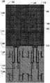
- FIG. 1is the first layer structure of the multilayer board of the 5G antenna integrated network device according to the preferred embodiment of the present invention
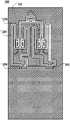
- 2is a second layer structure of the multilayer board of the 5G antenna integrated network device according to the preferred embodiment of the present invention
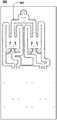
- 3is a third layer structure of the multilayer board of the 5G antenna integrated network device according to the preferred embodiment of the present invention.
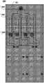
- FIG. 4is a fourth layer structure of the multilayer board of the 5G antenna integrated network device according to the preferred embodiment of the present invention.
- This embodimentprovides a 5G antenna integrated network device, which preferably includes two PCB boards, the PCB boards are copper-plated on both sides, and the PCB boards are sequentially stacked and connected to form a multi-layer board, and the PCB boards pass through
- the prepregis bonded and connected; it can also be a combination of two or more PCB boards to form a multilayer board; each layer of the multilayer board in this embodiment is shown in Figures 1 to 4, specifically including the first layer board Surface 100, second layer surface 200, third layer surface 300 and fourth layer surface 400, said first layer surface 100 and second layer surface 200 respectively correspond to the front and back of the first PCB board, The third-layer board surface 300 and the fourth-layer board surface 400 respectively correspond to the front and back of the second PCB board.
- the inner board surface of the multilayer boardis provided with a calibration network circuit 203, and the outer layer of the multilayer board
- a phase-shifting network circuit 107is provided on the board surface, the first-layer board surface 100 is located on the upper end surface of the multilayer board, and the phase-shifting network circuit 107 is provided on the first-layer board surface 100, the calibration network
- the circuit 203is arranged on the second layer surface 200 opposite to the first layer surface 100;
- the multilayer boardis provided with a plurality of metalized holes penetrating the multilayer board; the metalized holes connect the multilayer board
- the layer conduction connection between the layers, a part of the circuit in the multi-layer boardgoes to the inner layer and the part of the circuit goes to the surface layer to realize the conversion from the strip line to the microstrip line.
- the calibration network and the phase shifting networkare integrated on the same multilayer board, which reduces the number of adapters and avoids electrical problems and structural risk points caused by switching.
- the calibration network line 203 and the phase-shifting network line 107are vertically misaligned between the multilayer boards.
- the upper and lower outer layers of the multilayer boardare respectively provided with upper and lower metal grounds, and the calibration network line 203 and the upper and lower metal grounds form a stripline structure; that is, the upper and lower metal grounds They are respectively arranged on the first layer 100 and the fourth layer 400, and their grounds are connected to other grounds through metallized holes; the inner layer of the multilayer board is provided with a medium metal ground, and it is moved
- the phase network line 107 and the medium metal groundform a microstrip line structure.
- the connection between the strip line and the microstrip lineconstitutes a discontinuity.
- the groundthat is, the copper-clad area of each layer, is reasonably optimized, and then the line impedance at the conduction is adjusted according to the simulation to improve the discontinuity and ensure the standing wave after the module is integrated.
- the electrical indicatorsare good.
- a solder mask area 404is provided on the outer side of the multilayer board, and an oil-coated protective layer is provided on the solder mask area 404. As shown in FIG. 2, a number of metallized holes in each layer of the multilayer board are arranged in close proximity to each other at the same or nearly the same distance along the alignment of the calibration network line 203 to ensure equipotential distribution.
- the multi-layer board(that is, the integrated network formed by the calibration network and the phase shifting network) is provided with at least one calibration port, at least one radio frequency port, balancing resistance and grounding resistance.
- the phase-shifting networkcomposed of the phase-shifting network line 107 and the medium metal ground is provided with a DC grounding lightning protection sub-line 110.
- the copper clad layeris the ground corresponding to the circuit, and the copper foil filling area is determined according to the circuit characteristics of different modules; refer to Figure 1, the large copper clad area is the ground 101 on the side of the calibration network strip line (specifically, the upper metal ground);
- the calibration network 203includes a calibration network calibration port 103, a calibration network radio frequency port 104, a calibration network balance resistance 105; a calibration network ground resistance 106, a first metallized hole 102 on the first layer board; a microstrip phase shift network 107
- the main port of the microstrip line phase-shifting network and the antenna port of the stripline calibration networkare connected at 108; the phase-shifting network sub-port 109 is connected to the feed network of the antenna;
- the first layer of the board surface 100is integrated with a pad 111 and a solder mask
- the protective layer 112 and the phase shift slider 113corresponding to the phase shift network.
- the surrounding copper-clad areaneeds to be adjusted locally; the main port line of the phase-shifting network line 107 Adjustments are also needed, especially the multi-level impedance adjustment of the microstrip line at the conduction 108 to improve the deviation of the Smith chart after the connection.
- the large-area copper-clad area 201 of the second layer board 200is the middle layer ground; the second metalized hole 202 on the second layer board surface; the metal ground 201 and the second metalized hole 202 are the same or nearly the same along the calibration network line 203 Distance arrangement to ensure equipotential distribution.
- the distance between the main port 204 of the phase shift network and the antenna port of the stripline calibration networkmust be adjusted locally to improve the discontinuity.
- the last-stage impedance of the stripline line 205 at the conductionbecomes smaller to adjust the matching characteristics after connection.
- the third metallized holes 301 on the third layer surface 300penetrate through the metallized holes of other layers.
- the large-area copper-clad area of the fourth layer surface 400is the ground 401 on the other side of the calibration network strip line (specifically, the lower metal ground); and the fourth metallization hole 402, the pad 403, and the solder resist area 404.
- the multi-layer boardis not limited to the four-layer board; the number of radio frequency ports is not limited to 4 groups, and this embodiment only uses 4 groups as an illustration; the ground of the microstrip line phase-shifting network is not limited to being located in the middle layer as shown in the figure.
- the line impedancecan be equivalent to the change of the thickness of the dielectric substrate; the coupling calibration network and the phase shifting network are not limited to the wiring method shown in the figure; the phase shifting network is not limited to the full microstrip line form, and can be further used In the form of stripline to microstrip line, it can be equivalent if the transfer point is also matched and optimized.
- the calibration network of the 5G antenna integrated network device of the present inventionadopts a stripline scheme.
- the calibration network lineis located on the inner layer of the multilayer board, and the upper and lower layers are located on the outer layer.
- the lineis a large area of copper-clad area beyond a certain distance.
- Conduction connection through metallized holes; phase shifteradopts microstrip line scheme, the phase shifting network line is located on the outer layer of the multilayer board, and the ground is located on the inner layer or another outer layer.
- the position of the grounddetermines the thickness of the dielectric substrate and determines the shift Phase network line impedance, the ground is shared with the calibration network through a large-area metalized hole; the calibration network and the phase-shifting network are connected from the inner layer to the outer layer through the metalized hole, which causes discontinuity. Adjusting the ground at the connection point and optimizing the line impedance of the two modules at the connection point can improve the electrical indicators after the module is integrated, especially the standing wave. And it can make the antenna port environment tend to be consistent, with high accuracy, better stability and consistency.
Landscapes
- Engineering & Computer Science (AREA)
- Microelectronics & Electronic Packaging (AREA)
- Production Of Multi-Layered Print Wiring Board (AREA)
- Variable-Direction Aerials And Aerial Arrays (AREA)
Abstract
Description
Translated fromChinese本发明涉及通信技术领域,尤其涉及一种5G天线一体化网络装置。The present invention relates to the field of communication technology, in particular to a 5G antenna integrated network device.
随着5G网络快速建设,天线行业产品迭代越来越快。5G(第五代移动通信技术)MIMO(Multiple-Input Multiple-Output,多入多出技术)大规模天线阵的需求日新月异,高集成度高一致性的5G天线市场前景广泛。With the rapid construction of 5G networks, product iterations in the antenna industry are getting faster and faster. 5G (fifth generation mobile communication technology) MIMO (Multiple-Input Multiple-Output, multiple-input multiple-output, multiple-input multiple-output technology) demand for large-scale antenna arrays is changing day by day, and the market for highly integrated and consistent 5G antennas is broad.
现有办法通常使用多个组件进行转接,装配复杂,可靠性和一致性差,电性能实现难度较大,且成本偏高。那么,如何更好地设计5G天线,在密集阵小尺寸下更好地集成各个模块,在易于装配及可靠性良好的基础上,实现并提高电气指标一致性对于5G天线系列化产品具有举足轻重的作用。Existing methods usually use multiple components for switching, and the assembly is complicated, the reliability and consistency are poor, the electrical performance is difficult to realize, and the cost is relatively high. So, how to better design 5G antennas, better integrate various modules under the small size of the phalanx, and realize and improve the consistency of electrical indicators on the basis of easy assembly and good reliability. It is of great importance for the serialization of 5G antennas. effect.
综上可知,现有的方法在实际使用上,存在着较多的问题,所以有必要加以改进。In summary, the existing methods have many problems in actual use, so it is necessary to improve them.
发明内容Summary of the invention
针对上述的缺陷,本发明的目的在于提供一种5G天线一体化网络装置,能够使天线端口环境趋于一致,精度高、稳定性和一致性更好。In view of the above-mentioned defects, the purpose of the present invention is to provide a 5G antenna integrated network device, which can make the antenna port environment tend to be consistent, with high accuracy, better stability and consistency.
为了实现上述目的,本发明提供一种5G天线一体化网络装置,包括有至少两个PCB(线路板)板,所述PCB板双面镀铜且所述PCB板依次叠置连接以形成多层板,所述多层板的内层板面上设有校准网络线路,所述多层板的外层板面上设有移相网络线路,所述多层板上设有若干个贯通所述多层板的金属化孔,所述金属化孔将所述多层板之间的层面导通连接。In order to achieve the above objective, the present invention provides a 5G antenna integrated network device, including at least two PCB (circuit board) boards, the PCB boards are copper-plated on both sides, and the PCB boards are sequentially stacked and connected to form a multilayer The inner layer of the multilayer board is provided with a calibration network circuit, the outer layer of the multilayer board is provided with a phase-shifting network circuit, and the multilayer board is provided with a plurality of penetrating network circuits. The metallized hole of the multi-layer board, the metallized hole connects the layers between the multi-layer boards.
根据所述的5G天线一体化网络装置,所述校准网络线路与所述移相网络线路在所述多层板之间呈垂直错位分布。According to the 5G antenna integrated network device, the calibration network line and the phase-shifting network line are vertically misaligned between the multilayer boards.
根据所述的5G天线一体化网络装置,所述多层板的上外层板面和下外层板面上分别设有上下金属地,且所述校准网络线路与所述上下金属地构成带状线结构。According to the 5G antenna integrated network device, upper and lower metal grounds are respectively provided on the upper and lower outer surface of the multilayer board, and the calibration network line and the upper and lower metal grounds form a belt.状线结构。 Shape line structure.
根据所述的5G天线一体化网络装置,所述多层板的所述内层板面上设有中 金属地,且所述移相网络线路与所述中金属地构成微带线结构。According to the 5G antenna integrated network device, a mid-metal ground is provided on the inner surface of the multilayer board, and the phase-shifting network line and the mid-metal ground form a microstrip line structure.
根据所述的5G天线一体化网络装置,所述PCB板之间通过半固化片粘合连接。According to the 5G antenna integrated network device, the PCB boards are bonded and connected by a prepreg.
根据所述的5G天线一体化网络装置,所述多层板的外侧设有阻焊区,且所述阻焊区上设有覆油保护层。According to the 5G antenna integrated network device, a solder mask is provided on the outer side of the multilayer board, and an oil-coated protective layer is provided on the solder mask.
根据所述的5G天线一体化网络装置,所述多层板的每一层若干个所述金属化孔沿着所述校准网络线路的走线同等或近同等距离紧靠排布。According to the 5G antenna integrated network device, a plurality of the metallized holes on each layer of the multilayer board are arranged in close proximity to each other at the same or nearly the same distance along the alignment of the calibration network line.
根据所述的5G天线一体化网络装置,所述多层板设有至少一校准端口、至少一射频端口、平衡电阻和接地电阻。According to the 5G antenna integrated network device, the multilayer board is provided with at least one calibration port, at least one radio frequency port, balance resistance and ground resistance.
根据所述的5G天线一体化网络装置,所述移相网络线路和所述中金属地组成的移相网络设有直流接地雷电保护子线路。According to the 5G antenna integrated network device, the phase-shifting network composed of the phase-shifting network line and the medium metal ground is provided with a DC grounding lightning protection sub-line.
本发明将校准网络与移相网络集成在同一个多层板上,减少了转接件、避免了转接引起的电气问题及结构风险点。多层板的有效利用实现了带状线到微带线的转换,对地和导通处线路阻抗进行优化解决了不连续性问题,驻波良好。5G大规模天线阵端口众多,本发明能够使天线端口环境趋于一致,精度高、稳定性和一致性更好。The invention integrates the calibration network and the phase shifting network on the same multi-layer board, reduces the adapters, and avoids the electrical problems and structural risk points caused by the switching. The effective use of the multilayer board realizes the conversion from stripline to microstrip line, and optimizes the impedance of the ground and the line at the conduction to solve the discontinuity problem, and the standing wave is good. The 5G large-scale antenna array has many ports, and the present invention can make the antenna port environment tend to be consistent, with high precision, better stability and consistency.
图1为本发明优选实施例所述5G天线一体化网络装置的所述多层板的第一层面结构;FIG. 1 is the first layer structure of the multilayer board of the 5G antenna integrated network device according to the preferred embodiment of the present invention;
图2为本发明优选实施例所述5G天线一体化网络装置的所述多层板的第二层面结构;2 is a second layer structure of the multilayer board of the 5G antenna integrated network device according to the preferred embodiment of the present invention;
图3为本发明优选实施例所述5G天线一体化网络装置的所述多层板的第三层面结构;3 is a third layer structure of the multilayer board of the 5G antenna integrated network device according to the preferred embodiment of the present invention;
图4为本发明优选实施例所述5G天线一体化网络装置的所述多层板的第四层面结构。FIG. 4 is a fourth layer structure of the multilayer board of the 5G antenna integrated network device according to the preferred embodiment of the present invention.
为了使本发明的目的、技术方案及优点更加清楚明白,以下结合附图及实施例,对本发明进行进一步详细说明。应当理解,此处所描述的具体实施例仅 仅用以解释本发明,并不用于限定本发明。In order to make the objectives, technical solutions, and advantages of the present invention clearer, the following further describes the present invention in detail with reference to the accompanying drawings and embodiments. It should be understood that the specific embodiments described here are only used to explain the present invention, but not to limit the present invention.
本实施例提供了一种5G天线一体化网络装置,优选包括有两个PCB板,所述PCB板双面镀铜且PCB板依次叠置连接以形成多层板,所述PCB板之间通过半固化片粘合连接;也可以是2个以上的PCB板组合形成多层板;本实施例的所述多层板的每一层面分别如图1~图4所示,具体包括有第一层板面100、第二层板面200、第三层板面300以及第四层板面400,所述第一层板面100和第二层板面200分别对应为第一PCB板的正反面,第三层板面300和第四层板面400分别对应为第二PCB板的正反面,所述多层板的内层板面上设有校准网络线路203,所述多层板的外层板面上设有移相网络线路107,第一层板面100处于所述多层板的上端面,且所述移相网络线路107设于该第一层板面100上,所述校准网络线路203设于第一层板面100的反面第二层板面200上;所述多层板上设有若干个贯通所述多层板的金属化孔;所述金属化孔将多层板之间的层面导通连接,多层板中一部分线路走内层一部分线路走表层即实现了带状线到微带线的转换。本实施例将校准网络与移相网络集成在同一个多层板上,减少了转接件、避免了转接引起的电气问题及结构风险点。This embodiment provides a 5G antenna integrated network device, which preferably includes two PCB boards, the PCB boards are copper-plated on both sides, and the PCB boards are sequentially stacked and connected to form a multi-layer board, and the PCB boards pass through The prepreg is bonded and connected; it can also be a combination of two or more PCB boards to form a multilayer board; each layer of the multilayer board in this embodiment is shown in Figures 1 to 4, specifically including the first
如图,所述校准网络线路203与移相网络线路107在所述多层板之间呈垂直错位分布。所述多层板的上外层板面和下外层板面上分别设有上下金属地,且校准网络线路203与所述上下金属地构成带状线结构;即,其中所述上下金属地分别设于第一层板面100和第四层板面400上,其地通过金属化孔与其他地共地连接;所述多层板的内层板面上设有中金属地,且移相网络线路107与所述中金属地构成微带线结构。带状线与微带线连接处构成了不连续性,首先对地即各个层覆铜区域合理优化,其次根据仿真调整导通处线路阻抗以改善不连续性,确保模块一体化集成后驻波等电气指标良好。As shown in the figure, the
所述多层板的外侧设有阻焊区404,且所述阻焊区404上设有覆油保护层。如图2,所述多层板的每一层若干个金属化孔沿着所述校准网络线路203的走线同等或近同等距离紧靠排布,确保等电位分布。A
所述多层板(即所述校准网络和移相网络构成的一体化网络)设有至少一校准端口、至少一射频端口、平衡电阻和接地电阻。移相网络线路107和所述中金属地组成的移相网络设有直流接地雷电保护子线路110。覆铜层即为线路所对应的地,根据不同模块线路特性确定铜箔填充区域;参阅图1,大面积覆铜区 域为校准网络带状线一侧地101(具体为上金属地);所述校准网络203包括有校准网络校准端口103、校准网络射频端口104、校准网络平衡电阻105;校准网络接地电阻106,第一层面板上的第一金属化孔102;微带线移相网络107的微带线移相网络主口与带状线校准网络天线口导通处108;移相网络分口109与天线的馈电网络连接;第一层板面100集成有焊盘111、阻焊保护层112以及移相网络对应的移相滑块113。由于带状线结构的校准网络线路203与微带线结构的移相网络线路107导通处108产生了不连续性,其周围覆铜区域需进行局部调整;移相网络线路107的主口线路也需进行调整,尤其是导通处108的微带线多级阻抗调整以改善连接后史密斯圆图的偏离。The multi-layer board (that is, the integrated network formed by the calibration network and the phase shifting network) is provided with at least one calibration port, at least one radio frequency port, balancing resistance and grounding resistance. The phase-shifting network composed of the phase-shifting
第二层板200的大面积覆铜区域201为中间层地;第二层板面的第二金属化孔202;金属地201与第二金属化孔202沿着校准网络线路203同等或近同等距离排布,确保等电位分布。移相网络主口204与带状线校准网络天线口导通处的地,其与线路的距离需进行局部调整以改善不连续性。导通处带状线线路205的最后一级阻抗变小以调节连接后匹配特性。第三层板面300上的第三金属化孔301与其他层的所述金属化孔贯穿。第四层板面400的大面积覆铜区域为校准网络带状线另一侧地401(具体为下金属地);以及第四金属化孔402、焊盘403以及阻焊区404。所述多层板不局限于四层板;射频端口数量不局限于4组,本实施例仅以4组作为示意;微带线移相网络的地不局限于位于图示中间层,也可以位于外层,对应介质基板厚度改变则线路阻抗改变即可等效;耦合校准网络和移相网络不局限于图示走线方式;移相网络不局限于采用全微带线形式、可以进一步采用带状线转微带线形式对转接处同样进行匹配优化即可等效等。The large-area copper-
综上所述,本发明所述的5G天线一体化网络装置的校准网络采用带状线方案,校准网络线路位于多层板内层,上下地位于外层,线路一定距离以外大面积覆铜区域通过金属化孔导通连接;移相器采用微带线方案,移相网络线路位于多层板外层,地位于内层或另一外层,地的位置决定了介质基板厚度即决定了移相网络线路阻抗,地通过大面积金属化孔实现与校准网络共地;其中校准网络与移相网络从内层向外层通过金属化孔导通连接的过程中引起了不连续性,对导通连接处的地进行调整并对连接处两种模块的线路阻抗进行优化,能够使模块集成后电气指标改善,尤其是驻波。并且能够使天线端口环境趋于一致,精度高、稳定性和一致性更好。In summary, the calibration network of the 5G antenna integrated network device of the present invention adopts a stripline scheme. The calibration network line is located on the inner layer of the multilayer board, and the upper and lower layers are located on the outer layer. The line is a large area of copper-clad area beyond a certain distance. Conduction connection through metallized holes; phase shifter adopts microstrip line scheme, the phase shifting network line is located on the outer layer of the multilayer board, and the ground is located on the inner layer or another outer layer. The position of the ground determines the thickness of the dielectric substrate and determines the shift Phase network line impedance, the ground is shared with the calibration network through a large-area metalized hole; the calibration network and the phase-shifting network are connected from the inner layer to the outer layer through the metalized hole, which causes discontinuity. Adjusting the ground at the connection point and optimizing the line impedance of the two modules at the connection point can improve the electrical indicators after the module is integrated, especially the standing wave. And it can make the antenna port environment tend to be consistent, with high accuracy, better stability and consistency.
当然,本发明还可有其它多种实施例,在不背离本发明精神及其实质的情况下,熟悉本领域的技术人员当可根据本发明作出各种相应的改变和变形,但这些相应的改变和变形都应属于本发明所附的权利要求的保护范围。Of course, the present invention can also have various other embodiments. Without departing from the spirit and essence of the present invention, those skilled in the art can make various corresponding changes and modifications according to the present invention, but these corresponding All changes and deformations shall belong to the protection scope of the appended claims of the present invention.
Claims (9)
Translated fromChineseApplications Claiming Priority (2)
| Application Number | Priority Date | Filing Date | Title |
|---|---|---|---|
| CN201910949573.1ACN110691461B (en) | 2019-10-08 | 2019-10-08 | 5G antenna integrated network device |
| CN201910949573.1 | 2019-10-08 |
Publications (1)
| Publication Number | Publication Date |
|---|---|
| WO2021068437A1true WO2021068437A1 (en) | 2021-04-15 |
Family
ID=69111842
Family Applications (1)
| Application Number | Title | Priority Date | Filing Date |
|---|---|---|---|
| PCT/CN2020/071937CeasedWO2021068437A1 (en) | 2019-10-08 | 2020-01-14 | 5g-antenna integrated network apparatus |
Country Status (2)
| Country | Link |
|---|---|
| CN (1) | CN110691461B (en) |
| WO (1) | WO2021068437A1 (en) |
Cited By (1)
| Publication number | Priority date | Publication date | Assignee | Title |
|---|---|---|---|---|
| CN115913410A (en)* | 2022-10-17 | 2023-04-04 | 华南理工大学 | Broadband calibration network for multi-channel antenna array feed network |
Citations (7)
| Publication number | Priority date | Publication date | Assignee | Title |
|---|---|---|---|---|
| US6636180B2 (en)* | 2001-08-10 | 2003-10-21 | Hon Hai Precision Ind. Co., Ltd. | Printed circuit board antenna |
| CN104319448A (en)* | 2014-10-24 | 2015-01-28 | 中国电子科技集团公司第四十一研究所 | Multi-layer power distribution network of high-frequency printed boards based on accessory resistive films |
| CN204144434U (en)* | 2014-11-10 | 2015-02-04 | 广东盛华德通讯科技股份有限公司 | Independent electric regulating intelligent antenna |
| CN107799896A (en)* | 2017-11-24 | 2018-03-13 | 广东博纬通信科技有限公司 | A kind of TD LTE smart antennas for applying to frequency range near 3500MHz |
| US20180212474A1 (en)* | 2017-01-24 | 2018-07-26 | Energous Corporation | Microstrip antennas for wireless power transmitters |
| CN108417961A (en)* | 2018-04-17 | 2018-08-17 | 上海安费诺永亿通讯电子有限公司 | A kind of Massive MIMO arrays antenna |
| CN110167261A (en)* | 2019-06-26 | 2019-08-23 | 京信通信技术(广州)有限公司 | Interconnection structure between millimeter wave active antenna element and pcb board |
Family Cites Families (8)
| Publication number | Priority date | Publication date | Assignee | Title |
|---|---|---|---|---|
| NL1026104C2 (en)* | 2004-05-03 | 2005-11-07 | Thales Nederland Bv | Multi-layer PWB radiant circuit and phase-controlled antenna system in which it is used. |
| CN101702463B (en)* | 2009-10-31 | 2013-07-24 | 华南理工大学 | Dielectric loading quadrifilar helix antenna with power division phase shift feed network |
| KR101855139B1 (en)* | 2016-11-16 | 2018-05-08 | 주식회사 케이엠더블유 | Calibration in MIMO antenna |
| CN107342827B (en)* | 2017-07-27 | 2023-06-23 | 广东通宇通讯股份有限公司 | Antenna array calibration network |
| CN108521017B (en)* | 2018-05-28 | 2024-03-15 | 广东通宇通讯股份有限公司 | Feed network of large-scale MIMO antenna |
| CN108768549B (en)* | 2018-08-10 | 2023-09-19 | 昆山恩电开通信设备有限公司 | Multi-antenna calibration network device applied to 5G communication |
| CN110224231B (en)* | 2019-07-05 | 2024-06-14 | 中天宽带技术有限公司 | Calibration network device and Massive MIMO array antenna |
| CN211019430U (en)* | 2019-10-08 | 2020-07-14 | 摩比科技(深圳)有限公司 | 5G antenna integrated network device |
- 2019
- 2019-10-08CNCN201910949573.1Apatent/CN110691461B/enactiveActive
- 2020
- 2020-01-14WOPCT/CN2020/071937patent/WO2021068437A1/ennot_activeCeased
Patent Citations (7)
| Publication number | Priority date | Publication date | Assignee | Title |
|---|---|---|---|---|
| US6636180B2 (en)* | 2001-08-10 | 2003-10-21 | Hon Hai Precision Ind. Co., Ltd. | Printed circuit board antenna |
| CN104319448A (en)* | 2014-10-24 | 2015-01-28 | 中国电子科技集团公司第四十一研究所 | Multi-layer power distribution network of high-frequency printed boards based on accessory resistive films |
| CN204144434U (en)* | 2014-11-10 | 2015-02-04 | 广东盛华德通讯科技股份有限公司 | Independent electric regulating intelligent antenna |
| US20180212474A1 (en)* | 2017-01-24 | 2018-07-26 | Energous Corporation | Microstrip antennas for wireless power transmitters |
| CN107799896A (en)* | 2017-11-24 | 2018-03-13 | 广东博纬通信科技有限公司 | A kind of TD LTE smart antennas for applying to frequency range near 3500MHz |
| CN108417961A (en)* | 2018-04-17 | 2018-08-17 | 上海安费诺永亿通讯电子有限公司 | A kind of Massive MIMO arrays antenna |
| CN110167261A (en)* | 2019-06-26 | 2019-08-23 | 京信通信技术(广州)有限公司 | Interconnection structure between millimeter wave active antenna element and pcb board |
Cited By (1)
| Publication number | Priority date | Publication date | Assignee | Title |
|---|---|---|---|---|
| CN115913410A (en)* | 2022-10-17 | 2023-04-04 | 华南理工大学 | Broadband calibration network for multi-channel antenna array feed network |
Also Published As
| Publication number | Publication date |
|---|---|
| CN110691461A (en) | 2020-01-14 |
| CN110691461B (en) | 2024-12-17 |
Similar Documents
| Publication | Publication Date | Title |
|---|---|---|
| CN108768549B (en) | Multi-antenna calibration network device applied to 5G communication | |
| US5032803A (en) | Directional stripline structure and manufacture | |
| US8362856B2 (en) | RF transition with 3-dimensional molded RF structure | |
| CN106936521A (en) | Compact aerial feeds calibration network | |
| EP3707970A1 (en) | Additive manufacturing technology (amt) faraday boundaries in radio frequency circuits | |
| US11791527B2 (en) | Printed circuit boards and methods for manufacturing thereof for RF connectivity between electro-optic phase modulator and digital signal processor | |
| US20110241794A1 (en) | Printed circuit board impedance matching step for thick substrate broadband microwave (millimeter wave) devices | |
| CN115224462B (en) | Microwave multilayer board interlayer interconnection matching method | |
| CN104319448B (en) | A kind of multilayer power distribution network of high frequency printed board based on attached resistive film | |
| US6765469B2 (en) | Printed circuit board transformer | |
| WO2021068437A1 (en) | 5g-antenna integrated network apparatus | |
| CN209949547U (en) | PCB (printed circuit board) jumper structure of antenna system | |
| CN114024150B (en) | Active antenna array based on stripline one-to-six power division network | |
| CN105072800B (en) | A kind of pcb board different aspects realize the pcb board structure of microwave coaxial transmission | |
| CN211019430U (en) | 5G antenna integrated network device | |
| CN114665280B (en) | A 3D Transceiver and Feed Network Applied to Flat Package Array Antenna | |
| CN217114817U (en) | A feeder network system | |
| CN104916895A (en) | Radio frequency and band-shaped wire interface assembly method | |
| CN111856407B (en) | X-band dual-polarized high-isolation microwave TR assembly of star-loaded active phased array radar | |
| CN112909466B (en) | A switching board, switching network and antenna | |
| CN114744417A (en) | Feed network system | |
| CN114422045B (en) | Design method of phased array channel amplitude and phase correction network and storage medium | |
| CN111542168A (en) | Radio frequency interface circuit | |
| CN116885444B (en) | Chip phased array antenna structure | |
| Sorocki et al. | Study on low resistance permanent joints for assembly of PCB-integrated additively fabricated air-filled waveguide |
Legal Events
| Date | Code | Title | Description |
|---|---|---|---|
| 121 | Ep: the epo has been informed by wipo that ep was designated in this application | Ref document number:20875317 Country of ref document:EP Kind code of ref document:A1 | |
| NENP | Non-entry into the national phase | Ref country code:DE | |
| 122 | Ep: pct application non-entry in european phase | Ref document number:20875317 Country of ref document:EP Kind code of ref document:A1 |