WO2021059079A1 - Semiconductor device, storage device, and electronic apparatus - Google Patents
Semiconductor device, storage device, and electronic apparatusDownload PDFInfo
- Publication number
- WO2021059079A1 WO2021059079A1PCT/IB2020/058537IB2020058537WWO2021059079A1WO 2021059079 A1WO2021059079 A1WO 2021059079A1IB 2020058537 WIB2020058537 WIB 2020058537WWO 2021059079 A1WO2021059079 A1WO 2021059079A1
- Authority
- WO
- WIPO (PCT)
- Prior art keywords
- material layer
- insulator
- conductor
- region
- semiconductor device
- Prior art date
- Legal status (The legal status is an assumption and is not a legal conclusion. Google has not performed a legal analysis and makes no representation as to the accuracy of the status listed.)
- Ceased
Links
Images


Classifications
- H—ELECTRICITY
- H10—SEMICONDUCTOR DEVICES; ELECTRIC SOLID-STATE DEVICES NOT OTHERWISE PROVIDED FOR
- H10B—ELECTRONIC MEMORY DEVICES
- H10B43/00—EEPROM devices comprising charge-trapping gate insulators
- H10B43/20—EEPROM devices comprising charge-trapping gate insulators characterised by three-dimensional arrangements, e.g. with cells on different height levels
- H10B43/23—EEPROM devices comprising charge-trapping gate insulators characterised by three-dimensional arrangements, e.g. with cells on different height levels with source and drain on different levels, e.g. with sloping channels
- H10B43/27—EEPROM devices comprising charge-trapping gate insulators characterised by three-dimensional arrangements, e.g. with cells on different height levels with source and drain on different levels, e.g. with sloping channels the channels comprising vertical portions, e.g. U-shaped channels
- H—ELECTRICITY
- H10—SEMICONDUCTOR DEVICES; ELECTRIC SOLID-STATE DEVICES NOT OTHERWISE PROVIDED FOR
- H10D—INORGANIC ELECTRIC SEMICONDUCTOR DEVICES
- H10D30/00—Field-effect transistors [FET]
- H10D30/60—Insulated-gate field-effect transistors [IGFET]
- H10D30/69—IGFETs having charge trapping gate insulators, e.g. MNOS transistors
- H10D30/693—Vertical IGFETs having charge trapping gate insulators
- G—PHYSICS
- G11—INFORMATION STORAGE
- G11C—STATIC STORES
- G11C16/00—Erasable programmable read-only memories
- G11C16/02—Erasable programmable read-only memories electrically programmable
- G11C16/04—Erasable programmable read-only memories electrically programmable using variable threshold transistors, e.g. FAMOS
- G11C16/0483—Erasable programmable read-only memories electrically programmable using variable threshold transistors, e.g. FAMOS comprising cells having several storage transistors connected in series
- G—PHYSICS
- G11—INFORMATION STORAGE
- G11C—STATIC STORES
- G11C16/00—Erasable programmable read-only memories
- G11C16/02—Erasable programmable read-only memories electrically programmable
- G11C16/06—Auxiliary circuits, e.g. for writing into memory
- G11C16/08—Address circuits; Decoders; Word-line control circuits
- G—PHYSICS
- G11—INFORMATION STORAGE
- G11C—STATIC STORES
- G11C16/00—Erasable programmable read-only memories
- G11C16/02—Erasable programmable read-only memories electrically programmable
- G11C16/06—Auxiliary circuits, e.g. for writing into memory
- G11C16/10—Programming or data input circuits
- G—PHYSICS
- G11—INFORMATION STORAGE
- G11C—STATIC STORES
- G11C16/00—Erasable programmable read-only memories
- G11C16/02—Erasable programmable read-only memories electrically programmable
- G11C16/06—Auxiliary circuits, e.g. for writing into memory
- G11C16/10—Programming or data input circuits
- G11C16/14—Circuits for erasing electrically, e.g. erase voltage switching circuits
- G11C16/16—Circuits for erasing electrically, e.g. erase voltage switching circuits for erasing blocks, e.g. arrays, words, groups
- G—PHYSICS
- G11—INFORMATION STORAGE
- G11C—STATIC STORES
- G11C16/00—Erasable programmable read-only memories
- G11C16/02—Erasable programmable read-only memories electrically programmable
- G11C16/06—Auxiliary circuits, e.g. for writing into memory
- G11C16/24—Bit-line control circuits
- G—PHYSICS
- G11—INFORMATION STORAGE
- G11C—STATIC STORES
- G11C16/00—Erasable programmable read-only memories
- G11C16/02—Erasable programmable read-only memories electrically programmable
- G11C16/06—Auxiliary circuits, e.g. for writing into memory
- G11C16/26—Sensing or reading circuits; Data output circuits
- G—PHYSICS
- G11—INFORMATION STORAGE
- G11C—STATIC STORES
- G11C16/00—Erasable programmable read-only memories
- G11C16/02—Erasable programmable read-only memories electrically programmable
- G11C16/06—Auxiliary circuits, e.g. for writing into memory
- G11C16/32—Timing circuits
- H—ELECTRICITY
- H10—SEMICONDUCTOR DEVICES; ELECTRIC SOLID-STATE DEVICES NOT OTHERWISE PROVIDED FOR
- H10B—ELECTRONIC MEMORY DEVICES
- H10B41/00—Electrically erasable-and-programmable ROM [EEPROM] devices comprising floating gates
- H10B41/10—Electrically erasable-and-programmable ROM [EEPROM] devices comprising floating gates characterised by the top-view layout
- H—ELECTRICITY
- H10—SEMICONDUCTOR DEVICES; ELECTRIC SOLID-STATE DEVICES NOT OTHERWISE PROVIDED FOR
- H10B—ELECTRONIC MEMORY DEVICES
- H10B41/00—Electrically erasable-and-programmable ROM [EEPROM] devices comprising floating gates
- H10B41/20—Electrically erasable-and-programmable ROM [EEPROM] devices comprising floating gates characterised by three-dimensional arrangements, e.g. with cells on different height levels
- H10B41/23—Electrically erasable-and-programmable ROM [EEPROM] devices comprising floating gates characterised by three-dimensional arrangements, e.g. with cells on different height levels with source and drain on different levels, e.g. with sloping channels
- H10B41/27—Electrically erasable-and-programmable ROM [EEPROM] devices comprising floating gates characterised by three-dimensional arrangements, e.g. with cells on different height levels with source and drain on different levels, e.g. with sloping channels the channels comprising vertical portions, e.g. U-shaped channels
- H—ELECTRICITY
- H10—SEMICONDUCTOR DEVICES; ELECTRIC SOLID-STATE DEVICES NOT OTHERWISE PROVIDED FOR
- H10B—ELECTRONIC MEMORY DEVICES
- H10B41/00—Electrically erasable-and-programmable ROM [EEPROM] devices comprising floating gates
- H10B41/30—Electrically erasable-and-programmable ROM [EEPROM] devices comprising floating gates characterised by the memory core region
- H10B41/35—Electrically erasable-and-programmable ROM [EEPROM] devices comprising floating gates characterised by the memory core region with a cell select transistor, e.g. NAND
- H—ELECTRICITY
- H10—SEMICONDUCTOR DEVICES; ELECTRIC SOLID-STATE DEVICES NOT OTHERWISE PROVIDED FOR
- H10B—ELECTRONIC MEMORY DEVICES
- H10B41/00—Electrically erasable-and-programmable ROM [EEPROM] devices comprising floating gates
- H10B41/40—Electrically erasable-and-programmable ROM [EEPROM] devices comprising floating gates characterised by the peripheral circuit region
- H—ELECTRICITY
- H10—SEMICONDUCTOR DEVICES; ELECTRIC SOLID-STATE DEVICES NOT OTHERWISE PROVIDED FOR
- H10B—ELECTRONIC MEMORY DEVICES
- H10B43/00—EEPROM devices comprising charge-trapping gate insulators
- H10B43/10—EEPROM devices comprising charge-trapping gate insulators characterised by the top-view layout
- H—ELECTRICITY
- H10—SEMICONDUCTOR DEVICES; ELECTRIC SOLID-STATE DEVICES NOT OTHERWISE PROVIDED FOR
- H10B—ELECTRONIC MEMORY DEVICES
- H10B43/00—EEPROM devices comprising charge-trapping gate insulators
- H10B43/30—EEPROM devices comprising charge-trapping gate insulators characterised by the memory core region
- H10B43/35—EEPROM devices comprising charge-trapping gate insulators characterised by the memory core region with cell select transistors, e.g. NAND
- H—ELECTRICITY
- H10—SEMICONDUCTOR DEVICES; ELECTRIC SOLID-STATE DEVICES NOT OTHERWISE PROVIDED FOR
- H10B—ELECTRONIC MEMORY DEVICES
- H10B43/00—EEPROM devices comprising charge-trapping gate insulators
- H10B43/40—EEPROM devices comprising charge-trapping gate insulators characterised by the peripheral circuit region
- H—ELECTRICITY
- H10—SEMICONDUCTOR DEVICES; ELECTRIC SOLID-STATE DEVICES NOT OTHERWISE PROVIDED FOR
- H10D—INORGANIC ELECTRIC SEMICONDUCTOR DEVICES
- H10D30/00—Field-effect transistors [FET]
- H10D30/60—Insulated-gate field-effect transistors [IGFET]
- H10D30/68—Floating-gate IGFETs
- H10D30/689—Vertical floating-gate IGFETs
- H—ELECTRICITY
- H10—SEMICONDUCTOR DEVICES; ELECTRIC SOLID-STATE DEVICES NOT OTHERWISE PROVIDED FOR
- H10D—INORGANIC ELECTRIC SEMICONDUCTOR DEVICES
- H10D64/00—Electrodes of devices having potential barriers
- H10D64/01—Manufacture or treatment
- H10D64/031—Manufacture or treatment of data-storage electrodes
- H10D64/035—Manufacture or treatment of data-storage electrodes comprising conductor-insulator-conductor-insulator-semiconductor structures
- H—ELECTRICITY
- H10—SEMICONDUCTOR DEVICES; ELECTRIC SOLID-STATE DEVICES NOT OTHERWISE PROVIDED FOR
- H10D—INORGANIC ELECTRIC SEMICONDUCTOR DEVICES
- H10D64/00—Electrodes of devices having potential barriers
- H10D64/01—Manufacture or treatment
- H10D64/031—Manufacture or treatment of data-storage electrodes
- H10D64/037—Manufacture or treatment of data-storage electrodes comprising charge-trapping insulators
- H—ELECTRICITY
- H10—SEMICONDUCTOR DEVICES; ELECTRIC SOLID-STATE DEVICES NOT OTHERWISE PROVIDED FOR
- H10B—ELECTRONIC MEMORY DEVICES
- H10B41/00—Electrically erasable-and-programmable ROM [EEPROM] devices comprising floating gates
- H10B41/40—Electrically erasable-and-programmable ROM [EEPROM] devices comprising floating gates characterised by the peripheral circuit region
- H10B41/41—Electrically erasable-and-programmable ROM [EEPROM] devices comprising floating gates characterised by the peripheral circuit region of a memory region comprising a cell select transistor, e.g. NAND
- H—ELECTRICITY
- H10—SEMICONDUCTOR DEVICES; ELECTRIC SOLID-STATE DEVICES NOT OTHERWISE PROVIDED FOR
- H10D—INORGANIC ELECTRIC SEMICONDUCTOR DEVICES
- H10D30/00—Field-effect transistors [FET]
- H10D30/60—Insulated-gate field-effect transistors [IGFET]
- H10D30/67—Thin-film transistors [TFT]
- H10D30/674—Thin-film transistors [TFT] characterised by the active materials
- H10D30/6755—Oxide semiconductors, e.g. zinc oxide, copper aluminium oxide or cadmium stannate
Definitions
- one aspect of the present inventionis not limited to the above technical fields.
- the technical field of the invention disclosed in the present specification and the likerelates to a product, an operation method, or a manufacturing method.
- one aspect of the inventionrelates to a process, machine, manufacture, or composition (composition of matter). Therefore, more specifically, the technical fields of one aspect of the present invention disclosed in the present specification include semiconductor devices, display devices, liquid crystal display devices, light emitting devices, power storage devices, image pickup devices, storage devices, signal processing devices, and processors. , Electronic devices, systems, their driving methods, their manufacturing methods, or their inspection methods.
- CPUscentral processing units
- GPUsgraphics processing units
- storage devicesand sensors
- sensorshave been used in various electronic devices such as personal computers, smartphones, and digital cameras. Improvements are progressing in various aspects such as conversion and low power consumption.
- One aspect of the present inventionis to provide a highly reliable semiconductor device. Alternatively, one aspect of the present invention is to provide a semiconductor device having a large data capacity. Alternatively, one aspect of the present invention is to provide a novel semiconductor device. Alternatively, one aspect of the present invention is to apply a storage device having a novel semiconductor device. Alternatively, one aspect of the present invention is to provide an electronic device having the storage device.
- One aspect of the present inventionincludes a columnar first conductor, a second conductor, a third conductor, a first insulator, a second insulator, a third insulator, and a fourth insulator.
- a semiconductor devicehaving a fifth insulator, a sixth insulator, a first material layer, a second material layer, and a third material layer.
- the first material layerhas a first region and a second region.
- the first insulatoris located adjacent to the first conductor, and the first material layer is located adjacent to the first insulator.
- the second material layeris located adjacent to the first region of the first material layer, the second conductor is located adjacent to the second material layer, and the second insulator is the second conductor.
- the third insulatoris located adjacent to the second insulator.
- the third material layeris located so as to cover the second material layer, the second conductor, the second insulator, the third insulator, and the second region of the first material layer, and is positioned so as to cover the fourth insulation.
- the bodyis located adjacent to the third material layer, the sixth insulator is located adjacent to the fourth insulator, and the fifth insulator is located adjacent to the sixth insulator.
- the third conductoris located in a region adjacent to the fifth insulator and superposed on the first region of the first material layer.
- the second insulatorfunctions as a barrier insulating film that prevents oxygen from diffusing into the second conductor
- the fourth insulatorfunctions as a tunnel insulating film
- the sixth insulatorfunctions as a charge storage layer.
- the fifth insulatorfunctions as a gate insulating film.
- the first material layerhas an oxide containing indium, element M (M is aluminum, gallium, tin, or titanium) and zinc
- the second material layerhas an oxide containing indium, element M and zinc
- the third material layerhas an oxide containing indium, element M, and zinc.
- One aspect of the present inventionincludes a columnar first conductor, a second conductor, a third conductor, a fourth conductor, a first insulator, a second insulator, and a third insulator.
- a semiconductor devicehaving a fourth insulator, a fifth insulator, a first material layer, a second material layer, and a third material layer.
- the first material layerhas a first region and a second region. The first insulator is located adjacent to the first conductor, the first material layer is located adjacent to the first insulator, and the second material layer is the first region of the first material layer.
- the second conductoris located adjacent to the second material layer, the second insulator is located adjacent to the second conductor, and the third insulator is located adjacent to the second conductor. It is located adjacent to the second insulator.
- the third material layeris located so as to cover the second material layer, the second conductor, the second insulator, the third insulator, and the second region of the first material layer, and is positioned so as to cover the fourth insulation.
- the bodyis located adjacent to the third material layer, the fourth conductor is located in a region adjacent to the fourth insulator and superimposed on the first region of the first material layer, and the fifth insulator.
- the first material layermay have a fourth material layer and a fifth material layer.
- the fourth material layeris located adjacent to the first insulator
- the fifth material layeris located adjacent to the fourth material layer
- the first region of the first material layeris the fifth.
- the second region of the first material layeris located in the material layer and is located in the fifth material layer.
- the ratio of the number of atoms of the element M to indium contained in the second material layeris preferably larger than the ratio of the number of atoms of the element M to indium contained in the fifth material layer.
- the ratio of the number of atoms of the element M to indium contained in the fourth material layeris preferably larger than the ratio of the number of atoms of the element M to indium contained in the fifth material layer.
- the film thickness of the second region of the first material layermay be thinner than the film thickness of the first region of the first material layer.
- one aspect of the present inventionis a storage device including the semiconductor device according to any one of (1) to (5) above and peripheral circuits.
- one aspect of the present inventionis an electronic device having a storage device according to any one of (1) to (6) above and a housing.
- the semiconductor deviceis a device that utilizes semiconductor characteristics, and refers to a circuit including a semiconductor element (transistor, diode, photodiode, etc.), a device having the same circuit, and the like. It also refers to all devices that can function by utilizing semiconductor characteristics.
- a semiconductor elementtransistor, diode, photodiode, etc.
- the storage device, the display device, the light emitting device, the lighting device, the electronic device, and the likemay be a semiconductor device itself, and may have a semiconductor device.
- a circuit that enables functional connection between X and Yfor example, a logic circuit (inverter, NAND circuit, NOR circuit, etc.), signal conversion, etc.) Circuits (digital-to-analog conversion circuit, analog-to-digital conversion circuit, gamma correction circuit, etc.), potential level conversion circuit (power supply circuit (boost circuit, step-down circuit, etc.), level shifter circuit that changes the signal potential level, etc.), voltage source, current source , Switching circuit, amplification circuit (circuit that can increase signal amplitude or current amount, operational amplifier, differential amplification circuit, source follower circuit, buffer circuit, etc.), signal generation circuit, storage circuit, control circuit, etc.) It is possible to connect one or more to and from. As an example, even if another circuit is sandwiched between X and Y, if the signal output from X is transmitted to Y, it is assumed that X and Y are functionally connected. To do.
- X and Yare electrically connected, it means that X and Y are electrically connected (that is, another element between X and Y). Or when they are connected with another circuit in between) and when X and Y are directly connected (that is, they are connected without sandwiching another element or another circuit between X and Y). If there is) and.
- X and Y, the source (or the first terminal, etc.) and the drain (or the second terminal, etc.) of the transistorare electrically connected to each other, and the X, the source (or the second terminal, etc.) of the transistor are connected to each other. (1 terminal, etc.), the drain of the transistor (or the 2nd terminal, etc.), and Y are electrically connected in this order.
- the source of the transistor (or the first terminal, etc.)is electrically connected to X
- the drain of the transistor (or the second terminal, etc.)is electrically connected to Y
- the X, the source of the transistor(such as the second terminal).
- the first terminal, etc.), the drain of the transistor (or the second terminal, etc.), and Yare electrically connected in this order.
- Xis electrically connected to Y via the source (or first terminal, etc.) and drain (or second terminal, etc.) of the transistor, and X, the source (or first terminal, etc.) of the transistor. (Terminals, etc.), transistor drains (or second terminals, etc.), and Y are provided in this connection order.
- the source (or first terminal, etc.) and drain (or second terminal, etc.) of the transistorcan be separated. Separately, the technical scope can be determined. Note that these expression methods are examples, and are not limited to these expression methods.
- X and Yare assumed to be objects (for example, devices, elements, circuits, wirings, electrodes, terminals, conductive films, layers, etc.).
- circuit diagramshows that independent components are electrically connected to each other, one component has the functions of a plurality of components.
- one componenthas the functions of a plurality of components.
- the term "electrically connected” as used hereinincludes the case where one conductive film has the functions of a plurality of components in combination.
- the “resistance element”can be, for example, a circuit element having a resistance value higher than 0 ⁇ , wiring, or the like. Therefore, in the present specification and the like, the “resistive element” includes wiring having a resistance value, a transistor in which a current flows between a source and a drain, a diode, a coil, and the like. Therefore, the term “resistor element” can be paraphrased into terms such as “resistance”, “load”, and “region having a resistance value”, and conversely, “resistance”, “load”, and “region having a resistance value”. Can be rephrased as a term such as “resistive element”.
- the resistance valuecan be, for example, preferably 1 m ⁇ or more and 10 ⁇ or less, more preferably 5 m ⁇ or more and 5 ⁇ or less, and further preferably 10 m ⁇ or more and 1 ⁇ or less. Further, for example, it may be 1 ⁇ or more and 1 ⁇ 10 9 ⁇ or less.
- the “capacitance element”means, for example, a circuit element having a capacitance value higher than 0F, a wiring region having a capacitance value, a parasitic capacitance, a transistor gate capacitance, and the like. Can be. Therefore, in the present specification and the like, the “capacitive element” includes a circuit element including a pair of electrodes and a dielectric contained between the electrodes. In addition, terms such as “capacitive element”, “parasitic capacitance”, and “gate capacitance” may be paraphrased into terms such as "capacity”.
- the term “capacity”can be rephrased as terms such as “capacitive element”, “parasitic capacitance”, and “gate capacitance”.
- the term “pair of electrodes” in “capacity”may be paraphrased as “pair of conductors", “pair of conductive regions", “pair of regions” and the like.
- the value of the capacitancecan be, for example, 0.05 fF or more and 10 pF or less. Further, for example, it may be 1 pF or more and 10 ⁇ F or less.
- the transistorhas three terminals called a gate, a source, and a drain.
- the gateis a control terminal that controls the conduction state of the transistor.
- the two terminals that function as sources or drainsare the input and output terminals of the transistor.
- One of the two input / output terminalsbecomes a source and the other becomes a drain depending on the high and low potentials given to the conductive type (n-channel type, p-channel type) of the transistor and the three terminals of the transistor. Therefore, in the present specification and the like, the terms of source and drain may be paraphrased.
- the transistorwhen explaining the connection relationship of transistors, "one of the source or drain” (or the first electrode or the first terminal), “the other of the source or drain” (or the second electrode, or The notation (second terminal) is used.
- itmay have a back gate in addition to the above-mentioned three terminals.
- one of the gate or the back gate of the transistormay be referred to as a first gate
- the other of the gate or the back gate of the transistormay be referred to as a second gate.
- the terms “gate” and “backgate”may be interchangeable.
- the respective gatesWhen the transistor has three or more gates, the respective gates may be referred to as a first gate, a second gate, a third gate, and the like in the present specification and the like.
- a nodecan be paraphrased as a terminal, a wiring, an electrode, a conductive layer, a conductor, an impurity region, etc., depending on a circuit configuration, a device structure, and the like.
- terminals, wiring, etc.can be paraphrased as nodes.
- ground potentialground potential
- the potentialsare relative, and when the reference potential changes, the potential given to the wiring, the potential applied to the circuit or the like, the potential output from the circuit or the like also changes.
- the terms “high level potential” and “low level potential”do not mean a specific potential.
- both of the two wires“function as a wire that supplies a high level potential”
- the high level potentials provided by both wiresdo not have to be equal to each other.
- both of the two wiresare described as “functioning as a wire that supplies a low level potential”
- the low level potentials given by both wiresdo not have to be equal to each other. ..
- the "current”is a charge transfer phenomenon (electrical conduction).
- the description “electrical conduction of a positively charged body is occurring”means “electrical conduction of a negatively charged body in the opposite direction”. Is happening. " Therefore, in the present specification and the like, “current” refers to a charge transfer phenomenon (electrical conduction) accompanying the movement of carriers, unless otherwise specified.
- the carrierhere include electrons, holes, anions, cations, complex ions, and the like, and the carriers differ depending on the system in which the current flows (for example, semiconductor, metal, electrolytic solution, vacuum, etc.).
- the "current direction” in the wiring or the likeis the direction in which the positive carrier moves, and is described as a positive current amount.
- the direction in which the negative carrier movesis opposite to the direction of the current, and is expressed by the amount of negative current. Therefore, in the present specification and the like, if there is no notice about the positive or negative of the current (or the direction of the current), the description such as “current flows from element A to element B” means “current flows from element B to element A” or the like. It can be paraphrased as. Further, the description such as “a current is input to the element A” can be rephrased as "a current is output from the element A” or the like.
- the ordinal numbers “first”, “second”, and “third”are added to avoid confusion of the components. Therefore, the number of components is not limited. Moreover, the order of the components is not limited. For example, the component referred to in “first” in one of the embodiments of the present specification and the like may be a component referred to in “second” in another embodiment or in the claims. There can also be. Further, for example, the component mentioned in “first” in one of the embodiments of the present specification and the like may be omitted in another embodiment or in the claims.
- the terms “above” and “below”do not limit the positional relationship of the components directly above or below and in direct contact with each other.
- the expression “electrode B on the insulating layer A”it is not necessary that the electrode B is formed in direct contact with the insulating layer A, and another configuration is formed between the insulating layer A and the electrode B. Do not exclude those that contain elements.
- membrane and layercan be interchanged with each other depending on the situation.
- Electrodemay be used as part of a “wiring” and vice versa.
- the terms “electrode” and “wiring”include the case where a plurality of “electrodes” and “wiring” are integrally formed.
- a “terminal”may be used as part of a “wiring” or “electrode” and vice versa.
- the term “terminal”includes a case where a plurality of "electrodes", “wiring”, “terminals” and the like are integrally formed.
- the "electrode”can be a part of the “wiring” or the “terminal”, and for example, the “terminal” can be a part of the “wiring” or the “electrode”.
- terms such as “electrode”, “wiring”, and “terminal”may be replaced with terms such as "area” in some cases.
- terms such as “wiring”, “signal line”, and “power line”can be interchanged with each other in some cases or depending on the situation.
- the reverseis also true, and it may be possible to change terms such as “signal line” and “power line” to the term “wiring”.
- a term such as “power line”may be changed to a term such as "signal line”.
- terms such as “signal line”may be changed to terms such as "power line”.
- the term “potential” applied to the wiringmay be changed to a term such as “signal” in some cases or depending on the situation.
- the reverseis also true, and terms such as “signal” may be changed to the term “potential”.
- semiconductor impuritiesrefer to, for example, other than the main components constituting the semiconductor layer.
- an element having a concentration of less than 0.1 atomic%is an impurity.
- the inclusion of impuritiesmay cause, for example, the semiconductor to have a high defect level density, a decrease in carrier mobility, a decrease in crystallinity, and the like.
- the impurities that change the characteristics of the semiconductorinclude, for example, group 1 element, group 2 element, group 13 element, group 14 element, group 15 element, and other than the main component.
- transition metals and the likeand in particular, hydrogen (also contained in water), lithium, sodium, silicon, boron, phosphorus, carbon, nitrogen and the like.
- the impurities that change the characteristics of the semiconductorinclude, for example, Group 1 elements other than oxygen and hydrogen, Group 2 elements, Group 13 elements, Group 15 elements, and the like. There is.
- the switchmeans a switch that is in a conductive state (on state) or a non-conducting state (off state) and has a function of controlling whether or not a current flows.
- the switchmeans a switch having a function of selecting and switching a path through which a current flows.
- an electric switch, a mechanical switch, or the likecan be used. That is, the switch is not limited to a specific switch as long as it can control the current.
- Examples of electrical switchesinclude transistors (for example, bipolar transistors, MOS transistors, etc.), diodes (for example, PN diodes, PIN diodes, Schottky diodes, MIM (Metal Insulator Metal) diodes, and MIS (Metal Insulator Semiconductor) diodes. , Diode-connected transistors, etc.), or logic circuits that combine these.
- transistorsfor example, bipolar transistors, MOS transistors, etc.
- diodesfor example, PN diodes, PIN diodes, Schottky diodes, MIM (Metal Insulator Metal) diodes, and MIS (Metal Insulator Semiconductor) diodes. , Diode-connected transistors, etc.
- the "conducting state" of the transistormeans a state in which the source electrode and the drain electrode of the transistor can be regarded as being electrically short-circuited.
- the "non-conducting state" of the transistormeans a state in which the source electrode and the drain electrode of the transistor can be regarded as being electrically cut off.
- the polarity (conductive type) of the transistoris not particularly limited.
- An example of a mechanical switchis a switch that uses MEMS (Micro Electro Mechanical System) technology.
- the switchhas an electrode that can be moved mechanically, and by moving the electrode, it operates by controlling conduction and non-conduction.
- parallelmeans a state in which two straight lines are arranged at an angle of -10 ° or more and 10 ° or less. Therefore, the case of ⁇ 5 ° or more and 5 ° or less is also included.
- substantially parallel or approximately parallelmeans a state in which two straight lines are arranged at an angle of ⁇ 30 ° or more and 30 ° or less.
- verticalmeans a state in which two straight lines are arranged at an angle of 80 ° or more and 100 ° or less. Therefore, the case of 85 ° or more and 95 ° or less is also included.
- substantially verticalor “approximately vertical” means a state in which two straight lines are arranged at an angle of 60 ° or more and 120 ° or less.
- a highly reliable semiconductor devicecan be provided.
- a semiconductor device having a large data capacitycan be provided.
- a novel semiconductor devicecan be provided by one aspect of the present invention.
- a storage device having a novel semiconductor devicecan be applied.
- an electronic device having the storage devicecan be provided.
- the effect of one aspect of the present inventionis not limited to the effects listed above.
- the effects listed abovedo not preclude the existence of other effects.
- the other effectsare the effects not mentioned in this item, which are described below. Effects not mentioned in this item can be derived from those described in the description, drawings, etc. by those skilled in the art, and can be appropriately extracted from these descriptions.
- one aspect of the present inventionhas at least one of the above-listed effects and other effects. Therefore, one aspect of the present invention may not have the effects listed above in some cases.
- FIG. 1is a cross-sectional view for explaining a configuration example of a semiconductor device.
- 2A and 2Bare top views for explaining a configuration example of the semiconductor device.
- 3A to 3Care cross-sectional views for explaining a configuration example of the semiconductor device.
- 4A and 4Bare top views for explaining a configuration example of the semiconductor device.
- 5A and 5Bare cross-sectional views for explaining a manufacturing example of the semiconductor device.
- 6A and 6Bare cross-sectional views for explaining a manufacturing example of a semiconductor device.
- 7A and 7Bare cross-sectional views for explaining a manufacturing example of the semiconductor device.
- 8A and 8Bare cross-sectional views for explaining a manufacturing example of the semiconductor device.
- FIG. 9A and 9Bare cross-sectional views for explaining a manufacturing example of the semiconductor device.
- FIG. 10Ais a cross-sectional view for explaining a manufacturing example of the semiconductor device
- FIG. 10Bis a perspective view for explaining a manufacturing example of the semiconductor device.
- 11A and 11Bare cross-sectional views for explaining a manufacturing example of a semiconductor device.
- 12A and 12Bare cross-sectional views for explaining a manufacturing example of the semiconductor device.
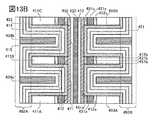
- 13A and 13Bare cross-sectional views for explaining a manufacturing example of a semiconductor device.
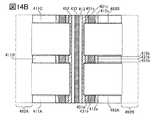
- FIG. 14Ais a cross-sectional view for explaining a configuration example of the semiconductor device
- FIG. 14Bis a cross-sectional view for explaining a manufacturing example of the semiconductor device.
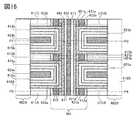
- FIG. 15A and 15Bare top views for explaining a configuration example of the semiconductor device.
- FIG. 16is a cross-sectional view for explaining a configuration example of the semiconductor device.
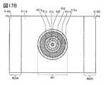
- 17A and 17Bare top views for explaining a configuration example of the semiconductor device.
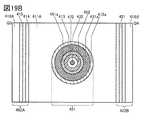
- FIG. 18is a cross-sectional view for explaining a configuration example of the semiconductor device.
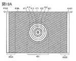
- 19A and 19Bare top views for explaining a configuration example of the semiconductor device.
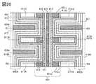
- FIG. 20is a cross-sectional view for explaining a configuration example of the semiconductor device.
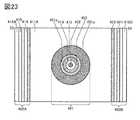
- FIG. 21is a top view for explaining a configuration example of the semiconductor device.
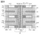
- FIG. 22is a cross-sectional view for explaining a configuration example of the semiconductor device.
- FIG. 23is a top view for explaining a configuration example of the semiconductor device.
- FIG. 24is a cross-sectional view for explaining a configuration example of the semiconductor device.
- FIG. 25is a top view for explaining a configuration example of the semiconductor device.
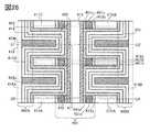
- FIG. 26is a cross-sectional view for explaining a configuration example of the semiconductor device.
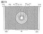
- 27A and 27Bare top views for explaining a configuration example of the semiconductor device.
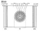
- FIG. 28is a cross-sectional view for explaining a configuration example of the semiconductor device.
- 29A and 29Bare top views for explaining a configuration example of the semiconductor device.
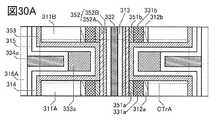
- 30A to 30Care cross-sectional views for explaining a configuration example of the semiconductor device.
- 31A and 31Bare top views for explaining a configuration example of the semiconductor device.
- 32A and 32Bare cross-sectional views for explaining a manufacturing example of the semiconductor device.
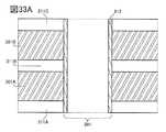
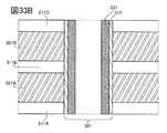
- 33A and 33Bare cross-sectional views for explaining a manufacturing example of a semiconductor device.
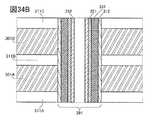
- 34A and 34Bare cross-sectional views for explaining a manufacturing example of the semiconductor device.
- 35A and 35Bare cross-sectional views for explaining a manufacturing example of a semiconductor device.
- 36A and 36Bare cross-sectional views for explaining a manufacturing example of a semiconductor device.
- FIG. 37Ais a cross-sectional view for explaining a manufacturing example of the semiconductor device
- FIG. 37Bis a perspective view for explaining a manufacturing example of the semiconductor device.
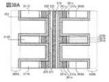
- 38A and 38Bare cross-sectional views for explaining a manufacturing example of the semiconductor device.
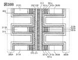
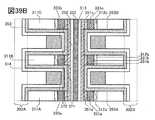
- 39A and 39Bare cross-sectional views for explaining a manufacturing example of a semiconductor device.
- FIG. 40A and 40Bare cross-sectional views for explaining a manufacturing example of a semiconductor device.
- FIG. 41is a cross-sectional view for explaining a manufacturing example of the semiconductor device.
- FIG. 42Ais a cross-sectional view for explaining a configuration example of the semiconductor device, and
- FIG. 42Bis a cross-sectional view for explaining a manufacturing example of the semiconductor device.
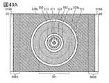
- 43A and 43Bare top views for explaining a configuration example of the semiconductor device.
- FIG. 44is a cross-sectional view for explaining a configuration example of the semiconductor device.
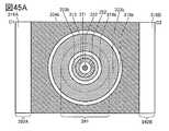
- 45A and 45Bare top views for explaining a configuration example of the semiconductor device.
- FIG. 46is a cross-sectional view for explaining a configuration example of the semiconductor device.
- FIG. 47A and 47Bare top views for explaining a configuration example of the semiconductor device.
- FIG. 48is a cross-sectional view for explaining a configuration example of the semiconductor device.
- FIG. 49is a top view for explaining a configuration example of the semiconductor device.
- FIG. 50is a cross-sectional view for explaining a configuration example of the semiconductor device.
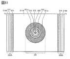
- FIG. 51is a top view for explaining a configuration example of the semiconductor device.
- FIG. 52is a cross-sectional view for explaining a configuration example of the semiconductor device.
- FIG. 53is a top view for explaining a configuration example of the semiconductor device.
- FIG. 54is a cross-sectional view for explaining a configuration example of the semiconductor device.
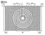
- 55A and 55Bare top views for explaining a configuration example of the semiconductor device.
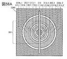
- FIG. 56A and 56Bare top views for explaining a configuration example of the semiconductor device.
- 57A and 57Bare top views for explaining a configuration example of the semiconductor device.
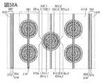
- 58A and 58Bare top views for explaining a configuration example of the semiconductor device.
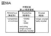
- FIG. 59Ais a diagram for explaining the classification of the crystal structure of IGZO
- FIG. 59Bis a diagram for explaining the XRD spectrum of crystalline IGZO
- FIG. 59Cis a diagram for explaining the microelectron diffraction pattern of crystalline IGZO.
- .. 60A and 60Bare circuit diagrams showing a configuration example of a semiconductor device.
- FIG. 61is a circuit diagram showing a configuration example of a semiconductor device.
- FIG. 61is a circuit diagram showing a configuration example of a semiconductor device.
- FIG. 62is a circuit diagram showing a configuration example of a semiconductor device.
- 63A and 63Bare timing charts showing operation examples of the semiconductor device.
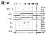
- 64A and 64Bare timing charts showing operation examples of the semiconductor device.
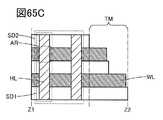
- FIG. 65Ais a perspective view for explaining a configuration example of a semiconductor device
- FIG. 65Bis a top view for explaining a configuration example of the semiconductor device
- FIG. 65Cis a cross section for explaining a configuration example of the semiconductor device. It is a figure.
- FIG. 66Ais a perspective view for explaining a configuration example of a semiconductor device
- FIG. 66Bis a top view for explaining a configuration example of the semiconductor device
- FIG. 66Cis a cross section for explaining a configuration example of the semiconductor device. It is a figure.
- FIG. 67A and 67Bare cross-sectional views for explaining a configuration example of the semiconductor device.
- 68A and 68Bare cross-sectional views for explaining a configuration example of the semiconductor device.
- FIG. 69is a cross-sectional view for explaining a configuration example of the semiconductor device.
- FIG. 70is a cross-sectional view for explaining a configuration example of the semiconductor device.
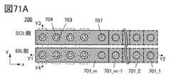
- 71Ais a top view for explaining a configuration example of a semiconductor device
- FIGS. 71B to 71Dare cross-sectional views for explaining a configuration example of the semiconductor device.
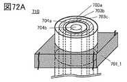
- 72A to 72Care perspective views for explaining a configuration example of the semiconductor device.
- FIG. 73is a top view for explaining a configuration example of the semiconductor device.
- FIG. 74is a block diagram for explaining an example of the storage device.
- 75Ais a perspective view showing an example of a semiconductor wafer
- FIG. 75Bis a perspective view showing an example of a chip
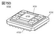
- FIGS. 75C and 75Dare perspective views showing an example of an electronic component.
- FIG. 76is a block diagram illustrating a CPU.
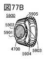
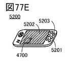
- 77A to 77Jare perspective views or schematic views illustrating an example of the product.
- 78A to 78Eare perspective views or camphor tree views illustrating an example of the product.
- a metal oxideis a metal oxide in a broad sense. Metal oxides are classified into oxide insulators, oxide conductors (including transparent oxide conductors), oxide semiconductors (also referred to as Oxide Semiconductor or simply OS) and the like. For example, when a metal oxide is used in the active layer of a transistor, the metal oxide may be referred to as an oxide semiconductor. That is, when a metal oxide can form a channel forming region of a transistor having at least one of an amplification action, a rectifying action, and a switching action, the metal oxide is referred to as a metal oxide semiconductor. be able to. Further, when describing as an OS transistor, it can be paraphrased as a transistor having a metal oxide or an oxide semiconductor.
- a metal oxide having nitrogenmay also be collectively referred to as a metal oxide. Further, a metal oxide having nitrogen may be referred to as a metal oxynitride.
- the configuration shown in each embodimentcan be appropriately combined with the configuration shown in other embodiments to form one aspect of the present invention. Further, when a plurality of configuration examples are shown in one embodiment, the configuration examples can be appropriately combined with each other.
- the content (may be a part of the content) described in one embodimentis the other content (may be a part of the content) described in the embodiment and one or more other implementations. It is possible to apply, combine, or replace at least one content with the content described in the form of (may be a part of the content).
- figure (which may be a part) described in one embodimentis different from another part of the figure, another figure (which may be a part) described in the embodiment, and one or more other figures.
- the figure (which may be a part) described in the embodimentis different from another part of the figure, another figure (which may be a part) described in the embodiment, and one or more other figures.
- more figurescan be formed.
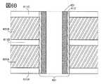
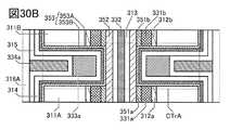
- FIG. 1is a cross-sectional view of the semiconductor device.
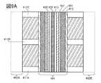
- 2Ais a top view of the portion of the alternate long and short dash line M1-M2 shown in FIG. 1
- FIG. 2Bis a top view of the portion of the alternate long and short dash line M3-M4 shown in FIG.
- some elementsare omitted for the sake of clarity.
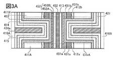
- the semiconductor deviceincludes an insulator 411A arranged above a substrate (not shown), an insulator 411B arranged above the insulator 411A, and an insulator arranged above the insulator 411B. It has 411C and.
- an insulator substrate, a semiconductor substrate, or a conductor substratemay be used.
- the insulator substrateinclude a glass substrate, a quartz substrate, a sapphire substrate, a stabilized zirconia substrate (yttria-stabilized zirconia substrate, etc.), a resin substrate, and the like.
- the semiconductor substratefor example, a semiconductor substrate made of silicon, a semiconductor substrate made of germanium, silicon carbide, silicon germanium, gallium arsenide, indium phosphide, zinc oxide, gallium oxide, or the like was used as a material. There are compound semiconductor substrates and the like.
- the conductor substrateincludes a graphite substrate, a metal substrate, an alloy substrate, and a conductive resin substrate.
- a substrate having a metal nitridea substrate having a metal oxide, and the like.
- a substrate in which a conductor or a semiconductor is provided in an insulator substratea substrate in which a conductor or an insulator is provided in a semiconductor substrate, a substrate in which a semiconductor or an insulator is provided in a conductor substrate, and the like.
- those on which an element is providedmay be used.
- Elements provided on the substrateinclude a capacitance element, a resistance element, a switch element, a light emitting element, a storage element, and the like.
- a flexible substratemay be used as the substrate.
- a method of providing the transistor on the flexible substratethere is also a method of forming the transistor on the non-flexible substrate, peeling off the transistor, and transposing it to the substrate which is a flexible substrate. In that case, it is advisable to provide a release layer between the non-flexible substrate and the transistor.
- the substratea sheet, film, foil, or the like in which fibers are woven may be used.
- the substratemay have elasticity. Further, the substrate may have a property of returning to the original shape when bending or pulling is stopped. Alternatively, it may have a property of not returning to the original shape.
- the substratehas, for example, a region having a thickness of 5 ⁇ m or more and 700 ⁇ m or less, preferably 10 ⁇ m or more and 500 ⁇ m or less, and more preferably 15 ⁇ m or more and 300 ⁇ m or less.
- the weight of the semiconductor device having a transistorcan be reduced.
- the substrate thinnerit may have elasticity even when glass or the like is used, or it may have a property of returning to the original shape when bending or pulling is stopped. Therefore, it is possible to alleviate the impact applied to the semiconductor device on the substrate due to dropping or the like. That is, it is possible to provide a durable semiconductor device.
- the substrate which is a flexible substratefor example, metal, alloy, resin or glass, fibers thereof, or the like can be used.
- a material having a linear expansion coefficient of 1 ⁇ 10 -3 / K or less, 5 ⁇ 10 -5 / K or less, or 1 ⁇ 10 -5 / K or lessmay be used.
- the resininclude polyester, polyolefin, polyamide (nylon, aramid, etc.), polyimide, polycarbonate, acrylic, and the like.
- aramidis suitable as a substrate which is a flexible substrate because of its low coefficient of linear expansion.
- the semiconductor devicehas a region 491.
- the region 491is a region in which an opening is formed in the middle of the manufacturing process of the semiconductor device, and an insulator, a conductor, a semiconductor, or the like is formed in the opening after the manufacturing process of the semiconductor device. It is formed.
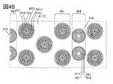
- the openingmay be a cylindrical opening as shown in FIGS. 2A and 2B.
- the region 491includes an insulator 412a (insulator 412b, insulator 412c), a conductor 431a (conductor 431b, conductor 431c), and a material layer in order from the side surface of the opening. 451a (material layer 451b, material layer 451c), material layer 452, insulator 413, and conductor 432 are arranged.
- the semiconductor devicehas a region 492A and a region 492B.
- the region 492A and the region 492Bare regions in which an opening is formed in the middle of the manufacturing process of the semiconductor device, and the opening is an insulator and a conductor through the manufacturing process of the semiconductor device. Etc. are formed.
- the openingmay be a slit-shaped opening as shown in FIGS. 2A and 2B.
- Region 492Aincludes a part of the material layer 453, a part of the insulator 414, a part of the insulator 421, a part of the insulator 415, a part of the conductor 434a, and one of the conductors 434b.
- a portion and an insulator 416Aare included.
- a part of the material layer 453, a part of the insulator 414, a part of the insulator 421, a part of the insulator 415, a part of the conductor 434a, and a conductor 434b And the insulator 416Bare included. Further, in FIG. 1, between the insulator 411A and the insulator 411B, a part of the conductor 434a, a part of the insulator 414, a part of the insulator 421, and a part of the insulator 415 are provided. , Are arranged.
- a part of the conductor 434b, a part of the insulator 414, a part of the insulator 421, and a part of the insulator 415are formed. Have been placed.
- the material layer 452has a region 471 and a region 472.
- the region 471is located adjacent to the material layer 453, and the region 472 is located adjacent to the material layer 451a (material layer 451b, material layer 451c).
- the region 471becomes a channel forming region of the cell transistor CTrA (cell transistor CTrB) by the manufacturing process of the semiconductor device, and the region 472 becomes a low resistance region in the manufacturing process of the semiconductor device.
- the conductor 434bfunctions as a first gate electrode and a word line that gives an electric potential to the first gate electrode, and the insulator 415 surrounded by the conductor 434b in FIG. 2A serves as a gate insulating film.
- the insulator 421 surrounded by the conductor 434bfunctions as a charge storage layer, and the insulator 414 surrounded by the conductor 434b functions as a tunnel insulating film.
- the conductor 431bfunctions as one of the source electrode and the drain electrode, and the conductor 431c functions as the other of the source electrode and the drain electrode.
- the region of the material layer 453 in contact with the material layer 452may also function as a channel forming region.
- the insulator 413functions as a gate insulating film, and the conductor 432 functions as a wiring for applying a potential to the second gate electrode and the second gate electrode.
- FIG. 2Aby replacing the conductor 434b with the conductor 434a, it can be regarded as a top view of the cell transistor CTrA.
- the conductor 434afunctions as a first gate electrode and a word line that gives an electric potential to the first gate electrode
- the insulator 415 surrounded by the conductor 434ais the first gate. It functions as an insulating film
- the insulator 421 surrounded by the conductor 434a in FIG. 2Afunctions as a charge storage layer
- the insulator 414 surrounded by the conductor 434a in FIG. 2Afunctions as a tunnel insulating film.
- the conductor 431afunctions as one of the source electrode and the drain electrode
- the conductor 431bfunctions as the other of the source electrode and the drain electrode.
- the region of the material layer 452 surrounded by the conductor 434a in FIG. 2Afunctions as a channel forming region.
- the region of the material layer 453 in contact with the material layer 452may also function as a channel forming region.
- the insulator 413functions as a second gate insulating film
- the conductor 432functions as a wiring for applying a potential to the second gate electrode and the second gate electrode.
- Insulator 412aas an example, impurities from the insulator 411A (e.g., water molecules, hydrogen atoms, hydrogen molecules, oxygen atoms, oxygen molecules, nitrogen atom, a nitrogen molecule, nitric oxide molecule (N 2 O, NO, NO 2 Etc.) have a function as a barrier insulating film that suppresses diffusion of the impurities into the conductor 431a. That is, the insulator 412a can suppress the influence of the impurities on the conductor 431a. Similarly, the insulator.
- impurities from the insulator 411Ae.g., water molecules, hydrogen atoms, hydrogen molecules, oxygen atoms, oxygen molecules, nitrogen atom, a nitrogen molecule, nitric oxide molecule (N 2 O, NO, NO 2 Etc.
- the 412bhas a function as a barrier insulating film that suppresses the diffusion of impurities from the insulator 411B to the conductor 431b as an example
- the insulator 412chas a function as an example in which impurities from the insulator 411C are a conductor. It has a function as a barrier insulating film that suppresses diffusion to 431c.
- the barrier insulating filmrefers to an insulating film having a barrier property.
- the barrier propertyis a function of suppressing the diffusion of the corresponding substance (also referred to as low permeability).
- the corresponding substancehas a function of capturing and fixing (also called gettering).
- the material layer 451amaterial layer 451b, material layer 451c
- the material layer 452material layer 453 included in the cell transistor CTrA and the cell transistor CTrB will be described.
- Material layer 451ais, for example, impurities in the material layer 452 (e.g., water molecules, hydrogen atoms, hydrogen molecules, oxygen atoms, oxygen molecules, nitrogen atom, a nitrogen molecule, nitric oxide molecule (N 2 O, NO, NO 2
- the material layer 452 and the conductor 431aare provided with a material layer 451a having a function of suppressing the permeation of impurities between the material layer 452 and the conductor 431a.
- the material layer 451bhas a function as a barrier film that suppresses the diffusion of impurities from the material layer 452 into the conductor 431b, as an example.
- the material layer 451chas a function as a barrier film that suppresses the diffusion of impurities from the material layer 452 into the conductor 431c.
- the cell transistor CTrA and the cell transistor CTrB of FIG. 1are OS transistors, it is preferable to apply, for example, a metal oxide that functions as an oxide semiconductor as the material layer 452, and the material layer 451a (material layer).
- a metal oxide that functions as an oxide semiconductoras the material layer 452
- the material layer 451amaterial layer
- the 451b and the material layer 451cfor example, it is preferable to use a material containing a metal element and oxygen contained in the metal oxide.
- the material layer 453is preferably a material containing the metal element and oxygen contained in the metal oxide, similarly to the material layer 451.
- the region 471 that functions as a channel forming region in the material layer 452is oxygen-deficient (this) more than the region 472 that functions as a low resistance region.
- the specification and the like, since there is.) is lowis small, or impurity concentration, may be called the oxygen deficiency in the metal oxide and V O (oxygen vacancy), the carrier concentration becomes lower high-resistance region. Therefore, it can be said that the region 471 is i-type (intrinsic) or substantially i-type.
- Transistors using metal oxidesare likely to fluctuate in electrical characteristics and may be unreliable if impurities or oxygen deficiencies (VO ) are present in the region where channels are formed in the metal oxide.
- the oxygen-deficient (V O) in the vicinity of hydrogen, oxygen vacancy (V O) containing hydrogen defects (hereinafter sometimes referred to as V O H.)Is formed, to generate electrons serving as carriers In some cases. Therefore, if oxygen deficiency is contained in the region where the channel is formed in the oxide semiconductor, the transistor has normal-on characteristics (the channel exists even if no voltage is applied to the gate electrode, and the current is applied to the transistor. Flowing characteristics). Therefore, in the region where a channel of the oxide semiconductor is formed, impurities, oxygen deficiency, and V O H it is preferred to be reduced as much as possible.
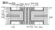
- the material layer 452may be a plurality of layers having a material layer 452A and a material layer 452B as shown in FIG. 3A. preferable. Note that FIG. 3A is an enlarged view of a region in which the cell transistor CTrA of FIG. 1 is formed.
- the material layer 451a(material layer 451b, material layer 451c), material layer 452A, material layer 452B, and the material layer 453 formed in a later step include, for example, indium and element M (element M is, for example, aluminum).
- element Mis, for example, aluminum
- metal oxides having indium, gallium, and zinchave a high bandgap and function as a semiconductor that is intrinsic (also referred to as type I) or substantially intrinsic.
- the cell transistor CTrA and the cell transistor CTrB in which the metal oxide is contained in the channel forming regionhave a characteristic that the off-current is very low. That is, since the leakage current in the cell transistor CTrA and the cell transistor CTrB that are in the off state can be reduced, the power consumption of the semiconductor device may be reduced.
- a metal oxide having an element Mmay be used as the material layer 451a (material layer 451b, material layer 451c).
- the material layer 451a (material layer 451b, material layer 451c)preferably has a higher concentration of element M than the material layer 452B.
- gallium oxidemay be used as the material layer 451a (material layer 451b, material layer 451c).
- a metal oxidesuch as In (indium) -M-Zn (zinc) oxide may be used as the material layer 451a (material layer 451b, material layer 451c).
- the atomic number ratio of the element M to Inis the atom of the element M to In in the metal oxide used for the material layer 452B. It is preferably larger than the number ratio.
- the film thickness of the material layer 451a (material layer 451b, material layer 451c)is preferably 0.5 nm or more and 5 nm or less, more preferably 1 nm or more and 3 nm or less, and further preferably 1 nm or more and 2 nm or less. Further, the material layer 451a (material layer 451b, material layer 451c) is preferably crystalline.
- the release of oxygen in the material layer 452A and the material layer 452Bcan be suitably suppressed.
- the material layer 451amaterial layer 451b, material layer 451c
- the material layer 451ahas a crystal structure such as a hexagonal crystal
- the release of oxygen in the material layer 452A and the material layer 452Bmay be suppressed.
- each of the material layer 452A and the material layer 452Bis an oxide having a different chemical composition.
- the atomic number ratio of the element M to the main component metal element in the metal oxide used for the material layer 452Bis the atomic number ratio of the element M to the main component metal element in the metal oxide used for the material layer 452A. It is preferably larger than the atomic number ratio.
- the atomic number ratio of the element M to In in the metal oxide used for the material layer 452Bis preferably larger than the atomic number ratio of the element M to In in the metal oxide used for the material layer 452A.
- the same composition as that of the material layer 451amay be used as the material layer 452B.
- the atomic number ratio of the element M to the metal element as the main componentis higher than the atomic number ratio of the element M to the metal element as the main component in the metal oxide used for the material layer 452A. It may be large. Further, the atomic number ratio of the element M to In in the metal oxide used for the material layer 453 may be larger than the atomic number ratio of the element M to In in the metal oxide used for the material layer 452A. Further, as the material layer 453, the same composition as that of the material layer 452A may be used.
- the material layer 453may be a plurality of layers having a material layer 453A and a material layer 453B as shown in FIG. 3B. Note that FIG. 3B is an enlarged view of the region where the cell transistor CTrA of FIG. 1 is formed.
- each of the material layer 453A and the material layer 453Bis an oxide having a different chemical composition.
- the atomic number ratio of the element M to the main component metal element in the metal oxide used for the material layer 453Bis the atomic number ratio of the element M to the main component metal element in the metal oxide used for the material layer 453A. It is preferably larger than the atomic number ratio.
- the same composition as that of the material layer 451amay be used as that of the material layer 451a (material layer 451b, material layer 451c) may be used.
- the material layer 452when the material layer 452 has the material layer 452A and the material layer 452B as shown in FIG. 3A, that is, as shown in the cell transistor CTrA shown in FIG. 3C, the material layer 452 is the material layer.
- the atomic number ratio of the element M to the metal element which is the main component in the metal oxide used for the material layer 452Bis , It is preferable that it is larger than the atomic number ratio of the element M to the metal element as the main component in each of the metal oxides used for the material layer 452A and the material layer 453A.
- the atomic number ratio of the element M to the main component metal element in the metal oxide used for the material layer 453Bis the ratio of the number of atoms of the element M to the main component metal element in each of the material layer 452A and the material layer 453A. It is preferably larger than the atomic number ratio of the element M.
- the atomic number ratio of the element M to the metal element as the main component in the metal oxide used for the material layer 451ais the respective metal oxides used for the material layer 452A and the material layer 453A. It is preferable that it is larger than the atomic number ratio of the element M to the metal element which is the main component.
- compositions of the material layer 451a(material layer 451b, material layer 451c), the material layer 452B, and the material layer 453B may be equal to each other. Further, as the material layer 453A, the same composition as that of the material layer 452A may be used.
- the metal oxides contained in the material layer 452A, the material layer 452B, and the material layer 453are referred to as In and gallium (hereinafter referred to as Ga).
- the atomic number ratio of In to the element M in the metal oxide used for the material layer 452Bis smaller than the atomic number ratio of In to the element M in the metal oxide used for the material layer 452A
- In-Ga-Zn oxide having a composition of 3 or its vicinitycan be used.
- a metal oxide having a composition in the vicinity of any onecan be used.
- indium oxidecan be used for the material layer 452A.
- material layers 451amaterial layer 451b, material layer 451c
- material layer 452Amaterial layer 452B
- material layer 453material layer 453A, material layer 453B
- Is preferably In: Ga: Zn4: 2: z, and is a metal oxide having a composition in which z is 3 or more and 4.1 or less and a composition in the vicinity thereof.
- the above compositionindicates the atomic number ratio in the oxide formed on the substrate or the atomic number ratio in the sputtering target.
- the composition of the material layer 452Aby increasing the ratio of In, the on-current of the transistor, the mobility of the field effect, and the like can be increased, which is preferable.
- the material layer 452Aso as to be in contact with the material layer 452B, impurities and oxygen are diffused from the insulator 413 and / or the conductor 432 to the material layer 452A via the material layer 452B. Can be suppressed.
- the material layer 453Bso as to be in contact with the material layer 452B, the insulator 414, the insulator 421, the insulator 415, the conductor 434a (conductor 434b), and the insulator 416A are arranged via the material layer 453B. Therefore, it is possible to suppress the diffusion of impurities and oxygen into the material layer 453A and the material layer 452A.
- the conductor 431a(material layer 451b, material layer 451c) is interposed through the material layer 451a (material layer 451b, material layer 451c).
- the material layer 452may be, for example, amorphous silicon (hereinafter referred to as Si transistor). It may be referred to as hydride amorphous silicon), microcrystalline silicon, polycrystalline silicon, single crystal silicon, or the like.
- the material layer 452may be a plurality of layers or a single layer as shown in FIGS. 3A and 3C. In the production examples such as the present specification, the material layer 452 will be described as a single layer.
- the material layer 453may be a plurality of layers or a single layer.
- the material layer 451is, for example, an impurity (element) for diffusing into the interface of the material layer 452 on the formation surface of the material layer 451 and a region near the interface. , Or ions).
- the conductoris selected from, for example, aluminum, chromium, copper, silver, gold, platinum, tantalum, nickel, titanium, molybdenum, tungsten, hafnium, vanadium, niobium, manganese, magnesium, zirconium, beryllium, indium, ruthenium and the like.
- a material containing at least one of the above-mentioned metal elementscan be used.
- an n-type impurity(donor) is used as the impurity.
- the n-type impurityfor example, phosphorus, arsenic and the like can be used.
- p-type impuritiesacceptors
- the p-type impurityfor example, boron, aluminum, gallium and the like can be used.
- the material layer 451may be a material capable of forming silicide at the interface of the material layer 452 on the forming surface of the material layer 451 and in a region near the interface.
- a material capable of forming silicidefor example, nickel, cobalt, molybdenum, tungsten, titanium or the like may be used.
- FIGS. 1, 2A, and 2Bshow a configuration in which one region 491 is provided between the region 492A and the region 492B
- one aspect of the present inventionis not limited to this. ..
- one aspect of the present inventionmay be a configuration in which a plurality of regions 491 are provided between the regions 492A and the regions 492B.
- the position of the region 494may be provided along a row in two or more different directions instead of being provided along a row in one direction as in the region 492 in FIG. 4A.
- the position of the region 494may be formed without depending on the regularity as described above.
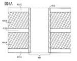
- the laminate 400 shown in FIG. 5Ahas, for example, an insulator 411A, a sacrificial layer 401A, an insulator 411B, a sacrificial layer 401B, and an insulator 411C.
- the insulator 411Ais placed above the substrate (not shown), the sacrificial layer 401A is placed on the insulator 411A, the insulator 411B is placed on the sacrificial layer 401A, and the sacrificial layer 401B is placed on the insulator 411B.
- the insulator 411Cis arranged on the sacrificial layer 401B.
- the insulator 411A to 411Cit is preferable that the insulator is a material in which the concentration of impurities such as water or hydrogen is reduced.
- the amount of hydrogen desorbed from the insulator 411A to the insulator 411Cwas converted into hydrogen molecules in the range of 50 ° C. or higher and 500 ° C. or lower in the temperature desorption gas analysis method (TDS (Thermal Destruction Spectroscopy)).
- the amount of desorptionis 2 ⁇ 10 15 molecules / cm 2 or less, preferably 1 ⁇ 10 15 molecules / cm 2 or less, more preferably 5 in terms of the area of any one of the insulators 411A to 411C. ⁇ 10 14 molecules / cm 2 or less may be used.
- the insulator 411A to the insulator 411Cmay be formed by using an insulator in which oxygen is released by heating.
- the materials applicable to the insulators 411A to 411Care not limited to those described above.
- Examples of the insulator 411A to the insulator 411Cinclude boron, carbon, nitrogen, oxygen, fluorine, magnesium, aluminum, silicon, phosphorus, chlorine, argon, gallium, germanium, yttrium, zirconium, lantern, neodymium, hafnium, and tantalum. Insulators containing one or more materials selected from the above may be used in single layers or in layers. Further, for example, a material containing silicon oxide or silicon nitride nitride may be used. However, the materials applicable to the insulators 411A to 411C are not limited to those described above.
- silicon oxiderefers to a material having a higher oxygen content than nitrogen as its composition
- silicon nitride as its compositionmeans a material having a higher nitrogen content than oxygen as its composition. Is shown.
- aluminum nitriderefers to a material whose composition has a higher oxygen content than nitrogen
- aluminum nitriderefers to a material whose composition has a higher nitrogen content than oxygen. Is shown.
- an openingis formed in the region 491 with respect to the laminate 400 shown in FIG. 5A by, for example, resist mask formation and etching treatment.
- the resist maskcan be formed by appropriately using, for example, a lithography method, a printing method, an inkjet method, or the like.
- the photomaskis not used, so that the manufacturing cost may be reduced.
- the etching processmay be a dry etching method or a wet etching method, or both may be used.
- an insulator 412is formed on the side surface of the opening of the region 491 so as to cover the insulators 411A to 411C, the sacrificial layer 401A, and the sacrificial layer 401B.
- the insulator 412functions as a film for forming the insulator 412a, the insulator 412b, and the insulator 412c in FIG. 1 in a later step. Therefore, in the present specification and the like, the description of the insulator 412 may be described by appropriately replacing the insulator 412a, the insulator 412b, and the insulator 412c.
- the insulator 412contains impurities (for example, water molecule, hydrogen atom, hydrogen molecule, oxygen atom, oxygen molecule, nitrogen atom, nitrogen molecule, nitrogen oxide) from the insulator 411A (insulator 411B, insulator 411C). It is preferable that the insulator functions as a barrier insulating film that suppresses the diffusion of molecules (N 2 O, NO, NO 2, etc.) into the material layer 452. In particular, the insulator 412 prevents the permeation of oxygen atoms or oxygen molecules. It is preferable to use a barrier insulating film.
- the insulator 412for example, aluminum oxide, hafnium oxide, gallium oxide, indium gallium zinc oxide, silicon nitride, silicon nitride or the like can be used.
- an oxide semiconductor described lateris used as the material layer 452
- impurities such as water and hydrogenpass through the conductor 431a (conductor 431b, conductor 431c) and the material layer 451a (material layer 451b, material layer 451c), and the insulator 411A (insulator 411B).
- the insulator 412is shown as a single layer, but one aspect of the present invention is not limited to this.
- the insulator 412 shown in FIGS. 1, 2B, and 6Amay have, for example, a configuration in which a plurality of the above-mentioned materials are laminated.
- silicon oxideis used for the insulator 412 in contact with the conductor 431a (conductor 431b, conductor 431c), and the insulation in contact with the insulator 411A (insulator 411B, insulator 411C) is used.
- Aluminum oxide, hafnium oxide, or the likemay be used for the body 412.
- the conductor 431is formed on the forming surface of the insulator 412.
- the conductor 431functions as a film for forming the conductor 431a, the conductor 431b, and the conductor 431c in FIG. 1 in a later step. Therefore, in the present specification and the like, the description of the conductor 431 can be described by appropriately replacing the conductors 431a, the conductors 431b, and the conductors 431c.
- the conductor 431functions as a film for forming the conductors 431a, the conductors 431b, and the conductors 431c, the conductors 431 will be subjected to the cell transistor CTrA in FIG. 1 by a later step. , The source electrode and drain electrode of the cell transistor CTrB, respectively.
- the conductor 431is preferably a material having high conductivity.
- the conductor 431include, for example, a nitride containing tantalum, a nitride containing titanium, a nitride containing molybdenum, a nitride containing tungsten, a nitride containing tantalum and aluminum, a nitride containing titanium and aluminum, and the like. Is preferably used.
- tantalum-containing nitridesare particularly preferred.
- ruthenium oxide, ruthenium nitride, an oxide containing strontium and ruthenium, an oxide containing lanthanum and nickel, and the likemay be used. These materials are preferable because they are conductive materials that are difficult to oxidize or materials that maintain conductivity even when oxygen is absorbed.
- the material layer 452when an oxide semiconductor described later is used as the material layer 452, it is preferable to use a conductive material having a function of suppressing the permeation of impurities such as water or hydrogen as the conductor 431.
- a conductive material having a function of suppressing the permeation of impurities such as water or hydrogenit is preferable to use tantalum, tantalum nitride, titanium, titanium nitride, ruthenium, ruthenium oxide, or the like as the conductor 431.
- the conductor 431is shown as a single layer, but one aspect of the present invention is not limited to this.
- the conductor 431 shown in FIGS. 1, 2B, and 6may have, for example, a configuration in which a plurality of the above-mentioned materials are laminated.
- the conductor 431uses a conductive material having a function of suppressing the permeation of impurities such as water or hydrogen in the first layer, and a conductive material that is difficult to oxidize in the second layer, or A material that maintains conductivity even if it absorbs oxygen may be used.
- the material layer 451is formed on the forming surface of the conductor 431.
- the material layer 451functions as a film for forming the material layer 451a, the material layer 451b, and the material layer 451c in FIG. 1 in a later step. Therefore, in the present specification and the like, the description of the material layer 451 can be described by appropriately replacing the material layer 451a, the material layer 451b, and the material layer 451c.
- a low resistance regionmay be formed in the vicinity of the interface of the material layer 451 with the conductor 431. Further, at this time, by applying the heat treatment, a compound may be formed by the component contained in the material layer 451 and the component contained in the conductor 431. In this production example, it is assumed that an appropriate material is selected for each of the conductor 431 and the material layer 451 so that the compound has a low resistance.
- the description of the material layer 451a (material layer 451b, material layer 451c) of the configuration example 1 of the semiconductor deviceis taken into consideration.
- the material layer 452is formed on the forming surface of the material layer 451.
- a part of the material layer 452functions as a channel forming region of the cell transistor CTrA and the cell transistor CTrB of FIG.
- the insulator 413is formed on the forming surface of the material layer 452.
- the insulator 413functions as the second gate insulating film of each of the cell transistor CTrA and the cell transistor CTrB in FIG.
- the insulator 413for example, silicon oxide or silicon oxide nitride is preferably used. Further, as the insulator 413, for example, aluminum oxide, hafnium oxide, or an oxide having aluminum and hafnium can be used.
- impuritiese.g., water molecules, hydrogen atoms, hydrogen molecules, oxygen atoms, oxygen molecules, nitrogen atom, a nitrogen molecule, nitric oxide molecule (N 2 O, NO , NO 2, etc.
- impuritiese.g., water molecules, hydrogen atoms, hydrogen molecules, oxygen atoms, oxygen molecules, nitrogen atom, a nitrogen molecule, nitric oxide molecule (N 2 O, NO , NO 2, etc.
- a barrier insulating filmthat suppresses permeation.
- the insulator 413can be used.
- an insulating material having a function of suppressing the permeation of oxygenFor example, it is preferable to use silicon nitride, silicon nitride oxide, silicon oxide nitride, aluminum nitride, aluminum nitride or the like as the insulator 413.
- the insulator 412for example, it is preferable to use an insulating material having a function of suppressing permeation of impurities such as water and hydrogen.
- an insulating material having a function of suppressing permeation of impuritiessuch as water and hydrogen.
- aluminum oxide or the likecan be used as the insulator 412.
- the material applicable to the insulator 412is not limited to the above, and the insulator 412 can be applied to the above-mentioned insulators 411A to 411C as, for example, a film having a reduced concentration of impurities such as water and hydrogen. Materials can be used.
- the insulator 413is shown as a single layer, but one aspect of the present invention is not limited to this.
- the insulator 413 shown in FIGS. 1, 2B, and 8Amay have, for example, a configuration in which a plurality of the above-mentioned materials are laminated.
- silicon oxidemay be used for the insulator 412 in contact with the material layer 452
- aluminum oxide, hafnium oxide, or the likemay be used for the insulator 412 in contact with the conductor 432.
- a metal oxide that functions as an oxide semiconductoris applied as the material layer 452.
- a metal oxide that functions as an oxide semiconductoris applied as the material layer 452.
- oxygenis supplied to the insulator 413, and the oxygen supplied to the insulator 413 is supplied to the material layer 452.
- the amount of oxygen contained in the oxide semiconductorincreases, so that it is possible to prevent the oxide semiconductor from being lowered in resistance.
- the conductor 432is formed on the forming surface of the insulator 413 so that the remaining opening of the region 491 is filled.
- the conductor 432functions as a wiring that gives an electric potential to the second gate electrode of each of the cell transistor CTrA and the cell transistor CTrB in FIG. 1, and the second gate electrode.
- the conductor 432is selected from, for example, aluminum, chromium, copper, silver, gold, platinum, tantalum, nickel, titanium, molybdenum, tungsten, hafnium, vanadium, niobium, manganese, magnesium, zirconium, berylium, indium, ruthenium and the like.
- a material containing at least one of the above-mentioned metal elementscan be used.
- a semiconductor having high electrical conductivity represented by polycrystalline silicon containing an impurity element such as phosphorus, and a silicide such as nickel silicidecan also be used.
- a conductive material containing a metal element and oxygen contained in a metal oxide applicable to the material layer 451 or the material layer 452may be used.
- the above-mentioned conductive material containing a metal element and nitrogenmay be used.
- a conductive material containing nitrogensuch as titanium nitride and tantalum nitride can be used.
- indium tin oxide, indium oxide containing tungsten oxide, indium zinc oxide containing tungsten oxide, indium oxide containing titanium oxide, indium tin oxide containing titanium oxide, indium zinc oxide, and siliconwere added.
- Indium tin oxidecan be used.
- indium gallium zinc oxide containing nitrogencan be used. By using such a material, it may be possible to capture hydrogen mixed in from a surrounding insulator or the like.
- the conductor 432for example, it is preferable to use a conductive material having a function of suppressing the permeation of impurities such as water and hydrogen.
- a conductive material having a function of suppressing the permeation of impuritiessuch as water and hydrogen.
- tantalum, tantalum nitride, titanium, titanium nitride, ruthenium, ruthenium oxide and the likeare preferably used, and a single layer or a laminated layer may be used.
- the conductor 432may have a configuration in which a plurality of the above-mentioned materials are laminated.
- a laminated structuremay be formed in which the above-mentioned material containing a metal element and a conductive material containing oxygen are combined.
- a laminated structuremay be formed in which the above-mentioned material containing a metal element and a conductive material containing nitrogen are combined.
- a laminated structuremay be formed in which the above-mentioned material containing a metal element, a conductive material containing oxygen, and a conductive material containing nitrogen are combined.
- an insulator having an excess oxygen regionas an insulator in contact with the periphery of the conductor, oxygen may be diffused in the region in contact with the insulator of the conductor.
- an insulator having an excess nitrogen regionas an insulator in contact with the periphery of the conductor, nitrogen may diffuse in the region in contact with the insulator of the conductor.
- a material containing a metal element and a conductive material containing nitrogenare combined.
- slit-shaped openingsare formed in the regions 492A and 492B by performing, for example, resist mask formation and etching treatment on the laminated body 400.
- the openings of the area 492A and the area 492Bare described as slits, but as shown in FIG. 4B, the openings of the area 492A and the area 492B may be cylindrical.
- the sacrificial layer 401A and the sacrificial layer 401Bare removed from the side surfaces of the openings formed in the region 492A and the region 492B by etching or the like, and the sacrificial layer 401B is surrounded by the sacrificial layer 401A.
- the region of the insulator 412, the conductor 431, and the material layer 451 and the region of the insulator 412, the conductor 431, and the material layer 451 surrounded by the sacrificial layer 401Bare removed, and the laminate 400 is removed.
- a recess 493A and a recess 493Bare formed in the recess.
- the insulator 412a(insulator 412b, insulator 412c), the conductor 431a (conductor 431b, conductor 431c), and the material layer 451a (material layer 451b). , Material layer 451c) is formed.
- the recess 493A and the recess 493Bmay be formed together with the openings of the region 492A and the region 492B at the stage of the manufacturing process of the semiconductor device shown in FIG. 9A. Further, the steps of removing the sacrificial layer 401A and the sacrificial layer 401B, a part of the insulator 412, a part of the conductor 431, and a part of the material layer 451c are subject to conditions such as etching treatment. It may be different. Therefore, in the step shown in FIG. 9B, conditions such as etching treatment may be changed depending on the material to be removed.
- FIG. 10Ashows a state in which oxygen is supplied to the region 471 as the process 10.
- Examples of the treatment for supplying oxygeninclude heat treatment in an oxygen atmosphere.
- microwave treatmentcan be performed in an atmosphere containing oxygen.
- the region 471is irradiated with microwaves, high frequencies such as RF, oxygen plasma, oxygen radicals, and the like.
- microwave processingfor example, it is preferable to use a microwave processing apparatus having a power source for generating high-density plasma using microwaves.
- the microwave processing apparatusmay have a power source for applying RF to the substrate side.
- high-density plasmahigh-density oxygen radicals can be generated.
- oxygen ions generated by the high-density plasmacan be efficiently guided to the material layer 452.
- the microwave treatmentis preferably performed under reduced pressure, and the pressure may be 60 Pa or more, preferably 133 Pa or more, more preferably 200 Pa or more, and further preferably 400 Pa or more.
- the oxygen flow rate ratio (O 2 / O 2 + Ar)is 50% or less, preferably 10% or more and 30% or less.
- the treatment temperaturemay be 750 ° C. or lower, preferably 500 ° C. or lower, for example, about 400 ° C.
- the heat treatmentmay be continuously performed without exposing to the outside air.
- microwave processingis performed in an atmosphere containing oxygen to turn oxygen gas into plasma using a high frequency such as microwave or RF, and the oxygen plasma is converted into a material layer 452 (cell transistor CTrA, And when the configuration of the cell transistor CTrB is FIG. 3A and FIG. 3C, it can act on the region 471 of the material layer 452A).
- the region 471can be irradiated with a high frequency such as a microwave or RF. That is, microwaves, high frequencies such as RF, oxygen plasma, and the like can be applied to the region 472 shown in FIG. 10A.
- Plasmaby the action such as a microwave, and divide the V O H region 471, the hydrogen H can be removed from the area 471.
- the conductors 431a(conductors 431b and conductors 431c) are provided so as to overlap with each other. Since the conductor 431a (conductor 431b1 conductor 431c) shields the action of microwaves, high frequencies such as RF, oxygen plasma, etc., these actions do not reach the region 472. Thus, the microwave treatment, the region 472, the reduction of V O H, and excessive amount of oxygen supply does not occur, it is possible to prevent a decrease in carrier concentration.
- oxygen deficiency in the region 471 of the material layer 452and by removing the V O H, it is possible to make the region 471 i-type or substantially i-type. Further, it is possible to suppress the supply of excess oxygen to the region 472 that functions as the source region or the drain region, and to maintain the n-type. As a result, fluctuations in the electrical characteristics of the cell transistor CTrA and the cell transistor CTrB can be suppressed, and fluctuations in the electrical characteristics of the cell transistor can be suppressed in the semiconductor device.
- FIG. 9Ashows that as the process 10, impurities are supplied to the recess 493A and the material layer 452 exposed in the recess 493B.
- a p-type impurity(acceptor) is used as an impurity in order to make the region 471 a p-type channel forming region.
- the p-type impurityfor example, boron, aluminum, gallium and the like can be used.
- an n-type impurity(donor) is used as an impurity in order to make the region 471 an n-type channel forming region.
- the n-type impurityfor example, phosphorus, arsenic and the like can be used.
- the region not exposed to the recess 493A and the recess 493B, that is, the region 472 in contact with the material layer 451a, the material layer 451b, and the material layer 451cmay have lower resistance than the region 471. is there. This is due to, for example, a low resistance due to a component contained in the conductor 431a (conductor 431b, conductor 431c) and a component of the material layer 452 near the interface between the material layer 451a (material layer 451b, material layer 451c). This is because various compounds may be produced.
- the region 471has a higher resistance than the region 472. Therefore, the region 472 functions as a low resistance region of the cell transistor CTrA and the cell transistor CTrB.
- FIG. 10Bis a perspective view of the structure shown in FIG. 10A.
- the side surfaces(each side surface of the insulator 411A to the insulator 411C), the recess 493A, and the recess 493B of the respective openings of the region 492A and the region 492B shown in FIG. 9B are formed.
- the material layer 453is formed.
- the material that can be applied to the material layer 453is the material layer 451.
- the material layer 451 and the material layer 452 formed in the steps shown in FIGS. 7A and 7Bwill be taken into consideration.
- the material layer 453may be configured by laminating a plurality of metal oxides applicable to the material layer 451 and / or the material layer 452.
- the material layer 452is in contact with the material layer 453 and the material layer 453 by using microwave treatment or the like as the treatment 10 in the same manner as in the steps shown in FIGS. 10A and 10B.
- Oxygenmay be supplied to the region (not shown).
- the material applicable to the material layer 453is the material layer 451.
- the material layer 452is the material layer 451.
- FIG. 11Ais shown so that the film thicknesses of the material layer 453 and the material layer 451c are equal to each other, the semiconductor device according to one aspect of the present invention is not limited to this.
- the film thickness of the material layer 453may be thicker or thinner than the film thickness of the material layer 451c.
- the insulator 414is formed on the side surface of each opening of the region 492A and the region 492B shown in FIG. 11A and the recess formed therein. That is, the insulator 414 is formed on the forming surface of the material layer 453.
- the insulator 414functions as a tunnel insulating film of the cell transistor CTrA and the cell transistor CTrB.
- the insulator 414for example, silicon oxide or silicon oxide nitride is preferably used. Further, as the insulator 414, for example, aluminum oxide, hafnium oxide, or an oxide having aluminum and hafnium may be used. Further, the insulator 414 may be an insulator in which these are laminated.
- the material layer 453 and the materialare formed through the insulator 414 by using microwave treatment or the like as the treatment 10 in the same manner as in the steps shown in FIGS. 10A and 10B.
- Oxygenmay be supplied to the region of the material layer 452 in contact with the layer 453 (not shown).
- the insulator 414may be an insulator obtained by laminating a material applicable to the insulator 413 on the above-mentioned material. it can.
- a material having a function of suppressing the permeation of impurities such as oxygen, water, and hydrogenas the insulator 414, water or hydrogen is diffused into the material layer 451 to the material layer 453, and the material layer 451 to the material. Desorption of oxygen from layer 453 may be prevented.
- microwave treatmentfor example, silicon oxide or silicon nitride nitride is formed on the forming surface of the material layer 453, and then the microwave treatment is performed, followed by oxygen and water.
- a material having a function of suppressing the permeation of impurities such as hydrogenmay be formed to form an insulator 414.
- the insulator 421is formed on the side surface of each opening of the region 492A and the region 492B shown in FIG. 11B and the recess formed therein. That is, the insulator 421 is formed on the forming surface of the insulator 414.
- the insulator 421functions as a charge storage layer for the cell transistor CTrA and the cell transistor CTrB.
- the insulator 421for example, silicon nitride or silicon nitride oxide can be used.
- the materials applicable to the insulator 421are not limited to these.
- a conductor, a semiconductor, or the likecan be applied as an alternative to the insulator 421.
- the thickness of the insulator 421is, for example, the material layer 451a (material layer 451b, material layer 451c), the conductor 431a (conductor 431b, conductor 431c), and the insulator 412a (insulator 412b).
- the thickness of the insulator 412c)is shown in substantially the same manner, but the semiconductor device according to one aspect of the present invention is not limited to this.
- An insulator for filling a part of each of the recess 493A and the recess 493B as long as the insulator 415, the conductor 434a, and the conductor 434bare formed in the recess 493A and the recess 493B in a later step.
- the film thickness of 421may be increased. Further, the film thickness of the insulator 421 may be reduced as long as the insulator 421 functions as a charge storage layer.
- the insulator 415is formed on the side surface of each opening of the region 492A and the region 492B shown in FIG. 12A and the recess formed therein. That is, the insulator 415 is formed on the forming surface of the insulator 421.
- the insulator 415functions as a gate insulating film of the cell transistor CTrA and the cell transistor CTrB.
- the insulator 415for example, silicon oxide or silicon oxide nitride is preferably used. Further, as the insulator 415, for example, aluminum oxide, hafnium oxide, or an oxide having aluminum and hafnium can be used. Further, the insulator 415 may be an insulator in which these are laminated. The insulator 415 is preferably thicker than the insulator 414. By making the insulator 415 thicker than the insulator 414, electric charges can be transferred from the material layer 453 to the insulator 421 via the insulator 414.
- the conductor 434is formed on the side surface of each opening of the region 492A and the region 492B shown in FIG. 12B and the recess formed therein. That is, the conductor 434 is formed on the forming surface of the insulator 415.
- the conductor 434for example, a material applicable to the conductor 432 described above can be used.
- the conductor 434 contained in the region 492A and the region 492Bis removed so that the conductor 434 remains only in the recesses described above by resist mask forming and etching treatment. As a result, the conductor 434a and the conductor 434b are formed. At this time, the exposed portion of the insulator 415 may be removed.
- the conductor 434afunctions as a gate electrode of the cell transistor CTrA and a word line that gives an electric potential to the gate electrode.
- the conductor 434bfunctions as a gate electrode of the cell transistor CTrB and a word line that gives an electric potential to the gate electrode.
- the insulator 416Ais formed so as to fill the opening of the region 492A
- the insulator 416Bis formed so as to fill the opening of the region 492B.
- insulator 416A and the insulator 416Bfor example, a material applicable to the above-mentioned insulator 413 can be used.
- the semiconductor device shown in FIG. 1Acan be manufactured.
- the configuration example of the semiconductor device that functions as a storage device according to one aspect of the present inventionis not limited to the configurations shown in FIGS. 1, 2A, and 2B.
- the configuration of the semiconductor devicemay be a circuit configuration in which FIGS. 1, 2A, and 2B are appropriately modified depending on the situation or as necessary.
- FIG. 14Ais a cross-sectional view of a semiconductor device having a configuration different from that of the semiconductor device of FIGS. 1, 2A, and 2B.
- 15Ais a top view of the portion of the alternate long and short dash line N1-N2 shown in FIG. 14, and
- FIG. 15Bis a top view of the portion of the alternate long and short dash line N3-N4 shown in FIG.
- the top view of FIG. 15A, and the top view of FIG. 15Bsome elements are omitted for the sake of clarity.
- the step shown in FIG. 14Bis performed instead of the step shown in FIG. 9B, and the insulator 413 is exposed in the recess 493A and the recess 493B by etching or the like. A part of the material layer 452 is removed to the extent that it does not occur.
- the material layer 452includes the region 471 of the material layer 452 in which the recess 493A and the recess 493B are formed, and the conductor 431a (conductor 431b, conductor 431c).
- the film thicknessmay be different from that of the region 472 of the material layer 452 to be superimposed.
- FIG. 16is a cross-sectional view of a semiconductor device having a configuration different from that of the semiconductor device of FIGS. 1, 2A, and 2B.
- 17Ais a top view of the portion of the alternate long and short dash line P1-P2 shown in FIG. 16
- FIG. 17Bis a top view of the portion of the alternate long and short dash line P3-P4 shown in FIG.
- the top view of FIG. 17A, and the top view of FIG. 17Bsome elements are omitted for the sake of clarity.
- a resist maskis formed, an etching process, and the like are performed, and the material layer 453 and the insulator contained in the region 492A and the region 492B are formed.
- the insulator 421, the insulator 421, the insulator 415, and the conductor 434are removed to form an insulator 416A so as to fill the opening of the region 492A, and an insulator 416B is formed so as to fill the opening of the region 492B. It has a film structure.
- the material layer 453a, the insulator 414a, the insulator 421a, the insulator 415a, and the conductor 434aare formed in the recess 493A, and the material layer 453b, the insulator 414b, the insulator 421b, and the insulator are formed in the recess 493B.
- the configuration in which the body 415b and the conductor 434b are formedis shown.
- a part of the insulator 415is removed until the insulator 414 is exposed to the opening of the region 492A, or a part of the insulator 414 is exposed. Stopped until the material layer 453 is removed and exposed to the openings in region 492A, forming insulators 416A and 416B of FIG. 1 on the sides of the openings in regions 492A and 492B, respectively. It may be (not shown).
- FIG. 18is a cross-sectional view of a semiconductor device having a configuration different from that of the semiconductor device of FIGS. 1, 2A, and 2B.
- FIG. 19Ais a top view of the portion of the alternate long and short dash line Q1-Q2 shown in FIG. 18, and
- FIG. 19Bis a top view of the portion of the alternate long and short dash line Q3-Q4 shown in FIG.
- the top view of FIG. 19A, and the top view of FIG. 19Bsome elements are omitted for the sake of clarity.
- the semiconductor device of FIGS. 18, 19A, and 19Bhas a configuration in which the steps after FIG. 11B are performed without performing the step of forming the material layer 453 of FIG. 11A in the step shown in FIG. 9B or FIG. 10A. It has become. If the insulator 414 functions sufficiently as a barrier insulating film to prevent the diffusion of impurities to the material layer 452, the material layer 453 may not be provided. In this case, since it is not necessary to provide the material layer 453, the step of manufacturing the semiconductor device can be shortened.
- FIG. 20is a cross-sectional view of a semiconductor device having a configuration different from that of the semiconductor device of FIGS. 1, 2A, and 2B.
- 21is a top view of the portion of the alternate long and short dash line R3-R4 shown in FIG. 20.
- the top view of the portion of the alternate long and short dash line R1-R2 shown in FIG. 20may have substantially the same configuration as that of FIG. 2A.
- some elementsare omitted for the sake of clarity.
- the semiconductor device of FIGS. 20 and 21has a configuration in which the steps after FIG. 7B are performed without performing the step of forming the material layer 451 of FIG. 7A in the process shown in FIG. 6B.
- the components, impurities, etc. contained in the material layer 452may diffuse to the conductor 431a (conductor 431b, conductor 431c), and the conductivity of the conductor 431a (conductor 431b, conductor 431c) may decrease. If not, it is not necessary to provide the material layer 451 that functions as a barrier film for the component and the impurity. In this case, since it is not necessary to provide the material layer 451, the process for manufacturing the semiconductor device can be shortened.
- FIG. 22is a cross-sectional view of a semiconductor device having a configuration different from that of the semiconductor device of FIGS. 1, 2A, and 2B.
- FIG. 23is a top view of the portion of the alternate long and short dash line S3-S4 shown in FIG. 22.
- the top view of the portion of the alternate long and short dash line S1-S2 shown in FIG. 22may have substantially the same configuration as that of FIG. 2A.
- some elementsare omitted for the sake of clarity.
- the semiconductor device of FIGS. 22 and 23has a configuration in which the steps after FIG. 6B are performed without performing the step of forming the insulator 412 of FIG. 6A in the process shown in FIG. 5B.
- Components, impurities, etc. contained in the insulator 411Adiffuse to the conductor 431a (conductor 431b, conductor 431c), and the conductor 431a (conductor 431b, conductor 431c) is diffused. If the conductivity of 431c) does not decrease, it is not necessary to provide an insulator 412 that functions as a barrier insulating film for the component, the impurity, and the like. In this case, since it is not necessary to provide the insulator 412, the process for manufacturing the semiconductor device can be shortened.
- FIGS. 1, 2A, and 2Bmay be changed to the configuration of the semiconductor device shown in FIGS. 24 and 25.
- FIG. 24is a cross-sectional view of a semiconductor device having a configuration different from that of the semiconductor device of FIGS. 1, 2A, and 2B.
- FIG. 25is a top view of the portion of the alternate long and short dash line T3-T4 shown in FIG. 24.
- the top view of the portion of the alternate long and short dash line T1-T2 shown in FIG. 24may have substantially the same configuration as that of FIG. 2A.
- some elementsare omitted for the sake of clarity.
- a conductoris formed on the side surface of the opening of the region 491, the steps 6A to 7A are not performed, and the steps after FIG. 7B are performed. It is a configuration that performed. A part of the region of the conductor is removed in the step of forming the recess 493A and the recess 493B in FIG. 9B. As a result, the conductor 461a, the conductor 461b, and the conductor 461c shown in FIG. 24 are formed.
- the conductors 461a, 461b, and 461care preferably conductive materials such that a low resistance region is formed in the vicinity of the interface with the material layer 452.
- the material layer 452is a material containing a metal oxide, the conductor 461a, the conductor 461b, and as the conductor 461c, resistance, 2.4 ⁇ 10 3 [ ⁇ / sq] or less, preferably A metal having a thickness of 1.0 ⁇ 10 3 [ ⁇ / sq] or less, a nitride having a metal element, or an oxide having a metal element is used.
- the conductive materialinclude a metal film such as aluminum, ruthenium, titanium, tantalum, tungsten, and chromium, a nitride film having a metal element such as Al-Ti nitride and titanium nitride, or indium zinc oxide, In-Ga-.
- An oxide film having a metal element such as Zn oxidecan be used.
- the conductors 461a, 461b, and 461care not limited to the above-mentioned conductive materials as long as they are materials that play a role in lowering the resistance of the material layer 452.
- an insulatorsuch as silicon nitride may be used as an alternative to the conductors 461a, 461b, and 461c.
- FIG. 9Bafter the steps of forming the recess 493A and the recess 493B and forming the conductor 461a, the conductor 461b, and the conductor 461c, heat treatment is performed to form the conductor 461a in the material layer 452.
- the material layer 452 and the conductorare formed by the components contained in the conductor 461a, the conductor 461b, and the conductor 461c and the components contained in the material layer 452.
- Compoundsmay be formed near the interface with the 461a, the conductor 461b, and the conductor 461c. The compound reduces the resistance of the region 472 of the material layer 452 in contact with the conductors 461a, 461b, and conductors 461c.
- the heat treatmentmay be performed in an atmosphere containing nitrogen.
- the metal element which is a component of the conductor 461a(conductor 461b, conductor 461c) is transferred from the conductor 461a (conductor 461b and conductor 461c) to the material layer 452 or as a component of the material layer 452.
- a certain metal elementmay diffuse into the conductor 461a (conductor 461b, conductor 461c), and the material layer 452 and the conductor 461a, the conductor 461b, and the conductor 461c may form a metal compound.
- the metal element of the material layer 452 and the metal elements of the conductor 461a, the conductor 461b, and the conductor 461cmay be alloyed.
- the metal element of the material layer 452With the metal element of the conductor 461a, the conductor 461b, and the conductor 461c, the metal element becomes a relatively stable state, and thus a highly reliable semiconductor. Equipment can be provided.
- the heat treatmenthydrogen in the material layer 452 diffused into the region 472 of the material layer 452 in contact with the conductor 461a, the conductor 461b, and the conductor 461c, and entered the oxygen deficiency existing in the region. In that case, it becomes a relatively stable state. Further, the hydrogen in the oxygen deficiency existing in the region 471 of the material layer 452 exposed in the recess 493A and the recess 493B escapes from the oxygen deficiency by the heat treatment at 250 ° C. or higher and diffuses into the region 472 to diffuse into the material layer 452. It enters the oxygen deficiency existing in the region 472 and becomes a relatively stable state. Therefore, the heat treatment lowers the resistance of the region 472 and makes the region 471 highly purified (reduces impurities such as water and hydrogen) to increase the resistance.
- the material layer 452when the material layer 452 is a material containing silicon, the material layer 452 comes into contact with the conductors 461a, 461b, and 461c to form the conductors 461a, 461b, and 461c. Impurities (elements, ions, etc.) contained may diffuse into the material layer 452. Further, at this time, depending on the situation or, in some cases, the recess 493A and the recess 493B are formed in FIG. 9B, and the heat treatment is performed after the step of forming the conductors 461a, 461b, and 461c. Is preferable. That is, an impurity region is formed on the surface of the material layer 452 in contact with the conductors 461a, 461b, and 461c, and near the interface.
- n-type impuritiesdonors
- An n-type impurity regionmay be formed near the interface of the body 461c.
- the impurities contained in the conductor 461a, the conductor 461b, and the conductor 461care p-type impurities (acceptors), the region 472 of the material layer 452, or the material layer 452 and the conductor 461a, the conductor 461b, In some cases, a p-type impurity region may be formed near the interface with the conductor 461c. That is, as a result, carriers are formed in the vicinity of the interface between the conductor 461a, the conductor 461b, and the conductor 461c of the region 472 of the material layer 452 or the region 472 of the material layer 452, and the region 472 is lowered in resistance. May occur.
- the conductive material contained in the conductor 461a, the conductor 461b, and the conductor 461c and the components contained in the material layer 452are used to cause the conductor 461a and the conductor 461b in the region 472 of the material layer 452.
- a metal silicidemay be formed in the vicinity of the interface with the conductor 461c.
- the semiconductor device of FIGS. 24 and 25it is before the step of forming the recess 493A and the recess 493B and forming the conductor 461a, the conductor 461b, and the conductor 461c in FIG. 9B. It is preferable that no heat treatment is performed in the process. This is because, in the step shown in FIG. 5B, the conductors 461a, the conductors 461b, and the conductors for forming the conductors 461c are formed on the material layer 452, so that the heat treatment is performed at this stage. This is because the resistance may be lowered in the region of the material layer 452 in contact with the conductor. Therefore, when the semiconductor device of FIGS.
- the heat treatment described aboveforms the recess 493A and the recess 493B in FIG. 9B, and also forms the conductor 461a, the conductor 461b, and the conductor 461c. It is preferable to do it later.
- FIG. 26is a cross-sectional view of a semiconductor device having a configuration different from that of the semiconductor device of FIGS. 1, 2A, and 2B.
- 27Ais a top view of the portion of the alternate long and short dash line U1-U2 shown in FIG. 26, and
- FIG. 27Bis a top view of the portion of the alternate long and short dash line U3-U4 shown in FIG. 26.
- the top view of FIG. 27A, and the top view of FIG. 27Bsome elements are omitted for the sake of clarity.
- the semiconductor device of FIGS. 26, 27A, and 27Bhas a configuration in which the steps of FIGS. 9A and subsequent steps are performed without performing the step of forming the conductor 432 of FIG. 8B in the step shown in FIG. 8A.
- the semiconductor devices of FIGS. 26, 27A, and 27Bare configured so that the second gate electrode and the wiring for giving an electric potential to the second gate electrode are not provided.
- configuration example of the semiconductor device that functions as a storage devicemay be a combination of the above-described semiconductor device configuration examples 1 to 8 as appropriate.
- the insulator, conductor, semiconductor, material layer and the like disclosed in the present specification and the likecan be formed by a PVD (Physical Vapor Deposition) method and a CVD (Chemical Vapor Deposition) method.
- the PVD methodinclude a sputtering method, a resistance heating vapor deposition method, an electron beam vapor deposition method, and a PLD (Pulsed Laser Deposition) method.
- the CVD methodinclude a plasma CVD method and a thermal CVD method.
- examples of the thermal CVD methodinclude a MOCVD (Metal Organic Chemical Vapor Deposition) method and an ALD (Atomic Layer Deposition) method.
- the thermal CVD methodis a film forming method that does not use plasma, it has an advantage that defects are not generated due to plasma damage.
- the inside of the chambermay be under atmospheric pressure or reduced pressure
- the raw material gas for the reactionis sequentially introduced into the chamber
- the film formationmay be performed by repeating the order of gas introduction.
- each switching valvealso called a high-speed valve
- the first raw material gasis not mixed at the same time or after that so that the multiple kinds of raw materials gas are not mixed.
- An active gasargon, nitrogen, etc. or the like is introduced, and a second raw material gas is introduced.
- the inert gasbecomes a carrier gas, and the inert gas may be introduced at the same time when the second raw material gas is introduced.
- the first raw material gasmay be discharged by vacuum exhaust, and then the second raw material gas may be introduced.
- the first raw material gasis adsorbed on the surface of the substrate to form a first thin layer, and reacts with the second raw material gas introduced later, so that the second thin layer is on the first thin layer.
- a thin filmis formed by being laminated on.
- Thermal CVD methodssuch as the MOCVD method and the ALD method can form various films such as the metal film, the semiconductor film, and the inorganic insulating film disclosed in the embodiments described so far, and for example, In-Ga-Zn.
- trimethylindium (In (CH 3 ) 3 ), trimethylgallium (Ga (CH 3 ) 3 ), and dimethylzinc (Zn (CH 3 ) 2 )are used.
- the combinationis not limited to these, and triethylgallium (Ga (C 2 H 5 ) 3 ) can be used instead of trimethylgallium, and diethylzinc (Zn (C 2 H 5 ) 2 ) can be used instead of dimethylzinc.
- diethylzincZn (C 2 H 5 ) 2
- dimethylzinccan also be used.
- a liquid containing a solvent and a hafnium precursor compoundhafnium alkoxide or tetrakisdimethylamide hafnium (TDHA, Hf [N (CH 3 )) 2 ] 4
- source gas obtained by vaporizing the hafnium amidesuch as, using the two kinds of gases ozone (O 3) as an oxidizing agent.
- hafnium precursor compoundhafnium alkoxide or tetrakisdimethylamide hafnium (TDHA, Hf [N (CH 3 )) 2
- source gas obtained by vaporizing the hafnium amidesuch as, using the two kinds of gases ozone (O 3) as an oxidizing agent.
- other materialsinclude tetrakis (ethylmethylamide) hafnium and the like.
- an aluminum oxide filmis formed by a film forming apparatus using the ALD method
- a raw materialobtained by vaporizing a liquid containing a solvent and an aluminum precursor compound (trimethylaluminum (TMA, Al (CH 3 ) 3), etc.).
- TMAtrimethylaluminum
- Al (CH 3 ) 3aluminum precursor compound
- H 2 Ogases
- Other materialsinclude tris (dimethylamide) aluminum, triisobutylaluminum, and aluminum tris (2,2,6,6-tetramethyl-3,5-heptane dinate).
- WF 6 gas and B 2 H 6 gasare sequentially and repeatedly introduced to form an initial tungsten film, and then WF 6 gas and H are formed. Two gases are introduced repeatedly in sequence to form a tungsten film.
- SiH 4 gasmay be used instead of B 2 H 6 gas.
- an oxide semiconductor filmfor example, an In-Ga-Zn-O film is formed by a film forming apparatus using the ALD method
- In (CH 3 ) 3 gas and O 3 gasare sequentially and repeatedly introduced.
- An In—O layeris formed, and then Ga (CH 3 ) 3 gas and O 3 gas are sequentially and repeatedly introduced to form a GaO layer, and then Zn (CH 3 ) 2 gas and O 3 gas are sequentially and repeatedly introduced.
- Zn (CH 3 ) 2 gas and O 3 gasare sequentially and repeatedly introduced.
- Zn (CH 3 ) 2 gas and O 3 gasare sequentially and repeatedly introduced.
- ZnO layerZnO layer.
- these gasesmay be used to form a mixed oxide layer such as an In—Ga—O layer, an In—Zn—O layer, and a Ga—Zn—O layer.
- O 3may be used of H 2 O gas obtained by bubbling water with an inert gas such as Ar in place of the gas, but better to use an O 3 gas containing no H are preferred.
- In (C 2 H 5 ) 3 gasmay be used instead of In (CH 3 ) 3 gas.
- Ga (C 2 H 5 ) 3 gasmay be used instead of Ga (CH 3 ) 3 gas.
- Zn (CH 3 ) 2 gasmay be used.
- the semiconductor deviceincludes an insulator 311A arranged above a substrate (not shown), an insulator 311B arranged above the insulator 311A, and an insulator arranged above the insulator 311B. It has 311C and.
- the description of the substrate described in the first embodimentwill be taken into consideration.
- the semiconductor devicehas a region 391.
- the region 391is a region in which an opening is formed in the middle of the manufacturing process of the semiconductor device, and an insulator, a conductor, a semiconductor, or the like is formed in the opening after the manufacturing process of the semiconductor device. It is formed.
- the openingmay be a cylindrical opening as shown in FIGS. 29A and 29B.
- the region 391includes an insulator 312a (insulator 312b, insulator 312c), a conductor 331a (conductor 331b, conductor 331c), and a material layer in order from the side surface of the opening.
- a 351amaterial layer 351b, material layer 351c
- a material layer 352, an insulator 313, and a conductor 332are arranged.
- the semiconductor devicehas a region 392A and a region 392B.
- the region 392A and the region 392Bare regions in which an opening is formed in the middle of the manufacturing process of the semiconductor device, and the opening is an insulator and a conductor through the manufacturing process of the semiconductor device. Etc. are formed.
- the openingmay be a slit-shaped opening as shown in FIGS. 29A and 29B.
- a part of the material layer 353, a part of the insulator 314, a part of the insulator 315, a part of the conductor 334a, a part of the conductor 334b, and an insulator 316B Andare included.
- a conductor 333a, a part of the conductor 334a, a part of the insulator 314, and a part of the insulator 315are arranged between the insulator 311A and the insulator 311B. Has been done.
- a conductor 333b, a part of the region of the conductor 334b, a part of the insulator 314, and a part of the insulator 315are arranged. There is.
- the material layer 352has a region 371 and a region 372.
- the region 371is located adjacent to the material layer 351a (material layer 351b, material layer 351c), and the region 372 is located adjacent to the material layer 353.
- the region 371becomes a channel forming region of the cell transistor CTrA (cell transistor CTrB) by the manufacturing process of the semiconductor device, and the region 372 becomes a low resistance region in the manufacturing process of the semiconductor device.
- the conductor 334bfunctions as a first gate electrode and a word line that gives an electric potential to the first gate electrode, and the insulator 315 surrounded by the conductor 334b in FIG. 29A serves as a gate insulating film.
- the conductor 333bfunctions as a floating gate electrode (sometimes referred to as a floating gate electrode), and the insulator 314 surrounded by the conductor 333b in FIG. 29A functions as a tunnel insulating film.
- the conductor 331bfunctions as one of the source electrode and the drain electrode, and the conductor 331c functions as the other of the source electrode and the drain electrode.
- 29Afunctions as a channel forming region. Further, depending on the material contained in the material layer 353, the region of the material layer 353 in contact with the material layer 352 may also function as a channel forming region. Further, the insulator 313 functions as a gate insulating film, and the conductor 332 functions as a wiring for applying a potential to the second gate electrode and the second gate electrode.
- FIG. 29Aby replacing the conductor 333b with the conductor 333a and replacing the conductor 334b with the conductor 334a, it can be regarded as a top view of the cell transistor CTrA.
- the conductor 334afunctions as a first gate electrode and a word line that gives an electric potential to the first gate electrode
- the insulator 315 surrounded by the conductor 334ais the first gate. It functions as an insulating film
- the conductor 333afunctions as a floating gate electrode
- the insulator 314 surrounded by the conductor 333a in FIG. 29Afunctions as a tunnel insulating film.
- the conductor 331afunctions as one of the source electrode and the drain electrode
- the conductor 331bfunctions as the other of the source electrode and the drain electrode.
- the region of the material layer 352 surrounded by the conductor 334a in FIG. 29Afunctions as a channel forming region.
- the region of the material layer 353 in contact with the material layer 352may also function as a channel forming region.
- the insulator 313functions as a second gate insulating film
- the conductor 332functions as a wiring for applying a potential to the second gate electrode and the second gate electrode.
- Insulator 312aas an example, impurities from the insulator 311A (e.g., water molecules, hydrogen atoms, hydrogen molecules, oxygen atoms, oxygen molecules, nitrogen atom, a nitrogen molecule, nitric oxide molecule (N 2 O, NO, NO 2 Etc.) have a function as a barrier insulating film that suppresses diffusion into the conductor 331a. That is, impurities in the conductor 331a can be suppressed by the insulator 312a.
- the insulator 312bis an example.
- the insulator 312cAs a barrier insulating film that suppresses the diffusion of impurities from the insulator 311B to the conductor 331b, the insulator 312c, for example, diffuses the impurities from the insulator 311C to the conductor 331c. It has a function as a barrier insulating film that suppresses this.
- the material layer 351amaterial layer 351b, material layer 351c
- the material layer 352material layer 353 included in the cell transistor CTrA and the cell transistor CTrB will be described.
- Material layer 351ais, for example, impurities in the material layer 352 (e.g., water molecules, hydrogen atoms, hydrogen molecules, oxygen atoms, oxygen molecules, nitrogen atom, a nitrogen molecule, nitric oxide molecule (N 2 O, NO, NO 2
- the material layer 352 and the conductor 331aare provided with a material layer 351a having a function of suppressing the permeation of impurities between the material layer 352 and the conductor 331a.
- the material layer 351bhas a function as a barrier film that suppresses the diffusion of impurities from the material layer 352 to the conductor 331b, as an example.
- the material layer 351chas a function as a barrier film that suppresses the diffusion of impurities from the material layer 352 into the conductor 331c.
- the cell transistor CTrA and the cell transistor CTrB of FIG. 28are OS transistors, it is preferable to apply, for example, a metal oxide that functions as an oxide semiconductor as the material layer 352, and the material layer 351a (material layer).
- a metal oxide that functions as an oxide semiconductoras the material layer 352
- the material layer 351amaterial layer
- the material layer 353is preferably a material containing the metal element and oxygen contained in the metal oxide, similarly to the material layer 351.
- the region 371 that functions as a channel forming region in the material layer 352is oxygen-deficient (V) more than the region 372 that functions as a low resistance region. Since O ) is low or the impurity concentration is low, the carrier concentration is low and the resistance region is high. Therefore, the region 371 can be said to be i-type (intrinsic) or substantially i-type.
- the material layer 352may be a plurality of layers having a material layer 352A and a material layer 352B as shown in FIG. 30A. preferable. Note that FIG. 30A is an enlarged view of the region where the cell transistor CTrA of FIG. 28 is formed.
- the material layer 351a(material layer 351b, material layer 351c), the material layer 352A, the material layer 352B, and the material layer 353 formed in a later step include, for example, indium and element M (as element M, for example, aluminum).
- element Mfor example, aluminum
- metal oxides having indium, gallium, and zinchave a high bandgap and function as a semiconductor that is intrinsic (also referred to as type I) or substantially intrinsic.
- the cell transistor CTrA and the cell transistor CTrB in which the metal oxide is contained in the channel forming regionhave a characteristic that the off-current is very low. That is, since the leakage current in the cell transistor CTrA and the cell transistor CTrB that are in the off state can be reduced, the power consumption of the semiconductor device may be reduced.
- a metal oxide having an element Mmay be used as the material layer 351a (material layer 351b, material layer 351c).
- the material layer 351a (material layer 351b, material layer 351c)preferably has a higher concentration of element M than the material layer 352B.
- gallium oxidemay be used as the material layer 351a (material layer 351b, material layer 351c).
- a metal oxidesuch as In (indium) -M-Zn (zinc) oxide may be used as the material layer 351a (material layer 351b, material layer 351c).
- the atomic number ratio of the element M to Inis the atom of the element M to In in the metal oxide used for the material layer 352B. It is preferably larger than the number ratio.
- the film thickness of the material layer 351a (material layer 351b, material layer 351c)is preferably 0.5 nm or more and 5 nm or less, more preferably 1 nm or more and 3 nm or less, and further preferably 1 nm or more and 2 nm or less. Further, the material layer 351a (material layer 351b, material layer 351c) preferably has crystallinity.
- the release of oxygen in the material layer 352A and the material layer 352Bcan be suitably suppressed.
- the material layer 351amaterial layer 351b, material layer 351c
- the material layer 351ahas a crystal structure such as a hexagonal crystal
- the release of oxygen in the material layer 352A and the material layer 352Bmay be suppressed.
- each of the material layer 352A and the material layer 352Bis an oxide having a different chemical composition.
- the atomic number ratio of the element M to the main component metal element in the metal oxide used for the material layer 352Bis the atomic number ratio of the element M to the main component metal element in the metal oxide used for the material layer 352A. It is preferably larger than the atomic number ratio.
- the atomic number ratio of the element M to In in the metal oxide used for the material layer 352Bis preferably larger than the atomic number ratio of the element M to In in the metal oxide used for the material layer 352A.
- the same composition as that of the material layer 351amay be used as the material layer 352B.
- the atomic number ratio of the element M to the metal element as the main componentis higher than the atomic number ratio of the element M to the metal element as the main component in the metal oxide used for the material layer 352A. It may be large. Further, the atomic number ratio of the element M to In in the metal oxide used for the material layer 353 may be larger than the atomic number ratio of the element M to In in the metal oxide used for the material layer 352A. Further, as the material layer 353, the same composition as that of the material layer 352A may be used.
- the material layer 353may be a plurality of layers having a material layer 353A and a material layer 353B as shown in FIG. 30B. Note that FIG. 30B is an enlarged view of the region where the cell transistor CTrA of FIG. 28 is formed.
- each of the material layer 353A and the material layer 353Bis an oxide having a different chemical composition.
- the atomic number ratio of the element M to the main component metal element in the metal oxide used for the material layer 353Bis the atomic number ratio of the element M to the main component metal element in the metal oxide used for the material layer 353A. It is preferably larger than the atomic number ratio.
- the same composition as that of the material layer 351amay be used as that of the material layer 351a (material layer 351b, material layer 351c) may be used.
- the material layer 352when the material layer 352 has the material layer 352A and the material layer 352B as shown in FIG. 30A, that is, as shown in the cell transistor CTrA shown in FIG. 30C, the material layer 352 is the material layer.
- the atomic number ratio of the element M to the metal element which is the main component in the metal oxide used for the material layer 352Bis , It is preferable that it is larger than the atomic number ratio of the element M to the metal element which is the main component in each of the metal oxides used for the material layer 352A and the material layer 353A.
- the atomic number ratio of the element M to the main component metal element in the metal oxide used for the material layer 353Bis the ratio of the number of atoms of the element M to the main component metal element in each of the material layer 352A and the material layer 353A. It is preferably larger than the atomic number ratio of the element M.
- the atomic number ratio of the element M to the metal element as the main component in the metal oxide used for the material layer 351ais the respective metal oxides used for the material layer 352A and the material layer 353A. It is preferable that it is larger than the atomic number ratio of the element M to the metal element which is the main component.
- compositions of the material layer 351a(material layer 351b, material layer 351c), the material layer 352B, and the material layer 353B may be equal to each other. Further, as the material layer 353A, the same composition as that of the material layer 352A may be used.
- the metal oxides contained in the material layer 352A, the material layer 352B, and the material layer 353are referred to as In and gallium (hereinafter referred to as Ga).
- the atomic number ratio of In to the element M in the metal oxide used for the material layer 352Bis smaller than the atomic number ratio of In to the element M in the metal oxide used for the material layer 352A
- In-Ga-Zn oxide having a composition of 3 or its vicinitycan be used.
- a metal oxide having a composition in the vicinity of any onecan be used.
- indium oxidecan be used for the material layer 352A.
- material layers 351amaterial layer 351b, material layer 351c
- material layer 352Amaterial layer 352B
- material layer 353material layer 353A, material layer 353B
- the above compositionindicates the atomic number ratio in the oxide formed on the substrate or the atomic number ratio in the sputtering target.
- the composition of the material layer 352Ait is preferable to increase the ratio of In because the on-current of the transistor, the mobility of the electric field effect, and the like can be increased.
- the material layer 352Aso as to be in contact with the material layer 352B, impurities and oxygen are diffused from the insulator 313 and / or the conductor 332 to the material layer 352A via the material layer 352B. Can be suppressed.
- the material layer 353Bso as to be in contact with the material layer 352B, the insulator 314, the conductor 333a (conductor 333b), the insulator 315, and the conductor 334a (conductor 334b) are arranged via the material layer 353B. ).
- the insulator 316A and the likecan suppress the diffusion of impurities and oxygen into the material layer 353A and the material layer 352A.
- the conductor 331a(material layer 351b, material layer 351c) is interposed through the material layer 351a (material layer 351b, material layer 351c).
- the material layer 352may be, for example, amorphous silicon (hydrogenated amorphous silicon), microcrystalline silicon, polycrystalline silicon, or single crystal silicon. It can be crystalline silicon or the like.
- the material layer 352may be a plurality of layers or a single layer as shown in FIGS. 30A and 30C. In the production examples such as the present specification, the material layer 352 will be described as a single layer.
- the material layer 353may be a plurality of layers or a single layer.
- the material layer 351is, for example, an impurity (element) for diffusing into the interface of the material layer 352 on the formation surface of the material layer 351 and a region near the interface. , Or ions).
- the conductoris selected from, for example, aluminum, chromium, copper, silver, gold, platinum, tantalum, nickel, titanium, molybdenum, tungsten, hafnium, vanadium, niobium, manganese, magnesium, zirconium, beryllium, indium, ruthenium and the like.
- a material containing at least one of the above-mentioned metal elementscan be used.
- an n-type impurity(donor) is used as the impurity.
- the n-type impurityfor example, phosphorus, arsenic and the like can be used.
- p-type impuritiesacceptors
- the p-type impurityfor example, boron, aluminum, gallium and the like can be used.
- the material layer 351may be a material capable of forming silicide at the interface of the material layer 352 on the forming surface of the material layer 351 and in a region near the interface, for example.
- a material capable of forming silicidefor example, nickel, cobalt, molybdenum, tungsten, titanium or the like may be used.
- FIG. 28, FIG. 29A, and FIG. 29Bshow a configuration in which one region 391 is provided between the region 392A and the region 392B
- one aspect of the present inventionis not limited to this. ..
- one aspect of the present inventionmay be a configuration in which a plurality of regions 391 are provided between the regions 392A and the regions 392B.
- FIG. 31Ashows a top view of the semiconductor device when a plurality of regions 391 are provided.
- the top viewis a top view of the alternate long and short dash line A3-A4 of the semiconductor device shown in FIG. 28, and is a developed view when a plurality of regions 391 are provided.
- the semiconductor device shown in FIG. 31Ahas a plurality of regions 392 in a slit shape, and a plurality of regions 391 are provided between adjacent regions 392.
- the plurality of regions 391may be provided in one row or as a plurality of rows in a direction having an angle with respect to the slit-shaped region 392.
- a plurality of regions 391may be arranged in a staggered pattern.
- the region 392is not slit-shaped, but may be cylindrical, for example.
- FIG. 31Bshows a configuration in which a cylindrical opening is provided in the region 394 instead of the slit-shaped opening formed in the region 392, and the material layer 353 and the insulator 314 to the insulator 316 are formed in the region 394. It has become.
- the shape of the region 394is not limited to a cylindrical shape, and may be a columnar shape having a figure represented in any two-dimensional shape such as an ellipse or a polygon as a bottom surface.
- the position of the region 394may be provided along a row in two or more different directions instead of being provided along a row in one direction as in the region 392 in FIG. 31A.
- the position of the region 394may be formed without depending on the regularity as described above.
- the laminate 300 shown in FIG. 32Ahas, for example, an insulator 311A, a sacrificial layer 301A, an insulator 311B, a sacrificial layer 301B, and an insulator 311C.
- the insulator 311Ais placed above the substrate (not shown), the sacrificial layer 301A is placed on the insulator 311A, the insulator 311B is placed on the sacrificial layer 301A, and the sacrificial layer 301B is placed on the insulator 311B.
- the insulator 311Cis arranged on the sacrificial layer 301B.
- Various materialscan be applied to the sacrificial layer 301A and the sacrificial layer 301B.
- silicon nitride, silicon oxide, aluminum oxide, or the likemay be used as the insulator.
- silicon, gallium, germanium or the likemay be used as the semiconductor.
- aluminum, copper, titanium, tungsten, tantalum or the likemay be used as the conductor. That is, as the sacrificial layer 301A and the sacrificial layer 301B, a material that can obtain an etching selectivity with a material used in other parts may be used.
- the insulator 311A to 311Cit is preferable that the insulator is a material in which the concentration of impurities such as water or hydrogen is reduced.
- the amount of hydrogen desorbed from the insulators 311A to 311Cis the amount desorbed in terms of hydrogen molecules in the range of 50 ° C. or higher and 500 ° C. or lower in the heated desorption gas analysis method (TDS).
- TDSheated desorption gas analysis method
- 2 ⁇ 10 15 molecules / cm 2 or lesspreferably 1 ⁇ 10 15 molecules / cm 2 or less, more preferably 5 ⁇ 10 14 molecules / cm / It may be cm 2 or less.
- the insulator 311A to the insulator 311Cmay be formed by using an insulator in which oxygen is released by heating.
- the materials applicable to the insulators 311A to 311Care not limited to the above description.
- Examples of the insulator 311A to the insulator 311Cinclude boron, carbon, nitrogen, oxygen, fluorine, magnesium, aluminum, silicon, phosphorus, chlorine, argon, gallium, germanium, yttrium, zirconium, lantern, neodymium, hafnium, and tantalum. Insulators containing one or more materials selected from the above may be used in single layers or in layers. Further, for example, a material containing silicon oxide or silicon nitride nitride may be used. However, the materials applicable to the insulators 311A to 311C are not limited to the above description.
- an openingis formed in the region 391 with respect to the laminate 300 shown in FIG. 32A by, for example, resist mask formation and etching treatment.
- the resist maskcan be formed by appropriately using, for example, a lithography method, a printing method, an inkjet method, or the like.
- the photomaskis not used, so that the manufacturing cost may be reduced.
- the etching processmay be a dry etching method or a wet etching method, or both may be used.
- an insulator 312is formed on the side surface of the opening of the region 391 so as to cover the insulators 311A to 311C, the sacrificial layer 301A, and the sacrificial layer 301B.
- the insulator 312functions as a film for forming the insulator 312a, the insulator 312b, and the insulator 312c in FIG. 28 in a later step. Therefore, in the present specification and the like, the description of the insulator 312 may be described by appropriately replacing the insulator 312a, the insulator 312b, and the insulator 312c.
- the insulator 312includes impurities (for example, water molecule, hydrogen atom, hydrogen molecule, oxygen atom, oxygen molecule, nitrogen atom, nitrogen molecule, nitrogen oxide) from the insulator 311A (insulator 311B, insulator 311C). It is preferable that the insulator functions as a barrier insulating film that suppresses the diffusion of molecules (N 2 O, NO, NO 2, etc.) into the material layer 352. In particular, the insulator 312 prevents the permeation of oxygen atoms or oxygen molecules. It is preferable to use a barrier insulating film.
- the insulator 312for example, aluminum oxide, hafnium oxide, gallium oxide, indium gallium zinc oxide, silicon nitride, silicon nitride or the like can be used.
- an oxide semiconductor described lateris used as the material layer 352
- impuritiessuch as water and hydrogen pass through the conductor 331a (conductor 331b, conductor 331c) and the material layer 351a (material layer 351b, material layer 351c), and the insulator 311A (insulator 311B).
- the insulator 312is shown as a single layer, but one aspect of the present invention is not limited to this.
- the insulator 312 shown in FIGS. 28, 29B, and 33Amay have, for example, a configuration in which a plurality of the above-mentioned materials are laminated.
- silicon oxideis used for the insulator 312 in contact with the conductor 331a (conductor 331b, conductor 331c), and insulation in contact with the insulator 311A (insulator 311B, insulator 311C).
- Aluminum oxide, hafnium oxide, or the likemay be used for the body 312.
- the conductor 331is formed on the forming surface of the insulator 312.
- the conductor 331functions as a film for forming the conductor 331a, the conductor 331b, and the conductor 331c in FIG. 28 in a later step. Therefore, in the present specification and the like, the description of the conductor 331 can be described by appropriately replacing the conductors 331a, the conductors 331b, and the conductors 331c.
- the conductor 331functions as a film for forming the conductor 331a, the conductor 331b, and the conductor 331c
- the conductor 331is referred to as the cell transistor CTrA in FIG. 28 by a later step.
- the conductor 331is preferably a material having high conductivity.
- the conductor 331include, for example, a nitride containing tantalum, a nitride containing titanium, a nitride containing molybdenum, a nitride containing tungsten, a nitride containing tantalum and aluminum, a nitride containing titanium and aluminum, and the like. Is preferably used.
- tantalum-containing nitridesare particularly preferred.
- ruthenium oxide, ruthenium nitride, an oxide containing strontium and ruthenium, an oxide containing lanthanum and nickel, and the likemay be used. These materials are preferable because they are conductive materials that are difficult to oxidize or materials that maintain conductivity even when oxygen is absorbed.
- the material layer 352when an oxide semiconductor described later is used as the material layer 352, it is preferable to use a conductive material having a function of suppressing the permeation of impurities such as water or hydrogen as the conductor 331.
- a conductive material having a function of suppressing the permeation of impurities such as water or hydrogenit is preferable to use tantalum, tantalum nitride, titanium, titanium nitride, ruthenium, ruthenium oxide, or the like as the conductor 331.
- the conductor 331is shown as a single layer, but one aspect of the present invention is not limited to this.
- the conductor 331 shown in FIGS. 28, 29B, and 33may have, for example, a configuration in which a plurality of the above-mentioned materials are laminated.
- the conductor 331uses a conductive material having a function of suppressing the permeation of impurities such as water or hydrogen in the first layer, and a conductive material that is hard to oxidize in the second layer, or A material that maintains conductivity even if it absorbs oxygen may be used.
- the material layer 351is formed on the forming surface of the conductor 331.
- the material layer 351functions as a film for forming the material layer 351a, the material layer 351b, and the material layer 351c in FIG. 28 in a later step. Therefore, in the present specification and the like, the description of the material layer 351 can be described by appropriately replacing the material layer 351a, the material layer 351b, and the material layer 351c.
- a low resistance regionmay be formed in the vicinity of the interface of the material layer 351 with the conductor 331. Further, at this time, by applying the heat treatment, a compound may be formed by the component contained in the material layer 351 and the component contained in the conductor 331. In this production example, it is assumed that an appropriate material is selected for each of the conductor 331 and the material layer 351 so that the compound has a low resistance.
- the description of the material layer 351a (material layer 351b, material layer 351c) of the configuration example 9 of the semiconductor deviceis taken into consideration.
- the material layer 352is formed on the forming surface of the material layer 351.
- a part of the material layer 352functions as a channel forming region of the cell transistor CTrA and the cell transistor CTrB of FIG. 28.
- the insulator 313is formed on the forming surface of the material layer 352.
- the insulator 313functions as the second gate insulating film of each of the cell transistor CTrA and the cell transistor CTrB in FIG. 28.
- the insulator 313for example, it is preferable to use silicon oxide or silicon oxide nitride. Further, as the insulator 313, for example, aluminum oxide, hafnium oxide, or an oxide having aluminum and hafnium can be used.
- the insulator 313is, for example, similar to the insulator 312, impurities (e.g., water molecules, hydrogen atoms, hydrogen molecules, oxygen atoms, oxygen molecules, nitrogen atom, a nitrogen molecule, nitric oxide molecule (N 2 O, NO , NO 2, etc.), preferably functions as a barrier insulating film that suppresses permeation.
- impuritiese.g., water molecules, hydrogen atoms, hydrogen molecules, oxygen atoms, oxygen molecules, nitrogen atom, a nitrogen molecule, nitric oxide molecule (N 2 O, NO , NO 2, etc.
- the cell transistor CTrA and the cell transistor CTrB of FIG. 28are OS transistors, that is, when a metal oxide functioning as an oxide semiconductor is applied as the material layer 352, the insulator 313 is used.
- an insulating material having a function of suppressing the permeation of oxygenFor example, it is preferable to use silicon nitride, silicon nitride, silicon oxide, aluminum nitride, aluminum nitride or the like as the insulator 313.
- silicon nitride, silicon nitride, silicon oxide, aluminum nitride, aluminum nitride or the likeas the insulator 313.
- the insulator 312for example, it is preferable to use an insulating material having a function of suppressing permeation of impurities such as water and hydrogen.
- an insulating material having a function of suppressing permeation of impuritiessuch as water and hydrogen.
- aluminum oxide or the likecan be used as the insulator 312.
- the material applicable to the insulator 312is not limited to the above, and the insulator 312 can be applied to the above-mentioned insulators 311A to 311C as, for example, a film having a reduced concentration of impurities such as water and hydrogen. Materials can be used.
- the insulator 313is shown as a single layer, but one aspect of the present invention is not limited to this.
- the insulator 313 shown in FIGS. 28, 29B, and 35Amay have, for example, a configuration in which a plurality of the above-mentioned materials are laminated.
- silicon oxidemay be used for the insulator 312 in contact with the material layer 352
- aluminum oxide, hafnium oxide, or the likemay be used for the insulator 312 in contact with the conductor 332.
- a metal oxide that functions as an oxide semiconductoris applied as the material layer 352, for example.
- a metal oxide that functions as an oxide semiconductoris applied as the material layer 352, for example.
- oxygenis supplied to the insulator 313, and the oxygen supplied to the insulator 313 is supplied to the material layer 352.
- the oxygen contained in the oxide semiconductorincreases, so that it is possible to prevent the oxide semiconductor from being lowered in resistance.
- the conductor 332is formed on the forming surface of the insulator 313 so as to fill the remaining opening of the region 391.
- the conductor 332functions as a wiring that gives an electric potential to the second gate electrode of each of the cell transistor CTrA and the cell transistor CTrB in FIG. 28, and the second gate electrode.
- the conductor 332is selected from, for example, aluminum, chromium, copper, silver, gold, platinum, tantalum, nickel, titanium, molybdenum, tungsten, hafnium, vanadium, niobium, manganese, magnesium, zirconium, beryllium, indium, ruthenium and the like.
- a material containing one or more of the above-mentioned metal elementscan be used.
- a semiconductor having high electrical conductivity typified by polycrystalline silicon containing an impurity element such as phosphorus and silicide such as nickel silicidecan also be used.
- a conductive material containing a metal element and oxygen contained in a metal oxide applicable to the material layer 351 or the material layer 352may be used.
- the above-mentioned conductive material containing a metal element and nitrogenmay be used.
- a conductive material containing nitrogensuch as titanium nitride and tantalum nitride can be used.
- indium tin oxide, indium oxide containing tungsten oxide, indium zinc oxide containing tungsten oxide, indium oxide containing titanium oxide, indium tin oxide containing titanium oxide, indium zinc oxide, and siliconwere added.
- Indium tin oxidecan be used.
- indium gallium zinc oxide containing nitrogencan be used. By using such a material, it may be possible to capture hydrogen mixed in from a surrounding insulator or the like.
- the conductor 332for example, it is preferable to use a conductive material having a function of suppressing the permeation of impurities such as water and hydrogen.
- a conductive material having a function of suppressing the permeation of impuritiessuch as water and hydrogen.
- tantalum, tantalum nitride, titanium, titanium nitride, ruthenium, ruthenium oxide and the likeare preferably used, and a single layer or a laminated layer may be used.
- the conductor 332may have a configuration in which a plurality of the above-mentioned materials are laminated.
- a laminated structuremay be formed in which the above-mentioned material containing a metal element and a conductive material containing oxygen are combined.
- a laminated structuremay be formed in which the above-mentioned material containing a metal element and a conductive material containing nitrogen are combined.
- a laminated structuremay be formed in which the above-mentioned material containing a metal element, a conductive material containing oxygen, and a conductive material containing nitrogen are combined.
- an insulator having an excess oxygen regionas an insulator in contact with the periphery of the conductor, oxygen may be diffused in the region in contact with the insulator of the conductor.
- an insulator having an excess nitrogen regionas an insulator in contact with the periphery of the conductor, nitrogen may diffuse in the region in contact with the insulator of the conductor.
- a material containing a metal element and a conductive material containing nitrogenare combined.
- slit-shaped openingsare formed in the regions 392A and 392B by performing, for example, resist mask formation and etching treatment on the laminated body 300.
- the openings of the regions 392A and 392Bare described as slits, but as shown in FIG. 31B, the openings of the regions 392A and 392B may be cylindrical.
- the sacrificial layer 301A and the sacrificial layer 301Bare removed from the side surfaces of the openings formed in the region 392A and the region 392B by etching or the like, and the sacrificial layer 301B is surrounded by the sacrificial layer 301A.
- the region of the insulator 312, the conductor 331, and the material layer 351 and the region of the insulator 312, the conductor 331, and the material layer 351 surrounded by the sacrificial layer 301Bare removed, and the laminate 300 is removed.
- a recess 393A and a recess 393Bare formed in the recess.
- the insulator 312a(insulator 312b, insulator 312c), the conductor 331a (conductor 331b, conductor 331c), and the material layer 351a (material layer 351b). , Material layer 351c) is formed.
- the recess 393A and the recess 393Bmay be formed together with the openings of the region 392A and the region 392B at the stage of the manufacturing process of the semiconductor device shown in FIG. 36A. Further, the steps of removing the sacrificial layer 301A and the sacrificial layer 301B, a part of the insulator 312, a part of the conductor 331, and a part of the material layer 351c are subject to conditions such as etching treatment. It may be different. Therefore, in the step shown in FIG. 36B, conditions such as etching treatment may be changed depending on the material to be removed.
- FIG. 37Ashows a state in which oxygen is supplied to the region 371 as the process 10.
- Examples of the treatment for supplying oxygeninclude heat treatment in an oxygen atmosphere.
- microwave treatmentcan be performed in an atmosphere containing oxygen.
- the region 371is irradiated with microwaves, high frequencies such as RF, oxygen plasma, oxygen radicals, and the like.
- microwave processingfor example, it is preferable to use a microwave processing apparatus having a power source for generating high-density plasma using microwaves.
- the microwave processing apparatusmay have a power source for applying RF to the substrate side.
- high-density plasmahigh-density oxygen radicals can be generated.
- oxygen ions generated by the high-density plasmacan be efficiently guided to the material layer 352.
- the microwave treatmentis preferably performed under reduced pressure, and the pressure may be 60 Pa or more, preferably 133 Pa or more, more preferably 200 Pa or more, and further preferably 400 Pa or more.
- the oxygen flow rate ratio (O 2 / O 2 + Ar)is 50% or less, preferably 10% or more and 30% or less.
- the treatment temperaturemay be 750 ° C. or lower, preferably 500 ° C. or lower, for example, about 400 ° C.
- the heat treatmentmay be continuously performed without exposing to the outside air.
- the region 372 shown in FIG. 37Ais provided so that the conductors 331a (conductors 331b and conductors 331c) are superimposed. Since the conductor 331a (conductor 331b, conductor 331c) shields the action of microwaves, high frequencies such as RF, oxygen plasma, etc., these actions do not reach the region 372. Thus, the microwave treatment, the region 372, the reduction of V O H, and excessive amount of oxygen supply does not occur, it is possible to prevent a decrease in carrier concentration.
- oxygen deficiency in the region 371 of the material layer 352and by removing the V O H, it is possible to make the region 371 i-type or substantially i-type. Further, it is possible to suppress the supply of excess oxygen to the region 372 that functions as a source region or a drain region, and maintain n-type formation. As a result, fluctuations in the electrical characteristics of the cell transistor CTrA and the cell transistor CTrB can be suppressed, and fluctuations in the electrical characteristics of the cell transistor can be suppressed in the semiconductor device.
- FIG. 36Ashows that as the process 10, impurities are supplied to the recess 393A and the material layer 352 exposed in the recess 393B.
- a p-type impurityis used as an impurity in order to make the region 371 a p-type channel forming region.
- the p-type impurityfor example, boron, aluminum, gallium and the like can be used.
- an n-type impurityis used as an impurity in order to make the region 371 an n-type channel forming region.
- the n-type impurityfor example, phosphorus, arsenic and the like can be used.
- the region not exposed to the recess 393A and the recess 393B, that is, the region 372 in contact with the material layer 351a, the material layer 351b, and the material layer 351cmay have a lower resistance than the region 371. is there. This is due to, for example, a low resistance due to a component contained in the conductor 331a (conductor 331b, conductor 331c) and a component of the material layer 352 near the interface between the material layer 351a (material layer 351b, material layer 351c). This is because various compounds may be produced.
- the treatment 10makes the region 371 more resistant than the region 372. Therefore, the region 372 functions as a low resistance region of the cell transistor CTrA and the cell transistor CTrB.
- FIG. 37Bis a perspective view of the structure shown in FIG. 37A.
- materialsare formed on the side surfaces (each side surface of the insulator 311A to the insulator 311C), the recess 393A, and the recess 393B of the respective openings of the region 392A and the region 392B shown in FIG. 36B.
- Layer 353is formed.
- the material that can be applied to the material layer 353is the material layer 351. And / or preferably a metal oxide applicable to the material layer 352.
- the description of the material layer 351 and the material layer 352 formed in the steps shown in FIGS. 34A and 34Bwill be taken into consideration.
- the material layer 353may be configured by laminating a plurality of metal oxides applicable to the material layer 351 and / or the material layer 352.
- the material layer 352is in contact with the material layer 353 and the material layer 353 by using microwave treatment or the like as the treatment 10 in the same manner as in the steps shown in FIGS. 37A and 37B.
- Oxygenmay be supplied to the region (not shown).
- the material applicable to the material layer 353is the material layer 351. And / or a metal oxide applicable to the material layer 352, or a material applicable to the insulator 314 described below.
- FIG. 38Ais shown so that the film thicknesses of the material layer 353 and the material layer 351c are equal to each other, the semiconductor device according to one aspect of the present invention is not limited to this.
- the film thickness of the material layer 353may be thicker or thinner than the film thickness of the material layer 351c.
- the insulator 314is formed on the side surface of each opening of the region 392A and the region 392B shown in FIG. 38A and the recess formed therein. That is, the insulator 314 is formed on the forming surface of the material layer 353.
- the insulator 314functions as a tunnel insulating film of the cell transistor CTrA and the cell transistor CTrB.
- the insulator 314for example, silicon oxide or silicon oxide nitride is preferably used. Further, as the insulator 314, for example, aluminum oxide, hafnium oxide, or an oxide having aluminum and hafnium may be used. Further, the insulator 314 may be an insulator in which these are laminated.
- the material layer 353 and the materialare formed through the insulator 314 by using microwave treatment or the like as the treatment 10 in the same manner as in the steps shown in FIGS. 37A and 37B.
- Oxygenmay be supplied to the region of the material layer 352 in contact with the layer 353 (not shown).
- the insulator 314may be an insulator obtained by laminating a material applicable to the insulator 313 on the above-mentioned material. it can.
- a material having a function of suppressing the permeation of impurities such as oxygen, water, and hydrogenas the insulator 314, water or hydrogen is diffused into the material layer 351 to the material layer 353, and the material layer 351 to the material is used. Desorption of oxygen from layer 353 may be prevented.
- microwave treatmentfor example, silicon oxide or silicon nitride nitride is formed on the forming surface of the material layer 353, and then the microwave treatment is performed, followed by oxygen and water.
- a material having a function of suppressing the permeation of impurities such as hydrogenmay be formed to form an insulator 314.
- the conductor 333is formed on the side surface of each opening of the region 392A and the region 392B shown in FIG. 38B and the recess formed therein. That is, the conductor 333 is formed on the forming surface of the insulator 314.
- the conductor 333for example, a material applicable to the conductor 332 described above can be used.
- the material applicable to the conductor 333is not limited to this.
- an insulator, a semiconductor, or the likecan be applied as an alternative to the conductor 333.
- the recess 393A and the remaining portion of the recess 393Bare formed so that the conductor 333 remains in a part of the recess 393A and the recess 393B described above by resist mask formation and etching treatment. 333, and the conductor 333 contained in the region 392A and the region 392B are removed. As a result, the conductor 333a is formed in the recess 393A, and the conductor 333b is formed in the recess 393B.
- the conductor 333afunctions as a floating gate electrode of the cell transistor CTrA. Further, as described above, the conductor 333b functions as a floating gate electrode of the cell transistor CTrB.
- the thicknesses of the conductor 333a and the conductor 333bare, for example, the material layer 351a (material layer 351b, material layer 351c) and the conductor 331a (conductor 331b, conductor 331c).
- the thickness of the insulator 312a(insulator 312b, insulator 312c) is shown, but the semiconductor device according to one aspect of the present invention is not limited thereto.
- the film thickness of the conductor 333a for filling a part of the recess 393Amay be increased.
- the film thickness of the conductor 333amay be reduced as long as the conductor 333a functions as a floating gate electrode.
- the film thickness of the conductor 333b for filling a part of the recess 393Bmay be increased.
- the film thickness of the conductor 333bmay be reduced.
- the insulator 315is formed on the side surface of each opening of the region 392A and the region 392B shown in FIG. 39B and the recess formed therein. That is, the insulator 315 is formed on the forming surface of the conductor 333a, on the forming surface of the conductor 333b, and on the forming surface of the insulator 314.
- the insulator 315functions as a gate insulating film of the cell transistor CTrA and the cell transistor CTrB.
- the insulator 315for example, silicon oxide or silicon oxide nitride is preferably used. Further, as the insulator 315, for example, aluminum oxide, hafnium oxide, or an oxide having aluminum and hafnium can be used. Further, the insulator 315 may be an insulator in which these are laminated. The insulator 315 is preferably thicker than the insulator 314. By making the insulator 315 thicker than the insulator 314, it is possible to transfer charges from the material layer 353 to the conductors 333a and 333b via the insulator 314.
- the conductor 334is formed on the side surface of each opening of the region 392A and the region 392B shown in FIG. 39A and the recess formed therein. That is, the conductor 334 is formed on the forming surface of the insulator 315.
- the conductor 334for example, a material applicable to the conductor 332 described above can be used.
- the conductors 334 contained in the regions 392A and 392Bare removed so that the conductors 334 remain only in the recesses described above by resist mask forming and etching treatment. As a result, the conductor 334a and the conductor 334b are formed. At this time, the exposed portion of the insulator 315 may be removed.
- the conductor 334afunctions as a gate electrode of the cell transistor CTrA and a word line that gives an electric potential to the gate electrode.
- the conductor 334bfunctions as a gate electrode of the cell transistor CTrB and a word line that gives an electric potential to the gate electrode.
- the insulator 316Ais formed so as to fill the opening of the region 392A, and the insulator 316B is formed so as to fill the opening of the region 392B.
- insulator 316A and the insulator 316Bfor example, a material applicable to the above-mentioned insulator 313 can be used.
- the semiconductor device shown in FIG. 28Acan be manufactured.
- the configuration example of the semiconductor device that functions as a storage device according to one aspect of the present inventionis not limited to the configurations shown in FIGS. 28, 29A, and 29B.
- the configuration of the semiconductor devicemay be a circuit configuration in which FIGS. 28, 29A, and 29B are appropriately modified depending on the situation or as necessary.
- FIGS. 28, 29A, and 29Bmay be changed to the configuration of the semiconductor device shown in FIGS. 42A, 43A, and 43B.
- 42Ais a cross-sectional view of a semiconductor device different from the configuration of the semiconductor device of FIGS. 28, 29A, and 29B.
- FIG. 43Ais a top view of the portion of the alternate long and short dash line B1-B2 shown in FIG. 42
- FIG. 43Bis a top view of the portion of the alternate long and short dash line B3-B4 shown in FIG. 42.
- some elementsare omitted for the sake of clarity.
- the step shown in FIG. 42Bis performed instead of the step shown in FIG. 36B, and the insulator 313 is exposed in the recess 393A and the recess 393B by etching or the like. A part of the material layer 352 is removed to the extent that it does not occur.
- the material layer 352includes the recess 393A, the region 371 of the material layer 352 in which the recess 393B is formed, and the conductor 331a (conductor 331b, conductor 331c).
- the film thicknessmay be different between the region 372 of the overlapping material layer 352 and the region 372.
- FIG. 44is a cross-sectional view of a semiconductor device having a configuration different from that of the semiconductor device of FIGS. 28, 29A, and 29B.
- 45Ais a top view of the portion of the alternate long and short dash line C1-C2 shown in FIG. 44
- FIG. 45Bis a top view of the portion of the alternate long and short dash line C3-C4 shown in FIG. 44.
- FIG. 44the top view of FIG. 45A, and the top view of FIG. 45B, some elements are omitted for the sake of clarity.
- a resist maskis formed, an etching process, or the like is performed, and the material layer 353 and the insulator contained in the region 392A and the region 392B are formed. 314, the insulator 315, and the conductor 334 are removed, the insulator 316A is formed so as to fill the opening of the region 392A, and the insulator 316B is formed so as to fill the opening of the region 392B. It has become.
- the insulator 314, the insulator 315, and the material layer 353are provided to such an extent that the conductor 334a and the conductor 334b remain after the step shown in FIG. 40B. It has been removed. Further, at this time, a part of the insulator 311A to the insulator 311C may be removed.
- the material layer 353a, the insulator 314a, the insulator 315a, and the conductor 334aare formed in the recess 393A
- the material layer 353b, the insulator 314b, the insulator 315b, and the conductor 334bare formed in the recess 393B. The configuration is shown.
- a part of the insulator 315is removed until the insulator 314 is exposed to the opening of the region 392A, or a part of the insulator 314 is exposed. Stopped until the material layer 353 is removed and exposed to the openings in region 392A, forming insulators 316A and 316B in FIG. 28 on the sides of the openings in regions 392A and 392B, respectively. It may be (not shown).
- FIG. 46is a cross-sectional view of a semiconductor device having a configuration different from that of the semiconductor device of FIGS. 28, 29A, and 29B.
- 47Ais a top view of the portion of the alternate long and short dash line D1-D2 shown in FIG. 46
- FIG. 47Bis a top view of the portion of the alternate long and short dash line D3-D4 shown in FIG. 46.
- some elementsare omitted for the sake of clarity.
- the semiconductor device of FIGS. 46, 47A, and 47Bhas a configuration in which the steps after FIG. 38B are performed without performing the step of forming the material layer 353 of FIG. 38A in the step shown in FIG. 36B or 37A. It has become. If the insulator 314 functions sufficiently as a barrier insulating film to prevent the diffusion of impurities to the material layer 352, the material layer 353 may not be provided. In this case, since it is not necessary to provide the material layer 353, the step of manufacturing the semiconductor device can be shortened.
- FIG. 48is a cross-sectional view of a semiconductor device having a configuration different from that of the semiconductor device of FIGS. 28, 29A, and 29B.
- FIG. 49is a top view of the portion of the alternate long and short dash line E3-E4 shown in FIG. 48.
- the top view of the portion of the alternate long and short dash line E1-E2 shown in FIG. 48may have substantially the same configuration as that of FIG. 29A.
- some elementsare omitted for the sake of clarity.
- the semiconductor device of FIGS. 48 and 49has a configuration in which the steps after FIG. 34B are performed without performing the step of forming the material layer 351 of FIG. 34A in the process shown in FIG. 33B.
- the components, impurities, etc. contained in the material layer 352may diffuse to the conductor 331a (conductor 331b, conductor 331c), and the conductivity of the conductor 331a (conductor 331b, conductor 331c) may decrease. If not, it is not necessary to provide the material layer 351 that functions as a barrier film for the component and the impurity. In this case, since it is not necessary to provide the material layer 351, the process for manufacturing the semiconductor device can be shortened.
- FIG. 50is a cross-sectional view of a semiconductor device having a configuration different from that of the semiconductor device of FIGS. 28, 29A, and 29B.
- FIG. 51is a top view of the portion of the alternate long and short dash line F3-F4 shown in FIG. 50.
- the top view of the portion of the alternate long and short dash line F1-F2 shown in FIG. 50may have substantially the same configuration as that of FIG. 29A.
- some elementsare omitted for the sake of clarity.
- the semiconductor device of FIGS. 50 and 51has a configuration in which the steps after FIG. 33B are performed without performing the step of forming the insulator 312 of FIG. 33A in the process shown in FIG. 32B.
- Components, impurities, etc. contained in the insulator 311Adiffuse into the conductor 331a (conductor 331b, conductor 331c), and the conductor 331a (conductor 331b, conductor) If the conductivity of 331c) does not decrease, it is not necessary to provide an insulator 312 that functions as a barrier insulating film for the component, the impurity, and the like. In this case, since it is not necessary to provide the insulator 312, the process for manufacturing the semiconductor device can be shortened.
- FIG. 52is a cross-sectional view of a semiconductor device having a configuration different from that of the semiconductor device of FIGS. 28, 29A, and 29B.
- FIG. 53is a top view of the portion of the alternate long and short dash line G3-G4 shown in FIG. 52.
- the top view of the portion of the alternate long and short dash line G1-G2 shown in FIG. 52may have substantially the same configuration as that of FIG. 29A.
- some elementsare omitted for the sake of clarity.
- a conductoris formed on the side surface of the opening of the region 391, and the steps from FIGS. 33A to 34A are not performed, and the steps after FIG. 34B are performed. It is a configuration that performed. A part of the region of the conductor is removed in the step of forming the recess 393A and the recess 393B in FIG. 36B. As a result, the conductor 361a, the conductor 361b, and the conductor 361c shown in FIG. 52 are formed.
- the conductors 361a, 361b, and 361care preferably conductive materials such that a low resistance region is formed in the vicinity of the interface with the material layer 352.
- the conductors 361a, 361b, and 361chave a resistance value of 2.4 ⁇ 10 3 [ ⁇ / sq] or less, preferably.
- a metal having a thickness of 1.0 ⁇ 10 3 [ ⁇ / sq] or less, a nitride having a metal element, or an oxide having a metal elementis used.
- the conductive materialinclude a metal film such as aluminum, ruthenium, titanium, tantalum, tungsten, and chromium, a nitride film having a metal element such as Al-Ti nitride and titanium nitride, or indium zinc oxide, In-Ga-.
- An oxide film having a metal element such as Zn oxidecan be used.
- the conductors 361a, 361b, and 361care not limited to the above-mentioned conductive materials as long as they are materials that play a role in lowering the resistance of the material layer 352.
- an insulatorsuch as silicon nitride may be used as an alternative to the conductors 361a, 361b, and 361c.
- the material layer 352 and the conductorare formed by the components contained in the conductor 361a, the conductor 361b, and the conductor 361c and the components contained in the material layer 352.
- Compoundsmay be formed near the interface with the 361a, the conductor 361b, and the conductor 361c. The compound reduces the resistance of the region 372 of the material layer 352 in contact with the conductors 361a, 361b, and 361c.
- the heat treatmentmay be performed in an atmosphere containing nitrogen.
- the metal element which is a component of the conductor 361a(conductor 361b, conductor 361c) is transferred from the conductor 361a (conductor 361b and conductor 361c) to the material layer 352 or as a component of the material layer 352.
- a certain metal elementmay diffuse into the conductor 361a (conductor 361b, conductor 361c), and the material layer 352 and the conductor 361a, the conductor 361b, and the conductor 361c may form a metal compound.
- the metal element of the material layer 352 and the metal elements of the conductor 361a, the conductor 361b, and the conductor 361cmay be alloyed.
- the metal element of the material layer 352With the metal element of the conductor 361a, the conductor 361b, and the conductor 361c, the metal element becomes a relatively stable state, and thus a highly reliable semiconductor. Equipment can be provided.
- the heat treatmenthydrogen in the material layer 352 diffused into the region 372 of the material layer 352 in contact with the conductor 361a, the conductor 361b, and the conductor 361c, and entered the oxygen deficiency existing in the region. In that case, it becomes a relatively stable state. Further, the hydrogen in the oxygen deficiency existing in the region 371 of the material layer 352 exposed in the recess 393A and the recess 393B escapes from the oxygen deficiency by the heat treatment at 250 ° C. or higher and diffuses into the region 372 to diffuse into the material layer 352. It enters the oxygen deficiency existing in the region 372 and becomes a relatively stable state. Therefore, the heat treatment lowers the resistance of the region 372 and purifies the region 371 (reduces impurities such as water and hydrogen) to increase the resistance.
- the material layer 352when the material layer 352 is a material containing silicon, the material layer 352 comes into contact with the conductors 361a, 361b, and 361c to form the conductors 361a, 361b, and 361c. Impurities (elements, ions, etc.) contained may diffuse into the material layer 352. Further, at this time, depending on the situation or, in some cases, heat treatment is performed after the steps of forming the recesses 393A and 393B in FIG. 36B and forming the conductors 361a, 361b, and 361c. Is preferable. That is, an impurity region is formed on the surface of the material layer 352 in contact with the conductors 361a, 361b, and 361c, and near the interface.
- the impurities contained in the conductor 361a, the conductor 361b, and the conductor 361care n-type impurities (donors), the region 372 of the material layer 352, or the material layer 352 and the conductor 361a, the conductor 361b, and the conductor An n-type impurity region may be formed near the interface of the body 361c.
- the impurities contained in the conductor 361a, the conductor 361b, and the conductor 361care p-type impurities (acceptors), the region 372 of the material layer 352, or the material layer 352 and the conductor 361a, the conductor 361b, In some cases, a p-type impurity region may be formed near the interface with the conductor 361c. That is, as a result, carriers are formed in the vicinity of the interface between the conductor 361a, the conductor 361b, and the conductor 361c of the region 372 of the material layer 352 or the region 372 of the material layer 352, and the region 372 is lowered in resistance. May occur.
- the conductive material contained in the conductor 361a, the conductor 361b, and the conductor 361c and the components contained in the material layer 352are used to obtain the conductor 361a and the conductor 361b in the region 372 of the material layer 352.
- a metal silicidemay be formed in the vicinity of the interface with the conductor 361c.
- the semiconductor device of FIGS. 52 and 53it is before the step of forming the recess 393A and the recess 393B and forming the conductor 361a, the conductor 361b, and the conductor 361c in FIG. 36B. It is preferable that no heat treatment is performed in the process. This is because, in the step shown in FIG. 32B, the conductors 361a, the conductors 361b, and the conductors for forming the conductors 361c are formed on the material layer 352, so that the heat treatment is performed at this stage. This is because the resistance may be lowered in the region of the material layer 352 in contact with the conductor. Therefore, when the semiconductor device of FIGS.
- the heat treatment described aboveforms the recess 393A and the recess 393B in FIG. 36B, and also forms the conductor 361a, the conductor 361b, and the conductor 361c. It is preferable to do it later.
- FIG. 54is a cross-sectional view of a semiconductor device having a configuration different from that of the semiconductor device of FIGS. 28, 29A, and 29B.
- FIG. 55Ais a top view of the portion of the alternate long and short dash line H1-H2 shown in FIG. 54
- FIG. 55Bis a top view of the portion of the alternate long and short dash line H3-H4 shown in FIG. 54.
- FIG. 54the top view of FIG. 55A, and the top view of FIG. 55B, some elements are omitted for the sake of clarity.
- the semiconductor device of FIGS. 54, 55A, and 55Bhas a configuration in which the steps of FIGS. 36A and subsequent steps are performed without performing the step of forming the conductor 332 of FIG. 35B in the step shown in FIG. 35A.
- the semiconductor devices of FIGS. 54, 55A, and 55Bare configured so that the second gate electrode and the wiring for giving an electric potential to the second gate electrode are not provided.
- configuration example of the semiconductor device that functions as a storage devicemay be a combination of the above-described semiconductor device configuration examples 9 to 16 as appropriate.
- the insulator, conductor, semiconductor, material layer, etc. disclosed in the present embodimentcan be formed by the film forming method described in the first embodiment.
- 56A and 56Bare top views showing the configuration of a semiconductor device in which an insulator 319 is newly formed outside the regions 391 and 391 shown in FIGS. 29A and 29B, respectively.
- an openingis first formed, and then an insulator 319 is formed so as to fill the opening.
- the insulator 319for example, a material applicable to the insulators 311A to 311C can be used.
- a material applicable to the insulators 311A to 311Ccan be used.
- the insulator 319silicon oxide, silicon oxide nitride, silicon nitride oxide, silicon nitride, aluminum oxide, aluminum nitride aluminum oxide, aluminum nitride, aluminum nitride and the like can be used.
- the insulator 319may be a film having a plurality of layers instead of a single film.
- the openingis formed so that the region 391 is divided and the conductor 332 is divided into the conductor 332_1 and the conductor 332_2. That is, by forming the opening in the region 391, each of the conductor 332, the insulator 313, the material layer 352, the material layer 353, the insulator 314, the conductor 333b, and the insulator 315 included in the region 391. Is divided into two.
- the conductor 332is divided into the conductor 332_1 and the conductor 332_2
- the insulator 313is divided into the insulator 313_1 and the insulator 313_2
- the material layer 352is the material layer 352_1 and the material layer.
- the material layer 353is divided into the material layer 353_1 and the material layer 353_2
- the insulator 314is divided into the insulator 314_1 and the insulator 314_2
- the conductor 333bis the conductor. It is divided into two parts, 333b_1 and a conductor 333b_2, and shows a configuration in which the insulator 315 is divided into two parts, an insulator 315_1 and an insulator 315_2.
- the outer periphery of the region 391 and the region 391 in FIG. 29Bhas the configuration shown in FIG. 56B.
- the conductor 332is divided into the conductor 332_1 and the conductor 332_2
- the insulator 313is divided into the insulator 313_1 and the insulator 313_2
- the material layer 352is a material.
- the body 312ashows a configuration in which the insulator 312a_1 and the insulator 312a_2 are divided into two parts.
- the number of cell transistors provided in the region 391can be doubled by configuring the semiconductor device so as to divide the region 391 by the insulator 319. .. That is, since the number of strings provided in the region 391 can be doubled, the semiconductor device having the configuration shown in FIGS. 56A and 56B is the semiconductor device having the configuration shown in FIGS. 29A and 29B.
- the storage capacitycan be made larger than that.
- the semiconductor device according to one aspect of the present inventionis not limited to the configurations shown in FIGS. 56A and 56B.
- the region 391is divided into two, but for example, as shown in FIG. 57A, the region 391 may be divided into three. Alternatively, for example, as shown in FIG. 57B, the region 391 may be divided into four.
- FIG. 57Ashows an example of a configuration in which the area 391 of FIG. 29B is divided into three.
- the conductor 332is divided into the conductor 332_1, the conductor 332_2, and the conductor 332_3, and the insulator 313 is divided into the insulator 313_1, the insulator 313_2, and the insulator 313_3.
- the material layer 352is divided into three parts, a material layer 352_1, a material layer 352_2, and a material layer 352___, and the material layer 351a is divided into a material layer 351a_1, a material layer 351a_2, and a material layer 351a_3, and the conductor 331a.
- FIG. 57Bshows an example of a configuration in which the area 391 of FIG. 29B is divided into four.
- the conductor 332is divided into four, a conductor 332_1, a conductor 332_2, a conductor 332___, and a conductor 332_4, and the insulator 313 is an insulator 313_1, an insulator 313_2, and an insulator 313___.
- the material layer 352is divided into the material layer 352_1, the material layer 352_2, the material layer 352___, and the material layer 352_2, and the material layer 351a is divided into the material layer 351a_1, the material layer 351a_2, and the material.
- the conductor 331ais divided into four conductors 331a_1, a conductor 331a_2, a conductor 331a_3 and a conductor 331a_4, and an insulator 312a is an insulator 312a_1 and an insulator 312a_2. It shows a configuration divided into four, an insulator 312a_3 and an insulator 312a_4.
- the region 391 of the semiconductor deviceis divided into two, three, and four is shown, but in the semiconductor device of one aspect of the present invention, the region 391 is divided into five or more. It may be configured.
- the semiconductor devicedoes not have a configuration in which one opening is provided for each region 391 as shown in FIGS. 56A and 56B, but is opened so as to straddle two or more regions 391.
- a portionmay be provided and the insulator 319 may be embedded in the opening.
- FIG. 58Ain a configuration in which a plurality of regions 391 are provided between the two slit-shaped regions 392, the plurality of regions are substantially parallel to the slit-shaped regions 392 and a plurality of regions.
- An openingmay be provided so that the conductor 332 of 391 straddles the opening, and the insulator 319 may be embedded in the opening.
- the word line electrically connected to the first gate of the cell transistoris between the insulator 311A and the insulator 311B, and the insulator 311B and the insulator 311C. It is provided between and. Therefore, when an opening is provided so as to span a plurality of regions 391 and an insulator 319 is provided in the opening, the first gate and the word line of the cell transistor are in a conductive state with an external circuit or the like. It is necessary to provide the opening.
- the insulator 319is provided so as to be substantially parallel to the slit-shaped region 392, so that the first gate and the word line of the cell transistor are conductive with an external circuit or the like. It is supposed to be in a state.
- the positions and shapes of the opening and the insulator 319are not particularly limited as long as the first gate and the word line of the cell transistor are in a conductive state with an external circuit or the like.
- an openingmay be provided in a direction having an angle with respect to the slit-shaped region 392, and an insulator 319 may be provided in the opening.
- the first gate and the word line of the cell transistorcan be connected to an external circuit or the like. It can be in a conductive state, and the semiconductor device having the configuration shown in FIG. 58B can be operated.
- the openingis provided to the inside of the regions 392 on both sides, the first gate of the cell transistor becomes non-conducting with an external circuit or the like, so that the semiconductor device in this case is It does not work properly.
- the metal oxidepreferably contains at least indium or zinc. In particular, it preferably contains indium and zinc. In addition to them, it is preferable that aluminum, gallium, yttrium, tin and the like are contained. It may also contain one or more selected from boron, silicon, titanium, iron, nickel, germanium, zirconium, molybdenum, lanthanum, cerium, neodymium, hafnium, tantalum, tungsten, magnesium, cobalt and the like. ..
- FIG. 59Ais a diagram illustrating classification of crystal structures of oxide semiconductors, typically IGZO (metal oxides containing In, Ga, and Zn).
- IGZOmetal oxides containing In, Ga, and Zn
- oxide semiconductorsare roughly classified into “Amorphous”, “Crystalline”, and “Crystal”.
- Amorphousincludes complete amorphous.
- the “Crystalline”includes CAAC (c-axis-aligned crystalline), nc (nanocrystalline), and CAC (cloud-aligned crystal) (extracting single crystal crystal).
- single crystal, poly crystal, and single crystal amorphousare excluded from the classification of "Crystalline”.
- “Crystal”includes single crystal and poly crystal.
- the structure in the thick frame shown in FIG. 59Ais an intermediate state between "Amorphous” and “Crystal", and belongs to a new boundary region (New crystal line phase). .. That is, the structure can be rephrased as a structure completely different from the energetically unstable "Amorphous", "Crystal” and the like.
- the crystal structure of the film or substratecan be evaluated using an X-ray diffraction (XRD) spectrum.
- XRDX-ray diffraction
- the XRD spectrum obtained by the GIXD (Glazing-Incidence XRD) measurement of the CAAC-IGZO film classified as "Crystalline"is shown in FIG. 59B (the vertical axis represents the intensity (Intensity) as an arbitrary unit (a.u.)). (Represented by).
- the GIXD methodis also referred to as a thin film method or a Seemann-Bohlin method.
- the XRD spectrum obtained by the GIXD measurement shown in FIG. 59Bwill be simply referred to as an XRD spectrum.
- the thickness of the CAAC-IGZO film shown in FIG. 59Bis 500 nm.
- a peak showing clear crystallinityis detected in the XRD spectrum of the CAAC-IGZO film.
- the crystal structure of the film or substratecan be evaluated by a diffraction pattern (also referred to as a microelectron diffraction pattern) observed by a micro electron diffraction method (NBED: Nano Beam Electron Diffraction).
- the diffraction pattern of the CAAC-IGZO filmis shown in FIG. 59C.
- FIG. 59Cis a diffraction pattern observed by the NBED in which the electron beam is incident parallel to the substrate.
- electron diffractionis performed with the probe diameter set to 1 nm.
- oxide semiconductorsmay be classified differently from FIG. 59A.
- oxide semiconductorsare divided into single crystal oxide semiconductors and other non-single crystal oxide semiconductors.
- the non-single crystal oxide semiconductorinclude the above-mentioned CAAC-OS and nc-OS.
- the non-single crystal oxide semiconductorincludes a polycrystalline oxide semiconductor, a pseudo-amorphous oxide semiconductor (a-like OS: amorphous-like oxide semiconductor), an amorphous oxide semiconductor, and the like.
- CAAC-OSCAAC-OS
- nc-OSnc-OS
- a-like OSthe details of the above-mentioned CAAC-OS, nc-OS, and a-like OS will be described.
- CAAC-OSis an oxide semiconductor having a plurality of crystal regions, and the plurality of crystal regions are oriented in a specific direction on the c-axis.
- the specific directionis the thickness direction of the CAAC-OS film, the normal direction of the surface to be formed of the CAAC-OS film, or the normal direction of the surface of the CAAC-OS film.
- the crystal regionis a region having periodicity in the atomic arrangement. When the atomic arrangement is regarded as a lattice arrangement, the crystal region is also a region in which the lattice arrangement is aligned. Further, the CAAC-OS has a region in which a plurality of crystal regions are connected in the ab plane direction, and the region may have distortion.
- the strainrefers to a region in which a plurality of crystal regions are connected in which the orientation of the lattice arrangement changes between a region in which the lattice arrangement is aligned and a region in which another grid arrangement is aligned. That is, CAAC-OS is an oxide semiconductor that is c-axis oriented and not clearly oriented in the ab plane direction.
- Each of the plurality of crystal regionsis composed of one or a plurality of minute crystals (crystals having a maximum diameter of less than 10 nm).
- the maximum diameter of the crystal regionis less than 10 nm.
- the size of the crystal regionmay be about several tens of nm.
- the position of the peak indicating the c-axis orientationmay vary depending on the type and composition of the metal elements constituting CAAC-OS.
- a plurality of bright spotsare observed in the electron diffraction pattern of the CAAC-OS film.
- a certain spot and another spotare observed at point-symmetrical positions with the spot of the incident electron beam passing through the sample (also referred to as a direct spot) as the center of symmetry.
- the lattice arrangement in the crystal regionis based on a hexagonal lattice, but the unit lattice is not limited to a regular hexagon and may be a non-regular hexagon. Further, in the above strain, it may have a lattice arrangement such as a pentagon or a heptagon.
- a clear grain boundarycannot be confirmed even in the vicinity of strain. That is, it can be seen that the formation of grain boundaries is suppressed by the distortion of the lattice arrangement. This is because CAAC-OS can tolerate distortion because the arrangement of oxygen atoms is not dense in the ab plane direction and the bond distance between atoms changes due to the replacement of metal atoms. It is thought that this is the reason.
- CAAC-OSfor which no clear crystal grain boundary is confirmed, is one of the crystalline oxides having a crystal structure suitable for the semiconductor layer of the transistor.
- a configuration having Znis preferable.
- In-Zn oxide and In-Ga-Zn oxideare more suitable than In oxide because they can suppress the generation of grain boundaries.
- CAAC-OSis an oxide semiconductor with high crystallinity and no clear grain boundaries can be confirmed. Therefore, it can be said that CAAC-OS is unlikely to cause a decrease in electron mobility due to grain boundaries. Further, since the crystallinity of the oxide semiconductor may be lowered due to the mixing of impurities or the generation of defects, CAAC-OS can be said to be an oxide semiconductor having few impurities and defects (oxygen deficiency, etc.). Therefore, the oxide semiconductor having CAAC-OS has stable physical properties. Therefore, the oxide semiconductor having CAAC-OS is resistant to heat and has high reliability. CAAC-OS is also stable against high temperatures in the manufacturing process (so-called thermal budget). Therefore, if CAAC-OS is used for the OS transistor, the degree of freedom in the manufacturing process can be expanded.
- nc-OShas periodicity in the atomic arrangement in a minute region (for example, a region of 1 nm or more and 10 nm or less, particularly a region of 1 nm or more and 3 nm or less).
- nc-OShas tiny crystals. Since the size of the minute crystal is, for example, 1 nm or more and 10 nm or less, particularly 1 nm or more and 3 nm or less, the minute crystal is also referred to as a nanocrystal.
- nc-OSdoes not show regularity in crystal orientation between different nanocrystals. Therefore, no orientation is observed in the entire film.
- the nc-OSmay be indistinguishable from the a-like OS and the amorphous oxide semiconductor depending on the analysis method. For example, when a structural analysis is performed on an nc-OS film using an XRD apparatus, a peak indicating crystallinity is not detected in the Out-of-plane XRD measurement using a ⁇ / 2 ⁇ scan. Further, when electron beam diffraction (also referred to as limited field electron diffraction) using an electron beam having a probe diameter larger than that of nanocrystals (for example, 50 nm or more) is performed on the nc-OS film, a diffraction pattern such as a halo pattern is performed. Is observed.
- electron beam diffractionalso referred to as limited field electron diffraction
- nanocrystalsfor example, 50 nm or more
- electron diffractionalso referred to as nanobeam electron diffraction
- an electron beam having a probe diameterfor example, 1 nm or more and 30 nm or less
- An electron diffraction pattern in which a plurality of spots are observed in a ring-shaped region centered on a direct spotmay be acquired.
- the a-like OSis an oxide semiconductor having a structure between nc-OS and an amorphous oxide semiconductor.
- the a-like OShas a void or low density region. That is, the a-like OS has lower crystallinity than the nc-OS and CAAC-OS.
- a-like OShas a higher hydrogen concentration in the membrane than nc-OS and CAAC-OS.
- CAC-OSrelates to the material composition.
- CAC-OSis, for example, a composition of a material in which the elements constituting the metal oxide are unevenly distributed in a size of 0.5 nm or more and 10 nm or less, preferably 1 nm or more and 3 nm or less, or a size close thereto.
- the metal oxideone or more metal elements are unevenly distributed, and the region having the metal element has a size of 0.5 nm or more and 10 nm or less, preferably 1 nm or more and 3 nm or less, or a size close thereto.
- the mixed stateis also called a mosaic shape or a patch shape.
- CAC-OShas a structure in which the material is separated into a first region and a second region to form a mosaic shape, and the first region is distributed in the membrane (hereinafter, also referred to as a cloud shape). It says.). That is, CAC-OS is a composite metal oxide having a structure in which the first region and the second region are mixed.
- the atomic number ratios of In, Ga, and Zn with respect to the metal elements constituting CAC-OS in the In-Ga-Zn oxideare expressed as [In], [Ga], and [Zn], respectively.
- the first regionis a region in which [In] is larger than [In] in the composition of the CAC-OS film.
- the second regionis a region in which [Ga] is larger than [Ga] in the composition of the CAC-OS film.
- the first regionis a region in which [In] is larger than [In] in the second region and [Ga] is smaller than [Ga] in the second region.
- the second regionis a region in which [Ga] is larger than [Ga] in the first region and [In] is smaller than [In] in the first region.
- the first regionis a region in which indium oxide, indium zinc oxide, or the like is the main component.
- the second regionis a region in which gallium oxide, gallium zinc oxide, or the like is the main component. That is, the first region can be rephrased as a region containing In as a main component. Further, the second region can be rephrased as a region containing Ga as a main component.
- a region containing In as a main component(No. 1) by EDX mapping acquired by using energy dispersive X-ray spectroscopy (EDX: Energy Dispersive X-ray spectroscopy). It can be confirmed that the region (1 region) and the region containing Ga as a main component (second region) have a structure in which they are unevenly distributed and mixed.
- EDXEnergy Dispersive X-ray spectroscopy
- CAC-OSWhen CAC-OS is used for a transistor, the conductivity caused by the first region and the insulating property caused by the second region act in a complementary manner to switch the switching function (On / Off function). Can be added to the CAC-OS. That is, the CAC-OS has a conductive function in a part of the material and an insulating function in a part of the material, and has a function as a semiconductor in the whole material. By separating the conductive function and the insulating function, both functions can be maximized. Therefore, by using CAC-OS as a transistor, high on-current ( Ion ), high field-effect mobility ( ⁇ ), and good switching operation can be realized.
- Ionon-current
- ⁇high field-effect mobility
- Oxide semiconductorshave various structures, and each has different characteristics.
- the oxide semiconductor of one aspect of the present inventionhas two or more of amorphous oxide semiconductor, polycrystalline oxide semiconductor, a-like OS, CAC-OS, nc-OS, and CAAC-OS. You may.
- the oxide semiconductoras a transistor, a transistor with high field effect mobility can be realized. Moreover, a highly reliable transistor can be realized.
- the carrier concentration of the oxide semiconductoris 1 ⁇ 10 17 cm -3 or less, preferably 1 ⁇ 10 15 cm -3 or less, more preferably 1 ⁇ 10 13 cm -3 or less, more preferably 1 ⁇ 10 11 cm ⁇ . It is 3 or less, more preferably less than 1 ⁇ 10 10 cm -3 , and more than 1 ⁇ 10 -9 cm -3.
- the impurity concentration in the oxide semiconductor filmmay be lowered to lower the defect level density.
- a low impurity concentration and a low defect level densityis referred to as high-purity intrinsic or substantially high-purity intrinsic.
- An oxide semiconductor having a low carrier concentrationmay be referred to as a high-purity intrinsic or substantially high-purity intrinsic oxide semiconductor.
- the trap level densitymay also be low.
- the charge captured at the trap level of the oxide semiconductortakes a long time to disappear, and may behave as if it were a fixed charge. Therefore, a transistor in which a channel formation region is formed in an oxide semiconductor having a high trap level density may have unstable electrical characteristics.
- Impuritiesinclude hydrogen, nitrogen, alkali metals, alkaline earth metals, iron, nickel, silicon and the like.
- the concentration of silicon and carbon in the oxide semiconductor and the concentration of silicon and carbon near the interface with the oxide semiconductorare 2 ⁇ 10 18 atoms / cm 3 or less, preferably 2 ⁇ 10 17 atoms / cm 3 or less.
- the oxide semiconductorcontains an alkali metal or an alkaline earth metal
- a defect levelmay be formed and carriers may be generated. Therefore, a transistor using an oxide semiconductor containing an alkali metal or an alkaline earth metal tends to have a normally-on characteristic. Therefore, the concentration of the alkali metal or alkaline earth metal in the oxide semiconductor obtained by SIMS is set to 1 ⁇ 10 18 atoms / cm 3 or less, preferably 2 ⁇ 10 16 atoms / cm 3 or less.
- normally onmeans a state in which a channel exists even if a voltage is not applied to the gate and a current flows through the transistor.
- normally offmeans that when a potential is not applied to the gate or a ground potential is applied to the gate, the current per 1 ⁇ m of the channel width flowing through the transistor is 1 ⁇ 10 -20 A or less at room temperature and 85 ° C. It means that it is 1 ⁇ 10 -18 A or less, or 1 ⁇ 10 -16 A or less at 125 ° C.
- the nitrogen concentration in the oxide semiconductor obtained by SIMSis less than 5 ⁇ 10 19 atoms / cm 3 , preferably 5 ⁇ 10 18 atoms / cm 3 or less, and more preferably 1 ⁇ 10 18 atoms / cm 3 or less. , More preferably 5 ⁇ 10 17 atoms / cm 3 or less.
- hydrogen contained in an oxide semiconductorreacts with oxygen bonded to a metal atom to become water, which may form an oxygen deficiency.
- oxygen deficiencyWhen hydrogen enters the oxygen deficiency, electrons that are carriers may be generated.
- a part of hydrogenmay be combined with oxygen that is bonded to a metal atom to generate an electron as a carrier. Therefore, a transistor using an oxide semiconductor containing hydrogen tends to have a normally-on characteristic. Therefore, it is preferable that hydrogen in the oxide semiconductor is reduced as much as possible.
- the hydrogen concentration obtained by SIMSis less than 1 ⁇ 10 20 atoms / cm 3 , preferably less than 1 ⁇ 10 19 atoms / cm 3 , and more preferably 5 ⁇ 10 18 atoms / cm. Less than 3 , more preferably less than 1 ⁇ 10 18 atoms / cm 3 .
- FIG. 60Ashows a circuit diagram of a NAND memory of one string.
- the NAND memory of one stringincludes the memory cells of the memory cells MC [1] to the memory cells MC [n], the wiring WL [1] to the wiring WL [n] for controlling them, the wiring BL, and the wiring. It has an SL, a transistor STR and a transistor BTr for selecting the string thereof, a wiring SL for controlling the transistor STR, and a wiring BSL for controlling the transistor BTr.
- the wiring WLfunctions as a wiring that gives a potential to the control gate of the cell transistor of the memory cell MC described later (in this specification and the like, it may be simply referred to as a gate), and the wiring SL and the wiring BL are the memories described later. It may function as a wiring that gives a potential to the first terminal and / or the second terminal of the cell transistor of the cell MC.
- Each memory cell MChas a cell transistor CTr.
- a cell transistoris a transistor that operates with a normally-on characteristic, and has a control gate and a charge storage layer.
- the charge storage layeris provided in a region that overlaps with the channel forming region via the tunnel insulating film, and the control gate is provided in the region that overlaps with the charge storage layer via the blocking film.
- a tunnel currentis generated by applying a write potential to the control gate and applying a predetermined potential to either the first terminal or the second terminal of the cell transistor, and the cell transistor is generated from the channel formation region of the cell transistor. Electrons are injected into the charge storage layer.
- the NAND memoryis a semiconductor device that utilizes this principle, and the detailed operating principle will be described later.
- a floating gatemay be used instead of the charge storage layer, and in the second embodiment, the cell transistor included in the semiconductor device is described as a transistor having a floating gate.
- the first terminal of the cell transistor CTris electrically connected in series with the second terminal of the cell transistor CTr of the adjacent memory cell MC in terms of circuit configuration. That is, the circuit configuration shown in FIG. 1A is such that n cell transistors CTr are electrically connected in series.
- the second terminal of the cell transistor CTr of the memory cell MC [1]is electrically connected to the first terminal of the transistor STR
- the first terminal of the cell transistor CTr of the memory cell MC [n]is the transistor BTr. It is electrically connected to the first terminal of.
- the control gates of the cell transistors CTr of the memory cells MC [1] to the memory cells MC [n]are electrically connected to each of the wiring WL [1] to the wiring WL [n].
- the second terminal of the transistor STRis electrically connected to the wiring SL, and the gate of the transistor STR is electrically connected to the wiring SSL.
- the second terminal of the transistor BTris electrically connected to the wiring BL, and the gate of the transistor BTr is electrically connected to the wiring BSL.
- the channel forming region of the cell transistor CTrmay be any one of, for example, silicon, germanium, gallium arsenide, silicon carbide (SiC), the metal oxide described in the fourth embodiment, or a plurality of materials selected from the above. It is preferable to have.
- the channel forming regioncontains one or more metal oxides selected from indium, element M (element M includes, for example, aluminum, gallium, yttrium, tin, etc.) and zinc, the metal oxidation
- element Mincludes, for example, aluminum, gallium, yttrium, tin, etc.
- the metal oxidationmay function as a wide gap semiconductor, and the cell transistor in which the metal oxide is contained in the channel forming region has a characteristic that the off-current is very low.
- each channel forming region of the transistor Str and the transistor BTrcan also have the above-mentioned metal oxide.
- the channel formation region of the transistor STR and / or the transistor BTrcan be configured differently from the channel formation region of the cell transistor CTr.
- a material containing the above-mentioned metal oxidecan be applied to the channel forming region of the cell transistor CTr, and a material containing silicon can be applied to the channel forming region of the transistor STR and / or the transistor BTr.
- one aspect of the present inventionis not limited to the semiconductor device shown in FIG. 60A.
- One aspect of the present inventionmay have a circuit configuration in which the semiconductor device shown in FIG. 60A is appropriately modified depending on the situation or as necessary.
- one aspect of the present inventionmay be a semiconductor device in which a back gate is provided in the cell transistor CTr.
- a back gateis provided in the cell transistor CTr of the memory cells MC [1] to the memory cells MC [n]. Therefore, the wiring BGL is electrically connected to each of the back gates.
- 60Bdoes not have a configuration in which the wiring BGL is electrically connected to each of the back gates of the cell transistors CTr of the memory cells MC [1] to the memory cells MC [n], but is connected to the back gates. On the other hand, they may be electrically connected independently to each other to supply different potentials. An operation example of the semiconductor device shown in FIG. 60B will be described later.
- the semiconductor devices shown in FIGS. 60A and 60Bmay be arranged side by side in a matrix.
- the circuit configuration thereofis the configuration shown in FIG. 61.
- the NAND memory of a plurality of strings shown in FIG. 61is described as one block of NAND memory.
- the semiconductor device shown in FIG. 61is arranged by arranging the semiconductor devices shown in FIG. 60A as one column in m columns (m is an integer of 1 or more), and shares the wiring WL with the memory cell MC in the same row. It is configured to be electrically connected as shown above. That is, the semiconductor device shown in FIG. 61 is a matrix-shaped semiconductor device having n rows and m columns, and has memory cells MC [1,1] to memory cells MC [n, m]. Therefore, the semiconductor device shown in FIG. 61 includes wiring WL [1] to wiring WL [n], wiring BL [1] to wiring BL [m], wiring BSL [1] to wiring BSL [m], and wiring.
- the SL [1] to the wiring SL [m] and the wiring SL [1] to the wiring SL [m]are electrically connected to each other.
- the control gate of the cell transistor CTr of the memory cell MC [j, i](j is an integer of 1 or more and n or less and i is an integer of 1 or more and m or less) is wired WL [j]. ] Is electrically connected.
- the wiring SL [i]is electrically connected to the second terminal of the transistor Str [i]
- the wiring BL [i]is electrically connected to the second terminal of the transistor BTr.
- FIG. 61shows memory cell MC [1,1], memory cell MC [1, i], memory cell MC [1, m], memory cell MC [j, 1], and memory cell MC [j, i].
- FIG. 62shows the semiconductor devices shown in FIG. 60B arranged side by side in m rows (m is an integer of 1 or more) as one row.
- the semiconductor device shown in FIG. 62has a configuration in which a back gate is provided in each transistor of all the memory cell MCs. Therefore, the semiconductor device shown in FIG. 62 is electrically connected to each back gate. It has a wiring BGL [1] to a wiring BGL [m] for connecting.
- the description of the semiconductor device shown in FIG. 61is taken into consideration.
- FIGS. 61 and 62have a configuration in which FIGS. 60A and 60B are arranged side by side in a matrix, respectively, but one aspect of the present invention is not limited to this. In some cases, the circuit configuration can be changed according to the situation or as necessary.
- wiring BSL [1] to wiring BSL [m]are shown as wiring for controlling the transistor BTr [1] to transistor BTr [m], respectively, but as one wiring. It may be configured to be electrically connected to each gate of the transistor BTr [1] to the transistor BTr [m].
- the wiring for controlling the transistor STR [1] to the transistor STR [m]is not the wiring SL [1] to the wiring SL [m], but the transistor STR [1] to the transistor STR [m] as one wiring. It may be configured to be electrically connected to each gate of [m].
- FIGS. 60A and 60BNext, an example of the operation method of the semiconductor device shown in FIGS. 60A and 60B will be described with reference to FIGS. 63A, 63B, 64A, and 64B.
- the semiconductor device of one aspect of the present inventionmay be able to handle not only binary data but also multi-valued or analog-valued data. Therefore, in the description of this operation method, the data handled for writing and reading is not limited to binary.
- Potential V PGMis a potential capable of injecting electrons charge accumulation layer of the cell transistor CTr in by applying to the control gate of the cell transistor CTr, the potential V PS is applying to the control gate of the cell transistor CTr Is the potential at which the cell transistor CTr can be turned on.
- FIG. 63Ais a timing chart showing an operation example of writing data to the semiconductor device.
- the timing chart of FIG. 63Ashows wiring WL [p] (p is an integer of 1 or more and n or less) and wiring WL [j] (where j is an integer of 1 or more and n or less and not p). ), Wiring BSL, Wiring SSL, and Wiring BL show changes in potential magnitude.
- the timing chart of FIG. 63Ashows an operation example of writing data to the memory cell MC [p].
- a low level potentialis always supplied to the wiring SSL.
- a low level potentialis applied to the gate of the transistor Str, so that the transistor Str is turned off.
- a high level potentialis supplied to the wiring BSL between the time T10 and the time T11. As a result, a high level potential is applied to the gate of the transistor BTr, so that the transistor BTr is turned on. Further, when the transistor BTr is turned on, the low level potential supplied from the wiring BL is applied to the first terminal of the cell transistor CTr of the memory cell MC [n].
- the potential VPSis supplied to the wiring WL [j].
- the potential V PS to the control gate of the cell transistor CTr having memory cells MC [j]is applied.
- the cell transistor CTr possessed by the memory cell MC [n]is turned on. It becomes.
- the low level potential supplied from the wiring BLis applied to the first terminal of the cell transistor CTr of the memory cell MC [n-1]. That is, the cell transistor CTr of the memory cell MC [j] is sequentially turned on.
- the potential V PGMis supplied to the wiring WL [p]. As a result, the potential V PGM is applied to the control gate of the cell transistor CTr of the memory cell MC [p]. Further, since the low level potential supplied from the wiring BL is applied to the first terminal of the cell transistor CTr of the memory cell MC [p] by the above-described operation, the cell transistor CTr of the memory cell MC [p] is applied. Electrons are injected into the charge storage layer from the channel formation region of. As a result, data is written to the memory cell MC [p]. The threshold voltage of the cell transistor CTr rises when electrons are injected into the charge storage layer from the channel formation region of the cell transistor CTr of the memory cell MC [p].
- a low level potentialis supplied to the wiring BSL.
- a low level potentialis applied to the gate of the transistor BTr, so that the transistor BTr is turned off.
- the transistor BTris turned off by setting the potential of the wiring BL to the high level potential without supplying the low level potential to the wiring BSL. Can be done.
- FIG. 63Bis a timing chart showing an operation example of reading data from the semiconductor device.
- the timing chart of FIG. 63Ashows the wiring WL [p], the wiring WL [q] (q is an integer of 1 or more and n or less and not p), and the wiring WL [j] (where j is It is an integer that is 1 or more and n or less and is not p and q), indicates a change in the potential magnitude of the wiring BSL, the wiring SL, and the wiring SL, and the magnitude of I READ as the current flowing between the wiring SL and the wiring BL. It shows the change of the wiring.
- 63Bshows an operation example of reading data from the memory cell MC [p] and the memory cell MC [q]. Then, it is assumed that electrons are injected into the charge storage layer of the cell transistor CTr of the memory cell MC [p], and no electrons are injected into the charge storage layer of the cell transistor CTr of the memory cell MC [q]. ..
- a high level potentialis supplied to the wiring BSL and the wiring SSL between the time T20 and the time T21.
- a high level potentialis applied to the gates of the transistor BTr and the transistor STR, so that the transistor BTr and the transistor STR are turned on.
- the low level potential supplied from the wiring SLis applied to the second terminal of the cell transistor CTr of the memory cell MC [1].
- a low level potentialis supplied to the wiring WL [p].
- a low level potentialis applied to the control gate of the cell transistor CTr of the memory cell MC [p].
- the threshold voltage of the cell transistor CTr of the memory cell MC [p]is increased.
- the cell transistor CTr of the memory cell MC [p]is turned off, and no current flows between the wiring SL and the wiring BL.
- a low level potentialis supplied to each of the wiring WL [p], the wiring WL [q], and the wiring WL [j] between the time T22 and the time T23. As a result, a low level potential is applied to the control gate of each cell transistor CTr of the memory cell MC [1] to the memory cell MC [n].
- the potential VPSis supplied to the wiring WL [j].
- the potential V PS to the control gate of the cell transistor CTr having memory cells MC [j]is applied.
- the cell transistor CTris turned on.
- the potential VPSis supplied to the wiring WL [p].
- the potential V PS to the control gate of the cell transistor CTr having memory cells MC [p]is is applied.
- the threshold voltage of the cell transistor CTr of the memory cell MC [p]rises, but the cell transistor since the control gate of CTr potential V PS is applied, in this operation example, the cell transistor CTr shall become substantially oN state.
- a low level potentialis supplied to the wiring WL [q] between the time T23 and the time T24.
- a low level potentialis applied to the control gate of the cell transistor CTr of the memory cell MC [j]. Since the cell transistor CTr of the memory cell MC operates with normal-on characteristics, even if a low level potential supplied from the wiring SL is applied to the first terminal of the cell transistor CTr of the memory cell MC [j]. , The cell transistor CTr is turned on.
- a low level potentialis supplied to the wiring BSL and the wiring SSL.
- a low level potentialis applied to the respective gates of the transistor BTr and the transistor STR, so that the transistor BTr and the transistor STR are turned off.
- FIG. 64Ais a timing chart showing an operation example of erasing the data held in the semiconductor device.
- the timing chart of FIG. 64Ashows changes in the potential magnitudes of the wiring WL [j] (where j is an integer of 1 or more and n or less), the wiring BSL, the wiring SSL, the wiring BL, and the wiring SL. Shown.
- the erasing operation for a general NAND memoryis performed in units of one block, and this operation example also follows it.
- one aspect of the present inventionis not limited to this, and for example, an erasing operation may be performed for each string.
- a low level potentialis supplied to the wiring BL and the wiring SL between the time T32 and the time T33.
- a low level potentialis supplied to the wiring BSL and the wiring SSL.
- a low level potentialis applied to the respective gates of the transistor BTr and the transistor STR, so that the transistor BTr and the transistor STR are turned off.
- a low level potentialis supplied to the wiring BSL and the wiring SSL between the time T40 and the time T41.
- a low level potentialis applied to the respective gates of the transistor BTr and the transistor STR, so that the transistor BTr and the transistor STR are turned off. Therefore, the second terminal of the transistor Str and the first terminal of the transistor BTr are in a floating state.
- the potential V BGERis supplied to the wiring BGL.
- the potential V BGERhas a very high potential.
- the second terminal of the transistor Str and the first terminal of the transistor BTrare in a floating state, and the potential of the wiring BGL becomes VBGER , so that all of the memory cells MC [1] to the memory cells MC [n] have.
- the potential of the channel formation region of the cell transistor CTris boosted by capacitive coupling. Therefore, the electrons injected into the charge storage layer of each cell transistor CTr are extracted toward the channel formation region side.
- a high level potentialis supplied to the wiring BSL and the wiring SSL between the time T41 and the time T42. As a result, a high level potential is applied to the respective gates of the transistor BTr and the transistor STR, so that the transistor BTr and the transistor STR are turned on.
- a high level potentialis supplied to the wiring BL between the time T42 and the time T43.
- the electrons extracted from the charge storage layer of the cell transistor CTrcan flow through the wiring BL.
- a low level potentialis supplied to the wiring BL between the time T43 and the time T44. Subsequently, a low level potential is supplied to the wiring BSL and the wiring SSL between the time T44 and the time T45. As a result, a low level potential is applied to the respective gates of the transistor BTr and the transistor STR, so that the transistor BTr and the transistor STR are turned off. Finally, after time T45, the wiring BGL is supplied with a low level potential.
- the datacan be erased from the semiconductor device shown in FIG. 60B by using the wiring BGL.
- FIG. 65A to 65Care examples of schematic views showing a part of the semiconductor device of FIG. 61 or 62.
- FIG. 65Ashows a perspective view of a part of the semiconductor device
- FIG. 65Bshows a top view of FIG. 65A.
- FIG. 65Cshows a cross-sectional view corresponding to the alternate long and short dash line Z1-Z2 of FIG. 65B.
- the semiconductor devicehas a structure in which a wiring WL and an insulator (a region in which hatching is not shown in FIGS. 65A to 65C) are laminated.
- An openingis formed in the structure so as to penetrate the insulator and the wiring WL at once. Then, in order to provide the memory cell MC in the region AR through which the wiring WL is penetrated, an insulator, a conductor, and a semiconductor are formed in the opening.
- the conductorfunctions as a source electrode or a drain electrode of the cell transistor CTr of the memory cell MC, and the semiconductor functions as a channel forming region of the cell transistor CTr.
- a channel forming region and a low resistance regionmay be formed in the semiconductor, and the low resistance region may be applied as a source electrode or a drain electrode of the cell transistor CTr.
- a region in which an insulator, a conductor, and a semiconductor are formed in the openingis illustrated as a region HL.
- the region HL contained inside the structureis shown by a broken line.
- the conductor of the region HLmay also function as a wiring BGL for electrically connecting to the back gate.
- FIG. 65Cit is shown that the semiconductor device shown in either FIG. 60A or FIG. 60B is formed in the region SD1 and the semiconductor device shown in FIG. 61 or FIG. 62 is formed in the region SD2. There is.
- the region TM where the wiring WL is exposedfunctions as a connection terminal for giving an electric potential to the wiring WL. That is, the potential can be applied to the gate of the cell transistor CTr by electrically connecting the wiring to the region TM.
- the wiring WLcorresponds to the conductors 434a and 434b in the semiconductor devices of FIGS. 1, 2A, and 2B of the first embodiment. Further, in this case, although not shown, the charge storage layer of the semiconductor device is formed between the wiring WL and the region HL.
- the wiring WLcorresponds to the conductor 334a and the conductor 334b in the semiconductor device of FIGS. 28, 29A, and 29B of the second embodiment. Further, in this case, although not shown, the floating gate electrode of the semiconductor device is formed between the wiring WL and the region HL.
- the shape of the region TMis not limited to the configuration examples shown in FIGS. 65A to 65C.
- an insulatoris formed on the region TM shown in FIGS. 65A to 65C, an opening is provided in the insulator, and the conductor fills the opening.
- the configurationmay be such that the PG is formed (FIGS. 66A to 66C).
- a wiring ERis formed on the conductor PG, whereby the wiring ER and the wiring WL are electrically connected.
- FIG. 66Athe conductor PG provided inside the structure is shown by a broken line, and the broken line in the region HL is omitted.
- the semiconductor devicemay form peripheral circuits of a memory cell array such as a read circuit and a precharge circuit in the lower layer thereof.
- a Si transistoris formed on a silicon substrate or the like to form the peripheral circuit, and then the peripheral circuit according to the first aspect or the second embodiment of the present invention described above.
- a semiconductor devicemay be formed.
- 67A and 69Aare cross-sectional views in which a peripheral circuit is composed of a planar type Si transistor, and a semiconductor device according to one aspect of the present invention is formed on an upper layer thereof.
- FIGS. 68A and 70Aare cross-sectional views in which the peripheral circuit is composed of a FIN type Si transistor, and the semiconductor device according to one aspect of the present invention is formed on the upper layer thereof.
- the semiconductor device shown in FIGS. 67A and 68Aapplies the configuration of the semiconductor device shown in FIG. 1 as an example, and the semiconductor device shown in FIGS. 69 and 70 is an example of the semiconductor device shown in FIG. 28. The configuration of is applied
- a conductor 1221 for electrically connecting to one of the source and drain of the cell transistor at one end of one string and the stringThe conductor 1222 and the conductor 1223 electrically connected to the back gate electrode of the cell transistor included in the above, the insulator 1202, and the insulator 1203 are illustrated.
- the conductor 1221is provided so as to be in contact with the insulator 412, the conductor 431, and the material layer 451 on the upper surface of the laminated body of the cell transistors.
- the insulator 1202is formed so as to cover the laminated body of the cell transistors and the conductor 1221. Further, the insulator 1202 is provided with an opening so that the back gate electrode (conductor 432) of the cell transistor is exposed, and the conductor 1222 is provided so as to fill the opening. Further, the conductor 1223 is provided so as to be in contact with the conductor 1222.
- the insulator 1203is formed so as to cover the conductor 1223, the insulator 1202, and the laminated body of the cell transistors.
- the conductor 1221, the conductor 1222, and the conductor 1223for example, it is preferable to use a material applicable to the conductor 432.
- the insulator 1202 and the insulator 1203for example, it is preferable to use a material applicable to the insulator 412.
- the insulator 1202, and the insulator 1203, impurities from the outside worlde.g., water molecules, hydrogen atoms, hydrogen molecules, oxygen atoms, oxygen molecules, nitrogen atom, a nitrogen molecule, nitric oxide molecule (N 2 O, NO, It is preferable to have a barrier insulating film that prevents (NO 2 and the like) from diffusing into the laminated body of cell transistors.
- the transistor Str and the transistor corresponding to the transistor BTrare omitted, but these transistors are insulated from the laminate having the cell transistor. It may be provided between the body 1202 and between the laminate having the cell transistor and the insulator 1201.
- the Si transistors constituting the peripheral circuitsare formed on the substrate 1700.
- the element separation layer 1701is formed between a plurality of Si transistors.
- a conductor 1712is formed as a source and a drain of the Si transistor.
- the conductor 1730is formed so as to extend in the channel width direction, and is connected to another Si transistor or the conductor 1712 (not shown).
- a single crystal semiconductor substrate made of silicon or silicon carbide, a polycrystalline semiconductor substrate, a compound semiconductor substrate made of silicon germanium, an SOI substrate, or the likecan be used.
- the substrate 1700for example, a glass substrate, a quartz substrate, a plastic substrate, a metal substrate, a flexible substrate, a bonding film, paper containing a fibrous material, a base film, or the like may be used. Further, a semiconductor element may be formed using a certain substrate, and then the semiconductor element may be transposed to another substrate. 67A, 68A, 69, and 70 show an example in which a single crystal silicon wafer is used for the substrate 1700.
- the planar type Si transistor shown in FIGS. 67A and 69shows a cross-sectional view in the channel length direction
- the planar type Si transistor shown in FIG. 67Bshows a cross-sectional view in the channel width direction.
- the Si transistoris provided in contact with a channel forming region 1793 provided in the well 1792, a low concentration impurity region 1794, a high concentration impurity region 1795 (collectively referred to as an impurity region), and the impurity region.
- a metal silicide or the likemay be used for the conductive region 1796.
- the FIN type Si transistor shown in FIGS. 68A and 70shows a cross-sectional view in the channel length direction
- the FIN type Si transistor shown in FIG. 68Bshows a cross-sectional view in the channel width direction.
- the channel forming region 1793has a convex shape
- a gate insulating film 1797 and a gate electrode 1790are provided along the side surfaces and the upper surface thereof.
- the SOI substratemay be processed to form a semiconductor layer having a convex shape.
- Insulator 1201is formed on the upper layer of the circuit formed by the Si transistor, the conductor 1712, the conductor 1730, etc. on the substrate 1700. Further, the insulator 1201 is formed so as to embed a conductor 1211 for electrically connecting to the circuit.
- a metal oxideis contained in the channel forming region of the cell transistor CTr, it is preferable to use an insulator having a barrier property against hydrogen or the like as the insulator 1201 and the conductor 1211. This is to suppress the diffusion of hydrogen from the Si transistor to the cell transistor CTr via the insulator 1201 and / or the conductor 1211.
- insulator 1201a material applicable to the above-mentioned insulators 411A to 411C can be used.
- tantalum nitride or the like having a barrier property against hydrogenmay be used as the conductor 1211. Further, by laminating tantalum nitride and tungsten having high conductivity, it is possible to suppress the diffusion of hydrogen from the Si transistor while maintaining the conductivity as wiring.
- FIGS. 68A, 68B, 69, and 70are the same as those shown in FIGS. 67A and 67B.
- FIGS. 71A to 71D, 72A to 72C, and 73are a top view of the memory cell array 700
- FIG. 71Bis a cross-sectional view of a portion shown by the alternate long and short dash line Y1-Y2 of FIG. 71A
- FIG. 71Cis a cross-sectional view of a portion shown by the alternate long and short dash line Y3-Y4 of FIG. 71A, and is a cross-sectional view for explaining the memory string.
- 71Dis an enlarged cross-sectional view of the portion surrounded by the alternate long and short dash line in FIG.
- FIGS. 72A and 72Bare enlarged perspective views of the portion surrounded by the alternate long and short dash line in FIG. 71B. It is a figure explaining the cell transistor 710 which functions as a memory cell respectively.
- FIG. 72Cis an enlarged perspective view of a portion surrounded by the alternate long and short dash line in FIG. 71C, and is a diagram for explaining a transistor that functions as a selection transistor.
- an orthogonal coordinate system including an x-axis, a y-axis, and a z-axiswill be set and described for convenience.
- the x-axis and the y-axisare taken parallel to the upper surface of the base 720 on which the memory cell array 700 is provided
- the z-axisis taken perpendicular to the upper surface of the base 720.
- the memory cell array 700has a laminate in which a conductor 701 (conductor 701_1 to conductor 701_m: m is a natural number of 2 or more) or a conductor 702 and an insulating film are alternately laminated on a substrate 720.
- the conductor 703(insulator 703_1 to insulator 703_4) is provided inside the opening formed so as to penetrate the laminate, and the oxide 704 (oxide 704_1 to oxide) is provided inside the insulator 703.
- Each unithas a conductor 706 (conductor 706_1 to conductor 706_1) that is electrically connected to each other, and a conductor 707 (conductor 707_1 to conductor 706_1) that is electrically connected to each of the conductors 701_1 to 701_m.
- the conductors 701are displayed in four or more stages in order to represent the plurality of conductors 701.
- the present embodimentis not limited to FIG. 71B, and at least the conductors 701 are displayed in two or more stages. You just have to have it.
- the memory cell array 700has a SOL-side laminate connected to the source line SOL and a BIL-side laminate electrically connected to the bit line BIL.
- the source line SOL and the bit line BILwill be described later.
- the conductor 701is provided so as to extend in the x-axis direction.
- the insulator 703 and the oxide 704are provided so as to extend in the z-axis direction. That is, it is preferable that the conductor 701, the insulator 703, and the oxide 704 are provided so as to intersect each other perpendicularly.
- the conductor 707is provided so as to extend in the z-axis direction.
- the conductor 708may be provided by stretching in the y-axis direction.
- a conductor that functions as a bit wire BIL connected to the conductor 705may be extended in the y-axis direction. Further, a part of the conductor 705 may be made to function as a bit wire BIL, and the conductor 705 may be extended in the y-axis direction.
- the oxide 704is formed in a columnar shape and is provided by extending in the z-axis direction. Further, the insulator 703 is provided so as to surround the side periphery of the columnar oxide 704. Further, the conductor 707 is formed in a columnar shape and is provided so as to extend in the z-axis direction.
- the columnar oxide 704is electrically connected to the conductor 706 at the lower end in the z-axis direction, and is electrically connected to the conductor 705 at the upper end. Further, as shown in FIG. 71C, the conductor 706 is electrically connected to the lower ends of two adjacent columnar oxides 704, and the upper ends of the two columnar oxides 704 are electrically separated from each other. It is electrically connected to the conductor 705.
- the vicinity of the region where the conductor 701, the insulator 703, and the oxide 704 intersectfunctions as a cell transistor. Further, the vicinity of the region where the conductor 702, the insulator 703, and the oxide 704 intersect each other functions as a selection transistor.
- the channel length direction of these cell transistors and selection transistorsis parallel to the z-axis. Cell transistors or selection transistors are electrically connected in series, which make up the memory string.
- the configuration of the semiconductor device shown in the present embodimentis an example, and the present invention is not limited to the number and arrangement of circuit elements, wirings, etc. shown in the drawings and the like according to the present embodiment. ..
- the number, arrangement, and the like of the circuit elements, wirings, and the like included in the semiconductor device according to the present embodimentcan be appropriately designed and determined according to the circuit configuration and the driving method.
- the substrate 720 on which the memory cell array 700 is providedpreferably has an insulating surface.
- a semiconductor substrate having an insulating film formed on the surface, an insulator substrate, a conductor substrate having an insulator formed on the surface, or the likemay be used.
- the semiconductor substrate, insulator substrate, and conductor substrate used as the substrate 720can be, for example, a substrate that can be used in the semiconductor device described in the first embodiment.
- the conductor 701functions as a gate of the cell transistor and is electrically connected to the word line. That is, the conductor 701, the conductor 707, and the conductor 708 also function as part of the word line.
- the conductor 701is preferably provided in a stepped shape in which the lower conductor 701 is extended toward the Y2 side from the upper conductor 701. By providing the conductor 701 in this way, a part of the upper surface of the conductor 701 in the lower layer does not overlap with the conductor 701 in the upper layer. Can be connected.
- a conductive materialsuch as silicon or metal to which impurities have been added can be used.
- siliconis used as the conductor 701
- amorphous silicon or polysiliconcan be used.
- p-type impurities and n-type impuritiesmay be added.
- the conductive material containing silicontitanium, cobalt, or silicide containing nickel can be used as the conductor 701.
- a metal materialaluminum, chromium, copper, silver, gold, platinum, tantalum, nickel, titanium, molybdenum, tungsten, hafnium, vanadium, niobium, manganese, magnesium, zirconium, beryllium, indium, etc.
- a material containing at least one metal element selected from ruthenium and the likecan be used.
- the conductor 702is provided on the conductor 701.
- the conductor 702functions as a gate of the selection transistor (bit line side selection transistor: SDT and source line side selection transistor: SST).
- the same material as that of the conductor 701can be used.
- the conductor 702may use the same material as the conductor 701, or may use a different material.
- the materials used for the conductor 701 and the conductor 702may be determined in consideration of the work function and the like.
- an oxide, a nitride, an oxide nitride, a nitride oxide, a metal oxide, a metal oxide nitride, and a metal nitride having insulating propertiesare provided. Things can be used. Silicon oxide, silicon oxide, silicon nitride, silicon nitride, silicon oxide with fluorine added, silicon oxide with carbon added, silicon oxide with carbon and nitrogen added, silicon oxide with pores or resin have a specific dielectric constant. Is low, so it is suitable to use for the insulating film.
- the oxide nitriderefers to a material whose composition has a higher oxygen content than nitrogen
- the nitride oxiderefers to a material whose composition has a higher nitrogen content than oxygen
- the metal oxide nitriderefers to a material whose composition has a higher oxygen content than nitrogen
- the metal nitride oxiderefers to a material whose composition has a higher nitrogen content than oxygen.
- the insulating filmaluminum oxide, gallium oxide, hafnium oxide, zirconium oxide, oxide having aluminum and hafnium, nitride oxide having aluminum and hafnium, oxide having silicon and hafnium, oxidation having silicon and hafnium.
- Nitridees or nitrides with silicon and hafniumcan also be used, but due to their high relative dielectric constant, parasitic capacitance may occur between the conductors 701 or between the conductors 701 and 702. .
- the material used for the insulating filmcan be determined according to the design and application of the device.
- the insulator 703has an insulator 703a, an insulator 703b, and an insulator 703c.
- the insulator 703ais provided on the conductor 701 side
- the insulator 703cis provided on the oxide 704 side
- the insulator 703bis provided between the insulator 703a and the insulator 703c.
- the insulator 703afunctions as a gate insulating layer
- the insulator 703bfunctions as a charge storage layer.
- the insulator 703cfunctions as a tunnel insulating layer.
- the selection transistordoes not have to be provided with the charge storage layer and the tunnel insulating layer. Therefore, in the bit line side transistor: SDT and the source line side transistor: SST, the insulator 703b and the insulator 703c may not be provided as the insulator 703, and only the insulator 703a may be provided.
- the oxide 704has a two-layer structure of the oxide 704a and the oxide 704b, but the present invention is not limited to this. As shown in FIG. 72B, the oxide 704 may have a three-layer structure of the oxide 704a, the oxide 704b, and the oxide 704c, or may have a laminated structure of four or more layers. Further, the insulator 711 may be provided inside the oxide 704b.
- silicon oxide or silicon oxide nitrideit is preferable to use silicon oxide or silicon oxide nitride as the insulator 703a. Further, aluminum oxide, hafnium oxide, or oxides having aluminum and hafnium may be used. Further, these may be laminated to form an insulator 703a.
- the insulator 703bit is preferable to use a material that functions as a charge storage layer, and it is preferable to use silicon nitride or silicon nitride oxide. Further, aluminum oxide, hafnium oxide, or oxides having aluminum and hafnium may be used.
- silicon oxide or silicon oxide nitrideAs the insulator 703c. Further, aluminum oxide, hafnium oxide, or oxides having aluminum and hafnium may be used. Further, these may be laminated to form an insulator 703c. Further, the insulator 703c is preferably thinner than the insulator 703a. As will be described in detail later, when writing or erasing data to the cell transistor, electric charges are transferred between the oxide 704 and the insulator 703b through the insulator 703c. That is, the insulator 703c functions as a tunnel insulating layer.
- the insulator 703 formed at the bottom of the openingsis different by using dry etching or the like. It needs to be removed by anisotropic etching. During anisotropic etching, the insulator 703c is also exposed to plasma, radicals, gas, chemicals, and the like on the side surfaces. If the side surface of the insulator 703c is damaged by these, a trap center is generated in the insulator 703c, which may affect the electrical characteristics of the transistor.
- the side surface of the insulator 703cis required to have high resistance to damage due to etching.
- the insulator 703a, the insulator 703b, and the insulator 703ccan be formed by using an ALD method, a CVD method, or the like. Further, in order to prevent contamination of the interfaces of the insulator 703a, the insulator 703b, and the insulator 703c, it is exposed to the air atmosphere in the same chamber or by using a multi-chamber type film forming apparatus having a plurality of chambers. It is preferable to form a film continuously without forming a film.
- the oxide 704it is preferable to use a metal oxide that functions as an oxide semiconductor. More preferably, an oxide semiconductor having a high field effect mobility is used. Such an oxide semiconductor has better transistor-on characteristics than a semiconductor made of silicon or the like, and can obtain high mobility.
- oxide 704In-M-Zn oxide (element M is aluminum, gallium, yttrium, copper, vanadium, beryllium, boron, titanium, iron, nickel, germanium, zirconium, molybdenum, lantern, cerium, neodymium). , Hafnium, tantalum, tungsten, gallium, etc. (one or more) and the like may be used. In particular, it is preferable to use In-Ga-Zn oxide. Moreover, you may use In-Ga oxide and In-Zn oxide as oxide 704.
- an oxide semiconductor having high field effect mobilityBy applying an oxide semiconductor having high field effect mobility to the semiconductor device, it may be possible to speed up the operation in writing, reading, or erasing.
- the oxide 704preferably has an oxide 704a provided on the insulator 703c side and an oxide 704b provided inside the oxide 704a, for example.
- FIG. 71Dis an enlarged view of the cell transistor 710 surrounded by the alternate long and short dash line in FIG. 71B.
- the oxide 704ait is preferable to use an oxide having a relatively wide energy gap with respect to the oxide 704b.
- an oxide having a wide energy gapmay be referred to as a wide gap
- an oxide having a narrow energy gapmay be referred to as a narrow gap.
- the oxide 704ahas a wide gap and the oxide 704b has a narrow gap
- the energy at the lower end of the conduction band of the oxide 704ais higher than the energy at the lower end of the conduction band of the oxide 704b.
- the electron affinity of the oxide 704ais smaller than the electron affinity of the oxide 704b.
- the oxide 704a and the oxide 704bare combined in a combination in which the atomic number ratio of each metal atom is different.
- the atomic number ratio of the element M in the constituent elementsis larger than the atomic number ratio of the element M in the constituent elements in the metal oxide used in the oxide 704b.
- the atomic number ratio of the element M to Inis preferably larger than the atomic number ratio of the element M to In in the metal oxide used for the oxide 704b.
- the atomic number ratio of In to the element Mis preferably larger than the atomic number ratio of In to the element M in the metal oxide used for the oxide 704a.
- a metal oxide having a composition of 1 and a composition close theretocan be used.
- a metal oxide having a composition of Ga: Zn4.1 and a composition in the vicinity thereof.
- the above compositionindicates the atomic number ratio in the oxide formed on the substrate or the atomic number ratio in the sputtering target.
- the oxides 704a and 704bmay be formed by a sputtering method, or may be formed by a plasma CVD method, a thermal CVD method (ALD method, MOCVD method, etc.) or the like. Further, in order to prevent contamination of the interface between the oxide 704a and the oxide 704b, the film forming apparatus of the multi-chamber type having a plurality of chambers or in the same chamber is used continuously without being exposed to the air atmosphere. It is preferable to form a film. Therefore, it is more preferable to form the oxide 704a and the oxide 704b in succession with the insulator 703a, the insulator 703b, and the insulator 703c.
- CAAC-OS described in the fourth embodimentit is preferable to use CAAC-OS described in the fourth embodiment as the oxide 704a and CAC-OS as the oxide 704b.
- CAAC-OSit is preferable that the c-axis is oriented parallel to the xy plane shown in FIG. 71A or the like, that is, perpendicular to the z-axis and oriented from the side surface of the opening toward the center. ..
- the lower end of the conduction bandchanges gently.
- the lower end of the conduction band at the junction between the oxide 704a and the oxide 704bis continuously changed or continuously bonded.
- the oxide 704a and the oxide 704bhave a common element (main component) other than oxygen, a mixed layer having a low defect level density can be formed.
- the oxide 704bis an In-Ga-Zn oxide
- the defect level density at the interface between the oxide 704a and the oxide 704bcan be lowered. Therefore, the influence of interfacial scattering on carrier conduction is reduced, and the cell transistor 710 can obtain a high on-current.
- the oxide 704bis provided so as to be surrounded by the oxide 704a.
- the carrierwhen the carrier is flowed through the oxide 704 in the direction from the conductor 705 to the conductor 706 or in the direction from the conductor 706 to the conductor 705, the carrier mainly in the component having a narrow gap. Flows. Therefore, when the above configuration is used, a high current driving force, that is, a large on-current and a high field effect mobility can be obtained in the on-state of the transistor.
- the oxide 704a between the oxide 704b and the insulator 703cthe oxide 704b serving as a carrier path and the insulator 703c do not come into direct contact with each other, and the formation of the trap center is suppressed. be able to.
- the trap center formed at the interface between the semiconductor (oxide semiconductor) and the insulatorcaptures electrons and fluctuates the threshold voltage of the transistor in the positive direction, so that the reliability of the transistor and the on / off characteristics of the transistor are changed. May have an adverse effect on. Therefore, since the transistor using the oxide is not affected by the electrical characteristics of the trap center, a higher current driving force, that is, a large on-current and a high field effect mobility can be obtained in the on state. Further, the transistor and the semiconductor device using the transistor can obtain high reliability.
- FIG. 72Bshows a different example of the cell transistor 710.
- the cell transistor 710is provided with an oxide 704a inside the insulator 703a, the insulator 703b, and the insulator 703c, an oxide 704b inside the oxide 704a, and inside the oxide 704b.
- the insulator 711may be provided so as to be embedded inside the oxide 704c.
- the insulator 711is not always provided, and the inside of the oxide 704c may be hollow.
- the oxide 704bmay be provided so as to be sandwiched between the oxide 704a and the oxide 704c.
- the oxide 704cpreferably has a wide gap like the oxide 704a.
- the insulator 711is preferably a material capable of supplying oxygen to the oxide 704 or a material capable of supplying impurities such as hydrogen and nitrogen.
- oxygenmay be supplied to the oxide 704.
- impuritiessuch as hydrogen and water contained in the oxide 704 can be removed, and the oxide 704 is highly purified.
- a cell transistor and a semiconductor device using the transistorcan obtain high reliability.
- the opening formed in the laminated body to which the cell transistor 710 is providedhas a circular upper surface in FIGS. 71A, 72A, 72B, etc., but is not limited to this, and for example, the upper surface has an elliptical shape. It may be a polygonal shape such as a triangle or a quadrangle. Further, in the case of a polygonal shape, the shape may have rounded corners. Further, the upper surface shapes of the insulator 703 and the oxide 704 may also change according to the upper surface shape of the opening. Further, the opening may have a shape in which the cross-sectional area of the opening below (conductor 706 side) is narrower than the cross-sectional area of the opening above (conductor 705 side).
- the cell transistoris composed of the oxide 704, the insulator 703, and the conductor 701 (any one of the conductor 701_1 to the conductor 701_m).
- FIG. 71shows an example in which cell transistors are stacked in m stages (m is a natural number of 4 or more).
- the conductor 705is electrically connected to the oxide 704 and functions as a part of the source wire SOL or the bit wire BIL.
- the conductor 705it is preferable to use a conductive material containing a metal element. Further, it is preferable that a metal compound layer containing the metal element contained in the conductor 705 and the component of the oxide 704 is formed at the interface between the conductor 705 and the oxide 704. The formation of the metal compound is preferable because the contact resistance between the conductor 705 and the oxide 704 is reduced.
- the conductor 705absorbs the oxygen contained in the oxide 704 and reduces the resistance of the oxide 704 near the interface between the conductor 705 and the oxide 704 to reduce the resistance of the oxide 704 to the conductor 705 and the oxide 704. Contact resistance can be reduced.
- the same material as the conductor 705can be used. Further, the conductor 706 may use the same material as the conductor 705, or may use a different material.
- a metal compound layer containing the metal element of the conductor 706 and the component of the oxide 704is formed at the interface between the conductor 706 and the oxide 704.
- the formation of the metal compoundis preferable because the contact resistance between the conductor 706 and the oxide 704 is reduced.
- the conductor 706absorbs the oxygen contained in the oxide 704 and reduces the resistance of the oxide 704 near the interface between the conductor 706 and the oxide 704 to reduce the resistance of the oxide 704 to the conductor 706 and the oxide 704. Contact resistance can be reduced.
- FIG. 73is a top view illustrating a memory cell array 700A in which a plurality of memory cell arrays 700 having six stages of cell transistors are combined.
- some componentsare omitted for ease of explanation.
- the selection transistorbit line side transistor: SDT and source line side transistor: SST
- the conductor 705that functions as a part of the bit line BIL and the source line SOL
- the conductor 708that functions as a part of the word line WOL are shown by solid lines. ..
- each memory cell array 700has four memory strings having six-stage cell transistors.
- the end of the memory string on the bit line sideis electrically connected to different bit line BILs (bit line BIL_1 to bit line BIL_1).
- bit line BIL_1bit line BIL_1 to bit line BIL_1.
- the end of the memory string on the source line sideis electrically connected to the source line SOL, and a common potential is given.
- the source line SOLmay be grounded or may be given a constant potential. Further, the potential may be changed according to the operation of the circuit.
- Conductors 701_1 to 701_1are electrically connected to different word lines WOL.
- the conductors 701_1 to 701_1are shown as reference numerals.
- the conductor 701 on the bit line sideis electrically connected to the word line WOLa_1 to the word line WOLa_6, respectively, and the conductor 701 on the source line side is electrically connected to the word line WOLb_1 to the word line WOLb_6, respectively.
- FIG. 74shows an example of the configuration of the storage device.
- the storage device 2600has a peripheral circuit 2601 and a memory cell array 2610.
- the peripheral circuit 2601has a low decoder 2621, a word line driver circuit 2622, a bit line driver circuit 2630, an output circuit 2640, and a control logic circuit 2660).
- the semiconductor device described in the first embodimentcan be applied to, for example, the memory cell array 2610.
- the storage device 2600is supplied with a low power supply voltage (VSS), a high power supply voltage (VDD) for the peripheral circuit 2601, and a high power supply voltage (VIL) for the memory cell array 2610 as power supply voltages from the outside.
- VSSlow power supply voltage
- VDDhigh power supply voltage
- VILhigh power supply voltage
- control signal (CE, WE, RE), the address signal ADDR, and the data signal WDATAare input to the storage device 2600 from the outside.
- the address signal ADDRis input to the low decoder 2621 and the column decoder 2631, and the data signal WDATA is input to the write circuit 2634.
- the control logic circuit 2660processes control signals (CE, WE, RE) input from the outside to generate control signals to be input to the low decoder 2621 and the column decoder 2631.
- CEis a chip enable signal
- WEis a write enable signal
- REis a read enable signal.
- the signal processed by the control logic circuit 2660is not limited to this, and other control signals may be input as needed.
- circuits or signalscan be appropriately discarded as needed.
- the transistorcan be applied to the storage device 2600.
- a small storage device 2600can be provided. Further, it is possible to provide a storage device 2600 capable of reducing power consumption. Further, it is possible to provide a storage device 2600 capable of improving the operating speed. In particular, by using only the p-channel type Si transistor, the manufacturing cost can be kept low.
- the configuration example of this embodimentis not limited to the configuration shown in FIG. 74.
- a part of the peripheral circuit 2601, for example, the precharge circuit 2632 and / and the sense amplifier 2633may be provided in the lower layer of the memory cell array 2610, and the configuration may be appropriately changed.
- This embodimentshows an example of a semiconductor wafer on which the semiconductor device and the like shown in the above embodiment are formed, and an electronic component in which the semiconductor device is incorporated.
- the semiconductor wafer 4800 shown in FIG. 75Ahas a wafer 4801 and a plurality of circuit units 4802 provided on the upper surface of the wafer 4801.
- the portion without the circuit portion 4802is the spacing 4803, which is a dicing region.
- a dicing processis performed. Dicing is performed along the scribing line SCL1 and the scribing line SCL2 (sometimes referred to as a dicing line or a cutting line) indicated by an alternate long and short dash line.
- the spacing 4803is provided so that a plurality of scribe lines SCL1 are parallel to each other and a plurality of scribe lines SCL2 are parallel to each other so that the dicing process can be easily performed. It is preferable to provide it so that it is vertical.
- the chip 4800a as shown in FIG. 75Bcan be cut out from the semiconductor wafer 4800.
- the chip 4800ahas a wafer 4801a, a circuit unit 4802, and a spacing 4803a.
- the spacing 4803ais preferably made as small as possible. In this case, the width of the spacing 4803 between the adjacent circuit units 4802 may be substantially the same as the cutting margin of the scribe line SCL1 or the cutting margin of the scribe line SCL2.
- the shape of the element substrate of one aspect of the present inventionis not limited to the shape of the semiconductor wafer 4800 shown in FIG. 75A.
- the shape of the element substratecan be appropriately changed depending on the process of manufacturing the device and the device for manufacturing the device.
- FIG. 75Cshows a perspective view of a substrate (mounting substrate 4704) on which the electronic component 4700 and the electronic component 4700 are mounted.
- the electronic component 4700 shown in FIG. 75Chas a chip 4800a in the mold 4711.
- the chip 4800a shown in FIG. 75Cshows a configuration in which circuit units 4802 are laminated. That is, the semiconductor device described in the above embodiment can be applied as the circuit unit 4802. In FIG. 75C, a part is omitted in order to show the inside of the electronic component 4700.
- the electronic component 4700has a land 4712 on the outside of the mold 4711.
- the land 4712is electrically connected to the electrode pad 4713, and the electrode pad 4713 is electrically connected to the chip 4800a by a wire 4714.
- the electronic component 4700is mounted on, for example, a printed circuit board 4702. A plurality of such electronic components are combined and electrically connected to each other on the printed circuit board 4702 to complete the mounting board 4704.
- FIG. 75Dshows a perspective view of the electronic component 4730.
- the electronic component 4730is an example of SiP (System in package) or MCM (Multi Chip Module).
- an interposer 4731is provided on a package substrate 4732 (printed circuit board), and a semiconductor device 4735 and a plurality of semiconductor devices 4710 are provided on the interposer 4731.
- the electronic component 4730has a semiconductor device 4710.
- the semiconductor device 4710can be, for example, the semiconductor device described in the above embodiment, a wideband memory (HBM: High Bandwidth Memory), or the like.
- HBMHigh Bandwidth Memory
- an integrated circuitsemiconductor device such as a CPU, GPU, FPGA, or storage device can be used.
- the package substrate 4732a ceramic substrate, a plastic substrate, a glass epoxy substrate, or the like can be used.
- the interposer 4731a silicon interposer, a resin interposer, or the like can be used.
- the interposer 4731has a plurality of wirings and has a function of electrically connecting a plurality of integrated circuits having different terminal pitches.
- the plurality of wiringsare provided in a single layer or multiple layers.
- the interposer 4731has a function of electrically connecting the integrated circuit provided on the interposer 4731 to the electrode provided on the package substrate 4732.
- the interposermay be referred to as a "rewiring board” or an "intermediate board”.
- a through electrodemay be provided on the interposer 4731, and the integrated circuit and the package substrate 4732 may be electrically connected using the through electrode.
- a TSVThrough Silicon Via
- interposer 4731It is preferable to use a silicon interposer as the interposer 4731. Since it is not necessary to provide an active element in the silicon interposer, it can be manufactured at a lower cost than an integrated circuit. On the other hand, since the wiring of the silicon interposer can be formed by a semiconductor process, it is easy to form fine wiring, which is difficult with a resin interposer.
- the interposer on which the HBM is mountedis required to form fine and high-density wiring. Therefore, it is preferable to use a silicon interposer as the interposer on which the HBM is mounted.
- the reliabilityis unlikely to decrease due to the difference in the expansion coefficient between the integrated circuit and the interposer. Further, since the surface of the silicon interposer is high, poor connection between the integrated circuit provided on the silicon interposer and the silicon interposer is unlikely to occur. In particular, in a 2.5D package (2.5-dimensional mounting) in which a plurality of integrated circuits are arranged side by side on an interposer, it is preferable to use a silicon interposer.
- a heat sinkheat dissipation plate
- the heights of the integrated circuits provided on the interposer 4731are the same.
- the heights of the semiconductor device 4710 and the semiconductor device 4735are the same.
- an electrode 4733may be provided on the bottom of the package substrate 4732.
- FIG. 75Dshows an example in which the electrode 4733 is formed of solder balls. By providing solder balls in a matrix on the bottom of the package substrate 4732, BGA (Ball Grid Array) mounting can be realized. Further, the electrode 4733 may be formed of a conductive pin. By providing conductive pins in a matrix on the bottom of the package substrate 4732, PGA (Pin Grid Array) mounting can be realized.
- the electronic component 4730can be mounted on another substrate by using various mounting methods, not limited to BGA and PGA.
- BGABand-GPU
- PGAStimble Pin Grid Array
- LGALand Grid Array
- QFPQuad Flat Package
- QFJQuad Flat J-leaded package
- QFNQuadFNeged
- FIG. 76is a block diagram showing a configuration of an example of a CPU using the semiconductor device described in the above embodiment as a part.
- the CPU shown in FIG. 76has an ALU 1191 (ALU: Arithmetic logic unit, arithmetic unit), an ALU controller 1192, an instruction decoder 1193, an interrupt controller 1194, a timing controller 1195, a register 1196, a register controller 1197, and a bus interface 1198 on a substrate 1190. It has (Bus I / F), a rewritable ROM 1199, and a ROM interface 1189 (ROM I / F).
- the substrate 1190a semiconductor substrate, an SOI substrate, a glass substrate, or the like is used.
- the ROM 1199 and the ROM interface 1189may be provided on separate chips.
- the configuration including the CPU or the arithmetic circuit shown in FIG. 76may be one core, a plurality of the cores may be included, and each core may operate in parallel, that is, a configuration such as a GPU.
- the number of bits that the CPU can handle in the internal arithmetic circuit or the data buscan be, for example, 8 bits, 16 bits, 32 bits, 64 bits, or the like.
- Instructions input to the CPU via the bus interface 1198are input to the instruction decoder 1193, decoded, and then input to the ALU controller 1192, interrupt controller 1194, register controller 1197, and timing controller 1195.
- the timing controller 1195generates a signal for controlling the operation timing of the ALU 1191, the ALU controller 1192, the instruction decoder 1193, the interrupt controller 1194, and the register controller 1197.
- the timing controller 1195includes an internal clock generator that generates an internal clock signal based on the reference clock signal, and supplies the internal clock signal to the above-mentioned various circuits.
- a memory cellis provided in the register 1196.
- the memory cell of the register 1196for example, the transistor shown in the previous embodiment can be used.
- the register controller 1197selects the holding operation in the register 1196 according to the instruction from the ALU 1191. That is, in the memory cell of the register 1196, it is selected whether to hold the data by the flip-flop or the data by the capacitive element. When data retention by flip-flop is selected, the power supply voltage is supplied to the memory cells in the register 1196. When the retention of data in the capacitive element is selected, the data is rewritten to the capacitive element, and the supply of the power supply voltage to the memory cell in the register 1196 can be stopped.
- FIGS. 77A to 77 (J) and 78A to 78Eshow how the electronic component 4700 having the semiconductor device is included in each electronic device.
- the information terminal 5500 shown in FIG. 77Ais a mobile phone (smartphone) which is a kind of information terminal.
- the information terminal 5500has a housing 5510 and a display unit 5511, and as an input interface, a touch panel is provided in the display unit 5511 and buttons are provided in the housing 5510.
- the information terminal 5500can hold a temporary file (for example, a cache when using a web browser) generated when the application is executed.
- a temporary filefor example, a cache when using a web browser
- FIG. 77Bshows an information terminal 5900 which is an example of a wearable terminal.
- the information terminal 5900has a housing 5901, a display unit 5902, an operation button 5903, an operator 5904, a band 5905, and the like.
- the wearable terminalcan hold a temporary file generated when the application is executed by applying the semiconductor device described in the above embodiment.
- FIG. 77Cshows a desktop information terminal 5300.
- the desktop type information terminal 5300has a main body 5301 of the information terminal, a display 5302, and a keyboard 5303.
- the desktop information terminal 5300can hold a temporary file generated when the application is executed by applying the semiconductor device described in the above embodiment.
- smartphones, wearable terminals, and desktop information terminalsare taken as examples of electronic devices and are shown in FIGS. 77A to 77C, respectively.
- information terminals other than smartphones, wearable terminals, and desktop information terminalscan be applied. it can.
- Examples of information terminals other than smartphones, wearable terminals, and desktop information terminalsinclude PDAs (Personal Digital Assistants), notebook-type information terminals, and workstations.
- FIG. 77Dshows an electric refrigerator / freezer 5800 as an example of an electric appliance.
- the electric refrigerator / freezer 5800has a housing 5801, a refrigerator door 5802, a freezer door 5803, and the like.
- the electric refrigerator / freezer 5800can be used as, for example, IoT (Internet of Things).
- IoTInternet of Things
- the electric refrigerator-freezer 5800can send and receive information such as foodstuffs stored in the electric refrigerator-freezer 5800 and the expiration date of the foodstuffs to the above-mentioned information terminal or the like via the Internet or the like. it can. Further, when the electric refrigerator / freezer 5800 transmits the information, the information can be held in the semiconductor device as a temporary file.
- an electric refrigerator / freezerhas been described as an electric appliance, but other electric appliances include, for example, a vacuum cleaner, a microwave oven, an electric oven, a rice cooker, a water heater, an IH cooker, a water server, and an air conditioner. Equipment, washing machines, dryers, audiovisual equipment, etc. can be mentioned.
- FIG. 77Eshows a portable game machine 5200, which is an example of a game machine.
- the portable game machine 5200has a housing 5201, a display unit 5202, a button 5203, and the like.
- FIG. 77Fshows a stationary game machine 7500, which is an example of a game machine.
- the stationary game machine 7500has a main body 7520 and a controller 7522.
- the controller 7522can be connected to the main body 7520 wirelessly or by wire.
- the controller 7522can be provided with a display unit for displaying a game image, a touch panel or stick as an input interface other than buttons, a rotary knob, a slide knob, and the like.
- the controller 7522is not limited to the shape shown in FIG. 77F, and the shape of the controller 7522 may be variously changed according to the genre of the game.
- a controller shaped like a guncan be used by using a trigger as a button.
- a controller having a shape imitating a musical instrument, a music device, or the likecan be used.
- the stationary game machinemay be in a form in which a controller is not used, and instead, a camera, a depth sensor, a microphone and the like are provided and operated by the gesture and / or voice of the game player.
- the above-mentioned video of the game machinecan be output by a display device such as a television device, a personal computer display, a game display, or a head-mounted display.
- a display devicesuch as a television device, a personal computer display, a game display, or a head-mounted display.
- the semiconductor device described in the above embodimentBy applying the semiconductor device described in the above embodiment to the portable game machine 5200, it is possible to realize the portable game machine 5200 with low power consumption. Further, since the heat generation from the circuit can be reduced due to the low power consumption, the influence of the heat generation on the circuit itself, the peripheral circuit, and the module can be reduced.
- FIGS. 77E and 77Fa portable game machine and a stationary game machine for home use are illustrated as examples of the game machine, but the electronic device of one aspect of the present invention is not limited thereto.
- Examples of the electronic device of one aspect of the present inventioninclude an arcade game machine installed in an entertainment facility (game center, amusement park, etc.), a pitching machine for batting practice installed in a sports facility, and the like.
- the semiconductor device described in the above embodimentcan be applied to an automobile which is a moving body and around the driver's seat of the automobile.
- FIG. 77Gshows an automobile 5700 as an example of a moving body.
- an instrument panelthat provides various information by displaying speedometers, tachometers, mileage, fuel gauges, gear status, air conditioner settings, etc. Further, a display device for displaying such information may be provided around the driver's seat.
- the computermay be used in an automatic driving system for an automobile 5700, a system for road guidance, a danger prediction, or the like. It can be used to retain necessary temporary information.
- the display devicemay be configured to display temporary information such as road guidance and danger prediction. Further, the image of the driving recorder installed in the automobile 5700 may be held.
- moving objectsinclude trains, monorails, ships, and flying objects (helicopters, unmanned aerial vehicles (drones), airplanes, rockets), and the like.
- Video cameraThe semiconductor device described in the above embodiment can be applied to a video camera.
- FIG. 771shows a video camera 6300, which is an example of an imaging device.
- the video camera 6300includes a first housing 6301, a second housing 6302, a display unit 6303, an operation key 6304, a lens 6305, a connection unit 6306, and the like.
- the operation key 6304 and the lens 6305are provided in the first housing 6301, and the display unit 6303 is provided in the second housing 6302.
- the first housing 6301 and the second housing 6302are connected by a connecting portion 6306, and the angle between the first housing 6301 and the second housing 6302 can be changed by the connecting portion 6306. is there.
- the image on the display unit 6303may be switched according to the angle between the first housing 6301 and the second housing 6302 on the connecting unit 6306.
- the video camera 6300When recording the video captured by the video camera 6300, it is necessary to encode according to the data recording format. By using the semiconductor device described above, the video camera 6300 can hold a temporary file generated during encoding.
- ICDimplantable cardioverter defibrillator
- FIG. 77 (J)is a schematic cross-sectional view showing an example of ICD.
- the ICD body 5400has at least a battery 5401, an electronic component 4700, a regulator, a control circuit, an antenna 5404, a wire 5402 to the right atrium, and a wire 5403 to the right ventricle.
- the ICD body 5400is surgically placed in the body, and two wires are passed through the subclavian vein 5405 and the superior vena cava 5406 of the human body, and one wire tip is placed in the right ventricle and the other wire tip is placed in the right atrium. To be done.
- the ICD main body 5400has a function as a pacemaker and performs pacing to the heart when the heart rate deviates from the specified range. Also, if pacing does not improve heart rate (such as fast ventricular tachycardia or ventricular fibrillation), electric shock treatment is given.
- the ICD body 5400needs to constantly monitor the heart rate in order to properly perform pacing and electric shock. Therefore, the ICD main body 5400 has a sensor for detecting the heart rate. Further, the ICD main body 5400 can store the heart rate data acquired by the sensor or the like, the number of times of treatment by pacing, the time, etc. in the electronic component 4700.
- the ICD main body 5400has a plurality of batteries, so that the safety can be enhanced. Specifically, even if a part of the battery of the ICD main body 5400 becomes unusable, the remaining battery can function, so that it also functions as an auxiliary power source.
- the antenna 5404 that can receive powerit may have an antenna that can transmit physiological signals.
- physiological signalssuch as pulse, respiratory rate, heart rate, and body temperature can be confirmed by an external monitoring device.
- a system for monitoring various cardiac activitiesmay be configured.
- the semiconductor device described in the above embodimentcan be applied to a computer such as a PC (Personal Computer) and an expansion device for an information terminal.
- a computersuch as a PC (Personal Computer) and an expansion device for an information terminal.
- SD cardThe semiconductor device described in the above embodiment can be applied to an SD card that can be attached to an electronic device such as an information terminal or a digital camera.
- FIG. 78Bis a schematic view of the appearance of the SD card
- FIG. 78Cis a schematic view of the internal structure of the SD card.
- the SD card 5110has a housing 5111, a connector 5112, and a substrate 5113.
- the connector 5112functions as an interface for connecting to an external device.
- the substrate 5113is housed in the housing 5111.
- the substrate 5113is provided with a storage device and a circuit for driving the storage device.
- an electronic component 4700 and a controller chip 5115are attached to the substrate 5113.
- the circuit configurations of the electronic component 4700 and the controller chip 5115are not limited to the above description, and the circuit configurations may be appropriately changed depending on the situation.
- the writing circuit, the low driver, the reading circuit, and the like provided in the electronic componentmay be incorporated in the controller chip 5115 instead of the electronic component 4700.
- the capacity of the SD card 5110can be increased.
- a wireless chip having a wireless communication functionmay be provided on the substrate 5113. As a result, wireless communication can be performed between the external device and the SD card 5110, and the data of the electronic component 4700 can be read and written.
- SSDSolid State Drive
- electronic devicesuch as an information terminal.
- a DRAM chipmay be used as the memory chip 5155.
- a processor, an ECC circuit, and the likeare incorporated in the controller chip 5156.
- the circuit configurations of the electronic component 4700, the memory chip 5155, and the controller chip 5115are not limited to the above description, and the circuit configurations may be appropriately changed depending on the situation.
- the controller chip 5156may also be provided with a memory that functions as a work memory.
- MCmemory cell
- MC [1]memory cell
- MC [2]memory cell
- MC [n]memory cell
- MC [1,1]memory cell
- MC [j, 1]memory cell
- MC [N, 1]memory cell
- MC [1, i]memory cell
- MC [j, i]memory cell
- MC [n, i]memory cell
- MC [1, m]memory cell
- MC [J, m]memory cell
- MC [n, m]memory cell
- CTrcell transistor
- CTrAcell transistor
- CTrBcell transistor
- STRtransistor
- STR [1]transistor
- STR [i]memory cell
Landscapes
- Engineering & Computer Science (AREA)
- Microelectronics & Electronic Packaging (AREA)
- Semiconductor Memories (AREA)
- Thin Film Transistor (AREA)
- Non-Volatile Memory (AREA)
Abstract
Description
Translated fromJapanese本発明の一態様は、半導体装置、記憶装置、及び電子機器に関する。One aspect of the present invention relates to a semiconductor device, a storage device, and an electronic device.
なお本発明の一態様は、上記の技術分野に限定されない。本明細書等で開示する発明の技術分野は、物、動作方法、又は、製造方法に関するものである。又は、本発明の一態様は、プロセス、マシン、マニュファクチャ、又は、組成物(コンポジション・オブ・マター)に関するものである。そのため、より具体的に本明細書で開示する本発明の一態様の技術分野としては、半導体装置、表示装置、液晶表示装置、発光装置、蓄電装置、撮像装置、記憶装置、信号処理装置、プロセッサ、電子機器、システム、それらの駆動方法、それらの製造方法、又はそれらの検査方法を一例として挙げることができる。Note that one aspect of the present invention is not limited to the above technical fields. The technical field of the invention disclosed in the present specification and the like relates to a product, an operation method, or a manufacturing method. Alternatively, one aspect of the invention relates to a process, machine, manufacture, or composition (composition of matter). Therefore, more specifically, the technical fields of one aspect of the present invention disclosed in the present specification include semiconductor devices, display devices, liquid crystal display devices, light emitting devices, power storage devices, image pickup devices, storage devices, signal processing devices, and processors. , Electronic devices, systems, their driving methods, their manufacturing methods, or their inspection methods.
近年、パーソナルコンピュータ、スマートフォン、デジタルカメラなどさまざまな電子機器に、セントラルプロセシングユニット(CPU)、グラフィクスプロセシングユニット(GPU)、記憶装置、センサなどの電子部品が用いられており、当該電子部品は、微細化、及び低消費電力など様々な面で改良が進んでいる。In recent years, electronic components such as central processing units (CPUs), graphics processing units (GPUs), storage devices, and sensors have been used in various electronic devices such as personal computers, smartphones, and digital cameras. Improvements are progressing in various aspects such as conversion and low power consumption.
特に、上述した電子機器などにおいて扱われているデータ量は増加しており、記憶容量の大きい記憶装置が求められている。記憶容量を大きくする手段として、例えば、特許文献1では、チャネル形成領域として金属酸化物を用いた3次元構造のNANDメモリ素子が開示されている。In particular, the amount of data handled by the above-mentioned electronic devices and the like is increasing, and a storage device having a large storage capacity is required. As a means for increasing the storage capacity, for example,
メモリ素子などを構成するトランジスタの半導体層は、チャネル形成領域と、低抵抗領域と、に分けられる。特に、3次元構造のNANDメモリの半導体層として金属酸化物を用いる場合、当該金属酸化物の低抵抗領域を如何に形成するかが重要となっている。トランジスタの半導体層として用いる金属酸化物において、キャリア濃度の低い(又は、本明細書等では、真性、実質的に真性などと言い換えて記載する場合がある。)領域がチャネル形成領域として機能し、キャリア濃度の高い領域が低抵抗領域として機能する。そのため、半導体層として金属酸化物を用いた3次元構造のNANDメモリの作製では、チャネル形成領域と低抵抗領域との作り分けが課題となる。また、チャネル形成領域と低抵抗領域とを作り分けた後は、チャネル形成領域におけるキャリア濃度が不純物などの拡散によって変化しないように、チャネル形成領域にバリア性の高い膜を成膜することが好ましい。また、NANDメモリのデータ容量の大きくするには、チャネル形成領域、及び低抵抗領域のそれぞれを小さく作り分けて、1個のストリングあたりのセルトランジスタ数を増やすことが好ましい。なお、セルトランジスタとは、メモリセルの一例であって、データの保存が可能な構造のトランジスタなどを含むものとする。The semiconductor layer of the transistor that constitutes a memory element or the like is divided into a channel formation region and a low resistance region. In particular, when a metal oxide is used as the semiconductor layer of a NAND memory having a three-dimensional structure, how to form a low resistance region of the metal oxide is important. In the metal oxide used as the semiconductor layer of the transistor, a region having a low carrier concentration (or, in the present specification and the like, it may be described in other words as intrinsic, substantially intrinsic, etc.) functions as a channel forming region. The region with high carrier concentration functions as the low resistance region. Therefore, in the production of a NAND memory having a three-dimensional structure using a metal oxide as a semiconductor layer, it is an issue to separately create a channel formation region and a low resistance region. Further, after the channel forming region and the low resistance region are separately formed, it is preferable to form a film having a high barrier property in the channel forming region so that the carrier concentration in the channel forming region does not change due to diffusion of impurities and the like. .. Further, in order to increase the data capacity of the NAND memory, it is preferable to make each of the channel formation region and the low resistance region small and increase the number of cell transistors per string. The cell transistor is an example of a memory cell, and includes a transistor having a structure capable of storing data.
本発明の一態様は、信頼性の高い半導体装置を提供することを課題の一とする。又は、本発明の一態様は、データ容量の大きい半導体装置を提供することを課題の一とする。又は、本発明の一態様は、新規な半導体装置を提供することを課題の一つとする。又は、本発明の一態様は、新規な半導体装置を有する記憶装置を適用することを課題の一とする。又は、本発明の一態様は、当該記憶装置を有する電子機器を提供することを課題の一とする。One aspect of the present invention is to provide a highly reliable semiconductor device. Alternatively, one aspect of the present invention is to provide a semiconductor device having a large data capacity. Alternatively, one aspect of the present invention is to provide a novel semiconductor device. Alternatively, one aspect of the present invention is to apply a storage device having a novel semiconductor device. Alternatively, one aspect of the present invention is to provide an electronic device having the storage device.
なお本発明の一態様の課題は、上記列挙した課題に限定されない。上記列挙した課題は、他の課題の存在を妨げるものではない。なお他の課題は、以下の記載で述べる、本項目で言及していない課題である。本項目で言及していない課題は、当業者であれば明細書又は図面等の記載から導き出せるものであり、これらの記載から適宜抽出することができる。なお、本発明の一態様は、上記列挙した課題、及び他の課題のうち、少なくとも一つの課題を解決するものである。なお、本発明の一態様は、上記列挙した課題、及び他の課題の全てを解決する必要はない。The problem of one aspect of the present invention is not limited to the problems listed above. The issues listed above do not preclude the existence of other issues. Other issues are issues not mentioned in this item, which are described below. Issues not mentioned in this item can be derived from descriptions in the description, drawings, etc. by those skilled in the art, and can be appropriately extracted from these descriptions. In addition, one aspect of the present invention solves at least one of the above-listed problems and other problems. It should be noted that one aspect of the present invention does not need to solve all of the above-listed problems and other problems.
(1)
本発明の一態様は、柱状の第1導電体と、第2導電体と、第3導電体と、第1絶縁体と、第2絶縁体と、第3絶縁体と、第4絶縁体と、第5絶縁体と、第6絶縁体と、第1材料層と、第2材料層と、第3材料層と、を有する半導体装置である。また、第1材料層は、第1領域と、第2領域と、を有する。第1絶縁体は、第1導電体に隣接するように位置し、第1材料層は、第1絶縁体に隣接するように位置している。第2材料層は、第1材料層の第1領域に隣接するように位置し、第2導電体は、第2材料層に隣接するように位置し、第2絶縁体は、第2導電体に隣接するように位置し、第3絶縁体は、第2絶縁体に隣接するように位置している。第3材料層は、第2材料層と、第2導電体と、第2絶縁体と、第3絶縁体と、第1材料層の第2領域と、を覆うように位置し、第4絶縁体は、第3材料層に隣接するように位置し、第6絶縁体は、第4絶縁体に隣接するように位置し、第5絶縁体は、第6絶縁体に隣接するように位置し、第3導電体は、第5絶縁体に隣接し、かつ第1材料層の第1領域に重畳する領域に位置している。また、第2絶縁体は、第2導電体への酸素の拡散を防ぐバリア絶縁膜として機能し、第4絶縁体は、トンネル絶縁膜として機能し、第6絶縁体は、電荷蓄積層として機能し、第5絶縁体は、ゲート絶縁膜として機能する。第1材料層は、インジウム、元素M(Mはアルミニウム、ガリウム、スズ、又はチタン)、亜鉛を含む酸化物を有し、第2材料層は、インジウム、元素M、亜鉛を含む酸化物を有し、第3材料層は、インジウム、元素M、亜鉛を含む酸化物を有する。(1)
One aspect of the present invention includes a columnar first conductor, a second conductor, a third conductor, a first insulator, a second insulator, a third insulator, and a fourth insulator. , A semiconductor device having a fifth insulator, a sixth insulator, a first material layer, a second material layer, and a third material layer. Further, the first material layer has a first region and a second region. The first insulator is located adjacent to the first conductor, and the first material layer is located adjacent to the first insulator. The second material layer is located adjacent to the first region of the first material layer, the second conductor is located adjacent to the second material layer, and the second insulator is the second conductor. The third insulator is located adjacent to the second insulator. The third material layer is located so as to cover the second material layer, the second conductor, the second insulator, the third insulator, and the second region of the first material layer, and is positioned so as to cover the fourth insulation. The body is located adjacent to the third material layer, the sixth insulator is located adjacent to the fourth insulator, and the fifth insulator is located adjacent to the sixth insulator. , The third conductor is located in a region adjacent to the fifth insulator and superposed on the first region of the first material layer. Further, the second insulator functions as a barrier insulating film that prevents oxygen from diffusing into the second conductor, the fourth insulator functions as a tunnel insulating film, and the sixth insulator functions as a charge storage layer. However, the fifth insulator functions as a gate insulating film. The first material layer has an oxide containing indium, element M (M is aluminum, gallium, tin, or titanium) and zinc, and the second material layer has an oxide containing indium, element M and zinc. However, the third material layer has an oxide containing indium, element M, and zinc.
(2)
本発明の一態様は、柱状の第1導電体と、第2導電体と、第3導電体と、第4導電体と、第1絶縁体と、第2絶縁体と、第3絶縁体と、第4絶縁体と、第5絶縁体と、第1材料層と、第2材料層と、第3材料層と、を有する半導体装置である。また、第1材料層は、第1領域と、第2領域と、を有する。第1絶縁体は、第1導電体に隣接するように位置し、第1材料層は、第1絶縁体に隣接するように位置し、第2材料層は、第1材料層の第1領域に隣接するように位置し、第2導電体は、第2材料層に隣接するように位置し、第2絶縁体は、第2導電体に隣接するように位置し、第3絶縁体は、第2絶縁体に隣接するように位置している。第3材料層は、第2材料層と、第2導電体と、第2絶縁体と、第3絶縁体と、第1材料層の第2領域と、を覆うように位置し、第4絶縁体は、第3材料層に隣接するように位置し、第4導電体は、第4絶縁体に隣接し、かつ第1材料層の第1領域に重畳する領域に位置し、第5絶縁体は、第4導電体と、第4絶縁体を覆うように位置し、第3導電体は、第5絶縁体に隣接し、かつ第1材料層の第1領域に重畳する領域に位置している。また、第2絶縁体は、第2導電体への酸素の拡散を防ぐバリア絶縁膜として機能し、第4絶縁体は、トンネル絶縁膜として機能し、第4導電体は、フローティングゲート電極として機能し、第5絶縁体は、ゲート絶縁膜として機能する。第1材料層は、インジウム、元素M(Mはアルミニウム、ガリウム、スズ、又はチタン)、亜鉛を含む酸化物を有し、第2材料層は、インジウム、元素M、亜鉛を含む酸化物を有し、第3材料層は、インジウム、元素M、亜鉛を含む酸化物を有する。(2)
One aspect of the present invention includes a columnar first conductor, a second conductor, a third conductor, a fourth conductor, a first insulator, a second insulator, and a third insulator. , A semiconductor device having a fourth insulator, a fifth insulator, a first material layer, a second material layer, and a third material layer. Further, the first material layer has a first region and a second region. The first insulator is located adjacent to the first conductor, the first material layer is located adjacent to the first insulator, and the second material layer is the first region of the first material layer. The second conductor is located adjacent to the second material layer, the second insulator is located adjacent to the second conductor, and the third insulator is located adjacent to the second conductor. It is located adjacent to the second insulator. The third material layer is located so as to cover the second material layer, the second conductor, the second insulator, the third insulator, and the second region of the first material layer, and is positioned so as to cover the fourth insulation. The body is located adjacent to the third material layer, the fourth conductor is located in a region adjacent to the fourth insulator and superimposed on the first region of the first material layer, and the fifth insulator. Is located so as to cover the fourth conductor and the fourth insulator, and the third conductor is located in a region adjacent to the fifth insulator and superposed on the first region of the first material layer. There is. Further, the second insulator functions as a barrier insulating film that prevents oxygen from diffusing into the second conductor, the fourth insulator functions as a tunnel insulating film, and the fourth conductor functions as a floating gate electrode. However, the fifth insulator functions as a gate insulating film. The first material layer has an oxide containing indium, element M (M is aluminum, gallium, tin, or titanium) and zinc, and the second material layer has an oxide containing indium, element M and zinc. However, the third material layer has an oxide containing indium, element M, and zinc.
(3)
また、上記(1)、又は(2)の構成において、第1材料層は、第4材料層と、第5材料層と、を有してもよい。特に、第4材料層は、第1絶縁体に隣接するように位置し、第5材料層は、第4材料層に隣接するように位置し、第1材料層の第1領域は、第5材料層に位置し、第1材料層の第2領域は、第5材料層に位置する構成とすることが好ましい。また、第2材料層に含まれている、インジウムに対する元素Mの原子数の比は、第5材料層に含まれている、インジウムに対する元素Mの原子数の比よりも大きいことが好ましい。また、第4材料層に含まれている、インジウムに対する元素Mの原子数の比は、第5材料層に含まれている、インジウムに対する元素Mの原子数の比よりも大きいことが好ましい。(3)
Further, in the configuration of the above (1) or (2), the first material layer may have a fourth material layer and a fifth material layer. In particular, the fourth material layer is located adjacent to the first insulator, the fifth material layer is located adjacent to the fourth material layer, and the first region of the first material layer is the fifth. It is preferable that the second region of the first material layer is located in the material layer and is located in the fifth material layer. Further, the ratio of the number of atoms of the element M to indium contained in the second material layer is preferably larger than the ratio of the number of atoms of the element M to indium contained in the fifth material layer. Further, the ratio of the number of atoms of the element M to indium contained in the fourth material layer is preferably larger than the ratio of the number of atoms of the element M to indium contained in the fifth material layer.
(4)
また、上記(1)乃至(3)のいずれか一の構成において、第1材料層の第2領域は、第1材料層の第1領域よりも酸素濃度が高くてもよい。(4)
Further, in the configuration of any one of (1) to (3) above, the second region of the first material layer may have a higher oxygen concentration than the first region of the first material layer.
(5)
また、上記(1)乃至(4)のいずれか一の構成において、第1材料層の第2領域の膜厚は、第1材料層の第1領域の膜厚よりも薄くてもよい。(5)
Further, in the configuration of any one of (1) to (4) above, the film thickness of the second region of the first material layer may be thinner than the film thickness of the first region of the first material layer.
(6)
また、本発明の一態様は、上記(1)乃至(5)のいずれか一の半導体装置と、周辺回路と、を有する記憶装置である。(6)
Further, one aspect of the present invention is a storage device including the semiconductor device according to any one of (1) to (5) above and peripheral circuits.
(7)
また、本発明の一態様は、上記(1)乃至(6)のいずれか一の記憶装置と、筐体と、を有する電子機器である。(7)
Further, one aspect of the present invention is an electronic device having a storage device according to any one of (1) to (6) above and a housing.
なお、本明細書等において、半導体装置とは、半導体特性を利用した装置であり、半導体素子(トランジスタ、ダイオード、フォトダイオード等)を含む回路、同回路を有する装置等をいう。また、半導体特性を利用することで機能しうる装置全般をいう。例えば、集積回路、集積回路を備えたチップや、パッケージにチップを収納した電子部品は半導体装置の一例である。また、記憶装置、表示装置、発光装置、照明装置及び電子機器等は、それ自体が半導体装置である場合があり、半導体装置を有している場合がある。In the present specification and the like, the semiconductor device is a device that utilizes semiconductor characteristics, and refers to a circuit including a semiconductor element (transistor, diode, photodiode, etc.), a device having the same circuit, and the like. It also refers to all devices that can function by utilizing semiconductor characteristics. For example, an integrated circuit, a chip having an integrated circuit, and an electronic component in which the chip is housed in a package are examples of semiconductor devices. Further, the storage device, the display device, the light emitting device, the lighting device, the electronic device, and the like may be a semiconductor device itself, and may have a semiconductor device.
また、本明細書等において、XとYとが接続されていると記載されている場合は、XとYとが電気的に接続されている場合と、XとYとが機能的に接続されている場合と、XとYとが直接接続されている場合とが、本明細書等に開示されているものとする。したがって、所定の接続関係、例えば、図又は文章に示された接続関係に限定されず、図又は文章に示された接続関係以外のものも、図又は文章に開示されているものとする。X、Yは、対象物(例えば、装置、素子、回路、配線、電極、端子、導電膜、層など)であるとする。Further, in the present specification and the like, when it is described that X and Y are connected, the case where X and Y are electrically connected and the case where X and Y are functionally connected are functionally connected. It is assumed that the case where X and Y are directly connected and the case where X and Y are directly connected are disclosed in the present specification and the like. Therefore, it is not limited to the predetermined connection relationship, for example, the connection relationship shown in the figure or text, and the connection relationship other than the connection relationship shown in the figure or text is also disclosed in the figure or text. It is assumed that X and Y are objects (for example, devices, elements, circuits, wirings, electrodes, terminals, conductive films, layers, etc.).
XとYとが電気的に接続されている場合の一例としては、XとYとの電気的な接続を可能とする素子(例えば、スイッチ、トランジスタ、容量素子、インダクタ、抵抗素子、ダイオード、表示デバイス、発光デバイス、負荷など)が、XとYとの間に1個以上接続されることが可能である。なお、スイッチは、オンオフが制御される機能を有している。つまり、スイッチは、導通状態(オン状態)、又は、非導通状態(オフ状態)になり、電流を流すか流さないかを制御する機能を有している。As an example of the case where X and Y are electrically connected, an element (for example, a switch, a transistor, a capacitive element, an inductor, a resistance element, a diode, a display) that enables an electrical connection between X and Y is used. One or more devices, light emitting devices, loads, etc.) can be connected between X and Y. The switch has a function of controlling on / off. That is, the switch is in a conductive state (on state) or a non-conducting state (off state), and has a function of controlling whether or not a current flows.
XとYとが機能的に接続されている場合の一例としては、XとYとの機能的な接続を可能とする回路(例えば、論理回路(インバータ、NAND回路、NOR回路など)、信号変換回路(デジタルアナログ変換回路、アナログデジタル変換回路、ガンマ補正回路など)、電位レベル変換回路(電源回路(昇圧回路、降圧回路など)、信号の電位レベルを変えるレベルシフタ回路など)、電圧源、電流源、切り替え回路、増幅回路(信号振幅又は電流量などを大きく出来る回路、オペアンプ、差動増幅回路、ソースフォロワ回路、バッファ回路など)、信号生成回路、記憶回路、制御回路など)が、XとYとの間に1個以上接続されることが可能である。なお、一例として、XとYとの間に別の回路を挟んでいても、Xから出力された信号がYへ伝達される場合は、XとYとは機能的に接続されているものとする。As an example of the case where X and Y are functionally connected, a circuit that enables functional connection between X and Y (for example, a logic circuit (inverter, NAND circuit, NOR circuit, etc.), signal conversion, etc.) Circuits (digital-to-analog conversion circuit, analog-to-digital conversion circuit, gamma correction circuit, etc.), potential level conversion circuit (power supply circuit (boost circuit, step-down circuit, etc.), level shifter circuit that changes the signal potential level, etc.), voltage source, current source , Switching circuit, amplification circuit (circuit that can increase signal amplitude or current amount, operational amplifier, differential amplification circuit, source follower circuit, buffer circuit, etc.), signal generation circuit, storage circuit, control circuit, etc.) It is possible to connect one or more to and from. As an example, even if another circuit is sandwiched between X and Y, if the signal output from X is transmitted to Y, it is assumed that X and Y are functionally connected. To do.
なお、XとYとが電気的に接続されている、と明示的に記載する場合は、XとYとが電気的に接続されている場合(つまり、XとYとの間に別の素子又は別の回路を挟んで接続されている場合)と、XとYとが直接接続されている場合(つまり、XとYとの間に別の素子又は別の回路を挟まずに接続されている場合)とを含むものとする。When it is explicitly stated that X and Y are electrically connected, it means that X and Y are electrically connected (that is, another element between X and Y). Or when they are connected with another circuit in between) and when X and Y are directly connected (that is, they are connected without sandwiching another element or another circuit between X and Y). If there is) and.
また、例えば、「XとYとトランジスタのソース(又は第1の端子など)とドレイン(又は第2の端子など)とは、互いに電気的に接続されており、X、トランジスタのソース(又は第1の端子など)、トランジスタのドレイン(又は第2の端子など)、Yの順序で電気的に接続されている。」と表現することができる。又は、「トランジスタのソース(又は第1の端子など)は、Xと電気的に接続され、トランジスタのドレイン(又は第2の端子など)はYと電気的に接続され、X、トランジスタのソース(又は第1の端子など)、トランジスタのドレイン(又は第2の端子など)、Yは、この順序で電気的に接続されている」と表現することができる。又は、「Xは、トランジスタのソース(又は第1の端子など)とドレイン(又は第2の端子など)とを介して、Yと電気的に接続され、X、トランジスタのソース(又は第1の端子など)、トランジスタのドレイン(又は第2の端子など)、Yは、この接続順序で設けられている」と表現することができる。これらの例と同様な表現方法を用いて、回路構成における接続の順序について規定することにより、トランジスタのソース(又は第1の端子など)と、ドレイン(又は第2の端子など)とを、区別して、技術的範囲を決定することができる。なお、これらの表現方法は、一例であり、これらの表現方法に限定されない。ここで、X、Yは、対象物(例えば、装置、素子、回路、配線、電極、端子、導電膜、層、など)であるとする。Further, for example, "X and Y, the source (or the first terminal, etc.) and the drain (or the second terminal, etc.) of the transistor are electrically connected to each other, and the X, the source (or the second terminal, etc.) of the transistor are connected to each other. (1 terminal, etc.), the drain of the transistor (or the 2nd terminal, etc.), and Y are electrically connected in this order. " Alternatively, "the source of the transistor (or the first terminal, etc.) is electrically connected to X, the drain of the transistor (or the second terminal, etc.) is electrically connected to Y, and the X, the source of the transistor (such as the second terminal). Or the first terminal, etc.), the drain of the transistor (or the second terminal, etc.), and Y are electrically connected in this order. " Alternatively, "X is electrically connected to Y via the source (or first terminal, etc.) and drain (or second terminal, etc.) of the transistor, and X, the source (or first terminal, etc.) of the transistor. (Terminals, etc.), transistor drains (or second terminals, etc.), and Y are provided in this connection order. " By defining the order of connections in the circuit configuration using the same representation as these examples, the source (or first terminal, etc.) and drain (or second terminal, etc.) of the transistor can be separated. Separately, the technical scope can be determined. Note that these expression methods are examples, and are not limited to these expression methods. Here, X and Y are assumed to be objects (for example, devices, elements, circuits, wirings, electrodes, terminals, conductive films, layers, etc.).
なお、回路図上は独立している構成要素同士が電気的に接続しているように図示されている場合であっても、1つの構成要素が、複数の構成要素の機能を併せ持っている場合もある。例えば配線の一部が電極としても機能する場合は、一の導電膜が、配線の機能、及び電極の機能の両方の構成要素の機能を併せ持っている。したがって、本明細書における電気的に接続とは、このような、一の導電膜が、複数の構成要素の機能を併せ持っている場合も、その範疇に含める。Even if the circuit diagram shows that independent components are electrically connected to each other, one component has the functions of a plurality of components. There is also. For example, when a part of the wiring also functions as an electrode, one conductive film has the functions of both the wiring function and the electrode function. Therefore, the term "electrically connected" as used herein includes the case where one conductive film has the functions of a plurality of components in combination.
また、本明細書等において、「抵抗素子」とは、例えば、0Ωよりも高い抵抗値を有する回路素子、配線などとすることができる。そのため、本明細書等において、「抵抗素子」は、抵抗値を有する配線、ソース−ドレイン間に電流が流れるトランジスタ、ダイオード、コイルなどを含むものとする。そのため、「抵抗素子」という用語は、「抵抗」、「負荷」、「抵抗値を有する領域」などの用語に言い換えることができ、逆に「抵抗」、「負荷」、「抵抗値を有する領域」という用語は、「抵抗素子」などの用語に言い換えることができる。抵抗値としては、例えば、好ましくは1mΩ以上10Ω以下、より好ましくは5mΩ以上5Ω以下、更に好ましくは10mΩ以上1Ω以下とすることができる。また、例えば、1Ω以上1×10⁹Ω以下としてもよい。Further, in the present specification and the like, the "resistance element" can be, for example, a circuit element having a resistance value higher than 0Ω, wiring, or the like. Therefore, in the present specification and the like, the "resistive element" includes wiring having a resistance value, a transistor in which a current flows between a source and a drain, a diode, a coil, and the like. Therefore, the term "resistor element" can be paraphrased into terms such as "resistance", "load", and "region having a resistance value", and conversely, "resistance", "load", and "region having a resistance value". Can be rephrased as a term such as "resistive element". The resistance value can be, for example, preferably 1 mΩ or more and 10 Ω or less, more preferably 5 mΩ or more and 5 Ω or less, and further preferably 10 mΩ or more and 1 Ω or less. Further, for example, it may be 1 Ω or more and 1 × 10⁹ Ω or less.
また、本明細書等において、「容量素子」とは、例えば、0Fよりも高い静電容量の値を有する回路素子、静電容量の値を有する配線の領域、寄生容量、トランジスタのゲート容量などとすることができる。そのため、本明細書等において、「容量素子」は、一対の電極と、当該電極の間に含まれている誘電体と、を含む回路素子を含むものとする。また、「容量素子」、「寄生容量」、「ゲート容量」などという用語は、「容量」などの用語に言い換えることができる場合がある。逆に、「容量」という用語は、「容量素子」、「寄生容量」、「ゲート容量」などの用語に言い換えることができる。また、「容量」の「一対の電極」という用語は、「一対の導電体」、「一対の導電領域」、「一対の領域」などに言い換えることができる場合がある。なお、静電容量の値としては、例えば、0.05fF以上10pF以下とすることができる。また、例えば、1pF以上10μF以下としてもよい。Further, in the present specification and the like, the “capacitance element” means, for example, a circuit element having a capacitance value higher than 0F, a wiring region having a capacitance value, a parasitic capacitance, a transistor gate capacitance, and the like. Can be. Therefore, in the present specification and the like, the "capacitive element" includes a circuit element including a pair of electrodes and a dielectric contained between the electrodes. In addition, terms such as "capacitive element", "parasitic capacitance", and "gate capacitance" may be paraphrased into terms such as "capacity". Conversely, the term "capacity" can be rephrased as terms such as "capacitive element", "parasitic capacitance", and "gate capacitance". Further, the term "pair of electrodes" in "capacity" may be paraphrased as "pair of conductors", "pair of conductive regions", "pair of regions" and the like. The value of the capacitance can be, for example, 0.05 fF or more and 10 pF or less. Further, for example, it may be 1 pF or more and 10 μF or less.
また、本明細書等において、トランジスタは、ゲート、ソース、及びドレインと呼ばれる3つの端子を有する。ゲートは、トランジスタの導通状態を制御する制御端子である。ソース又はドレインとして機能する2つの端子は、トランジスタの入出力端子である。2つの入出力端子は、トランジスタの導電型(nチャネル型、pチャネル型)及びトランジスタの3つの端子に与えられる電位の高低によって、一方がソースとなり他方がドレインとなる。このため、本明細書等においては、ソースやドレインの用語は、言い換えることができる場合がある。また、本明細書等では、トランジスタの接続関係を説明する際、「ソース又はドレインの一方」(又は第1電極、又は第1端子)、「ソース又はドレインの他方」(又は第2電極、又は第2端子)という表記を用いる。なお、トランジスタの構造によっては、上述した3つの端子に加えて、バックゲートを有する場合がある。この場合、本明細書等において、トランジスタのゲート又はバックゲートの一方を第1ゲートと呼称し、トランジスタのゲート又はバックゲートの他方を第2ゲートと呼称することがある。更に、同じトランジスタにおいて、「ゲート」と「バックゲート」の用語は互いに入れ換えることができる場合がある。また、トランジスタが、3以上のゲートを有する場合は、本明細書等においては、それぞれのゲートを第1ゲート、第2ゲート、第3ゲートなどと呼称することがある。Further, in the present specification and the like, the transistor has three terminals called a gate, a source, and a drain. The gate is a control terminal that controls the conduction state of the transistor. The two terminals that function as sources or drains are the input and output terminals of the transistor. One of the two input / output terminals becomes a source and the other becomes a drain depending on the high and low potentials given to the conductive type (n-channel type, p-channel type) of the transistor and the three terminals of the transistor. Therefore, in the present specification and the like, the terms of source and drain may be paraphrased. Further, in the present specification and the like, when explaining the connection relationship of transistors, "one of the source or drain" (or the first electrode or the first terminal), "the other of the source or drain" (or the second electrode, or The notation (second terminal) is used. Depending on the structure of the transistor, it may have a back gate in addition to the above-mentioned three terminals. In this case, in the present specification and the like, one of the gate or the back gate of the transistor may be referred to as a first gate, and the other of the gate or the back gate of the transistor may be referred to as a second gate. Moreover, in the same transistor, the terms "gate" and "backgate" may be interchangeable. When the transistor has three or more gates, the respective gates may be referred to as a first gate, a second gate, a third gate, and the like in the present specification and the like.
また、本明細書等において、ノードは、回路構成やデバイス構造等に応じて、端子、配線、電極、導電層、導電体、不純物領域等と言い換えることが可能である。また、端子、配線等をノードと言い換えることが可能である。Further, in the present specification and the like, a node can be paraphrased as a terminal, a wiring, an electrode, a conductive layer, a conductor, an impurity region, etc., depending on a circuit configuration, a device structure, and the like. In addition, terminals, wiring, etc. can be paraphrased as nodes.
また、本明細書等において、「電圧」と「電位」は、適宜言い換えることができる。「電圧」は、基準となる電位からの電位差のことであり、例えば基準となる電位をグラウンド電位(接地電位)とすると、「電圧」を「電位」に言い換えることができる。なお、グラウンド電位は必ずしも0Vを意味するとは限らない。また、電位は相対的なものであり、基準となる電位が変わることによって、配線に与えられる電位、回路などに印加される電位、回路などから出力される電位なども変化する。Further, in the present specification and the like, "voltage" and "potential" can be paraphrased as appropriate. The "voltage" is a potential difference from the reference potential. For example, if the reference potential is the ground potential (ground potential), the "voltage" can be paraphrased as the "potential". The ground potential does not necessarily mean 0V. Further, the potentials are relative, and when the reference potential changes, the potential given to the wiring, the potential applied to the circuit or the like, the potential output from the circuit or the like also changes.
また、本明細書等において、「高レベル電位」、「低レベル電位」という用語は、特定の電位を意味するものではない。例えば、2本の配線において、両方とも「高レベル電位を供給する配線として機能する」と記載されていた場合、両方の配線が与えるそれぞれの高レベル電位は、互いに等しくなくてもよい。また、同様に、2本の配線において、両方とも「低レベル電位を供給する配線として機能する」と記載されていた場合、両方の配線が与えるそれぞれの低レベル電位は、互いに等しくなくてもよい。Further, in the present specification and the like, the terms "high level potential" and "low level potential" do not mean a specific potential. For example, if it is stated that both of the two wires "function as a wire that supplies a high level potential", the high level potentials provided by both wires do not have to be equal to each other. Similarly, if both of the two wires are described as "functioning as a wire that supplies a low level potential", the low level potentials given by both wires do not have to be equal to each other. ..
「電流」とは、電荷の移動現象(電気伝導)のことであり、例えば、「正の荷電体の電気伝導が起きている」という記載は、「その逆向きに負の荷電体の電気伝導が起きている」と換言することができる。そのため、本明細書等において、「電流」とは、特に断らない限り、キャリアの移動に伴う電荷の移動現象(電気伝導)をいうものとする。ここでいうキャリアとは、電子、正孔、アニオン、カチオン、錯イオン等が挙げられ、電流の流れる系(例えば、半導体、金属、電解液、真空中など)によってキャリアが異なる。また、配線等における「電流の向き」は、正のキャリアが移動する方向とし、正の電流量で記載する。換言すると、負のキャリアが移動する方向は、電流の向きと逆の方向となり、負の電流量で表現される。そのため、本明細書等において、電流の正負(又は電流の向き)について断りがない場合、「素子Aから素子Bに電流が流れる」等の記載は「素子Bから素子Aに電流が流れる」等に言い換えることができるものとする。また、「素子Aに電流が入力される」等の記載は「素子Aから電流が出力される」等に言い換えることができるものとする。The "current" is a charge transfer phenomenon (electrical conduction). For example, the description "electrical conduction of a positively charged body is occurring" means "electrical conduction of a negatively charged body in the opposite direction". Is happening. " Therefore, in the present specification and the like, "current" refers to a charge transfer phenomenon (electrical conduction) accompanying the movement of carriers, unless otherwise specified. Examples of the carrier here include electrons, holes, anions, cations, complex ions, and the like, and the carriers differ depending on the system in which the current flows (for example, semiconductor, metal, electrolytic solution, vacuum, etc.). Further, the "current direction" in the wiring or the like is the direction in which the positive carrier moves, and is described as a positive current amount. In other words, the direction in which the negative carrier moves is opposite to the direction of the current, and is expressed by the amount of negative current. Therefore, in the present specification and the like, if there is no notice about the positive or negative of the current (or the direction of the current), the description such as "current flows from element A to element B" means "current flows from element B to element A" or the like. It can be paraphrased as. Further, the description such as "a current is input to the element A" can be rephrased as "a current is output from the element A" or the like.
また、本明細書等において、「第1」、「第2」、「第3」という序数詞は、構成要素の混同を避けるために付したものである。従って、構成要素の数を限定するものではない。また、構成要素の順序を限定するものではない。例えば、本明細書等の実施の形態の一において「第1」に言及された構成要素が、他の実施の形態、あるいは特許請求の範囲において「第2」に言及された構成要素とすることもありうる。また例えば、本明細書等の実施の形態の一において「第1」に言及された構成要素を、他の実施の形態、あるいは特許請求の範囲において省略することもありうる。Further, in the present specification and the like, the ordinal numbers "first", "second", and "third" are added to avoid confusion of the components. Therefore, the number of components is not limited. Moreover, the order of the components is not limited. For example, the component referred to in "first" in one of the embodiments of the present specification and the like may be a component referred to in "second" in another embodiment or in the claims. There can also be. Further, for example, the component mentioned in "first" in one of the embodiments of the present specification and the like may be omitted in another embodiment or in the claims.
また、本明細書等において、「上に」、「下に」などの配置を示す語句は、構成同士の位置関係を、図面を参照して説明するために、便宜上用いている場合がある。また、構成同士の位置関係は、各構成を描写する方向に応じて適宜変化するものである。従って、明細書等で説明した語句に限定されず、状況に応じて適切に言い換えることができる。例えば、「導電体の上面に位置する絶縁体」の表現では、示している図面の向きを180度回転することによって、「導電体の下面に位置する絶縁体」と言い換えることができる。Further, in the present specification and the like, terms indicating the arrangement such as "above" and "below" may be used for convenience in order to explain the positional relationship between the configurations with reference to the drawings. Further, the positional relationship between the configurations changes as appropriate according to the direction in which each configuration is depicted. Therefore, it is not limited to the words and phrases explained in the specification and the like, and can be appropriately paraphrased according to the situation. For example, in the expression of "insulator located on the upper surface of the conductor", it can be rephrased as "insulator located on the lower surface of the conductor" by rotating the direction of the drawing shown by 180 degrees.
また、「上」や「下」の用語は、構成要素の位置関係が直上又は直下で、かつ、直接接していることを限定するものではない。例えば、「絶縁層A上の電極B」の表現であれば、絶縁層Aの上に電極Bが直接接して形成されている必要はなく、絶縁層Aと電極Bとの間に他の構成要素を含むものを除外しない。In addition, the terms "above" and "below" do not limit the positional relationship of the components directly above or below and in direct contact with each other. For example, in the case of the expression "electrode B on the insulating layer A", it is not necessary that the electrode B is formed in direct contact with the insulating layer A, and another configuration is formed between the insulating layer A and the electrode B. Do not exclude those that contain elements.
また、本明細書等において、「膜」、「層」などの語句は、状況に応じて、互いに入れ替えることが可能である。例えば、「導電層」という用語を、「導電膜」という用語に変更することが可能な場合がある。又は、例えば、「絶縁膜」という用語を、「絶縁層」という用語に変更することが可能な場合がある。又は、場合によっては、又は、状況に応じて、「膜」、「層」などの語句を使わずに、別の用語に入れ替えることが可能である。例えば、「導電層」又は「導電膜」という用語を、「導電体」という用語に変更することが可能な場合がある。又は、例えば、「絶縁層」又は「絶縁膜」という用語を、「絶縁体」という用語に変更することが可能な場合がある。Further, in the present specification and the like, terms such as "membrane" and "layer" can be interchanged with each other depending on the situation. For example, it may be possible to change the term "conductive layer" to the term "conductive layer". Alternatively, for example, it may be possible to change the term "insulating film" to the term "insulating layer". Or, in some cases, or depending on the situation, it is possible to replace the term with another term without using the terms such as "membrane" and "layer". For example, it may be possible to change the term "conductive layer" or "conductive film" to the term "conductor". Alternatively, for example, it may be possible to change the term "insulating layer" or "insulating film" to the term "insulator".
また、本明細書等において「電極」、「配線」、「端子」などの用語は、これらの構成要素を機能的に限定するものではない。例えば、「電極」は「配線」の一部として用いられることがあり、その逆もまた同様である。さらに、「電極」や「配線」の用語は、複数の「電極」や「配線」が一体となって形成されている場合なども含む。また、例えば、「端子」は「配線」や「電極」の一部として用いられることがあり、その逆もまた同様である。更に、「端子」の用語は、複数の「電極」、「配線」、「端子」などが一体となって形成されている場合なども含む。そのため、例えば、「電極」は「配線」又は「端子」の一部とすることができ、また、例えば、「端子」は「配線」又は「電極」の一部とすることができる。また、「電極」、「配線」、「端子」などの用語は、場合によって、「領域」などの用語に置き換える場合がある。Further, in the present specification and the like, terms such as "electrode", "wiring", and "terminal" do not functionally limit these components. For example, an "electrode" may be used as part of a "wiring" and vice versa. Further, the terms "electrode" and "wiring" include the case where a plurality of "electrodes" and "wiring" are integrally formed. Also, for example, a "terminal" may be used as part of a "wiring" or "electrode" and vice versa. Further, the term "terminal" includes a case where a plurality of "electrodes", "wiring", "terminals" and the like are integrally formed. Therefore, for example, the "electrode" can be a part of the "wiring" or the "terminal", and for example, the "terminal" can be a part of the "wiring" or the "electrode". In addition, terms such as "electrode", "wiring", and "terminal" may be replaced with terms such as "area" in some cases.
また、本明細書等において、「配線」、「信号線」、「電源線」などの用語は、場合によっては、又は、状況に応じて、互いに入れ替えることが可能である。例えば、「配線」という用語を、「信号線」という用語に変更することが可能な場合がある。また、例えば、「配線」という用語を、「電源線」などの用語に変更することが可能な場合がある。また、その逆も同様で、「信号線」、「電源線」などの用語を、「配線」という用語に変更することが可能な場合がある。「電源線」などの用語は、「信号線」などの用語に変更することが可能な場合がある。また、その逆も同様で「信号線」などの用語は、「電源線」などの用語に変更することが可能な場合がある。また、配線に印加されている「電位」という用語を、場合によっては、又は、状況に応じて、「信号」などという用語に変更することが可能な場合がある。また、その逆も同様で、「信号」などの用語は、「電位」という用語に変更することが可能な場合がある。Further, in the present specification and the like, terms such as "wiring", "signal line", and "power line" can be interchanged with each other in some cases or depending on the situation. For example, it may be possible to change the term "wiring" to the term "signal line". Further, for example, it may be possible to change the term "wiring" to a term such as "power line". The reverse is also true, and it may be possible to change terms such as "signal line" and "power line" to the term "wiring". A term such as "power line" may be changed to a term such as "signal line". The reverse is also true, and terms such as "signal line" may be changed to terms such as "power line". Further, the term "potential" applied to the wiring may be changed to a term such as "signal" in some cases or depending on the situation. The reverse is also true, and terms such as "signal" may be changed to the term "potential".
本明細書等において、半導体の不純物とは、例えば、半導体層を構成する主成分以外をいう。例えば、濃度が0.1原子%未満の元素は不純物である。不純物が含まれることにより、例えば、半導体に欠陥準位密度が高くなること、キャリア移動度が低下すること、結晶性が低下することなどが起こる場合がある。半導体が酸化物半導体である場合、半導体の特性を変化させる不純物としては、例えば、第1族元素、第2族元素、第13族元素、第14族元素、第15族元素、主成分以外の遷移金属などがあり、特に、例えば、水素(水にも含まれる)、リチウム、ナトリウム、シリコン、ホウ素、リン、炭素、窒素などがある。具体的には、半導体がシリコン層である場合、半導体の特性を変化させる不純物としては、例えば、酸素、水素を除く第1族元素、第2族元素、第13族元素、第15族元素などがある。In the present specification and the like, semiconductor impurities refer to, for example, other than the main components constituting the semiconductor layer. For example, an element having a concentration of less than 0.1 atomic% is an impurity. The inclusion of impurities may cause, for example, the semiconductor to have a high defect level density, a decrease in carrier mobility, a decrease in crystallinity, and the like. When the semiconductor is an oxide semiconductor, the impurities that change the characteristics of the semiconductor include, for example,
本明細書等において、スイッチとは、導通状態(オン状態)、又は、非導通状態(オフ状態)になり、電流を流すか流さないかを制御する機能を有するものをいう。又は、スイッチとは、電流を流す経路を選択して切り替える機能を有するものをいう。一例としては、電気的なスイッチ、機械的なスイッチなどを用いることができる。つまり、スイッチは、電流を制御できるものであればよく、特定のものに限定されない。In the present specification and the like, the switch means a switch that is in a conductive state (on state) or a non-conducting state (off state) and has a function of controlling whether or not a current flows. Alternatively, the switch means a switch having a function of selecting and switching a path through which a current flows. As an example, an electric switch, a mechanical switch, or the like can be used. That is, the switch is not limited to a specific switch as long as it can control the current.
電気的なスイッチの一例としては、トランジスタ(例えば、バイポーラトランジスタ、MOSトランジスタなど)、ダイオード(例えば、PNダイオード、PINダイオード、ショットキーダイオード、MIM(Metal Insulator Metal)ダイオード、MIS(Metal Insulator Semiconductor)ダイオード、ダイオード接続のトランジスタなど)、又はこれらを組み合わせた論理回路などがある。なお、スイッチとしてトランジスタを用いる場合、トランジスタの「導通状態」とは、トランジスタのソース電極とドレイン電極が電気的に短絡されているとみなせる状態をいう。また、トランジスタの「非導通状態」とは、トランジスタのソース電極とドレイン電極が電気的に遮断されているとみなせる状態をいう。なおトランジスタを単なるスイッチとして動作させる場合には、トランジスタの極性(導電型)は特に限定されない。Examples of electrical switches include transistors (for example, bipolar transistors, MOS transistors, etc.), diodes (for example, PN diodes, PIN diodes, Schottky diodes, MIM (Metal Insulator Metal) diodes, and MIS (Metal Insulator Semiconductor) diodes. , Diode-connected transistors, etc.), or logic circuits that combine these. When a transistor is used as a switch, the "conducting state" of the transistor means a state in which the source electrode and the drain electrode of the transistor can be regarded as being electrically short-circuited. Further, the "non-conducting state" of the transistor means a state in which the source electrode and the drain electrode of the transistor can be regarded as being electrically cut off. When the transistor is operated as a simple switch, the polarity (conductive type) of the transistor is not particularly limited.
機械的なスイッチの一例としては、MEMS(マイクロ・エレクトロ・メカニカル・システム)技術を用いたスイッチがある。そのスイッチは、機械的に動かすことが可能な電極を有し、その電極が動くことによって、導通と非導通とを制御して動作する。An example of a mechanical switch is a switch that uses MEMS (Micro Electro Mechanical System) technology. The switch has an electrode that can be moved mechanically, and by moving the electrode, it operates by controlling conduction and non-conduction.
本明細書において、「平行」とは、二つの直線が−10°以上10°以下の角度で配置されている状態をいう。したがって、−5°以上5°以下の場合も含まれる。また、「略平行」又は「概略平行」とは、二つの直線が−30°以上30°以下の角度で配置されている状態をいう。また、「垂直」とは、二つの直線が80°以上100°以下の角度で配置されている状態をいう。したがって、85°以上95°以下の場合も含まれる。また、「略垂直」又は「概略垂直」とは、二つの直線が60°以上120°以下の角度で配置されている状態をいう。In the present specification, "parallel" means a state in which two straight lines are arranged at an angle of -10 ° or more and 10 ° or less. Therefore, the case of −5 ° or more and 5 ° or less is also included. Further, "substantially parallel" or "approximately parallel" means a state in which two straight lines are arranged at an angle of −30 ° or more and 30 ° or less. Further, "vertical" means a state in which two straight lines are arranged at an angle of 80 ° or more and 100 ° or less. Therefore, the case of 85 ° or more and 95 ° or less is also included. Further, "substantially vertical" or "approximately vertical" means a state in which two straight lines are arranged at an angle of 60 ° or more and 120 ° or less.
本発明の一態様によって、信頼性の高い半導体装置を提供することができる。又は、本発明の一態様によって、データ容量の大きい半導体装置を提供することができる。又は、本発明の一態様によって、新規な半導体装置を提供することができる。又は、本発明の一態様によって、新規な半導体装置を有する記憶装置を適用することができる。又は、本発明の一態様によって、当該記憶装置を有する電子機器を提供することができる。According to one aspect of the present invention, a highly reliable semiconductor device can be provided. Alternatively, according to one aspect of the present invention, a semiconductor device having a large data capacity can be provided. Alternatively, a novel semiconductor device can be provided by one aspect of the present invention. Alternatively, according to one aspect of the present invention, a storage device having a novel semiconductor device can be applied. Alternatively, according to one aspect of the present invention, an electronic device having the storage device can be provided.
なお本発明の一態様の効果は、上記列挙した効果に限定されない。上記列挙した効果は、他の効果の存在を妨げるものではない。なお他の効果は、以下の記載で述べる、本項目で言及していない効果である。本項目で言及していない効果は、当業者であれば明細書又は図面等の記載から導き出せるものであり、これらの記載から適宜抽出することができる。なお、本発明の一態様は、上記列挙した効果、及び他の効果のうち、少なくとも一つの効果を有するものである。従って本発明の一態様は、場合によっては、上記列挙した効果を有さない場合もある。The effect of one aspect of the present invention is not limited to the effects listed above. The effects listed above do not preclude the existence of other effects. The other effects are the effects not mentioned in this item, which are described below. Effects not mentioned in this item can be derived from those described in the description, drawings, etc. by those skilled in the art, and can be appropriately extracted from these descriptions. In addition, one aspect of the present invention has at least one of the above-listed effects and other effects. Therefore, one aspect of the present invention may not have the effects listed above in some cases.
図1は、半導体装置の構成例を説明するための断面図である。
図2A、及び図2Bは、半導体装置の構成例を説明するための上面図である。
図3A乃至図3Cは、半導体装置の構成例を説明するための断面図である。
図4A、及び図4Bは、半導体装置の構成例を説明するための上面図である。
図5A、及び図5Bは、半導体装置の作製例を説明するための断面図である。
図6A、及び図6Bは、半導体装置の作製例を説明するための断面図である。
図7A、及び図7Bは、半導体装置の作製例を説明するための断面図である。
図8A、及び図8Bは、半導体装置の作製例を説明するための断面図である。
図9A、及び図9Bは、半導体装置の作製例を説明するための断面図である。
図10Aは、半導体装置の作製例を説明するための断面図であり、図10Bは、半導体装置の作製例を説明するための斜視図である。
図11A、及び図11Bは、半導体装置の作製例を説明するための断面図である。
図12A、及び図12Bは、半導体装置の作製例を説明するための断面図である。
図13A、及び図13Bは、半導体装置の作製例を説明するための断面図である。
図14Aは、半導体装置の構成例を説明するための断面図であり、図14Bは、半導体装置の作製例を説明するための断面図である。
図15A、及び図15Bは、半導体装置の構成例を説明するための上面図である。
図16は、半導体装置の構成例を説明するための断面図である。
図17A、及び図17Bは、半導体装置の構成例を説明するための上面図である。
図18は、半導体装置の構成例を説明するための断面図である。
図19A、及び図19Bは、半導体装置の構成例を説明するための上面図である。
図20は、半導体装置の構成例を説明するための断面図である。
図21は、半導体装置の構成例を説明するための上面図である。
図22は、半導体装置の構成例を説明するための断面図である。
図23は、半導体装置の構成例を説明するための上面図である。
図24は、半導体装置の構成例を説明するための断面図である。
図25は、半導体装置の構成例を説明するための上面図である。
図26は、半導体装置の構成例を説明するための断面図である。
図27A、及び図27Bは、半導体装置の構成例を説明するための上面図である。
図28は、半導体装置の構成例を説明するための断面図である。
図29A、及び図29Bは、半導体装置の構成例を説明するための上面図である。
図30A乃至図30Cは、半導体装置の構成例を説明するための断面図である。
図31A、及び図31Bは、半導体装置の構成例を説明するための上面図である。
図32A、及び図32Bは、半導体装置の作製例を説明するための断面図である。
図33A、及び図33Bは、半導体装置の作製例を説明するための断面図である。
図34A、及び図34Bは、半導体装置の作製例を説明するための断面図である。
図35A、及び図35Bは、半導体装置の作製例を説明するための断面図である。
図36A、及び図36Bは、半導体装置の作製例を説明するための断面図である。
図37Aは半導体装置の作製例を説明するための断面図であり、図37Bは半導体装置の作製例を説明するための斜視図である。
図38A、及び図38Bは、半導体装置の作製例を説明するための断面図である。
図39A、及び図39Bは、半導体装置の作製例を説明するための断面図である。
図40A、及び図40Bは、半導体装置の作製例を説明するための断面図である。
図41は、半導体装置の作製例を説明するための断面図である。
図42Aは、半導体装置の構成例を説明するための断面図であり、図42Bは、半導体装置の作製例を説明するための断面図である。
図43A、及び図43Bは、半導体装置の構成例を説明するための上面図である。
図44は、半導体装置の構成例を説明するための断面図である。
図45A、及び図45Bは、半導体装置の構成例を説明するための上面図である。
図46は、半導体装置の構成例を説明するための断面図である。
図47A、及び図47Bは、半導体装置の構成例を説明するための上面図である。
図48は、半導体装置の構成例を説明するための断面図である。
図49は、半導体装置の構成例を説明するための上面図である。
図50は、半導体装置の構成例を説明するための断面図である。
図51は、半導体装置の構成例を説明するための上面図である。
図52は、半導体装置の構成例を説明するための断面図である。
図53は、半導体装置の構成例を説明するための上面図である。
図54は、半導体装置の構成例を説明するための断面図である。
図55A、及び図55Bは、半導体装置の構成例を説明するための上面図である。
図56A、及び図56Bは、半導体装置の構成例を説明するための上面図である。
図57A、及び図57Bは、半導体装置の構成例を説明するための上面図である。
図58A、及び図58Bは、半導体装置の構成例を説明するための上面図である。
図59AはIGZOの結晶構造の分類を説明する図であり、図59Bは結晶性IGZOのXRDスペクトルを説明する図であり、図59Cは結晶性IGZOの極微電子線回折パターンを説明する図である。
図60A、及び図60Bは、半導体装置の構成例を示す回路図である。
図61は、半導体装置の構成例を示す回路図である。
図62は、半導体装置の構成例を示す回路図である。
図63A、及び図63Bは、半導体装置の動作例を示すタイミングチャートである。
図64A、及び図64Bは、半導体装置の動作例を示すタイミングチャートである。
図65Aは半導体装置の構成例を説明するための斜視図であり、図65Bは半導体装置の構成例を説明するための上面図であり、図65Cは半導体装置の構成例を説明するための断面図である。
図66Aは半導体装置の構成例を説明するための斜視図であり、図66Bは半導体装置の構成例を説明するための上面図であり、図66Cは半導体装置の構成例を説明するための断面図である。
図67A、及び図67Bは、半導体装置の構成例を説明するための断面図である。
図68A、及び図68Bは、半導体装置の構成例を説明するための断面図である。
図69は、半導体装置の構成例を説明するための断面図である。
図70は、半導体装置の構成例を説明するための断面図である。
図71Aは、半導体装置の構成例を説明するための上面図であり、図71B乃至図71Dは、半導体装置の構成例を説明するための断面図である。
図72A乃至図72Cは、半導体装置の構成例を説明するための斜視図である。
図73は、半導体装置の構成例を説明するための上面図である。
図74は、記憶装置の一例を説明するためのブロック図である。
図75Aは半導体ウェハの一例を示す斜視図であり、図75Bはチップの一例を示す斜視図であり、図75C、及び図75Dは電子部品の一例を示す斜視図である。
図76は、CPUを説明するブロック図である。
図77A乃至図77Jは、製品の一例を説明する斜視図、又は、模式図である。
図78A乃至図78Eは、製品の一例を説明する斜視図、又は、樟式図である。FIG. 1 is a cross-sectional view for explaining a configuration example of a semiconductor device.
2A and 2B are top views for explaining a configuration example of the semiconductor device.
3A to 3C are cross-sectional views for explaining a configuration example of the semiconductor device.
4A and 4B are top views for explaining a configuration example of the semiconductor device.
5A and 5B are cross-sectional views for explaining a manufacturing example of the semiconductor device.
6A and 6B are cross-sectional views for explaining a manufacturing example of a semiconductor device.
7A and 7B are cross-sectional views for explaining a manufacturing example of the semiconductor device.
8A and 8B are cross-sectional views for explaining a manufacturing example of the semiconductor device.
9A and 9B are cross-sectional views for explaining a manufacturing example of the semiconductor device.
FIG. 10A is a cross-sectional view for explaining a manufacturing example of the semiconductor device, and FIG. 10B is a perspective view for explaining a manufacturing example of the semiconductor device.
11A and 11B are cross-sectional views for explaining a manufacturing example of a semiconductor device.
12A and 12B are cross-sectional views for explaining a manufacturing example of the semiconductor device.
13A and 13B are cross-sectional views for explaining a manufacturing example of a semiconductor device.
FIG. 14A is a cross-sectional view for explaining a configuration example of the semiconductor device, and FIG. 14B is a cross-sectional view for explaining a manufacturing example of the semiconductor device.
15A and 15B are top views for explaining a configuration example of the semiconductor device.
FIG. 16 is a cross-sectional view for explaining a configuration example of the semiconductor device.
17A and 17B are top views for explaining a configuration example of the semiconductor device.
FIG. 18 is a cross-sectional view for explaining a configuration example of the semiconductor device.
19A and 19B are top views for explaining a configuration example of the semiconductor device.
FIG. 20 is a cross-sectional view for explaining a configuration example of the semiconductor device.
FIG. 21 is a top view for explaining a configuration example of the semiconductor device.
FIG. 22 is a cross-sectional view for explaining a configuration example of the semiconductor device.
FIG. 23 is a top view for explaining a configuration example of the semiconductor device.
FIG. 24 is a cross-sectional view for explaining a configuration example of the semiconductor device.
FIG. 25 is a top view for explaining a configuration example of the semiconductor device.
FIG. 26 is a cross-sectional view for explaining a configuration example of the semiconductor device.
27A and 27B are top views for explaining a configuration example of the semiconductor device.
FIG. 28 is a cross-sectional view for explaining a configuration example of the semiconductor device.
29A and 29B are top views for explaining a configuration example of the semiconductor device.
30A to 30C are cross-sectional views for explaining a configuration example of the semiconductor device.
31A and 31B are top views for explaining a configuration example of the semiconductor device.
32A and 32B are cross-sectional views for explaining a manufacturing example of the semiconductor device.
33A and 33B are cross-sectional views for explaining a manufacturing example of a semiconductor device.
34A and 34B are cross-sectional views for explaining a manufacturing example of the semiconductor device.
35A and 35B are cross-sectional views for explaining a manufacturing example of a semiconductor device.
36A and 36B are cross-sectional views for explaining a manufacturing example of a semiconductor device.
FIG. 37A is a cross-sectional view for explaining a manufacturing example of the semiconductor device, and FIG. 37B is a perspective view for explaining a manufacturing example of the semiconductor device.
38A and 38B are cross-sectional views for explaining a manufacturing example of the semiconductor device.
39A and 39B are cross-sectional views for explaining a manufacturing example of a semiconductor device.
40A and 40B are cross-sectional views for explaining a manufacturing example of a semiconductor device.
FIG. 41 is a cross-sectional view for explaining a manufacturing example of the semiconductor device.
FIG. 42A is a cross-sectional view for explaining a configuration example of the semiconductor device, and FIG. 42B is a cross-sectional view for explaining a manufacturing example of the semiconductor device.
43A and 43B are top views for explaining a configuration example of the semiconductor device.
FIG. 44 is a cross-sectional view for explaining a configuration example of the semiconductor device.
45A and 45B are top views for explaining a configuration example of the semiconductor device.
FIG. 46 is a cross-sectional view for explaining a configuration example of the semiconductor device.
47A and 47B are top views for explaining a configuration example of the semiconductor device.
FIG. 48 is a cross-sectional view for explaining a configuration example of the semiconductor device.
FIG. 49 is a top view for explaining a configuration example of the semiconductor device.
FIG. 50 is a cross-sectional view for explaining a configuration example of the semiconductor device.
FIG. 51 is a top view for explaining a configuration example of the semiconductor device.
FIG. 52 is a cross-sectional view for explaining a configuration example of the semiconductor device.
FIG. 53 is a top view for explaining a configuration example of the semiconductor device.
FIG. 54 is a cross-sectional view for explaining a configuration example of the semiconductor device.
55A and 55B are top views for explaining a configuration example of the semiconductor device.
56A and 56B are top views for explaining a configuration example of the semiconductor device.
57A and 57B are top views for explaining a configuration example of the semiconductor device.
58A and 58B are top views for explaining a configuration example of the semiconductor device.
FIG. 59A is a diagram for explaining the classification of the crystal structure of IGZO, FIG. 59B is a diagram for explaining the XRD spectrum of crystalline IGZO, and FIG. 59C is a diagram for explaining the microelectron diffraction pattern of crystalline IGZO. ..
60A and 60B are circuit diagrams showing a configuration example of a semiconductor device.
FIG. 61 is a circuit diagram showing a configuration example of a semiconductor device.
FIG. 62 is a circuit diagram showing a configuration example of a semiconductor device.
63A and 63B are timing charts showing operation examples of the semiconductor device.
64A and 64B are timing charts showing operation examples of the semiconductor device.
FIG. 65A is a perspective view for explaining a configuration example of a semiconductor device, FIG. 65B is a top view for explaining a configuration example of the semiconductor device, and FIG. 65C is a cross section for explaining a configuration example of the semiconductor device. It is a figure.
FIG. 66A is a perspective view for explaining a configuration example of a semiconductor device, FIG. 66B is a top view for explaining a configuration example of the semiconductor device, and FIG. 66C is a cross section for explaining a configuration example of the semiconductor device. It is a figure.
67A and 67B are cross-sectional views for explaining a configuration example of the semiconductor device.
68A and 68B are cross-sectional views for explaining a configuration example of the semiconductor device.
FIG. 69 is a cross-sectional view for explaining a configuration example of the semiconductor device.
FIG. 70 is a cross-sectional view for explaining a configuration example of the semiconductor device.
71A is a top view for explaining a configuration example of a semiconductor device, and FIGS. 71B to 71D are cross-sectional views for explaining a configuration example of the semiconductor device.
72A to 72C are perspective views for explaining a configuration example of the semiconductor device.
FIG. 73 is a top view for explaining a configuration example of the semiconductor device.
FIG. 74 is a block diagram for explaining an example of the storage device.
75A is a perspective view showing an example of a semiconductor wafer, FIG. 75B is a perspective view showing an example of a chip, and FIGS. 75C and 75D are perspective views showing an example of an electronic component.
FIG. 76 is a block diagram illustrating a CPU.
77A to 77J are perspective views or schematic views illustrating an example of the product.
78A to 78E are perspective views or camphor tree views illustrating an example of the product.
本明細書等において、金属酸化物(metal oxide)とは、広い意味での金属の酸化物である。金属酸化物は、酸化物絶縁体、酸化物導電体(透明酸化物導電体を含む)、酸化物半導体(Oxide Semiconductor又は単にOSともいう)などに分類される。例えば、トランジスタの活性層に金属酸化物を用いた場合、当該金属酸化物を酸化物半導体と呼称する場合がある。つまり、金属酸化物が増幅作用、整流作用、及びスイッチング作用の少なくとも1つを有するトランジスタのチャネル形成領域を構成し得る場合、当該金属酸化物を、金属酸化物半導体(metal oxide semiconductor)と呼称することができる。また、OSトランジスタと記載する場合においては、金属酸化物又は酸化物半導体を有するトランジスタと換言することができる。In the present specification and the like, a metal oxide is a metal oxide in a broad sense. Metal oxides are classified into oxide insulators, oxide conductors (including transparent oxide conductors), oxide semiconductors (also referred to as Oxide Semiconductor or simply OS) and the like. For example, when a metal oxide is used in the active layer of a transistor, the metal oxide may be referred to as an oxide semiconductor. That is, when a metal oxide can form a channel forming region of a transistor having at least one of an amplification action, a rectifying action, and a switching action, the metal oxide is referred to as a metal oxide semiconductor. be able to. Further, when describing as an OS transistor, it can be paraphrased as a transistor having a metal oxide or an oxide semiconductor.
また、本明細書等において、窒素を有する金属酸化物も金属酸化物(metal oxide)と総称する場合がある。また、窒素を有する金属酸化物を、金属酸窒化物(metal oxynitride)と呼称してもよい。Further, in the present specification and the like, a metal oxide having nitrogen may also be collectively referred to as a metal oxide. Further, a metal oxide having nitrogen may be referred to as a metal oxynitride.
また、本明細書等において、各実施の形態に示す構成は、他の実施の形態に示す構成と適宜組み合わせて、本発明の一態様とすることができる。また、1つの実施の形態の中に、複数の構成例が示される場合は、互いに構成例を適宜組み合わせることが可能である。Further, in the present specification and the like, the configuration shown in each embodiment can be appropriately combined with the configuration shown in other embodiments to form one aspect of the present invention. Further, when a plurality of configuration examples are shown in one embodiment, the configuration examples can be appropriately combined with each other.
なお、ある一つの実施の形態の中で述べる内容(一部の内容でもよい)は、その実施の形態で述べる別の内容(一部の内容でもよい)と、一つ若しくは複数の別の実施の形態で述べる内容(一部の内容でもよい)との少なくとも一つの内容に対して、適用、組み合わせ、又は置き換えなどを行うことができる。It should be noted that the content (may be a part of the content) described in one embodiment is the other content (may be a part of the content) described in the embodiment and one or more other implementations. It is possible to apply, combine, or replace at least one content with the content described in the form of (may be a part of the content).
なお、実施の形態の中で述べる内容とは、各々の実施の形態において、様々な図を用いて述べる内容、又は明細書に記載される文章を用いて述べる内容のことである。Note that the content described in the embodiment is the content described using various figures or the content described in the description in each embodiment.
なお、ある一つの実施の形態において述べる図(一部でもよい)は、その図の別の部分、その実施の形態において述べる別の図(一部でもよい)と、一つ若しくは複数の別の実施の形態において述べる図(一部でもよい)との少なくとも一つの図に対して、組み合わせることにより、さらに多くの図を構成させることができる。It should be noted that the figure (which may be a part) described in one embodiment is different from another part of the figure, another figure (which may be a part) described in the embodiment, and one or more other figures. By combining at least one figure with the figure (which may be a part) described in the embodiment, more figures can be formed.
本明細書に記載の実施の形態については、図面を参照しながら説明する。但し、実施の形態は多くの異なる態様で実施することが可能であり、趣旨及びその範囲から逸脱することなく、その形態及び詳細を様々に変更し得ることは当業者であれば容易に理解される。従って、本発明は、実施の形態の記載内容に限定して解釈されるものではない。なお、実施の形態の発明の構成において、同一部分又は同様な機能を有する部分には同一の符号を異なる図面間で共通して用い、その繰り返しの説明は省略する場合がある。また、斜視図などにおいて、図面の明確性を期すために、一部の構成要素の記載を省略している場合がある。The embodiments described in the present specification will be described with reference to the drawings. However, it is easily understood by those skilled in the art that the embodiments can be implemented in many different embodiments, and that the embodiments and details can be changed in various ways without departing from the spirit and scope thereof. To. Therefore, the present invention is not construed as being limited to the description of the embodiments. In the configuration of the invention of the embodiment, the same reference numerals may be commonly used between different drawings for the same parts or parts having similar functions, and the repeated description thereof may be omitted. Further, in a perspective view or the like, the description of some components may be omitted in order to ensure the clarity of the drawing.
本明細書等において、複数の要素に同じ符号を用いる場合、特に、それらを区別する必要があるときには、符号に“_1”、“[n]”、“[m,n]”等の識別用の符号を付記して記載する場合がある。In the present specification and the like, when the same code is used for a plurality of elements, particularly when it is necessary to distinguish them, the code is used for identification such as "_1", "[n]", "[m, n]". May be added and described.
また、本明細書の図面において、大きさ、層の厚さ、又は領域は、明瞭化のために誇張されている場合がある。よって、必ずしもそのスケールに限定されない。なお図面は、理想的な例を模式的に示したものであり、図面に示す形状又は値などに限定されない。例えば、ノイズによる信号、電圧、若しくは電流のばらつき、又は、タイミングのずれによる信号、電圧、若しくは電流のばらつきなどを含むことが可能である。Also, in the drawings herein, the size, layer thickness, or area may be exaggerated for clarity. Therefore, it is not necessarily limited to that scale. The drawings schematically show ideal examples, and are not limited to the shapes or values shown in the drawings. For example, it is possible to include variations in the signal, voltage, or current due to noise, or variations in the signal, voltage, or current due to timing lag.
(実施の形態1)
本実施の形態では、本発明の一態様に係る、記憶装置として機能する半導体装置の構成の例と、当該半導体装置の作製方法の例と、について説明する。なお、本実施の形態では、電荷蓄積層を含むセルトランジスタを有する半導体装置について取り扱う。(Embodiment 1)
In the present embodiment, an example of the configuration of a semiconductor device functioning as a storage device and an example of a method of manufacturing the semiconductor device according to one aspect of the present invention will be described. In this embodiment, a semiconductor device having a cell transistor including a charge storage layer is dealt with.
<半導体装置の構成例1>
図1、図2A、及び図2Bを用いて、セルトランジスタCTrA、及びセルトランジスタCTrBを有する半導体装置の構成を説明する。図1は、当該半導体装置の断面図である。また、図2Aは、図1に示す一点鎖線M1−M2の部位の上面図であり、図2Bは、図1に示す一点鎖線M3−M4の部位の上面図である。なお、図1の断面図、図2Aの上面図、図2Bの上面図では、図の明瞭化のために一部の要素を省いて図示している。<Semiconductor device configuration example 1>
The configuration of the semiconductor device including the cell transistor CTrA and the cell transistor CTrB will be described with reference to FIGS. 1, 2A, and 2B. FIG. 1 is a cross-sectional view of the semiconductor device. 2A is a top view of the portion of the alternate long and short dash line M1-M2 shown in FIG. 1, and FIG. 2B is a top view of the portion of the alternate long and short dash line M3-M4 shown in FIG. In the cross-sectional view of FIG. 1, the top view of FIG. 2A, and the top view of FIG. 2B, some elements are omitted for the sake of clarity.
図1において、当該半導体装置は、基板(図示しない)の上方に配置された絶縁体411Aと、絶縁体411Aの上方に配置された絶縁体411Bと、絶縁体411Bの上方に配置された絶縁体411Cと、を有する。In FIG. 1, the semiconductor device includes an
なお、当該基板としては、例えば、絶縁体基板、半導体基板または導電体基板を用いればよい。絶縁体基板としては、例えば、ガラス基板、石英基板、サファイア基板、安定化ジルコニア基板(イットリア安定化ジルコニア基板など)、樹脂基板などがある。また、半導体基板としては、例えば、シリコンを材料とした半導体基板、ゲルマニウムを材料とした半導体基板、または炭化シリコン、シリコンゲルマニウム、ヒ化ガリウム、リン化インジウム、酸化亜鉛、酸化ガリウムなどを材料とした化合物半導体基板などがある。さらには、前述の半導体基板内部に絶縁体領域を有する半導体基板、例えばSOI(Silicon On Insulator)基板などがある。導電体基板としては、黒鉛基板、金属基板、合金基板、導電性樹脂基板などがある。または、金属の窒化物を有する基板、金属の酸化物を有する基板などがある。さらには、絶縁体基板に導電体または半導体が設けられた基板、半導体基板に導電体または絶縁体が設けられた基板、導電体基板に半導体または絶縁体が設けられた基板などがある。または、これらの基板に素子が設けられたものを用いてもよい。基板に設けられる素子としては、容量素子、抵抗素子、スイッチ素子、発光素子、記憶素子などがある。As the substrate, for example, an insulator substrate, a semiconductor substrate, or a conductor substrate may be used. Examples of the insulator substrate include a glass substrate, a quartz substrate, a sapphire substrate, a stabilized zirconia substrate (yttria-stabilized zirconia substrate, etc.), a resin substrate, and the like. As the semiconductor substrate, for example, a semiconductor substrate made of silicon, a semiconductor substrate made of germanium, silicon carbide, silicon germanium, gallium arsenide, indium phosphide, zinc oxide, gallium oxide, or the like was used as a material. There are compound semiconductor substrates and the like. Further, there is a semiconductor substrate having an insulator region inside the above-mentioned semiconductor substrate, for example, an SOI (Silicon On Insulator) substrate and the like. Examples of the conductor substrate include a graphite substrate, a metal substrate, an alloy substrate, and a conductive resin substrate. Alternatively, there are a substrate having a metal nitride, a substrate having a metal oxide, and the like. Further, there are a substrate in which a conductor or a semiconductor is provided in an insulator substrate, a substrate in which a conductor or an insulator is provided in a semiconductor substrate, a substrate in which a semiconductor or an insulator is provided in a conductor substrate, and the like. Alternatively, those on which an element is provided may be used. Elements provided on the substrate include a capacitance element, a resistance element, a switch element, a light emitting element, a storage element, and the like.
また、基板として、可とう性基板を用いてもよい。なお、可とう性基板上にトランジスタを設ける方法としては、非可とう性の基板上にトランジスタを作製した後、トランジスタを剥離し、可とう性基板である基板に転置する方法もある。その場合には、非可とう性基板とトランジスタとの間に剥離層を設けるとよい。なお、基板として、繊維を編みこんだシート、フィルムまたは箔などを用いてもよい。また、基板が伸縮性を有してもよい。また、基板は、折り曲げや引っ張りをやめた際に、元の形状に戻る性質を有してもよい。または、元の形状に戻らない性質を有してもよい。基板は、例えば、5μm以上700μm以下、好ましくは10μm以上500μm以下、さらに好ましくは15μm以上300μm以下の厚さとなる領域を有する。基板を薄くすると、トランジスタを有する半導体装置を軽量化することができる。また、基板を薄くすることで、ガラスなどを用いた場合にも伸縮性を有する場合や、折り曲げや引っ張りをやめた際に、元の形状に戻る性質を有する場合がある。そのため、落下などによって基板上の半導体装置に加わる衝撃などを緩和することができる。即ち、丈夫な半導体装置を提供することができる。Alternatively, a flexible substrate may be used as the substrate. As a method of providing the transistor on the flexible substrate, there is also a method of forming the transistor on the non-flexible substrate, peeling off the transistor, and transposing it to the substrate which is a flexible substrate. In that case, it is advisable to provide a release layer between the non-flexible substrate and the transistor. As the substrate, a sheet, film, foil, or the like in which fibers are woven may be used. Further, the substrate may have elasticity. Further, the substrate may have a property of returning to the original shape when bending or pulling is stopped. Alternatively, it may have a property of not returning to the original shape. The substrate has, for example, a region having a thickness of 5 μm or more and 700 μm or less, preferably 10 μm or more and 500 μm or less, and more preferably 15 μm or more and 300 μm or less. By thinning the substrate, the weight of the semiconductor device having a transistor can be reduced. Further, by making the substrate thinner, it may have elasticity even when glass or the like is used, or it may have a property of returning to the original shape when bending or pulling is stopped. Therefore, it is possible to alleviate the impact applied to the semiconductor device on the substrate due to dropping or the like. That is, it is possible to provide a durable semiconductor device.
可とう性基板である基板としては、例えば、金属、合金、樹脂もしくはガラス、またはそれらの繊維などを用いることができる。可とう性基板である基板は、線膨張率が低いほど環境による変形が抑制されて好ましい。可とう性基板である基板としては、例えば、線膨張率が1×10⁻³/K以下、5×10−5/K以下、または1×10−5/K以下である材質を用いればよい。樹脂としては、例えば、ポリエステル、ポリオレフィン、ポリアミド(ナイロン、アラミドなど)、ポリイミド、ポリカーボネート、アクリルなどがある。特に、アラミドは、線膨張率が低いため、可とう性基板である基板として好適である。As the substrate which is a flexible substrate, for example, metal, alloy, resin or glass, fibers thereof, or the like can be used. As for the substrate which is a flexible substrate, the lower the coefficient of linear expansion, the more the deformation due to the environment is suppressed, which is preferable. As the substrate which is a flexible substrate, for example, a material having a linear expansion coefficient of 1 × 10⁻³ / K or less, 5 × 10⁻⁵ / K or less, or 1 × 10⁻⁵ / K or less may be used. .. Examples of the resin include polyester, polyolefin, polyamide (nylon, aramid, etc.), polyimide, polycarbonate, acrylic, and the like. In particular, aramid is suitable as a substrate which is a flexible substrate because of its low coefficient of linear expansion.
本実施の形態で説明する作製例では、その工程中に加熱処理が含まれるため、基板としては、耐熱性の高い、且つ熱膨張率の低い材料を用いることが好ましい。In the production example described in this embodiment, since heat treatment is included in the process, it is preferable to use a material having high heat resistance and a low coefficient of thermal expansion as the substrate.
また、図1、図2A、及び図2Bにおいて、当該半導体装置には、領域491を有する。領域491は、当該半導体装置の作製工程の途中において、開口部が形成された領域であり、また、当該開口部には、当該半導体装置の作製工程を経て、絶縁体、導電体、半導体などが形成される。なお、当該開口部は、一例として、図2A、及び図2Bに示す通り、円筒状の開口部とすることができる。図2Bにおいて、領域491には、一例として、当該開口部の側面から順に、絶縁体412a(絶縁体412b、絶縁体412c)と、導電体431a(導電体431b、導電体431c)と、材料層451a(材料層451b、材料層451c)と、材料層452と、絶縁体413と、導電体432と、が配置されている。Further, in FIGS. 1, 2A, and 2B, the semiconductor device has a
また、当該半導体装置には、領域492Aと、領域492Bと、を有する。領域492A、及び領域492Bは、当該半導体装置の作製工程の途中において、開口部が形成された領域であり、また、当該開口部には、当該半導体装置の作製工程を経て、絶縁体、導電体などが形成される。なお、当該開口部は、一例として、図2A、及び図2Bに示す通り、スリット状の開口部とすることができる。領域492Aには、材料層453の一部と、絶縁体414の一部と、絶縁体421の一部と、絶縁体415の一部と、導電体434aの一部と、導電体434bの一部と、絶縁体416Aと、が含まれている。また、領域492Bには、材料層453の一部と、絶縁体414の一部と、絶縁体421の一部と、絶縁体415の一部と、導電体434aの一部と、導電体434bの一部と、絶縁体416Bと、が含まれている。また、図1において、絶縁体411Aと絶縁体411Bとの間には、導電体434aの一部と、絶縁体414の一部と、絶縁体421の一部と、絶縁体415の一部と、が配置されている。また、絶縁体411Bと絶縁体411Cとの間には、導電体434bの一部の領域と、絶縁体414の一部と、絶縁体421の一部と、絶縁体415の一部と、が配置されている。Further, the semiconductor device has a
また、材料層452は、領域471と、領域472と、を有する。領域471は、材料層453に隣接するように位置し、領域472は、材料層451a(材料層451b、材料層451c)に隣接するように位置している。なお、領域471は、当該半導体装置の作製工程によって、セルトランジスタCTrA(セルトランジスタCTrB)のチャネル形成領域となり、領域472は、当該半導体装置の作製工程において、低抵抗領域となる。Further, the
セルトランジスタCTrBにおいて、導電体434bは第1のゲート電極、及び第1のゲート電極に電位を与えるワード線として機能し、図2Aにおいて導電体434bに囲まれている絶縁体415はゲート絶縁膜として機能し、図2Aにおいて導電体434bに囲まれている絶縁体421は電荷蓄積層として機能し、導電体434bに囲まれている絶縁体414はトンネル絶縁膜として機能する。また、導電体431bはソース電極又はドレイン電極の一方として機能し、導電体431cはソース電極又はドレイン電極の他方として機能する。また、図2Aにおいて導電体434bに囲まれている材料層452の領域はチャネル形成領域として機能する。また、材料層453に含まれている材料によっては、材料層452と接している材料層453の領域もチャネル形成領域として機能する場合がある。また、絶縁体413は、ゲート絶縁膜として機能し、導電体432は第2のゲート電極、及び第2のゲート電極に電位を与える配線として機能する。In the cell transistor CTrB, the
また、図2Aにおいて、導電体434bを導電体434aに読み換えることで、セルトランジスタCTrAの上面図とみなすことができる。セルトランジスタCTrAにおいて、導電体434aは第1のゲート電極、及び第1のゲート電極に電位を与えるワード線として機能し、図2Aにおいて導電体434aに囲まれている絶縁体415は第1のゲート絶縁膜として機能し、図2Aにおいて導電体434aに囲まれている絶縁体421は電荷蓄積層として機能し、図2Aにおいて導電体434aに囲まれている絶縁体414はトンネル絶縁膜として機能する。また、導電体431aはソース電極又はドレイン電極の一方として機能し、導電体431bはソース電極又はドレイン電極の他方として機能する。また、図2Aにおいて導電体434aに囲まれている材料層452の領域はチャネル形成領域として機能する。また、材料層453に含まれている材料によっては、材料層452と接している材料層453の領域もチャネル形成領域として機能する場合がある。また、絶縁体413は、第2のゲート絶縁膜として機能し、導電体432は第2のゲート電極、及び第2のゲート電極に電位を与える配線として機能する。Further, in FIG. 2A, by replacing the
絶縁体412aは、一例として、絶縁体411Aからの不純物(例えば、水分子、水素原子、水素分子、酸素原子、酸素分子、窒素原子、窒素分子、酸化窒素分子(N2O、NO、NO2など)が導電体431aに拡散することを抑制するバリア絶縁膜としての機能を有する。つまり、絶縁体412aによって、当該不純物によって導電体431aに与える影響を抑制することができる。同様に、絶縁体412bは、一例として、絶縁体411Bからの不純物が導電体431bに拡散することを抑制するバリア絶縁膜としての機能を有し、絶縁体412cは、一例として、絶縁体411Cからの不純物が導電体431cに拡散することを抑制するバリア絶縁膜としての機能を有する。
なお、本明細書等において、バリア絶縁膜とは、バリア性を有する絶縁膜のことを指す。本明細書において、バリア性とは、対応する物質の拡散を抑制する機能(透過性が低いともいう)とする。または、対応する物質を、捕獲、および固着する(ゲッタリングともいう)機能とする。In the present specification and the like, the barrier insulating film refers to an insulating film having a barrier property. In the present specification, the barrier property is a function of suppressing the diffusion of the corresponding substance (also referred to as low permeability). Alternatively, the corresponding substance has a function of capturing and fixing (also called gettering).
次に、セルトランジスタCTrA、及びセルトランジスタCTrBに含まれる材料層451a(材料層451b、材料層451c)、材料層452、材料層453について説明する。Next, the
材料層451aは、一例として、材料層452への不純物(例えば、水分子、水素原子、水素分子、酸素原子、酸素分子、窒素原子、窒素分子、酸化窒素分子(N2O、NO、NO2など)の拡散を抑制するバリア膜としての機能を有する。材料層452と導電体431aとの間に、不純物の透過を抑制する機能を有する材料層451aを設けることによって、材料層452と導電体431aとの間の電気抵抗を低減することができる。同様に、材料層451bは、一例として、材料層452からの不純物が導電体431bに拡散することを抑制するバリア膜としての機能を有し、材料層451cは、一例として、材料層452からの不純物が導電体431cに拡散することを抑制するバリア膜としての機能を有する。
また、図1のセルトランジスタCTrA、及びセルトランジスタCTrBがOSトランジスタである場合、材料層452としては、例えば、酸化物半導体として機能する金属酸化物を適用することが好ましく、材料層451a(材料層451b、材料層451c)としては、例えば、当該金属酸化物に含まれている金属元素及び酸素を含む材料とすることが好ましい。また、材料層453としては、材料層451と同様に、当該金属酸化物に含まれている金属元素及び酸素を含む材料とすることが好ましい。When the cell transistor CTrA and the cell transistor CTrB of FIG. 1 are OS transistors, it is preferable to apply, for example, a metal oxide that functions as an oxide semiconductor as the
また、図1のセルトランジスタCTrA、及びセルトランジスタCTrBがOSトランジスタである場合、材料層452において、チャネル形成領域として機能する領域471は、低抵抗領域として機能する領域472よりも、酸素欠損(本明細書等では、金属酸化物中の酸素欠損をVO(oxygen vacancy)と呼称する場合がある。)が少なく、または不純物濃度が低いため、キャリア濃度が低い高抵抗領域となる。したがって、領域471は、i型(真性)または実質的にi型であるということができる。Further, when the cell transistor CTrA and the cell transistor CTrB of FIG. 1 are OS transistors, the
金属酸化物を用いたトランジスタは、金属酸化物中のチャネルが形成される領域に不純物または酸素欠損(VO)が存在すると、電気特性が変動しやすく、信頼性が悪くなる場合がある。また、酸素欠損(VO)近傍の水素が、酸素欠損(VO)に水素が入った欠陥(以下、VOHと呼称する場合がある。)を形成し、キャリアとなる電子を生成する場合がある。このため、酸化物半導体中のチャネルが形成される領域に酸素欠損が含まれていると、トランジスタはノーマリーオン特性(ゲート電極に電圧を印加しなくてもチャネルが存在し、トランジスタに電流が流れる特性)となりやすい。したがって、酸化物半導体中のチャネルが形成される領域では、不純物、酸素欠損、およびVOHはできる限り低減されていることが好ましい。Transistors using metal oxides are likely to fluctuate in electrical characteristics and may be unreliable ifimpurities or oxygen deficiencies (VO ) are present in the region where channels are formed in the metal oxide. The oxygen-deficient (VO) in the vicinity of hydrogen, oxygen vacancy (VO) containing hydrogen defects (hereinafter sometimes referred to as V OH.) Is formed, to generate electrons serving as carriers In some cases. Therefore, if oxygen deficiency is contained in the region where the channel is formed in the oxide semiconductor, the transistor has normal-on characteristics (the channel exists even if no voltage is applied to the gate electrode, and the current is applied to the transistor. Flowing characteristics). Therefore, in the region where a channel of the oxide semiconductor is formed, impurities, oxygen deficiency, and VO H it is preferred to be reduced as much as possible.
また、図1のセルトランジスタCTrA、及びセルトランジスタCTrBがOSトランジスタである場合、材料層452は、図3Aに示す通り、材料層452Aと、材料層452Bと、を有する複数の層とすることが好ましい。なお、図3Aは、図1のセルトランジスタCTrAが形成される領域を拡大した図である。Further, when the cell transistor CTrA and the cell transistor CTrB of FIG. 1 are OS transistors, the
材料層451a(材料層451b、材料層451c)、材料層452A、材料層452B、そして後の工程で形成される材料層453としては、例えば、インジウム、元素M(元素Mとしては、例えば、アルミニウム、ガリウム、イットリウム、スズ、銅、バナジウム、ベリリウム、ホウ素、シリコン、チタン、鉄、ニッケル、ゲルマニウム、ジルコニウム、モリブデン、ランタン、セリウム、ネオジム、ハフニウム、タンタル、タングステン、マグネシウム、コバルトなど)、亜鉛から一、又は複数選ばれた材料とすることができる。特に、インジウム、ガリウム、亜鉛を有する金属酸化物は、バンドギャップが高く、真性(I型ともいう。)、又は実質的に真性である半導体として機能する。The
当該金属酸化物がチャネル形成領域に含まれているセルトランジスタCTrA、及びセルトランジスタCTrBは、オフ電流が非常に低い特性を有する。つまり、オフ状態となっているセルトランジスタCTrA、及びセルトランジスタCTrBにおけるリーク電流を低くすることができるため、半導体装置の消費電力を低減することができる場合がある。The cell transistor CTrA and the cell transistor CTrB in which the metal oxide is contained in the channel forming region have a characteristic that the off-current is very low. That is, since the leakage current in the cell transistor CTrA and the cell transistor CTrB that are in the off state can be reduced, the power consumption of the semiconductor device may be reduced.
例えば、材料層451a(材料層451b、材料層451c)として、元素Mを有する金属酸化物を用いてもよい。材料層451a(材料層451b、材料層451c)は、材料層452Bよりも元素Mの濃度が高いことが好ましい。また、材料層451a(材料層451b、材料層451c)として、酸化ガリウムを用いてもよい。また、材料層451a(材料層451b、材料層451c)として、In(インジウム)−M−Zn(亜鉛)酸化物等の金属酸化物を用いてもよい。具体的には、材料層451a(材料層451b、材料層451c)に用いる金属酸化物において、Inに対する元素Mの原子数比が、材料層452Bに用いる金属酸化物における、Inに対する元素Mの原子数比より大きいことが好ましい。また、材料層451a(材料層451b、材料層451c)の膜厚は、0.5nm以上5nm以下が好ましく、より好ましくは1nm以上3nm以下、さらに好ましくは1nm以上2nm以下である。また、材料層451a(材料層451b、材料層451c)は、結晶性を有すると好ましい。材料層451a(材料層451b、材料層451c)が結晶性を有する場合、材料層452A、材料層452B中の酸素の放出を好適に抑制することが出来る。例えば、材料層451a(材料層451b、材料層451c)としては、六方晶などの結晶構造であれば、材料層452A、材料層452B中の酸素の放出を抑制できる場合がある。For example, a metal oxide having an element M may be used as the
また、例えば、材料層452A、材料層452Bのそれぞれは、化学組成が異なる酸化物とすることが好ましい。具体的には、材料層452Bに用いる金属酸化物における、主成分である金属元素に対する元素Mの原子数比は、材料層452Aに用いる金属酸化物における、主成分である金属元素に対する元素Mの原子数比より、大きいことが好ましい。また、材料層452Bに用いる金属酸化物における、Inに対する元素Mの原子数比は、材料層452Aに用いる金属酸化物における、Inに対する元素Mの原子数比より大きいことが好ましい。また、材料層452Bとしては、材料層451a(材料層451b、材料層451c)と同様の組成を用いてもよい。Further, for example, it is preferable that each of the
また、例えば、材料層453としては、主成分である金属元素に対する元素Mの原子数比が、材料層452Aに用いる金属酸化物における、主成分である金属元素に対する元素Mの原子数比より、大きくてもよい。また、材料層453に用いる金属酸化物における、Inに対する元素Mの原子数比は、材料層452Aに用いる金属酸化物における、Inに対する元素Mの原子数比より大きくてもよい。また、材料層453としては、材料層452Aと同様の組成を用いてもよい。Further, for example, in the
また、図1のセルトランジスタCTrA、及びセルトランジスタCTrBがOSトランジスタである場合、材料層453は、図3Bに示す通り、材料層453Aと、材料層453Bと、を有する複数の層としてもよい。なお、図3Bは、図1のセルトランジスタCTrAが形成される領域を拡大した図である。Further, when the cell transistor CTrA and the cell transistor CTrB of FIG. 1 are OS transistors, the
材料層453A、材料層453Bのそれぞれは、化学組成が異なる酸化物とすることが好ましい。具体的には、材料層453Bに用いる金属酸化物における、主成分である金属元素に対する元素Mの原子数比は、材料層453Aに用いる金属酸化物における、主成分である金属元素に対する元素Mの原子数比より、大きいことが好ましい。また、材料層453Bとしては、材料層451a(材料層451b、材料層451c)と同様の組成を用いてもよい。It is preferable that each of the
また、図3Bに示すセルトランジスタCTrAにおいて、材料層452が図3Aのように材料層452A、及び材料層452Bを有する場合、つまり、図3Cに示すセルトランジスタCTrAの通り、材料層452が材料層452A、及び材料層452Bを有し、材料層453が材料層453A、及び材料層453Bを有する場合、材料層452Bに用いる金属酸化物における、主成分である金属元素に対する元素Mの原子数比は、材料層452A及び材料層453Aに用いるそれぞれの金属酸化物における、主成分である金属元素に対する元素Mの原子数比より、大きいことが好ましい。また、材料層453Bに用いる金属酸化物における、主成分である金属元素に対する元素Mの原子数比は、材料層452A及び材料層453Aに用いるそれぞれの金属酸化物における、主成分である金属元素に対する元素Mの原子数比より、大きいことが好ましい。また、材料層451a(材料層451b、材料層451c)に用いる金属酸化物における、主成分である金属元素に対する元素Mの原子数比は、材料層452A及び材料層453Aに用いるそれぞれの金属酸化物における、主成分である金属元素に対する元素Mの原子数比より、大きいことが好ましい。Further, in the cell transistor CTrA shown in FIG. 3B, when the
また、このとき、材料層451a(材料層451b、材料層451c)、材料層452B、材料層453Bのそれぞれの組成は互いに等しくてもよい。また、材料層453Aとしては、材料層452Aと同様の組成を用いてもよい。Further, at this time, the compositions of the
ここで、図3A、又は図3Cに示すセルトランジスタCTrAにおける、材料層452A、材料層452B、及び材料層453に含まれている金属酸化物を、Inとガリウム(以下、Gaと記載する)と亜鉛(以下、Znと記載する)とを含む金属酸化物として、材料層452A、材料層452B、及び材料層453のそれぞれに適用できる金属酸化物のInとGaとZnとの原子数比の具体例について説明する。Here, in the cell transistor CTrA shown in FIG. 3A or FIG. 3C, the metal oxides contained in the
材料層452Bとしては、一例として、InとGaとZnとの原子数比がIn:Ga:Zn=1:3:4、またはIn:Ga:Zn=1:1:0.5の金属酸化物を用いればよい。また、材料層452Aとしては、一例として、InとGaとZnとの原子数比がIn:Ga:Zn=4:2:3、またはIn:Ga:Zn=1:1:1の金属酸化物を用いればよい。また、材料層453としては、一例として、InとGaとZnとの原子数比がIn:Ga:Zn=1:3:4、またGaとZnの原子数比がGa:Zn=2:1、またはGa:Zn=2:5の金属酸化物を用いればよい。As an example, the material layer 452B is a metal oxide having an atomic number ratio of In, Ga, and Zn of In: Ga: Zn = 1: 3: 4, or In: Ga: Zn = 1: 1: 0.5. Should be used. Further, as the
また、図3Cのように材料層453を積層構造とする場合の具体例としては、材料層453Aに、InとGaとZnとの原子数比がIn:Ga:Zn=4:2:3またはその近傍となる金属酸化物を用いて、材料層453Bに、In:Ga:Zn=1:3:4またはその近傍となる金属酸化物を用いればよい。又は、材料層453Aに、InとGaとZnとの原子数比がIn:Ga:Zn=4:2:3またはその近傍となる金属酸化物を用いて、材料層453Bに、GaとZnの原子数比がGa:Zn=2:1またはその近傍となる金属酸化物を用いればよい。又は、材料層453Aに、InとGaとZnとの原子数比がIn:Ga:Zn=4:2:3またはその近傍となる金属酸化物を用いて、材料層453Bに、GaとZnの原子数比がGa:Zn=2:5またはその近傍となる金属酸化物を用いればよい。又は、材料層453Aに、InとGaとZnとの原子数比がIn:Ga:Zn=4:2:3またはその近傍となる金属酸化物を用いて、材料層453Bに酸化ガリウムを用いればよい。Further, as a specific example of the case where the
また、例えば、材料層452Bに用いる金属酸化物における元素Mに対するInの原子数比が、材料層452Aに用いる金属酸化物における元素Mに対するInの原子数比より小さい場合、材料層452Aとして、InとGaとZnとの原子数比がIn:Ga:Zn=5:1:6またはその近傍、In:Ga:Zn=5:1:3またはその近傍、In:Ga:Zn=10:1:3またはその近傍などの組成であるIn−Ga−Zn酸化物を用いることができる。Further, for example, when the atomic number ratio of In to the element M in the metal oxide used for the material layer 452B is smaller than the atomic number ratio of In to the element M in the metal oxide used for the
また、上述した以外の組成としては、材料層452Aには、例えば、In:Zn=2:1の組成、In:Zn=5:1の組成、In:Zn=10:1の組成、これらのいずれか一の近傍の組成などを有する金属酸化物を用いることができる。又は、材料層452Aには、例えば、酸化インジウムを用いることができる。Further, as a composition other than the above, for example, the
これらの材料層451a(材料層451b、材料層451c)、材料層452A、材料層452B、及び材料層453(材料層453A、材料層453B)を上記の原子数比の関係を満たして組み合わせることが好ましい。例えば、図3AのセルトランジスタCTrAの場合、材料層452B、および材料層453を、In:Ga:Zn=1:3:4の組成およびその近傍の組成を有する金属酸化物、材料層452Aを、In:Ga:Zn=4:2:3から4.1の組成およびその近傍の組成を有する金属酸化物とすることが好ましい。また、例えば、図3CのセルトランジスタCTrAの場合、材料層452B、および材料層453Bを、In:Ga:Zn=1:3:4の組成およびその近傍の組成を有する金属酸化物、材料層452Aを、In:Ga:Zn=4:2:zとして、zが3以上4.1以下となる組成およびその近傍の組成を有する金属酸化物とすることが好ましい。なお、上記組成は、基体上に形成された酸化物中の原子数比、またはスパッタターゲットにおける原子数比を示す。また、材料層452Aの組成として、Inの比率を高めることで、トランジスタのオン電流、または電界効果移動度などを高めることが出来るため好適である。These
ところで、In、Ga、Znの原子数比がIn:Ga:Zn=a:b:c(a+b+c=1)である酸化物の組成が、原子数比がIn:Ga:Zn=A:B:C(A+B+C=1)の酸化物の組成の近傍であるとは、a、b、cが、(a−A)2+(b−B)2+(c−C)2≦r2を満たすことを言い、rは、例えば、0.20、好ましくは0.10、より好ましくは0.05とすることができる。By the way, the composition of the oxide in which the atomic number ratio of In, Ga, and Zn is In: Ga: Zn = a: b: c (a + b + c = 1) has the atomic number ratio of In: Ga: Zn = A: B :. The vicinity of the composition of the oxide of C (A + B + C = 1) means that a, b, and c satisfy(a-A) 2 + (b-B)2 + (c-C)2 ≤ r2. That said, r can be, for example, 0.20, preferably 0.10, more preferably 0.05.
このような条件において、材料層452Bに接するように材料層452Aを配置することで、材料層452Bを介して、絶縁体413及び/又は導電体432から、材料層452Aに、不純物及び酸素が拡散することを抑制することができる。同様に、材料層452Bに接するように材料層453Bを配置することで、材料層453Bを介して、絶縁体414、絶縁体421、絶縁体415、導電体434a(導電体434b)、絶縁体416Aなどから、材料層453A、材料層452Aに、不純物および酸素が拡散することを抑制することができる。また、同様に、材料層452Aに接するように材料層451a(材料層451b、材料層451c)を配置することで、材料層451a(材料層451b、材料層451c)を介して、導電体431a(導電体431b、導電体431c)、絶縁体412a(絶縁体412b、絶縁体412c)、絶縁体411A(絶縁体411B、絶縁体411C)などから、材料層452Aに、不純物および酸素が拡散することを抑制することができる。Under such conditions, by arranging the
また、図1のセルトランジスタCTrA、及びセルトランジスタCTrBとして、チャネル形成領域にシリコンを含むトランジスタ(以後、Siトランジスタと呼称する)を適用する場合、材料層452としては、例えば、非晶質シリコン(水素化アモルファスシリコンと呼称する場合がある)、微結晶シリコン、多結晶シリコン、単結晶シリコンなどとすることができる。Further, when a transistor containing silicon in the channel forming region (hereinafter referred to as Si transistor) is applied as the cell transistor CTrA and the cell transistor CTrB in FIG. 1, the
また、セルトランジスタCTrA、及びセルトランジスタCTrBにSiトランジスタを適用する場合、図3A、及び図3Cに示すように、材料層452を複数の層としてもよいし、単層としてもよい。なお、本明細書などの作製例では、材料層452は単層として説明する。Further, when a Si transistor is applied to the cell transistor CTrA and the cell transistor CTrB, the
また、材料層453に適用できる材料については、材料層451及び/又は材料層452に適用できる金属酸化物、又はトンネル絶縁膜として機能する材料、例えば、後に詳述する絶縁体414に適用できる材料とすることができる。なお、材料層453は、図3B、及び図3Cに示すように、複数の層としてもよいし、単層としてもよい。Regarding the material applicable to the
セルトランジスタCTrA、及びセルトランジスタCTrBがSiトランジスタである場合、材料層451としては、例えば、材料層451の形成面上の材料層452の界面、及び界面近傍の領域に拡散させるための不純物(元素、又はイオン)を含む導電体とすることが好ましい。When the cell transistor CTrA and the cell transistor CTrB are Si transistors, the
当該導電体には、例えば、アルミニウム、クロム、銅、銀、金、白金、タンタル、ニッケル、チタン、モリブデン、タングステン、ハフニウム、バナジウム、ニオブ、マンガン、マグネシウム、ジルコニウム、ベリリウム、インジウム、ルテニウムなどから選ばれた金属元素を1種以上含む材料を用いることができる。The conductor is selected from, for example, aluminum, chromium, copper, silver, gold, platinum, tantalum, nickel, titanium, molybdenum, tungsten, hafnium, vanadium, niobium, manganese, magnesium, zirconium, beryllium, indium, ruthenium and the like. A material containing at least one of the above-mentioned metal elements can be used.
また、セルトランジスタCTrA及びセルトランジスタCTrBをn型トランジスタとして構成する場合、当該不純物にはn型不純物(ドナー)を用いる。n型不純物としては、例えば、リン、ヒ素などを用いることができる。また、本作製方法例において、セルトランジスタCTrA及びセルトランジスタCTrBをp型トランジスタとする場合、当該不純物にはp型不純物(アクセプタ)を用いる。p型不純物としては、例えば、ボロン、アルミニウム、ガリウムなどを用いることができる。When the cell transistor CTrA and the cell transistor CTrB are configured as an n-type transistor, an n-type impurity (donor) is used as the impurity. As the n-type impurity, for example, phosphorus, arsenic and the like can be used. Further, in the example of this manufacturing method, when the cell transistor CTrA and the cell transistor CTrB are p-type transistors, p-type impurities (acceptors) are used as the impurities. As the p-type impurity, for example, boron, aluminum, gallium and the like can be used.
また、材料層451としては、又は、例えば、材料層451の形成面上の材料層452の界面、及び界面近傍の領域において、シリサイドを形成できるような材料でもよい。シリサイドを形成できるような材料としては、例えば、ニッケル、コバルト、モリブデン、タングステン、チタンなどを用いればよい。Further, the
なお、図1、図2A、及び図2Bでは、領域492Aと領域492Bとの間に、1個の領域491が設けられた構成を示しているが、本発明の一態様は、これに限定されない。例えば、本発明の一態様は、領域492Aと領域492Bとの間に、複数個の領域491が設けられた構成としてもよい。Although FIGS. 1, 2A, and 2B show a configuration in which one
その構成の具体例を図4Aに示す。図4Aには、複数の領域491を設けた場合の半導体装置の上面図を示している。なお、当該上面図は、図1に示す半導体装置の一点鎖線M3−M4における上面図で、領域491を複数設けた場合に展開した図となっている。図4Aに示す半導体装置は、複数の領域492をスリット状として有し、隣り合う領域492の間に領域491が複数設けられている。複数の領域491の配置としては、例えば、スリット状の領域492に対して、角度を有するような方向に領域491を1列に設けてもよい。また、別の配置としては、複数の領域491を千鳥状に配置してもよい。なお、領域492はスリット状でなく、代わりに、例えば、円筒状としてもよい。図4Bは、領域492に形成されるスリット状の開口部の代わりに、領域494に円筒状の開口部を設けて、領域494に材料層453、絶縁体414乃至絶縁体416を形成した構成となっている。なお、領域494の形状は、円筒状に限定されず、楕円形、多角形などあらゆる2次元状で表現される図形を底面とする柱状としてもよい。また、領域494の位置は、図4Aの領域492のように一方向の列に沿って設けるのでなく、異なる二方向以上の列に沿って設けてもよい。又は、領域494の位置は、上記のような規則性に依らずに形成してもよい。A specific example of the configuration is shown in FIG. 4A. FIG. 4A shows a top view of the semiconductor device when a plurality of
<<半導体装置の作製例1>>
次に、図1、図2A、及び図2Bに示した半導体装置の作製方法の例について説明する。<< Manufacturing Example 1 of Semiconductor Device >>
Next, an example of a method for manufacturing the semiconductor device shown in FIGS. 1, 2A, and 2B will be described.
初めに、図5Aに示す積層体400を作製する。積層体400は、一例として、絶縁体411Aと、犠牲層401Aと、絶縁体411Bと、犠牲層401Bと、絶縁体411Cと、を有する。絶縁体411Aは基板(図示しない。)の上方に配置され、犠牲層401Aは絶縁体411A上に配置され、絶縁体411Bは犠牲層401A上に配置され、犠牲層401Bは絶縁体411B上に配置され、絶縁体411Cは犠牲層401B上に配置されている。First, the laminate 400 shown in FIG. 5A is produced. The laminate 400 has, for example, an
犠牲層401A、及び犠牲層401Bとしては、様々な材料を適用することができる。例えば、絶縁体として、窒化シリコン、酸化シリコン、酸化アルミニウムなどを用いてもよい。または、半導体として、シリコン、ガリウム、ゲルマニウムなどを用いてもよい。または、導体として、アルミニウム、銅、チタン、タングステン、タンタルなどを用いてもよい。つまり、犠牲層401A、及び犠牲層401Bとしては、他の部分で用いられる材料と、エッチング選択比が取れるような材料を用いればよい。Various materials can be applied to the
絶縁体411A乃至絶縁体411Cとして、水、又は水素などの不純物濃度が低減されている材料であることが好ましい。例えば、絶縁体411A乃至絶縁体411Cの水素の脱離量は、昇温脱離ガス分析法(TDS(Thermal Desorption Spectroscopy))において、50℃以上500℃以下までの範囲において、水素分子に換算した脱離量が、絶縁体411A乃至絶縁体411Cのいずれか一の面積当たりに換算して、2×10¹⁵molecules/cm2以下、好ましくは1×1015molecules/cm2以下、より好ましくは5×1014molecules/cm2以下であればよい。また、絶縁体411A乃至絶縁体411Cは、加熱により酸素が放出される絶縁体を用いて形成してもよい。但し、絶縁体411A乃至絶縁体411Cに適用できる材料は、上述した記載に限定されない。As the
絶縁体411A乃至絶縁体411Cとしては、例えば、ホウ素、炭素、窒素、酸素、フッ素、マグネシウム、アルミニウム、シリコン、リン、塩素、アルゴン、ガリウム、ゲルマニウム、イットリウム、ジルコニウム、ランタン、ネオジム、ハフニウム、タンタルなどから一又は複数選ばれた材料を含む絶縁体を、単層で、又は積層で用いることができる場合がある。また、例えば、酸化シリコン又は酸化窒化シリコンを含む材料を用いることができる場合がある。但し、絶縁体411A乃至絶縁体411Cに適用できる材料は、上述した記載に限定されない。Examples of the
なお、本明細書中において、酸化窒化シリコンとは、その組成として窒素よりも酸素の含有量が多い材料を指し、窒化酸化シリコンとは、その組成として、酸素よりも窒素の含有量が多い材料を示す。また、本明細書中において、酸化窒化アルミニウムとは、その組成として窒素よりも酸素の含有量が多い材料を指し、窒化酸化アルミニウムとは、その組成として、酸素よりも窒素の含有量が多い材料を示す。In the present specification, silicon oxide refers to a material having a higher oxygen content than nitrogen as its composition, and silicon nitride as its composition means a material having a higher nitrogen content than oxygen as its composition. Is shown. Further, in the present specification, aluminum nitride refers to a material whose composition has a higher oxygen content than nitrogen, and aluminum nitride refers to a material whose composition has a higher nitrogen content than oxygen. Is shown.
次の工程では、図5Bに示す通り、例えば、レジストマスク形成とエッチング処理などによって、図5Aに示す積層体400に対して、領域491に開口部が形成される。In the next step, as shown in FIG. 5B, an opening is formed in the
レジストマスクの形成は、例えば、リソグラフィ法、印刷法、インクジェット法等を適宜用いて行うことができる。レジストマスクをインクジェット法で形成するとフォトマスクを使用しないため、製造コストを低減できる場合がある。また、エッチング処理については、ドライエッチング法でもウェットエッチング法でもよく、両方を用いてもよい。The resist mask can be formed by appropriately using, for example, a lithography method, a printing method, an inkjet method, or the like. When the resist mask is formed by the inkjet method, the photomask is not used, so that the manufacturing cost may be reduced. Further, the etching process may be a dry etching method or a wet etching method, or both may be used.
次に、図6Aに示す通り、領域491の開口部の側面に対して、絶縁体411A乃至絶縁体411C、犠牲層401A、及び犠牲層401Bを覆うように絶縁体412が成膜される。Next, as shown in FIG. 6A, an
絶縁体412は、後の工程で、図1における絶縁体412a、絶縁体412b、及び絶縁体412cを形成するための膜として機能する。そのため、本明細書等では、絶縁体412の記載は、絶縁体412a、絶縁体412b、及び絶縁体412cと適宜入れ替えて説明することができる場合がある。The
絶縁体412は、上述した通り、絶縁体411A(絶縁体411B、絶縁体411C)からの不純物(例えば、水分子、水素原子、水素分子、酸素原子、酸素分子、窒素原子、窒素分子、酸化窒素分子(N2O、NO、NO2など)が材料層452に拡散することを抑制するバリア絶縁膜として機能することが好ましい。特に、絶縁体412は、酸素原子、又は酸素分子の透過を防ぐバリア絶縁膜とすることが好ましい。As described above, the
絶縁体412としては、例えば、酸化アルミニウム、酸化ハフニウム、酸化ガリウム、インジウムガリウム亜鉛酸化物、窒化シリコン、または窒化酸化シリコンなどを用いることができる。特に、材料層452として、後述する酸化物半導体を用いる場合、例えば、絶縁体412として、水素を捕獲および水素を固着する機能が高い、酸化アルミニウムなどを用いることが好ましい。これにより、図1において、水、水素などの不純物が導電体431a(導電体431b、導電体431c)及び材料層451a(材料層451b、材料層451c)を介して、絶縁体411A(絶縁体411B、絶縁体411C)側から材料層452へ拡散することを抑制できる。As the
また、図1、図2B、及び図6Aでは、絶縁体412は単層として図示しているが、本発明の一態様はこれに限定されない。図1、図2B、及び図6Aに示す絶縁体412は、例えば、上述した材料を複数積層した構成としてもよい。例えば、図1、及び図2Bにおいて、導電体431a(導電体431b、導電体431c)と接する絶縁体412には、酸化シリコンを用い、絶縁体411A(絶縁体411B、絶縁体411C)と接する絶縁体412には、酸化アルミニウムや、酸化ハフニウムなどを用いてもよい。Further, in FIGS. 1, 2B, and 6A, the
続いて、図6Bに示す通り、絶縁体412の形成面上に導電体431が成膜される。Subsequently, as shown in FIG. 6B, the
導電体431は、後の工程で、図1における導電体431a、導電体431b、及び導電体431cを形成するための膜として機能する。そのため、本明細書等では、導電体431の記載は、導電体431a、導電体431b、及び導電体431cと適宜入れ替えて説明することができる。The
また、上記の通り、導電体431は、導電体431a、導電体431b、及び導電体431cを形成するための膜として機能するため、導電体431は、後の工程によって、図1におけるセルトランジスタCTrA、セルトランジスタCTrBのそれぞれのソース電極、ドレイン電極となる。Further, as described above, since the
導電体431は、導電率の高い材料であることが好ましい。導電体431としては、例えば、例えば、タンタルを含む窒化物、チタンを含む窒化物、モリブデンを含む窒化物、タングステンを含む窒化物、タンタルおよびアルミニウムを含む窒化物、チタンおよびアルミニウムを含む窒化物などを用いることが好ましい。本発明の一態様においては、タンタルを含む窒化物が特に好ましい。また、例えば、酸化ルテニウム、窒化ルテニウム、ストロンチウムとルテニウムを含む酸化物、ランタンとニッケルを含む酸化物などを用いてもよい。これらの材料は、酸化しにくい導電性材料、または、酸素を吸収しても導電性を維持する材料であるため、好ましい。The
また、特に、材料層452として後述する酸化物半導体を用いる場合、導電体431としては、例えば、水または水素などの不純物の透過を抑制する機能を有する導電性材料を用いることが好ましい。この場合、導電体431としては、タンタル、窒化タンタル、チタン、窒化チタン、ルテニウムまたは酸化ルテニウムなどを用いることが好ましい。Further, in particular, when an oxide semiconductor described later is used as the
また、図1、図2B、及び図6では、導電体431は単層として図示しているが、本発明の一態様はこれに限定されない。図1、図2B、及び図6に示す導電体431は、例えば、上述した材料を複数積層した構成としてもよい。具体的には、例えば、導電体431は、1層目に水または水素などの不純物の透過を抑制する機能を有する導電性材料を用いて、2層目に酸化しにくい導電性材料、または、酸素を吸収しても導電性を維持する材料を用いた構成としてもよい。Further, in FIGS. 1, 2B, and 6, the
そして、図7Aに示す通り、導電体431の形成面上に材料層451が成膜される。Then, as shown in FIG. 7A, the
材料層451は、後の工程で、図1における材料層451a、材料層451b、及び材料層451cを形成するための膜として機能する。そのため、本明細書等では、材料層451の記載は、材料層451a、材料層451b、及び材料層451cと適宜入れ替えて説明することができる。The
導電体431の形成面上に材料層451を接するように成膜することで、材料層451の、導電体431との界面近傍において、低抵抗領域が形成される場合がある。また、このとき、熱処理を加えることによって、材料層451に含まれる成分と導電体431に含まれる成分とによって化合物が形成される場合がある。なお、本作製例では、当該化合物は低抵抗となるように、導電体431と材料層451とのそれぞれに適切な材料が選択されているものとする。By forming the film so that the
なお、材料層451に適用できる材料については、半導体装置の構成例1の材料層451a(材料層451b、材料層451c)の説明を参酌する。Regarding the materials applicable to the
続いて、図7Bに示す通り、材料層451の形成面上に材料層452が成膜される。Subsequently, as shown in FIG. 7B, the
材料層452の一部の領域は、上述した通り、図1のセルトランジスタCTrA、及びセルトランジスタCTrBのチャネル形成領域として機能する。As described above, a part of the
なお、材料層452に適用できる材料については、半導体装置の構成例1の説明を参酌する。Regarding the material applicable to the
次に、図8Aに示す通り、材料層452の形成面上に絶縁体413が成膜される。Next, as shown in FIG. 8A, the
絶縁体413は、上記の通り、図1におけるセルトランジスタCTrA、及びセルトランジスタCTrBのそれぞれの第2のゲート絶縁膜として機能する。As described above, the
絶縁体413としては、例えば、酸化シリコンや、酸化窒化シリコンを用いることが好ましい。また、絶縁体413としては、例えば、酸化アルミニウム、酸化ハフニウム、またはアルミニウムおよびハフニウムを有する酸化物などを用いることができる。As the
また、絶縁体413は、例えば、絶縁体412と同様に、不純物(例えば、水分子、水素原子、水素分子、酸素原子、酸素分子、窒素原子、窒素分子、酸化窒素分子(N2O、NO、NO2など)の透過を抑制するバリア絶縁膜として機能することが好ましい。Further, the
そのため、図1のセルトランジスタCTrA、及びセルトランジスタCTrBがOSトランジスタである場合、つまり、材料層452として、例えば、酸化物半導体として機能する金属酸化物を適用している場合、絶縁体413としては、一例としては、酸素の透過を抑制する機能を有する絶縁性材料を用いることが好ましい。例えば、絶縁体413として、窒化シリコン、窒化酸化シリコン、酸化窒化シリコン、窒化アルミニウム、窒化酸化アルミニウムなどを用いることが好ましい。このような絶縁体413を形成することで、材料層452から酸素が脱離して、当該酸素が絶縁体413に拡散するのを防ぐことができる。これにより、材料層452から酸素が脱離したことによる、材料層452の低抵抗化を防ぐことができる。Therefore, when the cell transistor CTrA and the cell transistor CTrB of FIG. 1 are OS transistors, that is, when a metal oxide functioning as an oxide semiconductor is applied as the
また、絶縁体412としては、例えば、水、水素などの不純物などの透過を抑制する機能を有する絶縁性材料を用いることが好ましい。例えば、絶縁体412として、酸化アルミニウムなどを用いることができる。ただし、絶縁体412に適用できる材料は上述に限定せず、絶縁体412としては、例えば、水、水素などの不純物濃度が低減された膜として、上述した絶縁体411A乃至絶縁体411Cに適用できる材料を用いることができる。Further, as the
また、図1、図2B、及び図8Aでは、絶縁体413は単層として図示しているが、本発明の一態様はこれに限定されない。図1、図2B、及び図8Aに示す絶縁体413は、例えば、上述した材料を複数積層した構成としてもよい。例えば、図1、及び図2Bにおいて、材料層452と接する絶縁体412には、酸化シリコンを用い、導電体432と接する絶縁体412には、酸化アルミニウムや、酸化ハフニウムなどを用いてもよい。Further, in FIGS. 1, 2B, and 8A, the
特に、材料層452として、例えば、酸化物半導体として機能する金属酸化物を適用している場合を考える。例えば、酸化アルミニウムをスパッタ法により成膜することで、酸素が絶縁体413に供給され、絶縁体413に供給された酸素は、材料層452に供給される。材料層452に酸素が供給されることで、当該酸化物半導体に含まれる酸素が増えるため、当該酸化物半導体の低抵抗化を防ぐことができる。In particular, consider the case where, for example, a metal oxide that functions as an oxide semiconductor is applied as the
そして、図8Bに示す通り、領域491の残りの開口部が埋まるように、絶縁体413の形成面上に導電体432が成膜される。Then, as shown in FIG. 8B, the
導電体432は、上記の通り、図1におけるセルトランジスタCTrA、セルトランジスタCTrBのそれぞれの第2のゲート電極、及び第2のゲート電極に電位を与える配線として機能する。As described above, the
導電体432としては、例えば、アルミニウム、クロム、銅、銀、金、白金、タンタル、ニッケル、チタン、モリブデン、タングステン、ハフニウム、バナジウム、ニオブ、マンガン、マグネシウム、ジルコニウム、ベリリウム、インジウム、ルテニウムなどから選ばれた金属元素を1種以上含む材料を用いることができる。また、導電体432としては、リン等の不純物元素を含有させた多結晶シリコンに代表される、電気伝導度が高い半導体、ニッケルシリサイドなどのシリサイドも用いることができる。The
また、導電体432として、例えば、材料層451、又は材料層452に適用可能な金属酸化物に含まれる金属元素及び酸素を含む導電性材料を用いてもよい。また、前述した金属元素及び窒素を含む導電性材料を用いてもよい。例えば、窒化チタン、窒化タンタルなどの窒素を含む導電性材料を用いることができる。また、インジウム錫酸化物、酸化タングステンを含むインジウム酸化物、酸化タングステンを含むインジウム亜鉛酸化物、酸化チタンを含むインジウム酸化物、酸化チタンを含むインジウム錫酸化物、インジウム亜鉛酸化物、シリコンを添加したインジウム錫酸化物を用いることができる。また、窒素を含むインジウムガリウム亜鉛酸化物を用いることができる。このような材料を用いることで、周辺の絶縁体などから混入する水素を捕獲することができる場合がある。Further, as the
また、導電体432としては、例えば、水または水素などの不純物の透過を抑制する機能を有する導電性材料を用いることが好ましい。例えば、タンタル、窒化タンタル、チタン、窒化チタン、ルテニウムまたは酸化ルテニウムなどを用いることが好ましく、単層または積層とすればよい。Further, as the
また、導電体432としては、上述した材料を複数積層した構成としてもよい。例えば、前述した金属元素を含む材料と、酸素を含む導電性材料と、を組み合わせた積層構造としてもよい。また、前述した金属元素を含む材料と、窒素を含む導電性材料と、を組み合わせた積層構造としてもよい。また、前述した金属元素を含む材料と、酸素を含む導電性材料と、窒素を含む導電性材料と、を組み合わせた積層構造としてもよい。また、導電体の周辺に接する絶縁体として過剰酸素領域を有する絶縁体を適用することで、導電体の絶縁体と接する領域において、酸素が拡散する場合がある。これにより、金属元素を含む材料と、酸素を含む導電性材料と、を組み合わせた積層構造を形成することができる場合がある。また、同様に、導電体の周辺に接する絶縁体として過剰窒素領域を有する絶縁体を適用することで、導電体の絶縁体と接する領域において、窒素が拡散する場合がある。これにより、金属元素を含む材料と、窒素を含む導電性材料と、を組み合わせた積層構造を形成することができる場合がある。Further, the
次の工程では、図9Aに示す通り、積層体400に対して、例えば、レジストマスク形成とエッチング処理などを行うことによって、領域492A、及び領域492Bに、スリット状の開口部が形成される。なお、本工程では、領域492A、及び領域492Bの開口部をスリット状として説明するが、図4Bに示す通り、領域492A、及び領域492Bの開口部は円筒状としてもよい。In the next step, as shown in FIG. 9A, slit-shaped openings are formed in the
なお、レジストマスクの形成、エッチング処理などについては、図5Bの説明を参酌する。Regarding the formation of the resist mask, the etching process, etc., the explanation in FIG. 5B will be taken into consideration.
そして、図9Bに示す工程では、エッチング処理などを用いて、領域492A、及び領域492Bに形成された開口部の側面から犠牲層401A、及び犠牲層401Bが除去され、かつ犠牲層401Aに囲まれている絶縁体412と導電体431と材料層451との領域と、犠牲層401Bに囲まれている絶縁体412と導電体431と材料層451との領域と、が除去されて、積層体400に凹部493A、及び凹部493Bが形成される。また、これによって、材料層452の領域472と重畳する領域において、絶縁体412a(絶縁体412b、絶縁体412c)、導電体431a(導電体431b、導電体431c)、材料層451a(材料層451b、材料層451c)が形成される。Then, in the step shown in FIG. 9B, the
なお、凹部493A、及び凹部493Bは、図9Aに示す半導体装置の作製工程の段階で、領域492A、及び領域492Bの開口部と一括で形成できる場合がある。また、犠牲層401A及び犠牲層401B、絶縁体412の一部の領域、導電体431の一部の領域、材料層451cの一部の領域を除去する工程と、は互いにエッチング処理などの条件が異なっていてもよい。そのため、図9Bに示す工程では、除去する材料に応じて、エッチング処理などの条件を変えてもよい。The
ところで、材料層452として金属酸化物を有する材料を適用している場合、つまり、図1のセルトランジスタCTrA、及びセルトランジスタCTrBをOSトランジスタとする場合、領域492A、及び領域492Bのそれぞれの開口部、凹部493A、及び凹部493Bの形成後に、凹部493A、及び凹部493Bに露出している材料層452の領域471に対して、領域492A、及び領域492Bのそれぞれの開口部から酸素を供給する処理を行ってもよい。この場合、図10Aには、処理10として、領域471に対して、酸素を供給している様子を示している。酸素を供給する処理としては、例えば、酸素雰囲気下における熱処理などが挙げられる。By the way, when a material having a metal oxide is applied as the
また、酸素を供給する処理10としては、例えば、酸素を含む雰囲気でマイクロ波処理とすることができる。この場合、領域471にマイクロ波、RFなどの高周波、酸素プラズマ、酸素ラジカルなどが照射される。マイクロ波処理は、例えばマイクロ波を用いた高密度プラズマを発生させる電源を有する、マイクロ波処理装置を用いることが好ましい。また、マイクロ波処理装置は基板側にRFを印加する電源を有してもよい。高密度プラズマを用いることより、高密度の酸素ラジカルを生成することができる。また、基板側にRFを印加することで、高密度プラズマによって生成された酸素イオンを、効率よく材料層452に導くことができる。また、上記マイクロ波処理は、減圧下で行うことが好ましく、圧力を60Pa以上、好ましくは133Pa以上、より好ましくは200Pa以上、さらに好ましくは400Pa以上とすればよい。また、酸素流量比(O2/O2+Ar)が50%以下、好ましくは10%以上30%以下で行うとよい。また、処理温度は、750℃以下、好ましくは500℃以下、例えば400℃程度で行えばよい。また、酸素プラズマ処理を行った後に、外気に曝すことなく、連続して熱処理を行ってもよい。Further, as the
酸素を供給する処理10として、酸素を含む雰囲気でマイクロ波処理を行うことで、マイクロ波、またはRF等の高周波を用いて酸素ガスをプラズマ化し、当該酸素プラズマを材料層452(セルトランジスタCTrA、及びセルトランジスタCTrBの構成が図3A、図3Cのときは材料層452A)の領域471に作用させることができる。このとき、マイクロ波、またはRF等の高周波を領域471に照射することもできる。つまり、図10Aに示す領域472に、マイクロ波、またはRF等の高周波、酸素プラズマなどを作用させることができる。プラズマ、マイクロ波などの作用により、領域471のVOHを分断し、水素Hを領域471から除去することができる。つまり、領域471において、「VOH→H+VO)」、さらに「VO+O→null」という反応が起きて、領域471の水素濃度を低減することができる。よって、領域471中の酸素欠損、およびVOHを低減し、キャリア濃度を低下させることができる。As the
一方、図10Aに示す領域472には、導電体431a(導電体431b、導電体431c)が重畳するように設けられている。導電体431a(導電体431b1導電体431c)は、マイクロ波、またはRF等の高周波、酸素プラズマなどの作用を遮蔽するので、これらの作用は領域472には及ばない。これにより、マイクロ波処理によって、領域472で、VOHの低減、および過剰な量の酸素供給が発生しないので、キャリア濃度の低下を防ぐことができる。On the other hand, in the
このようにして、選択的に、材料層452の領域471の酸素欠損、およびVOHを除去することで、領域471をi型または実質的にi型とすることができる。さらに、ソース領域またはドレイン領域として機能する領域472に過剰な酸素が供給されるのを抑制し、n型化を維持することができる。これにより、セルトランジスタCTrA、セルトランジスタCTrBの電気特性の変動を抑制し、半導体装置内でセルトランジスタの電気特性がばらつくのを抑制することができる。Thus, optionally, oxygen deficiency in the
また、材料層452としてシリコンを有する材料を適用している場合、つまり、図1のセルトランジスタCTrA、及びセルトランジスタCTrBをSiトランジスタとする場合、領域492Aと領域492Bとのそれぞれの開口部、凹部493A、及び凹部493Bの形成後に、凹部493A、及び凹部493Bに露出している材料層452の領域471に対して、領域492Aと領域492Bとのそれぞれの開口部から不純物を供給する処理を行ってもよい。この場合、図9Aには、処理10として、凹部493A、及び凹部493Bに露出している材料層452に対して、不純物を供給している様子を示している。なお、処理10を行っている最中は、半導体装置に対して熱処理を行うのが好ましい。なお、セルトランジスタCTrA、及びセルトランジスタCTrBをn型トランジスタとする場合、領域471をp型のチャネル形成領域にするため、不純物としてp型不純物(アクセプタ)を用いる。p型不純物としては、例えば、ボロン、アルミニウム、ガリウムなどを用いることができる。また、セルトランジスタCTrをp型トランジスタとする場合、領域471をn型のチャネル形成領域にするため、不純物としてn型不純物(ドナー)を用いる。n型不純物としては、例えば、リン、ヒ素などを用いることができる。Further, when a material having silicon is applied as the
なお、材料層452において、凹部493A、及び凹部493Bに露出していない領域、つまり、材料層451a、材料層451b、及び材料層451cに接する領域472は、領域471よりも抵抗が低くなる場合がある。これは、例えば、導電体431a(導電体431b、導電体431c)に含まれる成分と、材料層451a(材料層451b、材料層451c)との界面近傍の材料層452の成分と、によって低抵抗な化合物が生成されることがあるためである。又は、処理10によって、領域471は領域472よりも抵抗が高くなるためである。このため、領域472は、セルトランジスタCTrA、及びセルトランジスタCTrBの低抵抗領域として機能する。In the
また、上述の通り、材料層452に酸素や不純物を供給する処理において、領域492Aと領域492Bとのそれぞれの開口部から当該供給を行うのではなく、図10Bに示すように、端子取り出し部から酸素供給を行ってもよい。また、材料層452に酸素を供給する処理は、図10Aの領域492Aと領域492Bとのそれぞれの開口部からの酸素供給と、図10Bの端子取り出し部からの酸素供給と、を組み合わせてもよい。なお、図10Bは、図10Aに示す構造体の斜視図である。Further, as described above, in the process of supplying oxygen or impurities to the
次の工程では、図11Aに示す通り、図9Bに示す領域492Aと領域492Bとのそれぞれの開口部の側面(絶縁体411A乃至絶縁体411Cのそれぞれの側面)、凹部493A、及び凹部493Bに、材料層453が成膜される。In the next step, as shown in FIG. 11A, the side surfaces (each side surface of the
材料層452として金属酸化物を有する材料を適用している場合、つまり、図1のセルトランジスタCTrA、及びセルトランジスタCTrBをOSトランジスタとする場合、材料層453に適用できる材料については、材料層451及び/又は材料層452に適用できる金属酸化物とすることが好ましい。なお、当該金属酸化物については、図7A、及び図7Bに示す工程で形成した材料層451、材料層452の説明を参酌する。When a material having a metal oxide is applied as the
また、材料層453は、材料層451及び/又は材料層452に適用できる金属酸化物を複数積層した構成としてもよい。Further, the
また、材料層453を成膜した後に、図10A、及び図10Bに示した工程と同様に、処理10として、マイクロ波処理などを用いて、材料層453、及び材料層453に接する材料層452の領域に対して酸素の供給を行ってもよい(図示しない)。Further, after the
また、材料層452としてシリコンを有する材料を適用している場合、つまり、図1のセルトランジスタCTrA、及びセルトランジスタCTrBをSiトランジスタとする場合、材料層453に適用できる材料については、材料層451及び/又は材料層452に適用できる金属酸化物、又は後述する絶縁体414に適用できる材料とすることができる。Further, when a material having silicon is applied as the
なお、図11Aでは、材料層453と材料層451cとのそれぞれの膜厚が等しいように図示しているが、本発明の一態様に係る半導体装置は、これに限定されない。材料層453の膜厚は、材料層451cの膜厚よりも厚くしてもよいし、薄くしてもよい。Although FIG. 11A is shown so that the film thicknesses of the
次の工程では、図11Bに示す通り、図11Aに示す領域492Aと領域492Bとのそれぞれの開口部の側面、及び形成されている凹部に、絶縁体414が成膜される。つまり、材料層453の形成面上に絶縁体414が形成される。In the next step, as shown in FIG. 11B, the
絶縁体414は、前述した通り、セルトランジスタCTrA、及びセルトランジスタCTrBのトンネル絶縁膜として機能する。As described above, the
絶縁体414としては、例えば、酸化シリコン、又は酸化窒化シリコンを用いることが好ましい。また、絶縁体414としては、例えば、酸化アルミニウム、酸化ハフニウム、又は、アルミニウム及びハフニウムを有する酸化物などを用いてもよい。また、絶縁体414としては、これらを積層した絶縁体としてもよい。As the
また、絶縁体414を成膜した後に、図10A、及び図10Bに示した工程と同様に、処理10として、マイクロ波処理などを用いて、絶縁体414を介して、材料層453、及び材料層453に接する材料層452の領域に対して酸素の供給を行ってもよい(図示しない)。Further, after the
また、材料層451乃至材料層453の少なくとも一が金属酸化物を含む材料である場合、絶縁体414としては、上述の材料に、絶縁体413に適用できる材料を積層した絶縁体とすることができる。特に、絶縁体414として、酸素、水、水素などの不純物の透過を抑制する機能を有する材料を用いることで、材料層451乃至材料層453への水、又は水素の拡散、材料層451乃至材料層453からの酸素の脱離を防ぐことができる場合がある。なお、処理10として、マイクロ波処理を行う場合、例えば、酸化シリコン、又は酸化窒化シリコンを材料層453の形成面上に成膜した後に、当該マイクロ波処理を行って、その後に、酸素、水、水素などの不純物の透過を抑制する機能を有する材料を成膜して、絶縁体414を形成すればよい。When at least one of the
次の工程では、図12Aに示す通り、図11Bに示す領域492Aと領域492Bとのそれぞれの開口部の側面、及び形成されている凹部に、絶縁体421が成膜される。つまり、絶縁体414の形成面に絶縁体421が形成される。In the next step, as shown in FIG. 12A, the
絶縁体421は、前述した通り、セルトランジスタCTrA、及びセルトランジスタCTrBの電荷蓄積層として機能する。As described above, the
絶縁体421としては、例えば、窒化シリコンや、窒化酸化シリコンを用いることができる。ただし、絶縁体421に適用できる材料は、これらに限定されない。絶縁体421の代替として、導電体、半導体などを適用できる場合がある。As the
なお、図12Aでは、絶縁体421の膜厚は、例えば、材料層451a(材料層451b、材料層451c)、導電体431a(導電体431b、導電体431c)、及び絶縁体412a(絶縁体412b、絶縁体412c)の膜厚とほぼ同様に図示しているが、本発明の一態様に係る半導体装置は、これに限定されない。後の工程において絶縁体415と、導電体434a及び導電体434bと、が凹部493A、及び凹部493Bに形成される範囲であれば、凹部493A及び凹部493Bのそれぞれの一部を埋めるための絶縁体421の膜厚は厚くしてもよい。また、絶縁体421が電荷蓄積層として機能する範囲であれば、絶縁体421の膜厚は薄くしてもよい。In FIG. 12A, the thickness of the
次の工程では、図12Bに示す通り、図12Aに示す領域492Aと領域492Bとのそれぞれの開口部の側面、及び形成されている凹部に、絶縁体415が成膜される。つまり、絶縁体421の形成面上に絶縁体415が形成される。In the next step, as shown in FIG. 12B, the
絶縁体415は、前述した通り、セルトランジスタCTrA、及びセルトランジスタCTrBのゲート絶縁膜として機能する。As described above, the
絶縁体415としては、例えば、酸化シリコンや、酸化窒化シリコンを用いることが好ましい。また、絶縁体415としては、例えば、酸化アルミニウム、酸化ハフニウム、またはアルミニウムおよびハフニウムを有する酸化物などを用いることができる。また、絶縁体415としては、これらを積層した絶縁体としてもよい。そして、絶縁体415は、絶縁体414よりも厚いことが好ましい。絶縁体415を絶縁体414よりも厚くすることで、材料層453から、絶縁体414を介して、絶縁体421に電荷の移動を行わせることができる。As the
次の工程では、図13Aに示す通り、図12Bに示す領域492Aと領域492Bとのそれぞれの開口部の側面、及び形成されている凹部に、導電体434が成膜される。つまり、絶縁体415の形成面に導電体434が形成される。In the next step, as shown in FIG. 13A, the
導電体434としては、例えば、前述した導電体432に適用できる材料を用いることができる。As the
次の工程では、図13Bに示す通り、レジストマスク形成とエッチング処理などによって、前述した凹部のみに導電体434が残るように、領域492A、及び領域492Bに含まれる導電体434が除去される。これによって、導電体434a、及び導電体434bが形成される。なお、このとき、絶縁体415の露出している部分が除去されてもよい。In the next step, as shown in FIG. 13B, the
なお、レジストマスクの形成、エッチング処理などについては、図5Bの説明を参酌する。Regarding the formation of the resist mask, the etching process, etc., the explanation in FIG. 5B will be taken into consideration.
導電体434aは、前述した通り、セルトランジスタCTrAのゲート電極、及び当該ゲート電極に電位を与えるワード線として機能する。また、導電体434bは、前述した通り、セルトランジスタCTrBのゲート電極、及び当該ゲート電極に電位を与えるワード線として機能する。As described above, the
次の工程では、図1Aに示す通り、領域492Aの開口部が埋まるように絶縁体416Aが成膜され、かつ領域492Bの開口部が埋まるように絶縁体416Bが成膜される。In the next step, as shown in FIG. 1A, the
絶縁体416A、及び絶縁体416Bとしては、例えば、上述した絶縁体413に適用できる材料を用いることができる。As the
上述した工程を行うことにより、図1Aに示した半導体装置を作製することができる。By performing the above-mentioned steps, the semiconductor device shown in FIG. 1A can be manufactured.
<半導体装置の構成例2>
本発明の一態様に係る、記憶装置として機能する半導体装置の構成例は、図1、図2A、及び図2Bに示す構成に限定されない。半導体装置の構成は、場合によって、状況に応じて、又は、必要に応じて、図1、図2A、及び図2Bを適宜変更した回路構成とすることができる。<Semiconductor device configuration example 2>
The configuration example of the semiconductor device that functions as a storage device according to one aspect of the present invention is not limited to the configurations shown in FIGS. 1, 2A, and 2B. The configuration of the semiconductor device may be a circuit configuration in which FIGS. 1, 2A, and 2B are appropriately modified depending on the situation or as necessary.
例えば、図1、図2A、及び図2Bの半導体装置の構成は、図14A、図15A、及び図15Bに示す半導体装置の構成に変更してもよい。図14Aは、図1、図2A、及び図2Bの半導体装置の構成とは異なる半導体装置の断面図である。また、図15Aは、図14に示す一点鎖線N1−N2の部位の上面図であり、図15Bは、図14に示す一点鎖線N3−N4の部位の上面図である。なお、図14の断面図、図15Aの上面図、図15Bの上面図では、図の明瞭化のために一部の要素を省いて図示している。For example, the configuration of the semiconductor device shown in FIGS. 1, 2A, and 2B may be changed to the configuration of the semiconductor device shown in FIGS. 14A, 15A, and 15B. FIG. 14A is a cross-sectional view of a semiconductor device having a configuration different from that of the semiconductor device of FIGS. 1, 2A, and 2B. 15A is a top view of the portion of the alternate long and short dash line N1-N2 shown in FIG. 14, and FIG. 15B is a top view of the portion of the alternate long and short dash line N3-N4 shown in FIG. In the cross-sectional view of FIG. 14, the top view of FIG. 15A, and the top view of FIG. 15B, some elements are omitted for the sake of clarity.
図14A、図15A、及び図15Bの半導体装置では、図9Bに示す工程の代わりに、図14Bに示す工程が行われて、エッチング処理などによって、凹部493A、及び凹部493Bに絶縁体413が露出しない程度に、材料層452の一部が除去されている。このように、本発明の一態様の半導体装置において、材料層452は、凹部493A、及び凹部493Bが形成された材料層452の領域471と、導電体431a(導電体431b、導電体431c)と重畳する材料層452の領域472と、で膜厚が異なっていてもよい。In the semiconductor device of FIGS. 14A, 15A, and 15B, the step shown in FIG. 14B is performed instead of the step shown in FIG. 9B, and the
<半導体装置の構成例3>
また、例えば、図1、図2A、及び図2Bの半導体装置の構成は、図16、図17A、及び図17Bに示す半導体装置の構成に変更してもよい。図16は、図1、図2A、及び図2Bの半導体装置の構成とは異なる半導体装置の断面図である。また、図17Aは、図16に示す一点鎖線P1−P2の部位の上面図であり、図17Bは、図16に示す一点鎖線P3−P4の部位の上面図である。なお、図16の断面図、図17Aの上面図、図17Bの上面図では、図の明瞭化のために一部の要素を省いて図示している。<Semiconductor device configuration example 3>
Further, for example, the configuration of the semiconductor device shown in FIGS. 1, 2A, and 2B may be changed to the configuration of the semiconductor device shown in FIGS. 16, 17A, and 17B. FIG. 16 is a cross-sectional view of a semiconductor device having a configuration different from that of the semiconductor device of FIGS. 1, 2A, and 2B. 17A is a top view of the portion of the alternate long and short dash line P1-P2 shown in FIG. 16, and FIG. 17B is a top view of the portion of the alternate long and short dash line P3-P4 shown in FIG. In the cross-sectional view of FIG. 16, the top view of FIG. 17A, and the top view of FIG. 17B, some elements are omitted for the sake of clarity.
図16、図17A、及び図17Bの半導体装置は、図13Bに示す工程の後に、レジストマスク形成とエッチング処理などを行って、領域492A、及び領域492Bに含まれている材料層453、絶縁体414、絶縁体421、絶縁体415、導電体434を除去して、領域492Aの開口部が埋まるように絶縁体416Aを成膜し、かつ領域492Bの開口部が埋まるように絶縁体416Bを成膜した構成となっている。In the semiconductor device of FIGS. 16, 17A, and 17B, after the steps shown in FIG. 13B, a resist mask is formed, an etching process, and the like are performed, and the
つまり、図16、図17A、及び図17Bの半導体装置は、図13Bに示す工程の後で、導電体434a、及び導電体434bが残る程度に、絶縁体414、絶縁体421、絶縁体415、材料層453が除去された構成となっている。また、このとき、絶縁体411A乃至絶縁体411Cの一部が除去されていてもよい。なお、図16では、凹部493Aにおいて、材料層453a、絶縁体414a、絶縁体421a、絶縁体415a、導電体434aが形成され、凹部493Bにおいて、材料層453b、絶縁体414b、絶縁体421b、絶縁体415b、導電体434bが形成されている構成を示している。That is, in the semiconductor devices of FIGS. 16, 17A, and 17B, the
なお、図13Bに示す工程の後のエッチング処理などは、絶縁体415の一部が除去されて、絶縁体414が領域492Aの開口部に露出する段階まで、又は、絶縁体414の一部が除去されて、材料層453が領域492Aの開口部に露出する段階までで止めて、図1の絶縁体416A、及び絶縁体416Bのそれぞれを領域492Aと領域492Bのそれぞれの開口部の側面に形成してもよい(図示しない)。In the etching process after the step shown in FIG. 13B, a part of the
なお、レジストマスクの形成、エッチング処理などについては、図5Bの説明を参酌する。Regarding the formation of the resist mask, the etching process, etc., the explanation in FIG. 5B will be taken into consideration.
<半導体装置の構成例4>
また、例えば、図1、図2A、及び図2Bの半導体装置の構成は、図18、図19A、及び図19Bに示す半導体装置の構成に変更してもよい。図18は、図1、図2A、及び図2Bの半導体装置の構成とは異なる半導体装置の断面図である。また、図19Aは、図18に示す一点鎖線Q1−Q2の部位の上面図であり、図19Bは、図18に示す一点鎖線Q3−Q4の部位の上面図である。なお、図18の断面図、図19Aの上面図、図19Bの上面図では、図の明瞭化のために一部の要素を省いて図示している。<Semiconductor device configuration example 4>
Further, for example, the configuration of the semiconductor device shown in FIGS. 1, 2A, and 2B may be changed to the configuration of the semiconductor device shown in FIGS. 18, 19A, and 19B. FIG. 18 is a cross-sectional view of a semiconductor device having a configuration different from that of the semiconductor device of FIGS. 1, 2A, and 2B. Further, FIG. 19A is a top view of the portion of the alternate long and short dash line Q1-Q2 shown in FIG. 18, and FIG. 19B is a top view of the portion of the alternate long and short dash line Q3-Q4 shown in FIG. In the cross-sectional view of FIG. 18, the top view of FIG. 19A, and the top view of FIG. 19B, some elements are omitted for the sake of clarity.
図18、図19A、及び図19Bの半導体装置は、図9B、又は図10Aに示す工程において、図11Aの材料層453を形成する工程を行わずに、図11B以降の工程を行った構成となっている。絶縁体414が、バリア絶縁膜として、材料層452に対しての不純物の拡散を防ぐために十分に機能する場合、材料層453を設けなくてもよい。この場合、材料層453を設ける必要がなくなるため、半導体装置を作製する工程を短くすることができる。The semiconductor device of FIGS. 18, 19A, and 19B has a configuration in which the steps after FIG. 11B are performed without performing the step of forming the
<半導体装置の構成例5>
また、例えば、図1、図2A、及び図2Bの半導体装置の構成は、図20、及び図21に示す半導体装置の構成に変更してもよい。図20は、図1、図2A、及び図2Bの半導体装置の構成とは異なる半導体装置の断面図である。また、図21は、図20に示す一点鎖線R3−R4の部位の上面図である。なお、図20に示す一点鎖線R1−R2の部位の上面図は、図2Aとほぼ同様の構成となる場合がある。なお、図20の断面図、図21の上面図では、図の明瞭化のために一部の要素を省いて図示している。<Semiconductor device configuration example 5>
Further, for example, the configuration of the semiconductor device shown in FIGS. 1, 2A, and 2B may be changed to the configuration of the semiconductor device shown in FIGS. 20 and 21. FIG. 20 is a cross-sectional view of a semiconductor device having a configuration different from that of the semiconductor device of FIGS. 1, 2A, and 2B. 21 is a top view of the portion of the alternate long and short dash line R3-R4 shown in FIG. 20. The top view of the portion of the alternate long and short dash line R1-R2 shown in FIG. 20 may have substantially the same configuration as that of FIG. 2A. In the cross-sectional view of FIG. 20 and the top view of FIG. 21, some elements are omitted for the sake of clarity.
図20、及び図21の半導体装置は、図6Bに示す工程において、図7Aの材料層451を形成する工程を行わずに、図7B以降の工程を行った構成となっている。材料層452に含まれている成分、不純物などが、導電体431a(導電体431b、導電体431c)に拡散して、導電体431a(導電体431b、導電体431c)の導電性が下がることがない場合、当該成分、当該不純物などのバリア膜として機能する材料層451を設けなくてもよい。この場合、材料層451を設ける必要がなくなるため、半導体装置を作製するための工程を短くすることができる。The semiconductor device of FIGS. 20 and 21 has a configuration in which the steps after FIG. 7B are performed without performing the step of forming the
<半導体装置の構成例6>
また、例えば、図1、図2A、及び図2Bの半導体装置の構成は、図22、及び図23に示す半導体装置の構成に変更してもよい。図22は、図1、図2A、及び図2Bの半導体装置の構成とは異なる半導体装置の断面図である。また、図23は、図22に示す一点鎖線S3−S4の部位の上面図である。なお、図22に示す一点鎖線S1−S2の部位の上面図は、図2Aとほぼ同様の構成となる場合がある。なお、図22の断面図、図23の上面図では、図の明瞭化のために一部の要素を省いて図示している。<Semiconductor device configuration example 6>
Further, for example, the configuration of the semiconductor device shown in FIGS. 1, 2A, and 2B may be changed to the configuration of the semiconductor device shown in FIGS. 22 and 23. FIG. 22 is a cross-sectional view of a semiconductor device having a configuration different from that of the semiconductor device of FIGS. 1, 2A, and 2B. Further, FIG. 23 is a top view of the portion of the alternate long and short dash line S3-S4 shown in FIG. 22. The top view of the portion of the alternate long and short dash line S1-S2 shown in FIG. 22 may have substantially the same configuration as that of FIG. 2A. In the cross-sectional view of FIG. 22 and the top view of FIG. 23, some elements are omitted for the sake of clarity.
図22、及び図23の半導体装置は、図5Bに示す工程において、図6Aの絶縁体412を形成する工程を行わずに、図6B以降の工程を行った構成となっている。絶縁体411A(絶縁体411B、絶縁体411C)に含まれている成分、不純物などが、導電体431a(導電体431b、導電体431c)に拡散して、導電体431a(導電体431b、導電体431c)の導電性が下がることがない場合、当該成分、当該不純物などのバリア絶縁膜として機能する絶縁体412を設けなくてもよい。この場合、絶縁体412を設ける必要がなくなるため、半導体装置を作製するための工程を短くすることができる。The semiconductor device of FIGS. 22 and 23 has a configuration in which the steps after FIG. 6B are performed without performing the step of forming the
<半導体装置の構成例7>
また、例えば、図1、図2A、及び図2Bの半導体装置の構成は、図24、及び図25に示す半導体装置の構成に変更してもよい。図24は、図1、図2A、及び図2Bの半導体装置の構成とは異なる半導体装置の断面図である。また、図25は、図24に示す一点鎖線T3−T4の部位の上面図である。なお、図24に示す一点鎖線T1−T2の部位の上面図は、図2Aとほぼ同様の構成となる場合がある。なお、図24の断面図、図25の上面図では、図の明瞭化のために一部の要素を省いて図示している。<Semiconductor device configuration example 7>
Further, for example, the configuration of the semiconductor device shown in FIGS. 1, 2A, and 2B may be changed to the configuration of the semiconductor device shown in FIGS. 24 and 25. FIG. 24 is a cross-sectional view of a semiconductor device having a configuration different from that of the semiconductor device of FIGS. 1, 2A, and 2B. Further, FIG. 25 is a top view of the portion of the alternate long and short dash line T3-T4 shown in FIG. 24. The top view of the portion of the alternate long and short dash line T1-T2 shown in FIG. 24 may have substantially the same configuration as that of FIG. 2A. In the cross-sectional view of FIG. 24 and the top view of FIG. 25, some elements are omitted for the sake of clarity.
図24、及び図25に示す半導体装置は、図5Bに示す工程において、領域491の開口部の側面に導電体を形成し、図6Aから図7Aまでの工程を行わず、図7B以降の工程を行った構成となっている。なお、当該導電体の一部の領域は、図9Bの凹部493A、及び凹部493Bを形成する工程で除去される。これにより、図24に示す導電体461a、導電体461b、及び導電体461cが形成される。In the semiconductor device shown in FIGS. 24 and 25, in the step shown in FIG. 5B, a conductor is formed on the side surface of the opening of the
導電体461a、導電体461b、及び導電体461cとしては、材料層452との界面近傍において、低抵抗領域が形成されるような導電材料とすることが好ましい。The
例えば、材料層452が金属酸化物を含む材料である場合、導電体461a、導電体461b、及び導電体461cとしては、抵抗値が、2.4×10³[Ω/sq]以下、好ましくは1.0×103[Ω/sq]以下である金属、金属元素を有する窒化物、または金属元素を有する酸化物を用いる。当該導電材料として、例えば、アルミニウム、ルテニウム、チタン、タンタル、タングステン、クロムなどの金属膜、Al−Ti窒化物、窒化チタンなどの金属元素を有する窒化膜、またはインジウム錫酸化物、In−Ga−Zn酸化物などの金属元素を有する酸化膜を用いることができる。For example, if the
また、材料層452を低抵抗化させる役割を果たす材料であれば、導電体461a、導電体461b、及び導電体461cは上述した導電材料に限定されない。例えば、導電体461a、導電体461b、及び導電体461cの代替として、窒化シリコンなどの絶縁体を用いることができる場合がある。Further, the
また、図9Bで、凹部493A、及び凹部493Bを形成するとともに、導電体461a、導電体461b、及び導電体461cを形成する工程の後に、熱処理を行うことで、材料層452に、導電体461a、導電体461b、及び導電体461cが接している領域において、導電体461a、導電体461b、及び導電体461cに含まれる成分と材料層452に含まれる成分とによって、材料層452と、導電体461a、導電体461b、及び導電体461cとの界面近傍において化合物が形成されることがある。当該化合物によって、材料層452の導電体461a、導電体461b、及び導電体461cと接する領域472が低抵抗化される。Further, in FIG. 9B, after the steps of forming the
また、当該熱処理は、窒素を含む雰囲気下で行ってもよい。当該熱処理により、導電体461a(導電体461b、及び導電体461c)から、導電体461a(導電体461b、導電体461c)の成分である金属元素が材料層452へ、または材料層452の成分である金属元素が導電体461a(導電体461b、導電体461c)へと、拡散し、材料層452と、導電体461a、導電体461b、及び導電体461cとが金属化合物を形成する場合がある。なお、その際、材料層452の金属元素と、導電体461a、導電体461b、及び導電体461cの金属元素とが、合金化してもよい。材料層452の金属元素と、導電体461a、導電体461b、及び導電体461cの金属元素とが、合金化することで、金属元素は、比較的安定な状態となるため、信頼性の高い半導体装置を提供することができる。Further, the heat treatment may be performed in an atmosphere containing nitrogen. By the heat treatment, the metal element which is a component of the
また、当該熱処理によって、材料層452中の水素は、導電体461a、導電体461b、及び導電体461cに接する材料層452の領域472に拡散し、当該領域に存在する酸素欠損の中に入った場合、比較的安定な状態となる。また、凹部493A、及び凹部493Bに露出している材料層452の領域471に存在する酸素欠損中の水素は、250℃以上の熱処理によって、酸素欠損から抜け出し、領域472に拡散し、材料層452の領域472に存在する酸素欠損の中に入り、比較的安定な状態となる。従って、熱処理によって、領域472はより低抵抗化され、領域471は高純度化(水、水素などの不純物の低減)されて、より高抵抗化される。Further, by the heat treatment, hydrogen in the
また、例えば、材料層452がシリコンを含む材料である場合、材料層452は導電体461a、導電体461b、及び導電体461cに接することで、導電体461a、導電体461b、及び導電体461cに含まれる不純物(元素、イオンなど)が材料層452に拡散する場合がある。また、このとき、状況に応じて、又は、場合によっては、図9Bで凹部493A、及び凹部493Bを形成するとともに、導電体461a、導電体461b、及び導電体461cを形成する工程の後に、熱処理を行うことが好ましい。つまり、材料層452の、導電体461a、導電体461b、及び導電体461cに接する表面、及び界面近傍に不純物領域が形成される。Further, for example, when the
導電体461a、導電体461b、及び導電体461cに含まれている不純物がn型不純物(ドナー)の場合、材料層452の領域472、又は材料層452と導電体461a、導電体461b、及び導電体461cの界面近傍にn型の不純物領域が形成される場合がある。一方、導電体461a、導電体461b、及び導電体461cに含まれている不純物がp型不純物(アクセプタ)の場合、材料層452の領域472、又は材料層452と導電体461a、導電体461b、及び導電体461cとの界面近傍にp型の不純物領域が形成される場合がある。つまり、これによって、材料層452の領域472、又は材料層452の領域472の導電体461a、導電体461b、及び導電体461cとの界面近傍にキャリアが形成されて、領域472が低抵抗化される場合がある。When the impurities contained in the
また、熱処理を行うことで、導電体461a、導電体461b、及び導電体461cに含まれる導電性材料と材料層452に含まれる成分によって、材料層452の領域472の導電体461a、導電体461b、及び導電体461cとの界面近傍に金属シリサイドが形成される場合がある。材料層452の領域472の導電体461a、導電体461b、及び導電体461cとの界面近傍に金属シリサイドが形成されることによって、材料層452の領域472の導電体461a、導電体461b、及び導電体461cとの界面近傍が低抵抗化される場合がある。Further, by performing the heat treatment, the conductive material contained in the
なお、図24、図25の半導体装置を作製する場合、図9Bで、凹部493A、及び凹部493Bを形成するとともに、導電体461a、導電体461b、及び導電体461cを形成する工程よりも前の工程で、熱処理を行わないことが好ましい。これは、図5Bに示す工程において、材料層452には、導電体461a、導電体461b、及び導電体461cを形成するための導電体が成膜されているため、この段階で熱処理を行うと、当該導電体と接する材料層452の領域で低抵抗化されてしまう場合があるからである。そのため、図24、図25の半導体装置を作製する場合、上述した熱処理は、図9Bで、凹部493A、及び凹部493Bを形成するとともに、導電体461a、導電体461b、及び導電体461cを形成した後に行うことが好ましい。When the semiconductor device of FIGS. 24 and 25 is manufactured, it is before the step of forming the
<半導体装置の構成例8>
また、例えば、図1、図2A、及び図2Bの半導体装置の構成は、図26、図27A、及び図27Bに示す半導体装置の構成に変更してもよい。図26は、図1、図2A、及び図2Bの半導体装置の構成とは異なる半導体装置の断面図である。また、図27Aは、図26に示す一点鎖線U1−U2の部位の上面図であり、図27Bは、図26に示す一点鎖線U3−U4の部位の上面図である。なお、図26の断面図、図27Aの上面図、図27Bの上面図では、図の明瞭化のために一部の要素を省いて図示している。<Semiconductor device configuration example 8>
Further, for example, the configuration of the semiconductor device shown in FIGS. 1, 2A, and 2B may be changed to the configuration of the semiconductor device shown in FIGS. 26, 27A, and 27B. FIG. 26 is a cross-sectional view of a semiconductor device having a configuration different from that of the semiconductor device of FIGS. 1, 2A, and 2B. 27A is a top view of the portion of the alternate long and short dash line U1-U2 shown in FIG. 26, and FIG. 27B is a top view of the portion of the alternate long and short dash line U3-U4 shown in FIG. 26. In the cross-sectional view of FIG. 26, the top view of FIG. 27A, and the top view of FIG. 27B, some elements are omitted for the sake of clarity.
図26、図27A、及び図27Bの半導体装置は、図8Aに示す工程において、図8Bの導電体432を形成する工程を行わずに、図9A以降の工程を行った構成となっている。The semiconductor device of FIGS. 26, 27A, and 27B has a configuration in which the steps of FIGS. 9A and subsequent steps are performed without performing the step of forming the
つまり、図26、図27A、及び図27Bの半導体装置は、第2のゲート電極、及び第2のゲート電極に電位を与える配線が設けられていない構成となっている。That is, the semiconductor devices of FIGS. 26, 27A, and 27B are configured so that the second gate electrode and the wiring for giving an electric potential to the second gate electrode are not provided.
なお、本発明の一態様に係る、記憶装置として機能する半導体装置の構成例は、上記に述べた半導体装置の構成例1乃至構成例8を適宜選択して組み合わせたものとしてもよい。Note that the configuration example of the semiconductor device that functions as a storage device according to one aspect of the present invention may be a combination of the above-described semiconductor device configuration examples 1 to 8 as appropriate.
なお、本明細書等で開示された、絶縁体、導電体、半導体、材料層などは、PVD(Physical Vapor Deposition)法、CVD(Chemical Vapor Deposition)法により形成することができる。PVD法としては、例えば、スパッタリング法、抵抗加熱蒸着法、電子ビーム蒸着法、PLD(Pulsed Laser Deposition)法などが挙げられる。また、CVD法として、プラズマCVD法、熱CVD法などが挙げられる。特に、熱CVD法としては、例えば、MOCVD(Metal Organic Chemical Vepor Deposition)法やALD(Atomic Layer Deposition)法などが挙げられる。The insulator, conductor, semiconductor, material layer and the like disclosed in the present specification and the like can be formed by a PVD (Physical Vapor Deposition) method and a CVD (Chemical Vapor Deposition) method. Examples of the PVD method include a sputtering method, a resistance heating vapor deposition method, an electron beam vapor deposition method, and a PLD (Pulsed Laser Deposition) method. Further, examples of the CVD method include a plasma CVD method and a thermal CVD method. In particular, examples of the thermal CVD method include a MOCVD (Metal Organic Chemical Vapor Deposition) method and an ALD (Atomic Layer Deposition) method.
熱CVD法は、プラズマを使わない成膜方法のため、プラズマダメージにより欠陥が生成されることが無いという利点を有する。Since the thermal CVD method is a film forming method that does not use plasma, it has an advantage that defects are not generated due to plasma damage.
熱CVD法は、原料ガスと酸化剤を同時にチャンバー内に送り、チャンバー内を大気圧または減圧下とし、基板近傍または基板上で反応させて基板上に堆積させることで成膜を行ってもよい。In the thermal CVD method, the raw material gas and the oxidizing agent may be sent into the chamber at the same time, the inside of the chamber is set to atmospheric pressure or reduced pressure, and the film may be reacted by reacting in the vicinity of the substrate or on the substrate to deposit on the substrate. ..
また、ALD法は、チャンバー内を大気圧または減圧下とし、反応のための原料ガスが順次にチャンバーに導入され、そのガス導入の順序を繰り返すことで成膜を行ってもよい。例えば、それぞれのスイッチングバルブ(高速バルブとも呼ぶ)を切り替えて2種類以上の原料ガスを順番にチャンバーに供給し、複数種の原料ガスが混ざらないように第1の原料ガスと同時またはその後に不活性ガス(アルゴン、或いは窒素など)などを導入し、第2の原料ガスを導入する。なお、同時に不活性ガスを導入する場合には、不活性ガスはキャリアガスとなり、また、第2の原料ガスの導入時にも同時に不活性ガスを導入してもよい。また、不活性ガスを導入する代わりに真空排気によって第1の原料ガスを排出した後、第2の原料ガスを導入してもよい。第1の原料ガスが基板の表面に吸着して第1の薄い層を成膜し、後から導入される第2の原料ガスと反応して、第2の薄い層が第1の薄い層上に積層されて薄膜が形成される。このガス導入順序を制御しつつ所望の厚さになるまで複数回繰り返すことで、段差被覆性に優れた薄膜を形成することができる。薄膜の厚さは、ガス導入順序を繰り返す回数によって調節することができるため、精密な膜厚調節が可能であり、微細なFETを作製する場合に適している。Further, in the ALD method, the inside of the chamber may be under atmospheric pressure or reduced pressure, the raw material gas for the reaction is sequentially introduced into the chamber, and the film formation may be performed by repeating the order of gas introduction. For example, each switching valve (also called a high-speed valve) is switched to supply two or more kinds of raw material gases to the chamber in order, and the first raw material gas is not mixed at the same time or after that so that the multiple kinds of raw materials gas are not mixed. An active gas (argon, nitrogen, etc.) or the like is introduced, and a second raw material gas is introduced. When the inert gas is introduced at the same time, the inert gas becomes a carrier gas, and the inert gas may be introduced at the same time when the second raw material gas is introduced. Further, instead of introducing the inert gas, the first raw material gas may be discharged by vacuum exhaust, and then the second raw material gas may be introduced. The first raw material gas is adsorbed on the surface of the substrate to form a first thin layer, and reacts with the second raw material gas introduced later, so that the second thin layer is on the first thin layer. A thin film is formed by being laminated on. By repeating this process a plurality of times until the desired thickness is obtained while controlling the gas introduction order, a thin film having excellent step covering property can be formed. Since the thickness of the thin film can be adjusted by the number of times the gas introduction sequence is repeated, the film thickness can be precisely adjusted, which is suitable for manufacturing a fine FET.
MOCVD法やALD法などの熱CVD法は、これまでに記載した実施形態に開示された金属膜、半導体膜、無機絶縁膜など様々な膜を形成することができ、例えば、In−Ga−Zn−O膜を成膜する場合には、トリメチルインジウム(In(CH3)3)、トリメチルガリウム(Ga(CH3)3)、及びジメチル亜鉛(Zn(CH3)2)を用いる。また、これらの組み合わせに限定されず、トリメチルガリウムに代えてトリエチルガリウム(Ga(C2H5)3)を用いることもでき、ジメチル亜鉛に代えてジエチル亜鉛(Zn(C2H5)2)を用いることもできる。Thermal CVD methods such as the MOCVD method and the ALD method can form various films such as the metal film, the semiconductor film, and the inorganic insulating film disclosed in the embodiments described so far, and for example, In-Ga-Zn. When forming a −O film, trimethylindium (In (CH3 )3 ), trimethylgallium (Ga (CH3 )3 ), and dimethylzinc (Zn (CH3 )2 ) are used. Further, the combination is not limited to these, and triethylgallium (Ga (C2 H5 )3) can be used instead of trimethylgallium, and diethylzinc (Zn (C 2 H5 )2 ) can be used instead of dimethylzinc. Can also be used.
例えば、ALD法を利用する成膜装置により酸化ハフニウム膜を形成する場合には、溶媒とハフニウム前駆体化合物を含む液体(ハフニウムアルコキシドや、テトラキスジメチルアミドハフニウム(TDMAH、Hf[N(CH3)2]4)などのハフニウムアミド)を気化させた原料ガスと、酸化剤としてオゾン(O3)の2種類のガスを用いる。また、他の材料としては、テトラキス(エチルメチルアミド)ハフニウムなどがある。For example, when a hafnium oxide film is formed by a film forming apparatus using the ALD method, a liquid containing a solvent and a hafnium precursor compound (hafnium alkoxide or tetrakisdimethylamide hafnium (TDHA, Hf [N (CH3 ))2 ]4) and source gas obtained by vaporizing the hafnium amide), such as, using the two kinds of gases ozone (O3) as an oxidizing agent. In addition, other materials include tetrakis (ethylmethylamide) hafnium and the like.
例えば、ALD法を利用する成膜装置により酸化アルミニウム膜を形成する場合には、溶媒とアルミニウム前駆体化合物を含む液体(トリメチルアルミニウム(TMA、Al(CH3)3)など)を気化させた原料ガスと、酸化剤としてH2Oの2種類のガスを用いる。また、他の材料としては、トリス(ジメチルアミド)アルミニウム、トリイソブチルアルミニウム、アルミニウムトリス(2,2,6,6−テトラメチル−3,5−ヘプタンジオナート)などがある。For example, when an aluminum oxide film is formed by a film forming apparatus using the ALD method, a raw material obtained by vaporizinga liquid containing a solvent and an aluminum precursor compound (trimethylaluminum (TMA, Al (CH 3 )3), etc.). a gas, using two types of gases H2 O as the oxidizing agent. Other materials include tris (dimethylamide) aluminum, triisobutylaluminum, and aluminum tris (2,2,6,6-tetramethyl-3,5-heptane dinate).
例えば、ALD法を利用する成膜装置により酸化シリコン膜を形成する場合には、ヘキサクロロジシランを被成膜面に吸着させ、酸化性ガス(O2、一酸化二窒素)のラジカルを供給して吸着物と反応させる。For example, when a silicon oxide film is formed by a film forming apparatus using the ALD method, hexachlorodisilane is adsorbed on the surface to be deposited and an oxidizing gas (O2 , dinitrogen monoxide) radical is supplied. React with adsorbent.
例えば、ALD法を利用する成膜装置によりタングステン膜を成膜する場合には、WF6ガスとB2H6ガスを順次繰り返し導入して初期タングステン膜を形成し、その後、WF6ガスとH2ガスを順次繰り返し導入してタングステン膜を形成する。なお、B2H6ガスに代えてSiH4ガスを用いてもよい。For example, when a tungsten film is formed by a film forming apparatus using the ALD method, WF6 gas and B2 H6 gas are sequentially and repeatedly introduced to form an initial tungsten film, and then WF6 gas and H are formed.Two gases are introduced repeatedly in sequence to form a tungsten film. In addition,SiH 4 gas may be used instead ofB 2 H6 gas.
例えば、ALD法を利用する成膜装置により酸化物半導体膜、例えばIn−Ga−Zn−O膜を成膜する場合には、In(CH3)3ガスとO3ガスを順次繰り返し導入してIn−O層を形成し、その後、Ga(CH3)3ガスとO3ガスを順次繰り返し導入してGaO層を形成し、更にその後Zn(CH3)2ガスとO3ガスを順次繰り返し導入してZnO層を形成する。なお、これらの層の順番はこの例に限らない。また、これらのガスを用いてIn−Ga−O層やIn−Zn−O層、Ga−Zn−O層などの混合酸化物層を形成しても良い。なお、O3ガスに替えてAr等の不活性ガスで水をバブリングして得られたH2Oガスを用いても良いが、Hを含まないO3ガスを用いる方が好ましい。また、In(CH3)3ガスにかえて、In(C2H5)3ガスを用いても良い。また、Ga(CH3)3ガスにかえて、Ga(C2H5)3ガスを用いても良い。また、Zn(CH3)2ガスを用いても良い。For example, when an oxide semiconductor film, for example, an In-Ga-Zn-O film is formed by a film forming apparatus using the ALD method, In (CH3 )3 gas and O3 gas are sequentially and repeatedly introduced. An In—O layer is formed, and then Ga (CH3 )3 gas and O3 gas are sequentially and repeatedly introduced to form a GaO layer, and then Zn (CH3 )2 gas and O3 gas are sequentially and repeatedly introduced. To form a ZnO layer. The order of these layers is not limited to this example. Further, these gases may be used to form a mixed oxide layer such as an In—Ga—O layer, an In—Zn—O layer, and a Ga—Zn—O layer. Incidentally, O3 may be used of H2 O gas obtained by bubbling water with an inert gas such as Ar in place of the gas, but better to use an O3 gas containing no H are preferred. Further, In (C2 H5 )3 gas may be used instead of In (CH3 )3 gas. Further, Ga (C2 H5 )3 gas may be used instead of Ga (CH3 )3 gas. Further, Zn (CH3 )2 gas may be used.
なお、本実施の形態は、本明細書で示す他の実施の形態と適宜組み合わせることができる。Note that this embodiment can be appropriately combined with other embodiments shown in the present specification.
(実施の形態2)
本実施の形態では、実施の形態1とは異なる、本発明の一態様に係る、記憶装置として機能する半導体装置の構成の例と、当該半導体装置の作製方法の例と、について説明する。なお、本実施の形態では、フローティングゲート電極を含むセルトランジスタを有する半導体装置について取り扱う。(Embodiment 2)
In the present embodiment, an example of the configuration of a semiconductor device functioning as a storage device and an example of a method of manufacturing the semiconductor device, which are different from the first embodiment, will be described according to one aspect of the present invention. In this embodiment, a semiconductor device having a cell transistor including a floating gate electrode is dealt with.
<半導体装置の構成例9>
図28、図29A、及び図29Bを用いて、セルトランジスタCTrA、及びセルトランジスタCTrBを有する半導体装置の構成を説明する。図28は、当該半導体装置の断面図である。また、図29Aは、図28に示す一点鎖線A1−A2の部位の上面図であり、図29Bは、図28に示す一点鎖線A3−A4の部位の上面図である。なお、図28の断面図、図29Aの上面図、図29Bの上面図では、図の明瞭化のために一部の要素を省いて図示している。<Semiconductor device configuration example 9>
A configuration of a semiconductor device including a cell transistor CTrA and a cell transistor CTrB will be described with reference to FIGS. 28, 29A, and 29B. FIG. 28 is a cross-sectional view of the semiconductor device. 29A is a top view of the portion of the alternate long and short dash line A1-A2 shown in FIG. 28, and FIG. 29B is a top view of the portion of the alternate long and short dash line A3-A4 shown in FIG. 28. In the cross-sectional view of FIG. 28, the top view of FIG. 29A, and the top view of FIG. 29B, some elements are omitted for the sake of clarity.
図28において、当該半導体装置は、基板(図示しない)の上方に配置された絶縁体311Aと、絶縁体311Aの上方に配置された絶縁体311Bと、絶縁体311Bの上方に配置された絶縁体311Cと、を有する。In FIG. 28, the semiconductor device includes an
なお、当該基板としては、例えば、実施の形態1で述べた基板の説明を参酌する。As the substrate, for example, the description of the substrate described in the first embodiment will be taken into consideration.
また、図28、図29A、及び図29Bにおいて、当該半導体装置には、領域391を有する。領域391は、当該半導体装置の作製工程の途中において、開口部が形成された領域であり、また、当該開口部には、当該半導体装置の作製工程を経て、絶縁体、導電体、半導体などが形成される。なお、当該開口部は、一例として、図29A、及び図29Bに示す通り、円筒状の開口部とすることができる。図29Bにおいて、領域391には、一例として、当該開口部の側面から順に、絶縁体312a(絶縁体312b、絶縁体312c)と、導電体331a(導電体331b、導電体331c)と、材料層351a(材料層351b、材料層351c)と、材料層352と、絶縁体313と、導電体332と、が配置されている。Further, in FIGS. 28, 29A, and 29B, the semiconductor device has a
また、当該半導体装置には、領域392Aと、領域392Bと、を有する。領域392A、及び領域392Bは、当該半導体装置の作製工程の途中において、開口部が形成された領域であり、また、当該開口部には、当該半導体装置の作製工程を経て、絶縁体、導電体などが形成される。なお、当該開口部は、一例として、図29A、及び図29Bに示す通り、スリット状の開口部とすることができる。領域392Aには、材料層353の一部と、絶縁体314の一部と、絶縁体315の一部と、導電体334aの一部と、導電体334bの一部と、絶縁体316Aと、が含まれている。また、領域392Bには、材料層353の一部と、絶縁体314の一部と、絶縁体315の一部と、導電体334aの一部と、導電体334bの一部と、絶縁体316Bと、が含まれている。また、図28において、絶縁体311Aと絶縁体311Bとの間には、導電体333aと、導電体334aの一部と、絶縁体314の一部と、絶縁体315の一部と、が配置されている。また、絶縁体311Bと絶縁体311Cとの間には、導電体333bと、導電体334bの一部の領域と、絶縁体314の一部と、絶縁体315の一部と、が配置されている。Further, the semiconductor device has a
また、材料層352は、領域371と、領域372と、を有する。領域371は、材料層351a(材料層351b、材料層351c)に隣接するように位置し、領域372は、材料層353に隣接するように位置している。なお、領域371は、当該半導体装置の作製工程によって、セルトランジスタCTrA(セルトランジスタCTrB)のチャネル形成領域となり、領域372は、当該半導体装置の作製工程において、低抵抗領域となる。Further, the
セルトランジスタCTrBにおいて、導電体334bは第1のゲート電極、及び第1のゲート電極に電位を与えるワード線として機能し、図29Aにおいて導電体334bに囲まれている絶縁体315はゲート絶縁膜として機能し、導電体333bはフローティングゲート電極(浮遊ゲート電極と呼称する場合がある。)として機能し、図29Aにおいて導電体333bに囲まれている絶縁体314はトンネル絶縁膜として機能する。また、導電体331bはソース電極又はドレイン電極の一方として機能し、導電体331cはソース電極又はドレイン電極の他方として機能する。また、図29Aにおいて導電体334bに囲まれている材料層352の領域はチャネル形成領域として機能する。また、材料層353に含まれている材料によっては、材料層352と接している材料層353の領域もチャネル形成領域として機能する場合がある。また、絶縁体313は、ゲート絶縁膜として機能し、導電体332は第2のゲート電極、及び第2のゲート電極に電位を与える配線として機能する。In the cell transistor CTrB, the
また、図29Aにおいて、導電体333bを導電体333aに読み換え、導電体334bを導電体334aに読み換えることで、セルトランジスタCTrAの上面図とみなすことができる。セルトランジスタCTrAにおいて、導電体334aは第1のゲート電極、及び第1のゲート電極に電位を与えるワード線として機能し、図29Aにおいて導電体334aに囲まれている絶縁体315は第1のゲート絶縁膜として機能し、導電体333aはフローティングゲート電極として機能し、図29Aにおいて導電体333aに囲まれている絶縁体314はトンネル絶縁膜として機能する。また、導電体331aはソース電極又はドレイン電極の一方として機能し、導電体331bはソース電極又はドレイン電極の他方として機能する。また、図29Aにおいて導電体334aに囲まれている材料層352の領域はチャネル形成領域として機能する。また、材料層353に含まれている材料によっては、材料層352と接している材料層353の領域もチャネル形成領域として機能する場合がある。また、絶縁体313は、第2のゲート絶縁膜として機能し、導電体332は第2のゲート電極、及び第2のゲート電極に電位を与える配線として機能する。Further, in FIG. 29A, by replacing the
絶縁体312aは、一例として、絶縁体311Aからの不純物(例えば、水分子、水素原子、水素分子、酸素原子、酸素分子、窒素原子、窒素分子、酸化窒素分子(N2O、NO、NO2など)が導電体331aに拡散することを抑制するバリア絶縁膜としての機能を有する。つまり、絶縁体312aによって、導電体331aの不純物を抑制することができる。同様に、絶縁体312bは、一例として、絶縁体311Bからの不純物が導電体331bに拡散することを抑制するバリア絶縁膜としての機能を有し、絶縁体312cは、一例として、絶縁体311Cからの不純物が導電体331cに拡散することを抑制するバリア絶縁膜としての機能を有する。
次に、セルトランジスタCTrA、及びセルトランジスタCTrBに含まれる材料層351a(材料層351b、材料層351c)、材料層352、材料層353について説明する。Next, the
材料層351aは、一例として、材料層352への不純物(例えば、水分子、水素原子、水素分子、酸素原子、酸素分子、窒素原子、窒素分子、酸化窒素分子(N2O、NO、NO2など)の拡散を抑制するバリア膜としての機能を有する。材料層352と導電体331aとの間に、不純物の透過を抑制する機能を有する材料層351aを設けることによって、材料層352と導電体331aとの間の電気抵抗を低減することができる。同様に、材料層351bは、一例として、材料層352からの不純物が導電体331bに拡散することを抑制するバリア膜としての機能を有し、材料層351cは、一例として、材料層352からの不純物が導電体331cに拡散することを抑制するバリア膜としての機能を有する。
また、図28のセルトランジスタCTrA、及びセルトランジスタCTrBがOSトランジスタである場合、材料層352としては、例えば、酸化物半導体として機能する金属酸化物を適用することが好ましく、材料層351a(材料層351b、材料層351c)としては、例えば、当該金属酸化物に含まれている金属元素及び酸素を含む材料とすることが好ましい。また、材料層353としては、材料層351と同様に、当該金属酸化物に含まれている金属元素及び酸素を含む材料とすることが好ましい。When the cell transistor CTrA and the cell transistor CTrB of FIG. 28 are OS transistors, it is preferable to apply, for example, a metal oxide that functions as an oxide semiconductor as the
また、図28のセルトランジスタCTrA、及びセルトランジスタCTrBがOSトランジスタである場合、材料層352において、チャネル形成領域として機能する領域371は、低抵抗領域として機能する領域372よりも、酸素欠損(VO)が少なく、または不純物濃度が低いため、キャリア濃度が低い高抵抗領域となる。したがって、領域371は、i型(真性)または実質的にi型であるということができる。Further, when the cell transistor CTrA and the cell transistor CTrB of FIG. 28 are OS transistors, the
また、図28のセルトランジスタCTrA、及びセルトランジスタCTrBがOSトランジスタである場合、材料層352は、図30Aに示す通り、材料層352Aと、材料層352Bと、を有する複数の層とすることが好ましい。なお、図30Aは、図28のセルトランジスタCTrAが形成される領域を拡大した図である。Further, when the cell transistor CTrA and the cell transistor CTrB of FIG. 28 are OS transistors, the
材料層351a(材料層351b、材料層351c)、材料層352A、材料層352B、そして後の工程で形成される材料層353としては、例えば、インジウム、元素M(元素Mとしては、例えば、アルミニウム、ガリウム、イットリウム、スズ、銅、バナジウム、ベリリウム、ホウ素、シリコン、チタン、鉄、ニッケル、ゲルマニウム、ジルコニウム、モリブデン、ランタン、セリウム、ネオジム、ハフニウム、タンタル、タングステン、マグネシウム、コバルトなど)、亜鉛から一、又は複数選ばれた材料とすることができる。特に、インジウム、ガリウム、亜鉛を有する金属酸化物は、バンドギャップが高く、真性(I型ともいう。)、又は実質的に真性である半導体として機能する。The
当該金属酸化物がチャネル形成領域に含まれているセルトランジスタCTrA、及びセルトランジスタCTrBは、オフ電流が非常に低い特性を有する。つまり、オフ状態となっているセルトランジスタCTrA、及びセルトランジスタCTrBにおけるリーク電流を低くすることができるため、半導体装置の消費電力を低減することができる場合がある。The cell transistor CTrA and the cell transistor CTrB in which the metal oxide is contained in the channel forming region have a characteristic that the off-current is very low. That is, since the leakage current in the cell transistor CTrA and the cell transistor CTrB that are in the off state can be reduced, the power consumption of the semiconductor device may be reduced.
例えば、材料層351a(材料層351b、材料層351c)として、元素Mを有する金属酸化物を用いてもよい。材料層351a(材料層351b、材料層351c)は、材料層352Bよりも元素Mの濃度が高いことが好ましい。また、材料層351a(材料層351b、材料層351c)として、酸化ガリウムを用いてもよい。また、材料層351a(材料層351b、材料層351c)として、In(インジウム)−M−Zn(亜鉛)酸化物等の金属酸化物を用いてもよい。具体的には、材料層351a(材料層351b、材料層351c)に用いる金属酸化物において、Inに対する元素Mの原子数比が、材料層352Bに用いる金属酸化物における、Inに対する元素Mの原子数比より大きいことが好ましい。また、材料層351a(材料層351b、材料層351c)の膜厚は、0.5nm以上5nm以下が好ましく、より好ましくは1nm以上3nm以下、さらに好ましくは1nm以上2nm以下である。また、材料層351a(材料層351b、材料層351c)は、結晶性を有すると好ましい。材料層351a(材料層351b、材料層351c)が結晶性を有する場合、材料層352A、材料層352B中の酸素の放出を好適に抑制することが出来る。例えば、材料層351a(材料層351b、材料層351c)としては、六方晶などの結晶構造であれば、材料層352A、材料層352B中の酸素の放出を抑制できる場合がある。For example, a metal oxide having an element M may be used as the
また、例えば、材料層352A、材料層352Bのそれぞれは、化学組成が異なる酸化物とすることが好ましい。具体的には、材料層352Bに用いる金属酸化物における、主成分である金属元素に対する元素Mの原子数比は、材料層352Aに用いる金属酸化物における、主成分である金属元素に対する元素Mの原子数比より、大きいことが好ましい。また、材料層352Bに用いる金属酸化物における、Inに対する元素Mの原子数比は、材料層352Aに用いる金属酸化物における、Inに対する元素Mの原子数比より大きいことが好ましい。また、材料層352Bとしては、材料層351a(材料層351b、材料層351c)と同様の組成を用いてもよい。Further, for example, it is preferable that each of the
また、例えば、材料層353としては、主成分である金属元素に対する元素Mの原子数比が、材料層352Aに用いる金属酸化物における、主成分である金属元素に対する元素Mの原子数比より、大きくてもよい。また、材料層353に用いる金属酸化物における、Inに対する元素Mの原子数比は、材料層352Aに用いる金属酸化物における、Inに対する元素Mの原子数比より大きくてもよい。また、材料層353としては、材料層352Aと同様の組成を用いてもよい。Further, for example, in the
また、図28のセルトランジスタCTrA、及びセルトランジスタCTrBがOSトランジスタである場合、材料層353は、図30Bに示す通り、材料層353Aと、材料層353Bと、を有する複数の層としてもよい。なお、図30Bは、図28のセルトランジスタCTrAが形成される領域を拡大した図である。Further, when the cell transistor CTrA and the cell transistor CTrB in FIG. 28 are OS transistors, the
材料層353A、材料層353Bのそれぞれは、化学組成が異なる酸化物とすることが好ましい。具体的には、材料層353Bに用いる金属酸化物における、主成分である金属元素に対する元素Mの原子数比は、材料層353Aに用いる金属酸化物における、主成分である金属元素に対する元素Mの原子数比より、大きいことが好ましい。また、材料層353Bとしては、材料層351a(材料層351b、材料層351c)と同様の組成を用いてもよい。It is preferable that each of the
また、図30Bに示すセルトランジスタCTrAにおいて、材料層352が図30Aのように材料層352A、及び材料層352Bを有する場合、つまり、図30Cに示すセルトランジスタCTrAの通り、材料層352が材料層352A、及び材料層352Bを有し、材料層353が材料層353A、及び材料層353Bを有する場合、材料層352Bに用いる金属酸化物における、主成分である金属元素に対する元素Mの原子数比は、材料層352A及び材料層353Aに用いるそれぞれの金属酸化物における、主成分である金属元素に対する元素Mの原子数比より、大きいことが好ましい。また、材料層353Bに用いる金属酸化物における、主成分である金属元素に対する元素Mの原子数比は、材料層352A及び材料層353Aに用いるそれぞれの金属酸化物における、主成分である金属元素に対する元素Mの原子数比より、大きいことが好ましい。また、材料層351a(材料層351b、材料層351c)に用いる金属酸化物における、主成分である金属元素に対する元素Mの原子数比は、材料層352A及び材料層353Aに用いるそれぞれの金属酸化物における、主成分である金属元素に対する元素Mの原子数比より、大きいことが好ましい。Further, in the cell transistor CTrA shown in FIG. 30B, when the
また、このとき、材料層351a(材料層351b、材料層351c)、材料層352B、材料層353Bのそれぞれの組成は互いに等しくてもよい。また、材料層353Aとしては、材料層352Aと同様の組成を用いてもよい。Further, at this time, the compositions of the
ここで、図30A、又は図30Cに示すセルトランジスタCTrAにおける、材料層352A、材料層352B、及び材料層353に含まれている金属酸化物を、Inとガリウム(以下、Gaと記載する)と亜鉛(以下、Znと記載する)とを含む金属酸化物として、材料層352A、材料層352B、及び材料層353のそれぞれに適用できる金属酸化物のInとGaとZnとの原子数比の具体例について説明する。Here, in the cell transistor CTrA shown in FIG. 30A or FIG. 30C, the metal oxides contained in the
材料層352Bとしては、一例として、InとGaとZnとの原子数比がIn:Ga:Zn=1:3:4、またはIn:Ga:Zn=1:1:0.5の金属酸化物を用いればよい。また、材料層352Aとしては、一例として、InとGaとZnとの原子数比がIn:Ga:Zn=4:2:3、またはIn:Ga:Zn=1:1:1の金属酸化物を用いればよい。また、材料層353としては、一例として、InとGaとZnとの原子数比がIn:Ga:Zn=1:3:4、またGaとZnの原子数比がGa:Zn=2:1、またはGa:Zn=2:5の金属酸化物を用いればよい。As an example, the
また、図30Cのように材料層353を積層構造とする場合の具体例としては、材料層353Aに、InとGaとZnとの原子数比がIn:Ga:Zn=4:2:3またはその近傍となる金属酸化物を用いて、材料層353Bに、In:Ga:Zn=1:3:4またはその近傍となる金属酸化物を用いればよい。又は、材料層353Aに、InとGaとZnとの原子数比がIn:Ga:Zn=4:2:3またはその近傍となる金属酸化物を用いて、材料層353Bに、GaとZnの原子数比がGa:Zn=2:1またはその近傍となる金属酸化物を用いればよい。又は、材料層353Aに、InとGaとZnとの原子数比がIn:Ga:Zn=4:2:3またはその近傍となる金属酸化物を用いて、材料層353Bに、GaとZnの原子数比がGa:Zn=2:5またはその近傍となる金属酸化物を用いればよい。又は、材料層353Aに、InとGaとZnとの原子数比がIn:Ga:Zn=4:2:3またはその近傍となる金属酸化物を用いて、材料層353Bに酸化ガリウムを用いればよい。Further, as a specific example of the case where the
また、例えば、材料層352Bに用いる金属酸化物における元素Mに対するInの原子数比が、材料層352Aに用いる金属酸化物における元素Mに対するInの原子数比より小さい場合、材料層352Aとして、InとGaとZnとの原子数比がIn:Ga:Zn=5:1:6またはその近傍、In:Ga:Zn=5:1:3またはその近傍、In:Ga:Zn=10:1:3またはその近傍などの組成であるIn−Ga−Zn酸化物を用いることができる。Further, for example, when the atomic number ratio of In to the element M in the metal oxide used for the
また、上述した以外の組成としては、材料層352Aには、例えば、In:Zn=2:1の組成、In:Zn=5:1の組成、In:Zn=10:1の組成、これらのいずれか一の近傍の組成などを有する金属酸化物を用いることができる。又は、材料層352Aには、例えば、酸化インジウムを用いることができる。Further, as a composition other than the above, for example, the
これらの材料層351a(材料層351b、材料層351c)、材料層352A、材料層352B、及び材料層353(材料層353A、材料層353B)を上記の原子数比の関係を満たして組み合わせることが好ましい。例えば、図30AのセルトランジスタCTrAの場合、材料層352B、および材料層353を、In:Ga:Zn=1:3:4の組成およびその近傍の組成を有する金属酸化物、材料層352Aを、In:Ga:Zn=4:2:3から4.1の組成およびその近傍の組成を有する金属酸化物とすることが好ましい。また、例えば、図30CのセルトランジスタCTrAの場合、材料層352B、および材料層353Bを、In:Ga:Zn=1:3:4の組成およびその近傍の組成を有する金属酸化物、材料層352Aを、In:Ga:Zn=4:2:3からIn:Ga:Zn=4.1の組成およびその近傍の組成を有する金属酸化物とすることが好ましい。なお、上記組成は、基体上に形成された酸化物中の原子数比、またはスパッタターゲットにおける原子数比を示す。また、材料層352Aの組成として、Inの比率を高めることで、トランジスタのオン電流、または電界効果移動度などを高めることが出来るため好適である。These
ところで、In、Ga、Znの原子数比がIn:Ga:Zn=a:b:c(a+b+c=1)である酸化物の組成が、原子数比がIn:Ga:Zn=A:B:C(A+B+C=1)の酸化物の組成の近傍であるとは、a、b、cが、(a−A)2+(b−B)2+(c−C)2≦r2を満たすことを言い、rは、例えば、0.20、好ましくは0.10、より好ましくは0.05とすることができる。By the way, the composition of the oxide in which the atomic number ratio of In, Ga, and Zn is In: Ga: Zn = a: b: c (a + b + c = 1) has the atomic number ratio of In: Ga: Zn = A: B :. The vicinity of the composition of the oxide of C (A + B + C = 1) means that a, b, and c satisfy(a-A) 2 + (b-B)2 + (c-C)2 ≤ r2. That said, r can be, for example, 0.20, preferably 0.10, more preferably 0.05.
このような条件において、材料層352Bに接するように材料層352Aを配置することで、材料層352Bを介して、絶縁体313及び/又は導電体332から、材料層352Aに、不純物及び酸素が拡散することを抑制することができる。同様に、材料層352Bに接するように材料層353Bを配置することで、材料層353Bを介して、絶縁体314、導電体333a(導電体333b)、絶縁体315、導電体334a(導電体334b)、絶縁体316Aなどから、材料層353A、材料層352Aに、不純物および酸素が拡散することを抑制することができる。また、同様に、材料層352Aに接するように材料層351a(材料層351b、材料層351c)を配置することで、材料層351a(材料層351b、材料層351c)を介して、導電体331a(導電体331b、導電体331c)、絶縁体312a(絶縁体312b、絶縁体312c)、絶縁体311A(絶縁体311B、絶縁体311C)などから、材料層352Aに、不純物および酸素が拡散することを抑制することができる。Under such conditions, by arranging the
また、図28のセルトランジスタCTrA、及びセルトランジスタCTrBとして、Siトランジスタを適用する場合、材料層352としては、例えば、非晶質シリコン(水素化アモルファスシリコン)、微結晶シリコン、多結晶シリコン、単結晶シリコンなどとすることができる。When a Si transistor is applied as the cell transistor CTrA and the cell transistor CTrB in FIG. 28, the
また、セルトランジスタCTrA、及びセルトランジスタCTrBにSiトランジスタを適用する場合、図30A、及び図30Cに示すように、材料層352を複数の層としてもよいし、単層としてもよい。なお、本明細書などの作製例では、材料層352は単層として説明する。Further, when a Si transistor is applied to the cell transistor CTrA and the cell transistor CTrB, the
また、材料層353に適用できる材料については、材料層351及び/又は材料層352に適用できる金属酸化物、又はトンネル絶縁膜として機能する材料、例えば、後に詳述する絶縁体314に適用できる材料とすることができる。なお、材料層353は、図30B、及び図30Cに示すように、複数の層としてもよいし、単層としてもよい。Regarding the material applicable to the
セルトランジスタCTrA、及びセルトランジスタCTrBがSiトランジスタである場合、材料層351としては、例えば、材料層351の形成面上の材料層352の界面、及び界面近傍の領域に拡散させるための不純物(元素、又はイオン)を含む導電体とすることが好ましい。When the cell transistor CTrA and the cell transistor CTrB are Si transistors, the
当該導電体には、例えば、アルミニウム、クロム、銅、銀、金、白金、タンタル、ニッケル、チタン、モリブデン、タングステン、ハフニウム、バナジウム、ニオブ、マンガン、マグネシウム、ジルコニウム、ベリリウム、インジウム、ルテニウムなどから選ばれた金属元素を1種以上含む材料を用いることができる。The conductor is selected from, for example, aluminum, chromium, copper, silver, gold, platinum, tantalum, nickel, titanium, molybdenum, tungsten, hafnium, vanadium, niobium, manganese, magnesium, zirconium, beryllium, indium, ruthenium and the like. A material containing at least one of the above-mentioned metal elements can be used.
また、セルトランジスタCTrA及びセルトランジスタCTrBをn型トランジスタとして構成する場合、当該不純物にはn型不純物(ドナー)を用いる。n型不純物としては、例えば、リン、ヒ素などを用いることができる。また、本作製方法例において、セルトランジスタCTrA及びセルトランジスタCTrBをp型トランジスタとする場合、当該不純物にはp型不純物(アクセプタ)を用いる。p型不純物としては、例えば、ボロン、アルミニウム、ガリウムなどを用いることができる。When the cell transistor CTrA and the cell transistor CTrB are configured as an n-type transistor, an n-type impurity (donor) is used as the impurity. As the n-type impurity, for example, phosphorus, arsenic and the like can be used. Further, in the example of this manufacturing method, when the cell transistor CTrA and the cell transistor CTrB are p-type transistors, p-type impurities (acceptors) are used as the impurities. As the p-type impurity, for example, boron, aluminum, gallium and the like can be used.
また、材料層351としては、又は、例えば、材料層351の形成面上の材料層352の界面、及び界面近傍の領域において、シリサイドを形成できるような材料でもよい。シリサイドを形成できるような材料としては、例えば、ニッケル、コバルト、モリブデン、タングステン、チタンなどを用いればよい。Further, the
なお、図28、図29A、及び図29Bでは、領域392Aと領域392Bとの間に、1個の領域391が設けられた構成を示しているが、本発明の一態様は、これに限定されない。例えば、本発明の一態様は、領域392Aと領域392Bとの間に、複数個の領域391が設けられた構成としてもよい。In addition, although FIG. 28, FIG. 29A, and FIG. 29B show a configuration in which one
その構成の具体例を図31Aに示す。図31Aには、複数の領域391を設けた場合の半導体装置の上面図を示している。なお、当該上面図は、図28に示す半導体装置の一点鎖線A3−A4における上面図で、領域391を複数設けた場合に展開した図となっている。図31Aに示す半導体装置は、複数の領域392をスリット状として有し、隣り合う領域392の間に領域391が複数設けられている。複数の領域391の配置としては、例えば、スリット状の領域392に対して、角度を有するような方向に複数の領域391を1列に、又はそれを複数の列として設けてもよい。別の配置としては、例えば、複数の領域391を千鳥状に配置してもよい。なお、領域392はスリット状でなく、代わりに、例えば、円筒状としてもよい。図31Bは、領域392に形成されるスリット状の開口部の代わりに、領域394に円筒状の開口部を設けて、領域394に材料層353、絶縁体314乃至絶縁体316を形成した構成となっている。なお、領域394の形状は、円筒状に限定されず、楕円形、多角形などあらゆる2次元状で表現される図形を底面とする柱状としてもよい。また、領域394の位置は、図31Aの領域392のように一方向の列に沿って設けるのでなく、異なる二方向以上の列に沿って設けてもよい。又は、領域394の位置は、上述のような規則性に依らずに形成してもよい。A specific example of the configuration is shown in FIG. 31A. FIG. 31A shows a top view of the semiconductor device when a plurality of
<<半導体装置の作製例2>>
次に、図28、図29A、及び図29Bに示した半導体装置の作製方法の例について説明する。<< Manufacturing Example 2 of Semiconductor Device >>
Next, an example of a method for manufacturing the semiconductor device shown in FIGS. 28, 29A, and 29B will be described.
初めに、図32Aに示す積層体300を作製する。積層体300は、一例として、絶縁体311Aと、犠牲層301Aと、絶縁体311Bと、犠牲層301Bと、絶縁体311Cと、を有する。絶縁体311Aは基板(図示しない。)の上方に配置され、犠牲層301Aは絶縁体311A上に配置され、絶縁体311Bは犠牲層301A上に配置され、犠牲層301Bは絶縁体311B上に配置され、絶縁体311Cは犠牲層301B上に配置されている。First, the laminate 300 shown in FIG. 32A is produced. The laminate 300 has, for example, an
犠牲層301A、及び犠牲層301Bとしては、様々な材料を適用することができる。例えば、絶縁体として、窒化シリコン、酸化シリコン、酸化アルミニウムなどを用いてもよい。または、半導体として、シリコン、ガリウム、ゲルマニウムなどを用いてもよい。または、導体として、アルミニウム、銅、チタン、タングステン、タンタルなどを用いてもよい。つまり、犠牲層301A、及び犠牲層301Bとしては、他の部分で用いられる材料と、エッチング選択比が取れるような材料を用いればよい。Various materials can be applied to the
絶縁体311A乃至絶縁体311Cとして、水、又は水素などの不純物濃度が低減されている材料であることが好ましい。例えば、絶縁体311A乃至絶縁体311Cの水素の脱離量は、昇温脱離ガス分析法(TDS)において、50℃以上500℃以下までの範囲において、水素分子に換算した脱離量が、絶縁体311A乃至絶縁体311Cのいずれか一の面積当たりに換算して、2×10¹⁵molecules/cm2以下、好ましくは1×1015molecules/cm2以下、より好ましくは5×1014molecules/cm2以下であればよい。また、絶縁体311A乃至絶縁体311Cは、加熱により酸素が放出される絶縁体を用いて形成してもよい。但し、絶縁体311A乃至絶縁体311Cに適用できる材料は、上述の記載に限定されない。As the
絶縁体311A乃至絶縁体311Cとしては、例えば、ホウ素、炭素、窒素、酸素、フッ素、マグネシウム、アルミニウム、シリコン、リン、塩素、アルゴン、ガリウム、ゲルマニウム、イットリウム、ジルコニウム、ランタン、ネオジム、ハフニウム、タンタルなどから一又は複数選ばれた材料を含む絶縁体を、単層で、又は積層で用いることができる場合がある。また、例えば、酸化シリコン又は酸化窒化シリコンを含む材料を用いることができる場合がある。但し、絶縁体311A乃至絶縁体311Cに適用できる材料は、上述の記載に限定されない。Examples of the
次の工程では、図32Bに示す通り、例えば、レジストマスク形成とエッチング処理などによって、図32Aに示す積層体300に対して、領域391に開口部が形成される。In the next step, as shown in FIG. 32B, an opening is formed in the
レジストマスクの形成は、例えば、リソグラフィ法、印刷法、インクジェット法等を適宜用いて行うことができる。レジストマスクをインクジェット法で形成するとフォトマスクを使用しないため、製造コストを低減できる場合がある。また、エッチング処理については、ドライエッチング法でもウェットエッチング法でもよく、両方を用いてもよい。The resist mask can be formed by appropriately using, for example, a lithography method, a printing method, an inkjet method, or the like. When the resist mask is formed by the inkjet method, the photomask is not used, so that the manufacturing cost may be reduced. Further, the etching process may be a dry etching method or a wet etching method, or both may be used.
次に、図33Aに示す通り、領域391の開口部の側面に対して、絶縁体311A乃至絶縁体311C、犠牲層301A、及び犠牲層301Bを覆うように絶縁体312が成膜される。Next, as shown in FIG. 33A, an
絶縁体312は、後の工程で、図28における絶縁体312a、絶縁体312b、及び絶縁体312cを形成するための膜として機能する。そのため、本明細書等では、絶縁体312の記載は、絶縁体312a、絶縁体312b、及び絶縁体312cと適宜入れ替えて説明することができる場合がある。The
絶縁体312は、上述した通り、絶縁体311A(絶縁体311B、絶縁体311C)からの不純物(例えば、水分子、水素原子、水素分子、酸素原子、酸素分子、窒素原子、窒素分子、酸化窒素分子(N2O、NO、NO2など)が材料層352に拡散することを抑制するバリア絶縁膜として機能することが好ましい。特に、絶縁体312は、酸素原子、又は酸素分子の透過を防ぐバリア絶縁膜とすることが好ましい。As described above, the
絶縁体312としては、例えば、酸化アルミニウム、酸化ハフニウム、酸化ガリウム、インジウムガリウム亜鉛酸化物、窒化シリコン、または窒化酸化シリコンなどを用いることができる。特に、材料層352として、後述する酸化物半導体を用いる場合、例えば、絶縁体312として、水素を捕獲および水素を固着する機能が高い、酸化アルミニウムなどを用いることが好ましい。これにより、図28において、水、水素などの不純物が導電体331a(導電体331b、導電体331c)及び材料層351a(材料層351b、材料層351c)を介して、絶縁体311A(絶縁体311B、絶縁体311C)側から材料層352へ拡散することを抑制できる。As the
また、図28、図29B、及び図33Aでは、絶縁体312は単層として図示しているが、本発明の一態様はこれに限定されない。図28、図29B、及び図33Aに示す絶縁体312は、例えば、上述した材料を複数積層した構成としてもよい。例えば、図28、及び図29Bにおいて、導電体331a(導電体331b、導電体331c)と接する絶縁体312には、酸化シリコンを用い、絶縁体311A(絶縁体311B、絶縁体311C)と接する絶縁体312には、酸化アルミニウムや、酸化ハフニウムなどを用いてもよい。Further, in FIGS. 28, 29B, and 33A, the
続いて、図33Bに示す通り、絶縁体312の形成面上に導電体331が成膜される。Subsequently, as shown in FIG. 33B, the
導電体331は、後の工程で、図28における導電体331a、導電体331b、及び導電体331cを形成するための膜として機能する。そのため、本明細書等では、導電体331の記載は、導電体331a、導電体331b、及び導電体331cと適宜入れ替えて説明することができる。The
また、上記の通り、導電体331は、導電体331a、導電体331b、及び導電体331cを形成するための膜として機能するため、導電体331は、後の工程によって、図28におけるセルトランジスタCTrA、セルトランジスタCTrBのそれぞれのソース電極、ドレイン電極となる。Further, as described above, since the
導電体331は、導電率の高い材料であることが好ましい。導電体331としては、例えば、例えば、タンタルを含む窒化物、チタンを含む窒化物、モリブデンを含む窒化物、タングステンを含む窒化物、タンタルおよびアルミニウムを含む窒化物、チタンおよびアルミニウムを含む窒化物などを用いることが好ましい。本発明の一態様においては、タンタルを含む窒化物が特に好ましい。また、例えば、酸化ルテニウム、窒化ルテニウム、ストロンチウムとルテニウムを含む酸化物、ランタンとニッケルを含む酸化物などを用いてもよい。これらの材料は、酸化しにくい導電性材料、または、酸素を吸収しても導電性を維持する材料であるため、好ましい。The
また、特に、材料層352として後述する酸化物半導体を用いる場合、導電体331としては、例えば、水または水素などの不純物の透過を抑制する機能を有する導電性材料を用いることが好ましい。この場合、導電体331としては、タンタル、窒化タンタル、チタン、窒化チタン、ルテニウムまたは酸化ルテニウムなどを用いることが好ましい。Further, in particular, when an oxide semiconductor described later is used as the
また、図28、図29B、及び図33では、導電体331は単層として図示しているが、本発明の一態様はこれに限定されない。図28、図29B、及び図33に示す導電体331は、例えば、上述した材料を複数積層した構成としてもよい。具体的には、例えば、導電体331は、1層目に水または水素などの不純物の透過を抑制する機能を有する導電性材料を用いて、2層目に酸化しにくい導電性材料、または、酸素を吸収しても導電性を維持する材料を用いた構成としてもよい。Further, in FIGS. 28, 29B, and 33, the
そして、図34Aに示す通り、導電体331の形成面上に材料層351が成膜される。Then, as shown in FIG. 34A, the
材料層351は、後の工程で、図28における材料層351a、材料層351b、及び材料層351cを形成するための膜として機能する。そのため、本明細書等では、材料層351の記載は、材料層351a、材料層351b、及び材料層351cと適宜入れ替えて説明することができる。The
導電体331の形成面上に材料層351を接するように成膜することで、材料層351の、導電体331との界面近傍において、低抵抗領域が形成される場合がある。また、このとき、熱処理を加えることによって、材料層351に含まれる成分と導電体331に含まれる成分とによって化合物が形成される場合がある。なお、本作製例では、当該化合物は低抵抗となるように、導電体331と材料層351とのそれぞれに適切な材料が選択されているものとする。By forming the film so that the
なお、材料層351に適用できる材料については、半導体装置の構成例9の材料層351a(材料層351b、材料層351c)の説明を参酌する。Regarding the materials applicable to the
続いて、図34Bに示す通り、材料層351の形成面上に材料層352が成膜される。Subsequently, as shown in FIG. 34B, the
材料層352の一部の領域は、上述した通り、図28のセルトランジスタCTrA、及びセルトランジスタCTrBのチャネル形成領域として機能する。As described above, a part of the
なお、材料層352に適用できる材料については、半導体装置の構成例9の説明を参酌する。Regarding the materials applicable to the
次に、図35Aに示す通り、材料層352の形成面上に絶縁体313が成膜される。Next, as shown in FIG. 35A, the
絶縁体313は、上記の通り、図28におけるセルトランジスタCTrA、及びセルトランジスタCTrBのそれぞれの第2のゲート絶縁膜として機能する。As described above, the
絶縁体313としては、例えば、酸化シリコンや、酸化窒化シリコンを用いることが好ましい。また、絶縁体313としては、例えば、酸化アルミニウム、酸化ハフニウム、またはアルミニウムおよびハフニウムを有する酸化物などを用いることができる。As the
また、絶縁体313は、例えば、絶縁体312と同様に、不純物(例えば、水分子、水素原子、水素分子、酸素原子、酸素分子、窒素原子、窒素分子、酸化窒素分子(N2O、NO、NO2など)の透過を抑制するバリア絶縁膜として機能することが好ましい。Further, the
そのため、図28のセルトランジスタCTrA、及びセルトランジスタCTrBがOSトランジスタである場合、つまり、材料層352として、例えば、酸化物半導体として機能する金属酸化物を適用している場合、絶縁体313としては、一例としては、酸素の透過を抑制する機能を有する絶縁性材料を用いることが好ましい。例えば、絶縁体313として、窒化シリコン、窒化酸化シリコン、酸化窒化シリコン、窒化アルミニウム、窒化酸化アルミニウムなどを用いることが好ましい。このような絶縁体313を形成することで、材料層352から酸素が脱離して、当該酸素が絶縁体313に拡散するのを防ぐことができる。これにより、材料層352から酸素が脱離したことによる、材料層352の低抵抗化を防ぐことができる。Therefore, when the cell transistor CTrA and the cell transistor CTrB of FIG. 28 are OS transistors, that is, when a metal oxide functioning as an oxide semiconductor is applied as the
また、絶縁体312としては、例えば、水、水素などの不純物などの透過を抑制する機能を有する絶縁性材料を用いることが好ましい。例えば、絶縁体312として、酸化アルミニウムなどを用いることができる。ただし、絶縁体312に適用できる材料は上述に限定せず、絶縁体312としては、例えば、水、水素などの不純物濃度が低減された膜として、上述した絶縁体311A乃至絶縁体311Cに適用できる材料を用いることができる。Further, as the
また、図28、図29B、及び図35Aでは、絶縁体313は単層として図示しているが、本発明の一態様はこれに限定されない。図28、図29B、及び図35Aに示す絶縁体313は、例えば、上述した材料を複数積層した構成としてもよい。例えば、図28、及び図29Bにおいて、材料層352と接する絶縁体312には、酸化シリコンを用い、導電体332と接する絶縁体312には、酸化アルミニウムや、酸化ハフニウムなどを用いてもよい。Further, in FIGS. 28, 29B, and 35A, the
特に、材料層352として、例えば、酸化物半導体として機能する金属酸化物を適用している場合を考える。例えば、酸化アルミニウムをスパッタ法により成膜することで、酸素が絶縁体313に供給され、絶縁体313に供給された酸素は、材料層352に供給される。材料層352に酸素が供給されることで、当該酸化物半導体に含まれる酸素が増えるため、当該酸化物半導体の低抵抗化を防ぐことができる。In particular, consider the case where a metal oxide that functions as an oxide semiconductor is applied as the
そして、図35Bに示す通り、領域391の残りの開口部が埋まるように、絶縁体313の形成面上に導電体332が成膜される。Then, as shown in FIG. 35B, the
導電体332は、上記の通り、図28におけるセルトランジスタCTrA、セルトランジスタCTrBのそれぞれの第2のゲート電極、及び第2のゲート電極に電位を与える配線として機能する。As described above, the
導電体332としては、例えば、アルミニウム、クロム、銅、銀、金、白金、タンタル、ニッケル、チタン、モリブデン、タングステン、ハフニウム、バナジウム、ニオブ、マンガン、マグネシウム、ジルコニウム、ベリリウム、インジウム、ルテニウムなどから選ばれた金属元素を1種以上含む材料を用いることができる。また、導電体332としては、リン等の不純物元素を含有させた多結晶シリコンに代表される、電気伝導度が高い半導体、ニッケルシリサイドなどのシリサイドも用いることができる。The
また、導電体332として、例えば、材料層351、又は材料層352に適用可能な金属酸化物に含まれる金属元素及び酸素を含む導電性材料を用いてもよい。また、前述した金属元素及び窒素を含む導電性材料を用いてもよい。例えば、窒化チタン、窒化タンタルなどの窒素を含む導電性材料を用いることができる。また、インジウム錫酸化物、酸化タングステンを含むインジウム酸化物、酸化タングステンを含むインジウム亜鉛酸化物、酸化チタンを含むインジウム酸化物、酸化チタンを含むインジウム錫酸化物、インジウム亜鉛酸化物、シリコンを添加したインジウム錫酸化物を用いることができる。また、窒素を含むインジウムガリウム亜鉛酸化物を用いることができる。このような材料を用いることで、周辺の絶縁体などから混入する水素を捕獲することができる場合がある。Further, as the
また、導電体332としては、例えば、水または水素などの不純物の透過を抑制する機能を有する導電性材料を用いることが好ましい。例えば、タンタル、窒化タンタル、チタン、窒化チタン、ルテニウムまたは酸化ルテニウムなどを用いることが好ましく、単層または積層とすればよい。Further, as the
また、導電体332としては、上述した材料を複数積層した構成としてもよい。例えば、前述した金属元素を含む材料と、酸素を含む導電性材料と、を組み合わせた積層構造としてもよい。また、前述した金属元素を含む材料と、窒素を含む導電性材料と、を組み合わせた積層構造としてもよい。また、前述した金属元素を含む材料と、酸素を含む導電性材料と、窒素を含む導電性材料と、を組み合わせた積層構造としてもよい。また、導電体の周辺に接する絶縁体として過剰酸素領域を有する絶縁体を適用することで、導電体の絶縁体と接する領域において、酸素が拡散する場合がある。これにより、金属元素を含む材料と、酸素を含む導電性材料と、を組み合わせた積層構造を形成することができる場合がある。また、同様に、導電体の周辺に接する絶縁体として過剰窒素領域を有する絶縁体を適用することで、導電体の絶縁体と接する領域において、窒素が拡散する場合がある。これにより、金属元素を含む材料と、窒素を含む導電性材料と、を組み合わせた積層構造を形成することができる場合がある。Further, the
次の工程では、図36Aに示す通り、積層体300に対して、例えば、レジストマスク形成とエッチング処理などを行うことによって、領域392A、及び領域392Bに、スリット状の開口部が形成される。なお、本工程では、領域392A、及び領域392Bの開口部をスリット状として説明するが、図31Bに示す通り、領域392A、及び領域392Bの開口部は円筒状としてもよい。In the next step, as shown in FIG. 36A, slit-shaped openings are formed in the
なお、レジストマスクの形成、エッチング処理などについては、図32Bの説明を参酌する。Regarding the formation of the resist mask, the etching process, etc., the explanation in FIG. 32B will be taken into consideration.
そして、図36Bに示す工程では、エッチング処理などを用いて、領域392A、及び領域392Bに形成された開口部の側面から犠牲層301A、及び犠牲層301Bが除去され、かつ犠牲層301Aに囲まれている絶縁体312と導電体331と材料層351との領域と、犠牲層301Bに囲まれている絶縁体312と導電体331と材料層351との領域と、が除去されて、積層体300に凹部393A、及び凹部393Bが形成される。また、これによって、材料層352の領域372と重畳する領域において、絶縁体312a(絶縁体312b、絶縁体312c)、導電体331a(導電体331b、導電体331c)、材料層351a(材料層351b、材料層351c)が形成される。Then, in the step shown in FIG. 36B, the
なお、凹部393A、及び凹部393Bは、図36Aに示す半導体装置の作製工程の段階で、領域392A、及び領域392Bの開口部と一括で形成できる場合がある。また、犠牲層301A及び犠牲層301B、絶縁体312の一部の領域、導電体331の一部の領域、材料層351cの一部の領域を除去する工程と、は互いにエッチング処理などの条件が異なっていてもよい。そのため、図36Bに示す工程では、除去する材料に応じて、エッチング処理などの条件を変えてもよい。The
ところで、材料層352として金属酸化物を有する材料を適用している場合、つまり、図28のセルトランジスタCTrA、及びセルトランジスタCTrBをOSトランジスタとする場合、領域392A、及び領域392Bのそれぞれの開口部、凹部393A、及び凹部393Bの形成後に、凹部393A、及び凹部393Bに露出している材料層352の領域371に対して、領域392A、及び領域392Bのそれぞれの開口部から酸素を供給する処理を行ってもよい。この場合、図37Aには、処理10として、領域371に対して、酸素を供給している様子を示している。酸素を供給する処理としては、例えば、酸素雰囲気下における熱処理などが挙げられる。By the way, when a material having a metal oxide is applied as the
また、酸素を供給する処理10としては、例えば、酸素を含む雰囲気でマイクロ波処理とすることができる。この場合、領域371にマイクロ波、RFなどの高周波、酸素プラズマ、酸素ラジカルなどが照射される。マイクロ波処理は、例えばマイクロ波を用いた高密度プラズマを発生させる電源を有する、マイクロ波処理装置を用いることが好ましい。また、マイクロ波処理装置は基板側にRFを印加する電源を有してもよい。高密度プラズマを用いることより、高密度の酸素ラジカルを生成することができる。また、基板側にRFを印加することで、高密度プラズマによって生成された酸素イオンを、効率よく材料層352に導くことができる。また、上記マイクロ波処理は、減圧下で行うことが好ましく、圧力を60Pa以上、好ましくは133Pa以上、より好ましくは200Pa以上、さらに好ましくは400Pa以上とすればよい。また、酸素流量比(O2/O2+Ar)が50%以下、好ましくは10%以上30%以下で行うとよい。また、処理温度は、750℃以下、好ましくは500℃以下、例えば400℃程度で行えばよい。また、酸素プラズマ処理を行った後に、外気に曝すことなく、連続して熱処理を行ってもよい。Further, as the
酸素を供給する処理10として、酸素を含む雰囲気でマイクロ波処理を行うことで、マイクロ波、またはRF等の高周波を用いて酸素ガスをプラズマ化し、当該酸素プラズマを材料層352(セルトランジスタCTrA、及びセルトランジスタCTrBの構成が図30A、図30Cのときは材料層352A)の領域371に作用させることができる。このとき、マイクロ波、またはRF等の高周波を領域371に照射することもできる。つまり、図37Aに示す領域372に、マイクロ波、またはRF等の高周波、酸素プラズマなどを作用させることができる。プラズマ、マイクロ波などの作用により、領域371のVOHを分断し、水素Hを領域371から除去することができる。つまり、領域371において、「VOH→H+VO)」、さらに「VO+O→null」という反応が起きて、領域371の水素濃度を低減することができる。よって、領域371中の酸素欠損、およびVOHを低減し、キャリア濃度を低下させることができる。As the
一方、図37Aに示す領域372には、導電体331a(導電体331b、導電体331c)が重畳するように設けられている。導電体331a(導電体331b、導電体331c)は、マイクロ波、またはRF等の高周波、酸素プラズマなどの作用を遮蔽するので、これらの作用は領域372には及ばない。これにより、マイクロ波処理によって、領域372で、VOHの低減、および過剰な量の酸素供給が発生しないので、キャリア濃度の低下を防ぐことができる。On the other hand, the
このようにして、選択的に、材料層352の領域371の酸素欠損、およびVOHを除去することで、領域371をi型または実質的にi型とすることができる。さらに、ソース領域またはドレイン領域として機能する領域372に過剰な酸素が供給されるのを抑制し、n型化を維持することができる。これにより、セルトランジスタCTrA、セルトランジスタCTrBの電気特性の変動を抑制し、半導体装置内でセルトランジスタの電気特性がばらつくのを抑制することができる。Thus, optionally, oxygen deficiency in the
また、材料層352としてシリコンを有する材料を適用している場合、つまり、図28のセルトランジスタCTrA、及びセルトランジスタCTrBをSiトランジスタとする場合、領域392Aと領域392Bとのそれぞれの開口部、凹部393A、及び凹部393Bの形成後に、凹部393A、及び凹部393Bに露出している材料層352の領域371に対して、領域392Aと領域392Bとのそれぞれの開口部から不純物を供給する処理を行ってもよい。この場合、図36Aには、処理10として、凹部393A、及び凹部393Bに露出している材料層352に対して、不純物を供給している様子を示している。なお、処理10を行っている最中は、半導体装置に対して熱処理を行うのが好ましい。なお、セルトランジスタCTrA、及びセルトランジスタCTrBをn型トランジスタとする場合、領域371をp型のチャネル形成領域にするため、不純物としてp型不純物(アクセプタ)を用いる。p型不純物としては、例えば、ボロン、アルミニウム、ガリウムなどを用いることができる。また、セルトランジスタCTrをp型トランジスタとする場合、領域371をn型のチャネル形成領域にするため、不純物としてn型不純物(ドナー)を用いる。n型不純物としては、例えば、リン、ヒ素などを用いることができる。Further, when a material having silicon is applied as the
なお、材料層352において、凹部393A、及び凹部393Bに露出していない領域、つまり、材料層351a、材料層351b、及び材料層351cに接する領域372は、領域371よりも抵抗が低くなる場合がある。これは、例えば、導電体331a(導電体331b、導電体331c)に含まれる成分と、材料層351a(材料層351b、材料層351c)との界面近傍の材料層352の成分と、によって低抵抗な化合物が生成されることがあるためである。又は、処理10によって、領域371は領域372よりも抵抗が高くなるためである。このため、領域372は、セルトランジスタCTrA、及びセルトランジスタCTrBの低抵抗領域として機能する。In the
また、上述の通り、材料層352に酸素や不純物を供給する処理において、領域392Aと領域392Bとのそれぞれの開口部から当該供給を行うのではなく、図37Bに示すように、端子取り出し部から酸素供給を行ってもよい。また、材料層352に酸素を供給する処理は、図37Aの領域392Aと領域392Bとのそれぞれの開口部からの酸素供給と、図37Bの端子取り出し部からの酸素供給と、を組み合わせてもよい。なお、図37Bは、図37Aに示す構造体の斜視図である。Further, as described above, in the process of supplying oxygen and impurities to the
次の工程では、図38Aに示す通り、図36Bに示す領域392Aと領域392Bとのそれぞれの開口部の側面(絶縁体311A乃至絶縁体311Cのそれぞれの側面)、凹部393A、凹部393Bに、材料層353が成膜される。In the next step, as shown in FIG. 38A, materials are formed on the side surfaces (each side surface of the
材料層352として金属酸化物を有する材料を適用している場合、つまり、図28のセルトランジスタCTrA、及びセルトランジスタCTrBをOSトランジスタとする場合、材料層353に適用できる材料については、材料層351及び/又は材料層352に適用できる金属酸化物とすることが好ましい。なお、当該金属酸化物については、図34A、及び図34Bに示す工程で形成した材料層351、材料層352の説明を参酌する。When a material having a metal oxide is applied as the
また、材料層353は、材料層351及び/又は材料層352に適用できる金属酸化物を複数積層した構成としてもよい。Further, the
また、材料層353を成膜した後に、図37A、及び図37Bに示した工程と同様に、処理10として、マイクロ波処理などを用いて、材料層353、及び材料層353に接する材料層352の領域に対して酸素の供給を行ってもよい(図示しない)。Further, after the
また、材料層352としてシリコンを有する材料を適用している場合、つまり、図28のセルトランジスタCTrA、及びセルトランジスタCTrBをSiトランジスタとする場合、材料層353に適用できる材料については、材料層351及び/又は材料層352に適用できる金属酸化物、又は後述する絶縁体314に適用できる材料とすることができる。Further, when a material having silicon is applied as the
なお、図38Aでは、材料層353と材料層351cとのそれぞれの膜厚が等しいように図示しているが、本発明の一態様に係る半導体装置は、これに限定されない。材料層353の膜厚は、材料層351cの膜厚よりも厚くしてもよいし、薄くしてもよい。Although FIG. 38A is shown so that the film thicknesses of the
次の工程では、図38Bに示す通り、図38Aに示す領域392Aと領域392Bとのそれぞれの開口部の側面、及び形成されている凹部に、絶縁体314が成膜される。つまり、材料層353の形成面上に絶縁体314が形成される。In the next step, as shown in FIG. 38B, the
絶縁体314は、前述した通り、セルトランジスタCTrA、及びセルトランジスタCTrBのトンネル絶縁膜として機能する。As described above, the
絶縁体314としては、例えば、酸化シリコン、又は酸化窒化シリコンを用いることが好ましい。また、絶縁体314としては、例えば、酸化アルミニウム、酸化ハフニウム、又は、アルミニウム及びハフニウムを有する酸化物などを用いてもよい。また、絶縁体314としては、これらを積層した絶縁体としてもよい。As the
また、絶縁体314を成膜した後に、図37A、及び図37Bに示した工程と同様に、処理10として、マイクロ波処理などを用いて、絶縁体314を介して、材料層353、及び材料層353に接する材料層352の領域に対して酸素の供給を行ってもよい(図示しない)。Further, after the
また、材料層351乃至材料層353の少なくとも一が金属酸化物を含む材料である場合、絶縁体314としては、上述の材料に、絶縁体313に適用できる材料を積層した絶縁体とすることができる。特に、絶縁体314として、酸素、水、水素などの不純物の透過を抑制する機能を有する材料を用いることで、材料層351乃至材料層353への水、又は水素の拡散、材料層351乃至材料層353からの酸素の脱離を防ぐことができる場合がある。なお、処理10として、マイクロ波処理を行う場合、例えば、酸化シリコン、又は酸化窒化シリコンを材料層353の形成面上に成膜した後に、当該マイクロ波処理を行って、その後に、酸素、水、水素などの不純物の透過を抑制する機能を有する材料を成膜して、絶縁体314を形成すればよい。When at least one of the
次の工程では、図39Aに示す通り、図38Bに示す領域392Aと領域392Bとのそれぞれの開口部の側面、及び形成されている凹部に、導電体333が成膜される。つまり、絶縁体314の形成面に導電体333が形成される。In the next step, as shown in FIG. 39A, the
導電体333としては、例えば、前述した導電体332に適用できる材料を用いることができる。但し、導電体333に適用できる材料は、これに限定されない。導電体333の代替として、絶縁体、半導体などを適用できる場合がある。As the
次の工程では、図39Bに示す通り、レジストマスク形成とエッチング処理などによって、前述した凹部393A、及び凹部393Bの一部に導電体333が残るように、凹部393A、及び凹部393Bの残りの部分の導電体333と、領域392A、及び領域392Bに含まれる導電体333と、が除去される。これによって、凹部393Aに導電体333aが形成され、凹部393Bに導電体333bが形成される。In the next step, as shown in FIG. 39B, the
導電体333aは、前述した通り、セルトランジスタCTrAのフローティングゲート電極として機能する。また、導電体333bは、前述した通り、セルトランジスタCTrBのフローティングゲート電極として機能する。As described above, the
なお、レジストマスクの形成、エッチング処理などについては、図32Bの説明を参酌する。Regarding the formation of the resist mask, the etching process, etc., the explanation in FIG. 32B will be taken into consideration.
なお、図39Bでは、導電体333aと、導電体333bと、のそれぞれの膜厚は、例えば、材料層351a(材料層351b、材料層351c)、導電体331a(導電体331b、導電体331c)、及び絶縁体312a(絶縁体312b、絶縁体312c)の膜厚よりも厚く図示しているが、本発明の一態様に係る半導体装置は、これに限定されない。後の工程において絶縁体315、及び導電体334aが凹部393Aに形成される範囲であれば、凹部393Aの一部を埋めるための導電体333aの膜厚は厚くしてもよい。また、導電体333aがフローティングゲート電極として機能する範囲であれば、導電体333aの膜厚は薄くしてもよい。また、同様に、後の工程において絶縁体315、及び導電体334bが凹部393Bに形成される範囲であれば、凹部393Bの一部を埋めるための導電体333bの膜厚は厚くしてもよく、導電体333bがフローティングゲート電極として機能する範囲であれば、導電体333bの膜厚は薄くしてもよい。In FIG. 39B, the thicknesses of the
次の工程では、図40Aに示す通り、図39Bに示す領域392Aと領域392Bとのそれぞれの開口部の側面、及び形成されている凹部に、絶縁体315が成膜される。つまり、導電体333aの形成面上と、導電体333bの形成面上と、絶縁体314の形成面上に絶縁体315が形成される。In the next step, as shown in FIG. 40A, the
絶縁体315は、前述した通り、セルトランジスタCTrA、及びセルトランジスタCTrBのゲート絶縁膜として機能する。As described above, the
絶縁体315としては、例えば、酸化シリコンや、酸化窒化シリコンを用いることが好ましい。また、絶縁体315としては、例えば、酸化アルミニウム、酸化ハフニウム、またはアルミニウムおよびハフニウムを有する酸化物などを用いることができる。また、絶縁体315としては、これらを積層した絶縁体としてもよい。そして、絶縁体315は、絶縁体314よりも厚いことが好ましい。絶縁体315を絶縁体314よりも厚くすることで、材料層353から、絶縁体314を介して、導電体333a、導電体333bに電荷の移動を行わせることができる。As the
次の工程では、図40Bに示す通り、図39Aに示す領域392Aと領域392Bとのそれぞれの開口部の側面、及び形成されている凹部に、導電体334が成膜される。つまり、絶縁体315の形成面に導電体334が形成される。In the next step, as shown in FIG. 40B, the
導電体334としては、例えば、前述した導電体332に適用できる材料を用いることができる。As the
次の工程では、図41に示す通り、レジストマスク形成とエッチング処理などによって、前述した凹部のみに導電体334が残るように、領域392A、及び領域392Bに含まれる導電体334が除去される。これによって、導電体334a、及び導電体334bが形成される。なお、このとき、絶縁体315の露出している部分が除去されてもよい。In the next step, as shown in FIG. 41, the
なお、レジストマスクの形成、エッチング処理などについては、図32Bの説明を参酌する。Regarding the formation of the resist mask, the etching process, etc., the explanation in FIG. 32B will be taken into consideration.
導電体334aは、前述した通り、セルトランジスタCTrAのゲート電極、及び当該ゲート電極に電位を与えるワード線として機能する。また、導電体334bは、前述した通り、セルトランジスタCTrBのゲート電極、及び当該ゲート電極に電位を与えるワード線として機能する。As described above, the
次の工程では、図28Aに示す通り、領域392Aの開口部が埋まるように絶縁体316Aが成膜され、かつ領域392Bの開口部が埋まるように絶縁体316Bが成膜される。In the next step, as shown in FIG. 28A, the
絶縁体316A、及び絶縁体316Bとしては、例えば、上述した絶縁体313に適用できる材料を用いることができる。As the
上述した工程を行うことにより、図28Aに示した半導体装置を作製することができる。By performing the above-mentioned steps, the semiconductor device shown in FIG. 28A can be manufactured.
<半導体装置の構成例10>
本発明の一態様に係る、記憶装置として機能する半導体装置の構成例は、図28、図29A、及び図29Bに示す構成に限定されない。半導体装置の構成は、場合によって、状況に応じて、又は、必要に応じて、図28、図29A、及び図29Bを適宜変更した回路構成とすることができる。<Semiconductor device configuration example 10>
The configuration example of the semiconductor device that functions as a storage device according to one aspect of the present invention is not limited to the configurations shown in FIGS. 28, 29A, and 29B. The configuration of the semiconductor device may be a circuit configuration in which FIGS. 28, 29A, and 29B are appropriately modified depending on the situation or as necessary.
例えば、図28、図29A、及び図29Bの半導体装置の構成は、図42A、図43A、及び図43Bに示す半導体装置の構成に変更してもよい。図42Aは、図28、図29A、及び図29Bの半導体装置の構成とは異なる半導体装置の断面図である。また、図43Aは、図42に示す一点鎖線B1−B2の部位の上面図であり、図43Bは、図42に示す一点鎖線B3−B4の部位の上面図である。なお、図42の断面図、図43Aの上面図、図43Bの上面図では、図の明瞭化のために一部の要素を省いて図示している。For example, the configuration of the semiconductor device shown in FIGS. 28, 29A, and 29B may be changed to the configuration of the semiconductor device shown in FIGS. 42A, 43A, and 43B. 42A is a cross-sectional view of a semiconductor device different from the configuration of the semiconductor device of FIGS. 28, 29A, and 29B. Further, FIG. 43A is a top view of the portion of the alternate long and short dash line B1-B2 shown in FIG. 42, and FIG. 43B is a top view of the portion of the alternate long and short dash line B3-B4 shown in FIG. 42. In the cross-sectional view of FIG. 42, the top view of FIG. 43A, and the top view of FIG. 43B, some elements are omitted for the sake of clarity.
図42A、図43A、及び図43Bの半導体装置では、図36Bに示す工程の代わりに、図42Bに示す工程が行われて、エッチング処理などによって、凹部393A、及び凹部393Bに絶縁体313が露出しない程度に、材料層352の一部が除去されている。このように、本発明の一態様の半導体装置において、材料層352は、凹部393A、及び凹部393Bが形成された材料層352の領域371と、導電体331a(導電体331b、導電体331c)と重畳する材料層352の領域372と、で膜厚が異なっていてもよい。In the semiconductor device of FIGS. 42A, 43A, and 43B, the step shown in FIG. 42B is performed instead of the step shown in FIG. 36B, and the
<半導体装置の構成例11>
また、例えば、図28、図29A、及び図29Bの半導体装置の構成は、図44、図45A、及び図45Bに示す半導体装置の構成に変更してもよい。図44は、図28、図29A、及び図29Bの半導体装置の構成とは異なる半導体装置の断面図である。また、図45Aは、図44に示す一点鎖線C1−C2の部位の上面図であり、図45Bは、図44に示す一点鎖線C3−C4の部位の上面図である。なお、図44の断面図、図45Aの上面図、図45Bの上面図では、図の明瞭化のために一部の要素を省いて図示している。<Semiconductor device configuration example 11>
Further, for example, the configuration of the semiconductor device shown in FIGS. 28, 29A, and 29B may be changed to the configuration of the semiconductor device shown in FIGS. 44, 45A, and 45B. FIG. 44 is a cross-sectional view of a semiconductor device having a configuration different from that of the semiconductor device of FIGS. 28, 29A, and 29B. 45A is a top view of the portion of the alternate long and short dash line C1-C2 shown in FIG. 44, and FIG. 45B is a top view of the portion of the alternate long and short dash line C3-C4 shown in FIG. 44. In the cross-sectional view of FIG. 44, the top view of FIG. 45A, and the top view of FIG. 45B, some elements are omitted for the sake of clarity.
図44、図45A、及び図45Bの半導体装置は、図40Bに示す工程の後に、レジストマスク形成とエッチング処理などを行って、領域392A、及び領域392Bに含まれている材料層353、絶縁体314、絶縁体315、導電体334を除去して、領域392Aの開口部が埋まるように絶縁体316Aを成膜し、かつ領域392Bの開口部が埋まるように絶縁体316Bを成膜した構成となっている。In the semiconductor device of FIGS. 44, 45A, and 45B, after the step shown in FIG. 40B, a resist mask is formed, an etching process, or the like is performed, and the
つまり、図44、図45A、及び図45Bの半導体装置は、図40Bに示す工程の後で、導電体334a、及び導電体334bが残る程度に、絶縁体314、絶縁体315、材料層353が除去された構成となっている。また、このとき、絶縁体311A乃至絶縁体311Cの一部が除去されていてもよい。なお、図44では、凹部393Aにおいて、材料層353a、絶縁体314a、絶縁体315a、導電体334aが形成され、凹部393Bにおいて、材料層353b、絶縁体314b、絶縁体315b、導電体334bが形成されている構成を示している。That is, in the semiconductor device of FIGS. 44, 45A, and 45B, the
なお、図40Bに示す工程の後のエッチング処理などは、絶縁体315の一部が除去されて、絶縁体314が領域392Aの開口部に露出する段階まで、又は、絶縁体314の一部が除去されて、材料層353が領域392Aの開口部に露出する段階までで止めて、図28の絶縁体316A、及び絶縁体316Bのそれぞれを領域392Aと領域392Bのそれぞれの開口部の側面に形成してもよい(図示しない)。In the etching process after the step shown in FIG. 40B, a part of the
なお、レジストマスクの形成、エッチング処理などについては、図32Bの説明を参酌する。Regarding the formation of the resist mask, the etching process, etc., the explanation in FIG. 32B will be taken into consideration.
<半導体装置の構成例12>
また、例えば、図28、図29A、及び図29Bの半導体装置の構成は、図46、図47A、及び図47Bに示す半導体装置の構成に変更してもよい。図46は、図28、図29A、及び図29Bの半導体装置の構成とは異なる半導体装置の断面図である。また、図47Aは、図46に示す一点鎖線D1−D2の部位の上面図であり、図47Bは、図46に示す一点鎖線D3−D4の部位の上面図である。なお、図46の断面図、図47Aの上面図、図47Bの上面図では、図の明瞭化のために一部の要素を省いて図示している。<Semiconductor device configuration example 12>
Further, for example, the configuration of the semiconductor device shown in FIGS. 28, 29A, and 29B may be changed to the configuration of the semiconductor device shown in FIGS. 46, 47A, and 47B. FIG. 46 is a cross-sectional view of a semiconductor device having a configuration different from that of the semiconductor device of FIGS. 28, 29A, and 29B. 47A is a top view of the portion of the alternate long and short dash line D1-D2 shown in FIG. 46, and FIG. 47B is a top view of the portion of the alternate long and short dash line D3-D4 shown in FIG. 46. In the cross-sectional view of FIG. 46, the top view of FIG. 47A, and the top view of FIG. 47B, some elements are omitted for the sake of clarity.
図46、図47A、及び図47Bの半導体装置は、図36B、又は図37Aに示す工程において、図38Aの材料層353を形成する工程を行わずに、図38B以降の工程を行った構成となっている。絶縁体314が、バリア絶縁膜として、材料層352に対しての不純物の拡散を防ぐために十分に機能する場合、材料層353を設けなくてもよい。この場合、材料層353を設ける必要がなくなるため、半導体装置を作製する工程を短くすることができる。The semiconductor device of FIGS. 46, 47A, and 47B has a configuration in which the steps after FIG. 38B are performed without performing the step of forming the
<半導体装置の構成例13>
また、例えば、図28、図29A、及び図29Bの半導体装置の構成は、図48、及び図49に示す半導体装置の構成に変更してもよい。図48は、図28、図29A、及び図29Bの半導体装置の構成とは異なる半導体装置の断面図である。また、図49は、図48に示す一点鎖線E3−E4の部位の上面図である。なお、図48に示す一点鎖線E1−E2の部位の上面図は、図29Aとほぼ同様の構成となる場合がある。なお、図48の断面図、図49の上面図では、図の明瞭化のために一部の要素を省いて図示している。<Semiconductor device configuration example 13>
Further, for example, the configuration of the semiconductor device shown in FIGS. 28, 29A, and 29B may be changed to the configuration of the semiconductor device shown in FIGS. 48 and 49. FIG. 48 is a cross-sectional view of a semiconductor device having a configuration different from that of the semiconductor device of FIGS. 28, 29A, and 29B. Further, FIG. 49 is a top view of the portion of the alternate long and short dash line E3-E4 shown in FIG. 48. The top view of the portion of the alternate long and short dash line E1-E2 shown in FIG. 48 may have substantially the same configuration as that of FIG. 29A. In the cross-sectional view of FIG. 48 and the top view of FIG. 49, some elements are omitted for the sake of clarity.
図48、及び図49の半導体装置は、図33Bに示す工程において、図34Aの材料層351を形成する工程を行わずに、図34B以降の工程を行った構成となっている。材料層352に含まれている成分、不純物などが、導電体331a(導電体331b、導電体331c)に拡散して、導電体331a(導電体331b、導電体331c)の導電性が下がることがない場合、当該成分、当該不純物などのバリア膜として機能する材料層351を設けなくてもよい。この場合、材料層351を設ける必要がなくなるため、半導体装置を作製するための工程を短くすることができる。The semiconductor device of FIGS. 48 and 49 has a configuration in which the steps after FIG. 34B are performed without performing the step of forming the
<半導体装置の構成例14>
また、例えば、図28、図29A、及び図29Bの半導体装置の構成は、図50、及び図51に示す半導体装置の構成に変更してもよい。図50は、図28、図29A、及び図29Bの半導体装置の構成とは異なる半導体装置の断面図である。また、図51は、図50に示す一点鎖線F3−F4の部位の上面図である。なお、図50に示す一点鎖線F1−F2の部位の上面図は、図29Aとほぼ同様の構成となる場合がある。なお、図50の断面図、図51の上面図では、図の明瞭化のために一部の要素を省いて図示している。<Semiconductor device configuration example 14>
Further, for example, the configuration of the semiconductor device shown in FIGS. 28, 29A, and 29B may be changed to the configuration of the semiconductor device shown in FIGS. 50 and 51. FIG. 50 is a cross-sectional view of a semiconductor device having a configuration different from that of the semiconductor device of FIGS. 28, 29A, and 29B. Further, FIG. 51 is a top view of the portion of the alternate long and short dash line F3-F4 shown in FIG. 50. The top view of the portion of the alternate long and short dash line F1-F2 shown in FIG. 50 may have substantially the same configuration as that of FIG. 29A. In the cross-sectional view of FIG. 50 and the top view of FIG. 51, some elements are omitted for the sake of clarity.
図50、及び図51の半導体装置は、図32Bに示す工程において、図33Aの絶縁体312を形成する工程を行わずに、図33B以降の工程を行った構成となっている。絶縁体311A(絶縁体311B、絶縁体311C)に含まれている成分、不純物などが、導電体331a(導電体331b、導電体331c)に拡散して、導電体331a(導電体331b、導電体331c)の導電性が下がることがない場合、当該成分、当該不純物などのバリア絶縁膜として機能する絶縁体312を設けなくてもよい。この場合、絶縁体312を設ける必要がなくなるため、半導体装置を作製するための工程を短くすることができる。The semiconductor device of FIGS. 50 and 51 has a configuration in which the steps after FIG. 33B are performed without performing the step of forming the
<半導体装置の構成例15>
また、例えば、図28、図29A、及び図29Bの半導体装置の構成は、図52、及び図53に示す半導体装置の構成に変更してもよい。図52は、図28、図29A、及び図29Bの半導体装置の構成とは異なる半導体装置の断面図である。また、図53は、図52に示す一点鎖線G3−G4の部位の上面図である。なお、図52に示す一点鎖線G1−G2の部位の上面図は、図29Aとほぼ同様の構成となる場合がある。なお、図52の断面図、図53の上面図では、図の明瞭化のために一部の要素を省いて図示している。<Semiconductor device configuration example 15>
Further, for example, the configuration of the semiconductor device shown in FIGS. 28, 29A, and 29B may be changed to the configuration of the semiconductor device shown in FIGS. 52 and 53. FIG. 52 is a cross-sectional view of a semiconductor device having a configuration different from that of the semiconductor device of FIGS. 28, 29A, and 29B. Further, FIG. 53 is a top view of the portion of the alternate long and short dash line G3-G4 shown in FIG. 52. The top view of the portion of the alternate long and short dash line G1-G2 shown in FIG. 52 may have substantially the same configuration as that of FIG. 29A. In the cross-sectional view of FIG. 52 and the top view of FIG. 53, some elements are omitted for the sake of clarity.
図52、及び図53に示す半導体装置は、図32Bに示す工程において、領域391の開口部の側面に導電体を形成し、図33Aから図34Aまでの工程を行わず、図34B以降の工程を行った構成となっている。なお、当該導電体の一部の領域は、図36Bの凹部393A、及び凹部393Bを形成する工程で除去される。これにより、図52に示す導電体361a、導電体361b、及び導電体361cが形成される。In the semiconductor device shown in FIGS. 52 and 53, in the step shown in FIG. 32B, a conductor is formed on the side surface of the opening of the
導電体361a、導電体361b、及び導電体361cとしては、材料層352との界面近傍において、低抵抗領域が形成されるような導電材料とすることが好ましい。The
例えば、材料層352が金属酸化物を含む材料である場合、導電体361a、導電体361b、及び導電体361cとしては、抵抗値が、2.4×10³[Ω/sq]以下、好ましくは1.0×103[Ω/sq]以下である金属、金属元素を有する窒化物、または金属元素を有する酸化物を用いる。当該導電材料として、例えば、アルミニウム、ルテニウム、チタン、タンタル、タングステン、クロムなどの金属膜、Al−Ti窒化物、窒化チタンなどの金属元素を有する窒化膜、またはインジウム錫酸化物、In−Ga−Zn酸化物などの金属元素を有する酸化膜を用いることができる。For example, when the
また、材料層352を低抵抗化させる役割を果たす材料であれば、導電体361a、導電体361b、及び導電体361cは上述した導電材料に限定されない。例えば、導電体361a、導電体361b、及び導電体361cの代替として、窒化シリコンなどの絶縁体を用いることができる場合がある。Further, the
また、図36Bで、凹部393A、及び凹部393Bを形成するとともに、導電体361a、導電体361b、及び導電体361cを形成する工程の後に、熱処理を行うことで、材料層352に、導電体361a、導電体361b、及び導電体361cが接している領域において、導電体361a、導電体361b、及び導電体361cに含まれる成分と材料層352に含まれる成分とによって、材料層352と、導電体361a、導電体361b、及び導電体361cとの界面近傍において化合物が形成されることがある。当該化合物によって、材料層352の導電体361a、導電体361b、及び導電体361cと接する領域372が低抵抗化される。Further, in FIG. 36B, after the steps of forming the
また、当該熱処理は、窒素を含む雰囲気下で行ってもよい。当該熱処理により、導電体361a(導電体361b、及び導電体361c)から、導電体361a(導電体361b、導電体361c)の成分である金属元素が材料層352へ、または材料層352の成分である金属元素が導電体361a(導電体361b、導電体361c)へと、拡散し、材料層352と、導電体361a、導電体361b、及び導電体361cとが金属化合物を形成する場合がある。なお、その際、材料層352の金属元素と、導電体361a、導電体361b、及び導電体361cの金属元素とが、合金化してもよい。材料層352の金属元素と、導電体361a、導電体361b、及び導電体361cの金属元素とが、合金化することで、金属元素は、比較的安定な状態となるため、信頼性の高い半導体装置を提供することができる。Further, the heat treatment may be performed in an atmosphere containing nitrogen. By the heat treatment, the metal element which is a component of the
また、当該熱処理によって、材料層352中の水素は、導電体361a、導電体361b、及び導電体361cに接する材料層352の領域372に拡散し、当該領域に存在する酸素欠損の中に入った場合、比較的安定な状態となる。また、凹部393A、及び凹部393Bに露出している材料層352の領域371に存在する酸素欠損中の水素は、250℃以上の熱処理によって、酸素欠損から抜け出し、領域372に拡散し、材料層352の領域372に存在する酸素欠損の中に入り、比較的安定な状態となる。従って、熱処理によって、領域372はより低抵抗化され、領域371は高純度化(水、水素などの不純物の低減)されて、より高抵抗化される。Further, by the heat treatment, hydrogen in the
また、例えば、材料層352がシリコンを含む材料である場合、材料層352は導電体361a、導電体361b、及び導電体361cに接することで、導電体361a、導電体361b、及び導電体361cに含まれる不純物(元素、イオンなど)が材料層352に拡散する場合がある。また、このとき、状況に応じて、又は、場合によっては、図36Bで凹部393A、及び凹部393Bを形成するとともに、導電体361a、導電体361b、及び導電体361cを形成する工程の後に、熱処理を行うことが好ましい。つまり、材料層352の、導電体361a、導電体361b、及び導電体361cに接する表面、及び界面近傍に不純物領域が形成される。Further, for example, when the
導電体361a、導電体361b、及び導電体361cに含まれている不純物がn型不純物(ドナー)の場合、材料層352の領域372、又は材料層352と導電体361a、導電体361b、及び導電体361cの界面近傍にn型の不純物領域が形成される場合がある。一方、導電体361a、導電体361b、及び導電体361cに含まれている不純物がp型不純物(アクセプタ)の場合、材料層352の領域372、又は材料層352と導電体361a、導電体361b、及び導電体361cとの界面近傍にp型の不純物領域が形成される場合がある。つまり、これによって、材料層352の領域372、又は材料層352の領域372の導電体361a、導電体361b、及び導電体361cとの界面近傍にキャリアが形成されて、領域372が低抵抗化される場合がある。When the impurities contained in the
また、熱処理を行うことで、導電体361a、導電体361b、及び導電体361cに含まれる導電性材料と材料層352に含まれる成分によって、材料層352の領域372の導電体361a、導電体361b、及び導電体361cとの界面近傍に金属シリサイドが形成される場合がある。材料層352の領域372の導電体361a、導電体361b、及び導電体361cとの界面近傍に金属シリサイドが形成されることによって、材料層352の領域372の導電体361a、導電体361b、及び導電体361cとの界面近傍が低抵抗化される場合がある。Further, by performing the heat treatment, the conductive material contained in the
なお、図52、図53の半導体装置を作製する場合、図36Bで、凹部393A、及び凹部393Bを形成するとともに、導電体361a、導電体361b、及び導電体361cを形成する工程よりも前の工程で、熱処理を行わないことが好ましい。これは、図32Bに示す工程において、材料層352には、導電体361a、導電体361b、及び導電体361cを形成するための導電体が成膜されているため、この段階で熱処理を行うと、当該導電体と接する材料層352の領域で低抵抗化されてしまう場合があるからである。そのため、図52、図53の半導体装置を作製する場合、上述した熱処理は、図36Bで、凹部393A、及び凹部393Bを形成するとともに、導電体361a、導電体361b、及び導電体361cを形成した後に行うことが好ましい。When the semiconductor device of FIGS. 52 and 53 is manufactured, it is before the step of forming the
<半導体装置の構成例16>
また、例えば、図28、図29A、及び図29Bの半導体装置の構成は、図54、図55A、及び図55Bに示す半導体装置の構成に変更してもよい。図54は、図28、図29A、及び図29Bの半導体装置の構成とは異なる半導体装置の断面図である。また、図55Aは、図54に示す一点鎖線H1−H2の部位の上面図であり、図55Bは、図54に示す一点鎖線H3−H4の部位の上面図である。なお、図54の断面図、図55Aの上面図、図55Bの上面図では、図の明瞭化のために一部の要素を省いて図示している。<Semiconductor device configuration example 16>
Further, for example, the configuration of the semiconductor device shown in FIGS. 28, 29A, and 29B may be changed to the configuration of the semiconductor device shown in FIGS. 54, 55A, and 55B. FIG. 54 is a cross-sectional view of a semiconductor device having a configuration different from that of the semiconductor device of FIGS. 28, 29A, and 29B. Further, FIG. 55A is a top view of the portion of the alternate long and short dash line H1-H2 shown in FIG. 54, and FIG. 55B is a top view of the portion of the alternate long and short dash line H3-H4 shown in FIG. 54. In the cross-sectional view of FIG. 54, the top view of FIG. 55A, and the top view of FIG. 55B, some elements are omitted for the sake of clarity.
図54、図55A、及び図55Bの半導体装置は、図35Aに示す工程において、図35Bの導電体332を形成する工程を行わずに、図36A以降の工程を行った構成となっている。The semiconductor device of FIGS. 54, 55A, and 55B has a configuration in which the steps of FIGS. 36A and subsequent steps are performed without performing the step of forming the
つまり、図54、図55A、及び図55Bの半導体装置は、第2のゲート電極、及び第2のゲート電極に電位を与える配線が設けられていない構成となっている。That is, the semiconductor devices of FIGS. 54, 55A, and 55B are configured so that the second gate electrode and the wiring for giving an electric potential to the second gate electrode are not provided.
なお、本発明の一態様に係る、記憶装置として機能する半導体装置の構成例は、上記に述べた半導体装置の構成例9乃至構成例16を適宜選択して組み合わせたものとしてもよい。Note that the configuration example of the semiconductor device that functions as a storage device according to one aspect of the present invention may be a combination of the above-described semiconductor device configuration examples 9 to 16 as appropriate.
なお、本実施の形態で開示された、絶縁体、導電体、半導体、材料層などは、実施の形態1で説明した成膜方法によって形成することができる。The insulator, conductor, semiconductor, material layer, etc. disclosed in the present embodiment can be formed by the film forming method described in the first embodiment.
なお、本実施の形態は、本明細書で示す他の実施の形態と適宜組み合わせることができる。Note that this embodiment can be appropriately combined with other embodiments shown in the present specification.
(実施の形態3)
本実施の形態では、実施の形態1、及び実施の形態2で説明した半導体装置において、記憶容量を大きくするための構成例について、説明する。なお、本実施の形態では、実施の形態2で説明した半導体装置を一例として説明を行うが、本実施の形態は実施の形態1で説明した半導体装置にも適用することができる。(Embodiment 3)
In the present embodiment, a configuration example for increasing the storage capacity in the semiconductor device described in the first embodiment and the second embodiment will be described. In the present embodiment, the semiconductor device described in the second embodiment will be described as an example, but the present embodiment can also be applied to the semiconductor device described in the first embodiment.
図56A、及び図56Bのそれぞれは、図29A、及び図29Bに示した領域391及び領域391の外部において、新たに絶縁体319が形成された半導体装置の構成を示した上面図である。56A and 56B are top views showing the configuration of a semiconductor device in which an
具体的には、図29A、及び図29Bの領域391及び領域391の外部において、初めに開口部が形成されて、次に当該開口部が埋められるように絶縁体319が形成されている。Specifically, outside the
絶縁体319としては、例えば、絶縁体311A乃至絶縁体311Cに適用できる材料を用いることができる。具体例としては、絶縁体319としては、酸化シリコン、酸化窒化シリコン、窒化酸化シリコン、窒化シリコン、酸化アルミニウム、酸化窒化アルミニウム、窒化アルミニウム、窒化酸化アルミニウムなどを用いることができる。又は絶縁体319は、単膜でなく、複数層を有する膜としてもよい。As the
図56Aでは、開口部は、一例として、領域391が分断するように、かつ導電体332が導電体332_1と導電体332_2の2つに分けられるように形成されている。つまり、領域391に開口部が形成されることによって、領域391に含まれている導電体332、絶縁体313、材料層352、材料層353、絶縁体314、導電体333b、絶縁体315のそれぞれが2つに分断されている。図56Aでは、導電体332が導電体332_1と導電体332_2の2つに分けられ、絶縁体313が絶縁体313_1と絶縁体313_2の2つに分けられ、材料層352が材料層352_1と材料層352_2の2つに分けられ、材料層353が材料層353_1と材料層353_2の2つに分けられ、絶縁体314が絶縁体314_1と絶縁体314_2の2つに分けられ、導電体333bが導電体333b_1と導電体333b_2の2つに分けられ、絶縁体315が絶縁体315_1と絶縁体315_2の2つに分けられている構成を示している。In FIG. 56A, as an example, the opening is formed so that the
また、図56Aに示すとおりに領域391とその周辺に開口部を形成することで、図29Bの領域391と領域391の外部の周辺は、図56Bに示す構成となる。具体的には、図56Bでは、導電体332が導電体332_1と導電体332_2の2つに分けられ、絶縁体313が絶縁体313_1と絶縁体313_2の2つに分けられ、材料層352が材料層352_1と材料層352_2の2つに分けられ、材料層351が材料層351a_1と材料層351a_2の2つに分けられ、導電体331aが導電体331a_1と導電体331a_2の2つに分けられ、絶縁体312aが絶縁体312a_1と絶縁体312a_2の2つに分けられている構成を示している。Further, by forming an opening in the
図56A、及び図56Bに示すとおり、絶縁体319によって、領域391を分断するように、半導体装置を構成することによって、領域391に設けられているセルトランジスタの数を2倍にすることができる。つまり、領域391に設けられているストリングの数を2倍にすることができるため、図56A、及び図56Bに示す構成を有する半導体装置は、図29A、及び図29Bに示す構成を有する半導体装置よりも記憶容量を大きくすることができる。As shown in FIGS. 56A and 56B, the number of cell transistors provided in the
また、本発明の一態様の半導体装置は、図56A、及び図56Bに示す構成に限定されない。図56A、及び図56Bでは、領域391を2つに分けた構成を示したが、例えば、図57Aに示す構成のとおり、領域391を3つに分けた構成としてもよい。又は、例えば、図57Bに示す構成のとおり、領域391を4つに分けた構成としてもよい。Further, the semiconductor device according to one aspect of the present invention is not limited to the configurations shown in FIGS. 56A and 56B. In FIGS. 56A and 56B, the
図57Aは、図29Bの領域391を3つに分けた構成の一例を示している。具体的には、図57Aでは、導電体332が導電体332_1と導電体332_2と導電体332_3の3つに分けられ、絶縁体313が絶縁体313_1と絶縁体313_2と絶縁体313_3の3つに分けられ、材料層352が材料層352_1と材料層352_2と材料層352_3の3つに分けられ、材料層351aが材料層351a_1と材料層351a_2と材料層351a_3の3つに分けられ、導電体331aが導電体331a_1と導電体331a_2と導電体331a_3の3つに分けられ、絶縁体312aが絶縁体312a_1と絶縁体312a_2と絶縁体312a_3の3つに分けられている構成を示している。FIG. 57A shows an example of a configuration in which the
また、図57Bは、図29Bの領域391を4つに分けた構成の一例を示している。具体的には、図57Aでは、導電体332が導電体332_1と導電体332_2と導電体332_3と導電体332_4の4つに分けられ、絶縁体313が絶縁体313_1と絶縁体313_2と絶縁体313_3と絶縁体313_4の4つに分けられ、材料層352が材料層352_1と材料層352_2と材料層352_3と材料層352_4の4つに分けられ、材料層351aが材料層351a_1と材料層351a_2と材料層351a_3と材料層351a_4の4つに分けられ、導電体331aが導電体331a_1と導電体331a_2と導電体331a_3と導電体331a_4の4つに分けられ、絶縁体312aが絶縁体312a_1と絶縁体312a_2と絶縁体312a_3と絶縁体312a_4の4つに分けられている構成を示している。Further, FIG. 57B shows an example of a configuration in which the
また、上記では、半導体装置の領域391を2つ、3つ、及び4つに分けた構成の例を示したが、本発明の一態様の半導体装置は、領域391を5つ以上に分けた構成としてもよい。Further, in the above, an example of the configuration in which the
また、本発明の一態様の半導体装置は、図56A、及び図56Bに示すような一つの領域391ごとに1個の開口部を設ける構成でなく、2つ以上の領域391をまたがるように開口部を設けて、当該開口部に絶縁体319を埋める構成としてもよい。具体的には、図58Aに示すとおり、2つのスリット状の領域392の間に複数の領域391が設けられている構成において、スリット状の領域392と概ね平行となるように、かつ複数の領域391の導電体332がまたがるように開口部を設けて、当該開口部に絶縁体319を埋める構成としてもよい。Further, the semiconductor device according to one aspect of the present invention does not have a configuration in which one opening is provided for each
ところで、図58Aの構成において、セルトランジスタの第1のゲートに電気的に接続されるワード線は、図28に示すとおり、絶縁体311Aと絶縁体311Bとの間、絶縁体311Bと絶縁体311Cとの間に設けられている。そのため、複数の領域391にまたがるように開口部を設けて当該開口部に絶縁体319を設ける場合、セルトランジスタの第1のゲート及びワード線が、外部の回路などと導通状態となるように、当該開口部を設ける必要がある。具体的には、図58Aの構成では、絶縁体319を、スリット状の領域392と概ね平行となるように設けることで、セルトランジスタの第1のゲート及びワード線が、外部の回路などと導通状態となるようになっている。By the way, in the configuration of FIG. 58A, as shown in FIG. 28, the word line electrically connected to the first gate of the cell transistor is between the
また、セルトランジスタの第1のゲート及びワード線が、外部の回路などと導通状態となる構成であれば、開口部及び絶縁体319の位置、形状については特に限定されない。例えば、図58Bに示すとおり、スリット状の領域392に対して、角度を有するような方向に開口部を設けて、当該開口部に絶縁体319を設けてもよい。なお、このとき、図58Bの上面において、当該開口部の一部が両側の領域392の内側に形成されないようにすることで、セルトランジスタの第1のゲート及びワード線は、外部の回路などと導通状態にすることができ、図58Bの構成の半導体装置を動作させることができる。逆に、当該開口部が両側の領域392の内側にまで設けられている場合、セルトランジスタの第1のゲートが、外部の回路などと非導通状態になってしまうため、この場合の半導体装置は正常に動作しない。Further, the positions and shapes of the opening and the
なお、本実施の形態は、本明細書で示す他の実施の形態と適宜組み合わせることができる。Note that this embodiment can be appropriately combined with other embodiments shown in the present specification.
(実施の形態4)
本実施の形態では、上記の実施の形態で説明したOSトランジスタに用いることができる金属酸化物(以下、酸化物半導体ともいう。)について説明する。(Embodiment 4)
In this embodiment, a metal oxide (hereinafter, also referred to as an oxide semiconductor) that can be used in the OS transistor described in the above embodiment will be described.
金属酸化物は、少なくともインジウムまたは亜鉛を含むことが好ましい。特にインジウムおよび亜鉛を含むことが好ましい。また、それらに加えて、アルミニウム、ガリウム、イットリウム、スズなどが含まれていることが好ましい。また、ホウ素、シリコン、チタン、鉄、ニッケル、ゲルマニウム、ジルコニウム、モリブデン、ランタン、セリウム、ネオジム、ハフニウム、タンタル、タングステン、マグネシウム、コバルトなどから選ばれた一種、または複数種が含まれていてもよい。The metal oxide preferably contains at least indium or zinc. In particular, it preferably contains indium and zinc. In addition to them, it is preferable that aluminum, gallium, yttrium, tin and the like are contained. It may also contain one or more selected from boron, silicon, titanium, iron, nickel, germanium, zirconium, molybdenum, lanthanum, cerium, neodymium, hafnium, tantalum, tungsten, magnesium, cobalt and the like. ..
<結晶構造の分類>
まず、酸化物半導体における、結晶構造の分類について、図59Aを用いて説明を行う。図59Aは、酸化物半導体、代表的にはIGZO(Inと、Gaと、Znと、を含む金属酸化物)の結晶構造の分類を説明する図である。<Crystal structure classification>
First, the classification of crystal structures in oxide semiconductors will be described with reference to FIG. 59A. FIG. 59A is a diagram illustrating classification of crystal structures of oxide semiconductors, typically IGZO (metal oxides containing In, Ga, and Zn).
図59Aに示すように、酸化物半導体は、大きく分けて「Amorphous(無定形)」と、「Crystalline(結晶性)」と、「Crystal(結晶)」と、に分類される。また、「Amorphous」の中には、completely amorphousが含まれる。また、「Crystalline」の中には、CAAC(c−axis−aligned crystalline)、nc(nanocrystalline)、及びCAC(cloud−aligned composite)が含まれる(excluding single crystal and poly crystal)。なお、「Crystalline」の分類には、single crystal、poly crystal、及びcompletely amorphousは除かれる。また、「Crystal」の中には、single crystal、及びpoly crystalが含まれる。As shown in FIG. 59A, oxide semiconductors are roughly classified into "Amorphous", "Crystalline", and "Crystal". In addition, "Amorphous" includes complete amorphous. Further, the "Crystalline" includes CAAC (c-axis-aligned crystalline), nc (nanocrystalline), and CAC (cloud-aligned crystal) (extracting single crystal crystal). In addition, single crystal, poly crystal, and single crystal amorphous are excluded from the classification of "Crystalline". Further, "Crystal" includes single crystal and poly crystal.
なお、図59Aに示す太枠内の構造は、「Amorphous(無定形)」と、「Crystal(結晶)」との間の中間状態であり、新しい境界領域(New crystalline phase)に属する構造である。すなわち、当該構造は、エネルギー的に不安定な「Amorphous(無定形)」、「Crystal(結晶)」などとは全く異なる構造と言い換えることができる。The structure in the thick frame shown in FIG. 59A is an intermediate state between "Amorphous" and "Crystal", and belongs to a new boundary region (New crystal line phase). .. That is, the structure can be rephrased as a structure completely different from the energetically unstable "Amorphous", "Crystal" and the like.
なお、膜または基板の結晶構造は、X線回折(XRD:X−Ray Diffraction)スペクトルを用いて評価することができる。ここで、「Crystalline」に分類されるCAAC−IGZO膜のGIXD(Grazing−Incidence XRD)測定で得られるXRDスペクトルを図59Bに示す(縦軸は強度(Intensity)を任意単位(a.u.)で表している)。なお、GIXD法は、薄膜法またはSeemann−Bohlin法ともいう。以降、図59Bに示すGIXD測定で得られるXRDスペクトルを、単にXRDスペクトルと記す。なお、図59Bに示すCAAC−IGZO膜の組成は、In:Ga:Zn=4:2:3[原子数比]近傍である。また、図59Bに示すCAAC−IGZO膜の厚さは、500nmである。The crystal structure of the film or substrate can be evaluated using an X-ray diffraction (XRD) spectrum. Here, the XRD spectrum obtained by the GIXD (Glazing-Incidence XRD) measurement of the CAAC-IGZO film classified as "Crystalline" is shown in FIG. 59B (the vertical axis represents the intensity (Intensity) as an arbitrary unit (a.u.)). (Represented by). The GIXD method is also referred to as a thin film method or a Seemann-Bohlin method. Hereinafter, the XRD spectrum obtained by the GIXD measurement shown in FIG. 59B will be simply referred to as an XRD spectrum. The composition of the CAAC-IGZO film shown in FIG. 59B is in the vicinity of In: Ga: Zn = 4: 2: 3 [atomic number ratio]. The thickness of the CAAC-IGZO film shown in FIG. 59B is 500 nm.
図59Bに示すように、CAAC−IGZO膜のXRDスペクトルでは、明確な結晶性を示すピークが検出される。具体的には、CAAC−IGZO膜のXRDスペクトルでは、2θ=31°近傍に、c軸配向を示すピークが検出される。なお、図59Bに示すように、2θ=31°近傍のピークは、ピーク強度が検出された角度を軸に左右非対称である。As shown in FIG. 59B, a peak showing clear crystallinity is detected in the XRD spectrum of the CAAC-IGZO film. Specifically, in the XRD spectrum of the CAAC-IGZO film, a peak showing c-axis orientation is detected in the vicinity of 2θ = 31 °. As shown in FIG. 59B, the peak near 2θ = 31 ° is asymmetrical with respect to the angle at which the peak intensity is detected.
また、膜または基板の結晶構造は、極微電子線回折法(NBED:Nano Beam Electron Diffraction)によって観察される回折パターン(極微電子線回折パターンともいう。)にて評価することができる。CAAC−IGZO膜の回折パターンを、図59Cに示す。図59Cは、電子線を基板に対して平行に入射するNBEDによって観察される回折パターンである。なお、図59Cに示すCAAC−IGZO膜の組成は、In:Ga:Zn=4:2:3[原子数比]近傍である。また、極微電子線回折法では、プローブ径を1nmとして電子線回折が行われる。Further, the crystal structure of the film or substrate can be evaluated by a diffraction pattern (also referred to as a microelectron diffraction pattern) observed by a micro electron diffraction method (NBED: Nano Beam Electron Diffraction). The diffraction pattern of the CAAC-IGZO film is shown in FIG. 59C. FIG. 59C is a diffraction pattern observed by the NBED in which the electron beam is incident parallel to the substrate. The composition of the CAAC-IGZO film shown in FIG. 59C is in the vicinity of In: Ga: Zn = 4: 2: 3 [atomic number ratio]. Further, in the microelectron diffraction method, electron diffraction is performed with the probe diameter set to 1 nm.
図59Cに示すように、CAAC−IGZO膜の回折パターンでは、c軸配向を示す複数のスポットが観察される。As shown in FIG. 59C, in the diffraction pattern of the CAAC-IGZO film, a plurality of spots showing c-axis orientation are observed.
<<酸化物半導体の構造>>
なお、酸化物半導体は、結晶構造に着目した場合、図59Aとは異なる分類となる場合がある。例えば、酸化物半導体は、単結晶酸化物半導体と、それ以外の非単結晶酸化物半導体と、に分けられる。非単結晶酸化物半導体としては、例えば、上述のCAAC−OS、及びnc−OSがある。また、非単結晶酸化物半導体には、多結晶酸化物半導体、擬似非晶質酸化物半導体(a−like OS:amorphous−like oxide semiconductor)、非晶質酸化物半導体、などが含まれる。<< Structure of oxide semiconductor >>
When focusing on the crystal structure, oxide semiconductors may be classified differently from FIG. 59A. For example, oxide semiconductors are divided into single crystal oxide semiconductors and other non-single crystal oxide semiconductors. Examples of the non-single crystal oxide semiconductor include the above-mentioned CAAC-OS and nc-OS. Further, the non-single crystal oxide semiconductor includes a polycrystalline oxide semiconductor, a pseudo-amorphous oxide semiconductor (a-like OS: amorphous-like oxide semiconductor), an amorphous oxide semiconductor, and the like.
ここで、上述のCAAC−OS、nc−OS、及びa−like OSの詳細について、説明を行う。Here, the details of the above-mentioned CAAC-OS, nc-OS, and a-like OS will be described.
[CAAC−OS]
CAAC−OSは、複数の結晶領域を有し、当該複数の結晶領域はc軸が特定の方向に配向している酸化物半導体である。なお、特定の方向とは、CAAC−OS膜の厚さ方向、CAAC−OS膜の被形成面の法線方向、またはCAAC−OS膜の表面の法線方向である。また、結晶領域とは、原子配列に周期性を有する領域である。なお、原子配列を格子配列とみなすと、結晶領域とは、格子配列の揃った領域でもある。さらに、CAAC−OSは、a−b面方向において複数の結晶領域が連結する領域を有し、当該領域は歪みを有する場合がある。なお、歪みとは、複数の結晶領域が連結する領域において、格子配列の揃った領域と、別の格子配列の揃った領域と、の間で格子配列の向きが変化している箇所を指す。つまり、CAAC−OSは、c軸配向し、a−b面方向には明らかな配向をしていない酸化物半導体である。[CAAC-OS]
CAAC-OS is an oxide semiconductor having a plurality of crystal regions, and the plurality of crystal regions are oriented in a specific direction on the c-axis. The specific direction is the thickness direction of the CAAC-OS film, the normal direction of the surface to be formed of the CAAC-OS film, or the normal direction of the surface of the CAAC-OS film. The crystal region is a region having periodicity in the atomic arrangement. When the atomic arrangement is regarded as a lattice arrangement, the crystal region is also a region in which the lattice arrangement is aligned. Further, the CAAC-OS has a region in which a plurality of crystal regions are connected in the ab plane direction, and the region may have distortion. The strain refers to a region in which a plurality of crystal regions are connected in which the orientation of the lattice arrangement changes between a region in which the lattice arrangement is aligned and a region in which another grid arrangement is aligned. That is, CAAC-OS is an oxide semiconductor that is c-axis oriented and not clearly oriented in the ab plane direction.
なお、上記複数の結晶領域のそれぞれは、1つまたは複数の微小な結晶(最大径が10nm未満である結晶)で構成される。結晶領域が1つの微小な結晶で構成されている場合、当該結晶領域の最大径は10nm未満となる。また、結晶領域が多数の微小な結晶で構成されている場合、当該結晶領域の大きさは、数十nm程度となる場合がある。Each of the plurality of crystal regions is composed of one or a plurality of minute crystals (crystals having a maximum diameter of less than 10 nm). When the crystal region is composed of one minute crystal, the maximum diameter of the crystal region is less than 10 nm. Further, when the crystal region is composed of a large number of minute crystals, the size of the crystal region may be about several tens of nm.
また、In−M−Zn酸化物(元素Mは、アルミニウム、ガリウム、イットリウム、スズ、チタンなどから選ばれた一種、または複数種)において、CAAC−OSは、インジウム(In)、及び酸素を有する層(以下、In層)と、元素M、亜鉛(Zn)、及び酸素を有する層(以下、(M,Zn)層)とが積層した、層状の結晶構造(層状構造ともいう)を有する傾向がある。なお、インジウムと元素Mは、互いに置換可能である。よって、(M,Zn)層にはインジウムが含まれる場合がある。また、In層には元素Mが含まれる場合がある。なお、In層にはZnが含まれる場合もある。当該層状構造は、例えば、高分解能TEM像において、格子像として観察される。Further, in In-M-Zn oxide (element M is one or more selected from aluminum, gallium, yttrium, tin, titanium and the like), CAAC-OS has indium (In) and oxygen. It tends to have a layered crystal structure (also referred to as a layered structure) in which a layer (hereinafter, In layer) and a layer having elements M, zinc (Zn), and oxygen (hereinafter, (M, Zn) layer) are laminated. There is. Indium and element M can be replaced with each other. Therefore, the (M, Zn) layer may contain indium. In addition, the In layer may contain the element M. The In layer may contain Zn. The layered structure is observed as a lattice image in, for example, a high-resolution TEM image.
CAAC−OS膜に対し、例えば、XRD装置を用いて構造解析を行うと、θ/2θスキャンを用いたOut−of−plane XRD測定では、c軸配向を示すピークが2θ=31°またはその近傍に検出される。なお、c軸配向を示すピークの位置(2θの値)は、CAAC−OSを構成する金属元素の種類、組成などにより変動する場合がある。When structural analysis is performed on the CAAC-OS film using, for example, an XRD device, in the Out-of-plane XRD measurement using the θ / 2θ scan, the peak showing the c-axis orientation is 2θ = 31 ° or its vicinity. Is detected. The position of the peak indicating the c-axis orientation (value of 2θ) may vary depending on the type and composition of the metal elements constituting CAAC-OS.
また、例えば、CAAC−OS膜の電子線回折パターンにおいて、複数の輝点(スポット)が観測される。なお、あるスポットと別のスポットとは、試料を透過した入射電子線のスポット(ダイレクトスポットともいう。)を対称中心として、点対称の位置に観測される。Further, for example, a plurality of bright spots are observed in the electron diffraction pattern of the CAAC-OS film. A certain spot and another spot are observed at point-symmetrical positions with the spot of the incident electron beam passing through the sample (also referred to as a direct spot) as the center of symmetry.
上記特定の方向から結晶領域を観察した場合、当該結晶領域内の格子配列は、六方格子を基本とするが、単位格子は正六角形とは限らず、非正六角形である場合がある。また、上記歪みにおいて、五角形、七角形などの格子配列を有する場合がある。なお、CAAC−OSにおいて、歪み近傍においても、明確な結晶粒界(グレインバウンダリー)を確認することはできない。即ち、格子配列の歪みによって、結晶粒界の形成が抑制されていることがわかる。これは、CAAC−OSが、a−b面方向において酸素原子の配列が稠密でないことや、金属原子が置換することで原子間の結合距離が変化することなどによって、歪みを許容することができるためと考えられる。When observing the crystal region from the above specific direction, the lattice arrangement in the crystal region is based on a hexagonal lattice, but the unit lattice is not limited to a regular hexagon and may be a non-regular hexagon. Further, in the above strain, it may have a lattice arrangement such as a pentagon or a heptagon. In CAAC-OS, a clear grain boundary cannot be confirmed even in the vicinity of strain. That is, it can be seen that the formation of grain boundaries is suppressed by the distortion of the lattice arrangement. This is because CAAC-OS can tolerate distortion because the arrangement of oxygen atoms is not dense in the ab plane direction and the bond distance between atoms changes due to the replacement of metal atoms. It is thought that this is the reason.
なお、明確な結晶粒界が確認される結晶構造は、いわゆる多結晶(polycrystal)と呼ばれる。結晶粒界は、再結合中心となり、キャリアが捕獲されトランジスタのオン電流の低下、電界効果移動度の低下などを引き起こす可能性が高い。よって、明確な結晶粒界が確認されないCAAC−OSは、トランジスタの半導体層に好適な結晶構造を有する結晶性の酸化物の一つである。なお、CAAC−OSを構成するには、Znを有する構成が好ましい。例えば、In−Zn酸化物、及びIn−Ga−Zn酸化物は、In酸化物よりも結晶粒界の発生を抑制できるため好適である。The crystal structure in which a clear grain boundary is confirmed is so-called polycrystal. The grain boundaries become the recombination center, and carriers are likely to be captured, causing a decrease in the on-current of the transistor, a decrease in the field effect mobility, and the like. Therefore, CAAC-OS, for which no clear crystal grain boundary is confirmed, is one of the crystalline oxides having a crystal structure suitable for the semiconductor layer of the transistor. In addition, in order to configure CAAC-OS, a configuration having Zn is preferable. For example, In-Zn oxide and In-Ga-Zn oxide are more suitable than In oxide because they can suppress the generation of grain boundaries.
CAAC−OSは、結晶性が高く、明確な結晶粒界が確認されない酸化物半導体である。よって、CAAC−OSは、結晶粒界に起因する電子移動度の低下が起こりにくいといえる。また、酸化物半導体の結晶性は不純物の混入や欠陥の生成などによって低下する場合があるため、CAAC−OSは不純物や欠陥(酸素欠損など)の少ない酸化物半導体ともいえる。従って、CAAC−OSを有する酸化物半導体は、物理的性質が安定する。そのため、CAAC−OSを有する酸化物半導体は熱に強く、信頼性が高い。また、CAAC−OSは、製造工程における高い温度(所謂サーマルバジェット)に対しても安定である。したがって、OSトランジスタにCAAC−OSを用いると、製造工程の自由度を広げることが可能となる。CAAC-OS is an oxide semiconductor with high crystallinity and no clear grain boundaries can be confirmed. Therefore, it can be said that CAAC-OS is unlikely to cause a decrease in electron mobility due to grain boundaries. Further, since the crystallinity of the oxide semiconductor may be lowered due to the mixing of impurities or the generation of defects, CAAC-OS can be said to be an oxide semiconductor having few impurities and defects (oxygen deficiency, etc.). Therefore, the oxide semiconductor having CAAC-OS has stable physical properties. Therefore, the oxide semiconductor having CAAC-OS is resistant to heat and has high reliability. CAAC-OS is also stable against high temperatures in the manufacturing process (so-called thermal budget). Therefore, if CAAC-OS is used for the OS transistor, the degree of freedom in the manufacturing process can be expanded.
[nc−OS]
nc−OSは、微小な領域(例えば、1nm以上10nm以下の領域、特に1nm以上3nm以下の領域)において原子配列に周期性を有する。別言すると、nc−OSは、微小な結晶を有する。なお、当該微小な結晶の大きさは、例えば、1nm以上10nm以下、特に1nm以上3nm以下であることから、当該微小な結晶をナノ結晶ともいう。また、nc−OSは、異なるナノ結晶間で結晶方位に規則性が見られない。そのため、膜全体で配向性が見られない。したがって、nc−OSは、分析方法によっては、a−like OSや非晶質酸化物半導体と区別が付かない場合がある。例えば、nc−OS膜に対し、XRD装置を用いて構造解析を行うと、θ/2θスキャンを用いたOut−of−plane XRD測定では、結晶性を示すピークが検出されない。また、nc−OS膜に対し、ナノ結晶よりも大きいプローブ径(例えば50nm以上)の電子線を用いる電子線回折(制限視野電子線回折ともいう。)を行うと、ハローパターンのような回折パターンが観測される。一方、nc−OS膜に対し、ナノ結晶の大きさと近いかナノ結晶より小さいプローブ径(例えば1nm以上30nm以下)の電子線を用いる電子線回折(ナノビーム電子線回折ともいう。)を行うと、ダイレクトスポットを中心とするリング状の領域内に複数のスポットが観測される電子線回折パターンが取得される場合がある。[Nc-OS]
The nc-OS has periodicity in the atomic arrangement in a minute region (for example, a region of 1 nm or more and 10 nm or less, particularly a region of 1 nm or more and 3 nm or less). In other words, nc-OS has tiny crystals. Since the size of the minute crystal is, for example, 1 nm or more and 10 nm or less, particularly 1 nm or more and 3 nm or less, the minute crystal is also referred to as a nanocrystal. In addition, nc-OS does not show regularity in crystal orientation between different nanocrystals. Therefore, no orientation is observed in the entire film. Therefore, the nc-OS may be indistinguishable from the a-like OS and the amorphous oxide semiconductor depending on the analysis method. For example, when a structural analysis is performed on an nc-OS film using an XRD apparatus, a peak indicating crystallinity is not detected in the Out-of-plane XRD measurement using a θ / 2θ scan. Further, when electron beam diffraction (also referred to as limited field electron diffraction) using an electron beam having a probe diameter larger than that of nanocrystals (for example, 50 nm or more) is performed on the nc-OS film, a diffraction pattern such as a halo pattern is performed. Is observed. On the other hand, when electron diffraction (also referred to as nanobeam electron diffraction) is performed on the nc-OS film using an electron beam having a probe diameter (for example, 1 nm or more and 30 nm or less) that is close to the size of the nanocrystal or smaller than the nanocrystal. An electron diffraction pattern in which a plurality of spots are observed in a ring-shaped region centered on a direct spot may be acquired.
[a−like OS]
a−like OSは、nc−OSと非晶質酸化物半導体との間の構造を有する酸化物半導体である。a−like OSは、鬆又は低密度領域を有する。即ち、a−like OSは、nc−OS及びCAAC−OSと比べて、結晶性が低い。また、a−like OSは、nc−OS及びCAAC−OSと比べて、膜中の水素濃度が高い。[A-like OS]
The a-like OS is an oxide semiconductor having a structure between nc-OS and an amorphous oxide semiconductor. The a-like OS has a void or low density region. That is, the a-like OS has lower crystallinity than the nc-OS and CAAC-OS. In addition, a-like OS has a higher hydrogen concentration in the membrane than nc-OS and CAAC-OS.
<<酸化物半導体の構成>>
次に、上述のCAC−OSの詳細について、説明を行う。なお、CAC−OSは材料構成に関する。<< Composition of oxide semiconductor >>
Next, the details of the above-mentioned CAC-OS will be described. The CAC-OS relates to the material composition.
[CAC−OS]
CAC−OSとは、例えば、金属酸化物を構成する元素が、0.5nm以上10nm以下、好ましくは、1nm以上3nm以下、またはその近傍のサイズで偏在した材料の一構成である。なお、以下では、金属酸化物において、一つまたは複数の金属元素が偏在し、該金属元素を有する領域が、0.5nm以上10nm以下、好ましくは、1nm以上3nm以下、またはその近傍のサイズで混合した状態をモザイク状、またはパッチ状ともいう。[CAC-OS]
The CAC-OS is, for example, a composition of a material in which the elements constituting the metal oxide are unevenly distributed in a size of 0.5 nm or more and 10 nm or less, preferably 1 nm or more and 3 nm or less, or a size close thereto. In the following, in the metal oxide, one or more metal elements are unevenly distributed, and the region having the metal element has a size of 0.5 nm or more and 10 nm or less, preferably 1 nm or more and 3 nm or less, or a size close thereto. The mixed state is also called a mosaic shape or a patch shape.
さらに、CAC−OSとは、第1の領域と、第2の領域と、に材料が分離することでモザイク状となり、当該第1の領域が、膜中に分布した構成(以下、クラウド状ともいう。)である。つまり、CAC−OSは、当該第1の領域と、当該第2の領域とが、混合している構成を有する複合金属酸化物である。Further, the CAC-OS has a structure in which the material is separated into a first region and a second region to form a mosaic shape, and the first region is distributed in the membrane (hereinafter, also referred to as a cloud shape). It says.). That is, CAC-OS is a composite metal oxide having a structure in which the first region and the second region are mixed.
ここで、In−Ga−Zn酸化物におけるCAC−OSを構成する金属元素に対するIn、Ga、およびZnの原子数比のそれぞれを、[In]、[Ga]、および[Zn]と表記する。例えば、In−Ga−Zn酸化物におけるCAC−OSにおいて、第1の領域は、[In]が、CAC−OS膜の組成における[In]よりも大きい領域である。また、第2の領域は、[Ga]が、CAC−OS膜の組成における[Ga]よりも大きい領域である。または、例えば、第1の領域は、[In]が、第2の領域における[In]よりも大きく、且つ、[Ga]が、第2の領域における[Ga]よりも小さい領域である。また、第2の領域は、[Ga]が、第1の領域における[Ga]よりも大きく、且つ、[In]が、第1の領域における[In]よりも小さい領域である。Here, the atomic number ratios of In, Ga, and Zn with respect to the metal elements constituting CAC-OS in the In-Ga-Zn oxide are expressed as [In], [Ga], and [Zn], respectively. For example, in CAC-OS in In-Ga-Zn oxide, the first region is a region in which [In] is larger than [In] in the composition of the CAC-OS film. The second region is a region in which [Ga] is larger than [Ga] in the composition of the CAC-OS film. Alternatively, for example, the first region is a region in which [In] is larger than [In] in the second region and [Ga] is smaller than [Ga] in the second region. Further, the second region is a region in which [Ga] is larger than [Ga] in the first region and [In] is smaller than [In] in the first region.
具体的には、上記第1の領域は、インジウム酸化物、インジウム亜鉛酸化物などが主成分である領域である。また、上記第2の領域は、ガリウム酸化物、ガリウム亜鉛酸化物などが主成分である領域である。つまり、上記第1の領域を、Inを主成分とする領域と言い換えることができる。また、上記第2の領域を、Gaを主成分とする領域と言い換えることができる。Specifically, the first region is a region in which indium oxide, indium zinc oxide, or the like is the main component. The second region is a region in which gallium oxide, gallium zinc oxide, or the like is the main component. That is, the first region can be rephrased as a region containing In as a main component. Further, the second region can be rephrased as a region containing Ga as a main component.
なお、上記第1の領域と、上記第2の領域とは、明確な境界が観察できない場合がある。Note that a clear boundary may not be observed between the first region and the second region.
例えば、In−Ga−Zn酸化物におけるCAC−OSでは、エネルギー分散型X線分光法(EDX:Energy Dispersive X−ray spectroscopy)を用いて取得したEDXマッピングにより、Inを主成分とする領域(第1の領域)と、Gaを主成分とする領域(第2の領域)とが、偏在し、混合している構造を有することが確認できる。For example, in CAC-OS in In-Ga-Zn oxide, a region containing In as a main component (No. 1) by EDX mapping acquired by using energy dispersive X-ray spectroscopy (EDX: Energy Dispersive X-ray spectroscopy). It can be confirmed that the region (1 region) and the region containing Ga as a main component (second region) have a structure in which they are unevenly distributed and mixed.
CAC−OSをトランジスタに用いる場合、第1の領域に起因する導電性と、第2の領域に起因する絶縁性とが、相補的に作用することにより、スイッチングさせる機能(On/Offさせる機能)をCAC−OSに付与することができる。つまり、CAC−OSとは、材料の一部では導電性の機能と、材料の一部では絶縁性の機能とを有し、材料の全体では半導体としての機能を有する。導電性の機能と絶縁性の機能とを分離させることで、双方の機能を最大限に高めることができる。よって、CAC−OSをトランジスタに用いることで、高いオン電流(Ion)、高い電界効果移動度(μ)、および良好なスイッチング動作を実現することができる。When CAC-OS is used for a transistor, the conductivity caused by the first region and the insulating property caused by the second region act in a complementary manner to switch the switching function (On / Off function). Can be added to the CAC-OS. That is, the CAC-OS has a conductive function in a part of the material and an insulating function in a part of the material, and has a function as a semiconductor in the whole material. By separating the conductive function and the insulating function, both functions can be maximized. Therefore, by using CAC-OS as a transistor, high on-current (Ion ), high field-effect mobility (μ), and good switching operation can be realized.
酸化物半導体は、多様な構造をとり、それぞれが異なる特性を有する。本発明の一態様の酸化物半導体は、非晶質酸化物半導体、多結晶酸化物半導体、a−like OS、CAC−OS、nc−OS、CAAC−OSのうち、二種以上を有していてもよい。Oxide semiconductors have various structures, and each has different characteristics. The oxide semiconductor of one aspect of the present invention has two or more of amorphous oxide semiconductor, polycrystalline oxide semiconductor, a-like OS, CAC-OS, nc-OS, and CAAC-OS. You may.
<酸化物半導体を有するトランジスタ>
続いて、上記酸化物半導体をトランジスタに用いる場合について説明する。<Transistor with oxide semiconductor>
Subsequently, a case where the oxide semiconductor is used for a transistor will be described.
上記酸化物半導体をトランジスタに用いることで、高い電界効果移動度のトランジスタを実現することができる。また、信頼性の高いトランジスタを実現することができる。By using the oxide semiconductor as a transistor, a transistor with high field effect mobility can be realized. Moreover, a highly reliable transistor can be realized.
トランジスタには、キャリア濃度の低い酸化物半導体を用いることが好ましい。例えば、酸化物半導体のキャリア濃度は1×1017cm−3以下、好ましくは1×1015cm−3以下、さらに好ましくは1×1013cm−3以下、より好ましくは1×1011cm−3以下、さらに好ましくは1×1010cm−3未満であり、1×10⁻⁹cm−3以上である。なお、酸化物半導体膜のキャリア濃度を低くする場合においては、酸化物半導体膜中の不純物濃度を低くし、欠陥準位密度を低くすればよい。本明細書等において、不純物濃度が低く、欠陥準位密度の低いことを高純度真性又は実質的に高純度真性と言う。なお、キャリア濃度の低い酸化物半導体を、高純度真性又は実質的に高純度真性な酸化物半導体と呼称する場合がある。It is preferable to use an oxide semiconductor having a low carrier concentration for the transistor. For example, the carrier concentration of the oxide semiconductor is 1 × 1017 cm-3 or less, preferably 1 × 1015 cm-3 or less, more preferably 1 × 1013 cm-3 or less, more preferably 1 × 1011 cm−. It is 3 or less, more preferablyless than 1 × 10 10 cm-3 , and more than 1 × 10⁻⁹ cm-3. When lowering the carrier concentration of the oxide semiconductor film, the impurity concentration in the oxide semiconductor film may be lowered to lower the defect level density. In the present specification and the like, a low impurity concentration and a low defect level density is referred to as high-purity intrinsic or substantially high-purity intrinsic. An oxide semiconductor having a low carrier concentration may be referred to as a high-purity intrinsic or substantially high-purity intrinsic oxide semiconductor.
また、高純度真性又は実質的に高純度真性である酸化物半導体膜は、欠陥準位密度が低いため、トラップ準位密度も低くなる場合がある。Further, since the oxide semiconductor film having high purity intrinsicity or substantially high purity intrinsicity has a low defect level density, the trap level density may also be low.
また、酸化物半導体のトラップ準位に捕獲された電荷は、消失するまでに要する時間が長く、あたかも固定電荷のように振る舞うことがある。そのため、トラップ準位密度の高い酸化物半導体にチャネル形成領域が形成されるトランジスタは、電気特性が不安定となる場合がある。In addition, the charge captured at the trap level of the oxide semiconductor takes a long time to disappear, and may behave as if it were a fixed charge. Therefore, a transistor in which a channel formation region is formed in an oxide semiconductor having a high trap level density may have unstable electrical characteristics.
従って、トランジスタの電気特性を安定にするためには、酸化物半導体中の不純物濃度を低減することが有効である。また、酸化物半導体中の不純物濃度を低減するためには、近接する膜中の不純物濃度も低減することが好ましい。不純物としては、水素、窒素、アルカリ金属、アルカリ土類金属、鉄、ニッケル、シリコン等がある。Therefore, in order to stabilize the electrical characteristics of the transistor, it is effective to reduce the impurity concentration in the oxide semiconductor. Further, in order to reduce the impurity concentration in the oxide semiconductor, it is preferable to reduce the impurity concentration in the adjacent film. Impurities include hydrogen, nitrogen, alkali metals, alkaline earth metals, iron, nickel, silicon and the like.
<不純物>
ここで、酸化物半導体中における各不純物の影響について説明する。<Impurities>
Here, the influence of each impurity in the oxide semiconductor will be described.
酸化物半導体において、第14族元素の一つであるシリコンや炭素が含まれると、酸化物半導体において欠陥準位が形成される。このため、酸化物半導体におけるシリコンや炭素の濃度と、酸化物半導体との界面近傍のシリコンや炭素の濃度(二次イオン質量分析法(SIMS:Secondary Ion Mass Spectrometry)により得られる濃度)を、2×10¹⁸atoms/cm3以下、好ましくは2×1017atoms/cm3以下とする。When silicon or carbon, which is one of the
また、酸化物半導体にアルカリ金属又はアルカリ土類金属が含まれると、欠陥準位を形成し、キャリアを生成する場合がある。従って、アルカリ金属又はアルカリ土類金属が含まれている酸化物半導体を用いたトランジスタはノーマリーオン特性となりやすい。このため、SIMSにより得られる酸化物半導体中のアルカリ金属又はアルカリ土類金属の濃度を、1×10¹⁸atoms/cm3以下、好ましくは2×1016atoms/cm3以下にする。Further, when the oxide semiconductor contains an alkali metal or an alkaline earth metal, a defect level may be formed and carriers may be generated. Therefore, a transistor using an oxide semiconductor containing an alkali metal or an alkaline earth metal tends to have a normally-on characteristic. Therefore, the concentration of the alkali metal or alkaline earth metal in the oxide semiconductor obtained by SIMS is set to 1 × 10¹⁸ atoms / cm3 or less, preferably 2 × 10¹⁶ atoms / cm3 or less.
なお、本明細書等において、ノーマリーオンとは、ゲートに電圧を印加しなくてもチャネルが存在し、トランジスタに電流が流れてしまう状態のことをいう。また、ノーマリーオフとは、ゲートに電位を印加しない、またはゲートに接地電位を与えたときに、トランジスタに流れるチャネル幅1μmあたりの電流が、室温において1×10⁻²⁰A以下、85℃において1×10⁻¹⁸A以下、または125℃において1×10⁻¹⁶A以下であることをいう。In the present specification and the like, the term "normally on" means a state in which a channel exists even if a voltage is not applied to the gate and a current flows through the transistor. In addition, normally off means that when a potential is not applied to the gate or a ground potential is applied to the gate, the current per 1 μm of the channel width flowing through the transistor is 1 × 10-20 A or less at room temperature and 85 ° C. It means that it is 1 × 10-18 A or less, or 1 × 10-16 A or less at 125 ° C.
また、酸化物半導体において、窒素が含まれると、キャリアである電子が生じ、キャリア濃度が増加し、n型化しやすい。この結果、窒素が含まれている酸化物半導体を半導体に用いたトランジスタはノーマリーオン特性となりやすい。または、酸化物半導体において、窒素が含まれると、トラップ準位が形成される場合がある。この結果、トランジスタの電気特性が不安定となる場合がある。このため、SIMSにより得られる酸化物半導体中の窒素濃度を、5×10¹⁹atoms/cm3未満、好ましくは5×1018atoms/cm3以下、より好ましくは1×1018atoms/cm3以下、さらに好ましくは5×1017atoms/cm3以下にする。Further, in an oxide semiconductor, when nitrogen is contained, electrons as carriers are generated, the carrier concentration is increased, and the n-type is easily formed. As a result, a transistor using an oxide semiconductor containing nitrogen as a semiconductor tends to have a normally-on characteristic. Alternatively, in an oxide semiconductor, when nitrogen is contained, a trap level may be formed. As a result, the electrical characteristics of the transistor may become unstable. Therefore, the nitrogen concentration in the oxide semiconductor obtained by SIMSis less than 5 × 10 19 atoms / cm3 , preferably 5 × 10¹⁸ atoms / cm3 or less, and more preferably 1 × 10¹⁸ atoms / cm3 or less. , More preferably 5 × 10¹⁷ atoms / cm3 or less.
また、酸化物半導体に含まれる水素は、金属原子と結合する酸素と反応して水になるため、酸素欠損を形成する場合がある。該酸素欠損に水素が入ることで、キャリアである電子が生成される場合がある。また、水素の一部が金属原子と結合する酸素と結合して、キャリアである電子を生成することがある。従って、水素が含まれている酸化物半導体を用いたトランジスタはノーマリーオン特性となりやすい。このため、酸化物半導体中の水素はできる限り低減されていることが好ましい。具体的には、酸化物半導体において、SIMSにより得られる水素濃度を、1×10²⁰atoms/cm3未満、好ましくは1×1019atoms/cm3未満、より好ましくは5×1018atoms/cm3未満、さらに好ましくは1×1018atoms/cm3未満にする。Further, hydrogen contained in an oxide semiconductor reacts with oxygen bonded to a metal atom to become water, which may form an oxygen deficiency. When hydrogen enters the oxygen deficiency, electrons that are carriers may be generated. In addition, a part of hydrogen may be combined with oxygen that is bonded to a metal atom to generate an electron as a carrier. Therefore, a transistor using an oxide semiconductor containing hydrogen tends to have a normally-on characteristic. Therefore, it is preferable that hydrogen in the oxide semiconductor is reduced as much as possible. Specifically, in an oxide semiconductor, the hydrogen concentration obtained by SIMSis less than 1 × 10 20 atoms / cm3 , preferably less than 1 × 10¹⁹ atoms / cm3 , and more preferably 5 × 10¹⁸ atoms / cm.Less than 3 , more preferably less than 1 × 10¹⁸ atoms / cm3 .
不純物が十分に低減された酸化物半導体をトランジスタのチャネル形成領域に用いることで、安定した電気特性を付与することができる。By using an oxide semiconductor with sufficiently reduced impurities in the channel formation region of the transistor, stable electrical characteristics can be imparted.
なお、本実施の形態は、本明細書で示す他の実施の形態と適宜組み合わせることができる。Note that this embodiment can be appropriately combined with other embodiments shown in the present specification.
(実施の形態5)
本実施の形態では、実施の形態1で説明した半導体装置の一例であるNANDメモリについて、説明する。(Embodiment 5)
In this embodiment, the NAND memory, which is an example of the semiconductor device described in the first embodiment, will be described.
<半導体装置の回路構成例>
はじめに、半導体装置の一例であるNANDメモリの回路構成について、図60Aを参照して、説明する。図60Aには、1個のストリングのNANDメモリの回路図を示している。1個のストリングのNANDメモリは、メモリセルMC[1]乃至メモリセルMC[n]のメモリセルと、それらを制御するための配線WL[1]乃至配線WL[n]と、配線BL及び配線SLと、そのストリングを選択するためのトランジスタSTr及びトランジスタBTrと、トランジスタSTrを制御するための配線SSLと、トランジスタBTrを制御するための配線BSLと、を有する。なお、配線WLは後述するメモリセルMCのセルトランジスタの制御ゲート(本明細書等では、単にゲートと言い換える場合がある。)に電位を与える配線として機能し、配線SL及び配線BLは後述するメモリセルMCのセルトランジスタの第1端子及び/又は第2端子に電位を与える配線として機能する場合がある。<Example of circuit configuration of semiconductor device>
First, the circuit configuration of the NAND memory, which is an example of the semiconductor device, will be described with reference to FIG. 60A. FIG. 60A shows a circuit diagram of a NAND memory of one string. The NAND memory of one string includes the memory cells of the memory cells MC [1] to the memory cells MC [n], the wiring WL [1] to the wiring WL [n] for controlling them, the wiring BL, and the wiring. It has an SL, a transistor STR and a transistor BTr for selecting the string thereof, a wiring SL for controlling the transistor STR, and a wiring BSL for controlling the transistor BTr. The wiring WL functions as a wiring that gives a potential to the control gate of the cell transistor of the memory cell MC described later (in this specification and the like, it may be simply referred to as a gate), and the wiring SL and the wiring BL are the memories described later. It may function as a wiring that gives a potential to the first terminal and / or the second terminal of the cell transistor of the cell MC.
それぞれのメモリセルMCは、セルトランジスタCTrを有する。一般的には、セルトランジスタは、ノーマリーオン特性で動作するトランジスタであり、制御ゲートと、電荷蓄積層と、を有する。電荷蓄積層は、トンネル絶縁膜を介して、チャネル形成領域と重畳する領域に設けられ、制御ゲートは、ブロッキング膜を介して、電荷蓄積層と重畳する領域に設けられる。セルトランジスタは、制御ゲートに書き込み電位を印加し、かつセルトランジスタの第1端子、又は第2端子の一方に所定の電位を与えることによってトンネル電流が発生して、当該セルトランジスタのチャネル形成領域から電荷蓄積層に電子が注入される。これにより、電荷蓄積層に電子が注入されたセルトランジスタでは、しきい値電圧が高くなる。NANDメモリはこの原理を利用した半導体装置であり、詳細な動作原理については後述する。なお、電荷蓄積層の代わりとしてフローティングゲートを用いてもよく、また、実施の形態2では、半導体装置に含まれるセルトランジスタを、フローティングゲートを有するトランジスタとして説明している。Each memory cell MC has a cell transistor CTr. Generally, a cell transistor is a transistor that operates with a normally-on characteristic, and has a control gate and a charge storage layer. The charge storage layer is provided in a region that overlaps with the channel forming region via the tunnel insulating film, and the control gate is provided in the region that overlaps with the charge storage layer via the blocking film. In the cell transistor, a tunnel current is generated by applying a write potential to the control gate and applying a predetermined potential to either the first terminal or the second terminal of the cell transistor, and the cell transistor is generated from the channel formation region of the cell transistor. Electrons are injected into the charge storage layer. As a result, the threshold voltage becomes high in the cell transistor in which electrons are injected into the charge storage layer. The NAND memory is a semiconductor device that utilizes this principle, and the detailed operating principle will be described later. A floating gate may be used instead of the charge storage layer, and in the second embodiment, the cell transistor included in the semiconductor device is described as a transistor having a floating gate.
セルトランジスタCTrの第1端子は、回路構成的には、隣接するメモリセルMCのセルトランジスタCTrの第2端子と直列に、電気的に接続されている。つまり、図1Aに示す回路構成は、セルトランジスタCTrがn個、直列に電気的に接続された構成となっている。加えて、メモリセルMC[1]のセルトランジスタCTrの第2端子は、トランジスタSTrの第1端子と電気的に接続され、メモリセルMC[n]のセルトランジスタCTrの第1端子は、トランジスタBTrの第1端子と電気的に接続されている。そして、メモリセルMC[1]乃至メモリセルMC[n]のそれぞれのセルトランジスタCTrの制御ゲートは、配線WL[1]乃至配線WL[n]の各々と電気的に接続されている。トランジスタSTrの第2端子は、配線SLと電気的に接続され、トランジスタSTrのゲートは、配線SSLと電気的に接続されている。トランジスタBTrの第2端子は、配線BLと電気的に接続され、トランジスタBTrのゲートは、配線BSLと電気的に接続されている。The first terminal of the cell transistor CTr is electrically connected in series with the second terminal of the cell transistor CTr of the adjacent memory cell MC in terms of circuit configuration. That is, the circuit configuration shown in FIG. 1A is such that n cell transistors CTr are electrically connected in series. In addition, the second terminal of the cell transistor CTr of the memory cell MC [1] is electrically connected to the first terminal of the transistor STR, and the first terminal of the cell transistor CTr of the memory cell MC [n] is the transistor BTr. It is electrically connected to the first terminal of. The control gates of the cell transistors CTr of the memory cells MC [1] to the memory cells MC [n] are electrically connected to each of the wiring WL [1] to the wiring WL [n]. The second terminal of the transistor STR is electrically connected to the wiring SL, and the gate of the transistor STR is electrically connected to the wiring SSL. The second terminal of the transistor BTr is electrically connected to the wiring BL, and the gate of the transistor BTr is electrically connected to the wiring BSL.
セルトランジスタCTrのチャネル形成領域は、例えば、シリコン、ゲルマニウム、ガリウムヒ素、シリコンカーバイド(SiC)、実施の形態4で説明する金属酸化物などのいずれか一、又は上記から選ばれた複数の材料を有することが好ましい。特に、当該チャネル形成領域において、インジウム、元素M(元素Mとしては、例えば、アルミニウム、ガリウム、イットリウム、錫など)、亜鉛から一、又は複数選ばれた金属酸化物が含まれる場合、当該金属酸化物は、ワイドギャップ半導体として機能することがあり、当該金属酸化物がチャネル形成領域に含まれているセルトランジスタは、オフ電流が非常に低い特性を有する。つまり、オフ状態となっているセルトランジスタCTrにおけるリーク電流を低くすることができるため、半導体装置の消費電力を低減することができる場合がある。また、トランジスタSTr、トランジスタBTrのそれぞれのチャネル形成領域も、上述の金属酸化物を有することができる。The channel forming region of the cell transistor CTr may be any one of, for example, silicon, germanium, gallium arsenide, silicon carbide (SiC), the metal oxide described in the fourth embodiment, or a plurality of materials selected from the above. It is preferable to have. In particular, when the channel forming region contains one or more metal oxides selected from indium, element M (element M includes, for example, aluminum, gallium, yttrium, tin, etc.) and zinc, the metal oxidation The thing may function as a wide gap semiconductor, and the cell transistor in which the metal oxide is contained in the channel forming region has a characteristic that the off-current is very low. That is, since the leakage current in the cell transistor CTr that is in the off state can be reduced, the power consumption of the semiconductor device may be reduced. Further, each channel forming region of the transistor Str and the transistor BTr can also have the above-mentioned metal oxide.
また、トランジスタSTr及び/又はトランジスタBTrのチャネル形成領域は、セルトランジスタCTrのチャネル形成領域と異なる構成にすることができる。例えば、セルトランジスタCTrのチャネル形成領域に前述した金属酸化物が含まれる材料を適用し、トランジスタSTr及び/又はトランジスタBTrのチャネル形成領域にシリコンが含まれる材料を適用することができる。Further, the channel formation region of the transistor STR and / or the transistor BTr can be configured differently from the channel formation region of the cell transistor CTr. For example, a material containing the above-mentioned metal oxide can be applied to the channel forming region of the cell transistor CTr, and a material containing silicon can be applied to the channel forming region of the transistor STR and / or the transistor BTr.
なお、本発明の一態様は、図60Aに示す半導体装置に限定されない。本発明の一態様は、場合によって、状況に応じて、又は、必要に応じて、図60Aに示す半導体装置を適宜変更した回路構成とすることができる。例えば、本発明の一態様は、図60Bに示す通り、セルトランジスタCTrにバックゲートを設けた半導体装置としてもよい。なお、図60Bに図示している半導体装置は、図1Aに図示している半導体装置の構成に加え、メモリセルMC[1]乃至メモリセルMC[n]が有するセルトランジスタCTrにバックゲートを設けて、当該バックゲートのそれぞれに配線BGLが電気的に接続された構成となっている。図60Bに示す半導体装置は、配線BGLがメモリセルMC[1]乃至メモリセルMC[n]が有するセルトランジスタCTrのバックゲートのそれぞれと電気的に接続されている構成でなく、当該バックゲートに対してそれぞれ独立に電気的に接続して、それぞれ互いに異なった電位を供給する構成としてもよい。なお、図60Bに示す半導体装置の動作例については、後述する。Note that one aspect of the present invention is not limited to the semiconductor device shown in FIG. 60A. One aspect of the present invention may have a circuit configuration in which the semiconductor device shown in FIG. 60A is appropriately modified depending on the situation or as necessary. For example, as shown in FIG. 60B, one aspect of the present invention may be a semiconductor device in which a back gate is provided in the cell transistor CTr. In the semiconductor device shown in FIG. 60B, in addition to the configuration of the semiconductor device shown in FIG. 1A, a back gate is provided in the cell transistor CTr of the memory cells MC [1] to the memory cells MC [n]. Therefore, the wiring BGL is electrically connected to each of the back gates. The semiconductor device shown in FIG. 60B does not have a configuration in which the wiring BGL is electrically connected to each of the back gates of the cell transistors CTr of the memory cells MC [1] to the memory cells MC [n], but is connected to the back gates. On the other hand, they may be electrically connected independently to each other to supply different potentials. An operation example of the semiconductor device shown in FIG. 60B will be described later.
ところで、図60A、図60Bに示す半導体装置の記憶容量を更に増やしたい場合、図60A、図60Bに示す半導体装置をマトリクス状となるように並べて配置すればよい。例えば、図60Aに示す半導体装置をマトリクス状となるように並べて配置した場合、その回路構成は、図61に示す構成となる。なお、本明細書等において、図61に示す複数のストリングのNANDメモリを1ブロックのNANDメモリと記載する。By the way, when it is desired to further increase the storage capacity of the semiconductor devices shown in FIGS. 60A and 60B, the semiconductor devices shown in FIGS. 60A and 60B may be arranged side by side in a matrix. For example, when the semiconductor devices shown in FIG. 60A are arranged side by side so as to form a matrix, the circuit configuration thereof is the configuration shown in FIG. 61. In addition, in this specification and the like, the NAND memory of a plurality of strings shown in FIG. 61 is described as one block of NAND memory.
図61に示す半導体装置は、図60Aに示した半導体装置を1列としてm列(mは1以上の整数である。)並べて配置したもので、配線WLを同じ行のメモリセルMCと共有するように電気的に接続した構成となっている。つまり、図61に示す半導体装置は、n行m列のマトリクス状の半導体装置であり、メモリセルMC[1,1]乃至メモリセルMC[n,m]を有する。そのため、図61に示す半導体装置は、配線WL[1]乃至配線WL[n]と、配線BL[1]乃至配線BL[m]と、配線BSL[1]乃至配線BSL[m]と、配線SL[1]乃至配線SL[m]と、配線SSL[1]乃至配線SSL[m]と、によって、電気的に接続されている。具体的には、メモリセルMC[j,i](jは1以上n以下の整数であり、iは1以上m以下の整数である。)のセルトランジスタCTrの制御ゲートは、配線WL[j]と電気的に接続されている。配線SL[i]はトランジスタSTr[i]の第2端子と電気的に接続され、配線BL[i]はトランジスタBTrの第2端子と電気的に接続されている。The semiconductor device shown in FIG. 61 is arranged by arranging the semiconductor devices shown in FIG. 60A as one column in m columns (m is an integer of 1 or more), and shares the wiring WL with the memory cell MC in the same row. It is configured to be electrically connected as shown above. That is, the semiconductor device shown in FIG. 61 is a matrix-shaped semiconductor device having n rows and m columns, and has memory cells MC [1,1] to memory cells MC [n, m]. Therefore, the semiconductor device shown in FIG. 61 includes wiring WL [1] to wiring WL [n], wiring BL [1] to wiring BL [m], wiring BSL [1] to wiring BSL [m], and wiring. The SL [1] to the wiring SL [m] and the wiring SL [1] to the wiring SL [m] are electrically connected to each other. Specifically, the control gate of the cell transistor CTr of the memory cell MC [j, i] (j is an integer of 1 or more and n or less and i is an integer of 1 or more and m or less) is wired WL [j]. ] Is electrically connected. The wiring SL [i] is electrically connected to the second terminal of the transistor Str [i], and the wiring BL [i] is electrically connected to the second terminal of the transistor BTr.
なお、図61は、メモリセルMC[1,1]、メモリセルMC[1,i]、メモリセルMC[1,m]、メモリセルMC[j,1]、メモリセルMC[j,i]、メモリセルMC[j,m]、メモリセルMC[n,1]、メモリセルMC[n,i]、メモリセルMC[n,m]、配線WL[1]、配線WL[j]、配線WL[n]、配線BL[1]、配線BL[i]、配線BL[m]、配線BSL[1]、配線BSL[i]、配線BSL[m]、配線SL[1]、配線SL[i]、配線SL[m]、配線SSL[1]、配線SSL[i]、配線SSL[m]、セルトランジスタCTr、トランジスタBTr[1]、トランジスタBTr[i]、トランジスタBTr[m]、トランジスタSTr[1]、トランジスタSTr[i]、トランジスタSTr[m]のみ図示している。Note that FIG. 61 shows memory cell MC [1,1], memory cell MC [1, i], memory cell MC [1, m], memory cell MC [j, 1], and memory cell MC [j, i]. , Memory cell MC [j, m], memory cell MC [n, 1], memory cell MC [n, i], memory cell MC [n, m], wiring WL [1], wiring WL [j], wiring WL [n], wiring BL [1], wiring BL [i], wiring BL [m], wiring BSL [1], wiring BSL [i], wiring BSL [m], wiring SL [1], wiring SL [ i], wiring SL [m], wiring SSL [1], wiring SSL [i], wiring SSL [m], cell transistor CTr, transistor BTr [1], transistor BTr [i], transistor BTr [m], transistor Only the STR [1], the transistor STR [i], and the transistor STR [m] are shown.
また、図60Bに示した半導体装置を1列としてm列(mは1以上の整数である。)並べて配置したものを、図62に示す。なお、図62に示す半導体装置は、全てのメモリセルMCが有するそれぞれのトランジスタにバックゲートを設けた構成となっており、そのため、図62に示す半導体装置は、それぞれのバックゲートと電気的に接続するための配線BGL[1]乃至配線BGL[m]を有する。なお、図62に示す半導体装置については、図61に示す半導体装置の説明の記載を参酌する。Further, FIG. 62 shows the semiconductor devices shown in FIG. 60B arranged side by side in m rows (m is an integer of 1 or more) as one row. The semiconductor device shown in FIG. 62 has a configuration in which a back gate is provided in each transistor of all the memory cell MCs. Therefore, the semiconductor device shown in FIG. 62 is electrically connected to each back gate. It has a wiring BGL [1] to a wiring BGL [m] for connecting. Regarding the semiconductor device shown in FIG. 62, the description of the semiconductor device shown in FIG. 61 is taken into consideration.
図61、図62に示した半導体装置は、それぞれ図60A、図60Bをマトリクス状に並べて配置した構成となっているが、本発明の一態様は、これに限定されない。場合によって、状況に応じて、又は必要に応じて、回路構成を変更することができる。例えば、図61、図62では、トランジスタBTr[1]乃至トランジスタBTr[m]を制御するための配線として、それぞれ配線BSL[1]乃至配線BSL[m]を図示したが、1本の配線としてトランジスタBTr[1]乃至トランジスタBTr[m]のそれぞれのゲートと電気的に接続する構成としてもよい。同様に、トランジスタSTr[1]乃至トランジスタSTr[m]を制御するための配線も、配線SSL[1]乃至配線SSL[m]でなく、1本の配線としてトランジスタSTr[1]乃至トランジスタSTr[m]のそれぞれのゲートと電気的に接続する構成としてもよい。The semiconductor devices shown in FIGS. 61 and 62 have a configuration in which FIGS. 60A and 60B are arranged side by side in a matrix, respectively, but one aspect of the present invention is not limited to this. In some cases, the circuit configuration can be changed according to the situation or as necessary. For example, in FIGS. 61 and 62, wiring BSL [1] to wiring BSL [m] are shown as wiring for controlling the transistor BTr [1] to transistor BTr [m], respectively, but as one wiring. It may be configured to be electrically connected to each gate of the transistor BTr [1] to the transistor BTr [m]. Similarly, the wiring for controlling the transistor STR [1] to the transistor STR [m] is not the wiring SL [1] to the wiring SL [m], but the transistor STR [1] to the transistor STR [m] as one wiring. It may be configured to be electrically connected to each gate of [m].
<<動作例>>
次に、図60A、図60Bに示した半導体装置の動作方法の一例について、図63A、図63B、図64A、及び図64Bを用いて、説明する。なお、本発明の一態様の半導体装置は、2値だけでなく、多値又はアナログ値のデータも扱うことができる場合がある。そのため、本動作方法の説明において、書き込み及び読み出しに扱うデータは、2値に限定されないものとする。<< Operation example >>
Next, an example of the operation method of the semiconductor device shown in FIGS. 60A and 60B will be described with reference to FIGS. 63A, 63B, 64A, and 64B. The semiconductor device of one aspect of the present invention may be able to handle not only binary data but also multi-valued or analog-valued data. Therefore, in the description of this operation method, the data handled for writing and reading is not limited to binary.
また、以下の説明で用いられる低レベル電位、高レベル電位は、特定の電位を意味するものではなく、配線が異なれば、具体的な電位も異なる場合がある。例えば、配線BSLに印加される低レベル電位、高レベル電位のそれぞれは、配線BLに印加される低レベル電位、高レベル電位と異なる電位であってもよい。In addition, the low-level potential and high-level potential used in the following description do not mean a specific potential, and the specific potential may differ depending on the wiring. For example, the low-level potential and the high-level potential applied to the wiring BSL may be different from the low-level potential and the high-level potential applied to the wiring BL, respectively.
電位VPGMは、セルトランジスタCTrの制御ゲートに印加することでセルトランジスタCTrの電荷蓄積層に電子を注入することができる電位であり、電位VPSは、セルトランジスタCTrの制御ゲートに印加することでセルトランジスタCTrをオン状態にすることができる電位である。Potential VPGM is a potential capable of injecting electrons charge accumulation layer of the cell transistor CTr in by applying to the control gate of the cell transistor CTr, the potential VPS is applying to the control gate of the cell transistor CTr Is the potential at which the cell transistor CTr can be turned on.
また、本動作方法例において、図60Bに示した配線BGLには、特に断らない限り、セルトランジスタCTrが正常に動作する範囲内の電位があらかじめ印加されているものとする。そのため、図60A、図60Bに示す半導体装置の動作は、互いに同様に考えることができる。Further, in this operation method example, it is assumed that a potential within the range in which the cell transistor CTr operates normally is applied in advance to the wiring BGL shown in FIG. 60B unless otherwise specified. Therefore, the operations of the semiconductor devices shown in FIGS. 60A and 60B can be considered in the same manner as each other.
[書き込み動作]
図63Aは、半導体装置にデータを書き込む動作例を示したタイミングチャートである。図63Aのタイミングチャートは、配線WL[p](pは1以上n以下の整数である。)、配線WL[j](ここでのjは、1以上n以下であり、かつpでない整数である。)、配線BSL、配線SSL、及び配線BLの電位の大きさの変化を示している。なお、図63Aのタイミングチャートは、メモリセルMC[p]にデータを書き込む動作例を示している。[Write operation]
FIG. 63A is a timing chart showing an operation example of writing data to the semiconductor device. The timing chart of FIG. 63A shows wiring WL [p] (p is an integer of 1 or more and n or less) and wiring WL [j] (where j is an integer of 1 or more and n or less and not p). ), Wiring BSL, Wiring SSL, and Wiring BL show changes in potential magnitude. The timing chart of FIG. 63A shows an operation example of writing data to the memory cell MC [p].
時刻T10以前において、配線BLには、低レベル電位が供給されている。Before time T10, a low level potential is supplied to the wiring BL.
また、時刻T10から時刻T13までの間において、配線SSLには、常に低レベル電位が供給されている。これにより、トランジスタSTrのゲートに低レベル電位が印加されるため、トランジスタSTrがオフ状態となる。Further, from time T10 to time T13, a low level potential is always supplied to the wiring SSL. As a result, a low level potential is applied to the gate of the transistor Str, so that the transistor Str is turned off.
時刻T10から時刻T11までの間において、配線BSLには高レベル電位が供給される。これにより、トランジスタBTrのゲートに高レベル電位が印加されるため、トランジスタBTrがオン状態となる。また、トランジスタBTrがオン状態となることによって、メモリセルMC[n]のセルトランジスタCTrの第1端子に、配線BLから供給された低レベル電位が印加される。A high level potential is supplied to the wiring BSL between the time T10 and the time T11. As a result, a high level potential is applied to the gate of the transistor BTr, so that the transistor BTr is turned on. Further, when the transistor BTr is turned on, the low level potential supplied from the wiring BL is applied to the first terminal of the cell transistor CTr of the memory cell MC [n].
時刻T11から時刻T12までの間において、配線WL[j]には電位VPSが供給される。これにより、メモリセルMC[j]が有するセルトランジスタCTrの制御ゲートに電位VPSが印加される。このとき、メモリセルMC[n]において、セルトランジスタCTrの第1端子に、配線BLから供給された低レベル電位が印加されているため、メモリセルMC[n]が有するセルトランジスタCTrがオン状態となる。また、これにより、メモリセルMC[n−1]のセルトランジスタCTrの第1端子に、配線BLから供給された低レベル電位が印加されることになる。つまり、メモリセルMC[j]が有するセルトランジスタCTrが順次オン状態となる。From time T11 to time T12, the potentialVPS is supplied to the wiring WL [j]. Thus, the potentialV PS to the control gate of the cell transistor CTr having memory cells MC [j] is is applied. At this time, in the memory cell MC [n], since the low level potential supplied from the wiring BL is applied to the first terminal of the cell transistor CTr, the cell transistor CTr possessed by the memory cell MC [n] is turned on. It becomes. Further, as a result, the low level potential supplied from the wiring BL is applied to the first terminal of the cell transistor CTr of the memory cell MC [n-1]. That is, the cell transistor CTr of the memory cell MC [j] is sequentially turned on.
また、時刻T11から時刻T12までの間において、配線WL[p]には、電位VPGMが供給される。これにより、メモリセルMC[p]が有するセルトランジスタCTrの制御ゲートに電位VPGMが印加される。また、前述の動作により、メモリセルMC[p]が有するセルトランジスタCTrの第1端子に配線BLから供給された低レベル電位が印加されているため、メモリセルMC[p]が有するセルトランジスタCTrのチャネル形成領域から電荷蓄積層に電子が注入される。これにより、メモリセルMC[p]へのデータの書き込みが行われる。なお、メモリセルMC[p]が有するセルトランジスタCTrのチャネル形成領域から電荷蓄積層に電子が注入されることによって、セルトランジスタCTrのしきい値電圧が上昇する。Further, between the time T11 and the time T12, the potential VPGM is supplied to the wiring WL [p].As a result, the potential V PGM is applied to the control gate of the cell transistor CTr of the memory cell MC [p]. Further, since the low level potential supplied from the wiring BL is applied to the first terminal of the cell transistor CTr of the memory cell MC [p] by the above-described operation, the cell transistor CTr of the memory cell MC [p] is applied. Electrons are injected into the charge storage layer from the channel formation region of. As a result, data is written to the memory cell MC [p]. The threshold voltage of the cell transistor CTr rises when electrons are injected into the charge storage layer from the channel formation region of the cell transistor CTr of the memory cell MC [p].
時刻T12までにおいて、配線BLから供給された低レベル電位が、トランジスタSTrの第1端子にまでに印加されたものとする。時刻T12から時刻T13までの間では、配線WL[j]、及び配線WL[p]に低レベル電位が印加される。It is assumed that the low level potential supplied from the wiring BL has been applied to the first terminal of the transistor STR by the time T12. Between the time T12 and the time T13, a low level potential is applied to the wiring WL [j] and the wiring WL [p].
時刻T13以降において、配線BSLに低レベル電位が供給される。これにより、トランジスタBTrのゲートに低レベル電位が印加されるため、トランジスタBTrがオフ状態となる。また、図63Aのタイミングチャートには図示していないが、このとき、配線BSLに低レベル電位を供給せず、配線BLの電位を高レベル電位とすることによって、トランジスタBTrをオフ状態にすることができる。After time T13, a low level potential is supplied to the wiring BSL. As a result, a low level potential is applied to the gate of the transistor BTr, so that the transistor BTr is turned off. Further, although not shown in the timing chart of FIG. 63A, at this time, the transistor BTr is turned off by setting the potential of the wiring BL to the high level potential without supplying the low level potential to the wiring BSL. Can be done.
以上の動作により、図60A、及び図60Bに示した半導体装置に対して、データを書き込むことができる。By the above operation, data can be written to the semiconductor devices shown in FIGS. 60A and 60B.
[読み出し動作]
図63Bは、半導体装置からデータを読み出す動作例を示したタイミングチャートである。図63Aのタイミングチャートは、配線WL[p]、配線WL[q](qは、1以上n以下であり、かつpでない整数である。)、配線WL[j](ここでのjは、1以上n以下であり、かつp及びqでない整数である。)、配線BSL、配線SSL、配線SLの電位の大きさの変化を示し、配線SL−配線BL間に流れる電流としてIREADの大きさの変化を示している。なお、図63Bのタイミングチャートは、メモリセルMC[p]及びメモリセルMC[q]からデータを読み出す動作例を示している。そして、メモリセルMC[p]のセルトランジスタCTrの電荷蓄積層には電子が注入されており、メモリセルMC[q]のセルトランジスタCTrの電荷蓄積層には電子が注入されていないものとする。[Read operation]
FIG. 63B is a timing chart showing an operation example of reading data from the semiconductor device. The timing chart of FIG. 63A shows the wiring WL [p], the wiring WL [q] (q is an integer of 1 or more and n or less and not p), and the wiring WL [j] (where j is It is an integer that is 1 or more and n or less and is not p and q), indicates a change in the potential magnitude of the wiring BSL, the wiring SL, and the wiring SL, and the magnitude of IREAD as the current flowing between the wiring SL and the wiring BL. It shows the change of the wiring. The timing chart of FIG. 63B shows an operation example of reading data from the memory cell MC [p] and the memory cell MC [q]. Then, it is assumed that electrons are injected into the charge storage layer of the cell transistor CTr of the memory cell MC [p], and no electrons are injected into the charge storage layer of the cell transistor CTr of the memory cell MC [q]. ..
時刻T20以前において、配線SLには、低レベル電位が供給されている。Before time T20, a low level potential is supplied to the wiring SL.
時刻T20から時刻T21までの間において、配線BSL及び配線SSLには高レベル電位が供給される。これにより、トランジスタBTr及びトランジスタSTrのゲートに高レベル電位が印加されるため、トランジスタBTr及びトランジスタSTrがオン状態となる。また、トランジスタSTrがオン状態となることによって、メモリセルMC[1]のセルトランジスタCTrの第2端子に配線SLから供給された低レベル電位が印加される。A high level potential is supplied to the wiring BSL and the wiring SSL between the time T20 and the time T21. As a result, a high level potential is applied to the gates of the transistor BTr and the transistor STR, so that the transistor BTr and the transistor STR are turned on. Further, when the transistor STR is turned on, the low level potential supplied from the wiring SL is applied to the second terminal of the cell transistor CTr of the memory cell MC [1].
時刻T21から時刻T22までの間において、配線WL[q]及び配線WL[j]には電位VPSが供給される。これにより、メモリセルMC[q]及びメモリセルMC[j]が有するセルトランジスタCTrの制御ゲートに電位VPSが印加される。このとき、メモリセルMC[q]及び/又はメモリセルMC[j]のセルトランジスタCTrの第2端子に、配線SLから供給された低レベル電位が印加されている場合、そのセルトランジスタCTrはオン状態となる。Between the time T21 and the time T22, the potential VPS is supplied to the wiring WL [q] and the wiring WL [j]. Thus, the potentialV PS to the control gate of the cell transistor CTr having memory cells MC [q] and the memory cell MC [j] is is applied. At this time, when the low level potential supplied from the wiring SL is applied to the second terminal of the cell transistor CTr of the memory cell MC [q] and / or the memory cell MC [j], the cell transistor CTr is turned on. It becomes a state.
一方、時刻T21から時刻T22までの間において、配線WL[p]には、低レベル電位が供給される。これにより、メモリセルMC[p]が有するセルトランジスタCTrの制御ゲートに低レベル電位が印加される。また、メモリセルMC[p]のセルトランジスタCTrの電荷蓄積層には電子が注入されているため、メモリセルMC[p]のセルトランジスタCTrのしきい値電圧が上昇している。以上の理由により、メモリセルMC[p]のセルトランジスタCTrはオフ状態となり、配線SL−配線BL間に電流は流れない。このとき、配線BLに流れる電流量を計測して、配線SL−配線BL間に電流が流れないことを示すことによって、メモリセルMC[p]のセルトランジスタCTrの電荷蓄積層には電子が注入されていることがいえる。On the other hand, between the time T21 and the time T22, a low level potential is supplied to the wiring WL [p]. As a result, a low level potential is applied to the control gate of the cell transistor CTr of the memory cell MC [p]. Further, since electrons are injected into the charge storage layer of the cell transistor CTr of the memory cell MC [p], the threshold voltage of the cell transistor CTr of the memory cell MC [p] is increased. For the above reasons, the cell transistor CTr of the memory cell MC [p] is turned off, and no current flows between the wiring SL and the wiring BL. At this time, by measuring the amount of current flowing through the wiring BL and indicating that no current flows between the wiring SL and the wiring BL, electrons are injected into the charge storage layer of the cell transistor CTr of the memory cell MC [p]. It can be said that it has been done.
時刻T22から時刻T23までの間において、配線WL[p]、配線WL[q]、配線WL[j]のそれぞれに低レベル電位が供給される。これにより、メモリセルMC[1]乃至メモリセルMC[n]が有するそれぞれのセルトランジスタCTrの制御ゲートに低レベル電位が印加される。A low level potential is supplied to each of the wiring WL [p], the wiring WL [q], and the wiring WL [j] between the time T22 and the time T23. As a result, a low level potential is applied to the control gate of each cell transistor CTr of the memory cell MC [1] to the memory cell MC [n].
時刻T23から時刻T24までの間において、配線WL[j]には電位VPSが供給される。これにより、メモリセルMC[j]が有するセルトランジスタCTrの制御ゲートに電位VPSが印加される。このとき、メモリセルMC[j]のセルトランジスタCTrの第1端子に、配線SLから供給された低レベル電位が印加されている場合、そのセルトランジスタCTrはオン状態となる。From time T23 to time T24, the potentialVPS is supplied to the wiring WL [j]. Thus, the potentialV PS to the control gate of the cell transistor CTr having memory cells MC [j] is is applied. At this time, when the low level potential supplied from the wiring SL is applied to the first terminal of the cell transistor CTr of the memory cell MC [j], the cell transistor CTr is turned on.
また、時刻T23から時刻T24までの間において、配線WL[p]には、電位VPSが供給される。これにより、メモリセルMC[p]が有するセルトランジスタCTrの制御ゲートに電位VPSが印加される。ところで、メモリセルMC[p]のセルトランジスタCTrの電荷蓄積層には電子が注入されているため、メモリセルMC[p]のセルトランジスタCTrのしきい値電圧が上昇しているが、セルトランジスタCTrの制御ゲートには電位VPSが印加されているため、本動作例では、セルトランジスタCTrは実質的にオン状態となるものとする。Further, between the time T23 and the time T24, the potentialVPS is supplied to the wiring WL [p]. Thus, the potentialV PS to the control gate of the cell transistor CTr having memory cells MC [p] is is applied. By the way, since electrons are injected into the charge storage layer of the cell transistor CTr of the memory cell MC [p], the threshold voltage of the cell transistor CTr of the memory cell MC [p] rises, but the cell transistor since the control gate of CTr potential VPS is applied, in this operation example, the cell transistor CTr shall become substantially oN state.
そして、時刻T23から時刻T24までの間において、配線WL[q]には低レベル電位が供給される。これにより、メモリセルMC[j]が有するセルトランジスタCTrの制御ゲートに低レベル電位が印加される。メモリセルMCが有するセルトランジスタCTrは、ノーマリーオン特性で動作するため、メモリセルMC[j]のセルトランジスタCTrの第1端子に、配線SLから供給された低レベル電位が印加されていても、そのセルトランジスタCTrはオン状態となる。Then, a low level potential is supplied to the wiring WL [q] between the time T23 and the time T24. As a result, a low level potential is applied to the control gate of the cell transistor CTr of the memory cell MC [j]. Since the cell transistor CTr of the memory cell MC operates with normal-on characteristics, even if a low level potential supplied from the wiring SL is applied to the first terminal of the cell transistor CTr of the memory cell MC [j]. , The cell transistor CTr is turned on.
つまり、メモリセルMC[1]乃至メモリセルMC[n]が有するそれぞれのセルトランジスタCTrがオン状態となっているため、それぞれのソース−ドレイン間に電流が流れる。つまり、このとき、配線BLに流れる電流量を計測して、配線SL−配線BL間に電流が流れていることを示すことによって、メモリセルMC[q]のセルトランジスタCTrの電荷蓄積層には電子が注入されていないことがいえる。That is, since each cell transistor CTr of the memory cell MC [1] to the memory cell MC [n] is in the ON state, a current flows between each source and drain. That is, at this time, by measuring the amount of current flowing through the wiring BL and indicating that the current is flowing between the wiring SL and the wiring BL, the charge storage layer of the cell transistor CTr of the memory cell MC [q] is covered. It can be said that no electrons have been injected.
時刻T24から時刻T25までにおいて、配線WL[p]、配線WL[q]、配線WL[j]のそれぞれに低レベル電位が供給される。これにより、メモリセルMC[1]乃至メモリセルMC[n]が有するそれぞれのセルトランジスタCTrの制御ゲートに低レベル電位が印加される。From time T24 to time T25, low level potentials are supplied to each of the wiring WL [p], the wiring WL [q], and the wiring WL [j]. As a result, a low level potential is applied to the control gate of each cell transistor CTr of the memory cell MC [1] to the memory cell MC [n].
時刻T25以降において、配線BSL及び配線SSLに低レベル電位が供給される。これにより、トランジスタBTr及びトランジスタSTrのそれぞれのゲートに低レベル電位が印加されるため、トランジスタBTr及びトランジスタSTrがオフ状態となる。After time T25, a low level potential is supplied to the wiring BSL and the wiring SSL. As a result, a low level potential is applied to the respective gates of the transistor BTr and the transistor STR, so that the transistor BTr and the transistor STR are turned off.
つまり、メモリセルMCからデータを読み出す場合、当該のメモリセルMCのセルトランジスタCTrの制御ゲートに低レベル電位を印加し、それ以外のメモリセルMCのセルトランジスタCTrの制御ゲートに高レベル電位を印加して、配線SL−配線BL間に流れる電流量を計測することによって、メモリセルMCに保持されているデータを読み出すことができる。That is, when reading data from the memory cell MC, a low level potential is applied to the control gate of the cell transistor CTr of the memory cell MC, and a high level potential is applied to the control gate of the cell transistor CTr of the other memory cell MC. Then, by measuring the amount of current flowing between the wiring SL and the wiring BL, the data held in the memory cell MC can be read out.
以上の動作により、図60A、図60Bに示した半導体装置から、データの書き込み、及びデータの読み出しを行うことができる。By the above operation, data can be written and read from the semiconductor devices shown in FIGS. 60A and 60B.
[消去動作]
図64Aは、半導体装置に保持されたデータを消去する動作例を示したタイミングチャートである。図64Aのタイミングチャートは、配線WL[j](ここでのjは、1以上n以下の整数である。)、配線BSL、配線SSL、配線BL、及び配線SLの電位の大きさの変化を示している。なお、一般的なNANDメモリに対する消去動作は1ブロック単位で行われており、本動作例もそれに従うものとする。但し、本発明の一態様はこれに限定されず、例えば、1個のストリング毎に消去動作を行ってもよい。[Erase operation]
FIG. 64A is a timing chart showing an operation example of erasing the data held in the semiconductor device. The timing chart of FIG. 64A shows changes in the potential magnitudes of the wiring WL [j] (where j is an integer of 1 or more and n or less), the wiring BSL, the wiring SSL, the wiring BL, and the wiring SL. Shown. It should be noted that the erasing operation for a general NAND memory is performed in units of one block, and this operation example also follows it. However, one aspect of the present invention is not limited to this, and for example, an erasing operation may be performed for each string.
時刻T30以前において、配線BL及び配線SLには、低レベル電位が供給されている。Before the time T30, a low level potential is supplied to the wiring BL and the wiring SL.
また、時刻T30から時刻T33までの間において、配線WL[j]には、常に低レベル電位が供給されている。Further, between the time T30 and the time T33, a low level potential is always supplied to the wiring WL [j].
時刻T30から時刻T31までの間において、配線BSL及び配線SSLには高レベル電位が供給される。これにより、トランジスタBTr及びトランジスタSTrのそれぞれのゲートに高レベル電位が印加されるため、トランジスタBTr及びトランジスタSTrがオン状態となる。また、トランジスタBTr及びトランジスタSTrがオン状態となることによって、メモリセルMC[1]が有するセルトランジスタCTrの第2端子に、配線SLから供給された低レベル電位が印加され、メモリセルMC[n]が有するセルトランジスタCTrの第1端子に、配線BLから供給された低レベル電位が印加される。A high level potential is supplied to the wiring BSL and the wiring SSL between the time T30 and the time T31. As a result, a high level potential is applied to the respective gates of the transistor BTr and the transistor STR, so that the transistor BTr and the transistor STR are turned on. Further, when the transistor BTr and the transistor Str are turned on, the low level potential supplied from the wiring SL is applied to the second terminal of the cell transistor CTr of the memory cell MC [1], and the memory cell MC [n] ], A low level potential supplied from the wiring BL is applied to the first terminal of the cell transistor CTr.
時刻T31から時刻T32までの間において、配線BL及び配線SLには、電位VERが供給される。なお、電位VERは、配線BL及び配線SLに流れる高レベル電位よりも高い電位としている。これによって、メモリセルMC[1]乃至メモリセルMC[n]が有する全てのセルトランジスタCTrのチャネル形成領域の電位が上昇するため、各セルトランジスタCTrの電荷蓄積層に注入されている電子が、チャネル形成領域側に引き抜かれる。From time T31 to time T32, the potentialVER is supplied to the wiring BL and the wiring SL. The potentialVER is a potential higher than the high level potential flowing through the wiring BL and the wiring SL. As a result, the potentials of the channel formation regions of all the cell transistors CTr of the memory cells MC [1] to the memory cells MC [n] rise, so that the electrons injected into the charge storage layer of each cell transistor CTr are charged. It is pulled out to the channel formation region side.
時刻T32から時刻T33までの間において、配線BL及び配線SLには、低レベル電位が供給される。A low level potential is supplied to the wiring BL and the wiring SL between the time T32 and the time T33.
時刻T33以降において、配線BSL及び配線SSLには低レベル電位が供給される。これにより、トランジスタBTr及びトランジスタSTrのそれぞれのゲートに低レベル電位が印加されるため、トランジスタBTr及びトランジスタSTrがオフ状態となる。After time T33, a low level potential is supplied to the wiring BSL and the wiring SSL. As a result, a low level potential is applied to the respective gates of the transistor BTr and the transistor STR, so that the transistor BTr and the transistor STR are turned off.
以上の動作により、図60A、図60Bに示した半導体装置から、データを消去することができる。By the above operation, data can be erased from the semiconductor devices shown in FIGS. 60A and 60B.
また、図60Bに示す半導体装置において、配線BGLを用いることによって、上述した消去動作とは別の消去動作を行うことができる。その動作例について図64Bに示す。Further, in the semiconductor device shown in FIG. 60B, by using the wiring BGL, it is possible to perform an erasing operation different from the erasing operation described above. An example of the operation is shown in FIG. 64B.
時刻T40以前において、配線BL及び配線SLには、低レベル電位が供給されている。Before the time T40, a low level potential is supplied to the wiring BL and the wiring SL.
また、時刻T40から時刻T45までの間において、配線WL[j]には、常に低レベル電位が供給される。Further, between the time T40 and the time T45, a low level potential is always supplied to the wiring WL [j].
時刻T40から時刻T41までの間において、配線BSL及び配線SSLには、低レベル電位が供給される。これにより、トランジスタBTr及びトランジスタSTrのそれぞれのゲートに低レベル電位が印加されるため、トランジスタBTr及びトランジスタSTrがオフ状態となる。このため、トランジスタSTrの第2端子とトランジスタBTrの第1端子との間は、フローティング状態となる。A low level potential is supplied to the wiring BSL and the wiring SSL between the time T40 and the time T41. As a result, a low level potential is applied to the respective gates of the transistor BTr and the transistor STR, so that the transistor BTr and the transistor STR are turned off. Therefore, the second terminal of the transistor Str and the first terminal of the transistor BTr are in a floating state.
また、時刻T40から時刻T41までの間において、配線BGLには、電位VBGERが供給される。電位VBGERは、非常に高い電位とする。トランジスタSTrの第2端子とトランジスタBTrの第1端子との間はフローティング状態であり、配線BGLの電位がVBGERとなることで、メモリセルMC[1]乃至メモリセルMC[n]が有する全てのセルトランジスタCTrのチャネル形成領域の電位が容量結合によって昇圧される。そのため、各セルトランジスタCTrの電荷蓄積層に注入されている電子が、チャネル形成領域側に引き抜かれる。Further, between the time T40 and the time T41, the potential VBGER is supplied to the wiring BGL. The potential VBGER has a very high potential. The second terminal of the transistor Str and the first terminal of the transistor BTr are in a floating state, and the potential of the wiring BGLbecomes VBGER , so that all of the memory cells MC [1] to the memory cells MC [n] have. The potential of the channel formation region of the cell transistor CTr is boosted by capacitive coupling. Therefore, the electrons injected into the charge storage layer of each cell transistor CTr are extracted toward the channel formation region side.
時刻T41から時刻T42までの間において、配線BSL及び配線SSLには、高レベル電位が供給される。これにより、トランジスタBTr及びトランジスタSTrのそれぞれのゲートに高レベル電位が印加されるため、トランジスタBTr及びトランジスタSTrがオン状態となる。A high level potential is supplied to the wiring BSL and the wiring SSL between the time T41 and the time T42. As a result, a high level potential is applied to the respective gates of the transistor BTr and the transistor STR, so that the transistor BTr and the transistor STR are turned on.
時刻T42から時刻T43までの間において、配線BLには、高レベル電位が供給される。これによって、セルトランジスタCTrの電荷蓄積層から引き抜いた電子を、配線BLに流すことができる。A high level potential is supplied to the wiring BL between the time T42 and the time T43. As a result, the electrons extracted from the charge storage layer of the cell transistor CTr can flow through the wiring BL.
時刻T43から時刻T44までの間において、配線BLには、低レベル電位が供給される。続いて、時刻T44から時刻T45までの間において、配線BSL及び配線SSLには、低レベル電位が供給される。これにより、トランジスタBTr及びトランジスタSTrのそれぞれのゲートに低レベル電位が印加されるため、トランジスタBTr及びトランジスタSTrがオフ状態となる。最後に、時刻T45以降において、配線BGLには、低レベル電位が供給される。A low level potential is supplied to the wiring BL between the time T43 and the time T44. Subsequently, a low level potential is supplied to the wiring BSL and the wiring SSL between the time T44 and the time T45. As a result, a low level potential is applied to the respective gates of the transistor BTr and the transistor STR, so that the transistor BTr and the transistor STR are turned off. Finally, after time T45, the wiring BGL is supplied with a low level potential.
以上の動作の通り、配線BGLを用いることでも、図60Bに示した半導体装置から、データを消去することができる。As described above, the data can be erased from the semiconductor device shown in FIG. 60B by using the wiring BGL.
<半導体装置の構造例>
次に、図61、又は図62に示す半導体装置の構造例について説明する。<Structural example of semiconductor device>
Next, a structural example of the semiconductor device shown in FIG. 61 or FIG. 62 will be described.
図65A乃至図65Cは、図61又は図62の半導体装置の一部を示した模式図の一例である。図65Aは当該半導体装置の一部の斜視図を示しており、図65Bは、図65Aの上面図を示している。更に、図65Cは、図65Bの一点鎖線Z1−Z2に対応する断面図を示している。65A to 65C are examples of schematic views showing a part of the semiconductor device of FIG. 61 or 62. FIG. 65A shows a perspective view of a part of the semiconductor device, and FIG. 65B shows a top view of FIG. 65A. Further, FIG. 65C shows a cross-sectional view corresponding to the alternate long and short dash line Z1-Z2 of FIG. 65B.
当該半導体装置は、配線WLと、絶縁体(図65A乃至図65Cではハッチングを図示していない領域)と、が積層された構造体を有する。The semiconductor device has a structure in which a wiring WL and an insulator (a region in which hatching is not shown in FIGS. 65A to 65C) are laminated.
当該構造体に対して、絶縁体と、配線WLと、を一括で貫通するような開口部が形成されている。そして、配線WLが貫通された領域ARにメモリセルMCを設けるために、当該開口部に絶縁体と、導電体と、半導体と、が形成されている。なお、当該導電体は、メモリセルMCのセルトランジスタCTrのソース電極、又はドレイン電極として機能し、当該半導体は、セルトランジスタCTrのチャネル形成領域として機能する。また、当該導電体を形成せず、当該半導体においてチャネル形成領域と低抵抗領域を形成して、当該低抵抗領域をセルトランジスタCTrのソース電極、又はドレイン電極として適用してもよい。図65A乃至図65Cでは、該開口部に絶縁体と、導電体と、半導体と、が形成されている領域を、領域HLとして図示している。特に、図65Aにおいて、構造体の内部に有する領域HLを破線で図示している。なお、メモリセルMCが有するトランジスタにバックゲートが設けられている場合、領域HLが有する当該導電体は、当該バックゲートと電気的に接続するための配線BGLとしても機能してよい。An opening is formed in the structure so as to penetrate the insulator and the wiring WL at once. Then, in order to provide the memory cell MC in the region AR through which the wiring WL is penetrated, an insulator, a conductor, and a semiconductor are formed in the opening. The conductor functions as a source electrode or a drain electrode of the cell transistor CTr of the memory cell MC, and the semiconductor functions as a channel forming region of the cell transistor CTr. Further, instead of forming the conductor, a channel forming region and a low resistance region may be formed in the semiconductor, and the low resistance region may be applied as a source electrode or a drain electrode of the cell transistor CTr. In FIGS. 65A to 65C, a region in which an insulator, a conductor, and a semiconductor are formed in the opening is illustrated as a region HL. In particular, in FIG. 65A, the region HL contained inside the structure is shown by a broken line. When the transistor of the memory cell MC is provided with a back gate, the conductor of the region HL may also function as a wiring BGL for electrically connecting to the back gate.
つまり、図65Cにおいて、図60A、及び図60Bのいずれかに示した半導体装置は領域SD1に形成され、図61、又は図62に示した半導体装置は領域SD2に形成されていることを示している。That is, in FIG. 65C, it is shown that the semiconductor device shown in either FIG. 60A or FIG. 60B is formed in the region SD1 and the semiconductor device shown in FIG. 61 or FIG. 62 is formed in the region SD2. There is.
ところで、配線WLが露出している領域TMは、配線WLに電位を与えるための接続端子として機能する。つまり、領域TMに配線を電気的に接続することによって、セルトランジスタCTrのゲートに電位を与えることができる。By the way, the region TM where the wiring WL is exposed functions as a connection terminal for giving an electric potential to the wiring WL. That is, the potential can be applied to the gate of the cell transistor CTr by electrically connecting the wiring to the region TM.
なお、配線WLは、実施の形態1の図1、図2A、及び図2Bの半導体装置における、導電体434a、導電体434bに相当する。また、この場合、当該半導体装置の電荷蓄積層としては、図示しないが、配線WLと領域HLとの間に形成される。The wiring WL corresponds to the
また、配線WLは、実施の形態2の図28、図29A、及び図29Bの半導体装置における、導電体334a、導電体334bに相当する。また、この場合、当該半導体装置のフローティングゲート電極としては、図示しないが、配線WLと領域HLとの間に形成される。Further, the wiring WL corresponds to the
なお、領域TMの形状は、図65A乃至図65Cに示した構成例に限定されない。本発明の一態様の半導体装置の構成は、例えば、図65A乃至図65Cに示す領域TM上に絶縁体が形成され、当該絶縁体に開口部が設けられ、当該開口部を埋めるように導電体PGが形成された構成としてもよい(図66A乃至図66C)。なお、導電体PG上には、配線ERが形成されており、これによって、配線ERと、配線WLと、が電気的に接続される。なお、図66Aにおいて、構造体の内部に設けられる導電体PGを破線で図示しており、領域HLの破線を省略している。The shape of the region TM is not limited to the configuration examples shown in FIGS. 65A to 65C. In the configuration of the semiconductor device according to one aspect of the present invention, for example, an insulator is formed on the region TM shown in FIGS. 65A to 65C, an opening is provided in the insulator, and the conductor fills the opening. The configuration may be such that the PG is formed (FIGS. 66A to 66C). A wiring ER is formed on the conductor PG, whereby the wiring ER and the wiring WL are electrically connected. In FIG. 66A, the conductor PG provided inside the structure is shown by a broken line, and the broken line in the region HL is omitted.
また、半導体装置は、その下層に読み出し回路、プリチャージ回路などのメモリセルアレイの周辺回路を形成してもよい。この場合、シリコン基板などの上にSiトランジスタを形成して当該周辺回路を構成し、その後に当該周辺回路上に、実施の形態1、又は実施の形態2で説明した本発明の一態様に係る半導体装置を形成すればよい。図67A、図69は、周辺回路をプレーナ型のSiトランジスタで構成して、その上層に本発明の一態様に係る半導体装置を形成した断面図である。また、図68A、図70は、周辺回路をFIN型のSiトランジスタで構成して、その上層に本発明の一態様に係る半導体装置を形成した断面図である。なお、図67A、及び図68Aに示す半導体装置は、一例として、図1の半導体装置の構成を適用しており、図69、及び図70に示す半導体装置は、一例として、図28の半導体装置の構成を適用している。Further, the semiconductor device may form peripheral circuits of a memory cell array such as a read circuit and a precharge circuit in the lower layer thereof. In this case, a Si transistor is formed on a silicon substrate or the like to form the peripheral circuit, and then the peripheral circuit according to the first aspect or the second embodiment of the present invention described above. A semiconductor device may be formed. 67A and 69A are cross-sectional views in which a peripheral circuit is composed of a planar type Si transistor, and a semiconductor device according to one aspect of the present invention is formed on an upper layer thereof. Further, FIGS. 68A and 70A are cross-sectional views in which the peripheral circuit is composed of a FIN type Si transistor, and the semiconductor device according to one aspect of the present invention is formed on the upper layer thereof. The semiconductor device shown in FIGS. 67A and 68A applies the configuration of the semiconductor device shown in FIG. 1 as an example, and the semiconductor device shown in FIGS. 69 and 70 is an example of the semiconductor device shown in FIG. 28. The configuration of is applied.
なお、図67A、図68A、図69、及び図70の半導体装置には、1個のストリングの一端のセルトランジスタのソース又はドレインの一方に電気的に接続するための導電体1221と、当該ストリングに含まれているセルトランジスタのバックゲート電極に電気的に接続されている導電体1222及び導電体1223と、絶縁体1202と、絶縁体1203と、を図示している。In the semiconductor device of FIGS. 67A, 68A, 69, and 70, a
導電体1221は、セルトランジスタの積層体の上面の絶縁体412、導電体431、材料層451に接するように設けられている。また、絶縁体1202は、セルトランジスタの積層体と導電体1221とを覆うように形成されている。また、絶縁体1202には、セルトランジスタのバックゲート電極(導電体432)が露出するように開口部が設けられ、当該開口部を埋めるように導電体1222が設けられている。また、導電体1223は、導電体1222に接するように設けられている。絶縁体1203は、導電体1223と、絶縁体1202と、セルトランジスタの積層体と、を覆うように形成されている。The
導電体1221、導電体1222、及び導電体1223としては、例えば、導電体432に適用できる材料を用いることが好ましい。As the
絶縁体1202、及び絶縁体1203としては、例えば、絶縁体412に適用できる材料を用いることが好ましい。特に、絶縁体1202、及び絶縁体1203は、外界からの不純物(例えば、水分子、水素原子、水素分子、酸素原子、酸素分子、窒素原子、窒素分子、酸化窒素分子(N2O、NO、NO2など)がセルトランジスタの積層体に拡散することを抑制するバリア絶縁膜を有することが好ましい。As the
なお、図67A、図68A、図69、及び図70の半導体装置には、トランジスタSTr、及びトランジスタBTrに対応するトランジスタを省略しているが、これらのトランジスタは、セルトランジスタを有する積層体と絶縁体1202との間、及びセルトランジスタを有する積層体と絶縁体1201との間に設けられていてもよい。In the semiconductor devices of FIGS. 67A, 68A, 69, and 70, the transistor Str and the transistor corresponding to the transistor BTr are omitted, but these transistors are insulated from the laminate having the cell transistor. It may be provided between the
図67A、図68A、図69、及び図70において、周辺回路を構成するSiトランジスタは、基板1700上に形成される。素子分離層1701は、複数のSiトランジスタの間に形成される。Siトランジスタのソース及びドレインとして導電体1712が形成されている。導電体1730は、チャネル幅方向に延びて形成しており、他のSiトランジスタ、又は導電体1712に接続されている(図示しない)。In FIGS. 67A, 68A, 69, and 70, the Si transistors constituting the peripheral circuits are formed on the
基板1700としては、シリコンや炭化シリコンからなる単結晶半導体基板、多結晶半導体基板、シリコンゲルマニウムからなる化合物半導体基板や、SOI基板などを用いることができる。As the
また、基板1700として、例えば、ガラス基板、石英基板、プラスチック基板、金属基板、可撓性基板、貼り合わせフィルム、繊維状の材料を含む紙、又は基材フィルム、などを用いてもよい。また、ある基板を用いて半導体素子を形成し、その後、別の基板に半導体素子を転置してもよい。図67A、図68A、図69、及び図70では、一例として、基板1700に単結晶シリコンウエハを用いた例を示している。Further, as the
ここで、Siトランジスタの詳細について説明を行う。図67A、図69に示すプレーナ型のSiトランジスタは、チャネル長方向の断面図を示し、図67Bに示すプレーナ型のSiトランジスタは、チャネル幅方向の断面図を示している。Siトランジスタは、ウェル1792に設けられたチャネル形成領域1793と、低濃度不純物領域1794及び高濃度不純物領域1795(これらを合わせて単に不純物領域とも呼ぶ)と、該不純物領域に接して設けられた導電性領域1796と、チャネル形成領域1793上に設けられたゲート絶縁膜1797と、ゲート絶縁膜1797上に設けられたゲート電極1790と、ゲート電極1790の側面に設けられた側壁絶縁層1798、側壁絶縁層1799とを有する。なお、導電性領域1796には、金属シリサイド等を用いてもよい。Here, the details of the Si transistor will be described. The planar type Si transistor shown in FIGS. 67A and 69 shows a cross-sectional view in the channel length direction, and the planar type Si transistor shown in FIG. 67B shows a cross-sectional view in the channel width direction. The Si transistor is provided in contact with a
また、図68A、図70に示すFIN型のSiトランジスタは、チャネル長方向の断面図を示し、図68Bに示すFIN型のSiトランジスタは、チャネル幅方向の断面図を示している。図68A、図68B、図70に示すSiトランジスタは、チャネル形成領域1793が凸形状を有し、その側面及び上面に沿ってゲート絶縁膜1797及びゲート電極1790が設けられている。本実施の形態では、半導体基板の一部を加工して凸部を形成する場合を示したが、SOI基板を加工して凸形状を有する半導体層を形成してもよい。Further, the FIN type Si transistor shown in FIGS. 68A and 70 shows a cross-sectional view in the channel length direction, and the FIN type Si transistor shown in FIG. 68B shows a cross-sectional view in the channel width direction. In the Si transistor shown in FIGS. 68A, 68B, and 70, the
基板1700上にSiトランジスタ、導電体1712、導電体1730などによって形成された回路の上層には絶縁体1201が形成されている。また、絶縁体1201には、当該回路と電気的に接続するための導電体1211が埋め込まれるように形成されている。ところで、セルトランジスタCTrのチャネル形成領域に金属酸化物が含まれている場合、絶縁体1201と導電体1211としては、水素などに対するバリア性を有する絶縁体を用いることが好ましい。これは、絶縁体1201、及び/又は導電体1211を介して、SiトランジスタからセルトランジスタCTrへの水素の拡散を抑制するためである。
絶縁体1201としては、上述した絶縁体411A乃至絶縁体411Cに適用できる材料を用いることができる。As the
導電体1211としては、例えば、水素に対するバリア性を有する窒化タンタル等を用いるとよい。また、窒化タンタルと導電性が高いタングステンを積層することで、配線としての導電性を保持したまま、Siトランジスタからの水素の拡散を抑制することができる。As the
なお、図68A、図68B、図69、及び図70に示す符号は、図67A、及び図67Bに示す符号と同一である。The reference numerals shown in FIGS. 68A, 68B, 69, and 70 are the same as those shown in FIGS. 67A and 67B.
なお、本実施の形態は、本明細書で示す他の実施の形態と適宜組み合わせることができる。Note that this embodiment can be appropriately combined with other embodiments shown in the present specification.
(実施の形態6)
本実施の形態では、実施の形態1で説明した半導体装置とは別の構成である、半導体装置について説明する。(Embodiment 6)
In this embodiment, a semiconductor device having a configuration different from that of the semiconductor device described in the first embodiment will be described.
一例として、半導体装置のセルトランジスタ、およびメモリセルアレイの構成について、図71A乃至図71D、図72A乃至図72C、図73を参照して説明する。図71Aは、メモリセルアレイ700の上面図であり、図71Bは、図71Aの一点鎖線Y1−Y2で示す部位の断面図である。また、図71Cは、図71Aの一点鎖線Y3−Y4で示す部位の断面図であり、メモリストリングを説明する断面図である。また、図71Dは、図71Bにおいて、一点鎖線で囲まれた部分を拡大した断面図であり、図72A、および図72Bは、図71Bにおいて、一点鎖線で囲まれた部分を拡大した斜視図であり、それぞれメモリセルとして機能するセルトランジスタ710を説明する図である。また、図72Cは、図71Cにおいて、一点鎖線で囲まれた部分を拡大した斜視図であり、選択トランジスタとして機能するトランジスタを説明する図である。なお、以下においては、図71A乃至図71Cに示すように、x軸、y軸、z軸からなる直交座標系を便宜上設定して説明する。ここで、x軸およびy軸は、メモリセルアレイ700を設ける基体720の上面に平行にとり、z軸は基体720の上面に垂直にとる。As an example, the configuration of the cell transistor and the memory cell array of the semiconductor device will be described with reference to FIGS. 71A to 71D, 72A to 72C, and 73. 71A is a top view of the
メモリセルアレイ700は、基体720上に、導電体701(導電体701_1乃至導電体701_m:mは、2以上の自然数)または導電体702と、絶縁膜と、が交互に積層された積層体を有し、該積層体を貫通するように形成された開口部の内側に、絶縁体703(絶縁体703_1乃至絶縁体703_4)を有し、絶縁体703の内側に酸化物704(酸化物704_1乃至酸化物704_4)を有し、酸化物704_1乃至酸化物704_4の上端部と、それぞれ電気的に接続する導電体705(導電体705_1乃至導電体705_4)を有し、酸化物704_1乃至酸化物704_4の下端部と、それぞれ電気的に接続する導電体706(導電体706_1乃至導電体706_4)を有し、導電体701_1乃至導電体701_mと、それぞれ電気的に接続する導電体707(導電体707_1乃至導電体707_m)を有し、導電体707_1乃至導電体707_mと、それぞれ電気的に接続する導電体708(導電体708_1乃至導電体708_m)を有する。なお、図71Bでは、複数の導電体701を表すために、導電体701を4段以上表示しているが、本実施の形態は図71Bに限られることなく、少なくとも導電体701を2段以上有していればよい。The
また、図71Aにおいて、メモリセルアレイ700は、ソース線SOLに接続されるSOL側の積層体とビット線BILに電気的に接続されるBIL側の積層体とを有する。なお、ソース線SOL、及びビット線BILについては後述する。Further, in FIG. 71A, the
ここで、図71Aおよび図71Bに示すように、導電体701はx軸方向に延伸して設けられる。また、図71Bおよび図71Cに示すように、絶縁体703および酸化物704はz軸方向に延伸して設けられる。つまり、導電体701と、絶縁体703および酸化物704と、は互いに垂直に交差して設けられることが好ましい。また、図71Bに示すように、導電体707はz軸方向に延伸して設けられる。また、導電体708をy軸方向に延伸して設けてもよい。また、導電体705に接続されるビット線BILとして機能する導電体をy軸方向に延伸して設けてもよい。また、導電体705の一部をビット線BILとして機能させ、導電体705をy軸方向に延伸して設けてもよい。Here, as shown in FIGS. 71A and 71B, the
酸化物704は、柱状に形成されており、z軸方向に延伸して設けられる。また、絶縁体703は、柱状の酸化物704の側周辺を囲うように設けられている。また、導電体707は、柱状に形成されており、z軸方向に延伸して設けられる。The
柱状の酸化物704は、z軸方向の下端において、導電体706と電気的に接続し、上端において、導電体705と電気的に接続する。また、図71Cに示すように、導電体706は、隣り合う2つの柱状の酸化物704の下端と電気に接続し、該2つの柱状の酸化物704の上端は、それぞれ、電気的に分離した導電体705と、電気的に接続する。The
ここで、導電体701と、絶縁体703および酸化物704と、が交差する領域近傍がセルトランジスタとして機能する。また、導電体702と、絶縁体703および酸化物704と、が交差する領域近傍が選択トランジスタとして機能する。これらのセルトランジスタおよび選択トランジスタのチャネル長方向はz軸に平行になる。セルトランジスタまたは選択トランジスタが電気的に直列に接続されており、これらがメモリストリングを構成している。Here, the vicinity of the region where the
なお、本実施の形態に示す半導体装置の構成は一例であり、本発明は、本実施の形態に係る図面等に示す、回路素子および配線等の、個数および配置等に限定されるものではない。本実施の形態に係る半導体装置が有する、回路素子および配線等の、個数および配置等は、回路構成や駆動方法に合わせて適宜設計して決めることができる。The configuration of the semiconductor device shown in the present embodiment is an example, and the present invention is not limited to the number and arrangement of circuit elements, wirings, etc. shown in the drawings and the like according to the present embodiment. .. The number, arrangement, and the like of the circuit elements, wirings, and the like included in the semiconductor device according to the present embodiment can be appropriately designed and determined according to the circuit configuration and the driving method.
メモリセルアレイ700を設ける基体720は絶縁表面を有していることが好ましい。絶縁表面を有する基板としては、表面に絶縁膜が形成された半導体基板、絶縁体基板、表面に絶縁体が形成された導電体基板などを用いればよい。なお、基体720として用いる、半導体基板、絶縁体基板、導電体基板としては、例えば、実施の形態1で説明した半導体装置に用いることができる基板とすることができる。The
導電体701は、セルトランジスタのゲートとして機能し、ワード線と電気的に接続する。すなわち、導電体701、導電体707、および導電体708は、ワード線の一部としても機能する。ここで、導電体701は、図71Bに示すように、下層の導電体701が上層の導電体701よりY2側に延伸した、階段状に設けられることが好ましい。このように、導電体701を設けることにより、下層の導電体701の上面の一部の領域が、より上層の導電体701と重ならないので、導電体701各層の当該領域と各導電体707を接続させることができる。The
導電体701として、不純物が添加されたシリコンや、金属など、導電性を有する材料を用いることができる。導電体701として、シリコンを用いる場合、アモルファスシリコンや、ポリシリコンを用いることができる。また、シリコンに導電性を持たせるため、p型不純物やn型不純物を添加してもよい。また、シリコンを含む導電性材料として、チタン、コバルト、またはニッケルを含むシリサイドを導電体701として用いることができる。また、金属材料を導電体701に用いる場合、アルミニウム、クロム、銅、銀、金、白金、タンタル、ニッケル、チタン、モリブデン、タングステン、ハフニウム、バナジウム、ニオブ、マンガン、マグネシウム、ジルコニウム、ベリリウム、インジウム、ルテニウムなどから選ばれた金属元素を1種以上含む材料を用いることができる。As the
導電体702は、導電体701の上に設けられる。導電体702は、選択トランジスタ(ビット線側選択トランジスタ:SDT、およびソース線側選択トランジスタ:SST)のゲートとして機能する。また、導電体702は、導電体701と同様の材料を用いることができる。また、導電体702は、導電体701と同じ材料を用いてもよいし、異なる材料を用いてもよい。導電体701、および導電体702の用途に応じて、仕事関数などを考慮し、導電体701、および導電体702に用いる材料を決定すればよい。The
導電体701、および導電体702の上層、および下層に設けられる絶縁膜として、絶縁性を有する酸化物、窒化物、酸化窒化物、窒化酸化物、金属酸化物、金属酸化窒化物、金属窒化酸化物などを用いることができる。酸化シリコン、酸化窒化シリコン、窒化酸化シリコン、窒化シリコン、フッ素を添加した酸化シリコン、炭素を添加した酸化シリコン、炭素および窒素を添加した酸化シリコン、空孔を有する酸化シリコンまたは樹脂は、比誘電率が低いため、該絶縁膜に用いることは好適である。なお、酸化窒化物とは、その組成として窒素よりも酸素の含有量が多い材料を指し、窒化酸化物は、その組成として酸素よりも窒素の含有量が多い材料を指す。また、金属酸化窒化物とは、その組成として窒素よりも酸素の含有量が多い材料を指し、金属窒化酸化物は、その組成として酸素よりも窒素の含有量が多い材料を指す。As the insulating film provided on the upper layer and the lower layer of the
一方、該絶縁膜として、酸化アルミニウム、酸化ガリウム、酸化ハフニウム、酸化ジルコニウム、アルミニウムおよびハフニウムを有する酸化物、アルミニウムおよびハフニウムを有する酸化窒化物、シリコンおよびハフニウムを有する酸化物、シリコンおよびハフニウムを有する酸化窒化物またはシリコンおよびハフニウムを有する窒化物などを用いることも可能だが、これらは比誘電率が高いため、導電体701間、または導電体701および導電体702の間に寄生容量が生じる場合がある。デバイスの設計、用途に応じて該絶縁膜に用いる材料を決めることができる。On the other hand, as the insulating film, aluminum oxide, gallium oxide, hafnium oxide, zirconium oxide, oxide having aluminum and hafnium, nitride oxide having aluminum and hafnium, oxide having silicon and hafnium, oxidation having silicon and hafnium. Nitridees or nitrides with silicon and hafnium can also be used, but due to their high relative dielectric constant, parasitic capacitance may occur between the
絶縁体703は、図72Aに示すように、絶縁体703a、絶縁体703b、および絶縁体703cを有する。絶縁体703aは、導電体701側に設けられ、絶縁体703cは、酸化物704側に設けられ、絶縁体703bは、絶縁体703aと絶縁体703cの間に設けられる。特に、導電体701と、絶縁体703および酸化物704と、が交差する領域近傍のセルトランジスタにおいて、絶縁体703aは、ゲート絶縁層として機能し、絶縁体703bは、電荷蓄積層として機能し、絶縁体703cは、トンネル絶縁層として機能する。As shown in FIG. 72A, the
なお、図72Cに示すように、選択トランジスタには、電荷蓄積層およびトンネル絶縁層を設けなくてもよい。よって、ビット線側トランジスタ:SDT、およびソース線側トランジスタ:SSTにおいて、絶縁体703として絶縁体703bおよび絶縁体703cを設けず、絶縁体703aのみを設ける構成にしてもよい。また、図72A、及び図72Cにおいて、酸化物704は、酸化物704a、および酸化物704bの2層構造としているが、これに限らない。図72Bに示すように、酸化物704は、酸化物704a、酸化物704b、および酸化物704cの3層構造を有していてもよいし、4層以上の積層構造でもよい。また、酸化物704bの内側に、絶縁体711が設けられていてもよい。As shown in FIG. 72C, the selection transistor does not have to be provided with the charge storage layer and the tunnel insulating layer. Therefore, in the bit line side transistor: SDT and the source line side transistor: SST, the
絶縁体703aとして、酸化シリコンや、酸化窒化シリコンを用いることが好ましい。また、酸化アルミニウム、酸化ハフニウム、またはアルミニウムおよびハフニウムを有する酸化物を用いてもよい。また、これらを積層して絶縁体703aとしてもよい。It is preferable to use silicon oxide or silicon oxide nitride as the
絶縁体703bは、電荷蓄積層として機能する材料を用いることが好ましく、窒化シリコンや、窒化酸化シリコンを用いることが好ましい。また、酸化アルミニウム、酸化ハフニウム、またはアルミニウムおよびハフニウムを有する酸化物を用いてもよい。For the
絶縁体703cとして、酸化シリコンや、酸化窒化シリコンを用いることが好ましい。また、酸化アルミニウム、酸化ハフニウム、またはアルミニウムおよびハフニウムを有する酸化物を用いてもよい。また、これらを積層して絶縁体703cとしてもよい。また、絶縁体703cは、絶縁体703aより薄いことが好ましい。詳細は後述するが、セルトランジスタへのデータの書き込み、または消去において、絶縁体703cを通って、酸化物704と絶縁体703bの間で、電荷の移動が行われる。すなわち、絶縁体703cは、トンネル絶縁層として機能する。It is preferable to use silicon oxide or silicon oxide nitride as the
特に、導電体701、導電体702、および絶縁膜を有する積層体に設けられた開口に絶縁体703を形成する場合、開口の底部に形成された絶縁体703は、ドライエッチングなどを用いた異方性エッチングにより除去する必要がある。異方性エッチングの際、絶縁体703cは、側面においても、プラズマ、ラジカル、ガス、薬液などに曝される。これらによって絶縁体703cの側面がダメージを受けると、絶縁体703cにトラップセンターが生じ、トランジスタの電気特性に影響を与える場合がある。トラップセンターの生成を抑制するためには、絶縁体703cの側面は、エッチングによるダメージに対して高い耐性を有していることが求められる。この場合、絶縁体703cとして、酸化アルミニウム、酸化シリコンと酸化アルミニウムの積層、または酸化窒化シリコンと酸化アルミニウムの積層を用いることが好ましい。In particular, when the
絶縁体703a、絶縁体703b、および絶縁体703cは、ALD法やCVD法などを用いて形成することができる。また、絶縁体703a、絶縁体703b、および絶縁体703cの界面の汚染を防ぐためには、同一チャンバー内で、または複数のチャンバーを有するマルチチャンバ方式の成膜装置を用いて、大気雰囲気に曝すことなく、連続で成膜することが好ましい。The
酸化物704は、酸化物半導体として機能する金属酸化物を用いることが好ましい。より好ましくは、電界効果移動度の高い酸化物半導体を用いることが好ましい。このような酸化物半導体は、シリコンなどからなる半導体と比較して、トランジスタのオン特性が良好で、高い移動度を得ることができる。As the
例えば、酸化物704として、In−M−Zn酸化物(元素Mは、アルミニウム、ガリウム、イットリウム、銅、バナジウム、ベリリウム、ホウ素、チタン、鉄、ニッケル、ゲルマニウム、ジルコニウム、モリブデン、ランタン、セリウム、ネオジム、ハフニウム、タンタル、タングステン、またはマグネシウムなどから選ばれた一種、または複数種)等の金属酸化物を用いるとよい。特に、好ましくは、In−Ga−Zn酸化物を用いるとよい。また、酸化物704として、In−Ga酸化物、In−Zn酸化物を用いてもよい。For example, as
半導体装置に、電界効果移動度の高い酸化物半導体を適用することにより、書き込み、読み出し、又は消去における動作を速くすることができる場合がある。By applying an oxide semiconductor having high field effect mobility to the semiconductor device, it may be possible to speed up the operation in writing, reading, or erasing.
酸化物704は、例えば、図71D、図72A、図72Cに示すように、絶縁体703c側に設けられる酸化物704aと酸化物704aの内側に設けられる酸化物704bを有することが好ましい。なお、図71Dは、図71Bにおいて一点鎖線で囲まれたセルトランジスタ710の拡大図である。このとき、酸化物704aは、酸化物704bに対して、相対的にエネルギーギャップの広い酸化物を用いることが好ましい。ここで、エネルギーギャップの広い酸化物を、ワイドギャップ、エネルギーギャップの狭い酸化物をナローギャップと呼ぶことがある。As shown in FIGS. 71D, 72A, and 72C, the
酸化物704aをワイドギャップとし、酸化物704bをナローギャップとする場合、酸化物704aの伝導帯下端のエネルギーが、酸化物704bの伝導帯下端のエネルギーより高くなることが好ましい。また、言い換えると、酸化物704aの電子親和力が、酸化物704bの電子親和力より小さいことが好ましい。When the
また、酸化物704aと酸化物704bは、各金属原子の原子数比が異なる組み合わせにすることが好ましい。具体的には、酸化物704aに用いる金属酸化物において、構成元素中の元素Mの原子数比が、酸化物704bに用いる金属酸化物における、構成元素中の元素Mの原子数比より、大きいことが好ましい。また、酸化物704aに用いる金属酸化物において、Inに対する元素Mの原子数比が、酸化物704bに用いる金属酸化物における、Inに対する元素Mの原子数比より大きいことが好ましい。また、酸化物704bに用いる金属酸化物において、元素Mに対するInの原子数比が、酸化物704aに用いる金属酸化物における、元素Mに対するInの原子数比より大きいことが好ましい。Further, it is preferable that the
酸化物704aには、実施の形態1で説明した通り、例えばIn:Ga:Zn=1:3:4、In:Ga:Zn=1:3:2、またはIn:Ga:Zn=1:1:1の組成およびその近傍の組成を有する金属酸化物を用いることができる。また、酸化物704bには、例えばIn:Ga:Zn=4:2:3からIn:Ga:Zn=4.1、In:Ga:Zn=1:1:1、In:Ga:Zn=5:1:6、In:Ga:Zn=5:1:3、またはIn:Ga:Zn=10:1:3の組成およびそれらの近傍の組成を有する金属酸化物を用いることができる。また、酸化物704bには、In:Zn=5:1、またはIn:Zn=10:1の組成およびそれらの近傍の組成を有する金属酸化物などを用いることができる。また、酸化物704bには、酸化インジウムを用いることができる。For the
これらの酸化物704aおよび酸化物704bを上記の原子数比の関係を満たして組み合わせることが好ましい。例えば、酸化物704aを、In:Ga:Zn=1:3:4の組成およびその近傍の組成を有する金属酸化物、酸化物704bを、In:Ga:Zn=4:2:3からIn:Ga:Zn=4.1の組成およびその近傍の組成を有する金属酸化物とするのが好ましい。なお、上記組成は、基体上に形成された酸化物中の原子数比、またはスパッタターゲットにおける原子数比を示す。It is preferable to combine these
また、酸化物704a、及び酸化物704bは、スパッタリング法を用いて形成してもよいし、プラズマCVD法、熱CVD法(ALD法やMOCVD法など)などを用いて形成してもよい。また、酸化物704a、及び酸化物704bの界面の汚染を防ぐためには、同一チャンバー内で、または複数のチャンバーを有するマルチチャンバ方式の成膜装置を用いて、大気雰囲気に曝すことなく、連続で成膜することが好ましい。そのため、絶縁体703a、絶縁体703b、及び絶縁体703cと連続で酸化物704a、及び酸化物704bを成膜することがより好ましい。Further, the
また、酸化物704aとして、実施の形態4で説明した、CAAC−OSを用い、酸化物704bとして、CAC−OSを用いることが好ましい。酸化物704aとして、CAAC−OSを用いる場合、c軸は、図71Aなどに示すx−y平面に平行、すなわちz軸に垂直で、かつ開口の側面から中心に向かうように配向することが好ましい。Further, it is preferable to use CAAC-OS described in the fourth embodiment as the
ここで、酸化物704aと酸化物704bの接合部において、伝導帯下端はなだらかに変化する。換言すると、酸化物704aと酸化物704bの接合部における伝導帯下端は、連続的に変化または連続接合するともいうことができる。このようにするためには、酸化物704aと酸化物704bとの界面において形成される混合層の欠陥準位密度を低くするとよい。Here, at the junction between the
具体的には、酸化物704aと酸化物704bが、酸素以外に共通の元素を有する(主成分とする。)ことで、欠陥準位密度が低い混合層を形成することができる。例えば、酸化物704bがIn−Ga−Zn酸化物の場合、酸化物704aとして、In−Ga−Zn酸化物、Ga−Zn酸化物、酸化ガリウムなどを用いるとよい。これにより、酸化物704aと酸化物704bとの界面における欠陥準位密度を低くすることができる。そのため、界面散乱によるキャリア伝導への影響が小さくなり、セルトランジスタ710は高いオン電流を得られる。Specifically, since the
なお、酸化物704として用いることができる金属酸化物のより詳細な説明については、後述する。A more detailed description of the metal oxide that can be used as the
図71D、および図72Aに示すように、酸化物704bは、酸化物704aに囲まれるように設けられている。このような構成の場合、酸化物704に、導電体705から導電体706への方向、あるいは導電体706から導電体705への方向にキャリアを流す際、ナローギャップを有する成分において、主にキャリアが流れる。このため、上記構成を用いる場合、トランジスタのオン状態において高い電流駆動力、つまり大きなオン電流、及び高い電界効果移動度を得ることができる。As shown in FIGS. 71D and 72A, the
また、酸化物704bと、絶縁体703cと、の間に酸化物704aを設けることで、キャリアパスとなる酸化物704bと、絶縁体703cが直に接することがなく、トラップセンターの形成を抑制することができる。半導体(酸化物半導体)と、絶縁体との界面に形成されたトラップセンターは、電子を捕獲し、トランジスタのしきい値電圧をプラス方向に変動させるため、トランジスタの信頼性や、オン、オフ特性に悪影響を及ぼす恐れがある。よって、当該酸化物を用いるトランジスタは、トラップセンターによる電気特性の影響を受けることがないため、オン状態においてより高い電流駆動力、つまり大きなオン電流、及び高い電界効果移動度を得ることができる。また、当該トランジスタ、および当該トランジスタを用いた半導体装置は、高い信頼性を得ることができる。Further, by providing the
なお、図71D、および図72Aに示す酸化物704は、酸化物704aが酸化物704bを囲うように設けられているが、本実施の形態はこれに限らない。図72Bに、セルトランジスタ710の異なる例を示す。図72Bにおいて、セルトランジスタ710は、絶縁体703a、絶縁体703b、および絶縁体703cの内側に、酸化物704aが設けられ、酸化物704aの内側に酸化物704bが設けられ、酸化物704bの内側に酸化物704cが設けられている。また、酸化物704cの内側には、絶縁体711が埋め込まれるように設けられていてもよい。なお、絶縁体711は、必ずしも設けなくてよく、酸化物704cの内側は、空洞でもよい。Note that the
酸化物704bは、酸化物704a、および酸化物704cに挟まれるように設けられていてもよい。このとき、酸化物704cは、酸化物704aと同様にワイドギャップであることが好ましい。ワイドギャップである酸化物704cを設けることで、酸化物704を流れるキャリアを酸化物704bに閉じ込めることができ、トランジスタのオン状態において高い電流駆動力、つまり大きなオン電流、及び高い電界効果移動度を得ることができる。The
また、酸化物704cの内側に絶縁体711を設ける場合、絶縁体711は、酸化物704に酸素を供給できる材料、または水素や窒素などの不純物を供給できる材料であることが好ましい。絶縁体711として、水素や窒素を極力含まない酸化物を用いることで、酸化物704に酸素を供給できる場合がある。酸化物704に酸素を供給することで、酸化物704中に含まれる水素や水などの不純物を除去することができ、酸化物704は高純度化する。不純物が極力低減された酸化物を酸化物704として用いることで、セルトランジスタ、および当該トランジスタを用いた半導体装置は、高い信頼性を得ることができる。When the
また、絶縁体711として、水素や窒素を含む酸化物を用いることで、酸化物704に水素や窒素を供給できる場合がある。酸化物704に水素や窒素を供給することで、酸化物704の抵抗値が下がる場合がある。酸化物704の抵抗値を、回路動作の弊害にならない程度に下げることで、より低い駆動電圧で、セルトランジスタを動作させることができる。また、セルトランジスタのオン状態において高い電流駆動力、つまり大きなオン電流、及び高い電界効果移動度を得ることができる。Further, by using an oxide containing hydrogen or nitrogen as the
なお、セルトランジスタ710が設けられる、積層体に形成された開口は、図71A、図72A、図72B等において、上面を円形状としているがこれに限られるものではなく、例えば上面を楕円形状としてもよいし、三角形、四角形などの多角形状にしてもよい。また、多角形状とする場合、角部が丸みを帯びている形状としてもよい。また、当該開口の上面形状に合わせて、絶縁体703、および酸化物704の上面形状も変化することがある。また、当該開口は、上方(導電体705側)の開口の断面積に比較して下方(導電体706側)の開口の断面積が狭くなる形状としてもよい。The opening formed in the laminated body to which the
酸化物704、絶縁体703、および導電体701(導電体701_1乃至導電体701_mのいずれか一)により、セルトランジスタが構成される。図71には、セルトランジスタがm段(mは4以上の自然数)積層している例を示している。The cell transistor is composed of the
導電体705は、酸化物704と電気的に接続し、ソース線SOL、またはビット線BILの一部として機能する。導電体705として、金属元素を含む導電性材料を用いることが好ましい。また、導電体705と酸化物704の界面には、導電体705が有する金属元素と、酸化物704の成分とを含む金属化合物層が形成されていることが好ましい。該金属化合物が形成されることで、導電体705と、酸化物704とのコンタクト抵抗が低減するため好ましい。または、酸化物704に含まれる酸素を、導電体705が吸収し、酸化物704の、導電体705と酸化物704の界面近傍の抵抗を低減することで、導電体705と、酸化物704とのコンタクト抵抗を低減することができる。The conductor 705 is electrically connected to the
導電体705として、アルミニウム、ルテニウム、チタン、タンタル、クロム、タングステン、および銅から選ばれた一、または複数の金属元素を含む導電性材料を用いることが好ましい。As the conductor 705, it is preferable to use a conductive material containing one or more metal elements selected from aluminum, ruthenium, titanium, tantalum, chromium, tungsten, and copper.
導電体706は、図71Cに示すように、ビット線BILの一部として機能する導電体705と電気的に接続される酸化物704と、ソース線SOLの一部として機能する導電体705と電気的に接続される酸化物704と、のそれぞれと電気的に接続することで、メモリストリングを構成する。図71Aの点線で囲まれた領域は、メモリストリングを表している。すなわち、図71Aでは、4つのメモリストリングを有するメモリセルアレイ700を示している。As shown in FIG. 71C, the
導電体706は、導電体705と同様の材料を用いることができる。また、導電体706は、導電体705と同じ材料を用いてもよいし、異なる材料を用いてもよい。As the
また、導電体706と酸化物704の界面には、導電体706が有する金属元素と、酸化物704の成分とを含む金属化合物層が形成されていることが好ましい。該金属化合物が形成されることで、導電体706と、酸化物704とのコンタクト抵抗が低減するため好ましい。または、酸化物704に含まれる酸素を、導電体706が吸収し、酸化物704の、導電体706と酸化物704の界面近傍の抵抗を低減することで、導電体706と、酸化物704とのコンタクト抵抗を低減することができる。Further, it is preferable that a metal compound layer containing the metal element of the
<メモリセルアレイ700A>
図73は、セルトランジスタを6段有するメモリセルアレイ700を複数組み合わせたメモリセルアレイ700Aを説明する上面図である。なお、図73では、説明を容易にするため、一部の構成要素を省略している。例えば、導電体701上に設けられる選択トランジスタ(ビット線側トランジスタ:SDT、およびソース線側トランジスタ:SST)や、それらの構成要件である導電体702は、省略している。また、ビット線BILやソース線SOLの一部として機能する導電体705(図71参照)、およびワード線WOLの一部として機能する導電体708(図71参照)は、実線にて示している。<
FIG. 73 is a top view illustrating a
メモリセルアレイ700Aにおいて、各メモリセルアレイ700は、6段のセルトランジスタを有するメモリストリングを4つ有する。In the
メモリストリングのビット線側の端は、それぞれ異なるビット線BIL(ビット線BIL_1乃至ビット線BIL_4)と電気的に接続する。一方、メモリストリングのソース線側の端は、ソース線SOLと電気的に接続されており、共通の電位が与えられている。ソース線SOLは、接地されていてもよいし、一定の電位が与えられていてもよい。また、回路の動作に合わせて、電位を変動させてもよい。The end of the memory string on the bit line side is electrically connected to different bit line BILs (bit line BIL_1 to bit line BIL_1). On the other hand, the end of the memory string on the source line side is electrically connected to the source line SOL, and a common potential is given. The source line SOL may be grounded or may be given a constant potential. Further, the potential may be changed according to the operation of the circuit.
導電体701_1乃至導電体701_6は、それぞれ異なるワード線WOLと電気的に接続する。なお、図73では、導電体701_1乃至導電体701_6のうち導電体701_1、及び導電体701_6を符号として示している。ビット線側の導電体701は、それぞれワード線WOLa_1乃至ワード線WOLa_6と電気的に接続され、ソース線側の導電体701は、それぞれワード線WOLb_1乃至ワード線WOLb_6と電気的に接続されている。Conductors 701_1 to 701_1 are electrically connected to different word lines WOL. In FIG. 73, of the conductors 701_1 to 701_1, the conductors 701_1 and the conductors 701_1 are shown as reference numerals. The
ビット線BIL(ビット線BIL_1乃至ビット線BIL_4)、およびワード線(ワード線WOLa_1乃至ワード線WOLa_6、およびワード線WOLb_1乃至ワード線WOLb_6)を適宜選択することで、メモリセルアレイ700内の任意のセルトランジスタを選択することができる。また、選択されたセルトランジスタに対して、書き込み、読み出し、消去などを行うことができる。Any cell transistor in the
また、各メモリストリングには、選択トランジスタ(図示しない)が設けられているため、メモリセルアレイ700A内の任意のメモリセルアレイ700を選択し、選択されたメモリセルアレイ700内の任意のセルトランジスタに対して、書き込み、読み出し、消去などを行うことができる。Further, since each memory string is provided with a selection transistor (not shown), an arbitrary
なお、本実施の形態は、本明細書で示す他の実施の形態と適宜組み合わせることができる。Note that this embodiment can be appropriately combined with other embodiments shown in the present specification.
(実施の形態7)
本実施の形態では、上記実施の形態で説明した半導体装置を有する記憶装置について説明する。(Embodiment 7)
In this embodiment, the storage device having the semiconductor device described in the above embodiment will be described.
図74に記憶装置の構成の一例を示す。記憶装置2600は、周辺回路2601、及びメモリセルアレイ2610を有する。周辺回路2601は、ローデコーダ2621、ワード線ドライバ回路2622、ビット線ドライバ回路2630、出力回路2640、コントロールロジック回路2660)を有する。FIG. 74 shows an example of the configuration of the storage device. The
実施の形態1で説明した半導体装置は、例えば、メモリセルアレイ2610に適用することができる。The semiconductor device described in the first embodiment can be applied to, for example, the
ビット線ドライバ回路2630は、カラムデコーダ2631、プリチャージ回路2632、センスアンプ2633、及び書き込み回路2634を有する。プリチャージ回路2632は、実施の形態5で説明した配線SL及び/又は配線BL(図74に図示していない)を所定の電位にプリチャージする機能を有する。センスアンプ2633は、メモリセルMCから読み出された電位(又は電流)をデータ信号として取得して、当該データ信号を増幅する機能を有する。増幅されたデータ信号は、出力回路2640を介して、デジタルのデータ信号RDATAとして記憶装置2600の外部に出力される。The bit
また、記憶装置2600には、外部から電源電圧として低電源電圧(VSS)、周辺回路2601用の高電源電圧(VDD)、メモリセルアレイ2610用の高電源電圧(VIL)が供給される。Further, the
また、記憶装置2600には、制御信号(CE、WE、RE)、アドレス信号ADDR、データ信号WDATAが外部から入力される。アドレス信号ADDRは、ローデコーダ2621及びカラムデコーダ2631に入力され、データ信号WDATAは書き込み回路2634に入力される。Further, the control signal (CE, WE, RE), the address signal ADDR, and the data signal WDATA are input to the
コントロールロジック回路2660は、外部から入力される制御信号(CE、WE、RE)を処理して、ローデコーダ2621、カラムデコーダ2631に入力するための制御信号を生成する。CEは、チップイネーブル信号であり、WEは、書き込みイネーブル信号であり、REは、読み出しイネーブル信号である。コントロールロジック回路2660が処理する信号は、これに限定されるものではなく、必要に応じて、他の制御信号を入力すればよい。The
なお、上述の各回路あるいは各信号は、必要に応じて、適宜、取捨することができる。The above-mentioned circuits or signals can be appropriately discarded as needed.
また、pチャネル型Siトランジスタと、後述する実施の形態の酸化物半導体(好ましくはIn、Ga、及びZnを含む酸化物)をチャネル形成領域に含むトランジスタを用い、記憶装置2600に適用することで、小型の記憶装置2600を提供できる。また、消費電力低減することが可能な記憶装置2600を提供できる。また、動作速度を向上することが可能な記憶装置2600を提供できる。特に、Siトランジスタはpチャネル型のみとすることで、製造コストを低く抑えることができる。Further, by using a p-channel type Si transistor and a transistor containing an oxide semiconductor (preferably an oxide containing In, Ga, and Zn) of the embodiment described later in the channel forming region, the transistor can be applied to the
なお、本実施の形態の構成例は、図74の構成に限定されない。例えば、周辺回路2601の一部、例えばプリチャージ回路2632又は/及びセンスアンプ2633をメモリセルアレイ2610の下層に設ける、などのように適宜構成を変更してもよい。Note that the configuration example of this embodiment is not limited to the configuration shown in FIG. 74. For example, a part of the
なお、本実施の形態は、本明細書で示す他の実施の形態と適宜組み合わせることができる。Note that this embodiment can be appropriately combined with other embodiments shown in the present specification.
(実施の形態8)
本実施の形態は、上記実施の形態に示す半導体装置などが形成された半導体ウェハ、及び当該半導体装置が組み込まれた電子部品の一例を示す。(Embodiment 8)
This embodiment shows an example of a semiconductor wafer on which the semiconductor device and the like shown in the above embodiment are formed, and an electronic component in which the semiconductor device is incorporated.
<半導体ウェハ>
初めに、半導体装置などが形成された半導体ウェハの例を、図75Aを用いて説明する。<Semiconductor wafer>
First, an example of a semiconductor wafer on which a semiconductor device or the like is formed will be described with reference to FIG. 75A.
図75Aに示す半導体ウェハ4800は、ウェハ4801と、ウェハ4801の上面に設けられた複数の回路部4802と、を有する。なお、ウェハ4801の上面において、回路部4802の無い部分は、スペーシング4803であり、ダイシング用の領域である。The
半導体ウェハ4800は、ウェハ4801の表面に対して、前工程によって複数の回路部4802を形成することで作製することができる。また、その後に、ウェハ4801の複数の回路部4802が形成された反対側の面を研削して、ウェハ4801を薄膜化してもよい。この工程により、ウェハ4801の反りなどを低減し、部品としての小型化を図ることができる。The
次の工程としては、ダイシング工程が行われる。ダイシングは、一点鎖線で示したスクライブラインSCL1及びスクライブラインSCL2(ダイシングライン、又は切断ラインと呼ぶ場合がある)に沿って行われる。なお、スペーシング4803は、ダイシング工程を容易に行うために、複数のスクライブラインSCL1が平行になるように設け、複数のスクライブラインSCL2が平行になるように設け、スクライブラインSCL1とスクライブラインSCL2が垂直になるように設けるのが好ましい。As the next process, a dicing process is performed. Dicing is performed along the scribing line SCL1 and the scribing line SCL2 (sometimes referred to as a dicing line or a cutting line) indicated by an alternate long and short dash line. The
ダイシング工程を行うことにより、図75Bに示すようなチップ4800aを、半導体ウェハ4800から切り出すことができる。チップ4800aは、ウェハ4801aと、回路部4802と、スペーシング4803aと、を有する。なお、スペーシング4803aは、極力小さくなるようにするのが好ましい。この場合、隣り合う回路部4802の間のスペーシング4803の幅が、スクライブラインSCL1の切りしろと、又はスクライブラインSCL2の切りしろとほぼ同等の長さであればよい。By performing the dicing step, the
なお、本発明の一態様の素子基板の形状は、図75Aに図示した半導体ウェハ4800の形状に限定されない。例えば、矩形の形状の半導体ウェハあってもよい。素子基板の形状は、素子の作製工程、及び素子を作製するための装置に応じて、適宜変更することができる。The shape of the element substrate of one aspect of the present invention is not limited to the shape of the
<電子部品>
図75Cに電子部品4700および電子部品4700が実装された基板(実装基板4704)の斜視図を示す。図75Cに示す電子部品4700は、モールド4711内にチップ4800aを有している。なお、図75Cに示すチップ4800aには、回路部4802が積層された構成を示している。つまり、回路部4802として、上記の実施の形態で説明した半導体装置を適用することができる。図75Cは、電子部品4700の内部を示すために、一部を省略している。電子部品4700は、モールド4711の外側にランド4712を有する。ランド4712は電極パッド4713と電気的に接続され、電極パッド4713はチップ4800aとワイヤ4714によって電気的に接続されている。電子部品4700は、例えばプリント基板4702に実装される。このような電子部品が複数組み合わされて、それぞれがプリント基板4702上で電気的に接続されることで実装基板4704が完成する。<Electronic components>
FIG. 75C shows a perspective view of a substrate (mounting substrate 4704) on which the
図75Dに電子部品4730の斜視図を示す。電子部品4730は、SiP(System in package)またはMCM(Multi Chip Module)の一例である。電子部品4730は、パッケージ基板4732(プリント基板)上にインターポーザ4731が設けられ、インターポーザ4731上に半導体装置4735、および複数の半導体装置4710が設けられている。FIG. 75D shows a perspective view of the electronic component 4730. The electronic component 4730 is an example of SiP (System in package) or MCM (Multi Chip Module). In the electronic component 4730, an
電子部品4730では、半導体装置4710を有する。半導体装置4710としては、例えば、上記実施の形態で説明した半導体装置、広帯域メモリ(HBM:High Bandwidth Memory)などとすることができる。また、半導体装置4735は、CPU、GPU、FPGA、記憶装置などの集積回路(半導体装置)を用いることができる。The electronic component 4730 has a
パッケージ基板4732は、セラミック基板、プラスチック基板、またはガラスエポキシ基板などを用いることができる。インターポーザ4731は、シリコンインターポーザ、樹脂インターポーザなどを用いることができる。As the
インターポーザ4731は、複数の配線を有し、端子ピッチの異なる複数の集積回路を電気的に接続する機能を有する。複数の配線は、単層または多層で設けられる。また、インターポーザ4731は、インターポーザ4731上に設けられた集積回路をパッケージ基板4732に設けられた電極と電気的に接続する機能を有する。これらのことから、インターポーザを「再配線基板」または「中間基板」と呼ぶ場合がある。また、インターポーザ4731に貫通電極を設けて、当該貫通電極を用いて集積回路とパッケージ基板4732を電気的に接続する場合もある。また、シリコンインターポーザでは、貫通電極として、TSV(Through Silicon Via)を用いることも出来る。The
インターポーザ4731としてシリコンインターポーザを用いることが好ましい。シリコンインターポーザでは能動素子を設ける必要が無いため、集積回路よりも低コストで作製することができる。一方で、シリコンインターポーザの配線形成は半導体プロセスで行なうことができるため、樹脂インターポーザでは難しい微細配線の形成が容易である。It is preferable to use a silicon interposer as the
HBMでは、広いメモリバンド幅を実現するために多くの配線を接続する必要がある。このため、HBMを実装するインターポーザには、微細かつ高密度の配線形成が求められる。よって、HBMを実装するインターポーザには、シリコンインターポーザを用いることが好ましい。In HBM, it is necessary to connect many wires in order to realize a wide memory bandwidth. Therefore, the interposer on which the HBM is mounted is required to form fine and high-density wiring. Therefore, it is preferable to use a silicon interposer as the interposer on which the HBM is mounted.
また、シリコンインターポーザを用いたSiPやMCMなどでは、集積回路とインターポーザ間の膨張係数の違いによる信頼性の低下が生じにくい。また、シリコンインターポーザは表面の平坦性が高いため、シリコンインターポーザ上に設ける集積回路とシリコンインターポーザ間の接続不良が生じにくい。特に、インターポーザ上に複数の集積回路を横に並べて配置する2.5Dパッケージ(2.5次元実装)では、シリコンインターポーザを用いることが好ましい。In addition, in SiP and MCM using a silicon interposer, the reliability is unlikely to decrease due to the difference in the expansion coefficient between the integrated circuit and the interposer. Further, since the surface of the silicon interposer is high, poor connection between the integrated circuit provided on the silicon interposer and the silicon interposer is unlikely to occur. In particular, in a 2.5D package (2.5-dimensional mounting) in which a plurality of integrated circuits are arranged side by side on an interposer, it is preferable to use a silicon interposer.
また、電子部品4730と重ねてヒートシンク(放熱板)を設けてもよい。ヒートシンクを設ける場合は、インターポーザ4731上に設ける集積回路の高さを揃えることが好ましい。例えば、本実施の形態に示す電子部品4730では、半導体装置4710と半導体装置4735の高さを揃えることが好ましい。Further, a heat sink (heat dissipation plate) may be provided so as to be overlapped with the electronic component 4730. When the heat sink is provided, it is preferable that the heights of the integrated circuits provided on the
電子部品4730を他の基板に実装するため、パッケージ基板4732の底部に電極4733を設けてもよい。図75Dでは、電極4733を半田ボールで形成する例を示している。パッケージ基板4732の底部に半田ボールをマトリクス状に設けることで、BGA(Ball Grid Array)実装を実現できる。また、電極4733を導電性のピンで形成してもよい。パッケージ基板4732の底部に導電性のピンをマトリクス状に設けることで、PGA(Pin Grid Array)実装を実現できる。In order to mount the electronic component 4730 on another substrate, an
電子部品4730は、BGAおよびPGAに限らず様々な実装方法を用いて他の基板に実装することができる。例えば、SPGA(Staggered Pin Grid Array)、LGA(Land Grid Array)、QFP(Quad Flat Package)、QFJ(Quad Flat J−leaded package)、またはQFN(Quad Flat Non−leaded package)などの実装方法を用いることができる。The electronic component 4730 can be mounted on another substrate by using various mounting methods, not limited to BGA and PGA. For example, SPGA (Staggered Pin Grid Array), LGA (Land Grid Array), QFP (Quad Flat Package), QFJ (Quad Flat J-leaded package), or QFN (QuadNeged) method using QFN be able to.
なお、本実施の形態は、本明細書で示す他の実施の形態と適宜組み合わせることができる。Note that this embodiment can be appropriately combined with other embodiments shown in the present specification.
(実施の形態9)
本実施の形態では、上記の実施の形態の半導体装置を備えることができるCPUについて説明する。(Embodiment 9)
In this embodiment, a CPU that can be provided with the semiconductor device of the above-described embodiment will be described.
図76は、上記の実施の形態で説明した半導体装置を一部に用いたCPUの一例の構成を示すブロック図である。FIG. 76 is a block diagram showing a configuration of an example of a CPU using the semiconductor device described in the above embodiment as a part.
図76に示すCPUは、基板1190上に、ALU1191(ALU:Arithmetic logic unit、演算回路)、ALUコントローラ1192、インストラクションデコーダ1193、インタラプトコントローラ1194、タイミングコントローラ1195、レジスタ1196、レジスタコントローラ1197、バスインターフェース1198(Bus I/F)、書き換え可能なROM1199、及びROMインターフェース1189(ROM I/F)を有している。基板1190は、半導体基板、SOI基板、ガラス基板などを用いる。ROM1199及びROMインターフェース1189は、別チップに設けてもよい。もちろん、図76に示すCPUは、その構成を簡略化して示した一例にすぎず、実際のCPUはその用途によって多種多様な構成を有している。例えば、図76に示すCPUまたは演算回路を含む構成を一つのコアとし、当該コアを複数含み、それぞれのコアが並列で動作するような構成、つまりGPUのような構成としてもよい。また、CPUが内部演算回路やデータバスで扱えるビット数は、例えば8ビット、16ビット、32ビット、64ビットなどとすることができる。The CPU shown in FIG. 76 has an ALU 1191 (ALU: Arithmetic logic unit, arithmetic unit), an
バスインターフェース1198を介してCPUに入力された命令は、インストラクションデコーダ1193に入力され、デコードされた後、ALUコントローラ1192、インタラプトコントローラ1194、レジスタコントローラ1197、タイミングコントローラ1195に入力される。Instructions input to the CPU via the
ALUコントローラ1192、インタラプトコントローラ1194、レジスタコントローラ1197、タイミングコントローラ1195は、デコードされた命令に基づき、各種制御を行なう。具体的にALUコントローラ1192は、ALU1191の動作を制御するための信号を生成する。また、インタラプトコントローラ1194は、CPUのプログラム実行中に、外部の入出力装置や、周辺回路からの割り込み要求を、その優先度やマスク状態から判断し、処理する。レジスタコントローラ1197は、レジスタ1196のアドレスを生成し、CPUの状態に応じてレジスタ1196の読み出しや書き込みを行なう。The
また、タイミングコントローラ1195は、ALU1191、ALUコントローラ1192、インストラクションデコーダ1193、インタラプトコントローラ1194、及びレジスタコントローラ1197の動作のタイミングを制御する信号を生成する。例えばタイミングコントローラ1195は、基準クロック信号を元に、内部クロック信号を生成する内部クロック生成部を備えており、内部クロック信号を上記各種回路に供給する。Further, the
図76に示すCPUでは、レジスタ1196に、メモリセルが設けられている。レジスタ1196のメモリセルとして、例えば、先の実施の形態に示したトランジスタなどを用いることができる。In the CPU shown in FIG. 76, a memory cell is provided in the
図76に示すCPUにおいて、レジスタコントローラ1197は、ALU1191からの指示に従い、レジスタ1196における保持動作の選択を行う。すなわち、レジスタ1196が有するメモリセルにおいて、フリップフロップによるデータの保持を行うか、容量素子によるデータの保持を行うかを、選択する。フリップフロップによるデータの保持が選択されている場合、レジスタ1196内のメモリセルへの、電源電圧の供給が行われる。容量素子におけるデータの保持が選択されている場合、容量素子へのデータの書き換えが行われ、レジスタ1196内のメモリセルへの電源電圧の供給を停止することができる。In the CPU shown in FIG. 76, the
なお、本実施の形態は、本明細書で示す他の実施の形態と適宜組み合わせることができる。Note that this embodiment can be appropriately combined with other embodiments shown in the present specification.
(実施の形態10)
本実施の形態では、上記実施の形態で説明した半導体装置を有する電子機器の一例について説明する。なお、図77A乃至図77(J)、図78A乃至図78Eには、当該半導体装置を有する電子部品4700が各電子機器に含まれている様子を図示している。(Embodiment 10)
In this embodiment, an example of an electronic device having the semiconductor device described in the above embodiment will be described. It should be noted that FIGS. 77A to 77 (J) and 78A to 78E show how the
[携帯電話]
図77Aに示す情報端末5500は、情報端末の一種である携帯電話(スマートフォン)である。情報端末5500は、筐体5510と、表示部5511と、を有しており、入力用インターフェースとして、タッチパネルが表示部5511に備えられ、ボタンが筐体5510に備えられている。[mobile phone]
The
情報端末5500は、上記実施の形態で説明した半導体装置を適用することで、アプリケーションの実行時に生成される一時的なファイル(例えば、ウェブブラウザの使用時のキャッシュなど)を保持することができる。By applying the semiconductor device described in the above embodiment, the
[ウェアラブル端末]
また、図77Bには、ウェアラブル端末の一例である情報端末5900が図示されている。情報端末5900は、筐体5901、表示部5902、操作ボタン5903、操作子5904、バンド5905などを有する。[Wearable device]
Further, FIG. 77B shows an
ウェアラブル端末は、先述した情報端末5500と同様に、上記実施の形態で説明した半導体装置を適用することで、アプリケーションの実行時に生成される一時的なファイルを保持することができる。Similar to the
[情報端末]
また、図77Cには、デスクトップ型情報端末5300が図示されている。デスクトップ型情報端末5300は、情報端末の本体5301と、ディスプレイ5302と、キーボード5303と、を有する。[Information terminal]
Further, FIG. 77C shows a
デスクトップ型情報端末5300は、先述した情報端末5500と同様に、上記実施の形態で説明した半導体装置を適用することで、アプリケーションの実行時に生成される一時的なファイルを保持することができる。Similar to the
なお、上述では、電子機器としてスマートフォン、ウェアラブル端末、デスクトップ用情報端末を例として、それぞれ図77A乃至図77Cに図示したが、スマートフォン、ウェアラブル端末、デスクトップ用情報端末以外の情報端末を適用することができる。スマートフォン、ウェアラブル端末、デスクトップ用情報端末以外の情報端末としては、例えば、PDA(Personal Digital Assistant)、ノート型情報端末、ワークステーションなどが挙げられる。In the above description, smartphones, wearable terminals, and desktop information terminals are taken as examples of electronic devices and are shown in FIGS. 77A to 77C, respectively. However, information terminals other than smartphones, wearable terminals, and desktop information terminals can be applied. it can. Examples of information terminals other than smartphones, wearable terminals, and desktop information terminals include PDAs (Personal Digital Assistants), notebook-type information terminals, and workstations.
[電化製品]
また、図77Dには、電化製品の一例として電気冷凍冷蔵庫5800が図示されている。電気冷凍冷蔵庫5800は、筐体5801、冷蔵室用扉5802、冷凍室用扉5803等を有する。[Electrical appliances]
Further, FIG. 77D shows an electric refrigerator / freezer 5800 as an example of an electric appliance. The electric refrigerator / freezer 5800 has a
電気冷凍冷蔵庫5800に上記実施の形態で説明した半導体装置を適用することによって、電気冷凍冷蔵庫5800を、例えば、IoT(Internet of Things)として利用することができる。IoTを利用することによって、電気冷凍冷蔵庫5800は、電気冷凍冷蔵庫5800に保存されている食材、その食材の消費期限などの情報を、インターネットなどを通じて、上述したような情報端末などに送受信することができる。また、電気冷凍冷蔵庫5800は、当該情報を送信する際に、当該情報を一時ファイルとして、当該半導体装置に保持することができる。By applying the semiconductor device described in the above embodiment to the electric refrigerator / freezer 5800, the electric refrigerator / freezer 5800 can be used as, for example, IoT (Internet of Things). By using IoT, the electric refrigerator-freezer 5800 can send and receive information such as foodstuffs stored in the electric refrigerator-freezer 5800 and the expiration date of the foodstuffs to the above-mentioned information terminal or the like via the Internet or the like. it can. Further, when the electric refrigerator / freezer 5800 transmits the information, the information can be held in the semiconductor device as a temporary file.
本一例では、電化製品として電気冷凍冷蔵庫について説明したが、その他の電化製品としては、例えば、掃除機、電子レンジ、電気オーブン、炊飯器、湯沸かし器、IH調理器、ウォーターサーバ、エアーコンディショナーを含む冷暖房器具、洗濯機、乾燥機、オーディオビジュアル機器などが挙げられる。In this example, an electric refrigerator / freezer has been described as an electric appliance, but other electric appliances include, for example, a vacuum cleaner, a microwave oven, an electric oven, a rice cooker, a water heater, an IH cooker, a water server, and an air conditioner. Equipment, washing machines, dryers, audiovisual equipment, etc. can be mentioned.
[ゲーム機]
また、図77Eには、ゲーム機の一例である携帯ゲーム機5200が図示されている。携帯ゲーム機5200は、筐体5201、表示部5202、ボタン5203等を有する。[game machine]
Further, FIG. 77E shows a portable game machine 5200, which is an example of a game machine. The portable game machine 5200 has a
更に、図77Fには、ゲーム機の一例である据え置き型ゲーム機7500が図示されている。据え置き型ゲーム機7500は、本体7520と、コントローラ7522を有する。なお、本体7520には、無線または有線によってコントローラ7522を接続することができる。また、図77Fには示していないが、コントローラ7522は、ゲームの画像を表示する表示部、ボタン以外の入力インターフェースとなるタッチパネルやスティック、回転式つまみ、スライド式つまみなどを備えることができる。また、コントローラ7522は、図77Fに示す形状に限定されず、ゲームのジャンルに応じて、コントローラ7522の形状を様々に変更してもよい。例えば、FPS(First Person Shooter)などのシューティングゲームでは、トリガーをボタンとし、銃を模した形状のコントローラを用いることができる。また、例えば、音楽ゲームなどでは、楽器、音楽機器などを模した形状のコントローラを用いることができる。更に、据え置き型ゲーム機は、コントローラを使わず、代わりにカメラ、深度センサ、マイクロフォンなどを備えて、ゲームプレイヤーのジェスチャー、及び/又は音声によって操作する形式としてもよい。Further, FIG. 77F shows a
また、上述したゲーム機の映像は、テレビジョン装置、パーソナルコンピュータ用ディスプレイ、ゲーム用ディスプレイ、ヘッドマウントディスプレイなどの表示装置によって、出力することができる。In addition, the above-mentioned video of the game machine can be output by a display device such as a television device, a personal computer display, a game display, or a head-mounted display.
携帯ゲーム機5200に上記実施の形態で説明した半導体装置を適用することによって、低消費電力の携帯ゲーム機5200を実現することができる。また、低消費電力により、回路からの発熱を低減することができるため、発熱によるその回路自体、周辺回路、及びモジュールへの影響を少なくすることができる。By applying the semiconductor device described in the above embodiment to the portable game machine 5200, it is possible to realize the portable game machine 5200 with low power consumption. Further, since the heat generation from the circuit can be reduced due to the low power consumption, the influence of the heat generation on the circuit itself, the peripheral circuit, and the module can be reduced.
更に、携帯ゲーム機5200に上記実施の形態で説明した半導体装置を適用することによって、ゲームの実行中に発生する演算に必要な一時ファイルなどの保持をおこなうことができる。Further, by applying the semiconductor device described in the above embodiment to the portable game machine 5200, it is possible to retain temporary files and the like required for calculations generated during the execution of the game.
図77E、及び図77Fのそれぞれでは、ゲーム機の一例として携帯ゲーム機、及び家庭用の据え置き型ゲーム機を図示しているが、本発明の一態様の電子機器はこれに限定されない。本発明の一態様の電子機器としては、例えば、娯楽施設(ゲームセンター、遊園地など)に設置されるアーケードゲーム機、スポーツ施設に設置されるバッティング練習用の投球マシンなどが挙げられる。In each of FIGS. 77E and 77F, a portable game machine and a stationary game machine for home use are illustrated as examples of the game machine, but the electronic device of one aspect of the present invention is not limited thereto. Examples of the electronic device of one aspect of the present invention include an arcade game machine installed in an entertainment facility (game center, amusement park, etc.), a pitching machine for batting practice installed in a sports facility, and the like.
[移動体]
上記実施の形態で説明した半導体装置は、移動体である自動車、及び自動車の運転席周辺に適用することができる。[Mobile]
The semiconductor device described in the above embodiment can be applied to an automobile which is a moving body and around the driver's seat of the automobile.
図77Gには移動体の一例である自動車5700が図示されている。FIG. 77G shows an
自動車5700の運転席周辺には、スピードメーターやタコメーター、走行距離、燃料計、ギア状態、エアコンの設定などを表示することで、様々な情報を提供するインストゥルメントパネルが備えられている。また、運転席周辺には、それらの情報を示す表示装置が備えられていてもよい。Around the driver's seat of the
特に当該表示装置には、自動車5700に設けられた撮像装置(図示しない。)からの映像を映し出すことによって、ピラーなどで遮られた視界、運転席の死角などを補うことができ、安全性を高めることができる。In particular, by projecting an image from an image pickup device (not shown) provided in the
上記実施の形態で説明した半導体装置は、情報を一時的に保持することができるため、例えば、当該コンピュータを自動車5700の自動運転システムや当該コンピュータを道路案内、危険予測などを行うシステムなどにおける、必要な一時的な情報の保持に用いることができる。当該表示装置には、道路案内、危険予測などの一時的な情報を表示する構成としてもよい。また、自動車5700に備え付けられたドライビングレコーダの映像を保持する構成としてもよい。Since the semiconductor device described in the above embodiment can temporarily hold information, for example, the computer may be used in an automatic driving system for an
なお、上述では、移動体の一例として自動車について説明しているが、移動体は自動車に限定されない。例えば、移動体としては、電車、モノレール、船、飛行体(ヘリコプター、無人航空機(ドローン)、飛行機、ロケット)なども挙げることができる。In the above, the automobile is described as an example of the moving body, but the moving body is not limited to the automobile. For example, moving objects include trains, monorails, ships, and flying objects (helicopters, unmanned aerial vehicles (drones), airplanes, rockets), and the like.
[カメラ]
上記実施の形態で説明した半導体装置は、カメラに適用することができる。[camera]
The semiconductor device described in the above embodiment can be applied to a camera.
図77Hには、撮像装置の一例であるデジタルカメラ6240が図示されている。デジタルカメラ6240は、筐体6241、表示部6242、操作ボタン6243、シャッターボタン6244等を有し、また、デジタルカメラ6240には、着脱可能なレンズ6246が取り付けられている。なお、ここではデジタルカメラ6240を、レンズ6246を筐体6241から取り外して交換することが可能な構成としたが、レンズ6246と筐体6241とが一体となっていてもよい。また、デジタルカメラ6240は、ストロボ装置や、ビューファインダー等を別途装着することができる構成としてもよい。FIG. 77H shows a
デジタルカメラ6240に上記実施の形態で説明した半導体装置を適用することによって、低消費電力のデジタルカメラ6240を実現することができる。また、低消費電力により、回路からの発熱を低減することができるため、発熱によるその回路自体、周辺回路、及びモジュールへの影響を少なくすることができる。By applying the semiconductor device described in the above embodiment to the
[ビデオカメラ]
上記実施の形態で説明した半導体装置は、ビデオカメラに適用することができる。[Video camera]
The semiconductor device described in the above embodiment can be applied to a video camera.
図771には、撮像装置の一例であるビデオカメラ6300が図示されている。ビデオカメラ6300は、第1筐体6301、第2筐体6302、表示部6303、操作キー6304、レンズ6305、接続部6306等を有する。操作キー6304及びレンズ6305は第1筐体6301に設けられており、表示部6303は第2筐体6302に設けられている。そして、第1筐体6301と第2筐体6302とは、接続部6306により接続されており、第1筐体6301と第2筐体6302の間の角度は、接続部6306により変更が可能である。表示部6303における映像を、接続部6306における第1筐体6301と第2筐体6302との間の角度に従って切り替える構成としてもよい。FIG. 771 shows a
ビデオカメラ6300で撮影した映像を記録する際、データの記録形式に応じたエンコードを行う必要がある。上述した半導体装置を利用することによって、ビデオカメラ6300は、エンコードの際に発生する一時的なファイルの保持を行うことができる。When recording the video captured by the
[ICD]
上記実施の形態で説明した半導体装置は、植え込み型除細動器(ICD)に適用することができる。[ICD]
The semiconductor device described in the above embodiment can be applied to an implantable cardioverter defibrillator (ICD).
図77(J)は、ICDの一例を示す断面模式図である。ICD本体5400は、バッテリー5401と、電子部品4700と、レギュレータと、制御回路と、アンテナ5404と、右心房へのワイヤ5402、右心室へのワイヤ5403とを少なくとも有している。FIG. 77 (J) is a schematic cross-sectional view showing an example of ICD. The
ICD本体5400は手術により体内に設置され、二本のワイヤは、人体の鎖骨下静脈5405及び上大静脈5406を通過させて一方のワイヤ先端が右心室、もう一方のワイヤ先端が右心房に設置されるようにする。The
ICD本体5400は、ペースメーカのとしての機能を有し、心拍数が規定の範囲から外れた場合に心臓に対してペーシングを行う。また、ペーシングによって心拍数が改善しない場合(速い心室頻拍や心室細動など)、電気ショックによる治療が行われる。The ICD
ICD本体5400は、ペーシング及び電気ショックを適切に行うため、心拍数を常に監視する必要がある。そのため、ICD本体5400は、心拍数を検知するためのセンサを有する。また、ICD本体5400は、当該センサなどによって取得した心拍数のデータ、ペーシングによる治療を行った回数、時間などを電子部品4700に記憶することができる。The
また、アンテナ5404で電力が受信でき、その電力はバッテリー5401に充電される。また、ICD本体5400は複数のバッテリーを有することにより、安全性を高くすることができる。具体的には、ICD本体5400の一部のバッテリーが使えなくなったとしても残りのバッテリーが機能させることができるため、補助電源としても機能する。In addition, electric power can be received by the
また、電力を受信できるアンテナ5404とは別に、生理信号を送信できるアンテナを有していてもよく、例えば、脈拍、呼吸数、心拍数、体温などの生理信号を外部のモニタ装置で確認できるような心臓活動を監視するシステムを構成してもよい。In addition to the
[PC用の拡張デバイス]
上記実施の形態で説明した半導体装置は、PC(Personal Computer)などの計算機、情報端末用の拡張デバイスに適用することができる。[Expansion device for PC]
The semiconductor device described in the above embodiment can be applied to a computer such as a PC (Personal Computer) and an expansion device for an information terminal.
図78Aは、当該拡張デバイスの一例として、持ち運びのできる、情報の記憶が可能なチップが搭載された、PCに外付けする拡張デバイス6100を示している。拡張デバイス6100は、例えば、USB(Universal Serial Bus)などでPCに接続することで、当該チップによる情報の記憶を行うことができる。なお、図78Aは、持ち運びが可能な形態の拡張デバイス6100を図示しているが、本発明の一態様に係る拡張デバイスは、これに限定されず、例えば、冷却用ファンなどを搭載した比較的大きい形態の拡張デバイスとしてもよい。FIG. 78A shows an
拡張デバイス6100は、筐体6101、キャップ6102、USBコネクタ6103及び基板6104を有する。基板6104は、筐体6101に収納されている。基板6104には、上記実施の形態で説明した半導体装置などを駆動する回路が設けられている。例えば、基板6104には、電子部品4700、コントローラチップ6106が取り付けられている。USBコネクタ6103は、外部装置と接続するためのインターフェースとして機能する。The
[SDカード]
上記実施の形態で説明した半導体装置は、情報端末やデジタルカメラなどの電子機器に取り付けが可能なSDカードに適用することができる。[SD card]
The semiconductor device described in the above embodiment can be applied to an SD card that can be attached to an electronic device such as an information terminal or a digital camera.
図78BはSDカードの外観の模式図であり、図78Cは、SDカードの内部構造の模式図である。SDカード5110は、筐体5111、コネクタ5112及び基板5113を有する。コネクタ5112が外部装置と接続するためのインターフェースとして機能する。基板5113は筐体5111に収納されている。基板5113には、記憶装置及び記憶装置を駆動する回路が設けられている。例えば、基板5113には、電子部品4700、コントローラチップ5115が取り付けられている。なお、電子部品4700とコントローラチップ5115とのそれぞれの回路構成は、上述の記載に限定せず、状況に応じて、適宜回路構成を変更してもよい。例えば、電子部品に備えられている書き込み回路、ロードライバ、読み出し回路などは、電子部品4700でなく、コントローラチップ5115に組み込んだ構成としてもよい。FIG. 78B is a schematic view of the appearance of the SD card, and FIG. 78C is a schematic view of the internal structure of the SD card. The
基板5113の裏面側にも電子部品4700を設けることで、SDカード5110の容量を増やすことができる。また、無線通信機能を備えた無線チップを基板5113に設けてもよい。これによって、外部装置とSDカード5110との間で無線通信を行うことができ、電子部品4700のデータの読み出し、書き込みが可能となる。By providing the
[SSD]
上記実施の形態で説明した半導体装置は、情報端末など電子機器に取り付けが可能なSSD(Solid State Drive)に適用することができる。[SSD]
The semiconductor device described in the above embodiment can be applied to an SSD (Solid State Drive) that can be attached to an electronic device such as an information terminal.
図78DはSSDの外観の模式図であり、図78Eは、SSDの内部構造の模式図である。SSD5150は、筐体5151、コネクタ5152及び基板5153を有する。コネクタ5152が外部装置と接続するためのインターフェースとして機能する。基板5153は筐体5151に収納されている。基板5153には、記憶装置及び記憶装置を駆動する回路が設けられている。例えば、基板5153には、電子部品4700、メモリチップ5155、コントローラチップ5156が取り付けられている。基板5153の裏面側にも電子部品4700を設けることで、SSD5150の容量を増やすことができる。メモリチップ5155にはワークメモリが組み込まれている。例えば、メモリチップ5155には、DRAMチップを用いればよい。コントローラチップ5156には、プロセッサ、ECC回路などが組み込まれている。なお、電子部品4700と、メモリチップ5155と、コントローラチップ5115と、のそれぞれの回路構成は、上述の記載に限定せず、状況に応じて、適宜回路構成を変更してもよい。例えば、コントローラチップ5156にも、ワークメモリとして機能するメモリを設けてもよい。FIG. 78D is a schematic view of the appearance of the SSD, and FIG. 78E is a schematic view of the internal structure of the SSD. The SSD 5150 has a
なお、本実施の形態は、本明細書で示す他の実施の形態と適宜組み合わせることができる。Note that this embodiment can be appropriately combined with other embodiments shown in the present specification.
MC:メモリセル、MC[1]:メモリセル、MC[2]:メモリセル、MC[n]:メモリセル、MC[1,1]:メモリセル、MC[j,1]:メモリセル、MC[n,1]:メモリセル、MC[1,i]:メモリセル、MC[j,i]:メモリセル、MC[n,i]:メモリセル、MC[1,m]:メモリセル、MC[j,m]:メモリセル、MC[n,m]:メモリセル、CTr:セルトランジスタ、CTrA:セルトランジスタ、CTrB:セルトランジスタ、STr:トランジスタ、STr[1]:トランジスタ、STr[i]:トランジスタ、STr[m]:トランジスタ、BTr:トランジスタ、BTr[1]:トランジスタ、BTr[i]:トランジスタ、BTr[m]:トランジスタ、SL:配線、SL[1]:配線、SL[i]:配線、SL[m]:配線、SSL:配線、SSL[1]:配線、SSL[i]:配線、SSL[m]:配線、BL:配線、BL[1]:配線、BL[i]:配線、BL[m]:配線、BSL:配線、BSL[1]:配線、BSL[i]:配線、BSL[m]:配線、WL[1]:配線、WL[2]:配線、WL[n]:配線、BGL:配線、BGL[1]:配線、BGL[i]:配線、BGL[m]:配線、WL:配線、ER:配線、PG:導電体、HL:領域、TM:領域、AR:領域、SD1:領域、SD2:領域、SOL:ソース線、WOL:ワード線、WOLa_1:ワード線、WOLa_2:ワード線、WOLa_3:ワード線、WOLa_4:ワード線、WOLa_5:ワード線、WOLa_6:ワード線、WOLb_1:ワード線、WOLb_2:ワード線、WOLb_3:ワード線、WOLb_4:ワード線、WOLb_5:ワード線、WOLb_6:ワード線、BIL:ビット線、BIL_1:ビット線、BIL_2:ビット線、BIL_3:ビット線、BIL_4:ビット線、10:処理、300:積層体、301A:犠牲層、301B:犠牲層、311A:絶縁体、311B:絶縁体、311C:絶縁体、312:絶縁体、312a:絶縁体、312a_1:絶縁体、312a_2:絶縁体、312a_3:絶縁体、312a_4:絶縁体、312b:絶縁体、312c:絶縁体、313:絶縁体、313_1:絶縁体、313_2:絶縁体、313_3:絶縁体、313_4:絶縁体、314:絶縁体、314_1:絶縁体、314_2:絶縁体、314a:絶縁体、314b:絶縁体、315:絶縁体、315_1:絶縁体、315_2:絶縁体、315a:絶縁体、315b:絶縁体、316:絶縁体、316A:絶縁体、316B:絶縁体、319:絶縁体、331:導電体、331a:導電体、331a_1:導電体、331a_2:導電体、331a_3:導電体、331a_4:導電体、331b:導電体、331c:導電体、332:導電体、332_1:導電体、332_2:導電体、332_3:導電体、332_4:導電体、333:導電体、333a:導電体、333b:導電体、333b_1:導電体、333b_2:導電体、334:導電体、334a:導電体、334b:導電体、351:材料層、351a:材料層、351a_1:材料層、351a_2:材料層、351a_3:材料層、351a_4:材料層、351b:材料層、351c:材料層、352:材料層、352_1:材料層、352_2:材料層、352_3:材料層、352_4:材料層、352A:材料層、352B:材料層、353:材料層、353_1:材料層、353_2:材料層、353a:材料層、353b:材料層、353A:材料層、353B:材料層、361a:導電体、361b:導電体、361c:導電体、371:領域、372:領域、391:領域、392:領域、392A:領域、392B:領域、393A:凹部、393B:凹部、394:領域、400:積層体、401A:犠牲層、401B:犠牲層、411A:絶縁体、411B:絶縁体、411C:絶縁体、412:絶縁体、412a:絶縁体、412b:絶縁体、412c:絶縁体、413:絶縁体、414:絶縁体、414a:絶縁体、414b:絶縁体、415:絶縁体、415a:絶縁体、415b:絶縁体、416:絶縁体、416A:絶縁体、416B:絶縁体、421:絶縁体、421a:絶縁体、421b:絶縁体、431:導電体、431a:導電体、431b:導電体、431c:導電体、432:導電体、434:導電体、434a:導電体、434b:導電体、451:材料層、451a:材料層、451b:材料層、451c:材料層、452:材料層、452A:材料層、452B:材料層、453:材料層、453a:材料層、453b:材料層、453A:材料層、453B:材料層、461a:導電体、461b:導電体、461c:導電体、471:領域、472:領域、491:領域、492:領域、492A:領域、492B:領域、493A:凹部、493B:凹部、494:領域、700:メモリセルアレイ、700A:メモリセルアレイ、701:導電体、701_m:導電体、701_1:導電体、701_6:導電体、702:導電体、703:絶縁体、703a:絶縁体、703b:絶縁体、703c:絶縁体、703_1:絶縁体、703_4:絶縁体、704:酸化物、704a:酸化物、704b:酸化物、704c:酸化物、704_1:酸化物、704_4:酸化物、705:導電体、705_1:導電体、705_4:導電体、706:導電体、706_1:導電体、706_4:導電体、707:導電体、707_m:導電体、707_1:導電体、708:導電体、708_m:導電体、708_1:導電体、710:セルトランジスタ、711:絶縁体、720:基体、1189:ROMインターフェース、1190:基板、1191:ALU、1192:ALUコントローラ、1193:インストラクションデコーダ、1194:インタラプトコントローラ、1195:タイミングコントローラ、1196:レジスタ、1197:レジスタコントローラ、1198:バスインターフェース、1201:絶縁体、1202:絶縁体、1203:絶縁体、1211:導電体、1221:導電体、1222:導電体、1223:導電体、1700:基板、1701:素子分離層、1712:導電体、1730:導電体、1790:ゲート電極、1793:チャネル形成領域、1794:低濃度不純物領域、1795:高濃度不純物領域、1796:導電性領域、1797:ゲート絶縁膜、1798:側壁絶縁層、1799:側壁絶縁層、2600:記憶装置、2601:周辺回路、2610:メモリセルアレイ、2621:ローデコーダ、2622:ワード線ドライバ回路、2630:ビット線ドライバ回路、2631:カラムデコーダ、2632:プリチャージ回路、2633:センスアンプ、2634:書き込み回路、2640:出力回路、2660:コントロールロジック回路、4700:電子部品、4702:プリント基板、4704:実装基板、4710:半導体装置、4714:ワイヤ、4730:電子部品、4731:インターポーザ、4732:パッケージ基板、4733:電極、4735:半導体装置、4800:半導体ウェハ、4800a:チップ、4801:ウェハ、4801a:ウェハ、4802:回路部、4803:スペーシング、4803a:スペーシング、5110:SDカード、5111:筐体、5112:コネクタ、5113:基板、5115:コントローラチップ、5150:SSD、5151:筐体、5152:コネクタ、5153:基板、5155:メモリチップ、5156:コントローラチップ、5200:携帯ゲーム機、5201:筐体、5202:表示部、5203:ボタン、5300:デスクトップ型情報端末、5301:本体、5302:ディスプレイ、5303:キーボード、5400:ICD本体、5401:バッテリー、5402:ワイヤ、5403:ワイヤ、5404:アンテナ、5405:鎖骨下静脈、5406:上大静脈、5500:情報端末、5510:筐体、5511:表示部、5700:自動車、5800:電気冷凍冷蔵庫、5801:筐体、5802:冷蔵室用扉、5803:冷凍室用扉、5900:情報端末、5901:筐体、5902:表示部、5903:操作ボタン、5904:操作子、5905:バンド、6100:拡張デバイス、6101:筐体、6102:キャップ、6103:USBコネクタ、6104:基板、6106:コントローラチップ、6240:デジタルカメラ、6241:筐体、6242:表示部、6243:操作ボタン、6244:シャッターボタン、6246:レンズ、6300:ビデオカメラ、6301:第1筐体、6302:第2筐体、6303:表示部、6304:操作キー、6305:レンズ、6306:接続部、7520:本体、7522:コントローラMC: memory cell, MC [1]: memory cell, MC [2]: memory cell, MC [n]: memory cell, MC [1,1]: memory cell, MC [j, 1]: memory cell, MC [N, 1]: memory cell, MC [1, i]: memory cell, MC [j, i]: memory cell, MC [n, i]: memory cell, MC [1, m]: memory cell, MC [J, m]: memory cell, MC [n, m]: memory cell, CTr: cell transistor, CTrA: cell transistor, CTrB: cell transistor, STR: transistor, STR [1]: transistor, STR [i] :. Transistor, STr [m]: Transistor, BTr: Transistor, BTr [1]: Transistor, BTr [i]: Transistor, BTr [m]: Transistor, SL: Wiring, SL [1]: Wiring, SL [i]: Wiring, SL [m]: Wiring, SL: Wiring, SSL [1]: Wiring, SSL [i]: Wiring, SL [m]: Wiring, BL: Wiring, BL [1]: Wiring, BL [i]: Wiring, BL [m]: Wiring, BSL: Wiring, BSL [1]: Wiring, BSL [i]: Wiring, BSL [m]: Wiring, WL [1]: Wiring, WL [2]: Wiring, WL [ n]: Wiring, BGL: Wiring, BGL [1]: Wiring, BGL [i]: Wiring, BGL [m]: Wiring, WL: Wiring, ER: Wiring, PG: Conductor, HL: Area, TM: Area , AR: Region, SD1: Region, SD2: Region, SOL: Source Line, WOL: Word Line, WOLa_1: Word Line, WOLa_2: Word Line, WOLa_3: Word Line, WOLa_4: Word Line, WOLa_5: Word Line, WOLa_6: Word line, WOLb_1: Word line, WOLb_2: Word line, WOLb_3: Word line, WOLb_4: Word line, WOLb_5: Word line, WOLb_6: Word line, BIL: Bit line, BIL_1: Bit line, BIL_2: Bit line, BIL_3: Bit wire, BIL_4: Bit wire, 10: Treatment, 300: Laminate, 301A: Sacrificial layer, 301B: Sacrificial layer, 311A: Insulator, 311B: Insulator, 311C: Insulator, 312: Insulator, 312a: Insulation Body, 312a_1: Insulator, 312a_2: Insulator, 312a_3: Insulator, 312a_4: Insulator, 312b: Insulator, 312c: Insulator, 313: Insulator, 313_1: Insulator, 313_2: Insulator, 313___: Insulation Body, 313___: Insulation, 314: Insulation, 314_1: Insulation, 314_2: Insulation Body, 314a: Insulator, 314b: Insulator, 315: Insulator, 315_1: Insulator, 315_2: Insulator, 315a: Insulator, 315b: Insulator, 316: Insulator, 316A: Insulator, 316B: Insulation Body 319: Insulator, 331: Conductor, 331a: Conductor, 331a_1: Conductor, 331a_2: Conductor, 331a_3: Conductor, 331a_4: Conductor, 331b: Conductor, 331c: Conductor, 332: Conductor Body, 332_1: Conductor, 332_2: Conductor, 332_3: Conductor, 332___: Conductor, 333: Conductor, 333a: Conductor, 333b: Conductor, 333b_1: Conductor, 333b_2: Conductor, 334: Conductor Body 334a: Conductor, 334b: Conductor, 351: Material layer, 351a: Material layer, 351a_1: Material layer, 351a_2: Material layer, 351a_3: Material layer, 351a_4: Material layer, 351b: Material layer, 351c: Material Layer, 352: Material layer, 352_1: Material layer, 352_2: Material layer, 352___: Material layer, 352___: Material layer, 352A: Material layer, 352B: Material layer, 353: Material layer, 353_1: Material layer, 353_2: Material Layer, 353a: Material layer, 353b: Material layer, 353A: Material layer, 353B: Material layer, 361a: Conductor, 361b: Conductor, 361c: Conductor, 371: Region, 372: Region, 391: Region, 392 : Region, 392A: Region, 392B: Region, 393A: Recess, 393B: Recess, 394: Region, 400: Laminate, 401A: Sacrificial layer, 401B: Sacrificial layer, 411A: Insulator, 411B: Insulator, 411C: Insulator, 412: Insulator, 412a: Insulator, 412b: Insulator, 412c: Insulator, 413: Insulator, 414: Insulator, 414a: Insulator, 414b: Insulator, 415: Insulator, 415a: Insulator, 415b: Insulator, 416: Insulator, 416A: Insulator, 416B: Insulator, 421: Insulator, 421a: Insulator, 421b: Insulator, 431: Conductor, 431a: Conductor, 431b: Conductor, 431c: Conductor, 432: Conductor, 434: Conductor, 434a: Conductor, 434b: Conductor, 451: Material layer, 451a: Material layer, 451b: Material layer, 451c: Material layer, 452: Material layer, 452A: Material layer, 452B: Material layer, 453: Material layer, 453a: Material layer, 453b: Material layer, 453A: Material layer, 453B: Material layer, 461a: Conductor, 461b: Conductor, 461c : Conductor, 471: Region, 472: Region, 491: Region, 492: Region, 492A: Region, 492B: Region, 493A: Recess, 493B: Recess, 494: Region, 700: Memory cell array, 700A: Memory cell array, 701: Conductor, 701_m: Conductor, 701_1: Conductor, 701_6: Conductor, 702: Conductor, 703: Insulator, 703a: Insulator, 703b: Insulator, 703c: Insulator, 703_1: Insulator, 703___: Insulator, 704: Oxide, 704a: Oxide, 704b: Oxide, 704c: Oxide, 704_1: Oxide, 704___: Oxide, 705: Conductor, 705_1: Conductor, 705___: Conductor, 706: Conductor, 706_1: Conductor, 706___: Conductor, 707: Conductor, 707_m: Conductor, 707_1: Conductor, 708: Conductor, 708_m: Conductor, 708_1: Conductor, 710: Cell transistor, 711: Insulator, 720: Substrate, 1189: ROM interface, 1190: Substrate, 1191: ALU, 1192: ALU controller, 1193: Instruction decoder, 1194: Interrupt controller, 1195: Timing controller, 1196: Register, 1197: Register controller , 1198: Bus interface, 1201: Insulator, 1202: Insulator, 1203: Insulator, 1211: Conductor, 1221: Conductor, 1222: Conductor, 1223: Conductor, 1700: Substrate, 1701: Element separation layer , 1712: Conductor, 1730: Conductor, 1790: Gate electrode, 1793: Channel formation region, 1794: Low concentration impurity region, 1795: High concentration impurity region, 1796: Conductive region, 1797: Gate insulating film, 1798: Side wall insulating layer, 1799: Side wall insulating layer, 2600: Storage device, 2601: Peripheral circuit, 2610: Memory cell array, 2621: Low decoder, 2622: Word line driver circuit, 2630: Bit line driver circuit, 2631: Column decoder, 2632. : Precharge circuit, 2633: Sense amplifier, 2634: Write circuit, 2640: Output circuit, 2660: Control logic circuit, 4700: Electronic components, 4702: Printed board, 4704: Mounting board, 4710: Semiconductor device, 4714: Wire, 4730: Electronic components, 4731: Interposer, 4732: Package substrate, 4733: Conductors, 4735: Semiconductor components 4800: Semiconductor wafer, 4800a: Chip, 4801: Wafer, 4801a: Wafer, 4802: Circuit unit, 4803: Spacing, 4803a: Spacing, 5110: SD card, 5111: Housing, 5112: Connector, 5113: Board, 5115: Controller chip, 5150: SSD, 1511: Housing, 5152: Connector, 5153: Board, 5155: Memory chip, 5156: Controller chip, 5200: Portable game machine, 5201: Housing, 5202: Display, 5203: Button, 5300: Desktop information terminal, 5301: Main body, 5302: Display, 5303: Keyboard, 5400: ICD main body, 5401: Battery, 5402: Wire, 5403: Wire, 5404: Antenna, 5405: Subclavian vein, 5406: Upper large vein, 5500: Information terminal, 5510: Housing, 5511: Display, 5700: Automobile, 5800: Electric refrigerator / freezer, 5801: Housing, 5802: Refrigerator door, 5803: Freezer door, 5900: Information terminal, 5901: Housing, 5902: Display, 5903: Operation buttons, 5904: Controller, 5905: Band, 6100: Expansion device, 6101: Housing, 6102: Cap, 6103: USB connector, 6104: Board, 6106: Controller chip, 6240: Digital camera, 6241: Housing, 6242: Display, 6243: Operation button, 6244: Shutter button, 6246: Lens, 6300: Video camera, 6301: First housing, 6302: Second housing, 6303: Display unit, 6304: Operation key, 6305: Lens, 6306: Connector unit, 7520: Main unit, 7522: Controller
Claims (7)
Translated fromJapanese第2導電体と、第3導電体と、
第1絶縁体と、第2絶縁体と、第3絶縁体と、第4絶縁体と、第5絶縁体と、第6絶縁体と、
第1材料層と、第2材料層と、第3材料層と、
を有し、
前記第1絶縁体は、前記第1導電体に隣接するように位置し、
前記第1材料層は、前記第1絶縁体に隣接するように位置し、
前記第1材料層は、第1領域と、第2領域と、を有し、
前記第2材料層は、前記第1材料層の前記第1領域に隣接するように位置し、
前記第2導電体は、前記第2材料層に隣接するように位置し、
前記第2絶縁体は、前記第2導電体に隣接するように位置し、
前記第3絶縁体は、前記第2絶縁体に隣接するように位置し、
前記第3材料層は、前記第2材料層と、前記第2導電体と、前記第2絶縁体と、前記第3絶縁体と、前記第1材料層の前記第2領域と、を覆うように位置し、
前記第4絶縁体は、前記第3材料層に隣接するように位置し、
前記第6絶縁体は、前記第4絶縁体に隣接するように位置し、
前記第5絶縁体は、前記第6絶縁体に隣接するように位置し、
前記第3導電体は、前記第5絶縁体に隣接し、かつ前記第1材料層の前記第1領域に重畳する領域に位置し、
前記第2絶縁体は、前記第2導電体への酸素の拡散を防ぐバリア絶縁膜として機能し、
前記第4絶縁体は、トンネル絶縁膜として機能し、
前記第6絶縁体は、電荷蓄積層として機能し、
前記第5絶縁体は、ゲート絶縁膜として機能し、
前記第1材料層は、インジウム、元素M(Mはアルミニウム、ガリウム、スズ、又はチタン)、亜鉛を含む酸化物を有し、
前記第2材料層は、インジウム、元素M、亜鉛を含む酸化物を有し、
前記第3材料層は、インジウム、元素M、亜鉛を含む酸化物を有する、
半導体装置。Columnar first conductor and
The second conductor, the third conductor,
The first insulator, the second insulator, the third insulator, the fourth insulator, the fifth insulator, the sixth insulator, and the like.
The first material layer, the second material layer, the third material layer,
Have,
The first insulator is located adjacent to the first conductor and is located adjacent to the first conductor.
The first material layer is located adjacent to the first insulator.
The first material layer has a first region and a second region.
The second material layer is located adjacent to the first region of the first material layer.
The second conductor is located adjacent to the second material layer and is located adjacent to the second material layer.
The second insulator is located adjacent to the second conductor and is located adjacent to the second conductor.
The third insulator is located adjacent to the second insulator and is located adjacent to the second insulator.
The third material layer covers the second material layer, the second conductor, the second insulator, the third insulator, and the second region of the first material layer. Located in
The fourth insulator is located adjacent to the third material layer and is located adjacent to the third material layer.
The sixth insulator is located adjacent to the fourth insulator and is located adjacent to the fourth insulator.
The fifth insulator is located adjacent to the sixth insulator and is located adjacent to the sixth insulator.
The third conductor is located in a region adjacent to the fifth insulator and superposed on the first region of the first material layer.
The second insulator functions as a barrier insulating film that prevents the diffusion of oxygen into the second conductor.
The fourth insulator functions as a tunnel insulating film and serves as a tunnel insulating film.
The sixth insulator functions as a charge storage layer and functions as a charge storage layer.
The fifth insulator functions as a gate insulating film and serves as a gate insulating film.
The first material layer has an oxide containing indium, element M (M is aluminum, gallium, tin, or titanium) and zinc.
The second material layer has an oxide containing indium, element M, and zinc.
The third material layer has an oxide containing indium, element M, and zinc.
Semiconductor device.
第2導電体と、第3導電体と、第4導電体と、
第1絶縁体と、第2絶縁体と、第3絶縁体と、第4絶縁体と、第5絶縁体と、
第1材料層と、第2材料層と、第3材料層と、
を有し、
前記第1絶縁体は、前記第1導電体に隣接するように位置し、
前記第1材料層は、前記第1絶縁体に隣接するように位置し、
前記第1材料層は、第1領域と、第2領域と、を有し、
前記第2材料層は、前記第1材料層の前記第1領域に隣接するように位置し、
前記第2導電体は、前記第2材料層に隣接するように位置し、
前記第2絶縁体は、前記第2導電体に隣接するように位置し、
前記第3絶縁体は、前記第2絶縁体に隣接するように位置し、
前記第3材料層は、前記第2材料層と、前記第2導電体と、前記第2絶縁体と、前記第3絶縁体と、前記第1材料層の前記第2領域と、を覆うように位置し、
前記第4絶縁体は、前記第3材料層に隣接するように位置し、
前記第4導電体は、前記第4絶縁体に隣接し、かつ前記第1材料層の前記第1領域に重畳する領域に位置し、
前記第5絶縁体は、前記第4導電体と、前記第4絶縁体を覆うように位置し、
前記第3導電体は、前記第5絶縁体に隣接し、かつ前記第1材料層の前記第1領域に重畳する領域に位置し、
前記第2絶縁体は、前記第2導電体への酸素の拡散を防ぐバリア絶縁膜として機能し、
前記第4絶縁体は、トンネル絶縁膜として機能し、
前記第4導電体は、フローティングゲート電極として機能し、
前記第5絶縁体は、ゲート絶縁膜として機能し、
前記第1材料層は、インジウム、元素M(Mはアルミニウム、ガリウム、スズ、又はチタン)、亜鉛を含む酸化物を有し、
前記第2材料層は、インジウム、元素M、亜鉛を含む酸化物を有し、
前記第3材料層は、インジウム、元素M、亜鉛を含む酸化物を有する、
半導体装置。Columnar first conductor and
The second conductor, the third conductor, the fourth conductor,
The first insulator, the second insulator, the third insulator, the fourth insulator, the fifth insulator,
The first material layer, the second material layer, the third material layer,
Have,
The first insulator is located adjacent to the first conductor and is located adjacent to the first conductor.
The first material layer is located adjacent to the first insulator.
The first material layer has a first region and a second region.
The second material layer is located adjacent to the first region of the first material layer.
The second conductor is located adjacent to the second material layer and is located adjacent to the second material layer.
The second insulator is located adjacent to the second conductor and is located adjacent to the second conductor.
The third insulator is located adjacent to the second insulator and is located adjacent to the second insulator.
The third material layer covers the second material layer, the second conductor, the second insulator, the third insulator, and the second region of the first material layer. Located in
The fourth insulator is located adjacent to the third material layer and is located adjacent to the third material layer.
The fourth conductor is located in a region adjacent to the fourth insulator and superposed on the first region of the first material layer.
The fifth insulator is located so as to cover the fourth conductor and the fourth insulator.
The third conductor is located in a region adjacent to the fifth insulator and superposed on the first region of the first material layer.
The second insulator functions as a barrier insulating film that prevents the diffusion of oxygen into the second conductor.
The fourth insulator functions as a tunnel insulating film and serves as a tunnel insulating film.
The fourth conductor functions as a floating gate electrode and functions as a floating gate electrode.
The fifth insulator functions as a gate insulating film and serves as a gate insulating film.
The first material layer has an oxide containing indium, element M (M is aluminum, gallium, tin, or titanium) and zinc.
The second material layer has an oxide containing indium, element M, and zinc.
The third material layer has an oxide containing indium, element M, and zinc.
Semiconductor device.
前記第1材料層は、第4材料層と、第5材料層と、を有し、
前記第4材料層は、前記第1絶縁体に隣接するように位置し、
前記第5材料層は、前記第4材料層に隣接するように位置し、
前記第1材料層の前記第1領域は、前記第5材料層に位置し、
前記第1材料層の前記第2領域は、前記第5材料層に位置し、
前記第2材料層に含まれている、インジウムに対する元素Mの原子数の比は、前記第5材料層に含まれている、インジウムに対する元素Mの原子数の比よりも大きく、
前記第4材料層に含まれている、インジウムに対する元素Mの原子数の比は、前記第5材料層に含まれている、インジウムに対する元素Mの原子数の比よりも大きい、
半導体装置。In claim 1 or 2,
The first material layer includes a fourth material layer and a fifth material layer.
The fourth material layer is located adjacent to the first insulator.
The fifth material layer is located adjacent to the fourth material layer.
The first region of the first material layer is located in the fifth material layer.
The second region of the first material layer is located in the fifth material layer.
The ratio of the number of atoms of the element M to indium contained in the second material layer is larger than the ratio of the number of atoms of the element M to indium contained in the fifth material layer.
The ratio of the number of atoms of element M to indium contained in the fourth material layer is larger than the ratio of the number of atoms of element M to indium contained in the fifth material layer.
Semiconductor device.
前記第1材料層の前記第2領域は、前記第1材料層の前記第1領域よりも酸素濃度が高い、
半導体装置。In any one of claims 1 to 3,
The second region of the first material layer has a higher oxygen concentration than the first region of the first material layer.
Semiconductor device.
前記第1材料層の前記第2領域の膜厚は、前記第1材料層の前記第1領域の膜厚よりも薄い、半導体装置。In any one of claims 1 to 4,
A semiconductor device in which the film thickness of the second region of the first material layer is thinner than the film thickness of the first region of the first material layer.
Priority Applications (4)
| Application Number | Priority Date | Filing Date | Title |
|---|---|---|---|
| JP2021547980AJP7635133B2 (en) | 2019-09-27 | 2020-09-15 | Semiconductor device, memory device, and electronic device |
| US17/640,549US12200934B2 (en) | 2019-09-27 | 2020-09-15 | Semiconductor device, storage device, and electronic device |
| US19/001,855US20250126795A1 (en) | 2019-09-27 | 2024-12-26 | Semiconductor device, storage device, and electronic device |
| JP2025020766AJP2025067950A (en) | 2019-09-27 | 2025-02-12 | Semiconductor Device |
Applications Claiming Priority (6)
| Application Number | Priority Date | Filing Date | Title |
|---|---|---|---|
| JP2019177403 | 2019-09-27 | ||
| JP2019-177398 | 2019-09-27 | ||
| JP2019-177403 | 2019-09-27 | ||
| JP2019177398 | 2019-09-27 | ||
| JP2019229433 | 2019-12-19 | ||
| JP2019-229433 | 2019-12-19 |
Related Child Applications (2)
| Application Number | Title | Priority Date | Filing Date |
|---|---|---|---|
| US17/640,549A-371-Of-InternationalUS12200934B2 (en) | 2019-09-27 | 2020-09-15 | Semiconductor device, storage device, and electronic device |
| US19/001,855ContinuationUS20250126795A1 (en) | 2019-09-27 | 2024-12-26 | Semiconductor device, storage device, and electronic device |
Publications (1)
| Publication Number | Publication Date |
|---|---|
| WO2021059079A1true WO2021059079A1 (en) | 2021-04-01 |
Family
ID=75164867
Family Applications (1)
| Application Number | Title | Priority Date | Filing Date |
|---|---|---|---|
| PCT/IB2020/058537CeasedWO2021059079A1 (en) | 2019-09-27 | 2020-09-15 | Semiconductor device, storage device, and electronic apparatus |
Country Status (3)
| Country | Link |
|---|---|
| US (2) | US12200934B2 (en) |
| JP (2) | JP7635133B2 (en) |
| WO (1) | WO2021059079A1 (en) |
Cited By (1)
| Publication number | Priority date | Publication date | Assignee | Title |
|---|---|---|---|---|
| TWI846251B (en)* | 2022-06-15 | 2024-06-21 | 日商鎧俠股份有限公司 | Semiconductor memory device and method for manufacturing the same |
Families Citing this family (1)
| Publication number | Priority date | Publication date | Assignee | Title |
|---|---|---|---|---|
| US20230066753A1 (en)* | 2021-09-01 | 2023-03-02 | Micron Technology, Inc. | Electronic devices including vertical strings of memory cells, and related memory devices, systems and methods |
Citations (3)
| Publication number | Priority date | Publication date | Assignee | Title |
|---|---|---|---|---|
| JP2018207038A (en)* | 2017-06-08 | 2018-12-27 | 株式会社半導体エネルギー研究所 | Semiconductor device, storage device, and electronic device |
| WO2019003060A1 (en)* | 2017-06-27 | 2019-01-03 | 株式会社半導体エネルギー研究所 | Semiconductor device, semiconductor wafer, storage device, and electronic device |
| JP2019024087A (en)* | 2017-07-21 | 2019-02-14 | 株式会社半導体エネルギー研究所 | Semiconductor device, semiconductor wafer, storage device, and electronic equipment |
Family Cites Families (9)
| Publication number | Priority date | Publication date | Assignee | Title |
|---|---|---|---|---|
| WO2012121265A1 (en) | 2011-03-10 | 2012-09-13 | Semiconductor Energy Laboratory Co., Ltd. | Memory device and method for manufacturing the same |
| US9312257B2 (en) | 2012-02-29 | 2016-04-12 | Semiconductor Energy Laboratory Co., Ltd. | Semiconductor device |
| JP6100559B2 (en) | 2012-03-05 | 2017-03-22 | 株式会社半導体エネルギー研究所 | Semiconductor memory device |
| US9634097B2 (en) | 2014-11-25 | 2017-04-25 | Sandisk Technologies Llc | 3D NAND with oxide semiconductor channel |
| DE112018002846T5 (en) | 2017-06-05 | 2020-02-13 | Semiconductor Energy Laboratory Co., Ltd. | Semiconductor device and manufacturing method of the semiconductor device |
| WO2018224911A1 (en) | 2017-06-08 | 2018-12-13 | 株式会社半導体エネルギー研究所 | Semiconductor device and method for driving semiconductor device |
| US10593693B2 (en) | 2017-06-16 | 2020-03-17 | Semiconductor Energy Laboratory Co., Ltd. | Semiconductor device and method for manufacturing semiconductor device |
| US11374012B2 (en) | 2017-07-06 | 2022-06-28 | Semiconductor Energy Laboratory Co., Ltd. | Semiconductor device and driving method of semiconductor device |
| KR102822348B1 (en)* | 2019-08-08 | 2025-06-18 | 삼성전자주식회사 | Integrated circuit device and method of manufacturing the same |
- 2020
- 2020-09-15WOPCT/IB2020/058537patent/WO2021059079A1/ennot_activeCeased
- 2020-09-15JPJP2021547980Apatent/JP7635133B2/enactiveActive
- 2020-09-15USUS17/640,549patent/US12200934B2/enactiveActive
- 2024
- 2024-12-26USUS19/001,855patent/US20250126795A1/enactivePending
- 2025
- 2025-02-12JPJP2025020766Apatent/JP2025067950A/enactivePending
Patent Citations (3)
| Publication number | Priority date | Publication date | Assignee | Title |
|---|---|---|---|---|
| JP2018207038A (en)* | 2017-06-08 | 2018-12-27 | 株式会社半導体エネルギー研究所 | Semiconductor device, storage device, and electronic device |
| WO2019003060A1 (en)* | 2017-06-27 | 2019-01-03 | 株式会社半導体エネルギー研究所 | Semiconductor device, semiconductor wafer, storage device, and electronic device |
| JP2019024087A (en)* | 2017-07-21 | 2019-02-14 | 株式会社半導体エネルギー研究所 | Semiconductor device, semiconductor wafer, storage device, and electronic equipment |
Cited By (1)
| Publication number | Priority date | Publication date | Assignee | Title |
|---|---|---|---|---|
| TWI846251B (en)* | 2022-06-15 | 2024-06-21 | 日商鎧俠股份有限公司 | Semiconductor memory device and method for manufacturing the same |
Also Published As
| Publication number | Publication date |
|---|---|
| US12200934B2 (en) | 2025-01-14 |
| JP2025067950A (en) | 2025-04-24 |
| US20220328516A1 (en) | 2022-10-13 |
| US20250126795A1 (en) | 2025-04-17 |
| JP7635133B2 (en) | 2025-02-25 |
| JPWO2021059079A1 (en) | 2021-04-01 |
Similar Documents
| Publication | Publication Date | Title |
|---|---|---|
| JP7720256B2 (en) | Semiconductor devices and electronic devices | |
| US12266392B2 (en) | Driving method of semiconductor device | |
| US20250126795A1 (en) | Semiconductor device, storage device, and electronic device | |
| JP7514240B2 (en) | Storage device, semiconductor device, and electronic device | |
| JP7706440B2 (en) | Storage device and electronic device | |
| WO2022049448A1 (en) | Semiconductor device and electronic equipment | |
| WO2021099879A1 (en) | Computer system, and method for operating information processing device | |
| JP7653416B2 (en) | Semiconductor Device | |
| WO2023144652A1 (en) | Storage device | |
| WO2022064318A1 (en) | Semiconductor device, method for driving semiconductor device, and electronic apparatus | |
| US20240423096A1 (en) | Semiconductor device, storage device, and electronic device | |
| JP7711280B2 (en) | Method for operating information processing device | |
| JP7730833B2 (en) | Semiconductor device and method for driving the same | |
| JP2025146942A (en) | Semiconductor devices and electronic devices | |
| WO2021099885A1 (en) | Semiconductor device and electronic apparatus | |
| JP2024058633A (en) | Semiconductor Device | |
| WO2023144653A1 (en) | Storage device | |
| WO2023170511A1 (en) | Semiconductor device, storage device, and electronic device |
Legal Events
| Date | Code | Title | Description |
|---|---|---|---|
| 121 | Ep: the epo has been informed by wipo that ep was designated in this application | Ref document number:20868542 Country of ref document:EP Kind code of ref document:A1 | |
| ENP | Entry into the national phase | Ref document number:2021547980 Country of ref document:JP Kind code of ref document:A | |
| NENP | Non-entry into the national phase | Ref country code:DE | |
| 122 | Ep: pct application non-entry in european phase | Ref document number:20868542 Country of ref document:EP Kind code of ref document:A1 |