WO2021033807A1 - Electronic device equipped with transparent antenna - Google Patents
Electronic device equipped with transparent antennaDownload PDFInfo
- Publication number
- WO2021033807A1 WO2021033807A1PCT/KR2019/010673KR2019010673WWO2021033807A1WO 2021033807 A1WO2021033807 A1WO 2021033807A1KR 2019010673 WKR2019010673 WKR 2019010673WWO 2021033807 A1WO2021033807 A1WO 2021033807A1
- Authority
- WO
- WIPO (PCT)
- Prior art keywords
- antenna
- metal mesh
- mesh line
- disposed
- electronic device
- Prior art date
- Legal status (The legal status is an assumption and is not a legal conclusion. Google has not performed a legal analysis and makes no representation as to the accuracy of the status listed.)
- Ceased
Links
Images


Classifications
- H—ELECTRICITY
- H01—ELECTRIC ELEMENTS
- H01Q—ANTENNAS, i.e. RADIO AERIALS
- H01Q1/00—Details of, or arrangements associated with, antennas
- H01Q1/52—Means for reducing coupling between antennas; Means for reducing coupling between an antenna and another structure
- H—ELECTRICITY
- H01—ELECTRIC ELEMENTS
- H01Q—ANTENNAS, i.e. RADIO AERIALS
- H01Q1/00—Details of, or arrangements associated with, antennas
- H01Q1/12—Supports; Mounting means
- H01Q1/22—Supports; Mounting means by structural association with other equipment or articles
- H01Q1/24—Supports; Mounting means by structural association with other equipment or articles with receiving set
- H01Q1/241—Supports; Mounting means by structural association with other equipment or articles with receiving set used in mobile communications, e.g. GSM
- H01Q1/242—Supports; Mounting means by structural association with other equipment or articles with receiving set used in mobile communications, e.g. GSM specially adapted for hand-held use
- H01Q1/243—Supports; Mounting means by structural association with other equipment or articles with receiving set used in mobile communications, e.g. GSM specially adapted for hand-held use with built-in antennas
- H—ELECTRICITY
- H01—ELECTRIC ELEMENTS
- H01Q—ANTENNAS, i.e. RADIO AERIALS
- H01Q1/00—Details of, or arrangements associated with, antennas
- H01Q1/12—Supports; Mounting means
- H01Q1/1271—Supports; Mounting means for mounting on windscreens
- H—ELECTRICITY
- H01—ELECTRIC ELEMENTS
- H01Q—ANTENNAS, i.e. RADIO AERIALS
- H01Q1/00—Details of, or arrangements associated with, antennas
- H01Q1/12—Supports; Mounting means
- H01Q1/22—Supports; Mounting means by structural association with other equipment or articles
- H01Q1/24—Supports; Mounting means by structural association with other equipment or articles with receiving set
- H01Q1/241—Supports; Mounting means by structural association with other equipment or articles with receiving set used in mobile communications, e.g. GSM
- H—ELECTRICITY
- H01—ELECTRIC ELEMENTS
- H01Q—ANTENNAS, i.e. RADIO AERIALS
- H01Q1/00—Details of, or arrangements associated with, antennas
- H01Q1/36—Structural form of radiating elements, e.g. cone, spiral, umbrella; Particular materials used therewith
- H01Q1/38—Structural form of radiating elements, e.g. cone, spiral, umbrella; Particular materials used therewith formed by a conductive layer on an insulating support
- H—ELECTRICITY
- H01—ELECTRIC ELEMENTS
- H01Q—ANTENNAS, i.e. RADIO AERIALS
- H01Q21/00—Antenna arrays or systems
- H01Q21/06—Arrays of individually energised antenna units similarly polarised and spaced apart
- H01Q21/08—Arrays of individually energised antenna units similarly polarised and spaced apart the units being spaced along or adjacent to a rectilinear path
- H—ELECTRICITY
- H01—ELECTRIC ELEMENTS
- H01Q—ANTENNAS, i.e. RADIO AERIALS
- H01Q21/00—Antenna arrays or systems
- H01Q21/28—Combinations of substantially independent non-interacting antenna units or systems
- H—ELECTRICITY
- H01—ELECTRIC ELEMENTS
- H01Q—ANTENNAS, i.e. RADIO AERIALS
- H01Q9/00—Electrically-short antennas having dimensions not more than twice the operating wavelength and consisting of conductive active radiating elements
- H01Q9/04—Resonant antennas
- H01Q9/0407—Substantially flat resonant element parallel to ground plane, e.g. patch antenna
- H01Q9/045—Substantially flat resonant element parallel to ground plane, e.g. patch antenna with particular feeding means
Definitions
- the present inventionrelates to an electronic device having a transparent antenna. More specifically, it relates to an electronic device having a transparent antenna incorporated in a display.
- Electronic devicescan be divided into mobile/portable terminals and stationary terminals depending on whether they can be moved. Again, electronic devices can be divided into handheld terminals and vehicle mounted terminals depending on whether the user can directly carry them.
- the functions of electronic devicesare diversifying. For example, there are functions of data and voice communication, taking pictures and videos through a camera, recording voice, playing music files through a speaker system, and outputting images or videos to the display unit.
- Some terminalsadd an electronic game play function or perform a multimedia player function.
- recent mobile terminalscan receive multicast signals providing visual content such as broadcasting and video or television programs.
- Such electronic devicesare diversified, they are implemented in the form of a multimedia player with complex functions such as, for example, taking photos or videos, playing music or video files, and receiving games and broadcasts. have.
- wireless communication systems using LTE communication technologyhave recently been commercialized in electronic devices, providing various services.
- wireless communication systems using 5G communication technologyare expected to be commercialized and provide various services. Meanwhile, some of the LTE frequency bands may be allocated to provide 5G communication services.
- the mobile terminalmay be configured to provide 5G communication services in various frequency bands. Recently, attempts have been made to provide a 5G communication service using a Sub6 band below 6GHz band. However, in the future, it is expected to provide 5G communication service using millimeter wave (mmWave) band in addition to Sub6 band for faster data rate.
- mmWavemillimeter wave
- the frequency bands to be allocated for 5G communication services in the millimeter wave (mmWave) bandare the 28 GHz band, 39 GHz and 64 GHz bands.
- a plurality of array antennasmay be disposed in the electronic device in the millimeter wave band.
- a plurality of other antennasmay be disposed in the electronic device. Accordingly, it is necessary to transmit and receive signals through the front side of the electronic device while preventing interference with a plurality of existing antennas. To this end, research on a transparent antenna implemented with a metal mesh line embedded in a display of an electronic device is being conducted.
- the Moire phenomenonmay also be referred to as an interference pattern, a wave pattern, and a grid pattern.
- This moiré phenomenonrefers to streaks that are visually created according to the difference in periods when regularly repeated shapes are repeatedly combined several times.
- itis necessary to alleviate the moiré phenomenon within a wide viewing angle range.
- Another objectis to reduce the moire phenomenon caused by overlapping metal mesh lines in an electronic device having a transparent antenna.
- Another object of the present inventionis to mitigate a decrease in visibility due to a moire phenomenon caused by a metal mesh line overlapping between an antenna region and a ground region.
- Another object of the present inventionis to propose a mesh line structure capable of maintaining or improving antenna characteristics while improving visibility in a multilayer metal mesh line structure.
- an electronic device provided with a transparent antenna for 5G communicationincludes an antenna built in and operating inside a display, and including a first metal mesh line formed in a first direction; A substrate on which the antenna is disposed and configured to act as a dielectric for the antenna; And a ground layer disposed under the substrate and configured to operate as a ground for the antenna.
- the inner area of the ground layer corresponding to the area in which the antenna is disposedis composed of a second metal mesh line formed in a second direction different from the first direction, and overlaps the antenna area and the ground area in the transparent antenna structure. Visibility can be improved by mitigating the moire phenomenon caused by the metal mesh line.
- a structure having a small change in antenna characteristics due to an alignment error of metal mesh lines between different layerscan be proposed.
- antenna efficiencyis improved and a change in antenna characteristics due to manufacturing errors is reduced.
- the change in transparency according to the viewing angleis relatively small, there is an advantage in that it is possible to alleviate the deterioration of display quality due to an antenna built-in display.
- the transparent antenna structurethere is an advantage in that it is possible to improve visibility and improve antenna performance such as antenna bandwidth characteristics.
- a shape in which the first metal mesh line and the second metal mesh line are combinedis a diamond shape.
- the rhombus shape in which the first metal mesh line and the second metal mesh line are combinedhas the same lattice size as a rhombus shape formed in an outer region other than the inner region of the ground layer. do.
- a shape in which the first metal mesh line and the second metal mesh line are combinedhas a rectangular shape.
- the rectangular shape in which the first metal mesh line and the second metal mesh line are combinedhas the same grid size as a rectangular shape formed in an outer area other than the inner area of the ground layer. do.
- a transmission lineconfigured to feed the antenna on the same layer as the antenna is included, and an end of the transmission line is connected to the antenna, and the end is connected to the first metal mesh line.
- the second metal mesh linemay be configured as a metal mesh line having the same shape as the combined shape.
- some of the transmission linesare disposed on an un-transparent region of the display, and the transmission line disposed on the opaque area is composed of a CPW line, and is composed of the CPW line. It may further include a transceiver circuit connected to the transmission line that is configured to transmit a 5G transmission signal to the antenna and receive a 5G reception signal received from the antenna.
- the transmission line disposed on the opaque areamay include an inner conductor area configured to operate as a signal line; An outer conductor region disposed adjacent to the inner conductor region and configured to operate as a ground; And a dielectric region formed between the inner conductor region and the outer conductor region, and may have a Co-Planar Waveguide (CPW) line structure.
- CPWCo-Planar Waveguide
- a metal mesh lineis not disposed in an area outside the area where the antenna is disposed.
- a second metal mesh line formed in a second directionis disposed in an inner area of the ground layer corresponding to an area in which the antenna is disposed, and the second metal mesh line formed in the first direction is disposed in an outer area of the ground layer.
- the first metal mesh line and the second metal mesh line formed in the second directionmay be connected and disposed.
- the first metal mesh lineis disposed in an antenna layer in which the antenna is disposed, and the second metal mesh line is complementarily configured in an inner area of the ground layer corresponding to an area in which the antenna is disposed.
- the first metal mesh line and the complementary second metal mesh lineare disposed in an outer region of the ground layer, so that a moire phenomenon of the transparent antenna may be reduced.
- the antennafurther includes a matching portion of a metal mesh line disposed between the antenna and a transmission line configured to feed the antenna, and an inner region of the ground layer corresponding to the matching portion and the matching portion May be composed of a metal mesh line having the same shape as the combined shape of the first metal mesh line and the second metal mesh line.
- a region adjacent to the boundary of the matching unitmay further include an inset region configured to perform impedance matching by removing a part of the first metal mesh line of the antenna.
- An electronic deviceincludes a display; A plurality of array antennas disposed inside the display and formed through a metal mesh line; A transceiver circuit connected to the array antennas through a transmission line, configured to transmit a 5G transmission signal to the array antenna and receive a 5G reception signal received from the array antenna; And a ground layer disposed under the antenna and configured to operate as a ground for the antenna.
- some of the plurality of array antennasare composed of a first metal mesh line having an interior formed in a first direction, and the remaining array antennas of the plurality of array antennas are formed in a second direction different from the first direction. It may be composed of a second metal mesh line.
- an inner area of the ground layer corresponding to the partial array antennais composed of the second metal mesh line, and an inner area of the ground layer corresponding to the remaining array antenna is the first metal mesh line Consists of Meanwhile, when the quality of a signal received through the partial array antenna formed of the first metal mesh line is low, the transceiver circuit may receive a signal through the remaining array antenna formed of the second metal mesh line.
- itmay further include a baseband processor connected to the transmission/reception unit circuit and configured to control the transmission/reception unit circuit.
- the baseband processorif both the quality of the signal received through the array antenna composed of the first metal mesh line and the signal quality received through the remaining array antenna composed of the second metal mesh line is equal to or greater than a threshold,
- the transceiver circuitmay be controlled to perform a diversity operation or a multiple input/output operation (MIMO) through the partial array antennas and the remaining array antennas.
- MIMOmultiple input/output operation
- the rhombus shape in which the first metal mesh line and the second metal mesh line are combinedhas the same lattice size as a rhombus shape formed in an outer region other than the inner region of the ground layer. do.
- the metal mesh lineis not disposed in an area outside the area in which the array antenna is disposed.
- the first metal mesh line or the second metal mesh lineis disposed in an inner area of the ground layer corresponding to an area in which the array antenna is disposed, and the first metal mesh line is disposed in an outer area of the ground layer.
- the first metal mesh line formed in the direction and the second metal mesh line formed in the second directionmay be connected and disposed.
- the moire of the transparent antennais formed by the first metal mesh line of the antenna layer on which the partial array antenna is disposed and the second metal mesh line complementary to the first metal mesh line in the ground layer. (Moire) phenomenon is reduced.
- a moire phenomenon of a transparent antenna due to the second metal mesh line of the antenna layer on which the remaining array antennas are disposed and the first metal mesh line complementary to the second metal mesh line in the ground layerThis can be reduced.
- FIGS. 1B and 1Care conceptual views of an example of an electronic device related to the present disclosure viewed from different directions.
- FIG. 2shows a configuration of a wireless communication unit of an electronic device capable of operating in a plurality of wireless communication systems according to the present invention.
- FIG. 3shows an example of a configuration in which a plurality of antennas of an electronic device according to the present invention can be disposed.
- FIG. 4Ashows an electronic device including a transparent antenna and a transmission line incorporated in a display according to the present invention.
- FIG. 4Bshows the structure of a display in which a transparent antenna is embedded according to the present invention.
- FIG 5shows a layer structure of a transparent antenna according to the present invention.
- FIG. 8shows a triangular wire pattern derived from a square wire pattern, a hexagonal wire pattern, and a diamond wire pattern.
- 9A to 9Cshow an overall layer structure and a structure for each layer in the transparent antenna unit having a metal mesh structure according to the present invention.
- FIG. 10shows a configuration of a patch antenna having various structures in connection with the present invention.
- FIG. 12shows a mesh configuration of an antenna layer in an array antenna having a complementary mesh structure according to the present invention.
- FIG. 13shows a mesh configuration of a ground layer in an array antenna having a complementary mesh structure according to the present invention.
- FIG. 14shows a detailed configuration of an electronic device including a plurality of array antennas having a complementary mesh structure according to the present invention.
- Electronic devices described hereininclude a mobile phone, a smart phone, a laptop computer, a digital broadcasting terminal, a personal digital assistants (PDA), a portable multimedia player (PMP), a navigation system, and a slate PC.
- PDApersonal digital assistants
- PMPportable multimedia player
- slate PCslate PC
- Tablet PCtablet PC
- ultrabookultrabook
- wearable devicewearable device, for example, smartwatch, glass-type terminal (smart glass), HMD (head mounted display)
- HMDhead mounted display
- FIG. 1Ais a block diagram illustrating an electronic device related to the present invention
- FIGS. 1B and 1Care conceptual views of an example of an electronic device related to the present disclosure viewed from different directions.
- the electronic device 100includes a wireless communication unit 110, an input unit 120, a sensing unit 140, an output unit 150, an interface unit 160, a memory 170, a control unit 180, and a power supply unit 190. ), etc.
- the components shown in FIG. 1Aare not essential for implementing an electronic device, and thus an electronic device described in the present specification may have more or fewer components than the components listed above.
- the wireless communication unit 110may be configured between the electronic device 100 and the wireless communication system, between the electronic device 100 and other electronic devices 100, or between the electronic device 100 and an external server. It may include one or more modules that enable wireless communication between. In addition, the wireless communication unit 110 may include one or more modules that connect the electronic device 100 to one or more networks.
- the one or more networksmay be, for example, a 4G communication network and a 5G communication network.
- the wireless communication unit 110may include at least one of a 4G wireless communication module 111, a 5G wireless communication module 112, a short-range communication module 113, and a location information module 114.
- the 4G wireless communication module 111may transmit and receive 4G base stations and 4G signals through a 4G mobile communication network. At this time, the 4G wireless communication module 111 may transmit one or more 4G transmission signals to the 4G base station. In addition, the 4G wireless communication module 111 may receive one or more 4G reception signals from the 4G base station.
- an uplink (UL) multi-input multi-output (MIMO)may be performed by a plurality of 4G transmission signals transmitted to the 4G base station.
- a downlink (DL) multi-input multiple output (MIMO)may be performed by a plurality of 4G reception signals received from a 4G base station.
- the 5G wireless communication module 112may transmit and receive 5G base stations and 5G signals through a 5G mobile communication network.
- the 4G base station and the 5G base stationmay have a non-stand-alone (NSA) structure.
- the 4G base station and the 5G base stationmay have a co-located structure disposed at the same location within a cell.
- the 5G base stationmay be disposed in a separate location from the 4G base station in a stand-alone (SA) structure.
- SAstand-alone
- the 5G wireless communication module 112may transmit and receive 5G base stations and 5G signals through a 5G mobile communication network. In this case, the 5G wireless communication module 112 may transmit one or more 5G transmission signals to the 5G base station. In addition, the 5G wireless communication module 112 may receive one or more 5G received signals from the 5G base station.
- the 5G frequency bandmay use the same band as the 4G frequency band, and this may be referred to as LTE re-farming.
- the 5G frequency bandthe Sub6 band, which is a band below 6GHz, may be used.
- a millimeter wave (mmWave) bandmay be used as a 5G frequency band to perform broadband high-speed communication.
- the electronic device 100may perform beam forming to expand communication coverage with a base station.
- uplink MIMOmay be performed by a plurality of 5G transmission signals transmitted to the 5G base station.
- downlink (DL) MIMOmay be performed by a plurality of 5G reception signals received from the 5G base station.
- the wireless communication unit 110may be in a dual connectivity (DC) state with a 4G base station and a 5G base station through the 4G wireless communication module 111 and the 5G wireless communication module 112.
- DCdual connectivity
- the dual connection between the 4G base station and the 5G base stationmay be referred to as EN-DC (EUTRAN NR DC).
- EUTRANis an Evolved Universal Telecommunication Radio Access Network, which means 4G wireless communication system
- NRis New Radio, which means 5G wireless communication system.
- a 4G reception signal and a 5G reception signalmay be simultaneously received through the 4G wireless communication module 111 and the 5G wireless communication module 112.
- the short range communication module 113is for short range communication, and includes BluetoothTM, Radio Frequency Identification (RFID), Infrared Data Association (IrDA), Ultra Wideband (UWB), ZigBee, and NFC. Near field communication may be supported by using at least one of (Near Field Communication), Wi-Fi (Wireless-Fidelity), Wi-Fi Direct, and Wireless USB (Wireless Universal Serial Bus) technologies.
- the short-range communication module 114may be configured between the electronic device 100 and a wireless communication system, between the electronic device 100 and other electronic devices 100, or between the electronic device 100 and other electronic devices 100 through wireless area networks. ) And a network in which the other electronic device 100 or an external server is located may support wireless communication.
- the local area wireless communication networkmay be a wireless personal area network (Wireless Personal Area Networks).
- short-range communication between electronic devicesmay be performed using the 4G wireless communication module 111 and the 5G wireless communication module 112.
- short-range communicationmay be performed between electronic devices through a device-to-device (D2D) method without passing through a base station.
- D2Ddevice-to-device
- carrier aggregationusing at least one of the 4G wireless communication module 111 and 5G wireless communication module 112 and the Wi-Fi communication module 113 for transmission speed improvement and communication system convergence (convergence)
- carrier aggregationusing at least one of the 4G wireless communication module 111 and 5G wireless communication module 112 and the Wi-Fi communication module 113 for transmission speed improvement and communication system convergence (convergence)
- 4G + WiFi carrier aggregationmay be performed using the 4G wireless communication module 111 and the Wi-Fi communication module 113.
- 5G + WiFi carrier aggregationmay be performed using the 5G wireless communication module 112 and the Wi-Fi communication module 113.
- the location information module 114is a module for obtaining a location (or current location) of an electronic device, and a representative example thereof is a GPS (Global Positioning System) module or a WiFi (Wireless Fidelity) module.
- a GPS moduleGlobal Positioning System
- WiFiWireless Fidelity
- the electronic devicemay acquire the location of the electronic device using a signal transmitted from a GPS satellite.
- the location of the electronic devicemay be obtained based on information of the Wi-Fi module and a wireless access point (AP) that transmits or receives a wireless signal.
- APwireless access point
- the location information module 114may perform any function among other modules of the wireless communication unit 110 in order to obtain data on the location of the electronic device as a substitute or additionally.
- the location information module 114is a module used to obtain the location (or current location) of the electronic device, and is not limited to a module that directly calculates or obtains the location of the electronic device.
- the electronic devicemay acquire the location of the electronic device based on information of the 5G wireless communication module and a 5G base station transmitting or receiving a wireless signal.
- the 5G base station in the mmWave bandis deployed in a small cell having a narrow coverage, it is advantageous to obtain the location of the electronic device.
- the input unit 120includes a camera 121 or an image input unit for inputting an image signal, a microphone 122 for inputting an audio signal, or an audio input unit, and a user input unit 123 for receiving information from a user, for example, , A touch key, a mechanical key, etc.).
- the voice data or image data collected by the input unit 120may be analyzed and processed as a user's control command.
- the sensing unit 140may include one or more sensors for sensing at least one of information in the electronic device, information on surrounding environments surrounding the electronic device, and user information.
- the sensing unit 140includes a proximity sensor 141, an illumination sensor 142, a touch sensor, an acceleration sensor, a magnetic sensor, and gravity.
- G-sensorfor example, camera (see 121)), microphone (microphone, see 122), battery gauge, environmental sensor (for example, barometer, hygrometer, thermometer, radiation detection sensor, It may include at least one of a heat sensor, a gas sensor, etc.), and a chemical sensor (eg, an electronic nose, a healthcare sensor, a biometric sensor, etc.). Meanwhile, the electronic device disclosed in this specification may combine and utilize information sensed by at least two or more of these sensors.
- the output unit 150is for generating an output related to visual, auditory or tactile sense, and includes at least one of the display unit 151, the sound output unit 152, the hap tip module 153, and the light output unit 154 can do.
- the display unit 151may implement a touch screen by forming a layer structure or integrally with the touch sensor.
- the touch screenmay function as a user input unit 123 that provides an input interface between the electronic device 100 and a user, and may provide an output interface between the electronic device 100 and a user.
- the interface unit 160serves as a passage between various types of external devices connected to the electronic device 100.
- the interface unit 160connects a wired/wireless headset port, an external charger port, a wired/wireless data port, a memory card port, and a device equipped with an identification module. It may include at least one of a port, an audio input/output (I/O) port, an input/output (video I/O) port, and an earphone port.
- the electronic device 100may perform appropriate control related to the connected external device in response to the connection of the external device to the interface unit 160.
- the memory 170stores data supporting various functions of the electronic device 100.
- the memory 170may store a plurality of application programs or applications driven by the electronic device 100, data for the operation of the electronic device 100, and commands. At least some of these application programs may be downloaded from an external server through wireless communication. In addition, at least some of these application programs may exist on the electronic device 100 from the time of delivery for basic functions of the electronic device 100 (eg, incoming calls, outgoing functions, message receiving, and outgoing functions). Meanwhile, the application program may be stored in the memory 170, installed on the electronic device 100, and driven by the controller 180 to perform an operation (or function) of the electronic device.
- the controller 180In addition to operations related to the application program, the controller 180 generally controls overall operations of the electronic device 100.
- the controller 180may provide or process appropriate information or functions to a user by processing signals, data, information, etc. input or output through the above-described components or by driving an application program stored in the memory 170.
- the controller 180may control at least some of the components examined together with FIG. 1A. Furthermore, in order to drive the application program, the controller 180 may operate by combining at least two or more of the components included in the electronic device 100 with each other.
- the power supply unit 190receives external power and internal power under the control of the controller 180 and supplies power to each of the components included in the electronic device 100.
- the power supply unit 190includes a battery, and the battery may be a built-in battery or a replaceable battery.
- At least some of the respective componentsmay operate in cooperation with each other to implement an operation, control, or control method of an electronic device according to various embodiments described below.
- the operation, control, or control method of the electronic devicemay be implemented on the electronic device by driving at least one application program stored in the memory 170.
- the disclosed electronic device 100includes a bar-shaped terminal body.
- the present inventionis not limited thereto, and may be applied to various structures such as a watch type, a clip type, a glass type, or a folder type in which two or more bodies are relatively movably coupled, a flip type, a slide type, a swing type, and a swivel type. .
- a description of a specific type of electronic devicemay be generally applied to other types of electronic devices.
- the terminal bodymay be understood as a concept referring to the electronic device 100 as at least one aggregate.
- the electronic device 100includes a case (for example, a frame, a housing, a cover, etc.) forming an exterior. As shown, the electronic device 100 may include a front case 101 and a rear case 102. Various electronic components are disposed in an inner space formed by the combination of the front case 101 and the rear case 102. At least one middle case may be additionally disposed between the front case 101 and the rear case 102.
- a casefor example, a frame, a housing, a cover, etc.
- the electronic device 100may include a front case 101 and a rear case 102.
- Various electronic componentsare disposed in an inner space formed by the combination of the front case 101 and the rear case 102.
- At least one middle casemay be additionally disposed between the front case 101 and the rear case 102.
- a display unit 151is disposed on the front of the terminal body to output information. As illustrated, the window 151a of the display unit 151 may be mounted on the front case 101 to form the front surface of the terminal body together with the front case 101.
- electronic componentsmay be mounted on the rear case 102 as well.
- Electronic components that can be mounted on the rear case 102include a removable battery, an identification module, and a memory card.
- a rear cover 103 for covering the mounted electronic componentmay be detachably coupled to the rear case 102. Accordingly, when the rear cover 103 is separated from the rear case 102, the electronic components mounted on the rear case 102 are exposed to the outside. Meanwhile, a part of the side surface of the rear case 102 may be implemented to operate as a radiator.
- the rear cover 103when the rear cover 103 is coupled to the rear case 102, a part of the side surface of the rear case 102 may be exposed. In some cases, when the rear case 102 is combined, the rear case 102 may be completely covered by the rear cover 103. Meanwhile, the rear cover 103 may be provided with an opening for exposing the camera 121b or the sound output unit 152b to the outside.
- the electronic device 100includes a display unit 151, first and second sound output units 152a and 152b, a proximity sensor 141, an illuminance sensor 142, a light output unit 154, and first and second sound output units.
- Cameras 121a and 121b, first and second operation units 123a and 123b, microphone 122, interface unit 160, and the likemay be provided.
- the display unit 151displays (outputs) information processed by the electronic device 100.
- the display unit 151may display execution screen information of an application program driven by the electronic device 100, or UI (User Interface) and GUI (Graphic User Interface) information according to such execution screen information. .
- two or more display units 151may exist depending on the implementation form of the electronic device 100.
- a plurality of display unitsmay be spaced apart or integrally disposed on one surface, or may be disposed on different surfaces, respectively.
- the display unit 151may include a touch sensor that senses a touch on the display unit 151 so as to receive a control command by a touch method. Using this, when a touch is made to the display unit 151, the touch sensor detects the touch, and the controller 180 may be configured to generate a control command corresponding to the touch based on this.
- Content input by the touch methodmay be letters or numbers, or menu items that can be indicated or designated in various modes.
- the display unit 151may form a touch screen together with a touch sensor, and in this case, the touch screen may function as a user input unit 123 (see FIG. 1A). In some cases, the touch screen may replace at least some functions of the first manipulation unit 123a.
- the first sound output unit 152amay be implemented as a receiver that transmits a call sound to the user's ear, and the second sound output unit 152b is a loud speaker that outputs various alarm sounds or multimedia reproduction sounds. ) Can be implemented.
- the light output unit 154is configured to output light for notifying when an event occurs. Examples of the event include message reception, call signal reception, missed call, alarm, schedule notification, e-mail reception, and information reception through an application.
- the controller 180may control the light output unit 154 to terminate the light output.
- the first camera 121aprocesses an image frame of a still image or moving picture obtained by an image sensor in a photographing mode or a video call mode.
- the processed image framemay be displayed on the display unit 151 and may be stored in the memory 170.
- the first and second manipulation units 123a and 123bare an example of a user input unit 123 that is operated to receive a command for controlling the operation of the electronic device 100, and may also be collectively referred to as a manipulating portion. have.
- the first and second operation units 123a and 123bmay be employed in any manner as long as the user operates while receiving a tactile feeling such as touch, push, and scroll.
- the first and second manipulation units 123a and 123bmay also be employed in a manner in which the first and second manipulation units 123a and 123b are operated without a user's tactile feeling through proximity touch, hovering touch, or the like.
- the electronic device 100may be provided with a fingerprint recognition sensor for recognizing a user's fingerprint, and the controller 180 may use fingerprint information detected through the fingerprint recognition sensor as an authentication means.
- the fingerprint recognition sensormay be embedded in the display unit 151 or the user input unit 123.
- the microphone 122is configured to receive a user's voice and other sounds.
- the microphone 122may be provided in a plurality of locations and configured to receive stereo sound.
- the interface unit 160becomes a passage through which the electronic device 100 can be connected to an external device.
- the interface unit 160is a connection terminal for connection with other devices (eg, earphones, external speakers), a port for short-range communication (eg, an infrared port (IrDA Port), a Bluetooth port (Bluetooth Port), a wireless LAN port, etc.], or at least one of a power supply terminal for supplying power to the electronic device 100.
- the interface unit 160may be implemented in the form of a socket for accommodating an external card such as a subscriber identification module (SIM) or a user identity module (UIM), or a memory card for storing information.
- SIMsubscriber identification module
- UIMuser identity module
- a second camera 121bmay be disposed on the rear surface of the terminal body.
- the second camera 121bhas a photographing direction substantially opposite to that of the first camera 121a.
- the second camera 121bmay include a plurality of lenses arranged along at least one line.
- the plurality of lensesmay be arranged in a matrix format.
- Such a cameramay be referred to as an array camera.
- an imagemay be photographed in various ways using a plurality of lenses, and an image of better quality may be obtained.
- the flash 124may be disposed adjacent to the second camera 121b.
- the flash 124illuminates light toward the subject when the subject is photographed by the second camera 121b.
- a second sound output unit 152bmay be additionally disposed on the terminal body.
- the second sound output unit 152bmay implement a stereo function together with the first sound output unit 152a, and may be used to implement a speakerphone mode during a call.
- At least one antenna for wireless communicationmay be provided in the terminal body.
- the antennamay be embedded in the terminal body or may be formed in a case. Meanwhile, a plurality of antennas connected to the 4G wireless communication module 111 and the 5G wireless communication module 112 may be disposed on the side of the terminal.
- the antennamay be formed in a film type and attached to the inner surface of the rear cover 103, or a case including a conductive material may be configured to function as an antenna.
- each of the plurality of antennasis implemented as an array antenna, a plurality of array antennas may be disposed in the electronic device.
- mmWavemillimeter wave
- the terminal bodyis provided with a power supply unit 190 (refer to FIG. 1A) for supplying power to the electronic device 100.
- the power supply unit 190may include a battery 191 built in the terminal body or configured to be detachable from the outside of the terminal body.
- the electronic deviceincludes a first power amplifier 210, a second power amplifier 220, and an RFIC 250.
- the electronic devicemay further include a modem 400 and an application processor 500.
- the modem 400 and the application processor AP 500may be physically implemented in one chip, and may be implemented in a logically and functionally separate form.
- the present inventionis not limited thereto and may be implemented in the form of physically separated chips depending on the application.
- the electronic deviceincludes a plurality of low noise amplifiers (LNAs) 410 to 440 in the receiver.
- LNAslow noise amplifiers
- the first power amplifier 210, the second power amplifier 220, the power and phase control unit 230, the control unit 250, and a plurality of low noise amplifiers 310 to 340are all the first communication system and the second communication Can operate in the system.
- the first communication system and the second communication systemmay be a 4G communication system and a 5G communication system, respectively.
- the RFIC 250may be configured as a 4G/5G integrated type, but is not limited thereto and may be configured as a 4G/5G separate type according to an application.
- the RFIC 250is configured as a 4G/5G integrated type, it is advantageous in terms of synchronization between 4G/5G circuits and has an advantage that control signaling by the modem 400 can be simplified.
- the RFIC 250when configured as a 4G/5G separate type, it may be referred to as a 4G RFIC and a 5G RFIC, respectively.
- the RFIC 250when the 5G band and the 4G band have a large difference in bands, such as when the 5G band is configured as a millimeter wave band, the RFIC 250 may be configured as a 4G/5G separate type. In this way, when the RFIC 250 is configured as a 4G/5G separate type, there is an advantage that RF characteristics can be optimized for each of the 4G band and the 5G band.
- the RFIC 250is configured as a 4G/5G separate type, the 4G RFIC and the 5G RFIC are logically and functionally separated, and physically, it is possible to be implemented in one chip.
- the application processor (AP) 500is configured to control the operation of each component of the electronic device. Specifically, the application processor (AP) 500 may control the operation of each component of the electronic device through the modem 400.
- the modem 400may be controlled through a power management IC (PMIC) for low power operation of an electronic device. Accordingly, the modem 400 may operate the power circuit of the transmitter and the receiver through the RFIC 250 in a low power mode.
- PMICpower management IC
- the application processor AP 500may control the RFIC 250 through the modem 300 as follows. For example, if the electronic device is in the idle mode, at least one of the first and second power amplifiers 110 and 120 operates in a low power mode or is turned off through the modem 300 through the RFIC. 250 can be controlled.
- the application processor (AP) 500may control the modem 300 to provide wireless communication capable of low power communication.
- the application processor (AP) 500may control the modem 400 to enable wireless communication with the lowest power. Accordingly, even though the throughput is slightly sacrificed, the application processor (AP) 500 may control the modem 400 and the RFIC 250 to perform short-range communication using only the short-range communication module 113.
- the modem 300may be controlled to select an optimal wireless interface.
- the application processor (AP, 500)may control the modem 400 to receive through both the 4G base station and the 5G base station according to the remaining battery capacity and available radio resource information.
- the application processor (AP, 500)may receive the remaining battery level information from the PMIC, and the available radio resource information from the modem 400. Accordingly, if the remaining battery capacity and available radio resources are sufficient, the application processor (AP, 500) may control the modem 400 and the RFIC 250 to receive reception through both the 4G base station and the 5G base station.
- the transmitting unit and the receiving unit of each radio systemmay be integrated into one transmitting and receiving unit. Accordingly, there is an advantage in that a circuit part integrating two types of system signals can be removed from the RF front-end.
- the front end partscan be controlled by the integrated transmission/reception unit, the front end parts can be integrated more efficiently than when the transmission/reception system is separated for each communication system.
- the multiple transmission/reception system as shown in FIG. 2has the advantage of enabling efficient resource allocation since it is possible to control other communication systems as needed, and thereby minimize system delay.
- the first power amplifier 210 and the second power amplifier 220may operate in at least one of the first and second communication systems.
- the first and second power amplifiers 220can operate in both the first and second communication systems.
- one of the first and second power amplifiers 210 and 220may operate in the 4G band and the other may operate in the millimeter wave band. have.
- 4x4 MIMOcan be implemented using four antennas as shown in FIG. 2.
- 4x4 DL MIMOmay be performed through downlink (DL).
- the first to fourth antennas ANT1 to ANT4may be configured to operate in both the 4G band and the 5G band.
- the 5G bandis a millimeter wave (mmWave) band
- the first to fourth antennas ANT1 to ANT4may be configured to operate in any one of the 4G band and the 5G band.
- each of a plurality of separate antennasmay be configured as an array antenna in the millimeter wave band.
- the power and phase controller 230may control the magnitude and/or phase of signals applied to each of the antennas ANT1 to ANT4.
- the power and phase controller 230may control the magnitude and/or phase of a signal even when each of the antennas ANT1 to ANT4 operates in a millimeter wave (mmWave) band.
- the power and phase controller 230may control the magnitude and/or phase of a signal applied to each antenna element of each of the array antennas ANT1 to ANT4.
- 2x2 MIMOcan be implemented using two antennas connected to the first power amplifier 210 and the second power amplifier 220 among the four antennas.
- 2x2 UL MIMO (2 Tx)may be performed through uplink (UL).
- a transmission signalmay be branched in each of one or two transmission paths, and the branched transmission signal may be connected to a plurality of antennas.
- a switch-type splitter or power divideris built into the RFIC corresponding to the RFIC 250, so that separate parts do not need to be placed outside, thereby improving component mounting performance.
- Ican. Specifically, it is possible to select the transmission unit (TX) of two different communication systems by using a single pole double throw (SPDT) type switch inside the RFIC corresponding to the control unit 250.
- TXtransmission unit
- SPDTsingle pole double throw
- an electronic device capable of operating in a plurality of wireless communication systems according to the present inventionmay further include a duplexer 231, a filter 232, and a switch 233.
- the duplexer 231is configured to separate signals in the transmission band and the reception band from each other.
- the signal of the transmission band transmitted through the first and second power amplifiers 210 and 220is applied to the antennas ANT1 and ANT4 through the first output port of the duplexer 231.
- signals in the reception band received through the antennas ANT1 and ANT4are received by the low noise amplifiers 310 and 340 through the second output port of the duplexer 231.
- the filter 232may be configured to pass a signal in a transmission band or a reception band and block signals in the remaining bands.
- the filter 232may include a transmission filter connected to the first output port of the duplexer 231 and a reception filter connected to the second output port of the duplexer 231.
- the filter 232may be configured to pass only the signal of the transmission band or only the signal of the reception band according to the control signal.
- the switch 233is configured to transmit only either a transmission signal or a reception signal.
- the switch 233may be configured in the form of a single pole double throw (SPDT) so as to separate a transmission signal and a reception signal in a time division multiplexing (TDD) scheme.
- the transmission signal and the reception signalare signals of the same frequency band, and accordingly, the duplexer 231 may be implemented in the form of a circulator.
- the switch 233is applicable to a frequency division multiplexing (FDD) scheme.
- the switch 233may be configured in the form of a Double Pole Double Throw (DPDT) so as to connect or block a transmission signal and a reception signal, respectively.
- DPDTDouble Pole Double Throw
- the switch 233is not necessarily required.
- the electronic devicemay further include a modem 400 corresponding to a control unit.
- the RFIC 250 and the modem 400may be referred to as a first control unit (or a first processor) and a second control unit (a second processor), respectively.
- the RFIC 250 and the modem 400may be implemented as physically separate circuits.
- the RFIC 250 and the modem 400may be physically divided into one circuit logically or functionally.
- the modem 400may perform control and signal processing for transmission and reception of signals through different communication systems through the RFIC 250.
- the modem 400may be obtained through control information received from a 4G base station and/or a 5G base station.
- the control informationmay be received through a physical downlink control channel (PDCCH), but is not limited thereto.
- PDCCHphysical downlink control channel
- the modem 400may control the RFIC 250 to transmit and/or receive signals through the first communication system and/or the second communication system at a specific time and frequency resource. Accordingly, the RFIC 250 may control transmission circuits including the first and second power amplifiers 210 and 220 to transmit a 4G signal or a 5G signal in a specific time period. Further, the RFIC 250 may control receiving circuits including the first to fourth low noise amplifiers 310 to 340 to receive a 4G signal or a 5G signal in a specific time period.
- the 5G frequency bandmay be a higher frequency band than the Sub6 band.
- the 5G frequency bandmay be a millimeter wave band, but is not limited thereto and may be changed according to an application.
- FIG. 3shows an example of a configuration in which a plurality of antennas of an electronic device according to the present invention can be disposed.
- a plurality of antennas 1110a to 1110dmay be disposed on the front surface of the electronic device 100.
- the plurality of antennas 1110a to 1110d disposed on the front surface of the electronic device 100may be implemented as a transparent antenna embedded in the display.
- antennas 1110S1 and 1110S2may be disposed on the side of the electronic device 100.
- antennas 1150Bmay be disposed on the rear surface of the electronic device 100.
- a plurality of antennas ANT 1 to ANT 4may be disposed on the front surface of the electronic device 100.
- each of the plurality of antennas ANT 1 to ANTmay be configured as an array antenna to perform beamforming in a millimeter wave band.
- Each of a plurality of antennas (ANT 1 to ANT) composed of a single antenna and/or a phased array antenna for use of a wireless circuit such as the transceiver circuit 250is mounted on the electronic device 100 Can be.
- each of the plurality of antennas 1110a to 1110dmay be configured as an array antenna.
- the electronic devicecan communicate with the base station through any one of the plurality of antennas 1110a to 1110d.
- the electronic devicemay perform multiple input/output (MIMO) communication with a base station through two or more of the plurality of antennas 1110a to 1110d.
- MIMOmultiple input/output
- At least one signalmay be transmitted or received through a plurality of antennas 1110S1 and 1110S2 on the side of the electronic device 100. Unlike illustrated, at least one signal may be transmitted or received through the plurality of antennas 1110S1 to 1110S4 on the front surface of the electronic device 100.
- each of the plurality of antennas 1110S1 to 1110S4may be configured as an array antenna.
- the electronic devicecan communicate with the base station through any one of the plurality of antennas 1110S1 to 1110S4. Alternatively, the electronic device may perform multiple input/output (MIMO) communication with the base station through two or more of the plurality of antennas 1110S1 to 1110S4.
- MIMOmultiple input/output
- the present inventionmay transmit or receive at least one signal through a plurality of antennas 1110a to 1110d, 1150B, 1110S1 to 1110S4 on the front and/or side of the electronic device 100.
- each of the plurality of antennas 1110a to 1110d, 1150B, and 1110S1 to 1110S4may be configured as an array antenna.
- the electronic devicecan communicate with the base station through any one of the plurality of antennas 1110a to 1110d, 1150B, and 1110S1 to 1110S4.
- the electronic devicemay perform multiple input/output (MIMO) communication with the base station through two or more of the plurality of antennas 1110a to 1110d, 1150B, and 1110S1 to 1110S4.
- MIMOmultiple input/output
- FIG. 4Ashows an electronic device including a transparent antenna and a transmission line incorporated in a display according to the present invention.
- FIG. 4Bshows the structure of a display in which a transparent antenna is incorporated according to the present invention.
- the electronic deviceincludes an antenna 1110 built into the display 151 and a transmission line 1120 configured to feed the antenna 1110.
- the display 151can be configured as an OLED or LCD.
- the electronic deviceincludes a transmission line 1120 configured to feed a plurality of antennas ANT 1 to ANT 4 and antennas ANT 1 to ANT 4 embedded in the display 151.
- each of the plurality of antennas ANT 1 to ANT 4may be implemented as an array antenna and configured to perform beamforming.
- array antennas of each of the plurality of antennas 1110a to 1110dmay be disposed to be spaced apart from each other to operate to perform multiple input/output (MIMO).
- MIMOmultiple input/output
- spatial beam formingmay be performed so that the beam directions by each of the plurality of antennas ANT 1 to ANT 4 are substantially orthogonal to each other.
- each antenna element of the plurality of array antennas ANT 1 to ANT 4 according to the present inventionmay be formed of a metal mesh formed in one direction to improve visibility.
- a metal mesh line formed in a diagonal direction of a specific anglemay be provided inside each antenna element of the plurality of array antennas ANT 1 to ANT 4.
- the present inventionis not limited thereto, and a metal mesh line formed in a horizontal direction or a vertical direction may be provided inside each antenna element.
- four antenna elementsmay be implemented as one array antenna.
- the present inventionis not limited thereto, and may be changed to a 2x1, 4x1, or 8x1 array antenna.
- beamformingmay be performed in a direction other than one axis, such as a horizontal direction, such as a vertical direction. To this end, it can be changed to a 2x2, 4x2, 4x4, 2x4 array antenna. Beamforming in the millimeter wave (mmWave) band is possible using such an array antenna.
- mmWavemillimeter wave
- the transparent antennamay operate in the Sub6 band.
- the transparent antenna operating in the Sub6 banddoes not have to be provided in the form of an array antenna.
- a single antennamay be arranged to be spaced apart from each other to operate to perform multiple input/output (MIMO).
- MIMOmultiple input/output
- the patch antenna of FIG. 4Ais not disposed as an array antenna, but a single antenna-type patch antenna is disposed in the upper left, lower left, upper right, and lower right of the electronic device, and each patch antenna is multi-input/output (MIMO). ) Can be operated.
- MIMOmulti-input/output
- a dielectric 1130that is, a dielectric substrate
- the dielectric 1130 in the form of a film on the topmay be used as a dielectric substrate of the antenna 1110.
- an antenna layermay be disposed on the dielectric 1130 in the form of a film.
- the antenna layermay be implemented with silver alloy, copper, aluminum, or the like.
- the antenna 1110 and the transmission line 1120 of FIG. 4Amay be disposed on the antenna layer.
- FIG. 5shows a layer structure of a transparent antenna according to the present invention.
- FIGS. 6 and 7show a layer structure for preventing a moiré phenomenon in a transparent antenna according to the present invention.
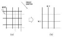
- FIG. 6shows that a moire phenomenon is prevented in a normal direction when different types of metal meshes are disposed between the antenna and the ground layer according to the present invention.
- FIG. 7shows that the moire phenomenon is prevented in the oblique direction when different types of metal meshes are arranged between the antenna and the ground layer according to the present invention.
- the present inventionis for mitigating a moire phenomenon by distributing wires (ie, metal meshes) constituting a unit grid in different layers.
- the Moire phenomenoncan also be referred to as interference fringes, wave patterns, and lattice patterns.
- This moiré phenomenonrefers to streaks that are visually created according to the difference in periods when regularly repeated shapes are repeatedly combined several times.
- the metal mesh of the antenna 1110 disposed on the antenna layer and the metal mesh of the ground layer GNDare configured in the same shape.
- the metal mesh inside the antenna 1110includes both metal mesh lines in the first direction and metal mesh lines in the second direction.
- the metal mesh of the ground layer GNDincludes both metal mesh lines in the first direction and metal mesh lines in the second direction.
- the metal mesh lines in the first direction and the second directionmay be a metal mesh line in a horizontal direction and a metal mesh line in a vertical direction, respectively.
- the metal mesh line according to the present inventionis not limited to a square lattice structure, and may be formed in a diamond structure or an arbitrary polygonal structure according to an application.
- the metal mesh lines in the first direction and the second directionmay be lines in any different directions, respectively.
- the metal mesh lines in the first direction and the second direction in such a rhombus structure or an arbitrary polygonal structurewill be described in detail below.
- unit grid sizes of the metal mesh of the antenna 1110 disposed on the antenna layer and the metal mesh of the ground layer GNDmay be expressed as dx and dy.
- a mesh structuresuch as a metal mesh line
- a moiré phenomenonmay occur. Accordingly, a problem may occur in visibility of a transparent antenna built into the display.
- the patch antenna 1100 disposed on the dielectric 1130has a double-sided structure in which a ground is disposed under the dielectric 1130.
- the moiré phenomenonmay be greater.
- a moire phenomenonmay occur from the viewpoint of a viewing angle (or electromagnetic wave) in the vertical direction.
- the metal mesh line of the antenna 1110 disposed on the antenna layermay be formed only in the first direction, that is, the mesh line ML1 in the horizontal direction.
- the metal mesh line disposed on the ground layer GNDmay be formed only in the second direction, that is, the vertical direction of the mesh line ML2.
- the metal mesh line of the antenna 1110 disposed on the antenna layermay be formed only in the second direction, that is, the vertical direction of the mesh line ML2.
- the metal mesh line disposed on the ground layer GNDmay be formed only in the first direction, that is, the mesh line ML1 in the horizontal direction.
- Moirémay be prevented by the metal mesh line of the antenna 1110 formed of the complementary mesh lines ML1 and ML2 as described above and the metal mesh line disposed on the ground layer GND. Accordingly, the moire phenomenon can be prevented from the viewpoint of the viewing angle (or electromagnetic wave) in the vertical direction.
- FIGS. 5 and 7 (a)from the viewpoint of the viewing angle (or electromagnetic wave) in the oblique direction, it may be considered that an error between mesh lines occurs even when a slight alignment error of the metal mesh structure occurs. . Accordingly, when an alignment error occurs between the antenna 1100 and the metal mesh line of the ground layer GND, a moire phenomenon may occur more in terms of a viewing angle (or electromagnetic wave) in the oblique direction.
- a complementary metal mesh line structure as shown in FIGS. 6(b) and 7(b)may be applied.
- the metal mesh line of the antenna 1110 disposed on the antenna layermay be formed only in the first direction, that is, the horizontal direction of the mesh line ML1.
- the metal mesh line disposed on the ground layer GNDmay be formed only in the second direction, that is, the vertical direction of the mesh line ML2.
- the metal mesh line of the antenna 1110 disposed on the antenna layermay be formed only in the second direction, that is, the vertical direction of the mesh line ML2.
- the metal mesh line disposed on the ground layer GNDmay be formed only in the first direction, that is, the mesh line ML1 in the horizontal direction.
- Moirémay be prevented by the metal mesh line of the antenna 1110 formed of the complementary mesh lines ML1 and ML2 as described above and the metal mesh line disposed on the ground layer GND. Accordingly, the moire phenomenon can be prevented from the viewpoint of the viewing angle (or electromagnetic wave) in the oblique direction.
- the metal mesh structure of the complementary shape according to the present inventioncan be used for any polygonal mesh structure in addition to a square mesh and a rhombus mesh.
- FIG. 8shows a triangular wire pattern derived from a square wire pattern, a hexagonal wire pattern, and a diamond wire pattern.
- a unit cell 100b of a rectangular wire pattern corresponding to a rectangular mesh structureis composed of a horizontal line 100i having a line width w and a vertical line 100j.
- the line width w of the horizontal line 100i and the vertical line 100jmay be implemented differently.
- the horizontal line 100i and the vertical line 100jcorrespond to the first metal mesh line ML1 in the first direction and the second metal mesh line ML2 in the second direction, respectively.
- the first metal mesh line ML1 corresponding to the horizontal line 100i and the second metal mesh line ML2 corresponding to the vertical line 100jmay be disposed on different layers.
- the antenna 1100is formed by the first metal mesh line ML1 corresponding to the horizontal line 100i, and the ground layer is formed by the second metal mesh line ML2 corresponding to the vertical line 100j.
- An inner region B of GND)may be formed.
- the antenna 1100is formed by the second metal mesh line ML2 corresponding to the vertical line 100j, and the ground layer is formed by the first metal mesh line ML1 corresponding to the horizontal line 100i.
- An inner region B of GNDmay be formed.
- the region 100B formed by the horizontal line 100i and the vertical line 100j arranged in different layersmay be determined according to the wavelength of the operating frequency.
- the size of the unit cell area 100B1may be determined so that a predetermined number or more of metal mesh lines are disposed inside the antenna 1100 of the mmWave band.
- a unit cell 100c of a hexagonal wire pattern corresponding to a hexagonal mesh structureincludes a hexagonal structure implemented by a plurality of mesh lines 100k.
- a plurality of mesh lines 100l extending from each vertex of the hexagonal structuremay be further included.
- the plurality of mesh lines 100lmay form different hexagonal structures.
- lines in the first directionmay be disposed on the antenna 100, and lines in the second direction may be disposed on the ground layer GND.
- lines formed on the left side of one axiseg, Yb axis
- lines formed on the right sidemay be disposed on the ground layer GND.
- first group mesh lines corresponding to an area including (1) to (4)may be disposed on the antenna layer 100.
- the second group mesh lines corresponding to regions including (5) to (8)may be disposed on the ground layer GND.
- a horizontal line ML1is added from a mesh line having a rhombus structure. Accordingly, it can be implemented as a triangular mesh line 100d. Accordingly, it is possible to construct a mesh with a triangular mesh line having a side length of Sb.
- the first metal mesh line MLS1 in the first directionmay be disposed on the antenna 1110, and the second metal mesh line MLS2 in the second direction may be disposed on the ground layer GND.
- the horizontal line ML1may be further disposed on the antenna 1110 to improve conductivity.
- the horizontal line ML1may be disposed on another antenna layer.
- another second transparent substratemay be formed on the antenna 1100, and another second antenna may be disposed on the second transparent substrate.
- the inside of the second antennamay be formed of a metal mesh having a horizontal line ML1. Accordingly, bandwidth characteristics may be further improved according to a stack structure of the second antenna disposed on the antenna 1100.
- there is an advantage that the radiation efficiencycan be further improved by the antenna of the stacked structure. As described above, while improving electrical characteristics such as antenna efficiency through the stacked structure, there is no metal mesh overlapping between the antenna layer, the second antenna layer, and the ground layer, thereby preventing moiré.
- some of the triangular mesh linesmay be implemented as a segment structure electrically separated from each other at a predetermined interval S. Accordingly, it is possible to selectively form an antenna region from a plurality of triangular mesh line structures.
- the predetermined interval S from the triangular mesh line boundary to the other triangular mesh line boundarymay increase by the distance between the antenna elements.
- the transparent antenna unit according to the present invention formed in a multilayer structureincludes an antenna 1110 corresponding to a radiator, a feeder, a substrate 1130, and a ground layer GND.
- FIGS. 9A to 9Cshow an overall layer structure and a structure for each layer in the transparent antenna unit having a metal mesh structure according to the present invention. Specifically, FIG. 9A shows an antenna layer and a ground layer having different metal mesh shapes. On the other hand, FIG. 9B shows an antenna layer having a metal mesh shape formed in one direction. Meanwhile, FIG. 9C shows a ground layer having a metal mesh shape formed in the other direction.
- the technical features of the transparent antenna unit including an antenna 1110, a feeder, a substrate 1130, and a ground layer (GND) according to the present inventionare as follows. Same as
- the part corresponding to the shadow region of (A)is a structure in which the meshes are shifted from each other.
- Areas (D) and (E)consist of a mesh structure or a solid structure (a metal-filled area, that is, a microstrip line formed area).
- Area (F)is implemented with a transparent material substrate (dielectric).
- a transparent dielectric material or an oxide conductor(ex. ITO, IZTO, etc.) that lowers the light reflection of the mesh line may be attached (ie, deposited or coated).
- the mesh structurei.e., the mesh structure
- the mesh structurecan be expanded to any polygonal shape in addition to the square/diamond.
- the antenna 1110is built into the display and operates, and is composed of a first metal mesh line MLS1 formed in the first direction.
- the substrate 1130is configured to operate as a dielectric for the antenna 1110 on which the antenna 1110 is disposed.
- the substrate 1130may be implemented as a transparent substrate such as PET, PES, Glass, or Quartz for transparency.
- the ground layer GNDis disposed under the substrate 1130 and is configured to operate as a ground for the antenna 1110.
- the inner area of the ground layer GND corresponding to the area in which the antenna 1110 is disposedmay be formed of a second metal mesh line MLS2 formed in a second direction different from the first direction.
- a shape in which the first metal mesh line MLS1 and the second metal mesh line MLS2 are combinedmay have a diamond shape. That is, the first metal mesh line MLS1 and the second metal mesh line MLS2 may be formed in different directions of a diamond structure, that is, in the first direction and the second direction.
- the rhombus shape in which the first metal mesh line MLS1 and the second metal mesh line MLS2 are combinedis the same as the rhombus shape formed in the outer region C rather than the inner region B of the ground layer GND It can be configured to have a grid size. Accordingly, when the antenna 1110 and the ground layer GND are combined and configured, the metal mesh line appears to be continuous even in the boundary region. Specifically, for all of the outer region C and the antenna region A + the inner region B, metal mesh lines are formed in a continuous structure without discontinuities at all vertices of the rhombus structure. Accordingly, the complementary mesh structure according to the present invention is continuously formed in all regions, thereby preventing moiré and improving visibility.
- the shapes of the first and second metal mesh linesare not limited thereto, and may be formed of a mesh line having a rectangular structure or a mesh line having an arbitrary polygonal structure according to an application.
- the shapes of the first and second metal mesh linesare in a first direction, that is, a horizontal mesh line ML1 and a second direction, that is, a vertical mesh line ML2, as shown in FIGS. 6 and 7. Can be formed. Accordingly, a shape in which the first metal mesh line ML1 and the second metal mesh line ML2 are combined may have a rectangular shape.
- the rectangular shape in which the first metal mesh line ML1 and the second metal mesh line ML2 are combinedis the same grid size as the rectangular shape formed in the outer area C, not the inner area B of the ground layer. It can be configured to have. Accordingly, when the antenna 1110 and the ground layer GND are combined and configured, the metal mesh line appears to be continuous even in the boundary region. Specifically, for all of the outer region C and the antenna region A + the inner region B, metal mesh lines are formed in a continuous structure without discontinuities at all vertices of the rectangular structure. Accordingly, the complementary mesh structure according to the present invention is continuously formed in all regions, thereby preventing moiré and improving visibility.
- the boundary line of the antenna 1110 configured with the first metal mesh line according to the present inventionmay also be implemented as a metal mesh line.
- a slight differenceoccurs between the electric field direction applied from the feeder, that is, the linear direction and the electric field direction of the first metal mesh line, that is, the oblique direction.
- the slope of the first metal mesh lineis less than a critical angle, for example, 30 degrees, the loss due to the difference in polarization is not large.
- a critical anglefor example, 30 degrees
- the transmission line 1120corresponding to the feeder in the transparent antenna unit having a complementary mesh structure according to the present invention will be described as follows.
- the transmission line 1120is configured to feed the antenna 1100 on the same layer as the antenna 1100.
- the end of the transmission line 1120is connected to the antenna 1100, the end of the first metal mesh line (ML1, MLS1) and the second metal mesh line (ML2, MLS2) has the same shape as the combined shape. It can be composed of a metal mesh line.
- the end of the transmission line 1120may be formed as first metal mesh lines ML1 and MLS1 inside.
- a region of the ground layer GND corresponding to the end of the transmission line 1120may be formed as second metal mesh lines ML2 and MLS2.
- some of the transmission lines 1120may be disposed on an un-transparent region of the display. Accordingly, a portion of the transmission line 1120 other than the end portion may be implemented in the form of a metal pattern (ie, solid) on the opaque area of the display.
- the opaque area of the displaymay be a bezel area or a side area of the display, or a portion in which the side area and the front area are connected.
- the transmission line 1120may be implemented as a microstrip line or a strip line such as a CPW line.
- the transmission line 1120 disposed on the opaque areamay be configured as a CPW line.
- the transmission line 1120 disposed on the opaque regionmay include an inner conductor region 1121, an outer conductor region 1122, and a dielectric region 1123.
- the inner conductor region 1121is configured to operate as a signal line
- the outer conductor region 1122is disposed adjacent to the inner conductor region 1121 and is configured to operate as a ground. Accordingly, the inner conductor region 1121 and the outer conductor region 1122 may be referred to as a strip line 1121 and a ground region 1122, respectively.
- the dielectric region 1123is formed between the inner conductor region 1121 and the outer conductor region 1122.
- the transmission line 1120 according to the present inventionmay be formed in a CPW (Co-Planar Waveguide) line structure.
- the transparent antenna having a complementary mesh structuresince the ground layer is also formed in a metal mesh structure, it is not necessary to form a dummy pattern around the antenna area. Accordingly, it is easy to implement the antenna layer itself, and there is an advantage in that the change in antenna characteristics becomes robust to the manufacturing process.
- the antenna characteristicsmay change according to a gap error with the dummy pattern.
- the metal mesh lineis not disposed in an area outside the area where the antenna 1100 is disposed, but is formed as a dielectric area.
- the ground layer GND1must have an inner region B and an outer region C corresponding to the antenna 1100 in different mesh structures. do.
- the antenna 1100may be composed of first metal mesh lines ML1 and MLS1 formed in the first direction.
- the second metal mesh lines MLS1 and ML1 formed in the second directionmay be disposed in the inner area B of the ground layer GND corresponding to the area A in which the antenna 1100 is disposed.
- the first metal mesh lines ML1 and MLS1 formed in the first direction and the second metal mesh lines ML2 and MLS2 formed in the second directionare connected and disposed. .
- the first metal mesh lines ML1 and MLS1are disposed in the antenna layer on which the antenna 1100 is disposed. Meanwhile, in the inner region B of the ground layer GND corresponding to the region A in which the antenna is disposed, the complementary second metal mesh lines ML2 and MLS2 are disposed. In addition, in the outer region C of the ground layer GND, first metal mesh lines ML1 and MLS1 and second metal mesh lines ML2 and MLS2 complementary thereto are disposed.
- the moire phenomenon of the transparent antennamay be reduced by a complementary metal mesh structure configured such that the metal mesh does not overlap in a plurality of layers.
- the transparent antenna unit having a complementary metal mesh structuremay further include a matching unit 1125.
- the matching unit 1125is disposed between the antenna 1100 and the transmission line 1120 configured to feed the antenna 1100, and may be implemented as a metal mesh line.
- the matching portion 1125 and the inner region B of the ground layer GND corresponding to the matching portion 1125are the first metal mesh lines ML1 and MLS1 and the second metal mesh lines ML2 and MLS2. It may be composed of a metal mesh line having the same shape as the combined shape.
- the inside of the matching part 1125may be formed of first metal mesh lines ML1 and MLS1 formed in the first direction.
- the inner region B of the ground layer GND corresponding to the matching portion 1125may be formed of second metal mesh lines ML2 and MLS2 formed in the second direction.
- the matching part 1125can be implemented as a metal mesh line, it is preferable to be formed in a short length for a low loss structure.
- the matching unit 1125may be implemented in an inset shape rather than a quarter-wavelength impedance converter between the transmission line 1120 and the antenna 1110.
- the matching portion 1125may be formed to have a length shorter than a quarter-wavelength length and thus has a low loss characteristic.
- the matching unit 1125is implemented with the same line width (ie, the same impedance) as the transmission line 1120 to prevent electrical loss at a boundary according to different line widths.
- the region adjacent to the boundary of the matching unit 1125may further include an inset region configured to achieve impedance matching by removing some of the first metal mesh lines ML1 and MLS1 of the antenna 1110. I can.
- the change in transparency according to the viewing angleis relatively reduced. Accordingly, transparency and visibility of the antenna at various angles may be improved.
- FIG. 10shows a patch antenna configuration of various structures in connection with the present invention.
- 10(a)corresponds to a solid-type patch antenna (Type A) in which the patch antenna is filled with a metal pattern.
- the ground layer of the patch antennais also implemented in a solid form filled with a metal pattern.
- FIG. 10Bcorresponds to a structure (Type B) in which the patch antenna has a rhombus shape by the first and second metal mesh lines.
- the ground layeris also implemented in a structure having a rhombus shape by the first and second metal mesh lines. Accordingly, a moire phenomenon may occur due to mesh lines overlapping the antenna region and the ground region.
- FIG. 10(c)shows a structure in which the patch antenna according to the present invention is implemented as a first metal mesh line in one direction, and a ground area corresponding to the antenna area is implemented as a second metal mesh line (Type C). It corresponds.
- a moiré phenomenonmay be reduced in the entire antenna structure including an area overlapping between the antenna area and the ground area.
- FIG. 11is a comparison of reflection coefficient characteristics according to various antenna structures according to the present invention. Specifically, FIG. 11 shows reflection coefficient characteristics for a patch antenna having a solid metal pattern of Type A, a transparent antenna of Type B, and a transparent antenna having a complementary mesh structure of Type C.
- Type Ahas a bandwidth of 27.46GHz to 28.99GHz based on -10dB.
- Type Bhas a bandwidth of 27.12GHz to 29.89GHz.
- Type Chas a bandwidth of 26.22GHz to 29.87GHz. Therefore, the transparent antenna having a complementary mesh structure according to the present invention has the widest bandwidth characteristic.
- the transparent antenna having a metal mesh structurehas a smaller area occupied by metal per unit area than when the entire area is filled with a metal pattern, so that radiation efficiency and the like are reduced.
- the frequency selectivity according to the resonance phenomenonis relaxed, and the bandwidth characteristics are improved.
- metal linesare partially removed from the overlapping portion, and the ratio of metal per unit area is further reduced. Accordingly, the frequency selectivity due to the resonance phenomenon is relaxed, and the bandwidth characteristics are further improved.
- metal linesare partially removed from the overlapping portion, thereby improving transparency.
- the transparencycan be determined by the following equation.
- the mesh pattern areamay be determined in consideration of the line width and length of the metal mesh line of the transparent antenna.
- the mesh pattern areain a solid form such as Type A, the mesh pattern area is the same as the outermost area of the antenna, and the transparency is 0%.
- the transparencyis further improved compared to the case where both the first and second metal mesh lines are disposed as in Type B.
- the area of the mesh patterncorresponds to 10%.
- the mesh pattern areais reduced to 5%. Accordingly, if the transparency is 90% in the Type B structure, the transparency can be improved to 95% in the Type C structure.
- Table 1compares the size and electrical characteristics of the patch antenna for the antenna structures of Type A to Type C having a center frequency of 28 GHz according to the present invention.
- the bandwidthincreases by about 3% and the antenna size decreases by about 33% compared to the Type B structure. Accordingly, through the transparent antenna having a complementary mesh structure according to the present invention, both antenna miniaturization and bandwidth enhancement are possible.
- metal linesare partially removed from the overlapping portion, and the ratio of metal per unit area is further reduced. Accordingly, the Type C structure having a complementary mesh structure has improved transparency compared to the Type B structure, and the moiré phenomenon is also reduced.
- the transparent antenna having a complementary mesh structure as in the present inventionmetal lines are partially removed from the overlapping portion, and the ratio of metal per unit area is further reduced. Accordingly, the frequency selectivity due to the resonance phenomenon is relaxed, and the bandwidth characteristics are further improved.
- the metal lineis partially removed, the radiation efficiency or gain slightly decreases, but other electrical characteristics can be improved, the antenna can be miniaturized, and the moiré phenomenon can be reduced and transparency can be improved.
- a transparent antenna having a complementary mesh structure for preventing a moire phenomenon caused by overlapping mesh lines according to the present inventionhas been described.
- an array antenna structure having a complementary mesh structure for preventing moiré according to another aspect of the present inventionwill be described.
- all descriptions of the above-described transparent antenna having a complementary mesh structureare applicable to the array antenna having the following complementary mesh structure.
- FIGS. 12 and 13show array antennas having a complementary mesh structure according to the present invention.
- FIG. 12shows a mesh configuration of an antenna layer in an array antenna having a complementary mesh structure according to the present invention.
- FIG. 13shows a mesh configuration of a ground layer in an array antenna having a complementary mesh structure according to the present invention.
- 14shows a detailed configuration of an electronic device including a plurality of array antennas having a complementary mesh structure according to the present invention.
- an electronic device including a transparent antenna unit according to the present inventionmay further include a ground layer GND.
- the ground layer GNDis disposed under the antenna 1100 and is configured to operate as a ground for the antenna 1100.
- some of the array antennas ANT 1 to ANT4may include first metal mesh lines ML1 and MLS1 formed in the first direction.
- the rest of the array antennas among the plurality of array antennas ANT 1 to ANT4may be formed of second metal mesh lines ML2 and MLS2 formed in a second direction different from the first direction.
- the array antennas ANT 1 and ANT3 disposed on the upper portionmay be formed of first metal mesh lines ML1 and MLS1.
- the array antennas ANT2 and ANT4 disposed belowmay be formed of second metal mesh lines ML2 and MLS2.
- the array antennas ANT1 and ANT2 disposed on the left sidemay be configured with first metal mesh lines ML1 and MLS1.
- the array antennas ANT3 and ANT4 disposed on the right sidemay be configured with the second metal mesh lines ML2 and MLS2. Further, it is not limited to such a combination, and the shape of the mesh line of the plurality of array antennas ANT 1 to ANT4 can be variously changed according to an application.
- an electronic device including a plurality of array antennas ANT 1 to ANT4 having a complementary mesh structuremay further include a transceiver circuit 1210.
- the transceiver circuit 1210is connected to the array antennas ANT 1 to ANT4 through a transmission line 1120. Further, the transceiver circuit 1210 is configured to transmit a 5G transmission signal to the array antenna ANT 1 or ANT4 and to receive a 5G reception signal received from the array antenna ANT 1 or ANT4.
- the inner region B of the ground layer GND1 corresponding to some array antennasmay be composed of second metal mesh lines ML2 and MLS2 that are complementary to the mesh line inside the antenna.
- the inner region B of the ground layer GND1 corresponding to the remaining array antennamay be composed of first metal mesh lines ML1 and MLS1 complementary to the mesh line inside the antenna.
- the performance of the array antennas ANT 1 to ANT4may be slightly different according to different shapes of the first metal mesh lines ML1 and MLS1 and the second metal mesh lines ML2 and MLS2 according to the present invention.
- the array antennas ANT 1 to ANT4 having a complementary mesh structure according to the present inventionmay receive a signal through an optimal array antenna according to the received signal quality.
- the transmission/reception unit circuit 1210is the remaining array antenna consisting of the second metal mesh lines ML2 and MLS2. The signal can be received through.
- the transmission line 1120 corresponding to the feeder for each element of the array antennas ANT 1 to ANT4is a first so that vertical polarization is generated as shown in FIGS. 9A to 9C.
- the second signalmay be transmitted to each element of the array antennas ANT 1 to ANT4 so that horizontal polarization is generated through a different second feeding unit.
- a maximum of 8 Txcan be implemented by using the first and second signals having vertical and horizontal polarizations, and the four array antennas ANT 1 to ANT4.
- a feeding partmay be provided in an optimal polarization direction according to a shape of a metal mesh line inside the array antennas ANT 1 to ANT4.
- the array antenna generated by the first metal mesh line ML1 in the horizontal directionmay be fed through the second feeding unit so that horizontal polarization is generated.
- the array antenna generated by the second metal mesh line ML2 in the vertical directionmay be fed through a feeder so that vertical polarization is generated.
- the array antenna generated in the oblique directionthat is, the first metal mesh line MLS1 in the first direction may be fed through the third feeder so that polarization in the first direction is generated.
- the array antenna generated in the second metal mesh line MLS2 in a different oblique direction, that is, in the second directionmay be fed through the fourth feeding unit so that polarization in the second direction is generated.
- the first and second metal mesh lines MLS1 and MLS2 in the diagonal direction of the first and second directionshave vertical polarization components rather than horizontal polarization. Bigger. Accordingly, some array antennas formed with the first metal mesh line MLS1 in the first direction and other array antennas formed with the second metal mesh line MLS2 in the second direction may both operate with vertical polarization. To this end, some array antennas formed of the first metal mesh line MLS1 and other array antennas formed of the second metal mesh line MLS2 may both be fed through a feeder.
- the array antennas formed of the first and second metal mesh lines MLS1 and MLS2 that are all fed through the same feederhave different reception characteristics according to the rotational state of the electronic device. Accordingly, when the signal quality received through some array antennas consisting of the first metal mesh lines ML1 and MLS1 is low, the transmission/reception unit circuit 1210 is the remaining array antenna consisting of the second metal mesh lines ML2 and MLS2. The signal can be received through.
- the electronic devicemay further include a baseband processor 1400 configured to be connected to the transceiver circuit 1210 to control the transceiver circuit 1210. Accordingly, the configured baseband processor 1400 may control the transceiver circuit 1210 to perform a diversity operation or a multiple input/output operation (MIMO) through some array antennas and the remaining array antennas according to the received signal quality.
- MIMOmultiple input/output operation
- some of the array antennas and the remaining array antennasare each formed with a first metal mesh line MLS1 and a second metal mesh line MLS2.
- the baseband processor 1400provides the first signal quality received through some array antennas composed of first metal mesh lines ML1 and MLS1 and the remaining array antennas composed of second metal mesh lines ML2 and MLS2. The quality of the second signal received through may be compared. In this regard, the baseband processor 1400 may determine whether the first signal quality and the second signal quality are both equal to or greater than a threshold. In this case, the baseband processor 1400 may control the transceiver circuit 1210 to perform a multiple input/output operation (MIMO) through some of the array antennas ANT or ANT3 and the remaining array antennas ANT2 or ANT4.
- MIMOmultiple input/output operation
- the baseband processor 1400includes some array antennas ANT1 including first metal mesh lines ML1 and MLS1. Alternatively, the signal can be received through ANT3).
- the baseband processor 1400includes the remaining array antennas composed of the second metal mesh lines ML2 and MLS2 ( The signal can be received via ANT2 or ANT4).
- the rhombus shape in which the first and second metal mesh lines MLS1 and MLS2 are combinedis the outer region C, not the inner region B of the ground layer GND. It can be configured to have the same lattice size as the rhombus shape formed in.
- the metal mesh lineis not disposed in an area outside the area in which the array antennas ANT1 to ANT4 are disposed, a dummy pattern does not exist. Accordingly, there is an advantage of reducing antenna efficiency and sensitivity to changes in antenna characteristics due to a dummy pattern.
- the first metal mesh lines ML1 and MLS1 or the second metal mesh lines ML1 and MLS1are complementary to the inner region B of the ground layer GND corresponding to the region where the array antennas ANT1 to ANT4 are disposed. ML2, MLS2) may be deployed.
- the first metal mesh lines ML1 and MLS1 formed in the first direction and the second metal mesh lines ML2 and MLS2 formed in the second directionare connected and disposed. I can.
- the transparent antennais formed by the first metal mesh lines ML1 and MLS1 of the antenna layer on which some array antennas are disposed and the second metal mesh lines ML2 and MLS2 complementary to the first metal mesh line in the ground layer.
- the moiré phenomenoncan be reduced.
- the transparent antennais formed by the second metal mesh lines ML2 and MLS2 of the antenna layer on which the remaining array antennas are disposed and the first metal mesh lines ML1 and MLS1 complementary to the second metal mesh line in the ground layer.
- the moiré phenomenoncan be reduced.
- designing and driving a plurality of RF modules and a configuration for performing a status check on the plurality of RF modulescan be implemented as computer-readable codes in a medium on which a program is recorded.
- the computer-readable mediumincludes all types of recording devices that store data that can be read by a computer system. Examples of computer-readable media include HDD (Hard Disk Drive), SSD (Solid State Disk), SDD (Silicon Disk Drive), ROM, RAM, CD-ROM, magnetic tape, floppy disk, optical data storage device, etc. There is also a carrier wave (e.g., transmission over the Internet).
- the computermay include the controllers 180, 1210, and 1250 of the terminal.
Landscapes
- Engineering & Computer Science (AREA)
- Computer Networks & Wireless Communication (AREA)
- Telephone Set Structure (AREA)
- Details Of Aerials (AREA)
Abstract
Description
Translated fromKorean본 발명은 투명 안테나를 구비하는 전자 기기에 관한 것이다. 보다 상세하게는, 디스플레이에 내장되는 투명 안테나를 구비하는 전자 기기에 관한 것이다.The present invention relates to an electronic device having a transparent antenna. More specifically, it relates to an electronic device having a transparent antenna incorporated in a display.
전자기기(electronic devices)는 이동 가능여부에 따라 이동 단말기(mobile/portable terminal) 및 고정 단말기(stationary terminal)으로 나뉠 수 있다. 다시 전자기기는 사용자의 직접 휴대 가능 여부에 따라 휴대(형) 단말기(handheld terminal) 및 거치형 단말기(vehicle mounted terminal)로 나뉠 수 있다.Electronic devices can be divided into mobile/portable terminals and stationary terminals depending on whether they can be moved. Again, electronic devices can be divided into handheld terminals and vehicle mounted terminals depending on whether the user can directly carry them.
전자기기의 기능은 다양화되고 있다. 예를 들면, 데이터와 음성통신, 카메라를 통한 사진촬영 및 비디오 촬영, 음성녹음, 스피커 시스템을 통한 음악파일 재생 그리고 디스플레이부에 이미지나 비디오를 출력하는 기능이 있다. 일부 단말기는 전자게임 플레이 기능이 추가되거나, 멀티미디어 플레이어 기능을 수행한다. 특히 최근의 이동 단말기는 방송과 비디오나 텔레비전 프로그램과 같은 시각적 컨텐츠를 제공하는 멀티캐스트 신호를 수신할 수 있다.The functions of electronic devices are diversifying. For example, there are functions of data and voice communication, taking pictures and videos through a camera, recording voice, playing music files through a speaker system, and outputting images or videos to the display unit. Some terminals add an electronic game play function or perform a multimedia player function. In particular, recent mobile terminals can receive multicast signals providing visual content such as broadcasting and video or television programs.
이와 같은 전자기기는 기능이 다양화됨에 따라 예를 들어, 사진이나 동영상의 촬영, 음악이나 동영상 파일의 재생, 게임, 방송의 수신 등의 복합적인 기능들을 갖춘 멀티미디어 기기(Multimedia player) 형태로 구현되고 있다.As such electronic devices are diversified, they are implemented in the form of a multimedia player with complex functions such as, for example, taking photos or videos, playing music or video files, and receiving games and broadcasts. have.
이러한 전자기기의 기능 지지 및 증대를 위해, 단말기의 구조적인 부분 및/또는 소프트웨어적인 부분을 개량하는 것이 고려될 수 있다.In order to support and increase the function of the electronic device, it may be considered to improve the structural part and/or the software part of the terminal.
상기 시도들에 더하여, 최근 전자기기는 LTE 통신 기술을 이용한 무선 통신 시스템이 상용화되어 다양한 서비스를 제공하고 있다. 또한, 향후에는 5G 통신 기술을 이용한 무선 통신 시스템이 상용화되어 다양한 서비스를 제공할 것으로 기대된다. 한편, LTE 주파수 대역 중 일부를 5G 통신 서비스를 제공하기 위하여 할당될 수 있다.In addition to the above attempts, wireless communication systems using LTE communication technology have recently been commercialized in electronic devices, providing various services. In addition, in the future, wireless communication systems using 5G communication technology are expected to be commercialized and provide various services. Meanwhile, some of the LTE frequency bands may be allocated to provide 5G communication services.
이와 관련하여, 이동 단말기는 5G 통신 서비스를 다양한 주파수 대역에서 제공하도록 구성될 수 있다. 최근에는 6GHz 대역 이하의 Sub6 대역을 이용하여 5G 통신 서비스를 제공하기 위한 시도가 이루어지고 있다. 하지만, 향후에는 보다 빠른 데이터 속도를 위해 Sub6 대역 이외에 밀리미터파(mmWave) 대역을 이용하여 5G 통신 서비스를 제공할 것으로 예상된다.In this regard, the mobile terminal may be configured to provide 5G communication services in various frequency bands. Recently, attempts have been made to provide a 5G communication service using a Sub6 band below 6GHz band. However, in the future, it is expected to provide 5G communication service using millimeter wave (mmWave) band in addition to Sub6 band for faster data rate.
한편, 이러한 밀리미터파(mmWave) 대역에서의 5G 통신 서비스를 위해 할당될 주파수 대역은 28GHz 대역, 39GHz 및 64 GHz 대역이 고려되고 있다. 이와 관련하여, 밀리미터파 대역에서 다수의 배열 안테나들이 전자 기기에 배치될 수 있다.Meanwhile, the frequency bands to be allocated for 5G communication services in the millimeter wave (mmWave) band are the 28 GHz band, 39 GHz and 64 GHz bands. In this regard, a plurality of array antennas may be disposed in the electronic device in the millimeter wave band.
한편, 이러한 다수의 배열 안테나 이외에 전자 기기에는 다른 다수의 안테나들이 배치될 수 있다. 따라서, 기존의 다수의 안테나들과 간섭을 방지하면서 전자 기기의 전면부를 통해 신호를 송신 및 수신할 필요가 있다. 이를 위해, 전자 기기의 디스플레이 내부에 내장되는 메탈 메쉬(metal mesh) 라인으로 구현되는 투명 안테나에 대한 연구가 이루어지고 있다.Meanwhile, in addition to the plurality of array antennas, a plurality of other antennas may be disposed in the electronic device. Accordingly, it is necessary to transmit and receive signals through the front side of the electronic device while preventing interference with a plurality of existing antennas. To this end, research on a transparent antenna implemented with a metal mesh line embedded in a display of an electronic device is being conducted.
한편, 이러한 메탈 메쉬 구조의 투명 안테나에서 안테나 영역과 그라운드 영역의 메쉬 라인이 중첩됨에 따라, 모아레(Moire) 현상이 발생하여 시인성(visibility)이 저하되는 문제점이 있다.Meanwhile, in such a transparent antenna having a metal mesh structure, as the mesh lines of the antenna region and the ground region overlap, there is a problem that a Moire phenomenon occurs and visibility is deteriorated.
이와 관련하여, 모아레(Moire) 현상은 간섭무늬, 물결무늬, 격자무늬로 또한 지칭할 수 있다. 이러한 모아레 현상은 규칙적으로 반복되는 형상이 여러 번 거듭하여 합쳐졌을 때, 이러한 주기의 차이에 따라 시각적으로 만들어지는 줄무늬를 의미한다. 한편, 이러한 메탈 메쉬 라인 구조의 투명 안테나에서 넓은 시야 각도 범위 내에서 모아레 현상이 전체적으로 완화될 필요가 있다. 하지만, 이러한 메탈 메쉬 라인 구조의 투명 안테나에서 넓은 시야 각도 범위 내에서 모아레 현상을 완화하기 위한 구체적인 방법이 없다는 문제점이 있다.In this regard, the Moire phenomenon may also be referred to as an interference pattern, a wave pattern, and a grid pattern. This moiré phenomenon refers to streaks that are visually created according to the difference in periods when regularly repeated shapes are repeatedly combined several times. On the other hand, in such a transparent antenna having a metal mesh line structure, it is necessary to alleviate the moiré phenomenon within a wide viewing angle range. However, there is a problem in that there is no specific method for mitigating the moire phenomenon within a wide viewing angle range in such a transparent antenna having a metal mesh line structure.
본 발명은 전술한 문제 및 다른 문제를 해결하는 것을 목적으로 한다. 또한, 다른 일 목적은 투명 안테나를 구비하는 전자 기기에서 메탈 메쉬 라인의 중첩에 따른 모아레 현상을 저감하기 위한 것이다.It is an object of the present invention to solve the above and other problems. In addition, another object is to reduce the moire phenomenon caused by overlapping metal mesh lines in an electronic device having a transparent antenna.
본 발명의 다른 일 목적은, 안테나 영역과 그라운드 영역 간에 중첩되는 메탈 메쉬 라인에 의한 모아레 현상에 의한 시인성 저하를 완화하기 위한 것이다.Another object of the present invention is to mitigate a decrease in visibility due to a moire phenomenon caused by a metal mesh line overlapping between an antenna region and a ground region.
본 발명의 다른 일 목적은, 다층 메탈 메쉬 라인 구조에서 시인성을 향상시키면서 안테나 특성을 유지하거나 개선시킬 수 있는 메쉬 라인 구조를 제안하기 위한 것이다.Another object of the present invention is to propose a mesh line structure capable of maintaining or improving antenna characteristics while improving visibility in a multilayer metal mesh line structure.
상기 또는 다른 목적을 달성하기 위해 본 발명에 따른 5G 통신을 위한 투명 안테나를 구비하는 전자 기기가 제공된다. 상기 전자 기기는 디스플레이 내부에 내장되어 동작하고, 내부가 제1 방향으로 형성된 제1 메탈 메쉬 라인으로 구성된 안테나; 상기 안테나가 배치되고, 상기 안테나에 대한 유전체로 동작하도록 구성된 기판(substrate); 및 상기 기판 하부에 배치되고, 상기 안테나에 대한 그라운드로 동작하도록 구성된 그라운드 레이어를 포함한다. 여기서, 상기 안테나가 배치된 영역에 대응하는 상기 그라운드 레이어의 내부 영역은 상기 제1 방향과 다른 제2 방향으로 형성된 제2 메탈 메쉬 라인으로 구성되어, 투명 안테나 구조에서 안테나 영역과 그라운드 영역에서 중첩되는 메탈 메쉬 라인에 의한 모아레 현상을 완화하여 시인성(visibility)을 개선할 수 있다. 또한, 투명 안테나 구조에서 서로 다른 레이어 간 메탈 메쉬 라인의 정렬 오차에 따른 안테나 특성 변화가 적은 형태의 구조를 제안할 수 있다. 또한, 안테나 영역 주변에 더미 메탈 패턴을 배치할 필요가 없어, 안테나 효율이 향상되고 제작 오차에 따른 안테나 특성 변화가 감소한다는 장점이 있다. 또한, 시야 각도에 따른 투명도 변화가 상대적으로 적어, 디스플레이 내장 안테나에 의한 디스플레이 품질 저하를 완화할 수 있다는 장점이 있다. 또한, 투명 안테나 구조에서 시인성 개선과 함께, 안테나 대역폭 특성 등의 안테나 성능 향상이 가능하다는 장점이 있다.In order to achieve the above or other objects, an electronic device provided with a transparent antenna for 5G communication according to the present invention is provided. The electronic device includes an antenna built in and operating inside a display, and including a first metal mesh line formed in a first direction; A substrate on which the antenna is disposed and configured to act as a dielectric for the antenna; And a ground layer disposed under the substrate and configured to operate as a ground for the antenna. Here, the inner area of the ground layer corresponding to the area in which the antenna is disposed is composed of a second metal mesh line formed in a second direction different from the first direction, and overlaps the antenna area and the ground area in the transparent antenna structure. Visibility can be improved by mitigating the moire phenomenon caused by the metal mesh line. In addition, in a transparent antenna structure, a structure having a small change in antenna characteristics due to an alignment error of metal mesh lines between different layers can be proposed. In addition, since it is not necessary to arrange a dummy metal pattern around the antenna region, there is an advantage in that antenna efficiency is improved and a change in antenna characteristics due to manufacturing errors is reduced. In addition, since the change in transparency according to the viewing angle is relatively small, there is an advantage in that it is possible to alleviate the deterioration of display quality due to an antenna built-in display. In addition, in the transparent antenna structure, there is an advantage in that it is possible to improve visibility and improve antenna performance such as antenna bandwidth characteristics.
일 실시 예에 따르면, 상기 제1 메탈 메쉬 라인과 상기 제2 메탈 메쉬 라인이 결합된 형상은 마름모 형상(diamond shape)인 것을 특징으로 한다.According to an embodiment, a shape in which the first metal mesh line and the second metal mesh line are combined is a diamond shape.
일 실시 예에 따르면, 상기 제1 메탈 메쉬 라인과 상기 제2 메탈 메쉬 라인이 결합된 마름모 형상은, 상기 그라운드 레이어의 상기 내부 영역이 아닌 외부 영역에 형성된 마름모 형상과 동일한 격자 크기를 갖는 것을 특징으로 한다.According to an embodiment, the rhombus shape in which the first metal mesh line and the second metal mesh line are combined has the same lattice size as a rhombus shape formed in an outer region other than the inner region of the ground layer. do.
일 실시 예에 따르면, 상기 제1 메탈 메쉬 라인과 상기 제2 메탈 메쉬 라인이 결합된 형상은 직사각형 형상(rectangular shape)인 것을 특징으로 한다.According to an embodiment, a shape in which the first metal mesh line and the second metal mesh line are combined has a rectangular shape.
일 실시 예에 따르면, 상기 제1 메탈 메쉬 라인과 상기 제2 메탈 메쉬 라인이 결합된 직사각형 형상은, 상기 그라운드 레이어의 상기 내부 영역이 아닌 외부 영역에 형성된 직사각형 형상과 동일한 격자 크기를 갖는 것을 특징으로 한다.According to an embodiment, the rectangular shape in which the first metal mesh line and the second metal mesh line are combined has the same grid size as a rectangular shape formed in an outer area other than the inner area of the ground layer. do.
일 실시 예에 따르면, 상기 안테나와 동일 레이어 상에서 상기 안테나를 급전하도록 구성된 전송 선로(transmission line)를 포함하고, 상기 전송 선로의 단부는 상기 안테나와 연결되고, 상기 단부는 상기 제1 메탈 메쉬 라인과 상기 제2 메탈 메쉬 라인이 결합된 형상과 동일한 형상의 메탈 메쉬 라인으로 구성될 수 있다.According to an embodiment, a transmission line configured to feed the antenna on the same layer as the antenna is included, and an end of the transmission line is connected to the antenna, and the end is connected to the first metal mesh line. The second metal mesh line may be configured as a metal mesh line having the same shape as the combined shape.
일 실시 예에 따르면, 상기 전송 선로 중 일부는 상기 디스플레이의 불투명 영역(un-transparent region) 상에 배치되고, 상기 불투명 영역 상에 배치되는 상기 전송 선로는 CPW 라인으로 구성되고, 상기 CPW 라인으로 구성되는 상기 전송 선로와 연결되고, 상기 안테나에 5G 송신 신호를 송신하고 상기 안테나로부터 수신된 5G 수신 신호를 수신하도록 구성되는 송수신부 회로를 더 포함할 수 있다.According to an embodiment, some of the transmission lines are disposed on an un-transparent region of the display, and the transmission line disposed on the opaque area is composed of a CPW line, and is composed of the CPW line. It may further include a transceiver circuit connected to the transmission line that is configured to transmit a 5G transmission signal to the antenna and receive a 5G reception signal received from the antenna.
일 실시 예에 따르면, 상기 불투명 영역 상에 배치되는 상기 전송 선로는 신호선으로 동작하도록 구성된 내부 도체 영역; 상기 내부 도체 영역에 인접하게 배치되고, 그라운드로 동작하도록 구성된 외부 도체 영역; 및 상기 내부 도체 영역과 상기 외부 도체 영역 사이에 형성되는 유전체 영역을 포함하는 CPW (Co-Planar Waveguide) 라인 구조로 형성될 수 있다.According to an embodiment, the transmission line disposed on the opaque area may include an inner conductor area configured to operate as a signal line; An outer conductor region disposed adjacent to the inner conductor region and configured to operate as a ground; And a dielectric region formed between the inner conductor region and the outer conductor region, and may have a Co-Planar Waveguide (CPW) line structure.
일 실시 예에 따르면, 상기 안테나가 배치된 영역의 외부 영역에는 메탈 메쉬 라인이 배치되지 않는 것을 특징으로 한다.According to an embodiment, a metal mesh line is not disposed in an area outside the area where the antenna is disposed.
일 실시 예에 따르면, 상기 안테나가 배치된 영역에 대응하는 상기 그라운드 레이어의 내부 영역에는 제2 방향으로 형성된 제2 메탈 메쉬 라인이 배치되고, 상기 그라운드 레이어의 외부 영역에는 상기 제1 방향으로 형성된 상기 제1 메탈 메쉬 라인과 상기 제2 방향으로 형성된 상기 제2 메탈 메쉬 라인이 연결되어 배치될 수 있다.According to an embodiment, a second metal mesh line formed in a second direction is disposed in an inner area of the ground layer corresponding to an area in which the antenna is disposed, and the second metal mesh line formed in the first direction is disposed in an outer area of the ground layer. The first metal mesh line and the second metal mesh line formed in the second direction may be connected and disposed.
일 실시 예에 따르면, 상기 안테나가 배치되는 안테나 레이어에는 상기 제1 메탈 메쉬 라인이 배치되고, 상기 안테나가 배치되는 영역에 대응하는 상기 그라운드 레이어의 내부 영역에는 상보적으로 구성된 상기 제2 메탈 메쉬 라인이 배치되고, 상기 그라운드 레이어의 외부 영역에는 상기 제1 메탈 메쉬 라인 및 상보적으로 구성된 상기 제2 메탈 메쉬 라인이 배치되어, 투명 안테나의 모아레(Moire) 현상이 저감될 수 있다.According to an embodiment, the first metal mesh line is disposed in an antenna layer in which the antenna is disposed, and the second metal mesh line is complementarily configured in an inner area of the ground layer corresponding to an area in which the antenna is disposed. The first metal mesh line and the complementary second metal mesh line are disposed in an outer region of the ground layer, so that a moire phenomenon of the transparent antenna may be reduced.
일 실시 예에 따르면, 상기 안테나는 상기 안테나와 상기 안테나를 급전하도록 구성된 전송 선로 사이에 배치되는 메탈 메쉬 라인의 정합부를 더 포함하고, 상기 정합부와 상기 정합부에 대응하는 상기 그라운드 레이어의 내부 영역은 상기 제1 메탈 메쉬 라인과 상기 제2 메탈 메쉬 라인이 결합된 형상과 동일한 형상의 메탈 메쉬 라인으로 구성될 수 있다.According to an embodiment, the antenna further includes a matching portion of a metal mesh line disposed between the antenna and a transmission line configured to feed the antenna, and an inner region of the ground layer corresponding to the matching portion and the matching portion May be composed of a metal mesh line having the same shape as the combined shape of the first metal mesh line and the second metal mesh line.
일 실시 예에 따르면, 상기 정합부의 경계에 인접한 영역에는 상기 안테나의 상기 제1 메탈 메쉬 라인의 일부가 제거되어 임피던스 정합이 이루어지도록 구성되는 인셋 영역(inset region)을 더 포함할 수 있다.According to an embodiment, a region adjacent to the boundary of the matching unit may further include an inset region configured to perform impedance matching by removing a part of the first metal mesh line of the antenna.
본 발명의 다른 양상에 따른 전자 기기는 디스플레이; 상기 디스플레이 내부에 배치되고, 메탈 메쉬 라인을 통해 형성되는 복수의 배열 안테나들; 상기 배열 안테나들과 전송 선로를 통해 연결되고, 상기 배열 안테나에 5G 송신 신호를 송신하고 상기 배열 안테나로부터 수신된 5G 수신 신호를 수신하도록 구성되는 송수신부 회로; 및 상기 안테나 하부에 배치되고, 상기 안테나에 대한 그라운드로 동작하도록 구성된 그라운드 레이어를 포함한다. 한편, 상기 복수의 배열 안테나 중 일부 배열 안테나는 내부가 제1 방향으로 형성된 제1 메탈 메쉬 라인으로 구성되고, 상기 복수의 배열 안테나 중 나머지 배열 안테나는 내부가 제1 방향과 다른 제2 방향으로 형성된 제2 메탈 메쉬 라인으로 구성될 수 있다.An electronic device according to another aspect of the present invention includes a display; A plurality of array antennas disposed inside the display and formed through a metal mesh line; A transceiver circuit connected to the array antennas through a transmission line, configured to transmit a 5G transmission signal to the array antenna and receive a 5G reception signal received from the array antenna; And a ground layer disposed under the antenna and configured to operate as a ground for the antenna. On the other hand, some of the plurality of array antennas are composed of a first metal mesh line having an interior formed in a first direction, and the remaining array antennas of the plurality of array antennas are formed in a second direction different from the first direction. It may be composed of a second metal mesh line.
일 실시 예에 따르면, 상기 일부 배열 안테나에 대응하는 상기 그라운드 레이어의 내부 영역은 상기 제2 메탈 메쉬 라인으로 구성되고, 상기 나머지 배열 안테나에 대응하는 상기 그라운드 레이어의 내부 영역은 상기 제1 메탈 메쉬 라인으로 구성된다. 한편, 상기 송수신부 회로는 상기 제1 메탈 메쉬 라인으로 구성된 상기 일부 배열 안테나를 통해 수신되는 신호 품질이 낮으면, 상기 제2 메탈 메쉬 라인으로 구성된 상기 나머지 배열 안테나를 통해 신호를 수신할 수 있다.According to an embodiment, an inner area of the ground layer corresponding to the partial array antenna is composed of the second metal mesh line, and an inner area of the ground layer corresponding to the remaining array antenna is the first metal mesh line Consists of Meanwhile, when the quality of a signal received through the partial array antenna formed of the first metal mesh line is low, the transceiver circuit may receive a signal through the remaining array antenna formed of the second metal mesh line.
일 실시 예에 따르면, 상기 송수신부 회로와 연결되어 상기 송수신부 회로를 제어하도록 구성된 기저대역 프로세서를 더 포함할 수 있다. 여기서, 상기 기저대역 프로세서는 상기 제1 메탈 메쉬 라인으로 구성된 상기 일부 배열 안테나를 통해 수신되는 신호 품질과 상기 제2 메탈 메쉬 라인으로 구성된 상기 나머지 배열 안테나를 통해 수신되는 신호 품질이 모두 임계치 이상이면, 상기 일부 배열 안테나와 상기 나머지 배열 안테나를 통해 다이버시티 동작 또는 다중 입출력 동작(MIMO)을 수행하도록 상기 송수신부 회로를 제어할 수 있다.According to an embodiment, it may further include a baseband processor connected to the transmission/reception unit circuit and configured to control the transmission/reception unit circuit. Here, the baseband processor, if both the quality of the signal received through the array antenna composed of the first metal mesh line and the signal quality received through the remaining array antenna composed of the second metal mesh line is equal to or greater than a threshold, The transceiver circuit may be controlled to perform a diversity operation or a multiple input/output operation (MIMO) through the partial array antennas and the remaining array antennas.
일 실시 예에 따르면, 상기 제1 메탈 메쉬 라인과 상기 제2 메탈 메쉬 라인이 결합된 마름모 형상은, 상기 그라운드 레이어의 상기 내부 영역이 아닌 외부 영역에 형성된 마름모 형상과 동일한 격자 크기를 갖는 것을 특징으로 한다.According to an embodiment, the rhombus shape in which the first metal mesh line and the second metal mesh line are combined has the same lattice size as a rhombus shape formed in an outer region other than the inner region of the ground layer. do.
일 실시 예에 따르면, 상기 배열 안테나가 배치된 영역의 외부 영역에는 메탈 메쉬 라인이 배치되지 않는 것을 특징으로 한다.According to an embodiment, the metal mesh line is not disposed in an area outside the area in which the array antenna is disposed.
일 실시 예에 따르면, 상기 배열 안테나가 배치된 영역에 대응하는 상기 그라운드 레이어의 내부 영역에는 상기 제1 메탈 메쉬 라인 또는 상기 제2 메탈 메쉬 라인이 배치되고, 상기 그라운드 레이어의 외부 영역에는 상기 제1 방향으로 형성된 상기 제1 메탈 메쉬 라인과 상기 제2 방향으로 형성된 상기 제2 메탈 메쉬 라인이 연결되어 배치될 수 있다.According to an embodiment, the first metal mesh line or the second metal mesh line is disposed in an inner area of the ground layer corresponding to an area in which the array antenna is disposed, and the first metal mesh line is disposed in an outer area of the ground layer. The first metal mesh line formed in the direction and the second metal mesh line formed in the second direction may be connected and disposed.
일 실시 예에 따르면, 상기 일부 배열 안테나가 배치되는 안테나 레이어의 상기 제1 메탈 메쉬 라인과 상기 그라운드 레이어에 상기 제1 메탈 메쉬 라인과 상보적으로 구성된 상기 제2 메탈 메쉬 라인에 의해 투명 안테나의 모아레(Moire) 현상이 저감된다. 또한, 상기 나머지 배열 안테나가 배치되는 안테나 레이어의 상기 제2 메탈 메쉬 라인과 상기 그라운드 레이어에 상기 제2 메탈 메쉬 라인과 상보적으로 구성된 상기 제1 메탈 메쉬 라인에 의해 투명 안테나의 모아레(Moire) 현상이 저감될 수 있다.According to an embodiment, the moire of the transparent antenna is formed by the first metal mesh line of the antenna layer on which the partial array antenna is disposed and the second metal mesh line complementary to the first metal mesh line in the ground layer. (Moire) phenomenon is reduced. In addition, a moire phenomenon of a transparent antenna due to the second metal mesh line of the antenna layer on which the remaining array antennas are disposed and the first metal mesh line complementary to the second metal mesh line in the ground layer This can be reduced.
본 발명에 따른 상보적인 메쉬 구조를 갖는 투명 안테나를 구비하는 전자 기기에 대해 설명하면 다음과 같다.An electronic device including a transparent antenna having a complementary mesh structure according to the present invention will be described as follows.
본 발명에 따르면, 투명 안테나 구조에서 안테나 영역과 그라운드 영역에서 중첩되는 메탈 메쉬 라인에 의한 모아레 현상을 완화하여 시인성(visibility)을 개선할 수 있다는 장점이 있다. According to the present invention, there is an advantage in that visibility can be improved by mitigating a moire phenomenon caused by metal mesh lines overlapping in an antenna region and a ground region in a transparent antenna structure.
또한, 본 발명에 따르면, 투명 안테나 구조에서 서로 다른 레이어 간 메탈 메쉬 라인의 정렬 오차에 따른 안테나 특성 변화가 적은 형태의 구조를 제안할 수 있다는 장점이 있다.In addition, according to the present invention, there is an advantage in that it is possible to propose a structure in which a change in antenna characteristics due to an alignment error of metal mesh lines between different layers in a transparent antenna structure is small.
또한, 본 발명에 따르면, 안테나 영역 주변에 더미 메탈 패턴을 배치할 필요가 없어, 안테나 효율이 향상되고 제작 오차에 따른 안테나 특성 변화가 감소한다는 장점이 있다.Further, according to the present invention, there is an advantage in that it is not necessary to arrange a dummy metal pattern around the antenna area, so that antenna efficiency is improved and a change in antenna characteristics due to manufacturing errors is reduced.
또한, 본 발명에 따르면, 시야 각도에 따른 투명도 변화가 상대적으로 적어, 디스플레이 내장 안테나에 의한 디스플레이 품질 저하를 완화할 수 있다는 장점이 있다.In addition, according to the present invention, there is an advantage in that a change in transparency according to a viewing angle is relatively small, so that a decrease in display quality due to an antenna built-in display can be alleviated.
또한, 본 발명에 따르면, 투명 안테나 구조에서 시인성 개선과 함께, 안테나 대역폭 특성 등의 안테나 성능 향상이 가능하다는 장점이 있다.In addition, according to the present invention, there is an advantage in that it is possible to improve visibility, such as antenna bandwidth characteristics, in a transparent antenna structure.
본 발명의 적용 가능성의 추가적인 범위는 이하의 상세한 설명으로부터 명백해질 것이다. 그러나 본 발명의 사상 및 범위 내에서 다양한 변경 및 수정은 당업자에게 명확하게 이해될 수 있으므로, 상세한 설명 및 본 발명의 바람직한 실시 예와 같은 특정 실시 예는 단지 예시로 주어진 것으로 이해되어야 한다.Further scope of applicability of the present invention will become apparent from the detailed description below. However, since various changes and modifications within the spirit and scope of the present invention can be clearly understood by those skilled in the art, specific embodiments such as the detailed description and preferred embodiments of the present invention should be understood as being given by way of example only.
도 1a는 본 발명과 관련된 전자 기기를 설명하기 위한 블록도이고, 도 1b 및 1c는 본 발명과 관련된 전자 기기의 일 예를 서로 다른 방향에서 바라본 개념도이다.1A is a block diagram illustrating an electronic device related to the present invention, and FIGS. 1B and 1C are conceptual views of an example of an electronic device related to the present disclosure viewed from different directions.
도 2는 본 발명에 따른 복수의 무선 통신 시스템에서 동작 가능한 전자 기기의 무선 통신부의 구성을 도시한다.2 shows a configuration of a wireless communication unit of an electronic device capable of operating in a plurality of wireless communication systems according to the present invention.
도 3은 본 발명에 따른 전자 기기의 복수의 안테나들이 배치될 수 있는 구성의 예시를 나타낸다.3 shows an example of a configuration in which a plurality of antennas of an electronic device according to the present invention can be disposed.
도 4a는 본 발명에 따른 디스플레이에 내장되는 투명 안테나와 전송 선로를 구비하는 전자 기기를 나타낸다.4A shows an electronic device including a transparent antenna and a transmission line incorporated in a display according to the present invention.
도 4b는 본 발명에 따른 투명 안테나가 내장되는 디스플레이의 구조를 나타낸다.4B shows the structure of a display in which a transparent antenna is embedded according to the present invention.
도 5는 본 발명에 따른 투명 안테나의 레이어 구조를 나타낸다.5 shows a layer structure of a transparent antenna according to the present invention.
도 6은 본 발명에 따른 안테나와 그라운드 레이어의 서로 다른 형태의 메탈 메쉬 배치 시 수직 방향(normal direction)에서 모아레 현상이 방지됨을 나타낸다.6 shows that the moire phenomenon is prevented in a normal direction when different types of metal meshes are arranged in the antenna and the ground layer according to the present invention.
도 7은 본 발명에 따른 안테나와 그라운드 레이어의 서로 다른 형태의 메탈 메쉬 배치 시 사선 방향(oblique direction)에서 모아레 현상이 방지됨을 나타낸다.7 shows that a moire phenomenon is prevented in an oblique direction when different types of metal meshes are disposed of the antenna and the ground layer according to the present invention.
도 8은 사각형 와이어 패턴, 육각형 와이어 패턴, 다이아몬드 와이어 패턴에서 파생되는 삼각형 와이어 패턴을 나타낸다.8 shows a triangular wire pattern derived from a square wire pattern, a hexagonal wire pattern, and a diamond wire pattern.
도 9a 내지 도 9c는 본 발명에 따른 메탈 메쉬 구조를 갖는 투명 안테나 유닛에서 전체 레이어 구조와 각 레이어 별 구조를 나타낸다.9A to 9C show an overall layer structure and a structure for each layer in the transparent antenna unit having a metal mesh structure according to the present invention.
도 10는 본 발명과 관련하여, 다양한 구조의 패치 안테나 구성을 나타낸다.10 shows a configuration of a patch antenna having various structures in connection with the present invention.
도 11은 본 발명에 따른 다양한 안테나 구조에 따른 반사 계수 특성을 비교한 것이다.11 is a comparison of reflection coefficient characteristics according to various antenna structures according to the present invention.
도 12은 본 발명에 따른 상보적 메쉬 구조를 갖는 배열 안테나에서, 안테나 레이어의 메쉬 구성을 나타낸다.12 shows a mesh configuration of an antenna layer in an array antenna having a complementary mesh structure according to the present invention.
도 13는 본 발명에 따른 상보적 메쉬 구조를 갖는 배열 안테나에서, 그라운드 레이어의 메쉬 구성을 나타낸다.13 shows a mesh configuration of a ground layer in an array antenna having a complementary mesh structure according to the present invention.
도 14는 본 발명에 따른 상보적 메쉬 구조를 갖는 복수의 배열 안테나를 포함하는 전자 기기의 상세한 구성을 나타낸다.14 shows a detailed configuration of an electronic device including a plurality of array antennas having a complementary mesh structure according to the present invention.
이하, 첨부된 도면을 참조하여 본 명세서에 개시된 실시 예를 상세히 설명하되, 도면 부호에 관계없이 동일하거나 유사한 구성요소는 동일한 참조 번호를 부여하고 이에 대한 중복되는 설명은 생략하기로 한다. 이하의 설명에서 사용되는 구성요소에 대한 접미사 "모듈" 및 "부"는 명세서 작성의 용이함만이 고려되어 부여되거나 혼용되는 것으로서, 그 자체로 서로 구별되는 의미 또는 역할을 갖는 것은 아니다. 또한, 본 명세서에 개시된 실시 예를 설명함에 있어서 관련된 공지 기술에 대한 구체적인 설명이 본 명세서에 개시된 실시 예의 요지를 흐릴 수 있다고 판단되는 경우 그 상세한 설명을 생략한다. 또한, 첨부된 도면은 본 명세서에 개시된 실시 예를 쉽게 이해할 수 있도록 하기 위한 것일 뿐, 첨부된 도면에 의해 본 명세서에 개시된 기술적 사상이 제한되지 않으며, 본 발명의 사상 및 기술 범위에 포함되는 모든 변경, 균등물 내지 대체물을 포함하는 것으로 이해되어야 한다.Hereinafter, exemplary embodiments disclosed in the present specification will be described in detail with reference to the accompanying drawings, but identical or similar elements are denoted by the same reference numerals regardless of reference numerals, and redundant descriptions thereof will be omitted. The suffixes "module" and "unit" for components used in the following description are given or used interchangeably in consideration of only the ease of preparation of the specification, and do not have meanings or roles that are distinguished from each other by themselves. In addition, in describing the embodiments disclosed in the present specification, when it is determined that a detailed description of related known technologies may obscure the subject matter of the embodiments disclosed in the present specification, the detailed description thereof will be omitted. In addition, the accompanying drawings are for easy understanding of the embodiments disclosed in the present specification, and the technical idea disclosed in the present specification is not limited by the accompanying drawings, and all modifications included in the spirit and scope of the present invention It should be understood to include equivalents or substitutes.
제1, 제2 등과 같이 서수를 포함하는 용어는 다양한 구성요소들을 설명하는데 사용될 수 있지만, 상기 구성요소들은 상기 용어들에 의해 한정되지는 않는다. 상기 용어들은 하나의 구성요소를 다른 구성요소로부터 구별하는 목적으로만 사용된다.Terms including ordinal numbers, such as first and second, may be used to describe various elements, but the elements are not limited by the terms. These terms are used only for the purpose of distinguishing one component from another component.
어떤 구성요소가 다른 구성요소에 "연결되어" 있다거나 "접속되어" 있다고 언급된 때에는, 그 다른 구성요소에 직접적으로 연결되어 있거나 또는 접속되어 있을 수도 있지만, 중간에 다른 구성요소가 존재할 수도 있다고 이해되어야 할 것이다. 반면에, 어떤 구성요소가 다른 구성요소에 "직접 연결되어" 있다거나 "직접 접속되어" 있다고 언급된 때에는, 중간에 다른 구성요소가 존재하지 않는 것으로 이해되어야 할 것이다.When a component is referred to as being "connected" or "connected" to another component, it is understood that it may be directly connected or connected to the other component, but other components may exist in the middle. Should be. On the other hand, when a component is referred to as being "directly connected" or "directly connected" to another component, it should be understood that there is no other component in the middle.
단수의 표현은 문맥상 명백하게 다르게 뜻하지 않는 한, 복수의 표현을 포함한다.Singular expressions include plural expressions unless the context clearly indicates otherwise.
본 출원에서, "포함한다" 또는 "가지다" 등의 용어는 명세서상에 기재된 특징, 숫자, 단계, 동작, 구성요소, 부품 또는 이들을 조합한 것이 존재함을 지정하려는 것이지, 하나 또는 그 이상의 다른 특징들이나 숫자, 단계, 동작, 구성요소, 부품 또는 이들을 조합한 것들의 존재 또는 부가 가능성을 미리 배제하지 않는 것으로 이해되어야 한다.In the present application, terms such as "comprises" or "have" are intended to designate the presence of features, numbers, steps, actions, components, parts, or combinations thereof described in the specification, but one or more other features. It is to be understood that the presence or addition of elements or numbers, steps, actions, components, parts, or combinations thereof, does not preclude in advance.
본 명세서에서 설명되는 전자 기기에는 휴대폰, 스마트 폰(smart phone), 노트북 컴퓨터(laptop computer), 디지털방송용 단말기, PDA(personal digital assistants), PMP(portable multimedia player), 네비게이션, 슬레이트 PC(slate PC), 태블릿 PC(tablet PC), 울트라북(ultrabook), 웨어러블 디바이스(wearable device, 예를 들어, 워치형 단말기 (smartwatch), 글래스형 단말기 (smart glass), HMD(head mounted display)) 등이 포함될 수 있다.Electronic devices described herein include a mobile phone, a smart phone, a laptop computer, a digital broadcasting terminal, a personal digital assistants (PDA), a portable multimedia player (PMP), a navigation system, and a slate PC. , Tablet PC (tablet PC), ultrabook (ultrabook), wearable device (wearable device, for example, smartwatch, glass-type terminal (smart glass), HMD (head mounted display)), etc. may be included. have.
그러나, 본 명세서에 기재된 실시 예에 따른 구성은 이동 단말기에만 적용 가능한 경우를 제외하면, 디지털 TV, 데스크탑 컴퓨터, 디지털 사이니지 등과 같은 고정 단말기에도 적용될 수도 있음을 본 기술분야의 당업자라면 쉽게 알 수 있을 것이다.However, it will be readily apparent to those skilled in the art that the configuration according to the embodiment described in the present specification may also be applied to fixed terminals such as digital TVs, desktop computers, and digital signage, except when applicable only to mobile terminals. will be.
도 1a 내지 도 1c를 참조하면, 도 1a는 본 발명과 관련된 전자 기기를 설명하기 위한 블록도이고, 도 1b 및 1c는 본 발명과 관련된 전자 기기의 일 예를 서로 다른 방향에서 바라본 개념도이다.1A to 1C, FIG. 1A is a block diagram illustrating an electronic device related to the present invention, and FIGS. 1B and 1C are conceptual views of an example of an electronic device related to the present disclosure viewed from different directions.
상기 전자 기기(100)는 무선 통신부(110), 입력부(120), 센싱부(140), 출력부(150), 인터페이스부(160), 메모리(170), 제어부(180) 및 전원 공급부(190) 등을 포함할 수 있다. 도 1a에 도시된 구성요소들은 전자 기기를 구현하는데 있어서 필수적인 것은 아니어서, 본 명세서 상에서 설명되는 전자 기기는 위에서 열거된 구성요소들 보다 많거나, 또는 적은 구성요소들을 가질 수 있다.The
보다 구체적으로, 상기 구성요소들 중 무선 통신부(110)는, 전자 기기(100)와 무선 통신 시스템 사이, 전자 기기(100)와 다른 전자 기기(100) 사이, 또는 전자 기기(100)와 외부서버 사이의 무선 통신을 가능하게 하는 하나 이상의 모듈을 포함할 수 있다. 또한, 상기 무선 통신부(110)는, 전자 기기(100)를 하나 이상의 네트워크에 연결하는 하나 이상의 모듈을 포함할 수 있다. 여기서, 하나 이상의 네트워크는 예컨대 4G 통신 네트워크 및 5G 통신 네트워크일 수 있다.More specifically, among the components, the
이러한 무선 통신부(110)는, 4G 무선 통신 모듈(111), 5G 무선 통신 모듈(112), 근거리 통신 모듈(113), 위치정보 모듈(114) 중 적어도 하나를 포함할 수 있다.The
4G 무선 통신 모듈(111)은 4G 이동통신 네트워크를 통해 4G 기지국과 4G 신호를 전송 및 수신할 수 있다. 이때, 4G 무선 통신 모듈(111)은 하나 이상의 4G 송신 신호를 4G 기지국으로 전송할 수 있다. 또한, 4G 무선 통신 모듈(111)은 하나 이상의 4G 수신 신호를 4G 기지국으로부터 수신할 수 있다.The 4G
이와 관련하여, 4G 기지국으로 전송되는 복수의 4G 송신 신호에 의해 상향링크(UL: Up-Link) 다중입력 다중출력(MIMO: Multi-Input Multi-Output)이 수행될 수 있다. 또한, 4G 기지국으로부터 수신되는 복수의 4G 수신 신호에 의해 하향링크(DL: Down-Link) 다중입력 다중출력(MIMO: Multi-Input Multi-Output)이 수행될 수 있다.In this regard, an uplink (UL) multi-input multi-output (MIMO) may be performed by a plurality of 4G transmission signals transmitted to the 4G base station. In addition, a downlink (DL) multi-input multiple output (MIMO) may be performed by a plurality of 4G reception signals received from a 4G base station.
5G 무선 통신 모듈(112)은 5G 이동통신 네트워크를 통해 5G 기지국과 5G 신호를 전송 및 수신할 수 있다. 여기서, 4G 기지국과 5G 기지국은 비-스탠드 얼론(NSA: Non-Stand-Alone) 구조일 수 있다. 예컨대, 4G 기지국과 5G 기지국은 셀 내 동일한 위치에 배치되는 공통-배치 구조(co-located structure)일 수 있다. 또는, 5G 기지국은 4G 기지국과 별도의 위치에 스탠드-얼론(SA: Stand-Alone) 구조로 배치될 수 있다.The 5G
5G 무선 통신 모듈(112)은 5G 이동통신 네트워크를 통해 5G 기지국과 5G 신호를 전송 및 수신할 수 있다. 이때, 5G 무선 통신 모듈(112)은 하나 이상의 5G 송신 신호를 5G 기지국으로 전송할 수 있다. 또한, 5G 무선 통신 모듈(112)은 하나 이상의 5G 수신 신호를 5G 기지국으로부터 수신할 수 있다.The 5G
이때, 5G 주파수 대역은 4G 주파수 대역과 동일한 대역을 사용할 수 있고, 이를 LTE 재배치(re-farming)이라고 지칭할 수 있다. 한편, 5G 주파수 대역으로, 6GHz 이하의 대역인 Sub6 대역이 사용될 수 있다.In this case, the 5G frequency band may use the same band as the 4G frequency band, and this may be referred to as LTE re-farming. On the other hand, as the 5G frequency band, the Sub6 band, which is a band below 6GHz, may be used.
반면, 광대역 고속 통신을 수행하기 위해 밀리미터파(mmWave) 대역이 5G 주파수 대역으로 사용될 수 있다. 밀리미터파(mmWave) 대역이 사용되는 경우, 전자 기기(100)는 기지국과의 통신 커버리지 확장(coverage expansion)을 위해 빔 포밍(beam forming)을 수행할 수 있다.On the other hand, a millimeter wave (mmWave) band may be used as a 5G frequency band to perform broadband high-speed communication. When a millimeter wave (mmWave) band is used, the
한편, 5G 주파수 대역에 관계없이, 5G 통신 시스템에서는 전송 속도 향상을 위해, 더 많은 수의 다중입력 다중출력(MIMO: Multi-Input Multi-Output)을 지원할 수 있다. 이와 관련하여, 5G 기지국으로 전송되는 복수의 5G 송신 신호에 의해 상향링크(UL: Up-Link) MIMO가 수행될 수 있다. 또한, 5G 기지국으로부터 수신되는 복수의 5G 수신 신호에 의해 하향링크(DL: Down-Link) MIMO가 수행될 수 있다.Meanwhile, regardless of the 5G frequency band, in a 5G communication system, a greater number of multiple input multiple outputs (MIMO) may be supported to improve transmission speed. In this regard, uplink (UL) MIMO may be performed by a plurality of 5G transmission signals transmitted to the 5G base station. In addition, downlink (DL) MIMO may be performed by a plurality of 5G reception signals received from the 5G base station.
한편, 무선 통신부(110)는 4G 무선 통신 모듈(111)과 5G 무선 통신 모듈(112)을 통해 4G 기지국 및 5G 기지국과 이중 연결(DC: Dual Connectivity) 상태일 수 있다. 이와 같이, 4G 기지국 및 5G 기지국과의 이중 연결을 EN-DC(EUTRAN NR DC)이라 지칭할 수 있다. 여기서, EUTRAN은 Evolved Universal Telecommunication Radio Access Network로 4G 무선 통신 시스템을 의미하고, NR은 New Radio로 5G 무선 통신 시스템을 의미한다.Meanwhile, the
한편, 4G 기지국과 5G 기지국이 공통-배치 구조(co-located structure)이면, 이종 반송파 집성(inter-CA(Carrier Aggregation)을 통해 스루풋(throughput) 향상이 가능하다. 따라서, 4G 기지국 및 5G 기지국과 EN-DC 상태이면, 4G 무선 통신 모듈(111) 및 5G 무선 통신 모듈(112)을 통해 4G 수신 신호와 5G 수신 신호를 동시에 수신할 수 있다.On the other hand, if the 4G base station and the 5G base station have a co-located structure, it is possible to improve throughput through inter-CA (Carrier Aggregation). In the EN-DC state, a 4G reception signal and a 5G reception signal may be simultaneously received through the 4G
근거리 통신 모듈(113)은 근거리 통신(Short range communication)을 위한 것으로서, 블루투스(Bluetooth™), RFID(Radio Frequency Identification), 적외선 통신(Infrared Data Association; IrDA), UWB(Ultra Wideband), ZigBee, NFC(Near Field Communication), Wi-Fi(Wireless-Fidelity), Wi-Fi Direct, Wireless USB(Wireless Universal Serial Bus) 기술 중 적어도 하나를 이용하여, 근거리 통신을 지원할 수 있다. 이러한, 근거리 통신 모듈(114)은, 근거리 무선 통신망(Wireless Area Networks)을 통해 전자 기기(100)와 무선 통신 시스템 사이, 전자 기기(100)와 다른 전자 기기(100) 사이, 또는 전자 기기(100)와 다른 전자 기기(100, 또는 외부서버)가 위치한 네트워크 사이의 무선 통신을 지원할 수 있다. 상기 근거리 무선 통신망은 근거리 무선 개인 통신망(Wireless Personal Area Networks)일 수 있다.The short
한편, 4G 무선 통신 모듈(111) 및 5G 무선 통신 모듈(112)을 이용하여 전자 기기 간 근거리 통신이 수행될 수 있다. 일 실시 예에서, 기지국을 경유하지 않고 전자 기기들 간에 D2D (Device-to-Device) 방식에 의해 근거리 통신이 수행될 수 있다.Meanwhile, short-range communication between electronic devices may be performed using the 4G
한편, 전송 속도 향상 및 통신 시스템 융합(convergence)을 위해, 4G 무선 통신 모듈(111) 및 5G 무선 통신 모듈(112) 중 적어도 하나와 Wi-Fi 통신 모듈(113)을 이용하여 반송파 집성(CA)이 수행될 수 있다. 이와 관련하여, 4G 무선 통신 모듈(111)과 Wi-Fi 통신 모듈(113)을 이용하여 4G + WiFi 반송파 집성(CA)이 수행될 수 있다. 또는, 5G 무선 통신 모듈(112)과 Wi-Fi 통신 모듈(113)을 이용하여 5G + WiFi 반송파 집성(CA)이 수행될 수 있다.Meanwhile, carrier aggregation (CA) using at least one of the 4G
위치정보 모듈(114)은 전자 기기의 위치(또는 현재 위치)를 획득하기 위한 모듈로서, 그의 대표적인 예로는 GPS(Global Positioning System) 모듈 또는 WiFi(Wireless Fidelity) 모듈이 있다. 예를 들어, 전자 기기는 GPS모듈을 활용하면, GPS 위성에서 보내는 신호를 이용하여 전자 기기의 위치를 획득할 수 있다. 다른 예로서, 전자 기기는 Wi-Fi모듈을 활용하면, Wi-Fi모듈과 무선신호를 송신 또는 수신하는 무선 AP(Wireless Access Point)의 정보에 기반하여, 전자 기기의 위치를 획득할 수 있다. 필요에 따라서, 위치정보모듈(114)은 치환 또는 부가적으로 전자 기기의 위치에 관한 데이터를 얻기 위해 무선 통신부(110)의 다른 모듈 중 어느 기능을 수행할 수 있다. 위치정보모듈(114)은 전자 기기의 위치(또는 현재 위치)를 획득하기 위해 이용되는 모듈로, 전자 기기의 위치를 직접적으로 계산하거나 획득하는 모듈로 한정되지는 않는다.The
구체적으로, 전자 기기는 5G 무선 통신 모듈(112)을 활용하면, 5G 무선 통신 모듈 과 무선신호를 송신 또는 수신하는 5G 기지국의 정보에 기반하여, 전자 기기의 위치를 획득할 수 있다. 특히, 밀리미터파(mmWave) 대역의 5G 기지국은 좁은 커버리지를 갖는 소형 셀(small cell)에 배치(deploy)되므로, 전자 기기의 위치를 획득하는 것이 유리하다.Specifically, if the electronic device utilizes the 5G
입력부(120)는, 영상 신호 입력을 위한 카메라(121) 또는 영상 입력부, 오디오 신호 입력을 위한 마이크로폰(microphone, 122), 또는 오디오 입력부, 사용자로부터 정보를 입력받기 위한 사용자 입력부(123, 예를 들어, 터치키(touch key), 푸시키(mechanical key) 등)를 포함할 수 있다. 입력부(120)에서 수집한 음성 데이터나 이미지 데이터는 분석되어 사용자의 제어명령으로 처리될 수 있다.The
센싱부(140)는 전자 기기 내 정보, 전자 기기를 둘러싼 주변 환경 정보 및 사용자 정보 중 적어도 하나를 센싱하기 위한 하나 이상의 센서를 포함할 수 있다. 예를 들어, 센싱부(140)는 근접센서(141, proximity sensor), 조도 센서(142, illumination sensor), 터치 센서(touch sensor), 가속도 센서(acceleration sensor), 자기 센서(magnetic sensor), 중력 센서(G-sensor), 자이로스코프 센서(gyroscope sensor), 모션 센서(motion sensor), RGB 센서, 적외선 센서(IR 센서: infrared sensor), 지문인식 센서(finger scan sensor), 초음파 센서(ultrasonic sensor), 광 센서(optical sensor, 예를 들어, 카메라(121 참조)), 마이크로폰(microphone, 122 참조), 배터리 게이지(battery gauge), 환경 센서(예를 들어, 기압계, 습도계, 온도계, 방사능 감지 센서, 열 감지 센서, 가스 감지 센서 등), 화학 센서(예를 들어, 전자 코, 헬스케어 센서, 생체 인식 센서 등) 중 적어도 하나를 포함할 수 있다. 한편, 본 명세서에 개시된 전자 기기는, 이러한 센서들 중 적어도 둘 이상의 센서에서 센싱되는 정보들을 조합하여 활용할 수 있다.The
출력부(150)는 시각, 청각 또는 촉각 등과 관련된 출력을 발생시키기 위한 것으로, 디스플레이부(151), 음향 출력부(152), 햅팁 모듈(153), 광 출력부(154) 중 적어도 하나를 포함할 수 있다. 디스플레이부(151)는 터치 센서와 상호 레이어 구조를 이루거나 일체형으로 형성됨으로써, 터치 스크린을 구현할 수 있다. 이러한 터치 스크린은, 전자 기기(100)와 사용자 사이의 입력 인터페이스를 제공하는 사용자 입력부(123)로써 기능함과 동시에, 전자 기기(100)와 사용자 사이의 출력 인터페이스를 제공할 수 있다.The
인터페이스부(160)는 전자 기기(100)에 연결되는 다양한 종류의 외부 기기와의 통로 역할을 수행한다. 이러한 인터페이스부(160)는, 유/무선 헤드셋 포트(port), 외부 충전기 포트(port), 유/무선 데이터 포트(port), 메모리 카드(memory card) 포트, 식별 모듈이 구비된 장치를 연결하는 포트(port), 오디오 I/O(Input/Output) 포트(port), 비디오 I/O(Input/Output) 포트(port), 이어폰 포트(port) 중 적어도 하나를 포함할 수 있다. 전자 기기(100)에서는, 상기 인터페이스부(160)에 외부 기기가 연결되는 것에 대응하여, 연결된 외부 기기와 관련된 적절할 제어를 수행할 수 있다.The
또한, 메모리(170)는 전자 기기(100)의 다양한 기능을 지원하는 데이터를 저장한다. 메모리(170)는 전자 기기(100)에서 구동되는 다수의 응용 프로그램(application program 또는 애플리케이션(application)), 전자 기기(100)의 동작을 위한 데이터들, 명령어들을 저장할 수 있다. 이러한 응용 프로그램 중 적어도 일부는, 무선 통신을 통해 외부 서버로부터 다운로드 될 수 있다. 또한 이러한 응용 프로그램 중 적어도 일부는, 전자 기기(100)의 기본적인 기능(예를 들어, 전화 착신, 발신 기능, 메시지 수신, 발신 기능)을 위하여 출고 당시부터 전자 기기(100)상에 존재할 수 있다. 한편, 응용 프로그램은, 메모리(170)에 저장되고, 전자 기기(100) 상에 설치되어, 제어부(180)에 의하여 상기 전자 기기의 동작(또는 기능)을 수행하도록 구동될 수 있다.In addition, the
제어부(180)는 상기 응용 프로그램과 관련된 동작 외에도, 통상적으로 전자 기기(100)의 전반적인 동작을 제어한다. 제어부(180)는 위에서 살펴본 구성요소들을 통해 입력 또는 출력되는 신호, 데이터, 정보 등을 처리하거나 메모리(170)에 저장된 응용 프로그램을 구동함으로써, 사용자에게 적절한 정보 또는 기능을 제공 또는 처리할 수 있다.In addition to operations related to the application program, the
또한, 제어부(180)는 메모리(170)에 저장된 응용 프로그램을 구동하기 위하여, 도 1a와 함께 살펴본 구성요소들 중 적어도 일부를 제어할 수 있다. 나아가, 제어부(180)는 상기 응용 프로그램의 구동을 위하여, 전자 기기(100)에 포함된 구성요소들 중 적어도 둘 이상을 서로 조합하여 동작시킬 수 있다.Also, in order to drive an application program stored in the
전원공급부(190)는 제어부(180)의 제어 하에서, 외부의 전원, 내부의 전원을 인가받아 전자 기기(100)에 포함된 각 구성요소들에 전원을 공급한다. 이러한 전원공급부(190)는 배터리를 포함하며, 상기 배터리는 내장형 배터리 또는 교체가능한 형태의 배터리가 될 수 있다.The
상기 각 구성요소들 중 적어도 일부는, 이하에서 설명되는 다양한 실시 예들에 따른 전자 기기의 동작, 제어, 또는 제어방법을 구현하기 위하여 서로 협력하여 동작할 수 있다. 또한, 상기 전자 기기의 동작, 제어, 또는 제어방법은 상기 메모리(170)에 저장된 적어도 하나의 응용 프로그램의 구동에 의하여 전자 기기 상에서 구현될 수 있다.At least some of the respective components may operate in cooperation with each other to implement an operation, control, or control method of an electronic device according to various embodiments described below. In addition, the operation, control, or control method of the electronic device may be implemented on the electronic device by driving at least one application program stored in the
도 1 b 및 1c를 참조하면, 개시된 전자 기기(100)는 바 형태의 단말기 바디를 구비하고 있다. 다만, 본 발명은 여기에 한정되지 않고 와치 타입, 클립 타입, 글래스 타입 또는 2 이상의 바디들이 상대 이동 가능하게 결합되는 폴더 타입, 플립 타입, 슬라이드 타입, 스윙 타입, 스위블 타입 등 다양한 구조에 적용될 수 있다. 전자 기기의 특정 유형에 관련될 것이나, 전자 기기의 특정유형에 관한 설명은 다른 타입의 전자 기기에 일반적으로 적용될 수 있다.1B and 1C, the disclosed
여기에서, 단말기 바디는 전자 기기(100)를 적어도 하나의 집합체로 보아 이를 지칭하는 개념으로 이해될 수 있다.Here, the terminal body may be understood as a concept referring to the
전자 기기(100)는 외관을 이루는 케이스(예를 들면, 프레임, 하우징, 커버 등)를 포함한다. 도시된 바와 같이, 전자 기기(100)는 프론트 케이스(101)와 리어 케이스(102)를 포함할 수 있다. 프론트 케이스(101)와 리어 케이스(102)의 결합에 의해 형성되는 내부공간에는 각종 전자부품들이 배치된다. 프론트 케이스(101)와 리어 케이스(102) 사이에는 적어도 하나의 미들 케이스가 추가로 배치될 수 있다.The
단말기 바디의 전면에는 디스플레이부(151)가 배치되어 정보를 출력할 수 있다. 도시된 바와 같이, 디스플레이부(151)의 윈도우(151a)는 프론트 케이스(101)에 장착되어 프론트 케이스(101)와 함께 단말기 바디의 전면을 형성할 수 있다.A
경우에 따라서, 리어 케이스(102)에도 전자부품이 장착될 수 있다. 리어 케이스(102)에 장착 가능한 전자부품은 착탈 가능한 배터리, 식별 모듈, 메모리 카드 등이 있다. 이 경우, 리어 케이스(102)에는 장착된 전자부품을 덮기 위한 후면커버(103)가 착탈 가능하게 결합될 수 있다. 따라서, 후면 커버(103)가 리어 케이스(102)로부터 분리되면, 리어 케이스(102)에 장착된 전자부품은 외부로 노출된다. 한편, 리어 케이스(102)의 측면 중 일부가 방사체(radiator)로 동작하도록 구현될 수 있다.In some cases, electronic components may be mounted on the
도시된 바와 같이, 후면커버(103)가 리어 케이스(102)에 결합되면, 리어 케이스(102)의 측면 일부가 노출될 수 있다. 경우에 따라서, 상기 결합시 리어 케이스(102)는 후면커버(103)에 의해 완전히 가려질 수도 있다. 한편, 후면커버(103)에는 카메라(121b)나 음향 출력부(152b)를 외부로 노출시키기 위한 개구부가 구비될 수 있다.As shown, when the
전자 기기(100)에는 디스플레이부(151), 제1 및 제2 음향 출력부(152a, 152b), 근접 센서(141), 조도 센서(142), 광 출력부(154), 제1 및 제2 카메라(121a, 121b), 제1 및 제2 조작유닛(123a, 123b), 마이크로폰(122), 인터페이스부(160) 등이 구비될 수 있다.The
디스플레이부(151)는 전자 기기(100)에서 처리되는 정보를 표시(출력)한다. 예를 들어, 디스플레이부(151)는 전자 기기(100)에서 구동되는 응용 프로그램의 실행화면 정보, 또는 이러한 실행화면 정보에 따른 UI(User Interface), GUI(Graphic User Interface) 정보를 표시할 수 있다.The
또한, 디스플레이부(151)는 전자 기기(100)의 구현 형태에 따라 2개 이상 존재할 수 있다. 이 경우, 전자 기기(100)에는 복수의 디스플레이부들이 하나의 면에 이격되거나 일체로 배치될 수 있고, 또한 서로 다른 면에 각각 배치될 수도 있다.In addition, two or
디스플레이부(151)는 터치 방식에 의하여 제어 명령을 입력 받을 수 있도록, 디스플레이부(151)에 대한 터치를 감지하는 터치센서를 포함할 수 있다. 이를 이용하여, 디스플레이부(151)에 대하여 터치가 이루어지면, 터치센서는 상기 터치를 감지하고, 제어부(180)는 이에 근거하여 상기 터치에 대응하는 제어명령을 발생시키도록 이루어질 수 있다. 터치 방식에 의하여 입력되는 내용은 문자 또는 숫자이거나, 각종 모드에서의 지시 또는 지정 가능한 메뉴항목 등일 수 있다.The
이처럼, 디스플레이부(151)는 터치센서와 함께 터치 스크린을 형성할 수 있으며, 이 경우에 터치 스크린은 사용자 입력부(123, 도 1a 참조)로 기능할 수 있다. 경우에 따라, 터치 스크린은 제1조작유닛(123a)의 적어도 일부 기능을 대체할 수 있다.As such, the
제1음향 출력부(152a)는 통화음을 사용자의 귀에 전달시키는 리시버(receiver)로 구현될 수 있으며, 제2 음향 출력부(152b)는 각종 알람음이나 멀티미디어의 재생음을 출력하는 라우드 스피커(loud speaker)의 형태로 구현될 수 있다.The first
광 출력부(154)는 이벤트의 발생시 이를 알리기 위한 빛을 출력하도록 이루어진다. 상기 이벤트의 예로는 메시지 수신, 호 신호 수신, 부재중 전화, 알람, 일정 알림, 이메일 수신, 애플리케이션을 통한 정보 수신 등을 들 수 있다. 제어부(180)는 사용자의 이벤트 확인이 감지되면, 빛의 출력이 종료되도록 광 출력부(154)를 제어할 수 있다.The
제1카메라(121a)는 촬영 모드 또는 화상통화 모드에서 이미지 센서에 의해 얻어지는 정지영상 또는 동영상의 화상 프레임을 처리한다. 처리된 화상 프레임은 디스플레이부(151)에 표시될 수 있으며, 메모리(170)에 저장될 수 있다.The
제1 및 제2 조작유닛(123a, 123b)은 전자 기기(100)의 동작을 제어하기 위한 명령을 입력 받기 위해 조작되는 사용자 입력부(123)의 일 예로서, 조작부(manipulating portion)로도 통칭될 수 있다. 제1 및 제2 조작유닛(123a, 123b)은 터치, 푸시, 스크롤 등 사용자가 촉각적인 느낌을 받으면서 조작하게 되는 방식(tactile manner)이라면 어떤 방식이든 채용될 수 있다. 또한, 제1 및 제2 조작유닛(123a, 123b)은 근접 터치(proximity touch), 호버링(hovering) 터치 등을 통해서 사용자의 촉각적인 느낌이 없이 조작하게 되는 방식으로도 채용될 수 있다.The first and
한편, 전자 기기(100)에는 사용자의 지문을 인식하는 지문인식센서가 구비될 수 있으며, 제어부(180)는 지문인식센서를 통하여 감지되는 지문정보를 인증수단으로 이용할 수 있다. 상기 지문인식센서는 디스플레이부(151) 또는 사용자 입력부(123)에 내장될 수 있다.Meanwhile, the
마이크로폰(122)은 사용자의 음성, 기타 소리 등을 입력 받도록 이루어진다. 마이크로폰(122)은 복수의 개소에 구비되어 스테레오 음향을 입력 받도록 구성될 수 있다.The
인터페이스부(160)는 전자 기기(100)를 외부기기와 연결시킬 수 있는 통로가 된다. 예를 들어, 인터페이스부(160)는 다른 장치(예를 들어, 이어폰, 외장 스피커)와의 연결을 위한 접속단자, 근거리 통신을 위한 포트[예를 들어, 적외선 포트(IrDA Port), 블루투스 포트(Bluetooth Port), 무선 랜 포트(Wireless LAN Port) 등], 또는 전자 기기(100)에 전원을 공급하기 위한 전원공급단자 중 적어도 하나일 수 있다. 이러한 인터페이스부(160)는 SIM(Subscriber Identification Module) 또는 UIM(User Identity Module), 정보 저장을 위한 메모리 카드 등의 외장형 카드를 수용하는 소켓의 형태로 구현될 수도 있다.The
단말기 바디의 후면에는 제2카메라(121b)가 배치될 수 있다. 이 경우, 제2카메라(121b)는 제1카메라(121a)와 실질적으로 반대되는 촬영 방향을 가지게 된다.A
제2카메라(121b)는 적어도 하나의 라인을 따라 배열되는 복수의 렌즈를 포함할 수 있다. 복수의 렌즈는 행렬(matrix) 형식으로 배열될 수도 있다. 이러한 카메라는, 어레이(array) 카메라로 명명될 수 있다. 제2카메라(121b)가 어레이 카메라로 구성되는 경우, 복수의 렌즈를 이용하여 다양한 방식으로 영상을 촬영할 수 있으며, 보다 나은 품질의 영상을 획득할 수 있다.The
플래시(124)는 제2카메라(121b)에 인접하게 배치될 수 있다. 플래시(124)는 제2카메라(121b)로 피사체를 촬영하는 경우에 피사체를 향하여 빛을 비추게 된다.The
단말기 바디에는 제2 음향 출력부(152b)가 추가로 배치될 수 있다. 제2 음향 출력부(152b)는 제1음향 출력부(152a)와 함께 스테레오 기능을 구현할 수 있으며, 통화시 스피커폰 모드의 구현을 위하여 사용될 수도 있다.A second
단말기 바디에는 무선 통신을 위한 적어도 하나의 안테나가 구비될 수 있다. 안테나는 단말기 바디에 내장되거나, 케이스에 형성될 수 있다. 한편, 4G 무선 통신 모듈(111) 및 5G 무선 통신 모듈(112)와 연결되는 복수의 안테나는 단말기 측면에 배치될 수 있다. 또는, 안테나는 필름 타입으로 형성되어 후면 커버(103)의 내측면에 부착될 수도 있고, 도전성 재질을 포함하는 케이스가 안테나로서 기능하도록 구성될 수도 있다.At least one antenna for wireless communication may be provided in the terminal body. The antenna may be embedded in the terminal body or may be formed in a case. Meanwhile, a plurality of antennas connected to the 4G
한편, 단말기 측면에 배치되는 복수의 안테나는 MIMO를 지원하도록 4개 이상으로 구현될 수 있다. 또한, 5G 무선 통신 모듈(112)이 밀리미터파(mmWave) 대역에서 동작하는 경우, 복수의 안테나 각각이 배열 안테나(array antenna)로 구현됨에 따라, 전자 기기에 복수의 배열 안테나가 배치될 수 있다.Meanwhile, four or more antennas disposed on the side of the terminal may be implemented to support MIMO. In addition, when the 5G
단말기 바디에는 전자 기기(100)에 전원을 공급하기 위한 전원 공급부(190, 도 1a 참조)가 구비된다. 전원 공급부(190)는 단말기 바디에 내장되거나, 단말기 바디의 외부에서 착탈 가능하게 구성되는 배터리(191)를 포함할 수 있다.The terminal body is provided with a power supply unit 190 (refer to FIG. 1A) for supplying power to the
이하에서는 본 발명에 따른 다중 송신 시스템 구조 및 이를 구비하는 전자 기기, 특히 이종 무선 시스템(heterogeneous radio system)에서 전력 증폭기 및 이를 구비하는 전자 기기와 관련된 실시 예들에 대해 첨부된 도면을 참조하여 살펴보겠다. 본 발명은 본 발명의 정신 및 필수적 특징을 벗어나지 않는 범위에서 다른 특정한 형태로 구체화될 수 있음은 당업자에게 자명하다.Hereinafter, a structure of a multiplex transmission system according to the present invention and an electronic device having the same, in particular, a power amplifier in a heterogeneous radio system and embodiments related to an electronic device having the same will be described with reference to the accompanying drawings. It is obvious to those skilled in the art that the present invention can be embodied in other specific forms without departing from the spirit and essential features of the present invention.
도 2는 본 발명에 따른 복수의 무선 통신 시스템에서 동작 가능한 전자 기기의 무선 통신부의 구성을 도시한다. 도 2를 참조하면, 전자 기기는 제1 전력 증폭기(210), 제2 전력 증폭기(220) 및 RFIC(250)를 포함한다. 또한, 전자 기기는 모뎀(Modem, 400) 및 어플리케이션 프로세서(AP: Application Processor, 500)를 더 포함할 수 있다. 여기서, 모뎀(Modem, 400)과 어플리케이션 프로세서(AP, 500)와 물리적으로 하나의 chip에 구현되고, 논리적 및 기능적으로 분리된 형태로 구현될 수 있다. 하지만, 이에 한정되지 않고 응용에 따라 물리적으로 분리된 chip의 형태로 구현될 수도 있다.2 shows a configuration of a wireless communication unit of an electronic device capable of operating in a plurality of wireless communication systems according to the present invention. Referring to FIG. 2, the electronic device includes a
한편, 전자 기기는 수신부에서 복수의 저잡음 증폭기(LNA: Low Noise Amplifier, 410 내지 440)을 포함한다. 여기서, 제1 전력 증폭기(210), 제2 전력 증폭기(220), 전력 및 위상 제어부(230), 제어부(250) 및 복수의 저잡음 증폭기(310 내지 340)는 모두 제1 통신 시스템과 제2 통신 시스템에서 동작 가능하다. 이때, 제1 통신 시스템과 제2 통신 시스템은 각각 4G 통신 시스템과 5G 통신 시스템일 수 있다.Meanwhile, the electronic device includes a plurality of low noise amplifiers (LNAs) 410 to 440 in the receiver. Here, the
도 2에 도시된 바와 같이, RFIC(250)는 4G/5G 일체형으로 구성될 수 있지만, 이에 한정되지 않고 응용에 따라 4G/5G 분리형으로 구성될 수 있다. RFIC(250)가 4G/5G 일체형으로 구성되는 경우, 4G/5G 회로 간 동기화 (synchronization) 측면에서 유리할 뿐만 아니라, 모뎀(400)에 의한 제어 시그널링이 단순화될 수 있다는 장점이 있다.As shown in FIG. 2, the
한편, RFIC(250)가 4G/5G 분리형으로 구성되는 경우, 4G RFIC 및 5G RFIC로 각각 지칭될 수 있다. 특히, 5G 대역이 밀리미터파 대역으로 구성되는 경우와 같이 5G 대역과 4G 대역의 대역 차이가 큰 경우, RFIC(250)가 4G/5G 분리형으로 구성될 수 있다. 이와 같이, RFIC(250)가 4G/5G 분리형으로 구성되는 경우, 4G 대역과 5G 대역 각각에 대하여 RF 특성을 최적화할 수 있다는 장점이 있다.Meanwhile, when the
한편, RFIC(250)가 4G/5G 분리형으로 구성되는 경우에도 4G RFIC 및 5G RFIC가 논리적 및 기능적으로 분리되고 물리적으로는 하나의 chip에 구현되는 것도 가능하다.Meanwhile, even when the
한편, 어플리케이션 프로세서(AP, 500)는 전자 기기의 각 구성부의 동작을 제어하도록 구성한다. 구체적으로, 어플리케이션 프로세서(AP, 500)는 모뎀(400)을 통해 전자 기기의 각 구성부의 동작을 제어할 수 있다.Meanwhile, the application processor (AP) 500 is configured to control the operation of each component of the electronic device. Specifically, the application processor (AP) 500 may control the operation of each component of the electronic device through the
예를 들어, 전자 기기의 저전력 동작(low power operation)을 위해 전력 관리 IC (PMIC: Power Management IC)를 통해 모뎀(400)을 제어할 수 있다. 이에 따라, 모뎀(400)은 RFIC(250)를 통해 송신부 및 수신부의 전력 회로를 저전력 모드에서 동작시킬 수 있다.For example, the
이와 관련하여, 어플리케이션 프로세서(AP, 500)는 전자 기기가 대기 모드(idle mode)에 있다고 판단되면, 모뎀(300)을 통해 RFIC(250)를 다음과 같이 제어할 수 있다. 예를 들어, 전자 기기가 대기 모드(idle mode)에 있다면, 제1 및 제2 전력 증폭기(110, 120) 중 적어도 하나가 저전력 모드에서 동작하거나 또는 오프(off)되도록 모뎀(300)을 통해 RFIC(250)를 제어할 수 있다.In this regard, when it is determined that the electronic device is in the idle mode, the
다른 실시 예에 따르면, 어플리케이션 프로세서(AP, 500)는 전자 기기가 low battery mode이면, 저전력 통신이 가능한 무선 통신을 제공하도록 모뎀(300)을 제어할 수 있다. 예를 들어, 전자 기기가 4G 기지국, 5G 기지국 및 액세스 포인트 중 복수의 엔티티와 연결된 경우, 어플리케이션 프로세서(AP, 500)는 가장 저전력으로 무선 통신이 가능하도록 모뎀(400)을 제어할 수 있다. 이에 따라, 스루풋을 다소 희생하더라도 어플리케이션 프로세서(AP, 500)는 근거리 통신 모듈(113)만을 이용하여 근거리 통신을 수행하도록 모뎀(400)과 RFIC(250)를 제어할 수 있다.According to another embodiment, when the electronic device is in a low battery mode, the application processor (AP) 500 may control the modem 300 to provide wireless communication capable of low power communication. For example, when an electronic device is connected to a plurality of entities among a 4G base station, a 5G base station, and an access point, the application processor (AP) 500 may control the
또 다른 실시 예에 따르면, 전자 기기의 배터리 잔량이 임계치 이상이면, 최적의 무선 인터페이스를 선택하도록 모뎀(300)을 제어할 수 있다. 예를 들어, 어플리케이션 프로세서(AP, 500)는 배터리 잔량과 가용 무선 자원 정보에 따라 4G 기지국 및 5G 기지국 모두를 통해 수신할 수 있도록 모뎀(400)을 제어할 수 있다. 이때, 어플리케이션 프로세서(AP, 500)는 배터리 잔량 정보는 PMIC로부터 수신하고, 가용 무선 자원 정보는 모뎀(400)으로부터 수신할 수 있다. 이에 따라, 배터리 잔량과 가용 무선 자원이 충분하면, 어플리케이션 프로세서(AP, 500)는 4G 기지국 및 5G 기지국 모두를 통해 수신할 수 있도록 모뎀(400)과 RFIC(250)를 제어할 수 있다.According to another embodiment, when the remaining battery power of the electronic device is equal to or greater than a threshold, the modem 300 may be controlled to select an optimal wireless interface. For example, the application processor (AP, 500) may control the
한편, 도 2의 다중 송수신 시스템(multi-transceiving system)은 각각의 무선 시스템(radio System)의 송신부와 수신부를 하나의 송수신부로 통합할 수 있다. 이에 따라, RF 프론트 엔드(Front-end)에서 두 종류의 시스템 신호를 통합하는 회로부분을 제거할 수 있다는 장점이 있다.Meanwhile, in the multi-transceiving system of FIG. 2, the transmitting unit and the receiving unit of each radio system may be integrated into one transmitting and receiving unit. Accordingly, there is an advantage in that a circuit part integrating two types of system signals can be removed from the RF front-end.
또한, 프론트 엔드 부품을 통합된 송수신부로 제어 가능하므로, 송수신 시스템이 통신 시스템 별로 분리되었을 경우보다 효율적으로 프론트 엔드 부품을 통합할 수 있다.In addition, since the front end parts can be controlled by the integrated transmission/reception unit, the front end parts can be integrated more efficiently than when the transmission/reception system is separated for each communication system.
또한, 통신 시스템 별로 분리되는 경우, 필요에 따라 다른 통신 시스템을 제어하는 것이 불가능하거나, 이로 인한 시스템 지연(system delay)를 가중시키기 때문에 효율적인 자원 할당이 불가능하다. 반면에, 도 2와 같은 다중 송수신 시스템은, 필요에 따라 다른 통신 시스템을 제어하는 것이 가능하고, 이로 인한 시스템 지연을 최소화할 수 있어 효율적인 자원 할당이 가능한 장점이 있다.In addition, when separated for each communication system, it is impossible to control other communication systems as necessary, or because a system delay is increased due to this, it is impossible to efficiently allocate resources. On the other hand, the multiple transmission/reception system as shown in FIG. 2 has the advantage of enabling efficient resource allocation since it is possible to control other communication systems as needed, and thereby minimize system delay.
한편, 제1 전력 증폭기(210)와 제2 전력 증폭기(220)는 제1 및 제2 통신 시스템 중 적어도 하나에서 동작할 수 있다. 이와 관련하여, 5G 통신 시스템이 4G 대역 또는 Sub6 대역에서 동작하는 경우, 제1 및 제2 전력 증폭기(220)는 제1 및 제2 통신 시스템에서 모두 동작 가능하다.Meanwhile, the
반면에, 5G 통신 시스템이 밀리미터파(mmWave) 대역에서 동작하는 경우, 제1 및 제2 전력 증폭기(210, 220)는 어느 하나는 4G 대역에서 동작하고, 다른 하나는 밀리미터파 대역에서 동작할 수 있다.On the other hand, when the 5G communication system operates in the millimeter wave (mmWave) band, one of the first and
한편, 송수신부와 수신부를 통합하여, 송수신 겸용 안테나를 이용하여 하나의 안테나로 2개의 서로 다른 무선 통신 시스템을 구현할 수 있다. 이때, 도 2와 같이 4개의 안테나를 이용하여 4x4 MIMO 구현이 가능하다. 이때, 하향링크(DL)를 통해 4x4 DL MIMO가 수행될 수 있다.Meanwhile, by integrating the transmitting and receiving unit and the receiving unit, it is possible to implement two different wireless communication systems with a single antenna using a transmitting and receiving antenna. At this time, 4x4 MIMO can be implemented using four antennas as shown in FIG. 2. In this case, 4x4 DL MIMO may be performed through downlink (DL).
한편, 5G 대역이 Sub6 대역이면, 제1 내지 제4 안테나(ANT1 내지 ANT4)는 4G 대역과 5G 대역에서 모두 동작하도록 구성될 수 있다. 반면에, 5G 대역이 밀리미터파(mmWave) 대역이면, 제1 내지 제4 안테나(ANT1 내지 ANT4)는 4G 대역과 5G 대역 중 어느 하나의 대역에서 동작하도록 구성될 수 있다. 이때, 5G 대역이 밀리미터파(mmWave) 대역이면, 별도의 복수 안테나 각각이 밀리미터파 대역에서 배열 안테나로 구성될 수 있다.Meanwhile, if the 5G band is the Sub6 band, the first to fourth antennas ANT1 to ANT4 may be configured to operate in both the 4G band and the 5G band. On the other hand, if the 5G band is a millimeter wave (mmWave) band, the first to fourth antennas ANT1 to ANT4 may be configured to operate in any one of the 4G band and the 5G band. In this case, if the 5G band is a millimeter wave (mmWave) band, each of a plurality of separate antennas may be configured as an array antenna in the millimeter wave band.
한편, 전력 및 위상 제어부(230)는 각각의 안테나(ANT1 내지 ANT4)로 인가되는 신호의 크기 및/또는 위상을 제어할 수 있다. 이와 관련하여, 전력 및 위상 제어부(230)는 각각의 안테나(ANT1 내지 ANT4)가 밀리미터파(mmWave) 대역에서 동작하는 경우에도 신호의 크기 및/또는 위상을 제어할 수 있다. 구체적으로, 전력 및 위상 제어부(230)는 각각의 배열 안테나(ANT1 내지 ANT4)의 각각의 안테나 소자에 인가되는 신호의 크기 및/또는 위상을 제어할 수 있다.Meanwhile, the power and
한편, 4개의 안테나 중 제1 전력 증폭기(210)와 제2 전력 증폭기(220)에 연결된 2개의 안테나를 이용하여 2x2 MIMO 구현이 가능하다. 이때, 상향링크(UL)를 통해 2x2 UL MIMO (2 Tx)가 수행될 수 있다. 또는, 2x2 UL MIMO에 한정되는 것은 아니고, 1 Tx 또는 4 Tx로 구현 가능하다. 이때, 5G 통신 시스템이 1 Tx로 구현되는 경우, 제1 및 제2 전력 증폭기(210, 220) 중 어느 하나만 5G 대역에서 동작하면 된다. 한편, 5G 통신 시스템이 4Tx로 구현되는 경우, 5G 대역에서 동작하는 추가적인 전력 증폭기가 더 구비될 수 있다. 또는, 하나 또는 두 개의 송신 경로 각각에서 송신 신호를 분기하고, 분기된 송신 신호를 복수의 안테나에 연결할 수 있다.Meanwhile, 2x2 MIMO can be implemented using two antennas connected to the
한편, RFIC(250)에 해당하는 RFIC 내부에 스위치 형태의 분배기(Splitter) 또는 전력 분배기(power divider)가 내장되어 있어, 별도의 부품이 외부에 배치될 필요가 없고 이로 인해 부품 실장성을 개선시킬 수 있다. 구체적으로, 제어부(250)에 해당하는 RFIC 내부에 SPDT (Single Pole Double Throw) 형태의 스위치를 사용하여 2개의 서로 다른 통신 시스템의 송신부(TX) 선택이 가능하다.On the other hand, a switch-type splitter or power divider is built into the RFIC corresponding to the
또한, 본 발명에 따른 복수의 무선 통신 시스템에서 동작 가능한 전자 기기는 듀플렉서(duplexer, 231), 필터(232) 및 스위치(233)를 더 포함할 수 있다.In addition, an electronic device capable of operating in a plurality of wireless communication systems according to the present invention may further include a
듀플렉서(231)는 송신 대역과 수신 대역의 신호를 상호 분리하도록 구성된다. 이때, 제1 및 제2 전력 증폭기(210, 220)를 통해 송신되는 송신 대역의 신호는 듀플렉서(231)의 제1 출력 포트를 통해 안테나(ANT1, ANT4)에 인가된다. 반면에, 안테나(ANT1, ANT4)를 통해 수신되는 수신 대역의 신호는 듀플렉서(231)의 제2 출력포트를 통해 저잡음 증폭기(310, 340)로 수신된다.The
필터(232)는 송신 대역 또는 수신 대역의 신호를 통과(pass)시키고 나머지 대역의 신호는 차단(block)하도록 구성될 수 있다. 이때, 필터(232)는 듀플렉서(231)의 제1 출력 포트에 연결되는 송신 필터와 듀플렉서(231)의 제2 출력포트에 연결되는 수신 필터로 구성될 수 있다. 대안적으로, 필터(232)는 제어 신호에 따라 송신 대역의 신호만을 통과시키거나 또는 수신 대역의 신호만을 통과시키도록 구성될 수 있다.The
스위치(233)는 송신 신호 또는 수신 신호 중 어느 하나만을 전달하도록 구성된다. 본 발명의 일 실시 예에서, 스위치(233)는 시분할 다중화(TDD: Time Division Duplex) 방식으로 송신 신호와 수신 신호를 분리하도록 SPDT (Single Pole Double Throw) 형태로 구성될 수 있다. 이때, 송신 신호와 수신 신호는 동일 주파수 대역의 신호이고, 이에 따라 듀플렉서(231)는 서큘레이터(circulator) 형태로 구현될 수 있다.The
한편, 본 발명의 다른 실시 예에서, 스위치(233)는 주파수 분할 다중화(FDD: Time Division Duplex) 방식에서도 적용 가능하다. 이때, 스위치(233)는 송신 신호와 수신 신호를 각각 연결 또는 차단할 수 있도록 DPDT (Double Pole Double Throw) 형태로 구성될 수 있다. 한편, 듀플렉서(231)에 의해 송신 신호와 수신 신호의 분리가 가능하므로, 스위치(233)가 반드시 필요한 것은 아니다.Meanwhile, in another embodiment of the present invention, the
한편, 본 발명에 따른 전자 기기는 제어부에 해당하는 모뎀(400)을 더 포함할 수 있다. 이때, RFIC(250)와 모뎀(400)을 각각 제1 제어부 (또는 제1 프로세서)와 제2 제어부(제2 프로세서)로 지칭할 수 있다. 한편, RFIC(250)와 모뎀(400)은 물리적으로 분리된 회로로 구현될 수 있다. 또는, RFIC(250)와 모뎀(400)은 물리적으로 하나의 회로에 논리적 또는 기능적으로 구분될 수 있다.Meanwhile, the electronic device according to the present invention may further include a
모뎀(400)은 RFIC(250)를 통해 서로 다른 통신 시스템을 통한 신호의 송신과 수신에 대한 제어 및 신호 처리를 수행할 수 있다. 모뎀(400)은 4G 기지국 및/또는 5G 기지국으로부터 수신된 제어 정보(Control Information)를 통해 획득할 수 있다. 여기서, 제어 정보는 물리 하향링크 제어 채널(PDCCH: Physical Downlink Control Channel)을 통해 수신될 수 있지만, 이에 한정되는 것은 아니다.The
모뎀(400)은 특정 시간 및 주파수 자원에서 제1 통신 시스템 및/또는 제2 통신 시스템을 통해 신호를 송신 및/또는 수신하도록 RFIC(250)를 제어할 수 있다. 이에 따라, RFIC(250)는 특정 시간 구간에서 4G 신호 또는 5G 신호를 송신하도록 제1 및 제2 전력 증폭기(210, 220)를 포함한 송신 회로들을 제어할 수 있다. 또한, RFIC(250)는 특정 시간 구간에서 4G 신호 또는 5G 신호를 수신하도록 제1 내지 제4 저잡음 증폭기(310 내지 340)를 포함한 수신 회로들을 제어할 수 있다.The
한편, 도 2와 같은 다중 송수신 시스템이 구비된 본 발명에 따른 투명 안테나를 구비하는 전자기기의 구체적인 동작 및 기능에 대해서 이하에서 검토하기로 한다. On the other hand, the detailed operation and function of the electronic device having a transparent antenna according to the present invention equipped with a multiple transmission/reception system as shown in FIG. 2 will be described below.
본 발명에 따른 5G 통신 시스템에서, 5G 주파수 대역은 Sub6 대역보다 높은 주파수 대역일 수 있다. 예를 들어, 5G 주파수 대역은 밀리미터파 대역일 수 있지만, 이에 한정되는 것은 아니고 응용에 따라 변경 가능하다.In the 5G communication system according to the present invention, the 5G frequency band may be a higher frequency band than the Sub6 band. For example, the 5G frequency band may be a millimeter wave band, but is not limited thereto and may be changed according to an application.
도 3은 본 발명에 따른 전자 기기의 복수의 안테나들이 배치될 수 있는 구성의 예시를 나타낸다. 도 3을 참조하면, 전자 기기(100)의 전면에 복수의 안테나들(1110a 내지 1110d)이 배치될 수 있다. 여기서, 전자 기기(100)의 전면에 배치되는 복수의 안테나들(1110a 내지 1110d)은 디스플레이에 내장되는 투명 안테나로 구현될 수 있다.3 shows an example of a configuration in which a plurality of antennas of an electronic device according to the present invention can be disposed. Referring to FIG. 3, a plurality of
또한, 전자 기기(100)의 측면에 복수의 안테나들(1110S1 및 1110S2)이 배치될 수 있다. 또한, 전자 기기(100)의 배면에 안테나들(1150B)이 배치될 수 있다.In addition, a plurality of antennas 1110S1 and 1110S2 may be disposed on the side of the
한편, 도 2를 참조하면, 전자 기기(100)의 전면에 복수의 안테나들(ANT 1 내지 ANT 4)이 배치될 수 있다. 여기서, 복수의 안테나들(ANT 1 내지 ANT) 각각은 밀리미터파 대역에서 빔 포밍을 수행할 수 있도록 배열 안테나로 구성될 수 있다. 송수신부 회로(250)와 같은 무선 회로의 사용을 위한 단일(single) 안테나 및/또는 위상 배열 안테나로 구성된 복수의 안테나들(ANT 1 내지 ANT) 각각이 전자 기기(100) 상에 장착(mount)될 수 있다.Meanwhile, referring to FIG. 2, a plurality of
한편, 도 2 및 도 3을 참조하면, 복수의 안테나들(ANT 1 내지 ANT 4)에 해당하는 복수의 안테나들(1110a 내지 1110d)을 통해, 적어도 하나 이상의 신호를 송신하거나 또는 수신할 수 있다. 이와 관련하여, 복수의 안테나들(1110a 내지 1110d) 각각이 배열 안테나로 구성 가능하다. 전자 기기는 복수의 안테나들(1110a 내지 1110d) 중 어느 하나의 안테나를 통해 기지국과 통신이 가능하다. 또는, 전자 기기는 복수의 안테나들(1110a 내지 1110d) 중 둘 이상의 안테나를 통해 기지국과 다중 입출력(MIMO) 통신이 가능하다.Meanwhile, referring to FIGS. 2 and 3, at least one signal may be transmitted or received through a plurality of
한편, 본 발명은 전자 기기(100)의 측면에 복수의 안테나들(1110S1 및 1110S2)을 통해, 적어도 하나 이상의 신호를 송신하거나 또는 수신할 수 있다. 도시된 바와 달리, 전자 기기(100)의 전면에 복수의 안테나들(1110S1 내지 1110S4)을 통해, 적어도 하나 이상의 신호를 송신하거나 또는 수신할 수 있다. 이와 관련하여, 복수의 안테나들(1110S1 내지 1110S4) 각각이 배열 안테나로 구성 가능하다. 전자 기기는 복수의 안테나들(1110S1 내지 1110S4) 중 어느 하나의 안테나를 통해 기지국과 통신이 가능하다. 또는, 전자 기기는 복수의 안테나들(1110S1 내지 1110S4) 중 둘 이상의 안테나를 통해 기지국과 다중 입출력(MIMO) 통신이 가능하다.Meanwhile, according to the present invention, at least one signal may be transmitted or received through a plurality of antennas 1110S1 and 1110S2 on the side of the
한편, 본 발명은 전자 기기(100)의 전면 및/또는 측면에 복수의 안테나들(1110a 내지 1110d, 1150B, 1110S1 내지 1110S4)을 통해, 적어도 하나 이상의 신호를 송신하거나 또는 수신할 수 있다. 이와 관련하여, 복수의 안테나들(1110a 내지 1110d, 1150B, 1110S1 내지 1110S4) 각각이 배열 안테나로 구성 가능하다. 전자 기기는 복수의 안테나들(1110a 내지 1110d, 1150B, 1110S1 내지 1110S4) 중 어느 하나의 안테나를 통해 기지국과 통신이 가능하다. 또는, 전자 기기는 복수의 안테나들(1110a 내지 1110d, 1150B, 1110S1 내지 1110S4) 중 둘 이상의 안테나를 통해 기지국과 다중 입출력(MIMO) 통신이 가능하다.Meanwhile, the present invention may transmit or receive at least one signal through a plurality of
이하에서는, 본 발명에 따른 디스플레이에 내장되는 투명 안테나를 구비하는 전자 기기에 대해 설명하기로 한다. 이와 관련하여, 도 4a는 본 발명에 따른 디스플레이에 내장되는 투명 안테나와 전송 선로를 구비하는 전자 기기를 나타낸다. 또한, 도 4b는 본 발명에 따른 투명 안테나가 내장되는 디스플레이의 구조를 나타낸다.Hereinafter, an electronic device having a transparent antenna incorporated in a display according to the present invention will be described. In this regard, FIG. 4A shows an electronic device including a transparent antenna and a transmission line incorporated in a display according to the present invention. In addition, FIG. 4B shows the structure of a display in which a transparent antenna is incorporated according to the present invention.
도 4a를 참조하면, 전자 기기는 디스플레이(151)에 내장되는 안테나(1110)와 안테나(1110)를 급전하도록 구성된 전송 선로(transmission line, 1120)를 포함한다. 여기서, 디스플레이(151)는 OLED 또는 LCD로 구성 가능하다. 한편, 도 3 및 도 4a를 참조하면, 전자 기기는 디스플레이(151)에 내장되는 복수의 안테나들(ANT 1 내지 ANT 4)과 안테나들(ANT 1 내지 ANT 4)을 급전하도록 구성된 전송 선로(1120)을 포함한다. 여기서, 복수의 안테나들(ANT 1 내지 ANT 4)은 각각 배열 안테나(array antenna)로 구현되어 빔 포밍을 수행하도록 구성 가능하다. 한편, 복수의 안테나들(1110a 내지 1110d) 각각의 배열 안테나는 상호 간에 이격되어 배치되어 다중 입출력(MIMO)를 수행하도록 동작할 수 있다. 이와 관련하여, 복수의 안테나들(ANT 1 내지 ANT 4) 각각에 의한 빔 방향은 실질적으로 상호 직교하도록 공간 빔 포밍(spatial beam forming)이 수행될 수 있다.Referring to FIG. 4A, the electronic device includes an
이와 관련하여, 본 발명에 따른 복수의 배열 안테나들(ANT 1 내지 ANT 4)의 각각의 안테나 소자는 시인성 향상을 위해 일 방향으로 형성된 메탈 메쉬로 형성될 수 있다. 이와 관련하여, 복수의 배열 안테나들(ANT 1 내지 ANT 4)의 각각의 안테나 소자의 내부에는 특정 각도의 사선 방향으로 형성된 메탈 메쉬 라인이 구비될 수 있다. 하지만, 이에 한정되는 것은 아니고, 각각의 안테나 소자의 내부에는 수평 방향 또는 수직 방향으로 형성된 메탈 메쉬 라인이 구비될 수 있다.In this regard, each antenna element of the plurality of
이와 관련하여, 도 4a와 같이 4개의 안테나 소자가 하나의 배열 안테나로 구현될 수 있다. 하지만, 이에 한정되는 것은 아니라, 2x1, 4x1, 8x1 배열 안테나 등으로 변경 가능하다. 또한, 일 축 방향, 예컨대 수평 방향 이외에 타 축 방향, 예컨대 수직 방향으로도 빔 포밍을 수행할 수 있다. 이를 위해, 2x2, 4x2, 4x4, 2 x4 배열 안테나 등으로 변경 가능하다. 이와 같은 배열 안테나를 이용하여 밀리미터 파(mmWave) 대역에서 빔 포밍이 가능하다.In this regard, as shown in FIG. 4A, four antenna elements may be implemented as one array antenna. However, the present invention is not limited thereto, and may be changed to a 2x1, 4x1, or 8x1 array antenna. In addition, beamforming may be performed in a direction other than one axis, such as a horizontal direction, such as a vertical direction. To this end, it can be changed to a 2x2, 4x2, 4x4, 2x4 array antenna. Beamforming in the millimeter wave (mmWave) band is possible using such an array antenna.
한편, 본 발명에 따른 투명 안테나를 구비하는 전자기기에서, 투명 안테나는 Sub6 대역에서 동작할 수도 있다. 이와 관련하여, Sub6 대역에서 동작하는 투명 안테나는 배열 안테나 형태로 구비되어야 하는 것은 아니다. 따라서, Sub6 대역에서 동작하는 투명 안테나는 단일 안테나가 상호 간에 이격되어 배치되어 다중 입출력(MIMO)를 수행하도록 동작할 수 있다.Meanwhile, in an electronic device having a transparent antenna according to the present invention, the transparent antenna may operate in the Sub6 band. In this regard, the transparent antenna operating in the Sub6 band does not have to be provided in the form of an array antenna. Accordingly, in the transparent antenna operating in the Sub6 band, a single antenna may be arranged to be spaced apart from each other to operate to perform multiple input/output (MIMO).
이에 따라, 도 4a의 패치 안테나가 배열 안테나로 배치되지 않고, 단일 안테나 형태의 패치 안테나가 전자 기기의 좌측 상부, 좌측 하부, 우측 상부 및 우측 하부에 배치되고, 각각의 패치 안테나가 다중 입출력(MIMO)를 수행하도록 동작할 수 있다.Accordingly, the patch antenna of FIG. 4A is not disposed as an array antenna, but a single antenna-type patch antenna is disposed in the upper left, lower left, upper right, and lower right of the electronic device, and each patch antenna is multi-input/output (MIMO). ) Can be operated.
한편, 본 발명에 따른 투명 안테나가 내장되는 디스플레이 구조에 대해 설명하면 다음과 같다. 도 4b를 참조하면, 디스플레이(151) 내부의 OLED 디스플레이 패널과 OCA 상부에 유전체(1130), 즉 유전체 기판이 배치될 수 있다. 여기서, 상부에 필름 형태의 유전체(1130)가 안테나(1110)의 유전체 기판(dielectric substrate)으로 사용될 수 있다. 또한, 필름 형태의 유전체(1130) 상부에 안테나 레이어가 배치될 수 있다. 여기서, 안테나 레이어는 은 합금(Ag alloy), 구리(copper), 알루미늄(aluminum) 등으로 구현될 수 있다. 한편, 안테나 레이어에는 도 4a의 안테나(1110)와 전송 선로(1120)가 배치될 수 있다.Meanwhile, a display structure in which a transparent antenna according to the present invention is embedded will be described as follows. Referring to FIG. 4B, a dielectric 1130, that is, a dielectric substrate, may be disposed on the OLED display panel and the OCA inside the
한편, 도 4a 및 도 4b를 참조하면, 본 발명에 따른 투명 안테나는 패치 안테나 내부가 메탈 메쉬 격자 구조로 형성될 수 있다. 이와 관련하여, 도 5는 본 발명에 따른 투명 안테나의 레이어 구조를 나타낸다. 한편, 도 6 및 도 7은 본 발명에 따른 투명 안테나에서 모아레 현상을 방지하기 위한 레이어 구조를 나타낸다. 구체적으로, 도 6은 본 발명에 따른 안테나와 그라운드 레이어의 서로 다른 형태의 메탈 메쉬 배치 시 수직 방향(normal direction)에서 모아레 현상이 방지됨을 나타낸다. 또한, 도 7은 본 발명에 따른 안테나와 그라운드 레이어의 서로 다른 형태의 메탈 메쉬 배치 시 사선 방향(oblique direction)에서 모아레 현상이 방지됨을 나타낸다.Meanwhile, referring to FIGS. 4A and 4B, in the transparent antenna according to the present invention, the inside of the patch antenna may be formed in a metal mesh grid structure. In this regard, FIG. 5 shows a layer structure of a transparent antenna according to the present invention. Meanwhile, FIGS. 6 and 7 show a layer structure for preventing a moiré phenomenon in a transparent antenna according to the present invention. Specifically, FIG. 6 shows that a moire phenomenon is prevented in a normal direction when different types of metal meshes are disposed between the antenna and the ground layer according to the present invention. In addition, FIG. 7 shows that the moire phenomenon is prevented in the oblique direction when different types of metal meshes are arranged between the antenna and the ground layer according to the present invention.
도 6 및 도 7을 참조하면, 본 발명은 단위 격자를 구성하는 와이어(즉, 메탈 메쉬)를 다른 층에 분산 배치하여, 모아레(Moire) 현상을 완화하기 위한 것이다. 모아레(Moire) 현상은 간섭무늬, 물결무늬, 격자무늬로 또한 지칭할 수 있다. 이러한 모아레 현상은 규칙적으로 반복되는 형상이 여러 번 거듭하여 합쳐졌을 때, 이러한 주기의 차이에 따라 시각적으로 만들어지는 줄무늬를 의미한다.Referring to FIGS. 6 and 7, the present invention is for mitigating a moire phenomenon by distributing wires (ie, metal meshes) constituting a unit grid in different layers. The Moire phenomenon can also be referred to as interference fringes, wave patterns, and lattice patterns. This moiré phenomenon refers to streaks that are visually created according to the difference in periods when regularly repeated shapes are repeatedly combined several times.
도 5 및 도 6 (a)를 참조하면, 안테나 레이어에 배치되는 안테나(1110)의 메탈 메쉬와 그라운드 레이어(GND)의 메탈 메쉬가 동일한 형태로 구성됨을 나타낸다. 이와 관련하여, 안테나(1110) 내부에 메탈 메쉬는 제1 방향의 메탈 메쉬 라인들과 제2 방향의 메탈 메쉬 라인들을 모두 구비한다. 또한, 그라운드 레이어(GND)의 메탈 메쉬는 제1 방향의 메탈 메쉬 라인들과 제2 방향의 메탈 메쉬 라인들을 모두 구비한다. 여기서, 사각형 격자 구조의 메탈 메쉬의 경우, 제1 방향 및 제2 방향의 메탈 메쉬 라인은 각각 수평 방향의 메탈 메쉬 라인과 수직 방향의 메탈 메쉬 라인일 수 있다.Referring to FIGS. 5 and 6A, it is shown that the metal mesh of the
한편, 본 발명에 따른 메탈 메쉬 라인은 사각형 격자 구조에 한정되는 것은 아니고, 응용에 따라 마름모(diamond) 구조 또는 임의의 다각형(polygon) 구조로 형성될 수 있다. 이러한 마름모 구조 또는 임의의 다각형 구조에서 제1 방향 및 제2 방향의 메탈 메쉬 라인은 각각 임의의 서로 다른 방향의 라인일 수 있다. 이러한 마름모 구조 또는 임의의 다각형 구조에서 제1 방향 및 제2 방향의 메탈 메쉬 라인은 대해서는 아래에서 상세히 설명하기로 한다.Meanwhile, the metal mesh line according to the present invention is not limited to a square lattice structure, and may be formed in a diamond structure or an arbitrary polygonal structure according to an application. In such a rhombus structure or an arbitrary polygonal structure, the metal mesh lines in the first direction and the second direction may be lines in any different directions, respectively. The metal mesh lines in the first direction and the second direction in such a rhombus structure or an arbitrary polygonal structure will be described in detail below.
한편, 도 6 (a)를 참조하면, 안테나 레이어에 배치되는 안테나(1110)의 메탈 메쉬와 그라운드 레이어(GND)의 메탈 메쉬의 단위 격자 크기는 dx 및 dy로 표시될 수 있다. 이와 관련하여, 메탈 메쉬 라인과 같은 메쉬 구조(mesh structure)를 복수의 레이어에 적용하게 되면 모아레 현상이 발생할 수 있다. 이에 따라, 디스플레이 내에 내장되는 투명 안테나의 시인성(visibility)에 문제가 발생할 수 있다. 한편, 도 5와 같이 유전체(1130) 상에 배치되는 패치 안테나(1100)는 유전체(1130) 하부에 그라운드가 배치되는 양면 구조로 형성된다. 이와 같이 양면 구조의 패치 안테나(1100)를 메쉬 라인을 이용하여 구현 시, 모아레 현상이 크게 발생할 수 있다는 문제점이 있다. 이와 관련하여, 패치 안테나(1100)와 그라운드 레이어(GND)가 모두 동일한 형태와 크기로 구성되는 경우 모아레 현상이 더 크게 발생할 수 있다. 특히, 안테나(1100)와 그라운드 레이어(GND)의 메탈 메쉬 라인 간에 정렬 오차(alignment error)가 발생하는 경우, 수직 방향의 뷰잉 각도 (또는 전자기파) 관점에서 모아레 현상이 발생할 수 있다.Meanwhile, referring to FIG. 6A, unit grid sizes of the metal mesh of the
반면에, 도 5 및 도 6 (b)를 참조하면, 안테나 레이어에 배치되는 안테나(1110)의 메탈 메쉬 라인은 제1 방향, 즉 수평 방향의 메쉬 라인(ML1)으로만 형성될 수 있다. 이러한 경우, 그라운드 레이어(GND)에 배치되는 메탈 메쉬 라인은 제2 방향, 즉 수직 방향의 메쉬 라인(ML2)으로만 형성될 수 있다.On the other hand, referring to FIGS. 5 and 6B, the metal mesh line of the
반면에, 안테나 레이어에 배치되는 안테나(1110)의 메탈 메쉬 라인은 제2 방향, 즉 수직 방향의 메쉬 라인(ML2)으로만 형성될 수 있다. 이러한 경우, 그라운드 레이어(GND)에 배치되는 메탈 메쉬 라인은 제1 방향, 즉 수평 방향의 메쉬 라인(ML1)으로만 형성될 수 있다.On the other hand, the metal mesh line of the
이와 같이 상보적인 메쉬 라인(ML1, ML2)으로 형성되는 안테나(1110)의 메탈 메쉬 라인과 그라운드 레이어(GND)에 배치되는 메탈 메쉬 라인에 의해 모아레 현상이 방지될 수 있다. 이에 따라, 수직 방향의 뷰잉 각도 (또는 전자기파) 관점에서 모아레 현상이 방지 수 있다.Moiré may be prevented by the metal mesh line of the
한편, 도 5 및 도 7(a)를 참조하면, 사선 방향의 뷰잉 각도 (또는 전자기파) 관점에서는 메탈 메쉬 구조의 약간의 정렬 오차 발생 시에도 메쉬 라인 간 오차가 더 크게 발생하는 것으로 간주될 수 있다. 따라서, 안테나(1100)와 그라운드 레이어(GND)의 메탈 메쉬 라인 간에 정렬 오차(alignment error)가 발생하는 경우, 사선 방향의 뷰잉 각도 (또는 전자기파) 관점에서 모아레 현상이 더 크게 발생할 수 있다.On the other hand, referring to FIGS. 5 and 7 (a), from the viewpoint of the viewing angle (or electromagnetic wave) in the oblique direction, it may be considered that an error between mesh lines occurs even when a slight alignment error of the metal mesh structure occurs. . Accordingly, when an alignment error occurs between the antenna 1100 and the metal mesh line of the ground layer GND, a moire phenomenon may occur more in terms of a viewing angle (or electromagnetic wave) in the oblique direction.
이러한 모아레 현상을 방지하기 위해, 도 6(b) 및 도 7(b)와 같이 상보적인 메탈 메쉬 라인 구조가 적용될 수 있다.In order to prevent such a moiré phenomenon, a complementary metal mesh line structure as shown in FIGS. 6(b) and 7(b) may be applied.
이와 관련하여, 도 5 및 도 7 (b)를 참조하면, 안테나 레이어에 배치되는 안테나(1110)의 메탈 메쉬 라인은 제1 방향, 즉 수평 방향의 메쉬 라인(ML1)으로만 형성될 수 있다. 이러한 경우, 그라운드 레이어(GND)에 배치되는 메탈 메쉬 라인은 제2 방향, 즉 수직 방향의 메쉬 라인(ML2)으로만 형성될 수 있다.In this regard, referring to FIGS. 5 and 7B, the metal mesh line of the
반면에, 안테나 레이어에 배치되는 안테나(1110)의 메탈 메쉬 라인은 제2 방향, 즉 수직 방향의 메쉬 라인(ML2)으로만 형성될 수 있다. 이러한 경우, 그라운드 레이어(GND)에 배치되는 메탈 메쉬 라인은 제1 방향, 즉 수평 방향의 메쉬 라인(ML1)으로만 형성될 수 있다.On the other hand, the metal mesh line of the
이와 같이 상보적인 메쉬 라인(ML1, ML2)으로 형성되는 안테나(1110)의 메탈 메쉬 라인과 그라운드 레이어(GND)에 배치되는 메탈 메쉬 라인에 의해 모아레 현상이 방지될 수 있다. 이에 따라, 사선 방향의 뷰잉 각도 (또는 전자기파) 관점에서도 모아레 현상이 방지 수 있다.Moiré may be prevented by the metal mesh line of the
한편, 본 발명에 따른 상보적 형상의 메탈 메쉬 구조는 사각형 메쉬, 마름모 메쉬 이외에 임의의 다각형 메쉬 구조에도 활용 가능하다. 이와 관련하여, 도 8은 사각형 와이어 패턴, 육각형 와이어 패턴, 다이아몬드 와이어 패턴에서 파생되는 삼각형 와이어 패턴을 나타낸다.On the other hand, the metal mesh structure of the complementary shape according to the present invention can be used for any polygonal mesh structure in addition to a square mesh and a rhombus mesh. In this regard, FIG. 8 shows a triangular wire pattern derived from a square wire pattern, a hexagonal wire pattern, and a diamond wire pattern.
도 8(a)를 참조하면, 사각형 메쉬 구조에 해당하는 사각형 와이어 패턴의 유닛 셀(unit cell, 100b)는 선폭(w)를 갖는 수평 라인(100i)과 수직 라인(100j)으로 구성된다. 응용에 따라, 수평 라인(100i)과 수직 라인(100j)의 선폭(w)은 상이하게 구현될 수 있다. 한편, 수평 라인(100i)과 수직 라인(100j)은 각각 제1 방향의 제1 메탈 메쉬 라인(ML1)과 제2 방향의 제2 메탈 메쉬 라인(ML2)에 해당한다.Referring to FIG. 8A, a
이와 관련하여, 수평 라인(100i)에 해당하는 제1 메탈 메쉬 라인(ML1)과 수직 라인(100j)에 해당하는 제2 메탈 메쉬 라인(ML2)은 서로 다른 레이어에 배치될 수 있다. 일 예로, 수평 라인(100i)에 해당하는 제1 메탈 메쉬 라인(ML1)에 의해 안테나(1100)가 형성되고, 수직 라인(100j)에 해당하는 제2 메탈 메쉬 라인(ML2)에 의해 그라운드 레이어(GND)의 내부 영역(B)이 형성될 수 있다. 다른 예로, 수직 라인(100j)에 해당하는 제2 메탈 메쉬 라인(ML2)에 의해 안테나(1100)가 형성되고, 수평 라인(100i)에 해당하는 제1 메탈 메쉬 라인(ML1)에 의해 그라운드 레이어(GND)의 내부 영역(B)이 형성될 수 있다. 한편, 서로 다른 레이어 배치된 수평 라인(100i)과 수직 라인(100j)에 의해 형성되는 영역(100B)은 동작 주파수의 파장에 따라 결정될 수 있다. 예를 들어, mmWave 대역의 안테나(1100) 내부에 소정 개수 이상의 메탈 메쉬 라인이 배치되도록 유닛 셀 영역(100B1)의 크기가 결정될 수 있다.In this regard, the first metal mesh line ML1 corresponding to the horizontal line 100i and the second metal mesh line ML2 corresponding to the
한편, 도 8(b)를 참조하면, 육각형 메쉬 구조에 해당하는 육각형 와이어 패턴의 유닛 셀(100c)은 복수 개의 메쉬 라인들(100k)로 구현된 육각형 구조를 포함한다. 상기 육각형 구조의 각 정점(vertex)에서 연장되는 복수 개의 메쉬 라인들(100l)을 더 포함할 수 있다. 여기서, 복수 개의 메쉬 라인들(100l)은 다른 육각형 구조를 형성할 수 있다.Meanwhile, referring to FIG. 8B, a unit cell 100c of a hexagonal wire pattern corresponding to a hexagonal mesh structure includes a hexagonal structure implemented by a plurality of mesh lines 100k. A plurality of mesh lines 100l extending from each vertex of the hexagonal structure may be further included. Here, the plurality of mesh lines 100l may form different hexagonal structures.
이와 관련하여, 복수 개의 메쉬 라인들(100k, 100l) 중 제1 방향의 라인들은 안테나(100)에 배치되고, 나머지 제2 방향의 라인들은 그라운드 레이어(GND)에 배치될 수 있다. 이와 관련하여, 일 축 (예컨대, Yb축)을 기준으로 좌측에 형성된 라인들은 안테나(100)에 배치되고, 우측에 형성된 라인들은 그라운드 레이어(GND)에 배치될 수 있다. 예를 들어, 복수 개의 메쉬 라인들(100k, 100l) 중 (1) 내지 (4)를 포함하는 영역에 해당하는 제1 그룹 메쉬 라인들은 안테나 레이어(100)에 배치될 수 있다. 반면에, 복수 개의 메쉬 라인들(100k, 100l) 중 (5) 내지 (8)을 포함하는 영역에 해당하는 제2 그룹 메쉬 라인들은 그라운드 레이어(GND)에 배치될 수 있다.In this regard, among the plurality of mesh lines 100k and 100l, lines in the first direction may be disposed on the
한편, 도 8(c)를 참조하면, 마름모 구조의 메쉬 라인에서 수평 라인(ML1)이 추가된 구조이다. 이에 따라, 삼각형 형상의 메쉬 라인(100d)으로 구현 가능한다. 이에 따라, 한 변의 길이가 Sb인 삼각형 형상의 메쉬 라인으로 메쉬 구성이 가능하다. 이와 관련하여, 제1 방향의 제1 메탈 메쉬 라인(MLS1)은 안테나(1110)에 배치되고, 제2 방향의 제2 메탈 메쉬 라인(MLS2)은 그라운드 레이어(GND)에 배치될 수 있다.Meanwhile, referring to FIG. 8C, a horizontal line ML1 is added from a mesh line having a rhombus structure. Accordingly, it can be implemented as a
한편, 수평 라인(ML1)은 도전율 향상을 위해 안테나(1110)에 더 배치될 수 있다. 대안으로, 수평 라인(ML1)은 또 다른 안테나 레이어에 배치될 수 있다. 이와 관련하여, 안테나(1100) 상부에 또 다른 제2 투명 기판이 형성되고, 제2 투명 기판 상부에 다른 제2 안테나가 배치될 수 있다. 여기서, 제2 안테나의 내부가 수평 라인(ML1)의 메탈 메쉬로 형성될 수 있다. 이에 따라, 안테나(1100) 상부에 배치되는 제2 안테나의 적층 구조(stack structure)에 따라 대역폭 특성을 더 향상시킬 수 있다. 또한, 적층 구조의 안테나에 의해 방사 효율 또한 더 향상될 수 있다는 장점이 있다. 이와 같이 적층 구조를 통해 안테나 효율 등 전기적 특성을 개선하면서 안테나 레이어, 제2 안테나 레이어 및 그라운드 레이어 간에 중첩되는 메탈 메쉬가 없어서, 모아레 현상을 방지할 수 있다.Meanwhile, the horizontal line ML1 may be further disposed on the
한편, 삼각형 형상의 메쉬 라인 중 일부는 상호 간에 소정 간격 S로 전기적으로 분리된 분절 구조(segment structure)로 구현 가능하다. 이에 따라, 복수개의 삼각형 형상의 메쉬 라인 구조에서 안테나 영역을 선택적으로 형성하는 것이 가능하다. 한편, 더미 패턴이 존재하지 않도록 구성하는 경우, 삼각형 메쉬 라인 경계에서 다른 삼각형 메쉬 라인 경계까지의 소정 간격 S는 안테나 소자 간의 거리만큼 증가할 수 있다.On the other hand, some of the triangular mesh lines may be implemented as a segment structure electrically separated from each other at a predetermined interval S. Accordingly, it is possible to selectively form an antenna region from a plurality of triangular mesh line structures. On the other hand, when the dummy pattern does not exist, the predetermined interval S from the triangular mesh line boundary to the other triangular mesh line boundary may increase by the distance between the antenna elements.
한편, 도 5를 참조하면, 다층 구조로 형성된 본 발명에 따른 투명 안테나 유닛은 방사체에 해당하는 안테나(1110), 급전부(feeder), 기판(1130), 그라운드 레이어(GND)를 포함한다. 한편, 도 9a 내지 도 9c는 본 발명에 따른 메탈 메쉬 구조를 갖는 투명 안테나 유닛에서 전체 레이어 구조와 각 레이어 별 구조를 나타낸다. 구체적으로, 도 9a는 서로 다른 메탈 메쉬 형태를 갖는 안테나 레이어와 그라운드 레이어를 함께 나타낸 것이다. 반면에, 도 9b는 일 방향으로 형성된 메탈 메쉬 형태를 갖는 안테나 레이어를 나타낸다. 한편, 도 9c는 타 방향으로 형성된 메탈 메쉬 형태를 갖는 그라운드 레이어를 나타낸다.Meanwhile, referring to FIG. 5, the transparent antenna unit according to the present invention formed in a multilayer structure includes an
도 5 및 도 9a 내지 도 9c를 참조하여, 본 발명에 따른 해당하는 안테나(1110), 급전부(feeder), 기판(1130), 그라운드 레이어(GND)를 포함하는 투명 안테나 유닛의 기술적 특징은 다음과 같다.5 and 9A to 9C, the technical features of the transparent antenna unit including an
1) 다층구조로 형성 (Radiator/Feeding: 1층, Ground: 2층)되고, 메탈 메쉬 라인으로 구성되는 투명 안테나이다.1) It is a transparent antenna formed in a multi-layered structure (Radiator/Feeding: 1 layer, Ground: 2 layers) and composed of metal mesh lines.
2) (A) 영역과 그라운드 영역에서 (A)의 그림자 영역(shadow region)에 해당하는 부분은 그물망(메쉬)가 서로 어긋나 있는 구조이다.2) In the area (A) and the ground area, the part corresponding to the shadow region of (A) is a structure in which the meshes are shifted from each other.
3) 그라운드 영역 중 안테나 영역의 외부 영역인 (C) 영역은, 수직(normal) 방향에서 바라보면 도 9a 및 도 9c와 같이 주기적 다각형 유닛 셀(Unit cell)로 구성된 메쉬 구조로 구성된다. 또한, 안테나 영역인 (A) 영역과 (A) 영역에 대응하는 (B) 영역은, 수직(normal) 방향에서 바라보면 도 9a와 같이 주기적 다각형 유닛 셀(Unit cell)로 구성된 메쉬 구조로 구성된다.3) The area (C), which is an area outside the antenna area of the ground area, is configured in a mesh structure composed of periodic polygonal unit cells as shown in FIGS. 9A and 9C when viewed from a normal direction. In addition, the area (A) and the area (B) corresponding to the area (A), which are antenna areas, have a mesh structure composed of periodic polygonal unit cells as shown in FIG. 9A when viewed from a normal direction. .
4) (D)와 (E) 영역은 메쉬 구조 혹은 Solid 구조 (금속으로 채워진 영역, 즉 Microstrip 라인이 형성된 영역)로 구성된다.4) Areas (D) and (E) consist of a mesh structure or a solid structure (a metal-filled area, that is, a microstrip line formed area).
5) (F) 영역은 투명 소재 기판 (유전체)로 구현된다.5) Area (F) is implemented with a transparent material substrate (dielectric).
6) 외곽 금속층 위로 투명 유전체 소재 또는 메쉬 라인의 빛 반사를 낮추는 산화물 전도체 (ex. ITO, IZTO 쪋. 등)이 부착 (즉, 증착 또는 코팅)될 수 있다.6) On the outer metal layer, a transparent dielectric material or an oxide conductor (ex. ITO, IZTO, etc.) that lowers the light reflection of the mesh line may be attached (ie, deposited or coated).
7) 그물망 구조 (즉, 메쉬 구조)는 사각형/다이아몬드 이외에도 임의의 다각형 형상으로 확장 가능하다.7) The mesh structure (i.e., the mesh structure) can be expanded to any polygonal shape in addition to the square/diamond.
이와 관련하여, 안테나(1110)는 디스플레이 내부에 내장되어 동작하고, 내부가 제1 방향으로 형성된 제1 메탈 메쉬 라인(MLS1)으로 구성된다. 또한, 기판(1130)은 안테나(1110)가 배치되고, 안테나(1110)에 대한 유전체(dielectric)로 동작하도록 구성된다. 여기서, 기판(1130)은 투명도를 위해 PET, PES, Glass, Quartz 등과 같은 투명 기판(transparent substrate)로 구현 가능하다. 한편, 그라운드 레이어(GND)는 기판(1130) 하부에 배치되고, 안테나(1110)에 대한 그라운드로 동작하도록 구성된다. 여기서, 안테나(1110)가 배치된 영역에 대응하는 그라운드 레이어(GND)의 내부 영역은 제1 방향과 다른 제2 방향으로 형성된 제2 메탈 메쉬 라인(MLS2)으로 구성될 수 있다.In this regard, the
여기서, 제1 메탈 메쉬 라인(MLS1) 및 제2 메탈 메쉬 라인(MLS2)이 결합된 형상은 마름모 형상(diamond shape)일 수 있다. 즉, 제1 메탈 메쉬 라인(MLS1) 및 제2 메탈 메쉬 라인(MLS2)은 마름모(diamond) 구조의 서로 다른 방향, 즉 제1 방향 및 제2 방향으로 형성될 수 있다.Here, a shape in which the first metal mesh line MLS1 and the second metal mesh line MLS2 are combined may have a diamond shape. That is, the first metal mesh line MLS1 and the second metal mesh line MLS2 may be formed in different directions of a diamond structure, that is, in the first direction and the second direction.
한편, 제1 메탈 메쉬 라인(MLS1)과 제2 메탈 메쉬 라인(MLS2)이 결합된 마름모 형상은, 그라운드 레이어(GND)의 내부 영역(B)이 아닌 외부 영역(C)에 형성된 마름모 형상과 동일한 격자 크기를 갖도록 구성 가능하다. 이에 따라, 안테나(1110)와 그라운드 레이어(GND)를 결합하여 구성하면 메탈 메쉬 라인이 경계 영역에서도 연속되는 것으로 보인다. 구체적으로, 외부 영역(C)과 안테나 영역(A) + 내부 영역(B) 전부에 대해, 마름모 구조의 모든 정점(vertex)에서 메탈 메쉬 라인이 불연속점 없이 연속된 구조로 형성된다. 이에 따라, 본 발명에 따른 상보적 형태의 메쉬 구조가 모든 영역에서 연속적으로 형성되어, 모아레 현상이 방지되고 시인성이 향상될 수 있다.On the other hand, the rhombus shape in which the first metal mesh line MLS1 and the second metal mesh line MLS2 are combined is the same as the rhombus shape formed in the outer region C rather than the inner region B of the ground layer GND It can be configured to have a grid size. Accordingly, when the
한편, 제1 및 제2 메탈 메쉬 라인의 형상은 이에 한정되는 것은 아니고, 응용에 따라 사각형 구조의 메쉬 라인 또는 임의의 다각형 구조의 메쉬 라인으로 구성될 수 있다. 일 예로서, 제1 및 제2 메탈 메쉬 라인의 형상은 도 6 및 도 7과 같이 제1 방향, 즉 수평 방향의 메쉬 라인(ML1)과 제2 방향, 즉 수직 방향의 메쉬 라인(ML2)으로 형성될 수 있다. 따라서, 제1 메탈 메쉬 라인(ML1)과 제2 메탈 메쉬 라인(ML2)이 결합된 형상은 직사각형 형상(rectangular shape)으로 구성될 수 있다. 이와 관련하여, 제1 메탈 메쉬 라인(ML1)과 제2 메탈 메쉬 라인(ML2)이 결합된 직사각형 형상은 그라운드 레이어의 내부 영역(B)이 아닌 외부 영역(C)에 형성된 직사각형 형상과 동일한 격자 크기를 갖도록 구성 가능하다. 이에 따라, 안테나(1110)와 그라운드 레이어(GND)를 결합하여 구성하면 메탈 메쉬 라인이 경계 영역에서도 연속되는 것으로 보인다. 구체적으로, 외부 영역(C)과 안테나 영역(A) + 내부 영역(B) 전부에 대해, 직사각형 구조의 모든 정점(vertex)에서 메탈 메쉬 라인이 불연속점 없이 연속된 구조로 형성된다. 이에 따라, 본 발명에 따른 상보적 형태의 메쉬 구조가 모든 영역에서 연속적으로 형성되어, 모아레 현상이 방지되고 시인성이 향상될 수 있다. Meanwhile, the shapes of the first and second metal mesh lines are not limited thereto, and may be formed of a mesh line having a rectangular structure or a mesh line having an arbitrary polygonal structure according to an application. As an example, the shapes of the first and second metal mesh lines are in a first direction, that is, a horizontal mesh line ML1 and a second direction, that is, a vertical mesh line ML2, as shown in FIGS. 6 and 7. Can be formed. Accordingly, a shape in which the first metal mesh line ML1 and the second metal mesh line ML2 are combined may have a rectangular shape. In this regard, the rectangular shape in which the first metal mesh line ML1 and the second metal mesh line ML2 are combined is the same grid size as the rectangular shape formed in the outer area C, not the inner area B of the ground layer. It can be configured to have. Accordingly, when the
한편, 본 발명에 따른 제1 메탈 메쉬 라인으로 구성된 안테나(1110)의 경계선도 메탈 메쉬 라인으로 구현될 수 있다. 이와 관련하여, 급전부(feeder)로부터 인가되는 전계 방향, 즉 직선 방향과 제1 메탈 메쉬 라인의 전계 방향, 즉 사선 방향에 다소 차이가 발생한다. 하지만, 제1 메탈 메쉬 라인의 기울기가 임계 각도, 예컨대 30도 이하이면 편파 차이에 따른 손실은 크지 않다. 또한, 제1 메탈 메쉬 라인의 서로 다른 기울기를 이용하여 안테나 소자 별로 편파 변화에 적응적으로 대응할 수 있다는 장점이 있다.Meanwhile, the boundary line of the
한편, 본 발명에 따른 상보적 메쉬 구조의 투명 안테나 유닛에서 급전부(feeder)에 해당하는 전송 선로(1120)에 대해 설명하면 다음과 같다. 이와 관련하여, 전송 선로(1120)는 안테나(1100)와 동일 레이어 상에서 안테나(1100)를 급전하도록 구성된다. 구체적으로, 전송 선로(1120)의 단부는 안테나(1100)와 연결되고, 단부는 제1 메탈 메쉬 라인(ML1, MLS1)과 제2 메탈 메쉬 라인(ML2, MLS2)이 결합된 형상과 동일한 형상의 메탈 메쉬 라인으로 구성될 수 있다. 일 예로, 전송 선로(1120)의 단부는 내부가 제1 메탈 메쉬 라인(ML1, MLS1)으로 형성될 수 있다. 이에 대응하여, 그라운드 레이어(GND) 중 전송 선로(1120)의 단부에 대응하는 영역은 내부가 제2 메탈 메쉬 라인(ML2, MLS2)으로 형성될 수 있다.Meanwhile, the
한편, 도 9a 내지 도 9c를 참조하면, 전송 선로(1120) 중 일부는 디스플레이의 불투명 영역(un-transparent region) 상에 배치될 수 있다. 이에 따라, 전송 선로(1120)의 단부가 아닌 나머지 부분은 디스플레이의 불투명 영역 상에 금속 패턴 (즉, solid) 형태로 구현될 수 있다. 이와 관련하여, 디스플레이의 불투명 영역은 디스플레이의 베젤 영역 또는 측면 영역 또는 측면 영역과 전면 영역이 연결되는 부분일 수 있다.Meanwhile, referring to FIGS. 9A to 9C, some of the
또한, 전송 선로(1120)는 마이크로스트립 라인으로 구현되거나 또는 CPW 라인과 같은 스트립 라인 형태로 구현될 수 있다. 이와 관련하여, 불투명 영역 상에 배치되는 전송 선로(1120)는 CPW 라인으로 구성될 수 있다. 한편, 불투명 영역 상에 배치되는 전송 선로(1120)는 내부 도체 영역(1121), 외부 도체 영역(1122) 및 유전체 영역(1123)으로 구성될 수 있다.Further, the
한편, 내부 도체 영역(1121)은 신호선으로 동작하도록 구성되고, 외부 도체 영역(1122)은 내부 도체 영역(1121)에 인접하게 배치되고, 그라운드로 동작하도록 구성된다. 이에 따라, 내부 도체 영역(1121)과 외부 도체 영역(1122)은 각각 스트립 라인(1121) 및 그라운드 영역(1122)으로 지칭될 수 있다. 한편, 유전체 영역(1123)은 내부 도체 영역(1121)과 외부 도체 영역(1122) 사이에 형성된다. 이에 따라, 본 발명에 따른 전송 선로(1120)는 CPW (Co-Planar Waveguide) 라인 구조로 형성될 수 있다.Meanwhile, the
한편, 본 발명에 따른 상보적 메쉬 구조를 갖는 투명 안테나에서는 그라운드 레이어도 메탈 메쉬 구조로 형성되므로, 안테나 영역 주변에 더미 패턴이 형성될 필요가 없다. 이에 따라, 안테나 레이어 자체의 구현이 용이하고, 안테나 특성의 변화가 제작 공정에 강인(robust)하게 되는 장점이 있다. 안테나 레이어에서 안테나(1100) 주변에 소정 간격으로 이격된 더미 패턴이 배치되는 경우 더미 패턴과의 간격 오차에 따라 안테나 특성이 변할 수 있다.Meanwhile, in the transparent antenna having a complementary mesh structure according to the present invention, since the ground layer is also formed in a metal mesh structure, it is not necessary to form a dummy pattern around the antenna area. Accordingly, it is easy to implement the antenna layer itself, and there is an advantage in that the change in antenna characteristics becomes robust to the manufacturing process. When a dummy pattern spaced apart from the dummy pattern is disposed around the antenna 1100 in the antenna layer, the antenna characteristics may change according to a gap error with the dummy pattern.
본 발명에서는 모아레 현상 방지를 통한 시인성 향상과 함께, 안테나 특성 변화가 제작 공정에 강인한 상보적 메쉬 구조를 갖는 투명 안테나를 제시한다. 이와 관련하여, 안테나(1100)가 배치된 영역의 외부 영역에는 메탈 메쉬 라인이 배치되지 않고, 유전체 영역으로 형성된다.In the present invention, a transparent antenna having a complementary mesh structure in which a change in antenna characteristics is robust to a manufacturing process is proposed as well as improved visibility through prevention of moiré. In this regard, the metal mesh line is not disposed in an area outside the area where the antenna 1100 is disposed, but is formed as a dielectric area.
한편, 도 5 내지 도 9c을 참조하면 이러한 상보적 메쉬 구조를 위해, 그라운드 레이어(GND1)는 안테나(1100)에 대응하는 내부 영역(B)과 외부 영역(C)이 서로 다른 메쉬 구조로 형성되어야 한다. 이와 관련하여, 안테나(1100)는 내부가 제1 방향으로 형성된 제1 메탈 메쉬 라인(ML1, MLS1)으로 구성될 수 있다. 반면에, 안테나(1100)가 배치된 영역(A)에 대응하는 그라운드 레이어(GND)의 내부 영역(B)에는 제2 방향으로 형성된 제2 메탈 메쉬 라인(MLS1, ML1)이 배치될 수 있다. 또한, 그라운드 레이어(GND)의 외부 영역(C)에는 제1 방향으로 형성된 제1 메탈 메쉬 라인(ML1, MLS1)과 제2 방향으로 형성된 제2 메탈 메쉬 라인(ML2, MLS2)이 연결되어 배치된다.Meanwhile, referring to FIGS. 5 to 9C, for such a complementary mesh structure, the ground layer GND1 must have an inner region B and an outer region C corresponding to the antenna 1100 in different mesh structures. do. In this regard, the antenna 1100 may be composed of first metal mesh lines ML1 and MLS1 formed in the first direction. On the other hand, the second metal mesh lines MLS1 and ML1 formed in the second direction may be disposed in the inner area B of the ground layer GND corresponding to the area A in which the antenna 1100 is disposed. In addition, in the outer region C of the ground layer GND, the first metal mesh lines ML1 and MLS1 formed in the first direction and the second metal mesh lines ML2 and MLS2 formed in the second direction are connected and disposed. .
따라서, 안테나(1100)가 배치되는 안테나 레이어에는 제1 메탈 메쉬 라인(ML1, MLS1)이 배치된다. 한편, 안테나가 배치되는 영역(A)에 대응하는 그라운드 레이어(GND)의 내부 영역(B)에는 상보적으로 구성된 제2 메탈 메쉬 라인(ML2, MLS2)이 배치된다. 또한, 그라운드 레이어(GND)의 외부 영역(C)에는 제1 메탈 메쉬 라인(ML1, MLS1)과 이에 상보적으로 구성된 제2 메탈 메쉬 라인(ML2, MLS2)이 배치된다. 이와 같은 메탈 메쉬가 복수의 레이어에서 중첩되지 않도록 구성된 상보적 메탈 메쉬 구조에 의해 투명 안테나의 모아레(Moire) 현상이 저감될 수 있다.Accordingly, the first metal mesh lines ML1 and MLS1 are disposed in the antenna layer on which the antenna 1100 is disposed. Meanwhile, in the inner region B of the ground layer GND corresponding to the region A in which the antenna is disposed, the complementary second metal mesh lines ML2 and MLS2 are disposed. In addition, in the outer region C of the ground layer GND, first metal mesh lines ML1 and MLS1 and second metal mesh lines ML2 and MLS2 complementary thereto are disposed. The moire phenomenon of the transparent antenna may be reduced by a complementary metal mesh structure configured such that the metal mesh does not overlap in a plurality of layers.
한편, 본 발명에 따른 상보적 메탈 메쉬 구조의 투명 안테나 유닛은 정합부(1125)를 더 포함할 수 있다. 정합부(1125)는 안테나(1100)와 안테나(1100)를 급전하도록 구성된 전송 선로(1120) 사이에 배치되고, 메탈 메쉬 라인으로 구현될 수 있다.Meanwhile, the transparent antenna unit having a complementary metal mesh structure according to the present invention may further include a matching unit 1125. The matching unit 1125 is disposed between the antenna 1100 and the
구체적으로, 정합부(1125)와 정합부(1125)에 대응하는 그라운드 레이어(GND)의 내부 영역(B)은 제1 메탈 메쉬 라인(ML1, MLS1)과 제2 메탈 메쉬 라인(ML2, MLS2)이 결합된 형상과 동일한 형상의 메탈 메쉬 라인으로 구성될 수 있다. 이와 관련하여, 정합부(1125)의 내부는 제1 방향으로 형성된 제1 메탈 메쉬 라인(ML1, MLS1)으로 형성될 수 있다. 반면에, 정합부(1125)에 대응하는 그라운드 레이어(GND)의 내부 영역(B)은 제2 방향으로 형성된 제2 메탈 메쉬 라인(ML2, MLS2)으로 형성될 수 있다.Specifically, the matching portion 1125 and the inner region B of the ground layer GND corresponding to the matching portion 1125 are the first metal mesh lines ML1 and MLS1 and the second metal mesh lines ML2 and MLS2. It may be composed of a metal mesh line having the same shape as the combined shape. In this regard, the inside of the matching part 1125 may be formed of first metal mesh lines ML1 and MLS1 formed in the first direction. On the other hand, the inner region B of the ground layer GND corresponding to the matching portion 1125 may be formed of second metal mesh lines ML2 and MLS2 formed in the second direction.
한편, 본 발명에 따른 정합부(1125)는 메탈 메쉬 라인으로 구현될 수 있기 때문에, 저손실 구조를 위해 짧은 길이로 형성되는 것이 바람직하다. 이를 위해, 정합부(1125)는 전송 선로(1120)와 안테나(1110) 간의 4반파장(quarter-wavelength) 임피던스 변환기가 아닌 인셋 형상(inset shape)으로 구현될 수 있다.On the other hand, since the matching part 1125 according to the present invention can be implemented as a metal mesh line, it is preferable to be formed in a short length for a low loss structure. To this end, the matching unit 1125 may be implemented in an inset shape rather than a quarter-wavelength impedance converter between the
이에 따라, 정합부(1125)는 4반파장(quarter-wavelength) 길이보다 짧은 길이로 형성될 수 있어서 저손실 특성을 갖는다. 또한, 정합부(1125)는 전송 선로(1120)와 동일한 선폭(즉, 동일한 임피던스)로 구현되어 서로 다른 선폭에 따른 경계에서의 전기적 손실을 방지할 수 있다. 따라서, 정합부(1125)의 경계에 인접한 영역에는 안테나(1110)의 제1 메탈 메쉬 라인(ML1, MLS1)의 일부가 제거되어 임피던스 정합이 이루어지도록 구성되는 인셋 영역(inset region)을 더 포함할 수 있다.Accordingly, the matching portion 1125 may be formed to have a length shorter than a quarter-wavelength length and thus has a low loss characteristic. In addition, the matching unit 1125 is implemented with the same line width (ie, the same impedance) as the
이상에서는 본 발명에 따른 메쉬 라인이 중첩에 따른 모아레 현상을 방지하는 상보적 메쉬 구조를 갖는 투명 안테나에 대해 설명하였다. 이와 관련하여, 본 발명에 따른 메쉬 라인이 중첩에 따른 모아레 현상을 방지하는 상보적 메쉬 구조의 기술적 특징은 다음과 같다.In the above, a transparent antenna having a complementary mesh structure for preventing a moire phenomenon caused by overlapping mesh lines according to the present invention has been described. In this regard, the technical characteristics of the complementary mesh structure for preventing the moire phenomenon caused by overlapping mesh lines according to the present invention are as follows.
1) 본 발명을 적용 시, 2층 이상의 금속 그물망으로 구성된 안테나의 모아레 (Moire) 현상을 완화시켜 시인성 개선을 기대할 수 있다.1) When applying the present invention, it is expected to improve visibility by mitigating the Moire phenomenon of an antenna composed of two or more layers of metal mesh.
2) 본 발명을 적용 시, 다층 그물망 구조의 정렬(Align)에 둔감하도록 안테나를 제작 가능하다. 따라서, 복수의 레이어 간 고정밀의 정렬(Align)이 불필요하다. 이에 따라, 투명 안테나 제작 난이도가 낮아져, 투명 안테나 제작 단가를 저감할 수 있다.2) When applying the present invention, it is possible to manufacture an antenna so as to be insensitive to the alignment of a multi-layered network structure. Therefore, high-precision alignment between a plurality of layers is unnecessary. Accordingly, the difficulty of manufacturing the transparent antenna is lowered, and the cost of manufacturing the transparent antenna can be reduced.
3) 본 발명을 적용 시, 시인성 개선을 위한 더미(Dummy)패턴이 필요하지 않게 된다. 이에 따라, 더미 패턴으로 인한 안테나 효율 감소나 특성 민감도를 사전에 방지할 수 있다.3) When applying the present invention, a dummy pattern for improving visibility is not required. Accordingly, a decrease in antenna efficiency or characteristic sensitivity due to the dummy pattern can be prevented in advance.
4) 본 발명을 적용 시, 바라보는 시야 각도에 따른 투명도 변화가 상대적으로 감소하게 된다. 이에 따라, 다양한 각도에서 안테나의 투명도 및 시인성이 개선될 수 있다.4) When applying the present invention, the change in transparency according to the viewing angle is relatively reduced. Accordingly, transparency and visibility of the antenna at various angles may be improved.
5) 본 발명을 적용 시, 일 방향으로만 형성된 메쉬 라인에 따라 안테나 소형화가 가능하다. 이와 같이 일 방향으로만 형성되는 메쉬 라인과 다른 레이어에서 다른 방향으로 형성되는 메쉬 라인에 의해 안테나 투명도 개선이 가능하다.5) When applying the present invention, it is possible to miniaturize the antenna according to the mesh line formed in only one direction. As described above, antenna transparency can be improved by the mesh line formed only in one direction and the mesh line formed in a different direction in another layer.
6) 본 발명을 적용 시, 안테나 대역폭 확장 효과를 얻을 수 있다. 일반적인 패치 안테나의 대역폭 <10%인 데 비해, 본 발명에 따른 상보 메쉬 구조의 패치 안테나의 대역폭은 약 13%이다.6) When applying the present invention, an antenna bandwidth extension effect can be obtained. While the bandwidth of a typical patch antenna is <10%, the bandwidth of the patch antenna of the complementary mesh structure according to the present invention is about 13%.
이와 관련하여, 도 10는 본 발명과 관련하여, 다양한 구조의 패치 안테나 구성을 나타낸다. 도 10(a)는 패치 안테나가 금속 패턴으로 채워진 Solid 형태의 패치 안테나 (Type A)에 해당한다. 여기서, 패치 안테나의 그라운드 레이어도 금속 패턴으로 채워진 Solid 형태로 구현된다.In this regard, FIG. 10 shows a patch antenna configuration of various structures in connection with the present invention. 10(a) corresponds to a solid-type patch antenna (Type A) in which the patch antenna is filled with a metal pattern. Here, the ground layer of the patch antenna is also implemented in a solid form filled with a metal pattern.
한편, 도 10(b)는 패치 안테나가 제1 및 제2 메탈 메쉬 라인에 의해 마름모 형태의 형상을 갖는 구조 (Type B)에 해당한다. 여기서, 그라운드 레이어도 제1 및 제2 메탈 메쉬 라인에 의해 마름모 형태의 형상을 갖는 구조로 구현된다. 이에 따라, 안테나 영역과 그라운드 영역에서 중첩되는 메쉬 라인에 의해 모아레 현상이 발생할 수 있다.Meanwhile, FIG. 10B corresponds to a structure (Type B) in which the patch antenna has a rhombus shape by the first and second metal mesh lines. Here, the ground layer is also implemented in a structure having a rhombus shape by the first and second metal mesh lines. Accordingly, a moire phenomenon may occur due to mesh lines overlapping the antenna region and the ground region.
반면에, 도 10(c)는 본 발명에 따른 패치 안테나가 일 방향의 제1 메탈 메쉬 라인으로 구현되고, 안테나 영역에 대응하는 그라운드 영역이 제2 메탈 메쉬 라인으로 구현된 구조 (Type C)에 해당한다. 이와 같은 상보적 메쉬 구조에 따라, 안테나 영역과 그라운드 영역에서 중첩되는 영역을 포함하여 전체 안테나 구조에서 모아레 현상이 저감될 수 있다.On the other hand, FIG. 10(c) shows a structure in which the patch antenna according to the present invention is implemented as a first metal mesh line in one direction, and a ground area corresponding to the antenna area is implemented as a second metal mesh line (Type C). It corresponds. According to such a complementary mesh structure, a moiré phenomenon may be reduced in the entire antenna structure including an area overlapping between the antenna area and the ground area.
한편, 도 11은 본 발명에 따른 다양한 안테나 구조에 따른 반사 계수 특성을 비교한 것이다. 구체적으로, 도 11은 Type A의 Solid 금속 패턴을 갖는 패치 안테나, Type B의 투명 안테나 및 Type C의 상보적 메쉬 구조를 갖는 투명 안테나에 대한 반사 계수 특성을 나타낸다.Meanwhile, FIG. 11 is a comparison of reflection coefficient characteristics according to various antenna structures according to the present invention. Specifically, FIG. 11 shows reflection coefficient characteristics for a patch antenna having a solid metal pattern of Type A, a transparent antenna of Type B, and a transparent antenna having a complementary mesh structure of Type C.
도 11을 참조하면, -10dB를 기준으로 Type A는 27.46GHz 내지 28.99GHz의 대역폭을 갖는다. 한편, -10dB를 기준으로 Type B는 27.12GHz 내지 29.89GHz의 대역폭을 갖는다. 반면에, -10dB를 기준으로 Type C는 26.22GHz 내지 29.87GHz의 대역폭을 갖는다. 따라서, 본 발명에 따른 상보적 메쉬 구조를 갖는 투명 안테나가 가장 넓은 대역폭 특성을 갖는다. 이와 관련하여, 메탈 메쉬 구조를 갖는 투명 안테나는 전체 영역이 금속 패턴으로 채워진 경우보다 단위 면적 당 금속이 차지하는 면적이 적어 방사 효율 등은 감소한다. 하지만, 이와 같이 단위 면적 당 금속이 차지하는 면적이 적게 배치됨에 따라, 공진 현상에 따른 주파수 선택성이 완화되어 대역폭 특성이 향상된다. 또한, 본 발명과 같이 상보적 메쉬 구조를 갖는 투명 안테나는 중첩된 부분에서 메탈 라인이 일부 제거된 형태로, 단위 면적 당 금속이 차지하는 비율은 더 감소한다. 이에 따라, 공진 현상에 따른 주파수 선택성이 완화되어 대역폭 특성은 더 향상되게 된다. 또한, 본 발명과 같이 상보적 메쉬 구조를 갖는 투명 안테나는 중첩된 부분에서 메탈 라인이 일부 제거되어, 투명도가 개선된다. 이와 관련하여, 투명도는 다음과 같은 수식으로 결정될 수 있다.Referring to FIG. 11, Type A has a bandwidth of 27.46GHz to 28.99GHz based on -10dB. On the other hand, based on -10dB, Type B has a bandwidth of 27.12GHz to 29.89GHz. On the other hand, based on -10dB, Type C has a bandwidth of 26.22GHz to 29.87GHz. Therefore, the transparent antenna having a complementary mesh structure according to the present invention has the widest bandwidth characteristic. In this regard, the transparent antenna having a metal mesh structure has a smaller area occupied by metal per unit area than when the entire area is filled with a metal pattern, so that radiation efficiency and the like are reduced. However, as the area occupied by the metal per unit area is reduced as described above, the frequency selectivity according to the resonance phenomenon is relaxed, and the bandwidth characteristics are improved. In addition, in the transparent antenna having a complementary mesh structure as in the present invention, metal lines are partially removed from the overlapping portion, and the ratio of metal per unit area is further reduced. Accordingly, the frequency selectivity due to the resonance phenomenon is relaxed, and the bandwidth characteristics are further improved. In addition, in the transparent antenna having a complementary mesh structure as in the present invention, metal lines are partially removed from the overlapping portion, thereby improving transparency. In this regard, the transparency can be determined by the following equation.

여기서, 그물망 패턴 면적은 투명 안테나의 메탈 메쉬 라인의 선폭과 길이를 고려하여 결정될 수 있다. 이와 관련하여, Type A와 같은 Solid 형태에서는 그물망 패턴 면적이 안테나 최외곽 면적과 동일하게 되어, 투명도는 0%이다. 한편, Type C와 같이 제1 및 제2 메탈 메쉬 라인 중 하나만 배치되는 경우, Type B와 같이 제1 및 제2 메탈 메쉬 라인이 모두 배치되는 경우에 비해 투명도가 더 개선된다. 예를 들어, Type B 구조에서 투명도가 90%인 경우, 그물망 패턴 면적은 10%에 해당한다. 하지만, Type C 구조에서는 제1 및 제2 메탈 메쉬 라인 중 하나만 배치되므로, 그물망 패턴 면적은 5%로 감소한다. 이에 따라, Type B 구조에서 투명도가 90%이면, Type C 구조에서는 투명도가 95%로 개선될 수 있다.Here, the mesh pattern area may be determined in consideration of the line width and length of the metal mesh line of the transparent antenna. In this regard, in a solid form such as Type A, the mesh pattern area is the same as the outermost area of the antenna, and the transparency is 0%. On the other hand, when only one of the first and second metal mesh lines is disposed as in Type C, the transparency is further improved compared to the case where both the first and second metal mesh lines are disposed as in Type B. For example, when the transparency is 90% in the Type B structure, the area of the mesh pattern corresponds to 10%. However, in the Type C structure, since only one of the first and second metal mesh lines is disposed, the mesh pattern area is reduced to 5%. Accordingly, if the transparency is 90% in the Type B structure, the transparency can be improved to 95% in the Type C structure.
한편, 표 1은 본 발명에 따른 중심 주파수가 28GHz인 Type A 내지 Type C의 안테나 구조에 대한 패치 안테나 크기와 전기적 특성을 비교한 것이다.On the other hand, Table 1 compares the size and electrical characteristics of the patch antenna for the antenna structures of Type A to Type C having a center frequency of 28 GHz according to the present invention.
따라서, 본 발명에 따른 상보적 메쉬 구조를 갖는 Type C 구조는 Type B 구조에 비해 대역폭은 약 3% 증가하고, 안테나 사이즈는 약 33% 감소한다. 이에 따라, 본 발명에 따른 상보적 메쉬 구조를 갖는 투명 안테나를 통해, 안테나 소형화와 대역폭 향상이 모두 가능하게 된다. 또한, 전술한 바와 같이, 본 발명과 같이 상보적 메쉬 구조를 갖는 투명 안테나는 중첩된 부분에서 메탈 라인이 일부 제거된 형태로, 단위 면적 당 금속이 차지하는 비율은 더 감소한다. 이에 따라, 상보적 메쉬 구조를 갖는 Type C 구조는 Type B 구조에 비해 투명도가 향상되고, 모아레 현상도 저감된다.Accordingly, in the Type C structure having a complementary mesh structure according to the present invention, the bandwidth increases by about 3% and the antenna size decreases by about 33% compared to the Type B structure. Accordingly, through the transparent antenna having a complementary mesh structure according to the present invention, both antenna miniaturization and bandwidth enhancement are possible. In addition, as described above, in the transparent antenna having a complementary mesh structure as in the present invention, metal lines are partially removed from the overlapping portion, and the ratio of metal per unit area is further reduced. Accordingly, the Type C structure having a complementary mesh structure has improved transparency compared to the Type B structure, and the moiré phenomenon is also reduced.
전술한 바와 같이, 본 발명과 같이 상보적 메쉬 구조를 갖는 투명 안테나는 중첩된 부분에서 메탈 라인이 일부 제거된 형태로, 단위 면적 당 금속이 차지하는 비율은 더 감소한다. 이에 따라, 공진 현상에 따른 주파수 선택성이 완화되어 대역폭 특성은 더 향상되게 된다. 다만, 메탈 라인이 일부 제거됨에 따라 방사 효율이나 이득이 다소 감소하지만, 다른 전기적 특성의 개선과 안테나 소형화가 가능하고, 모아레 현상 저감과 투명도 개선이 가능하다.As described above, in the transparent antenna having a complementary mesh structure as in the present invention, metal lines are partially removed from the overlapping portion, and the ratio of metal per unit area is further reduced. Accordingly, the frequency selectivity due to the resonance phenomenon is relaxed, and the bandwidth characteristics are further improved. However, as the metal line is partially removed, the radiation efficiency or gain slightly decreases, but other electrical characteristics can be improved, the antenna can be miniaturized, and the moiré phenomenon can be reduced and transparency can be improved.
한편, Type C 구조와 같이 단위 면적 당 금속이 차지하는 비율이 감소하여 다소 방사 효율이 감소하여도, 이는 mmWave 대역에서 지향성을 갖는 배열 안테나를 통해 보상이 충분히 가능하다.On the other hand, even if the radiation efficiency slightly decreases due to a decrease in the ratio of metal per unit area as in the Type C structure, this can be sufficiently compensated through an array antenna having directivity in the mmWave band.
이상에서는 본 발명에 따른 메쉬 라인이 중첩에 따른 모아레 현상을 방지하는 상보적 메쉬 구조를 갖는 투명 안테나에 대해 설명하였다. 이하에서는 본 발명의 다른 양상에 따른 모아레 현상을 방지하는 상보적 메쉬 구조를 갖는 배열 안테나 구조에 대해 설명하기로 한다. 이와 관련하여, 전술된 상보적 메쉬 구조를 갖는 투명 안테나에 대한 모든 설명이 이하의 상보적 메쉬 구조를 갖는 배열 안테나에 적용 가능하다.In the above, a transparent antenna having a complementary mesh structure for preventing a moire phenomenon caused by overlapping mesh lines according to the present invention has been described. Hereinafter, an array antenna structure having a complementary mesh structure for preventing moiré according to another aspect of the present invention will be described. In this regard, all descriptions of the above-described transparent antenna having a complementary mesh structure are applicable to the array antenna having the following complementary mesh structure.
이와 관련하여, 도 12 및 도 13는 본 발명에 따른 상보적 메쉬 구조를 갖는 배열 안테나를 나타낸다. 구체적으로, 도 12은 본 발명에 따른 상보적 메쉬 구조를 갖는 배열 안테나에서, 안테나 레이어의 메쉬 구성을 나타낸다. 한편, 도 13는 본 발명에 따른 상보적 메쉬 구조를 갖는 배열 안테나에서, 그라운드 레이어의 메쉬 구성을 나타낸다. 또한, 도 14은 본 발명에 따른 상보적 메쉬 구조를 갖는 복수의 배열 안테나를 포함하는 전자 기기의 상세한 구성을 나타낸다.In this regard, FIGS. 12 and 13 show array antennas having a complementary mesh structure according to the present invention. Specifically, FIG. 12 shows a mesh configuration of an antenna layer in an array antenna having a complementary mesh structure according to the present invention. Meanwhile, FIG. 13 shows a mesh configuration of a ground layer in an array antenna having a complementary mesh structure according to the present invention. 14 shows a detailed configuration of an electronic device including a plurality of array antennas having a complementary mesh structure according to the present invention.
도 4a 내지 도 9c 및 도 12 내지 도 14을 참조하면, 복수의 배열 안테나들(ANT 1 내지 ANT4)은 디스플레이(151) 내부에 배치되고, 메탈 메쉬 라인을 통해 형성된다. 한편, 본 발명에 따른 투명 안테나 유닛을 구비하는 전자 기기는 그라운드 레이어(GND)를 더 포함할 수 있다. 이와 관련하여, 그라운드 레이어(GND)는 안테나(1100) 하부에 배치되고, 안테나(1100)에 대한 그라운드로 동작하도록 구성된다.4A to 9C and 12 to 14, a plurality of
이와 관련하여, 복수의 배열 안테나들(ANT 1 내지 ANT4) 중 일부 배열 안테나는 내부가 제1 방향으로 형성된 제1 메탈 메쉬 라인(ML1, MLS1)으로 구성될 수 있다. 반면에, 복수의 배열 안테나들(ANT 1 내지 ANT4) 중 나머지 배열 안테나는 내부가 제1 방향과 다른 제2 방향으로 형성된 제2 메탈 메쉬 라인(ML2, MLS2)으로 구성될 수 있다. 이와 관련하여, 상부에 배치되는 배열 안테나(ANT 1, ANT3)는 제1 메탈 메쉬 라인(ML1, MLS1)으로 구성될 수 있다. 이에 따라, 하부에 배치되는 배열 안테나(ANT2, ANT4)는 제2 메탈 메쉬 라인(ML2, MLS2)으로 구성될 수 있다. 대안으로, 좌측에 배치되는 배열 안테나(ANT1, ANT2)는 제1 메탈 메쉬 라인(ML1, MLS1)으로 구성될 수 있다. 이에 따라, 우측에 배치되는 배열 안테나(ANT3, ANT4)는 제2 메탈 메쉬 라인(ML2, MLS2)으로 구성될 수 있다. 또한, 이러한 조합에 한정되는 것은 아니고, 응용에 따라 복수의 배열 안테나들(ANT 1 내지 ANT4)의 메쉬 라인 형태는 다양하게 변경 가능하다.In this regard, some of the
한편, 상보적 메쉬 구조를 갖는 복수의 배열 안테나들(ANT 1 내지 ANT4)을 구비하는 전자 기기는 송수신부 회로(transceiver circuit, 1210)를 더 포함할 수 있다. 이와 관련하여, 송수신부 회로(1210)는 배열 안테나들(ANT 1 내지 ANT4)과 전송 선로(1120)를 통해 연결된다. 또한, 송수신부 회로(1210)는 배열 안테나(ANT 1 또는 ANT4)에 5G 송신 신호를 송신하고 배열 안테나(ANT 1 또는 ANT4)로부터 수신된 5G 수신 신호를 수신하도록 구성된다.Meanwhile, an electronic device including a plurality of
한편, 일부 배열 안테나에 대응하는 그라운드 레이어(GND1)의 내부 영역(B)은 안테나 내부의 메쉬 라인과 상보적인 제2 메탈 메쉬 라인(ML2, MLS2)으로 구성될 수 있다. 반면에, 나머지 배열 안테나에 대응하는 그라운드 레이어(GND1)의 내부 영역(B)은 안테나 내부의 메쉬 라인과 상보적인 제1 메탈 메쉬 라인(ML1, MLS1)으로 구성될 수 있다.Meanwhile, the inner region B of the ground layer GND1 corresponding to some array antennas may be composed of second metal mesh lines ML2 and MLS2 that are complementary to the mesh line inside the antenna. On the other hand, the inner region B of the ground layer GND1 corresponding to the remaining array antenna may be composed of first metal mesh lines ML1 and MLS1 complementary to the mesh line inside the antenna.
한편, 본 발명에 따른 제1 메탈 메쉬 라인(ML1, MLS1)과 제2 메탈 메쉬 라인(ML2, MLS2)의 서로 다른 형태에 따라 배열 안테나들(ANT 1 내지 ANT4)의 성능이 다소 상이할 수 있다. 이에 따라, 본 발명에 따른 상보적 메쉬 구조를 갖는 배열 안테나들(ANT 1 내지 ANT4)에서 수신 신호 품질에 따라 최적의 배열 안테나를 통해 신호를 수신할 수 있다.Meanwhile, the performance of the
이에 따라, 송수신부 회로(1210)는 제1 메탈 메쉬 라인(ML1, MLS1)으로 구성된 일부 배열 안테나를 통해 수신되는 신호 품질이 낮으면, 제2 메탈 메쉬 라인(ML2, MLS2)으로 구성된 나머지 배열 안테나를 통해 신호를 수신할 수 있다.Accordingly, when the signal quality received through some array antennas consisting of the first metal mesh lines ML1 and MLS1 is low, the transmission/
이와 관련하여, 배열 안테나들(ANT 1 내지 ANT4) 각각의 소자에 대해 급전부(feeder)에 해당하는 전송 선로(1120)는 도 9a 내지 도 9c와 같이 수직 편파(vertical polarization)가 생성되도록 제1 신호를 전달할 수 있다. 반면에, 배열 안테나들(ANT 1 내지 ANT4) 각각의 소자에 대해 다른 제2 급전부를 통해 수평 편파(horizontal polarization)가 생성되도록 제2 신호를 전달할 수 있다.In this regard, the
이에 따라, 본 발명에서는 수직 편파와 수평 편파를 갖는 제1 신호와 제2 신호와 4개의 배열 안테나들(ANT 1 내지 ANT4)를 이용하여 최대 8 Tx까지 구현이 가능하다.Accordingly, in the present invention, a maximum of 8 Tx can be implemented by using the first and second signals having vertical and horizontal polarizations, and the four
한편, 본 발명의 일 실시 예에 따르면, 배열 안테나들(ANT 1 내지 ANT4) 내부의 메탈 메쉬 라인 형태에 따라 최적의 편파 방향으로 급전부가 구비될 수 있다. 이와 관련하여, 수평 방향의 제1 메탈 메쉬 라인(ML1)으로 생성된 배열 안테나는 수평 편파가 생성되도록 제2 급전부를 통해 급전될 수 있다. 반면에, 수직 방향의 제2 메탈 메쉬 라인(ML2)으로 생성된 배열 안테나는 수직 편파가 생성되도록 급전부(feeder)를 통해 급전될 수 있다.Meanwhile, according to an exemplary embodiment of the present invention, a feeding part may be provided in an optimal polarization direction according to a shape of a metal mesh line inside the
한편, 사선 방향, 즉 제1 방향의 제1 메탈 메쉬 라인(MLS1)으로 생성된 배열 안테나는 제1 방향의 편파가 생성되도록 제3 급전부를 통해 급전될 수 있다. 반면에, 다른 사선 방향, 즉 제2 방향의 제2 메탈 메쉬 라인(MLS2)으로 생성된 배열 안테나는 제2 방향의 편파가 생성되도록 제4 급전부를 통해 급전될 수 있다.Meanwhile, the array antenna generated in the oblique direction, that is, the first metal mesh line MLS1 in the first direction may be fed through the third feeder so that polarization in the first direction is generated. On the other hand, the array antenna generated in the second metal mesh line MLS2 in a different oblique direction, that is, in the second direction, may be fed through the fourth feeding unit so that polarization in the second direction is generated.
한편, 마름모 격자 구조에서 너비 방향의 폭보다 길이 방향 길이가 더 긴 경우, 사선 방향의 제1 및 제2 방향의 제1 및 제2 메탈 메쉬 라인(MLS1, MLS2)은 수평 편파보다는 수직 편파 성분이 더 크다. 이에 따라, 제1 방향의 제1 메탈 메쉬 라인(MLS1)으로 형성된 일부 배열 안테나와 제2 방향의 제2 메탈 메쉬 라인(MLS2)으로 형성된 다른 배열 안테나를 모두 수직 편파로 동작하게 구성할 수 있다. 이를 위해, 제1 메탈 메쉬 라인(MLS1)으로 형성된 일부 배열 안테나와 제2 메탈 메쉬 라인(MLS2)으로 형성된 다른 배열 안테나가 모두 급전부(feeder)를 통해 급전될 수 있다.On the other hand, when the length in the length direction is longer than the width in the width direction in the rhombic lattice structure, the first and second metal mesh lines MLS1 and MLS2 in the diagonal direction of the first and second directions have vertical polarization components rather than horizontal polarization. Bigger. Accordingly, some array antennas formed with the first metal mesh line MLS1 in the first direction and other array antennas formed with the second metal mesh line MLS2 in the second direction may both operate with vertical polarization. To this end, some array antennas formed of the first metal mesh line MLS1 and other array antennas formed of the second metal mesh line MLS2 may both be fed through a feeder.
이에 따라, 모두 동일한 급전부(feeder)를 통해 급전되는 제1 및 제2 메탈 메쉬 라인(MLS1, MLS2)으로 형성된 배열 안테들은 전자 기기의 회전 상태에 따라 서로 다른 수신 특성을 갖는다. 이에 따라, 송수신부 회로(1210)는 제1 메탈 메쉬 라인(ML1, MLS1)으로 구성된 일부 배열 안테나를 통해 수신되는 신호 품질이 낮으면, 제2 메탈 메쉬 라인(ML2, MLS2)으로 구성된 나머지 배열 안테나를 통해 신호를 수신할 수 있다.Accordingly, the array antennas formed of the first and second metal mesh lines MLS1 and MLS2 that are all fed through the same feeder have different reception characteristics according to the rotational state of the electronic device. Accordingly, when the signal quality received through some array antennas consisting of the first metal mesh lines ML1 and MLS1 is low, the transmission/
한편, 본 발명에 따른 전자 기기는 송수신부 회로(1210)와 연결되어 송수신부 회로(1210)를 제어하도록 구성된 기저대역 프로세서(1400)를 더 포함할 수 있다. 이에 따라, 구성된 기저대역 프로세서(1400)는 수신 신호 품질에 따라 일부 배열 안테나와 나머지 배열 안테나를 통해 다이버시티 동작 또는 다중 입출력 동작(MIMO)을 수행하도록 송수신부 회로(1210)를 제어할 수 있다. 여기서, 일부 배열 안테나와 나머지 배열 안테나는 각각 내부가 제1 메탈 메쉬 라인(MLS1)과 제2 메탈 메쉬 라인(MLS2)으로 형성된다.Meanwhile, the electronic device according to the present invention may further include a
구체적으로, 기저대역 프로세서(1400)는 제1 메탈 메쉬 라인(ML1, MLS1)으로 구성된 일부 배열 안테나를 통해 수신되는 제1 신호 품질과 제2 메탈 메쉬 라인(ML2, MLS2)으로 구성된 나머지 배열 안테나를 통해 수신되는 제2 신호 품질을 비교할 수 있다. 이와 관련하여, 기저대역 프로세서(1400)는 제1 신호 품질과 제2 신호 품질이 모두 임계치 이상인지 여부를 판단할 수 있다. 이 경우, 기저대역 프로세서(1400)는 일부 배열 안테나(ANT 또는 ANT3)와 나머지 배열 안테나(ANT2 또는 ANT4)를 통해 다중 입출력 동작(MIMO)을 수행하도록 송수신부 회로(1210)를 제어할 수 있다.Specifically, the
한편, 제1 신호 품질만 임계치 이상이고, 제1 및 제2 신호 품질의 차이가 특정 값 이상이면, 기저대역 프로세서(1400)는 제1 메탈 메쉬 라인(ML1, MLS1)으로 구성된 일부 배열 안테나(ANT1 또는 ANT3)를 통해 신호를 수신할 수 있다. 반면에, 제2 신호 품질만 임계치 이상이고, 제1 및 제2 신호 품질의 차이가 특정 값 이상이면, 기저대역 프로세서(1400)는 제2 메탈 메쉬 라인(ML2, MLS2)으로 구성된 나머지 배열 안테나(ANT2 또는 ANT4)를 통해 신호를 수신할 수 있다.On the other hand, if only the first signal quality is greater than or equal to the threshold value, and the difference between the first and second signal quality is greater than or equal to a specific value, the
한편, 본 발명에 따른 상보적 메쉬 구조에서, 제1 및 제2 메탈 메쉬 라인 (MLS1, MLS2)이 결합된 마름모 형상은, 그라운드 레이어(GND)의 내부 영역(B)이 아닌 외부 영역(C)에 형성된 마름모 형상과 동일한 격자 크기를 갖도록 구성 가능하다.On the other hand, in the complementary mesh structure according to the present invention, the rhombus shape in which the first and second metal mesh lines MLS1 and MLS2 are combined is the outer region C, not the inner region B of the ground layer GND. It can be configured to have the same lattice size as the rhombus shape formed in.
또한, 배열 안테나(ANT1 내지 ANT4)가 배치된 영역의 외부 영역에는 메탈 메쉬 라인이 배치되지 않아, 더미 패턴이 존재하지 않는다. 이에 따라, 더미 패턴으로 인한 안테나 효율 저하와 안테나 특성 변화 민감성을 저감할 수 있다는 장점이 있다. 이와 관련하여, 배열 안테나(ANT1 내지 ANT4)가 배치된 영역에 대응하는 그라운드 레이어(GND)의 내부 영역(B)에는 상보적으로 제1 메탈 메쉬 라인(ML1, MLS1) 또는 제2 메탈 메쉬 라인(ML2, MLS2)이 배치될 수 있다. 반면, 그라운드 레이어(GND)의 외부 영역(C)에는 제1 방향으로 형성된 제1 메탈 메쉬 라인(ML1, MLS1)과 제2 방향으로 형성된 제2 메탈 메쉬 라인(ML2, MLS2)이 연결되어 배치될 수 있다.In addition, since the metal mesh line is not disposed in an area outside the area in which the array antennas ANT1 to ANT4 are disposed, a dummy pattern does not exist. Accordingly, there is an advantage of reducing antenna efficiency and sensitivity to changes in antenna characteristics due to a dummy pattern. In this regard, the first metal mesh lines ML1 and MLS1 or the second metal mesh lines ML1 and MLS1 are complementary to the inner region B of the ground layer GND corresponding to the region where the array antennas ANT1 to ANT4 are disposed. ML2, MLS2) may be deployed. On the other hand, in the outer region C of the ground layer GND, the first metal mesh lines ML1 and MLS1 formed in the first direction and the second metal mesh lines ML2 and MLS2 formed in the second direction are connected and disposed. I can.
한편, 일부 배열 안테나가 배치되는 안테나 레이어의 제1 메탈 메쉬 라인(ML1, MLS1)과 그라운드 레이어에 제1 메탈 메쉬 라인과 상보적으로 구성된 제2 메탈 메쉬 라인(ML2, MLS2)에 의해 투명 안테나의 모아레 현상이 저감될 수 있다.On the other hand, the transparent antenna is formed by the first metal mesh lines ML1 and MLS1 of the antenna layer on which some array antennas are disposed and the second metal mesh lines ML2 and MLS2 complementary to the first metal mesh line in the ground layer. The moiré phenomenon can be reduced.
또한, 나머지 배열 안테나가 배치되는 안테나 레이어의 제2 메탈 메쉬 라인(ML2, MLS2)과 그라운드 레이어에 제2 메탈 메쉬 라인과 상보적으로 구성된 제1 메탈 메쉬 라인(ML1, MLS1)에 의해 투명 안테나의 모아레 현상이 저감될 수 있다.In addition, the transparent antenna is formed by the second metal mesh lines ML2 and MLS2 of the antenna layer on which the remaining array antennas are disposed and the first metal mesh lines ML1 and MLS1 complementary to the second metal mesh line in the ground layer. The moiré phenomenon can be reduced.
이상에서는 본 발명에 따른 디스플레이에 내장되는 상보적인 메쉬 구조를 갖는 투명 안테나를 구비하는 전자 기기에 대해 살펴보았다. 이와 같은 상보적인 메쉬 구조를 갖는 투명 안테나를 구비하는 전자 기기에 대해 설명하면 다음과 같다.In the above, an electronic device having a transparent antenna having a complementary mesh structure embedded in the display according to the present invention has been described. An electronic device having a transparent antenna having such a complementary mesh structure will be described as follows.
본 발명에 따르면, 투명 안테나 구조에서 안테나 영역과 그라운드 영역에서 중첩되는 메탈 메쉬 라인에 의한 모아레 현상을 완화하여 시인성(visibility)을 개선할 수 있다는 장점이 있다. According to the present invention, there is an advantage in that visibility can be improved by mitigating a moire phenomenon caused by metal mesh lines overlapping in an antenna region and a ground region in a transparent antenna structure.
또한, 본 발명에 따르면, 투명 안테나 구조에서 서로 다른 레이어 간 메탈 메쉬 라인의 정렬 오차에 따른 안테나 특성 변화가 적은 형태의 구조를 제안할 수 있다는 장점이 있다.In addition, according to the present invention, there is an advantage in that it is possible to propose a structure in which a change in antenna characteristics due to an alignment error of metal mesh lines between different layers in a transparent antenna structure is small.
또한, 본 발명에 따르면, 안테나 영역 주변에 더미 메탈 패턴을 배치할 필요가 없어, 안테나 효율이 향상되고 제작 오차에 따른 안테나 특성 변화가 감소한다는 장점이 있다.Further, according to the present invention, there is an advantage in that it is not necessary to arrange a dummy metal pattern around the antenna area, so that antenna efficiency is improved and a change in antenna characteristics due to manufacturing errors is reduced.
또한, 본 발명에 따르면, 시야 각도에 따른 투명도 변화가 상대적으로 적어, 디스플레이 내장 안테나에 의한 디스플레이 품질 저하를 완화할 수 있다는 장점이 있다.In addition, according to the present invention, there is an advantage in that a change in transparency according to a viewing angle is relatively small, so that a decrease in display quality due to an antenna built-in display can be alleviated.
또한, 본 발명에 따르면, 투명 안테나 구조에서 시인성 개선과 함께, 안테나 대역폭 특성 등의 안테나 성능 향상이 가능하다는 장점이 있다.In addition, according to the present invention, there is an advantage in that it is possible to improve visibility, such as antenna bandwidth characteristics, in a transparent antenna structure.
본 발명의 적용 가능성의 추가적인 범위는 이하의 상세한 설명으로부터 명백해질 것이다. 그러나 본 발명의 사상 및 범위 내에서 다양한 변경 및 수정은 당업자에게 명확하게 이해될 수 있으므로, 상세한 설명 및 본 발명의 바람직한 실시 예와 같은 특정 실시 예는 단지 예시로 주어진 것으로 이해되어야 한다.Further scope of applicability of the present invention will become apparent from the detailed description below. However, since various changes and modifications within the spirit and scope of the present invention can be clearly understood by those skilled in the art, specific embodiments such as the detailed description and preferred embodiments of the present invention should be understood as being given by way of example only.
전술한 본 발명과 관련하여, 다수의 RF 모듈들과 이에 대한 상태 점검을 수행하는 구성의 설계 및 이의 구동은 프로그램이 기록된 매체에 컴퓨터가 읽을 수 있는 코드로서 구현하는 것이 가능하다. 컴퓨터가 읽을 수 있는 매체는, 컴퓨터 시스템에 의하여 읽혀질 수 있는 데이터가 저장되는 모든 종류의 기록장치를 포함한다. 컴퓨터가 읽을 수 있는 매체의 예로는, HDD(Hard Disk Drive), SSD(Solid State Disk), SDD(Silicon Disk Drive), ROM, RAM, CD-ROM, 자기 테이프, 플로피 디스크, 광 데이터 저장 장치 등이 있으며, 또한 캐리어 웨이브(예를 들어, 인터넷을 통한 전송)의 형태로 구현되는 것도 포함한다. 또한, 상기 컴퓨터는 단말기의 제어부(180, 1210, 1250)를 포함할 수도 있다. 따라서, 상기의 상세한 설명은 모든 면에서 제한적으로 해석되어서는 아니되고 예시적인 것으로 고려되어야 한다. 본 발명의 범위는 첨부된 청구항의 합리적 해석에 의해 결정되어야 하고, 본 발명의 등가적 범위 내에서의 모든 변경은 본 발명의 범위에 포함된다.In connection with the above-described present invention, designing and driving a plurality of RF modules and a configuration for performing a status check on the plurality of RF modules can be implemented as computer-readable codes in a medium on which a program is recorded. The computer-readable medium includes all types of recording devices that store data that can be read by a computer system. Examples of computer-readable media include HDD (Hard Disk Drive), SSD (Solid State Disk), SDD (Silicon Disk Drive), ROM, RAM, CD-ROM, magnetic tape, floppy disk, optical data storage device, etc. There is also a carrier wave (e.g., transmission over the Internet). In addition, the computer may include the
Claims (20)
Translated fromKoreanPriority Applications (3)
| Application Number | Priority Date | Filing Date | Title |
|---|---|---|---|
| KR1020217031601AKR102511299B1 (en) | 2019-08-22 | 2019-08-22 | Electronic device having a transparent antenna |
| US17/597,751US11955708B2 (en) | 2019-08-22 | 2019-08-22 | Electronic device equipped with transparent antenna |
| PCT/KR2019/010673WO2021033807A1 (en) | 2019-08-22 | 2019-08-22 | Electronic device equipped with transparent antenna |
Applications Claiming Priority (1)
| Application Number | Priority Date | Filing Date | Title |
|---|---|---|---|
| PCT/KR2019/010673WO2021033807A1 (en) | 2019-08-22 | 2019-08-22 | Electronic device equipped with transparent antenna |
Publications (1)
| Publication Number | Publication Date |
|---|---|
| WO2021033807A1true WO2021033807A1 (en) | 2021-02-25 |
Family
ID=74660491
Family Applications (1)
| Application Number | Title | Priority Date | Filing Date |
|---|---|---|---|
| PCT/KR2019/010673CeasedWO2021033807A1 (en) | 2019-08-22 | 2019-08-22 | Electronic device equipped with transparent antenna |
Country Status (3)
| Country | Link |
|---|---|
| US (1) | US11955708B2 (en) |
| KR (1) | KR102511299B1 (en) |
| WO (1) | WO2021033807A1 (en) |
Cited By (3)
| Publication number | Priority date | Publication date | Assignee | Title |
|---|---|---|---|---|
| WO2023286883A1 (en)* | 2021-07-12 | 2023-01-19 | 엘지전자 주식회사 | Antenna device and image display device having same |
| EP4254670A4 (en)* | 2022-02-15 | 2023-12-06 | Yungu (Gu'an) Technology Co., Ltd. | ANTENNA INTEGRATED DISPLAY SCREEN, DISPLAY DEVICE AND ELECTRONIC DEVICE |
| US20230420854A1 (en)* | 2022-06-23 | 2023-12-28 | Dongwoo Fine-Chem Co., Ltd. | Antenna structure and image display device including the same |
Families Citing this family (8)
| Publication number | Priority date | Publication date | Assignee | Title |
|---|---|---|---|---|
| KR102716674B1 (en)* | 2019-12-27 | 2024-10-11 | 동우 화인켐 주식회사 | Antenna device |
| US11929541B2 (en)* | 2020-11-20 | 2024-03-12 | U-Blox Ag | GNSS antenna |
| KR20220132870A (en)* | 2021-03-24 | 2022-10-04 | 동우 화인켐 주식회사 | Antrnna device and display device including the same |
| TWI818257B (en)* | 2021-05-07 | 2023-10-11 | 財團法人工業技術研究院 | Transparent antenna and manufacturing method thereof |
| KR102801306B1 (en)* | 2022-07-05 | 2025-04-30 | 엘지전자 주식회사 | Antenna module placed on a vehicle |
| EP4554001A4 (en)* | 2022-07-13 | 2025-08-20 | Lg Electronics Inc | Antenna module arranged in vehicle |
| CN119487698A (en)* | 2022-07-13 | 2025-02-18 | Lg电子株式会社 | Antenna module configured in a vehicle |
| US12431608B2 (en) | 2022-08-02 | 2025-09-30 | Lg Electronics Inc. | Antenna module arranged in vehicle |
Citations (2)
| Publication number | Priority date | Publication date | Assignee | Title |
|---|---|---|---|---|
| WO2006106982A1 (en)* | 2005-04-01 | 2006-10-12 | Nissha Printing Co., Ltd. | Transparent antenna for display, light transmissive member for display, having antenna, and part for housing, having antenna |
| WO2011089219A1 (en)* | 2010-01-21 | 2011-07-28 | Bouygues Telecom | Optically transparent printed antenna having a meshed ground plane |
Family Cites Families (5)
| Publication number | Priority date | Publication date | Assignee | Title |
|---|---|---|---|---|
| KR102516621B1 (en)* | 2016-04-08 | 2023-03-31 | 삼성전자주식회사 | Method for controlling antenna and electronic device thereof |
| KR101973742B1 (en)* | 2018-01-18 | 2019-04-29 | 동우 화인켐 주식회사 | Transparent film antenna and display device including the same |
| KR102041690B1 (en)* | 2017-12-14 | 2019-11-27 | 주식회사 제이마이크로 | Transparent antenna, device having the same, and method for preparing the same |
| KR102028352B1 (en)* | 2018-01-16 | 2019-10-04 | 포항공과대학교 산학협력단 | An apparatus of antenna and mobile device thereof |
| KR102498570B1 (en)* | 2019-03-29 | 2023-02-09 | 동우 화인켐 주식회사 | Antenna structure |
- 2019
- 2019-08-22WOPCT/KR2019/010673patent/WO2021033807A1/ennot_activeCeased
- 2019-08-22USUS17/597,751patent/US11955708B2/enactiveActive
- 2019-08-22KRKR1020217031601Apatent/KR102511299B1/enactiveActive
Patent Citations (2)
| Publication number | Priority date | Publication date | Assignee | Title |
|---|---|---|---|---|
| WO2006106982A1 (en)* | 2005-04-01 | 2006-10-12 | Nissha Printing Co., Ltd. | Transparent antenna for display, light transmissive member for display, having antenna, and part for housing, having antenna |
| WO2011089219A1 (en)* | 2010-01-21 | 2011-07-28 | Bouygues Telecom | Optically transparent printed antenna having a meshed ground plane |
Non-Patent Citations (3)
| Title |
|---|
| ALEXIS MARTIN: "Improvement of 60 GHz Transparent Patch Antenna Array Performance Through Specific Double-Sided Micrometric Mesh Metal Technology", IEEE ACCESS, vol. 7, 13 December 2018 (2018-12-13), pages 2256 - 2262, XP011695889, DOI: 10.1109/ACCESS.2018.2886478* |
| JACK P. LOMBARDI: "Copper Transparent Antennas on Flexible Glass by Subtractive and Semi-Additive Fabrication for Automotive Applications", 2018 IEEE 68TH ELECTRONIC COMPONENTS AND TECHNOLOGY CONFERENCE (ECTC, 1 June 2018 (2018-06-01), pages 2107 - 2115, XP033380276, DOI: 10.1109/ECTC.2018.00316* |
| PARK, JUNHO ET AL.: "An Optically Invisible Antenna-on-Display Concept for Millimeter-Wave 5G Cellular Devices", IEEE TRANSACTIONS ON ANTENNAS AND PROPAGATION, vol. 67, no. 5, 22 February 2019 (2019-02-22), pages 2942 - 2952, XP011722871, DOI: 10.1109/TAP.2019.2900399* |
Cited By (3)
| Publication number | Priority date | Publication date | Assignee | Title |
|---|---|---|---|---|
| WO2023286883A1 (en)* | 2021-07-12 | 2023-01-19 | 엘지전자 주식회사 | Antenna device and image display device having same |
| EP4254670A4 (en)* | 2022-02-15 | 2023-12-06 | Yungu (Gu'an) Technology Co., Ltd. | ANTENNA INTEGRATED DISPLAY SCREEN, DISPLAY DEVICE AND ELECTRONIC DEVICE |
| US20230420854A1 (en)* | 2022-06-23 | 2023-12-28 | Dongwoo Fine-Chem Co., Ltd. | Antenna structure and image display device including the same |
Also Published As
| Publication number | Publication date |
|---|---|
| US11955708B2 (en) | 2024-04-09 |
| KR102511299B1 (en) | 2023-03-20 |
| KR20210126778A (en) | 2021-10-20 |
| US20220255215A1 (en) | 2022-08-11 |
Similar Documents
| Publication | Publication Date | Title |
|---|---|---|
| WO2021033807A1 (en) | Electronic device equipped with transparent antenna | |
| WO2021085669A1 (en) | Electronic device comprising 5g antenna | |
| WO2021033806A1 (en) | Electronic device equipped with transparent antenna | |
| WO2021049674A1 (en) | Electronic device having antenna | |
| WO2021256589A1 (en) | Electronic device having antenna | |
| WO2021206199A1 (en) | Electronic device with antenna | |
| WO2021085666A1 (en) | Electronic device having 5g antenna | |
| WO2021095934A1 (en) | Electronic device provided with 5g antenna | |
| WO2020222337A1 (en) | Electronic device comprising array antennas | |
| WO2021157752A1 (en) | Electronic device provided with antenna | |
| WO2021085665A1 (en) | Electronic device having 5g antenna | |
| WO2021182651A1 (en) | Electronic device equipped with 5g antenna | |
| WO2021045268A1 (en) | Electronic device having antenna | |
| WO2021049672A1 (en) | Electronic device having antenna | |
| WO2021157751A1 (en) | Electronic device including antenna | |
| WO2021177575A1 (en) | Electronic device comprising antenna | |
| WO2021085667A1 (en) | Electronic device provided with 5g antenna | |
| WO2021235578A1 (en) | Electronic device having antenna | |
| WO2021066206A1 (en) | Cone antenna assembly | |
| WO2021112286A1 (en) | Electronic device having transparent antenna | |
| WO2020262745A1 (en) | Electronic device comprising antenna for millimeter wave band | |
| WO2020218643A1 (en) | Electronic device having connector | |
| WO2022019351A1 (en) | Electronic device equipped with antenna module | |
| WO2021020599A1 (en) | Electronic device with antenna | |
| WO2021049679A1 (en) | Electronic device having antenna |
Legal Events
| Date | Code | Title | Description |
|---|---|---|---|
| 121 | Ep: the epo has been informed by wipo that ep was designated in this application | Ref document number:19941975 Country of ref document:EP Kind code of ref document:A1 | |
| ENP | Entry into the national phase | Ref document number:20217031601 Country of ref document:KR Kind code of ref document:A | |
| NENP | Non-entry into the national phase | Ref country code:DE | |
| 122 | Ep: pct application non-entry in european phase | Ref document number:19941975 Country of ref document:EP Kind code of ref document:A1 |