WO2021008088A1 - Fingerprint detection apparatus and electronic device - Google Patents
Fingerprint detection apparatus and electronic deviceDownload PDFInfo
- Publication number
- WO2021008088A1 WO2021008088A1PCT/CN2019/129434CN2019129434WWO2021008088A1WO 2021008088 A1WO2021008088 A1WO 2021008088A1CN 2019129434 WCN2019129434 WCN 2019129434WWO 2021008088 A1WO2021008088 A1WO 2021008088A1
- Authority
- WO
- WIPO (PCT)
- Prior art keywords
- optical sensing
- fingerprint detection
- optical
- microlens
- sensing pixels
- Prior art date
- Legal status (The legal status is an assumption and is not a legal conclusion. Google has not performed a legal analysis and makes no representation as to the accuracy of the status listed.)
- Ceased
Links
Images


Classifications
- G—PHYSICS
- G06—COMPUTING OR CALCULATING; COUNTING
- G06F—ELECTRIC DIGITAL DATA PROCESSING
- G06F3/00—Input arrangements for transferring data to be processed into a form capable of being handled by the computer; Output arrangements for transferring data from processing unit to output unit, e.g. interface arrangements
- G06F3/01—Input arrangements or combined input and output arrangements for interaction between user and computer
- G06F3/048—Interaction techniques based on graphical user interfaces [GUI]
- G06F3/0487—Interaction techniques based on graphical user interfaces [GUI] using specific features provided by the input device, e.g. functions controlled by the rotation of a mouse with dual sensing arrangements, or of the nature of the input device, e.g. tap gestures based on pressure sensed by a digitiser
- G06F3/0488—Interaction techniques based on graphical user interfaces [GUI] using specific features provided by the input device, e.g. functions controlled by the rotation of a mouse with dual sensing arrangements, or of the nature of the input device, e.g. tap gestures based on pressure sensed by a digitiser using a touch-screen or digitiser, e.g. input of commands through traced gestures
Definitions
- the embodiments of the present applicationrelate to the field of fingerprint detection, and more specifically, to fingerprint detection devices and electronic equipment.
- the contrast of the image formed by the collimating holeis related to the depth of the collimating hole, and a relatively large depth is required to achieve higher imaging quality, and the light utilization rate of this scheme is low.
- the solution of using microlens to focusis limited by the process and lens surface. Although the light utilization rate is high, the optical path design is more complicated, and the lack of standardized design parameters makes the optical signals at different positions easy to alias, resulting in signal The contrast is low, and the image quality of the fingerprint is not high.
- a fingerprint detection device and electronic equipmentare provided, which can reduce the thickness of an optical fingerprint module on the basis of improving the fingerprint recognition effect of dry fingers.
- a fingerprint detection devicewhich is suitable for under the display screen to realize under-screen optical fingerprint detection.
- the fingerprint detection deviceincludes a plurality of fingerprint detection units arranged in an array or staggered, and the plurality of fingerprint detection Each fingerprint detection unit in the unit includes:
- At least one microlensarranged above the plurality of optical sensing pixels
- At least one light blocking layeris arranged between the at least one micro lens and the plurality of optical sensing pixels, and each of the at least one light blocking layer is provided with the plurality of optical sensing pixels The corresponding opening;
- the oblique light signals in the 2M directions reflected from the finger above the display screenare condensed by the at least one microlens, and then are respectively transmitted to the plurality of apertures through the at least one light blocking layer.
- the oblique light signalis used to detect fingerprint information of the finger, and M is a positive integer.
- the oblique light signals in 2M directions reflected from the finger above the display screenare respectively transmitted to the plurality of optical sensing pixels through the openings provided in the at least one light blocking layer , Not only can reduce the exposure time of the multiple optical sensing pixels, as well as the thickness and cost of the fingerprint detection device, but also can improve the robustness, tolerance tolerance, field of view and field of view of the fingerprint detection device, thereby improving fingerprint recognition The effect, especially the fingerprint recognition effect of dry fingers.
- shifting the center position of the photosensitive area of each optical sensing pixel of the plurality of optical sensing pixels relative to the center position of the same optical sensing pixelcan be adjusted between the one microlens and the plurality of optical sensing pixels.
- the vertical distance ofis constant, the image distance of the one microlens is further increased, so that the thickness of the fingerprint detection device can be reduced.
- the oblique optical signals in the 2M directionscan be designed symmetrically, which can simplify the structural complexity of the fingerprint detection unit.
- the complexity of the optical path design of at least one light blocking layer in the fingerprint detection unitcan be simplified.
- the 2M directionsinclude a first direction and a second direction
- the projection of the first direction on the display screenis perpendicular to the projection of the second direction on the display screen.
- the projection of the first direction or the second direction on the display screenis perpendicular to the polarization direction of the display screen.
- the light receiving direction of the fingerprint detection unitincludes the best light receiving direction for fingerprint identification, thereby increasing the optical signal received by the fingerprint detection unit. Semaphore to ensure the effect of fingerprint recognition.
- the plurality of optical sensing pixelsform a rectangular array of optical sensing pixels, and a projection of the first direction or the second direction on the rectangular array of optical sensing pixels is parallel to the optical sensing pixel.
- the first directionis designed to be parallel to the diagonal direction of the rectangular array of optical sensing pixels, so that the light spot area of the optical sensing pixel can move in the diagonal direction, which can not only increase the deviation tolerance of the light plate area, but also
- the pixel arrangement of optical sensing pixelscan be rationally designed for oblique light signals.
- the at least one microlensis a microlens
- the plurality of optical sensing pixelsare the first column of optical sensing pixels in a 2x2 optical sensing pixel matrix array
- the one microlensis located in the Above the center position of the 2x2 optical sensing pixel matrix array
- the second row of optical sensing pixels of the 2x2 optical sensing pixel matrix arrayare multiplexed as optical sensing pixels in the first row of optical sensing pixels in other fingerprint detection units.
- optical signals in two directionsare converged to two optical sensing pixels through a microlens, which can effectively simplify the design complexity of the fingerprint detection unit.
- two fingerprint detection units adjacent in the row direction of the 2x2 optical sensing pixel matrix array in the fingerprint detection deviceare located in the first column of the 2x2 optical sensing pixel matrix array
- the arrangement direction of the optical sensing pixelsis misaligned by one optical sensing pixel.
- the footprint of the fingerprint detection unitcan be saved and the size of the fingerprint detection unit can be reduced.
- the at least one microlensis a microlens
- the plurality of optical sensing pixelsare the first row and the first column of the optical sensing pixels in the first column of the 4x2 optical sensing pixel matrix array.
- Sensing pixels and optical sensing pixels in the fourth row and first column, the one microlensis located at the center of the second column of optical sensing pixels in the 4x2 optical sensing pixel matrix array away from the side length of the first column of optical sensing pixels Above the position, the optical sensing pixels in the 4x2 optical sensing pixel matrix array except for the optical sensing pixels in the first row and first column and the optical sensing pixels in the fourth row and first column are multiplexed into other fingerprints Optical sensing pixels in the detection unit.
- optical signals in two directionsare converged to two optical sensing pixels through a microlens, which can effectively simplify the design complexity of the fingerprint detection unit.
- the thickness of the fingerprint detection unitcan be reduced by increasing the length of the path between the micro lens and the optical sensing pixel for transmitting the optical signal.
- two fingerprint detection units adjacent in the row direction of the 4x2 optical sensing pixel matrix array in the fingerprint detection deviceare located in the first column of the 4x2 optical sensing pixel matrix array
- the arrangement direction of the optical sensing pixelsis misaligned by one optical sensing pixel.
- the footprint of the fingerprint detection unitcan be saved and the size of the fingerprint detection unit can be reduced.
- the plurality of optical sensing pixelsis a 4x4 optical sensing pixel rectangular array
- the 4x4 optical sensing pixel rectangular arrayincludes four 2x2 optical sensing pixel rectangular arrays distributed in an array, wherein the 4x4 In the rectangular array of optical sensing pixels, a 2x2 rectangular array of optical sensing pixels in the first column, first row, and a 2x2 rectangular array of optical sensing pixels in the second row and second column are used to receive oblique light signals in one direction.
- the 4x4 rectangular array of optical sensing pixelsThe 2x2 optical sensing pixel rectangular array in the first column and second row and the 2x2 optical sensing pixel rectangular array in the first row and second column are used to receive oblique light signals in another direction.
- the at least one microlensincludes a 3x2 microlens rectangular array and two 2x2 microlens rectangular arrays
- the 3x2 microlens rectangular arrayis located in the first column of the 4x4 optical sensing pixel rectangular array
- the two 2x2 rectangular microlens arraysare respectively located above the first and fourth rows of optical sensing pixels in the fourth column of optical sensing pixels in the 4x4 optical sensing pixel rectangular array, so
- the four microlenses in each of the two 2x2 microlens rectangular arraysare located above the four corners of the corresponding optical sensing pixel, so that the first in the 4x4 optical sensing pixel rectangular array
- the first row of the 2x2 optical sensing pixel rectangular array and the second row and the second column of the 2x2 optical sensing pixel rectangular arrayreceive oblique light signals in a diagonal direction of the 4x4 optical sensing pixel rectangular array, and the 4x4 optical sensing pixel
- the 2x2 optical sensing pixel rectangular arrayis
- the microlenses located above the side length of the 4x4 optical sensing pixel rectangular array in the two 2x2 rectangular microlens arraysare multiplexed as microlenses in other fingerprint detection units.
- each optical sensing pixel in the 4x4 optical sensing pixel rectangular arrayis used to receive the light signal condensed by the microlens above the adjacent optical sensing pixel, so that the 4x4 optical sensing pixel rectangular array
- the 2x2 optical sensing pixel rectangular array in the first column, the first row, and the 2x2 optical sensing pixel rectangular array in the second row and the second columnreceive the oblique light signal in the direction of one side of the 4x4 optical sensing pixel rectangular array
- the first column and the second row of the 2x2 optical sensing pixel rectangular array and the first row and second column of the 2x2 optical sensing pixel rectangular arrayreceive the position of the other side length adjacent to the one side length.
- Direction of tilt light signalis used to receive the light signal condensed by the microlens above the adjacent optical sensing pixel, so that the 4x4 optical sensing pixel rectangular array
- the microlens located above the outer region of the 4x4 optical sensing pixel rectangular array in the at least one microlensis multiplexed as a microlens in another fingerprint detection unit.
- the plurality of optical sensing pixelsare rows of optical sensing pixels, and at least one row of the first optical sensing pixels in the plurality of rows of optical sensing pixels is used to receive oblique light signals in one direction, At least one row of second optical sensing pixels in the plurality of rows of optical sensing pixels is used for receiving oblique light signals in another direction.
- each optical sensing pixel in the plurality of rows of optical sensing pixelsis used to receive light signals condensed by the microlenses above the adjacent optical sensing pixels, so that the at least one row of first optical sensing pixels The pixels receive the oblique light signal along the arrangement direction of the optical sensing pixels, and the at least one row of second optical sensing pixels receive the oblique light signal along the vertical direction of the arrangement direction of the optical sensing pixels.
- the at least one microlensis a 3x1 microlens rectangular array
- the plurality of optical sensing pixelsare the first column of optical sensing pixels in a 4x2 optical sensing pixel rectangular array
- the 3x1 microlens rectangular arrayThe array is located above the rectangular array of 4x2 optical sensing pixels
- the second column of optical sensing pixels in the rectangular array of 4x2 optical sensing pixelsare multiplexed as optical sensing pixels in other fingerprint detection units.
- the at least one light-blocking layeris a multi-layer light-blocking layer
- the bottom-layer light-blocking layer in the multi-layer light-blocking layeris provided with multiple light-blocking layers corresponding to the plurality of optical sensing pixels. Openings, so that the at least one microlens converges oblique light signals in the 2M directions to the plurality of optical sensing pixels through the plurality of openings, respectively.
- the apertures corresponding to the same optical sensing pixel in the multi-layer light-blocking layerare sequentially reduced from top to bottom.
- the top light blocking layer of the multilayer light blocking layeris provided with at least one opening corresponding to the plurality of optical sensing pixels.
- the at least one light blocking layeris a light blocking layer
- the one light blocking layeris provided with a plurality of inclined holes corresponding to the plurality of optical sensing pixels, so that the At least one microlens converges oblique light signals in the 2M directions to the plurality of optical sensing pixels through the plurality of openings.
- the thickness of the light blocking layeris greater than or equal to a preset thickness, so that the plurality of inclined holes are respectively used for transmitting the inclined optical signals in the 2M directions.
- the fingerprint detection devicefurther includes a transparent medium layer, and the lens medium layer is used to connect the at least one microlens, the at least one light blocking layer, and the plurality of optical sensing pixels .
- the fingerprint detection devicefurther includes a filter layer disposed in the optical path between the at least one micro lens and the plurality of optical sensing pixels or disposed in the micro lens Above, it is used to filter the light signal of non-target band to pass the light signal of target band.
- an electronic deviceincluding:
- the fingerprint detection device described in the first aspect or any one of the possible implementation manners of the first aspectis arranged below the display screen to realize under-screen optical fingerprint detection.
- Fig. 1is a schematic structural diagram of an electronic device to which the present application can be applied.
- Fig. 2is a schematic cross-sectional view of the electronic device shown in Fig. 1.
- Fig. 3is another schematic structural diagram of an electronic device to which the present application can be applied.
- Fig. 4is a schematic cross-sectional view of the electronic device shown in Fig. 3.
- 5 to 29are schematic structural diagrams of the fingerprint detection unit of the embodiment of the present application.
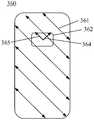
- Fig. 30is a schematic top view of a fingerprint detection device according to an embodiment of the present application.
- Fig. 31is a schematic side cross-sectional view of the fingerprint detection device shown in Fig. 30 along the BB' direction.
- FIG. 32is a schematic structural diagram of optical path transmission in a scenario where the light-receiving direction of the finger is perpendicular to the fingerprint direction in an embodiment of the present application.
- FIG. 33is a schematic structural diagram of optical path transmission in a scenario where the light receiving direction of the finger is parallel to the fingerprint direction in an embodiment of the present application.
- 34 to 37are schematic structural diagrams of the relationship between the polarization direction of the display screen and the light-receiving direction of the fingerprint detection device in an embodiment of the present application.
- Figures 38 to 43are schematic structural diagrams of a fingerprint detection unit or fingerprint detection device according to an embodiment of the present application.
- FIG. 44 and FIG. 45are respectively a side sectional view of a fingerprint detection device for receiving a single direction according to an embodiment of the present application and a schematic diagram of the deviation tolerance of the light spot area in the optical sensing pixel.
- FIG. 46 and FIG. 47are respectively a side sectional view of a dual-directional fingerprint detection device and a schematic diagram of the deviation tolerance of the light spot area in the optical sensing pixel according to an embodiment of the present application.
- FIG. 48 to FIG. 67are another schematic structural diagrams of a fingerprint detection unit or fingerprint detection device according to an embodiment of the present application.
- FIG. 68is a schematic structural diagram of structural parameters in a fingerprint detection device according to an embodiment of the present application.
- Fig. 69 and Fig. 70are both schematic top views of the fingerprint detection device shown in Fig. 68.
- the technical solutions of the embodiments of the present applicationcan be applied to various electronic devices.
- portable or mobile computing devicessuch as smartphones, notebook computers, tablet computers, and gaming devices, as well as other electronic devices such as electronic databases, automobiles, and bank automated teller machines (ATM).
- ATMbank automated teller machines
- the embodiments of the present applicationare not limited thereto.
- biometric recognition technologyincludes but is not limited to fingerprint recognition, palmprint recognition, iris recognition, face recognition, and living body recognition.
- fingerprint recognition technologyincludes but is not limited to fingerprint recognition, palmprint recognition, iris recognition, face recognition, and living body recognition.
- fingerprint recognition technologyuses fingerprint recognition technology as an example.
- the under-screen fingerprint recognition technologyrefers to the installation of the fingerprint recognition module below the display screen, so as to realize the fingerprint recognition operation in the display area of the display screen. There is no need to set a fingerprint collection area on the front of the electronic device except for the display area.
- the fingerprint recognition moduleuses the light returned from the top surface of the display assembly of the electronic device to perform fingerprint sensing and other sensing operations. This returned light carries information about objects (such as fingers) that are in contact with or close to the top surface of the display assembly.
- the fingerprint recognition module located under the display assemblycollects and detects this returned light to realize fingerprint recognition under the screen.
- the design of the fingerprint identification modulemay be to implement the desired optical imaging by appropriately configuring optical elements for collecting and detecting the returned light, so as to detect the fingerprint information of the finger.
- in-display fingerprint recognition technologyrefers to the installation of fingerprint recognition modules or part of fingerprint recognition modules inside the display screen, so as to realize fingerprint recognition operations in the display area of the display screen without the need for electronic
- the fingerprint collection areais set on the front of the device except the display area.
- FIGS. 1 to 4show schematic diagrams of electronic devices to which the embodiments of the present application can be applied.
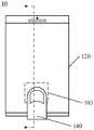
- 1 and 3are schematic diagrams of the orientation of the electronic device 10
- FIGS. 2 and 4are schematic cross-sectional views of the electronic device 10 shown in FIGS. 1 and 3, respectively.
- the electronic device 10may include a display screen 120 and an optical fingerprint recognition module 130.
- the display screen 120may be a self-luminous display screen, which uses a self-luminous display unit as a display pixel.
- the display screen 120may be an Organic Light-Emitting Diode (OLED) display screen or a Micro-LED (Micro-LED) display screen.
- the display screen 120may also be a liquid crystal display (LCD) or other passive light-emitting display, which is not limited in the embodiment of the present application.
- the display screen 120may also be specifically a touch display screen, which can not only perform screen display, but also detect a user's touch or pressing operation, so as to provide a user with a human-computer interaction interface.
- the electronic device 10may include a touch sensor, and the touch sensor may specifically be a touch panel (TP), which may be provided on the surface of the display screen 120, or may be partially integrated or The whole is integrated into the display screen 120 to form the touch display screen.
- TPtouch panel
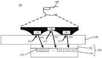
- the optical fingerprint module 130includes an optical fingerprint sensor, and the optical fingerprint sensor includes a sensing array 133 having a plurality of optical sensing units 131 (also referred to as optical sensing pixels, photosensitive pixels, pixel units, etc.).
- the area where the sensing array 133 is located or the sensing area thereofis the fingerprint detection area 103 of the optical fingerprint module 130 (also referred to as fingerprint collection area, fingerprint recognition area, etc.).
- the optical sensing unit 131may be a photodetector, that is, the sensing array 133 may specifically be a photodetector (Photodetector) array, which includes a plurality of photodetectors distributed in an array.
- the optical fingerprint module 130is arranged in a partial area below the display screen 120.
- the fingerprint detection area 103may be located in the display area of the display screen 120.
- the optical fingerprint module 130may also be arranged in other positions, such as the side of the display screen 120 or the non-transparent area at the edge of the electronic device 10, and the optical fingerprint module 130 may be designed to The optical signal from at least a part of the display area of the display screen 120 is guided to the optical fingerprint module 130, so that the fingerprint detection area 103 is actually located in the display area of the display screen 120.
- the electronic device 10when the user needs to unlock the electronic device 10 or perform other fingerprint verification, he only needs to press his finger on the fingerprint detection area 103 located in the display screen 120 to realize fingerprint input. Since fingerprint detection can be implemented in the screen, the electronic device 10 adopting the above structure does not need to reserve space on the front side for setting fingerprint buttons (such as the Home button), so that a full screen solution can be adopted, that is, the display area of the display screen 120 It can be basically extended to the front of the entire electronic device 10.
- fingerprint buttonssuch as the Home button
- the optical fingerprint module 130may include a light detecting part 134 and an optical component 132.
- the light detection part 134includes the sensor array 133 (also called an optical fingerprint sensor), a reading circuit and other auxiliary circuits electrically connected to the sensor array 133, which can be fabricated on a chip by a semiconductor process (Die), such as an optical imaging chip or an optical fingerprint sensor.
- the optical component 132may be disposed above the sensing array 133 of the light detecting part 134, and it may specifically include a filter layer (Filter), a light guide layer or a light path guiding structure, and other optical elements.
- the filter layerIt can be used to filter out ambient light penetrating the finger, and the light guide layer or light path guiding structure is mainly used to guide the reflected light reflected from the surface of the finger to the sensing array 133 for optical detection.
- the optical assembly 132 and the light detecting part 134may be packaged in the same optical fingerprint component.
- the optical component 132 and the optical detection part 134may be packaged in the same optical fingerprint chip, or the optical component 132 may be arranged outside the chip where the optical detection part 134 is located, for example, the optical component 132 It is attached above the chip, or some components of the optical assembly 132 are integrated into the chip.
- the area or light sensing range of the sensing array 133 of the optical fingerprint module 130corresponds to the fingerprint detection area 103 of the optical fingerprint module 130.
- the fingerprint collection area 103 of the optical fingerprint module 130may be equal to or not equal to the area or light sensing range of the sensing array 133 of the optical fingerprint module 130, which is not specifically limited in the embodiment of the present application. .
- the light pathis guided by light collimation, and the fingerprint detection area 103 of the optical fingerprint module 130 can be designed to be substantially the same as the area of the sensing array of the optical fingerprint module 130.
- the area of the fingerprint detection area 103 of the optical fingerprint module 130may be larger than that of the optical fingerprint module. 130 the area of the sensing array 133.
- the light path guiding structure that the optical assembly 132 may includeis exemplified below.
- the optical collimatormay be specifically a collimator (Collimator) layer fabricated on a semiconductor silicon wafer, which has A plurality of collimating units or micro-holes
- the collimating unitmay be specifically a small hole, among the reflected light reflected from the finger, the light that is perpendicularly incident on the collimating unit can pass through and be received by the sensor chip below it , And the light whose incident angle is too large is attenuated by multiple reflections inside the collimating unit, so each sensor chip can basically only receive the reflected light reflected by the fingerprint pattern directly above it, which can effectively improve image resolution Rate, thereby improving the fingerprint recognition effect.
- the optical path guiding structuremay be an optical lens (Lens) layer, which has one or more lens units, such as a lens group composed of one or more aspheric lenses , which is used to converge the reflected light reflected from the finger to the sensing array 133 of the light detection part 134 below it, so that the sensing array 133 can perform imaging based on the reflected light, thereby obtaining a fingerprint image of the finger .
- Lensoptical lens
- the optical lens layermay further have a pinhole or a micro-aperture formed in the optical path of the lens unit, for example, one or more light-shielding sheets may be formed in the optical path of the lens unit, of which at least One light-shielding sheet may be formed with light-transmitting micro-holes in the optical axis or optical center area of the lens unit, and the light-transmitting micro-holes may serve as the aforementioned pinholes or micro-apertures.
- the pinhole or micro-aperture diaphragmcan cooperate with the optical lens layer and/or other optical film layers above the optical lens layer to expand the field of view of the optical fingerprint module 130 to improve the optical fingerprint module 130 Fingerprint imaging effect.
- the light path guiding structuremay be a micro lens array including a plurality of micro lenses, which may be formed by a semiconductor growth process or other processes
- each microlensmay correspond to one of the sensing units of the sensing array 133, respectively.
- other optical film layersmay be formed between the microlens layer and the sensing unit, such as a dielectric layer or a passivation layer.
- a light blocking layer(or called a light blocking layer, a light blocking layer, etc.) with micro holes (or called openings) may also be included between the micro lens layer and the sensing unit, wherein the micro The hole is formed between the corresponding micro lens and the sensing unit, the light blocking layer can block the optical interference between the adjacent micro lens and the sensing unit, and make the light corresponding to the sensing unit converge through the micro lens To the inside of the micropore and transfer to the sensing unit through the micropore for optical fingerprint imaging.
- a micro lens layermay be further provided above or below the collimator layer or the optical lens layer.
- a micro lens layermay be further provided above or below the collimator layer or the optical lens layer.
- the optical assembly 132may also include other optical elements, such as filters or other optical films, which may be arranged between the optical path guiding structure and the optical fingerprint sensor or arranged at all.
- the display screen 120 and the optical path guide structureare mainly used to isolate the influence of external interference light on the optical fingerprint detection.
- the filter layercan be used to filter out the ambient light that penetrates the finger and enters the optical fingerprint sensor through the display screen 120. Similar to the light path guiding structure, the filter layer can be specific to each The optical fingerprint sensors are separately arranged to filter out interference light, or a large-area filter layer can also be used to simultaneously cover the multiple optical fingerprint sensors.
- the fingerprint identification module 140can be used to collect user fingerprint information (such as fingerprint image information).
- the optical fingerprint module 130can use the display unit (ie, the OLED light source) of the OLED display 120 in the fingerprint detection area 103 as an excitation light source for optical fingerprint detection.
- the display unitie, the OLED light source
- the display screen 120emits a beam of light 111 to the target finger 140 above the fingerprint detection area 103.
- the light 111is reflected on the surface of the finger 140 to form reflected light or pass through all the fingers.
- the finger 140scatters to form scattered light (transmitted light).
- the above-mentioned reflected light and scattered lightare collectively referred to as reflected light.
- the ridge 141 and valley 142 of the fingerprinthave different light reflection capabilities
- the reflected light 151 from the fingerprint ridge and the reflected light 152 from the fingerprint valleyhave different light intensities, and the reflected light passes through the optical component 132. After that, it is received by the sensor array 133 in the optical fingerprint module 130 and converted into a corresponding electrical signal, that is, a fingerprint detection signal; based on the fingerprint detection signal, fingerprint image data can be obtained, and fingerprint matching verification can be further performed, thereby
- the electronic device 10realizes the optical fingerprint recognition function.
- the optical fingerprint module 130may also use a built-in light source or an external light source to provide an optical signal for fingerprint detection and identification.
- the optical fingerprint module 130can be applied not only to self-luminous displays such as OLED displays, but also to non-self-luminous displays, such as liquid crystal displays or other passive light-emitting displays.
- the optical fingerprint system of the electronic device 10may also include an excitation light source for optical fingerprint detection.
- the light sourcemay specifically be an infrared light source or a light source of invisible light of a specific wavelength, which may be arranged under the backlight module of the liquid crystal display or arranged in the edge area under the protective cover of the electronic device 10, and the optical fingerprint module 130 can be arranged under the edge area of the liquid crystal panel or the protective cover and guided by the light path so that the fingerprint detection light can reach the optical fingerprint module 130; or, the optical fingerprint module 130 can also be arranged on the backlight module Below, and the backlight module is designed to allow the fingerprint detection light to pass through the liquid crystal panel and the backlight module and reach the optical fingerprint module 130 by opening holes or other optical designs on the film layers such as diffuser, brightness enhancement film, and reflective film. .
- the optical fingerprint module 130uses a built-in light source or an infrared light source or an infrared light source or an infrared light source or a light source of invisible light of a specific wavelength
- the electronic device 10may also include a transparent protective cover plate, which may be a glass cover plate or a sapphire cover plate, which is located above the display screen 120 and covers the front surface of the electronic device 10 . Therefore, in the embodiments of the present application, the so-called finger pressing on the display screen 120 actually refers to pressing on the cover plate above the display screen 120 or covering the surface of the protective layer of the cover plate.
- a transparent protective cover platewhich may be a glass cover plate or a sapphire cover plate
- the optical fingerprint module 130may include only one optical fingerprint sensor.
- the fingerprint detection area 103 of the optical fingerprint module 130has a small area and a fixed position, so the user needs to press his finger when inputting a fingerprint. Go to the specific position of the fingerprint detection area 103, otherwise the optical fingerprint module 130 may not be able to collect fingerprint images, resulting in poor user experience.
- the optical fingerprint module 130may specifically include multiple optical fingerprint sensors. The multiple optical fingerprint sensors may be arranged side by side under the display screen 120 in a splicing manner, and the sensing areas of the multiple optical fingerprint sensors together constitute the fingerprint detection area 103 of the optical fingerprint module 130.
- the fingerprint detection area 103 of the optical fingerprint module 130can be extended to the main area of the lower half of the display screen, that is, to the area where the finger is habitually pressed, so as to realize the blind fingerprint input operation. Further, when the number of optical fingerprint sensors is sufficient, the fingerprint detection area 103 can also be extended to half of the display area or even the entire display area, thereby realizing half-screen or full-screen fingerprint detection.
- the optical fingerprint module 130 in the electronic device 10may include a plurality of optical fingerprint sensors, and the plurality of optical fingerprint sensors may be arranged side by side on the display screen 120 by means such as splicing. Below, and the sensing areas of the multiple optical fingerprint sensors collectively constitute the fingerprint detection area 103 of the optical fingerprint device 130.
- the optical component 132may include a plurality of light path guiding structures, and each light path guiding structure corresponds to an optical fingerprint sensor (ie, the sensing array 133), and is attached and arranged above the corresponding optical fingerprint sensor.
- the multiple optical fingerprint sensorsmay also share an overall optical path guiding structure, that is, the optical path guiding structure has an area large enough to cover the sensing array of the multiple optical fingerprint sensors.
- the optical sensor array of each optical fingerprint sensormay be One of the optical sensing units is configured with one or more collimating units, and is attached and arranged above the corresponding optical sensing unit.
- the multiple optical sensing unitscan also share one collimating unit, that is, the one collimating unit has an aperture large enough to cover the multiple optical sensing units. Since one collimating unit can correspond to multiple optical sensing units or one optical sensing unit corresponds to multiple collimating units, the correspondence between the spatial period of the display screen 120 and the spatial period of the optical fingerprint sensor is destroyed.
- the spatial structure of the light-emitting display arrayis similar to the spatial structure of the optical sensing array of the optical fingerprint sensor. It can also effectively prevent the optical fingerprint module 130 from using the light signal passing through the display 120 to perform fingerprint imaging to generate moiré fringes, which effectively improves the optical fingerprint model. Group 130 fingerprint recognition effect.
- the optical fingerprint module 130includes multiple sensor chips
- one optical lensmay be configured for each sensor chip to perform fingerprint imaging, or multiple sensor chips may be configured with one optical lens. Realize light convergence and fingerprint imaging. Even when a sensor chip has two sensing arrays (Dual Array) or multiple sensing arrays (Multi-Array), the sensor chip can also be equipped with two or more optical lenses to cooperate with the two sensing arrays or Multiple sensing arrays perform optical imaging, thereby reducing the imaging distance and enhancing the imaging effect.
- FIGS. 1 to 4are only examples of this application, and should not be construed as limiting the application.
- the optical fingerprint module 130may include a plurality of fingerprint sensors distributed in a square or circular shape.
- the effective view of the sensing array 133 of the optical fingerprint module 130is limited by the area of the optical component.
- the microlens arrayis located directly above or obliquely above the sensing array 133, and one microlens corresponds to one optical sensing unit, that is, each microlens in the microlens array will receive The light is focused to the optical sensor unit corresponding to the same micro lens. Therefore, the fingerprint recognition area of the sensor array 133 is affected by the size of the microlens array.
- the fingerprint detection device of the embodiment of the present applicationis suitable for under the display screen to realize the under-screen optical fingerprint detection.
- the fingerprint detection devicemay be applicable to the electronic device 10 shown in FIGS. 1 to 4, or the device may be the optical fingerprint module 130 shown in FIGS. 2 or 4.
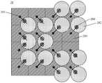
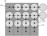
- the fingerprint detection deviceincludes a plurality of fingerprint detection units 21 as shown in FIG. 5.
- the fingerprint detection devicemay include a plurality of fingerprint detection units distributed in an array or staggered, and may also include a plurality of fingerprint detection units distributed in a centrally symmetrical or axisymmetrical manner, which is not specifically limited in the embodiment of the present application.
- the fingerprint detection devicemay include a plurality of fingerprint detection units that are independently arranged in structure but arranged in a staggered arrangement. For example, two adjacent columns or two rows of fingerprint detection units in the fingerprint detection device are arranged alternately.
- the fingerprint detection devicemay also include a plurality of fingerprint detection units interlaced in structure.
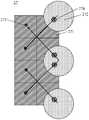
- the microlens in each fingerprint detection unit in the fingerprint detection devicecan converge the received oblique light signal to the optical sensing pixels under the microlenses in the plurality of adjacent fingerprint detection units.
- each microlenscondenses the received oblique light signal to the optical sensing pixels under a plurality of microlenses adjacent to the same microlens.
- each fingerprint detection unit of the plurality of fingerprint detection unitsincludes a plurality of optical sensing pixels, at least one microlens, and at least one light blocking layer.
- the at least one microlensmay be arranged above the plurality of optical sensing pixels, or the plurality of optical sensing pixels may be respectively arranged on a plurality of microlenses adjacent to the one microlens.
- the at least one light blocking layermay be disposed between the at least one microlens and the plurality of optical sensing pixels, and each of the at least one light blocking layer is provided with the multiple A hole corresponding to each optical sensing pixel.
- the oblique light signals in multiple directions reflected from the finger above the display screenare condensed by the at least one microlens, and are respectively transmitted to the multiple light-blocking layers through the openings provided in the at least one light-blocking layer.
- Optical sensing pixels, and the oblique light signalis used to detect fingerprint information of the finger.
- the oblique light signals in multiple directions received by the at least one microlensmay be incident directions of oblique light for the at least one microlens.
- the at least one microlenscan be regarded as a whole.
- the multiple directionscan be the optical signals received by the at least one microlens from 4 directions, up, down, left, and right.
- the angle of the oblique light signal in the direction relative to the plane where the display screen is locatedmay be the same or different.
- the multiple directionsmay be directions for the plane where the display screen is located, or directions for the three-dimensional space. The multiple directions may be different from each other or partly different.
- the microlensmay be various lenses with a converging function to increase the field of view and increase the amount of light signals transmitted to the photosensitive pixels.
- the material of the microlensmay be an organic material, such as resin.
- the optical sensing pixelmay be a photo sensor for converting light signals into electrical signals.
- the optical sensing pixelmay use a complementary metal oxide semiconductor (Complementary Metal Oxide Semiconductor, CMOS) device, a semiconductor device composed of a PN junction, which has unidirectional conductivity characteristics.
- CMOScomplementary Metal Oxide Semiconductor
- the optical sensitivity of the optical sensing pixel to blue, green, red or infrared lightis greater than a first predetermined threshold, and the quantum efficiency is greater than a second predetermined threshold.
- the first predetermined thresholdmay be 0.5v/lux-sec
- the second predetermined thresholdmay be 40%.
- the photosensitive pixelhas higher light sensitivity and higher quantum efficiency for blue light (wavelength of 460 ⁇ 30nm), green light (wavelength of 540 ⁇ 30nm), red light or infrared light (wavelength ⁇ 610nm), so that To detect the corresponding light.
- each optical sensing pixel in the plurality of optical sensing pixelsmay be a polygonal pixel such as a quadrilateral or hexagonal pixel, or may be a pixel of other shapes, such as a circular pixel, so that the plurality of optical sensing pixels have more High symmetry, higher sampling efficiency, equal distance between adjacent pixels, better angular resolution, less aliasing effects.
- the above-mentioned parameters for the optical sensor pixelscan correspond to the light required for fingerprint detection. For example, if the light required for fingerprint detection is only one wavelength of light, the above-mentioned parameters of the photosensitive pixel only need to meet the light of that wavelength. Just ask.
- the signals received by the multiple optical sensing pixelsare oblique light signals in multiple directions. That is, optical signals in multiple directions that are incident obliquely.
- the dry hand fingerprintWhen the dry hand fingerprint is not in contact with the OLED screen, the contrast between the fingerprint ridge and the fingerprint valley of the fingerprint image in the vertical direction is poor, and the image is blurred to the point where the fingerprint lines cannot be distinguished.
- This applicationadopts a reasonable optical path design to allow the optical path to receive oblique light signals. While being able to better obtain normal finger fingerprints, it can better detect dry finger fingerprint images. In normal life scenarios, such as washing hands, getting up in the morning, plastering fingers, low temperature and other scenes, the fingers are usually dry, and the stratum corneum is uneven. When it is pressed on the OLED screen, local areas of the fingers will have poor contact. The occurrence of this situation causes the current optical fingerprint solution to have a poor effect on dry hand fingerprint recognition.
- the beneficial effect of this applicationis to improve the dry hand fingerprint imaging effect and make the dry hand fingerprint image clearer.
- the oblique light signals in the multiple directionscan be subjected to non-frontal light imaging (ie oblique light imaging) through the one microlens, which can shorten the optical path between the one microlens and the optical sensing pixel array
- the thickness of the design layerin turn, can effectively reduce the thickness of the fingerprint detection device.
- the object-side numerical aperture of the optical systemcan be enlarged, thereby improving the robustness and tolerance tolerance of the fingerprint detection device.
- the numerical aperturecan be used to measure the angular range of light that the at least one microlens can collect.
- the multiple optical sensing pixelscan also expand the field of view and field of view of the fingerprint detection unit by receiving light signals in multiple directions, thereby increasing the field of view and field of view of the fingerprint detection device, for example,
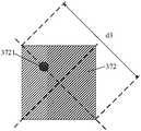
- the field of view of the fingerprint detection devicecan be expanded from 6x9mm 2 to 7.5x10.5mm 2 to further improve the fingerprint recognition effect.
- the spatial period of the microlensThat is, the spacing between adjacent microlenses
- the spatial period of the optical sensing pixelsthat is, the spacing between adjacent optical sensing pixels
- the cost of the lenscan be reduced and the density of the plurality of optical sensing pixels can be increased, thereby reducing the size and the size of the fingerprint detection device. cost.
- a single fingerprint detection unitcan multiplex optical signals in multiple directions (for example, a single microlens can multiplex optical signals at 4 angles), and can split and image light beams with different object aperture angles. The amount of light entering the fingerprint detection device is increased, thereby reducing the exposure time of the optical sensing pixel.
- the plurality of optical sensing pixelscan respectively receive oblique light signals from multiple directions
- the plurality of optical sensing pixelscan be divided into a plurality of optical sensing pixel groups according to the direction of the oblique light signal.
- the multiple optical sensing pixel groupsmay be respectively used to receive the oblique light signals in the multiple directions, that is, each optical sensing pixel group may generate a fingerprint image based on the received oblique light signals, so that the multiple optical sensing pixel groups
- the sensing pixel groupcan be used to generate multiple fingerprint images.
- the multiple fingerprint imagescan be superimposed to obtain a high-resolution fingerprint image based on this high-resolution fingerprint image
- Fingerprint recognitioncan improve fingerprint recognition performance.
- the oblique light signals in multiple directions reflected from the finger above the display screenare condensed by the at least one microlens, and then transmitted to the at least one light-blocking layer through the openings.
- the plurality of optical sensing pixelscan not only reduce the exposure time of the plurality of optical sensing pixels, and the thickness and cost of the fingerprint detection device, but also can improve the robustness, tolerance tolerance, field of view and angle of the fingerprint detection device. The field of view, thereby improving the fingerprint recognition effect, especially the fingerprint recognition effect of dry fingers.
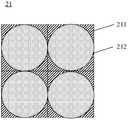
- the number of the at least one microlensis equal to the number of the plurality of optical sensing pixels, wherein a microlens is provided above each optical sensing pixel of the plurality of optical sensing pixels .
- the at least one microlensis a 2x2 microlens rectangular array
- the plurality of optical sensing pixelsis a 2x2 optical sensing pixel rectangular array
- each optical sensing pixel in the 2x2 optical sensing pixel rectangular arrayA micro lens is set directly above the.
- the at least one microlensis a 2x2 microlens rectangular array
- the plurality of optical sensing pixelsis a 2x2 optical sensing pixel rectangular array
- each of the 2x2 optical sensing pixel rectangular arraysis optically sensitive
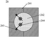
- a micro lensis arranged diagonally above the pixel. For example, as shown in FIG.
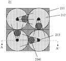
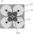
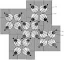
- the fingerprint detection unit 21may include four optical sensing pixels 211 and four microlenses 212 distributed in a rectangular array, wherein a microlens is arranged directly above each optical sensing pixel 211 212.
- the fingerprint detection unit 21may include a top light blocking layer and a bottom light blocking layer.
- the top light blocking layermay include four openings 2141 corresponding to the four microlenses 212
- the bottom light blocking layermay include four openings 213 corresponding to the four microlenses 212, respectively.
- the 2x2 microlens rectangular arrayreceives the oblique light signals in the multiple directions in a clockwise direction, and each microlens in the 2x2 microlens rectangular array converges the received oblique light signals To the optical sensing pixel below the adjacent microlens in the clockwise direction, or the 2x2 microlens rectangular array receives the oblique light signals in the multiple directions in the counterclockwise direction, in the 2x2 microlens rectangular array Each of the microlenses converges the received oblique light signal to the optical sensing pixel under the adjacent microlens in the counterclockwise direction.
- the four microlenses 212can respectively converge oblique light signals in multiple directions to the four optical sensing pixels 211 along the following path: the oblique light signals received by the microlens 212 in the upper right corner Converges to the optical sensing pixel 211 in the upper left corner, the micro lens 212 in the upper left corner converges the received oblique light signal to the optical sensing pixel 211 in the lower left corner, and the micro lens 212 in the lower left corner converges the received oblique light signal to the lower right corner.
- the optical sensing pixel 211 in the upper right corner and the micro lens 212 in the lower right cornerconverge the received oblique light signal to the optical sensing pixel 211 in the upper right corner. Therefore, when the fingerprint detection device includes multiple fingerprint detection units distributed in an array, multiple fingerprint images can be generated based on the received light signals in multiple directions, and then a high-resolution fingerprint image can be obtained to improve the fingerprint Recognition effect.
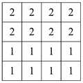
- the rectangular array of 4x4 fingerprint detection unitsmay include an optical sensing pixel array as shown in FIG. 8, where "1" indicates an optical sensing pixel for receiving a tilt light signal in the first direction, and “2” indicates a Optical sensor pixels that receive the tilt light signal in the second direction, “3” represents the optical sensor pixel for receiving the tilt light signal in the third direction, and “4" represents the optical sensor pixel for receiving the tilt light signal in the fourth direction .
- the optical sensing pixels represented by "1", “2", “3” and “4"can be used to generate a fingerprint image respectively, that is, a total of 4 fingerprint images can be generated, and these 4 fingerprint images can be used It is merged into a high-resolution fingerprint image to improve the recognition effect of the fingerprint detection device.
- the first direction to the fourth directionmay be the directions in which the lower right microlens 212, the upper right microlens 212, the upper left microlens 212, and the lower left microlens 212 receive the oblique light signal, respectively.
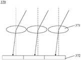
- Fig. 9is a side view of the fingerprint detection device under the display screen.
- the fingerprint detection devicemay include microlenses 212 distributed in an array, a top light blocking layer and a bottom light blocking layer located below the microlenses 212, and an array of optical fibers located below the bottom light blocking layer.
- the top light blocking layer and the bottom light blocking layerare respectively formed with corresponding openings 2141 and 213.
- the fingerprint detection deviceis arranged below the display screen 216.
- each microlens 212converges the received oblique light signal with a specific direction (the light signal shown by the solid line in the figure) to the corresponding optical sensing pixel through the corresponding opening 2141 and the opening 213, and will receive
- the received oblique light signal in a non-specific direction(the light signal shown by the dotted line in the figure) is transmitted to the area of the light blocking layer except for the opening 2141 and the opening 214 to avoid being received by other optical sensing pixels, thereby causing fingerprint images Segmentation imaging.
- FIG. 10is a schematic diagram of an optical path of an optical signal inclined in two directions according to an embodiment of the present application.
- FIG. 10may be a schematic side sectional view of the fingerprint detection device including the fingerprint detection unit shown in FIG. 7 in the AA' direction.
- a microlens 212 in the fingerprint detection unitreceives oblique light signals in one direction (that is, the fourth direction) (the light shown by the solid line in FIG. 10) through the corresponding opening 2141 and the opening 213. Signal) is converged to the corresponding optical sensor pixel (for example, the lower right optical sensor pixel 211 shown in FIG. 7), and another microlens 212 in the fingerprint detection unit (for example, the upper right microlens 212 shown in FIG.
- the fingerprint recognition area (also called fingerprint collection area or fingerprint detection area) of the fingerprint detection device shown in FIG. 10includes a first recognition area and a second recognition area, which are used to converge in the second direction
- the fingerprint recognition area corresponding to the microlens 212 of the oblique light signal aboveis the first recognition area
- the fingerprint recognition area corresponding to the microlens for condensing the oblique light signal in the fourth directionis the second recognition area.
- the first recognition areais shifted to the right by the first increase area relative to the array formed by the optical sensing pixels
- the second recognition areais shifted to the left by the second increase area relative to the column formed by the optical sensing pixels.
- the recognition areaadditionally includes the first increased area and the second increased area, effectively increasing the visible area (ie, the field of view).
- the overlapping area of the first recognition area and the second recognition areacan effectively improve the image resolution of the fingerprint image, thereby improving the fingerprint recognition effect.
- optical path design shown in FIG. 7is only an example of this application, and should not be understood as a limitation to this application.
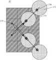
- the 2x2 microlens rectangular arrayreceives the oblique light signals in the multiple directions along the diagonal direction of the 2x2 microlens rectangular array, and the 2x2 microlens rectangular Each microlens in the array converges the received oblique light signal to the optical sensing pixel under the adjacent microlens in the diagonal direction. For example, as shown in FIGS.
- the four microlenses 212can respectively converge oblique light signals in multiple directions to the four optical sensing pixels 211 along the following path: the microlens 212 in the upper right corner will receive The received oblique light signal converges to the optical sensing pixel 211 in the lower left corner, the micro lens 212 in the lower left corner converges the received oblique light signal to the optical sensing pixel 211 in the upper right corner, and the micro lens 212 in the upper left corner will receive the oblique light The signal converges to the optical sensing pixel 211 in the lower right corner, and the micro lens 212 in the lower right corner converges the received oblique light signal to the optical sensing pixel 211 in the upper left corner. Therefore, when the fingerprint detection device includes multiple fingerprint detection units distributed in an array, multiple fingerprint images can be generated based on the received light signals in multiple directions, and then a high-resolution fingerprint image can be obtained to improve the fingerprint Recognition effect.
- the rectangular array of 4x4 fingerprint detection unitsmay include an optical sensing pixel array as shown in FIG. 8, where "1" represents the optical sensing pixel used to receive the oblique light signal in the first direction, and “2" represents the For the optical sensing pixel that receives the tilt light signal in the second direction, “3” indicates the optical sensing pixel for receiving the tilt light signal in the third direction, and “4" indicates the optical sensing pixel for receiving the tilt light signal in the fourth direction Pixels.
- the optical sensing pixels represented by "1", “2", “3” and “4"can be used to generate a fingerprint image respectively, that is, a total of 4 fingerprint images can be generated, and these 4 fingerprint images can be used It is merged into a high-resolution fingerprint image to improve the recognition effect of the fingerprint detection device.
- the first direction to the fourth aspectmay be the directions in which the lower left microlens 212, the lower right microlens 212, the upper right microlens 212, and the upper left microlens 212 receive oblique light signals, respectively.
- the fingerprint detection devicemay include at least one light blocking layer and an optical sensing pixel array.
- the at least one light blocking layeris a plurality of light blocking layers.
- One opening in the small hole array in each of the plurality of light blocking layerscorresponds to a plurality of optical sensing pixels in the optical sensing pixel, or each of the plurality of light blocking layers
- One opening in the small hole array in the light blocking layercorresponds to one optical sensing pixel in the optical sensing pixel.
- one opening in the small hole array in the top light blocking layer of the plurality of light blocking layerscorresponds to the plurality of optical sensing pixels in the optical sensing pixels.
- one opening in the small hole array in the top light blocking layer of the plurality of light blocking layerscorresponds to one optical sensing pixel in the optical sensing pixel.
- One opening in the small hole array in the bottom light blocking layer of the plurality of light blocking layerscorresponds to one optical sensing pixel in the optical sensing pixel.
- the apertures of the plurality of light blocking layers corresponding to the same optical sensing pixelare sequentially reduced from top to bottom.
- the at least one light blocking layeris one light blocking layer.
- the thickness of the one light blocking layeris greater than a preset threshold.
- the metal wiring layer of the optical sensing pixel arrayis arranged at the back focal plane position of the microlens array, and the metal wiring layer is opened above each optical sensing pixel in the optical sensing pixel array. Holes to form the bottom light blocking layer.
- the fingerprint detection unitmay include at least one light blocking layer and a plurality of optical sensing pixels, wherein each of the at least one light blocking layer is provided with an opening corresponding to the plurality of optical sensing pixels. hole.
- the at least one light blocking layermay be a multilayer light blocking layer, and the top light blocking layer of the multilayer light blocking layer may be provided with at least one opening corresponding to the plurality of optical sensing pixels.
- one small hole of the small hole array in the top light blocking layercorresponds to at least two optical sensing pixels of the plurality of optical sensing pixels. For example, as shown in FIG.
- the at least one light-blocking layermay include a top light-blocking layer and a bottom light-blocking layer, wherein the top light-blocking layer is provided with 4 openings 2141 corresponding to 4 optical sensing pixels. .
- the bottom light blocking layeris provided with 4 openings 213 corresponding to 4 optical sensing pixels, respectively.
- the at least one light blocking layermay include a top light blocking layer and a bottom light blocking layer, wherein the top light blocking layer is provided with 1 opening 2142 corresponding to 4 optical sensing pixels. .
- the bottom light blocking layeris provided with 4 openings 213 corresponding to 4 optical sensing pixels, respectively.
- the openings provided in the light-blocking layer in FIG. 12 and FIG. 13are only described by taking the fingerprint detection unit shown in FIG. 11 as an example, and the implementation method can be applied to various embodiments of the present application.
- the at least one light blocking layermay be more than 2 light blocking layers.
- the at least one light blocking layermay be a light blocking layer, that is, the at least one light blocking layer may be a straight-hole collimator or a few-hole collimator with a certain thickness.
- FIGS. 5 to 13are only examples in which a microlens is disposed above each optical sensing pixel, and should not be construed as a limitation of the present application.
- the fingerprint detection unitmay also include other numbers or other arrangements of microlenses or optical sensing pixels.
- the at least one microlensis a multi-row microlens
- the plurality of optical sensing pixelsare multiple rows of optical sensing pixels corresponding to the multi-row microlens, wherein the multi-row optical Each row of optical sensing pixels in the sensing pixels is misaligned and arranged under the corresponding row of micro lenses.
- the multiple rows of microlensesmay be multiple columns or rows of microlenses.
- the multiple rows of optical sensing pixelsmay be multiple columns or rows of optical sensing pixels.
- the at least one layer of light blocking layermay be provided with a corresponding optical path design, so that the multiple rows of microlenses receive the oblique light signals in the multiple directions along the misalignment direction of the multiple rows of optical sensing pixels, so Each row of microlenses in the multiple rows of microlenses converges the received oblique light signal to the optical sensing pixels under the same row of microlenses or an adjacent row of microlenses.
- the fingerprint detection unit 22may include 4 columns of optical sensing pixels distributed in a rectangular array and 4 columns of microlenses corresponding to the 4 columns of optical sensing pixels. Among these 4 columns of optical sensing pixels, Each column of optical sensing pixels includes 6 optical sensing pixels 221, each of the four microlens columns includes 6 microlenses 222, and one optical sensing pixel 221 is disposed under one microlens 222 in a staggered manner.
- the fingerprint detection unit 22may further include a top light blocking layer and a bottom light blocking layer. At this time, for each microlens 222, the top light blocking layer and the bottom light blocking layer may be provided with corresponding openings 2241 and 2231 respectively.
- each microlens 222 in each row of microlenses in the plurality of rows of microlensescan converge the received optical signal to the optical sensor obliquely below the same microlens 222 through the corresponding opening 2241 and the opening 2231 Pixel 221. Therefore, when the fingerprint detection device includes multiple fingerprint detection units distributed in an array, multiple fingerprint images can be generated based on the received light signals in multiple directions, and then a high-resolution fingerprint image can be obtained to improve the fingerprint Recognition effect.
- the fingerprint detection unit shown in FIG. 14may include an optical sensing pixel array as shown in FIG. 15, where "1" represents the optical sensing pixel for receiving the oblique light signal in the first direction, and “2" represents Optical sensing pixels that receive oblique light signals in the second direction.
- the optical sensing pixels denoted by "1” and “2”can be used to generate a fingerprint image respectively, that is, a total of 2 fingerprint images can be generated, and these 2 fingerprint images can be combined into a high resolution Fingerprint image, and then improve the recognition effect of the fingerprint detection device.
- the first directionmay be the direction in which the microlens in the first column and the second column of microlenses receive the oblique light signal
- the second directionmay It is the direction of the oblique light signal received by the third and fourth columns of microlenses.
- the projection of each microlens in each row of microlenses in the plurality of rows of microlenses on the plane where the display screen is locatedis circular, and the projection of each microlens in the plurality of rows of optical sensing pixels
- the projection of each optical sensing pixel in each row of optical sensing pixels on the plane where the display screen is locatedis rectangular, and the center of each optical sensing pixel in each row of optical sensing pixels in the multiple rows of optical sensing pixels is at
- the projection on the plane where the display screen is locatedis offset by a predetermined distance along the misalignment direction of the multiple rows of optical sensing pixels relative to the projection on the plane where the display screen is located relative to the center of the corresponding microlens.
- each row of microlenses in the plurality of rows of microlensesis offset along the misalignment direction by a predetermined distance along the respective misalignment direction.
- the misalignment directionis the diagonal direction of each optical sensing pixel in each row of optical sensing pixels in the multiple rows of optical sensing pixels, that is,
- Each microlens 222 in each row of microlenses in the multiple rows of microlensesis offset by a predetermined distance along the diagonal direction of the same optical sensing pixel 221.
- each optical sensing pixel 221 in each row of optical sensing pixels in the multiple rows of optical sensing pixelsmay be provided with its corresponding opening 2241 and opening 2231, that is, in the fingerprint detection unit 22
- At least one light-blocking layeris provided with a corresponding opening above each optical sensing pixel 221.
- the misalignment directionmay also be the direction in which the vertical side length of each optical sensing pixel in each row of optical sensing pixels in the plurality of rows of optical sensing pixels is located.
- the misalignment directionmay also be the direction where the rows or the columns of the optical sensing pixel array are located.
- the preset distancemay also be an offset distance in the direction where the side length of the optical sensing pixel 221 is located.
- the preset distancemay include an offset distance along the X axis direction and an offset distance along the Y axis direction.
- the side length of the optical sensing pixelis 12.5mm
- the diameter of the microlensis 11.5mm
- the offset distance along the X axis directioncan be 4 to 5mm
- the offset distance along the Y axis directioncan be 4 ⁇ 5mm.
- the offset distance along the X-axis directionmay not be equal to the offset distance along the Y-axis direction.
- the offset distance in the direction or the offset distance along the Y-axis directionmay be greater than 5 mm or less than 4 mm.
- the fingerprint detection unit 22may include a top light blocking layer and a bottom light blocking layer.
- the top light blocking layer and the bottom light blocking layermay be provided with corresponding openings 2242 and 2232, respectively.
- each microlens 222 in each row of microlenses in the plurality of rows of microlensescan converge the received oblique light signal to the adjacent microlens 222 through the corresponding opening 2242 and the opening 2232.
- the micro lens 222 in the upper left cornercan converge the received oblique light signal to the optical sensing pixel 221 directly below the adjacent micro lens 222 in the second row and the first column.
- the bottom light blocking layermay be provided with a corresponding opening 2232 above each optical sensing pixel 221 in each row of the multiple rows of optical sensing pixels, and the top layer blocking light
- the layermay be provided with a corresponding opening 2242 above the optical sensing pixel 221 adjacent to the same optical sensing pixel 221.
- misalignment directionmay also be other directions.
- the misalignment directionis the direction in which the horizontal side length of each optical sensing pixel in each row of optical sensing pixels in the plurality of rows of optical sensing pixels is located.
- the misalignment directionmay be the direction where the rows or the columns of the multiple rows of optical sensing pixels are located.
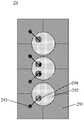
- the number of the at least one microlensis smaller than the number of the plurality of optical sensing pixels.
- the at least one microlensis a microlens
- the plurality of optical sensing pixelsis a 2x2 optical sensing pixel rectangular array
- the one microlensis arranged on the 2x2 optical sensing pixel rectangular array Directly above.
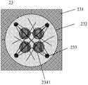
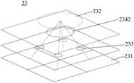
- the fingerprint detection unit 23may include a microlens 232 and four optical sensing pixels 231 distributed in a rectangular array.
- At least one light-blocking layer in the fingerprint detection unit 23may be respectively provided with openings corresponding to the four optical sensing pixels 231 under the one microlens, so that the one microlens
- the lenscan receive the oblique light signals in the multiple directions along the diagonal direction of the 2x2 optical sensing pixel rectangular array, and the one microlens can transmit the oblique light signals in the multiple directions along the diagonal
- the line directionsrespectively converge to the optical sensing pixels in the rectangular array of optical sensing pixels, so as to increase the amount of signal that each optical sensing pixel can receive, thereby improving the fingerprint recognition effect. For example, as shown in FIG. 18 or FIG.
- the at least one light blocking layermay include a top light blocking layer and a bottom light blocking layer.
- the top light blocking layeris provided with openings 2341 corresponding to the four optical sensing pixels 231 under the one microlens 232, and the bottom light blocking layer is provided below the one microlens 232.
- the four optical sensing pixels 231correspond to the openings 232 respectively.
- the one micro lens 232converges the received light signals in multiple directions to the four optical sensing pixels 231 through the corresponding opening 2341 and the opening 232.
- the four small holes of the top light blocking layer corresponding to the four optical sensing pixels 231can also be combined into one large hole.
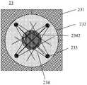
- the one microlensis a 2x2 microlens rectangular array
- the plurality of optical sensing pixelsis a 3x3 optical sensing pixel rectangular array
- each adjacent 4 optical sensing pixels in the 3x3 rectangular arrayA micro lens is set directly above the.
- a microlensis arranged directly above the center position of every 4 adjacent optical sensing pixels.
- the fingerprint detection unit 24may include 4 microlenses 242 distributed in a rectangular array and 9 optical sensing pixels 241 distributed in a rectangular array.
- At least one light blocking layer in the fingerprint detection unit 24may be respectively provided with openings corresponding to the optical sensing pixels 241 on the 4 corners of the 3x3 optical sensing pixel rectangular array. Hole, so that each microlens 242 in the 2x2 microlens rectangular array can converge the received oblique light signal to the same distance in the optical sensing pixels 241 on the 4 corners of the 3x3 optical sensing pixel rectangular array
- the micro lens 424is the closest optical sensor pixel 241.
- the at least one light blocking layermay include a top light blocking layer and a bottom light blocking layer.
- the top light blocking layeris provided with openings 244 corresponding to the optical sensing pixels 241 on the four corners, respectively, and the bottom light blocking layer is provided with openings 244 corresponding to the optical sensing pixels 241 on the four corners, respectively 243.
- the four microlenses 242can respectively converge the oblique light signals in the multiple directions to the optical sensing pixels 241 at the four corners through the corresponding openings 2341 and the openings 243.
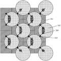
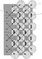
- a fingerprint detection deviceincluding a plurality of fingerprint detection units 24 can be formed in a staggered arrangement.
- the central fingerprint detection unit located in the middle position, the optical sensing pixel 241 between the optical sensing pixel 241 in the upper left corner and the optical sensing pixel 241 in the upper right cornercan be multiplexed as the location of another fingerprint detection unit.
- the optical sensor pixel 241 between the upper left optical sensor pixel 241 and the lower left optical sensor pixel 241 of the central fingerprint detection unitcan be multiplexed as another fingerprint detection unit located in the lower right corner.
- the optical sensing pixel 241 between the lower left optical sensing pixel 241 and the lower right optical sensing pixel 241 of the central fingerprint detection unitcan be reused for the optical sensing pixel located in the upper right corner of another fingerprint detection unit 241.
- the optical sensing pixel 241 between the lower right optical sensing pixel 241 and the upper right optical sensing pixel 241 of the central fingerprint detection unitcan be reused for the optical sensing pixel 241 located in the upper left corner of another fingerprint detection unit.
- the fingerprint detection devicemay include a plurality of optical sensing pixels as shown in FIG. 25, where "0" represents optical sensing pixels that are not used to receive light signals, and "1", “2", “3” and “ 4" respectively indicates that it is used to receive 4 optical sensing pixels in different directions, and the blank space indicates that it can be multiplexed as optical sensing pixels in other fingerprint detection units. That is to say, the optical sensing pixels represented by “1”, “2", “3” and “4" can be used to generate a fingerprint image respectively, that is, a total of 4 fingerprint images can be generated, and these 4 fingerprint images can be used It is merged into a high-resolution fingerprint image to improve the recognition effect of the fingerprint detection device.
- the at least one microlensis a 3x3 microlens rectangular array
- the plurality of optical sensing pixelsis a 4x4 optical sensing pixel rectangular array
- every adjacent 4x4 optical sensing pixel rectangular arrayis A micro lens is arranged directly above each optical sensing pixel.
- the fingerprint detection unit 25may include 9 microlenses 252 distributed in a rectangular array and 16 optical sensing pixels 251 distributed in a rectangular array.
- a micro lens 252is provided directly above each of the four adjacent optical sensing pixels 251 among the 16 optical sensing pixels 251.
- At least one light-blocking layer in the fingerprint detection unit 25may be respectively provided with openings corresponding to the 16 optical sensing pixels 251, so that the central microlens in the 3x3 microlens rectangular array The lens converges the received oblique light signals to the 4 optical sensing pixels below the central microlens.
- the at least one light blocking layermay include a top light blocking layer and a bottom light blocking layer.
- the top light blocking layeris provided with openings 2541 corresponding to the 16 optical sensing pixels 251 respectively
- the bottom light blocking layeris provided with openings 253 corresponding to the 16 optical sensing pixels 251 respectively. Therefore, the nine microlenses 252 can respectively converge the oblique light signals in the multiple directions to the 16 optical sensing pixels 251 through the corresponding openings 2341 and the openings 243.
- the fingerprint detection devicemay include a plurality of optical sensing pixels as shown in FIG. 28, wherein “1", “2”, “3” and “4" respectively indicate that they are used to receive optical sensing in 4 different directions. Pixels. That is to say, the optical sensing pixels represented by “1”, “2”, “3” and “4" can be used to generate a fingerprint image respectively, that is, a total of 4 fingerprint images can be generated, and these 4 fingerprint images can be used It is merged into a high-resolution fingerprint image to improve the recognition effect of the fingerprint detection device.
- FIG. 27is only an example of this application and should not be construed as a limitation to this application.
- the two optical sensing pixels 251 located between the two corners in the 4x4 optical sensing pixel rectangular arraycan be combined into one large hole in the top light-blocking layer.
- the four adjacent optical sensing pixels 251 at the center position and the four small holes corresponding to the top light-blocking layercan be combined into one large hole to reduce processing difficulty and increase convergence The amount of light signal, thereby improving the fingerprint recognition effect of the fingerprint detection device.
- the abovedescribes the fingerprint detection units that can be misaligned in the arrangement, and the following describes the fingerprint detection units that are staggered on the optical path structure.
- the fingerprint detection devicemay include a plurality of fingerprint detection units arranged in an array or staggered arrangement, and each fingerprint detection unit of the plurality of fingerprint detection units may include a microlens, at least one light blocking layer, and a plurality of optical sensors. Pixels, each light-blocking layer in the at least one light-blocking layer is provided with an opening corresponding to the plurality of optical sensing pixels, and the at least one light-blocking layer is disposed on the one microlens and the plurality of optical Sensing the middle of the pixel.
- the microlenses in the plurality of fingerprint detection unitscan converge the received oblique light signals to the optical sensing pixels in the plurality of adjacent fingerprint detection units.
- the multiple optical sensing pixels in each fingerprint detection unit in the fingerprint detection deviceare used to receive the oblique light signals converged by the microlenses in the adjacent multiple fingerprint detection units.
- the staggered multiple fingerprint detection unitsare described below from the perspective of the fingerprint detection device.
- FIG. 30is a schematic top view of the fingerprint detection device 30 according to an embodiment of the present application
- FIG. 31is a side cross-sectional view of the fingerprint detection device 30 shown in FIG. 30 along the direction BB′.
- the fingerprint detection device 30may include 3x3 fingerprint detection units, wherein each of the 3x3 fingerprint detection units includes a microlens and a 2x2 optical sensing pixel rectangular array located below the one microlens .
- the 2x2 optical sensing pixel rectangular array in the middle fingerprint detection unitis used to receive the fingerprint detection units located on 4 corners of the 3x3 fingerprint detection unit. The oblique light signal converged by the microlens.
- the microlens in the central fingerprint detection unit in the center of the 3x3 fingerprint detection unit rectangular arrayis used to converge the received oblique light signals in multiple directions along the diagonal direction of the 3x3 fingerprint detection unit rectangular array To the optical sensing pixels near the central fingerprint detection unit in adjacent fingerprint detection units.
- the fingerprint detection device 30may include a microlens array 310, at least one light blocking layer, and an optical sensing pixel array 340.
- the microlens array 310may be used to be arranged under the display screen of an electronic device, the at least one light blocking layer may be arranged under the microlens array 310, and the optical sensing pixel array 340 may be arranged at all.
- Below the at least one light blocking layermay be the microlens array 310 and the at least one layer of light blocking layer.
- the microlens array 310 and the at least one layer of light blocking layermay be the light guide structure included in the optical component 132 shown in FIG. 3 or FIG. 4, and the optical sensing pixel array 340 may be the light guide structure of FIGS.
- the sensing array 133 with multiple optical sensing units 131also referred to as optical sensing pixels, photosensitive pixels, pixel units, etc.
- the microlens array 310includes a plurality of microlenses.
- the microlens array 310may include a first microlens 311, a second microlens 312, and a third microlens 313.
- the at least one light blocking layermay include a plurality of light blocking layers, for example, the at least one light blocking layer may include a first light blocking layer 320 and a second light blocking layer 330.
- the optical sensing pixel array 340may include a plurality of optical sensing pixels.
- the optical sensing pixel arraymay include a first optical sensing pixel 341, a second optical sensing pixel 342, a third optical sensing pixel 343, and a fourth optical sensing pixel.
- the first light blocking layer 320 and the second light blocking layer 330are respectively provided with each of the plurality of microlenses (that is, the first microlens 311, the second microlens 312, and the third microlens 313) corresponding to each microlens At least one opening.
- the first light blocking layer 320is provided with a first opening 321 and a second opening 322 corresponding to the first microlens 311, and the first light blocking layer 320 is also provided with a first opening 321 corresponding to the second microlens 312.
- the second opening 322 and the third opening 323, and the first light blocking layer 320are provided with a third opening 323 and a fourth opening 324 corresponding to the third microlens 313.
- the second light blocking layer 330is provided with a fifth opening 331 and a sixth opening 332 corresponding to the first microlens 311, and the second light blocking layer 330 is also provided with a second microlens 312 corresponding to The seventh opening 333 and the eighth opening 334, and the second light blocking layer 330 are provided with a ninth opening 335 and a tenth opening 336 corresponding to the third microlens 313.
- a plurality of optical sensing pixelsare arranged under each micro lens in the micro lens array 310.
- the multiple optical sensing pixels arranged under each microlensare respectively used for receiving the light signals condensed through multiple adjacent microlenses.
- a third optical sensing pixel 343 and a fourth optical sensing pixel 344may be provided below the second microlens 312, wherein the third optical sensing pixel 343 may be used for Receiving the oblique light signal converged by the first microlens 311 and passed through the second opening 322 and the seventh opening 333, the fourth optical sensing pixel 344 can be used to receive the oblique light signal converged by the third microlens 313 and passed through the The oblique light signal of the third opening 323 and the eighth opening 334.
- the at least one light blocking layeris formed with a plurality of light guide channels corresponding to each microlens in the microlens array 310, and the bottoms of the plurality of light guide channels corresponding to each microlens respectively extend to adjacent Below multiple micro lenses.
- the plurality of light guide channels corresponding to the second microlens 312may include a light guide channel formed by a second opening 322 and a sixth opening 332, and a third opening
- the hole 323 and the ninth opening 335form a light guide channel.
- the light guide channel formed by the second opening 322 and the sixth opening 332extends below the first microlens 311, and the light guide channel formed by the third opening 323 and the ninth opening 335 extends to the third microlens Below 313.
- An optical sensing pixelmay be disposed under each light guide channel of the plurality of light guide channels corresponding to each micro lens in the micro lens array 310. Taking the second microlens 312 as an example, a second optical sensing pixel 342 is provided under the light guide channel formed by the second opening 322 and the sixth opening 332, and the third opening 323 and the ninth opening A fifth optical sensing pixel 345 is arranged below the light guide channel formed by 335.
- the optical sensing pixel array 340can receive oblique light signals in multiple directions, and converge the oblique light signals in multiple directions through a single microlens, which can solve the single problem.
- the fingerprint detection device 30can not only solve the problem of poor recognition of dry fingers by the vertical light signal and the long exposure time of the single-object telecentric microlens array solution, but also solve the problem of excessive thickness and tolerance tolerance. Over-poor and over-size issues.
- the embodiment of the present applicationdoes not specifically limit the arrangement and size of the optical sensing pixel array.
- the fingerprint detection unitmay include a plurality of optical sensing pixels distributed in a polygonal (for example, diamond shape), circular, or elliptical shape.
- the fingerprint detection device 30may further include a transparent medium layer 350.
- the transparent medium layer 350may be disposed at at least one of the following positions: between the microlens array 310 and the at least one light blocking layer; between the at least one light blocking layer; and the at least one light blocking layer Layer and optical sensing pixel array 340.
- the transparent medium layer 350may include a first medium layer 351 located between the microlens array 310 and the at least one light blocking layer (that is, the first light blocking layer 320) and the first blocking layer.
- the second medium layer 352between the light layer 320 and the second light blocking layer 330.
- the material of the transparent medium layer 350is any transparent material that is transparent to light, such as glass, which can also be transitioned by air or vacuum, which is not specifically limited in this application.
- the fingerprint detection device for receiving oblique light signals in four directionsis described above, but the embodiment of the present application is not limited to this.
- the fingerprint detection devicecan also be used to receive oblique light signals in two directions or three directions to achieve the beneficial effects mentioned above.
- the fingerprint detection deviceis suitable for under the display screen to realize under-screen optical fingerprint detection, and the fingerprint detection device includes a plurality of fingerprint detection units arranged in an array or staggered, and the plurality Each fingerprint detection unit in the fingerprint detection unit includes at least one microlens, at least one light blocking layer under the at least one microlens, and a plurality of optical sensing pixels under the at least one light blocking layer.
- the at least one microlensis arranged above the plurality of optical sensing pixels; the at least one light blocking layer is arranged between the at least one microlens and the plurality of optical sensing pixels, and the at least one Each of the light-shielding layers is provided with openings corresponding to the plurality of optical sensing pixels; the oblique light signals in 2M directions reflected from the finger above the display screen pass through the at least one micro After the lenses are converged, they are respectively transmitted to the plurality of optical sensing pixels through the openings provided in the at least one light blocking layer, the oblique light signal is used to detect fingerprint information of the finger, and M is a positive integer.
- the 2M directionsinclude a first direction and a second direction
- the projection of the first direction on the display screenis perpendicular to the projection of the second direction on the display screen. projection.
- a fingerprintcontains raised ridges and concave valleys.
- the optical fingerprint systemrelies on the reflected light from the fingerprint surface to form images.
- the difference between ridges and valleysis more obvious; as shown in Figure 33, when the incident light is parallel to the direction of the fingerprint, the reflected light of the valleys will not be blocked by the sides of the ridges, and the difference between the ridges and valleys is not obvious.
- the receiving directionis a single direction, since the direction of pressing the fingerprint is random, the pressed fingerprint is likely to be parallel to the receiving direction. At this time, the fingerprint signal is very poor and it may be difficult to identify.
- the multi-directional light-receiving solutioncollects signal light at different angles. Take orthogonal bidirectional light-receiving as an example.
- the multi-directional (two-way) light-receiving solutioncan receive a relatively good signal when the fingerprint is pressed randomly, and improve the fingerprint recognition ability.
- the projection of the first direction or the second direction on the display screenis perpendicular to the polarization direction of the display screen.
- the display screen of an electronic deviceis an OLED screen
- the OLED screenhas polarization characteristics, and the angle between the polarization direction and the horizontal (or vertical) direction of the screen is 45 degrees or 135 degrees.
- the polarization characteristics of the OLED screenmake the signal amount of the fingerprint vary with the angle between the incident surface and the polarization direction. When the incident surface is perpendicular to the polarization direction, the signal amount is the largest, and when the incident surface is parallel to the polarization direction, the signal amount is the smallest.
- the best light-receiving direction of a screen with a 45-degree polarization directionis exactly the worst light-receiving direction of a screen with a 135-degree polarization direction.
- the light receiving directioncan only be selected at 45 degrees or 135 degrees from the best light receiving direction.
- the light collection direction of the fingerprint detection device 362is the direction 363 or the opposite direction of the direction 363.
- the multi-directional light-receiving schemetake the orthogonal four-way or two-way light-receiving scheme as an example. Since it can receive signal light in four (two) directions at the same time, it can receive the most light under the 45° and 135 degree screens. Signal light in the best direction.
- the light-receiving directions of the fingerprint detection device 362are the direction 364 and the direction 365.
- the light collection direction of the fingerprint detection device 362is the direction 364, the direction 365, the opposite direction of the direction 364, and the opposite direction of the direction 365.
- those skilled in the artcan design the arrangement of the plurality of optical sensing pixels based on the first direction or the second direction.
- the plurality of optical sensing pixelsform a rectangular array of optical sensing pixels, and the projection of the first direction or the second direction on the rectangular array of optical sensing pixels is parallel to the diagonal of the rectangular array of optical sensing pixels Line direction.
- the at least one microlensis a microlens
- the plurality of optical sensing pixelsare the first column of optical sensing pixels in a 2x2 optical sensing pixel matrix array
- the one microlensis located at all Above the center position of the 2x2 optical sensing pixel matrix array
- the second row of optical sensing pixels of the 2x2 optical sensing pixel matrix arrayare multiplexed as optical sensing pixels in the first row of optical sensing pixels in other fingerprint detection units.
- two fingerprint detection units that are adjacent in the row direction of the 2x2 optical sensing pixel matrix arrayare located in the first column of optical sensing pixels in the 2x2 optical sensing pixel matrix array.
- One optical sensor pixelis misaligned in the arrangement direction.
- the plurality of optical sensing pixelsis a 2x2 optical sensing pixel rectangular array
- the opening of the at least one light blocking layermakes the optical sensing pixels in the first row, first column and the second column of the 2x2 optical sensing pixel rectangular array
- Row and second column of optical sensing pixelsreceive oblique light signals along a diagonal direction of the 2x2 optical sensing pixel rectangular array
- the opening of the at least one light blocking layeralso makes the first in the 2x2 optical sensing pixel rectangular array
- One row of the second column of optical sensing pixels and the second row of the first column of optical sensing pixelsreceive oblique light signals along another diagonal direction of the 2x2 rectangular array of optical sensing pixels.
- the fingerprint detection unit 26may include a microlens 262 and two optical sensing pixels 261 on the left of the four optical sensing pixels 261 distributed in a rectangular array, wherein the two left The two optical sensing pixels 261 are used to receive oblique light signals in two directions converged by the one microlens 262.
- the fingerprint detection unit 26may include a top light blocking layer and a bottom light blocking layer.
- the top light blocking layermay include two openings 262 corresponding to the two optical sensing pixels 261 on the left side
- the bottom light blocking layermay include two openings 262 corresponding to the two optical sensing pixels 261 on the left side. Two openings 263.
- the two openings 262 in the top light blocking layercan be combined into one large hole.
- the at least one microlensis one microlens
- the plurality of optical sensing pixelsare two optical sensing pixels
- the one microlensis located above the symmetry axis of the two optical sensing pixels
- the at least one The opening of the light blocking layerenables the two optical sensing pixels to receive oblique light signals in two directions respectively.
- the one micro lensis located above the center position of the long sides of the two optical sensing pixels.
- two adjacent fingerprint detection units in the fingerprint detection deviceare misaligned by one optical sensing pixel in the arrangement direction of the two optical sensing pixels, so as to rationally design the microlens in the fingerprint detection device.
- each fingerprint detection unit in the fingerprint detection devicemay include one microlens 262 and two optical sensing pixels 261 corresponding to the one microlens.
- the at least one microlensis three microlenses
- the first of the three microlensesis located above the center of the 2x2 optical sensing pixel rectangular array
- the first of the three microlensesis Two microlenses are located above the corners of the optical sensing pixels in the first row and second column of the 2x2 optical sensing pixel array away from the center position
- the third microlens of the three microlensesis located on the 2x2 optical sensing pixel array.
- the second microlens or the third microlenscan be multiplexed as the first of the adjacent fingerprint detection unit Micro lens.
- each fingerprint detection unit in the fingerprint detection devicemay include three microlenses 262 and four optical sensing pixels 261 arranged in an array corresponding to the three microlenses 262 (ie, 2x2 optical sensing Pixel 261 array).
- one of the three microlenses 262is located above the center of the 2x2 optical sensing pixel 261 array; the other two of the three microlenses 262 are located on the 2x2 Above the two adjacent corners of the four corners of the optical sensing pixel 261 array.
- the microlens 262 located above the center positionis used to converge the received optical signal to the optical sensing pixels 261 to which the other two of the four corners belong, and the other two microlenses 262 are respectively used for receiving The received light signal converges to the optical sensing pixel 261 where the two corners are located.
- the other two microlenses 262can also be multiplexed as microlenses located above the center of the optical sensing pixel array in other fingerprint detection units.
- the fingerprint detection devicemay include multiple fingerprint detection units (such as the fingerprint detection units shown in FIGS. 38 to 40), and the size of the fingerprint detection device can be reduced by rationally designing the arrangement of the multiple fingerprint detection units.
- the fingerprint detection devicemay include multiple complete fingerprint detection units and multiple incomplete fingerprint detection units.
- the complete fingerprint detection unitincludes a micro lens and two optical sensing pixels
- the incomplete fingerprint detection unitincludes a micro lens and one optical sensing pixel.
- the fingerprint detection devicemay include a plurality of optical sensing pixels for receiving oblique light signals in direction 1, and a plurality of optical sensing pixels for receiving oblique light signals in direction 2, wherein , "1" and "2" respectively indicate the optical sensing pixels used to receive two different directions.
- the optical sensing pixels indicated by "1" and “2"can be used to generate a fingerprint image respectively, that is, a total of two fingerprint images can be generated, and the two fingerprint images can be combined into a high-resolution Fingerprint images, thereby enhancing the recognition effect of the fingerprint detection device.
- the two small-sized openings for two optical sensing pixels in the top light-blocking layercan be combined into one large-sized opening.
- the large-size openingmay be an oval opening or other polygonal openings. For example, rectangular openings.
- the photosensitive unitcan be translated a certain distance in the corresponding direction so that the signal light falls on the center of the photosensitive unit.
- the microlens 371 in the fingerprint detection device 370condenses a single-direction oblique light signal to the optical sensing pixel 372, optionally, as shown in FIG. 45, each of the fingerprint detection device 370
- the micro lens 371moves along the direction of the side length of the optical sensing pixel 372.
- the offset range of the spot area 3721is the length d1 of the side length of the optical sensing pixel 372.
- the microlens 371 in the fingerprint detection device 370can converge the oblique light signal in one direction to the corresponding optical sensing pixel 372, and the other microlens 373 can converge the oblique light signal in another direction to the corresponding optical sensing pixel 372.
- both the microlens 371 and the microlens 373are arranged above the center position of the optical sensing pixel 372, so that the signal light is at the irradiation position and the optical sensing pixel 372.
- the center positions of the sensing pixels 372are separated by a certain distance d2.
- each microlens 371 and each microlens 373 in the fingerprint detection device 370move along the direction of the diagonal of the optical sensing pixel 372.
- the offset range of the spot area 3721is the length d3 of the diagonal of the optical sensing pixel 372.
- each microlens in the fingerprint detection unitmoves along the direction of the diagonal of the optical sensing pixel.
- the center position of the light spot area in the fingerprint detection devicemoves along the direction of the diagonal of the optical sensing pixel.
- the angle between the offset direction of the microlens and the side length of the optical sensing pixel in the four-way and two-way light collection schemesis 45 degrees.
- the at least one microlensis a microlens
- the plurality of optical sensing pixelsare the first row and the first column of the first column of the optical sensing pixels in the 4x2 optical sensing pixel matrix array.
- the one microlensis located at the side length of the second column of optical sensing pixels in the 4x2 optical sensing pixel matrix array away from the first column of optical sensing pixels Above the center position, the optical sensing pixels in the 4x2 optical sensing pixel matrix array except for the optical sensing pixels in the first row and first column and the optical sensing pixels in the fourth row and first column are multiplexed into other Optical sensing pixels in the fingerprint detection unit.
- two fingerprint detection units adjacent in the row direction of the 4x2 optical sensing pixel matrix array in the fingerprint detection deviceare misaligned by one optical sensing pixel in the column direction of the 4x2 optical sensing pixel matrix array .
- the optical sensing pixels in the second row and first column of the 4x2 optical sensing pixel matrix arraycan be multiplexed into the first row and first column of the optical sensing pixels in the adjacent fingerprint detection units in the row direction.
- the fingerprint detection unit 27includes a microlens 272 and two optical sensing pixels 271 (ie, the upper left optical sensing pixel 271 and the lower left optical sensing pixel 271 in the 4x2 optical sensing pixel 271 matrix array).
- the two openings 274 in the top light blocking layer corresponding to the two optical sensing pixels 271 and the two openings 273 in the bottom light blocking layer corresponding to the two optical sensing pixels 271make the micro
- the lens 272condenses the received light signal to the two optical sensing pixels 271.
- the at least one microlensis three microlenses
- the plurality of optical sensing pixelsare the first column of optical sensing pixels in a 4x2 optical sensing pixel matrix array
- the three microlensesare evenly distributed on the 4x2 optical sensing pixel.
- the sensing pixel matrix array of the second row of optical sensing pixelsis above the side length away from the first row of optical sensing pixels.
- two fingerprint detection units adjacent to each other in the row direction of the 4x2 optical sensing pixel matrix arraythe first column of the optical sensing pixel in the 4x2 optical sensing pixel matrix array
- One optical sensor pixelis misaligned in the arrangement direction.
- one of the three microlenses 272is located on the side length of the second row of optical sensing pixels in the 4x2 optical sensing pixel matrix array away from the first row of optical sensing pixels Above the center position of the three microlenses, the other two microlenses 272 of the three microlenses are respectively located on the side of the second row of optical sensing pixels in the 4x2 optical sensing pixel matrix array away from the first row of optical sensing pixels Above the long ends.
- the at least one microlensis four microlenses
- the plurality of optical sensing pixelsare a 2x2 optical sensing pixel matrix array
- the optical sensing pixels in the 2x2 optical sensing pixel rectangular arrayare located in the 4x3 optical sensing pixel rectangular array.
- the other two microlensesare located far away from all of the four corners of the 4x3 optical sensing pixel rectangular array along the diagonal direction of the 2x2 optical sensing pixel rectangular array.
- the optical sensing pixels in the 4x3 optical sensing pixel rectangular array excluding the 2x2 optical sensing pixel rectangular arrayare multiplexed as 2x2 optical sensing for receiving oblique light signals in the adjacent fingerprint detection unit Optical sensing pixels in a rectangular array of pixels.
- the micro lens 272 in the upper right cornerconverges the received light signal along the diagonal direction of the optical sensing pixel 271 to the optical sensing pixel 271 in the second row and second column.
- the micro lens 272 in the lower right cornerconverges the received light signal along the diagonal direction of the optical sensor pixel 271 to the optical sensor pixel 271 in the third row and second column.
- the microlens 272 in the upper left cornercan converge the received light signals to the optical sensing pixels 271 in the third row and the first column along the diagonal direction of the optical sensing pixels 271.
- the micro lens 272 in the lower left cornercan converge the received light signal to the optical sensing pixel 271 in the second row and the first column along the diagonal direction of the optical sensing pixel 271.
- the upper-left microlens 272moves the received light signal along the diagonal of the optical sensor pixel 271, and can also converge to the optical sensor pixel 271 at other positions (for example, the optical sensor pixel in the third row and the first column 271).
- the rows of microlenses in the plurality of fingerprint detection units in the fingerprint detection deviceare mutually displaced.
- the fingerprint detection deviceincludes multiple rows of microlenses, in which two adjacent rows of microlenses are misaligned.
- the fingerprint detection devicemay include multiple complete and multiple incomplete fingerprint detection units as shown in FIG. 48.
- the complete fingerprint detection unitincludes a micro lens and two optical sensing pixels
- the incomplete fingerprint detection unitincludes a micro lens and one optical sensing pixel.
- the optical sensing pixels adjacent to the optical sensing pixel for receiving the oblique light signal in the direction 1 in the fingerprint detection deviceare all the optical sensing pixels for receiving the oblique light signal in the direction 2.
- the two small-sized openings for two optical sensing pixels in the top light-blocking layercan be combined into one large-sized opening.
- the large-size openingmay be an oval opening or other polygonal openings. For example, rectangular openings.
- the fingerprint detection devicemay include four fingerprint detection units as shown in FIG. 50.
- the optical sensing pixels for receiving oblique light signals in two directions in the four fingerprint detection unitsmay be arranged in an array.
- two adjacent fingerprint detection unitsmay share a microlens (ie, a shared microlens), and the shared microlens corresponds to a large-size opening in the at least one light blocking layer .
- the plurality of optical sensing pixelsis a 4x4 optical sensing pixel rectangular array
- the 4x4 optical sensing pixel rectangular arrayincludes four 2x2 optical sensing pixel rectangular arrays distributed in an array, wherein the In the 4x4 optical sensing pixel rectangular array, the first column, the first row, the 2x2 optical sensing pixel rectangular array and the second row and the second column of the 2x2 optical sensing pixel rectangular array are used to receive oblique light signals in one direction.
- the 4x4 optical sensing pixelis rectangular The 2x2 rectangular array of optical sensing pixels in the first column and second row and the 2x2 rectangular array of optical sensing pixels in the first row and second column are used for receiving oblique light signals in another direction.
- the microlens corresponding to the same optical sensing pixelis shifted in a direction opposite to the direction of the oblique light received by each optical sensing pixel in the fingerprint detection unit.
- the microlenses corresponding to the multiple optical sensing pixelsmay be combined into one large-size microlens.
- the plurality of optical sensing pixelsmay directly correspond to one microlens.
- a plurality of small-size openings corresponding to the plurality of optical sensing pixels in the top light blocking layer in the at least one light blocking layermay also be Merge into a large size opening.
- the top light blocking layer of the at least one light blocking layeris provided with an opening corresponding to each optical sensing pixel.
- the at least one microlensincludes a 3x2 microlens rectangular array and two 2x2 microlens rectangular arrays.
- the 3x2 microlens rectangular arrayis located in the first to third columns of the 4x4 optical sensing pixel rectangular array.
- the two 2x2 rectangular microlens arraysare respectively located above the first and fourth rows of optical sensing pixels in the fourth column of optical sensing pixels in the 4x4 rectangular array of optical sensing pixels, and the two 2x2 microlens
- the four microlenses in each 2x2 microlens rectangular array in the rectangular array of lensesare respectively located above the four corners of the corresponding optical sensing pixel, so that the first column and the first row of the 4x4 optical sensing pixel rectangular array are 2x2
- the rectangular array of optical sensing pixels and the 2x2 rectangular array of optical sensing pixels in the second row and second columnreceive the oblique light signal in a diagonal direction of the rectangular array of 4x4 optical sensing pixels, and the first in the rectangular array of 4x4 optical sensing pixels
- a rectangular array of 2x2 optical sensing pixels in a second row and a rectangular array of 2x2 optical sensing pixels in a first row and second columnreceive another diagonal light signal.
- the array of optical sensing pixels 281 in the fingerprint detection unit 28is used to receive oblique light signals in two diagonal directions of the array.
- Each microlens 282 in the fingerprint detection unit 28moves a certain distance in the opposite direction of the collected oblique light signal.
- the certain distancemay be half the length of the diagonal of the optical sensing pixel 281.
- each light blocking layer in the fingerprint detection unit 28may be provided with an opening for each optical sensing pixel 281.
- the fingerprint detection devicemay include four 2x2 optical sensing pixel arrays distributed in an array, wherein two diagonal 2x2 optical sensing pixel arrays are respectively used to receive data in two directions.
- the top light blocking layer in the at least one light blocking layermay be provided with a large size for the plurality of optical sensing pixels 281. Size opening.
- the optical sensing pixels 281 in the multiple fingerprint detection units 28are continuously distributed in an array.
- each optical sensing pixel in the 4x4 optical sensing pixel rectangular arrayis used to receive the light signal condensed by the microlens above the adjacent optical sensing pixel, so that the second optical sensing pixel in the 4x4 optical sensing pixel rectangular array A rectangular array of 2x2 optical sensing pixels in the first row and a rectangular array of 2x2 optical sensing pixels in the second row and second column receives the oblique light signal in the direction of one side of the rectangular array of 4x4 optical sensing pixels, and the 4x4 optical The first column and the second row of the 2x2 optical sensing pixel rectangular array and the first row and second column of the 2x2 optical sensing pixel rectangular array in the rectangular array of sensing pixels receive the tilt in the direction of the other side length adjacent to the one side length Light signal.
- the microlens located above the outer area of the 4x4 optical sensing pixel rectangular arrayis multiplexed as a microl
- the array of optical sensing pixels 281 in the fingerprint detection unit 28is used to receive oblique light signals in two adjacent side length directions of the array.
- Each microlens 282 in the fingerprint detection unit 28moves a certain distance in the opposite direction of the collected oblique light signal.
- the certain distancemay be the length of the side length of the optical sensing pixel 281.
- each light blocking layer in the fingerprint detection unit 28may be provided with an opening for each optical sensing pixel 281.
- the fingerprint detection devicemay include a plurality of fingerprint detection units 28, and the optical sensing pixels 281 in the plurality of fingerprint detection units 28 are continuously distributed in an array.
- the plurality of optical sensing pixelsare multiple rows of optical sensing pixels, and at least one of the first optical sensing pixels in the plurality of rows of optical sensing pixels is used to receive oblique light signals in one direction At least one row of second optical sensing pixels in the plurality of rows of optical sensing pixels is used for receiving oblique light signals in another direction.
- the fingerprint detection devicewhen the fingerprint detection device includes a plurality of fingerprint detection units distributed in an array, the fingerprint detection device includes an optical sensing pixel array distributed in an array, and at least one row or one column of the optical sensing pixel array is used to receive data from one direction. Oblique light signals, the remaining rows or columns are used to receive oblique light signals in the other direction.
- each optical sensing pixel in the plurality of rows of optical sensing pixelsis used to receive the light signal condensed by the microlens above the adjacent optical sensing pixels, so that the at least one row of first optical sensing pixels is along the optical sensing
- the arrangement direction of the pixelsreceives the oblique light signal
- the at least one row of second optical sensing pixelsreceives the oblique light signal along the vertical direction of the arrangement direction of the optical sensing pixels.
- the fingerprint detection unit 29includes an array of 4x4 optical sensing pixels 291, and each optical sensing pixel 291 in the 4x4 optical sensing pixel 291 array is used to receive the microlens above the adjacent optical sensing pixel 291 292 Converged optical signal.
- the bottom light blocking layer of the at least one light blocking layeris provided with an opening 264 corresponding to each optical sensing pixel 291, and the top light blocking layer of the at least one light blocking layer is provided with each optical sensing pixel 291 corresponding to ⁇ 263 ⁇ The opening 263.
- the first row and the second row of the fingerprint detection unit 29are used to receive the horizontal oblique light signal
- the third row and the fourth row of the fingerprint detection unit 29are used to receive the vertical Direction of tilt light signal.
- the at least one microlensis a 3x1 microlens rectangular array
- the plurality of optical sensing pixelsare the first column of optical sensing pixels in a 4x2 optical sensing pixel rectangular array
- the 3x1 microlens rectangular arrayis located at all Above the 4x2 rectangular array of optical sensing pixels
- the second column of optical sensing pixels in the rectangular array of 4x2 optical sensing pixelsare multiplexed as optical sensing pixels in other fingerprint detection units.
- the first and second rows of optical sensing pixels 291 of the 3x1 microlens rectangular arrayreceive a diagonal optical signal.
- the 3x1 microlensThe third and fourth rows of the optical sensing pixels 291 of the rectangular array receive light signals in another diagonal direction.
- the top light-blocking layer in the at least one light-blocking layeris provided with the 3x1 microlens rectangle Four openings 294 corresponding to the array, and the bottom light-blocking layer in the at least one light-blocking layer is provided with four openings 293 corresponding to the 3 ⁇ 1 microlens rectangular array.
- the fingerprint detection devicemay include a plurality of fingerprint detection units 29 distributed in an array.
- the fingerprint detection devicemay include four fingerprint detection units 29.
- a large-size opening in the top light blocking layercorresponds to the second and third rows of optical sensing pixels 291 in the 3 ⁇ 1 microlens rectangular array.
- the structure of the fingerprint detection unit or the fingerprint detection deviceis introduced above. For example, it is expected to construct the structure of the fingerprint detection unit or the fingerprint detection device based on the transmission of light signals. However, in the manufacturing process, mass production is required based on specific design parameters. , The specific design parameters of the fingerprint detection device are exemplified below.
- FIG. 68is a schematic structural diagram of a fingerprint detection device according to an embodiment of the present application.
- the following structural diagram 68describes the design parameters of the fingerprint detection device.
- the fingerprint detection deviceincludes a micro lens array, Z light blocking layers located under the micro lens array, and an optical sensing pixel array located below the Z light blocking layers, and Z is a positive integer.
- the micro lens arrayis used to be arranged below the display screen; Z light blocking layers are arranged below the micro lens array, and each of the Z light blocking layers is provided with a small Hole array; the optical sensing pixel array is arranged below the small hole array of the bottom light-blocking layer in the Z light-blocking layers.
- the fingerprint detection device and the microlens array, the Z light-blocking layers, and the optical sensing pixel array in the fingerprint detection devicemay refer to the relevant description above. To avoid repetition, here No longer.
- the microlens arraymay include a plurality of microlenses 411, and the Z light blocking layers may include a top light blocking layer 412, a middle light blocking layer 413, and a bottom light blocking layer 414.
- the optical sensor The pixel arraymay include a plurality of optical sensing pixels 415.
- Crepresents the maximum aperture of a single microlens. If it is a square or other shaped microlens, C can be the maximum length of the microlens cross section in the periodic direction.
- Prepresents the period of the micro lens.
- Hrepresents the height of a single microlens, that is, the height from the vertex of the microlens to the top of the flat layer.
- D 1 , D 2 , and D 3respectively represent the maximum aperture of the small holes in the bottom light blocking layer 414, the middle light blocking layer 413 and the top light blocking layer 412, that is, the size at the maximum aperture of the opening.
- X 1 , X 2 , and X 3respectively indicate that the center position of the opening in the bottom light blocking layer 414, the middle light blocking layer 413 and the top light blocking layer 412 and the center position of the corresponding microlens are in the plane where the microlens array is located On the offset.
- Z 1 , Z 2 , and Z 3respectively represent the distances between the bottom light blocking layer 414, the middle light blocking layer 413 and the top light blocking layer 412 and the bottom (for example, the lower surface) of the microlens array.
- the microlenses in the microlens arraymay be circular microlenses, that is, FIG. 68 may be a side cross-sectional view of the fingerprint detection device 40 shown in FIG. 69 along the direction EE'.
- the microlenses in the microlens arraymay also be square microlenses. That is, FIG. 69 may be a side cross-sectional view of the fingerprint detection device 40 shown in FIG. 70 along the F-F' direction.
- the microlenses in the microlens arrayare circular microlenses, and the large gap between adjacent circular microlenses in the circular microlens matrix results in a relatively small effective light collection area, and its proportion is generally 60%;
- the microlens in the square microlens matrixcan be cut to obtain a square microlens by cutting a sphere through a rectangular parallelepiped. Compared with the circular microlens matrix, it can obtain a higher light-receiving area ratio (such as 98% the above).
- a single microlensmay also have other shapes.
- the small hole array of each of the Z light-blocking layerssatisfies 0 ⁇ X i /Z d ⁇ 3, so that the light returning from the finger above the display screen After the signal is converged by the microlens array, it is transmitted to the optical sensing pixel array through the small hole array provided in the Z light blocking layers, and the optical signal is used to detect fingerprint information of the finger.
- Z drepresents the vertical distance between the bottom light blocking layer and the micro lens array
- X irepresents the distance between the projection of the first center and the second center on the plane where the micro lens array is located
- the first One centeris the center of the microlens in the microlens array
- the second centeris the small center of the i-th light-blocking layer in the Z light-blocking layers for transmitting the light signal converged by the microlens.
- the center of the holeFor example, Z d represents the vertical distance between the lower surface of the bottom light blocking layer and the lower surface of the micro lens array.
- Z drepresents the vertical distance between the upper surface of the bottom light blocking layer and the lower surface of the microlens array.
- the small hole array of each of the Z light-blocking layerssatisfies 0 ⁇ X i /Z d ⁇ 3/2.
- the small hole array of each of the Z light-blocking layerssatisfies 1/2 ⁇ X i /Z d ⁇ 3/2.
- the i-th light-blocking layermay be the i-th light-blocking layer from top to bottom, or the i-th light-blocking layer from bottom to top.
- the structural parameters of the small holes in the small hole arrayit is possible to avoid the aliasing of the optical signals returned from different positions of the finger, that is, the brightness of the fingerprint image is increased on the basis of ensuring the contrast of the fingerprint image, and the reliability of the fingerprint image is increased.
- the noise ratio and resolutionimprove the fingerprint recognition effect and recognition accuracy.
- the structural parameter X i /Z d of the small holes in the small hole arrayis the distance between the first center and the second center, which can be divided into three parameters in the spatial rectangular coordinate system.
- the center position of each microlens array in the microlens arraymay be taken as the origin, the direction in which the rows of the microlens array are located is the X axis, and the direction where the columns of the microlens array are located is the Y axis.
- Axis, the direction perpendicular to the XY planeis the Z axis.
- the parameter X i aperturesmay be replaced in the aperture position of the XY coordinate system, and replace the orifice parameter Z D array of apertures in the aperture parameters Z-axis direction.
- the center position of the microlens arraymay also be used as the origin to determine the spatial position of each small hole in the small hole array.
- one microlensmay transmit the concentrated light signal to the corresponding optical sensor pixel through multiple small holes, therefore, one microlens may correspond to multiple Two parameters X i /Z d .
- a small holemay correspond to multiple parameters X i /Z d , in other words, it can pass through multiple The parameters X i /Z d design a small hole space structure.
- the maximum aperture of the small holes in the small hole array in the bottom light blocking layerneeds to be larger than the first preset value and smaller than the second preset value.
- the small holes in the small hole array in the bottom light blocking layersatisfy 0um ⁇ D d ⁇ 6um, where D d represents the maximum diameter of the small holes in the small hole array in the bottom light blocking layer.
- D drepresents the maximum diameter of the small holes in the small hole array in the bottom light blocking layer.
- the small holes in the small hole array in the bottom light blocking layersatisfy 0.5um ⁇ D d ⁇ 5um.
- the small holes in the small hole array in the bottom light blocking layersatisfy 0.4um ⁇ D d ⁇ 4um.
- the fingerprint image acquired through small hole imagingthe greater the image contrast, the smaller the brightness (that is, the brightness of the small hole). Correspondingly, the greater the brightness, the smaller the image contrast.
- the maximum aperture of the small holecan not only ensure that each optical sensor pixel of the optical sensor pixel array can receive enough light signals, but also can ensure that the imaged image has sufficient brightness.
- each microlens in the microlens arraymay satisfy the formula 0 ⁇ H/C ⁇ 1, where H represents the maximum thickness of the microlens in the microlens array, and C represents The maximum aperture of the microlens in the microlens array.
- Hrepresents the maximum thickness of the microlens in the microlens array
- Crepresents The maximum aperture of the microlens in the microlens array.
- each microlens in the microlens arraysatisfies 0 ⁇ H/C ⁇ 1/2.
- each microlens in the microlens arraysatisfies 0.2 ⁇ H/C ⁇ 0.4.
- the maximum aperture of the microlensmay be the maximum width of the cross section with the largest area of the microlens.
- the microlensis a hemispherical lens, and the maximum aperture of the microlens may be the maximum width of the plane of the hemispherical lens.
- each microlens in the microlens arrayis a hemispherical microlens, and the curvature of each microlens in the microlens array is less than or equal to 0.5.
- the spherical aberration of the microlens in the microlens arraywill not affect the imaging quality.
- the ratio between the maximum thickness of the microlens and the maximum apertureon the basis of the miniaturized fingerprint detection device, it can be ensured that the microlens focuses the converged optical signal in the small hole of the bottom light blocking layer. In turn, the imaging quality of the fingerprint image is guaranteed.
- the spherical aberration of the microlens arrayis reduced on the basis of ensuring that the fingerprint detection device has a small thickness, thereby ensuring the fingerprint recognition effect.
- the distance between the bottom light blocking layer and the micro lens arraysatisfies 0um ⁇ Z d ⁇ 100um.
- the distance between the bottom light blocking layer and the micro lens arraysatisfies 2um ⁇ Z d ⁇ 50um.
- the distance between the bottom light blocking layer and the micro lens arraysatisfies 3um ⁇ Z d ⁇ 40um.
- the thickness of the fingerprint detection devicecan be effectively reduced.
- the maximum distance or the minimum distance between each of the Z light blocking layers and the microlens arraycan also be restricted, which all belong to the technical solutions protected by the embodiments of the present application.
- the microlens arraysatisfies 0um ⁇ P ⁇ 100um.
- the micro lens arraysatisfies 2um ⁇ P ⁇ 50um.
- the microlens arraysatisfies 1um ⁇ P ⁇ 40um.
- Prepresents the period of the microlens in the microlens array.
- the distance between the center positions of two adjacent microlenses in the microlens arraysatisfies 0um ⁇ P ⁇ 100um, that is, P can also be used to indicate the distance between two adjacent microlenses in the microlens array The distance between the center positions.
- the period of the microlens arrayBy constraining the period of the microlens array, it is not only convenient to produce the microlens array separately, but also beneficial to spatially matching the optical sensing pixel array, thereby obtaining an optical fingerprint image with a desired resolution.
- the small holes in the small hole array in each of the Z light blocking layers and the microlenses in the microlens arraysatisfy 0 ⁇ D i /P ⁇ 3, wherein, Di represents the aperture of the small holes in the ith light-blocking layer of the Z light-blocking layers, and P represents the period of the microlenses in the microlens array.
- the small holes in the small hole array in each of the Z light blocking layers and the microlenses in the microlens arraysatisfy 0 ⁇ D i /P ⁇ 2.
- the small holes in the small hole array in each of the Z light blocking layers and the micro lenses in the micro lens arraysatisfy 1 ⁇ D i /P ⁇ 4.
- one small hole in the small hole array in the fingerprint detection devicemay correspond to one micro lens or multiple micro lenses. That is, one or more microlenses can transmit optical signals to the corresponding optical sensing pixels through a small hole in the small hole array.
- the parameter Di /Pcan effectively simplify the design of the optical path parameters.
- the microlens arraysatisfies 0 ⁇ C/P ⁇ 1, where C represents the maximum aperture of the microlens in the microlens array, and P represents the size of the microlens array The period of the microlens.
- the duty cycle of the microlens arraycan be increased, thereby ensuring that the fingerprint detection device has a smaller volume.
- the Z light blocking layerssatisfy 0 ⁇ Z i /Z d ⁇ 1, where Z i represents the i-th light blocking layer among the Z light blocking layers and the The vertical distance between the micro lens array, Z d represents the vertical distance between the bottom light blocking layer and the micro lens array.
- the Z light blocking layerssatisfy 0 ⁇ Z i /Z d ⁇ 0.5.
- the design parameters of the Z light-blocking layerscan be simplified, so that the installation efficiency of the Z light-blocking layers can be improved in the mass production process.
- the fingerprint detection devicecan be provided with two light-blocking layers (ie, light-blocking layers related to Z1 and Z2), or three light-blocking layers (ie, light-blocking layers related to Z1, Z2, and Z3).
- the number of light-blocking layerscan also be one or more than three, which is not specifically limited in this application.
- Table 2exemplarily shows the structural parameters of the fingerprint detection device designed by the ratio of the two parameters.
- the ratio of the two parameters mentioned abovecan also be used to design the structure of the fingerprint detection device. It should be noted that the embodiments of the present application are not limited to the above specific values, and those skilled in the art can determine the specific values of each parameter according to actual optical path design requirements. For example, the above parameters can be accurate to three or four digits after the decimal point.
- the fingerprint detection devicemay include a plurality of fingerprint detection units arranged in an array or staggered arrangement, among the plurality of optical sensing pixels in each fingerprint detection unit of the plurality of fingerprint detection units The center position of the photosensitive area of each optical sensing pixel is offset from the center position of the same optical sensing pixel.
- the center position of the photosensitive area of each of the plurality of optical sensing pixelsdoes not overlap with the center position of the same optical sensing pixel.
- the photosensitive areas of the fingerprint detection deviceare periodically arranged in a unit of fingerprint detection unit, rather than in a unit period of optical sensing pixels.
- the thickness of the fingerprint detection devicecan be reduced as much as possible by receiving light signals at multiple oblique angles and shifting the center position of the photosensitive area of the optical sensing pixel.
- the optical sensing pixel in this applicationmay refer to the area where the photosensitive device is provided on the substrate, and the photosensitive area of the optical sensing pixel refers to the area that can guide the oblique light signal to the optical sensing pixel through the opening in the at least one light blocking layer.
- the areain other words, the photosensitive area may also refer to the area of the optical sensing pixel that can be illuminated by the opening in the light blocking layer in the fingerprint detection unit, and the sensing area is also referred to as the light spot area.
- the distance between the center position of each optical sensing pixel of the plurality of optical sensing pixels and the center position of the one microlensis smaller than the center position of the photosensitive area of the same optical sensing pixel And the distance between the center of the one microlens.
- the center position of the photosensitive area of each optical sensing pixel of the plurality of optical sensing pixelsis shifted relative to the center position of the same optical sensing pixel, which can increase the optical sensing of each of the plurality of optical sensing pixels.
- the distance between the center position of the photosensitive area of the sensing pixel and the center position of the one micro lensis shifted relative to the center position of the same optical sensing pixel, which can increase the optical sensing of each of the plurality of optical sensing pixels.
- the image distance of the one microlenscan be increased while keeping the vertical distance between the one microlens and the plurality of optical sensing pixels unchanged.
- the photosensitive area of each of the plurality of optical sensing pixelsis formed with a light spot area through an opening provided in the at least one light blocking layer, and the light spot area is The center position relative to the projection of the center position of the one microlens on the plane where the plurality of optical sensing pixels is offset by a first distance, the center position of the one microlens and the center position of the spot area
- the connection lineforms a first angle with the direction perpendicular to the display screen, and the first distance is inversely proportional to the cotangent of the first angle.
- the first included anglemay be the refraction angle when light enters the fingerprint detection unit or the optical path medium of the fingerprint detection unit from air
- the optical path mediummay include the one microlens and the one microlens and the The transparent medium between the plurality of optical sensing pixels.
- the first included anglemay be an oblique incident angle in the fingerprint detection unit or the optical path medium of the fingerprint detection unit.
- the first included anglemay be the included angle between the oblique light signal transmitted in the fingerprint detection unit or the optical path medium of the fingerprint detection unit and the direction perpendicular to the display screen.
- the light spot areais smaller than the photosensitive area of each optical sensing pixel of the plurality of optical sensing pixels, and the light spot area is disposed on a side of the photosensitive area close to or far from the one microlens.
- the light spot areacan also be set at the center of the photosensitive area.
- the vertical distance between the one microlens and the plurality of optical sensing pixelsis equal to the product of the cotangent of the first included angle and the first distance.
- his the vertical distance
- xis the first distance
- ⁇is the first included angle.
- the vertical distancemay also be referred to as the optical path height of the fingerprint detection unit.
- the one microlensimage the light signal returned via the finger to the plurality of optical sensing pixels to form a fingerprint image.
- setting the vertical distance as the product of the cotangent of the first included angle and the first distancecan make the one microlens image the oblique light signals in multiple directions to the shifted photosensitive area.
- the parameters of the fingerprint detection unit in the fingerprint detection deviceare as follows:
- the plurality of optical sensing pixelsare located below the one microlens, the plurality of optical sensing pixels are a 2x2 optical sensing pixel rectangular array, and each optical sensing pixel in the 2x2 optical sensing pixel rectangular array is a rectangular pixel, Its side length is 7.5um, the center position of the photosensitive area of each optical sensing pixel in the 2x2 optical sensing pixel rectangular array is 5um away from the center position of the 2x2 optical sensing pixel rectangular array, and the optical path of the fingerprint detection unit
- the oblique incident angle of the mediumthat is, the first included angle
- the oblique incident angle of the mediumis approximately 19°.
- the thickness of the optical path of the fingerprint detection unitis about 20 um.
- the optical path of the fingerprint detection unitIt needs 40um, and the processing difficulty increases exponentially.
- the fingerprint detection device of the present applicationis evenly distributed with respect to the photosensitive area, and the optical path thickness is thinner.
- the offset of the center position of the photosensitive area, the position of the light spot area in the photosensitive area, the position of the bottom light blocking layer of the at least one light blocking layer, and the position of the light blocking layer in the at least one light blocking layermay be adjusted by adjusting At least one of the setting position of the opening, the radius of curvature of the microlens, and the height of the optical path of the fingerprint detection unit is to reasonably design the angle (that is, the first angle) and direction of the oblique light signal to be received by the plurality of optical sensing pixels .
- the center position of the photosensitive area of each optical sensing pixel of the plurality of optical sensing pixelsis relatively far from or close to the center position of the same optical sensing pixel.
- the direction of the center positionis offset.
- those skilled in the artcan determine the first distance based on the first angle and the vertical distance, and then determine the positional relationship between the one microlens and the plurality of optical sensing pixels based on the first distance .
- the plurality of optical sensing pixelsare located under the one micro lens.
- the plurality of optical sensing pixelsare respectively located below the plurality of microlenses adjacent to the one microlens.
- the plurality of optical sensing pixelsare arranged under the one microlens, and the center position of the photosensitive area of each optical sensing pixel of the plurality of optical sensing pixels is farther away from the center position of the same optical sensing pixel.
- the directions of the center positions of the plurality of optical sensing pixelsare shifted.
- each of the plurality of optical sensing pixelsis a rectangular pixel
- the first distanceis less than The length of the oblique side of the rectangular pixel indicates that the one microlens can converge the received oblique light signal to the photosensitive area of the plurality of optical sensing pixels under the one microlens.
- the direction of the center positionis offset.
- y being a negative numberindicates that the center position of the photosensitive area of each of the plurality of optical sensing pixels is shifted from the center position of the same optical sensing pixel to a direction close to the center position of the plurality of optical sensing pixels.
- zis a positive number indicating that the center position of the spot area is relative to the center position of the sensing area, and the distance away from the center position of the plurality of optical sensing pixels, z is a negative number indicating that the center position of the spot area is relative to the center of the sensing area
- the positionis a distance offset in a direction close to the center position of the plurality of optical sensing pixels.
- the plurality of optical sensing pixelsare respectively located below the plurality of microlenses adjacent to the first microlens, and the center position of the photosensitive area of each optical sensing pixel of the plurality of optical sensing pixels Relative to the center position of the same optical sensing pixel, it is offset in a direction away from or close to the center position of the plurality of optical sensing pixels.
- each of the plurality of optical sensing pixelsis a rectangular pixel
- the first distanceis greater than The length of the oblique side of the rectangular pixel indicates that the one microlens can converge the received oblique light signal to the photosensitive area of the optical sensing pixel under the plurality of microlenses adjacent to the one microlens.
- zis a positive number indicating that the center position of the light spot area is relative to the center position of the sensing area and is offset along the direction close to the center position of the plurality of optical sensing pixels;
- zis a negative number indicating that the center position of the light spot area is relative to the center of the sensing area
- the positionis a distance offset in a direction away from the center position of the plurality of optical sensing pixels.
- each optical sensing pixel in the plurality of optical sensing pixelsis shifted along the diagonal of the same optical sensing pixel, so that each optical sensing pixel of the plurality of optical sensing pixels is The center of the photosensitive area is located on the diagonal of the same optical sensing pixel.
- the four photosensitive regions of the 2x2 optical sensing pixel rectangular arraymay be distributed on the four corners of the 2x2 optical sensing pixel rectangular array.
- the center position of the photosensitive area of each optical sensing pixel of the plurality of optical sensing pixelsis offset along the side length of the same optical sensing pixel, so that the optical sensing pixel of each of the plurality of optical sensing pixels is The line connecting the center position of the photosensitive area and the center position of the same optical sensing pixel is parallel to the side length of the same optical sensing pixel.
- the four photosensitive regions of the 2x2 optical sensing pixel rectangular arraymay be distributed on four sides of the 2x2 optical sensing pixel rectangular array.
- the center position of the photosensitive area of each of the plurality of optical sensing pixelsis offset from the center position of the same optical sensing pixel by a first distance, and the plurality of optical sensing pixels
- Each optical sensing pixel in the sensing pixelsis a rectangular pixel, and the first distance is less than or equal to the side length P of the rectangular pixel.
- the range of the first distanceis P/10 to P/2.
- the angle of the oblique light signal in each of the multiple directions relative to the display screenranges from 10 degrees to 60 degrees.
- the angles of the oblique light signals in the multiple directions relative to the display screenare the same.
- the range of the oblique incident angle in the airmay be 10 degrees to 60 degrees.
- the at least one light-blocking layeris a plurality of light-blocking layers
- the bottom light-blocking layer of the plurality of light-blocking layersis provided with multiple light-blocking layers corresponding to the multiple optical sensing pixels. Openings, so that the one microlens condenses the oblique light signals in the multiple directions to the photosensitive regions of the multiple optical sensing pixels through the multiple openings.
- the top light blocking layer of the plurality of light blocking layersis provided with at least one opening corresponding to the plurality of optical sensing pixels.
- an openingmay be provided in the top light blocking layer for each of the plurality of optical sensing pixels.
- the top light blocking layermay be one of the plurality of optical sensing pixels. At least two optical sensing pixels are provided with an opening.
- the apertures of the plurality of light blocking layers corresponding to the same optical sensing pixelare sequentially reduced from top to bottom.
- the aperture diameter of the opening in the upper light blocking layeris set to be larger than the aperture diameter of the opening in the lower light blocking layer.
- the multiple light blocking layerscan guide more (a certain angular range) of light signals to the corresponding photosensitive pixels.
- the metal wiring layers of the plurality of optical sensing pixelsare arranged at the back focal plane position of the one microlens, and the metal wiring layer is respectively formed with a plurality of layers above the photosensitive regions of the plurality of optical sensing pixels. A hole is opened to form the bottom light blocking layer of the plurality of light blocking layers.
- an opening corresponding to the photosensitive area of each optical sensing pixelis formed on the metal wiring layer of the fingerprint sensor chip to form the bottom light-blocking layer of the plurality of light-blocking layers.
- the metal wiring layer of the fingerprint sensor chipcan be reused for the optical path layer between the micro lens and the optical sensing pixel.
- the at least one light blocking layeras an 2-3 layer diaphragm as an example, there are four optical sensing pixels (such as photodiode pixels) under a micro lens, and the photosensitive area (Active Area, AA) of each optical sensing pixel is The center has a certain offset relative to the center position of the same optical sensing pixel.
- the one microlens unitcan simultaneously receive the optical signals in the four oblique directions and converge to the four optical signals. Sensing pixels.
- the at least one light blocking layeris a light blocking layer
- the one light blocking layeris provided with a plurality of inclined holes corresponding to the plurality of optical sensing pixels, so that the A micro lens converges the oblique light signals in the multiple directions to the photosensitive regions of the plurality of optical sensing pixels through the plurality of oblique holes.
- the thickness of the one light blocking layeris greater than or equal to the preset thickness, so that the plurality of inclined holes are respectively used to transmit the inclined light signals in the plurality of directions, and the transmission of the plurality of inclined holes can be avoided.
- Crosstalkoccurs in the oblique light signal.
- the plurality of inclined holesmay be a plurality of inclined holes with different inclination angles.
- the holesmay be inclined holes whose inclination angles are partly or all the same.
- the direction of the plurality of inclined holesmay be the direction of the optical signal expected to be received by the optical sensing pixel after being condensed by the micro lens.
- the transmittance of each light-blocking layer in the at least one light-blocking layer to light in a specific wavelength bandis less than a preset threshold (such as 20%) to avoid corresponding The light passes.
- the openingsmay be cylindrical through holes, or through holes of other shapes, such as polygonal through holes.
- the aperture of the openingmay be greater than a predetermined value, for example, the aperture of the opening is greater than 100 nm, so as to transmit required light for imaging.
- the aperture of the openingis also smaller than a predetermined value to ensure that the light blocking layer can block unwanted light.
- the aperture of the openingmay be smaller than the diameter of the micro lens.
- the openings in the at least one light blocking layermay also include large-aperture openings that are equivalently synthesized by a plurality of small-aperture openings.
- the plurality of openings with small aperturesmay be a plurality of openings corresponding to a plurality of optical sensing pixels, respectively.
- a plurality of small-aperture openings in the top light-blocking layer of the at least one light-blocking layer for transmitting light signals converged by the same microlensmay be combined into one large-aperture opening.
- each light blocking layer in the at least one light blocking layermay be a metal layer, and correspondingly, the openings provided in the light blocking layer may be through holes formed in the metal layer.
- the light blocking layer in the at least one light blocking layermay also be a black polymer light absorbing material.
- the at least one light blocking layerhas a visible light waveband transmittance of less than 2%.
- the parameter setting of the openingshould be as far as possible to maximize the transmission of the optical signal required for imaging to the optical sensing pixel, and the unnecessary light is blocked to the maximum.
- the parameters of the openingmay be set to maximize the transmission of the optical signal obliquely incident at a specific angle (for example, 35 degrees) to the corresponding optical sensing pixel, and to maximize the blocking of other optical signals.
- the fingerprint detection devicemay further include a transparent medium layer.
- the lens medium layeris used to connect the one microlens, the at least one light blocking layer and the plurality of optical sensing pixels.
- the transparent medium layercan transmit light signals in the target wavelength band (that is, light signals in the wavelength band required for fingerprint detection).
- the transparent dielectric layermay be oxide or nitride.
- the transparent medium layermay include multiple layers to implement functions such as protection, transition, and buffering respectively.
- a transition layercan be provided between the inorganic layer and the organic layer to achieve a tight connection;
- a protective layercan be provided on the easily oxidized layer to achieve protection.
- the fingerprint detection devicefurther includes a filter layer.
- the filter layeris arranged in the optical path between the microlens array and the optical sensing pixel array or is arranged above the microlens array, and the filter layer is used to filter light signals in non-target wavelength bands to The light signal passing through the target band.
- the filter layermay be a polarizer, a color filter, an infrared filter, etc., to achieve functions such as selecting polarization and selecting a specific spectrum.
- the transmittance of the filter layer to the light of the target wavelength bandmay be greater than or equal to a preset threshold, and the cut-off rate of the light of the non-target wavelength band may be greater than or equal to the preset threshold.
- the preset thresholdmay be 80%.
- the filter layermay be an independently formed filter layer.
- the filter layermay be a filter layer formed by using blue crystal or blue glass as a carrier.
- the filter layermay be a coating formed on the surface of any layer in the optical path.
- a coating filmcan be formed on the surface of the optical sensing pixel, the surface of any layer of the transparent medium layer, or the surface of the microlens to form the filter layer.
- the fingerprint detection devicemay also include an image sensor drive unit, a microprogrammed control unit (MCU) and other devices.
- MCUmicroprogrammed control unit
- the size of the sequence number of the foregoing processesdoes not mean the order of execution.
- the execution order of each processshould be determined by its function and internal logic, and should not be implemented in this application.
- the implementation process of the exampleconstitutes any limitation.
- the embodiment of the present applicationalso provides an electronic device, which may include a display screen and the fingerprint detection device of the above embodiment of the application, wherein the fingerprint detection device is arranged under the display screen to realize the screen Under optical fingerprint detection.
- the electronic devicecan be any electronic device with a display screen.
- the electronic devicemay be the electronic device 10 shown in FIGS. 1 to 4.
- the display screenmay be the display screen described above, such as an OLED display screen or other display screens.
- OLEDorganic light-emitting diode
- a foam layermay be provided below the display screen, and the foam layer may be provided with at least one opening above the fingerprint detection device, the at least one opening It is used to transmit the light signal reflected by the finger to the fingerprint detection device.
- the black foammay be provided with an opening above the fingerprint detection device.
- the fingerWhen a finger is placed above the lit display screen, the finger will The light emitted by the display screen is reflected, and the reflected light reflected by the finger penetrates the display screen and is transmitted to the fingerprint detection device through the at least one opening.
- the fingerprintis a diffuse reflector whose reflected light exists in all directions.
- the specific light path in the fingerprint detection devicecan be used to make the optical sensing pixel array in the fingerprint detection device receive oblique light signals in multiple directions, and the processing unit in the fingerprint detection device may interact with the fingerprint
- the processing unit connected to the detection devicecan obtain the reconstructed fingerprint image through an algorithm, and then perform fingerprint recognition.
- the fingerprint detection devicemay output the collected image to the MCU, FPGA, DSP, computer-specific processor or electronic device dedicated processor to perform fingerprint identification.
- the unitscan be implemented by electronic hardware, computer software, or a combination of both, in order to clearly illustrate the interchangeability of hardware and software.
- the composition and steps of each examplehave been described generally in terms of function. Whether these functions are executed by hardware or software depends on the specific application and design constraint conditions of the technical solution. Professionals and technicians can use different methods for each specific application to implement the described functions, but such implementation should not be considered beyond the scope of this application.
- the disclosed system and devicemay be implemented in other ways.
- the device embodiments described aboveare only illustrative.
- the division of the unitsis only a logical function division, and there may be other divisions in actual implementation, for example, multiple units or components can be combined or It can be integrated into another system, or some features can be ignored or not implemented.
- the displayed or discussed mutual coupling or direct coupling or communication connectionmay be indirect coupling or communication connection through some interfaces, devices or units, and may also be electrical, mechanical or other forms of connection.
- the units described as separate componentsmay or may not be physically separated, and the components displayed as units may or may not be physical units, that is, they may be located in one place, or they may be distributed on multiple network units. Some or all of the units may be selected according to actual needs to achieve the objectives of the solutions of the embodiments of the present application.
- the functional units in the various embodiments of the present applicationmay be integrated into one processing unit, or each unit may exist alone physically, or two or more units may be integrated into one unit.
- the above-mentioned integrated unitcan be implemented in the form of hardware or software functional unit.
- the integrated unitis implemented in the form of a software functional unit and sold or used as an independent product, it can be stored in a computer readable storage medium.
- the technical solution of this applicationis essentially or the part that contributes to the existing technology, or all or part of the technical solution can be embodied in the form of a software product, and the computer software product is stored in a storage medium It includes several instructions to make a computer device (which may be a personal computer, a server, or a network device, etc.) execute all or part of the steps of the method described in each embodiment of the present application.
- the aforementioned storage mediainclude: U disk, mobile hard disk, read-only memory (ROM, Read-Only Memory), random access memory (RAM, Random Access Memory), magnetic disk or optical disk and other media that can store program code .
Landscapes
- Engineering & Computer Science (AREA)
- General Engineering & Computer Science (AREA)
- Theoretical Computer Science (AREA)
- Human Computer Interaction (AREA)
- Physics & Mathematics (AREA)
- General Physics & Mathematics (AREA)
- Image Input (AREA)
- Measurement Of The Respiration, Hearing Ability, Form, And Blood Characteristics Of Living Organisms (AREA)
Abstract
Description
Translated fromChinese本申请要求以下申请的优先权,其全部内容通过应用结合在本申请中:This application claims the priority of the following applications, all of which are incorporated into this application by application:
2019-07-12提交中国专利局、申请号为PCT/CN2019/095780、发明名称为“指纹检测的装置和电子设备”的PCT申请;On July 12, 2019, a PCT application filed with the Chinese Patent Office, the application number is PCT/CN2019/095780, and the invention title is "fingerprint detection device and electronic equipment";
2019-07-12提交中国专利局、申请号为PCT/CN2019/095880、发明名称为“指纹检测装置和电子设备”的PCT申请;On July 12, 2019, a PCT application filed with the Chinese Patent Office, the application number is PCT/CN2019/095880, and the invention title is "fingerprint detection device and electronic equipment";
2019-08-02提交中国专利局、申请号为PCT/CN2019/099135、发明名称为“指纹检测装置和电子设备”的PCT申请;以及On 2019-08-02, a PCT application filed with the Chinese Patent Office, the application number is PCT/CN2019/099135, and the invention title is "fingerprint detection device and electronic equipment"; and
2019-09-26提交中国专利局、申请号为PCT/CN2019/108223、发明名称为“指纹检测装置和电子设备”的PCT申请。On 2019-09-26, a PCT application with the application number PCT/CN2019/108223 and the invention title "fingerprint detection device and electronic equipment" was submitted to the Chinese Patent Office.
本申请实施例涉及指纹检测领域,并且更具体地,涉及指纹检测装置和电子设备。The embodiments of the present application relate to the field of fingerprint detection, and more specifically, to fingerprint detection devices and electronic equipment.
由于未来手持电子产品日益小型化,目前镜头式的屏下光学指纹产品的尺寸难以适应这种趋势,急需向着厚度更薄、体积更小、集成化程度更高的方向发展。而当前存在的小型化方案中,利用准直孔成像的图像对比度与准直孔的深度有关,需要比较大的深度才能实现较高的成像质量,同时这种方案的光线利用率较低。利用微透镜聚焦的方案,受限于工艺和透镜面形,虽然光线利用率较高,但是光路设计较为复杂,缺少具有规范性的设计参数,使得不同位置处的光信号容易混叠,造成信号对比度偏低,指纹的成像质量不高。Due to the increasing miniaturization of handheld electronic products in the future, the size of the current lens-type under-screen optical fingerprint products is difficult to adapt to this trend, and there is an urgent need to develop in the direction of thinner thickness, smaller volume, and higher degree of integration. However, in the current miniaturization scheme, the contrast of the image formed by the collimating hole is related to the depth of the collimating hole, and a relatively large depth is required to achieve higher imaging quality, and the light utilization rate of this scheme is low. The solution of using microlens to focus is limited by the process and lens surface. Although the light utilization rate is high, the optical path design is more complicated, and the lack of standardized design parameters makes the optical signals at different positions easy to alias, resulting in signal The contrast is low, and the image quality of the fingerprint is not high.
发明内容Summary of the invention
提供了一种指纹检测装置和电子设备,能够在提升干手指指纹识别效果的基础上,降低光学指纹模组的厚度。A fingerprint detection device and electronic equipment are provided, which can reduce the thickness of an optical fingerprint module on the basis of improving the fingerprint recognition effect of dry fingers.
第一方面,提供了一种指纹检测装置,适用于显示屏的下方以实现屏下光学指纹检测,所述指纹检测装置包括呈阵列分布或交错设置多个指纹检测 单元,所述多个指纹检测单元中的每个指纹检测单元包括:In the first aspect, a fingerprint detection device is provided, which is suitable for under the display screen to realize under-screen optical fingerprint detection. The fingerprint detection device includes a plurality of fingerprint detection units arranged in an array or staggered, and the plurality of fingerprint detection Each fingerprint detection unit in the unit includes:
多个光学感应像素;Multiple optical sensing pixels;
至少一个微透镜,设置在所述多个光学感应像素的上方;At least one microlens arranged above the plurality of optical sensing pixels;
至少一个挡光层,设置在所述至少一个微透镜和所述多个光学感应像素之间,所述至少一层挡光层中每一层挡光层中设置有所述多个光学感应像素对应的开孔;At least one light blocking layer is arranged between the at least one micro lens and the plurality of optical sensing pixels, and each of the at least one light blocking layer is provided with the plurality of optical sensing pixels The corresponding opening;
其中,从所述显示屏上方的手指反射的2M个方向上的倾斜光信号通过所述至少一个微透镜会聚后,通过所述至少一层挡光层中设置的开孔分别传输至所述多个光学感应像素,所述倾斜光信号用于检测所述手指的指纹信息,M为正整数。Wherein, the oblique light signals in the 2M directions reflected from the finger above the display screen are condensed by the at least one microlens, and then are respectively transmitted to the plurality of apertures through the at least one light blocking layer. Optical sensing pixels, the oblique light signal is used to detect fingerprint information of the finger, and M is a positive integer.
从所述显示屏上方的手指反射的2M个方向上的倾斜光信号通过所述一个微透镜会聚后,通过所述至少一个挡光层中设置的开孔分别传输至所述多个光学感应像素,不仅能够降低所述多个光学感应像素的曝光时长,以及指纹检测装置的厚度和成本,而且能够提高指纹检测装置的鲁棒性、公差容忍度、视场角以及视场,进而提升指纹识别效果,尤其是干手指的指纹识别效果。After being condensed by the one microlens, the oblique light signals in 2M directions reflected from the finger above the display screen are respectively transmitted to the plurality of optical sensing pixels through the openings provided in the at least one light blocking layer , Not only can reduce the exposure time of the multiple optical sensing pixels, as well as the thickness and cost of the fingerprint detection device, but also can improve the robustness, tolerance tolerance, field of view and field of view of the fingerprint detection device, thereby improving fingerprint recognition The effect, especially the fingerprint recognition effect of dry fingers.
此外,将所述多个光学感应像素中的每一个光学感应像素的感光区域的中心位置相对同一个光学感应像素的中心位置偏移,能够在所述一个微透镜和所述多个光学感应像素的垂直距离一定的情况下,进一步增加所述一个微透镜的像距,进而能够减小所述指纹检测装置的厚度。In addition, shifting the center position of the photosensitive area of each optical sensing pixel of the plurality of optical sensing pixels relative to the center position of the same optical sensing pixel can be adjusted between the one microlens and the plurality of optical sensing pixels. When the vertical distance of is constant, the image distance of the one microlens is further increased, so that the thickness of the fingerprint detection device can be reduced.
而且,能够通过对称式设计所述2M个方向上的倾斜光信号,能够简化指纹检测单元的结构复杂度。例如,能够简化指纹检测单元中的至少一个挡光层的光路设计的复杂度。Moreover, the oblique optical signals in the 2M directions can be designed symmetrically, which can simplify the structural complexity of the fingerprint detection unit. For example, the complexity of the optical path design of at least one light blocking layer in the fingerprint detection unit can be simplified.
在一些可能的实现方式中,所述2M个方向包括第一方向和第二方向,所述第一方向在所述显示屏上的投影垂直于所述第二方向在所述显示屏上的投影。In some possible implementation manners, the 2M directions include a first direction and a second direction, and the projection of the first direction on the display screen is perpendicular to the projection of the second direction on the display screen. .
在一些可能的实现方式中,所述第一方向或所述第二方向在所述显示屏上的投影垂直于所述显示屏的偏振方向。In some possible implementation manners, the projection of the first direction or the second direction on the display screen is perpendicular to the polarization direction of the display screen.
通过接收垂直于所述显示屏的偏振方向的倾斜光信号,能够保证所述指纹检测单元的收光方向包括用于指纹识别的最佳收光方向,进而增加指纹检测单元接收到的光信号的信号量,以保证指纹识别效果。By receiving the oblique light signal perpendicular to the polarization direction of the display screen, it can be ensured that the light receiving direction of the fingerprint detection unit includes the best light receiving direction for fingerprint identification, thereby increasing the optical signal received by the fingerprint detection unit. Semaphore to ensure the effect of fingerprint recognition.
在一些可能的实现方式中,所述多个光学感应像素形成光学感应像素矩形阵列,所述第一方向或所述第二方向在所述光学感应像素矩形阵列上的投影平行于所述光学感应像素矩形阵列的对角线方向。In some possible implementations, the plurality of optical sensing pixels form a rectangular array of optical sensing pixels, and a projection of the first direction or the second direction on the rectangular array of optical sensing pixels is parallel to the optical sensing pixel. The diagonal direction of a rectangular array of pixels.
将第一方向设计为平行于光学感应像素矩形阵列的对角线方向,使得光学感应像素的光斑区域可以在所述对角线的方向上移动,不仅能够增加光板区域的偏移容限,而且能够针对倾斜光信号合理化设计光学感应像素的像素排布方式。The first direction is designed to be parallel to the diagonal direction of the rectangular array of optical sensing pixels, so that the light spot area of the optical sensing pixel can move in the diagonal direction, which can not only increase the deviation tolerance of the light plate area, but also The pixel arrangement of optical sensing pixels can be rationally designed for oblique light signals.
在一些可能的实现方式中,所述至少一个微透镜为一个微透镜,所述多个光学感应像素为2x2光学感应像素矩阵阵列中的第一列光学感应像素,所述一个微透镜位于所述2x2光学感应像素矩阵阵列的中心位置的上方,所述2x2光学感应像素矩阵阵列的第二列光学感应像素复用为其他指纹检测单元中的第一列光学感应像素中的光学感应像素。In some possible implementations, the at least one microlens is a microlens, the plurality of optical sensing pixels are the first column of optical sensing pixels in a 2x2 optical sensing pixel matrix array, and the one microlens is located in the Above the center position of the 2x2 optical sensing pixel matrix array, the second row of optical sensing pixels of the 2x2 optical sensing pixel matrix array are multiplexed as optical sensing pixels in the first row of optical sensing pixels in other fingerprint detection units.
通过一个微透镜将两个方向的光信号会聚至两个光学感应像素,能够有效简化指纹检测单元的设计复杂度。The optical signals in two directions are converged to two optical sensing pixels through a microlens, which can effectively simplify the design complexity of the fingerprint detection unit.
在一些可能的实现方式中,所述指纹检测装置中的在所述2x2光学感应像素矩阵阵列的行方向上相邻的两个指纹检测单元,在所述2x2光学感应像素矩阵阵列中的第一列光学感应像素的排列方向上错位一个光学感应像素。In some possible implementations, two fingerprint detection units adjacent in the row direction of the 2x2 optical sensing pixel matrix array in the fingerprint detection device are located in the first column of the 2x2 optical sensing pixel matrix array The arrangement direction of the optical sensing pixels is misaligned by one optical sensing pixel.
通过错位一个光学感应像素,能够节省指纹检测单元的占用空间,以减小指纹检测单元的尺寸。By displacing an optical sensor pixel, the footprint of the fingerprint detection unit can be saved and the size of the fingerprint detection unit can be reduced.
在一些可能的实现方式中,所述至少一个微透镜为一个微透镜,所述多个光学感应像素为4x2光学感应像素矩阵阵列中的第一列光学感应像素中的第一行第一列光学感应像素和第四行第一列光学感应像素,所述一个微透镜位于所述4x2光学感应像素矩阵阵列中的第二列光学感应像素的远离所述第一列光学感应像素的边长的中心位置的上方,所述4x2光学感应像素矩阵阵列中的除所述第一行第一列光学感应像素和所述第四行第一列光学感应像素之外的光学感应像素,复用为其他指纹检测单元中的光学感应像素。In some possible implementations, the at least one microlens is a microlens, and the plurality of optical sensing pixels are the first row and the first column of the optical sensing pixels in the first column of the 4x2 optical sensing pixel matrix array. Sensing pixels and optical sensing pixels in the fourth row and first column, the one microlens is located at the center of the second column of optical sensing pixels in the 4x2 optical sensing pixel matrix array away from the side length of the first column of optical sensing pixels Above the position, the optical sensing pixels in the 4x2 optical sensing pixel matrix array except for the optical sensing pixels in the first row and first column and the optical sensing pixels in the fourth row and first column are multiplexed into other fingerprints Optical sensing pixels in the detection unit.
通过一个微透镜将两个方向的光信号会聚至两个光学感应像素,能够有效简化指纹检测单元的设计复杂度。The optical signals in two directions are converged to two optical sensing pixels through a microlens, which can effectively simplify the design complexity of the fingerprint detection unit.
此外,通过增加微透镜和光学感应像素之间用于传输光信号的路径的长度,可以降低指纹检测单元的厚度。In addition, the thickness of the fingerprint detection unit can be reduced by increasing the length of the path between the micro lens and the optical sensing pixel for transmitting the optical signal.
在一些可能的实现方式中,所述指纹检测装置中的在所述4x2光学感应 像素矩阵阵列的行方向上相邻的两个指纹检测单元,在所述4x2光学感应像素矩阵阵列中的第一列光学感应像素的排列方向上错位一个光学感应像素。In some possible implementations, two fingerprint detection units adjacent in the row direction of the 4x2 optical sensing pixel matrix array in the fingerprint detection device are located in the first column of the 4x2 optical sensing pixel matrix array The arrangement direction of the optical sensing pixels is misaligned by one optical sensing pixel.
通过错位一个光学感应像素,能够节省指纹检测单元的占用空间,以减小指纹检测单元的尺寸。此外,还能尽可能的用较少的微透镜实现相同效果的指纹识别效果。By displacing an optical sensor pixel, the footprint of the fingerprint detection unit can be saved and the size of the fingerprint detection unit can be reduced. In addition, it is possible to achieve the same fingerprint recognition effect with as few microlenses as possible.
在一些可能的实现方式中,所述多个光学感应像素为4x4光学感应像素矩形阵列,所述4x4光学感应像素矩形阵列包括4个呈阵列分布的2x2光学感应像素矩形阵列,其中,所述4x4光学感应像素矩形阵列中的第一列第一行2x2光学感应像素矩形阵列以及第二行第二列2x2光学感应像素矩形阵列用于接收一个方向的倾斜光信号,所述4x4光学感应像素矩形阵列中的第一列第二行2x2光学感应像素矩形阵列以及第一行第二列2x2光学感应像素矩形阵列用于接收另一个方向的倾斜光信号。In some possible implementation manners, the plurality of optical sensing pixels is a 4x4 optical sensing pixel rectangular array, and the 4x4 optical sensing pixel rectangular array includes four 2x2 optical sensing pixel rectangular arrays distributed in an array, wherein the 4x4 In the rectangular array of optical sensing pixels, a 2x2 rectangular array of optical sensing pixels in the first column, first row, and a 2x2 rectangular array of optical sensing pixels in the second row and second column are used to receive oblique light signals in one direction. The 4x4 rectangular array of optical sensing pixels The 2x2 optical sensing pixel rectangular array in the first column and second row and the 2x2 optical sensing pixel rectangular array in the first row and second column are used to receive oblique light signals in another direction.
在一些可能的实现方式中,所述至少一个微透镜包括一个3x2微透镜矩形阵列和两个2x2微透镜矩形阵列,所述3x2微透镜矩形阵列位于所述4x4光学感应像素矩形阵列中第一列至第三列光学感应像素的上方,所述两个2x2微透镜矩形阵列分别位于所述4x4光学感应像素矩形阵列中第四列光学感应像素中的第一、四行光学感应像素的上方,所述两个2x2微透镜矩形阵列中的每一个2x2微透镜矩形阵列中的四个微透镜分别位于相应的光学感应像素的四个角的上方,使得所述4x4光学感应像素矩形阵列中的第一列第一行2x2光学感应像素矩形阵列以及第二行第二列2x2光学感应像素矩形阵列接收所述4x4光学感应像素矩形阵列的一个对角线方向的倾斜光信号,以及所述4x4光学感应像素矩形阵列中的第一列第二行2x2光学感应像素矩形阵列以及第一行第二列2x2光学感应像素矩形阵列接收另一个对角线方向的倾斜光信号。In some possible implementations, the at least one microlens includes a 3x2 microlens rectangular array and two 2x2 microlens rectangular arrays, the 3x2 microlens rectangular array is located in the first column of the 4x4 optical sensing pixel rectangular array Above the third column of optical sensing pixels, the two 2x2 rectangular microlens arrays are respectively located above the first and fourth rows of optical sensing pixels in the fourth column of optical sensing pixels in the 4x4 optical sensing pixel rectangular array, so The four microlenses in each of the two 2x2 microlens rectangular arrays are located above the four corners of the corresponding optical sensing pixel, so that the first in the 4x4 optical sensing pixel rectangular array The first row of the 2x2 optical sensing pixel rectangular array and the second row and the second column of the 2x2 optical sensing pixel rectangular array receive oblique light signals in a diagonal direction of the 4x4 optical sensing pixel rectangular array, and the 4x4 optical sensing pixel The 2x2 optical sensing pixel rectangular array in the first column and second row and the 2x2 optical sensing pixel rectangular array in the first row and second column in the rectangular array receive another diagonal light signal.
在一些可能的实现方式中,所述两个2x2微透镜矩形阵列中的位于所述4x4光学感应像素矩形阵列的边长的上方的微透镜复用为其他指纹检测单元中的微透镜。In some possible implementation manners, the microlenses located above the side length of the 4x4 optical sensing pixel rectangular array in the two 2x2 rectangular microlens arrays are multiplexed as microlenses in other fingerprint detection units.
在一些可能的实现方式中,所述4x4光学感应像素矩形阵列中的每一个光学感应像素用于接收相邻的光学感应像素上方的微透镜会聚的光信号,使得所述4x4光学感应像素矩形阵列中的第一列第一行2x2光学感应像素矩形阵列以及第二行第二列2x2光学感应像素矩形阵列接收所述4x4光学感应像 素矩形阵列的一个边长所在的方向的倾斜光信号,以及所述4x4光学感应像素矩形阵列中的第一列第二行2x2光学感应像素矩形阵列以及第一行第二列2x2光学感应像素矩形阵列接收与所述一个边长相邻的另一个边长所在的方向的倾斜光信号。In some possible implementation manners, each optical sensing pixel in the 4x4 optical sensing pixel rectangular array is used to receive the light signal condensed by the microlens above the adjacent optical sensing pixel, so that the 4x4 optical sensing pixel rectangular array The 2x2 optical sensing pixel rectangular array in the first column, the first row, and the 2x2 optical sensing pixel rectangular array in the second row and the second column receive the oblique light signal in the direction of one side of the 4x4 optical sensing pixel rectangular array, and In the 4x4 optical sensing pixel rectangular array, the first column and the second row of the 2x2 optical sensing pixel rectangular array and the first row and second column of the 2x2 optical sensing pixel rectangular array receive the position of the other side length adjacent to the one side length. Direction of tilt light signal.
在一些可能的实现方式中,所述至少一个微透镜中位于所述4x4光学感应像素矩形阵列的外侧区域的上方的微透镜复用为其他指纹检测单元中的微透镜。In some possible implementation manners, the microlens located above the outer region of the 4x4 optical sensing pixel rectangular array in the at least one microlens is multiplexed as a microlens in another fingerprint detection unit.
在一些可能的实现方式中,所述多个光学感应像素为多排光学感应像素,所述多排光学感应像素中的至少一排第一光学感应像素用于接收一个方向上的倾斜光信号,所述多排光学感应像素中的至少一排第二光学感应像素用于接收另一个方向上的倾斜光信号。In some possible implementations, the plurality of optical sensing pixels are rows of optical sensing pixels, and at least one row of the first optical sensing pixels in the plurality of rows of optical sensing pixels is used to receive oblique light signals in one direction, At least one row of second optical sensing pixels in the plurality of rows of optical sensing pixels is used for receiving oblique light signals in another direction.
在一些可能的实现方式中,所述多排光学感应像素中的每一个光学感应像素用于接收相邻的光学感应像素上方的微透镜会聚的光信号,使得所述至少一排第一光学感应像素沿着光学感应像素的排列方向接收倾斜光信号,以及所述至少一排第二光学感应像素沿光学感应像素的排列方向的垂直方向接收倾斜光信号。In some possible implementations, each optical sensing pixel in the plurality of rows of optical sensing pixels is used to receive light signals condensed by the microlenses above the adjacent optical sensing pixels, so that the at least one row of first optical sensing pixels The pixels receive the oblique light signal along the arrangement direction of the optical sensing pixels, and the at least one row of second optical sensing pixels receive the oblique light signal along the vertical direction of the arrangement direction of the optical sensing pixels.
在一些可能的实现方式中,所述至少一个微透镜为3x1微透镜矩形阵列,所述多个光学感应像素为4x2光学感应像素矩形阵列中的第一列光学感应像素,所述3x1微透镜矩形阵列位于所述4x2光学感应像素矩形阵列的上方,所述4x2光学感应像素矩形阵列中的第二列光学感应像素复用为其他指纹检测单元中的光学感应像素。In some possible implementations, the at least one microlens is a 3x1 microlens rectangular array, the plurality of optical sensing pixels are the first column of optical sensing pixels in a 4x2 optical sensing pixel rectangular array, and the 3x1 microlens rectangular array The array is located above the rectangular array of 4x2 optical sensing pixels, and the second column of optical sensing pixels in the rectangular array of 4x2 optical sensing pixels are multiplexed as optical sensing pixels in other fingerprint detection units.
在一些可能的实现方式中,所述至少一层挡光层为多层挡光层,所述多层挡光层中的底层挡光层设置有与所述多个光学感应像素分别对应的多个开孔,以便所述至少一个微透镜通过所述多个开孔将所述2M个方向上的倾斜光信号分别会聚至所述多个光学感应像素。In some possible implementations, the at least one light-blocking layer is a multi-layer light-blocking layer, and the bottom-layer light-blocking layer in the multi-layer light-blocking layer is provided with multiple light-blocking layers corresponding to the plurality of optical sensing pixels. Openings, so that the at least one microlens converges oblique light signals in the 2M directions to the plurality of optical sensing pixels through the plurality of openings, respectively.
在一些可能的实现方式中,所述多层挡光层中与同一光学感应像素对应的开孔由上至下孔径依次减小。In some possible implementations, the apertures corresponding to the same optical sensing pixel in the multi-layer light-blocking layer are sequentially reduced from top to bottom.
在一些可能的实现方式中,所述多层挡光层的顶层挡光层设置有所述多个光学感应像素对应的至少一个开孔。In some possible implementations, the top light blocking layer of the multilayer light blocking layer is provided with at least one opening corresponding to the plurality of optical sensing pixels.
在一些可能的实现方式中,所述至少一层挡光层为一层挡光层,所述一层挡光层设置有与所述多个光学感应像素分别对应多个倾斜孔,使得所述至 少一个微透镜通过所述多个开孔将所述2M个方向上的倾斜光信号分别会聚至所述多个光学感应像素。In some possible implementations, the at least one light blocking layer is a light blocking layer, and the one light blocking layer is provided with a plurality of inclined holes corresponding to the plurality of optical sensing pixels, so that the At least one microlens converges oblique light signals in the 2M directions to the plurality of optical sensing pixels through the plurality of openings.
在一些可能的实现方式中,所述一层挡光层的厚度大于或等于预设厚度,使得所述多个倾斜孔分别用于传输所述2M个方向上的倾斜光信号。In some possible implementation manners, the thickness of the light blocking layer is greater than or equal to a preset thickness, so that the plurality of inclined holes are respectively used for transmitting the inclined optical signals in the 2M directions.
在一些可能的实现方式中,所述指纹检测装置还包括透明介质层,所述透镜介质层用于连接所述至少一个微透镜、所述至少一层挡光层以及所述多个光学感应像素。In some possible implementations, the fingerprint detection device further includes a transparent medium layer, and the lens medium layer is used to connect the at least one microlens, the at least one light blocking layer, and the plurality of optical sensing pixels .
在一些可能的实现方式中,所述指纹检测装置还包括滤波层,所述滤波层设置在所述至少一个微透镜到所述多个光学感应像素之间的光路中或者设置在所述微透镜上方,用于滤除非目标波段的光信号,以透过目标波段的光信号。In some possible implementations, the fingerprint detection device further includes a filter layer disposed in the optical path between the at least one micro lens and the plurality of optical sensing pixels or disposed in the micro lens Above, it is used to filter the light signal of non-target band to pass the light signal of target band.
第二方面,提供了一种电子设备,包括:In the second aspect, an electronic device is provided, including:
显示屏;以及Display screen; and
第一方面或第一方面中任一种可能实现的方式中所述的指纹检测的装置,所述装置设置于所述显示屏下方,以实现屏下光学指纹检测。The fingerprint detection device described in the first aspect or any one of the possible implementation manners of the first aspect is arranged below the display screen to realize under-screen optical fingerprint detection.
图1是本申请可以适用的电子设备的示意性结构图。Fig. 1 is a schematic structural diagram of an electronic device to which the present application can be applied.
图2是图1所示的电子设备的剖面示意图。Fig. 2 is a schematic cross-sectional view of the electronic device shown in Fig. 1.
图3是本申请可以适用的电子设备的另一示意性结构图。Fig. 3 is another schematic structural diagram of an electronic device to which the present application can be applied.
图4是图3所示的电子设备的剖面示意图。Fig. 4 is a schematic cross-sectional view of the electronic device shown in Fig. 3.
图5至图29本申请实施例的指纹检测单元的示意性结构图。5 to 29 are schematic structural diagrams of the fingerprint detection unit of the embodiment of the present application.
图30是本申请实施例的指纹检测装置的示意性俯视图。Fig. 30 is a schematic top view of a fingerprint detection device according to an embodiment of the present application.
图31是图30所示的指纹检测装置沿B-B'方向的示意性侧剖面图。Fig. 31 is a schematic side cross-sectional view of the fingerprint detection device shown in Fig. 30 along the BB' direction.
图32是本申请实施例的手指的收光方向垂直指纹方向的场景下光路传输的示意性结构图。FIG. 32 is a schematic structural diagram of optical path transmission in a scenario where the light-receiving direction of the finger is perpendicular to the fingerprint direction in an embodiment of the present application.
图33是本申请实施例的手指的收光方向平行于指纹方向的场景下光路传输的示意性结构图。FIG. 33 is a schematic structural diagram of optical path transmission in a scenario where the light receiving direction of the finger is parallel to the fingerprint direction in an embodiment of the present application.
图34至图37是本申请实施例的显示屏的偏振方向和指纹检测装置的收光方向之间的关系的示意性结构图。34 to 37 are schematic structural diagrams of the relationship between the polarization direction of the display screen and the light-receiving direction of the fingerprint detection device in an embodiment of the present application.
图38至图43是本申请实施例的指纹检测单元或指纹检测装置的示意性 结构图。Figures 38 to 43 are schematic structural diagrams of a fingerprint detection unit or fingerprint detection device according to an embodiment of the present application.
图44和图45分别是本申请实施例的用于接收单一方向的指纹检测装置的侧剖图和光学感应像素中光斑区域的偏移容限的示意图。FIG. 44 and FIG. 45 are respectively a side sectional view of a fingerprint detection device for receiving a single direction according to an embodiment of the present application and a schematic diagram of the deviation tolerance of the light spot area in the optical sensing pixel.
图46和图47分别是本申请实施例的用于接收双方向的指纹检测装置的侧剖图和光学感应像素中光斑区域的偏移容限的示意图。FIG. 46 and FIG. 47 are respectively a side sectional view of a dual-directional fingerprint detection device and a schematic diagram of the deviation tolerance of the light spot area in the optical sensing pixel according to an embodiment of the present application.
图48至图67是本申请实施例的指纹检测单元或指纹检测装置的另一示意性结构图。FIG. 48 to FIG. 67 are another schematic structural diagrams of a fingerprint detection unit or fingerprint detection device according to an embodiment of the present application.
图68是本申请实施例的指纹检测装置中结构参数的示意性结构图。FIG. 68 is a schematic structural diagram of structural parameters in a fingerprint detection device according to an embodiment of the present application.
图69和图70均为图68所示的指纹检测装置的示意性俯视图。Fig. 69 and Fig. 70 are both schematic top views of the fingerprint detection device shown in Fig. 68.
下面将结合附图,对本申请中的技术方案进行描述。The technical solution in this application will be described below in conjunction with the drawings.
本申请实施例的技术方案可以应用于各种电子设备。例如,智能手机、笔记本电脑、平板电脑、游戏设备等便携式或移动计算设备,以及电子数据库、汽车、银行自动柜员机(Automated Teller Machine,ATM)等其他电子设备。但本申请实施例对此并不限定。The technical solutions of the embodiments of the present application can be applied to various electronic devices. For example, portable or mobile computing devices such as smartphones, notebook computers, tablet computers, and gaming devices, as well as other electronic devices such as electronic databases, automobiles, and bank automated teller machines (ATM). However, the embodiments of the present application are not limited thereto.
本申请实施例的技术方案可以用于生物特征识别技术。其中,生物特征识别技术包括但不限于指纹识别、掌纹识别、虹膜识别、人脸识别以及活体识别等识别技术。为了便于说明,下文以指纹识别技术为例进行说明。The technical solutions of the embodiments of the present application can be used in biometric identification technology. Among them, the biometric recognition technology includes but is not limited to fingerprint recognition, palmprint recognition, iris recognition, face recognition, and living body recognition. For ease of description, the following uses fingerprint recognition technology as an example.
本申请实施例的技术方案可以用于屏下指纹识别技术和屏内指纹识别技术。The technical solutions of the embodiments of the present application can be used for off-screen fingerprint identification technology and in-screen fingerprint identification technology.
屏下指纹识别技术是指将指纹识别模组安装在显示屏下方,从而实现在显示屏的显示区域内进行指纹识别操作,不需要在电子设备正面除显示区域外的区域设置指纹采集区域。具体地,指纹识别模组使用从电子设备的显示组件的顶面返回的光来进行指纹感应和其他感应操作。这种返回的光携带与显示组件的顶面接触或者接近的物体(例如手指)的信息,位于显示组件下方的指纹识别模组通过采集和检测这种返回的光以实现屏下指纹识别。其中,指纹识别模组的设计可以为通过恰当地配置用于采集和检测返回的光的光学元件来实现期望的光学成像,从而检测出所述手指的指纹信息。The under-screen fingerprint recognition technology refers to the installation of the fingerprint recognition module below the display screen, so as to realize the fingerprint recognition operation in the display area of the display screen. There is no need to set a fingerprint collection area on the front of the electronic device except for the display area. Specifically, the fingerprint recognition module uses the light returned from the top surface of the display assembly of the electronic device to perform fingerprint sensing and other sensing operations. This returned light carries information about objects (such as fingers) that are in contact with or close to the top surface of the display assembly. The fingerprint recognition module located under the display assembly collects and detects this returned light to realize fingerprint recognition under the screen. The design of the fingerprint identification module may be to implement the desired optical imaging by appropriately configuring optical elements for collecting and detecting the returned light, so as to detect the fingerprint information of the finger.
相应的,屏内(In-display)指纹识别技术是指将指纹识别模组或者部分指纹识别模组安装在显示屏内部,从而实现在显示屏的显示区域内进行指纹识 别操作,不需要在电子设备正面除显示区域外的区域设置指纹采集区域。Correspondingly, in-display fingerprint recognition technology refers to the installation of fingerprint recognition modules or part of fingerprint recognition modules inside the display screen, so as to realize fingerprint recognition operations in the display area of the display screen without the need for electronic The fingerprint collection area is set on the front of the device except the display area.
图1至图4示出了本申请实施例可以适用的电子设备的示意图。其中,图1和图3为电子设备10的定向示意图,图2和图4分别为图1和图3所示的电子设备10的剖面示意图。请参见图1至图4,电子设备10可以包括显示屏120和光学指纹识别模组130。Figures 1 to 4 show schematic diagrams of electronic devices to which the embodiments of the present application can be applied. 1 and 3 are schematic diagrams of the orientation of the
其中,显示屏120可以为自发光显示屏,其采用具有自发光的显示单元作为显示像素。比如显示屏120可以为有机发光二极管(Organic Light-Emitting Diode,OLED)显示屏或者微型发光二极管(Micro-LED)显示屏。在其他可替代实施例中,显示屏120也可以为液晶显示屏(Liquid Crystal Display,LCD)或者其他被动发光显示屏,本申请实施例对此不做限制。进一步地,显示屏120还可以具体为触控显示屏,其不仅可以进行画面显示,还可以检测用户的触摸或者按压操作,从而为用户提供一个人机交互界面。比如,在一种实施例中,电子设备10可以包括触摸传感器,所述触摸传感器可以具体为触控面板(Touch Panel,TP),其可以设置在所述显示屏120表面,也可以部分集成或者整体集成到所述显示屏120内部,从而形成所述触控显示屏。Wherein, the
光学指纹模组130包括光学指纹传感器,所述光学指纹传感器包括具有多个光学感应单元131(也可以称为光学感应像素、感光像素、像素单元等)的感应阵列133。所述感应阵列133所在区域或者其感应区域为所述光学指纹模组130的指纹检测区域103(也称为指纹采集区域、指纹识别区域等)。例如,所述光学感应单元131可以是光探测器,即所述感应阵列133具体可以为光探测器(Photo detector)阵列,其包括多个呈阵列式分布的光探测器。The
其中,所述光学指纹模组130设置在所述显示屏120下方的局部区域。Wherein, the
请继续参见图1,所述指纹检测区域103可以位于所述显示屏120的显示区域之中。在一种可替代实施例中,所述光学指纹模组130还可以设置在其他位置,比如所述显示屏120的侧面或者所述电子设备10的边缘非透光区域,并通过光路设计来将来自所述显示屏120的至少部分显示区域的光信号导引到所述光学指纹模组130,从而使得所述指纹检测区域103实际上位于所述显示屏120的显示区域。Please continue to refer to FIG. 1, the
针对电子设备10,用户在需要对所述电子设备10进行解锁或者其他指纹验证的时候,只需要将手指按压在位于所述显示屏120的指纹检测区域 103,便可以实现指纹输入。由于指纹检测可以在屏内实现,因此采用上述结构的电子设备10无需其正面专门预留空间来设置指纹按键(比如Home键),从而可以采用全面屏方案,即所述显示屏120的显示区域可以基本扩展到整个电子设备10的正面。With regard to the
请继续参见图2,所述光学指纹模组130可以包括光检测部分134和光学组件132。所述光检测部分134包括所述感应阵列133(也可称为光学指纹传感器)以及与所述感应阵列133电性连接的读取电路及其他辅助电路,其可以在通过半导体工艺制作在一个芯片(Die)上,比如光学成像芯片或者光学指纹传感器。所述光学组件132可以设置在所述光检测部分134的感应阵列133的上方,其可以具体包括滤光层(Filter)、导光层或光路引导结构、以及其他光学元件,所述滤光层可以用于滤除穿透手指的环境光,而所述导光层或光路引导结构主要用于从手指表面反射回来的反射光导引至所述感应阵列133进行光学检测。Please continue to refer to FIG. 2, the
在本申请的一些实施例中,所述光学组件132可以与所述光检测部分134封装在同一个光学指纹部件。比如所述光学组件132可以与所述光学检测部分134封装在同一个光学指纹芯片,也可以将所述光学组件132设置在所述光检测部分134所在的芯片外部,比如将所述光学组件132贴合在所述芯片上方,或者将所述光学组件132的部分元件集成在上述芯片之中。In some embodiments of the present application, the
在本申请的一些实施例中,所述光学指纹模组130的感应阵列133的所在区域或者光感应范围对应所述光学指纹模组130的指纹检测区域103。其中,所述光学指纹模组130的指纹采集区域103可以等于或不等于所述光学指纹模组130的感应阵列133的所在区域的面积或者光感应范围,本申请实施例对此不做具体限定。In some embodiments of the present application, the area or light sensing range of the
例如,通过光线准直方式进行光路引导,所述光学指纹模组130的指纹检测区域103可以设计成与所述光学指纹模组130的感应阵列的面积基本一致。For example, the light path is guided by light collimation, and the
又例如,例如通过例如透镜成像的光路设计、反射式折叠光路设计或者其他光线会聚或者反射等光路设计,可以使得所述光学指纹模组130的指纹检测区域103的面积大于所述光学指纹模组130的感应阵列133的面积。For another example, for example, through optical path design such as lens imaging, reflective folding optical path design, or other light convergence or reflection, the area of the
下面对光学组件132可以包括的光路引导结构进行示例性说明。The light path guiding structure that the
以所述光路引导结构采用具有高深宽比的通孔阵列的光学准直器为例, 所述光学准直器可以具体为在半导体硅片制作而成的准直器(Collimator)层,其具有多个准直单元或者微孔,所述准直单元可以具体为小孔,从手指反射回来的反射光中,垂直入射到所述准直单元的光线可以穿过并被其下方的传感器芯片接收,而入射角度过大的光线在所述准直单元内部经过多次反射被衰减掉,因此每一个传感器芯片基本只能接收到其正上方的指纹纹路反射回来的反射光,能够有效提高图像分辨率,进而提高指纹识别效果。Taking an optical collimator with a high-aspect-ratio through hole array in the optical path guiding structure as an example, the optical collimator may be specifically a collimator (Collimator) layer fabricated on a semiconductor silicon wafer, which has A plurality of collimating units or micro-holes, the collimating unit may be specifically a small hole, among the reflected light reflected from the finger, the light that is perpendicularly incident on the collimating unit can pass through and be received by the sensor chip below it , And the light whose incident angle is too large is attenuated by multiple reflections inside the collimating unit, so each sensor chip can basically only receive the reflected light reflected by the fingerprint pattern directly above it, which can effectively improve image resolution Rate, thereby improving the fingerprint recognition effect.
以所述光路引导结构采用光学镜头的光路设计为例,所述光路引导结构可以为光学透镜(Lens)层,其具有一个或多个透镜单元,比如一个或多个非球面透镜组成的透镜组,其用于将从手指反射回来的反射光会聚到其下方的光检测部分134的感应阵列133,以使得所述感应阵列133可以基于所述反射光进行成像,从而得到所述手指的指纹图像。进一步地,所述光学透镜层在所述透镜单元的光路中还可以形成有针孔或者微孔光阑,比如,在所述透镜单元的光路中可以形成有一个或者多个遮光片,其中至少一个遮光片可以在所述透镜单元的光轴或者光学中心区域形成有透光微孔,所述透光微孔可以作为上述针孔或者微孔光阑。所述针孔或者微孔光阑可以配合所述光学透镜层和/或所述光学透镜层上方的其他光学膜层,扩大光学指纹模组130的视场,以提高所述光学指纹模组130的指纹成像效果。Taking the optical path design of the optical lens as an example of the optical path guiding structure, the optical path guiding structure may be an optical lens (Lens) layer, which has one or more lens units, such as a lens group composed of one or more aspheric lenses , Which is used to converge the reflected light reflected from the finger to the
以所述光路引导结构采用微透镜(Micro-Lens)层的光路设计为例,所述光路引导结构可以为包括由多个微透镜形成的微透镜阵列,其可以通过半导体生长工艺或者其他工艺形成在所述光检测部分134的感应阵列133上方,并且每一个微透镜可以分别对应于所述感应阵列133的其中一个感应单元。并且所述微透镜层和所述感应单元之间还可以形成其他光学膜层,比如介质层或者钝化层。更具体地,所述微透镜层和所述感应单元之间还可以包括具有微孔(或称为开孔)的挡光层(或称为遮光层、阻光层等),其中所述微孔形成在其对应的微透镜和感应单元之间,所述挡光层可以阻挡相邻微透镜和感应单元之间的光学干扰,并使得所述感应单元所对应的光线通过所述微透镜会聚到所述微孔内部并经由所述微孔传输到所述感应单元以进行光学指纹成像。Taking the light path design of the light path guiding structure using a micro-lens layer as an example, the light path guiding structure may be a micro lens array including a plurality of micro lenses, which may be formed by a semiconductor growth process or other processes Above the
应理解,上述针对光路引导结构的几种实现方案可以单独使用也可以结合使用。It should be understood that the foregoing several implementation solutions for the optical path guiding structure can be used alone or in combination.
例如,可以在所述准直器层或者所述光学透镜层的上方或下方进一步设 置微透镜层。当然,在所述准直器层或者所述光学透镜层与所述微透镜层结合使用时,其具体叠层结构或者光路可能需要按照实际需要进行调整。For example, a micro lens layer may be further provided above or below the collimator layer or the optical lens layer. Of course, when the collimator layer or the optical lens layer is used in combination with the micro lens layer, its specific laminated structure or optical path may need to be adjusted according to actual needs.
另一方面,所述光学组件132还可以包括其他光学元件,比如滤光层(Filter)或其他光学膜片,其可以设置在所述光路引导结构和所述光学指纹传感器之间或者设置在所述显示屏120与所述光路引导结构之间,主要用于隔离外界干扰光对光学指纹检测的影响。其中,所述滤光层可以用于滤除穿透手指并经过所述显示屏120进入所述光学指纹传感器的环境光,与所述光路引导结构相类似,所述滤光层可以针对每个光学指纹传感器分别设置以滤除干扰光,或者也可以采用一个大面积的滤光层同时覆盖所述多个光学指纹传感器。On the other hand, the
指纹识别模组140可以用于采集用户的指纹信息(比如指纹图像信息)。The
以显示屏120采用具有自发光显示单元的显示屏为例,比如有机发光二极管(Organic Light-Emitting Diode,OLED)显示屏或者微型发光二极管(Micro-LED)显示屏。所述光学指纹模组130可以利用所述OLED显示屏120位于所述指纹检测区域103的显示单元(即OLED光源)作为光学指纹检测的激励光源。当手指140按压在所述指纹检测区域103时,显示屏120向所述指纹检测区域103上方的目标手指140发出一束光111,该光111在手指140的表面发生反射形成反射光或者经过所述手指140内部散射而形成散射光(透射光)。在相关专利申请中,为便于描述,上述反射光和散射光统称为反射光。由于指纹的脊(ridge)141与谷(valley)142对于光的反射能力不同,因此,来自指纹脊的反射光151和来自指纹谷的反射光152具有不同的光强,反射光经过光学组件132后,被光学指纹模组130中的感应阵列133所接收并转换为相应的电信号,即指纹检测信号;基于所述指纹检测信号便可以获得指纹图像数据,并且可以进一步进行指纹匹配验证,从而在电子设备10实现光学指纹识别功能。Take the
在其他替代方案中,光学指纹模组130也可以采用内置光源或者外置光源来提供用于进行指纹检测识别的光信号。在这种情况下,光学指纹模组130不仅可以适用于如OLED显示屏等自发光显示屏,还可以适用于非自发光显示屏,比如液晶显示屏或者其他的被动发光显示屏。In other alternatives, the
以应用在具有背光模组和液晶面板的液晶显示屏为例,为支持液晶显示屏的屏下指纹检测,电子设备10的光学指纹系统还可以包括用于光学指纹 检测的激励光源,所述激励光源可以具体为红外光源或者特定波长非可见光的光源,其可以设置在所述液晶显示屏的背光模组下方或者设置在电子设备10的保护盖板下方的边缘区域,而所述光学指纹模组130可以设置液晶面板或者保护盖板的边缘区域下方并通过光路引导以使得指纹检测光可以到达所述光学指纹模组130;或者,所述光学指纹模组130也可以设置在所述背光模组下方,且所述背光模组通过对扩散片、增亮片、反射片等膜层进行开孔或者其他光学设计以允许指纹检测光穿过液晶面板和背光模组并到达所述光学指纹模组130。当采用所述光学指纹模组130采用内置光源或者外置光源来提供用于进行指纹检测的光信号时,其检测原理与上面描述内容是一致的。Taking a liquid crystal display with a backlight module and a liquid crystal panel as an example, in order to support the under-screen fingerprint detection of the liquid crystal display, the optical fingerprint system of the
在具体实现上,所述电子设备10还可以包括透明保护盖板,所述盖板可以为玻璃盖板或者蓝宝石盖板,其位于所述显示屏120的上方并覆盖所述电子设备10的正面。因此,本申请实施例中,所谓的手指按压在所述显示屏120实际上是指按压在所述显示屏120上方的盖板或者覆盖所述盖板的保护层表面。In terms of specific implementation, the
另一方面,所述光学指纹模组130可以仅包括一个光学指纹传感器,此时光学指纹模组130的指纹检测区域103的面积较小且位置固定,因此用户在进行指纹输入时需要将手指按压到所述指纹检测区域103的特定位置,否则光学指纹模组130可能无法采集到指纹图像而造成用户体验不佳。在其他替代实施例中,所述光学指纹模组130可以具体包括多个光学指纹传感器。所述多个光学指纹传感器可以通过拼接方式并排设置在所述显示屏120的下方,且所述多个光学指纹传感器的感应区域共同构成所述光学指纹模组130的指纹检测区域103。从而所述光学指纹模组130的指纹检测区域103可以扩展到所述显示屏的下半部分的主要区域,即扩展到手指惯常按压区域,从而实现盲按式指纹输入操作。进一步地,当所述光学指纹传感器数量足够时,所述指纹检测区域103还可以扩展到半个显示区域甚至整个显示区域,从而实现半屏或者全屏指纹检测。On the other hand, the
请参见图3和图4,所述电子设备10中的光学指纹模组130可以包括多个光学指纹传感器,所述多个光学指纹传感器可以通过例如拼接等方式并排设置在所述显示屏120的下方,且所述多个光学指纹传感器的感应区域共同构成所述光学指纹装置130的指纹检测区域103。Referring to FIGS. 3 and 4, the
进一步地,所述光学组件132可以包括多个光路引导结构,每个光路引导结构分别对应一个光学指纹传感器(即感应阵列133),并分别贴合设置在其对应的光学指纹传感器的上方。或者,所述多个光学指纹传感器也可以共享一个整体的光路引导结构,即所述光路引导结构具有一个足够大的面积以覆盖所述多个光学指纹传感器的感应阵列。Further, the
以所述光学组件132采用具有高深宽比的通孔阵列的光学准直器为例,所述当光学指纹模组130包括多个光学指纹传感器时,可以为每个光学指纹传感器的光学感应阵列中的一个光学感应单元配置一个或多个准直单元,并贴合设置在其对应的光学感应单元的上方。当然,所述多个光学感应单元也可以共享一个准直单元,即所述一个准直单元具有足够大的孔径以覆盖多个光学感应单元。由于一个准直单元可以对应多个光学感应单元或一个光学感应单元对应多个准直单元,破坏了显示屏120的空间周期和光学指纹传感器的空间周期的对应性,因此,即使显示屏120的发光显示阵列的空间结构和光学指纹传感器的光学感应阵列的空间结构类似,也能够有效避免光学指纹模组130利用经过显示屏120的光信号进行指纹成像生成莫尔条纹,有效提高了光学指纹模组130的指纹识别效果。Taking the
以所述光学组件132采用光学镜头为例,当光学指纹模组130包括多个传感器芯片时,可以为每一个传感器芯片配置一个光学镜头进行指纹成像,或者为多个传感器芯片配置一个光学镜头来实现光线会聚和指纹成像。甚至于,当一个传感器芯片具有两个感应阵列(Dual Array)或多个感应阵列(Multi-Array)时,也可以为这个传感器芯片配置两个或多个光学镜头配合所述两个感应阵列或多个感应阵列进行光学成像,从而减小成像距离并增强成像效果。Taking the
应当理解,附图1至4仅为本申请的示例,不应理解为对本申请的限制。It should be understood that FIGS. 1 to 4 are only examples of this application, and should not be construed as limiting the application.
例如,本申请对指纹传感器的数量、尺寸和排布情况不做具体限定,其可以根据实际需求进行调整。例如,光学指纹模组130可以包括多个呈方形或圆形分布的多个指纹传感器。For example, this application does not specifically limit the number, size, and arrangement of fingerprint sensors, which can be adjusted according to actual needs. For example, the
需要说明的是,假设光学组件132包括的光学导引结构为光学准直器或微透镜阵列时,所述光学指纹模组130的感应阵列133的有效视受到到光学组件的面积的限制。以微透镜阵列为例,一般设计中,所述微透镜阵列位于感应阵列133的正上方或斜上方,且一个微透镜对应一个光学感应单元,即 微透镜阵列中的每一个微透镜将接收到的光线聚焦至同一微透镜对应的光学感应单元。因此,所述感应阵列133的指纹识别区域受到微透镜阵列的尺寸的影响。It should be noted that, assuming that the optical guiding structure included in the
因此,如何提升指纹识别的区域,成为一个亟待解决的技术问题。Therefore, how to improve the fingerprint recognition area has become an urgent technical problem to be solved.
本申请实施例的指纹检测的装置适用于显示屏下方以实现屏下光学指纹检测。所述指纹检测装置可以适用于图1至图4所示的电子设备10,或者说所述装置可以是图2或与4所示的光学指纹模组130。例如,所述指纹检测装置包括多个如图5所示的指纹检测单元21。The fingerprint detection device of the embodiment of the present application is suitable for under the display screen to realize the under-screen optical fingerprint detection. The fingerprint detection device may be applicable to the
应当理解,所述指纹检测装置可包括呈阵列分布或交错设置多个指纹检测单元,也可以包括呈中心对称或轴对称分布的多个指纹检测单元,本申请实施例对此不做具体限定。例如,所述指纹检测装置可以包括在结构上独立设置但在排列方式上交错设置的多个指纹检测单元。例如,所述指纹检测装置中的相邻的两列或两行指纹检测单元交错设置。当然,所述指纹检测装置也可包括在结构上相互交错的多个指纹检测单元。例如,所述指纹检测装置中的每一个指纹检测单元中的微透镜可将接收到的倾斜光信号会聚至相邻的多个指纹检测单元中的微透镜下方的光学感应像素。换言之,每一个微透镜将接收到的倾斜光信号会聚至与同一微透镜相邻的多个微透镜下方的光学感应像素。It should be understood that the fingerprint detection device may include a plurality of fingerprint detection units distributed in an array or staggered, and may also include a plurality of fingerprint detection units distributed in a centrally symmetrical or axisymmetrical manner, which is not specifically limited in the embodiment of the present application. For example, the fingerprint detection device may include a plurality of fingerprint detection units that are independently arranged in structure but arranged in a staggered arrangement. For example, two adjacent columns or two rows of fingerprint detection units in the fingerprint detection device are arranged alternately. Of course, the fingerprint detection device may also include a plurality of fingerprint detection units interlaced in structure. For example, the microlens in each fingerprint detection unit in the fingerprint detection device can converge the received oblique light signal to the optical sensing pixels under the microlenses in the plurality of adjacent fingerprint detection units. In other words, each microlens condenses the received oblique light signal to the optical sensing pixels under a plurality of microlenses adjacent to the same microlens.
其中,所述多个指纹检测单元中的每个指纹检测单元包括多个光学感应像素、至少一个微透镜以及至少一个挡光层。Wherein, each fingerprint detection unit of the plurality of fingerprint detection units includes a plurality of optical sensing pixels, at least one microlens, and at least one light blocking layer.
在具体实现中,所述至少一个微透镜可以设置在所述多个光学感应像素的上方,或所述多个光学感应像素可分别设置在与所述一个微透镜相邻的多个微透镜的下方;所述至少一个挡光层可设置在所述至少一个微透镜和所述多个光学感应像素之间,所述至少一层挡光层中每一层挡光层中设置有所述多个光学感应像素对应的开孔。其中,从所述显示屏上方的手指反射的多个方向上的倾斜光信号通过所述至少一个微透镜会聚后,通过所述至少一层挡光层中设置的开孔分别传输至所述多个光学感应像素,所述倾斜光信号用于检测所述手指的指纹信息。In a specific implementation, the at least one microlens may be arranged above the plurality of optical sensing pixels, or the plurality of optical sensing pixels may be respectively arranged on a plurality of microlenses adjacent to the one microlens. Below; the at least one light blocking layer may be disposed between the at least one microlens and the plurality of optical sensing pixels, and each of the at least one light blocking layer is provided with the multiple A hole corresponding to each optical sensing pixel. Wherein, the oblique light signals in multiple directions reflected from the finger above the display screen are condensed by the at least one microlens, and are respectively transmitted to the multiple light-blocking layers through the openings provided in the at least one light-blocking layer. Optical sensing pixels, and the oblique light signal is used to detect fingerprint information of the finger.
至少一个微透镜接收到的多个方向上的倾斜光信号可以是针对所述至少一个微透镜的倾斜光的入射方向。例如,可以将所述至少一个微透镜看作一个整体,此时在俯视图上,所述多个方向可以是所述至少一个微透镜接收 到的来自上下左右4个方向的光信号,这4个方向的倾斜光信号相对所述显示屏所在的平面的夹角可以相同,也可以不同。所述多个方向可以是针对所述显示屏所在的平面而言的方向,也可以是针对立体空间而言的方向。所述多个方向可以互不相同,也可以部分不相同。The oblique light signals in multiple directions received by the at least one microlens may be incident directions of oblique light for the at least one microlens. For example, the at least one microlens can be regarded as a whole. In this case, in the top view, the multiple directions can be the optical signals received by the at least one microlens from 4 directions, up, down, left, and right. The angle of the oblique light signal in the direction relative to the plane where the display screen is located may be the same or different. The multiple directions may be directions for the plane where the display screen is located, or directions for the three-dimensional space. The multiple directions may be different from each other or partly different.
所述微透镜可以是各种具有会聚功能的镜头,用于增大视场,增加传输至感光像素的光信号量。所述微透镜的材料可以为有机材料,例如树脂。The microlens may be various lenses with a converging function to increase the field of view and increase the amount of light signals transmitted to the photosensitive pixels. The material of the microlens may be an organic material, such as resin.
所述光学感应像素可以为光电传感器,用于将光信号转换为电信号。可选地,所述光学感应像素可以采用互补金属氧化物半导体(Complementary Metal Oxide Semiconductor,CMOS)器件,由一个PN结组成的半导体器件,具有单方向导电特性。可选地,所述光学感应像素对于蓝光、绿光、红光或红外光的光灵敏度大于第一预定阈值,量子效率大于第二预定阈值。例如,该第一预定阈值可以为0.5v/lux-sec,该第二预定阈值可以为40%。也就是说,感光像素对于蓝光(波长为460±30nm)、绿光(波长为540±30nm)、红光或红外光(波长≥610nm)具有较高的光灵敏度和较高的量子效率,以便于检测相应的光。The optical sensing pixel may be a photo sensor for converting light signals into electrical signals. Optionally, the optical sensing pixel may use a complementary metal oxide semiconductor (Complementary Metal Oxide Semiconductor, CMOS) device, a semiconductor device composed of a PN junction, which has unidirectional conductivity characteristics. Optionally, the optical sensitivity of the optical sensing pixel to blue, green, red or infrared light is greater than a first predetermined threshold, and the quantum efficiency is greater than a second predetermined threshold. For example, the first predetermined threshold may be 0.5v/lux-sec, and the second predetermined threshold may be 40%. That is to say, the photosensitive pixel has higher light sensitivity and higher quantum efficiency for blue light (wavelength of 460±30nm), green light (wavelength of 540±30nm), red light or infrared light (wavelength ≥610nm), so that To detect the corresponding light.
需要说明的是,本申请实施例对所述微透镜和所述光学感应像素的具体形状不做限定。例如,所述多个光学感应像素中每个光学感应像素可以是四边形或六边形像素等多边形像素,也可以是其他形状像素,例如圆形像素,以使得所述多个光学感应像素具有更高的对称性,更高的采样效率,相邻像素等距,更好的角度分辨率,更少的混迭效应。此外,针对光学感应像素的上述参数可以对应于指纹检测所需的光,例如,若指纹检测所需的光仅为一种波段的光,则感光像素的上述参数仅需要满足该波段的光的要求即可。It should be noted that the embodiments of the present application do not limit the specific shapes of the microlens and the optical sensing pixel. For example, each optical sensing pixel in the plurality of optical sensing pixels may be a polygonal pixel such as a quadrilateral or hexagonal pixel, or may be a pixel of other shapes, such as a circular pixel, so that the plurality of optical sensing pixels have more High symmetry, higher sampling efficiency, equal distance between adjacent pixels, better angular resolution, less aliasing effects. In addition, the above-mentioned parameters for the optical sensor pixels can correspond to the light required for fingerprint detection. For example, if the light required for fingerprint detection is only one wavelength of light, the above-mentioned parameters of the photosensitive pixel only need to meet the light of that wavelength. Just ask.
所述多个光学感应像素接收的信号为多个方向的倾斜光信号。即倾斜入射的多个方向的光信号。The signals received by the multiple optical sensing pixels are oblique light signals in multiple directions. That is, optical signals in multiple directions that are incident obliquely.
当干手指纹与OLED屏接触不好时,垂直方向的指纹图像的指纹脊和指纹谷的对比度差,图像模糊到分辨不了指纹纹路,本申请通过合理的光路设计,让光路接收倾斜光信号,在能够较好的获取正常手指指纹的同时,可以更好的检测出干手指指纹图像。在正常生活场景下,例如洗完手、早晨起床、手指抹灰、低温等场景下手指通常较干,其角质层不均匀,其按压在OLED屏上时,手指局部区域会出现接触不良。这种情况的出现造成当前光学指纹方案对干手指纹识别的效果不好,本申请的有益效果就是提升干手指纹成像 效果,让干手指纹图像变清晰。When the dry hand fingerprint is not in contact with the OLED screen, the contrast between the fingerprint ridge and the fingerprint valley of the fingerprint image in the vertical direction is poor, and the image is blurred to the point where the fingerprint lines cannot be distinguished. This application adopts a reasonable optical path design to allow the optical path to receive oblique light signals. While being able to better obtain normal finger fingerprints, it can better detect dry finger fingerprint images. In normal life scenarios, such as washing hands, getting up in the morning, plastering fingers, low temperature and other scenes, the fingers are usually dry, and the stratum corneum is uneven. When it is pressed on the OLED screen, local areas of the fingers will have poor contact. The occurrence of this situation causes the current optical fingerprint solution to have a poor effect on dry hand fingerprint recognition. The beneficial effect of this application is to improve the dry hand fingerprint imaging effect and make the dry hand fingerprint image clearer.
此外,通过所述一个微透镜对所述多个方向的倾斜光信号可以进行非正对光成像(即倾斜光成像),能够缩短所述一个微透镜至所述光学感应像素阵列之间的光路设计层的厚度,进而,能够有效降低所述指纹检测装置的厚度。In addition, the oblique light signals in the multiple directions can be subjected to non-frontal light imaging (ie oblique light imaging) through the one microlens, which can shorten the optical path between the one microlens and the optical sensing pixel array The thickness of the design layer, in turn, can effectively reduce the thickness of the fingerprint detection device.
与此同时,通过对多个方向的倾斜光信号成像,能够扩大光学系统的物方数值孔径,进而提高指纹检测装置的鲁棒性以及公差容忍度。其中数值孔径可以用以衡量所述至少一个微透镜能够收集的光的角度范围。换言之,所述多个光学感应像素通过接收多个方向的光信号还能够扩大所述指纹检测单元的视场角和视场,进而增加所述指纹检测装置的视场角和视场,例如所述指纹检测装置的视场可以由6x9mm2扩展到7.5x10.5mm2,进一步提升指纹识别效果。At the same time, by imaging oblique light signals in multiple directions, the object-side numerical aperture of the optical system can be enlarged, thereby improving the robustness and tolerance tolerance of the fingerprint detection device. The numerical aperture can be used to measure the angular range of light that the at least one microlens can collect. In other words, the multiple optical sensing pixels can also expand the field of view and field of view of the fingerprint detection unit by receiving light signals in multiple directions, thereby increasing the field of view and field of view of the fingerprint detection device, for example, The field of view of the fingerprint detection device can be expanded from 6x9mm2 to 7.5x10.5mm2 to further improve the fingerprint recognition effect.
而且,通过在所述至少一个微透镜的下方设置多个光学感应像素,在所述至少一个微透镜的数量和所述多个光学感应像素的数量不相等时,可以使得微透镜的空间周期(即相邻微透镜之间的间距)和光学感应像素的空间周期(即相邻光学感应像素之间的间距)不相等,进而能够避免指纹图像中出现莫尔条纹并提升指纹识别效果。尤其是,所述至少一个微透镜的数量小于所述多个光学感应像素的数量时,可以减少透镜的成本以及提升所述多个光学感应像素的密度,进而降低所述指纹检测装置的尺寸和成本。Moreover, by arranging a plurality of optical sensing pixels under the at least one microlens, when the number of the at least one microlens and the plurality of optical sensing pixels are not equal, the spatial period of the microlens ( That is, the spacing between adjacent microlenses) and the spatial period of the optical sensing pixels (that is, the spacing between adjacent optical sensing pixels) are not equal, so that moiré fringes can be avoided in the fingerprint image and the fingerprint recognition effect can be improved. In particular, when the number of the at least one microlens is less than the number of the plurality of optical sensing pixels, the cost of the lens can be reduced and the density of the plurality of optical sensing pixels can be increased, thereby reducing the size and the size of the fingerprint detection device. cost.
与此同时,通过单个指纹检测单元可以复用多个方向的光信号(例如通过单个微透镜可以复用4个角度的光信号),可以对不同的物方孔径角的光束进行分割成像,有效提高了指纹检测装置的进光量,由此可以降低光学感应像素的曝光时长。At the same time, a single fingerprint detection unit can multiplex optical signals in multiple directions (for example, a single microlens can multiplex optical signals at 4 angles), and can split and image light beams with different object aperture angles. The amount of light entering the fingerprint detection device is increased, thereby reducing the exposure time of the optical sensing pixel.
而且,由于所述多个光学感应像素分别能够接收到来自多个方向的倾斜光信号,因此按照倾斜光信号的方向,可以将所述多个光学感应像素划分为多个光学感应像素组,所述多个光学感应像素组可以分别用于接收所述多个方向的倾斜光信号,即每个光学感应像素组可以基于接收到的倾斜光信号生成一张指纹图像,由此所述多个光学感应像素组可以用于生成多张指纹图像,在这种情况下,可以将所述多张指纹图像进行叠加,以获取一张高分辨率的指纹图像,进而基于这张高分辨率的指纹图像进行指纹识别,可以提高指纹识别性能。Moreover, since the plurality of optical sensing pixels can respectively receive oblique light signals from multiple directions, the plurality of optical sensing pixels can be divided into a plurality of optical sensing pixel groups according to the direction of the oblique light signal. The multiple optical sensing pixel groups may be respectively used to receive the oblique light signals in the multiple directions, that is, each optical sensing pixel group may generate a fingerprint image based on the received oblique light signals, so that the multiple optical sensing pixel groups The sensing pixel group can be used to generate multiple fingerprint images. In this case, the multiple fingerprint images can be superimposed to obtain a high-resolution fingerprint image based on this high-resolution fingerprint image Fingerprint recognition can improve fingerprint recognition performance.
基于以上分析可知,从所述显示屏上方的手指反射的多个方向上的倾斜光信号通过所述至少一个微透镜会聚后,通过所述至少一层挡光层中设置的开孔分别传输至所述多个光学感应像素,不仅能够降低所述多个光学感应像素的曝光时长,以及指纹检测装置的厚度和成本,而且能够提高指纹检测装置的鲁棒性、公差容忍度、视场角以及视场,进而提升指纹识别效果,尤其是干手指的指纹识别效果。Based on the above analysis, it can be seen that the oblique light signals in multiple directions reflected from the finger above the display screen are condensed by the at least one microlens, and then transmitted to the at least one light-blocking layer through the openings. The plurality of optical sensing pixels can not only reduce the exposure time of the plurality of optical sensing pixels, and the thickness and cost of the fingerprint detection device, but also can improve the robustness, tolerance tolerance, field of view and angle of the fingerprint detection device. The field of view, thereby improving the fingerprint recognition effect, especially the fingerprint recognition effect of dry fingers.
下面结合附图对本申请实施例的指纹检测单元进行说明。The fingerprint detection unit of the embodiment of the present application will be described below with reference to the accompanying drawings.
在本申请的一些实施例中,所述至少一个微透镜的数量等于所述多个光学感应像素的数量,其中所述多个光学感应像素中的每一个光学感应像素的上方设置有一个微透镜。In some embodiments of the present application, the number of the at least one microlens is equal to the number of the plurality of optical sensing pixels, wherein a microlens is provided above each optical sensing pixel of the plurality of optical sensing pixels .
在一种实现方式中,所述至少一个微透镜为2x2微透镜矩形阵列,所述多个光学感应像素为2x2光学感应像素矩形阵列,所述2x2光学感应像素矩形阵列中的每一个光学感应像素的正上方设置有一个微透镜。在另一种实现方式中,所述至少一个微透镜为2x2微透镜矩形阵列,所述多个光学感应像素为2x2光学感应像素矩形阵列,所述2x2光学感应像素矩形阵列中的每一个光学感应像素的斜上方设置有一个微透镜。例如,如图5所示,所述指纹检测单元21可包括呈矩形阵列分布的4个光学感应像素211和4个微透镜212,其中,每个光学感应像素211的正上方设置有一个微透镜212。此时,就光路设计而言,如图6所示,所述指纹检测单元21可包括顶层挡光层和底层挡光层。其中,所述顶层挡光层可包括分别对应所述4个微透镜212的4个开孔2141,所述底层挡光层可包括分别对应所述4个微透镜212的4个开孔213。In an implementation manner, the at least one microlens is a 2x2 microlens rectangular array, the plurality of optical sensing pixels is a 2x2 optical sensing pixel rectangular array, and each optical sensing pixel in the 2x2 optical sensing pixel rectangular array A micro lens is set directly above the. In another implementation manner, the at least one microlens is a 2x2 microlens rectangular array, the plurality of optical sensing pixels is a 2x2 optical sensing pixel rectangular array, and each of the 2x2 optical sensing pixel rectangular arrays is optically sensitive A micro lens is arranged diagonally above the pixel. For example, as shown in FIG. 5, the
在光线传输过程中,所述2x2微透镜矩形阵列沿顺时针方向接收所述多个方向上的倾斜光信号,所述2x2微透镜矩形阵列中的每一个微透镜将接收到的倾斜光信号会聚至所述顺时针方向上的相邻微透镜下方的光学感应像素,或所述2x2微透镜矩形阵列沿逆时针方向接收所述多个方向上的倾斜光信号,所述2x2微透镜矩形阵列中的每一个微透镜将接收到的倾斜光信号会聚至所述逆时针方向上的相邻微透镜下方的光学感应像素。结合图7来说,所述4个微透镜212可以沿以下路径将多个方向的倾斜光信号分别会聚至所述4个光学感应像素211:右上角的微透镜212将接收到的倾斜光信号会聚至左上角的光学感应像素211,左上角的微透镜212将接收到的倾斜光信号 会聚至左下角的光学感应像素211,左下角的微透镜212将接收到的倾斜光信号会聚至右下角的光学感应像素211,以及右下角的微透镜212将接收到的倾斜光信号会聚至右上角的光学感应像素211。由此,所述指纹检测装置包括阵列分布的多个指纹检测单元时,可以基于接收到的多个方向的光信号生成多幅指纹图像,进而得到一幅高分辨率的指纹图像,以提升指纹识别效果。In the light transmission process, the 2x2 microlens rectangular array receives the oblique light signals in the multiple directions in a clockwise direction, and each microlens in the 2x2 microlens rectangular array converges the received oblique light signals To the optical sensing pixel below the adjacent microlens in the clockwise direction, or the 2x2 microlens rectangular array receives the oblique light signals in the multiple directions in the counterclockwise direction, in the 2x2 microlens rectangular array Each of the microlenses converges the received oblique light signal to the optical sensing pixel under the adjacent microlens in the counterclockwise direction. With reference to FIG. 7, the four
换言之,所述4x4指纹检测单元矩形阵列可以包括如图8所示的光学感应像素阵列,其中,“1”表示用于接收第一方向的倾斜光信号的光学感应像素,“2”表示用于接收第二方向的倾斜光信号的光学感应像素,“3”表示用于接收第三方向的倾斜光信号的光学感应像素,“4”表示用于接收第四方向的倾斜光信号的光学感应像素。也就是说,“1”、“2”、“3”以及“4”表示的光学感应像素分别可以用于生成一幅指纹图像,即总共可以生成4幅指纹图像,这4幅指纹图像可以用于合并成一幅高分辨率的指纹图像,进而提升指纹检测装置的识别效果。结合图7来说,所述第一方向至第四方向可以分别是右下角微透镜212、右上角微透镜212、左上角微透镜212以及左下角微透镜212接收的倾斜光信号所在的方向。In other words, the rectangular array of 4x4 fingerprint detection units may include an optical sensing pixel array as shown in FIG. 8, where "1" indicates an optical sensing pixel for receiving a tilt light signal in the first direction, and "2" indicates a Optical sensor pixels that receive the tilt light signal in the second direction, "3" represents the optical sensor pixel for receiving the tilt light signal in the third direction, and "4" represents the optical sensor pixel for receiving the tilt light signal in the fourth direction . That is to say, the optical sensing pixels represented by "1", "2", "3" and "4" can be used to generate a fingerprint image respectively, that is, a total of 4 fingerprint images can be generated, and these 4 fingerprint images can be used It is merged into a high-resolution fingerprint image to improve the recognition effect of the fingerprint detection device. With reference to FIG. 7, the first direction to the fourth direction may be the directions in which the lower
图9是位于显示屏下方的指纹检测装置的侧视图。Fig. 9 is a side view of the fingerprint detection device under the display screen.
如图9所示,所述指纹检测装置可包括呈阵列分布的微透镜212,位于微透镜212下方的顶层挡光层和底层挡光层,以及位于底层挡光层下方的呈阵列分布的光学感应像素,其中针对每个微透镜212,所述顶层挡光层和底层挡光层分别形成有对应的开孔2141和开孔213。所述指纹检测装置设置在显示屏216的下方。其中,每个微透镜212通过对应的开孔2141以及开孔213将接收到的具有特定方向的倾斜光信号(图中实线所示的光信号)会聚至对应的光学感应像素,并将接收到的非特定方向的倾斜光信号(图中虚线所示的光信号)传输至挡光层中除开孔2141以及开孔214之外的区域,以避免被其他光学感应像素接收,进而造成指纹图像的分割成像。As shown in FIG. 9, the fingerprint detection device may include
图10是本申请实施例针对两个方向倾斜光信号的光路示意图。FIG. 10 is a schematic diagram of an optical path of an optical signal inclined in two directions according to an embodiment of the present application.
结合图7来说,图10可以是包括图7所示的指纹检测单元的指纹检测装置在A-A'方向上的示意性侧剖面图,此时,指纹检测单元中的一个微透镜212(例如图7所示的左下角微透镜212)通过对应的开孔2141以及开孔213将接收到的一个方向(即所述第四方向)的倾斜光信号(图10中实线所示 的光信号)会聚至对应的光学感应像素(例如图7所示的右下角光学感应像素211),指纹检测单元中的另一微透镜212(例如图7所示的右上角微透镜212)通过对应的开孔2141以及开孔213将接收到的另一方向(即所述第二方向)的倾斜光信号(图10中虚线所示的光信号)会聚至对应的光学感应像素(例如图7所示的左上角光学感应像素211)。With reference to FIG. 7, FIG. 10 may be a schematic side sectional view of the fingerprint detection device including the fingerprint detection unit shown in FIG. 7 in the AA' direction. At this time, a
在指纹采集过程中,图10所示的指纹检测装置的指纹识别区域(又称为指纹采集区域或指纹检测区域)包括第一识别区域和第二识别区域,其中用于汇聚所述第二方向上的倾斜光信号的微透镜212对应的指纹识别区域为第一识别区域,用于会聚所述第四方向上的倾斜光信号的微透镜对应的指纹识别区域为第二识别区域。所述第一识别区域相对光学感应像素形成的阵列向右偏移第一增加区域,所述第二识别区域相对光学感应像素形成的这列向左偏移第二增加区域。换言之,假设所述第一识别区域和所述第二识别区域均等于所述光学感应阵列所在的区域,相对仅接收一个方向上的光信号的指纹检测装置,图10所示的指纹检测装置的识别区域额外包括所述第一增加区域和所述第二增加区域,有效增加了可视区域(即视场)。此外,所述第一识别区域和所述第二识别区域的重叠区域,能够有效提高指纹图像的图像分辨率,进而提升了指纹识别效果。In the fingerprint collection process, the fingerprint recognition area (also called fingerprint collection area or fingerprint detection area) of the fingerprint detection device shown in FIG. 10 includes a first recognition area and a second recognition area, which are used to converge in the second direction The fingerprint recognition area corresponding to the
应理解,图7所示的光路设计仅为本申请的示例,不应理解为对本申请的限制。It should be understood that the optical path design shown in FIG. 7 is only an example of this application, and should not be understood as a limitation to this application.
对于光路设计,在另一种实现方式中,所述2x2微透镜矩形阵列沿所述2x2微透镜矩形阵列的对角线方向接收所述多个方向上的倾斜光信号,所述2x2微透镜矩形阵列中每一个微透镜将接收到的倾斜光信号会聚至所述对角线方向上的相邻微透镜下方的光学感应像素。例如,如图11和图12所示,所述4个微透镜212可以沿以下路径将多个方向的倾斜光信号分别会聚至所述4个光学感应像素211:右上角的微透镜212将接收到的倾斜光信号会聚至左下角的光学感应像素211,左下角的微透镜212将接收到的倾斜光信号会聚至右上角的光学感应像素211,左上角的微透镜212将接收到的倾斜光信号会聚至右下角的光学感应像素211,以及右下角的微透镜212将接收到的倾斜光信号会聚至左上角的光学感应像素211。由此,所述指纹检测装置包括阵列分布的多个指纹检测单元时,可以基于接收到的多个方向的光信号生成多幅指纹图像,进而得到一幅高分辨率的指纹图像,以提升指纹识别效 果。For the optical path design, in another implementation manner, the 2x2 microlens rectangular array receives the oblique light signals in the multiple directions along the diagonal direction of the 2x2 microlens rectangular array, and the 2x2 microlens rectangular Each microlens in the array converges the received oblique light signal to the optical sensing pixel under the adjacent microlens in the diagonal direction. For example, as shown in FIGS. 11 and 12, the four
类似地,所述4x4指纹检测单元矩形阵列可以包括如图8所示的光学感应像素阵列,其中,“1”表示用于接收第一方向的倾斜光信号的光学感应像素,“2”表示用于接收第二方向的倾斜光信号的光学感应像素,“3”表示用于接收第三方向的倾斜光信号的光学感应像素,“4”表示用于接收第四方向的倾斜光信号的光学感应像素。也就是说,“1”、“2”、“3”以及“4”表示的光学感应像素分别可以用于生成一幅指纹图像,即总共可以生成4幅指纹图像,这4幅指纹图像可以用于合并成一幅高分辨率的指纹图像,进而提升指纹检测装置的识别效果。结合图11来说,所述第一方向至第四方面可以分别是左下角微透镜212、右下角微透镜212、右上角微透镜212、左上角微透镜212接收的倾斜光信号所在的方向。Similarly, the rectangular array of 4x4 fingerprint detection units may include an optical sensing pixel array as shown in FIG. 8, where "1" represents the optical sensing pixel used to receive the oblique light signal in the first direction, and "2" represents the For the optical sensing pixel that receives the tilt light signal in the second direction, "3" indicates the optical sensing pixel for receiving the tilt light signal in the third direction, and "4" indicates the optical sensing pixel for receiving the tilt light signal in the fourth direction Pixels. That is to say, the optical sensing pixels represented by "1", "2", "3" and "4" can be used to generate a fingerprint image respectively, that is, a total of 4 fingerprint images can be generated, and these 4 fingerprint images can be used It is merged into a high-resolution fingerprint image to improve the recognition effect of the fingerprint detection device. With reference to FIG. 11, the first direction to the fourth aspect may be the directions in which the lower
所述指纹检测装置可包括至少一个挡光层和光学感应像素阵列。在一种实现中,所述至少一个挡光层为多个挡光层。所述多个挡光层中的每一个挡光层中的小孔阵列中的一个开孔对应所述光学感应像素中的多个光学感应像素,或者所述多个挡光层中的每一个挡光层中的小孔阵列中的一个开孔对应所述光学感应像素中的一个光学感应像素。例如,所述多个挡光层中的顶层挡光层中的小孔阵列中的一个开孔对应所述光学感应像素中的多个光学感应像素。又例如,所述多个挡光层中的顶层挡光层中的小孔阵列中的一个开孔对应所述光学感应像素中的一个光学感应像素。所述多个挡光层中的底层挡光层中的小孔阵列中的一个开孔对应所述光学感应像素中的一个光学感应像素。可选地,所述多个挡光层中与同一光学感应像素对应的开孔由上至下孔径依次减小。在另一种实现中,所述至少一个挡光层为一个挡光层。可选地,所述一个挡光层的厚度大于预设阈值。可选地,所述光学感应像素阵列的金属布线层设置在所述微透镜阵列的后焦平面位置,所述金属布线层在所述光学感应像素阵列中的每一个光学感应像素的上方一个开孔,以形成所述底层挡光层。The fingerprint detection device may include at least one light blocking layer and an optical sensing pixel array. In one implementation, the at least one light blocking layer is a plurality of light blocking layers. One opening in the small hole array in each of the plurality of light blocking layers corresponds to a plurality of optical sensing pixels in the optical sensing pixel, or each of the plurality of light blocking layers One opening in the small hole array in the light blocking layer corresponds to one optical sensing pixel in the optical sensing pixel. For example, one opening in the small hole array in the top light blocking layer of the plurality of light blocking layers corresponds to the plurality of optical sensing pixels in the optical sensing pixels. For another example, one opening in the small hole array in the top light blocking layer of the plurality of light blocking layers corresponds to one optical sensing pixel in the optical sensing pixel. One opening in the small hole array in the bottom light blocking layer of the plurality of light blocking layers corresponds to one optical sensing pixel in the optical sensing pixel. Optionally, the apertures of the plurality of light blocking layers corresponding to the same optical sensing pixel are sequentially reduced from top to bottom. In another implementation, the at least one light blocking layer is one light blocking layer. Optionally, the thickness of the one light blocking layer is greater than a preset threshold. Optionally, the metal wiring layer of the optical sensing pixel array is arranged at the back focal plane position of the microlens array, and the metal wiring layer is opened above each optical sensing pixel in the optical sensing pixel array. Holes to form the bottom light blocking layer.
换言之,所述指纹检测单元可包括至少一个挡光层和多个光学感应像素,其中所述至少一层挡光层中每一层挡光层中设置有所述多个光学感应像素对应的开孔。例如,所述至少一层挡光层可为多层挡光层,所述多层挡光层的顶层挡光层可设置有所述多个光学感应像素对应的至少一个开孔。例如,所述顶层挡光层中的小孔阵列的一个小孔对应所述多个光学感应像素中的 至少两个光学感应像素。例如,如图12所示,所述至少一层挡光层可包括顶层挡光层和底层挡光层,其中所述顶层挡光层设置有4个光学感应像素分别对应的4个开孔2141。底层挡光层设置有4个光学感应像素分别对应的4个开孔213。又例如,如图13所示,所述至少一层挡光层可包括顶层挡光层和底层挡光层,其中所述顶层挡光层设置有4个光学感应像素对应的1个开孔2142。底层挡光层设置有4个光学感应像素分别对应的4个开孔213。In other words, the fingerprint detection unit may include at least one light blocking layer and a plurality of optical sensing pixels, wherein each of the at least one light blocking layer is provided with an opening corresponding to the plurality of optical sensing pixels. hole. For example, the at least one light blocking layer may be a multilayer light blocking layer, and the top light blocking layer of the multilayer light blocking layer may be provided with at least one opening corresponding to the plurality of optical sensing pixels. For example, one small hole of the small hole array in the top light blocking layer corresponds to at least two optical sensing pixels of the plurality of optical sensing pixels. For example, as shown in FIG. 12, the at least one light-blocking layer may include a top light-blocking layer and a bottom light-blocking layer, wherein the top light-blocking layer is provided with 4
需要说明的是,图12和图13中挡光层中设置的开孔仅以图11所示的指纹检测单元为例进行了说明,其实现方式可适用于本申请的各种实施例,本申请对此不做限制。例如,所述至少一个挡光层可以是大于2层的挡光层。或者,所述至少一个挡光层可以是一层挡光层,即所述至少一个挡光层可以是具有一定厚度的直孔准直器或些孔准直器。还应理解,图5至图13仅为每一个光学感应像素的上方设置有一个微透镜的示例,不应理解为对本申请的限制。例如,所述指纹检测单元还可包括其它数量或其它排列方式的微透镜或光学感应像素。例如,在另一种实现方式中,所述至少一个微透镜为多排微透镜,所述多个光学感应像素为所述多排微透镜对应的多排光学感应像素,其中所述多排光学感应像素中的每一排光学感应像素错位设置在对应的一排微透镜的下方。可选地,所述多排微透镜可以是多列或多行微透镜。所述多排光学感应像素可以是多列或多行光学感应像素。It should be noted that the openings provided in the light-blocking layer in FIG. 12 and FIG. 13 are only described by taking the fingerprint detection unit shown in FIG. 11 as an example, and the implementation method can be applied to various embodiments of the present application. There is no restriction on this application. For example, the at least one light blocking layer may be more than 2 light blocking layers. Alternatively, the at least one light blocking layer may be a light blocking layer, that is, the at least one light blocking layer may be a straight-hole collimator or a few-hole collimator with a certain thickness. It should also be understood that FIGS. 5 to 13 are only examples in which a microlens is disposed above each optical sensing pixel, and should not be construed as a limitation of the present application. For example, the fingerprint detection unit may also include other numbers or other arrangements of microlenses or optical sensing pixels. For example, in another implementation manner, the at least one microlens is a multi-row microlens, and the plurality of optical sensing pixels are multiple rows of optical sensing pixels corresponding to the multi-row microlens, wherein the multi-row optical Each row of optical sensing pixels in the sensing pixels is misaligned and arranged under the corresponding row of micro lenses. Optionally, the multiple rows of microlenses may be multiple columns or rows of microlenses. The multiple rows of optical sensing pixels may be multiple columns or rows of optical sensing pixels.
其中,所述至少一层挡光层可设置有相应的光路设计,以使得所述多排微透镜沿所述多排光学感应像素的错位方向接收所述多个方向上的倾斜光信号,所述多排微透镜中的每一排微透镜将接收到的倾斜光信号汇聚至同一排微透镜或相邻一排微透镜下的光学感应像素。Wherein, the at least one layer of light blocking layer may be provided with a corresponding optical path design, so that the multiple rows of microlenses receive the oblique light signals in the multiple directions along the misalignment direction of the multiple rows of optical sensing pixels, so Each row of microlenses in the multiple rows of microlenses converges the received oblique light signal to the optical sensing pixels under the same row of microlenses or an adjacent row of microlenses.
例如,如图14所示,所述指纹检测单元22可包括呈矩形阵列分布的4列光学感应像素和所述4列光学感应像素对应的4列微透镜,其中这4列光学感应像素中的每列光学感应像素包括6个光学感应像素221,这4列微透镜中的每列微透镜包括6个微透镜222,一个光学感应像素221错位设置在一个微透镜222的下方。指纹检测单元22还可包括顶层挡光层和底层挡光层。此时,针对每个微透镜222,所述顶层挡光层和所述底层挡光层可分别设置有其对应的开孔2241和开孔2231。其中,所述多排微透镜中的每一排微透镜中的每一个微透镜222通过对应的开孔2241和开孔2231可以将接收到的光信号会聚至同一微透镜222斜下方的光学感应像素221。由此,所述 指纹检测装置包括阵列分布的多个指纹检测单元时,可以基于接收到的多个方向的光信号生成多幅指纹图像,进而得到一幅高分辨率的指纹图像,以提升指纹识别效果。For example, as shown in FIG. 14, the
换言之,图14所示的指纹检测单元可以包括如图15所示的光学感应像素阵列,其中,“1”表示用于接收第一方向的倾斜光信号的光学感应像素,“2”表示用于接收第二方向的倾斜光信号的光学感应像素。也就是说,“1”和“2”、表示的光学感应像素分别可以用于生成一幅指纹图像,即总共可以生成2幅指纹图像,这2幅指纹图像可以用于合并成一幅高分辨率的指纹图像,进而提升指纹检测装置的识别效果。结合图14来说,基于由左向右的顺序,所述第一方向可以是针对第一列和第二列微透镜中的微透镜接收的倾斜光信号所在的方向,所述第二方向可以是第三列和第四列微透镜接收的倾斜光信号所在的方向。In other words, the fingerprint detection unit shown in FIG. 14 may include an optical sensing pixel array as shown in FIG. 15, where "1" represents the optical sensing pixel for receiving the oblique light signal in the first direction, and "2" represents Optical sensing pixels that receive oblique light signals in the second direction. In other words, the optical sensing pixels denoted by "1" and "2" can be used to generate a fingerprint image respectively, that is, a total of 2 fingerprint images can be generated, and these 2 fingerprint images can be combined into a high resolution Fingerprint image, and then improve the recognition effect of the fingerprint detection device. With reference to FIG. 14, based on the order from left to right, the first direction may be the direction in which the microlens in the first column and the second column of microlenses receive the oblique light signal, and the second direction may It is the direction of the oblique light signal received by the third and fourth columns of microlenses.
在本申请的一个实施例中,所述多排微透镜中的每一排微透镜中的每一个微透镜在所述显示屏所在平面的投影为圆形,所述多排光学感应像素中的每一排光学感应像素中的每一个光学感应像素在所述显示屏所在平面的投影为矩形,所述多排光学感应像素中的每一排光学感应像素中的每一个光学感应像素的中心在所述显示屏所在的平面上的投影,相对对应的微透镜的中心在所述显示屏所在的平面上的投影,沿所述多排光学感应像素的错位方向偏移预设距离,所述预设距离小于或等于所述矩形的边长,或所述预设距离小于或等于所述圆形的直径。或者说,所述多排微透镜中的每一排微透镜沿错位方向沿各自的错位方向偏移预设距离。例如,在一种实现方式中,如图14所示,所述错位方向为所述多排光学感应像素中的每一排光学感应像素中的每一个光学感应像素的对角线方向,即所述多排微透镜中的每一排微透镜中的每一个微透镜222沿同一光学感应像素221的对角线方向偏移预设距离。此时,所述多排光学感应像素中的每一排光学感应像素中的每一个光学感应像素221的上方可设置有其对应的开孔2241和开孔2231,即所述指纹检测单元22中的至少一层挡光层在每一个光学感应像素221的上方设置有其对应的开孔。当然,所述错位方向也可以为所述多排光学感应像素中的每一排光学感应像素中的每一个光学感应像素的竖直边长所在的方向。例如所述错位方向也可以是光学感应像素阵列的行所在的方向或列所在的方向。In an embodiment of the present application, the projection of each microlens in each row of microlenses in the plurality of rows of microlenses on the plane where the display screen is located is circular, and the projection of each microlens in the plurality of rows of optical sensing pixels The projection of each optical sensing pixel in each row of optical sensing pixels on the plane where the display screen is located is rectangular, and the center of each optical sensing pixel in each row of optical sensing pixels in the multiple rows of optical sensing pixels is at The projection on the plane where the display screen is located is offset by a predetermined distance along the misalignment direction of the multiple rows of optical sensing pixels relative to the projection on the plane where the display screen is located relative to the center of the corresponding microlens. The distance is set to be less than or equal to the side length of the rectangle, or the preset distance is less than or equal to the diameter of the circle. In other words, each row of microlenses in the plurality of rows of microlenses is offset along the misalignment direction by a predetermined distance along the respective misalignment direction. For example, in one implementation, as shown in FIG. 14, the misalignment direction is the diagonal direction of each optical sensing pixel in each row of optical sensing pixels in the multiple rows of optical sensing pixels, that is, Each
需要说明的是,所述预设距离也可以是在光学感应像素221的边长所在 的方向的偏移距离,例如,以光学感应像素221的两个边长为X轴方向和Y轴方向,其中,所述预设距离可以包括沿X轴方向的偏移距离和沿Y轴方向的偏移距离。例如,假设所述光学感应像素的边长为12.5mm,所述微透镜的直径为11.5mm,沿X轴方向的偏移距离可以为4~5mm,沿Y轴方向的偏移距离可以为4~5mm。当然,上述参数仅为示例,不应理解为对本身的限制,例如,所述沿X轴方向的偏移距离也可以不等于沿Y轴方向的偏移距离,又例如,所述沿X轴方向的偏移距离或所述沿Y轴方向的偏移距离可以是大于5mm或小于4mm。It should be noted that the preset distance may also be an offset distance in the direction where the side length of the
针对所述错位方向,在另一种实现方式中,如图16所示,所述指纹检测单元22可包括顶层挡光层和底层挡光层。此时,针对每个微透镜222,所述顶层挡光层和所述底层挡光层可分别设置有其对应的开孔2242和开孔2232。其中,所述多排微透镜中的每一排微透镜中的每一个微透镜222通过对应的开孔2242和开孔2232可以将接收到的倾斜光信号会聚至相邻微透镜222正下方的光学感应像素221。例如,左上角微透镜222可将接收到的倾斜光信号会聚至相邻的第二行第一列微透镜222正下方的光学感应像素221。此时,所述底层挡光层可在所述多排光学感应像素中的每一排光学感应像素中的每一个光学感应像素221的上方设置其对应的开孔2232,以及所述顶层挡光层可在与同一光学感应像素221相邻的光学感应像素221的上方设置有其对应的开孔2242。Regarding the misalignment direction, in another implementation manner, as shown in FIG. 16, the
应当理解,所述错位方向也可以为其他方向。例如,所述错位方向为所述多排光学感应像素中的每一排光学感应像素中的每一个光学感应像素的水平边长所在的方向。又例如,所述错位方向可以为所述多排光学感应像素的行所在的方向或列所在的方向。It should be understood that the misalignment direction may also be other directions. For example, the misalignment direction is the direction in which the horizontal side length of each optical sensing pixel in each row of optical sensing pixels in the plurality of rows of optical sensing pixels is located. For another example, the misalignment direction may be the direction where the rows or the columns of the multiple rows of optical sensing pixels are located.
在本申请的另一些实施例中,所述至少一个微透镜的数量小于所述多个光学感应像素的数量。In some other embodiments of the present application, the number of the at least one microlens is smaller than the number of the plurality of optical sensing pixels.
在一种实现方式中,所述至少一个微透镜为一个微透镜,所述多个光学感应像素为2x2光学感应像素矩形阵列,其中所述一个微透镜设置在所述2x2光学感应像素矩形阵列的正上方。例如,如图17所示,所述指纹检测单元23可包括一个微透镜232和呈矩形阵列分布的4个光学感应像素231。In an implementation manner, the at least one microlens is a microlens, the plurality of optical sensing pixels is a 2x2 optical sensing pixel rectangular array, and the one microlens is arranged on the 2x2 optical sensing pixel rectangular array Directly above. For example, as shown in FIG. 17, the
在具体光路设计中,所述指纹检测单元23中的至少一个挡光层可在所述一个微透镜的下方分别设置有所述4个光学感应像素231对应的开孔,以 使得所述一个微透镜可沿所述2x2光学感应像素矩形阵列的对角线方向接收所述多个方向上的倾斜光信号,所述一个微透镜将所述多个方向上的倾斜光信号可沿所述对角线方向分别会聚至所述光学感应像素矩形阵列中的光学感应像素,以增加每个光学感应像素能够接收到的信号量,进而提升指纹识别效果。例如,如图18或图19所示,所述至少一个挡光层可包括顶层挡光层和底层挡光层。所述顶层挡光层在所述一个微透镜232的下方设置有所述4个光学感应像素231分别对应的开孔2341,所述底层挡光层在所述一个微透镜232的下方设置有所述4个光学感应像素231分别对应的开孔232。所述一个微透镜232通过对应的开孔2341以及开孔232将接收到的多个方向的光信号分别会聚至所述4个光学感应像素231。当然,所述顶层挡光层的对应所述4个光学感应像素231的4个小孔也可以合并为一个大孔。例如图20或图21所示的开孔2342。In a specific light path design, at least one light-blocking layer in the
在另一种实现方式中,所述一个微透镜为2x2微透镜矩形阵列,所述多个光学感应像素为3x3光学感应像素矩形阵列,所述3x3矩形阵列中每相邻的4个光学感应像素的正上方设置有一个微透镜。例如,所述3x3矩形阵列中每相邻的4个光学感应像素的中心位置的正上方设置有一个微透镜。例如,如图22所示,所述指纹检测单元24可包括呈矩形阵列分布的4个微透镜242和呈矩形阵列分布的9个光学感应像素241。In another implementation manner, the one microlens is a 2x2 microlens rectangular array, the plurality of optical sensing pixels is a 3x3 optical sensing pixel rectangular array, and each adjacent 4 optical sensing pixels in the 3x3 rectangular array A micro lens is set directly above the. For example, in the 3x3 rectangular array, a microlens is arranged directly above the center position of every 4 adjacent optical sensing pixels. For example, as shown in FIG. 22, the
在具体光路设计中,如图23所示,所述指纹检测单元24中的至少一个挡光层可分别设置有所述3x3光学感应像素矩形阵列的4个角上的光学感应像素241对应的开孔,以使得所述2x2微透镜矩形阵列中的每一个微透镜242可将接收到的倾斜光信号会聚至所述3x3光学感应像素矩形阵列的4个角上的光学感应像素241中的距离同一微透镜424距离最近的光学感应像素241。例如,所述至少一个挡光层可包括顶层挡光层和底层挡光层。所述顶层挡光层设置有所述4个角上的光学感应像素241分别对应的开孔244,所述底层挡光层设置有所述4个角上的光学感应像素241分别对应的开孔243。由此,所述4个微透镜242可通过对应的开孔2341和开孔243将所述多个方向的倾斜光信号分别会聚至所述4个角上的光学感应像素241。In the specific light path design, as shown in FIG. 23, at least one light blocking layer in the
由于所述3x3光学感应像素矩形阵列中只有4个角上的光学感应像素241会接收到用于检测指纹信息的倾斜光信号,因此,为了增加光学感应像素的利用率,在本申请的一些实施例中,可以通过交错排列的方式可形成包 括多个指纹检测单元24的指纹检测装置。例如,如图24所示,位于中间位置的中心指纹检测单元,其左上角光学感应像素241和右上角光学感应像素241之间的光学感应像素241可被复用为另一个指纹检测单元的位于左下角的光学感应像素241,所述中心指纹检测单元的左上角光学感应像素241和左下角光学感应像素241之间的光学感应像素241可被复用为另一指纹检测单元的位于右下角的光学感应像素241,所述中心指纹检测单元的左下角光学感应像素241和右下角光学感应像素241之间的光学感应像素241可被复用于另一指纹检测单元的位于右上角的光学感应像素241,所述中心指纹检测单元的右下角光学感应像素241和右上角光学感应像素241之间的光学感应像素241可被复用于另一指纹检测单元的位于左上角的光学感应像素241。Since only the
换言之,所述指纹检测装置可包括如图25所示的多个光学感应像素,其中,“0”表示不用于接收光信号的光学感应像素,“1”、“2”、“3”以及“4”分别表示用于接收4个不同方向的光学感应像素,空白处表示可以复用为其它指纹检测单元中的光学感应像素。也就是说,“1”、“2”、“3”以及“4”表示的光学感应像素分别可以用于生成一幅指纹图像,即总共可以生成4幅指纹图像,这4幅指纹图像可以用于合并成一幅高分辨率的指纹图像,进而提升指纹检测装置的识别效果。In other words, the fingerprint detection device may include a plurality of optical sensing pixels as shown in FIG. 25, where "0" represents optical sensing pixels that are not used to receive light signals, and "1", "2", "3" and " 4" respectively indicates that it is used to receive 4 optical sensing pixels in different directions, and the blank space indicates that it can be multiplexed as optical sensing pixels in other fingerprint detection units. That is to say, the optical sensing pixels represented by "1", "2", "3" and "4" can be used to generate a fingerprint image respectively, that is, a total of 4 fingerprint images can be generated, and these 4 fingerprint images can be used It is merged into a high-resolution fingerprint image to improve the recognition effect of the fingerprint detection device.
在另一种实现方式中,所述至少一个微透镜为3x3微透镜矩形阵列,所述多个光学感应像素为4x4光学感应像素矩形阵列,所述4x4光学感应像素矩形阵列中每相邻的4个光学感应像素的正上方设置有一个微透镜。例如,如图26所示,所述指纹检测单元25可包括呈矩形阵列分布的9个微透镜252和呈矩形阵列分布的16个光学感应像素251。其中,所述16个光学感应像素251中每相邻的4个光学感应像素251的正上方设置有一个微透镜252。In another implementation manner, the at least one microlens is a 3x3 microlens rectangular array, the plurality of optical sensing pixels is a 4x4 optical sensing pixel rectangular array, and every adjacent 4x4 optical sensing pixel rectangular array is A micro lens is arranged directly above each optical sensing pixel. For example, as shown in FIG. 26, the
在具体光路设计中,所述指纹检测单元25中的至少一个挡光层可分别设置有所述16个的光学感应像素251对应的开孔,以使得所述3x3微透镜矩形阵列中的中心微透镜将接收到的倾斜光信号分别会聚至所述中心微透镜下方的4个光学感应像素,所述3x3微透镜矩形阵列中的4个角上的微透镜中的每一个微透镜将接收到的倾斜光信号会聚至同一微透镜下方的位于所述4x4光学感应像素矩形阵列的角上的光学感应像素,所述3x3微透镜矩形阵列中的其他微透镜中的每一个微透镜将接收到的倾斜光信号会聚至同一微透镜下方的外侧的两个光学感应像素。例如,如图27所示,所述至少 一个挡光层可包括顶层挡光层和底层挡光层。所述顶层挡光层设置有所述16个的光学感应像素251分别对应的开孔2541,所述底层挡光层设置有所述16个的光学感应像素251分别对应的开孔253。由此,所述9个微透镜252可通过对应的开孔2341和开孔243将所述多个方向的倾斜光信号分别会聚至所述16个光学感应像素251。In the specific light path design, at least one light-blocking layer in the
换言之,所述指纹检测装置可包括如图28所示的多个光学感应像素,其中,“1”、“2”、“3”以及“4”分别表示用于接收4个不同方向的光学感应像素。也就是说,“1”、“2”、“3”以及“4”表示的光学感应像素分别可以用于生成一幅指纹图像,即总共可以生成4幅指纹图像,这4幅指纹图像可以用于合并成一幅高分辨率的指纹图像,进而提升指纹检测装置的识别效果。In other words, the fingerprint detection device may include a plurality of optical sensing pixels as shown in FIG. 28, wherein "1", "2", "3" and "4" respectively indicate that they are used to receive optical sensing in 4 different directions. Pixels. That is to say, the optical sensing pixels represented by "1", "2", "3" and "4" can be used to generate a fingerprint image respectively, that is, a total of 4 fingerprint images can be generated, and these 4 fingerprint images can be used It is merged into a high-resolution fingerprint image to improve the recognition effect of the fingerprint detection device.
当然,图27仅为本申请的示例,不应理解为对本申请的限制。Of course, FIG. 27 is only an example of this application and should not be construed as a limitation to this application.
例如,如图29所示,所述4x4光学感应像素矩形阵列中的位于两个角之间的两个光学感应像素251在顶层挡光层对应的两个小孔,可合并为一个大孔,所述4x4光学感应像素矩形阵列中的位于中心位置的4个相邻的光学感应像素251在顶层挡光层对应的四个小孔,可合并为一个大孔,以降低加工难度,以及增加会聚的光信号量,进而提升所述指纹检测装置的指纹识别效果。For example, as shown in FIG. 29, the two
上文针对在排列方式上可错位设置的指纹检测单元进行了介绍,下面对在光路结构上交错设置的指纹检测单元进行说明。The above describes the fingerprint detection units that can be misaligned in the arrangement, and the following describes the fingerprint detection units that are staggered on the optical path structure.
例如,指纹检测装置可包括呈阵列分布或交错设置的多个指纹检测单元,所述多个指纹检测单元中的每一个指纹检测单元可包括一个微透镜、至少一个挡光层以及多个光学感应像素,所述至少一个挡光层中的每一个挡光层设置有所述多个光学感应像素对应的开孔,所述至少一个挡光层设置在所述一个微透镜和所述多个光学感应像素的中间。其中,所述多个指纹检测单元中的微透镜可将接收到的倾斜光信号会聚至相邻的多个指纹检测单元中的光学感应像素。换言之,所述指纹检测装置中的每一个指纹检测单元中的多个光学感应像素用于接收相邻的多个指纹检测单元中的微透镜会聚的倾斜光信号。为便于描述,下面从指纹检测装置的角度对交错设置的多个指纹检测单元进行说明。For example, the fingerprint detection device may include a plurality of fingerprint detection units arranged in an array or staggered arrangement, and each fingerprint detection unit of the plurality of fingerprint detection units may include a microlens, at least one light blocking layer, and a plurality of optical sensors. Pixels, each light-blocking layer in the at least one light-blocking layer is provided with an opening corresponding to the plurality of optical sensing pixels, and the at least one light-blocking layer is disposed on the one microlens and the plurality of optical Sensing the middle of the pixel. Wherein, the microlenses in the plurality of fingerprint detection units can converge the received oblique light signals to the optical sensing pixels in the plurality of adjacent fingerprint detection units. In other words, the multiple optical sensing pixels in each fingerprint detection unit in the fingerprint detection device are used to receive the oblique light signals converged by the microlenses in the adjacent multiple fingerprint detection units. For ease of description, the staggered multiple fingerprint detection units are described below from the perspective of the fingerprint detection device.
图30是本申请实施例的指纹检测装置30的示意性俯视图,图31是图30所示的指纹检测装置30沿B-B'方向的侧剖面图。FIG. 30 is a schematic top view of the
如图30所示,指纹检测装置30可包括3x3指纹检测单元,其中所述3x3指纹检测单元中的每一个指纹检测单元包括一个微透镜和位于所述一个微透镜下方的2x2光学感应像素矩形阵列。以3x3指纹检测单元中位于中间位置的中间指纹检测单元为例,所述中间指纹检测单元中的2x2光学感应像素矩形阵列分别用于接收3x3指纹检测单元中的位于4个角上的指纹检测单元中的微透镜所汇聚的倾斜光信号。换言之,所述3x3指纹检测单元矩形阵列中的位于中心位置的中心指纹检测单元中的微透镜用于将接收到的多个方向的倾斜光信号沿3x3指纹检测单元矩形阵列的对角线方向会聚至相邻的指纹检测单元中的靠近所述中心指纹检测单元的光学感应像素。As shown in FIG. 30, the
如图31所示,所述指纹检测装置30可以包括微透镜阵列310、至少一层挡光层以及光学感应像素阵列340。所述微透镜阵列310可以用于设置在电子设备的显示屏的下方,所述至少一层挡光层可以设置在所述微透镜阵列310的下方,所述光学感应像素阵列340可以设置在所述至少一个挡光层的下方。其中,所述微透镜阵列310和所述至少一层挡光层可以是图3或图4所示的光学组件132中包括的导光结构,所述光学感应像素阵列340可以是图1至图4所示的具有多个光学感应单元131(也可以称为光学感应像素、感光像素、像素单元等)的感应阵列133,为避免重复,此处不再赘述。As shown in FIG. 31, the
微透镜阵列310包括多个微透镜。例如所述微透镜阵列310可以包括第一微透镜311、第二微透镜312以及第三微透镜313。所述至少一个挡光层可以包括多个挡光层,例如所述至少一个挡光层可以包括第一挡光层320和第二挡光层330。所述光学感应像素阵列340可以包括多个光学感应像素,例如所述光学感应像素阵列可以包括第一光学感应像素341、第二光学感应像素342、第三光学感应像素343、第四光学感应像素344、第五光学感应像素345以及第六光学感应像素346。第一挡光层320和第二挡光层330中分别设置有所述多个微透镜(即第一微透镜311、第二微透镜312以及第三微透镜313)中每一个微透镜对应的至少一个开孔。例如,所述第一挡光层320设置有第一微透镜311对应的第一开孔321和第二开孔322,所述第一挡光层320还设置有第二微透镜312对应的第二开孔322和第三开孔323,以及所述第一挡光层320中设置有第三微透镜313对应的第三开孔323和第四开孔324。类似地,所述第二挡光层330设置有第一微透镜311对应的第五开孔331和第六开孔332,所述第二挡光层330还设置有第二微透镜312对应 的第七开孔333和第八开孔334,以及所述第二挡光层330中设置有第三微透镜313对应的第九开孔335和第十开孔336。The
在具体光路设计中,所述微透镜阵列310中的每一个微透镜的下方设置有多个光学感应像素。所述每一个微透镜下方设置的多个光学感应像素分别用于接收经由相邻的多个微透镜汇聚的光信号。以所述第二微透镜312为例,所述第二微透镜312的下方可以设置有第三光学感应像素343和第四光学感应像素344,其中,所述第三光学感应像素343可以用于接收经过第一微透镜311汇聚的并通过第二开孔322和第七开孔333的倾斜光信号,所述第四光学感应像素344可以用于接收经过第三微透镜313汇聚的并通过第三开孔323和第八开孔334的倾斜光信号。In the specific light path design, a plurality of optical sensing pixels are arranged under each micro lens in the
换言之,所述至少一个挡光层形成有微透镜阵列310中的每个微透镜对应的多个导光通道,所述每个微透镜对应的多个导光通道的底部分别延伸至相邻的多个微透镜的下方。以所述第二微透镜312为例,所述第二微透镜312对应的多个导光通道可以包括由第二开孔322和第六开孔332形成的导光通道,以及由第三开孔323和第九开孔335形成的导光通道。由第二开孔322和第六开孔332形成的导光通道延伸至第一微透镜311的下方,由第三开孔323和第九开孔335形成的导光通道延伸至第三微透镜313的下方。所述微透镜阵列310中的每个微透镜对应的多个导光通道中的每个导光通道的下方可以设置有一个光学感应像素。以所述第二微透镜312为例,由第二开孔322和第六开孔332形成的导光通道的下方设置有第二光学感应像素342,由第三开孔323和第九开孔335形成的导光通道的下方设置有第五光学感应像素345。In other words, the at least one light blocking layer is formed with a plurality of light guide channels corresponding to each microlens in the
通过对每一个微透镜对应的多个导光通道的合理设计,可以使得光学感应像素阵列340接收多个方向的倾斜光信号,并通过单个微透镜汇聚多个方向的倾斜光信号,能够解决单物方远心微透镜阵列方案曝光时间过长的问题。换言之,所述指纹检测装置30不仅能够解决垂直光信号对干手指的识别效果过差的问题以及单物方远心微透镜阵列方案曝光时间过长的问题,还能够解决厚度过大、公差容忍度过差以及尺寸过大的问题。By rationally designing multiple light guide channels corresponding to each microlens, the optical
应理解,本申请实施例对所述光学感应像素阵列中的排列方式以及尺寸不做具体限定。例如,所述指纹检测单元可包括多个呈多边形(例如菱形)、圆形或椭圆形分布的光学感应像素。It should be understood that the embodiment of the present application does not specifically limit the arrangement and size of the optical sensing pixel array. For example, the fingerprint detection unit may include a plurality of optical sensing pixels distributed in a polygonal (for example, diamond shape), circular, or elliptical shape.
请继续参见图31,指纹检测装置30还可以包括透明介质层350。Please continue to refer to FIG. 31, the
其中透明介质层350可以设置在以下位置中的至少一处:所述微透镜阵列310和所述至少一个挡光层之间;所述至少一个挡光层之间;以及所述至少一个挡光层和光学感应像素阵列340之间。例如,所述透明介质层350可以包括位于所述微透镜阵列310和所述至少一个挡光层(即所述第一挡光层320)之间的第一介质层351以及所述第一挡光层320和所述第二挡光层330之间的第二介质层352。Wherein the transparent
透明介质层350的材料是对光透明的任一透明材料,例如玻璃,也可以是由空气或真空过渡,本申请对此不做具体限定。The material of the transparent
上文介绍了用于接收4个方向的倾斜光信号的指纹检测装置,但本申请实施例不限于此。所述指纹检测装置还可以用于接收两个方向或三个方向的倾斜光信号,以实现上文中涉及的有益效果。The fingerprint detection device for receiving oblique light signals in four directions is described above, but the embodiment of the present application is not limited to this. The fingerprint detection device can also be used to receive oblique light signals in two directions or three directions to achieve the beneficial effects mentioned above.
在本申请的一些实施例中,所述指纹检测装置适用于显示屏的下方以实现屏下光学指纹检测,所述指纹检测装置包括呈阵列分布或交错设置多个指纹检测单元,所述多个指纹检测单元中的每个指纹检测单元包括至少一个微透镜、位于所述至少一个微透镜下方的至少一个挡光层以及位于所述至少一个挡光层下方的多个光学感应像素。In some embodiments of the present application, the fingerprint detection device is suitable for under the display screen to realize under-screen optical fingerprint detection, and the fingerprint detection device includes a plurality of fingerprint detection units arranged in an array or staggered, and the plurality Each fingerprint detection unit in the fingerprint detection unit includes at least one microlens, at least one light blocking layer under the at least one microlens, and a plurality of optical sensing pixels under the at least one light blocking layer.
其中,所述至少一个微透镜设置在所述多个光学感应像素的上方;所述至少一个挡光层设置在所述至少一个微透镜和所述多个光学感应像素之间,所述至少一层挡光层中每一层挡光层中设置有所述多个光学感应像素对应的开孔;从所述显示屏上方的手指反射的2M个方向上的倾斜光信号通过所述至少一个微透镜会聚后,通过所述至少一层挡光层中设置的开孔分别传输至所述多个光学感应像素,所述倾斜光信号用于检测所述手指的指纹信息,M为正整数。Wherein, the at least one microlens is arranged above the plurality of optical sensing pixels; the at least one light blocking layer is arranged between the at least one microlens and the plurality of optical sensing pixels, and the at least one Each of the light-shielding layers is provided with openings corresponding to the plurality of optical sensing pixels; the oblique light signals in 2M directions reflected from the finger above the display screen pass through the at least one micro After the lenses are converged, they are respectively transmitted to the plurality of optical sensing pixels through the openings provided in the at least one light blocking layer, the oblique light signal is used to detect fingerprint information of the finger, and M is a positive integer.
在本申请的一些实施例中,所述2M个方向包括第一方向和第二方向,所述第一方向在所述显示屏上的投影垂直于所述第二方向在所述显示屏上的投影。In some embodiments of the present application, the 2M directions include a first direction and a second direction, and the projection of the first direction on the display screen is perpendicular to the projection of the second direction on the display screen. projection.
通常,指纹包含凸起的脊和凹陷的谷,光学指纹系统依靠指纹表面反射光成像,如图32所示,当入射光线垂直与指纹方向时,谷的反射光线会被脊的侧边遮挡使得脊谷差异更明显;如图33所示,当入射光线平行于指纹方向时,谷的反射光线不会被脊的侧边遮挡,此时脊谷差异不太明显。若收 光方向为单一方向,由于按压指纹的方向随机的,按压的指纹很可能平行于收光方向,此时指纹信号很差,可能会难以识别。而多向收光方案由于会收集不同角度的信号光,以正交双向收光为例,若一个方向收到最差的信号(平行于指纹方向),则另一个方向收到的一定是最佳信号(垂直于指纹方向)。多向(双向)收光方案可以在指纹按压随机的情况下收到较为良好的信号,提高指纹的辨识能力。Generally, a fingerprint contains raised ridges and concave valleys. The optical fingerprint system relies on the reflected light from the fingerprint surface to form images. The difference between ridges and valleys is more obvious; as shown in Figure 33, when the incident light is parallel to the direction of the fingerprint, the reflected light of the valleys will not be blocked by the sides of the ridges, and the difference between the ridges and valleys is not obvious. If the receiving direction is a single direction, since the direction of pressing the fingerprint is random, the pressed fingerprint is likely to be parallel to the receiving direction. At this time, the fingerprint signal is very poor and it may be difficult to identify. The multi-directional light-receiving solution collects signal light at different angles. Take orthogonal bidirectional light-receiving as an example. If one direction receives the worst signal (parallel to the fingerprint direction), the other direction must receive the worst signal. Good signal (perpendicular to the fingerprint direction). The multi-directional (two-way) light-receiving solution can receive a relatively good signal when the fingerprint is pressed randomly, and improve the fingerprint recognition ability.
在本申请的一些实施例中,所述第一方向或所述第二方向在所述显示屏上的投影垂直于所述显示屏的偏振方向。In some embodiments of the present application, the projection of the first direction or the second direction on the display screen is perpendicular to the polarization direction of the display screen.
通常,电子设备的显示屏为OLED屏幕,所述OLED屏幕具有偏振特性,其偏振方向与屏幕水平(或竖直)方向的夹角呈45度或135度。例如,如图34所示的偏振方向361或如图35所示的偏振方向366。OLED屏幕的偏振特性使得指纹的信号量会随着入射面与偏振方向的夹角不同而不同。当入射面垂直于偏振方向时信号量最大,当入射面平行于偏振方向时信号量最小。换言之,具有45度偏振方向的屏幕的最佳收光方向正好为具有135度偏振方向的屏幕的最差收光方向。Generally, the display screen of an electronic device is an OLED screen, and the OLED screen has polarization characteristics, and the angle between the polarization direction and the horizontal (or vertical) direction of the screen is 45 degrees or 135 degrees. For example, the
因此,单一收光方向方案为了保证两种屏幕均能使用,只能选择与最佳收光方向呈45度的方向或135度的方向作为收光方向。例如,如图34或图35所示,指纹检测装置362的收光方向为方向363或方向363的反方向。Therefore, in order to ensure that both screens can be used in the single light receiving direction solution, the light receiving direction can only be selected at 45 degrees or 135 degrees from the best light receiving direction. For example, as shown in FIG. 34 or FIG. 35, the light collection direction of the
针对多向收光方案,以正交四向或双向收光方案为例,由于可以同时接收四个(两个)方向的信号光线,使之在45°和135度屏幕下均可接收到最佳方向的信号光。例如,如图36所示,指纹检测装置362的收光方向为方向364和方向365。又例如,如图37所示,指纹检测装置362的收光方向为方向364、方向365、方向364的反方向以及方向365的反方向。For the multi-directional light-receiving scheme, take the orthogonal four-way or two-way light-receiving scheme as an example. Since it can receive signal light in four (two) directions at the same time, it can receive the most light under the 45° and 135 degree screens. Signal light in the best direction. For example, as shown in FIG. 36, the light-receiving directions of the
换个角度,本领域技术人员可以基于所述第一方向或所述第二方向设计所述多个光学感应像素的排列方式。From another perspective, those skilled in the art can design the arrangement of the plurality of optical sensing pixels based on the first direction or the second direction.
例如,所述多个光学感应像素形成光学感应像素矩形阵列,所述第一方向或所述第二方向在所述光学感应像素矩形阵列上的投影平行于所述光学感应像素矩形阵列的对角线方向。For example, the plurality of optical sensing pixels form a rectangular array of optical sensing pixels, and the projection of the first direction or the second direction on the rectangular array of optical sensing pixels is parallel to the diagonal of the rectangular array of optical sensing pixels Line direction.
在本申请的一些实施例中,所述至少一个微透镜为一个微透镜,所述多个光学感应像素为2x2光学感应像素矩阵阵列中的第一列光学感应像素,所述一个微透镜位于所述2x2光学感应像素矩阵阵列的中心位置的上方,所述 2x2光学感应像素矩阵阵列的第二列光学感应像素复用为其他指纹检测单元中的第一列光学感应像素中的光学感应像素。可选地,所述指纹检测装置中的在所述2x2光学感应像素矩阵阵列的行方向上相邻的两个指纹检测单元,在所述2x2光学感应像素矩阵阵列中的第一列光学感应像素的排列方向上错位一个光学感应像素。In some embodiments of the present application, the at least one microlens is a microlens, the plurality of optical sensing pixels are the first column of optical sensing pixels in a 2x2 optical sensing pixel matrix array, and the one microlens is located at all Above the center position of the 2x2 optical sensing pixel matrix array, the second row of optical sensing pixels of the 2x2 optical sensing pixel matrix array are multiplexed as optical sensing pixels in the first row of optical sensing pixels in other fingerprint detection units. Optionally, in the fingerprint detection device, two fingerprint detection units that are adjacent in the row direction of the 2x2 optical sensing pixel matrix array are located in the first column of optical sensing pixels in the 2x2 optical sensing pixel matrix array. One optical sensor pixel is misaligned in the arrangement direction.
换言之,所述多个光学感应像素为2x2光学感应像素矩形阵列,所述至少一个挡光层的开孔使得所述2x2光学感应像素矩形阵列中的第一行第一列光学感应像素以及第二行第二列光学感应像素沿所述2x2光学感应像素矩形阵列的一个对角线方向接收倾斜光信号,所述至少一个挡光层的开孔还使得所述2x2光学感应像素矩形阵列中的第一行第二列光学感应像素以及第二行第一列光学感应像素沿所述2x2光学感应像素矩形阵列的另一个对角线方向接收倾斜光信号。In other words, the plurality of optical sensing pixels is a 2x2 optical sensing pixel rectangular array, and the opening of the at least one light blocking layer makes the optical sensing pixels in the first row, first column and the second column of the 2x2 optical sensing pixel rectangular array Row and second column of optical sensing pixels receive oblique light signals along a diagonal direction of the 2x2 optical sensing pixel rectangular array, and the opening of the at least one light blocking layer also makes the first in the 2x2 optical sensing pixel rectangular array One row of the second column of optical sensing pixels and the second row of the first column of optical sensing pixels receive oblique light signals along another diagonal direction of the 2x2 rectangular array of optical sensing pixels.
例如,如图38所示,所述指纹检测单元26可包括一个微透镜262和呈矩形阵列分布的4个光学感应像素261中的左侧两个光学感应像素261,其中,所述左侧两个光学感应像素261用于接收所述一个微透镜262汇聚的两个方向的倾斜光信号。此时,就光路设计而言,如图38所示,所述指纹检测单元26可包括顶层挡光层和底层挡光层。其中,所述顶层挡光层可包括分别对应所述左侧两个光学感应像素261对应的两个开孔262,所述底层挡光层可包括所述左侧两个光学感应像素261对应的两个开孔263。可选地,所述顶层挡光层中的两个开孔262可合并为一个大孔。For example, as shown in FIG. 38, the
换言之,所述至少一个微透镜为一个微透镜,所述多个光学感应像素为两个光学感应像素,所述一个微透镜位于所述两个光学感应像素的对称轴的上方,所述至少一个挡光层的开孔使得所述两个光学感应像素分别接收两个方向的倾斜光信号。例如,所述一个微透镜位于所述两个光学感应像素的长边的中心位置的上方。可选地,所述指纹检测装置中相邻的两个指纹检测单元在所述两个光学感应像素的排列方向上错位一个光学感应像素,以合理设计所述指纹检测装置中的微透镜。In other words, the at least one microlens is one microlens, the plurality of optical sensing pixels are two optical sensing pixels, the one microlens is located above the symmetry axis of the two optical sensing pixels, and the at least one The opening of the light blocking layer enables the two optical sensing pixels to receive oblique light signals in two directions respectively. For example, the one micro lens is located above the center position of the long sides of the two optical sensing pixels. Optionally, two adjacent fingerprint detection units in the fingerprint detection device are misaligned by one optical sensing pixel in the arrangement direction of the two optical sensing pixels, so as to rationally design the microlens in the fingerprint detection device.
例如,如图39所示,指纹检测装置中的每一个指纹检测单元可以包括一个微透镜262和所述一个微透镜对应的两个光学感应像素261。For example, as shown in FIG. 39, each fingerprint detection unit in the fingerprint detection device may include one
换言之,所述至少一个微透镜为三个微透镜,所述三个微透镜中的第一微透镜位于所述2x2光学感应像素矩形阵列的中心位置的上方,所述三个微 透镜中的第二微透镜位于所述2x2光学感应像素阵列中的第一行第二列光学感应像素的远离所述中心位置的角的上方,所述三个微透镜中的第三微透镜位于所述2x2光学感应像素阵列中的第二行第二列光学感应像素的远离所述中心位置的角的上方,所述第二微透镜或所述第三微透镜可复用为相邻指纹检测单元的第一微透镜。In other words, the at least one microlens is three microlenses, the first of the three microlenses is located above the center of the 2x2 optical sensing pixel rectangular array, and the first of the three microlenses is Two microlenses are located above the corners of the optical sensing pixels in the first row and second column of the 2x2 optical sensing pixel array away from the center position, and the third microlens of the three microlenses is located on the 2x2 optical sensing pixel array. Above the corners of the optical sensing pixels in the second row and second column of the sensing pixel array away from the center position, the second microlens or the third microlens can be multiplexed as the first of the adjacent fingerprint detection unit Micro lens.
例如,如图40所示,指纹检测装置中的每一个指纹检测单元可以包括三个微透镜262以及所述三个微透镜262对应的呈阵列分布的四个光学感应像素261(即2x2光学感应像素261阵列)。其中,所述三个微透镜262中的一个微透镜262位于所述2x2光学感应像素261阵列的中心位置的上方;所述三个微透镜262中的另外两个微透镜262设置在所述2x2光学感应像素261阵列的四个角中相邻的两个角的上方。位于中心位置的上方的微透镜262用于将接收到的光信号会聚至所述四个角中的另外两个角所属的光学感应像素261,所述另外两个微透镜262分别用于将接收到的光信号会聚至所述两个角所在的光学感应像素261。For example, as shown in FIG. 40, each fingerprint detection unit in the fingerprint detection device may include three
可选地,所述另外两个微透镜262还可以复用为其他指纹检测单元中的位于光学感应像素阵列的中心位置的上方的微透镜。Optionally, the other two
指纹检测装置可包括多个指纹检测单元(例如图38至图40所示的指纹检测单元),通过合理设计所述多个指纹检测单元之间的排列方式,可以缩小指纹检测装置的尺寸。The fingerprint detection device may include multiple fingerprint detection units (such as the fingerprint detection units shown in FIGS. 38 to 40), and the size of the fingerprint detection device can be reduced by rationally designing the arrangement of the multiple fingerprint detection units.
例如,如图41所示,所述指纹检测装置可以包括多个完整的指纹检测单元和多个非完整的指纹检测单元。其中,所述完整的指纹检测单元包括一个微透镜和两个光学感应像素,所述非完整的指纹检测单元包括一个微透镜和一个光学感应像素。换言之,如图42所示,所述指纹检测装置可包括用于接收方向1上的倾斜光信号的多个光学感应像素和用于接收方向2上的倾斜光信号的多个光学感应像素,其中,“1”和“2”、分别表示用于接收两个不同方向的光学感应像素。也就是说,“1”和“2”表示的光学感应像素分别可以用于生成一幅指纹图像,即总共可以生成两幅指纹图像,这两幅指纹图像可以用于合并成一幅高分辨率的指纹图像,进而提升指纹检测装置的识别效果。进一步地,针对完整的指纹检测单元,其中顶层挡光层中的针对两个光学感应像素的两个小尺寸开孔可以合并为一个大尺寸开孔。可选地,如图43所示,所述大尺寸开孔可以是椭圆形开孔或其他多边形开孔。例如矩形开孔。For example, as shown in FIG. 41, the fingerprint detection device may include multiple complete fingerprint detection units and multiple incomplete fingerprint detection units. Wherein, the complete fingerprint detection unit includes a micro lens and two optical sensing pixels, and the incomplete fingerprint detection unit includes a micro lens and one optical sensing pixel. In other words, as shown in FIG. 42, the fingerprint detection device may include a plurality of optical sensing pixels for receiving oblique light signals in
为了接收倾斜信号光,指纹检测单元中的微透镜和感光单元之间需要有一定位移,收光方向为单一方向时,可以将感光单元往相应方向平移一定距离使得信号光落在感光单元中心。例如,如图44所示,若指纹检测装置370中的微透镜371将单一方向的倾斜光信号会聚至光学感应像素372,可选地,如图45所示,指纹检测装置370中的每一个微透镜371沿光学感应像素372的边长所在的方向移动。此时,光斑区域3721的偏移范围为光学感应像素372的边长的长度d1。In order to receive the tilt signal light, a certain displacement is required between the microlens in the fingerprint detection unit and the photosensitive unit. When the light receiving direction is a single direction, the photosensitive unit can be translated a certain distance in the corresponding direction so that the signal light falls on the center of the photosensitive unit. For example, as shown in FIG. 44, if the
当指纹检测装置需要同时接收不同方向的倾斜光线时,如图46所示,指纹检测装置370中的微透镜371可将一个方向的倾斜光信号会聚至对应的光学感应像素372,另一个微透镜373可将另一个方向的倾斜光信号会聚至对应的光学感应像素372。此时,在一种实现方式中,如图46所示,将微透镜371和微透镜373均设置在光学感应像素372的中心位置的上方,使得信号光在光学感应像素372的照射位置和光学感应像素372的中心位置间隔一定距离d2。在另一种实现方式中,如图47所示,指纹检测装置370中的每一个微透镜371和每一个微透镜373沿光学感应像素372的对角线所在的方向移动。此时,光斑区域3721的偏移范围为光学感应像素372的对角线的的长度d3。When the fingerprint detection device needs to receive oblique light in different directions at the same time, as shown in FIG. 46, the
换言之,当指纹检测装置需要同时接收不同方向的倾斜光线时,在一种实现方式中,指纹检测单元中的每一个微透镜沿光学感应像素的对角线所在的方向移动。在另一种实现方式中,指纹检测装置中的光斑区域的中心位置沿光学感应像素的对角线所在的方向移动。例如,四向和双向收光方案中微透镜的偏移方向与光学感应像素的边长的夹角为45度。当光斑区域与光学感应像素的中心位置之间有一定偏移量时,相较于水平或竖直移动的光斑区域偏移,按照光学感应像素的对角方向移动的光斑区域时,其偏移的容限更高。In other words, when the fingerprint detection device needs to receive oblique light in different directions at the same time, in one implementation, each microlens in the fingerprint detection unit moves along the direction of the diagonal of the optical sensing pixel. In another implementation manner, the center position of the light spot area in the fingerprint detection device moves along the direction of the diagonal of the optical sensing pixel. For example, the angle between the offset direction of the microlens and the side length of the optical sensing pixel in the four-way and two-way light collection schemes is 45 degrees. When there is a certain offset between the light spot area and the center position of the optical sensor pixel, compared to the horizontal or vertical movement of the light spot area, when the light spot area moves in the diagonal direction of the optical sensor pixel, its offset The tolerance is higher.
在本申请的一些实施例中,所述至少一个微透镜为一个微透镜,所述多个光学感应像素为4x2光学感应像素矩阵阵列中的第一列光学感应像素中的第一行第一列光学感应像素和第四行第一列光学感应像素,所述一个微透镜位于所述4x2光学感应像素矩阵阵列中的第二列光学感应像素的远离所述第一列光学感应像素的边长的中心位置的上方,所述4x2光学感应像素矩阵阵列中的除所述第一行第一列光学感应像素和所述第四行第一列光学感应像 素之外的光学感应像素,复用为其他指纹检测单元中的光学感应像素。可选地,所述指纹检测装置中的在所述4x2光学感应像素矩阵阵列的行方向上相邻的两个指纹检测单元,在所述4x2光学感应像素矩阵阵列中列方向上错位一个光学感应像素。例如,结合图48来说,所述4x2光学感应像素矩阵阵列中第二行第一列光学感应像素可以复用为行方向上的相邻的指纹检测单元中的第一行第一列光学感应像素。In some embodiments of the present application, the at least one microlens is a microlens, and the plurality of optical sensing pixels are the first row and the first column of the first column of the optical sensing pixels in the 4x2 optical sensing pixel matrix array. Optical sensing pixels and the fourth row and first column of optical sensing pixels, the one microlens is located at the side length of the second column of optical sensing pixels in the 4x2 optical sensing pixel matrix array away from the first column of optical sensing pixels Above the center position, the optical sensing pixels in the 4x2 optical sensing pixel matrix array except for the optical sensing pixels in the first row and first column and the optical sensing pixels in the fourth row and first column are multiplexed into other Optical sensing pixels in the fingerprint detection unit. Optionally, two fingerprint detection units adjacent in the row direction of the 4x2 optical sensing pixel matrix array in the fingerprint detection device are misaligned by one optical sensing pixel in the column direction of the 4x2 optical sensing pixel matrix array . For example, in conjunction with FIG. 48, the optical sensing pixels in the second row and first column of the 4x2 optical sensing pixel matrix array can be multiplexed into the first row and first column of the optical sensing pixels in the adjacent fingerprint detection units in the row direction. .
例如,如图48所示,指纹检测单元27包括微透镜272、两个光学感应像素271(即4x2光学感应像素271矩阵阵列中的左上角光学感应像素271和左下角光学感应像素271)。其中,顶层挡光层中与所述两个光学感应像素271对应的两个开孔274以及底层挡光层中的与所述两个光学感应像素271对应的两个开孔273使得所述微透镜272将接收到的光信号会聚至所述两个光学感应像素271。For example, as shown in FIG. 48, the
换言之,所述至少一个微透镜为三个微透镜,所述多个光学感应像素为4x2光学感应像素矩阵阵列中的第一列光学感应像素,所述三个微透镜均匀分布在所述4x2光学感应像素矩阵阵列中的第二列光学感应像素的远离所述第一列光学感应像素的边长的上方。可选地,所述指纹检测装置中的在所述4x2光学感应像素矩阵阵列的行方向上相邻的两个指纹检测单元,在所述4x2光学感应像素矩阵阵列中的第一列光学感应像素的排列方向上错位一个光学感应像素。In other words, the at least one microlens is three microlenses, the plurality of optical sensing pixels are the first column of optical sensing pixels in a 4x2 optical sensing pixel matrix array, and the three microlenses are evenly distributed on the 4x2 optical sensing pixel. The sensing pixel matrix array of the second row of optical sensing pixels is above the side length away from the first row of optical sensing pixels. Optionally, in the fingerprint detection device, two fingerprint detection units adjacent to each other in the row direction of the 4x2 optical sensing pixel matrix array, the first column of the optical sensing pixel in the 4x2 optical sensing pixel matrix array One optical sensor pixel is misaligned in the arrangement direction.
例如,如图49所示,所述三个微透镜中的一个微透镜272位于所述4x2光学感应像素矩阵阵列中的第二列光学感应像素的远离所述第一列光学感应像素的边长的中心位置的上方,所述三个微透镜中的另外两个微透镜272分别位于所述4x2光学感应像素矩阵阵列中的第二列光学感应像素的远离所述第一列光学感应像素的边长的两端的上方。For example, as shown in FIG. 49, one of the three
换言之,所述至少一个微透镜为四个微透镜,所述多个光学感应像素为2x2光学感应像素矩阵阵列,所述2x2光学感应像素矩形阵列中的光学感应像素位于4x3光学感应像素矩形阵列的第二、三行中的第一、二列位置,其中,所述四个微透镜中的两个微透镜分别位于所述2x2光学感应像素矩形阵列的四个角中靠近所述4x3光学感应像素矩形阵列的第三列的两个角的上方,另外两个微透镜沿所述2x2光学感应像素矩形阵列的对角线方向分别位于所述4x3光学感应像素矩形阵列的四个角中的远离所述2x2光学感应像素矩形 阵列的中心位置的两个角的上方。可选地,所述4x3光学感应像素矩形阵中除所述2x2光学感应像素矩形阵列之外的光学感应像素,复用为相邻的指纹检测单元中的用于接收倾斜光信号的2x2光学感应像素矩形阵列中的光学感应像素。In other words, the at least one microlens is four microlenses, the plurality of optical sensing pixels are a 2x2 optical sensing pixel matrix array, and the optical sensing pixels in the 2x2 optical sensing pixel rectangular array are located in the 4x3 optical sensing pixel rectangular array. The positions of the first and second columns in the second and third rows, wherein two of the four microlenses are respectively located in the four corners of the 2x2 optical sensing pixel rectangular array close to the 4x3 optical sensing pixel Above the two corners of the third column of the rectangular array, the other two microlenses are located far away from all of the four corners of the 4x3 optical sensing pixel rectangular array along the diagonal direction of the 2x2 optical sensing pixel rectangular array. Above the two corners of the center position of the 2x2 optical sensing pixel rectangular array. Optionally, the optical sensing pixels in the 4x3 optical sensing pixel rectangular array excluding the 2x2 optical sensing pixel rectangular array are multiplexed as 2x2 optical sensing for receiving oblique light signals in the adjacent fingerprint detection unit Optical sensing pixels in a rectangular array of pixels.
例如,如图50所示,右上角的微透镜272将接收到的光信号沿光学感应像素271的对角线方向,会聚至第二行第二列光学感应像素271。右下角的微透镜272将接收到的光信号沿光学感应像素271的对角线方向,会聚至第三行第二列光学感应像素271。左上角的微透镜272可将接收到的光信号沿光学感应像素271的对角线方向会聚至第三行第一列光学感应像素271。左下角的微透镜272可将接收到的光信号沿光学感应像素271的对角线方向会聚至第二行第一列光学感应像素271。For example, as shown in FIG. 50, the
可替代地,左上角微透镜272将接收到的光信号沿光学感应像素271的对角线方向,也可以会聚至其他位置处的光学感应像素271(例如,第三行第一列光学感应像素271)。Alternatively, the upper-left
在本申请的一些实施例中,所述指纹检测装置中的多个指纹检测单元中的多排微透镜相互错位分布。例如,指纹检测装置包括多排微透镜,所述多排微透镜中相邻的两排微透镜错位分布。In some embodiments of the present application, the rows of microlenses in the plurality of fingerprint detection units in the fingerprint detection device are mutually displaced. For example, the fingerprint detection device includes multiple rows of microlenses, in which two adjacent rows of microlenses are misaligned.
例如,如图51所示,所述指纹检测装置可以包括多个完整和多个非完整的如图48所示的指纹检测单元。其中,所述完整的指纹检测单元包括一个微透镜和两个光学感应像素,所述非完整的指纹检测单元包括一个微透镜和一个光学感应像素。换言之,如图52所示,所述指纹检测装置中的与用于接收方向1上的倾斜光信号的光学感应像素相邻的光学感应像素均为用于接收方向2上的倾斜光信号的多个光学感应像素,使得光学感应像素阵列中的光学感应像素均匀分布,提升指纹检测装置的识别效果。进一步地,针对完整的指纹检测单元,其中顶层挡光层中的针对两个光学感应像素的两个小尺寸开孔可以合并为一个大尺寸开孔。可选地,如图53所示,所述大尺寸开孔可以是椭圆形开孔或其他多边形开孔。例如矩形开孔。For example, as shown in FIG. 51, the fingerprint detection device may include multiple complete and multiple incomplete fingerprint detection units as shown in FIG. 48. Wherein, the complete fingerprint detection unit includes a micro lens and two optical sensing pixels, and the incomplete fingerprint detection unit includes a micro lens and one optical sensing pixel. In other words, as shown in FIG. 52, the optical sensing pixels adjacent to the optical sensing pixel for receiving the oblique light signal in the
又例如,如图54所示,所述指纹检测装置可包括4个如图50所示的指纹检测单元。可选地,如图55所示,这四个指纹检测单元中的用于接收两个方向上的倾斜光信号的光学感应像素可以呈阵列式分布。可选地,如图56所示,相邻的两个指纹检测单元可以共用一个微透镜(即共用微透镜),所 述共用微透镜在所述至少一个挡光层中对应一个大尺寸开孔。For another example, as shown in FIG. 54, the fingerprint detection device may include four fingerprint detection units as shown in FIG. 50. Optionally, as shown in FIG. 55, the optical sensing pixels for receiving oblique light signals in two directions in the four fingerprint detection units may be arranged in an array. Optionally, as shown in FIG. 56, two adjacent fingerprint detection units may share a microlens (ie, a shared microlens), and the shared microlens corresponds to a large-size opening in the at least one light blocking layer .
在本申请的一些实施例中,所述多个光学感应像素为4x4光学感应像素矩形阵列,所述4x4光学感应像素矩形阵列包括4个呈阵列分布的2x2光学感应像素矩形阵列,其中,所述4x4光学感应像素矩形阵列中的第一列第一行2x2光学感应像素矩形阵列以及第二行第二列2x2光学感应像素矩形阵列用于接收一个方向的倾斜光信号,所述4x4光学感应像素矩形阵列中的第一列第二行2x2光学感应像素矩形阵列以及第一行第二列2x2光学感应像素矩形阵列用于接收另一个方向的倾斜光信号。In some embodiments of the present application, the plurality of optical sensing pixels is a 4x4 optical sensing pixel rectangular array, and the 4x4 optical sensing pixel rectangular array includes four 2x2 optical sensing pixel rectangular arrays distributed in an array, wherein the In the 4x4 optical sensing pixel rectangular array, the first column, the first row, the 2x2 optical sensing pixel rectangular array and the second row and the second column of the 2x2 optical sensing pixel rectangular array are used to receive oblique light signals in one direction. The 4x4 optical sensing pixel is rectangular The 2x2 rectangular array of optical sensing pixels in the first column and second row and the 2x2 rectangular array of optical sensing pixels in the first row and second column are used for receiving oblique light signals in another direction.
换言之,沿指纹检测单元中的每一个光学感应像素接收的倾斜光方向的反方向,偏移同一个光学感应像素对应的微透镜。可选地,多个光学感应像素对应的微透镜偏移后的位置存在重叠时,可以将所述多个光学感应像素对应的微透镜合并为一个大尺寸微透镜。例如,所述多个光学感应像素对应的微透镜偏移后的位置完全重叠时,所述多个光学感应像素可以直接对应一个微透镜。可选地,所述多个光学感应像素对应一个微透镜时,所述至少一个挡光层中的顶层挡光层中的与所述多个光学感应像素对应的多个小尺寸开孔也可以合并为一个大尺寸开孔。可选地,所述至少一个挡光层中的顶层挡光层设置有每一个光学感应像素对应的开孔。In other words, the microlens corresponding to the same optical sensing pixel is shifted in a direction opposite to the direction of the oblique light received by each optical sensing pixel in the fingerprint detection unit. Optionally, when the shifted positions of the microlenses corresponding to the multiple optical sensing pixels overlap, the microlenses corresponding to the multiple optical sensing pixels may be combined into one large-size microlens. For example, when the shifted positions of the microlenses corresponding to the plurality of optical sensing pixels completely overlap, the plurality of optical sensing pixels may directly correspond to one microlens. Optionally, when the plurality of optical sensing pixels correspond to one microlens, a plurality of small-size openings corresponding to the plurality of optical sensing pixels in the top light blocking layer in the at least one light blocking layer may also be Merge into a large size opening. Optionally, the top light blocking layer of the at least one light blocking layer is provided with an opening corresponding to each optical sensing pixel.
作为示例,所述至少一个微透镜包括一个3x2微透镜矩形阵列和两个2x2微透镜矩形阵列,所述3x2微透镜矩形阵列位于所述4x4光学感应像素矩形阵列中第一列至第三列光学感应像素的上方,所述两个2x2微透镜矩形阵列分别位于所述4x4光学感应像素矩形阵列中第四列光学感应像素中的第一、四行光学感应像素的上方,所述两个2x2微透镜矩形阵列中的每一个2x2微透镜矩形阵列中的四个微透镜分别位于相应的光学感应像素的四个角的上方,使得所述4x4光学感应像素矩形阵列中的第一列第一行2x2光学感应像素矩形阵列以及第二行第二列2x2光学感应像素矩形阵列接收所述4x4光学感应像素矩形阵列的一个对角线方向的倾斜光信号,以及所述4x4光学感应像素矩形阵列中的第一列第二行2x2光学感应像素矩形阵列以及第一行第二列2x2光学感应像素矩形阵列接收另一个对角线方向的倾斜光信号。可选地,所述两个2x2微透镜矩形阵列中的位于所述4x4光学感应像素矩形阵列的边长的上方的微透镜复用为其他指纹检测单元中的微透镜。As an example, the at least one microlens includes a 3x2 microlens rectangular array and two 2x2 microlens rectangular arrays. The 3x2 microlens rectangular array is located in the first to third columns of the 4x4 optical sensing pixel rectangular array. Above the sensing pixels, the two 2x2 rectangular microlens arrays are respectively located above the first and fourth rows of optical sensing pixels in the fourth column of optical sensing pixels in the 4x4 rectangular array of optical sensing pixels, and the two 2x2 microlens The four microlenses in each 2x2 microlens rectangular array in the rectangular array of lenses are respectively located above the four corners of the corresponding optical sensing pixel, so that the first column and the first row of the 4x4 optical sensing pixel rectangular array are 2x2 The rectangular array of optical sensing pixels and the 2x2 rectangular array of optical sensing pixels in the second row and second column receive the oblique light signal in a diagonal direction of the rectangular array of 4x4 optical sensing pixels, and the first in the rectangular array of 4x4 optical sensing pixels A rectangular array of 2x2 optical sensing pixels in a second row and a rectangular array of 2x2 optical sensing pixels in a first row and second column receive another diagonal light signal. Optionally, the microlenses located above the side length of the 4x4 optical sensing pixel rectangular array in the two 2x2 rectangular microlens arrays are multiplexed as microlenses in other fingerprint detection units.
例如,如图57所示,指纹检测单元28中的光学感应像素281阵列用于 接收所述阵列的两个对角线方向的倾斜光信号。所述指纹检测单元28中的每一个微透镜282沿汇聚的倾斜光信号的反方向移动一定距离。例如,所述一定距离可以为光学感应像素281的对角线的一半长度。其中所述指纹检测单元28中的每一个挡光层可以为每一个光学感应像素281设置一个开孔。换言之,如图58所示,所述指纹检测装置可包括呈阵列分布的4个2x2光学感应像素阵列,其中,两个对角线方向的2x2光学感应像素阵列分别用于接收两个方向上的倾斜光信号。可选地,如图59所示,多个光学感应像素281对应一个微透镜282时,所述至少一个挡光层中的顶层挡光层中可以为所述多个光学感应像素281设置一个大尺寸开孔。可选地,如图60所示,多个指纹检测单元28中的光学感应像素281连续的呈阵列分布。For example, as shown in Fig. 57, the array of
作为另一示例,所述4x4光学感应像素矩形阵列中的每一个光学感应像素用于接收相邻的光学感应像素上方的微透镜会聚的光信号,使得所述4x4光学感应像素矩形阵列中的第一列第一行2x2光学感应像素矩形阵列以及第二行第二列2x2光学感应像素矩形阵列接收所述4x4光学感应像素矩形阵列的一个边长所在的方向的倾斜光信号,以及所述4x4光学感应像素矩形阵列中的第一列第二行2x2光学感应像素矩形阵列以及第一行第二列2x2光学感应像素矩形阵列接收与所述一个边长相邻的另一个边长所在的方向的倾斜光信号。可选地,其特征在于,所述至少一个微透镜中位于所述4x4光学感应像素矩形阵列的外侧区域的上方的微透镜复用为其他指纹检测单元中的微透镜。As another example, each optical sensing pixel in the 4x4 optical sensing pixel rectangular array is used to receive the light signal condensed by the microlens above the adjacent optical sensing pixel, so that the second optical sensing pixel in the 4x4 optical sensing pixel rectangular array A rectangular array of 2x2 optical sensing pixels in the first row and a rectangular array of 2x2 optical sensing pixels in the second row and second column receives the oblique light signal in the direction of one side of the rectangular array of 4x4 optical sensing pixels, and the 4x4 optical The first column and the second row of the 2x2 optical sensing pixel rectangular array and the first row and second column of the 2x2 optical sensing pixel rectangular array in the rectangular array of sensing pixels receive the tilt in the direction of the other side length adjacent to the one side length Light signal. Optionally, it is characterized in that, in the at least one microlens, the microlens located above the outer area of the 4x4 optical sensing pixel rectangular array is multiplexed as a microlens in another fingerprint detection unit.
例如,如图61所示,指纹检测单元28中的光学感应像素281阵列用于接收所述阵列的两个相邻的边长方向的倾斜光信号。所述指纹检测单元28中的每一个微透镜282沿汇聚的倾斜光信号的反方向移动一定距离。例如,所述一定距离可以为光学感应像素281的边长的长度。其中所述指纹检测单元28中的每一个挡光层可以为每一个光学感应像素281设置一个开孔。可选地,如图62所示,所述指纹检测装置可包括多个指纹检测单元28,所述多个指纹检测单元28中的光学感应像素281连续的呈阵列分布。For example, as shown in FIG. 61, the array of
在本申请的一些实施例中,所述多个光学感应像素为多排光学感应像素,所述多排光学感应像素中的至少一排第一光学感应像素用于接收一个方向上的倾斜光信号,所述多排光学感应像素中的至少一排第二光学感应像素用于接收另一个方向上的倾斜光信号。In some embodiments of the present application, the plurality of optical sensing pixels are multiple rows of optical sensing pixels, and at least one of the first optical sensing pixels in the plurality of rows of optical sensing pixels is used to receive oblique light signals in one direction At least one row of second optical sensing pixels in the plurality of rows of optical sensing pixels is used for receiving oblique light signals in another direction.
换言之,指纹检测装置包括呈阵列分布的多个指纹检测单元时,所述指纹检测装置包括呈阵列分布的光学感应像素阵列,所述光学感应像素阵列中的至少一行或一列用于接收一个方向的倾斜光信号,剩余的行或列用于接收另一个方向的倾斜光信号。In other words, when the fingerprint detection device includes a plurality of fingerprint detection units distributed in an array, the fingerprint detection device includes an optical sensing pixel array distributed in an array, and at least one row or one column of the optical sensing pixel array is used to receive data from one direction. Oblique light signals, the remaining rows or columns are used to receive oblique light signals in the other direction.
作为示例,所述多排光学感应像素中的每一个光学感应像素用于接收相邻的光学感应像素上方的微透镜会聚的光信号,使得所述至少一排第一光学感应像素沿着光学感应像素的排列方向接收倾斜光信号,以及所述至少一排第二光学感应像素沿光学感应像素的排列方向的垂直方向接收倾斜光信号。As an example, each optical sensing pixel in the plurality of rows of optical sensing pixels is used to receive the light signal condensed by the microlens above the adjacent optical sensing pixels, so that the at least one row of first optical sensing pixels is along the optical sensing The arrangement direction of the pixels receives the oblique light signal, and the at least one row of second optical sensing pixels receives the oblique light signal along the vertical direction of the arrangement direction of the optical sensing pixels.
例如,如图63所示,指纹检测单元29包括4x4光学感应像素291阵列,所述4x4光学感应像素291阵列中的每一个光学感应像素291用于接收相邻的光学感应像素291上方的微透镜292汇聚的光信号。所述至少一个挡光层中的底层挡光层设置有每一个光学感应像素291对应的开孔264,且所述至少一个挡光层中的顶层挡光层设置有每一个光学感应像素291对应的开孔263。换言之,如图64所示,所述指纹检测单元29的第一行和第二行用于接收水平方向的倾斜光信号,所述指纹检测单元29的第三行和第四行用于接收垂直方向的倾斜光信号。For example, as shown in FIG. 63, the
作为另一示例,所述至少一个微透镜为3x1微透镜矩形阵列,所述多个光学感应像素为4x2光学感应像素矩形阵列中的第一列光学感应像素,所述3x1微透镜矩形阵列位于所述4x2光学感应像素矩形阵列的上方,所述4x2光学感应像素矩形阵列中的第二列光学感应像素复用为其他指纹检测单元中的光学感应像素。As another example, the at least one microlens is a 3x1 microlens rectangular array, the plurality of optical sensing pixels are the first column of optical sensing pixels in a 4x2 optical sensing pixel rectangular array, and the 3x1 microlens rectangular array is located at all Above the 4x2 rectangular array of optical sensing pixels, the second column of optical sensing pixels in the rectangular array of 4x2 optical sensing pixels are multiplexed as optical sensing pixels in other fingerprint detection units.
例如,如图65所示,通过三个微透镜292,所述3x1微透镜矩形阵列的第一行和第二行光学感应像素291接收一个对角线方向上的光信号,所述3x1微透镜矩形阵列的第三行和第四行光学感应像素291接收另一个对角线方向上的光信号,同样地,所述至少一个挡光层中的顶层挡光层设置有所述3x1微透镜矩形阵列对应的四个开孔294,所述至少一个挡光层中的底层挡光层设置有所述3x1微透镜矩形阵列对应的四个开孔293。可选地,指纹检测装置可包括呈阵列式分布的多个指纹检测单元29。例如,如图66所示,所述指纹检测装置可包括4个指纹检测单元29。可选地,如图67所示,所述顶层挡光层中的与所述3x1微透镜矩形阵列中第二行和第三行光学感应像素291对应一个大尺寸开孔。For example, as shown in FIG. 65, through three
上文针对指纹检测单元或指纹检测装置的结构进行了介绍,例如基于光信号的传递期望构造指纹检测单元或指纹检测装置的结构,而在制造过程中,需要基于具体的设计参数进行批量化生产,下面对指纹检测装置的具体设计参数进行示例性说明。The structure of the fingerprint detection unit or the fingerprint detection device is introduced above. For example, it is expected to construct the structure of the fingerprint detection unit or the fingerprint detection device based on the transmission of light signals. However, in the manufacturing process, mass production is required based on specific design parameters. , The specific design parameters of the fingerprint detection device are exemplified below.
图68是本申请实施例的指纹检测装置的示意性结构图,为便于理解,下面结构图68对所述指纹检测装置的设计参数进行说明。FIG. 68 is a schematic structural diagram of a fingerprint detection device according to an embodiment of the present application. For ease of understanding, the following structural diagram 68 describes the design parameters of the fingerprint detection device.
作为示例,指纹检测装置包括微透镜阵列、位于所述微透镜阵列下方的Z个挡光层以及位于所述Z个挡光层下方的光学感应像素阵列,Z为正整数。其中,所述微透镜阵列用于设置在所述显示屏的下方;Z个挡光层设置在所述微透镜阵列的下方,所述Z个挡光层中的每一个挡光层设置有小孔阵列;光学感应像素阵列设置在所述Z个挡光层中的底层挡光层的小孔阵列的下方。As an example, the fingerprint detection device includes a micro lens array, Z light blocking layers located under the micro lens array, and an optical sensing pixel array located below the Z light blocking layers, and Z is a positive integer. Wherein, the micro lens array is used to be arranged below the display screen; Z light blocking layers are arranged below the micro lens array, and each of the Z light blocking layers is provided with a small Hole array; the optical sensing pixel array is arranged below the small hole array of the bottom light-blocking layer in the Z light-blocking layers.
应当理解,所述指纹检测装置以及所述指纹检测装置中的所述微透镜阵列、所述Z个挡光层、所述光学感应像素阵列可以参见上文中的相关描述,为避免重复,此处不再赘述。It should be understood that the fingerprint detection device and the microlens array, the Z light-blocking layers, and the optical sensing pixel array in the fingerprint detection device may refer to the relevant description above. To avoid repetition, here No longer.
如图68所示,所述微透镜阵列可包括多个微透镜411,所述Z个挡光层可以包括顶层挡光层412、中间挡光层413以及底层挡光层414,所述光学感应像素阵列可以包括多个光学感应像素415。C表示单个微透镜的最大口径,若为方形或其他形状微透镜,C可以为在周期方向微透镜截面的最大长度。P表示微透镜的周期。H表示单个微透镜的高度,即微透镜顶点到平坦层顶部的高度。D1、D2、D3分别表示底层挡光层414、中间挡光层413以及顶层挡光层412中的小孔最大孔径,即开孔的最大口径处尺寸。X1、X2、X3分别表示底层挡光层414、中间挡光层413以及顶层挡光层412中开孔的中心位置与对应的微透镜的中心位置在所述微透镜阵列所在的平面上的偏移量。Z1、Z2、Z3分别表示底层挡光层414、中间挡光层413以及顶层挡光层412与所述微透镜阵列的底部(例如下表面)之间的距离。As shown in FIG. 68, the microlens array may include a plurality of
所述微透镜阵列中的微透镜可以是圆形微透镜,即图68可以是图69所示的指纹检测装置40沿E-E'方向的侧剖面图。所述微透镜阵列中的微透镜也可以是方形微透镜。即图69可以是图70所示的指纹检测装置40沿F-F'方向的侧剖面图。例如,所述微透镜阵列中的微透镜为圆形微透镜,圆形微透镜矩阵中相邻圆形微透镜之间的空隙较大导致其有效收光面积占比较小, 其占比一般为60%;方形微透镜矩阵中的微透镜可以通过将一球体通过长方体形式去裁切得到方形微透镜,相比圆形微透镜矩阵,其可以获得更高的收光面积占比(例如98%以上)。当然,为了实现高占空比,单个微透镜也可以是其他形状。The microlenses in the microlens array may be circular microlenses, that is, FIG. 68 may be a side cross-sectional view of the
下面以图68所示的结构为例,设计指纹检测装置的具体参数。The following takes the structure shown in Figure 68 as an example to design the specific parameters of the fingerprint detection device.
在本申请的一些实施例中,所述Z个挡光层中的每一个挡光层的小孔阵列满足0≤Xi/Zd≤3,使得从所述显示屏上方的手指返回的光信号通过所述微透镜阵列的会聚后,通过所述Z个挡光层中设置的小孔阵列传输至所述光学感应像素阵列,所述光信号用于检测所述手指的指纹信息。Zd表示所述底层挡光层和所述微透镜阵列之间垂直距离,Xi表示第一中心和第二中心在所述微透镜阵列所在的平面上的投影之间的距离,所述第一中心为所述微透镜阵列中的微透镜的中心,所述第二中心为所述Z个挡光层中第i个挡光层中的用于传输所述微透镜汇聚的光信号的小孔的中心。例如,Zd表示所述底层挡光层的下表面和所述微透镜阵列的下表面之间垂直距离。又例如,Zd表示所述底层挡光层的上表面和所述微透镜阵列的下表面之间垂直距离。例如,所述Z个挡光层中的每一个挡光层的小孔阵列满足0≤Xi/Zd≤3/2。又例如,所述Z个挡光层中的每一个挡光层的小孔阵列满足1/2≤Xi/Zd≤3/2。In some embodiments of the present application, the small hole array of each of the Z light-blocking layers satisfies 0≤Xi /Zd ≤3, so that the light returning from the finger above the display screen After the signal is converged by the microlens array, it is transmitted to the optical sensing pixel array through the small hole array provided in the Z light blocking layers, and the optical signal is used to detect fingerprint information of the finger. Zd represents the vertical distance between the bottom light blocking layer and the micro lens array, Xi represents the distance between the projection of the first center and the second center on the plane where the micro lens array is located, and the first One center is the center of the microlens in the microlens array, and the second center is the small center of the i-th light-blocking layer in the Z light-blocking layers for transmitting the light signal converged by the microlens. The center of the hole. For example, Zd represents the vertical distance between the lower surface of the bottom light blocking layer and the lower surface of the micro lens array. For another example, Zd represents the vertical distance between the upper surface of the bottom light blocking layer and the lower surface of the microlens array. For example, the small hole array of each of the Z light-blocking layers satisfies 0≦Xi /Zd ≦3/2. For another example, the small hole array of each of the Z light-blocking layers satisfies 1/2≦Xi /Zd ≦3/2.
其中,所述第i个挡光层可以是由上至下的第i个挡光层,也可以是由下至上的第i个挡光层。Wherein, the i-th light-blocking layer may be the i-th light-blocking layer from top to bottom, or the i-th light-blocking layer from bottom to top.
通过约束小孔阵列中小孔的结构参数,能够避免经由手指的不同位置返回的光信号发送混叠,即在保证指纹图像对比度的基础上提高了指纹图像的亮度,增大了指纹图像的信噪比和分辨率,提高了指纹识别效果和识别准确度。By constraining the structural parameters of the small holes in the small hole array, it is possible to avoid the aliasing of the optical signals returned from different positions of the finger, that is, the brightness of the fingerprint image is increased on the basis of ensuring the contrast of the fingerprint image, and the reliability of the fingerprint image is increased. The noise ratio and resolution improve the fingerprint recognition effect and recognition accuracy.
需要说明的是,小孔阵列中小孔的结构参数Xi/Zd为第一中心和第二中心之间的距离,其可以在空间直角坐标系中划分为三个参数。例如,可以以所述微透镜阵列中的每一个微透镜阵列的中心位置为原点,以所述微透镜阵列的行所在的方向为X轴,以所述微透镜阵列的列所在的方向为Y轴,以垂直X-Y平面的方向为Z轴。此时,可以将小孔参数Xi替换为小孔在X-Y坐标系中的位置,并将小孔参数Zd替换为小孔阵列中的小孔在Z轴方向上的参数。又例如,也可以以所述微透镜阵列的中心位置为原点,确定小孔阵列中每一个小孔的空间位置。It should be noted that the structural parameter Xi /Zd of the small holes in the small hole array is the distance between the first center and the second center, which can be divided into three parameters in the spatial rectangular coordinate system. For example, the center position of each microlens array in the microlens array may be taken as the origin, the direction in which the rows of the microlens array are located is the X axis, and the direction where the columns of the microlens array are located is the Y axis. Axis, the direction perpendicular to the XY plane is the Z axis. In this case, the parameter Xi apertures may be replaced in the aperture position of the XY coordinate system, and replace the orifice parameter ZD array of apertures in the aperture parameters Z-axis direction. For another example, the center position of the microlens array may also be used as the origin to determine the spatial position of each small hole in the small hole array.
还需要说明的是,针对小孔阵列中小孔的相关参数,由于一个微透镜有可能将会聚的光信号通过多个小孔传输至对应的光学感应像素,因此,一个微透镜有可能对应多个参数Xi/Zd。此外,由于多个微透镜有可能会通过一个小孔将会聚的光信号传输至对应的光学感应像素,类似地,一个小孔可能会对应多个参数Xi/Zd,换言之,可以通过多个参数Xi/Zd设计一个小孔的空间结构。It should also be noted that for the relevant parameters of the small holes in the small hole array, since one microlens may transmit the concentrated light signal to the corresponding optical sensor pixel through multiple small holes, therefore, one microlens may correspond to multiple Two parameters Xi /Zd . In addition, since multiple microlenses may transmit the concentrated light signal to the corresponding optical sensor pixel through a small hole, similarly, a small hole may correspond to multiple parameters Xi /Zd , in other words, it can pass through multiple The parameters Xi /Zd design a small hole space structure.
在本申请的一些实施例中,所述底层挡光层中小孔阵列中的小孔的最大孔径需要大于第一预设值并小于第二预设值。In some embodiments of the present application, the maximum aperture of the small holes in the small hole array in the bottom light blocking layer needs to be larger than the first preset value and smaller than the second preset value.
例如,所述底层挡光层中的小孔阵列中的小孔的满足0um<Dd≤6um,其中,Dd表示所述底层挡光层中的小孔阵列中的小孔的最大孔径。例如,底层挡光层中的小孔阵列中的小孔的满足0.5um<Dd≤5um。又例如,底层挡光层中的小孔阵列中的小孔的满足0.4um<Dd≤4um。For example, the small holes in the small hole array in the bottom light blocking layer satisfy 0um<Dd ≤6um, where Dd represents the maximum diameter of the small holes in the small hole array in the bottom light blocking layer. For example, the small holes in the small hole array in the bottom light blocking layer satisfy 0.5um<Dd ≤5um. For another example, the small holes in the small hole array in the bottom light blocking layer satisfy 0.4um<Dd ≤4um.
通过小孔成像获取的指纹图像,其图像对比度越大亮度(即小孔的进光亮)越小,对应的,其亮度越大,图像对比度越小,本实施例中,通过约束小孔阵列中小孔的最大孔径,不仅能够保证光学感应像素阵列的每一个光学感应像素能够接收到足够的光信号,而且能够保证成像的图像具有足够的亮度。The fingerprint image acquired through small hole imaging, the greater the image contrast, the smaller the brightness (that is, the brightness of the small hole). Correspondingly, the greater the brightness, the smaller the image contrast. In this embodiment, by constraining the small hole array The maximum aperture of the small hole can not only ensure that each optical sensor pixel of the optical sensor pixel array can receive enough light signals, but also can ensure that the imaged image has sufficient brightness.
在本申请的一些实施例中,所述微透镜阵列中的每一个微透镜可以满足公式0<H/C≤1,其中,H表示所述微透镜阵列中的微透镜的最大厚度,C表示所述微透镜阵列中的微透镜的最大口径。例如,所述微透镜阵列中的每一个微透镜满足0<H/C≤1/2。又例如,所述微透镜阵列中的每一个微透镜满足0.2<H/C≤0.4。In some embodiments of the present application, each microlens in the microlens array may satisfy the
其中,所述微透镜的最大口径可以是所述微透镜的面积最大的剖面的最大宽度。例如,所述微透镜为半球透镜,所述微透镜的最大口径可以是所述半球透镜的平面的最大宽度。Wherein, the maximum aperture of the microlens may be the maximum width of the cross section with the largest area of the microlens. For example, the microlens is a hemispherical lens, and the maximum aperture of the microlens may be the maximum width of the plane of the hemispherical lens.
换言之,所述微透镜阵列中每一个微透镜为半球型微透镜,所述微透镜阵列中每一个微透镜的曲率小于或等于0.5。In other words, each microlens in the microlens array is a hemispherical microlens, and the curvature of each microlens in the microlens array is less than or equal to 0.5.
通过小孔成像获取指纹图像时,需要保证微透镜阵列中微透镜的球差不会影响成像质量。本实施例中,通过约束微透镜的最大厚度与最大口径之间的比值,在小型化指纹检测装置的基础上,能够保证微透镜将汇聚的光信号聚焦在底层挡光层的小孔内,进而保证指纹图像的成像质量。换言之,通过 约束H和C的比值,在保证指纹检测装置具有较小的厚度的基础上,减小所述微透镜阵列的球差,进而保证指纹识别效果。When acquiring a fingerprint image through small hole imaging, it is necessary to ensure that the spherical aberration of the microlens in the microlens array will not affect the imaging quality. In this embodiment, by constraining the ratio between the maximum thickness of the microlens and the maximum aperture, on the basis of the miniaturized fingerprint detection device, it can be ensured that the microlens focuses the converged optical signal in the small hole of the bottom light blocking layer. In turn, the imaging quality of the fingerprint image is guaranteed. In other words, by restricting the ratio of H to C, the spherical aberration of the microlens array is reduced on the basis of ensuring that the fingerprint detection device has a small thickness, thereby ensuring the fingerprint recognition effect.
在本申请的一些实施例中,所述底层挡光层和所述微透镜阵列之间满足0um≤Zd≤100um。例如,所述底层挡光层和所述微透镜阵列之间满足2um≤Zd≤50um。又例如,所述底层挡光层和所述微透镜阵列之间满足3um≤Zd≤40um。In some embodiments of the present application, the distance between the bottom light blocking layer and the micro lens array satisfies 0um≦Zd ≦100um. For example, the distance between the bottom light blocking layer and the micro lens array satisfies 2um≦Zd ≦50um. For another example, the distance between the bottom light blocking layer and the micro lens array satisfies 3um≦Zd ≦40um.
通过约束底层挡光层和所述微透镜阵列之间的参数,能够有效减小所述指纹检测装置的厚度。当然,也可以约束所述Z个挡光层中每一个挡光层和所述微透镜阵列之间的最大距离或最小距离,其均属于本申请实施例所保护的技术方案。By constraining the parameters between the bottom light blocking layer and the microlens array, the thickness of the fingerprint detection device can be effectively reduced. Of course, the maximum distance or the minimum distance between each of the Z light blocking layers and the microlens array can also be restricted, which all belong to the technical solutions protected by the embodiments of the present application.
在本申请的一些实施例中,所述微透镜阵列满足0um<P≤100um。例如,所述微透镜阵列满足2um≤P≤50um。又例如,所述微透镜阵列满足1um≤P≤40um。其中,P表示所述微透镜阵列中的微透镜的周期。In some embodiments of the application, the microlens array satisfies 0um<P≤100um. For example, the micro lens array satisfies 2um≦P≦50um. For another example, the microlens array satisfies 1um≤P≤40um. Wherein, P represents the period of the microlens in the microlens array.
换言之,所述微透镜阵列中相邻的两个微透镜的中心位置之间的距离满足0um<P≤100um,即P也可以用于表示所述微透镜阵列中相邻的两个微透镜的中心位置之间的距离。In other words, the distance between the center positions of two adjacent microlenses in the microlens array satisfies 0um<P≤100um, that is, P can also be used to indicate the distance between two adjacent microlenses in the microlens array The distance between the center positions.
通过约束微透镜阵列的周期,不仅便于单独生产微透镜阵列,而且有利于在空间上匹配光学感应像素阵列,进而获取具有期望分辨率的光学指纹图像。By constraining the period of the microlens array, it is not only convenient to produce the microlens array separately, but also beneficial to spatially matching the optical sensing pixel array, thereby obtaining an optical fingerprint image with a desired resolution.
在本申请的一些实施例中,所述Z个挡光层中每一个挡光层中小孔阵列中的小孔与所述微透镜阵列中的微透镜满足0<Di/P≤3,其中,Di表示所述Z个挡光层中第i个挡光层中小孔阵列中的小孔的孔径,P表示所述微透镜阵列中的微透镜的周期。例如,所述Z个挡光层中每一个挡光层中小孔阵列中的小孔与所述微透镜阵列中的微透镜满足0<Di/P≤2。又例如,所述Z个挡光层中每一个挡光层中小孔阵列中的小孔与所述微透镜阵列中的微透镜满足1<Di/P≤4。In some embodiments of the present application, the small holes in the small hole array in each of the Z light blocking layers and the microlenses in the microlens array satisfy 0<Di /P≤3, Wherein,Di represents the aperture of the small holes in the ith light-blocking layer of the Z light-blocking layers, and P represents the period of the microlenses in the microlens array. For example, the small holes in the small hole array in each of the Z light blocking layers and the microlenses in the microlens array satisfy 0<Di /P≦2. For another example, the small holes in the small hole array in each of the Z light blocking layers and the micro lenses in the micro lens array satisfy 1<Di /P≦4.
换言之,指纹检测装置中小孔阵列中的一个小孔可以对应一个微透镜或多个微透镜。即一个或多个微透镜可以通过小孔阵列中的一个小孔将光信号传输至对应的光学感应像素。In other words, one small hole in the small hole array in the fingerprint detection device may correspond to one micro lens or multiple micro lenses. That is, one or more microlenses can transmit optical signals to the corresponding optical sensing pixels through a small hole in the small hole array.
针对阵列分布的微透镜阵列和小孔阵列,通过参数Di/P,可以有效简化光路参数的设计。For the array of microlens arrays and small hole arrays, the parameterDi /P can effectively simplify the design of the optical path parameters.
在本申请的一些实施例中,所述微透镜阵列满足满足0<C/P≤1,其中,C表示所述微透镜阵列中的微透镜的最大口径,P表示所述微透镜阵列中的微透镜的周期。In some embodiments of the present application, the microlens array satisfies 0<C/P≤1, where C represents the maximum aperture of the microlens in the microlens array, and P represents the size of the microlens array The period of the microlens.
通过约束C和P之间的比值,能够增大微透镜阵列的占空比,进而保证所述指纹检测装置具有较小的体积。By restricting the ratio between C and P, the duty cycle of the microlens array can be increased, thereby ensuring that the fingerprint detection device has a smaller volume.
在本申请的一些实施例中,所述Z个挡光层满足满足0≤Zi/Zd≤1,其中,Zi表示所述Z个挡光层中第i个挡光层和所述微透镜阵列之间垂直距离,Zd表示所述底层挡光层和所述微透镜阵列之间垂直距离。例如,所述Z个挡光层满足0≤Zi/Zd≤0.5。In some embodiments of the present application, the Z light blocking layers satisfy 0≤Zi /Zd ≤1, where Zi represents the i-th light blocking layer among the Z light blocking layers and the The vertical distance between the micro lens array, Zd represents the vertical distance between the bottom light blocking layer and the micro lens array. For example, the Z light blocking layers satisfy 0≦Zi /Zd ≦0.5.
换言之,通过规定参数Zi/Zd,能够简化所述Z个挡光层的设计参数,以在批量化生产过程中,能够提高所述Z个挡光层的安装效率。In other words, by specifying the parameters Zi /Zd , the design parameters of the Z light-blocking layers can be simplified, so that the installation efficiency of the Z light-blocking layers can be improved in the mass production process.
下面为上述参数的具体数值的示例。The following are examples of specific values of the above parameters.
表1Table 1
如表1所示,指纹检测装置可以设置有两个挡光层(即与Z1和Z2相关的挡光层),也可以设置有三个挡光层(即与Z1、Z2和Z3相关的挡光层),当然,也设置的挡光层的数量也可以是一个,或大于三个,本申请对此不做 具体限定。As shown in Table 1, the fingerprint detection device can be provided with two light-blocking layers (ie, light-blocking layers related to Z1 and Z2), or three light-blocking layers (ie, light-blocking layers related to Z1, Z2, and Z3). Of course, the number of light-blocking layers can also be one or more than three, which is not specifically limited in this application.
基于表1的参数的取值,表2示例性给出了通过两个参数的比值设计的指纹检测装置的结构参数。Based on the values of the parameters in Table 1, Table 2 exemplarily shows the structural parameters of the fingerprint detection device designed by the ratio of the two parameters.
表2Table 2
如表2所示,也可以利用上文中涉及的两个参数的比值设计指纹检测装置的结构。需要说明的是,本申请实施例并不局限于上述具体数值,本领域技术人员可以根据实际的光路设计需求确定各个参数的具体数值。例如,上述参数可以精确到小数点后的三位数或四位数。As shown in Table 2, the ratio of the two parameters mentioned above can also be used to design the structure of the fingerprint detection device. It should be noted that the embodiments of the present application are not limited to the above specific values, and those skilled in the art can determine the specific values of each parameter according to actual optical path design requirements. For example, the above parameters can be accurate to three or four digits after the decimal point.
在本申请的一些实施例中,指纹检测装置可包括呈阵列式分布或交错设置的多个指纹检测单元,所述多个指纹检测单元中的每一个指纹检测单元中的多个光学感应像素中的每一个光学感应像素的感光区域的中心位置相对同一个光学感应像素的中心位置偏移。In some embodiments of the present application, the fingerprint detection device may include a plurality of fingerprint detection units arranged in an array or staggered arrangement, among the plurality of optical sensing pixels in each fingerprint detection unit of the plurality of fingerprint detection units The center position of the photosensitive area of each optical sensing pixel is offset from the center position of the same optical sensing pixel.
换言之,所述多个光学感应像素中的每一个光学感应像素的感光区域的 中心位置和同一光学感应像素的中心位置并不重合。或者说,所述指纹检测装置的感光区域是以指纹检测单元为单位周期排列的,而非以光学感应像素为单位周期排列。In other words, the center position of the photosensitive area of each of the plurality of optical sensing pixels does not overlap with the center position of the same optical sensing pixel. In other words, the photosensitive areas of the fingerprint detection device are periodically arranged in a unit of fingerprint detection unit, rather than in a unit period of optical sensing pixels.
将所述多个光学感应像素中的每一个光学感应像素的感光区域的中心位置相对同一个光学感应像素的中心位置偏移,能够在所述一个微透镜和所述多个光学感应像素的垂直距离一定的情况下,增加所述一个微透镜的像距,进而能够减小所述指纹检测装置的厚度。Offset the center position of the photosensitive area of each optical sensing pixel of the plurality of optical sensing pixels relative to the center position of the same optical sensing pixel, which can be positioned between the one micro lens and the plurality of optical sensing pixels. In the case of a certain distance, increasing the image distance of the one microlens can reduce the thickness of the fingerprint detection device.
换言之,针对所述指纹检测装置,通过接收多个倾斜角度的光信号以及偏移光学感应像素的感光区域的中心位置,可以尽可能的减小所述指纹检测装置的厚度。In other words, with respect to the fingerprint detection device, the thickness of the fingerprint detection device can be reduced as much as possible by receiving light signals at multiple oblique angles and shifting the center position of the photosensitive area of the optical sensing pixel.
应理解,本申请中的光学感应像素可以指在基板上设置有感光器件的区域,光学感应像素的感光区域指通过至少一个挡光层中的开孔能够将倾斜光信号引导至光学感应像素的区域,换言之,所述感光区域也可以指光学感应像素中的通过指纹检测单元中的挡光层中的开孔能够被照亮的区域,所述感应区域也称为光斑区域。It should be understood that the optical sensing pixel in this application may refer to the area where the photosensitive device is provided on the substrate, and the photosensitive area of the optical sensing pixel refers to the area that can guide the oblique light signal to the optical sensing pixel through the opening in the at least one light blocking layer. The area, in other words, the photosensitive area may also refer to the area of the optical sensing pixel that can be illuminated by the opening in the light blocking layer in the fingerprint detection unit, and the sensing area is also referred to as the light spot area.
在本申请的一些实施例中,所述多个光学感应像素中的每一个光学感应像素的中心位置和所述一个微透镜的中心位置之间的距离小于同一光学感应像素的感光区域的中心位置和所述一个微透镜的中心位置之间的距离。In some embodiments of the present application, the distance between the center position of each optical sensing pixel of the plurality of optical sensing pixels and the center position of the one microlens is smaller than the center position of the photosensitive area of the same optical sensing pixel And the distance between the center of the one microlens.
换言之,所述多个光学感应像素的中的每一个光学感应像素的感光区域的中心位置相对同一光学感应像素的中心位置进行偏移,可以增加所述多个光学感应像素的中的每一个光学感应像素的感光区域的中心位置和所述一个微透镜的中心位置之间的距离。In other words, the center position of the photosensitive area of each optical sensing pixel of the plurality of optical sensing pixels is shifted relative to the center position of the same optical sensing pixel, which can increase the optical sensing of each of the plurality of optical sensing pixels. The distance between the center position of the photosensitive area of the sensing pixel and the center position of the one micro lens.
由此,能够在保持所述一个微透镜和所述多个光学感应像素的垂直距离不变的情况下,增加所述一个微透镜的像距。Thus, the image distance of the one microlens can be increased while keeping the vertical distance between the one microlens and the plurality of optical sensing pixels unchanged.
在本申请的一些实施例中,所述多个光学感应像素中的每一个光学感应像素的感光区域上通过所述至少一个挡光层中设置的开孔形成有光斑区域,所述光斑区域的中心位置相对所述一个微透镜的中心位置在所述多个光学感应像素所在的平面的投影,偏移第一距离,所述一个微透镜的中心位置和所述光斑区域的中心位置之间的连线,与垂直与所述显示屏的方向形成第一夹角,所述第一距离与所述第一夹角的余切成反比。In some embodiments of the present application, the photosensitive area of each of the plurality of optical sensing pixels is formed with a light spot area through an opening provided in the at least one light blocking layer, and the light spot area is The center position relative to the projection of the center position of the one microlens on the plane where the plurality of optical sensing pixels is offset by a first distance, the center position of the one microlens and the center position of the spot area The connection line forms a first angle with the direction perpendicular to the display screen, and the first distance is inversely proportional to the cotangent of the first angle.
其中,所述第一夹角可以是光线从空气入射所述指纹检测单元或指纹检 测单元的光路介质时的折射角,所述光路介质可以包括所述一个微透镜以及所述一个微透镜和所述多个光学感应像素之间的透明介质。Wherein, the first included angle may be the refraction angle when light enters the fingerprint detection unit or the optical path medium of the fingerprint detection unit from air, and the optical path medium may include the one microlens and the one microlens and the The transparent medium between the plurality of optical sensing pixels.
换言之,所述第一夹角可以是所述指纹检测单元或指纹检测单元的光路介质中的斜入射角。In other words, the first included angle may be an oblique incident angle in the fingerprint detection unit or the optical path medium of the fingerprint detection unit.
或者说,所述第一夹角可以是所述指纹检测单元或指纹检测单元的光路介质中传输的倾斜光信号与垂直于显示屏的方向的夹角。In other words, the first included angle may be the included angle between the oblique light signal transmitted in the fingerprint detection unit or the optical path medium of the fingerprint detection unit and the direction perpendicular to the display screen.
作为示例,所述光斑区域小于所述多个光学感应像素中每一个光学感应像素的感光区域,所述光斑区域设置于感光区域的靠近或远离所述一个微透镜的一侧。当然,所述光斑区域也可以设置在感光区域的中心位置。As an example, the light spot area is smaller than the photosensitive area of each optical sensing pixel of the plurality of optical sensing pixels, and the light spot area is disposed on a side of the photosensitive area close to or far from the one microlens. Of course, the light spot area can also be set at the center of the photosensitive area.
在本申请的一些实施例中,所述一个微透镜和所述多个光学感应像素之间的垂直距离等于所述第一夹角的余切和所述第一距离的乘积。In some embodiments of the present application, the vertical distance between the one microlens and the plurality of optical sensing pixels is equal to the product of the cotangent of the first included angle and the first distance.
换言之,可以通过公式h=x*cotθ确定所述垂直距离。其中,h为所述垂直距离,x为所述第一距离,θ为所述第一夹角。所述垂直距离也可以称为所述指纹检测单元的光路高度。In other words, the vertical distance can be determined by the formula h=x*cotθ. Wherein, h is the vertical distance, x is the first distance, and θ is the first included angle. The vertical distance may also be referred to as the optical path height of the fingerprint detection unit.
由此,能够保证所述一个微透镜将经由手指返回的光信号成像到所述多个光学感应像素,以形成指纹图像。Therefore, it can be ensured that the one microlens image the light signal returned via the finger to the plurality of optical sensing pixels to form a fingerprint image.
换言之,将所述垂直距离设置为所述第一夹角的余切和所述第一距离的乘积,可以使得所述一个微透镜将多个方向上的倾斜光信号成像至发生偏移的感光区域。In other words, setting the vertical distance as the product of the cotangent of the first included angle and the first distance can make the one microlens image the oblique light signals in multiple directions to the shifted photosensitive area.
以空气中的斜入射角(即所述第一夹角)为26°的光信号为例,假设指纹检测装置中的指纹检测单元的参数如下:Taking an optical signal with an oblique incident angle of 26° in the air (that is, the first included angle) as an example, it is assumed that the parameters of the fingerprint detection unit in the fingerprint detection device are as follows:
所述多个光学感应像素位于所述一个微透镜的下方,所述多个光学感应像素为2x2光学感应像素矩形阵列,所述2x2光学感应像素矩形阵列中的每一个光学感应像素为矩形像素,其边长为7.5um,所述2x2光学感应像素矩形阵列中的每一个光学感应像素的感光区域的中心位置距离所述2x2光学感应像素矩形阵列的中心位置距离5um,所述指纹检测单元的光路介质的斜入射角(即所述第一夹角)约为19°。The plurality of optical sensing pixels are located below the one microlens, the plurality of optical sensing pixels are a 2x2 optical sensing pixel rectangular array, and each optical sensing pixel in the 2x2 optical sensing pixel rectangular array is a rectangular pixel, Its side length is 7.5um, the center position of the photosensitive area of each optical sensing pixel in the 2x2 optical sensing pixel rectangular array is 5um away from the center position of the 2x2 optical sensing pixel rectangular array, and the optical path of the fingerprint detection unit The oblique incident angle of the medium (that is, the first included angle) is approximately 19°.
此时,若所述指纹检测装置中的微透镜的周期为15um,且偏移感光区域的中心位置,所述指纹检测单元的光路的厚度约为20um左右。At this time, if the period of the microlens in the fingerprint detection device is 15 um and the center position of the photosensitive area is shifted, the thickness of the optical path of the fingerprint detection unit is about 20 um.
与此同时,若所述指纹检测装置中的微透镜的周期为7.5um,(即微透镜和光学感应像素一一对应),且不偏移感光区域的中心位置,所述指纹检测 单元的光路需要40um,加工难度呈指数增长。At the same time, if the period of the microlens in the fingerprint detection device is 7.5um, (that is, the microlens and the optical sensing pixel correspond one to one), and the center position of the photosensitive area is not shifted, the optical path of the fingerprint detection unit It needs 40um, and the processing difficulty increases exponentially.
由此可见,本申请的指纹检测装置相对感光区域均匀分布的方案,光路厚度更薄。It can be seen that the fingerprint detection device of the present application is evenly distributed with respect to the photosensitive area, and the optical path thickness is thinner.
在具体实现中,可以通过调整感光区域的中心位置的偏移量、光斑区域在感光区域中的位置、所述至少一个挡光层的底层挡光层的位置、所述至少一个挡光层中开孔的设置位置、微透镜的曲率半径以及指纹检测单元的光路高度中的至少一项合理设计所述多个光学感应像素要接收的倾斜光信号的角度(即所述第一角度)和方向。In a specific implementation, the offset of the center position of the photosensitive area, the position of the light spot area in the photosensitive area, the position of the bottom light blocking layer of the at least one light blocking layer, and the position of the light blocking layer in the at least one light blocking layer may be adjusted by adjusting At least one of the setting position of the opening, the radius of curvature of the microlens, and the height of the optical path of the fingerprint detection unit is to reasonably design the angle (that is, the first angle) and direction of the oblique light signal to be received by the plurality of optical sensing pixels .
在本申请的一些实施例中,所述多个光学感应像素中的每一个光学感应像素的感光区域的中心位置相对同一光学感应像素的中心位置,向远离或靠近所述多个光学感应像素的中心位置的方向偏移。In some embodiments of the present application, the center position of the photosensitive area of each optical sensing pixel of the plurality of optical sensing pixels is relatively far from or close to the center position of the same optical sensing pixel. The direction of the center position is offset.
换言之,本领域技术人员可以基于所述第一角度和所述垂直距离,确定出第一距离,进而基于所述第一距离确定出所述一个微透镜和所述多个光学感应像素的位置关系。例如,所述多个光学感应像素位于所述一个微透镜的下方。又例如,所述多个光学感应像素分别位于与所述一个微透镜相邻的多个微透镜的下方。In other words, those skilled in the art can determine the first distance based on the first angle and the vertical distance, and then determine the positional relationship between the one microlens and the plurality of optical sensing pixels based on the first distance . For example, the plurality of optical sensing pixels are located under the one micro lens. For another example, the plurality of optical sensing pixels are respectively located below the plurality of microlenses adjacent to the one microlens.
例如,所述多个光学感应像素设置在所述一个微透镜的下方,所述多个光学感应像素中的每一个光学感应像素的感光区域的中心位置相对同一光学感应像素的中心位置,向远离所述多个光学感应像素的中心位置的方向偏移。For example, the plurality of optical sensing pixels are arranged under the one microlens, and the center position of the photosensitive area of each optical sensing pixel of the plurality of optical sensing pixels is farther away from the center position of the same optical sensing pixel. The directions of the center positions of the plurality of optical sensing pixels are shifted.
换言之,假设所述多个光学感应像素中的每一个光学感应像素为矩形像素,本领域技术人员基于所述第一角度和所述垂直距离确定出第一距离后,若所述第一距离小于所述矩形像素的斜边的长度,说明所述一个微透镜可以将接收到的倾斜光信号汇聚至所述一个微透镜下方的多个光学感应像素的感光区域。In other words, assuming that each of the plurality of optical sensing pixels is a rectangular pixel, after a person skilled in the art determines the first distance based on the first angle and the vertical distance, if the first distance is less than The length of the oblique side of the rectangular pixel indicates that the one microlens can converge the received oblique light signal to the photosensitive area of the plurality of optical sensing pixels under the one microlens.
此时,可以通过公式y=x-1/2L确定所述多个光学感应像素中每一个光学感应像素的感光区域的中心位置相对同一光学感应像素的中心位置的偏移距离,其中,y表示所述偏移距离,y为正数表示所述多个光学感应像素中的每一个光学感应像素的感光区域的中心位置相对同一光学感应像素的中心位置,向远离所述多个光学感应像素的中心位置的方向偏移。y为负数表示所述多个光学感应像素中的每一个光学感应像素的感光区域的中心位置 相对同一光学感应像素的中心位置,向靠近所述多个光学感应像素的中心位置的方向偏移。At this time, the offset distance of the center position of the photosensitive area of each optical sensing pixel of the plurality of optical sensing pixels relative to the center position of the same optical sensing pixel can be determined by the formula y=x-1/2L, where y represents The offset distance, y being a positive number, means that the center position of the photosensitive area of each optical sensing pixel of the plurality of optical sensing pixels is farther from the center position of the same optical sensing pixel. The direction of the center position is offset. y being a negative number indicates that the center position of the photosensitive area of each of the plurality of optical sensing pixels is shifted from the center position of the same optical sensing pixel to a direction close to the center position of the plurality of optical sensing pixels.
当然,也可以通过公式y=x-1/2L-z确定所述多个光学感应像素中每一个光学感应像素的感光区域的中心位置相对同一光学感应像素的中心位置的偏移距离,其中,z表示光斑区域的中心位置相对感应区域的中心位置偏移的距离。z为正数表示光斑区域的中心位置相对感应区域的中心位置,沿远离所述多个光学感应像素的中心位置的方向偏移的距离,z为负数表示光斑区域的中心位置相对感应区域的中心位置,沿靠近所述多个光学感应像素的中心位置的方向偏移的距离。Of course, the offset distance of the center position of the photosensitive area of each optical sensing pixel of the plurality of optical sensing pixels relative to the center position of the same optical sensing pixel can also be determined by the formula y=x-1/2L-z, where, z represents the offset distance of the center position of the spot area relative to the center position of the sensing area. z is a positive number indicating that the center position of the spot area is relative to the center position of the sensing area, and the distance away from the center position of the plurality of optical sensing pixels, z is a negative number indicating that the center position of the spot area is relative to the center of the sensing area The position is a distance offset in a direction close to the center position of the plurality of optical sensing pixels.
又例如,所述多个光学感应像素分别位于与所述第一个微透镜相邻的多个微透镜的下方,所述多个光学感应像素中的每一个光学感应像素的感光区域的中心位置相对同一光学感应像素的中心位置,向远离或靠近所述多个光学感应像素的中心位置的方向偏移。For another example, the plurality of optical sensing pixels are respectively located below the plurality of microlenses adjacent to the first microlens, and the center position of the photosensitive area of each optical sensing pixel of the plurality of optical sensing pixels Relative to the center position of the same optical sensing pixel, it is offset in a direction away from or close to the center position of the plurality of optical sensing pixels.
换言之,假设所述多个光学感应像素中的每一个光学感应像素为矩形像素,本领域技术人员基于所述第一角度和所述垂直距离确定出第一距离后,若所述第一距离大于所述矩形像素的斜边的长度,说明所述一个微透镜可以将接收到的倾斜光信号汇聚至与所述一个微透镜相邻的多个微透镜下方的光学感应像素的感光区域。In other words, assuming that each of the plurality of optical sensing pixels is a rectangular pixel, after a person skilled in the art determines the first distance based on the first angle and the vertical distance, if the first distance is greater than The length of the oblique side of the rectangular pixel indicates that the one microlens can converge the received oblique light signal to the photosensitive area of the optical sensing pixel under the plurality of microlenses adjacent to the one microlens.
此时,可以通过公式y=x-L确定所述多个光学感应像素中每一个光学感应像素的感光区域的中心位置相对同一光学感应像素的中心位置的偏移距离,其中,y表示所述偏移距离,y为正数表示所述多个光学感应像素中的每一个光学感应像素的感光区域的中心位置相对同一光学感应像素的中心位置,向靠近所述多个光学感应像素的中心位置的方向偏移。y为负数表示所述多个光学感应像素中的每一个光学感应像素的感光区域的中心位置相对同一光学感应像素的中心位置,向远离所述多个光学感应像素的中心位置的方向偏移。At this time, the offset distance of the center position of the photosensitive area of each optical sensing pixel of the plurality of optical sensing pixels relative to the center position of the same optical sensing pixel can be determined by the formula y=xL, where y represents the offset Distance, y being a positive number indicates that the center position of the photosensitive area of each of the plurality of optical sensing pixels is closer to the center position of the plurality of optical sensing pixels relative to the center position of the same optical sensing pixel Offset. y being a negative number means that the center position of the photosensitive area of each of the plurality of optical sensing pixels is shifted away from the center position of the plurality of optical sensing pixels relative to the center position of the same optical sensing pixel.
当然,也可以通过公式y=x-L-z确定所述多个光学感应像素中每一个光学感应像素的感光区域的中心位置相对同一光学感应像素的中心位置的偏移距离,其中,z表示光斑区域的中心位置相对感应区域的中心位置偏移的距离。z为正数表示光斑区域的中心位置相对感应区域的中心位置,沿靠近所述多个光学感应像素的中心位置的方向偏移的距离,z为负数表示光斑区 域的中心位置相对感应区域的中心位置,沿远离所述多个光学感应像素的中心位置的方向偏移的距离。Of course, the offset distance of the center position of the photosensitive area of each of the plurality of optical sensing pixels relative to the center position of the same optical sensing pixel can also be determined by the formula y=xLz, where z represents the center of the light spot area The distance the position is offset from the center of the sensing area. z is a positive number indicating that the center position of the light spot area is relative to the center position of the sensing area and is offset along the direction close to the center position of the plurality of optical sensing pixels; z is a negative number indicating that the center position of the light spot area is relative to the center of the sensing area The position is a distance offset in a direction away from the center position of the plurality of optical sensing pixels.
例如,所述多个光学感应像素中的每一个光学感应像素的感光区域的中心位置沿同一光学感应像素的对角线偏移,使得所述多个光学感应像素中的每一个光学感应像素的感光区域的中心位置位于同一光学感应像素的对角线上。For example, the center position of the photosensitive area of each optical sensing pixel in the plurality of optical sensing pixels is shifted along the diagonal of the same optical sensing pixel, so that each optical sensing pixel of the plurality of optical sensing pixels is The center of the photosensitive area is located on the diagonal of the same optical sensing pixel.
以所述多个光学感应像素为2x2光学感应像素矩形阵列为例,所述2x2光学感应像素矩形阵列的四个感光区域可以分布在所述2x2光学感应像素矩形阵列的四个角上。Taking the plurality of optical sensing pixels as a 2x2 optical sensing pixel rectangular array as an example, the four photosensitive regions of the 2x2 optical sensing pixel rectangular array may be distributed on the four corners of the 2x2 optical sensing pixel rectangular array.
又例如,所述多个光学感应像素中的每一个光学感应像素的感光区域的中心位置沿同一光学感应像素的边长偏移,使得所述多个光学感应像素中的每一个光学感应像素的感光区域的中心位置与同一光学感应像素的中心位置的连线,平行于同一光学感应像素的边长。For another example, the center position of the photosensitive area of each optical sensing pixel of the plurality of optical sensing pixels is offset along the side length of the same optical sensing pixel, so that the optical sensing pixel of each of the plurality of optical sensing pixels is The line connecting the center position of the photosensitive area and the center position of the same optical sensing pixel is parallel to the side length of the same optical sensing pixel.
以所述多个光学感应像素为2x2光学感应像素矩形阵列为例,所述2x2光学感应像素矩形阵列的四个感光区域可以分布在所述2x2光学感应像素矩形阵列的四个边上。Taking the plurality of optical sensing pixels as a 2x2 optical sensing pixel rectangular array as an example, the four photosensitive regions of the 2x2 optical sensing pixel rectangular array may be distributed on four sides of the 2x2 optical sensing pixel rectangular array.
在本申请的一些实施例中,所述多个光学感应像素中的每一个光学感应像素的感光区域的中心位置相对同一个光学感应像素的中心位置,偏移第一距离,所述多个光学感应像素中的每一个光学感应像素为矩形像素,所述第一距离小于或等于所述矩形像素的边长P。例如,所述第一距离的范围为P/10~P/2。In some embodiments of the present application, the center position of the photosensitive area of each of the plurality of optical sensing pixels is offset from the center position of the same optical sensing pixel by a first distance, and the plurality of optical sensing pixels Each optical sensing pixel in the sensing pixels is a rectangular pixel, and the first distance is less than or equal to the side length P of the rectangular pixel. For example, the range of the first distance is P/10 to P/2.
在本申请的一些实施例中,所述多个方向中的每一个方向上的倾斜光信号相对所述显示屏的夹角的范围为10度~60度。例如,所述多个方向上的倾斜光信号相对所述显示屏的夹角相同。In some embodiments of the present application, the angle of the oblique light signal in each of the multiple directions relative to the display screen ranges from 10 degrees to 60 degrees. For example, the angles of the oblique light signals in the multiple directions relative to the display screen are the same.
换言之,空气中的斜入射角的范围可以是10度~60度。In other words, the range of the oblique incident angle in the air may be 10 degrees to 60 degrees.
在本申请的一些实施例中,所述至少一个挡光层为多个挡光层,所述多个挡光层中的底层挡光层设置有与所述多个光学感应像素分别对应的多个开孔,以便所述一个微透镜通过所述多个开孔将所述多个方向上的倾斜光信号分别会聚至所述多个光学感应像素的感光区域。所述多个挡光层的顶层挡光层设置有所述多个光学感应像素对应的至少一个开孔。例如,所述顶层挡光层中可为所述多个光学感应像素中的每一个光学感应像素设置一个开孔, 又例如,所述顶层挡光层中可为所述多个光学感应像素中的至少两个光学感应像素设置一个开孔。In some embodiments of the present application, the at least one light-blocking layer is a plurality of light-blocking layers, and the bottom light-blocking layer of the plurality of light-blocking layers is provided with multiple light-blocking layers corresponding to the multiple optical sensing pixels. Openings, so that the one microlens condenses the oblique light signals in the multiple directions to the photosensitive regions of the multiple optical sensing pixels through the multiple openings. The top light blocking layer of the plurality of light blocking layers is provided with at least one opening corresponding to the plurality of optical sensing pixels. For example, an opening may be provided in the top light blocking layer for each of the plurality of optical sensing pixels. For another example, the top light blocking layer may be one of the plurality of optical sensing pixels. At least two optical sensing pixels are provided with an opening.
例如,所述多个挡光层中与同一光学感应像素对应的开孔由上至下孔径依次减小。For example, the apertures of the plurality of light blocking layers corresponding to the same optical sensing pixel are sequentially reduced from top to bottom.
换言之,上方的挡光层中的开孔孔径设置的大于下方的挡光层中的开孔孔径,由此。可以使得所述多个挡光层可以引导较多(一定的角度范围)的光信号至相应的感光像素。In other words, the aperture diameter of the opening in the upper light blocking layer is set to be larger than the aperture diameter of the opening in the lower light blocking layer. The multiple light blocking layers can guide more (a certain angular range) of light signals to the corresponding photosensitive pixels.
又例如,所述多个光学感应像素的金属布线层设置在所述一个微透镜的后焦平面位置,所述金属布线层在所述多个光学感应像素的感光区域的上方分别形成有多个开孔,以形成所述多个挡光层的底层挡光层。For another example, the metal wiring layers of the plurality of optical sensing pixels are arranged at the back focal plane position of the one microlens, and the metal wiring layer is respectively formed with a plurality of layers above the photosensitive regions of the plurality of optical sensing pixels. A hole is opened to form the bottom light blocking layer of the plurality of light blocking layers.
换言之,通过在指纹传感器芯片的金属布线层上,形成每一个光学感应像素的感光区域对应的开孔,以形成所述多个挡光层中的底层挡光层。或者说,可以将所述指纹传感器芯片的金属布线层复用于微透镜和光学感应像素之间的光路层。In other words, an opening corresponding to the photosensitive area of each optical sensing pixel is formed on the metal wiring layer of the fingerprint sensor chip to form the bottom light-blocking layer of the plurality of light-blocking layers. In other words, the metal wiring layer of the fingerprint sensor chip can be reused for the optical path layer between the micro lens and the optical sensing pixel.
以所述至少一个挡光层为2-3层光阑为例,一个微透镜下方有四个光学感应像素(例如光电二极管像素),每一个光学感应像素的感光区域(Active Area,AA)的中心相对于同一个光学感应像素的中心位置有一定偏移通过光阑的合理搭配,可以使得所述一个微透镜单元同时接收四个斜方向上的光信号,并分别会聚至所述四个光学感应像素。Taking the at least one light blocking layer as an 2-3 layer diaphragm as an example, there are four optical sensing pixels (such as photodiode pixels) under a micro lens, and the photosensitive area (Active Area, AA) of each optical sensing pixel is The center has a certain offset relative to the center position of the same optical sensing pixel. Through a reasonable combination of the diaphragm, the one microlens unit can simultaneously receive the optical signals in the four oblique directions and converge to the four optical signals. Sensing pixels.
在本申请的一另些实施例中,所述至少一个挡光层为一个挡光层,所述一个挡光层设置有与所述多个光学感应像素分别对应多个倾斜孔,使得所述一个微透镜通过所述多个倾斜孔将所述多个方向上的倾斜光信号分别会聚至所述多个光学感应像素的感光区域。In some other embodiments of the present application, the at least one light blocking layer is a light blocking layer, and the one light blocking layer is provided with a plurality of inclined holes corresponding to the plurality of optical sensing pixels, so that the A micro lens converges the oblique light signals in the multiple directions to the photosensitive regions of the plurality of optical sensing pixels through the plurality of oblique holes.
例如,所述一个挡光层的厚度大于或等于预设厚度,使得所述多个倾斜孔分别用于传输所述多个方向上的倾斜光信号,并能够避免所述多个倾斜孔传输的倾斜光信号发生串扰。For example, the thickness of the one light blocking layer is greater than or equal to the preset thickness, so that the plurality of inclined holes are respectively used to transmit the inclined light signals in the plurality of directions, and the transmission of the plurality of inclined holes can be avoided. Crosstalk occurs in the oblique light signal.
应理解,在具体实现中,本领域技术人员可以根据光路设计要求确定所述多个倾斜孔中每一个倾斜孔的倾斜角度,所述多个倾斜孔可以是倾斜角度互不相同的多个倾斜孔,也可以是倾斜角度部分相同或全部相同的倾斜孔。所述多个倾斜孔的方向可以是经过微透镜会聚后的光学感应像素期待接收到的光信号的方向。It should be understood that in specific implementation, those skilled in the art can determine the inclination angle of each of the plurality of inclined holes according to the requirements of the optical path design, and the plurality of inclined holes may be a plurality of inclined holes with different inclination angles. The holes may be inclined holes whose inclination angles are partly or all the same. The direction of the plurality of inclined holes may be the direction of the optical signal expected to be received by the optical sensing pixel after being condensed by the micro lens.
在具体实现中,所述至少一个挡光层中的每个挡光层对特定波段(比如可见光或者610nm以上波段)的光的透过率小于预设阈值(例如20%),以避免相应的光通过。所述开孔可以为圆柱形通孔,也可以为其它形状的通孔,例如多边形通孔。所述开孔的孔径可以大于预定值,例如,所述开孔的孔径大于100nm,以便于透过所需的光以进行成像。所述开孔的孔径也要小于预定值,以确保所述挡光层能够阻挡不需要的光。又例如,所述开孔的孔径可以小于微透镜的直径。In a specific implementation, the transmittance of each light-blocking layer in the at least one light-blocking layer to light in a specific wavelength band (such as visible light or a wavelength band above 610 nm) is less than a preset threshold (such as 20%) to avoid corresponding The light passes. The openings may be cylindrical through holes, or through holes of other shapes, such as polygonal through holes. The aperture of the opening may be greater than a predetermined value, for example, the aperture of the opening is greater than 100 nm, so as to transmit required light for imaging. The aperture of the opening is also smaller than a predetermined value to ensure that the light blocking layer can block unwanted light. For another example, the aperture of the opening may be smaller than the diameter of the micro lens.
作为示例,所述至少一个挡光层中的开孔也可以包括通过多个小孔径的开孔等效合成的大孔径开孔。例如,所述多个小孔径的开孔可以为多个光学感应像素分别对应的多个开孔。例如,可以将所述至少一个挡光层中的顶层挡光层中的用于传输同一微透镜会聚的光信号的多个小孔径开孔合并为一个大孔径开孔。As an example, the openings in the at least one light blocking layer may also include large-aperture openings that are equivalently synthesized by a plurality of small-aperture openings. For example, the plurality of openings with small apertures may be a plurality of openings corresponding to a plurality of optical sensing pixels, respectively. For example, a plurality of small-aperture openings in the top light-blocking layer of the at least one light-blocking layer for transmitting light signals converged by the same microlens may be combined into one large-aperture opening.
例如,所述至少一个挡光层中的每个挡光层可以为金属层,相应地,挡光层内设置的开孔可以为形成在金属层的通孔。所述至少一个挡光层中的挡光层也可以是黑色高分子吸光材料。例如,针对大于预设角度的光信号,所述至少一个挡光层具有小于2%的可见光波段透过率。For example, each light blocking layer in the at least one light blocking layer may be a metal layer, and correspondingly, the openings provided in the light blocking layer may be through holes formed in the metal layer. The light blocking layer in the at least one light blocking layer may also be a black polymer light absorbing material. For example, for an optical signal greater than a predetermined angle, the at least one light blocking layer has a visible light waveband transmittance of less than 2%.
应理解,所述开孔的参数设置应尽可能使得成像所需的光信号最大化地传输至光学感应像素,而不需要的光被最大化地阻挡。例如,所述开孔的参数可以设置为使得以特定角度(例如35度)倾斜入射的光信号最大化的传输至对应的光学感应像素,而最大化阻挡其他光信号。It should be understood that the parameter setting of the opening should be as far as possible to maximize the transmission of the optical signal required for imaging to the optical sensing pixel, and the unnecessary light is blocked to the maximum. For example, the parameters of the opening may be set to maximize the transmission of the optical signal obliquely incident at a specific angle (for example, 35 degrees) to the corresponding optical sensing pixel, and to maximize the blocking of other optical signals.
应理解,上述附图仅为本申请的示例,不应理解为对本申请的限制。It should be understood that the above-mentioned drawings are only examples of the present application and should not be construed as limiting the present application.
作为示例,在本申请的一些实施例中,所述指纹检测装置还可以包括透明介质层。其中,所述透镜介质层用于连接所述一个微透镜、所述至少一个挡光层以及所述多个光学感应像素。As an example, in some embodiments of the present application, the fingerprint detection device may further include a transparent medium layer. Wherein, the lens medium layer is used to connect the one microlens, the at least one light blocking layer and the plurality of optical sensing pixels.
例如,所述透明介质层可透过目标波段的光信号(即指纹检测所需波段的光信号)。例如,透明介质层可采用氧化物或氮化物等。可选地,透明介质层可以包括多层,以分别实现保护、过渡和缓冲等功能。例如,在无机层和有机层之间可以设置过渡层,以实现紧密的连接;在易氧化的层上可以设置保护层,以实现保护。For example, the transparent medium layer can transmit light signals in the target wavelength band (that is, light signals in the wavelength band required for fingerprint detection). For example, the transparent dielectric layer may be oxide or nitride. Optionally, the transparent medium layer may include multiple layers to implement functions such as protection, transition, and buffering respectively. For example, a transition layer can be provided between the inorganic layer and the organic layer to achieve a tight connection; a protective layer can be provided on the easily oxidized layer to achieve protection.
作为另一示例,在本申请的一些实施例中,所述指纹检测装置还包括滤波层。其中,所述滤波层设置在所述微透镜阵列到所述光学感应像素阵列之 间的光路中或者设置在所述微透镜阵列上方,所述滤波层用于滤除非目标波段的光信号,以透过目标波段的光信号。As another example, in some embodiments of the present application, the fingerprint detection device further includes a filter layer. Wherein, the filter layer is arranged in the optical path between the microlens array and the optical sensing pixel array or is arranged above the microlens array, and the filter layer is used to filter light signals in non-target wavelength bands to The light signal passing through the target band.
例如,所述滤波层可以是偏振片、彩色滤光片以及红外滤光片等,以实现如选择偏振、选择特定光谱的功能。For example, the filter layer may be a polarizer, a color filter, an infrared filter, etc., to achieve functions such as selecting polarization and selecting a specific spectrum.
又例如,所述滤波层对目标波段的光的透过率可以大于或等于预设阈值,对非目标波段的光的截止率可以大于或等于所述预设阈值。例如,所述预设阈值可以是80%。可选地,所述滤波层可以为独立形成的滤波层。例如,所述滤波层可以是采用蓝水晶或者蓝玻璃做载体形成的滤波层。可选地,所述滤波层可以为形成在所述光路中任一层表面的镀膜。例如,可以在光学感应像素表面、透明介质层中任一层的表面或微透镜的表面形成的镀膜,进而形成滤波层。For another example, the transmittance of the filter layer to the light of the target wavelength band may be greater than or equal to a preset threshold, and the cut-off rate of the light of the non-target wavelength band may be greater than or equal to the preset threshold. For example, the preset threshold may be 80%. Optionally, the filter layer may be an independently formed filter layer. For example, the filter layer may be a filter layer formed by using blue crystal or blue glass as a carrier. Optionally, the filter layer may be a coating formed on the surface of any layer in the optical path. For example, a coating film can be formed on the surface of the optical sensing pixel, the surface of any layer of the transparent medium layer, or the surface of the microlens to form the filter layer.
又例如,所述指纹检测装置还可以包括图像传感器驱动单元,微程序控制器(Microprogrammed Control Unit,MCU)等器件。For another example, the fingerprint detection device may also include an image sensor drive unit, a microprogrammed control unit (MCU) and other devices.
以上结合附图详细描述了本申请的优选实施方式,但是,本申请并不限于上述实施方式中的具体细节,在本申请的技术构思范围内,可以对本申请的技术方案进行多种简单变型,这些简单变型均属于本申请的保护范围。The preferred embodiments of the present application are described in detail above with reference to the accompanying drawings. However, the present application is not limited to the specific details in the above-mentioned embodiments. Within the scope of the technical concept of the present application, various simple modifications can be made to the technical solutions of the present application. These simple variants all belong to the protection scope of this application.
例如,在上述具体实施方式中所描述的各个具体技术特征,在不矛盾的情况下,可以通过任何合适的方式进行组合,为了避免不必要的重复,本申请对各种可能的组合方式不再另行说明。For example, the specific technical features described in the above specific embodiments can be combined in any suitable manner without contradiction. In order to avoid unnecessary repetition, this application no longer discusses various possible combinations. Explain separately.
又例如,本申请的各种不同的实施方式之间也可以进行任意组合,只要其不违背本申请的思想,其同样应当视为本申请所公开的内容。For another example, various different implementations of this application can also be combined arbitrarily, as long as they do not violate the idea of this application, they should also be regarded as the content disclosed in this application.
应理解,在本申请的各种方法实施例中,上述各过程的序号的大小并不意味着执行顺序的先后,各过程的执行顺序应以其功能和内在逻辑确定,而不应对本申请实施例的实施过程构成任何限定。It should be understood that, in the various method embodiments of the present application, the size of the sequence number of the foregoing processes does not mean the order of execution. The execution order of each process should be determined by its function and internal logic, and should not be implemented in this application. The implementation process of the example constitutes any limitation.
本申请实施例还提供了一种电子设备,该电子设备可以包括显示屏以及上述本申请实施例的指纹检测的装置,其中,所述指纹检测的装置设置于所述显示屏下方,以实现屏下光学指纹检测。The embodiment of the present application also provides an electronic device, which may include a display screen and the fingerprint detection device of the above embodiment of the application, wherein the fingerprint detection device is arranged under the display screen to realize the screen Under optical fingerprint detection.
该电子设备可以为任何具有显示屏的电子设备。例如,所述电子设备可以是图1至图4中所示的电子设备10。The electronic device can be any electronic device with a display screen. For example, the electronic device may be the
显示屏可以采用以上描述中的显示屏,例如OLED显示屏或其他显示屏,显示屏的相关说明可以参考以上描述中关于显示屏的描述,为了简洁,在此 不再赘述。The display screen may be the display screen described above, such as an OLED display screen or other display screens. For the related description of the display screen, please refer to the description of the display screen in the above description.
在本申请的一些实施例中,所述显示屏的下方可以设置有一层泡棉层,所述泡棉层在所述指纹检测装置的上方可以设置有至少一个开孔,所述至少一个开孔用于将经由手指反射的光信号传输至所述指纹检测装置。In some embodiments of the present application, a foam layer may be provided below the display screen, and the foam layer may be provided with at least one opening above the fingerprint detection device, the at least one opening It is used to transmit the light signal reflected by the finger to the fingerprint detection device.
例如,所述显示屏下方有一层黑色泡棉,所述黑色泡棉在所述指纹检测装置的上方可以设置有一个开孔,当手指放于点亮的所述显示屏上方时,手指就会反射所述显示屏发出的光,经由所述手指反射的反射光会穿透所述显示屏以及通过所述至少一个开孔传输至所述指纹检测装置。指纹是一个漫反射体,其反射光在各方向都存在。For example, there is a layer of black foam below the display screen, and the black foam may be provided with an opening above the fingerprint detection device. When a finger is placed above the lit display screen, the finger will The light emitted by the display screen is reflected, and the reflected light reflected by the finger penetrates the display screen and is transmitted to the fingerprint detection device through the at least one opening. The fingerprint is a diffuse reflector whose reflected light exists in all directions.
此时,可以使用所述指纹检测装置中的特定光路,使所述指纹检测装置中的光学感应像素阵列接收多个方向的倾斜光信号,所述指纹检测装置中的处理单元或与所述指纹检测装置相连的处理单元通过算法可以获取重构的指纹图像,进而进行指纹识别。At this time, the specific light path in the fingerprint detection device can be used to make the optical sensing pixel array in the fingerprint detection device receive oblique light signals in multiple directions, and the processing unit in the fingerprint detection device may interact with the fingerprint The processing unit connected to the detection device can obtain the reconstructed fingerprint image through an algorithm, and then perform fingerprint recognition.
在本申请的一些实施例中,所述指纹检测装置和所述显示屏之间可以存在或不存在间隙。In some embodiments of the present application, there may or may not be a gap between the fingerprint detection device and the display screen.
例如,所述指纹检测装置和所述显示屏之间可以存在0-1000um的间隙。For example, there may be a gap of 0-1000um between the fingerprint detection device and the display screen.
在本申请的一些实施例中,所述指纹检测装置可以将采集的图像输出给MCU、FPGA、DSP、计算机专用处理器或者电子设备的专用处理器,进而进行指纹识别。In some embodiments of the present application, the fingerprint detection device may output the collected image to the MCU, FPGA, DSP, computer-specific processor or electronic device dedicated processor to perform fingerprint identification.
应理解,本申请实施例中的具体的例子只是为了帮助本领域技术人员更好地理解本申请实施例,而非限制本申请实施例的范围。It should be understood that the specific examples in the embodiments of the present application are only intended to help those skilled in the art to better understand the embodiments of the present application, rather than limiting the scope of the embodiments of the present application.
应理解,在本申请实施例和所附权利要求书中使用的术语是仅仅出于描述特定实施例的目的,而非旨在限制本申请实施例。例如,在本申请实施例和所附权利要求书中所使用的单数形式的“一种”、“上述”和“该”也旨在包括多数形式,除非上下文清楚地表示其他含义。It should be understood that the terms used in the embodiments of the present application and the appended claims are only for the purpose of describing specific embodiments, and are not intended to limit the embodiments of the present application. For example, the singular forms of "a", "above" and "the" used in the embodiments of this application and the appended claims are also intended to include plural forms, unless the context clearly indicates other meanings.
本领域普通技术人员可以意识到,结合本文中所公开的实施例描述的各示例的单元,能够以电子硬件、计算机软件或者二者的结合来实现,为了清楚地说明硬件和软件的可互换性,在上述说明中已经按照功能一般性地描述了各示例的组成及步骤。这些功能究竟以硬件还是软件方式来执行,取决于技术方案的特定应用和设计约束条件。专业技术人员可以对每个特定的应用来使用不同方法来实现所描述的功能,但是这种实现不应认为超出本申请的 范围。A person of ordinary skill in the art may be aware that, in combination with the examples described in the embodiments disclosed herein, the units can be implemented by electronic hardware, computer software, or a combination of both, in order to clearly illustrate the interchangeability of hardware and software. In the above description, the composition and steps of each example have been described generally in terms of function. Whether these functions are executed by hardware or software depends on the specific application and design constraint conditions of the technical solution. Professionals and technicians can use different methods for each specific application to implement the described functions, but such implementation should not be considered beyond the scope of this application.
在本申请所提供的几个实施例中,应该理解到,所揭露的系统、装置,可以通过其它的方式实现。例如,以上所描述的装置实施例仅仅是示意性的,例如,所述单元的划分,仅仅为一种逻辑功能划分,实际实现时可以有另外的划分方式,例如多个单元或组件可以结合或者可以集成到另一个系统,或一些特征可以忽略,或不执行。另外,所显示或讨论的相互之间的耦合或直接耦合或通信连接可以是通过一些接口、装置或单元的间接耦合或通信连接,也可以是电的,机械的或其它的形式连接。In the several embodiments provided in this application, it should be understood that the disclosed system and device may be implemented in other ways. For example, the device embodiments described above are only illustrative. For example, the division of the units is only a logical function division, and there may be other divisions in actual implementation, for example, multiple units or components can be combined or It can be integrated into another system, or some features can be ignored or not implemented. In addition, the displayed or discussed mutual coupling or direct coupling or communication connection may be indirect coupling or communication connection through some interfaces, devices or units, and may also be electrical, mechanical or other forms of connection.
所述作为分离部件说明的单元可以是或者也可以不是物理上分开的,作为单元显示的部件可以是或者也可以不是物理单元,即可以位于一个地方,或者也可以分布到多个网络单元上。可以根据实际的需要选择其中的部分或者全部单元来实现本申请实施例方案的目的。The units described as separate components may or may not be physically separated, and the components displayed as units may or may not be physical units, that is, they may be located in one place, or they may be distributed on multiple network units. Some or all of the units may be selected according to actual needs to achieve the objectives of the solutions of the embodiments of the present application.
另外,在本申请各个实施例中的各功能单元可以集成在一个处理单元中,也可以是各个单元单独物理存在,也可以是两个或两个以上单元集成在一个单元中。上述集成的单元既可以采用硬件的形式实现,也可以采用软件功能单元的形式实现。In addition, the functional units in the various embodiments of the present application may be integrated into one processing unit, or each unit may exist alone physically, or two or more units may be integrated into one unit. The above-mentioned integrated unit can be implemented in the form of hardware or software functional unit.
所述集成的单元如果以软件功能单元的形式实现并作为独立的产品销售或使用时,可以存储在一个计算机可读取存储介质中。基于这样的理解,本申请的技术方案本质上或者说对现有技术做出贡献的部分,或者该技术方案的全部或部分可以以软件产品的形式体现出来,该计算机软件产品存储在一个存储介质中,包括若干指令用以使得一台计算机设备(可以是个人计算机,服务器,或者网络设备等)执行本申请各个实施例所述方法的全部或部分步骤。而前述的存储介质包括:U盘、移动硬盘、只读存储器(ROM,Read-Only Memory)、随机存取存储器(RAM,Random Access Memory)、磁碟或者光盘等各种可以存储程序代码的介质。If the integrated unit is implemented in the form of a software functional unit and sold or used as an independent product, it can be stored in a computer readable storage medium. Based on this understanding, the technical solution of this application is essentially or the part that contributes to the existing technology, or all or part of the technical solution can be embodied in the form of a software product, and the computer software product is stored in a storage medium It includes several instructions to make a computer device (which may be a personal computer, a server, or a network device, etc.) execute all or part of the steps of the method described in each embodiment of the present application. The aforementioned storage media include: U disk, mobile hard disk, read-only memory (ROM, Read-Only Memory), random access memory (RAM, Random Access Memory), magnetic disk or optical disk and other media that can store program code .
以上所述,仅为本申请的具体实施方式,但本申请的保护范围并不局限于此,任何熟悉本技术领域的技术人员在本申请揭露的技术范围内,可轻易想到各种等效的修改或替换,这些修改或替换都应涵盖在本申请的保护范围之内。因此,本申请的保护范围应以权利要求的保护范围为准。The above are only specific implementations of this application, but the protection scope of this application is not limited to this. Anyone familiar with the technical field can easily think of various equivalents within the technical scope disclosed in this application. Modifications or replacements, these modifications or replacements shall be covered within the protection scope of this application. Therefore, the protection scope of this application shall be subject to the protection scope of the claims.
Claims (24)
Translated fromChinesePriority Applications (1)
| Application Number | Priority Date | Filing Date | Title |
|---|---|---|---|
| CN201980013671.2ACN111801679B (en) | 2019-07-12 | 2019-12-27 | Fingerprint detection device and electronic device |
Applications Claiming Priority (8)
| Application Number | Priority Date | Filing Date | Title |
|---|---|---|---|
| PCT/CN2019/095780WO2021007700A1 (en) | 2019-07-12 | 2019-07-12 | Fingerprint detection apparatus and electronic device |
| PCT/CN2019/095880WO2021007730A1 (en) | 2019-07-12 | 2019-07-12 | Fingerprint detection apparatus and electronic device |
| CNPCT/CN2019/095880 | 2019-07-12 | ||
| CNPCT/CN2019/095780 | 2019-07-12 | ||
| CNPCT/CN2019/099135 | 2019-08-02 | ||
| PCT/CN2019/099135WO2021022425A1 (en) | 2019-08-02 | 2019-08-02 | Fingerprint detection apparatus and electronic device |
| PCT/CN2019/108223WO2021007953A1 (en) | 2019-07-12 | 2019-09-26 | Fingerprint detection apparatus and electronic device |
| CNPCT/CN2019/108223 | 2019-09-26 |
Publications (1)
| Publication Number | Publication Date |
|---|---|
| WO2021008088A1true WO2021008088A1 (en) | 2021-01-21 |
Family
ID=71798897
Family Applications (1)
| Application Number | Title | Priority Date | Filing Date |
|---|---|---|---|
| PCT/CN2019/129434CeasedWO2021008088A1 (en) | 2019-07-12 | 2019-12-27 | Fingerprint detection apparatus and electronic device |
Country Status (2)
| Country | Link |
|---|---|
| CN (1) | CN211180842U (en) |
| WO (1) | WO2021008088A1 (en) |
Cited By (1)
| Publication number | Priority date | Publication date | Assignee | Title |
|---|---|---|---|---|
| EP4502968A4 (en)* | 2022-05-31 | 2025-07-23 | Samsung Electronics Co Ltd | Method for obtaining a fingerprint using a display and an optical sensor, and electronic device therefor |
Families Citing this family (3)
| Publication number | Priority date | Publication date | Assignee | Title |
|---|---|---|---|---|
| CN111801679B (en)* | 2019-07-12 | 2024-04-30 | 深圳市汇顶科技股份有限公司 | Fingerprint detection device and electronic device |
| US12266208B2 (en) | 2021-07-07 | 2025-04-01 | Tianjin Jiiov Technology Co., Ltd. | Biometric information recognition module and electronic device |
| CN113780103B (en)* | 2021-08-23 | 2024-06-25 | 天津极豪科技有限公司 | Biological information identification module and electronic equipment |
Citations (6)
| Publication number | Priority date | Publication date | Assignee | Title |
|---|---|---|---|---|
| CN207851850U (en)* | 2017-07-17 | 2018-09-11 | 金佶科技股份有限公司 | fingerprint identification device |
| KR101948870B1 (en)* | 2018-07-09 | 2019-02-15 | 실리콘 디스플레이 (주) | Fingerprint recognition sensor and display device having the same |
| CN109508577A (en)* | 2017-09-14 | 2019-03-22 | 上海箩箕技术有限公司 | Display module |
| CN109863506A (en)* | 2019-01-22 | 2019-06-07 | 深圳市汇顶科技股份有限公司 | Fingerprint identification device and electronic equipment |
| US20190180071A1 (en)* | 2017-12-11 | 2019-06-13 | Samsung Electronics Co., Ltd. | Three-dimensional fingerprint sensing device, method of sensing fingerprint by using the same, and electronic apparatus including the same |
| CN210052176U (en)* | 2019-07-12 | 2020-02-11 | 深圳市汇顶科技股份有限公司 | Fingerprint detection device and electronic equipment |
- 2019
- 2019-12-27CNCN201922451701.8Upatent/CN211180842U/enactiveActive
- 2019-12-27WOPCT/CN2019/129434patent/WO2021008088A1/ennot_activeCeased
Patent Citations (6)
| Publication number | Priority date | Publication date | Assignee | Title |
|---|---|---|---|---|
| CN207851850U (en)* | 2017-07-17 | 2018-09-11 | 金佶科技股份有限公司 | fingerprint identification device |
| CN109508577A (en)* | 2017-09-14 | 2019-03-22 | 上海箩箕技术有限公司 | Display module |
| US20190180071A1 (en)* | 2017-12-11 | 2019-06-13 | Samsung Electronics Co., Ltd. | Three-dimensional fingerprint sensing device, method of sensing fingerprint by using the same, and electronic apparatus including the same |
| KR101948870B1 (en)* | 2018-07-09 | 2019-02-15 | 실리콘 디스플레이 (주) | Fingerprint recognition sensor and display device having the same |
| CN109863506A (en)* | 2019-01-22 | 2019-06-07 | 深圳市汇顶科技股份有限公司 | Fingerprint identification device and electronic equipment |
| CN210052176U (en)* | 2019-07-12 | 2020-02-11 | 深圳市汇顶科技股份有限公司 | Fingerprint detection device and electronic equipment |
Cited By (1)
| Publication number | Priority date | Publication date | Assignee | Title |
|---|---|---|---|---|
| EP4502968A4 (en)* | 2022-05-31 | 2025-07-23 | Samsung Electronics Co Ltd | Method for obtaining a fingerprint using a display and an optical sensor, and electronic device therefor |
Also Published As
| Publication number | Publication date |
|---|---|
| CN211180842U (en) | 2020-08-04 |
Similar Documents
| Publication | Publication Date | Title |
|---|---|---|
| CN111095286B (en) | Fingerprint detection device and electronic equipment | |
| CN111095282B (en) | Fingerprint detection device and electronic equipment | |
| CN111108511B (en) | Fingerprint detection device and electronic equipment | |
| CN111801679B (en) | Fingerprint detection device and electronic device | |
| US11455826B2 (en) | Method for identifying fingerprint, fingerprint identification apparatus and electronic device | |
| WO2020151159A1 (en) | Fingerprint recognition apparatus and electronic device | |
| KR102737569B1 (en) | Fingerprint recognition devices and electronic devices | |
| CN113239856B (en) | Fingerprint detection device and electronic equipment | |
| CN210295125U (en) | Fingerprint detection device and electronic equipment | |
| CN211180842U (en) | Fingerprint detection device and electronic equipment | |
| CN210864747U (en) | Fingerprint detection device and electronic equipment | |
| CN210605739U (en) | Fingerprint detection device and electronic equipment | |
| CN111108509B (en) | Fingerprint detection device and electronic equipment | |
| WO2021007730A1 (en) | Fingerprint detection apparatus and electronic device | |
| CN111598068B (en) | Fingerprint identification device and electronic equipment | |
| CN210864757U (en) | Fingerprint detection device and electronic equipment | |
| CN212135456U (en) | Fingerprint recognition devices and electronic equipment | |
| CN210864750U (en) | Fingerprint detection device and electronic equipment |
Legal Events
| Date | Code | Title | Description |
|---|---|---|---|
| 121 | Ep: the epo has been informed by wipo that ep was designated in this application | Ref document number:19937631 Country of ref document:EP Kind code of ref document:A1 | |
| NENP | Non-entry into the national phase | Ref country code:DE | |
| 122 | Ep: pct application non-entry in european phase | Ref document number:19937631 Country of ref document:EP Kind code of ref document:A1 |