WO2021007730A1 - Fingerprint detection apparatus and electronic device - Google Patents
Fingerprint detection apparatus and electronic deviceDownload PDFInfo
- Publication number
- WO2021007730A1 WO2021007730A1PCT/CN2019/095880CN2019095880WWO2021007730A1WO 2021007730 A1WO2021007730 A1WO 2021007730A1CN 2019095880 WCN2019095880 WCN 2019095880WWO 2021007730 A1WO2021007730 A1WO 2021007730A1
- Authority
- WO
- WIPO (PCT)
- Prior art keywords
- microlens
- light
- optical
- fingerprint detection
- fingerprint
- Prior art date
- Legal status (The legal status is an assumption and is not a legal conclusion. Google has not performed a legal analysis and makes no representation as to the accuracy of the status listed.)
- Ceased
Links
Images


Classifications
- G—PHYSICS
- G06—COMPUTING OR CALCULATING; COUNTING
- G06V—IMAGE OR VIDEO RECOGNITION OR UNDERSTANDING
- G06V40/00—Recognition of biometric, human-related or animal-related patterns in image or video data
- G06V40/10—Human or animal bodies, e.g. vehicle occupants or pedestrians; Body parts, e.g. hands
- G06V40/12—Fingerprints or palmprints
- G06V40/13—Sensors therefor
- G06V40/1318—Sensors therefor using electro-optical elements or layers, e.g. electroluminescent sensing
- G—PHYSICS
- G06—COMPUTING OR CALCULATING; COUNTING
- G06V—IMAGE OR VIDEO RECOGNITION OR UNDERSTANDING
- G06V10/00—Arrangements for image or video recognition or understanding
- G06V10/10—Image acquisition
- G06V10/12—Details of acquisition arrangements; Constructional details thereof
- G06V10/14—Optical characteristics of the device performing the acquisition or on the illumination arrangements
- G06V10/143—Sensing or illuminating at different wavelengths
- G—PHYSICS
- G06—COMPUTING OR CALCULATING; COUNTING
- G06V—IMAGE OR VIDEO RECOGNITION OR UNDERSTANDING
- G06V10/00—Arrangements for image or video recognition or understanding
- G06V10/10—Image acquisition
- G06V10/12—Details of acquisition arrangements; Constructional details thereof
- G06V10/14—Optical characteristics of the device performing the acquisition or on the illumination arrangements
- G06V10/147—Details of sensors, e.g. sensor lenses
- G—PHYSICS
- G06—COMPUTING OR CALCULATING; COUNTING
- G06V—IMAGE OR VIDEO RECOGNITION OR UNDERSTANDING
- G06V40/00—Recognition of biometric, human-related or animal-related patterns in image or video data
- G06V40/10—Human or animal bodies, e.g. vehicle occupants or pedestrians; Body parts, e.g. hands
- G06V40/12—Fingerprints or palmprints
- G06V40/13—Sensors therefor
- G06V40/1324—Sensors therefor by using geometrical optics, e.g. using prisms
Definitions
- the embodiments of the present applicationrelate to the field of fingerprint detection, and more specifically, to fingerprint detection devices and electronic equipment.
- the under-screen optical fingerprint recognition technologyis to install the optical fingerprint module under the display screen, and realize fingerprint recognition by collecting the optical fingerprint image.
- the requirements for fingerprint recognition performanceare getting higher and higher.
- the contact area between the dry fingers and the display screenis very small, and the recognition response area is very small, resulting in discontinuities in the collected fingerprints and easy loss of feature points, which affects the performance of fingerprint recognition .
- a fingerprint detection device and electronic equipmentare provided, which can solve the following technical problems:
- the thickness of the fingerprint detection deviceis too large.
- the size of the fingerprint detection deviceis too large.
- a fingerprint detection devicewhich is suitable for under the display screen to realize under-screen optical fingerprint detection, including:
- a microlens arrayconfigured to be arranged below the display screen and including a plurality of microlenses
- At least one light blocking layeris disposed under the microlens array, and a plurality of light guide channels corresponding to each of the plurality of microlenses are formed, and a plurality of light guide channels corresponding to each of the plurality of microlenses are formed.
- the bottom of the light channelrespectively extends below the adjacent multiple micro lenses;
- the optical sensing pixel arrayis arranged under the at least one light blocking layer and includes a plurality of optical sensing pixels, and one of the plurality of light guide channels corresponding to each microlens is provided below each light guide channel Optical sensor pixels;
- a plurality of optical sensing pixelsare arranged below each microlens, and the plurality of optical sensing pixels arranged below each microlens are respectively used for receiving the convergent and passing through the corresponding plurality of microlenses.
- the optical signal transmitted by the light guide channel, and the optical signalis used to detect fingerprint information of a finger.
- Aiming at problem 1by designing multiple light guide channels for each microlens, and making the bottoms of the multiple light guide channels corresponding to each microlens extend below the adjacent multiple microlenses, each The multiple optical sensing pixels under each microlens can respectively receive oblique light signals converged from multiple adjacent microlenses and transmitted through the corresponding light guide channel.
- the dry hand fingerprintis not in contact with the OLED screen, the contrast between the fingerprint ridge and the fingerprint valley of the fingerprint image in the vertical direction is poor, and the image is blurred to the point where the fingerprint lines cannot be distinguished.
- This applicationuses a reasonable optical path design to allow the optical path to receive light signals in oblique directions , While it can better obtain normal finger fingerprints, it can better detect dry finger fingerprint images.
- the beneficial effect of this applicationis to improve the dry hand fingerprint imaging effect and make the dry hand fingerprint image clearer.
- the optical sensing pixel arraycan also expand the field of view of the optical sensing pixel array by receiving the oblique light signal.
- the field of view of the fingerprint detection devicecan be expanded from 6x9mm 2 to 7.5x10.5mm 2 , which is further improved Fingerprint recognition effect.
- a plurality of optical sensing pixelsare arranged under each microlens, so that the spatial period of the lens array and the spatial period of the optical sensing pixel array are not equal, thereby avoiding moiré fringes in the fingerprint image and improving the fingerprint recognition effect.
- Aiming at problem 2by designing multiple light guide channels for each microlens, and making the bottoms of the multiple light guide channels corresponding to each microlens extend below the adjacent multiple microlenses, a single Imaging optical path with micro lens and multiple optical sensing pixels. That is, multiple optical sensing pixels receive light signals at multiple angles by multiplexing a single microlens, which can split and image light beams with different object aperture angles, effectively increasing the amount of light entering the fingerprint detection device, and thus can reduce The exposure time of the optical sensing pixel array, where the aperture angle is also called the lens aperture angle, which is the angle formed by the object point on the optical axis of the microlens and the effective diameter of the front lens of the microlens. The larger the aperture angle of the microlens, the greater the amount of light entering the microlens, which is directly proportional to the effective diameter of the microlens and inversely proportional to the distance of the focal point.
- the optical sensing pixel arraymay be divided into a plurality of optical sensing pixel groups, wherein each optical sensing pixel in each optical sensing pixel group is used for receiving the same direction as the light guide channel corresponding to the same optical sensing pixel group
- the oblique light signalthat is, each optical sensing pixel group can generate a fingerprint image based on the received oblique light signal, so the multiple optical sensing pixel groups can be used to generate multiple fingerprint images, in this case It is possible to superimpose the multiple fingerprint images to obtain a high-resolution fingerprint image, and then perform fingerprint identification based on this high-resolution fingerprint image.
- each microlenscan converge oblique light signals in multiple directions through multiple light guide channels, or the optical sensing pixel array can simultaneously acquire multiple fingerprint images through optical path design, even if the optical The exposure time of the sensing pixel array results in a lower resolution of each fingerprint image. It is also possible to process multiple fingerprint images with lower resolution to obtain a fingerprint image with higher resolution.
- the fingerprint recognition effectcan be guaranteed while reducing the exposure time of the optical sensing pixel array (ie, the image sensor).
- the imaging light path of a single microlens and multiple optical sensing pixelscan perform non-frontal light imaging (ie, oblique light imaging) of the object beam of the fingerprint under the screen, especially the one arranged below each microlens
- the multiple optical sensing pixelsare respectively used to receive the optical signals converged by the adjacent multiple microlenses, thereby being able to enlarge the object-side numerical aperture of the optical system and shorten the optical path design of the optical sensing pixel array (that is, the at least one The thickness of the light-blocking layer) can ultimately effectively reduce the thickness of the fingerprint detection device.
- the imaging light path with a single microlens and multiple optical sensing pixelscan perform non-frontal light imaging of the object beam of the fingerprint under the screen, which can expand the object numerical aperture of the optical system and improve the robustness of the system And the tolerance tolerance of the fingerprint detection device.
- the numerical apertureis the product of the refractive index (h) and the aperture angle (u) of the medium between the front lens of the microlens and the inspected object.
- the imaging light path of a single microlens and multiple optical sensing pixels and the light guide channel provided in the at least one light blocking layercan improve the performance of the optical sensing pixels without affecting each other.
- the density of the optical sensing pixels in the optical sensing pixel arraycan further reduce the size of the fingerprint detection device.
- the technical solution of the present applicationcan make the optical sensing pixel array 240 only receive the light signal of the oblique angle through a reasonable design of the multiple light guide channels corresponding to each microlens, and converge multiple angles through a single microlens.
- the oblique light signalsolves the problem of too long exposure time for the single-object telecentric microlens array scheme.
- the fingerprint detection devicecan not only solve the problem of poor recognition of dry fingers by the vertical light signal and the long exposure time of the single-object telecentric microlens array, but also solve the thickness of the fingerprint detection device. Too big, too poor tolerance tolerance and too big size problems.
- the multiple light guide channels corresponding to each microlensare centrally symmetrically distributed along the optical axis direction of the same microlens.
- the process complexity of the fingerprint detection devicecan be reduced.
- each light guide channel of the plurality of light guide channels corresponding to each microlensforms a preset angle with the first plane, so that a plurality of light guide channels are arranged below each microlens.
- the optical sensing pixelsare respectively used for receiving optical signals converged by a plurality of adjacent microlenses and transmitted through the corresponding light guide channel, wherein the first plane is a plane parallel to the display screen.
- the preset included anglecan ensure that the bottom ends of the multiple light guide channels corresponding to each microlens extend below the multiple adjacent microlenses of the same microlens.
- the preset included angleranges from 15 degrees to 60 degrees.
- the projections of the multiple light guide channels corresponding to each microlens on the first planeare symmetrically distributed relative to the optical axis of the same microlens on the projection center of the first plane.
- each optical sensing pixel in the optical sensing pixel arraycan receive sufficient light signals, thereby improving the resolution of the fingerprint image and the fingerprint recognition effect.
- the distribution of the multiple optical sensing pixels under each microlensis polygonal.
- microlenses in the microlens arrayare distributed in an array, when the distribution of the multiple optical sensing pixels under each microlens is polygonal, the correspondence between the microlens array and the optical sensing array can be effectively simplified. In this way, the structural design of the fingerprint detection device is simplified.
- the polygonis a rectangle or a rhombus.
- the at least one light blocking layeris a plurality of light blocking layers, and at least one opening corresponding to each microlens is provided in different light blocking layers to form each microlens Corresponding multiple light guide channels.
- the number of openings in different light blocking layers corresponding to the same microlensincreases sequentially from top to bottom.
- the optical signals expected to be received by the optical sensing pixel arraycan be filtered out.
- the smaller upper part of the light-blocking layer and the lower part of the light-blocking layer with a larger opening densitycan form multiple light guide channels for each microlens.
- the preparation complexity of the at least one light blocking layercan be reduced, and the strength of the upper part of the light blocking layer can be increased.
- the apertures of the openings in different light blocking layers corresponding to the same microlensare sequentially reduced from top to bottom.
- the optical signals expected to be received by the optical sensing pixel arraycan be filtered out.
- each of the microlensescan image the oblique light signal in the openings of the bottom light-blocking layer of the plurality of light-blocking layers, thereby realizing micro-aperture imaging.
- the bottom light-blocking layer of the plurality of light-blocking layersis provided with a plurality of openings corresponding to each microlens, and a plurality of light guide channels corresponding to each microlens Pass through a plurality of openings corresponding to the same micro lens in the bottom light blocking layer respectively.
- the non-bottom light-blocking layer of the plurality of light-blocking layersis provided with an opening in the middle position of the back focus of two adjacent microlenses in the plurality of microlenses, and the The two light guide channels corresponding to the two adjacent microlenses all pass through the corresponding openings of the two adjacent microlenses in the non-bottom light blocking layer.
- the top light-blocking layer of the plurality of light-blocking layersis provided with an opening on the optical axis of each microlens, and a plurality of light guide channels corresponding to each microlens All pass through the corresponding openings of the same micro lens in the top light blocking layer.
- the at least one light blocking layerincludes only one light blocking layer, and the plurality of light guide channels are a plurality of inclined through holes corresponding to the same microlens in the one light blocking layer.
- the thickness of the one light-blocking layeris greater than a preset threshold, so that the multiple optical sensing pixels disposed under each microlens are respectively used to receive the light-blocking layer through the adjacent multiple microlenses.
- the fingerprint detection devicefurther includes:
- the transparent medium layeris set in at least one of the following positions:
- the at least one light blocking layer and the optical sensing pixel arrayare configured to be used as the at least one light blocking layer and the optical sensing pixel array.
- the at least one light blocking layer and the microlens arrayare integrated, or the at least one light blocking layer and the optical sensing pixel array are integrated.
- each microlenssatisfies at least one of the following conditions:
- the projection of the condensing surface of the micro lens on a plane perpendicular to its optical axisis rectangular or circular;
- the condensing surface of the microlensis spherical or aspherical;
- the curvature of the light-condensing surface of the microlensis the same in all directions;
- the micro lensincludes at least one lens
- the focal length of the microlensis in the range of 10um-2mm.
- the microlens arraymeets at least one of the following conditions:
- the microlens arrayis arranged in a polygonal shape
- the duty cycle of the microlens arrayranges from 100% to 50%.
- the period of the microlens arrayis not equal to the period of the optical sensing pixel array, and the period of the microlens array is a rational multiple of the period of the optical sensing pixel array.
- the distance between the fingerprint detection device and the display screenis 20um-1000um.
- the devicefurther includes:
- the filter layeris set in at least one of the following positions:
- an electronic deviceincluding:
- Display screenthe device for fingerprint detection in the first aspect or any possible implementation of the first aspect, the device is arranged below the display screen to achieve under-screen optical fingerprint detection.
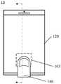
- Fig. 1is a schematic structural diagram of an electronic device to which the present application can be applied.
- Fig. 2is a schematic cross-sectional view of the electronic device shown in Fig. 1.
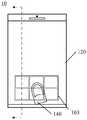
- Fig. 3is another schematic structural diagram of an electronic device to which the present application can be applied.
- Fig. 4is a schematic cross-sectional view of the electronic device shown in Fig. 3.
- Fig. 5is a front view of a fingerprint detection device according to an embodiment of the present application.
- Fig. 6is a schematic top view of a fingerprint detection device according to an embodiment of the present application.
- FIG. 7 and 8are schematic diagrams of modified structures of the fingerprint detection device shown in FIG. 5.
- FIG. 9is another schematic top view of the fingerprint detection device of the embodiment of the present application.
- the technical solutions of the embodiments of the present applicationcan be applied to various electronic devices.
- portable or mobile computing devicessuch as smartphones, notebook computers, tablet computers, and gaming devices, as well as other electronic devices such as electronic databases, automobiles, and bank automated teller machines (ATM).
- ATMbank automated teller machines
- the embodiments of the present applicationare not limited thereto.
- biometric recognition technologyincludes but is not limited to fingerprint recognition, palmprint recognition, iris recognition, face recognition, and living body recognition.
- fingerprint recognition technologyincludes but is not limited to fingerprint recognition, palmprint recognition, iris recognition, face recognition, and living body recognition.
- fingerprint recognition technologyuses fingerprint recognition technology as an example.
- the under-screen fingerprint recognition technologyrefers to the installation of the fingerprint recognition module below the display screen, so as to realize the fingerprint recognition operation in the display area of the display screen. There is no need to set a fingerprint collection area on the front of the electronic device except for the display area.
- the fingerprint recognition moduleuses the light returned from the top surface of the display assembly of the electronic device to perform fingerprint sensing and other sensing operations. This returned light carries information about objects (such as fingers) that are in contact with or close to the top surface of the display assembly.
- the fingerprint recognition module located under the display assemblycollects and detects this returned light to realize fingerprint recognition under the screen.
- the design of the fingerprint identification modulemay be to implement the desired optical imaging by appropriately configuring optical elements for collecting and detecting the returned light, so as to detect the fingerprint information of the finger.
- in-display fingerprint recognition technologyrefers to the installation of fingerprint recognition modules or part of fingerprint recognition modules inside the display screen, so as to realize fingerprint recognition operations in the display area of the display screen without the need for electronic
- the fingerprint collection areais set on the front of the device except the display area.
- FIG. 1 and FIG. 3are schematic diagrams of the orientation of the electronic device 10
- FIG. 2 and FIG. 4are cross-sectional schematic diagrams of the electronic device 10 shown in FIG. 1 and FIG. 3, respectively.
- the electronic device 10may include a display screen 120 and an optical fingerprint recognition module 130.
- the display screen 120may be a self-luminous display, which uses a self-luminous display unit as display pixels.
- the display screen 120may be an Organic Light-Emitting Diode (OLED) display screen or a Micro-LED (Micro-LED) display screen.
- the display screen 120may also be a liquid crystal display (LCD) or other passive light-emitting display, which is not limited in the embodiment of the present application.
- the display screen 120may also be specifically a touch display screen, which can not only perform screen display, but also detect a user's touch or pressing operation, so as to provide a user with a human-computer interaction interface.
- the electronic device 10may include a touch sensor, and the touch sensor may specifically be a touch panel (TP), which may be provided on the surface of the display screen 120, or may be partially integrated or The whole is integrated into the display screen 120 to form the touch display screen.
- TPtouch panel
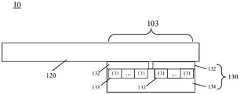
- the optical fingerprint module 130includes an optical fingerprint sensor, and the optical fingerprint sensor includes a sensing array 133 having a plurality of optical sensing units 131 (also referred to as optical sensing pixels, photosensitive pixels, pixel units, etc.).
- the area where the sensing array 133 is located or the sensing area thereofis the fingerprint detection area 103 of the optical fingerprint module 130 (also referred to as fingerprint collection area, fingerprint recognition area, etc.).
- the optical fingerprint module 130is arranged in a partial area below the display screen 120.
- the fingerprint detection area 103may be located in the display area of the display screen 120.
- the optical fingerprint module 130may also be arranged in other positions, such as the side of the display screen 120 or the non-transparent area at the edge of the electronic device 10, and the optical fingerprint module 130 may be designed to The optical signal from at least a part of the display area of the display screen 120 is guided to the optical fingerprint module 130, so that the fingerprint detection area 103 is actually located in the display area of the display screen 120.
- the electronic device 10when the user needs to unlock the electronic device 10 or perform other fingerprint verification, only need to press the finger on the fingerprint detection area 103 located in the display screen 120 to realize fingerprint input. Since fingerprint detection can be implemented in the screen, the electronic device 10 adopting the above structure does not need to reserve space on the front side for setting fingerprint buttons (such as the Home button), so that a full screen solution can be adopted, that is, the display area of the display screen 120 It can be basically extended to the front of the entire electronic device 10.
- fingerprint buttonssuch as the Home button
- the optical fingerprint module 130may include a light detecting part 134 and an optical component 132.
- the light detection part 134includes the sensor array 133 (also called an optical fingerprint sensor), a reading circuit and other auxiliary circuits electrically connected to the sensor array 133, which can be fabricated on a chip by a semiconductor process (Die), such as an optical imaging chip or an optical fingerprint sensor.
- the sensing array 133is specifically a photodetector (photodetector) array, which includes a plurality of photodetectors distributed in an array, and the photodetectors can be used as the optical sensing unit as described above.
- the optical component 132may be disposed above the sensing array 133 of the light detecting part 134, and it may specifically include a filter layer (Filter), a light guide layer or a light path guiding structure, and other optical elements.
- the filter layerIt can be used to filter out ambient light penetrating the finger, and the light guide layer or light path guiding structure is mainly used to guide the reflected light reflected from the surface of the finger to the sensing array 133 for optical detection.
- the optical assembly 132 and the light detecting part 134may be packaged in the same optical fingerprint component.
- the optical component 132 and the optical detection part 134may be packaged in the same optical fingerprint chip, or the optical component 132 may be arranged outside the chip where the optical detection part 134 is located, for example, the optical component 132 It is attached above the chip, or some components of the optical assembly 132 are integrated into the chip.
- the area or light sensing range of the sensing array 133 of the optical fingerprint module 130corresponds to the fingerprint detection area 103 of the optical fingerprint module 130.
- the fingerprint collection area 103 of the optical fingerprint module 130may be equal to or not equal to the area or light sensing range of the sensing array 133 of the optical fingerprint module 130, which is not specifically limited in the embodiment of the present application. .
- the light pathis guided by light collimation, and the fingerprint detection area 103 of the optical fingerprint module 130 can be designed to be substantially the same as the area of the sensing array of the optical fingerprint module 130.
- the area of the fingerprint detection area 103 of the optical fingerprint module 130can be made larger than that of the optical fingerprint module. 130 the area of the sensing array 133.
- the light path guiding structure that the optical assembly 132 may includeis exemplified below.
- the optical collimatormay specifically be a collimator (Collimator) layer fabricated on a semiconductor silicon wafer, which has A plurality of collimating units or micro-holes
- the collimating unitmay be specifically a small hole, among the reflected light reflected from the finger, the light that is perpendicularly incident on the collimating unit can pass through and be received by the sensor chip below it , And the light whose incident angle is too large is attenuated by multiple reflections inside the collimating unit, so each sensor chip can basically only receive the reflected light reflected by the fingerprint pattern directly above it, which can effectively improve image resolution Rate, thereby improving the fingerprint recognition effect.
- the optical path guiding structuremay be an optical lens (Lens) layer, which has one or more lens units, such as a lens group composed of one or more aspheric lenses , which is used to converge the reflected light reflected from the finger to the sensing array 133 of the light detection part 134 below it, so that the sensing array 133 can perform imaging based on the reflected light, thereby obtaining a fingerprint image of the finger .
- Lensoptical lens
- the optical lens layermay further have a pinhole or a micro-aperture formed in the optical path of the lens unit, for example, one or more light-shielding sheets may be formed in the optical path of the lens unit, of which at least One light-shielding sheet may be formed with light-transmitting micro-holes in the optical axis or optical center area of the lens unit, and the light-transmitting micro-holes may serve as the aforementioned pinholes or micro-apertures.
- the pinhole or micro-aperture diaphragmcan cooperate with the optical lens layer and/or other optical film layers above the optical lens layer to expand the field of view of the optical fingerprint module 130 to improve the optical fingerprint module 130 Fingerprint imaging effect.
- the light path guiding structuremay be a micro lens array including a plurality of micro lenses, which may be formed by a semiconductor growth process or other processes
- each microlensmay correspond to one of the sensing units of the sensing array 133, respectively.
- other optical film layersmay be formed between the microlens layer and the sensing unit, such as a dielectric layer or a passivation layer.
- a light blocking layer(or called a light blocking layer, a light blocking layer, etc.) with micro holes (or called openings) may also be included between the micro lens layer and the sensing unit, wherein the micro The hole is formed between the corresponding micro lens and the sensing unit, the light blocking layer can block the optical interference between the adjacent micro lens and the sensing unit, and make the light corresponding to the sensing unit converge through the micro lens To the inside of the micropore and transfer to the sensing unit through the micropore for optical fingerprint imaging.
- a micro lens layermay be further provided above or below the collimator layer or the optical lens layer.
- a micro lens layermay be further provided above or below the collimator layer or the optical lens layer.
- the optical assembly 132may also include other optical elements, such as filters or other optical films, which may be arranged between the optical path guiding structure and the optical fingerprint sensor or arranged at all.
- the display screen 120 and the optical path guide structureare mainly used to isolate the influence of external interference light on the optical fingerprint detection.
- the filter layercan be used to filter out the ambient light that penetrates the finger and enters the optical fingerprint sensor through the display screen 120. Similar to the light path guiding structure, the filter layer can be specific to each The optical fingerprint sensors are separately arranged to filter out interference light, or a large-area filter layer can also be used to simultaneously cover the multiple optical fingerprint sensors.
- the fingerprint identification module 140can be used to collect user fingerprint information (such as fingerprint image information).
- the optical fingerprint module 130can use the display unit (ie, the OLED light source) of the OLED display 120 in the fingerprint detection area 103 as an excitation light source for optical fingerprint detection.
- the display unitie, the OLED light source
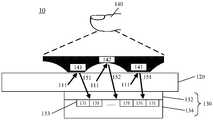
- the display screen 120emits a beam of light 111 to the target finger 140 above the fingerprint detection area 103.
- the light 111is reflected on the surface of the finger 140 to form reflected light or pass through all the fingers.
- the finger 140scatters to form scattered light (transmitted light).
- the above-mentioned reflected light and scattered lightare collectively referred to as reflected light.
- the ridge 141 and valley 142 of the fingerprinthave different light reflection capabilities
- the reflected light 151 from the fingerprint ridge and the reflected light 152 from the fingerprint valleyhave different light intensities, and the reflected light passes through the optical component 132. After that, it is received by the sensor array 133 in the optical fingerprint module 130 and converted into a corresponding electrical signal, that is, a fingerprint detection signal; based on the fingerprint detection signal, fingerprint image data can be obtained, and fingerprint matching verification can be further performed, thereby
- the electronic device 10realizes the optical fingerprint recognition function.
- the optical fingerprint module 130may also use a built-in light source or an external light source to provide an optical signal for fingerprint detection and identification.
- the optical fingerprint module 130can be applied not only to self-luminous displays such as OLED displays, but also to non-self-luminous displays, such as liquid crystal displays or other passive light-emitting displays.
- the optical fingerprint system of the electronic device 10may also include an excitation light source for optical fingerprint detection.
- the light sourcemay specifically be an infrared light source or a light source of invisible light of a specific wavelength, which may be arranged under the backlight module of the liquid crystal display or arranged in the edge area under the protective cover of the electronic device 10, and the optical fingerprint module 130 can be arranged under the edge area of the liquid crystal panel or the protective cover and guided by the light path so that the fingerprint detection light can reach the optical fingerprint module 130; or, the optical fingerprint module 130 can also be arranged on the backlight module Below, and the backlight module is designed to allow the fingerprint detection light to pass through the liquid crystal panel and the backlight module and reach the optical fingerprint module 130 by opening holes or other optical designs on the film layers such as diffuser, brightness enhancement film, and reflective film. .
- the optical fingerprint module 130uses a built-in light source or an infrared light source or an infrared light source or an infrared light source or a light source of invisible light of a specific wavelength
- the electronic device 10may also include a transparent protective cover plate, which may be a glass cover plate or a sapphire cover plate, which is located above the display screen 120 and covers the front surface of the electronic device 10 . Therefore, in the embodiments of the present application, the so-called finger pressing on the display screen 120 actually refers to pressing on the cover plate above the display screen 120 or covering the surface of the protective layer of the cover plate.
- a transparent protective cover platewhich may be a glass cover plate or a sapphire cover plate
- the optical fingerprint module 130may include only one optical fingerprint sensor.
- the fingerprint detection area 103 of the optical fingerprint module 130has a small area and a fixed position, so the user needs to press his finger when inputting a fingerprint. Go to the specific position of the fingerprint detection area 103, otherwise the optical fingerprint module 130 may not be able to collect fingerprint images, resulting in poor user experience.
- the optical fingerprint module 130may specifically include multiple optical fingerprint sensors. The multiple optical fingerprint sensors may be arranged side by side under the display screen 120 in a splicing manner, and the sensing areas of the multiple optical fingerprint sensors together constitute the fingerprint detection area 103 of the optical fingerprint module 130.
- the fingerprint detection area 103 of the optical fingerprint module 130can be extended to the main area of the lower half of the display screen, that is, to the area where the finger is habitually pressed, so as to realize the blind fingerprint input operation. Further, when the number of optical fingerprint sensors is sufficient, the fingerprint detection area 103 can also be extended to half of the display area or even the entire display area, thereby realizing half-screen or full-screen fingerprint detection.
- the optical fingerprint module 130 in the electronic device 10may include a plurality of optical fingerprint sensors, and the plurality of optical fingerprint sensors may be arranged side by side on the display screen 120 by means such as splicing. Below, and the sensing areas of the multiple optical fingerprint sensors collectively constitute the fingerprint detection area 103 of the optical fingerprint device 130.
- the optical component 132may include a plurality of light path guiding structures, and each light path guiding structure corresponds to an optical fingerprint sensor (that is, the sensing array 133), and is attached and arranged above the corresponding optical fingerprint sensor.
- the multiple optical fingerprint sensorsmay also share an overall optical path guiding structure, that is, the optical path guiding structure has an area large enough to cover the sensing array of the multiple optical fingerprint sensors.
- the optical sensor array of each optical fingerprint sensormay be One of the optical sensing units is configured with one or more collimating units, and is attached and arranged above the corresponding optical sensing unit.
- the multiple optical sensing unitscan also share one collimating unit, that is, the one collimating unit has an aperture large enough to cover the multiple optical sensing units. Since one collimating unit can correspond to multiple optical sensing units or one optical sensing unit corresponds to multiple collimating units, the correspondence between the spatial period of the display screen 120 and the spatial period of the optical fingerprint sensor is destroyed.
- the spatial structure of the light-emitting display arrayis similar to the spatial structure of the optical sensing array of the optical fingerprint sensor. It can also effectively prevent the optical fingerprint module 130 from using the light signal passing through the display 120 to perform fingerprint imaging to generate moiré fringes, which effectively improves the optical fingerprint model. Group 130 fingerprint recognition effect.
- the optical fingerprint module 130includes multiple sensor chips
- one optical lensmay be configured for each sensor chip to perform fingerprint imaging, or multiple sensor chips may be configured with one optical lens. Realize light convergence and fingerprint imaging. Even when a sensor chip has two sensing arrays (Dual Array) or multiple sensing arrays (Multi-Array), the sensor chip can also be equipped with two or more optical lenses to cooperate with the two sensing arrays or Multiple sensing arrays perform optical imaging, thereby reducing the imaging distance and enhancing the imaging effect.
- FIGS. 1 to 4are only examples of this application, and should not be construed as limiting the application.
- this applicationdoes not specifically limit the number, size, and arrangement of fingerprint sensors, which can be adjusted according to actual needs.
- the number of multiple fingerprint sensors of the optical fingerprint module 130may be 2, 3, 4, or 5, etc., and the multiple fingerprint sensors may be distributed in a square or circular shape.
- the embodiments of the present applicationcan be applied to the detection of various types of fingers, and are particularly suitable for the detection of dry fingers.
- the so-called dry fingersrefer to dry fingers or clean fingers.
- the current fingerprint recognition solutionhas a poor fingerprint recognition effect on dry fingers, and the fingerprint recognition solution provided by the embodiment of the present application can improve the fingerprint recognition performance on dry fingers.
- FIG. 5shows a schematic diagram of a fingerprint detection device 20 according to an embodiment of the present application.
- the fingerprint detection device 20may be applicable to the electronic device 10 shown in FIGS. 1 to 4, or the device 20 may be the optical fingerprint module 130 shown in FIGS. 1 to 5.
- the fingerprint detection device 20may include a microlens array 210, at least one light blocking layer, and an optical sensing pixel array 240.
- the microlens array 210may be used to be arranged under the display screen of an electronic device, the at least one light blocking layer may be arranged under the microlens array 210, and the optical sensing pixel array 240 may be arranged at all. Below the at least one light blocking layer. It should be noted that the microlens array 210 and the at least one light blocking layer may be the light guide structure included in the optical component 132 shown in FIG. 2 or FIG.
- optical sensing pixel array 240may be The sensing array 133 with a plurality of optical sensing units 131 (also referred to as optical sensing pixels, photosensitive pixels, pixel units, etc.) shown in FIG. 1 to FIG. 4 will not be repeated here to avoid repetition.
- optical sensing units 131also referred to as optical sensing pixels, photosensitive pixels, pixel units, etc.
- the microlens array 210includes a plurality of microlenses.
- the micro lens array 210may include a first micro lens 211, a second micro lens 212, and a third micro lens 213.
- the at least one light blocking layermay include a plurality of light blocking layers, for example, the at least one light blocking layer may include a first light blocking layer 220 and a second light blocking layer 230.
- the optical sensing pixel array 240may include a plurality of optical sensing pixels.
- the optical sensing pixel arraymay include a first optical sensing pixel 241, a second optical sensing pixel 242, a third optical sensing pixel 243, and a fourth optical sensing pixel. 244, the fifth optical sensing pixel 245 and the sixth optical sensing pixel 246.
- the at least one light blocking layeris formed with a plurality of light guide channels corresponding to each micro lens in the micro lens array 210, and the bottoms of the plurality of light guide channels corresponding to each micro lens respectively extend to adjacent Below multiple micro lenses.
- the first light blocking layer 220 and the second light blocking layer 230are respectively provided with each of the plurality of microlenses (ie, the first microlens 211, the second microlens 212 and at least one opening corresponding to the third microlens 213).
- the first light blocking layer 220is provided with a first opening 221 and a second opening 222 corresponding to the first microlens 211
- the first light blocking layer 220is also provided with a first opening 221 and a second opening 222 corresponding to the second microlens 212.
- the second opening 222 and the third opening 223, and the first light blocking layer 220are provided with a third opening 223 and a fourth opening 224 corresponding to the third microlens 213.
- the second light blocking layer 230is provided with a fifth opening 231 and a sixth opening 232 corresponding to the first microlens 211, and the second light blocking layer 230 is also provided with a second microlens 212 corresponding to the The seventh opening 233 and the eighth opening 234, and the second light blocking layer 230 are provided with a ninth opening 235 and a tenth opening 236 corresponding to the third microlens 213.
- the plurality of light guide channels corresponding to the second microlens 212may include a light guide channel formed by a second opening 222 and a sixth opening 232, and a third opening
- the hole 223 and the ninth opening 235form a light guide channel.
- the light guide channel formed by the second opening 222 and the sixth opening 232extends below the first microlens 211, and the light guide channel formed by the third opening 223 and the ninth opening 235 extends to the third microlens 213 below.
- an optical sensing pixelmay be provided under each of the multiple light guide channels corresponding to each micro lens in the micro lens array 210.
- a second optical sensing pixel 242is provided below the light guide channel formed by the second opening 222 and the sixth opening 232, and the third opening 223 and the ninth opening
- a fifth optical sensing pixel 245is arranged under the light guide channel formed by 235.
- a plurality of optical sensing pixelsare arranged below each microlens in the microlens array 210.
- the multiple optical sensing pixels arranged under each microlensare respectively used for receiving optical signals converged by adjacent multiple microlenses and transmitted through the corresponding light guide channel, and the optical signals are used for detecting fingerprints of fingers information.
- a third optical sensing pixel 243 and a fourth optical sensing pixel 244may be arranged below the second microlens 212, wherein the third optical sensing pixel 243 may be used for Receiving the oblique light signal converged by the first microlens 211 and transmitted through the light guide channel formed by the second opening 222 and the seventh opening 233, the fourth optical sensing pixel 244 can be used to receive the third microlens The oblique light signal converged by the lens 213 and transmitted through the light guide channel formed by the third opening 223 and the eighth opening 234.
- the distribution of multiple optical sensing pixels under each microlens in the microlens array 210may be polygonal.
- the polygonincludes but is not limited to a rectangle or a diamond.
- the distribution of the multiple optical sensing pixels under each microlens in the microlens array 210may be circular or elliptical.
- microlenses in the microlens arrayare distributed in an array, when the distribution of the multiple optical sensing pixels under each microlens is polygonal, the correspondence between the microlens array and the optical sensing array can be effectively simplified. In this way, the structural design of the fingerprint detection device is simplified.
- FIG. 6is a schematic top view of the second microlens 212 shown in FIG. 5.
- four optical sensing pixelsmay be disposed under the second microlens 212, and the distribution of the four optical sensing pixels may appear as a rectangle.
- the embodiment of the present applicationdoes not limit the specific corresponding manner of each microlens and the lower optical sensing pixel.
- the second microlens 212may cover part or all of the photosensitive area (AA) of the third optical sensing pixel 243.
- the first The two microlenses 212can cover the light guiding area (PD area, AA) of the third optical sensing pixel 243, which is converged by the first microlens 211 and formed by the second opening 222 and the seventh opening 233 The area that the oblique light signal transmitted by the channel can irradiate to ensure that the third optical sensing pixel 243 can receive enough light signal to improve the fingerprint recognition effect.
- the thickness of the fingerprint detection deviceis too large.
- the size of the fingerprint detection deviceis too large.
- each The multiple optical sensing pixels under each microlenscan respectively receive the oblique light signal converged from multiple adjacent microlenses and transmitted through the corresponding light guide channel, and the oblique light signal is used to detect the fingerprint information of the dry finger.
- the dry hand fingerprintis not in contact with the OLED screen, the contrast between the fingerprint ridge and the fingerprint valley of the fingerprint image in the vertical direction is poor, and the image is blurred to the point where the fingerprint lines cannot be distinguished.
- This applicationuses a reasonable optical path design to allow the optical path to receive light signals in oblique directions , While it can better obtain normal finger fingerprints, it can better detect dry finger fingerprint images.
- the fingersIn normal life scenarios, such as washing hands, getting up in the morning, plastering fingers, low temperature and other scenes, the fingers are usually dry, and the stratum corneum is uneven. When it is pressed on the OLED screen, local areas of the fingers will have poor contact. The occurrence of this situation causes the current optical fingerprint solution to have a poor effect on dry hand fingerprint recognition.
- the beneficial effect of this applicationis to improve the dry hand fingerprint imaging effect and make the dry hand fingerprint image clearer.
- the optical sensing pixel array 240can also expand the field of view and the field of view of the optical sensing pixel array 240 by receiving the tilt light signal.
- the field of view of the fingerprint detection device 20can be expanded from 6x9mm 2 to 7.5x10. .5mm 2 , further enhance the fingerprint recognition effect.
- a plurality of optical sensing pixelsare arranged under each microlens, so that the spatial period of the lens array 210 and the spatial period of the optical sensing pixel array 240 are not equal, thereby avoiding moiré fringes in the fingerprint image and improving fingerprint recognition effect.
- Aiming at problem 2by designing multiple light guide channels for each microlens, and making the bottoms of the multiple light guide channels corresponding to each microlens extend below the adjacent multiple microlenses, a single Imaging optical path with micro lens and multiple optical sensing pixels. That is, a single microlens can multiplex optical signals of multiple angles (for example, a single microlens can multiplex optical signals of 4 angles), which can split and image light beams with different object aperture angles, effectively improving The light input of the fingerprint detection device can reduce the exposure time of the optical sensing pixel array.
- the aperture angleis the angle formed by the object point on the optical axis of the microlens and the effective diameter of the front lens of the microlens. The larger the aperture angle of the microlens, the greater the light input of the microlens.
- the effective diameter of the lensis proportional and inversely proportional to the distance of the focal point.
- the optical sensing pixel arraymay be divided into a plurality of optical sensing pixel groups, wherein each optical sensing pixel in each optical sensing pixel group is used for receiving the same direction as the light guide channel corresponding to the same optical sensing pixel group
- the oblique light signalthat is, each optical sensing pixel group can generate a fingerprint image based on the received oblique light signal, so the multiple optical sensing pixel groups can be used to generate multiple fingerprint images, in this case It is possible to superimpose the multiple fingerprint images to obtain a high-resolution fingerprint image, and then perform fingerprint identification based on this high-resolution fingerprint image.
- the optical sensing pixel array 240can converge oblique light signals to the optical sensing pixels under the adjacent multiple microlenses through the 4 light guide channels corresponding to each microlens, that is, the optical sensing pixels
- the array 240can be divided into 4 optical sensing pixel groups for forming 4 fingerprint images. Based on these 4 fingerprint images, a fingerprint image with a higher resolution can be obtained, thereby improving the fingerprint recognition effect.
- each microlenscan converge oblique light signals in multiple directions through multiple light guide channels, or the optical sensing pixel array can simultaneously acquire multiple fingerprint images through optical path design, even if the optical The exposure time of the sensing pixel array results in a lower resolution of each fingerprint image. It is also possible to process multiple fingerprint images with lower resolution to obtain a fingerprint image with higher resolution.
- the imaging light path of a single microlens and multiple optical sensing pixelscan perform non-frontal light imaging (ie, oblique light imaging) of the object beam of the fingerprint under the screen, especially the one arranged below each microlens
- the multiple optical sensing pixelsare respectively used to receive the optical signals converged by the adjacent multiple microlenses, thereby being able to enlarge the object-side numerical aperture of the optical system and shorten the optical path design of the optical sensing pixel array (that is, the at least one The thickness of the light-blocking layer) can ultimately effectively reduce the thickness of the fingerprint detection device.
- the imaging light path with a single microlens and multiple optical sensing pixelscan perform non-frontal light imaging of the object beam of the fingerprint under the screen, which can expand the object numerical aperture of the optical system and improve the robustness of the system And the tolerance tolerance of the fingerprint detection device 20.
- the numerical aperturecan be the product of the refractive index (h) of the medium between the front lens of the microlens and the object to be inspected and half of the aperture angle (u).
- the imaging light path of a single microlens and multiple optical sensing pixels and the light guide channel provided in the at least one light blocking layercan improve the performance of the optical sensing pixels without affecting each other.
- the density of the optical sensing pixels in the optical sensing pixel array 240can further reduce the size of the fingerprint detection device.
- the technical solution of the present applicationcan make the optical sensing pixel array 240 only receive the light signal of the oblique angle through a reasonable design of the multiple light guide channels corresponding to each microlens, and converge multiple angles through a single microlens.
- the oblique light signalsolves the problem of too long exposure time for the single-object telecentric microlens array scheme.
- the fingerprint detection device 20can not only solve the problem of poor recognition of dry fingers by the vertical light signal and the long exposure time of the single-object telecentric microlens array solution, but also solve the problem of the fingerprint detection device. Problems with excessive thickness, poor tolerance tolerance, and excessive size.
- the multiple light guide channels corresponding to each microlens in the microlens array 210may be centrally symmetrically distributed along the optical axis direction of the same microlens.
- the second microlens 212corresponds to the light guide channel extending below the microlens in the upper right corner, and the second microlens 212 extends below the microlens in the lower left corner.
- the light guide channelis symmetrical along the optical axis of the second microlens 212.
- the second microlens 212corresponds to the light guide channel extending below the microlens in the upper left corner and the second microlens 212 extends to the lower right microlens.
- the light guide channel under the lensis symmetrical along the optical axis of the second microlens 212.
- each light guide channel of the multiple light guide channels corresponding to each microlens in the microlens array 210 and the first planemay form a preset angle, so that each A plurality of optical sensing pixels arranged under the microlens are respectively used for receiving optical signals converged by a plurality of adjacent microlenses and transmitted through the corresponding light guide channel, wherein the first plane is parallel to the display screen Plane.
- the preset included anglecan ensure that the bottom ends of the multiple light guide channels corresponding to each microlens extend below the multiple adjacent microlenses of the same microlens.
- the plane where the optical sensing pixel array 240 is locatedis parallel to the first plane, and the guide formed by the second opening 222 and the sixth opening 232
- the light channelforms a first angle with the plane where the optical sensing pixel array 240 is located
- the light guide channel formed by the third opening 223 and the ninth opening 235forms a first angle with the plane where the optical sensing pixel array 240 is located.
- Two angles. The first angleis equal to the second angle.
- the first anglemay not be equal to the second angle, which is not limited in the embodiment of the present application.
- the preset anglemay be the angle between the axis of the light guide channel and the first plane, or the angle between any straight line passing through the light guide channel and the first plane
- the range of the preset anglemay be any range from 0 degrees to 90 degrees, for example, the range of the preset angle may be 15 degrees to 60 degrees, or 10 degrees to 70 degrees, This application does not specifically limit this.
- the projection of the multiple light guide channels corresponding to each microlens in the microlens array 210 on the first planecan be relative to the projection of the optical axis of the same microlens on the first plane.
- the centeris symmetrically distributed to ensure that each optical sensing pixel in the optical sensing pixel array can receive enough light signals, thereby improving the resolution of the fingerprint image and the fingerprint recognition effect.
- each light guide channelis an inclined channel
- the end surface of each light guide channel on the first planeis elliptical
- the first planeThe four light guide channels corresponding to the two microlenses 212 are symmetrically distributed along the optical axis of the second microlens 212 on the projection center of the first plane near the end surface of the optical sensing pixel array 340.
- the fingerprint detection device 20may include a plurality of light-blocking layers, and different light-blocking layers are provided with at least one opening corresponding to each microlens to form each microlens. Multiple light guide channels corresponding to the lens.
- the at least one light blocking layermay include the first light blocking layer 220 and the second light blocking layer 230 described above with respect to FIG. 5.
- the number of openings corresponding to the same microlens in different light blocking layerscan be sequentially increased from top to bottom to form multiple light guide channels corresponding to each microlens.
- the spacing between the openings in different light blocking layersdecreases sequentially from top to bottom.
- the distance D between two adjacent openings in the first light blocking layer 220is greater than the distance d between two adjacent openings in the second light blocking layer 230 .
- Most of the light signals that the fingerprint detection device does not expect to receiveare blocked by the upper part of the light-blocking layer with a lower density of openings in the plurality of light-blocking layers, and the density of openings in the plurality of light-blocking layers is blocked
- the smaller upper part of the light-blocking layer and the lower part of the light-blocking layer with a larger opening densitycan form multiple light guide channels for each microlens.
- the preparation complexity of the at least one light-shielding layercan also be reduced and the strength of the upper part of the light-shielding layer can be increased.
- a plurality of openings corresponding to each microlensmay be provided in the bottom light blocking layer of the plurality of light blocking layers, and the plurality of light guide channels corresponding to each microlens respectively pass through A plurality of openings corresponding to the same micro lens in the bottom light blocking layer.
- the non-bottom light-blocking layer of the plurality of light-blocking layersmay be provided with an opening in the middle position of the back focus of two adjacent microlenses in the plurality of microlenses, and the two adjacent microlenses The two corresponding light guide channels both pass through the corresponding openings of the two adjacent microlenses in the non-bottom light blocking layer.
- the top light-blocking layer of the multiple light-blocking layersmay be provided with an opening on the optical axis of each microlens, and the multiple light guide channels corresponding to each microlens pass through the top-level block. The corresponding opening of the same micro lens in the optical layer.
- FIG. 7is another schematic structural diagram of the fingerprint detection device 20 according to an embodiment of the present application.
- the fingerprint detection device 20may include a third light blocking layer 260 in addition to the first light blocking layer 220 and the second light blocking layer 230 shown in FIG. 6, wherein the third blocking layer
- the optical layer 260includes an eleventh opening 261, a twelfth opening 262 and a thirteenth opening 263.
- the second light blocking layer 230is provided with a sixth opening 232 and a ninth opening 235 corresponding to the second micro lens 212.
- the first light blocking layer 220may be provided with a second opening 222 at an intermediate position between the back focus of the first microlens 211 and the back focus of the second microlens 212, and the first light blocking layer 220
- a third opening 223may be provided at an intermediate position between the back focus of the third microlens 213 and the back focus of the second microlens 212.
- the third light blocking layer 260may be provided with a twelfth opening 262 at a position close to the first light blocking layer 220 in the optical axis direction of the second microlens 260.
- a light guide channel corresponding to the second microlens 212passes through the twelfth opening 262, the second opening 222, and the sixth opening 232, and the other corresponding to the second microlens 212
- the light guide channelpasses through the twelfth opening, the third opening 223 and the ninth opening 235.
- the apertures of the openings corresponding to the same microlens in different light-blocking layerscan also be sequentially reduced from top to bottom, so as to filter out the optical signals expected to be received by the optical sensing pixel array 240.
- each of the microlensescan image the oblique light signal in the openings of the bottom light-blocking layer of the plurality of light-blocking layers, thereby realizing micro-aperture imaging.
- the aperture of the opening of the third light blocking layer 260is larger than the aperture of the opening in the first light blocking layer 220, and the aperture of the opening in the first light blocking layer 220 is larger than The aperture of the opening in the second light blocking layer 230.
- the fingerprint detection device 20may also include only one light blocking layer.
- the multiple light guide channelsmay be a plurality of inclined through holes corresponding to the same microlens in the one light blocking layer.
- the thickness of the one light-blocking layeris greater than a preset threshold, so that the plurality of optical sensing pixels arranged under each microlens are respectively used to receive the light-blocking layer converged by the adjacent plurality of microlenses and pass through the corresponding guide.
- the optical signal transmitted by the optical channelis greater than a preset threshold, so that the plurality of optical sensing pixels arranged under each microlens are respectively used to receive the light-blocking layer converged by the adjacent plurality of microlenses and pass through the corresponding guide. The optical signal transmitted by the optical channel.
- the fingerprint detection device 20may further include a transparent medium layer 250.
- the transparent medium layer 250may be disposed at at least one of the following positions: between the microlens array 210 and the at least one light blocking layer; between the at least one light blocking layer; and the at least one light blocking layer Layer and optical sensing pixel array 240.
- the transparent medium layer 250may include a first medium layer 251 located between the microlens array 210 and the at least one light blocking layer (that is, the first light blocking layer 220) and the first blocking layer The second medium layer 252 between the light layer 220 and the second light blocking layer 230.
- the material of the transparent medium layer 250is any transparent material that is transparent to light, such as glass, which can also be transitioned by air or vacuum, which is not specifically limited in this application.
- FIG. 8is another schematic structural diagram of the fingerprint detection device 20 according to an embodiment of the present application.
- the fingerprint detection device 20may further include a filter layer 270, and the filter layer 270 may be disposed at at least one of the following positions: above the micro lens array 210, the micro lens array 210 And the at least one light blocking layer; between the at least one light blocking layer; and between the at least one light blocking layer and the optical sensing pixel array 240.
- the filter layer 270may be disposed between the optical sensing pixel array 240 and the second light blocking layer 230.
- the filter layer 270may be the filter layer in the optical component 132 mentioned above.
- the filter layer 270is used to reduce undesired ambient light in fingerprint sensing, so as to improve the optical sensing of the optical sensing pixel array 240 to the received light.
- the filter layer 270may specifically be used to filter out light of a specific wavelength, for example, near-infrared light and part of red light. For example, human fingers absorb most of the energy of light with a wavelength below 580nm. If one or more optical filters or optical filter layers are designed to filter light with wavelengths from 580nm to infrared, it can greatly reduce the impact of ambient light on fingerprints. The influence of optical detection in induction.
- the filter layer 270may include one or more optical filters, and the one or more optical filters may be configured as, for example, band-pass filters to allow the transmission of light emitted by the OLED screen while blocking infrared rays in sunlight. Light and other light components. When the under-screen fingerprint detection device 20 is used outdoors, this kind of optical filtering can effectively reduce the background light caused by sunlight.
- One or more optical filtersmay be implemented as, for example, an optical filter coating formed on one or more continuous interfaces, or may be implemented as one or more discrete interfaces. It should be understood that the filter layer 270 may be formed at any position along the optical path from the reflected light formed by the reflection of the finger to the optical sensing pixel array 240, which is not specifically limited in the embodiment of the present application.
- the light entrance surface of the filter layer 270may be provided with an optical inorganic coating or an organic blackened coating, so that the reflectance of the light entrance surface of the filter layer 270 is lower than a first threshold, such as 1%, so that It is ensured that the optical sensing pixel array 240 can receive sufficient light signals, thereby improving the fingerprint recognition effect.
- a first thresholdsuch as 1%
- the filter layer 270fixed on the upper surface of the optical sensing pixel array 240 by a fixing device as an example.
- the filter layer 270 and the optical sensing pixel array 240can be glued and fixed in the non-sensitizing area of the optical sensing pixel array 240, and the filter layer 270 and the photosensitive area of the optical sensing pixel array 240 There is a gap between.
- the lower surface of the filter layer 270is fixed on the upper surface of the optical sensing pixel array 240 by glue with a refractive index lower than a predetermined refractive index.
- the predetermined refractive indexincludes but is not limited to 1.3.
- the at least one light blocking layer and the microlens array 210may be integrated, or the at least one light blocking layer and the optical sensing pixel array 240 may be integrated, or even
- the microlens array 210, the at least one light blocking layer and the optical sensing pixel 240are all integrated into one component.
- each microlens in the microlens array 210may satisfy at least one of the following conditions: the projection of the condensing surface of the microlens on a plane perpendicular to its optical axis is Rectangular or circular; the condenser surface of the microlens is spherical or aspherical; the curvature of the condenser surface of the microlens is the same in all directions; the microlens includes at least one lens; and the microlens The focal length range is 10um-2mm.
- the microlens array 210satisfies at least one of the following conditions: the microlens array 210 is arranged in a polygonal shape and the duty ratio of the microlens array 210 ranges from 100% to 50%. %.
- the microlens array 210is arranged in a square or hexagonal shape.
- the duty cycle of the micro lens array 210is 85%.
- the period of the microlens array 210is not equal to the period of the optical sensing pixel array 240, and the period of the microlens array 210 is the same as the period of the optical sensing pixel array 240.
- the distance between the fingerprint detection device 20 and the display screenis 20um-1000um, so as to ensure that the fingerprint detection device 20 and the display screen have a sufficient safety distance, thereby ensuring that the The device vibrates or falls, causing the fingerprint detection device 20 to hit the display screen and cause damage to the device.
- FIG. 1 to FIG. 8are only examples of the present application, and should not be construed as limiting the present application.
- the first light blocking layer 220may also be provided with a plurality of openings corresponding to each microlens, wherein the plurality of light guide channels corresponding to each microlens respectively pass through the same microlens.
- the lenscorresponds to a plurality of openings in the first light blocking layer 220.
- each microlens in the microlens array 210may be filled with a circle or a square.
- the material of each microlens in the microlens array 210may be plastic or glass.
- the production process of each microlens in the microlens array 210can be realized by a micro-nano processing process or a compression molding process.
- FIG. 9is another schematic top view of the second microlens 212 shown in FIG. 5.
- four microlensesmay be disposed under the second microlens 212, and the distribution of the four microlenses may be a rhombus.
- the embodiment of the present applicationalso provides an electronic device, which may include a display screen and the fingerprint detection device of the above embodiment of the application, wherein the fingerprint detection device is arranged under the display screen to realize the screen Under optical fingerprint detection.
- the electronic devicecan be any electronic device with a display screen.
- the display screenmay be the display screen described above, such as an OLED display screen or other display screens.
- OLED display screenor other display screens.
- the unitscan be implemented by electronic hardware, computer software, or a combination of both, in order to clearly illustrate the interchangeability of hardware and software.
- the composition and steps of each examplehave been described generally in terms of function. Whether these functions are executed by hardware or software depends on the specific application and design constraint conditions of the technical solution. Professionals and technicians can use different methods for each specific application to implement the described functions, but such implementation should not be considered beyond the scope of this application.
- the disclosed system and devicemay be implemented in other ways.
- the device embodiments described aboveare only illustrative.
- the division of the unitsis only a logical function division, and there may be other divisions in actual implementation, for example, multiple units or components can be combined or It can be integrated into another system, or some features can be ignored or not implemented.
- the displayed or discussed mutual coupling or direct coupling or communication connectionmay be indirect coupling or communication connection through some interfaces, devices or units, and may also be electrical, mechanical or other forms of connection.
- the units described as separate componentsmay or may not be physically separated, and the components displayed as units may or may not be physical units, that is, they may be located in one place, or they may be distributed on multiple network units. Some or all of the units may be selected according to actual needs to achieve the objectives of the solutions of the embodiments of the present application.
- the functional units in the various embodiments of the present applicationmay be integrated into one processing unit, or each unit may exist alone physically, or two or more units may be integrated into one unit.
- the above-mentioned integrated unitcan be implemented in the form of hardware or software functional unit.
- the integrated unitis implemented in the form of a software functional unit and sold or used as an independent product, it can be stored in a computer readable storage medium.
- the technical solution of this applicationis essentially or the part that contributes to the existing technology, or all or part of the technical solution can be embodied in the form of a software product, and the computer software product is stored in a storage medium It includes several instructions to make a computer device (which may be a personal computer, a server, or a network device, etc.) execute all or part of the steps of the method described in each embodiment of the present application.
- the aforementioned storage mediainclude: U disk, mobile hard disk, read-only memory (ROM, Read-Only Memory), random access memory (RAM, Random Access Memory), magnetic disk or optical disk and other media that can store program code .
Landscapes
- Engineering & Computer Science (AREA)
- Physics & Mathematics (AREA)
- General Physics & Mathematics (AREA)
- Multimedia (AREA)
- Theoretical Computer Science (AREA)
- Human Computer Interaction (AREA)
- Health & Medical Sciences (AREA)
- General Health & Medical Sciences (AREA)
- Vascular Medicine (AREA)
- Optics & Photonics (AREA)
- Image Input (AREA)
- Measurement Of The Respiration, Hearing Ability, Form, And Blood Characteristics Of Living Organisms (AREA)
Abstract
Description
Translated fromChinese本申请实施例涉及指纹检测领域,并且更具体地,涉及指纹检测装置和电子设备。The embodiments of the present application relate to the field of fingerprint detection, and more specifically, to fingerprint detection devices and electronic equipment.
随着终端行业的高速发展,生物识别技术越来越受到人们重视,更加便捷的屏下生物特征识别技术,例如屏下光学指纹识别技术的实用化已成为大众所需。With the rapid development of the terminal industry, people pay more and more attention to biometric technology, and more convenient under-screen biometric identification technology, such as the practical use of under-screen optical fingerprint identification technology, has become a popular demand.
屏下光学指纹识别技术是将光学指纹模组设置于显示屏下,通过采集光学指纹图像,实现指纹识别。随着终端产品的发展,对指纹识别性能的要求越来越高。然而,在某些情况下,例如,干手指的情况,干手指和显示屏的接触面积非常小,识别响应面积非常小,导致采集的指纹不连续,特征点容易丢失,影响了指纹识别的性能。The under-screen optical fingerprint recognition technology is to install the optical fingerprint module under the display screen, and realize fingerprint recognition by collecting the optical fingerprint image. With the development of terminal products, the requirements for fingerprint recognition performance are getting higher and higher. However, in some cases, such as dry fingers, the contact area between the dry fingers and the display screen is very small, and the recognition response area is very small, resulting in discontinuities in the collected fingerprints and easy loss of feature points, which affects the performance of fingerprint recognition .
因此,如何提升指纹识别的性能,成为一个亟待解决的技术问题。Therefore, how to improve the performance of fingerprint recognition has become a technical problem to be solved urgently.
发明内容Summary of the invention
提供了一种指纹检测装置和电子设备,能够解决以下技术问题:A fingerprint detection device and electronic equipment are provided, which can solve the following technical problems:
1.垂直光信号对干手指的识别效果过差的问题。1. The problem of poor recognition of dry fingers by vertical light signals.
2.单物方远心微透镜阵列方案曝光时间过长的问题。2. The long exposure time of the single-object telecentric microlens array scheme.
3.指纹检测装置的厚度过大的问题。3. The thickness of the fingerprint detection device is too large.
4.指纹检测装置的公差容忍度过差的问题。4. The tolerance of fingerprint detection device is too poor.
5.指纹检测装置尺寸过大的问题。5. The size of the fingerprint detection device is too large.
第一方面,提供了一种指纹检测装置,适用于显示屏的下方以实现屏下光学指纹检测,包括:In the first aspect, a fingerprint detection device is provided, which is suitable for under the display screen to realize under-screen optical fingerprint detection, including:
微透镜阵列,用于设置在所述显示屏的下方,且包括多个微透镜;A microlens array, configured to be arranged below the display screen and including a plurality of microlenses;
至少一个挡光层,设置在所述微透镜阵列的下方,且形成有所述多个微透镜中的每个微透镜对应的多个导光通道,所述每个微透镜对应的多个导光通道的底部分别延伸至相邻的多个微透镜的下方;At least one light blocking layer is disposed under the microlens array, and a plurality of light guide channels corresponding to each of the plurality of microlenses are formed, and a plurality of light guide channels corresponding to each of the plurality of microlenses are formed. The bottom of the light channel respectively extends below the adjacent multiple micro lenses;
光学感应像素阵列,设置在所述至少一个挡光层的下方,且包括多个光 学感应像素,所述每个微透镜对应的多个导光通道中的每个导光通道的下方设置有一个光学感应像素;The optical sensing pixel array is arranged under the at least one light blocking layer and includes a plurality of optical sensing pixels, and one of the plurality of light guide channels corresponding to each microlens is provided below each light guide channel Optical sensor pixels;
其中,所述每个微透镜的下方设置有多个光学感应像素,所述每个微透镜下方设置的多个光学感应像素分别用于接收经由相邻的多个微透镜汇聚的并通过对应的导光通道传输的光信号,所述光信号用于检测手指的指纹信息。Wherein, a plurality of optical sensing pixels are arranged below each microlens, and the plurality of optical sensing pixels arranged below each microlens are respectively used for receiving the convergent and passing through the corresponding plurality of microlenses. The optical signal transmitted by the light guide channel, and the optical signal is used to detect fingerprint information of a finger.
针对问题1,通过为每个微透镜设计多个导光通道,并且使得所述每个微透镜对应的多个导光通道的底部分别延伸至相邻的多个微透镜的下方,可以使得每个微透镜下的多个光学感应像素分别能够接收到来自多个相邻的微透镜汇聚的并通过对应的导光通道传输的倾斜光信号。当干手指纹与OLED屏接触不好时,垂直方向的指纹图像的指纹脊和指纹谷的对比度差,图像模糊到分辨不了指纹纹路,本申请通过合理的光路设计,让光路接收倾斜方向光信号,在能够较好的获取正常手指指纹的同时,可以更好的检测出干手指指纹图像。在正常生活场景下,例如洗完手、早晨起床、手指抹灰、低温等场景下手指通常较干,其角质层不均匀,其按压在OLED屏上时,手指局部区域会出现接触不良。这种情况的出现造成当前光学指纹方案对干手指纹识别的效果不好,本申请的有益效果就是提升干手指纹成像效果,让干手指纹图像变清晰。Aiming at problem 1, by designing multiple light guide channels for each microlens, and making the bottoms of the multiple light guide channels corresponding to each microlens extend below the adjacent multiple microlenses, each The multiple optical sensing pixels under each microlens can respectively receive oblique light signals converged from multiple adjacent microlenses and transmitted through the corresponding light guide channel. When the dry hand fingerprint is not in contact with the OLED screen, the contrast between the fingerprint ridge and the fingerprint valley of the fingerprint image in the vertical direction is poor, and the image is blurred to the point where the fingerprint lines cannot be distinguished. This application uses a reasonable optical path design to allow the optical path to receive light signals in oblique directions , While it can better obtain normal finger fingerprints, it can better detect dry finger fingerprint images. In normal life scenarios, such as washing hands, getting up in the morning, plastering fingers, low temperature and other scenes, the fingers are usually dry, and the stratum corneum is uneven. When it is pressed on the OLED screen, local areas of the fingers will have poor contact. The occurrence of this situation causes the current optical fingerprint solution to have a poor effect on dry hand fingerprint recognition. The beneficial effect of this application is to improve the dry hand fingerprint imaging effect and make the dry hand fingerprint image clearer.
此外,所述光学感应像素阵列通过接收倾斜光信号还能够扩大所述光学感应像素阵列的视场角,例如可以所述指纹检测装置的视场由6x9mm2扩展到7.5x10.5mm2,进一步提升指纹识别效果。In addition, the optical sensing pixel array can also expand the field of view of the optical sensing pixel array by receiving the oblique light signal. For example, the field of view of the fingerprint detection device can be expanded from 6x9mm2 to 7.5x10.5mm2 , which is further improved Fingerprint recognition effect.
并且,每个微透镜下方设置有多个光学感应像素,使得透镜阵列的空间周期和光学感应像素阵列的空间周期不相等,进而能够避免指纹图像中出现莫尔条纹并提升指纹识别效果。In addition, a plurality of optical sensing pixels are arranged under each microlens, so that the spatial period of the lens array and the spatial period of the optical sensing pixel array are not equal, thereby avoiding moiré fringes in the fingerprint image and improving the fingerprint recognition effect.
针对问题2,通过为每个微透镜设计多个导光通道,并且使得所述每个微透镜对应的多个导光通道的底部分别延伸至相邻的多个微透镜的下方,可以形成单个微透镜与多光学感应像素搭配的成像光路。即多个光学感应像素通过复用单个微透镜接收多个角度的光信号,由此可以对不同的物方孔径角的光束进行分割成像,有效提高了指纹检测装置的进光量,由此可以降低光学感应像素阵列的曝光时长,其中孔径角又称镜口角,是微透镜光轴上的物体点与微透镜的前透镜的有效直径所形成的角度。微透镜的孔径角越大,微 透镜的进光量就越大,其与微透镜的有效直径成正比,与焦点的距离成反比。Aiming at problem 2, by designing multiple light guide channels for each microlens, and making the bottoms of the multiple light guide channels corresponding to each microlens extend below the adjacent multiple microlenses, a single Imaging optical path with micro lens and multiple optical sensing pixels. That is, multiple optical sensing pixels receive light signals at multiple angles by multiplexing a single microlens, which can split and image light beams with different object aperture angles, effectively increasing the amount of light entering the fingerprint detection device, and thus can reduce The exposure time of the optical sensing pixel array, where the aperture angle is also called the lens aperture angle, which is the angle formed by the object point on the optical axis of the microlens and the effective diameter of the front lens of the microlens. The larger the aperture angle of the microlens, the greater the amount of light entering the microlens, which is directly proportional to the effective diameter of the microlens and inversely proportional to the distance of the focal point.
具体而言,由于每个微透镜下方的多个光学感应像素分别能够接收到来自多个相邻的微透镜汇聚的并通过对应的导光通道传输的倾斜光信号,因此按照导光通道的方向,可以将所述光学感应像素阵列划分为多个光学感应像素组,其中每个光学感应像素组中的每个光学感应像素用于接收方向与同一光学感应像素组对应的导光通道的方向相同的倾斜光信号,即每个光学感应像素组可以基于接收到的倾斜光信号生成一张指纹图像,由此所述多个光学感应像素组可以用于生成多张指纹图像,在这种情况下,可以将所述多张指纹图像进行叠加,以获取一张高分辨率的指纹图像,进而基于这张高分辨率的指纹图像进行指纹识别。Specifically, since the multiple optical sensing pixels under each microlens can receive the oblique light signals converged from multiple adjacent microlenses and transmitted through the corresponding light guide channel, it follows the direction of the light guide channel. , The optical sensing pixel array may be divided into a plurality of optical sensing pixel groups, wherein each optical sensing pixel in each optical sensing pixel group is used for receiving the same direction as the light guide channel corresponding to the same optical sensing pixel group The oblique light signal, that is, each optical sensing pixel group can generate a fingerprint image based on the received oblique light signal, so the multiple optical sensing pixel groups can be used to generate multiple fingerprint images, in this case It is possible to superimpose the multiple fingerprint images to obtain a high-resolution fingerprint image, and then perform fingerprint identification based on this high-resolution fingerprint image.
由此可见,由于每个微透镜可以通过多个导光通道向多个方向汇聚倾斜光信号,或者说所述光学感应像素阵列可以通过光路设计同时获取多张指纹图像,因此即使降低所述光学感应像素阵列的曝光时长,进而导致每张指纹图像的分辨率较低,也可以通过对分辨率较低的多张指纹图像进行处理,进而获得一张分辨率较高的指纹图像。It can be seen that, because each microlens can converge oblique light signals in multiple directions through multiple light guide channels, or the optical sensing pixel array can simultaneously acquire multiple fingerprint images through optical path design, even if the optical The exposure time of the sensing pixel array results in a lower resolution of each fingerprint image. It is also possible to process multiple fingerprint images with lower resolution to obtain a fingerprint image with higher resolution.
也就是说,基于上述技术方案,可以保证指纹识别效果的同时降低所述光学感应像素阵列(即图像传感器)的曝光时长。That is to say, based on the above technical solution, the fingerprint recognition effect can be guaranteed while reducing the exposure time of the optical sensing pixel array (ie, the image sensor).
针对问题3,通过单个微透镜与多光学感应像素搭配的成像光路可以对屏下指纹的物方光束进行非正对光成像(即倾斜光成像),尤其是所述每个微透镜下方设置的多个光学感应像素分别用于接收经由相邻的多个微透镜汇聚的光信号,由此能够扩大光学系统的物方数值孔径并缩短所述光学感应像素阵列的光路设计(即所述至少一个挡光层)的厚度,最终能够有效降低所述指纹检测装置的厚度。Aiming at problem 3, the imaging light path of a single microlens and multiple optical sensing pixels can perform non-frontal light imaging (ie, oblique light imaging) of the object beam of the fingerprint under the screen, especially the one arranged below each microlens The multiple optical sensing pixels are respectively used to receive the optical signals converged by the adjacent multiple microlenses, thereby being able to enlarge the object-side numerical aperture of the optical system and shorten the optical path design of the optical sensing pixel array (that is, the at least one The thickness of the light-blocking layer) can ultimately effectively reduce the thickness of the fingerprint detection device.
针对问题4,通过单个微透镜与多光学感应像素搭配的成像光路可以对屏下指纹的物方光束进行非正对光成像,能够扩大光学系统的物方数值孔径,进而提高系统的鲁棒性以及指纹检测装置的公差容忍度。其中数值孔径是微透镜的前透镜与被检物体之间介质的折射率(h)和孔径角(u)半数的正玄的乘积。Aiming at problem 4, the imaging light path with a single microlens and multiple optical sensing pixels can perform non-frontal light imaging of the object beam of the fingerprint under the screen, which can expand the object numerical aperture of the optical system and improve the robustness of the system And the tolerance tolerance of the fingerprint detection device. The numerical aperture is the product of the refractive index (h) and the aperture angle (u) of the medium between the front lens of the microlens and the inspected object.
针对问题5,通过单个微透镜与多光学感应像素搭配的成像光路和所述至少一个挡光层中设置的导光通道,可以在保证相邻两个光学感应像素不相互影响的情况下提升所述光学感应像素阵列中的光学感应像素的密度,进而 能够降低所述指纹检测装置的尺寸。In response to question 5, the imaging light path of a single microlens and multiple optical sensing pixels and the light guide channel provided in the at least one light blocking layer can improve the performance of the optical sensing pixels without affecting each other. The density of the optical sensing pixels in the optical sensing pixel array can further reduce the size of the fingerprint detection device.
由上可知,本申请的技术方案通过对每个微透镜对应的多个导光通道的合理设计,可以使得光学感应像素阵列240只接收倾斜角度的光信号,并通过单个微透镜汇聚多个角度的倾斜光信号,解决了单物方远心微透镜阵列方案曝光时间过长的问题。换句话说,所述指纹检测装置不仅能够解决垂直光信号对干手指的识别效果过差的问题以及单物方远心微透镜阵列的曝光时间过长的问题,还能够解决指纹检测装置的厚度过大、公差容忍度过差以及尺寸过大的问题。It can be seen from the above that the technical solution of the present application can make the optical
在一些可能的实现方式中,所述每个微透镜对应的多个导光通道沿同一微透镜的光轴方向中心对称分布。In some possible implementation manners, the multiple light guide channels corresponding to each microlens are centrally symmetrically distributed along the optical axis direction of the same microlens.
通过中心对称的方式设置每个微透镜对应的多个导光通道,能够降低所述指纹检测装置的工艺复杂度。By arranging a plurality of light guide channels corresponding to each microlens in a center-symmetric manner, the process complexity of the fingerprint detection device can be reduced.
在一些可能的实现方式中,所述每个微透镜对应的多个导光通道中的每个导光通道和第一平面形成预设夹角,以使所述每个微透镜下方设置的多个光学感应像素分别用于接收经由相邻的多个微透镜汇聚的并通过对应的导光通道传输的光信号,其中,所述第一平面为与所述显示屏平行的平面。In some possible implementations, each light guide channel of the plurality of light guide channels corresponding to each microlens forms a preset angle with the first plane, so that a plurality of light guide channels are arranged below each microlens. The optical sensing pixels are respectively used for receiving optical signals converged by a plurality of adjacent microlenses and transmitted through the corresponding light guide channel, wherein the first plane is a plane parallel to the display screen.
通过所述预设夹角可以保证所述每个微透镜对应的多个导光通道的底端分别延伸至同一微透镜相邻的多个微透镜的下方。The preset included angle can ensure that the bottom ends of the multiple light guide channels corresponding to each microlens extend below the multiple adjacent microlenses of the same microlens.
在一些可能的实现方式中,所述预设夹角的范围为15度至60度。In some possible implementation manners, the preset included angle ranges from 15 degrees to 60 degrees.
在一些可能的实现方式中,所述每个微透镜对应的多个导光通道在所述第一平面的投影相对同一微透镜的光轴在所述第一平面的投影中心对称分布。In some possible implementation manners, the projections of the multiple light guide channels corresponding to each microlens on the first plane are symmetrically distributed relative to the optical axis of the same microlens on the projection center of the first plane.
由此,能够保证所述光学感应像素阵列中的每个光学感应像素均能够接收到足够的光信号,进而提升指纹图像的分辨率和指纹识别效果。As a result, it can be ensured that each optical sensing pixel in the optical sensing pixel array can receive sufficient light signals, thereby improving the resolution of the fingerprint image and the fingerprint recognition effect.
在一些可能的实现方式中,所述每个微透镜下方的多个光学感应像素的分布呈多边形。In some possible implementations, the distribution of the multiple optical sensing pixels under each microlens is polygonal.
由于所述微透镜阵列中的微透镜呈阵列式分布,因此当所述每个微透镜下方的多个光学感应像素的分布呈多边形时,能够有效简化微透镜阵列和所述光学感应阵列的对应方式,进而简化所述指纹检测装置的结构设计。Because the microlenses in the microlens array are distributed in an array, when the distribution of the multiple optical sensing pixels under each microlens is polygonal, the correspondence between the microlens array and the optical sensing array can be effectively simplified. In this way, the structural design of the fingerprint detection device is simplified.
在一些可能的实现方式中,所述多边形为矩形或菱形。In some possible implementation manners, the polygon is a rectangle or a rhombus.
在一些可能的实现方式中,所述至少一个挡光层为多个挡光层,不同挡 光层中设置有所述每个微透镜对应的至少一个开孔,以形成所述每个微透镜对应的多个导光通道。In some possible implementation manners, the at least one light blocking layer is a plurality of light blocking layers, and at least one opening corresponding to each microlens is provided in different light blocking layers to form each microlens Corresponding multiple light guide channels.
在一些可能的实现方式中,不同挡光层中的与同一微透镜对应的开孔的数量由上至下依次增大。In some possible implementations, the number of openings in different light blocking layers corresponding to the same microlens increases sequentially from top to bottom.
由此,能够筛选出所述光学感应像素阵列期望接收到的光信号。Thus, the optical signals expected to be received by the optical sensing pixel array can be filtered out.
通过所述多个挡光层中的开孔密度较小的上部分挡光层遮挡大部分所述指纹检测装置不期望接收的光信号,并通过所述多个挡光层中的开孔密度较小的上部分挡光层与开孔密度较大的下部分挡光层可以形成每个微透镜对应多个导光通道。Most of the light signals that the fingerprint detection device does not expect to receive are blocked by the upper part of the light-blocking layer with a lower density of openings in the plurality of light-blocking layers, and the density of openings in the plurality of light-blocking layers is blocked The smaller upper part of the light-blocking layer and the lower part of the light-blocking layer with a larger opening density can form multiple light guide channels for each microlens.
此外,还可以在保证形成每个微透镜对应的多个导光通道的情况下,降低所述至少一个挡光层的制备复杂度,增加上部分遮光层的强度。In addition, while ensuring that multiple light guide channels corresponding to each microlens are formed, the preparation complexity of the at least one light blocking layer can be reduced, and the strength of the upper part of the light blocking layer can be increased.
在一些可能的实现方式中,不同挡光层中的与同一微透镜对应的开孔的孔径由上至下依次减小。In some possible implementations, the apertures of the openings in different light blocking layers corresponding to the same microlens are sequentially reduced from top to bottom.
由此,能够筛选出所述光学感应像素阵列期望接收到的光信号。Thus, the optical signals expected to be received by the optical sensing pixel array can be filtered out.
此外,所述每个微透镜可以将倾斜光信号成像在所述多个挡光层的底层挡光层的开孔内,进而实现微孔光阑成像。In addition, each of the microlenses can image the oblique light signal in the openings of the bottom light-blocking layer of the plurality of light-blocking layers, thereby realizing micro-aperture imaging.
在一些可能的实现方式中,所述多个挡光层中的底层挡光层中设置有所述每个微透镜对应的多个开孔,所述每个微透镜对应的多个导光通道分别穿过所述底层挡光层中的同一微透镜对应的多个开孔。In some possible implementations, the bottom light-blocking layer of the plurality of light-blocking layers is provided with a plurality of openings corresponding to each microlens, and a plurality of light guide channels corresponding to each microlens Pass through a plurality of openings corresponding to the same micro lens in the bottom light blocking layer respectively.
在一些可能的实现方式中,所述多个挡光层中的非底层挡光层在所述多个微透镜中相邻的两个微透镜的后焦点的中间位置设置有开孔,所述相邻的两个微透镜对应的两个导光通道均穿过所述非底层挡光层中的所述相邻的两个微透镜对应的开孔。In some possible implementation manners, the non-bottom light-blocking layer of the plurality of light-blocking layers is provided with an opening in the middle position of the back focus of two adjacent microlenses in the plurality of microlenses, and the The two light guide channels corresponding to the two adjacent microlenses all pass through the corresponding openings of the two adjacent microlenses in the non-bottom light blocking layer.
在一些可能的实现方式中,所述多个挡光层中的顶层挡光层在所述每个微透镜的光轴上设置有开孔,所述每个微透镜对应的多个导光通道均穿过所述顶层挡光层中同一微透镜对应的开孔。In some possible implementations, the top light-blocking layer of the plurality of light-blocking layers is provided with an opening on the optical axis of each microlens, and a plurality of light guide channels corresponding to each microlens All pass through the corresponding openings of the same micro lens in the top light blocking layer.
在一些可能的实现方式中,所述至少一个挡光层仅包括一个挡光层,所述多个导光通道为所述一个挡光层中的同一微透镜对应的多个倾斜通孔。In some possible implementations, the at least one light blocking layer includes only one light blocking layer, and the plurality of light guide channels are a plurality of inclined through holes corresponding to the same microlens in the one light blocking layer.
在一些可能的实现方式中,所述一个挡光层的厚度大于预设阈值,以使所述每个微透镜下方设置的多个光学感应像素分别用于接收经由相邻的多个微透镜汇聚的并通过对应的导光通道传输的光信号。In some possible implementation manners, the thickness of the one light-blocking layer is greater than a preset threshold, so that the multiple optical sensing pixels disposed under each microlens are respectively used to receive the light-blocking layer through the adjacent multiple microlenses. The optical signal transmitted through the corresponding optical channel.
在一些可能的实现方式中,所述指纹检测装置还包括:In some possible implementation manners, the fingerprint detection device further includes:
透明介质层,设置在以下位置中的至少一处:The transparent medium layer is set in at least one of the following positions:
所述微透镜阵列和所述至少一个挡光层之间;Between the microlens array and the at least one light blocking layer;
所述至少一个挡光层之间;以及Between the at least one light blocking layer; and
所述至少一个挡光层和光学感应像素阵列。The at least one light blocking layer and the optical sensing pixel array.
在一些可能的实现方式中,所述至少一层挡光层和所述微透镜阵列集成设置,或所述至少一层挡光层和所述光学感应像素阵列集成设置。In some possible implementations, the at least one light blocking layer and the microlens array are integrated, or the at least one light blocking layer and the optical sensing pixel array are integrated.
在一些可能的实现方式中,所述每个微透镜满足以下条件中的至少一项:In some possible implementation manners, each microlens satisfies at least one of the following conditions:
所述微透镜的聚光面在与其光轴垂直的平面上的投影为矩形或圆形;The projection of the condensing surface of the micro lens on a plane perpendicular to its optical axis is rectangular or circular;
所述微透镜的聚光面为球面或非球面;The condensing surface of the microlens is spherical or aspherical;
所述微透镜的聚光面的各个方向上的曲率相同;The curvature of the light-condensing surface of the microlens is the same in all directions;
所述微透镜包括至少一片透镜;以及The micro lens includes at least one lens; and
所述微透镜的焦距范围为10um-2mm。The focal length of the microlens is in the range of 10um-2mm.
在一些可能的实现方式中,所述微透镜阵列满足以下条件的至少一项:In some possible implementation manners, the microlens array meets at least one of the following conditions:
所述微透镜阵列呈多边形排列;和The microlens array is arranged in a polygonal shape; and
所述微透镜阵列的占空比的范围为100%-50%。The duty cycle of the microlens array ranges from 100% to 50%.
在一些可能的实现方式中,所述微透镜阵列的周期与所述光学感应像素阵列的周期不相等,且所述微透镜阵列的周期是所述光学感应像素阵列的周期的有理数倍。In some possible implementations, the period of the microlens array is not equal to the period of the optical sensing pixel array, and the period of the microlens array is a rational multiple of the period of the optical sensing pixel array.
在一些可能的实现方式中,所述指纹检测装置与所述显示屏之间的距离为20um-1000um。In some possible implementations, the distance between the fingerprint detection device and the display screen is 20um-1000um.
在一些可能的实现方式中,所述装置还包括:In some possible implementation manners, the device further includes:
滤光层,设置在以下位置的至少一处:The filter layer is set in at least one of the following positions:
所述微透镜阵列的上方;和Above the microlens array; and
所述微透镜阵列与所述光学感应像素阵列之间。Between the micro lens array and the optical sensing pixel array.
第二方面,提供了一种电子设备,包括:In the second aspect, an electronic device is provided, including:
显示屏;第一方面或第一方面的任意可能的实现方式中的指纹检测的装置,所述装置设置于所述显示屏下方,以实现屏下光学指纹检测。Display screen; the device for fingerprint detection in the first aspect or any possible implementation of the first aspect, the device is arranged below the display screen to achieve under-screen optical fingerprint detection.
图1是本申请可以适用的电子设备的示意性结构图。Fig. 1 is a schematic structural diagram of an electronic device to which the present application can be applied.
图2是图1所示的电子设备的剖面示意图。Fig. 2 is a schematic cross-sectional view of the electronic device shown in Fig. 1.
图3是本申请可以适用的电子设备的另一示意性结构图。Fig. 3 is another schematic structural diagram of an electronic device to which the present application can be applied.
图4是图3所示的电子设备的剖面示意图。Fig. 4 is a schematic cross-sectional view of the electronic device shown in Fig. 3.
图5是本申请实施例的指纹检测装置的主视图。Fig. 5 is a front view of a fingerprint detection device according to an embodiment of the present application.
图6是本申请实施例的指纹检测装置的示意性俯视图。Fig. 6 is a schematic top view of a fingerprint detection device according to an embodiment of the present application.
图7和图8是图5所示的指纹检测装置的变形结构的示意图。7 and 8 are schematic diagrams of modified structures of the fingerprint detection device shown in FIG. 5.
图9是本申请实施例的指纹检测装置的另一示意性俯视图。FIG. 9 is another schematic top view of the fingerprint detection device of the embodiment of the present application.
下面将结合附图,对本申请中的技术方案进行描述。The technical solution in this application will be described below in conjunction with the drawings.
本申请实施例的技术方案可以应用于各种电子设备。例如,智能手机、笔记本电脑、平板电脑、游戏设备等便携式或移动计算设备,以及电子数据库、汽车、银行自动柜员机(Automated Teller Machine,ATM)等其他电子设备。但本申请实施例对此并不限定。The technical solutions of the embodiments of the present application can be applied to various electronic devices. For example, portable or mobile computing devices such as smartphones, notebook computers, tablet computers, and gaming devices, as well as other electronic devices such as electronic databases, automobiles, and bank automated teller machines (ATM). However, the embodiments of the present application are not limited thereto.
本申请实施例的技术方案可以用于生物特征识别技术。其中,生物特征识别技术包括但不限于指纹识别、掌纹识别、虹膜识别、人脸识别以及活体识别等识别技术。为了便于说明,下文以指纹识别技术为例进行说明。The technical solutions of the embodiments of the present application can be used in biometric identification technology. Among them, the biometric recognition technology includes but is not limited to fingerprint recognition, palmprint recognition, iris recognition, face recognition, and living body recognition. For ease of description, the following uses fingerprint recognition technology as an example.
本申请实施例的技术方案可以用于屏下指纹识别技术和屏内指纹识别技术。The technical solutions of the embodiments of the present application can be used for off-screen fingerprint identification technology and in-screen fingerprint identification technology.
屏下指纹识别技术是指将指纹识别模组安装在显示屏下方,从而实现在显示屏的显示区域内进行指纹识别操作,不需要在电子设备正面除显示区域外的区域设置指纹采集区域。具体地,指纹识别模组使用从电子设备的显示组件的顶面返回的光来进行指纹感应和其他感应操作。这种返回的光携带与显示组件的顶面接触或者接近的物体(例如手指)的信息,位于显示组件下方的指纹识别模组通过采集和检测这种返回的光以实现屏下指纹识别。其中,指纹识别模组的设计可以为通过恰当地配置用于采集和检测返回的光的光学元件来实现期望的光学成像,从而检测出所述手指的指纹信息。The under-screen fingerprint recognition technology refers to the installation of the fingerprint recognition module below the display screen, so as to realize the fingerprint recognition operation in the display area of the display screen. There is no need to set a fingerprint collection area on the front of the electronic device except for the display area. Specifically, the fingerprint recognition module uses the light returned from the top surface of the display assembly of the electronic device to perform fingerprint sensing and other sensing operations. This returned light carries information about objects (such as fingers) that are in contact with or close to the top surface of the display assembly. The fingerprint recognition module located under the display assembly collects and detects this returned light to realize fingerprint recognition under the screen. The design of the fingerprint identification module may be to implement the desired optical imaging by appropriately configuring optical elements for collecting and detecting the returned light, so as to detect the fingerprint information of the finger.
相应的,屏内(In-display)指纹识别技术是指将指纹识别模组或者部分指纹识别模组安装在显示屏内部,从而实现在显示屏的显示区域内进行指纹识别操作,不需要在电子设备正面除显示区域外的区域设置指纹采集区域。Correspondingly, in-display fingerprint recognition technology refers to the installation of fingerprint recognition modules or part of fingerprint recognition modules inside the display screen, so as to realize fingerprint recognition operations in the display area of the display screen without the need for electronic The fingerprint collection area is set on the front of the device except the display area.
图1至图4示出了本申请实施例可以适用的电子设备的示意图。其中, 图1和图3为电子设备10的定向示意图,图2和图4分别为图1和图3所示的电子设备10的剖面示意图。Figures 1 to 4 show schematic diagrams of electronic devices to which the embodiments of the present application can be applied. 1 and FIG. 3 are schematic diagrams of the orientation of the
请参见图1至图4,电子设备10可以包括显示屏120和光学指纹识别模组130。Referring to FIGS. 1 to 4, the
显示屏120可以为自发光显示屏,其采用具有自发光的显示单元作为显示像素。比如显示屏120可以为有机发光二极管(Organic Light-Emitting Diode,OLED)显示屏或者微型发光二极管(Micro-LED)显示屏。在其他可替代实施例中,显示屏120也可以为液晶显示屏(Liquid Crystal Display,LCD)或者其他被动发光显示屏,本申请实施例对此不做限制。进一步地,显示屏120还可以具体为触控显示屏,其不仅可以进行画面显示,还可以检测用户的触摸或者按压操作,从而为用户提供一个人机交互界面。比如,在一种实施例中,电子设备10可以包括触摸传感器,所述触摸传感器可以具体为触控面板(Touch Panel,TP),其可以设置在所述显示屏120表面,也可以部分集成或者整体集成到所述显示屏120内部,从而形成所述触控显示屏。The
光学指纹模组130包括光学指纹传感器,所述光学指纹传感器包括具有多个光学感应单元131(也可以称为光学感应像素、感光像素、像素单元等)的感应阵列133。所述感应阵列133所在区域或者其感应区域为所述光学指纹模组130的指纹检测区域103(也称为指纹采集区域、指纹识别区域等)。The
其中,所述光学指纹模组130设置在所述显示屏120下方的局部区域。Wherein, the
请继续参见图1,所述指纹检测区域103可以位于所述显示屏120的显示区域之中。在一种可替代实施例中,所述光学指纹模组130还可以设置在其他位置,比如所述显示屏120的侧面或者所述电子设备10的边缘非透光区域,并通过光路设计来将来自所述显示屏120的至少部分显示区域的光信号导引到所述光学指纹模组130,从而使得所述指纹检测区域103实际上位于所述显示屏120的显示区域。Please continue to refer to FIG. 1, the
针对电子设备10,用户在需要对所述电子设备10进行解锁或者其他指纹验证的时候,只需要将手指按压在位于所述显示屏120的指纹检测区域103,便可以实现指纹输入。由于指纹检测可以在屏内实现,因此采用上述结构的电子设备10无需其正面专门预留空间来设置指纹按键(比如Home键),从而可以采用全面屏方案,即所述显示屏120的显示区域可以基本扩展到整个电子设备10的正面。For the
请继续参见图2,所述光学指纹模组130可以包括光检测部分134和光学组件132。所述光检测部分134包括所述感应阵列133(也可称为光学指纹传感器)以及与所述感应阵列133电性连接的读取电路及其他辅助电路,其可以在通过半导体工艺制作在一个芯片(Die)上,比如光学成像芯片或者光学指纹传感器。所述感应阵列133具体为光探测器(Photo detector)阵列,其包括多个呈阵列式分布的光探测器,所述光探测器可以作为如上所述的光学感应单元。所述光学组件132可以设置在所述光检测部分134的感应阵列133的上方,其可以具体包括滤光层(Filter)、导光层或光路引导结构、以及其他光学元件,所述滤光层可以用于滤除穿透手指的环境光,而所述导光层或光路引导结构主要用于从手指表面反射回来的反射光导引至所述感应阵列133进行光学检测。Please continue to refer to FIG. 2, the
在本申请的一些实施例中,所述光学组件132可以与所述光检测部分134封装在同一个光学指纹部件。比如所述光学组件132可以与所述光学检测部分134封装在同一个光学指纹芯片,也可以将所述光学组件132设置在所述光检测部分134所在的芯片外部,比如将所述光学组件132贴合在所述芯片上方,或者将所述光学组件132的部分元件集成在上述芯片之中。In some embodiments of the present application, the
在本申请的一些实施例中,所述光学指纹模组130的感应阵列133的所在区域或者光感应范围对应所述光学指纹模组130的指纹检测区域103。其中,所述光学指纹模组130的指纹采集区域103可以等于或不等于所述光学指纹模组130的感应阵列133的所在区域的面积或者光感应范围,本申请实施例对此不做具体限定。In some embodiments of the present application, the area or light sensing range of the
例如,通过光线准直方式进行光路引导,所述光学指纹模组130的指纹检测区域103可以设计成与所述光学指纹模组130的感应阵列的面积基本一致。For example, the light path is guided by light collimation, and the
又例如,例如通过例如透镜成像的光路设计、反射式折叠光路设计或者其他光线汇聚或者反射等光路设计,可以使得所述光学指纹模组130的指纹检测区域103的面积大于所述光学指纹模组130的感应阵列133的面积。For another example, for example, through optical path design such as lens imaging, reflective folding optical path design, or other light convergence or reflection, the area of the
下面对光学组件132可以包括的光路引导结构进行示例性说明。The light path guiding structure that the
以所述光路引导结构采用具有高深宽比的通孔阵列的光学准直器为例,所述光学准直器可以具体为在半导体硅片制作而成的准直器(Collimator)层,其具有多个准直单元或者微孔,所述准直单元可以具体为小孔,从手指 反射回来的反射光中,垂直入射到所述准直单元的光线可以穿过并被其下方的传感器芯片接收,而入射角度过大的光线在所述准直单元内部经过多次反射被衰减掉,因此每一个传感器芯片基本只能接收到其正上方的指纹纹路反射回来的反射光,能够有效提高图像分辨率,进而提高指纹识别效果。Taking an optical collimator with a high-aspect-ratio through hole array in the optical path guiding structure as an example, the optical collimator may specifically be a collimator (Collimator) layer fabricated on a semiconductor silicon wafer, which has A plurality of collimating units or micro-holes, the collimating unit may be specifically a small hole, among the reflected light reflected from the finger, the light that is perpendicularly incident on the collimating unit can pass through and be received by the sensor chip below it , And the light whose incident angle is too large is attenuated by multiple reflections inside the collimating unit, so each sensor chip can basically only receive the reflected light reflected by the fingerprint pattern directly above it, which can effectively improve image resolution Rate, thereby improving the fingerprint recognition effect.
以所述光路引导结构采用光学镜头的光路设计为例,所述光路引导结构可以为光学透镜(Lens)层,其具有一个或多个透镜单元,比如一个或多个非球面透镜组成的透镜组,其用于将从手指反射回来的反射光汇聚到其下方的光检测部分134的感应阵列133,以使得所述感应阵列133可以基于所述反射光进行成像,从而得到所述手指的指纹图像。进一步地,所述光学透镜层在所述透镜单元的光路中还可以形成有针孔或者微孔光阑,比如,在所述透镜单元的光路中可以形成有一个或者多个遮光片,其中至少一个遮光片可以在所述透镜单元的光轴或者光学中心区域形成有透光微孔,所述透光微孔可以作为上述针孔或者微孔光阑。所述针孔或者微孔光阑可以配合所述光学透镜层和/或所述光学透镜层上方的其他光学膜层,扩大光学指纹模组130的视场,以提高所述光学指纹模组130的指纹成像效果。Taking the optical path design of the optical lens as an example of the optical path guiding structure, the optical path guiding structure may be an optical lens (Lens) layer, which has one or more lens units, such as a lens group composed of one or more aspheric lenses , Which is used to converge the reflected light reflected from the finger to the
以所述光路引导结构采用微透镜(Micro-Lens)层的光路设计为例,所述光路引导结构可以为包括由多个微透镜形成的微透镜阵列,其可以通过半导体生长工艺或者其他工艺形成在所述光检测部分134的感应阵列133上方,并且每一个微透镜可以分别对应于所述感应阵列133的其中一个感应单元。并且所述微透镜层和所述感应单元之间还可以形成其他光学膜层,比如介质层或者钝化层。更具体地,所述微透镜层和所述感应单元之间还可以包括具有微孔(或称为开孔)的挡光层(或称为遮光层、阻光层等),其中所述微孔形成在其对应的微透镜和感应单元之间,所述挡光层可以阻挡相邻微透镜和感应单元之间的光学干扰,并使得所述感应单元所对应的光线通过所述微透镜汇聚到所述微孔内部并经由所述微孔传输到所述感应单元以进行光学指纹成像。Taking the light path design of the light path guiding structure using a micro-lens layer as an example, the light path guiding structure may be a micro lens array including a plurality of micro lenses, which may be formed by a semiconductor growth process or other processes Above the
应理解,上述针对光路引导结构的几种实现方案可以单独使用也可以结合使用。It should be understood that the foregoing several implementation solutions for the optical path guiding structure can be used alone or in combination.
例如,可以在所述准直器层或者所述光学透镜层的上方或下方进一步设置微透镜层。当然,在所述准直器层或者所述光学透镜层与所述微透镜层结合使用时,其具体叠层结构或者光路可能需要按照实际需要进行调整。For example, a micro lens layer may be further provided above or below the collimator layer or the optical lens layer. Of course, when the collimator layer or the optical lens layer is used in combination with the micro lens layer, its specific laminated structure or optical path may need to be adjusted according to actual needs.
另一方面,所述光学组件132还可以包括其他光学元件,比如滤光层(Filter)或其他光学膜片,其可以设置在所述光路引导结构和所述光学指纹传感器之间或者设置在所述显示屏120与所述光路引导结构之间,主要用于隔离外界干扰光对光学指纹检测的影响。其中,所述滤光层可以用于滤除穿透手指并经过所述显示屏120进入所述光学指纹传感器的环境光,与所述光路引导结构相类似,所述滤光层可以针对每个光学指纹传感器分别设置以滤除干扰光,或者也可以采用一个大面积的滤光层同时覆盖所述多个光学指纹传感器。On the other hand, the
指纹识别模组140可以用于采集用户的指纹信息(比如指纹图像信息)。The
以显示屏120采用具有自发光显示单元的显示屏为例,比如有机发光二极管(Organic Light-Emitting Diode,OLED)显示屏或者微型发光二极管(Micro-LED)显示屏。所述光学指纹模组130可以利用所述OLED显示屏120位于所述指纹检测区域103的显示单元(即OLED光源)作为光学指纹检测的激励光源。当手指140按压在所述指纹检测区域103时,显示屏120向所述指纹检测区域103上方的目标手指140发出一束光111,该光111在手指140的表面发生反射形成反射光或者经过所述手指140内部散射而形成散射光(透射光)。在相关专利申请中,为便于描述,上述反射光和散射光统称为反射光。由于指纹的脊(ridge)141与谷(valley)142对于光的反射能力不同,因此,来自指纹脊的反射光151和来自指纹谷的反射光152具有不同的光强,反射光经过光学组件132后,被光学指纹模组130中的感应阵列133所接收并转换为相应的电信号,即指纹检测信号;基于所述指纹检测信号便可以获得指纹图像数据,并且可以进一步进行指纹匹配验证,从而在电子设备10实现光学指纹识别功能。Take the
在其他替代方案中,光学指纹模组130也可以采用内置光源或者外置光源来提供用于进行指纹检测识别的光信号。在这种情况下,光学指纹模组130不仅可以适用于如OLED显示屏等自发光显示屏,还可以适用于非自发光显示屏,比如液晶显示屏或者其他的被动发光显示屏。In other alternatives, the
以应用在具有背光模组和液晶面板的液晶显示屏为例,为支持液晶显示屏的屏下指纹检测,电子设备10的光学指纹系统还可以包括用于光学指纹检测的激励光源,所述激励光源可以具体为红外光源或者特定波长非可见光的光源,其可以设置在所述液晶显示屏的背光模组下方或者设置在电子设备 10的保护盖板下方的边缘区域,而所述光学指纹模组130可以设置液晶面板或者保护盖板的边缘区域下方并通过光路引导以使得指纹检测光可以到达所述光学指纹模组130;或者,所述光学指纹模组130也可以设置在所述背光模组下方,且所述背光模组通过对扩散片、增亮片、反射片等膜层进行开孔或者其他光学设计以允许指纹检测光穿过液晶面板和背光模组并到达所述光学指纹模组130。当采用所述光学指纹模组130采用内置光源或者外置光源来提供用于进行指纹检测的光信号时,其检测原理与上面描述内容是一致的。Taking a liquid crystal display with a backlight module and a liquid crystal panel as an example, in order to support the under-screen fingerprint detection of the liquid crystal display, the optical fingerprint system of the
在具体实现上,所述电子设备10还可以包括透明保护盖板,所述盖板可以为玻璃盖板或者蓝宝石盖板,其位于所述显示屏120的上方并覆盖所述电子设备10的正面。因此,本申请实施例中,所谓的手指按压在所述显示屏120实际上是指按压在所述显示屏120上方的盖板或者覆盖所述盖板的保护层表面。In terms of specific implementation, the
另一方面,所述光学指纹模组130可以仅包括一个光学指纹传感器,此时光学指纹模组130的指纹检测区域103的面积较小且位置固定,因此用户在进行指纹输入时需要将手指按压到所述指纹检测区域103的特定位置,否则光学指纹模组130可能无法采集到指纹图像而造成用户体验不佳。在其他替代实施例中,所述光学指纹模组130可以具体包括多个光学指纹传感器。所述多个光学指纹传感器可以通过拼接方式并排设置在所述显示屏120的下方,且所述多个光学指纹传感器的感应区域共同构成所述光学指纹模组130的指纹检测区域103。从而所述光学指纹模组130的指纹检测区域103可以扩展到所述显示屏的下半部分的主要区域,即扩展到手指惯常按压区域,从而实现盲按式指纹输入操作。进一步地,当所述光学指纹传感器数量足够时,所述指纹检测区域103还可以扩展到半个显示区域甚至整个显示区域,从而实现半屏或者全屏指纹检测。On the other hand, the
请参见图3和图4,所述电子设备10中的光学指纹模组130可以包括多个光学指纹传感器,所述多个光学指纹传感器可以通过例如拼接等方式并排设置在所述显示屏120的下方,且所述多个光学指纹传感器的感应区域共同构成所述光学指纹装置130的指纹检测区域103。Referring to FIGS. 3 and 4, the
进一步地,所述光学组件132可以包括多个光路引导结构,每个光路引导结构分别对应一个光学指纹传感器(即感应阵列133),并分别贴合设置在 其对应的光学指纹传感器的上方。或者,所述多个光学指纹传感器也可以共享一个整体的光路引导结构,即所述光路引导结构具有一个足够大的面积以覆盖所述多个光学指纹传感器的感应阵列。Further, the
以所述光学组件132采用具有高深宽比的通孔阵列的光学准直器为例,所述当光学指纹模组130包括多个光学指纹传感器时,可以为每个光学指纹传感器的光学感应阵列中的一个光学感应单元配置一个或多个准直单元,并贴合设置在其对应的光学感应单元的上方。当然,所述多个光学感应单元也可以共享一个准直单元,即所述一个准直单元具有足够大的孔径以覆盖多个光学感应单元。由于一个准直单元可以对应多个光学感应单元或一个光学感应单元对应多个准直单元,破坏了显示屏120的空间周期和光学指纹传感器的空间周期的对应性,因此,即使显示屏120的发光显示阵列的空间结构和光学指纹传感器的光学感应阵列的空间结构类似,也能够有效避免光学指纹模组130利用经过显示屏120的光信号进行指纹成像生成莫尔条纹,有效提高了光学指纹模组130的指纹识别效果。Taking the
以所述光学组件132采用光学镜头为例,当光学指纹模组130包括多个传感器芯片时,可以为每一个传感器芯片配置一个光学镜头进行指纹成像,或者为多个传感器芯片配置一个光学镜头来实现光线汇聚和指纹成像。甚至于,当一个传感器芯片具有两个感应阵列(Dual Array)或多个感应阵列(Multi-Array)时,也可以为这个传感器芯片配置两个或多个光学镜头配合所述两个感应阵列或多个感应阵列进行光学成像,从而减小成像距离并增强成像效果。Taking the
应当理解,附图1至4仅为本申请的示例,不应理解为对本申请的限制。It should be understood that FIGS. 1 to 4 are only examples of this application, and should not be construed as limiting the application.
例如,本申请对指纹传感器的数量、尺寸和排布情况不做具体限定,其可以根据实际需求进行调整。例如,光学指纹模组130的多个指纹传感器的个数可以为2个,3个,4个或5个等,该多个指纹传感器可以呈方形或圆形分布等。For example, this application does not specifically limit the number, size, and arrangement of fingerprint sensors, which can be adjusted according to actual needs. For example, the number of multiple fingerprint sensors of the
本申请实施例可以应用于各类手指的检测,尤其能够适用于干手指的检测。所谓的干手指,指的是比较干燥的手指或者较为干净的手指。目前的指纹识别的方案对干手指的指纹识别效果欠佳,而本申请实施例提供的指纹识别的方案能够提升对干手指的指纹识别性能。The embodiments of the present application can be applied to the detection of various types of fingers, and are particularly suitable for the detection of dry fingers. The so-called dry fingers refer to dry fingers or clean fingers. The current fingerprint recognition solution has a poor fingerprint recognition effect on dry fingers, and the fingerprint recognition solution provided by the embodiment of the present application can improve the fingerprint recognition performance on dry fingers.
本申请实施例的指纹检测的装置适用于显示屏下方以实现屏下光学指 纹检测。图5示出了本申请实施例的指纹检测的装置20的示意图。所述指纹检测装置20可以适用于图1至图4所示的电子设备10,或者说所述装置20可以是图1至图5所示的光学指纹模组130。The fingerprint detection device of the embodiment of the present application is suitable for under the display screen to realize the under-screen optical fingerprint detection. FIG. 5 shows a schematic diagram of a
请参见图5,所述指纹检测装置20可以包括微透镜阵列210、至少一层挡光层以及光学感应像素阵列240。所述微透镜阵列210可以用于设置在电子设备的显示屏的下方,所述至少一层挡光层可以设置在所述微透镜阵列210的下方,所述光学感应像素阵列240可以设置在所述至少一个挡光层的下方。需要说明的是,所述微透镜阵列210和所述至少一层挡光层可以是图2或图4所示的光学组件132中包括的导光结构,所述光学感应像素阵列240可以是图1至图4所示的具有多个光学感应单元131(也可以称为光学感应像素、感光像素、像素单元等)的感应阵列133,为避免重复,此处不再赘述。Referring to FIG. 5, the
请继续参见图5,所述微透镜阵列210包括多个微透镜。例如所述微透镜阵列210可以包括第一微透镜211、第二微透镜212以及第三微透镜213。所述至少一个挡光层可以包括多个挡光层,例如所述至少一个挡光层可以包括第一挡光层220和第二挡光层230。所述光学感应像素阵列240可以包括多个光学感应像素,例如所述光学感应像素阵列可以包括第一光学感应像素241、第二光学感应像素242、第三光学感应像素243、第四光学感应像素244、第五光学感应像素245以及第六光学感应像素246。Please continue to refer to FIG. 5, the
其中,所述至少一个挡光层形成有微透镜阵列210中的每个微透镜对应的多个导光通道,所述每个微透镜对应的多个导光通道的底部分别延伸至相邻的多个微透镜的下方。Wherein, the at least one light blocking layer is formed with a plurality of light guide channels corresponding to each micro lens in the
请继续参见图5,所述第一挡光层220和所述第二挡光层230中分别设置有所述多个微透镜中每个微透镜(即第一微透镜211、第二微透镜212以及第三微透镜213)对应的至少一个开孔。例如,所述第一挡光层220设置有第一微透镜211对应的第一开孔221和第二开孔222,所述第一挡光层220还设置有第二微透镜212对应的第二开孔222和第三开孔223,以及所述第一挡光层220中设置有第三微透镜213对应的第三开孔223和第四开孔224。类似地,所述第二挡光层230设置有第一微透镜211对应的第五开孔231和第六开孔232,所述第二挡光层230还设置有第二微透镜212对应的第七开孔233和第八开孔234,以及所述第二挡光层230中设置有第三微透镜213 对应的第九开孔235和第十开孔236。Please continue to refer to FIG. 5, the first
以所述第二微透镜212为例,所述第二微透镜212对应的多个导光通道可以包括由第二开孔222和第六开孔232形成的导光通道,以及由第三开孔223和第九开孔235形成的导光通道。由第二开孔222和第六开孔232形成的导光通道延伸至第一微透镜211的下方,由第三开孔223和第九开孔235形成的导光通道延伸至第三微透镜213的下方。Taking the
进一步地,所述微透镜阵列210中的每个微透镜对应的多个导光通道中的每个导光通道的下方可以设置有一个光学感应像素。Further, an optical sensing pixel may be provided under each of the multiple light guide channels corresponding to each micro lens in the
以所述第二微透镜212为例,由第二开孔222和第六开孔232形成的导光通道的下方设置有第二光学感应像素242,由第三开孔223和第九开孔235形成的导光通道的下方设置有第五光学感应像素245。Taking the
更进一步地,所述微透镜阵列210中的每个微透镜的下方设置有多个光学感应像素。所述每个微透镜下方设置的多个光学感应像素分别用于接收经由相邻的多个微透镜汇聚的并通过对应的导光通道传输的光信号,所述光信号用于检测手指的指纹信息。Furthermore, a plurality of optical sensing pixels are arranged below each microlens in the
以所述第二微透镜212为例,所述第二微透镜212的下方可以设置有第三光学感应像素243和第四光学感应像素244,其中,所述第三光学感应像素243可以用于接收经过第一微透镜211汇聚的并通过由第二开孔222和第七开孔233形成的导光通道传输的倾斜光信号,所述第四光学感应像素244可以用于接收经过第三微透镜213汇聚的并通过由第三开孔223和第八开孔234形成的导光通道传输的倾斜光信号。Taking the
此外,所述微透镜阵列210中的每个微透镜下方的多个光学感应像素的分布可以呈多边形。例如,所述多边形包括但不限于矩形或菱形。又例如,所述微透镜阵列210中的每个微透镜下方的多个光学感应像素的分布可以呈圆形或椭圆形。In addition, the distribution of multiple optical sensing pixels under each microlens in the
由于所述微透镜阵列中的微透镜呈阵列式分布,因此当所述每个微透镜下方的多个光学感应像素的分布呈多边形时,能够有效简化微透镜阵列和所述光学感应阵列的对应方式,进而简化所述指纹检测装置的结构设计。Because the microlenses in the microlens array are distributed in an array, when the distribution of the multiple optical sensing pixels under each microlens is polygonal, the correspondence between the microlens array and the optical sensing array can be effectively simplified. In this way, the structural design of the fingerprint detection device is simplified.
图6是图5中所示的第二微透镜212的示意性俯视图。FIG. 6 is a schematic top view of the
请参见图6,所述第二微透镜212下方可以设置4个光学感应像素,其中这4个光学感应像素的分布可以呈现为矩形。Please refer to FIG. 6, four optical sensing pixels may be disposed under the
需要说明的是,本申请实施例对每个微透镜和下方光学感应像素的具体对应方式不做限定。以第二微透镜212下方的第三光学感应像素243为例,所述第二微透镜212可以覆盖第三光学感应像素243的感光区域(AA)的部分或全部区域,优选地,所述第二微透镜212可以覆盖第三光学感应像素243的感光区域(PD area,AA)中的经由所述第一微透镜211汇聚的并通过第二开孔222和第七开孔233形成的导光通道传输的倾斜光信号能够照射到的区域,以保证所述第三光学感应像素243能够接收到足够的光信号,以提升指纹识别效果。It should be noted that the embodiment of the present application does not limit the specific corresponding manner of each microlens and the lower optical sensing pixel. Taking the third
基于以上技术方案,可以至少解决以下技术问题:Based on the above technical solutions, at least the following technical problems can be solved:
1.垂直光信号对干手指的识别效果过差的问题。1. The problem of poor recognition of dry fingers by vertical light signals.
2.单物方远心微透镜阵列方案曝光时间过长的问题。2. The long exposure time of the single-object telecentric microlens array scheme.
3.指纹检测装置的厚度过大的问题。3. The thickness of the fingerprint detection device is too large.
4.指纹检测装置的公差容忍度过差的问题。4. The tolerance of fingerprint detection device is too poor.
5.指纹检测装置尺寸过大的问题。5. The size of the fingerprint detection device is too large.
针对问题1,通过为每个微透镜设计多个导光通道,并且使得所述每个微透镜对应的多个导光通道的底部分别延伸至相邻的多个微透镜的下方,可以使得每个微透镜下的多个光学感应像素分别能够接收到来自多个相邻的微透镜汇聚的并通过对应的导光通道传输的倾斜光信号,利用倾斜光信号检测干手指的指纹信息。当干手指纹与OLED屏接触不好时,垂直方向的指纹图像的指纹脊和指纹谷的对比度差,图像模糊到分辨不了指纹纹路,本申请通过合理的光路设计,让光路接收倾斜方向光信号,在能够较好的获取正常手指指纹的同时,可以更好的检测出干手指指纹图像。在正常生活场景下,例如洗完手、早晨起床、手指抹灰、低温等场景下手指通常较干,其角质层不均匀,其按压在OLED屏上时,手指局部区域会出现接触不良。这种情况的出现造成当前光学指纹方案对干手指纹识别的效果不好,本申请的有益效果就是提升干手指纹成像效果,让干手指纹图像变清晰。Aiming at problem 1, by designing multiple light guide channels for each microlens, and making the bottoms of the multiple light guide channels corresponding to each microlens extend below the adjacent multiple microlenses, each The multiple optical sensing pixels under each microlens can respectively receive the oblique light signal converged from multiple adjacent microlenses and transmitted through the corresponding light guide channel, and the oblique light signal is used to detect the fingerprint information of the dry finger. When the dry hand fingerprint is not in contact with the OLED screen, the contrast between the fingerprint ridge and the fingerprint valley of the fingerprint image in the vertical direction is poor, and the image is blurred to the point where the fingerprint lines cannot be distinguished. This application uses a reasonable optical path design to allow the optical path to receive light signals in oblique directions , While it can better obtain normal finger fingerprints, it can better detect dry finger fingerprint images. In normal life scenarios, such as washing hands, getting up in the morning, plastering fingers, low temperature and other scenes, the fingers are usually dry, and the stratum corneum is uneven. When it is pressed on the OLED screen, local areas of the fingers will have poor contact. The occurrence of this situation causes the current optical fingerprint solution to have a poor effect on dry hand fingerprint recognition. The beneficial effect of this application is to improve the dry hand fingerprint imaging effect and make the dry hand fingerprint image clearer.
此外,所述光学感应像素阵列240通过接收倾斜光信号还能够扩大所述光学感应像素阵列240的视场角和视场,例如可以所述指纹检测装置20的视场由6x9mm2扩展到7.5x10.5mm2,进一步提升指纹识别效果。In addition, the optical
并且,每个微透镜下方设置有多个光学感应像素,使得透镜阵列210的空间周期和光学感应像素阵列240的空间周期不相等,进而能够避免指纹图 像中出现莫尔条纹并提升指纹识别效果。In addition, a plurality of optical sensing pixels are arranged under each microlens, so that the spatial period of the
针对问题2,通过为每个微透镜设计多个导光通道,并且使得所述每个微透镜对应的多个导光通道的底部分别延伸至相邻的多个微透镜的下方,可以形成单个微透镜与多光学感应像素搭配的成像光路。即通过单个微透镜可以复用多个角度的光信号(例如通过单个微透镜可以复用4个角度的光信号),由此可以对不同的物方孔径角的光束进行分割成像,有效提高了指纹检测装置的进光量,由此可以降低光学感应像素阵列的曝光时长。需要说明的是,孔径角是微透镜光轴上的物体点与微透镜的前透镜的有效直径所形成的角度,微透镜的孔径角越大,微透镜的进光量就越大,其与微透镜的有效直径成正比,与焦点的距离成反比。Aiming at problem 2, by designing multiple light guide channels for each microlens, and making the bottoms of the multiple light guide channels corresponding to each microlens extend below the adjacent multiple microlenses, a single Imaging optical path with micro lens and multiple optical sensing pixels. That is, a single microlens can multiplex optical signals of multiple angles (for example, a single microlens can multiplex optical signals of 4 angles), which can split and image light beams with different object aperture angles, effectively improving The light input of the fingerprint detection device can reduce the exposure time of the optical sensing pixel array. It should be noted that the aperture angle is the angle formed by the object point on the optical axis of the microlens and the effective diameter of the front lens of the microlens. The larger the aperture angle of the microlens, the greater the light input of the microlens. The effective diameter of the lens is proportional and inversely proportional to the distance of the focal point.
具体而言,由于每个微透镜下的多个光学感应像素分别能够接收到来自多个相邻的微透镜汇聚的并通过对应的导光通道传输的倾斜光信号,因此按照导光通道的方向,可以将所述光学感应像素阵列划分为多个光学感应像素组,其中每个光学感应像素组中的每个光学感应像素用于接收方向与同一光学感应像素组对应的导光通道的方向相同的倾斜光信号,即每个光学感应像素组可以基于接收到的倾斜光信号生成一张指纹图像,由此所述多个光学感应像素组可以用于生成多张指纹图像,在这种情况下,可以将所述多张指纹图像进行叠加,以获取一张高分辨率的指纹图像,进而基于这张高分辨率的指纹图像进行指纹识别。Specifically, since the multiple optical sensing pixels under each microlens can respectively receive the oblique light signal converged from multiple adjacent microlenses and transmitted through the corresponding light guide channel, it follows the direction of the light guide channel , The optical sensing pixel array may be divided into a plurality of optical sensing pixel groups, wherein each optical sensing pixel in each optical sensing pixel group is used for receiving the same direction as the light guide channel corresponding to the same optical sensing pixel group The oblique light signal, that is, each optical sensing pixel group can generate a fingerprint image based on the received oblique light signal, so the multiple optical sensing pixel groups can be used to generate multiple fingerprint images, in this case It is possible to superimpose the multiple fingerprint images to obtain a high-resolution fingerprint image, and then perform fingerprint identification based on this high-resolution fingerprint image.
结合图5来说,所述光学感应像素阵列240可以通过每个微透镜对应的4个导光通道向相邻的多个微透镜下方的光学感应像素汇聚倾斜光信号,即所述光学感应像素阵列240可以划分为4个光学感应像素组,用于形成4张指纹图像,基于这4张指纹图像可以获取一张分辨率较高的指纹图像,进而提升指纹识别效果。With reference to FIG. 5, the optical
由此可见,由于每个微透镜可以通过多个导光通道向多个方向汇聚倾斜光信号,或者说所述光学感应像素阵列可以通过光路设计同时获取多张指纹图像,因此即使降低所述光学感应像素阵列的曝光时长,进而导致每张指纹图像的分辨率较低,也可以通过对分辨率较低的多张指纹图像进行处理,进而获得一张分辨率较高的指纹图像。It can be seen that, because each microlens can converge oblique light signals in multiple directions through multiple light guide channels, or the optical sensing pixel array can simultaneously acquire multiple fingerprint images through optical path design, even if the optical The exposure time of the sensing pixel array results in a lower resolution of each fingerprint image. It is also possible to process multiple fingerprint images with lower resolution to obtain a fingerprint image with higher resolution.
也就是说,基于上述技术方案,可以保证指纹识别效果的同时降低所述光学感应像素阵列240(即图像传感器)的曝光时长。That is to say, based on the above technical solution, it is possible to reduce the exposure time of the optical sensing pixel array 240 (ie, the image sensor) while ensuring the fingerprint recognition effect.
针对问题3,通过单个微透镜与多光学感应像素搭配的成像光路可以对屏下指纹的物方光束进行非正对光成像(即倾斜光成像),尤其是所述每个微透镜下方设置的多个光学感应像素分别用于接收经由相邻的多个微透镜汇聚的光信号,由此能够扩大光学系统的物方数值孔径并缩短所述光学感应像素阵列的光路设计(即所述至少一个挡光层)的厚度,最终能够有效降低所述指纹检测装置的厚度。Aiming at problem 3, the imaging light path of a single microlens and multiple optical sensing pixels can perform non-frontal light imaging (ie, oblique light imaging) of the object beam of the fingerprint under the screen, especially the one arranged below each microlens The multiple optical sensing pixels are respectively used to receive the optical signals converged by the adjacent multiple microlenses, thereby being able to enlarge the object-side numerical aperture of the optical system and shorten the optical path design of the optical sensing pixel array (that is, the at least one The thickness of the light-blocking layer) can ultimately effectively reduce the thickness of the fingerprint detection device.
针对问题4,通过单个微透镜与多光学感应像素搭配的成像光路可以对屏下指纹的物方光束进行非正对光成像,能够扩大光学系统的物方数值孔径,进而提高系统的鲁棒性以及指纹检测装置20的公差容忍度。其中数值孔径可以是微透镜的前透镜与被检物体之间介质的折射率(h)和孔径角(u)半数的正玄的乘积。Aiming at problem 4, the imaging light path with a single microlens and multiple optical sensing pixels can perform non-frontal light imaging of the object beam of the fingerprint under the screen, which can expand the object numerical aperture of the optical system and improve the robustness of the system And the tolerance tolerance of the
针对问题5,通过单个微透镜与多光学感应像素搭配的成像光路和所述至少一个挡光层中设置的导光通道,可以在保证相邻两个光学感应像素不相互影响的情况下提升所述光学感应像素阵列240中的光学感应像素的密度,进而能够降低所述指纹检测装置的尺寸。In response to question 5, the imaging light path of a single microlens and multiple optical sensing pixels and the light guide channel provided in the at least one light blocking layer can improve the performance of the optical sensing pixels without affecting each other. The density of the optical sensing pixels in the optical
由上可知,本申请的技术方案通过对每个微透镜对应的多个导光通道的合理设计,可以使得光学感应像素阵列240只接收倾斜角度的光信号,并通过单个微透镜汇聚多个角度的倾斜光信号,解决了单物方远心微透镜阵列方案曝光时间过长的问题。换句话说,所述指纹检测装置20不仅能够解决垂直光信号对干手指的识别效果过差的问题以及单物方远心微透镜阵列方案曝光时间过长的问题,还能够解决指纹检测装置的厚度过大、公差容忍度过差以及尺寸过大的问题。It can be seen from the above that the technical solution of the present application can make the optical
下面对每个微透镜对应的多个导光通道的设计方式进行详细说明。The design of multiple light guide channels corresponding to each microlens will be described in detail below.
在本申请的一些实施例中,微透镜阵列210中的每个微透镜对应的多个导光通道可以沿同一微透镜的光轴方向中心对称分布。通过中心对称的方式设置每个微透镜对应的多个导光通道,能够降低所述指纹检测装置的工艺复杂度。In some embodiments of the present application, the multiple light guide channels corresponding to each microlens in the
以第二微透镜212为例,请继续参见图6,所述第二微透镜212对应的延伸至右上角微透镜下方的导光通道和第二微透镜212对应的延伸至左下角微透镜下方的导光通道沿所述第二微透镜212的光轴方向中心对称,第二微透镜212对应的延伸至左上角微透镜下方的导光通道和第二微透镜212对应 的延伸至右下角微透镜下方的导光通道沿所述第二微透镜212的光轴方向中心对称。Taking the
在本申请的一些实施例中,微透镜阵列210中的每个微透镜对应的多个导光通道中的每个导光通道和第一平面可以形成预设夹角,以使所述每个微透镜下方设置的多个光学感应像素分别用于接收经由相邻的多个微透镜汇聚的并通过对应的导光通道传输的光信号,其中,所述第一平面为与所述显示屏平行的平面。通过所述预设夹角可以保证所述每个微透镜对应的多个导光通道的底端分别延伸至同一微透镜相邻的多个微透镜的下方。In some embodiments of the present application, each light guide channel of the multiple light guide channels corresponding to each microlens in the
请继续参见图6,以所述第二微透镜212为例,所述光学感应像素阵列240所在的平面和所述第一平面平行,由第二开孔222和第六开孔232形成的导光通道和与所述光学感应像素阵列240所在的平面形成第一角度,由第三开孔223和第九开孔235形成的导光通道和与所述光学感应像素阵列240所在的平面形成第二角度。其中所述第一角度等于所述第二角度。当然,在其他可替代实施例中,所述第一角度也可以不等于所述第二角度,本申请实施例对此不做限制。Please continue to refer to FIG. 6, taking the
需要说明的是,所述预设夹角可以是导光通道的轴线和所述第一平面的夹角,也可以是经过所述导光通道的任一直线与所述第一平面的夹角;此外,所述预设夹角的范围可以是0度至90度内的任一范围,例如所述预设夹角的范围可以为15度至60度,也可以是10度至70度,本申请对此不做具体限定。It should be noted that the preset angle may be the angle between the axis of the light guide channel and the first plane, or the angle between any straight line passing through the light guide channel and the first plane In addition, the range of the preset angle may be any range from 0 degrees to 90 degrees, for example, the range of the preset angle may be 15 degrees to 60 degrees, or 10 degrees to 70 degrees, This application does not specifically limit this.
在本申请的一些实施例中,微透镜阵列210中的每个微透镜对应的多个导光通道在所述第一平面的投影相对同一微透镜的光轴在所述第一平面的投影可以中心对称分布,以保证所述光学感应像素阵列中的每个光学感应像素均能够接收到足够的光信号,进而提升指纹图像的分辨率和指纹识别效果。In some embodiments of the present application, the projection of the multiple light guide channels corresponding to each microlens in the
请继续参见图6,以所述第二微透镜212为例,由于每个导光通道为倾斜通道,因此每个导光通道在所述第一平面上的端面均为椭圆形,所述第二微透镜212对应的4个导光通道在靠近所述光学感应像素阵列340的端面沿所述第二微透镜212的光轴在所述第一平面的投影中心对称分布。Please continue to refer to FIG. 6, taking the
下面对指纹检测装置20中的至少一个挡光层的实现方式进行详细说明。The implementation of at least one light blocking layer in the
在本申请的一些实施例中,所述指纹检测装置20可以包括多个挡光层,不同挡光层中设置有所述每个微透镜对应的至少一个开孔,以形成所述每个 微透镜对应的多个导光通道。例如,所述至少一个挡光层可以包括上文中针对图5所描述的第一挡光层220和第二挡光层230。In some embodiments of the present application, the
在一些实现方式中,不同挡光层中的与同一微透镜对应的开孔的数量由上至下可以依次增大,以形成每个微透镜对应的多个导光通道。In some implementation manners, the number of openings corresponding to the same microlens in different light blocking layers can be sequentially increased from top to bottom to form multiple light guide channels corresponding to each microlens.
换句话说,不同挡光层中的开孔之间的间距由上至下依次减小。例如请参见图5,所述第一挡光层220中的相邻的两个开孔之间的间距D大于所述第二挡光层230中的相邻两个开孔之间的间距d。通过所述多个挡光层中的开孔密度较小的上部分挡光层遮挡大部分所述指纹检测装置不期望接收的光信号,并通过所述多个挡光层中的开孔密度较小的上部分挡光层与开孔密度较大的下部分挡光层可以形成每个微透镜对应多个导光通道。此外,还可以降低所述至少一个挡光层的制备复杂度并增加上部分遮光层的强度。In other words, the spacing between the openings in different light blocking layers decreases sequentially from top to bottom. For example, referring to FIG. 5, the distance D between two adjacent openings in the first
举例来说,所述多个挡光层中的底层挡光层中可以设置有所述每个微透镜对应的多个开孔,所述每个微透镜对应的多个导光通道分别穿过所述底层挡光层中的同一微透镜对应的多个开孔。所述多个挡光层中的非底层挡光层在所述多个微透镜中相邻的两个微透镜的后焦点的中间位置可以设置有开孔,所述相邻的两个微透镜对应的两个导光通道均穿过所述非底层挡光层中的所述相邻的两个微透镜对应的开孔。所述多个挡光层中的顶层挡光层在所述每个微透镜的光轴上可以设置有开孔,所述每个微透镜对应的多个导光通道均穿过所述顶层挡光层中同一微透镜对应的开孔。For example, a plurality of openings corresponding to each microlens may be provided in the bottom light blocking layer of the plurality of light blocking layers, and the plurality of light guide channels corresponding to each microlens respectively pass through A plurality of openings corresponding to the same micro lens in the bottom light blocking layer. The non-bottom light-blocking layer of the plurality of light-blocking layers may be provided with an opening in the middle position of the back focus of two adjacent microlenses in the plurality of microlenses, and the two adjacent microlenses The two corresponding light guide channels both pass through the corresponding openings of the two adjacent microlenses in the non-bottom light blocking layer. The top light-blocking layer of the multiple light-blocking layers may be provided with an opening on the optical axis of each microlens, and the multiple light guide channels corresponding to each microlens pass through the top-level block. The corresponding opening of the same micro lens in the optical layer.
图7是本申请实施例的指纹检测装置20的另一示意性结构图。FIG. 7 is another schematic structural diagram of the
请参见图7,所述指纹检测装置20除了包括图6所示的第一挡光层220和第二挡光层230之外还可以包括第三挡光层260,其中,所述第三挡光层260包括第十一开孔261、第十二开孔262以及第十三开孔263。Referring to FIG. 7, the
其中,以第二微透镜212为例,所述第二挡光层230设置有所述第二微透镜212对应的第六开孔232和第九开孔235。所述第一挡光层220在所述第一微透镜211的后焦点和所述第二微透镜212的后焦点的中间位置可以设置第二开孔222,所述第一挡光层220在所述第三微透镜213的后焦点和所述第二微透镜212的后焦点的中间位置可以设置有第三开孔223。所述第三挡光层260可以在所述第二微透镜260的光轴方向靠近所述第一挡光层220的位置设置有第十二开孔262。此时,所述第二微透镜212对应的一个导光通道穿过所述第十二开孔262、第二开孔222以及第六开孔232,所述第二 微透镜212对应的另一个导光通道穿过所述第十二开孔、第三开孔223以及第九开孔235。Taking the second
在另一些实现方式中,不同挡光层中的与同一微透镜对应的开孔的孔径由上至下还可以依次减小,以筛选出所述光学感应像素阵列240期望接收到的光信号。此外,所述每个微透镜可以将倾斜光信号成像在所述多个挡光层的底层挡光层的开孔内,进而实现微孔光阑成像。In other implementations, the apertures of the openings corresponding to the same microlens in different light-blocking layers can also be sequentially reduced from top to bottom, so as to filter out the optical signals expected to be received by the optical
请继续参见图7,所述第三挡光层260的开孔的孔径大于所述第一挡光层220中的开孔的孔径,所述第一挡光层220中的开孔的孔径大于所述第二挡光层230中的开孔的孔径。Please continue to refer to FIG. 7, the aperture of the opening of the third light blocking layer 260 is larger than the aperture of the opening in the first
需要说明的是,所述指纹检测装置20也可以仅包括一个挡光层,此时所述多个导光通道可以为所述一个挡光层中的同一微透镜对应的多个倾斜通孔。例如,所述一个挡光层的厚度大于预设阈值,以使所述每个微透镜下方设置的多个光学感应像素分别用于接收经由相邻的多个微透镜汇聚的并通过对应的导光通道传输的光信号。It should be noted that the
请继续参见图5或图7,指纹检测装置20还可以包括透明介质层250。Please continue to refer to FIG. 5 or FIG. 7, the
其中透明介质层250可以设置在以下位置中的至少一处:所述微透镜阵列210和所述至少一个挡光层之间;所述至少一个挡光层之间;以及所述至少一个挡光层和光学感应像素阵列240之间。例如,所述透明介质层250可以包括位于所述微透镜阵列210和所述至少一个挡光层(即所述第一挡光层220)之间的第一介质层251以及所述第一挡光层220和所述第二挡光层230之间的第二介质层252。Wherein the transparent
透明介质层250的材料是对光透明的任一透明材料,例如玻璃,也可以是由空气或真空过渡,本申请对此不做具体限定。The material of the transparent
图8是本申请实施例的指纹检测装置20的另一示意性结构图。FIG. 8 is another schematic structural diagram of the
请参见图8,所述指纹检测装置20还可以包括滤光层270,所述滤光层270可以设置在以下位置的至少一处:所述微透镜阵列210的上方,所述微透镜阵列210和所述至少一个挡光层之间;所述至少一个挡光层之间;以及所述至少一个挡光层和光学感应像素阵列240之间。例如,所述滤光层270可以设置在所述光学感应像素阵列240和所述第二挡光层230之间。例如所述滤光层270可以是上文涉及的光学组件132中的滤光层。Referring to FIG. 8, the
滤光层270用于来减少指纹感应中的不期望的环境光,以提高所述光学 感应像素阵列240对接收到的光的光学感应。滤光层270具体可以用于过滤掉特定波长的光,例如,近红外光和部分的红光等。例如,人类手指吸收波长低于580nm的光的能量中的大部分,如果一个或多个光学过滤器或光学过滤层被设计为过滤波长从580nm至红外的光,则可以大大减少环境光对指纹感应中的光学检测的影响。The
例如,所述滤光层270可以包括一个或多个光学过滤器,一个或多个光学过滤器可以配置为例如带通过滤器,以允许OLED屏发射的光的传输,同时阻挡太阳光中的红外光等其他光组分。当在室外使用屏下所述指纹检测装置20时,这种光学过滤可以有效地减少由太阳光造成的背景光。一个或多个光学过滤器可以实现为例如光学过滤涂层,光学过滤涂层形成在一个或多个连续界面上,或可以实现为一个或多个离散的界面上。应理解,滤光层270可以制作在沿着到经由手指反射形成的反射光至成所述光学感应像素阵列240的光学路径的任一位置上,本申请实施例对此不做具体限定。For example, the
此外,所述滤光层270的进光面可以设置有光学无机镀膜或有机黑化涂层,以使得滤光层270的进光面的反射率低于第一阈值,例如1%,从而能够保证所述光学感应像素阵列240能够接收到足够的光信号,进而提升指纹识别效果。In addition, the light entrance surface of the
以所述滤光层270通过固定装置固定在光学感应像素阵列240的上表面为例。所述滤光层270和所述光学感应像素阵列240可以在所述光学感应像素阵列240的非感光区域进行点胶固定,且所述滤光层270和所述光学感应像素阵列240的感光区域之间存在间隙。或者所述滤光层270的下表面通过折射率低于预设折射率的胶水固定在所述光学感应像素阵列240的上表面,例如,所述预设折射率包括但不限于1.3。Take the
在本申请的一些实施例中,所述至少一层挡光层和所述微透镜阵列210可以集成设置,或所述至少一层挡光层和所述光学感应像素阵列240可以集成设置,甚至所述微透镜阵列210、所述至少一个挡光层和所述光学感应像素240均集成设置成一个部件。In some embodiments of the present application, the at least one light blocking layer and the
在本申请的一些实施例中,所述微透镜阵列210中的每个微透镜可以满足以下条件中的至少一项:所述微透镜的聚光面在与其光轴垂直的平面上的投影为矩形或圆形;所述微透镜的聚光面为球面或非球面;所述微透镜的聚光面的各个方向上的曲率相同;所述微透镜包括至少一片透镜;以及所述微 透镜的焦距范围为10um-2mm。In some embodiments of the present application, each microlens in the
在本申请的一些实施例中,所述微透镜阵列210满足以下条件的至少一项:所述微透镜阵列210呈多边形排列和所述微透镜阵列210的占空比的范围为100%-50%。例如所述微透镜阵列210呈正方形或六边形排列。又例如所述微透镜阵列210的占空比为85%。In some embodiments of the present application, the
在本申请的一些实施例中,所述微透镜阵列210的周期与所述光学感应像素阵列240的周期不相等,且所述微透镜阵列210的周期是所述光学感应像素阵列240的周期的有理数倍,进而避免了指纹成像过程中出现莫尔条纹并提升指纹识别效果。In some embodiments of the present application, the period of the
在本申请的一些实施例中,所述指纹检测装置20与所述显示屏之间的距离为20um-1000um,以保证指纹检测装置20与显示屏具有足够的安全距离,进而保证不会因电子设备振动或者跌落而引起指纹检测装置20撞击显示屏而造成器件损坏。In some embodiments of the present application, the distance between the
应理解,图1至图8仅为本申请的示例,不应理解为对本申请的限制。It should be understood that FIG. 1 to FIG. 8 are only examples of the present application, and should not be construed as limiting the present application.
例如,在其他可替代实施例中,所述第一挡光层220也可以设置有每个微透镜对应的多个开孔,其中每个微透镜对应的多个导光通道分别穿过同一微透镜对应的所述第一挡光层220中的多个开孔。For example, in other alternative embodiments, the first
又例如,所述微透镜阵列210中每个微透镜可以以圆形进行填充,也可以以方形进行填充。所述微透镜阵列210中每个微透镜的材料可以是塑料或者玻璃。所述微透镜阵列210中每个微透镜生产工艺可以通过微纳加工工艺或者压模工艺实现。For another example, each microlens in the
又例如,图9是图5中所示的第二微透镜212的另一示意性俯视图。请参见图9,所述第二微透镜212下方可以设置4个微透镜,其中这4个微透镜的分布可以呈现为菱形。For another example, FIG. 9 is another schematic top view of the
本申请实施例还提供了一种电子设备,该电子设备可以包括显示屏以及上述本申请实施例的指纹检测的装置,其中,所述指纹检测的装置设置于所述显示屏下方,以实现屏下光学指纹检测。The embodiment of the present application also provides an electronic device, which may include a display screen and the fingerprint detection device of the above embodiment of the application, wherein the fingerprint detection device is arranged under the display screen to realize the screen Under optical fingerprint detection.
该电子设备可以为任何具有显示屏的电子设备。The electronic device can be any electronic device with a display screen.
显示屏可以采用以上描述中的显示屏,例如OLED显示屏或其他显示屏,显示屏的相关说明可以参考以上描述中关于显示屏的描述,为了简洁,在此不再赘述。The display screen may be the display screen described above, such as an OLED display screen or other display screens. For the related description of the display screen, refer to the description of the display screen in the above description. For the sake of brevity, details are not repeated here.
应理解,本申请实施例中的具体的例子只是为了帮助本领域技术人员更好地理解本申请实施例,而非限制本申请实施例的范围。It should be understood that the specific examples in the embodiments of the present application are only intended to help those skilled in the art to better understand the embodiments of the present application, rather than limiting the scope of the embodiments of the present application.
应理解,在本申请实施例和所附权利要求书中使用的术语是仅仅出于描述特定实施例的目的,而非旨在限制本申请实施例。例如,在本申请实施例和所附权利要求书中所使用的单数形式的“一种”、“上述”和“该”也旨在包括多数形式,除非上下文清楚地表示其他含义。It should be understood that the terms used in the embodiments of the present application and the appended claims are only for the purpose of describing specific embodiments, and are not intended to limit the embodiments of the present application. For example, the singular forms of "a", "above" and "the" used in the embodiments of this application and the appended claims are also intended to include plural forms, unless the context clearly indicates other meanings.
本领域普通技术人员可以意识到,结合本文中所公开的实施例描述的各示例的单元,能够以电子硬件、计算机软件或者二者的结合来实现,为了清楚地说明硬件和软件的可互换性,在上述说明中已经按照功能一般性地描述了各示例的组成及步骤。这些功能究竟以硬件还是软件方式来执行,取决于技术方案的特定应用和设计约束条件。专业技术人员可以对每个特定的应用来使用不同方法来实现所描述的功能,但是这种实现不应认为超出本申请的范围。A person of ordinary skill in the art may be aware that, in combination with the examples described in the embodiments disclosed herein, the units can be implemented by electronic hardware, computer software, or a combination of both, in order to clearly illustrate the interchangeability of hardware and software. In the above description, the composition and steps of each example have been described generally in terms of function. Whether these functions are executed by hardware or software depends on the specific application and design constraint conditions of the technical solution. Professionals and technicians can use different methods for each specific application to implement the described functions, but such implementation should not be considered beyond the scope of this application.
在本申请所提供的几个实施例中,应该理解到,所揭露的系统、装置,可以通过其它的方式实现。例如,以上所描述的装置实施例仅仅是示意性的,例如,所述单元的划分,仅仅为一种逻辑功能划分,实际实现时可以有另外的划分方式,例如多个单元或组件可以结合或者可以集成到另一个系统,或一些特征可以忽略,或不执行。另外,所显示或讨论的相互之间的耦合或直接耦合或通信连接可以是通过一些接口、装置或单元的间接耦合或通信连接,也可以是电的,机械的或其它的形式连接。In the several embodiments provided in this application, it should be understood that the disclosed system and device may be implemented in other ways. For example, the device embodiments described above are only illustrative. For example, the division of the units is only a logical function division, and there may be other divisions in actual implementation, for example, multiple units or components can be combined or It can be integrated into another system, or some features can be ignored or not implemented. In addition, the displayed or discussed mutual coupling or direct coupling or communication connection may be indirect coupling or communication connection through some interfaces, devices or units, and may also be electrical, mechanical or other forms of connection.
所述作为分离部件说明的单元可以是或者也可以不是物理上分开的,作为单元显示的部件可以是或者也可以不是物理单元,即可以位于一个地方,或者也可以分布到多个网络单元上。可以根据实际的需要选择其中的部分或者全部单元来实现本申请实施例方案的目的。The units described as separate components may or may not be physically separated, and the components displayed as units may or may not be physical units, that is, they may be located in one place, or they may be distributed on multiple network units. Some or all of the units may be selected according to actual needs to achieve the objectives of the solutions of the embodiments of the present application.
另外,在本申请各个实施例中的各功能单元可以集成在一个处理单元中,也可以是各个单元单独物理存在,也可以是两个或两个以上单元集成在一个单元中。上述集成的单元既可以采用硬件的形式实现,也可以采用软件功能单元的形式实现。In addition, the functional units in the various embodiments of the present application may be integrated into one processing unit, or each unit may exist alone physically, or two or more units may be integrated into one unit. The above-mentioned integrated unit can be implemented in the form of hardware or software functional unit.
所述集成的单元如果以软件功能单元的形式实现并作为独立的产品销售或使用时,可以存储在一个计算机可读取存储介质中。基于这样的理解,本申请的技术方案本质上或者说对现有技术做出贡献的部分,或者该技术方 案的全部或部分可以以软件产品的形式体现出来,该计算机软件产品存储在一个存储介质中,包括若干指令用以使得一台计算机设备(可以是个人计算机,服务器,或者网络设备等)执行本申请各个实施例所述方法的全部或部分步骤。而前述的存储介质包括:U盘、移动硬盘、只读存储器(ROM,Read-Only Memory)、随机存取存储器(RAM,Random Access Memory)、磁碟或者光盘等各种可以存储程序代码的介质。If the integrated unit is implemented in the form of a software functional unit and sold or used as an independent product, it can be stored in a computer readable storage medium. Based on this understanding, the technical solution of this application is essentially or the part that contributes to the existing technology, or all or part of the technical solution can be embodied in the form of a software product, and the computer software product is stored in a storage medium It includes several instructions to make a computer device (which may be a personal computer, a server, or a network device, etc.) execute all or part of the steps of the method described in each embodiment of the present application. The aforementioned storage media include: U disk, mobile hard disk, read-only memory (ROM, Read-Only Memory), random access memory (RAM, Random Access Memory), magnetic disk or optical disk and other media that can store program code .
以上所述,仅为本申请的具体实施方式,但本申请的保护范围并不局限于此,任何熟悉本技术领域的技术人员在本申请揭露的技术范围内,可轻易想到各种等效的修改或替换,这些修改或替换都应涵盖在本申请的保护范围之内。因此,本申请的保护范围应以权利要求的保护范围为准。The above are only specific implementations of this application, but the protection scope of this application is not limited to this. Anyone familiar with the technical field can easily think of various equivalents within the technical scope disclosed in this application. Modifications or replacements, these modifications or replacements shall be covered within the protection scope of this application. Therefore, the protection scope of this application shall be subject to the protection scope of the claims.
Claims (23)
Translated fromChinesePriority Applications (15)
| Application Number | Priority Date | Filing Date | Title |
|---|---|---|---|
| CN201980004242.9ACN111095279B (en) | 2019-07-12 | 2019-07-12 | Fingerprint detection device and electronic equipment |
| PCT/CN2019/095880WO2021007730A1 (en) | 2019-07-12 | 2019-07-12 | Fingerprint detection apparatus and electronic device |
| EP19929178.2AEP3789913B1 (en) | 2019-07-12 | 2019-09-26 | Fingerprint detection apparatus and electronic device |
| CN201980004244.8ACN111108510B (en) | 2019-07-12 | 2019-09-26 | Fingerprint detection device and electronic equipment |
| KR1020207030945AKR102475288B1 (en) | 2019-07-12 | 2019-09-26 | Fingerprint detection device and electronic device |
| PCT/CN2019/108223WO2021007953A1 (en) | 2019-07-12 | 2019-09-26 | Fingerprint detection apparatus and electronic device |
| CN201921636356.9UCN210864747U (en) | 2019-07-12 | 2019-09-26 | Fingerprint detection device and electronic equipment |
| CN202110586440.XACN113239856B (en) | 2019-07-12 | 2019-09-26 | Fingerprint detection device and electronic equipment |
| PCT/CN2019/111103WO2021007964A1 (en) | 2019-07-12 | 2019-10-14 | Fingerprint detection apparatus and electronic device |
| CN201980004247.1ACN111108511B (en) | 2019-07-12 | 2019-10-14 | Fingerprint detection device and electronic equipment |
| CN201921720097.8UCN210605739U (en) | 2019-07-12 | 2019-10-14 | Fingerprint detection device and electronic equipment |
| CN201980013671.2ACN111801679B (en) | 2019-07-12 | 2019-12-27 | Fingerprint detection device and electronic device |
| PCT/CN2019/129434WO2021008088A1 (en) | 2019-07-12 | 2019-12-27 | Fingerprint detection apparatus and electronic device |
| CN201922451701.8UCN211180842U (en) | 2019-07-12 | 2019-12-27 | Fingerprint detection device and electronic equipment |
| US17/034,981US11531430B2 (en) | 2019-07-12 | 2020-09-28 | Fingerprint detection apparatus and electronic device |
Applications Claiming Priority (1)
| Application Number | Priority Date | Filing Date | Title |
|---|---|---|---|
| PCT/CN2019/095880WO2021007730A1 (en) | 2019-07-12 | 2019-07-12 | Fingerprint detection apparatus and electronic device |
Publications (1)
| Publication Number | Publication Date |
|---|---|
| WO2021007730A1true WO2021007730A1 (en) | 2021-01-21 |
Family
ID=70400297
Family Applications (1)
| Application Number | Title | Priority Date | Filing Date |
|---|---|---|---|
| PCT/CN2019/095880CeasedWO2021007730A1 (en) | 2019-07-12 | 2019-07-12 | Fingerprint detection apparatus and electronic device |
Country Status (2)
| Country | Link |
|---|---|
| CN (1) | CN111095279B (en) |
| WO (1) | WO2021007730A1 (en) |
Cited By (2)
| Publication number | Priority date | Publication date | Assignee | Title |
|---|---|---|---|---|
| CN114002769A (en)* | 2021-10-20 | 2022-02-01 | 武汉华星光电技术有限公司 | Filter and collimation composite film, its manufacturing method, and display device |
| US11804509B2 (en) | 2019-10-18 | 2023-10-31 | Shenzhen GOODIX Technology Co., Ltd. | Fingerprint detection apparatus and electronic device |
Families Citing this family (3)
| Publication number | Priority date | Publication date | Assignee | Title |
|---|---|---|---|---|
| CN111881873B (en)* | 2020-08-04 | 2024-04-30 | 深圳市汇顶科技股份有限公司 | Fingerprint identification device and electronic equipment |
| WO2022041145A1 (en)* | 2020-08-28 | 2022-03-03 | 深圳市汇顶科技股份有限公司 | Fingerprint recognition apparatus and electronic device |
| CN113569642A (en)* | 2021-06-28 | 2021-10-29 | 深圳阜时科技有限公司 | Optical sensing device and electronic equipment |
Citations (5)
| Publication number | Priority date | Publication date | Assignee | Title |
|---|---|---|---|---|
| US20160227081A1 (en)* | 2015-01-29 | 2016-08-04 | Truelight Corporation | Thin Optical Imaging module of a Biometric Apparatus |
| CN206058224U (en)* | 2016-08-04 | 2017-03-29 | 京东方科技集团股份有限公司 | A kind of lines harvester and display device |
| CN207650835U (en)* | 2017-11-30 | 2018-07-24 | 华为技术有限公司 | Display panel and mobile terminal |
| CN108416247A (en)* | 2017-02-09 | 2018-08-17 | 上海箩箕技术有限公司 | Optical fingerprint sensor module |
| CN109863506A (en)* | 2019-01-22 | 2019-06-07 | 深圳市汇顶科技股份有限公司 | Fingerprint identification device and electronic equipment |
Family Cites Families (17)
| Publication number | Priority date | Publication date | Assignee | Title |
|---|---|---|---|---|
| DE4304605C1 (en)* | 1993-02-16 | 1994-03-31 | Hahn Biometrix Gmbh I G | Fingerprint identification process using optical scanning - using contact pressure controlled activation and comparison of image intensity with reference level |
| JP3751872B2 (en)* | 2001-10-30 | 2006-03-01 | 日本電気株式会社 | Fingerprint input device |
| DE102006004802B4 (en)* | 2006-01-23 | 2008-09-25 | Fraunhofer-Gesellschaft zur Förderung der angewandten Forschung e.V. | Image acquisition system and method for producing at least one image capture system |
| CN105678255B (en)* | 2016-01-04 | 2019-01-08 | 京东方科技集团股份有限公司 | A kind of optical fingerprint identification display screen and display device |
| CN105550664A (en)* | 2016-01-08 | 2016-05-04 | 上海箩箕技术有限公司 | Optical fingerprint sensor module |
| CN105956545B (en)* | 2016-04-29 | 2020-09-25 | 格科微电子(上海)有限公司 | Method for forming optical fingerprint identification device |
| CN106228144B (en)* | 2016-08-02 | 2023-10-13 | 京东方科技集团股份有限公司 | Fingerprint identification display device |
| CN106886767B (en)* | 2017-02-23 | 2019-07-05 | 京东方科技集团股份有限公司 | A kind of optical fingerprint identification device and display panel |
| CN107066976B (en)* | 2017-04-17 | 2021-05-25 | 京东方科技集团股份有限公司 | A display device with fingerprint recognition function |
| CN108009500A (en)* | 2017-11-30 | 2018-05-08 | 北京集创北方科技股份有限公司 | Finger print detection device and its detection method, touch-screen and electronic equipment |
| CN108073912B (en)* | 2018-01-03 | 2021-01-26 | 京东方科技集团股份有限公司 | Fingerprint identification device and fingerprint identification device |
| CN108681703B (en)* | 2018-05-14 | 2022-05-31 | 京东方科技集团股份有限公司 | A device, module, equipment and system for fingerprint identification |
| CN109643382A (en)* | 2018-07-04 | 2019-04-16 | 深圳市汇顶科技股份有限公司 | Fingerprint identification device and terminal |
| CN109496313B (en)* | 2018-10-26 | 2022-05-17 | 深圳市汇顶科技股份有限公司 | Fingerprint identification device and electronic equipment |
| CN109643379B (en)* | 2018-11-19 | 2023-06-23 | 深圳市汇顶科技股份有限公司 | Fingerprint identification method and device and electronic equipment |
| CN208848221U (en)* | 2019-04-10 | 2019-05-10 | 深圳市汇顶科技股份有限公司 | Optical fingerprint identification devices and electronic equipment |
| CN210052176U (en)* | 2019-07-12 | 2020-02-11 | 深圳市汇顶科技股份有限公司 | Fingerprint detection device and electronic equipment |
- 2019
- 2019-07-12WOPCT/CN2019/095880patent/WO2021007730A1/ennot_activeCeased
- 2019-07-12CNCN201980004242.9Apatent/CN111095279B/enactiveActive
Patent Citations (5)
| Publication number | Priority date | Publication date | Assignee | Title |
|---|---|---|---|---|
| US20160227081A1 (en)* | 2015-01-29 | 2016-08-04 | Truelight Corporation | Thin Optical Imaging module of a Biometric Apparatus |
| CN206058224U (en)* | 2016-08-04 | 2017-03-29 | 京东方科技集团股份有限公司 | A kind of lines harvester and display device |
| CN108416247A (en)* | 2017-02-09 | 2018-08-17 | 上海箩箕技术有限公司 | Optical fingerprint sensor module |
| CN207650835U (en)* | 2017-11-30 | 2018-07-24 | 华为技术有限公司 | Display panel and mobile terminal |
| CN109863506A (en)* | 2019-01-22 | 2019-06-07 | 深圳市汇顶科技股份有限公司 | Fingerprint identification device and electronic equipment |
Cited By (2)
| Publication number | Priority date | Publication date | Assignee | Title |
|---|---|---|---|---|
| US11804509B2 (en) | 2019-10-18 | 2023-10-31 | Shenzhen GOODIX Technology Co., Ltd. | Fingerprint detection apparatus and electronic device |
| CN114002769A (en)* | 2021-10-20 | 2022-02-01 | 武汉华星光电技术有限公司 | Filter and collimation composite film, its manufacturing method, and display device |
Also Published As
| Publication number | Publication date |
|---|---|
| CN111095279A (en) | 2020-05-01 |
| CN111095279B (en) | 2023-09-08 |
Similar Documents
| Publication | Publication Date | Title |
|---|---|---|
| CN111108511B (en) | Fingerprint detection device and electronic equipment | |
| CN111095282B (en) | Fingerprint detection device and electronic equipment | |
| CN111095286B (en) | Fingerprint detection device and electronic equipment | |
| CN210052176U (en) | Fingerprint detection device and electronic equipment | |
| CN110088768B (en) | Under-screen fingerprint recognition device and electronic equipment | |
| US11232317B2 (en) | Fingerprint identification apparatus and electronic device | |
| WO2020151159A1 (en) | Fingerprint recognition apparatus and electronic device | |
| WO2021077259A1 (en) | Fingerprint recognition method, fingerprint recognition device and electronic apparatus | |
| CN210295125U (en) | Fingerprint detection device and electronic equipment | |
| CN111095277B (en) | Optical fingerprint device and electronic equipment | |
| CN210109828U (en) | Fingerprint recognition devices and electronic equipment | |
| CN113239856B (en) | Fingerprint detection device and electronic equipment | |
| WO2021035622A1 (en) | Fingerprint recognition apparatus and electronic device | |
| WO2021007730A1 (en) | Fingerprint detection apparatus and electronic device | |
| CN111108509B (en) | Fingerprint detection device and electronic equipment | |
| CN110720106A (en) | Fingerprint identification device and electronic equipment | |
| CN110945527B (en) | Fingerprint identification device and electronic equipment | |
| KR20220013487A (en) | Fingerprint recognition device and electronic device | |
| CN210605739U (en) | Fingerprint detection device and electronic equipment | |
| CN210864747U (en) | Fingerprint detection device and electronic equipment | |
| WO2020150939A1 (en) | Fingerprint recognition apparatus and electronic device | |
| CN111801684A (en) | Fingerprint detection device and electronic equipment | |
| WO2020191601A1 (en) | Fingerprint recognition apparatus and electronic device | |
| CN210864756U (en) | Optical fingerprint device and electronic equipment | |
| WO2021008088A1 (en) | Fingerprint detection apparatus and electronic device |
Legal Events
| Date | Code | Title | Description |
|---|---|---|---|
| 121 | Ep: the epo has been informed by wipo that ep was designated in this application | Ref document number:19937561 Country of ref document:EP Kind code of ref document:A1 | |
| NENP | Non-entry into the national phase | Ref country code:DE | |
| 122 | Ep: pct application non-entry in european phase | Ref document number:19937561 Country of ref document:EP Kind code of ref document:A1 |