WO2020235889A1 - Electronic device comprising antenna module - Google Patents
Electronic device comprising antenna moduleDownload PDFInfo
- Publication number
- WO2020235889A1 WO2020235889A1PCT/KR2020/006451KR2020006451WWO2020235889A1WO 2020235889 A1WO2020235889 A1WO 2020235889A1KR 2020006451 WKR2020006451 WKR 2020006451WWO 2020235889 A1WO2020235889 A1WO 2020235889A1
- Authority
- WO
- WIPO (PCT)
- Prior art keywords
- circuit board
- printed circuit
- conductive
- disposed
- conductive line
- Prior art date
- Legal status (The legal status is an assumption and is not a legal conclusion. Google has not performed a legal analysis and makes no representation as to the accuracy of the status listed.)
- Ceased
Links
Images


Classifications
- H—ELECTRICITY
- H01—ELECTRIC ELEMENTS
- H01Q—ANTENNAS, i.e. RADIO AERIALS
- H01Q1/00—Details of, or arrangements associated with, antennas
- H01Q1/12—Supports; Mounting means
- H01Q1/22—Supports; Mounting means by structural association with other equipment or articles
- H01Q1/2283—Supports; Mounting means by structural association with other equipment or articles mounted in or on the surface of a semiconductor substrate as a chip-type antenna or integrated with other components into an IC package
- H—ELECTRICITY
- H01—ELECTRIC ELEMENTS
- H01Q—ANTENNAS, i.e. RADIO AERIALS
- H01Q1/00—Details of, or arrangements associated with, antennas
- H01Q1/12—Supports; Mounting means
- H01Q1/22—Supports; Mounting means by structural association with other equipment or articles
- H01Q1/24—Supports; Mounting means by structural association with other equipment or articles with receiving set
- H01Q1/241—Supports; Mounting means by structural association with other equipment or articles with receiving set used in mobile communications, e.g. GSM
- H01Q1/242—Supports; Mounting means by structural association with other equipment or articles with receiving set used in mobile communications, e.g. GSM specially adapted for hand-held use
- H01Q1/243—Supports; Mounting means by structural association with other equipment or articles with receiving set used in mobile communications, e.g. GSM specially adapted for hand-held use with built-in antennas
- H—ELECTRICITY
- H01—ELECTRIC ELEMENTS
- H01Q—ANTENNAS, i.e. RADIO AERIALS
- H01Q1/00—Details of, or arrangements associated with, antennas
- H01Q1/36—Structural form of radiating elements, e.g. cone, spiral, umbrella; Particular materials used therewith
- H01Q1/38—Structural form of radiating elements, e.g. cone, spiral, umbrella; Particular materials used therewith formed by a conductive layer on an insulating support
- H—ELECTRICITY
- H01—ELECTRIC ELEMENTS
- H01Q—ANTENNAS, i.e. RADIO AERIALS
- H01Q1/00—Details of, or arrangements associated with, antennas
- H01Q1/44—Details of, or arrangements associated with, antennas using equipment having another main function to serve additionally as an antenna, e.g. means for giving an antenna an aesthetic aspect
- H01Q1/46—Electric supply lines or communication lines
- H—ELECTRICITY
- H01—ELECTRIC ELEMENTS
- H01Q—ANTENNAS, i.e. RADIO AERIALS
- H01Q13/00—Waveguide horns or mouths; Slot antennas; Leaky-waveguide antennas; Equivalent structures causing radiation along the transmission path of a guided wave
- H01Q13/20—Non-resonant leaky-waveguide or transmission-line antennas; Equivalent structures causing radiation along the transmission path of a guided wave
- H01Q13/206—Microstrip transmission line antennas
- H—ELECTRICITY
- H01—ELECTRIC ELEMENTS
- H01Q—ANTENNAS, i.e. RADIO AERIALS
- H01Q21/00—Antenna arrays or systems
- H01Q21/06—Arrays of individually energised antenna units similarly polarised and spaced apart
- H01Q21/08—Arrays of individually energised antenna units similarly polarised and spaced apart the units being spaced along or adjacent to a rectilinear path
- H—ELECTRICITY
- H01—ELECTRIC ELEMENTS
- H01Q—ANTENNAS, i.e. RADIO AERIALS
- H01Q9/00—Electrically-short antennas having dimensions not more than twice the operating wavelength and consisting of conductive active radiating elements
- H01Q9/04—Resonant antennas
- H01Q9/0407—Substantially flat resonant element parallel to ground plane, e.g. patch antenna
- H—ELECTRICITY
- H04—ELECTRIC COMMUNICATION TECHNIQUE
- H04M—TELEPHONIC COMMUNICATION
- H04M1/00—Substation equipment, e.g. for use by subscribers
- H04M1/02—Constructional features of telephone sets
- H04M1/0202—Portable telephone sets, e.g. cordless phones, mobile phones or bar type handsets
- H04M1/0206—Portable telephones comprising a plurality of mechanically joined movable body parts, e.g. hinged housings
- H04M1/0247—Portable telephones comprising a plurality of mechanically joined movable body parts, e.g. hinged housings comprising more than two body parts
- H—ELECTRICITY
- H05—ELECTRIC TECHNIQUES NOT OTHERWISE PROVIDED FOR
- H05K—PRINTED CIRCUITS; CASINGS OR CONSTRUCTIONAL DETAILS OF ELECTRIC APPARATUS; MANUFACTURE OF ASSEMBLAGES OF ELECTRICAL COMPONENTS
- H05K1/00—Printed circuits
- H05K1/02—Details
- H05K1/0213—Electrical arrangements not otherwise provided for
- H05K1/0216—Reduction of cross-talk, noise or electromagnetic interference
- H05K1/0218—Reduction of cross-talk, noise or electromagnetic interference by printed shielding conductors, ground planes or power plane
- H05K1/0219—Printed shielding conductors for shielding around or between signal conductors, e.g. coplanar or coaxial printed shielding conductors
- H05K1/0221—Coaxially shielded signal lines comprising a continuous shielding layer partially or wholly surrounding the signal lines
- H—ELECTRICITY
- H05—ELECTRIC TECHNIQUES NOT OTHERWISE PROVIDED FOR
- H05K—PRINTED CIRCUITS; CASINGS OR CONSTRUCTIONAL DETAILS OF ELECTRIC APPARATUS; MANUFACTURE OF ASSEMBLAGES OF ELECTRICAL COMPONENTS
- H05K1/00—Printed circuits
- H05K1/02—Details
- H05K1/0213—Electrical arrangements not otherwise provided for
- H05K1/0216—Reduction of cross-talk, noise or electromagnetic interference
- H05K1/0218—Reduction of cross-talk, noise or electromagnetic interference by printed shielding conductors, ground planes or power plane
- H05K1/0219—Printed shielding conductors for shielding around or between signal conductors, e.g. coplanar or coaxial printed shielding conductors
- H05K1/0222—Printed shielding conductors for shielding around or between signal conductors, e.g. coplanar or coaxial printed shielding conductors for shielding around a single via or around a group of vias, e.g. coaxial vias or vias surrounded by a grounded via fence
- H—ELECTRICITY
- H05—ELECTRIC TECHNIQUES NOT OTHERWISE PROVIDED FOR
- H05K—PRINTED CIRCUITS; CASINGS OR CONSTRUCTIONAL DETAILS OF ELECTRIC APPARATUS; MANUFACTURE OF ASSEMBLAGES OF ELECTRICAL COMPONENTS
- H05K1/00—Printed circuits
- H05K1/02—Details
- H05K1/0213—Electrical arrangements not otherwise provided for
- H05K1/0237—High frequency adaptations
- H05K1/0243—Printed circuits associated with mounted high frequency components
- H—ELECTRICITY
- H05—ELECTRIC TECHNIQUES NOT OTHERWISE PROVIDED FOR
- H05K—PRINTED CIRCUITS; CASINGS OR CONSTRUCTIONAL DETAILS OF ELECTRIC APPARATUS; MANUFACTURE OF ASSEMBLAGES OF ELECTRICAL COMPONENTS
- H05K1/00—Printed circuits
- H05K1/02—Details
- H05K1/14—Structural association of two or more printed circuits
- H05K1/147—Structural association of two or more printed circuits at least one of the printed circuits being bent or folded, e.g. by using a flexible printed circuit
- H—ELECTRICITY
- H04—ELECTRIC COMMUNICATION TECHNIQUE
- H04M—TELEPHONIC COMMUNICATION
- H04M1/00—Substation equipment, e.g. for use by subscribers
- H04M1/02—Constructional features of telephone sets
- H04M1/0202—Portable telephone sets, e.g. cordless phones, mobile phones or bar type handsets
- H04M1/026—Details of the structure or mounting of specific components
- H04M1/0277—Details of the structure or mounting of specific components for a printed circuit board assembly
- H—ELECTRICITY
- H05—ELECTRIC TECHNIQUES NOT OTHERWISE PROVIDED FOR
- H05K—PRINTED CIRCUITS; CASINGS OR CONSTRUCTIONAL DETAILS OF ELECTRIC APPARATUS; MANUFACTURE OF ASSEMBLAGES OF ELECTRICAL COMPONENTS
- H05K2201/00—Indexing scheme relating to printed circuits covered by H05K1/00
- H05K2201/10—Details of components or other objects attached to or integrated in a printed circuit board
- H05K2201/10007—Types of components
- H05K2201/10098—Components for radio transmission, e.g. radio frequency identification [RFID] tag, printed or non-printed antennas
Definitions
- the embodiments disclosed in this documentrelate to an electronic device including an antenna module.
- the high-band frequency signalmay include a millimeter wave having a frequency band of 20GHz to 300GHz. Since the high-band frequency signal has a short wavelength, an antenna and an electronic device using such a signal can be miniaturized and/or lightweight. Due to the short wavelength of the high-band frequency signal, the electronic device can mount relatively many antennas in the same area, while the straightness of the radio waves becomes stronger and the propagation path loss occurs seriously, resulting in a decrease in the propagation characteristics of the antenna Can be.
- the antenna radiator part and the logic partare manufactured as a single printed circuit board, the shape of the antenna module is fixed, and it may be difficult to be mounted on various types of electronic devices.
- individual design and manufacturingare required according to the use of complex frequencies or various physical properties of the electronic device, so that the manufacturing process of the antenna module may be inefficient.
- Various embodiments of the present inventionprovide stable signal radiation characteristics under various mounting conditions through an antenna module including a structure in which a rigid printed circuit board (PCB) and a flexible printed circuit board are combined. It is intended to provide an electronic device including an antenna module capable of.
- PCBprinted circuit board
- An electronic deviceincludes a housing, a first plate placed on the front side of the housing, a second plate placed on the rear side of the housing, and the first plate and the second plate.
- a second printed circuitcomprising an antenna module, wherein the antenna module has a material different from that of the first printed circuit board and the first printed circuit board, and at least partly coupled to one surface of the first printed circuit board in an overlapping area A substrate, a first conductive line included in the first printed circuit board, a second conductive line included in the second printed circuit board, a first disposed on the second printed circuit board and connected to the second conductive line A conductive pattern, a first connection member connecting the first conductive line and the second conductive line in the overlapping area, and a first connecting member connecting the first printed circuit board and the second printed circuit board in the overlapping area It may include 2 connecting members.
- an electronic deviceincludes a first plate, a second plate facing in a direction opposite to the first plate, and a side surface surrounding a space between the first plate and the second plate.
- a housingincluding a member, and an antenna module disposed inside the housing, wherein the antenna module has a material different from that of a first printed circuit board and the first printed circuit board, and the first A second printed circuit board at least partially coupled to one surface of the printed circuit board, and a third printed circuit board at least partially coupled to the one surface of the first printed circuit board in a second overlapping area, wherein the first The printed circuit board includes a first conductive line connected to the second printed circuit board and a second conductive line connected to the third printed circuit board, and a first conductive pattern disposed on the second printed circuit board Is connected to the first conductive line through a first connection member disposed in the first overlapping region, and a second conductive pattern disposed on the third printed circuit board is a second connection member disposed in the second overlapping region.
- an antenna moduleincluding a structure in which a rigid printed circuit board and a flexible printed circuit board are combined, some antennas may be disposed on the flexible printed circuit board to optimize antenna signal radiation characteristics.
- the antenna modulecan be placed at the location.
- FIG. 1is a block diagram of an electronic device in a network environment according to various embodiments of the present disclosure.
- FIG. 2is a block diagram of an electronic device for supporting legacy network communication and 5G network communication, according to various embodiments.
- FIG. 3shows an embodiment of the structure of the third antenna module described with reference to FIG. 2, for example.
- FIG. 4is a cross-sectional view taken along line B-B' of the third antenna module 300a of FIG. 3.
- FIG. 5is a front perspective view of a mobile electronic device according to an exemplary embodiment.
- FIG. 6is a perspective view of the rear side of the electronic device of FIG. 5.
- FIG. 7is an exploded perspective view of the electronic device of FIG. 5.
- FIG. 8is a flowchart illustrating a method of manufacturing an antenna module according to an exemplary embodiment.
- FIG. 9Ais a diagram illustrating an antenna module including a combination structure of a first printed circuit board and a second printed circuit board according to an exemplary embodiment.
- FIG. 9Bshows, for example, an embodiment of a combined portion of the first printed circuit board and the third printed circuit board of FIG. 9A.
- 9Cis a diagram illustrating an antenna module including a combination structure of a first printed circuit board and a second printed circuit board according to another exemplary embodiment.
- FIG. 10Ashows, for example, an embodiment of the coupling portion of FIG. 9A.
- Fig. 10bshows another embodiment of the coupling part of Fig. 9a, for example.
- Fig. 10cshows another embodiment of the coupling part of Fig. 9a, for example.
- FIG. 10Dshows, for example, an embodiment showing a periphery of the connection member of FIG. 9A.
- FIG. 11Ashows, for example, an embodiment of a signal line of the second printed circuit board of FIG. 9A.
- Fig. 11Bshows another embodiment of the signal line of the second printed circuit board of Fig. 9A, for example.
- Fig. 11Cshows another embodiment of the signal line of the second printed circuit board of Fig. 9A, for example.
- FIG. 12is a diagram illustrating an antenna module including a combination structure of a first printed circuit board and a second printed circuit board according to another embodiment.
- FIG. 13is a diagram illustrating an antenna module including a combination structure of a first printed circuit board and a second printed circuit board according to another embodiment.
- FIG. 14is a diagram illustrating an antenna module including a combination structure of a first printed circuit board and a second printed circuit board according to another embodiment.
- FIG. 15is a diagram illustrating an antenna module including a combination structure of a first printed circuit board and a second printed circuit board according to another embodiment.
- 16is a diagram illustrating an antenna module including a combination structure of a first printed circuit board and a second printed circuit board according to another exemplary embodiment.
- 17Ais a diagram illustrating examples in which an antenna module is disposed in an electronic device according to an exemplary embodiment.
- 17Bis a cross-sectional view taken along 17A-17A' in FIGS. 17A.
- FIG. 18is a flowchart illustrating a method of manufacturing an antenna module according to various embodiments of the present disclosure.
- FIG. 19is a diagram illustrating an antenna module including a combination structure of a first printed circuit board and a second printed circuit board according to another exemplary embodiment.
- FIG. 20is a diagram illustrating an antenna module including a combined structure of a first printed circuit board and a second printed circuit board according to another embodiment.
- 21is a diagram illustrating an antenna module including a combination structure of a first printed circuit board and a second printed circuit board according to another exemplary embodiment.
- FIG. 22is a diagram illustrating an antenna module including a combination structure of a first printed circuit board and a second printed circuit board according to another embodiment.
- FIG. 23is a diagram illustrating an antenna module including a combination structure of a first printed circuit board and a second printed circuit board according to another exemplary embodiment.
- FIG. 24is a diagram illustrating an antenna module including a combination structure of a first printed circuit board and a second printed circuit board according to another exemplary embodiment.
- 25is a flowchart illustrating a method of manufacturing an antenna module according to various embodiments of the present disclosure.
- 26Ais a diagram illustrating an antenna module including a combination structure of a first printed circuit board, a second printed circuit board, and a third printed circuit board according to an exemplary embodiment.
- 26Bshows, for example, an embodiment of a coupling portion between a power supply unit and a side member in FIG. 26A.
- 26Cillustrates an embodiment in which, for example, the power supply unit of FIG. 26A is disposed in the electronic device.
- FIG. 27is a flowchart illustrating a method of manufacturing an antenna module according to various embodiments of the present disclosure.
- 28Ais a diagram illustrating an antenna module including a combination structure of a first printed circuit board, a second printed circuit board, and a third printed circuit board according to another exemplary embodiment.
- 28Bis a diagram illustrating an antenna module including a combination structure of a first printed circuit board, a second printed circuit board, and a third printed circuit board according to another exemplary embodiment.
- 29Ais a diagram illustrating an antenna module for connecting two rigid printed circuit boards to one flexible circuit board according to various embodiments of the present disclosure.
- 29Bis a diagram illustrating an example in which the antenna module of FIG. 29A is disposed inside the electronic device.
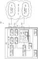
- FIG. 1is a block diagram of an electronic device 101 in a network environment 100 according to various embodiments.
- the electronic device 101communicates with the electronic device 102 through a first network 198 (eg, a short-range wireless communication network), or a second network 199 It is possible to communicate with the electronic device 104 or the server 108 through (eg, a long-distance wireless communication network).
- the electronic device 101may communicate with the electronic device 104 through the server 108.
- the electronic device 101includes a processor 120, a memory 130, an input device 150, an audio output device 155, a display device 160, an audio module 170, and a sensor module ( 176, interface 177, haptic module 179, camera module 180, power management module 188, battery 189, communication module 190, subscriber identification module 196, or antenna module 197 ) Can be included.
- a sensor module176, interface 177, haptic module 179, camera module 180, power management module 188, battery 189, communication module 190, subscriber identification module 196, or antenna module 197
- at least one of these componentsmay be omitted or one or more other components may be added to the electronic device 101.
- some of these componentsmay be implemented as one integrated circuit.
- the sensor module 176eg, a fingerprint sensor, an iris sensor, or an illuminance sensor
- the display device 160eg, a display.
- the processor 120for example, executes software (eg, a program 140) to implement at least one other component (eg, a hardware or software component) of the electronic device 101 connected to the processor 120. It can be controlled and can perform various data processing or operations. According to an embodiment, as at least a part of data processing or operation, the processor 120 stores commands or data received from other components (eg, the sensor module 176 or the communication module 190) to the volatile memory 132 The command or data stored in the volatile memory 132 may be processed, and result data may be stored in the nonvolatile memory 134.
- softwareeg, a program 140
- the processor 120stores commands or data received from other components (eg, the sensor module 176 or the communication module 190) to the volatile memory 132
- the command or data stored in the volatile memory 132may be processed, and result data may be stored in the nonvolatile memory 134.
- the processor 120includes a main processor 121 (eg, a central processing unit or an application processor), and an auxiliary processor 123 (eg, a graphics processing unit, an image signal processor) that can be operated independently or together. , A sensor hub processor, or a communication processor). Additionally or alternatively, the coprocessor 123 may be set to use less power than the main processor 121 or to be specialized for a designated function. The secondary processor 123 may be implemented separately from the main processor 121 or as a part thereof.
- a main processor 121eg, a central processing unit or an application processor
- an auxiliary processor 123eg, a graphics processing unit, an image signal processor
- the coprocessor 123may be set to use less power than the main processor 121 or to be specialized for a designated function.
- the secondary processor 123may be implemented separately from the main processor 121 or as a part thereof.
- the coprocessor 123is, for example, on behalf of the main processor 121 while the main processor 121 is in an inactive (eg, sleep) state, or the main processor 121 is active (eg, an application is executed). ) While in the state, together with the main processor 121, at least one of the components of the electronic device 101 (for example, the display device 160, the sensor module 176, or the communication module 190) It is possible to control at least some of the functions or states related to. According to an embodiment, the coprocessor 123 (eg, an image signal processor or a communication processor) may be implemented as part of another functionally related component (eg, the camera module 180 or the communication module 190). have.
- an image signal processor or a communication processormay be implemented as part of another functionally related component (eg, the camera module 180 or the communication module 190). have.
- the memory 130may store various data used by at least one component of the electronic device 101 (eg, the processor 120 or the sensor module 176).
- the datamay include, for example, software (eg, the program 140) and input data or output data for commands related thereto.
- the memory 130may include a volatile memory 132 or a nonvolatile memory 134.
- the program 140may be stored as software in the memory 130, and may include, for example, an operating system 142, middleware 144, or an application 146.
- the input device 150may receive a command or data to be used for a component of the electronic device 101 (eg, the processor 120) from an outside (eg, a user) of the electronic device 101.
- the input device 150may include, for example, a microphone, a mouse, a keyboard, or a digital pen (eg, a stylus pen).
- the sound output device 155may output an sound signal to the outside of the electronic device 101.
- the sound output device 155may include, for example, a speaker or a receiver.
- the speakercan be used for general purposes such as multimedia playback or recording playback, and the receiver can be used to receive incoming calls.
- the receivermay be implemented separately from or as a part of the speaker.
- the display device 160may visually provide information to the outside of the electronic device 101 (eg, a user).
- the display device 160may include, for example, a display, a hologram device, or a projector and a control circuit for controlling the device.
- the display device 160may include a touch circuitry set to sense a touch, or a sensor circuit (eg, a pressure sensor) set to measure the strength of a force generated by the touch. have.
- the audio module 170may convert sound into an electric signal or, conversely, convert an electric signal into sound. According to an embodiment, the audio module 170 obtains sound through the input device 150, the sound output device 155, or an external electronic device (for example, an external electronic device directly or wirelessly connected to the electronic device 101). Sound may be output through the electronic device 102) (for example, a speaker or headphones).
- the sensor module 176detects an operating state (eg, power or temperature) of the electronic device 101, or an external environmental state (eg, a user state), and generates an electrical signal or data value corresponding to the detected state. can do.
- the sensor module 176is, for example, a gesture sensor, a gyro sensor, an atmospheric pressure sensor, a magnetic sensor, an acceleration sensor, a grip sensor, a proximity sensor, a color sensor, an infrared (IR) sensor, a biometric sensor, It may include a temperature sensor, a humidity sensor, or an illuminance sensor.
- the interface 177may support one or more designated protocols that may be used for the electronic device 101 to connect directly or wirelessly with an external electronic device (eg, the electronic device 102 ).
- the interface 177may include, for example, a high definition multimedia interface (HDMI), a universal serial bus (USB) interface, an SD card interface, or an audio interface.
- HDMIhigh definition multimedia interface
- USBuniversal serial bus
- SD card interfaceSecure Digital Card
- the connection terminal 178may include a connector through which the electronic device 101 can be physically connected to an external electronic device (eg, the electronic device 102 ).
- the connection terminal 178may include, for example, an HDMI connector, a USB connector, an SD card connector, or an audio connector (eg, a headphone connector).
- the haptic module 179may convert an electrical signal into a mechanical stimulus (eg, vibration or movement) or an electrical stimulus that a user can perceive through a tactile or motor sense.
- the haptic module 179may include, for example, a motor, a piezoelectric element, or an electrical stimulation device.
- the camera module 180may capture a still image and a video.
- the camera module 180may include one or more lenses, image sensors, image signal processors, or flashes.
- the power management module 188may manage power supplied to the electronic device 101.
- the power management module 388may be implemented as at least a part of a power management integrated circuit (PMIC), for example.
- PMICpower management integrated circuit
- the battery 189may supply power to at least one component of the electronic device 101.
- the battery 189may include, for example, a non-rechargeable primary cell, a rechargeable secondary cell, or a fuel cell.
- the communication module 190is a direct (eg, wired) communication channel or a wireless communication channel between the electronic device 101 and an external electronic device (eg, electronic device 102, electronic device 104, or server 108). It is possible to support establishment and communication through the established communication channel.
- the communication module 190operates independently of the processor 120 (eg, an application processor), and may include one or more communication processors that support direct (eg, wired) communication or wireless communication.
- the communication module 190is a wireless communication module 192 (eg, a cellular communication module, a short-range wireless communication module, or a global navigation satellite system (GNSS) communication module) or a wired communication module 194 (eg : A LAN (local area network) communication module, or a power line communication module) may be included.
- a corresponding communication moduleis a first network 198 (for example, a short-range communication network such as Bluetooth, WiFi direct or IrDA (infrared data association)) or a second network 199 (for example, a cellular network, the Internet, or It can communicate with external electronic devices through a computer network (for example, a telecommunication network such as a LAN or WAN).
- the wireless communication module 192uses subscriber information stored in the subscriber identification module 196 (eg, International Mobile Subscriber Identifier (IMSI)) within a communication network such as the first network 198 or the second network 199.
- IMSIInternational Mobile Subscriber Identifier
- the antenna module 197may transmit a signal or power to the outside (eg, an external electronic device) or receive from the outside.
- the antenna modulemay include one antenna including a conductor formed on a substrate (eg, a PCB) or a radiator formed of a conductive pattern.
- the antenna module 197may include a plurality of antennas. In this case, at least one antenna suitable for a communication method used in a communication network such as the first network 198 or the second network 199 is, for example, provided by the communication module 190 from the plurality of antennas. Can be chosen.
- the signal or powermay be transmitted or received between the communication module 190 and an external electronic device through the at least one selected antenna.
- other componentseg, RFIC
- other than the radiatormay be additionally formed as a part of the antenna module 197.
- At least some of the componentsare connected to each other through a communication method (e.g., bus, general purpose input and output (GPIO), serial peripheral interface (SPI), or mobile industry processor interface (MIPI))) between peripheral devices and signal (E.g. commands or data) can be exchanged with each other.
- a communication methode.g., bus, general purpose input and output (GPIO), serial peripheral interface (SPI), or mobile industry processor interface (MIPI)
- GPIOgeneral purpose input and output
- SPIserial peripheral interface
- MIPImobile industry processor interface
- the command or datamay be transmitted or received between the electronic device 101 and the external electronic device 104 through the server 108 connected to the second network 199.
- Each of the electronic devices 102 and 104may be a device of the same or different type as the electronic device 101.
- all or part of the operations executed by the electronic device 101may be executed by one or more of the external electronic devices 102, 104, or 108.
- the electronic device 101needs to perform a function or service automatically or in response to a request from a user or another device, the electronic device 101 does not execute the function or service by itself.
- One or more external electronic devices receiving the requestmay execute at least a part of the requested function or service, or an additional function or service related to the request, and transmit the execution result to the electronic device 101.
- the electronic device 101may process the result as it is or additionally and provide it as at least a part of a response to the request.
- cloud computing, distributed computing, or client-server computing technologymay be used.
- the electronic device 101includes a first communication processor 212, a second communication processor 214, a first radio frequency integrated circuit (RFIC) 222, a second RFIC 224, and a third RFIC 226, a fourth RFIC 228, a first radio frequency front end (RFFE) 232, a second RFFE 234, a first antenna module 242, a second antenna module 244, and an antenna (248) may be included.
- the electronic device 101may further include a processor 120 and a memory 130.
- the network 199may include a first network 292 and a second network 294.
- the electronic device 101may further include at least one of the components illustrated in FIG. 1, and the network 199 may further include at least one other network.
- a first communication processor 212, a second communication processor 214, a first RFIC 222, a second RFIC 224, a fourth RFIC 228, a first RFFE 232, And the second RFFE 234may form at least a part of the wireless communication module 192.
- the fourth RFIC 228may be omitted or may be included as a part of the third RFIC 226.
- the first communication processor 212may support establishment of a communication channel of a band to be used for wireless communication with the first network 292 and communication of a legacy network through the established communication channel.
- the first networkmay be a legacy network including a second generation (2G), 3G, 4G, or long term evolution (LTE) network.
- the second communication processor 214establishes a communication channel corresponding to a designated band (eg, about 6 GHz to about 60 GHz) among bands to be used for wireless communication with the second network 294, and communicates 5G network through the established communication channel.
- a designated bandeg, about 6 GHz to about 60 GHz
- the second network 294may be a 5G network defined by 3GPP.
- the first communication processor 212 or the second communication processor 214corresponds to another designated band (eg, about 6 GHz or less) among bands to be used for wireless communication with the second network 294. It is possible to establish a communication channel and support 5G network communication through the established communication channel.
- the first communication processor 212 and the second communication processor 214may be implemented in a single chip or a single package. According to various embodiments, the first communication processor 212 or the second communication processor 214 may be formed in a single chip or a single package with the processor 120, the auxiliary processor 123, or the communication module 190. .
- the first RFIC 222transmits a baseband signal generated by the first communication processor 212 from about 700 MHz to about 3 GHz used for the first network 292 (eg, a legacy network). Can be converted to a radio frequency (RF) signal.
- RFradio frequency
- an RF signalis obtained from the first network 292 (eg, a legacy network) through an antenna (eg, the first antenna module 242), and through an RFFE (eg, the first RFFE 232). It can be preprocessed.
- the first RFIC 222may convert the preprocessed RF signal into a baseband signal to be processed by the first communication processor 212.
- the second RFIC 224transmits the baseband signal generated by the first communication processor 212 or the second communication processor 214 to the second network 294 (e.g., 5G network). It can convert into an RF signal (hereinafter, referred to as 5G Sub6 RF signal) of the Sub6 band (eg, about 6 GHz or less). Upon reception, a 5G Sub6 RF signal is obtained from the second network 294 (eg, 5G network) through an antenna (eg, the second antenna module 244), and RFFE (eg, the second RFFE 234) Can be pretreated through.
- the second RFIC 224may convert the preprocessed 5G Sub6 RF signal into a baseband signal to be processed by a corresponding one of the first communication processor 212 or the second communication processor 214.
- the third RFIC 226transmits the baseband signal generated by the second communication processor 214 to the RF of the 5G Above6 band (eg, about 6 GHz to about 60 GHz) to be used in the second network 294 (eg, 5G network). It can be converted into a signal (hereinafter, 5G Above6 RF signal).
- the 5G Above6 RF signalmay be obtained from the second network 294 (eg, 5G network) through an antenna (eg, antenna 248) and preprocessed through the third RFFE 236.
- the third RFIC 226may convert the pre-processed 5G Above 6 RF signal into a baseband signal to be processed by the second communication processor 214.
- the third RFFE 236may be formed as a part of the third RFIC 226.
- the electronic device 101may include the fourth RFIC 228 separately or at least as a part of the third RFIC 226.
- the fourth RFIC 228converts the baseband signal generated by the second communication processor 214 into an RF signal (hereinafter, IF signal) of an intermediate frequency band (eg, about 9 GHz to about 11 GHz). After conversion, the IF signal may be transferred to the third RFIC 226.
- the third RFIC 226may convert the IF signal into a 5G Above6 RF signal.
- the 5G Above6 RF signalmay be received from the second network 294 (eg, 5G network) through an antenna (eg, antenna 248) and converted into an IF signal by the third RFIC 226. .
- the fourth RFIC 228may convert the IF signal into a baseband signal so that the second communication processor 214 can process it.
- the first RFIC 222 and the second RFIC 224may be implemented as a single chip or at least part of a single package.
- the first RFFE 232 and the second RFFE 234may be implemented as a single chip or at least part of a single package.
- at least one of the first antenna module 242 or the second antenna module 244may be omitted or combined with another antenna module to process RF signals of a plurality of corresponding bands.
- the third RFIC 226 and the antenna 248may be disposed on the same substrate to form the third antenna module 246.
- the wireless communication module 192 or the processor 120may be disposed on a first substrate (eg, a main PCB).
- the third RFIC 226is located in a partial area (eg, lower surface) of the second substrate (eg, sub PCB) separate from the first substrate, and the antenna 248 is disposed in another area (eg, upper surface). Is disposed, a third antenna module 246 may be formed.
- the antenna 248may include, for example, an antenna array that can be used for beamforming.
- the electronic device 101may improve the quality or speed of communication with the second network 294 (for example, a 5G network).
- the second network 294can be operated independently from the first network 292 (eg, a legacy network) (eg, Stand-Alone (SA)), or connected and operated (eg: Non-Stand Alone (NSA)).
- a 5G networkmay have only an access network (eg, 5G radio access network (RAN) or next generation RAN (NG RAN)) and no core network (eg, next generation core (NGC)).
- the electronic device 101may access an external network (eg, the Internet) under the control of the core network (eg, evolved packed core (EPC)) of the legacy network.
- EPCevolved packed core
- Protocol information(eg, LTE protocol information) for communication with a legacy network or protocol information (eg, New Radio (NR) protocol information) for communication with a 5G network is stored in the memory 230 and other components (eg, processor information) 120, the first communication processor 212, or the second communication processor 214.
- LTE protocol informationfor communication with a legacy network
- protocol informationeg, New Radio (NR) protocol information
- 5G networkis stored in the memory 230 and other components (eg, processor information) 120, the first communication processor 212, or the second communication processor 214.
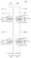
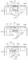
- FIG. 3shows an embodiment of the structure of the third antenna module 246 described with reference to FIG. 2, for example.
- 300a of FIG. 3is a perspective view of the third antenna module 246 viewed from one side
- 300b of FIG. 3is a perspective view of the third antenna module 246 viewed from the other side
- 300C of FIG. 3is a cross-sectional view taken along line A-A' of the third antenna module 246.
- the third antenna module 246includes a printed circuit board 310, an antenna array 330, a radio frequency integrate circuit (RFIC) 352, and a power manage integrate circuit (PMIC). 354, a module interface 370 may be included.
- the third antenna module 246may further include a shield member 390.
- at least one of the aforementioned partsmay be omitted, or at least two of the parts may be integrally formed.
- the printed circuit board 310may include a plurality of conductive layers, and a plurality of non-conductive layers alternately stacked with the conductive layers.
- the printed circuit board 310may provide electrical connection between the printed circuit board 310 and/or various electronic components disposed outside by using wires and conductive vias formed on the conductive layer.
- the antenna array 330may include a plurality of antenna elements 332, 334, 336, or 338 arranged to form a directional beam.
- the antenna elementsmay be formed on the first surface of the printed circuit board 310 as shown.
- the antenna array 330may be formed inside the printed circuit board 310.
- the antenna array 330may include a plurality of antenna arrays (eg, a dipole antenna array and/or a patch antenna array) of the same or different shape or type.
- the RFIC 352(for example, the third RFIC 226 in FIG. 2) is a different area of the printed circuit board 310 spaced apart from the antenna array (for example, a second side opposite to the first side). ) Can be placed.
- the RFICis configured to process a signal of a selected frequency band transmitted/received through the antenna array 330.
- the RFIC 352may convert a baseband signal obtained from a communication processor (not shown) into an RF signal of a designated band during transmission. Upon reception, the RFIC 352 may convert an RF signal received through the antenna array 352 into a baseband signal and transmit it to a communication processor.
- the RFIC 352is an IF signal obtained from an intermediate frequency integrate circuit (IFIC) (eg, the fourth RFIC 228 in FIG. 2) (eg, about 9 GHz to about 11GHz) can be up-converted to the RF signal of the selected band.
- IFICintermediate frequency integrate circuit
- the RFIC 352may down-convert the RF signal obtained through the antenna array 352, convert it into an IF signal, and transmit it to the IFIC.
- the PMIC 354may be disposed in another partial area (eg, the second surface) of the printed circuit board 310, spaced apart from the antenna array.
- the PMICmay receive a voltage from a main PCB (not shown) and provide power required for various components (eg, RFIC 352) on an antenna module.
- the shielding member 390may be disposed on a part (eg, the second surface) of the printed circuit board 310 to electromagnetically shield at least one of the RFIC 352 and the PMIC 354.
- the shielding member 390may include a shield can.
- the third antenna module 246may be electrically connected to another printed circuit board (eg, a main circuit board) through a module interface.
- the module interfacemay include a connecting member, for example, a coaxial cable connector, a board to board connector, an interposer, or a flexible printed circuit board (FPCB).
- FPCBflexible printed circuit board
- FIG. 4is a cross-sectional view taken along line B-B' of the third antenna module 246 of 300a of FIG. 3.
- the printed circuit board 310 of the illustrated embodimentmay include an antenna layer 411 and a network layer 413.
- the antenna layer 411may include at least one dielectric layer 437-1, and an antenna element 336 and/or a power feeding unit 425 formed on or inside the outer surface of the dielectric layer.
- the feeding part 425may include a feeding point 427 and/or a feeding line 429.
- the network layer 413includes at least one dielectric layer 437-2, at least one ground layer 433 formed on or inside the outer surface of the dielectric layer 437-2, and at least one conductive via ( 435), a transmission line 423, and/or a signal line 429 may be included.
- the third RFIC 226 of 300c of FIG. 3is, for example, the network layer through the first and second solder bumps 440-1 and 440-2. 413) can be electrically connected.
- various connection structureseg, soldering or BGA
- the third RFIC 226may be electrically connected to the antenna element 336 through a first connection unit 440-1, a transmission line 423, and a power supply unit 425.
- the third RFIC 226may also be electrically connected to the ground layer 433 through the second connection part 440-2 and the conductive via 435.
- the third RFIC 226may also be electrically connected to the module interface mentioned above through the signal line 429.
- the electronic device 500includes a first surface (or front surface) 510A, a second surface (or rear surface) 510B, and a first surface 510A. And a housing 510 including a side surface 510C surrounding a space between the second surfaces 510B.
- the housingmay refer to a structure forming some of the first surface 510A, the second surface 510B, and the side surfaces 510C of FIG. 5.
- at least a portion of the first surface 510Amay be formed by a substantially transparent front plate 502 (eg, a glass plate including various coating layers or a polymer plate).
- the second surface 510Bmay be formed by a substantially opaque rear plate 511.
- the back plate 511is formed by, for example, coated or colored glass, ceramic, polymer, metal (eg, aluminum, stainless steel (STS), or magnesium), or a combination of at least two of the above materials. Can be.
- the side surface 510Cis coupled to the front plate 502 and the rear plate 511, and may be formed by a side bezel structure (or “side member”) 518 including metal and/or polymer.
- the rear plate 511 and the side bezel structure 518are integrally formed and may include the same material (eg, a metal material such as aluminum).
- the front plate 502includes two first regions 510D that are curved toward the rear plate 511 from the first surface 510A and extend seamlessly, the front plate It may be included at both ends of the long edge (502).
- the rear plate 511is curved toward the front plate 502 from the second surface 510B to seamlessly extend two second regions 510E with a long edge. Can be included at both ends.
- the front plate 502 (or the rear plate 511)may include only one of the first regions 510D (or the second regions 510E). In another embodiment, some of the first regions 510D or the second regions 510E may not be included.
- the side bezel structure 518when viewed from the side of the electronic device 500, is the first region 510D or the second region 510E. It may have one thickness (or width), and may have a second thickness that is thinner than the first thickness on a side surface including the first regions 510D or the second regions 510E.
- the electronic device 500includes a display 501, an audio module 503, 507, 514, a sensor module 504, 516, 519, a camera module 505, 512, 513, and a key input. It may include at least one of the device 517, the light emitting element 506, and the connector holes 508, 509. In some embodiments, the electronic device 500 may omit at least one of the components (for example, the key input device 517 or the light emitting device 506) or additionally include other components.
- the display 501may be exposed through a substantial portion of the front plate 502, for example. In some embodiments, at least a portion of the display 501 may be exposed through the first surface 510A and the front plate 502 forming the first regions 510D of the side surface 510C. In some embodiments, the edge of the display 501 may be formed to have substantially the same shape as an adjacent outer shape of the front plate 502. In another embodiment (not shown), in order to expand the area to which the display 501 is exposed, the distance between the outer periphery of the display 501 and the outer periphery of the front plate 502 may be formed substantially the same.
- a recess or openingis formed in a part of the screen display area of the display 501, and the audio module 514 and the sensor are aligned with the recess or the opening. It may include at least one or more of the module 504, the camera module 505, and the light emitting device 506. In another embodiment (not shown), an audio module 514, a sensor module 504, a camera module 505, a fingerprint sensor 516, and a light emitting element 506 are provided on the rear surface of the screen display area of the display 501. ) May include at least one or more of.
- the display 501is coupled to or adjacent to a touch sensing circuit, a pressure sensor capable of measuring the intensity (pressure) of a touch, and/or a digitizer that detects a magnetic field type stylus pen. Can be placed.
- a touch sensing circuitcapable of measuring the intensity (pressure) of a touch
- a digitizercapable of measuring the intensity (pressure) of a touch
- a digitizerthat detects a magnetic field type stylus pen.
- at least a portion of the sensor modules 504 and 519 and/or at least a portion of the key input device 517may include the first regions 510D and/or the second regions 510E. Can be placed in the field.
- the audio modules 503, 507, and 514may include microphone holes 503 and speaker holes 507 and 514.
- a microphone for acquiring external soundmay be disposed inside, and in some embodiments, a plurality of microphones may be disposed to detect the direction of sound.
- the speaker holes 507 and 514may include an external speaker hole 507 and a call receiver hole 514.
- the speaker holes 507 and 514 and the microphone hole 503may be implemented as a single hole, or a speaker may be included without the speaker holes 507 and 514 (eg, piezo speakers).
- the sensor modules 504, 516, and 519may generate electrical signals or data values corresponding to an internal operating state of the electronic device 500 or an external environmental state.
- the sensor modules 504, 516, 519are, for example, a first sensor module 504 (for example, a proximity sensor) and/or a second sensor module 504 disposed on the first surface 510A of the housing 510 ( Not shown) (for example, a fingerprint sensor), and/or a third sensor module 519 (for example, HRM sensor) and/or a fourth sensor module 516 disposed on the second side 510B of the housing 510 ) (E.g. fingerprint sensor).
- the fingerprint sensormay be disposed on the first surface 510A of the housing 510 (eg, the display 501 as well as the second surface 510B.
- the electronic device 500is a sensor module, not shown, for example, for example, at least one of a gesture sensor, a gyro sensor, an atmospheric pressure sensor, a magnetic sensor, an acceleration sensor, a grip sensor, a color sensor, an infrared (IR) sensor, a biometric sensor, a temperature sensor, a humidity sensor, or an illuminance sensor 504 is further included.
- a gesture sensore.g, a gyro sensor, an atmospheric pressure sensor, a magnetic sensor, an acceleration sensor, a grip sensor, a color sensor, an infrared (IR) sensor, a biometric sensor, a temperature sensor, a humidity sensor, or an illuminance sensor 504 is further included.
- IRinfrared
- the camera modules 505, 512, 513include a first camera device 505 disposed on the first surface 510A of the electronic device 500, and a second camera device 512 disposed on the second surface 510B. ), and/or a flash 513.
- the camera devices 505 and 512may include one or more lenses, an image sensor, and/or an image signal processor.
- the flash 513may include, for example, a light emitting diode or a xenon lamp. In some embodiments, two or more lenses (infrared cameras, wide-angle and telephoto lenses) and image sensors may be disposed on one surface of the electronic device 500.
- the key input device 517may be disposed on the side surface 510C of the housing 510.
- the electronic device 500may not include some or all of the above-mentioned key input devices 517, and the key input device 517 that is not included may be used as a soft key or the like on the display 501. It can be implemented in a form.
- the key input devicemay include a sensor module 516 disposed on the second surface 510B of the housing 510.
- the light emitting element 506may be disposed on the first surface 510A of the housing 510, for example.
- the light-emitting element 506may provide state information of the electronic device 500 in the form of light, for example.
- the light emitting element 506may provide a light source that is linked to the operation of the camera module 505, for example.
- the light-emitting element 506may include, for example, an LED, an IR LED, and a xenon lamp.
- the connector holes 508 and 509are a first connector hole 508 capable of receiving a connector (eg, a USB connector) for transmitting and receiving power and/or data with an external electronic device, and/or an external electronic device And a second connector hole (eg, an earphone jack) 509 capable of accommodating a connector for transmitting and receiving an audio signal.
- a connectoreg, a USB connector
- a second connector holeeg, an earphone jack
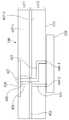
- the electronic device 700includes a side member 710, a first support member 711 (eg, a bracket), a front plate 720, a display 730, a printed circuit board 740, and A battery 750, a second support member 760 (eg, a rear case), an antenna 770, and a rear plate 780 may be included.
- the electronic device 700may omit at least one of the components (for example, the first support member 711 or the second support member 760), or may additionally include other components.
- At least one of the components of the electronic device 700may be the same as or similar to at least one of the components of the electronic device 500 of FIG. 5 or 6, and redundant descriptions will be omitted below.
- the first support member 711may be disposed inside the electronic device 700 to be connected to the side member 710 or may be integrally formed with the side member 710.
- the first support member 711may be formed of, for example, a metal material and/or a non-metal (eg, polymer) material.
- the display 730may be coupled to one surface and the printed circuit board 740 may be coupled to the other surface.
- a processor, memory, and/or interfacemay be mounted on the printed circuit board 740.
- the processormay include, for example, one or more of a central processing unit, an application processor, a graphic processing unit, an image signal processor, a sensor hub processor, or a communication processor.
- the memorymay include, for example, volatile memory or nonvolatile memory.
- the interfacemay include, for example, a high definition multimedia interface (HDMI), a universal serial bus (USB) interface, an SD card interface, and/or an audio interface.
- HDMIhigh definition multimedia interface
- USBuniversal serial bus
- the interfacemay electrically or physically connect the electronic device 700 to an external electronic device, for example, and may include a USB connector, an SD card/MMC connector, or an audio connector.
- the battery 750is a device for supplying power to at least one component of the electronic device 700, and may include, for example, a non-rechargeable primary cell, a rechargeable secondary cell, or a fuel cell. . At least a portion of the battery 750 may be disposed substantially on the same plane as the printed circuit board 740, for example. The battery 750 may be integrally disposed within the electronic device 700 or may be disposed detachably from the electronic device 700.
- the antenna 770may be disposed between the rear plate 780 and the battery 750.
- the antenna 770may include, for example, a near field communication (NFC) antenna, a wireless charging antenna, and/or a magnetic secure transmission (MST) antenna.
- NFCnear field communication
- MSTmagnetic secure transmission
- the antenna 770may perform short-range communication with an external device or wirelessly transmit/receive power required for charging.
- an antenna structuremay be formed by a part of the side member 710 and/or the first support member 711 or a combination thereof.
- FIG. 8is a flowchart illustrating a method of manufacturing an antenna module according to an exemplary embodiment.
- a first printed circuit board for disposing a communication circuit(eg, the third RFIC 226 of FIG. 2 or the communication circuit 990 of FIG. 9A described later) (For example, the first printed circuit board 910 of FIG. 9A to be described later) may be formed.
- the communication circuitmay be disposed on one surface of the first printed circuit board.
- the communication circuitmay include an RFIC.
- a second printed circuit board including at least one antennamay be formed.
- the second printed circuit boardmay implement at least a portion of at least one conductive layer as an antenna.
- the first printed circuit board and the second printed circuit boardare formed of a conductive material such as solder (for example, the first connection part 440-1 of FIG. 4 or the connection member of FIG. 9A ( 915, 916)).
- the first printed circuit boardincludes a first surface (eg, a first surface 910_1 in FIG. 9A described later) and a second surface facing the first surface (eg, in FIG. 9A described later).
- the second surface 910_2)may be included.
- the second printed circuit boardincludes a third surface (eg, a third surface 920_1 in FIG. 9A described later) and a fourth surface facing in a direction opposite to the third surface (eg, a fourth surface (eg, 920_2)).
- a part of the second side of the first printed circuit board and a part of the third side of the second printed circuit boardmay be combined.
- a conductive material such as soldermay be disposed in an overlapped portion between the second and third surfaces, and may electrically connect the first printed circuit board and the second printed circuit board.
- the communication circuitmay be disposed on the first surface of the first printed circuit board.
- operation 810may be performed, or operation 810 and operation 820 may be performed simultaneously.
- one of the first printed circuit board and the second printed circuit boardmay be formed first, and the other may be formed later and combined.
- the first printed circuit board and the second printed circuit boardmay be formed and combined together.
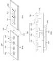
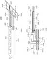
- FIG. 9Ais a diagram illustrating an antenna module including a combination structure of a first printed circuit board and a second printed circuit board according to an exemplary embodiment.
- the antenna module 900may include a first printed circuit board 910 and a second printed circuit board 920.
- the antenna module 900may be provided in a PCB design method.
- 901 of FIG. 9Ais a perspective view of the antenna module 900
- 903 of FIG. 9Ais a cross-sectional view taken along 9A-9A' of the antenna module 900.
- the first printed circuit board 910(for example, a rigid printed circuit board) includes at least one insulating layer (or dielectric layer) 911, at least one conductive layer 912, and a conductive line 913.
- the conductive line 914may include at least one.
- the conductive line 913 or the conductive line 914may be disposed through at least one insulating layer (or dielectric layer) 911 and a portion of the at least one conductive layer 912.
- the insulating layer (or dielectric layer) 911 and the conductive layer 912may be alternately stacked. For example, after a specific insulating layer (or dielectric layer) 911 is formed, a conductive layer 912 is formed on the specific insulating layer (or dielectric layer) 911, and then insulated again on the conductive layer 912 The operation of forming the layer (or dielectric layer) 911 may be repeated for a specified number of times. The number of the insulating layer (or dielectric layer) 911 and the conductive layer 912 may vary.
- the second printed circuit board 920(eg, a flexible printed circuit board) may be formed of a material different from that of the first printed circuit board 910.
- the second printed circuit board 920includes at least one conductive pattern 921 (eg, a dipole antenna), at least one power supply 926, at least one conductive layer 923 and 924, and/or at least one conductive layer.
- Line 925may be included.
- the second printed circuit board 920may be disposed to protrude from the first printed circuit board 910.
- the first printed circuit board 910 and at least a portion of the second printed circuit board 920may be connected.
- the first printed circuit board 910may include a first surface 910_1 and a second surface 910_2 facing in a direction opposite to the first surface 910_1.
- the second printed circuit board 920may include a third surface 920_1 and a fourth surface 920_2 facing in a direction opposite to the third surface 920_1.
- a part of the second surface 910_2 of the first printed circuit board 910 and a part of the third surface 920_1 of the second printed circuit board 920may be combined.
- the conductive line 925may be connected to the conductive line 913 through a connection member 915 (eg, a solder ball).
- the conductive layers 923 and 924may be connected to at least one of the conductive layers 912 (eg, a ground region) through a connection member 916 (eg, a solder ball).
- the conductive layers 923 and 924may form an electrical shield for the conductive line 925.
- Some of the connection members 916are not connected to the ground region, and may be formed to couple the first printed circuit board 910 and the second printed circuit board 920.
- the communication circuit 990may transmit a communication signal through the conductive pattern 921.
- the communication circuit 990may transmit and receive a communication signal through a conductive line (or a power supply line) 913, 915, 925, 921 (for example, a transmission line 423).
- the third printed circuit board 930may include a fifth surface 930_1 and a sixth surface 930_2 facing in a direction opposite to the fifth surface 930_1.
- a part of the second surface 910_2 of the first printed circuit board 910 and a part of the fifth surface 930_1 of the third printed circuit board 930may be combined.
- the first printed circuit board 910 and the third printed circuit board 930may be coupled through at least one connecting member 918.
- connection member 918is disposed on the second surface 910_2 of the first printed circuit board 910 and the fifth surface 930_1 of the third printed circuit board 930 Can be.
- some of the connection members 918may be connected to a ground region (eg, some of the conductive layers 912 ).
- some of the connection members 918are not connected to any feeder or ground area, and are used only for bonding the first printed circuit board 910 and the third printed circuit board 930 (example : Can be used as an adhesive member for bonding the first printed circuit board 910 and the third printed circuit board 930 ).
- the third printed circuit board 930may be formed of the same material as the first printed circuit board 910 (for example, a rigid printed circuit board). According to another embodiment, at least a portion of the third printed circuit board 930 may be formed of the same material as the second printed circuit board 920 (eg, a flexible printed circuit board).
- the third printed circuit board 930may include a conductive pattern 931 (eg, a patch antenna) and a conductive pattern 936.
- the conductive pattern 936may be connected to the conductive line 914 through the connection member 917.
- the conductive pattern 936 and the connection member 917may be connected through an additional conductive line.
- the conductive pattern 936may transmit a communication signal from the communication circuit 990 to the conductive pattern 931.
- the conductive pattern 936may transmit a communication signal to the conductive pattern 931 through coupling.
- the conductive pattern 936may be directly connected to the conductive pattern 931 through a conductive line (not shown), and may transmit a communication signal to the conductive pattern 931.
- the communication circuit 990may transmit a communication signal through the conductive pattern 931.
- the communication circuit 990may transmit and receive a communication signal through a conductive line (or a power supply line) 914, 917, 936, 931 (for example, a transmission line 423).
- the communication circuit 990may be disposed on the first surface 910_1 of the first printed circuit board 910.
- the communication circuit 990may be connected to the conductive line 913 and the conductive line 914.
- FIG. 9Bshows, for example, an embodiment of the bonding portion 951 of the first printed circuit board 910 and the third printed circuit board 930 of FIG. 9A.
- the first printed circuit board 910includes a plurality of conductive layers 11L, 12L, 13L, 14L, 15L, 16L, or a plurality of conductive layers 11L, 12L, 13L, 14L, 15L, 16L. ) May include a first insulating material (eg, prepreg) DS1 disposed therebetween.
- the first printed circuit board 910may have a structure in which the same number of conductive layers are disposed on both sides of the center substrate C1.
- the first printed circuit board 910in which the same number of conductive layers are stacked on both sides based on the central substrate by a manufacturing method in which an operation of stacking two conductive layers forming a pair on both sides is performed several times.
- the gap H11 between the plurality of conductive layers 11L, 12L, 13L, 14L, 15L, 16Lmay be substantially the same, and the first printed circuit board 910 may be formed on both sides based on the central substrate C1. It may have substantially the same height (or thickness) (H12, H13).
- the first printed circuit board 910is a conductive via having a connection lead for electrically connecting a plurality of conductive layers 11L, 12L, 13L, 14L, 15L, 16L disposed on different layers. (VIA1) may be included.
- the number of conductive layers included in the first printed circuit board 910is not limited to the example illustrated in FIG. 9B and may vary.
- the first printed circuit board 910includes insulating layers SR11 and SR12 formed by applying an insulating material (eg, solder mask insulating ink) to a conductive layer 11L and/or a conductive layer 16L. ) Can be included. Since the regions covered by the insulating layer SR11 in the conductive layer 11L and the regions covered by the insulating layer SR12 in the conductive layer 16L are not exposed to the outside, oxidation can be prevented.
- an insulating materialeg, solder mask insulating ink
- a region not covered by the insulating layer SR11 in the conductive layer 11Lis the communication circuit 990 (eg, the wireless communication module 192 or the third RFIC 226), the connector ( Components such as 980 may be used as terminals (or lands) for coupling to the first printed circuit board 910.
- the communication circuit 990 or the connector 980may be used as terminals (or lands) for coupling to the first printed circuit board 910.
- a region not applied by the insulating layer SR12 in the conductive layer 16Lis the first printed circuit board 910 through the connection members 917 and 918 (for example, conductive materials). And it may be used as a terminal (or land) electrically connecting the third printed circuit board 930.
- the insulating layer SR12is connected to the first printed circuit board 910 and the third printed circuit board 930 through a connection member such as solder, it is possible to prevent the occurrence of solder bridges.
- the third printed circuit board 930includes a third insulating layer disposed between a plurality of conductive layers 31L, 32L, 33L, and 34L, or a plurality of conductive layers 31L, 32L, 33L, and 34L. It may contain a substance (eg, prepreg or polyimide) (DS3).
- the third printed circuit board 930may have a structure in which the same number of conductive layers are disposed on both sides of the center substrate C3. For example, a third printed circuit in which the same number of conductive layers are stacked on both sides based on the central substrate (C3) by a manufacturing method in which the operation of stacking two conductive layers forming a pair on each side is performed several times.
- the substrate 930may be formed. This manufacturing method can prevent breakage such as warping or tearing of the printed circuit board due to an environment such as temperature or pressure applied on the manufacturing thereof.
- the gap H31 between the plurality of conductive layers 31L, 32L, 33L, and 34Lmay be substantially the same, and the third printed circuit board 930 has substantially the same height on both sides of the center substrate C3. (Or thickness) (H32, H33) may have.
- the third printed circuit board 930may include a conductive via VIA3 electrically connecting at least some of the plurality of conductive layers 31L, 32L, 33L, and 34L.
- the conductive via VIA3may include a conductive hole drilled for the purpose of arranging connection conduction for electrically connecting the conductive layers 31L, 32L, 33L, and 34L disposed in different layers. According to various embodiments, the number of conductive layers included in the third printed circuit board 930 is not limited to the example illustrated in FIG. 9B and may vary.
- the third printed circuit board 930includes insulating layers SR31 formed by applying an insulating material such as an epoxy-based solder mask insulating ink to the conductive layer 31L and/or the conductive layer 34L.
- SR32may be included. Since the regions covered by the insulating layer SR31 in the conductive layer 31L and the regions covered by the insulating layer SR32 in the conductive layer 34L are not exposed to the outside, oxidation can be prevented.
- a region of the conductive layer 31L that is not coated by the insulating layer SR31is connected to the first printed circuit board 910 through the connection members 917 and 918 (eg, conductive materials). It may be used as a terminal (or land) to be electrically connected.
- the insulating layer SR31may prevent the occurrence of solder bridges when connecting the first and third printed circuit boards 910 and 930 through a connection member such as solder.
- the first printed circuit board 910 or the third printed circuit board 930is a copper clad laminate (CCL) (or an original) (for example, a conductive layer 912, a plurality of conductive substrates). It may be formed using the layers 11L, 12L, 13L, 14L, 15L, 16L or a plurality of conductive layers 31L, 32L, 33L, and 34L).
- the copper clad laminatemay be, for example, a composite copper clad laminate made by combining two or more types of reinforcing substrates.
- the composite copper clad laminatemay include a composite type of laminate material bonded with a flame retardant epoxy resin (CEM)-1 or CEM-3 defined by NEMA.
- CEMflame retardant epoxy resin
- CEM-1may include a central substrate (or core) made of paper impregnated with an epoxy resin, or an outer substrate made of woven glass fibers impregnated with an epoxy resin, and a copper foil bonded to the outer substrate.
- CEM-3is a central substrate made of non-woven glass fibers impregnated with epoxy resin (e.g., glass non-woven fabric), an outer substrate made of woven glass fibers impregnated with an epoxy resin, or bonded to the outer substrate It may contain copper foil. Glass fibers or paper can improve mechanical processability, heat resistance or dimensional stability.
- the copper clad laminateis a central substrate made of nonwoven glass fibers (eg, glass nonwoven fabric) impregnated with a polyester resin, an outer substrate made of glass fibers impregnated with a resin, or the outer substrate and It may be FR-6 containing a bonded copper foil.
- CEM-3may be designed to replace FR-4 or FR-5.
- CEM-3has relatively few glass fibers compared to FR-4 or FR-5, so its mechanical strength may be relatively low.
- this mechanical strengthcan be taken into account.
- CEM-3when punching is required, CEM-3, which is more advantageous for punching, may be applied to manufacture a printed circuit board instead of FR-4.
- the copper clad laminatemay be a high frequency copper clad laminate made of a material capable of responding to high-speed signal transmission.
- a material capable of responding to high-speed signal transmissionFor example, in a printed circuit board, since the propagation speed of a signal is inversely proportional to the dielectric constant of the material, using a material with a low permittivity can increase the propagation speed of the signal.
- the copper clad laminatemay be in a form in which a film prepreg of an insulating material is disposed on a plate formed of a metal such as aluminum or iron, and then the copper foil is bonded to the film prepreg.
- the copper clad laminatemay include a flexible copper clad laminate (FCCL) for a flexible printed circuit board (FPCB).
- FCCLflexible copper clad laminate
- FPCBflexible printed circuit board
- the flexible copper clad laminatemay be in a form in which copper foil is bonded with an adhesive (eg, acrylic adhesive), such as a polyester film or polyimide film having soluble properties.
- the first printed circuit board 910 and the third printed circuit board 930may be manufactured based on different copper clad laminates. According to various embodiments, the first printed circuit board 910 and the third printed circuit board 930 may be manufactured based on the same copper clad laminate.
- the first printed circuit board 910may be manufactured using a plurality of different copper clad laminates.
- the third printed circuit board 930may be manufactured using a plurality of different copper clad laminates.
- the number of conductive layers included in the third printed circuit board 930may be different from the number of conductive layers included in the first printed circuit board 910.
- the number of conductive layers (eg, 4) included in the third printed circuit board 930may be smaller than the number of conductive layers (eg, 6) included in the first printed circuit board 910. have.
- the number of conductive layers included in the third printed circuit board 930is equal to the number of conductive layers included in the first printed circuit board 910 or the first printed circuit board It may be larger than the number of conductive layers included in 910.
- the first insulating material DS1 and the third insulating material DS3may include different materials. According to some embodiments, the first insulating material DS1 and the third insulating material DS3 may be the same.
- the first insulating material DS1may vary depending on the copper clad laminate that forms the basis of the first printed circuit board 910 and the insulating material included therein.
- the third insulating material DS3may vary depending on the copper clad laminate that forms the basis of the third printed circuit board 930 and the insulating material included therein.
- a gap H11 between a plurality of conductive layers 11L, 12L, 13L, 14L, 15L, 16L of the first printed circuit board 910, or a plurality of gaps in the third printed circuit board 930may be different.
- the gap H11may be smaller than the gap H31.
- the gap H11may be substantially the same as the gap H31 or larger than the gap H31.
- the thickness H1 of the first printed circuit board 910may be different from the thickness H3 of the third printed circuit board 930.
- the thickness H1 of the first printed circuit board 910may be smaller than the thickness H3 of the third printed circuit board 930.
- the thickness H1 of the first printed circuit board 910is substantially equal to the thickness H3 of the third printed circuit board 930 or the thickness of the third printed circuit board 930 ( May be greater than H3).
- connection members 917 and 918eg, conductive materials
- soldermay be disposed between the second surface 910_2 and the fifth surface 930_1, and the first printed circuit board 910 and the third printed circuit board 930 may be electrically connected.
- the communication circuit 990may be disposed or coupled to the first surface 910_1 of the first printed circuit board 910 through a conductive material 991 such as solder, and the first printed circuit board It may be electrically connected to 910.
- At least some of the plurality of conductive layers 31L, 32L, 33L, and 34L included in the third printed circuit board 930may be used as a plurality of conductive patterns (eg, patch antennas).
- the conductive layers 33L and 34Lmay include conductive patterns 931a and 931b electrically connected to the communication circuit 990.
- the conductive patterns 931a and 931bmay receive power from the communication circuit 990 to transmit or receive a wireless signal.
- Some 917 of the connection members 917 and 918 (eg, conductive materials) connecting the first printed circuit board 910 and the third printed circuit board 930are part of the conductive layer 32L ( For example, it may be used as a conductive path for transferring a signal or power between the conductive pattern 936 and the communication circuit 990.
- the conductive layer 31Lmay include a dummy pattern 939.
- the dummy pattern 939may be in an electrically floating state physically separated from other conductive elements.
- the dummy pattern 939may be electromagnetically coupled to the conductive pattern 936 of the conductive layer 32L to adjust the radiation characteristics.
- the dummy pattern 939may move the resonance frequency to a designated frequency or may move the resonance frequency by a designated frequency.
- the dummy pattern 939may improve antenna performance by reducing electromagnetic noise.
- the dummy pattern 939when viewed from the top of the sixth surface 930_2, may at least partially overlap the conductive pattern 936 of the conductive layer 32L. According to various embodiments, the dummy pattern 939 provides a uniform coefficient of thermal expansion when manufacturing the third printed circuit board 930, thereby preventing a warpage of the printed circuit board that may be caused by high temperature heat. have.
- At least some of the plurality of conductive layers included in the first printed circuit board 910 or the third printed circuit board 930may include a ground plane.
- the ground planemay shield electromagnetic noise from the flow of signals or power in the first printed circuit board 910 or the third printed circuit board 930.
- the ground planemay dissipate heat generated from the antenna module 900 or transferred from the outside to the antenna module 900.
- at least one ground plane (not shown) included in the third printed circuit board 930is at least one ground plane included in the first printed circuit board 910 through conductive materials 918. It can be electrically connected to the plane.
- At least a portion of the plurality of conductive layers 11L, 12L, 13L, 14L, 15L, 16L of the first printed circuit board 910is a conductive pattern included in the third printed circuit board 930
- At least one first ground planeeg, one of a plurality of conductive layers 11L, 12L, 13L, 14L, 15L, 16L
- the radiation characteristic of the antenna module 900may be determined based on a distance between the conductive patterns 931a and 931b included in the third printed circuit board 930 separated from the first ground plane.
- the radiation characteristic of the antenna module 900may be determined based on the shape (eg, width, length, and thickness) of the first ground plane.
- the radiation characteristic of the antenna module 900may be determined based on an insulating material (eg, dielectric constant) between the conductive patterns 931a and 931b included in the third printed circuit board 930 and the first ground plane. I can.
- At least some of the plurality of conductive layers 31L, 32L, 33L, and 34L included in the third printed circuit board 930are at least one conductive layer included in the third printed circuit board 930.
- At least one third ground plane(eg, one of the plurality of conductive layers 31L, 32L, 33L, and 34L) related to the radiation characteristics of the patterns 931a and 931b may be included.
- the radiation characteristic of the antenna module 900may be determined based on a distance between the conductive patterns 931a and 931b included in the third printed circuit board 930 separated from the third ground plane.
- the radiation characteristic of the antenna module 900may be determined based on the shape of the third ground plane (eg, width, length, thickness).
- the radiation characteristic of the antenna module 900may be determined based on an insulating material (eg, dielectric constant) between the conductive patterns 931a and 931b included in the third printed circuit board 930 and the third ground plane. I can.
- the first ground plane and the third ground plane of the first printed circuit board 910may be omitted.
- the connector 980may be disposed or coupled to the first surface 910_1 of the first printed circuit board 910 through a conductive material 981 such as solder, and the first printed circuit board ( 910) and may be electrically connected.
- the connector 980may be electrically connected to the communication circuit 990 or various other elements disposed on the first printed circuit board 910 through at least one conductive layer included in the first printed circuit board 910. .
- the power management circuitmay be disposed or coupled to the first surface 910_1 of the first printed circuit board 910 through a conductive material such as solder, and the first printed circuit board ( 910) and may be electrically connected.
- the power management circuitincludes a communication circuit 990, a connector 980, or various other elements disposed on the first printed circuit board 910 through at least one conductive layer included in the first printed circuit board 910. : Passive element) and can be electrically connected.
- the antenna module 900may include a conductive cover 992 coupled to the first printed circuit board 910 through a conductive material 971.
- the conductive cover 992may cover at least a portion of the communication circuit 990, and may be electrically connected to the ground plane of the first printed circuit board 910.
- the conductive cover 992may reduce external electromagnetic noise or electromagnetic noise generated from the antenna module 900 from flowing into the communication circuit 990.
- the conductive cover 992may be referred to as a shielding member or a shield can.
- 9Cis a diagram illustrating an antenna module including a combination structure of a first printed circuit board and a third printed circuit board according to another embodiment.
- the antenna module 900cmay include a first printed circuit board 910 and a third printed circuit board 930.
- the antenna module 900cmay be provided in a PCB design method.
- 905 of FIG. 9Cis a perspective view of the antenna module 900c
- 907 of FIG. 9Cis a cross-sectional view taken along 9C-9C' of the antenna module 900c.
- the first printed circuit board 910(for example, a rigid printed circuit board) includes at least one insulating layer (or dielectric layer) 911, at least one conductive layer 912 and/or a conductive line ( 913) may be included.
- the conductive line 913may be disposed through at least one insulating layer (or dielectric layer) 911 and a portion of the at least one conductive layer 912.
- the configuration of the first printed circuit board 910 of FIG. 9Cmay be the same or similar to the configuration of the first printed circuit board 910 of FIG. 9A, and redundant descriptions will be omitted below.
- the first printed circuit board 910 and at least a portion of the third printed circuit board 930may overlap and be combined.
- the first printed circuit board 910may include a first surface 910_1 and a second surface 910_2 facing in a direction opposite to the first surface 910_1.
- the third printed circuit board 930may include a fifth surface 930_1 and a sixth surface 930_2 facing in a direction opposite to the fifth surface 930_1.
- a part of the second surface 910_2 of the first printed circuit board 910 and a part of the fifth surface 930_1 of the third printed circuit board 930may overlap and be combined.
- At least one dummy pattern 919 coupled to the connection member 918may be disposed on the second surface 910_2 of the printed circuit board 910 and the fifth surface 930_1 of the third printed circuit board 930. have. According to various embodiments, some of the connection members 918 may be connected to a ground region (eg, some of the conductive layers 912 ). According to various embodiments, some of the connection members 918 are not connected to any feeder or ground area, and are used only for bonding the first printed circuit board 910 and the third printed circuit board 930 (example : Can be used as an adhesive member for bonding the first printed circuit board 910 and the third printed circuit board 930 ).
- the third printed circuit board 930may include at least one conductive pattern 931 (eg, a patch antenna) and/or at least one conductive pattern 936.
- the conductive pattern 936may be connected to the conductive line 913 through the connection member 915.
- the conductive pattern 936 and the connection member 915may be connected through an additional conductive line.
- the conductive pattern 936may transmit a communication signal from the communication circuit 990 (eg, the wireless communication module 192 or the third RFIC 226) to the conductive pattern 931.
- the conductive pattern 936may transmit a communication signal to the conductive pattern 931 through coupling.
- the conductive pattern 936may be connected to the conductive pattern 931 through a conductive line (not shown), and may transmit a communication signal to the conductive pattern 931.
- the communication circuit 990may be disposed on the first surface 910_1 of the first printed circuit board 910.
- the third printed circuit board 930may be formed of the same material as the first printed circuit board 910 (for example, a rigid printed circuit board). According to another embodiment, at least a part of the third printed circuit board 930 may be formed of a material different from the first printed circuit board 910 (eg, a flexible printed circuit board).
- FIG. 10Ashows, for example, an embodiment of the engaging portion 950 of FIG. 9A. 9A and 10A, although spaced apart from each other in the drawing, the first overlapping portion 1001 of the first printed circuit board 910 and the second overlapping portion 1002 of the second printed circuit board 920 are It is an area that overlaps each other (eg, the combined portion 950 or (eg, the first overlapping area)).
- the first overlapping portion 1001 and the second overlapping portion 1002may have a width of a specific size (eg, the first size W1 or about 1 mm).
- the first overlapping portion 1001may include a first insulating region 1040-1
- the second overlapping portion 1002may include a second insulating region 1040-2.
- the first signal pad 1015-1, the first guide pad 1016-1, and the first dummy pad 1010may be formed in the first insulating region 1040-1.
- the second signal pad 1015-2, the second guide pad 1016-2, and the second dummy pad 1020may be formed in the second insulating region 1040-2.
- the first signal pad 1015-1 and the second signal pad 1015-2may be electrically connected through the connection member 915.
- the first signal pad 1015-1may be connected to the conductive line 913.
- the second signal pad 1015-2may be connected to the conductive line 925.
- the conductive pattern 921includes a conductive line 913, a first signal pad 1015-1, a connection member 915, a second signal pad 1015-2, a conductive line 925, and a power supply unit 926. It can be fed through.
- the size of the second signal pad 1015-2may be greater than or equal to the size of the first signal pad 1015-1.
- the first signal pad 1015-1 and the second signal pad 1015-2may be disposed at at least partially overlapping positions.
- the first guide pad 1016-1 and the second guide pad 1016-2may be coupled through the connection member 916.
- the first guide pad 1016-1may be connected to at least one of the conductive layers 912 (eg, a ground area).
- the second guide pad 1016-2may be connected to the conductive layers 923 and 924.
- the size of the second guide pad 1016-2may be greater than or equal to the size of the first guide pad 1016-1.
- the first guide pad 1016-1 and the second guide pad 1016-2may be disposed at at least partially overlapping positions.
- the first dummy pad 1010 and the second dummy pad 1020may be coupled through a dummy connection member (not shown).
- a dummy connection member(not shown).
- the first printed circuit board 910 and the second printed circuit board 920may maintain the bonding.
- the first dummy pad 1010 and the second dummy pad 1020may be disposed at a position at least partially overlapping.
- the first dummy pad 1010 and the second dummy pad 1020may be formed at a specific interval (eg, the first pad interval PD1 or about 0.25 mm).
- the connection member 915, the connection member 916, or the dummy connection membermay be formed through an adhesive self-align (ASA) process.
- ASAadhesive self-align
- the ASA processis performed between conductive lines or patterns of heterogeneous substrates (for example, between the first signal pad 1015-1 and the second signal pad 1015-2, and the first guide pad 1016-1). ) And the second guide pad 1016-2 or between the first dummy pad 1010 and the second dummy pad 1020 ).
- the ASA processcan include at least three operations. In the first operation, a resin containing a conductive component (eg, lead (Pb)) may be applied to the surface for bonding. In the second operation, conductors or patterns for bonding may be matched.
- a resin containing a conductive componenteg, lead (Pb)
- the applied resinis melted and bonded between the conductors or patterns of the different substrates, and the conductors or patterns of the different substrates may be connected to each other.
- wires or patterns of the mmWave antennafor example, between the first signal pad 1015-1 and the second signal pad 1015-2, the first guide pad 1016-1, the second guide pad 1016) -2)
- Between, between the first dummy pad 1010 or the second dummy pad 1020may be formed as a fine gap due to a high frequency band.
- the applied resinmay include a conductive component and may include a self-assembly paste having a melting point of a specific temperature (eg, about 200°C to 250°C) at which the FPCB is not damaged by heat.
- a specific temperatureeg, about 200°C to 250°C
- the conductive component of the self-aligned pastemay be collected in the portion with the conductive pattern, and the non-conductive component of the self-aligned paste may be collected in the portion without the conductive pattern.
- Componentscan be isolated from each other.
- the guide via 1030may be connected between the conductive layers 923 and 924.
- the guide via 1030may form an electrical shield for the conductive line 925 together with the conductive layers 923 and 924.
- FIG. 10Bshows another embodiment of the engaging portion 950 of FIG. 9A, for example. 9A and 10B, although spaced apart from each other in the drawing, the first overlapping portion 1001 of the first printed circuit board 910 and the second overlapping portion 1002 of the second printed circuit board 920 are It is an area that overlaps each other (for example, the coupling portion 950).
- At least one of the components of the coupling portion 950 of FIG. 10Amay be the same or similar to at least one of the components of the coupling portion 950 of FIG. 10B, and redundant descriptions will be omitted below.
- the first overlapping portion 1001may include a first insulating region 1040-1 and a first metal region 1050-1.
- the second overlapping portion 1002may include a second insulating region 1040-2 and a second metal region 1050-2.
- the first signal pad 1015-1 and the first guide pad 1016-1may be formed in the first metal region 1050-1.
- the first dummy pad 1010may be formed in the first insulating region 1040-1.
- the second signal pad 1015-2 and the second guide pad 1016-2may be formed in the second metal region 1050-2.
- the second dummy pad 1020may be formed in the second insulating region 1040-2.
- the first dummy pad 1010 or the second dummy pad 1020may be disposed at a specific interval (eg, a second pad interval PD2).
- the first dummy pad 1010 and the second dummy pad 1020may be formed in a rectangular shape having a specific size (eg, about 0.2 mm in width and about 0.8 mm in height).
- FIG. 10Cshows another embodiment of the engaging portion 950 of FIG. 9A, for example. 9A and 10C, although spaced apart from each other in the drawing, the first overlapping portion 1001 of the first printed circuit board 910 and the second overlapping portion 1002 of the second printed circuit board 920 are It is an area that overlaps each other (for example, the coupling portion 950).
- At least one of the components of the coupling portion 950 of FIG. 10Amay be the same as or similar to at least one of the components of the coupling portion 950 of FIG. 10C, and redundant descriptions will be omitted below.
- the first overlapping portion 1001may include the first metal region 1050-1.
- the second overlapping portion 1002may include a second metal region 1050-2.
- the first signal pad 1015-1, the first guide pad 1016-1, and/or the first dummy pad 1010may be formed in the first metal region 1050-1.
- the second signal pad 1015-2, the second guide pad 1016-2, and/or the second dummy pad 1020may be formed in the second metal region 1050-2.
- the first dummy pad 1010 and the second dummy pad 1020may be formed in a surface shape having a size similar to that of the first metal region 1050-1 or the second metal region 1050-2. I can.
- FIG. 10Dshows, for example, an embodiment showing a peripheral portion of the connection member 915 of FIG. 9A.
- 1003 of FIG. 10Dis a perspective view of the engagement portion 950 and 1004 of FIG. 10D is a cross-sectional view of the engagement portion 950.
- the first signal pad 1015-1 and the second signal pad 1015-2may be coupled through a connection member 915.
- the first signal pad 1015-1may be connected to the conductive line 913 through the first signal via 1025-1.
- the second signal pad 1015-2may be connected to the conductive line 925 through the second signal via 1025-2.
- the first guide pad 1016-1 and the second guide pad 1016-2may be coupled through the connection member 916.
- the first guide pad 1016-1may be connected to at least one of the conductive layers 912 (eg, a ground area) through the first guide via 1051-1.
- the second guide pad 1016-2may be connected to the conductive layers 923 and 924 through the second guide via 1051-2.
- FIG. 11Ashows, for example, an embodiment of a signal line of the second printed circuit board of FIG. 9A.
- 11Ais a cross-sectional view taken along 9B-9B' in FIG. 9A.
- the second printed circuit board 920may include one conductive layer.
- the insulating layer (or dielectric layer) 1110may include an insulator (or dielectric) 1111.
- the conductive layer 1120may include at least one conductive line 1121, 1122, and 1123. At least one conductive line 1121, 1122, 1123 may be stacked on the insulator (or dielectric) 1111.
- the first conductive line 1121 and the third conductive line 1123are ground lines, and may be connected to a ground region among the conductive layers 912 of the first printed circuit board 910 through the connection member 916.
- the second conductive line 1122(for example, the conductive line 925) is a signal line and may be connected to the conductive line 913 through a connection member 915. As an embodiment, the second conductive line 1122 may be disposed between the first conductive line 1121 and the third conductive line 1123.
- the first conductive line 1121, the second conductive line 1122, and the third conductive line 1123may be formed as a single planar waveguide (CPW).
- the first conductive line 1121 and the third conductive line 1123may electrically shield the second conductive line 1122.
- Fig. 11Bshows another embodiment of the signal line of the second printed circuit board of Fig. 9A, for example. 11B is a cross-sectional view taken along 9B-9B' in FIG. 9A.
- the second printed circuit board 920may include a plurality of conductive layers.
- the first conductive layer 1130may include a first conductor 1131 (eg, a conductive layer 923).
- the first insulating layer (or dielectric layer) 1140may include a first insulator (or dielectric) 1141.
- the second conductive layer 1150may include a second conductor 1151 (eg, a conductive line 925 ).
- the first insulating layer (or dielectric layer) 1140may be stacked between the first conductive layer 1130 and the second conductive layer 1150.
- the second conductive layer 1150may be stacked on the first insulating layer (or dielectric layer) 1140.
- the first conductor 1131may be connected to a ground region among the conductive layers 912 of the first printed circuit board 910 through the connection member 916.
- the second conductor 1151is a signal line and may be connected to the conductive line 913 through a connection member 915.
- the second conductor 1151may be formed as a micro strip line.
- the first conductor 1131may electrically shield the second conductor 1151.
- Fig. 11Cshows another embodiment of the signal line of the second printed circuit board of Fig. 9A, for example. 11C is a cross-sectional view taken along 9B-9B' in FIG. 9A.
- the second printed circuit board 920may include a plurality of conductive layers.
- the first conductive layer 1130may include a first conductor 1131 (eg, a conductive layer 923).
- the first insulating layer (or dielectric layer) 1140may include a first insulator (or dielectric) 1141.
- the second conductive layer 1150may include a second conductor 1151 (eg, a conductive line 925 ).
- the second insulating layer (or dielectric layer) 1160may include a second insulator (or dielectric) 1161.
- the third conductive layer 1170may include a third conductor 1171 (eg, a conductive layer 924).
- the first insulating layer (or dielectric layer) 1140may be stacked between the first conductive layer 1130 and the second conductive layer 1150.
- the second conductive layer 1150may be stacked between the first insulating layer (or dielectric layer) 1140 and the second insulating layer (or dielectric layer) 1160.
- the second insulating layer (or dielectric layer) 1160may be stacked between the second conductive layer 1150 and the third conductive layer 1170.
- a first insulating layer (or dielectric layer) 1140, a second insulating layer (or dielectric layer) 1160, or a second conductive layer 1150is formed between the third conductive layer 1170 and the first conductive layer 1130. Can be stacked.
- the first conductor 1131 or the third conductor 1171may be connected to a ground region among the conductive layers 912 of the first printed circuit board 910 through the connection member 916.
- the second conductor 1151is a signal line and may be connected to the conductive line 913 through a connection member 915.
- the second conductor 1151may be formed as a strip line.
- the first conductor 1131 and the third conductor 1171may electrically shield the second conductor 1151.
- At least one guide via 1190may be disposed between the first conductor 1131 and the third conductor 1171.
- the guide vias 1190may be disposed in a direction parallel to the second conductor 1151 according to a first specific distance S.
- the guide vias 1190may be disposed on both sides of the second conductor 1151 according to a second specific distance W.
- the guide vias 1190may electrically connect the first conductor 1131 and the third conductor 1171.
- the guide vias 1190may electrically shield the second conductor 1151.
- FIG. 12is a diagram illustrating an antenna module including a combination structure of a first printed circuit board and a second printed circuit board according to another embodiment.
- an antenna module 1200(eg, an antenna module 900) includes a first printed circuit board 1210 (eg, a first printed circuit board 910) and a second printed circuit board 1220. (For example, the second printed circuit board 920) may be included.
- the antenna module 1200may be provided in a PCB design method. 1201 of FIG. 12 is a perspective view of the antenna module 1200, and 1203 of FIG. 12 is a cross-sectional view taken along 12-12' of the antenna module 1200. At least one of the components of FIG. 12 (eg, the first printed circuit board 1210 and the second printed circuit board 1220) is at least one of the components of FIG. 9A (eg, the first printed circuit board 910 ). ), may be the same as or similar to the second printed circuit board 920), and redundant descriptions will be omitted below.
- the antenna module 1200may further include a third printed circuit board 1230 and/or a fourth printed circuit board 1240.
- the third printed circuit board 1230may include a fifth surface 1230_1 and a sixth surface 1230_2 facing in a direction opposite to the fifth surface 1230_1.
- the fourth printed circuit board 1240may include a seventh surface 1240_1 and an eighth surface 1240_2 facing in a direction opposite to the seventh surface 1240_1.
- At least a portion of the first printed circuit board 1210 and at least a portion of the third printed circuit board 1230may be connected.
- a part of the second surface 1210_2 of the first printed circuit board 1210 and a part of the fifth surface 1230_1 of the third printed circuit board 1230may be combined.
- the first printed circuit board 1210 and the third printed circuit board 1230may be coupled through at least one connecting member 1218.
- At least one dummy pattern coupled to the connection member 1218may be disposed on the second surface 1210_2 of the first printed circuit board 1210 and the fifth surface 1230_1 of the third printed circuit board 1230.
- connection members 1218may be connected to a ground region (eg, some of the conductive layers 1212 ). According to various embodiments, some of the connection members 1218 are not connected to any feeder or ground region, and are used only for bonding the first printed circuit board 1210 and the third printed circuit board 1230 (example : Can be used as an adhesive member for bonding the first printed circuit board 1210 and the third printed circuit board 1230).
- At least a portion of the third printed circuit board 1230 and at least a portion of the fourth printed circuit board 1240may be connected.
- a part of the sixth surface 1230_2 of the third printed circuit board 1230 and a part of the seventh surface 1240_1 of the fourth printed circuit board 1240may be combined.
- the third printed circuit board 1230 and the fourth printed circuit board 1240may be coupled through at least one connecting member 1238.
- At least one dummy pattern coupled to the connection member 1238may be disposed on the sixth surface 1230_2 of the third printed circuit board 1230 and the seventh surface 1240_1 of the fourth printed circuit board 1240. .
- connection members 1238may be connected to a ground region (eg, some of the conductive layers 1212 ).
- the connection member 1238is not connected to any power supply or ground, and is used only for bonding the third printed circuit board 1230 and the fourth printed circuit board 1240 (for example, the third It may be used as an adhesive member for bonding the printed circuit board 1230 and the fourth printed circuit board 1240 ).
- the third printed circuit board 1230may be formed of the same material as the first printed circuit board 1210 (eg, a rigid printed circuit board).
- at least a portion of the fourth printed circuit board 1240may be formed of a material different from the third printed circuit board 1230 (eg, a flexible printed circuit board).
- the third printed circuit board 1230may include at least one conductive layer 1231 and 1236.
- the conductive pattern 1236may be connected to the conductive line 1214 through the connection member 1217.
- the conductive pattern 1231may be connected to the conductive pattern 1236 through a conductive line 1235.
- the fourth printed circuit board 1240may include a conductive pattern 1241 (eg, a patch antenna) and a conductive pattern 1246.
- the conductive pattern 1246may be connected to the conductive pattern 1231 through the connection member 1237.
- the conductive pattern 1246 and the connection member 1237may be connected through an additional conductive line.
- the conductive pattern 1246may transmit a communication signal from the communication circuit 1290 (eg, the wireless communication module 192 or the third RFIC 226) to the conductive pattern 1241.
- the conductive pattern 1246may transmit a communication signal to the conductive pattern 1241 through coupling.
- the conductive pattern 1246may be connected to the conductive pattern 1241 through a conductive line (not shown), and may transmit a communication signal to the conductive pattern 1241.
- the conductive pattern 1231 of the third printed circuit board 1230may operate as an antenna element.
- the conductive pattern 1231may be connected to the conductive pattern 1236 through the conductive line 1235 and may be connected to the conductive line 1214.
- the conductive pattern 1241may serve as a director when the adjacent conductive pattern 1246 operates as an antenna.
- the conductive pattern 1231 of the third printed circuit board 1230may operate as an additional patch antenna.
- the conductive pattern 1231may operate as a dual band patch antenna together with the conductive pattern 1241.
- FIG. 13is a diagram illustrating an antenna module including a combination structure of a first printed circuit board and a second printed circuit board according to another embodiment.
- an antenna module 1300(eg, an antenna module 900) includes a first printed circuit board 1310 (eg, a first printed circuit board 910) and a second printed circuit board 1320. (Eg, a second printed circuit board 920) and a third printed circuit board 1330 (eg, a third printed circuit board 930).
- the antenna module 1300may be provided in a PCB design method.
- 1301 of FIG. 13is a perspective view of the antenna module 1300
- 1303 of FIG. 13is a cross-sectional view taken along 13-13' of the antenna module 1300. At least one of the components of FIG.
- the first printed circuit board 910, the second printed circuit board 920, and the third printed circuit board 930is at least one of the components of FIG. 9 ( Example: The first printed circuit board 910, the second printed circuit board 920, and the third printed circuit board 930) may be the same or similar, and redundant descriptions will be omitted below.
- the second printed circuit board 1320may include a plurality of sub-circuit boards 1320a and 1320b.
- the plurality of sub-circuit boards 1320a and 1320bmay extend in different directions from the first printed circuit board 1310.
- the plurality of sub-circuit boards 1320a and 1320bmay include at least one refractive portion 1320a_1 and 1320b_1.
- the conductive pattern 1321a of the first sub-circuit board 1320amay be disposed to be spaced apart from the conductive pattern 1321b of the second sub-circuit board 1320b by a specific distance.
- the antenna module 1300When the antenna module 1300 is disposed in the electronic device (eg, the electronic device 101), at least one electronic component (eg, the audio module 170) of the electronic device is disposed between the conductive pattern 1321a and the conductive pattern 1321b. ), the connection terminal 178) may be disposed.
- the conductive pattern 1321a and the conductive pattern 1321bmay form different beams according to a grounding condition.
- each of the plurality of sub-circuit boards 1320a and 1320bmay be implemented as separate circuit boards, and some may be formed in a combined form.
- FIG. 14is a diagram illustrating an antenna module including a combination structure of a first printed circuit board and a second printed circuit board according to another embodiment.
- the antenna module 1400includes a first printed circuit board 1410 (eg, a first printed circuit board 910), a second printed circuit board 1420 (eg, a second printed circuit board ( 920) and a third printed circuit board 1430.
- the antenna module 1400may be provided in a PCB design method.
- 1401 of FIG. 14is a perspective view of the antenna module 1400
- 1403 of FIG. 14is a cross-sectional view taken along 14-14' of the antenna module 1400.
- At least one of the components of FIG. 14eg, the first printed circuit board 1410 and the second printed circuit board 1420
- is at least one of the components of FIG. 9eg, the first printed circuit board 910
- the third printed circuit board 1430may be formed of substantially the same material as the second printed circuit board 1420.
- the third printed circuit board 1430may include at least one conductive pattern 1431 (eg, a dipole antenna), at least one conductive layer 1433 and 1434, and/or at least one conductive line 1435. .
- the first printed circuit board 1410 and at least a portion of the third printed circuit board 1430may be connected.
- the first printed circuit board 1410has a first side 1410_1 (eg, a first side 910_1), and a second side 1410_2 facing in a direction opposite to the first side 1410_1 (eg : The second surface 910_2) may be included.
- the third printed circuit board 1430may include a fifth surface 1430_1 and a sixth surface 1430_2 facing in a direction opposite to the fifth surface 1430_1. A part of the second surface 1410_2 of the first printed circuit board 1410 and a part of the fifth surface 1430_1 of the third printed circuit board 1430 may be combined.
- the conductive line 1435may be connected to the conductive line 1414 through a connection member 1417 (eg, a solder ball).
- the conductive layers 1433 and 1434may be connected to at least one of the conductive layers 1412 (eg, a ground region) through a connection member 1418 (eg, a solder ball).
- the conductive layers 1433 and 1434may form an electrical shield for the conductive line 1435.
- Some of the connection members 1418are not connected to the ground region, and may be formed to couple the first printed circuit board 1410 and the third printed circuit board 1430.
- the conductive pattern 1431may be connected to the power supply unit 1436.
- the power supply unit 1436may be connected to the conductive line 1435.
- the power supply unit 1436may transmit a communication signal from the communication circuit 1490 (eg, the wireless communication module 192 or the third RFIC 226) to the conductive pattern 1431.
- the second printed circuit board 1420may be disposed to protrude from the first printed circuit board 1410.
- the third printed circuit board 1430may be disposed to protrude from the first printed circuit board 1410 in a different direction from the second printed circuit board 1420.
- FIG. 15is a diagram illustrating an antenna module including a combination structure of a first printed circuit board and a second printed circuit board according to another embodiment.
- an antenna module 1500(eg, an antenna module 900) includes a first printed circuit board 1510 (eg, a first printed circuit board 910) and a second printed circuit board 1520. (For example, a second printed circuit board 920) and a third printed circuit board 1530 may be included.
- the antenna module 1500may be provided in a PCB design method.
- 1501 of FIG. 15is a perspective view of the antenna module 1500
- 1503 of FIG. 15is a cross-sectional view taken along 15-15' of the antenna module 1500.
- At least one of the components of FIG. 15(eg, the first printed circuit board 1510 and the second printed circuit board 1520) is at least one of the components of FIG. 9 (eg, the first printed circuit board 910 ), may be the same as or similar to the second printed circuit board 920), and redundant descriptions will be omitted below.
- the first printed circuit board 1510 and at least a portion of the third printed circuit board 1530may be connected.
- the first printed circuit board 1510has a first side 1510_1 (eg, a first side 910_1), and a second side 1510_2 facing in a direction opposite to the first side 1510_1 (eg : The second surface 910_2) may be included.
- the third printed circuit board 1530may include a fifth surface 1530_1 and a sixth surface 1530_2 facing in a direction opposite to the fifth surface 1530_1. A part of the first surface 1510_1 of the first printed circuit board 1510 and a part of the sixth surface 1530_2 of the third printed circuit board 1530 may be combined.
- the conductive line 1535may be connected to the conductive line 1514 through a connection member 1517 (eg, a solder ball).
- the conductive layers 1533 and 1534may be connected to at least one of the conductive layers 1512 (eg, a ground region) through a connection member 1518 (eg, a solder ball).
- the conductive layers 1533 and 1534may form an electrical shield for the conductive line 1535.
- Some of the connection members 1518are not connected to the ground region, and may be formed to couple the first printed circuit board 1510 and the third printed circuit board 1530.
- the conductive pattern 1531may be connected to the power supply unit 1536.
- the power supply unit 1536may be connected to the conductive line 1535.
- the power supply unit 1536may transmit a communication signal from the communication circuit 1590 (eg, the wireless communication module 192 or the third RFIC 226) to the conductive pattern 1521.
- the second printed circuit board 1520may be disposed to protrude from the second surface 1510_2 of the first printed circuit board 1510.
- the third printed circuit board 1530may be disposed to protrude from the first surface 1510_1 of the first printed circuit board 1510.
- 16is a diagram illustrating an antenna module including a combination structure of a first printed circuit board and a second printed circuit board according to another exemplary embodiment.
- an antenna module 1600(eg, an antenna module 900) includes a first printed circuit board 1610 (eg, a first printed circuit board 910) and a second printed circuit board 1620 It may include.
- the antenna module 1600may be provided in a PCB design method.
- 1601 of FIG. 16is a perspective view of the antenna module 1600
- 1603 of FIG. 16is a cross-sectional view of the antenna module 1600 taken along 16-16'.
- At least one of the components of FIG. 16(eg, the first printed circuit board 1610) may be the same as or similar to at least one of the components of FIG. 9 (eg, the first printed circuit board 910), and , Redundant description will be omitted below.
- the second printed circuit board 1620may be disposed to protrude to both sides of the first printed circuit board 1610.
- the second printed circuit board 1620may include a first conductive pattern 1621 and a second conductive pattern 1631.
- the first conductive pattern 1621may be disposed on one protruding end of the second printed circuit board 1620.
- the second conductive pattern 1631may be disposed on the other protruding end of the second printed circuit board 1620.
- the first conductive pattern 1621 and the second conductive pattern 1631may be formed of substantially the same conductive pattern (eg, a dipole antenna).
- the first printed circuit board 1610has a first side 1610_1 (eg, a first side 910_1), and a second side 1610_2 facing in a direction opposite to the first side 1610_1 (eg : The second surface 910_2) may be included.
- the second printed circuit board 1620may include a third surface 1620_1 and a fourth surface 1620_2 facing in a direction opposite to the third surface 1610_1.
- the conductive line 1613may be connected to the conductive line 1625 through a connection member 1615 (eg, a solder ball).
- the conductive line 1625may be connected to the power supply unit 1626, and the power supply unit 1626 may be connected to the conductive pattern 1621.
- the conductive layers 1623 and 1624may be connected to at least one of the conductive layers 1612 (eg, a ground region) through a connection member 1616 (eg, a solder ball).
- the conductive layers 1623 and 1624may form an electrical shield for the conductive line 1625.
- the conductive line 1614may be connected to the conductive line 1635 through a connection member 1617 (eg, a solder ball).
- the conductive line 1635may be connected to the power supply unit 1636, and the power supply unit 1636 may be connected to the conductive pattern 1631.
- the conductive layers 1633 and 1634may be connected to at least one of the conductive layers 1612 (eg, a ground region) through a connection member 1618 (eg, a solder ball).
- the conductive layers 1633 and 1634may form an electrical shield for the conductive line 1635.
- 17Ais a diagram illustrating examples in which an antenna module is disposed in an electronic device according to an exemplary embodiment.
- 17Bis a cross-sectional view taken along 17A-17A' in FIGS. 17A.
- an electronic deviceeg, electronic devices 101, 500, 700
- a front plate 720eg, a front plate 502 or a first plate
- a rear plate 780Example: At least one electronic component (1700a, 1700b, 1700c, 1700d) in a housing including a rear plate 511 or a second plate) and a side member 710 (eg, side bezel structure 518) (eg: An audio module 170, a sensor module 176, an interface 177, a connection terminal 178, or a camera module 180 may be included.
- the antenna module 1700eg, the antenna module 900
- the antenna module 1700includes a first printed circuit board 1710 (eg, a first printed circuit board 910 or a rigid printed circuit board) and a second printed circuit board 1720 (eg, a second printed circuit board) coupled to each other.
- a substrate 920 or a flexible printed circuit boardmay be included.
- the antenna module 1700may be disposed by overlapping at least a portion of the electronic component 1700a.
- the second printed circuit board 1720 of the antenna module 1700may be formed of a flexible printed circuit board to have a thin thickness and/or flexibility.
- the second printed circuit board 1720may be disposed to cross the electronic component 1700a and to be adjacent to the side member 710.
- At least one conductive pattern 1721 (eg, a conductive pattern 921 or a dipole antenna) included in the second printed circuit board 1720is spaced apart from the first printed circuit board 1710 and the side member 710 It can be arranged adjacent to.
- the conductive pattern 1721may be disposed at various positions regardless of the position of the first printed circuit board 1710.
- the conductive pattern 1721may be disposed at various positions according to the shape of the second printed circuit board 1720.
- the second printed circuit board 1720may be disposed across the plurality of electronic components 1700a and 1700c.
- the second printed circuit board 1720may be formed to include at least one curved portion.
- the second printed circuit board 1720may be disposed parallel to the rear plate 780.
- the second printed circuit board 1720may be disposed between the rear plate 780 and the electronic component 1700a.
- the conductive pattern 1721may be disposed close to a connection portion between the rear plate 780 and the side member 710.
- the ejection portion 710b of the side member 710may be disposed on the rear plate 780 and the metal portion 710a of the side member 710. Accordingly, the beam by the conductive pattern 1721 may be formed through the emitting portion 710b.
- the second printed circuit board 1720may be bent and disposed according to the shape of the side member 710 of the electronic component 1700a.
- the second printed circuit board 1720may be disposed between the rear plate 780 and the electronic component 1700a.
- the conductive pattern 1721may be disposed close to a connection portion between the front plate 720 and the side member 710.
- the ejected portion 710b of the side member 710may be disposed between the front plate 720 and the metal portion 710a of the side member 710. Accordingly, the beam by the conductive pattern 1721 may be formed through the emitting portion 710b.
- FIG. 18is a flowchart illustrating a method of manufacturing an antenna module according to various embodiments of the present disclosure.
- At least one antennaeg, a patch antenna or a conductive pattern 1922 of FIG. 19 described later
- a communication circuiteg, a third antenna of FIG.
- a first printed circuit boardeg, the first printed circuit board 1910 of FIG. 19 described later
- the communication circuitmay be disposed on one surface of the first printed circuit board.
- the communication circuitmay include an RFIC.
- a second printed circuit board including at least one antenna(eg, a dipole antenna or a conductive pattern 1921 of FIG. 19 described later) (eg, a second printed circuit board of FIG. 19 described later)
- the circuit board 1920may be formed.
- the second printed circuit boardmay implement at least a portion of at least one conductive layer as an antenna.
- the first printed circuit board and the second printed circuit boardare formed of a conductive material such as solder (for example, the first connection part 440-1 of FIG. 4 or the connection member of FIG. 19 described later). 1915, 1916)).
- the first printed circuit boardincludes a first surface (eg, a first surface 1910_1 in FIG. 19 described later) and a second surface facing in a direction opposite to the first surface (eg, in FIG. 19 described later).
- a second surface 1910_2)may be included.
- the second printed circuit boardincludes a third surface (eg, a third surface (1920_1) in FIG. 19 described later) and a fourth surface facing in a direction opposite to the third surface (eg, a fourth surface of FIG. 1920_2)).
- At least a portion of the second side of the first printed circuit board and at least a portion of the third side of the second printed circuit boardmay be combined.
- a conductive material such as soldermay be disposed in an overlapped portion between the second and third surfaces, and may electrically connect the first printed circuit board and the second printed circuit board.
- the communication circuitmay be disposed on the first surface of the first printed circuit board.
- FIG. 19is a diagram illustrating an antenna module including a combination structure of a first printed circuit board and a second printed circuit board according to another exemplary embodiment.
- the antenna module 1900may include a first printed circuit board 1910 and a second printed circuit board 1920.
- the antenna module 1900may be provided in a PCB design method.
- 1901 of FIG. 19is a perspective view of the antenna module 1900
- 1903 of FIG. 19is a cross-sectional view taken along 19-19' of the antenna module 1900.
- the first printed circuit board 1910(for example, a rigid printed circuit board) includes at least one insulating layer (or dielectric layer) 1911, at least one conductive layer 1912, and a conductive line 1913.
- a conductive line 1914 and/or at least one conductive pattern 1922may be included.
- the conductive pattern 1922may be connected to the conductive line 1914.
- the conductive line 1913 or the conductive line 1914may be disposed through at least one insulating layer (or dielectric layer) 1911 and a portion of the at least one conductive layer 1912.
- the insulating layer (or dielectric layer) 1911 and the conductive layer 1912may be alternately stacked. For example, after a specific insulating layer (or dielectric layer) 1911 is formed, and a conductive layer 1912 is formed on the specific insulating layer (or dielectric layer) 1911, the conductive layer 1912 is again insulated. The operation in which the layer (or dielectric layer) 1911 is formed may be repeated for a specified number of times. The number of the insulating layer (or dielectric layer) 1911 and the conductive layer 1912 may vary.
- the second printed circuit board 1920may be formed of a material different from that of the first printed circuit board 1910.
- the second printed circuit board 1920may include at least one of at least one conductive pattern 1921 (eg, a dipole antenna), at least one conductive layer 1923 and 1924, and at least one conductive line 1925. It may include.
- the second printed circuit board 1920may be disposed to protrude from the first printed circuit board 1910.
- the first printed circuit board 1910 and at least a part of the second printed circuit board 1920may be connected.
- the first printed circuit board 1910may include a first surface 1910_1 and a second surface 1910_2 facing in a direction opposite to the first surface 1910_1.
- the second printed circuit board 1920may include a third surface 1920_1 and a fourth surface 1920_2 facing in a direction opposite to the third surface 1920_1.
- a part of the second surface 1910_2 of the first printed circuit board 1910 and a part of the third surface 1920_1 of the second printed circuit board 1920may be combined.
- the conductive line 1925may be connected to the conductive line 1913 through a connection member 1915 (eg, a solder ball).
- the conductive layers 1923 and 1924may be connected to at least one of the conductive layers 1912 (eg, a ground region) through a connection member 1916 (eg, a solder ball).
- the conductive layers 1923 and 1924may form an electrical shield for the conductive line 1925.
- Some of the connection members 1916are not connected to the ground area, and may be formed to couple the first printed circuit board 1910 and the second printed circuit board 1920.
- the communication circuit 1990may be disposed on the first surface 1910_1 of the first printed circuit board 1910.
- the communication circuit 1990may be connected to the conductive line 1913 and/or the conductive line 1914.
- the communication circuit 1990may transmit a communication signal to the conductive pattern 1921 through the conductive line 1913.
- the communication circuit 1990may transmit a communication signal to the conductive pattern 1922 through the conductive line 1914.
- FIG. 20is a diagram illustrating an antenna module including a combined structure of a first printed circuit board and a second printed circuit board according to another embodiment.
- the antenna module 2000(eg, the antenna module 1900) includes a first printed circuit board 2010 (eg, a first printed circuit board 1910) and a second printed circuit board 2020. (For example, a second printed circuit board 1920) may be included.
- the antenna module 2000may be provided in a PCB design method.
- 2001 of FIG. 20is a perspective view of the antenna module 2000
- 2003 of FIG. 20is a cross-sectional view taken along 20-20' of the antenna module 2000.
- At least one of the components of FIG. 20(eg, the first printed circuit board 2010 and the second printed circuit board 2020) is at least one of the components of FIG. 19 (eg, the first printed circuit board 1910 ). ), may be the same as or similar to the second printed circuit board 1920), and redundant descriptions will be omitted below.
- the second printed circuit board 2020may include a plurality of sub-circuit boards 2020a and 2020b.
- the plurality of sub-circuit boards 2020a and 2020bmay extend in different directions from the first printed circuit board 2010.
- the plurality of sub-circuit boards 2020a and 2020bmay include at least one refractive portion 2020a_1 and 2020b_1.
- the conductive pattern 2021a of the first sub-circuit board 2020amay be spaced apart from the conductive pattern 2021b of the second sub-circuit board 2020b by a specific distance.
- the antenna module 2000When the antenna module 2000 is disposed in an electronic device (eg, electronic devices 101, 500, 700), at least one electronic component of the electronic device (eg, between the conductive pattern 2021a and the conductive pattern 2021b) is An audio module 170 or a connection terminal 178 may be disposed.
- the conductive pattern 2021a and the conductive pattern 2021bmay form different beams according to a grounding condition.
- Each of the plurality of sub-circuit boards 2020a and 2020bmay be implemented as separate circuit boards, and some may be formed in a combined form.
- 21is a diagram illustrating an antenna module including a combination structure of a first printed circuit board and a second printed circuit board according to another exemplary embodiment.
- the antenna module 2100(eg, the antenna module 1900) includes a first printed circuit board 2110 (eg, a first printed circuit board 1910) and a second printed circuit board 2120. (For example, a second printed circuit board 1920) may be included.
- the antenna module 2100may be provided in a PCB design method.
- 2101 of FIG. 21is a perspective view of the antenna module 2100
- 2103 of FIG. 21is a cross-sectional view taken along 21-21' of the antenna module 2100.
- At least one of the components of FIG. 21(eg, the first printed circuit board 2110 and the second printed circuit board 2120) is at least one of the components of FIG. 19 (eg, the first printed circuit board 1910 ). ), may be the same as or similar to the second printed circuit board 1920), and redundant descriptions will be omitted below.
- the first printed circuit board 2110may include a first surface 2110_1 and a second surface 2110_2 facing in a direction opposite to the first surface 2110_1.
- the first printed circuit board 2110may include a step 2160 on a part of the second surface 2110_2.
- the step 2160may include a third surface 2110_3 facing in a direction opposite to the first surface 2110_1.
- the second printed circuit board 2120may include a fourth surface 2120_1 and a fifth surface 2120_2 facing in a direction opposite to the fourth surface 2120_1.
- a part of the third surface 2110_3 of the first printed circuit board 2110 and a part of the fourth surface 2120_1 of the second printed circuit board 2120may be combined.
- the conductive line 2125may be connected to the conductive line 2113 through a connection member 2115 (eg, a solder ball).
- the conductive layers 2123 and 2124may be connected to at least one of the conductive layers 2112 (eg, a ground region) through a connection member 2116 (eg, a solder ball).
- the conductive layers 2123 and 2124may form an electrical shield for the conductive line 2125.
- Some of the connection members 2116are not connected to the ground region, and may be formed to couple the first printed circuit board 2110 and the second printed circuit board 2120.
- FIG. 22is a diagram illustrating an antenna module including a combination structure of a first printed circuit board and a second printed circuit board according to another embodiment.
- an antenna module 2200(eg, an antenna module 1900) includes a first printed circuit board 2210 (eg, a first printed circuit board 1910) and a second printed circuit board 2220. (For example, a second printed circuit board 1920) may be included.
- the antenna module 2200may be provided in a PCB design method.
- 2201 of FIG. 22is a perspective view of the antenna module 2200
- 2203 of FIG. 22is a cross-sectional view taken along 22-22' of the antenna module 2200.
- At least one of the components of FIG. 22(eg, the first printed circuit board 2210 and the second printed circuit board 2220) is at least one of the components of FIG. 19 (eg, the first printed circuit board 1910 ). ), may be the same as or similar to the second printed circuit board 1920), and redundant descriptions will be omitted below.
- the first printed circuit board 2210may include a first surface 2210_1 and a second surface 2210_2 facing in a direction opposite to the first surface 2210_1. Further, the first printed circuit board 2210 may include a first surface 2210_1 and a third surface 2210_3 facing a different direction from the second surface 2210_2.
- the second printed circuit board 2220may include a fourth surface 2220_1 and a fifth surface 2220_2 facing in a direction opposite to the fourth surface 2220_1.
- the first printed circuit board 2210 and at least a portion of the second printed circuit board 2220may be connected.
- a part of the third surface 2210_3 of the first printed circuit board 2210may be combined with a part of the fourth surface 2220_1 of the second printed circuit board 2220.
- the conductive line 2213may be connected to the conductive line 2225 through a connection member 2215 (eg, a solder ball).
- the conductive line 2225may be connected to the power supply unit 2226, and the power supply unit 2226 may be connected to the conductive pattern 2221 (eg, a dipole antenna).
- the conductive layers 2223 and 2224may be connected to at least one of the conductive layers 2212 (eg, a ground region) through a connection member 2216 (eg, a solder ball).
- the conductive layers 2223 and 2224may form an electrical shield for the conductive line 2225.
- Some of the connection members 2216are not connected to the ground region, and may be formed to couple the first printed circuit board 2210 and the second printed circuit board 2220.
- FIG. 23is a diagram illustrating an antenna module including a combination structure of a first printed circuit board and a second printed circuit board according to another exemplary embodiment.
- an antenna module 2300(eg, an antenna module 2100) includes a first printed circuit board 2310 (eg, a first printed circuit board 2110) and a second printed circuit board 2320. (For example, the second printed circuit board 2120) may be included.
- the antenna module 2300may be provided in a PCB design method.
- 2301 of FIG. 23is a perspective view of the antenna module 2300
- 2303 of FIG. 23is a cross-sectional view taken along 23-23' of the antenna module 2300.
- At least one of the components of FIG. 23(eg, the first printed circuit board 2310 and the second printed circuit board 2320) is at least one of the components of FIG. 21 (eg, the first printed circuit board 2110 ). ), may be the same as or similar to the second printed circuit board 2120), and redundant descriptions will be omitted below.
- the first printed circuit board 2310may include a first surface 2310_1 and a second surface 2310_2 facing in a direction opposite to the first surface 2310_1.
- the first printed circuit board 2310may include a step 2360 (eg, a step 2160) on a part of the second surface 2310_2.
- the step 2360may include a third surface 2310_3 facing in a direction opposite to the first surface 2310_1.
- the second printed circuit board 2320may include a fourth surface 2320_1 and a fifth surface 2320_2 facing in a direction opposite to the fourth surface 2320_1.
- a part of the third surface 2310_3 of the first printed circuit board 2310 and a part of the fourth surface 2320_1 of the second printed circuit board 2320may be combined.
- the conductive line 2325may be connected to the conductive line 2313 through a connection member 2315 (eg, a solder ball).
- the conductive layers 2323 and 2324may be connected to at least one of the conductive layers 2312 (eg, a ground region) through a connection member 2316 (eg, a solder ball).
- the conductive layers 2323 and 2324may form an electrical shield for the conductive line 2325.
- the step 2360may be formed in the arrangement direction of the conductive patterns 2322.
- the conductive pattern 2321 of the second printed circuit board 2320may be disposed to protrude from the first printed circuit board 2310 in the same direction as the arrangement direction of the conductive pattern 2322.
- the conductive pattern 2321may be arranged in a direction different from the arrangement direction of the conductive pattern 2322.
- the conductive line 2325may be refracted at the refracting portion 2320a and connected to the conductive pattern 2321.
- the conductive pattern 2321may be disposed at various positions regardless of the size of the third surface 2310_3 through the refracting portion 2320a.
- FIG. 24is a diagram illustrating an antenna module including a combination structure of a first printed circuit board and a second printed circuit board according to another exemplary embodiment.
- the antenna module 2400(eg, the antenna module 2300) includes a first printed circuit board 2410 (eg, a first printed circuit board 2310) and a second printed circuit board 2420. (For example, a second printed circuit board 2320) may be included.
- the antenna module 2400may be provided in a PCB design method.
- 2401 of FIG. 24is a perspective view of the antenna module 2400
- 2403 of FIG. 24is a cross-sectional view of the antenna module 2400 taken along 24-24'.
- At least one of the components of FIG. 24(eg, the first printed circuit board 2410 and the second printed circuit board 2420) is at least one of the components of FIG. 23 (eg, the first printed circuit board 2310 ). ), may be the same as or similar to the second printed circuit board 2320), and a duplicate description will be omitted below.
- the first printed circuit board 2410may include a first surface 2410_1 and a second surface 2410_2 facing in a direction opposite to the first surface 2410_1.
- the first printed circuit board 2410may include a step 2460 (eg, a step 2360) in a part of the second surface 2410_2.
- the step 2460may include a third surface 2410_3 facing in a direction opposite to the first surface 2410_1.
- the second printed circuit board 2420may include a fourth surface 2420_1 and a fifth surface 2420_2 facing in a direction opposite to the fourth surface 2420_1.
- a part of the third surface 2410_3 of the first printed circuit board 2410 and a part of the fourth surface 2420_1 of the second printed circuit board 2420may be combined.
- the conductive line 2425may be connected to the conductive line 2413 through a connection member 2415 (eg, a solder ball).
- the conductive layers 2423 and 2424may be connected to at least one of the conductive layers 2412 (eg, a ground region) through a connection member 2416 (eg, a solder ball).
- the conductive layers 2423 and 2424may form an electrical shield for the conductive line 2425.
- the step 2460may be formed in the arrangement direction of the conductive patterns 2422.
- the conductive pattern 2421 of the second printed circuit board 2420may be disposed to protrude from the first printed circuit board 2410 in a direction substantially the same as the arrangement direction of the conductive pattern 2422.
- the conductive patterns 2421may be arranged in substantially the same direction as the arrangement direction of the conductive patterns 2422, for example.
- the conductive line 2425may be refracted at the refracting portion 2420a and connected to the conductive pattern 2421.
- the conductive pattern 2421may be disposed in various positions regardless of the size of the third surface 2410_3 through the refracting portion 2420a.
- 25is a flowchart illustrating a method of manufacturing an antenna module according to various embodiments of the present disclosure.
- At least one antennaeg, a patch antenna or a conductive pattern 2262 of FIG. 26A described later
- a communication circuiteg, a third antenna of FIG.
- a first printed circuit boardeg, the first printed circuit board 2610 of FIG. 26A to be described later
- the communication circuitmay be disposed on one surface of the first printed circuit board.
- the communication circuitmay include an RFIC.
- a second printed circuit boardeg, a flexible printed circuit board or a second printed circuit board including at least one conductive line (eg, a conductive line 2625 of FIG. 26A described later)
- a second printed circuit board 2620may be formed.
- a third printed circuit board(eg, a rigid printed circuit board or a rigid printed circuit board) including at least one power supply unit (eg, a power supply unit that supplies power through the slit 2638 of FIG. 26A described later)
- a third printed circuit board 2630 of FIG. 26A to be described latermay be formed.
- the first printed circuit board and the second printed circuit boardare a conductive material such as solder (for example, the first connection part 440-1 of FIG. 4 or the connection member of FIG. 26A ( 2615, 2616)).
- the first printed circuit boardincludes a first surface (eg, a first surface 2610_1 in FIG. 26A described later) and a second surface facing in a direction opposite to the first surface (eg, in FIG. 26A described later).
- a second surface 2610_2)may be included.
- the first printed circuit boardmay include a step on a portion of the second surface. The step may include a third surface facing a direction opposite to the first surface (eg, a third surface 2610_3 in FIG. 26A described later).
- the second printed circuit boardincludes a fourth surface (e.g., the fourth surface 2620_1 in FIG. 26A described later) and a fifth surface facing the fourth surface (eg, the fifth surface 2620_2 of FIG. 26A described later). )).
- a part of the third side of the first printed circuit board and a part of the fourth side of the second printed circuit boardmay be combined.
- a conductive material such as soldermay be disposed in an overlapped portion between the third and fourth surfaces, and may electrically connect the first printed circuit board and the second printed circuit board.
- the communication circuitmay be disposed on the first surface of the first printed circuit board.
- the second printed circuit board and the third printed circuit boardare formed of a conductive material such as solder (for example, the first connection part 440-1 of FIG. 4 or the connection member of FIG. 26A ( 2626)).
- the third printed circuit boardincludes a sixth surface (eg, a sixth surface 2630_1 in FIG. 26A described later) and a seventh surface facing in a direction opposite to the sixth surface (eg, in FIG. 26A described later). It may include a seventh surface 2630_2).
- a part of the fifth side of the second printed circuit board and a part of the sixth side of the third printed circuit boardmay be combined.
- a conductive material such as soldermay be disposed in an overlapped portion between the fifth and sixth surfaces, and may electrically connect the second printed circuit board and the third printed circuit board.
- 26Ais a diagram illustrating an antenna module including a combination structure of a first printed circuit board, a second printed circuit board, and a third printed circuit board according to an exemplary embodiment.
- an antenna module 2600(eg, an antenna module 2100) includes a first printed circuit board 2610 (eg, a first printed circuit board 2110), and a second printed circuit board 2620. (For example, a second printed circuit board 2120) and a third printed circuit board 2630 may be included.
- the antenna module 2600may be provided in a PCB design method.
- 2601 of FIG. 26Ais a perspective view of the antenna module 2600
- 2603 of FIG. 26Ais a cross-sectional view taken along 26a-26a' of the antenna module 2600.
- At least one of the components of FIG. 26A(eg, the first printed circuit board 2610 and the second printed circuit board 2620) is at least one of the components of FIG. 21 (eg, the first printed circuit board 2110 ). ), may be the same as or similar to the second printed circuit board 2120), and redundant descriptions will be omitted below.
- the first printed circuit board 2610may include a first surface 2610_1 and a second surface 2610_2 facing in a direction opposite to the first surface 2610_1.
- the first printed circuit board 2610may include a step 2660 (eg, a step 2160) on a part of the second surface 2610_2.
- the step 2660may include a third surface 2610_3 facing in a direction opposite to the first surface 2610_1.
- the second printed circuit board 2620may include a fourth surface 2620_1 and a fifth surface 2620_2 facing a direction opposite to the fourth surface 2620_1.
- a part of the third surface 2610_3 of the first printed circuit board 2610 and a part of the fourth surface 2620_1 of the second printed circuit board 2620may be combined.
- the conductive line 2625may be connected to the conductive line 2613 through a connection member 2615 (eg, a solder ball).
- the conductive layers 2623 and 2624may be connected to at least one of the conductive layers 2612 (eg, a ground region) through a connection member 2616 (eg, a solder ball).
- the conductive layers 2623 and 2624may form an electrical shield for the conductive line 2625.
- the third printed circuit board 2630may include a sixth surface 2630_1 and a seventh surface 2630_2 facing in a direction opposite to the sixth surface 2630_1.
- a part of the fifth surface 2620_2 of the second printed circuit board 2620 and a part of the sixth surface 2630_1 of the third printed circuit board 2630may be combined.
- the third printed circuit board 2630may include at least one power supply unit 2636 and a slit 2638.
- the power supply unit 2636may be connected to the conductive line 2625 through the connection member 2626.
- the conductive line 2625may be connected to the conductive line 2613 through a connection member 2615.
- the communication circuit 2690eg, the wireless communication module 192 or the third RFIC 226, may transmit a communication signal to the power supply unit 2636 through the conductive line 2613.
- the slit 2638is a through hole formed in a side member (eg, side member 710) of an electronic device (eg, electronic device 101, 500, 700). (712)).
- the slit 2638 and the through holemay be combined to be included in the horn antenna.
- the communication circuit 2690may transmit a communication signal to the slit 2638 and the horn antenna including the through hole through the power supply unit 2636.
- 26Bshows, for example, an embodiment of a coupling portion between a power supply unit and a side member in FIG. 26A.
- the electronic devicemay include a side member 710 formed at least partially of a conductive material.
- the second printed circuit board 2620 of the antenna module 2600may be disposed on the side member 710.
- a through hole 712 including a first opening 7121 and a second opening 7122may be formed in the first portion P1 of the side member 710.
- the side member 710may include a first surface 7101 and a second surface 7102 facing in a direction opposite to the first surface 7101.
- the second surface 7102 of the side member 710 and the seventh surface 2630_2 of the third printed circuit board 2630may be disposed in a manner of making surface contact.
- the second opening 7122 of the through hole 712 of the side member 710 and the slit 2638 of the third printed circuit board 2630may face each other.
- the slit 2638may have substantially the same size and shape as the second opening 7122.
- the communication circuit 2690passes through the conductive line 2625 and is electrically sealed by a plurality of conductive vias 2637 of the third printed circuit board 2630 and the slit 2638 therebetween. It may be configured to transmit and/or receive a signal having a frequency in the range of 3 GHz to 100 GHz through the through hole 712 of the connected side member 710.
- the second printed circuit board 2620 and the third printed circuit board 2630may be coupled through at least one connection member 2628.
- some of the connection members 2628may be connected to a ground region (eg, some of the conductive layers 2623 and 2624).
- at least one dummy coupled to the connection member 2628is provided on the fifth side 2620_2 of the second printed circuit board 2620 and the sixth side 2630_1 of the third printed circuit board 2630. Patterns can be placed.
- connection members 2628are not connected to any power supply or ground area, and are used only for bonding the second printed circuit board 2620 and the third printed circuit board 2630 (for example, the second printed circuit board (2620) and the third printed circuit board (2630) can be used as an adhesive member for bonding.
- 26Cillustrates an embodiment in which, for example, the power supply unit of FIG. 26A is disposed in the electronic device.
- the electronic device 700(eg, electronic devices 101, 500, 700) includes a front plate 720 (eg, a front plate 502 or a first plate), a front plate ( 720) and the side member 710 surrounding the space 701 between the rear plate 780 (for example, the rear plate 511 or the second plate) facing the opposite direction and the space 701 between the front plate 720 and the rear plate 780 ) (For example, the side bezel structure 518) may be included.
- the side member 710may include a through hole 712 as a part of the horn waveguide structure.
- the antenna module 2600includes a third printed circuit board 2630 and a third printed circuit board 2630 disposed to contact the side member 710 in the inner space 701 of the electronic device 700. ), and a second printed circuit board 2620 that connects the first printed circuit board 2610 and the third printed circuit board 2630 to each other.
- the third printed circuit board 2630may have a slit (eg, the slit 2638 of FIG. 26B) formed on one surface (eg, the seventh surface 2630_2 in FIG. 26B), and the slit The side member 710 may be contacted to face the through hole 712.
- the first printed circuit board 2610may include a conductive pattern 2622 disposed on one side and a communication circuit 2690 disposed on the other side opposite to one side.
- the first printed circuit board 2610 and the third printed circuit board 2630may be disposed in different directions.
- the first printed circuit board 2610may be disposed in a direction parallel to the rear plate 780.
- the antenna module 2600is a side direction (1 direction) through the slit and through hole 712 of the third printed circuit board 2630 and/or a direction in which the rear plate 780 is directed through the conductive pattern 2622
- the beam patterncan be formed in (direction 2).
- FIG. 27is a flowchart illustrating a method of manufacturing an antenna module according to various embodiments of the present disclosure.
- a first printed circuit board for disposing a communication circuit(eg, the third RFIC 226 of FIG. 2 or the communication circuit 2890 of FIG. 28A described later) (For example, a rigid printed circuit board or the first printed circuit board 2810 of FIG. 28A to be described later) may be formed.
- the communication circuitmay be disposed on one surface of the first printed circuit board.
- the communication circuitmay include an RFIC.
- a second printed circuit board(eg, a flexible printed circuit board or a second printed circuit board including at least one conductive line (eg, the conductive line 2813 of FIG. 28A described later)) A second printed circuit board 2820) may be formed.
- a third printed circuit board(eg, a rigid printed circuit board or a diagram to be described later) including at least one antenna (eg, a patch antenna or the conductive pattern 2831 of FIG. 28A described later).
- a third printed circuit board 2830 of 28amay be formed.
- the first printed circuit board and the second printed circuit boardare conductive materials such as solder (for example, the first connection part 440-1 of FIG. 4 or the connection member of FIG. 28A ( 2815, 2816)).
- the first printed circuit boardincludes a first surface (eg, a first surface 2810_1 in FIG. 28A described later) and a second surface facing in a direction opposite to the first surface (eg, in FIG. 28A described later).
- the second surface 2810_2)may be included.
- the second printed circuit boardincludes a third surface (e.g., a third surface 2820_1 in FIG. 28A described later) and a fourth surface facing in a direction opposite to the third surface (e.g., the fourth surface of FIG.
- 2820_2)may be included.
- a part of the second side of the first printed circuit board and a part of the third side of the second printed circuit boardmay be combined.
- a conductive material such as soldermay be disposed in an overlapped portion between the second and third surfaces, and may electrically connect the first printed circuit board and the second printed circuit board.
- the communication circuitmay be disposed on the first surface of the first printed circuit board.
- the second printed circuit board and the third printed circuit boardare conductive materials such as solder (for example, the first connection part 440-1 of FIG. 4 or the connection member of FIG. 28A ( 2827, 2828)).
- the third printed circuit boardincludes a fifth surface (eg, a fifth surface 2830_1 in FIG. 28A to be described later) and a sixth surface facing in a direction opposite to the fifth surface (eg, in FIG. 28A described later).
- a sixth surface 2830_2)may be included.
- a part of the fourth side of the second printed circuit board and a part of the fifth side of the third printed circuit boardmay be combined.
- a conductive material such as soldermay be disposed in an overlapped portion between the fourth and fifth surfaces, and may electrically connect the second and third printed circuit boards.
- 28Ais a diagram illustrating an antenna module including a combination structure of a first printed circuit board, a second printed circuit board, and a third printed circuit board according to another exemplary embodiment.
- the antenna module 2800amay include a first printed circuit board 2810, a second printed circuit board 2820, and a third printed circuit board 2830.
- the antenna module 2800amay be provided in a PCB design method.
- 2801 of FIG. 28Ais a perspective view of the antenna module 2800a
- 2803 of FIG. 28Ais a cross-sectional view taken along 28a-28a' of the antenna module 2800a.
- the first printed circuit board 2810(for example, a rigid printed circuit board) includes at least one insulating layer (or dielectric layer) 2811, at least one conductive layer 2812, and at least one conductive layer. Line 2813 may be included.
- the insulating layer (or dielectric layer) 2811 and the conductive layer 2812may be alternately stacked. For example, after a specific insulating layer (or dielectric layer) 2811 is formed, and a conductive layer 2812 is formed on the specific insulating layer (or dielectric layer) 2811, it is again insulated on the conductive layer 2812. The operation in which the layer (or dielectric layer) 2811 is formed may be repeated for a specified number of times. The number of the insulating layer (or dielectric layer) 2811 and the conductive layer 2812 may vary.
- the second printed circuit board 2820(for example, a flexible circuit board) may be formed of a material different from that of the first printed circuit board 2810.
- the second printed circuit board 2820may include at least one conductive layer 2822 and 2824 and at least one conductive line 2825.
- the third printed circuit board 2830(eg, a rigid printed circuit board) may be formed of substantially the same material as the first printed circuit board 2810.
- the third printed circuit board 2830may include at least one conductive line 2836 and at least one conductive pattern 2831 (eg, a patch antenna).
- the first printed circuit board 2810 and at least a part of the second printed circuit board 2820may be connected.
- the first printed circuit board 2810may include a first surface 2810_1 and a second surface 2810_2 facing in a direction opposite to the first surface 2810_1.
- the second printed circuit board 2820may include a third surface 2820_1 and a fourth surface 2820_2 facing in a direction opposite to the third surface 2820_1.
- a part of the second surface 2810_2 of the first printed circuit board 2810 and a part of the third surface 2820_1 of the second printed circuit board 2820may be combined.
- the conductive line 2825may be connected to the conductive line 2813 through a connection member 2815 (eg, a solder ball).
- the conductive layers 2823 and 2824may be connected to at least one of the conductive layers 2812 (eg, a ground region) through a connection member 2816 (eg, a solder ball).
- the conductive layers 2823 and 2824may form an electrical shield for the conductive line 2825.
- Some of the connection members 2816are not connected to the ground area, and may be formed to couple the first printed circuit board 2810 and the second printed circuit board 2820.
- the bonding portion of the first printed circuit board 2810 and the second printed circuit board 2820may be formed according to the bonding method between the printed circuit boards described in FIGS. 10A to 10D.
- the third printed circuit board 2830may include a fifth surface 2830_1 and a sixth surface 2830_2 facing in a direction opposite to the fifth surface 2830_1.
- a part of the fourth surface 2820_2 of the second printed circuit board 2820 and a part of the fifth surface 2830_1 of the third printed circuit board 2830may be combined.
- the power supply unit 2834may be connected to the conductive line 2825 through a connection member 2827 (eg, a solder ball).
- the second printed circuit board 2820 and the third printed circuit board 2830may be coupled through at least one connecting member 2828.
- connection member 2828may be disposed on the fourth surface 2820_2 of the second printed circuit board 2820 and the fifth surface 2830_1 of the third printed circuit board 2830.
- some of the connection members 2828may be connected to a ground region (eg, some of the conductive layers 2812 ).
- some of the connection members 2828are not connected to any feeder or ground area, and are used only for bonding the second printed circuit board 2820 and the third printed circuit board 2830 (e.g. : Can be used as an adhesive member for bonding the second printed circuit board 2820 and the third printed circuit board 2830).
- the communication circuit 2890(for example, the wireless communication module 192 or the third RFIC 226) may be disposed on the first surface 2810_1 of the first printed circuit board 2810.
- the communication circuit 2890may transmit a communication signal to the conductive pattern 2831 through the conductive lines 2813 and 2825 and the power supply unit 2835.
- 28Bis a diagram illustrating an antenna module including a combination structure of a first printed circuit board, a second printed circuit board, and a third printed circuit board according to another exemplary embodiment.
- the antenna module 2800bincludes a first printed circuit board 2810 (eg, a first printed circuit board 2810), a second printed circuit board 2820 (eg, a second printed circuit board ( 2820)) and a third printed circuit board 2830.
- the antenna module 2800bmay be provided in a PCB design method.
- 2805 of FIG. 28Bis a perspective view of the antenna module 2800b
- 2807 of FIG. 28Bis a cross-sectional view taken along 28b-28b' of the antenna module 2800b.
- At least one of the components of FIG. 28B(eg, the first printed circuit board 2810 and the second printed circuit board 2820) is at least one of the components of FIG. 28A (eg, the first printed circuit board 2810 ). ), may be the same as or similar to the second printed circuit board 2820), and redundant descriptions will be omitted below.
- the third printed circuit board 2830(for example, a rigid printed circuit board) includes a conductive line 2835, at least one power supply unit 2836, and at least one conductive pattern 2831 (for example, a patch Antenna).
- the second printed circuit board 2820 and at least a portion of the third printed circuit board 2830may be connected.
- the power supply unit 2836may be connected to the conductive line 2835, and the conductive line 2835 may be connected to the conductive line 2825 through a connection member 2827 (eg, a solder ball).
- the second printed circuit board 2820 and the third printed circuit board 2830may be coupled through at least one connecting member 2828.
- some of the connection members 2828may be connected to at least one conductive layer 283 and 2834.
- Some of the connection members 2828may be connected to a ground region (eg, some of the conductive layers 2812 ).
- the conductive layers 2833 and 2834may form an electrical shield for the conductive line 2835.
- at least the fourth surface 2820_2 of the second printed circuit board 2820 and the fifth surface 2830_1 of the third printed circuit board 2830are coupled to some of the connection members 2828.
- One dummy patternmay be disposed.
- Some of the connection members 2828are not connected to any feeder or ground area, and are used only for bonding the second printed circuit board 2820 and the third printed circuit board 2830 (e.g., the second printed circuit board (2820) and the third printed circuit board 2830 may be used as an adhesive member for bonding.
- 29Ais a diagram illustrating an antenna module for connecting two rigid printed circuit boards to one flexible circuit board according to various embodiments of the present disclosure.
- the antenna module 2900may include a first printed circuit board 2910, a second printed circuit board 2920, and a third printed circuit board 2930.
- the antenna module 2900amay be provided in a PCB design method.
- 2901 of FIG. 29Ais a perspective view of the antenna module 2900a
- 2903 of FIG. 29Ais a cross-sectional view of the antenna module 2900a taken along 29a-29a'.
- the first printed circuit board 2910(eg, a rigid printed circuit board) includes at least one insulating layer (or dielectric layer) 2911, at least one conductive layer 2912, and at least one conductive line. At least one of the 2913, at least one conductive line 2914 and/or at least one conductive pattern 2922 (eg, a patch antenna) may be included.
- the conductive line 2913 or the conductive line 2914may be disposed through at least one insulating layer (or dielectric layer) 2911 and a portion of the at least one conductive layer 2912.
- the insulating layer (or dielectric layer) 2911 and the conductive layer 2912may be stacked alternately with each other. For example, after a specific insulating layer (or dielectric layer) 2911 is formed, and a conductive layer 2912 is formed on the specific insulating layer (or dielectric layer) 2911, the conductive layer 2912 is again insulated. The operation in which the layer (or dielectric layer) 2911 is formed may be repeated for a specified number of times. The number of the insulating layer (or dielectric layer) 2911 and the conductive layer 2912 may vary.
- the second printed circuit board 2920(eg, a flexible printed circuit board) may be formed of a material different from that of the first printed circuit board 2910.
- the second printed circuit board 2920includes at least one conductive pattern 2921a (for example, a dipole antenna), at least one power supply 2926a, at least one conductive layer 2923a, 2924a, and/or at least one conductive layer. It may include a line 2925a.
- the second printed circuit board 2920may be disposed to protrude from the first printed circuit board 2910.
- the first printed circuit board 2910may include a first surface 2910_1 and a second surface 2910_2 facing in a direction opposite to the first surface 2910_1.
- the first printed circuit board 2910may include a step 2960a in a part of the second surface 2910_2.
- the step 2960amay include a third surface 2910_3 facing in a direction opposite to the first surface 2910_1.
- the second printed circuit board 2920may include a fourth surface 2920_1 and a fifth surface 2920_2 facing in a direction opposite to the fourth surface 2920_1.
- a part of the third surface 2910_3 of the first printed circuit board 2910 and a part of the fourth surface 2920_1 of the second printed circuit board 2920may be combined.
- the conductive line 2925amay be connected to the conductive line 2913 through a connection member 2915 (eg, a solder ball).
- the conductive layers 2923a and 2924amay be connected to at least one of the conductive layers 2912 (eg, a ground region) through a connection member 2916 (eg, a solder ball).
- the conductive layers 2923a and 2924amay form an electrical shield for the conductive line 2925a.
- Some of the connection members 2916are not connected to the ground area, and may be formed to couple the first printed circuit board 2910 and the second printed circuit board 2920.
- the bonding portion of the first printed circuit board 2910 and the second printed circuit board 2920may be disposed to have a specific spacing.
- the second printed circuit board 2920may be disposed to be spaced apart from one end of the second surface 2910_2 by a first distance D1 (eg, about 1 mm) or more.
- the second printed circuit board 2920may be disposed to overlap the first printed circuit board 2910 and the second gap D2 (eg, about 1.2 mm or W1 of FIG. 10A) or more.
- the communication circuit 2990a(eg, the wireless communication module 192 or the third RFIC 226) may be disposed on the first surface 2910_1 of the first printed circuit board 2910.
- the conductive pattern 2921amay be connected to the power feeding part 2926a.
- the power supply unit 2926amay be connected to the conductive line 2925a.
- the conductive line 2925amay be connected to the conductive line 2913 through a connection member 2915.
- the communication circuit 2990amay transmit and receive communication signals through the conductive lines (or feed lines) 2913, 2915, 2925a, and 2921a (for example, the transmission line 423).
- the conductive pattern 2922may be connected to the conductive line 2914.
- the communication circuit 2990amay transmit and receive a communication signal through the conductive lines (or power supply lines) 2914 and 2922 (eg, the transmission line 423).
- the third printed circuit board 2930may be formed of substantially the same material as the first printed circuit board 2910.
- the third printed circuit board 2930may have the same or similar structure as the first printed circuit board 2910.
- the third printed circuit board 2930includes at least one insulating layer (or dielectric layer) 2991, at least one conductive layer 2932, at least one conductive line 2933 and/or at least one conductive layer. It may include at least one of the patterns 2942.
- the conductive line 2933 or the conductive line 2934may be disposed to penetrate a portion of the at least one insulating layer (or dielectric layer) 2931 and the at least one conductive layer 2932.
- the insulating layer (or dielectric layer) 2931 and the conductive layer 2932may be alternately stacked. For example, after a specific insulating layer (or dielectric layer) 2931 is formed, and a conductive layer 2932 is formed on the specific insulating layer (or dielectric layer) 2931, it is again insulated on the conductive layer 2932 The operation of forming the layer (or dielectric layer) 2931 may be repeated for a specified number of times. The number of the insulating layer (or dielectric layer) 2931 and the conductive layer 2932 may be different.
- the third printed circuit board 2930may include a sixth surface 2930_1 and a seventh surface 2930_2 facing in a direction opposite to the sixth surface 2930_1.
- the third printed circuit board 2930may include a step 2960b on a part of the seventh surface 2930_2.
- the step 2960bmay include an eighth surface 2930_3 facing in a direction opposite to the sixth surface 2910_1.
- a part of the eighth surface 2930_3 of the third printed circuit board 2930 and a part of the fourth surface 2920_1 of the second printed circuit board 2920may be combined.
- the conductive line 2925bmay be connected to the conductive line 2933 through a connection member 2935 (eg, a solder ball).
- the conductive layers 2923b and 2924bmay be connected to at least one of the conductive layers 2932 (eg, a ground region) through a connection member 2936 (eg, a solder ball).
- the conductive layers 2923b and 2924bmay form an electrical shield for the conductive line 2925b.
- Some of the connection members 2936are not connected to the ground area, and may be formed to couple the third printed circuit board 2930 and the second printed circuit board 2920.
- the bonding portion of the third printed circuit board 2930 and the second printed circuit board 2920may be disposed to have a specific interval.
- the second printed circuit board 2920may be disposed to be spaced apart from one end of the seventh surface 2930_2 by a first distance D1 (eg, about 1 mm) or more.
- the second printed circuit board 2920may be disposed to overlap the third printed circuit board 2930 and the second gap D2 (eg, about 1.2 mm or the first size W1 of FIG. 10A) or more.
- the communication circuit 2990b(for example, the wireless communication module 192 or the third RFIC 226) may be disposed on the sixth surface 2930_1 of the third printed circuit board 2930.
- the conductive pattern 2921bmay be connected to the power feeding part 2926b.
- the power supply unit 2926bmay be connected to the conductive line 2925b.
- the conductive line 2925bmay be connected to the conductive line 2933 through a connection member 2935.
- the communication circuit 2990bmay transmit and receive communication signals through the conductive lines (or power supply lines) 2933, 2935, 2925b, and 2921b (for example, the transmission line 423).
- the conductive pattern 2942may be connected to the conductive line 2934.
- the communication circuit 2990bmay transmit and receive communication signals through the conductive lines (or power supply lines) 2934 and 2942 (eg, the transmission line 423).
- the communication circuit 2990a and the communication circuit 2990bmay transmit communication signals of the same or similar frequency band. According to another embodiment, the communication circuit 2990a may transmit a communication signal of a frequency band different from that of the communication circuit 2990b.
- the first printed circuit board 2910 or the third printed circuit board 2930may not include the conductive pattern 2922 or the conductive pattern 2942.
- 29Bis a diagram illustrating an example in which the antenna module of FIG. 29A is disposed inside the electronic device.
- an electronic component 2900a disposed in an electronic devicehas a first surface 2900a_1 and a first surface 2900a_1 facing opposite to the first surface 2900a_1. It may include two sides 2900a_2.
- the electronic component 2900amay include a first surface 2900a_1 and a third surface 2900a_3 facing a different direction from the second surface 2900a_2.
- the antenna module 2900may be disposed to face three different surfaces.
- the first surface 2910_1 of the first printed circuit board 2910may be disposed to face the first surface 2900a_1 of the electronic component 2900a.
- a part of the fourth surface 2920_1 of the second printed circuit board 2920may be disposed to face the first surface 2900a_1 of the electronic component 2900a.
- the second printed circuit board 2920may be disposed to be bent at one end of the electronic component 2900a.
- a part of the fourth surface 2920_1 of the second printed circuit board 2920may be disposed to face the third surface 2900a_3 of the electronic component 2900a.
- a portion of the fourth surface 2920_1 of the second printed circuit board 2920may be disposed to face the second surface 2900a_2 of the electronic component 2900a.
- the sixth surface 2930_1 of the third printed circuit board 2930may be disposed to face the second surface 2900a_2 of the electronic component 2900a. Accordingly, the conductive patterns 2921a, 2921b, 2922, and 2942 included in the antenna module 700 may be disposed in various directions by avoiding the electronic component 2900a in a narrow space.
- conductive patterns included in the antenna module 2900may be disposed to face different directions.
- the conductive pattern 2922 included in the first printed circuit board 2910is disposed to face a front plate (for example, the front plates 502 and 720 or the first plate), and the second printed circuit board (
- the conductive pattern 2921a or 2921b included in the 2920)is disposed to face a side member (for example, the side member 710)
- the conductive pattern 2942 included in the third printed circuit board 2930is a rear plate ( For example, it may be arranged to face the rear plates 511 and 780 or the second plate.
- an electronic device(eg, electronic device 101) includes a housing (eg, a housing 510), a first plate (eg, front plates 502, 720) placed on the front surface of the housing, and the A second plate (eg, rear plates 511, 780) placed on the rear surface of the housing, and an antenna module disposed between the first plate and the second plate (eg, antenna modules 197, 900, 1200, 1300, 1400, 1500, 1600, 1900, 2000, 2100, 2200, 2300, 2400, 2600, 2800, 2900)), and the antenna module includes a first printed circuit board (eg, a first printed circuit board 910, 1210, 1310, 1410, 1510, 1610, 1910, 2010, 2110, 2210, 2310, 2410, 2610, 2810, 2910)), has a different material from the first printed circuit board, and the first printed circuit in the overlapping area A second printed circuit board to which at least a portion of the substrate is bonded to the first printed circuit board
- the electronic deviceis disposed on the other surface of the first printed circuit board, and a wireless communication circuit (for example, a wireless communication module 192 or communication circuit 990, 1290) that processes a signal having a specific frequency band. , 1390, 1490, 1590, 1690, 1990, 2090, 2190, 2290, 2390, 2490, 2690, 2890, 2990)), and the first conductive line may be connected to the wireless communication circuit.
- a wireless communication circuitfor example, a wireless communication module 192 or communication circuit 990, 1290
- the second printed circuit boardincludes at least one additional conductive line (eg, first conductive line 1121 or third conductive line 1123) disposed on the same conductive layer as the second conductive line.
- the additional conductive linemay be connected to the ground region of the first printed circuit board through the second connection member to form an electrical shield for the second conductive line.
- the second conductive line or the additional conductive linemay be formed as a co-planar waveguide.
- the second printed circuit boardincludes at least one conductor (eg, the first conductor 1131 or the third conductor 1171) disposed on a conductive layer different from the second conductive line.
- the conductormay be connected to a ground region of the first printed circuit board through the second connection member to form an electric shield for the second conductive line.
- the second conductive linemay be formed as a micro strip line or a strip line.
- the second printed circuit boardincludes a first conductive layer (eg, the first conductive layer 1130) disposed under the second conductive line, and a second conductive layer including the second conductive line.
- a layereg, the second conductive layer 1150
- a third conductive layerdisposed above the second conductive line (eg, the third conductive layer 1170)
- the first conductive layer and the second conductive layerA first insulating layer (for example, a first insulating layer (or dielectric layer) 1140) disposed therebetween, and a second insulating layer (for example, a second insulating layer) disposed between the second conductive layer and the third conductive layer (Or a dielectric layer) 1160), wherein the first conductive layer or the third conductive layer is connected to a ground region of the first printed circuit board through the second connection member, It is possible to form an electrical shield (shield).
- the second printed circuit boardincludes a plurality of guide vias (eg, guide vias 1190) connecting the first conductive layer and the third conductive layer, and the plurality of guide vias Electronic devices arranged at specific intervals on both sides of the second conductive line.
- guide viaseg, guide vias 1190
- the first printed circuit boardmay surround a first signal pad (eg, first signal pad 1015-1) connected to the first conductive line, and a periphery of the first signal pad.
- the second printed circuit boardfurther includes at least one first guide pad (eg, first guide pad 1016-1) disposed, and the second printed circuit board includes a second signal pad (eg, a first guide pad 1016-1) connected to the second conductive line. 2 signal pad 1015-2) and at least one second guide pad (for example, a second guide pad 1016-2) disposed to surround a periphery of the second signal pad, and the first
- the signal pad and the second signal padmay be coupled through the first connection member, and the first guide pad and the second guide pad may be coupled through the second connection member.
- the first printed circuit boardfurther includes at least one first dummy pad (for example, the first dummy pad 1010) disposed at a specific interval in the overlapping area
- the second printed circuitThe substrate further includes at least one second dummy pad (for example, a second dummy pad 1020) disposed at the specific interval in the overlapping region, and the first dummy pad and the second dummy pad are connected to a third Can be joined through the member.
- the first guide padmay be connected to a ground area of the first printed circuit board, and the first dummy pad may not be connected to the ground area.
- the first printed circuit boardincludes a second conductive line connected to the wireless communication circuit and a second conductive pattern connected to the second conductive line (eg, conductive patterns 1922, 2022, 2122, 2222). , 2322, 2422, 2622, 2922)), and the second conductive pattern may constitute an antenna of a different type from the first conductive pattern.
- a second conductive lineconnected to the wireless communication circuit and a second conductive pattern connected to the second conductive line (eg, conductive patterns 1922, 2022, 2122, 2222). , 2322, 2422, 2622, 2922)
- the second conductive patternmay constitute an antenna of a different type from the first conductive pattern.
- the second conductive patternis disposed to face a first direction (eg, a rear surface of the electronic device), and the first conductive pattern is a direction different from the first direction (eg, a side surface of the electronic device).
- a first directioneg, a rear surface of the electronic device
- the first conductive patternis a direction different from the first direction (eg, a side surface of the electronic device).
- the second printed circuit boardincludes electronic components (eg, an audio module 170, a sensor module 176, an interface 177, a connection terminal 178), and a camera module included in the electronic device. 180) or electronic components 1700a, 1700b, 1700c, 1700d) and the second plate.
- electronic componentseg, an audio module 170, a sensor module 176, an interface 177, a connection terminal 178
- a camera moduleincluded in the electronic device. 180
- electronic components 1700a, 1700b, 1700c, 1700dor electronic components 1700a, 1700b, 1700c, 1700d
- the first printed circuit boardincludes a step (eg, step 2160, 2360, 2460, 2660, 2960), and the first connection member and the second connection member are disposed at the step. Can be.
- the electronic deviceincludes a first plate, a second plate facing in a direction opposite to the first plate, and a housing including a side member surrounding a space between the first plate and the second plate, and And an antenna module disposed inside the housing, wherein the antenna module has a first printed circuit board and a material different from that of the first printed circuit board, and at least on one surface of the first printed circuit board in a first overlapping area A second printed circuit board to which a portion is coupled, and a third printed circuit board (for example, a third printed circuit board 930, 1230, 1330, at least partially coupled to the one surface of the first printed circuit board in the second overlapping area) , 1430, 1530)), wherein the first printed circuit board includes a first conductive line connected to the second printed circuit board, and a second conductive line connected to the third printed circuit board (eg, conductive Lines (914, 1214, 1314, 1414, 1514)), and the first conductive pattern disposed on the second printed circuit board
- the second conductive pattern(eg, conductive patterns 931, 1231, 1331) connected to and disposed on the third printed circuit board is connected to the second conductive line through a second connection member disposed in the second overlapping area.
- the first printed circuit board and the second printed circuit boardare coupled by at least one third connecting member disposed to surround a periphery of the first connecting member, and the first printed circuit board and the The third printed circuit board may be coupled by at least one fourth connecting member disposed in the second overlapping region.
- the first printed circuit boardfurther includes at least one first dummy pad disposed at a specific interval in the first overlapping area, and the second printed circuit board is disposed in the first overlapping area. At least one second dummy pad disposed at a specific interval may be further included, and the first dummy pad and the second dummy pad may be coupled through a fifth connection member.
- the third connection membermay be connected to a ground area of the first printed circuit board, and the fourth connection member or the fifth connection member may not be connected to the ground area.
- the third printed circuit boardmay be formed of the same material as the first printed circuit board.
- the third printed circuit boardmay be formed of the same material as the second printed circuit board.
- a certain (eg, first) componentis “(functionally or communicatively) connected” or “connected” to another (eg, second) component
- the certain componentis It may be directly connected to the component, or may be connected through another component (eg, a third component).
- adapted to or configured tomeans “adapted to or configured to” depending on the situation, for example, in hardware or software, “suitable for”, “having the ability to ", “changed to” , “Made to”, “can do”, or “designed to” can be used interchangeably.
- the expression “a device configured to”may mean that the device “can” along with other devices or parts.
- a processor configured (or configured) to perform A, B, and Crefers to a processor dedicated to performing the operations (eg, an embedded processor), or one stored in a memory device (eg, memory 130).
- a general-purpose processoreg, CPU or AP
- moduleused in this document includes a unit composed of hardware, software, or firmware, and is used interchangeably with terms such as logic, logic blocks, parts, or circuits. I can.
- the “module”may be an integrally configured component or a minimum unit that performs one or more functions, or a part thereof.
- Modulescan be implemented mechanically or electronically, for example, known or future development, application-specific integrated circuit (ASIC) chips, field-programmable gate arrays (FPGAs), or It may include a programmable logic device.
- ASICapplication-specific integrated circuit
- FPGAsfield-programmable gate arrays
- At least a part of an apparatus (eg, modules or functions thereof) or a method (eg, operations) according to various embodimentsis a command stored in a computer-readable storage medium (eg, memory 150) in the form of a program module Can be implemented as When the command is executed by a processor (for example, the processor 150), the processor may perform a function corresponding to the command.
- Computer-readable recording mediainclude hard disks, floppy disks, magnetic media (e.g. magnetic tape), optical recording media (e.g. CD-ROM, DVD, magnetic-optical media (e.g. floppy disk)), internal memory, etc.
- the instructionmay include code generated by a compiler or code that can be executed by an interpreter.
- Each of the constituent elementsmay be composed of a singular or a plurality of entities, and some of the aforementioned sub-elements may be omitted, or other sub-elements may be omitted. It may contain more. Alternatively or additionally, some constituent elements (eg, a module or a program module) may be integrated into a single entity to perform the same or similar functions performed by each corresponding constituent element before the consolidation. Operations performed by modules, program modules, or other components according to various embodiments may be sequentially, parallel, repetitively or heuristically executed, or at least some operations may be executed in a different order, omitted, or other operations. Can be added.
Landscapes
- Engineering & Computer Science (AREA)
- Microelectronics & Electronic Packaging (AREA)
- Signal Processing (AREA)
- Computer Networks & Wireless Communication (AREA)
- Physics & Mathematics (AREA)
- Electromagnetism (AREA)
- Support Of Aerials (AREA)
- Telephone Set Structure (AREA)
Abstract
Description
Translated fromKorean본 문서에서 개시되는 실시 예들은, 안테나 모듈을 포함하는 전자 장치와 관련된다.The embodiments disclosed in this document relate to an electronic device including an antenna module.
모바일 트래픽의 급격한 증가로, 20GHz 이상의 고대역 주파수 기반의 차세대 통신 기술(예: 5G(generation) 또는 WiGig(wireless gigabit alliance))이 개발되고 있다. 고대역 주파수 신호는 20GHz 에서 300GHz 대역의 주파수 대역을 가지는 밀리미터파를 포함할 수 있다. 고대역의 주파수 신호는 파장이 짧아서, 이러한 신호를 사용하는 안테나 및 전자 장치는 소형화 및/또는 경량화될 수 있다. 고대역의 주파수 신호의 짧은 파장으로 인해, 전자 장치는 동일한 면적에 상대적으로 많은 안테나들을 실장할 수 있는 반면, 전파의 직진성이 강해지고, 전파 경로 손실이 심각하게 발생하여, 안테나의 전파 특성이 저하될 수 있다.With the rapid increase in mobile traffic, a next-generation communication technology based on a high-band frequency of 20 GHz or higher (for example, 5G (generation) or WiGig (wireless gigabit alliance)) is being developed. The high-band frequency signal may include a millimeter wave having a frequency band of 20GHz to 300GHz. Since the high-band frequency signal has a short wavelength, an antenna and an electronic device using such a signal can be miniaturized and/or lightweight. Due to the short wavelength of the high-band frequency signal, the electronic device can mount relatively many antennas in the same area, while the straightness of the radio waves becomes stronger and the propagation path loss occurs seriously, resulting in a decrease in the propagation characteristics of the antenna Can be.
종래의 안테나 모듈은 안테나 방사체 부분과 로직 부분이 하나의 인쇄 회로 기판으로 제작되어, 안테나 모듈의 형태가 고정적이고, 다양한 형태의 전자 장치에 실장되기 어려울 수 있다. 또한, 동일한 실장 조건에서도, 복합적인 주파수 사용 또는 전자 장치의 다양한 물성에 따라 개별적인 설계 및 제조가 필요하여, 안테나 모듈의 생산 과정이 비효율적일 수 있다.In the conventional antenna module, since the antenna radiator part and the logic part are manufactured as a single printed circuit board, the shape of the antenna module is fixed, and it may be difficult to be mounted on various types of electronic devices. In addition, even under the same mounting conditions, individual design and manufacturing are required according to the use of complex frequencies or various physical properties of the electronic device, so that the manufacturing process of the antenna module may be inefficient.
본 발명의 다양한 실시 예들은 경성(rigid) 인쇄 회로 기판(printed circuit board, PCB) 및 연성(flexible) 인쇄 회로 기판이 결합된 구조를 포함하는 안테나 모듈을 통하여 다양한 실장 조건에서 안정적인 신호 방사 특성을 제공할 수 있는 안테나 모듈을 포함하는 전자 장치를 제공하고자 한다.Various embodiments of the present invention provide stable signal radiation characteristics under various mounting conditions through an antenna module including a structure in which a rigid printed circuit board (PCB) and a flexible printed circuit board are combined. It is intended to provide an electronic device including an antenna module capable of.
본 문서에 개시되는 일 실시 예에 따른 전자 장치는, 하우징, 상기 하우징의 전면에 놓이는 제1 플레이트, 상기 하우징의 후면에 놓이는 제2 플레이트, 및 상기 제1 플레이트와 상기 제2 플레이트 사이에 배치되는 안테나 모듈을 포함하고, 상기 안테나 모듈은, 제1 인쇄 회로 기판, 상기 제1 인쇄 회로 기판과 다른 재질을 가지며, 중첩 영역에서 상기 제1 인쇄 회로 기판의 일면에 적어도 일부가 결합되는 제2 인쇄 회로 기판, 상기 제1 인쇄 회로 기판에 포함되는 제1 도전 라인, 상기 제2 인쇄 회로 기판에 포함되는 제2 도전 라인, 상기 제2 인쇄 회로 기판에 배치되고, 상기 제2 도전 라인에 연결되는 제1 도전성 패턴, 상기 중첩 영역에서, 상기 제1 도전 라인과 상기 제2 도전 라인을 연결하는 제1 연결 부재, 및 상기 중첩 영역에서, 상기 제1 인쇄 회로 기판과 상기 제2 인쇄 회로 기판을 결합시키는 제2 연결 부재를 포함할 수 있다.An electronic device according to an embodiment disclosed in the present document includes a housing, a first plate placed on the front side of the housing, a second plate placed on the rear side of the housing, and the first plate and the second plate. A second printed circuit comprising an antenna module, wherein the antenna module has a material different from that of the first printed circuit board and the first printed circuit board, and at least partly coupled to one surface of the first printed circuit board in an overlapping area A substrate, a first conductive line included in the first printed circuit board, a second conductive line included in the second printed circuit board, a first disposed on the second printed circuit board and connected to the second conductive line A conductive pattern, a first connection member connecting the first conductive line and the second conductive line in the overlapping area, and a first connecting member connecting the first printed circuit board and the second printed circuit board in the overlapping area It may include 2 connecting members.
또한, 본 문서에 개시되는 일 실시 예에 따른 전자 장치는, 제1 플레이트, 상기 제1 플레이트와 반대 방향으로 향하는 제2 플레이트, 및 상기 제1 플레이트 및 상기 제2 플레이트 사이의 공간을 둘러싸는 측면 부재를 포함하는 하우징, 및 상기 하우징 내부에 배치되는 안테나 모듈을 포함하고, 상기 안테나 모듈은, 제1 인쇄 회로 기판, 상기 제1 인쇄 회로 기판과 다른 재질을 가지며, 제1 중첩 영역에서 상기 제1 인쇄 회로 기판의 일면에 적어도 일부가 결합되는 제2 인쇄 회로 기판, 및 제2 중첩 영역에서 상기 제1 인쇄 회로 기판의 상기 일면에 적어도 일부가 결합되는 제3 인쇄 회로 기판을 포함하고, 상기 제1 인쇄 회로 기판은, 상기 제2 인쇄 회로 기판과 연결되는 제1 도전 라인, 및 상기 제3 인쇄 회로 기판과 연결되는 제2 도전 라인을 포함하고, 상기 제2 인쇄 회로 기판에 배치되는 제1 도전성 패턴은 상기 제1 중첩 영역에 배치되는 제1 연결 부재를 통해 상기 제1 도전 라인에 연결되고, 상기 제3 인쇄 회로 기판에 배치되는 제2 도전성 패턴은 상기 제2 중첩 영역에 배치되는 제2 연결 부재를 통해 상기 제2 도전 라인에 연결되고, 상기 제1 인쇄 회로 기판 및 상기 제2 인쇄 회로 기판은 상기 제1 연결 부재의 주변을 둘러싸도록 배치되는 적어도 하나의 제3 연결 부재에 의해 결합되고, 상기 제1 인쇄 회로 기판 및 상기 제3 인쇄 회로 기판은 상기 제2 중첩 영역에 배치되는 적어도 하나의 제4 연결 부재에 의해 결합될 수 있다.In addition, an electronic device according to an embodiment disclosed in the present document includes a first plate, a second plate facing in a direction opposite to the first plate, and a side surface surrounding a space between the first plate and the second plate. And a housing including a member, and an antenna module disposed inside the housing, wherein the antenna module has a material different from that of a first printed circuit board and the first printed circuit board, and the first A second printed circuit board at least partially coupled to one surface of the printed circuit board, and a third printed circuit board at least partially coupled to the one surface of the first printed circuit board in a second overlapping area, wherein the first The printed circuit board includes a first conductive line connected to the second printed circuit board and a second conductive line connected to the third printed circuit board, and a first conductive pattern disposed on the second printed circuit board Is connected to the first conductive line through a first connection member disposed in the first overlapping region, and a second conductive pattern disposed on the third printed circuit board is a second connection member disposed in the second overlapping region The first printed circuit board and the second printed circuit board are coupled to the second conductive line through at least one third connecting member disposed to surround a periphery of the first connecting member, and the The first printed circuit board and the third printed circuit board may be coupled by at least one fourth connecting member disposed in the second overlapping area.
본 문서에 개시되는 실시 예들에 따르면, 경성 인쇄 회로 기판 및 연성 인쇄 회로 기판이 결합된 구조를 포함하는 안테나 모듈에 있어서, 일부 안테나를 연성 인쇄 회로 기판에 배치하여 안테나 신호 방사 특성이 최적화 될 수 있는 위치에 안테나 모듈을 배치할 수 있다.According to the embodiments disclosed in this document, in an antenna module including a structure in which a rigid printed circuit board and a flexible printed circuit board are combined, some antennas may be disposed on the flexible printed circuit board to optimize antenna signal radiation characteristics. The antenna module can be placed at the location.
이 외에, 본 문서를 통해 직접적 또는 간접적으로 파악되는 다양한 효과들이 제공될 수 있다.In addition to this, various effects that are directly or indirectly identified through this document can be provided.
도 1은 다양한 실시 예들에 따른 네트워크 환경 내의 전자 장치의 블럭도이다.1 is a block diagram of an electronic device in a network environment according to various embodiments of the present disclosure.
도 2는 다양한 실시 예들에 따른, 레거시 네트워크 통신 및 5G 네트워크 통신을 지원하기 위한 전자 장치의 블록도이다.2 is a block diagram of an electronic device for supporting legacy network communication and 5G network communication, according to various embodiments.
도 3은, 예를 들어, 도 2를 참조하여 설명된 제3 안테나 모듈의 구조의 일 실시 예를 도시한다.FIG. 3 shows an embodiment of the structure of the third antenna module described with reference to FIG. 2, for example.
도 4는, 도 3의 300a의 제3 안테나 모듈의 라인 B-B'에 대한 단면을 도시한다.FIG. 4 is a cross-sectional view taken along line B-B' of the
도 5은, 일 실시 예에 따른 모바일 전자 장치의 전면의 사시도이다.5 is a front perspective view of a mobile electronic device according to an exemplary embodiment.
도 6는, 도 5의 전자 장치의 후면의 사시도이다.6 is a perspective view of the rear side of the electronic device of FIG. 5.
도 7은, 도 5의 전자 장치의 전개 사시도이다.7 is an exploded perspective view of the electronic device of FIG. 5.
도 8은 일 실시 예에 따른 안테나 모듈의 제조 방법을 나타내는 흐름도이다.8 is a flowchart illustrating a method of manufacturing an antenna module according to an exemplary embodiment.
도 9a는 일 실시 예에 따른 제1 인쇄 회로 기판 및 제2 인쇄 회로 기판의 결합 구조를 포함하는 안테나 모듈을 나타내는 도면이다.9A is a diagram illustrating an antenna module including a combination structure of a first printed circuit board and a second printed circuit board according to an exemplary embodiment.
도 9b는, 예를 들어, 도 9a의 제1 인쇄 회로 기판 및 제3 인쇄 회로 기판의 결합 부분의 일 실시 예를 도시한다.FIG. 9B shows, for example, an embodiment of a combined portion of the first printed circuit board and the third printed circuit board of FIG. 9A.
도 9c는 다른 실시 예에 따른 제1 인쇄 회로 기판 및 제2 인쇄 회로 기판의 결합 구조를 포함하는 안테나 모듈을 나타내는 도면이다.9C is a diagram illustrating an antenna module including a combination structure of a first printed circuit board and a second printed circuit board according to another exemplary embodiment.
도 10a는, 예를 들어, 도 9a의 결합 부분의 일 실시 예를 도시한다.FIG. 10A shows, for example, an embodiment of the coupling portion of FIG. 9A.
도 10b는, 예를 들어, 도 9a의 결합 부분의 다른 실시 예를 도시한다.Fig. 10b shows another embodiment of the coupling part of Fig. 9a, for example.
도 10c는, 예를 들어, 도 9a의 결합 부분의 또 다른 실시 예를 도시한다.Fig. 10c shows another embodiment of the coupling part of Fig. 9a, for example.
도 10d는, 예를 들어, 도 9a의 연결 부재의 주변부를 나타내는 일 실시 예를 도시한다.FIG. 10D shows, for example, an embodiment showing a periphery of the connection member of FIG. 9A.
도 11a는, 예를 들어, 도 9a의 제2 인쇄 회로 기판의 신호 라인의 일 실시 예를 도시한다.FIG. 11A shows, for example, an embodiment of a signal line of the second printed circuit board of FIG. 9A.
도 11b는, 예를 들어, 도 9a의 제2 인쇄 회로 기판의 신호 라인의 다른 실시 예를 도시한다.Fig. 11B shows another embodiment of the signal line of the second printed circuit board of Fig. 9A, for example.
도 11c는, 예를 들어, 도 9a의 제2 인쇄 회로 기판의 신호 라인의 또 따른 실시 예를 도시한다.Fig. 11C shows another embodiment of the signal line of the second printed circuit board of Fig. 9A, for example.
도 12는 또 다른 실시 예에 따른 제1 인쇄 회로 기판 및 제2 인쇄 회로 기판의 결합 구조를 포함하는 안테나 모듈을 나타내는 도면이다.12 is a diagram illustrating an antenna module including a combination structure of a first printed circuit board and a second printed circuit board according to another embodiment.
도 13은 또 다른 실시 예에 따른 제1 인쇄 회로 기판 및 제2 인쇄 회로 기판의 결합 구조를 포함하는 안테나 모듈을 나타내는 도면이다.13 is a diagram illustrating an antenna module including a combination structure of a first printed circuit board and a second printed circuit board according to another embodiment.
도 14는 또 다른 실시 예에 따른 제1 인쇄 회로 기판 및 제2 인쇄 회로 기판의 결합 구조를 포함하는 안테나 모듈을 나타내는 도면이다.14 is a diagram illustrating an antenna module including a combination structure of a first printed circuit board and a second printed circuit board according to another embodiment.
도 15는 또 다른 실시 예에 따른 제1 인쇄 회로 기판 및 제2 인쇄 회로 기판의 결합 구조를 포함하는 안테나 모듈을 나타내는 도면이다.15 is a diagram illustrating an antenna module including a combination structure of a first printed circuit board and a second printed circuit board according to another embodiment.
도 16은 또 다른 실시 예에 따른 제1 인쇄 회로 기판 및 제2 인쇄 회로 기판의 결합 구조를 포함하는 안테나 모듈을 나타내는 도면이다.16 is a diagram illustrating an antenna module including a combination structure of a first printed circuit board and a second printed circuit board according to another exemplary embodiment.
도 17a는 일 실시 예에 따른 안테나 모듈이 전자 장치에 배치되는 예들을 나타내는 도면이다.17A is a diagram illustrating examples in which an antenna module is disposed in an electronic device according to an exemplary embodiment.
도 17b는, 도 17a에서 17a-17a'에 따른 단면도를 나타낸다.17B is a cross-sectional view taken along 17A-17A' in FIGS. 17A.
도 18은 다양한 실시 예에 따른 안테나 모듈을 제조 방법을 나타내는 흐름도이다.18 is a flowchart illustrating a method of manufacturing an antenna module according to various embodiments of the present disclosure.
도 19는 또 다른 실시 예에 따른 제1 인쇄 회로 기판 및 제2 인쇄 회로 기판의 결합 구조를 포함하는 안테나 모듈을 나타내는 도면이다.19 is a diagram illustrating an antenna module including a combination structure of a first printed circuit board and a second printed circuit board according to another exemplary embodiment.
도 20은 또 다른 실시 예에 따른 제1 인쇄 회로 기판 및 제2 인쇄 회로 기판의 결합 구조를 포함하는 안테나 모듈을 나타내는 도면이다.20 is a diagram illustrating an antenna module including a combined structure of a first printed circuit board and a second printed circuit board according to another embodiment.
도 21은 또 다른 실시 예에 따른 제1 인쇄 회로 기판 및 제2 인쇄 회로 기판의 결합 구조를 포함하는 안테나 모듈을 나타내는 도면이다.21 is a diagram illustrating an antenna module including a combination structure of a first printed circuit board and a second printed circuit board according to another exemplary embodiment.
도 22는 또 다른 실시 예에 따른 제1 인쇄 회로 기판 및 제2 인쇄 회로 기판의 결합 구조를 포함하는 안테나 모듈을 나타내는 도면이다.22 is a diagram illustrating an antenna module including a combination structure of a first printed circuit board and a second printed circuit board according to another embodiment.
도 23은 또 다른 실시 예에 따른 제1 인쇄 회로 기판 및 제2 인쇄 회로 기판의 결합 구조를 포함하는 안테나 모듈을 나타내는 도면이다.23 is a diagram illustrating an antenna module including a combination structure of a first printed circuit board and a second printed circuit board according to another exemplary embodiment.
도 24는 또 다른 실시 예에 따른 제1 인쇄 회로 기판 및 제2 인쇄 회로 기판의 결합 구조를 포함하는 안테나 모듈을 나타내는 도면이다.24 is a diagram illustrating an antenna module including a combination structure of a first printed circuit board and a second printed circuit board according to another exemplary embodiment.
도 25는 다양한 실시 예에 따른 안테나 모듈을 제조 방법을 나타내는 흐름도이다.25 is a flowchart illustrating a method of manufacturing an antenna module according to various embodiments of the present disclosure.
도 26a는 일 실시 예에 따른 제1 인쇄 회로 기판, 제2 인쇄 회로 기판 및 제3 인쇄 회로 기판의 결합 구조를 포함하는 안테나 모듈을 나타내는 도면이다.26A is a diagram illustrating an antenna module including a combination structure of a first printed circuit board, a second printed circuit board, and a third printed circuit board according to an exemplary embodiment.
도 26b는, 예를 들어, 도 26a에서 급전부와 측면 부재의 결합 부분의 일 실시 예를 도시한다.26B shows, for example, an embodiment of a coupling portion between a power supply unit and a side member in FIG. 26A.
도 26c는, 예를 들어, 도 26a의 급전부가 전자 장치에 배치된 일 실시 예를 도시한다.26C illustrates an embodiment in which, for example, the power supply unit of FIG. 26A is disposed in the electronic device.
도 27은 다양한 실시 예에 따른 안테나 모듈의 제조 방법을 나타내는 흐름도이다.27 is a flowchart illustrating a method of manufacturing an antenna module according to various embodiments of the present disclosure.
도 28a는 다른 실시 예에 따른 제1 인쇄 회로 기판, 제2 인쇄 회로 기판 및 제3 인쇄 회로 기판의 결합 구조를 포함하는 안테나 모듈을 나타내는 도면이다.28A is a diagram illustrating an antenna module including a combination structure of a first printed circuit board, a second printed circuit board, and a third printed circuit board according to another exemplary embodiment.
도 28b는 또 다른 실시 예에 따른 제1 인쇄 회로 기판, 제2 인쇄 회로 기판 및 제3 인쇄 회로 기판의 결합 구조를 포함하는 안테나 모듈을 나타내는 도면이다.28B is a diagram illustrating an antenna module including a combination structure of a first printed circuit board, a second printed circuit board, and a third printed circuit board according to another exemplary embodiment.
도 29a는 다양한 실시 예에 따른 2개의 경성 인쇄 회로 기판을 하나의 연성 회로 기판으로 연결하는 안테나 모듈을 나타내는 도면이다.29A is a diagram illustrating an antenna module for connecting two rigid printed circuit boards to one flexible circuit board according to various embodiments of the present disclosure.
도 29b는, 도 29a의 안테나 모듈이 전자 장치의 내부에 배치된 일 예를 나타내는 도면이다.29B is a diagram illustrating an example in which the antenna module of FIG. 29A is disposed inside the electronic device.
도면의 설명과 관련하여, 동일 또는 유사한 구성요소에 대해서는 동일 또는 유사한 참조 부호가 사용될 수 있다.In connection with the description of the drawings, the same or similar reference numerals may be used for the same or similar components.
이하, 본 발명의 다양한 실시 예가 첨부된 도면을 참조하여 기재된다. 그러나, 이는 본 발명을 특정한 실시 형태에 대해 한정하려는 것이 아니며, 본 발명의 실시 예의 다양한 변경(modification), 균등물(equivalent), 및/또는 대체물(alternative)을 포함하는 것으로 이해되어야 한다.Hereinafter, various embodiments of the present invention will be described with reference to the accompanying drawings. However, this is not intended to limit the present invention to a specific embodiment, it should be understood to include various modifications, equivalents, and/or alternatives of the embodiments of the present invention.
도 1은, 다양한 실시 예들에 따른, 네트워크 환경(100) 내의 전자 장치(101)의 블럭도이다. 도 1을 참조하면, 네트워크 환경(100)에서 전자 장치(101)는 제1 네트워크(198)(예: 근거리 무선 통신 네트워크)를 통하여 전자 장치(102)와 통신하거나, 또는 제2 네트워크(199)(예: 원거리 무선 통신 네트워크)를 통하여 전자 장치(104) 또는 서버(108)와 통신할 수 있다. 일 실시 예에 따르면, 전자 장치(101)는 서버(108)를 통하여 전자 장치(104)와 통신할 수 있다. 일 실시 예에 따르면, 전자 장치(101)는 프로세서(120), 메모리(130), 입력 장치(150), 음향 출력 장치(155), 표시 장치(160), 오디오 모듈(170), 센서 모듈(176), 인터페이스(177), 햅틱 모듈(179), 카메라 모듈(180), 전력 관리 모듈(188), 배터리(189), 통신 모듈(190), 가입자 식별 모듈(196), 또는 안테나 모듈(197)을 포함할 수 있다. 어떤 실시 예에서는, 전자 장치(101)에는, 이 구성요소들 중 적어도 하나(예: 표시 장치(160) 또는 카메라 모듈(180))가 생략되거나, 하나 이상의 다른 구성 요소가 추가될 수 있다. 어떤 실시 예에서는, 이 구성요소들 중 일부들은 하나의 통합된 회로로 구현될 수 있다. 예를 들면, 센서 모듈(176)(예: 지문 센서, 홍채 센서, 또는 조도 센서)은 표시 장치(160)(예: 디스플레이)에 임베디드된 채 구현될 수 있다1 is a block diagram of an
프로세서(120)는, 예를 들면, 소프트웨어(예: 프로그램(140))를 실행하여 프로세서(120)에 연결된 전자 장치(101)의 적어도 하나의 다른 구성요소(예: 하드웨어 또는 소프트웨어 구성요소)을 제어할 수 있고, 다양한 데이터 처리 또는 연산을 수행할 수 있다. 일 실시 예에 따르면, 데이터 처리 또는 연산의 적어도 일부로서, 프로세서(120)는 다른 구성요소(예: 센서 모듈(176) 또는 통신 모듈(190))로부터 수신된 명령 또는 데이터를 휘발성 메모리(132)에 로드하고, 휘발성 메모리(132)에 저장된 명령 또는 데이터를 처리하고, 결과 데이터를 비휘발성 메모리(134)에 저장할 수 있다. 일 실시 예에 따르면, 프로세서(120)는 메인 프로세서(121)(예: 중앙 처리 장치 또는 어플리케이션 프로세서), 및 이와는 독립적으로 또는 함께 운영 가능한 보조 프로세서(123)(예: 그래픽 처리 장치, 이미지 시그널 프로세서, 센서 허브 프로세서, 또는 커뮤니케이션 프로세서)를 포함할 수 있다. 추가적으로 또는 대체적으로, 보조 프로세서(123)은 메인 프로세서(121)보다 저전력을 사용하거나, 또는 지정된 기능에 특화되도록 설정될 수 있다. 보조 프로세서(123)는 메인 프로세서(121)와 별개로, 또는 그 일부로서 구현될 수 있다.The
보조 프로세서(123)는, 예를 들면, 메인 프로세서(121)가 인액티브(예: 슬립) 상태에 있는 동안 메인 프로세서(121)를 대신하여, 또는 메인 프로세서(121)가 액티브(예: 어플리케이션 실행) 상태에 있는 동안 메인 프로세서(121)와 함께, 전자 장치(101)의 구성요소들 중 적어도 하나의 구성요소(예: 표시 장치(160), 센서 모듈(176), 또는 통신 모듈(190))와 관련된 기능 또는 상태들의 적어도 일부를 제어할 수 있다. 일 실시 예에 따르면, 보조 프로세서(123)(예: 이미지 시그널 프로세서 또는 커뮤니케이션 프로세서)는 기능적으로 관련 있는 다른 구성 요소(예: 카메라 모듈(180) 또는 통신 모듈(190))의 일부로서 구현될 수 있다. The coprocessor 123 is, for example, on behalf of the main processor 121 while the main processor 121 is in an inactive (eg, sleep) state, or the main processor 121 is active (eg, an application is executed). ) While in the state, together with the main processor 121, at least one of the components of the electronic device 101 (for example, the
메모리(130)는, 전자 장치(101)의 적어도 하나의 구성요소(예: 프로세서(120) 또는 센서모듈(176))에 의해 사용되는 다양한 데이터를 저장할 수 있다. 데이터는, 예를 들어, 소프트웨어(예: 프로그램(140)) 및, 이와 관련된 명령에 대한 입력 데이터 또는 출력 데이터를 포함할 수 있다. 메모리(130)는, 휘발성 메모리(132) 또는 비휘발성 메모리(134)를 포함할 수 있다.The
프로그램(140)은 메모리(130)에 소프트웨어로서 저장될 수 있으며, 예를 들면, 운영 체제(142), 미들 웨어(144) 또는 어플리케이션(146)을 포함할 수 있다.The program 140 may be stored as software in the
입력 장치(150)는, 전자 장치(101)의 구성요소(예: 프로세서(120))에 사용될 명령 또는 데이터를 전자 장치(101)의 외부(예: 사용자)로부터 수신할 수 있다. 입력 장치(150)은, 예를 들면, 마이크, 마우스, 키보드, 또는 디지털 펜(예: 스타일러스 펜)을 포함할 수 있다.The input device 150 may receive a command or data to be used for a component of the electronic device 101 (eg, the processor 120) from an outside (eg, a user) of the
음향 출력 장치(155)는 음향 신호를 전자 장치(101)의 외부로 출력할 수 있다. 음향 출력 장치(155)는, 예를 들면, 스피커 또는 리시버를 포함할 수 있다. 스피커는 멀티미디어 재생 또는 녹음 재생과 같이 일반적인 용도로 사용될 수 있고, 리시버는 착신 전화를 수신하기 위해 사용될 수 있다. 일 실시 예에 따르면, 리시버는 스피커와 별개로, 또는 그 일부로서 구현될 수 있다.The sound output device 155 may output an sound signal to the outside of the
표시 장치(160)는 전자 장치(101)의 외부(예: 사용자)로 정보를 시각적으로 제공할 수 있다. 표시 장치(160)은, 예를 들면, 디스플레이, 홀로그램 장치, 또는 프로젝터 및 해당 장치를 제어하기 위한 제어 회로를 포함할 수 있다. 일 실시 예에 따르면, 표시 장치(160)는 터치를 감지하도록 설정된 터치 회로(touch circuitry), 또는 상기 터치에 의해 발생되는 힘의 세기를 측정하도록 설정된 센서 회로(예: 압력 센서)를 포함할 수 있다.The
오디오 모듈(170)은 소리를 전기 신호로 변환시키거나, 반대로 전기 신호를 소리로 변환시킬 수 있다. 일 실시 예에 따르면, 오디오 모듈(170)은, 입력 장치(150)를 통해 소리를 획득하거나, 음향 출력 장치(155), 또는 전자 장치(101)와 직접 또는 무선으로 연결된 외부 전자 장치(예: 전자 장치(102)) (예: 스피커 또는 헤드폰))를 통해 소리를 출력할 수 있다.The audio module 170 may convert sound into an electric signal or, conversely, convert an electric signal into sound. According to an embodiment, the audio module 170 obtains sound through the input device 150, the sound output device 155, or an external electronic device (for example, an external electronic device directly or wirelessly connected to the electronic device 101). Sound may be output through the electronic device 102) (for example, a speaker or headphones).
센서 모듈(176)은 전자 장치(101)의 작동 상태(예: 전력 또는 온도), 또는 외부의 환경 상태(예: 사용자 상태)를 감지하고, 감지된 상태에 대응하는 전기 신호 또는 데이터 값을 생성할 수 있다. 일 실시 예에 따르면, 센서 모듈(176)은, 예를 들면, 제스처 센서, 자이로 센서, 기압 센서, 마그네틱 센서, 가속도 센서, 그립 센서, 근접 센서, 컬러 센서, IR(infrared) 센서, 생체 센서, 온도 센서, 습도 센서, 또는 조도 센서를 포함할 수 있다.The sensor module 176 detects an operating state (eg, power or temperature) of the
인터페이스(177)는 전자 장치(101)이 외부 전자 장치(예: 전자 장치(102))와 직접 또는 무선으로 연결되기 위해 사용될 수 있는 하나 이상의 지정된 프로토콜들을 지원할 수 있다. 일 실시 예에 따르면, 인터페이스(177)는, 예를 들면, HDMI(high definition multimedia interface), USB(universal serial bus) 인터페이스, SD카드 인터페이스, 또는 오디오 인터페이스를 포함할 수 있다.The
연결 단자(178)는, 그를 통해서 전자 장치(101)가 외부 전자 장치(예: 전자 장치(102))와 물리적으로 연결될 수 있는 커넥터를 포함할 수 있다. 일 실시 예에 따르면, 연결 단자(178)은, 예를 들면, HDMI 커넥터, USB 커넥터, SD 카드 커넥터, 또는 오디오 커넥터(예: 헤드폰 커넥터)를 포함할 수 있다.The
햅틱 모듈(179)은 전기적 신호를 사용자가 촉각 또는 운동 감각을 통해서 인지할 수 있는 기계적인 자극(예: 진동 또는 움직임) 또는 전기적인 자극으로 변환할 수 있다. 일 실시 예에 따르면, 햅틱 모듈(179)은, 예를 들면, 모터, 압전 소자, 또는 전기 자극 장치를 포함할 수 있다.The haptic module 179 may convert an electrical signal into a mechanical stimulus (eg, vibration or movement) or an electrical stimulus that a user can perceive through a tactile or motor sense. According to an embodiment, the haptic module 179 may include, for example, a motor, a piezoelectric element, or an electrical stimulation device.
카메라 모듈(180)은 정지 영상 및 동영상을 촬영할 수 있다. 일 실시 예에 따르면, 카메라 모듈(180)은 하나 이상의 렌즈들, 이미지 센서들, 이미지 시그널 프로세서들, 또는 플래시들을 포함할 수 있다.The
전력 관리 모듈(188)은 전자 장치(101)에 공급되는 전력을 관리할 수 있다. 일 실시 예에 따르면, 전력 관리 모듈(388)은, 예를 들면, PMIC(power management integrated circuit)의 적어도 일부로서 구현될 수 있다.The power management module 188 may manage power supplied to the
배터리(189)는 전자 장치(101)의 적어도 하나의 구성 요소에 전력을 공급할 수 있다. 일 실시 예에 따르면, 배터리(189)는, 예를 들면, 재충전 불가능한 1차 전지, 재충전 가능한 2차 전지 또는 연료 전지를 포함할 수 있다.The
통신 모듈(190)은 전자 장치(101)와 외부 전자 장치(예: 전자 장치(102), 전자 장치(104), 또는 서버(108))간의 직접(예: 유선) 통신 채널 또는 무선 통신 채널의 수립, 및 수립된 통신 채널을 통한 통신 수행을 지원할 수 있다. 통신 모듈(190)은 프로세서(120)(예: 어플리케이션 프로세서)와 독립적으로 운영되고, 직접(예: 유선) 통신 또는 무선 통신을 지원하는 하나 이상의 커뮤니케이션 프로세서를 포함할 수 있다. 일 실시 예에 따르면, 통신 모듈(190)은 무선 통신 모듈(192)(예: 셀룰러 통신 모듈, 근거리 무선 통신 모듈, 또는 GNSS(global navigation satellite system) 통신 모듈) 또는 유선 통신 모듈(194)(예: LAN(local area network) 통신 모듈, 또는 전력선 통신 모듈)을 포함할 수 있다. 이들 통신 모듈 중 해당하는 통신 모듈은 제1 네트워크(198)(예: 블루투스, WiFi direct 또는 IrDA(infrared data association) 같은 근거리 통신 네트워크) 또는 제2 네트워크(199)(예: 셀룰러 네트워크, 인터넷, 또는 컴퓨터 네트워크(예: LAN 또는 WAN)와 같은 원거리 통신 네트워크)를 통하여 외부 전자 장치와 통신할 수 있다. 이런 여러 종류의 통신 모듈들은 하나의 구성 요소(예: 단일 칩)으로 통합되거나, 또는 서로 별도의 복수의 구성 요소들(예: 복수 칩들)로 구현될 수 있다. 무선 통신 모듈(192)은 가입자 식별 모듈(196)에 저장된 가입자 정보(예: 국제 모바일 가입자 식별자(IMSI))를 이용하여 제1 네트워크(198) 또는 제2 네트워크(199)와 같은 통신 네트워크 내에서 전자 장치(101)를 확인 및 인증할 수 있다.The communication module 190 is a direct (eg, wired) communication channel or a wireless communication channel between the
안테나 모듈(197)은 신호 또는 전력을 외부(예: 외부 전자 장치)로 송신하거나 외부로부터 수신할 수 있다. 일 실시 예에 따르면, 안테나 모듈은 서브스트레이트(예: PCB) 위에 형성된 도전체 또는 도전성 패턴으로 이루어진 방사체를 포함하는 하나의 안테나를 포함할 수 있다. 일 실시 예에 따르면, 안테나 모듈(197)은 복수의 안테나들을 포함할 수 있다. 이런 경우, 제1 네트워크(198) 또는 제2 네트워크(199)와 같은 통신 네트워크에서 사용되는 통신 방식에 적합한 적어도 하나의 안테나가, 예를 들면, 통신 모듈(190)에 의하여 상기 복수의 안테나들로부터 선택될 수 있다. 신호 또는 전력은 상기 선택된 적어도 하나의 안테나를 통하여 통신 모듈(190)과 외부 전자 장치 간에 송신되거나 수신될 수 있다. 어떤 실시 예에 따르면, 방사체 이외에 다른 부품(예: RFIC)이 추가로 안테나 모듈(197)의 일부로 형성될 수 있다.The
상기 구성요소들 중 적어도 일부는 주변 기기들 간 통신 방식(예: 버스, GPIO(general purpose input and output), SPI(serial peripheral interface), 또는 MIPI(mobile industry processor interface))를 통해 서로 연결되고 신호(예: 명령 또는 데이터)를 상호간에 교환할 수 있다.At least some of the components are connected to each other through a communication method (e.g., bus, general purpose input and output (GPIO), serial peripheral interface (SPI), or mobile industry processor interface (MIPI))) between peripheral devices and signal (E.g. commands or data) can be exchanged with each other.
일 실시 예에 따르면, 명령 또는 데이터는 제2 네트워크(199)에 연결된 서버(108)를 통해서 전자 장치(101)와 외부의 전자 장치(104)간에 송신 또는 수신될 수 있다. 전자 장치(102, 104) 각각은 전자 장치(101)와 동일한 또는 다른 종류의 장치일 수 있다. 일 실시 예에 따르면, 전자 장치(101)에서 실행되는 동작들의 전부 또는 일부는 외부 전자 장치들(102, 104, or 108) 중 하나 이상의 외부 장치들에서 실행될 수 있다. 예를 들면, 전자 장치(101)가 어떤 기능이나 서비스를 자동으로, 또는 사용자 또는 다른 장치로부터의 요청에 반응하여 수행해야 할 경우에, 전자 장치(101)는 기능 또는 서비스를 자체적으로 실행시키는 대신에 또는 추가적으로, 하나 이상의 외부 전자 장치들에게 그 기능 또는 그 서비스의 적어도 일부를 수행하라고 요청할 수 있다. 상기 요청을 수신한 하나 이상의 외부 전자 장치들은 요청된 기능 또는 서비스의 적어도 일부, 또는 상기 요청과 관련된 추가 기능 또는 서비스를 실행하고, 그 실행의 결과를 전자 장치(101)로 전달할 수 있다. 전자 장치(101)는 상기 결과를, 그대로 또는 추가적으로 처리하여, 상기 요청에 대한 응답의 적어도 일부로서 제공할 수 있다. 이를 위하여, 예를 들면, 클라우드 컴퓨팅, 분산 컴퓨팅, 또는 클라이언트-서버 컴퓨팅 기술이 이용될 수 있다. According to an embodiment, the command or data may be transmitted or received between the
도2는 다양한 실시 예들에 따른, 레거시 네트워크 통신 및 5G 네트워크 통신을 지원하기 위한 전자 장치(101)의 블록도(200)이다. 도 2를 참조하면, 전자 장치(101)는 제1 커뮤니케이션 프로세서(212), 제2 커뮤니케이션 프로세서(214), 제1 radio frequency integrated circuit(RFIC)(222), 제2 RFIC(224), 제3 RFIC(226), 제4 RFIC(228), 제1 radio frequency front end(RFFE)(232), 제2 RFFE(234), 제1 안테나 모듈(242), 제2 안테나 모듈(244), 및 안테나(248)을 포함할 수 있다. 전자 장치(101)는 프로세서(120) 및 메모리(130)를 더 포함할 수 있다. 네트워크(199)는 제1 네트워크(292)와 제2 네트워크(294)를 포함할 수 있다. 다른 실시 예에 따르면, 전자 장치(101)는 도1에 기재된 부품들 중 적어도 하나의 부품을 더 포함할 수 있고, 네트워크(199)는 적어도 하나의 다른 네트워크를 더 포함할 수 있다. 일 실시 예에 따르면, 제1 커뮤니케이션 프로세서(212), 제2 커뮤니케이션 프로세서(214), 제1 RFIC(222), 제2 RFIC(224), 제4 RFIC(228), 제1 RFFE(232), 및 제2 RFFE(234)는 무선 통신 모듈(192)의 적어도 일부를 형성할 수 있다. 다른 실시 예에 따르면, 제4 RFIC(228)는 생략되거나, 제3 RFIC(226)의 일부로서 포함될 수 있다.2 is a block diagram 200 of an
제1 커뮤니케이션 프로세서(212)는 제1 네트워크(292)와의 무선 통신에 사용될 대역의 통신 채널의 수립, 및 수립된 통신 채널을 통한 레거시 네트워크 통신을 지원할 수 있다. 다양한 실시 예들에 따르면, 제1 네트워크는 2세대(2G), 3G, 4G, 또는 long term evolution(LTE) 네트워크를 포함하는 레거시 네트워크일 수 있다. 제2 커뮤니케이션 프로세서(214)는 제2 네트워크(294)와의 무선 통신에 사용될 대역 중 지정된 대역(예: 약 6GHz ~ 약 60GHz)에 대응하는 통신 채널의 수립, 및 수립된 통신 채널을 통한 5G 네크워크 통신을 지원할 수 있다. 다양한 실시 예들에 따르면, 제2 네트워크(294)는 3GPP에서 정의하는 5G 네트워크일 수 있다. 추가적으로, 일 실시 예에 따르면, 제1 커뮤니케이션 프로세서(212) 또는 제2 커뮤니케이션 프로세서(214)는 제2 네트워크(294)와의 무선 통신에 사용될 대역 중 다른 지정된 대역(예: 약 6GHz 이하)에 대응하는 통신 채널의 수립, 및 수립된 통신 채널을 통한 5G 네크워크 통신을 지원할 수 있다. 일 실시 예에 따르면, 제1 커뮤니케이션 프로세서(212)와 제2 커뮤니케이션 프로세서(214)는 단일(single) 칩 또는 단일 패키지 내에 구현될 수 있다. 다양한 실시 예들에 따르면, 제1 커뮤니케이션 프로세서(212) 또는 제2 커뮤니케이션 프로세서(214)는 프로세서(120), 보조 프로세서(123), 또는 통신 모듈(190)과 단일 칩 또는 단일 패키지 내에 형성될 수 있다.The
제1 RFIC(222)는, 송신 시에, 제1 커뮤니케이션 프로세서(212)에 의해 생성된 기저대역(baseband) 신호를 제1 네트워크(292)(예: 레거시 네트워크)에 사용되는 약 700MHz 내지 약 3GHz의 라디오 주파수(RF) 신호로 변환할 수 있다. 수신 시에는, RF 신호가 안테나(예: 제1 안테나 모듈(242))를 통해 제1 네트워크(292)(예: 레거시 네트워크)로부터 획득되고, RFFE(예: 제1 RFFE(232))를 통해 전처리(preprocess)될 수 있다. 제1 RFIC(222)는 전처리된 RF 신호를 제1 커뮤니케이션 프로세서(212)에 의해 처리될 수 있도록 기저대역 신호로 변환할 수 있다.The first RFIC 222 transmits a baseband signal generated by the
제2 RFIC(224)는, 송신 시에, 제1 커뮤니케이션 프로세서(212) 또는 제2 커뮤니케이션 프로세서(214)에 의해 생성된 기저대역 신호를 제2 네트워크(294)(예: 5G 네트워크)에 사용되는 Sub6 대역(예: 약 6GHz 이하)의 RF 신호(이하, 5G Sub6 RF 신호)로 변환할 수 있다. 수신 시에는, 5G Sub6 RF 신호가 안테나(예: 제2 안테나 모듈(244))를 통해 제2 네트워크(294)(예: 5G 네트워크)로부터 획득되고, RFFE(예: 제2 RFFE(234))를 통해 전처리될 수 있다. 제2 RFIC(224)는 전처리된 5G Sub6 RF 신호를 제1 커뮤니케이션 프로세서(212) 또는 제2 커뮤니케이션 프로세서(214) 중 대응하는 커뮤니케이션 프로세서에 의해 처리될 수 있도록 기저대역 신호로 변환할 수 있다.The second RFIC 224 transmits the baseband signal generated by the
제3 RFIC(226)는 제2 커뮤니케이션 프로세서(214)에 의해 생성된 기저대역 신호를 제2 네트워크(294)(예: 5G 네트워크)에서 사용될 5G Above6 대역(예: 약 6GHz ~ 약 60GHz)의 RF 신호(이하, 5G Above6 RF 신호)로 변환할 수 있다. 수신 시에는, 5G Above6 RF 신호가 안테나(예: 안테나(248))를 통해 제2 네트워크(294)(예: 5G 네트워크)로부터 획득되고 제3 RFFE(236)를 통해 전처리될 수 있다. 제3 RFIC(226)는 전처리된 5G Above 6 RF 신호를 제2 커뮤니케이션 프로세서(214)에 의해 처리될 수 있도록 기저대역 신호로 변환할 수 있다. 일 실시 예에 따르면, 제3 RFFE(236)는 제3 RFIC(226)의 일부로서 형성될 수 있다.The
전자 장치(101)는, 일 실시 예에 따르면, 제3 RFIC(226)와 별개로 또는 적어도 그 일부로서, 제4 RFIC(228)를 포함할 수 있다. 이런 경우, 제4 RFIC(228)는 제2 커뮤니케이션 프로세서(214)에 의해 생성된 기저대역 신호를 중간(intermediate) 주파수 대역(예: 약 9GHz ~ 약 11GHz)의 RF 신호(이하, IF 신호)로 변환한 뒤, 상기 IF 신호를 제3 RFIC(226)로 전달할 수 있다. 제3 RFIC(226)는 IF 신호를 5G Above6 RF 신호로 변환할 수 있다. 수신 시에, 5G Above6 RF 신호가 안테나(예: 안테나(248))를 통해 제2 네트워크(294)(예: 5G 네트워크)로부터 수신되고 제3 RFIC(226)에 의해 IF 신호로 변환될 수 있다. 제4 RFIC(228)는 IF 신호를 제2 커뮤니케이션 프로세서(214)가 처리할 수 있도록 기저대역 신호로 변환할 수 있다.According to an embodiment, the
일 실시 예에 따르면, 제1 RFIC(222)와 제2 RFIC(224)는 단일 칩 또는 단일 패키지의 적어도 일부로 구현될 수 있다. 일 실시 예에 따르면, 제1 RFFE(232)와 제2 RFFE(234)는 단일 칩 또는 단일 패키지의 적어도 일부로 구현될 수 있다. 일 실시 예에 따르면, 제1 안테나 모듈(242) 또는 제2 안테나 모듈(244)중 적어도 하나의 안테나 모듈은 생략되거나 다른 안테나 모듈과 결합되어 대응하는 복수의 대역들의 RF 신호들을 처리할 수 있다.According to an embodiment, the first RFIC 222 and the second RFIC 224 may be implemented as a single chip or at least part of a single package. According to an embodiment, the
일 실시 예에 따르면, 제3 RFIC(226)와 안테나(248)는 동일한 서브스트레이트에 배치되어 제3 안테나 모듈(246)을 형성할 수 있다. 예를 들어, 무선 통신 모듈(192) 또는 프로세서(120)가 제1 서브스트레이트(예: main PCB)에 배치될 수 있다. 이런 경우, 제1 서브스트레이트와 별도의 제2 서브스트레이트(예: sub PCB)의 일부 영역(예: 하면)에 제3 RFIC(226)가, 다른 일부 영역(예: 상면)에 안테나(248)가 배치되어, 제3 안테나 모듈(246)이 형성될 수 있다. 일 실시 예에 따르면, 안테나(248)는, 예를 들면, 빔포밍에 사용될 수 있는 안테나 어레이를 포함할 수 있다. 제3 RFIC(226)와 안테나(248)를 동일한 서브스트레이트에 배치함으로써 그 사이의 전송 선로의 길이를 줄이는 것이 가능하다. 이는, 예를 들면, 5G 네트워크 통신에 사용되는 고주파 대역(예: 약 6GHz ~ 약 60GHz)의 신호가 전송 선로에 의해 손실(예: 감쇄)되는 것을 줄일 수 있다. 이로 인해, 전자 장치(101)는 제2 네트워크(294)(예: 5G 네트워크)와의 통신의 품질 또는 속도를 향상시킬 수 있다.According to an embodiment, the
제2 네트워크(294)(예: 5G 네트워크)는 제1 네트워크(292)(예: 레거시 네트워크)와 독립적으로 운영되거나(예: Stand-Alone (SA)), 연결되어 운영될 수 있다(예: Non-Stand Alone (NSA)). 예를 들면, 5G 네트워크에는 액세스 네트워크(예: 5G radio access network(RAN) 또는 next generation RAN(NG RAN))만 있고, 코어 네트워크(예: next generation core(NGC))는 없을 수 있다. 이런 경우, 전자 장치(101)는 5G 네트워크의 액세스 네트워크에 액세스한 후, 레거시 네트워크의 코어 네트워크(예: evolved packed core(EPC))의 제어 하에 외부 네트워크(예: 인터넷)에 액세스할 수 있다. 레거시 네트워크와 통신을 위한 프로토콜 정보(예: LTE 프로토콜 정보) 또는 5G 네트워크와 통신을 위한 프로토콜 정보(예: New Radio(NR) 프로토콜 정보)는 메모리(230)에 저장되어, 다른 부품(예: 프로세서(120), 제1 커뮤니케이션 프로세서(212), 또는 제2 커뮤니케이션 프로세서(214))에 의해 액세스될 수 있다.The second network 294 (eg, 5G network) can be operated independently from the first network 292 (eg, a legacy network) (eg, Stand-Alone (SA)), or connected and operated (eg: Non-Stand Alone (NSA)). For example, a 5G network may have only an access network (eg, 5G radio access network (RAN) or next generation RAN (NG RAN)) and no core network (eg, next generation core (NGC)). In this case, after accessing the access network of the 5G network, the
도 3은, 예를 들어, 도 2를 참조하여 설명된 제3 안테나 모듈(246)의 구조의 일 실시 예를 도시한다. 도 3의 300a는, 상기 제3 안테나 모듈(246)을 일측에서 바라본 사시도이고, 도 3의 300b는 상기 제3 안테나 모듈(246)을 다른 측에서 바라본 사시도이다. 도 3의 300c는 상기 제3 안테나 모듈(246)의 A-A'에 대한 단면도이다.FIG. 3 shows an embodiment of the structure of the
도 3을 참조하면, 일 실시 예에서, 제3 안테나 모듈(246)은 인쇄회로기판(310), 안테나 어레이(330), RFIC(radio frequency integrate circuit)(352), PMIC(power manage integrate circuit)(354), 모듈 인터페이스(370)을 포함할 수 있다. 선택적으로, 제3 안테나 모듈(246)은 차폐 부재(390)를 더 포함할 수 있다. 다른 실시 예들에서는, 상기 언급된 부품들 중 적어도 하나가 생략되거나, 상기 부품들 중 적어도 두 개가 일체로 형성될 수도 있다.Referring to FIG. 3, in an embodiment, the
인쇄회로기판(310)은 복수의 도전성 레이어들, 및 상기 도전성 레이어들과 교번하여 적층된 복수의 비도전성 레이어들을 포함할 수 있다. 상기 인쇄회로기판(310)은, 상기 도전성 레이어에 형성된 배선들 및 도전성 비아들을 이용하여 인쇄회로기판(310) 및/또는 외부에 배치된 다양한 전자 부품들 간 전기적 연결을 제공할 수 있다.The printed
안테나 어레이(330)(예를 들어, 도 2의 안테나(248))는, 방향성 빔을 형성하도록 배치된 복수의 안테나 엘리먼트들(332, 334, 336, 또는 338)을 포함할 수 있다. 상기 안테나 엘리먼트들은, 도시된 바와 같이 인쇄회로기판(310)의 제1 면에 형성될 수 있다. 다른 실시 예에 따르면, 안테나 어레이(330)는 인쇄회로기판(310)의 내부에 형성될 수 있다. 실시 예들에 따르면, 안테나 어레이(330)는, 동일 또는 상이한 형상 또는 종류의 복수의 안테나 어레이들(예: 다이폴 안테나 어레이, 및/또는 패치 안테나 어레이)을 포함할 수 있다.The antenna array 330 (eg, the antenna 248 in FIG. 2) may include a plurality of
RFIC(352)(예를 들어, 도 2의 제3 RFIC(226))는, 상기 안테나 어레이와 이격된, 인쇄회로기판(310)의 다른 영역(예: 상기 제1 면의 반대쪽인 제2 면)에 배치될 수 있다. 상기 RFIC는, 안테나 어레이(330)를 통해 송/수신되는, 선택된 주파수 대역의 신호를 처리할 수 있도록 구성된다. 일 실시 예에 따르면, RFIC(352)는, 송신 시에, 통신 프로세서(미도시)로부터 획득된 기저대역 신호를 지정된 대역의 RF 신호로 변환할 수 있다. 상기 RFIC(352)는, 수신 시에, 안테나 어레이(352)를 통해 수신된 RF 신호를, 기저대역 신호로 변환하여 통신 프로세서에 전달할 수 있다.The RFIC 352 (for example, the
다른 실시 예에 따르면, RFIC(352)는, 송신 시에, IFIC(intermediate frequency integrate circuit)(예를 들어, 도 2의 제4 RFIC(228))로부터 획득된 IF 신호(예: 약 9GHz ~ 약 11GHz) 를 선택된 대역의 RF 신호로 업 컨버트 할 수 있다. 상기 RFIC(352)는, 수신 시에, 안테나 어레이(352)를 통해 획득된 RF 신호를 다운 컨버트하여 IF 신호로 변환하여 상기 IFIC에 전달할 수 있다.According to another embodiment, at the time of transmission, the
PMIC(354)는, 상기 안테나 어레이와 이격된, 인쇄회로기판(310)의 다른 일부 영역(예: 상기 제2 면)에 배치될 수 있다. PMIC는 메인 PCB(미도시)로부터 전압을 공급받아서, 안테나 모듈 상의 다양한 부품(예를 들어, RFIC(352))에 필요한 전원을 제공할 수 있다.The
차폐 부재(390)는 RFIC(352) 또는 PMIC(354) 중 적어도 하나를 전자기적으로 차폐하도록 상기 인쇄회로기판(310)의 일부(예를 들어, 상기 제2 면)에 배치될 수 있다. 일 실시 예에 따르면, 차폐 부재(390)는 쉴드캔을 포함할 수 있다.The shielding
도시되지 않았으나, 다양한 실시 예들에서, 제3 안테나 모듈(246)은, 모듈 인터페이스를 통해 다른 인쇄회로기판(예: 주 회로기판)과 전기적으로 연결될 수 있다. 상기 모듈 인터페이스는, 연결 부재, 예를 들어, 동축 케이블 커넥터, board to board 커넥터, 인터포저, 또는 FPCB(flexible printed circuit board)를 포함할 수 있다. 상기 연결 부재를 통하여, 상기 안테나 모듈의 RFIC(352) 및/또는 PMIC(354)가 상기 인쇄회로기판과 전기적으로 연결될 수 있다.Although not shown, in various embodiments, the
도 4는, 도 3의 300a의 제3 안테나 모듈(246)의 라인 B-B'에 대한 단면을 도시한다. 도시된 실시 예의 인쇄회로기판(310)은 안테나 레이어(411)와 네트워크 레이어(413)를 포함할 수 있다.FIG. 4 is a cross-sectional view taken along line B-B' of the
상기 안테나 레이어(411)는, 적어도 하나의 유전층(437-1), 및 상기 유전층의 외부 표면 상에 또는 내부에 형성된 안테나 엘리먼트(336) 및/또는 급전부(425)를 포함할 수 있다. 상기 급전부(425)는 급전점(427) 및/또는 급전선(429)을 포함할 수 있다.The
상기 네트워크 레이어(413)는, 적어도 하나의 유전층(437-2), 및 상기 유전층(437-2)의 외부 표면 상에 또는 내부에 형성된 적어도 하나의 그라운드 층(433), 적어도 하나의 도전성 비아(435), 전송선로(423), 및/또는 신호 선로(429)를 포함할 수 있다.The
아울러, 도시된 실시 예에서, 도 3의 300c의 제3 RFIC(226)는, 예를 들어 제1 및 제2 연결부들(solder bumps)(440-1, 440-2)을 통하여 상기 네트워크 레이어(413)에 전기적으로 연결될 수 있다. 다른 실시 예들에서는, 연결부 대신 다양한 연결 구조(예를 들어, 납땜 또는 BGA)가 사용될 수 있다. 상기 제3 RFIC(226)는, 제1 연결부(440-1), 전송 선로(423), 및 급전부(425)를 통하여 상기 안테나 엘리먼트(336)와 전기적으로 연결될 수 있다. 제3 RFIC(226)는 또한, 상기 제2 연결부(440-2), 및 도전성 비아(435)를 통하여 상기 그라운드 층(433)과 전기적으로 연결될 수 있다. 도시되지는 않았으나, 제3 RFIC(226)는 또한 상기 신호 선로(429)를 통하여, 위에 언급된 모듈 인터페이스와 전기적으로 연결될 수 있다.In addition, in the illustrated embodiment, the
도 5 및 도 6를 참조하면, 일 실시 예에 따른 전자 장치(500)는, 제1 면(또는 전면)(510A), 제2 면(또는 후면)(510B), 및 제1 면(510A) 및 제2 면(510B) 사이의 공간을 둘러싸는 측면(510C)을 포함하는 하우징(510)을 포함할 수 있다. 다른 실시 예(미도시)에서는, 하우징은, 도 5의 제1 면(510A), 제2 면(510B) 및 측면(510C)들 중 일부를 형성하는 구조를 지칭할 수도 있다. 일 실시 예에 따르면, 제1 면(510A)은 적어도 일부분이 실질적으로 투명한 전면 플레이트(502)(예: 다양한 코팅 레이어들을 포함하는 글라스 플레이트, 또는 폴리머 플레이트)에 의하여 형성될 수 있다. 제2 면(510B)은 실질적으로 불투명한 후면 플레이트(511)에 의하여 형성될 수 있다. 상기 후면 플레이트(511)는, 예를 들어, 코팅 또는 착색된 유리, 세라믹, 폴리머, 금속(예: 알루미늄, 스테인레스 스틸(STS), 또는 마그네슘), 또는 상기 물질들 중 적어도 둘의 조합에 의하여 형성될 수 있다. 상기 측면(510C)은, 전면 플레이트(502) 및 후면 플레이트(511)와 결합하며, 금속 및/또는 폴리머를 포함하는 측면 베젤 구조 (또는 "측면 부재")(518)에 의하여 형성될 수 있다. 어떤 실시 예에서는, 후면 플레이트(511) 및 측면 베젤 구조(518)는 일체로 형성되고 동일한 물질(예: 알루미늄과 같은 금속 물질)을 포함할 수 있다.5 and 6, the
도시된 실시 예에서는, 상기 전면 플레이트(502)는, 상기 제1 면(510A)으로부터 상기 후면 플레이트(511) 쪽으로 휘어져 심리스하게(seamless) 연장된 2개의 제1 영역(510D)들을, 상기 전면 플레이트(502)의 긴 엣지(long edge) 양단에 포함할 수 있다. 도시된 실시 예(도 6 참조)에서, 상기 후면 플레이트(511)는, 상기 제2 면(510B)으로부터 상기 전면 플레이트(502) 쪽으로 휘어져 심리스하게 연장된 2개의 제2 영역(510E)들을 긴 엣지 양단에 포함할 수 있다. 어떤 실시 예에서는, 상기 전면 플레이트(502)(또는 상기 후면 플레이트(511))가 상기 제1 영역(510D)들(또는 상기 제2 영역(510E)들) 중 하나 만을 포함할 수 있다. 다른 실시 예에서는, 상기 제1 영역(510D)들 또는 제2 영역(510E)들 중 일부가 포함되지 않을 수 있다. 상기 실시 예들에서, 상기 전자 장치(500)의 측면에서 볼 때, 측면 베젤 구조(518)는, 상기와 같은 제1 영역(510D)들 또는 제2 영역(510E)들이 포함되지 않는 측면 쪽에서는 제1 두께(또는 폭)을 가지고, 상기 제1 영역(510D)들 또는 제2 영역(510E)들을 포함한 측면 쪽에서는 상기 제1 두께보다 얇은 제2 두께를 가질 수 있다.In the illustrated embodiment, the
일 실시 예에 따르면, 전자 장치(500)는, 디스플레이(501), 오디오 모듈(503, 507, 514), 센서 모듈(504, 516, 519), 카메라 모듈(505, 512, 513), 키 입력 장치(517), 발광 소자(506), 및 커넥터 홀(508, 509) 중 적어도 하나 이상을 포함할 수 있다. 어떤 실시 예에서는, 전자 장치(500)는, 구성요소들 중 적어도 하나(예: 키 입력 장치(517), 또는 발광 소자(506))를 생략하거나 다른 구성요소를 추가적으로 포함할 수 있다.According to an embodiment, the
디스플레이(501)는, 예를 들어, 전면 플레이트(502)의 상당 부분을 통하여 노출될 수 있다. 어떤 실시 예에서는, 상기 제1 면(510A), 및 상기 측면(510C)의 제1 영역(510D)들을 형성하는 전면 플레이트(502)를 통하여 상기 디스플레이(501)의 적어도 일부가 노출될 수 있다. 어떤 실시 예에서는, 디스플레이(501)의 모서리를 상기 전면 플레이트(502)의 인접한 외곽 형상과 대체로 동일하게 형성할 수 있다. 다른 실시 예(미도시)에서는, 디스플레이(501)가 노출되는 면적을 확장하기 위하여, 디스플레이(501)의 외곽과 전면 플레이트(502)의 외곽 간의 간격이 대체로 동일하게 형성될 수 있다.The
다른 실시 예(미도시)에서는, 디스플레이(501)의 화면 표시 영역의 일부에 리세스 또는 개구부(opening)을 형성하고, 상기 리세스 또는 상기 개구부(opening)와 정렬되는 오디오 모듈(514), 센서 모듈(504), 카메라 모듈(505), 및 발광 소자(506) 중 적어도 하나 이상을 포함할 수 있다. 다른 실시 예(미도시)에서는, 디스플레이(501)의 화면 표시 영역의 배면에, 오디오 모듈(514), 센서 모듈(504), 카메라 모듈(505), 지문 센서(516), 및 발광 소자(506) 중 적어도 하나 이상을 포함할 수 있다. 다른 실시 예(미도시)에서는, 디스플레이(501)는, 터치 감지 회로, 터치의 세기(압력)를 측정할 수 있는 압력 센서, 및/또는 자기장 방식의 스타일러스 펜을 검출하는 디지타이저와 결합되거나 인접하여 배치될 수 있다. 어떤 실시 예에서는, 상기 센서 모듈(504, 519)의 적어도 일부, 및/또는 키 입력 장치(517)의 적어도 일부가, 상기 제1 영역(510D)들, 및/또는 상기 제2 영역(510E)들에 배치될 수 있다.In another embodiment (not shown), a recess or opening is formed in a part of the screen display area of the
오디오 모듈(503, 507, 514)은, 마이크 홀(503) 및 스피커 홀(507, 514)을 포함할 수 있다. 마이크 홀(503)은 외부의 소리를 획득하기 위한 마이크가 내부에 배치될 수 있고, 어떤 실시 예에서는 소리의 방향을 감지할 수 있도록 복수개의 마이크가 배치될 수 있다. 스피커 홀(507, 514)은, 외부 스피커 홀(507) 및 통화용 리시버 홀(514)을 포함할 수 있다. 어떤 실시 예에서는 스피커 홀(507, 514)과 마이크 홀(503)이 하나의 홀로 구현 되거나, 스피커 홀(507, 514) 없이 스피커가 포함될 수 있다(예: 피에조 스피커).The
센서 모듈(504, 516, 519)은, 전자 장치(500)의 내부의 작동 상태, 또는 외부의 환경 상태에 대응하는 전기 신호 또는 데이터 값을 생성할 수 있다. 센서 모듈(504, 516, 519)은, 예를 들어, 하우징(510)의 제1 면(510A)에 배치된 제1 센서 모듈(504)(예: 근접 센서) 및/또는 제2 센서 모듈(미도시)(예: 지문 센서), 및/또는 상기 하우징(510)의 제2 면(510B)에 배치된 제3 센서 모듈(519)(예: HRM 센서) 및/또는 제4 센서 모듈(516) (예: 지문 센서)을 포함할 수 있다. 상기 지문 센서는 하우징(510)의 제1면(510A)(예: 디스플레이(501)뿐만 아니라 제2면(510B)에 배치될 수 있다. 전자 장치(500)는, 도시되지 않은 센서 모듈, 예를 들어, 제스처 센서, 자이로 센서, 기압 센서, 마그네틱 센서, 가속도 센서, 그립 센서, 컬러 센서, IR(infrared) 센서, 생체 센서, 온도 센서, 습도 센서, 또는 조도 센서(504) 중 적어도 하나를 더 포함할 수 있다.The
카메라 모듈(505, 512, 513)은, 전자 장치(500)의 제1 면(510A)에 배치된 제1 카메라 장치(505), 및 제2 면(510B)에 배치된 제2 카메라 장치(512), 및/또는 플래시(513)를 포함할 수 있다. 상기 카메라 장치들(505, 512)은, 하나 또는 복수의 렌즈들, 이미지 센서, 및/또는 이미지 시그널 프로세서를 포함할 수 있다. 플래시(513)는, 예를 들어, 발광 다이오드 또는 제논 램프(xenon lamp)를 포함할 수 있다. 어떤 실시 예에서는, 2개 이상의 렌즈들(적외선 카메라, 광각 및 망원 렌즈) 및 이미지 센서들이 전자 장치(500)의 한 면에 배치될 수 있다.The
키 입력 장치(517)는, 하우징(510)의 측면(510C)에 배치될 수 있다. 다른 실시 예에서는, 전자 장치(500)는 상기 언급된 키 입력 장치(517) 중 일부 또는 전부를 포함하지 않을 수 있고 포함되지 않은 키 입력 장치(517)는 디스플레이(501) 상에 소프트 키 등 다른 형태로 구현될 수 있다. 어떤 실시 예에서, 키 입력 장치는 하우징(510)의 제2면(510B)에 배치된 센서 모듈(516)을 포함할 수 있다.The
발광 소자(506)는, 예를 들어, 하우징(510)의 제1 면(510A)에 배치될 수 있다. 발광 소자(506)는, 예를 들어, 전자 장치(500)의 상태 정보를 광 형태로 제공할 수 있다. 다른 실시 예에서는, 발광 소자(506)는, 예를 들어, 카메라 모듈(505)의 동작과 연동되는 광원을 제공할 수 있다. 발광 소자(506)는, 예를 들어, LED, IR LED 및 제논 램프를 포함할 수 있다.The
커넥터 홀(508, 509)은, 외부 전자 장치와 전력 및/또는 데이터를 송수신하기 위한 커넥터(예를 들어, USB 커넥터)를 수용할 수 있는 제1 커넥터 홀(508), 및/또는 외부 전자 장치와 오디오 신호를 송수신하기 위한 커넥터를 수용할 수 있는 제2 커넥터 홀(예를 들어, 이어폰 잭)(509)을 포함할 수 있다.The connector holes 508 and 509 are a
도 7을 참조하면, 전자 장치(700)는, 측면 부재(710), 제1 지지부재(711)(예: 브라켓), 전면 플레이트(720), 디스플레이(730), 인쇄 회로 기판(740), 배터리(750), 제2 지지부재(760)(예: 리어 케이스), 안테나(770), 및 후면 플레이트(780)를 포함할 수 있다. 어떤 실시 예에서는, 전자 장치(700)는, 구성요소들 중 적어도 하나(예: 제1 지지부재(711), 또는 제2 지지부재(760))를 생략하거나 다른 구성요소를 추가적으로 포함할 수 있다. 전자 장치(700)의 구성요소들 중 적어도 하나는, 도 5, 또는 도 6의 전자 장치(500)의 구성요소들 중 적어도 하나와 동일, 또는 유사할 수 있으며, 중복되는 설명은 이하 생략한다.Referring to FIG. 7, the
제1 지지부재(711)는, 전자 장치(700) 내부에 배치되어 측면 부재(710)와 연결될 수 있거나, 측면 부재(710)와 일체로 형성될 수 있다. 제1 지지부재(711)는, 예를 들어, 금속 재질 및/또는 비금속 (예: 폴리머) 재질로 형성될 수 있다. 제1 지지부재(711)는, 일면에 디스플레이(730)가 결합되고 타면에 인쇄 회로 기판(740)이 결합될 수 있다. 인쇄 회로 기판(740)에는, 프로세서, 메모리, 및/또는 인터페이스가 장착될 수 있다. 프로세서는, 예를 들어, 중앙처리장치, 어플리케이션 프로세서, 그래픽 처리 장치, 이미지 시그널 프로세서, 센서 허브 프로세서, 또는 커뮤니케이션 프로세서 중 하나 또는 그 이상을 포함할 수 있다.The
메모리는, 예를 들어, 휘발성 메모리 또는 비휘발성 메모리를 포함할 수 있다.The memory may include, for example, volatile memory or nonvolatile memory.
인터페이스는, 예를 들어, HDMI(high definition multimedia interface), USB(universal serial bus) 인터페이스, SD카드 인터페이스, 및/또는 오디오 인터페이스를 포함할 수 있다. 인터페이스는, 예를 들어, 전자 장치(700)를 외부 전자 장치와 전기적 또는 물리적으로 연결시킬 수 있으며, USB 커넥터, SD 카드/MMC 커넥터, 또는 오디오 커넥터를 포함할 수 있다.The interface may include, for example, a high definition multimedia interface (HDMI), a universal serial bus (USB) interface, an SD card interface, and/or an audio interface. The interface may electrically or physically connect the
배터리(750)는 전자 장치(700)의 적어도 하나의 구성 요소에 전력을 공급하기 위한 장치로서, 예를 들면, 재충전 불가능한 1차 전지, 또는 재충전 가능한 2차 전지, 또는 연료 전지를 포함할 수 있다. 배터리(750)의 적어도 일부는, 예를 들어, 인쇄 회로 기판(740)과 실질적으로 동일 평면 상에 배치될 수 있다. 배터리(750)는 전자 장치(700) 내부에 일체로 배치될 수 있고, 전자 장치(700)와 탈부착 가능하게 배치될 수도 있다.The
안테나(770)는, 후면 플레이트(780)와 배터리(750) 사이에 배치될 수 있다. 안테나(770)는, 예를 들어, NFC(near field communication) 안테나, 무선 충전 안테나, 및/또는 MST(magnetic secure transmission) 안테나를 포함할 수 있다. 안테나(770)는, 예를 들어, 외부 장치와 근거리 통신을 하거나, 충전에 필요한 전력을 무선으로 송수신 할 수 있다. 다른 실시 예에서는, 측면 부재(710) 및/또는 상기 제1 지지부재(711)의 일부 또는 그 조합에 의하여 안테나 구조가 형성될 수 있다.The
도 8은 일 실시 예에 따른 안테나 모듈을 제조 방법을 나타내는 흐름도이다.8 is a flowchart illustrating a method of manufacturing an antenna module according to an exemplary embodiment.
도 8을 참조하면, 일 실시 예에서, 동작 810에서, 통신 회로(예: 도 2의 제3 RFIC(226) 또는 후술된 도 9a의 통신 회로(990))를 배치하기 위한 제1 인쇄 회로 기판(예: 후술된 도 9a의 제1 인쇄 회로 기판(910))을 형성할 수 있다. 예를 들면, 통신 회로는 제1 인쇄 회로 기판의 일면에 배치될 수 있다. 일 실시 예에 따르면, 통신 회로는 RFIC를 포함할 수 있다.Referring to FIG. 8, in an embodiment, in
일 실시 예에 따르면, 동작 820에서, 적어도 하나의 안테나를 포함하는 제2 인쇄 회로 기판(예: 후술된 도 9a의 제2 인쇄 회로 기판(920))을 형성할 수 있다. 예를 들면, 제2 인쇄 회로 기판은 적어도 하나의 도전성 층 중 적어도 일부를 안테나로 구현할 수 있다.According to an embodiment, in
일 실시 예에 따르면, 동작 830에서, 제1 인쇄 회로 기판 및 제2 인쇄 회로 기판은 솔더와 같은 도전성 물질(예: 도 4의 제1 연결부(440-1) 또는 후술된 도 9a의 연결 부재(915, 916))을 통해 연결될 수 있다. 예를 들면, 제1 인쇄 회로 기판은 제1 면(예: 후술된 도 9a의 제1 면(910_1))과, 상기 제1 면과 반대 방향으로 향하는 제2 면(예: 후술된 도 9a의 제2 면(910_2))을 포함할 수 있다. 제2 인쇄 회로 기판은 제3 면(예: 후술된 도 9a의 제3 면(920_1))과, 상기 제3 면과 반대 방향으로 향하는 제4 면(예: 후술된 도 9a의 제4 면(920_2))을 포함할 수 있다. 제1 인쇄 회로 기판의 제2 면의 일부 및 제2 인쇄 회로 기판의 제3 면의 일부는 결합될 수 있다. 솔더와 같은 도전성 물질은 상기 제2 면과 상기 제3 면 사이의 중첩된 부분에 배치될 수 있고, 제1 인쇄 회로 기판 및 제2 인쇄 회로 기판을 전기적으로 연결할 수 있다. 다양한 실시 예에 따르면, 통신 회로는 제1 인쇄 회로 기판의 제1 면에 배치될 수 있다.According to an embodiment, in
다양한 실시 예에 따르면, 동작 820이 수행된 후 동작 810이 수행되거나 동작 810과 동작 820은 동시에 수행될 수도 있다. 예를 들면, 제1 인쇄 회로 기판 및 제2 인쇄 회로 기판 중 어느 하나가 먼저 형성되고 다른 하나는 나중에 형성되어 결합될 수 있다. 다른 실시 예로서, 제1 인쇄 회로 기판 및 제2 인쇄 회로 기판이 함께 형성되고 결합될 수 있다.According to various embodiments, after
도 9a는 일 실시 예에 따른 제1 인쇄 회로 기판 및 제2 인쇄 회로 기판의 결합 구조를 포함하는 안테나 모듈을 나타내는 도면이다.9A is a diagram illustrating an antenna module including a combination structure of a first printed circuit board and a second printed circuit board according to an exemplary embodiment.
도 9a를 참조하면, 안테나 모듈(900)은 제1 인쇄 회로 기판(910) 및 제2 인쇄 회로 기판(920)을 포함할 수 있다. 안테나 모듈(900)은 PCB 설계 방식으로 마련될 수 있다. 도 9a의 901은 안테나 모듈(900)의 사시도이고, 도 9a의 903은 안테나 모듈(900)의 9A-9A'에 의한 단면도이다.Referring to FIG. 9A, the
일 실시 예에 따르면, 제1 인쇄 회로 기판(910)(예: 경성 인쇄 회로 기판)은 적어도 하나의 절연층(또는 유전층)(911), 적어도 하나의 도전층(912), 도전 라인(913) 및/또는 도전 라인(914) 중 적어도 하나를 포함할 수 있다. 예를 들면, 도전 라인(913) 또는 도전 라인(914)은 적어도 하나의 절연층(또는 유전층)(911) 및 적어도 하나의 도전층(912) 중 일부를 관통하여 배치될 수 있다.According to an embodiment, the first printed circuit board 910 (for example, a rigid printed circuit board) includes at least one insulating layer (or dielectric layer) 911, at least one
일 실시 예에 따르면, 상기 절연층(또는 유전층)(911)과 상기 도전층(912)은 서로 교번되게 적층될 수 있다. 예를 들면, 특정 절연층(또는 유전층)(911)이 형성되고, 상기 특정 절연층(또는 유전층)(911) 상에 도전층(912)이 형성된 후, 상기 도전층(912) 상에 다시 절연층(또는 유전층)(911)이 형성되는 동작이 지정된 횟수 동안 반복될 수 있다. 상기 절연층(또는 유전층)(911)과 도전층(912)의 개수는 달라질 수 있다.According to an embodiment, the insulating layer (or dielectric layer) 911 and the
일 실시 예에 따르면, 제2 인쇄 회로 기판(920)(예: 연성 인쇄 회로 기판)은 제1 인쇄 회로 기판(910)과 다른 재질로 형성될 수 있다. 제2 인쇄 회로 기판(920)은 적어도 하나의 도전성 패턴(921)(예: 다이폴 안테나), 적어도 하나의 급전부(926), 적어도 하나의 도전층(923, 924) 및/또는 적어도 하나의 도전 라인(925)을 포함할 수 있다. 다양한 실시 예에 따르면, 제2 인쇄 회로 기판(920)은 제1 인쇄 회로 기판(910)으로부터 돌출되도록 배치될 수 있다.According to an embodiment, the second printed circuit board 920 (eg, a flexible printed circuit board) may be formed of a material different from that of the first printed
일 실시 예에 따르면, 제1 인쇄 회로 기판(910)의 적어도 일부 및 제2 인쇄 회로 기판(920)의 적어도 일부(예: 제1 중첩 영역)는 연결될 수 있다. 예를 들면, 제1 인쇄 회로 기판(910)은 제1 면(910_1), 및 제1 면(910_1)과 반대 방향으로 향하는 제2 면(910_2)을 포함할 수 있다. 제2 인쇄 회로 기판(920)은 제3 면(920_1), 및 제3 면(920_1)과 반대 방향으로 향하는 제4 면(920_2)을 포함할 수 있다. 제1 인쇄 회로 기판(910)의 제2 면(910_2)의 일부 및 제2 인쇄 회로 기판(920)의 제3 면(920_1)의 일부는 결합될 수 있다. 결합 부분(950)에서, 도전 라인(925)은 연결 부재(915)(예: 솔더 볼)를 통해 도전 라인(913)에 연결될 수 있다. 도전층들(923, 924)은 연결 부재(916)(예: 솔더 볼)를 통해 도전층들(912) 중 적어도 하나(예: 접지 영역)에 연결될 수 있다. 도전층들(923, 924)은 도전 라인(925)에 대하여 전기적 쉴드(shield)를 형성할 수 있다. 연결 부재(916)들 중 일부는 접지 영역에 연결되지 않고, 제1 인쇄 회로 기판(910)과 제2 인쇄 회로 기판(920)의 결합을 위해 형성될 수 있다.According to an embodiment, at least a portion of the first printed
일 실시 예에 따르면, 통신 회로(990)(예: 무선 통신 모듈(192) 또는 제3 RFIC(226))는 도전성 패턴(921)으로 통신 신호를 전송할 수 있다. 예를 들면, 통신 회로(990)는 도전 라인(또는 급전 선로)(913, 915, 925, 921)(예: 전송 선로(423))를 통해 통신 신호를 송수신할 수 있다.According to an embodiment, the communication circuit 990 (eg, the wireless communication module 192 or the third RFIC 226) may transmit a communication signal through the
일 실시 예에 따르면, 제1 인쇄 회로 기판(910)의 적어도 일부와 제3 인쇄 회로 기판(930)의 적어도 일부(예: 제2 중첩 영역)는 연결될 수 있다. 예를 들면, 제3 인쇄 회로 기판(930)은 제5 면(930_1), 및 제5 면(930_1)과 반대 방향을 향하는 제6 면(930_2)을 포함할 수 있다. 제1 인쇄 회로 기판(910)의 제2 면(910_2)의 일부 및 제3 인쇄 회로 기판(930)의 제5 면(930_1)의 일부는 결합될 수 있다. 제1 인쇄 회로 기판(910) 및 제3 인쇄 회로 기판(930)은 적어도 하나의 연결 부재(918)를 통해 결합될 수 있다. 제1 인쇄 회로 기판(910)의 제2 면(910_2) 및 제3 인쇄 회로 기판(930)의 제5 면(930_1)에는 연결 부재(918)와 결합되는 적어도 하나의 더미 패턴(919)이 배치될 수 있다. 다양한 실시 예에 따르면, 연결 부재(918)들 중 일부는 접지 영역(예: 도전층(912)들 중 일부)에 연결될 수 있다. 다양한 실시 예에 따르면, 연결 부재(918)들 중 일부는 어떠한 급전부 또는 접지 영역에 연결되지 않고, 제1 인쇄 회로 기판(910)과 제3 인쇄 회로 기판(930)의 결합을 위해서만 사용(예: 제1 인쇄 회로 기판(910) 및 제3 인쇄 회로 기판(930)의 접착을 위한 접착 부재로 이용)될 수 있다.According to an embodiment, at least a portion of the first printed
일 실시 예에 따르면, 제3 인쇄 회로 기판(930)의 적어도 일부는 제1 인쇄 회로 기판(910)과 동일한 재질(예: 경성 인쇄 회로 기판)로 형성될 수 있다. 다른 실시 예에 따르면, 제3 인쇄 회로 기판(930)의 적어도 일부는 제2 인쇄 회로 기판(920)과 동일한 재질(예: 연성 인쇄 회로 기판)로 형성될 수 있다.According to an embodiment, at least a portion of the third printed
일 실시 예에 따르면, 제3 인쇄 회로 기판(930)은 도전성 패턴(931)(예: 패치 안테나) 및 도전성 패턴(936)를 포함할 수 있다. 예를 들면, 도전성 패턴(936)는 연결 부재(917)를 통해 도전 라인(914)과 연결될 수 있다. 다양한 실시 예로서, 도전성 패턴(936)와 연결 부재(917)는 추가적인 도전 라인을 통해 연결될 수 있다. 도전성 패턴(936)는 통신 회로(990)로부터의 통신 신호를 도전성 패턴(931)에 전송할 수 있다. 도전성 패턴(936)는 커플링을 통해 통신 신호를 도전성 패턴(931)에 전송할 수 있다. 다른 실시 예로서, 도전성 패턴(936)는 도전 라인(미도시)을 통해 도전성 패턴(931)에 직접 연결되고, 통신 신호를 도전성 패턴(931)에 전송할 수 있다.According to an embodiment, the third printed
일 실시 예에 따르면, 통신 회로(990)는 도전성 패턴(931)으로 통신 신호를 전송할 수 있다. 예를 들면, 통신 회로(990)는 도전 라인(또는 급전 선로)(914, 917, 936, 931)(예: 전송 선로(423))를 통해 통신 신호를 송수신할 수 있다.According to an embodiment, the
일 실시 예에 따르면, 통신 회로(990)는 제1 인쇄 회로 기판(910)의 제1 면(910_1)에 배치될 수 있다. 예를 들면, 통신 회로(990)는 도전 라인(913) 및 도전 라인(914)에 연결될 수 있다.According to an embodiment, the
도 9b는, 예를 들어, 도 9a의 제1 인쇄 회로 기판(910) 및 제3 인쇄 회로 기판(930)의 결합 부분(951)의 일 실시 예를 도시한다.FIG. 9B shows, for example, an embodiment of the
일 실시 예에 따르면, 제1 인쇄 회로 기판(910)은 복수의 도전성 층들(11L, 12L, 13L, 14L, 15L, 16L), 또는 복수의 도전성 층들(11L, 12L, 13L, 14L, 15L, 16L) 사이에 배치된 제1 절연성 물질(예: 프리프레그)(DS1)을 포함할 수 있다. 일 실시 예에서, 제1 인쇄 회로 기판(910)은 중심 기재(C1)를 기준으로 양쪽에 동일한 개수의 도전성 층들이 배치된 구조를 가질 수 있다. 예를 들어, 쌍을 이루는 두 개의 도전성 층들을 양쪽에 각각 적층하는 동작을 여러 번 이행하는 제조 방법에 의해, 중심 기재를 기준으로 양쪽에 동일한 개수의 도전성 층들이 적층된 제1 인쇄 회로 기판(910)이 형성될 수 있다. 이러한 제조 방법은, 그 제조 상에서 가해지는 온도 또는 압력과 같은 환경에 의해 인쇄 회로 기판의 휘어짐 또는 찢어짐과 같은 파손을 방지할 수 있다. 복수의 도전성 층들(11L, 12L, 13L, 14L, 15L, 16L) 사이의 간극(H11)은 실질적으로 동일할 수 있고, 제1 인쇄 회로 기판(910)은 중심 기재(C1)를 기준으로 양쪽으로 실질적으로 동일한 높이(또는 두께)(H12, H13)를 가질 수 있다. 일 실시 예에 따르면, 제1 인쇄 회로 기판(910)은 서로 다른 층에 배치된 복수의 도전성 층들(11L, 12L, 13L, 14L, 15L, 16L)을 전기적으로 연결하기 위한 접속 도선을 가지는 도전성 비아(VIA1)를 포함할 수 있다. 다양한 실시 예에 따르면, 제1 인쇄 회로 기판(910)에 포함된 도전성 층의 개수는 도 9b에 도시된 예에 국한되지 않고 다양할 수 있다.According to an embodiment, the first printed
일 실시 예에 따르면, 제1 인쇄 회로 기판(910)은, 도전성 층(11L) 및/또는 도전성 층(16L)에 절연성 물질(예: 솔더 마스크 절연 잉크)로 도포하여 형성된 절연성 층들(SR11, SR12)을 포함할 수 있다. 도전성 층(11L)에서 절연성 층(SR11)에 의해 커버되는 영역, 및 도전성 층(16L)에서 절연성 층(SR12)에 의해 커버되는 영역은 외부로 노출되지 않으므로 산화가 방지될 수 있다.According to an embodiment, the first printed
다양한 실시 예에 따르면, 도전성 층(11L)에서 절연성 층(SR11)에 의해 도포되지 않은 영역은, 통신 회로(990)(예: 무선 통신 모듈(192) 또는 제3 RFIC(226)), 커넥터(980)와 같은 부품들을 제1 인쇄 회로 기판(910)에 결합하기 위한 단자(또는, 랜드)로 활용될 수 있다. 절연성 층(SR11)은, 제1 인쇄 회로 기판(910)에 통신 회로(990), 또는 커넥터(980)와 같은 부품들을 솔더와 같은 연결 부재를 통해 연결할 때, 솔더의 브리지 발생을 방지할 수 있다.According to various embodiments, a region not covered by the insulating layer SR11 in the
다양한 실시 예에 따르면, 도전성 층(16L)에서 절연성 층(SR12)에 의해 도포되지 않은 영역은, 연결 부재들(917, 918)(예: 도전성 물질들)을 통해 제1 인쇄 회로 기판(910) 및 제3 인쇄 회로 기판(930)을 전기적으로 연결하는 단자(또는, 랜드)로 활용될 수 있다. 절연성 층(SR12)은, 제1 인쇄 회로 기판(910) 및 제3 인쇄 회로 기판(930)을 솔더와 같은 연결 부재를 통해 연결할 때, 솔더의 브리지 발생을 방지할 수 있다.According to various embodiments, a region not applied by the insulating layer SR12 in the
일 실시 예에 따르면, 제3 인쇄 회로 기판(930)은 복수의 도전성 층들(31L, 32L, 33L, 34L), 또는 복수의 도전성 층들(31L, 32L, 33L, 34L) 사이에 배치되는 제3 절연성 물질(예: 프리프레그 또는 폴리이미드)(DS3)을 포함할 수 있다. 일 실시 예에서, 제3 인쇄 회로 기판(930)은 중심 기재(C3)를 기준으로 양쪽에 동일한 개수의 도전성 층들이 배치된 구조를 가질 수 있다. 예를 들어, 쌍을 이루는 두 개의 도전성 층들을 양쪽에 각각 적층하는 동작을 여러 번 이행하는 제조 방법에 의해, 중심 기재(C3)를 기준으로 양쪽에 동일한 개수의 도전성 층들이 적층된 제3 인쇄 회로 기판(930)이 형성될 수 있다. 이러한 제조 방법은, 그 제조 상에서 가해지는 온도 또는 압력과 같은 환경에 의해 인쇄 회로 기판의 휘어짐 또는 찢어짐과 같은 파손을 방지할 수 있다. 복수의 도전성 층들(31L, 32L, 33L, 34L) 사이의 간극(H31)은 실질적으로 동일할 수 있고, 제3 인쇄 회로 기판(930)은 중심 기재(C3)를 기준으로 양쪽으로 실질적으로 동일한 높이(또는 두께)(H32, H33)를 가질 수 있다. 일 실시 예에 따르면, 제3 인쇄 회로 기판(930)은 복수의 도전성 층들(31L, 32L, 33L, 34L) 중 적어도 일부를 전기적으로 연결하는 도전성 비아(VIA3)를 포함할 수 있다. 도전성 비아(VIA3)는 서로 다른 층에 배치된 도전성 층들(31L, 32L, 33L, 34L)을 전기적으로 연결하기 위한 접속 도전을 배치할 목적으로 뚫은 도전성 홀(hole)을 포함할 수 있다. 다양한 실시 예에 따르면, 제3 인쇄 회로 기판(930)에 포함된 도전성 층의 개수는 도 9b에 도시된 예에 국한되지 않고 다양할 수 있다.According to an embodiment, the third printed
일 실시 예에 따르면, 제3 인쇄 회로 기판(930)은, 도전성 층(31L) 및/또는 도전성 층(34L)에 에폭시 성분의 솔더 마스크 절연 잉크와 같은 절연 물질을 도포하여 형성된 절연성 층들(SR31, SR32)을 포함할 수 있다. 도전성 층(31L)에서 절연성 층(SR31)에 의해 커버되는 영역, 및 도전성 층(34L)에서 절연성 층(SR32)에 의해 커버되는 영역은 외부로 노출되지 않으므로 산화가 방지될 수 있다.According to an embodiment, the third printed
일 실시 예에 따르면, 도전성 층(31L)에서 절연성 층(SR31)에 의해 도포되지 않은 영역은 연결 부재들(917, 918)(예: 도전성 물질들)을 통해 제1 인쇄 회로 기판(910)과 전기적 연결되는 단자(또는, 랜드(land))로 활용될 수 있다. 절연성 층(SR31)은, 제1 인쇄 회로 기판(910) 및 제3 인쇄 회로 기판(930)을 솔더와 같은 연결 부재를 통해 연결할 때, 솔더의 브리지 발생을 방지할 수 있다.According to an embodiment, a region of the
일 실시 예에 따르면, 제1 인쇄 회로 기판(910) 또는 제3 인쇄 회로 기판(930)은 동박 적층판(CCL(copper clad laminate))(또는 원판)(예: 도전층(912), 복수의 도전성 층들(11L, 12L, 13L, 14L, 15L, 16L) 또는 복수의 도전성 층들(31L, 32L, 33L, 34L))을 이용하여 형성될 수 있다. 동박 적층판은, 예를 들어, 2 종류 이상의 보강 기재를 복합하여 만든 복합 동박 적층판일 수 있다. 일 실시 예에 따르면, 복합 동박 적층판은 NEMA에서 정의한 CEM(composite type of laminate material bonded with a flame retardant epoxy resin)-1 또는 CEM-3을 포함할 수 있다. CEM-1은 에폭시 수지를 함침시킨 페이퍼로 이루어진 중심 기재(또는 코어), 또는 에폭시 수지를 함침시킨 직조된 유리 섬유로 이루어진 바깥 기재와, 상기 바깥 기재와 결합된 동박을 포함할 수 있다. CEM-3은 에폭시 수지를 함침시킨 직조되지 않은(non-woven) 유리 섬유(예: 유리 부직포)로 이루어진 중심 기재, 에폭시 수지를 함침시킨 직조된 유리 섬유로 이루어진 바깥 기재, 또는 상기 바깥 기재와 결합된 동박을 포함할 수 있다. 유리 섬유 또는 페이퍼는 기계적 가공성, 내열성 또는 치수 안정성을 향상시킬 수 있다. 어떤 실시 예에 따르면, 동박 적층판은 폴리에스테르(polyester) 수지를 함침시킨 직조되지 않은 유리 섬유(예: 유리 부직포)로 이루어진 중심 기재, 수지를 함침시킨 유리 섬유로 이루어진 바깥 기재, 또는 상기 바깥 기재와 결합된 동박을 포함하는 FR-6일 수도 있다.According to an embodiment, the first printed
다양한 실시 예에 따르면, CEM-3은 FR-4 또는 FR-5를 대체하도록 설계될 수 있다. CEM-3은 FR-4 또는 FR-5와 비교하여 상대적으로 적은 유리 섬유를 가지므로 그 기계적 강도가 상대적으로 낮을 수 있다. FR-4 또는 FR-5를 대체하도록 CEM-3가 설계될 때, 이러한 기계적 강도가 고려될 수 있다. 다양한 실시 예에 따르면, 펀칭(punching) 가공이 필요할 때, 펀칭 가공에 더 유리한 CEM-3가 FR-4를 대신하여 인쇄 회로 기판의 제조에 적용될 수도 있다.According to various embodiments, CEM-3 may be designed to replace FR-4 or FR-5. CEM-3 has relatively few glass fibers compared to FR-4 or FR-5, so its mechanical strength may be relatively low. When CEM-3 is designed to replace FR-4 or FR-5, this mechanical strength can be taken into account. According to various embodiments, when punching is required, CEM-3, which is more advantageous for punching, may be applied to manufacture a printed circuit board instead of FR-4.
다양한 실시 예에 따르면, 동박 적층판은 고속의 신호 전송에 대응할 수 있는 재질로 만든 고주파용 동박 적층판일 수 있다. 예를 들어, 인쇄 회로 기판에서 신호의 전파 속도는 재료의 유전율에 반비례하므로 유전율이 낮은 재료를 사용하면 신호의 전파 속도를 높일 수 있다.According to various embodiments, the copper clad laminate may be a high frequency copper clad laminate made of a material capable of responding to high-speed signal transmission. For example, in a printed circuit board, since the propagation speed of a signal is inversely proportional to the dielectric constant of the material, using a material with a low permittivity can increase the propagation speed of the signal.
어떤 실시 예에 따르면, 동박 적층판은 알루미늄 또는 철과 같은 금속으로 형성된 판에 절연성 물질의 필름 프리프레그(film prepreg)를 배치한 후 필름 프리프레그에 동박을 결합하는 형태일 수도 있다.According to some embodiments, the copper clad laminate may be in a form in which a film prepreg of an insulating material is disposed on a plate formed of a metal such as aluminum or iron, and then the copper foil is bonded to the film prepreg.
어떤 실시 예에 따르면, 동박 적층판은 연성 인쇄 회로 기판(FPCB(flexible printed circuit board))용 플렉서블 동박 적층판(FCCL(flexible copper clad laminate))을 포함할 수 있다. 플렉서블 동박 적층판은, 예를 들어, 가용성을 가진 폴리에스테르 필름 또는 폴리이미드 필름 등과 동박을 접착제(예: 아크릴 접착제)로 결합한 형태일 수 있다.According to some embodiments, the copper clad laminate may include a flexible copper clad laminate (FCCL) for a flexible printed circuit board (FPCB). The flexible copper clad laminate may be in a form in which copper foil is bonded with an adhesive (eg, acrylic adhesive), such as a polyester film or polyimide film having soluble properties.
일 실시 예에 따르면, 제1 인쇄 회로 기판(910) 및 제3 인쇄 회로 기판(930)은 서로 다른 동박 적층판을 기초로 제조될 수 있다. 다양한 실시 예에 따르면, 제1 인쇄 회로 기판(910) 및 제3 인쇄 회로 기판(930)은 동일한 동박 적층판을 기초로 제조될 수 있다.According to an embodiment, the first printed
다양한 실시 예에 따르면, 제1 인쇄 회로 기판(910)은 서로 다른 복수의 동박 적층판들을 이용하여 제조될 수 있다.According to various embodiments, the first printed
다양한 실시 예에 따르면, 제3 인쇄 회로 기판(930)은 서로 다른 복수의 동박 적층판들을 이용하여 제조될 수 있다.According to various embodiments, the third printed
일 실시 예에 따르면, 제3 인쇄 회로 기판(930)에 포함된 도전성 층의 개수는 제1 인쇄 회로 기판(910)에 포함된 도전성 층의 개수와 다를 수 있다. 예를 들어, 제3 인쇄 회로 기판(930)에 포함된 도전성 층의 개수(예: 4 개)는 제1 인쇄 회로 기판(910)에 포함된 도전성 층의 개수(예: 6 개)보다 작을 수 있다. 어떤 실시 예에 따르면(미도시), 제3 인쇄 회로 기판(930)에 포함된 도전성 층의 개수는, 제1 인쇄 회로 기판(910)에 포함된 도전성 층의 개수와 같거나 제1 인쇄 회로 기판(910)에 포함된 도전성 층의 개수보다 클 수 있다.According to an embodiment, the number of conductive layers included in the third printed
일 실시 예에 따르면, 제1 절연성 물질(DS1) 및 제3 절연성 물질(DS3)은 서로 다른 물질을 포함할 수 있다. 어떤 실시 예에 따르면, 제1 절연성 물질(DS1) 및 제3 절연성 물질(DS3)은 서로 동일할 수 있다. 제1 절연성 물질(DS1)은 제1 인쇄 회로 기판(910)을 형성하는 기초가 되는 동박 적층판, 및 이에 포함된 절연성 물질에 따라 다양할 수 있다. 제3 절연성 물질(DS3)은 제3 인쇄 회로 기판(930)을 형성하는 기초가 되는 동박 적층판, 및 이에 포함된 절연성 물질에 따라 다양할 수 있다.According to an embodiment, the first insulating material DS1 and the third insulating material DS3 may include different materials. According to some embodiments, the first insulating material DS1 and the third insulating material DS3 may be the same. The first insulating material DS1 may vary depending on the copper clad laminate that forms the basis of the first printed
일 실시 예에 따르면, 제1 인쇄 회로 기판(910)의 복수의 도전성 층들(11L, 12L, 13L, 14L, 15L, 16L) 간의 간극(H11), 또는 제3 인쇄 회로 기판(930)의 복수의 도전성 층들(31L, 32L, 33L, 34L) 간의 간극(H31)은 서로 다를 수 있다. 예를 들어, 간극(H11)은 간극(H31)보다 작을 수 있다. 어떤 실시 예에 따르면, 간극(H11)은, 간극(H31)과 실질적으로 같거나 간극(H31)보다 클 수 있다.According to an embodiment, a gap H11 between a plurality of
일 실시 예에 따르면, 제1 인쇄 회로 기판(910)의 두께(H1)는 제3 인쇄 회로 기판(930)의 두께(H3)와 다를 수 있다. 예를 들어, 제1 인쇄 회로 기판(910)의 두께(H1)는 제3 인쇄 회로 기판(930)의 두께(H3)보다 작을 수 있다. 어떤 실시 예에 따르면, 제1 인쇄 회로 기판(910)의 두께(H1)는, 제3 인쇄 회로 기판(930)의 두께(H3)와 실질적으로 같거나 제3 인쇄 회로 기판(930)의 두께(H3)보다 클 수 있다.According to an embodiment, the thickness H1 of the first printed
일 실시 예에 따르면, 솔더와 같은 연결 부재들(917, 918)(예: 도전성 물질들)은 제2 면(910_2) 및 제5 면(930_1) 사이에 배치될 수 있고, 제1 인쇄 회로 기판(910) 및 제3 인쇄 회로 기판(930)을 전기적으로 연결할 수 있다.According to an embodiment, the
일 실시 예에 따르면, 통신 회로(990)는 솔더와 같은 도전성 물질(991)을 통해 제1 인쇄 회로 기판(910)의 제1 면(910_1)에 배치 또는 결합될 수 있고, 제1 인쇄 회로 기판(910)과 전기적으로 연결될 수 있다.According to an embodiment, the
일 실시 예에 따르면, 제3 인쇄 회로 기판(930)에 포함된 복수의 도전성 층들(31L, 32L, 33L, 34L) 중 적어도 일부는 복수의 도전성 패턴(예: 패치 안테나)으로 활용될 수 있다.According to an embodiment, at least some of the plurality of
예를 들어, 도전성 층들(33L, 34L)은 통신 회로(990)와 전기적으로 연결되는 도전성 패턴(931a, 931b)을 포함할 수 있다. 도전성 패턴(931a, 931b)은 통신 회로(990)로부터 전력을 제공받아 무선 신호를 송신 또는 수신할 수 있다. 제1 인쇄 회로 기판(910) 및 제3 인쇄 회로 기판(930)을 연결하는 연결 부재들(917, 918)(예: 도전성 물질들) 중 일부(917)는, 도전성 층(32L)의 일부(예: 도전성 패턴(936)) 및 통신 회로(990) 사이에서 신호 또는 전력을 전달하기 위한 도전성 경로로 활용될 수 있다.For example, the
예를 들어, 도전성 층(31L)은 더미 패턴(939)을 포함할 수 있다. 더미 패턴(939)은 다른 도전성 요소와 물리적으로 분리된 전기적 플로팅 상태에 있을 수 있다. 일 실시 예에 따르면, 더미 패턴(939)은 도전성 층(32L)의 도전성 패턴(936)과 전자기적으로 커플링되어 방사 특성을 조정할 수 있다. 예를 들어, 더미 패턴(939)은 지정된 주파수로 공진 주파수를 이동시키거나, 또는 지정된 만큼 공진 주파수를 이동시킬 수 있다. 예를 들어, 더미 패턴(939)은 전자기적 노이즈를 줄여 안테나 성능을 향상시킬 수 있다.For example, the
일 실시 예에 따르면, 제6 면(930_2)의 위에서 볼 때, 더미 패턴(939)은 도전성 층(32L)의 도전성 패턴(936)와 적어도 일부 중첩될 수 있다. 다양한 실시 예에 따르면, 더미 패턴(939)은, 제3 인쇄 회로 기판(930)을 제조할 때 균등한 열팽창계수를 제공함으로써, 고온의 열에 의해 발생할 수 있는 인쇄 회로 기판의 휨 현상을 방지할 수 있다.According to an embodiment, when viewed from the top of the sixth surface 930_2, the
일 실시 예에 따르면, 제1 인쇄 회로 기판(910) 또는 제3 인쇄 회로 기판(930)에 포함된 복수의 도전성 층들 중 적어도 일부는 그라운드 플레인을 포함할 수 있다. 그라운드 플레인은 제1 인쇄 회로 기판(910) 또는 제3 인쇄 회로 기판(930)에서 신호 또는 전력의 흐름에 대한 전자기적 노이즈를 차폐할 수 있다. 어떤 실시 예에 따르면, 그라운드 플레인은 안테나 모듈(900)에서 발생하거나 외부로부터 안테나 모듈(900)로 전달된 열을 분산할 수도 있다. 일 실시 예에 따르면, 제3 인쇄 회로 기판(930)에 포함된 적어도 하나의 그라운드 플레인(미도시)은 도전성 물질들(918)을 통해 제1 인쇄 회로 기판(910)에 포함된 적어도 하나의 그라운드 플레인과 전기적으로 연결될 수 있다.According to an embodiment, at least some of the plurality of conductive layers included in the first printed
일 실시 예에 따르면, 제1 인쇄 회로 기판(910)의 복수의 도전성 층들(11L, 12L, 13L, 14L, 15L, 16L) 중 적어도 일부는, 제3 인쇄 회로 기판(930)에 포함된 도전성 패턴(931a, 931b)의 방사 특성과 관련하는 적어도 하나의 제1 그라운드 플레인(ground plane)(예: 복수의 도전성 층들(11L, 12L, 13L, 14L, 15L, 16L) 중 하나)을 포함할 수 있다. 예를 들어, 안테나 모듈(900)의 방사 특성은, 제3 인쇄 회로 기판(930)에 포함된 도전성 패턴(931a, 931b)이 제1 그라운드 플레인으로부터 이격된 거리를 기초로 결정될 수 있다. 예를 들어, 안테나 모듈(900)의 방사 특성은, 제1 그라운드 플레인의 형태(예: 폭, 길이, 두께)를 기초로 결정될 수 있다. 예를 들어, 안테나 모듈(900)의 방사 특성은, 제3 인쇄 회로 기판(930)에 포함된 도전성 패턴(931a, 931b) 및 제1 그라운드 플레인 사이의 절연성 물질(예: 유전율)을 기초로 결정될 수 있다.According to an embodiment, at least a portion of the plurality of
일 실시 예에 따르면, 제3 인쇄 회로 기판(930)에 포함된 복수의 도전성 층들(31L, 32L, 33L, 34L) 중 적어도 일부는, 제3 인쇄 회로 기판(930)에 포함된 적어도 하나의 도전성 패턴(931a, 931b)의 방사 특성과 관련하는 적어도 하나의 제3 그라운드 플레인(예: 복수의 도전성 층들(31L, 32L, 33L, 34L) 중 하나)을 포함할 수 있다. 예를 들어, 안테나 모듈(900)의 방사 특성은, 제3 인쇄 회로 기판(930)에 포함된 도전성 패턴(931a, 931b)이 제3 그라운드 플레인으로부터 이격된 거리를 기초로 결정될 수 있다. 예를 들어, 안테나 모듈(900)의 방사 특성은 제3 그라운드 플레인의 형태(예: 폭, 길이, 두께)를 기초로 결정될 수 있다. 예를 들어, 안테나 모듈(900)의 방사 특성은, 제3 인쇄 회로 기판(930)에 포함된 도전성 패턴(931a, 931b) 및 제3 그라운드 플레인 사이의 절연성 물질(예: 유전율)을 기초로 결정될 수 있다.According to an embodiment, at least some of the plurality of
다양한 실시 예에 따르면, 제3 인쇄 회로 기판(930)에 포함된 도전성 패턴(931a, 931b)의 방사 특성과 관련하는 그라운드 플레인으로서, 제1 인쇄 회로 기판(910)의 제1 그라운드 플레인 및 제3 인쇄 회로 기판(930)의 제3 그라운드 플레인 중 하나는 생략될 수 있다.According to various embodiments of the present disclosure, as a ground plane related to radiation characteristics of the
일 실시 예에 따르면, 커넥터(980)는 솔더와 같은 도전성 물질(981)을 통해 제1 인쇄 회로 기판(910)의 제1 면(910_1)에 배치 또는 결합될 수 있고, 제1 인쇄 회로 기판(910)과 전기적으로 연결될 수 있다. 커넥터(980)는 제1 인쇄 회로 기판(910)에 포함된 적어도 하나의 도전성 층을 통해 통신 회로(990) 또는 제1 인쇄 회로 기판(910)에 배치된 다양한 다른 요소들과 전기적으로 연결될 수 있다.According to an embodiment, the
다양한 실시 예에 따르면(미도시), 전력 관리 회로는 솔더와 같은 도전성 물질을 통해 제1 인쇄 회로 기판(910)의 제1 면(910_1)에 배치 또는 결합될 수 있고, 제1 인쇄 회로 기판(910)과 전기적으로 연결될 수 있다. 전력 관리 회로는 제1 인쇄 회로 기판(910)에 포함된 적어도 하나의 도전성 층을 통해 통신 회로(990), 커넥터(980) 또는 제1 인쇄 회로 기판(910)에 배치된 다양한 다른 요소들(예: 수동 소자)과 전기적으로 연결될 수 있다.According to various embodiments (not shown), the power management circuit may be disposed or coupled to the first surface 910_1 of the first printed
일 실시 예에 따르면, 안테나 모듈(900)은 도전성 물질(971)을 통해 제1 인쇄 회로 기판(910)과 결합되는 도전성 커버(992)를 포함할 수 있다. 도전성 커버(992)는 통신 회로(990)를 적어도 일부 커버할 수 있고, 제1 인쇄 회로 기판(910)의 그라운드 플레인과 전기적으로 연결될 수 있다. 도전성 커버(992)는, 외부로부터의 전자기적 노이즈 또는 안테나 모듈(900)에서 발생된 전자기적 노이즈가 통신 회로(990)로 유입되는 것을 줄일 수 있다. 어떤 실시 예에 따르면, 도전성 커버(992)는 쉴딩 부재(shielding member) 또는 쉴드 캔(shield can)으로 지칭될 수도 있다.According to an embodiment, the
도 9c는 다른 실시 예에 따른 제1 인쇄 회로 기판 및 제3 인쇄 회로 기판의 결합 구조를 포함하는 안테나 모듈을 나타내는 도면이다.9C is a diagram illustrating an antenna module including a combination structure of a first printed circuit board and a third printed circuit board according to another embodiment.
도 9c를 참조하면, 안테나 모듈(900c)은 제1 인쇄 회로 기판(910) 및 제3 인쇄 회로 기판(930)을 포함할 수 있다. 안테나 모듈(900c)은 PCB 설계 방식으로 마련될 수 있다. 도 9c의 905는 안테나 모듈(900c)의 사시도이고, 도 9c의 907은 안테나 모듈(900c)의 9C-9C'에 의한 단면도이다.Referring to FIG. 9C, the
일 실시 예에 따르면, 제1 인쇄 회로 기판(910)(예: 경성 인쇄 회로 기판)은 적어도 하나의 절연층(또는 유전층)(911), 적어도 하나의 도전층(912) 및/또는 도전 라인(913) 중 적어도 하나를 포함할 수 있다. 예를 들면, 도전 라인(913)은 적어도 하나의 절연층(또는 유전층)(911) 및 적어도 하나의 도전층(912) 중 일부를 관통하여 배치될 수 있다. 도 9c의 제1 인쇄 회로 기판(910)의 구성은 도 9a의 제1 인쇄 회로 기판(910)의 구성과 동일 또는 유사할 수 있으며, 중복되는 설명은 이하 생략한다.According to an embodiment, the first printed circuit board 910 (for example, a rigid printed circuit board) includes at least one insulating layer (or dielectric layer) 911, at least one
일 실시 예에 따르면, 제1 인쇄 회로 기판(910)의 적어도 일부 및 제3 인쇄 회로 기판(930)의 적어도 일부는 중첩되어 결합될 수 있다. 예를 들면, 제1 인쇄 회로 기판(910)은 제1 면(910_1), 및 제1 면(910_1)과 반대 방향으로 향하는 제2 면(910_2)을 포함할 수 있다. 제3 인쇄 회로 기판(930)은 제5 면(930_1), 및 제5 면(930_1)과 반대 방향으로 향하는 제6 면(930_2)을 포함할 수 있다. 제1 인쇄 회로 기판(910)의 제2 면(910_2)의 일부 및 제3 인쇄 회로 기판(930)의 제5 면(930_1)의 일부는 중첩되어 결합될 수 있다. 인쇄 회로 기판(910)의 제2 면(910_2) 및 제3 인쇄 회로 기판(930)의 제5 면(930_1)에는 연결 부재(918)와 결합되는 적어도 하나의 더미 패턴(919)이 배치될 수 있다. 다양한 실시 예에 따르면, 연결 부재(918)들 중 일부는 접지 영역(예: 도전층(912)들 중 일부)에 연결될 수 있다. 다양한 실시 예에 따르면, 연결 부재(918)들 중 일부는 어떠한 급전부 또는 접지 영역에 연결되지 않고, 제1 인쇄 회로 기판(910)과 제3 인쇄 회로 기판(930)의 결합을 위해서만 사용(예: 제1 인쇄 회로 기판(910) 및 제3 인쇄 회로 기판(930)의 접착을 위한 접착 부재로 이용)될 수 있다.According to an embodiment, at least a portion of the first printed
일 실시 예에 따르면, 제3 인쇄 회로 기판(930)은 적어도 하나의 도전성 패턴(931)(예: 패치 안테나) 및/또는 적어도 하나의 도전성 패턴(936)를 포함할 수 있다. 예를 들면, 도전성 패턴(936)는 연결 부재(915)를 통해 도전 라인(913)과 연결될 수 있다. 다양한 실시 예로서, 도전성 패턴(936)와 연결 부재(915)는 추가적인 도전 라인을 통해 연결될 수 있다. 도전성 패턴(936)는 통신 회로(990)(예: 무선 통신 모듈(192) 또는 제3 RFIC(226))로부터의 통신 신호를 도전성 패턴(931)에 전송할 수 있다. 도전성 패턴(936)는 커플링을 통해 통신 신호를 도전성 패턴(931)에 전송할 수 있다. 다른 실시 예로서, 도전성 패턴(936)는 도전 라인(미도시)을 통해 도전성 패턴(931)에 연결되고, 통신 신호를 도전성 패턴(931)에 전송할 수 있다. 일 실시 예에 따르면, 통신 회로(990)는 제1 인쇄 회로 기판(910)의 제1 면(910_1)에 배치될 수 있다.According to an embodiment, the third printed
일 실시 예에 따르면, 제3 인쇄 회로 기판(930)의 적어도 일부는 제1 인쇄 회로 기판(910)과 동일한 재질(예: 경성 인쇄 회로 기판)로 형성될 수 있다. 다른 실시 예에 따르면, 제3 인쇄 회로 기판(930)의 적어도 일부는 제1 인쇄 회로 기판(910)과 다른 재질(예: 연성 인쇄 회로 기판)로 형성될 수 있다.According to an embodiment, at least a portion of the third printed
도 10a는, 예를 들어, 도 9a의 결합 부분(950)의 일 실시 예를 도시한다. 도 9a 및 도 10a를 참조하면, 도면 상에서 서로 이격되어 있지만, 제1 인쇄 회로 기판(910)의 제1 중첩 부분(1001)과 제2 인쇄 회로 기판(920)의 제2 중첩 부분(1002)은 서로 중첩되는 영역(예: 결합 부분(950) 또는 (예: 제1 중첩 영역))이다. 제1 중첩 부분(1001)과 제2 중첩 부분(1002)은 특정 크기(예: 제1 크기(W1) 또는 약 1mm)의 폭을 가질 수 있다.FIG. 10A shows, for example, an embodiment of the engaging
일 실시 예에 따르면, 제1 중첩 부분(1001)은 제1 절연 영역(1040-1)을 포함하고, 제2 중첩 부분(1002)은 제2 절연 영역(1040-2)을 포함할 수 있다. 제1 신호 패드(1015-1), 제1 가이드 패드(1016-1) 및 제1 더미 패드(1010)는 제1 절연 영역(1040-1)에 형성될 수 있다. 제2 신호 패드(1015-2), 제2 가이드 패드(1016-2) 및 제2 더미 패드(1020)는 제2 절연 영역(1040-2)에 형성될 수 있다.According to an embodiment, the first overlapping
일 실시 예에 따르면, 제1 신호 패드(1015-1) 및 제2 신호 패드(1015-2)는 연결 부재(915)를 통해 전기적으로 연결될 수 있다. 예를 들면, 제1 신호 패드(1015-1)는 도전 라인(913)에 연결될 수 있다. 제2 신호 패드(1015-2)는 도전 라인(925)에 연결될 수 있다. 도전성 패턴(921)은 도전 라인(913), 제1 신호 패드(1015-1), 연결 부재(915), 제2 신호 패드(1015-2), 도전 라인(925) 및 급전부(926)를 통해 급전될 수 있다. 제2 신호 패드(1015-2)의 크기는 제1 신호 패드(1015-1)의 크기보다 크거나 같을 수 있다. 제4 면(920_2)의 위에서 볼 때, 제1 신호 패드(1015-1) 및 제2 신호 패드(1015-2)는 적어도 일부 중첩되는 위치에 배치될 수 있다.According to an embodiment, the first signal pad 1015-1 and the second signal pad 1015-2 may be electrically connected through the
일 실시 예에 따르면, 제1 가이드 패드(1016-1) 및 제2 가이드 패드(1016-2)는 연결 부재(916)를 통해 결합될 수 있다. 예를 들면, 제1 가이드 패드(1016-1)는 도전층들(912) 중 적어도 하나(예: 접지 영역)에 연결될 수 있다. 제2 가이드 패드(1016-2)는 도전층들(923, 924)에 연결될 수 있다. 제2 가이드 패드(1016-2)의 크기는 제1 가이드 패드(1016-1)의 크기보다 크거나 같을 수 있다. 제4 면(920_2)의 위에서 볼 때, 제1 가이드 패드(1016-1) 및 제2 가이드 패드(1016-2)는 적어도 일부 중첩되는 위치에 배치될 수 있다.According to an embodiment, the first guide pad 1016-1 and the second guide pad 1016-2 may be coupled through the
일 실시 예에 따르면, 제1 더미 패드(1010) 및 제2 더미 패드(1020)는 더미 연결 부재(미도시)를 통해 결합될 수 있다. 예를 들면, 제1 더미 패드(1010) 및 제2 더미 패드(1020)의 결합을 통해, 제1 인쇄 회로 기판(910) 및 제2 인쇄 회로 기판(920)은 결합을 유지할 수 있다. 제4 면(920_2)의 위에서 볼 때, 제1 더미 패드(1010) 및 제2 더미 패드(1020)는 적어도 일부 중첩되는 위치에 배치될 수 있다.According to an embodiment, the
일 실시 예에 따르면, 제1 더미 패드(1010) 및 제2 더미 패드(1020)는 특정 간격(예: 제1 패드 간격(PD1) 또는 약 0.25mm)으로 형성될 수 있다. 연결 부재(915), 연결 부재(916) 또는 더미 연결 부재는 ASA(adhesive self-align) 공정을 통해 형성될 수 있다.According to an embodiment, the
다양한 실시 예에 따르면, ASA 공정은 이종 기판의 도선들 또는 패턴들 간(예: 제1 신호 패드(1015-1) 및 제2 신호 패드(1015-2) 사이, 제1 가이드 패드(1016-1) 및 제2 가이드 패드(1016-2) 사이, 또는 제1 더미 패드(1010) 및 제2 더미 패드(1020) 사이)에 전기적 연결을 위한 접합 공정의 하나이다. 예를 들면, ASA 공정은 적어도 세 가지 동작을 포함할 수 있다. 제1 동작에서, 접합하기 위한 면에 도전 성분(예: 납(Pb))이 포함된 수지가 도포될 수 있다. 제2 동작에서, 접합하기 위한 도선 또는 패턴이 일치될 수 있다. 제3 동작에서, 일치된 도선들 또는 패턴들이 일정 온도로 가열되면, 도포된 수지가 녹아 이종 기판의 도선들 또는 패턴들 사이에 결합되고, 이종 기판의 도선들 또는 패턴들은 서로 연결될 수 있다. 예컨대, mmWave 안테나의 도선들 또는 패턴들(예: 제1 신호 패드(1015-1), 제2 신호 패드(1015-2) 사이, 제1 가이드 패드(1016-1), 제2 가이드 패드(1016-2) 사이, 제1 더미 패드(1010) 또는 제2 더미 패드(1020) 사이)은 높은 주파수 대역으로 인해 미세 간극으로 형성될 수 있다. 상기 도포된 수지는 도전 성분을 포함하고, FPCB가 열에 손상되지 않는 특정 온도(예: 약 200℃~250℃)의 녹는점을 갖는 자기정렬형 페이스트(self-assembly paste)를 포함할 수 있다. 상기 특정 온도에 도달한 경우, 도전 패턴이 있는 부분에는 상기 자기정렬형 페이스트의 도전 성분이 모이고, 도전 패턴이 없는 부분에는 상기 자기정렬형 페이스트의 비도전성 성분이 모일 수 있고, 도전 성분과 비도전성 성분은 서로 격리될 수 있다.According to various embodiments, the ASA process is performed between conductive lines or patterns of heterogeneous substrates (for example, between the first signal pad 1015-1 and the second signal pad 1015-2, and the first guide pad 1016-1). ) And the second guide pad 1016-2 or between the
일 실시 예에 따르면, 가이드 비아(1030)는 도전층들(923, 924) 사이에 연결될 수 있다. 예를 들면, 가이드 비아(1030)는 도전층들(923, 924)과 함께 도전 라인(925)에 대하여 전기적 쉴드를 형성할 수 있다.According to an embodiment, the guide via 1030 may be connected between the
도 10b는, 예를 들어, 도 9a의 결합 부분(950)의 다른 실시 예를 도시한다. 도 9a 및 도 10b를 참조하면, 도면 상에서 서로 이격되어 있지만, 제1 인쇄 회로 기판(910)의 제1 중첩 부분(1001)과 제2 인쇄 회로 기판(920)의 제2 중첩 부분(1002)은 서로 중첩되는 영역(예: 결합 부분(950))이다. 도 10a의 결합 부분(950)의 구성요소들 중 적어도 하나는 도 10b의 결합 부분(950)의 구성요소들 중 적어도 하나와 동일 또는 유사할 수 있으며, 중복되는 설명은 이하 생략한다.10B shows another embodiment of the engaging
일 실시 예에 따르면, 제1 중첩 부분(1001)은 제1 절연 영역(1040-1) 및 제1 금속 영역(1050-1)을 포함할 수 있다. 제2 중첩 부분(1002)은 제2 절연 영역(1040-2) 및 제2 금속 영역(1050-2)을 포함할 수 있다. 제1 신호 패드(1015-1) 및 제1 가이드 패드(1016-1)는 제1 금속 영역(1050-1)에 형성될 수 있다. 제1 더미 패드(1010)는 제1 절연 영역(1040-1)에 형성될 수 있다. 제2 신호 패드(1015-2) 및 제2 가이드 패드(1016-2)는 제2 금속 영역(1050-2)에 형성될 수 있다. 제2 더미 패드(1020)는 제2 절연 영역(1040-2)에 형성될 수 있다. 제1 더미 패드(1010) 또는 제2 더미 패드(1020)는 특정 간격(예: 제2 패드 간격(PD2))으로 배치될 수 있다.According to an embodiment, the first overlapping
일 실시 예에 따르면, 제1 더미 패드(1010) 및 제2 더미 패드(1020)는 특정 크기(예: 가로 약 0.2mm, 세로 약 0.8mm)를 가지는 사각 형태로 형성될 수 있다.According to an embodiment, the
도 10c는, 예를 들어, 도 9a의 결합 부분(950)의 또 다른 실시 예를 도시한다. 도 9a 및 도 10c를 참조하면, 도면 상에서 서로 이격되어 있지만, 제1 인쇄 회로 기판(910)의 제1 중첩 부분(1001)과 제2 인쇄 회로 기판(920)의 제2 중첩 부분(1002)는 서로 중첩되는 영역(예: 결합 부분(950))이다. 도 10a의 결합 부분(950)의 구성요소들 중 적어도 하나는 도 10c의 결합 부분(950)의 구성요소들 중 적어도 하나와 동일 또는 유사할 수 있으며, 중복되는 설명은 이하 생략한다.10C shows another embodiment of the engaging
일 실시 예에 따르면, 제1 중첩 부분(1001)은 제1 금속 영역(1050-1)을 포함할 수 있다. 제2 중첩 부분(1002)은 제2 금속 영역(1050-2)을 포함할 수 있다. 제1 신호 패드(1015-1), 제1 가이드 패드(1016-1), 및/또는 제1 더미 패드(1010)는 제1 금속 영역(1050-1)에 형성될 수 있다. 제2 신호 패드(1015-2), 제2 가이드 패드(1016-2) 및/또는 제2 더미 패드(1020)는 제2 금속 영역(1050-2)에 형성될 수 있다.According to an embodiment, the first overlapping
일 실시 예에 따르면, 제1 더미 패드(1010) 및 제2 더미 패드(1020)는 제1 금속 영역(1050-1) 또는 제2 금속 영역(1050-2)과 유사한 크기의 면 형태로 형성될 수 있다.According to an embodiment, the
도 10d는, 예를 들어, 도 9a의 연결 부재(915)의 주변부를 나타내는 일 실시 예를 도시한다. 도 10d의 1003은 결합 부분(950)의 사시도이고, 도 10d의 1004는 결합 부분(950)의 단면도이다. 도 9a 및 도 10d을 참조하면, 제1 신호 패드(1015-1) 및 제2 신호 패드(1015-2)는 연결 부재(915)를 통해 결합될 수 있다. 제1 신호 패드(1015-1)는 제1 신호 비아(1025-1)를 통해 도전 라인(913)에 연결될 수 있다. 제2 신호 패드(1015-2)는 제2 신호 비아(1025-2)를 통해 도전 라인(925)에 연결될 수 있다. 제1 가이드 패드(1016-1) 및 제2 가이드 패드(1016-2)는 연결 부재(916)를 통해 결합될 수 있다. 제1 가이드 패드(1016-1)는 제1 가이드 비아(1051-1)를 통해 도전층들(912) 중 적어도 하나(예: 접지 영역)에 연결될 수 있다. 제2 가이드 패드(1016-2)는 제2 가이드 비아(1051-2)를 통해 도전층들(923, 924)에 연결될 수 있다.FIG. 10D shows, for example, an embodiment showing a peripheral portion of the
도 11a는, 예를 들어, 도 9a의 제2 인쇄 회로 기판의 신호 라인의 일 실시 예를 도시한다. 도 11a는, 도 9a에서 9B-9B'에 따른 단면도이다.FIG. 11A shows, for example, an embodiment of a signal line of the second printed circuit board of FIG. 9A. 11A is a cross-sectional view taken along 9B-9B' in FIG. 9A.
도 9a 및 도 11a를 참조하면, 제2 인쇄 회로 기판(920)은 하나의 도전층을 포함할 수 있다. 예를 들면, 절연층(또는 유전층)(1110)은 절연체(또는 유전체)(1111)를 포함할 수 있다. 도전층(1120)은 적어도 하나의 도전 라인(1121, 1122, 1123)을 포함할 수 있다. 적어도 하나의 도전 라인(1121, 1122, 1123)은 절연체(또는 유전체)(1111) 상에 적층될 수 있다. 제1 도전 라인(1121) 및 제3 도전 라인(1123)은 접지 라인으로써, 연결 부재(916)를 통해 제1 인쇄 회로 기판(910)의 도전층들(912) 중 접지 영역에 연결될 수 있다. 제2 도전 라인(1122)(예: 도전 라인(925))은 신호 라인으로써, 연결 부재(915)를 통해 도전 라인(913)에 연결될 수 있다. 일 실시 예로서, 제2 도전 라인(1122)은 제1 도전 라인(1121) 및 제3 도전 라인(1123) 사이에 배치될 수 있다.9A and 11A, the second printed
다양한 실시 예에 따르면, 제1 도전 라인(1121), 제2 도전 라인(1122) 및 제3 도전 라인(1123)은 단일 평면 도파로(CPW, co-planar waveguide)로 형성될 수 있다. 제1 도전 라인(1121) 및 제3 도전 라인(1123)은 제2 도전 라인(1122)에 대하여 전기적으로 쉴드를 형성할 수 있다.According to various embodiments, the first
도 11b는, 예를 들어, 도 9a의 제2 인쇄 회로 기판의 신호 라인의 다른 실시 예를 도시한다. 도 11b는, 도 9a에서 9B-9B'에 따른 단면도이다.Fig. 11B shows another embodiment of the signal line of the second printed circuit board of Fig. 9A, for example. 11B is a cross-sectional view taken along 9B-9B' in FIG. 9A.
도 9a 및 도 11b를 참조하면, 제2 인쇄 회로 기판(920)은 복수의 도전층을 포함할 수 있다. 예를 들면, 제1 도전층(1130)은 제1 도전체(1131)(예: 도전층(923))를 포함할 수 있다. 제1 절연층(또는 유전층)(1140)은 제1 절연체(또는 유전체)(1141)를 포함할 수 있다. 제2 도전층(1150)은 제2 도전체(1151)(예: 도전 라인(925))를 포함할 수 있다. 제1 절연층(또는 유전층)(1140)은 제1 도전층(1130)과 제2 도전층(1150) 사이에 적층될 수 있다. 제2 도전층(1150)은 제1 절연층(또는 유전층)(1140) 상에 적층될 수 있다.9A and 11B, the second printed
일 실시 예에 따르면, 제1 도전체(1131)는 연결 부재(916)를 통해 제1 인쇄 회로 기판(910)의 도전층들(912) 중 접지 영역에 연결될 수 있다. 제2 도전체(1151)는 신호 라인으로써, 연결 부재(915)를 통해 도전 라인(913)에 연결될 수 있다. 다양한 실시 예에 따르면, 제2 도전체(1151)는 마이크로 스트립 라인으로 형성될 수 있다. 제1 도전체(1131)는 제2 도전체(1151)에 대하여 전기적으로 쉴드를 형성할 수 있다.According to an embodiment, the
도 11c는, 예를 들어, 도 9a의 제2 인쇄 회로 기판의 신호 라인의 또 다른 실시 예를 도시한다. 도 11c는, 도 9a에서 9B-9B'에 따른 단면도이다.Fig. 11C shows another embodiment of the signal line of the second printed circuit board of Fig. 9A, for example. 11C is a cross-sectional view taken along 9B-9B' in FIG. 9A.
도 9a 및 도 11c를 참조하면, 제2 인쇄 회로 기판(920)은 복수의 도전층을 포함할 수 있다. 예를 들면, 제1 도전층(1130)은 제1 도전체(1131)(예: 도전층(923))를 포함할 수 있다. 제1 절연층(또는 유전층)(1140)은 제1 절연체(또는 유전체)(1141)를 포함할 수 있다. 제2 도전층(1150)은 제2 도전체(1151)(예: 도전 라인(925))를 포함할 수 있다. 제2 절연층(또는 유전층)(1160)은 제2 절연체(또는 유전체)(1161)를 포함할 수 있다. 제3 도전층(1170)은 제3 도전체(1171)(예: 도전층(924))를 포함할 수 있다.9A and 11C, the second printed
일 실시 예에 따르면, 제1 절연층(또는 유전층)(1140)은 제1 도전층(1130)과 제2 도전층(1150) 사이에 적층될 수 있다. 제2 도전층(1150)은 제1 절연층(또는 유전층)(1140)과 제2 절연층(또는 유전층)(1160) 사이에 적층될 수 있다. 제2 절연층(또는 유전층)(1160)은 제2 도전층(1150)과 제3 도전층(1170) 사이에 적층될 수 있다. 제3 도전층(1170)과 제1 도전층(1130) 사이에 제1 절연층(또는 유전층)(1140), 제2 절연층(또는 유전층)(1160), 또는 제2 도전층(1150)이 적층될 수 있다.According to an embodiment, the first insulating layer (or dielectric layer) 1140 may be stacked between the first
일 실시 예에 따르면, 제1 도전체(1131) 또는 제3 도전체(1171)는 연결 부재(916)를 통해 제1 인쇄 회로 기판(910)의 도전층들(912) 중 접지 영역에 연결될 수 있다. 제2 도전체(1151)는 신호 라인으로써, 연결 부재(915)를 통해 도전 라인(913)에 연결될 수 있다. 다양한 실시 예에 따르면, 제2 도전체(1151)는 스트립 라인으로 형성될 수 있다. 제1 도전체(1131) 및 제3 도전체(1171)는 제2 도전체(1151)에 대하여 전기적으로 쉴드를 형성할 수 있다.According to an embodiment, the
다양한 실시 예에 따르면, 적어도 하나의 가이드 비아(1190)(예: 도 10a의 가이드 비아(1030))는 제1 도전체(1131)와 제3 도전체(1171) 사이에 배치될 수 있다. 예를 들면, 가이드 비아(1190)들은 제2 도전체(1151)와 평행한 방향으로 제1 특정 간격(S)에 따라 배치될 수 있다. 가이드 비아(1190)들은 제2 도전체(1151)를 중심으로 양쪽으로 제2 특정 간격(W)에 따라 배치될 수 있다. 가이드 비아(1190)들은 제1 도전체(1131)와 제3 도전체(1171)를 전기적으로 연결할 수 있다. 가이드 비아(1190)들은 제2 도전체(1151)에 대하여 전기적으로 쉴드를 형성할 수 있다.According to various embodiments, at least one guide via 1190 (eg, the guide via 1030 of FIG. 10A) may be disposed between the
도 12는 또 다른 실시 예에 따른 제1 인쇄 회로 기판 및 제2 인쇄 회로 기판의 결합 구조를 포함하는 안테나 모듈을 나타내는 도면이다.12 is a diagram illustrating an antenna module including a combination structure of a first printed circuit board and a second printed circuit board according to another embodiment.
도 12를 참조하면, 안테나 모듈(1200)(예: 안테나 모듈(900))은 제1 인쇄 회로 기판(1210)(예: 제1 인쇄 회로 기판(910)) 및 제2 인쇄 회로 기판(1220)(예: 제2 인쇄 회로 기판(920))을 포함할 수 있다. 안테나 모듈(1200)은 PCB 설계 방식으로 마련될 수 있다. 도 12의 1201은 안테나 모듈(1200)의 사시도이고, 도 12의 1203은 안테나 모듈(1200)의 12-12'에 의한 단면도이다. 도 12의 구성요소들 중 적어도 하나(예: 제1 인쇄 회로 기판(1210), 제2 인쇄 회로 기판(1220))는 도 9a의 구성요소들 중 적어도 하나(예: 제1 인쇄 회로 기판(910), 제2 인쇄 회로 기판(920))와 동일 또는 유사할 수 있으며, 중복되는 설명은 이하 생략한다.Referring to FIG. 12, an antenna module 1200 (eg, an antenna module 900) includes a first printed circuit board 1210 (eg, a first printed circuit board 910) and a second printed
일 실시 예에 따르면, 안테나 모듈(1200)은 제3 인쇄 회로 기판(1230) 및/또는 제4 인쇄 회로 기판(1240)을 더 포함할 수 있다. 예를 들면, 제3 인쇄 회로 기판(1230)은 제5 면(1230_1), 및 제5 면(1230_1)과 반대 방향을 향하는 제6 면(1230_2)을 포함할 수 있다. 제4 인쇄 회로 기판(1240)은 제7 면(1240_1), 및 제7 면(1240_1)과 반대 방향을 향하는 제8 면(1240_2)을 포함할 수 있다.According to an embodiment, the
일 실시 예에 따르면, 제1 인쇄 회로 기판(1210)의 적어도 일부와 제3 인쇄 회로 기판(1230)의 적어도 일부(예: 제2 중첩 영역)는 연결될 수 있다. 예를 들면, 제1 인쇄 회로 기판(1210)의 제2 면(1210_2)의 일부 및 제3 인쇄 회로 기판(1230)의 제5 면(1230_1)의 일부는 결합될 수 있다. 제1 인쇄 회로 기판(1210) 및 제3 인쇄 회로 기판(1230)은 적어도 하나의 연결 부재(1218)를 통해 결합될 수 있다. 제1 인쇄 회로 기판(1210)의 제2 면(1210_2) 및 제3 인쇄 회로 기판(1230)의 제5 면(1230_1)에는 연결 부재(1218)와 결합되는 적어도 하나의 더미 패턴이 배치될 수 있다. 다양한 실시 예에 따르면, 연결 부재(1218)들 중 일부는 접지 영역(예: 도전층(1212)들 중 일부)에 연결될 수 있다. 다양한 실시 예에 따르면, 연결 부재(1218)들 중 일부는 어떠한 급전부 또는 접지 영역에 연결되지 않고, 제1 인쇄 회로 기판(1210)와 제3 인쇄 회로 기판(1230)의 결합을 위해서만 사용(예: 제1 인쇄 회로 기판(1210) 및 제3 인쇄 회로 기판(1230)의 접착을 위한 접착 부재로 이용)될 수 있다.According to an embodiment, at least a portion of the first printed
일 실시 예에 따르면, 제3 인쇄 회로 기판(1230)의 적어도 일부와 제4 인쇄 회로 기판(1240)의 적어도 일부(예: 제3 중첩 영역)는 연결될 수 있다. 예를 들면, 제3 인쇄 회로 기판(1230)의 제6 면(1230_2)의 일부 및 제4 인쇄 회로 기판(1240)의 제7 면(1240_1)의 일부는 결합될 수 있다. 제3 인쇄 회로 기판(1230) 및 제4 인쇄 회로 기판(1240)은 적어도 하나의 연결 부재(1238)를 통해 결합될 수 있다. 제3 인쇄 회로 기판(1230)의 제6 면(1230_2) 및 제4 인쇄 회로 기판(1240)의 제7 면(1240_1)에는 연결 부재(1238)와 결합되는 적어도 하나의 더미 패턴이 배치될 수 있다. 다양한 실시 예에 따르면, 연결 부재(1238)들 중 일부는 접지 영역(예: 도전층(1212)들 중 일부)에 연결될 수 있다. 다양한 실시 예에 따르면, 연결 부재(1238)는 어떠한 급전부 또는 접지부에 연결되지 않고, 제3 인쇄 회로 기판(1230) 및 제4 인쇄 회로 기판(1240)의 결합을 위해서만 사용(예: 제3 인쇄 회로 기판(1230) 및 제4 인쇄 회로 기판(1240)의 접착을 위한 접착 부재로 이용)될 수 있다.According to an embodiment, at least a portion of the third printed
일 실시 예에 따르면, 제3 인쇄 회로 기판(1230)의 적어도 일부는 제1 인쇄 회로 기판(1210)과 동일한 재질(예: 경성 인쇄 회로 기판)로 형성될 수 있다. 또 다른 예로, 제4 인쇄 회로 기판(1240)의 적어도 일부는 제3 인쇄 회로 기판(1230)과 다른 재질(예: 연성 인쇄 회로 기판)로 형성될 수 있다.According to an embodiment, at least a part of the third printed
일 실시 예에 따르면, 제3 인쇄 회로 기판(1230)은 적어도 하나의 도전층(1231, 1236)을 포함할 수 있다. 예를 들면, 도전성 패턴(1236)은 연결 부재(1217)를 통해 도전 라인(1214)에 연결될 수 있다. 도전성 패턴(1231)은 도전 라인(1235)을 통해 도전성 패턴(1236)에 연결될 수 있다.According to an embodiment, the third printed
일 실시 예에 따르면, 제4 인쇄 회로 기판(1240)은 도전성 패턴(1241)(예: 패치 안테나) 및 도전성 패턴(1246)를 포함할 수 있다. 예를 들면, 도전성 패턴(1246)는 연결 부재(1237)를 통해 도전성 패턴(1231)과 연결될 수 있다. 다양한 실시 예로서, 도전성 패턴(1246)와 연결 부재(1237)는 추가적인 도전 라인을 통해 연결될 수 있다. 도전성 패턴(1246)는 통신 회로(1290)(예: 무선 통신 모듈(192) 또는 제3 RFIC(226))로부터의 통신 신호를 도전성 패턴(1241)에 전송할 수 있다. 도전성 패턴(1246)는 커플링을 통해 통신 신호를 도전성 패턴(1241)에 전송할 수 있다. 다른 실시 예로서, 도전성 패턴(1246)는 도전 라인(미도시)을 통해 도전성 패턴(1241)에 연결되고, 통신 신호를 도전성 패턴(1241)에 전송할 수 있다.According to an embodiment, the fourth printed
일 실시 예에 따르면, 제3 인쇄 회로 기판(1230)의 도전성 패턴(1231)은 안테나 엘리먼트로 동작할 수 있다. 도전성 패턴(1231)은 도전 라인(1235)을 통해 도전성 패턴(1236)과 연결될 수 있으며, 도전 라인(1214)와 연결될 수 있다. 도전성 패턴(1241)은 인접한 도전성 패턴(1246)가 안테나로 동작할 때 디렉터(director) 역할을 수행할 수 있다. 다른 실시 예에서, 제3 인쇄 회로 기판(1230)의 도전성 패턴(1231)은 추가적인 패치 안테나로 동작할 수 있다. 도전성 패턴(1231)은 도전성 패턴(1241)과 함께 듀얼 밴드(dual band) 패치 안테나로 동작할 수 있다.According to an embodiment, the
도 13은 또 다른 실시 예에 따른 제1 인쇄 회로 기판 및 제2 인쇄 회로 기판의 결합 구조를 포함하는 안테나 모듈을 나타내는 도면이다.13 is a diagram illustrating an antenna module including a combination structure of a first printed circuit board and a second printed circuit board according to another embodiment.
도 13을 참조하면, 안테나 모듈(1300)(예: 안테나 모듈(900))은 제1 인쇄 회로 기판(1310)(예: 제1 인쇄 회로 기판(910)), 제2 인쇄 회로 기판(1320)(예: 제2 인쇄 회로 기판(920)) 및 제3 인쇄 회로 기판(1330)(예: 제3 인쇄 회로 기판(930))을 포함할 수 있다. 안테나 모듈(1300)은 PCB 설계 방식으로 마련될 수 있다. 도 13의 1301은 안테나 모듈(1300)의 사시도이고, 도 13의 1303은 안테나 모듈(1300)의 13-13'에 의한 단면도이다. 도 13의 구성요소들 중 적어도 하나(예: 제1 인쇄 회로 기판(1310), 제2 인쇄 회로 기판(1320), 제3 인쇄 회로 기판(1330))는 도 9의 구성요소들 중 적어도 하나(예: 제1 인쇄 회로 기판(910), 제2 인쇄 회로 기판(920), 제3 인쇄 회로 기판(930))와 동일 또는 유사할 수 있으며, 중복되는 설명은 이하 생략한다.Referring to FIG. 13, an antenna module 1300 (eg, an antenna module 900) includes a first printed circuit board 1310 (eg, a first printed circuit board 910) and a second printed
일 실시 예에 따르면, 제2 인쇄 회로 기판(1320)은 복수의 서브 회로 기판(1320a, 1320b)을 포함할 수 있다. 예를 들면, 복수의 서브 회로 기판(1320a, 1320b)은 제1 인쇄 회로 기판(1310)으로부터 서로 다른 방향으로 연장될 수 있다. 복수의 서브 회로 기판(1320a, 1320b)은 적어도 하나의 굴절 부분(1320a_1, 1320b_1)을 포함할 수 있다. 다양한 실시 예에 따르면, 제1 서브 회로 기판(1320a)의 도전성 패턴(1321a)은 제2 서브 회로 기판(1320b)의 도전성 패턴(1321b)과 특정 거리만큼 이격되어 배치될 수 있다. 안테나 모듈(1300)이 전자 장치(예: 전자 장치(101))에 배치될 때, 도전성 패턴(1321a) 및 도전성 패턴(1321b) 사이에 전자 장치의 적어도 하나의 전자 부품(예: 오디오 모듈(170), 연결 단자(178))이 배치될 수 있다. 다양한 실시 예에 따르면, 도전성 패턴(1321a) 및 도전성 패턴(1321b)은 접지 조건에 따라 서로 다른 형태의 빔을 형성할 수 있다. 다양한 실시 예로서, 복수의 서브 회로 기판(1320a, 1320b)은 각각 별개의 회로 기판으로 구현될 수 있고, 일부가 결합된 형태로 형성될 수 있다.According to an embodiment, the second printed
도 14는 또 다른 실시 예에 따른 제1 인쇄 회로 기판 및 제2 인쇄 회로 기판의 결합 구조를 포함하는 안테나 모듈을 나타내는 도면이다.14 is a diagram illustrating an antenna module including a combination structure of a first printed circuit board and a second printed circuit board according to another embodiment.
도 14를 참조하면, 안테나 모듈(1400)은 제1 인쇄 회로 기판(1410)(예: 제1 인쇄 회로 기판(910)), 제2 인쇄 회로 기판(1420)(예: 제2 인쇄 회로 기판(920)) 및 제3 인쇄 회로 기판(1430)을 포함할 수 있다. 안테나 모듈(1400)은 PCB 설계 방식으로 마련될 수 있다. 도 14의 1401은 안테나 모듈(1400)의 사시도이고, 도 14의 1403은 안테나 모듈(1400)의 14-14'에 의한 단면도이다. 도 14의 구성요소들 중 적어도 하나(예: 제1 인쇄 회로 기판(1410), 제2 인쇄 회로 기판(1420))는 도 9의 구성요소들 중 적어도 하나(예: 제1 인쇄 회로 기판(910), 제2 인쇄 회로 기판(920))와 동일 또는 유사할 수 있으며, 중복되는 설명은 이하 생략한다.Referring to FIG. 14, the
일 실시 예에 따르면, 제3 인쇄 회로 기판(1430)(예: 연성 인쇄 회로 기판)은 제2 인쇄 회로 기판(1420)과 실질적으로 동일한 재질로 형성될 수 있다. 제3 인쇄 회로 기판(1430)은 적어도 하나의 도전성 패턴(1431)(예: 다이폴 안테나), 적어도 하나의 도전층(1433, 1434) 및/또는 적어도 하나의 도전 라인(1435)을 포함할 수 있다.According to an embodiment, the third printed circuit board 1430 (eg, a flexible printed circuit board) may be formed of substantially the same material as the second printed
일 실시 예에 따르면, 제1 인쇄 회로 기판(1410)의 적어도 일부 및 제3 인쇄 회로 기판(1430)의 적어도 일부는 연결될 수 있다. 예를 들면, 제1 인쇄 회로 기판(1410)은 제1 면(1410_1)(예: 제1 면(910_1)), 및 제1 면(1410_1)과 반대 방향으로 향하는 제2 면(1410_2)(예: 제2 면(910_2))을 포함할 수 있다. 제3 인쇄 회로 기판(1430)은 제5 면(1430_1), 및 제5 면(1430_1)과 반대 방향으로 향하는 제6 면(1430_2)을 포함할 수 있다. 제1 인쇄 회로 기판(1410)의 제2 면(1410_2)의 일부 및 제3 인쇄 회로 기판(1430)의 제5 면(1430_1)의 일부는 결합될 수 있다. 결합 부분에서, 도전 라인(1435)은 연결 부재(1417)(예: 솔더 볼)를 통해 도전 라인(1414)에 연결될 수 있다. 도전층들(1433, 1434)은 연결 부재(1418)(예: 솔더 볼)를 통해 도전층들(1412) 중 적어도 하나(예: 접지 영역)에 연결될 수 있다. 도전층들(1433, 1434)은 도전 라인(1435)에 대하여 전기적 쉴드(shield)를 형성할 수 있다. 연결 부재(1418)들 중 일부는 접지 영역에 연결되지 않고, 제1 인쇄 회로 기판(1410)과 제3 인쇄 회로 기판(1430)의 결합을 위해 형성될 수 있다.According to an embodiment, at least a portion of the first printed
일 실시 예에 따르면, 도전성 패턴(1431)은 급전부(1436)에 연결될 수 있다. 급전부(1436)는 도전 라인(1435)에 연결될 수 있다. 예를 들면, 급전부(1436)는 통신 회로(1490)(예: 무선 통신 모듈(192) 또는 제3 RFIC(226))로부터의 통신 신호를 도전성 패턴(1431)에 전송할 수 있다.According to an embodiment, the
일 실시 예에 따르면, 제2 인쇄 회로 기판(1420)은 제1 인쇄 회로 기판(1410)으로부터 돌출되도록 배치될 수 있다. 제3 인쇄 회로 기판(1430)은 제2 인쇄 회로 기판(1420)과 다른 방향으로 제1 인쇄 회로 기판(1410)으로부터 돌출되도록 배치될 수 있다.According to an embodiment, the second printed
도 15는 또 다른 실시 예에 따른 제1 인쇄 회로 기판 및 제2 인쇄 회로 기판의 결합 구조를 포함하는 안테나 모듈을 나타내는 도면이다.15 is a diagram illustrating an antenna module including a combination structure of a first printed circuit board and a second printed circuit board according to another embodiment.
도 15를 참조하면, 안테나 모듈(1500)(예: 안테나 모듈(900))은 제1 인쇄 회로 기판(1510)(예: 제1 인쇄 회로 기판(910)), 제2 인쇄 회로 기판(1520)(예: 제2 인쇄 회로 기판(920)) 및 제3 인쇄 회로 기판(1530)을 포함할 수 있다. 안테나 모듈(1500)은 PCB 설계 방식으로 마련될 수 있다. 도 15의 1501은 안테나 모듈(1500)의 사시도이고, 도 15의 1503은 안테나 모듈(1500)의 15-15'에 의한 단면도이다. 도 15의 구성요소들 중 적어도 하나(예: 제1 인쇄 회로 기판(1510), 제2 인쇄 회로 기판(1520))는 도 9의 구성요소들 중 적어도 하나(예: 제1 인쇄 회로 기판(910), 제2 인쇄 회로 기판(920))와 동일 또는 유사할 수 있으며, 중복되는 설명은 이하 생략한다.Referring to FIG. 15, an antenna module 1500 (eg, an antenna module 900) includes a first printed circuit board 1510 (eg, a first printed circuit board 910) and a second printed
일 실시 예에 따르면, 제1 인쇄 회로 기판(1510)의 적어도 일부 및 제3 인쇄 회로 기판(1530)의 적어도 일부는 연결될 수 있다. 예를 들면, 제1 인쇄 회로 기판(1510)은 제1 면(1510_1)(예: 제1 면(910_1)), 및 제1 면(1510_1)과 반대 방향으로 향하는 제2 면(1510_2)(예: 제2 면(910_2))을 포함할 수 있다. 제3 인쇄 회로 기판(1530)은 제5 면(1530_1), 및 제5 면(1530_1)과 반대 방향으로 향하는 제6 면(1530_2)을 포함할 수 있다. 제1 인쇄 회로 기판(1510)의 제1 면(1510_1)의 일부 및 제3 인쇄 회로 기판(1530)의 제6 면(1530_2)의 일부는 결합될 수 있다. 결합 부분에서, 도전 라인(1535)은 연결 부재(1517)(예: 솔더 볼)를 통해 도전 라인(1514)에 연결될 수 있다. 도전층들(1533, 1534)은 연결 부재(1518)(예: 솔더 볼)를 통해 도전층들(1512) 중 적어도 하나(예: 접지 영역)에 연결될 수 있다. 도전층들(1533, 1534)은 도전 라인(1535)에 대하여 전기적 쉴드(shield)를 형성할 수 있다. 연결 부재(1518)들 중 일부는 접지 영역에 연결되지 않고, 제1 인쇄 회로 기판(1510)과 제3 인쇄 회로 기판(1530)의 결합을 위해 형성될 수 있다.According to an embodiment, at least a portion of the first printed
일 실시 예에 따르면, 도전성 패턴(1531)은 급전부(1536)에 연결될 수 있다. 급전부(1536)는 도전 라인(1535)에 연결될 수 있다. 예를 들면, 급전부(1536)는 통신 회로(1590)(예: 무선 통신 모듈(192) 또는 제3 RFIC(226))로부터의 통신 신호를 도전성 패턴(1521)에 전송할 수 있다.According to an embodiment, the
일 실시 예에 따르면, 제2 인쇄 회로 기판(1520)은 제1 인쇄 회로 기판(1510)의 제2 면(1510_2)으로부터 돌출되도록 배치될 수 있다. 제3 인쇄 회로 기판(1530)은 제1 인쇄 회로 기판(1510)의 제1 면(1510_1)으로부터 돌출되도록 배치될 수 있다.According to an embodiment, the second printed
도 16은 또 다른 실시 예에 따른 제1 인쇄 회로 기판 및 제2 인쇄 회로 기판의 결합 구조를 포함하는 안테나 모듈을 나타내는 도면이다.16 is a diagram illustrating an antenna module including a combination structure of a first printed circuit board and a second printed circuit board according to another exemplary embodiment.
도 16을 참조하면, 안테나 모듈(1600)(예: 안테나 모듈(900))은 제1 인쇄 회로 기판(1610)(예: 제1 인쇄 회로 기판(910)) 및 제2 인쇄 회로 기판(1620)을 포함할 수 있다. 안테나 모듈(1600)은 PCB 설계 방식으로 마련될 수 있다. 도 16의 1601은 안테나 모듈(1600)의 사시도이고, 도 16의 1603은 안테나 모듈(1600)의 16-16'에 의한 단면도이다. 도 16의 구성요소들 중 적어도 하나(예: 제1 인쇄 회로 기판(1610))는 도 9의 구성요소들 중 적어도 하나(예: 제1 인쇄 회로 기판(910))와 동일 또는 유사할 수 있으며, 중복되는 설명은 이하 생략한다.Referring to FIG. 16, an antenna module 1600 (eg, an antenna module 900) includes a first printed circuit board 1610 (eg, a first printed circuit board 910) and a second printed
일 실시 예에 따르면, 제2 인쇄 회로 기판(1620)은 제1 인쇄 회로 기판(1610)의 양쪽으로 돌출되도록 배치될 수 있다. 예를 들면, 제2 인쇄 회로 기판(1620)은 제1 도전성 패턴(1621) 및 제2 도전성 패턴(1631)을 포함할 수 있다. 제1 도전성 패턴(1621)은 제2 인쇄 회로 기판(1620)의 돌출된 일단에 배치될 수 있다. 제2 도전성 패턴(1631)은 제2 인쇄 회로 기판(1620)의 돌출된 타단에 배치될 수 있다.According to an embodiment, the second printed
다양한 실시 예에 따르면, 제1 도전성 패턴(1621) 및 제2 도전성 패턴(1631)은 실질적으로 동일한 도전성 패턴(예: 다이폴 안테나)으로 형성될 수 있다.According to various embodiments, the first
일 실시 예에 따르면, 제1 인쇄 회로 기판(1610)의 적어도 일부 및 제2 인쇄 회로 기판(1620)의 적어도 일부는 연결될 수 있다. 예를 들면, 제1 인쇄 회로 기판(1610)은 제1 면(1610_1)(예: 제1 면(910_1)), 및 제1 면(1610_1)과 반대 방향으로 향하는 제2 면(1610_2)(예: 제2 면(910_2))을 포함할 수 있다. 제2 인쇄 회로 기판(1620)은 제3 면(1620_1), 및 제3 면(1610_1)과 반대 방향으로 향하는 제4 면(1620_2)을 포함할 수 있다. 제1 인쇄 회로 기판(1610)의 제2 면(1610_2)의 적어도 일부 및 제2 인쇄 회로 기판(1620)의 제3 면(1620_1)의 적어도 일부는 결합될 수 있다. 결합 부분에서, 도전 라인(1613)은 연결 부재(1615)(예: 솔더 볼)를 통해 도전 라인(1625)에 연결될 수 있다. 도전 라인(1625)은 급전부(1626)에 연결되고, 급전부(1626)는 도전성 패턴(1621)에 연결될 수 있다. 도전층들(1623, 1624)은 연결 부재(1616)(예: 솔더 볼)를 통해 도전층들(1612) 중 적어도 하나(예: 접지 영역)에 연결될 수 있다. 도전층들(1623, 1624)은 도전 라인(1625)에 대하여 전기적 쉴드(shield)를 형성할 수 있다. 또 다른 예로, 도전 라인(1614)은 연결 부재(1617)(예: 솔더 볼)를 통해 도전 라인(1635)에 연결될 수 있다. 도전 라인(1635)은 급전부(1636)에 연결되고, 급전부(1636)는 도전성 패턴(1631)에 연결될 수 있다. 도전층들(1633, 1634)은 연결 부재(1618)(예: 솔더 볼)를 통해 도전층들(1612) 중 적어도 하나(예: 접지 영역)에 연결될 수 있다. 도전층들(1633, 1634)은 도전 라인(1635)에 대하여 전기적 쉴드(shield)를 형성할 수 있다.According to an embodiment, at least a part of the first printed
도 17a는 일 실시 예에 따른 안테나 모듈이 전자 장치에 배치되는 예들을 나타내는 도면이다. 도 17b는, 도 17a에서 17a-17a'에 따른 단면도를 나타낸다.17A is a diagram illustrating examples in which an antenna module is disposed in an electronic device according to an exemplary embodiment. 17B is a cross-sectional view taken along 17A-17A' in FIGS. 17A.
도 17a 및 도 17b를 참조하면, 전자 장치(예: 전자 장치(101, 500, 700))는 전면 플레이트(720)(예: 전면 플레이트(502) 또는 제1 플레이트), 후면 플레이트(780)(예: 후면 플레이트(511) 또는 제2 플레이트) 및 측면 부재(710)(예: 측면 베젤 구조(518))를 포함하는 하우징 내에 적어도 하나의 전자 부품(1700a, 1700b, 1700c, 1700d)(예: 오디오 모듈(170), 센서 모듈(176), 인터페이스(177), 연결 단자(178), 또는 카메라 모듈(180))을 포함할 수 있다. 안테나 모듈(1700)(예: 안테나 모듈(900))은 적어도 하나의 전자 부품(1700a, 1700b, 1700c, 1700d) 사이에 배치될 수 있다. 안테나 모듈(1700)은 서로 결합된 제1 인쇄 회로 기판(1710)(예: 제1 인쇄 회로 기판(910) 또는 경성 인쇄 회로 기판) 및 제2 인쇄 회로 기판(1720)(예: 제2 인쇄 회로 기판(920) 또는 연성 인쇄 회로 기판)을 포함할 수 있다.17A and 17B, an electronic device (eg,
일 실시 예에 따르면, 1701에서, 안테나 모듈(1700)은 전자 부품(1700a)과 적어도 일부가 중첩되어 배치될 수 있다. 안테나 모듈(1700)의 제2 인쇄 회로 기판(1720)은 연성 인쇄 회로 기판으로 형성되어 얇은 두께 및/또는 유연성을 가질 수 있다. 제2 인쇄 회로 기판(1720)은 전자 부품(1700a)을 가로질러 측면 부재(710)에 인접하도록 배치될 수 있다. 제2 인쇄 회로 기판(1720)에 포함된 적어도 하나의 도전성 패턴(1721)(예: 도전성 패턴(921) 또는 다이폴 안테나)은, 제1 인쇄 회로 기판(1710)과 이격되고, 측면 부재(710)에 인접하도록 배치될 수 있다.According to an embodiment, in 1701, the
일 실시 예에 따르면, 1702 또는 1703에서, 도전성 패턴(1721)은 제1 인쇄 회로 기판(1710)의 위치와 관계 없이 다양한 위치에 배치될 수 있다. 예를 들면, 도전성 패턴(1721)은 제2 인쇄 회로 기판(1720)의 형태에 따라 다양한 위치에 배치될 수 있다. 제2 인쇄 회로 기판(1720)은 복수의 전자 부품(1700a, 1700c)을 가로질러 배치될 수 있다. 제2 인쇄 회로 기판(1720)은 적어도 하나의 굴곡 부분을 포함하도록 형성될 수 있다.According to an embodiment, in 1702 or 1703, the
일 실시 예에 따르면, 1704에서, 제2 인쇄 회로 기판(1720)은 후면 플레이트(780)와 평행하게 배치될 수 있다. 예를 들면, 제2 인쇄 회로 기판(1720)은 후면 플레이트(780)와 전자 부품(1700a) 사이에 배치될 수 있다. 도전성 패턴(1721)은 후면 플레이트(780)와 측면 부재(710)의 연결 부위에 근접하게 배치될 수 있다. 측면 부재(710)의 사출 부분(710b)은 후면 플레이트(780)와 측면 부재(710)의 금속 부분(710a)에 배치될 수 있다. 따라서, 도전성 패턴(1721)에 의한 빔은 사출 부분(710b)을 통해 형성될 수 있다.According to an embodiment, in 1704, the second printed
일 실시 예에 따르면, 1705에서, 제2 인쇄 회로 기판(1720)은 전자 부품(1700a)의 측면 부재(710)의 형상에 따라 구부러져 배치될 수 있다. 예를 들면, 제2 인쇄 회로 기판(1720)은 후면 플레이트(780)와 전자 부품(1700a) 사이에 배치될 수 있다. 도전성 패턴(1721)은 전면 플레이트(720)와 측면 부재(710)의 연결 부위에 근접하게 배치될 수 있다. 측면 부재(710)의 사출 부분(710b)은 전면 플레이트(720)와 측면 부재(710)의 금속 부분(710a) 사이에 배치될 수 있다. 따라서, 도전성 패턴(1721)에 의한 빔은 사출 부분(710b)을 통해 형성될 수 있다.According to an embodiment, in 1705, the second printed
도 18은 다양한 실시 예에 따른 안테나 모듈을 제조 방법을 나타내는 흐름도이다.18 is a flowchart illustrating a method of manufacturing an antenna module according to various embodiments of the present disclosure.
도 18을 참조하면, 일 실시 예에서, 동작 1810에서, 적어도 하나의 안테나(예: 패치 안테나 또는 후술된 도 19의 도전성 패턴(1922))를 포함하고, 통신 회로(예: 도 2의 제3 RFIC(226) 또는 후술된 도 19의 통신 회로(1990))를 배치하기 위한 제1 인쇄 회로 기판(예: 후술된 도 19의 제1 인쇄 회로 기판(1910))을 형성할 수 있다. 예를 들면, 통신 회로는 제1 인쇄 회로 기판의 일면에 배치될 수 있다. 일 실시 예에 따르면, 통신 회로는 RFIC를 포함할 수 있다.Referring to FIG. 18, in an embodiment, in
일 실시 예에 따르면, 동작 1820에서, 적어도 하나의 안테나(예: 다이폴 안테나 또는 후술된 도 19의 도전성 패턴(1921))를 포함하는 제2 인쇄 회로 기판(예: 후술된 도 19의 제2 인쇄 회로 기판(1920))을 형성할 수 있다. 예를 들면, 제2 인쇄 회로 기판은 적어도 하나의 도전성 층 중 적어도 일부를 안테나로 구현할 수 있다.According to an embodiment, in
일 실시 예에 따르면, 동작 1830에서, 제1 인쇄 회로 기판 및 제2 인쇄 회로 기판은 솔더와 같은 도전성 물질(예: 도 4의 제1 연결부(440-1) 또는 후술된 도 19의 연결 부재(1915, 1916))을 통해 연결될 수 있다. 예를 들면, 제1 인쇄 회로 기판은 제1 면(예: 후술된 도 19의 제1 면(1910_1))과, 상기 제1 면과 반대 방향으로 향하는 제2 면(예: 후술된 도 19의 제2 면(1910_2))을 포함할 수 있다. 제2 인쇄 회로 기판은 제3 면(예: 후술된 도 19의 제3 면(1920_1))과, 상기 제3 면과 반대 방향으로 향하는 제4 면(예: 후술된 도 19의 제4 면(1920_2))을 포함할 수 있다. 제1 인쇄 회로 기판의 제2 면의 적어도 일부 및 제2 인쇄 회로 기판의 제3 면의 적어도 일부는 결합될 수 있다. 솔더와 같은 도전성 물질은 상기 제2 면과 상기 제3 면 사이의 중첩된 부분에 배치될 수 있고, 제1 인쇄 회로 기판 및 제2 인쇄 회로 기판을 전기적으로 연결할 수 있다. 다양한 실시 예에 따르면, 통신 회로는 제1 인쇄 회로 기판의 제1 면에 배치될 수 있다.According to an embodiment, in
도 19는 또 다른 실시 예에 따른 제1 인쇄 회로 기판 및 제2 인쇄 회로 기판의 결합 구조를 포함하는 안테나 모듈을 나타내는 도면이다.19 is a diagram illustrating an antenna module including a combination structure of a first printed circuit board and a second printed circuit board according to another exemplary embodiment.
도 19를 참조하면, 안테나 모듈(1900)은 제1 인쇄 회로 기판(1910) 및 제2 인쇄 회로 기판(1920)을 포함할 수 있다. 안테나 모듈(1900)은 PCB 설계 방식으로 마련될 수 있다. 도 19의 1901은 안테나 모듈(1900)의 사시도이고, 도 19의 1903은 안테나 모듈(1900)의 19-19'에 의한 단면도이다.Referring to FIG. 19, the
일 실시 예에 따르면, 제1 인쇄 회로 기판(1910)(예: 경성 인쇄 회로 기판)은 적어도 하나의 절연층(또는 유전층)(1911), 적어도 하나의 도전층(1912), 도전 라인(1913), 도전 라인(1914) 및/또는 적어도 하나의 도전성 패턴(1922)(예: 패치 안테나) 중 적어도 하나를 포함할 수 있다. 일 실시 예에 따르면, 도전성 패턴(1922)은 도전 라인(1914)에 연결될 수 있다. 예컨대, 도전 라인(1913) 또는 도전 라인(1914)은 적어도 하나의 절연층(또는 유전층)(1911) 및 적어도 하나의 도전층(1912) 중 일부를 관통하여 배치될 수 있다.According to an embodiment, the first printed circuit board 1910 (for example, a rigid printed circuit board) includes at least one insulating layer (or dielectric layer) 1911, at least one
일 실시 예에 따르면, 상기 절연층(또는 유전층)(1911)과 상기 도전층(1912)은 서로 교번되게 적층될 수 있다. 예를 들어, 특정 절연층(또는 유전층)(1911)이 형성되고, 상기 특정 절연층(또는 유전층)(1911) 상에 도전층(1912)이 형성된 후, 상기 도전층(1912) 상에 다시 절연층(또는 유전층)(1911)이 형성되는 동작이 지정된 횟수 동안 반복될 수 있다. 상기 절연층(또는 유전층)(1911)과 도전층(1912)의 개수는 달라질 수 있다.According to an embodiment, the insulating layer (or dielectric layer) 1911 and the
일 실시 예에 따르면, 제2 인쇄 회로 기판(1920)(예: 연성 인쇄 회로 기판)은 제1 인쇄 회로 기판(1910)과 다른 재질로 형성될 수 있다. 예를 들면, 제2 인쇄 회로 기판(1920)은 적어도 하나의 도전성 패턴(1921)(예: 다이폴 안테나), 적어도 하나의 도전층(1923, 1924) 및 적어도 하나의 도전 라인(1925) 중 적어도 하나를 포함할 수 있다. 다양한 실시 예에 따르면, 제2 인쇄 회로 기판(1920)은 제1 인쇄 회로 기판(1910)으로부터 돌출되도록 배치될 수 있다.According to an embodiment, the second printed circuit board 1920 (eg, a flexible printed circuit board) may be formed of a material different from that of the first printed
일 실시 예에 따르면, 제1 인쇄 회로 기판(1910)의 적어도 일부와 제2 인쇄 회로 기판(1920)의 적어도 일부는 연결될 수 있다. 예를 들면, 제1 인쇄 회로 기판(1910)은 제1 면(1910_1), 및 제1 면(1910_1)과 반대 방향을 향하는 제2 면(1910_2)을 포함할 수 있다. 제2 인쇄 회로 기판(1920)은 제3 면(1920_1), 및 제3 면(1920_1)과 반대 방향을 향하는 제4 면(1920_2)을 포함할 수 있다. 제1 인쇄 회로 기판(1910)의 제2 면(1910_2)의 일부와 제2 인쇄 회로 기판(1920)의 제3 면(1920_1)의 일부는 결합될 수 있다. 결합 부분에서, 도전 라인(1925)은 연결 부재(1915)(예: 솔더 볼)를 통해 도전 라인(1913)에 연결될 수 있다. 도전층들(1923, 1924)은 연결 부재(1916)(예: 솔더 볼)를 통해 도전층들(1912) 중 적어도 하나(예: 접지 영역)에 연결될 수 있다. 도전층들(1923, 1924)은 도전 라인(1925)에 대하여 전기적 쉴드(shield)를 형성할 수 있다. 연결 부재(1916)들 중 일부는 접지 영역에 연결되지 않고, 제1 인쇄 회로 기판(1910)과 제2 인쇄 회로 기판(1920)의 결합을 위해 형성될 수 있다.According to an embodiment, at least a part of the first printed
일 실시 예에 따르면, 통신 회로(1990)(예: 무선 통신 모듈(192) 또는 제3 RFIC(226))는 제1 인쇄 회로 기판(1910)의 제1 면(1910_1)에 배치될 수 있다. 예를 들면, 통신 회로(1990)는 도전 라인(1913) 및/또는 도전 라인(1914)에 연결될 수 있다. 통신 회로(1990)는 도전 라인(1913)을 통해 도전성 패턴(1921)에 통신 신호를 전송할 수 있다. 또 다른 예로, 통신 회로(1990)는 도전 라인(1914)을 통해 도전성 패턴(1922)에 통신 신호를 전송할 수 있다.According to an embodiment, the communication circuit 1990 (for example, the wireless communication module 192 or the third RFIC 226) may be disposed on the first surface 1910_1 of the first printed
도 20은 또 다른 실시 예에 따른 제1 인쇄 회로 기판 및 제2 인쇄 회로 기판의 결합 구조를 포함하는 안테나 모듈을 나타내는 도면이다.20 is a diagram illustrating an antenna module including a combined structure of a first printed circuit board and a second printed circuit board according to another embodiment.
도 20을 참조하면, 안테나 모듈(2000)(예: 안테나 모듈(1900))은 제1 인쇄 회로 기판(2010)(예: 제1 인쇄 회로 기판(1910)) 및 제2 인쇄 회로 기판(2020)(예: 제2 인쇄 회로 기판(1920))을 포함할 수 있다. 안테나 모듈(2000)은 PCB 설계 방식으로 마련될 수 있다. 도 20의 2001은 안테나 모듈(2000)의 사시도이고, 도 20의 2003은 안테나 모듈(2000)의 20-20'에 의한 단면도이다. 도 20의 구성요소들 중 적어도 하나(예: 제1 인쇄 회로 기판(2010), 제2 인쇄 회로 기판(2020))는 도 19의 구성요소들 중 적어도 하나(예: 제1 인쇄 회로 기판(1910), 제2 인쇄 회로 기판(1920))와 동일 또는 유사할 수 있으며, 중복되는 설명은 이하 생략한다.Referring to FIG. 20, the antenna module 2000 (eg, the antenna module 1900) includes a first printed circuit board 2010 (eg, a first printed circuit board 1910) and a second printed
일 실시 예에 따르면, 제2 인쇄 회로 기판(2020)은 복수의 서브 회로 기판(2020a, 2020b)을 포함할 수 있다. 예를 들면, 복수의 서브 회로 기판(2020a, 2020b)은 제1 인쇄 회로 기판(2010)으로부터 서로 다른 방향으로 연장될 수 있다. 복수의 서브 회로 기판(2020a, 2020b)은 적어도 하나의 굴절 부분(2020a_1, 2020b_1)을 포함할 수 있다. 다양한 실시 예에 따르면, 제1 서브 회로 기판(2020a)의 도전성 패턴(2021a)은 제2 서브 회로 기판(2020b)의 도전성 패턴(2021b)과 특정 거리만큼 이격되어 배치될 수 있다. 안테나 모듈(2000)이 전자 장치(예: 전자 장치(101, 500, 700))에 배치될 때, 도전성 패턴(2021a) 및 도전성 패턴(2021b) 사이에 전자 장치의 적어도 하나의 전자 부품(예: 오디오 모듈(170), 또는 연결 단자(178))이 배치될 수 있다. 다양한 실시 예에 따르면, 도전성 패턴(2021a) 및 도전성 패턴(2021b)은 접지 조건에 따라 서로 다른 형태의 빔을 형성할 수 있다. 복수의 서브 회로 기판(2020a, 2020b)은 각각 별개의 회로 기판으로 구현될 수 있고, 일부가 결합된 형태로 형성될 수 있다. According to an embodiment, the second printed
도 21은 또 다른 실시 예에 따른 제1 인쇄 회로 기판 및 제2 인쇄 회로 기판의 결합 구조를 포함하는 안테나 모듈을 나타내는 도면이다.21 is a diagram illustrating an antenna module including a combination structure of a first printed circuit board and a second printed circuit board according to another exemplary embodiment.
도 21을 참조하면, 안테나 모듈(2100)(예: 안테나 모듈(1900))은 제1 인쇄 회로 기판(2110)(예: 제1 인쇄 회로 기판(1910)) 및 제2 인쇄 회로 기판(2120)(예: 제2 인쇄 회로 기판(1920))을 포함할 수 있다. 안테나 모듈(2100)은 PCB 설계 방식으로 마련될 수 있다. 도 21의 2101은 안테나 모듈(2100)의 사시도이고, 도 21의 2103은 안테나 모듈(2100)의 21-21'에 의한 단면도이다. 도 21의 구성요소들 중 적어도 하나(예: 제1 인쇄 회로 기판(2110), 제2 인쇄 회로 기판(2120))는 도 19의 구성요소들 중 적어도 하나(예: 제1 인쇄 회로 기판(1910), 제2 인쇄 회로 기판(1920))와 동일 또는 유사할 수 있으며, 중복되는 설명은 이하 생략한다.Referring to FIG. 21, the antenna module 2100 (eg, the antenna module 1900) includes a first printed circuit board 2110 (eg, a first printed circuit board 1910) and a second printed
일 실시 예에 따르면, 제1 인쇄 회로 기판(2110)의 적어도 일부와 제2 인쇄 회로 기판(2120)의 적어도 일부는 연결될 수 있다. 예를 들면, 제1 인쇄 회로 기판(2110)은 제1 면(2110_1), 및 제1 면(2110_1)과 반대 방향을 향하는 제2 면(2110_2)을 포함할 수 있다. 제1 인쇄 회로 기판(2110)은 제2 면(2110_2)의 일부에 단차(2160)를 포함할 수 있다. 단차(2160)는 제1 면(2110_1)과 반대 방향을 향하는 제3 면(2110_3)을 포함할 수 있다. 제2 인쇄 회로 기판(2120)은 제4 면(2120_1), 및 제4 면(2120_1)과 반대 방향을 향하는 제5 면(2120_2)을 포함할 수 있다. 제1 인쇄 회로 기판(2110)의 제3 면(2110_3)의 일부와 제2 인쇄 회로 기판(2120)의 제4 면(2120_1)의 일부는 결합될 수 있다. 결합 부분에서, 도전 라인(2125)은 연결 부재(2115)(예: 솔더 볼)를 통해 도전 라인(2113)에 연결될 수 있다. 도전층들(2123, 2124)은 연결 부재(2116)(예: 솔더 볼)를 통해 도전층들(2112) 중 적어도 하나(예: 접지 영역)에 연결될 수 있다. 도전층들(2123, 2124)은 도전 라인(2125)에 대하여 전기적 쉴드(shield)를 형성할 수 있다. 연결 부재(2116)들 중 일부는 접지 영역에 연결되지 않고, 제1 인쇄 회로 기판(2110)과 제2 인쇄 회로 기판(2120)의 결합을 위해 형성될 수 있다.According to an embodiment, at least a part of the first printed
도 22는 또 다른 실시 예에 따른 제1 인쇄 회로 기판 및 제2 인쇄 회로 기판의 결합 구조를 포함하는 안테나 모듈을 나타내는 도면이다.22 is a diagram illustrating an antenna module including a combination structure of a first printed circuit board and a second printed circuit board according to another embodiment.
도 22를 참조하면, 안테나 모듈(2200)(예: 안테나 모듈(1900))은 제1 인쇄 회로 기판(2210)(예: 제1 인쇄 회로 기판(1910)) 및 제2 인쇄 회로 기판(2220)(예: 제2 인쇄 회로 기판(1920))을 포함할 수 있다. 안테나 모듈(2200)은 PCB 설계 방식으로 마련될 수 있다. 도 22의 2201은 안테나 모듈(2200)의 사시도이고, 도 22의 2203은 안테나 모듈(2200)의 22-22'에 의한 단면도이다. 도 22의 구성요소들 중 적어도 하나(예: 제1 인쇄 회로 기판(2210), 제2 인쇄 회로 기판(2220))는 도 19의 구성요소들 중 적어도 하나(예: 제1 인쇄 회로 기판(1910), 제2 인쇄 회로 기판(1920))와 동일 또는 유사할 수 있으며, 중복되는 설명은 이하 생략한다.Referring to FIG. 22, an antenna module 2200 (eg, an antenna module 1900) includes a first printed circuit board 2210 (eg, a first printed circuit board 1910) and a second printed
일 실시 예에 따르면, 제1 인쇄 회로 기판(2210)은 제1 면(2210_1), 및 제1 면(2210_1)과 반대 방향을 향하는 제2 면(2210_2)을 포함할 수 있다. 또한, 제1 인쇄 회로 기판(2210)은 제1 면(2210_1) 및 제2 면(2210_2)과 다른 방향을 향하는 제3 면(2210_3)을 포함할 수 있다. 제2 인쇄 회로 기판(2220)은 제4 면(2220_1), 및 제4 면(2220_1)과 반대 방향을 향하는 제5 면(2220_2)을 포함할 수 있다.According to an embodiment, the first printed
일 실시 예에 따르면, 제1 인쇄 회로 기판(2210)의 적어도 일부와 제2 인쇄 회로 기판(2220)의 적어도 일부는 연결될 수 있다. 예를 들면, 제1 인쇄 회로 기판(2210)의 제3 면(2210_3)의 일부는 제2 인쇄 회로 기판(2220)의 제4 면(2220_1)의 일부와 결합할 수 있다. 도전 라인(2213)은 연결 부재(2215)(예: 솔더 볼)를 통해 도전 라인(2225)과 연결될 수 있다. 도전 라인(2225)는 급전부(2226)에 연결되고, 급전부(2226)는 도전성 패턴(2221)(예: 다이폴 안테나)과 연결될 수 있다. 도전층들(2223, 2224)은 연결 부재(2216)(예: 솔더 볼)를 통해 도전층들(2212) 중 적어도 하나(예: 접지 영역)에 연결될 수 있다. 도전층들(2223, 2224)은 도전 라인(2225)에 대하여 전기적 쉴드(shield)를 형성할 수 있다. 연결 부재(2216)들 중 일부는 접지 영역에 연결되지 않고, 제1 인쇄 회로 기판(2210)과 제2 인쇄 회로 기판(2220)의 결합을 위해 형성될 수 있다.According to an embodiment, at least a portion of the first printed
도 23은 또 다른 실시 예에 따른 제1 인쇄 회로 기판 및 제2 인쇄 회로 기판의 결합 구조를 포함하는 안테나 모듈을 나타내는 도면이다.23 is a diagram illustrating an antenna module including a combination structure of a first printed circuit board and a second printed circuit board according to another exemplary embodiment.
도 23을 참조하면, 안테나 모듈(2300)(예: 안테나 모듈(2100))은 제1 인쇄 회로 기판(2310)(예: 제1 인쇄 회로 기판(2110)) 및 제2 인쇄 회로 기판(2320)(예: 제2 인쇄 회로 기판(2120))을 포함할 수 있다. 안테나 모듈(2300)은 PCB 설계 방식으로 마련될 수 있다. 도 23의 2301은 안테나 모듈(2300)의 사시도이고, 도 23의 2303은 안테나 모듈(2300)의 23-23'에 의한 단면도이다. 도 23의 구성요소들 중 적어도 하나(예: 제1 인쇄 회로 기판(2310), 제2 인쇄 회로 기판(2320))는 도 21의 구성요소들 중 적어도 하나(예: 제1 인쇄 회로 기판(2110), 제2 인쇄 회로 기판(2120))와 동일 또는 유사할 수 있으며, 중복되는 설명은 이하 생략한다.Referring to FIG. 23, an antenna module 2300 (eg, an antenna module 2100) includes a first printed circuit board 2310 (eg, a first printed circuit board 2110) and a second printed
일 실시 예에 따르면, 제1 인쇄 회로 기판(2310)의 적어도 일부와 제2 인쇄 회로 기판(2320)의 적어도 일부는 연결될 수 있다. 예를 들면, 제1 인쇄 회로 기판(2310)은 제1 면(2310_1), 및 제1 면(2310_1)과 반대 방향을 향하는 제2 면(2310_2)을 포함할 수 있다. 제1 인쇄 회로 기판(2310)은 제2 면(2310_2)의 일부에 단차(2360)(예: 단차(2160))를 포함할 수 있다. 단차(2360)는 제1 면(2310_1)과 반대 방향을 향하는 제3 면(2310_3)을 포함할 수 있다. 제2 인쇄 회로 기판(2320)은 제4 면(2320_1), 및 제4 면(2320_1)과 반대 방향을 향하는 제5 면(2320_2)을 포함할 수 있다. 제1 인쇄 회로 기판(2310)의 제3 면(2310_3)의 일부와 제2 인쇄 회로 기판(2320)의 제4 면(2320_1)의 일부는 결합될 수 있다. 결합 부분에서, 도전 라인(2325)은 연결 부재(2315)(예: 솔더 볼)를 통해 도전 라인(2313)에 연결될 수 있다. 도전층들(2323, 2324)은 연결 부재(2316)(예: 솔더 볼)를 통해 도전층들(2312) 중 적어도 하나(예: 접지 영역)에 연결될 수 있다. 도전층들(2323, 2324)은 도전 라인(2325)에 대하여 전기적 쉴드(shield)를 형성할 수 있다.According to an embodiment, at least a part of the first printed
일 실시 예에 따르면, 제1 인쇄 회로 기판(2310)에서, 단차(2360)는 도전성 패턴(2322)의 배열 방향으로 형성될 수 있다. 제2 인쇄 회로 기판(2320)의 도전성 패턴(2321)은 도전성 패턴(2322)의 배열 방향과 동일한 방향으로 제1 인쇄 회로 기판(2310)으로부터 돌출되어 배치될 수 있다. 도전성 패턴(2321)은 도전성 패턴(2322)의 배열 방향과 다른 방향으로 배열될 수 있다.According to an embodiment, in the first printed
일 실시 예에 따르면, 도전 라인(2325)은 굴절 부분(2320a)에서 굴절되어 도전성 패턴(2321)에 연결될 수 있다. 도전성 패턴(2321)은 굴절 부분(2320a)을 통해 제3 면(2310_3)의 크기에 관계 없이 다양한 위치에 배치될 수 있다.According to an embodiment, the
도 24는 또 다른 실시 예에 따른 제1 인쇄 회로 기판 및 제2 인쇄 회로 기판의 결합 구조를 포함하는 안테나 모듈을 나타내는 도면이다.24 is a diagram illustrating an antenna module including a combination structure of a first printed circuit board and a second printed circuit board according to another exemplary embodiment.
도 24를 참조하면, 안테나 모듈(2400)(예: 안테나 모듈(2300))은 제1 인쇄 회로 기판(2410)(예: 제1 인쇄 회로 기판(2310)) 및 제2 인쇄 회로 기판(2420)(예: 제2 인쇄 회로 기판(2320))을 포함할 수 있다. 안테나 모듈(2400)은 PCB 설계 방식으로 마련될 수 있다. 도 24의 2401은 안테나 모듈(2400)의 사시도이고, 도 24의 2403은 안테나 모듈(2400)의 24-24'에 의한 단면도이다. 도 24의 구성요소들 중 적어도 하나(예: 제1 인쇄 회로 기판(2410), 제2 인쇄 회로 기판(2420))는 도 23의 구성요소들 중 적어도 하나(예: 제1 인쇄 회로 기판(2310), 제2 인쇄 회로 기판(2320))와 동일 또는 유사할 수 있으며, 중복되는 설명은 이하 생략한다.Referring to FIG. 24, the antenna module 2400 (eg, the antenna module 2300) includes a first printed circuit board 2410 (eg, a first printed circuit board 2310) and a second printed
일 실시 예에 따르면, 제1 인쇄 회로 기판(2410)의 적어도 일부와 제2 인쇄 회로 기판(2420)의 적어도 일부는 연결될 수 있다. 예를 들면, 제1 인쇄 회로 기판(2410)은 제1 면(2410_1), 및 제1 면(2410_1)과 반대 방향을 향하는 제2 면(2410_2)을 포함할 수 있다. 제1 인쇄 회로 기판(2410)은 제2 면(2410_2)의 일부에 단차(2460)(예: 단차(2360))를 포함할 수 있다. 단차(2460)는 제1 면(2410_1)과 반대 방향을 향하는 제3 면(2410_3)을 포함할 수 있다. 제2 인쇄 회로 기판(2420)은 제4 면(2420_1), 및 제4 면(2420_1)과 반대 방향을 향하는 제5 면(2420_2)을 포함할 수 있다. 제1 인쇄 회로 기판(2410)의 제3 면(2410_3)의 일부와 제2 인쇄 회로 기판(2420)의 제4 면(2420_1)의 일부는 결합될 수 있다. 결합 부분에서, 도전 라인(2425)은 연결 부재(2415)(예: 솔더 볼)를 통해 도전 라인(2413)에 연결될 수 있다. 도전층들(2423, 2424)은 연결 부재(2416)(예: 솔더 볼)를 통해 도전층들(2412) 중 적어도 하나(예: 접지 영역)에 연결될 수 있다. 도전층들(2423, 2424)은 도전 라인(2425)에 대하여 전기적 쉴드(shield)를 형성할 수 있다.According to an embodiment, at least a part of the first printed
일 실시 예에 따르면, 제1 인쇄 회로 기판(2410)에서, 단차(2460)는 도전성 패턴(2422)의 배열 방향으로 형성될 수 있다. 제2 인쇄 회로 기판(2420)의 도전성 패턴(2421)은 도전성 패턴(2422)의 배열 방향과 실질적으로 동일한 방향으로 제1 인쇄 회로 기판(2410)으로부터 돌출되어 배치될 수 있다. 도전성 패턴(2421)은, 예를 들어, 도전성 패턴(2422)의 배열 방향과 실질적으로 동일한 방향으로 배열될 수 있다.According to an embodiment, in the first printed
일 실시 예에 따르면, 도전 라인(2425)은 굴절 부분(2420a)에서 굴절되어 도전성 패턴(2421)에 연결될 수 있다. 도전성 패턴(2421)은 굴절 부분(2420a)을 통해 제3 면(2410_3)의 크기에 관계 없이 다양한 위치에 배치될 수 있다.According to an embodiment, the
도 25는 다양한 실시 예에 따른 안테나 모듈을 제조 방법을 나타내는 흐름도이다.25 is a flowchart illustrating a method of manufacturing an antenna module according to various embodiments of the present disclosure.
도 25를 참조하면, 일 실시 예에서, 동작 2510에서, 적어도 하나의 안테나(예: 패치 안테나 또는 후술된 도 26a의 도전성 패턴(2622))를 포함하고, 통신 회로(예: 도 2의 제3 RFIC(226) 또는 후술된 도 26a의 통신 회로(2690))를 배치하기 위한 제1 인쇄 회로 기판(예: 후술된 도 26a의 제1 인쇄 회로 기판(2610))을 형성할 수 있다. 예를 들면, 통신 회로는 제1 인쇄 회로 기판의 일면에 배치될 수 있다. 일 실시 예에 따르면, 통신 회로는 RFIC를 포함할 수 있다.Referring to FIG. 25, in an embodiment, in
일 실시 예에 따르면, 동작 2520에서, 적어도 하나의 도전 라인(예: 후술된 도 26a의 도전 라인(2625))을 포함하는 제2 인쇄 회로 기판(예: 연성 인쇄 회로 기판 또는 후술된 도 26a의 제2 인쇄 회로 기판(2620))을 형성할 수 있다.According to an embodiment, in
일 실시 예에 따르면, 동작 2530에서, 적어도 하나의 급전부(예: 후술된 도 26a의 슬릿(2638)을 통해 급전하는 급전부)를 포함하는 제3 인쇄 회로 기판(예: 경성 인쇄 회로 기판 또는 후술된 도 26a의 제3 인쇄 회로 기판(2630))을 형성할 수 있다.According to an embodiment, in
일 실시 예에 따르면, 동작 2540에서, 제1 인쇄 회로 기판 및 제2 인쇄 회로 기판은 솔더와 같은 도전성 물질(예: 도 4의 제1 연결부(440-1) 또는 후술된 도 26a의 연결 부재(2615, 2616))을 통해 연결될 수 있다. 예를 들면, 제1 인쇄 회로 기판은 제1 면(예: 후술된 도 26a의 제1 면(2610_1))과, 상기 제1 면과 반대 방향으로 향하는 제2 면(예: 후술된 도 26a의 제2 면(2610_2))을 포함할 수 있다. 제1 인쇄 회로 기판은 제2 면의 일부에 단차를 포함할 수 있다. 단차는 제1 면과 반대 방향을 향하는 제3 면(예: 후술된 도 26a의 제3 면(2610_3))을 포함할 수 있다. 제2 인쇄 회로 기판은 제4 면(예: 후술된 도 26a의 제4 면(2620_1)), 및 제4 면과 반대 방향을 향하는 제5 면(예: 후술된 도 26a의 제5 면(2620_2))을 포함할 수 있다. 제1 인쇄 회로 기판의 제3 면의 일부와 제2 인쇄 회로 기판의 제4 면의 일부는 결합될 수 있다. 솔더와 같은 도전성 물질은 상기 제3 면과 상기 제4 면 사이의 중첩된 부분에 배치될 수 있고, 제1 인쇄 회로 기판 및 제2 인쇄 회로 기판을 전기적으로 연결할 수 있다. 다양한 실시 예에 따르면, 통신 회로는 제1 인쇄 회로 기판의 제1 면에 배치될 수 있다. According to an embodiment, in
일 실시 예에 따르면, 동작 2550에서, 제2 인쇄 회로 기판 및 제3 인쇄 회로 기판은 솔더와 같은 도전성 물질(예: 도 4의 제1 연결부(440-1) 또는 후술된 도 26a의 연결 부재(2626))을 통해 연결될 수 있다. 예를 들면, 제3 인쇄 회로 기판은 제6 면(예: 후술된 도 26a의 제6 면(2630_1))과, 상기 제6 면과 반대 방향으로 향하는 제7 면(예: 후술된 도 26a의 제7 면(2630_2))을 포함할 수 있다. 제2 인쇄 회로 기판의 제5 면의 일부 및 제3 인쇄 회로 기판의 제6 면의 일부는 결합될 수 있다. 솔더와 같은 도전성 물질은 상기 제5 면과 상기 제6 면 사이의 중첩된 부분에 배치될 수 있고, 제2 인쇄 회로 기판 및 제3 인쇄 회로 기판을 전기적으로 연결할 수 있다.According to an embodiment, in
도 26a는 일 실시 예에 따른 제1 인쇄 회로 기판, 제2 인쇄 회로 기판 및 제3 인쇄 회로 기판의 결합 구조를 포함하는 안테나 모듈을 나타내는 도면이다.26A is a diagram illustrating an antenna module including a combination structure of a first printed circuit board, a second printed circuit board, and a third printed circuit board according to an exemplary embodiment.
도 26a를 참조하면, 안테나 모듈(2600)(예: 안테나 모듈(2100))은 제1 인쇄 회로 기판(2610)(예: 제1 인쇄 회로 기판(2110)), 제2 인쇄 회로 기판(2620)(예: 제2 인쇄 회로 기판(2120)) 및 제3 인쇄 회로 기판(2630)을 포함할 수 있다. 안테나 모듈(2600)은 PCB 설계 방식으로 마련될 수 있다. 도 26a의 2601은 안테나 모듈(2600)의 사시도이고, 도 26a의 2603은 안테나 모듈(2600)의 26a-26a'에 의한 단면도이다. 도 26a의 구성요소들 중 적어도 하나(예: 제1 인쇄 회로 기판(2610), 제2 인쇄 회로 기판(2620))는 도 21의 구성요소들 중 적어도 하나(예: 제1 인쇄 회로 기판(2110), 제2 인쇄 회로 기판(2120))와 동일 또는 유사할 수 있으며, 중복되는 설명은 이하 생략한다.Referring to FIG. 26A, an antenna module 2600 (eg, an antenna module 2100) includes a first printed circuit board 2610 (eg, a first printed circuit board 2110), and a second printed
일 실시 예에 따르면, 제1 인쇄 회로 기판(2610)의 적어도 일부와 제2 인쇄 회로 기판(2620)의 적어도 일부는 연결될 수 있다. 예를 들면, 제1 인쇄 회로 기판(2610)은 제1 면(2610_1), 및 제1 면(2610_1)과 반대 방향을 향하는 제2 면(2610_2)을 포함할 수 있다. 제1 인쇄 회로 기판(2610)은 제2 면(2610_2)의 일부에 단차(2660)(예: 단차(2160))를 포함할 수 있다. 단차(2660)는 제1 면(2610_1)과 반대 방향을 향하는 제3 면(2610_3)을 포함할 수 있다. 제2 인쇄 회로 기판(2620)은 제4 면(2620_1), 및 제4 면(2620_1)과 반대 방향을 향하는 제5 면(2620_2)을 포함할 수 있다. 제1 인쇄 회로 기판(2610)의 제3 면(2610_3)의 일부와 제2 인쇄 회로 기판(2620)의 제4 면(2620_1)의 일부는 결합될 수 있다. 결합 부분에서, 도전 라인(2625)은 연결 부재(2615)(예: 솔더 볼)를 통해 도전 라인(2613)에 연결될 수 있다. 도전층들(2623, 2624)은 연결 부재(2616)(예: 솔더 볼)를 통해 도전층들(2612) 중 적어도 하나(예: 접지 영역)에 연결될 수 있다. 도전층들(2623, 2624)은 도전 라인(2625)에 대하여 전기적 쉴드(shield)를 형성할 수 있다.According to an embodiment, at least a part of the first printed
일 실시 예에 따르면, 제2 인쇄 회로 기판(2620)의 적어도 일부와 제3 인쇄 회로 기판(2630)의 적어도 일부는 연결될 수 있다. 예를 들면, 제3 인쇄 회로 기판(2630)은 제6 면(2630_1), 및 제6 면(2630_1)의 반대 방향을 향하는 제7 면(2630_2)을 포함할 수 있다. 제2 인쇄 회로 기판(2620)의 제5 면(2620_2)의 일부와 제3 인쇄 회로 기판(2630)의 제6 면(2630_1)의 일부는 결합될 수 있다.According to an embodiment, at least a part of the second printed
일 실시 예에 따르면, 제3 인쇄 회로 기판(2630)은 적어도 하나의 급전부(2636) 및 슬릿(2638)을 포함할 수 있다. 예를 들면, 급전부(2636)는 연결 부재(2626)를 통해 도전 라인(2625)과 연결될 수 있다. 도전 라인(2625)은 연결 부재(2615)를 통해 도전 라인(2613)과 연결될 수 있다. 통신 회로(2690)(예: 무선 통신 모듈(192) 또는 제3 RFIC(226))는 도전 라인(2613)을 통해 급전부(2636)로 통신 신호를 전송할 수 있다.According to an embodiment, the third printed
일 실시 예에 따르면, 슬릿(2638)은 전자 장치(예: 전자 장치(101, 500, 700))의 측면 부재(예: 측면 부재(710))에 형성된 관통홀(예: 도 26b의 관통홀(712))에 연결될 수 있다. 슬릿(2638)과 상기 관통홀은 결합되어 혼 안테나에 포함될 수 있다. 통신 회로(2690)는 급전부(2636)를 통해 슬릿(2638)과 상기 관통홀을 포함하는 혼 안테나에 통신 신호를 전송할 수 있다.According to an embodiment, the
도 26b는, 예를 들어, 도 26a에서 급전부와 측면 부재의 결합 부분의 일 실시 예를 도시한다.26B shows, for example, an embodiment of a coupling portion between a power supply unit and a side member in FIG. 26A.
도 26a 및 도 26b를 참조하면, 전자 장치(예: 전자 장치(700))는 적어도 일부가 도전성 재질로 형성된 측면 부재(710)를 포함할 수 있다. 안테나 모듈(2600)의 제2 인쇄 회로 기판(2620)은 측면 부재(710)에 배치될 수 있다. 측면 부재(710)의 제1 부분(P1)에는 제1 오프닝(7121) 및 제2 오프닝(7122)을 포함하는 관통홀(712)이 형성될 수 있다.Referring to FIGS. 26A and 26B, the electronic device (eg, the electronic device 700) may include a
일 실시 예에 따르면, 측면 부재(710)는 제1 면(7101), 및 제1 면(7101)과 반대 방향을 향하는 제2 면(7102)을 포함할 수 있다. 측면 부재(710)의 제2 면(7102)과 제3 인쇄 회로 기판(2630)의 제7 면(2630_2)은 면접촉하는 방식으로 배치될 수 있다. 이러한 경우, 측면 부재(710)의 관통홀(712)의 제2 오프닝(7122)과 제3 인쇄 회로 기판(2630)의 슬릿(2638)은 서로 대면할 수 있다.According to an embodiment, the
일 실시 예에 따르면, 슬릿(2638)은 제2 오프닝(7122)과 실질적으로 동일한 크기 및 형상을 가질 수 있다. 다양한 실시 예에 따르면, 통신 회로(2690)는 도전 라인(2625)을 통하고, 제3 인쇄 회로 기판(2630)의 복수의 도전성 비아들(2637)에 의해 전기적으로 밀폐된 슬릿(2638) 및 이와 연결된 측면 부재(710)의 관통홀(712)을 통하여 3 GHz ~ 100 GHz 범위의 주파수를 가진 신호를 송신 및/또는 수신하도록 구성될 수 있다.According to an embodiment, the
일 실시 예에 따르면, 제2 인쇄 회로 기판(2620) 및 제3 인쇄 회로 기판(2630)은 적어도 하나의 연결 부재(2628)를 통해 결합될 수 있다. 예를 들면, 연결 부재(2628)들 중 일부는 접지 영역(예: 도전층들(2623, 2624) 중 일부)에 연결될 수 있다. 다양한 실시 예에 따르면, 제2 인쇄 회로 기판(2620)의 제5 면(2620_2) 및 제3 인쇄 회로 기판(2630)의 제6 면(2630_1)에는 연결 부재(2628)와 결합되는 적어도 하나의 더미 패턴이 배치될 수 있다. 연결 부재(2628)들 중 일부는 어떠한 급전부 또는 접지 영역에 연결되지 않고, 제2 인쇄 회로 기판(2620)과 제3 인쇄 회로 기판(2630)의 결합을 위해서만 사용(예: 제2 인쇄 회로 기판(2620) 및 제3 인쇄 회로 기판(2630)의 접착을 위한 접착 부재로 이용)될 수 있다.According to an embodiment, the second printed
도 26c는, 예를 들어, 도 26a의 급전부가 전자 장치에 배치된 일 실시 예를 도시한다.26C illustrates an embodiment in which, for example, the power supply unit of FIG. 26A is disposed in the electronic device.
도 26a 내지 도 26c를 참고하면, 전자 장치(700)(예: 전자 장치(101, 500, 700))는 전면 플레이트(720)(예: 전면 플레이트(502) 또는 제1 플레이트), 전면 플레이트(720)와 반대 방향을 향하는 후면 플레이트(780)(예: 후면 플레이트(511) 또는 제2 플레이트) 및 전면 플레이트(720)와 후면 플레이트(780) 사이의 공간(701)을 둘러싸는 측면 부재(710)(예: 측면 베젤 구조(518))를 포함할 수 있다. 일 실시 예에 따르면, 측면 부재(710)는 혼 도파 구조의 일부로서 관통홀(712)을 포함할 수 있다.26A to 26C, the electronic device 700 (eg,
다양한 실시 예에 따르면, 안테나 모듈(2600)은 전자 장치(700)의 내부 공간(701)에서 측면 부재(710)와 접하도록 배치되는 제3 인쇄 회로 기판(2630), 제3 인쇄 회로 기판(2630)과 이격 배치되는 제1 인쇄 회로 기판(2610), 그리고 제1 인쇄 회로 기판(2610)과 제3 인쇄 회로 기판(2630)을 연결하는 제2 인쇄 회로 기판(2620)을 포함할 수 있다. 일 실시 예에 따르면, 제3 인쇄 회로 기판(2630)은 일면(예: 도 26b의 제7 면(2630_2))에 슬릿(예: 도 26b의 슬릿(2638))이 형성될 수 있고, 슬릿은 관통홀(712)과 대면하도록 측면 부재(710)에 접촉될 수 있다. 일 실시 예에 따르면, 제1 인쇄 회로 기판(2610)은 일면에 배치되는 도전성 패턴(2622)과, 일면과 대향되는 타면에 배치되는 통신 회로(2690)를 포함할 수 있다.According to various embodiments, the
다양한 실시 예에 따르면, 연성 인쇄 회로 기판으로 형성된 제2 인쇄 회로 기판(2620)을 통해, 제1 인쇄 회로 기판(2610)과 제3 인쇄 회로 기판(2630)은 서로 다른 방향으로 배치될 수 있다. 예를 들면, 제1 인쇄 회로 기판(2610)은 후면 플레이트(780)와 평행한 방향으로 배치될 수 있다. 따라서, 안테나 모듈(2600)은 제3 인쇄 회로 기판(2630)의 슬릿 및 관통홀(712)을 통하여 측면 방향(① 방향) 및/또는 도전성 패턴(2622)을 통하여 후면 플레이트(780)가 향하는 방향(② 방향)으로 빔 패턴을 형성할 수 있다.According to various embodiments, through the second printed
도 27은 다양한 실시 예에 따른 안테나 모듈을 제조 방법을 나타내는 흐름도이다.27 is a flowchart illustrating a method of manufacturing an antenna module according to various embodiments of the present disclosure.
도 27을 참조하면, 일 실시 예에서, 동작 2710에서, 통신 회로(예: 도 2의 제3 RFIC(226) 또는 후술된 도 28a의 통신 회로(2890))를 배치하기 위한 제1 인쇄 회로 기판(예: 경성 인쇄 회로 기판 또는 후술된 도 28a의 제1 인쇄 회로 기판(2810))을 형성할 수 있다. 예를 들면, 통신 회로는 제1 인쇄 회로 기판의 일면에 배치될 수 있다. 일 실시 예에 따르면, 통신 회로는 RFIC를 포함할 수 있다.Referring to FIG. 27, in an embodiment, in
일 실시 예에 따르면, 동작 2720에서, 적어도 하나의 도전 라인(예: 후술된 도 28a의 도전 라인(2813))을 포함하는 제2 인쇄 회로 기판(예: 연성 인쇄 회로 기판 또는 후술된 도 28a의 제2 인쇄 회로 기판(2820))을 형성할 수 있다.According to an embodiment, in
일 실시 예에 따르면, 동작 2730에서, 적어도 하나의 안테나(예: 패치 안테나 또는 후술된 도 28a의 도전성 패턴(2831))를 포함하는 제3 인쇄 회로 기판(예: 경성 인쇄 회로 기판 또는 후술된 도 28a의 제3 인쇄 회로 기판(2830))을 형성할 수 있다.According to an embodiment, in
일 실시 예에 따르면, 동작 2740에서, 제1 인쇄 회로 기판 및 제2 인쇄 회로 기판은 솔더와 같은 도전성 물질(예: 도 4의 제1 연결부(440-1) 또는 후술된 도 28a의 연결 부재(2815, 2816))을 통해 연결될 수 있다. 예를 들면, 제1 인쇄 회로 기판은 제1 면(예: 후술된 도 28a의 제1 면(2810_1))과, 상기 제1 면과 반대 방향으로 향하는 제2 면(예: 후술된 도 28a의 제2 면(2810_2))을 포함할 수 있다. 제2 인쇄 회로 기판은 제3 면(예: 후술된 도 28a의 제3 면(2820_1))과, 상기 제3 면과 반대 방향으로 향하는 제4 면(예: 후술된 도 28a의 제4 면(2820_2))을 포함할 수 있다. 제1 인쇄 회로 기판의 제2 면의 일부 및 제2 인쇄 회로 기판의 제3 면의 일부는 결합될 수 있다. 솔더와 같은 도전성 물질은 상기 제2 면과 상기 제3 면 사이의 중첩된 부분에 배치될 수 있고, 제1 인쇄 회로 기판 및 제2 인쇄 회로 기판을 전기적으로 연결할 수 있다. 다양한 실시 예에 따르면, 통신 회로는 제1 인쇄 회로 기판의 제1 면에 배치될 수 있다.According to an embodiment, in
일 실시 예에 따르면, 동작 2750에서, 제2 인쇄 회로 기판 및 제3 인쇄 회로 기판은 솔더와 같은 도전성 물질(예: 도 4의 제1 연결부(440-1) 또는 후술된 도 28a의 연결 부재(2827, 2828))을 통해 연결될 수 있다. 예를 들면, 제3 인쇄 회로 기판은 제5 면(예: 후술된 도 28a의 제5 면(2830_1))과, 상기 제5 면과 반대 방향으로 향하는 제6 면(예: 후술된 도 28a의 제6 면(2830_2))을 포함할 수 있다. 제2 인쇄 회로 기판의 제4 면의 일부 및 제3 인쇄 회로 기판의 제5 면의 일부는 결합될 수 있다. 솔더와 같은 도전성 물질은 상기 제4 면과 상기 제5 면 사이의 중첩된 부분에 배치될 수 있고, 제2 인쇄 회로 기판 및 제3 인쇄 회로 기판을 전기적으로 연결할 수 있다.According to an embodiment, in operation 2750, the second printed circuit board and the third printed circuit board are conductive materials such as solder (for example, the first connection part 440-1 of FIG. 4 or the connection member of FIG. 28A ( 2827, 2828)). For example, the third printed circuit board includes a fifth surface (eg, a fifth surface 2830_1 in FIG. 28A to be described later) and a sixth surface facing in a direction opposite to the fifth surface (eg, in FIG. 28A described later). A sixth surface 2830_2) may be included. A part of the fourth side of the second printed circuit board and a part of the fifth side of the third printed circuit board may be combined. A conductive material such as solder may be disposed in an overlapped portion between the fourth and fifth surfaces, and may electrically connect the second and third printed circuit boards.
도 28a는 다른 실시 예에 따른 제1 인쇄 회로 기판, 제2 인쇄 회로 기판 및 제3 인쇄 회로 기판의 결합 구조를 포함하는 안테나 모듈을 나타내는 도면이다.28A is a diagram illustrating an antenna module including a combination structure of a first printed circuit board, a second printed circuit board, and a third printed circuit board according to another exemplary embodiment.
도 28a를 참조하면, 안테나 모듈(2800a)은 제1 인쇄 회로 기판(2810), 제2 인쇄 회로 기판(2820) 및 제3 인쇄 회로 기판(2830)을 포함할 수 있다. 안테나 모듈(2800a)은 PCB 설계 방식으로 마련될 수 있다. 도 28a의 2801은 안테나 모듈(2800a)의 사시도이고, 도 28a의 2803은 안테나 모듈(2800a)의 28a-28a'에 의한 단면도이다.Referring to FIG. 28A, the
일 실시 예에 따르면, 제1 인쇄 회로 기판(2810)(예: 경성 인쇄 회로 기판)은 적어도 하나의 절연층(또는 유전층)(2811), 적어도 하나의 도전층(2812), 및 적어도 하나의 도전 라인(2813)을 포함할 수 있다.According to an embodiment, the first printed circuit board 2810 (for example, a rigid printed circuit board) includes at least one insulating layer (or dielectric layer) 2811, at least one
일 실시 예에 따르면, 상기 절연층(또는 유전층)(2811)과 상기 도전층(2812)은 서로 교번되게 적층될 수 있다. 예를 들어, 특정 절연층(또는 유전층)(2811)이 형성되고, 상기 특정 절연층(또는 유전층)(2811) 상에 도전층(2812)이 형성된 후, 상기 도전층(2812) 상에 다시 절연층(또는 유전층)(2811)이 형성되는 동작이 지정된 횟수 동안 반복될 수 있다. 상기 절연층(또는 유전층)(2811)과 도전층(2812)의 개수는 달라질 수 있다.According to an embodiment, the insulating layer (or dielectric layer) 2811 and the
일 실시 예에 따르면, 제2 인쇄 회로 기판(2820)(예: 연성 회로 기판)은 제1 인쇄 회로 기판(2810)과 다른 재질로 형성될 수 있다. 제2 인쇄 회로 기판(2820)은 적어도 하나의 도전층(2823, 2824) 및 적어도 하나의 도전 라인(2825)을 포함할 수 있다.According to an embodiment, the second printed circuit board 2820 (for example, a flexible circuit board) may be formed of a material different from that of the first printed
일 실시 예에 따르면, 제3 인쇄 회로 기판(2830)(예: 경성 인쇄 회로 기판)은 제1 인쇄 회로 기판(2810)과 실질적으로 동일한 재질로 형성될 수 있다. 제3 인쇄 회로 기판(2830)은 적어도 하나의 도전 라인(2836) 및 적어도 하나의 도전성 패턴(2831)(예: 패치 안테나)을 포함할 수 있다.According to an embodiment, the third printed circuit board 2830 (eg, a rigid printed circuit board) may be formed of substantially the same material as the first printed
일 실시 예에 따르면, 제1 인쇄 회로 기판(2810)의 적어도 일부 및 제2 인쇄 회로 기판(2820)의 적어도 일부는 연결될 수 있다. 예를 들면, 제1 인쇄 회로 기판(2810)은 제1 면(2810_1), 및 제1 면(2810_1)과 반대 방향으로 향하는 제2 면(2810_2)을 포함할 수 있다. 제2 인쇄 회로 기판(2820)은 제3 면(2820_1), 및 제3 면(2820_1)과 반대 방향으로 향하는 제4 면(2820_2)을 포함할 수 있다. 제1 인쇄 회로 기판(2810)의 제2 면(2810_2)의 일부 및 제2 인쇄 회로 기판(2820)의 제3 면(2820_1)의 일부는 결합될 수 있다. 결합 부분에서, 도전 라인(2825)은 연결 부재(2815)(예: 솔더 볼)를 통해 도전 라인(2813)에 연결될 수 있다. 도전층들(2823, 2824)은 연결 부재(2816)(예: 솔더 볼)를 통해 도전층들(2812) 중 적어도 하나(예: 접지 영역)에 연결될 수 있다. 도전층들(2823, 2824)은 도전 라인(2825)에 대하여 전기적 쉴드(shield)를 형성할 수 있다. 연결 부재(2816)들 중 일부는 접지 영역에 연결되지 않고, 제1 인쇄 회로 기판(2810)과 제2 인쇄 회로 기판(2820)의 결합을 위해 형성될 수 있다.According to an embodiment, at least a part of the first printed
다양한 실시 예에 따르면, 제1 인쇄 회로 기판(2810) 및 제2 인쇄 회로 기판(2820)의 결합 부분은 도 10a 내지 도 10d에서 설명된 인쇄 회로 기판 사이의 결합 방식에 따라 형성될 수 있다.According to various embodiments, the bonding portion of the first printed
일 실시 예에 따르면, 제2 인쇄 회로 기판(2820)의 적어도 일부와 제3 인쇄 회로 기판(2830)의 적어도 일부는 연결될 수 있다. 예를 들면, 제3 인쇄 회로 기판(2830)은 제5 면(2830_1), 및 제5 면(2830_1)과 반대 방향을 향하는 제6 면(2830_2)을 포함할 수 있다. 제2 인쇄 회로 기판(2820)의 제4 면(2820_2)의 일부 및 제3 인쇄 회로 기판(2830)의 제5 면(2830_1)의 일부는 결합될 수 있다. 결합 부분에서, 급전부(2836)는 연결 부재(2827)(예: 솔더 볼)를 통해 도전 라인(2825)에 연결될 수 있다. 제2 인쇄 회로 기판(2820) 및 제3 인쇄 회로 기판(2830)은 적어도 하나의 연결 부재(2828)를 통해 결합될 수 있다. 제2 인쇄 회로 기판(2820)의 제4 면(2820_2) 및 제3 인쇄 회로 기판(2830)의 제5 면(2830_1)에는 연결 부재(2828)와 결합되는 적어도 하나의 더미 패턴이 배치될 수 있다. 다양한 실시 예에 따르면, 연결 부재(2828)들 중 일부는 접지 영역(예: 도전층(2812)들 중 일부)에 연결될 수 있다. 다양한 실시 예에 따르면, 연결 부재(2828)들 중 일부는 어떠한 급전부 또는 접지 영역에 연결되지 않고, 제2 인쇄 회로 기판(2820)와 제3 인쇄 회로 기판(2830)의 결합을 위해서만 사용(예: 제2 인쇄 회로 기판(2820) 및 제3 인쇄 회로 기판(2830)의 접착을 위한 접착 부재로 이용)될 수 있다.According to an embodiment, at least a portion of the second printed
일 실시 예에 따르면, 통신 회로(2890)(예: 무선 통신 모듈(192) 또는 제3 RFIC(226))는 제1 인쇄 회로 기판(2810)의 제1 면(2810_1)에 배치될 수 있다. 예를 들면, 통신 회로(2890)는 도전 라인들(2813, 2825) 및 급전부(2836)를 통해 도전성 패턴(2831)으로 통신 신호를 전송할 수 있다.According to an embodiment, the communication circuit 2890 (for example, the wireless communication module 192 or the third RFIC 226) may be disposed on the first surface 2810_1 of the first printed
도 28b는 또 다른 실시 예에 따른 제1 인쇄 회로 기판, 제2 인쇄 회로 기판 및 제3 인쇄 회로 기판의 결합 구조를 포함하는 안테나 모듈을 나타내는 도면이다.28B is a diagram illustrating an antenna module including a combination structure of a first printed circuit board, a second printed circuit board, and a third printed circuit board according to another exemplary embodiment.
도 28b를 참조하면, 안테나 모듈(2800b)은 제1 인쇄 회로 기판(2810)(예: 제1 인쇄 회로 기판(2810)), 제2 인쇄 회로 기판(2820)(예: 제2 인쇄 회로 기판(2820)) 및 제3 인쇄 회로 기판(2830)을 포함할 수 있다. 안테나 모듈(2800b)은 PCB 설계 방식으로 마련될 수 있다. 도 28b의 2805은 안테나 모듈(2800b)의 사시도이고, 도 28b의 2807은 안테나 모듈(2800b)의 28b-28b'에 의한 단면도이다. 도 28b의 구성요소들 중 적어도 하나(예: 제1 인쇄 회로 기판(2810), 제2 인쇄 회로 기판(2820))는 도 28a의 구성요소들 중 적어도 하나(예: 제1 인쇄 회로 기판(2810), 제2 인쇄 회로 기판(2820))와 동일 또는 유사할 수 있으며, 중복되는 설명은 이하 생략한다.Referring to FIG. 28B, the
일 실시 예에 따르면, 제3 인쇄 회로 기판(2830)(예: 경성 인쇄 회로 기판)은 도전 라인(2835), 적어도 하나의 급전부(2836) 및 적어도 하나의 도전성 패턴(2831)(예: 패치 안테나)을 포함할 수 있다.According to an embodiment, the third printed circuit board 2830 (for example, a rigid printed circuit board) includes a
일 실시 예에 따르면, 제2 인쇄 회로 기판(2820)의 적어도 일부와 제3 인쇄 회로 기판(2830)의 적어도 일부는 연결될 수 있다. 예를 들면, 급전부(2836)는 도전 라인(2835)과 연결되고, 도전 라인(2835)은 연결 부재(2827)(예: 솔더 볼)를 통해 도전 라인(2825)에 연결될 수 있다. 제2 인쇄 회로 기판(2820) 및 제3 인쇄 회로 기판(2830)은 적어도 하나의 연결 부재(2828)를 통해 결합될 수 있다. 다양한 실시 예에 따르면, 연결 부재(2828)들 중 일부는 적어도 하나의 도전층(2833, 2834)에 연결될 수 있다. 연결 부재(2828)들 중 일부는 접지 영역(예: 도전층(2812)들 중 일부)에 연결될 수 있다. 도전층(2833, 2834)은 도전 라인(2835)에 대하여 전기적 쉴드(shield)를 형성할 수 있다. 다양한 실시 예에 따르면, 제2 인쇄 회로 기판(2820)의 제4 면(2820_2) 및 제3 인쇄 회로 기판(2830)의 제5 면(2830_1)에는 연결 부재(2828)들 중 일부와 결합되는 적어도 하나의 더미 패턴이 배치될 수 있다. 연결 부재(2828)들 중 일부는 어떠한 급전부 또는 접지 영역에 연결되지 않고, 제2 인쇄 회로 기판(2820)와 제3 인쇄 회로 기판(2830)의 결합을 위해서만 사용(예: 제2 인쇄 회로 기판(2820) 및 제3 인쇄 회로 기판(2830)의 접착을 위한 접착 부재로 이용)될 수 있다.According to an embodiment, at least a portion of the second printed
도 29a는 다양한 실시 예에 따른 2개의 경성 인쇄 회로 기판을 하나의 연성 회로 기판으로 연결하는 안테나 모듈을 나타내는 도면이다.29A is a diagram illustrating an antenna module for connecting two rigid printed circuit boards to one flexible circuit board according to various embodiments of the present disclosure.
도 29a를 참조하면, 안테나 모듈(2900)은 제1 인쇄 회로 기판(2910), 제2 인쇄 회로 기판(2920) 및 제3 인쇄 회로 기판(2930)을 포함할 수 있다. 안테나 모듈(2900a)은 PCB 설계 방식으로 마련될 수 있다. 도 29a의 2901은 안테나 모듈(2900a)의 사시도이고, 도 29a의 2903은 안테나 모듈(2900a)의 29a-29a'에 의한 단면도이다.Referring to FIG. 29A, the
일 실시 예에 따르면, 제1 인쇄 회로 기판(2910)(예: 경성 인쇄 회로 기판)은 적어도 하나의 절연층(또는 유전층)(2911), 적어도 하나의 도전층(2912), 적어도 하나의 도전 라인(2913), 적어도 하나의 도전 라인(2914) 및/또는 적어도 하나의 도전성 패턴(2922)(예: 패치 안테나) 중 적어도 하나를 포함할 수 있다. 예를 들면, 도전 라인(2913) 또는 도전 라인(2914)은 적어도 하나의 절연층(또는 유전층)(2911) 및 적어도 하나의 도전층(2912) 중 일부를 관통하여 배치될 수 있다.According to an embodiment, the first printed circuit board 2910 (eg, a rigid printed circuit board) includes at least one insulating layer (or dielectric layer) 2911, at least one
일 실시 예에 따르면, 상기 절연층(또는 유전층)(2911)과 상기 도전층(2912)은 서로 교번되게 적층될 수 있다. 예를 들면, 특정 절연층(또는 유전층)(2911)이 형성되고, 상기 특정 절연층(또는 유전층)(2911) 상에 도전층(2912)이 형성된 후, 상기 도전층(2912) 상에 다시 절연층(또는 유전층)(2911)이 형성되는 동작이 지정된 횟수 동안 반복될 수 있다. 상기 절연층(또는 유전층)(2911)과 도전층(2912)의 개수는 달라질 수 있다.According to an embodiment, the insulating layer (or dielectric layer) 2911 and the
일 실시 예에 따르면, 제2 인쇄 회로 기판(2920)(예: 연성 인쇄 회로 기판)은 제1 인쇄 회로 기판(2910)과 다른 재질로 형성될 수 있다. 제2 인쇄 회로 기판(2920)은 적어도 하나의 도전성 패턴(2921a)(예: 다이폴 안테나), 적어도 하나의 급전부(2926a), 적어도 하나의 도전층(2923a, 2924a) 및/또는 적어도 하나의 도전 라인(2925a)을 포함할 수 있다. 다양한 실시 예에 따르면, 제2 인쇄 회로 기판(2920)은 제1 인쇄 회로 기판(2910)으로부터 돌출되도록 배치될 수 있다.According to an embodiment, the second printed circuit board 2920 (eg, a flexible printed circuit board) may be formed of a material different from that of the first printed
일 실시 예에 따르면, 제1 인쇄 회로 기판(2910)의 적어도 일부 및 제2 인쇄 회로 기판(2920)의 적어도 일부는 연결될 수 있다. 예를 들면, 제1 인쇄 회로 기판(2910)은 제1 면(2910_1), 및 제1 면(2910_1)과 반대 방향으로 향하는 제2 면(2910_2)을 포함할 수 있다. 제1 인쇄 회로 기판(2910)은 제2 면(2910_2)의 일부에 단차(2960a)를 포함할 수 있다. 단차(2960a)는 제1 면(2910_1)과 반대 방향을 향하는 제3 면(2910_3)을 포함할 수 있다. 제2 인쇄 회로 기판(2920)은 제4 면(2920_1), 및 제4 면(2920_1)과 반대 방향으로 향하는 제5 면(2920_2)을 포함할 수 있다. 제1 인쇄 회로 기판(2910)의 제3 면(2910_3)의 일부 및 제2 인쇄 회로 기판(2920)의 제4 면(2920_1)의 일부는 결합될 수 있다. 결합 부분에서, 도전 라인(2925a)은 연결 부재(2915)(예: 솔더 볼)를 통해 도전 라인(2913)에 연결될 수 있다. 도전층들(2923a, 2924a)은 연결 부재(2916)(예: 솔더 볼)를 통해 도전층들(2912) 중 적어도 하나(예: 접지 영역)에 연결될 수 있다. 도전층들(2923a, 2924a)은 도전 라인(2925a)에 대하여 전기적 쉴드(shield)를 형성할 수 있다. 연결 부재(2916)들 중 일부는 접지 영역에 연결되지 않고, 제1 인쇄 회로 기판(2910)과 제2 인쇄 회로 기판(2920)의 결합을 위해 형성될 수 있다.According to an embodiment, at least a part of the first printed
일 실시 예에 따르면, 제1 인쇄 회로 기판(2910)과 제2 인쇄 회로 기판(2920)의 결합 부분은 특정 간격을 가지도록 배치될 수 있다. 예를 들면, 제2 인쇄 회로 기판(2920)은 제2 면(2910_2)의 한 끝단으로부터 제1 간격(D1)(예: 약 1mm) 이상 이격되도록 배치될 수 있다. 제2 인쇄 회로 기판(2920)은 제1 인쇄 회로 기판(2910)과 제2 간격(D2)(예: 약 1.2mm 또는 도 10a의 W1) 이상 중첩되도록 배치될 수 있다.According to an embodiment, the bonding portion of the first printed
일 실시 예에 따르면, 통신 회로(2990a)(예: 무선 통신 모듈(192) 또는 제3 RFIC(226))는 제1 인쇄 회로 기판(2910)의 제1 면(2910_1)에 배치될 수 있다. 예를 들면, 도전성 패턴(2921a)은 급전부(2926a)에 연결될 수 있다. 급전부(2926a)는 도전 라인(2925a)에 연결될 수 있다. 도전 라인(2925a)은 연결 부재(2915)를 통해 도전 라인(2913)에 연결될 수 있다. 통신 회로(2990a)는 도전 라인들(또는 급전 선로)(2913, 2915, 2925a, 2921a)(예: 전송 선로(423))을 통해 통신 신호를 송수신할 수 있다. 다양한 실시 예에 따르면, 도전성 패턴(2922)은 도전 라인(2914)에 연결될 수 있다. 통신 회로(2990a)는 도전 라인들(또는 급전 선로)(2914, 2922)(예: 전송 선로(423))을 통해 통신 신호를 송수신할 수 있다.According to an embodiment, the
일 실시 예에 따르면, 제3 인쇄 회로 기판(2930)(예: 경성 인쇄 회로 기판)은 제1 인쇄 회로 기판(2910)과 실질적으로 동일한 재질로 형성될 수 있다. 제3 인쇄 회로 기판(2930)은 제1 인쇄 회로 기판(2910)과 동일 또는 유사한 구조를 가질 수 있다. 예를 들면, 제3 인쇄 회로 기판(2930)은 적어도 하나의 절연층(또는 유전층)(2931), 적어도 하나의 도전층(2932), 적어도 하나의 도전 라인(2933) 및/또는 적어도 하나의 도전성 패턴(2942) 중 적어도 하나를 포함할 수 있다. 도전 라인(2933) 또는 도전 라인(2934)은 적어도 하나의 절연층(또는 유전층)(2931) 및 적어도 하나의 도전층(2932) 중 일부를 관통하여 배치될 수 있다.According to an embodiment, the third printed circuit board 2930 (eg, a rigid printed circuit board) may be formed of substantially the same material as the first printed
일 실시 예에 따르면, 상기 절연층(또는 유전층)(2931)과 상기 도전층(2932)은 서로 교번되게 적층될 수 있다. 예를 들면, 특정 절연층(또는 유전층)(2931)이 형성되고, 상기 특정 절연층(또는 유전층)(2931) 상에 도전층(2932)이 형성된 후, 상기 도전층(2932) 상에 다시 절연층(또는 유전층)(2931)이 형성되는 동작이 지정된 횟수 동안 반복될 수 있다. 상기 절연층(또는 유전층)(2931)과 도전층(2932)의 개수는 달라질 수 있다.According to an exemplary embodiment, the insulating layer (or dielectric layer) 2931 and the
일 실시 예에 따르면, 제3 인쇄 회로 기판(2930)의 적어도 일부 및 제2 인쇄 회로 기판(2920)의 적어도 일부는 연결될 수 있다. 예를 들면, 제3 인쇄 회로 기판(2930)은 제6 면(2930_1), 및 제6 면(2930_1)과 반대 방향으로 향하는 제7 면(2930_2)을 포함할 수 있다. 제3 인쇄 회로 기판(2930)은 제7 면(2930_2)의 일부에 단차(2960b)를 포함할 수 있다. 단차(2960b)는 제6 면(2910_1)과 반대 방향을 향하는 제8 면(2930_3)을 포함할 수 있다. 제3 인쇄 회로 기판(2930)의 제8 면(2930_3)의 일부 및 제2 인쇄 회로 기판(2920)의 제4 면(2920_1)의 일부는 결합될 수 있다. 결합 부분에서, 도전 라인(2925b)은 연결 부재(2935)(예: 솔더 볼)를 통해 도전 라인(2933)에 연결될 수 있다. 도전층들(2923b, 2924b)은 연결 부재(2936)(예: 솔더 볼)를 통해 도전층들(2932) 중 적어도 하나(예: 접지 영역)에 연결될 수 있다. 도전층들(2923b, 2924b)은 도전 라인(2925b)에 대하여 전기적 쉴드(shield)를 형성할 수 있다. 연결 부재(2936)들 중 일부는 접지 영역에 연결되지 않고, 제3 인쇄 회로 기판(2930)과 제2 인쇄 회로 기판(2920)의 결합을 위해 형성될 수 있다.According to an embodiment, at least a part of the third printed
일 실시 예에 따르면, 제3 인쇄 회로 기판(2930)과 제2 인쇄 회로 기판(2920)의 결합 부분은 특정 간격을 가지도록 배치될 수 있다. 예를 들면, 제2 인쇄 회로 기판(2920)은 제7 면(2930_2)의 한 끝단으로부터 제1 간격(D1)(예: 약 1mm) 이상 이격되도록 배치될 수 있다. 제2 인쇄 회로 기판(2920)은 제3 인쇄 회로 기판(2930)과 제2 간격(D2)(예: 약 1.2mm 또는 도 10a의 제1 크기(W1)) 이상 중첩되도록 배치될 수 있다.According to an embodiment, the bonding portion of the third printed
일 실시 예에 따르면, 통신 회로(2990b)(예: 무선 통신 모듈(192) 또는 제3 RFIC(226))는 제3 인쇄 회로 기판(2930)의 제6 면(2930_1)에 배치될 수 있다. 예를 들면, 도전성 패턴(2921b)은 급전부(2926b)에 연결될 수 있다. 급전부(2926b)는 도전 라인(2925b)에 연결될 수 있다. 도전 라인(2925b)은 연결 부재(2935)를 통해 도전 라인(2933)에 연결될 수 있다. 통신 회로(2990b)는 도전 라인들(또는 급전 선로)(2933, 2935, 2925b, 2921b)(예: 전송 선로(423))을 통해 통신 신호를 송수신할 수 있다. 다양한 실시 예에 따르면, 도전성 패턴(2942)은 도전 라인(2934)에 연결될 수 있다. 통신 회로(2990b)는 도전 라인들(또는 급전 선로)(2934, 2942)(예: 전송 선로(423))을 통해 통신 신호를 송수신할 수 있다.According to an embodiment, the
일 실시 예에 따르면, 통신 회로(2990a) 및 통신 회로(2990b)는 동일 또는 유사한 주파수 대역의 통신 신호를 전송할 수 있다. 다른 실시 예에 따르면, 통신 회로(2990a)는 통신 회로(2990b)와 다른 주파수 대역의 통신 신호를 전송할 수 있다.According to an embodiment, the
일 실시 예에 따르면, 제1 인쇄 회로 기판(2910) 또는 제3 인쇄 회로 기판(2930)은 도전성 패턴(2922) 또는 도전성 패턴(2942)을 포함하지 않을 수 있다.According to an embodiment, the first printed
도 29b는, 도 29a의 안테나 모듈이 전자 장치의 내부에 배치된 일 예를 나타내는 도면이다.29B is a diagram illustrating an example in which the antenna module of FIG. 29A is disposed inside the electronic device.
도 29b를 참조하면, 전자 장치(예: 전자 장치(101, 500, 700)) 내에 배치된 전자 부품(2900a)은 제1 면(2900a_1), 및 제1 면(2900a_1)의 반대 방향을 향하는 제2 면(2900a_2)을 포함할 수 있다. 전자 부품(2900a)은 제1 면(2900a_1) 및 제2 면(2900a_2)과 다른 방향을 향하는 제3 면(2900a_3)을 포함할 수 있다.Referring to FIG. 29B, an
일 실시 예에 따르면, 안테나 모듈(2900)은 서로 다른 세 면을 향하도록 배치될 수 있다. 예를 들면, 제1 인쇄 회로 기판(2910)의 제1 면(2910_1)은 전자 부품(2900a)의 제1 면(2900a_1)과 대면하도록 배치될 수 있다. 제2 인쇄 회로 기판(2920)의 제4 면(2920_1)의 일부는 전자 부품(2900a)의 제1 면(2900a_1)과 대면하도록 배치될 수 있다. 제2 인쇄 회로 기판(2920)은 전자 부품(2900a)의 일단에서 구부러지도록 배치될 수 있다. 제2 인쇄 회로 기판(2920)의 제4 면(2920_1)의 일부는 전자 부품(2900a)의 제3 면(2900a_3)과 대면하도록 배치될 수 있다. 제2 인쇄 회로 기판(2920)의 제4 면(2920_1)의 일부는 전자 부품(2900a)의 제2 면(2900a_2)과 대면하도록 배치될 수 있다. 제3 인쇄 회로 기판(2930)의 제6 면(2930_1)은 전자 부품(2900a)의 제2 면(2900a_2)과 대면하도록 배치될 수 있다. 따라서, 안테나 모듈(700)에 포함된 도전성 패턴들(2921a, 2921b, 2922, 2942)은 좁은 공간에서 전자 부품(2900a)을 회피하여 다양한 방향으로 배치될 수 있다.According to an embodiment, the
일 실시 예에 따르면, 안테나 모듈(2900)에 포함된 도전성 패턴들은 서로 다른 방향을 향하도록 배치될 수 있다. 예를 들면, 제1 인쇄 회로 기판(2910)에 포함된 도전성 패턴(2922)는 전면 플레이트(예: 전면 플레이트(502, 720) 또는 제1 플레이트)를 향하도록 배치되고, 제2 인쇄 회로 기판(2920)에 포함된 도전성 패턴(2921a 또는 2921b)는 측면 부재(예: 측면 부재(710))를 향하도록 배치되고, 제3 인쇄 회로 기판(2930)에 포함된 도전성 패턴(2942)은 후면 플레이트(예: 후면 플레이트(511, 780) 또는 제2 플레이트)를 향하도록 배치될 수 있다.According to an embodiment, conductive patterns included in the
다양한 실시 예에 따르면, 전자 장치(예: 전자 장치(101))는 하우징(예: 하우징(510)), 상기 하우징의 전면에 놓이는 제1 플레이트(예: 전면 플레이트(502, 720)), 상기 하우징의 후면에 놓이는 제2 플레이트(예: 후면 플레이트(511, 780)), 및 상기 제1 플레이트와 상기 제2 플레이트 사이에 배치되는 안테나 모듈(예: 안테나 모듈(197, 900, 1200, 1300, 1400, 1500, 1600, 1900, 2000, 2100, 2200, 2300, 2400, 2600, 2800, 2900))을 포함하고, 상기 안테나 모듈은, 제1 인쇄 회로 기판(예: 제1 인쇄 회로 기판(910, 1210, 1310, 1410, 1510, 1610, 1910, 2010, 2110, 2210, 2310, 2410, 2610, 2810, 2910)), 상기 제1 인쇄 회로 기판과 다른 재질을 가지며, 중첩 영역에서 상기 제1 인쇄 회로 기판의 일면에 적어도 일부가 결합되는 제2 인쇄 회로 기판 제1 인쇄 회로 기판(예: 제2 인쇄 회로 기판(920, 1220, 1320, 1420, 1520, 1620, 1920, 2020, 2120, 2220, 2320, 2420, 2620, 2820, 2920)), 상기 제1 인쇄 회로 기판에 포함되는 제1 도전 라인(예: 도전 라인(913, 1213, 1313, 1413, 1513, 1613, 1913, 2013, 2113, 2213, 2313, 2413, 2613, 2813, 2913)), 상기 제2 인쇄 회로 기판에 포함되는 제2 도전 라인(예: 도전 라인(925, 1225, 1325, 1425, 1525, 1625, 1925, 2025, 2125, 2225, 2325, 2425, 2625, 2825, 2925)), 상기 제2 인쇄 회로 기판에 배치되고, 상기 제2 도전 라인에 연결되는 제1 도전성 패턴(예: 도전성 패턴(921, 1221, 1321, 1421, 1521, 1621, 1721 1921, 2021, 2121, 2221, 2321, 2421, 2921)), 상기 중첩 영역에서, 상기 제1 도전 라인과 상기 제2 도전 라인을 연결하는 제1 연결 부재(예: 연결 부재(915, 1215, 1315, 1415, 1515, 1615, 1915, 2015, 2115, 2215, 2315, 2415, 2615, 2815, 2915)), 및 상기 중첩 영역에서, 상기 제1 인쇄 회로 기판과 상기 제2 인쇄 회로 기판을 결합시키는 제2 연결 부재(예: 연결 부재(916, 1216, 1316, 1416, 1516, 1616, 1916, 2016, 2116, 2216, 2316, 2416, 2616, 2816, 2916))를 포함할 수 있다.According to various embodiments, an electronic device (eg, electronic device 101) includes a housing (eg, a housing 510), a first plate (eg, front plates 502, 720) placed on the front surface of the housing, and the A second plate (eg, rear plates 511, 780) placed on the rear surface of the housing, and an antenna module disposed between the first plate and the second plate (eg, antenna modules 197, 900, 1200, 1300, 1400, 1500, 1600, 1900, 2000, 2100, 2200, 2300, 2400, 2600, 2800, 2900)), and the antenna module includes a first printed circuit board (eg, a first printed circuit board 910, 1210, 1310, 1410, 1510, 1610, 1910, 2010, 2110, 2210, 2310, 2410, 2610, 2810, 2910)), has a different material from the first printed circuit board, and the first printed circuit in the overlapping area A second printed circuit board to which at least a portion of the substrate is bonded to the first printed circuit board (for example, the second printed circuit boards 920, 1220, 1320, 1420, 1520, 1620, 1920, 2020, 2120, 2220, 2320, 2420, 2620, 2820, 2920)), a first conductive line included in the first printed circuit board (e.g., conductive lines 913, 1213, 1313, 1413, 1513, 1613, 1913, 2013, 2113, 2213, 2313 , 2413, 2613, 2813, 2913)), and a second conductive line included in the second printed circuit board (eg, conductive lines 925, 1225, 1325, 1425, 1525, 1625, 1925, 2025, 2125, 2225, 2325, 2425, 2625, 2825, 2925)), a first conductive pattern disposed on the second printed circuit board and connected to the second conductive line (for example, conductive patterns 921, 1221, 1321, 1421, 1521, 1621, 1721 1921, 202 1, 2121, 2221, 2321, 2421, 2921)), a first connecting member connecting the first conductive line and the second conductive line in the overlapping area (for example, connecting members 915, 1215, 1315, 1415 , 1515, 1615, 1915, 2015, 2115, 2215, 2315, 2415, 2615, 2815, 2915)), and in the overlapping area, a second connection for coupling the first printed circuit board and the second printed circuit board A member (eg, connecting members 916, 1216, 1316, 1416, 1516, 1616, 1916, 2016, 2116, 2216, 2316, 2416, 2616, 2816, 2916) may be included.
다양한 실시 예에 따르면, 상기 전자 장치는 상기 제1 인쇄 회로 기판의 타면에 배치되고, 특정 주파수 대역을 가진 신호를 처리하는 무선 통신 회로(예: 무선 통신 모듈(192) 또는 통신 회로(990, 1290, 1390, 1490, 1590, 1690, 1990, 2090, 2190, 2290, 2390, 2490, 2690, 2890, 2990))를 더 포함하고, 상기 제1 도전 라인은 상기 무선 통신 회로에 연결될 수 있다.According to various embodiments, the electronic device is disposed on the other surface of the first printed circuit board, and a wireless communication circuit (for example, a wireless communication module 192 or
다양한 실시 예에 따르면, 상기 제2 인쇄 회로 기판은 상기 제2 도전 라인과 동일한 도전층에 배치되는 적어도 하나의 추가 도전 라인(예: 제1 도전 라인(1121) 또는 제3 도전 라인(1123))을 포함하고, 상기 추가 도전 라인은 상기 제2 연결 부재를 통해 상기 제1 인쇄 회로 기판의 접지 영역에 연결되어 상기 제2 도전 라인에 대한 전기적인 쉴드(shield)를 형성할 수 있다.According to various embodiments, the second printed circuit board includes at least one additional conductive line (eg, first
다양한 실시 예에 따르면, 상기 제2 도전 라인 또는 상기 추가 도전 라인은 단일 평면 도파로(co-planar waveguide)로 형성될 수 있다.According to various embodiments, the second conductive line or the additional conductive line may be formed as a co-planar waveguide.
다양한 실시 예에 따르면, 상기 제2 인쇄 회로 기판은 상기 제2 도전 라인과 다른 도전층에 배치되는 적어도 하나의 도전체(예: 제1 도전체(1131) 또는 제3 도전체(1171))를 포함하고, 상기 도전체는 상기 제2 연결 부재를 통해 상기 제1 인쇄 회로 기판의 접지 영역에 연결되어 상기 제2 도전 라인에 대한 전기적인 쉴드(shield)를 형성할 수 있다.According to various embodiments, the second printed circuit board includes at least one conductor (eg, the
다양한 실시 예에 따르면, 상기 제2 도전 라인은 마이크로 스트립 라인 또는 스트립 라인으로 형성될 수 있다.According to various embodiments, the second conductive line may be formed as a micro strip line or a strip line.
다양한 실시 예에 따르면, 상기 제2 인쇄 회로 기판은 상기 제2 도전 라인의 하부에 배치되는 제1 도전층(예: 제1 도전층(1130)), 상기 제2 도전 라인을 포함하는 제2 도전층(예: 제2 도전층(1150)), 상기 제2 도전 라인의 상부에 배치되는 제3 도전층(예: 제3 도전층(1170)), 상기 제1 도전층과 상기 제2 도전층 사이에 배치되는 제1 절연층(예: 제1 절연층(또는 유전층)(1140)) 및 상기 제2 도전층과 상기 제3 도전층 사이에 배치되는 제2 절연층(예: 제2 절연층(또는 유전층)(1160))을 포함하고, 상기 제1 도전층 또는 상기 제3 도전층은 상기 제2 연결 부재를 통해 상기 제1 인쇄 회로 기판의 접지 영역에 연결되어 상기 제2 도전 라인에 대한 전기적인 쉴드(shield)를 형성할 수 있다.According to various embodiments of the present disclosure, the second printed circuit board includes a first conductive layer (eg, the first conductive layer 1130) disposed under the second conductive line, and a second conductive layer including the second conductive line. A layer (eg, the second conductive layer 1150), a third conductive layer disposed above the second conductive line (eg, the third conductive layer 1170), the first conductive layer and the second conductive layer A first insulating layer (for example, a first insulating layer (or dielectric layer) 1140) disposed therebetween, and a second insulating layer (for example, a second insulating layer) disposed between the second conductive layer and the third conductive layer (Or a dielectric layer) 1160), wherein the first conductive layer or the third conductive layer is connected to a ground region of the first printed circuit board through the second connection member, It is possible to form an electrical shield (shield).
다양한 실시 예에 따르면, 상기 제2 인쇄 회로 기판은 상기 제1 도전층과 상기 제3 도전층을 연결하는 복수의 가이드 비아(예: 가이드 비아(1190))를 포함하고, 상기 복수의 가이드 비아는 상기 제2 도전 라인의 양 측면에 특정 간격으로 배열되는 전자 장치.According to various embodiments, the second printed circuit board includes a plurality of guide vias (eg, guide vias 1190) connecting the first conductive layer and the third conductive layer, and the plurality of guide vias Electronic devices arranged at specific intervals on both sides of the second conductive line.
다양한 실시 예에 따르면, 상기 제1 인쇄 회로 기판은, 상기 제1 도전 라인에 연결된 제1 신호 패드(예: 제1 신호 패드(1015-1)), 및 상기 제1 신호 패드의 주변을 둘러싸도록 배치되는 적어도 하나의 제1 가이드 패드(예: 제1 가이드 패드(1016-1))를 더 포함하고, 상기 제2 인쇄 회로 기판은, 상기 제2 도전 라인에 연결된 제2 신호 패드(예: 제2 신호 패드(1015-2)) 및 상기 제2 신호 패드의 주변을 둘러싸도록 배치되는 적어도 하나의 제2 가이드 패드(예: 제2 가이드 패드(1016-2))를 더 포함하고, 상기 제1 신호 패드 및 상기 제2 신호 패드는 상기 제1 연결 부재를 통해 결합되고, 상기 제1 가이드 패드 및 상기 제2 가이드 패드는 상기 제2 연결 부재를 통해 결합될 수 있다.According to various embodiments, the first printed circuit board may surround a first signal pad (eg, first signal pad 1015-1) connected to the first conductive line, and a periphery of the first signal pad. The second printed circuit board further includes at least one first guide pad (eg, first guide pad 1016-1) disposed, and the second printed circuit board includes a second signal pad (eg, a first guide pad 1016-1) connected to the second conductive line. 2 signal pad 1015-2) and at least one second guide pad (for example, a second guide pad 1016-2) disposed to surround a periphery of the second signal pad, and the first The signal pad and the second signal pad may be coupled through the first connection member, and the first guide pad and the second guide pad may be coupled through the second connection member.
다양한 실시 예에 따르면, 상기 제1 인쇄 회로 기판은 상기 중첩 영역에 특정 간격으로 배치되는 적어도 하나의 제1 더미 패드(예: 제1 더미 패드(1010))를 더 포함하고, 상기 제2 인쇄 회로 기판은 상기 중첩 영역에 상기 특정 간격으로 배치되는 적어도 하나의 제2 더미 패드(예: 제2 더미 패드(1020))를 더 포함하고, 상기 제1 더미 패드 및 상기 제2 더미 패드는 제3 연결 부재를 통해 결합될 수 있다.According to various embodiments, the first printed circuit board further includes at least one first dummy pad (for example, the first dummy pad 1010) disposed at a specific interval in the overlapping area, and the second printed circuit The substrate further includes at least one second dummy pad (for example, a second dummy pad 1020) disposed at the specific interval in the overlapping region, and the first dummy pad and the second dummy pad are connected to a third Can be joined through the member.
다양한 실시 예에 따르면, 상기 제1 가이드 패드는 상기 제1 인쇄 회로 기판의 접지 영역에 연결되고, 상기 제1 더미 패드는 상기 접지 영역에 연결되지 않을 수 있다.According to various embodiments, the first guide pad may be connected to a ground area of the first printed circuit board, and the first dummy pad may not be connected to the ground area.
다양한 실시 예에 따르면, 상기 제1 인쇄 회로 기판은 상기 무선 통신 회로에 연결되는 제2 도전 라인 및 상기 제2 도전 라인에 연결되는 제2 도전성 패턴(예: 도전성 패턴(1922, 2022, 2122, 2222, 2322, 2422, 2622, 2922))을 포함하고, 상기 제2 도전성 패턴은 상기 제1 도전성 패턴과 다른 종류의 안테나를 구성할 수 있다.According to various embodiments, the first printed circuit board includes a second conductive line connected to the wireless communication circuit and a second conductive pattern connected to the second conductive line (eg,
다양한 실시 예에 따르면, 상기 제2 도전성 패턴은 제1 방향(예: 전자 장치의 후면 방향)을 향하도록 배치되고, 상기 제1 도전성 패턴은 상기 제1 방향과 다른 방향(예: 전자 장치의 측면 방향)을 향하도록 배치될 수 있다.According to various embodiments, the second conductive pattern is disposed to face a first direction (eg, a rear surface of the electronic device), and the first conductive pattern is a direction different from the first direction (eg, a side surface of the electronic device). Direction).
다양한 실시 예에 따르면, 상기 제2 인쇄 회로 기판은 상기 전자 장치에 포함된 전자 부품(예: 오디오 모듈(170), 센서 모듈(176), 인터페이스(177), 연결 단자(178), 카메라 모듈(180) 또는 전자 부품(1700a, 1700b, 1700c, 1700d))과 상기 제2 플레이트 사이에 배치될 수 있다.According to various embodiments, the second printed circuit board includes electronic components (eg, an audio module 170, a sensor module 176, an
다양한 실시 예에 따르면, 상기 제1 인쇄 회로 기판은 단차(예: 단차(2160, 2360, 2460, 2660, 2960))를 포함하고, 상기 제1 연결 부재 및 상기 제2 연결 부재는 상기 단차에 배치될 수 있다.According to various embodiments, the first printed circuit board includes a step (eg,
다양한 실시 예에 따르면, 전자 장치는 제1 플레이트, 상기 제1 플레이트와 반대 방향으로 향하는 제2 플레이트, 및 상기 제1 플레이트 및 상기 제2 플레이트 사이의 공간을 둘러싸는 측면 부재를 포함하는 하우징, 및 상기 하우징 내부에 배치되는 안테나 모듈을 포함하고, 상기 안테나 모듈은, 제1 인쇄 회로 기판, 상기 제1 인쇄 회로 기판과 다른 재질을 가지며, 제1 중첩 영역에서 상기 제1 인쇄 회로 기판의 일면에 적어도 일부가 결합되는 제2 인쇄 회로 기판, 및 제2 중첩 영역에서 상기 제1 인쇄 회로 기판의 상기 일면에 적어도 일부가 결합되는 제3 인쇄 회로 기판(예: 제3 인쇄 회로 기판(930, 1230, 1330, 1430, 1530))을 포함하고, 상기 제1 인쇄 회로 기판은, 상기 제2 인쇄 회로 기판과 연결되는 제1 도전 라인, 및 상기 제3 인쇄 회로 기판과 연결되는 제2 도전 라인(예: 도전 라인(914, 1214, 1314, 1414, 1514))을 포함하고, 상기 제2 인쇄 회로 기판에 배치되는 제1 도전성 패턴은 상기 제1 중첩 영역에 배치되는 제1 연결 부재를 통해 상기 제1 도전 라인에 연결되고, 상기 제3 인쇄 회로 기판에 배치되는 제2 도전성 패턴(예: 도전성 패턴(931, 1231, 1331))은 상기 제2 중첩 영역에 배치되는 제2 연결 부재를 통해 상기 제2 도전 라인에 연결되고, 상기 제1 인쇄 회로 기판 및 상기 제2 인쇄 회로 기판은 상기 제1 연결 부재의 주변을 둘러싸도록 배치되는 적어도 하나의 제3 연결 부재에 의해 결합되고, 상기 제1 인쇄 회로 기판 및 상기 제3 인쇄 회로 기판은 상기 제2 중첩 영역에 배치되는 적어도 하나의 제4 연결 부재에 의해 결합될 수 있다.According to various embodiments of the present disclosure, the electronic device includes a first plate, a second plate facing in a direction opposite to the first plate, and a housing including a side member surrounding a space between the first plate and the second plate, and And an antenna module disposed inside the housing, wherein the antenna module has a first printed circuit board and a material different from that of the first printed circuit board, and at least on one surface of the first printed circuit board in a first overlapping area A second printed circuit board to which a portion is coupled, and a third printed circuit board (for example, a third printed
다양한 실시 예에 따르면, 상기 제1 인쇄 회로 기판은 상기 제1 중첩 영역에 특정 간격으로 배치되는 적어도 하나의 제1 더미 패드를 더 포함하고, 상기 제2 인쇄 회로 기판은 상기 제1 중첩 영역에 상기 특정 간격으로 배치되는 적어도 하나의 제2 더미 패드를 더 포함하고, 상기 제1 더미 패드 및 상기 제2 더미 패드는 제5 연결 부재를 통해 결합될 수 있다.According to various embodiments of the present disclosure, the first printed circuit board further includes at least one first dummy pad disposed at a specific interval in the first overlapping area, and the second printed circuit board is disposed in the first overlapping area. At least one second dummy pad disposed at a specific interval may be further included, and the first dummy pad and the second dummy pad may be coupled through a fifth connection member.
다양한 실시 예에 따르면, 상기 제3 연결 부재는 상기 제1 인쇄 회로 기판의 접지 영역에 연결되고, 상기 제4 연결 부재 또는 상기 제5 연결 부재는 상기 접지 영역에 연결되지 않을 수 있다.According to various embodiments, the third connection member may be connected to a ground area of the first printed circuit board, and the fourth connection member or the fifth connection member may not be connected to the ground area.
다양한 실시 예에 따르면, 상기 제3 인쇄 회로 기판은 상기 제1 인쇄 회로 기판과 동일한 재질로 형성될 수 있다.According to various embodiments, the third printed circuit board may be formed of the same material as the first printed circuit board.
다양한 실시 예에 따르면, 상기 제3 인쇄 회로 기판은 상기 제2 인쇄 회로 기판과 동일한 재질로 형성될 수 있다.According to various embodiments, the third printed circuit board may be formed of the same material as the second printed circuit board.
본 문서의 다양한 실시 예들 및 이에 사용된 용어들은 본 문서에 기재된 기술을 특정한 실시 형태에 대해 한정하려는 것이 아니며, 해당 실시 예의 다양한 변경, 균등물, 및/또는 대체물을 포함하는 것으로 이해되어야 한다. 도면의 설명과 관련하여, 유사한 구성요소에 대해서는 유사한 참조 부호가 사용될 수 있다. 단수의 표현은 문맥상 명백하게 다르게 뜻하지 않는 한, 복수의 표현을 포함할 수 있다. 본 문서에서, "A 또는 B", "A 및/또는 B 중 적어도 하나", "A, B 또는 C" 또는 "A, B 및/또는 C 중 적어도 하나" 등의 표현은 함께 나열된 항목들의 모든 가능한 조합을 포함할 수 있다. "제1", "제2", "첫째", 또는 "둘째" 등의 표현들은 해당 구성요소들을, 순서 또는 중요도에 상관없이 수식할 수 있고, 한 구성요소를 다른 구성요소와 구분하기 위해 사용될 뿐 해당 구성요소들을 한정하지 않는다. 어떤(예: 제1) 구성요소가 다른(예: 제2) 구성요소에 "(기능적으로 또는 통신적으로) 연결되어" 있다거나 "접속되어" 있다고 언급된 때에는, 상기 어떤 구성요소가 상기 다른 구성요소에 직접적으로 연결되거나, 다른 구성요소(예: 제3 구성요소)를 통하여 연결될 수 있다.Various embodiments of the present document and terms used therein are not intended to limit the technology described in this document to a specific embodiment, and should be understood to include various modifications, equivalents, and/or substitutes of the corresponding embodiment. In connection with the description of the drawings, similar reference numerals may be used for similar elements. Singular expressions may include plural expressions unless the context clearly indicates otherwise. In this document, expressions such as "A or B", "at least one of A and/or B", "A, B or C" or "at least one of A, B and/or C" are all of the items listed together. It can include possible combinations. Expressions such as "first", "second", "first", or "second" can modify the corresponding elements regardless of their order or importance, and are used to distinguish one element from another. However, it does not limit the components. When it is stated that a certain (eg, first) component is “(functionally or communicatively) connected” or “connected” to another (eg, second) component, the certain component is It may be directly connected to the component, or may be connected through another component (eg, a third component).
본 문서에서, "~하도록 설정된(adapted to or configured to)"은 상황에 따라, 예를 들면, 하드웨어적 또는 소프트웨어적으로 "~에 적합한", "~하는 능력을 가지는", "~하도록 변경된", "~하도록 만들어진", "~를 할 수 있는", 또는 "~하도록 설계된"과 상호 호환적으로(interchangeably) 사용될 수 있다. 어떤 상황에서는, "~하도록 구성된 장치"라는 표현은, 그 장치가 다른 장치 또는 부품들과 함께 "~할 수 있는" 것을 의미할 수 있다. 예를 들면, 문구 "A, B, 및 C를 수행하도록 설정된 (또는 구성된) 프로세서"는 해당 동작들을 수행하기 위한 전용 프로세서(예: 임베디드 프로세서), 또는 메모리 장치(예: 메모리 130)에 저장된 하나 이상의 프로그램들을 실행함으로써, 해당 동작들을 수행할 수 있는 범용 프로세서(예: CPU 또는 AP)를 의미할 수 있다.In this document, "adapted to or configured to" means "adapted to or configured to" depending on the situation, for example, in hardware or software, "suitable for", "having the ability to ...", "changed to" , "Made to", "can do", or "designed to" can be used interchangeably. In some situations, the expression "a device configured to" may mean that the device "can" along with other devices or parts. For example, the phrase “a processor configured (or configured) to perform A, B, and C” refers to a processor dedicated to performing the operations (eg, an embedded processor), or one stored in a memory device (eg, memory 130). By executing the above programs, it may mean a general-purpose processor (eg, CPU or AP) capable of performing corresponding operations.
본 문서에서 사용된 용어 "모듈"은 하드웨어, 소프트웨어 또는 펌웨어(firmware)로 구성된 유닛(unit)을 포함하며, 예를 들면, 로직, 논리 블록, 부품, 또는 회로 등의 용어와 상호 호환적으로 사용될 수 있다. "모듈"은, 일체로 구성된 부품 또는 하나 또는 그 이상의 기능을 수행하는 최소 단위 또는 그 일부가 될 수 있다. "모듈"은 기계적으로 또는 전자적으로 구현될 수 있으며, 예를 들면, 어떤 동작들을 수행하는, 알려졌거나 앞으로 개발될, ASIC(application-specific integrated circuit) 칩, FPGAs(field-programmable gate arrays), 또는 프로그램 가능 논리 장치를 포함할 수 있다.The term "module" used in this document includes a unit composed of hardware, software, or firmware, and is used interchangeably with terms such as logic, logic blocks, parts, or circuits. I can. The "module" may be an integrally configured component or a minimum unit that performs one or more functions, or a part thereof. "Modules" can be implemented mechanically or electronically, for example, known or future development, application-specific integrated circuit (ASIC) chips, field-programmable gate arrays (FPGAs), or It may include a programmable logic device.
다양한 실시 예들에 따른 장치(예: 모듈들 또는 그 기능들) 또는 방법(예: 동작들)의 적어도 일부는 프로그램 모듈의 형태로 컴퓨터로 판독 가능한 저장 매체(예: 메모리(150))에 저장된 명령어로 구현될 수 있다. 상기 명령어가 프로세서(예: 프로세서(150))에 의해 실행될 경우, 프로세서가 상기 명령어에 해당하는 기능을 수행할 수 있다. 컴퓨터로 판독 가능한 기록 매체는, 하드디스크, 플로피디스크, 마그네틱 매체(예: 자기테이프), 광기록 매체(예: CD-ROM, DVD, 자기-광 매체(예: 플롭티컬 디스크), 내장 메모리 등을 포함할 수 있다. 명령어는 컴파일러에 의해 만들어지는 코드 또는 인터프리터에 의해 실행될 수 있는 코드를 포함할 수 있다.At least a part of an apparatus (eg, modules or functions thereof) or a method (eg, operations) according to various embodiments is a command stored in a computer-readable storage medium (eg, memory 150) in the form of a program module Can be implemented as When the command is executed by a processor (for example, the processor 150), the processor may perform a function corresponding to the command. Computer-readable recording media include hard disks, floppy disks, magnetic media (e.g. magnetic tape), optical recording media (e.g. CD-ROM, DVD, magnetic-optical media (e.g. floppy disk)), internal memory, etc. The instruction may include code generated by a compiler or code that can be executed by an interpreter.
다양한 실시 예들에 따른 구성 요소(예: 모듈 또는 프로그램 모듈) 각각은 단수 또는 복수의 개체로 구성될 수 있으며, 전술한 해당 서브 구성 요소들 중 일부 서브 구성 요소가 생략되거나, 또는 다른 서브 구성 요소를 더 포함할 수 있다. 대체적으로 또는 추가적으로, 일부 구성 요소들(예: 모듈 또는 프로그램 모듈)은 하나의 개체로 통합되어, 통합되기 이전의 각각의 해당 구성 요소에 의해 수행되는 기능을 동일 또는 유사하게 수행할 수 있다. 다양한 실시 예들에 따른 모듈, 프로그램 모듈 또는 다른 구성 요소에 의해 수행되는 동작들은 순차적, 병렬적, 반복적 또는 휴리스틱(heuristic)하게 실행되거나, 적어도 일부 동작이 다른 순서로 실행되거나, 생략되거나, 또는 다른 동작이 추가될 수 있다.Each of the constituent elements (eg, a module or a program module) according to various embodiments may be composed of a singular or a plurality of entities, and some of the aforementioned sub-elements may be omitted, or other sub-elements may be omitted. It may contain more. Alternatively or additionally, some constituent elements (eg, a module or a program module) may be integrated into a single entity to perform the same or similar functions performed by each corresponding constituent element before the consolidation. Operations performed by modules, program modules, or other components according to various embodiments may be sequentially, parallel, repetitively or heuristically executed, or at least some operations may be executed in a different order, omitted, or other operations. Can be added.
Claims (15)
Translated fromKoreanPriority Applications (1)
| Application Number | Priority Date | Filing Date | Title |
|---|---|---|---|
| US17/528,720US12142815B2 (en) | 2019-05-17 | 2021-11-17 | Electronic device comprising antenna module |
Applications Claiming Priority (2)
| Application Number | Priority Date | Filing Date | Title |
|---|---|---|---|
| KR1020190058108AKR102639685B1 (en) | 2019-05-17 | 2019-05-17 | Electronic device comprising antenna module |
| KR10-2019-0058108 | 2019-05-17 |
Related Child Applications (1)
| Application Number | Title | Priority Date | Filing Date |
|---|---|---|---|
| US17/528,720ContinuationUS12142815B2 (en) | 2019-05-17 | 2021-11-17 | Electronic device comprising antenna module |
Publications (1)
| Publication Number | Publication Date |
|---|---|
| WO2020235889A1true WO2020235889A1 (en) | 2020-11-26 |
Family
ID=73458681
Family Applications (1)
| Application Number | Title | Priority Date | Filing Date |
|---|---|---|---|
| PCT/KR2020/006451CeasedWO2020235889A1 (en) | 2019-05-17 | 2020-05-15 | Electronic device comprising antenna module |
Country Status (3)
| Country | Link |
|---|---|
| US (1) | US12142815B2 (en) |
| KR (1) | KR102639685B1 (en) |
| WO (1) | WO2020235889A1 (en) |
Families Citing this family (9)
| Publication number | Priority date | Publication date | Assignee | Title |
|---|---|---|---|---|
| KR102766393B1 (en)* | 2020-10-23 | 2025-02-13 | 동우 화인켐 주식회사 | Antenna device and image display device including the same |
| KR102629968B1 (en)* | 2021-07-30 | 2024-01-29 | 주식회사 에이치제이웨이브 | 3D Vertically Polarized Antenna Structure |
| EP4372913A4 (en) | 2021-08-26 | 2024-10-30 | Samsung Electronics Co., Ltd. | ANTENNA AND ELECTRONIC DEVICE COMPRISING IT |
| KR20230083635A (en)* | 2021-12-03 | 2023-06-12 | 삼성전기주식회사 | Antenna substrate and electronic device including thereof |
| WO2023200067A1 (en)* | 2022-04-15 | 2023-10-19 | 삼성전자 주식회사 | Electronic device comprising antenna |
| IT202200014683A1 (en)* | 2022-07-13 | 2024-01-13 | Commscope Technologies Llc | ANTENNA FILTER UNITS FOR BASE STATION ANTENNAS AND RELATED RADIO ADAPTOR BOARDS |
| WO2024106870A1 (en)* | 2022-11-14 | 2024-05-23 | 삼성전자 주식회사 | Antenna module and electronic device comprising antenna module |
| US20240224423A1 (en)* | 2022-12-30 | 2024-07-04 | Nxp B.V. | Interposers with millimeter-wave coaxial-to-waveguide transistions |
| KR102733458B1 (en)* | 2023-10-17 | 2024-12-10 | 주식회사 아이에스시 | Ultrathin antenna based on strip line structure |
Citations (5)
| Publication number | Priority date | Publication date | Assignee | Title |
|---|---|---|---|---|
| JP2003309483A (en)* | 2002-04-16 | 2003-10-31 | Mitsubishi Electric Corp | High frequency module, active phased array antenna and communication device |
| KR20100120661A (en)* | 2008-02-20 | 2010-11-16 | 인터내셔널 비지네스 머신즈 코포레이션 | Radio frequency(rf) integated circuit(ic) packages with integrated aperture-coupled patch antenna(s) |
| KR20110025547A (en)* | 2009-09-04 | 2011-03-10 | 엘지전자 주식회사 | Antenna assembly and mobile terminal having same |
| US20160055948A1 (en)* | 2013-06-14 | 2016-02-25 | Murata Manufacturing Co., Ltd. | Mounting structure of flexible inductor and electronic device |
| KR20160108225A (en)* | 2015-03-06 | 2016-09-19 | 해리스 코포레이션 | Electronic device including patch antenna assembly having capacitive feed points and spaced apart conductive shielding vias and related methods |
Family Cites Families (11)
| Publication number | Priority date | Publication date | Assignee | Title |
|---|---|---|---|---|
| JP2003087022A (en) | 2001-09-07 | 2003-03-20 | Tdk Corp | Antenna module and electronic equipment using the same |
| KR101144528B1 (en)* | 2010-08-31 | 2012-05-11 | 주식회사 에이스테크놀로지 | A patch antenna synchronous generating linearly polarized wave and circularly polarized wave |
| KR20130076291A (en)* | 2011-12-28 | 2013-07-08 | 삼성전기주식회사 | Side radiation antenna and wireless telecommunication module |
| WO2017111769A1 (en) | 2015-12-22 | 2017-06-29 | Intel Corporation | Microelectronic devices designed with compound semiconductor devices and integrated on an inter die fabric |
| US10347967B2 (en) | 2016-01-26 | 2019-07-09 | Qualcomm Incorporated | Signal delivery and antenna layout using flexible printed circuit board (PCB) |
| EP3566262A4 (en) | 2017-01-04 | 2021-02-24 | AMI Research & Development, LLC | Low profile antenna - conformal |
| US10716157B2 (en) | 2017-02-09 | 2020-07-14 | Apple Inc. | 5G/LTE dual connectivity |
| KR102332463B1 (en)* | 2017-03-15 | 2021-11-30 | 삼성전자주식회사 | Antenna device having slit structure and electronic device including the same |
| KR102364470B1 (en) | 2017-08-23 | 2022-02-18 | 삼성전자주식회사 | Electronic device comprising antenna |
| KR102572820B1 (en) | 2018-11-19 | 2023-08-30 | 삼성전자 주식회사 | Antenna using horn structure and electronic device including the same |
| KR102663103B1 (en) | 2019-01-24 | 2024-05-07 | 삼성전자주식회사 | Antenna module that plural printed circuit boards are layered and electronic device including the same |
- 2019
- 2019-05-17KRKR1020190058108Apatent/KR102639685B1/enactiveActive
- 2020
- 2020-05-15WOPCT/KR2020/006451patent/WO2020235889A1/ennot_activeCeased
- 2021
- 2021-11-17USUS17/528,720patent/US12142815B2/enactiveActive
Patent Citations (5)
| Publication number | Priority date | Publication date | Assignee | Title |
|---|---|---|---|---|
| JP2003309483A (en)* | 2002-04-16 | 2003-10-31 | Mitsubishi Electric Corp | High frequency module, active phased array antenna and communication device |
| KR20100120661A (en)* | 2008-02-20 | 2010-11-16 | 인터내셔널 비지네스 머신즈 코포레이션 | Radio frequency(rf) integated circuit(ic) packages with integrated aperture-coupled patch antenna(s) |
| KR20110025547A (en)* | 2009-09-04 | 2011-03-10 | 엘지전자 주식회사 | Antenna assembly and mobile terminal having same |
| US20160055948A1 (en)* | 2013-06-14 | 2016-02-25 | Murata Manufacturing Co., Ltd. | Mounting structure of flexible inductor and electronic device |
| KR20160108225A (en)* | 2015-03-06 | 2016-09-19 | 해리스 코포레이션 | Electronic device including patch antenna assembly having capacitive feed points and spaced apart conductive shielding vias and related methods |
Also Published As
| Publication number | Publication date |
|---|---|
| US20220077566A1 (en) | 2022-03-10 |
| KR20200132490A (en) | 2020-11-25 |
| US12142815B2 (en) | 2024-11-12 |
| KR102639685B1 (en) | 2024-02-23 |
Similar Documents
| Publication | Publication Date | Title |
|---|---|---|
| WO2020235889A1 (en) | Electronic device comprising antenna module | |
| WO2019146893A1 (en) | Antenna structure and electronic device comprising antenna structure | |
| WO2020153823A1 (en) | Antenna module having plurality of printed circuit boards laminated therein, and electronic device comprising same | |
| WO2020231112A1 (en) | Electronic device including antenna | |
| WO2020105987A1 (en) | Antenna using horn structure and electronic device including the same | |
| WO2020040499A1 (en) | Antenna module and electronic device comprising same | |
| WO2019107775A1 (en) | Electronic device comprising antenna | |
| WO2020171580A1 (en) | Antenna and electronic device comprising same | |
| WO2020101262A1 (en) | Antenna using slot and electronic device including the same | |
| WO2021025468A1 (en) | Electronic device including antenna | |
| WO2017171388A1 (en) | Camera module and optical apparatus comprising same | |
| WO2020139045A1 (en) | Antenna module and electronic device comprising same | |
| WO2020153629A1 (en) | Electronic device including antenna | |
| WO2021085666A1 (en) | Electronic device having 5g antenna | |
| WO2020171397A1 (en) | Flexible flat cable and method of producing the same | |
| WO2022220500A1 (en) | Antenna module and electronic device comprising same | |
| WO2021246823A1 (en) | Electrnic device comprising antenna | |
| WO2020141863A1 (en) | Electronic device comprising antenna module | |
| WO2022019680A1 (en) | Electronic device comprising antenna | |
| WO2021085667A1 (en) | Electronic device provided with 5g antenna | |
| WO2021246730A1 (en) | Electronic apparatus including interposer | |
| WO2021256684A1 (en) | Electronic device including antenna | |
| WO2025005686A1 (en) | Electronic device including antenna | |
| WO2023200067A1 (en) | Electronic device comprising antenna | |
| WO2023085561A1 (en) | Electronic device comprising conductive connection member |
Legal Events
| Date | Code | Title | Description |
|---|---|---|---|
| 121 | Ep: the epo has been informed by wipo that ep was designated in this application | Ref document number:20809548 Country of ref document:EP Kind code of ref document:A1 | |
| NENP | Non-entry into the national phase | Ref country code:DE | |
| 122 | Ep: pct application non-entry in european phase | Ref document number:20809548 Country of ref document:EP Kind code of ref document:A1 |