WO2020226119A1 - High-frequency circuit and communication device - Google Patents
High-frequency circuit and communication deviceDownload PDFInfo
- Publication number
- WO2020226119A1 WO2020226119A1PCT/JP2020/018263JP2020018263WWO2020226119A1WO 2020226119 A1WO2020226119 A1WO 2020226119A1JP 2020018263 WJP2020018263 WJP 2020018263WWO 2020226119 A1WO2020226119 A1WO 2020226119A1
- Authority
- WO
- WIPO (PCT)
- Prior art keywords
- terminal
- transmission
- high frequency
- circuit
- signal
- Prior art date
- Legal status (The legal status is an assumption and is not a legal conclusion. Google has not performed a legal analysis and makes no representation as to the accuracy of the status listed.)
- Ceased
Links
Images


Classifications
- H—ELECTRICITY
- H04—ELECTRIC COMMUNICATION TECHNIQUE
- H04B—TRANSMISSION
- H04B1/00—Details of transmission systems, not covered by a single one of groups H04B3/00 - H04B13/00; Details of transmission systems not characterised by the medium used for transmission
- H—ELECTRICITY
- H04—ELECTRIC COMMUNICATION TECHNIQUE
- H04B—TRANSMISSION
- H04B1/00—Details of transmission systems, not covered by a single one of groups H04B3/00 - H04B13/00; Details of transmission systems not characterised by the medium used for transmission
- H04B1/02—Transmitters
- H04B1/04—Circuits
- H—ELECTRICITY
- H04—ELECTRIC COMMUNICATION TECHNIQUE
- H04B—TRANSMISSION
- H04B1/00—Details of transmission systems, not covered by a single one of groups H04B3/00 - H04B13/00; Details of transmission systems not characterised by the medium used for transmission
- H04B1/38—Transceivers, i.e. devices in which transmitter and receiver form a structural unit and in which at least one part is used for functions of transmitting and receiving
- H04B1/40—Circuits
Definitions
- the present inventionrelates to a high frequency circuit and a communication device including the high frequency circuit.
- Patent Document 1discloses a configuration of a high-frequency circuit capable of simultaneously transmitting high-frequency signals in different frequency bands.
- the present inventionhas been made to solve the above problems, and the occurrence of intermodulation distortion is suppressed when a plurality of high-frequency signals amplified by a plurality of power amplifiers are simultaneously transmitted. It is an object of the present invention to provide a high frequency circuit and a communication device.
- the high frequency circuitcomprises a high frequency signal of the first communication band and a high frequency signal of the second communication band whose frequency at least partially overlaps with the first communication band.
- a first transmission circuithaving a first terminal and a second terminal and outputting a high frequency signal of the first communication band from the first terminal, and a third terminal, which are high frequency circuits capable of transmitting at the same time.
- a second transmission circuithaving a fourth terminal and outputting a high frequency signal of the second communication band from the third terminal, and the first transmission circuit is further input from the second terminal.
- the second transmission circuitfurther comprises a first power amplifier that amplifies a high frequency signal and an isolator arranged on a signal path between the output end of the first power amplifier and the first terminal.
- the second power amplifier that amplifies the high frequency signal input from the fourth terminalis provided.
- the present inventionit is possible to provide a high frequency circuit and a communication device in which the occurrence of intermodulation distortion is suppressed when a plurality of high frequency signals amplified by a plurality of power amplifiers are simultaneously transmitted.
- FIG. 1is a circuit configuration diagram of a high frequency circuit and a communication device according to an embodiment.
- FIG. 2is a diagram showing a circuit state when two transmission signals are simultaneously transmitted in the high frequency circuit according to the embodiment.
- FIG. 3Ais a diagram showing a first frequency relationship between the first communication band and the second communication band.
- FIG. 3Bis a diagram showing a second frequency relationship between the first communication band and the second communication band.
- FIG. 4is a schematic diagram showing an example of the frequency relationship between the high frequency signal of 4G-LTE, the high frequency signal of 5G-NR, and the intermodulation distortion.
- FIG. 5is a circuit configuration diagram of the high frequency circuit and the communication device according to the first modification of the embodiment.
- FIG. 6is a circuit configuration diagram of the high frequency circuit and the communication device according to the second modification of the embodiment.
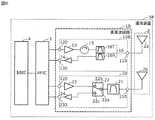
- FIG. 1is a circuit configuration diagram of a high frequency circuit 1 and a communication device 5 according to an embodiment.
- the communication device 5includes a high frequency circuit 1, an antenna circuit 2, an RF signal processing circuit (RFIC) 3, and a baseband signal processing circuit (BBIC) 4.
- RFICRF signal processing circuit
- BBICbaseband signal processing circuit
- the antenna circuit 2has antennas 2a and 2b.
- the antenna 2ais an example of the first antenna, is connected to the transmission / reception terminal 110 of the high frequency circuit 1, and radiates and receives a high frequency signal including the frequency of the first communication band.
- the antenna 2bis an example of the second antenna, is connected to the transmission / reception terminal 210 of the high frequency circuit 1, and radiates and receives a high frequency signal including the frequency of the second communication band.
- the antenna circuit 2may not have two antennas 2a and 2b, and may be composed of only one antenna. That is, the antenna 2a and the antenna 2b may be the same antenna. In this case, the one antenna is connected to both the transmission / reception terminals 110 and 210 of the high frequency circuit 1.
- RFIC3is an RF signal processing circuit that processes high frequency signals. Specifically, the RFIC 3 processes the transmission signal input from the BBIC 4 by up-conversion or the like, and outputs the high-frequency transmission signal generated by the signal processing to the high-frequency circuit 1. Further, the RFIC 3 has a control unit that outputs a control signal for controlling the connection switching of the switches 12 and 22 included in the high frequency circuit 1 to the switches 12 and 22.
- the BBIC 4is a circuit that processes a signal using an intermediate frequency band having a lower frequency than the high frequency signal propagating in the high frequency circuit 1.
- the signal processed by the BBIC 4is used, for example, as an image signal for displaying an image, or as a voice signal for a call via a speaker.
- the BBIC 4may have the above control unit. Further, the control unit may be included in the communication device 5 other than the RFIC 3 and the BBIC 4.
- the high frequency circuit 1includes a transmission circuit 10 and a transmission circuit 20.
- the transmission circuit 10is an example of a first transmission circuit, and is an example of a transmission / reception terminal 110, a transmission terminal 120, a reception terminal 130, a filter 11, a switch 12, a power amplifier 13, a low noise amplifier 14, and an isolator 15. And have.
- the transmission / reception terminal 110is an example of the first terminal
- the transmission terminal 120is an example of the second terminal
- the reception terminal 130is an example of the fifth terminal.
- the power amplifier 13is an example of a first power amplifier, and is a transmission amplifier that amplifies a high-frequency transmission signal input from the transmission terminal 120.
- the switch 12is an example of the first switch, has a common terminal 12a (first common terminal), a selection terminal 12b (first selection terminal), and a selection terminal 12c (second selection terminal), and is selected from the common terminal 12a.
- the connection with the terminal 12b and the connection between the common terminal 12a and the selection terminal 12care switched.
- the switch 12is, for example, a SPDT (Single Pole Double Throw) type switch circuit.
- the filter 11is an example of a first filter having a first communication band as a pass band, and is connected between the common terminal 12a and the transmission / reception terminal 110.
- the filter 11may be arranged on a signal path connecting the output terminal of the power amplifier 13 and the transmission / reception terminal 110.
- the low noise amplifier 14is an example of the first low noise amplifier, and is a reception amplifier connected between the selection terminal 12c and the reception terminal 130 to amplify the high frequency reception signal input from the transmission / reception terminal 110.
- the isolator 15is connected between the power amplifier 13 and the selection terminal 12b.
- the isolator 15has a characteristic of passing a high frequency signal of the first communication band in the direction from the power amplifier 13 to the transmission / reception terminal 110 and attenuating the high frequency signal of a predetermined frequency band in the direction from the transmission / reception terminal 110 to the power amplifier 13. doing.
- the predetermined frequency bandis an overlapping band of the first communication band and the second communication band.
- the transmission circuit 10outputs a high-frequency transmission signal of the first communication band from the transmission / reception terminal 110 in a state where the common terminal 12a and the selection terminal 12b are connected, and the common terminal 12a and the selection terminal 12c are connected to each other. In the connected state, the high frequency reception signal of the first communication band is output from the reception terminal 130. That is, the transmission circuit 10 executes the transmission of the high frequency signal and the reception of the high frequency signal by the switching operation of the switch 12 in a time division duplex (TDD: Time Division Duplex) system.
- TDDTime Division Duplex
- the transmission circuit 10may be a circuit that transmits a high frequency signal and does not receive the high frequency signal. That is, the transmission circuit 10 does not have to include the low noise amplifier 14, the switch 12, and the receiving terminal 130.
- the isolator 15may be arranged on the signal path connecting the output terminal of the power amplifier 13 and the transmission / reception terminal 110, and in particular, is arranged between the transmission / reception terminal 110 and the filter 11. Is desirable. Further, the transmission circuit 10 does not have to have the filter 11.
- the transmission circuit 20is an example of a second transmission circuit, and includes a transmission / reception terminal 210, a transmission terminal 220, a reception terminal 230, a filter 21, a switch 22, a power amplifier 23, and a low noise amplifier 24. doing.
- the transmission / reception terminal 210is an example of the third terminal, and the transmission terminal 220 is an example of the fourth terminal.
- the power amplifier 23is an example of a second power amplifier, and is a transmission amplifier that amplifies a high-frequency transmission signal input from the transmission terminal 220.
- the switch 22has a common terminal 22a, selection terminals 22b and 22c, and switches the connection between the common terminal 22a and the selection terminal 22b and the connection between the common terminal 22a and the selection terminal 22c.
- the switch 22is, for example, a SPDT type switch circuit.
- the filter 21is an example of a second filter having a second communication band as a pass band, and is connected between the common terminal 22a and the transmission / reception terminal 210.
- the filter 21may be arranged on a signal path connecting the output end of the power amplifier 23 and the transmission / reception terminal 210.
- the low noise amplifier 24is a reception amplifier that is connected between the selection terminal 22c and the reception terminal 230 and amplifies the high frequency reception signal input from the transmission / reception terminal 210.
- the power amplifiers 13 and 23 and the low noise amplifiers 14 and 24are, for example, a Si-based CMOS (Complementary Metal Oxide Sensor), a field effect transistor (FET) made of GaAs, or a heterobipolar transistor (HBT). It is composed of.
- CMOSComplementary Metal Oxide Sensor
- FETfield effect transistor
- HBTheterobipolar transistor
- the transmission circuit 20outputs a high-frequency transmission signal of the second communication band from the transmission / reception terminal 210 in a state where the common terminal 22a and the selection terminal 22b are connected, and the common terminal 22a and the selection terminal 22c are connected. In the state, the high frequency reception signal of the second communication band is output from the reception terminal 230. That is, the transmission circuit 20 executes the transmission of the high frequency signal and the reception of the high frequency signal by the switching operation of the switch 22 by the time division duplex (TDD) method.
- TDDtime division duplex
- the transmission circuit 20may be a circuit that transmits a high frequency signal and does not receive the high frequency signal. That is, the transmission circuit 20 does not have to include the low noise amplifier 24, the switch 22, and the receiving terminal 230. Further, the transmission circuit 20 does not have to have the filter 21.
- the high frequency circuit 1may be composed of one module, and for example, the transmission circuits 10 and 20 may be mounted in one mounting board or one package.
- transmission circuits 10 and 20may be composed of individual modules.
- the frequency of the second communication bandoverlaps with that of the first communication band at least partially.
- the high frequency signal of the first communication bandcan be transmitted from the transmission circuit 10, and at the same time, the high frequency signal of the second communication band can be transmitted from the transmission circuit 20. It becomes.
- the transmission circuit 10transmits, for example, a high frequency signal of the first communication band in the first communication system, and the transmission circuit 20 is different from, for example, the first communication system.
- the high frequency signal of the second communication band in the two communication systemsmay be transmitted.
- FIG. 2is a diagram showing a circuit state when two transmission signals are simultaneously transmitted in the high frequency circuit 1 according to the embodiment.
- the first communication systemis, for example, a fifth generation mobile communication system (5G)
- the second communication systemis, for example, a fourth generation mobile communication system (4G).
- the first communication systemmay be 4G and the second communication system may be 5G.
- the high frequency circuit 1is connected to the high frequency signal of the first communication band.
- the high frequency signal of the second communication bandcan be transmitted at the same time.
- the high frequency signal of the second communication band output from the transmission / reception terminal 210 of the transmission circuit 20is the antenna 2b and the antenna 2a. It is assumed that the signal flows from the transmission / reception terminal 110 into the transmission circuit 10 via the above.
- Intermodulation distortion(hereinafter sometimes referred to as IMD) is generated by the high frequency signal of the first communication band.
- IMDIntermodulation distortion
- the high frequency circuit 1even if the high frequency signal of the second communication band output from the transmission / reception terminal 210 of the transmission circuit 20 flows into the transmission circuit 10, the power amplifier 13
- the isolator 15 arranged between the output terminal and the transmission / reception terminal 110can prevent the inflowing high frequency signal of the second communication band from reaching the power amplifier 13. Therefore, the intermodulation distortion generated by the interaction between the high frequency signal of the second communication band flowing into the transmission circuit 10 and the high frequency signal of the first communication band output from the power amplifier 13 can be suppressed. Therefore, deterioration of the signal quality of the high frequency signal of the first communication band output from the transmission circuit 10 can be suppressed. That is, it is possible to provide the high frequency circuit 1 in which the occurrence of intermodulation distortion is suppressed when a plurality of high frequency signals amplified by a plurality of power amplifiers are simultaneously transmitted.
- the intermodulation distortion generated by the interaction between the 4G high frequency transmission signal and the 5G high frequency transmission signalcan be suppressed. Therefore, the coexistence standard of 4G service and 5G service can be satisfied.
- FIG. 3Ais a diagram showing the first frequency relationship between the first communication band and the second communication band.
- the first communication band and the second communication bandmay have the same frequency range.
- the first communication bandis, for example, 5G-NR n41 (band: 2494 to 2690 MHz)
- the second communication bandis, for example, 4G-LTE Band 41 (band: 2494 to 2690 MHz).
- the pass band of the filter 11is n41 of 5G-NR
- the pass band of the filter 21is Band 41 of 4G-LTE. That is, the pass bands of the filters 11 and 21 are the same.
- the overlapping band between the first communication band and the second communication bandcovers the entire area of n41 and Band41. Therefore, in the case of this frequency relationship, the isolator 15 passes high frequency signals in the frequency bands of n41 and Band41 in the direction from the power amplifier 13 to the transmission / reception terminal 110, and the direction from the transmission / reception terminal 110 to the power amplifier 13. Has the property of attenuating high-frequency signals in the frequency bands of n41 and Band41.
- FIG. 4is a schematic diagram showing an example of the frequency relationship between a 4G-LTE high-frequency signal, a 5G-NR high-frequency signal, and intermodulation distortion.
- the transmission circuit 10transmits the high frequency signal of n41 of 5G-NR and the transmission circuit 20 transmits the high frequency signal of Band 41 of 4G-LTE ( The state of occurrence of the third-order intermodulation distortion of EN-DC) is shown.
- the first transmission signal for transmitting the transmission circuit 10is the signal of the first channel of n41 (first communication band) of 5G-NR
- the second transmission signal for transmitting the transmission circuit 20is 4G.
- -Itis a signal of the second channel of Band 41 (second communication band) of LTE.
- the center frequency of the first channel of n41 of 5G-NR and the second channel of Band41 of 4G-LTEare different. That is, the first transmission signal is the transmission signal of the first channel in the first communication band defined by 5G, and the second transmission signal is the transmission of the second channel in the second communication band defined by 4G. It is a signal.
- the first communication band and the second communication bandhave the same frequency range.
- the intensity of the 5G high-frequency transmission signal output from the power amplifier 13is 27 dBm and the propagation loss in the filter 11 is 4 dB
- the intensity of the high-frequency transmission signal radiated from the antenna 2ais 23 dBm.
- the intensity of the 4G high-frequency transmission signal output from the power amplifier 23is 27 dBm and the propagation loss at the filter 21 is 4 dB
- the intensity of the high-frequency transmission signal radiated from the antenna 2bis 23 dBm. It becomes.
- the isolation between the antennas 2a and 2bis 10 dB
- intermodulation distortionoccurs in the transmission circuit 10 due to the 5G high frequency transmission signal (intensity 23 dBm) and the wraparound 4G high frequency transmission signal (intensity 13 dBm). To do.
- the first channel (first frequency f1) of n41 of 5G-NRis the channel on the low frequency side of n41
- the second channel (second frequency f2) of Band 41 of 4G-LTEis Band 41.
- third-order intermodulation distortion IMD 3Lfrequency: 2f1-f2
- IMD 3Hfrequency: 2f2-f1
- the third-order intermodulation distortion IMD 3Loverlaps with, for example, the band 30 or 40 of 4G-LTE.
- the high-frequency circuit 1includes a circuit that transmits or receives a high-frequency signal of Band 30 or Band 40 of 4G-LTE, or if the circuit is arranged in the vicinity of the high-frequency circuit 1, the above-mentioned third-order intermodulation If the distorted IMD 3L exceeds the reference value in 3GPP, the coexistence standard of 4G service and 5G service cannot be satisfied, and the signal quality in the circuit deteriorates.
- the intermodulation distortion generated by the 5G high-frequency transmission signal and the wraparound 4G high-frequency transmission signalis not limited to the third-order intermodulation distortion.
- the isolator 15is arranged in the transmission circuit 10, intermodulation generated by the interaction between the high-frequency transmission signal of 5G and the high-frequency transmission signal of 4G Distortion can be suppressed. Therefore, the coexistence standard of 4G service and 5G service can be satisfied.
- FIG. 3Bis a diagram showing a second frequency relationship between the first communication band and the second communication band.
- the frequencies of the first communication band and the second communication banddo not have to completely overlap.
- the first communication bandis, for example, 5G-NR nX (bands: fx1 to fx2)
- the second communication bandis, for example, 4G-LTE BandY (bands: fy1 to fy2). Is.
- the overlapping band between the first communication band and the second communication bandis phy1 to fx2.
- the isolator 15passes high frequency signals in the nX frequency band (fx1 to fx2) in the direction from the power amplifier 13 to the transmission / reception terminal 110, and the power amplifier 13 from the transmission / reception terminal 110. In the direction toward, it is sufficient that it has a characteristic of attenuating high frequency signals in a frequency band including overlapping bands (fy1 to fx2).
- the high-frequency circuit according to the present inventionmay include only the transmission circuit 10 among the transmission circuits 10 and 20 included in the high-frequency circuit 1 according to the embodiment. That is, in the high frequency circuit according to the present invention, at least a part of the frequency range of the first communication band of the first communication system and the frequency range of the second communication band of the second communication system different from the first communication system overlap.
- a high-frequency circuit used in a signal transmission system capable of simultaneously transmitting a high-frequency signal of the first communication band and a high-frequency signal of the second communication band, the high-frequency circuitincludes a transmission / reception terminal 110 and a transmission terminal.
- Ithas 120, a power amplifier 13 that amplifies a high-frequency signal input from the transmission terminal 120, and an isolator 15 arranged on a signal path between the output end of the power amplifier 13 and the transmission / reception terminal 110, and has power.
- the high frequency signal of the first communication band amplified by the amplifier 13can be output from the transmission / reception terminal 110.
- the first communication systemmay be 5G out of 4G and 5G.
- EN-DCwhich simultaneously transmits a high-frequency signal in the 4G-LTE communication band and a high-frequency signal in the 5G-NR communication band
- the power value of the 5G high-frequency transmission signalis smaller than the power value of the 4G high-frequency transmission signal. .. Therefore, in EN-DC, the signal quality of the 5G high-frequency transmission signal is more likely to deteriorate due to intermodulation distortion.
- the isolator 15is arranged in the transmission circuit that transmits the 5G high frequency signal, the coexistence standard of 4G service and 5G service can be efficiently satisfied.
- the high frequency circuit 1has a transmission / reception terminal 110 and a transmission terminal 120, and has a transmission circuit 10 for outputting a high frequency signal of the first communication band from the transmission / reception terminal 110, and a transmission / reception terminal 210 and a transmission terminal 220.
- a transmission circuit 20that outputs a high-frequency signal of a communication band from a transmission / reception terminal 210 is provided.
- the transmission circuit 20further includes a power amplifier 23 that amplifies a high frequency signal input from the transmission terminal 220. Further, the transmission circuit 10 further includes a power amplifier 13 that amplifies a high-frequency signal input from the transmission terminal 120, and an isolator 15 arranged on a signal path between the output terminal of the power amplifier 13 and the transmission / reception terminal 110. , Can have.
- the high frequency signal of the second communication band output from the transmission / reception terminal 210 of the transmission circuit 20flows into the transmission circuit 10, the high frequency signal of the second communication band flowing in by the isolator 15 reaches the power amplifier 13. You can prevent that. Therefore, it is possible to suppress the intermodulation distortion generated by the interaction between the high frequency signal of the second communication band flowing into the transmission circuit 10 and the high frequency signal of the first communication band output from the power amplifier 13, and output from the transmission circuit 10. It is possible to suppress deterioration of the signal quality of the high frequency signal of the first communication band.
- the frequency range of the first communication band and the frequency range of the second communication bandoverlap at least partially, and the transmission circuit 10 has a high frequency of the first communication system.
- the signalis transmitted, and the transmission circuit 20 can transmit a high frequency signal of a second communication system different from the first communication system.
- the high frequency circuit 1can simultaneously transmit the first transmission signal of the first communication band and the second transmission signal of the second communication band, and the first communication band.
- the second communication bandhave the same frequency range
- the first transmission signalis the transmission signal of the first channel in the first communication band defined by the first communication system
- the second transmission signalis the second transmission signal.
- the transmission signal of the second channel having a frequency different from that of the first channel in the second communication band defined by the two communication systemsmay be used.
- the isolator 15outputs the high frequency signal of the second communication band that has flowed into the transmission circuit 10 from the power amplifier 13.
- Mutual modulation distortion generated by interaction with the high frequency signal of the first communication bandcan be suppressed, and deterioration of the signal quality of the high frequency signal of the first communication band output from the transmission circuit 10 can be suppressed.
- one of the first communication system and the second communication systemmay be 5G, and the other of the first communication system and the second communication system may be 4G.
- the high frequency transmission signal corresponding to 4G and the high frequency transmission signal corresponding to 5Gcan be used.
- the generated intermodulation distortioncan be suppressed below the reference value. Therefore, the coexistence standard of 4G service and 5G service can be satisfied.
- the isolator 15passes a high frequency signal of the first communication band in the direction from the power amplifier 13 to the transmission / reception terminal 110, and has a predetermined frequency in the direction from the transmission / reception terminal 110 to the power amplifier 13. It has a characteristic of attenuating high-frequency signals in the band, and the predetermined frequency band may be a band including an overlapping band of the frequency range of the first communication band and the frequency range of the second communication band.
- the transmission circuit 10further includes a filter 11 having a first communication band as a pass band, which is arranged between the output terminal of the power amplifier 13 and the transmission / reception terminal 110 for transmission.
- the circuit 20may further include a filter 21 having a second communication band as a pass band, which is arranged between the output terminal of the power amplifier 23 and the transmission / reception terminal 210.
- the noise component of the high frequency signal of the first communication band output from the transmission circuit 10can be reduced, and the noise component of the high frequency signal of the second communication band output from the transmission circuit 20 can be reduced.
- the signal quality of the high frequency transmission signal output from 1can be improved.
- the transmission circuit 10further includes a receiving terminal 130, a common terminal 12a, a selection terminal 12b and 12c, and a connection between the common terminal 12a and the selection terminal 12b and a common terminal. It has a switch 12 for switching the connection between the selection terminal 12a and the selection terminal 12c, and a low noise amplifier 14 connected between the selection terminal 12c and the reception terminal 130.
- the isolator 15has the selection terminal 12b and the power amplifier 13. Connected in between, the common terminal 12a can be connected to the filter 11.
- the intermodulation distortion generated by the interaction between the high frequency signal of the second communication band flowing into the TDD transmission circuit 10 and the high frequency signal of the first communication band output from the power amplifier 13can be suppressed and transmitted.
- Deterioration of signal quality of the high frequency signal of the first communication band output from the circuit 10can be suppressed.
- the high frequency circuithas at least a frequency range of the first communication band of the first communication system and a frequency range of the second communication band of the second communication system different from the first communication system. It is a high-frequency circuit used in a signal transmission system that partially overlaps and can simultaneously transmit a high-frequency signal in the first communication band and a high-frequency signal in the second communication band, and the high-frequency circuit is a transmission / reception terminal.
- the high frequency signal of the first communication band amplified by the power amplifier 13can be output from the transmission / reception terminal 110.
- the first communication systemmay be 5G out of 4G and 5G.
- the coexistence standard of 4G service and 5G servicecan be efficiently satisfied.
- the communication device 5has an RFIC 3 for processing a high frequency signal transmitted / received by the antenna circuit 2 and a high frequency circuit 1 for transmitting a high frequency signal between the antenna circuit 2 and the RFIC 3. Can be prepared.
- the communication device 5comprises an RFIC 3 that processes a high frequency signal transmitted / received by the antenna circuit 2 and a high frequency circuit 1 that transmits a high frequency signal between the antenna circuit 2 and the RFIC 3.
- the antenna circuit 2can have an antenna 2a connected to the transmission / reception terminal 110 and an antenna 2b connected to the transmission / reception terminal 210.
- FIG. 5is a circuit configuration diagram of the high frequency circuit 1A and the communication device 5A according to the first modification of the embodiment.
- the high-frequency circuit 1A and the communication device 5A according to the present modificationhave different configurations of the second transmission circuit as compared with the high-frequency circuit 1 and the communication device 5 according to the embodiment.
- the high frequency circuit 1A and the communication device 5A according to the present modificationwill be described mainly with different configurations, omitting description of the same configurations as the high frequency circuit 1 and the communication device 5 according to the embodiment.
- the communication device 5Aincludes a high frequency circuit 1A, an antenna circuit 2, an RFIC 3, and a BBIC 4.
- the high frequency circuit 1Aincludes a transmission circuit 10 and a transmission circuit 20A.
- the transmission circuit 20Ais an example of a second transmission circuit, which includes a transmission / reception terminal 210, a transmission terminal 220, a reception terminal 230, a filter 21, a switch 22, a power amplifier 23, a low noise amplifier 24, and an isolator 25. And have.
- the transmission / reception terminal 210is an example of the third terminal, and the transmission terminal 220 is an example of the fourth terminal.
- the isolator 25is connected between the power amplifier 23 and the selection terminal 22b.
- the isolator 25has a characteristic of passing a high frequency signal of the second communication band in the direction from the power amplifier 23 to the transmission / reception terminal 210 and attenuating the high frequency signal of a predetermined frequency band in the direction from the transmission / reception terminal 210 to the power amplifier 23.
- the predetermined frequency bandis an overlapping band of the first communication band and the second communication band.
- the transmission circuit 20Aoutputs a high frequency transmission signal of the second communication band from the transmission / reception terminal 210 in a state where the common terminal 22a and the selection terminal 22b are connected, and the common terminal 22a and the selection terminal 22c are connected to each other. In the connected state, the high frequency reception signal of the second communication band is output from the reception terminal 230. That is, the transmission circuit 20A executes the transmission of the high frequency signal and the reception of the high frequency signal by the switching operation of the switch 22 by the time division duplex (TDD) method.
- TDDtime division duplex
- the transmission circuit 20Amay be a circuit that transmits a high frequency signal and does not receive the high frequency signal. That is, the transmission circuit 20A does not have to include the low noise amplifier 24, the switch 22, and the receiving terminal 230.
- the isolator 25may be arranged on the signal path connecting the output terminal of the power amplifier 23 and the transmission / reception terminal 210, and in particular, the isolator 25 is arranged between the transmission / reception terminal 210 and the filter 21. Is desirable. Further, the transmission circuit 20A does not have to have the filter 21.
- the frequency of the second communication bandoverlaps with that of the first communication band at least partially.
- the high frequency signal of the first communication bandcan be transmitted from the transmission circuit 10
- the high frequency signal of the second communication bandcan be transmitted from the transmission circuit 20A. It becomes.
- the output end of the power amplifier 13The isolator 15 arranged between the transmission / reception terminal 110 can prevent the inflowing high frequency signal of the second communication band from reaching the power amplifier 13. Therefore, it is possible to suppress intermodulation distortion generated by the interaction between the high frequency signal of the second communication band and the high frequency signal of the first communication band output from the power amplifier 13.
- the output end of the power amplifier 23The isolator 25 arranged between the transmission / reception terminal 210 can prevent the inflowing high frequency signal of the first communication band from reaching the power amplifier 23. Therefore, it is possible to suppress the intermodulation distortion generated by the interaction between the high frequency signal of the first communication band and the high frequency signal of the second communication band output from the power amplifier 23.
- FIG. 6is a circuit configuration diagram of the high frequency circuit 1B and the communication device 5B according to the second modification of the embodiment.
- the high-frequency circuit 1B and the communication device 5B according to the present modificationhave different configurations of the first transmission circuit as compared with the high-frequency circuit 1 and the communication device 5 according to the embodiment.
- the same configurations as the high frequency circuit 1 and the communication device 5 according to the embodimentwill be omitted, and different configurations will be mainly described.
- the communication device 5Bincludes a high frequency circuit 1B, an antenna circuit 2, RFIC3, and BBIC4.
- the high frequency circuit 1Bincludes a transmission circuit 10B and a transmission circuit 20.
- the transmission circuit 10Bis an example of the first transmission circuit, and includes a transmission / reception terminal 110, a transmission terminal 120, a reception terminal 130, a duplexer 16, a power amplifier 13, a low noise amplifier 14, and an isolator 15. doing.
- the power amplifier 13is an example of a first power amplifier, and is a transmission amplifier that amplifies a high-frequency transmission signal input from the transmission terminal 120.
- the duplexer 16is an example of a first filter having a first communication band as a pass band, a transmission filter 16T having a transmission band of the first communication band as a pass band, and a reception band of the first communication band as a pass band. It is composed of a receiving filter 16R. The output end of the transmission filter 16T and the input end of the reception filter 16R are connected to the transmission / reception terminal 110.
- the low noise amplifier 14is an example of the first low noise amplifier, and is a reception amplifier connected between the output terminal of the reception filter 16R and the reception terminal 130 to amplify the high frequency reception signal input from the transmission / reception terminal 110. ..
- the isolator 15is connected between the input end of the transmission filter 16T and the power amplifier 13.
- the isolator 15has a characteristic of passing a high frequency signal of the first communication band in the direction from the power amplifier 13 to the transmission / reception terminal 110 and attenuating the high frequency signal of a predetermined frequency band in the direction from the transmission / reception terminal 110 to the power amplifier 13. doing.
- the predetermined frequency bandis an overlapping band of the first communication band and the second communication band.
- the transmission circuit 10Boutputs a high-frequency transmission signal in the transmission band of the first communication band from the transmission / reception terminal 110, and at the same time outputs a high-frequency reception signal in the reception band of the first communication band from the reception terminal 130. That is, the transmission circuit 10B executes the transmission of the high-frequency signal and the reception of the high-frequency signal by the frequency division duplex (FDD: Frequency Division Duplex) method.
- FDDFrequency Division Duplex
- the transmission circuit 10Bmay be a circuit that transmits a high frequency signal and does not receive the high frequency signal. That is, the transmission circuit 10B does not have to include the low noise amplifier 14, the reception filter 16R, and the reception terminal 130.
- the isolator 15may be arranged on the signal path connecting the output terminal of the power amplifier 13 and the transmission / reception terminal 110, and in particular, is arranged between the transmission / reception terminal 110 and the transmission filter 16T. Is desirable.
- the high frequency circuit 1Bcan simultaneously transmit the high frequency signal of the first communication band and the high frequency signal of the second communication band. ..
- the high frequency signal of the second communication band output from the transmission / reception terminal 210 of the transmission circuit 20is the antenna 2b and the antenna 2a. It is assumed that the signal flows from the transmission / reception terminal 110 into the transmission circuit 10B via the above.
- the high frequency circuit 1Beven if the high frequency signal of the second communication band output from the transmission / reception terminal 210 of the transmission circuit 20 flows into the transmission circuit 10B, the power amplifier 13
- the isolator 15 arranged between the output terminal and the transmission / reception terminal 110can prevent the inflowing high frequency signal of the second communication band from reaching the power amplifier 13. Therefore, it is possible to suppress intermodulation distortion generated by the interaction between the high frequency signal of the second communication band flowing into the transmission circuit 10B and the high frequency signal of the first communication band output from the power amplifier 13. Therefore, deterioration of the signal quality of the high frequency signal of the first communication band output from the transmission circuit 10B can be suppressed. That is, it is possible to provide the high frequency circuit 1B in which the occurrence of intermodulation distortion is suppressed when a plurality of high frequency signals amplified by a plurality of power amplifiers are simultaneously transmitted.
- the transmission circuit 20may be an FDD type circuit as well as the transmission circuit 10B. That is, in the transmission circuit 20, a duplexer may be arranged instead of the filter 21 and the switch 22.
- the high-frequency circuit and communication deviceare applied to a communication system such as 3GPP as described above, and typically a 4G-LTE high-frequency signal and a 5G-NR high-frequency signal. Applies to systems that send and at the same time. For example, as a combination of the first communication band / second communication band, (1) Band 41 of 5G-NR n41 / 4G-LTE and (2) Band 71 of 5G-NR n71 / 4G-LTE mentioned in the embodiment. , (3) 5G-NR n3 / 4G-LTE Band3, and the like.
- the high-frequency circuit and communication deviceare systems that simultaneously transmit a first communication band of 5G-NR / a second communication band of 4G-LTE having different frequency bands, or different. It can also be applied to a system that simultaneously transmits a first communication band of 4G-LTE and a second communication band of 4G-LTE having a frequency band.
- the frequencies of the mutual modulation distortion caused by the two high frequency transmission signalsare typically 2f Tx1- f Tx2 , 2f Tx2- f Tx1 , and f Tx1- f. Examples thereof include, but are not limited to, Tx2 and f Tx2- f Tx1 , and include those defined by mf Tx1 ⁇ nf Tx2 and mf Tx2 ⁇ nf Tx1 (m and n are natural numbers).
- the power amplifiers 13 and 23may be mounted on different mounting boards, or may be included in different modules. Furthermore, the power amplifiers 13 and 23 may be included in different mobile terminals.
- the configuration when two different communication bands are used at the same timeis illustrated, but the configuration of the high-frequency circuit and the communication device according to the present invention includes three or more different communication bands. It can also be applied to configurations when used at the same time. That is, the present invention also includes a high-frequency circuit or communication device having a configuration in which three or more different communication bands are used at the same time and including a high-frequency circuit or communication device configuration according to the above embodiment and a modification thereof.
- control unitmay be realized as an IC or LSI (Large Scale Integration) which is an integrated circuit.
- the method of making an integrated circuitmay be realized by a dedicated circuit or a general-purpose processor.
- An FPGAField Programmable Gate Array
- reconfigurable processorthat can reconfigure the connection and settings of the circuit cells inside the LSI may be used.
- an integrated circuit technology that replaces an LSIappears due to advances in semiconductor technology or another technology derived from it, it is naturally possible to integrate functional blocks using that technology.
- the communication systemis defined by a standardization body or the like (for example, 3GPP, IEEE (Institute of Electrical and Electronics Engineers)).
- Radio Access Technologymeans a communication system constructed.
- the communication systemfor example, a 5G-NR system, a 4G-LTE system, a WLAN (Wireless Local Area Network) system, and the like can be used, but the communication system is not limited thereto.
- the communication bandmeans a frequency band defined in advance by a standardization body or the like for a communication system.
- a 5G-NR frequency band, a 4G-LTE frequency band, and the likecan be used, but the communication band is not limited thereto.
- the present inventioncan be widely used in communication devices such as mobile phones as a multi-band / multi-mode compatible front-end circuit that employs a method of simultaneously transmitting high-frequency signals of different communication systems, such as EN-DC.
- RFICradio frequency circuit
- BBICBaseband signal processing circuit
- 5A, 5B communication device 10B20, 20A Transmission circuit 11, 21 Filter 12, 22 Switch 12a, 22a Common terminal 12b, 12c, 22b, 22c Selection terminal 13, 23 Power amplifier 14, 24 Low noise amplifier 15 , 25 Isolator 16 Duplexer 16R Receive filter 16T Transmission filter 110, 210 Transmission / reception terminal 120, 220 Transmission terminal 130, 230 Reception terminal
Landscapes
- Engineering & Computer Science (AREA)
- Computer Networks & Wireless Communication (AREA)
- Signal Processing (AREA)
- Transceivers (AREA)
Abstract
Description
Translated fromJapanese本発明は、高周波回路および当該高周波回路を備えた通信装置に関する。The present invention relates to a high frequency circuit and a communication device including the high frequency circuit.
マルチバンド化およびマルチモード化に対応した高周波回路に対して、周波数の異なる複数の高周波信号を同時に高品質で送信することが求められている。It is required to simultaneously transmit a plurality of high frequency signals having different frequencies with high quality to a high frequency circuit corresponding to multiband and multimode.
特許文献1には、異なる周波数帯域の高周波信号を同時に送信することが可能な高周波回路の構成が開示されている。
しかしながら、特許文献1に開示された高周波回路において、周波数帯域が少なくとも一部重複する2つの通信バンドの送信信号を同時に出力した場合、一方の送信経路に配置された電力増幅器から出力された送信信号が他方の送信経路に配置された電力増幅器に回り込む場合がある。この場合、当該他方の送信経路に配置された電力増幅器において、2つの送信信号がミキシングされて相互変調歪が発生してしまい、送信信号の品質が劣化するという問題がある。However, in the high frequency circuit disclosed in
そこで、本発明は、上記課題を解決するためになされたものであって、複数の電力増幅器により増幅された複数の高周波信号を同時送信している際に、相互変調歪の発生が抑制された高周波回路および通信装置を提供することを目的とする。Therefore, the present invention has been made to solve the above problems, and the occurrence of intermodulation distortion is suppressed when a plurality of high-frequency signals amplified by a plurality of power amplifiers are simultaneously transmitted. It is an object of the present invention to provide a high frequency circuit and a communication device.
上記目的を達成するために、本発明の一態様に係る高周波回路は、第1通信バンドの高周波信号と、前記第1通信バンドと周波数が少なくとも一部重複する第2通信バンドの高周波信号とを、同時に送信することが可能な高周波回路であって、第1端子および第2端子を有し、前記第1通信バンドの高周波信号を前記第1端子から出力する第1伝送回路と、第3端子および第4端子を有し、前記第2通信バンドの高周波信号を前記第3端子から出力する第2伝送回路と、を備え、前記第1伝送回路は、さらに、前記第2端子から入力された高周波信号を増幅する第1電力増幅器と、前記第1電力増幅器の出力端と前記第1端子との間の信号経路上に配置されたアイソレータと、を有し、前記第2伝送回路は、さらに、前記第4端子から入力された高周波信号を増幅する第2電力増幅器を有する。In order to achieve the above object, the high frequency circuit according to one aspect of the present invention comprises a high frequency signal of the first communication band and a high frequency signal of the second communication band whose frequency at least partially overlaps with the first communication band. A first transmission circuit having a first terminal and a second terminal and outputting a high frequency signal of the first communication band from the first terminal, and a third terminal, which are high frequency circuits capable of transmitting at the same time. A second transmission circuit having a fourth terminal and outputting a high frequency signal of the second communication band from the third terminal, and the first transmission circuit is further input from the second terminal. The second transmission circuit further comprises a first power amplifier that amplifies a high frequency signal and an isolator arranged on a signal path between the output end of the first power amplifier and the first terminal. The second power amplifier that amplifies the high frequency signal input from the fourth terminal is provided.
本発明によれば、複数の電力増幅器により増幅された複数の高周波信号を同時送信する際に、相互変調歪の発生が抑制された高周波回路および通信装置を提供することが可能となる。According to the present invention, it is possible to provide a high frequency circuit and a communication device in which the occurrence of intermodulation distortion is suppressed when a plurality of high frequency signals amplified by a plurality of power amplifiers are simultaneously transmitted.
以下、本発明の実施の形態について、実施例および図面を用いて詳細に説明する。なお、以下で説明する実施の形態は、いずれも包括的または具体的な例を示すものである。以下の実施の形態で示される数値、形状、材料、構成要素、構成要素の配置および接続形態などは、一例であり、本発明を限定する主旨ではない。以下の実施の形態における構成要素のうち、独立請求項に記載されていない構成要素については、任意の構成要素として説明される。また、図面に示される構成要素の大きさまたは大きさの比は、必ずしも厳密ではない。Hereinafter, embodiments of the present invention will be described in detail with reference to examples and drawings. It should be noted that all of the embodiments described below are comprehensive or specific examples. Numerical values, shapes, materials, components, arrangement of components, connection modes, etc. shown in the following embodiments are examples, and are not intended to limit the present invention. Among the components in the following embodiments, the components not described in the independent claims are described as arbitrary components. Also, the sizes or ratios of the components shown in the drawings are not always exact.
(実施の形態)
[1.高周波回路1および通信装置5の構成]
図1は、実施の形態に係る高周波回路1および通信装置5の回路構成図である。同図に示すように、通信装置5は、高周波回路1と、アンテナ回路2と、RF信号処理回路(RFIC)3と、ベースバンド信号処理回路(BBIC)4と、を備える。(Embodiment)
[1. Configuration of
FIG. 1 is a circuit configuration diagram of a
アンテナ回路2は、アンテナ2aおよび2bを有する。アンテナ2aは、第1アンテナの一例であり、高周波回路1の送受信端子110に接続され、第1通信バンドの周波数を含む高周波信号を放射送信し、また、受信する。アンテナ2bは、第2アンテナの一例であり、高周波回路1の送受信端子210に接続され、第2通信バンドの周波数を含む高周波信号を放射送信し、また、受信する。なお、アンテナ回路2は、2つのアンテナ2aおよび2bを有していなくてもよく、1つのアンテナのみで構成されていてもよい。つまり、アンテナ2aとアンテナ2bとは、同一のアンテナであってもよい。この場合には、上記1つのアンテナは、高周波回路1の送受信端子110および210の双方に接続される。The
RFIC3は、高周波信号を処理するRF信号処理回路である。具体的には、RFIC3は、BBIC4から入力された送信信号をアップコンバートなどにより信号処理し、当該信号処理して生成された高周波送信信号を、高周波回路1に出力する。また、RFIC3は、高周波回路1が有するスイッチ12および22の接続切り換えを制御するための制御信号を、スイッチ12および22に出力する制御部を有している。RFIC3 is an RF signal processing circuit that processes high frequency signals. Specifically, the
BBIC4は、高周波回路1を伝搬する高周波信号よりも低周波の中間周波数帯域を用いて信号処理する回路である。BBIC4で処理された信号は、例えば、画像表示のための画像信号として使用され、または、スピーカを介した通話のために音声信号として使用される。なお、BBIC4が上記制御部を有していてもよい。また、上記制御部は、RFIC3およびBBIC4以外の通信装置5に含まれていてもよい。The BBIC 4 is a circuit that processes a signal using an intermediate frequency band having a lower frequency than the high frequency signal propagating in the
高周波回路1は、伝送回路10と、伝送回路20と、を備える。The
伝送回路10は、第1伝送回路の一例であり、送受信端子110と、送信端子120と、受信端子130と、フィルタ11と、スイッチ12と、電力増幅器13と、低雑音増幅器14と、アイソレータ15と、を有している。The
送受信端子110は第1端子の一例であり、送信端子120は第2端子の一例であり、受信端子130は第5端子の一例である。The transmission /
電力増幅器13は、第1電力増幅器の一例であり、送信端子120から入力された高周波送信信号を増幅する送信増幅器である。The
スイッチ12は、第1スイッチの一例であり、共通端子12a(第1共通端子)、選択端子12b(第1選択端子)および選択端子12c(第2選択端子)を有し、共通端子12aと選択端子12bとの接続、および、共通端子12aと選択端子12cとの接続を切り換える。スイッチ12は、例えば、SPDT(Single Pole Double Throw)型のスイッチ回路である。The
フィルタ11は、第1通信バンドを通過帯域とする第1フィルタの一例であり、共通端子12aと送受信端子110との間に接続されている。なお、フィルタ11は、電力増幅器13の出力端と送受信端子110とを結ぶ信号経路上に配置されていてもよい。The
低雑音増幅器14は、第1低雑音増幅器の一例であり、選択端子12cと受信端子130との間に接続され、送受信端子110から入力された高周波受信信号を増幅する受信増幅器である。The
アイソレータ15は、電力増幅器13と選択端子12bとの間に接続されている。アイソレータ15は、電力増幅器13から送受信端子110への方向の第1通信バンドの高周波信号を通過させ、送受信端子110から電力増幅器13への方向の所定の周波数帯域の高周波信号を減衰させる特性を有している。上記所定の周波数帯域は、第1通信バンドと第2通信バンドとの重複帯域である。The
上記構成により、伝送回路10は、共通端子12aと選択端子12bとが接続されている状態において、第1通信バンドの高周波送信信号を送受信端子110から出力し、共通端子12aと選択端子12cとが接続されている状態において、第1通信バンドの高周波受信信号を受信端子130から出力する。つまり、伝送回路10は、スイッチ12の切り換え動作により、高周波信号の送信と高周波信号の受信とを、時分割複信(TDD:Time Division Duplex)方式で実行する。With the above configuration, the
なお、伝送回路10は、高周波信号を送信し、高周波信号を受信しない回路であってもよい。つまり、伝送回路10は、低雑音増幅器14、スイッチ12および受信端子130を備えていなくてもよい。この場合には、アイソレータ15は、電力増幅器13の出力端と送受信端子110とを結ぶ信号経路上に配置されていてもよく、特に、送受信端子110とフィルタ11との間に配置されていることが望ましい。また、伝送回路10は、フィルタ11を有していなくてもよい。The
伝送回路20は、第2伝送回路の一例であり、送受信端子210と、送信端子220と、受信端子230と、フィルタ21と、スイッチ22と、電力増幅器23と、低雑音増幅器24と、を有している。The
送受信端子210は第3端子の一例であり、送信端子220は第4端子の一例である。The transmission /
電力増幅器23は、第2電力増幅器の一例であり、送信端子220から入力された高周波送信信号を増幅する送信増幅器である。The
スイッチ22は、共通端子22a、選択端子22bおよび22cを有し、共通端子22aと選択端子22bとの接続、および、共通端子22aと選択端子22cとの接続を切り換える。スイッチ22は、例えば、SPDT型のスイッチ回路である。The
フィルタ21は、第2通信バンドを通過帯域とする第2フィルタの一例であり、共通端子22aと送受信端子210との間に接続されている。なお、フィルタ21は、電力増幅器23の出力端と送受信端子210とを結ぶ信号経路上に配置されていてもよい。The
低雑音増幅器24は、選択端子22cと受信端子230との間に接続され、送受信端子210から入力された高周波受信信号を増幅する受信増幅器である。The
なお、電力増幅器13、23、低雑音増幅器14および24は、例えば、Si系のCMOS(Complementary Metal Oxide Semiconductor)、または、GaAsを材料とする電界効果型トランジスタ(FET)、ヘテロバイポーラトランジスタ(HBT)などで構成されている。The
伝送回路20は、共通端子22aと選択端子22bとが接続されている状態において、第2通信バンドの高周波送信信号を送受信端子210から出力し、共通端子22aと選択端子22cとが接続されている状態において、第2通信バンドの高周波受信信号を受信端子230から出力する。つまり、伝送回路20は、スイッチ22の切り換え動作により、高周波信号の送信と高周波信号の受信とを、時分割複信(TDD)方式で実行する。The
なお、伝送回路20は、高周波信号を送信し、高周波信号を受信しない回路であってもよい。つまり、伝送回路20は、低雑音増幅器24、スイッチ22および受信端子230を備えていなくてもよい。また、伝送回路20は、フィルタ21を有していなくてもよい。The
なお、高周波回路1は、1つのモジュールで構成されていてもよく、例えば、伝送回路10および20が、1つの実装基板または1つのパッケージ内に実装されていてもよい。The
また、伝送回路10および20は、それぞれ個別のモジュールで構成されていてもよい。Further, the
本実施の形態に係る高周波回路1において、第2通信バンドは、第1通信バンドと周波数が少なくとも一部重複している。In the
高周波回路1および通信装置5の上記構成によれば、第1通信バンドの高周波信号を伝送回路10から送信し、これと同時に、第2通信バンドの高周波信号を伝送回路20から送信することが可能となる。According to the above configuration of the
なお、本実施の形態に係る高周波回路1において、伝送回路10は、例えば、第1通信システムにおける第1通信バンドの高周波信号を伝送し、伝送回路20は、例えば、第1通信システムと異なる第2通信システムにおける第2通信バンドの高周波信号を伝送してもよい。In the
図2は、実施の形態に係る高周波回路1において、2つの送信信号を同時送信する場合の回路状態を表す図である。同図に示すように、第1通信システムは、例えば、第5世代移動通信システム(5G)であり、第2通信システムは、例えば、第4世代移動通信システム(4G)である。なお、第1通信システムが4Gであり、第2通信システムが5Gであってもよい。スイッチ12の共通端子12aと選択端子12bとが接続されており、かつ、スイッチ22の共通端子22aと選択端子22bとが接続されている場合、高周波回路1は、第1通信バンドの高周波信号と、第2通信バンドの高周波信号とを、同時に送信することが可能となる。第1通信バンドの高周波信号と第2通信バンドの高周波信号とが同時送信されている状態において、伝送回路20の送受信端子210から出力された第2通信バンドの高周波信号が、アンテナ2bおよびアンテナ2aを経由して送受信端子110から伝送回路10に流入することが想定される。FIG. 2 is a diagram showing a circuit state when two transmission signals are simultaneously transmitted in the
この場合、伝送回路10へ流入した第2通信バンドの高周波信号が電力増幅器13に到達すると、伝送回路10へ流入した第2通信バンドの高周波信号と電力増幅器13から送受信端子110へ向けて出力される第1通信バンドの高周波信号とにより、相互変調歪(InterModulation Distortion、以降IMDと記す場合がある)が発生する。この相互変調歪の高周波成分が、伝送回路10からアンテナ2aを介して出力される第1通信バンドの高周波信号に重畳されると、伝送回路10から出力される第1通信バンドの高周波信号の信号品質が劣化する。In this case, when the high frequency signal of the second communication band flowing into the
これに対して、本実施の形態に係る高周波回路1によれば、伝送回路20の送受信端子210から出力された第2通信バンドの高周波信号が伝送回路10に流入しても、電力増幅器13の出力端と送受信端子110との間に配置されたアイソレータ15により、流入した第2通信バンドの高周波信号が電力増幅器13に到達することを阻止できる。このため、伝送回路10に流入した第2通信バンドの高周波信号と、電力増幅器13から出力される第1通信バンドの高周波信号との相互作用により発生する相互変調歪を抑制できる。よって、伝送回路10から出力される第1通信バンドの高周波信号の信号品質の劣化を抑制できる。つまり、複数の電力増幅器により増幅された複数の高周波信号を同時送信する際に、相互変調歪の発生が抑制された高周波回路1を提供することが可能となる。On the other hand, according to the
4Gから5Gへの通信システムの移行段階において、4Gと5Gとを併存させる通信システムが提案されている。この場合、例えば、4G-LTE(Long Term Evolution)の通信バンドの高周波信号と、5G-NR(New Radio)の通信バンドの高周波信号とを同時送信させる必要がある(EN-DC:LTE-NR Dual Connectivity)。このシステムにおいて、4Gに対応した高周波送信信号と5Gに対応した高周波送信信号とで発生する相互変調歪が基準値を超えると、例えば、3GPP(Third Generation Partnership Project)における4Gサービスおよび5Gサービスの共存(Coexistence)規格を満足できなくなる。At the transition stage of the communication system from 4G to 5G, a communication system in which 4G and 5G coexist has been proposed. In this case, for example, it is necessary to simultaneously transmit a high frequency signal of a communication band of 4G-LTE (Long Term Evolution) and a high frequency signal of a communication band of 5G-NR (New Radio) (EN-DC: LTE-NR). Dual Signality). In this system, if the mutual modulation distortion generated by the high frequency transmission signal corresponding to 4G and the high frequency transmission signal corresponding to 5G exceeds the reference value, for example, coexistence of 4G service and 5G service in 3GPP (Third Generation Partnership Project). (Coexistence) The standard cannot be satisfied.
これに対して、本実施の形態に係る高周波回路1の上記構成によれば、4Gの高周波送信信号と5Gの高周波送信信号との相互作用により発生する相互変調歪を抑制できる。よって、4Gサービスおよび5Gサービスの共存規格を満足できる。On the other hand, according to the above configuration of the
図3Aは、第1通信バンドおよび第2通信バンドの第1の周波数関係を示す図である。本実施の形態に係る高周波回路1において、第1通信バンドと第2通信バンドとは、同じ周波数範囲を有していてもよい。第1通信バンドは、例えば、5G-NRのn41(帯域:2496~2690MHz)であり、第2通信バンドは、例えば、4G-LTEのBand41(帯域:2496~2690MHz)である。これより、図3Aに示すように、フィルタ11の通過帯域は5G-NRのn41となっており、フィルタ21の通過帯域は4G-LTEのBand41となっている。つまり、フィルタ11および21の通過帯域は同じである。また、第1通信バンドと第2通信バンドとの重複帯域は、n41およびBand41の全域となる。したがって、本周波数関係の場合には、アイソレータ15は、電力増幅器13から送受信端子110への方向においては、n41およびBand41の周波数帯域の高周波信号を通過させ、送受信端子110から電力増幅器13への方向においては、n41およびBand41の周波数帯域の高周波信号を減衰させる特性を有する。FIG. 3A is a diagram showing the first frequency relationship between the first communication band and the second communication band. In the
図4は、4G-LTEの高周波信号、5G-NRの高周波信号、および相互変調歪の周波数関係の一例を表す概略図である。同図には、実施の形態に係る高周波回路1において、伝送回路10が5G-NRのn41の高周波信号を伝送し、かつ、伝送回路20が4G-LTEのBand41の高周波信号を伝送した場合(EN-DC)の、3次相互変調歪の発生状況が示されている。なお、この場合、伝送回路10を伝送する第1送信信号は、5G-NRのn41(第1通信バンド)の第1チャネルの信号であり、伝送回路20を伝送する第2送信信号は、4G-LTEのBand41(第2通信バンド)の第2チャネルの信号である。5G-NRのn41の第1チャネルと4G-LTEのBand41の第2チャネルとは中心周波数が異なる。つまり、第1送信信号は、5Gにて規定された第1通信バンドにおける第1チャネルの送信信号であり、第2送信信号は、4Gにて規定された第2通信バンドにおける第2チャネルの送信信号である。ここで、第1通信バンドと第2通信バンドとは、同じ周波数範囲を有している。FIG. 4 is a schematic diagram showing an example of the frequency relationship between a 4G-LTE high-frequency signal, a 5G-NR high-frequency signal, and intermodulation distortion. In the figure, in the
電力増幅器13から出力される5Gの高周波送信信号の強度が27dBmであり、フィルタ11での伝搬損失が4dBであるとすると、アンテナ2aから放射される上記高周波送信信号の強度は23dBmとなる。同様にして、電力増幅器23から出力される4Gの高周波送信信号の強度が27dBmであり、フィルタ21での伝搬損失が4dBであるとすると、アンテナ2bから放射される上記高周波送信信号の強度は23dBmとなる。ここで、アンテナ2aおよび2b間のアイソレーションが10dBであるとすると、アンテナ2aに回り込んでくる4Gの高周波送信信号の強度は、13dBm(=23dBm-10dB)となる。Assuming that the intensity of the 5G high-frequency transmission signal output from the
アイソレータ15が伝送回路10に配置されていない場合、伝送回路10において、5Gの高周波送信信号(強度23dBm)と、回り込んできた4Gの高周波送信信号(強度13dBm)とにより、相互変調歪が発生する。When the
ここで、例えば、5G-NRのn41の第1チャネル(第1周波数f1)がn41の低周波側のチャネルであり、かつ、4G-LTEのBand41の第2チャネル(第2周波数f2)がBand41の高周波側のチャネルである場合、3次相互変調歪IMD3L(周波数:2f1-f2)およびIMD3H(周波数:2f2-f1)が発生する。このうち、3次相互変調歪IMD3Lは、例えば、4G-LTEのBand30または40の帯域と重なる。このとき、4G-LTEのBand30またはBand40の高周波信号を送信または受信する回路が高周波回路1に含まれる場合、または、当該回路が高周波回路1の近傍に配置されている場合、上記3次相互変調歪IMD3Lが3GPPにおける基準値を超えると、4Gサービスおよび5Gサービスの共存規格を満足できなくなり、上記回路における信号品質が劣化してしまう。なお、5Gの高周波送信信号と、回り込んできた4Gの高周波送信信号とで発生する相互変調歪は、3次相互変調歪に限られない。Here, for example, the first channel (first frequency f1) of n41 of 5G-NR is the channel on the low frequency side of n41, and the second channel (second frequency f2) of Band 41 of 4G-LTE is Band 41. In the case of the channel on the high frequency side of the above, third-order intermodulation distortion IMD3L (frequency: 2f1-f2) and IMD3H (frequency: 2f2-f1) are generated. Of these, the third-order intermodulation distortion IMD3L overlaps with, for example, the band 30 or 40 of 4G-LTE. At this time, if the high-
これに対して、本実施の形態に係る高周波回路1では、アイソレータ15が伝送回路10に配置されていることで、5Gの高周波送信信号と4Gの高周波送信信号との相互作用により発生する相互変調歪を抑制できる。よって、4Gサービスおよび5Gサービスの共存規格を満足できる。On the other hand, in the high-
図3Bは、第1通信バンドおよび第2通信バンドの第2の周波数関係を示す図である。本実施の形態に係る高周波回路1において、第1通信バンドと第2通信バンドとは、周波数が完全に重複していなくてもよい。図3Bに示すように、第1通信バンドは、例えば、5G-NRのnX(帯域:fx1~fx2)であり、第2通信バンドは、例えば、4G-LTEのBandY(帯域:fy1~fy2)である。この場合、第1通信バンドと第2通信バンドとの重複帯域は、fy1~fx2となる。したがって、本周波数関係の場合には、アイソレータ15は、電力増幅器13から送受信端子110への方向においては、nXの周波数帯域(fx1~fx2)の高周波信号を通過させ、送受信端子110から電力増幅器13への方向においては、重複帯域(fy1~fx2)を含む周波数帯域の高周波信号を減衰させる特性を有していればよい。FIG. 3B is a diagram showing a second frequency relationship between the first communication band and the second communication band. In the
なお、本発明に係る高周波回路は、実施の形態に係る高周波回路1が備える伝送回路10および20のうち、伝送回路10のみを有していてもよい。すなわち、本発明に係る高周波回路は、第1通信システムの第1通信バンドの周波数範囲と、第1通信システムと異なる第2通信システムの第2通信バンドの周波数範囲と、が少なくとも一部重複し、第1通信バンドの高周波信号と第2通信バンドの高周波信号とを同時送信することが可能である信号伝送システムに使用される高周波回路であって、当該高周波回路は、送受信端子110および送信端子120と、送信端子120から入力された高周波信号を増幅する電力増幅器13と、電力増幅器13の出力端と送受信端子110との間の信号経路上に配置されたアイソレータ15と、を有し、電力増幅器13で増幅された第1通信バンドの高周波信号を送受信端子110から出力することができる。The high-frequency circuit according to the present invention may include only the
これによれば、第2通信バンドの高周波信号が上記高周波回路に流入しても、アイソレータ15により流入した第2通信バンドの高周波信号が電力増幅器13に到達することを阻止できる。よって、上記高周波回路に流入した第2通信バンドの高周波信号と、電力増幅器13から出力される第1通信バンドの高周波信号との相互作用により発生する相互変調歪を抑制でき、当該高周波回路から出力される第1通信バンドの高周波信号の信号品質の劣化を抑制できる。According to this, even if the high frequency signal of the second communication band flows into the high frequency circuit, it is possible to prevent the high frequency signal of the second communication band that has flowed in by the isolator 15 from reaching the
また、上記第1通信システムは、4Gおよび5Gのうちの5Gであってもよい。4G-LTEの通信バンドの高周波信号と、5G-NRの通信バンドの高周波信号とを同時送信させるEN-DCにおいて、5Gの高周波送信信号の電力値は4Gの高周波送信信号の電力値よりも小さい。このため、EN-DCにおいて、5Gの高周波送信信号のほうが、相互変調歪により信号品質が低下し易い。これに対して、5Gの高周波信号を伝送する伝送回路にアイソレータ15が配置されていることにより、4Gサービスおよび5Gサービスの共存規格を効率よく満足できる。Further, the first communication system may be 5G out of 4G and 5G. In EN-DC, which simultaneously transmits a high-frequency signal in the 4G-LTE communication band and a high-frequency signal in the 5G-NR communication band, the power value of the 5G high-frequency transmission signal is smaller than the power value of the 4G high-frequency transmission signal. .. Therefore, in EN-DC, the signal quality of the 5G high-frequency transmission signal is more likely to deteriorate due to intermodulation distortion. On the other hand, since the
[2.効果等]
以上のように、本実施の形態によれば、高周波回路1は、第1通信バンドの周波数範囲と第2通信バンドの周波数範囲とが少なくとも一部重複し、第1通信バンドの高周波信号と、第2通信バンドの高周波信号とを、同時に送信することが可能である。また、高周波回路1は、送受信端子110および送信端子120を有し、第1通信バンドの高周波信号を送受信端子110から出力する伝送回路10と、送受信端子210および送信端子220を有し、第2通信バンドの高周波信号を送受信端子210から出力する伝送回路20と、を備える。伝送回路20は、さらに、送信端子220から入力された高周波信号を増幅する電力増幅器23を有する。また、伝送回路10は、さらに、送信端子120から入力された高周波信号を増幅する電力増幅器13と、電力増幅器13の出力端と送受信端子110との間の信号経路上に配置されたアイソレータ15と、を有することができる。[2. Effect, etc.]
As described above, according to the present embodiment, in the
これにより、伝送回路20の送受信端子210から出力された第2通信バンドの高周波信号が伝送回路10に流入しても、アイソレータ15により流入した第2通信バンドの高周波信号が電力増幅器13に到達することを阻止できる。よって、伝送回路10に流入した第2通信バンドの高周波信号と、電力増幅器13から出力される第1通信バンドの高周波信号との相互作用により発生する相互変調歪を抑制でき、伝送回路10から出力される第1通信バンドの高周波信号の信号品質の劣化を抑制できる。As a result, even if the high frequency signal of the second communication band output from the transmission /
また、本実施の形態によれば、高周波回路1は、第1通信バンドの周波数範囲と第2通信バンドの周波数範囲とは、少なくとも一部重複し、伝送回路10は、第1通信システムの高周波信号を伝送し、伝送回路20は、第1通信システムと異なる第2通信システムの高周波信号を伝送しうる。Further, according to the present embodiment, in the
これにより、異なる2以上の通信システムから同時に送信される高周波信号が、相互変調歪により品質劣化することを抑制できる。As a result, it is possible to prevent quality deterioration of high-frequency signals simultaneously transmitted from two or more different communication systems due to intermodulation distortion.
また、本実施の形態によれば、高周波回路1は、第1通信バンドの第1送信信号と、第2通信バンドの第2送信信号とを同時に送信することが可能であり、第1通信バンドと第2通信バンドとは同じ周波数範囲を有し、第1送信信号は、第1通信システムにて規定された第1通信バンドにおける第1チャネルの送信信号であり、第2送信信号は、第2通信システムにて規定された第2通信バンドにおける、第1チャネルと周波数が異なる第2チャネルの送信信号であってもよい。Further, according to the present embodiment, the
これにより、第1通信バンドと第2通信バンドとが同じ周波数範囲を有していても、アイソレータ15により、伝送回路10に流入した第2通信バンドの高周波信号と、電力増幅器13から出力される第1通信バンドの高周波信号との相互作用により発生する相互変調歪を抑制でき、伝送回路10から出力される第1通信バンドの高周波信号の信号品質の劣化を抑制できる。As a result, even if the first communication band and the second communication band have the same frequency range, the
また、本実施の形態によれば、第1通信システムおよび第2通信システムの一方は、5Gであり、第1通信システムおよび第2通信システムの他方は、4Gであってもよい。Further, according to the present embodiment, one of the first communication system and the second communication system may be 5G, and the other of the first communication system and the second communication system may be 4G.
これにより、4G-LTEの通信バンドの高周波信号と、5G-NRの通信バンドの高周波信号とを同時送信させるEN-DCにおいて、4Gに対応した高周波送信信号と5Gに対応した高周波送信信号とで発生する相互変調歪を基準値以下に抑制できる。よって、4Gサービスおよび5Gサービスの共存規格を満足できる。As a result, in EN-DC that simultaneously transmits the high frequency signal of the 4G-LTE communication band and the high frequency signal of the 5G-NR communication band, the high frequency transmission signal corresponding to 4G and the high frequency transmission signal corresponding to 5G can be used. The generated intermodulation distortion can be suppressed below the reference value. Therefore, the coexistence standard of 4G service and 5G service can be satisfied.
また、本実施の形態によれば、アイソレータ15は、電力増幅器13から送受信端子110への方向の第1通信バンドの高周波信号を通過させ、送受信端子110から電力増幅器13への方向の所定の周波数帯域の高周波信号を減衰させる特性を有し、当該所定の周波数帯域は、第1通信バンドの周波数範囲と第2通信バンドの周波数範囲との重複帯域を含む帯域でありうる。Further, according to the present embodiment, the isolator 15 passes a high frequency signal of the first communication band in the direction from the
これにより、送受信端子110を介して伝送回路10に流入する第2通信バンドの高周波信号のうち、少なくとも上記重複帯域の高周波成分が電力増幅器13に流入することを阻止できる。よって、上記相互変調歪を抑制できる。As a result, among the high frequency signals of the second communication band flowing into the
また、本実施の形態によれば、伝送回路10は、さらに、電力増幅器13の出力端と送受信端子110との間に配置された、第1通信バンドを通過帯域とするフィルタ11を備え、伝送回路20は、さらに、電力増幅器23の出力端と送受信端子210との間に配置された、第2通信バンドを通過帯域とするフィルタ21を備えてもよい。Further, according to the present embodiment, the
これにより、伝送回路10から出力される第1通信バンドの高周波信号のノイズ成分を低減でき、また、伝送回路20から出力される第2通信バンドの高周波信号のノイズ成分を低減できるので、高周波回路1から出力される高周波送信信号の信号品質を向上できる。As a result, the noise component of the high frequency signal of the first communication band output from the
また、本実施の形態によれば、伝送回路10は、さらに、受信端子130と、共通端子12a、選択端子12bおよび12cを有し、共通端子12aと選択端子12bとの接続、および、共通端子12aと選択端子12cとの接続を切り換えるスイッチ12と、選択端子12cと受信端子130との間に接続された低雑音増幅器14とを有し、アイソレータ15は、選択端子12bと電力増幅器13との間に接続され、共通端子12aはフィルタ11に接続されうる。Further, according to the present embodiment, the
これにより、TDD方式の伝送回路10に流入した第2通信バンドの高周波信号と、電力増幅器13から出力される第1通信バンドの高周波信号との相互作用により発生する相互変調歪を抑制でき、伝送回路10から出力される第1通信バンドの高周波信号の信号品質の劣化を抑制できる。As a result, the intermodulation distortion generated by the interaction between the high frequency signal of the second communication band flowing into the
また、本実施の形態によれば、高周波回路は、第1通信システムの第1通信バンドの周波数範囲と、第1通信システムと異なる第2通信システムの第2通信バンドの周波数範囲と、が少なくとも一部重複し、第1通信バンドの高周波信号と第2通信バンドの高周波信号とを同時送信することが可能である信号伝送システムに使用される高周波回路であって、当該高周波回路は、送受信端子110および送信端子120と、送信端子120から入力された高周波信号を増幅する電力増幅器13と、電力増幅器13の出力端と送受信端子110との間の信号経路上に配置されたアイソレータ15と、を有し、電力増幅器13で増幅された第1通信バンドの高周波信号を送受信端子110から出力することができる。Further, according to the present embodiment, the high frequency circuit has at least a frequency range of the first communication band of the first communication system and a frequency range of the second communication band of the second communication system different from the first communication system. It is a high-frequency circuit used in a signal transmission system that partially overlaps and can simultaneously transmit a high-frequency signal in the first communication band and a high-frequency signal in the second communication band, and the high-frequency circuit is a transmission / reception terminal. The 110 and the
これにより、第2通信バンドの高周波信号が上記高周波回路に流入しても、アイソレータ15により流入した第2通信バンドの高周波信号が電力増幅器13に到達することを阻止できる。よって、上記高周波回路に流入した第2通信バンドの高周波信号と、電力増幅器13から出力される第1通信バンドの高周波信号との相互作用により発生する相互変調歪を抑制でき、当該高周波回路から出力される第1通信バンドの高周波信号の信号品質の劣化を抑制できる。As a result, even if the high frequency signal of the second communication band flows into the high frequency circuit, it is possible to prevent the high frequency signal of the second communication band that has flowed in by the isolator 15 from reaching the
また、本実施の形態によれば、上記第1通信システムは、4Gおよび5Gのうちの5Gであってもよい。これにより、4Gサービスおよび5Gサービスの共存規格を効率よく満足できる。Further, according to the present embodiment, the first communication system may be 5G out of 4G and 5G. As a result, the coexistence standard of 4G service and 5G service can be efficiently satisfied.
また、本実施の形態によれば、通信装置5は、アンテナ回路2で送受信される高周波信号を処理するRFIC3と、アンテナ回路2とRFIC3との間で高周波信号を伝送する高周波回路1と、を備えることができる。Further, according to the present embodiment, the
これにより、複数の電力増幅器13および23により増幅された複数の高周波信号を同時送信する際に、相互変調歪の発生が抑制された通信装置5を提供することができる。This makes it possible to provide the
また、本実施の形態によれば、通信装置5は、アンテナ回路2で送受信される高周波信号を処理するRFIC3と、アンテナ回路2とRFIC3との間で高周波信号を伝送する高周波回路1と、を備え、アンテナ回路2は、送受信端子110に接続されたアンテナ2aと、送受信端子210に接続されたアンテナ2bと、を有することができる。Further, according to the present embodiment, the
これにより、伝送回路10から出力される第1通信バンドの高周波信号と、伝送回路20から出力される第2通信バンドの高周波信号との相互干渉を抑制できる。As a result, mutual interference between the high frequency signal of the first communication band output from the
[3.変形例1に係る高周波回路1Aおよび通信装置5Aの構成]
図5は、実施の形態の変形例1に係る高周波回路1Aおよび通信装置5Aの回路構成図である。本変形例に係る高周波回路1Aおよび通信装置5Aは、実施の形態に係る高周波回路1および通信装置5と比較して、第2伝送回路の構成が異なる。以下、本変形例に係る高周波回路1Aおよび通信装置5Aについて、実施の形態に係る高周波回路1および通信装置5と同じ構成については説明を省略し、異なる構成を中心に説明する。[3. Configuration of
FIG. 5 is a circuit configuration diagram of the
図5に示すように、通信装置5Aは、高周波回路1Aと、アンテナ回路2と、RFIC3と、BBIC4と、を備える。As shown in FIG. 5, the
高周波回路1Aは、伝送回路10と、伝送回路20Aと、を備える。The
伝送回路20Aは、第2伝送回路の一例であり、送受信端子210と、送信端子220と、受信端子230と、フィルタ21と、スイッチ22と、電力増幅器23と、低雑音増幅器24と、アイソレータ25と、を有している。The
送受信端子210は第3端子の一例であり、送信端子220は第4端子の一例である。The transmission /
アイソレータ25は、電力増幅器23と選択端子22bとの間に接続されている。アイソレータ25は、電力増幅器23から送受信端子210への方向の第2通信バンドの高周波信号を通過させ、送受信端子210から電力増幅器23への方向の所定の周波数帯域の高周波信号を減衰させる特性を有している。上記所定の周波数帯域は、第1通信バンドと第2通信バンドとの重複帯域である。The
上記構成により、伝送回路20Aは、共通端子22aと選択端子22bとが接続されている状態において、第2通信バンドの高周波送信信号を送受信端子210から出力し、共通端子22aと選択端子22cとが接続されている状態において、第2通信バンドの高周波受信信号を受信端子230から出力する。つまり、伝送回路20Aは、スイッチ22の切り換え動作により、高周波信号の送信と高周波信号の受信とを、時分割複信(TDD)方式で実行する。With the above configuration, the
なお、伝送回路20Aは、高周波信号を送信し、高周波信号を受信しない回路であってもよい。つまり、伝送回路20Aは、低雑音増幅器24、スイッチ22および受信端子230を備えていなくてもよい。この場合には、アイソレータ25は、電力増幅器23の出力端と送受信端子210とを結ぶ信号経路上に配置されていてもよく、特に、送受信端子210とフィルタ21との間に配置されていることが望ましい。また、伝送回路20Aは、フィルタ21を有していなくてもよい。The
本変形例に係る高周波回路1Aにおいて、第2通信バンドは、第1通信バンドと周波数が少なくとも一部重複している。In the
高周波回路1Aおよび通信装置5Aの上記構成によれば、第1通信バンドの高周波信号を伝送回路10から送信し、これと同時に、第2通信バンドの高周波信号を伝送回路20Aから送信することが可能となる。According to the above configuration of the
本変形例に係る高周波回路1Aの上記構成によれば、伝送回路20Aの送受信端子210から出力された第2通信バンドの高周波信号が伝送回路10に流入しても、電力増幅器13の出力端と送受信端子110との間に配置されたアイソレータ15により、流入した第2通信バンドの高周波信号が電力増幅器13に到達することを阻止できる。よって、第2通信バンドの高周波信号と、電力増幅器13から出力される第1通信バンドの高周波信号との相互作用により発生する相互変調歪を抑制できる。また、これと同時に、伝送回路10の送受信端子110から出力された第1通信バンドの高周波信号が、アンテナ2aおよび2bを経由して伝送回路20Aに流入しても、電力増幅器23の出力端と送受信端子210との間に配置されたアイソレータ25により、流入した第1通信バンドの高周波信号が電力増幅器23に到達することを阻止できる。よって、第1通信バンドの高周波信号と、電力増幅器23から出力される第2通信バンドの高周波信号との相互作用により発生する相互変調歪を抑制できる。According to the above configuration of the
つまり、伝送回路10から出力される第1通信バンドの高周波信号、および、伝送回路20Aから出力される第2通信バンドの高周波信号の双方の信号品質の劣化を抑制できる。つまり、複数の電力増幅器により増幅された複数の高周波信号を同時送信する際に、2つの送信信号のそれぞれにおける相互変調歪の発生が高精度に抑制された高周波回路1Aを提供することが可能となる。That is, deterioration of signal quality of both the high frequency signal of the first communication band output from the
[4.変形例2に係る高周波回路1Bおよび通信装置5Bの構成]
図6は、実施の形態の変形例2に係る高周波回路1Bおよび通信装置5Bの回路構成図である。本変形例に係る高周波回路1Bおよび通信装置5Bは、実施の形態に係る高周波回路1および通信装置5と比較して、第1伝送回路の構成が異なる。以下、本変形例に係る高周波回路1Bおよび通信装置5Bについて、実施の形態に係る高周波回路1および通信装置5と同じ構成については説明を省略し、異なる構成を中心に説明する。[4. Configuration of
FIG. 6 is a circuit configuration diagram of the
図6に示すように、通信装置5Bは、高周波回路1Bと、アンテナ回路2と、RFIC3と、BBIC4と、を備える。As shown in FIG. 6, the
高周波回路1Bは、伝送回路10Bと、伝送回路20と、を備える。The
伝送回路10Bは、第1伝送回路の一例であり、送受信端子110と、送信端子120と、受信端子130と、デュプレクサ16と、電力増幅器13と、低雑音増幅器14と、アイソレータ15と、を有している。The
電力増幅器13は、第1電力増幅器の一例であり、送信端子120から入力された高周波送信信号を増幅する送信増幅器である。The
デュプレクサ16は、第1通信バンドを通過帯域とする第1フィルタの一例であり、第1通信バンドの送信帯域を通過帯域とする送信フィルタ16T、および、第1通信バンドの受信帯域を通過帯域とする受信フィルタ16Rで構成されている。送信フィルタ16Tの出力端と受信フィルタ16Rの入力端とは、送受信端子110に接続されている。The
低雑音増幅器14は、第1低雑音増幅器の一例であり、受信フィルタ16Rの出力端と受信端子130との間に接続され、送受信端子110から入力された高周波受信信号を増幅する受信増幅器である。The
アイソレータ15は、送信フィルタ16Tの入力端と電力増幅器13との間に接続されている。アイソレータ15は、電力増幅器13から送受信端子110への方向の第1通信バンドの高周波信号を通過させ、送受信端子110から電力増幅器13への方向の所定の周波数帯域の高周波信号を減衰させる特性を有している。上記所定の周波数帯域は、第1通信バンドと第2通信バンドとの重複帯域である。The
上記構成により、伝送回路10Bは、第1通信バンドの送信帯域の高周波送信信号を送受信端子110から出力し、同時に、第1通信バンドの受信帯域の高周波受信信号を受信端子130から出力する。つまり、伝送回路10Bは、高周波信号の送信と高周波信号の受信とを、周波数分割複信(FDD:Frequency Division Duplex)方式で実行する。With the above configuration, the
なお、伝送回路10Bは、高周波信号を送信し、高周波信号を受信しない回路であってもよい。つまり、伝送回路10Bは、低雑音増幅器14、受信フィルタ16Rおよび受信端子130を備えていなくてもよい。この場合には、アイソレータ15は、電力増幅器13の出力端と送受信端子110とを結ぶ信号経路上に配置されていてもよく、特に、送受信端子110と送信フィルタ16Tとの間に配置されていることが望ましい。The
スイッチ22の共通端子22aと選択端子22bとが接続されている場合、高周波回路1Bは、第1通信バンドの高周波信号と、第2通信バンドの高周波信号とを、同時に送信することが可能となる。第1通信バンドの高周波信号と第2通信バンドの高周波信号とが同時送信されている状態において、伝送回路20の送受信端子210から出力された第2通信バンドの高周波信号が、アンテナ2bおよびアンテナ2aを経由して送受信端子110から伝送回路10Bに流入することが想定される。この場合、伝送回路10Bへ流入した第2通信バンドの高周波信号が電力増幅器13に到達すると、当該第2通信バンドの高周波信号と電力増幅器13から送受信端子110へ向けて出力される第1通信バンドの高周波信号とにより、相互変調歪が発生する。この相互変調歪の高周波成分が、伝送回路10Bからアンテナ2aを介して出力される第1通信バンドの高周波信号に重畳されると、伝送回路10Bから出力される第1通信バンドの高周波信号の信号品質が劣化する。When the
これに対して本変形例に係る高周波回路1Bの上記構成によれば、伝送回路20の送受信端子210から出力された第2通信バンドの高周波信号が伝送回路10Bに流入しても、電力増幅器13の出力端と送受信端子110との間に配置されたアイソレータ15により、流入した第2通信バンドの高周波信号が電力増幅器13に到達することを阻止できる。このため、伝送回路10Bに流入した第2通信バンドの高周波信号と、電力増幅器13から出力される第1通信バンドの高周波信号との相互作用により発生する相互変調歪を抑制できる。よって、伝送回路10Bから出力される第1通信バンドの高周波信号の信号品質の劣化を抑制できる。つまり、複数の電力増幅器により増幅された複数の高周波信号を同時送信する際に、相互変調歪の発生が抑制された高周波回路1Bを提供することが可能となる。On the other hand, according to the above configuration of the
なお、本変形例に係る高周波回路1Bにおいて、伝送回路10Bと同様に、伝送回路20もFDD方式の回路であってもよい。つまり、伝送回路20は、フィルタ21およびスイッチ22に替えて、デュプレクサが配置されていてもよい。In the
(その他の実施の形態)
以上、本発明に係る高周波回路および通信装置について、実施の形態およびその変形例を挙げて説明したが、本発明の高周波回路および通信装置は、上記実施の形態およびその変形例に限定されるものではない。上記実施の形態およびその変形例における任意の構成要素を組み合わせて実現される別の実施の形態や、上記実施の形態およびその変形例に対して本発明の主旨を逸脱しない範囲で当業者が思いつく各種変形を施して得られる変形例や、本開示の高周波回路および通信装置を内蔵した各種機器も本発明に含まれる。(Other embodiments)
The high-frequency circuit and communication device according to the present invention have been described with reference to embodiments and modifications thereof. However, the high-frequency circuit and communication device of the present invention are limited to the above-described embodiments and modifications thereof. is not. Those skilled in the art can think of another embodiment realized by combining the above-described embodiment and any component in the modified example, or the above-described embodiment and its modified example without departing from the spirit of the present invention. The present invention also includes examples of modifications obtained by performing various modifications, and various devices incorporating the high-frequency circuit and communication device of the present disclosure.
なお、上記実施の形態およびその変形例に係る高周波回路および通信装置は、上述したように3GPPなどの通信システムに適用され、典型的には、4G-LTEの高周波信号と5G-NRの高周波信号とを同時送信するシステムに適用される。例えば、第1通信バンド/第2通信バンドの組み合わせとして、(1)実施の形態で挙げた5G-NRのn41/4G-LTEのBand41、(2)5G-NRのn71/4G-LTEのBand71、(3)5G-NRのn3/4G-LTEのBand3、などが挙げられる。The high-frequency circuit and communication device according to the above-described embodiment and its modification are applied to a communication system such as 3GPP as described above, and typically a 4G-LTE high-frequency signal and a 5G-NR high-frequency signal. Applies to systems that send and at the same time. For example, as a combination of the first communication band / second communication band, (1) Band 41 of 5G-NR n41 / 4G-LTE and (2) Band 71 of 5G-NR n71 / 4G-LTE mentioned in the embodiment. , (3) 5G-NR n3 / 4G-LTE Band3, and the like.
また、上記実施の形態およびその変形例に係る高周波回路および通信装置は、異なる周波数帯域を有する5G-NRの第1通信バンド/4G-LTEの第2通信バンドを同時送信するシステム、または、異なる周波数帯域を有する4G-LTEの第1通信バンド/4G-LTEの第2通信バンドを同時送信するシステムにも適用できる。Further, the high-frequency circuit and communication device according to the above-described embodiment and its modification are systems that simultaneously transmit a first communication band of 5G-NR / a second communication band of 4G-LTE having different frequency bands, or different. It can also be applied to a system that simultaneously transmits a first communication band of 4G-LTE and a second communication band of 4G-LTE having a frequency band.
また、2つの高周波送信信号(第1送信信号Tx1および第2送信信号Tx2)による相互変調歪の周波数としては、典型的には、2fTx1-fTx2、2fTx2-fTx1、fTx1-fTx2、およびfTx2-fTx1が挙げられるが、これに限られず、mfTx1±nfTx2、および、mfTx2±nfTx1(m、nは自然数)で規定されるものが含まれる。The frequencies of the mutual modulation distortion caused by the two high frequency transmission signals (first transmission signal Tx1 and second transmission signal Tx2) are typically 2fTx1- fTx2 , 2fTx2- fTx1 , and fTx1- f.Examples thereof include, but are not limited to,Tx2 and fTx2- fTx1 , and include those defined by mfTx1 ± nfTx2 and mfTx2 ± nfTx1 (m and n are natural numbers).
また、本発明に係る高周波回路では、電力増幅器13および23は、互いに異なる実装基板に実装されていてもよく、また、互いに異なるモジュールに含まれていてもよい。さらには、電力増幅器13および23は、互いに異なる移動体端末に含まれていてもよい。Further, in the high frequency circuit according to the present invention, the
また、上記実施の形態およびその変形例では、2つの異なる通信バンドを同時使用する場合の構成を例示したが、本発明に係る高周波回路および通信装置の構成は、3つ以上の異なる通信バンドを同時使用する場合の構成にも適用できる。つまり、3つ以上の異なる通信バンドを同時使用する構成であって、上記実施の形態およびその変形例に係る高周波回路または通信装置の構成を含む高周波回路または通信装置も、本発明に含まれる。Further, in the above-described embodiment and its modification, the configuration when two different communication bands are used at the same time is illustrated, but the configuration of the high-frequency circuit and the communication device according to the present invention includes three or more different communication bands. It can also be applied to configurations when used at the same time. That is, the present invention also includes a high-frequency circuit or communication device having a configuration in which three or more different communication bands are used at the same time and including a high-frequency circuit or communication device configuration according to the above embodiment and a modification thereof.
また、例えば、上記実施の形態およびその変形例に係る高周波回路および通信装置において、図面に開示された各回路素子および信号経路を接続する経路の間に別の高周波回路素子および配線などが挿入されていてもよい。Further, for example, in the high-frequency circuit and communication device according to the above-described embodiment and its modification, another high-frequency circuit element and wiring are inserted between the paths connecting the circuit elements and the signal paths disclosed in the drawings. You may be.
また、本発明に係る制御部は、集積回路であるIC、LSI(Large Scale Integration)として実現されてもよい。また、集積回路化の手法は、専用回路または汎用プロセッサで実現してもよい。LSI製造後に、プログラムすることが可能なFPGA(Field Programmable Gate Array)や、LSI内部の回路セルの接続や設定を再構成可能なリコンフィギュラブル・プロセッサを利用しても良い。さらには、半導体技術の進歩または派生する別技術によりLSIに置き換わる集積回路化の技術が登場すれば、当然、その技術を用いて機能ブロックの集積化を行ってもよい。Further, the control unit according to the present invention may be realized as an IC or LSI (Large Scale Integration) which is an integrated circuit. Further, the method of making an integrated circuit may be realized by a dedicated circuit or a general-purpose processor. An FPGA (Field Programmable Gate Array) that can be programmed after the LSI is manufactured, or a reconfigurable processor that can reconfigure the connection and settings of the circuit cells inside the LSI may be used. Furthermore, if an integrated circuit technology that replaces an LSI appears due to advances in semiconductor technology or another technology derived from it, it is naturally possible to integrate functional blocks using that technology.
なお、上記実施の形態およびその変形例に係る高周波回路および通信装置において、通信システムとは、標準化団体等(例えば3GPP、IEEE(Institute of Electrical and Electronics Engineers))によって定義された無線アクセス技術(RAT:Radio Access Technology)を用いて構築される通信システムを意味する。通信システムとしては、例えば5G-NRシステム、4G-LTEシステムおよびWLAN(Wireless Local Area Network)システム等を用いることができるが、これらに限定されない。In the high-frequency circuit and communication device according to the above embodiment and its modification, the communication system is defined by a standardization body or the like (for example, 3GPP, IEEE (Institute of Electrical and Electronics Engineers)). : Radio Access Technology) means a communication system constructed. As the communication system, for example, a 5G-NR system, a 4G-LTE system, a WLAN (Wireless Local Area Network) system, and the like can be used, but the communication system is not limited thereto.
また、通信バンドとは、通信システムのために標準化団体等によって予め定義された周波数バンドを意味する。通信バンドとしては、例えば5G-NR周波数バンドおよび4G-LTE周波数バンド等を用いることができるが、これらに限定されない。The communication band means a frequency band defined in advance by a standardization body or the like for a communication system. As the communication band, for example, a 5G-NR frequency band, a 4G-LTE frequency band, and the like can be used, but the communication band is not limited thereto.
本発明は、例えばEN-DCなどのように、異なる通信システムの高周波信号を同時送信する方式を採用するマルチバンド/マルチモード対応のフロントエンド回路として、携帯電話などの通信機器に広く利用できる。The present invention can be widely used in communication devices such as mobile phones as a multi-band / multi-mode compatible front-end circuit that employs a method of simultaneously transmitting high-frequency signals of different communication systems, such as EN-DC.
1、1A、1B 高周波回路
2 アンテナ回路
2a、2b アンテナ
3 RF信号処理回路(RFIC)
4 ベースバンド信号処理回路(BBIC)
5、5A、5B 通信装置
10、10B、20、20A 伝送回路
11、21 フィルタ
12、22 スイッチ
12a、22a 共通端子
12b、12c、22b、22c 選択端子
13、23 電力増幅器
14、24 低雑音増幅器
15、25 アイソレータ
16 デュプレクサ
16R 受信フィルタ
16T 送信フィルタ
110、210 送受信端子
120、220 送信端子
130、230 受信端子1, 1A, 1B
4 Baseband signal processing circuit (BBIC)
5, 5A,
Claims (12)
Translated fromJapanese第1端子および第2端子を有し、前記第1通信バンドの高周波信号を前記第1端子から出力する第1伝送回路と、
第3端子および第4端子を有し、前記第2通信バンドの高周波信号を前記第3端子から出力する第2伝送回路と、を備え、
前記第1伝送回路は、さらに、
前記第2端子から入力された高周波信号を増幅する第1電力増幅器と、
前記第1電力増幅器の出力端と前記第1端子との間の信号経路上に配置されたアイソレータと、を有し、
前記第2伝送回路は、さらに、
前記第4端子から入力された高周波信号を増幅する第2電力増幅器を有する、
高周波回路。A high-frequency circuit capable of simultaneously transmitting a high-frequency signal of the first communication band and a high-frequency signal of the second communication band whose frequency partially overlaps with that of the first communication band.
A first transmission circuit having a first terminal and a second terminal and outputting a high frequency signal of the first communication band from the first terminal.
It has a third terminal and a fourth terminal, and includes a second transmission circuit that outputs a high frequency signal of the second communication band from the third terminal.
The first transmission circuit further
A first power amplifier that amplifies the high frequency signal input from the second terminal, and
It has an isolator arranged on a signal path between the output end of the first power amplifier and the first terminal.
The second transmission circuit further
It has a second power amplifier that amplifies the high frequency signal input from the fourth terminal.
High frequency circuit.
前記第1伝送回路は、第1通信システムの高周波信号を伝送し、
前記第2伝送回路は、前記第1通信システムと異なる第2通信システムの高周波信号を伝送する、
請求項1に記載の高周波回路。The frequency range of the first communication band and the frequency range of the second communication band overlap at least partially.
The first transmission circuit transmits a high frequency signal of the first communication system.
The second transmission circuit transmits a high frequency signal of a second communication system different from the first communication system.
The high frequency circuit according to claim 1.
前記第1通信バンドと前記第2通信バンドとは、同じ周波数範囲を有し、
前記第1送信信号は、前記第1通信システムにて規定された前記第1通信バンドにおける第1チャネルの送信信号であり、
前記第2送信信号は、前記第2通信システムにて規定された前記第2通信バンドにおける、前記第1チャネルと周波数が異なる第2チャネルの送信信号である、
請求項2に記載の高周波回路。The high frequency circuit can simultaneously transmit the first transmission signal of the first communication band and the second transmission signal of the second communication band.
The first communication band and the second communication band have the same frequency range and have the same frequency range.
The first transmission signal is a transmission signal of the first channel in the first communication band defined by the first communication system.
The second transmission signal is a transmission signal of a second channel having a frequency different from that of the first channel in the second communication band defined by the second communication system.
The high frequency circuit according to claim 2.
前記第1通信システムおよび前記第2通信システムの他方は、第4世代移動通信システム(4G)である、
請求項2または3に記載の高周波回路。One of the first communication system and the second communication system is a fifth generation mobile communication system (5G).
The other of the first communication system and the second communication system is a fourth generation mobile communication system (4G).
The high frequency circuit according to claim 2 or 3.
前記所定の周波数帯域は、前記第1通信バンドの周波数範囲と前記第2通信バンドの周波数範囲との重複帯域を含む帯域である、
請求項1~4のいずれか1項に記載の高周波回路。The isolator passes a high frequency signal of the first communication band in the direction from the first power amplifier to the first terminal, and a high frequency signal in a predetermined frequency band in the direction from the first terminal to the first power amplifier. Has the property of attenuating
The predetermined frequency band is a band including an overlapping band between the frequency range of the first communication band and the frequency range of the second communication band.
The high frequency circuit according to any one of claims 1 to 4.
前記第1電力増幅器の出力端と前記第1端子との間に配置された、前記第1通信バンドを通過帯域とする第1フィルタを備え、
前記第2伝送回路は、さらに、
前記第2電力増幅器の出力端と前記第3端子との間に配置された、前記第2通信バンドを通過帯域とする第2フィルタを備える、
請求項1~5のいずれか1項に記載の高周波回路。The first transmission circuit further
A first filter having the first communication band as a pass band is provided between the output terminal of the first power amplifier and the first terminal.
The second transmission circuit further
A second filter having the second communication band as a pass band is provided between the output end of the second power amplifier and the third terminal.
The high frequency circuit according to any one of claims 1 to 5.
第5端子と、
第1共通端子、第1選択端子および第2選択端子を有し、前記第1共通端子と前記第1選択端子との接続、および、前記第1共通端子と前記第2選択端子との接続を切り換える第1スイッチと、
前記第2選択端子と前記第5端子との間に接続された第1低雑音増幅器と、を有し、
前記アイソレータは、前記第1選択端子と前記第1電力増幅器との間に接続され、
前記第1共通端子は、前記第1フィルタに接続されている、
請求項6に記載の高周波回路。The first transmission circuit further
5th terminal and
It has a first common terminal, a first selection terminal, and a second selection terminal, and connects the first common terminal to the first selection terminal and the connection between the first common terminal to the second selection terminal. The first switch to switch and
It has a first low noise amplifier connected between the second selection terminal and the fifth terminal.
The isolator is connected between the first selection terminal and the first power amplifier.
The first common terminal is connected to the first filter.
The high frequency circuit according to claim 6.
第5端子と、
第1低雑音増幅器と、を有し、
前記第1フィルタは、
前記第1通信バンドの送信帯域を通過帯域とする送信フィルタ、および、前記第1通信バンドの受信帯域を通過帯域とする受信フィルタで構成されており、
前記送信フィルタの出力端と前記受信フィルタの入力端とは、前記第1端子に接続され、
前記アイソレータは、前記送信フィルタの入力端と前記第1電力増幅器との間に接続され、
前記第1低雑音増幅器は、前記受信フィルタの出力端と前記第5端子との間に接続されている、
請求項6に記載の高周波回路。The first transmission circuit further
5th terminal and
With a first low noise amplifier,
The first filter is
It is composed of a transmission filter having the transmission band of the first communication band as a pass band and a reception filter having the reception band of the first communication band as a pass band.
The output end of the transmission filter and the input end of the reception filter are connected to the first terminal.
The isolator is connected between the input end of the transmit filter and the first power amplifier.
The first low noise amplifier is connected between the output end of the reception filter and the fifth terminal.
The high frequency circuit according to claim 6.
前記高周波回路は、
第1端子および第2端子と、
前記第2端子から入力された高周波信号を増幅する第1電力増幅器と、
前記第1電力増幅器の出力端と前記第1端子との間の信号経路上に配置されたアイソレータと、を有し、
前記第1電力増幅器で増幅された前記第1通信バンドの高周波信号を前記第1端子から出力する、
高周波回路。The frequency range of the first communication band of the first communication system and the frequency range of the second communication band of the second communication system different from the first communication system overlap at least partially, and the high frequency signal of the first communication band A high frequency circuit used in a signal transmission system capable of simultaneously transmitting a high frequency signal of the second communication band and the high frequency signal of the second communication band.
The high frequency circuit
1st terminal and 2nd terminal,
A first power amplifier that amplifies the high frequency signal input from the second terminal, and
It has an isolator arranged on a signal path between the output end of the first power amplifier and the first terminal.
The high frequency signal of the first communication band amplified by the first power amplifier is output from the first terminal.
High frequency circuit.
請求項9に記載の高周波回路。The first communication system is a fifth generation mobile communication system (5G).
The high frequency circuit according to claim 9.
前記アンテナ回路と前記RF信号処理回路との間で前記高周波信号を伝送する請求項1~10のいずれか1項に記載の高周波回路と、を備える、
通信装置。An RF signal processing circuit that processes high-frequency signals sent and received by the antenna circuit,
The high-frequency circuit according to any one of claims 1 to 10 for transmitting the high-frequency signal between the antenna circuit and the RF signal processing circuit.
Communication device.
前記アンテナ回路と前記RF信号処理回路との間で前記高周波信号を伝送する請求項1~8のいずれか1項に記載の高周波回路と、を備え、
前記アンテナ回路は、
前記第1端子に接続された第1アンテナと、
前記第2端子に接続された第2アンテナと、を有する、
通信装置。An RF signal processing circuit that processes high-frequency signals sent and received by the antenna circuit,
The high-frequency circuit according to any one of claims 1 to 8 for transmitting the high-frequency signal between the antenna circuit and the RF signal processing circuit.
The antenna circuit
The first antenna connected to the first terminal and
It has a second antenna connected to the second terminal.
Communication device.
Applications Claiming Priority (2)
| Application Number | Priority Date | Filing Date | Title |
|---|---|---|---|
| JP2019-089188 | 2019-05-09 | ||
| JP2019089188 | 2019-05-09 |
Publications (1)
| Publication Number | Publication Date |
|---|---|
| WO2020226119A1true WO2020226119A1 (en) | 2020-11-12 |
Family
ID=73051069
Family Applications (1)
| Application Number | Title | Priority Date | Filing Date |
|---|---|---|---|
| PCT/JP2020/018263CeasedWO2020226119A1 (en) | 2019-05-09 | 2020-04-30 | High-frequency circuit and communication device |
Country Status (1)
| Country | Link |
|---|---|
| WO (1) | WO2020226119A1 (en) |
Citations (4)
| Publication number | Priority date | Publication date | Assignee | Title |
|---|---|---|---|---|
| JPH08195695A (en)* | 1995-01-12 | 1996-07-30 | Murata Mfg Co Ltd | Transmitter-receiver with shared antenna |
| US20100226292A1 (en)* | 2009-03-03 | 2010-09-09 | Oleksandr Gorbachov | Multi-channel radio frequency front end circuit with full receive diversity for multi-path mitigation |
| JP2015041791A (en)* | 2013-08-20 | 2015-03-02 | シャープ株式会社 | Portable terminal device |
| US20190090297A1 (en)* | 2017-09-18 | 2019-03-21 | T-Mobile Usa, Inc. | Rffe for dual connectivity |
- 2020
- 2020-04-30WOPCT/JP2020/018263patent/WO2020226119A1/ennot_activeCeased
Patent Citations (4)
| Publication number | Priority date | Publication date | Assignee | Title |
|---|---|---|---|---|
| JPH08195695A (en)* | 1995-01-12 | 1996-07-30 | Murata Mfg Co Ltd | Transmitter-receiver with shared antenna |
| US20100226292A1 (en)* | 2009-03-03 | 2010-09-09 | Oleksandr Gorbachov | Multi-channel radio frequency front end circuit with full receive diversity for multi-path mitigation |
| JP2015041791A (en)* | 2013-08-20 | 2015-03-02 | シャープ株式会社 | Portable terminal device |
| US20190090297A1 (en)* | 2017-09-18 | 2019-03-21 | T-Mobile Usa, Inc. | Rffe for dual connectivity |
Non-Patent Citations (2)
| Title |
|---|
| 3GPP: "3rd Generation Partnership Project; Technical Specification Group Radio Access Network; Evolved Universal Terrestrial Radio Access (E-UTRA); User Equipment (UE) radio transmission and reception (Release 15)", 3GPP TS 36.101 V15.6.0, April 2019 (2019-04-01), pages 41 - 43, XP051695425, Retrieved from the Internet <URL:https://www.3gpp.org/ftp/Specs/2019-03/Rel-15/36_series/36101-f60.zip>* |
| 3GPP: "3rd Generation Partnership Project; Technical Specification Group Radio Access Network; NR; User Equipment (UE) radio transmission and reception; Part 1: Range 1 Standalone (Release 15)", 3GPP TS 38.101-1 V15.5.0, 26 March 2019 (2019-03-26), pages 16 - 17, XP051695450, Retrieved from the Internet <URL:https://www.3gpp.org/ftp/Specs/2019-03/Rel-15/38_series/38101-1-f50.zip>* |
Similar Documents
| Publication | Publication Date | Title |
|---|---|---|
| US11239889B2 (en) | Radio-frequency circuit and communication device | |
| CN212935883U (en) | High-frequency circuit and communication device | |
| CN111756386B (en) | Front-end circuit and communication device | |
| US11336310B2 (en) | Radio frequency circuit and communication device | |
| US11349510B2 (en) | Radio frequency front end module and communication device | |
| US11496163B2 (en) | Radio frequency circuit, radio frequency module, and communication device | |
| US12283977B2 (en) | High frequency circuit, diversity module, and communication apparatus | |
| US20240097719A1 (en) | Radio-frequency circuit and communication device | |
| JP2021016052A (en) | High frequency circuit and communication device | |
| US11201632B2 (en) | High-frequency front-end module and communication device | |
| CN113169749B (en) | Front end module and communication device | |
| US11757415B2 (en) | High frequency amplifier circuit and communication device | |
| US11483019B2 (en) | Radio-frequency module and communication device | |
| US12395197B2 (en) | Radio frequency circuit and communication device | |
| US20240283471A1 (en) | Radio frequency circuit and communication device | |
| JP2020205472A (en) | High frequency circuit and communication device | |
| WO2020226119A1 (en) | High-frequency circuit and communication device | |
| WO2023189178A1 (en) | High-frequency module | |
| WO2024042910A1 (en) | High-frequency module and communication device | |
| WO2022202048A1 (en) | High-frequency circuit | |
| WO2022264862A1 (en) | High-frequency circuit and communication device | |
| WO2023189276A1 (en) | High frequency circuit and communication device |
Legal Events
| Date | Code | Title | Description |
|---|---|---|---|
| 121 | Ep: the epo has been informed by wipo that ep was designated in this application | Ref document number:20802856 Country of ref document:EP Kind code of ref document:A1 | |
| NENP | Non-entry into the national phase | Ref country code:DE | |
| 122 | Ep: pct application non-entry in european phase | Ref document number:20802856 Country of ref document:EP Kind code of ref document:A1 | |
| NENP | Non-entry into the national phase | Ref country code:JP |