WO2020211625A1 - Display device and display method therefor - Google Patents
Display device and display method thereforDownload PDFInfo
- Publication number
- WO2020211625A1 WO2020211625A1PCT/CN2020/082048CN2020082048WWO2020211625A1WO 2020211625 A1WO2020211625 A1WO 2020211625A1CN 2020082048 WCN2020082048 WCN 2020082048WWO 2020211625 A1WO2020211625 A1WO 2020211625A1
- Authority
- WO
- WIPO (PCT)
- Prior art keywords
- liquid crystal
- display device
- crystal layer
- upper substrate
- refractive index
- Prior art date
- Legal status (The legal status is an assumption and is not a legal conclusion. Google has not performed a legal analysis and makes no representation as to the accuracy of the status listed.)
- Ceased
Links
Images


Classifications
- G—PHYSICS
- G02—OPTICS
- G02F—OPTICAL DEVICES OR ARRANGEMENTS FOR THE CONTROL OF LIGHT BY MODIFICATION OF THE OPTICAL PROPERTIES OF THE MEDIA OF THE ELEMENTS INVOLVED THEREIN; NON-LINEAR OPTICS; FREQUENCY-CHANGING OF LIGHT; OPTICAL LOGIC ELEMENTS; OPTICAL ANALOGUE/DIGITAL CONVERTERS
- G02F1/00—Devices or arrangements for the control of the intensity, colour, phase, polarisation or direction of light arriving from an independent light source, e.g. switching, gating or modulating; Non-linear optics
- G02F1/01—Devices or arrangements for the control of the intensity, colour, phase, polarisation or direction of light arriving from an independent light source, e.g. switching, gating or modulating; Non-linear optics for the control of the intensity, phase, polarisation or colour
- G02F1/13—Devices or arrangements for the control of the intensity, colour, phase, polarisation or direction of light arriving from an independent light source, e.g. switching, gating or modulating; Non-linear optics for the control of the intensity, phase, polarisation or colour based on liquid crystals, e.g. single liquid crystal display cells
- G02F1/133—Constructional arrangements; Operation of liquid crystal cells; Circuit arrangements
- G02F1/1333—Constructional arrangements; Manufacturing methods
- G02F1/1335—Structural association of cells with optical devices, e.g. polarisers or reflectors
- G—PHYSICS
- G02—OPTICS
- G02F—OPTICAL DEVICES OR ARRANGEMENTS FOR THE CONTROL OF LIGHT BY MODIFICATION OF THE OPTICAL PROPERTIES OF THE MEDIA OF THE ELEMENTS INVOLVED THEREIN; NON-LINEAR OPTICS; FREQUENCY-CHANGING OF LIGHT; OPTICAL LOGIC ELEMENTS; OPTICAL ANALOGUE/DIGITAL CONVERTERS
- G02F1/00—Devices or arrangements for the control of the intensity, colour, phase, polarisation or direction of light arriving from an independent light source, e.g. switching, gating or modulating; Non-linear optics
- G02F1/01—Devices or arrangements for the control of the intensity, colour, phase, polarisation or direction of light arriving from an independent light source, e.g. switching, gating or modulating; Non-linear optics for the control of the intensity, phase, polarisation or colour
- G02F1/13—Devices or arrangements for the control of the intensity, colour, phase, polarisation or direction of light arriving from an independent light source, e.g. switching, gating or modulating; Non-linear optics for the control of the intensity, phase, polarisation or colour based on liquid crystals, e.g. single liquid crystal display cells
- G02F1/133—Constructional arrangements; Operation of liquid crystal cells; Circuit arrangements
- G02F1/1333—Constructional arrangements; Manufacturing methods
- G02F1/1343—Electrodes
- G—PHYSICS
- G09—EDUCATION; CRYPTOGRAPHY; DISPLAY; ADVERTISING; SEALS
- G09G—ARRANGEMENTS OR CIRCUITS FOR CONTROL OF INDICATING DEVICES USING STATIC MEANS TO PRESENT VARIABLE INFORMATION
- G09G3/00—Control arrangements or circuits, of interest only in connection with visual indicators other than cathode-ray tubes
- G09G3/20—Control arrangements or circuits, of interest only in connection with visual indicators other than cathode-ray tubes for presentation of an assembly of a number of characters, e.g. a page, by composing the assembly by combination of individual elements arranged in a matrix no fixed position being assigned to or needed to be assigned to the individual characters or partial characters
- G09G3/34—Control arrangements or circuits, of interest only in connection with visual indicators other than cathode-ray tubes for presentation of an assembly of a number of characters, e.g. a page, by composing the assembly by combination of individual elements arranged in a matrix no fixed position being assigned to or needed to be assigned to the individual characters or partial characters by control of light from an independent source
- G09G3/36—Control arrangements or circuits, of interest only in connection with visual indicators other than cathode-ray tubes for presentation of an assembly of a number of characters, e.g. a page, by composing the assembly by combination of individual elements arranged in a matrix no fixed position being assigned to or needed to be assigned to the individual characters or partial characters by control of light from an independent source using liquid crystals
Definitions
- the present disclosurerelates to the field of display technology, and more particularly to a display device and a display method thereof.
- embodiments of the present disclosureprovide a display device and a display method thereof.
- an embodiment of the present inventionprovides a display device, including:
- the upper substrate and the lower substratearranged oppositely;
- a waveguide layerlocated between the liquid crystal layer and the upper substrate
- a collimated light sourcelocated on the side of the waveguide layer.
- the driving electrodeadopts a conductive grating structure in which positively charged electrodes and negatively charged electrodes are alternately arranged in a lateral direction perpendicular to the normal direction of the display device.
- the driving electrodeis a transparent conductive material.
- the brightness sensoris located at the opposite side edges of the display device, and is configured to detect the brightness of the ambient light, and adjust the brightness of the collimated light source according to the detected brightness of the ambient light.
- the upper substrateis located on the light-exit side of the display device, and when the waveguide layer and the upper substrate are different layers adjacent to each other, the upper substrate Located on the surface of the waveguide layer facing away from the lower substrate.
- the upper substrateis located on the light exit side of the display device, and, in the case where the waveguide layer is multiplexed with the upper substrate, the upper substrate is located on the liquid crystal layer. On the surface facing away from the lower substrate.
- the coating layeris formed of a transparent material.
- At least one of the upper substrate and the lower substrateis formed of a transparent material.
- the liquid crystal layeris a liquid crystal layer operating in an ADS mode.
- the embodiments of the present disclosurealso provide a display method applied to the above-mentioned display device, including:
- FIG. 1is a schematic structural diagram of a display device provided by an embodiment of the disclosure
- FIG. 2is a state diagram of the display device when the driving electrode is loaded with a driving voltage
- FIG. 3is an implementation flowchart of a display method applied to the display device according to an embodiment of the present invention.
- a display deviceAs shown in FIG. 1, it is a schematic structural diagram of a display device provided by an embodiment of the present disclosure.
- the display deviceincludes:
- the upper substrate 101 and the lower substrate 102are arranged oppositely;
- the liquid crystal layer 103 and the driving electrode 104located between the upper substrate 101 and the lower substrate 102, by applying a driving voltage on the driving electrode 104, control the refractive index of the liquid crystal layer 103 in the birefringence of the liquid crystal layer, the maximum refractive index ne and Change between minimum refractive index no;
- the waveguide layer 105located between the liquid crystal layer 103 and the upper substrate 101;
- the collimated light source 106located on the side of the waveguide layer 105.
- the maximum refractive index ne and the minimum refractive index noare the extraordinary refractive index and the ordinary refractive index in the birefringence of the liquid crystal layer, respectively.
- the upper substrate 101 and/or the lower substrate 102are, for example, formed of a transparent material, such as a higher refractive index LCD (Liquid Crystal Display) or OLED (Organic Light-Emitting Diode, organic light-emitting diode) substrate glass. Alternatively, for example, some special optical glass or resin materials are used, but not limited thereto.
- the thicknessis, for example, 0.1-2mm. The specific thickness is determined by product design or process conditions, and the upper and lower surfaces are required to have good flatness and parallelism.
- the collimated light source 106is, for example, an edge-type collimated light source, such as but not limited to CCFL (Cold Cathode Fluorescent Lamp), B (LED) + Y phosphor, RG phosphor, and QD (quantum dot)
- CCFLCold Cathode Fluorescent Lamp
- BLED + Y phosphor
- RG phosphorRG phosphor
- QDquantum dot
- the light sourceis also alternatively, for example, a highly collimated light source, or alternatively, for example, a divergent light source.
- the light incident from the collimated light source 106is concentrated and incident on the waveguide layer 105.
- the light emitted by the collimated light source 106is formed by mixing the three monochromatic lights of R, G, and B to form white light, or white light can be formed by white LED light strips with relatively good collimation, or alternatively by strips CCFL tubes add some light collimating structures to form white light, but it is not limited to these types.
- white lightcan be formed by white LED light strips with relatively good collimation, or alternatively by strips CCFL tubes add some light collimating structures to form white light, but it is not limited to these types.
- a laser chip or LED light bar with the same width as the panelis used, or some beam expansion structures are added in front of a sparsely distributed laser chip or LED light bar.
- the light exit direction of the collimated light source 106needs to form a certain angle with the normal of the waveguide layer 105, so that the incident light can be totally reflected at the interface between the waveguide and the upper substrate.
- the side collimated light source 106is arranged to cover the side of the waveguide layer 105, but does not directly emit light to the liquid crystal layer and the layers above. In the actual structure, there will be a sealant on the outermost surface of the liquid crystal layer, and no light will enter the liquid crystal layer.
- the liquid crystal material of the liquid crystal layer 103is, for example, a positive liquid crystal, and then the liquid crystal layer 103 is a liquid crystal layer working in an ADS mode.
- the ADS modeis the abbreviation of ADSDS (Advanced Super Dimension Switch, Advanced Super Dimension Switch Technology). It is a general term for the core technology represented by wide viewing angle technology. It uses materials that are formed on the same array substrate, such as ITO materials.
- the formed pixel electrode and the common electrodegenerate the lateral electric field (especially the fringe electric field between the two) to deflect the liquid crystal molecules to realize the image display mode, which essentially belongs to the improved category of the IPS mode.
- the drawings of the present disclosureonly schematically show that two kinds of electrodes with different electric properties are alternately arranged (for example, to serve as a pixel electrode and a common electrode), but in fact, in a more specific embodiment
- the two electrodes with different electrical propertiesare arranged in the same layer as shown schematically in the drawings (in this case, it is substantially equivalent to the IPS mode of the related technology, and the electric field between the two is only parallel.
- the two electrodes with different electrical propertiesare not located in the same layer, but more specifically, at least one insulating layer is formed between them , And the two overlap at least partially, and the overlapping part of the two (that is, the part where the respective orthographic projections of the two overlap each other on the array substrate) constitute the storage capacitor of the corresponding pixel to maintain the liquid crystal molecules during one frame time
- the electric field between the twoincludes not only the transverse electric field Ey parallel to the transverse direction of the array substrate, but also the stronger perpendicular to the array distributed near the edges of the two electrodes.
- the vertical electric field Ez in the normal direction of the substratecan increase the degree of deflection of the liquid crystal molecules in the on state, and achieve better and effective light transmission at the edge of the electrode, increase the pixel aperture ratio, and improve The transmittance of the entire panel.
- a fringe electric fieldis formed between the two kinds of electrodes, and the liquid crystal molecules are driven to rotate horizontally via the fringe electric field to generate gray scales for display.
- the thickness of the liquid crystal layer 103is generally about 3um.
- the driving electrode 104is, for example, formed on the surface of the lower substrate 102 facing the liquid crystal layer 103, and is covered by the liquid crystal layer 103 (essentially it can be regarded as the driving electrode 104 is placed in the liquid crystal layer 103, and one side is from the liquid crystal layer 103).
- 103is exposed to abut the lower substrate 102), and for example, positively charged electrodes and negatively charged electrodes are alternately arranged in a lateral direction perpendicular to the normal direction of the display device to form a conductive grating structure, and the alternating arrangement period of the electrodes is determined by
- the designed light emission direction and colorare determined.
- the duty cycleis usually set to 0.5, for example, and the height of the grating is usually set to about 200 nm, for example, and the specific value depends on the beam confinement capability of the waveguide layer 105.
- the driving electrode 104is, for example, a transparent conductive material, such as ITO (Indium Tin Oxide), or, for example, a metal, such as Mo (molybdenum) or Ag (silver), or Al (aluminum).
- a transparent conductive materialsuch as ITO (Indium Tin Oxide), or, for example, a metal, such as Mo (molybdenum) or Ag (silver), or Al (aluminum).
- the thicknessis suitably selected to meet the requirements of the applied voltage, such as 70-300 nm.
- a transparent conductive materialis selected.
- the waveguide layer 105is, for example, transparent, and a material with a higher refractive index is usually selected to form a waveguide to effectively confine light waves.
- the refractive index of the waveguide layer 105is, for example, higher than the refractive index of the material of the upper substrate 101, for example, it is selected to be made of materials such as ITO or Si 3 N 4 ; and the thickness is, for example, 2 ⁇ m or even thicker to several tens of microns, But it is not limited to this. Controlling the change of the refractive index of the liquid crystal layer can make the light out of the waveguide layer into the liquid crystal layer.
- the display device in the embodiment of the present disclosuremay additionally include a brightness sensor, which may be located on opposite sides of the display device.
- the brightness sensoris configured to detect the brightness of the ambient light and adjust the collimation by the detected brightness of the ambient light.
- the brightness sensoris selected as a photoresistor, for example.
- the upper substrate 101is located on the light exit side of the display device. More specifically, in the case where the waveguide layer 105 and the upper substrate 101 are different layers adjacent to each other, the upper substrate 101 is located on the surface of the waveguide layer 105 that faces away from the lower substrate 102; and In the case where the waveguide layer 105 is multiplexed with, for example, the upper substrate 101, the upper substrate 101 is located on the surface of the liquid crystal layer 103 that faces away from the lower substrate 102.
- the display devicemay additionally include, for example, a cladding layer 107 on the surface of the upper substrate 101 facing away from the liquid crystal layer 103.
- the refractive index of the cladding layer 107should be lower than that of the upper substrate. 101’s refractive index.
- the coating layer 107is also formed of, for example, a transparent material, such as optical glass or resin material.
- a frame sealant 108 that encloses the liquid crystal layeris provided on the periphery of the liquid crystal layer 103, and the frame sealant 108 encloses the liquid crystal layer 103 in the lateral direction.
- the driving electrode 104is not loaded with a driving voltage, and this is the initial state of the display device.
- the ambient lightcan directly pass through the display device, and the display device is in a transparent state.
- the display deviceis equivalent to glass and does not affect the viewing of the screen behind the display device.
- the driving electrode 104is loaded with a driving voltage.
- the display deviceis switched to a reflection state in which light of a specific wavelength is filtered.
- the collimated light source 106is turned on, and the driving electrode 104 is applied with a driving voltage.
- a liquid crystal gratingis formed in the liquid crystal layer 103.
- the extending direction of the bars of the formed liquid crystal gratingis, for example, parallel to the extending direction of the strip-shaped electrodes.
- the liquid crystal simulation software TechWizis used in the embodiment of the present disclosure to simulate the deflection state and dynamic response of the liquid crystal layer 103 under the above-mentioned design of the driving electrode 104
- the final studydetermined that in the design of the driving electrode 104 in the embodiment of the present disclosure, the period of forming the liquid crystal grating is one-half of the period of the driving electrode 104.
- Figure 2shows one of these two periods. Relationship between.
- Such an ADS liquid crystal material and a liquid crystal grating formed by driving electrodes with a positive and negative alternating grating structureare formed with a period of half the electrode period, which greatly reduces the difficulty of the process and regulates the direction and intensity of light.
- This type of liquid crystal drive modeis used for other display modes and liquid crystal gratings, for example.
- an embodiment of the present disclosurealso provides a display method applied to the display device, including the steps shown in FIG. 3:
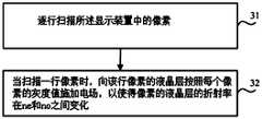
- Step 31Scan the pixels in the display device line by line.
- Step 32When scanning a row of pixels, apply an electric field to the portion of the liquid crystal layer corresponding to the row of pixels according to the gray value of each pixel, so that the refractive index of the liquid crystal layer corresponding to the pixel is between ne and no Change between.
- the "correspondence” heremeans, for example, that the orthographic projection of a certain pixel on the lower substrate 102 and the orthographic projection of the corresponding part of the liquid crystal layer on the lower substrate 102 at least partially overlap, or even completely overlap, so that the driving electrode faces the liquid crystal layer.
- the application of an electric field to the corresponding partresults in the grayscale required for imaging of the pixel.
- the display effect of the display devicealso changes accordingly.
- the display effects of the display deviceare mainly divided into two types: transparent display and reflective display.
- Transparent displayis a state that does not need to be displayed, that is, the driving electrode 104 is not loaded with a driving voltage, and the collimated light source 106 is not lit.
- the display deviceis equivalent to glass and does not affect the viewing of the picture behind the display device.
- Reflective color displaythat is, the driving electrode 104 is loaded with a driving voltage, and the liquid crystal layer 103 forms a liquid crystal grating.
- “reflective color display”means that the liquid crystal grating is selective to the light of different wavelengths projected on it. At different parts of the liquid crystal grating, the light of the corresponding specific wavelength is diffracted and passed, and the light of other wavelengths is reflected back to realize the light of the specific wavelength is diffracted by the liquid crystal grating to display the corresponding color light, but not The finger light is reflected by the human eye toward the observer to realize the display.
- the selection of different wavelengths of light distributed at each part of the gratingis specifically embodied as: the period, height, and duty cycle of the liquid crystal grating at each part are correspondingly designed by the color of the light to be emitted. It is determined that certain geometric parameters can allow certain specific wavelengths to pass, while other wavelengths cannot pass and are directly reflected back, so as to achieve specific colors of light. It should be pointed out that when different driving voltages are applied to the electrodes in different parts, the height of the corresponding parts of the formed liquid crystal grating will change accordingly, which affects the light emission.
- the settings for achieving selective light emission of different wavelengths (ie, colors) at different parts of the gratingare as follows, for example.
- the formed grating strip periodis, for example, 330-450nm (especially 350nm), and the width is 190-210nm (especially In the case of 198nm), red light in the range of 600-780nm is obtained.
- the formed grating strip periodis, for example, 240-280nm (especially 240nm), and the width is 125-145nm (especially In the case of 135nm), the green light emission in the range of 500-600nm is obtained.
- the formed gratinghas a period of 120-200nm (especially 180nm), and a width of 90-110nm ( Especially in the case of 102nm), the blue light emission in the range of 380-500nm is obtained.
- the formed grating strip periodis, for example, 210-230nm (especially 220nm) and the width is 110-130nm (especially In the case of 124nm), the cyan light emission in the range of 450-550nm is obtained.
- the formed grating strip periodis, for example, 290-320nm (especially 300nm), and the width is 160-180nm (especially In the case of 170nm), a yellow light emission in the range of 580+/-50nm is obtained.
- the "reflective color display”includes the following three implementation forms when different ambient light is incident from the back:
- the display modeis directly realized through the ambient light.
- the collimated light source 106is not lit, and the ambient light directly projected from the back is used as the backlight, and the ambient light is reflected and filtered by the liquid crystal grating to realize the liquid crystal color display with ambient light as the light source.
- the side-mounted collimated light source 106lights up, is incident obliquely into the waveguide layer and is reflected, and the color is developed through the liquid crystal grating to realize the liquid crystal color display with the collimated light source as the light source.
- the intensity of the ambient lightis between the above two states, there is the ambient light directly projected from the back and the side incident light from the collimated light source 106 obliquely incident into the waveguide layer 105 and reflected side light in the panel.
- an ambient light intensity detection sensorsuch as a dynamic iris, can sense the ambient light intensity signal in real time and transmit it back to the system light intensity signal.
- the light source 106can be collimated to different degrees. Based on the driving of light intensity, it is actually provided to adjust the collimated light source according to the ambient light intensity detected in real time to realize the compensated light emission, thereby realizing a display mode in which the image quality is not affected by the ambient light intensity.
- the driving voltage applied to the driving electrode 104is different, and the refractive index of the liquid crystal layer 103 also changes accordingly.
- the refractive index of the liquid crystal layer 103is less than the refractive index of the waveguide layer 105, total reflection is achieved in the waveguide layer 105, resulting in no light coupling out of the waveguide layer 105, and it is in the L0 state; when the refractive index of the liquid crystal layer 103 is greater than
- the refractive index of the waveguide layer 105 and the difference between the refractive index of the liquid crystal layer 103 and the grating refractive indexare the largest, the effect of the liquid crystal grating is the most obvious, and the coupling efficiency of light coupling out of the waveguide layer 105 is the highest, which is in the L255 state; when the liquid crystal layer 103 When the refractive index is between the above two conditions, it is in other grayscale states. For example, when different driving voltages are applied, the height of the formed liquid crystal grating is inconsistent
- the diffraction grating formulacan be used:
- ni and Theyare the refractive index and the incident angle of the medium through which the light enters the diffraction grating
- mis the diffraction order
- ⁇is the grating period
- ⁇is the wavelength of the incident light
- ⁇ dis the clamp between the direction of the diffracted light and the plane normal Angle
- ndis the refractive index of the liquid crystal layer
- the equivalent refractive index of the driving electrode and the upper substrategenerally the refractive indices of the three are also very close.
- the light-emitting direction of a pixel at a certain position on the panelis often fixed, which is determined by the position of the pixel relative to the human eye, that is, the light-emitting direction ⁇ d of the display mode in the above formula is fixed.
- the period ⁇ of the gratingat different positions for the light emission direction ⁇ d, as described above, light of a given color (wavelength ⁇ ) can be emitted in a given direction ⁇ d.
- the display device and display method provided by the embodiments of the present disclosurehave at least the following superior technical effects:
- the display deviceprovided by the embodiment of the present invention includes an upper substrate and a lower substrate that are arranged oppositely; a liquid crystal layer and a driving electrode located between the upper substrate and the lower substrate are controlled by applying a driving voltage on the driving electrode
- the refractive index of the liquid crystal layervaries between a maximum refractive index ne and a minimum refractive index no; a waveguide layer located between the liquid crystal layer and the upper substrate; a collimated light source located on the side of the waveguide layer.
- the process difficultycan be greatly reduced under the condition of ensuring PPI.
Landscapes
- Physics & Mathematics (AREA)
- Engineering & Computer Science (AREA)
- General Physics & Mathematics (AREA)
- Nonlinear Science (AREA)
- Chemical & Material Sciences (AREA)
- Crystallography & Structural Chemistry (AREA)
- Computer Hardware Design (AREA)
- Theoretical Computer Science (AREA)
- Mathematical Physics (AREA)
- Optics & Photonics (AREA)
- Liquid Crystal (AREA)
Abstract
Description
Translated fromChinese相关申请的交叉引用Cross references to related applications
本公开实施例要求于2019年4月17日递交中国专利局的、申请号为201910310207.1的中国专利申请的权益,该申请的全部内容以引用方式并入本文。The embodiments of the present disclosure require the rights and interests of the Chinese patent application with application number 201910310207.1 filed with the Chinese Patent Office on April 17, 2019, and the entire content of the application is incorporated herein by reference.
本公开涉及显示技术领域,尤其涉及一种显示装置及其显示方法。The present disclosure relates to the field of display technology, and more particularly to a display device and a display method thereof.
显示器发展至今,有几个重要的研发方向,如节能显示、超高清晰度、超宽色域和色纯度显示、超大超薄显示、三维显示等等。期望的是将最真实所见的色彩尽可能无损的还原到显示屏上,并最大化利用环境光强,将功耗降到最低。其中,超高PPI的需求是未来显示着力要解决的问题之一,现在VR/AR显示的快速发展促使这一方向的快速发展。Since the development of displays, there have been several important research and development directions, such as energy-saving display, ultra-high definition, ultra-wide color gamut and color purity display, ultra-large and ultra-thin display, three-dimensional display and so on. The expectation is to restore the most real colors to the display screen as losslessly as possible, maximize the use of ambient light, and minimize power consumption. Among them, the demand for ultra-high PPI is one of the problems that the display will focus on in the future. The rapid development of VR/AR display now promotes the rapid development in this direction.
因此,如何在保证PPI的情况下降低工艺难度是亟需解决的问题。Therefore, how to reduce the process difficulty while ensuring PPI is an urgent problem to be solved.
发明内容Summary of the invention
为至少部分地克服上述相关技术中的缺陷和/或不足,本公开的实施例提供一种显示装置及其显示方法。In order to at least partially overcome the defects and/or deficiencies in the above-mentioned related technologies, embodiments of the present disclosure provide a display device and a display method thereof.
本公开的实施例提供技术方案如下:The embodiments of the present disclosure provide technical solutions as follows:
根据本公开实施例的第一方面,本发明实施例提供了一种显示装置,包括:According to the first aspect of the embodiments of the present disclosure, an embodiment of the present invention provides a display device, including:
相对设置的上基板和下基板;The upper substrate and the lower substrate arranged oppositely;
位于所述上基板和所述下基板之间的液晶层和驱动电极,通过在所述驱动电极上加载驱动电压,控制所述液晶层的折射率在液晶层的双折射率中的最大折射率和最小折射率之间变化;The liquid crystal layer and the driving electrode located between the upper substrate and the lower substrate, by applying a driving voltage on the driving electrode, the refractive index of the liquid crystal layer is controlled to be the maximum refractive index among the birefringence of the liquid crystal layer And the minimum refractive index change;
位于所述液晶层和所述上基板之间的波导层;和A waveguide layer located between the liquid crystal layer and the upper substrate; and
位于所述波导层侧面的准直光源。A collimated light source located on the side of the waveguide layer.
在本公开的示例性实施例中,所述驱动电极采用带正电电极和带负电电极在与所述显示装置的法向垂直的横向上交替布置的导电的光栅结构。In an exemplary embodiment of the present disclosure, the driving electrode adopts a conductive grating structure in which positively charged electrodes and negatively charged electrodes are alternately arranged in a lateral direction perpendicular to the normal direction of the display device.
在本公开的示例性实施例中,所述驱动电极为透明导电材料。In an exemplary embodiment of the present disclosure, the driving electrode is a transparent conductive material.
在本公开的示例性实施例中,还包括:In the exemplary embodiment of the present disclosure, it further includes:
亮度传感器,所述亮度传感器位于显示装置的相对的两侧边缘处,且配置为检测环境光亮度,并通过根据检测到的所述环境光亮度调节所述准直光源的亮度。Brightness sensor, the brightness sensor is located at the opposite side edges of the display device, and is configured to detect the brightness of the ambient light, and adjust the brightness of the collimated light source according to the detected brightness of the ambient light.
在本公开的示例性实施例中,所述上基板位于所述显示装置的出光侧,并且,在所述波导层与所述上基板是彼此邻靠的不同层的情况下,所述上基板位于所述波导层的背离所述下基板的表面上。In an exemplary embodiment of the present disclosure, the upper substrate is located on the light-exit side of the display device, and when the waveguide layer and the upper substrate are different layers adjacent to each other, the upper substrate Located on the surface of the waveguide layer facing away from the lower substrate.
在本公开的示例性实施例中,所述上基板位于所述显示装置的出光侧,并且,在所述波导层与所述上基板复用的情况下,所述上基板位于所述液晶层的背离所述下基板的表面上。In an exemplary embodiment of the present disclosure, the upper substrate is located on the light exit side of the display device, and, in the case where the waveguide layer is multiplexed with the upper substrate, the upper substrate is located on the liquid crystal layer. On the surface facing away from the lower substrate.
在本公开的示例性实施例中,还包括:In the exemplary embodiment of the present disclosure, it further includes:
位于所述上基板背离所述液晶层一侧表面上的包覆层,所述包覆层的折射率低于所述上基板的折射率。A cladding layer located on a surface of the upper substrate facing away from the liquid crystal layer, and the refractive index of the cladding layer is lower than the refractive index of the upper substrate.
在本公开的示例性实施例中,所述包覆层由透明材料形成。In an exemplary embodiment of the present disclosure, the coating layer is formed of a transparent material.
在本公开的示例性实施例中,所述上基板和所述下基板中的至少一个由透明材料形成。In an exemplary embodiment of the present disclosure, at least one of the upper substrate and the lower substrate is formed of a transparent material.
在本公开的示例性实施例中,所述液晶层是工作于ADS模式的液晶层。In an exemplary embodiment of the present disclosure, the liquid crystal layer is a liquid crystal layer operating in an ADS mode.
根据本公开实施例的第二方面,本公开实施例还提供了一种应用于上述显示装置的显示方法,包括:According to the second aspect of the embodiments of the present disclosure, the embodiments of the present disclosure also provide a display method applied to the above-mentioned display device, including:
逐行扫描所述显示装置中的像素;Scanning the pixels in the display device line by line;
当扫描一行像素时,向该行像素的液晶层按照每个像素的灰度值施加电场,以使得所述像素的液晶层的折射率在液晶层的双折射率中的最大折射率和最小折射率之间变化。When scanning a row of pixels, an electric field is applied to the liquid crystal layer of the row of pixels according to the gray value of each pixel, so that the refractive index of the liquid crystal layer of the pixel is the maximum refractive index and the minimum refractive index in the birefringence of the liquid crystal layer Rate varies between.
通过阅读参照以下附图所作的对非限制性实施例所作的详细描述,本公开实施例的其它特征、目的和优点将会变得更明显。为了更清楚地说明本公开实施例的技术方案,下面将对本公开实施例的描述中所需要使用的附图作简单地介绍,显而易见地,下面描述中的附图仅仅是本公开的一些实施例,对于本领域普通技术人员来讲,在不付出创造性劳动性的前提下,还可以根据这些附图获得其他的附图本公开实施例上述 的和/或附加的方面和优点从下面结合附图对实施例的描述中将变得明显和容易理解,其中:By reading the detailed description of the non-limiting embodiments with reference to the following drawings, other features, purposes and advantages of the embodiments of the present disclosure will become more apparent. In order to explain the technical solutions of the embodiments of the present disclosure more clearly, the following will briefly introduce the drawings that need to be used in the description of the embodiments of the present disclosure. Obviously, the drawings in the following description are only some embodiments of the present disclosure. For those of ordinary skill in the art, without creative labor, other drawings can be obtained based on these drawings. The above-mentioned and/or additional aspects and advantages of the embodiments of the present disclosure are combined with the drawings below. The description of the embodiments will become obvious and easy to understand, where:
图1为本公开实施例提供的一种显示装置的结构示意图;FIG. 1 is a schematic structural diagram of a display device provided by an embodiment of the disclosure;
图2为驱动电极加载驱动电压时显示装置的状态图;FIG. 2 is a state diagram of the display device when the driving electrode is loaded with a driving voltage;
图3为本发明实施例提供的一种应用于该显示装置的显示方法的实现流程图。FIG. 3 is an implementation flowchart of a display method applied to the display device according to an embodiment of the present invention.
下面结合附图和实施例对本公开实施例作进一步的详细说明。可以理解的是,此处所描述的具体实施例仅仅用于解释相关发明,而非对该发明的限定。另外还需要说明的是,为了便于描述,附图中仅示出了与发明相关的部分。为了清楚起见,附图中的各个部分没有按比例绘制。此外,在图中可能未示出某些公知的部分。The embodiments of the present disclosure will be further described in detail below with reference to the drawings and embodiments. It can be understood that the specific embodiments described here are only used to explain the related invention, but not to limit the invention. In addition, it should be noted that, for ease of description, only the parts related to the invention are shown in the drawings. For the sake of clarity, the various parts in the drawings are not drawn to scale. In addition, some well-known parts may not be shown in the figure.
在下文中描述了本公开的实施例的许多特定的细节,例如部件的结构、材料、尺寸、处理工艺和技术,以便更清楚地理解本公开的实施例。但正如本领域的技术人员能够理解的那样,可以不按照这些特定的细节来实现本公开的实施例。In the following, many specific details of the embodiments of the present disclosure are described, such as the structure, materials, dimensions, processing technology and technology of the components, in order to understand the embodiments of the present disclosure more clearly. However, as those skilled in the art can understand, the embodiments of the present disclosure may not be implemented according to these specific details.
附图中各部件尺寸和形状不反映本公开的实施例的一种显示装置的部件的真实比例,目的只是示意说明本公开的实施例内容。The size and shape of the components in the drawings do not reflect the true proportions of the components of a display device of the embodiments of the present disclosure, and the purpose is only to schematically illustrate the content of the embodiments of the present disclosure.
需要说明的是,在不冲突的情况下,本公开实施例中的实施例及实施例中的特征可以相互组合。It should be noted that the embodiments in the embodiments of the present disclosure and the features in the embodiments can be combined with each other if there is no conflict.
根据本公开实施例的总体技术构思,在本公开实施例的一方面,提供了一种显示装置。如图1所示,为本公开实施例提供的一种显示装置的结构示意图。该显示装置包括:According to the general technical idea of the embodiment of the present disclosure, in one aspect of the embodiment of the present disclosure, a display device is provided. As shown in FIG. 1, it is a schematic structural diagram of a display device provided by an embodiment of the present disclosure. The display device includes:
相对设置的上基板101和下基板102;The
位于上基板101和下基板102之间的液晶层103和驱动电极104,通过在驱动电极104上加载驱动电压,控制液晶层103的折射率在液晶层的双折射率中的最大折射率ne和最小折射率no之间变化;The
位于液晶层103和上基板101之间的波导层105;The
位于波导层105侧面的准直光源106。The collimated
其中,最大折射率ne和最小折射率no分别是液晶层的双折射率中的非常光折射率和寻常光折射率。Among them, the maximum refractive index ne and the minimum refractive index no are the extraordinary refractive index and the ordinary refractive index in the birefringence of the liquid crystal layer, respectively.
上基板101和/或下基板102例如是由透明材料形成,比如由较高折射率的LCD (Liquid Crystal Display,液晶显示器)或OLED(Organic Light-Emitting Diode,有机发光二极管)基板玻璃构成,也替代地例如使用一些特殊的光学玻璃或树脂材料等,但不限于此。其厚度例如是0.1-2mm,具体厚度由产品设计或工艺条件决定,要求上下表面具有较好的平整度及平行度。The
准直光源106例如是侧入式准直光源,例如但不限于使用CCFL(Cold Cathode Fluorescent Lamp,冷阴极荧光灯管),B(LED)+Y荧光粉,RG荧光粉,及QD(量子点)光源,也替代地例如是高准直性的光源,或替代地例如是发散性的光源。其中,准直光源106的光源入射光集中入射到波导层105。The collimated
准直光源106的出光例如由发射的R、G、B三种单色光经过混光后形成白光,或者也可由准直性比较好的白光LED灯条形成白光,或替代地由条状的CCFL灯管加一些光线准直结构形成白光,但不限于这些类型。为了和面板的宽度匹配,例如采用和面板宽度一致的激光器芯片或LED灯条,或者在较稀疏分布的激光器芯片或LED灯条前加一些扩束结构。准直光源106的出光方向例如需要和和波导层105法线成一定夹角,以使得入射光可以在波导与上基板之间的界面处发生全反射。和波导层对准时,侧置的准直光源106布置成覆盖波导层105的侧面,但不直接向液晶层及以上各层出射光线。实际结构中液晶层的最外面会有封框胶,不会出现光线射入液晶层的情况。The light emitted by the collimated
液晶层103的液晶材料例如采用正性液晶,且继而液晶层103是工作于ADS模式的液晶层。其中,ADS模式是ADSDS(Advanced Super Dimension Switch,高级超维场转换技术)的简称,是以宽视角技术为代表的核心技术的统称,是利用处于同形成于阵列基板上的例如均由ITO材料形成的像素电极和公共电极产生的横向电场(特别是二者之间的边缘电场)使液晶分子产生偏转来实现图像显示的模式,实质上属于IPS模式的改进的范畴。The liquid crystal material of the
需要注意的是,本公开的附图仅示意性地示出带不同电性的两种电极交替地布置(例如来分布充当像素电极和公共电极),但实际上,在更具体的实施例中,例如,带不同电性的该两种电极是例如附图示意性所示般同层布置的(这种情况下实质上等效于相关技术的IPS模式,二者之间的电场仅为平行于阵列基板的横向上的Ey电场,由此驱动液晶分子水平旋转来产生灰阶进行显示);或者在替代的更具体地的实施例中,例如,采用了等效于ADS模式所包括的HADS、IADS或AADS这三种具体工作模式的电极设置,更具体地即,带不同电性的该两种电极并非位于同层,而是更具体 地在二者之间形成有至少一层绝缘层,且两者至少部分地重叠,且两者的交叠部分(即两者的各自在阵列基板上的正投影彼此重合的部分)构成相应像素的存储电容以用于维持一帧时间期间液晶分子的驱动状态来实现显示),因此这种情况下二者之间的电场不仅包括平行于阵列基板的横向上的横向电场Ey,还包括在该两种电极边缘附近分布的较强的垂直于阵列基板的法向上的竖向电场Ez,在开态状态下该竖向电场可使得液晶分子的偏转程度加大,在电极的边缘处可实现更佳有效的光透过,增加像素开口率,提升整个面板的透过率。换言之,在该两种电极之间形成了边缘电场且经由该边缘电场来驱动液晶分子水平旋转来产生灰阶进行显示。It should be noted that the drawings of the present disclosure only schematically show that two kinds of electrodes with different electric properties are alternately arranged (for example, to serve as a pixel electrode and a common electrode), but in fact, in a more specific embodiment For example, the two electrodes with different electrical properties are arranged in the same layer as shown schematically in the drawings (in this case, it is substantially equivalent to the IPS mode of the related technology, and the electric field between the two is only parallel. The Ey electric field in the lateral direction of the array substrate, thereby driving the horizontal rotation of the liquid crystal molecules to generate gray scales for display); or in an alternative more specific embodiment, for example, a HADS equivalent to the ADS mode is used , IADS, or AADS are three specific working modes of electrode settings. More specifically, the two electrodes with different electrical properties are not located in the same layer, but more specifically, at least one insulating layer is formed between them , And the two overlap at least partially, and the overlapping part of the two (that is, the part where the respective orthographic projections of the two overlap each other on the array substrate) constitute the storage capacitor of the corresponding pixel to maintain the liquid crystal molecules during one frame time In this case, the electric field between the two includes not only the transverse electric field Ey parallel to the transverse direction of the array substrate, but also the stronger perpendicular to the array distributed near the edges of the two electrodes. The vertical electric field Ez in the normal direction of the substrate can increase the degree of deflection of the liquid crystal molecules in the on state, and achieve better and effective light transmission at the edge of the electrode, increase the pixel aperture ratio, and improve The transmittance of the entire panel. In other words, a fringe electric field is formed between the two kinds of electrodes, and the liquid crystal molecules are driven to rotate horizontally via the fringe electric field to generate gray scales for display.
本公开实施例中,液晶层103的厚度一般在3um左右。In the embodiment of the present disclosure, the thickness of the
驱动电极104例如形成于所述下基板102的朝向所述液晶层103的表面上、且被液晶层103覆盖(实质上可视为驱动电极104置于液晶层103中,且一侧从液晶层103暴露以邻靠下方的下基板102),并且例如呈带正电电极和带负电电极在与显示装置的法向垂直的横向上交替布置形成导电的光栅结构,其电极的交替布置的周期由设计的出光方向以及颜色决定,占空比通常例如设置为0.5,光栅的高度通常例如设置为200nm左右,具体取值取决于波导层105的光束缚能力。The driving
驱动电极104例如是透明导电材料,如ITO(氧化铟锡),也例如是金属,如Mo(钼)或者Ag(银)、Al(铝)。厚度例如选择为以可以满足施加电压的需求为宜,如70-300nm。本公开实施例一些实施例中例如选择为透明导电材料。The driving
波导层105例如为透明的且通常会选择较高折射率的材料形成波导,以对光波进行有效束缚。具体地,波导层105的折射率例如高于上基板101的材料的折射率,例如选择为由ITO或者Si3N4等材料制成;且厚度例为如2μm甚至更厚到几十微米,但不限于此。控制液晶层折射率变化可以使光线从波导层中耦出至液晶层中。The
另外,本公开实施例中的显示装置还例如额外地包括亮度传感器,可以位于显示装置的相对的两侧边缘,该亮度传感器配置为检测环境光亮度,并通过检测到的环境光亮度调节准直光源106的亮度。亮度传感器例如选择为光敏电阻。In addition, the display device in the embodiment of the present disclosure may additionally include a brightness sensor, which may be located on opposite sides of the display device. The brightness sensor is configured to detect the brightness of the ambient light and adjust the collimation by the detected brightness of the ambient light. The brightness of the
在本公开的示例性实施例中,上基板101位于显示装置的出光侧。更具体地,在所述波导层105与所述上基板101是彼此邻靠的不同层的情况下,所述上基板101位于所述波导层105的背离所述下基板102的表面上;而在所述波导层105例如与上基板101复用的情况下,所述上基板101位于所述液晶层103的背离所述下基板102的表面上。In an exemplary embodiment of the present disclosure, the
在本公开的示例性实施例中,该显示装置还例如额外地包括位于上基板101背离液晶层103一侧表面上的包覆层107,该包覆层107的折射率应该要低于上基板101的折射率。该包覆层107也例如是由透明材料形成的,比如光学玻璃或者树脂材料等。In an exemplary embodiment of the present disclosure, the display device may additionally include, for example, a
另外,在液晶层103的周缘还例如设置有围封所述液晶层的整圈封框胶108,所述封框胶108在所述横向上围封所述液晶层103。In addition, a
参考图1,为驱动电极104没有加载驱动电压的情况,此时为显示装置的初始状态。当所有膜材都是由透明材料形成时,此时环境光可以直接透过该显示装置,该显示装置为透明状态。此时显示装置相当于玻璃,对看到显示装置后面的画面不产生影响。Referring to FIG. 1, it is a case where the driving
参考图2,为驱动电极104加载驱动电压的情况,此时显示装置切换为针对特定波长光进行过滤的反射状态。假设在没有环境光的条件下,点亮准直光源106,驱动电极104加载驱动电压,此时液晶层103中形成液晶光栅。形成的液晶光栅的栅条延伸方向例如平行于条形电极延伸的方向。Referring to FIG. 2, it is a case where the driving
为确保液晶层103能实现通过大尺寸驱动电极,实现小尺寸光栅的方式,本公开实施例中用液晶模拟软件TechWiz模拟在驱动电极104的上述设计情况下的液晶层103的偏转状态和动态响应过程,最终研究确定出本公开实施例中这种驱动电极104的设计方式下,形成液晶光栅的周期为驱动电极104周期结构的二分之一,例如图2所示呈现了这两种周期之间的关系。In order to ensure that the
就目前的加工工艺而言,越小尺寸的光栅结构加工越难,尤其是当周期性参数降到纳米级别时,加工难度越大,且控制精度越差。这种ADS液晶材料和采用正负交替光栅结构的驱动电极的方式形成的液晶光栅例如形成为其具备的周期是电极周期一半,将工艺难度大大降低,对光的方向和强度进行调控。这种方式的液晶驱动模式,例如是其他方式的显示方式和液晶光栅所用。As far as the current processing technology is concerned, the smaller the grating structure is, the more difficult it is to process, especially when the periodic parameters drop to the nanometer level, the greater the processing difficulty and the worse the control accuracy. Such an ADS liquid crystal material and a liquid crystal grating formed by driving electrodes with a positive and negative alternating grating structure, for example, are formed with a period of half the electrode period, which greatly reduces the difficulty of the process and regulates the direction and intensity of light. This type of liquid crystal drive mode is used for other display modes and liquid crystal gratings, for example.
基于上述显示装置,本公开实施例还提供了一种应用于该显示装置的显示方法,包括如图3所示的步骤:Based on the above display device, an embodiment of the present disclosure also provides a display method applied to the display device, including the steps shown in FIG. 3:
步骤31,逐行扫描所述显示装置中的像素。Step 31: Scan the pixels in the display device line by line.
步骤32,当扫描一行像素时,按照每个像素所需呈现的灰度值向液晶层的与该行像素对应的部分施加电场,以使得与该像素对应的液晶层的折射率在ne和no之间变化。Step 32: When scanning a row of pixels, apply an electric field to the portion of the liquid crystal layer corresponding to the row of pixels according to the gray value of each pixel, so that the refractive index of the liquid crystal layer corresponding to the pixel is between ne and no Change between.
此处的“对应”例如是指某一像素在下基板102上的正投影与液晶层的相应部分在 下基板102上的正投影至少部分地交叠,甚至完全重叠,使得由驱动电极向液晶层的该相应部分施加电场导致该像素成像所需的灰度。The "correspondence" here means, for example, that the orthographic projection of a certain pixel on the
本公开实施例中,随着像素的液晶层的折射率的变化,显示装置的显示效果也在随之变化。In the embodiments of the present disclosure, as the refractive index of the liquid crystal layer of the pixel changes, the display effect of the display device also changes accordingly.
其中,显示装置的显示效果主要分为两种:透明显示和反射式显示。Among them, the display effects of the display device are mainly divided into two types: transparent display and reflective display.
透明显示,即不需要显示的状态,即驱动电极104不加载驱动电压、准直光源106不点亮,显示装置相当于玻璃,对看到显示装置后面的画面不产生影响。Transparent display is a state that does not need to be displayed, that is, the driving
反射式彩色显示,即驱动电极104加载驱动电压,液晶层103形成液晶光栅,此处的“反射式彩色显示”是指,通过液晶光栅对于投射到其上的不同波长的光的选择性来实现在液晶光栅的不同部位处分别将各自相应特定波长的光衍射通过、并且将其他波长的光往回反射,来实现特定波长的光经液晶光栅衍射进行显示由此呈现相应颜色光,而并非是指光在该处被朝向观察者的人眼反射以实现显示。具体地,这种在光栅各个部位处分布对于不同波长的光的选择具体体现为:液晶光栅在各部位处的周期、高度、以及占空比由各处相应地所设计的待出射光的颜色决定,特定几何参数可以让某些特定波长通过,而其他波长无法通过而被直接往回反射,从而实现特定颜色出光。需要指出的是,在不同部位的电极加载不同的驱动电压的情况下,形成的液晶光栅的相应部位的高度会相应发生变化,影响到出光。Reflective color display, that is, the driving
具体地,光栅不同部位处实现不同波长(即颜色)的选择性出光的设置例如如下。Specifically, the settings for achieving selective light emission of different wavelengths (ie, colors) at different parts of the grating are as follows, for example.
红色出光的实现方式:作为示例,当液晶光栅在预期实现红色的部位处的几何参数设计为:所形成的光栅条周期例如为330-450nm(特别是350nm),宽度为190-210nm(特别是198nm)的情况,即得到600-780nm范围内的红色出光。The realization of red light emission: As an example, when the geometric parameters of the liquid crystal grating at the part where red is expected to be realized are designed as: the formed grating strip period is, for example, 330-450nm (especially 350nm), and the width is 190-210nm (especially In the case of 198nm), red light in the range of 600-780nm is obtained.
绿色出光的实现方式:作为示例,当液晶光栅在预期实现绿色的部位处的几何参数设计为:所形成的光栅条周期例如为240-280nm(特别是240nm),宽度为125-145nm(特别是135nm)的情况,即得到500-600nm范围内的绿色出光。The realization of green light emission: As an example, when the geometric parameters of the liquid crystal grating at the part where green is expected to be realized are designed as follows: the formed grating strip period is, for example, 240-280nm (especially 240nm), and the width is 125-145nm (especially In the case of 135nm), the green light emission in the range of 500-600nm is obtained.
蓝色出光的实现方式:作为示例,当液晶光栅在预期实现蓝色的部位处的几何参数设计为:所形成的光栅条周期例如为120-200nm(特别是180nm),宽度为90-110nm(特别是102nm)的情况,即得到380-500nm范围内的蓝色出光。The realization of blue light: As an example, when the geometric parameters of the liquid crystal grating at the part where blue is expected to be realized are designed as follows: the formed grating has a period of 120-200nm (especially 180nm), and a width of 90-110nm ( Especially in the case of 102nm), the blue light emission in the range of 380-500nm is obtained.
利用如上的光栅各个部位的结构尺寸参数设置,便于实现R、G、B像素的出光。Utilizing the structure size parameter setting of each part of the grating as above, it is convenient to realize the light emission of R, G, and B pixels.
并且在额外的实施例中,还例如能够实现青色(C)和黄色(Y)的补充色,结合现有的RGB三基色,实现RGBCY五基色显示,扩展色域,实现高饱和度和高色域 显示。具体地如下阐释。And in an additional embodiment, for example, it is possible to realize complementary colors of cyan (C) and yellow (Y), combine the existing RGB three primary colors to realize RGBCY five primary color display, expand the color gamut, and achieve high saturation and high color Domain display. The specific explanation is as follows.
青色出光的实现方式:作为示例,当液晶光栅在预期实现青色的部位处的几何参数设计为:所形成的光栅条周期例如为210-230nm(特别是220nm),宽度为110-130nm(特别是124nm)的情况,即得到450-550nm范围内的青色出光。The realization of cyan light emission: As an example, when the geometric parameters of the liquid crystal grating at the place where cyan is expected to be realized are designed as follows: the formed grating strip period is, for example, 210-230nm (especially 220nm) and the width is 110-130nm (especially In the case of 124nm), the cyan light emission in the range of 450-550nm is obtained.
黄色出光的实现方式:作为示例,当液晶光栅在预期实现黄色的部位处的几何参数设计为:所形成的光栅条周期例如为290-320nm(特别是300nm),宽度为160-180nm(特别是170nm)的情况,即得到在580+/-50nm范围的黄色出光。The realization of yellow light emission: As an example, when the geometric parameters of the liquid crystal grating at the part where yellow is expected to be realized are designed as: the formed grating strip period is, for example, 290-320nm (especially 300nm), and the width is 160-180nm (especially In the case of 170nm), a yellow light emission in the range of 580+/-50nm is obtained.
在更具体的实施例中,所述“反射式彩色显示”包括如下三种从背面入射不同环境光情况下的实现形式:In a more specific embodiment, the "reflective color display" includes the following three implementation forms when different ambient light is incident from the back:
1、环境光足够强时,通过环境光直接实现显示的模式。该种模式下,准直光源106不点亮,利用背面直接投射的环境光作为背光,通过液晶光栅对环境光反射过滤,实现环境光作为光源的液晶彩色显示。1. When the ambient light is strong enough, the display mode is directly realized through the ambient light. In this mode, the collimated
2、环境光非常弱时,侧置的准直光源106点亮,倾斜入射到波导层中并且反射,通过液晶光栅显色,实现准直光源作为光源的液晶彩色显示。2. When the ambient light is very weak, the side-mounted collimated
3、当环境光强度介于以上两种状态之间时,同时存在背面直接投射的环境光、以及从侧置的准直光源106倾斜入射到波导层105中并且反射的侧入光在面板中传播,在此情况下例如通过一种环境光强检测传感器,如动态光阑等,实时感知环境光强信号,并传输回系统光强信号,根据用户亮度设计,实现不同程度准直光源106的基于光强的驱动,实际上提供针对实时检测到的环境光强进行对于准直光源的调节来实现了经补偿的发光,由此实现画质不受环境光强影响的显示模式。3. When the intensity of the ambient light is between the above two states, there is the ambient light directly projected from the back and the side incident light from the collimated
在液晶彩色显示时,驱动电极104上加载的驱动电压不同,液晶层103的折射率也随之变化。当液晶层103的折射率小于波导层105的折射率时,在波导层105中实现了全反射,导致没有光从波导层105耦合出来,此时为L0状态;当液晶层103的折射率大于波导层105的折射率且液晶层103的折射率和光栅折射率相差最大时,液晶光栅的作用最明显,光线从波导层105耦合出来的耦合效率最高,此时为L255状态;当液晶层103的折射率处在以上两种情况之间时,为其他灰阶状态,如加载不同的驱动电压时,形成的液晶光栅的高度不一致,实现对于出光光强的控制,由此实现对彩色显示像素的进一步的灰阶的控制。In the liquid crystal color display, the driving voltage applied to the driving
实现彩色显示时,可以通过衍射光栅公式:When realizing color display, the diffraction grating formula can be used:
nisinθi-ndsinθd=mλ/Λ(m=1,2,3…)ni sinθi -nd sinθd = mλ/Λ(m=1, 2, 3...)
其中,ni和
相较于相关技术,基于上述技术方案,本公开实施例提供的显示装置和显示方法至少具有下列优越的技术效果:Compared with related technologies, based on the above technical solutions, the display device and display method provided by the embodiments of the present disclosure have at least the following superior technical effects:
本发明实施例提供的显示装置,包括相对设置的上基板和下基板;位于所述上基板和所述下基板之间的液晶层和驱动电极,通过在所述驱动电极上加载驱动电压,控制所述液晶层的折射率在最大折射率ne和最小折射率no之间变化;位于所述液晶层和所述上基板之间的波导层;位于所述波导层侧面的准直光源。与相关技术相比,在保证PPI的情况下能够大大降低工艺难度。The display device provided by the embodiment of the present invention includes an upper substrate and a lower substrate that are arranged oppositely; a liquid crystal layer and a driving electrode located between the upper substrate and the lower substrate are controlled by applying a driving voltage on the driving electrode The refractive index of the liquid crystal layer varies between a maximum refractive index ne and a minimum refractive index no; a waveguide layer located between the liquid crystal layer and the upper substrate; a collimated light source located on the side of the waveguide layer. Compared with related technologies, the process difficulty can be greatly reduced under the condition of ensuring PPI.
以上描述仅为本公开实施例的较佳实施例以及对所运用技术原理的说明。本领域技术人员应当理解,本公开实施例中所涉及的发明范围,并不限于上述技术特征的特定组合而成的技术方案,同时也应涵盖在不脱离所述发明构思的情况下,由上述技术特征或其等同特征进行任意组合而形成的其它技术方案。例如上述特征与本公开实施例中公开的(但不限于)具有类似功能的技术特征进行互相替换而形成的技术方案。The above description is only a preferred embodiment of the embodiments of the present disclosure and an explanation of the applied technical principles. Those skilled in the art should understand that the scope of the invention involved in the embodiments of the present disclosure is not limited to the technical solutions formed by the specific combination of the above technical features, and should also cover the above-mentioned technical solutions without departing from the inventive concept. Other technical solutions formed by any combination of technical features or equivalent features. For example, the above-mentioned features and the technical features disclosed in the embodiments of the present disclosure (but not limited to) having similar functions are replaced with each other to form a technical solution.
Claims (11)
Translated fromChineseApplications Claiming Priority (2)
| Application Number | Priority Date | Filing Date | Title |
|---|---|---|---|
| CN201910310207.1ACN109856854A (en) | 2019-04-17 | 2019-04-17 | A display device and display method thereof |
| CN201910310207.1 | 2019-04-17 |
Publications (1)
| Publication Number | Publication Date |
|---|---|
| WO2020211625A1true WO2020211625A1 (en) | 2020-10-22 |
Family
ID=66889273
Family Applications (1)
| Application Number | Title | Priority Date | Filing Date |
|---|---|---|---|
| PCT/CN2020/082048CeasedWO2020211625A1 (en) | 2019-04-17 | 2020-03-30 | Display device and display method therefor |
Country Status (2)
| Country | Link |
|---|---|
| CN (1) | CN109856854A (en) |
| WO (1) | WO2020211625A1 (en) |
Families Citing this family (1)
| Publication number | Priority date | Publication date | Assignee | Title |
|---|---|---|---|---|
| CN109856854A (en)* | 2019-04-17 | 2019-06-07 | 京东方科技集团股份有限公司 | A display device and display method thereof |
Citations (6)
| Publication number | Priority date | Publication date | Assignee | Title |
|---|---|---|---|---|
| JPH02287441A (en)* | 1989-04-28 | 1990-11-27 | Matsushita Electric Ind Co Ltd | light deflection element |
| WO2014081415A1 (en)* | 2012-11-20 | 2014-05-30 | Hewlett-Packard Development Company, Lp | Directional waveguide-based pixel for use in a multiview display screen |
| CN106292052A (en)* | 2016-10-24 | 2017-01-04 | 京东方科技集团股份有限公司 | A kind of display floater and device |
| CN106292051A (en)* | 2016-10-21 | 2017-01-04 | 京东方科技集团股份有限公司 | A kind of display device and display packing thereof |
| CN108957830A (en)* | 2018-07-06 | 2018-12-07 | 京东方科技集团股份有限公司 | The control method of display device and display device, display equipment |
| CN109856854A (en)* | 2019-04-17 | 2019-06-07 | 京东方科技集团股份有限公司 | A display device and display method thereof |
Family Cites Families (7)
| Publication number | Priority date | Publication date | Assignee | Title |
|---|---|---|---|---|
| CN107918233B (en)* | 2016-10-24 | 2023-12-01 | 京东方科技集团股份有限公司 | a display device |
| CN106291943B (en)* | 2016-10-24 | 2017-10-27 | 京东方科技集团股份有限公司 | Display panel and display device |
| CN106647093A (en)* | 2017-03-02 | 2017-05-10 | 京东方科技集团股份有限公司 | Liquid crystal display panel, liquid crystal display and displaying method thereof |
| CN106896583B (en)* | 2017-05-05 | 2019-10-25 | 京东方科技集团股份有限公司 | Display substrate and manufacturing method thereof, display panel and display device |
| CN107238961B (en)* | 2017-07-21 | 2021-02-05 | 京东方科技集团股份有限公司 | Touch display panel and display device |
| CN108681133B (en)* | 2018-03-23 | 2021-09-03 | 京东方科技集团股份有限公司 | Display panel, display method and vehicle-mounted head-up display system |
| CN108535911A (en)* | 2018-05-21 | 2018-09-14 | 京东方科技集团股份有限公司 | A kind of transparent liquid crystal display device |
- 2019
- 2019-04-17CNCN201910310207.1Apatent/CN109856854A/enactivePending
- 2020
- 2020-03-30WOPCT/CN2020/082048patent/WO2020211625A1/ennot_activeCeased
Patent Citations (6)
| Publication number | Priority date | Publication date | Assignee | Title |
|---|---|---|---|---|
| JPH02287441A (en)* | 1989-04-28 | 1990-11-27 | Matsushita Electric Ind Co Ltd | light deflection element |
| WO2014081415A1 (en)* | 2012-11-20 | 2014-05-30 | Hewlett-Packard Development Company, Lp | Directional waveguide-based pixel for use in a multiview display screen |
| CN106292051A (en)* | 2016-10-21 | 2017-01-04 | 京东方科技集团股份有限公司 | A kind of display device and display packing thereof |
| CN106292052A (en)* | 2016-10-24 | 2017-01-04 | 京东方科技集团股份有限公司 | A kind of display floater and device |
| CN108957830A (en)* | 2018-07-06 | 2018-12-07 | 京东方科技集团股份有限公司 | The control method of display device and display device, display equipment |
| CN109856854A (en)* | 2019-04-17 | 2019-06-07 | 京东方科技集团股份有限公司 | A display device and display method thereof |
Also Published As
| Publication number | Publication date |
|---|---|
| CN109856854A (en) | 2019-06-07 |
Similar Documents
| Publication | Publication Date | Title |
|---|---|---|
| CN106291943B (en) | Display panel and display device | |
| US10754186B2 (en) | Display device and display method | |
| JP3575024B2 (en) | Reflective color liquid crystal device and electronic equipment using the same | |
| JP4650578B2 (en) | Liquid crystal display device | |
| CN107918233B (en) | a display device | |
| CN106292052A (en) | A kind of display floater and device | |
| JP4364536B2 (en) | Liquid crystal display | |
| CN108761946A (en) | A kind of transparent display panel and transparent display | |
| CN108957830B (en) | Display device, control method of display device, and display apparatus | |
| CN101807386A (en) | Liquid crystal indicator | |
| TW201348816A (en) | Transparent display device | |
| US10831059B2 (en) | Display panel, display apparatus and method of controlling the same | |
| WO2020151434A1 (en) | Display panel and drive method thereof, and display system | |
| CN102032508A (en) | Light-emitting device and display | |
| CN110646989B (en) | Display panel, display device and control method thereof | |
| CN107945760A (en) | Liquid crystal display panel and its driving method, display device | |
| CN102591111A (en) | Projector | |
| CN206096694U (en) | Display panel and device | |
| CN112859426B (en) | Display panel and display device | |
| US20030058385A1 (en) | Liquid crystal display device | |
| JP2007279224A (en) | Liquid crystal display | |
| JP2007240903A (en) | Optical control element and display device | |
| CN206096710U (en) | Display device | |
| KR20080067041A (en) | Transflective Liquid Crystal Display Panel | |
| WO2020211541A1 (en) | Transparent display panel, and method for manufacturing same |
Legal Events
| Date | Code | Title | Description |
|---|---|---|---|
| 121 | Ep: the epo has been informed by wipo that ep was designated in this application | Ref document number:20791666 Country of ref document:EP Kind code of ref document:A1 | |
| NENP | Non-entry into the national phase | Ref country code:DE | |
| 122 | Ep: pct application non-entry in european phase | Ref document number:20791666 Country of ref document:EP Kind code of ref document:A1 | |
| 122 | Ep: pct application non-entry in european phase | Ref document number:20791666 Country of ref document:EP Kind code of ref document:A1 | |
| 32PN | Ep: public notification in the ep bulletin as address of the adressee cannot be established | Free format text:NOTING OF LOSS OF RIGHTS PURSUANT TO RULE 112(1) EPC (EPO FORM 1205A DATED 04/05/2022) | |
| 122 | Ep: pct application non-entry in european phase | Ref document number:20791666 Country of ref document:EP Kind code of ref document:A1 |