WO2020202274A1 - Display device, and method for manufacturing display device - Google Patents
Display device, and method for manufacturing display deviceDownload PDFInfo
- Publication number
- WO2020202274A1 WO2020202274A1PCT/JP2019/014079JP2019014079WWO2020202274A1WO 2020202274 A1WO2020202274 A1WO 2020202274A1JP 2019014079 WJP2019014079 WJP 2019014079WWO 2020202274 A1WO2020202274 A1WO 2020202274A1
- Authority
- WO
- WIPO (PCT)
- Prior art keywords
- layer
- display device
- metal body
- forming step
- sealing
- Prior art date
- Legal status (The legal status is an assumption and is not a legal conclusion. Google has not performed a legal analysis and makes no representation as to the accuracy of the status listed.)
- Ceased
Links
Images


Classifications
- H—ELECTRICITY
- H10—SEMICONDUCTOR DEVICES; ELECTRIC SOLID-STATE DEVICES NOT OTHERWISE PROVIDED FOR
- H10K—ORGANIC ELECTRIC SOLID-STATE DEVICES
- H10K59/00—Integrated devices, or assemblies of multiple devices, comprising at least one organic light-emitting element covered by group H10K50/00
- H10K59/80—Constructional details
- H10K59/87—Passivation; Containers; Encapsulations
- H10K59/873—Encapsulations
- H10K59/8731—Encapsulations multilayered coatings having a repetitive structure, e.g. having multiple organic-inorganic bilayers
- G—PHYSICS
- G09—EDUCATION; CRYPTOGRAPHY; DISPLAY; ADVERTISING; SEALS
- G09F—DISPLAYING; ADVERTISING; SIGNS; LABELS OR NAME-PLATES; SEALS
- G09F9/00—Indicating arrangements for variable information in which the information is built-up on a support by selection or combination of individual elements
- G—PHYSICS
- G09—EDUCATION; CRYPTOGRAPHY; DISPLAY; ADVERTISING; SEALS
- G09F—DISPLAYING; ADVERTISING; SIGNS; LABELS OR NAME-PLATES; SEALS
- G09F9/00—Indicating arrangements for variable information in which the information is built-up on a support by selection or combination of individual elements
- G09F9/30—Indicating arrangements for variable information in which the information is built-up on a support by selection or combination of individual elements in which the desired character or characters are formed by combining individual elements
- H—ELECTRICITY
- H05—ELECTRIC TECHNIQUES NOT OTHERWISE PROVIDED FOR
- H05B—ELECTRIC HEATING; ELECTRIC LIGHT SOURCES NOT OTHERWISE PROVIDED FOR; CIRCUIT ARRANGEMENTS FOR ELECTRIC LIGHT SOURCES, IN GENERAL
- H05B33/00—Electroluminescent light sources
- H05B33/02—Details
- H—ELECTRICITY
- H05—ELECTRIC TECHNIQUES NOT OTHERWISE PROVIDED FOR
- H05B—ELECTRIC HEATING; ELECTRIC LIGHT SOURCES NOT OTHERWISE PROVIDED FOR; CIRCUIT ARRANGEMENTS FOR ELECTRIC LIGHT SOURCES, IN GENERAL
- H05B33/00—Electroluminescent light sources
- H05B33/02—Details
- H05B33/04—Sealing arrangements, e.g. against humidity
- H—ELECTRICITY
- H05—ELECTRIC TECHNIQUES NOT OTHERWISE PROVIDED FOR
- H05B—ELECTRIC HEATING; ELECTRIC LIGHT SOURCES NOT OTHERWISE PROVIDED FOR; CIRCUIT ARRANGEMENTS FOR ELECTRIC LIGHT SOURCES, IN GENERAL
- H05B33/00—Electroluminescent light sources
- H05B33/12—Light sources with substantially two-dimensional radiating surfaces
- H05B33/22—Light sources with substantially two-dimensional radiating surfaces characterised by the chemical or physical composition or the arrangement of auxiliary dielectric or reflective layers
Definitions
- the present inventionrelates to a display device and a method for manufacturing the display device.
- a self-luminous organic EL display devicethat uses an organic EL (electroluminescence) element (light emitting element) is attracting attention.
- organic ELelectroluminescence
- a plurality of organic EL elementsare arranged in a matrix, and a display area for displaying information is a plurality of organic EL elements.
- each organic EL element of the organic EL display devicehas an anode, a cathode, and a functional layer having an organic EL layer (light emitting layer) made of an organic material while being sandwiched between the anode and the cathode. It is provided.
- the organic EL display deviceis provided with a sealing structure in which the organic EL element is covered with a sealing layer in order to suppress deterioration of the organic EL element due to infiltration of moisture, oxygen, or the like.
- a sealing inorganic insulating film made of an inorganic material and a sealing organic insulating film made of an organic materialare alternately laminated. are doing.
- an inorganic substancesuch as silicon nitride (SiNx), silicon oxide (SiO 2 ), or silicon nitride (SiCN) is used by a CVD method so as to cover the organic EL element.
- a first sealing inorganic insulating film made of a materialis formed.
- a sealing organic insulating film made of an organic material such as a polyimide resinis formed by an inkjet method so as to cover the first sealing inorganic insulating film.
- a second sealing inorganic insulating film made of the above-mentioned inorganic materialwas formed by a CVD method so as to cover the sealing organic insulating film, and a sealing layer (TFE layer) was provided.
- the sealing performance of the sealing layermay be deteriorated due to particles (foreign substances), and the life of the light emitting element is shortened, so that the display device is reliable. It sometimes caused the problem of impaired sex.
- the particles generated when the CVD method is performedare on the light emitting element in the display region or on the sealing organic insulating film. Sometimes it adhered to the bank that defines the edge. As a result, defects due to particles may occur in the first sealing inorganic insulating film.
- a defectmay occur in the second sealing inorganic insulating film at the adhered portion, and moisture, oxygen, etc. may enter the sealing organic insulating film through the defect.
- the defectreaches the defect generated in the first sealing inorganic insulating film, the light emitting element in the vicinity of the defect may be damaged and the life may be shortened.
- the display deviceincludes a base substrate, a thin film transistor layer provided on the base substrate, a plurality of light emitting elements provided on the thin film transistor layer, and the plurality of light emitting elements. It is defined by a sealing layer provided so as to cover the element and in which a first sealing inorganic insulating film, a sealing organic insulating film, and a second sealing inorganic insulating film are laminated in this order, and the plurality of light emitting elements.
- a display deviceincluding a display area and a frame area surrounding the display area, and each of the plurality of light emitting elements is provided with a first electrode, a functional layer, and a second electrode in this order, and the frame.
- a frame-shaped bank defining the edge of the sealing organic insulating filmis provided in the region, a convex portion is provided in the frame region so as to surround the bank, and the convex portion electrically floats. It includes a metal body in a state and a resin layer superimposed on the metal body.
- the method for manufacturing the display deviceincludes a thin film transistor layer forming step of forming a thin film transistor layer on a base substrate, a light emitting element forming step of forming a plurality of light emitting elements on the thin film transistor layer, and the plurality of light emitting elements.
- the sealing layerincludes a sealing layer forming step of forming a first sealing inorganic insulating film, a sealing organic insulating film, and a sealing layer having a second sealing inorganic insulating film so as to cover the element.
- the convex portionis provided so as to surround the bank in the frame region, and the convex portion includes a metal body that is electrically in a float state and a resin layer that is superimposed on the metal body. Therefore, the particles can be attracted to the metal body by the electrostatic force due to the electric charge in the metal body, and the attracted particles can be captured by the resin layer. As a result, it is possible to provide a highly reliable display device capable of preventing deterioration of the sealing performance of the sealing layer due to particles, and a method for manufacturing the display device.
- FIG. 1Ais a plan view showing a main configuration of an organic EL display device according to a first embodiment of the present invention
- FIG. 1Bis a region surrounded by Ib in FIG. 1A. It is a top view which shows the structure of the main part in.
- FIG. 2is a diagram illustrating a schematic internal configuration of a display area in the organic EL display device shown in FIG. 1 (a).
- FIG. 3is a cross-sectional view showing a main configuration of a display area in the organic EL display device shown in FIG. 1 (a).
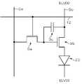
- FIG. 4is an equivalent circuit diagram showing the thin film transistor layer shown in FIG.
- FIG. 5is a cross-sectional view showing the organic EL layer shown in FIG. FIG.
- FIG. 6is a cross-sectional view showing a main configuration of the organic EL display device shown in FIG. 1A, and is a sectional view taken along line VI-VI of FIG.
- FIG. 7is a flowchart showing a manufacturing method of the organic EL display device shown in FIG.
- FIG. 8is a cross-sectional view showing a main part configuration of a modification 1 of the organic EL display device according to the first embodiment, and is a cross-sectional view corresponding to the VI-VI line cross-sectional view of FIG. 1 (a).
- FIG. 9is a flowchart showing a method of manufacturing the organic EL display device shown in FIG. FIG.
- FIG. 10is a cross-sectional view showing a main part configuration of a modification 2 of the organic EL display device according to the first embodiment, and is a cross-sectional view corresponding to the VI-VI line cross-sectional view of FIG. 1 (a).
- FIG. 11is a flowchart showing a method of manufacturing the organic EL display device shown in FIG.
- FIG. 12 (a)is an enlarged cross-sectional view showing a convex portion in the modified example 3 of the organic EL display device according to the first embodiment
- FIG. 12 (b)is an enlarged cross-sectional view showing the organic EL according to the first embodiment. It is an enlarged cross-sectional view which shows the convex part in the modification 4 of the display device.
- FIG. 12 (a)is an enlarged cross-sectional view showing a convex portion in the modified example 3 of the organic EL display device according to the first embodiment
- FIG. 12 (b)is an enlarged cross-sectional view showing the organic EL according to the first embodiment
- FIG. 13Ais a plan view showing a main configuration of the organic EL display device according to the second embodiment of the present invention
- FIG. 13Bis a region surrounded by IIb of FIG. 13A.
- FIG. 14Ais a plan view showing a main configuration of the organic EL display device according to the third embodiment of the present invention
- FIG. 14Bis a region surrounded by IIIb of FIG. 14A.
- FIG. 15 (a)is a plan view showing a configuration example of a main part of a method for manufacturing an organic EL display device according to a fourth embodiment of the present invention
- FIG. 15 (b)is a plan view showing a fourth embodiment. It is a top view which shows the modification of the manufacturing method of the organic EL display device.
- FIG. 1Ais a plan view showing a main configuration of an organic EL display device according to a first embodiment of the present invention
- FIG. 1Bis a region surrounded by Ib in FIG. 1A. It is a top view which shows the structure of the main part in.
- FIG. 2is a diagram illustrating a schematic internal configuration of a display area in the organic EL display device shown in FIG. 1 (a).
- FIG. 3is a cross-sectional view showing a main configuration of a display area in the organic EL display device shown in FIG. 1 (a).
- FIG. 4is an equivalent circuit diagram showing the thin film transistor layer shown in FIG.
- FIG. 5is a cross-sectional view showing the organic EL layer shown in FIG.
- FIG. 6is a cross-sectional view showing a main configuration of the organic EL display device shown in FIG. 1A, and is a sectional view taken along line VI-VI of FIG. 1A.
- the organic EL display device 50aincludes, for example, a rectangular display area D for displaying information and a frame area F provided around the display area D. There is. Further, in the frame area F, a terminal portion E is provided at the end of the frame area F, and wiring (not shown) provided in a plurality of light emitting elements described later that define the display area D is provided in the terminal portion. It is connected to E. Further, for example, a flexible printed circuit board (not shown) is connected to the terminal portion E, and a signal, a power supply voltage, and the like are supplied to the pixels via the flexible printed circuit board.
- a plurality of sub-pixels Pare arranged in a matrix. Specifically, in the display area D, a sub-pixel P having a red light emitting region Lr for displaying red, a sub pixel P having a green light emitting region Lg for displaying green, and a blue display. Sub-pixels P having a blue light emitting region Lb for performing the above are provided so as to be adjacent to each other.
- one pixelis composed of three adjacent sub-pixels P having a red light emitting region Lr, a green light emitting region Lg, and a blue light emitting region Lb.
- the organic EL display device 50aserves as a light emitting element provided on the base substrate 10, the thin film transistor (TFT) layer 20a provided on the base substrate 10, and the thin film transistor layer 20a.
- the organic EL element 30a of the aboveis provided.
- the base substrate 10is, for example, a plastic substrate made of polyimide resin.
- the thin film transistor layer 20aincludes a base coat film 11, semiconductor layers 14a and 14b, a gate insulating film 13, a first metal layer, a first interlayer insulating film 15, a second metal layer, and a second interlayer. It includes an insulating film 17, a third metal layer, and a flattening film 19.
- the first metal layerincludes a gate wire 12 extending in the row direction, gate electrodes 12a and 12b, and a lower conductive layer.
- the second metal layerincludes a power line (not shown) extending in the row direction and an upper conductive layer.
- the third metal layerincludes a source line Sa extending in the row direction, a power supply line Sb extending in the row direction, source electrodes 18a and 18c, and drain electrodes 18b and 18d.
- the gate line 12 and the source line Saare examples, and may be provided in another layer.
- the thin film transistor layer 20aincludes a base coat film 11 provided on the base substrate 10, a plurality of first thin film transistors 9a provided on the base coat film 11, and a plurality of second thin film transistors. It includes 9b, a plurality of capacitors 9c, each first thin film transistor 9a, each second thin film transistor 9b, and a flattening film 19 provided on each capacitor 9c.
- a plurality of gate lines 12are provided so as to extend parallel to each other in the lateral direction in the drawing.
- the thin film transistor layer 20aas shown in FIGS.
- each subpixel Pis provided with a first thin film transistor 9a, a second thin film transistor 9b, and a capacitor 9c, respectively.
- the base coat film 11is composed of, for example, a single-layer film or a laminated film of an inorganic insulating film such as silicon nitride, silicon oxide, or silicon oxynitride.
- the first thin film transistor 9ais connected to the corresponding gate line 12 and the source line Sa in each sub-pixel P. Further, as shown in FIG. 3, the first thin film transistor 9a includes a gate electrode 12a, a gate insulating film 13, a semiconductor layer 14a, a first interlayer insulating film 15, and a second interlayer insulating film 17 provided in this order on the base coat film 11. , And a source electrode 18a and a drain electrode 18b.
- the gate electrode 12ais provided in an island shape on the base coat film 11. Further, as shown in FIG. 3, the gate insulating film 13 is provided so as to cover the gate electrode 12a. Further, as shown in FIG. 3, the semiconductor layer 14a is provided on the gate insulating film 13 so as to overlap the gate electrode 12a, and has a channel region overlapping the gate electrode 12a and a source region arranged with the channel region interposed therebetween. And a drain region.
- the first interlayer insulating film 15 and the second interlayer insulating film 17are provided in order so as to cover the channel region of the semiconductor layer 14a.
- the source electrode 18a and the drain electrode 18bare provided on the second interlayer insulating film 17 so as to be separated from each other.
- the source electrode 18a and the drain electrode 18bare the sources of the semiconductor layer 14a via the contact holes formed in the laminated film of the first interlayer insulating film 15 and the second interlayer insulating film 17. It is connected to the region and the drain region, respectively.
- the gate insulating film 13, the first interlayer insulating film 15, and the second interlayer insulating film 17are made of, for example, a single-layer film or a laminated film of an inorganic insulating film such as silicon nitride, silicon oxide, or silicon oxynitride. ..
- the second thin film transistor 9bis connected to the corresponding first thin film transistor 9a and the power supply line Sb in each sub-pixel P.
- the first thin film transistor 9bincludes a gate electrode 12b, a gate insulating film 13, a semiconductor layer 14b, a first interlayer insulating film 15, and a second interlayer insulating film 17 provided in this order on the base coat film 11. , And a source electrode 18c and a drain electrode 18d.
- the gate electrode 12bis provided in an island shape on the base coat film 11. Further, as shown in FIG. 3, the gate insulating film 13 is provided so as to cover the gate electrode 12b. Further, as shown in FIG. 3, the semiconductor layer 14b is provided on the gate insulating film 13 so as to overlap the gate electrode 12b, and has a channel region overlapping the gate electrode 12b and a source region arranged with the channel region interposed therebetween. And a drain region.
- the first interlayer insulating film 15 and the second interlayer insulating film 17are provided in order so as to cover the channel region of the semiconductor layer 14b.
- the source electrode 18c and the drain electrode 18dare provided on the second interlayer insulating film 17 so as to be separated from each other.
- the source electrode 18c and the drain electrode 18dare the sources of the semiconductor layer 14b via the contact holes formed in the laminated film of the first interlayer insulating film 15 and the second interlayer insulating film 17. It is connected to the region and the drain region, respectively.
- the first thin film transistor 9a and the second thin film transistor 9bmay be top gate type thin film transistors.
- the capacitor 9cis connected to the corresponding first thin film transistor 9a and the power supply line Sb in each sub-pixel P.
- the capacitor 9cis a gate insulating film provided in order so as to cover the lower conductive layer 12c which is the same layer as the gate electrode 12a and is formed of the same material and the lower conductive layer 12c.
- the 13 and the first interlayer insulating film 15 and the upper conductive layer 16 provided on the first interlayer insulating film 15 so as to overlap the lower conductive layer 12care provided.
- the upper conductive layer 16is also called a capacitive wiring.
- the flattening film 19is made of a colorless and transparent organic resin material such as an acrylic resin, a polyimide resin, or an epoxy resin.
- the organic EL element 30aincludes a plurality of first electrodes 21, edge covers 22, a plurality of organic EL layers 23, and a second electrode 24, which are sequentially provided on the flattening film 19. ..
- the plurality of first electrodes 21are provided in a matrix on the flattening film 19 so as to correspond to the plurality of sub-pixels P.
- the first electrode 21is an anode of the organic EL element 30a, and as shown in FIG. 3, is connected to the drain electrode 18d of each second thin film transistor 9b via a contact hole Ca formed in the flattening film 19. Has been done.
- the first electrode 21is electrically connected to the power supply line Sb via the second thin film transistor 9b as a driving transistor of the organic EL element 30a (see FIG. 4).
- the first electrode 21has a function of injecting holes into the organic EL layer 23.
- the first electrode 21is more preferably formed of a material having a large work function in order to improve the hole injection efficiency into the organic EL layer 23.
- examples of the material constituting the first electrode 21include silver (Ag), aluminum (Al), vanadium (V), cobalt (Co), nickel (Ni), tungsten (W), and gold. (Au), Titanium (Ti), Ruthenium (Ru), Manganese (Mn), Indium (In), Ytterbium (Yb), Lithium Fluoride (LiF), Platinum (Pt), Palladium (Pd), Molybdenum (Mo) , Iridium (Ir), tin (Sn) and other metal materials. Further, the material constituting the first electrode 21 may be, for example, an alloy such as astatine (At) / oxidized astatine (AtO 2 ).
- the material constituting the first electrode 21is, for example, a conductive oxide such as tin oxide (SnO), zinc oxide (ZnO), indium tin oxide (ITO), or indium zinc oxide (IZO). There may be. Further, the first electrode 21 may be formed by laminating a plurality of layers made of the above materials. Examples of the compound material having a large work function include indium tin oxide (ITO) and indium zinc oxide (IZO).
- the edge cover 22is provided in a grid pattern so as to cover the peripheral edge of each first electrode 21. That is, as illustrated in FIG. 3, the edge cover 22 has an opening 22k that exposes the first electrode 21, and also covers the edge of the first electrode 22.
- the material constituting the edge cover 22include organic resin materials such as polyimide resin, acrylic resin, polysiloxane resin, and novolak resin.
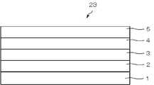
- each organic EL layer 23includes a hole injection layer 1, a hole transport layer 2, a light emitting layer 3, an electron transport layer 4, and an electron injection layer, which are sequentially provided on the first electrode 21. It has 5.
- the hole injection layer 1is also called an anode buffer layer, and has a function of bringing the energy levels of the first electrode 21 and the organic EL layer 23 closer to each other and improving the hole injection efficiency from the first electrode 21 to the organic EL layer 23. Have.
- the hole transport layer 2has a function of improving the hole transport efficiency from the first electrode 21 to the organic EL layer 23.
- the electron transport layer 4has a function of efficiently moving electrons to the light emitting layer 3.
- the electron injection layer 5has a function of bringing the energy levels of the second electrode 24 and the organic EL layer 23 closer to each other and improving the efficiency of injecting electrons from the second electrode 24 into the organic EL layer 23.
- the drive voltage of the organic EL element 30can be lowered.
- the electron injection layer 5is also called a cathode buffer layer.
- a functional layeris provided between the first electrode 21 and the second electrode 24.
- This functional layerincludes the hole injection layer 1, the hole transport layer 2, the light emitting layer 3, the electron transport layer 4, and the electron injection layer 5.
- the functional layermay have, for example, a three-layer laminated structure of a hole injection layer / hole transport layer, a light emitting layer, and an electron transport layer / electron injection layer.
- the second electrode 24is the cathode of the organic EL element 30a, and is provided so as to cover each organic EL layer 23 and the edge cover 22 as shown in FIG. Further, the second electrode 24 is provided in common to the plurality of organic EL elements 30a, and constitutes a low power supply voltage electrode (ELVSS). Further, the second electrode 24 is connected to a low power supply voltage source (not shown) via the terminal portion E. Further, the second electrode 24 has a function of injecting electrons into the organic EL layer 23. Further, the second electrode 24 is more preferably made of a material having a small work function in order to improve the efficiency of electron injection into the organic EL layer 23.
- examples of the material constituting the second electrode 24include silver (Ag), aluminum (Al), vanadium (V), cobalt (Co), nickel (Ni), tungsten (W), and gold.
- AuCalcium (Ca), Titanium (Ti), Yttrium (Y), Sodium (Na), Ruthenium (Ru), Manganese (Mn), Indium (In), Magnesium (Mg), Lithium (Li), Ytterbium (Yb), lithium fluoride (LiF) and the like can be mentioned.
- the second electrode 24is, for example, magnesium (Mg) / copper (Cu), magnesium (Mg) / silver (Ag), sodium (Na) / potassium (K), asstatin (At) / oxidized asstatin (AtO 2). ), Lithium (Li) / Aluminum (Al), Lithium (Li) / Calcium (Ca) / Aluminum (Al), Lithium Fluoride (LiF) / Calcium (Ca) / Aluminum (Al), etc. You may.
- the second electrode 24may be formed of, for example, a conductive oxide such as tin oxide (SnO), zinc oxide (ZnO), indium tin oxide (ITO), and indium zinc oxide (IZO). .. Further, the second electrode 24 may be formed by laminating a plurality of layers made of the above materials.
- Examples of materials having a small work functioninclude magnesium (Mg), lithium (Li), lithium fluoride (LiF), magnesium (Mg) / copper (Cu), magnesium (Mg) / silver (Ag), and sodium.
- (Na) / potassium (K)lithium (Li) / aluminum (Al), lithium (Li) / calcium (Ca) / aluminum (Al), lithium fluoride (LiF) / calcium (Ca) / aluminum (Al) And so on.
- the sealing layer 28is provided so as to cover a plurality of organic EL elements (light emitting elements) 30a in the organic EL display device 50a. Further, as shown in FIG. 3, the sealing layer 28 is provided on the first sealing inorganic insulating film 25 provided so as to cover the second electrode 24 and the first sealing inorganic insulating film 25. It includes a sealing organic insulating film 26 and a second sealing inorganic insulating film 27 provided so as to cover the sealing organic insulating film 26, and has a function of protecting the organic EL layer 23 from moisture, oxygen, and the like. There is.
- the first sealing inorganic insulating film 25is provided on a plurality of organic EL elements 30a. Further, the second sealing inorganic insulating film 27 is provided above the sealing organic insulating film 26, and is formed so as to seal the sealing organic insulating film 26 together with the first sealing inorganic insulating film 25. There is. Further, the first sealed inorganic insulating film 25 and the second sealed inorganic insulating film 27 are formed by, for example, a CVD (Chemical vapor Deposition) method using CMM (Common Metal Mask), and are, for example, oxidized.
- CVDChemical vapor Deposition
- CMMCommon Metal Mask
- Inorganic materialssuch as silicon nitride (SiNx (x is a positive number)), silicon nitride (SiCN), such as silicon (SiO 2 ), aluminum oxide (Al 2 O 3 ), trisilicon tetroxide (Si 3 N 4 ). It is composed of.
- the sealing organic insulating film 26is made of an organic material that can be applied by an inkjet method, such as acrylic resin, epoxy resin, silicone resin, polyurea resin, parylene resin, polyimide resin, and polyamide resin. Further, as illustrated in FIG. 3, the film thickness of the sealing organic insulating film 26 is thicker than the film thickness of the first sealing inorganic insulating film 25 and the film thickness of the second sealing inorganic insulating film 27. It is configured. Specifically, the first sealing inorganic insulating film 25 and the second sealing inorganic insulating film 27 are each formed, for example, with a film thickness of 1 ⁇ m. On the other hand, the sealing organic insulating film 26 is formed, for example, with a film thickness of 10 ⁇ m.
- the organic EL display device 50ahas a frame-shaped first bank 45 surrounding the display area D and a frame-shaped second bank 45 surrounding the first bank 45 in the frame area F.
- a bank 46is provided, and the first bank 45 and the second bank 46 regulate the wet spread of the sealing organic insulating film 26 applied by an inkjet method or the like.
- the edge 26e (FIG. 6) of the sealing organic insulating film 26is defined by a bank.
- the bankalso includes a first bank 45 and a second bank 46. In this way, by providing the first bank 45 and the second bank 46 as banks, the wet spread of the sealing organic insulating film 26 can be more reliably regulated.
- the first bank 45is formed of, for example, the same layer as the flattening film 19 and made of the same material. Further, as illustrated in FIG. 6, the first bank 45 is configured to overlap with the edge 26e of the sealing organic insulating film 26. Further, as shown by the alternate long and short dash line in FIG. 1A, the second electrode 24 is provided so as to cover the display area D in a plan view and between the first bank 45 and the display area D. Has been done.
- the second bank 46is, for example, the same layer as the flattening film 19, the lower bank 46a formed of the same material, and the same layer as the edge cover 22 (FIG. 3). Moreover, it is formed of the same material and includes an upper layer bank 46b laminated on the lower layer bank 46a.
- the edge 25e of the first sealing inorganic insulating film 25 and the edge 27e of the second sealing inorganic insulating film 27are formed in the frame region F ( In FIG. 1A), it is located outside the edge 26e of the sealing organic insulating film 26. Further, as shown in FIG. 6, since the edge 27e of the second sealing inorganic insulating film 27 is located outside the edge 25e of the first sealing inorganic insulating film 25, the sealing layer 28 (FIG. 6). In 3), the second sealing inorganic insulating film 27 of the outermost layer covers the plurality of organic EL elements 30a, and the sealing performance for each organic EL element 30a can be reliably improved.
- the organic EL display device 50ahas a frame-shaped convex portion 70 so as to surround the first bank 45 and the second bank 46 in the frame area F. Is provided. Further, as illustrated in FIG. 1B, the convex portion 70 is configured to be larger than the metal body 70a in a plan view with the frame-shaped metal body 70a, and is superimposed on the metal body 70a. Includes a frame-shaped resin layer 70b. Further, the height H0 of the convex portion 70 is higher than the height H1 of the first bank 45 and the same height as the height H2 of the second bank 46, preferably the height, as illustrated in FIG. It is set to a height of H2 or higher.
- the metal body 70ais electrically configured to be in a float state, and an electric charge is present (localized) inside the metal body 70a, and particles can be attracted (sucked) by the electrostatic force of the electric charge.
- the metal body 70ais, for example, the same layer as the source line Sa included in the thin film transistor layer 20a, and is made of the same material. That is, the metal body 70a is the same layer as the metal layer (source line Sa) that abuts on the flattening film 19 among the metal layers contained in the thin film transistor layer 20a, and is made of the same material. Contact the part.
- the float state referred to heremeans that the metal body 70a does not contribute to the display and is not directly and electrically connected to the signal line for display.
- the metal body 70amay be connected to the frame region F or a guard ring (not shown) provided on the mother substrate described later. By being connected to the guard ring in this way, it can be used as a countermeasure against electrostatic discharge in the organic EL display device 50a.
- the resin layer 70bis made of, for example, a resin material, and particles attracted by the metal body 70a are attached to the surface of the resin layer 70b to capture the particles.
- the resin layer 70bhas, for example, a flattening film portion 70b1 provided so as to cover the metal body 70a, and an edge overlapping the metal body 70a and the flattening film portion 70b1. Includes a cover portion 70b2.
- the flattening film portion 70b1is, for example, the same layer as the flattening film 19 and is formed of the same material
- the edge cover portion 70b2is, for example, the same layer as the edge cover 22 (FIG. 3) and is made of the same material. Is formed by.
- the convex portion 70is provided so as to be covered by the flattening film portion 70b1 in a state where the metal body 70a is in contact with the flattening film portion 70b1, particles attracted by the metal body 70a can be more attracted. It can be easily captured. Further, in the convex portion 70, by providing the flattening film portion 70b1 and the edge cover portion 70b2 on the resin layer 70b, the surface area of the convex portion 70 is increased to facilitate the adhesion of particles, and the electricity of the convex portion 70 is increased. The capacitance can be increased to further increase the electrostatic force of the metal body 70a, and the force for attracting particles can be further improved.
- the height H0 of the convex portion 70is not limited to the above description, and may be lower than the height H1 of the first bank 45, for example. However, as described above, the particles can be more easily captured when the height H0 of the convex portion 70 is equal to or higher than the height H1 of the first bank 45 and the height H2 of the second bank 46. It is preferable in that.
- the second electrode 24is the first electrode 21. It is electrically connected to the electrode conductive portion A1 which is in the same layer as the above and is made of the same material.
- the electrode conductive portion A1is the same layer as the wiring layer of the thin film transistor layer 20a (FIG. 3), for example, the source wire Sa, and is formed of the same material as the wiring conductive portion S1. It is electrically connected in the frame area F.
- the wiring conduction portion S1is electrically connected to the above-mentioned low power supply voltage source via the routing wiring and the terminal portion E (not shown), and the low power supply voltage source and the second electrode 24 are electrically connected to each other.
- the organic EL display device 50a described aboveturns on the first thin film transistor 9a by inputting a gate signal to the first thin film transistor 9a via the gate line 12 in each subpixel P, and turns on the first thin film transistor 9a and sets the first thin film transistor 9a through the source line Sa.
- a predetermined voltage corresponding to the source signalis written to the gate electrode 12b of the two thin film transistors 9b and the capacitor 9c, and the current from the specified power supply line Sb is supplied to the organic EL layer 23 based on the gate voltage of the second thin film transistor 9b.
- the light emitting layer 3 of the organic EL layer 23emits light to display information.
- the organic EL display device 50aeven if the first thin film transistor 9a is turned off, the gate voltage of the second thin film transistor 9b is held by the capacitor 9c, so that the light emitting layer is used until the gate signal of the next frame is input. The light emission by 3 is maintained.
- FIG. 7is a flowchart showing a manufacturing method of the organic EL display device shown in FIG.
- the method for manufacturing the organic EL display device 50aincludes a thin film transistor F layer forming step S1, an organic EL element forming step S2, a sealing layer forming step S3, a flexible step S4, and a dividing step S5. And the mounting step S6.
- a multi-chamfering method using a mother substrate(see FIG. 14 described later) is adopted for manufacturing the organic EL display device 50a, and each of the above steps is carried out using the mother substrate.
- the mother substrateis a substrate to be the base substrate 10, and as will be described in detail later, a plurality of panel constituent regions constituting the display panel included in the organic EL display device 50a are included.
- the thin film transistor layer forming step S1includes a base coat film forming step S11, a gate electrode forming step S12, a gate insulating film forming step S13, a semiconductor layer forming step S14, an interlayer insulating film forming step S15, and a source / drain electrode forming step S16. And the flattening film forming step S17.
- the base coat film forming step S11on the surface of the mother substrate, for example, silicon oxide (SiOx), silicon nitride (SiNx), silicon oxynitride (SiOxNy; x> y), silicon nitride (SiNxOy; An inorganic insulating film such as x> y) is formed to form the base coat film 11.
- a titanium film, an aluminum film, and a titanium filmare sequentially formed on the mother substrate on which the base coat film 11 is formed by, for example, a sputtering method to form a laminated conductive film, and then the laminated conductive film is formed.
- the laminated conductive filmis patterned by photolithography to form gate electrodes 12a and 12b.
- the gate wire 12 and various routing wiresare also formed.
- a gate insulating film 13is formed by forming an inorganic insulating film such as silicon (SiNxOy; x> y) in a single layer or in a laminated manner.
- a semiconductor filmis formed on the mother substrate on which the gate insulating film 13 is formed, for example, by a CVD method, and the semiconductor film is subjected to crystallization treatment or low resistance as necessary.
- the semiconductor filmis patterned by photolithography (resist coating, prebaking treatment, exposure treatment, development treatment, post-baking treatment, etching treatment and resist peeling treatment) to form semiconductor layers 14a and 14b. ..
- silicon oxide (SiOx), silicon nitride (SiNx), and silicon oxynitride (SiOxNy; x>are placed on the mother substrate on which the semiconductor layers 14a and 14b are formed, for example, by a CVD method.
- an inorganic insulating filmsuch as silicon nitride oxide (SiNxOy; x> y) is formed to form the first interlayer insulating film 15.
- the second interlayer insulating film 17is formed by forming an inorganic insulating film such as
- the interlayer insulating film forming step S15includes an upper conductive layer forming step of forming the upper conductive layer 16 provided between the first interlayer insulating film 15 and the second interlayer insulating film 17.
- a titanium film, an aluminum film, and a titanium filmare sequentially formed on the mother substrate on which the second interlayer insulating film 17 is formed by, for example, a sputtering method to form a laminated conductive film.
- the laminated conductive filmis patterned by photolithography to form the source electrode 18a and the drain electrode 18b.
- the source wire Sa and the likeare also formed from the laminated electric film forming the source electrode 18a and the drain electrode 18b.
- the metal body forming step for forming the metal body 70a included in the convex portion forming step for forming the convex portion 70is performed at the same time. That is, by patterning the laminated electric film forming the source electrode 18a and the drain electrode 18b, the metal body 70a is formed in the same layer as the source wire Sa and made of the same material.
- a photosensitive resin materialsuch as a polyimide resin is applied onto the mother substrate on which the source electrode 18a and the drain electrode 18b are formed by a known coating method such as a spin coating method or an inkjet method. Is applied. Then, the coating film of the photosensitive resin material is subjected to prebaking treatment, exposure treatment, developing treatment and post-baking treatment, and the coating film is patterned to form the flattening film 19. At this time, the lower bank 46a of the first bank 45 and the second bank 46 is also formed from the coating film forming the flattening film 19.
- the flattening film portion forming step for forming the flattening film portion 70b1 of the resin layer 70b, which is included in the convex portion forming step for forming the convex portion 70is simultaneously performed. That is, by patterning the coating film, the flattening film portion 71b1 is formed in the same layer as the flattening film 19 and made of the same material.
- the thin film transistor layer 20ais formed.
- the organic EL element forming step S2includes a first electrode forming step S21, an edge cover forming step S22, an organic EL layer forming step S23, and a second electrode forming step S24.
- the organic EL element forming step S2is an example of a light emitting element forming step.
- an indium tin oxide (ITO) film, a silver alloy film, and an indium tin oxide (ITO) filmare sequentially formed on the mother substrate on which the thin film transistor layer 20a is formed, for example, by a sputtering method.
- a filmis formed to form a laminated conductive film.
- the laminated conductive filmis patterned by photolithography to form the first electrode 21.
- a photosensitive resin materialsuch as a polyimide resin is applied onto the mother substrate on which the first electrode 21 is formed by a known coating method such as a spin coating method. Then, the coating film of the photosensitive resin material is subjected to prebaking treatment, exposure treatment, developing treatment and post-baking treatment, and the coating film is patterned to form the edge cover 22. At this time, the upper bank 46b of the second bank 46 is also formed from the coating film forming the edge cover 22.
- the edge cover portion forming step for forming the edge cover portion 70b2 of the resin layer 70b, which is included in the convex portion forming step for forming the convex portion 70is performed at the same time. That is, by patterning the coating film, the edge cover portion 71b2 is formed in the same layer as the edge cover 22 and made of the same material.
- the hole injection layer 1 and the hole transportare carried out on the mother substrate on which the edge cover 22 is formed by using a known FMM (Fine Metal Mask), for example, by a vacuum deposition method.
- the layer 2, the light emitting layer 3, the electron transport layer 4, and the electron injection layer 5are formed in this order to form the organic EL layer 23 on each first electrode 21.
- a silver alloy filmis formed on the mother substrate on which the organic EL layer 23 is formed by using a CMM that can be patterned for each display panel, for example, by a vacuum vapor deposition method.
- the second electrode 24is formed in common with the plurality of organic EL elements 30a.
- a plurality of organic EL elements (light emitting elements) 30aare formed on the thin film transistor layer 20a.
- the sealing layer forming step S3first, silicon oxide (SiOx), silicon nitride (SiNx), and silicon oxynitride (SiOxNy) are used on the mother substrate on which the organic EL element 30a is formed, for example, by a CVD method.
- the first sealing inorganic insulating film 25is formed by forming an inorganic insulating film such as x> y) or silicon nitride (SiNxOy; x> y) in a single layer or in a laminated manner.
- an organic materialsuch as an acrylic resin is applied to the mother substrate on which the first sealing inorganic insulating film 25 is formed, for example, by an inkjet method to form the sealing organic insulating film 26.
- an organic materialsuch as an acrylic resin is applied to the mother substrate on which the first sealing inorganic insulating film 25 is formed, for example, by an inkjet method to form the sealing organic insulating film 26.
- the outward spread of the applied organic material in the frame region Fis blocked by the first bank 45, and the sealing organic insulating film 26 is formed inside the first bank 45.
- a second sealing inorganic insulating film 27is formed by forming an inorganic insulating film such as silicon nitride oxide (SiNxOy; x> y) in a single layer or in a laminated manner.
- the sealing layer 28 in which the first sealing inorganic insulating film 25, the sealing organic insulating film 26, and the second sealing inorganic insulating film 27 are laminatedis organic. It is formed so as to cover the EL element 30a.
- each of the first sealing inorganic insulating film 25 and the second sealing inorganic insulating film 27 formed by the CVD methodis a ground electrode (not shown) in which the mother substrate performs the CVD method. It is performed in contact with.
- an electric field (electrostatic force) due to the electric charge in the metal body 70acan be reliably formed between the metal body 70a and the ground electrode. The particles can be reliably attracted to the metal body 70a.
- a protective sheet(not shown) is attached to the surface of the mother substrate on which the sealing layer 28 is formed, and then the lower surface of the mother substrate is irradiated with laser light from the glass substrate side.
- the glass substrateis peeled off from the lower surface of the mother substrate, and a protective sheet (not shown) is attached to the lower surface of the mother substrate from which the glass substrate has been peeled off.
- the mother substrate from which the glass substrate has been peeled offis divided into display panel units by irradiation with laser light.
- the dividing line DL when dividing the mother substrateis a boundary between each panel constituent area and its outer region, and is a portion corresponding to the outer edge of each panel constituent area (see FIG. 14 described later). ..
- the FPCis connected to the terminal portion E to the display panel obtained by dividing the mother board.
- the organic EL display device 50acan be manufactured.
- the convex portion 70is provided so as to surround the first bank 45 and the second bank 46 in the frame area F.
- the convex portion 70includes a metal body 70a that is electrically in a float state and a resin layer 70b that overlaps the metal body 70a.
- the particlescan be attracted to the metal body 70a by the electrostatic force due to the electric charge in the metal body 70a, and the attracted particles can be captured by the resin layer 70b.
- the present embodimentprovides a highly reliable organic EL display device (display device) 50a capable of preventing deterioration of the sealing performance of the sealing layer 28 due to particles, and a method for manufacturing the same. Can be done.
- FIG. 8is a cross-sectional view showing a main part configuration of a modification 1 of the organic EL display device according to the first embodiment, and is a cross-sectional view corresponding to the VI-VI line cross-sectional view of FIG. 1 (a).
- FIG. 9is a flowchart showing a method of manufacturing the organic EL display device shown in FIG.
- the difference between the present embodiment and the first embodimentis that instead of the metal body 70a of the convex portion 70, the metal body 70c of the convex portion 70 is in the same layer as the gate wire 12 and is made of the same material. It is a point that provided.
- the elements common to the first embodimentare designated by the same reference numerals, and the duplicated description thereof will be omitted.
- the convex portion 70has a metal body 70c formed so as to be covered with the gate insulating film 13 on the base coat film 11.
- the metal body 70cis formed in a frame shape so as to surround the second bank 46. Further, as described above, the metal body 70c is the same layer as the gate wire 12 and is made of the same material, and is below the resin layer 70b (on the base substrate 10 side) so as to overlap the resin layer 70b. It is provided in.
- the metal body forming step for forming the metal body 70c included in the convex portion forming step for forming the convex portion 70is simultaneously performed. .. That is, by patterning the laminated electric film forming the gate electrode 12a and the gate 12b, the metal body 70c is formed in the same layer as the gate wire 12 and made of the same material. Further, in the present embodiment, unlike the first embodiment, the source / drain electrode forming step S36 does not include the metal body forming step.
- the convex portionis the same layer as any one of the plurality of metal layers and is made of the same material.
- Metal bodiescan be constructed. As described above, by forming the metal body of the convex portion in the same layer as any one metal layer contained in the thin film transistor layer 20a and using the same material, the organic EL display device is thinned and the manufacturing process is simplified. It is preferable in that it can be easily converted.
- FIG. 10is a cross-sectional view showing a main part configuration of a modification 2 of the organic EL display device according to the first embodiment, and is a cross-sectional view corresponding to the VI-VI line cross-sectional view of FIG. 1 (a).
- FIG. 11is a flowchart showing a method of manufacturing the organic EL display device shown in FIG.
- the difference between the present embodiment and the first embodimentis that instead of the metal body 70a of the convex portion 70, the metal body of the convex portion 70 is in the same layer as the first electrode 21 and is made of the same material. It is a point where 70d is provided.
- the elements common to the first embodimentare designated by the same reference numerals, and the duplicated description thereof will be omitted.
- the convex portion 70has a metal body 70d formed so as to cover the flattening film portion 70b1.
- the metal body 70dis formed in a frame shape so as to surround the second bank 46. Further, as described above, the metal body 70d is the same layer as the first electrode 21 and is made of the same material, and is provided between the flattening film portion 70b1 and the edge cover portion 70b2 of the resin layer 70b. ing.
- the metal body forming step for forming the metal body 70d included in the convex portion forming step for forming the convex portion 70is performed at the same time. Be told. That is, by patterning the laminated electric film forming the first electrode 21, the metal body 70d is formed in the same layer as the first electrode 21 and made of the same material. Further, in the present embodiment, unlike the first embodiment, the source / drain electrode forming step S46 does not include the metal body forming step.
- the convex portion 70can be formed by forming the first sealing inorganic insulating film 25 so as to cover the metal body 70d without providing the edge cover portion 70b2.
- FIG. 12 (a)is an enlarged cross-sectional view showing a convex portion in the modified example 3 of the organic EL display device according to the first embodiment
- FIG. 12 (b)is an enlarged cross-sectional view showing the organic EL according to the first embodiment. It is an enlarged cross-sectional view which shows the convex part in the modification 4 of the display device.
- the difference between the present embodiment and the second modificationis that the metal body 70d of the convex portion 70 is in contact with the first sealing inorganic insulating film 25 with respect to the first sealing inorganic insulating film 25. It is an exposed point.
- the elements common to the above modification 2are designated by the same reference numerals, and the duplicated description thereof will be omitted.
- the metal body 70d of the convex portion 70is different from that of the second modification, and is not covered with the edge cover portion 70b2, and is the first sealed inorganic material. It is exposed to the insulating film 25 and is in contact with the first sealing inorganic insulating film 25.
- the edge cover portion 70b2is not provided, and the metal body 70d of the convex portion 70 has an upper surface thereof. The entire surface is covered with the first sealing inorganic insulating film 25 and is in contact with the first sealing inorganic insulating film 25.
- FIG. 13Ais a plan view showing a main configuration of the organic EL display device according to the second embodiment of the present invention
- FIG. 13Bis a region surrounded by IIb of FIG. 13A. It is a top view which shows the structure of the main part in.
- the convex portion 80is provided instead of the frame-shaped convex portion 70.
- the elements common to the first embodimentare designated by the same reference numerals, and the duplicated description thereof will be omitted.
- a convex portion 80is provided in the frame region F so as to surround the second bank 46. Further, as illustrated in FIG. 13B, the convex portion 80 includes a plurality of island-shaped metal bodies 80a and a plurality of island-shaped resin layers 80b. Each of the plurality of metal bodies 80a is electrically in a float state, similarly to the metal bodies of the above-described embodiments. Further, the plurality of resin layers 80b are superimposed on the metal body 80a, similarly to the resin layers of the above-described embodiments.
- FIG. 14Ais a plan view showing a main configuration of the organic EL display device according to the third embodiment of the present invention
- FIG. 14Bis a region surrounded by IIIb of FIG. 14A. It is a top view which shows the structure of the main part in.
- the convex portion 90is provided instead of the frame-shaped convex portion 70.
- the elements common to the first embodimentare designated by the same reference numerals, and the duplicated description thereof will be omitted.
- a convex portion 90is provided in the frame region F so as to surround the second bank 46.
- the convex portion 90includes a frame-shaped metal body 90a and a plurality of island-shaped resin layers 90b.
- the metal body 90ais electrically in a float state like the metal body of each of the above-described embodiments.
- the plurality of resin layers 90bare superimposed on the metal body 90a as in the case of the resin layers of the above-described embodiments.
- FIG. 15 (a)is a plan view showing a configuration example of a main part of a method for manufacturing an organic EL display device according to a fourth embodiment of the present invention
- FIG. 15 (b)is a plan view showing a fourth embodiment. It is a top view which shows the modification of the manufacturing method of the organic EL display device.
- the convex portion 110is provided instead of the frame-shaped convex portion 70.
- the elements common to the first embodimentare designated by the same reference numerals, and the duplicated description thereof will be omitted.
- each panel constituent region PRincludes a portion constituting the display region D and a portion constituting the frame region F including the terminal portion E.
- Such a mother substrate 60is used in manufacturing an organic EL display device in a state of being formed on a glass substrate.
- the dividing step S5 for dividing the mother substrate 60 into the display panel unitsis performed.
- this dividing step S5as shown by the alternate long and short dash line in FIG. 15A, division is performed along the dividing line DL. Further, the convex portion having the metal body and the resin layer is provided along the dividing line DL.
- the rectangular convex portion 110is between the two vertical division lines DL in the figure and the two horizontal division lines DL in the figure. Is formed between.
- the configurationmay be such that the rectangular convex portion 120 is provided.
- the positional relationship and shape between the dividing line DL and the convex portionare not limited to those described above, and are not limited as long as the convex portion is provided along the dividing line DL.
- the dividing line DL and the convex portiondo not overlap with each other in that particle scattering during division can be avoided.
- the number of dividing linescan be easily reduced. It is preferable in that the display panel can be manufactured.
- an organic EL display devicehaving a resin layer including a flattening film portion and an edge cover portion has been exemplified, but the present invention is not limited to this, and for example, a flattening film.
- the resin layer of the convex portionmay be formed by only one of the portion and the edge cover portion.
- an organic EL display devicein which the first electrode is used as an anode and the second electrode is used as a cathode is illustrated, but in the present invention, the laminated structure of the organic EL layer is inverted and the first electrode is used as a cathode.
- the present inventioncan also be applied to an organic EL display device using the second electrode as an anode.
- an organic EL display deviceincluding an element substrate having an electrode of the thin film transistor connected to the first electrode as a drain electrode is illustrated, but the present invention illustrates the thin film transistor connected to the first electrode. It can also be applied to an organic EL display device provided with an element substrate called an electrode as a source electrode.
- the organic EL display devicehas been described as an example of the display device, but the present invention can be applied to a display device including a plurality of light emitting elements driven by an electric current.
- the present inventioncan be applied to a display device provided with a QLED (Quantum-dot light emission diode) which is a light emitting element using a quantum dot-containing layer.
- QLEDQuantum-dot light emission diode
- the present inventionis useful for a highly reliable display device capable of preventing deterioration of the sealing performance of the sealing layer due to particles, and a method for manufacturing the display device.
Landscapes
- Chemical & Material Sciences (AREA)
- Inorganic Chemistry (AREA)
- Physics & Mathematics (AREA)
- General Physics & Mathematics (AREA)
- Engineering & Computer Science (AREA)
- Theoretical Computer Science (AREA)
- Electroluminescent Light Sources (AREA)
Abstract
Description
Translated fromJapanese本発明は、表示装置、及び表示装置の製造方法に関するものである。The present invention relates to a display device and a method for manufacturing the display device.
液晶表示装置に代わる表示装置として、有機EL(electroluminescence)素子(発光素子)を用いた自発光型の有機EL表示装置が注目されている。ここで、有機EL表示装置には、例えば、下記特許文献1に記載されているように、複数の有機EL素子がマトリクス状に配置されており、情報を表示する表示領域が複数の有機EL素子により規定されている。また、有機EL表示装置の各有機EL素子には、陽極と、陰極と、これらの陽極と陰極との間に挟まれるとともに、有機材料からなる有機EL層(発光層)を有する機能層とが設けられている。また、有機EL表示装置では、水分や酸素等の浸入による有機EL素子の劣化を抑制するために、封止層によって有機EL素子を覆う封止構造が設けられている。As a display device that replaces the liquid crystal display device, a self-luminous organic EL display device that uses an organic EL (electroluminescence) element (light emitting element) is attracting attention. Here, in the organic EL display device, for example, as described in
ところで、上記のような従来の有機EL表示装置では、その上記封止構造として、一般的に、無機材料からなる封止無機絶縁膜と、有機材料からなる封止有機絶縁膜とを交互に積層している。具体的には、従来の有機EL表示装置では、例えば、有機EL素子を覆うように、CVD法により、窒化シリコン(SiNx)、酸化シリコン(SiO2)、又は炭窒化ケイ素(SiCN)等の無機材料からなる第1封止無機絶縁膜を成膜する。次に、第1封止無機絶縁膜を覆うように、インクジェット方式により、ポリイミド樹脂等の有機材料からなる封止有機絶縁膜を成膜する。続いて、封止有機絶縁膜を覆うように、CVD法により、上記無機材料からなる第2封止無機絶縁膜を成膜して、封止層(TFE層)を設けていた。By the way, in the conventional organic EL display device as described above, as the sealing structure thereof, generally, a sealing inorganic insulating film made of an inorganic material and a sealing organic insulating film made of an organic material are alternately laminated. are doing. Specifically, in the conventional organic EL display device, for example, an inorganic substance such as silicon nitride (SiNx), silicon oxide (SiO2 ), or silicon nitride (SiCN) is used by a CVD method so as to cover the organic EL element. A first sealing inorganic insulating film made of a material is formed. Next, a sealing organic insulating film made of an organic material such as a polyimide resin is formed by an inkjet method so as to cover the first sealing inorganic insulating film. Subsequently, a second sealing inorganic insulating film made of the above-mentioned inorganic material was formed by a CVD method so as to cover the sealing organic insulating film, and a sealing layer (TFE layer) was provided.
ところが、上記のような従来の有機EL表示装置では、パーティクル(異物)に起因して封止層の封止性能が低下することがあり、発光素子の寿命低下が発生して、表示装置の信頼性が損なわれるという問題を生じることがあった。具体的にいえば、第1封止無機絶縁膜はCVD法によって成膜されていたので、当該CVD法を行った際に生じる上記パーティクルが表示領域内の発光素子上や封止有機絶縁膜のエッジを規定するバンク上に付着することがあった。この結果、第1封止無機絶縁膜にパーティクルによる欠陥が生じることがあった。更に、バンク上にパーティクルが付着した場合には、当該付着した箇所において、第2封止無機絶縁膜に欠陥が生じることがあり、当該欠陥を介して水分や酸素等が封止有機絶縁膜内に浸入し、更に第1封止無機絶縁膜に生じた欠陥に達すると、その欠陥近傍の発光素子にダメージを与えて寿命低下が生じることがあった。However, in the conventional organic EL display device as described above, the sealing performance of the sealing layer may be deteriorated due to particles (foreign substances), and the life of the light emitting element is shortened, so that the display device is reliable. It sometimes caused the problem of impaired sex. Specifically, since the first sealing inorganic insulating film was formed by the CVD method, the particles generated when the CVD method is performed are on the light emitting element in the display region or on the sealing organic insulating film. Sometimes it adhered to the bank that defines the edge. As a result, defects due to particles may occur in the first sealing inorganic insulating film. Further, when particles adhere to the bank, a defect may occur in the second sealing inorganic insulating film at the adhered portion, and moisture, oxygen, etc. may enter the sealing organic insulating film through the defect. When the defect reaches the defect generated in the first sealing inorganic insulating film, the light emitting element in the vicinity of the defect may be damaged and the life may be shortened.
上記の課題に鑑み、本発明は、パーティクルに起因する封止層の封止性能の低下を防ぐことができる信頼性に優れた表示装置、及び表示装置の製造方法を提供することを目的とする。In view of the above problems, it is an object of the present invention to provide a highly reliable display device capable of preventing deterioration of the sealing performance of the sealing layer due to particles, and a method for manufacturing the display device. ..
上記目的を達成するために、本発明に係る表示装置は、ベース基板と、前記ベース基板上に設けられた薄膜トランジスタ層と、前記薄膜トランジスタ層上に設けられた複数の発光素子と、前記複数の発光素子を覆うように設けられ、第1封止無機絶縁膜、封止有機絶縁膜、及び第2封止無機絶縁膜がこの順に積層された封止層と、前記複数の発光素子により規定された表示領域と、前記表示領域を囲む額縁領域と、を備え、前記複数の各発光素子には、第1電極、機能層、及び第2電極がこの順に設けられた表示装置であって、前記額縁領域には、前記封止有機絶縁膜のエッジを規定する枠状のバンクが設けられ、前記額縁領域には、前記バンクを囲むように凸部が設けられ、前記凸部は、電気的にフロート状態である金属体と、当該金属体に重畳する樹脂層と、を含むものである。In order to achieve the above object, the display device according to the present invention includes a base substrate, a thin film transistor layer provided on the base substrate, a plurality of light emitting elements provided on the thin film transistor layer, and the plurality of light emitting elements. It is defined by a sealing layer provided so as to cover the element and in which a first sealing inorganic insulating film, a sealing organic insulating film, and a second sealing inorganic insulating film are laminated in this order, and the plurality of light emitting elements. A display device including a display area and a frame area surrounding the display area, and each of the plurality of light emitting elements is provided with a first electrode, a functional layer, and a second electrode in this order, and the frame. A frame-shaped bank defining the edge of the sealing organic insulating film is provided in the region, a convex portion is provided in the frame region so as to surround the bank, and the convex portion electrically floats. It includes a metal body in a state and a resin layer superimposed on the metal body.
また、本発明に係る表示装置の製造方法は、ベース基板上に薄膜トランジスタ層を形成する薄膜トランジスタ層形成工程と、前記薄膜トランジスタ層上に複数の発光素子を形成する発光素子形成工程と、前記複数の発光素子を覆うように、第1封止無機絶縁膜、封止有機絶縁膜、及び第2封止無機絶縁膜を有する封止層を形成する封止層形成工程と、を含み、前記封止層形成工程よりも前に、前記複数の発光素子により規定された表示領域を囲む額縁領域に枠状のバンクを形成し、前記封止層形成工程において、前記封止有機絶縁膜を形成する有機樹脂材料の前記額縁領域の外側への広がりを前記バンクにより阻止する表示装置の製造方法であって、前記封止層形成工程よりも前に、前記額縁領域において、前記バンクを囲むように、電気的にフロート状態である金属体と、当該金属体に重畳する樹脂層と、を含む凸部を形成するものである。Further, the method for manufacturing the display device according to the present invention includes a thin film transistor layer forming step of forming a thin film transistor layer on a base substrate, a light emitting element forming step of forming a plurality of light emitting elements on the thin film transistor layer, and the plurality of light emitting elements. The sealing layer includes a sealing layer forming step of forming a first sealing inorganic insulating film, a sealing organic insulating film, and a sealing layer having a second sealing inorganic insulating film so as to cover the element. An organic resin that forms a frame-shaped bank in a frame region surrounding a display region defined by the plurality of light emitting elements before the forming step, and forms the sealing organic insulating film in the sealing layer forming step. A method of manufacturing a display device in which the bank prevents the material from spreading outward from the frame region, and electrically so as to surround the bank in the frame region prior to the sealing layer forming step. It forms a convex portion including a metal body in a float state and a resin layer superimposed on the metal body.
凸部が額縁領域においてバンクを囲むように設けられており、当該凸部は電気的にフロート状態である金属体と、当該金属体に重畳する樹脂層と、を含んでいる。このため、金属体内の電荷による静電力によってパーティクルを当該金属体に引き付けるとともに、引き付けられたパーティクルを樹脂層で捕捉することができる。この結果、パーティクルに起因する封止層の封止性能の低下を防ぐことができる信頼性に優れた表示装置、及び表示装置の製造方法を提供することができる。The convex portion is provided so as to surround the bank in the frame region, and the convex portion includes a metal body that is electrically in a float state and a resin layer that is superimposed on the metal body. Therefore, the particles can be attracted to the metal body by the electrostatic force due to the electric charge in the metal body, and the attracted particles can be captured by the resin layer. As a result, it is possible to provide a highly reliable display device capable of preventing deterioration of the sealing performance of the sealing layer due to particles, and a method for manufacturing the display device.
以下、本発明の実施形態を図面に基づいて詳細に説明する。なお、本発明は、以下の各実施形態に限定されるものではない。また、以下の説明では、本発明を有機EL表示装置に適用した場合を例示して説明する。また、各図中の構成部材の寸法は、実際の構成部材の寸法及び各構成部材の寸法比率等を忠実に表したものではない。Hereinafter, embodiments of the present invention will be described in detail with reference to the drawings. The present invention is not limited to the following embodiments. Further, in the following description, a case where the present invention is applied to an organic EL display device will be described as an example. Further, the dimensions of the constituent members in each drawing do not faithfully represent the actual dimensions of the constituent members and the dimensional ratio of each constituent member.
《第1の実施形態》
図1(a)は、本発明の第1の実施形態に係る有機EL表示装置の要部構成を示す平面図であり、図1(b)は、図1(a)のIbで囲んだ領域での要部構成を示す平面図である。図2は、図1(a)に示した有機EL表示装置での表示領域の概略内部構成を説明する図である。図3は、図1(a)に示した有機EL表示装置での表示領域の要部構成を示す断面図である。図4は、図3に示した薄膜トランジスタ層を示す等価回路図である。図5は、図3に示した有機EL層を示す断面図である。図6は、図1(a)に示した有機EL表示装置の要部構成を示す断面図であり、図1(a)のVI-VI線断面図である。<< First Embodiment >>
FIG. 1A is a plan view showing a main configuration of an organic EL display device according to a first embodiment of the present invention, and FIG. 1B is a region surrounded by Ib in FIG. 1A. It is a top view which shows the structure of the main part in. FIG. 2 is a diagram illustrating a schematic internal configuration of a display area in the organic EL display device shown in FIG. 1 (a). FIG. 3 is a cross-sectional view showing a main configuration of a display area in the organic EL display device shown in FIG. 1 (a). FIG. 4 is an equivalent circuit diagram showing the thin film transistor layer shown in FIG. FIG. 5 is a cross-sectional view showing the organic EL layer shown in FIG. FIG. 6 is a cross-sectional view showing a main configuration of the organic EL display device shown in FIG. 1A, and is a sectional view taken along line VI-VI of FIG. 1A.
有機EL表示装置50aは、図1(a)に示すように、例えば、矩形状に設けられた情報表示を行う表示領域Dと、表示領域Dの周囲に設けられた額縁領域Fとを備えている。また、額縁領域Fには、端子部Eが当該額縁領域Fの端部に設けられており、表示領域Dを規定する後述の複数の発光素子に設けられた配線(図示せず)が端子部Eに接続されている。また、この端子部Eには、例えば、図略のフレキシブルプリント回路基板が接続されており、当該フレキシブルプリント回路基板を介して信号及び電源電圧等が画素に供給されるようになっている。As shown in FIG. 1A, the organic
また、表示領域Dには、図2に示すように、複数のサブ画素Pがマトリクス状に配列されている。具体的にいえば、表示領域Dには、赤色の表示を行うための赤色発光領域Lrを有するサブ画素P、緑色の表示を行うための緑色発光領域Lgを有するサブ画素P、及び青色の表示を行うための青色発光領域Lbを有するサブ画素Pが互いに隣り合うように設けられている。ここで、表示領域Dでは、赤色発光領域Lr、緑色発光領域Lg及び青色発光領域Lbを有する隣り合う3つのサブ画素Pにより、1つの画素が構成されている。Further, in the display area D, as shown in FIG. 2, a plurality of sub-pixels P are arranged in a matrix. Specifically, in the display area D, a sub-pixel P having a red light emitting region Lr for displaying red, a sub pixel P having a green light emitting region Lg for displaying green, and a blue display. Sub-pixels P having a blue light emitting region Lb for performing the above are provided so as to be adjacent to each other. Here, in the display area D, one pixel is composed of three adjacent sub-pixels P having a red light emitting region Lr, a green light emitting region Lg, and a blue light emitting region Lb.
有機EL表示装置50aは、図3に示すように、ベース基板10と、ベース基板10上に設けられた薄膜トランジスタ(TFT:Thin Film Transistor)層20aと、薄膜トランジスタ層20a上に設けられた発光素子としての有機EL素子30aとを備えている。As shown in FIG. 3, the organic
ベース基板10は、例えば、ポリイミド樹脂製のプラスチック基板である。The
図2及び図3に示すように、薄膜トランジスタ層20aは、ベースコート膜11、半導体層14a及び14b、ゲート絶縁膜13、第1金属層、第1層間絶縁膜15、第2金属層、第2層間絶縁膜17、第3金属層、及び平坦化膜19を含む。上記第1金属層は、行方向に延伸するゲート線12、ゲート電極12a及び12b、及び下部導電層を含む。上記第2金属層は、行方向に延伸する電源線(図示せず)、及び上部導電層を含む。上記第3金属層は、列方向に延伸するソース線Sa、列方向に延伸する電源線Sb、ソース電極18a及び18c、及びドレイン電極18b及び18dを含む。上記のゲート線12やソース線Saは一例であり、他の層に設けられていてもよい。As shown in FIGS. 2 and 3, the thin
具体的には、薄膜トランジスタ層20aは、図3に示すように、ベース基板10上に設けられたベースコート膜11と、ベースコート膜11上に設けられた複数の第1薄膜トランジスタ9a、複数の第2薄膜トランジスタ9b、及び複数のキャパシタ9cと、各第1薄膜トランジスタ9a、各第2薄膜トランジスタ9b、及び各キャパシタ9c上に設けられた平坦化膜19とを備えている。ここで、薄膜トランジスタ層20aでは、図2及び図4に示すように、図中横方向に互いに平行に延びるように複数のゲート線12が設けられている。また、薄膜トランジスタ層20aでは、図2及び図4に示すように、図中縦方向に互いに平行に延びるように複数のソース線Saが設けられている。また、薄膜トランジスタ層20aでは、図2及び図4に示すように、各ソース線Saと隣り合って、図中縦方向に互いに平行に延びるように複数の電源線Sbが設けられている。また、各電源線Sbは、図4に示すように、高電源電圧線(ELVDD)を構成する内部配線であり、後述の有機EL層の陽極と図略の高電源電圧源との間を導通している。また、薄膜トランジスタ層20aでは、図4に示すように、各サブ画素Pにおいて、第1薄膜トランジスタ9a、第2薄膜トランジスタ9b及びキャパシタ9cがそれぞれ設けられている。Specifically, as shown in FIG. 3, the thin
ベースコート膜11は、例えば、窒化シリコン、酸化シリコン、酸窒化シリコン等の無機絶縁膜の単層膜又は積層膜により構成されている。The
第1薄膜トランジスタ9aは、図4に示すように、各サブ画素Pにおいて、対応するゲート線12及びソース線Saに接続されている。また、第1薄膜トランジスタ9aは、図3に示すように、ベースコート膜11上に順に設けられたゲート電極12a、ゲート絶縁膜13、半導体層14a、第1層間絶縁膜15、第2層間絶縁膜17、並びにソース電極18a及びドレイン電極18bを備えている。As shown in FIG. 4, the first
ここで、ゲート電極12aは、図3に示すように、ベースコート膜11上に島状に設けられている。また、ゲート絶縁膜13は、図3に示すように、ゲート電極12aを覆うように設けられている。また、半導体層14aは、図3に示すように、ゲート絶縁膜13上にゲート電極12aと重なるように設けられ、ゲート電極12aと重なるチャネル領域と、そのチャネル領域を挟んで配置されたソース領域及びドレイン領域とを有している。Here, as shown in FIG. 3, the gate electrode 12a is provided in an island shape on the
また、第1層間絶縁膜15及び第2層間絶縁膜17は、図3に示すように、半導体層14aのチャネル領域を覆うように順に設けられている。また、ソース電極18a及びドレイン電極18bは、図3に示すように、第2層間絶縁膜17上に互いに離間するように設けられている。また、ソース電極18a及びドレイン電極18bは、図3に示すように、第1層間絶縁膜15及び第2層間絶縁膜17の積層膜に形成された各コンタクトホールを介して、半導体層14aのソース領域及びドレイン領域にそれぞれ接続されている。Further, as shown in FIG. 3, the first
また、ゲート絶縁膜13、第1層間絶縁膜15及び第2層間絶縁膜17は、例えば、窒化シリコン、酸化シリコン、酸窒化シリコン等の無機絶縁膜の単層膜又は積層膜により構成されている。The
第2薄膜トランジスタ9bは、図4に示すように、各サブ画素Pにおいて、対応する第1薄膜トランジスタ9a及び電源線Sbに接続されている。また、第1薄膜トランジスタ9bは、図3に示すように、ベースコート膜11上に順に設けられたゲート電極12b、ゲート絶縁膜13、半導体層14b、第1層間絶縁膜15、第2層間絶縁膜17、並びにソース電極18c及びドレイン電極18dを備えている。As shown in FIG. 4, the second
ここで、ゲート電極12bは、図3に示すように、ベースコート膜11上に島状に設けられている。また、ゲート絶縁膜13は、図3に示すように、ゲート電極12bを覆うように設けられている。また、半導体層14bは、図3に示すように、ゲート絶縁膜13上にゲート電極12bと重なるように設けられ、ゲート電極12bと重なるチャネル領域と、そのチャネル領域を挟んで配置されたソース領域及びドレイン領域とを有している。Here, as shown in FIG. 3, the
また、第1層間絶縁膜15及び第2層間絶縁膜17は、図3に示すように、半導体層14bのチャネル領域を覆うように順に設けられている。また、ソース電極18c及びドレイン電極18dは、図3に示すように、第2層間絶縁膜17上に互いに離間するように設けられている。また、ソース電極18c及びドレイン電極18dは、図3に示すように、第1層間絶縁膜15及び第2層間絶縁膜17の積層膜に形成された各コンタクトホールを介して、半導体層14bのソース領域及びドレイン領域にそれぞれ接続されている。Further, as shown in FIG. 3, the first
なお、本実施形態では、ボトムゲート型の第1薄膜トランジスタ9a及び第2薄膜トランジスタ9bを例示したが、第1薄膜トランジスタ9a及び第2薄膜トランジスタ9bは、トップゲート型の薄膜トランジスタであってもよい。Although the bottom gate type first
キャパシタ9cは、図4に示すように、各サブ画素Pにおいて、対応する第1薄膜トランジスタ9a及び電源線Sbに接続されている。ここで、キャパシタ9cは、図3に示すように、ゲート電極12aと同層で、かつ同一材料により形成された下部導電層12cと、下部導電層12cを覆うように順に設けられたゲート絶縁膜13及び第1層間絶縁膜15と、第1層間絶縁膜15上に下部導電層12cと重なるように設けられた上部導電層16とを備えている。なお、上部導電層16は、容量配線とも呼ばれている。As shown in FIG. 4, the
平坦化膜19は、例えば、アクリル樹脂、ポリイミド樹脂、又はエポキシ樹脂等の無色透明な有機樹脂材料により構成されている。The flattening
有機EL素子30aは、図3に示すように、平坦化膜19上に順に設けられた複数の第1電極21、エッジカバー22、複数の有機EL層23、及び第2電極24を備えている。As shown in FIG. 3, the
複数の第1電極21は、図3に示すように、複数のサブ画素Pに対応するように、平坦化膜19上にマトリクス状に設けられている。また、第1電極21は、有機EL素子30aの陽極であり、図3に示すように、平坦化膜19に形成されたコンタクトホールCaを介して、各第2薄膜トランジスタ9bのドレイン電極18dに接続されている。また、第1電極21は、有機EL素子30aの駆動用トランジスタとしての第2薄膜トランジスタ9bを介して電源線Sbと電気的に接続されている(図4参照)。また、第1電極21は、有機EL層23にホール(正孔)を注入する機能を有している。また、第1電極21は、有機EL層23への正孔注入効率を向上させるために、仕事関数の大きな材料で形成するのがより好ましい。As shown in FIG. 3, the plurality of
具体的にいえば、第1電極21を構成する材料としては、例えば、銀(Ag)、アルミニウム(Al)、バナジウム(V)、コバルト(Co)、ニッケル(Ni)、タングステン(W)、金(Au)、チタン(Ti)、ルテニウム(Ru)、マンガン(Mn)、インジウム(In)、イッテルビウム(Yb)、フッ化リチウム(LiF)、白金(Pt)、パラジウム(Pd)、モリブデン(Mo)、イリジウム(Ir)、スズ(Sn)等の金属材料が挙げられる。また、第1電極21を構成する材料は、例えば、アスタチン(At)/酸化アスタチン(AtO2)等の合金であっても構わない。さらに、第1電極21を構成する材料は、例えば、酸化スズ(SnO)、酸化亜鉛(ZnO)、インジウムスズ酸化物(ITO)、インジウム亜鉛酸化物(IZO)のような導電性酸化物等であってもよい。また、第1電極21は、上記材料からなる層を複数積層して形成されていてもよい。なお、仕事関数の大きな化合物材料としては、例えば、インジウムスズ酸化物(ITO)やインジウム亜鉛酸化物(IZO)等が挙げられる。Specifically, examples of the material constituting the
エッジカバー22は、図3に示すように、各第1電極21の周縁部を覆うように格子状に設けられている。つまり、エッジカバー22は、図3に例示するように、第1電極21を露出する開口部22kを有するとともに、第1電極22のエッジを覆うようになっている。ここで、エッジカバー22を構成する材料としては、例えば、ポリイミド樹脂、アクリル樹脂、ポリシロキサン樹脂、ノボラック樹脂等の有機樹脂材料が挙げられる。As shown in FIG. 3, the
複数の有機EL層23は、図3に示すように、各第1電極21上に配置され、複数のサブ画素に対応するように、マトリクス状に設けられている。また、各有機EL層23は、図5に示すように、第1電極21上に順に設けられた正孔注入層1、正孔輸送層2、発光層3、電子輸送層4及び電子注入層5を備えている。As shown in FIG. 3, the plurality of organic EL layers 23 are arranged on each of the
正孔注入層1は、陽極バッファ層とも呼ばれ、第1電極21と有機EL層23とのエネルギーレベルを近づけ、第1電極21から有機EL層23への正孔注入効率を改善する機能を有している。The
正孔輸送層2は、第1電極21から有機EL層23への正孔の輸送効率を向上させる機能を有している。The
発光層3は、第1電極21及び第2電極24による電圧印加の際に、第1電極21及び第2電極24から正孔及び電子がそれぞれ注入されるとともに、正孔及び電子が再結合する領域である。In the light emitting layer 3, when a voltage is applied by the
電子輸送層4は、電子を発光層3まで効率良く移動させる機能を有している。The
電子注入層5は、第2電極24と有機EL層23とのエネルギーレベルを近づけ、第2電極24から有機EL層23へ電子が注入される効率を向上させる機能を有し、この機能により、有機EL素子30の駆動電圧を下げることができる。なお、電子注入層5は、陰極バッファ層とも呼ばれる。The
また、第1電極21と第2電極24との間には、機能層が設けられている。この機能層は、上記正孔注入層1、正孔輸送層2、発光層3、電子輸送層4、及び電子注入層5を含む。なお、この説明以外に、機能層は、例えば、正孔注入層兼正孔輸送層、発光層、及び電子輸送層兼電子注入層の3層積層構造であってもよい。Further, a functional layer is provided between the
第2電極24は、有機EL素子30aの陰極であり、図3に示すように、各有機EL層23及びエッジカバー22を覆うように設けられている。また、この第2電極24は、複数の有機EL素子30aに共通して設けられており、低電源電圧電極(ELVSS)を構成している。また、第2電極24は、端子部Eを介して低電源電圧源(図示せず)に接続されている。また、第2電極24は、有機EL層23に電子を注入する機能を有している。また、第2電極24は、有機EL層23への電子注入効率を向上させるために、仕事関数の小さな材料で構成するのがより好ましい。The
具体的にいえば、第2電極24を構成する材料としては、例えば、銀(Ag)、アルミニウム(Al)、バナジウム(V)、コバルト(Co)、ニッケル(Ni)、タングステン(W)、金(Au)、カルシウム(Ca)、チタン(Ti)、イットリウム(Y)、ナトリウム(Na)、ルテニウム(Ru)、マンガン(Mn)、インジウム(In)、マグネシウム(Mg)、リチウム(Li)、イッテルビウム(Yb)、フッ化リチウム(LiF)等が挙げられる。また、第2電極24は、例えば、マグネシウム(Mg)/銅(Cu)、マグネシウム(Mg)/銀(Ag)、ナトリウム(Na)/カリウム(K)、アスタチン(At)/酸化アスタチン(AtO2)、リチウム(Li)/アルミニウム(Al)、リチウム(Li)/カルシウム(Ca)/アルミニウム(Al)、フッ化リチウム(LiF)/カルシウム(Ca)/アルミニウム(Al)等の合金により形成されていてもよい。Specifically, examples of the material constituting the
また、第2電極24は、例えば、酸化スズ(SnO)、酸化亜鉛(ZnO)、インジウムスズ酸化物(ITO)、インジウム亜鉛酸化物(IZO)等の導電性酸化物により形成されていてもよい。また、第2電極24は、上記材料からなる層を複数積層して形成されていてもよい。Further, the
なお、仕事関数が小さい材料としては、例えば、マグネシウム(Mg)、リチウム(Li)、フッ化リチウム(LiF)、マグネシウム(Mg)/銅(Cu)、マグネシウム(Mg)/銀(Ag)、ナトリウム(Na)/カリウム(K)、リチウム(Li)/アルミニウム(Al)、リチウム(Li)/カルシウム(Ca)/アルミニウム(Al)、フッ化リチウム(LiF)/カルシウム(Ca)/アルミニウム(Al)等が挙げられる。Examples of materials having a small work function include magnesium (Mg), lithium (Li), lithium fluoride (LiF), magnesium (Mg) / copper (Cu), magnesium (Mg) / silver (Ag), and sodium. (Na) / potassium (K), lithium (Li) / aluminum (Al), lithium (Li) / calcium (Ca) / aluminum (Al), lithium fluoride (LiF) / calcium (Ca) / aluminum (Al) And so on.
封止層28は、有機EL表示装置50aにおいて、複数の有機EL素子(発光素子)30aを覆うように設けられている。また、この封止層28は、図3に示すように、第2電極24を覆うように設けられた第1封止無機絶縁膜25と、第1封止無機絶縁膜25上に設けられた封止有機絶縁膜26と、封止有機絶縁膜26を覆うように設けられた第2封止無機絶縁膜27とを備え、有機EL層23を水分や酸素等から保護する機能を有している。The
第1封止無機絶縁膜25は、複数の有機EL素子30a上に設けられている。また、第2封止無機絶縁膜27は、封止有機絶縁膜26よりも上側に設けられ、第1封止無機絶縁膜25とともに、封止有機絶縁膜26を封止するように形成されている。更に、第1封止無機絶縁膜25及び第2封止無機絶縁膜27は、例えば、CMM(Common Metal Mask)を用いたCVD(Chemical vapor Deposition)法により、成膜されており、例えば、酸化シリコン(SiO2)や酸化アルミニウム(Al2O3)、四窒化三ケイ素(Si3N4)のような窒化シリコン(SiNx(xは正数))、炭窒化ケイ素(SiCN)等の無機材料により構成されている。The first sealing inorganic insulating
封止有機絶縁膜26は、例えば、アクリル樹脂、エポキシ樹脂、シリコーン樹脂、ポリ尿素樹脂、パリレン樹脂、ポリイミド樹脂、ポリアミド樹脂等のインクジェット方式で塗布可能な有機材料により構成されている。さらに、封止有機絶縁膜26の膜厚は、図3に例示するように、第1封止無機絶縁膜25の膜厚及び第2封止無機絶縁膜27の膜厚よりも厚い膜厚に構成されている。具体的にいえば、第1封止無機絶縁膜25及び第2封止無機絶縁膜27は、例えば、各々、1μmの膜厚で形成されている。一方、封止有機絶縁膜26は、例えば、10μmの膜厚で形成されている。The sealing organic insulating
また、有機EL表示装置50aは、図1(a)に示すように、額縁領域Fにおいて、表示領域Dを囲む枠状の第1バンク45と、当該第1バンク45を囲む枠状の第2バンク46とを備えており、これらの第1バンク45及び第2バンク46により、インクジェット方式等で塗布された封止有機絶縁膜26の濡れ広がりを規制している。なお、封止有機絶縁膜26のエッジ26e(図6)は、バンクにより規定されている。また、このバンクは、第1バンク45及び第2バンク46を含む。このように、バンクとして、第1バンク45及び第2バンク46を設けることにより、封止有機絶縁膜26の濡れ広がりをより確実に規制することができる。Further, as shown in FIG. 1A, the organic
第1バンク45は、例えば、平坦化膜19と同層で、かつ同一材料によって形成されている。また、この第1バンク45は、図6に例示するように、封止有機絶縁膜26のエッジ26eと重なるように構成されている。また、第2電極24が、図1(a)に二点鎖線にて示すように、平面視において、表示領域Dを覆うように、かつ、第1バンク45と表示領域Dとの間に設けられている。The
また、第2バンク46は、図6に示すように、例えば、平坦化膜19と同層で、かつ同一材料によって形成された下層バンク46aと、エッジカバー22(図3)と同層で、かつ同一材料によって形成されるとともに、下層バンク46aに積層された上層バンク46bとを備えている。Further, as shown in FIG. 6, the
また、本実施形態の有機EL表示装置50aでは、図6に例示するように、第1封止無機絶縁膜25のエッジ25eと第2封止無機絶縁膜27のエッジ27eが、額縁領域F(図1(a))において、封止有機絶縁膜26のエッジ26eの外側に位置している。更に、同図6に示すように、第2封止無機絶縁膜27のエッジ27eが、第1封止無機絶縁膜25のエッジ25eよりも外側に位置しているので、封止層28(図3)において、最外層の第2封止無機絶縁膜27が複数の有機EL素子30aを覆うこととなり、各有機EL素子30aに対する封止性能を確実に向上させることができる。Further, in the organic
また、有機EL表示装置50aは、図1(a)及び図1(b)に示すように、額縁領域Fにおいて、第1バンク45及び第2バンク46を囲むように、枠状の凸部70が設けられている。また、この凸部70は、図1(b)に例示するように、枠状の金属体70aと、平面視で、当該金属体70aよりも大きく構成されるとともに、当該金属体70aに重畳する枠状の樹脂層70bを含む。また、この凸部70の高さH0は、図6に例示するように、第1バンク45の高さH1よりも高く、また第2バンク46の高さH2と同じ高さ、好ましくは高さH2以上の高さに設定されている。Further, as shown in FIGS. 1A and 1B, the organic
金属体70aは、電気的にフロート状態に構成されており、その内部に電荷が存在(局在)しており、その電荷の静電力によってパーティクルを引き付ける(吸引する)ことができるようになっている。また、金属体70aは、図6に示すように、例えば、薄膜トランジスタ層20aに含まれたソース線Saと同層で、かつ同一材料により構成されている。つまり、金属体70aは、薄膜トランジスタ層20aに含まれた金属層のうち、平坦化膜19に当接する金属層(ソース線Sa)と同層で、かつ同一材料により構成され、後述の平坦化膜部と当接する。また、ここで言うフロート状態とは、金属体70aが表示に寄与せず、表示するための信号線と直接、電気的に接続しないことを指す。なお、金属体70aは、額縁領域F又は後述のマザー基板に設けられたガードリング(図示せず)に接続されていてもよい。このようにガードリングに接続されることで、有機EL表示装置50aでの静電放電の対策にも使用可能となる。The
樹脂層70bは、例えば、樹脂材料により構成されており、その表面に、金属体70aによって引き付けられたパーティクルを付着することにより、当該パーティクルを捕捉するようになっている。The
具体的にいえば、樹脂層70bは、例えば、図6に示すように、金属体70aを覆うように設けられた平坦化膜部70b1と、金属体70a及び平坦化膜部70b1に重畳するエッジカバー部70b2とを含む。平坦化膜部70b1は、例えば、平坦化膜19と同層で、かつ同一材料によって形成されており、エッジカバー部70b2は、例えば、エッジカバー22(図3)と同層で、かつ同一材料によって形成されている。Specifically, as shown in FIG. 6, the
また、凸部70では、金属体70aが平坦化膜部70b1に当接した状態で、当該平坦化膜部70b1によって覆われるように設けられているので、金属体70aによって引き付けられたパーティクルをより容易に捕捉することができる。また、凸部70では、樹脂層70bに平坦化膜部70b1とエッジカバー部70b2とを設けることにより、当該凸部70の表面積を増やしてパーティクルを付着させ易くするとともに、当該凸部70の電気容量を増加させて金属体70aの静電力をより増やすことができ、パーティクルを引き付ける力をより向上させることが可能となる。Further, since the
なお、凸部70の高さH0は、上述の説明に限定されるものではなく、例えば、第1バンク45の高さH1よりも低くてもよい。但し、上記のように、凸部70の高さH0が、第1バンク45の高さH1及び第2バンク46の高さH2以上である場合の方が、パーティクルを容易に捕捉することができる点で好ましい。The height H0 of the
また、有機EL表示装置50aでは、図6に示すように、平坦化膜19に設けられたスリットからなるトレンチTが設けられており、このトレンチTにおいて、第2電極24は、第1電極21と同層で、かつ同一材料により形成された電極導通部A1に電気的に接続されている。また、この電極導通部A1は、同図6に示すように、薄膜トランジスタ層20a(図3)の配線層、例えば、ソース線Saと同層で、かつ同一材料により形成された配線導通部S1と額縁領域Fにおいて電気的に接続されている。また、この配線導通部S1は、図略の引き回し配線及び端子部Eを介して上述の低電源電圧源に電気的に接続されて、当該低電源電圧源と第2電極24とは互いに導通される。Further, in the organic
上述した有機EL表示装置50aは、各サブ画素Pにおいて、ゲート線12を介して第1薄膜トランジスタ9aにゲート信号を入力することにより、第1薄膜トランジスタ9aをオン状態にし、ソース線Saを介して第2薄膜トランジスタ9bのゲート電極12b、及びキャパシタ9cにソース信号に対応する所定の電圧を書き込み、第2薄膜トランジスタ9bのゲート電圧に基づいて、規定された電源線Sbからの電流が有機EL層23に供給されることにより、有機EL層23の発光層3が発光して、情報表示を行うように構成されている。The organic
また、有機EL表示装置50aでは、第1薄膜トランジスタ9aがオフ状態になっても、第2薄膜トランジスタ9bのゲート電圧がキャパシタ9cによって保持されるので、次のフレームのゲート信号が入力されるまで発光層3による発光が維持される。Further, in the organic
次に、図7も参照して、本実施形態の有機EL表示装置50aの製造方法について具体的に説明する。図7は、図1に示した有機EL表示装置の製造方法を示すフローチャートである。Next, the manufacturing method of the organic
有機EL表示装置50aの製造方法は、図7に示すように、薄膜トランジスタF層形成工程S1と、有機EL素子形成工程S2と、封止層形成工程S3と、フレキシブル化工程S4と、分断工程S5と、実装工程S6とを含む。As shown in FIG. 7, the method for manufacturing the organic
この有機EL表示装置50aの製造には、マザー基板(後掲の図14参照)を用いた多面取りの方法が採用され、当該マザー基板を用いて上述の各工程が実施される。また、マザー基板は、ベース基板10となる基板であって、後に詳述するように、有機EL表示装置50aに含まれた表示パネルを構成するパネル構成領域を複数内在している。A multi-chamfering method using a mother substrate (see FIG. 14 described later) is adopted for manufacturing the organic
薄膜トランジスタ層形成工程S1は、ベースコート膜形成工程S11と、ゲート電極形成工程S12と、ゲート絶縁膜形成工程S13と、半導体層形成工程S14と、層間絶縁膜形成工程S15と、ソースドレイン電極形成工程S16と、平坦化膜形成工程S17とを含む。The thin film transistor layer forming step S1 includes a base coat film forming step S11, a gate electrode forming step S12, a gate insulating film forming step S13, a semiconductor layer forming step S14, an interlayer insulating film forming step S15, and a source / drain electrode forming step S16. And the flattening film forming step S17.
ベースコート膜形成工程S11では、上記マザー基板の表面に、例えば、プラズマCVD法により、酸化シリコン(SiOx)、窒化シリコン(SiNx)、酸窒化シリコン(SiOxNy;x>y)、窒化酸化シリコン(SiNxOy;x>y)などの無機絶縁膜を成膜して、ベースコート膜11を形成する。In the base coat film forming step S11, on the surface of the mother substrate, for example, silicon oxide (SiOx), silicon nitride (SiNx), silicon oxynitride (SiOxNy; x> y), silicon nitride (SiNxOy; An inorganic insulating film such as x> y) is formed to form the
次に、ゲート電極形成工程S12では、ベースコート膜11が形成されたマザー基板上に、例えばスパッタリング法により、チタン膜、アルミニウム膜およびチタン膜を順に成膜して積層導電膜を形成した後に、その積層導電膜をフォトリソグラフィによりパターニングして、ゲート電極12a及び12bを形成する。このとき、ゲート電極12a及び12bを形成する積層導電膜からは、ゲート線12や各種の引き回し配線なども併せて形成する。Next, in the gate electrode forming step S12, a titanium film, an aluminum film, and a titanium film are sequentially formed on the mother substrate on which the
続いて、ゲート絶縁膜形成工程S13では、ゲート電極12a及び12bが形成されたマザー基板上に、酸化シリコン(SiOx)、窒化シリコン(SiNx)、酸窒化シリコン(SiOxNy;x>y)、窒化酸化シリコン(SiNxOy;x>y)などの無機絶縁膜を単層でまたは積層するように成膜して、ゲート絶縁膜13を形成する。Subsequently, in the gate insulating film forming step S13, silicon oxide (SiOx), silicon nitride (SiNx), silicon oxynitride (SiOxNy; x> y), and oxidation nitride on the mother substrate on which the
次に、半導体層形成工程S14では、ゲート絶縁膜13が形成されたマザー基板上に、例えばCVD法により半導体膜を成膜し、その半導体膜に対し、必要に応じて結晶化処理や低抵抗化処理を施した後に、当該半導体膜をフォトリソグラフィ(レジスト塗布、プリベーク処理、露光処理、現像処理、ポストベーク処理、エッチング処理およびレジスト剥離処理)によりパターニングして、半導体層14a及び14bを形成する。Next, in the semiconductor layer forming step S14, a semiconductor film is formed on the mother substrate on which the
続いて、層間絶縁膜形成工程S15では、半導体層14a及び14bが形成されたマザー基板上に、例えばCVD法により、酸化シリコン(SiOx)、窒化シリコン(SiNx)、酸窒化シリコン(SiOxNy;x>y)、窒化酸化シリコン(SiNxOy;x>y)などの無機絶縁膜を成膜して、第1層間絶縁膜15を形成する。続いて、第1層間絶縁膜15上に、例えばCVD法により、酸化シリコン(SiOx)、窒化シリコン(SiNx)、酸窒化シリコン(SiOxNy;x>y)、窒化酸化シリコン(SiNxOy;x>y)などの無機絶縁膜を成膜して、第2層間絶縁膜17を形成する。尚、この層間絶縁膜形成工程S15は、第1層間絶縁膜15と第2層間絶縁膜17との間に設けられる上部導電層16を形成する上部導電層形成工程を含む。Subsequently, in the interlayer insulating film forming step S15, silicon oxide (SiOx), silicon nitride (SiNx), and silicon oxynitride (SiOxNy; x> are placed on the mother substrate on which the semiconductor layers 14a and 14b are formed, for example, by a CVD method. y), an inorganic insulating film such as silicon nitride oxide (SiNxOy; x> y) is formed to form the first
次に、ソースドレイン電極形成工程S16では、第2層間絶縁膜17が形成されたマザー基板上に、例えばスパッタリング法により、チタン膜、アルミニウム膜およびチタン膜を順に成膜して、積層導電膜を形成した後に、その積層導電膜をフォトリソグラフィによりパターニングして、ソース電極18a及びドレイン電極18bを形成する。このとき、ソース電極18a及びドレイン電極18bを形成する積層電電膜からは、ソース線Saなども併せて形成する。Next, in the source / drain electrode forming step S16, a titanium film, an aluminum film, and a titanium film are sequentially formed on the mother substrate on which the second
更に、このソースドレイン電極形成工程S16では、凸部70を形成する凸部形成工程に含まれた、金属体70aを形成する金属体形成工程が同時に行われる。すなわち、ソース電極18a及びドレイン電極18bを形成する積層電電膜をパターニングすることにより、金属体70aが、ソース線Saと同層で、かつ同一材料により形成される。Further, in the source / drain electrode forming step S16, the metal body forming step for forming the
続いて、平坦化膜形成工程S17では、ソース電極18a及びドレイン電極18bが形成されたマザー基板上に、例えばスピンコート法やインクジェット法などの公知の塗布法により、ポリイミド樹脂などの感光性樹脂材料を塗布する。そして、この感光性樹脂材料の塗布膜に対し、プリベーク処理、露光処理、現像処理およびポストベーク処理を行って、当該塗布膜をパターニングすることにより、平坦化膜19を形成する。このとき、平坦化膜19を形成する塗布膜からは、第1バンク45、第2バンク46の下層バンク46aを併せて形成する。Subsequently, in the flattening film forming step S17, a photosensitive resin material such as a polyimide resin is applied onto the mother substrate on which the
更に、この平坦化膜形成工程S17では、凸部70を形成する凸部形成工程に含まれた、樹脂層70bの平坦化膜部70b1を形成する平坦化膜部形成工程が同時に行われる。すなわち、上記塗布膜をパターニングすることにより、平坦化膜部71b1が、平坦化膜19と同層で、かつ同一材料により形成される。Further, in the flattening film forming step S17, the flattening film portion forming step for forming the flattening film portion 70b1 of the
以上のように、薄膜トランジスタ層形成工程S1では、薄膜トランジスタ層20aが形成される。As described above, in the thin film transistor layer forming step S1, the thin
有機EL素子形成工程S2は、第1電極形成工程S21と、エッジカバー形成工程S22と、有機EL層形成工程S23と、第2電極形成工程S24とを含む。なお、有機EL素子形成工程S2は、発光素子形成工程の一例である。The organic EL element forming step S2 includes a first electrode forming step S21, an edge cover forming step S22, an organic EL layer forming step S23, and a second electrode forming step S24. The organic EL element forming step S2 is an example of a light emitting element forming step.
第1電極形成工程S21では、薄膜トランジスタ層20aが形成されたマザー基板上に、例えば、スパッタリング法により、インジウムスズ酸化物(ITO)膜、銀合金膜およびインジウムスズ酸化物(ITO)膜を順に成膜して積層導電膜を形成する。そして、この積層導電膜をフォトリソグラフィによりパターニングして、第1電極21を形成する。In the first electrode forming step S21, an indium tin oxide (ITO) film, a silver alloy film, and an indium tin oxide (ITO) film are sequentially formed on the mother substrate on which the thin
次に、エッジカバー形成工程S22では、第1電極21が形成されたマザー基板上に、例えばスピンコート法などの公知の塗布法により、ポリイミド樹脂などの感光性樹脂材料を塗布する。そして、この感光性樹脂材料の塗布膜に対し、プリベーク処理、露光処理、現像処理およびポストベーク処理を行って、当該塗布膜をパターニングすることにより、エッジカバー22を形成する。このとき、エッジカバー22を形成する塗布膜からは、第2バンク46の上層バンク46bを併せて形成する。Next, in the edge cover forming step S22, a photosensitive resin material such as a polyimide resin is applied onto the mother substrate on which the
更に、このエッジカバー形成工程S22では、凸部70を形成する凸部形成工程に含まれた、樹脂層70bのエッジカバー部70b2を形成するエッジカバー部形成工程が同時に行われる。すなわち、上記塗布膜をパターニングすることにより、エッジカバー部71b2が、エッジカバー22と同層で、かつ同一材料により形成される。Further, in this edge cover forming step S22, the edge cover portion forming step for forming the edge cover portion 70b2 of the
続いて、有機EL層形成工程S23では、エッジカバー22が形成されたマザー基板上に、公知のFMM(Fine Metal Mask)を用いて、例えば真空蒸着法により、正孔注入層1、正孔輸送層2、発光層3、電子輸送層4、及び電子注入層5を順に成膜して、個々の第1電極21上に有機EL層23を形成する。Subsequently, in the organic EL layer forming step S23, the
次に、第2電極形成工程S24では、有機EL層23が形成されたマザー基板上に、表示パネル単位でパターニング可能なCMMを用いて、例えば真空蒸着法により銀合金膜を成膜することにより、複数の有機EL素子30aに共通して、第2電極24を形成する。Next, in the second electrode forming step S24, a silver alloy film is formed on the mother substrate on which the
以上のように、有機EL素子形成工程S2では、薄膜トランジスタ層20a上に複数の有機EL素子(発光素子)30aが形成される。As described above, in the organic EL element forming step S2, a plurality of organic EL elements (light emitting elements) 30a are formed on the thin
封止層形成工程S3では、まず、有機EL素子30aが形成されたマザー基板上に、CMMを用いて、例えばCVD法により、酸化シリコン(SiOx)、窒化シリコン(SiNx)、酸窒化シリコン(SiOxNy;x>y)、窒化酸化シリコン(SiNxOy;x>y)などの無機絶縁膜を単層でまたは積層するように成膜して、第1封止無機絶縁膜25を形成する。In the sealing layer forming step S3, first, silicon oxide (SiOx), silicon nitride (SiNx), and silicon oxynitride (SiOxNy) are used on the mother substrate on which the
続いて、第1封止無機絶縁膜25が形成されたマザー基板上に、例えば、インクジェット法によりアクリル樹脂などの有機材料を塗布して、封止有機絶縁膜26を形成する。このとき、塗布された有機材料の額縁領域Fの外側への広がりは第1バンク45により堰き止められて、第1バンク45の内側に封止有機絶縁膜26が形成される。Subsequently, an organic material such as an acrylic resin is applied to the mother substrate on which the first sealing inorganic insulating
そして、封止有機絶縁膜26が形成されたマザー基板上に、CMMを用いて、例えばCVD法により、酸化シリコン(SiOx)、窒化シリコン(SiNx)、酸窒化シリコン(SiOxNy;x>y)、窒化酸化シリコン(SiNxOy;x>y)などの無機絶縁膜を単層でまたは積層するように成膜して、第2封止無機絶縁膜27を形成する。Then, on the mother substrate on which the sealing organic insulating
以上のように、封止層形成工程S3では、第1封止無機絶縁膜25、封止有機絶縁膜26、及び第2封止無機絶縁膜27が積層された封止層28が複数の有機EL素子30aを覆うように形成される。As described above, in the sealing layer forming step S3, the
また、封止層形成工程S3では、CVD法による第1封止無機絶縁膜25及び第2封止無機絶縁膜27の各成膜は、マザー基板がCVD法を行う接地電極(図示せず)に当接した状態で行われる。これにより、本実施形態の有機EL表示装置50aの製造方法では、金属体70aと上記接地電極との間で、金属体70a内の電荷による電界(静電力)を確実に形成することができ、パーティクルを当該金属体70aに確実に引き付けることが可能となる。Further, in the sealing layer forming step S3, each of the first sealing inorganic insulating
フレキシブル化工程S4では、封止層28が形成されたマザー基板の表面に保護シート(図示せず)を貼り付けた後に、そのマザー基板の下面にガラス基板側からレーザー光を照射することにより、マザー基板の下面からガラス基板を剥離し、さらに、ガラス基板を剥離したマザー基板の下面に保護シート(図示せず)を貼り付ける。In the flexible step S4, a protective sheet (not shown) is attached to the surface of the mother substrate on which the
分断工程S5では、ガラス基板を剥離したマザー基板を、レーザー光の照射により表示パネル単位に分断する。このとき、マザー基板を分断する際の分断ラインDLは、個々のパネル構成領域とその外側領域との境界であり、各パネル構成領域の外縁に相当する箇所である(後掲の図14参照)。このようにマザー基板を分断することにより、複数の上記表示パネルを得る。In the dividing step S5, the mother substrate from which the glass substrate has been peeled off is divided into display panel units by irradiation with laser light. At this time, the dividing line DL when dividing the mother substrate is a boundary between each panel constituent area and its outer region, and is a portion corresponding to the outer edge of each panel constituent area (see FIG. 14 described later). .. By dividing the mother substrate in this way, a plurality of the above display panels are obtained.
実装工程S6では、マザー基板を分断して得た表示パネルに対し、端子部EへのFPCの接続などを行う。In the mounting step S6, the FPC is connected to the terminal portion E to the display panel obtained by dividing the mother board.
以上のように、有機EL表示装置50aを製造することができる。As described above, the organic
以上のように構成された本実施形態の有機EL表示装置50aでは、額縁領域Fにおいて、第1バンク45及び第2バンク46を囲むように凸部70が設けられている。この凸部70は、電気的にフロート状態である金属体70aと、当該金属体70aに重畳する樹脂層70bと、を含んでいる。これにより、本実施形態の有機EL表示装置50aでは、金属体70a内の電荷による静電力によってパーティクルを当該金属体70aに引き付けるとともに、引き付けられたパーティクルを樹脂層70bで捕捉することができる。この結果、本実施形態では、パーティクルに起因する封止層28の封止性能の低下を防ぐことができる信頼性に優れた有機EL表示装置(表示装置)50a、及びその製造方法を提供することができる。In the organic
《第1の実施形態の変形例1》
図8は、第1の実施形態に係る有機EL表示装置の変形例1の要部構成を示す断面図であり、図1(a)のVI-VI線断面図に相当する断面図である。図9は、図8に示した有機EL表示装置の製造方法を示すフローチャートである。<<
FIG. 8 is a cross-sectional view showing a main part configuration of a
図において、本実施形態と上記第1の実施形態との相違点は、凸部70の金属体70aに代えて、ゲート線12と同層で、かつ同一材料により、凸部70の金属体70cを設けた点である。なお、上記第1の実施形態と共通する要素については、同じ符号を付して、その重複した説明を省略する。In the figure, the difference between the present embodiment and the first embodiment is that instead of the
本実施形態の有機EL表示装置50bでは、図8に示すように、凸部70は、ベースコート膜11上でゲート絶縁膜13に覆われるように形成された金属体70cを有する。この金属体70cは、金属体70aと同様に、第2バンク46を囲むように、枠状に形成されている。また、金属体70cは、上述したように、ゲート線12と同層で、かつ同一材料により構成されており、樹脂層70bと重畳するように、当該樹脂層70bの下方(ベース基板10側)に設けられている。In the organic
また、本実施形態では、図9に示すように、ゲート電極形成工程S32において、凸部70を形成する凸部形成工程に含まれた、金属体70cを形成する金属体形成工程が同時に行われる。すなわち、ゲート電極12a及びド12bを形成する積層電電膜をパターニングすることにより、金属体70cが、ゲート線12と同層で、かつ同一材料により形成される。更に、本実施形態では、第1の実施形態と異なり、ソースドレイン電極形成工程S36には、上記金属体形成工程は含まれない。Further, in the present embodiment, as shown in FIG. 9, in the gate electrode forming step S32, the metal body forming step for forming the
以上の構成により、本実施形態では、上記第1の実施形態と同様な作用・効果を奏することができる。With the above configuration, in this embodiment, the same actions and effects as those in the first embodiment can be obtained.
なお、上記の説明以外に、互いに異なる層に形成された複数の金属層を含む薄膜トランジスタ層20aにおいて、当該複数の金属層のいずれか1つの金属層と同層で、かつ同一材料により、凸部の金属体を構成することができる。このように、薄膜トランジスタ層20aに含まれたいずれか1つの金属層と同層で、かつ同一材料により、凸部の金属体を構成することにより、有機EL表示装置の薄膜化及び製造工程の簡略化を容易に図ることができる点で好ましい。In addition to the above description, in the thin
《第1の実施形態の変形例2》
図10は、第1の実施形態に係る有機EL表示装置の変形例2の要部構成を示す断面図であり、図1(a)のVI-VI線断面図に相当する断面図である。図11は、図10に示した有機EL表示装置の製造方法を示すフローチャートである。<<
FIG. 10 is a cross-sectional view showing a main part configuration of a
図において、本実施形態と上記第1の実施形態との相違点は、凸部70の金属体70aに代えて、第1電極21と同層で、かつ同一材料により、凸部70の金属体70dを設けた点である。なお、上記第1の実施形態と共通する要素については、同じ符号を付して、その重複した説明を省略する。In the figure, the difference between the present embodiment and the first embodiment is that instead of the
本実施形態の有機EL表示装置50cでは、図10に示すように、凸部70は、平坦化膜部70b1を覆うように形成された金属体70dを有する。この金属体70dは、金属体70aと同様に、第2バンク46を囲むように、枠状に形成されている。また、金属体70dは、上述したように、第1電極21と同層で、かつ同一材料により構成されており、樹脂層70bの平坦化膜部70b1とエッジカバー部70b2との間に設けられている。In the organic
また、本実施形態では、図11に示すように、第1電極形成工程S51において、凸部70を形成する凸部形成工程に含まれた、金属体70dを形成する金属体形成工程が同時に行われる。すなわち、第1電極21を形成する積層電電膜をパターニングすることにより、金属体70dが、第1電極21と同層で、かつ同一材料により形成される。更に、本実施形態では、第1の実施形態と異なり、ソースドレイン電極形成工程S46には、上記金属体形成工程は含まれない。Further, in the present embodiment, as shown in FIG. 11, in the first electrode forming step S51, the metal body forming step for forming the
以上の構成により、本実施形態では、上記第1の実施形態と同様な作用・効果を奏することができる。With the above configuration, in this embodiment, the same actions and effects as those in the first embodiment can be obtained.
なお、上記の説明以外に、例えば、エッジカバー部70b2を設けることなく、金属体70dを覆うように第1封止無機絶縁膜25を成膜することにより凸部70を構成することできる。但し、上記のように、金属体70dを覆うようにエッジカバー部70b2を設ける場合の方が、当該金属体70dの角部での上記電界の集中を抑制することができる点で好ましい。In addition to the above description, for example, the
《第1の実施形態の他の変形例》
図12(a)は、第1の実施形態に係る有機EL表示装置の変形例3での凸部を示す拡大断面図であり、図12(b)は、第1の実施形態に係る有機EL表示装置の変形例4での凸部を示す拡大断面図である。<< Other Modifications of the First Embodiment >>
FIG. 12 (a) is an enlarged cross-sectional view showing a convex portion in the modified example 3 of the organic EL display device according to the first embodiment, and FIG. 12 (b) is an enlarged cross-sectional view showing the organic EL according to the first embodiment. It is an enlarged cross-sectional view which shows the convex part in the
図において、本実施形態と上記変形例2との相違点は、凸部70の金属体70dを第1封止無機絶縁膜25と接するように、当該第1封止無機絶縁膜25に対して露出した点である。なお、上記変形例2と共通する要素については、同じ符号を付して、その重複した説明を省略する。In the figure, the difference between the present embodiment and the second modification is that the
本実施形態では、例えば、図12(a)に示すように、凸部70の金属体70dは、変形例2のものとは異なり、エッジカバー部70b2で覆われることなく、第1封止無機絶縁膜25に対して露出されて、当該第1封止無機絶縁膜25と接している。In the present embodiment, for example, as shown in FIG. 12A, the
また、本実施形態では、例えば、図12(b)に示すように、変形例2のものとは異なり、エッジカバー部70b2を設けておらず、凸部70の金属体70dでは、その上面の全面が第1封止無機絶縁膜25に覆われて、当該第1封止無機絶縁膜25と接している。Further, in the present embodiment, for example, as shown in FIG. 12B, unlike the modification example 2, the edge cover portion 70b2 is not provided, and the
以上の構成により、本実施形態では、上記第1の実施形態と同様な作用・効果を奏することができる。With the above configuration, in this embodiment, the same actions and effects as those in the first embodiment can be obtained.
《第2の実施形態》
図13(a)は、本発明の第2の実施形態に係る有機EL表示装置の要部構成を示す平面図であり、図13(b)は、図13(a)のIIbで囲んだ領域での要部構成を示す平面図である。<< Second Embodiment >>
FIG. 13A is a plan view showing a main configuration of the organic EL display device according to the second embodiment of the present invention, and FIG. 13B is a region surrounded by IIb of FIG. 13A. It is a top view which shows the structure of the main part in.
図において、本実施形態と上記第1の実施形態との主な相違点は、枠状の凸部70に代えて、凸部80を設けた点である。なお、上記第1の実施形態と共通する要素については、同じ符号を付して、その重複した説明を省略する。In the figure, the main difference between the present embodiment and the first embodiment is that the
本実施形態の有機EL表示装置50dでは、図13(a)に示すように、第2バンク46を囲むように、凸部80が額縁領域Fに設けられている。また、この凸部80は、図13(b)に例示するように、複数の島状の金属体80aと、複数の島状の樹脂層80bと、を含んでいる。複数の各金属体80aは、上記の各実施形態の金属体と同様に、電気的にフロート状態である。また、複数の各樹脂層80bは、上記の各実施形態の樹脂層と同様に、金属体80aに重畳している。In the organic
以上の構成により、本実施形態では、上記第1の実施形態と同様な作用・効果を奏することができる。With the above configuration, in this embodiment, the same actions and effects as those in the first embodiment can be obtained.
《第3の実施形態》
図14(a)は、本発明の第3の実施形態に係る有機EL表示装置の要部構成を示す平面図であり、図14(b)は、図14(a)のIIIbで囲んだ領域での要部構成を示す平面図である。<< Third Embodiment >>
FIG. 14A is a plan view showing a main configuration of the organic EL display device according to the third embodiment of the present invention, and FIG. 14B is a region surrounded by IIIb of FIG. 14A. It is a top view which shows the structure of the main part in.
図において、本実施形態と上記第1の実施形態との主な相違点は、枠状の凸部70に代えて、凸部90を設けた点である。なお、上記第1の実施形態と共通する要素については、同じ符号を付して、その重複した説明を省略する。In the figure, the main difference between the present embodiment and the first embodiment is that the
本実施形態の有機EL表示装置50eでは、図14(a)に示すように、第2バンク46を囲むように、凸部90が額縁領域Fに設けられている。また、この凸部90は、図14(b)に例示するように、枠状の金属体90aと、複数の島状の樹脂層90bと、を含んでいる。金属体90aは、上記の各実施形態の金属体と同様に、電気的にフロート状態である。また、複数の各樹脂層90bは、上記の各実施形態の樹脂層と同様に、金属体90aに重畳している。In the organic
以上の構成により、本実施形態では、上記第1の実施形態と同様な作用・効果を奏することができる。With the above configuration, in this embodiment, the same actions and effects as those in the first embodiment can be obtained.
《第4の実施形態》
図15(a)は、本発明の第4の実施形態に係る有機EL表示装置の製造方法の要部構成例を示す平面図であり、図15(b)は、第4の実施形態に係る有機EL表示装置の製造方法の変形例を示す平面図である。<< Fourth Embodiment >>
FIG. 15 (a) is a plan view showing a configuration example of a main part of a method for manufacturing an organic EL display device according to a fourth embodiment of the present invention, and FIG. 15 (b) is a plan view showing a fourth embodiment. It is a top view which shows the modification of the manufacturing method of the organic EL display device.
図において、本実施形態と上記第1の実施形態との主な相違点は、枠状の凸部70に代えて、凸部110を設けた点である。なお、上記第1の実施形態と共通する要素については、同じ符号を付して、その重複した説明を省略する。In the figure, the main difference between the present embodiment and the first embodiment is that the
本実施形態では、図15(a)に示すように、上記マザー基板60において、複数、例えば9個の上記表示パネルが同時に形成されるようになっている。つまり、本実施形態では、マザー基板60上には、9個のパネル構成領域PRが設けられており、各パネル構成領域PRでは、薄膜トランジスタ層20a、有機EL素子30a、及び封止層28が順次形成される。また、各パネル構成領域PRには、表示領域Dを構成する部分や端子部Eを含む額縁領域Fを構成する部分を含む。このようなマザー基板60は、ガラス基板上に形成された状態で有機EL表示装置の製造に用いられる。In the present embodiment, as shown in FIG. 15A, a plurality of, for example, nine display panels are simultaneously formed on the
また、本実施形態では、上述したように、封止層形成工程S3の後に、マザー基板60を上記表示パネル単位に分断する分断工程S5が行われる。この分断工程S5では、図15(a)に二点鎖線にて示すように、上記分断ラインDLに沿って分断が行われる。また、上記金属体及び樹脂層を有する凸部は、分断ラインDLに沿って設けられている。Further, in the present embodiment, as described above, after the sealing layer forming step S3, the dividing step S5 for dividing the
具体的には、本実施形態では、図15(a)に示すように、矩形状の凸部110が図の縦方向の2つの分断ラインDLの間及び図の横方向の2つの分断ラインDLの間に形成されている。なお、この説明以外に、例えば、図15(b)に示すように、縦方向の分断ラインDLと図の横方向の分断ラインDLとの交差部において、これらの分断ラインDLと重畳しないように、矩形状の凸部120を設ける構成でもよい。また、分断ラインDLと上記凸部との位置関係や形状等は、上述のものに限定されるものではなく、凸部が分断ラインDLに沿って設けられているものであれば何等限定されない。但し、図15(a)及び図15(b)に例示したように、分断ラインDLと凸部とが互いに重畳しない場合の方が、分断時のパーティクル飛散を避けることができる点で好ましい。また、図15(b)に例示した場合では、図15(a)に例示した場合に比べて、例えば、四隅にコーナーRを有する表示パネルを製造する場合に分断ライン数を削減して容易に当該表示パネルを製造することができる点で好ましい。Specifically, in the present embodiment, as shown in FIG. 15A, the rectangular
以上の構成により、本実施形態では、上記第1の実施形態と同様な作用・効果を奏することができる。With the above configuration, in this embodiment, the same actions and effects as those in the first embodiment can be obtained.
尚、上記各実施形態では、平坦化膜部とエッジカバー部とを含んだ樹脂層を有する有機EL表示装置を例示したが、本発明はこれに限定されるものではなく、例えば、平坦化膜部及びエッジカバー部のいずれか一方のみにより凸部の樹脂層を構成してもよい。In each of the above embodiments, an organic EL display device having a resin layer including a flattening film portion and an edge cover portion has been exemplified, but the present invention is not limited to this, and for example, a flattening film. The resin layer of the convex portion may be formed by only one of the portion and the edge cover portion.
また、上記各実施形態では、第1電極を陽極とし、第2電極を陰極とした有機EL表示装置を例示したが、本発明は、有機EL層の積層構造を反転させ、第1電極を陰極とし、第2電極を陽極とした有機EL表示装置にも適用することができる。Further, in each of the above embodiments, an organic EL display device in which the first electrode is used as an anode and the second electrode is used as a cathode is illustrated, but in the present invention, the laminated structure of the organic EL layer is inverted and the first electrode is used as a cathode. The present invention can also be applied to an organic EL display device using the second electrode as an anode.
また、上記各実施形態では、第1電極に接続された薄膜トランジスタの電極をドレイン電極とした素子基板を備えた有機EL表示装置を例示したが、本発明は、第1電極に接続された薄膜トランジスタの電極をソース電極と呼ぶ素子基板を備えた有機EL表示装置にも適用することができる。Further, in each of the above embodiments, an organic EL display device including an element substrate having an electrode of the thin film transistor connected to the first electrode as a drain electrode is illustrated, but the present invention illustrates the thin film transistor connected to the first electrode. It can also be applied to an organic EL display device provided with an element substrate called an electrode as a source electrode.
また、上記各実施形態では、表示装置として有機EL表示装置を例に挙げて説明したが、本発明は、電流によって駆動される複数の発光素子を備えた表示装置に適用することができる。例えば、量子ドット含有層を用いた発光素子であるQLED(Quantum-dot light emitting diode)を備えた表示装置に適用することができる。Further, in each of the above embodiments, the organic EL display device has been described as an example of the display device, but the present invention can be applied to a display device including a plurality of light emitting elements driven by an electric current. For example, it can be applied to a display device provided with a QLED (Quantum-dot light emission diode) which is a light emitting element using a quantum dot-containing layer.
本発明は、パーティクルに起因する封止層の封止性能の低下を防ぐことができる信頼性に優れた表示装置、及び表示装置の製造方法に有用である。The present invention is useful for a highly reliable display device capable of preventing deterioration of the sealing performance of the sealing layer due to particles, and a method for manufacturing the display device.
D 表示領域
F 額縁領域
E 端子部
Sa ソース線
10 ベース基板
12 ゲート線
20a 薄膜トランジスタ層
21 第1電極(陽極)
22 エッジカバー
22k 開口部
23 有機EL層(機能層)
24 第2電極(陰極)
25 第1封止無機絶縁膜
26 封止有機絶縁膜
26e エッジ
27 第2封止無機絶縁膜
28 封止層
30a 有機EL素子(発光素子)
60 マザー基板
70、80、90,110、120 凸部
70a、70c、70d、80a.90a 金属体
70b、80b、90b 樹脂層
70b1 平坦化膜部
70b2 エッジカバー部
50a~50e 有機EL表示装置(表示装置)D Display area F Frame area E Terminal part
22
24 Second electrode (cathode)
25 1st sealing inorganic insulating
60
Claims (21)
Translated fromJapanese前記ベース基板上に設けられた薄膜トランジスタ層と、
前記薄膜トランジスタ層上に設けられた複数の発光素子と、
前記複数の発光素子を覆うように設けられ、第1封止無機絶縁膜、封止有機絶縁膜、及び第2封止無機絶縁膜がこの順に積層された封止層と、
前記複数の発光素子により規定された表示領域と、
前記表示領域を囲む額縁領域と、を備え、
前記複数の各発光素子には、第1電極、機能層、及び第2電極がこの順に設けられた表示装置であって、
前記額縁領域には、前記封止有機絶縁膜のエッジを規定する枠状のバンクが設けられ、
前記額縁領域には、前記バンクを囲むように凸部が設けられ、
前記凸部は、電気的にフロート状態である金属体と、当該金属体に重畳する樹脂層と、を含む、表示装置。With the base board
The thin film transistor layer provided on the base substrate and
A plurality of light emitting elements provided on the thin film transistor layer and
A sealing layer provided so as to cover the plurality of light emitting elements, in which a first sealing inorganic insulating film, a sealing organic insulating film, and a second sealing inorganic insulating film are laminated in this order.
The display area defined by the plurality of light emitting elements and
A frame area surrounding the display area is provided.
Each of the plurality of light emitting elements is a display device in which a first electrode, a functional layer, and a second electrode are provided in this order.
A frame-shaped bank defining the edge of the sealing organic insulating film is provided in the frame region.
A convex portion is provided in the frame area so as to surround the bank.
The convex portion is a display device including a metal body that is electrically in a float state and a resin layer that superimposes on the metal body.
前記薄膜トランジスタ層は、互いに異なる層に形成された複数の金属層と、当該複数の金属層及び前記第1電極との間に設けられた平坦化膜と、を含む請求項1~請求項5のいずれか1項に記載の表示装置。It has an opening that exposes the first electrode, and further includes an edge cover that covers the edge of the first electrode.
The thin film transistor layer according to claim 1 to 5, wherein the thin film transistor layer includes a plurality of metal layers formed in different layers, and a flattening film provided between the plurality of metal layers and the first electrode. The display device according to any one item.
前記樹脂層は、前記平坦化膜と同層で、かつ同一材料により構成される平坦化膜部を含む請求項6に記載の表示装置。The metal body is the same layer as the metal layer of any one of the plurality of metal layers, and is made of the same material.
The display device according to claim 6, wherein the resin layer is the same layer as the flattening film and includes a flattening film portion made of the same material.
前記金属体は、前記第1電極と同層で、かつ同一材料により構成されるとともに、前記平坦化膜部を覆う請求項6に記載の表示装置。The resin layer includes a flattening film portion that is the same layer as the flattening film and is made of the same material.
The display device according to claim 6, wherein the metal body is in the same layer as the first electrode, is made of the same material, and covers the flattening film portion.
前記薄膜トランジスタ層上に複数の発光素子を形成する発光素子形成工程と、
前記複数の発光素子を覆うように、第1封止無機絶縁膜、封止有機絶縁膜、及び第2封止無機絶縁膜を有する封止層を形成する封止層形成工程と、を含み、
前記封止層形成工程よりも前に、前記複数の発光素子により規定された表示領域を囲む額縁領域に枠状のバンクを形成し、
前記封止層形成工程において、前記封止有機絶縁膜を形成する有機樹脂材料の前記額縁領域の外側への広がりを前記バンクにより阻止する表示装置の製造方法であって、
前記封止層形成工程よりも前に、前記額縁領域において、前記バンクを囲むように、電気的にフロート状態である金属体と、当該金属体に重畳する樹脂層と、を含む凸部を形成する、表示装置の製造方法。A thin film transistor layer forming process for forming a thin film transistor layer on a base substrate,
A light emitting element forming step of forming a plurality of light emitting elements on the thin film transistor layer,
A sealing layer forming step of forming a sealing layer having a first sealing inorganic insulating film, a sealing organic insulating film, and a second sealing inorganic insulating film so as to cover the plurality of light emitting elements is included.
Prior to the sealing layer forming step, a frame-shaped bank is formed in a frame region surrounding a display region defined by the plurality of light emitting elements.
A method for manufacturing a display device in which, in the sealing layer forming step, the organic resin material forming the sealing organic insulating film is prevented from spreading to the outside of the frame region by the bank.
Prior to the sealing layer forming step, a convex portion including a metal body electrically in a float state and a resin layer superposed on the metal body is formed in the frame region so as to surround the bank. A method of manufacturing a display device.
前記薄膜トランジスタ層に含まれた複数の金属層のいずれか1つの金属層と同層で、かつ同一材料により、前記金属体を形成する金属体形成工程と、
前記薄膜トランジスタ層に含まれた平坦化膜と同層で、かつ同一材料により、前記樹脂層に含まれた平坦化膜部を形成する平坦化膜部形成工程と、を含む請求項14に記載の表示装置の製造方法。The thin film transistor layer forming step is
A metal body forming step of forming the metal body with the same layer as any one of the plurality of metal layers included in the thin film transistor layer and with the same material.
14. The method according to claim 14, further comprising a flattening film portion forming step of forming the flattening film portion contained in the resin layer with the same layer as the flattening film contained in the thin film transistor layer and using the same material. How to manufacture a display device.
前記平坦化膜部成工程は、前記金属体に当接して前記平坦化膜部を形成する請求項15に記載の表示装置の製造方法。In the metal body forming step, the metal body is formed from the same material as the metal layer in contact with the flattening film among the plurality of metal layers.
The method for manufacturing a display device according to claim 15, wherein the flattening film portion forming step is abutting against the metal body to form the flattening film portion.
前記発光素子形成工程は、前記平坦化膜部を覆うように、前記第1電極と同層で、かつ同一材料により、前記金属体を形成する金属体形成工程を含む請求項14に記載の表示装置の製造方法。The thin film transistor layer forming step includes a flattening film portion forming step of forming a flattening film portion contained in the resin layer with the same layer as the flattening film contained in the thin film transistor layer and using the same material.
The display according to claim 14, wherein the light emitting element forming step includes a metal body forming step of forming the metal body with the same layer and the same material as the first electrode so as to cover the flattening film portion. Manufacturing method of the device.
前記マザー基板の前記各パネル構成領域に前記薄膜トランジスタ層、前記発光素子、及び前記封止層を形成し、
前記封止層形成工程の後に、前記マザー基板を前記表示パネル単位に分断する分断工程をさらに含み、
前記凸部を、前記分断工程で前記マザー基板の前記表示パネル単位に分断する分断ラインに沿って形成する請求項12~請求項17のいずれか1項に記載の表示装置の製造方法。Using a mother board that has multiple panel configuration areas that make up the display panel
The thin film transistor layer, the light emitting element, and the sealing layer are formed in the panel constituent regions of the mother substrate.
After the sealing layer forming step, a dividing step of dividing the mother substrate into the display panel units is further included.
The method for manufacturing a display device according to any one of claims 12 to 17, wherein the convex portion is formed along a dividing line that divides the convex portion into the display panel units of the mother substrate in the dividing step.
Priority Applications (1)
| Application Number | Priority Date | Filing Date | Title |
|---|---|---|---|
| PCT/JP2019/014079WO2020202274A1 (en) | 2019-03-29 | 2019-03-29 | Display device, and method for manufacturing display device |
Applications Claiming Priority (1)
| Application Number | Priority Date | Filing Date | Title |
|---|---|---|---|
| PCT/JP2019/014079WO2020202274A1 (en) | 2019-03-29 | 2019-03-29 | Display device, and method for manufacturing display device |
Publications (1)
| Publication Number | Publication Date |
|---|---|
| WO2020202274A1true WO2020202274A1 (en) | 2020-10-08 |
Family
ID=72666616
Family Applications (1)
| Application Number | Title | Priority Date | Filing Date |
|---|---|---|---|
| PCT/JP2019/014079CeasedWO2020202274A1 (en) | 2019-03-29 | 2019-03-29 | Display device, and method for manufacturing display device |
Country Status (1)
| Country | Link |
|---|---|
| WO (1) | WO2020202274A1 (en) |
Cited By (2)
| Publication number | Priority date | Publication date | Assignee | Title |
|---|---|---|---|---|
| WO2024009728A1 (en)* | 2022-07-05 | 2024-01-11 | ソニーセミコンダクタソリューションズ株式会社 | Display device and electronic device |
| US12328994B2 (en) | 2021-05-31 | 2025-06-10 | Japan Display Inc. | Electronic device |
Citations (10)
| Publication number | Priority date | Publication date | Assignee | Title |
|---|---|---|---|---|
| US20150034935A1 (en)* | 2013-07-31 | 2015-02-05 | Samsung Display Co., Ltd. | Flexible display device and manufacturing method thereof |
| US20150091030A1 (en)* | 2013-09-30 | 2015-04-02 | Samsung Display Co., Ltd. | Display devices and methods of manufacturing display devices |
| US20170053973A1 (en)* | 2015-08-19 | 2017-02-23 | Samsung Display Co., Ltd. | Organic light-emitting display apparatus and method of manufacturing the same |
| US20170077456A1 (en)* | 2015-09-11 | 2017-03-16 | Samsung Display Co., Ltd. | Display device |
| US20170110532A1 (en)* | 2015-10-16 | 2017-04-20 | Samsung Display Co., Ltd. | Display apparatus |
| US20170244061A1 (en)* | 2016-12-28 | 2017-08-24 | Shanghai Tianma AM-OLED Co., Ltd. | Display panel and display apparatus |
| US20180102502A1 (en)* | 2016-10-10 | 2018-04-12 | Samsung Display Co., Ltd. | Display apparatus |
| WO2018167926A1 (en)* | 2017-03-16 | 2018-09-20 | シャープ株式会社 | Display device and manufacturing method therefor |
| WO2018229991A1 (en)* | 2017-06-16 | 2018-12-20 | シャープ株式会社 | Display device and production method therefor |
| US20190097162A1 (en)* | 2017-09-27 | 2019-03-28 | Boe Technology Group Co., Ltd. | Display panel and manufacturing method thereof |
- 2019
- 2019-03-29WOPCT/JP2019/014079patent/WO2020202274A1/ennot_activeCeased
Patent Citations (10)
| Publication number | Priority date | Publication date | Assignee | Title |
|---|---|---|---|---|
| US20150034935A1 (en)* | 2013-07-31 | 2015-02-05 | Samsung Display Co., Ltd. | Flexible display device and manufacturing method thereof |
| US20150091030A1 (en)* | 2013-09-30 | 2015-04-02 | Samsung Display Co., Ltd. | Display devices and methods of manufacturing display devices |
| US20170053973A1 (en)* | 2015-08-19 | 2017-02-23 | Samsung Display Co., Ltd. | Organic light-emitting display apparatus and method of manufacturing the same |
| US20170077456A1 (en)* | 2015-09-11 | 2017-03-16 | Samsung Display Co., Ltd. | Display device |
| US20170110532A1 (en)* | 2015-10-16 | 2017-04-20 | Samsung Display Co., Ltd. | Display apparatus |
| US20180102502A1 (en)* | 2016-10-10 | 2018-04-12 | Samsung Display Co., Ltd. | Display apparatus |
| US20170244061A1 (en)* | 2016-12-28 | 2017-08-24 | Shanghai Tianma AM-OLED Co., Ltd. | Display panel and display apparatus |
| WO2018167926A1 (en)* | 2017-03-16 | 2018-09-20 | シャープ株式会社 | Display device and manufacturing method therefor |
| WO2018229991A1 (en)* | 2017-06-16 | 2018-12-20 | シャープ株式会社 | Display device and production method therefor |
| US20190097162A1 (en)* | 2017-09-27 | 2019-03-28 | Boe Technology Group Co., Ltd. | Display panel and manufacturing method thereof |
Cited By (2)
| Publication number | Priority date | Publication date | Assignee | Title |
|---|---|---|---|---|
| US12328994B2 (en) | 2021-05-31 | 2025-06-10 | Japan Display Inc. | Electronic device |
| WO2024009728A1 (en)* | 2022-07-05 | 2024-01-11 | ソニーセミコンダクタソリューションズ株式会社 | Display device and electronic device |
Similar Documents
| Publication | Publication Date | Title |
|---|---|---|
| TWI659529B (en) | Organic light emitting display device | |
| US9991464B2 (en) | Organic light-emitting display device and method of fabricating the same | |
| JP6709274B2 (en) | Display device | |
| KR102652822B1 (en) | Electroluminescent display device | |
| KR101575168B1 (en) | Top emission type organic electro luminescent device and method of fabricating the same | |
| KR101927334B1 (en) | Organic electro luminescence device and method for fabricating the same | |
| CN106997893B (en) | Organic light emitting display device and method of manufacturing the same | |
| KR20180047600A (en) | Organic light emitting display device and method of manufacturing the same | |
| KR20140055606A (en) | Flexible organic electroluminescent device and method for fabricating the same | |
| US12200957B2 (en) | Display device including dam and separation walls | |
| CN113615318B (en) | display device | |
| WO2020174612A1 (en) | Display device | |
| JP2018116236A (en) | Display divice | |
| CN112715056B (en) | Display device and method for manufacturing display device | |
| CN100426516C (en) | Dual panel type organic electroluminescent device and method of fabricating the same | |
| WO2022113333A1 (en) | Display device | |
| WO2020202274A1 (en) | Display device, and method for manufacturing display device | |
| WO2021149108A1 (en) | Display device | |
| KR101950837B1 (en) | Organic electro luminescence device and method for fabricating the same | |
| WO2020021722A1 (en) | Method for manufacturing display device | |
| US20200091258A1 (en) | Display device, display device production method, display device production apparatus, and controller | |
| CN111937492B (en) | Display device | |
| WO2020194427A1 (en) | Display device and method for manufacturing same | |
| JP2021093322A (en) | Manufacturing method of display device | |
| US20200274097A1 (en) | Display device, exposure device, and manufacturing method of display device |
Legal Events
| Date | Code | Title | Description |
|---|---|---|---|
| 121 | Ep: the epo has been informed by wipo that ep was designated in this application | Ref document number:19923608 Country of ref document:EP Kind code of ref document:A1 | |
| NENP | Non-entry into the national phase | Ref country code:DE | |
| 122 | Ep: pct application non-entry in european phase | Ref document number:19923608 Country of ref document:EP Kind code of ref document:A1 | |
| NENP | Non-entry into the national phase | Ref country code:JP |