WO2020195553A1 - Antenna device and electronic apparatus - Google Patents
Antenna device and electronic apparatusDownload PDFInfo
- Publication number
- WO2020195553A1 WO2020195553A1PCT/JP2020/008512JP2020008512WWO2020195553A1WO 2020195553 A1WO2020195553 A1WO 2020195553A1JP 2020008512 WJP2020008512 WJP 2020008512WWO 2020195553 A1WO2020195553 A1WO 2020195553A1
- Authority
- WO
- WIPO (PCT)
- Prior art keywords
- resonance
- circuit
- feeding coil
- resonance circuit
- feeding
- Prior art date
- Legal status (The legal status is an assumption and is not a legal conclusion. Google has not performed a legal analysis and makes no representation as to the accuracy of the status listed.)
- Ceased
Links
Images


Classifications
- G—PHYSICS
- G06—COMPUTING OR CALCULATING; COUNTING
- G06K—GRAPHICAL DATA READING; PRESENTATION OF DATA; RECORD CARRIERS; HANDLING RECORD CARRIERS
- G06K19/00—Record carriers for use with machines and with at least a part designed to carry digital markings
- G06K19/06—Record carriers for use with machines and with at least a part designed to carry digital markings characterised by the kind of the digital marking, e.g. shape, nature, code
- G06K19/067—Record carriers with conductive marks, printed circuits or semiconductor circuit elements, e.g. credit or identity cards also with resonating or responding marks without active components
- G06K19/07—Record carriers with conductive marks, printed circuits or semiconductor circuit elements, e.g. credit or identity cards also with resonating or responding marks without active components with integrated circuit chips
- G06K19/077—Constructional details, e.g. mounting of circuits in the carrier
- H—ELECTRICITY
- H01—ELECTRIC ELEMENTS
- H01Q—ANTENNAS, i.e. RADIO AERIALS
- H01Q13/00—Waveguide horns or mouths; Slot antennas; Leaky-waveguide antennas; Equivalent structures causing radiation along the transmission path of a guided wave
- H01Q13/10—Resonant slot antennas
- H—ELECTRICITY
- H01—ELECTRIC ELEMENTS
- H01Q—ANTENNAS, i.e. RADIO AERIALS
- H01Q19/00—Combinations of primary active antenna elements and units with secondary devices, e.g. with quasi-optical devices, for giving the antenna a desired directional characteristic
- H01Q19/02—Details
- H—ELECTRICITY
- H01—ELECTRIC ELEMENTS
- H01Q—ANTENNAS, i.e. RADIO AERIALS
- H01Q21/00—Antenna arrays or systems
- H01Q21/29—Combinations of different interacting antenna units for giving a desired directional characteristic
- H—ELECTRICITY
- H01—ELECTRIC ELEMENTS
- H01Q—ANTENNAS, i.e. RADIO AERIALS
- H01Q5/00—Arrangements for simultaneous operation of antennas on two or more different wavebands, e.g. dual-band or multi-band arrangements
- H01Q5/30—Arrangements for providing operation on different wavebands
- H01Q5/307—Individual or coupled radiating elements, each element being fed in an unspecified way
- H01Q5/342—Individual or coupled radiating elements, each element being fed in an unspecified way for different propagation modes
- H01Q5/35—Individual or coupled radiating elements, each element being fed in an unspecified way for different propagation modes using two or more simultaneously fed points
- H—ELECTRICITY
- H01—ELECTRIC ELEMENTS
- H01Q—ANTENNAS, i.e. RADIO AERIALS
- H01Q7/00—Loop antennas with a substantially uniform current distribution around the loop and having a directional radiation pattern in a plane perpendicular to the plane of the loop
- H01Q7/06—Loop antennas with a substantially uniform current distribution around the loop and having a directional radiation pattern in a plane perpendicular to the plane of the loop with core of ferromagnetic material
Definitions
- the present inventionrelates to an antenna device used in an RFID system, a short-range wireless communication system, or the like, and an electronic device provided with the antenna device.
- an antenna deviceconfigured by mounting a ferrite chip antenna in which a coil conductor pattern is formed on a ferrite chip on a circuit board has been used.
- Patent Document 1a ferrite chip antenna in which a coil conductor pattern is formed on a ferrite chip is arranged on a circuit board, and a loop-shaped conductor pattern is formed on the circuit board, and the loop-shaped conductor pattern is formed.
- An antenna device in which an antenna and a ferrite chip antenna are magnetically coupled to each otheris shown.
- an object of the present inventionis to provide an antenna device having a wide communication range while obtaining a high gain and an electronic device including the antenna device.
- the antenna deviceas an example of the present disclosure is The first feeding coil connected to the RFIC and The second feeding coil connected to the RFIC and A first resonant circuit that magnetically couples to the first feeding coil, A second resonant circuit that magnetically couples to the second feeding coil is provided.
- the electronic device as an example of the present disclosureis in an electronic device including an antenna device and an RFIC connected to the antenna device,
- the antenna deviceis The first feeding coil connected to the RFIC and The second feeding coil connected to the RFIC and A first resonant circuit that magnetically couples to the first feeding coil,
- a second resonant circuit that magnetically couples to the second feeding coilis provided. Resonance between the resonance frequency of the first resonance circuit and the resonance of the second resonance circuit to the extent that the frequency characteristics of the impedance magnitudes of the first resonance circuit and the second resonance circuit as viewed from the RFIC become monomodal. Equal to frequency, It is characterized by that.
- the communicable rangeis expanded.
- the resonance frequencies of the two resonant circuitsare equal to the extent that the frequency characteristics of the impedance magnitudes of the two resonant circuits as seen from the feeder circuit are unifying, the two resonant circuits are well-balanced. Energy is transferred and the gain of the antenna is increased.
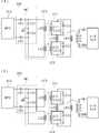
- FIG. 1is a perspective view of the antenna device 101 according to the first embodiment.
- 2 (A)is a plan view of the antenna device 101
- FIG. 2 (B)is a cross-sectional view of a portion BB in FIG. 2 (A).
- FIG. 3is a plan view showing a pattern of the planar conductor 10 formed on the first main surface MS1 of the substrate 1.
- FIG. 4is a diagram schematically showing the current flowing through the first feeding coil 31, the second feeding coil 32, and the planar conductor 10.
- FIG. 5is a perspective view showing the positional relationship between the antenna device 101 and the communication partner antenna 500.
- 6 (A) and 6 (B)are circuit diagrams of a circuit composed of an antenna device 101 and a communication partner antenna 500 coupled thereto.
- FIG. 7Ais a conceptual diagram showing the relationship between the resonance frequency of the feeding side resonance circuit LC3 and the resonance frequency of the first resonance circuit LC1 and the second resonance circuit LC2.
- FIG. 7Bis a conceptual diagram showing the relationship between the resonance frequency of the feeding side resonance circuit LC3 and the resonance frequency of the first resonance circuit LC1 and the second resonance circuit LC2 of the antenna device in the comparative example.
- FIG. 8is an actual measurement diagram showing the frequency characteristics of the real part of the impedance of the feeding side resonance circuit LC3, the first resonance circuit LC1, and the second resonance circuit LC2.
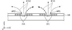
- FIG. 9is a partial cross-sectional view of a planar conductor along a line that selectively passes through the first opening AP1 and the second opening AP2.
- FIG. 10is a diagram showing the distance d between the first opening AP1 and the second opening AP2.
- FIG. 11is a diagram showing the relationship between the interval d shown in FIG. 10 and the coupling coefficients of the first resonance circuit LC1 and the second resonance circuit LC2.
- FIG. 12is a plan view of the antenna device 102 according to the second embodiment.
- 13 (A)is a plan view of the antenna device 103 according to the third embodiment
- FIG. 13 (B)is a plan view showing a pattern of the planar conductor 10 formed on the substrate 1 of the antenna device 103.
- FIG. 14is a circuit diagram of a circuit composed of an antenna device 103 and a communication partner antenna 500 coupled thereto.
- FIG. 1is a perspective view of the antenna device 101 according to the first embodiment.
- 2 (A)is a plan view of the antenna device 101
- FIG. 2 (B)is a cross-sectional view of a portion BB in FIG. 2 (A).
- FIG. 3is a plan view showing a pattern of the planar conductor 10 formed on the first main surface MS1 of the substrate 1.
- the antenna device 101is provided in an electronic device.
- electronic devicesinclude, for example, mobile phone terminals such as smartphones and feature phones, wearable terminals such as smart watches and smart glasses, mobile PCs such as notebook PCs and tablet PCs, information devices such as cameras, game machines, and toys, IC tags, and SD.
- Various electronic devicessuch as information media such as cards, SIM cards, and IC cards.
- a circuit board having an antenna device partially configuredis provided in the housing of the electronic device.
- the antenna device 101includes a substrate 1, a first feeding coil 31, a second feeding coil 32, and capacitors C11, C12, C21, and C22 arranged on the substrate 1.
- the metal member 2, the first feeding coil 31, the second feeding coil 32, and the capacitors C11, C12, C21, and C22are mounted on the substrate 1.
- the substrate 1has a first main surface MS1, and the winding axes of both the first power feeding coil 31 and the second feeding coil 32 are orthogonal to the first main surface MS1.
- the first feeding coil 31 and the second feeding coil 32are components in which, for example, a rectangular loop-shaped, rectangular helical-shaped, or rectangular spiral-shaped coil is formed inside a laminated body of an insulating base material layer such as magnetic ferrite. Is.
- the first feeding coil 31 and the second feeding coil 32are connected to the feeding circuit 300 including the RFIC 310 described later.
- the member 2is arranged on the first main surface MS1 of the substrate 1.
- the member 2has a first conductive portion 21 and a second conductive portion 22 facing each other on a side surface orthogonal to the first main surface MS1.
- the member 2is some kind of functional component such as a metal mechanical component, a shield case, and a battery. Any of the four side surfaces of the member 2 may be a conductive portion, or the entire outer surface may be a conductive portion.
- the substrate 1is a circuit board on which a plurality of electronic components other than the components constituting the antenna device are mounted, and is a planar conductor 10 extending in a planar manner on the first main surface MS1. Is formed.
- the planar conductor 10is, for example, a copper foil attached to an insulating base material.
- the planar conductor 10may be a planar ground conductor or the like formed inside the substrate 1.
- the planar conductor 10is formed with a first opening AP1, a second opening AP2, a first slit SL1, a second slit SL2, and the like.
- the first slit SL1connects the first opening AP1 to the outer edge.
- the second slit SL2connects the second opening AP2 to the outer edge.
- Four pad electrodesare formed inside the first opening AP1 and the second opening AP2, respectively.
- Four terminal electrodesare formed on the lower surfaces of the first feeding coil 31 and the second feeding coil 32, respectively, and are connected to the pad electrodes. Two of the four terminal electrodes of the first feeding coil 31 and the second feeding coil 32 are connected to the feeding circuit formed in the substrate 1 via an interlayer connecting conductor. The other two terminal electrodes are dummy terminal electrodes for mounting.
- Capacitors C11, C12, C21 and C22are all chip capacitors. Capacitors C11 and C12 are mounted so as to straddle the slit SL1. Similarly, the capacitors C21 and C22 are mounted so as to straddle the slit SL2.
- FIG. 4is a diagram schematically showing the current flowing through the first feeding coil 31, the second feeding coil 32, and the planar conductor 10.
- the capacitor C1is a resonance capacitor having the combined capacitance of the capacitors C11 and C12
- the capacitor C2is a resonance capacitor having the combined capacitance of the capacitors C21 and C22.
- the first feeding coil 31 and the second feeding coil 32are connected to the feeding circuit so as to generate magnetic fluxes having the same phase as each other. Therefore, when the right-handed current flows through the first feed coil 31, the right-handed current also flows through the second feed coil 32. In this phase, a right-handed current flows through the outer circumference of the first opening AP1 (inner circumference of the planar conductor 10) at the position where the first feeding coil 31 is mounted, and the second feeding coil 32 is mounted at the position where the second feeding coil 32 is mounted. A right-handed current flows around the outer circumference of the two-opening AP2 (the inner circumference of the planar conductor 10). Along with this, a clockwise current flows mainly along the outer circumference of the slits SL1 and SL2 and the planar conductor 10.
- the swirling direction of the current flowing through the feeding coils 31 and 32 and the swirling direction of the current flowing through the planar conductor 10are opposite to each other.
- the swirling direction of the current flowing through the feeding coils 31 and 32 and the swirling direction of the current flowing through the planar conductor 10are in the same direction. Further, the current passing through the resonance capacitors C1 and C2 is dominant rather than the current flowing along the edge of the planar conductor 10.
- the first feeding coil 31, the second feeding coil 32, and the planar conductor 10are coupled, and the planar conductor 10 acts as a conductor that contributes to radiation. Since the planar conductor 10 has a larger area than the first feeding coil 31 and the second feeding coil 32, the radiation efficiency is higher than when the first feeding coil 31 and the second feeding coil 32 are used alone.
- FIG. 5is a perspective view showing the positional relationship between the antenna device 101 and the communication partner antenna 500.
- the communication partner antenna 500is a coiled antenna wound in a plane for a plurality of turns.
- FIGS. 6A and 6 (B)are circuit diagrams of a circuit composed of the antenna device 101 and the communication partner antenna 500 coupled thereto.
- the inductor L31represents the first feeding coil 31 with a circuit symbol
- the inductor L32represents the second feeding coil 32 with a circuit symbol.
- FIG. 6Ashows an example in which the first feeding coil 31 and the second feeding coil 32 are connected in series
- FIG. 6Bshows an example in which the first feeding coil 31 and the second feeding coil 32 are connected in parallel. This is an example.
- the inductor L11is an inductance component mainly generated in the first opening AP1 of the planar conductor 10
- the inductor L12is mainly the second opening AP2 of the planar conductor 10. It is an inductance component generated in.
- the inductor L11 and the capacitors C11 and C12constitute the first resonant circuit LC1
- the inductor L12 and the capacitors C21 and C22constitute the second resonant circuit LC2.
- the inductors L13 and L14are inductance components due to a current path mainly flowing along the outer circumference of the planar conductor 10.
- One of the capacitors C11 and C12is a capacitor for coarse adjustment of the resonance frequency, and the other is a capacitor for fine adjustment.
- one of the capacitors C21 and C22is a capacitor for coarse adjustment of the resonance frequency, and the other is a capacitor for fine adjustment.
- the feeding side resonance circuit LC3is configured by the inductors L31 and L32 and the capacitors C31 and C32.
- the power supply circuit 300is composed of the RFIC 310 and the capacitors C31, C32, C41 and C42.
- Capacitors C31, C32, C41, and C42constitute an impedance matching circuit MC that matches the impedance between the RFIC 310 and the first feeding coil 31 and the second feeding coil 32.
- the inductor L500represents the communication partner antenna 500 with the circuit symbol of the inductor.
- the inductors L11, L12, L13, and L14are magnetically coupled with the communication partner antenna 500 (inductor L500).
- FIG. 7Ais a conceptual diagram showing the relationship between the resonance frequency of the feeding side resonance circuit LC3 and the resonance frequencies of the first resonance circuit LC1 and the second resonance circuit LC2.
- FIG. 7Bis a conceptual diagram showing the relationship between the resonance frequency of the feeding side resonance circuit LC3 and the resonance frequency of the first resonance circuit LC1 and the second resonance circuit LC2 of the antenna device in the comparative example. ..
- the horizontal axisis the frequency
- the vertical axisis the actual magnitude of the impedance of the feeding side resonance circuit LC3, the first resonance circuit LC1 and the second resonance circuit LC2.
- frequency characteristicsare obtained by measuring the actual magnitude of the impedance of the feeding side resonance circuit, the first resonance circuit, and the second resonance circuit as viewed from the RFIC 310 in FIGS. 6 (A) and 6 (B). For example, it can be obtained by sweeping and measuring the frequency of the applied signal with a network analyzer.
- the magnitude of the actual part of the impedance viewed from the RFIC 310means the connection between the RFIC 310 and the capacitors C41 and C42 from two connection points, that is, in the present embodiment. It means the magnitude of the real part of the impedance to be measured, which can be measured from a point.
- the resonance frequency f3 of the feeding side resonance circuit LC3is different from the resonance frequency f1 of the first resonance circuit LC1 and the resonance frequency f2 of the second resonance circuit LC2.
- the resonance frequency f3 of the feeding side resonance circuit LC3is 13.56 MHz.
- the resonance frequency f1 of the first resonance circuit LC1 and the resonance frequency f2 of the second resonance circuit LC2are both 3 MHz to 4 MHz higher than the resonance frequency f3 of the feeding side resonance circuit LC3.
- the resonance frequency f1 of the first resonance circuit LC1 and the resonance frequency f2 of the second resonance circuit LC2are both about 25% higher than the resonance frequency f3 of the feeding side resonance circuit LC3.
- the resonance frequency f3 of the feeding side resonance circuit LC3is 13.56MHz
- the resonance frequency f1 of the first resonance circuit LC1is 3MHz to 4MHz from the resonance frequency f3 of the feeding side resonance circuit LC3.
- the resonance frequency f2 of the second resonance circuit LC2is 3 MHz to 4 MHz higher than the resonance frequency f1 of the first resonance circuit LC1.
- the resonance frequency f1 of the first resonance circuit LC1is close to the resonance frequency f3 of the feeding side resonance circuit, and the resonance frequency f2 of the second resonance circuit LC2 is separated from the resonance frequency f3 of the feeding side resonance circuit. Therefore, the resonance of the feeding side resonance circuit, the resonance of the first resonance circuit LC1 and the resonance of the second resonance circuit LC2 are in an independent state (three resonance states). Therefore, a large amount of energy is transmitted from the first feeding coil 31 to the first resonant circuit LC1, but not sufficiently transmitted to the second resonant circuit LC2. Therefore, even though the two resonant circuits LC1 and LC2 are provided, the communicable range is not effectively expanded.
- the frequency characteristic of the actual magnitude of the impedance of the first resonance circuit LC1 and the second resonance circuit LC2 as viewed from the RFIC 310is monomodal.
- the resonance frequency f1 of the first resonance circuit LC1 and the resonance frequency f2 of the second resonance circuit LC2are equal to each other.
- the frequency characteristics of the impedance magnitudes of the first resonant circuit LC1 and the second resonant circuit LC2 as seen from the feeding circuit 300are not bimodal, and the first to the extent that they are bimodal.
- the resonance frequency f1 of the resonance circuit LC1 and the resonance frequency f2 of the second resonance circuit LC2are not different.
- the resonance frequency f1 of the first resonance circuit LC1 and the resonance frequency f2 of the second resonance circuit LC2are close to the resonance frequency f3 of the feeding side resonance circuit LC3, the resonance of the feeding side resonance circuit LC3 and the first resonance This is a state in which resonance of the circuit LC1 and resonance of the second resonance circuit LC2 occur (two resonance states). Therefore, energy is transmitted from the feeding side resonance circuit LC3 to the first resonance circuit LC1 and the second resonance circuit LC2 in a well-balanced manner. As a result, the communicable range is expanded.
- FIG. 7Ashows an example in which the resonance frequency f1 of the first resonance circuit LC1 and the resonance frequency f2 of the second resonance circuit LC2 are higher than the resonance frequency of the feeding side resonance circuit LC3, but the high-low relationship of these frequencies is opposite. It may be. That is, the resonance frequency f1 of the first resonance circuit LC1 and the resonance frequency f2 of the second resonance circuit LC2 may be lower than the resonance frequency of the feeding side resonance circuit LC3. However, if the resonance frequency of any of the first resonant circuit LC1, the second resonant circuit LC2, and the feeding side resonant circuit LC3 is lower than 13.56MHz, the capacitance becomes capacitive at the feeding frequency of 13.56MHz, so that the feeding side resonance occurs.
- the circuit LC3, the first resonant circuit LC1 and the second resonant circuit LC2are not magnetically coupled, and energy is not supplied to the first resonant circuit LC1 and the second resonant circuit LC2. Therefore, for example, the resonance frequency f1 of the first resonance circuit LC1 and the resonance frequency f2 of the second resonance circuit LC2 are set to 13.56 MHz, and the resonance frequency of the feeding side resonance circuit LC3 is 3 MHz to 4 MHz higher (about 25% higher) than 13.56 MHz. Let the frequency be.
- the difference between the resonance frequency of the feeding side resonance circuit LC3 and the resonance frequency of the first resonance circuit LC1 and the second resonance circuit LC2is the coupling coefficient between the feeding side resonance circuit LC3 and the first resonance circuit LC1 and the second resonance circuit LC2. Or, it may be determined in consideration of the energy transmission efficiency.
- the communication frequency bandis an HF band such as 13.56 MHz band, even if the magnetic material layers of the feeding coils 31 and 32 are magnetic material ferrite, the loss coefficient is small, so that the magnetic material layer is provided. The effect of improving the Q value of the coil antenna is high.
- FIG. 8is an actual measurement diagram showing the frequency characteristics of the real part of the impedance of the feeding side resonance circuit LC3, the first resonance circuit LC1, and the second resonance circuit LC2.
- the horizontal axisis the frequency
- the vertical axisis the actual magnitude of the impedance of the feeding side resonance circuit LC3, the first resonance circuit LC1 and the second resonance circuit LC2.
- the resonance frequency f3 of the feeding side resonance circuit LC3is 13.75 MHz
- the resonance frequency f1 of the first resonance circuit LC1 and the resonance frequency f2 of the second resonance circuit LC2are 16.90 MHz.
- FIG. 9is a partial cross-sectional view of a planar conductor along a line that selectively passes through the first opening AP1 and the second opening AP2.
- the currents i11 and i12indicate the directions of the currents flowing through the planar conductor 10.
- the magnetic fluxes ⁇ 11 and ⁇ 12indicate the directions of the magnetic fluxes generated by the currents i11 and i12.
- the swirling direction of the current flowing along the edges of the openings AP1 and AP2 formed in the planar conductor 10is the same when viewed in the vertical direction (Z-axis direction) of the planar conductor 10.
- the direction. Therefore, the directions (phases) of the magnetic fluxes entering and exiting the openings AP1 and AP2are the same.
- the direction of the magnetic flux exiting the opening AP1 and entering the opening AP2is opposite to the direction of the magnetic flux exiting the opening AP2 and entering the opening AP1, so that the coupling between the first resonant circuit LC1 and the second resonant circuit LC2 is weak. Therefore, the effect of expanding the communicable range is high by providing the two resonance circuits LC1 and LC2.
- the magnetic flux generated in the first feeding coil 31 and the magnetic flux generated in the second feeding coil 32are the first feeding coil 31 and the magnetic flux generated in the second feeding coil 32.
- the feeding circuit 300may be connected to the first feeding coil 31 and the second feeding coil 32 so as to be in phase in the coil winding axis direction of the second feeding coil 32.
- FIG. 10is a diagram showing the distance d between the first opening AP1 and the second opening AP2.
- FIG. 11is a diagram showing the relationship between this interval d and the coupling coefficients of the first resonant circuit LC1 and the second resonant circuit LC2.
- the magnetic flux entering and exiting the first opening AP1 and the magnetic flux entering and exiting the second opening AP2are in phase.
- the size of the first opening AP1 and the second opening AP2is 2.5 mm ⁇ 3.4 mm (3.4 mm in the X direction). If the coupling coefficient is, for example, 3% or less, it can be said that the coupling between the first resonant circuit LC1 and the second resonant circuit LC2 is sufficiently weak and does not affect each other. Therefore, if the first opening AP1 and the second opening AP2 are separated by three times or more of their width (3.4 mm), the coupling coefficient is weak enough to be 3% or less, which is the resonance frequency of the first resonance circuit LC1. It can be set to the same frequency as the resonance frequency of the second resonance circuit LC2.
- Second Embodimentan antenna device in which the configurations of the first feeding coil and the second feeding coil are different from the examples shown in the first embodiment is shown.
- FIG. 12is a plan view of the antenna device 102 according to the second embodiment.
- the antenna device 102includes a substrate 1, a first feeding coil 31 and a second feeding coil 32 formed on the substrate 1, and capacitors C10 and C20 mounted on the substrate 1.
- the first feeding coil 31is formed around the first opening AP1, and the second feeding coil 32 is formed around the second opening AP2.
- a power supply circuit 300is configured on the substrate 1, and the power supply circuit 300, the first power supply coil 31, and the second power supply coil 32 are connected to each other via conductor patterns 51, 52, and 53.
- the first feeding coil 31, the second feeding coil 32, and the conductor patterns 51, 52, and 53are electrically insulated from the planar conductor 10.
- a single capacitor C10is connected to the slit SL1, and a single capacitor C20 is connected to the slit SL2.
- Other configurationsare the same as those of the antenna device 101 shown in the first embodiment.
- the first opening AP1 and the second opening AP2are, for example, 3 mm ⁇ 3 mm squares, and are separated from each other by 3 times or more of 3 mm. Further, the first feeding coil 31 and the second feeding coil 32 are connected in series to the feeding circuit 300, and the first feeding coil 31 and the second feeding coil 32 feed the magnetic fluxes in the same phase with each other. It is connected to the circuit 300.
- the first feeding coil 31 and the second feeding coil 32are easily arranged close to each other in the first opening AP1 and the second opening AP2 in the Z-axis direction, and the total line length of the opposing portions thereof is lengthened. Therefore, it is easy to increase the coupling coefficient of the first feeding coil 31 with respect to the first resonant circuit LC1 and the coupling coefficient of the second feeding coil 32 with respect to the second resonant circuit LC2.
- FIG. 13 (A)is a plan view of the antenna device 103 according to the third embodiment
- FIG. 13 (B)is a plan view showing a pattern of the planar conductor 10 formed on the substrate 1 of the antenna device 103. ..
- the antenna device 103includes a substrate 1, a first coil coupling element 61, a second coil coupling element 62, and capacitors C11, C12, C21, and C22 arranged on the substrate 1.
- the metal member 2, the first coil coupling element 61, the second coil coupling element 62, and the capacitors C11, C12, C21, and C22are mounted on the substrate 1.
- the configuration of the member 2, the capacitors C11, C12, C21, and C22is the same as the configuration shown in the first embodiment.
- the first coil coupling element 61 and the second coil coupling element 62are connected to a power feeding circuit 300 including an RFIC 310 described later.
- FIG. 14is a circuit diagram of a circuit composed of the antenna device 103 and the communication partner antenna 500 coupled thereto.
- the inductor L31is the primary coil of the first coil coupling element 61
- the inductor L32is the primary coil of the second coil coupling element 62.
- the inductor L11is a secondary coil of the first coil coupling element 61
- the inductor L12is a secondary coil of the second coil coupling element 62. That is, the first coil coupling element 61 and the second coil coupling element 62 are elements that act as transformers in which the coils are magnetically coupled to each other.
- the first coil coupling element 61 and the second coil coupling element 62may be elements in which the primary coil and the secondary coil are vertically wound in a conductor pattern, or the primary coil and the secondary coil are horizontally wound. It may be an element composed of the conductor pattern of.
- the first resonant circuit LC1is composed of the inductor L11 and the capacitors C11 and C12
- the second resonant circuit LC2is composed of the inductor L12 and the capacitors C21 and C22.
- the inductors L13 and L14are inductance components due to a current path mainly flowing along the outer circumference of the planar conductor 10.
- the coil coupling elementmay be used to couple the feeding side resonance circuit LC3 and the first resonance circuit LC1 and the feeding side resonance circuit LC3 and the second resonance circuit LC2.
- an element configured as a baluncan also be used.
- AP1... 1st opening AP2 ... 2nd opening C1, C2 ... Resonant capacitors C10, C11, C12, C20, C21, C22 ... Capacitors C31, C32, C41, C42 ... Capacitors i11, i12 ... Currents L11, L12 ... Inductors L13, L14 ... Inductor L31, L32 ... Inductor L500 ... Inductor LC1 ... First resonance circuit LC2 ... Second resonance circuit LC3 ... Feed side resonance circuit MC ... Impedance matching circuit MS1 ... First main surface SL1 ... First slit SL2 ... Second slit 1 ... Substrate 2 ... Member 10 ...
- Planar conductor 21... First conductive portion 22 ... Second conductive portion 31 ... First feeding coil 32 ... Second feeding coil 51, 52, 53 ... Conductor pattern 61 . First coil coupling element 62 ... Second coil coupling elements 101, 102, 103 ... Antenna device 300 ... Feeding circuit 310 ... RFIC 500 ... Communication partner antenna
Landscapes
- Engineering & Computer Science (AREA)
- Computer Hardware Design (AREA)
- Microelectronics & Electronic Packaging (AREA)
- Physics & Mathematics (AREA)
- General Physics & Mathematics (AREA)
- Theoretical Computer Science (AREA)
- Details Of Aerials (AREA)
Abstract
Description
Translated fromJapanese本発明は、RFIDシステムや近距離無線通信システム等に用いられるアンテナ装置及びそれを備えた電子機器に関するものである。The present invention relates to an antenna device used in an RFID system, a short-range wireless communication system, or the like, and an electronic device provided with the antenna device.
従来、フェライトチップにコイル導体パターンが形成されてなるフェライトチップアンテナを回路基板に実装することで構成されるアンテナ装置が用いられている。Conventionally, an antenna device configured by mounting a ferrite chip antenna in which a coil conductor pattern is formed on a ferrite chip on a circuit board has been used.
例えば、特許文献1には、フェライトチップにコイル導体パターンが形成されてなるフェライトチップアンテナを回路基板上に配置し、また、回路基板にループ状の導体パターンを形成し、このループ状の導体パターンとフェライトチップアンテナとを互いに磁界結合させたアンテナ装置が示されている。For example, in
特許文献1に記載のアンテナ装置では、フェライトチップアンテナを回路基板の1箇所に配置するだけでは、広範囲での通信が難しかった。そのため、例えば、RFIDタグを備えるカードと通信を行う場合に、つまり、相対的に大きなサイズのアンテナを備えるカードと通信を行う場合に、カードを規定位置にかざさないと、適正な通信が困難な場合があった。In the antenna device described in
また、回路基板上に複数のフェライトチップアンテナを配置することで、通信可能なエリアを拡げることが考えられるが、共振周波数の設定によっては、高い利得が得られない。It is also possible to expand the communicable area by arranging multiple ferrite chip antennas on the circuit board, but high gain cannot be obtained depending on the resonance frequency setting.
そこで、本発明の目的は、高利得を得つつ通信可能範囲を拡げたアンテナ装置及びそれを備える電子機器を提供することにある。Therefore, an object of the present invention is to provide an antenna device having a wide communication range while obtaining a high gain and an electronic device including the antenna device.
本開示の一例としてのアンテナ装置は、
RFICに接続される第1給電コイルと、
前記RFICに接続される第2給電コイルと、
前記第1給電コイルに磁界結合する第1共振回路と、
前記第2給電コイルに磁界結合する第2共振回路と、を備え、
前記RFICから視た、前記第1共振回路及び前記第2共振回路のインピーダンスの大きさの周波数特性が単峰性となる程度に、前記第1共振回路の共振周波数と前記第2共振回路の共振周波数とが等しい、
ことを特徴とする。The antenna device as an example of the present disclosure is
The first feeding coil connected to the RFIC and
The second feeding coil connected to the RFIC and
A first resonant circuit that magnetically couples to the first feeding coil,
A second resonant circuit that magnetically couples to the second feeding coil is provided.
Resonance between the resonance frequency of the first resonance circuit and the resonance of the second resonance circuit to the extent that the frequency characteristics of the impedance magnitudes of the first resonance circuit and the second resonance circuit as viewed from the RFIC become monomodal. Equal to frequency,
It is characterized by that.
本開示の一例としての電子機器は、
アンテナ装置と、このアンテナ装置に接続されたRFICとを備えた電子機器において、
前記アンテナ装置は、
RFICに接続される第1給電コイルと、
前記RFICに接続される第2給電コイルと、
前記第1給電コイルに磁界結合する第1共振回路と、
前記第2給電コイルに磁界結合する第2共振回路と、を備え、
前記RFICから視た、前記第1共振回路及び前記第2共振回路のインピーダンスの大きさの周波数特性が単峰性となる程度に、前記第1共振回路の共振周波数と前記第2共振回路の共振周波数とが等しい、
ことを特徴とする。The electronic device as an example of the present disclosure is
In an electronic device including an antenna device and an RFIC connected to the antenna device,
The antenna device is
The first feeding coil connected to the RFIC and
The second feeding coil connected to the RFIC and
A first resonant circuit that magnetically couples to the first feeding coil,
A second resonant circuit that magnetically couples to the second feeding coil is provided.
Resonance between the resonance frequency of the first resonance circuit and the resonance of the second resonance circuit to the extent that the frequency characteristics of the impedance magnitudes of the first resonance circuit and the second resonance circuit as viewed from the RFIC become monomodal. Equal to frequency,
It is characterized by that.
本発明によれば、少なくとも2つの給電コイルと、それらにそれぞれ磁界結合する共振回路とを備えるので、通信可能範囲が拡大される。しかも、給電回路から視た、2つの共振回路のインピーダンスの大きさの周波数特性が単峰性となる程度に、2つの共振回路の共振周波数が等しいので、給電回路から2つの共振回路へバランス良くエネルギーが伝達され、アンテナの利得が高まる。According to the present invention, since at least two feeding coils and a resonance circuit that magnetically couples to each of them are provided, the communicable range is expanded. Moreover, since the resonance frequencies of the two resonant circuits are equal to the extent that the frequency characteristics of the impedance magnitudes of the two resonant circuits as seen from the feeder circuit are unifying, the two resonant circuits are well-balanced. Energy is transferred and the gain of the antenna is increased.
以降、図を参照して幾つかの具体的な例を挙げて、本発明を実施するための複数の形態を示す。各図中には同一箇所に同一符号を付している。要点の説明又は理解の容易性を考慮して、実施形態を説明の便宜上、複数の実施形態に分けて示すが、異なる実施形態で示した構成の部分的な置換又は組み合わせは可能である。第2の実施形態以降では第1の実施形態と共通の事柄についての記述を省略し、異なる点についてのみ説明する。特に、同様の構成による同様の作用効果については実施形態毎には逐次言及しない。Hereinafter, a plurality of embodiments for carrying out the present invention will be shown with reference to the drawings with reference to some specific examples. The same reference numerals are given to the same parts in each figure. Although the embodiments are divided into a plurality of embodiments for convenience of explanation in consideration of explanation of the main points or ease of understanding, partial replacement or combination of the configurations shown in different embodiments is possible. In the second and subsequent embodiments, the description of matters common to those of the first embodiment will be omitted, and only the differences will be described. In particular, the same action and effect due to the same configuration will not be mentioned sequentially for each embodiment.
《第1の実施形態》
図1は第1の実施形態に係るアンテナ装置101の斜視図である。図2(A)はアンテナ装置101の平面図であり、図2(B)は、図2(A)におけるB-B部分の断面図である。図3は基板1の第1主面MS1に形成されている面状導体10のパターンを示す平面図である。<< First Embodiment >>
FIG. 1 is a perspective view of the
アンテナ装置101は電子機器に設けられている。この電子機器は例えばスマートフォンやフィーチャーフォン等の携帯電話端末、スマートウォッチやスマートグラス等のウェアラブル端末、ノートPCやタブレットPC等の携帯PC、カメラ、ゲーム機、玩具等の情報機器、ICタグ、SDカード、SIMカード、ICカード等の情報媒体等、様々な電子機器である。典型的には、一部にアンテナ装置が構成された回路基板が電子機器の筐体内に設けられる。The
アンテナ装置101は、基板1と、この基板1に配置された、第1給電コイル31、第2給電コイル32、及びキャパシタC11,C12,C21,C22を備える。本実施形態では、金属物である部材2、第1給電コイル31、第2給電コイル32、及びキャパシタC11,C12,C21,C22は基板1に実装されている。The
基板1は第1主面MS1を有し、第1給電コイル31、第2給電コイル32は、いずれも巻回軸が第1主面MS1に直交する。第1給電コイル31、第2給電コイル32は、例えば、矩形ループ状、矩形ヘリカル状、又は矩形スパイラル状のコイルが、磁性体フェライト等の絶縁基材層の積層体の内部に構成された部品である。第1給電コイル31及び第2給電コイル32は、後に示すRFIC310を含む給電回路300に接続される。The
部材2は基板1の第1主面MS1上に配置されている。部材2は、第1主面MS1に対して直交する側面に、互いに対向する第1導電部21及び第2導電部22を有する。部材2は、例えば金属製の機構部品、シールドケース、バッテリー等、何らかの機能部品である。部材2の四側面のいずれもが導電部であってもよいし、外面全面が導電部であってもよい。The
図3に表れているように、基板1は、例えばアンテナ装置を構成する部品以外の複数の電子部品が実装される回路基板であり、第1主面MS1に、面状に拡がる面状導体10が形成されている。この面状導体10は、例えば、絶縁基材に張り付けられた銅箔である。面状導体10は、基板1の内部に形成された面状のグランド導体等であってもよい。面状導体10には、第1開口AP1、第2開口AP2、第1スリットSL1及び第2スリットSL2等が形成されている。第1スリットSL1は第1開口AP1を外縁に連接する。また、第2スリットSL2は第2開口AP2を外縁に連接する。第1開口AP1、第2開口AP2の内部には四つのパッド電極がそれぞれ形成されている。第1給電コイル31、第2給電コイル32の下面にはそれぞれ四つの端子電極が形成されていて、上記パッド電極に接続される。第1給電コイル31、第2給電コイル32それぞれの4つの端子電極のうち二つの端子電極は層間接続導体を介して基板1内に形成されている給電回路に接続されている。その他の二つの端子電極は実装のためのダミーの端子電極である。As shown in FIG. 3, the
キャパシタC11,C12,C21,C22はいずれもチップコンデンサである。キャパシタC11,C12はスリットSL1を跨ぐように実装されている。同様に、キャパシタC21,C22はスリットSL2を跨ぐように実装されている。Capacitors C11, C12, C21 and C22 are all chip capacitors. Capacitors C11 and C12 are mounted so as to straddle the slit SL1. Similarly, the capacitors C21 and C22 are mounted so as to straddle the slit SL2.
図4は、第1給電コイル31、第2給電コイル32、及び面状導体10に流れる電流を概略的に示す図である。図4において、キャパシタC1は上記キャパシタC11,C12の合成容量を有する共振キャパシタであり、キャパシタC2は上記キャパシタC21,C22の合成容量を有する共振キャパシタである。FIG. 4 is a diagram schematically showing the current flowing through the
第1給電コイル31と第2給電コイル32は、互いに同相の磁束を生じるように上記給電回路に接続される。したがって、第1給電コイル31に右旋の電流が流れるとき、第2給電コイル32にも右旋の電流が流れる。この位相で、第1給電コイル31が実装された位置の第1開口AP1の外周(面状導体10の内周)に右旋の電流が流れ、第2給電コイル32が実装された位置の第2開口AP2の外周(面状導体10の内周)に右旋の電流が流れる。また、これに伴い、スリットSL1,SL2及び面状導体10の主に外周に沿って右回りの電流が流れる。The
ちなみに、スリットSL1,SL2に共振キャパシタC1,C2を配置しない場合は、給電コイル31,32に流れる電流の旋回方向と面状導体10に流れる電流の旋回方向とは逆の関係になるが、本実施形態では、共振キャパシタC1,C2があるので、給電コイル31,32に流れる電流の旋回方向と面状導体10に流れる電流の旋回方向とは同方向である。また、面状導体10の縁端に沿って流れる電流よりも、共振キャパシタC1,C2を経由する電流が支配的である。By the way, when the resonance capacitors C1 and C2 are not arranged in the slits SL1 and SL2, the swirling direction of the current flowing through the feeding coils 31 and 32 and the swirling direction of the current flowing through the
このようにして、第1給電コイル31及び第2給電コイル32と面状導体10とが結合して、面状導体10は放射に寄与する導体として作用する。面状導体10は第1給電コイル31、第2給電コイル32より広面積であるので、第1給電コイル31、第2給電コイル32を単体で用いる場合より放射効率が高い。In this way, the
図5はアンテナ装置101と通信相手アンテナ500との位置関係を示す斜視図である。通信相手アンテナ500は平面内に複数ターン巻回されたコイル状のアンテナである。FIG. 5 is a perspective view showing the positional relationship between the
図6(A)、図6(B)は、アンテナ装置101及びそれに結合する通信相手アンテナ500で構成される回路の回路図である。図6(A)、図6(B)において、インダクタL31は第1給電コイル31を回路記号で表したものであり、インダクタL32は第2給電コイル32を回路記号で表したものである。図6(A)は、第1給電コイル31と第2給電コイル32とを直列接続した例であり、図6(B)は、第1給電コイル31と第2給電コイル32とを並列接続した例である。6 (A) and 6 (B) are circuit diagrams of a circuit composed of the
図6(A),図6(B)において、インダクタL11は、面状導体10の主に第1開口AP1に生じるインダクタンス成分であり、インダクタL12は、面状導体10の主に第2開口AP2に生じるインダクタンス成分である。インダクタL11とキャパシタC11,C12とで第1共振回路LC1が構成されていて、インダクタL12とキャパシタC21,C22とで第2共振回路LC2が構成されている。インダクタL13,L14は面状導体10の主に外周に沿って流れる電流経路によるインダクタンス成分である。キャパシタC11,C12の一方は共振周波数の粗調整用キャパシタであり、他方は微調整用のキャパシタである。同様に、キャパシタC21,C22の一方は共振周波数の粗調整用キャパシタであり、他方は微調整用のキャパシタである。In FIGS. 6A and 6B, the inductor L11 is an inductance component mainly generated in the first opening AP1 of the
インダクタL31,L32及びキャパシタC31,C32によって、給電側共振回路LC3が構成されている。The feeding side resonance circuit LC3 is configured by the inductors L31 and L32 and the capacitors C31 and C32.
RFIC310及びキャパシタC31,C32,C41,C42によって給電回路300が構成されている。キャパシタC31,C32,C41,C42によって、RFIC310と第1給電コイル31及び第2給電コイル32との間でインピーダンスを整合させるインピーダンス整合回路MCが構成されている。The
インダクタL500は通信相手アンテナ500をインダクタの回路記号で表したものである。インダクタL11,L12,L13,L14は通信相手アンテナ500(インダクタL500)と磁界結合する。The inductor L500 represents the
図7(A)は、上記給電側共振回路LC3の共振周波数と、第1共振回路LC1及び第2共振回路LC2の共振周波数と、の関係を示す概念図である。また、図7(B)は、比較例におけるアンテナ装置の、給電側共振回路LC3の共振周波数と、第1共振回路LC1及び第2共振回路LC2の共振周波数と、の関係を示す概念図である。図7(A)、図7(B)において、横軸は周波数、縦軸は、給電側共振回路LC3、第1共振回路LC1及び第2共振回路LC2のインピーダンスの実部の大きさである。これらの周波数特性は、図6(A)、図6(B)中のRFIC310から視た、給電側共振回路、第1共振回路及び第2共振回路のインピーダンスの実部の大きさを測定したものであり、例えば、ネットワークアナライザで印加信号の周波数を掃引して測定することで得られる。ここで、「RFIC310から視た・・・インピーダンスの実部の大きさ」とは、RFIC310と測定対象との2つの接続点から、つまり本実施形態においては、RFIC310とキャパシタC41,C42との接続点から測定され得る、測定対象のインピーダンスの実部の大きさを意味する。FIG. 7A is a conceptual diagram showing the relationship between the resonance frequency of the feeding side resonance circuit LC3 and the resonance frequencies of the first resonance circuit LC1 and the second resonance circuit LC2. Further, FIG. 7B is a conceptual diagram showing the relationship between the resonance frequency of the feeding side resonance circuit LC3 and the resonance frequency of the first resonance circuit LC1 and the second resonance circuit LC2 of the antenna device in the comparative example. .. In FIGS. 7A and 7B, the horizontal axis is the frequency, and the vertical axis is the actual magnitude of the impedance of the feeding side resonance circuit LC3, the first resonance circuit LC1 and the second resonance circuit LC2. These frequency characteristics are obtained by measuring the actual magnitude of the impedance of the feeding side resonance circuit, the first resonance circuit, and the second resonance circuit as viewed from the
図7(A)に示す本実施形態では、給電側共振回路LC3の共振周波数f3と、第1共振回路LC1の共振周波数f1及び第2共振回路LC2の共振周波数f2とは異なる。この例では、給電側共振回路LC3の共振周波数f3は13.56MHzである。また、第1共振回路LC1の共振周波数f1及び第2共振回路LC2の共振周波数f2は、いずれも給電側共振回路LC3の共振周波数f3から3MHz~4MHz高い。割合としては、第1共振回路LC1の共振周波数f1及び第2共振回路LC2の共振周波数f2は、いずれも給電側共振回路LC3の共振周波数f3から約25%高い。In the present embodiment shown in FIG. 7A, the resonance frequency f3 of the feeding side resonance circuit LC3 is different from the resonance frequency f1 of the first resonance circuit LC1 and the resonance frequency f2 of the second resonance circuit LC2. In this example, the resonance frequency f3 of the feeding side resonance circuit LC3 is 13.56 MHz. Further, the resonance frequency f1 of the first resonance circuit LC1 and the resonance frequency f2 of the second resonance circuit LC2 are both 3 MHz to 4 MHz higher than the resonance frequency f3 of the feeding side resonance circuit LC3. As a ratio, the resonance frequency f1 of the first resonance circuit LC1 and the resonance frequency f2 of the second resonance circuit LC2 are both about 25% higher than the resonance frequency f3 of the feeding side resonance circuit LC3.
図7(B)に示す比較例では、給電側共振回路LC3の共振周波数f3は13.56MHzであり、第1共振回路LC1の共振周波数f1は、給電側共振回路LC3の共振周波数f3から3MHz~4MHz高い。そして、第2共振回路LC2の共振周波数f2は、第1共振回路LC1の共振周波数f1からさらに3MHz~4MHz高い。In the comparative example shown in FIG. 7B, the resonance frequency f3 of the feeding side resonance circuit LC3 is 13.56MHz, and the resonance frequency f1 of the first resonance circuit LC1 is 3MHz to 4MHz from the resonance frequency f3 of the feeding side resonance circuit LC3. high. The resonance frequency f2 of the second resonance circuit LC2 is 3 MHz to 4 MHz higher than the resonance frequency f1 of the first resonance circuit LC1.
比較例のアンテナ装置では、第1共振回路LC1の共振周波数f1が給電側共振回路の共振周波数f3に近く、第2共振回路LC2の共振周波数f2は給電側共振回路の共振周波数f3から離れているので、給電側共振回路の共振、第1共振回路LC1の共振及び第2共振回路LC2の共振がそれぞれ独立した状態(3共振状態)となる。そのため、第1給電コイル31から第1共振回路LC1に多くのエネルギーが伝送されるが、第2共振回路LC2には十分伝送されない。そのため、2つの共振回路LC1,LC2を備えているにもかかわらず、通信可能範囲は効果的に拡がらない。In the antenna device of the comparative example, the resonance frequency f1 of the first resonance circuit LC1 is close to the resonance frequency f3 of the feeding side resonance circuit, and the resonance frequency f2 of the second resonance circuit LC2 is separated from the resonance frequency f3 of the feeding side resonance circuit. Therefore, the resonance of the feeding side resonance circuit, the resonance of the first resonance circuit LC1 and the resonance of the second resonance circuit LC2 are in an independent state (three resonance states). Therefore, a large amount of energy is transmitted from the
本実施形態のアンテナ装置では、図7(A)に示されるように、RFIC310から視た、第1共振回路LC1及び第2共振回路LC2のインピーダンスの実部の大きさの周波数特性が単峰性となる程度に、第1共振回路LC1の共振周波数f1と第2共振回路LC2の共振周波数f2とが等しい。言い換えれば、給電回路300から視た、第1共振回路LC1及び第2共振回路LC2のインピーダンスの大きさの周波数特性が双峰性となっておらず、また、双峰性となる程度に第1共振回路LC1の共振周波数f1と第2共振回路LC2の共振周波数f2とが異なってはいない。そして、第1共振回路LC1の共振周波数f1及び第2共振回路LC2の共振周波数f2が給電側共振回路LC3の共振周波数f3に近接しているので、給電側共振回路LC3の共振と、第1共振回路LC1の共振及び第2共振回路LC2の共振とが生じる状態(2共振状態)となる。そのため、給電側共振回路LC3から第1共振回路LC1及び第2共振回路LC2にバランスよくエネルギーが伝送される。その結果、通信可能範囲が拡大される。In the antenna device of the present embodiment, as shown in FIG. 7A, the frequency characteristic of the actual magnitude of the impedance of the first resonance circuit LC1 and the second resonance circuit LC2 as viewed from the
図7(A)では、第1共振回路LC1の共振周波数f1及び第2共振回路LC2の共振周波数f2が給電側共振回路LC3の共振周波数より高い例を示したが、この周波数の高低関係は逆であってもよい。つまり、第1共振回路LC1の共振周波数f1及び第2共振回路LC2の共振周波数f2が給電側共振回路LC3の共振周波数より低くてもよい。ただし、第1共振回路LC1、第2共振回路LC2及び給電側共振回路LC3のいずれについても、共振周波数が13.56MHzより低いと、給電の周波数である13.56MHzにおいて容量性となるので、給電側共振回路LC3と第1共振回路LC1及び第2共振回路LC2とが磁界結合せず、第1共振回路LC1及び第2共振回路LC2にエネルギーが供給されない。したがって、例えば、第1共振回路LC1の共振周波数f1及び第2共振回路LC2の共振周波数f2を13.56MHzとし、給電側共振回路LC3の共振周波数を13.56MHzより3MHz~4MHz高い(約25%高い)周波数とする。FIG. 7A shows an example in which the resonance frequency f1 of the first resonance circuit LC1 and the resonance frequency f2 of the second resonance circuit LC2 are higher than the resonance frequency of the feeding side resonance circuit LC3, but the high-low relationship of these frequencies is opposite. It may be. That is, the resonance frequency f1 of the first resonance circuit LC1 and the resonance frequency f2 of the second resonance circuit LC2 may be lower than the resonance frequency of the feeding side resonance circuit LC3. However, if the resonance frequency of any of the first resonant circuit LC1, the second resonant circuit LC2, and the feeding side resonant circuit LC3 is lower than 13.56MHz, the capacitance becomes capacitive at the feeding frequency of 13.56MHz, so that the feeding side resonance occurs. The circuit LC3, the first resonant circuit LC1 and the second resonant circuit LC2 are not magnetically coupled, and energy is not supplied to the first resonant circuit LC1 and the second resonant circuit LC2. Therefore, for example, the resonance frequency f1 of the first resonance circuit LC1 and the resonance frequency f2 of the second resonance circuit LC2 are set to 13.56 MHz, and the resonance frequency of the feeding side resonance circuit LC3 is 3 MHz to 4 MHz higher (about 25% higher) than 13.56 MHz. Let the frequency be.
給電側共振回路LC3の共振周波数と、第1共振回路LC1及び第2共振回路LC2の共振周波数との差は、給電側共振回路LC3と第1共振回路LC1及び第2共振回路LC2との結合係数や、エネルギーの伝送効率を考慮して定めればよい。The difference between the resonance frequency of the feeding side resonance circuit LC3 and the resonance frequency of the first resonance circuit LC1 and the second resonance circuit LC2 is the coupling coefficient between the feeding side resonance circuit LC3 and the first resonance circuit LC1 and the second resonance circuit LC2. Or, it may be determined in consideration of the energy transmission efficiency.
なお、通信周波数帯が例えば13.56MHz帯などのHF帯であれば、給電コイル31,32の磁性体層が磁性体フェライトであっても、損失係数が小さいので、磁性体層を備えることによる、コイルアンテナのQ値の向上効果は高い。If the communication frequency band is an HF band such as 13.56 MHz band, even if the magnetic material layers of the feeding coils 31 and 32 are magnetic material ferrite, the loss coefficient is small, so that the magnetic material layer is provided. The effect of improving the Q value of the coil antenna is high.
図8は、給電側共振回路LC3、第1共振回路LC1、及び第2共振回路LC2についての、インピーダンスの実部の周波数特性を示す実測図である。図8において、横軸は周波数、縦軸は、給電側共振回路LC3、第1共振回路LC1及び第2共振回路LC2のインピーダンスの実部の大きさである。この例では、給電側共振回路LC3の共振周波数f3は13.75MHzであり、第1共振回路LC1の共振周波数f1及び第2共振回路LC2の共振周波数f2は16.90MHzである。FIG. 8 is an actual measurement diagram showing the frequency characteristics of the real part of the impedance of the feeding side resonance circuit LC3, the first resonance circuit LC1, and the second resonance circuit LC2. In FIG. 8, the horizontal axis is the frequency, and the vertical axis is the actual magnitude of the impedance of the feeding side resonance circuit LC3, the first resonance circuit LC1 and the second resonance circuit LC2. In this example, the resonance frequency f3 of the feeding side resonance circuit LC3 is 13.75 MHz, and the resonance frequency f1 of the first resonance circuit LC1 and the resonance frequency f2 of the second resonance circuit LC2 are 16.90 MHz.
次に、第1共振回路LC1が発生する磁束と第2共振回路LC2が発生する磁束との位相関係について示す。図9は、第1開口AP1及び第2開口AP2を選択的に通るラインでの、面状導体の部分断面図である。図9において、電流i11,i12は、面状導体10に流れる電流の方向を示している。また、磁束φ11,φ12は、電流i11,i12によって発生される磁束の方向を示している。Next, the phase relationship between the magnetic flux generated by the first resonant circuit LC1 and the magnetic flux generated by the second resonant circuit LC2 will be shown. FIG. 9 is a partial cross-sectional view of a planar conductor along a line that selectively passes through the first opening AP1 and the second opening AP2. In FIG. 9, the currents i11 and i12 indicate the directions of the currents flowing through the
図9に表れているように、面状導体10に形成された開口AP1,AP2の縁に沿って流れる電流の旋回方向は、面状導体10の垂直方向(Z軸方向)に視て、同方向である。そのため、開口AP1,AP2を出入りする磁束の方向(位相)は等しい。例えば、開口AP1から出て開口AP2へ入る磁束の方向と、開口AP2から出て開口AP1へ入る磁束の方向とは逆であるので、第1共振回路LC1と第2共振回路LC2との結合は弱い。そのため、2つの共振回路LC1,LC2を備えていることによる、通信可能範囲の拡大効果が高い。As shown in FIG. 9, the swirling direction of the current flowing along the edges of the openings AP1 and AP2 formed in the
開口AP1,AP2の縁に沿って流れる電流の旋回方向を上記のとおりとするためには、第1給電コイル31に生じる磁束と第2給電コイル32に生じる磁束とが、第1給電コイル31及び第2給電コイル32のコイル巻回軸方向で同相となるように、第1給電コイル31及び第2給電コイル32に給電回路300を接続すればよい。In order to make the swirling direction of the current flowing along the edges of the openings AP1 and AP2 as described above, the magnetic flux generated in the
次に、第1給電コイル31と第2給電コイル32との位置関係と第1共振回路LC1及び第2共振回路LC2の結合係数との関係を示す。Next, the positional relationship between the
図10は第1開口AP1と第2開口AP2との間隔dを示す図である。図11は、この間隔dと第1共振回路LC1及び第2共振回路LC2の結合係数との関係を示す図である。ここで、第1開口AP1に出入りする磁束と第2開口AP2に出入りする磁束とは同相である。FIG. 10 is a diagram showing the distance d between the first opening AP1 and the second opening AP2. FIG. 11 is a diagram showing the relationship between this interval d and the coupling coefficients of the first resonant circuit LC1 and the second resonant circuit LC2. Here, the magnetic flux entering and exiting the first opening AP1 and the magnetic flux entering and exiting the second opening AP2 are in phase.
このシミュレーションでは、第1開口AP1及び第2開口AP2のサイズは、2.5mm×3.4mm(X方向に3.4mm)である。結合係数が例えば3%以下であれば、第1共振回路LC1と第2共振回路LC2との結合は十分に弱く、互いに影響を及ぼしあわないと言える。したがって、第1開口AP1及び第2開口AP2は、それらの幅(3.4mm)の3倍以上離れていれば、結合係数は3%以下、と充分に弱く、第1共振回路LC1の共振周波数と第2共振回路LC2の共振周波数とは同じ周波数に設定できる。In this simulation, the size of the first opening AP1 and the second opening AP2 is 2.5 mm × 3.4 mm (3.4 mm in the X direction). If the coupling coefficient is, for example, 3% or less, it can be said that the coupling between the first resonant circuit LC1 and the second resonant circuit LC2 is sufficiently weak and does not affect each other. Therefore, if the first opening AP1 and the second opening AP2 are separated by three times or more of their width (3.4 mm), the coupling coefficient is weak enough to be 3% or less, which is the resonance frequency of the first resonance circuit LC1. It can be set to the same frequency as the resonance frequency of the second resonance circuit LC2.
《第2の実施形態》
第2の実施形態では、第1給電コイル及び第2給電コイルの構成が第1の実施形態で示した例とは異なるアンテナ装置について示す。<< Second Embodiment >>
In the second embodiment, an antenna device in which the configurations of the first feeding coil and the second feeding coil are different from the examples shown in the first embodiment is shown.
図12は第2の実施形態に係るアンテナ装置102の平面図である。アンテナ装置102は、基板1と、この基板1に形成された第1給電コイル31及び第2給電コイル32、基板1に実装されたキャパシタC10,C20を備える。FIG. 12 is a plan view of the
本実施形態では、第1給電コイル31は、第1開口AP1の周囲に形成されていて、第2給電コイル32は、第2開口AP2の周囲に形成されている。基板1には給電回路300が構成されていて、この給電回路300、第1給電コイル31及び第2給電コイル32は、導体パターン51,52,53を介して接続されている。第1給電コイル31、第2給電コイル32及び導体パターン51,52,53は面状導体10から電気的に絶縁されている。なお、スリットSL1には単一のキャパシタC10が接続されていて、スリットSL2には単一のキャパシタC20が接続されている。その他の構成は第1の実施形態で示したアンテナ装置101と同様である。In the present embodiment, the
第1開口AP1及び第2開口AP2は例えば3mm×3mmの方形であり、互いの間隔を3mmの3倍以上離している。また、第1給電コイル31と第2給電コイル32とは給電回路300に対して直列接続されていて、第1給電コイル31と第2給電コイル32とが、互いに同相の磁束を生じるように給電回路300に接続されている。The first opening AP1 and the second opening AP2 are, for example, 3 mm × 3 mm squares, and are separated from each other by 3 times or more of 3 mm. Further, the
本実施形態によれば、第1開口AP1及び第2開口AP2に第1給電コイル31及び第2給電コイル32をそれぞれZ軸方向に近接配置しやすく、且つ両者の対向部の総線長を長くできるので、第1共振回路LC1に対する第1給電コイル31の結合係数、第2共振回路LC2に対する第2給電コイル32の結合係数、をそれぞれ高めやすい。According to the present embodiment, the
《第3の実施形態》
第3の実施形態では、給電側共振回路のインダクタ、第1共振回路側及び第2共振回路側のインダクタをコイル結合素子で構成したアンテナ装置について例示する。<< Third Embodiment >>
In the third embodiment, an antenna device in which the inductor of the feeding side resonance circuit and the inductors of the first resonance circuit side and the second resonance circuit side are composed of coil coupling elements will be exemplified.
図13(A)は第3の実施形態に係るアンテナ装置103の平面図であり、図13(B)はアンテナ装置103の基板1に形成された面状導体10のパターンを示す平面図である。13 (A) is a plan view of the
アンテナ装置103は、基板1と、この基板1に配置された、第1コイル結合素子61、第2コイル結合素子62、及びキャパシタC11,C12,C21,C22を備える。本実施形態では、金属物である部材2、第1コイル結合素子61、第2コイル結合素子62、及びキャパシタC11,C12,C21,C22は基板1に実装されている。The
部材2、キャパシタC11,C12,C21,C22の構成は第1の実施形態で示した構成と同様である。第1コイル結合素子61及び第2コイル結合素子62は、後に示すRFIC310を含む給電回路300に接続される。The configuration of the
図14は、アンテナ装置103及びそれに結合する通信相手アンテナ500で構成される回路の回路図である。図14において、インダクタL31は第1コイル結合素子61の一次コイルであり、インダクタL32は第2コイル結合素子62の一次コイルである。また、インダクタL11は第1コイル結合素子61の二次コイルであり、インダクタL12は第2コイル結合素子62の二次コイルである。つまり、第1コイル結合素子61、第2コイル結合素子62はコイル同士が磁界結合するトランスとして作用する素子である。第1コイル結合素子61及び第2コイル結合素子62は、一次コイルと二次コイルとが縦巻きの導体パターンで構成された素子であってもよいし、一次コイルと二次コイルとが横巻きの導体パターンで構成された素子であってもよい。FIG. 14 is a circuit diagram of a circuit composed of the
図14において、第1共振回路LC1は、インダクタL11とキャパシタC11,C12とで構成されていて、第2共振回路LC2は、インダクタL12とキャパシタC21,C22とで構成されている。インダクタL13,L14は面状導体10の主に外周に沿って流れる電流経路によるインダクタンス成分である。In FIG. 14, the first resonant circuit LC1 is composed of the inductor L11 and the capacitors C11 and C12, and the second resonant circuit LC2 is composed of the inductor L12 and the capacitors C21 and C22. The inductors L13 and L14 are inductance components due to a current path mainly flowing along the outer circumference of the
その他の構成は第1の実施形態で示したとおりである。このように、コイル結合素子を用いて、給電側共振回路LC3と第1共振回路LC1との結合、及び給電側共振回路LC3と第2共振回路LC2との結合を行ってもよい。なお、コイル結合素子としては、バランとして構成された素子を用いることもできる。Other configurations are as shown in the first embodiment. In this way, the coil coupling element may be used to couple the feeding side resonance circuit LC3 and the first resonance circuit LC1 and the feeding side resonance circuit LC3 and the second resonance circuit LC2. As the coil coupling element, an element configured as a balun can also be used.
最後に、上述の実施形態の説明は、すべての点で例示であって、制限的なものではない。当業者にとって変形及び変更が適宜可能である。本発明の範囲は、上述の実施形態ではなく、特許請求の範囲によって示される。さらに、本発明の範囲には、特許請求の範囲内と均等の範囲内での実施形態からの変更が含まれる。Finally, the above description of the embodiment is exemplary in all respects and is not restrictive. Modifications and changes can be made as appropriate for those skilled in the art. The scope of the present invention is indicated by the scope of claims, not by the above-described embodiment. Further, the scope of the present invention includes changes from the embodiment within the scope of the claims and within the scope of the claims.
AP1…第1開口
AP2…第2開口
C1,C2…共振キャパシタ
C10,C11,C12,C20,C21,C22…キャパシタ
C31,C32,C41,C42…キャパシタ
i11,i12…電流
L11,L12…インダクタ
L13,L14…インダクタ
L31,L32…インダクタ
L500…インダクタ
LC1…第1共振回路
LC2…第2共振回路
LC3…給電側共振回路
MC…インピーダンス整合回路
MS1…第1主面
SL1…第1スリット
SL2…第2スリット
1…基板
2…部材
10…面状導体
21…第1導電部
22…第2導電部
31…第1給電コイル
32…第2給電コイル
51,52,53…導体パターン
61…第1コイル結合素子
62…第2コイル結合素子
101,102,103…アンテナ装置
300…給電回路
310…RFIC
500…通信相手アンテナAP1 ... 1st opening AP2 ... 2nd opening C1, C2 ... Resonant capacitors C10, C11, C12, C20, C21, C22 ... Capacitors C31, C32, C41, C42 ... Capacitors i11, i12 ... Currents L11, L12 ... Inductors L13, L14 ... Inductor L31, L32 ... Inductor L500 ... Inductor LC1 ... First resonance circuit LC2 ... Second resonance circuit LC3 ... Feed side resonance circuit MC ... Impedance matching circuit MS1 ... First main surface SL1 ... First slit SL2 ...
500 ... Communication partner antenna
Claims (6)
Translated fromJapanese前記RFICに接続される第2給電コイルと、
前記第1給電コイルに磁界結合する第1共振回路と、
前記第2給電コイルに磁界結合する第2共振回路と、を備え、
前記RFICから視た、前記第1共振回路及び前記第2共振回路のインピーダンスの大きさの周波数特性が単峰性となる程度に、前記第1共振回路の共振周波数と前記第2共振回路の共振周波数とが等しい、
アンテナ装置。The first feeding coil connected to the RFIC and
The second feeding coil connected to the RFIC and
A first resonant circuit that magnetically couples to the first feeding coil,
A second resonant circuit that magnetically couples to the second feeding coil is provided.
Resonance between the resonance frequency of the first resonance circuit and the resonance of the second resonance circuit to the extent that the frequency characteristics of the impedance magnitudes of the first resonance circuit and the second resonance circuit as viewed from the RFIC become monomodal. Equal to frequency,
Antenna device.
前記第1スリットを渡るように前記平面導体に接続される第1キャパシタと、
前記第2スリットを渡るように前記平面導体に接続される第2キャパシタと、
を備え、
前記第1共振回路は、前記第1開口及び前記第1スリットで構成されるインダクタと、前記第1キャパシタとで構成され、
前記第2共振回路は、前記第2開口及び前記第2スリットで構成されるインダクタと、前記第2キャパシタとで構成される、
請求項1に記載のアンテナ装置。A planar conductor having a first opening, a first slit extending from the first opening to the outer edge, a second opening, and a second slit extending from the second opening to the outer edge.
A first capacitor connected to the flat conductor so as to cross the first slit,
A second capacitor connected to the flat conductor so as to cross the second slit,
With
The first resonant circuit is composed of an inductor composed of the first opening and the first slit, and the first capacitor.
The second resonant circuit is composed of an inductor composed of the second opening and the second slit, and the second capacitor.
The antenna device according to claim 1.
請求項2に記載のアンテナ装置。The first opening and the second opening are separated by three times or more the maximum width of the first opening and the second opening.
The antenna device according to claim 2.
前記キャパシタ、前記第1給電コイル及び前記第2給電コイルによって、給電側共振回路が構成され、
前記給電側共振回路の共振周波数は、前記第1共振回路及び前記第2共振回路の周波数とは異なる、
請求項1から3のいずれかに記載のアンテナ装置。A capacitor connected to the first feeding coil and the second feeding coil is provided.
The feeding side resonance circuit is formed by the capacitor, the first feeding coil, and the second feeding coil.
The resonance frequency of the feeding side resonance circuit is different from the frequencies of the first resonance circuit and the second resonance circuit.
The antenna device according to any one of claims 1 to 3.
請求項1から4のいずれかに記載のアンテナ装置。Regarding the connection relationship of the RFIC to the first feeding coil and the second feeding coil, the magnetic flux generated in the first feeding coil and the magnetic flux generated in the second feeding coil are the first feeding coil and the second feeding coil. The relationship is that they are in phase in the direction of the coil winding axis.
The antenna device according to any one of claims 1 to 4.
前記アンテナ装置は、
RFICに接続される第1給電コイルと、
前記RFICに接続される第2給電コイルと、
前記第1給電コイルに磁界結合する第1共振回路と、
前記第2給電コイルに磁界結合する第2共振回路と、を備え、
前記RFICから視た、前記第1共振回路及び前記第2共振回路のインピーダンスの大きさの周波数特性が単峰性となる程度に、前記第1共振回路の共振周波数と前記第2共振回路の共振周波数とが等しい、
ことを特徴とする電子機器。In an electronic device including an antenna device and an RFIC connected to the antenna device,
The antenna device is
The first feeding coil connected to the RFIC and
The second feeding coil connected to the RFIC and
A first resonant circuit that magnetically couples to the first feeding coil,
A second resonant circuit that magnetically couples to the second feeding coil is provided.
Resonance between the resonance frequency of the first resonance circuit and the resonance of the second resonance circuit to the extent that the frequency characteristics of the impedance magnitudes of the first resonance circuit and the second resonance circuit as viewed from the RFIC become monomodal. Equal to frequency,
An electronic device characterized by that.
Applications Claiming Priority (2)
| Application Number | Priority Date | Filing Date | Title |
|---|---|---|---|
| JP2019060382 | 2019-03-27 | ||
| JP2019-060382 | 2019-03-27 |
Publications (1)
| Publication Number | Publication Date |
|---|---|
| WO2020195553A1true WO2020195553A1 (en) | 2020-10-01 |
Family
ID=72609312
Family Applications (1)
| Application Number | Title | Priority Date | Filing Date |
|---|---|---|---|
| PCT/JP2020/008512CeasedWO2020195553A1 (en) | 2019-03-27 | 2020-02-28 | Antenna device and electronic apparatus |
Country Status (1)
| Country | Link |
|---|---|
| WO (1) | WO2020195553A1 (en) |
Cited By (1)
| Publication number | Priority date | Publication date | Assignee | Title |
|---|---|---|---|---|
| CN112467362A (en)* | 2020-12-03 | 2021-03-09 | 深圳市海之景科技有限公司 | 5G dual-frequency antenna and communication terminal |
Citations (3)
| Publication number | Priority date | Publication date | Assignee | Title |
|---|---|---|---|---|
| JP2001085927A (en)* | 1999-07-15 | 2001-03-30 | Fuji Electric Co Ltd | Antenna unit and communication area expansion method |
| WO2007060792A1 (en)* | 2005-11-22 | 2007-05-31 | Murata Manufacturing Co., Ltd. | Coil antenna and portable electronic apparatus |
| US20170346163A1 (en)* | 2016-05-25 | 2017-11-30 | Samsung Electronics Co., Ltd. | Electronic device including nfc antenna |
- 2020
- 2020-02-28WOPCT/JP2020/008512patent/WO2020195553A1/ennot_activeCeased
Patent Citations (3)
| Publication number | Priority date | Publication date | Assignee | Title |
|---|---|---|---|---|
| JP2001085927A (en)* | 1999-07-15 | 2001-03-30 | Fuji Electric Co Ltd | Antenna unit and communication area expansion method |
| WO2007060792A1 (en)* | 2005-11-22 | 2007-05-31 | Murata Manufacturing Co., Ltd. | Coil antenna and portable electronic apparatus |
| US20170346163A1 (en)* | 2016-05-25 | 2017-11-30 | Samsung Electronics Co., Ltd. | Electronic device including nfc antenna |
Cited By (2)
| Publication number | Priority date | Publication date | Assignee | Title |
|---|---|---|---|---|
| CN112467362A (en)* | 2020-12-03 | 2021-03-09 | 深圳市海之景科技有限公司 | 5G dual-frequency antenna and communication terminal |
| CN112467362B (en)* | 2020-12-03 | 2021-10-29 | 深圳市海之景科技有限公司 | 5G dual-frequency antenna and communication terminal |
Similar Documents
| Publication | Publication Date | Title |
|---|---|---|
| CN207800911U (en) | Antenna device and electronic apparatus | |
| JP5928640B2 (en) | ANTENNA DEVICE AND WIRELESS COMMUNICATION DEVICE | |
| JP6260729B2 (en) | Feeding element | |
| US10511089B2 (en) | Antenna device and electronic apparatus | |
| JP6311833B2 (en) | Antenna device | |
| CN106299706B (en) | Antenna assembly and wireless communication device | |
| JP2010200309A (en) | Proximity antenna and wireless communication device | |
| WO2015147132A1 (en) | Antenna device and communications apparatus | |
| US9893708B2 (en) | Impedance conversion ratio setting method, impedance conversion circuit, and communication terminal apparatus | |
| CN106797073A (en) | Anneta module and electronic equipment | |
| JP6701948B2 (en) | Antenna device and electronic device | |
| JPWO2019176636A1 (en) | Antenna device, communication system, and electronic device | |
| JP2013141164A (en) | Antenna device and communication terminal device | |
| WO2020195553A1 (en) | Antenna device and electronic apparatus | |
| JP6981334B2 (en) | Composite antenna device and electronic equipment | |
| US10511350B2 (en) | Antenna device and electronic device | |
| CN210123792U (en) | Antenna device and electronic apparatus | |
| JP6566184B1 (en) | ANTENNA DEVICE AND ELECTRONIC DEVICE | |
| JP6428990B1 (en) | ANTENNA DEVICE AND ELECTRONIC DEVICE | |
| JP2021048530A (en) | Coil antenna, antenna device, and electronic apparatus |
Legal Events
| Date | Code | Title | Description |
|---|---|---|---|
| 121 | Ep: the epo has been informed by wipo that ep was designated in this application | Ref document number:20776525 Country of ref document:EP Kind code of ref document:A1 | |
| NENP | Non-entry into the national phase | Ref country code:DE | |
| 122 | Ep: pct application non-entry in european phase | Ref document number:20776525 Country of ref document:EP Kind code of ref document:A1 | |
| NENP | Non-entry into the national phase | Ref country code:JP |