WO2020087195A1 - Holographic display system and method for forming holographic image - Google Patents
Holographic display system and method for forming holographic imageDownload PDFInfo
- Publication number
- WO2020087195A1 WO2020087195A1PCT/CN2018/112305CN2018112305WWO2020087195A1WO 2020087195 A1WO2020087195 A1WO 2020087195A1CN 2018112305 WCN2018112305 WCN 2018112305WWO 2020087195 A1WO2020087195 A1WO 2020087195A1
- Authority
- WO
- WIPO (PCT)
- Prior art keywords
- light
- display system
- holographic display
- light beam
- reflected
- Prior art date
- Legal status (The legal status is an assumption and is not a legal conclusion. Google has not performed a legal analysis and makes no representation as to the accuracy of the status listed.)
- Ceased
Links
Images


Classifications
- G—PHYSICS
- G02—OPTICS
- G02B—OPTICAL ELEMENTS, SYSTEMS OR APPARATUS
- G02B30/00—Optical systems or apparatus for producing three-dimensional [3D] effects, e.g. stereoscopic images
- G02B30/20—Optical systems or apparatus for producing three-dimensional [3D] effects, e.g. stereoscopic images by providing first and second parallax images to an observer's left and right eyes
- G02B30/26—Optical systems or apparatus for producing three-dimensional [3D] effects, e.g. stereoscopic images by providing first and second parallax images to an observer's left and right eyes of the autostereoscopic type
- G02B30/33—Optical systems or apparatus for producing three-dimensional [3D] effects, e.g. stereoscopic images by providing first and second parallax images to an observer's left and right eyes of the autostereoscopic type involving directional light or back-light sources
- H—ELECTRICITY
- H04—ELECTRIC COMMUNICATION TECHNIQUE
- H04N—PICTORIAL COMMUNICATION, e.g. TELEVISION
- H04N13/00—Stereoscopic video systems; Multi-view video systems; Details thereof
- H04N13/30—Image reproducers
- H04N13/302—Image reproducers for viewing without the aid of special glasses, i.e. using autostereoscopic displays
- H04N13/32—Image reproducers for viewing without the aid of special glasses, i.e. using autostereoscopic displays using arrays of controllable light sources; using moving apertures or moving light sources
- H—ELECTRICITY
- H04—ELECTRIC COMMUNICATION TECHNIQUE
- H04N—PICTORIAL COMMUNICATION, e.g. TELEVISION
- H04N13/00—Stereoscopic video systems; Multi-view video systems; Details thereof
- H04N13/30—Image reproducers
- H04N13/332—Displays for viewing with the aid of special glasses or head-mounted displays [HMD]
- H04N13/344—Displays for viewing with the aid of special glasses or head-mounted displays [HMD] with head-mounted left-right displays
- H—ELECTRICITY
- H04—ELECTRIC COMMUNICATION TECHNIQUE
- H04N—PICTORIAL COMMUNICATION, e.g. TELEVISION
- H04N13/00—Stereoscopic video systems; Multi-view video systems; Details thereof
- H04N13/30—Image reproducers
- H04N13/349—Multi-view displays for displaying three or more geometrical viewpoints without viewer tracking
- H04N13/354—Multi-view displays for displaying three or more geometrical viewpoints without viewer tracking for displaying sequentially
- H—ELECTRICITY
- H04—ELECTRIC COMMUNICATION TECHNIQUE
- H04N—PICTORIAL COMMUNICATION, e.g. TELEVISION
- H04N13/00—Stereoscopic video systems; Multi-view video systems; Details thereof
- H04N13/30—Image reproducers
- H04N13/363—Image reproducers using image projection screens
- H—ELECTRICITY
- H04—ELECTRIC COMMUNICATION TECHNIQUE
- H04N—PICTORIAL COMMUNICATION, e.g. TELEVISION
- H04N13/00—Stereoscopic video systems; Multi-view video systems; Details thereof
- H04N13/30—Image reproducers
- H04N13/365—Image reproducers using digital micromirror devices [DMD]
- H—ELECTRICITY
- H04—ELECTRIC COMMUNICATION TECHNIQUE
- H04N—PICTORIAL COMMUNICATION, e.g. TELEVISION
- H04N13/00—Stereoscopic video systems; Multi-view video systems; Details thereof
- H04N13/30—Image reproducers
- H04N13/388—Volumetric displays, i.e. systems where the image is built up from picture elements distributed through a volume
- H04N13/39—Volumetric displays, i.e. systems where the image is built up from picture elements distributed through a volume the picture elements emitting light at places where a pair of light beams intersect in a transparent material
- H—ELECTRICITY
- H04—ELECTRIC COMMUNICATION TECHNIQUE
- H04N—PICTORIAL COMMUNICATION, e.g. TELEVISION
- H04N9/00—Details of colour television systems
- H04N9/12—Picture reproducers
- H04N9/31—Projection devices for colour picture display, e.g. using electronic spatial light modulators [ESLM]
- H04N9/3129—Projection devices for colour picture display, e.g. using electronic spatial light modulators [ESLM] scanning a light beam on the display screen
- G—PHYSICS
- G02—OPTICS
- G02B—OPTICAL ELEMENTS, SYSTEMS OR APPARATUS
- G02B26/00—Optical devices or arrangements for the control of light using movable or deformable optical elements
- G02B26/08—Optical devices or arrangements for the control of light using movable or deformable optical elements for controlling the direction of light
- G02B26/10—Scanning systems
- G02B26/101—Scanning systems with both horizontal and vertical deflecting means, e.g. raster or XY scanners
- G—PHYSICS
- G02—OPTICS
- G02B—OPTICAL ELEMENTS, SYSTEMS OR APPARATUS
- G02B30/00—Optical systems or apparatus for producing three-dimensional [3D] effects, e.g. stereoscopic images
- G02B30/20—Optical systems or apparatus for producing three-dimensional [3D] effects, e.g. stereoscopic images by providing first and second parallax images to an observer's left and right eyes
- G02B30/22—Optical systems or apparatus for producing three-dimensional [3D] effects, e.g. stereoscopic images by providing first and second parallax images to an observer's left and right eyes of the stereoscopic type
- G02B30/24—Optical systems or apparatus for producing three-dimensional [3D] effects, e.g. stereoscopic images by providing first and second parallax images to an observer's left and right eyes of the stereoscopic type involving temporal multiplexing, e.g. using sequentially activated left and right shutters
- G—PHYSICS
- G03—PHOTOGRAPHY; CINEMATOGRAPHY; ANALOGOUS TECHNIQUES USING WAVES OTHER THAN OPTICAL WAVES; ELECTROGRAPHY; HOLOGRAPHY
- G03B—APPARATUS OR ARRANGEMENTS FOR TAKING PHOTOGRAPHS OR FOR PROJECTING OR VIEWING THEM; APPARATUS OR ARRANGEMENTS EMPLOYING ANALOGOUS TECHNIQUES USING WAVES OTHER THAN OPTICAL WAVES; ACCESSORIES THEREFOR
- G03B21/00—Projectors or projection-type viewers; Accessories therefor
- G03B21/14—Details
- G03B21/20—Lamp housings
- G03B21/2006—Lamp housings characterised by the light source
- G03B21/2033—LED or laser light sources
Definitions
- the present inventionrelates to a display system, and more specifically, to a display system and method capable of generating a holographic image with depth of field.
- Traditional Holographyis a photographic technology that records the reflected or transmitted light wave information of a photographed object through a film, and then reconstructs the recorded light reflected or transmitted light object to produce the actual existence of the object in three dimensions (Three -dimensional, 3D) spatial illusion. Therefore, looking at the photos from different orientations and angles, you can see the different angles of the object being shot, so that people produce stereo vision.
- Pepper's phantom (Pepper's ghost) projection imageis to use the principle of mirror refraction to place a high-resolution two-dimensional (2D) film in front of the audience, and put a metal sheet between the 2D film and the audience to make The audience sees the reflected image on the metal foil, which results in the fusion of visual and virtual images. Since the image projected by the above 2D film has no depth of field, it is not a true 3D stereoscopic image (Stereoscopic Images).
- the projection device "Hyper VSN” launched by British startup Kino-mohas propeller blades embedded with light-emitting diodes (LEDs).
- LEDslight-emitting diodes
- the microprocessor and sensorcollect the angle of each LED. Speed and position, and then send a signal to each LED to form a 3D stereoscopic image, creating the illusion of an object hanging in the air.
- the disadvantageis that the resolution of the stereoscopic image is not good.
- 3D flat display systemssuch as 3D glasses, enable human eyes to see 3D stereoscopic images; or through parallax barriers (cylindrical barriers) or cylindrical lenses (cylindrical lenses) to control the light in the 3D flat display system
- the projection directioncauses human eyes to see 3D stereoscopic images.
- the adjustment function of the eyemakes the eye focus on the screen of the traditional 3D display system, and the convergence of the 3D stereoscopic image is protruding or deeper into the screen. This conflict will cause people It is difficult to see overly convex or concave scenes, which can cause eye fatigue. It may even cause ophthalmic diseases under long-term use.
- the holographic display technology(Yasuhiro Takaki, "Development of scanning” Holographic "display” using MEMS “SLM,” Proc.SPIE 10022, Holography, Diffractive Active Optics, and Applications VII, 100220J (31 October 2016)), which is a fixed type
- the refracting mirror (Fixed mirror) and a microelectromechanical systems (MEMS) mirror unit (microelectromechanical systems) mirror unit (unit)constitutes a microelectromechanical system laser scanning unit, and then consists of at least two microelectromechanical system laser scanning units to form a microelectromechanical system laser Scan arrays.
- MEMSmicroelectromechanical systems
- the disadvantageis that, in order to provide sufficient screen size and viewing area with ultra-high resolution, the volume of the laser scanning array of the microelectromechanical system of the display system will be very large, and in addition, the volume of each microelectromechanical system is too large, resulting in close range Or long-range imaging loses the holographic effect, which is not conducive to application.
- holographic projection technology(Holographic projection device for the enlargement of reconstruction zone, US Patent No. US8,335,028B2) is to use a number of micromirror elements to form a group of arrays, where each micromirror element corresponds to the corresponding actuator Coupling, by directly modulating the incident wavefront to generate a reflected wavefront, resulting in a wavefront that can reconstruct the scene, and achieve the effect of holographic projection.
- the light source of this technologyis a plane wavefront, and the observer can only be in a limited Within the scope of plane observation, the holographic image reconstructed in a focal plane can be seen.
- a holographic display systemthat is small, easy to apply, and has a cost advantage. It can not only produce a high-resolution 3D stereoscopic image with depth of field in its unique method, but also can respond to different uses. There is a need among users to provide holographic 3D stereoscopic images suitable for different user fields of view, so as to reduce the burden on the user's eyes by the holographic display system.
- the present caseprovides a holographic display system, including: at least one light source that emits a light beam; and a first integrated system reflection device disposed on the path of the light beam to form the light beam into at least a first reflected light beam ; And a second integrated system reflecting device, disposed on the path of the at least one first reflected beam, forming the at least one first reflected beam to form at least one second reflected beam, wherein at least two of the second The reflected beam forms a hologram.
- the light sourceis selected from the group consisting of silicon-organic light-emitting diodes, silicon nitride microelectromechanical systems, micro-organic light-emitting diode hybrid systems, laser light, low-pixel matrix light sources, digital light processing devices, or at least two or more of the above Group.
- the first integrated system reflecting deviceis a first MEMS reflecting device unit, or a first MEMS reflecting device array composed of at least two of the first MEMS reflecting device units .
- the second integrated system reflection deviceis a second MEMS reflection device unit, or a second MEMS reflection device array composed of at least two second MEMS reflection device units .
- the at least two second reflected light beamsform at least one focal point.
- the holographic display systemfurther includes a reflecting device
- the reflecting deviceis disposed on the path of the at least one second reflected light beam to form at least one third reflected light beam.
- the reflecting deviceincludes at least one reflecting element.
- the reflective elementis selected from the group consisting of flat mirrors, Fresnel lenses, curved mirrors, dioptric mirrors, flat mirror arrays, periodic structured nanostructured polymer films, and diffractive Bragg grating waveguides, which can display images Groups or groups of at least two of the above.
- the holographic display systemfurther includes a light processing device
- the light processing deviceis disposed between the light source and the first integrated system reflection device, and is located on the path of the light beam.
- the light processing deviceis a collimating mirror, a collimator, or a light collimating element.
- This caseprovides a method for forming a hologram, including: Step 1, characterized by at least one light source emitting at least one light beam; Step 2, characterized by a first integrated system reflection device forming the light beam into a first reflection Light beam; step 3, characterized in that the first reflected light beam is formed into a second reflected light beam by a second integrated system reflection device; wherein at least two of the second reflected light beams form at least one focal point; and at least two The second reflected beam produces a hologram at the at least one focal point.
- the light sourceis selected from the group consisting of silicon-organic light-emitting diodes, silicon nitride microelectromechanical systems, micro-organic light-emitting diode hybrid systems, laser light, low-pixel matrix light sources, digital light processing devices, or at least two or more of the above Group.
- the first integrated system reflecting deviceis a first MEMS reflecting device unit, or a first MEMS reflecting device array composed of at least two of the first MEMS reflecting device units .
- the second integrated system reflection deviceis a second MEMS reflection device unit, or a second MEMS reflection device array composed of at least two second MEMS reflection device units .
- the methodfurther includes a step of reflecting the second reflected light beam into a third reflected light beam by a reflecting device, and the reflecting device is disposed on the path of the second reflected light beam.
- the reflecting deviceincludes at least one reflecting element.
- the reflective elementis selected from a module including a plane mirror, a Fresnel lens, a curved mirror, a dioptric mirror, a plane mirror array, a periodic structure of a nanostructured polymer film, a diffractive Bragg grating waveguide, and an image display Or a group of at least two of the above.
- step 1 and step 2further include a step: the light beam is made nearly parallel by a light processing device, and the light processing device is disposed between the light source and the first integrated system reflection device And located on the path of the light beam.
- the light processing deviceis a collimating mirror, a collimator, or a light collimating element.
- This casealso provides a method of forming a hologram, including: Step 1, characterized in that at least two light beams are provided by at least one light source, and a wavefront reconstruction is formed after the at least two beams meet; Step 2, characterized in that A receiver receives the wavefront reconstructed beam; and step 3, characterized in that the wavefront reconstructed beam forms a holographic effect.
- the light sourceis a digital light source.
- the light sourcecan control the intensity, color, frequency and / or direction of the light beam.
- FIG. 1is a schematic diagram of a common laser scanning unit of a micro-electromechanical system.
- FIG. 2is a schematic diagram of an embodiment of the holographic display system of the present application.
- FIG. 3is a schematic diagram of an embodiment of the holographic display system of the present application.
- FIG. 4is a schematic diagram of an embodiment of the holographic display system of the present application.
- FIG. 5is a schematic diagram of an embodiment in which the holographic display system of the present application is applied to glasses.
- FIG. 6is a schematic diagram of an embodiment in which the holographic display system of the present application is applied to glasses.
- FIG. 7is a schematic diagram of visual imaging of a common myopic eye.
- FIG. 8is a schematic diagram of an embodiment in which the holographic display system of the present application is applied to glasses.
- FIG. 9is a flowchart of a method for forming a holographic effect.
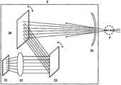
- FIG. 1is a schematic diagram of a common MEMS laser scanning unit 1, including a point light source 11, a fixed refractor 12, and a MEMS mirror unit 13.
- the holographic display technology of FIG. 1is to form a viewing zone by the laser scanning unit 1 of the micro-electromechanical system.
- the principleis to concentrate the single beam emitted by the point light source 11 to a certain point, and generate wavefront reconstruction at that point To form a flat image. Therefore, in order to make the image show a three-dimensional effect, multiple MEMS laser scanning units 1 must be formed into a MEMS laser scanning array to form multiple different points in space at the same time Holographic.
- the light sourceis a single point light conditions, it will take about 1 second up to 200 million pixels greater than 8x10 7 Hz x40fps Approximately imaging conditions, however, so if the image forming condition to form a full image to be projected, the image must be sacrificed Resolution.
- the shortcoming of the holographic display technology in FIG. 1is that it requires a large number of microelectromechanical system laser scanning units 1 to form a microelectromechanical system laser scanning array, so it has It is bulky, expensive to manufacture, and loses the holographic effect of short-range or long-range imaging.
- FIG. 2is a schematic diagram of an embodiment of the holographic display system 2 of the present application, including a light source 21, a first integrated system reflection device 22, and a second integrated system reflection device 23.
- the light source 21includes, but is not limited to, silicon-organic light-emitting diode (Si-OLED), silicon nitride micro-electromechanical system (SiN MEMS), micro organic light-emitting diode hybrid system (Micro LED) Hybrid system, laser light, low pixel matrix light source 1.
- the first integrated system reflection device 22may be a micro-electromechanical system mirror unit, or may be composed of multiple MEMS mirror array composed of two MEMS mirror units;
- the second integrated system reflecting device 23can be a MEMS mirror unit, or a MEMS mirror composed of multiple MEMS mirror units Mirror array.
- the holographic display system 2 of FIG. 2emits a light beam from a light source 21, a first integrated system reflection device 22 is disposed on the path of the light beam, the light beam is formed into a plurality of first reflected light beams, and a The second integrated system reflection device 23 is disposed on the path of the plurality of first reflected light beams, forms the plurality of first reflected light beams into a plurality of second reflected light beams, and forms a hologram from the plurality of second reflected light beams.
- Step 1at least one light beam is emitted from at least one light source, Step 2, the light beam is first reflected by a first integrated system reflection device to form a first reflected beam, Step 3 , And then reflected by a second integrated system reflection device to form a second reflected beam, wherein at least two of the second reflected beams form at least one focal point, and at least two of the second reflected beams form the at least one
- the focal pointproduces a wavefront reconstruction effect to form a hologram.
- the holographic display system 2 of FIG. 2adopts the first integrated system reflection device 22 and the second integrated system reflection device 23, respectively replacing the fixed mirror 12 and the MEMS mirror unit of the general MEMS laser scanning unit 1 13.
- the light beam generated by the light source 21 of the holographic display system 2 of FIG. 2is processed by two sets of movable integrated system reflection devices 22, 23 to form multiple point light sources after focusing at multiple locations, which can be formed Hologram with depth of field effect. Therefore, the holographic display system 2 only needs a light source with a lower pixel (2-100k pixels) and at least two integrated system reflection device units, which can achieve or even surpass the MEMS composed of multiple MEMS laser scanning units 1 in FIG.
- the effect of the system laser scanning array, and the two imaging methodsare different, this application can reduce production costs, greatly reduce the volume of the holographic display system, and improve the resolution of the holographic image.
- the light source 31includes, but is not limited to, silicon-organic light-emitting diodes, silicon nitride microelectromechanical systems, micro-organic light-emitting diode hybrid systems, laser light, low-pixel matrix light sources, digital light processing devices, or more than at least two of the above Light source group;
- the light processing device 32can be a collimating mirror, collimator, or light collimating element;
- the first integrated system reflecting device 33can be a micro-electromechanical system mirror unit, or by multiple MEMS mirror array composed of two MEMS mirror units;
- the second integrated system reflection device 34can be a MEMS mirror unit, or a MEMS mirror composed of multiple MEMS mirror units Mirror array;
- the reflective element 35may be a transparent / opaque reflective plate or
- the holographic display system 3 of FIG. 3may be that the light source 31 emits a plurality of point light sources, and a parallel beam group is formed by the light processing device 32, and these parallel beam groups are first processed by the first integrated system reflection device 33 to form a plurality of first
- the reflected light beamis processed by the second integrated system reflection device 34 to form a plurality of second reflected light beams, and then reflected at the reflective element 35 to form a plurality of third reflected light beams.
- the third reflected light beam formed at the reflective element 35can extend (as shown by the dotted line in FIG. 3) to the other side of the reflective element 35 to form a virtual focal point P, which generates a wavefront at the virtual focal point P Reconstruct the effect and form a hologram.
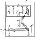
- the light source 41may be a digital light processing device, which includes a lamp 411 (Lamp), a condenser 412, a color filter 413, a shaping lens 414, and a digital micro-reflection chip (Digital Micro-mirror Device, DMD) 415;
- the first integrated system reflection device 42may be a micro-electro-mechanical system mirror unit, or a micro-electro-mechanical system reflection composed of multiple micro-electro-mechanical system mirror units Mirror array, or liquid crystal mirror;
- the second integrated system reflecting device 43can be a MEMS mirror unit, or a MEMS mirror array composed of multiple MEMS mirror units , Or a liquid crystal mirror;
- the reflective element 44can be a transparent / opaque reflector or mirror, including but not limited to a plane mirror, Fre
- the holographic display system 4 of FIG. 4may be that the light source 41 emits multiple beams, which are first processed by the first integrated system reflection device 42 to form multiple first reflected beams, and then processed by the second integrated system reflection device 43 to form multiple After the second reflected beam, a reflection is generated at the reflective element 44 to form a plurality of third reflected beams.
- the third reflected light beam formed at the reflective element 44can extend (as shown by the dotted line in FIG. 4) to the other side of the reflective element 44 to form a virtual focal point P, which generates a wavefront at the virtual focal point P Reconstruct the effect and form a hologram.
- the first integrated system reflection device 33, 42 and the second integrated system reflection device 34, 43 used in the holographic display systems 3, 4 of FIGS. 3 and 4can make the light beam form multiple point light sources, Thus forming a hologram with depth of field effect. Therefore, the holographic display system 3, 4 only requires a light source with a lower pixel (2-100k pixels) and at least two integrated system reflection device units, which can achieve or even surpass the composition of multiple MEMS laser scanning units 1 in FIG.
- the effect of the laser scanning array of the MEMS, and the two imaging methodsare different, this application can reduce production costs, greatly reduce the volume of the holographic display system, and improve the holographic resolution.
- this applicationonly needs a light source with a lower pixel (2-100kpixel) and a smaller volume of the holographic display system to generate a high pixel with a depth of field Holographic images, therefore, the present application can respond to the needs of different users to provide holographic 3D stereoscopic images suitable for different user fields of view, so as to reduce the burden on the eyes of the user by the holographic display system.
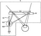
- FIG. 5is a schematic diagram of an embodiment in which the holographic display system of the present application is applied to glasses 5.
- the glasses 5includes a frame 51 and a lens group 52.
- the holographic display system provided in this embodimentincludes a light source 511 and two sets of integrated system reflection device arrays 512, which can be disposed in the spectacle frame 51 because of their small size.
- the light source 511includes, but is not limited to, laser light or a low-pixel matrix light source;
- the lens group 52includes a plurality of plane or refractive reflective lenses; in an embodiment, the integrated system reflection device array 512 may be a micro-electromechanical mirror array.
- the application example of the holographic display system in FIG. 5may be that a light source 511 and an integrated system reflection device array 512 are arranged in the frame 51 of the glasses 5, when the single or multiple light beams emitted by the light source 511 can be reflected by the integrated system reflection device After the array 512 processes and sequentially forms a plurality of first reflected light beams and a plurality of second reflected light beams, the second reflected light beams are then reflected to the lens group 52 of the glasses 5, and are reflected at the lens joint of the lens group 52 to form multiple Third reflected beam. As shown in FIG. 5, the third reflected light beams can extend into a virtual image on the other side of the lens group. This design can correspond to different users, expanding the user ’s field of view (FOV) range and the full depth of any depth of field. image.
- FOVfield of view
- FIG. 6is a schematic diagram of an embodiment in which the holographic display system of the present application is applied to the glasses 6.
- the glasses 6includes a frame 61 and a lens group 62.
- the holographic display system provided in this embodimentincludes a light source 611 and two sets of integrated system reflection device arrays 612, which can be disposed in the spectacle frame 51 due to their small size.
- the light source 611includes but is not limited to laser light or low-pixel matrix light source;
- the lens group 62includes multiple planar or refractive reflective lenses; in an embodiment, the integrated system reflection device array 612 may be a micro-electromechanical mirror array.
- the application example of the holographic display system of FIG. 6may be that a light source 611 and an integrated system reflection device array 612 are provided in the frame 61 of the glasses 6, when the single or multiple light beams emitted by the light source 611 can be reflected by the integrated system reflection device After the array 612 processes and sequentially forms a plurality of first reflected light beams and a plurality of second reflected light beams, the second reflected light beams are then reflected to the lens group 62 of the glasses 6 on the transparent reflection surface of the lens group 62 (such as Fresnel) At the ear (Fresnel reflection surface) to form a plurality of third reflected light beams. As shown in FIG. 6, the third reflected beams can be extended into a virtual image on the other side of the lens group. This design can correspond to different users, expanding the field of view (FOV) range of the user and the total image of any depth of field .
- FOVfield of view
- FIG. 7is a schematic diagram of visual imaging of a common myopic eye. As shown in FIG. 7, near-sightedness is a situation where the visual imaging of the eye is not focused on the retina, but is focused in front of the retina.
- FIG. 8is a schematic diagram of an embodiment in which the holographic display system of the present application is applied to glasses 8.
- the glasses 8includes a frame 81 and a lens 82.
- the holographic display system provided in this embodimentincludes a light source 811 and two sets of integrated system reflection device arrays 812, which can be disposed in the spectacle frame 51 due to their small size.
- the light source 811includes but is not limited to laser light or low-pixel matrix light source;
- the lens 82is a plastic or glass flat or refractive reflective lens; in an embodiment, the integrated system reflection device 812 may be a micro-electromechanical reflection device array.
- the application example of the holographic display system of FIG. 8may be that a light source 811 and an integrated system reflection device array 812 are arranged in the glasses frame 81 of the glasses 8.
- the integrated system reflection device 812 processingAfter forming a plurality of first reflected light beams and a plurality of second reflected light beams in sequence, the second reflected light beams are then reflected to the lens 82, and reflected at the lens 82 to form a plurality of third reflected light beams (as shown in FIG. 8 Dashed line shown).
- the glasses 8 of this embodimentmay be individually designed for different myopic users, and as shown in FIG.
- these third reflected light beamscan be imaged on the retina of the user ’s eyeball by adjusting the reflection angle according to the user ’s myopic degree. After wearing glasses 8, a user with myopia can achieve a refractive effect according to individual needs and see a clear hologram.
- the application examples of the holographic display system of Figs. 5, 6, and 8adopt the integrated system reflection device as shown in Figs. 2, 3, and / or 4, so that they are in line with common MEMS laser scanning arrays.
- the image imaging methodis different and the volume is reduced, but also the myopic user can clearly see the holographic image without burden on the eyes.
- FIG. 9is a flowchart of a method for forming a holographic effect.
- a wavefront reconstruction step 91where at least two light beams are provided by at least one light source, and the at least two beams meet to form a wavefront reconstruction.
- the wavefront reconstructed beamis received by a receiver.
- the wavefront reconstructed light beamforms a holographic effect.
- the light sourceis a digital light source.
- the light sourcecan control the intensity, color, frequency, and / or direction of the light beam.
- the holographic display system of this casecan also be applied to display devices such as HUDs, mobile phones, televisions, computers, or notebook computers by adjusting the angle of light beam reflection.
- vehicle safety regulationsstipulate that vehicle projection needs a distance of more than 7-20 meters. If this application is combined with windshield and AR technology to the head-up display projection technology of the car, it can overcome the limitation of the projection distance of the existing projection device It can reach more than 0-20 meters, and can overcome the limitation of the general display device's field of view of only 10 °, which can make it reach the range of 40 ° -50 °.
Landscapes
- Engineering & Computer Science (AREA)
- Multimedia (AREA)
- Signal Processing (AREA)
- Physics & Mathematics (AREA)
- Optics & Photonics (AREA)
- General Physics & Mathematics (AREA)
- Testing, Inspecting, Measuring Of Stereoscopic Televisions And Televisions (AREA)
- Diffracting Gratings Or Hologram Optical Elements (AREA)
Abstract
Description
Translated fromChinese本发明是关于一种显示系统,更具体地说,是关于一种能够产生具有景深的全像式影像的显示系统及其方法。The present invention relates to a display system, and more specifically, to a display system and method capable of generating a holographic image with depth of field.
传统的全像术(Holography)是透过记录胶片被摄物体反射或透射光波讯息的照相技术,再经过重建该纪录的物体反射或透射的光波讯息,制造出所述物体实际存在于三维(Three-dimensional,3D)空间的错觉。因此,从不同的方位和角度观察照片,可以看到被拍摄物体的不同角度,使人产生立体视觉。Traditional Holography is a photographic technology that records the reflected or transmitted light wave information of a photographed object through a film, and then reconstructs the recorded light reflected or transmitted light object to produce the actual existence of the object in three dimensions (Three -dimensional, 3D) spatial illusion. Therefore, looking at the photos from different orientations and angles, you can see the different angles of the object being shot, so that people produce stereo vision.
佩珀尔幻象(Pepper's ghost)的投射影像,是利用镜像折射原理,在观众眼前放置高解析度的二维(Two-dimensional,2D)影片,并在2D影片和观众之间架起金属薄片,使观众看见金属薄片上的反射影像,造成视觉上真实影像与虚拟影像融合而呈现的效果。由于上述2D影片投射成像的影像没有景深,因此并非真正的3D立体影像(Stereoscopic Images)。Pepper's phantom (Pepper's ghost) projection image is to use the principle of mirror refraction to place a high-resolution two-dimensional (2D) film in front of the audience, and put a metal sheet between the 2D film and the audience to make The audience sees the reflected image on the metal foil, which results in the fusion of visual and virtual images. Since the image projected by the above 2D film has no depth of field, it is not a true 3D stereoscopic image (Stereoscopic Images).
英国新创公司Kino-mo推出的投影装置「Hyper VSN」,具有嵌入发光二极管(Light-emitting diode,LED)的螺旋桨叶片,当螺旋桨旋转时,微处理器和感应器采集每处LED的角度,速度和位置,再向每个LED发送讯号,形成3D立体影像,产生空中有物体悬挂的错觉,其缺点在于立体影像解析度不佳。The projection device "Hyper VSN" launched by British startup Kino-mo has propeller blades embedded with light-emitting diodes (LEDs). When the propeller rotates, the microprocessor and sensor collect the angle of each LED. Speed and position, and then send a signal to each LED to form a 3D stereoscopic image, creating the illusion of an object hanging in the air. The disadvantage is that the resolution of the stereoscopic image is not good.
目前市面上常见的3D平面显示系统,如3D眼镜,可使人眼视觉看到3D立体影像;或者透过视差屏障(parallax barrier)或柱状透镜(cylindrical lens)来控制3D平面显示系统中光的投射方向,造成人眼视觉看到3D立体影像。然 而,眼睛的调节(Accommodation)功能,使得眼睛聚焦在传统的3D显示系统的荧幕上,而3D立体影像的辐辏点(Convergence)却是凸出或深入于荧幕,这种冲突会造成人眼看不清楚过凸或过凹的景物,从而造成眼睛疲劳,长期使用下甚至有可能引起眼科疾病。Common 3D flat display systems currently on the market, such as 3D glasses, enable human eyes to see 3D stereoscopic images; or through parallax barriers (cylindrical barriers) or cylindrical lenses (cylindrical lenses) to control the light in the 3D flat display system The projection direction causes human eyes to see 3D stereoscopic images. However, the adjustment function of the eye makes the eye focus on the screen of the traditional 3D display system, and the convergence of the 3D stereoscopic image is protruding or deeper into the screen. This conflict will cause people It is difficult to see overly convex or concave scenes, which can cause eye fatigue. It may even cause ophthalmic diseases under long-term use.
Yasuhiro Takaki推出的全像显示技术(Yasuhiro Takaki,"Development of scanning holographic display using MEMS SLM,"Proc.SPIE 10022,Holography,Diffractive Optics,and Applications VII,100220J(31 October 2016)),是采用一个固定式折射镜(Fixed mirror)以及一个微机电系统(Microelectromechanical Systems,MEMS)反射镜单元(unit)组成一个微机电系统雷射扫描单元,再由至少两个微机电系统雷射扫描单元组成微机电系统雷射扫描阵列(arrays)。其缺点在于,为了提供具有超高解析度的足够屏幕尺寸和观看区域,所述显示系统的微机电系统雷射扫描阵列的体积将甚为庞大,此外每一个微机电系统体积过大造成近距离或远距离显像射失去全像效果,不利于应用。The holographic display technology (Yasuhiro Takaki, "Development of scanning" Holographic "display" using MEMS "SLM," Proc.SPIE 10022, Holography, Diffractive Active Optics, and Applications VII, 100220J (31 October 2016)), which is a fixed type The refracting mirror (Fixed mirror) and a microelectromechanical systems (MEMS) mirror unit (microelectromechanical systems) mirror unit (unit) constitutes a microelectromechanical system laser scanning unit, and then consists of at least two microelectromechanical system laser scanning units to form a microelectromechanical system laser Scan arrays. The disadvantage is that, in order to provide sufficient screen size and viewing area with ultra-high resolution, the volume of the laser scanning array of the microelectromechanical system of the display system will be very large, and in addition, the volume of each microelectromechanical system is too large, resulting in close range Or long-range imaging loses the holographic effect, which is not conducive to application.
再以现有的微型投影技术(Optical micro-projection system and projection method,美国专利编号US9,374,566 B2)为例,其是应用2个微机电系统反射镜单元组成一组投影装置的技术,以降低投影机的体积。然而,该投影技术的成像仍为一2D的平面投影图像。Taking the existing micro-projection technology (Optical micro-projection system and projection method, US Patent No. US 9,374,566 B2) as an example, it is a technology that uses 2 MEMS mirror units to form a group of projection devices to reduce The volume of the projector. However, the imaging of the projection technology is still a 2D planar projection image.
此外,全息投影技术(Holographic projection device for the enlargement of a reconstruction zone,美国专利编号US8,335,028B2)是利用数个微镜元件组成一组阵列,其中每个微镜元件与相对应的致动器耦合,藉由将入射波前直接调制生成反射波前,造成可重建场景的波阵面,而达成全息投影的效果,然而此技术的光源为平面波前,且观察者仅能在一受限的平面观察范围内,才能看到于一焦平面重建的全像式影像。In addition, holographic projection technology (Holographic projection device for the enlargement of reconstruction zone, US Patent No. US8,335,028B2) is to use a number of micromirror elements to form a group of arrays, where each micromirror element corresponds to the corresponding actuator Coupling, by directly modulating the incident wavefront to generate a reflected wavefront, resulting in a wavefront that can reconstruct the scene, and achieve the effect of holographic projection. However, the light source of this technology is a plane wavefront, and the observer can only be in a limited Within the scope of plane observation, the holographic image reconstructed in a focal plane can be seen.
为了解决上述问题,实有必要提供一种体积小、便于应用,且具有成本优势的全像显示系统,不仅能够以其独特的方法产生具有景深的高解析度3D立体图像,还能够对应不同使用者间的需求,来提供适合不同使用者视野的全像式3D立体图像,以降低全像显示系统对使用人的眼睛的负担。In order to solve the above problems, it is necessary to provide a holographic display system that is small, easy to apply, and has a cost advantage. It can not only produce a high-resolution 3D stereoscopic image with depth of field in its unique method, but also can respond to different uses. There is a need among users to provide holographic 3D stereoscopic images suitable for different user fields of view, so as to reduce the burden on the user's eyes by the holographic display system.
发明内容Summary of the invention
本案提供一种全像显示系统,包括:至少一光源,所述光源发射一光束;一第一整合系统反射装置,设置于所述光束的路径上,将所述光束形成至少一第一反射光束;以及一第二整合系统反射装置,设置于所述至少一第一反射光束的路径上,将所述至少一第一反射光束形成至少一第二反射光束,其中,至少两个所述第二反射光束形成一全像。The present case provides a holographic display system, including: at least one light source that emits a light beam; and a first integrated system reflection device disposed on the path of the light beam to form the light beam into at least a first reflected light beam ; And a second integrated system reflecting device, disposed on the path of the at least one first reflected beam, forming the at least one first reflected beam to form at least one second reflected beam, wherein at least two of the second The reflected beam forms a hologram.
根据上述构想,其中所述光源选自包括硅-有机发光二极管、氮化硅微机电系统、微有机发光二极管混合系统、雷射光、低像素矩阵光源、数位光处理装置或上述至少二者以上的群组。According to the above concept, wherein the light source is selected from the group consisting of silicon-organic light-emitting diodes, silicon nitride microelectromechanical systems, micro-organic light-emitting diode hybrid systems, laser light, low-pixel matrix light sources, digital light processing devices, or at least two or more of the above Group.
根据上述构想,其中所述第一整合系统反射装置为一第一微机电系统反射装置单元,或由至少两个所述第一微机电系统反射装置单元组成的一第一微机电系统反射装置阵列。According to the above conception, wherein the first integrated system reflecting device is a first MEMS reflecting device unit, or a first MEMS reflecting device array composed of at least two of the first MEMS reflecting device units .
根据上述构想,其中所述第二整合系统反射装置为一第二微机电系统反射装置单元,或由至少两个所述第二微机电系统反射装置单元组成的一第二微机电系统反射装置阵列。According to the above conception, wherein the second integrated system reflection device is a second MEMS reflection device unit, or a second MEMS reflection device array composed of at least two second MEMS reflection device units .
根据上述构想,其中所述至少两个第二反射光束,形成至少一聚焦处。According to the above conception, wherein the at least two second reflected light beams form at least one focal point.
根据上述构想,其中所述全像显示系统更进一步包括一反射装置,所述反射装置设置于所述至少一第二反射光束的路径上,形成至少一第三反射光束。According to the above concept, wherein the holographic display system further includes a reflecting device, the reflecting device is disposed on the path of the at least one second reflected light beam to form at least one third reflected light beam.
根据上述构想,其中所述反射装置包括至少一反射元件。According to the above concept, wherein the reflecting device includes at least one reflecting element.
根据上述构想,其中所述反射元件选自包括平面镜、菲涅耳透镜、曲面镜、屈光镜、平面反射镜阵列、周期结构的纳米结构高分子膜、绕射布拉格光栅波导,可显示图象的模组或上述至少二者以上的群组。According to the above concept, wherein the reflective element is selected from the group consisting of flat mirrors, Fresnel lenses, curved mirrors, dioptric mirrors, flat mirror arrays, periodic structured nanostructured polymer films, and diffractive Bragg grating waveguides, which can display images Groups or groups of at least two of the above.
根据上述构想,其中所述全像显示系统更进一步包括一光处理装置,所述光处理装置设置于所述光源及所述第一整合系统反射装置间,且位于所述光束的路径上。According to the above concept, wherein the holographic display system further includes a light processing device, the light processing device is disposed between the light source and the first integrated system reflection device, and is located on the path of the light beam.
根据上述构想,其中所述光处理装置为准直镜、准直器、或光准直元件。According to the above conception, wherein the light processing device is a collimating mirror, a collimator, or a light collimating element.
本案提供一种形成全像的方法,包括:步骤1,其特征在于由至少一光源发射至少一光束;步骤2,其特征在于由一第一整合系统反射装置将所述光束形成一第一反射光束;步骤3,其特征在于由一第二整合系统反射装置将所述第一反射光束形成一第二反射光束;其中,至少两个所述第二反射光束形成至少一聚焦处;以及至少两个所述第二反射光束于所述至少一聚焦处产生一全像。This case provides a method for forming a hologram, including:
根据上述构想,其中所述光源选自包括硅-有机发光二极管、氮化硅微机电系统、微有机发光二极管混合系统、雷射光、低像素矩阵光源、数位光处理装置或上述至少二者以上的群组。According to the above concept, wherein the light source is selected from the group consisting of silicon-organic light-emitting diodes, silicon nitride microelectromechanical systems, micro-organic light-emitting diode hybrid systems, laser light, low-pixel matrix light sources, digital light processing devices, or at least two or more of the above Group.
根据上述构想,其中所述第一整合系统反射装置为一第一微机电系统反射装置单元,或由至少两个所述第一微机电系统反射装置单元组成的一第一微机电系统反射装置阵列。According to the above conception, wherein the first integrated system reflecting device is a first MEMS reflecting device unit, or a first MEMS reflecting device array composed of at least two of the first MEMS reflecting device units .
根据上述构想,其中所述第二整合系统反射装置为一第二微机电系统反射装置单元,或由至少两个所述第二微机电系统反射装置单元组成的一第二微机电系统反射装置阵列。According to the above conception, wherein the second integrated system reflection device is a second MEMS reflection device unit, or a second MEMS reflection device array composed of at least two second MEMS reflection device units .
根据上述构想,其中所述的方法更进一步包括一步骤,由一反射装置将所 述第二反射光束反射为第三反射光束,所述反射装置设置于所述第二反射光束的路径上。According to the above concept, the method further includes a step of reflecting the second reflected light beam into a third reflected light beam by a reflecting device, and the reflecting device is disposed on the path of the second reflected light beam.
根据上述构想,其中所述反射裝置包括至少一反射元件。According to the above concept, wherein the reflecting device includes at least one reflecting element.
根据上述构想,其中所述反射元件选自包括平面镜、菲涅耳透镜、曲面镜、屈光镜、平面反射镜阵列、周期结构的纳米结构高分子膜、绕射布拉格光栅波导,可显示图像的模组或上述至少二者以上的群组。According to the above concept, wherein the reflective element is selected from a module including a plane mirror, a Fresnel lens, a curved mirror, a dioptric mirror, a plane mirror array, a periodic structure of a nanostructured polymer film, a diffractive Bragg grating waveguide, and an image display Or a group of at least two of the above.
根据上述构想,其中步骤1及步骤2间更进一步包括一步骤:由一光处理装置使所述光束达到近乎平行,所述光处理装置设置于所述光源及所述第一整合系统反射装置间,且位于所述光束的路径上。According to the above concept,
根据上述构想,其中所述光处理装置为准直镜、准直器、或光准直元件。According to the above conception, wherein the light processing device is a collimating mirror, a collimator, or a light collimating element.
本案另提供一种形成全像的方法,包括:步骤1,其特征在于由至少一光源提供至少两个光束,所述至少两个光束交会后形成一波前重建;步骤2,其特征在于由一接收器接收所述波前重建的光束;以及步骤3,其特征在于所述波前重建的光束形成一全像效果。This case also provides a method of forming a hologram, including:
根据上述构想,其中所述光源为一数位光源。According to the above conception, wherein the light source is a digital light source.
根据上述构想,其中所述光源可以控制所述光束的强度、颜色、频率和/或方向。According to the above concept, wherein the light source can control the intensity, color, frequency and / or direction of the light beam.
图1为一常见的微机电系统雷射扫描单元示意图。FIG. 1 is a schematic diagram of a common laser scanning unit of a micro-electromechanical system.
图2为本申请的全像显示系统的一实施例示意图。FIG. 2 is a schematic diagram of an embodiment of the holographic display system of the present application.
图3为本申请的全像显示系统的一实施例示意图。FIG. 3 is a schematic diagram of an embodiment of the holographic display system of the present application.
图4为本申请的全像显示系统的一实施例示意图。4 is a schematic diagram of an embodiment of the holographic display system of the present application.
图5为本申请的全像显示系统应用于眼镜的一实施例示意图。FIG. 5 is a schematic diagram of an embodiment in which the holographic display system of the present application is applied to glasses.
图6为本申请的全像显示系统应用于眼镜的一实施例示意图。FIG. 6 is a schematic diagram of an embodiment in which the holographic display system of the present application is applied to glasses.
图7为一常见的近视眼的视觉成像示意图。7 is a schematic diagram of visual imaging of a common myopic eye.
图8为本申请的全像显示系统应用于眼镜的一实施例示意图。FIG. 8 is a schematic diagram of an embodiment in which the holographic display system of the present application is applied to glasses.
图9为一种形成全像效果的方法流程图。9 is a flowchart of a method for forming a holographic effect.
本申请能够以多种形式及方式实现,在以下实施例以及图式中所描述的内容,是展示本申请的实施方式。所属技术领域中具有通常知识者,能够以其他未展示的方式实施本申请,本申请的权利范围应以权利要求项为准。The present application can be implemented in various forms and ways. The contents described in the following examples and drawings illustrate the implementation of the present application. Those with ordinary knowledge in the technical field can implement this application in other ways not shown, and the scope of rights of this application should be subject to the claims.
请参阅图1。Please refer to Figure 1.
图1为一常见的微机电系统雷射扫描单元1示意图,包括点光源11、固定式折射镜12,以及微机电系统反射镜单元13。FIG. 1 is a schematic diagram of a common MEMS
图1的全像显示技术,是由微机电系统雷射扫描单元1形成一视区(viewing zone),其原理是将点光源11射出的单一光束集中到某一点,于该点产生波前重建效果而形成平面影像,因此,为了使影像呈现出立体效果,必须将多个微机电系统雷射扫描单元1组成微机电系统雷射扫描阵列,才能同时于空间中呈现多个不同的点而形成全像。此外,在光源为单一点光源的条件下,大概需耗时1秒可达到200万画素x40fps约需大于8x10⁷赫兹的成像条件,然而,若依此成像条件欲形成全像投影,必须牺牲影像的解析度才能达成。基于上述可知,为了提供具有超高解析度的足够屏幕尺寸和观看区域,图1全像显示技术的缺点在于需由众多微机电系统雷射扫描单元1组成微机电系统雷射扫描阵列,因而有着体积大、造价昂贵,以及近距离或远距离显像射失去全像效果等问题。The holographic display technology of FIG. 1 is to form a viewing zone by the
请参阅图2。Please refer to Figure 2.
图2为本申请的全像显示系统2的一实施例示意图,包括光源21、第一整合系统反射装置22,以及第二整合系统反射装置23。其中,光源21包含但不限于硅-有机发光二极管(Si-OLED)、氮化硅微机电系统(SiN MEMS)、微有机发光二极管混合系统(Micro LED Hybrid System)、雷射光、低像素矩阵光源、数位光处理装置(Digital Light Processing,DLP),或者为上述至少二者以上的群组;在实施例中,第一整合系统反射装置22可为一微机电系统反射镜单元,或是由多个微机电系统反射镜单元组成的微机电系统反射镜阵列;第二整合系统反射装置23可为一微机电系统反射镜单元,或是由多个微机电系统反射镜单元组成的微机电系统反射镜阵列。FIG. 2 is a schematic diagram of an embodiment of the holographic display system 2 of the present application, including a light source 21, a first integrated system reflection device 22, and a second integrated system reflection device 23. Among them, the light source 21 includes, but is not limited to, silicon-organic light-emitting diode (Si-OLED), silicon nitride micro-electromechanical system (SiN MEMS), micro organic light-emitting diode hybrid system (Micro LED) Hybrid system, laser light, low pixel
图2的全像显示系统2是由光源21发射一光束,将一第一整合系统反射装置22,设置于所述光束的路径上,将所述光束形成多个第一反射光束,并将一第二整合系统反射装置23,设置于多个第一反射光束的路径上,将所述多个第一反射光束形成多个第二反射光束,并由多个第二反射光束形成一全像。The holographic display system 2 of FIG. 2 emits a light beam from a light source 21, a first integrated system reflection device 22 is disposed on the path of the light beam, the light beam is formed into a plurality of first reflected light beams, and a The second integrated system reflection device 23 is disposed on the path of the plurality of first reflected light beams, forms the plurality of first reflected light beams into a plurality of second reflected light beams, and forms a hologram from the plurality of second reflected light beams.
而运用本申请形成全像的方法,其步骤为:步骤1,由至少一光源发射至少一光束,步骤2,该光束首先经由一第一整合系统反射装置反射,形成第一反射光束,步骤3,再经由一第二整合系统反射装置反射,形成第二反射光束,其中,至少两个所述第二反射光束形成至少一聚焦处,以及至少两个所述第二反射光束于所述至少一聚焦处产生波前重建效果而形成一全像。Using the method of forming a hologram of the present application, the steps are:
图2的全像显示系统2是采用第一整合系统反射装置22以及第二整合系统反射装置23,分别取代了一般微机电系统激光扫描单元1的固定式反射镜12以及微机电系统反射镜单元13。与图1相比,图2全像显示系统2的光源21产生的光束,经由两组可动式的整合系统反射装置22,23处理,于多处聚焦后形成多 个点光源,即可形成具有景深效果的全像。因此,全像显示系统2仅需要较低像素(2~100k pixel)的光源以及至少两个整合系统反射装置单元,即可达到甚或超越图1多个微机电系统激光扫描单元1组成的微机电系统激光扫描阵列的效果,且两者成像方式不同,本申请可降低生产成本、大幅缩减全像显示系统的体积,并提升全像的解析度。The holographic display system 2 of FIG. 2 adopts the first integrated system reflection device 22 and the second integrated system reflection device 23, respectively replacing the fixed
请参阅图3。Please refer to Figure 3.
图3为本申请的全像显示系统3的一实施例示意图,包括光源31、光处理装置32、第一整合系统反射装置33、第二整合系统反射装置34,以及反射元件35。其中,光源31包含但不限于硅-有机发光二极管、氮化硅微机电系统、微有机发光二极管混合系统、雷射光、低像素矩阵光源、数位光处理装置,或者为上述至少二者以上的多光源群组;光处理装置32可以为准直镜、准直器、或光准直元件;在实施例中,第一整合系统反射装置33可为一微机电系统反射镜单元,或是由多个微机电系统反射镜单元组成的微机电系统反射镜阵列;第二整合系统反射装置34可为一微机电系统反射镜单元,或是由多个微机电系统反射镜单元组成的微机电系统反射镜阵列;反射元件35可以为透明/不透明的反射板或反射镜,包括但不限于平面镜、菲涅耳透镜(Fresnel lens)、曲面镜、屈光镜、平面反射镜阵列、可显示图像的模组或上述至少二者以上的群组。3 is a schematic diagram of an embodiment of the
图3的全像显示系统3可以是光源31发射多个点光源,通过光处理装置32形成平行的光束组,该些平行光束组首先经由第一整合系统反射装置33处理,形成多个第一反射光束,再经由第二整合系统反射装置34处理,形成多个第二反射光束后,再于反射元件35处产生反射,形成多个第三反射光束。而如图3所示,在反射元件35处形成的第三反射光束,可以延伸(如图3绘示的虚线)至反射元件35的另一侧形成虚焦点P,在虚焦点P产生波前重建效果而形成全 像。The
请参阅图4。Please refer to Figure 4.
图4为本申请的全像显示系统4的一实施例示意图,包括光源41、第一整合系统反射装置42、第二整合系统反射装置43,以及反射元件44。其中,光源41可为数位光处理装置,其包括灯411(Lamp)、聚光镜(condensing lens)412、色彩滤波器(color filter)413、光塑型镜(shaping lens)414,以及数位微反射晶片(Digital Micro-mirror Device,DMD)415;在实施例中,第一整合系统反射装置42可为一微机电系统反射镜单元,或是由多个微机电系统反射镜单元组成的微机电系统反射镜阵列,或是液晶反射镜(liquid crystal mirror);第二整合系统反射装置43可为一微机电系统反射镜单元,或是由多个微机电系统反射镜单元组成的微机电系统反射镜阵列,或是液晶反射镜;反射元件44可以为透明/不透明的反射板或反射镜,包括但不限于平面镜、菲涅耳透镜、曲面镜、屈光镜、平面反射镜阵列、周期结构的纳米结构高分子膜(periodic nanostructure photopolymer film)、绕射布拉格光栅波导(Bragg grating waveguide),可显示图像的模组或上述至少二者以上的群组。4 is a schematic diagram of an embodiment of the holographic display system 4 of the present application, including a light source 41, a first integrated system reflection device 42, a second integrated system reflection device 43, and a reflective element 44. The light source 41 may be a digital light processing device, which includes a lamp 411 (Lamp), a condenser 412, a color filter 413, a shaping lens 414, and a digital micro-reflection chip (Digital Micro-mirror Device, DMD) 415; in an embodiment, the first integrated system reflection device 42 may be a micro-electro-mechanical system mirror unit, or a micro-electro-mechanical system reflection composed of multiple micro-electro-mechanical system mirror units Mirror array, or liquid crystal mirror; the second integrated system reflecting device 43 can be a MEMS mirror unit, or a MEMS mirror array composed of multiple MEMS mirror units , Or a liquid crystal mirror; the reflective element 44 can be a transparent / opaque reflector or mirror, including but not limited to a plane mirror, Fresnel lens, curved mirror, diopter, plane mirror array, periodic structure of nanostructured polymer Film (periodic nanostructure photopolymer film), diffractive Bragg grating waveguide (Bragggratingwaveguide), a module that can display images or the above to More than two groups.
图4的全像显示系统4可以是光源41发射多个光束,首先经由第一整合系统反射装置42处理,形成多个第一反射光束,再经由第二整合系统反射装置43处理,形成多个第二反射光束后,再于反射元件44处产生反射,形成多个第三反射光束。而如图4所示,在反射元件44处形成的第三反射光束,可以延伸(如图4绘示的虚线)至反射元件44的另一侧形成虚焦点P,在虚焦点P产生波前重建效果而形成全像。The holographic display system 4 of FIG. 4 may be that the light source 41 emits multiple beams, which are first processed by the first integrated system reflection device 42 to form multiple first reflected beams, and then processed by the second integrated system reflection device 43 to form multiple After the second reflected beam, a reflection is generated at the reflective element 44 to form a plurality of third reflected beams. As shown in FIG. 4, the third reflected light beam formed at the reflective element 44 can extend (as shown by the dotted line in FIG. 4) to the other side of the reflective element 44 to form a virtual focal point P, which generates a wavefront at the virtual focal point P Reconstruct the effect and form a hologram.
与图1相比,图3及图4的全像显示系统3,4所采用的第一整合系统反射装置33,42以及第二整合系统反射装置34,43能够使光束形成多个点光源,从而形 成具有景深效果的全像。因此,全像显示系统3,4仅需要较低像素(2~100k pixel)的光源以及至少两个整合系统反射装置单元,即可达到甚或超越图1多个微机电系统雷射扫描单元1组成的微机电系统雷射扫描阵列的效果,且两者成像方式不同,本申请可降低生产成本、大幅缩减全像显示系统体积,并提升全像解析度。Compared with FIG. 1, the first integrated
请参阅图5至图8。Please refer to Figure 5 to Figure 8.
藉由图2、图3和/或图4实施例的技术,本申请仅需要较低像素(2~100k pixel)的光源及较小的全像显示系统体积,即可产生具有景深的高像素全像式影像,因此,本申请能够对应不同使用者间的需求,来提供适合不同使用者视野的全像式3D立体影像,以降低全像显示系统对使用人的眼睛的负担。With the technology of the embodiment of FIG. 2, FIG. 3 and / or FIG. 4, this application only needs a light source with a lower pixel (2-100kpixel) and a smaller volume of the holographic display system to generate a high pixel with a depth of field Holographic images, therefore, the present application can respond to the needs of different users to provide holographic 3D stereoscopic images suitable for different user fields of view, so as to reduce the burden on the eyes of the user by the holographic display system.
图5为本申请的全像显示系统应用于眼镜5的一实施例示意图,眼镜5包括眼镜架51以及镜片组52。本实施例提供的全像显示系统包括光源511以及两组整合系统反射装置阵列512,其因体积小而可以设置在眼镜架51内。其中,光源511包含但不限于雷射光或低像素矩阵光源;镜片组52包括多片平面或屈光反射镜片;在实施例中,整合系统反射装置阵列512可以是微机电反射镜阵列。FIG. 5 is a schematic diagram of an embodiment in which the holographic display system of the present application is applied to
图5的全像显示系统应用实施例,可以是在眼镜5的眼镜架51内设置光源511以及整合系统反射装置阵列512,当光源511发射的单一或多个光束,能够藉由整合系统反射装置阵列512处理,依序形成多个第一反射光束与多个第二反射光束后,该些第二反射光束再反射至眼镜5的镜片组52,于镜片组52的镜片接合处反射,形成多个第三反射光束。如图5所示,该些第三反射光束可以在镜片组的另一侧延伸成虚像,此设计可以对应不同使用者,扩大使用者的视野(field of view,FOV)范围与任意景深的全像。The application example of the holographic display system in FIG. 5 may be that a
图6为本申请的全像显示系统应用于眼镜6的一实施例示意图,眼镜6包括眼镜架61以及镜片组62。本实施例提供的全像显示系统包括光源611以及两组整合系统反射装置阵列612,其因体积小而可以设置在眼镜架51内。其中,光源611包含但不限于雷射光或低像素矩阵光源;镜片组62包括多片平面或屈光反射镜片;在实施例中,整合系统反射装置阵列612可以是微机电反射镜阵列。FIG. 6 is a schematic diagram of an embodiment in which the holographic display system of the present application is applied to the
图6的全像显示系统应用实施例,可以是在眼镜6的眼镜架61内设置光源611以及整合系统反射装置阵列612,当光源611发射的单一或多个光束,能够藉由整合系统反射装置阵列612处理,依序形成多个第一反射光束与多个第二反射光束后,该些第二反射光束再反射至眼镜6的镜片组62,于镜片组62的透明反射面(如菲涅耳(Fresnel)反射面)处反射,形成多个第三反射光束。如图6所示,该些第三反射光束可以在镜片组的另一侧延伸成虚像,此设计可以对应不同使用者,扩大使用者视野(field of view,FOV)范围与任意景深的全像。The application example of the holographic display system of FIG. 6 may be that a
请参阅图7与图8。Please refer to Figure 7 and Figure 8.
图7为一常见的近视眼的视觉成像示意图。如图7所示,近视(Near-sightedness)是眼睛视觉成像并未聚焦在视网膜上,而是聚焦在视网膜之前的情形。7 is a schematic diagram of visual imaging of a common myopic eye. As shown in FIG. 7, near-sightedness is a situation where the visual imaging of the eye is not focused on the retina, but is focused in front of the retina.
图8为本申请的全像显示系统应用于眼镜8的一实施例示意图,眼镜8包括眼镜架81以及镜片82。本实施例提供的全像显示系统包括光源811以及两组整合系统反射装置阵列812,其因体积小而可以设置在眼镜架51内。其中,光源811包含但不限于雷射光或低像素矩阵光源;镜片82为塑胶或玻璃材质的平面或屈光反射镜片;在实施例中,整合系统反射装置812可以是微机电反射装置阵列。FIG. 8 is a schematic diagram of an embodiment in which the holographic display system of the present application is applied to
与图7相比,图8的全像显示系统应用实施例,可以是在眼镜8的眼镜架81内设置光源811以及整合系统反射装置阵列812,当光源811发射的光束藉由整合系统反射装置812处理,依序形成多个第一反射光束与多个第二反射光束后,该些第二反射光束再反射至镜片82,于镜片82处反射形成多个第三反射光束(如图8绘示的虚线)。本实施例的眼镜8,可以是为了不同的近视使用者个别设计而成,而如图8所示,这些第三反射光束可以依使用者近视度数调整反射角度在使用者眼球的视网膜上成像,使具有近视的使用者在配戴眼镜8后,能够按照个别需求达到屈光效果,看到清晰的全像。Compared with FIG. 7, the application example of the holographic display system of FIG. 8 may be that a
图5、6、8的全像显示系统应用实施例,是采用了如图2、图3和/或图4所示的整合系统反射装置,因此,与常见的微机电系统雷射扫描阵列相比,不仅影像成像方式不同、体积减小,还能令近视的使用者在眼睛无负担的情况下,清楚地看到全像式影像。The application examples of the holographic display system of Figs. 5, 6, and 8 adopt the integrated system reflection device as shown in Figs. 2, 3, and / or 4, so that they are in line with common MEMS laser scanning arrays. In addition, not only the image imaging method is different and the volume is reduced, but also the myopic user can clearly see the holographic image without burden on the eyes.
请参阅图9。See Figure 9.
图9为一种形成全像效果的方法流程图。运用本申请的方法时,有一波前重建步骤91,由至少一光源提供至少两个光束,所述至少两个光束交会后形成一波前重建。再经由一光束接收步骤92,由一接收器接收所述波前重建的光束。在一全像效果形成步骤93中,所述波前重建的光束形成一全像效果。在一实施例中,所述光源为一数位光源。在另一实施例中,所述光源可以控制所述光束的强度、颜色、频率和/或方向。9 is a flowchart of a method for forming a holographic effect. When using the method of the present application, there is a
本案的全像显示系统,还可以藉由调整光束反射的角度,应用于汽车抬头显示器HUD、手机、电视、电脑或笔记型电脑等显示设备。目前汽车安全法规规定车用投影需达7~20公尺以上的距离,如将本申请结合挡风玻璃与AR技术应用到汽车的抬头显示器投影技术上,可以克服现有投影装置投影距离的限 制,达到0-20公尺以上,并能够克服一般显示装置视野只有10°的限制,可使其达到40°~50°的范围。The holographic display system of this case can also be applied to display devices such as HUDs, mobile phones, televisions, computers, or notebook computers by adjusting the angle of light beam reflection. At present, automobile safety regulations stipulate that vehicle projection needs a distance of more than 7-20 meters. If this application is combined with windshield and AR technology to the head-up display projection technology of the car, it can overcome the limitation of the projection distance of the existing projection device It can reach more than 0-20 meters, and can overcome the limitation of the general display device's field of view of only 10 °, which can make it reach the range of 40 ° -50 °.
符号说明Symbol Description
1 微机电系统雷射扫描单元1 MEMS laser scanning unit
11 点光源11 Point light source
12 固定式折射镜12 Fixed refracting mirror
13 微机电系统反射镜13 MEMS mirror
2 全像显示系统2 Holographic display system
21 光源21 Light source
22 第一整合系统反射装置22 First integrated system reflection device
23 第二整合系统反射装置23 Second integrated system reflection device
3 全像显示系统3 Holographic display system
31 光源31 Light source
32 光处理装置32 Light processing device
33 第一整合系统反射装置33 First integrated system reflection device
34 第二整合系统反射装置34 Second integrated system reflection device
35 反射元件35 reflective elements
4 全像显示系统4 Holographic display system
41 光源41 Light source
411 灯411 lights
412 聚光镜412 Condenser lens
413 色彩滤波器413 Color filter
414 光塑型镜414 Light shaping mirror
415 数位微反射晶片415 Digital micro-reflection chip
42 第一整合系统反射装置42 First integrated system reflection device
43 第二整合系统反射装置43 Second integrated system reflection device
44 反射元件44 Reflective elements
5 眼镜5 Glasses
51 眼镜架51 glasses frames
511 光源511 light source
512 整合系统反射装置阵列512 Integrated system reflection device array
52 镜片组52 lens group
6 眼镜6 Glasses
61 眼镜架61 glasses frames
611 光源611 light source
612 整合系统反射装置阵列612 Integrated system reflection device array
62 镜片组62 lens group
8 眼镜8 Glasses
81 眼镜架81 glasses frame
811 光源811 light source
812 整合系统反射装置阵列812 Integrated system reflection device array
82 镜片82 lenses
91 波前重建步骤91 Wavefront reconstruction steps
92 光束接收步骤92 Beam receiving steps
93 全像效果形成步骤93 Steps for forming holographic effect
P 虚焦点P virtual focus
Claims (29)
Translated fromChinesePriority Applications (5)
| Application Number | Priority Date | Filing Date | Title |
|---|---|---|---|
| PCT/CN2018/112305WO2020087195A1 (en) | 2018-10-29 | 2018-10-29 | Holographic display system and method for forming holographic image |
| EP19878384.7AEP3874743B1 (en) | 2018-10-29 | 2019-10-29 | System and method for displaying a 3d image with depths |
| CN201980071908.2ACN112970247B (en) | 2018-10-29 | 2019-10-29 | System and method for displaying multiple depth-of-field images |
| US17/289,238US11924401B2 (en) | 2018-10-29 | 2019-10-29 | System and method for displaying a 3D image with depths |
| PCT/CN2019/114089WO2020088468A1 (en) | 2018-10-29 | 2019-10-29 | System and method for displaying a 3d image with depths |
Applications Claiming Priority (1)
| Application Number | Priority Date | Filing Date | Title |
|---|---|---|---|
| PCT/CN2018/112305WO2020087195A1 (en) | 2018-10-29 | 2018-10-29 | Holographic display system and method for forming holographic image |
Publications (1)
| Publication Number | Publication Date |
|---|---|
| WO2020087195A1true WO2020087195A1 (en) | 2020-05-07 |
Family
ID=70462520
Family Applications (2)
| Application Number | Title | Priority Date | Filing Date |
|---|---|---|---|
| PCT/CN2018/112305CeasedWO2020087195A1 (en) | 2018-10-29 | 2018-10-29 | Holographic display system and method for forming holographic image |
| PCT/CN2019/114089CeasedWO2020088468A1 (en) | 2018-10-29 | 2019-10-29 | System and method for displaying a 3d image with depths |
Family Applications After (1)
| Application Number | Title | Priority Date | Filing Date |
|---|---|---|---|
| PCT/CN2019/114089CeasedWO2020088468A1 (en) | 2018-10-29 | 2019-10-29 | System and method for displaying a 3d image with depths |
Country Status (4)
| Country | Link |
|---|---|
| US (1) | US11924401B2 (en) |
| EP (1) | EP3874743B1 (en) |
| CN (1) | CN112970247B (en) |
| WO (2) | WO2020087195A1 (en) |
Cited By (1)
| Publication number | Priority date | Publication date | Assignee | Title |
|---|---|---|---|---|
| US11924401B2 (en) | 2018-10-29 | 2024-03-05 | Hes Ip Holdings, Llc | System and method for displaying a 3D image with depths |
Families Citing this family (1)
| Publication number | Priority date | Publication date | Assignee | Title |
|---|---|---|---|---|
| US12253669B2 (en)* | 2020-11-20 | 2025-03-18 | Google Llc | Time-sequential MEMS projector |
Citations (4)
| Publication number | Priority date | Publication date | Assignee | Title |
|---|---|---|---|---|
| CN1800963A (en)* | 2005-01-06 | 2006-07-12 | 明基电通股份有限公司 | projection display device |
| CN103913940A (en)* | 2012-12-28 | 2014-07-09 | 台达电子工业股份有限公司 | Stereoscopic projection device and display method using same |
| CN105607454A (en)* | 2016-01-25 | 2016-05-25 | 京东方科技集团股份有限公司 | Holographic display apparatus and holographic display method |
| CN108663874A (en)* | 2018-04-16 | 2018-10-16 | 广景视睿科技(深圳)有限公司 | A kind of optical element and bidirectional projection's system |
Family Cites Families (10)
| Publication number | Priority date | Publication date | Assignee | Title |
|---|---|---|---|---|
| US6563105B2 (en) | 1999-06-08 | 2003-05-13 | University Of Washington | Image acquisition with depth enhancement |
| CN102823264A (en) | 2011-03-31 | 2012-12-12 | 松下电器产业株式会社 | Video processing apparatus that can change depth of stereoscopic video, system therefor, video processing method, and video processing program |
| EP2898263A4 (en) | 2012-09-21 | 2016-05-25 | Third Dimension Ip Llc | 3D REVERSE ANGLE CONVERGENT DISPLAY |
| CN104104934B (en) | 2012-10-04 | 2019-02-19 | 陈笛 | Assembly and method for glasses-free multi-viewer three-dimensional display |
| US9392129B2 (en)* | 2013-03-15 | 2016-07-12 | John Castle Simmons | Light management for image and data control |
| US10268041B2 (en)* | 2014-05-24 | 2019-04-23 | Amalgamated Vision Llc | Wearable display for stereoscopic viewing |
| WO2017112958A1 (en)* | 2015-12-24 | 2017-06-29 | Meta Company | Optical engine for creating wide-field of view fovea-based display |
| US10365709B2 (en) | 2017-03-03 | 2019-07-30 | Microsoft Technology Licensing, Llc | MEMS scanning display device |
| WO2019126632A1 (en)* | 2017-12-22 | 2019-06-27 | Arizona Board Of Regents On Behalf Of The University Of Arizona | Methods and apparatus for angular and spatial modulation of light |
| WO2020087195A1 (en) | 2018-10-29 | 2020-05-07 | 陈台国 | Holographic display system and method for forming holographic image |
- 2018
- 2018-10-29WOPCT/CN2018/112305patent/WO2020087195A1/ennot_activeCeased
- 2019
- 2019-10-29WOPCT/CN2019/114089patent/WO2020088468A1/ennot_activeCeased
- 2019-10-29EPEP19878384.7Apatent/EP3874743B1/enactiveActive
- 2019-10-29USUS17/289,238patent/US11924401B2/enactiveActive
- 2019-10-29CNCN201980071908.2Apatent/CN112970247B/enactiveActive
Patent Citations (4)
| Publication number | Priority date | Publication date | Assignee | Title |
|---|---|---|---|---|
| CN1800963A (en)* | 2005-01-06 | 2006-07-12 | 明基电通股份有限公司 | projection display device |
| CN103913940A (en)* | 2012-12-28 | 2014-07-09 | 台达电子工业股份有限公司 | Stereoscopic projection device and display method using same |
| CN105607454A (en)* | 2016-01-25 | 2016-05-25 | 京东方科技集团股份有限公司 | Holographic display apparatus and holographic display method |
| CN108663874A (en)* | 2018-04-16 | 2018-10-16 | 广景视睿科技(深圳)有限公司 | A kind of optical element and bidirectional projection's system |
Cited By (1)
| Publication number | Priority date | Publication date | Assignee | Title |
|---|---|---|---|---|
| US11924401B2 (en) | 2018-10-29 | 2024-03-05 | Hes Ip Holdings, Llc | System and method for displaying a 3D image with depths |
Also Published As
| Publication number | Publication date |
|---|---|
| WO2020088468A1 (en) | 2020-05-07 |
| EP3874743A1 (en) | 2021-09-08 |
| EP3874743B1 (en) | 2025-04-23 |
| US20220014727A1 (en) | 2022-01-13 |
| CN112970247B (en) | 2024-03-12 |
| US11924401B2 (en) | 2024-03-05 |
| EP3874743A4 (en) | 2022-06-22 |
| CN112970247A (en) | 2021-06-15 |
Similar Documents
| Publication | Publication Date | Title |
|---|---|---|
| US9964768B2 (en) | Head mounted display using spatial light modulator to generate a holographic image | |
| US20180284441A1 (en) | Wide field head mounted display | |
| US10429648B2 (en) | Augmented reality head worn device | |
| US6416181B1 (en) | Monocentric autostereoscopic optical apparatus and method | |
| US20180084232A1 (en) | Optical See-Through Head Worn Display | |
| US6940645B2 (en) | Monocentric autostereoscopic optical apparatus with a spherical gradient-index ball lens | |
| US20130009853A1 (en) | Eye-glasses mounted display | |
| JP7093729B2 (en) | See-through display system | |
| WO2014115095A2 (en) | Transflective holographic film for head worn display | |
| CN101868750A (en) | Display apparatus, display method, and head-up display | |
| CN107111142A (en) | Head-mounted imaging device with curved microlens array | |
| JP6737291B2 (en) | Display device and head-up display | |
| JP2013532297A (en) | Embedded lattice structure | |
| JP2016500829A (en) | True 3D display with convergence angle slice | |
| CN110133860B (en) | Display device | |
| CN107908013A (en) | A kind of true three-dimensional enhanced reality display methods of the big depth of field and system | |
| CN111338081A (en) | AR optical system and AR display device | |
| JP2021028724A (en) | Projection apparatus and projection method | |
| CN105158903B (en) | Display | |
| CN110780433A (en) | Off-axis reflective optical system and electronic equipment | |
| CN113376837A (en) | Near-eye display optical system, near-eye display apparatus and method | |
| WO2020087195A1 (en) | Holographic display system and method for forming holographic image | |
| Ando et al. | Retinal projection display using holographic optical element | |
| CN106226906A (en) | A kind of image display device and head-mounted display apparatus | |
| KR20160082364A (en) | Optical system for displaying hologram |
Legal Events
| Date | Code | Title | Description |
|---|---|---|---|
| 121 | Ep: the epo has been informed by wipo that ep was designated in this application | Ref document number:18938974 Country of ref document:EP Kind code of ref document:A1 | |
| NENP | Non-entry into the national phase | Ref country code:DE | |
| 122 | Ep: pct application non-entry in european phase | Ref document number:18938974 Country of ref document:EP Kind code of ref document:A1 |