WO2020054373A1 - Imaging device and imaging method - Google Patents
Imaging device and imaging methodDownload PDFInfo
- Publication number
- WO2020054373A1 WO2020054373A1PCT/JP2019/033262JP2019033262WWO2020054373A1WO 2020054373 A1WO2020054373 A1WO 2020054373A1JP 2019033262 WJP2019033262 WJP 2019033262WWO 2020054373 A1WO2020054373 A1WO 2020054373A1
- Authority
- WO
- WIPO (PCT)
- Prior art keywords
- period
- voltage
- electrode
- imaging device
- sensitivity
- Prior art date
- Legal status (The legal status is an assumption and is not a legal conclusion. Google has not performed a legal analysis and makes no representation as to the accuracy of the status listed.)
- Ceased
Links
Images


Classifications
- H—ELECTRICITY
- H04—ELECTRIC COMMUNICATION TECHNIQUE
- H04N—PICTORIAL COMMUNICATION, e.g. TELEVISION
- H04N25/00—Circuitry of solid-state image sensors [SSIS]; Control thereof
- H04N25/50—Control of the SSIS exposure
- H04N25/53—Control of the integration time
- H04N25/531—Control of the integration time by controlling rolling shutters in CMOS SSIS
- H—ELECTRICITY
- H04—ELECTRIC COMMUNICATION TECHNIQUE
- H04N—PICTORIAL COMMUNICATION, e.g. TELEVISION
- H04N25/00—Circuitry of solid-state image sensors [SSIS]; Control thereof
- H04N25/50—Control of the SSIS exposure
- H04N25/53—Control of the integration time
- H04N25/533—Control of the integration time by using differing integration times for different sensor regions
- H—ELECTRICITY
- H04—ELECTRIC COMMUNICATION TECHNIQUE
- H04N—PICTORIAL COMMUNICATION, e.g. TELEVISION
- H04N25/00—Circuitry of solid-state image sensors [SSIS]; Control thereof
- H04N25/50—Control of the SSIS exposure
- H04N25/57—Control of the dynamic range
- H04N25/58—Control of the dynamic range involving two or more exposures
- H04N25/587—Control of the dynamic range involving two or more exposures acquired sequentially, e.g. using the combination of odd and even image fields
- H04N25/589—Control of the dynamic range involving two or more exposures acquired sequentially, e.g. using the combination of odd and even image fields with different integration times, e.g. short and long exposures
- H—ELECTRICITY
- H04—ELECTRIC COMMUNICATION TECHNIQUE
- H04N—PICTORIAL COMMUNICATION, e.g. TELEVISION
- H04N25/00—Circuitry of solid-state image sensors [SSIS]; Control thereof
- H04N25/70—SSIS architectures; Circuits associated therewith
- H04N25/76—Addressed sensors, e.g. MOS or CMOS sensors
- H04N25/78—Readout circuits for addressed sensors, e.g. output amplifiers or A/D converters
Definitions
- the present disclosurerelates to an imaging device and an imaging method.
- the brightness value of an image output from an imaging devicehas been adjusted.
- the adjustment of the brightness valueis performed according to, for example, the illuminance of the subject.
- Adjustment of the luminance valuecan be realized by, for example, adjustment of the amount of incident light on the image sensor.
- the adjustment of the incident light amountcan be realized by, for example, adjusting the aperture of the lens, adjusting the exposure time by using a shutter, and reducing the light by using an ND (Neutral Density) filter.
- NDNeutral Density
- Adjustment of the luminance valuecan also be realized by adjusting the sensitivity itself of the image sensor.
- the sensitivity of the image sensoris adjusted, the amount of positive or negative charge read from the image sensor is adjusted.
- the amount of chargeis adjusted, the brightness value of the output image is adjusted.
- Patent Literatures 1 and 2disclose an imaging device capable of adjusting sensitivity.
- a voltageis applied to the photoelectric conversion layer.
- the sensitivity of the image sensoris adjusted by controlling the time width of the voltage application.
- JP 2007-104114A JP-A-2017-135704 JP-A-2017-005051
- the prior arthas not sufficiently examined obtaining high sensitivity while ensuring image quality.
- the present disclosureprovides a technique suitable for obtaining high sensitivity while ensuring image quality.
- An imaging deviceincluding a pixel array, In the first frame, a first period, a third period, and a second period appear in this order, In the first period, pixel signal reading of a first row in the pixel array is performed, In the second period, pixel signal reading of a second row in the pixel array is performed, The first period and the second period are high-sensitivity exposure periods, The third period is a low-sensitivity exposure period.
- An imaging deviceis provided.
- the technology according to the present disclosureis suitable for obtaining high sensitivity while ensuring image quality.
- FIG. 1is a schematic diagram of an imaging device.
- FIG. 2is a schematic sectional view of a device structure of a unit pixel.
- FIG. 3Ais a diagram for explaining an operation in the imaging device.
- FIG. 3Bis an enlarged view of a part of FIG. 3A.
- FIG. 4is a diagram for explaining a control signal in a signal reading period.
- FIG. 5Ais a diagram for describing an operation in the imaging device.
- FIG. 5Bis an enlarged view of a part of FIG. 5A.
- FIG. 6is a diagram illustrating the relationship between the voltage of the counter electrode and the pixel signal readout.
- FIG. 7is a diagram illustrating a relationship between the voltage of the counter electrode and the pixel signal readout.
- FIG. 1is a schematic diagram of an imaging device.
- FIG. 2is a schematic sectional view of a device structure of a unit pixel.
- FIG. 3Ais a diagram for explaining an operation in the imaging device
- FIG. 8is a diagram illustrating the relationship between the voltage of the counter electrode and the pixel signal readout.
- FIG. 9is a diagram illustrating a relationship between the potential difference between the pixel electrode and the counter electrode and the normalized sensitivity.
- FIG. 10is a diagram for explaining an operation in the imaging device.
- FIG. 11is a diagram for explaining the operation of the imaging device.
- FIG. 12is a diagram for explaining an operation in the imaging device.
- FIG. 13Ais a diagram for describing an operation in the imaging device.
- FIG. 13Bis an enlarged view of a part of FIG. 13A.
- FIG. 14is a diagram for explaining the operation of the imaging device.
- FIG. 15is a schematic diagram of the imaging device.
- FIG. 16Ais a diagram for describing an operation in the imaging device.
- FIG. 16Bis a diagram including a diagram in which a part of FIG. 16A is enlarged.
- An imaging deviceincludes: An imaging device including a pixel array, In the first frame, a first period, a third period, and a second period appear in this order, In the first period, pixel signal reading of a first row in the pixel array is performed, In the second period, pixel signal reading of a second row in the pixel array is performed, The first period and the second period are high-sensitivity exposure periods, The third period is a low-sensitivity exposure period.
- the technology according to the first aspectis suitable for obtaining high sensitivity while ensuring image quality. Note that, in the third period, the reading of the pixel signals from any row of the pixel array may not be performed.
- a total period of the high sensitivity exposure periodmay be equal to or longer than a total period of the low sensitivity exposure period.
- the fourth period, the sixth period, and the fifth periodmay appear in this order.
- pixel signal reading of a fourth row in the pixel arraymay be performed.
- pixel signal reading of a fifth row in the pixel arraymay be performed.
- the pixel signal readout of any row of the pixel arraymay not be performed, the fourth period and the fifth period may be low-sensitivity exposure periods, and the sixth period may be a high-sensitivity exposure period. It may be a sensitivity exposure period.
- the second frame of the third aspectis suitable for imaging with low sensitivity.
- the imaging devicemay further include a semiconductor substrate and a photoelectric conversion unit, wherein the photoelectric conversion unit includes: A photoelectric conversion layer, a first electrode, and a second electrode may be provided, and the semiconductor substrate, the first electrode, the photoelectric conversion layer, and the second electrode are stacked in this order. May be.
- the fourth aspectit is possible to realize an imaging device in which the sensitivity can be easily adjusted.
- the imaging devicemay have at least one of the following features (i) and (ii).
- the imaging devicemay further include a third electrode, and the semiconductor substrate, the third electrode, the photoelectric conversion layer, and the second electrode are stacked in this order.
- the third electrodemay be controlled to have different voltages during the high-sensitivity exposure period and the low-sensitivity exposure period.
- the feature (ii)may be such that the second electrode is controlled to have different voltages during the high-sensitivity exposure period and the low-sensitivity exposure period.
- the sensitivitycan be adjusted.
- the imaging devicemay control the voltage of the second electrode to the first voltage during the high sensitivity exposure period, May perform a first drive using a first drive voltage as the first voltage, and a second drive using a second drive voltage as the first voltage, wherein the first drive voltage and the second drive The voltage may be different from the voltage.
- the sensitivitycan be easily adjusted.
- the imaging devicemay further include a third electrode, wherein the semiconductor substrate, the third electrode, The photoelectric conversion layer and the second electrode may be stacked in this order, and the voltage of the third electrode may be controlled to a third voltage during the high-sensitivity exposure period.
- the sensitivitycan be easily adjusted.
- the imaging devicemay further include a semiconductor substrate and a photoelectric conversion unit, wherein the photoelectric conversion unit includes: It may be an embedded photodiode embedded in the semiconductor substrate.
- the eighth aspectit is possible to realize an imaging device in which the sensitivity can be easily adjusted.
- the imaging deviceincludes a first transistor that resets the embedded photodiode, a charge accumulation unit that accumulates charges generated by the embedded photodiode, A second transistor for transferring the charge from the photodiode to the charge storage unit, wherein the high-sensitivity exposure period is a period from the turn-off of the first transistor to the turn-off of the second transistor.
- the low sensitivity exposure periodmay be a period from turning off of the second transistor to turning off of the first transistor.
- the sensitivitycan be adjusted based on the switching timing of the first transistor and the second transistor.
- An imaging methodincludes: An imaging method using an imaging device including a pixel array, In the first frame, a first period, a third period, and a second period appear in this order, In the first period, pixel signals of a first row in the pixel array are read out, In the second period, a pixel signal of a second row in the pixel array is read out, The first period and the second period are high-sensitivity exposure periods, The third period is a low-sensitivity exposure period.
- the technique according to the tenth aspectis suitable for obtaining high sensitivity while ensuring image quality. Note that, in the third period, it is not necessary to read out pixel signals in any row of the pixel array.
- An imaging deviceincludes: Signal lines, A plurality of pixels each generating a pixel signal according to the amount of incident light, and sequentially outputting the pixel signal to the signal line, A voltage supply circuit for supplying a first voltage and a second voltage different from the first voltage to the plurality of pixels alternately at least twice each in the first frame period; With Each of the plurality of pixels includes: Light is converted into an electric signal at a first sensitivity during a first period in which the first voltage is supplied, and at a second sensitivity higher than the first sensitivity in a second period during which the second voltage is supplied. A photoelectric conversion unit that converts light into an electric signal, A first transistor that amplifies the electric signal and outputs the pixel signal; Including Each of the plurality of pixels outputs the pixel signal to the signal line during the second period in the first frame period.
- each of the plurality of pixelsoutputs the pixel signal to the signal line during the first period in the first frame period. You don't have to.
- each of the photoelectric conversion units of the plurality of pixelsincludes a first electrode electrically connected to a gate of the first transistor;
- the voltage supply circuitmay include a second electrode facing the first electrode, and a photoelectric conversion layer between the first electrode and the second electrode. The first voltage and the second voltage may be alternately supplied to the second electrode of the photoelectric conversion unit.
- each of the photoelectric conversion units of the plurality of pixelshas a first surface and a second surface opposite to the first surface.
- the first electrodemay be electrically connected to a gate of the first transistor, and the voltage supply circuit may include a third electrode of the photoelectric conversion unit of each of the plurality of pixels, The first voltage and the second voltage may be supplied alternately.
- each of the photoelectric conversion units of the plurality of pixelsmay include a photodiode, and each of the plurality of pixels includes a source and a source.
- a second transistorhaving one of a drain electrically connected to the photodiode and the other of a source and a drain electrically connected to a gate of the first transistor, and one of a source and a drain electrically connected to the photodiode;
- a third transistorto which a predetermined voltage is applied to the other of the source and the drain, wherein the voltage supply circuit includes a gate of the third transistor, the first voltage and the third voltage. Two voltages may be supplied alternately.
- the voltage supply circuitalternately supplies a third voltage and a fourth voltage different from the third voltage to the gate of the second transistor. May be.
- the total length of the second period within the first frame periodis equal to the first period. It may be equal to or greater than the total length of the first period in a frame period.
- the imaging deviceincludes a first control circuit that causes the voltage supply circuit to supply the first voltage and the second voltage.
- a second control circuitconfigured to cause each of the plurality of pixels to sequentially output the pixel signal to the signal line.
- An imaging deviceincludes: An imaging device including a pixel array,
- the control mode of the imaging deviceincludes a first mode in which a first frame is generated,
- the change of the duty ratio in the first modeis performed such that the first condition, the second condition, and the third condition are satisfied before and after the change.
- the first frameis a frame in which a first period, a third period, and a second period appear in this order.
- the first period and the second periodare one of a high-sensitivity exposure period and a low-sensitivity exposure period.
- the third periodis the other of the high sensitivity exposure period and the low sensitivity exposure period.
- the first conditionis a condition that pixel signals are read from a first row in the pixel array in the first period.
- the second conditionis a condition that pixel signals are read from a second row in the pixel array in the second period.
- the third conditionis a condition that no pixel signal is read from any of the rows of the pixel array in the third period.
- the duty ratiois a ratio of a total period of the high sensitivity exposure period in the first frame to a period of the first frame.
- the technology according to the nineteenth aspectis suitable for obtaining high sensitivity while ensuring image quality.
- the technology according to the nineteenth aspectis suitable for obtaining low sensitivity while ensuring image quality.
- An imaging methodincludes: An imaging method using an imaging device including a pixel array,
- the control mode of the imaging deviceincludes a first mode in which a first frame is generated,
- the change of the duty ratio in the first modeis performed so that the first condition, the second condition, and the third condition are satisfied before and after the change.
- the first frameis a frame in which a first period, a third period, and a second period appear in this order.
- the first period and the second periodare one of a high-sensitivity exposure period and a low-sensitivity exposure period.
- the third periodis the other of the high sensitivity exposure period and the low sensitivity exposure period.
- the first conditionis a condition that pixel signals are read from a first row in the pixel array in the first period.
- the second conditionis a condition that pixel signals are read from a second row in the pixel array in the second period.
- the third conditionis a condition that no pixel signal is read from any of the rows of the pixel array in the third period.
- the duty ratiois a ratio of a total period of the high sensitivity exposure period in the first frame to a period of the first frame.
- the technique according to the twentieth aspectis suitable for obtaining high sensitivity while ensuring image quality.
- the technology according to the twentieth aspectis also suitable for obtaining low sensitivity while ensuring image quality.
- the high sensitivity exposure periodrefers to a period in which higher sensitivity is obtained as compared with the low sensitivity exposure period.
- the low-sensitivity exposure periodrefers to a period in which lower sensitivity is obtained as compared with the high-sensitivity exposure period.
- the low sensitivityis a concept including a state where the sensitivity is zero.
- the low sensitivity exposure periodis a concept that includes a period in which the sensitivity is zero.
- ordinal numbers of first, second, third, etc.may be used.
- an elementis given an ordinal number, it is not essential that the same kind of element having a lower number be present.
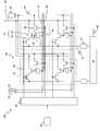
- FIG. 1illustrates an exemplary circuit configuration of the imaging device according to the first embodiment.
- the imaging device 100 shown in FIG. 1has a pixel array PA including a plurality of unit pixels 10 arranged two-dimensionally.
- FIG. 1schematically shows an example in which unit pixels 10 are arranged in a matrix of 2 rows and 2 columns. Needless to say, the number and arrangement of the unit pixels 10 in the imaging device 100 are not limited to the example shown in FIG.
- each unit pixel 10includes the photoelectric conversion unit 13 and the signal detection circuit 14.
- the photoelectric conversion unit 13has a photoelectric conversion layer sandwiched between two electrodes facing each other, and generates a signal by receiving incident light.
- the entirety of the photoelectric conversion unit 13does not need to be an independent element for each unit pixel 10.
- a part of the photoelectric conversion unit 13may extend over a plurality of unit pixels 10.
- the signal detection circuit 14is a circuit that detects a signal generated by the photoelectric conversion unit 13.
- the signal detection circuit 14includes a signal detection transistor 24 and an address transistor 26.
- the signal detection transistor 24 and the address transistor 26are typically field effect transistors (FETs).
- FETsfield effect transistors
- an N-channel MOSis exemplified as the signal detection transistor 24 and the address transistor 26.
- the control terminal (gate here) of the signal detection transistor 24has an electrical connection with the photoelectric conversion unit 13.
- the signal charges (holes or electrons) generated by the photoelectric conversion unit 13are stored in the charge storage unit 41.
- the charge storage unit 41extends to a region including a region between the gate of the signal detection transistor 24 and the photoelectric conversion unit 13.
- the charge storage section 41is a portion including a so-called floating diffusion. Details of the structure of the photoelectric conversion unit 13 will be described later.
- the imaging device 100includes a driving unit that drives the pixel array PA and acquires an image at a plurality of timings.
- the drive sectionincludes a voltage supply circuit 32, a voltage supply circuit 35, a reset voltage source 34, a vertical scanning circuit 36, a column signal processing circuit 37, a horizontal signal readout circuit 38, and a pixel drive signal generation circuit 39.
- the photoelectric conversion unit 13 of each unit pixel 10further has a connection with the sensitivity control line 42.
- the sensitivity control line 42is connected to the voltage supply circuit 32.
- the voltage supply circuit 32supplies different voltages to the counter electrode 12 between the high-sensitivity exposure period and the low-sensitivity exposure period. Further, different voltages may be supplied to the counter electrode 12 between the frames.
- the photoelectric conversion unit 13has the pixel electrode 11 and the photoelectric conversion layer 15 in addition to the counter electrode 12.
- the shield electrode 17has a connection with the sensitivity control line 45.
- the sensitivity control line 45is connected to the voltage supply circuit 35.
- the voltage supply circuit 35supplies a shield voltage to the shield electrode 17.
- the shield electrode 17 and the pixel electrode 11are electrically separated. 1 and 2, the shield electrode 17 and the pixel electrode 11 are separated from each other.
- the shield electrode 17 and the pixel electrode 11are in contact with one surface of the photoelectric conversion layer 15, and the counter electrode 12 is in contact with the other surface of the photoelectric conversion layer 15.
- the shield voltage at the shield electrode 17can be used for suppressing crosstalk between the unit pixels 10. For example, this crosstalk suppression is realized by applying a shield voltage lower than the reset voltage Vr applied to the pixel electrode 11 to the shield electrode 17.
- the shield voltage applied to the shield electrode 17may be a negative voltage.
- the shield electrode 17may surround the pixel electrode 11. More specifically, a plurality of through holes are provided in the shield electrode 17, and one pixel electrode 11 may be accommodated in each through hole.
- the shield electrode 17may be a single integrated electrode, or may be configured by a plurality of electrodes separated from each other.
- the sensitivity control line 45 and the voltage supply circuit 35may be omitted, and the shield electrode 17 may be connected to the ground of the imaging device 100. Even in this case, crosstalk can be suppressed. Further, the shield electrode 17, the sensitivity control line 45, and the voltage supply circuit 35 may be omitted. These points are the same for the second embodiment.
- one of the positive and negative charges (signal charge) generated by the photoelectric conversionis stored in the charge storage unit 41 with relatively high sensitivity. That is, in the “high sensitivity exposure period”, light is converted into an electric signal with relatively high sensitivity.
- the “low-sensitivity exposure period” in the first embodimentone of the positive and negative charges (signal charge) generated by photoelectric conversion is stored in the charge storage unit 41 with relatively low sensitivity. That is, in the “low-sensitivity exposure period”, light is converted into an electric signal with relatively low sensitivity.
- the low sensitivityincludes a case where the sensitivity is zero.
- the voltage supply circuit 32 and the voltage supply circuit 35are not limited to a specific power supply circuit, and may be a circuit that generates a predetermined voltage, or a circuit that converts a voltage supplied from another power supply to a predetermined voltage. It may be.
- Each unit pixel 10has a connection to the power supply line 40 that supplies the power supply voltage VDD. As shown in the figure, an input terminal (typically, a drain) of the signal detection transistor 24 is connected to the power supply line 40. When the power supply line 40 functions as a source follower power supply, the signal detection transistor 24 amplifies and outputs the signal generated by the photoelectric conversion unit 13.
- the input terminal (here, drain) of the address transistor 26is connected to the output terminal (here, source) of the signal detection transistor 24.
- the output terminal (the source here) of the address transistor 26is connected to one of the plurality of vertical signal lines 47 arranged for each column of the pixel array PA.
- the control terminal (here, gate) of the address transistor 26is connected to the address control line 46, and by controlling the potential of the address control line 46, the output of the signal detection transistor 24 is connected to the corresponding vertical signal line 47. It can be selectively read.
- the address control line 46is connected to a vertical scanning circuit (also called “row scanning circuit”) 36.
- the vertical scanning circuit 36selects a plurality of unit pixels 10 arranged in each row on a row basis by applying a predetermined voltage to the address control line 46. Thereby, the reading of the signal of the selected unit pixel 10 and the reset of the pixel electrode 11 described later are executed.
- the vertical scanning circuit 36is connected to the pixel drive signal generation circuit 39.
- the pixel drive signal generation circuit 39generates a signal for driving the unit pixels 10 arranged in each row of the pixel array PA.
- the generated pixel drive signalis supplied to the unit pixels 10 in the row selected by the vertical scanning circuit 36.
- the vertical signal line 47is a main signal line that transmits a pixel signal from the pixel array PA to a peripheral circuit.
- a column signal processing circuit (also called a “row signal storage circuit”) 37is connected to the vertical signal line 47.
- the column signal processing circuit 37performs noise suppression signal processing represented by correlated double sampling and analog-digital conversion (AD conversion). As illustrated, the column signal processing circuit 37 is provided corresponding to each column of the unit pixels 10 in the pixel array PA.
- These column signal processing circuits 37are connected to a horizontal signal readout circuit (also referred to as a “column scanning circuit”) 38.
- the horizontal signal read circuit 38sequentially reads signals from the plurality of column signal processing circuits 37 to a horizontal common signal line 49.
- the unit pixel 10has the reset transistor 28.
- the reset transistor 28can be, for example, a field-effect transistor, like the signal detection transistor 24 and the address transistor 26.
- an N-channel MOSis applied as the reset transistor 28 will be described unless otherwise specified.
- the reset transistor 28is connected between a reset voltage line 44 that supplies a reset voltage Vr and the charge storage unit 41.
- the control terminal (here, gate) of the reset transistor 28is connected to a reset control line 48, and the potential of the charge storage unit 41 can be reset to the reset voltage Vr by controlling the potential of the reset control line 48. it can.
- the reset control line 48is connected to the vertical scanning circuit 36. Therefore, when the vertical scanning circuit 36 applies a predetermined voltage to the reset control line 48, the plurality of unit pixels 10 arranged in each row can be reset in row units.
- the reset voltage line 44 that supplies the reset voltage Vr to the reset transistor 28is connected to the reset voltage supply circuit 34 (hereinafter, simply referred to as “reset voltage source 34”).
- the reset voltage source 34only needs to have a configuration capable of supplying a predetermined reset voltage Vr to the reset voltage line 44 during the operation of the imaging device 100.
- the reset voltage source 34Not limited.
- Each of the voltage supply circuit 32, the voltage supply circuit 35, and the reset voltage source 34may be a part of a single voltage supply circuit, or may be an independent and separate voltage supply circuit. Note that at least one of the voltage supply circuit 32, the voltage supply circuit 35, and the reset voltage source 34 may be a part of the vertical scanning circuit 36.
- the sensitivity control voltage from the voltage supply circuit 32, the sensitivity control voltage from the voltage supply circuit 35, and / or the reset voltage Vr from the reset voltage source 34are supplied to each unit pixel 10 via the vertical scanning circuit 36. Is also good.
- the power supply voltage VDD of the signal detection circuit 14can be used as the reset voltage Vr.
- a voltage supply circuit(not shown in FIG. 1) for supplying a power supply voltage to each unit pixel 10 and the reset voltage source 34 can be shared.
- the power supply line 40 and the reset voltage line 44can be shared, the wiring in the pixel array PA can be simplified.
- the reset voltage Vrto a voltage different from the power supply voltage VDD of the signal detection circuit 14, more flexible control of the imaging device 100 is enabled.
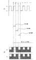
- FIG. 2schematically illustrates an exemplary device structure of the unit pixel 10.
- the above-described signal detection transistor 24, address transistor 26, and reset transistor 28are formed on the semiconductor substrate 20.
- the semiconductor substrate 20is not limited to a substrate that is entirely a semiconductor.
- the semiconductor substrate 20may be an insulating substrate or the like in which a semiconductor layer is provided on a surface on which a photosensitive region is formed.
- a P-type silicon (Si) substrateis used as the semiconductor substrate 20 will be described.
- the semiconductor substrate 20has impurity regions (N-type regions in this case) 26 s, 24 s, 24 d, 28 d, and 28 s, and element isolation regions 20 t for electrical isolation between the unit pixels 10.
- the element isolation region 20tis also provided between the impurity region 24d and the impurity region 28d.
- the element isolation region 20tis formed, for example, by performing ion implantation of an acceptor under predetermined implantation conditions.
- the impurity regions 26 s, 24 s, 24 d, 28 d and 28 sare typically diffusion layers formed in the semiconductor substrate 20.
- the signal detection transistor 24includes an impurity region 24s and an impurity region 24d, and a gate electrode 24g (typically, a polysilicon electrode).
- the impurity region 24sfunctions as, for example, a source region of the signal detection transistor 24.
- the impurity region 24dfunctions as, for example, a drain region of the signal detection transistor 24.
- a channel region of the signal detection transistor 24is formed between the impurity region 24s and the impurity region 24d.
- address transistor 26includes impurity region 26s and impurity region 24s, and gate electrode 26g (typically, a polysilicon electrode) connected to address control line 46 (see FIG. 1).
- the signal detection transistor 24 and the address transistor 26are electrically connected to each other by sharing the impurity region 24s.
- the impurity region 26sfunctions as, for example, a source region of the address transistor 26.
- the impurity region 26shas a connection with a vertical signal line 47 (see FIG. 1) not shown in FIG.
- Reset transistor 28includes impurity regions 28d and 28s, and a gate electrode 28g (typically, a polysilicon electrode) connected to reset control line 48 (see FIG. 1).
- the impurity region 28sfunctions as, for example, a source region of the reset transistor 28.
- the impurity region 28shas a connection with a reset voltage line 44 (see FIG. 1) not shown in FIG.
- an interlayer insulating layer 50(typically, a silicon dioxide layer) is disposed so as to cover the signal detection transistor 24, the address transistor 26, and the reset transistor 28.
- a wiring layer 56may be disposed in the interlayer insulating layer 50.
- the wiring layer 56is typically formed from a metal such as copper, and may include, for example, a wiring such as the above-described vertical signal line 47 as a part thereof.
- the number of insulating layers in the interlayer insulating layer 50 and the number of layers included in the wiring layer 56 disposed in the interlayer insulating layer 50can be arbitrarily set and are not limited to the example shown in FIG.
- the above-described photoelectric conversion unit 13is disposed.
- the plurality of unit pixels 10 configuring the pixel array PAare formed on the semiconductor substrate 20.
- the plurality of unit pixels 10 two-dimensionally arranged on the semiconductor substrate 20form a photosensitive region (pixel region).
- the distance (pixel pitch) between two adjacent unit pixels 10may be, for example, about 2 ⁇ m.
- the photoelectric conversion unit 13includes the pixel electrode 11, the counter electrode 12, and the photoelectric conversion layer 15 disposed therebetween.
- the counter electrode 12 and the photoelectric conversion layer 15are formed over a plurality of unit pixels 10.
- the pixel electrode 11is provided for each unit pixel 10, and is electrically separated from the pixel electrode 11 of another unit pixel 10 by being spatially separated from the pixel electrode 11 of another adjacent unit pixel 10. Are separated.
- the counter electrode 12is typically a transparent electrode formed from a transparent conductive material.
- the counter electrode 12is disposed on the side of the photoelectric conversion layer 15 where light is incident. Therefore, light transmitted through the counter electrode 12 is incident on the photoelectric conversion layer 15.
- the light detected by the imaging device 100is not limited to light within a visible light wavelength range (for example, 380 nm or more and 780 nm or less).
- transparentmeans transmitting at least a portion of light in the wavelength range to be detected, and it is not essential that light be transmitted over the entire visible light wavelength range. In this specification, all electromagnetic waves including infrared rays and ultraviolet rays are expressed as “light” for convenience.
- a transparent conductive oxide (TCO)such as ITO, IZO, AZO, FTO, SnO2, TiO2, and ZnO2 can be used.
- the photoelectric conversion layer 15receives the incident light and generates a hole-electron pair.
- the photoelectric conversion layer 15is typically formed from an organic semiconductor material. Specific examples of the material forming the photoelectric conversion layer 15 will be described later.
- the photoelectric conversion layer 15typically has a film shape.
- the counter electrode 12has a connection with the sensitivity control line 42 connected to the voltage supply circuit 32.
- the counter electrode 12may be formed over a plurality of unit pixels 10. By doing so, it is possible to apply a sensitivity control voltage of a desired magnitude from the voltage supply circuit 32 to the plurality of unit pixels 10 via the sensitivity control line 42 at a time.
- the counter electrode 12may be configured so that the sensitivity control voltage is applied collectively to each row of the pixel array PA.
- the counter electrode 12may be provided separately for each unit pixel 10 as long as a desired level of sensitivity control voltage can be applied from the voltage supply circuit 32.
- the photoelectric conversion layer 15may be provided separately for each unit pixel 10.
- one of the holes and electrons of the hole-electron pair generated in the photoelectric conversion layer 15 by the photoelectric conversionis controlled by the pixel electrode 11. Can be collected.
- holesare used as signal charges
- the signal charge amount collected per unit timechanges according to the potential difference between the pixel electrode 11 and the counter electrode 12.
- holesare used as signal charges
- the pixel electrode 11 facing the counter electrode 12is provided with an appropriate bias voltage between the counter electrode 12 and the pixel electrode 11 so that the positive and negative charges generated by photoelectric conversion in the photoelectric conversion layer 15 are generated. Collect one.
- the pixel electrode 11is formed of a metal such as aluminum or copper, a metal nitride, or polysilicon doped with an impurity to have conductivity.
- the pixel electrode 11may be a light-shielding electrode.
- a TaN electrode having a thickness of 100 nm as the pixel electrode 11a sufficient light shielding property can be realized.
- a transistorin this example, at least one of the signal detection transistor 24, the address transistor 26, and the reset transistor 28
- a light-shielding filmmay be formed in the interlayer insulating layer 50 using the above-described wiring layer 56.
- the pixel electrode 11is connected to the gate electrode 24g of the signal detection transistor 24 via the plug 52, the wiring 53, and the contact plug 54.
- the gate of the signal detection transistor 24has an electrical connection with the pixel electrode 11.
- the plug 52 and the wiring 53can be formed from a metal such as copper, for example.
- the plug 52, the wiring 53, and the contact plug 54constitute at least a part of the charge storage unit 41 (see FIG. 1) between the signal detection transistor 24 and the photoelectric conversion unit 13.
- the wiring 53may be a part of the wiring layer 56.
- the pixel electrode 11is also connected to the impurity region 28d via the plug 52, the wiring 53, and the contact plug 55. In the configuration illustrated in FIG.
- the gate electrode 24g of the signal detection transistor 24, the plug 52, the wiring 53, the contact plugs 54 and 55, and the impurity region 28d that is one of the source region and the drain region of the reset transistor 28are It functions as a charge storage section 41 that stores the signal charges collected by the electrodes 11.
- a voltage corresponding to the amount of the signal charges stored in the charge storage unit 41is applied to the gate of the signal detection transistor 24.
- the signal detection transistor 24amplifies this voltage.
- the voltage amplified by the signal detection transistor 24is selectively read as a signal voltage via the address transistor 26.
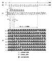
- FIG. 3Ais a timing chart illustrating an example of an operation of the imaging device according to the first embodiment.
- FIG. 3Bis an enlarged view of a part of FIG. 3A.
- the graph (a) in FIG. 3Ashows the falling (or rising) timing of the vertical synchronization signal VD.
- the graph (b)shows the falling (or rising) timing of the horizontal synchronization signal HD.
- the graph (c)shows an example of a temporal change of the voltage Vb applied from the voltage supply circuit 32 to the counter electrode 12 via the sensitivity control line 42.
- Graph (d)schematically shows a signal readout period, a high sensitivity exposure period, and a low sensitivity exposure period in each row of the pixel array PA.
- the reference of the voltage Vbis, for example, the ground potential of the imaging device.
- a predetermined voltage Vsis applied to the shield electrode 17 from the voltage supply circuit 35 via the sensitivity control line 45.
- the voltage Vsis, for example, 0V.
- the signal readout period in each row of the pixel array PAis shown in association with the sensitivity. Specifically, these are shown in the horizontal bar for each row.
- the white rectangle in the upper half of each barschematically represents the high sensitivity exposure period in each row.
- the hatched portion in the upper half of each barschematically represents the low sensitivity exposure period in each row.
- the halftone rectangle in the lower half of each barschematically represents the signal readout period in each row.
- the reset of the charge accumulation unit 41 of each unit pixel 10 in the pixel array PA and the reading of the pixel signal accumulated after the resetare executed.
- the pixel signalis read out and the charge storage unit 41 for charge storage in the next one frame period is reset.
- signal reading of a plurality of pixels belonging to the R0-th rowis started based on the vertical synchronization signal VD.
- Time t0is one of the start times.
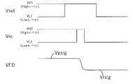
- FIG. 4shows an example of a timing chart of the control signal in the signal reading period.
- Vselrepresents the potential of the address control line 46.
- the potential Vselcan change between a low level VL1 and a high level VH1.
- Vrcrepresents the potential of the reset control line 48.
- the potential Vrccan change between a low level VL2 and a high level VH2.
- VFDrepresents the potential of the charge storage unit 41.
- the potential VFDis used as the pixel signal Vpsig when the charge is stored in the charge storage unit 41.
- the potential VFDis used as a reset signal Vrsig when the charge storage unit 41 is reset.
- a signal reading periodstarts.
- the potential Vsel of the address control line 46 in the R0-th rowswitches from a low level to a high level based on the vertical synchronization signal VD.
- the address transistor 26 whose gate is connected to the address control line 46switches from OFF to ON.
- the potential VFD of the charge storage section 41is output to the vertical signal line 47.
- the pixel signal Vpsigis output to the vertical signal line 47.
- the pixel signal Vpsigis a signal corresponding to the amount of charge stored in the charge storage unit 41 during the previous one frame period.
- the pixel signal Vpsigis transmitted to the column signal processing circuit 37.
- the signal readout period represented by the halftone dot rectangle in the graph (d)includes a reset period as well as a period for reading out the pixel signal Vpsig.
- the reset periodis a period for resetting the potential of the charge storage unit 41 of the unit pixel 10. Specifically, in this example, after the completion of the pixel reading, the pixels belonging to the row R0 are reset. Between the completion of the pixel reading and the reset of the pixels belonging to the R0-th row, AD conversion of the pixel signal in the column signal processing circuit 37 may be interposed.
- the reset of the pixels belonging to the R0-th rowis performed in the following procedure.
- the potential Vrc of the reset control line 48 in the R0th rowswitches from a low level to a high level.
- the reset transistor 28 whose gate is connected to the reset control line 48switches from OFF to ON.
- the charge storage unit 41 and the reset voltage line 44are connected, and the reset voltage Vr is supplied to the charge storage unit 41.
- the potential of the charge storage unit 41is reset to the reset voltage Vr.
- the reset voltage Vris, for example, 0V.
- the potential Vrc of the reset control line 48switches from the high level to the low level.
- the reset transistor 28switches from ON to OFF.
- the reset signal Vrsigis read from the unit pixel 10 in the R0th row via the vertical signal line 47.
- the reset signal Vrsigis a signal corresponding to the magnitude of the reset voltage Vr.
- the reset signal Vrsigis transmitted to the column signal processing circuit 37.
- the read pixel signal Vpsig and the reset signal Vrsigare transmitted to the column signal processing circuit 37, respectively.
- the reset signal Vrsigcorresponds to a noise component, and noise is removed by subtracting the noise component from the pixel signal Vpsig.
- signal readout and reset of pixels belonging to each of the rows R0 to R7are sequentially executed in row units in accordance with the horizontal synchronization signal HD.
- the interval between the pulses of the horizontal synchronizing signal HDin other words, the period from when a certain row is selected to when the next row is selected may be referred to as a “1H period”.
- a period H0 from time t0 to time t1corresponds to a 1H period.
- a period H1 from time t1 to time t2also corresponds to a 1H period.
- a period H2 from time t2 to time t3also corresponds to a 1H period.
- a period H3 from time t3 to time t4also corresponds to a 1H period.
- a period H4 from time t4 to time t5also corresponds to a 1H period.
- a period H5 from time t5 to time t6also corresponds to a 1H period.
- a period H6 from time t6 to time t7also corresponds to a 1H period.
- a period H7 from time t7 to time t8also corresponds to a 1H period.
- the pixels belonging to the row R0are read while the charges are stored in the charge storage unit 41.
- the pixels belonging to the R1th roware read.
- the pixels belonging to the row R2are read while the charges are stored in the charge storage unit 41.
- the pixels belonging to the row R3are read while the charges are stored in the charge storage unit 41.
- the pixels belonging to the R4th roware read while the charges are stored in the charge storage unit 41.
- reading of the pixels belonging to the R5th rowis performed while the charge is stored in the charge storage unit 41.
- the pixels belonging to the R6th roware read while the charges are stored in the charge storage unit 41.
- the pixels belonging to the R7th roware read while the charges are stored in the charge storage unit 41.
- the expression that reading is performed in a certain periodshould not be limitedly interpreted as indicating that only the entire period is spent for reading. This expression is a concept that includes spending a part of the period for reading. In the example of FIG. 3A, the reading of the pixels belonging to each row is performed during the high sensitivity exposure period.
- the length of each 1H period included in the first frameis the same. However, these lengths may be different from each other.
- scanningrefers to signal reading from pixels belonging to each row.
- the voltage V1is applied to the counter electrode 12 by the voltage supply circuit 32 during the reading of the pixels belonging to the periods H0, H1, H2, H3, H4, H5, H6, and H7.
- the voltage Vb applied to the common electrode 12 from the voltage supply circuit 32is switched from the voltage V2 to the voltage V1.
- the voltage Vbis switched from the voltage V1 to the voltage V2.
- voltage Vbis switched from voltage V2 to voltage V1.
- the voltage Vbis switched from the voltage V1 to the voltage V2.
- the voltage Vbis switched from the voltage V2 to the voltage V1.
- the voltage Vbis switched from the voltage V1 to the voltage V2. After this, such switching of the voltage Vb is repeated.
- the voltage V2is typically a voltage at which the potential difference between the pixel electrode 11 and the counter electrode 12 becomes 0 V or less. Hereinafter, this potential difference will be further described.
- the reset voltage Vrcan be supplied from the reset voltage source 34 to the charge storage unit 41 via the reset voltage line 44 and the reset transistor 28.
- the voltage of the pixel electrode 11is also reset to the voltage Vr.
- the potential differencecan be made 0 V when the voltage of the pixel electrode 11 is reset to the voltage Vr.
- the voltage Vrmay be 0V.
- each high-sensitivity exposure periodis longer and each low-sensitivity exposure period is shorter than in the examples of FIGS. 3A and 3B.
- each readout periodis shorter than the high-sensitivity exposure period that includes that period.
- the imaging device 100includes a pixel array PA.
- a first period, a third period, and a second periodappear in this order.
- pixel signal reading of the first row in the pixel array PAis performed.
- pixel signal reading of the second row in the pixel array PAis performed.
- the third periodthe reading of the pixel signals in any row of the pixel array PA is not performed.
- the first period and the second periodare high-sensitivity exposure periods.
- the third periodis a low sensitivity exposure period. Note that the first row and the second row are different rows. In the example of FIG.
- the length of the period of the first frameis the same as the length of the period from the start of the pixel signal reading to the start of the next pixel signal reading in a certain row. This is the same for a second frame in FIG. 13A described later. Specifically, in the example of FIG. 3A, the length of the period of the first frame is the length of the period from time t0 to time t15. The length of the period of the second frame described later is the length of the period from time t15 to t30.
- the driving unitsets the first period, the second period, and the third period, and sets the timing of reading the pixel signal.
- the drive unitmay set a fourth period, a fifth period, and a sixth period described below.
- the period from time t0 to time tu0may correspond to the first period.
- a period from time tu0 to time t1may correspond to a third period.
- a period from time t1 to time tu1may correspond to the second period.
- Row R0may correspond to the first row.
- Row R1may correspond to the second row.
- the first period and the third periodare adjacent to each other.
- the third period and the second periodare adjacent to each other.
- the period from time t1 to time tu1may correspond to the first period.
- This periodis a high sensitivity exposure period.
- the low sensitivity exposure period following the first periodmay correspond to the third period.
- the high sensitivity exposure period following the third periodmay correspond to the second period.
- the R1 rowmay correspond to the first row.
- Row R2may correspond to the second row.
- a period from time td0 to time tu0may correspond to the first period.
- a period from time tu0 to time td1may correspond to a third period.
- a period from time td1 to time tu1may correspond to the second period.
- Row R0may correspond to the first row.
- Row R1may correspond to the second row.
- the first period and the third periodare adjacent to each other.
- the third period and the second periodare adjacent to each other.
- the period from time td1 to time tu1may correspond to the first period.
- This periodis a high sensitivity exposure period.
- the low sensitivity exposure period following the first periodmay correspond to the third period.
- the high sensitivity exposure period following the third periodmay correspond to the second period.
- the R1 rowmay correspond to the first row.
- Row R2may correspond to the second row.
- the technique of the present embodimentis suitable for obtaining high sensitivity while maintaining image quality. Hereinafter, this point will be described.
- FIGS. 6 to 8shows the time change of the voltage Vb applied to the counter electrode 12. Each lower rectangle indicates that pixel signals are being read.
- a period Tgindicates a period in which pixel signal reading is performed.
- the first period and the second periodare high-sensitivity exposure periods.
- the third periodis a low-sensitivity exposure period. Setting these periods in this way is suitable for performing imaging with high sensitivity for the following reasons.
- the first period, the second period, and the third periodare set opposite to the above as shown in FIG.
- the period Tgeasily protrudes from the low-sensitivity exposure period. This protrusion is disadvantageous from the viewpoint of obtaining good image quality.
- the first and second periodsare high-sensitivity exposure periods
- the third periodis a low-sensitivity exposure period.
- the period Tghardly protrudes from the high-sensitivity exposure period. For this reason, when the timing of reading each pixel signal is fixed (that is, when the frame rate is fixed), in the example of FIG. 8 as compared with the example of FIG. It is understood that this is easy to prevent.
- the present disclosuredoes not exclude a form in which the timing of reading each pixel signal is changed. It is possible to lengthen the interval between each pixel signal read. In this case, even if the first period and the second period are set to the low-sensitivity exposure period and the third period is set to the high-sensitivity exposure period as shown in FIG. Can be. More specifically, by adopting a long interval and keeping a long high-sensitivity exposure period within the long interval, it is possible to obtain high sensitivity without causing the above-mentioned overhang. However, if the interval is long, it is difficult to secure the frame rate. For this reason, the example of FIG. 8 is more advantageous than the example of FIG. 7 from the viewpoint of obtaining high sensitivity while ensuring image quality, even in consideration of the mode of changing the timing of reading each pixel signal.
- the technology of the present embodimentis suitable for obtaining high sensitivity while ensuring image quality.
- the first row and the second rowmay be adjacent to each other or may not be adjacent to each other.
- the first period, the third period, and the second periodappear in this order.
- the X periodis defined as the first period or the second period
- the X period and the third periodmay be alternately repeated in the first frame.
- the first framemay be configured by only this repetition.
- the high-sensitivity exposure periodsare dispersed in a plurality of regions. Then, an image on which the imaging data in each high sensitivity exposure period is superimposed is obtained.
- the high-sensitivity exposure periodis not easily biased to a specific area in one frame period, and information over the entire one frame period can be easily obtained. For this reason, it is easier to image a subject that changes with time satisfactorily than when the high-sensitivity exposure periods are combined into one region in the first frame. For example, it is easy to take a good image of a blinking subject such as an LED.
- the timing at which the subject shinesmay not come within the high-sensitivity exposure periods.
- the high-sensitivity exposure periodis dispersed in a plurality of regions, such a situation is unlikely to occur, so that a blinking subject can be easily imaged.
- the total period of the high sensitivity exposure periodmay be equal to or longer than the total period of the low sensitivity exposure period. This makes it easy to perform imaging with high sensitivity. This feature can be applied to other embodiments. However, in the first frame, the total period of the high sensitivity exposure period may be shorter than the total period of the low sensitivity exposure period.
- the imaging device 100may include a control mode that operates in a rolling shutter mode.
- the rolling shutter methodis a method in which pixel signals are sequentially read out for each row of the pixel array PA.
- a high-sensitivity exposure periodis sequentially set for each row of the pixel array PA.
- the “first frame” in FIG. 3Amay be a frame when the imaging device 100 operates in the rolling shutter mode. This is the same for the other drawings. The same applies to a “second frame” in FIG. 10 described later.
- the imaging device 100includes the semiconductor substrate 20 and the photoelectric conversion unit 13.
- the photoelectric conversion unit 13includes a photoelectric conversion layer 15, a first electrode 11, and a second electrode 12.
- the semiconductor substrate 20, the first electrode 11, the photoelectric conversion layer 15, and the second electrode 12are stacked in this order. According to such a laminated structure, it is possible to realize an imaging device in which sensitivity can be easily adjusted.
- the first electrode 11corresponds to the pixel electrode 11.
- the second electrode 12corresponds to the counter electrode 12. Specifically, the first electrode 11 and the second electrode 12 are in contact with the photoelectric conversion layer 15, respectively.
- the imaging device 100includes the first voltage supply circuit 32.
- the first voltage supply circuit 32controls the voltage Vb of the second electrode 12 to a first voltage during a high sensitivity exposure period.
- the first voltage supply circuit 32controls the voltage Vb of the second electrode 12 to a second voltage during the low sensitivity exposure period.
- the first voltage and the second voltageare different from each other.
- the expression of controlling to the first voltage or the second voltageis an expression intended to mean that the target attained voltage is the first voltage or the second voltage. This expression should not be interpreted as being limited to a mode in which the voltage Vb of the second electrode 12 instantaneously reaches the first voltage or the second voltage.
- This expressionincludes a mode in which the voltage Vb of the second electrode 12 reaches the first voltage or the second voltage over time due to the influence of a time constant or the like. The same applies to the expression of controlling to a third voltage or a fourth voltage described later.
- the first voltagecorresponds to the voltage V1.
- the second voltagecorresponds to the voltage V2.
- the imaging devicecollects holes on the pixel electrodes 11. For this reason, the first voltage is set higher than the second voltage.
- the imaging devicemay be configured to collect electrons instead of holes at the pixel electrodes 11. In that case, the first voltage can be lower than the second voltage.
- the imaging device 100may have an R component and a C component that change the voltage of the second electrode 12 according to a time constant determined by the R component and the C component from the start of the third period.
- the third periodis, for example, twice or more the time constant. With this configuration, in the third period, the voltage of the second electrode can be made sufficiently close to the assumed value even in consideration of the existence of the time constant. This is advantageous from the viewpoint of obtaining a desired sensitivity.
- the third periodmay be at least three times the time constant.
- the third periodis, for example, 20 ⁇ s or more.
- the third periodis, for example, 30 times or less the time constant.
- the third periodis, for example, 300 ⁇ s or less.
- the R componentis a resistance component.
- the C componentis a capacitance component.
- the voltage of the second electrode 12changes from the start of the first period according to the time constant.
- the first periodmay be at least twice or at least three times the time constant.
- the first periodmay be longer than 20 ⁇ s.
- the first periodmay be equal to or less than 30 times the time constant.
- the first periodmay be 300 ⁇ s or less.
- the voltage of the second electrode 12changes according to the time constant.
- the second periodmay be at least twice or three times the time constant.
- the second periodmay be longer than 20 ⁇ s.
- the second periodmay be equal to or less than 30 times the time constant.
- the second periodmay be 300 ⁇ s or less.
- the R componentcan include the resistance of the second electrode 12.
- the R componentmay include the resistance of the second electrode 12 and the resistance of the photoelectric conversion layer 15. More specifically, a voltage supply source to the second electrode 12 is defined as a power supply PS, a voltage output part of the power supply PS to the second electrode 12 is defined as a first end, and the photoelectric conversion layer 15 and the first electrode When the eleventh boundary is defined as the second end, the R component may be a combined resistance of elements constituting an electric path from the first end to the second end.
- the concept that the R component includes the resistor R1 of an elementincludes a case where the R component is R1.
- the R componentincludes the resistor R1 of an element means that this element of the resistor R1 and another element of the resistor R2 are connected in series, and when the R component is R1 + R2, this element and the other element of the resistor R2 are included.
- This conceptgenerally includes a case where the R component is a combined resistance of a plurality of resistors, such as a case where the elements are connected in parallel and the R component is R1R2 / (R1 + R2).
- the C componentcan include the capacity of the photoelectric conversion layer 15.
- the above-mentioned C componentcan include the capacity of the second electrode 12 and the capacity of the photoelectric conversion layer 15. More specifically, a voltage supply source to the second electrode 12 is defined as a power supply PS, a voltage output part of the power supply PS to the second electrode 12 is defined as a first end, and the photoelectric conversion layer 15 and the first electrode
- the above-mentioned C componentmay be a combined capacitance of elements constituting an electric path from the first end to the second end.
- the concept that the C component includes the capacitance C1 of an elementincludes a case where the C component is C1.
- the C componentincludes the capacitance C1 of a certain element means that when this element of the capacitance C1 and another element of the capacitance C2 are connected in parallel and the C component is C1 + C2, this element and the other element of the capacitance C2
- This conceptgenerally includes a case where the C component is a combined capacitance of a plurality of capacitors, such as when the components are connected in series and the C component is C1C2 / (C1 + C2).
- the pixel signals of the first row in the pixel array PAare read out.
- the second periodpixel signal reading of the second row in the pixel array PA is performed.
- the third periodthe reading of the pixel signals in any row of the pixel array PA is not performed.
- the first period and the second periodare high-sensitivity exposure periods.
- the third periodis a low sensitivity exposure period.
- the duty ratiomay be changed so that these are maintained. Along with these, the duty ratio may be changed so that other features of the present embodiment are maintained.
- the duty ratioindicates the ratio of the total period of the high sensitivity exposure period in the first frame to the period of the first frame.
- the sensitivitycan be adjusted by changing the duty ratio.
- Electronic ND controlrefers to electrical control of the sensitivity of the image sensor.
- the electronic ND controlcan also be realized by adjusting the magnitude of the potential difference between the pixel electrode 11 and the counter electrode 12 during the high sensitivity exposure period.
- the potential of the counter electrode 12 with respect to the potential of the pixel electrode 11can be controlled.
- one of the holes and the electrons out of the hole-electron pairs generated in the photoelectric conversion layer 15 by the photoelectric conversioncan be collected in the pixel electrode 11.
- the signal charge amount collected per unit timechanges according to the potential difference between the pixel electrode 11 and the counter electrode 12. By changing this potential difference, electronic ND control can be realized.
- FIG. 9shows an example of a change in light receiving sensitivity of the photoelectric conversion layer 15 with respect to a potential difference between the pixel electrode 11 and the counter electrode 12.
- the horizontal axis in FIG. 9indicates the potential difference between the pixel electrode 11 and the counter electrode 12.
- the vertical axis in FIG. 9indicates the normalized sensitivity of the photoelectric conversion layer 15.
- the normalized sensitivityis a value obtained by standardizing the sensitivity when the potential difference between the pixel electrode 11 and the counter electrode 12 is 10 V as 1.0.
- FIG. 9shows that the light receiving sensitivity of the photoelectric conversion layer 15 can be adjusted by adjusting the potential difference between the pixel electrode 11 and the counter electrode 12.
- ND2represents the normalized sensitivity corresponding to the ND2 filter that reduces the amount of light incident on the image sensor by half.
- ND4represents the normalized sensitivity corresponding to the ND4 filter that reduces the amount of light incident on the image sensor to one-fourth.
- ND8represents the normalized sensitivity corresponding to the ND8 filter that reduces the amount of light incident on the image sensor by 8.
- the normalized sensitivity corresponding to the ND2 filteris 0.5, which is half of 1.0.
- the normalized sensitivity corresponding to the ND4 filteris 0.25, which is a quarter of 1.0.
- the normalized sensitivity corresponding to the ND8 filteris 0.125, which is one eighth of 1.0.
- the photoelectric conversion layer 15can function as an electronic ND filter, and electronic ND control can be realized.
- FIG. 10shows an example of electronic ND control by adjusting the magnitude of the potential difference between the pixel electrode 11 and the counter electrode 12.
- the imaging device 100controls the voltage Vb of the second electrode 12 to the first voltage V1 during the high sensitivity exposure period.
- the imaging device 100performs a first drive using the first drive voltage Vm as the first voltage V1 and a second drive using the second drive voltage Vn as the first voltage V1.
- the first drive voltage and the second drive voltageare different from each other.
- the example of FIG. 10can be realized by the above-described laminated structure.
- the potential difference between the pixel electrode 11 and the counter electrode 12is selected from two types, a first value that is relatively large and a second value that is relatively small.
- the sensitivitycan be adjusted even when the first value and the second value are fixed.
- the sensitivitycan be adjusted by changing the ratio of the period of the first value to the sum of the period of the first value and the period of the second value.
- a potential difference at which the normalized sensitivity of the photoelectric conversion layer 15 is 1.0can be used as the first value. This potential difference is 10 V in the above example. As the second value, a potential difference at which the normalized sensitivity of the photoelectric conversion layer 15 becomes 0.0 can be used. This potential difference is 0 V in the above example.
- the light receiving sensitivity of the photoelectric conversion layer 15changes nonlinearly with respect to the potential difference between the pixel electrode 11 and the counter electrode 12.
- the electronic ND controlby changing the duty ratio, the light receiving sensitivity can be linearly changed with respect to the duty ratio. Therefore, adjustment of the sensitivity is easy.
- the electronic ND controlby adjusting the magnitude of the potential difference between the pixel electrode 11 and the counter electrode 12 can be realized. For example, this can be realized by using a storage unit that stores a function indicating the relationship between the potential difference and the light receiving sensitivity.
- the period Txis a low-sensitivity exposure period.
- the pulse of the voltage Vbis intermittent in the period Tx.
- the entire period Tyis a high-sensitivity exposure period. 11 and 12 are also included in the first embodiment.
- FIG. 13Ais a timing chart illustrating an example of an operation of the imaging device according to the second embodiment.
- FIG. 13Bis an enlarged view of a part of FIG. 13A.
- a second frameis generated in addition to the first frame described in FIG. 5A.
- a period H15 from time t15 to time t16corresponds to a 1H period.
- a period H16 from time t16 to time t17also corresponds to a 1H period.
- a period H17 from time t17 to time t18also corresponds to a 1H period.
- a period H18 from time t18 to time t19also corresponds to a 1H period.
- a period H19 from time t19 to time t20also corresponds to a 1H period.
- a period H20 from time t20 to time t21also corresponds to a 1H period.
- a period H21 from time t21 to time t22also corresponds to a 1H period.
- a period H22 from time t22 to time t23also corresponds to the 1H period.
- the pixels belonging to the R0-th roware read out, and thereafter, charges are stored in the charge storage unit 41.
- the pixels belonging to the R1 roware read out, and thereafter, the charges are stored in the charge storage unit 41.
- the period H17reading of the pixels belonging to the R2th row is performed, and thereafter, charge is stored in the charge storage unit 41.
- the period H18reading of the pixels belonging to the R3 row is performed, and thereafter, charge is stored in the charge storage unit 41.
- the period H19reading of the pixels belonging to the R4th row is performed, and thereafter, charge is stored in the charge storage unit 41.
- the length of each 1H period included in the second frameis the same. However, these lengths may be different from each other.
- the voltage V2is applied to the common electrode 12 by the voltage supply circuit 32 during the reading of the pixels belonging to the periods H15, H16, H17, H18, H19, H20, H21, and H22. Note that a predetermined voltage Vs is applied to the shield electrode 17 by the voltage supply circuit 35 as in the first embodiment.
- the voltage Vb applied from the voltage supply circuit 32 to the counter electrode 12is the voltage V2.
- voltage Vbis switched from voltage V2 to voltage V1.
- the voltage Vbis switched from the voltage V1 to the voltage V2.
- the voltage Vbis switched from the voltage V2 to the voltage V1.
- the voltage Vbis switched from the voltage V1 to the voltage V2.
- the voltage Vbis switched from the voltage V2 to the voltage V1. After this, such switching of the voltage Vb is repeated.
- the technique of the present embodiment described with reference to FIGS. 13A and 13Bcan be expressed as follows.
- the fourth period, the sixth period, and the fifth periodappear in this order.
- pixel signal reading of the fourth row in the pixel array PAis performed.
- pixel signal reading of the fifth row in the pixel array PAis performed.
- the sixth periodthe reading of the pixel signals from any row of the pixel array PA is not performed.
- the fourth and fifth periodsare low-sensitivity exposure periods.
- the sixth periodis a high sensitivity exposure period.
- Such a second frameis suitable for performing imaging with low sensitivity.
- the fourth row and the fifth roware different rows.
- the period from time t15 to time td15may correspond to the fourth period.
- a period from time td15 to time t16may correspond to a sixth period.
- a period from time t16 to time td16may correspond to a fifth period.
- Row R0may correspond to the fourth row.
- Row R1may correspond to the fifth row.
- the fourth period and the sixth periodare adjacent to each other.
- the sixth period and the fifth periodare adjacent to each other.
- the control mode of the imaging device 100includes a first mode in which a first frame is generated and a second mode in which a second frame is generated.
- the fourth row and the fifth rowmay be adjacent to each other or may not be adjacent to each other.
- the period from time t16 to time td16may correspond to the fourth period.
- This periodis a low sensitivity exposure period.
- the high sensitivity exposure period following the fourth periodmay correspond to the sixth period.
- the low sensitivity exposure period following the sixth periodmay correspond to the fifth period.
- Row R1may correspond to the fourth row.
- the R2th rowmay correspond to the fifth row.
- the modeis switched from the first mode to the second mode at time t15.
- the period in which the first mode is executedincludes a period from time t0 to time t15. During this period, the first frame is formed.
- the period in which the second mode is executedincludes a period from time t15 to time t30. During this period, the second frame is formed.
- the first mode and the second modeare switched based on a set value of the sensitivity (hereinafter, sometimes referred to as a set sensitivity).
- the set valueindicates a target value to be obtained by the control.
- the set sensitivitychanges according to the duty ratio and the set value of the potential difference between the pixel electrode 11 and the counter electrode 12 during the high sensitivity exposure period (hereinafter, may be referred to as the set potential difference). Value.
- the setting sensitivityincreases as the duty ratio increases.
- the setting sensitivityincreases as the setting potential difference increases. More specifically, the set sensitivity increases in proportion to the duty ratio.
- the set sensitivityincreases nonlinearly with respect to the set potential difference. This non-linear increase can be known in advance through experiments and the like.
- the light receiving sensitivity of the photoelectric conversion layer 15 when the potential difference between the pixel electrode 11 and the counter electrode 12 takes a certain valueis normalized to 1.
- This normalized sensitivityis referred to as a normalized sensitivity following the example of FIG.
- the normalized sensitivitychanges non-linearly with respect to the potential difference between the pixel electrode 11 and the counter electrode 12, as shown in FIG.
- the set value of the normalized sensitivitymay be referred to as a set normalized sensitivity.
- the above-mentioned certain value(that is, the potential difference that makes the normalized sensitivity 1) may be referred to as a potential difference H.
- a potential difference that makes the normalized sensitivity zeromay be referred to as a potential difference L.
- the potential difference Hcan be set to 10V.
- the potential difference Lis, for example, 0V.
- the modein the first mode, when the set sensitivity decreases and becomes lower than the switching threshold, the mode is switched from the first mode to the second mode.
- the modeIn the second mode, the mode is switched from the second mode to the first mode when the set sensitivity increases and becomes equal to or higher than the switching threshold.
- the switching threshold value in the first examplefor example, a value of 0.3 or more and 0.7 or less, specifically, 0.5 can be used.
- the modein the first mode, when the set sensitivity decreases and becomes less than the first threshold, the mode is switched from the first mode to the second mode. In the second mode, the mode is switched from the second mode to the first mode when the set sensitivity increases and becomes equal to or higher than the second threshold.
- the first thresholdis smaller than the second threshold.
- a value of 0.25 or more and 0.41 or less, specifically, 0.33can be used.
- a value between 0.42 and 0.58, specifically, 0.5can be used.
- the set potential difference during the low sensitivity exposure periodis set to the potential difference L.
- the set standardization sensitivity during the low sensitivity exposure periodis zero.
- the set sensitivityis a product of the duty ratio and the set standardized sensitivity during the high sensitivity exposure period.
- the set sensitivityis 1 (ie, 100%) when the duty ratio is 1 (ie, 100%) and the set standardized sensitivity during the high sensitivity exposure period is 1 (ie, 100%).
- the setting sensitivityis 0 when the duty ratio is 0, and is 0 even when the setting normalization sensitivity is 0.
- 0.33is used as the first threshold value
- 0.5is used as the second threshold value
- the set standardized sensitivity in the high sensitivity exposure periodis set to 1.
- the ratio of the length of the high sensitivity exposure period to the length of the low sensitivity exposure period in the first modeis set to 1: 2
- a set sensitivity of 0.33can be realized in the first mode.
- the pixel signal read from the pixel belonging to the row R0is accumulated in the pixel during the interval from the reading of the pixel signal of the first frame to the reading of the pixel signal of the second frame.
- Thisis a signal corresponding to the applied charge.
- This periodis a charge accumulation period of the pixels in the row R0. The same can be said for the rows R1 to R7.
- the length of the accumulation period of the charge extracted by reading the pixel signal of the second frameis the same in each of the rows R0 to R7.
- the total length of the high-sensitivity exposure period in the charge accumulation perioddiffers in each of the rows R0 to R7. This is because the length of each high-sensitivity exposure period differs between the first frame and the second frame. Specifically, the length of each high-sensitivity exposure period in the first frame is longer than the length of each high-sensitivity exposure period in the second frame.
- the number of high-sensitivity exposure periods in the charge accumulation periodis the same, but the younger rows include more high-sensitivity exposure periods in the first frame.
- the total length of the high-sensitivity exposure period in the charge accumulation periodis longer in the lower rows.
- a gaincan be applied to the output signal of the pixel. More specifically, a gain corresponding to the ratio Tt / Ta of the total period Tt of the high sensitivity exposure period to the accumulation period Ta can be applied to the output signal of the pixel. More specifically, a gain that is inversely proportional to the ratio Tt / Ta can be applied to the output signal of the pixel. By applying a gain in this manner, correction of an output signal for suppressing non-uniformity in sensitivity for each row is realized.
- the ratio Tt / Tais the ratio Tt / Ta of the total period Tt of the high-sensitivity exposure period to the accumulation period Ta.
- the accumulation period Tais a period of an interval between pixel signal reading in one row and pixel signal reading.
- the sensitivityis modulated by changing the voltage Vb of the counter electrode 12.
- the sensitivitycan be modulated by changing the voltage of the shield electrode 17 while keeping the voltage of the counter electrode 12 constant.
- the sensitivityis modulated by changing the voltage of the shield electrode 17.
- the third embodimentwill be described with reference to FIG.
- the description of the same contents as the first embodimentmay be omitted.
- the technology of the third embodimentis applicable not only to the first embodiment but also to other embodiments.
- the voltage Vb of the counter electrode 12is always maintained at the voltage V1 by the voltage supply circuit 32.
- the voltage Vs of the shield electrode 17is changed between the voltage V3 and the voltage V4 by the voltage supply circuit 35 via the sensitivity control line 45.
- the voltage V3is higher than the voltage V4.
- the voltage V4is lower than the voltage V3.
- the voltage V3is higher than the reset voltage Vr, and the voltage V4 is lower than the reset voltage Vr.
- the voltage V3 and the voltage V4are smaller than the voltage V1.
- the reference of the voltage Vsis, for example, the ground potential of the imaging device.
- a period in which the voltage Vs of the shield electrode 17 is set to the voltage V3corresponds to a high sensitivity exposure period.
- a period in which the voltage Vs of the shield electrode 17 is set to the voltage V4corresponds to a low sensitivity exposure period.
- the voltage V3is applied to the shield electrode 17 during the reading of the pixels belonging to the periods H0, H1, H2, H3, H4, H5, H6, and H7.
- voltage Vs applied to shield electrode 17is switched from voltage V4 to voltage V3.
- voltage Vsis switched from voltage V3 to voltage V4.
- the voltage Vsis switched from the voltage V4 to the voltage V3.
- the voltage Vsis switched from the voltage V3 to the voltage V4.
- the voltage Vsis switched from the voltage V4 to the voltage V3.
- the voltage Vsis switched from the voltage V3 to the voltage V4. After this, such switching of the voltage Vs is repeated.
- the sensitivityis modulated by an electric field generated by a potential difference between the pixel electrode 11 and the counter electrode 12 and an electric field generated by a potential difference between the shield electrode 17 and the counter electrode 12.
- the voltage of the counter electrode 12is higher than the voltage of the pixel electrode 11, and an electric field is generated from the counter electrode 12 to the pixel electrode 11.
- the voltage of the shield electrode 17is higher than the voltage of the pixel electrode 11, for example, the signal charge is less likely to be captured by the shield electrode 17 and easily flows into the pixel electrode 11. Therefore, high sensitivity can be obtained.
- the voltage of the shield electrode 17is smaller (for example, lower than the voltage of the pixel electrode 11), the signal charge is easily captured by the shield electrode 17 and hardly flows into the pixel electrode 11. Therefore, low sensitivity is obtained.
- the photoelectric conversion layer 15is more likely to exhibit good sensitivity in a wide area than in the latter case.
- a magnitude relationship of voltage of the counter electrode 12> voltage of the shield electrode 17> voltage of the pixel electrode 11can be adopted.
- a magnitude relationship of voltage of the counter electrode 12> voltage of the pixel electrode 11> voltage of the shield electrode 17can be adopted.
- the voltage of the pixel electrode 11is higher than the voltage of the counter electrode 12, and an electric field is generated from the pixel electrode 11 to the counter electrode 12.
- the voltage of the shield electrode 17is small (for example, lower than the voltage of the pixel electrode 11)
- the signal chargeis hard to be captured by the shield electrode 17 and easily flows into the pixel electrode 11. Therefore, high sensitivity can be obtained.
- the voltage of the shield electrode 17is larger than the voltage of the pixel electrode 11, for example, the signal charge is easily captured by the shield electrode 17 and hardly flows into the pixel electrode 11. Therefore, low sensitivity is obtained.
- the photoelectric conversion layer 15is more likely to exhibit good sensitivity in a wide area than in the latter case.
- a magnitude relationship of voltage of the counter electrode 12 ⁇ voltage of the shield electrode 17 ⁇ voltage of the pixel electrode 11can be adopted.
- a magnitude relationship of voltage of the counter electrode 12 ⁇ voltage of the pixel electrode 11 ⁇ voltage of the shield electrode 17can be adopted.
- the imaging device 100includes the second voltage supply circuit 35.
- the second voltage supply circuit 35controls the voltage Vs of the shield electrode 17 to a fourth voltage during the low sensitivity exposure period.
- the second voltage supply circuit 35controls the voltage Vs of the shield electrode 17 to a third voltage during a high sensitivity exposure period.
- the third voltage and the fourth voltageare different from each other. By controlling the voltage of the first electrode 11 in this way, the sensitivity can be adjusted.
- the third voltagecorresponds to the voltage V3.
- the fourth voltagecorresponds to the voltage V4.
- the third voltageis set higher than the fourth voltage.
- the imaging devicemay be configured to collect electrons instead of holes at the pixel electrodes 11. In that case, the third voltage can be lower than the fourth voltage.
- the imaging device 100may have an R component and a C component that change the voltage of the shield electrode 17 according to a time constant determined by the R component and the C component from the start of the third period.
- the third periodis, for example, twice or more the time constant. By doing so, in the third period, the voltage of the shield electrode 17 can be made sufficiently close to the assumed value even in consideration of the existence of the time constant. This is advantageous from the viewpoint of obtaining a desired sensitivity.
- the third periodmay be at least three times the time constant.
- the third periodis, for example, 20 ⁇ s or more.
- the third periodis, for example, 30 times or less the time constant.
- the third periodis, for example, 300 ⁇ s or less.
- the voltage of the shield electrode 17changes from the start of the first period according to the time constant.
- the first periodmay be at least twice or at least three times the time constant.
- the first periodmay be longer than 20 ⁇ s.
- the first periodmay be equal to or less than 30 times the time constant.
- the first periodmay be 300 ⁇ s or less.
- the voltage of the shield electrode 17changes from the start of the second period according to the time constant.
- the second periodmay be at least twice or three times the time constant.
- the second periodmay be longer than 20 ⁇ s.
- the second periodmay be equal to or less than 30 times the time constant.
- the second periodmay be 300 ⁇ s or less.
- the R componentcan include the resistance of the first electrode 11.
- the R componentmay include the resistance of the shield electrode 17 and the resistance of the photoelectric conversion layer 15. More specifically, a voltage supply source to the shield electrode 17 is defined as a power supply PS, a voltage output part of the power supply PS to the shield electrode 17 is defined as a first end, and a voltage between the photoelectric conversion layer 15 and the second electrode 12 is defined.
- the above-mentioned R componentmay be a combined resistance of elements constituting an electric path from the first end to the second end.
- the C componentcan include the capacity of the photoelectric conversion layer 15.
- the above-mentioned C componentcan include the capacity of the shield electrode 17 and the capacity of the photoelectric conversion layer 15. More specifically, a voltage supply source to the shield electrode 17 is defined as a power supply PS, a voltage output part of the power supply PS to the shield electrode 17 is defined as a first end, and a voltage between the photoelectric conversion layer 15 and the second electrode 12 is defined.
- the above-mentioned C componentmay be a combined capacitance of elements constituting an electric path from the first end to the second end.
- the time constant for defining the manner of voltage change of the second electrode 12 described in the first embodimentcan be referred to as a second time constant.
- the R component and the C component that define the second time constant described in the first embodimentcan be referred to as a second R component and a second C component.
- the time constant for defining the manner of voltage change of the shield electrode 17 described in the third embodimentcan be referred to as a third time constant.
- the R component and the C component that define the third time constant described in the third embodimentcan be referred to as a third R component and a third C component.
- the voltage supply circuit 35supplies a voltage to the shield electrode 17.
- the voltage supply circuit 35can set this voltage to a different value between the high sensitivity exposure period and the low sensitivity exposure period.
- the voltage supply circuit 35can set this voltage to a different value between frames.
- the technologies of the first and third embodimentscan be collectively expressed as follows.
- the imaging devicehas at least one of the following features (i) and (ii).
- Characteristic (i)is that the imaging device further includes a third electrode 17, the semiconductor substrate 20, the third electrode 17, the photoelectric conversion layer 15, and the second electrode 12 are stacked in this order, and the third electrode 17 is formed. 17 is controlled to have different voltages between the high-sensitivity exposure period and the low-sensitivity exposure period.
- the feature (ii)is that the second electrode 12 is controlled to have different voltages during the high sensitivity exposure period and the low sensitivity exposure period. By controlling the voltage of the electrodes in this way, the sensitivity can be adjusted.
- the third electrode 17corresponds to the shield electrode 17.
- the imaging devicehas at least one of the following features (I) and (II).
- a feature (I)is that the imaging apparatus has the feature (i) and a third time constant that is a third time constant that changes the voltage of the third electrode according to the third time constant, and is included in the third period. Is a feature that is at least twice the third time constant.
- a feature (II)is that the imaging apparatus has the feature (ii) and a second time constant that is a second time constant and changes a voltage of the second electrode according to the second time constant, and the third period Is a feature that is at least twice the second time constant.
- Electronic ND controlcan also be realized by adjusting the voltage Vs of the shield electrode 17. That is, in this example, the imaging device further includes the shield electrode 17. The semiconductor substrate 20, the shield electrode 17, the photoelectric conversion layer 15, and the second electrode 12 are stacked in this order. The imaging device controls the voltage Vs of the shield electrode 17 to the third voltage V3 during the high sensitivity exposure period. The imaging device performs third driving using the third driving voltage as the third voltage V3 and fourth driving using the fourth driving voltage as the third voltage V3. The third drive voltage and the fourth drive voltage are different from each other. This example can be realized by the above-described laminated structure.
- FIG. 15illustrates an exemplary circuit configuration of the imaging device according to the fourth embodiment.
- the imaging device 200 illustrated in FIG. 15has a pixel array PA including a plurality of unit pixels 60 arranged two-dimensionally.
- FIG. 15schematically illustrates an example in which the unit pixels 60 are arranged in a matrix of 2 rows and 2 columns. Needless to say, the number and arrangement of the unit pixels 60 in the imaging device 200 are not limited to the example shown in FIG.
- Each unit pixel 60includes a photoelectric conversion unit 69, a shutter gate transistor 61, and a transfer transistor 62.
- Each unit pixel 60constitutes a readout circuit 65.
- the read circuit 65includes an address transistor 26, a signal detection transistor 24, and a reset transistor 28.
- the photoelectric conversion unit 69is a photodiode. Specifically, the photoelectric conversion unit 69 is an embedded photodiode embedded in a semiconductor substrate. The photoelectric converter 69 receives the incident light and generates a signal charge according to the illuminance. The polarity of the signal charge may be either positive or negative.
- the transfer transistor 62switches whether or not to transfer the signal charge generated by the photoelectric conversion unit 69 to the readout circuit 65.
- the transfer transistor 62is typically a field effect transistor (FET).
- FETfield effect transistor
- an N-channel MOSis illustrated as the transfer transistor 62.
- the control signal line 81is connected to the control terminal which is the input of the transfer transistor 62.
- the control signal line 81is connected to the vertical scanning circuit 36. ON and OFF of the transfer transistor 62 are controlled by the voltage level of the control signal line 81. The control of the voltage level is performed by the vertical scanning circuit 36.
- the signal charge generated by the photoelectric conversion unit 69is transferred to the charge storage unit 41.
- the charge storage unit 41is provided in a region including a region between the transfer transistor 62, the control terminal of the signal detection transistor 24, and the reset transistor 28.
- control terminal of the transfer transistor 62is a gate. The same applies to the signal detection transistor 24, the address transistor 26, the shutter gate transistor 61, and the transfer transistor 62.
- the readout circuit 65detects the electric signal generated by the photoelectric conversion unit 69 and transferred to the charge storage unit 41.
- the control terminal of the signal detection transistor 24is connected to the output (one of the source and the drain) of the transfer transistor 62.
- the source of the signal detection transistor 24is connected to the vertical signal line 47 via the address transistor 26.
- An address control line 46is connected to a control terminal of the address transistor 26. ON and OFF of the address transistor 26 are controlled by the vertical scanning circuit 36 via the address control line 46.
- the signal detection transistor 24amplifies and outputs the voltage applied to its own control terminal, that is, the voltage of the charge storage unit 41.
- the signal amplified by the signal detection transistor 24is selectively read out as a signal voltage via the address transistor 26 and the vertical signal line 47.
- the shutter gate transistor 61is a shutter gate transistor for the photoelectric conversion unit 69.
- the control terminal of the shutter gate transistor 61is connected to a shutter gate control line 82 connected to the vertical scanning circuit 36. Therefore, the vertical scanning circuit 36 can switch the shutter gate transistor 61 on and off.
- the vertical scanning circuit 36can switch the shutter gate transistor 61 on and off.
- FIG. 16Ais a part of a timing chart showing an example of the operation of the imaging device according to the fourth embodiment.
- the figure below the block arrow in FIG. 16Bis an enlarged view of a part of FIG. 16A. Above the block arrow in FIG. 16B, a part of FIG. 3B is reproduced.
- the timing chart of the example of the fourth embodimentis obtained by replacing the graph (c) in FIG. 3A with the graphs (c1) and (c2) in FIG. 16A.
- a graph (c1)shows an example of a temporal change of the voltage Vtr of the control terminal of the transfer transistor 62.
- the graph (c2)shows an example of a temporal change of the voltage Vrst of the control terminal of the shutter gate transistor 61.
- the voltage Vtrchanges between the voltage Vtr_on and the voltage Vtr_off.
- the transfer transistor 62is kept on.
- the voltage Vrstchanges between the voltage Vrst_on and the voltage Vrst_off. During a period when the voltage Vrst is the voltage Vrst_on, the shutter gate transistor 61 is maintained in the on state. During a period when the voltage Vrst is equal to the voltage Vrst_off, the shutter gate transistor 61 is maintained in the off state. The voltage Vrst_on is higher than the voltage Vrst_off.
- the voltage Vtris maintained at the voltage Vtr_on during the period in which the voltage Vb of the counter electrode 12 is V1 in FIG. 3A. During this period, the voltage Vrst is maintained at the voltage Vrst_off. 3, the voltage Vtr is maintained at the voltage Vtr_off during a period in which the voltage Vb of the counter electrode 12 is V2. During this period, the voltage Vrst is maintained at the voltage Vrst_on.
- a high-sensitivity exposure period and a low-sensitivity exposure periodare provided as in the case where the voltage Vb of the first embodiment shown in FIG. 3A is employed.
- the low sensitivity exposure period of the fourth embodimentwill be described.
- the charge generated in the photoelectric conversion unit 69does not move to the charge storage unit 41, and the sensitivity is zero.
- Such a period in which the sensitivity is zeromay correspond to the low sensitivity exposure period in the fourth embodiment.
- the charges generated in the photoelectric conversion unit 69may overflow, and the overflowed charges may move to the charge accumulation unit 41.
- the light incident on the charge storage unit 41may be photoelectrically converted to generate charges.
- the sensitivity generated in this wayis generally called parasitic light sensitivity (Parasitic Light Sensitivity).
- the period in which the parasitic light sensitivity occursmay also correspond to the low sensitivity exposure period.
- the voltage Vrstis maintained at the voltage Vrst_off while the voltage Vtr is the voltage Vtr_on.
- the voltage Vrstis maintained at the voltage Vrst_on.
- the shutter gate transistor 61is turned on at the timing when the transfer transistor 62 is turned off.
- the shutter gate transistor 61is turned off at the timing when the transfer transistor 62 is turned on. That is, the voltage Vtr and the voltage Vrst are complementarily turned on and off.
- the ON / OFF control of the voltage Vtr and the voltage Vrstbe complementary. That is, it is not essential that the period in which the voltage Vtr is the voltage Vtr_on and the period in which the voltage Vrst is the voltage Vrst_off match. It is not essential that the period in which the voltage Vtr is the voltage Vtr_off coincides with the period in which the voltage Vrst is the voltage Vrst_on. It is not essential that the turn-off timing of the transfer transistor 62 and the turn-on timing of the shutter gate transistor 61 match. It is not essential that the turn-on timing of the transfer transistor 62 and the turn-off timing of the shutter gate transistor 61 match.
- the technology of the present embodimentcan be expressed as follows.
- the imaging device 200includes a semiconductor substrate and a photoelectric conversion unit 69.
- the photoelectric conversion unit 69is an embedded photodiode embedded in a semiconductor substrate.
- the imaging device 200includes a first transistor 61, a charge storage unit 41, and a second transistor 62.
- the first transistor 61resets the embedded photodiode.
- the charge accumulating unit 41accumulates charges generated by the embedded photodiode.
- the second transistor 62transfers a charge from the embedded photodiode to the charge storage unit 41.
- the high sensitivity exposure periodis a period from turning off of the first transistor 61 to turning off of the second transistor 62.
- the low-sensitivity exposure periodis a period from turning off of the second transistor 62 to turning off of the first transistor 61.
- the first transistor 61corresponds to the shutter gate transistor 61.
- the second transistor 62corresponds to the transfer transistor 62.
- the imaging device 100includes the pixel array PA.
- the control mode of the imaging device 100includes a first mode in which a first frame is generated.
- the change of the duty ratio in the first modeis performed such that the state where the first condition, the second condition, and the third condition are satisfied before and after the change is maintained.
- the first frameis a frame in which the first period, the third period, and the second period appear in this order.
- the first period and the second periodare one of a high sensitivity exposure period and a low sensitivity exposure period.
- the third periodis the other of the high sensitivity exposure period and the low sensitivity exposure period.
- the first conditionis a condition that pixel signals are read from the first row in the pixel array PA in the first period.
- the second conditionis a condition that pixel signals are read from the second row in the pixel array PA in the second period.
- the third conditionis a condition that, in the third period, the pixel signal readout of any row of the pixel array PA is not performed.
- the duty ratiois a ratio of the total period of the high sensitivity exposure period in the first frame to the period of the first frame.
- the pixel signal readingmay be performed in both the first period, the second period, and the third period. Absent. In this case, as understood from the description of the first embodiment, the image quality is easily ensured. Further, in the reference embodiment, the duty ratio is changed so that the first condition, the second condition, and the third condition are maintained. By changing the duty ratio, high sensitivity or low sensitivity can be obtained.
- the technology according to the first embodimentis suitable for obtaining high sensitivity while ensuring image quality.
- the technology according to the first embodimentis also suitable for obtaining low sensitivity while ensuring image quality.
- a P frame and a Q frame corresponding to the first frame and having different duty ratioscan be generated.
- the first frame shown in FIG. 3Acan be considered as a P frame.
- the first frame shown in FIG. 5Acan be considered a Q frame.
- the first and second periodsare high-sensitivity exposure periods, and the third period is a low-sensitivity exposure period.
- the first and second periodsmay be low-sensitivity exposure periods, and the third period may be a high-sensitivity exposure period.
- the imaging devicecan be applied to various camera systems and sensor systems such as a digital still camera, a medical camera, a monitoring camera, a vehicle-mounted camera, a digital single-lens reflex camera, and a digital mirrorless single-lens camera.
Landscapes
- Engineering & Computer Science (AREA)
- Multimedia (AREA)
- Signal Processing (AREA)
- Transforming Light Signals Into Electric Signals (AREA)
- Solid State Image Pick-Up Elements (AREA)
Abstract
Description
Translated fromJapanese本開示は、撮像装置および撮像方法に関する。The present disclosure relates to an imaging device and an imaging method.
従来、撮像装置から出力される画像の輝度値を調整することが行われている。輝度値の調整は、例えば、被写体の照度等に応じてなされる。Conventionally, the brightness value of an image output from an imaging device has been adjusted. The adjustment of the brightness value is performed according to, for example, the illuminance of the subject.
輝度値の調整は、例えば、撮像素子の入射光量の調整により実現できる。入射光量の調整は、例えば、レンズの絞りの調整、シャッタによる露光時間の調整、ND(Neutral Density)フィルタによる減光等により、実現できる。Adjustment of the luminance value can be realized by, for example, adjustment of the amount of incident light on the image sensor. The adjustment of the incident light amount can be realized by, for example, adjusting the aperture of the lens, adjusting the exposure time by using a shutter, and reducing the light by using an ND (Neutral Density) filter.
輝度値の調整は、撮像素子の感度そのものの調整によっても実現できる。撮像素子の感度が調整されると、撮像素子から読み出される正または負の電荷の量が調整される。電荷の量が調整されると、出力画像の輝度値が調整される。特許文献1および2には、感度の調整が可能な撮像素子が記載されている。Adjustment of the luminance value can also be realized by adjusting the sensitivity itself of the image sensor. When the sensitivity of the image sensor is adjusted, the amount of positive or negative charge read from the image sensor is adjusted. When the amount of charge is adjusted, the brightness value of the output image is adjusted.
特許文献1および2の撮像素子では、光電変換層に電圧が印加される。この電圧印加の時間幅の制御を通じて、撮像素子の感度が調整される。で は In the imaging devices of
従来技術では、画質を確保しつつ高い感度を得ることについて、十分に検討されていない。本開示は、画質を確保しつつ高い感度を得るのに適した技術を提供する。The prior art has not sufficiently examined obtaining high sensitivity while ensuring image quality. The present disclosure provides a technique suitable for obtaining high sensitivity while ensuring image quality.
本開示は、
画素アレイを備えた撮像装置であって、
第1フレームにおいて、第1期間と第3期間と第2期間とがこの順に現れ、
前記第1期間において、前記画素アレイにおける第1の行の画素信号読み出しが行われ、
前記第2期間において、前記画素アレイにおける第2の行の画素信号読み出しが行われ、
前記第1期間および前記第2期間は、高感度露光期間であり、
前記第3期間は、低感度露光期間である、
撮像装置を提供する。The present disclosure
An imaging device including a pixel array,
In the first frame, a first period, a third period, and a second period appear in this order,
In the first period, pixel signal reading of a first row in the pixel array is performed,
In the second period, pixel signal reading of a second row in the pixel array is performed,
The first period and the second period are high-sensitivity exposure periods,
The third period is a low-sensitivity exposure period.
An imaging device is provided.
本開示に係る技術は、画質を確保しつつ高い感度を得るのに適している。技術 The technology according to the present disclosure is suitable for obtaining high sensitivity while ensuring image quality.
(本開示に係る一態様の概要)
本開示の第1態様に係る撮像装置は、
画素アレイを備えた撮像装置であって、
第1フレームにおいて、第1期間と第3期間と第2期間とがこの順に現れ、
前記第1期間において、前記画素アレイにおける第1の行の画素信号読み出しが行われ、
前記第2期間において、前記画素アレイにおける第2の行の画素信号読み出しが行われ、
前記第1期間および前記第2期間は、高感度露光期間であり、
前記第3期間は、低感度露光期間である。(Overview of one embodiment according to the present disclosure)
An imaging device according to a first aspect of the present disclosure includes:
An imaging device including a pixel array,
In the first frame, a first period, a third period, and a second period appear in this order,
In the first period, pixel signal reading of a first row in the pixel array is performed,
In the second period, pixel signal reading of a second row in the pixel array is performed,
The first period and the second period are high-sensitivity exposure periods,
The third period is a low-sensitivity exposure period.
第1態様に係る技術は、画質を確保しつつ高い感度を得るのに適している。なお、前記第3期間において、前記画素アレイのいずれの行の画素信号読み出しも行われなくてもよい。技術 The technology according to the first aspect is suitable for obtaining high sensitivity while ensuring image quality. Note that, in the third period, the reading of the pixel signals from any row of the pixel array may not be performed.
本開示の第2態様において、例えば、第1態様に係る撮像装置では、前記第1フレームにおいて、前記高感度露光期間の総期間は、前記低感度露光期間の総期間以上であってもよい。In the second aspect of the present disclosure, for example, in the imaging device according to the first aspect, in the first frame, a total period of the high sensitivity exposure period may be equal to or longer than a total period of the low sensitivity exposure period.
第2態様に係る技術によれば、高い感度での撮像を行い易い。According to the technique according to the second aspect, it is easy to perform imaging with high sensitivity.
本開示の第3態様において、例えば、第1または第2態様に係る撮像装置では、第2フレームにおいて、第4期間と第6期間と第5期間とがこの順に現れてもよく、前記第4期間において、前記画素アレイにおける第4の行の画素信号読み出しが行われてもよく、前記第5期間において、前記画素アレイにおける第5の行の画素信号読み出しが行われてもよく、前記第6期間において、前記画素アレイのいずれの行の画素信号読み出しも行われなくてもよく、前記第4期間および前記第5期間は、低感度露光期間であってもよく、前記第6期間は、高感度露光期間であってもよい。In the third aspect of the present disclosure, for example, in the imaging device according to the first or second aspect, in the second frame, the fourth period, the sixth period, and the fifth period may appear in this order. In a period, pixel signal reading of a fourth row in the pixel array may be performed. In the fifth period, pixel signal reading of a fifth row in the pixel array may be performed. In the period, the pixel signal readout of any row of the pixel array may not be performed, the fourth period and the fifth period may be low-sensitivity exposure periods, and the sixth period may be a high-sensitivity exposure period. It may be a sensitivity exposure period.
第3態様の第2フレームは、低い感度での撮像を行う場合に適している。第 The second frame of the third aspect is suitable for imaging with low sensitivity.
本開示の第4態様において、例えば、第1から第3態様のいずれか1つに係る撮像装置は、半導体基板と、光電変換部と、をさらに備えていてもよく、前記光電変換部は、光電変換層と、第1電極と、第2電極と、を備えていてもよく、前記半導体基板と、前記第1電極と、前記光電変換層と、前記第2電極とは、この順に積層されていてもよい。In a fourth aspect of the present disclosure, for example, the imaging device according to any one of the first to third aspects may further include a semiconductor substrate and a photoelectric conversion unit, wherein the photoelectric conversion unit includes: A photoelectric conversion layer, a first electrode, and a second electrode may be provided, and the semiconductor substrate, the first electrode, the photoelectric conversion layer, and the second electrode are stacked in this order. May be.
第4態様によれば、感度の調整が容易な撮像素子を実現できる。According to the fourth aspect, it is possible to realize an imaging device in which the sensitivity can be easily adjusted.
本開示の第5態様において、例えば、第4態様に係る撮像装置は、以下の特徴(i)および(ii)の少なくとも一方を有していてもよい。特徴(i)は、前記撮像装置は、第3電極をさらに備えていてもよく、前記半導体基板と、前記第3電極と、前記光電変換層と、前記第2電極とは、この順に積層されていてもよく、前記第3電極を、前記高感度露光期間と前記低感度露光期間とで互いに異なる電圧へと制御するという特徴であってもよい。特徴(ii)は、前記第2電極を、前記高感度露光期間と前記低感度露光期間とで互いに異なる電圧へと制御するという特徴であってもよい。に お い て In the fifth aspect of the present disclosure, for example, the imaging device according to the fourth aspect may have at least one of the following features (i) and (ii). In the feature (i), the imaging device may further include a third electrode, and the semiconductor substrate, the third electrode, the photoelectric conversion layer, and the second electrode are stacked in this order. And the third electrode may be controlled to have different voltages during the high-sensitivity exposure period and the low-sensitivity exposure period. The feature (ii) may be such that the second electrode is controlled to have different voltages during the high-sensitivity exposure period and the low-sensitivity exposure period.
第5態様のように電極の電圧を制御すると、感度を調整できる。感 度 By controlling the voltage of the electrode as in the fifth embodiment, the sensitivity can be adjusted.
本開示の第6態様において、例えば、第4または第5態様に係る撮像装置は、前記高感度露光期間において、前記第2電極の電圧を第1電圧へと制御してもよく、前記撮像装置は、前記第1電圧として第1駆動電圧を用いる第1駆動と、前記第1電圧として第2駆動電圧を用いる第2駆動と、を行ってもよく、前記第1駆動電圧と前記第2駆動電圧とは互いに異なっていてもよい。In a sixth aspect of the present disclosure, for example, the imaging device according to the fourth or fifth aspect may control the voltage of the second electrode to the first voltage during the high sensitivity exposure period, May perform a first drive using a first drive voltage as the first voltage, and a second drive using a second drive voltage as the first voltage, wherein the first drive voltage and the second drive The voltage may be different from the voltage.
第6態様によれば、感度の調整が容易である。According to the sixth aspect, the sensitivity can be easily adjusted.
本開示の第7態様において、例えば、第4から第6態様のいずれか1つに係る撮像装置は、第3電極をさらに備えていてもよく、前記半導体基板と、前記第3電極と、前記光電変換層と、前記第2電極とは、この順に積層されていてもよく、前記高感度露光期間において、前記第3電極の電圧を第3電圧へと制御してもよく、前記撮像装置は、前記第3電圧として第3駆動電圧を用いる第3駆動と、前記第3電圧として第4駆動電圧を用いる第4駆動と、を行ってもよく、前記第3駆動電圧と前記第4駆動電圧とは互いに異なっていてもよい。In the seventh aspect of the present disclosure, for example, the imaging device according to any one of the fourth to sixth aspects may further include a third electrode, wherein the semiconductor substrate, the third electrode, The photoelectric conversion layer and the second electrode may be stacked in this order, and the voltage of the third electrode may be controlled to a third voltage during the high-sensitivity exposure period. A third drive using a third drive voltage as the third voltage, and a fourth drive using a fourth drive voltage as the third voltage, wherein the third drive voltage and the fourth drive voltage are used. And may be different from each other.
第7態様によれば、感度の調整が容易である。According to the seventh aspect, the sensitivity can be easily adjusted.
本開示の第8態様において、例えば、第1から第3態様のいずれか1つに係る撮像装置は、半導体基板と、光電変換部と、をさらに備えていてもよく、前記光電変換部は、前記半導体基板に埋め込まれた埋め込みフォトダイオードであってもよい。In an eighth aspect of the present disclosure, for example, the imaging device according to any one of the first to third aspects may further include a semiconductor substrate and a photoelectric conversion unit, wherein the photoelectric conversion unit includes: It may be an embedded photodiode embedded in the semiconductor substrate.
第8態様によれば、感度の調整が容易な撮像素子を実現できる。According to the eighth aspect, it is possible to realize an imaging device in which the sensitivity can be easily adjusted.
本開示の第9態様において、例えば、第8態様に係る撮像装置は、前記埋め込みフォトダイオードをリセットする第1トランジスタと、前記埋め込みフォトダイオードで生成された電荷を蓄積する電荷蓄積部と、前記埋め込みフォトダイオードから前記電荷蓄積部に前記電荷を転送する第2トランジスタと、を備えていてもよく、前記高感度露光期間は、前記第1トランジスタのターンオフから前記第2トランジスタのターンオフまでの期間であってもよく、前記低感度露光期間は、前記第2トランジスタのターンオフから前記第1トランジスタのターンオフまでの期間であってもよい。In a ninth aspect of the present disclosure, for example, the imaging device according to the eighth aspect includes a first transistor that resets the embedded photodiode, a charge accumulation unit that accumulates charges generated by the embedded photodiode, A second transistor for transferring the charge from the photodiode to the charge storage unit, wherein the high-sensitivity exposure period is a period from the turn-off of the first transistor to the turn-off of the second transistor. Alternatively, the low sensitivity exposure period may be a period from turning off of the second transistor to turning off of the first transistor.
第9態様によれば、第1トランジスタおよび第2トランジスタのスイッチングタイミングに基づいて、感度を調整できる。According to the ninth aspect, the sensitivity can be adjusted based on the switching timing of the first transistor and the second transistor.
本開示の第10態様に係る撮像方法は、
画素アレイを備えた撮像装置を用いた撮像方法であって、
第1フレームにおいて、第1期間と第3期間と第2期間とがこの順に現れ、
前記第1期間において、前記画素アレイにおける第1の行の画素信号読み出しを行い、
前記第2期間において、前記画素アレイにおける第2の行の画素信号読み出しを行い、
前記第1期間および前記第2期間は、高感度露光期間であり、
前記第3期間は、低感度露光期間である。An imaging method according to a tenth aspect of the present disclosure includes:
An imaging method using an imaging device including a pixel array,
In the first frame, a first period, a third period, and a second period appear in this order,
In the first period, pixel signals of a first row in the pixel array are read out,
In the second period, a pixel signal of a second row in the pixel array is read out,
The first period and the second period are high-sensitivity exposure periods,
The third period is a low-sensitivity exposure period.
第10態様に係る技術は、画質を確保しつつ高い感度を得るのに適している。なお、前記第3期間において、前記画素アレイのいずれの行の画素信号読み出しも行わなくてもよい。The technique according to the tenth aspect is suitable for obtaining high sensitivity while ensuring image quality. Note that, in the third period, it is not necessary to read out pixel signals in any row of the pixel array.
本開示の第11態様に係る撮像装置は、
信号線と、
それぞれが入射光の量に応じた画素信号を生成し、前記画素信号を前記信号線に順次に出力する複数の画素と、
第1のフレーム期間において、第1電圧と前記第1電圧と異なる第2電圧とをそれぞれ2回以上交互に、前記複数の画素のそれぞれに同時に供給する電圧供給回路と、
を備え、
前記複数の画素のそれぞれは、
前記第1電圧が供給される第1期間において第1の感度で光を電気信号に変換し、前記第2電圧が供給される第2期間において前記第1の感度よりも高い第2の感度で光を電気信号に変換する光電変換部と、
前記電気信号を増幅して前記画素信号を出力する第1トランジスタと、
を含み、
前記複数の画素のそれぞれは、前記第1のフレーム期間内の前記第2期間において、前記画素信号を前記信号線に出力する。An imaging device according to an eleventh aspect of the present disclosure includes:
Signal lines,
A plurality of pixels each generating a pixel signal according to the amount of incident light, and sequentially outputting the pixel signal to the signal line,
A voltage supply circuit for supplying a first voltage and a second voltage different from the first voltage to the plurality of pixels alternately at least twice each in the first frame period;
With
Each of the plurality of pixels includes:
Light is converted into an electric signal at a first sensitivity during a first period in which the first voltage is supplied, and at a second sensitivity higher than the first sensitivity in a second period during which the second voltage is supplied. A photoelectric conversion unit that converts light into an electric signal,
A first transistor that amplifies the electric signal and outputs the pixel signal;
Including
Each of the plurality of pixels outputs the pixel signal to the signal line during the second period in the first frame period.
本開示の第12態様において、例えば、第11態様に係る撮像装置では、前記複数の画素のそれぞれは、前記第1のフレーム期間内の前記第1期間において、前記画素信号を前記信号線に出力しなくてもよい。In a twelfth aspect of the present disclosure, for example, in the imaging device according to the eleventh aspect, each of the plurality of pixels outputs the pixel signal to the signal line during the first period in the first frame period. You don't have to.
本開示の第13態様において、例えば、第11態様に係る撮像装置では、前記複数の画素のそれぞれの前記光電変換部は、前記第1トランジスタのゲートに電気的に接続される第1電極と、前記第1電極に対向する第2電極と、前記第1電極と前記第2電極との間の光電変換層とを含んでいてもよく、前記電圧供給回路は、前記複数の画素のそれぞれの前記光電変換部の前記第2電極に、前記第1電圧および前記第2電圧を交互に供給してもよい。In a thirteenth aspect of the present disclosure, for example, in the imaging device according to the eleventh aspect, each of the photoelectric conversion units of the plurality of pixels includes a first electrode electrically connected to a gate of the first transistor; The voltage supply circuit may include a second electrode facing the first electrode, and a photoelectric conversion layer between the first electrode and the second electrode. The first voltage and the second voltage may be alternately supplied to the second electrode of the photoelectric conversion unit.
本開示の第14態様において、例えば、第11態様に係る撮像装置では、前記複数の画素のそれぞれの前記光電変換部は、第1面と前記第1面の反対側の第2面とを有する光電変換層と、前記第1面上に位置する第1電極および第3電極と、前記第2面上に位置し前記第1電極および前記第3電極に対向する第2電極とを含んでいてもよく、前記第1電極は、前記第1トランジスタのゲートに電気的に接続されていてもよく、前記電圧供給回路は、前記複数の画素のそれぞれの前記光電変換部の前記第3電極に、前記第1電圧および前記第2電圧を交互に供給してもよい。In a fourteenth aspect of the present disclosure, for example, in the imaging device according to the eleventh aspect, each of the photoelectric conversion units of the plurality of pixels has a first surface and a second surface opposite to the first surface. A photoelectric conversion layer, a first electrode and a third electrode located on the first surface, and a second electrode located on the second surface and facing the first electrode and the third electrode. The first electrode may be electrically connected to a gate of the first transistor, and the voltage supply circuit may include a third electrode of the photoelectric conversion unit of each of the plurality of pixels, The first voltage and the second voltage may be supplied alternately.
本開示の第15態様において、例えば、第11態様に係る撮像装置では、前記複数の画素のそれぞれの前記光電変換部は、フォトダイオードを含んでいてもよく前記複数の画素のそれぞれは、ソースおよびドレインの一方が前記フォトダイオードに電気的に接続され、ソースおよびドレインの他方が前記第1トランジスタのゲートに電気的に接続される第2トランジスタと、ソースおよびドレインの一方が前記フォトダイオードに電気的に接続され、ソースおよびドレインの他方に所定の電圧が印加される第3トランジスタと、を含んでいてもよく、前記電圧供給回路は、前記第3トランジスタのゲートに、前記第1電圧および前記第2電圧を交互に供給してもよい。In a fifteenth aspect of the present disclosure, for example, in the imaging device according to the eleventh aspect, each of the photoelectric conversion units of the plurality of pixels may include a photodiode, and each of the plurality of pixels includes a source and a source. A second transistor having one of a drain electrically connected to the photodiode and the other of a source and a drain electrically connected to a gate of the first transistor, and one of a source and a drain electrically connected to the photodiode; And a third transistor to which a predetermined voltage is applied to the other of the source and the drain, wherein the voltage supply circuit includes a gate of the third transistor, the first voltage and the third voltage. Two voltages may be supplied alternately.
本開示の第16態様において、例えば、第15態様に係る撮像装置では、前記電圧供給回路は、前記第2トランジスタのゲートに、第3電圧と前記第3電圧と異なる第4電圧を交互に供給してもよい。In a sixteenth aspect of the present disclosure, for example, in the imaging device according to the fifteenth aspect, the voltage supply circuit alternately supplies a third voltage and a fourth voltage different from the third voltage to the gate of the second transistor. May be.
本開示の第17態様において、例えば、第11から第16態様のいずれか1つに係る撮像装置では、前記第1のフレーム期間内における前記第2期間の長さの合計は、前記第1のフレーム期間内における前記第1期間の長さの合計以上であってもよい。In a seventeenth aspect of the present disclosure, for example, in the imaging device according to any one of the eleventh to sixteenth aspects, the total length of the second period within the first frame period is equal to the first period. It may be equal to or greater than the total length of the first period in a frame period.
本開示の第18態様において、例えば、第11から第17態様のいずれか1つに係る撮像装置は、前記電圧供給回路に、前記第1電圧および前記第2電圧を供給させる第1制御回路と、前記複数の画素のそれぞれに、前記画素信号を前記信号線に順次に出力させる、第2制御回路と、をさらに備えていてもよい。In an eighteenth aspect of the present disclosure, for example, the imaging device according to any one of the eleventh to seventeenth aspects includes a first control circuit that causes the voltage supply circuit to supply the first voltage and the second voltage. A second control circuit configured to cause each of the plurality of pixels to sequentially output the pixel signal to the signal line.
本開示の第19態様に係る撮像装置は、
画素アレイを備えた撮像装置であって、
前記撮像装置の制御モードは、第1フレームが生成される第1モードを備え、
前記第1モードのデューティ比の変更が、該変更の前後で第1条件、第2条件および第3条件が満たされた状態が維持されるように実行される。
ここで、前記第1フレームは、第1期間と第3期間と第2期間とがこの順に現れるフレームである。前記第1期間および前記第2期間は、高感度露光期間および低感度露光期間の一方である。前記第3期間は、前記高感度露光期間および前記低感度露光期間の他方である。前記第1条件は、前記第1期間において、前記画素アレイにおける第1の行の、画素信号読み出しが行われるという条件である。前記第2条件は、前記第2期間において、前記画素アレイにおける第2の行の、画素信号読み出しが行われるという条件である。前記第3条件は、前記第3期間において、前記画素アレイのいずれの行の画素信号読み出しも行われないという条件である。前記デューティ比は、前記第1フレームの期間に対する、該第1フレームにおける前記高感度露光期間の総期間の比率である。An imaging device according to a nineteenth aspect of the present disclosure includes:
An imaging device including a pixel array,
The control mode of the imaging device includes a first mode in which a first frame is generated,
The change of the duty ratio in the first mode is performed such that the first condition, the second condition, and the third condition are satisfied before and after the change.
Here, the first frame is a frame in which a first period, a third period, and a second period appear in this order. The first period and the second period are one of a high-sensitivity exposure period and a low-sensitivity exposure period. The third period is the other of the high sensitivity exposure period and the low sensitivity exposure period. The first condition is a condition that pixel signals are read from a first row in the pixel array in the first period. The second condition is a condition that pixel signals are read from a second row in the pixel array in the second period. The third condition is a condition that no pixel signal is read from any of the rows of the pixel array in the third period. The duty ratio is a ratio of a total period of the high sensitivity exposure period in the first frame to a period of the first frame.
第19態様に係る技術は、画質を確保しつつ高い感度を得るのに適している。第19態様に係る技術は、画質を確保しつつ低い感度を得るのにも適している。技術 The technology according to the nineteenth aspect is suitable for obtaining high sensitivity while ensuring image quality. The technology according to the nineteenth aspect is suitable for obtaining low sensitivity while ensuring image quality.
本開示の第20態様に係る撮像方法は、
画素アレイを備えた撮像装置を用いた撮像方法であって、
前記撮像装置の制御モードは、第1フレームが生成される第1モードを備え、
前記第1モードのデューティ比の変更を、該変更の前後で第1条件、第2条件および第3条件が満たされた状態が維持されるように実行する。
ここで、前記第1フレームは、第1期間と第3期間と第2期間とがこの順に現れるフレームである。前記第1期間および前記第2期間は、高感度露光期間および低感度露光期間の一方である。前記第3期間は、前記高感度露光期間および前記低感度露光期間の他方である。前記第1条件は、前記第1期間において、前記画素アレイにおける第1の行の、画素信号読み出しが行われるという条件である。前記第2条件は、前記第2期間において、前記画素アレイにおける第2の行の、画素信号読み出しが行われるという条件である。前記第3条件は、前記第3期間において、前記画素アレイのいずれの行の画素信号読み出しも行われないという条件である。前記デューティ比は、前記第1フレームの期間に対する、該第1フレームにおける前記高感度露光期間の総期間の比率である。An imaging method according to a twentieth aspect of the present disclosure includes:
An imaging method using an imaging device including a pixel array,
The control mode of the imaging device includes a first mode in which a first frame is generated,
The change of the duty ratio in the first mode is performed so that the first condition, the second condition, and the third condition are satisfied before and after the change.
Here, the first frame is a frame in which a first period, a third period, and a second period appear in this order. The first period and the second period are one of a high-sensitivity exposure period and a low-sensitivity exposure period. The third period is the other of the high sensitivity exposure period and the low sensitivity exposure period. The first condition is a condition that pixel signals are read from a first row in the pixel array in the first period. The second condition is a condition that pixel signals are read from a second row in the pixel array in the second period. The third condition is a condition that no pixel signal is read from any of the rows of the pixel array in the third period. The duty ratio is a ratio of a total period of the high sensitivity exposure period in the first frame to a period of the first frame.
第20態様に係る技術は、画質を確保しつつ高い感度を得るのに適している。第20態様に係る技術は、画質を確保しつつ低い感度を得るのにも適している。The technique according to the twentieth aspect is suitable for obtaining high sensitivity while ensuring image quality. The technology according to the twentieth aspect is also suitable for obtaining low sensitivity while ensuring image quality.
本明細書では、高感度露光期間という用語と、低感度露光期間という用語と、が用いられる。高感度露光期間は、低感度露光期間に比べ、高い感度が得られる期間を指す。低感度露光期間は、高感度露光期間に比べ、低い感度が得られる期間を指す。ここで、低い感度は、感度がゼロである様を含む概念である。低感度露光期間は、感度がゼロである期間が含む概念である。で は In this specification, the terms high-sensitivity exposure period and low-sensitivity exposure period are used. The high sensitivity exposure period refers to a period in which higher sensitivity is obtained as compared with the low sensitivity exposure period. The low-sensitivity exposure period refers to a period in which lower sensitivity is obtained as compared with the high-sensitivity exposure period. Here, the low sensitivity is a concept including a state where the sensitivity is zero. The low sensitivity exposure period is a concept that includes a period in which the sensitivity is zero.
本明細書では、第1、第2、第3・・・という序数詞を用いることがある。ある要素に序数詞が付されている場合に、より若番の同種類の要素が存在することは必須ではない。序 In this specification, the ordinal numbers of first, second, third, etc. may be used. When an element is given an ordinal number, it is not essential that the same kind of element having a lower number be present.
以下、図面を参照しながら、本開示の実施形態を詳細に説明する。なお、以下で説明する実施形態は、いずれも包括的または具体的な例を示す。以下の実施形態で示される数値、形状、材料、構成要素、構成要素の配置および接続形態、ステップ、ステップの順序などは、一例であり、本開示を限定する主旨ではない。本明細書において説明される種々の態様は、矛盾が生じない限り互いに組み合わせることが可能である。また、以下の実施形態における構成要素のうち、最上位概念を示す独立請求項に記載されていない構成要素については、任意の構成要素として説明される。以下の説明において、実質的に同じ機能を有する構成要素は共通の参照符号で示し、説明を省略することがある。Hereinafter, embodiments of the present disclosure will be described in detail with reference to the drawings. Each of the embodiments described below shows a comprehensive or specific example. Numerical values, shapes, materials, components, arrangements and connection forms of components, steps, order of steps, and the like shown in the following embodiments are merely examples, and do not limit the present disclosure. The various aspects described herein can be combined with each other as long as no conflict occurs. In addition, among the components in the following embodiments, components not described in the independent claims indicating the highest concept are described as arbitrary components. In the following description, components having substantially the same function are denoted by common reference numerals, and description thereof may be omitted.
(実施形態1)
(撮像装置の回路構成)
図1は、実施形態1に係る撮像装置の例示的な回路構成を示す。図1に示す撮像装置100は、2次元に配列された複数の単位画素10を含む画素アレイPAを有する。図1は、単位画素10が2行2列のマトリクス状に配置された例を模式的に示している。言うまでもないが、撮像装置100における単位画素10の数および配置は、図1に示す例に限定されない。(Embodiment 1)
(Circuit configuration of imaging device)
FIG. 1 illustrates an exemplary circuit configuration of the imaging device according to the first embodiment. The
各単位画素10は、光電変換部13および信号検出回路14を有する。後に図面を参照して説明するように、光電変換部13は、互いに対向する2つの電極の間に挟まれた光電変換層を有し、入射した光を受けて信号を生成する。光電変換部13は、その全体が、単位画素10ごとに独立した素子である必要はなく、光電変換部13の例えば一部分が複数の単位画素10にまたがっていてもよい。信号検出回路14は、光電変換部13によって生成された信号を検出する回路である。この例では、信号検出回路14は、信号検出トランジスタ24およびアドレストランジスタ26を含んでいる。信号検出トランジスタ24およびアドレストランジスタ26は、典型的には、電界効果トランジスタ(FET)であり、ここでは、信号検出トランジスタ24およびアドレストランジスタ26としてNチャンネルMOSを例示する。{Each
図1において模式的に示すように、信号検出トランジスタ24の制御端子(ここではゲート)は、光電変換部13との電気的な接続を有する。光電変換部13によって生成される信号電荷(正孔または電子)は、電荷蓄積部41に蓄積される。電荷蓄積部41は、信号検出トランジスタ24のゲートと光電変換部13との間の領域を含む領域に拡がっている。電荷蓄積部41は、いわゆるフローティングディフュージョンを含む部分である。光電変換部13の構造の詳細は、後述する。制 御 As schematically shown in FIG. 1, the control terminal (gate here) of the
撮像装置100は、画素アレイPAを駆動し、複数のタイミングで画像を取得する駆動部を備えている。駆動部は、電圧供給回路32、電圧供給回路35、リセット電圧源34、垂直走査回路36、カラム信号処理回路37、水平信号読み出し回路38および画素駆動信号生成回路39を含む。The
各単位画素10の光電変換部13は、さらに、感度制御線42との接続を有している。図1に例示する構成において、感度制御線42は、電圧供給回路32に接続されている。以下において詳述するように、電圧供給回路32は、高感度露光期間と低感度露光期間との間で互いに異なる電圧を対向電極12に供給する。また、フレーム間で異なる電圧を対向電極12に供給してもよい。(4) The
後述するように、光電変換部13は、対向電極12に加えて、画素電極11および光電変換層15を有する。また、図1に例示する構成において、シールド電極17は、感度制御線45との接続を有している。感度制御線45は、電圧供給回路35に接続されている。電圧供給回路35は、シールド電圧をシールド電極17に供給する。典型的には、シールド電極17と画素電極11とは、電気的に分離されている。図1および2の例では、シールド電極17と画素電極11とは、互いに離間している。この例では、シールド電極17および画素電極11は光電変換層15の一方の表面に接し、対向電極12は光電変換層15の他方の表面に接している。よ う As will be described later, the
シールド電極17におけるシールド電圧は、単位画素10間のクロストーク抑制に利用可能である。例えば、このクロストーク抑制は、画素電極11に印加されるリセット電圧Vrよりも低いシールド電圧をシールド電極17に印加することによって実現される。シールド電極17に印加されるシールド電圧は、負電圧であってもよい。シ ー ル ド The shield voltage at the
画素電極11の厚さ方向に沿って観察したとき、すなわち平面視において、シールド電極17は、画素電極11を取り囲んでいてもよい。より具体的には、シールド電極17には複数の貫通穴が設けられており、1つの貫通穴につき1つの画素電極11が収容されていてもよい。シールド電極17は、ひとつながりの一体の電極であってもよく、互いに分離された複数の電極によって構成されていてもよい。シ ー ル ド When observed along the thickness direction of the
なお、感度制御線45および電圧供給回路35を省略し、シールド電極17を撮像装置100のグランドに接続してもよい。このようにしても、クロストークは抑制され得る。また、シールド電極17、感度制御線45および電圧供給回路35を省略してもよい。これらの点は、実施形態2についても同様である。The
実施形態1における「高感度露光期間」では、光電変換により生成される正および負の電荷の一方(信号電荷)が、相対的に高い感度で電荷蓄積部41に蓄積される。すなわち「高感度露光期間」では、相対的に高い感度で光が電気信号に変換される。また、実施形態1における「低感度露光期間」では、光電変換により生成される正および負の電荷の一方(信号電荷)が、相対的に低い感度で電荷蓄積部41に蓄積される。すなわち「低感度露光期間」では、相対的に低い感度で光が電気信号に変換される。低い感度とは、感度が0である場合を含む。これらは、後述の実施形態2および3についても同様である。In the “high sensitivity exposure period” in the first embodiment, one of the positive and negative charges (signal charge) generated by the photoelectric conversion is stored in the
画素電極11の電位に対する対向電極12の電位を制御することにより、光電変換によって光電変換層15内に生じた正孔-電子対のうち、正孔および電子のいずれか一方を、画素電極11によって収集することができる。例えば信号電荷として正孔を利用する場合には、画素電極11よりも対向電極12の電位を高くすることにより、画素電極11によって正孔を選択的に収集することが可能である。また、単位時間当たりに収集される信号電荷量は画素電極11と対向電極12との電位差に応じて変化する。以下では、信号電荷として正孔を利用する場合を例示する。もちろん、信号電荷として電子を利用することも可能である。電圧供給回路32および電圧供給回路35は、特定の電源回路に限定されず、所定の電圧を生成する回路であってもよいし、他の電源から供給された電圧を所定の電圧に変換する回路であってもよい。By controlling the potential of the
各単位画素10は、電源電圧VDDを供給する電源線40との接続を有する。図示するように、電源線40には、信号検出トランジスタ24の入力端子(典型的にはドレイン)が接続されている。電源線40がソースフォロア電源として機能することにより、信号検出トランジスタ24は、光電変換部13によって生成された信号を増幅して出力する。{Each
信号検出トランジスタ24の出力端子(ここではソース)には、アドレストランジスタ26の入力端子(ここではドレイン)が接続されている。アドレストランジスタ26の出力端子(ここではソース)は、画素アレイPAの列ごとに配置された複数の垂直信号線47のうちの1つに接続されている。アドレストランジスタ26の制御端子(ここではゲート)は、アドレス制御線46に接続されており、アドレス制御線46の電位を制御することにより、信号検出トランジスタ24の出力を、対応する垂直信号線47に選択的に読み出すことができる。The input terminal (here, drain) of the
図示する例では、アドレス制御線46は、垂直走査回路(「行走査回路」とも呼ばれる)36に接続されている。垂直走査回路36は、アドレス制御線46に所定の電圧を印加することにより、各行に配置された複数の単位画素10を行単位で選択する。これにより、選択された単位画素10の信号の読み出しと、後述する、画素電極11のリセットとが実行される。In the example shown, the
さらに、垂直走査回路36には、画素駆動信号生成回路39が接続されている。図示する例では、画素駆動信号生成回路39は、画素アレイPAの各行に配置された単位画素10を駆動する信号を生成する。生成された画素駆動信号は、垂直走査回路36により選択された行の単位画素10に供給される。(4) Further, the
垂直信号線47は、画素アレイPAからの画素信号を周辺回路へ伝達する主信号線である。垂直信号線47には、カラム信号処理回路(「行信号蓄積回路」とも呼ばれる)37が接続されている。カラム信号処理回路37は、相関二重サンプリングに代表される雑音抑制信号処理およびアナログ-デジタル変換(AD変換)などを行う。図示するように、カラム信号処理回路37は、画素アレイPAにおける単位画素10の各列に対応して設けられる。これらのカラム信号処理回路37には、水平信号読み出し回路(「列走査回路」とも呼ばれる)38が接続されている。水平信号読み出し回路38は、複数のカラム信号処理回路37から水平共通信号線49に信号を順次読み出す。The
図1に例示する構成において、単位画素10は、リセットトランジスタ28を有する。リセットトランジスタ28は、例えば、信号検出トランジスタ24およびアドレストランジスタ26と同様に、電界効果トランジスタであり得る。以下では、特に断りの無い限り、リセットトランジスタ28としてNチャンネルMOSを適用した例を説明する。図示するように、このリセットトランジスタ28は、リセット電圧Vrを供給するリセット電圧線44と、電荷蓄積部41との間に接続されている。リセットトランジスタ28の制御端子(ここではゲート)は、リセット制御線48に接続されており、リセット制御線48の電位を制御することによって、電荷蓄積部41の電位をリセット電圧Vrにリセットすることができる。この例では、リセット制御線48が、垂直走査回路36に接続されている。したがって、垂直走査回路36がリセット制御線48に所定の電圧を印加することにより、各行に配置された複数の単位画素10を行単位でリセットすることが可能である。In the configuration illustrated in FIG. 1, the
この例では、リセットトランジスタ28にリセット電圧Vrを供給するリセット電圧線44が、リセット電圧供給回路34(以下、単に「リセット電圧源34」と呼ぶ。)に接続されている。リセット電圧源34は、撮像装置100の動作時にリセット電圧線44に所定のリセット電圧Vrを供給可能な構成を有していればよく、上述の電圧供給回路32と同様に、特定の電源回路に限定されない。電圧供給回路32、電圧供給回路35およびリセット電圧源34の各々は、単一の電圧供給回路の一部分であってもよいし、独立した別個の電圧供給回路であってもよい。なお、電圧供給回路32、電圧供給回路35およびリセット電圧源34の少なくとも1つが、垂直走査回路36の一部分であってもよい。あるいは、電圧供給回路32からの感度制御電圧、電圧供給回路35からの感度制御電圧および/またはリセット電圧源34からのリセット電圧Vrが、垂直走査回路36を介して各単位画素10に供給されてもよい。In this example, the
リセット電圧Vrとして、信号検出回路14の電源電圧VDDを用いることも可能である。この場合、各単位画素10に電源電圧を供給する電圧供給回路(図1において不図示)と、リセット電圧源34とを共通化し得る。また、電源線40と、リセット電圧線44を共通化できるので、画素アレイPAにおける配線を単純化し得る。ただし、リセット電圧Vrを、信号検出回路14の電源電圧VDDと異なる電圧とすることにより、撮像装置100のより柔軟な制御を可能にする。(4) The power supply voltage VDD of the
(単位画素のデバイス構造)
図2は、単位画素10の例示的なデバイス構造を模式的に示す。図2に例示する構成では、上述の信号検出トランジスタ24、アドレストランジスタ26およびリセットトランジスタ28が、半導体基板20に形成されている。半導体基板20は、その全体が半導体である基板に限定されない。半導体基板20は、感光領域が形成される側の表面に半導体層が設けられた絶縁性基板などであってもよい。ここでは、半導体基板20としてP型シリコン(Si)基板を用いる例を説明する。(Device structure of unit pixel)
FIG. 2 schematically illustrates an exemplary device structure of the
半導体基板20は、不純物領域(ここではN型領域)26s、24s、24d、28dおよび28sと、単位画素10間の電気的な分離のための素子分離領域20tとを有する。ここでは、素子分離領域20tは、不純物領域24dと不純物領域28dとの間にも設けられている。素子分離領域20tは、例えば所定の注入条件のもとでアクセプタのイオン注入を行うことによって形成される。The
不純物領域26s、24s、24d、28dおよび28sは、典型的には、半導体基板20内に形成された拡散層である。図2に模式的に示すように、信号検出トランジスタ24は、不純物領域24sおよび不純物領域24dと、ゲート電極24g(典型的にはポリシリコン電極)とを含む。不純物領域24sは、信号検出トランジスタ24の例えばソース領域として機能する。不純物領域24dは、信号検出トランジスタ24の例えばドレイン領域として機能する。不純物領域24sと不純物領域24dとの間に、信号検出トランジスタ24のチャネル領域が形成される。The
同様に、アドレストランジスタ26は、不純物領域26sおよび不純物領域24sと、アドレス制御線46(図1参照)に接続されたゲート電極26g(典型的にはポリシリコン電極)とを含む。この例では、信号検出トランジスタ24およびアドレストランジスタ26は、不純物領域24sを共有することによって互いに電気的に接続されている。不純物領域26sは、アドレストランジスタ26の例えばソース領域として機能する。不純物領域26sは、図2において不図示の垂直信号線47(図1参照)との接続を有する。リセットトランジスタ28は、不純物領域28dおよび28sと、リセット制御線48(図1参照)に接続されたゲート電極28g(典型的にはポリシリコン電極)とを含む。不純物領域28sは、リセットトランジスタ28の例えばソース領域として機能する。不純物領域28sは、図2において不図示のリセット電圧線44(図1参照)との接続を有する。Similarly, address
半導体基板20上には、信号検出トランジスタ24、アドレストランジスタ26およびリセットトランジスタ28を覆うように層間絶縁層50(典型的には二酸化シリコン層)が配置されている。図示するように、層間絶縁層50中には、配線層56が配置され得る。配線層56は、典型的には、銅などの金属から形成され、例えば、上述の垂直信号線47などの配線をその一部に含み得る。層間絶縁層50中の絶縁層の層数、および、層間絶縁層50中に配置される配線層56に含まれる層数は、任意に設定可能であり、図2に示す例に限定されない。(4) On the
層間絶縁層50上には、上述の光電変換部13が配置される。別の言い方をすれば、本開示の実施形態では、画素アレイPA(図1参照)を構成する複数の単位画素10が、半導体基板20上に形成されている。半導体基板20上に2次元に配列された複数の単位画素10は、感光領域(画素領域)を形成する。隣接する2つの単位画素10間の距離(画素ピッチ)は、例えば2μm程度であり得る。(4) On the
光電変換部13は、画素電極11と、対向電極12と、これらの間に配置された光電変換層15とを含む。この例では、対向電極12および光電変換層15は、複数の単位画素10にまたがって形成されている。他方、画素電極11は、単位画素10ごとに設けられており、隣接する他の単位画素10の画素電極11と空間的に分離されることによって、他の単位画素10の画素電極11から電気的に分離されている。The
対向電極12は、典型的には、透明な導電性材料から形成される透明電極である。対向電極12は、光電変換層15において光が入射される側に配置される。したがって、光電変換層15には、対向電極12を透過した光が入射する。なお、撮像装置100によって検出される光は、可視光の波長範囲(例えば、380nm以上780nm以下)内の光に限定されない。本明細書における「透明」は、検出しようとする波長範囲の光の少なくとも一部を透過することを意味し、可視光の波長範囲全体にわたって光を透過することは必須ではない。本明細書では、赤外線および紫外線を含めた電磁波全般を、便宜上「光」と表現する。対向電極12には、例えば、ITO、IZO、AZO、FTO、SnO2、TiO2、ZnO2などの透明導電性酸化物(Transparent Conducting Oxide(TCO))を用いることができる。The
光電変換層15は、入射する光を受けて正孔-電子対を発生させる。光電変換層15は、典型的には、有機半導体材料から形成される。光電変換層15を構成する材料の具体例は、後述する。光電変換層15は、典型的には、膜の形状を有する。(4) The
図1を参照して説明したように、対向電極12は、電圧供給回路32に接続された感度制御線42との接続を有する。対向電極12は、複数の単位画素10にまたがって形成されていてもよい。このようにすれば、感度制御線42を介して、電圧供給回路32から所望の大きさの感度制御電圧を複数の単位画素10の間に一括して印加することが可能である。感度制御電圧を画素アレイPAの行ごとに一括印加するように対向電極12を構成することもできる。電圧供給回路32から所望の大きさの感度制御電圧を印加することができれば、対向電極12は、単位画素10ごとに分離して設けられていてもよい。同様に、光電変換層15が単位画素10ごとに分離して設けられていてもよい。As described with reference to FIG. 1, the
画素電極11の電位に対する対向電極12の電位を制御することにより、光電変換によって光電変換層15内に生じた正孔-電子対のうち、正孔および電子のいずれか一方を、画素電極11によって収集することができる。例えば信号電荷として正孔を利用する場合、画素電極11よりも対向電極12の電位を高くすることにより、画素電極11によって正孔を選択的に収集することが可能である。また、単位時間当たりに収集される信号電荷量は画素電極11と対向電極12との間の電位差に応じて変化する。以下では、信号電荷として正孔を利用する場合を例示する。もちろん、信号電荷として電子を利用することも可能である。By controlling the potential of the
対向電極12に対向する画素電極11は、対向電極12と画素電極11との間に適切なバイアス電圧が与えられることにより、光電変換層15において光電変換によって発生した正および負の電荷のうちの一方を収集する。画素電極11は、アルミニウム、銅などの金属、金属窒化物、または、不純物がドープされることにより導電性が付与されたポリシリコンなどから形成される。The
画素電極11を遮光性の電極としてもよい。例えば、画素電極11として、厚さが100nmのTaN電極を形成することにより、十分な遮光性を実現し得る。画素電極11を遮光性の電極とすることにより、半導体基板20に形成されたトランジスタ(この例では信号検出トランジスタ24、アドレストランジスタ26およびリセットトランジスタ28の少なくともいずれか)のチャネル領域または不純物領域への、光電変換層15を通過した光の入射を抑制し得る。上述の配線層56を利用して層間絶縁層50内に遮光膜を形成してもよい。これらの遮光性の電極ないし遮光膜によって半導体基板20に形成されたトランジスタのチャネル領域への光の入射を抑制することにより、トランジスタの特性のシフト(例えば閾値電圧の変動)などを抑制し得る。また、半導体基板20に形成された不純物領域への光の入射を抑制することにより、不純物領域における意図しない光電変換によるノイズの混入を抑制し得る。このように、半導体基板20への光の入射の抑制は、撮像装置100の信頼性の向上に貢献する。(4) The
図2に模式的に示すように、画素電極11は、プラグ52、配線53およびコンタクトプラグ54を介して、信号検出トランジスタ24のゲート電極24gに接続されている。言い換えれば、信号検出トランジスタ24のゲートは、画素電極11との電気的な接続を有する。プラグ52および配線53は、例えば銅などの金属から形成され得る。プラグ52、配線53およびコンタクトプラグ54は、信号検出トランジスタ24と光電変換部13との間の電荷蓄積部41(図1参照)の少なくとも一部を構成する。配線53は、配線層56の一部であり得る。また、画素電極11は、プラグ52、配線53およびコンタクトプラグ55を介して、不純物領域28dにも接続されている。図2に例示する構成において、信号検出トランジスタ24のゲート電極24g、プラグ52、配線53、コンタクトプラグ54および55、ならびに、リセットトランジスタ28のソース領域およびドレイン領域の一方である不純物領域28dは、画素電極11によって収集された信号電荷を蓄積する電荷蓄積部41として機能する。(2) As schematically shown in FIG. 2, the
画素電極11によって信号電荷が収集されることにより、電荷蓄積部41に蓄積された信号電荷の量に応じた電圧が、信号検出トランジスタ24のゲートに印加される。信号検出トランジスタ24は、この電圧を増幅する。信号検出トランジスタ24によって増幅された電圧が、信号電圧としてアドレストランジスタ26を介して選択的に読み出される。(4) As the signal charges are collected by the
(撮像装置の動作)
図3Aおよび3Bを参照しながら、高感度露光期間および低感度露光期間を用いた画像の取得について説明する。図3Aは、実施形態1に係る撮像装置における動作の一例を示すタイミングチャートである。図3Bは、図3Aの一部を拡大した図である。図3A中のグラフ(a)は、垂直同期信号VDの立ち下がり(または立ち上がり)のタイミングを示す。グラフ(b)は、水平同期信号HDの立ち下がり(または立ち上がり)のタイミングを示す。また、グラフ(c)は、感度制御線42を介して電圧供給回路32から対向電極12に印加される電圧Vbの時間的変化の一例を示す。グラフ(d)は、画素アレイPAの各行における信号読み出し期間、高感度露光期間および低感度露光期間を模式的に示す。電圧Vbの基準は、例えば、撮像装置のグランド電位である。また、図3Aおよび3Bには示していないが、シールド電極17には感度制御線45を介して電圧供給回路35から所定の電圧Vsが印加されている。電圧Vsは、例えば0Vである。(Operation of imaging device)
With reference to FIGS. 3A and 3B, acquisition of an image using the high sensitivity exposure period and the low sensitivity exposure period will be described. FIG. 3A is a timing chart illustrating an example of an operation of the imaging device according to the first embodiment. FIG. 3B is an enlarged view of a part of FIG. 3A. The graph (a) in FIG. 3A shows the falling (or rising) timing of the vertical synchronization signal VD. The graph (b) shows the falling (or rising) timing of the horizontal synchronization signal HD. The graph (c) shows an example of a temporal change of the voltage Vb applied from the
図3Aのグラフ(d)では、画素アレイPAの各行における信号読み出し期間が、感度と関連付けられて示されている。具体的には、各行に関する横長のバーにおいて、これらが示されている。各バーの上半分における白の矩形は、各行における高感度露光期間を模式的に表している。各バーの上半分における斜線部は、各行における低感度露光期間を模式的に表している。各バーの下半分における網点の矩形は、各行における信号の読み出し期間を模式的に表している。グ ラ フ In the graph (d) of FIG. 3A, the signal readout period in each row of the pixel array PA is shown in association with the sensitivity. Specifically, these are shown in the horizontal bar for each row. The white rectangle in the upper half of each bar schematically represents the high sensitivity exposure period in each row. The hatched portion in the upper half of each bar schematically represents the low sensitivity exposure period in each row. The halftone rectangle in the lower half of each bar schematically represents the signal readout period in each row.
以下、撮像装置100における動作の一例を説明する。簡単のため、ここでは、画素アレイPAに含まれる画素の行数が、第R0行から第R7行の合計8行である場合における動作の例を説明する。Hereinafter, an example of the operation of the
画像の取得においては、画素アレイPA中の各単位画素10の電荷蓄積部41のリセットと、リセット後に蓄積された画素信号の読み出しとが実行される。本実施形態における撮像装置においては、一度の読み出し期間の中で、画素信号の読み出しおよび次の1フレーム期間における電荷蓄積のための電荷蓄積部41のリセットを行う。例えば、図3Aに示すように、垂直同期信号VDに基づき、第R0行に属する複数の画素の信号読み出しを開始する。時刻t0は、その開始時刻の1つである。In the acquisition of the image, the reset of the
上述のとおり、図3Aの(d)における一つの網点の矩形で示される期間が、信号読み出し期間である。図4に、信号読み出し期間における制御信号のタイミングチャートの一例を示す。図4において、Vselは、アドレス制御線46の電位を表す。電位Vselは、LowレベルであるVL1と、HighレベルであるVH1と、の間で変化し得る。Vrcは、リセット制御線48の電位を表す。電位Vrcは、LowレベルであるVL2と、HighレベルであるVH2と、の間で変化し得る。VFDは、電荷蓄積部41の電位を表す。電位VFDは、電荷蓄積部41に電荷が蓄積されているときには、画素信号Vpsigとして利用される。電位VFDは、電荷蓄積部41がリセットされているときには、リセット信号Vrsigとして利用される。と お り As described above, the period indicated by the rectangle of one dot in (d) of FIG. 3A is the signal readout period. FIG. 4 shows an example of a timing chart of the control signal in the signal reading period. In FIG. 4, Vsel represents the potential of the
時刻t0において、信号読み出し期間が開始される。その信号読み出し期間において、まず初めに、垂直同期信号VDに基づいて、第R0行のアドレス制御線46の電位Vselが、LowレベルからHighレベルに切り替わる。これにより、そのアドレス制御線46にゲートが接続されているアドレストランジスタ26は、OFFからONに切り替わる。これにより、電荷蓄積部41の電位VFDが、垂直信号線47に出力される。具体的には、画素信号Vpsigが、垂直信号線47に出力される。この画素信号Vpsigは、前の1フレーム期間に電荷蓄積部41に蓄積された電荷量に対応する信号である。画素信号Vpsigは、カラム信号処理回路37へ伝達される。に お い て At time t0, a signal reading period starts. In the signal reading period, first, the potential Vsel of the
図3Aの例では、グラフ(d)の網点の矩形で表された信号読み出し期間は、画素信号Vpsigを読み出すための期間とともに、リセット期間を含む。リセット期間は、単位画素10の電荷蓄積部41の電位をリセットするための期間である。具体的には、この例では、上記の画素読み出しの完了後に、第R0行に属する画素のリセットが行われる。画素読み出しの完了と第R0行に属する画素のリセットとの間に、カラム信号処理回路37における画素信号のAD変換等を介在させてもよい。3A, in the example of FIG. 3A, the signal readout period represented by the halftone dot rectangle in the graph (d) includes a reset period as well as a period for reading out the pixel signal Vpsig. The reset period is a period for resetting the potential of the
第R0行に属する画素のリセットは、以下の手順で行われる。第R0行のリセット制御線48の電位Vrcが、図4に示すように、LowレベルからHighレベルに切り替わる。これにより、そのリセット制御線48にゲートが接続されているリセットトランジスタ28は、OFFからONに切り替わる。これにより、電荷蓄積部41とリセット電圧線44とが接続され、電荷蓄積部41にリセット電圧Vrが供給される。これにより、電荷蓄積部41の電位が、リセット電圧Vrにリセットされる。ここで、リセット電圧Vrは、例えば0Vである。画素 The reset of the pixels belonging to the R0-th row is performed in the following procedure. As shown in FIG. 4, the potential Vrc of the
その後、リセット制御線48の電位Vrcが、HighレベルからLowレベルに切り替わる。これにより、リセットトランジスタ28は、ONからOFFに切り替わる。リセットトランジスタ28がOFFであるときに、垂直信号線47を介して、第R0行の単位画素10からリセット信号Vrsigが読み出される。リセット信号Vrsigは、リセット電圧Vrの大きさに対応する信号である。リセット信号Vrsigは、カラム信号処理回路37へ伝達される。(4) Thereafter, the potential Vrc of the
リセット信号Vrsigの読み出し後、アドレス制御線46の電位Vselが、HighレベルからLowレベルに切り替わる。これにより、アドレストランジスタ26は、ONからOFFに切り替わる。(4) After reading the reset signal Vrsig, the potential Vsel of the
上述のとおり、読み出された画素信号Vpsigおよびリセット信号Vrsigは、それぞれ、カラム信号処理回路37に伝達される。これらの信号の差分をとることにより、固定パターンノイズを除去することができる。具体的には、リセット信号Vrsigがノイズ成分に対応し、そのノイズ成分を画素信号Vpsigから差し引くことにより、ノイズが除去される。(4) As described above, the read pixel signal Vpsig and the reset signal Vrsig are transmitted to the column
この例では、図3Aに模式的に示すように、水平同期信号HDにあわせて、第R0行から第R7行の各行に属する画素の信号読み出しおよびリセットを行単位で順次に実行する。以下では、水平同期信号HDのパルスの間隔、換言すれば、ある行が選択されてから次の行が選択されるまでの期間を「1H期間」と呼ぶことがある。In this example, as schematically shown in FIG. 3A, signal readout and reset of pixels belonging to each of the rows R0 to R7 are sequentially executed in row units in accordance with the horizontal synchronization signal HD. Hereinafter, the interval between the pulses of the horizontal synchronizing signal HD, in other words, the period from when a certain row is selected to when the next row is selected may be referred to as a “1H period”.
この例では、例えば、時刻t0から時刻t1までの期間H0が、1H期間に相当する。時刻t1から時刻t2までの期間H1も、1H期間に相当する。時刻t2から時刻t3までの期間H2も、1H期間に相当する。時刻t3から時刻t4までの期間H3も、1H期間に相当する。時刻t4から時刻t5までの期間H4も、1H期間に相当する。時刻t5から時刻t6までの期間H5も、1H期間に相当する。時刻t6から時刻t7までの期間H6も、1H期間に相当する。時刻t7から時刻t8までの期間H7も、1H期間に相当する。In this example, for example, a period H0 from time t0 to time t1 corresponds to a 1H period. A period H1 from time t1 to time t2 also corresponds to a 1H period. A period H2 from time t2 to time t3 also corresponds to a 1H period. A period H3 from time t3 to time t4 also corresponds to a 1H period. A period H4 from time t4 to time t5 also corresponds to a 1H period. A period H5 from time t5 to time t6 also corresponds to a 1H period. A period H6 from time t6 to time t7 also corresponds to a 1H period. A period H7 from time t7 to time t8 also corresponds to a 1H period.
期間H0において、電荷蓄積部41への電荷の蓄積が行われつつ、第R0行に属する画素の読出しが行われる。期間H1において、電荷蓄積部41への電荷の蓄積が行われつつ、第R1行に属する画素の読出しが行われる。期間H2において、電荷蓄積部41への電荷の蓄積が行われつつ、第R2行に属する画素の読出しが行われる。期間H3において、電荷蓄積部41への電荷の蓄積が行われつつ、第R3行に属する画素の読出しが行われる。期間H4において、電荷蓄積部41への電荷の蓄積が行われつつ、第R4行に属する画素の読出しが行われる。期間H5において、電荷蓄積部41への電荷の蓄積が行われつつ、第R5行に属する画素の読出しが行われる。期間H6において、電荷蓄積部41への電荷の蓄積が行われつつ、第R6行に属する画素の読出しが行われる。期間H7において、電荷蓄積部41への電荷の蓄積が行われつつ、第R7行に属する画素の読出しが行われる。なお、ある期間において読み出しが行われるという表現は、読み出しにその期間の全てを費やすことのみを表すと限定的に解釈されるべきでない。この表現は、読み出しにその期間の一部を費やすことを含む概念である。図3Aの例では、各行に属する画素の読み出しは、高感度露光期間において行われる。In the period H0, the pixels belonging to the row R0 are read while the charges are stored in the
本実施形態では、第1フレームに含まれた各1H期間の長さは、同一である。ただし、これらの長さは、互いに異なっていてもよい。で は In the present embodiment, the length of each 1H period included in the first frame is the same. However, these lengths may be different from each other.
図3Aの例においては、垂直同期信号VDに基づいて、第R0行から第R7行の8行分の走査が行われる。ここで、走査は、各々の行に属する画素からの信号読み出しを指す。AIn the example of FIG. 3A, scanning of eight rows from the R0th row to the R7th row is performed based on the vertical synchronization signal VD. Here, scanning refers to signal reading from pixels belonging to each row.
期間H0、期間H1、期間H2、期間H3、期間H4、期間H5、期間H6および期間H7に属する画素の読み出しの間は、電圧供給回路32によって対向電極12に電圧V1が印加される。(4) The voltage V1 is applied to the
具体的には、時刻t0において、電圧供給回路32から対向電極12に印加される電圧Vbが、電圧V2から電圧V1に切り替えられる。次に、時刻tu0において、電圧Vbは、電圧V1から電圧V2に切り替えられる。次に、時刻t1において、電圧Vbが、電圧V2から電圧V1に切り替えられる。次に、時刻tu1において、電圧Vbは、電圧V1から電圧V2に切り替えられる。次に、時刻t2において、電圧Vbが、電圧V2から電圧V1に切り替えられる。次に、時刻tu2において、電圧Vbは、電圧V1から電圧V2に切り替えられる。これ以降においても、このような電圧Vbの切り替えが繰り返される。{Specifically, at time t0, the voltage Vb applied to the
電圧V2は、典型的には、画素電極11と対向電極12との間の電位差が0V以下となるような電圧である。以下、この電位差について、さらに説明する。上述のとおり、リセットトランジスタ28をONにすることにより、リセット電圧源34から、リセット電圧線44およびリセットトランジスタ28を介して、電荷蓄積部41にリセット電圧Vrを供給できる。電荷蓄積部41にリセット電圧Vrを供給すると、画素電極11の電圧も電圧Vrにリセットされる。電圧V2を電圧Vrと同じに設定することにより、画素電極11の電圧が電圧Vrにリセットされているときにおいて上記電位差を0Vにできる。上述のとおり、電圧Vrは0Vであってもよい。The voltage V2 is typically a voltage at which the potential difference between the
光電変換層15に印加されるバイアス電圧が0Vとなる状態において、光電変換層15で発生した電荷はほとんど消失する。その理由は、光の照射によって生じた正および負の電荷のほとんどが速やかに再結合し、消滅してしまうためであると推測される。その一方で、高感度露光時に電荷蓄積部41に蓄積された信号電荷は、画素のリセット動作が行われるまで失われることなく保持される。この信号電荷は、低感度露光状態および高感度露光状態の切り替えによって破棄されない。その結果、高感度露光期間と低感度露光期間とが繰り返されたとしても、各高感度露光時に蓄積された信号電荷は積分される。高感度露光時は、上記の例では、バイアス電圧が10Vのときである。なお、低感度露光時に光電変換層15に正のバイアス電圧が印加される場合は、低感度露光時にも信号電荷が蓄積される。このような場合には、高感度露光時に加え、低感度露光時に蓄積された信号電荷も積分される。(4) In a state where the bias voltage applied to the
(高感度露光期間が長い例)
本実施形態の別例を、図5Aおよび5Bに示す。図5Aおよび5Bの別例では、図3Aおよび3Bの例に比べ、個々の高感度露光期間が長く、個々の低感度露光期間が短い。図5Aおよび5Bの別例によれば、図3Aおよび3Bの例に比べ、高い感度を得易い。図5Aおよび5Bの別例では、個々の読み出し期間が、当該期間が含まれている高感度露光期間よりも短い。(Example of high sensitivity exposure period)
Another example of the present embodiment is shown in FIGS. 5A and 5B. 5A and 5B, each high-sensitivity exposure period is longer and each low-sensitivity exposure period is shorter than in the examples of FIGS. 3A and 3B. According to the other examples of FIGS. 5A and 5B, higher sensitivity is easily obtained as compared with the examples of FIGS. 3A and 3B. In another example of FIGS. 5A and 5B, each readout period is shorter than the high-sensitivity exposure period that includes that period.
図3A、3B、図5Aおよび5B等を用いて説明した本実施形態の技術は、以下のように表現できる。撮像装置100は、画素アレイPAを備える。第1フレームにおいて、第1期間と第3期間と第2期間とがこの順に現れる。第1期間において、画素アレイPAにおける第1の行の画素信号読み出しが行われる。第2期間において、画素アレイPAにおける第2の行の画素信号読み出しが行われる。第3期間において、画素アレイPAのいずれの行の画素信号読み出しも行われない。第1期間および第2期間は、高感度露光期間である。第3期間は、低感度露光期間である。なお、第1の行および第2の行は、互いに異なる行である。上記第1フレームの期間の長さは、図3Aの例では、ある行における、画素信号読み出しの開始時点から次の画素信号読み出しの開始時点までの期間の長さと同じである。この点は、後述の図13Aの第2フレームについても同様である。具体的には、図3Aの例では、上記第1フレームの期間の長さは、時刻t0からt15までの期間の長さである。後述の第2フレームの期間の長さは、時刻t15からt30までの期間の長さである。また、図3の例では、駆動部が、第1期間、第2期間および第3期間を設定し、画素信号読み出しのタイミングを設定する。駆動部は、後述の第4期間、第5期間および第6期間を設定するものであってもよい。The technology of the present embodiment described with reference to FIGS. 3A and 3B, FIGS. 5A and 5B, and the like can be expressed as follows. The
具体的に、図3Bに示すように、図3Aの例では、時刻t0から時刻tu0までの期間が、第1期間に対応し得る。時刻tu0から時刻t1までの期間が、第3期間に対応し得る。時刻t1から時刻tu1までの期間が、第2期間に対応し得る。第R0行が、第1の行に対応し得る。第R1行が、第2の行に対応し得る。第1期間と第3期間とは、互いに隣り合っている。第3期間と第2期間とは、互いに隣り合っている。{Specifically, as shown in FIG. 3B, in the example of FIG. 3A, the period from time t0 to time tu0 may correspond to the first period. A period from time tu0 to time t1 may correspond to a third period. A period from time t1 to time tu1 may correspond to the second period. Row R0 may correspond to the first row. Row R1 may correspond to the second row. The first period and the third period are adjacent to each other. The third period and the second period are adjacent to each other.
別の捉え方をすると、図3Aにおいて、時刻t1から時刻tu1までの期間が、第1期間に対応し得る。この期間は、高感度露光期間である。この第1期間に続く低感度露光期間が、第3期間に対応し得る。この第3期間に続く高感度露光期間が、第2期間に対応し得る。第R1行が、第1の行に対応し得る。第R2行が、第2の行に対応し得る。種々の捉え方があり得る点は、他の実施形態についても同様である。From another perspective, in FIG. 3A, the period from time t1 to time tu1 may correspond to the first period. This period is a high sensitivity exposure period. The low sensitivity exposure period following the first period may correspond to the third period. The high sensitivity exposure period following the third period may correspond to the second period. The R1 row may correspond to the first row. Row R2 may correspond to the second row. The points that can be considered variously are the same for the other embodiments.
図5Bに示すように、図5Aの例では、時刻td0から時刻tu0までの期間が、第1期間に対応し得る。時刻tu0から時刻td1までの期間が、第3期間に対応し得る。時刻td1から時刻tu1までの期間が、第2期間に対応し得る。第R0行が、第1の行に対応し得る。第R1行が、第2の行に対応し得る。第1期間と第3期間とは、互いに隣り合っている。第3期間と第2期間とは、互いに隣り合っている。As shown in FIG. 5B, in the example of FIG. 5A, a period from time td0 to time tu0 may correspond to the first period. A period from time tu0 to time td1 may correspond to a third period. A period from time td1 to time tu1 may correspond to the second period. Row R0 may correspond to the first row. Row R1 may correspond to the second row. The first period and the third period are adjacent to each other. The third period and the second period are adjacent to each other.
別の捉え方をすると、図5Aにおいて、時刻td1から時刻tu1までの期間が、第1期間に対応し得る。この期間は、高感度露光期間である。この第1期間に続く低感度露光期間が、第3期間に対応し得る。この第3期間に続く高感度露光期間が、第2期間に対応し得る。第R1行が、第1の行に対応し得る。第R2行が、第2の行に対応し得る。In another way, in FIG. 5A, the period from time td1 to time tu1 may correspond to the first period. This period is a high sensitivity exposure period. The low sensitivity exposure period following the first period may correspond to the third period. The high sensitivity exposure period following the third period may correspond to the second period. The R1 row may correspond to the first row. Row R2 may correspond to the second row.
上記本実施形態の技術は、画質を確保しつつ高い感度を得るのに適している。以下、この点について説明する。The technique of the present embodiment is suitable for obtaining high sensitivity while maintaining image quality. Hereinafter, this point will be described.
図6から8の上段は、対向電極12に印加される電圧Vbの時間変化を表す。下段の各長方形は、画素信号読み出しがなされていることを表す。か ら The upper part of FIGS. 6 to 8 shows the time change of the voltage Vb applied to the
良好な画質を得る観点からは、低感度露光期間と高感度露光期間とを跨ぐ期間に画素信号読み出しがなされる画素アレイPAの行は、ないほうがよい。図6の例では、本実施形態と同様、そのような行は存在しない。よって、この点では、図6の例は、良好な画質を得る観点から有利である。From the viewpoint of obtaining good image quality, it is better that there is no row of the pixel array PA from which pixel signals are read out during a period that spans the low-sensitivity exposure period and the high-sensitivity exposure period. In the example of FIG. 6, there is no such row as in the present embodiment. Therefore, in this regard, the example of FIG. 6 is advantageous from the viewpoint of obtaining good image quality.
しかし、本発明者らの検討によれば、図6の例には、良好な画像を得る観点から、改善の余地がある。具体的には、図6の例では、低感度露光期間と高感度露光期間の両方において、画素信号読み出しがなされている。この場合、低感度露光期間に画素信号読み出しを行う画素アレイPAの行と、高感度露光期間に行う画素アレイPAの行との間に出力レベル差が発生し得る。そして、出力レベル差により、像に、周期的な横縞が現れ得る。However, according to the study of the present inventors, there is room for improvement in the example of FIG. 6 from the viewpoint of obtaining a good image. Specifically, in the example of FIG. 6, pixel signals are read out during both the low-sensitivity exposure period and the high-sensitivity exposure period. In this case, an output level difference may occur between a row of the pixel array PA from which pixel signals are read during the low sensitivity exposure period and a row of the pixel array PA during the high sensitivity exposure period. Then, due to the output level difference, periodic horizontal stripes may appear in the image.
横縞の出現を抑制するには、低感度露光期間と高感度露光期間の一方において、画素信号読み出しを行うことが考えられる。本発明者らは、どちらの期間で画素信号読み出しを行うかを検討した。以下、検討内容について、図7および8を参照して説明する。図7および8において、期間Tgは、画素信号読み出しが行われる期間を指す。抑制 す る To suppress the appearance of horizontal stripes, it is conceivable to perform pixel signal reading during one of the low-sensitivity exposure period and the high-sensitivity exposure period. The present inventors have studied which period the pixel signal is read out. Hereinafter, the contents of the study will be described with reference to FIGS. 7 and 8, a period Tg indicates a period in which pixel signal reading is performed.
図8の例では、第1期間および第2期間は、高感度露光期間である。第3期間は、低感度露光期間である。これらの期間をこのように設定することは、以下の理由で、高い感度での撮像を行う場合に適している。In the example of FIG. 8, the first period and the second period are high-sensitivity exposure periods. The third period is a low-sensitivity exposure period. Setting these periods in this way is suitable for performing imaging with high sensitivity for the following reasons.
図7のように第1期間、第2期間および第3期間を上記とは反対に設定することを考える。その場合、感度を高くするために短い低感度露光期間および長い高感度露光期間を採用すると、低感度露光期間から期間Tgがはみ出し易くなる。このはみ出しは、良好な画質を得る観点から不利である。一方、図8の例では、第1期間および第2期間は高感度露光期間であり、第3期間は低感度露光期間である。この場合、感度を高くするために短い低感度露光期間および長い高感度露光期間を採用すると、高感度露光期間から期間Tgがはみ出し難くなる。このことから、各画素信号読み出しのタイミングを固定する(つまり、フレームレートを固定する)場合、図7の例に比べて図8の例の方が、高い感度を確保しつつ上記はみ出しによる画質劣化を防ぎ易いことが理解される。を Suppose that the first period, the second period, and the third period are set opposite to the above as shown in FIG. In this case, if a short low-sensitivity exposure period and a long high-sensitivity exposure period are employed to increase the sensitivity, the period Tg easily protrudes from the low-sensitivity exposure period. This protrusion is disadvantageous from the viewpoint of obtaining good image quality. On the other hand, in the example of FIG. 8, the first and second periods are high-sensitivity exposure periods, and the third period is a low-sensitivity exposure period. In this case, if a short low-sensitivity exposure period and a long high-sensitivity exposure period are used to increase the sensitivity, the period Tg hardly protrudes from the high-sensitivity exposure period. For this reason, when the timing of reading each pixel signal is fixed (that is, when the frame rate is fixed), in the example of FIG. 8 as compared with the example of FIG. It is understood that this is easy to prevent.
本開示は、各画素信号読み出しのタイミングを変化させる形態を排除しない。各画素信号読み出しの間のインターバルを長くすることは可能である。その場合、図7のように第1期間および第2期間を低感度露光期間に設定し第3期間を高感度露光期間に設定しても、上記のはみ出しを発生させることなく高い感度を得ることができる。具体的には、長いインターバルを採用し、その長いインターバル内に長い高感度露光期間を収めることにより、上記のはみ出しを発生させることなく高い感度を得ることができる。しかし、インターバルを長くすると、フレームレートを確保し難い。このため、各画素信号読み出しのタイミングを変化させる形態を考慮しても、図7の例に比べ、図8の例は、画質を確保しつつ高い感度を得る観点から有利である。The present disclosure does not exclude a form in which the timing of reading each pixel signal is changed. It is possible to lengthen the interval between each pixel signal read. In this case, even if the first period and the second period are set to the low-sensitivity exposure period and the third period is set to the high-sensitivity exposure period as shown in FIG. Can be. More specifically, by adopting a long interval and keeping a long high-sensitivity exposure period within the long interval, it is possible to obtain high sensitivity without causing the above-mentioned overhang. However, if the interval is long, it is difficult to secure the frame rate. For this reason, the example of FIG. 8 is more advantageous than the example of FIG. 7 from the viewpoint of obtaining high sensitivity while ensuring image quality, even in consideration of the mode of changing the timing of reading each pixel signal.
以上の理由で、本実施形態の技術は、画質を確保しつつ高い感度を得るのに適している。For the above reasons, the technology of the present embodiment is suitable for obtaining high sensitivity while ensuring image quality.
第1の行および第2の行は、互いに隣り合っていてもよく、互いに隣り合っていなくてもよい。1The first row and the second row may be adjacent to each other or may not be adjacent to each other.
上述のとおり、本実施形態では、第1フレームにおいて、第1期間と第3期間と第2期間とがこの順に現れる。第X期間を第1期間または第2期間と定義したとき、第1フレームにおいて、第X期間と第3期間とが交互に繰り返されてもよい。第1フレームは、この繰り返しのみによって構成されていてもよい。As described above, in the present embodiment, in the first frame, the first period, the third period, and the second period appear in this order. When the X period is defined as the first period or the second period, the X period and the third period may be alternately repeated in the first frame. The first frame may be configured by only this repetition.
上述の説明から理解されるように、本実施形態では、第1フレームにおいて、高感度露光期間が、複数領域に分散されている。そして、各高感度露光期間における撮像データが重畳された画像が得られる。このようにすれば、1フレーム期間中の特定の領域に高感度露光期間が偏り難く、1フレーム期間の全体にわたる情報を取得し易い。このため、第1フレームにおいて高感度露光期間を1領域にまとめる場合に比べ、時間的に変化する被写体を良好に撮像し易い。例えば、LED等の点滅する被写体を良好に撮像し易い。具体的には、高感度露光期間を1領域にまとめると、被写体が光るタイミングが高感度露光期間内に訪れないことがある。これに対し、高感度露光期間を複数領域に分散させると、そのような事態が発生し難いため、点滅する被写体を撮像し易い。理解 As understood from the above description, in the present embodiment, in the first frame, the high-sensitivity exposure periods are dispersed in a plurality of regions. Then, an image on which the imaging data in each high sensitivity exposure period is superimposed is obtained. By doing so, the high-sensitivity exposure period is not easily biased to a specific area in one frame period, and information over the entire one frame period can be easily obtained. For this reason, it is easier to image a subject that changes with time satisfactorily than when the high-sensitivity exposure periods are combined into one region in the first frame. For example, it is easy to take a good image of a blinking subject such as an LED. Specifically, if the high-sensitivity exposure periods are combined into one region, the timing at which the subject shines may not come within the high-sensitivity exposure periods. On the other hand, if the high-sensitivity exposure period is dispersed in a plurality of regions, such a situation is unlikely to occur, so that a blinking subject can be easily imaged.
第1フレームにおいて、高感度露光期間の総期間は、低感度露光期間の総期間以上であってもよい。このようにすれば、高い感度での撮像を行い易い。なお、この特徴は、他の実施形態にも適用可能である。ただし、第1フレームにおいて、高感度露光期間の総期間は、低感度露光期間の総期間未満であってもよい。In the first frame, the total period of the high sensitivity exposure period may be equal to or longer than the total period of the low sensitivity exposure period. This makes it easy to perform imaging with high sensitivity. This feature can be applied to other embodiments. However, in the first frame, the total period of the high sensitivity exposure period may be shorter than the total period of the low sensitivity exposure period.
撮像装置100は、ローリングシャッタ方式で動作する制御モードを含んでいてもよい。ここで、ローリングシャッタ方式とは、画素アレイPAの行ごとに、画素信号読み出しを順次に行う方式である。また、ローリングシャッタ方式では、画素アレイPAの行ごとに、高感度露光期間が順次に設定される。図3Aの「第1つのフレーム」は、撮像装置100がローリングシャッタ方式で動作しているときのフレームであってもよい。この点は、他の図についても同様である。また、後述の図10の「第2フレーム」についても同様である。The
図1および2の例では、撮像装置100は、半導体基板20と、光電変換部13と、を備える。光電変換部13は、光電変換層15と、第1電極11と、第2電極12と、を備える。半導体基板20と、第1電極11と、光電変換層15と、第2電極12とは、この順に積層されている。このような積層構造によれば、感度の調整が容易な撮像素子を実現できる。第1電極11は、画素電極11に対応する。第2電極12は、対向電極12に対応する。具体的には、第1電極11および第2電極12は、それぞれ、光電変換層15に接している。1 and 2, the
図1および2の例では、撮像装置100は、第1電圧供給回路32を備える。第1電圧供給回路32は、高感度露光期間において、第2電極12の電圧Vbを第1電圧へと制御する。第1電圧供給回路32は、低感度露光期間において、第2電極12の電圧Vbを第2電圧へと制御する。第1電圧と第2電圧とは互いに異なる。このように第2電極12の電圧を制御すると、感度を調整できる。第1電圧または第2電圧へと制御するという表現は、目標到達電圧が第1電圧または第2電圧であることを意とした表現である。この表現は、第2電極12の電圧Vbが第1電圧または第2電圧に瞬時に到達する態様に限定して解釈されるべきではない。この表現は、第2電極12の電圧Vbが時定数等の影響により第1電圧または第2電圧に時間をかけて到達する態様を含む。この点は、後述の第3電圧または第4電圧へと制御するという表現についても同様である。図1から3の例では、第1電圧は、電圧V1に対応する。第2電圧は、電圧V2に対応する。In the examples of FIGS. 1 and 2, the
図1および図2の例では、撮像装置は正孔を画素電極11に集める。このため、第1電圧を、第2電圧よりも大きくしている。しかし、上述のように、撮像装置を、正孔ではなく電子を画素電極11に集めるように構成することもできる。その場合、第1電圧を、第2電圧よりも小さくすることができる。In the examples of FIGS. 1 and 2, the imaging device collects holes on the
撮像装置100は、R成分およびC成分であって、第3期間の開始時点からR成分およびC成分によって定まる時定数に従って第2電極12の電圧を変化させるR成分およびC成分を有し得る。第3期間は、例えば、時定数の2倍以上である。このようにすれば、第3期間において、時定数の存在を考慮しても、第2電極の電圧を想定値に十分近づけることができる。このことは、所望の感度を得る観点から有利である。第3期間は、時定数の3倍以上であってもよい。第3期間は、例えば、20μs以上である。第3期間は、例えば、時定数の30倍以下である。第3期間は、例えば、300μs以下である。R成分は、抵抗成分である。C成分は、容量成分である。The
同様に、第1期間の開始時点から、上記時定数に従って、第2電極12の電圧は変化する。第1期間は、時定数の2倍以上または3倍以上であってもよい。第1期間は、20μs以上であってもよい。第1期間は、時定数の30倍以下であってもよい。第1期間は、300μs以下であってもよい。Similarly, the voltage of the
同様に、第2期間の開始時点から、上記時定数に従って、第2電極12の電圧は変化する。第2期間は、時定数の2倍以上または3倍以上であってもよい。第2期間は、20μs以上であってもよい。第2期間は、時定数の30倍以下であってもよい。第2期間は、300μs以下であってもよい。Similarly, from the start of the second period, the voltage of the
上記のR成分は、第2電極12の抵抗を含み得る。具体的には、上記のR成分は、第2電極12の抵抗と、光電変換層15の抵抗と、を含み得る。より具体的には、第2電極12への電圧供給源を電源PSと定義し、電源PSにおける第2電極12への電圧出力部を第1端と定義し、光電変換層15と第1電極11の境界を第2端と定義したとき、上記のR成分は、第1端から第2端までの電気経路を構成する要素の合成抵抗であり得る。なお、R成分がある要素の抵抗R1を含むとは、当該R成分がR1である場合を含む概念である。また、R成分がある要素の抵抗R1を含むとは、抵抗R1のこの要素と抵抗R2の他の要素が直列接続されており当該R成分がR1+R2である場合、この要素と抵抗R2の他の要素が並列接続されており当該R成分がR1R2/(R1+R2)である場合等、当該R成分が複数の抵抗の合成抵抗である場合一般を含む概念である。The R component can include the resistance of the
上記のC成分は、光電変換層15の容量を含み得る。具体的には、上記のC成分は、第2電極12の容量と、光電変換層15の容量と、を含み得る。より具体的には、第2電極12への電圧供給源を電源PSと定義し、電源PSにおける第2電極12への電圧出力部を第1端と定義し、光電変換層15と第1電極11の境界を第2端と定義したとき、上記のC成分は、第1端から第2端までの電気経路を構成する要素の合成容量であり得る。なお、C成分がある要素の容量C1を含むとは、当該C成分がC1である場合を含む概念である。また、C成分がある要素の容量C1を含むとは、容量C1のこの要素と容量C2の他の要素が並列接続されており当該C成分がC1+C2である場合、この要素と容量C2の他の要素が直列接続されており当該C成分がC1C2/(C1+C2)である場合等、当該C成分が複数の容量の合成容量である場合一般を含む概念である。The C component can include the capacity of the
上述のように、本実施形態では、第1期間において、画素アレイPAにおける第1の行の画素信号読み出しが行われる。第2期間において、画素アレイPAにおける第2の行の画素信号読み出しが行われる。第3期間において、画素アレイPAのいずれの行の画素信号読み出しも行われない。第1期間および第2期間は、高感度露光期間である。第3期間は、低感度露光期間である。これらが維持されるように、デューティ比が変更されてもよい。これらとともに、本実施形態の他の特徴が維持されるように、デューティ比が変更されてもよい。ここで、デューティ比は、第1フレームの期間に対する、第1フレームにおける高感度露光期間の総期間の比率を指す。デューティ比の変更により、感度を調整できる。As described above, in the present embodiment, in the first period, the pixel signals of the first row in the pixel array PA are read out. In the second period, pixel signal reading of the second row in the pixel array PA is performed. In the third period, the reading of the pixel signals in any row of the pixel array PA is not performed. The first period and the second period are high-sensitivity exposure periods. The third period is a low sensitivity exposure period. The duty ratio may be changed so that these are maintained. Along with these, the duty ratio may be changed so that other features of the present embodiment are maintained. Here, the duty ratio indicates the ratio of the total period of the high sensitivity exposure period in the first frame to the period of the first frame. The sensitivity can be adjusted by changing the duty ratio.
具体的には、上記のデューティ比の変更により、電子ND(Neutral Density)制御が実現される。電子ND制御は、撮像素子の感度の電気的な制御を指す。電子ND制御は、高感度露光期間における画素電極11と対向電極12との間の電位差の大きさを調整することによっても実現できる。以下、これら2通りの電子ND制御について説明する。Specifically, by changing the duty ratio, electronic ND (Neutral @ Density) control is realized. Electronic ND control refers to electrical control of the sensitivity of the image sensor. The electronic ND control can also be realized by adjusting the magnitude of the potential difference between the
まず、画素電極11と対向電極12との間の電位差の大きさの調整による電子ND制御について説明する。First, the electron ND control by adjusting the magnitude of the potential difference between the
先の説明から理解されるように、本実施形態によれば、画素電極11の電位に対する対向電極12の電位を制御できる。これにより、光電変換によって光電変換層15内に生じた正孔-電子対のうち、正孔および電子のいずれか一方を、画素電極11に収集できる。単位時間当たりに収集される信号電荷量は、画素電極11と対向電極12との間の電位差に応じて変化する。この電位差を変化させることで、電子ND制御を実現できる。As understood from the above description, according to the present embodiment, the potential of the
図9に、画素電極11と対向電極12との間の電位差に対する、光電変換層15の受光感度の変化の一例を示す。図9の横軸は、画素電極11と対向電極12との間の電位差を示している。図9の縦軸は、光電変換層15の規格化感度を示している。ここで、規格化感度は、画素電極11と対向電極12の電位差が10Vであるときの感度を1.0として規格化した値である。FIG. 9 shows an example of a change in light receiving sensitivity of the
図9は、画素電極11と対向電極12の間の電位差を調整することで、光電変換層15の受光感度を調整できることを示している。具体的には、図9において、「ND2」は、撮像素子への入射光量を半分に減光するND2フィルタに対応する規格化感度を表している。「ND4」は、撮像素子への入射光量を4分の1に減光するND4フィルタに対応する規格化感度を表している。「ND8」は、撮像素子への入射光量を8分の1に減光するND8フィルタに対応する規格化感度を表している。ND2フィルタに対応する規格化感度は、1.0の半分の0.5である。ND4フィルタに対応する規格化感度は、1.0の4分の1の0.25である。ND8フィルタに対応する規格化感度は、1.0の8分の1の0.125である。これらの規格化感度は、画素電極11と対向電極12の間の電位差を調整し、光電変換層15に印加される電界を調整することにより調整できる。FIG. 9 shows that the light receiving sensitivity of the
このように、所望のND機能に相当する受光感度に対応する電位差を、画素電極11と対向電極12の間に与えることができる。これにより、光電変換層15を電子NDフィルタとして機能させることができ、電子ND制御を実現できる。As described above, a potential difference corresponding to the light receiving sensitivity corresponding to a desired ND function can be given between the
画素電極11と対向電極12との間の電位差の大きさの調整による電子ND制御の例を、図10に示す。図10の例では、撮像装置100は、高感度露光期間において、第2電極12の電圧Vbを第1電圧V1へと制御する。撮像装置100は、第1電圧V1として第1駆動電圧Vmを用いる第1駆動と、第1電圧V1として第2駆動電圧Vnを用いる第2駆動と、を行う。第1駆動電圧と第2駆動電圧とは互いに異なる。図10の例は、上述の積層構造により実現可能である。FIG. 10 shows an example of electronic ND control by adjusting the magnitude of the potential difference between the
次に、デューティ比の変更による電子ND制御について説明する。Next, electronic ND control by changing the duty ratio will be described.
画素電極11と対向電極12との間の電位差を、相対的に大きい第1の値と、相対的に小さい第2の値の2種類から選択することを考える。このような選択がなされる場合、第1の値および第2の値を固定する場合であっても、感度の調整は可能である。第1の値の期間と第2の値の期間の合計に対する第1の値の期間の比率を変更することにより、感度を調整できる。Consider that the potential difference between the
特に限定されないが、第1の値として、光電変換層15の規格化感度が1.0となる電位差を用いることができる。この電位差は、上記の例では、10Vである。第2の値として、光電変換層15の規格化感度が0.0となる電位差を用いることができる。この電位差は、上記の例では、0Vである。な い Although not particularly limited, a potential difference at which the normalized sensitivity of the
デューティ比の変更による電子ND制御を行うと、図3Aに示す第1フレームが生成される運転と、図5Aに示す第1フレームが生成される運転と、を切り替えることができる。前者の第1フレームでは、個々の高感度露光期間が、相対的に短い。後者の第1フレームでは、個々の高感度露光期間が、相対的に長い。電子 By performing the electronic ND control by changing the duty ratio, the operation in which the first frame shown in FIG. 3A is generated and the operation in which the first frame shown in FIG. 5A is generated can be switched. In the former first frame, each high-sensitivity exposure period is relatively short. In the latter first frame, the individual high-sensitivity exposure periods are relatively long.
図9の例では、画素電極11と対向電極12との間の電位差に対して、光電変換層15の受光感度が、非線形的に変化している。このような場合であっても、デューティ比の変更による電子ND制御によれば、デューティ比に対して受光感度を線形的に変化させることができる。このため、感度の調整が簡単である。ただし、このような場合であっても、画素電極11と対向電極12との間の電位差の大きさの調整による電子ND制御は実現可能である。例えば、電位差と受光感度との関係を示す関数を記憶させる記憶部を用いることによって、実現可能である。In the example of FIG. 9, the light receiving sensitivity of the
第1フレームにおいて、高感度露光期間が均等に分布していることは必須ではない。図11の例では、図3Aの例とは異なり、期間Txが、低感度露光期間である。別の言い方をすると、図11の例では、図3Aの例と比較したとき、期間Txにおいて、電圧Vbのパルスが間欠している。一方、図12の例では、図3Aの例とは異なり、期間Tyの全部が、高感度露光期間である。図11および図12の形態も、実施形態1に含まれる。に お い て In the first frame, it is not essential that the high sensitivity exposure periods are evenly distributed. In the example of FIG. 11, unlike the example of FIG. 3A, the period Tx is a low-sensitivity exposure period. Stated another way, in the example of FIG. 11, as compared with the example of FIG. 3A, the pulse of the voltage Vb is intermittent in the period Tx. On the other hand, in the example of FIG. 12, unlike the example of FIG. 3A, the entire period Ty is a high-sensitivity exposure period. 11 and 12 are also included in the first embodiment.
(実施形態2)
以下、実施形態2について説明する。実施形態2においては、実施形態1と同様の内容については、説明を省略することがある。(Embodiment 2)
Hereinafter, the second embodiment will be described. In the second embodiment, the description of the same contents as the first embodiment may be omitted.
図13Aは、実施形態2に係る撮像装置における動作の一例を示すタイミングチャートである。図13Bは、図13Aの一部を拡大した図である。図5Aと図13Aを比較することにより理解されるように、実施形態2では、図5Aで説明した第1フレームに加え、第2フレームが生成される。FIG. 13A is a timing chart illustrating an example of an operation of the imaging device according to the second embodiment. FIG. 13B is an enlarged view of a part of FIG. 13A. As can be understood by comparing FIG. 5A and FIG. 13A, in the second embodiment, a second frame is generated in addition to the first frame described in FIG. 5A.
図13Aの第2フレームでは、第1フレームと同様、水平同期信号HDにあわせて、第R0行から第R7行の各行に属する画素の信号読み出しおよびリセットを行単位で順次に実行する。In the second frame of FIG. 13A, similarly to the first frame, signal readout and reset of pixels belonging to each of the rows R0 to R7 are sequentially executed in row units in accordance with the horizontal synchronization signal HD.
この例の第2フレームでは、時刻t15から時刻t16までの期間H15は、1H期間に相当する。時刻t16から時刻t17までの期間H16も、1H期間に相当する。時刻t17から時刻t18までの期間H17も、1H期間に相当する。時刻t18から時刻t19までの期間H18も、1H期間に相当する。時刻t19から時刻t20までの期間H19も、1H期間に相当する。時刻t20から時刻t21までの期間H20も、1H期間に相当する。時刻t21から時刻t22までの期間H21も、1H期間に相当する。時刻t22から時刻t23までの期間H22も、1H期間に相当する。で は In the second frame of this example, a period H15 from time t15 to time t16 corresponds to a 1H period. A period H16 from time t16 to time t17 also corresponds to a 1H period. A period H17 from time t17 to time t18 also corresponds to a 1H period. A period H18 from time t18 to time t19 also corresponds to a 1H period. A period H19 from time t19 to time t20 also corresponds to a 1H period. A period H20 from time t20 to time t21 also corresponds to a 1H period. A period H21 from time t21 to time t22 also corresponds to a 1H period. A period H22 from time t22 to time t23 also corresponds to the 1H period.
期間H15において、第R0行に属する画素の読出しが行われ、その後、電荷蓄積部41への電荷の蓄積が行われる。期間H16において、第R1行に属する画素の読出しが行われ、その後、電荷蓄積部41への電荷の蓄積が行われる。期間H17において、第R2行に属する画素の読出しが行われ、その後、電荷蓄積部41への電荷の蓄積が行われる。期間H18において、第R3行に属する画素の読出しが行われ、その後、電荷蓄積部41への電荷の蓄積が行われる。期間H19において、第R4行に属する画素の読出しが行われ、その後、電荷蓄積部41への電荷の蓄積が行われる。期間H20において、第R5行に属する画素の読出しが行われ、その後、電荷蓄積部41への電荷の蓄積が行われる。期間H21において、第R6行に属する画素の読出しが行われ、その後、電荷蓄積部41への電荷の蓄積が行われる。期間H22において、第R7行に属する画素の読出しが行われ、その後、電荷蓄積部41への電荷の蓄積が行われる。In the period H15, the pixels belonging to the R0-th row are read out, and thereafter, charges are stored in the
本実施形態では、第2フレームに含まれた各1H期間の長さは、同一である。ただし、これらの長さは、互いに異なっていてもよい。で は In the present embodiment, the length of each 1H period included in the second frame is the same. However, these lengths may be different from each other.
期間H15、期間H16、期間H17、期間H18、期間H19、期間H20、期間H21および期間H22に属する画素の読み出しの間は、電圧供給回路32によって対向電極12に電圧V2が印加される。なお、シールド電極17には、実施形態1と同様に、電圧供給回路35によって所定の電圧Vsが印加されている。(4) The voltage V2 is applied to the
具体的には、時刻t15において、電圧供給回路32から対向電極12に印加される電圧Vbが、電圧V2である。時刻td15において、電圧Vbは、電圧V2から電圧V1に切り替えられる。次に、時刻t16において、電圧Vbが、電圧V1から電圧V2に切り替えられる。次に、時刻td16において、電圧Vbは、電圧V2から電圧V1に切り替えられる。次に、時刻t17において、電圧Vbが、電圧V1から電圧V2に切り替えられる。次に、時刻td17において、電圧Vbは、電圧V2から電圧V1に切り替えられる。これ以降においても、このような電圧Vbの切り替えが繰り返される。{Specifically, at time t15, the voltage Vb applied from the
図13Aおよび13B等を用いて説明した本実施形態の技術は、以下のように表現できる。第2フレームにおいて、第4期間と第6期間と第5期間とがこの順に現れる。第4期間において、画素アレイPAにおける第4の行の画素信号読み出しが行われる。第5期間において、画素アレイPAにおける第5の行の画素信号読み出しが行われる。第6期間において、画素アレイPAのいずれの行の画素信号読み出しも行われない。第4期間および第5期間は、低感度露光期間である。第6期間は、高感度露光期間である。このような第2フレームは、低い感度での撮像を行う場合に適している。なお、第4の行および第5の行は、互いに異なる行である。The technique of the present embodiment described with reference to FIGS. 13A and 13B can be expressed as follows. In the second frame, the fourth period, the sixth period, and the fifth period appear in this order. In the fourth period, pixel signal reading of the fourth row in the pixel array PA is performed. In the fifth period, pixel signal reading of the fifth row in the pixel array PA is performed. In the sixth period, the reading of the pixel signals from any row of the pixel array PA is not performed. The fourth and fifth periods are low-sensitivity exposure periods. The sixth period is a high sensitivity exposure period. Such a second frame is suitable for performing imaging with low sensitivity. The fourth row and the fifth row are different rows.
具体的に、図13Bに示すように、図13Aの例では、時刻t15から時刻td15までの期間が、第4期間に対応し得る。時刻td15から時刻t16までの期間が、第6期間に対応し得る。時刻t16から時刻td16までの期間が、第5期間に対応し得る。第R0行が、第4の行に対応し得る。第R1行が、第5の行に対応し得る。第4期間と第6期間とは、互いに隣り合っている。第6期間と第5期間とは、互いに隣り合っている。撮像装置100の制御モードは、第1フレームが生成される第1モードと、第2フレームが生成される第2モードと、を備える。Specifically, as shown in FIG. 13B, in the example of FIG. 13A, the period from time t15 to time td15 may correspond to the fourth period. A period from time td15 to time t16 may correspond to a sixth period. A period from time t16 to time td16 may correspond to a fifth period. Row R0 may correspond to the fourth row. Row R1 may correspond to the fifth row. The fourth period and the sixth period are adjacent to each other. The sixth period and the fifth period are adjacent to each other. The control mode of the
第4の行および第5の行は、互いに隣り合っていてもよく、互いに隣り合っていなくてもよい。The fourth row and the fifth row may be adjacent to each other or may not be adjacent to each other.
別の捉え方をすると、図13Aにおいて、時刻t16から時刻td16までの期間が、第4期間に対応し得る。この期間は、低感度露光期間である。この第4期間に続く高感度露光期間が、第6期間に対応し得る。この第6期間に続く低感度露光期間が、第5期間に対応し得る。第R1行が、第4の行に対応し得る。第R2行が、第5の行に対応し得る。From another perspective, in FIG. 13A, the period from time t16 to time td16 may correspond to the fourth period. This period is a low sensitivity exposure period. The high sensitivity exposure period following the fourth period may correspond to the sixth period. The low sensitivity exposure period following the sixth period may correspond to the fifth period. Row R1 may correspond to the fourth row. The R2th row may correspond to the fifth row.
図13Aの例では、時刻t15において、第1モードから第2モードに切り替わっている。第1モードが実行される期間は、時刻t0から時刻t15までの期間を含む。この期間において、第1フレームが形成されている。第2モードが実行される期間は、時刻t15から時刻t30までの期間を含む。この期間において、第2フレームが形成されている。で は In the example of FIG. 13A, the mode is switched from the first mode to the second mode at time t15. The period in which the first mode is executed includes a period from time t0 to time t15. During this period, the first frame is formed. The period in which the second mode is executed includes a period from time t15 to time t30. During this period, the second frame is formed.
この例では、第1モードと第2モードとは、感度の設定値(以下、設定感度と称することがある)に基づいて切り替えられる。ここで、設定値は、制御により得るべき目標値を指す。で は In this example, the first mode and the second mode are switched based on a set value of the sensitivity (hereinafter, sometimes referred to as a set sensitivity). Here, the set value indicates a target value to be obtained by the control.
この例では、設定感度は、デューティ比と、高感度露光期間における画素電極11と対向電極12との間の電位差の設定値(以下、設定電位差と称することがある)と、に応じて変化する値である。In this example, the set sensitivity changes according to the duty ratio and the set value of the potential difference between the
具体的には、設定感度は、デューティ比が大きくなるにつれて大きくなる。設定感度は、設定電位差が大きくなるにつれて大きくなる。より具体的には、設定感度は、デューティ比に比例して大きくなる。設定感度は、設定電位差に対して非線形的に増加する。この非線形的な増加は、実験などを通じて予め知ることができる。Specifically, the setting sensitivity increases as the duty ratio increases. The setting sensitivity increases as the setting potential difference increases. More specifically, the set sensitivity increases in proportion to the duty ratio. The set sensitivity increases nonlinearly with respect to the set potential difference. This non-linear increase can be known in advance through experiments and the like.
上記非線形的な増加について、さらに説明する。画素電極11と対向電極12との間の電位差がある値をとるときの光電変換層15の受光感度を、1に規格化する。この規格化された感度を、図9の例に倣い、規格化感度と称する。規格化感度は、図9のように、画素電極11と対向電極12との間の電位差に対して非線形的に変化する。以下では、規格化感度の設定値を、設定規格化感度と称することがある。上記ある値(すなわち規格化感度を1にする電位差)を、電位差Hと称することがある。規格化感度を0にする電位差を、電位差Lと称することがある。図9を用いた説明に倣い、電位差Hを10Vにできる。電位差Lは、例えば0Vである。さ ら に The non-linear increase will be further described. The light receiving sensitivity of the
第1の例では、第1モードにおいて、設定感度が低下して切替閾値未満になったときに、第1モードから第2モードに切り替わる。第2モードにおいて、設定感度が上昇して切替閾値以上になったときに、第2モードから第1モードに切り替わる。第1の例の切替閾値として、例えば0.3以上0.7以下の値、具体的には0.5を用いることができる。で は In the first example, in the first mode, when the set sensitivity decreases and becomes lower than the switching threshold, the mode is switched from the first mode to the second mode. In the second mode, the mode is switched from the second mode to the first mode when the set sensitivity increases and becomes equal to or higher than the switching threshold. As the switching threshold value in the first example, for example, a value of 0.3 or more and 0.7 or less, specifically, 0.5 can be used.
第2の例では、第1モードにおいて、設定感度が低下して第1閾値未満になったときに、第1モードから第2モードに切り替わる。第2モードにおいて、設定感度が上昇して第2閾値以上になったときに、第2モードから第1モードに切り替わる。第1閾値は、第2閾値よりも小さい。第2の例の第1閾値として、例えば0.25以上0.41以下の値、具体的には0.33を用いることができる。上記第2の例の第2閾値として、例えば0.42以上0.58以下の値、具体的には0.5を用いることができる。で は In the second example, in the first mode, when the set sensitivity decreases and becomes less than the first threshold, the mode is switched from the first mode to the second mode. In the second mode, the mode is switched from the second mode to the first mode when the set sensitivity increases and becomes equal to or higher than the second threshold. The first threshold is smaller than the second threshold. As the first threshold value of the second example, for example, a value of 0.25 or more and 0.41 or less, specifically, 0.33 can be used. As the second threshold value in the second example, for example, a value between 0.42 and 0.58, specifically, 0.5 can be used.
一具体例では、低感度露光期間における設定電位差は、電位差Lに設定される。このため、低感度露光期間における設定規格化感度は、ゼロである。設定感度は、デューティ比と、高感度露光期間における設定規格化感度と、の積である。この具体例では、デューティ比が1(つまり100%)でありかつ高感度露光期間における設定規格化感度が1(つまり100%)であるときにおいて、設定感度は1(つまり100%)である。設定感度は、デューティ比が0であるときにおいて0であり、設定規格化感度が0であるときにおいても0である。この具体例と上記第2の例を組み合わせ、第1閾値として0.33を用い、第2閾値として0.5を用い、高感度露光期間における設定規格化感度を1に設定するとする。この場合、第1モードにおける高感度露光期間の長さと低感度露光期間の長さの比を1:2に設定することにより、設定感度0.33を第1モードにおいて実現できる。In one specific example, the set potential difference during the low sensitivity exposure period is set to the potential difference L. For this reason, the set standardization sensitivity during the low sensitivity exposure period is zero. The set sensitivity is a product of the duty ratio and the set standardized sensitivity during the high sensitivity exposure period. In this specific example, the set sensitivity is 1 (ie, 100%) when the duty ratio is 1 (ie, 100%) and the set standardized sensitivity during the high sensitivity exposure period is 1 (ie, 100%). The setting sensitivity is 0 when the duty ratio is 0, and is 0 even when the setting normalization sensitivity is 0. Assume that this specific example is combined with the above second example, 0.33 is used as the first threshold value, 0.5 is used as the second threshold value, and the set standardized sensitivity in the high sensitivity exposure period is set to 1. In this case, by setting the ratio of the length of the high sensitivity exposure period to the length of the low sensitivity exposure period in the first mode to 1: 2, a set sensitivity of 0.33 can be realized in the first mode.
図13Aの例では、第2フレームの期間において、第R0行に属する画素から読み出される画素信号は、第1フレームの画素信号読み出しから第2フレームの画素信号読み出しまでのインターバル期間に当該画素に蓄積された電荷に応じた信号である。この期間は、第R0行の画素の電荷蓄積期間である。第R1行~第R7行についても同様のことが言える。In the example of FIG. 13A, in the period of the second frame, the pixel signal read from the pixel belonging to the row R0 is accumulated in the pixel during the interval from the reading of the pixel signal of the first frame to the reading of the pixel signal of the second frame. This is a signal corresponding to the applied charge. This period is a charge accumulation period of the pixels in the row R0. The same can be said for the rows R1 to R7.
図13Aの例では、第R0行~第R7行の各行で、第2フレームの画素信号読み出しにより取り出される電荷の蓄積期間の長さは同一である。しかし、第R0行~第R7行の各行で、電荷蓄積期間における高感度露光期間の総期間の長さは異なる。なぜなら、第1フレームと第2フレームとでは、個々の高感度露光期間の長さが異なるためである。具体的には、第1フレームにおける個々の高感度露光期間の長さは、第2フレームにおける個々の高感度露光期間の長さよりも長い。そして、第R0行~第R7行では電荷蓄積期間における高感度露光期間の数は同じであるが、若番の行ほど第1フレームの高感度露光期間を多く含む。このため、若番の行ほど電荷蓄積期間における高感度露光期間の総期間は長い。しかし、この相違があっても、同一画面中において画素アレイPAの行ごとの感度の不均一が発生するのを抑えることができる。AIn the example of FIG. 13A, the length of the accumulation period of the charge extracted by reading the pixel signal of the second frame is the same in each of the rows R0 to R7. However, the total length of the high-sensitivity exposure period in the charge accumulation period differs in each of the rows R0 to R7. This is because the length of each high-sensitivity exposure period differs between the first frame and the second frame. Specifically, the length of each high-sensitivity exposure period in the first frame is longer than the length of each high-sensitivity exposure period in the second frame. In the rows R0 to R7, the number of high-sensitivity exposure periods in the charge accumulation period is the same, but the younger rows include more high-sensitivity exposure periods in the first frame. For this reason, the total length of the high-sensitivity exposure period in the charge accumulation period is longer in the lower rows. However, even if there is this difference, it is possible to suppress the occurrence of non-uniformity in the sensitivity of each row of the pixel array PA in the same screen.
具体的には、画素アレイPAの各行について、画素の出力信号にゲインをかけることができる。より具体的には、画素の出力信号に、蓄積期間Taに対する高感度露光期間の総期間Ttの比Tt/Taに応じたゲインをかけることができる。さらに具体的には、画素の出力信号に、比Tt/Taに反比例するゲインをかけることができる。このようにゲインをかけることにより、行ごとの感度の不均一を抑制するための出力信号の補正が実現される。{Specifically, for each row of the pixel array PA, a gain can be applied to the output signal of the pixel. More specifically, a gain corresponding to the ratio Tt / Ta of the total period Tt of the high sensitivity exposure period to the accumulation period Ta can be applied to the output signal of the pixel. More specifically, a gain that is inversely proportional to the ratio Tt / Ta can be applied to the output signal of the pixel. By applying a gain in this manner, correction of an output signal for suppressing non-uniformity in sensitivity for each row is realized.
図13Aの例では、画素アレイPAのある行の比Tt/Taがrat1であり別の行の比Tt/Taがrat2である場合において、当該ある行に属する画素の出力信号にかけるゲインと当該別の行に属する画素の出力信号にかけるゲインの比率を、rat2:rat1に設定することができる。このようにすれば、画素アレイPAのある行と別の行の感度の不均一を抑制できる。この抑制の効果は、特に、高感度露光期間における設定規格化感度をある1つの値に固定するとともに低感度露光期間における設定規格化感度を別の1つの値に固定する場合に、発揮され易い。ただし、これらが固定されない場合であっても、この効果は、ある程度発揮され得る。ここで、比Tt/Taは、蓄積期間Taに対する高感度露光期間の総期間Ttの比Tt/Taである。蓄積期間Taは、1つの行における画素信号読み出しと画素信号読み出しの間のインターバルの期間である。In the example of FIG. 13A, when the ratio Tt / Ta of one row of the pixel array PA is rat1 and the ratio Tt / Ta of another row is rat2, the gain applied to the output signal of the pixel belonging to the certain row and the gain The ratio of the gain applied to the output signals of the pixels belonging to another row can be set to rat2: rat1. In this way, it is possible to suppress non-uniformity in sensitivity between one row and another row of the pixel array PA. The effect of this suppression is easily exhibited especially when the set normalization sensitivity during the high-sensitivity exposure period is fixed at one value and the set normalization sensitivity during the low-sensitivity exposure period is fixed at another value. . However, even if these are not fixed, this effect can be exhibited to some extent. Here, the ratio Tt / Ta is the ratio Tt / Ta of the total period Tt of the high-sensitivity exposure period to the accumulation period Ta. The accumulation period Ta is a period of an interval between pixel signal reading in one row and pixel signal reading.
(実施形態3)
実施形態1および2では、対向電極12の電圧Vbを変化させることによって、感度を変調させていた。しかし、対向電極12の電圧を一定に維持しつつ、シールド電極17の電圧を変化させることによって、感度を変調させることもできる。実施形態3では、シールド電極17の電圧を変化させることによって、感度を変調させる。(Embodiment 3)
In the first and second embodiments, the sensitivity is modulated by changing the voltage Vb of the
以下、実施形態3について、図14を参照しながら説明する。実施形態3においては、実施形態1と同様の内容については、説明を省略することがある。なお、実施形態3の技術は、実施形態1のみならず、他の実施形態にも適用可能である。Hereinafter, the third embodiment will be described with reference to FIG. In the third embodiment, the description of the same contents as the first embodiment may be omitted. Note that the technology of the third embodiment is applicable not only to the first embodiment but also to other embodiments.
実施形態3では、図14に示すように、電圧供給回路32によって、対向電極12の電圧Vbが電圧V1に常時維持されている。一方、シールド電極17の電圧Vsは、感度制御線45を介して、電圧供給回路35によって電圧V3と電圧V4の間で変化している。電圧V3は、電圧V4に比べて高い電圧である。電圧V4は、電圧V3に比べて低い電圧である。例えば、電圧V3はリセット電圧Vrよりも大きく、電圧V4はリセット電圧Vrよりも小さい。また、例えば、電圧V3および電圧V4は、電圧V1よりも小さい。電圧Vsの基準は、例えば、撮像装置のグランド電位である。シールド電極17の電圧Vsが電圧V3に設定されている期間は、高感度露光期間に対応する。シールド電極17の電圧Vsが電圧V4に設定されている期間は、低感度露光期間に対応する。In the third embodiment, as shown in FIG. 14, the voltage Vb of the
図14の例では、期間H0、期間H1、期間H2、期間H3、期間H4、期間H5、期間H6および期間H7に属する画素の読み出しの間は、シールド電極17に電圧V3が印加される。In the example of FIG. 14, the voltage V3 is applied to the
具体的には、時刻t0において、シールド電極17に印加される電圧Vsが、電圧V4から電圧V3に切り替えられる。時刻tu0において、電圧Vsは、電圧V3から電圧V4に切り替えられる。次に、時刻t1において、電圧Vsが、電圧V4から電圧V3に切り替えられる。次に、時刻tu1において、電圧Vsは、電圧V3から電圧V4に切り替えられる。次に、時刻t2において、電圧Vsが、電圧V4から電圧V3に切り替えられる。次に、時刻tu2において、電圧Vsは、電圧V3から電圧V4に切り替えられる。これ以降においても、このような電圧Vsの切り替えが繰り返される。{Specifically, at time t0, voltage Vs applied to shield
実施の形態3によれば、実施の形態1と同様の効果が得られる。According to the third embodiment, the same effect as in the first embodiment can be obtained.
ここで、実施形態3における感度の変調の原理を説明する。感度は、画素電極11と対向電極12との間の電位差によって生じる電界、およびシールド電極17と対向電極12との間の電位差によって生じる電界によって変調される。Here, the principle of sensitivity modulation in the third embodiment will be described. The sensitivity is modulated by an electric field generated by a potential difference between the
信号電荷が正孔であり、対向電極12の電圧が画素電極11の電圧よりも大きく、対向電極12から画素電極11に向かう電界が生じている状況を考える。シールド電極17の電圧が(例えば画素電極11の電圧よりも)大きい場合には、信号電荷は、シールド電極17に捕獲され難く、画素電極11に流れ込み易い。このため、高い感度が得られる。これに対し、シールド電極17の電圧が(例えば画素電極11の電圧よりも)小さい場合には、信号電荷は、シールド電極17に捕獲され易く、画素電極11に流れ込み難い。このため、低い感度が得られる。別の言い方をすると、前者の場合には、後者の場合に比べ、光電変換層15が広い領域で良好な感度を示し易い。例えば、高感度露光期間において、対向電極12の電圧>シールド電極17の電圧>画素電極11の電圧という大小関係を採用できる。低感度露光期間において、対向電極12の電圧>画素電極11の電圧>シールド電極17の電圧という大小関係を採用できる。Consider a situation where the signal charge is a hole, the voltage of the
信号電荷が電子であり、画素電極11の電圧が対向電極12の電圧よりも大きく、画素電極11から対向電極12に向かう電界が生じている状況を考える。シールド電極17の電圧が(例えば画素電極11の電圧よりも)小さい場合には、信号電荷は、シールド電極17に捕獲され難く、画素電極11に流れ込み易い。このため、高い感度が得られる。これに対し、シールド電極17の電圧が(例えば画素電極11の電圧よりも)大きい場合には、信号電荷は、シールド電極17に捕獲され易く、画素電極11に流れ込み難い。このため、低い感度が得られる。別の言い方をすると、前者の場合には、後者の場合に比べ、光電変換層15が広い領域で良好な感度を示し易い。例えば、高感度露光期間において、対向電極12の電圧<シールド電極17の電圧<画素電極11の電圧という大小関係を採用できる。低感度露光期間において、対向電極12の電圧<画素電極11の電圧<シールド電極17の電圧という大小関係を採用できる。Consider a situation in which the signal charge is an electron, the voltage of the
シールド電極17による感度の変調の詳細については、特許文献3などを参照されたい。For details of the modulation of the sensitivity by the
対向電極12の電圧とシールド電極17の電圧の両方を変化させることもできる。そのようにしても、低感度露光期間と高感度露光期間とを設定できる。両 方 Both the voltage of the
実施形態3では、撮像装置100は、第2電圧供給回路35を備える。第2電圧供給回路35は、低感度露光期間において、シールド電極17の電圧Vsを第4電圧へと制御する。第2電圧供給回路35は、高感度露光期間において、シールド電極17の電圧Vsを第3電圧へと制御する。第3電圧と第4電圧とは互いに異なる。このように第1電極11の電圧を制御すると、感度を調整できる。第3電圧は、電圧V3に対応する。第4電圧は、電圧V4に対応する。In the third embodiment, the
実施形態3では、正孔を画素電極11に集める。このため、第3電圧を、第4電圧よりも大きくしている。しかし、上述のように、撮像装置を、正孔ではなく電子を画素電極11に集めるように構成することもできる。その場合、第3電圧を、第4電圧よりも小さくすることができる。In the third embodiment, holes are collected in the
撮像装置100は、R成分およびC成分であって、第3期間の開始時点からR成分およびC成分によって定まる時定数に従ってシールド電極17の電圧を変化させるR成分およびC成分を有し得る。第3期間は、例えば、時定数の2倍以上である。このようにすれば、第3期間において、時定数の存在を考慮しても、シールド電極17の電圧を想定値に十分近づけることができる。このことは、所望の感度を得る観点から有利である。第3期間は、時定数の3倍以上であってもよい。第3期間は、例えば、20μs以上である。第3期間は、例えば、時定数の30倍以下である。第3期間は、例えば、300μs以下である。The
同様に、第1期間の開始時点から、上記時定数に従って、シールド電極17の電圧は変化する。第1期間は、時定数の2倍以上または3倍以上であってもよい。第1期間は、20μs以上であってもよい。第1期間は、時定数の30倍以下であってもよい。第1期間は、300μs以下であってもよい。Similarly, the voltage of the
同様に、第2期間の開始時点から、上記時定数に従って、シールド電極17の電圧は変化する。第2期間は、時定数の2倍以上または3倍以上であってもよい。第2期間は、20μs以上であってもよい。第2期間は、時定数の30倍以下であってもよい。第2期間は、300μs以下であってもよい。Similarly, the voltage of the
上記のR成分は、第1電極11の抵抗を含み得る。具体的には、上記のR成分は、シールド電極17の抵抗と、光電変換層15の抵抗と、を含み得る。より具体的には、シールド電極17への電圧供給源を電源PSと定義し、電源PSにおけるシールド電極17への電圧出力部を第1端と定義し、光電変換層15と第2電極12の境界を第2端と定義したとき、上記のR成分は、第1端から第2端までの電気経路を構成する要素の合成抵抗であり得る。The R component can include the resistance of the
上記のC成分は、光電変換層15の容量を含み得る。具体的には、上記のC成分は、シールド電極17の容量と、光電変換層15の容量と、を含み得る。より具体的には、シールド電極17への電圧供給源を電源PSと定義し、電源PSにおけるシールド電極17への電圧出力部を第1端と定義し、光電変換層15と第2電極12の境界を第2端と定義したとき、上記のC成分は、第1端から第2端までの電気経路を構成する要素の合成容量であり得る。The C component can include the capacity of the
実施形態1で説明した、第2電極12の電圧変化の仕方を規定する時定数を、第2時定数と称することができる。実施形態1で説明した、第2時定数を規定するR成分およびC成分を、第2R成分および第2C成分と称することができる。実施形態3で説明した、シールド電極17の電圧変化の仕方を規定する時定数を、第3時定数と称することができる。実施形態3で説明した、第3時定数を規定するR成分およびC成分を、第3R成分および第3C成分と称することができる。The time constant for defining the manner of voltage change of the
上述の説明から理解されるように、電圧供給回路35は、電圧をシールド電極17に供給する。電圧供給回路35は、この電圧を、高感度露光期間と低感度露光期間との間で互いに異なる値に設定できる。また、電圧供給回路35は、この電圧を、フレーム間で異なる値に設定できる。理解 As understood from the above description, the
実施形態1および3の技術をまとめて、以下のように表現できる。撮像装置は、以下の特徴(i)および(ii)の少なくとも一方を有する。特徴(i)は、撮像装置は、第3電極17をさらに備え、半導体基板20と、第3電極17と、光電変換層15と、第2電極12とは、この順に積層され、第3電極17を、高感度露光期間と低感度露光期間とで互いに異なる電圧へと制御するという特徴である。特徴(ii)は、第2電極12を、高感度露光期間と低感度露光期間とで互いに異なる電圧へと制御するという特徴である。このように電極の電圧を制御すると、感度を調整できる。ここで、第3電極17は、シールド電極17に対応する。技術 The technologies of the first and third embodiments can be collectively expressed as follows. The imaging device has at least one of the following features (i) and (ii). Characteristic (i) is that the imaging device further includes a
具体的には、実施形態1および3の技術をまとめて、以下のように表現できる。撮像装置は、以下の特徴(I)および(II)の少なくとも一方を有する。特徴(I)は、撮像装置は、特徴(i)と、第3時定数であって該第3時定数に従って第3電極の電圧を変化させる第3時定数と、を有し、第3期間は、第3時定数の2倍以上であるという特徴である。特徴(II)は、撮像装置は、特徴(ii)と、第2時定数であって該第2時定数に従って第2電極の電圧を変化させる第2時定数と、を有し、第3期間は、第2時定数の2倍以上であるという特徴である。このようにすれば、第3期間において、時定数の存在を考慮しても、電極の電圧を想定値に十分近づけることができる。このことは、所望の感度を得る観点から有利である。Specifically, the technologies of the first and third embodiments can be collectively expressed as follows. The imaging device has at least one of the following features (I) and (II). A feature (I) is that the imaging apparatus has the feature (i) and a third time constant that is a third time constant that changes the voltage of the third electrode according to the third time constant, and is included in the third period. Is a feature that is at least twice the third time constant. A feature (II) is that the imaging apparatus has the feature (ii) and a second time constant that is a second time constant and changes a voltage of the second electrode according to the second time constant, and the third period Is a feature that is at least twice the second time constant. With this configuration, in the third period, the voltage of the electrode can be made sufficiently close to the assumed value even in consideration of the existence of the time constant. This is advantageous from the viewpoint of obtaining a desired sensitivity.
電子ND制御は、シールド電極17の電圧Vsの調整によっても実現できる。すなわち、この例では、撮像装置は、シールド電極17をさらに備える。半導体基板20と、シールド電極17と、光電変換層15と、第2電極12とは、この順に積層されている。撮像装置は、高感度露光期間において、シールド電極17の電圧Vsを第3電圧V3へと制御する。撮像装置は、第3電圧V3として第3駆動電圧を用いる第3駆動と、第3電圧V3として第4駆動電圧を用いる第4駆動と、を行う。第3駆動電圧と第4駆動電圧とは互いに異なる。この例は、上述の積層構造により実現可能である。Electronic ND control can also be realized by adjusting the voltage Vs of the
(実施形態4)
以下、実施形態4について説明する。実施形態4においては、実施形態1と同様の内容については、説明を省略することがある。(Embodiment 4)
Hereinafter, the fourth embodiment will be described. In the fourth embodiment, description of the same contents as those in the first embodiment may be omitted.
図15は、実施形態4に係る撮像装置の例示的な回路構成を示す。図15に示す撮像装置200は、2次元に配列された複数の単位画素60を含む画素アレイPAを有する。図15は、単位画素60が2行2列のマトリクス状に配置された例を模式的に示している。言うまでもないが、撮像装置200における単位画素60の数および配置は、図15に示す例に限定されない。FIG. 15 illustrates an exemplary circuit configuration of the imaging device according to the fourth embodiment. The
各単位画素60は、光電変換部69と、シャッタゲートトランジスタ61と、転送トランジスタ62と、を有する。{Each
各単位画素60では、読み出し回路65が構成されている。読み出し回路65は、アドレストランジスタ26と、信号検出トランジスタ24と、リセットトランジスタ28と、を含んでいる。読 み 出 し Each
本実施形態では、光電変換部69は、フォトダイオードである。具体的には、光電変換部69は、半導体基板に埋め込まれた埋め込みフォトダイオードである。光電変換部69は、入射光を受けて照度に応じた信号電荷を生成する。信号電荷の極性は、正および負のいずれであってもよい。で は In the present embodiment, the
転送トランジスタ62は、光電変換部69によって生成された信号電荷を読み出し回路65に転送するか否かを切り替える。転送トランジスタ62は、典型的には、電界効果トランジスタ(FET)である。ここでは、転送トランジスタ62としてNチャンネルMOSを例示する。(4) The
転送トランジスタ62の入力である制御端子には、制御信号線81が接続されている。制御信号線81は、垂直走査回路36に接続されている。転送トランジスタ62のオンおよびオフは、制御信号線81の電圧レベルによって制御される。この電圧レベルの制御は、垂直走査回路36によって行われる。転送トランジスタ62をオンとすることにより、光電変換部69によって生成された信号電荷が、電荷蓄積部41に転送される。電荷蓄積部41は、転送トランジスタ62、信号検出トランジスタ24の制御端子およびリセットトランジスタ28の間の領域を含む領域に設けられている。The
図示の例では、転送トランジスタ62の制御端子は、ゲートである。この点は、信号検出トランジスタ24、アドレストランジスタ26、シャッタゲートトランジスタ61および転送トランジスタ62についても同様である。で は In the illustrated example, the control terminal of the
読み出し回路65は、光電変換部69で生成され、電荷蓄積部41に転送された電気信号を検出する。図示するように、信号検出トランジスタ24の制御端子は、転送トランジスタ62の出力(ソースおよびドレインの一方)に接続されている。信号検出トランジスタ24のソースは、アドレストランジスタ26を介して、垂直信号線47に接続されている。アドレストランジスタ26の制御端子には、アドレス制御線46が接続されている。アドレストランジスタ26のオンおよびオフは、アドレス制御線46を介して、垂直走査回路36によって制御される。The
撮像装置200の動作時、信号検出トランジスタ24は、自身の制御端子に印加された電圧、すなわち、電荷蓄積部41の電圧を増幅して出力する。信号検出トランジスタ24によって増幅された信号は、アドレストランジスタ26および垂直信号線47を介して信号電圧として選択的に読み出される。(4) During operation of the
シャッタゲートトランジスタ61は、光電変換部69用のシャッタゲートトランジスタである。シャッタゲートトランジスタ61の制御端子は、垂直走査回路36に接続されたシャッタゲート制御線82に接続されている。したがって、垂直走査回路36は、シャッタゲートトランジスタ61におけるオンおよびオフを切り替えることができる。シャッタゲートトランジスタ61をオンとすることにより、光電変換部69の電荷をリセットし、シャッタゲートトランジスタ61がオンである期間は光電変換部69における光電変換動作を停止することができる。シャッタゲートトランジスタ61がオフである期間は、光電変換部69はリセットされない状態であり、光電変換部69における光電変換動作を行わせることができる。(4) The
図16Aは、実施形態4に係る撮像装置における動作の一例を示すタイミングチャートの一部である。図16Bのブロック矢印の下の図は、図16Aの一部を拡大した図である。図16Bのブロック矢印の上側では、図3Bの一部を再掲している。FIG. 16A is a part of a timing chart showing an example of the operation of the imaging device according to the fourth embodiment. The figure below the block arrow in FIG. 16B is an enlarged view of a part of FIG. 16A. Above the block arrow in FIG. 16B, a part of FIG. 3B is reproduced.
実施形態4の当該一例のタイミングチャートは、図3Aのグラフ(c)を、図16Aのグラフ(c1)および(c2)に置き換えものである。The timing chart of the example of the fourth embodiment is obtained by replacing the graph (c) in FIG. 3A with the graphs (c1) and (c2) in FIG. 16A.
図16Aにおいて、グラフ(c1)は、転送トランジスタ62の制御端子の電圧Vtrの時間変化の一例を示す。グラフ(c2)は、シャッタゲートトランジスタ61の制御端子の電圧Vrstの時間変化の一例を示す。In FIG. 16A, a graph (c1) shows an example of a temporal change of the voltage Vtr of the control terminal of the
図16Aの例では、電圧Vtrは、電圧Vtr_onと電圧Vtr_offとの間で変化している。電圧Vtrが電圧Vtr_onである期間において、転送トランジスタ62はオン状態に維持される。電圧Vtrが電圧Vtr_offである期間において、転送トランジスタ62はオフ状態に維持される。電圧Vtr_onは、電圧Vtr_offよりも大きい。で は In the example of FIG. 16A, the voltage Vtr changes between the voltage Vtr_on and the voltage Vtr_off. During the period when the voltage Vtr is equal to the voltage Vtr_on, the
電圧Vrstは、電圧Vrst_onと電圧Vrst_offとの間で変化している。電圧Vrstが電圧Vrst_onである期間において、シャッタゲートトランジスタ61はオン状態に維持される。電圧Vrstが電圧Vrst_offである期間において、シャッタゲートトランジスタ61はオフ状態に維持される。電圧Vrst_onは、電圧Vrst_offよりも大きい。The voltage Vrst changes between the voltage Vrst_on and the voltage Vrst_off. During a period when the voltage Vrst is the voltage Vrst_on, the
図16Aの例では、図16Bと3Bとの比較から理解されるように、図3Aにおいて対向電極12の電圧VbがV1である期間において、電圧Vtrは、電圧Vtr_onに維持されている。この期間において、電圧Vrstは、電圧Vrst_offに維持されている。図3において対向電極12の電圧VbがV2である期間において、電圧Vtrは、電圧Vtr_offに維持されている。この期間において、電圧Vrstは、電圧Vrst_onに維持されている。In the example of FIG. 16A, as understood from the comparison between FIGS. 16B and 3B, the voltage Vtr is maintained at the voltage Vtr_on during the period in which the voltage Vb of the
図16Aに示す電圧Vtrおよび電圧Vrstによれば、図3Aに示す実施形態1の電圧Vbを採用した場合と同様に、高感度露光期間および低感度露光期間がもたらされる。According to the voltage Vtr and the voltage Vrst shown in FIG. 16A, a high-sensitivity exposure period and a low-sensitivity exposure period are provided as in the case where the voltage Vb of the first embodiment shown in FIG. 3A is employed.
ここで、実施形態4の低感度露光期間について、説明する。低感度露光期間において、電圧Vrstが電圧Vrst_onに維持されかつ電圧Vtrが電圧Vtr_offに維持されている状況を考える。理想的には、この状況においては、光電変換部69で発生した電荷は電荷蓄積部41に移動せず、感度はゼロである。このような感度がゼロである期間は、実施形態4の低感度露光期間に該当し得る。一方、光電変換部69に太陽光などの強い光が入射する場合には、光電変換部69で発生した電荷があふれ出し、あふれ出した電荷が電荷蓄積部41に移動することがある。また、上記の場合には、電荷蓄積部41に入射した光が光電変換して電荷が発生することがある。このようにして生じる感度は、一般的には、寄生光感度(Parasitic Light Sensitivity)と呼ばれている。実施形態4では、寄生光感度が生じている期間も、低感度露光期間に該当し得る。Here, the low sensitivity exposure period of the fourth embodiment will be described. Consider a situation in which the voltage Vrst is maintained at the voltage Vrst_on and the voltage Vtr is maintained at the voltage Vtr_off during the low-sensitivity exposure period. Ideally, in this situation, the charge generated in the
図16Aの例では、電圧Vtrが電圧Vtr_onである期間において、電圧Vrstは電圧Vrst_offに維持される。電圧Vtrが電圧Vtr_offである期間において、電圧Vrstは電圧Vrst_onに維持される。別の言い方をすると、転送トランジスタ62のターンオフのタイミングで、シャッタゲートトランジスタ61はターンオンされる。転送トランジスタ62のターンオンのタイミングで、シャッタゲートトランジスタ61はターンオフされる。つまり、電圧Vtrと電圧Vrstとは、相補的にオンオフ制御される。In the example of FIG. 16A, the voltage Vrst is maintained at the voltage Vrst_off while the voltage Vtr is the voltage Vtr_on. During the period when the voltage Vtr is the voltage Vtr_off, the voltage Vrst is maintained at the voltage Vrst_on. In other words, at the timing when the
ただし、電圧Vtrと電圧Vrstのオンオフ制御が相補的であることは必須ではない。つまり、電圧Vtrが電圧Vtr_onである期間と、電圧Vrstが電圧Vrst_offである期間とが、一致していることは必須ではない。電圧Vtrが電圧Vtr_offである期間と、電圧Vrstが電圧Vrst_onである期間とが、一致していることは必須ではない。転送トランジスタ62のターンオフのタイミングと、シャッタゲートトランジスタ61はターンオンのタイミングとが、一致していることは必須ではない。転送トランジスタ62のターンオンのタイミングと、シャッタゲートトランジスタ61のターンオフのタイミングとが、一致していることは必須ではない。{However, it is not essential that the ON / OFF control of the voltage Vtr and the voltage Vrst be complementary. That is, it is not essential that the period in which the voltage Vtr is the voltage Vtr_on and the period in which the voltage Vrst is the voltage Vrst_off match. It is not essential that the period in which the voltage Vtr is the voltage Vtr_off coincides with the period in which the voltage Vrst is the voltage Vrst_on. It is not essential that the turn-off timing of the
本実施形態の技術は、以下のように表現できる。撮像装置200は、半導体基板と、光電変換部69と、を備える。光電変換部69は、半導体基板に埋め込まれた埋め込みフォトダイオードである。技術 The technology of the present embodiment can be expressed as follows. The
具体的には、撮像装置200は、第1トランジスタ61と、電荷蓄積部41と、第2トランジスタ62と、を備える。第1トランジスタ61は、埋め込みフォトダイオードをリセットする。電荷蓄積部41は、埋め込みフォトダイオードで生成された電荷を蓄積する。第2トランジスタ62は、埋め込みフォトダイオードから電荷蓄積部41に電荷を転送する。高感度露光期間は、第1トランジスタ61のターンオフから第2トランジスタ62のターンオフまでの期間である。低感度露光期間は、第2トランジスタ62のターンオフから第1トランジスタ61のターンオフまでの期間である。図15の例では、第1トランジスタ61は、シャッタゲートトランジスタ61に対応する。第2トランジスタ62は、転送トランジスタ62に対応する。Specifically, the
(参考実施形態1)
上述のデューティ比の変更は、低い感度の実現および高い感度の実現の両方を可能にする。また、デューティ比の変更と、上述の実施形態で説明した画質確保に有利な技術と組み合わせることができる。この組み合わせから、以下に記載する、参考実施形態1に係る技術を導くことができる。(Reference Embodiment 1)
The above-described change in the duty ratio enables both low sensitivity and high sensitivity to be realized. Further, it is possible to combine the change of the duty ratio with the technique advantageous for securing the image quality described in the above embodiment. From this combination, the technology according to the first embodiment described below can be derived.
参考実施形態1では、撮像装置100は、画素アレイPAを備える。撮像装置100の制御モードは、第1フレームが生成される第1モードを備える。第1モードのデューティ比の変更が、該変更の前後で第1条件、第2条件および第3条件が満たされた状態が維持されるように実行される。ここで、第1フレームは、第1期間と第3期間と第2期間とがこの順に現れるフレームである。第1期間および第2期間は、高感度露光期間および低感度露光期間の一方である。第3期間は、高感度露光期間および低感度露光期間の他方である。第1条件は、第1期間において、画素アレイPAにおける第1の行の、画素信号読み出しが行われるという条件である。第2条件は、第2期間において、画素アレイPAにおける第2の行の、画素信号読み出しが行われるという条件である。第3条件は、第3期間において、画素アレイPAのいずれの行の画素信号読み出しも行われないという条件である。デューティ比は、第1フレームの期間に対する、該第1フレームにおける高感度露光期間の総期間の比率である。In the first embodiment, the
参考実施形態1では、第1条件、第2条件および第3条件から理解されるように、第1期間および第2期間と、第3期間と、の両方で、画素信号読み出しが行われることがない。この場合、実施形態1の説明から理解されるように、画質が確保され易い。さらに、参考実施形態では、第1条件、第2条件および第3条件が満たされた状態が維持されるように、デューティ比を変更する。デューティ比の変更により、高い感度を得ることも低い感度を得ることもできる。In the first embodiment, as can be understood from the first condition, the second condition, and the third condition, the pixel signal reading may be performed in both the first period, the second period, and the third period. Absent. In this case, as understood from the description of the first embodiment, the image quality is easily ensured. Further, in the reference embodiment, the duty ratio is changed so that the first condition, the second condition, and the third condition are maintained. By changing the duty ratio, high sensitivity or low sensitivity can be obtained.
以上の理由で、参考実施形態1に係る技術は、画質を確保しつつ高い感度を得るのに適している。参考実施形態1に係る技術は、画質を確保しつつ低い感度を得るのにも適している。For the above reasons, the technology according to the first embodiment is suitable for obtaining high sensitivity while ensuring image quality. The technology according to the first embodiment is also suitable for obtaining low sensitivity while ensuring image quality.
例えば、デューティ比の変更により、第1フレームに該当するPフレームおよびQフレームであって、互いに異なるデューティ比を有するPフレームおよびQフレームを生成できる。例えば、図3Aに示す第1フレームをPフレームと考えることができる。図5Aに示す第1フレームをQフレームと考えることができる。For example, by changing the duty ratio, a P frame and a Q frame corresponding to the first frame and having different duty ratios can be generated. For example, the first frame shown in FIG. 3A can be considered as a P frame. The first frame shown in FIG. 5A can be considered a Q frame.
図3Aおよび図5Aに示す第1フレームでは、第1期間および第2期間は高感度露光期間であり、第3期間は低感度露光期間である。しかし、第1期間および第2期間が低感度露光期間であり、第3期間が高感度露光期間であってもよい。A In the first frame shown in FIGS. 3A and 5A, the first and second periods are high-sensitivity exposure periods, and the third period is a low-sensitivity exposure period. However, the first and second periods may be low-sensitivity exposure periods, and the third period may be a high-sensitivity exposure period.
参考実施形態1の技術と、他の実施形態の技術とを、任意に組み合わせてもよい。技術 The technology of the first embodiment and the technology of the other embodiments may be arbitrarily combined.
本開示による撮像装置は、デジタルスチルカメラ、医療用カメラ、監視用カメラ、車載用カメラ、デジタル一眼レフカメラ、デジタルミラーレス一眼カメラなど、様々なカメラシステムおよびセンサシステムに適用できる。The imaging device according to the present disclosure can be applied to various camera systems and sensor systems such as a digital still camera, a medical camera, a monitoring camera, a vehicle-mounted camera, a digital single-lens reflex camera, and a digital mirrorless single-lens camera.
10,60 単位画素
11 画素電極
12 対向電極
13,69 光電変換部
14 信号検出回路
15 光電変換層
17 シールド電極
20 半導体基板
20t 素子分離領域
24d,24s,26s,28d,28s 不純物領域
24 信号検出トランジスタ
26 アドレストランジスタ
28 リセットトランジスタ
24g,26g,28g ゲート電極
32,35 電圧供給回路
34 リセット電圧源
36 垂直走査回路
37 カラム信号処理回路
38 水平信号読み出し回路
39 画素駆動信号生成回路
40 電源線
41 電荷蓄積部
42,45 感度制御線
44 リセット電圧線
46 アドレス制御線
47 垂直信号線
48 リセット制御線
49 水平共通信号線
50 層間絶縁層
52,54,55 プラグ
53 配線
56 配線層
61 シャッタゲートトランジスタ
62 転送トランジスタ
65 読み出し回路
81 制御信号線
82 シャッタゲート制御線
100,200 撮像装置
PA 画素アレイ10, 60
Claims (18)
Translated fromJapanese第1フレームにおいて、第1期間と第3期間と第2期間とがこの順に現れ、
前記第1期間において、前記画素アレイにおける第1の行の画素信号読み出しが行われ、
前記第2期間において、前記画素アレイにおける第2の行の画素信号読み出しが行われ、
前記第1期間および前記第2期間は、高感度露光期間であり、
前記第3期間は、低感度露光期間である、
撮像装置。An imaging device including a pixel array,
In the first frame, a first period, a third period, and a second period appear in this order,
In the first period, pixel signal reading of a first row in the pixel array is performed,
In the second period, pixel signal reading of a second row in the pixel array is performed,
The first period and the second period are high-sensitivity exposure periods,
The third period is a low-sensitivity exposure period.
Imaging device.
請求項1に記載の撮像装置。In the first frame, a total period of the high sensitivity exposure period is equal to or longer than a total period of the low sensitivity exposure period.
The imaging device according to claim 1.
前記第4期間において、前記画素アレイにおける第4の行の画素信号読み出しが行われ、
前記第5期間において、前記画素アレイにおける第5の行の画素信号読み出しが行われ、
前記第4期間および前記第5期間は、低感度露光期間であり、
前記第6期間は、高感度露光期間である、
請求項1または請求項2に記載の撮像装置。In the second frame, the fourth period, the sixth period, and the fifth period appear in this order,
In the fourth period, pixel signal reading of a fourth row in the pixel array is performed,
In the fifth period, pixel signal reading of a fifth row in the pixel array is performed,
The fourth period and the fifth period are low-sensitivity exposure periods,
The sixth period is a high-sensitivity exposure period.
The imaging device according to claim 1.
前記光電変換部は、光電変換層と、第1電極と、第2電極と、を備え、
前記半導体基板と、前記第1電極と、前記光電変換層と、前記第2電極とは、この順に積層されている、
請求項1から3のいずれか一項に記載の撮像装置。The imaging device further includes a semiconductor substrate and a photoelectric conversion unit,
The photoelectric conversion unit includes a photoelectric conversion layer, a first electrode, and a second electrode,
The semiconductor substrate, the first electrode, the photoelectric conversion layer, and the second electrode are stacked in this order.
The imaging device according to claim 1.
前記半導体基板と、前記第3電極と、前記光電変換層と、前記第2電極とは、この順に積層され、
前記第3電極を、前記高感度露光期間と前記低感度露光期間とで互いに異なる電圧へと制御する。
(ii)前記第2電極を、前記高感度露光期間と前記低感度露光期間とで互いに異なる電圧へと制御する。The imaging device according to claim 4, having at least one of the following features (i) and (ii). (I) the imaging device further includes a third electrode;
The semiconductor substrate, the third electrode, the photoelectric conversion layer, and the second electrode are stacked in this order,
The third electrode is controlled to have different voltages during the high-sensitivity exposure period and the low-sensitivity exposure period.
(Ii) controlling the second electrode to have different voltages during the high-sensitivity exposure period and the low-sensitivity exposure period.
前記撮像装置は、前記第1電圧として第1駆動電圧を用いる第1駆動と、前記第1電圧として第2駆動電圧を用いる第2駆動と、を行い、
前記第1駆動電圧と前記第2駆動電圧とは互いに異なる、請求項4または5に記載の撮像装置。The imaging device controls the voltage of the second electrode to a first voltage during the high sensitivity exposure period,
The imaging apparatus performs first driving using a first driving voltage as the first voltage, and performing second driving using a second driving voltage as the first voltage;
The imaging device according to claim 4, wherein the first drive voltage and the second drive voltage are different from each other.
前記半導体基板と、前記第3電極と、前記光電変換層と、前記第2電極とは、この順に積層され、
前記撮像装置は、前記高感度露光期間において、前記第3電極の電圧を第3電圧へと制御し、
前記撮像装置は、前記第3電圧として第3駆動電圧を用いる第3駆動と、前記第3電圧として第4駆動電圧を用いる第4駆動と、を行い、
前記第3駆動電圧と前記第4駆動電圧とは互いに異なる、請求項4から6のいずれか一項に記載の撮像装置。The imaging device further includes a third electrode,
The semiconductor substrate, the third electrode, the photoelectric conversion layer, and the second electrode are stacked in this order,
The imaging device controls the voltage of the third electrode to a third voltage during the high sensitivity exposure period,
The imaging device performs a third drive using a third drive voltage as the third voltage, and a fourth drive using a fourth drive voltage as the third voltage,
The imaging device according to claim 4, wherein the third drive voltage and the fourth drive voltage are different from each other.
前記光電変換部は、前記半導体基板に埋め込まれた埋め込みフォトダイオードである、
請求項1から3のいずれか一項に記載の撮像装置。The imaging device further includes a semiconductor substrate and a photoelectric conversion unit,
The photoelectric conversion unit is an embedded photodiode embedded in the semiconductor substrate,
The imaging device according to claim 1.
前記埋め込みフォトダイオードをリセットする第1トランジスタと、
前記埋め込みフォトダイオードで生成された電荷を蓄積する電荷蓄積部と、
前記埋め込みフォトダイオードから前記電荷蓄積部に前記電荷を転送する第2トランジスタと、を備え、
前記高感度露光期間は、前記第1トランジスタのターンオフから前記第2トランジスタのターンオフまでの期間であり、
前記低感度露光期間は、前記第2トランジスタのターンオフから前記第1トランジスタのターンオフまでの期間である、
請求項8に記載の撮像装置。The imaging device,
A first transistor for resetting the embedded photodiode;
A charge accumulation unit that accumulates charges generated by the embedded photodiode;
A second transistor that transfers the charge from the buried photodiode to the charge storage unit,
The high-sensitivity exposure period is a period from turning off the first transistor to turning off the second transistor,
The low-sensitivity exposure period is a period from turning off the second transistor to turning off the first transistor.
An imaging device according to claim 8.
第1フレームにおいて、第1期間と第3期間と第2期間とがこの順に現れ、
前記第1期間において、前記画素アレイにおける第1の行の画素信号読み出しを行い、
前記第2期間において、前記画素アレイにおける第2の行の画素信号読み出しを行い、
前記第1期間および前記第2期間は、高感度露光期間であり、
前記第3期間は、低感度露光期間である、
撮像方法。An imaging method using an imaging device including a pixel array,
In the first frame, a first period, a third period, and a second period appear in this order,
In the first period, pixel signals of a first row in the pixel array are read out,
In the second period, a pixel signal of a second row in the pixel array is read out,
The first period and the second period are high-sensitivity exposure periods,
The third period is a low-sensitivity exposure period.
Imaging method.
それぞれが入射光の量に応じた画素信号を生成し、前記画素信号を前記信号線に順次に出力する複数の画素と、
第1のフレーム期間において、第1電圧と前記第1電圧と異なる第2電圧とをそれぞれ2回以上交互に、前記複数の画素のそれぞれに同時に供給する電圧供給回路と、
を備え、
前記複数の画素のそれぞれは、
前記第1電圧が供給される第1期間において第1の感度で光を電気信号に変換し、前記第2電圧が供給される第2期間において前記第1の感度よりも高い第2の感度で光を電気信号に変換する光電変換部と、
前記電気信号を増幅して前記画素信号を出力する第1トランジスタと、
を含み、
前記複数の画素のそれぞれは、前記第1のフレーム期間内の前記第2期間において、前記画素信号を前記信号線に出力する、
撮像装置。Signal lines,
A plurality of pixels each generating a pixel signal according to the amount of incident light, and sequentially outputting the pixel signal to the signal line,
A voltage supply circuit for supplying a first voltage and a second voltage different from the first voltage to the plurality of pixels alternately at least twice each in the first frame period;
With
Each of the plurality of pixels includes:
Light is converted into an electric signal with a first sensitivity in a first period in which the first voltage is supplied, and with a second sensitivity higher than the first sensitivity in a second period in which the second voltage is supplied. A photoelectric conversion unit that converts light into an electric signal,
A first transistor that amplifies the electric signal and outputs the pixel signal;
Including
Each of the plurality of pixels outputs the pixel signal to the signal line during the second period in the first frame period;
Imaging device.
前記電圧供給回路は、前記複数の画素のそれぞれの前記光電変換部の前記第2電極に、前記第1電圧および前記第2電圧を交互に供給する、請求項11に記載の撮像装置。The photoelectric conversion unit of each of the plurality of pixels includes a first electrode electrically connected to a gate of the first transistor, a second electrode facing the first electrode, the first electrode and the second electrode. And a photoelectric conversion layer between the two electrodes,
The imaging device according to claim 11, wherein the voltage supply circuit alternately supplies the first voltage and the second voltage to the second electrodes of the photoelectric conversion units of the plurality of pixels.
前記第1電極は、前記第1トランジスタのゲートに電気的に接続され、
前記電圧供給回路は、前記複数の画素のそれぞれの前記光電変換部の前記第3電極に、前記第1電圧および前記第2電圧を交互に供給する、請求項11に記載の撮像装置。The photoelectric conversion unit of each of the plurality of pixels includes a photoelectric conversion layer having a first surface and a second surface opposite to the first surface, a first electrode positioned on the first surface, and a third electrode. An electrode, and a second electrode located on the second surface and facing the first electrode and the third electrode;
The first electrode is electrically connected to a gate of the first transistor,
The imaging device according to claim 11, wherein the voltage supply circuit alternately supplies the first voltage and the second voltage to the third electrodes of the photoelectric conversion units of the plurality of pixels.
前記複数の画素のそれぞれは、
ソースおよびドレインの一方が前記フォトダイオードに電気的に接続され、ソースおよびドレインの他方が前記第1トランジスタのゲートに電気的に接続される第2トランジスタと、
ソースおよびドレインの一方が前記フォトダイオードに電気的に接続され、ソースおよびドレインの他方に所定の電圧が印加される第3トランジスタと、
を含み、
前記電圧供給回路は、前記第3トランジスタのゲートに、前記第1電圧および前記第2電圧を交互に供給する、請求項11に記載の撮像装置。The photoelectric conversion unit of each of the plurality of pixels includes a photodiode,
Each of the plurality of pixels includes:
A second transistor having one of a source and a drain electrically connected to the photodiode, and the other of the source and the drain electrically connected to a gate of the first transistor;
A third transistor having one of a source and a drain electrically connected to the photodiode, and having a predetermined voltage applied to the other of the source and the drain;
Including
The imaging device according to claim 11, wherein the voltage supply circuit alternately supplies the first voltage and the second voltage to a gate of the third transistor.
前記複数の画素のそれぞれに、前記画素信号を前記信号線に順次に出力させる、第2制御回路と、
をさらに備える、請求項11から17のいずれか一項に記載の撮像装置。A first control circuit for supplying the first voltage and the second voltage to the voltage supply circuit;
A second control circuit that causes each of the plurality of pixels to sequentially output the pixel signal to the signal line;
The imaging device according to any one of claims 11 to 17, further comprising:
Priority Applications (5)
| Application Number | Priority Date | Filing Date | Title |
|---|---|---|---|
| CN201980029941.9ACN112075072B (en) | 2018-09-14 | 2019-08-26 | Image pickup apparatus |
| JP2020546817AJP7445899B2 (en) | 2018-09-14 | 2019-08-26 | Imaging device and imaging method |
| US17/185,821US11863895B2 (en) | 2018-09-14 | 2021-02-25 | Imaging device and imaging method for obtaining a high-sensitivity image |
| US18/516,508US12120445B2 (en) | 2018-09-14 | 2023-11-21 | Imaging device and imaging method for obtaining a high-sensitivity image |
| JP2024021039AJP2024040460A (en) | 2018-09-14 | 2024-02-15 | Imaging device |
Applications Claiming Priority (2)
| Application Number | Priority Date | Filing Date | Title |
|---|---|---|---|
| JP2018172881 | 2018-09-14 | ||
| JP2018-172881 | 2018-09-14 |
Related Child Applications (1)
| Application Number | Title | Priority Date | Filing Date |
|---|---|---|---|
| US17/185,821ContinuationUS11863895B2 (en) | 2018-09-14 | 2021-02-25 | Imaging device and imaging method for obtaining a high-sensitivity image |
Publications (1)
| Publication Number | Publication Date |
|---|---|
| WO2020054373A1true WO2020054373A1 (en) | 2020-03-19 |
Family
ID=69778230
Family Applications (1)
| Application Number | Title | Priority Date | Filing Date |
|---|---|---|---|
| PCT/JP2019/033262CeasedWO2020054373A1 (en) | 2018-09-14 | 2019-08-26 | Imaging device and imaging method |
Country Status (4)
| Country | Link |
|---|---|
| US (2) | US11863895B2 (en) |
| JP (2) | JP7445899B2 (en) |
| CN (1) | CN112075072B (en) |
| WO (1) | WO2020054373A1 (en) |
Cited By (1)
| Publication number | Priority date | Publication date | Assignee | Title |
|---|---|---|---|---|
| WO2021199807A1 (en)* | 2020-03-31 | 2021-10-07 | パナソニックIpマネジメント株式会社 | Imaging device and imaging method |
Citations (3)
| Publication number | Priority date | Publication date | Assignee | Title |
|---|---|---|---|---|
| JP2017135704A (en)* | 2016-01-22 | 2017-08-03 | パナソニックIpマネジメント株式会社 | Imaging device |
| US20180151610A1 (en)* | 2016-11-28 | 2018-05-31 | Omnivision Technologies, Inc. | Storage Gate Protection |
| JP2018137738A (en)* | 2017-02-22 | 2018-08-30 | パナソニックIpマネジメント株式会社 | Imaging apparatus and imaging module |
Family Cites Families (28)
| Publication number | Priority date | Publication date | Assignee | Title |
|---|---|---|---|---|
| JP4398082B2 (en)* | 2000-11-10 | 2010-01-13 | 富士フイルム株式会社 | Solid-state imaging device and solid-state imaging apparatus |
| JP2002152602A (en)* | 2000-11-15 | 2002-05-24 | Matsushita Electric Ind Co Ltd | Digital still camera |
| JP3793033B2 (en)* | 2001-03-29 | 2006-07-05 | 株式会社東芝 | Infrared sensor and driving method thereof |
| JP3793205B2 (en) | 2003-03-06 | 2006-07-05 | 松下電器産業株式会社 | Charge detection device and solid-state imaging device |
| JP4351667B2 (en) | 2003-03-06 | 2009-10-28 | パナソニック株式会社 | Manufacturing method of charge detection device |
| JP4578792B2 (en) | 2003-09-26 | 2010-11-10 | 富士通セミコンダクター株式会社 | Solid-state imaging device |
| JP4511442B2 (en) | 2005-09-30 | 2010-07-28 | 富士フイルム株式会社 | Sensitivity variable imaging device and imaging apparatus equipped with the same |
| CN1956490B (en)* | 2005-10-28 | 2012-06-20 | 索尼株式会社 | Solid-state imaging device, method of driving solid-state imaging device, and imaging device |
| JP4487944B2 (en)* | 2006-02-09 | 2010-06-23 | ソニー株式会社 | Solid-state imaging device |
| JP4973115B2 (en)* | 2006-10-16 | 2012-07-11 | ソニー株式会社 | Solid-state imaging device, driving method of solid-state imaging device, and imaging device |
| JP4866257B2 (en)* | 2007-02-09 | 2012-02-01 | 株式会社Kenzan | Semiconductor image sensor |
| US8009211B2 (en)* | 2007-04-03 | 2011-08-30 | Canon Kabushiki Kaisha | Image sensing apparatus and image capturing system |
| JP5537905B2 (en)* | 2009-11-10 | 2014-07-02 | 富士フイルム株式会社 | Imaging device and imaging apparatus |
| CN102298893B (en)* | 2010-06-28 | 2014-09-17 | 京东方科技集团股份有限公司 | Source electrode driving circuit and display device |
| JP4993007B2 (en) | 2010-07-26 | 2012-08-08 | 富士通セミコンダクター株式会社 | Solid-state imaging device |
| JP2012105225A (en)* | 2010-11-12 | 2012-05-31 | Sony Corp | Image processing system, imaging apparatus, image processing method and program |
| JP5891451B2 (en)* | 2010-12-22 | 2016-03-23 | パナソニックIpマネジメント株式会社 | Imaging device |
| US9344647B2 (en) | 2013-07-08 | 2016-05-17 | Semiconductor Components Industries, Llc | Imaging systems with dynamic shutter operation |
| JP2015109590A (en)* | 2013-12-05 | 2015-06-11 | 株式会社東芝 | Solid-state imaging device |
| JP6555512B2 (en)* | 2014-10-23 | 2019-08-07 | パナソニックIpマネジメント株式会社 | Imaging device and image acquisition device |
| JP6562250B2 (en) | 2015-06-08 | 2019-08-21 | パナソニックIpマネジメント株式会社 | Imaging device and imaging module |
| JP6574653B2 (en)* | 2015-09-11 | 2019-09-11 | キヤノン株式会社 | Imaging apparatus and imaging system |
| JP2017098815A (en)* | 2015-11-26 | 2017-06-01 | キヤノン株式会社 | Photoelectric conversion device and imaging system |
| CN107113385B (en)* | 2015-12-03 | 2021-02-02 | 松下知识产权经营株式会社 | camera |
| US9848148B1 (en)* | 2016-06-17 | 2017-12-19 | Semiconductor Components Industries, Llc | Methods and apparatus for a multiple storage pixel imaging system |
| CN108021843A (en)* | 2016-10-31 | 2018-05-11 | 深圳指瑞威科技有限公司 | High sensitivity fingerprint sensor based on BCD techniques |
| CN108389875A (en)* | 2017-02-03 | 2018-08-10 | 松下知识产权经营株式会社 | Photographic device |
| JP7357297B2 (en)* | 2018-09-14 | 2023-10-06 | パナソニックIpマネジメント株式会社 | Imaging device and imaging method |
- 2019
- 2019-08-26WOPCT/JP2019/033262patent/WO2020054373A1/ennot_activeCeased
- 2019-08-26CNCN201980029941.9Apatent/CN112075072B/enactiveActive
- 2019-08-26JPJP2020546817Apatent/JP7445899B2/enactiveActive
- 2021
- 2021-02-25USUS17/185,821patent/US11863895B2/enactiveActive
- 2023
- 2023-11-21USUS18/516,508patent/US12120445B2/enactiveActive
- 2024
- 2024-02-15JPJP2024021039Apatent/JP2024040460A/enactivePending
Patent Citations (3)
| Publication number | Priority date | Publication date | Assignee | Title |
|---|---|---|---|---|
| JP2017135704A (en)* | 2016-01-22 | 2017-08-03 | パナソニックIpマネジメント株式会社 | Imaging device |
| US20180151610A1 (en)* | 2016-11-28 | 2018-05-31 | Omnivision Technologies, Inc. | Storage Gate Protection |
| JP2018137738A (en)* | 2017-02-22 | 2018-08-30 | パナソニックIpマネジメント株式会社 | Imaging apparatus and imaging module |
Cited By (2)
| Publication number | Priority date | Publication date | Assignee | Title |
|---|---|---|---|---|
| WO2021199807A1 (en)* | 2020-03-31 | 2021-10-07 | パナソニックIpマネジメント株式会社 | Imaging device and imaging method |
| JPWO2021199807A1 (en)* | 2020-03-31 | 2021-10-07 |
Also Published As
| Publication number | Publication date |
|---|---|
| US12120445B2 (en) | 2024-10-15 |
| CN112075072A (en) | 2020-12-11 |
| JP2024040460A (en) | 2024-03-25 |
| JP7445899B2 (en) | 2024-03-08 |
| JPWO2020054373A1 (en) | 2021-08-30 |
| US20240089630A1 (en) | 2024-03-14 |
| CN112075072B (en) | 2024-11-01 |
| US20210185261A1 (en) | 2021-06-17 |
| US11863895B2 (en) | 2024-01-02 |
Similar Documents
| Publication | Publication Date | Title |
|---|---|---|
| US9961262B2 (en) | Solid-state imaging device having a switchable conversion gain in the floating diffusion, method for driving solid-state imaging device, and electronic apparatus | |
| US8284282B2 (en) | Solid state imaging device, driving method of the solid state imaging device, and electronic equipment | |
| US8816266B2 (en) | Solid-state imaging device, method for driving solid-state imaging device, and electronic apparatus | |
| CN109561264B (en) | Solid-state imaging device, driving method of solid-state imaging device, and electronic device | |
| US11528443B2 (en) | Imaging device and imaging method | |
| US10431622B2 (en) | Solid-state imaging apparatus, and electronic apparatus | |
| JP6351423B2 (en) | Imaging apparatus and imaging system | |
| US9848145B2 (en) | Imaging device including pixels | |
| CN104917942B (en) | Image capture device and image capture system | |
| JP2024040460A (en) | Imaging device | |
| US20150341584A1 (en) | Imaging device and imaging system | |
| US20210258520A1 (en) | Imaging device | |
| US20230007195A1 (en) | Imaging device and imaging method | |
| JP7338983B2 (en) | Solid-state imaging device, driving method for solid-state imaging device, and electronic device | |
| JP2011055345A (en) | Imaging apparatus | |
| WO2011105018A1 (en) | Solid-state imaging device and camera system | |
| WO2023079795A1 (en) | Imaging device | |
| JP2021132368A (en) | Imaging device | |
| WO2016204225A1 (en) | Solid-state imaging device, method of driving solid-state image capturing device, and electronic instrument |
Legal Events
| Date | Code | Title | Description |
|---|---|---|---|
| 121 | Ep: the epo has been informed by wipo that ep was designated in this application | Ref document number:19859074 Country of ref document:EP Kind code of ref document:A1 | |
| ENP | Entry into the national phase | Ref document number:2020546817 Country of ref document:JP Kind code of ref document:A | |
| NENP | Non-entry into the national phase | Ref country code:DE | |
| 122 | Ep: pct application non-entry in european phase | Ref document number:19859074 Country of ref document:EP Kind code of ref document:A1 |