WO2020004845A1 - Flexible lighting device and display panel using micro led chips - Google Patents
Flexible lighting device and display panel using micro led chipsDownload PDFInfo
- Publication number
- WO2020004845A1 WO2020004845A1PCT/KR2019/007250KR2019007250WWO2020004845A1WO 2020004845 A1WO2020004845 A1WO 2020004845A1KR 2019007250 WKR2019007250 WKR 2019007250WWO 2020004845 A1WO2020004845 A1WO 2020004845A1
- Authority
- WO
- WIPO (PCT)
- Prior art keywords
- flexible
- micro led
- flexible circuit
- lighting apparatus
- flexible substrate
- Prior art date
- Legal status (The legal status is an assumption and is not a legal conclusion. Google has not performed a legal analysis and makes no representation as to the accuracy of the status listed.)
- Ceased
Links
Images


Classifications
- H—ELECTRICITY
- H10—SEMICONDUCTOR DEVICES; ELECTRIC SOLID-STATE DEVICES NOT OTHERWISE PROVIDED FOR
- H10H—INORGANIC LIGHT-EMITTING SEMICONDUCTOR DEVICES HAVING POTENTIAL BARRIERS
- H10H29/00—Integrated devices, or assemblies of multiple devices, comprising at least one light-emitting semiconductor element covered by group H10H20/00
- H10H29/10—Integrated devices comprising at least one light-emitting semiconductor component covered by group H10H20/00
- H10H29/14—Integrated devices comprising at least one light-emitting semiconductor component covered by group H10H20/00 comprising multiple light-emitting semiconductor components
- H10H29/142—Two-dimensional arrangements, e.g. asymmetric LED layout
- H—ELECTRICITY
- H01—ELECTRIC ELEMENTS
- H01L—SEMICONDUCTOR DEVICES NOT COVERED BY CLASS H10
- H01L25/00—Assemblies consisting of a plurality of semiconductor or other solid state devices
- H01L25/03—Assemblies consisting of a plurality of semiconductor or other solid state devices all the devices being of a type provided for in a single subclass of subclasses H10B, H10D, H10F, H10H, H10K or H10N, e.g. assemblies of rectifier diodes
- H01L25/04—Assemblies consisting of a plurality of semiconductor or other solid state devices all the devices being of a type provided for in a single subclass of subclasses H10B, H10D, H10F, H10H, H10K or H10N, e.g. assemblies of rectifier diodes the devices not having separate containers
- H01L25/075—Assemblies consisting of a plurality of semiconductor or other solid state devices all the devices being of a type provided for in a single subclass of subclasses H10B, H10D, H10F, H10H, H10K or H10N, e.g. assemblies of rectifier diodes the devices not having separate containers the devices being of a type provided for in group H10H20/00
- H01L25/0753—Assemblies consisting of a plurality of semiconductor or other solid state devices all the devices being of a type provided for in a single subclass of subclasses H10B, H10D, H10F, H10H, H10K or H10N, e.g. assemblies of rectifier diodes the devices not having separate containers the devices being of a type provided for in group H10H20/00 the devices being arranged next to each other
- F—MECHANICAL ENGINEERING; LIGHTING; HEATING; WEAPONS; BLASTING
- F21—LIGHTING
- F21K—NON-ELECTRIC LIGHT SOURCES USING LUMINESCENCE; LIGHT SOURCES USING ELECTROCHEMILUMINESCENCE; LIGHT SOURCES USING CHARGES OF COMBUSTIBLE MATERIAL; LIGHT SOURCES USING SEMICONDUCTOR DEVICES AS LIGHT-GENERATING ELEMENTS; LIGHT SOURCES NOT OTHERWISE PROVIDED FOR
- F21K9/00—Light sources using semiconductor devices as light-generating elements, e.g. using light-emitting diodes [LED] or lasers
- F21K9/60—Optical arrangements integrated in the light source, e.g. for improving the colour rendering index or the light extraction
- F—MECHANICAL ENGINEERING; LIGHTING; HEATING; WEAPONS; BLASTING
- F21—LIGHTING
- F21S—NON-PORTABLE LIGHTING DEVICES; SYSTEMS THEREOF; VEHICLE LIGHTING DEVICES SPECIALLY ADAPTED FOR VEHICLE EXTERIORS
- F21S2/00—Systems of lighting devices, not provided for in main groups F21S4/00 - F21S10/00 or F21S19/00, e.g. of modular construction
- F—MECHANICAL ENGINEERING; LIGHTING; HEATING; WEAPONS; BLASTING
- F21—LIGHTING
- F21V—FUNCTIONAL FEATURES OR DETAILS OF LIGHTING DEVICES OR SYSTEMS THEREOF; STRUCTURAL COMBINATIONS OF LIGHTING DEVICES WITH OTHER ARTICLES, NOT OTHERWISE PROVIDED FOR
- F21V23/00—Arrangement of electric circuit elements in or on lighting devices
- H—ELECTRICITY
- H01—ELECTRIC ELEMENTS
- H01L—SEMICONDUCTOR DEVICES NOT COVERED BY CLASS H10
- H01L23/00—Details of semiconductor or other solid state devices
- H01L23/52—Arrangements for conducting electric current within the device in operation from one component to another, i.e. interconnections, e.g. wires, lead frames
- H01L23/538—Arrangements for conducting electric current within the device in operation from one component to another, i.e. interconnections, e.g. wires, lead frames the interconnection structure between a plurality of semiconductor chips being formed on, or in, insulating substrates
- H01L23/5387—Flexible insulating substrates
- H—ELECTRICITY
- H01—ELECTRIC ELEMENTS
- H01L—SEMICONDUCTOR DEVICES NOT COVERED BY CLASS H10
- H01L25/00—Assemblies consisting of a plurality of semiconductor or other solid state devices
- H01L25/03—Assemblies consisting of a plurality of semiconductor or other solid state devices all the devices being of a type provided for in a single subclass of subclasses H10B, H10D, H10F, H10H, H10K or H10N, e.g. assemblies of rectifier diodes
- H01L25/10—Assemblies consisting of a plurality of semiconductor or other solid state devices all the devices being of a type provided for in a single subclass of subclasses H10B, H10D, H10F, H10H, H10K or H10N, e.g. assemblies of rectifier diodes the devices having separate containers
- H01L25/13—Assemblies consisting of a plurality of semiconductor or other solid state devices all the devices being of a type provided for in a single subclass of subclasses H10B, H10D, H10F, H10H, H10K or H10N, e.g. assemblies of rectifier diodes the devices having separate containers the devices being of a type provided for in group H10H20/00
- H—ELECTRICITY
- H10—SEMICONDUCTOR DEVICES; ELECTRIC SOLID-STATE DEVICES NOT OTHERWISE PROVIDED FOR
- H10H—INORGANIC LIGHT-EMITTING SEMICONDUCTOR DEVICES HAVING POTENTIAL BARRIERS
- H10H20/00—Individual inorganic light-emitting semiconductor devices having potential barriers, e.g. light-emitting diodes [LED]
- H10H20/80—Constructional details
- H10H20/84—Coatings, e.g. passivation layers or antireflective coatings
- H—ELECTRICITY
- H10—SEMICONDUCTOR DEVICES; ELECTRIC SOLID-STATE DEVICES NOT OTHERWISE PROVIDED FOR
- H10H—INORGANIC LIGHT-EMITTING SEMICONDUCTOR DEVICES HAVING POTENTIAL BARRIERS
- H10H20/00—Individual inorganic light-emitting semiconductor devices having potential barriers, e.g. light-emitting diodes [LED]
- H10H20/80—Constructional details
- H10H20/85—Packages
- H10H20/852—Encapsulations
- H—ELECTRICITY
- H10—SEMICONDUCTOR DEVICES; ELECTRIC SOLID-STATE DEVICES NOT OTHERWISE PROVIDED FOR
- H10H—INORGANIC LIGHT-EMITTING SEMICONDUCTOR DEVICES HAVING POTENTIAL BARRIERS
- H10H20/00—Individual inorganic light-emitting semiconductor devices having potential barriers, e.g. light-emitting diodes [LED]
- H10H20/80—Constructional details
- H10H20/85—Packages
- H10H20/855—Optical field-shaping means, e.g. lenses
- H10H20/856—Reflecting means
- H—ELECTRICITY
- H10—SEMICONDUCTOR DEVICES; ELECTRIC SOLID-STATE DEVICES NOT OTHERWISE PROVIDED FOR
- H10H—INORGANIC LIGHT-EMITTING SEMICONDUCTOR DEVICES HAVING POTENTIAL BARRIERS
- H10H20/00—Individual inorganic light-emitting semiconductor devices having potential barriers, e.g. light-emitting diodes [LED]
- H10H20/80—Constructional details
- H10H20/85—Packages
- H10H20/857—Interconnections, e.g. lead-frames, bond wires or solder balls
- H—ELECTRICITY
- H10—SEMICONDUCTOR DEVICES; ELECTRIC SOLID-STATE DEVICES NOT OTHERWISE PROVIDED FOR
- H10H—INORGANIC LIGHT-EMITTING SEMICONDUCTOR DEVICES HAVING POTENTIAL BARRIERS
- H10H20/00—Individual inorganic light-emitting semiconductor devices having potential barriers, e.g. light-emitting diodes [LED]
- H10H20/80—Constructional details
- H10H20/85—Packages
- H10H20/858—Means for heat extraction or cooling
- H10H20/8582—Means for heat extraction or cooling characterised by their shape
- H—ELECTRICITY
- H10—SEMICONDUCTOR DEVICES; ELECTRIC SOLID-STATE DEVICES NOT OTHERWISE PROVIDED FOR
- H10H—INORGANIC LIGHT-EMITTING SEMICONDUCTOR DEVICES HAVING POTENTIAL BARRIERS
- H10H20/00—Individual inorganic light-emitting semiconductor devices having potential barriers, e.g. light-emitting diodes [LED]
- H10H20/01—Manufacture or treatment
- H10H20/036—Manufacture or treatment of packages
- H10H20/0363—Manufacture or treatment of packages of optical field-shaping means
- H—ELECTRICITY
- H10—SEMICONDUCTOR DEVICES; ELECTRIC SOLID-STATE DEVICES NOT OTHERWISE PROVIDED FOR
- H10H—INORGANIC LIGHT-EMITTING SEMICONDUCTOR DEVICES HAVING POTENTIAL BARRIERS
- H10H20/00—Individual inorganic light-emitting semiconductor devices having potential barriers, e.g. light-emitting diodes [LED]
- H10H20/01—Manufacture or treatment
- H10H20/036—Manufacture or treatment of packages
- H10H20/0364—Manufacture or treatment of packages of interconnections
- H—ELECTRICITY
- H10—SEMICONDUCTOR DEVICES; ELECTRIC SOLID-STATE DEVICES NOT OTHERWISE PROVIDED FOR
- H10H—INORGANIC LIGHT-EMITTING SEMICONDUCTOR DEVICES HAVING POTENTIAL BARRIERS
- H10H20/00—Individual inorganic light-emitting semiconductor devices having potential barriers, e.g. light-emitting diodes [LED]
- H10H20/01—Manufacture or treatment
- H10H20/036—Manufacture or treatment of packages
- H10H20/0365—Manufacture or treatment of packages of means for heat extraction or cooling
- H—ELECTRICITY
- H10—SEMICONDUCTOR DEVICES; ELECTRIC SOLID-STATE DEVICES NOT OTHERWISE PROVIDED FOR
- H10H—INORGANIC LIGHT-EMITTING SEMICONDUCTOR DEVICES HAVING POTENTIAL BARRIERS
- H10H20/00—Individual inorganic light-emitting semiconductor devices having potential barriers, e.g. light-emitting diodes [LED]
- H10H20/80—Constructional details
- H10H20/85—Packages
- H10H20/8506—Containers
- H—ELECTRICITY
- H10—SEMICONDUCTOR DEVICES; ELECTRIC SOLID-STATE DEVICES NOT OTHERWISE PROVIDED FOR
- H10H—INORGANIC LIGHT-EMITTING SEMICONDUCTOR DEVICES HAVING POTENTIAL BARRIERS
- H10H20/00—Individual inorganic light-emitting semiconductor devices having potential barriers, e.g. light-emitting diodes [LED]
- H10H20/80—Constructional details
- H10H20/85—Packages
- H10H20/851—Wavelength conversion means
- H—ELECTRICITY
- H10—SEMICONDUCTOR DEVICES; ELECTRIC SOLID-STATE DEVICES NOT OTHERWISE PROVIDED FOR
- H10H—INORGANIC LIGHT-EMITTING SEMICONDUCTOR DEVICES HAVING POTENTIAL BARRIERS
- H10H20/00—Individual inorganic light-emitting semiconductor devices having potential barriers, e.g. light-emitting diodes [LED]
- H10H20/80—Constructional details
- H10H20/85—Packages
- H10H20/852—Encapsulations
- H10H20/853—Encapsulations characterised by their shape
- H—ELECTRICITY
- H10—SEMICONDUCTOR DEVICES; ELECTRIC SOLID-STATE DEVICES NOT OTHERWISE PROVIDED FOR
- H10H—INORGANIC LIGHT-EMITTING SEMICONDUCTOR DEVICES HAVING POTENTIAL BARRIERS
- H10H20/00—Individual inorganic light-emitting semiconductor devices having potential barriers, e.g. light-emitting diodes [LED]
- H10H20/80—Constructional details
- H10H20/882—Scattering means
Definitions
- the present inventionrelates to a flexible lighting device and a display panel using micro AD chips.
- Such a surface lighting deviceis classified into a direct type surface lighting device and an edge type surface lighting device according to the position where the LED packages are arranged.
- the direct type surface lighting apparatusis formed by placing a plurality of LED packages widely and two-dimensionally under the light diffuser plate, and the edge type surface lighting apparatus is formed by placing LED packages along the edge of the light guide plate having rigidity.
- the conventional surface lighting devicehas a limitation that it can be used only in the form of a flat plate due to the rigidity of the printed circuit board on which the LED packages are mounted.
- the conventional surface light source devicehas a limitation that it cannot be installed to be adapted to various surface shapes of various objects, and is always installed only on an object surface having a plane.
- OLEDinstead of LED packages
- the flexible surface lighting device using the OLEDis not easy to commercialize due to problems such as high price and low light efficiency of the OLED.
- the micro LED display panelincludes a plurality of plate-shaped micro LED modules.
- the plate-shaped micro LED moduleincludes a mount substrate and a plurality of micro LEDs mounted on the mount substrate. And, the micro LEDs include a red micro LED, a green micro LED and a blue micro LED that can form pixels.
- Micro LEDsconsist of very small micro LED chips with at least one side length of several to several hundred micrometers.
- the micro LED display panelmay be implemented by matrix-aligning the plate-shaped micro LED modules by connecting the side surfaces to one another.
- a vertical gap lineis formed between the micro LED modules neighboring in the horizontal direction
- a horizontal gap lineis formed between the micro LED modules neighboring in the vertical direction.
- region where such a gap line was formedis recessed compared with another area
- a flexible light transmitting film having a specific function, in particular, an anti-reflective functionis attached.
- airmay remain in the gap lines and defects may occur.
- the gap line causing residual airis particularly hollow because the resin layer provided in the underfill form is inclined at the seam portion of each of the neighboring micro LED modules, that is, the boundary portion between the neighboring micro LED modules. There is much air left in this area.
- cutting the light transmissive film with a laser or blade along the seam between the microLED modules, ie the gap linemay be considered.
- Thismay be attached to each of the plurality of light transmitting film micro LED modules cut to correspond to the number of LED modules. In this case, a portion without the light transmissive film is formed in a straight line between the cured small light transmissive films, and an extreme refractive index difference occurs between the portion and the portion with the tube transmissive film, and light leakage occurs.
- An object of the present inventionis to provide a flexible surface lighting apparatus that can be deformed into various shapes by being mounted on the flexible substrate in an array that can guarantee the flexibility of the flexible substrate.
- the lines and longitudinal gap linesallow for more effective removal of the air remaining between the light transmitting film and the LED modules and to provide a technique for minimizing the total area of the holes for bleeding air.
- the flexible surface lighting apparatusincludes a flexible substrate including an upper insulating film, a lower insulating film, and a metal thin film layer interposed between the upper insulating film and the lower insulating film; A plurality of micro LED chips arranged two-dimensionally on an upper surface of the flexible substrate; And a translucent resin portion formed on an upper surface of the flexible substrate to have flexibility and to cover upper and side surfaces of the micro LED chips, wherein the flexible substrate includes a white reflective layer in contact with the translucent resin portion on the upper insulating film.
- a flexible LED lighting apparatusincludes a first micro LED module and a second flexible circuit board including a first flexible circuit board and a plurality of micro LED chips mounted on the first flexible circuit board; A flexible micro LED panel including a second micro LED module including a plurality of micro LED chips mounted on the second flexible circuit board; And a light transmitting sheet formed on the flexible micro LED panel to cover the first micro LED module and the second micro LED module, wherein side surfaces of the first flexible circuit board and the second flexible circuit board are in a horizontal direction.
- the longitudinal directionmay be adjacent to each other, and a two-way wiring part may be formed to electrically connect the bottom surface of the first flexible circuit board and the second flexible circuit board.
- a flexible LED lighting apparatusincludes at least four or more flexible circuit boards and a plurality of micro LED chips each mounted on the plurality of flexible circuit boards. ; And a light transmitting sheet formed on the expandable flexible micro LED panel and covering the plurality of micro LED chips, and provided at a point where the plurality of flexible circuit boards meet at a bottom of the plurality of flexible circuit boards. It includes a four-way wiring for electrically connecting the two flexible circuit boards.
- a flexible LED lighting deviceincludes a flexible micro LED panel; And a light transmitting sheet disposed on the flexible micro LED panel, wherein the flexible micro LED panel includes: a plurality of flexible circuit boards arranged without gaps in contact with sides in a horizontal direction and a vertical direction; A plurality of LED chips mounted on the substrates and entirely covered by the light transmitting sheet, and a two-way wiring portion electrically connecting two flexible circuit boards adjacent in the horizontal or vertical direction of the flexible circuit boards; And a 4-way wiring part provided at a point where four flexible circuit boards of the plurality of flexible circuit boards meet and electrically connecting the flexible circuit boards, wherein the 2-way wiring part and the 4-way wiring part are the flexible. Formed on the same plane at the bottom of the circuit board .
- a flexible LED lighting apparatusincludes a first flexible circuit board, a second flexible circuit board, and an N-th flexible circuit board having a quadrangular shape and overlapping edge regions of at least one side, where N is a natural number of 3 or more.
- a plurality of LED chipseach of which is mounted on the plurality of flexible circuit boards, and each of the plurality of flexible circuit boards includes a first edge region and a first edge region parallel to each other.
- a second stepped portionincluding a second edge region, and having a first stepped portion recessed to a predetermined depth from an upper surface of the flexible circuit board in the first edge region, and a second recessed portion to a predetermined depth from a bottom surface of the flexible circuit board in the second edge region.
- a stepped portionis formed and the plurality of flexible circuit boards The first wiring portion is formed in a region where the first stepped portion of the first flexible circuit board and the second stepped portion of the second flexible circuit board overlap.
- a flexible LED lighting apparatusincludes a first flexible circuit board, a second flexible circuit board, and an N-th flexible circuit board having a quadrangular shape and overlapping edge regions of at least one side, where N is a natural number of 3 or more.
- a first wiring partis formed in an area including an edge area and an upper surface of a first edge area of the first flexible circuit board and a bottom surface of an edge area of the second flexible circuit board overlap with each other among the plurality of flexible circuit boards, The first flexible circuit board and the second flexi through the first wiring part.
- the circuit boardis electrically connected.
- a micro LED display panelis provided on a first mount substrate and a plurality of micro LED pixels arranged in a matrix on an upper surface of the first mount substrate and the first mount substrate according to an aspect of the present invention.
- a first micro LED moduleformed and including a resin layer having an inclined surface at an edge thereof;
- a second micro LED moduledisposed adjacent at least one side to form a horizontal gap or a vertical gap between the first micro LED module; And a light transmitting film covering upper surfaces of the first micro LED module and the second micro LED module, wherein the light transmitting film comprises first air holes formed along the horizontal gap and the vertical gap. Sinking which includes second air holes formed along the surface of the resin layer between the first micro LED module and the second micro LED module to correspond to each of the first air holes and the second air holes. ) Is formed.
- a method of manufacturing a micro LED display panelincludes preparing a mount substrate and a plurality of micro LED modules in which a plurality of micro LED chips are arranged in a matrix on the mount substrate; Attaching the plurality of micro LED modules side by side to form a horizontal gap line and a vertical gap line; And disposing a light transmitting film so as to contact an upper surface of the plurality of micro LED modules, wherein the light transmitting film comprises: first air holes formed along the horizontal gap line and along the longitudinal gap line; And formed second air holes.
- the flexible surface lighting apparatusmay be deformed into various shapes by being mounted on the flexible substrate in an array that can guarantee the flexibility of the flexible substrate without the micro LED chips in a packageless bare chip state.
- the shape maintaining layer or the flexible substratemay be deformed and maintained in a desired shape.
- the flexible LED lighting apparatushas a very small thickness, and may be freely formed into curved surfaces having various curvatures, and even when formed as curved surfaces having a predetermined curvature, it may emit uniform surface light. Can be.
- a plurality of flexible LED modules including a flexible circuit board having a small size and the LED chips mounted on the flexible circuit boardare prepared, and the several LED modules are disposed adjacent to each other without gaps between the sides.
- the LED chips of the LED modulesmay be electrically connected in series, in parallel, or in parallel to implement a large area flexible LED lighting device.
- a wavelength conversion sheet having a large area and a light diffusing sheet having a large areaare connected to a plurality of LED chips provided in several flexible LED modules, that is, without gaps between sides. It is provided to cover all the LED chips mounted on multiple flexible circuit boards, so that they can be manufactured efficiently and with high economic efficiency. Although several LED modules are used, the sides of the LED modules are used without gaps, so the boundary between the LED modules may not be easily displayed.
- the flexible LED lighting apparatus according to the second disclosuremay be advantageously used for lighting of various designs, interior lighting, vehicle and building interior lighting.
- the fourth disclosurein the implementation of a micro LED display panel in which a light transmitting film is disposed on the top surfaces of the micro LED modules connected to each other while forming a horizontal gap line and a vertical gap line, the horizontal gap line and Due to the longitudinal gap line, air remaining between the light transmitting film and the LED modules can be removed more effectively, and the total area of the holes for bleeding air can be minimized.
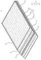
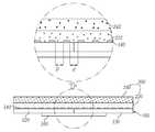
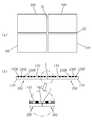
- FIG. 1is a partial cutaway perspective view showing a flexible surface lighting apparatus according to a first embodiment of the first disclosure.
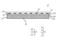
- FIG. 2is a cross-sectional view showing a flexible surface lighting apparatus according to a first embodiment of the first disclosure.
- FIG. 3is a view for explaining an example to which the flexible surface lighting apparatus illustrated in FIGS. 1 and 2 is applied.
- FIG. 4is a cross-sectional view showing a flexible surface lighting apparatus according to a second embodiment of the first disclosure.
- FIG. 5is a cross-sectional view showing a flexible surface lighting apparatus according to a third embodiment of the first disclosure.
- FIG. 6is a cross-sectional view showing a flexible surface lighting apparatus according to a fourth embodiment of the first disclosure.
- FIG. 7is a view for explaining an application example of the flexible surface lighting apparatus according to the fourth embodiment of the first disclosure.
- FIG 8is a cross-sectional view showing a flexible surface lighting apparatus according to a fifth embodiment of the first disclosure.
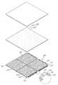
- FIG. 9is a perspective view illustrating a flexible LED lighting apparatus according to an embodiment of the second disclosure.
- FIG. 10is an exploded perspective view showing a flexible LED lighting apparatus according to an embodiment of the second disclosure.
- FIG. 11is a bottom exploded perspective view illustrating a flexible LED lighting apparatus according to an embodiment of the second disclosure.
- FIG. 12is an enlarged cross-sectional view illustrating a flexible LED lighting apparatus according to an embodiment of the second disclosure.
- FIG. 13is an enlarged cross-sectional view illustrating a flexible LED lighting apparatus further including a flexible boundary adhesive unit according to another embodiment of the second disclosure.
- FIG. 14is an enlarged cross-sectional view showing an LED lighting device further including an underfill material according to another embodiment of the second disclosure.
- FIG. 15is a bottom view of a flexible LED lighting apparatus according to another embodiment of the second disclosure.
- FIG. 15is a bottom view of a flexible LED lighting apparatus according to another embodiment of the second disclosure.
- 16is a perspective view illustrating a flexible LED lighting apparatus according to an embodiment of the third disclosure.
- FIG. 17is an exploded perspective view showing a flexible LED lighting apparatus according to an embodiment of the third disclosure.
- FIG. 18is an exploded perspective view illustrating an expandable flexible micro LED panel of a flexible LED lighting apparatus according to an embodiment of the third disclosure.
- FIG. 19is a plan view illustrating the expandable flexible micro LED panel illustrated in FIG. 18.
- 20A and 20Bare cross-sectional views taken along the line A-A of FIG. 19 and cross-sectional views taken along the line B-B of FIG.
- 21is an exploded perspective view showing a flexible LED lighting apparatus according to another embodiment of the third disclosure.
- FIG. 22is an exploded cross-sectional view illustrating a flexible LED lighting apparatus according to still another embodiment of the third disclosure.
- FIG. 23is a cross-sectional view of the flexible LED lighting apparatus shown in FIG. 22.
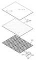
- FIG. 24is a perspective view illustrating the micro LED display panel according to the embodiment of the fourth disclosure with the light transmitting film separated.
- 25is a perspective view illustrating a micro LED display panel according to an embodiment of the fourth disclosure with a light transmitting film attached thereto.
- 26 to 29are diagrams for sequentially describing a method of manufacturing a micro LED display panel according to an embodiment of the fourth disclosure.
- 1 to 3are diagrams for describing a flexible surface lighting apparatus according to a first embodiment of the first disclosure.
- the flexible surface lighting apparatus 1can be deformed into a desired form by an external force, and in a state where the external force is removed, the state after being deformed It is configured to maintain the same, and includes a flexible substrate (flexible substrate) 10, the micro LED chip 20, the transparent resin portion 30, the wavelength conversion film (40).
- the flexible substrate 10includes a flexible substrate material, a circuit, and the like, such as, for example, a flexible printed circuit board (FPCB), and as described in more detail below, flexibility and It has a shape retaining function after deformation.
- a flexible substrate materialsuch as, for example, a flexible printed circuit board (FPCB), and as described in more detail below, flexibility and It has a shape retaining function after deformation.
- FPCBflexible printed circuit board
- the plurality of micro LED chips 20are arranged in a two-dimensional matrix on the upper surface of the flexible substrate 10, the length of at least one side to a few to several hundred micrometers, more preferably, less than 200 micrometers Small, when arrayed on the flexible substrate 10 with sufficient chip-to-chip spacing, it is possible to allow the flexible substrate 10 to be deformed into a desired shape.
- each of the micro LED chips 20includes a transparent sapphire substrate 21 at an upper portion thereof, and downwards from a buffer layer 212 formed in contact with a lower surface of the transparent sapphire substrate 21.
- the conductive semiconductor layer 22, the active layer 23, and the second conductive semiconductor layer 24are included.
- each of the micro LED chips 20may include a first electrode pad 25a connected to the first conductive semiconductor layer 22 and a second electrode pad 25b connected to the second conductive semiconductor layer 24.
- the first electrode pad 25a and the second electrode pad 25bare connected to the first and second electrodes on the flexible substrate by the first solder bumps 26a and the second solder bumps 26b.
- the first electrode pad 25amay be formed through a region in which a portion including the active layer 23 and the second conductive semiconductor layer 24 is removed from the semiconductor stacked structure of the micro LED chip 20. It may be connected to the first conductive semiconductor layer 25a.
- the bonding wiresmay fall off or be damaged.
- the micro LED chip 20may be a light of a wavelength capable of producing white light together with a wavelength conversion material, in particular, a blue LED chip emitting blue light, and more preferably, a gallium nitride based LED chip.
- the translucent resin part 30may transmit the micro LED chip 20 at high transmittance, and covers both the top and side surfaces of the micro LED chip 20 and the top surface of the flexible substrate 10. It is formed to.
- the translucent resin part 30is formed to contact both the top and side surfaces of the micro LED chip 20 and the top surface of the flexible substrate 10.
- the upper surface of the translucent resin portion 30is parallel to the upper surface of the flexible substrate 10.
- the light-transmissive resin part 30is preferably formed of a transparent silicone resin or a transparent epoxy resin, and when the flexible substrate 10 is deformed, it has a degree of flexibility that can be deformed together.
- a light diffusion or light scattering patternmay be formed on the upper surface of the transparent resin part 30.
- the wavelength conversion film 40is formed on the upper surface of the transparent resin portion 30, the wavelength conversion of the light transmitted through the side and the upper surface of the micro LED chip 20 and transmitted through the transparent resin portion 30 And a wavelength conversion material, and the wavelength conversion material may include one or more phosphors or quantum dots.
- the flexible substrate 10has a flexibility to be easily deformed by an external force and a shape maintaining function after deformation.
- the flexible substrate 10includes a shape maintaining layer 14 for maintaining the deformed state of the flexible substrate 10 when the external force that deforms the flexible substrate 10 is removed. .
- the flexible substrate 10further includes a white reflective layer 18 disposed at the top thereof in contact with the light transmissive resin part 30 and a core layer 16 formed under the white reflective layer 18. do.
- the shape maintaining layer 14 described aboveis located under the core layer 16.
- the white reflective layer 18is preferably a white PSR film having good reflectivity.
- a plurality of holes 181 corresponding to the micro LED chips 20are formed in the white reflective layer 18.
- micro LED chips 20are positioned in each of the plurality of holes 181 (only one is shown in FIG. 2).
- each of the plurality of holes 181may have a depth such that each of the holes 181 may accommodate lower portions of the micro LED chip 20 or solder bumps, and the active layer of the micro LED chip 20 may be formed. It is determined to the extent that it can be out of the hole 181.
- the core layer 16is a portion that substantially performs the circuit board function of the flexible substrate 10, and the upper insulating film 162 and the lower insulating film 164 and the metal thin film layer 163 interposed therebetween. ).
- a polyimide filmis used as the upper insulating film 162 and the lower insulating film 164
- the metal thin film layer 163is a layer formed of a metal thin film having a predetermined pattern.
- Cu thin filmis used.
- the shape maintaining layer 14is formed in contact with the lower surface of the core layer 16, in particular, the lower surface of the lower insulating film 164, the flexibility to allow deformation and the shape after deformation It is made of a metal material having a predetermined thickness having retention properties.
- an Al plate having a constant thicknessis used as the shape maintaining layer 14.
- Al platehere includes an Al alloy plate.
- the shape retaining layer 14 formed of an Al plateallows the flexible substrate 10 to be deformed by an external force that bends or bends the flexible substrate 10, while maintaining the deformed state in the state where the external force is removed. Do it.
- the flexible surface lighting apparatus 1 indicated by the virtual line in FIG. 3is bent at an angle in accordance with the top surface curvature of the object O having a triangular cross section. At this time, the flexible surface illumination device 1 is maintained at the bent angle due to the shape maintaining layer 14 described above.
- the flexible substrate 10may further include an adhesive film 12 adhered to the external object O at the bottom thereof.
- FIG. 4is a cross-sectional view showing a flexible surface lighting apparatus according to a second embodiment of the first disclosure.
- the flexible surface lighting apparatus 1includes a flexible substrate 10, micro LED chips 20, and a transparent resin part 30.
- a plurality of wavelength conversion materials 41such as phosphors or quantum dots are widely distributed in the translucent resin part 30.
- FIG. 5is a cross-sectional view showing a flexible surface lighting apparatus according to a third embodiment of the present invention.
- the flexible surface lighting apparatus 1includes a flexible substrate 10, micro LED chips 20, and a transparent resin part 30.
- the flexible surface lighting apparatus according to the present embodimentunlike the previous embodiments, includes a wavelength conversion layer 42 formed to cover the top and side surfaces of the micro LED chip 20, and the wavelength conversion layer ( 42) a wavelength conversion material such as a phosphor or a quantum dot is formed on the top and side surfaces of the micro LED chip 20.
- FIG. 6is a view for explaining a flexible surface lighting apparatus according to a fourth embodiment of the first disclosure.
- the flexible surface lighting apparatusincludes a flexible substrate 10, a plurality of micro LED chips 20 two-dimensionally arranged on an upper surface of the flexible substrate 10, and A heat dissipation unit 60 having a wavelength conversion material for converting wavelengths of light emitted from upper and side surfaces of the micro LED chips 20, and a curved coupling surface to which the flexible substrate 10 is bent and coupled; It includes a light-transmitting resin portion 30 formed on the upper surface of the flexible substrate 10 to cover the upper surface and the side surfaces of the micro LED chip 20.
- the light-transmissive resin part 30has flexibility to be bent together with the flexible substrate 10 when the flexible substrate 10 is coupled to the curved coupling surface of the heat dissipating part 60.
- the flexible substrate 10further includes a white reflective layer 18 disposed at the top of the flexible substrate 10 and a core layer 16 formed under the white reflective layer 18.
- the white reflective layer 18is preferably a white PSR film having good reflectivity.
- the core layer 16is a portion that substantially performs the circuit board function of the flexible substrate 10, and the upper insulating film 162 and the lower insulating film 164 and the metal thin film layer 163 interposed therebetween. ).
- a polyimide filmis used as the upper insulating film 162 and the lower insulating film 164
- the metal thin film layer 163is a layer formed of a metal thin film having a predetermined pattern.
- Cu thin filmis used.
- the flexible substrate 10includes an adhesive film 12 under the core layer 16, and by the adhesive film 12, the flexible substrate 10 is adhered to the heat dissipation unit 60. .
- the heat dissipation unit 60is made of a metal material having flexibility for allowing deformation and shape retention after deformation. In this embodiment, an Al plate having a certain thickness is used as the heat dissipation unit 60.
- the heat dissipation unit 60 and the flexible substrate 10 coupled with the heat dissipation unit 60may be deformed in various forms by an external force. At this time, since the heat dissipation part 60 has a property of maintaining the deformed state as it is when the external force is released, the flexible substrate 10 also maintains the deformed state.
- the flexible substrate 60maintains its deformed state depending on the deformed form of the heat dissipation unit 60. As shown in FIG. 6, the heat dissipation unit 60 is maintained in a waveform-deformed state, and the flexible substrate 10 coupled thereto is also maintained in a deformed state. Furthermore, the translucent resin portion 30 coupled to the flexible substrate 10 is also maintained in a form corresponding to the waveform of the heat dissipation portion 60 similarly to the flexible substrate 10.
- the flexible substrate 10 and the light-transmissive resin portion 30have flexibility, and the heat dissipation portion 60 coupled to the flexible substrate 10 has a property of maintaining its curved deformation state in a curved state. Therefore, when the heat dissipating part 60 is deformed to be bent, the flexible substrate 10 and the transparent resin 30 may also be maintained in a curved shape corresponding thereto.
- FIG. 7Aillustrates an example in which the heat dissipation part 60 is maintained in a bent shape that is bent at approximately 90 degrees, and the flexible substrate 10 and the transparent resin part 30 are also maintained in a bent shape which is bent at 90 degrees.
- 7 (b)shows an example in which the flexible substrate 10 and the transparent resin part 30 are also maintained in a semi-circular bent shape when the heat dissipating part 60 is maintained in a semi-circular bent shape.
- FIG 8is a cross-sectional view showing a flexible surface lighting apparatus according to a fifth embodiment of the first disclosure.
- the flexible surface lighting apparatusincludes a heat dissipation unit 60 including a heat dissipation plate 62 and a plurality of heat dissipation fins 64 formed on the bottom surface of the heat dissipation plate 62.
- the heat sink 60is made of a metal plate, preferably Al plate, which can be deformed by an external force and can remain deformed when the external force is removed.
- the rest of the configurationis substantially the same as that of the fourth embodiment of the first disclosure described above, and thus a detailed description thereof will be omitted.
- the flexible surface lighting apparatusmay further include a light diffusing film on the upper surface of the transparent resin part.
- the thickness of the flexible substrate 10may vary according to the size and pitch of the micro LED chip 20 mounted on the flexible substrate 10.
- the micro LED chip 20having a width of several tens to hundreds of micrometers, more preferably, the micro LED chip 20 having a size of 100 ⁇ m ⁇ 300 ⁇ m is applied, the micro LED chip ( When the 20 are arrayed, a flexible substrate 10 of about 0.15 mm may be used, and when the micro LED chips 20 are arrayed at about 0.6 to 0.8 mm pitch interval, the flexible substrate 10 having a thickness of 0.30 mm ) May be used, and when the LED chips 20 are arrayed at a pitch interval of about 0.4 to 0.6 mm, a flexible substrate 10 having a thickness of about 0.45 mm may be used.
- uniform surface lightcan be obtained by reducing the pitch, the number and thickness of stacking of the flexible substrate 10 increase, making it difficult to change the curvature freely.
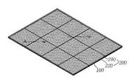
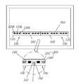
- 9 to 12are diagrams for describing a flexible LED lighting apparatus according to an embodiment of the second disclosure.
- a flexible LED lighting apparatusis a surface lighting apparatus that can be modified in various forms, including an expandable flexible micro LED panel 100 and the expandable flexible micro LED panel. And a light transmitting sheet 200 disposed on the 100.
- the light transmitting sheet 200receives light emitted from the expandable flexible micro LED panel 100 from the bottom surface and radiates it from the top surface to the outside, and may be formed as a single layer of film, but has two or more layers having various functions. It is preferable that the films have a stacked structure.
- the light transmitting sheet 200is laminated so as to be in direct contact with the upper surface of the expandable flexible micro LED panel 100, the wavelength for wavelength conversion of the light emitted from the expandable flexible micro LED panel 100 A conversion sheet 220 and a light diffusion sheet 240 for diffusing the light passing through the wavelength conversion sheet 220 to emit to the outside.
- the wavelength conversion sheet 220is molded by mixing a wavelength conversion material 222 such as a phosphor or a quantum dot with a transparent resin.
- White lightmay be generated by mixing the wavelength converted by the wavelength converting material and the light passing through the wavelength converting sheet 220 without passing through the wavelength converting material.
- the light diffusion sheet 240may include, for example, a light diffusion material 242 such as TiO 2 , SiO 2, and the like, and diffuses and emits wavelength-converted light.
- the light transmitting sheet 200is coupled to the upper surface of the flexible micro LED panel 100 in a stacked form, side surfaces of the plurality of flexible circuit boards 120 included in the flexible micro LED panel 100 are attached to each other. It keeps the state. At this time, of course, the light transmitting sheet 200 has a flexible characteristic.
- the extended flexible micro LED panel 100is mounted on the flexible circuit boards 120 and the plurality of flexible circuit boards 120 having a rectangular or square shape, and is entirely covered by the light transmitting sheet 200.
- the plurality of flexible circuit boards 120are arranged in a matrix along the horizontal and vertical directions, and each of the flexible circuit boards 120 is disposed such that the four sides thereof are in contact with corresponding sides of other neighboring flexible circuit boards 120. . Accordingly, the expandable flexible micro LED panel 100 may not have any unwanted gaps between neighboring flexible circuit boards 120 and 120.
- the wiring unit 160is for connecting the LED chips 140 of the adjacent flexible circuit boards 120 in series or in parallel and may be formed of, for example, a jumper or a harness.
- the wiring unit 160includes a two-way wiring unit 162 provided between two flexible circuit boards 120 adjacent in the horizontal direction or the vertical direction, and four adjacent flexible circuit boards 120. And the four-way wiring unit 164 provided at a point where the 120, 120, and 120 meet.
- the two-way wiring unit 162includes only wires for electrically connecting the LED chips 140 on two flexible circuit boards 120 and 120 adjacent in a horizontal or vertical direction, and the four-way wiring unit 164. Is a wiring for electrically connecting the LED chips 160 on two flexible circuit boards 120 and 120 adjacent in the horizontal direction and the LED chips 140 on the two flexible circuit boards 120 and 120 adjacent in the vertical direction. It may include all the wiring to be connected.
- Each of the LED chips 140may be micro LED chips having a length of at least one side of several tens to several hundred micrometers. Since the sizes of the LED chips 140 are very small and the flexible circuit boards 120 are flexible, the extended flexible circuit board which connects the flexible circuit boards 120 and the LED chip mounted on the extended flexible circuit board are mounted. Deformation of the expandable micro LED panel 100 including the 140 may be possible to a fine size. Since the unit flexible circuit board 120 and the LED chips 140 mounted on the unit flexible circuit board 120 constitute one LED module, the expandable flexible micro LED panel 100 connects a plurality of LED modules. It is the same as pasting.
- the LED chip 140is a wireless chip without a bonding wire, in particular, a flip chip type having both a first conductive electrode pad and a second conductive electrode pad at the bottom thereof and mounted on the flexible circuit board 120 in a flip chip method. It is preferable that it is an LED chip. If an LED chip that requires a bonding wire is used, the bonding wire may be damaged when the light transmitting sheet is laminated.
- the second spacing d between two neighboring LED chips 140 and 140 on the two neighboring circuit boards 120 and 120preferably has the following relationship.
- the boundary region between two neighboring flexible circuit boards 120 and 120becomes excessively dark compared to the other regions, and the second interval is 0.9 of the first interval.
- the boundary area between two neighboring flexible circuit boards 120 and 120becomes excessively bright compared to other areas, and in both cases, it hinders to realize a uniform surface light source.
- the empty space between the LED chips 140is filled with a portion of the light transmitting sheet, in particular a portion of the wavelength conversion sheet 220 is compressed.
- the flexible LED lighting apparatus described abovemay be manufactured according to the following process.
- a large-area light transmitting sheet 200more specifically, a wavelength conversion sheet 220 and / or a light diffusion sheet 240 is prepared in a large area, and combined to match the size of the light transmitting sheet 200
- the flexible LED modulesthat is, the flexible circuit boards 120 on which the LED chips 140 are mounted.
- a structure including a plurality of flexible circuit boards 120 arranged without a gap and a plurality of LED chips 120 mounted on the flexible circuit board 120is disposed in contact with the light transmitting sheet 200.
- the wiring circuits 160are used to electrically connect the flexible circuit boards 120. This electrical connection connects the LED chips 140 on different circuit boards in parallel.
- Each of the flexible LED modules composed of the LED chips 140 mounted on the flexible circuit board 120is manufactured without a bezel for placement and assembly as described above.
- the rear surface of the flexible circuit board 120may be divided into a positive electrode portion and a negative electrode portion.
- two adjacent flexible circuit boards 120 and 120that is, bottom surfaces of the first flexible circuit board 120 and the second flexible circuit board 120 each include a positive electrode part and a negative electrode part.
- the side of the positive electrode of the first flexible circuit board 120 and the side of the negative electrode of the second flexible circuit board 120may be adjacent to each other.
- FIG. 13is a view for explaining a flexible LED lighting apparatus according to another embodiment of the second disclosure.
- the flexible LED lighting apparatususes the flexible flexible micro LED panel 100 and the light transmitting sheet 200 disposed on the flexible flexible micro LED panel.
- the extended flexible micro LED panel 100includes a plurality of flexible circuit boards 120 arranged on the flexible circuit boards and arranged without a gap in contact with side surfaces in a horizontal or vertical direction.
- a wiring unitmounted and electrically connected to the plurality of LED chips 140 entirely covered by the light transmitting sheet 200 and neighboring flexible circuit boards 120 at the bottom of the flexible circuit boards 120. And 160.
- the flexible LED lighting apparatusfurther includes a flexible boundary adhesive part 170 formed along a boundary between neighboring flexible circuit boards 120.
- the flexible boundary adhesive part 170may be a flexible adhesive tape that is attached to two neighboring edges of the flexible circuit board 120 along the boundary or at two adjacent edges of the flexible circuit board 120 along the boundary. It may be a flexible sealing material applied for a long time. Since the flexible boundary adhesive part 170 has flexibility similar to that of the flexible circuit board 120, the flexible micro LED panel 100 has a flexible characteristic as a whole.
- the flexible boundary adhesive part 170may be provided to cover at least a portion of the wiring part 160 connecting the adjacent flexible circuit boards 120 and 120. Since the rest of the configuration is the same as in the previous embodiment, description is omitted to avoid duplication.
- FIG. 14is a view for explaining a flexible LED lighting apparatus according to another embodiment of the second disclosure.
- the flexible LED lighting apparatuslike the previous embodiment, includes the expandable flexible micro LED panel 100 and the light transmitting sheet disposed on the expandable flexible micro LED panel 100 (
- the flexible flexible LED panel 100includes a plurality of flexible circuit boards 120 arranged on the flexible circuit boards without gaps in contact with side surfaces in a horizontal direction or a vertical direction.
- the wiring unit 160may be mounted to electrically connect the plurality of LED chips 140 that are entirely covered by the light transmitting sheet 200 and the flexible circuit boards 120 adjacent to the bottom of the flexible circuit boards.
- the underfill 201is filled between neighboring LED chips 140.
- the underfill 201may be formed of a resin material, and more preferably, may be formed of a resin material including a wavelength converting material such as a phosphor or a quantum dot, or a resin material including a light reflecting material or a light scattering material. .
- the underfill 201may have a recess in the center between neighboring LED chips 140 and 140.
- FIG. 15is a view illustrating a bottom of the flexible LED unit of the flexible LED lighting apparatus according to another embodiment of the second disclosure.
- the flexible LED lighting apparatuslike the previous embodiment, includes an expandable micro LED panel 100, and the expandable micro LED panel 100 has a rectangular or rectangular shape and has a horizontal direction and The plurality of flexible circuit boards 120 are arranged without a gap in contact with side surfaces along the longitudinal direction.
- the flexible circuit boards 120are electrically connected to each other by the wiring units 160.
- each of the wiring units 160has a flexible wiring film having both ends detachably connected to two corresponding connectors 167 and 167 provided on the bottoms of the adjacent flexible substrates 120 and 120.
- FPCBflexible boundary adhesive part 170
- the flexible boundary adhesive part 170may be a flexible adhesive tape 170 that is attached to two adjacent edges of the flexible circuit boards 120 and 120 along a boundary between neighboring flexible circuit boards 120 and 120. Can be.
- the flexible LED lighting devicemay have the following configuration.
- the number and thickness of layers of the flexible substratemay vary depending on the size and pitch of the LED chip mounted on the flexible substrate. For example, when a micro LED chip having a width of several tens to hundreds of micrometers, more preferably, a micro LED chip having a size of 100 ⁇ m ⁇ 300 ⁇ m is arrayed at approximately 0.8 mm pitch interval, an approximately 0.15 mm thick flexible circuit board is used. When the LED chips are arrayed at approximately 0.6 to 0.8 mm pitch intervals, a flexible substrate having a thickness of 0.30 mm may be used as a two-layer stacked structure, and the LED chips may be arrayed at approximately 0.4 to 0.6 mm pitch intervals.
- multilayer number of a flexible circuit boardis 1-3 layers, Most preferably, it is 1 layer.
- the term "layer”means an insulating layer on which a conductive pattern is formed, and the number of layers means the number of insulating layers.
- the LED chipsare microphone LED chips having a width of tens to hundreds of micrometers and are mounted in a matrix array on the flexible substrate.
- Each of the LED chipsmay include a light-transmitting sapphire substrate, a buffer layer formed under the sapphire substrate, a first conductive semiconductor layer formed under the buffer layer, and an active layer formed under the first conductive semiconductor layer. And a second conductivity type semiconductor layer formed under the active layer.
- An active layeris interposed between the second conductive semiconductor layer and the first conductive semiconductor layer, and the active layer is a layer that generates light by combining electrons and holes.
- a lower surface of the second conductive semiconductor layermay be exposed downward, and a portion of the second conductive semiconductor layer and the active layer may be removed to expose a portion of the lower surface of the first conductive semiconductor layer downward.
- a first conductive electrode padis formed on the exposed lower surface of the first conductive type conductor layer and extends downward, and a second conductive layer having a different polarity than the first conductive electrode pad is formed on the lower surface of the second conductive semiconductor layer.
- a type electrode padis formed.
- the light transmitting sheetwhich may include a wavelength converting sheet and a light diffusing sheet, includes light entering surfaces in contact with the LED chips, and light exit surfaces emitting light entering through the light emitting surfaces to the outside.
- the light transmitting sheetfunctions as a waveguide.
- the heights of the LED chipsare very small, in the order of several to several hundred micrometers, the height of the light transmitting sheet can be relatively high, so that the light can be spread evenly and uniformly emitted from the light transmitting sheet. .
- the wavelength converted light and the wavelength converted lightmay be sufficiently mixed in the wavelength conversion sheet and emitted to the outside.
- the light diffusion sheet belonging to the upper or lower side of the light transmitting sheetis based on a resin material having both flexibility and light transmission, for example, a silicone resin, and the diffusion agent is uniformly mixed in the form of particles in the resin material. And formed by the distributed material.
- a resin material having both flexibility and light transmissionfor example, a silicone resin
- the diffusion agentis uniformly mixed in the form of particles in the resin material. And formed by the distributed material.
- the diffusing agentTiO 2 , SiO 2 , or a mixture thereof may be selected and used.
- a plurality of nanosilvermay be added to a portion of the light transmitting sheet, particularly, the light transmitting sheet located in an area in contact with the LED chip.
- the plurality of nanosilvermoves to the first conductive electrode pad and the second conductive electrode pad of the LED chip containing Cu when the temperature and pressure of approximately 150 °C to form a cluster, the cluster by the nanosilver
- the coupling between the conductive electrode pad and the second conductive electrode pad and the soldercan be reinforced and cracks can be suppressed.
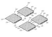
- FIG. 16is a perspective view illustrating a flexible LED lighting apparatus according to an embodiment of the third disclosure
- FIG. 17is an exploded perspective view illustrating the flexible LED lighting apparatus according to the embodiment of the third disclosure
- FIG. 18is a third perspective view.
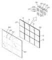
- FIG. 19is an exploded view illustrating the expandable flexible micro LED panel of the flexible LED lighting apparatus according to the exemplary embodiment of the present disclosure
- FIG. 19is a plan view illustrating the expandable flexible micro LED panel illustrated in FIG. 18, and FIGS. (b) is a sectional view taken along AA of FIG. 19 and a sectional view taken along BB of FIG.
- a flexible LED lighting apparatusis a surface lighting apparatus that can be modified in various forms, including an expandable flexible micro LED panel 100 and the expandable flexible micro LED panel. And a light transmitting film 200 disposed on the 100.
- the light transmitting membrane 200receives light emitted from the expandable flexible micro LED panel 100 from the bottom surface and radiates from the upper surface to the outside, and may be formed as a single layer of film, but has two or more layers having various functions. It is preferable that the films have a stacked structure. In addition, one or more layers of the light transmitting film 200 may be formed in advance and attached to the expandable micro LED panel 100, or may be molded on the expandable micro LED panel 100.
- the light transmitting film 200is laminated so as to be in direct contact with the upper surface of the expandable flexible micro LED panel 100, the wavelength for wavelength conversion of the light emitted from the expandable flexible micro LED panel 100 A conversion sheet 220 and a light diffusion sheet 240 for diffusing the light passing through the wavelength conversion sheet 220 to be emitted to the outside.
- the wavelength conversion sheet 220is molded by mixing a wavelength conversion material such as a phosphor or a quantum dot with a transparent resin.
- White lightmay be generated by mixing light converted by the wavelength converting material and light passing through the wavelength converting sheet 220 without passing through the wavelength converting material.
- the light diffusion sheetmay include, for example, a light diffusion material 242 such as TiO 2 , SiO 2, and the like, and diffuses and emits wavelength converted light.
- the light transmitting film 200is coupled to the upper surface of the flexible micro LED panel 100 in a stacked form, the edges of the plurality of flexible circuit boards 120 included in the flexible micro LED panel 100 overlap each other. It keeps attached state. At this time, it is a matter of course that the light transmitting film 200 has a flexible characteristic.
- the flexible flexible micro LED panel 100has a rectangular or square shape, and a plurality of flexible circuit boards 120 are attached to each other in a horizontal direction and a vertical direction by overlapping a portion of an edge thereof up and down, and the flexible circuit board 120.
- a plurality of LED chips 140mounted on each of the plurality of LED chips 140 and entirely covered by the light transmitting film 200, and interposed between edge overlapping regions of neighboring flexible circuit boards 120.
- One or more wiring units 160 that electrically connect the circuit boards 120are included.
- the plurality of flexible circuit boards 120are arranged in a horizontal direction and a longitudinal direction, and each of the flexible circuit boards 120 has a flexible circuit board adjacent to each of four corner peripheral edge regions. And overlap with the corresponding edge regions of the 120 up and down. Accordingly, the expandable flexible micro LED panel 100 may suppress unwanted gaps between neighboring flexible circuit boards 120 and 120.
- each of the flexible circuit boards 120may include a first step portion 122 and a second step at two edge regions facing each other among edge regions overlapping with other neighboring flexible circuit boards 120. It includes a step 124.
- the first step portion 122is recessed to a certain depth from an upper surface of the flexible circuit board 120 in one edge region of the flexible circuit board 120 to form a step with the upper surface.
- the second stepped portion 124is recessed to a certain depth from the bottom surface of the flexible circuit board 120 in the other edge region opposite the one edge of the flexible circuit board 120 to form a step with the bottom surface.
- the flexible circuit board 120is formed in a substantially quadrangular structure having four edges, and is superimposed on another flexible circuit board 120 at each of the four edges.
- the circuit board 120includes first step portions 122 at two edges that cross at right angles to each other, and second step portions 122 are formed at opposite sides of the edge where the first step portions 122 are formed. It is formed at right angles.
- an upper surface of the first step portion 122 of the flexible circuit board 120may have a second step portion of another flexible circuit board 120 adjacent thereto.
- a wiring unit disposed to face the bottom of the 124 and electrically connecting the two flexible circuit boards 120 and 120 adjacent to each other between the first stepped part 122 and the second stepped part 124. 160is formed.
- the wiring part 160includes the first connection part 160a formed in the first step part 122 and the second connection part 160b formed in the second step part 124 formed in the second step part 124. ) May be included.
- the wiring unit 160connects the LED chips 140 of the adjacent flexible circuit boards 120 in series or in parallel.
- the wiring portions 160are edges of the wiring portions 160 provided in the edge overlapping region of the two flexible circuit boards 120 adjacent in the horizontal direction and the two flexible circuit boards 120 adjacent in the vertical direction.
- the wiring part 160 provided in the overlap areais included.
- the overlapped regionoverlaps the first stepped portion 122 formed at one edge of one flexible circuit board 120 and the second stepped portion 124 formed at the other edge of another flexible circuit board 120 neighboring.
- the wiring portion 160is provided between the first step portion 122 and the second step portion 124.
- Each of the LED chips 140may be micro LED chips having a length of at least one side of several tens to several hundred micrometers. Since the sizes of the LED chips 140 are very small and the flexible circuit boards 120 have flexibility, the LED chips 140 are mounted on the extended flexible circuit board and the extended flexible circuit board which overlap the edges of the flexible circuit boards 120. Modification of the expandable micro LED panel 100 including the LED chips 140 may be possible to a fine size.
- the wavelength conversion sheet 220is formed on the entire region except for the region where the first step portion 122 is formed among the entire upper surface of the flexible circuit board 120 on which the LED chips 140 are mounted.
- the expandable flexible micro LED panel 100includes a plurality of LEDs. It is the same as connecting LED modules.
- the region in which the flexible circuit board 120 and the first and second stepped portions 122 and 124 of the flexible circuit board 120 overlap with each otherhas a flexible characteristic almost similar to that of other regions of the flexible circuit board 120. . This works advantageously in transforming the finished flexible LED lighting device into the desired shape.
- the LED chip 140is a wireless chip without a bonding wire, in particular, a flip chip type having both a first conductive electrode pad and a second conductive electrode pad at the bottom thereof and mounted on the flexible circuit board 120 in a flip chip method. It is preferable that it is an LED chip. If an LED chip that requires a bonding wire is used, the bonding wire may be damaged when the light transmitting film is laminated.
- the second spacing d between two neighboring LED chips 140 and 140 on the two neighboring circuit boards 120 and 120preferably has the following relationship.
- the boundary region between two neighboring flexible circuit boards 120 and 120becomes excessively dark compared to the other regions, and the second interval is 0.9 of the first interval.
- the boundary area between two neighboring flexible circuit boards 120 and 120becomes excessively bright compared to other areas, and in both cases, it hinders to realize a uniform surface light source.
- the flexible LED lighting apparatus described abovemay be manufactured according to the following process.
- a large-area light transmitting film 200more specifically, a wavelength conversion sheet 220 and / or a light diffusion sheet 240 is prepared in a large area and bonded to match the size of the light transmitting film 200
- the flexible LED modulesare arranged to contact the bottom surface of the light transmitting film 200, in particular, the wavelength conversion sheet 220.
- the flexible micro LED panel 120 connecting the flexible LED modules 100 'may be prepared first, and the wavelength conversion sheet 220 and the light diffusion sheet 240 having a large area may be sequentially arranged on the upper surface thereof. have.
- Wiring portions 160a, 160b (160) provided between)electrically connect the flexible circuit boards 120.
- a structure including a plurality of flexible circuit boards 120 arranged without a gap and a plurality of LED chips 120 mounted on the flexible circuit board 120is disposed in contact with the light transmitting film 200.
- a specific flexible circuit boardis defined as a first flexible circuit board 120, and four flexible circuit boards arranged to overlap four edges of the first flexible circuit board 120 are provided as second, It is defined as a third, fourth and fifth flexible circuit boards.
- the first flexible circuit board 120includes a first edge region and a second edge region located opposite to each other, and the first edge region is recessed to a predetermined depth from an upper surface of the first flexible circuit board 120.
- the first stepped part 122is formed, and the second edge area is provided with a second stepped part 124 formed by recessing a predetermined depth from the bottom of the first flexible circuit board 120.
- the first wiring portionis located between the bottom of the second edge region of the first flexible circuit board 120 having the second step portion 124 and the top surface of the edge region having the first step portion of the third flexible circuit board 120.
- the second wiring portionis located.
- the first flexible circuit board 120may include a third edge region perpendicular to the first edge region and a fourth edge region located opposite the third edge region, and the first flexible circuit board 120
- the third wiring portionis positioned between the top surface of the third edge region of the substrate and the bottom surface of the edge region of the fourth flexible circuit board, and the bottom surface of the fourth edge region of the first flexible circuit board 120 and the fifth flexible circuit board 120.
- the fourth wiring portionis positioned between the upper surface of the edge region of the substrate.
- FIG. 21illustrates a flexible LED lighting apparatus according to another exemplary embodiment of the third disclosure.
- the flexible LED lighting apparatuslike the previous embodiment, includes an expandable flexible micro LED panel 100 and a light transmitting film disposed on the expandable flexible micro LED panel.
- the extended flexible micro LED panel 100is mounted on the flexible circuit boards and a plurality of flexible circuit boards 120 having edge regions arranged to overlap each other and entirely covered by the light transmitting film 200.
- the LED chip 140includes a plurality of LED chips 140 and a wiring unit 160 to electrically connect the flexible circuit boards 120 in a region where the flexible circuit boards 120 overlap each other.
- the light transmitting filmincludes a plurality of wavelength conversion sheets 220 ′ and a light diffusion sheet 240.
- the plurality of unit wavelength conversion sheets 220 'are provided. Each is formed on each of the flexible circuit boards 120 to cover the LED chips 140 mounted on the flexible circuit boards 120.
- the wavelength conversion sheet 220 ′is not formed in the first step portion 122, which is a part of the edge region overlapping the other flexible circuit board 120.
- FIG. 22 and 23are exploded cross-sectional views illustrating a flexible LED lighting apparatus according to still another embodiment of the third disclosure, and FIG. 23 is a cross-sectional view of the flexible LED lighting apparatus illustrated in FIG. 22.
- the flexible LED lighting apparatuslike the previous embodiment, includes the expandable flexible micro LED panel 100 and the light disposed on the expandable flexible micro LED panel 100.
- the extended flexible micro LED panel 100may include a transmissive membrane, and may be mounted on the flexible circuit boards 120 and a plurality of flexible circuit boards 120 having edge regions arranged to overlap each other.
- the light transmitting filmincludes a plurality of wavelength conversion sheets 220 ′ and a light diffusion sheet 240.
- Each of the plurality of unit wavelength conversion sheets 220 ′is formed on each of the flexible circuit boards 120 to cover the LED chips 140 mounted on the flexible circuit board 120.
- the wavelength conversion sheet 220 ′is not formed in edge regions overlapping the other flexible circuit board 120.
- the wavelength conversion sheets 220 'are combined to form one large area wavelength conversion sheet.
- a large area light diffusion sheet 240is provided to cover the wavelength ring film. It is also conceivable for the plurality of unit light diffusing sheets to form one large area light diffusing sheet.
- the edge region adjacent to the edge of the flexible circuit board 120is the remaining region of the flexible circuit board 120, that is, In addition, the chip is coplanar with the area where the LED chips are mounted. That is, the flexible circuit board 120 has the same thickness of the region where the LED chips are mounted and the wavelength conversion sheet is formed and the thickness of the edge region where the wiring portion is formed.
- the overlapping regionmay overlap the edge region of at least one of the two flexible circuit boards 120 and 120.
- the formed first connection portion 160a and the second connection portion 160bmeet to form the wiring portion 160 connecting the LED chips 140 of the flexible circuit boards 120 and 120 in series or in parallel. Since the wiring unit 160 is formed at all four edge regions of the flexible circuit board 120, the flexible circuit board 120 may be electrically connected between the LED chips in both the horizontal and vertical connections.
- the wavelength conversion sheetis in contact with the side surface as well as the top surface of the LED chips, the wavelength conversion sheet may be disposed or formed in contact with only the top surface of the LED chips.
- an underfill materialmay be further provided between the adjacent LED chips to cover the sides of the LED chips.
- the underfill materialpreferably includes a resin, and may be a mixed material of the resin and the wavelength conversion material. Phosphor or quantum dot may be used as the wavelength conversion material.
- white lightmay be realized by mixing light that is wavelength-converted by the wavelength conversion material and light that is not wavelength-converted by the wavelength conversion material among the light emitted from the LED chip.
- the flexible LED lighting devicemay have a configuration as follows.
- the number and thickness of layers of the flexible substratemay vary depending on the size and pitch of the LED chip mounted on the flexible substrate. For example, when a micro LED chip having a width of several tens to hundreds of micrometers, more preferably, a micro LED chip having a size of 100 ⁇ m ⁇ 300 ⁇ m is arrayed at approximately 0.8 mm pitch interval, an approximately 0.15 mm thick flexible circuit board is used. When the LED chips are arrayed at approximately 0.6 to 0.8 mm pitch intervals, a flexible substrate having a thickness of 0.30 mm may be used as a two-layer stacked structure, and the LED chips may be arrayed at approximately 0.4 to 0.6 mm pitch intervals.
- multilayer number of a flexible circuit boardis 1-3 layers, Most preferably, it is 1 layer.
- the term "layer”means an insulating layer on which a conductive pattern is formed, and the number of layers means the number of insulating layers.
- the LED chipsare microphone LED chips having a width of tens to hundreds of micrometers and are mounted in a matrix array on the flexible substrate.
- Each of the LED chipsmay include a light-transmitting sapphire substrate, a buffer layer formed under the sapphire substrate, a first conductive semiconductor layer formed under the buffer layer, and an active layer formed under the first conductive semiconductor layer. And a second conductivity type semiconductor layer formed under the active layer.
- An active layeris interposed between the second conductive semiconductor layer and the first conductive semiconductor layer, and the active layer is a layer that generates light by combining electrons and holes.
- a lower surface of the second conductive semiconductor layermay be exposed downward, and a portion of the second conductive semiconductor layer and the active layer may be removed to expose a portion of the lower surface of the first conductive semiconductor layer downward.
- a first conductive electrode padis formed on the exposed lower surface of the first conductive type conductor layer and extends downward, and a second conductive layer having a different polarity than the first conductive electrode pad is formed on the lower surface of the second conductive semiconductor layer.
- a type electrode padis formed.
- the light transmitting filmwhich may include the wavelength conversion sheet and the light diffusion sheet, includes light incidence surfaces in contact with the LED chips, and light emission surfaces for emitting light entering through the light incidence surfaces to the outside.
- the permeable membranefunctions as a waveguide.
- the height of the LED chipsis very small, in the order of several to several hundred micrometers, the height of the light transmitting film can be relatively high, and thus, light can be spread evenly and uniformly emitted from the light transmitting film.
- the wavelength converted light and the wavelength converted lightmay be sufficiently mixed in the wavelength conversion sheet and emitted to the outside.
- the light diffusion sheet belonging to the upper or lower side of the light transmitting filmis based on a resin material having both flexibility and light transmission, such as a silicone resin, and the diffusion agent is uniformly mixed in the form of particles in the resin material. And formed by the distributed material.
- a resin material having both flexibility and light transmissionsuch as a silicone resin
- the diffusion agentis uniformly mixed in the form of particles in the resin material. And formed by the distributed material.
- the diffusion agentTiO 2 , SiO 2 , or a mixture thereof may be selected and used.
- a plurality of nanosilvermay be added to a portion of the light transmitting film, particularly, the light transmitting film located in a region in contact with the LED chip.
- the plurality of nanosilvermoves to the first conductive electrode pad and the second conductive electrode pad of the LED chip containing Cu when the temperature and pressure of approximately 150 °C to form a cluster, the cluster by the nanosilver
- the coupling between the conductive electrode pad and the second conductive electrode pad and the soldercan be reinforced and cracks can be suppressed.
- FIG. 24is a perspective view illustrating a micro LED display panel according to an embodiment of the fourth disclosure with the light transmitting film separated
- FIG. 25is a light transmission film of the micro LED display panel according to an embodiment of the fourth disclosure. It is a perspective view shown in the attached state.
- a micro LED display panelincludes a plurality of micro LED modules 100 arranged in a matrix with side surfaces connected to each other, and the plurality of micro LED modules. It includes a light transmitting film 300 covering the entire upper surface of the (100).
- the light transmitting film 300is a flexible film that performs a specific function. In the present embodiment, one including an antiglare film is used.
- the display panel according to the present exemplary embodimentmay further include a support frame 200, and may be used to support the micro LED modules 100 arranged in the matrix in the support frame 200.
- the LED display panel according to the present exemplary embodimentmay further include structures for fixing the micro LED modules 100 to the support frame 200.
- the micro LED display panelmay further include an interface board and a power supply.
- Each of the plurality of micro LED modules 100includes a rectangular mount substrate 110 and a plurality of LED pixels 120 arranged in a matrix on an upper surface of the mount substrate 110.
- Each of the plurality of LED pixels 120includes three LED chips mounted on a top surface of the mount substrate 110 by flip chip bonding, and the three LED chips each include a first micro LED chip emitting red light. 120R, a second micro LED chip 120G for emitting green light, and a third micro LED chip 120B for emitting blue light.
- Each of the micro LED chips 120R, 120G, and 120Bmay be formed of a semiconductor chip in which a self-equipped electrode pad is directly bonded to an electrode on a mount substrate, without being accommodated in a separate package having a lead frame or a lead terminal. Do.
- the first, second and third micro LED chips 120R, 120G, and 120Bare flip chip type LEDs in which both the first conductive electrode and the second conductive electrode face the mount substrate. Since the first, second and third micro LED chips 120R, 120G, and 120B are flip chip type LED chips, there are no bonding wires and electrodes on the light emitting surface to which the light transmitting film 300 is attached. 300 and the first, second and third micro LED chips 120R, 120G and 120B are capable of complete face-to-face contact.
- the plurality of plate-shaped micro LED modules 100are arranged in a matrix with the sides connected to each other.
- the micro LED modules 100 gathered by this arrangementform one display panel.
- the rear surface of the mount substrate 110may include driving IC elements for operating micro LEDs.
- the plurality of plate-shaped LED modules 100are joined to sides to form a matrix to form horizontal gap lines CL and vertical gap lines VL intersecting with the horizontal gap lines CL.
- the horizontal gap lines CL and the vertical gap lines VLare horizontally adjacent plate-shaped micro LED modules 100 and fine linear gaps between the adjacent plate-shaped micro LED modules 100 in a neighboring longitudinal direction. Formed by fine linear gaps between them.
- the LED display panelincludes one flexible light transmitting film 300 disposed on and in contact with the top surfaces of the matrixed micro LED modules 100, which is approximately It may have a thickness of 300 to 400 nm, an antiglare film (AG film; 320; see FIGS. 26 to 29) and an adhesive layer 340 of 200 to 300 nm thickness of approximately 100 nm thickness 29).
- the adhesive layer 340(see FIGS. 26 to 29) is a layer that can be melted by the heat applied during the autoclave process described below.
- the light transmitting film 300includes a plurality of air holes to remove the remaining air from between the micro LED modules 100 and the light transmitting film 300.
- the plurality of air holesmay include a plurality of first air holes 301 formed in the light transmitting film 300 along the horizontal gap line CL, and the light transmission along the vertical gap line VL. Second air holes 303 formed in the film 300 are included.
- the light transmitting film 300further includes a third air hole 305 formed at the intersection of the horizontal gap line CL and the vertical line VL. At this time, air suction through the first air holes 301 and the second air holes 303, and further, the first air holes 301, the second air holes 303, and the first air holes 301 and the second air holes 303.
- the light transmitting film 300is in close contact with the upper surfaces of the micro LED modules 100 by air suction through the three air holes 305, and between the light transmitting film 300 and the micro LED modules 100. Remaining air is removed.
- each of the micro LED modules 100includes a driving micro LED on a mount substrate including the first micro LED chip 120R, the second micro LED chip 120G, and the third micro LED chip 120B. It further comprises a 140 formed on the top surface of the mount substrate 110 to cover the side of the chip.
- the front surface of the resin layer 140may be coplanar with the light emitting surfaces of the micro LED chips 120R, 120G, and 120B. Accordingly, due to the air suction through the air holes 301, 302, and 303, the light transmitting film 300 has the micro LEDs 100 in all regions other than the gap lines CL and VL (collectively L). And a front surface and a face-to-face of the resin layer 140.
- the resin layer 140may be formed in a mixture of the resin and the reflective material to serve as a reflective wall.
- the resinmay, for example, be a silicone resin and the reflective material may be TiO 2 or SiO 2 on the particles.
- the resin layer 140has a surface coplanar with the light emitting surface of the micro LED chips 120R, 120G, and 120B, and provides an advantage that the resin layer 140 is in close contact with the light transmitting film 300 without remaining air. Note that you may.
- the resin layer 140has an inclined surface 142 at the edge, and by the inclined surface 142, the inclined surfaces 142 of two neighboring resin layers 140 are interposed between the neighboring micro LED modules 100.
- An air gap line Lof approximately V-shaped cross section is formed.
- a plurality of plate-shaped micro LED modules 100are prepared, and a plurality of plate-shaped micro LED modules 100 are connected to each other side by side and arranged in a matrix. As such, the plate-shaped micro LED modules 100 are connected to each other side by side, so that the plurality of plate-shaped micro LED modules 100 includes a horizontal gap line CL and a vertical gap line VL. Gap lines L are formed.
- the support framemay be used to fix the plate-shaped micro LED module 100 arranged in a matrix, but is not shown.
- each of the micro LED modules 100includes a mount substrate 110, a plurality of micro LED chips 120R, 120G, and 120B mounted on the mount substrate 110, and a micro LED chip ( And a resin layer 140 filled between 120R, 120G, and 120B.
- a gap line Lis formed between the neighboring micro LED modules 100, and the gap line L has a V-shaped cross section due to the inclined surface 142 of the resin layer 140.
- the light transmitting film 300is disposed to contact the top surfaces of the plurality of plate-shaped micro LED modules 100.
- the light transmitting film 300may have a thickness of approximately 300 to 400 nm, and may be composed of an antiglare film 320 having a thickness of approximately 100 nm and an adhesive layer 340 having a thickness of 200 to 300 nm. .
- airremains in the gap line L between the plate-shaped micro LED modules 100, that is, the horizontal gap line CL and the vertical gap line VL.
- the light transmitting film 300is formed along the gap lines L, that is, the horizontal gap line CL and the vertical gap line VL.
- the air holes Hare formed.
- the air holes Hmay include the first air holes 301 formed along the horizontal gap line CL, the second air holes 303 formed along the longitudinal gap line VL, and the vertical holes. And a third air hole 305 formed at the intersection of the directional gap line CL and the horizontal gap line VL.
- Hole processing for forming the holes (H)can be performed using the needle (2). Alternatively, lasers can be used to form air holes.
- the width or diameter of the air holemay be approximately 10 ⁇ 30um.
- the panel having the light transmitting film 300 disposed on the upper surface of the LED modules 100 in the clave 3is charged and an autoclave process is performed while a temperature of approximately 50 ° C. is applied.
- the air remaining in the gap line L generated by the inclined surfaces 142 of the neighboring resin layers 140is discharged through the air hole H, and is heated at the temperature of 50 ° C.
- the adhesive layer 340 of the light transmitting film 300 having fluidityfills the gap line L. As a result, the air hole is blocked.
- a part of the adhesive layer 340is melted as described above, and the portion filling the gap line L is referred to as a sink and denoted by reference numeral 342.
- air holesare formed in the light transmitting film after the light transmitting film is disposed on the top surfaces of the plate-shaped micro LED modules. It may be.
Landscapes
- Engineering & Computer Science (AREA)
- Microelectronics & Electronic Packaging (AREA)
- Power Engineering (AREA)
- Physics & Mathematics (AREA)
- Condensed Matter Physics & Semiconductors (AREA)
- General Physics & Mathematics (AREA)
- Computer Hardware Design (AREA)
- General Engineering & Computer Science (AREA)
- Optics & Photonics (AREA)
- Led Device Packages (AREA)
Abstract
Description
Translated fromKorean본 발명은 마이크로 에이디 칩들을 이용하는 플렉시블 조명 장치 및 디스플레이 패널에 관한 것이다.The present invention relates to a flexible lighting device and a display panel using micro AD chips.
여기에서 본 발명에 관한 배경기술이 제공되는데, 이 배경기술이 반드시 공지기술인 것은 아니다.Here, a background art related to the present invention is provided, which is not necessarily well known.
다수의 엘이디 패키지를 광원들로 이용하는 면조명 장치가 알려져 있다. 이러한 면조명 장치는 엘이디 패키지들이 배치되는 위치에 따라 직하형 면조명 장치와 에지형 면조명 장치로 구분된다. 직하형 면조명 장치는 광 확산판의 직하에 넓게 그리고 2차원적으로 다수개의 엘이디 패키지들이 배치되어 이루어지고, 에지형 면조명 장치는 강성을 갖는 도광판의 모서리를 따라 엘이디 패키지들이 배치되어 이루어진다. 그러나 기존 면조명 장치는, 엘이디 패키지들이 실장되는 인쇄회로기판의 강성으로 인하여, 평판 형태로 밖에 이용될 수 없다는 한계가 있다. 그로 인해, 종래 면광원 장치는, 다양한 객체들의 다양한 표면 형상들에 적응되어 설치되지 못하고, 항상, 평면을 갖는 객체 표면에만 설치될 수 밖에 없는 한계를 갖고 있다. 이러한 문제점을 해결하기 위해, 광원으로서 엘이디 패키지들 대신에 OLED를 이용함으로써 플렉시블 면조명 장치를 구현하고자 하는 시도가 있었다. 하지만, 이러한 OLED를 이용한 플렉시블 면조명 장치는 OLED의 높은 가격과 낮은 광효율 등의 문제점으로 인하여 상용화가 쉽지 않다.Surface lighting apparatuses using a plurality of LED packages as light sources are known. Such a surface lighting device is classified into a direct type surface lighting device and an edge type surface lighting device according to the position where the LED packages are arranged. The direct type surface lighting apparatus is formed by placing a plurality of LED packages widely and two-dimensionally under the light diffuser plate, and the edge type surface lighting apparatus is formed by placing LED packages along the edge of the light guide plate having rigidity. However, the conventional surface lighting device has a limitation that it can be used only in the form of a flat plate due to the rigidity of the printed circuit board on which the LED packages are mounted. Therefore, the conventional surface light source device has a limitation that it cannot be installed to be adapted to various surface shapes of various objects, and is always installed only on an object surface having a plane. In order to solve this problem, there has been an attempt to implement a flexible surface lighting apparatus by using OLED instead of LED packages as a light source. However, the flexible surface lighting device using the OLED is not easy to commercialize due to problems such as high price and low light efficiency of the OLED.
플렉시블 회로 기판 상에 소형의, 특히 적어도 한 변의 길이가 수백마이크로미터 미만인 엘이디 칩(즉, 마이크로 엘이디 칩)들을 실장하여, 면 조명 장치인 플렉시블 엘이디 조명 장치의 개발에 대한 시도가 있어 왔다. 그러나, 여러 가지 기술적인 한계로 인해, 예컨대, 일반적인 다이 본더 설비가 이용될 수 있는 회로 기판의 면적 제한과 단일의 플렉시블 회로 기판이 적용 가능한 크기의 한계로 인해 대면적의 플렉시블 엘이디 조명 장치를 구현하기 어려웠다.Attempts have been made to develop flexible LED lighting devices, which are surface lighting devices, by mounting LED chips (ie, micro LED chips) having a small size, especially at least one side of less than several hundred micrometers, on a flexible circuit board. However, due to various technical limitations, for example, due to the area limitations of the circuit board in which a general die bonder facility can be used and the limitation of the size applicable to a single flexible circuit board, it is possible to implement a large area flexible LED lighting device. It was difficult.
마이크로 엘이디 디스플레이 패널은 복수개의 판형 마이크로 엘이디 모듈들을 포함한다. 판형 마이크로 엘이디 모듈은 마운트 기판과 그 마운트 기판 상에 실장된 복수개의 마이크로 엘이디들을 포함한다. 그리고, 마이크로 엘이디들은 픽셀들을 형성할 수 있는 적색 마이크로 엘이디, 녹색 마이크로 엘이디 및 청색 마이크로 엘이디를 포함한다. 마이크로 엘이디는 적어도 한 변의 길이가 수 내지 수백마이크로미터 사이즈로 매우 작은 마이크로 엘이디 칩으로 되어 있다.The micro LED display panel includes a plurality of plate-shaped micro LED modules. The plate-shaped micro LED module includes a mount substrate and a plurality of micro LEDs mounted on the mount substrate. And, the micro LEDs include a red micro LED, a green micro LED and a blue micro LED that can form pixels. Micro LEDs consist of very small micro LED chips with at least one side length of several to several hundred micrometers.
한편, 종래에는 판형 마이크로 엘이디 모듈들을 측면들끼리 이어 붙여 행렬 배열함으로써 마이크로 엘이디 디스플레이 패널이 구현될 수 있다. 이와 같이 구현된 마이크로 엘이디 디스플레이 패널은 가로 방향으로 이웃하는 마이크로 엘이디 모듈들 사이에 세로 방향 갭 라인이 형성되고 세로 방향으로 이웃하는 마이크로 엘이디 모듈 사이에 가로 방향 갭 라인이 형성된다. 그리고 이러한 갭 라인이 형성된 영역은 다른 영역과 비교하여 움푹 파여 있다.Meanwhile, in the related art, the micro LED display panel may be implemented by matrix-aligning the plate-shaped micro LED modules by connecting the side surfaces to one another. In the micro LED display panel implemented as described above, a vertical gap line is formed between the micro LED modules neighboring in the horizontal direction, and a horizontal gap line is formed between the micro LED modules neighboring in the vertical direction. And the area | region where such a gap line was formed is recessed compared with another area | region.
또한, 위와 같이 배열된 마이크로 엘이디 모듈들 상에는 특정 기능의, 특히, 난반사 방지 기능의 유연성 광 투과 필름이 부착된다. 이때, 갭 라인들에는 에어가 잔존하여 불량이 발생할 수 있다. 위와 같이 잔존 에어를 야기하는 갭 라인은 이웃하는 마이크로 엘이디 모듈들 각각의 심 부분, 즉, 이웃하는 마이크로 엘이디 모듈들 사이의 경계 부분에서 언더필 형태로 제공되는 수지층이 경사져 있으므로 특히 움푹하게 파여진다. 이 부분에 많은 에어가 잔존한다. 잔존 에어를 제거하기 위해서, 마이크로 엘이디 모듈들 사이의 이음새, 즉 갭 라인을 따라 레이저나 블레이드로 투광성 필름을 커팅하는 것이 고려될 수 있다. 이렇게 하면 엘이디 모듈들 수에 대응되게 절단된 복수개의 광 투과 필름들 마이크로 엘이디 모듈들 각각에 붙어 있을 수 있다. 이 경우, 커닝된 작은 광 투과 필름들 사이에 광 투광 필름이 없는 부분이 직선 형태로 생기며, 이 부분과 관 투과 필름이 있는 부분 사이에는 극심한 굴절률 차이가 발생하고 빛 샘 현상이 발생한다.Further, on the micro LED modules arranged as above, a flexible light transmitting film having a specific function, in particular, an anti-reflective function is attached. At this time, air may remain in the gap lines and defects may occur. As described above, the gap line causing residual air is particularly hollow because the resin layer provided in the underfill form is inclined at the seam portion of each of the neighboring micro LED modules, that is, the boundary portion between the neighboring micro LED modules. There is much air left in this area. In order to remove the remaining air, cutting the light transmissive film with a laser or blade along the seam between the microLED modules, ie the gap line, may be considered. This may be attached to each of the plurality of light transmitting film micro LED modules cut to correspond to the number of LED modules. In this case, a portion without the light transmissive film is formed in a straight line between the cured small light transmissive films, and an extreme refractive index difference occurs between the portion and the portion with the tube transmissive film, and light leakage occurs.
본 발명의 목적은 패키지 없는 배어 칩 상태의 마이크로 엘이디 칩들이 플렉시블 기판의 유연성을 보장할 수 있는 배열로 상기 플렉시블 기판 상에 실장됨으로써, 다양한 형상으로 변형 가능한 플렉시블 면조명 장치를 제공하는 것이다. SUMMARY OF THE INVENTION An object of the present invention is to provide a flexible surface lighting apparatus that can be deformed into various shapes by being mounted on the flexible substrate in an array that can guarantee the flexibility of the flexible substrate.
본 발명의 다른 목적은 엘이디 칩들이 실장되는 작은 크기의 유연성 회로 기판들을 이용하여 대면적으로 제작된 플렉시블 엘이디 조명 장치를 제공하는 것이다.It is another object of the present invention to provide a flexible LED lighting device manufactured in large-scale using small size flexible circuit boards on which LED chips are mounted.
본 발명의 또 다른 목적은, 가로 방향 갭 라인과 세로 방향 갭 라인을 형성하면서 측면들끼리 이어 붙여진 마이크로 엘이디 모듈들의 상면 상에 광 투과 필름을 배치한 마이크로 엘이디 디스플레이 패널의 구현에 있어서, 가로 방향 갭 라인과 세로 방향 갭 라인으로 인해 광 투과 필름과 엘이디 모듈들 사이에 잔존하는 에어가 보다 더 효과적으로 제거될 수 있고, 에어를 빼내기 위한 홀의 총 면적을 최소화할 수 있는 기술을 제공하는 것이다.It is still another object of the present invention to implement a micro LED display panel in which a light transmitting film is disposed on an upper surface of micro LED modules connected to side surfaces while forming a horizontal gap line and a vertical gap line. The lines and longitudinal gap lines allow for more effective removal of the air remaining between the light transmitting film and the LED modules and to provide a technique for minimizing the total area of the holes for bleeding air.
제1 개시에 따른 플렉시블 면조명 장치는 상부 절연 필름, 하부 절연 필름 및 상기 상부 절연 필름과 상기 하부 절연 필름 사이에 개재된 금속 박막층을 포함하는 플렉시블 기판(flexible substrate); 상기 플렉시블 기판의 상면에 2차원적으로 배열된 다수개의 마이크로 엘이디 칩들; 및 유연성을 가지며, 상기 마이크로 엘이디 칩들의 상면 및 측면을 덮도록 상기 플렉시블 기판의 상면에 형성된 투광성 수지부를 포함하며, 상기 플렉시블 기판은 상기 상부 절연 필름에 상기 투광성 수지부와 접하는 백색 반사층을 포함한다.The flexible surface lighting apparatus according to the first disclosure includes a flexible substrate including an upper insulating film, a lower insulating film, and a metal thin film layer interposed between the upper insulating film and the lower insulating film; A plurality of micro LED chips arranged two-dimensionally on an upper surface of the flexible substrate; And a translucent resin portion formed on an upper surface of the flexible substrate to have flexibility and to cover upper and side surfaces of the micro LED chips, wherein the flexible substrate includes a white reflective layer in contact with the translucent resin portion on the upper insulating film. .
제2 개시의 일측면에 따른 플렉시블 엘이디 조명 장치는, 제1 플렉시블 회로 기판과 상기 제1 플렉시블 회로 기판상에 실장되는 복수개의 마이크로 엘이디 칩을 포함하는 제1 마이크로 엘이디 모듈과 제2 플렉시블 회로 기판과 상기 제2 플렉시블 회로 기판상에 실장되는 복수개의 마이크로 엘이디 칩을 포함하는 제2 마이크로 엘이디 모듈을 포함하는 플렉시블 마이크로 엘이디 패널; 및 상기 플렉시블 마이크로 엘이디 패널 상에 형성되어 상기 제1 마이크로 엘이디 모듈과 상기 제2 마이크로 엘이디 모듈을 덮는 광 투과 시트를 포함하며, 상기 제1 플렉시블 회로 기판과 상기 제2 플렉시블 회로 기판의 측면은 가로 방향 또는 세로 방향이 인접하게 배치되고, 상기 제1 플렉시블 회로 기판과 상기 제2 플렉시블 회로 기판의 저면은 전기적으로 연결하는 2웨이 배선부가 형성된다.According to an aspect of the second disclosure, a flexible LED lighting apparatus includes a first micro LED module and a second flexible circuit board including a first flexible circuit board and a plurality of micro LED chips mounted on the first flexible circuit board; A flexible micro LED panel including a second micro LED module including a plurality of micro LED chips mounted on the second flexible circuit board; And a light transmitting sheet formed on the flexible micro LED panel to cover the first micro LED module and the second micro LED module, wherein side surfaces of the first flexible circuit board and the second flexible circuit board are in a horizontal direction. Alternatively, the longitudinal direction may be adjacent to each other, and a two-way wiring part may be formed to electrically connect the bottom surface of the first flexible circuit board and the second flexible circuit board.
제2 개시의 다른 측면에 따른 플렉시블 엘이디 조명 장치는, 적어도 4개 이상의 복수개의 플렉시블 회로 기판들과 상기 복수개의 플렉시블 회로 기판들상에 각각 실장되는 복수개의 마이크로 엘이디 칩을 포함하는 확장형 플렉시블 마이크로 엘이디 패널; 및 상기 확장형 플렉시블 마이크로 엘이디 패널 상에 형성되어 상기 복수개의 마이크로 엘이디 칩을 덮는 광 투과 시트를 포함하며, 상기 복수개의 플렉시블 회로 기판들의 저면에서 상기 복수개의 플렉시블 회로 기판들이 만나는 점에 제공되고, 상기 복수개의 플렉시블 회로 기판들을 전기적으로 연결하는 4웨이 배선부를 포함한다.A flexible LED lighting apparatus according to another aspect of the second disclosure includes at least four or more flexible circuit boards and a plurality of micro LED chips each mounted on the plurality of flexible circuit boards. ; And a light transmitting sheet formed on the expandable flexible micro LED panel and covering the plurality of micro LED chips, and provided at a point where the plurality of flexible circuit boards meet at a bottom of the plurality of flexible circuit boards. It includes a four-way wiring for electrically connecting the two flexible circuit boards.
제2 개시의 또 다른 측면에 따른 플렉시블 엘이디 조명 장치는 플렉시블 마이크로 엘이디 패널; 및 상기 플렉시블 마이크로 엘이디 패널 상에 배치된 광 투과 시트를 포함하며, 상기 플렉시블 마이크로 엘이디 패널은, 가로 방향 및 세로 방향을 따라 측면들끼리 접하여 갭 없이 배열되는 복수개의 플렉시블 회로 기판들과, 상기 플렉시블 회로 기판들 상에 실장되어, 상기 광 투과 시트에 의해 전체적으로 덮이는 복수개의 엘이디 칩들과, 상기 플렉시블 회로 기판들의 가로 방향 또는 세로 방향으로 인접하는 두 플렉시블 회로 기판들을 전기적으로 연결하는 2웨이 배선부와, 상기 복수개의 플렉시블 회로 기판들 중 4개의 플렉시블 회로 기판들이 만나는 점에 제공되어, 상기 플렉시블 회로 기판들을 전기적으로 연결하는 4웨이 배선부를 포함하며, 상기 2웨이 배선부와 상기 4웨이 배선부는 상기 플렉시블 회로 기판의 저면에서 동일 평면상에 형성된다.According to another aspect of the second disclosure, a flexible LED lighting device includes a flexible micro LED panel; And a light transmitting sheet disposed on the flexible micro LED panel, wherein the flexible micro LED panel includes: a plurality of flexible circuit boards arranged without gaps in contact with sides in a horizontal direction and a vertical direction; A plurality of LED chips mounted on the substrates and entirely covered by the light transmitting sheet, and a two-way wiring portion electrically connecting two flexible circuit boards adjacent in the horizontal or vertical direction of the flexible circuit boards; And a 4-way wiring part provided at a point where four flexible circuit boards of the plurality of flexible circuit boards meet and electrically connecting the flexible circuit boards, wherein the 2-way wiring part and the 4-way wiring part are the flexible. Formed on the same plane at the bottom of the circuit board .
제3 개시의 일측면에 따른 플렉시블 엘이디 조명 장치는, 사각형으로 이루어져 적어도 한 변의 가장자리 영역들이 중첩되게 배치된 제1 플렉시블 회로 기판, 제2 플렉시블 회로 기판 및 제N 플렉시블 회로 기판(N은 3이상의 자연수)을 포함하는 복수개의 플렉시블 회로 기판들을 포함하고, 상기 복수개의 플렉시블 회로 기판들 상에 각각 실장되는 복수개의 엘이디 칩들과, 상기 복수개의 플렉시블 회로 기판들 각각은 서로 평행하게 위치한 제1 가장자리 영역과 제2 가장자리 영역을 포함하고, 상기 제1 가장자리 영역에는 상기 플렉시블 회로 기판의 상면으로부터 일정 깊이 함몰된 제1 단차부가 형성되고, 상기 제2 가장자리 영역에는 상기 플렉시블 회로 기판의 저면으로부터 일정 깊이 함몰된 제2 단차부가 형성되고, 상기 복수개의 플렉시블 회로 기판들 중에 상기 제1 플렉시블 회로 기판의 제1 단차부와 상기 제2 플렉시블 회로 기판의 제2 단차부가 겹치는 영역에 제1 배선부가 형성된다.According to an aspect of the third disclosure, a flexible LED lighting apparatus includes a first flexible circuit board, a second flexible circuit board, and an N-th flexible circuit board having a quadrangular shape and overlapping edge regions of at least one side, where N is a natural number of 3 or more. A plurality of LED chips each of which is mounted on the plurality of flexible circuit boards, and each of the plurality of flexible circuit boards includes a first edge region and a first edge region parallel to each other. A second stepped portion including a second edge region, and having a first stepped portion recessed to a predetermined depth from an upper surface of the flexible circuit board in the first edge region, and a second recessed portion to a predetermined depth from a bottom surface of the flexible circuit board in the second edge region. A stepped portion is formed and the plurality of flexible circuit boards The first wiring portion is formed in a region where the first stepped portion of the first flexible circuit board and the second stepped portion of the second flexible circuit board overlap.
제3 개시의 다른 측면에 따른 플렉시블 엘이디 조명 장치는, 사각형으로 이루어져 적어도 한 변의 가장자리 영역들이 중첩되게 배치된 제1 플렉시블 회로 기판, 제2 플렉시블 회로 기판 및 제N 플렉시블 회로 기판(N은 3이상의 자연수)을 포함하는 복수개의 플렉시블 회로 기판들과, 상기 복수개의 플렉시블 회로 기판들 상에 각각 실장되는 복수개의 엘이디 칩들과, 상기 복수개의 플렉시블 회로 기판들 각각은 서로 평행하게 위치한 제1 가장자리 영역과 제2 가장자리 영역을 포함하고, 상기 복수개의 플렉시블 회로 기판들 중에 상기 제1 플렉시블 회로 기판의 제1 가장자리 영역의 상면과 상기 제2 플렉시블 회로 기판의 가장자리 영역의 저면이 겹치는 영역에 제1 배선부가 형성되고, 상기 제1 배선부를 통해 상기 제1 플렉시블 회로 기판과 상기 제2 플렉시블 회로 기판이 전기적으로 연결된다.According to another aspect of the third disclosure, a flexible LED lighting apparatus includes a first flexible circuit board, a second flexible circuit board, and an N-th flexible circuit board having a quadrangular shape and overlapping edge regions of at least one side, where N is a natural number of 3 or more. A plurality of flexible circuit boards, a plurality of LED chips respectively mounted on the plurality of flexible circuit boards, and each of the plurality of flexible circuit boards, wherein the first edge region and the second edge region are parallel to each other. A first wiring part is formed in an area including an edge area and an upper surface of a first edge area of the first flexible circuit board and a bottom surface of an edge area of the second flexible circuit board overlap with each other among the plurality of flexible circuit boards, The first flexible circuit board and the second flexi through the first wiring part. The circuit board is electrically connected.
제4 개시의 일측면에 따른 마이크로 엘이디 디스플레이 패널은 본 발명의 일측면에 따른 제1 마운트 기판과 상기 제1 마운트 기판의 상면에 행렬 배열된 복수개의 마이크로 엘이디 픽셀들과 상기 제1 마운트 기판 상에 형성되며 가장자리에 경사면을 갖는 수지층을 포함하는 제1 마이크로 엘이디 모듈; 제2 마운트 기판과 상기 제2 마운트 기판의 상면에 행렬 배열된 복수개의 마이크로 엘이디 픽셀들과 상기 제2 마운트 기판 상에 형성되며 가장자리에 경사면을 갖는 수지층을 포함하고, 상기 제1 마이크로 엘이디 모듈의 적어도 하나의 측면에 인접하게 배치되어, 상기 제1 마이크로 엘이디 모듈과의 사이에 가로 방향 갭 또는 세로 방향 갭을 형성하는 제2 마이크로 엘이디 모듈; 상기 제1 마이크로 엘이디 모듈 및 상기 제2 마이크로 엘이디 모듈의 상면을 커버하는 광 투과 필름;을 포함하며, 상기 광 투과 필름은, 상기 가로 방향 갭을 따라 형성된 제1 에어 홀들과, 상기 세로 방향 갭을 따라 형성된 제2 에어 홀들을 포함하며, 상기 제1 에어 홀들과 상기 제2 에어 홀들 각각에 대응되게 상기 제1 마이크로 엘이디 모듈과 상기 제2 마이크로 엘이디 모듈 사이에는 상기 수지층의 경사면에 접하는 싱크(Sinking)부가 형성된다.A micro LED display panel according to one aspect of the fourth disclosure is provided on a first mount substrate and a plurality of micro LED pixels arranged in a matrix on an upper surface of the first mount substrate and the first mount substrate according to an aspect of the present invention. A first micro LED module formed and including a resin layer having an inclined surface at an edge thereof; A plurality of micro LED pixels arranged in a matrix on an upper surface of the second mount substrate and the second mount substrate, and a resin layer formed on the second mount substrate and having an inclined surface at an edge thereof. A second micro LED module disposed adjacent at least one side to form a horizontal gap or a vertical gap between the first micro LED module; And a light transmitting film covering upper surfaces of the first micro LED module and the second micro LED module, wherein the light transmitting film comprises first air holes formed along the horizontal gap and the vertical gap. Sinking which includes second air holes formed along the surface of the resin layer between the first micro LED module and the second micro LED module to correspond to each of the first air holes and the second air holes. ) Is formed.
제4 개시의 일 측면에 따른 마이크로 엘이디 디스플레이 패널 제조방법은 마운트 기판 및 상기 마운트 기판에 복수개의 마이크로 엘이디 칩들이 행렬 배열된 복수개의 마이크로 엘이디 모듈들을 준비하는 단계; 가로 방향 갭 라인과 세로 방향 갭 라인이 형성되게, 상기 복수개의 마이크로 엘이디 모듈들을 측면들끼리 이어 붙이는 단계; 및 상기 복수개의 마이크로 엘이디 모듈들의 상면에 접하도록 광 투과 필름을 배치하는 단계를 포함하며, 상기 광 투과 필름은, 상기 가로 방향 갭 라인을 따라 형성된 제1 에어 홀들과, 상기 세로 방향 갭 라인을 따라 형성된 제2 에어 홀들을 포함한다.A method of manufacturing a micro LED display panel according to an aspect of the fourth disclosure includes preparing a mount substrate and a plurality of micro LED modules in which a plurality of micro LED chips are arranged in a matrix on the mount substrate; Attaching the plurality of micro LED modules side by side to form a horizontal gap line and a vertical gap line; And disposing a light transmitting film so as to contact an upper surface of the plurality of micro LED modules, wherein the light transmitting film comprises: first air holes formed along the horizontal gap line and along the longitudinal gap line; And formed second air holes.
제1 개시에 따른 플렉시블 면조명 장치는, 패키지 없는 배어 칩 상태의 마이크로 엘이디 칩들이 플렉시블 기판의 유연성을 보장할 수 있는 배열로 상기 플렉시블 기판 상에 실장됨으로써, 다양한 형상으로 변형 가능하며, 플렉시블 기판에 구비된 형상 유지층 또는 플렉시블 기판이 결합되는 방열부가 변형된 상태로 플렉시블 기판을 유지함으로써, 원하는 형상으로 변형되어 유지될 수 있다.The flexible surface lighting apparatus according to the first disclosure may be deformed into various shapes by being mounted on the flexible substrate in an array that can guarantee the flexibility of the flexible substrate without the micro LED chips in a packageless bare chip state. By holding the flexible substrate in a deformed state in which the provided shape maintaining layer or the flexible substrate is bonded, the shape maintaining layer or the flexible substrate may be deformed and maintained in a desired shape.
제2 개시 및 제3 개시에 따른 플렉시블 엘이디 조명 장치는, 매우 작은 두께를 가지며, 자유자재로 다양한 곡률을 갖는 곡면으로 형성될 수 있으며, 소정 곡률을 갖는 곡면으로 형성될 때에도, 균일한 면광을 발할 수 있다. 제2 개시에 따르면, 작은 사이즈를 갖는 플렉시블 회로 기판 및 그 플렉시블 회로 기판에 실장된 엘이디 칩들을 포함하는 플렉시블 엘이디 모듈을 여러 개 준비하고, 이 여러 개의 엘이디 모듈들을 측면들끼리 갭 없이 인접하게 배치하고, 이들 엘이디 모듈들의 엘이디 칩들을 직렬 또는 병렬 또는 직병렬로 전기적으로 연결하여, 대면적의 플렉시블 엘이디 조명 장치를 구현할 수 있다. 또한, 제2 개시에 따른 플렉시블 엘이디 조명 장치는, 대면적을 갖는 파장 변환 시트와 대면적을 갖는 광 확산 시트가 여러개의 플렉시블 엘이디 모듈들에 구비된 다수의 엘이디 칩들, 즉, 측면끼리 갭 없이 연결된 여러 개의 유연성 회로기판들에 실장된 모든 엘이디 칩들을 모두 덮도록 제공되므로, 효율적으로 그리고 높은 경제성으로 제작될 수 있다. 여러개의 엘이디 모듈들을 이용하지만, 측면끼리 갭 없이 붙여 이용하므로, 엘이디 모듈들 사이의 경계가 잘 나타나지 않을 수 있다. 또한 제2 개시에 따른 플렉시블 엘이디 조명 장치는 다양한 디자인의 조명, 인테리어 조명, 차량 및 건물 실내 조명 등에 유리하게 이용될 수 있다.The flexible LED lighting apparatus according to the second disclosure and the third disclosure has a very small thickness, and may be freely formed into curved surfaces having various curvatures, and even when formed as curved surfaces having a predetermined curvature, it may emit uniform surface light. Can be. According to the second disclosure, a plurality of flexible LED modules including a flexible circuit board having a small size and the LED chips mounted on the flexible circuit board are prepared, and the several LED modules are disposed adjacent to each other without gaps between the sides. The LED chips of the LED modules may be electrically connected in series, in parallel, or in parallel to implement a large area flexible LED lighting device. In addition, the flexible LED lighting apparatus according to the second disclosure, a wavelength conversion sheet having a large area and a light diffusing sheet having a large area are connected to a plurality of LED chips provided in several flexible LED modules, that is, without gaps between sides. It is provided to cover all the LED chips mounted on multiple flexible circuit boards, so that they can be manufactured efficiently and with high economic efficiency. Although several LED modules are used, the sides of the LED modules are used without gaps, so the boundary between the LED modules may not be easily displayed. In addition, the flexible LED lighting apparatus according to the second disclosure may be advantageously used for lighting of various designs, interior lighting, vehicle and building interior lighting.
제4 개시에 따르면, 가로 방향 갭 라인과 세로 방향 갭 라인을 형성하면서 측면들끼리 이어 붙여진 마이크로 엘이디 모듈들의 상면 상에 광 투과 필름을 배치한 마이크로 엘이디 디스플레이 패널의 구현에 있어서, 가로 방향 갭 라인과 세로 방향 갭 라인으로 인해 광 투과 필름과 엘이디 모듈들 사이에 잔존하는 에어가 보다 더 효과적으로 제거될 수 있고, 에어를 빼내기 위한 홀의 총 면적을 최소화할 수 있다.According to the fourth disclosure, in the implementation of a micro LED display panel in which a light transmitting film is disposed on the top surfaces of the micro LED modules connected to each other while forming a horizontal gap line and a vertical gap line, the horizontal gap line and Due to the longitudinal gap line, air remaining between the light transmitting film and the LED modules can be removed more effectively, and the total area of the holes for bleeding air can be minimized.
도 1은 제1 개시의 제1 실시예에 따른 플렉시블 면조명 장치를 도시한 부분 절개 사시도이다.1 is a partial cutaway perspective view showing a flexible surface lighting apparatus according to a first embodiment of the first disclosure.
도 2는 제1 개시의 제1 실시예에 따른 플렉시블 면조명 장치를 도시한 단면도이다.2 is a cross-sectional view showing a flexible surface lighting apparatus according to a first embodiment of the first disclosure.
도 3 도 1 및 도 2에 도시된 플렉시블 면조명 장치가 적용되는 하나의 예를 설명하기 위한 도면이다.FIG. 3 is a view for explaining an example to which the flexible surface lighting apparatus illustrated in FIGS. 1 and 2 is applied.
도 4는 제1 개시의 제2 실시예에 따른 플렉시블 면조명 장치를 도시한 단면도이다.4 is a cross-sectional view showing a flexible surface lighting apparatus according to a second embodiment of the first disclosure.
도 5는 제1 개시의 제3 실시예에 따른 플렉시블 면조명 장치를 도시한 단면도이다.5 is a cross-sectional view showing a flexible surface lighting apparatus according to a third embodiment of the first disclosure.
도 6은 제1 개시의 제4 실시예에 따른 플렉시블 면조명 장치를 도시한 단면도이다.6 is a cross-sectional view showing a flexible surface lighting apparatus according to a fourth embodiment of the first disclosure.
도 7은 제1 개시의 제4 실시예에 따른 플렉시블 면조명 장치의 응용예를 설명하기 위한 도면이다.7 is a view for explaining an application example of the flexible surface lighting apparatus according to the fourth embodiment of the first disclosure.
도 8은 제1 개시의 제5 실시예예 따른 플렉시블 면조명 장치를 도시한 단면도이다.8 is a cross-sectional view showing a flexible surface lighting apparatus according to a fifth embodiment of the first disclosure.
도 9는 제2 개시의 일 실시예에 따른 플렉시블 엘이디 조명 장치를 도시한 사시도이다.9 is a perspective view illustrating a flexible LED lighting apparatus according to an embodiment of the second disclosure.
도 10은 제2 개시의 일 실시예에 따른 플렉시블 엘이디 조명 장치를 도시한 분해사시도이다.10 is an exploded perspective view showing a flexible LED lighting apparatus according to an embodiment of the second disclosure.
도 11은 제2 개시의 일 실시예에 따른 플렉시블 엘이디 조명 장치를 도시한 저면 분해 사시도이다.11 is a bottom exploded perspective view illustrating a flexible LED lighting apparatus according to an embodiment of the second disclosure.
도 12는 제2 개시의 일 실시예에 따른 플렉시블 엘이디 조명 장치를 도시한 확대 단면도이다.12 is an enlarged cross-sectional view illustrating a flexible LED lighting apparatus according to an embodiment of the second disclosure.
도 13은 제2 개시의 다른 실시예에 따라 플렉시블 경계 접착부를 더 포함하는 플렉시블 엘이디 조명 장치를 도시한 확대 단면도이이다.FIG. 13 is an enlarged cross-sectional view illustrating a flexible LED lighting apparatus further including a flexible boundary adhesive unit according to another embodiment of the second disclosure.
도 14는 제2 개시의 다른 실시예예 따라 언더필 재료를 더 포함하는 엘이디 조명 장치를 도시한 확대 단면도이다.FIG. 14 is an enlarged cross-sectional view showing an LED lighting device further including an underfill material according to another embodiment of the second disclosure.
도 15는 제2 개시의 또 다른 실시예에 따른 플렉시블 엘이디 조명 장치를 도시한 저면도이다.FIG. 15 is a bottom view of a flexible LED lighting apparatus according to another embodiment of the second disclosure. FIG.
도 16은 제3 개시의 일 실시예에 따른 플렉시블 엘이디 조명 장치를 도시한 사시도이다.16 is a perspective view illustrating a flexible LED lighting apparatus according to an embodiment of the third disclosure.
도 17은 제3 개시의 일 실시예에 따른 플렉시블 엘이디 조명 장치를 도시한 분해사시도이다.17 is an exploded perspective view showing a flexible LED lighting apparatus according to an embodiment of the third disclosure.
도 18은 제3 개시의 일 실시예에 따른 플렉시블 엘이디 조명 장치의 확장형 플렉시블 마이크로 엘이디 패널을 도시한 분해사시도이다.FIG. 18 is an exploded perspective view illustrating an expandable flexible micro LED panel of a flexible LED lighting apparatus according to an embodiment of the third disclosure.
도 19는 도 18에 도시된 확장형 플렉시블 마이크로 엘이디 패널을 도시한 평면도이다.FIG. 19 is a plan view illustrating the expandable flexible micro LED panel illustrated in FIG. 18.
도 20의 (a) 및 (b)는 도 19의 A-A를 따라 취해진 단면도 및 도 19의 B-B를 따라 취해진 단면도이다.20A and 20B are cross-sectional views taken along the line A-A of FIG. 19 and cross-sectional views taken along the line B-B of FIG.
도 21은 제3 개시의 다른 실시예에 따른 플렉시블 엘이디 조명 장치를 도시한 분해사시도이다.21 is an exploded perspective view showing a flexible LED lighting apparatus according to another embodiment of the third disclosure.
도 22는 제3 개시의 또 다른 실시예에 따른 플렉시블 엘이디 조명 장치를 도시한 분해 단면도이다.22 is an exploded cross-sectional view illustrating a flexible LED lighting apparatus according to still another embodiment of the third disclosure.
도 23은 도 22에 도시된 플렉시블 엘이디 조명 장치의 단면도이다.FIG. 23 is a cross-sectional view of the flexible LED lighting apparatus shown in FIG. 22.
도 24는 제4 개시의 일 실시예에 따른 마이크로 엘이디 디스플레이 패널을 광 투과 필름이 분리된 상태로 도시한 사시도이다.24 is a perspective view illustrating the micro LED display panel according to the embodiment of the fourth disclosure with the light transmitting film separated.
도 25는 제4 개시의 일 실시예에 따른 마이크로 엘이디 디스플레이 패널을 광 투과 필름이 부착된 상태로 도시한 사시도이다.25 is a perspective view illustrating a micro LED display panel according to an embodiment of the fourth disclosure with a light transmitting film attached thereto.
도 26 내지 도 29는 제4 개시의 일 실시예에 따른 마이크로 엘이디 디스플레이 패널 제조방법을 차례대로 설명하기 위한 도면들이다.26 to 29 are diagrams for sequentially describing a method of manufacturing a micro LED display panel according to an embodiment of the fourth disclosure.
[제1 개시][First disclosure]
제1 개시에 대하여, 도 1 내지 도 8만을 참조하여 설명한다.The first disclosure will be described with reference to FIGS. 1 to 8 only.
도 1 내지 도 3은 제1 개시의 제1 실시예에 따른 플렉시블 면조명 장치를 설명하기 위한 도면들이다.1 to 3 are diagrams for describing a flexible surface lighting apparatus according to a first embodiment of the first disclosure.
도 1 내지 도 3을 참조하면, 제1 개시의 제1 실시예에 따른 플렉시블 면조명 장치(1)는, 외력에 의해 원하는 형태로 변형 가능하고, 그 외력이 제거된 상태에서는, 변형된 후의 상태를 그대로 유지할 수 있도록 구성된 것으로서, 플렉시블 기판(flexible substrate; 10)과, 마이크로 엘이디 칩(20)들과, 투광성 수지부(30)와, 파장변환필름(40)을 포함한다.1 to 3, the flexible
본 실시예에서, 상기 플렉시블 기판(10)은 예컨대 FPCB(Flexible Printed Circuit Board)와 같이 유연성을 갖는 기판 재료와 회로 등을 포함하는 것으로서, 이하 더 자세히 설명되는 바와 같이, 변형을 허용하기 위한 유연성과 변형 후 형상 유지 기능을 갖는다.In the present embodiment, the
상기 다수개의 마이크로 엘이디 칩(20)들은 상기 플렉시블 기판(10)의 상면에 2차원적으로 행렬 배열되는 것으로서, 적어도 한 변의 길이가 수 내지 수백 마이크로미터, 더 바람직하게는, 2백 마이크로미터 이하로 작아서, 충분한 칩간 간격을 가지고 상기 플렉시블 기판(10) 상에 어레이될 경우, 상기 플렉시블 기판(10)이 원하는 형태로 변형되는 것을 허용할 수 있다.The plurality of
본 실시예에서, 상기 마이크로 엘이디 칩(20)들 각각은 상부에 투명 사파이어 기판(21)을 포함하고, 그 투명 사파이어 기판(21)의 하부면과 접해 형성된 버퍼층(212)으로부터 아래를 향해 제1 도전형 반도체층(22), 활성층(23) 및 제2 도전형 반도체층(24)을 포함한다. 또한, 상기 마이크로 엘이디 칩(20)들 각각은 상기 제1 도전형 반도체층(22)과 연결된 제1 전극패드(25a)와 상기 제2 도전형 반도체층(24)과 연결된 제2 전극패드(25b)를 상기 플렉시블 기판(10)과 마주하는 면에 구비하는 플립칩형 마이크로 엘이디 칩이다. 상기 제1 전극패드(25a)와 상기 제2 전극패드(25b)는 제1 솔더범프(26a) 및 제2 솔더범프(26b)에 의해 상기 플렉시블 기판 상의 제1 및 제2 전극과 연결된다.In the present exemplary embodiment, each of the micro LED chips 20 includes a
이때, 상기 제1 전극패드(25a)는 상기 마이크로 엘이디 칩(20)의 반도체 적층 구조에서 활성층(23) 및 제2 도전형 반도체층(24)을 포함하는 일부 영역이 제거되어 오픈된 영역을 통해 재1 도전형 반도체층(25a)과 연결될 수 있다. 본딩와이어에 의해 전극패드가 기판 상의 전극과 연결되는 래터럴(lateral) 타입 엘이디 칩의 경우에는, 플렉시블 기판(10)을 변형시킬 때, 본딩와이어의 탈락이나 손상이 있지만, 본 실시예와 같이, 플립칩 타입 엘이디 칩을 이용하면, 플렉시블 기판(10)을 변형시키더라도 위와 같은 문제가 발생하지 않는다.In this case, the
또한, 상기 마이크로 엘이디 칩(20)은 파장변환재료와 함께 백색광을 만들어낼 수 있는 파장의 광, 특히, 청색광을 발하는 청색 엘이디 칩, 더 바람직하게는, 질화갈륨계 엘이디 칩일 수 있다.In addition, the
상기 투광성 수지부(30)는, 상기 마이크로 엘이디 칩(20)을 높은 투과율로 투과시킬 수 있는 것으로서, 상기 마이크로 엘이디 칩(20)들의 상면 및 측면들과 상기 플렉시블 기판(10)의 상면을 모두 덮도록 형성된다. 그리고, 상기 투광성 수지부(30)는, 상기 마이크로 엘이디 칩(20)들의 상면 및 측면들과 상기 플렉시블 기판(10)의 상면과 모두 접하도록 형성된다. 또한, 상기 투광성 수지부(30)의 상면은 상기 플렉시블 기판(10)의 상면과 평행한 것이 바람직하다. 상기 투광성 수지부(30)는 투명 실리콘 수지 또는 투명 에폭시 수지로 형성되는 것이 바람직하며, 상기 플렉시블 기판(10)을 변형할 때, 함께 변형 가능한 정도의 유연성을 갖는다. 또한, 도시하지는 않았지만, 상기 투광성 수지부(30)의 상면에는 광 확산 또는 광 산란 패턴이 형성될 수 있다.The
상기 파장변환필름(40)은, 상기 투광성 수지부(30)의 상면에 형성되어, 상기 마이크로 엘이디 칩(20)들의 측면 및 상면을 통해 나와 상기 투광성 수지부(30)를 투과한 광을 파장 변환하는 파장변환재료를 포함하며, 이 파장변환재료는 1종 이상의 형광체 또는 퀀텀닷을 포함할 수 있다.The
앞에서 언급한 바와 같이, 상기 플렉시블 기판(10)은, 외력에 의해 쉽게 변형될 수 있는 유연성과 변형 후 형상 유지 기능을 갖는다. 이를 위해, 상기 플렉시블 기판(10)은, 상기 플렉시블 기판(10)을 변형시키는 외력이 제거될 때, 상기 플렉시블 기판(10)의 변형된 상태를 유지시켜주는 형상 유지층(14) 등을 포함한다.As mentioned above, the
더 구체적으로, 상기 플렉시블 기판(10)은 상기 투광성 수지부(30)와 접하도록 최상부에 배치된 백색 반사층(18)과, 상기 백색 반사층(18)의 하부에 형성된 코어층(16)을 더 포함한다. 또한, 전술한 형상 유지층(14)은 상기 코어층(16)의 하부에 위치한다. 상기 백색 반사층(18)은 반사도가 좋은 백색 PSR 필름인 것이 바람직하다.More specifically, the
상기 백색 반사층(18)에는 상기 마이크로 엘이디 칩(20)들에 대응하는 다수의 홀(181)들이 형성된다. 또한, 상기 다수의 홀(181; 도 2에 하나만 표시함)들 각각에는 마이크로 엘이디 칩(20)들이 위치한다. 이때, 상기 다수의 홀(181)들 각각의 깊이는, 상기 홀(181)들 각각이 상기 마이크로 엘이디 칩(20) 하부 또는 솔더 범프들을 수용할 수 있되, 상기 마이크로 엘이디 칩(20)의 활성층이 상기 홀(181) 밖에 나와 있을 수 있는 정도로 정해진다.A plurality of
그리고, 상기 코어층(16)은, 실질적으로 플렉시블 기판(10)의 회로 기판 기능을 수행하는 부분으로서, 상부 절연 필름(162) 및 하부 절연 필름(164)와 이들 사이에 개재된 금속 박막층(163)을 포함한다. 본 실시예에서, 상기 상부 절연 필름(162) 및 상기 하부 절연 필름(164)으로 폴리이미드 필름이 이용되고, 상기 금속 박막층(163)은, 일정 패턴의 금속 박막으로 형성된 층으로서, 본 실시예에서는, Cu 박막이 이용된다.In addition, the
본 실시예에서, 상기 형상 유지층(14)은 상기 코어층(16)의 하부면, 특히, 상기 하부 절연 필름(164)의 하부면에 접하여 형성된 것으로서, 변형을 허용하기 위한 유연성과 변형 후 형상 유지성을 갖는 소정 두께의 금속 소재로 이루어진다. 본 실시예에서는, 일정 두께를 갖는 Al 플레이트가 형상 유지층(14)으로 이용된다. 여기에서, 용어 “ Al 플레이트”는 Al 합금 플레이트를 포함한다는 것에 유의한다. Al 플레이트로 형성된 형상 유지층(14)은, 플렉시블 기판(10)을 구부리거나 휘는 외력에 의해 플렉시블 기판(10)의 변형을 허용하면서도, 외력이 제거된 상태에서는, 그 변형된 상태를 그대로 유지하도록 해준다.In this embodiment, the
도 3에서 가상선으로 표시된 플렉시블 면조명 장치(1)는, 삼각형 단면을 갖는 객체(O)의 상면 굴곡에 맞추어, 일정 각도로 구부려진다. 이때, 플렉시블 면조명 장치(1)는 전술한 형상 유지층(14)으로 인해 그 구부려진 각도 그대로 유지된다. 또한, 상기 플렉시블 기판(10)은 외부 객체(O)에 접착되는 접착 필름(12)을 가장 하부에 더 포함할 수 있다.The flexible
도 4는 제1 개시의 제2 실시예에 따른 플렉시블 면조명 장치를 도시한 단면도이다.4 is a cross-sectional view showing a flexible surface lighting apparatus according to a second embodiment of the first disclosure.
도 4를 참조하면, 본 실시예에 따른 플렉시블 면조명 장치(1)는, 플렉시블 기판(flexible substrate; 10)과, 마이크로 엘이디 칩(20)들과, 투광성 수지부(30)를 포함한다. 다만, 본 실시예에 따른 플렉시블 면조명 장치는 앞선 실시예의 파장변환필름이 생략되는 대신, 상기 투광성 수지부(30) 내에 다수의 형광체 또는 퀀텀닷과 같은 파장변환재료(41)들이 폭넓게 분포된다.Referring to FIG. 4, the flexible
도 5는 발명의 제3 실시예에 따른 플렉시블 면조명 장치를 도시한 단면도이다.5 is a cross-sectional view showing a flexible surface lighting apparatus according to a third embodiment of the present invention.
도 5를 참조하면, 본 실시예에 따른 플렉시블 면조명 장치(1)는, 플렉시블 기판(flexible substrate; 10)과, 마이크로 엘이디 칩(20)들과, 투광성 수지부(30)를 포함한다. 다만, 본 실시예에 따른 플렉시블 면조명 장치는, 앞선 실시예들과 달리, 상기 마이크로 엘이디 칩(20)의 상면 및 측면들을 덮도록 형성된 파장변환층(42)을 포함하며, 이 파장변환층(42)은 형광체 또는 퀀텀닷과 같은 파장변환재료가 상기 마이크로 엘이디칩(20)의 상면 및 측면 상에 형성되어 이루어진다.Referring to FIG. 5, the flexible
도 6은 제1 개시의 제4 실시예에 따른 플렉시블 면조명 장치를 설명하기 위한 도면이다.6 is a view for explaining a flexible surface lighting apparatus according to a fourth embodiment of the first disclosure.
도 6을 참조하면, 본 실시예에 따른 플렉시블 면조명 장치는 플렉시블 기판(10)과, 상기 플렉시블 기판(10)의 상면에 2차원적으로 배열된 다수개의 마이크로 엘이디 칩(20)들과, 상기 마이크로 엘이디 칩(20)들의 상면들 및 측면들에서 방출된 광의 파장을 변환화는 파장변환재료와, 상기 플렉시블 기판(10)이 굴곡지게 결합되는 굴곡진 결합면을 갖는 방열부(60)와, 상기 마이크로 엘이디 칩(20)들의 상면 및 측면들을 덮도록 상기 플렉시블 기판(10)의 상면에 형성된 투광성 수지부(30)를 포함한다. 상기 투광성 수지부(30)는, 상기 플렉시블 기판(10)이 상기 방열부(60)의 굴곡진 결합면에 결합될 때, 상기 플렉시블 기판(10)과 함께 굴곡지게 변형되도록 유연성을 갖는다.Referring to FIG. 6, the flexible surface lighting apparatus according to the present embodiment includes a
상기 플렉시블 기판(10)은 상기 투광성 수지부(30)와 접하도록 최상부에 배치된 백색 반사층(18)과, 상기 백색 반사층 (18)의 하부에 형성된 코어층(16)을 더 포함한다. 상기 백색 반사층(18)은 반사도가 좋은 백색 PSR 필름인 것이 바람직하다. 그리고, 상기 코어층(16)은, 실질적으로 플렉시블 기판(10)의 회로 기판 기능을 수행하는 부분으로서, 상부 절연 필름(162) 및 하부 절연 필름(164)와 이들 사이에 개재된 금속 박막층(163)을 포함한다. 본 실시예에서, 상기 상부 절연 필름(162) 및 상기 하부 절연 필름(164)으로 폴리이미드 필름이 이용되고, 상기 금속 박막층(163)은, 일정 패턴의 금속 박막으로 형성된 층으로서, 본 실시예에서는, Cu 박막이 이용된다.The
상기 플렉시블 기판(10)은 상기 코어층(16)의 하부에 접착필름(12)을 포함하며, 상기 접착필름(12)에 의해, 상기 플렉시블 기판(10)은 상기 방열부(60)에 접착된다. 상기 방열부(60)는 변형을 허용하기 위한 유연성과 변형 후 형상 유지성을 갖는 금속 소재로 이루어진다. 본 실시예에서는, 일정 두께를 갖는 Al 플레이트가 방열부(60)로 이용된다. 상기 방열부(60) 및 상기 방열부(60)와 결합된 플렉시블 기판(10)은 외력에 의해 다양한 형태로 변형될 수 있다. 이때, 방열부(60)가 외력이 해제되면 변형된 상태를 그대로 유지하는 성질을 가지므로, 플렉시블 기판(10) 또한 변형된 상태를 그대로 유지한다. 즉, 상기 플렉시블 기판(60)은 상기 방열부(60)의 변형된 형태에 의존하여 자신의 변형된 상태가 유지된다. 도 6에 도시된 바에 따르면, 방열부(60)가 파형으로 변형된 상태로 유지되고, 그와 결합된 플렉시블 기판(10) 또한 변형된 상태로 유지된다. 더 나아가, 플렉시블 기판(10)과 결합되어 있는 투광성 수지부(30) 또한 플렉시블 기판(10)과 마찬가지로 방열부(60)의 파형에 대응되는 형태로 유지된다.The
플렉시블 기판(10) 및 투광성 수지부(30)가 유연성을 가지고, 상기 플렉시블 기판(10)에 결합되어 있는 방열부(60)가 굴곡지게 변형된 상태로 그 굴곡진 변형 상태를 유지하는 성질을 가지므로, 상기 방열부(60)를 굴곡지게 변형시키면, 플렉시블 기판(10)과 투광성 수지(30)도 그에 상응하는 형상을 굴곡진 상태로 유지될 수 있다. 도 7의 (a) 방열부(60)가 대략 90도로 꺾인 굴곡 형태로 유지되는 경우, 플렉시블 기판(10) 및 투광성 수지부(30)도 90도 꺾인 굴곡 형태로 유지되는 예를 보여주고, 도 7의 (b)는 방열부(60)가 대략 반원형으로 휘어진 굴곡 형태로 유지되는 경우, 플렉시블 기판(10) 및 투광성 수지부(30)도 반원형으로 휘어진 굴곡 형태로 유지되는 예를 보여준다.The
도 8은 제1 개시의 제5 실시예예 따른 플렉시블 면조명 장치를 도시한 단면도이다.8 is a cross-sectional view showing a flexible surface lighting apparatus according to a fifth embodiment of the first disclosure.
도 8을 참조하면, 제1 개시의 제5 실시예에 따른 플렉시블 면조명 장치는 방열판(62)과 그 방열판(62)의 저면에 형성된 다수의 방열핀(64)로 구성된 방열부(60)로 이루어진다. 방열판(60)은 외력에 의해 변형될 수 있고 외력이 제거되면 변형된 상태를 유지할 수 있는 금속 플레이트, 바람직하게는, Al 플레이트로 되어 있다. 나머지 구성은 전술한 제1 개시의 제4 실시예와 실질적으로 동일하므로 구체적인 설명을 생략한다.Referring to FIG. 8, the flexible surface lighting apparatus according to the fifth embodiment of the first disclosure includes a
앞선 실시예들에서 자세히 설명되지는 않았지만, 제1 개시에 따른 플렉시블 면조명 장치는 상면에 투광성 수지부의 상면에 광확산 필름을 더 포함할 수 있다.Although not described in detail in the foregoing embodiments, the flexible surface lighting apparatus according to the first disclosure may further include a light diffusing film on the upper surface of the transparent resin part.
제1 개시에 따라, 상기 플렉시블 기판(10)에 실장되는 마이크로 엘이디 칩(20)의 크기 및 피치(pitch)에 따라 플렉시블 기판(10)의 두께가 달라질 수 있다. 예컨대, 수십 내지 수백 마이크로미터 폭을 갖는 마이크로 엘이디 칩(20), 더 바람직하게는, 100㎛×300㎛ 크기의 마이크로 엘이디 칩(20)이 적용되는 경우, 대략 0.8mm 피치 간격으로 마이크로 엘이디 칩(20)들이 어레이되는 경우, 대략 0.15mm의 플렉시블 기판(10)이 이용될 수 있고, 대략 0.6~0.8mm 피치 간격으로 마이크로 엘이디 칩(20)들이 어레이되는 경우, 0.30mm 두께를 갖는 플렉시블 기판(10)이 이용될 수 있으며, 대략 0.4~0.6mm 피치 간격으로 엘이디 칩(20)들이 어레이되는 경우, 대략 0.45mm 두께를 갖는 플렉시블 기판(10)이 이용될 수 있다. 피치를 줄임으로써 균일한 면광을 얻을 수 있지만, 플렉시블 기판(10)의 적층수와 두께가 증가하여, 곡률을 자유자재로 변경하는 것이 어려워진다.According to the first disclosure, the thickness of the
[제2 개시][Second disclosure]
제2 개시에 대하여, 도 9 내지 도 15만을 참조하여 설명한다.The second disclosure will be described with reference to FIGS. 9 to 15 only.
도 9 내지 도 12는 제2 개시의 일 실시예에 따른 플렉시블 엘이디 조명 장치를 설명하기 위한 도면들이다.9 to 12 are diagrams for describing a flexible LED lighting apparatus according to an embodiment of the second disclosure.
도 9 내지 도 12를 참조하면, 제2 개시의 일 실시예에 따른 플렉시블 엘이디 조명 장치는, 다양한 형태로 변형 가능한 면 조명 장치로서, 확장형 플렉시블 마이크로 엘이디 패널(100)과, 상기 확장형 플렉시블 마이크로 엘이디 패널(100) 상에 배치된 광 투과 시트(200)를 포함한다.9 to 12, a flexible LED lighting apparatus according to an embodiment of the second disclosure is a surface lighting apparatus that can be modified in various forms, including an expandable flexible
상기 광 투과 시트(200)는, 상기 확장형 플렉시블 마이크로 엘이디 패널(100)에서 나온 광을 저면에서 받아 상면에서 외부로 방사하는 것으로서, 단일 층의 막으로 형성될 수 있지만, 다양한 기능을 갖는 2층 이상의 막들이 적층된 구조로 이루어진 것이 바람직하다. 본 실시예에 있어서, 상기 광 투과 시트(200)는, 상기 확장형 플렉시블 마이크로 엘이디 패널(100)의 상면에 직접 접하도록 적층되어, 상기 확장형 플렉시블 마이크로 엘이디 패널(100)에서 나온 광을 파장 변환하는 파장 변환 시트(220)와, 상기 파장 변환 시트(220)를 통과한 광을 확산시켜 외부로 방출하기 위한 광 확산 시트(240)을 포함한다.The
상기 파장 변환 시트(220)는, 투명 수지에 형광체 또는 퀀텀닷과 같은 파장 변환재료(222)를 혼합하여 성형된다. 상기 파장 변환재료에 의해 파장 변환된 광과 파장 변환재료를 거치지 않고 파장 변환 시트(220)를 통과한 광의 혼합에 의해 백색광이 만들어질 수 있다. 상기 광 확산 시트(240)은 예컨대, TiO2,SiO2등과 같은 광 확산 물질(242)을 포함할 수 있으며, 파장 변환된 광을 확산하여 방사하는 역할을 한다. 또한, 상기 광 투과 시트(200)는, 플렉시블 마이크로 엘이디 패널(100)의 상면에 적층 형태로 결합되므로, 플렉시블 마이크로 엘이디 패널(100)에 포함된 복수개의 플렉시블 회로 기판(120)들을 측면들이 이어 붙여진 상태로 유지시켜주는 기능을 한다. 이때, 상기 광 투과 시트(200)가 플렉시블한 특성을 가짐은 물론이다.The
상기 확장형 플렉시블 마이크로 엘이디 패널(100)은 직사각형 또는 정사각형을 갖는 복수개의 플렉시블 회로 기판(120)들과, 상기 플렉시블 회로 기판(120)들 상에 실장되어, 상기 광 투과 시트(200)에 의해 전체적으로 덮이는 복수개의 엘이디 칩(140)들과, 상기 플렉시블 회로 기판(120)들의 저면에서 이웃하는 플렉시블 회로 기판(120)들을 전기적으로 연결하는 하나 이상의 배선부(160)를 포함한다. 상기 복수개의 플렉시블 회로 기판(120)들은 가로 방향과 세로 방향을 따라 행렬 배열되며, 각 플렉시블 회로 기판(120)은, 네 측면들이 이웃하는 다른 플렉시블 회로 기판(120)들의 대응 측면과 접하도록 배치된다. 이에 따라, 상기 확장형 플렉시블 마이크로 엘이디 패널(100)은 이웃하는 플렉시블 회로 기판(120, 120)들 사이에 원치 않는 어떠한 갭(gap)도 갖지 않을 수 있다.The extended flexible
상기 배선부(160)는, 이웃하는 플렉시블 회로 기판(120)들의 엘이디 칩(140)들을 직렬 또는 직병렬로 연결하기 위한 것으로서, 예컨대, 점퍼(jumper) 또는 하니스(harness)로 형성될 수 있다. 또한, 본 실시예에서, 상기 배선부(160)는 가로 방향 또는 세로 방향으로 인접하는 두 플렉시블 회로 기판(120) 사이에 제공된 2웨이 배선부(162)와, 이웃하는 4개의 플렉시블 회로 기판(120, 120, 120, 120)이 만나는 지점에 제공된 4웨이 배선부(164)를 포함한다. 상기 2웨이 배선부(162)는 가로 또는 세로 방향으로 인접하는 두 플렉시블 회로 기판(120, 120) 상의 엘이디 칩(140)들을 전기적으로 연결하는 배선들만을 포함하고, 상기 4웨이 배선부(164)는 가로 방향으로 인접하는 두 플렉시블 회로 기판(120, 120) 상의 엘이디 칩(160)들을 전기적으로 연결하는 배선과 세로 방향으로 인접하는 두 플렉시블 회로 기판(120, 120) 상의 엘이디 칩(140)들을 전기적으로 연결하는 배선을 모두 포함할 수 있다.The
상기 엘이디 칩(140)들 각각은 적어도 한 변의 길이가 수십 내지 수백 마이크로미터 크기인 마이크로 엘이디 칩들일 수 있다. 이와 같이 엘이디 칩(140)들의 크기가 매우 작고, 플렉시블 회로 기판(120)들이 유연성을 가지므로, 플렉시블 회로 기판(120)들을 이어 붙인 확장형 유연성 회로 기판과 그 확장형 유연성 회로 기판에 실장되어 있는 엘이디 칩(140)들을 포함하는 확장형 마이크로 엘이디 패널(100)의 변형은 미세 크기까지도 가능할 수 있다. 단위 플렉시블 회로 기판(120)과 해당 단위 플렉시블 회로 기판(120) 상에 실장된 엘이디 칩(140)들이 하나의 엘이디 모듈을 구성하므로, 상기 확장형 플렉시블 마이크로 엘이디 패널(100)은 복수개의 엘이디 모듈들을 이어 붙여 형성한 것과 같다.Each of the
상기 엘이디 칩(140)은 본딩 와이어가 없는 와이어리스 칩, 특히, 하부에 제1 도전형 전극패드와 제2 도전형 전극패드를 모두 구비하여 플립칩 방식으로 플렉시블 회로 기판(120)에 실장되는 플립칩형 엘이디 칩인 것이 바람직하다. 만일 본딩 와이어를 필요로 하는 엘이디 칩을 이용하는 경우, 광 투과 시트의 적층시 본딩 와이어가 손상될 수 있다.The
도 12에 가장 잘 도시된 바와 같이, 상기 플렉시블 마이크로 엘이디 패널에 어레이된 특정 엘이디 칩(140)들의 열 내에서 하나의 플렉시블 회로 기판(120) 상에서 이웃하는 엘이디 칩(140)들 사이의 제1 간격 D과 이웃하는 두 회로 기판(120, 120) 상에서 이웃하는 두 엘이디 칩(140, 140)들 사이의 제2 간격 d는 다음과 같은 관계식을 갖는 것이 바람직하다.As best shown in FIG. 12, a first gap between neighboring
D = (0.9 ~ 1.1) ×dD = (0.9 to 1.1) × d
제2 간격이 제1 간격의 1.1배를 초과하면, 두 이웃하는 플렉시블 회로 기판(120, 120) 사이의 경계 영역이 다른 영역에 비해 과도하게 어두워지는 초래되고, 제2 간격이 제1 간격의 0.9배 미만이 되면, 두 이웃하는 플렉시블 회로 기판(120, 120) 사이의 경계 영역이 다른 영역에 비해 과도하게 밝아지는 현상이 초래되어, 두 경우 모두, 균일한 면광원을 구현하는데 있어서 방해가 된다.When the second interval exceeds 1.1 times the first interval, the boundary region between two neighboring
본 실시예에 있어서, 엘이디 칩(140)들 사이의 빈 공간은 광 투과 시트의 일부, 특히, 파장 변환 시트(220)의 일부가 압축되어 채워진다.In this embodiment, the empty space between the LED chips 140 is filled with a portion of the light transmitting sheet, in particular a portion of the
위에서 설명한 플렉시블 엘이디 조명 장치는 다음과 같은 공정에 따라 제작될 수 있다.The flexible LED lighting apparatus described above may be manufactured according to the following process.
먼저, 대면적의 광 투과 시트(200), 더 구체적으로, 대면적으로 파장 변환 시트(220) 및/또는 광 확산 시트(240)을 준비하고, 그 광 투과 시트(200)의 사이즈에 맞게 결합된 플렉시블 엘이디 모듈들, 즉, 엘이디 칩(140)들이 실장되어 있는 플렉시블 회로 기판(120)들을 배치한다. 이에 의해, 갭 없이 배열된 복수개의 플렉시블 회로 기판(120)들과 그 플렉시블 회로 기판(120) 상에 실장된 다수의 엘이디 칩(120)들을 포함하는 구조가 상기 광 투과 시트(200)와 접하여 배치될 수 있다. 다음, 배선부(160)들을 이용하여, 플렉시블 회로 기판(120)들을 전기적으로 연결한다. 이 전기적 연결은 서로 다른 회로 기판에 있는 엘이디 칩(140)들을 직병렬로 연결한다. 플렉시블 회로 기판(120) 그 플렉시블 회로 기판(120)에 실장된 엘이디 칩(140)들로 구성된 플렉시블 엘이디 모듈 각각은 전술한 것과 같은 배치 및 조립을 위해 베젤(Bezel)이 없도록 제작 한다. 편리한 직병렬 연결을 위하여, 플렉시블 회로 기판(120)의 배면을 양의 전극부와 음의 전극부로 나눠 주는 것이 좋다. 따라서, 이웃하는 두 플렉시브 회로 기판(120, 120), 즉, 제1 플렉시블 회로 기판(120)과 상기 제2 플렉시블 회로기판(120)의 저면은 각각 양의 전극부와 음의 전극부를 포함하며, 상기 제1 플렉시블 회로 기판(120)의 양의 전극부의 측면과 상기 제2 플렉시블 회로 기판(120)의 음의 전극부의 측면이 서로 인접해 있도록 하는 것이 바람직하다.First, a large-area
도 13은 제2 개시의 다른 실시예에 따른 플렉시블 엘이디 조명 장치를 설명하기 위한 도면이다.13 is a view for explaining a flexible LED lighting apparatus according to another embodiment of the second disclosure.
도 13을 참조하면, 본 실시예에 따른 플렉시블 엘이디 조명 장치는, 앞선 실시예와 마찬가지로, 확장형 플렉시블 마이크로 엘이디 패널(100)과, 상기 확장형 플렉시블 마이크로 엘이디 패널 상에 배치된 광 투과 시트(200)를 포함하며, 상기 확장형 플렉시블 마이크로 엘이디 패널(100)은, 가로 방향 또는 세로 방향을 따라 측면들끼리 접하여 갭(gap) 없이 배열되는 복수개의 플렉시블 회로 기판(120)들과, 상기 플렉시블 회로 기판들 상에 실장되어, 상기 광 투과 시트(200)에 의해 전체적으로 덮이는 복수개의 엘이디 칩들(140)과, 상기 플렉시블 회로 기판(120)들의 저면에서 이웃하는 플렉시블 회로 기판(120)들을 전기적으로 연결하는 배선부(160)를 포함하다.Referring to FIG. 13, the flexible LED lighting apparatus according to the present embodiment, like the previous embodiment, uses the flexible flexible
이에 더하여, 상기 플렉시블 엘이디 조명 장치는 이웃하는 플렉시블 회로 기판들(120) 사이의 경계를 따라 형성된 플렉시블 경계 접착부(170)를 더 포함한다. 상기 플렉시블 경계 접착부(170)는 상기 경계를 따라 상기 플렉시블 회로 기판(120)의 이웃하는 두 가장자리에 길게 부착되는 플렉시블 접착 테이프이거나 또는 상기 경계를 따라 상기 플렉시블 회로 기판(120)의 이웃하는 두 가장자리에 길게 도포되는 플렉시블 실링재일 수 있다. 상기 플렉시블 경계 접착부(170)는 상기 플렉시블 회로 기판(120)이 갖는 유연성과 유사한 유연성을 가지므로, 플렉시블 마이크로 엘이디 패널(100)이 전체적으로 플렉시블한 특성을 갖도록 해준다. 그리고, 상기 플렉시블 경계 접착부(170)는 이웃하는 플렉시블 회로 기판(120, 120)을 연결하는 배선부(160)의 적어도 일부를 덮도록 제공될 수 있다. 나머지 구성은 앞선 실시예와 동일하므로, 중복을 피하기 위해 설명을 생략한다.In addition, the flexible LED lighting apparatus further includes a flexible boundary
도 14는 제2 개시의 다른 실시예에 따른 플렉시블 엘이디 조명 장치를 설명하기 위한 도면이다.14 is a view for explaining a flexible LED lighting apparatus according to another embodiment of the second disclosure.
도 14를 참조하면, 본 실시예에 따른 플렉시블 엘이디 조명 장치는, 앞선 실시예와 마찬가지로, 확장형 플렉시블 마이크로 엘이디 패널(100)과, 상기 확장형 플렉시블 마이크로 엘이디 패널(100) 상에 배치된 광 투과 시트(200)를 포함하며, 상기 확장형 플렉시블 마이크로 엘이디 패널(100)은, 가로 방향 또는 세로 방향을 따라 측면들끼리 접하여 갭 없이 배열되는 복수개의 플렉시블 회로 기판(120)들과, 상기 플렉시블 회로 기판들 상에 실장되어, 상기 광 투과 시트(200)에 의해 전체적으로 덮이는 복수개의 엘이디 칩(140)들과, 상기 플렉시블 회로 기판들의 저면에서 이웃하는 플렉시블 회로 기판(120)들을 전기적으로 연결하는 배선부(160)를 포함하다. 본 실시예에 있어서, 이웃하는 엘이디 칩(140)들 사이에는 언더필(201)이 채워져 형성된다. 상기 언더필(201)은 수지 재료로 성될 수 있으며, 더 바람직하게는, 형광체나 퀀텀닷 등의 파장 변환재료가 포함된 수지 재료 또는 광 반사 물질 또는 광 산란 물질이 포함된 수지 재료로 형성될 수 있다. 언더필(201)은 이웃하는 엘이디 칩(140, 140) 사이의 중앙에 오목부를 가질 수 있다.Referring to FIG. 14, the flexible LED lighting apparatus according to the present exemplary embodiment, like the previous embodiment, includes the expandable flexible
도 15는 제2 개시의 또 다른 실시예에 따른 플렉시블 엘이디 조명 장치의 플렉시블 엘이디 유닛의 저면을 도시한 도면이다.FIG. 15 is a view illustrating a bottom of the flexible LED unit of the flexible LED lighting apparatus according to another embodiment of the second disclosure.
도 15를 참조하면, 본 실시예에 따른 플렉시블 엘이디 조명 장치는, 앞선 실시예와 마찬가지로, 확장형 마이크로 엘이디 패널(100)을 포함하며, 확장형 마이크로 엘이디 패널(100)은 사각형 또는 직사각형을 가지며 가로 방향 및 세로 방향을 따라 측면들끼리 접하여 갭 없이 배열되는 복수개의 플렉시블 회로 기판(120)들을 포함한다. 그리고, 상기 플렉시블 회로 기판(120)들은 배선부(160)들에 의해 전기적으로 연결된다. 본 실시예에 있어서, 상기 배선부(160)들 각각은 이웃하는 플렉시블 기판(120, 120)의 저면에 설치된 두 대응 커넥터(167, 167)에 분리가능하게 접속되는 양 단부를 갖는 플렉시블 배선 필름(예컨대, FPCB) 또는 케이블(165)을 포함한다. 또한, 플렉시블 경계 접착부(170)는 이웃하는 플렉시블 회로 기판들(120, 120) 사이의 경계를 따라 상기 플렉시블 회로 기판(120, 120)의 이웃하는 두 가장자리에 길게 부착되는 플렉시블 접착 테이프(170)일 수 있다.Referring to FIG. 15, the flexible LED lighting apparatus according to the present embodiment, like the previous embodiment, includes an expandable
위 실시예들에서 자세히 설명되지 않았지만 플렉시블 엘이디 조명 장치는 다음과 같은 구성을 가질 수 있다.Although not described in detail in the above embodiments, the flexible LED lighting device may have the following configuration.
상기 플렉시블 기판에 실장되는 엘이디 칩의 크기 및 피치(pitch)에 따라 플렉시블 기판의 층수 및 두께가 달라질 수 있다. 예컨대, 수십 내지 수백 마이크로미터 폭을 갖는 마이크로 엘이디 칩, 더 바람직하게는, 100㎛×300㎛ 크기의 마이크로 엘이디 칩이 대략 0.8mm 피치 간격으로 어레이되는 경우, 대략 0.15mm 두께의 플렉시블 회로 기판이 이용될 수 있고, 대략 0.6~0.8mm 피치 간격으로 엘이디 칩들이 어레이되는 경우, 2층 적층 구조로 0.30mm 두께를 갖는 플렉시블 기판이 이용될 수 있으며, 대략 0.4~0.6mm 피치 간격으로 엘이디 칩들이 어레이되는 경우, 3층 적층 구조로 대략 0.45mm 두께를 갖는 플렉시블 회로 기판이 이용될 수 있다. 피치를 줄임으로써 균일한 면광을 얻을 수 있지만, 플렉시블 회로 기판의 적층수와 두께가 증가하여, 곡률을 자유자재로 변경하는 것이 어려워진다. 따라서, 플렉시블 회로 기판의 적층수는 1~3층, 가장 바람직하게는 1층인 것이 바람직하다. 여기에서, 용어 "층"은 도전성 패턴이 형성되는 절연층을 의미하며, 층의 개수는 그 절연층의 개수를 의미한다.The number and thickness of layers of the flexible substrate may vary depending on the size and pitch of the LED chip mounted on the flexible substrate. For example, when a micro LED chip having a width of several tens to hundreds of micrometers, more preferably, a micro LED chip having a size of 100 μm × 300 μm is arrayed at approximately 0.8 mm pitch interval, an approximately 0.15 mm thick flexible circuit board is used. When the LED chips are arrayed at approximately 0.6 to 0.8 mm pitch intervals, a flexible substrate having a thickness of 0.30 mm may be used as a two-layer stacked structure, and the LED chips may be arrayed at approximately 0.4 to 0.6 mm pitch intervals. In this case, a flexible circuit board having a thickness of approximately 0.45 mm in a three-layer laminated structure can be used. Although uniform surface light can be obtained by reducing the pitch, the number and thickness of stacking of the flexible circuit boards increase, making it difficult to change the curvature freely. Therefore, it is preferable that the laminated | multilayer number of a flexible circuit board is 1-3 layers, Most preferably, it is 1 layer. Here, the term "layer" means an insulating layer on which a conductive pattern is formed, and the number of layers means the number of insulating layers.
상기 엘이디 칩들은, 수십 내지 수백 마이크로미터 폭을 갖는 마이크 엘이디 칩들로서, 상기 플렉시블 기판 상에 행렬 배열로 실장된다. 또한, 상기 엘이디 칩들 각각은, 투광성을 갖는 사파이어 기판과, 상기 사파이어 기판의 하부에 형성된 버퍼층과, 상기 버퍼층의 하부에 형성된 제1 도전형 반도체층과 상기 제1 도전형 반도체층의 하부에 형성된 활성층과, 상기 활성층의 하부에 형성된 제2 도전형 반도체층을 포함할 수 있다. 제2 도전형 반도체층과 제1 도전형 반도체층 사이에 활성층이 개재되며, 상기 활성층은 전자와 정공의 결합에 의해 광을 발생시키는 층이다. 제2 도전형 반도체층의 하부면은 아래를 향해 노출되어 있고, 상기 제2 도전형 반도체층과 상기 활성층의 일부가 제거되어 상기 제1 도전형 반도체층의 하부면 일부도 아래를 향해 노출될 수 있다. 상기 제1 도전형 도체층의의 노출 하부면에 제1 도전형 전극패드가 형성되어 아래로 연장되고 제2 도전형 반도체층 하부면에는 상기 제1 도전형 전극패드와 다른 극성을 갖는 제2 도전형 전극패드가 형성된다.The LED chips are microphone LED chips having a width of tens to hundreds of micrometers and are mounted in a matrix array on the flexible substrate. Each of the LED chips may include a light-transmitting sapphire substrate, a buffer layer formed under the sapphire substrate, a first conductive semiconductor layer formed under the buffer layer, and an active layer formed under the first conductive semiconductor layer. And a second conductivity type semiconductor layer formed under the active layer. An active layer is interposed between the second conductive semiconductor layer and the first conductive semiconductor layer, and the active layer is a layer that generates light by combining electrons and holes. A lower surface of the second conductive semiconductor layer may be exposed downward, and a portion of the second conductive semiconductor layer and the active layer may be removed to expose a portion of the lower surface of the first conductive semiconductor layer downward. have. A first conductive electrode pad is formed on the exposed lower surface of the first conductive type conductor layer and extends downward, and a second conductive layer having a different polarity than the first conductive electrode pad is formed on the lower surface of the second conductive semiconductor layer. A type electrode pad is formed.
예컨대, 파장 변환 시트와 광 확산 시트를 포함할 수 있는 광 투과 시트는 엘이디 칩들과 접해 있는 입광면들과, 상기 입광면들을 통해 들어온 광을 외부로 방출하는 출광면을 포함한다. 상기 광 투과 시트는 도파로의 기능을 한다. 그리고, 엘이디 칩들의 높이가 수 내지 수백 마이크로 미터 크기로 매우 작으므로, 상대적으로 광 투과 시트의 높이를 높게 형성할 수 있으며, 따라서, 광 투과 시트에서 광이 충분히 균일하게 퍼져 외부로 방출될 수 있다. 그리고, 파장 변환 시트 적용의 경우, 파장 변환 시트에서 파장 변환된 광과 파장 변환된 광이 충분히 혼합되어 외부로 방출될 수 있다.For example, the light transmitting sheet, which may include a wavelength converting sheet and a light diffusing sheet, includes light entering surfaces in contact with the LED chips, and light exit surfaces emitting light entering through the light emitting surfaces to the outside. The light transmitting sheet functions as a waveguide. In addition, since the heights of the LED chips are very small, in the order of several to several hundred micrometers, the height of the light transmitting sheet can be relatively high, so that the light can be spread evenly and uniformly emitted from the light transmitting sheet. . In the case of the wavelength conversion sheet application, the wavelength converted light and the wavelength converted light may be sufficiently mixed in the wavelength conversion sheet and emitted to the outside.
앞에서 언급한 바와 같이, 상기 광 투과 시트에 상측 또는 하측에 속해 있는 광 확산 시트는 예컨대 실리콘 수지와 같이 유연성과 투광 을 모두 갖는 수지 재료를 기본으로 하여 그 수지 재료 내에 확산제가 입자 형태로 균일하게 혼합되어 분포된 재료에 의해 형성된다. 상기 확산제로는 TiO2,SiO2,또는 이들의 혼합물이 선택되어 이용될 수 있다. 또한, 상기 광 투과 시트, 특히, 엘이디 칩과 접해 있는 영역에 위치한 광 투과 시트의 일부에 다수의 나노은을 첨가할 수 있다. 이 경우, 다수의 나노은은 대략 150℃의 온도와 압력을 가하면 Cu를 포함하는 엘이디 칩의 제1 도전성 전극 패드 및 제2 도전성 전극패드로 이동하여 클러스터를 형성하며, 이 나노은에 의한 클러스터가 제1 도전성 전극패드 및 제2 도전성 전극패드와 솔더간의 간의 결합을 보강하고 크랙(crack)을 억제할 수 있다.As mentioned above, the light diffusion sheet belonging to the upper or lower side of the light transmitting sheet is based on a resin material having both flexibility and light transmission, for example, a silicone resin, and the diffusion agent is uniformly mixed in the form of particles in the resin material. And formed by the distributed material. As the diffusing agent, TiO2 , SiO2 , or a mixture thereof may be selected and used. In addition, a plurality of nanosilver may be added to a portion of the light transmitting sheet, particularly, the light transmitting sheet located in an area in contact with the LED chip. In this case, the plurality of nanosilver moves to the first conductive electrode pad and the second conductive electrode pad of the LED chip containing Cu when the temperature and pressure of approximately 150 ℃ to form a cluster, the cluster by the nanosilver The coupling between the conductive electrode pad and the second conductive electrode pad and the solder can be reinforced and cracks can be suppressed.
[제3 개시][Third disclosure]
제3 개시에 대하여, 도 26 내지 도 23만을 참조하여 설명한다.The third disclosure will be described with reference to FIGS. 26 to 23 only.
도 16은 제3 개시의 일 실시예에 따른 플렉시블 엘이디 조명 장치를 도시한 사시도이고, 도 17은 제3 개시의 일 실시예에 따른 플렉시블 엘이디 조명 장치를 도시한 분해사시도이고, 도 18은 제3 개시의 일 실시예에 따른 플렉시블 엘이디 조명 장치의 확장형 플렉시블 마이크로 엘이디 패널을 도시한 분해하시도이고, 도 19는 도 18에 도시된 확장형 플렉시블 마이크로 엘이디 패널을 도시한 평면도이고, 도 20의 (a) 및 (b)는 도 19의 A-A를 따라 취해진 단면도 및 도 19의 B-B를 따라 취해진 단면도이다.FIG. 16 is a perspective view illustrating a flexible LED lighting apparatus according to an embodiment of the third disclosure, FIG. 17 is an exploded perspective view illustrating the flexible LED lighting apparatus according to the embodiment of the third disclosure, and FIG. 18 is a third perspective view. FIG. 19 is an exploded view illustrating the expandable flexible micro LED panel of the flexible LED lighting apparatus according to the exemplary embodiment of the present disclosure, and FIG. 19 is a plan view illustrating the expandable flexible micro LED panel illustrated in FIG. 18, and FIGS. (b) is a sectional view taken along AA of FIG. 19 and a sectional view taken along BB of FIG.
도 16 내지 도 20을 참조하면, 제3 개시의 일 실시예에 따른 플렉시블 엘이디 조명 장치는, 다양한 형태로 변형 가능한 면 조명 장치로서, 확장형 플렉시블 마이크로 엘이디 패널(100)과, 상기 확장형 플렉시블 마이크로 엘이디 패널(100) 상에 배치된 광 투과막(200)을 포함한다.16 to 20, a flexible LED lighting apparatus according to an embodiment of the third disclosure is a surface lighting apparatus that can be modified in various forms, including an expandable flexible
상기 광 투과막(200)은, 상기 확장형 플렉시블 마이크로 엘이디 패널(100)에서 나온 광을 저면에서 받아 상면에서 외부로 방사하는 것으로서, 단일 층의 막으로 형성될 수 있지만, 다양한 기능을 갖는 2층 이상의 막들이 적층된 구조로 이루어진 것이 바람직하다. 또한, 상기 광 투과막(200)을 구성하는 1층 이상의 막은 미리 형성되어 확장형 마이크로 엘이디 패널(100)에 부착될 수도 있고, 확장형 마이크로 엘이디 패널(100) 상에서 성형될 수도 있다.The
본 실시예에 있어서, 상기 광 투과막(200)은, 상기 확장형 플렉시블 마이크로 엘이디 패널(100)의 상면에 직접 접하도록 적층되어, 상기 확장형 플렉시블 마이크로 엘이디 패널(100)에서 나온 광을 파장 변환하는 파장 변환 시트(220)과, 상기 파장 변환 시트(220)을 통과한 광을 확산시켜 외부로 방출하기 위한 광 확산 시트(240)을 포함한다.In the present embodiment, the
상기 파장 변환 시트(220)은, 투명 수지에 형광체 또는 퀀텀닷과 같은 파장변환재료를 혼합하여 성형된다. 상기 파장변환재료에 의해 파장변환된 광과 파장변환재료를 거치지 않고 파장 변환 시트(220)을 통과한 광의 혼합에 의해 백색광이 만들어질 수 있다. 상기 광 확산 시트는 예컨대, TiO2, SiO2 등과 같은 광 확산 물질(242)을 포함할 수 있으며, 파장변환된 광을 확산하여 방사하는 역할을 한다. 또한, 상기 광 투과막(200)은, 플렉시블 마이크로 엘이디 패널(100)의 상면에 적층 형태로 결합되므로, 플렉시블 마이크로 엘이디 패널(100)에 포함된 복수개의 플렉시블 회로 기판(120)들을 가장자리끼리 중첩되어 이어 붙여진 상태로 유지시켜주는 기능을 한다. 이때, 상기 광 투과막(200)이 플렉시블한 특성을 가짐은 물론이다.The
상기 확장형 플렉시블 마이크로 엘이디 패널(100)은 직사각형 또는 정사각형을 가지며 가장자리 일부 영역이 상하로 중첩되어 가로 방향 및 세로 방향으로 이어 붙여지는 복수개의 플렉시블 회로 기판(120)들과, 상기 플렉시블 회로 기판(120)들 상에 실장되어, 상기 광 투과막(200)에 의해 전체적으로 덮이는 복수개의 엘이디 칩(140)들과, 이웃하는 플렉시블 회로 기판(120)들의 가장자리 중첩 영역들 사이에 개재되어, 이웃하는 플렉시블 회로 기판(120)들을 전기적으로 연결하는 하나 이상의 배선부(160)를 포함한다.The flexible flexible
앞에서 언급한 바와 같이, 상기 복수개의 플렉시블 회로 기판(120)들은 가로 방향과 세로 방향을 따라 행렬 배열되며, 각 플렉시블 회로 기판(120)은, 4개의 모서리 주변 가장자리 영역들 각각이 이웃하는 플렉시블 회로 기판(120)들의 대응 가장자리 영역들과 상하로 포개져 중첩되도록 배치된다. 이에 따라, 상기 확장형 플렉시블 마이크로 엘이디 패널(100)은 이웃하는 플렉시블 회로 기판(120, 120)들 사이에 원치 않는 갭(gap)을 억제할 수 있다.As mentioned above, the plurality of
본 실시예에 있어서, 상기 플렉시블 회로 기판(120)들 각각은 이웃하는 다른 플렉시블 회로 기판(120)가 중첩되는 가장자리 영역들 중 서로 대향되는 두 가장자리 영역들에 제1 단차부(122)와 제2 단차부(124)를 포함한다. 상기 제1 단차부(122)는 상기 플렉시블 회로 기판(120)의 일측 가장자리 영역에 상기 플렉시블 회로 기판(120)의 상면으로부터 일정 깊이 함몰되어 상기 상면과 단차를 이루도록 형성된다. 또한, 상기 제2 단차부(124)는 상기 플렉시블 회로 기판(120)의 일측 가장자리 반대편의 타측 가장자리 영역에 상기 플렉시블 회로 기판(120)의 저면으로부터 일정 깊이 함몰되어 상기 저면과 단차를 이루도록 형성된다. 또한, 본 실시예에 있어서는, 플렉시블 회로 기판(120)이 4개의 가장자리를 갖는 대략 4각형 구조로 형성되고 상기 4개의 가장자리 각각에서 다른 플렉시블 회로 기판(120)과 중첩적으로 이어 붙여지므로, 상기 플렉시블 회로 기판(120)은 서로 직각으로 교차하는 두 가장자리에 제1 단차부(122)들을 각각 구비하고, 상기 제1 단차부(122)들이 형성된 가장자리 반대편들 각각에는 제2 단차부(122)들이 서로 직각을 이루며 형성된다.In the present exemplary embodiment, each of the
그리고, 상기 플렉시블 회로 기판(120)의 일측 가장자리에서, 상기 플렉시블 회로 기판(120)의 제1 단차부(122)의 상면은 그와 이웃하는 다른 플렉시블 회로 기판(120))의 제2 단차부(124)의 저면과 마주하게 배치되며, 상기 제1 단차부(122)와 상기 제 2 단차부(124) 사이에는 상기 서로 이웃하는 두 플렉시블 회로 기판(120, 120)을 전기적으로 연결하는 배선부(160)가 형성된다. 이때, 상기 배선부(160)는 상기 제1 단차부(122)에 형성된 제1 접속부(160a)와 상기 제2 단차부(124)에 형성된 제2 단차부(124)에 형성된 제2 접속부(160b)를 포함할 수 있다. 상기 배선부(160)는, 이웃하는 플렉시블 회로 기판(120)들의 엘이디 칩(140)들을 직렬 또는 직병렬로 연결한다.In addition, at one edge of the
본 실시예에서, 상기 배선부(160)들은 가로 방향으로 이웃하는 두 플렉시블 회로 기판(120)들의 가장자리 중첩 영역에 제공된 배선부(160)와 세로 방향으로 이웃하는 두 플렉시블 회로 기판(120)의 가장자리 중첩 영역에 제공된 배선부(160)를 포함하다. 그리고, 상기 중첩 영역은 하나의 플렉시블 회로 기판(120)의 일측 가장자리에 형성된 제1 단차부(122)와 이웃하는 다른 플렉시블 회로 기판(120)의 타측 가장자리에 형성된 제2 단차부(124)가 중첩되는 영역이고, 상기 제1 단차부(122)와 상기 제2 단차부(124)의 사이에 상기 배선부(160)가 제공된다.In the present exemplary embodiment, the
상기 엘이디 칩(140)들 각각은 적어도 한 변의 길이가 수십 내지 수백 마이크로미터 크기인 마이크로 엘이디 칩들일 수 있다. 이와 같이 엘이디 칩(140)들의 크기가 매우 작고, 플렉시블 회로 기판(120)들이 유연성을 가지므로, 플렉시블 회로 기판(120)들의 가장자리를 중첩시켜 연결한 확장형 플렉시블 회로 기판과 그 확장형 플렉시블 회로 기판에 실장되어 있는 엘이디 칩(140)들을 포함하는 확장형 마이크로 엘이디 패널(100)의 변형은 미세 크기까지도 가능할 수 있다. 엘이디 칩(140)들이 실장된 플렉시블 회로 기판(120)의 상면 전 영역 중 제1 단차부(122)가 형성된 영역을 제외한 전 영역 상에 파장 변환 시트(220)이 형성된다.Each of the
단위 플렉시블 회로 기판(120)과 해당 단위 플렉시블 회로 기판(120) 상에 실장된 엘이디 칩(140)들이 하나의 엘이디 모듈(100')을 구성하므로, 상기 확장형 플렉시블 마이크로 엘이디 패널(100)은 복수개의 엘이디 모듈들을 이어 붙여 형성한 것과 같다. 또한, 플렉시블 회로 기판(120)과 플렉시블 회로 기판(120)의 제1 및 제2 단차부(122, 124)가 중첩되는 영역은 플렉시블 회로 기판(120)의 다른 영역과 거의 유사한 플렉시블한 특성을 갖는다. 이는 완성된 플렉시블 엘이디 조명 장치를 원하는 형상으로 변형시키는데 있어서 유리하게 작용한다.Since the unit
상기 엘이디 칩(140)은 본딩 와이어가 없는 와이어리스 칩, 특히, 하부에 제1 도전형 전극패드와 제2 도전형 전극패드를 모두 구비하여 플립칩 방식으로 플렉시블 회로 기판(120)에 실장되는 플립칩형 엘이디 칩인 것이 바람직하다. 만일 본딩 와이어를 필요로 하는 엘이디 칩을 이용하는 경우, 광 투과막의 적층시 본딩 와이어가 손상될 수 있다.The
도 19에 가장 잘 도시된 바와 같이, 상기 플렉시블 마이크로 엘이디 패널에 어레이된 특정 엘이디 칩(140)들의 열 내에서 하나의 플렉시블 회로 기판(120) 상에서 이웃하는 엘이디 칩(140)들 사이의 제1 간격 D과 이웃하는 두 회로 기판(120, 120) 상에서 이웃하는 두 엘이디 칩(140, 140)들 사이의 제2 간격 d는 다음과 같은 관계식을 갖는 것이 바람직하다.As best shown in FIG. 19, a first gap between neighboring
D = (0.9 ~ 1.1) ×dD = (0.9 to 1.1) × d
제2 간격이 제1 간격의 1.1배를 초과하면, 두 이웃하는 플렉시블 회로 기판(120, 120) 사이의 경계 영역이 다른 영역에 비해 과도하게 어두워지는 초래되고, 제2 간격이 제1 간격의 0.9배 미만이 되면, 두 이웃하는 플렉시블 회로 기판(120, 120) 사이의 경계 영역이 다른 영역에 비해 과도하게 밝아지는 현상이 초래되어, 두 경우 모두, 균일한 면광원을 구현하는데 있어서 방해가 된다.When the second interval exceeds 1.1 times the first interval, the boundary region between two neighboring
위에서 설명한 플렉시블 엘이디 조명 장치는 다음과 같은 공정에 따라 제작될 수 있다.The flexible LED lighting apparatus described above may be manufactured according to the following process.
먼저, 대면적의 광 투과막(200), 더 구체적으로, 대면적으로 파장 변환 시트(220) 및/또는 광 확산 시트(240)을 준비하고, 그 광 투과막(200)의 사이즈에 맞게 결합된 플렉시블 엘이디 모듈들을 광 투과막(200), 특히, 파장 변환 시트(220)의 저면과 접하도록 배치한다. 대안적으로 플렉시블 엘이디 모듈(100')들을 이어 연결한 플렉시블 마이크로 엘이디 패널(120)을 먼저 준비하고, 그 상면에 대면적의 파장 변환 시트(220)과 광 확산 시트(240)을 차례로 배치할 수 있다. 플렉시블 마이크로 엘이디 패널(100)들을 가장자리 영역들에서 중첩하여 연결할 때, 특정 플렉시블 회로 기판(120)의 제1 단차부(122)와 그와 이웃하는 플렉시블 회로 기판(120)의 제2 단차부(124) 사이에 제공된 배선부(160a, 160b; 160)가 플렉시블 회로 기판(120)들을 전기적으로 연결한다.First, a large-area
이에 의해, 갭 없이 배열된 복수개의 플렉시블 회로 기판(120)들과 그 플렉시블 회로 기판(120) 상에 실장된 다수의 엘이디 칩(120)들을 포함하는 구조가 상기 광 투과막(200)과 접하여 배치될 수 있다. 플렉시블 회로 기판(120)의 가장자리 영역에 미리 형성된 배선부들을 이용하므로, 플렉시블 회로 기판(120)들의 저면에서 플렉시블 회로 기판(120)들을 전기적으로 연결하는 수단은 추가적으로 요구되지 않을 수 있다.As a result, a structure including a plurality of
상기 플렉시블 회로 기판들 중 특정 플렉시블 회로 기판을 제1 플렉시블 회로 기판(120)이라 정의하고, 상기 제1 플렉시블 회로 기판(120)의 네 가장자리들과 중첩되게 배치되는 4개의 플렉시블 회로 기판을 제2, 제3, 제4 및 제5 플렉시블 회로 기판이라 정의한다.Among the flexible circuit boards, a specific flexible circuit board is defined as a first
이때, 상기 제1 플렉시블 회로 기판(120)은 서로 반대편에 위치한 제1 가장자리 영역과 제2 가장자리 영역을 포함하고, 상기 제1 가장자리 영역에는 상기 제1 플렉시블 회로 기판(120)의 상면으로부터 일정 깊이 함몰되어 형성된 제1 단차부(122)가 구비되고, 상기 제2 가장자리 영역에는 상기 제1 플렉시블 회로 기판(120)의 저면으로부터 일정 깊이 함몰되어 형성된 제2 단차부(124)가 구비된다. 제1 단차부(122)가 구비된 상기 제1 플렉시블 회로 기판(120)의 제1 가장자리 영역의 상면과 상기 제2 플렉시블 회로 기판(120)의 제2 단차부가 구비된 특정 가장자리 영역 저면 사이에 제1 배선부가 위치하고, 제2 단차부(124)가 구비된 상기 제1 플렉시블 회로 기판(120)의 제2 가장자리 영역의 저면과 제3 플렉시블 회로 기판의 제1단차부가 구비된 가장자리 영역의 상면 사이에는 제2 배선부가 위치한다. 또한, 상기 제1 플렉시블 회로 기판(120)은 상기 제1 가장자리 영역과 직교하는 제3 가장자리 영역과 상기 제3 가장자리 영역 반대편에 위치한 제4 가장자리 영역을 포함하고, 상기 제1 플렉시블 회로 기판(120)의 제3 가장자리 영역의 상면과 상기 제4 플렉시블 회로 기판의 가장자리 영역 저면 사이에 제3 배선부가 위치하고, 상기 제1 플렉시블 회로 기판(120)의 제4 가장자리 영역의 저면과 제5 플렉시블 회로 기판(120)의 가장자리 영역 상면 사이에는 제4 배선부가 위치한다. 제3 가장자리영역에 제1 단차부(122)가 구비되면, 그 반대편의 제4 가장자리 영역에는 제2 단차부(124)가 구비된다.In this case, the first
도 21은 제3 개시의 다른 실시예에 따른 플렉시블 엘이디 조명 장치를 설명하기 위한 도면이다.FIG. 21 illustrates a flexible LED lighting apparatus according to another exemplary embodiment of the third disclosure.
도 21을 참조하면, 본 실시예에 따른 플렉시블 엘이디 조명 장치는, 앞선 실시예와 마찬가지로, 확장형 플렉시블 마이크로 엘이디 패널(100)과, 상기 확장형 플렉시블 마이크로 엘이디 패널 상에 배치된 광 투과막을 포함하며, 상기 확장형 플렉시블 마이크로 엘이디 패널(100)은, 가장자리 영역들이 중첩되게 배열되는 복수개의 플렉시블 회로 기판(120)들과, 상기 플렉시블 회로 기판들 상에 실장되어, 상기 광 투과막(200)에 의해 전체적으로 덮이는 복수개의 엘이디 칩들(140)과, 상기 플렉시블 회로 기판(120)들이 중첩되는 영역에서 상기 플렉시블 회로 기판(120)들을 전기적으로 연결하는 배선부(160)를 포함한다. 또한, 상기 광 투과막은 복수개의 파장 변환 시트(220')들과 광 확산 시트(240)을 포함한다. 하나의 파장 변환 시트가 복수개의 엘이디 모듈을 연결하여 형성된 확장형 플렉시블 마이크로 엘이디 패널(100)을 덮도록 배치되는 앞선 실시예와 달리, 본 실시예에 있어서는, 복수개의 단위 파장 변환 시트(220')들 각각이 상기 플렉시블 회로 기판(120) 각각에 형성되어 해당 플렉시블 회로 기판(120)에 실장된 엘이디 칩(140)들을 덮는다. 이때, 다른 플렉시블 회로 기판(120)과 중첩되는 가장자리 영역의 일부인 제1 단차부(122)에는 파장 변환 시트(220')이 형성되지 않는다. 파장 변환 시트(220')들이 합쳐져 하나의 대면적 파장 변환 시트를 이루며, 대면적 광 확산 시트(240)은 상기 파장 변환 시트를 덮도록 제공된다. 복수개의 단위 광 확산 시트들이 하나의 대면적 광 확산 시트를 이루도록 하는 것도 고려될 수 있다.Referring to FIG. 21, the flexible LED lighting apparatus according to the present embodiment, like the previous embodiment, includes an expandable flexible
도 22 및 도 23은 제3 개시의 또 다른 실시예에 따른 플렉시블 엘이디 조명 장치를 도시한 분해 단면도이고, 도 23은 도 22에 도시된 플렉시블 엘이디 조명 장치의 단면도이다.22 and 23 are exploded cross-sectional views illustrating a flexible LED lighting apparatus according to still another embodiment of the third disclosure, and FIG. 23 is a cross-sectional view of the flexible LED lighting apparatus illustrated in FIG. 22.
도 22 및 도 23을 참조하면, 본 실시예에 따른 플렉시블 엘이디 조명 장치는, 앞선 실시예와 마찬가지로, 확장형 플렉시블 마이크로 엘이디 패널(100)과, 상기 확장형 플렉시블 마이크로 엘이디 패널(100) 상에 배치된 광 투과막을 포함하며, 상기 확장형 플렉시블 마이크로 엘이디 패널(100)은, 가장자리 영역들이 중첩되게 배열되는 복수개의 플렉시블 회로 기판(120)들과, 상기 플렉시블 회로 기판(120)들 상에 실장되어, 상기 광 투과막에 의해 전체적으로 덮이는 복수개의 엘이디 칩들(140)과, 상기 플렉시블 회로 기판(120)들이 중첩되는 영역에서 상기 플렉시블 회로 기판(120)들을 전기적으로 연결하는 배선부(160a, 160b; 160)를 포함한다. 또한, 상기 광 투과막은 복수개의 파장 변환 시트(220')들과 광 확산 시트(240)을 포함한다. 복수개의 단위 파장 변환 시트(220')들 각각은 상기 플렉시블 회로 기판(120) 각각에 형성되어 해당 플렉시블 회로 기판(120)에 실장된 엘이디 칩(140)들을 덮는다. 이때, 다른 플렉시블 회로 기판(120)과 중첩되는 가장자리 영역들에는 파장 변환 시트(220')이 형성되지 않는다. 파장 변환 시트(220')들이 합쳐져 하나의 대면적 파장 변환 시트를 이룬다. 대면적 광 확산 시트(240)은 상기 파장환막을 덮도록 제공된다. 복수개의 단위 광 확산 시트들이 하나의 대면적 광 확산 시트를 이루도록 하는 것도 고려될 수 있다. 플렉시블 회로 기판(120)의 가장자리 영역에 단차부가 형성된 앞선 실시예들과 달리, 본 실시예에 있어서는, 플렉시블 회로 기판(120)의 모서리와 인접한 가장자리 영역이 플렉시블 회로 기판(120)의 나머지 영역, 즉, 엘이디 칩들이 실장되는 영역과 동일 평면을 이루고 있다. 즉, 플렉시블 회로 기판(120)은 엘이디 칩들이 실장되고 파장 변환 시트가 형성되는 영역의 두께와 배선부가 형성되는 가장자리 영역의 두께가 같다.Referring to FIGS. 22 and 23, the flexible LED lighting apparatus according to the present embodiment, like the previous embodiment, includes the expandable flexible
두 플렉시블 회로 기판(120, 120)들이 중첩되는 영역에서, 두 플렉시블 회로 기판(120, 120)들 중 적어도 하나의 플렉시블 회로 기판(120)의 가장자리 영역에 포개어 중첩될 수 있으며, 이때, 중첩 영역에 형성된 제1 접속부(160a)와 제2 접속부(160b)가 만나 플렉시블 회로 기판(120, 120)들의 엘이디 칩(140)들을 직렬 또는 직병렬로 연결하는 배선부(160)를 형성한다. 플렉시블 회로 기판(120)의 네 모서리의 가장자리 영역 모두에 배선부(160)가 형성되므로, 플렉시블 회로 기판(120)들을 가로 방향 및 세로 방향 연결 모두에서 엘이디 칩들간의 전기적 연결이 가능하다. In the region where the two
위 실시예들에 있어서는 파장 변환 시트가 엘이디 칩들의 상면뿐 아니라 측면과도 접하지만, 파장 변환 시트가 엘이디 칩들의 상면에만 접하여 배치되거나 형성될 수 있다. 이 경우, 이웃하는 엘이디 칩들 사이에 채워져 엘이디 칩들의 측면을 덮는 언더필 재료가 더 구비될 수 있다. 언더필 재료는 수지를 포함하는 것이 바람직하며, 수지와 파장변환재료의 혼합 재료일 수 있다. 파장변환재료로는 형광체 또는 퀀텀닷이 이용될 수 있다. 예컨대, 엘이디 칩에서 발광된 광중 파장변환재료에 의해 파장변환된 광과 파장변환재료를 거치지 않아 파장변환되지 않은 광의 혼합에 의해 예컨대 백색광을 구현할 수 있다.In the above embodiments, the wavelength conversion sheet is in contact with the side surface as well as the top surface of the LED chips, the wavelength conversion sheet may be disposed or formed in contact with only the top surface of the LED chips. In this case, an underfill material may be further provided between the adjacent LED chips to cover the sides of the LED chips. The underfill material preferably includes a resin, and may be a mixed material of the resin and the wavelength conversion material. Phosphor or quantum dot may be used as the wavelength conversion material. For example, white light may be realized by mixing light that is wavelength-converted by the wavelength conversion material and light that is not wavelength-converted by the wavelength conversion material among the light emitted from the LED chip.
또한, 위 실시예들에서 자세히 설명되지 않았지만 플렉시블 엘이디 조명 장치는 다음과 같은 구성을 가질 수 있다.In addition, although not described in detail in the above embodiments, the flexible LED lighting device may have a configuration as follows.
상기 플렉시블 기판에 실장되는 엘이디 칩의 크기 및 피치(pitch)에 따라 플렉시블 기판의 층수 및 두께가 달라질 수 있다. 예컨대, 수십 내지 수백 마이크로미터 폭을 갖는 마이크로 엘이디 칩, 더 바람직하게는, 100㎛×300㎛ 크기의 마이크로 엘이디 칩이 대략 0.8mm 피치 간격으로 어레이되는 경우, 대략 0.15mm 두께의 플렉시블 회로 기판이 이용될 수 있고, 대략 0.6~0.8mm 피치 간격으로 엘이디 칩들이 어레이되는 경우, 2층 적층 구조로 0.30mm 두께를 갖는 플렉시블 기판이 이용될 수 있으며, 대략 0.4~0.6mm 피치 간격으로 엘이디 칩들이 어레이되는 경우, 3층 적층 구조로 대략 0.45mm 두께를 갖는 플렉시블 회로 기판이 이용될 수 있다. 피치를 줄임으로써 균일한 면광을 얻을 수 있지만, 플렉시블 회로 기판의 적층수와 두께가 증가하여, 곡률을 자유자재로 변경하는 것이 어려워진다. 따라서, 플렉시블 회로 기판의 적층수는 1~3층, 가장 바람직하게는 1층인 것이 바람직하다. 여기에서, 용어 "층"은 도전성 패턴이 형성되는 절연층을 의미하며, 층의 개수는 그 절연층의 개수를 의미한다.The number and thickness of layers of the flexible substrate may vary depending on the size and pitch of the LED chip mounted on the flexible substrate. For example, when a micro LED chip having a width of several tens to hundreds of micrometers, more preferably, a micro LED chip having a size of 100 μm × 300 μm is arrayed at approximately 0.8 mm pitch interval, an approximately 0.15 mm thick flexible circuit board is used. When the LED chips are arrayed at approximately 0.6 to 0.8 mm pitch intervals, a flexible substrate having a thickness of 0.30 mm may be used as a two-layer stacked structure, and the LED chips may be arrayed at approximately 0.4 to 0.6 mm pitch intervals. In this case, a flexible circuit board having a thickness of approximately 0.45 mm in a three-layer laminated structure can be used. Although uniform surface light can be obtained by reducing the pitch, the number and thickness of stacking of the flexible circuit boards increase, making it difficult to change the curvature freely. Therefore, it is preferable that the laminated | multilayer number of a flexible circuit board is 1-3 layers, Most preferably, it is 1 layer. Here, the term "layer" means an insulating layer on which a conductive pattern is formed, and the number of layers means the number of insulating layers.
상기 엘이디 칩들은, 수십 내지 수백 마이크로미터 폭을 갖는 마이크 엘이디 칩들로서, 상기 플렉시블 기판 상에 행렬 배열로 실장된다. 또한, 상기 엘이디 칩들 각각은, 투광성을 갖는 사파이어 기판과, 상기 사파이어 기판의 하부에 형성된 버퍼층과, 상기 버퍼층의 하부에 형성된 제1 도전형 반도체층과 상기 제1 도전형 반도체층의 하부에 형성된 활성층과, 상기 활성층의 하부에 형성된 제2 도전형 반도체층을 포함할 수 있다. 제2 도전형 반도체층과 제1 도전형 반도체층 사이에 활성층이 개재되며, 상기 활성층은 전자와 정공의 결합에 의해 광을 발생시키는 층이다. 제2 도전형 반도체층의 하부면은 아래를 향해 노출되어 있고, 상기 제2 도전형 반도체층과 상기 활성층의 일부가 제거되어 상기 제1 도전형 반도체층의 하부면 일부도 아래를 향해 노출될 수 있다. 상기 제1 도전형 도체층의의 노출 하부면에 제1 도전형 전극패드가 형성되어 아래로 연장되고 제2 도전형 반도체층 하부면에는 상기 제1 도전형 전극패드와 다른 극성을 갖는 제2 도전형 전극패드가 형성된다.The LED chips are microphone LED chips having a width of tens to hundreds of micrometers and are mounted in a matrix array on the flexible substrate. Each of the LED chips may include a light-transmitting sapphire substrate, a buffer layer formed under the sapphire substrate, a first conductive semiconductor layer formed under the buffer layer, and an active layer formed under the first conductive semiconductor layer. And a second conductivity type semiconductor layer formed under the active layer. An active layer is interposed between the second conductive semiconductor layer and the first conductive semiconductor layer, and the active layer is a layer that generates light by combining electrons and holes. A lower surface of the second conductive semiconductor layer may be exposed downward, and a portion of the second conductive semiconductor layer and the active layer may be removed to expose a portion of the lower surface of the first conductive semiconductor layer downward. have. A first conductive electrode pad is formed on the exposed lower surface of the first conductive type conductor layer and extends downward, and a second conductive layer having a different polarity than the first conductive electrode pad is formed on the lower surface of the second conductive semiconductor layer. A type electrode pad is formed.
예컨대, 파장 변환 시트와 광 확산 시트를 포함할 수 있는 광 투과막은 엘이디 칩들과 접해 있는 입광면들과, 상기 입광면들을 통해 들어온 광을 외부로 방출하는 출광면을 포함한다. 상기 꽝 투과막은 도파로의 기능을 한다. 그리고, 엘이디 칩들의 높이가 수 내지 수백 마이크로 미터 크기로 매우 작으므로, 상대적으로 광 투과막의 높이를 높게 형성할 수 있으며, 따라서, 광 투과막에서 광이 충분히 균일하게 퍼져 외부로 방출될 수 있다. 그리고, 파장 변환 시트 적용의 경우, 파장 변환 시트에서 파장변환된 광과 파장변환된 광이 충분히 혼합되어 외부로 방출될 수 있다.For example, the light transmitting film, which may include the wavelength conversion sheet and the light diffusion sheet, includes light incidence surfaces in contact with the LED chips, and light emission surfaces for emitting light entering through the light incidence surfaces to the outside. The permeable membrane functions as a waveguide. In addition, since the height of the LED chips is very small, in the order of several to several hundred micrometers, the height of the light transmitting film can be relatively high, and thus, light can be spread evenly and uniformly emitted from the light transmitting film. In the case of the wavelength conversion sheet application, the wavelength converted light and the wavelength converted light may be sufficiently mixed in the wavelength conversion sheet and emitted to the outside.
앞에서 언급한 바와 같이, 상기 광 투과막에 상측 또는 하측에 속해 있는 광 확산 시트는 예컨대 실리콘 수지와 같이 유연성과 투광 을 모두 갖는 수지 재료를 기본으로 하여 그 수지 재료 내에 확산제가 입자 형태로 균일하게 혼합되어 분포된 재료에 의해 형성된다. 상기 확산제로는 TiO2, SiO2, 또는 이들의 혼합물이 선택되어 이용될 수 있다. 또한, 상기 광 투과막, 특히, 엘이디 칩과 접해 있는 영역에 위치한 광 투과막의 일부에 다수의 나노은을 첨가할 수 있다. 이 경우, 다수의 나노은은 대략 150℃의 온도와 압력을 가하면 Cu를 포함하는 엘이디 칩의 제1 도전성 전극 패드 및 제2 도전성 전극패드로 이동하여 클러스터를 형성하며, 이 나노은에 의한 클러스터가 제1 도전성 전극패드 및 제2 도전성 전극패드와 솔더간의 간의 결합을 보강하고 크랙(crack)을 억제할 수 있다.As mentioned above, the light diffusion sheet belonging to the upper or lower side of the light transmitting film is based on a resin material having both flexibility and light transmission, such as a silicone resin, and the diffusion agent is uniformly mixed in the form of particles in the resin material. And formed by the distributed material. As the diffusion agent, TiO2 , SiO2 , or a mixture thereof may be selected and used. In addition, a plurality of nanosilver may be added to a portion of the light transmitting film, particularly, the light transmitting film located in a region in contact with the LED chip. In this case, the plurality of nanosilver moves to the first conductive electrode pad and the second conductive electrode pad of the LED chip containing Cu when the temperature and pressure of approximately 150 ℃ to form a cluster, the cluster by the nanosilver The coupling between the conductive electrode pad and the second conductive electrode pad and the solder can be reinforced and cracks can be suppressed.
[제4 개시][The fourth disclosure]
제4 개시에 대하여, 도 24 내지 도 29만을 참조하여 설명한다.The fourth disclosure will be described with reference to FIGS. 24 to 29 only.
도 24는 제4 개시의 일 실시예에 따른 마이크로 엘이디 디스플레이 패널을 광 투과 필름이 분리된 상태로 도시한 사시도이고, 도 25는 제4 개시의 일 실시예에 따른 마이크로 엘이디 디스플레이 패널을 광 투과 필름이 부착된 상태로 도시한 사시도이다.24 is a perspective view illustrating a micro LED display panel according to an embodiment of the fourth disclosure with the light transmitting film separated, and FIG. 25 is a light transmission film of the micro LED display panel according to an embodiment of the fourth disclosure. It is a perspective view shown in the attached state.
도 24 및 도 25를 참조하면, 제4 개시의 일 실시예에 따른 마이크로 엘이디 디스플레이 패널은, 측면들끼리 이어 붙여진 채로 행렬 배열된 복수개의 마이크로 엘이디 모듈(100)들과, 상기 복수개의 마이크로 엘이디 모듈(100)들의 상면을 전체적으로 덮는 광 투과 필름(300)을 포함한다. 상기 광 투과 필름(300)은 특정 기능을 수행하는 유연성 필름으로서, 본 실시예에 있어서는, 난반사 방지 필름(antiglare film)을 포함하는 것이 이용된다. 또한, 본 실시예에 따른 디스플레이 패널은 서포트 프레임(200)을 더 포함할 수 있으며, 상기 서포트 프레임(200)에 상기 행렬 배열된 마이크로 엘이디 모듈(100)들을 지지하는데 이용될 수 있다. 도시하지는 않았지만, 본 실시예에 따른 엘이디 디스플레이 패널은 마이크로 엘이디 모듈(100)들을 상기 서포트 프레임(200)에 고정하기 위한 구조들을 더 포함할 수 있다. 더 나아가, 상기 마이크로 엘이디 디스플레이 패널은 인터페이스 보드 및 전원공급부 등을 더 포함할 수 있다.24 and 25, a micro LED display panel according to an embodiment of the fourth disclosure includes a plurality of
상기 복수개의 마이크로 엘이디 모듈(100)들 각각은 직사각형 마운트 기판(110)과 상기 마운트 기판(110)의 상면에 행렬 배열된 복수개의 엘이디 픽셀(120)을 포함한다. 그리고, 복수개의 엘이디 픽셀(120) 각각은 상기 마운트 기판(110)의 상면에 플립칩 본딩 방식으로 실장된 3개의 엘이디 칩들을 포함하며, 그 3개의 엘이디 칩들은 적색광을 발광하는 제1 마이크로 엘이디 칩(120R), 녹색광을 발광하는 제2 마이크로 엘이디 칩(120G), 및 청색광을 발광하는 제3 마이크로 엘이디 칩(120B)을 포함한다. 상기 마이크로 엘이디 칩들(120R, 120G, 120B) 각각은, 리드프레임 또는 리드단자를 구비한 별도의 패키지에 수용됨 없이, 자체 구비된 전극패드가 마운트 기판 상의 전극과 직접 본딩되는 반도체 칩으로 이루어지는 것이 바람직하다. 상기 제1, 제2 및 제3 마이크로 엘이디 칩들(120R, 120G, 120B)은 제1 도전형 전극과 제2 도전형 전극이 모두 마운트 기판과 마주하는 측에 구비한 플립칩형 엘이디인 것이 바람직하다. 제1, 제2 및 제3 마이크로 엘이디 칩들(120R, 120G, 120B)들이 플립칩형 엘이디 칩이므로, 광 투과 필름(300)이 부착되는 발광면에는 본딩와이어 및 전극이 없으며, 따라서, 광 투과 필름(300)과 제1, 제2 및 제3 마이크로 엘이디 칩들(120R, 120G, 120B)들은 완전한 면대면 접촉이 가능하다.Each of the plurality of
상기 복수개의 판형 마이크로 엘이디 모듈(100)들은 측면들끼리 이어 붙여진 채로 행렬 배열된다. 이러한 배열에 의해 모인 마이크로 엘이디 모듈(100)들이 하나의 디스플레이 패널을 형성한다. 그리고, 상기 마운트 기판(110)의 배면에는 마이크로 엘이디들의 동작을 위한 구동 IC 소자들이 구비될 수 있다. 복수개의 판형 엘이디 모듈(100)들이 측면들끼리 이어 붙여져 행렬로 배열된 것에 의해 가로 방향 갭 라인(CL)들과 이와 90로 교차하는 세로 방향 갭 라인(VL)들이 형성된다. 이 가로 방향 갭 라인(CL)들과 세로 방향 갭 라인(VL)들은 이웃하는 세로 방향으로 이웃하는 판형 마이크로 엘이디 모듈(100)들 사이의 미세 선형 틈들과 가로 방향으로 이웃하는 판형 마이크로 엘이디 모듈(100)들 사이의 미세 선형 틈들에 의해 형성된다.The plurality of plate-shaped
또한, 앞에서 언급한 바와 같이, 상기 엘이디 디스플레이 패널은 행렬 배열된 마이크로 엘이디 모듈(100)들의 상면 상에 접하여 배치되는 하나의 유연성 광 투과 필름(300)을 포함하며, 이 투과 필름(300) 은 대략 300~400 nm의 두께를 가질 수 있으며, 대략 100 nm두께의 난반사 방지 필름(antiglare film; AG film; 320; 도 26 내지 도 29 참조)과 200~300 nm 두께의 접착층(340; 도 26 내지 도 29 참조)으로 구성될 수 있다. 상기 접착층(340; 도 26 내지 도 29 참조)은 이하 설명되는 오토클레이브 공정이 수행되는 동안 가해지는 열에 의해 용융될 수 있는 층이다. 상기 하나의 광 투과 필름(300)이 복수개의 마이크로 엘이디 모듈(100)들의 상면에 접하여 배치될 때, 전술한 가로 방향 갭 라인(CL)들과 전술한 세로 방향 갭 라인(VL)로 인해, 마이크로 엘이디 모듈(100)들과 광 투과 필름(300) 사이에는 에어가 잔존한다. 본 실시예에 있어서, 상기 광 투과 필름(300)은 상기 잔존 에어를 상기 마이크로 엘이디 모듈(100)들과 상기 광 투과 필름(300) 사이로부터 제거하기 위해, 복수의 에어 홀들을 포함한다. 상기 복수의 에어 홀들은 상기 가로 방향 갭 라인(CL)을 따라 상기 광 투과 필름(300)에 형성된 다수의 제1 에어 홀(301)들과, 상기 세로 방향 갭 라인(VL)을 따라 상기 광 투과 필름(300)에 형성된 제2 에어 홀(303)들을 포함한다. 더 나아가, 상기 광 투과 필름(300)은 상기 가로 방향 갭 라인(CL)과 상기 세로 방향 라인(VL)의 교차점에 형성된 제3 에어 홀(305)을 더 포함한다. 이때, 상기 제1 에어 홀(301)들과 상기 제2 에어 홀(303)들을 통한 에어 흡입, 더 나아가, 상기 제1 에어 홀(301)들, 상기 제2 에어 홀(303)들 및 상기 제3 에어 홀(305)들을 통한 에어 흡입에 의해 상기 광 투과 필름(300)이 상기 마이크로 엘이디 모듈(100)들의 상면에 밀착되며, 상기 광 투과 필름(300)과 상기 마이크로 엘이디 모듈(100)들 사이의 잔존 에어가 제거된다.In addition, as mentioned above, the LED display panel includes one flexible
한편, 상기 마이크로 엘이디 모듈(100)들 각각은 상기 제1 마이크로 엘이디 칩(120R), 상기 제2 마이크로 엘이디 칩(120G) 및 상기 제3 마이크로 엘이디 칩(120B)을 포함하는 마운트 기판 상의 모는 마이크로 엘이디 칩들의 측면을 덮도록 상기 마운트 기판(110)의 상면에 형성된 (140)을 더 포함한다. 이때 상기 수지층(140)의 전방 표면이 상기 마이크로 엘이디 칩들(120R, 120G, 120B)의 발광면들과 동일 평면 상에 있을 수 있다. 이에 따라, 상기 에어 홀들(301, 302, 303)을 통한 에어 흡입에 의해, 광 투과 필름(300)은 상기 갭 라인들(CL, VL; 통칭하여 L) 외 모든 영역에서 마이크로 엘이디(100)들 및 수지층(140)의 전방 표면과 면대 면으로 밀착되어 있을 수 있다. 이때, 상기 수지층(140)은 수지와 반사 재료의 혼합물에 형성되어 반사벽으로서의 역할을 할 수 있다. 수지는 예컨대 실리콘 수지가 이용될 수 있고, 반사 재료는 입자 상의 TiO2또는 SiO2일 수 있다. 상기 수지층(140)은, 마이크로 엘이디 칩들(120R, 120G, 120B)의 발광면과 동일 평면을 이루는 표면을 구비하여, 광 투과 필름(300)과 잔존 에어 없이 밀착되는 이점을 제공하지만, 생략될 수도 있음에 유의한다. 이때, 상기 수지층(140)은 가장자리에 경사면(142)을 가지며, 이 경사면(142)에 의해, 이웃하는 마이크로 엘이디 모듈(100) 사이에는 이웃하는 두 수지층(140)의 경사면(142)들이 만나 형성되는 대략 V형 단면의 에어 갭 라인(L)이 생긴다.Meanwhile, each of the
이제 제4 개시의 일 실시예에 따른 마이크로 엘이디 디스플레이 패널 제조방법에 대해 설명한다.Now, a method of manufacturing a micro LED display panel according to an embodiment of the fourth disclosure will be described.
먼저, 도 26의 (a) 및 (b)에 도시된 바와 같이. 복수개의 판형 마이크로 엘이디 모듈(100)들이 준비되고, 복수개의 판형 마이크로 엘이디 모듈(100)들이 측면들끼리 이어 붙여져 행렬 배열된다. 이와 같이, 판형 마이크로 엘이디 모듈(100)들은 측면들끼리 이어 붙임으로써, 이웃하는 판형 마이크로 엘이디 모듈(100)들 사이에는 가로 방향 갭 라인(CL)과 세로 방향 갭 라인(VL)을 포함하는 복수의 갭 라인(L)들이 형성된다. 서포트 프레임이 행렬 배열된 판형 마이크로 엘이디 모듈(100)들의 고정에 이용될 수 있으나 도시를 생략한다. 앞에서 언급한 바와 같이, 마이크로 엘이디 모듈(100)들 각각은 마운트 기판(110)과 상기 마운트 기판(110) 상에 실장된 복수개의 마이크로 엘이디 칩(120R), 120G, 120B)들과 마이크로 엘이디 칩(120R, 120G, 120B)사이에 채워지는 수지층(140)을 포함한다. 이웃하는 마이크로 엘이디 모듈(100)들 사이에는 갭 라인(L)이 형성되며, 이 갭 라인(L)은 수지층(140)의 경사면(142)으로 인해 V형 단면을 갖는다.First, as shown in FIGS. 26A and 26B. A plurality of plate-shaped
다음 도 27의 (a) 및 (b)에 도시된 바와 같이, 상기 복수개의 판형 마이크로 엘이디 모듈(100)들의 상면에 접하도록 광 투과 필름(300)이 배치된다. 상기 광 투과 필름(300) 은 대략 300~400 nm의 두께를 가질 수 있으며, 대략 100 nm두께의 난반사 방지 필름(antiglare film; 320)과 200~300 nm 두께의 접착층(340)으로 구성될 수 있다. 이 상태에서는, 판형 마이크로 엘이디 모듈(100)들 사이의 갭 라인(L), 즉, 가로 방향 갭 라인(CL)과 세로 방향 갭 라인(VL)에는 에어가 잔존한다.Next, as illustrated in FIGS. 27A and 27B, the
다음 도 28의 (a) 및 도 (b)에 도시된 바와 같이, 갭 라인(L)들, 즉, 가로 방향 갭 라인(CL)과 세로 방향 갭 라인(VL)을 따라 상기 광 투과 필름(300)에는 에어홀(H)들이 형성된다. 상기 에어 홀(H)들은 상기 가로 방향 갭 라인(CL)을 따라 형성된 제1 에어 홀(301)들과, 상기 세로 방향 갭 라인(VL)을 따라 형성된 제2 에어 홀(303)들과 상기 세로 방향 갭 라인(CL)과 상기 가로 방향 갭 라인(VL)의 교차점에 형성된 제3 에어 홀(305)을 포함한다. 상기 홀(H) 들을 형성하는 홀 가공은 니들(2)을 이용하여 수행될 수 있다. 대안적으로 레이저를 이용하여 에어 홀을 형성할 수 있다. 상기 에어 홀의 폭 또는 직경은 대략 10~30um 일 수 있다.Next, as shown in FIGS. 28A and 28B, the
다음, 도 29에 도시된 바와 같이 클레이브 (3) 내에 엘이디 모듈(100)들의 상면에 광 투과 필름(300)이 배치된 패널을 장입하고 대략 50℃의 온도가 가해지면서 오토 클레이브 공정이 수행된다. 이 오토 클레이브 공정에 의해, 에어 홀(H)을 통해 이웃하는 수지층(140)들의 경사면(142)들에 의해 생긴 갭 라인(L)에 잔존하는 에어가 배출되며, 상기 50℃ 온도의 가온에 의해 유동성을 갖게 된 광 투과 필름(300)의 접착층(340)이 상기 갭 라인(L) 내를 채운다. 이에 의해, 상기 에어 홀이 막히게 된다. 본 명세서에서, 상기와 같이 접착층(340)의 일부가 녹아 상기 갭 라인(L)을 채운 부분을 싱크부라 칭하고 도면부호 342를 부여한다.Next, as shown in FIG. 29, the panel having the
위 실시예의 설명에서는 상기 광 투과 필름을 판형 마이크로 엘이디 모듈들의 상면에 배치한 후에 상기 광 투과 필름에 에어 홀들을 형성하지만, 미리 에어 홀이 형성된 광 투과 필름을 판형 마이크로 엘이디 모듈들의 상면에 접하여 배치시킬 수도 있다.In the description of the above embodiment, air holes are formed in the light transmitting film after the light transmitting film is disposed on the top surfaces of the plate-shaped micro LED modules. It may be.
Claims (16)
Translated fromKoreanPriority Applications (1)
| Application Number | Priority Date | Filing Date | Title |
|---|---|---|---|
| US17/254,250US11482568B2 (en) | 2018-06-28 | 2019-06-17 | Flexible lighiing device and display panel using micro LED chips |
Applications Claiming Priority (8)
| Application Number | Priority Date | Filing Date | Title |
|---|---|---|---|
| KR10-2018-0074420 | 2018-06-28 | ||
| KR1020180074420AKR20200001672A (en) | 2018-06-28 | 2018-06-28 | flexible illuminator using micro LED chips |
| KR10-2018-0089721 | 2018-08-01 | ||
| KR1020180089721AKR20200014498A (en) | 2018-08-01 | 2018-08-01 | flexible LED lighting apparatus |
| KR10-2018-0091312 | 2018-08-06 | ||
| KR1020180091312AKR20200016068A (en) | 2018-08-06 | 2018-08-06 | flexible LED lighting apparatus |
| KR1020180134860AKR102555265B1 (en) | 2018-11-06 | 2018-11-06 | Micro led display panel and method for making the same |
| KR10-2018-0134860 | 2018-11-06 |
Publications (1)
| Publication Number | Publication Date |
|---|---|
| WO2020004845A1true WO2020004845A1 (en) | 2020-01-02 |
Family
ID=68984662
Family Applications (1)
| Application Number | Title | Priority Date | Filing Date |
|---|---|---|---|
| PCT/KR2019/007250CeasedWO2020004845A1 (en) | 2018-06-28 | 2019-06-17 | Flexible lighting device and display panel using micro led chips |
Country Status (2)
| Country | Link |
|---|---|
| US (1) | US11482568B2 (en) |
| WO (1) | WO2020004845A1 (en) |
Cited By (3)
| Publication number | Priority date | Publication date | Assignee | Title |
|---|---|---|---|---|
| CN111816752A (en)* | 2020-06-23 | 2020-10-23 | 安徽精卓光显技术有限责任公司 | Mini LED preparation method and Mini LED |
| CN115004289A (en)* | 2020-01-21 | 2022-09-02 | 首尔伟傲世有限公司 | Display device with micro LED module |
| EP4246583A4 (en)* | 2020-11-12 | 2025-07-30 | Seoul Semiconductor Co Ltd | LIGHT-EMITTING MODULE, METHOD FOR MANUFACTURING SAME AND DISPLAY DEVICE USING THE SAME |
Families Citing this family (4)
| Publication number | Priority date | Publication date | Assignee | Title |
|---|---|---|---|---|
| USD950110S1 (en)* | 2019-05-29 | 2022-04-26 | Nanolumens Acquisition, Inc. | Light emitting display module with diffusely reflective facade |
| CN112310056B (en) | 2019-08-02 | 2024-06-18 | 日亚化学工业株式会社 | Light emitting device and surface light emitting source |
| CN116802428A (en)* | 2021-01-05 | 2023-09-22 | 昕诺飞控股有限公司 | Light emitting device including flexible light matrix |
| KR102778707B1 (en)* | 2024-11-06 | 2025-03-12 | 주식회사 동부엘이디 | Flexible led display module that can be rolled |
Citations (5)
| Publication number | Priority date | Publication date | Assignee | Title |
|---|---|---|---|---|
| JP2014179319A (en)* | 2013-03-13 | 2014-09-25 | Palo Alto Research Center Inc | Led lighting device with cured structural support |
| US20140306244A1 (en)* | 2013-04-15 | 2014-10-16 | Nthdegree Technologies Worldwide Inc. | Conductive phosphor layer electrode for vertical led |
| WO2016069766A1 (en)* | 2014-10-28 | 2016-05-06 | The Regents Of The University Of California | Flexible arrays of micro light emitting diodes using a photoelectrochemical (pec) liftoff technique |
| KR20160075689A (en)* | 2013-12-17 | 2016-06-29 | 럭스뷰 테크놀로지 코포레이션 | Display module and system applications |
| US20170040306A1 (en)* | 2015-06-30 | 2017-02-09 | Apple Inc. | Electronic Devices With Soft Input-Output Components |
Family Cites Families (5)
| Publication number | Priority date | Publication date | Assignee | Title |
|---|---|---|---|---|
| US7404652B2 (en) | 2004-12-15 | 2008-07-29 | Avago Technologies Ecbu Ip Pte Ltd | Light-emitting diode flash module with enhanced spectral emission |
| JP2008089945A (en) | 2006-10-02 | 2008-04-17 | Tokai Kogaku Kk | Display device |
| KR20080001742U (en) | 2008-05-23 | 2008-06-11 | (주)이노웍스 | LED transparent board |
| DE202008017988U1 (en) | 2008-05-26 | 2011-02-10 | C.R.F. Società Consortile per Azioni, Orbassano | Transparent display device with tracks provided with an opaque coating |
| KR102687577B1 (en)* | 2016-12-30 | 2024-07-22 | 엘지디스플레이 주식회사 | Light emitting diode display apparatus and multi screen display apparatus using the same |
- 2019
- 2019-06-17WOPCT/KR2019/007250patent/WO2020004845A1/ennot_activeCeased
- 2019-06-17USUS17/254,250patent/US11482568B2/enactiveActive
Patent Citations (5)
| Publication number | Priority date | Publication date | Assignee | Title |
|---|---|---|---|---|
| JP2014179319A (en)* | 2013-03-13 | 2014-09-25 | Palo Alto Research Center Inc | Led lighting device with cured structural support |
| US20140306244A1 (en)* | 2013-04-15 | 2014-10-16 | Nthdegree Technologies Worldwide Inc. | Conductive phosphor layer electrode for vertical led |
| KR20160075689A (en)* | 2013-12-17 | 2016-06-29 | 럭스뷰 테크놀로지 코포레이션 | Display module and system applications |
| WO2016069766A1 (en)* | 2014-10-28 | 2016-05-06 | The Regents Of The University Of California | Flexible arrays of micro light emitting diodes using a photoelectrochemical (pec) liftoff technique |
| US20170040306A1 (en)* | 2015-06-30 | 2017-02-09 | Apple Inc. | Electronic Devices With Soft Input-Output Components |
Cited By (4)
| Publication number | Priority date | Publication date | Assignee | Title |
|---|---|---|---|---|
| CN115004289A (en)* | 2020-01-21 | 2022-09-02 | 首尔伟傲世有限公司 | Display device with micro LED module |
| EP4092658A4 (en)* | 2020-01-21 | 2024-02-14 | Seoul Viosys Co., Ltd | Display device having micro led module |
| CN111816752A (en)* | 2020-06-23 | 2020-10-23 | 安徽精卓光显技术有限责任公司 | Mini LED preparation method and Mini LED |
| EP4246583A4 (en)* | 2020-11-12 | 2025-07-30 | Seoul Semiconductor Co Ltd | LIGHT-EMITTING MODULE, METHOD FOR MANUFACTURING SAME AND DISPLAY DEVICE USING THE SAME |
Also Published As
| Publication number | Publication date |
|---|---|
| US11482568B2 (en) | 2022-10-25 |
| US20210265328A1 (en) | 2021-08-26 |
Similar Documents
| Publication | Publication Date | Title |
|---|---|---|
| WO2020004845A1 (en) | Flexible lighting device and display panel using micro led chips | |
| WO2018097447A1 (en) | Display device using semiconductor light emitting device and fabrication method thereof | |
| WO2011122846A2 (en) | Optical device and method for manufacturing same | |
| WO2012108636A2 (en) | Light emitting device having wavelength converting layer | |
| WO2015060507A1 (en) | Display device using semiconductor light emitting device | |
| WO2019098596A1 (en) | Lighting module and lighting apparatus having same | |
| WO2021085935A1 (en) | Light-emitting element for display, and display apparatus having same | |
| WO2014157905A1 (en) | Light-emitting element package | |
| WO2020060053A1 (en) | Light-emitting device package capable of implementing surface light source, light-emitting module, and manufacturing method therefor | |
| WO2014182104A1 (en) | Light source module and backlight unit having same | |
| WO2015064883A1 (en) | Light source module and backlight unit having the same | |
| WO2021141407A1 (en) | Display device | |
| WO2021054702A1 (en) | Light-emitting element for display, and light-emitting package having same | |
| WO2020036320A1 (en) | Light-emitting diode package and display device comprising light-emitting diode package | |
| WO2010147290A1 (en) | Light emitting diode package, and backlight unit and display device using the same | |
| WO2014133367A1 (en) | Light-emitting module | |
| WO2013024916A1 (en) | Wavelength conversion chip for a light emitting diode, and method for manufacturing same | |
| WO2019146819A1 (en) | Method for manufacturing display device using semiconductor light-emitting elements and display device | |
| WO2021261841A1 (en) | Display device and method for manufacturing same | |
| WO2017150804A1 (en) | Light emitting diode, method for manufacturing light emitting diode, light emitting diode display device, and method for manufacturing light emitting diode display device | |
| WO2021085993A1 (en) | Light-emitting device for display, and led display apparatus having same | |
| WO2016018071A1 (en) | Light source module | |
| WO2012002710A2 (en) | Optical element device | |
| WO2022059909A1 (en) | Display device and manufacturing method therfor | |
| WO2019156334A1 (en) | Micro led display panel |
Legal Events
| Date | Code | Title | Description |
|---|---|---|---|
| 121 | Ep: the epo has been informed by wipo that ep was designated in this application | Ref document number:19827384 Country of ref document:EP Kind code of ref document:A1 | |
| NENP | Non-entry into the national phase | Ref country code:DE | |
| 122 | Ep: pct application non-entry in european phase | Ref document number:19827384 Country of ref document:EP Kind code of ref document:A1 |