WO2019193812A1 - High-frequency module - Google Patents
High-frequency moduleDownload PDFInfo
- Publication number
- WO2019193812A1 WO2019193812A1PCT/JP2019/001839JP2019001839WWO2019193812A1WO 2019193812 A1WO2019193812 A1WO 2019193812A1JP 2019001839 WJP2019001839 WJP 2019001839WWO 2019193812 A1WO2019193812 A1WO 2019193812A1
- Authority
- WO
- WIPO (PCT)
- Prior art keywords
- signal
- circuit
- frequency band
- path
- detection circuit
- Prior art date
- Legal status (The legal status is an assumption and is not a legal conclusion. Google has not performed a legal analysis and makes no representation as to the accuracy of the status listed.)
- Ceased
Links
Images


Classifications
- H—ELECTRICITY
- H04—ELECTRIC COMMUNICATION TECHNIQUE
- H04B—TRANSMISSION
- H04B1/00—Details of transmission systems, not covered by a single one of groups H04B3/00 - H04B13/00; Details of transmission systems not characterised by the medium used for transmission
- H04B1/06—Receivers
- H04B1/10—Means associated with receiver for limiting or suppressing noise or interference
- H04B1/1027—Means associated with receiver for limiting or suppressing noise or interference assessing signal quality or detecting noise/interference for the received signal
- H—ELECTRICITY
- H04—ELECTRIC COMMUNICATION TECHNIQUE
- H04B—TRANSMISSION
- H04B1/00—Details of transmission systems, not covered by a single one of groups H04B3/00 - H04B13/00; Details of transmission systems not characterised by the medium used for transmission
- H04B1/005—Details of transmission systems, not covered by a single one of groups H04B3/00 - H04B13/00; Details of transmission systems not characterised by the medium used for transmission adapting radio receivers, transmitters andtransceivers for operation on two or more bands, i.e. frequency ranges
- H04B1/0053—Details of transmission systems, not covered by a single one of groups H04B3/00 - H04B13/00; Details of transmission systems not characterised by the medium used for transmission adapting radio receivers, transmitters andtransceivers for operation on two or more bands, i.e. frequency ranges with common antenna for more than one band
- H04B1/0057—Details of transmission systems, not covered by a single one of groups H04B3/00 - H04B13/00; Details of transmission systems not characterised by the medium used for transmission adapting radio receivers, transmitters andtransceivers for operation on two or more bands, i.e. frequency ranges with common antenna for more than one band using diplexing or multiplexing filters for selecting the desired band
- H—ELECTRICITY
- H03—ELECTRONIC CIRCUITRY
- H03H—IMPEDANCE NETWORKS, e.g. RESONANT CIRCUITS; RESONATORS
- H03H9/00—Networks comprising electromechanical or electro-acoustic elements; Electromechanical resonators
- H03H9/70—Multiple-port networks for connecting several sources or loads, working on different frequencies or frequency bands, to a common load or source
- H03H9/72—Networks using surface acoustic waves
- H—ELECTRICITY
- H04—ELECTRIC COMMUNICATION TECHNIQUE
- H04B—TRANSMISSION
- H04B1/00—Details of transmission systems, not covered by a single one of groups H04B3/00 - H04B13/00; Details of transmission systems not characterised by the medium used for transmission
- H04B1/06—Receivers
- H04B1/16—Circuits
- H04B1/18—Input circuits, e.g. for coupling to an antenna or a transmission line
- H—ELECTRICITY
- H04—ELECTRIC COMMUNICATION TECHNIQUE
- H04B—TRANSMISSION
- H04B1/00—Details of transmission systems, not covered by a single one of groups H04B3/00 - H04B13/00; Details of transmission systems not characterised by the medium used for transmission
- H04B1/06—Receivers
- H04B1/10—Means associated with receiver for limiting or suppressing noise or interference
- H04B1/1027—Means associated with receiver for limiting or suppressing noise or interference assessing signal quality or detecting noise/interference for the received signal
- H04B2001/1072—Means associated with receiver for limiting or suppressing noise or interference assessing signal quality or detecting noise/interference for the received signal by tuning the receiver frequency
Definitions
- the present inventionrelates to a high frequency module.
- a high-frequency receiving circuitthat processes a received signal received by an antenna extracts a signal in a desired frequency band from the received signal using a filter, and amplifies the signal in the desired frequency band using an LNA (low noise amplifier).
- LNAlow noise amplifier
- Patent Document 1As one method for achieving this requirement, a method as disclosed in Patent Document 1 in which a part of a signal extracted by a filter is detected by a detector and the gain of the LNA is controlled according to the signal level. Can be considered.
- the technique disclosed in Patent Document 1is used for the purpose of preventing destruction of the LNA at the time of inputting a high power signal, but can also be used for the purpose of improving the reception sensitivity as described above. By improving the reception sensitivity, it is possible to improve the communication accuracy of the communication device including the high frequency reception circuit.
- the detection circuit provided in the one pathperforms the detection using a part of the main signal handled in the one path, the detection signal is compensated for the loss due to the leakage of the signal. There is a risk of loss or noise.
- the present inventionprovides a high-frequency module that can suppress loss and noise generation in one path when compensating for loss due to leakage of a signal in one path among a plurality of commonly connected paths.
- the purposeis to provide.
- a high-frequency moduleis disposed on a first path connecting a common terminal and a first input / output terminal, and includes a first filter having a first frequency band as a pass band, the common terminal, and a second filter.
- a second filterdisposed on a second path connecting the input / output terminal and having a second frequency band different from the first frequency band as a pass band; and connected to the first path and leaking to the first path.
- a first detection circuitthat detects a leakage signal in the second frequency band and outputs a signal indicating a detection result.
- the high-frequency module and the likewhen compensating for loss due to leakage of a signal of one path among a plurality of commonly connected paths to another path, not the signal of the one path Therefore, it is possible to suppress the occurrence of loss and noise in one path.
- FIG. 1is a configuration diagram illustrating the high-frequency module according to the first embodiment.
- FIG. 2is a configuration diagram illustrating a first example of the first detection circuit according to the first embodiment.
- FIG. 3is a configuration diagram illustrating a second example of the first detection circuit according to the first embodiment.
- FIG. 4is a configuration diagram illustrating a third example of the first detection circuit according to the first embodiment.
- FIG. 5is a configuration diagram illustrating a fourth example of the first detection circuit according to the first embodiment.
- FIG. 6is a configuration diagram illustrating a fifth example of the first detection circuit according to the first embodiment.
- FIG. 7is a configuration diagram illustrating a sixth example of the first detection circuit according to the first embodiment.
- FIG. 1is a configuration diagram illustrating the high-frequency module according to the first embodiment.
- FIG. 2is a configuration diagram illustrating a first example of the first detection circuit according to the first embodiment.
- FIG. 3is a configuration diagram illustrating a second example of the first detection circuit
- FIG. 8is a configuration diagram illustrating a first example of the first amplifier circuit according to the first embodiment.
- FIG. 9is a configuration diagram illustrating a second example of the first amplifier circuit according to the first embodiment.
- FIG. 10is a configuration diagram illustrating a third example of the first amplifier circuit according to the first embodiment.
- FIG. 11is a configuration diagram illustrating a fourth example of the first amplifier circuit according to the first embodiment.
- FIG. 12is a configuration diagram illustrating the high-frequency module according to the second embodiment.
- FIG. 13is a configuration diagram illustrating the high-frequency module according to the third embodiment.
- FIG. 14is a configuration diagram illustrating the high-frequency module according to the fourth embodiment.
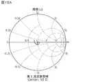
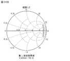
- FIG. 15Ais a Smith chart showing impedance characteristics in the first frequency band when the first path is viewed from the common terminal side.
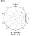
- FIG. 15Bis a Smith chart showing impedance characteristics in the second frequency band when the first path is viewed from the common terminal side.
- FIG. 16Ais a Smith chart showing impedance characteristics in the second frequency band when the second path is viewed from the common terminal side.
- FIG. 16Bis a Smith chart showing impedance characteristics in the first frequency band when the second path is viewed from the common terminal side.
- FIG. 17is a configuration diagram illustrating a communication apparatus according to the fifth embodiment.
- Embodiment 1[1. Configuration of high-frequency module] First, the configuration of the high-frequency module according to Embodiment 1 will be described.
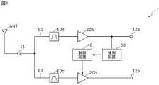
- FIG. 1is a configuration diagram showing a high-frequency module 1 according to the first embodiment.
- an antenna element ANTis also shown in FIG.
- the high frequency module 1includes filters 10a and 10b, amplifier circuits 20a and 20b, a detection circuit 30, and a control circuit 40.
- the filter 10ais a first filter that is disposed on a path L1 (first path) that connects the common terminal 11 and the input / output terminal 12a (first input / output terminal) and uses the first frequency band as a pass band.
- the filter 10bis disposed on a path L2 (second path) connecting the common terminal 11 and the input / output terminal 12b (second input / output terminal), and uses a second frequency band different from the first frequency band as a pass band. This is the second filter.
- the filters 10a and 10bare, for example, bandpass filters configured by elastic wave filters.
- the filters 10a and 10bare not limited to elastic wave filters, and may be configured by other filters (LC filter or the like).
- the filters 10a and 10bare not limited to bandpass filters, and may be low-pass filters, high-pass filters, band elimination filters, or the like.
- the antenna element ANTis connected to the common terminal 11 via a switch circuit or the like (not shown), for example.
- the antenna element ANTis a multi-band antenna that transmits and receives high-frequency signals and conforms to a communication standard such as LTE (Long Term Evolution).
- an RF signal processing circuitRFIC: Radio Frequency Integrated Circuit
- RFICRadio Frequency Integrated Circuit
- Which of the filters 10a and 10b is used for communicationis controlled by RFIC, for example.
- carrier aggregation (CA)in which communication using the first frequency band and communication using the second frequency band are simultaneously performed may be performed.
- the amplifying circuit 20ais a second amplifying circuit disposed in the path L1, and amplifies the signal in the first frequency band that passes through the filter 10a.
- the amplifier circuit 20ais disposed between the filter 10a and the input / output terminal 12a in the path L1.
- the amplifier circuit 20bis a first amplifier circuit disposed in the path L2, and amplifies the signal in the second frequency band that passes through the filter 10b.
- the amplifier circuit 20bis disposed between the filter 10b and the input / output terminal 12b in the path L2.
- the amplifier circuits 20a and 20bare circuits including a PA (power amplifier) when the high frequency module 1 is used for transmission, and include an LNA (low noise amplifier) when the high frequency module 1 is used for reception.
- the high-frequency module 1is used for reception, for example, and the amplifier circuits 20a and 20b are circuits including an LNA. Specific examples of the amplifier circuits 20a and 20b will be described with reference to FIGS.
- the detection circuit 30is a first detection circuit that is connected to the path L1, detects a leak signal in the second frequency band leaking to the path L1, and outputs a signal indicating the detection result.
- the leakage signal in the second frequency band that has leaked into the path L1is a signal in the second frequency band that should flow from the common terminal 11 to the path L2, and has entered the path L1 without flowing into the path L2. Signal.
- the signal of the first frequency band handled by the path L1leaks to the path L2 that is commonly connected to the path L1.
- the signal in the second frequency band leaking to the path L1is referred to as a leakage signal, and the description will be made by paying attention to the leakage signal in the second frequency band.
- the losscan be compensated by controlling the amplifier circuit 20b arranged in the path L2 according to the change of the signal in the second frequency band. Specifically, since the amount of signal in the second frequency band passing through the path L2 changes (decreases) by the amount of leakage of the signal in the second frequency band to the path L1, if the change is detected, the amount of leakage By controlling the gain and the like of the amplifier circuit 20b according to the loss, it is possible to compensate for the leakage.
- a detection circuit for detecting a change in the signal in the second frequency band passing through the path L2is connected to the path L2, and the change is made. It is conceivable to detect this directly. However, in this method, since the detection circuit provided in the path L2 performs the detection using a part of the signal (main signal) in the second frequency band handled in the path L2, further loss occurs in the main signal. Or noise may occur. That is, another loss occurs to compensate for the loss due to the leakage of the signal.
- the detection circuit 30 for detecting a change in the signal in the second frequency bandis connected to the path L1.
- the detection circuit 30does not directly detect the change in the path L2, but indirectly detects the change in the path L1.
- the detection circuit 30detects the change by detecting a leakage signal in the second frequency band that has leaked to the path L1. Since the magnitude of the leakage signal in the path L1 and the change in the signal in the second frequency band in the path L2 are correlated, the detection circuit 30 can detect the change by detecting the leakage signal.
- the leakage signal of the second frequency bandcan be easily detected by distinguishing from the first frequency band in the path L1 through which the signal of the first frequency band passes. it can.
- the detection circuit 30 that detects a change in the signal in the second frequency bandit is possible to suppress the loss and noise caused by the detection circuit 30 in the path L2. That is, it is possible to suppress generation of loss and noise in the path L2.
- the losscan be compensated for in the high-frequency module 1, the SN characteristic can be kept good, and the demodulation of the signal is facilitated by an RFIC or the like connected to the subsequent stage of the high-frequency module 1.
- the detection circuit 30is connected, for example, between the amplifier circuit 20a and the input / output terminal 12a in the path L1. Thereby, since the leak signal is also amplified by the amplifier circuit 20a, the detection circuit 30 can easily detect the leak signal. Note that, depending on the frequency characteristics of the amplifier circuit 20a, the leakage signal in the second frequency band may not be correctly amplified, so the detection circuit 30 may be connected between the filter 10a and the amplifier circuit 20a in the path L1. And it may be connected between the common terminal 11 and the filter 10a.
- the detection circuit 30is intended to detect a leakage signal in the second frequency band, and has a configuration that does not detect a signal in the first frequency band as much as possible. That is, the detection circuit 30 selectively detects the leakage signal in the second frequency band, in other words, distinguishes the signal in the first frequency band from the signal in the second frequency band, and mainly detects the leakage signal in the second frequency band. Is a circuit for detecting Specific examples of the configuration of the detection circuit 30 will be described with reference to FIGS.
- the control circuit 40is a circuit that controls the amplifier circuit 20b based on a signal indicating the detection result output from the detection circuit 30.
- the control circuit 40is an AD conversion circuit, acquires an analog signal as a signal indicating a detection result from the detection circuit 30, converts the analog signal into a digital signal, and controls the amplifier circuit 20b with the digital signal.
- the control circuit 40may be a microprocessor (microcomputer).
- the control circuit 40is provided separately from the amplifier circuit 20b, but may be provided in the amplifier circuit 20b.
- the high frequency module 1may not include the control circuit 40.
- the control circuit 40may be included in the RFIC.
- FIG. 2is a configuration diagram illustrating a first example of the first detection circuit (detection circuit 30) according to the first embodiment.
- the detection circuit 30includes, for example, a comparator 31a and an integration circuit 32.
- the comparator 31ais a detection circuit that receives a leak signal and detects the input leak signal.
- the comparator 31areceives the leakage signal and the reference voltage, and outputs a signal indicating the comparison result between the voltage indicated by the leakage signal and the reference voltage as a signal indicating the detection result.
- a leak signalis input to the positive input terminal of the comparator 31a, and a reference voltage is input (applied) to the negative input terminal.
- a positive voltage signalis output as a signal indicating the comparison result from the comparator 31a, and the voltage indicated by the leakage signal becomes smaller than the reference voltage.
- the comparator 31aoutputs a signal indicating 0 as a signal indicating the comparison result.
- the leakage signalcan be easily detected by using the comparator 31a.
- the reference voltageis determined based on, for example, a comparison result output from the comparator 31a when no leakage signal is input to the comparator 31a. Specifically, a reference voltage is determined such that a signal indicating a comparison result output from the comparator 31a when the leakage signal is not input to the comparator 31a is zero.
- the integration circuit 32is a circuit that integrates a signal indicating the detection result in the detection circuit (comparator 31a) and outputs a signal obtained by the integration as a signal indicating the detection result. That is, the integrating circuit 32 is a circuit that smoothes the output of the comparator 31a and converts it into a DC signal. By integrating the signal indicating the detection result in the comparator 31a, the detection circuit 30 can output a DC signal as a signal indicating the detection result. That is, since the signal indicating the detection result becomes a direct current signal and is easy to handle, control using the signal indicating the detection result (for example, control of the amplifier circuit 20b by the control circuit 40) is facilitated.
- the integration circuit 32is, for example, a circuit composed of a capacitor connected between the signal path and the ground, an LC circuit, or the like, but is not particularly limited as long as it is an integration circuit.
- FIG. 3is a configuration diagram illustrating a second example of the first detection circuit (detection circuit 30) according to the first embodiment.
- the detection circuit 30further includes a coupler 33 as compared with the first example.
- the coupler 33is a circuit that extracts a leakage signal from the path L1. Since the coupler 33 can extract a signal of a specific frequency, using the coupler 33 does not extract the signal of the first frequency band that is the main signal in the path L1, but leaks the signal (the signal of the second frequency band). ) Only easier to extract. Thus, the coupler 33 does not extract the signal of the first frequency band, and it is easy to extract only the leakage signal, so that the detection circuit (comparator 31a) can easily detect the leakage signal. Further, the coupler 33 makes it difficult for the signal in the first frequency band to be input to the detection circuit 30.
- the detection circuit 30connected to the path L1 for detecting the leakage signal in the second frequency band can suppress the loss in the signal in the first frequency band.
- FIG. 4is a configuration diagram illustrating a third example of the first detection circuit (detection circuit 30) according to the first embodiment.
- the rectifier circuit 31bis a detection circuit that rectifies an input leakage signal and outputs a signal obtained by the rectification as a signal indicating a detection result. That is, in the third example, the detection circuit 30 includes a rectifier circuit 31b instead of the comparator 31a as a detection circuit.
- the rectifier circuit 31bis, for example, a diode bridge full-wave rectifier circuit, and rectifies both positive and negative waves in the leakage signal.
- the rectifier circuit 31bdetects the signal by rectifying the leakage signal into a positive signal.
- the rectifier circuit 31bhas a simple configuration such as a diode or a load, the detection circuit can be reduced in size. In the following FIGS. 5 to 7, an example in which the detection circuit is the comparator 31a will be described.
- FIG. 5is a configuration diagram illustrating a fourth example of the first detection circuit (detection circuit 30) according to the first embodiment.
- the detection circuit 30further includes a filter 34 and an amplifier circuit 35 in addition to the configuration in the first example. Since other configurations are the same as those of the first example, detailed description thereof is omitted.
- the filter 34is a filter that allows the signal in the second frequency band to pass and blocks the signal in the first frequency band.
- the filter 34is a band-pass filter that passes a signal in the second frequency band, but may be a high-pass filter, a low-pass filter, a band elimination filter, or the like.
- the filter 34is provided between the coupler 33 and the comparator 31a, and a leakage signal is input to the detection circuit (comparator 31a) through the filter 34.
- the detection circuit 30Since the detection circuit 30 is connected to the path L1, it is necessary to prevent a loss from occurring in the signal in the first frequency band that is the main signal in the path L1.
- the detection circuit 30includes the filter 34 that passes the signal of the second frequency band and blocks the signal of the first frequency band, so that the signal of the first frequency band is reflected by the filter 34. It becomes difficult to input to the detection circuit 30. For this reason, in the path
- the detection circuitsince the leakage signal in the second frequency band that has leaked to the path L1 passes through the filter 34, the detection circuit can effectively detect the leakage signal via the filter 34.
- the amplification circuit 35is a circuit that amplifies the leakage signal, and is provided between the filter 34 and the comparator 31a.
- the leakage signalis input to the detection circuit (comparator 31a) through the amplification circuit 35.
- the filter 34 and the amplifier circuit 35are provided in the order of the filter 34 and the amplifier circuit 35, but the order in which they are provided may be reversed.
- the configuration of the amplifier circuit 35is not particularly limited as long as it is a circuit capable of amplifying a signal in the second frequency band.
- the detection circuit 30may not have both the filter 34 and the amplification circuit 35, and may have either one.
- the comparator 31ahas a frequency characteristic that corresponds to the second frequency band and does not correspond to the first frequency band, the detection circuit 30 does not have the filter 34, but the first frequency band It becomes difficult for the signal to be input to the detection circuit 30.
- the frequency characteristic of the comparator 31a that corresponds to the second frequency band and does not correspond to the first frequency bandis the first response to the signal of the second frequency band when comparing the voltage of the signal input to the comparator 31a. A characteristic that does not react to signals in the frequency band.
- the comparator 31ahas a frequency characteristic that corresponds to the second frequency band and does not correspond to the first frequency band, and is provided with the filter 34, so that the signal in the first frequency band is more effectively detected by the detection circuit 30. Can be difficult to input. Further, the comparator 31a may have a function of changing the frequency characteristics of the comparator 31a. As a result, leakage signals in other frequency bands different from the second frequency band can be detected by the comparator, so that one detection circuit 30 can compensate for losses in a plurality of paths. In the following FIGS. 6 and 7, an example in which the detection circuit 30 does not include the filter 34 and the amplification circuit 35 will be described, but either or both of them may be included.
- FIG. 6is a configuration diagram illustrating a fifth example of the first detection circuit (detection circuit 30) according to the first embodiment.
- the detection circuit 30further includes a mixer 36 with respect to the configuration in the second example. Since other configurations are the same as those of the second example, detailed description thereof is omitted.
- the mixer 36is a circuit that mixes the leakage signal and the signal of the first frequency band that passes through the path L1.
- the mixer 36outputs a signal having a frequency that is a sum and a difference of the two frequencies based on the heterodyne principle with respect to the input signals having two different frequencies.
- the leakage signalis based on Asin ⁇ (A: amplitude of the leakage signal, ⁇ : frequency of the second frequency band). Value
- the signal of the first frequency bandis Bsin ⁇ (B: amplitude of the signal of the first frequency band, ⁇ : value based on the frequency of the first frequency band)
- the signal represented by the following Expression 1is Output from the mixer 36.
- the output from the mixer 36is a signal in a frequency band lower than the frequency of the leakage signal and the frequency of the signal in the first frequency band. Is included.
- a filter 34such as a low-pass filter
- the comparator 31acan detect the leakage signal based on the low frequency band signal.
- the first frequency band and the second frequency bandare close, as one of the outputs of the mixer 36, the first frequency band and the second frequency are set to a frequency band lower than the first frequency band and the second frequency band. Since the signal represented by the difference from the band is output, the leakage signal can be easily detected. Therefore, the detection accuracy of the detection circuit is improved, and loss can be compensated effectively.
- FIG. 7is a configuration diagram illustrating a sixth example of the first detection circuit (detection circuit 30) according to the first embodiment.
- the detection circuit 30further includes a reference voltage control circuit 37 that controls the reference voltage with respect to the configuration in the first example, and the reference voltage is controlled to be variable. Since other configurations are the same as those of the first example, detailed description thereof is omitted.
- the reference voltageis variably controlled based on the comparison result output from the comparator 31a when no leak signal is input to the comparator 31a.
- the reference voltage control circuit 37controls the reference voltage based on the comparison result output from the comparator 31a when no leakage signal is input to the comparator 31a.
- the reference voltage control circuit 37controls (determines) the reference voltage so that the signal indicating the comparison result output from the comparator 31a becomes 0 when no leakage signal is input to the comparator 31a. It is.
- the shiftcan be corrected by controlling (calibrating) the reference voltage. Therefore, the detection accuracy of the detection circuit is improved, and loss can be compensated effectively.
- the leakage signal of the second frequency bandis not input to the comparator 31a.
- the reference voltage control circuit 37controls the reference voltage so that the signal indicating the comparison result output from the comparator 31a becomes zero.
- the reference voltage control circuit 37does not control the reference voltage, and the comparator 31a detects a leakage signal using the reference voltage controlled (determined) when CA is not performed. .
- a reference voltage deviationcan be corrected each time CA is not performed. Therefore, the detection accuracy of the detection circuit is improved, and loss can be compensated effectively.
- the detection circuit 30may not include the reference voltage control circuit 37.
- the reference voltagemay be variably controlled by a circuit outside the detection circuit 30.
- amplifier circuit 20a and 20bare described with reference to FIGS.
- the descriptionwill be given focusing on the amplifier circuit 20b controlled by the control circuit 40, but the amplifier circuit 20a has the same configuration as the amplifier circuit 20b, for example.
- the amplifier circuit 20bis controlled according to the change in the signal amount in the second frequency band (the magnitude of the leakage signal leaking to the path L1), so that the loss due to the signal leaking to the path L1 can be compensated.
- the amplifier circuit 20b provided in the path L2is controlled in order to compensate for the loss caused by the leakage of the signal in the second frequency band to the path L1, but a specific method for controlling the amplifier circuit 20b is described below. Specifically, there are a method of controlling the gain of the amplifier circuit 20b and a method of controlling the input impedance of the amplifier circuit 20b. By controlling the gain of the amplifier circuit 20b, it is possible to compensate for the loss due to the signal leaking to the path L1. Further, by controlling the input impedance of the amplifier circuit 20b, it is possible to compensate for the loss due to the signal leaking to the path L1.
- NFNoise Figure
- FIG. 8is a configuration diagram illustrating a first example of the first amplifier circuit (amplifier circuit 20b) according to the first embodiment.
- the amplification circuit 20bis controlled based on a signal indicating a detection result output from the detection circuit 30.
- the control circuit 40acquires a signal indicating the detection result, generates a control signal from the signal, and controls the amplifier circuit 20b based on the control signal.
- the gain Gis expressed by the following formula 2.
- ⁇ Voutis the output voltage of the amplifier circuit 20b
- ⁇ Voutis the input voltage of the amplifier circuit 20b
- ⁇ Ioutis the output current of the amplifier circuit 20b
- Routis the resistance value (load resistance value) of the load constituting the amplifier circuit 20b
- gmIs the mutual conductance of the amplifier circuit 20b.
- the gain Gis proportional to the load resistance value Rout, and the proportionality constant at this time is the mutual conductance gm. It can be seen that an amplifier circuit having a larger mutual conductance gm can obtain a higher gain G.
- the gain Gcan be controlled by controlling the mutual conductance gm.
- the gain G of the amplifier circuit 20bis controlled based on a signal (control signal) indicating the detection result.
- the amplifier circuit 20bis configured by an LNA 21a, and the gain G of the amplifier circuit 20b is controlled by controlling the operating current (current source) of the LNA 21a. This is because the mutual conductance gm indicates the ease of current flow in the amplifier circuit 20b and changes according to the operating current of the amplifier circuit 20b (LNA 21a).
- control circuit 40controls the LNA 21a so as to change the operating current of the LNA 21a in accordance with the signal indicating the detection result (that is, according to the magnitude of the leakage signal), whereby the mutual conductance of the amplifier circuit 20b is controlled.
- the gain Gis changed by changing gm.
- FIG. 9is a configuration diagram showing a second example of the first amplifier circuit (amplifier circuit 20b) in the first embodiment.
- the gain Gcan also be controlled by controlling the load resistance value Rout.
- the amplifier circuit 20bis configured by an LNA 21b, and the gain G of the amplifier circuit 20b is controlled by controlling the number of loads constituting the LNA 21b. This is because the load resistance value Rout changes according to the number of loads (here, the number of loads connected in parallel to each other).
- an inductoris shown as a load constituting the amplifier circuit 20b (LNA 21b), and a switch connected in series to each load is shown as a configuration for controlling the number of loads.
- control circuit 40specifically controls the LNA 21b so as to change the number of effective loads according to the signal indicating the detection result (that is, according to the magnitude of the leakage signal).
- the load resistance value Rout of the amplifier circuit 20bis changed, and the gain G is changed.
- FIG. 10is a configuration diagram showing a third example of the first amplifier circuit (amplifier circuit 20b) in the first embodiment.
- the amplifier circuit 20bis configured by an LNA 21c, and the gain of the amplifier circuit 20b is controlled by controlling the number of transistors configuring the LNA 21c.
- the mutual conductance gmindicates the ease of current flow in the amplifier circuit 20b, and as shown in FIG. 10, the number of paths through which current flows changes according to the number of transistors connected in parallel to each other. This is because the ease of flow changes. Therefore, the control circuit 40 controls the LNA 21c so as to change the number of effective transistors (the number of paths through which current flows) according to the signal indicating the detection result (that is, according to the magnitude of the leakage signal). Thus, the gain is changed by changing the mutual conductance gm of the amplifier circuit 20b.
- FIG. 11is a configuration diagram illustrating a fourth example of the first amplifier circuit (amplifier circuit 20b) according to the first embodiment.
- the input impedance of the amplifier circuitis matched in the frequency band of the signal passing through the path in which the amplifier circuit is provided, and is open in the frequency band excluding the frequency band.
- the input impedance of the amplifier circuit 20bis not matched in the second frequency band. Therefore, by controlling the input impedance of the amplifier circuit 20b, it is possible to compensate for loss due to signal leakage.
- the amplifier circuit 20bis configured by an LNA 21 and a matching circuit 22 provided on the front stage (antenna element ANT side) of the LNA 21, and the matching circuit 22 is controlled to input the amplifier circuit 20b. Impedance is controlled.
- the LNA 21may be any of the LNAs 21a to 21c described above, or may be another LNA that does not have the gain control function of the LNAs 21a to 21c.
- the matching circuit 22includes, for example, a series inductor provided in parallel with the path where the LNA 21 is arranged, and a shunt inductor provided between the path where the LNA 21 is arranged and the ground. However, it may be composed of other impedance elements (capacitors or the like). Further, either the series inductor or the shunt inductor may not be provided.
- the control circuit 40controls the matching circuit 22 so as to change the number of series inductors and the number of shunt inductors according to the signal indicating the detection result (that is, according to the magnitude of the leakage signal). Specifically, the input impedance of the amplifier circuit 20b is changed by switching on and off the switches connected to the inductors.
- control circuit 40(for example, AD conversion circuit) may be provided in the amplifier circuit 20b.
- the amplifier circuit 20bacquires a signal indicating the detection result
- the control circuit 40 included in the amplifier circuit 20bgenerates a control signal (digital signal) based on the signal indicating the detection result, and based on the control signal
- the current source shown in FIG. 8 and the switches shown in FIGS. 9 to 11may be controlled. Since the high frequency module 1 includes the control circuit 40, the control circuit 40 can control the amplifier circuit 20 b.
- Embodiment 2Next, the high frequency module in Embodiment 2 is demonstrated using FIG.
- FIG. 12is a configuration diagram showing the high-frequency module 1a according to the second embodiment.
- FIG. 12also shows an antenna element ANT in addition to the high-frequency module 1a.
- the filters 10a to 10nare arranged on the paths L1 to Ln connecting the three or more input / output terminals 12a to 12n and the common terminal 11.
- the high-frequency module 1adiffers from the high-frequency module 1 according to the first embodiment in that it has one or more paths in addition to the two paths L1 and L2.
- a filter 10n and an amplifier circuit 20nare arranged, and a detection circuit 30n is connected. Since the other points are the same as those of the high-frequency module 1 in the first embodiment, the description thereof is omitted.
- the detection circuit 30a connected to the path L1corresponds to the detection circuit 30 in the first embodiment.
- the input / output terminal 12nis a third input / output terminal
- the path Lnis a third path
- the filter 10nis a third frequency band different from the first frequency band and the second frequency band. It is a filter.
- the filter 10nis a band-pass filter configured by, for example, an elastic wave filter, like the filters 10a and 10b.
- the filter 10nis not limited to an acoustic wave filter, but may be another filter (LC filter or the like), not limited to a band pass filter, but may be a low pass filter, a high pass filter, a band elimination filter, or the like.
- the paths L1 to Lnmay include a path where no filter or amplifier circuit is arranged.
- the detection circuit 30nis a circuit that selectively detects a leakage signal in the second frequency band that has leaked to the path Ln and outputs a signal indicating the detection result.
- the leakage signal in the second frequency band that has leaked to the path Lnis a signal in the second frequency band that should flow from the common terminal 11 to the path L2, and has entered the path Ln without flowing to the path L2. Signal.
- the detection circuit 30nhas, for example, the same circuit configuration as the detection circuit 30 described with reference to FIGS. For example, the detection circuit 30n outputs a signal indicating the detection result to the control circuit 40 for controlling the amplifier circuit 20b provided in the path L2.
- the detection circuit 30ndoes not directly detect a change in the signal in the second frequency band on the path L2, but indirectly detects on the path Ln. Specifically, the detection circuit 30n detects the change by detecting a leakage signal in the second frequency band that has leaked into the path Ln. Therefore, the control circuit 40 controls the amplifier circuit 20b based on not only the leakage signal in the second frequency band in the path L1 but also the leakage signal in the second frequency band in the path Ln.
- Embodiment 3Next, the high frequency module in Embodiment 3 is demonstrated using FIG.
- FIG. 13is a configuration diagram showing the high-frequency module 1b according to the third embodiment.
- FIG. 13also shows an antenna element ANT in addition to the high-frequency module 1b.
- the filters 10a to 10nare disposed on the paths L1 to Ln connecting the three or more input / output terminals 12a to 12n and the common terminal 11.
- the high-frequency module 1bdiffers from the high-frequency module 1 in the first embodiment in that it has one or more paths in addition to the two paths L1 and L2.
- a filter 10n and an amplifier circuit 20nare arranged, and a control circuit 40n for controlling the amplifier circuit 20n is provided. Since the other points are the same as those of the high-frequency module 1 in the first embodiment, the description thereof is omitted.
- the control circuit 40b that controls the amplifier circuit 20bcorresponds to the control circuit 40 in the first embodiment.
- the detection circuit 30detects a leak signal in the second frequency band leaked to the path L1 and a leak signal in the third frequency band leaked to the path L1, and outputs a signal indicating the detection result.
- Circuitthat is, in the third embodiment, the detection circuit 30 is a circuit that can detect signals in a plurality of different frequency bands. For example, when one of the second frequency band and the third frequency band is lower than the first frequency band and the other is higher than the first frequency band, the detection circuit 30 blocks the first frequency band, A filter 34 (band elimination filter) that passes the second frequency band and the third frequency band may be provided.
- the detection circuit 30detects a signal in the second frequency band leaked in the path L1, outputs a signal indicating the detection result to the control circuit 40b, detects a signal in the third frequency band leaked in the path L1, A signal indicating the detection result is output to the control circuit 40n.
- control circuit 40bcontrols the amplifier circuit 20b based on the detection result of the leakage signal in the second frequency band to compensate for the loss due to the signal leaking to the path L1, and the control circuit 40n
- the control circuit 40nBy controlling the amplifier circuit 20n based on the detection result of the leakage signal in the three frequency bands, the loss due to the leakage of the signal to the path L1 is compensated.
- the single detection circuit 30can compensate for a loss due to signal leakage not only on the path L2 but also on a plurality of paths.
- Embodiment 4Next, the high frequency module in Embodiment 4 is demonstrated using FIG.
- FIG. 14is a configuration diagram illustrating the high-frequency module 1c according to the fourth embodiment.
- FIG. 14also shows an antenna element ANT in addition to the high-frequency module 1c.
- the filters 10a to 10nare arranged on the paths L1 to Ln connecting the three or more input / output terminals 12a to 12n and the common terminal 11.
- the high-frequency module 1cis different from the high-frequency module 1 according to the first embodiment in that it has one or more paths in addition to the two paths L1 and L2.
- FIG. 14shows a switch SW that switches connection between the common terminal 11 (antenna element ANT) and each path.
- the switch SWconnects the common terminal 11 and one path, or connects the common terminal 11 and a plurality of paths simultaneously.
- CAis performed by connecting the common terminal 11 and a plurality of paths simultaneously.
- the control circuit 40controls not only the control of the amplifier circuit 20b (here, control of the matching circuit 22) but also the input impedance of the amplifier circuit 20a based on a signal indicating the detection result of the detection circuit 30. . Specifically, the control circuit 40 controls the input circuit of the amplifier circuit 20a by controlling the matching circuit 220 included in the amplifier circuit 20a.
- the LNA 210 included in the amplifier circuit 20amay be any of the LNAs 21a to 21c described above.
- the fact that the signal of the second frequency band is leaking to the path L1means that the input impedance of the amplifier circuit 20a is not fully open in the second frequency band. Therefore, in the path L1, the signal in the first frequency band is passed and the signal in the second frequency band is reflected, and in the path L2, the signal in the second frequency band is passed and the first frequency band is passed.
- the control circuit 40controls the matching circuits 22 and 220 based on the signal indicating the detection result of the detection circuit 30 so as to reflect the above signal.
- FIG. 15Ais a Smith chart showing impedance characteristics in the first frequency band when the first path (path L1) is viewed from the common terminal 11 side.
- FIG. 15Bis a Smith chart showing impedance characteristics in the second frequency band when the first path (path L1) is viewed from the common terminal 11 side.
- FIG. 16Ais a Smith chart showing impedance characteristics in the second frequency band when the second path (path L2) is viewed from the common terminal 11 side.
- FIG. 16Bis a Smith chart showing impedance characteristics in the first frequency band when the second path (path L2) is viewed from the common terminal 11 side. Note that these Smith charts are normalized by 50 ⁇ , for example. Further, at the time of impedance characteristic measurement (simulation), it is assumed that each path is separated in order to ignore the influence from other paths.
- the matching circuit 220is controlled so that the impedance characteristic in the first frequency band when the path L1 is viewed from the common terminal 11 is close to 50 ⁇ and matching is achieved. Thereby, in the path
- FIG. 15Bit is understood that the impedance characteristic in the second frequency band when the path L1 is viewed from the common terminal 11 is close to the open state by controlling the matching circuit 220. This makes it difficult for signals in the second frequency band to leak to the path L1, and makes it difficult for loss to occur in the main signal in the second frequency band on the path L2.
- the matching circuit 22is controlled, so that the impedance characteristic in the second frequency band when the path L2 is viewed from the common terminal 11 is in the vicinity of 50 ⁇ and matching is achieved. Thereby, in the path
- the impedance characteristic in the first frequency band when the path L2 is viewed from the common terminal 11is close to the open state by controlling the matching circuit 22. This makes it difficult for signals in the first frequency band to leak to the path L2, and makes it difficult for the main signal in the first frequency band to be lost in the path L1.
- the gains of the LNAs 210 and 21may also be controlled based on the detection result of the detection circuit 30. Thereby, it is possible to more effectively compensate for the loss due to the leakage of the signal.
- FIG. 17is a configuration diagram showing the communication device 60 according to the fifth embodiment.
- the communication device 60includes an antenna element ANT, a high frequency module 1d, and an RFIC 50.
- the high-frequency module 1d applied to the communication device 60 in the present embodimenthas three or more paths, and each path includes detection circuits 30a to 30n that detect leakage signals in the frequency bands of the other paths.
- control circuits 40a to 40n for controlling the amplification circuits 20a to 20n of the own path based on the leakage signal detected in the other pathare provided.
- the detection circuit 30ahas a first frequency that is a main signal in the path L1 according to the pass band and attenuation band of the filter 34 included in the detection circuit 30a and the frequency characteristics of the detection circuit (comparator 31a) included in the detection circuit 30a.
- a leak signal that can be detectedis determined while preventing a signal in the band from being input to the detection circuit 30a. For example, when the detection circuit 30a does not have the mixer 36, a leak signal in a band farther from the first frequency band becomes easier to detect.
- the leakage signals that can be detected by the detection circuits 30a to 30nare appropriately designed according to the required specifications.
- the paths L1 to Lnmay include a path in which no detection circuit or control circuit is provided.
- the antenna element ANTis built in the communication device 60, it may be provided separately from the communication device 60.
- the RFIC 50is a circuit that processes a high-frequency signal transmitted and received by the antenna element ANT. Specifically, the RFIC 50 processes a high-frequency signal (here, a high-frequency reception signal) input from the antenna element ANT via the high-frequency module 1d by down-conversion, and the received signal generated by the signal processing. Is output to the baseband signal processing circuit (BBIC).
- the high-frequency moduleis for reception, but may be for transmission. In this case, the RFIC 50 performs signal processing on the transmission signal input from the baseband signal processing circuit (BBIC) by up-conversion, etc.
- a high-frequency signal generated by the signal processing(here, a high-frequency transmission signal) is output to the high-frequency module.
- the high-frequency module 1is disposed on the path L1 connecting the common terminal 11 and the input / output terminal 12a, the filter 10a having the first frequency band as the pass band, the common terminal 11 and the input / output terminal 12b. And a filter 10b having a second frequency band different from the first frequency band as a pass band, and a leak signal in the second frequency band that is connected to the path L1 and leaked to the path L1 is detected. And a detection circuit 30 that outputs a signal indicating the detection result.
- the high-frequency module 1may further include an amplifier circuit 20b disposed in the path L2, and the amplifier circuit 20b may be controlled based on a signal indicating the detection result.
- the loss due to the signal leaking to the path L1is compensated by controlling the amplifier circuit 20b according to the change of the signal in the second frequency band (the magnitude of the leaking signal leaking to the path L1). Can do.
- the high-frequency module 1may further include a control circuit 40 that controls the amplifier circuit 20b based on a signal indicating the detection result.
- control of the amplifier circuit 20bcan be performed by the control circuit 40.
- the gain of the amplifier circuit 20bmay be controlled based on a signal indicating the detection result. Specifically, the gain of the amplifier circuit 20b is determined based on the signal indicating the detection result, such as the operating current of the amplifier circuit 20b, the number of loads constituting the amplifier circuit 20b, or the number of transistors constituting the amplifier circuit 20b. It may be controlled by being controlled.
- the input impedance of the amplifier circuit 20bmay be controlled based on a signal indicating the detection result.
- the noise figure (NF: Noise Figure) at the first stage of the amplifier circuit 20bcan be improved, the NF of the entire high-frequency module 1 that is greatly affected by the NF at the first stage can be improved.
- the high-frequency module 1may further include an amplifier circuit 20a disposed in the path L1, and the input impedance of the amplifier circuit 20a may be controlled based on a signal indicating the detection result.
- the detection circuit 30integrates a detection circuit that receives a leakage signal, detects the input leakage signal, and a signal indicating a detection result in the detection circuit, and indicates a detection result of a signal obtained by the integration. And an integration circuit 32 that outputs the signal.
- the detection circuit 30can output a DC signal as a signal indicating the detection result. That is, since the signal indicating the detection result becomes a direct current signal and is easy to handle, control using the signal indicating the detection result (for example, control of the amplifier circuit 20b by the control circuit 40) is facilitated.
- the detection circuit 30further includes a filter 34 that allows the leakage signal to pass therethrough and blocks the signal in the first frequency band, and the leakage signal is input to the detection circuit via the filter 34. Also good.
- the signal in the first frequency bandis reflected by the filter 34 and is difficult to be input to the detection circuit 30. For this reason, generation
- the detection circuitcan effectively detect the leakage signal via the filter 34.
- the detection circuit 30may further include an amplification circuit 35 that amplifies the leakage signal, and the leakage signal may be input to the detection circuit via the amplification circuit 35.
- the leakage signalcan be amplified by the amplifier circuit 35, even when the leakage signal is very small, the detection accuracy of the detection circuit is improved and the loss can be effectively compensated.
- the detection circuit 30may further include a mixer 36 that mixes the leakage signal and the signal of the first frequency band, and the leakage signal may be input to the detection circuit via the mixer 36.
- the first frequency band and the second frequency bandare close to each other, as one of the outputs of the mixer 36, the first frequency band and the second frequency band are lower than the first frequency band and the second frequency band. Since the signal represented by the difference from the two frequency bands is output, it is easy to detect the leak signal. Therefore, the detection accuracy of the detection circuit is improved, and loss can be compensated effectively.
- the detection circuit 30may further include a coupler 33 that extracts a leakage signal from the path L1, and the leakage signal extracted by the coupler 33 may be input to the detection circuit.
- the detection circuitcan easily detect the leakage signal. Further, the coupler 33 makes it difficult for the signal in the first frequency band to be input to the detection circuit 30. Therefore, it is possible to suppress the loss and noise caused by the detection circuit 30 for the signal in the first frequency band that is the main signal in the path L1. In other words, the detection circuit 30 connected to the path L1 for detecting the leakage signal in the second frequency band can suppress the loss in the signal in the first frequency band.
- the detection circuitmay be a comparator 31a that receives a leakage signal and a reference voltage and outputs a signal indicating a comparison result between the voltage indicated by the leakage signal and the reference voltage as a signal indicating the detection result.
- the leakage signalcan be easily detected by using the comparator 31a.
- the comparator 31amay have a frequency characteristic that corresponds to the second frequency band and does not correspond to the first frequency band.
- the comparator 31amay have a function of changing the frequency characteristics of the comparator 31a.
- the loss in a plurality of pathscan be compensated by one detection circuit 30.
- the reference voltagemay be variably controlled.
- the shiftcan be corrected by controlling (calibrating) the reference voltage. Therefore, the detection accuracy of the detection circuit is improved, and loss can be compensated effectively.
- the reference voltagemay be variably controlled based on a comparison result output from the comparator 31a when no leakage signal is input to the comparator 31a.
- the detection circuitmay be a rectification circuit 31b that rectifies an input leakage signal and outputs a signal obtained by the rectification as a signal indicating a detection result.
- the leakage signalcan be easily detected by using the rectifier circuit 31b. Further, since the rectifier circuit 31b has a simple configuration such as a diode or a load, the detection circuit can be reduced in size.
- the high-frequency module 1ais further disposed on a path Ln connecting the common terminal 11 and the input / output terminal 12n, and uses a third frequency band different from the first frequency band and the second frequency band as a pass band.
- a filter 10n and a detection circuit 30n that is connected to the path Ln, detects a leak signal in the second frequency band leaked to the path Ln, and outputs a signal indicating the detection resultmay be provided.
- the high-frequency moduleincludes the amplifier circuits 20a and 20b, but may not include the amplifier circuits 20a and 20b.
- the high-frequency moduleincludes the control circuit 40, but may not include the control circuit 40.
- the present inventioncan be widely used in communication devices such as mobile phones as high-frequency modules applicable to multiband systems.
Landscapes
- Engineering & Computer Science (AREA)
- Computer Networks & Wireless Communication (AREA)
- Signal Processing (AREA)
- Physics & Mathematics (AREA)
- Acoustics & Sound (AREA)
- Amplifiers (AREA)
Abstract
Description
Translated fromJapanese本発明は、高周波モジュールに関する。The present invention relates to a high frequency module.
アンテナが受信した受信信号を処理する高周波受信回路は、フィルタによって受信信号から所望の周波数帯域の信号を取り出し、LNA(ローノイズアンプ)によって所望の周波数帯域の信号を増幅する。このような回路には、例えば、回路後段に接続されるRFIC(Radio Frequency Integrated Circuit)等での信号の復調に関する受信感度の向上が要求される。A high-frequency receiving circuit that processes a received signal received by an antenna extracts a signal in a desired frequency band from the received signal using a filter, and amplifies the signal in the desired frequency band using an LNA (low noise amplifier). Such a circuit is required to improve reception sensitivity related to demodulation of a signal in, for example, an RFIC (Radio Frequency Integrated Circuit) connected to a subsequent stage of the circuit.
この要求を達成する1つの方法として、フィルタによって取り出された信号の一部が検波器によって検波され、その信号レベルに応じてLNAのゲイン等が制御される特許文献1に開示されたような方法が考えられる。特許文献1に開示された技術は、大電力信号入力時のLNAの破壊を防ぐ目的で用いられているが、上記のように受信感度を向上させる目的でも用いることができる技術である。受信感度を向上させることで、高周波受信回路を含む通信装置の通信精度を向上させることが可能となる。As one method for achieving this requirement, a method as disclosed in
近年、携帯電話端末等の通信装置において、1つの端末で複数の周波数帯域の高周波信号を送受信する、マルチバンド化に対応することが要求されており、通過帯域が互いに異なる複数のフィルタ、言い換えると、複数の経路のそれぞれの一方の入出力端子が、例えばアンテナ側で共通接続された高周波モジュールが開発されている。上記特許文献1に開示された技術は、このような高周波モジュールにも適用できる。例えば、高周波モジュールにおけるある一の経路に当該一の経路で取り扱われる主信号(当該一の経路に設けられたフィルタの通過帯域に対応する信号)の信号レベルの変化を検知する検知回路を設ける。これにより、他の経路に当該一の経路を通過するはずだった信号が漏れたとしても、当該変化に応じて当該一の経路に設けられた増幅回路を制御することで、信号が漏れたことによる損失を補填できる。このように損失を補填すれば、高周波モジュールを含む通信装置の通信精度を向上できることとなる。In recent years, communication devices such as mobile phone terminals have been required to support multi-band transmission and reception of high-frequency signals in a plurality of frequency bands with a single terminal, in other words a plurality of filters having different passbands, in other words A high-frequency module in which one input / output terminal of each of a plurality of paths is commonly connected on the antenna side, for example, has been developed. The technique disclosed in
しかしながら、当該一の経路に設けられた検知回路は、当該一の経路において取り扱われる主信号の一部を用いて上記検知を行うため、信号が漏れたことによる損失を補填する際に主信号に損失が発生したりノイズが発生したりするおそれがある。However, since the detection circuit provided in the one path performs the detection using a part of the main signal handled in the one path, the detection signal is compensated for the loss due to the leakage of the signal. There is a risk of loss or noise.
そこで、本発明は、共通接続された複数の経路のうち一の経路の信号が他の経路に漏れたことによる損失を補填する際に、一の経路における損失およびノイズの発生を抑制できる高周波モジュール等を提供することを目的とする。Therefore, the present invention provides a high-frequency module that can suppress loss and noise generation in one path when compensating for loss due to leakage of a signal in one path among a plurality of commonly connected paths. The purpose is to provide.
本発明の一態様に係る高周波モジュールは、共通端子と第1入出力端子とを結ぶ第1経路上に配置され、第1周波数帯域を通過帯域とする第1フィルタと、前記共通端子と第2入出力端子とを結ぶ第2経路上に配置され、前記第1周波数帯域とは異なる第2周波数帯域を通過帯域とする第2フィルタと、前記第1経路に接続され、前記第1経路に漏れた前記第2周波数帯域の漏れ信号を検知し、検知結果を示す信号を出力する第1検知回路と、を備える。A high-frequency module according to one aspect of the present invention is disposed on a first path connecting a common terminal and a first input / output terminal, and includes a first filter having a first frequency band as a pass band, the common terminal, and a second filter. A second filter disposed on a second path connecting the input / output terminal and having a second frequency band different from the first frequency band as a pass band; and connected to the first path and leaking to the first path. A first detection circuit that detects a leakage signal in the second frequency band and outputs a signal indicating a detection result.
本発明に係る高周波モジュール等によれば、共通接続された複数の経路のうち一の経路の信号が他の経路に漏れたことによる損失を補填する際に、当該一の経路における信号ではなく他の経路における信号を用いることができるため、一の経路における損失およびノイズの発生を抑制できる。According to the high-frequency module and the like according to the present invention, when compensating for loss due to leakage of a signal of one path among a plurality of commonly connected paths to another path, not the signal of the one path Therefore, it is possible to suppress the occurrence of loss and noise in one path.
以下、本発明の実施の形態について、図面を用いて詳細に説明する。なお、以下で説明する実施の形態は、いずれも包括的または具体的な例を示すものである。以下の実施の形態で示される数値、形状、材料、構成要素、構成要素の配置および接続形態などは、一例であり、本発明を限定する主旨ではない。以下の実施の形態における構成要素のうち、独立請求項に記載されていない構成要素については、任意の構成要素として説明される。また、各図において、実質的に同一の構成に対しては同一の符号を付しており、重複する説明は省略または簡略化する場合がある。また、以下の実施の形態において、「接続される」とは、直接接続される場合だけでなく、他の素子等を介して電気的に接続される場合も含まれる。Hereinafter, embodiments of the present invention will be described in detail with reference to the drawings. It should be noted that each of the embodiments described below shows a comprehensive or specific example. Numerical values, shapes, materials, constituent elements, arrangement of constituent elements, connection forms, and the like shown in the following embodiments are merely examples, and are not intended to limit the present invention. Among the constituent elements in the following embodiments, constituent elements not described in the independent claims are described as optional constituent elements. Moreover, in each figure, the same code | symbol is attached | subjected to the substantially same structure, and the overlapping description may be abbreviate | omitted or simplified. In the following embodiments, “connected” includes not only the case of direct connection but also the case of electrical connection via other elements.
(実施の形態1)
[1.高周波モジュールの構成]
まず、実施の形態1に係る高周波モジュールの構成について説明する。(Embodiment 1)
[1. Configuration of high-frequency module]
First, the configuration of the high-frequency module according to
図1は、実施の形態1における高周波モジュール1を示す構成図である。なお、図1には、高周波モジュール1の他にアンテナ素子ANTも示されている。高周波モジュール1は、フィルタ10aおよび10b、増幅回路20aおよび20b、検知回路30ならびに制御回路40を備える。FIG. 1 is a configuration diagram showing a high-
フィルタ10aは、共通端子11と入出力端子12a(第1入出力端子)とを結ぶ経路L1(第1経路)上に配置され、第1周波数帯域を通過帯域とする第1フィルタである。フィルタ10bは、共通端子11と入出力端子12b(第2入出力端子)とを結ぶ経路L2(第2経路)上に配置され、第1周波数帯域とは異なる第2周波数帯域を通過帯域とする第2フィルタである。フィルタ10aおよび10bは、例えば、弾性波フィルタにより構成されたバンドパスフィルタである。なお、フィルタ10aおよび10bは、弾性波フィルタに限らず、その他のフィルタ(LCフィルタ等)により構成されてもよい。また、フィルタ10aおよび10bは、バンドパスフィルタに限らず、ローパスフィルタ、ハイパスフィルタまたはバンドエリミネーションフィルタ等であってもよい。The
共通端子11には、例えば、スイッチ回路等(図示せず)を介してアンテナ素子ANTが接続される。アンテナ素子ANTは、高周波信号を送受信する、例えばLTE(Long Term Evolution)等の通信規格に準拠したマルチバンド対応のアンテナである。また、入出力端子12aおよび12bには、図示しないが、例えば、RF信号処理回路(RFIC:Radio Frequency Integrated Circuit)が接続される。フィルタ10aおよび10bのいずれを用いて通信を行うかは、例えば、RFICによって制御される。例えば、第1周波数帯域を用いた通信と第2周波数帯域を用いた通信とが同時に行われるキャリアアグリゲーション(CA)が行われてもよい。The antenna element ANT is connected to the
増幅回路20aは、経路L1に配置される第2増幅回路であり、フィルタ10aを通過する第1周波数帯域の信号を増幅する。増幅回路20aは、例えば、経路L1においてフィルタ10aと入出力端子12aとの間に配置される。増幅回路20bは、経路L2に配置される第1増幅回路であり、フィルタ10bを通過する第2周波数帯域の信号を増幅する。増幅回路20bは、例えば、経路L2においてフィルタ10bと入出力端子12bとの間に配置される。増幅回路20aおよび20bは、高周波モジュール1が送信用に用いられる場合には、PA(パワーアンプ)を含む回路となり、高周波モジュール1が受信用に用いられる場合には、LNA(ローノイズアンプ)を含む回路となる。本実施の形態では、高周波モジュール1は、例えば受信用に用いられ、増幅回路20aおよび20bは、LNAを含む回路となる。増幅回路20aおよび20bの具体例については後述する図8から図11で説明する。The amplifying
検知回路30は、経路L1に接続され、経路L1に漏れている第2周波数帯域の漏れ信号を検知し、検知結果を示す信号を出力する第1検知回路である。なお、経路L1に漏れた第2周波数帯域の漏れ信号とは、共通端子11から経路L2へ本来流れるはずの第2周波数帯域の信号であり、経路L2に流れずに経路L1に進入してしまった信号のことである。以下、高周波モジュール1に検知回路30が設けられる理由について説明する。The
近年、1つの端末で複数の周波数帯域の高周波信号を送受信する、マルチバンド化に対応することが要求されており、高周波モジュール1では、通過帯域が互いに異なる複数のフィルタ(ここではフィルタ10aおよび10b)、言い換えると、複数の経路(ここでは経路L1およびL2)のそれぞれの一方の入出力端子が、共通端子11において共通接続されている。このため、経路L2で取り扱われる第2周波数帯域の信号(フィルタ10bの通過帯域に対応する信号)が、経路L2と共通接続されている経路L1に漏れてしまう。同じように、経路L1で取り扱われる第1周波数帯域の信号(フィルタ10aの通過帯域に対応する信号)が、経路L1と共通接続されている経路L2に漏れてしまう。ここでは、経路L1へ漏れている第2周波数帯域の信号を漏れ信号と呼び、第2周波数帯域の漏れ信号に着目して説明する。In recent years, it has been required to support multi-band transmission and reception of high-frequency signals in a plurality of frequency bands with one terminal. In the high-
第2周波数帯域の信号が経路L1に漏れたときに、第2周波数帯域の信号にはその漏れた分に相当する損失が発生する。そこで、経路L2に配置される増幅回路20bを第2周波数帯域の信号の変化に応じて制御することで当該損失を補填することができる。具体的には、第2周波数帯域の信号が経路L1に漏れた分、経路L2を通過する第2周波数帯域の信号量が変化(減少)するため、当該変化を検知すれば、漏れた分の損失に応じて増幅回路20bのゲイン等を制御することで、漏れた分の損失を補填することができる。When a signal in the second frequency band leaks to the path L1, a loss corresponding to the leaked amount occurs in the signal in the second frequency band. Therefore, the loss can be compensated by controlling the
経路L2を通過する第2周波数帯域の信号の変化を検知する方法としては、経路L2を通過する第2周波数帯域の信号の変化を検知するための検知回路を経路L2に接続して、当該変化を直接検知する方法が考えられる。しかし当該方法では、経路L2に設けられた検知回路は、経路L2において取り扱われる第2周波数帯域の信号(主信号)の一部を用いて上記検知を行うため、主信号にさらに損失が発生したりノイズが発生したりするおそれがある。つまり、信号が漏れたことによる損失の補填のために、別の損失が発生してしまう。As a method for detecting a change in the signal in the second frequency band passing through the path L2, a detection circuit for detecting a change in the signal in the second frequency band passing through the path L2 is connected to the path L2, and the change is made. It is conceivable to detect this directly. However, in this method, since the detection circuit provided in the path L2 performs the detection using a part of the signal (main signal) in the second frequency band handled in the path L2, further loss occurs in the main signal. Or noise may occur. That is, another loss occurs to compensate for the loss due to the leakage of the signal.
これに対して、本実施の形態では、第2周波数帯域の信号の変化を検知するための検知回路30は、経路L1に接続される。検知回路30は、当該変化を経路L2において直接検知するのではなく、経路L1において間接的に検知する。具体的には、検知回路30は、経路L1に漏れた第2周波数帯域の漏れ信号を検知することで、当該変化を検知する。経路L1における漏れ信号の大きさと経路L2における第2周波数帯域の信号の変化とは相関しているため、検知回路30は、漏れ信号を検知することで当該変化を検知できる。また、第1周波数帯域と第2周波数帯域とは異なるため、第1周波数帯域の信号が通過する経路L1において、第1周波数帯域と区別して第2周波数帯域の漏れ信号を容易に検知することができる。このように、経路L2に第2周波数帯域の信号の変化を検知する検知回路30を接続する必要がないため、経路L2において検知回路30に起因する損失およびノイズの発生を抑制できる。つまり、経路L2における損失およびノイズの発生を抑制できる。In contrast, in the present embodiment, the
高周波モジュール1において損失が補填できることで、SN特性を良好に保つことができ、高周波モジュール1の後段に接続されるRFIC等で、信号の復調が容易となる。Since the loss can be compensated for in the high-
また、信号が漏れたことによる損失を補填する方法として、他の信号を合成したり、信号の位相を調整したりする方法があるが、これらの方法を適用しようとすると回路構成が複雑化してしまう。これに対して、本発明では、検知回路30を設けるだけの簡易な構成で信号が漏れたことによる損失を補填できる。In addition, as a method of compensating for the loss due to the leakage of the signal, there are methods of synthesizing other signals and adjusting the phase of the signal. However, if these methods are applied, the circuit configuration becomes complicated. End up. On the other hand, in the present invention, loss due to signal leakage can be compensated with a simple configuration in which only the
検知回路30は、例えば、経路L1において増幅回路20aと入出力端子12aとの間に接続される。これにより、漏れ信号も増幅回路20aによって増幅されるため、検知回路30は、漏れ信号を検知しやすくなる。なお、増幅回路20aの周波数特性によっては、第2周波数帯域の漏れ信号を正しく増幅できないこともあるため、検知回路30は、経路L1においてフィルタ10aと増幅回路20aとの間に接続されてもよいし、共通端子11とフィルタ10aとの間に接続されてもよい。The
検知回路30は、第2周波数帯域の漏れ信号を検知することを目的としており、第1周波数帯域の信号をなるべく検知しないような構成を有している。つまり、検知回路30は、第2周波数帯域の漏れ信号を選択的に検知する、言い換えると、第1周波数帯域の信号と第2周波数帯域の信号とを区別して、主として第2周波数帯域の漏れ信号を検知する回路である。検知回路30の構成の具体例については、後述する図2から図7で説明する。The
制御回路40は、検知回路30から出力される検知結果を示す信号に基づいて増幅回路20bを制御する回路である。例えば、制御回路40は、AD変換回路であり、検知回路30から検知結果を示す信号としてアナログ信号を取得し、そして、当該アナログ信号をデジタル信号に変換し、当該デジタル信号によって増幅回路20bを制御する。例えば、制御回路40は、マイクロプロセッサ(マイコン)等であってもよい。なお、制御回路40は、増幅回路20bと別体に設けられているが、増幅回路20bに備えられていてもよい。また、高周波モジュール1は、制御回路40を備えていなくてもよく、例えば、制御回路40は、RFICに備えられていてもよい。The
[2.検知回路の具体例]
次に、検知回路30の具体例を図2から図7を用いて説明する。[2. Specific example of detection circuit]
Next, a specific example of the
図2は、実施の形態1における第1検知回路(検知回路30)の第1例を示す構成図である。FIG. 2 is a configuration diagram illustrating a first example of the first detection circuit (detection circuit 30) according to the first embodiment.
検知回路30は、例えば、コンパレータ31aおよび積分回路32を有する。The
コンパレータ31aは、漏れ信号が入力され、入力された漏れ信号を検波する検波回路である。コンパレータ31aは、漏れ信号および基準電圧が入力され、漏れ信号が示す電圧と基準電圧との比較結果を示す信号を、検波結果を示す信号として出力する。例えば、コンパレータ31aが有する正極入力端子に漏れ信号が入力され、負極入力端子に基準電圧が入力(印加)される。これにより、漏れ信号が示す電圧が基準電圧よりも大きくなっている期間には、コンパレータ31aから比較結果を示す信号として正電圧の信号が出力され、漏れ信号が示す電圧が基準電圧よりも小さくなっている期間には、コンパレータ31aから比較結果を示す信号として0を示す信号が出力される。このように、コンパレータ31aを用いることで、容易に漏れ信号を検波することができる。The
基準電圧は、例えば、コンパレータ31aに漏れ信号が入力されないときにコンパレータ31aから出力される比較結果に基づいて決定される。具体的には、コンパレータ31aに漏れ信号が入力されないときにコンパレータ31aから出力される比較結果を示す信号が0となるような基準電圧が決定される。The reference voltage is determined based on, for example, a comparison result output from the
積分回路32は、検波回路(コンパレータ31a)における検波結果を示す信号を積分し、当該積分により得られる信号を、検知結果を示す信号として出力する回路である。つまり、積分回路32は、コンパレータ31aの出力を平滑して、直流信号に変換する回路である。コンパレータ31aにおける検波結果を示す信号が積分されることにより、検知回路30は、検知結果を示す信号として直流信号を出力することができる。つまり、検知結果を示す信号が直流信号となって取り扱いやすくなるため、検知結果を示す信号を用いた制御(例えば制御回路40による増幅回路20bの制御)をしやすくなる。なお、積分回路32は、例えば信号経路とグランドとの間に接続されたキャパシタからなる回路やLC回路等であるが、積分回路であれば特に限定されない。The
図3は、実施の形態1における第1検知回路(検知回路30)の第2例を示す構成図である。第2例では、検知回路30は、第1例と比べて、さらに、カプラ33を有している。FIG. 3 is a configuration diagram illustrating a second example of the first detection circuit (detection circuit 30) according to the first embodiment. In the second example, the
カプラ33は、経路L1から漏れ信号を抽出する回路である。カプラ33は、特定の周波数の信号を抽出することができるため、カプラ33を用いることで経路L1における主信号である第1周波数帯域の信号は抽出せず、漏れ信号(第2周波数帯域の信号)だけを抽出しやすくなる。これにより、カプラ33によって第1周波数帯域の信号は抽出せず漏れ信号だけを抽出しやすくなるため、検波回路(コンパレータ31a)は漏れ信号を検波しやすくなる。また、カプラ33によって第1周波数帯域の信号は検知回路30に入力されにくくなる。そのため、経路L1において主信号である第1周波数帯域の信号に対して検知回路30に起因する損失およびノイズの発生を抑制できる。つまり、第2周波数帯域の漏れ信号を検知するための経路L1に接続された検知回路30によって、第1周波数帯域の信号に損失が発生してしまうことを抑制できる。The
なお、以下の図4、図5および図7では、検知回路30がカプラ33を有していない例について説明する。カプラ33を有していない場合でも、例えば、後述するようにコンパレータ31aの周波数特性を第2周波数帯域に対応するように調整したり、検知回路30が設けられる経路(経路L1から分岐する経路)のインピーダンスを第2周波数帯域において整合させるように調整したりすれば、漏れ信号を抽出することができる。In the following FIG. 4, FIG. 5, and FIG. 7, an example in which the
図4は、実施の形態1における第1検知回路(検知回路30)の第3例を示す構成図である。整流回路31bは、入力された漏れ信号を整流し、当該整流により得られる信号を、検波結果を示す信号として出力する検波回路である。つまり、第3例では、検知回路30は、検波回路として、コンパレータ31aの代わりに整流回路31bを有する。FIG. 4 is a configuration diagram illustrating a third example of the first detection circuit (detection circuit 30) according to the first embodiment. The
整流回路31bは、例えば、ダイオードブリッジ全波整流回路であり、漏れ信号における正負の両波を整流する。例えば、整流回路31bは、漏れ信号を正の信号に整流することで検波する。整流回路31bを用いることで、容易に漏れ信号を検波することができる。また、整流回路31bは、ダイオードや負荷等の簡単な構成となるため、検波回路を小型化できる。なお、以下の図5から図7では、検波回路がコンパレータ31aである例について説明する。The
図5は、実施の形態1における第1検知回路(検知回路30)の第4例を示す構成図である。FIG. 5 is a configuration diagram illustrating a fourth example of the first detection circuit (detection circuit 30) according to the first embodiment.
第4例では、検知回路30は、第1例での構成に対してさらに、フィルタ34および増幅回路35を有する。その他の構成については、第1例と同じであるため詳細な説明は省略する。In the fourth example, the
フィルタ34は、第2周波数帯域の信号を通過させ、かつ、第1周波数帯域の信号を遮断するフィルタである。ここでは、フィルタ34は、第2周波数帯域の信号を通過させるバンドパスフィルタであるが、ハイパスフィルタ、ローパスフィルタまたはバンドエリミネーションフィルタ等であってもよい。フィルタ34は、カプラ33とコンパレータ31aとの間に設けられ、検波回路(コンパレータ31a)には、フィルタ34を介して漏れ信号が入力される。The
検知回路30は、経路L1に接続されるため、経路L1における主信号である第1周波数帯域の信号に損失が発生しないようにする必要がある。これに対して、検知回路30は、第2周波数帯域の信号を通過させ、かつ、第1周波数帯域の信号を遮断するフィルタ34を有するため、フィルタ34で第1周波数帯域の信号が反射されて、検知回路30に入力されにくくなる。このため、経路L1において、主信号である第1周波数帯域の信号に対して、検知回路30に起因する損失およびノイズの発生を抑制できる。一方で、経路L1に漏れた第2周波数帯域の漏れ信号は、フィルタ34を通過するため、検波回路はフィルタ34を介して漏れ信号を効果的に検波することができる。Since the
増幅回路35は、漏れ信号を増幅する回路であり、フィルタ34とコンパレータ31aとの間に設けられ、検波回路(コンパレータ31a)には、増幅回路35を介して漏れ信号が入力される。これにより、漏れ信号を増幅回路35によって増幅することができるため、漏れ信号が微小な場合でも、検波回路の検波精度が向上し、効果的に損失を補填できるようになる。なお、経路L1からコンパレータ31aを見たときに、フィルタ34および増幅回路35は、フィルタ34、増幅回路35の順序で設けられているが、その設けられる順序は逆であってもよい。また、増幅回路35は、第2周波数帯域の信号を増幅可能な回路であれば構成は特に限定されない。The
なお、検知回路30は、フィルタ34および増幅回路35の両方を有していなくてもよく、いずれか一方を有していてもよい。例えば、コンパレータ31aは、第2周波数帯域に対応し、第1周波数帯域に対応しない周波数特性を有している場合、検知回路30は、フィルタ34を有していなくても、第1周波数帯域の信号が検知回路30に入力されにくくなる。第2周波数帯域に対応し、第1周波数帯域に対応しないコンパレータ31aの周波数特性とは、コンパレータ31aに入力される信号の電圧を比較する際に、第2周波数帯域の信号に反応し、第1周波数帯域の信号には反応しない特性のことである。これにより、検知回路30は、フィルタ34を有していなくても、第1周波数帯域の信号が検知回路30に入力されにくくなり、経路L1において、検知回路に起因する損失およびノイズの発生を抑制できる。なお、コンパレータ31aが、第2周波数帯域に対応し、第1周波数帯域に対応しない周波数特性を有しつつ、フィルタ34も設けられることで、より効果的に第1周波数帯域の信号が検知回路30に入力されにくくすることができる。また、コンパレータ31aは、コンパレータ31aが有する周波数特性を可変する機能を有していてもよい。これにより、第2周波数帯域とは異なる他の周波数帯域の漏れ信号もコンパレータにて検波できるようになるため、1つの検知回路30で複数の経路における損失を補填できる。以下の図6および図7では、検知回路30が、フィルタ34および増幅回路35を有していない例について説明するが、そのいずれかもしくは両方を有していてもよい。Note that the
図6は、実施の形態1における第1検知回路(検知回路30)の第5例を示す構成図である。FIG. 6 is a configuration diagram illustrating a fifth example of the first detection circuit (detection circuit 30) according to the first embodiment.
第5例では、検知回路30は、第2例での構成に対してさらに、ミキサ36を有する。その他の構成については、第2例と同じであるため詳細な説明は省略する。In the fifth example, the
ミキサ36は、漏れ信号と、経路L1を通過する第1周波数帯域の信号とを混合する回路である。ミキサ36は、入力された2つの異なる周波数の信号に対して、ヘテロダインの原理により、当該2つの周波数の和と差の周波数の信号を出力する。ここでは、第2周波数帯域の漏れ信号と第1周波数帯域の信号がミキサ36に入力されるため、例えば、漏れ信号をAsinα(A:漏れ信号の振幅、α:第2周波数帯域の周波数に基づく値)、第1周波数帯域の信号をBsinβ(B:第1周波数帯域の信号の振幅、β:第1周波数帯域の周波数に基づく値)としたときに、以下の式1で表される信号がミキサ36から出力される。The

したがって、ミキサ36からの出力には、漏れ信号の周波数および第1周波数帯域の信号の周波数よりも低周波数帯域の信号である
図7は、実施の形態1における第1検知回路(検知回路30)の第6例を示す構成図である。FIG. 7 is a configuration diagram illustrating a sixth example of the first detection circuit (detection circuit 30) according to the first embodiment.
第6例では、検知回路30は、第1例での構成に対してさらに、基準電圧を制御する基準電圧制御回路37を有し、基準電圧が制御されて可変となっている。その他の構成については、第1例と同じであるため詳細な説明は省略する。In the sixth example, the
基準電圧は、コンパレータ31aに漏れ信号が入力されないときにコンパレータ31aから出力される比較結果に基づいて、可変制御される。例えば、基準電圧制御回路37は、コンパレータ31aに漏れ信号が入力されないときに、コンパレータ31aから出力される比較結果に基づいて、基準電圧を制御する。具体的には、基準電圧制御回路37は、コンパレータ31aに漏れ信号が入力されないときにコンパレータ31aから出力される比較結果を示す信号が0となるように、基準電圧を制御(決定)するフィードバック回路である。これにより、温度等の環境または製造ばらつき等によって、基準電圧がずれてしまった場合でも、基準電圧を制御(キャリブレーション等)されることで、ずれを補正することができる。したがって、検波回路の検波精度が向上し、効果的に損失を補填できる。例えば、第1周波数帯域での通信と第2周波数帯域での通信とが同時に行われないとき(CAが行われないとき)には、コンパレータ31aに第2周波数帯域の漏れ信号が入力されないため、基準電圧制御回路37は、コンパレータ31aから出力される比較結果を示す信号が0となるように基準電圧を制御する。そして、CAが行われるときには、基準電圧制御回路37は、基準電圧を制御せず、コンパレータ31aは、CAが行われないときに制御(決定)された基準電圧を用いて漏れ信号の検波を行う。これにより、例えば、CAを行う高周波モジュールでは、CAが行われないタイミングにおいてその都度、基準電圧のずれの補正ができる。したがって、検波回路の検波精度が向上し、効果的に損失を補填できる。The reference voltage is variably controlled based on the comparison result output from the
なお、検知回路30は、基準電圧制御回路37を有していなくてもよい。例えば、基準電圧は、検知回路30外の回路によって可変制御されてもよい。Note that the
[3.増幅回路の具体例]
次に、増幅回路20aおよび20bの具体例を図8から図11を用いて説明する。ここでは、制御回路40に制御される増幅回路20bに着目して説明するが、増幅回路20aは、例えば増幅回路20bと同じ構成を有している。第2周波数帯域の信号量の変化(経路L1に漏れる漏れ信号の大きさ)に応じて増幅回路20bが制御されることで、経路L1に信号が漏れたことによる損失を補填することができる。[3. Specific example of amplifier circuit]
Next, specific examples of the
上述したように、経路L1に第2周波数帯域の信号が漏れたことによる損失を補填するために、経路L2に設けられた増幅回路20bが制御されるが、増幅回路20bを制御する方法として具体的には、増幅回路20bのゲインを制御する方法と、増幅回路20bの入力インピーダンスを制御する方法とがある。増幅回路20bのゲインを制御することで、経路L1に信号が漏れたことによる損失を補填することができる。また、増幅回路20bの入力インピーダンスを制御することで、経路L1に信号が漏れたことによる損失を補填することができる。また、増幅回路20bの初段での雑音指数(NF:Noise Figure)を改善できるため、当該初段でのNFの影響が大きい高周波モジュール1全体のNFを改善することができる。まず、図8から図10を用いて増幅回路20bのゲインを制御する方法について説明する。As described above, the
図8は、実施の形態1における第1増幅回路(増幅回路20b)の第1例を示す構成図である。FIG. 8 is a configuration diagram illustrating a first example of the first amplifier circuit (
増幅回路20bは、検知回路30が出力する検知結果を示す信号に基づいて制御される。例えば、制御回路40は、検知結果を示す信号を取得し、当該信号から制御信号を生成して、制御信号に基づいて増幅回路20bを制御する。例えば、増幅回路20bのゲインをGとしたときに、ゲインGは以下の式2で表される。式2において、ΔVoutは増幅回路20bの出力電圧、ΔVoutは増幅回路20bの入力電圧、ΔIoutは増幅回路20bの出力電流、Routは増幅回路20bを構成する負荷の抵抗値(負荷抵抗値)、gmは増幅回路20bの相互コンダクタンスである。The

式2からゲインGは、負荷抵抗値Routに比例し、このときの比例定数が相互コンダクタンスgmとなる。相互コンダクタンスgmが大きい増幅回路ほど高いゲインGを得ることができることがわかる。From
式2より、相互コンダクタンスgmを制御することで、ゲインGを制御できる。例えば、増幅回路20bのゲインGは、検知結果を示す信号(制御信号)に基づいて制御される。図8に示されるように、増幅回路20bは、LNA21aにより構成され、LNA21aの動作電流(電流源)が制御されることで、増幅回路20bのゲインGが制御される。相互コンダクタンスgmは、増幅回路20bにおける電流の流れやすさを示しており、増幅回路20b(LNA21a)の動作電流に応じて変化するためである。したがって、制御回路40は、検知結果を示す信号に応じて(つまり、漏れ信号の大きさに応じて)、LNA21aの動作電流を変化させるようにLNA21aを制御することで、増幅回路20bの相互コンダクタンスgmを変化させて、ゲインGを変化させる。From
図9は、実施の形態1における第1増幅回路(増幅回路20b)の第2例を示す構成図である。FIG. 9 is a configuration diagram showing a second example of the first amplifier circuit (
式2より、負荷抵抗値Routを制御することでも、ゲインGを制御できることがわかる。図9に示されるように、増幅回路20bは、LNA21bにより構成され、LNA21bを構成する負荷の数が制御されることで、増幅回路20bのゲインGが制御される。負荷抵抗値Routは、負荷の数(ここでは互いに並列接続される負荷の数)に応じて変化するためである。図9では、増幅回路20b(LNA21b)を構成する負荷としてインダクタを示しており、負荷の数を制御するための構成として、各負荷に直列に接続されたスイッチを示している。したがって、制御回路40は、検知結果を示す信号に応じて(つまり、漏れ信号の大きさに応じて)、有効となる負荷の数を変化させるようにLNA21bを制御することで、具体的には、負荷に接続されたスイッチのオンオフを切り替えることで、増幅回路20bの負荷抵抗値Routを変化させて、ゲインGを変化させる。From
図10は、実施の形態1における第1増幅回路(増幅回路20b)の第3例を示す構成図である。FIG. 10 is a configuration diagram showing a third example of the first amplifier circuit (
図10に示されるように、増幅回路20bは、LNA21cにより構成され、LNA21cを構成するトランジスタの数が制御されることで、増幅回路20bのゲインが制御される。相互コンダクタンスgmは、増幅回路20bにおける電流の流れやすさを示しており、図10に示されるように、互いに並列に接続されたトランジスタの数に応じて電流が流れる経路数が変化することで電流の流れやすさが変化するためである。したがって、制御回路40は、検知結果を示す信号に応じて(つまり、漏れ信号の大きさに応じて)、有効となるトランジスタの数(電流が流れる経路数)を変化させるようにLNA21cを制御することで、増幅回路20bの相互コンダクタンスgmを変化させて、ゲインを変化させる。As shown in FIG. 10, the
次に、増幅回路20bの入力インピーダンスを制御する方法について説明する。Next, a method for controlling the input impedance of the
図11は、実施の形態1における第1増幅回路(増幅回路20b)の第4例を示す構成図である。FIG. 11 is a configuration diagram illustrating a fourth example of the first amplifier circuit (
増幅回路の入力インピーダンスは、当該増幅回路が設けられている経路を通過する信号の周波数帯域において整合が取れており、当該周波数帯域を除く周波数帯域においてオープンとなる状態が理想である。しかし、例えば、経路L1へ第2周波数帯域の信号が漏れているということは、第2周波数帯域において、増幅回路20bの入力インピーダンスの整合がとれていないということになる。したがって、増幅回路20bの入力インピーダンスを制御することで、信号が漏れたことによる損失を補填することができる。Ideally, the input impedance of the amplifier circuit is matched in the frequency band of the signal passing through the path in which the amplifier circuit is provided, and is open in the frequency band excluding the frequency band. However, for example, if the signal in the second frequency band leaks to the path L1, the input impedance of the
図11に示されるように、増幅回路20bは、LNA21およびLNA21の前段(アンテナ素子ANT側)に設けられた整合回路22により構成され、整合回路22が制御されることで、増幅回路20bの入力インピーダンスが制御される。LNA21は、上述したLNA21a~21cのいずれであってもよく、LNA21a~21cの有するゲインの制御機能を全く有しない他のLNAであってもよい。整合回路22は、例えば、LNA21が配置される経路上、または、当該経路に並列に設けられたシリーズインダクタと当該LNA21が配置される経路とグランドとの間に設けられたシャントインダクタとにより構成されているが、その他のインピーダンス素子(キャパシタ等)から構成されていてもよい。また、シリーズインダクタおよびシャントインダクタのいずれかが設けられていなくてもよい。As shown in FIG. 11, the
制御回路40は、検知結果を示す信号に応じて(つまり、漏れ信号の大きさに応じて)、シリーズインダクタの数およびシャントインダクタの数を変化させるように整合回路22を制御することで、具体的には、各インダクタに接続されたスイッチのオンオフを切り替えることで、増幅回路20bの入力インピーダンスを変化させる。The
なお、制御回路40(例えばAD変換回路)は、増幅回路20b内に設けられていてもよい。この場合、増幅回路20bは、検知結果を示す信号を取得し、増幅回路20bが有する制御回路40は、検知結果を示す信号に基づいて制御信号(デジタル信号)を生成し、制御信号に基づいて図8に示される電流源や図9から図11に示されるスイッチを制御してもよい。高周波モジュール1が制御回路40を備えることで、増幅回路20bの制御を制御回路40によって行うことができる。In addition, the control circuit 40 (for example, AD conversion circuit) may be provided in the
(実施の形態2)
次に、実施の形態2における高周波モジュールについて図12を用いて説明する。(Embodiment 2)
Next, the high frequency module in
図12は、実施の形態2における高周波モジュール1aを示す構成図である。なお、図12には、高周波モジュール1aの他にアンテナ素子ANTも示されている。FIG. 12 is a configuration diagram showing the high-frequency module 1a according to the second embodiment. FIG. 12 also shows an antenna element ANT in addition to the high-frequency module 1a.
実施の形態2では、3つ以上の入出力端子12a~12nと共通端子11とを結ぶ経路L1~Ln上にフィルタ10a~10nが配置されている。高周波モジュール1aは、2つの経路L1およびL2に加え、さらに、1つ以上の経路を有している点が、実施の形態1における高周波モジュール1と異なる。経路Lnには、フィルタ10nおよび増幅回路20nが配置され、検知回路30nが接続されている。その他の点は、実施の形態1における高周波モジュール1と同じであるため、説明を省略する。なお、経路L1に接続されている検知回路30aは、実施の形態1における検知回路30に対応する。また、例えば、入出力端子12nを第3入出力端子、経路Lnを第3経路とし、フィルタ10nは、第1周波数帯域および第2周波数帯域とは異なる第3周波数帯域を通過帯域とする第3フィルタである。フィルタ10nは、フィルタ10aおよび10bと同じように、例えば、弾性波フィルタにより構成されたバンドパスフィルタである。なお、フィルタ10nは、弾性波フィルタに限らず、その他のフィルタ(LCフィルタ等)であってもよいし、バンドパスフィルタに限らず、ローパスフィルタ、ハイパスフィルタまたはバンドエリミネーションフィルタ等であってもよい。また、経路L1~Lnには、フィルタまたは増幅回路が配置されていない経路があってもよい。In the second embodiment, the
実施の形態2では、検知回路30nは、経路Lnに漏れた第2周波数帯域の漏れ信号を選択的に検知し、検知結果を示す信号を出力する回路である。なお、経路Lnに漏れた第2周波数帯域の漏れ信号とは、共通端子11から経路L2へ本来流れるはずの第2周波数帯域の信号であり、経路L2に流れずに経路Lnに進入してしまった信号のことである。検知回路30nは、例えば、図2から図7で説明した検知回路30と同じ回路構成を有する。検知回路30nは、例えば、経路L2に設けられた増幅回路20bを制御するための制御回路40に検知結果を示す信号を出力する。つまり、検知回路30nは、検知回路30aと同じように、第2周波数帯域の信号の変化を経路L2において直接検知するのではなく、経路Lnにおいて間接的に検知する。具体的には、検知回路30nは、経路Lnに漏れた第2周波数帯域の漏れ信号を検知することで、当該変化を検知する。したがって、制御回路40は、経路L1における第2周波数帯域の漏れ信号だけでなく、経路Lnにおける第2周波数帯域の漏れ信号に基づいて、増幅回路20bを制御する。In the second embodiment, the
これによれば、複数の経路に漏れる第2周波数帯域の漏れ信号のそれぞれの検知結果を用いることができるため、漏れた信号(経路L2へ流れず、他の経路へ進入した信号)の検知精度を向上でき、また、信号が漏れたことによる損失の補填精度を向上できる。According to this, since each detection result of the leak signal of the second frequency band leaking to a plurality of paths can be used, the detection accuracy of the leaked signal (the signal that has entered the other path without flowing to the path L2) In addition, it is possible to improve the accuracy of loss compensation due to signal leakage.
(実施の形態3)
次に、実施の形態3における高周波モジュールについて図13を用いて説明する。(Embodiment 3)
Next, the high frequency module in Embodiment 3 is demonstrated using FIG.
図13は、実施の形態3における高周波モジュール1bを示す構成図である。なお、図13には、高周波モジュール1bの他にアンテナ素子ANTも示されている。FIG. 13 is a configuration diagram showing the high-
実施の形態3では、3つ以上の入出力端子12a~12nと共通端子11とを結ぶ経路L1~Ln上にフィルタ10a~10nが配置されている。高周波モジュール1bは、2つの経路L1およびL2に加え、さらに、1つ以上の経路を有している点が、実施の形態1における高周波モジュール1と異なる。経路Lnには、フィルタ10nおよび増幅回路20nが配置され、増幅回路20nを制御する制御回路40nが設けられている。その他の点は、実施の形態1における高周波モジュール1と同じであるため、説明を省略する。なお、増幅回路20bを制御する制御回路40bは、実施の形態1における制御回路40に対応する。In the third embodiment, the
実施の形態3では、検知回路30は、経路L1に漏れた第2周波数帯域の漏れ信号、および、経路L1に漏れた第3周波数帯域の漏れ信号を検知し、検知結果を示す信号を出力する回路である。つまり、実施の形態3では、検知回路30は、互いに異なる複数の周波数帯域の信号を検知可能な回路である。検知回路30は、例えば、第2周波数帯域および第3周波数帯域のうちの一方が第1周波数帯域よりも低く、他方が第1周波数帯域よりも高い場合には、第1周波数帯域を遮断し、第2周波数帯域および第3周波数帯域を通過させるフィルタ34(バンドエリミネーションフィルタ)を有しているとよい。検知回路30に第1周波数帯域の信号が入力されないようにし、かつ、第2周波数帯域の信号と第3周波数帯域の信号とを区別して検知できるようにするためである。検知回路30は、経路L1に漏れた第2周波数帯域の信号を検知し、当該検知結果を示す信号を制御回路40bに出力し、経路L1に漏れた第3周波数帯域の信号を検知し、当該検知結果を示す信号を制御回路40nに出力する。そして、制御回路40bは、第2周波数帯域の漏れ信号についての検知結果に基づいて増幅回路20bを制御することで、経路L1へ信号が漏れたことによる損失を補填し、制御回路40nは、第3周波数帯域の漏れ信号についての検知結果に基づいて増幅回路20nを制御することで、経路L1へ信号が漏れたことによる損失を補填する。In the third embodiment, the
このように、1つの検知回路30によって、経路L2だけでなく、複数の経路について、信号が漏れたことによる損失を補填できる。As described above, the
(実施の形態4)
次に、実施の形態4における高周波モジュールについて図14を用いて説明する。(Embodiment 4)
Next, the high frequency module in Embodiment 4 is demonstrated using FIG.
図14は、実施の形態4における高周波モジュール1cを示す構成図である。なお、図14には、高周波モジュール1cの他にアンテナ素子ANTも示されている。FIG. 14 is a configuration diagram illustrating the high-
実施の形態4では、3つ以上の入出力端子12a~12nと共通端子11とを結ぶ経路L1~Ln上にフィルタ10a~10nが配置されている。高周波モジュール1cは、2つの経路L1およびL2に加え、さらに、1つ以上の経路を有している点が、実施の形態1における高周波モジュール1と異なる。なお、実施の形態1から実施の形態3では、図示を省略していたが、図14には、共通端子11(アンテナ素子ANT)と各経路との接続を切り替えるスイッチSWを図示している。スイッチSWは、共通端子11と1つの経路とを接続し、もしくは、共通端子11と複数の経路とを同時に接続する。共通端子11と複数の経路とが同時に接続されることで、CAが行われる。In the fourth embodiment, the
実施の形態4では、制御回路40は、増幅回路20bの制御(ここでは整合回路22の制御)だけでなく、増幅回路20aの入力インピーダンスも検知回路30の検知結果を示す信号に基づいて制御する。具体的には、制御回路40は、増幅回路20aが有する整合回路220を制御することで、増幅回路20aの入力インピーダンスを制御する。なお、増幅回路20aが有するLNA210は、上述したLNA21a~21cのいずれであってもよい。In the fourth embodiment, the
経路L1へ第2周波数帯域の信号が漏れているということは、第2周波数帯域において、増幅回路20aの入力インピーダンスがオープンの状態になりきれていないことになる。そこで、経路L1においては、第1周波数帯域の信号を通過させて、第2周波数帯域の信号を反射し、かつ、経路L2においては、第2周波数帯域の信号を通過させて、第1周波数帯域の信号を反射するように、制御回路40は、検知回路30の検知結果を示す信号に基づいて、整合回路22および220を制御する。The fact that the signal of the second frequency band is leaking to the path L1 means that the input impedance of the
図15Aは、共通端子11側から第1経路(経路L1)を見たときの第1周波数帯域におけるインピーダンス特性を示すスミスチャートである。図15Bは、共通端子11側から第1経路(経路L1)を見たときの第2周波数帯域におけるインピーダンス特性を示すスミスチャートである。図16Aは、共通端子11側から第2経路(経路L2)を見たときの第2周波数帯域におけるインピーダンス特性を示すスミスチャートである。図16Bは、共通端子11側から第2経路(経路L2)を見たときの第1周波数帯域におけるインピーダンス特性を示すスミスチャートである。なお、これらのスミスチャートは、例えば、50Ωで正規化している。また、インピーダンス特性の測定(シミュレーション)時には、他の経路からの影響を無視するために、各経路は切り離されているとする。FIG. 15A is a Smith chart showing impedance characteristics in the first frequency band when the first path (path L1) is viewed from the
図15Aに示されるように、整合回路220が制御されることで、共通端子11から経路L1を見たときの第1周波数帯域におけるインピーダンス特性は、50Ω付近となり整合が取れていることがわかる。これにより、経路L1において、第1周波数帯域の主信号に損失が発生しにくくなる。また、図15Bに示されるように、整合回路220が制御されることで、共通端子11から経路L1を見たときの第2周波数帯域におけるインピーダンス特性は、オープンの状態に近いことがわかる。これにより、経路L1に第2周波数帯域の信号が漏れにくくなり、経路L2において、第2周波数帯域の主信号に損失が発生しにくくなる。As shown in FIG. 15A, the
図16Aに示されるように、整合回路22が制御されることで、共通端子11から経路L2を見たときの第2周波数帯域におけるインピーダンス特性は、50Ω付近となり整合が取れていることがわかる。これにより、経路L2において、第2周波数帯域の主信号に損失が発生しにくくなる。また、図16Bに示されるように、整合回路22が制御されることで、共通端子11から経路L2を見たときの第1周波数帯域におけるインピーダンス特性は、オープンの状態に近いことがわかる。これにより、経路L2に第1周波数帯域の信号が漏れにくくなり、経路L1において、第1周波数帯域の主信号に損失が発生しにくくなる。As shown in FIG. 16A, the matching
このように、増幅回路20bの入力インピーダンスだけでなく、増幅回路20aの入力インピーダンスも制御されることで、経路L1へ信号がより漏れにくくなり、また、経路L2への漏れ信号も少なくすることができる。In this way, not only the input impedance of the
なお、検知回路30の検知結果に基づいて、LNA210および21のゲインも制御されてもよい。これにより、より効果的に、信号が漏れたことによる損失を補填することができる。Note that the gains of the
(実施の形態5)
以上の実施の形態1~4で説明した高周波モジュールは、通信装置に適用することもできる。そこで、本実施の形態では、このような通信装置について説明する。(Embodiment 5)
The high-frequency module described in the first to fourth embodiments can also be applied to a communication device. Therefore, in this embodiment, such a communication device will be described.
図17は、実施の形態5における通信装置60を示す構成図である。通信装置60は、アンテナ素子ANT、高周波モジュール1dおよびRFIC50を備える。なお、本実施の形態で通信装置60に適用する高周波モジュール1dは、3つ以上の経路を有し、各経路には、他の経路の周波数帯域の漏れ信号を検知する検知回路30a~30n、および、他の経路で検知された漏れ信号に基づいて自経路の増幅回路20a~20nを制御する制御回路40a~40nが設けられている。FIG. 17 is a configuration diagram showing the
例えば、検知回路30aは、検知回路30aが有するフィルタ34の通過帯域および減衰帯域や、検知回路30aが有する検波回路(コンパレータ31a)の周波数特性に応じて、経路L1における主信号である第1周波数帯域の信号が検知回路30aに入力されないようにしつつ、検知可能な漏れ信号が決まっている。例えば、検知回路30aがミキサ36を有さない場合には、第1周波数帯域から遠い帯域の漏れ信号ほど、検知しやすくなる。検知回路30a~30nが検知可能な漏れ信号は、要求仕様等に応じて適宜設計される。For example, the
また、経路L1~Lnには、検知回路または制御回路が設けられていない経路が含まれていてもよい。Further, the paths L1 to Ln may include a path in which no detection circuit or control circuit is provided.
また、アンテナ素子ANTは、通信装置60に内蔵されているが、通信装置60とは別に設けられていてもかまわない。Further, although the antenna element ANT is built in the
RFIC50は、アンテナ素子ANTで送受信される高周波信号を処理する回路である。具体的には、RFIC50は、アンテナ素子ANTから高周波モジュール1dを介して入力された高周波信号(ここでは高周波受信信号)を、ダウンコンバートなどにより信号処理し、当該信号処理して生成された受信信号をベースバンド信号処理回路(BBIC)へ出力する。なお、高周波モジュールは、受信用であったが、送信用であってもよく、この場合、RFIC50は、ベースバンド信号処理回路(BBIC)から入力された送信信号をアップコンバートなどにより信号処理し、当該信号処理して生成された高周波信号(ここでは高周波送信信号)を高周波モジュールに出力する。これにより、共通接続された複数の経路のうち一の経路の信号が他の経路に漏れたことによる損失を補填する際に、一の経路における損失およびノイズの発生を抑制できる通信装置を提供できる。The
(効果等のまとめ)
以上説明したように、高周波モジュール1は、共通端子11と入出力端子12aとを結ぶ経路L1上に配置され、第1周波数帯域を通過帯域とするフィルタ10aと、共通端子11と入出力端子12bとを結ぶ経路L2上に配置され、第1周波数帯域とは異なる第2周波数帯域を通過帯域とするフィルタ10bと、経路L1に接続され、経路L1に漏れた第2周波数帯域の漏れ信号を検知し、検知結果を示す信号を出力する検知回路30と、を備える。(Summary of effects, etc.)
As described above, the high-
これによれば、共通接続された複数の経路のうち一の経路(経路L2)の信号が他の経路(経路L1)に漏れたことによる損失を補填する際に、一の経路(経路L2)における損失およびノイズの発生を抑制できる。According to this, when compensating for a loss caused by a signal of one route (route L2) leaking to another route (route L1) among a plurality of commonly connected routes, one route (route L2). Loss and noise can be suppressed.
また、例えば、高周波モジュール1は、さらに、経路L2に配置される増幅回路20bを備え、増幅回路20bは、検知結果を示す信号に基づいて制御されてもよい。For example, the high-
これによれば、第2周波数帯域の信号の変化(経路L1に漏れる漏れ信号の大きさ)に応じて増幅回路20bを制御することで、経路L1に信号が漏れたことによる損失を補填することができる。According to this, the loss due to the signal leaking to the path L1 is compensated by controlling the
また、例えば、高周波モジュール1は、さらに、検知結果を示す信号に基づいて増幅回路20bを制御する制御回路40を備えていてもよい。For example, the high-
これによれば、増幅回路20bの制御を制御回路40によって行うことができる。According to this, the control of the
また、例えば、増幅回路20bのゲインは、検知結果を示す信号に基づいて制御されてもよい。具体的には、増幅回路20bのゲインは、検知結果を示す信号に基づいて、増幅回路20bの動作電流、増幅回路20bを構成する負荷の数、または、増幅回路20bを構成するトランジスタの数が制御されることで制御されてもよい。Further, for example, the gain of the
これによれば、増幅回路20bのゲインを制御することで、経路L1に信号が漏れたことによる損失を補填することができる。According to this, by controlling the gain of the
また、例えば、増幅回路20bの入力インピーダンスは、検知結果を示す信号に基づいて制御されてもよい。Further, for example, the input impedance of the
これによれば、増幅回路20bの入力インピーダンスを制御することで、経路L1に信号が漏れたことによる損失を補填することができる。また、増幅回路20bの初段での雑音指数(NF:Noise Figure)を改善できるため、当該初段でのNFの影響が大きい高周波モジュール1全体のNFを改善することができる。According to this, by controlling the input impedance of the
また、例えば、高周波モジュール1は、さらに、経路L1に配置される増幅回路20aを備え、増幅回路20aの入力インピーダンスは、検知結果を示す信号に基づいて制御されてもよい。For example, the high-
これによれば、増幅回路20bの入力インピーダンスだけでなく、増幅回路20aの入力インピーダンスも制御されることで、経路L1へ信号がより漏れにくくなり、また、経路L2への漏れ信号も少なくすることができる。According to this, not only the input impedance of the
また、例えば、検知回路30は、漏れ信号が入力され、入力された漏れ信号を検波する検波回路と、検波回路における検波結果を示す信号を積分し、当該積分により得られる信号を検知結果を示す信号として出力する積分回路32と、を有していてもよい。In addition, for example, the
これによれば、検波回路における検波結果を示す信号が積分されることにより、検知回路30は、検知結果を示す信号として直流信号を出力することができる。つまり、検知結果を示す信号が直流信号となって取り扱いやすくなるため、検知結果を示す信号を用いた制御(例えば制御回路40による増幅回路20bの制御)をしやすくなる。According to this, when the signal indicating the detection result in the detection circuit is integrated, the
また、例えば、検知回路30は、さらに、漏れ信号を通過させ、かつ、第1周波数帯域の信号を遮断するフィルタ34を有し、検波回路には、フィルタ34を介して漏れ信号が入力されてもよい。In addition, for example, the
これによれば、フィルタ34で第1周波数帯域の信号が反射されて検知回路30に入力されにくくなる。このため、経路L1において主信号である第1周波数帯域の信号に対して検知回路30に起因する損失およびノイズの発生を抑制できる。一方で経路L1に漏れた第2周波数帯域の漏れ信号は、フィルタ34を通過するため、検波回路はフィルタ34を介して漏れ信号を効果的に検波することができる。According to this, the signal in the first frequency band is reflected by the
また、例えば、検知回路30は、さらに、漏れ信号を増幅する増幅回路35を有し、検波回路には、増幅回路35を介して漏れ信号が入力されてもよい。For example, the
これによれば、漏れ信号を増幅回路35によって増幅することができるため、漏れ信号が微小な場合でも、検波回路の検波精度が向上し、効果的に損失を補填できるようになる。According to this, since the leakage signal can be amplified by the
また、例えば、検知回路30は、さらに、漏れ信号と、第1周波数帯域の信号とを混合するミキサ36を有し、検波回路には、ミキサ36を介して漏れ信号が入力されてもよい。For example, the
これによれば、第1周波数帯域と第2周波数帯域とが近い場合でも、ミキサ36の出力の1つとして、第1周波数帯域および第2周波数帯域より低周波数帯域に、第1周波数帯域と第2周波数帯域との差分によって表される信号が出力されるため、漏れ信号の検知が容易となる。したがって、検波回路の検波精度が向上し、効果的に損失を補填できる。According to this, even when the first frequency band and the second frequency band are close to each other, as one of the outputs of the
また、例えば、検知回路30は、さらに、経路L1から漏れ信号を抽出するカプラ33を有し、検波回路には、カプラ33により抽出された漏れ信号が入力されてもよい。For example, the
これによれば、カプラ33によって第1周波数帯域の信号は抽出せず漏れ信号だけを抽出しやすくなるため、検波回路は漏れ信号を検波しやすくなる。また、カプラ33によって第1周波数帯域の信号は検知回路30に入力されにくくなる。そのため、経路L1において主信号である第1周波数帯域の信号に対して検知回路30に起因する損失およびノイズの発生を抑制できる。つまり、第2周波数帯域の漏れ信号を検知するための経路L1に接続された検知回路30によって、第1周波数帯域の信号に損失が発生してしまうことを抑制できる。According to this, since the
また、例えば、検波回路は、漏れ信号および基準電圧が入力され、漏れ信号が示す電圧と基準電圧との比較結果を示す信号を、検波結果を示す信号として出力するコンパレータ31aであってもよい。For example, the detection circuit may be a
これによれば、コンパレータ31aを用いることで、容易に漏れ信号を検波することができる。According to this, the leakage signal can be easily detected by using the
また、例えば、コンパレータ31aは、第2周波数帯域に対応し、第1周波数帯域に対応しない周波数特性を有していてもよい。For example, the
これによれば、検知回路30は、フィルタ34を有していなくても、第1周波数帯域の信号が検知回路30に入力されにくくなり、経路L1において検知回路に起因する損失およびノイズの発生を抑制できる。According to this, even if the
また、例えば、コンパレータ31aは、コンパレータ31aが有する周波数特性を可変する機能を有していてもよい。For example, the
これによれば、第2周波数帯域とは異なる他の周波数帯域の漏れ信号もコンパレータにて検波できるようになるため、1つの検知回路30で複数の経路における損失を補填できる。According to this, since a leak signal in another frequency band different from the second frequency band can be detected by the comparator, the loss in a plurality of paths can be compensated by one
また、例えば、基準電圧は可変制御されてもよい。For example, the reference voltage may be variably controlled.
これによれば、温度等の環境または製造ばらつきによって、基準電圧がずれてしまった場合でも、基準電圧を制御(キャリブレーション等)されることで、ずれを補正することができる。したがって、検波回路の検波精度が向上し、効果的に損失を補填できる。According to this, even when the reference voltage is shifted due to environment such as temperature or manufacturing variations, the shift can be corrected by controlling (calibrating) the reference voltage. Therefore, the detection accuracy of the detection circuit is improved, and loss can be compensated effectively.
また、例えば、基準電圧は、コンパレータ31aに漏れ信号が入力されないときにコンパレータ31aから出力される比較結果に基づいて、可変制御されてもよい。Further, for example, the reference voltage may be variably controlled based on a comparison result output from the
これによれば、例えば、CAを行う高周波モジュールでは、CAが行われないタイミングにおいてその都度、基準電圧のずれの補正ができる。したがって、検波回路の検波精度が向上し、効果的に損失を補填できる。According to this, for example, in a high frequency module that performs CA, it is possible to correct a deviation of the reference voltage each time CA is not performed. Therefore, the detection accuracy of the detection circuit is improved, and loss can be compensated effectively.
また、例えば、検波回路は、入力された漏れ信号を整流し、当該整流により得られる信号を、検波結果を示す信号として出力する整流回路31bであってもよい。For example, the detection circuit may be a
これによれば、整流回路31bを用いることで、容易に漏れ信号を検波することができる。また、整流回路31bは、ダイオードや負荷等の簡単な構成となるため、検波回路を小型化できる。According to this, the leakage signal can be easily detected by using the
また、例えば、高周波モジュール1aは、さらに、共通端子11と入出力端子12nとを結ぶ経路Ln上に配置され、第1周波数帯域および第2周波数帯域とは異なる第3周波数帯域を通過帯域とするフィルタ10nと、経路Lnに接続され、経路Lnに漏れた第2周波数帯域の漏れ信号を検知し、検知結果を示す信号を出力する検知回路30nと、を備えていてもよい。Further, for example, the high-frequency module 1a is further disposed on a path Ln connecting the
これによれば、複数の経路に漏れる第2周波数帯域の漏れ信号のそれぞれの検知結果を用いることができるため、漏れた信号(経路L2へ流れず、他の経路へ進入した信号)の検知精度を向上でき、また、信号が漏れたことによる損失の補填精度を向上できる。According to this, since each detection result of the leak signal of the second frequency band leaking to a plurality of paths can be used, the detection accuracy of the leaked signal (the signal that has entered the other path without flowing to the path L2) In addition, it is possible to improve the accuracy of loss compensation due to signal leakage.
(その他の実施の形態)
以上、本発明に係る高周波モジュールおよび通信装置について、実施の形態を挙げて説明したが、本発明は、上記実施の形態に限定されるものではない。上記実施の形態における任意の構成要素を組み合わせて実現される別の実施の形態や、上記実施の形態に対して本発明の主旨を逸脱しない範囲で当業者が思いつく各種変形を施して得られる変形例や、本発明に係る高周波モジュールを内蔵した各種機器も本発明に含まれる。(Other embodiments)
As described above, the high-frequency module and the communication device according to the present invention have been described with reference to the embodiment. However, the present invention is not limited to the above-described embodiment. Another embodiment realized by combining arbitrary constituent elements in the above-described embodiment, and modifications obtained by applying various modifications conceivable by those skilled in the art to the above-described embodiment without departing from the gist of the present invention. Examples and various devices incorporating the high-frequency module according to the present invention are also included in the present invention.
例えば、上記実施の形態では、高周波モジュールは、増幅回路20aおよび20bを備えていたが、備えていなくてもよい。For example, in the above embodiment, the high-frequency module includes the
また、例えば、上記実施の形態では、高周波モジュールは、制御回路40を備えたが、備えていなくてもよい。Further, for example, in the above embodiment, the high-frequency module includes the
本発明は、マルチバンドシステムに適用できる高周波モジュールとして、携帯電話などの通信機器に広く利用できる。The present invention can be widely used in communication devices such as mobile phones as high-frequency modules applicable to multiband systems.
1、1a、1b、1c、1d 高周波モジュール
10a フィルタ(第1フィルタ)
10b フィルタ(第2フィルタ)
10n フィルタ(第3フィルタ)
11 共通端子
12a 入出力端子(第1入出力端子)
12b 入出力端子(第2入出力端子)
12n 入出力端子(第3入出力端子)
20a 増幅回路(第2増幅回路)
20b 増幅回路(第1増幅回路)
20n 増幅回路
21、21a、21b、21c、210 LNA
22、220 整合回路
30、30a 検知回路(第1検知回路)
30b 検知回路
30n 検知回路(第2検知回路)
31a コンパレータ(検波回路)
31b 整流回路(検波回路)
32 積分回路
33 カプラ
34 フィルタ
35 増幅回路
36 ミキサ
37 基準電圧制御回路
40、40a、40b、40n 制御回路
50 RFIC(RF信号処理回路)
60 通信装置
ANT アンテナ素子
L1 経路(第1経路)
L2 経路(第2経路)
Ln 経路(第3経路)
SW スイッチ1, 1a, 1b, 1c, 1d High-
10b filter (second filter)
10n filter (third filter)
11
12b Input / output terminal (second input / output terminal)
12n input / output terminal (third input / output terminal)
20a Amplifier circuit (second amplifier circuit)
20b Amplifier circuit (first amplifier circuit)
22, 220
31a Comparator (detection circuit)
31b Rectifier circuit (detector circuit)
32
60 communication device ANT antenna element L1 route (first route)
L2 route (second route)
Ln route (third route)
SW switch
Claims (19)
Translated fromJapanese前記共通端子と第2入出力端子とを結ぶ第2経路上に配置され、前記第1周波数帯域とは異なる第2周波数帯域を通過帯域とする第2フィルタと、
前記第1経路に接続され、前記第1経路に漏れた前記第2周波数帯域の漏れ信号を検知し、検知結果を示す信号を出力する第1検知回路と、を備える、
高周波モジュール。A first filter disposed on a first path connecting the common terminal and the first input / output terminal and having a first frequency band as a pass band;
A second filter disposed on a second path connecting the common terminal and the second input / output terminal and having a second frequency band different from the first frequency band as a pass band;
A first detection circuit that is connected to the first path, detects a leakage signal of the second frequency band that has leaked to the first path, and outputs a signal indicating a detection result;
High frequency module.
前記第1増幅回路は、前記検知結果を示す信号に基づいて制御される、
請求項1に記載の高周波モジュール。The high-frequency module further includes a first amplifier circuit disposed in the second path,
The first amplifier circuit is controlled based on a signal indicating the detection result.
The high frequency module according to claim 1.
請求項2に記載の高周波モジュール。The high-frequency module further includes a control circuit that controls the first amplifier circuit based on a signal indicating the detection result.
The high frequency module according to claim 2.
請求項2または3に記載の高周波モジュール。The gain of the first amplifier circuit is controlled based on a signal indicating the detection result.
The high frequency module according to claim 2 or 3.
請求項4に記載の高周波モジュール。The gain of the first amplifier circuit is configured based on a signal indicating the detection result, the operating current of the first amplifier circuit, the number of loads constituting the first amplifier circuit, or the first amplifier circuit. Controlled by controlling the number of transistors,
The high frequency module according to claim 4.
請求項2~5のいずれか1項に記載の高周波モジュール。The input impedance of the first amplifier circuit is controlled based on a signal indicating the detection result.
The high-frequency module according to any one of claims 2 to 5.
前記第2増幅回路の入力インピーダンスは、前記検知結果を示す信号に基づいて制御される、
請求項2~6のいずれか1項に記載の高周波モジュール。The high-frequency module further includes a second amplifier circuit disposed in the first path,
The input impedance of the second amplifier circuit is controlled based on a signal indicating the detection result.
The high-frequency module according to any one of claims 2 to 6.
前記漏れ信号が入力され、入力された漏れ信号を検波する検波回路と、
前記検波回路における検波結果を示す信号を積分し、当該積分により得られる信号を前記検知結果を示す信号として出力する積分回路と、を有する、
請求項1~7のいずれか1項に記載の高周波モジュール。The first detection circuit includes:
A detection circuit that receives the leakage signal and detects the input leakage signal;
Integrating a signal indicating a detection result in the detection circuit, and outputting a signal obtained by the integration as a signal indicating the detection result,
The high-frequency module according to any one of claims 1 to 7.
前記検波回路には、前記フィルタを介して前記漏れ信号が入力される、
請求項8に記載の高周波モジュール。The first detection circuit further includes a filter that allows the signal in the second frequency band to pass therethrough and blocks the signal in the first frequency band;
The leakage signal is input to the detection circuit via the filter.
The high frequency module according to claim 8.
前記検波回路には、前記増幅回路を介して前記漏れ信号が入力される、
請求項8または9に記載の高周波モジュール。The first detection circuit further includes an amplification circuit that amplifies the leakage signal,
The leakage signal is input to the detection circuit via the amplifier circuit.
The high frequency module according to claim 8 or 9.
前記検波回路には、前記ミキサを介して前記漏れ信号が入力される、
請求項8~10のいずれか1項に記載の高周波モジュール。The first detection circuit further includes a mixer that mixes the leakage signal and the signal of the first frequency band,
The leakage signal is input to the detection circuit via the mixer.
The high-frequency module according to any one of claims 8 to 10.
前記検波回路には、前記カプラにより抽出された前記漏れ信号が入力される、
請求項8~11のいずれか1項に記載の高周波モジュール。The first detection circuit further includes a coupler that extracts the leakage signal from the first path,
The leakage signal extracted by the coupler is input to the detection circuit.
The high-frequency module according to any one of claims 8 to 11.
請求項8~12のいずれか1項に記載の高周波モジュール。The detection circuit is a comparator that receives the leakage signal and a reference voltage, and outputs a signal indicating a comparison result between the voltage indicated by the leakage signal and the reference voltage as a signal indicating the detection result.
The high-frequency module according to any one of claims 8 to 12.
請求項13に記載の高周波モジュール。The comparator has a frequency characteristic corresponding to the second frequency band and not corresponding to the first frequency band;
The high-frequency module according to claim 13.
請求項13または14に記載の高周波モジュール。The comparator has a function of varying the frequency characteristics of the comparator.
The high frequency module according to claim 13 or 14.
請求項13~15のいずれか1項に記載の高周波モジュール。The reference voltage is variably controlled.
The high-frequency module according to any one of claims 13 to 15.
請求項16に記載の高周波モジュール。The reference voltage is variably controlled based on a comparison result output from the comparator when the leakage signal is not input to the comparator.
The high frequency module according to claim 16.
請求項8~12のいずれか1項に記載の高周波モジュール。The detection circuit is a rectification circuit that rectifies the input leakage signal and outputs a signal obtained by the rectification as a signal indicating the detection result.
The high-frequency module according to any one of claims 8 to 12.
前記共通端子と第3入出力端子とを結ぶ第3経路上に配置され、前記第1周波数帯域および前記第2周波数帯域とは異なる第3周波数帯域を通過帯域とする第3フィルタと、
前記第3経路に接続され、前記第3経路に漏れた前記第2周波数帯域の漏れ信号を検知し、検知結果を示す信号を出力する第2検知回路と、を備える、
請求項1~18のいずれか1項に記載の高周波モジュール。The high frequency module further includes:
A third filter disposed on a third path connecting the common terminal and the third input / output terminal and having a third frequency band different from the first frequency band and the second frequency band as a pass band;
A second detection circuit that is connected to the third path, detects a leak signal of the second frequency band leaking to the third path, and outputs a signal indicating a detection result;
The high-frequency module according to any one of claims 1 to 18.
Priority Applications (2)
| Application Number | Priority Date | Filing Date | Title |
|---|---|---|---|
| CN201980024200.1ACN111937315B (en) | 2018-04-05 | 2019-01-22 | High frequency module |
| US17/061,093US11476880B2 (en) | 2018-04-05 | 2020-10-01 | Radio frequency module |
Applications Claiming Priority (2)
| Application Number | Priority Date | Filing Date | Title |
|---|---|---|---|
| JP2018073351 | 2018-04-05 | ||
| JP2018-073351 | 2018-04-05 |
Related Child Applications (1)
| Application Number | Title | Priority Date | Filing Date |
|---|---|---|---|
| US17/061,093ContinuationUS11476880B2 (en) | 2018-04-05 | 2020-10-01 | Radio frequency module |
Publications (1)
| Publication Number | Publication Date |
|---|---|
| WO2019193812A1true WO2019193812A1 (en) | 2019-10-10 |
Family
ID=68100425
Family Applications (1)
| Application Number | Title | Priority Date | Filing Date |
|---|---|---|---|
| PCT/JP2019/001839CeasedWO2019193812A1 (en) | 2018-04-05 | 2019-01-22 | High-frequency module |
Country Status (3)
| Country | Link |
|---|---|
| US (1) | US11476880B2 (en) |
| CN (1) | CN111937315B (en) |
| WO (1) | WO2019193812A1 (en) |
Citations (6)
| Publication number | Priority date | Publication date | Assignee | Title |
|---|---|---|---|---|
| JPS5525209A (en)* | 1978-08-11 | 1980-02-22 | Hitachi Ltd | Gain control circuit |
| JP2007104141A (en)* | 2005-09-30 | 2007-04-19 | Mitsumi Electric Co Ltd | Variable gain circuit |
| WO2008015898A1 (en)* | 2006-08-02 | 2008-02-07 | Nec Corporation | Transmitter |
| JP2010226298A (en)* | 2009-03-23 | 2010-10-07 | Renesas Electronics Corp | Radio transmission / reception device and method for measuring transmission power of radio transmission / reception device |
| JP2013038531A (en)* | 2011-08-05 | 2013-02-21 | Renesas Electronics Corp | High frequency circuit and high frequency module |
| US20180091241A1 (en)* | 2016-09-26 | 2018-03-29 | Intel IP Corporation | Transmitter performance calibration systems and methods |
Family Cites Families (13)
| Publication number | Priority date | Publication date | Assignee | Title |
|---|---|---|---|---|
| FR2829888B1 (en)* | 2001-09-20 | 2003-12-19 | Cit Alcatel | DECISION DEVICE FOR ELECTRICAL SIGNAL MODULE |
| JP2003179521A (en) | 2001-12-13 | 2003-06-27 | Hitachi Ltd | Semiconductor device |
| US6944427B2 (en)* | 2003-01-31 | 2005-09-13 | Motorola, Inc. | Reduced crossmodulation operation of a multimode communication device |
| US7564275B2 (en)* | 2006-06-10 | 2009-07-21 | Freescale Semiconductor, Inc. | Switching circuit and a method of driving a load |
| JP4692631B2 (en)* | 2006-07-05 | 2011-06-01 | 株式会社村田製作所 | Filter module and communication device |
| JP2009545266A (en)* | 2006-08-03 | 2009-12-17 | エヌエックスピー ビー ヴィ | Improvements in or relating to automatic gain control of wireless devices |
| JP2008054260A (en) | 2006-08-28 | 2008-03-06 | Kenwood Corp | Reception high-frequency circuit |
| JP2009010469A (en)* | 2007-06-26 | 2009-01-15 | Oki Electric Ind Co Ltd | High-frequency receiver, high-frequency receiving method, lsi for high-frequency signal, and lsi for baseband signal |
| US8059694B2 (en)* | 2008-03-11 | 2011-11-15 | Nokia Corporation | Method, apparatus and computer program to efficiently acquire signals in a cognitive radio environment |
| US9391650B2 (en)* | 2011-02-11 | 2016-07-12 | Qualcomm Incorporated | Front-end RF filters with embedded impedance transformation |
| JP6114198B2 (en)* | 2011-11-28 | 2017-04-12 | スカイワークスフィルターソリューションズジャパン株式会社 | High frequency filter |
| JP6386312B2 (en) | 2014-09-09 | 2018-09-05 | ルネサスエレクトロニクス株式会社 | Semiconductor device |
| US10211863B1 (en)* | 2017-08-15 | 2019-02-19 | Bae Systems Information And Electronic Systems Integration Inc. | Complementary automatic gain control for anti-jam communications |
- 2019
- 2019-01-22WOPCT/JP2019/001839patent/WO2019193812A1/ennot_activeCeased
- 2019-01-22CNCN201980024200.1Apatent/CN111937315B/enactiveActive
- 2020
- 2020-10-01USUS17/061,093patent/US11476880B2/enactiveActive
Patent Citations (6)
| Publication number | Priority date | Publication date | Assignee | Title |
|---|---|---|---|---|
| JPS5525209A (en)* | 1978-08-11 | 1980-02-22 | Hitachi Ltd | Gain control circuit |
| JP2007104141A (en)* | 2005-09-30 | 2007-04-19 | Mitsumi Electric Co Ltd | Variable gain circuit |
| WO2008015898A1 (en)* | 2006-08-02 | 2008-02-07 | Nec Corporation | Transmitter |
| JP2010226298A (en)* | 2009-03-23 | 2010-10-07 | Renesas Electronics Corp | Radio transmission / reception device and method for measuring transmission power of radio transmission / reception device |
| JP2013038531A (en)* | 2011-08-05 | 2013-02-21 | Renesas Electronics Corp | High frequency circuit and high frequency module |
| US20180091241A1 (en)* | 2016-09-26 | 2018-03-29 | Intel IP Corporation | Transmitter performance calibration systems and methods |
Also Published As
| Publication number | Publication date |
|---|---|
| CN111937315B (en) | 2022-03-25 |
| US11476880B2 (en) | 2022-10-18 |
| CN111937315A (en) | 2020-11-13 |
| US20210021291A1 (en) | 2021-01-21 |
Similar Documents
| Publication | Publication Date | Title |
|---|---|---|
| GB2576657A (en) | Combined output matching network and filter for power amplifier with concurrent functionality | |
| TW201824769A (en) | Transmission module and transmission and reception module | |
| CN109379050A (en) | Amplifier circuit in low noise | |
| US20140306780A1 (en) | Duplexers | |
| US10079671B2 (en) | Circuit and method for providing an adjustable impedance | |
| US20130163482A1 (en) | Mobile communication terminal and method for simultaneous communication using a plurality of frequencies | |
| US10027352B2 (en) | Receiving a plurality of radio frequency bands | |
| US8159619B2 (en) | Multi-standard integrated television receiver | |
| US20140225675A1 (en) | Apparatus for a radio frequency integrated circuit | |
| US9960898B2 (en) | Radio frequency front-end circuit | |
| KR101666042B1 (en) | Transmission arrangement and method for analyzing an amplified transmission signal | |
| US20230396216A1 (en) | Receiver Circuit | |
| US8242846B2 (en) | Power amplifier | |
| EP3053276B1 (en) | Transceiver arrangement, communication device, and method | |
| JP2010021826A (en) | Semiconductor integrated circuit | |
| CN111937315B (en) | High frequency module | |
| US12323114B2 (en) | Biasing solution for push-pull power amplifier for low loadline and high common mode rejection ratio background | |
| KR20130113240A (en) | Apparatus and method for matching impedence | |
| CN114257181B (en) | Radio frequency circuit, radio frequency front end module and push-pull power amplifier | |
| US20110237212A1 (en) | Radio receiving circuit | |
| TW201407977A (en) | Signal converting circuit and signal converting method | |
| WO2022065012A1 (en) | High-frequency circuit and communication device | |
| WO2008015898A1 (en) | Transmitter | |
| JP4755666B2 (en) | Wireless communication module | |
| US20140159812A1 (en) | Signal converting apparatus and receiving apparatus for supporting concurrent dual bands in wireless communication system |
Legal Events
| Date | Code | Title | Description |
|---|---|---|---|
| 121 | Ep: the epo has been informed by wipo that ep was designated in this application | Ref document number:19781338 Country of ref document:EP Kind code of ref document:A1 | |
| NENP | Non-entry into the national phase | Ref country code:DE | |
| 122 | Ep: pct application non-entry in european phase | Ref document number:19781338 Country of ref document:EP Kind code of ref document:A1 | |
| NENP | Non-entry into the national phase | Ref country code:JP |