WO2019186913A1 - Switching circuit and variable attenuator - Google Patents
Switching circuit and variable attenuatorDownload PDFInfo
- Publication number
- WO2019186913A1 WO2019186913A1PCT/JP2018/013299JP2018013299WWO2019186913A1WO 2019186913 A1WO2019186913 A1WO 2019186913A1JP 2018013299 WJP2018013299 WJP 2018013299WWO 2019186913 A1WO2019186913 A1WO 2019186913A1
- Authority
- WO
- WIPO (PCT)
- Prior art keywords
- switch
- state
- resistor
- circuit
- switching circuit
- Prior art date
- Legal status (The legal status is an assumption and is not a legal conclusion. Google has not performed a legal analysis and makes no representation as to the accuracy of the status listed.)
- Ceased
Links
Images


Classifications
- H—ELECTRICITY
- H03—ELECTRONIC CIRCUITRY
- H03H—IMPEDANCE NETWORKS, e.g. RESONANT CIRCUITS; RESONATORS
- H03H7/00—Multiple-port networks comprising only passive electrical elements as network components
- H03H7/24—Frequency- independent attenuators
- H03H7/25—Frequency- independent attenuators comprising an element controlled by an electric or magnetic variable
- H—ELECTRICITY
- H03—ELECTRONIC CIRCUITRY
- H03K—PULSE TECHNIQUE
- H03K17/00—Electronic switching or gating, i.e. not by contact-making and –breaking
- H03K17/51—Electronic switching or gating, i.e. not by contact-making and –breaking characterised by the components used
- H03K17/56—Electronic switching or gating, i.e. not by contact-making and –breaking characterised by the components used by the use, as active elements, of semiconductor devices
- H03K17/687—Electronic switching or gating, i.e. not by contact-making and –breaking characterised by the components used by the use, as active elements, of semiconductor devices the devices being field-effect transistors
- H03K17/693—Switching arrangements with several input- or output-terminals, e.g. multiplexers, distributors
- H—ELECTRICITY
- H01—ELECTRIC ELEMENTS
- H01P—WAVEGUIDES; RESONATORS, LINES, OR OTHER DEVICES OF THE WAVEGUIDE TYPE
- H01P1/00—Auxiliary devices
- H01P1/22—Attenuating devices
- H—ELECTRICITY
- H03—ELECTRONIC CIRCUITRY
- H03H—IMPEDANCE NETWORKS, e.g. RESONANT CIRCUITS; RESONATORS
- H03H11/00—Networks using active elements
- H03H11/02—Multiple-port networks
- H03H11/16—Networks for phase shifting
- H—ELECTRICITY
- H03—ELECTRONIC CIRCUITRY
- H03H—IMPEDANCE NETWORKS, e.g. RESONANT CIRCUITS; RESONATORS
- H03H11/00—Networks using active elements
- H03H11/02—Multiple-port networks
- H03H11/24—Frequency-independent attenuators
- H03H11/245—Frequency-independent attenuators using field-effect transistor
- H—ELECTRICITY
- H03—ELECTRONIC CIRCUITRY
- H03K—PULSE TECHNIQUE
- H03K17/00—Electronic switching or gating, i.e. not by contact-making and –breaking
- H03K17/04—Modifications for accelerating switching
- H—ELECTRICITY
- H03—ELECTRONIC CIRCUITRY
- H03K—PULSE TECHNIQUE
- H03K17/00—Electronic switching or gating, i.e. not by contact-making and –breaking
- H03K17/51—Electronic switching or gating, i.e. not by contact-making and –breaking characterised by the components used
- H03K17/56—Electronic switching or gating, i.e. not by contact-making and –breaking characterised by the components used by the use, as active elements, of semiconductor devices
- H03K17/687—Electronic switching or gating, i.e. not by contact-making and –breaking characterised by the components used by the use, as active elements, of semiconductor devices the devices being field-effect transistors
- H—ELECTRICITY
- H03—ELECTRONIC CIRCUITRY
- H03K—PULSE TECHNIQUE
- H03K2217/00—Indexing scheme related to electronic switching or gating, i.e. not by contact-making or -breaking covered by H03K17/00
- H03K2217/0054—Gating switches, e.g. pass gates
- H—ELECTRICITY
- H04—ELECTRIC COMMUNICATION TECHNIQUE
- H04B—TRANSMISSION
- H04B1/00—Details of transmission systems, not covered by a single one of groups H04B3/00 - H04B13/00; Details of transmission systems not characterised by the medium used for transmission
- H04B1/38—Transceivers, i.e. devices in which transmitter and receiver form a structural unit and in which at least one part is used for functions of transmitting and receiving
- H04B1/40—Circuits
- H04B1/44—Transmit/receive switching
Definitions
- the present inventionprovides a switching circuit in which a first switch and a second switch are connected in parallel and in series to a circuit element, and the first and second switches are alternately controlled on and off, and a variable attenuation using the switching circuit.
- a switching circuitin which a first switch and a second switch are connected in parallel and in series to a circuit element, and the first and second switches are alternately controlled on and off, and a variable attenuation using the switching circuit.
- a conventional switching circuitloads, for example, an inductive element and resonates with a capacitive parasitic element to cancel the influence of the parasitic element (see, for example, Patent Document 1). ).
- the above-described conventional switching circuithas a problem in that it becomes a narrow band because it uses resonance due to the inductive element and the parasitic capacitance.
- the present inventionhas been made to solve the above-described problems, and an object of the present invention is to provide a switching circuit capable of suppressing a phase change at the time of switching over a wide band.
- a variable attenuatorincludes a first switch connected in parallel to a circuit element, and a second switch connected in series to a parallel circuit composed of the circuit element and the first switch.
- the first switch and the second switchare alternately turned on and off.
- variable attenuator of the present inventionis configured such that a switch is connected to a circuit element in series and in parallel, and an on / off operation is alternately performed. Thereby, the phase change at the time of switching can be suppressed over a wide band.
- FIG. 2Ais an equivalent circuit diagram showing an operation in the first state of the switching circuit according to Embodiment 1 of the present invention
- FIG. 2Bis an equivalent circuit diagram showing an operation in the second state.
- FIG. 4Ais an equivalent circuit diagram showing an operation in the first state of the switching circuit according to the second embodiment of the present invention
- FIG. 4Bis an equivalent circuit diagram showing an operation in the second state. It is a block diagram which shows the variable attenuator by Embodiment 3 of this invention.
- FIG. 6Ais an equivalent circuit diagram showing an operation in the first state of the variable attenuator according to Embodiment 3 of the present invention
- FIG. 6Bis an equivalent circuit diagram showing an operation in the second state
- 7Ais a pass characteristic of the variable attenuator according to Embodiment 3 of the present invention
- FIG. 7Bis an explanatory view showing the pass phase.
- Itis a block diagram which shows the variable attenuator by Embodiment 4 of this invention.
- FIG. 10Ais an equivalent circuit diagram showing the operation in the first state of the variable attenuator according to Embodiment 5 of the present invention
- FIG. 10Bis the equivalent circuit diagram showing the operation in the second state.
- FIG. 11Ais a pass characteristic of a variable attenuator according to Embodiment 5 of the present invention
- FIG. 11Bis an explanatory view showing a pass phase. It is a block diagram which shows the variable attenuator by Embodiment 6 of this invention.
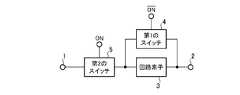
- FIG. 1is a configuration diagram showing a switching circuit according to the present embodiment.
- the switching circuit shown in FIG. 1includes a first terminal 1, a second terminal 2, a circuit element 3, a first switch 4, and a second switch 5.
- a signal source having an internal impedance Z 0is connected to the first terminal 1, and a load having an impedance Z 0 is connected to the second terminal 2.
- illustration of these signal sources and loadsis omitted.
- a first switch 4is connected to the circuit element 3 in parallel, and a second switch 5 is connected in series.
- a parallel circuit of the circuit element 3 and the first switch 4is connected to the second terminal 2, and the second switch 5 is connected to the first terminal 1.
- the first switch 4 and the second switch 5are alternately switched on and off, and are composed of FETs such as MOS FETs and HEMTs, MEMS switches, or the like. Let's say.
- FETs or the likeare used as the first switch 4 and the second switch 5, and it is conceivable that one end of the switch is a drain and the other end is a source. The source and the other end may be the drain.
- the first switch connected in parallel to the circuit element, and the parallel circuit configured by the circuit element and the first switchare connected in series. Since the first switch and the second switch are alternately turned on and off, the phase change at the time of switching can be suppressed over a wide band.
- the first switch and the second switchoperate as a short circuit when turned on and as a capacitor when turned off, so that the switching circuit can be realized with a simple configuration. it can.
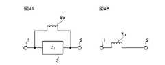
- FIG. 1the first switch and the second switch are switches represented by resistors in the on state and inductive parasitic elements in the off state.
- FIG. 3is a configuration diagram illustrating the switching circuit according to the second embodiment.
- the illustrated switching circuitincludes a first terminal 1, a second terminal 2, a circuit element 3, a first switch 6, and a second switch 7.
- the first switch 6 and the second switch 7are resistance elements in the on state and inductive parasitic elements in the off state, and other configurations are the same as those in the first embodiment.
- the first switch 6 and the second switch 7are composed of MOS FETs, HEMTs, MEMS switches, or the like.
- an FET or the likeis used as a switch, and one end of the switch may be a drain and the other end may be a source. Conversely, one end may be a source and the other end may be a drain.
- the first switch and the second switchoperate as a short circuit when turned on and as an inductor when turned off, so that the switching circuit has a simple configuration. Can be realized.
- Embodiment 3the switching circuit of the first or second embodiment is used for two shunt circuits of a ⁇ -type attenuator.
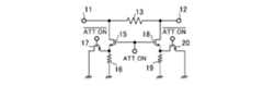
- FIG. 5is a block diagram showing the variable attenuator of the third embodiment.
- the illustrated variable attenuatorincludes a first terminal 11, a second terminal 12, a resistor 13, a third switch 14, second switches 15 and 18, resistors 16 and 19, and first switches 17 and 20. .
- the first terminal 11is an input terminal of the variable attenuator, and the second terminal 12 is an output terminal.
- the resistor 13is a series resistor of a ⁇ -type attenuator and is connected between the first terminal 11 and the second terminal 12.
- the third switch 14is a switch connected in parallel with the resistor 13.
- the second switch 15is a switch connected in series from the first terminal 11 to the shunt, and corresponds to the second switch 5 of the first embodiment.
- the resistor 16is connected in series to the second switch 15 and corresponds to the circuit element 3 of the first embodiment.
- the first switch 17is a switch connected in parallel to the resistor 16 from the connection point of the second switch 15 and the resistor 16 to the resistor 16 and corresponds to the first switch 4 of the first embodiment.
- the second switch 18is a switch connected in series from the second terminal 12 to the shunt, and corresponds to the second switch 5 of the first embodiment.
- the resistor 19is connected in series to the second switch 18 and corresponds to the circuit element 3 of the first embodiment.
- the first switch 20is a switch connected in parallel to the resistor 19 from the connection point of the second switch 18 and the resistor 19 to the resistor 19, and corresponds to the first switch 4 of the first embodiment.
- the two shunt circuits of the ⁇ -type attenuatorinclude the switching circuit including the second switch 15, the resistor 16, and the first switch 17, and the second switch 18.
- a switching circuitcomprising a resistor 19 and a first switch 20 is used.
- the third switch 14, the second switches 15 and 18, and the first switches 17 and 20use FETs, and are represented by resistors in the on state and capacitive parasitic elements in the off state.
- the on-resistance of the on statecan be ignored, represents the parasitic capacitance of the off state 14a, 15a, 18a, 17a, and 20a, to the capacitance value C 14, C 15, C 18 , C 17, C 20.
- the resistance values of the resistors 13 , 16 , and 19are R13, R16, and R19. Note that a switch using an FET uses a drain terminal and a source terminal as a switch, and the drain terminal and the source terminal of the connection shown in FIG. 5 may be reversed.
- the second switches 15 and 18are turned on, and the third switch 14 and the first switches 17 and 20 are turned off.
- the second switches 15 and 18are turned off, and the third switch 14 and the first switches 17 and 20 are turned on.
- the resistance 13In the ⁇ -type attenuator, the resistance 13 generally has a low resistance, so the relationship with the off-capacitance of the switch is R 13 ⁇ 1 / j ⁇ C 14 .
- An equivalent circuit in the first stateis shown in FIG. 6A, and an equivalent circuit in the second state is shown in FIG. 6B.
- the phase fluctuation between the first state and the second statecan be suppressed without depending on the frequency.
- the capacitancedoes not affect the absolute value of the attenuation amount of the present ⁇ -type attenuator. As a result, it is possible to obtain characteristics with different passage amplitudes in which fluctuations in the passage phase are suppressed in the first state and the second state.
- FIG. 7shows the calculation result when the attenuation is set to 3 dB in the equivalent circuit shown in FIG.
- FIG. 7Ashows the pass characteristic
- FIG. 7Bshows the pass phase.
- the characteristic 701aindicates the first state
- the characteristic 702aindicates the second state
- the characteristic 701bindicates the first state
- the characteristic 702bindicates the second state.
- the element value of the resistor 13is 18 ⁇
- the element values of the resistor 16 and the resistor 19are 274 ⁇
- the off-capacitance of the third switch 14is 0.05 pF
- the second switches 15 and 18 and the first switches 17 and 20The off capacitance was set to 0.1 pF.
- the pass characteristics of the second state and the first stateare 3.04 dB at 2 GHz and 2.95 dB at 10 GHz, and the difference in pass characteristics is 0.1 dB or less.
- the second stateis ⁇ 3.4 deg and the first state is ⁇ 3.6 deg at 2 GHz
- the second stateis ⁇ 17.6 deg at 10 GHz
- the first stateis ⁇ 16. 8 deg
- the phase difference between the two statescan be suppressed to 1 deg or less.
- the phase fluctuationcan be suppressed in the 5-fold band.
- variable attenuator of the third embodimentthe two shunt circuits of the ⁇ -type attenuator are replaced with the switching circuit of the first embodiment, a resistor is used for the circuit element of the switching circuit, and The third switch is connected in parallel with the series resistor of the ⁇ -type attenuator, and the third switch is controlled to be turned off in the first state and turned on in the second state, and the first switch is turned to the first state. Since the second switch is turned on in the first state and turned off in the second state, the phase change at the time of switching over a wide band is also achieved in the ⁇ -type attenuator. Can be suppressed.
- FIG. 4is an example of a low attenuation ⁇ -type variable attenuator.
- FIG. 8shows a variable attenuator of the fourth embodiment.
- the illustrated variable attenuatorincludes a first terminal 11, a second terminal 12, a resistor 13, second switches 15 and 18, resistors 16 and 19, and first switches 17 and 20. That is, in the variable attenuator of the fourth embodiment, the third switch 14 is not connected in parallel to the resistor 13 connected in series between the first terminal 11 and the second terminal 12.
- the configurationis the same as that of the ⁇ -type variable attenuator shown in the third embodiment.
- the ⁇ -type variable attenuator of the fourth embodimentcan be switched between a first state where the input signal is attenuated by the resistor 13, the resistor 16, and the resistor 19, and a second state where the input signal is not attenuated.
- the first statethe second switches 15 and 18 are turned on, and the first switches 17 and 20 are turned off.
- the second statethe second switches 15 and 18 are turned off, and the first switches 17 and 20 are turned on.
- the resistance value of the resistor 13is several ⁇ . Therefore, it is not necessary to short-circuit the resistor 13 as in the third embodiment.
- the equivalent circuit of the first state and the second stateis the same as that of FIG. 6A and FIG. 6B except that there is no parasitic capacitance 14a in the off state in the third switch 14, and thus is shown in the first embodiment.
- the phase fluctuation between the first state and the second statecan be suppressed without depending on the frequency by the equation (3) with the principle of the circuit configuration connected to the shunt.
- variable attenuator of the fourth embodimentthe two shunt circuits of the ⁇ -type attenuator are replaced with the switching circuit of the first embodiment, and resistors are used as circuit elements of the switching circuit.
- the switch 1is turned off in the first state and turned on in the second state, and the second switch is turned on in the first state and turned off in the second state. Also in the attenuator, the phase change at the time of switching can be suppressed over a wide band.
- the configuration of the first embodimentis used as the switching circuit.
- the configuration of the second embodimentmay be used.
- FIG. 9is a configuration diagram illustrating the variable attenuator of the fifth embodiment.
- the illustrated variable attenuatorincludes a first terminal 11, a second terminal 12, resistors 21 and 22, a fourth switch 23, a fifth switch 24, a resistor 25, a second switch 26, and a first switch 27. Is provided.
- the resistor 21 and the resistor 22are connected in series between the first terminal 11 and the second terminal 12, the fourth switch 23 is connected in parallel to the resistor 21, and the fifth switch 24 is connected in parallel to the resistor 22. It is connected.
- variable attenuator of the fifth embodimentuses a switching circuit including the resistor 25, the second switch 26, and the first switch 27 as the shunt circuit of the T-type variable attenuator.
- the fourth switch 23, the fifth switch 24, the second switch 26, and the first switch 27use FETs, and are represented by resistors in the on state and capacitive parasitic elements in the off state.
- the on-state on-resistanceis negligible
- the off-state parasitic capacitancesare represented by 23a, 24a, 26a, and 27a
- the capacitance valuesare represented by C 23 , C 24 , C 26 , and C 27 .
- the resistance values of the resistors 21 , 22 , and 25are R21, R22, and R25. Note that the switch using the FET uses the drain terminal and the source terminal as a switch, and the drain terminal and the source terminal of the connection shown in FIG. 9 may be reversed.
- the input signalis attenuated by the resistor 21, the resistor 22, and the resistor 25, the resistor 21 and the resistor 22 are short-circuited, and the resistor 25 is connected to the first terminal 11. It is possible to switch to the second state in which the input signal is not attenuated by disconnecting from the second terminal 12.
- the second switch 26is turned on, and the fourth switch 23, the fifth switch 24, and the first switch 27 are turned off.
- the second switch 26is turned off, and the fourth switch 23, the fifth switch 24, and the first switch 27 are turned on.
- the switch off-capacitanceis R 21 ⁇ 1 / j ⁇ C 23 and R 22 ⁇ 1 / j ⁇ C 24 .
- FIG. 10AAn equivalent circuit in the first state is shown in FIG. 10A, and an equivalent circuit in the second state is shown in FIG. 10B.
- the phase fluctuation between the first state and the second statecan be suppressed without depending on the frequency.
- the capacitancedoes not affect the absolute value of the attenuation amount of the T-type variable attenuator. As a result, it is possible to obtain characteristics with different passage amplitudes in which fluctuations in the passage phase are suppressed in the first state and the second state.
- FIG. 11shows the calculation result when the attenuation is set to 3 dB in the equivalent circuit shown in FIG.
- FIG. 11Ashows the pass characteristic
- FIG. 11Bshows the pass phase.
- the characteristic 1101aindicates the first state
- the characteristic 1102aindicates the second state
- the characteristic 1101bindicates the first state
- the characteristic 1102bindicates the second state.
- the element values of the resistor 21 and the resistor 22are 9 ⁇
- the element value of the resistor 25is 132 ⁇
- the off capacitance of the fourth switch 23 and the fifth switch 24is 0.05 pF
- the second switch 26 and the first switchThe 27 off capacitances were each 0.1 pF.
- the pass characteristics of the second state and the first stateare 3.02 dB at 2 GHz and 3.01 dB at 10 GHz, and the difference in pass characteristics is 0.1 dB or less.
- the passing phaseis ⁇ 1.8 deg in the second state at 2 GHz, ⁇ 1.6 deg in the first state, and ⁇ 9.1 deg.
- the first stateis -8.2 deg, and the phase difference between both states can be suppressed to 1 deg or less.
- the configuration of the fifth embodimentcan suppress the phase fluctuation in the 5-fold band.
- the shunt circuit of the T-type attenuatoris replaced with the switching circuit of the first embodiment, a resistor is used for the circuit element of the switching circuit, and T 4th and 5th switches are connected in parallel with the two series resistors of the type attenuator, and the 4th and 5th switches are turned off in the first state and turned on in the 2nd state. Since the first switch is controlled to be turned off in the first state and turned on in the second state, the second switch is turned on in the first state and turned off in the second state. Also in the type attenuator, the phase change at the time of switching can be suppressed over a wide band.
- FIG. 6is an example of a low attenuation T-type variable attenuator.
- FIG. 12shows a variable attenuator of the sixth embodiment.
- the illustrated variable attenuatorincludes a first terminal 11, a second terminal 12, resistors 21 and 22, a resistor 25, a second switch 26, and a first switch 27. That is, the variable attenuator according to the sixth embodiment includes a fourth switch 23 connected in parallel to the resistors 21 and 22 connected in series between the first terminal 11 and the second terminal 12. Except for the absence of the fifth switch 24, the configuration is the same as that of the T-type variable attenuator shown in the fifth embodiment.
- the T-type variable attenuator according to the sixth embodimentcan be switched between a first state in which the input signal is attenuated by the resistor 21, the resistor 22, and the resistor 25 and a second state in which the input signal is not attenuated.
- the first statethe second switch 26 is turned on, and the first switch 27 is turned off.
- the second statethe second switch 26 is turned off and the first switch 27 is turned on.
- the equivalent circuit of the first state and the second stateis the same as that shown in FIGS. 10A and 10B except that the parasitic capacitance 23a in the OFF state of the fourth switch 23 and the parasitic capacitance 24a in the OFF state of the fifth switch 24 do not exist.
- the expression (3) of the first embodimentwhen the high frequency or the value of R 25 is large, the phase fluctuation between the first state and the second state can be suppressed without depending on the frequency. Further, the capacitance does not affect the absolute value of the attenuation amount of the T-type variable attenuator. As a result, it is possible to obtain characteristics with different passage amplitudes in which fluctuations in the passage phase are suppressed in the first state and the second state.
- variable attenuator of the sixth embodimentthe shunt circuit of the T-type attenuator is replaced with the switching circuit of the first embodiment, and a resistor is used as the circuit element of the switching circuit. Since the switch is controlled to be off in the first state and on in the second state, and the second switch is controlled to be on in the first state and off in the second state, a low attenuation T-type variable attenuator The phase change at the time of switching can be suppressed over a wide band.
- the configuration of the first embodimentis used as the switching circuit.
- the configuration of the second embodimentmay be used.
- the switching circuit and the variable attenuator according to the present inventionrelate to a configuration in which switches having the same parasitic component are connected to circuit elements in series and in parallel, and are alternately turned on and off. It is particularly effective to apply to a circuit in which it is necessary to suppress a phase change at the time of switching over a wide band.
Landscapes
- Attenuators (AREA)
- Networks Using Active Elements (AREA)
- Electronic Switches (AREA)
Abstract
Description
Translated fromJapanese本発明は、回路素子に対して第1のスイッチと第2のスイッチを並列と直列に接続し、これら第1及び第2のスイッチを交互にオンオフ制御する切替回路と、これを用いた可変減衰器に関する。The present invention provides a switching circuit in which a first switch and a second switch are connected in parallel and in series to a circuit element, and the first and second switches are alternately controlled on and off, and a variable attenuation using the switching circuit. Related to the vessel.
従来の切替回路は切り替え時に寄生素子により生じる位相変化を補償するために、例えば誘導素子を装荷して容量性の寄生素子と共振させ、寄生素子の影響を相殺していた(例えば特許文献1参照)。In order to compensate for a phase change caused by a parasitic element at the time of switching, a conventional switching circuit loads, for example, an inductive element and resonates with a capacitive parasitic element to cancel the influence of the parasitic element (see, for example, Patent Document 1). ).
しかしながら、上記従来の切替回路では、誘導素子と寄生容量による共振を利用しているために、狭帯域となってしまう問題があった。However, the above-described conventional switching circuit has a problem in that it becomes a narrow band because it uses resonance due to the inductive element and the parasitic capacitance.
この発明は上記のような課題を解決するためになされたもので、切替時における位相変化を広帯域にわたって抑圧することのできる切替回路を提供することを目的とする。The present invention has been made to solve the above-described problems, and an object of the present invention is to provide a switching circuit capable of suppressing a phase change at the time of switching over a wide band.
この発明に係る可変減衰器は、回路素子に並列に接続された第1のスイッチと、回路素子と第1のスイッチで構成された並列回路に対して直列に接続された第2のスイッチとを備え、第1のスイッチと第2のスイッチとが交互にオンオフ動作するようにしたものである。A variable attenuator according to the present invention includes a first switch connected in parallel to a circuit element, and a second switch connected in series to a parallel circuit composed of the circuit element and the first switch. The first switch and the second switch are alternately turned on and off.
この発明の可変減衰器は、回路素子にスイッチを直列と並列にそれぞれ接続し、交互にオンオフ動作するようにしたものである。これにより、切替時における位相変化を広帯域にわたって抑圧することができる。The variable attenuator of the present invention is configured such that a switch is connected to a circuit element in series and in parallel, and an on / off operation is alternately performed. Thereby, the phase change at the time of switching can be suppressed over a wide band.
以下、この発明をより詳細に説明するために、この発明を実施するための形態について、添付の図面に従って説明する。
実施の形態1.
図1は、本実施の形態による切替回路を示す構成図である。
図1に示す切替回路は、第1の端子1、第2の端子2、回路素子3、第1のスイッチ4、第2のスイッチ5を備える。第1の端子1には内部インピーダンスZ0の信号源が接続され、第2の端子2にはインピーダンスZ0の負荷が接続される。なお、これら信号源と負荷の図示は省略している。回路素子3には第1のスイッチ4が並列に接続され、第2のスイッチ5が直列に接続されている。回路素子3と第1のスイッチ4の並列回路は第2の端子2に接続され、第2のスイッチ5は第1の端子1に接続されている。第1のスイッチ4及び第2のスイッチ5は交互にオンオフ制御されるスイッチであり、MOS FETやHEMTといったFET、またはMEMSスイッチ等からなり、オン状態ではオン抵抗、オフ状態ではオフ容量で表されるとする。Hereinafter, in order to explain the present invention in more detail, modes for carrying out the present invention will be described with reference to the accompanying drawings.
FIG. 1 is a configuration diagram showing a switching circuit according to the present embodiment.
The switching circuit shown in FIG. 1 includes a
次に、このように構成された切替回路の動作について説明する。
第1の端子1から信号が入力されると、第1の状態では第2のスイッチ5がオン、第1のスイッチ4がオフとなるように制御する。一方、第2の状態では第2のスイッチ5がオフ、第1のスイッチ4がオンとなるよう制御する。第1のスイッチ4と第2のスイッチ5のオン抵抗はRon4,Ron5≒0として無視できるとし、オフ容量4a,5aはC4,C5とする。図1の第1の状態の等価回路を図2Aに示し、第2の状態の等価回路を図2Bに示す。Next, the operation of the switching circuit configured as described above will be described.
When a signal is input from the
回路素子3のインピーダンスZ3が抵抗R3のとき図2Aの第1の状態の場合の通過特性S21の位相を計算すると、


同様に、Z3が容量C3の場合は、位相変動を抑える条件を求めると、
C5=C3+C4 (4)
となり、式(4)を満たすようにすることで周波数に関係なく広帯域にわたって位相変動を抑圧することができる。Similarly, when Z3 is a capacity C3 , the condition for suppressing the phase fluctuation is obtained as follows:
C5 = C3 + C4 (4)
Thus, by satisfying Equation (4), it is possible to suppress the phase variation over a wide band regardless of the frequency.
同様に、Z3が誘導素子L3の場合は、位相変動を抑える条件を求めると、
なお、本実施の形態では、第1のスイッチ4及び第2のスイッチ5としてFET等を用いており、スイッチの一端をドレイン、他端をソースとすることが考えられるが、反対に、一端をソース、他端をドレインとしてもよい。In the present embodiment, FETs or the like are used as the
以上説明したように、実施の形態1の切替回路によれば、回路素子に並列に接続された第1のスイッチと、回路素子と第1のスイッチで構成された並列回路に対して直列に接続された第2のスイッチとを備え、第1のスイッチと第2のスイッチとが交互にオンオフ動作するようにしたので、切替時における位相変化を広帯域にわたって抑圧することができる。As described above, according to the switching circuit of the first embodiment, the first switch connected in parallel to the circuit element, and the parallel circuit configured by the circuit element and the first switch are connected in series. Since the first switch and the second switch are alternately turned on and off, the phase change at the time of switching can be suppressed over a wide band.
また、実施の形態1の切替回路によれば、第1のスイッチと第2のスイッチは、オン時に短絡、オフ時に容量として動作するようにしたので、切替回路を簡素な構成で実現することができる。Further, according to the switching circuit of the first embodiment, the first switch and the second switch operate as ashort circuit when turned on and as a capacitor when turned off, so that the switching circuit can be realized with a simple configuration. it can.
実施の形態2.
実施の形態2は、第1のスイッチ及び第2のスイッチとして、オン状態では抵抗、オフ状態では誘導性の寄生素子で表されるスイッチとしたものである。
In the second embodiment, the first switch and the second switch are switches represented by resistors in the on state and inductive parasitic elements in the off state.
図3は、実施の形態2の切替回路を示す構成図である。図示の切替回路は、第1の端子1、第2の端子2、回路素子3、第1のスイッチ6、第2のスイッチ7を備える。第1のスイッチ6及び第2のスイッチ7は、オン状態で抵抗、オフ状態で誘導性の寄生素子であり、他の構成は実施の形態1と同様である。これら第1のスイッチ6及び第2のスイッチ7は、MOS FETやHEMT、MEMSスイッチなどで構成される。FIG. 3 is a configuration diagram illustrating the switching circuit according to the second embodiment. The illustrated switching circuit includes a
次に、実施の形態2の切替回路の動作について説明する。
第1の状態では、第2のスイッチ7をオン、第1のスイッチ6をオフとなるよう制御する。一方、第2の状態では、第2のスイッチ7をオフ、第1のスイッチ6をオンとなるよう制御する。第1のスイッチ6と第2のスイッチ7のオン抵抗はRon6,Ron7≒0と無視できるとし、オフ時の誘導性の寄生素子6b,7bはそれぞれL6,L7とする。図3における第1の状態の等価回路を図4Aに示し、第2の状態の等価回路を図4Bに示す。Next, the operation of the switching circuit according to the second embodiment will be described.
In the first state, control is performed so that the
回路素子3のインピーダンスZ3が抵抗R3のとき図4Aに示す第1の状態において、通過特性S21の位相を計算すると、


同様にZ3が容量(C3)のとき位相変動で抑制できる条件は、
同様にZ3が誘導素子(L3)のとき位相変動を抑制できる条件は、
本実施の形態ではスイッチとして、FETなどを用いており、スイッチの一端をドレイン、他端をソースとすることが考えられるほか、逆に一端をソース、他端をドレインとしてもよい。In this embodiment, an FET or the like is used as a switch, and one end of the switch may be a drain and the other end may be a source. Conversely, one end may be a source and the other end may be a drain.
以上説明したように、実施の形態2の切替回路によれば、第1のスイッチと第2のスイッチは、オン時に短絡、オフ時にインダクタとして動作するようにしたので、切替回路を簡素な構成で実現することができる。As described above, according to the switching circuit of the second embodiment, the first switch and the second switch operate as ashort circuit when turned on and as an inductor when turned off, so that the switching circuit has a simple configuration. Can be realized.
実施の形態3.
実施の形態3は、実施の形態1または実施の形態2の切替回路を、π型減衰器の二つのシャント回路に用いたものである。
In the third embodiment, the switching circuit of the first or second embodiment is used for two shunt circuits of a π-type attenuator.
図5は、実施の形態3の可変減衰器を示す構成図である。図示の可変減衰器は、第1の端子11、第2の端子12、抵抗13、第3のスイッチ14、第2のスイッチ15,18、抵抗16,19、第1のスイッチ17,20を備える。第1の端子11は可変減衰器の入力端子であり、第2の端子12は出力端子である。抵抗13はπ型減衰器のシリーズ抵抗であり第1の端子11と第2の端子12間に接続される。第3のスイッチ14は、抵抗13と並列接続されたスイッチである。第2のスイッチ15は第1の端子11からシャントに直列接続されたスイッチであり、実施の形態1の第2のスイッチ5に相当する。抵抗16は第2のスイッチ15に直列接続され、実施の形態1の回路素子3に相当する抵抗である。第1のスイッチ17は第2のスイッチ15と抵抗16の接続点からシャントに抵抗16に対して並列接続されたスイッチであり、実施の形態1の第1のスイッチ4に相当する。第2のスイッチ18は、第2の端子12からシャントに直列接続されたスイッチであり、実施の形態1の第2のスイッチ5に相当する。抵抗19は第2のスイッチ18に直列接続され、実施の形態1の回路素子3に相当する抵抗である。第1のスイッチ20は第2のスイッチ18と抵抗19の接続点からシャントに抵抗19に対して並列接続されたスイッチであり、実施の形態1の第1のスイッチ4に相当する。このように、実施の形態3の可変減衰器では、π型減衰器の二つのシャント回路に、第2のスイッチ15、抵抗16、第1のスイッチ17からなる切替回路と、第2のスイッチ18、抵抗19、第1のスイッチ20からなる切替回路を用いている。FIG. 5 is a block diagram showing the variable attenuator of the third embodiment. The illustrated variable attenuator includes a
第3のスイッチ14、第2のスイッチ15,18、第1のスイッチ17,20はFETを用いており、オン状態では抵抗、オフ状態では容量性の寄生素子で表されるとする。オン状態のオン抵抗は無視できるとし、オフ状態の寄生容量を14a,15a,18a,17a,20aと表し、その容量値をC14,C15,C18,C17,C20とする。また、抵抗13,16,19の抵抗値をR13,R16,R19とする。なおFETを用いたスイッチはドレイン端子とソース端子間をスイッチとして用いており図5に示す接続のドレイン端子、ソース端子を逆にしてもよい。The
次に、このように構成された実施の形態3の可変減衰器の動作について説明する。
実施の形態3のπ型減衰器は、入力信号を抵抗13、抵抗16、抵抗19により減衰させる第1の状態と、抵抗13を短絡し、抵抗16と抵抗19をそれぞれ第1の端子11と第2の端子12から切り離して入力信号を減衰させない第2の状態に切り替えることができる。
第1の状態では、第2のスイッチ15,18をオン、第3のスイッチ14及び第1のスイッチ17,20をオフ状態にする。第2の状態では第2のスイッチ15,18をオフ、第3のスイッチ14及び第1のスイッチ17,20をオン状態とする。また、π型減衰器では、一般に抵抗13は低抵抗となるため、スイッチのオフ容量との関係はR13<<1/jωC14となる。
第1の状態時の等価回路を図6Aに示し、第2の状態の等価回路を図6Bに示す。実施の形態1の式(3)より高周波やR16,R19の値が大きい場合は、周波数に依存することなく第1の状態と第2の状態の位相変動を抑えることができる。また、容量は本π型減衰器の減衰量の絶対値には影響を与えない。これにより第1の状態と第2の状態で通過位相の変動を抑えた、通過振幅の異なる特性を得ることができる。Next, the operation of the variable attenuator of
In the π-type attenuator of the third embodiment, a first state in which an input signal is attenuated by the
In the first state, the
An equivalent circuit in the first state is shown in FIG. 6A, and an equivalent circuit in the second state is shown in FIG. 6B. When the high frequency and the values of R16 and R19 are larger than the expression (3) in the first embodiment, the phase fluctuation between the first state and the second state can be suppressed without depending on the frequency. Further, the capacitance does not affect the absolute value of the attenuation amount of the present π-type attenuator. As a result, it is possible to obtain characteristics with different passage amplitudes in which fluctuations in the passage phase are suppressed in the first state and the second state.
図7に図6で示した等価回路で減衰量を3dBに設定した時の計算結果を示す。図7Aが通過特性、図7Bが通過位相を示している。図7Aにおいて、特性701aが第1の状態、特性702aが第2の状態を示し、図7Bにおいて、特性701bが第1の状態、特性702bが第2の状態を示している。
計算では抵抗13の素子値を18Ω、抵抗16と抵抗19の素子値を274Ω、第3のスイッチ14のオフ容量を0.05pF、第2のスイッチ15,18及び第1のスイッチ17,20のオフ容量をそれぞれ0.1pFとした。第2の状態と第1の状態の通過特性は、2GHzで3.04dB、10GHzで2.95dBであり、通過特性の差は0.1dB以下である。同様に通過位相は、2GHzでは第2の状態が-3.4deg、第1の状態が-3.6degであり、10GHzで第2の状態が-17.6deg、第1の状態が-16.8degであり、両状態の位相差は1deg以下に抑えることができる。実施の形態3の構成により5倍帯域で位相変動を抑制できる。FIG. 7 shows the calculation result when the attenuation is set to 3 dB in the equivalent circuit shown in FIG. FIG. 7A shows the pass characteristic, and FIG. 7B shows the pass phase. 7A, the characteristic 701a indicates the first state, the characteristic 702a indicates the second state, and in FIG. 7B, the characteristic 701b indicates the first state and the characteristic 702b indicates the second state.
In the calculation, the element value of the
以上説明したように、実施の形態3の可変減衰器によれば、π型減衰器の二つのシャント回路を実施の形態1の切替回路に置き換えると共に、切替回路の回路素子に抵抗を用い、かつ、π型減衰器のシリーズ抵抗と並列に第3のスイッチを接続し、第3のスイッチを第1の状態でオフ、第2の状態でオンに制御し、第1のスイッチを第1の状態でオフ、第2の状態でオンに制御し、第2のスイッチを第1の状態でオン、第2の状態でオフに制御したので、π型減衰器においても切替時における位相変化を広帯域にわたって抑圧することができる。As described above, according to the variable attenuator of the third embodiment, the two shunt circuits of the π-type attenuator are replaced with the switching circuit of the first embodiment, a resistor is used for the circuit element of the switching circuit, and The third switch is connected in parallel with the series resistor of the π-type attenuator, and the third switch is controlled to be turned off in the first state and turned on in the second state, and the first switch is turned to the first state. Since the second switch is turned on in the first state and turned off in the second state, the phase change at the time of switching over a wide band is also achieved in the π-type attenuator. Can be suppressed.
実施の形態4.
実施の形態4は、低減衰なπ型可変減衰器の例である。図8に実施の形態4の可変減衰器を示す。
図示の可変減衰器は、第1の端子11、第2の端子12、抵抗13、第2のスイッチ15,18、抵抗16,19、第1のスイッチ17,20を備える。すなわち、実施の形態4の可変減衰器は、第1の端子11と第2の端子12との間に直列に接続された抵抗13に対して並列に第3のスイッチ14が接続されていないことを除き、実施の形態3に示すπ型可変減衰器と同一の構成である。
The fourth embodiment is an example of a low attenuation π-type variable attenuator. FIG. 8 shows a variable attenuator of the fourth embodiment.
The illustrated variable attenuator includes a
次に実施の形態4の可変減衰器の動作について説明する。
実施の形態4のπ型可変減衰器は入力信号を抵抗13、抵抗16、抵抗19により減衰させる第1の状態と、入力信号を減衰させない第2の状態に切り替えることができる。第1の状態では、第2のスイッチ15,18をオン状態にし、第1のスイッチ17,20をオフ状態にする。第2の状態では第2のスイッチ15,18をオフ状態にし、第1のスイッチ17,20をオン状態にする。第1の状態の減衰量が低減衰のときは抵抗13の抵抗値が数Ωになるため、実施の形態3の様に抵抗13を短絡しなくてもよい。第1の状態と第2の状態の等価回路は、第3のスイッチ14におけるオフ状態の寄生容量14aが存在しないことを除いて図6A及び図6Bと同等になるため、実施の形態1に示したシャントに接続された回路構成の原理との式(3)により周波数に依存することなく第1の状態と第2の状態の位相変動を抑えることができる。Next, the operation of the variable attenuator of the fourth embodiment will be described.
The π-type variable attenuator of the fourth embodiment can be switched between a first state where the input signal is attenuated by the
以上説明したように、実施の形態4の可変減衰器によれば、π型減衰器の二つのシャント回路を実施の形態1の切替回路に置き換えると共に、切替回路の回路素子に抵抗を用い、第1のスイッチを第1の状態でオフ、第2の状態でオンに制御し、第2のスイッチを第1の状態でオン、第2の状態でオフに制御したので、低減衰なπ型可変減衰器においても、切替時における位相変化を広帯域にわたって抑圧することができる。As described above, according to the variable attenuator of the fourth embodiment, the two shunt circuits of the π-type attenuator are replaced with the switching circuit of the first embodiment, and resistors are used as circuit elements of the switching circuit. The
なお、上記実施の形態3及び実施の形態4では、切替回路として実施の形態1の構成を用いたが、実施の形態2の構成を用いてもよい。In the third and fourth embodiments, the configuration of the first embodiment is used as the switching circuit. However, the configuration of the second embodiment may be used.
実施の形態5.
実施の形態5は、T型可変減衰器に実施の形態1の切替回路を用いたものである。
図9は、実施の形態5の可変減衰器を示す構成図である。
図示の可変減衰器は、第1の端子11、第2の端子12、抵抗21,22、第4のスイッチ23、第5のスイッチ24、抵抗25、第2のスイッチ26、第1のスイッチ27を備える。抵抗21と抵抗22は第1の端子11と第2の端子12の間に直列に接続され、抵抗21には第4のスイッチ23が並列接続され、抵抗22には第5のスイッチ24が並列接続されている。抵抗21と抵抗22との接続点には第2のスイッチ26の一端側が接続され、第2のスイッチ26の他端側には抵抗25が接続されていると共に、第1のスイッチ27が接続されている。また、これら抵抗25及び第1のスイッチ27の他端側は接地されている。これら第2のスイッチ26と第1のスイッチ27は、実施の形態1の第2のスイッチ5と第1のスイッチ4に相当するスイッチである。すなわち、実施の形態5の可変減衰器は、T型可変減衰器のシャント回路に、抵抗25、第2のスイッチ26、第1のスイッチ27からなる切替回路を用いている。
In the fifth embodiment, the switching circuit of the first embodiment is used for a T-type variable attenuator.
FIG. 9 is a configuration diagram illustrating the variable attenuator of the fifth embodiment.
The illustrated variable attenuator includes a
第4のスイッチ23、第5のスイッチ24、第2のスイッチ26、第1のスイッチ27はFETを用いており、オン状態では抵抗、オフ状態では容量性の寄生素子で表される。オン状態のオン抵抗は無視できるとし、オフ状態の寄生容量を23a,24a,26a,27aと表し、その容量値をC23,C24,C26,C27とする。また、抵抗21,22,25の抵抗値をR21,R22,R25とする。なおFETを用いたスイッチはドレイン端子とソース端子間をスイッチとして用いており図9に示す接続のドレイン端子、ソース端子を逆にしてもよい。The fourth switch 23, the
次に、実施の形態5の可変減衰器の動作について説明する。
実施の形態5のT型可変減衰器は、入力信号を抵抗21、抵抗22、抵抗25により減衰させる第1の状態と、抵抗21と抵抗22を短絡し、抵抗25を第1の端子11と第2の端子12から切り離して、入力信号を減衰させない第2の状態に切り替えることができる。第1の状態では、第2のスイッチ26をオン状態にし、第4のスイッチ23と第5のスイッチ24、第1のスイッチ27をオフ状態にする。第2の状態では、第2のスイッチ26をオフ状態にし、第4のスイッチ23と第5のスイッチ24、第1のスイッチ27をオン状態にする。また、T型減衰器では一般に抵抗21と抵抗22が低抵抗となるため、スイッチのオフ容量との関係はR21<<1/jωC23,R22<<1/jωC24となる。Next, the operation of the variable attenuator of the fifth embodiment will be described.
In the T-type variable attenuator of the fifth embodiment, the input signal is attenuated by the
第1の状態時の等価回路を図10Aに示し、第2の状態の等価回路を図10Bに示す。実施の形態1の式(3)より高周波やR25の値が大きい場合は、周波数に依存することなく第1の状態と第2の状態の位相変動を抑えることができる。また、容量は本T型可変減衰器の減衰量の絶対値には影響を与えない。これにより第1の状態と第2の状態で通過位相の変動を抑えた、通過振幅の異なる特性を得ることができる。An equivalent circuit in the first state is shown in FIG. 10A, and an equivalent circuit in the second state is shown in FIG. 10B. When the high frequency and the value of R25 are larger than the expression (3) in the first embodiment, the phase fluctuation between the first state and the second state can be suppressed without depending on the frequency. Further, the capacitance does not affect the absolute value of the attenuation amount of the T-type variable attenuator. As a result, it is possible to obtain characteristics with different passage amplitudes in which fluctuations in the passage phase are suppressed in the first state and the second state.
図11に図9で示した等価回路で減衰量を3dBに設定した時の計算結果を示す。図11Aが通過特性、図11Bが通過位相を示している。図11Aにおいて、特性1101aが第1の状態、特性1102aが第2の状態を示し、図11Bにおいて、特性1101bが第1の状態、特性1102bが第2の状態を示している。
計算では抵抗21と抵抗22の素子値を9Ω、抵抗25の素子値を132Ω、第4のスイッチ23と第5のスイッチ24のオフ容量を0.05pF、第2のスイッチ26と第1のスイッチ27のオフ容量をそれぞれ0.1pFとした。第2の状態と第1の状態の通過特性は、2GHzで3.02dB、10GHzで3.01dBであり、通過特性の差は0.1dB以下である。同様に通過位相は、2GHzで第2の状態が-1.8deg、第1の状態が-1.6degであり、10GHzで第2の状態が-9.1deg.第1の状態が-8.2degであり、両状態の位相差は1deg以下に抑えることができる。このように、実施の形態5の構成により5倍帯域で位相変動を抑制できる。FIG. 11 shows the calculation result when the attenuation is set to 3 dB in the equivalent circuit shown in FIG. FIG. 11A shows the pass characteristic, and FIG. 11B shows the pass phase. 11A, the characteristic 1101a indicates the first state, the characteristic 1102a indicates the second state, and in FIG. 11B, the characteristic 1101b indicates the first state, and the characteristic 1102b indicates the second state.
In the calculation, the element values of the
以上説明したように、実施の形態5の可変減衰器によれば、T型減衰器のシャント回路を実施の形態1の切替回路に置き換えると共に、切替回路の回路素子に抵抗を用い、かつ、T型減衰器の二つのシリーズ抵抗にそれぞれ並列になるよう第4のスイッチと第5のスイッチを接続し、第4のスイッチと第5のスイッチを第1の状態でオフ、第2の状態でオンに制御し、第1のスイッチを第1の状態でオフ、第2の状態でオンに制御し、第2のスイッチを第1の状態でオン、第2の状態でオフに制御したので、T型減衰器においても、切替時における位相変化を広帯域にわたって抑圧することができる。As described above, according to the variable attenuator of the fifth embodiment, the shunt circuit of the T-type attenuator is replaced with the switching circuit of the first embodiment, a resistor is used for the circuit element of the switching circuit, and T 4th and 5th switches are connected in parallel with the two series resistors of the type attenuator, and the 4th and 5th switches are turned off in the first state and turned on in the 2nd state. Since the first switch is controlled to be turned off in the first state and turned on in the second state, the second switch is turned on in the first state and turned off in the second state. Also in the type attenuator, the phase change at the time of switching can be suppressed over a wide band.
実施の形態6.
実施の形態6は、低減衰なT型可変減衰器の例である。図12に実施の形態6の可変減衰器を示す。
図示の可変減衰器は、第1の端子11、第2の端子12、抵抗21,22、抵抗25、第2のスイッチ26、第1のスイッチ27を備える。すなわち、実施の形態6の可変減衰器は、第1の端子11と第2の端子12との間に直列に接続された抵抗21,22に対してそれぞれ並列接続された第4のスイッチ23と第5のスイッチ24がないことを除き、実施の形態5に示すT型可変減衰器と同一の構成である。
The sixth embodiment is an example of a low attenuation T-type variable attenuator. FIG. 12 shows a variable attenuator of the sixth embodiment.
The illustrated variable attenuator includes a
次に、実施の形態6の可変減衰器の動作について説明する。
実施の形態6のT型可変減衰器は、入力信号を抵抗21、抵抗22、抵抗25により減衰させる第1の状態と、入力信号を減衰させない第2の状態に切り替えることができる。第1の状態では、第2のスイッチ26をオン状態にし、第1のスイッチ27をオフ状態にする。第2の状態では、第2のスイッチ26をオフ状態にし、第1のスイッチ27をオン状態にする。
第1の状態の減衰量が低減衰のときは抵抗21,22の抵抗値が低いため、実施の形態5の様に抵抗21,22を短絡しなくてもよい。第1の状態と第2の状態の等価回路は、第4のスイッチ23のオフ状態の寄生容量23aと第5のスイッチ24のオフ状態の寄生容量24aが存在しないことを除いて図10A及び図10Bと同等になる。実施の形態1の式(3)により、高周波やR25の値が大きい場合は、周波数に依存することなく第1の状態と第2の状態の位相変動を抑えることができる。また、容量は本T型可変減衰器の減衰量の絶対値には影響を与えない。これにより第1の状態と第2の状態で通過位相の変動を抑えた、通過振幅の異なる特性を得ることができる。Next, the operation of the variable attenuator of the sixth embodiment will be described.
The T-type variable attenuator according to the sixth embodiment can be switched between a first state in which the input signal is attenuated by the
When the attenuation amount in the first state is low, the resistance values of the
以上説明したように、実施の形態6の可変減衰器によれば、T型減衰器のシャント回路を実施の形態1の切替回路に置き換えると共に、切替回路の回路素子に抵抗を用い、第1のスイッチを第1の状態でオフ、第2の状態でオンに制御し、第2のスイッチを第1の状態でオン、第2の状態でオフに制御したので、低減衰なT型可変減衰器においても、切替時における位相変化を広帯域にわたって抑圧することができる。As described above, according to the variable attenuator of the sixth embodiment, the shunt circuit of the T-type attenuator is replaced with the switching circuit of the first embodiment, and a resistor is used as the circuit element of the switching circuit. Since the switch is controlled to be off in the first state and on in the second state, and the second switch is controlled to be on in the first state and off in the second state, a low attenuation T-type variable attenuator The phase change at the time of switching can be suppressed over a wide band.
なお、上記実施の形態5及び実施の形態6では、切替回路として実施の形態1の構成を用いたが、実施の形態2の構成を用いてもよい。In the fifth and sixth embodiments, the configuration of the first embodiment is used as the switching circuit. However, the configuration of the second embodiment may be used.
本願発明はその発明の範囲内において、各実施の形態の自由な組み合わせ、あるいは各実施の形態の任意の構成要素の変形、もしくは各実施の形態において任意の構成要素の省略が可能である。In the present invention, within the scope of the invention, a free combination of each embodiment, a modification of an arbitrary component of each embodiment, or an omission of any component in each embodiment is possible.
以上のように、この発明に係る切替回路及び可変減衰器は、回路素子に寄生成分が同一のスイッチを直列と並列にそれぞれ接続し、交互にオンオフ制御する構成に関するものであり、例えば、可変減衰器において広帯域にわたって切換時の位相変化を抑圧することが必要な回路に対して適用することが特に有効である。As described above, the switching circuit and the variable attenuator according to the present invention relate to a configuration in which switches having the same parasitic component are connected to circuit elements in series and in parallel, and are alternately turned on and off. It is particularly effective to apply to a circuit in which it is necessary to suppress a phase change at the time of switching over a wide band.
1,11 第1の端子、2,12 第2の端子、3 回路素子、4,6,17,20,27 第1のスイッチ、5,7,15,18,26 第2のスイッチ、13,16,19,21,22,25 抵抗、14 第3のスイッチ、23 第4のスイッチ、24 第5のスイッチ。1,11 1st terminal, 2,12 2nd terminal, 3 circuit element, 4, 6, 17, 20, 27, first switch, 5, 7, 15, 18, 26 second switch, 13, 16, 19, 21, 22, 25 resistance, 14 third switch, 23 fourth switch, 24 fifth switch.
Claims (7)
Translated fromJapanese前記回路素子と前記第1のスイッチで構成された並列回路に対して直列に接続された第2のスイッチとを備え、
前記第1のスイッチと前記第2のスイッチとが交互にオンオフ動作することを特徴とする切替回路。A first switch connected in parallel to the circuit element;
A second switch connected in series to the parallel circuit composed of the circuit element and the first switch;
The switching circuit, wherein the first switch and the second switch are alternately turned on and off.
前記第3のスイッチを第1の状態でオフ、第2の状態でオンに制御し、
前記第1のスイッチを前記第1の状態でオフ、前記第2の状態でオンに制御し、
前記第2のスイッチを前記第1の状態でオン、前記第2の状態でオフに制御したことを特徴とする可変減衰器。The two shunt circuits of the π-type attenuator are replaced with the switching circuit according to any one of claims 1 to 3, a resistor is used for the circuit element of the switching circuit, and the π-type attenuator is used. Connect a third switch in parallel with the series resistance of the attenuator,
Controlling the third switch off in the first state and on in the second state;
Controlling the first switch off in the first state and on in the second state;
The variable attenuator, wherein the second switch is controlled to be on in the first state and off in the second state.
前記第1のスイッチを前記第1の状態でオフ、前記第2の状態でオンに制御し、
前記第2のスイッチを前記第1の状態でオン、前記第2の状態でオフに制御したことを特徴とする可変減衰器。The two shunt circuits of the π-type attenuator are replaced with the switching circuit according to any one of claims 1 to 3, and a resistor is used for the circuit element of the switching circuit.
Controlling the first switch off in the first state and on in the second state;
The variable attenuator, wherein the second switch is controlled to be on in the first state and off in the second state.
前記第4のスイッチと前記第5のスイッチを第1の状態でオフ、第2の状態でオンに制御し、
前記第1のスイッチを前記第1の状態でオフ、前記第2の状態でオンに制御し、
前記第2のスイッチを前記第1の状態でオン、前記第2の状態でオフに制御したことを特徴とする可変減衰器。A shunt circuit of a T-type attenuator is replaced with the switching circuit according to any one of claims 1 to 3, a resistor is used for the circuit element of the switching circuit, and the T-type attenuator is used. Connect the 4th switch and the 5th switch so that they are in parallel with the two series resistors, respectively.
Controlling the fourth switch and the fifth switch to be off in the first state and on in the second state;
Controlling the first switch off in the first state and on in the second state;
The variable attenuator, wherein the second switch is controlled to be on in the first state and off in the second state.
前記第1のスイッチを前記第1の状態でオフ、前記第2の状態でオンに制御し、
前記第2のスイッチを前記第1の状態でオン、前記第2の状態でオフに制御したことを特徴とする可変減衰器。While replacing the shunt circuit of a T-type attenuator with the switching circuit of any one of Claims 1-3, using resistance for the said circuit element of the said switching circuit,
Controlling the first switch off in the first state and on in the second state;
The variable attenuator, wherein the second switch is controlled to be on in the first state and off in the second state.
Priority Applications (4)
| Application Number | Priority Date | Filing Date | Title |
|---|---|---|---|
| JP2018547487AJP6452917B1 (en) | 2018-03-29 | 2018-03-29 | Switching circuit and variable attenuator |
| PCT/JP2018/013299WO2019186913A1 (en) | 2018-03-29 | 2018-03-29 | Switching circuit and variable attenuator |
| EP18912940.6AEP3758225B1 (en) | 2018-03-29 | 2018-03-29 | Switching circuit and variable attenuator |
| US17/015,978US11451208B2 (en) | 2018-03-29 | 2020-09-09 | Switching circuit and variable attenuator |
Applications Claiming Priority (1)
| Application Number | Priority Date | Filing Date | Title |
|---|---|---|---|
| PCT/JP2018/013299WO2019186913A1 (en) | 2018-03-29 | 2018-03-29 | Switching circuit and variable attenuator |
Related Child Applications (1)
| Application Number | Title | Priority Date | Filing Date |
|---|---|---|---|
| US17/015,978ContinuationUS11451208B2 (en) | 2018-03-29 | 2020-09-09 | Switching circuit and variable attenuator |
Publications (1)
| Publication Number | Publication Date |
|---|---|
| WO2019186913A1true WO2019186913A1 (en) | 2019-10-03 |
Family
ID=65020486
Family Applications (1)
| Application Number | Title | Priority Date | Filing Date |
|---|---|---|---|
| PCT/JP2018/013299CeasedWO2019186913A1 (en) | 2018-03-29 | 2018-03-29 | Switching circuit and variable attenuator |
Country Status (4)
| Country | Link |
|---|---|
| US (1) | US11451208B2 (en) |
| EP (1) | EP3758225B1 (en) |
| JP (1) | JP6452917B1 (en) |
| WO (1) | WO2019186913A1 (en) |
Families Citing this family (2)
| Publication number | Priority date | Publication date | Assignee | Title |
|---|---|---|---|---|
| CN113162581B (en)* | 2021-03-22 | 2022-08-05 | 中国电子科技集团公司第十三研究所 | Broadband digital phase shifter based on GaN HEMT device |
| US12095435B2 (en)* | 2022-06-13 | 2024-09-17 | Fujikura Ltd. | High frequency variable attenuation circuit |
Citations (5)
| Publication number | Priority date | Publication date | Assignee | Title |
|---|---|---|---|---|
| JPH1155059A (en)* | 1997-07-29 | 1999-02-26 | Mitsubishi Electric Corp | Variable attenuator |
| JP2003309454A (en) | 2002-04-15 | 2003-10-31 | Mitsubishi Electric Corp | Variable attenuator |
| JP2008182291A (en)* | 2007-01-23 | 2008-08-07 | Yokogawa Electric Corp | Switch circuit and step attenuator using the switch circuit |
| JP2009152861A (en)* | 2007-12-20 | 2009-07-09 | Denso Corp | Switching circuit |
| JP2014082755A (en)* | 2012-10-16 | 2014-05-08 | Freescale Semiconductor Inc | Electronic circuits with variable attenuators and methods of their operation |
Family Cites Families (6)
| Publication number | Priority date | Publication date | Assignee | Title |
|---|---|---|---|---|
| JPH0288303U (en) | 1988-12-27 | 1990-07-12 | ||
| US5666089A (en)* | 1996-04-12 | 1997-09-09 | Hewlett-Packard Company | Monolithic step attenuator having internal frequency compensation |
| KR101030050B1 (en)* | 2009-12-14 | 2011-04-21 | 한국과학기술원 | Digital Attenuator with Low Phase Shift |
| JP6076193B2 (en)* | 2013-05-20 | 2017-02-08 | 三菱電機株式会社 | Phase shift circuit |
| US10530320B2 (en)* | 2016-07-15 | 2020-01-07 | Psemi Corporation | Attenuator de-Qing loss improvement and phase balance |
| US20180062622A1 (en)* | 2016-08-30 | 2018-03-01 | Skyworks Solutions, Inc. | Binary-weighted attenuator having compensation circuit |
- 2018
- 2018-03-29JPJP2018547487Apatent/JP6452917B1/enactiveActive
- 2018-03-29EPEP18912940.6Apatent/EP3758225B1/enactiveActive
- 2018-03-29WOPCT/JP2018/013299patent/WO2019186913A1/ennot_activeCeased
- 2020
- 2020-09-09USUS17/015,978patent/US11451208B2/enactiveActive
Patent Citations (5)
| Publication number | Priority date | Publication date | Assignee | Title |
|---|---|---|---|---|
| JPH1155059A (en)* | 1997-07-29 | 1999-02-26 | Mitsubishi Electric Corp | Variable attenuator |
| JP2003309454A (en) | 2002-04-15 | 2003-10-31 | Mitsubishi Electric Corp | Variable attenuator |
| JP2008182291A (en)* | 2007-01-23 | 2008-08-07 | Yokogawa Electric Corp | Switch circuit and step attenuator using the switch circuit |
| JP2009152861A (en)* | 2007-12-20 | 2009-07-09 | Denso Corp | Switching circuit |
| JP2014082755A (en)* | 2012-10-16 | 2014-05-08 | Freescale Semiconductor Inc | Electronic circuits with variable attenuators and methods of their operation |
Non-Patent Citations (1)
| Title |
|---|
| See also references ofEP3758225A4 |
Also Published As
| Publication number | Publication date |
|---|---|
| EP3758225B1 (en) | 2023-05-03 |
| EP3758225A4 (en) | 2021-03-10 |
| JP6452917B1 (en) | 2019-01-16 |
| US20200412321A1 (en) | 2020-12-31 |
| US11451208B2 (en) | 2022-09-20 |
| JPWO2019186913A1 (en) | 2020-04-30 |
| EP3758225A1 (en) | 2020-12-30 |
Similar Documents
| Publication | Publication Date | Title |
|---|---|---|
| JP4998550B2 (en) | Frequency variable band elimination filter | |
| US7719386B2 (en) | Phase shifter having components which suppress fluctuations in the phase shifter pass characteristics | |
| KR101030050B1 (en) | Digital Attenuator with Low Phase Shift | |
| US20150364805A1 (en) | Electronic device | |
| JPH08250963A (en) | Phase shifter | |
| JP6452917B1 (en) | Switching circuit and variable attenuator | |
| JP2008219748A (en) | Attenuation characteristic variable filter | |
| JP4214710B2 (en) | Variable attenuator | |
| JP6425612B2 (en) | Variable attenuator | |
| JP6076193B2 (en) | Phase shift circuit | |
| JP5822660B2 (en) | High frequency switch | |
| JPH07312508A (en) | Variable attenuator | |
| JP2001339276A (en) | Phase shifter | |
| WO2018003007A1 (en) | High frequency switch | |
| JP2014110605A (en) | Phase shift circuit | |
| CN113330684A (en) | Configurable micro-acoustic RF filter | |
| US20240348235A1 (en) | Switchable acoustic filter topologies with improved performance | |
| JP7490153B2 (en) | Phase Shift Circuit | |
| JP2011244187A (en) | Band variable filter | |
| JPH11205086A (en) | Phase shifter | |
| EP3373455B1 (en) | High frequency switch | |
| JP4595850B2 (en) | Phase shifter | |
| JP2002246802A (en) | Semiconductor switch and phase shift circuit and attenuator | |
| WO2023242974A1 (en) | High-frequency switch | |
| JPH10270904A (en) | Phase shifter |
Legal Events
| Date | Code | Title | Description |
|---|---|---|---|
| ENP | Entry into the national phase | Ref document number:2018547487 Country of ref document:JP Kind code of ref document:A | |
| 121 | Ep: the epo has been informed by wipo that ep was designated in this application | Ref document number:18912940 Country of ref document:EP Kind code of ref document:A1 | |
| ENP | Entry into the national phase | Ref document number:2018912940 Country of ref document:EP Effective date:20200922 | |
| NENP | Non-entry into the national phase | Ref country code:DE |