WO2019159216A1 - Light-emitting device - Google Patents
Light-emitting deviceDownload PDFInfo
- Publication number
- WO2019159216A1 WO2019159216A1PCT/JP2018/004808JP2018004808WWO2019159216A1WO 2019159216 A1WO2019159216 A1WO 2019159216A1JP 2018004808 WJP2018004808 WJP 2018004808WWO 2019159216 A1WO2019159216 A1WO 2019159216A1
- Authority
- WO
- WIPO (PCT)
- Prior art keywords
- light emitting
- emitting device
- layer
- metal oxide
- light
- Prior art date
- Legal status (The legal status is an assumption and is not a legal conclusion. Google has not performed a legal analysis and makes no representation as to the accuracy of the status listed.)
- Ceased
Links
Images


Classifications
- H—ELECTRICITY
- H10—SEMICONDUCTOR DEVICES; ELECTRIC SOLID-STATE DEVICES NOT OTHERWISE PROVIDED FOR
- H10H—INORGANIC LIGHT-EMITTING SEMICONDUCTOR DEVICES HAVING POTENTIAL BARRIERS
- H10H20/00—Individual inorganic light-emitting semiconductor devices having potential barriers, e.g. light-emitting diodes [LED]
- H10H20/80—Constructional details
- H10H20/81—Bodies
- H10H20/811—Bodies having quantum effect structures or superlattices, e.g. tunnel junctions
- H10H20/812—Bodies having quantum effect structures or superlattices, e.g. tunnel junctions within the light-emitting regions, e.g. having quantum confinement structures
- H—ELECTRICITY
- H05—ELECTRIC TECHNIQUES NOT OTHERWISE PROVIDED FOR
- H05B—ELECTRIC HEATING; ELECTRIC LIGHT SOURCES NOT OTHERWISE PROVIDED FOR; CIRCUIT ARRANGEMENTS FOR ELECTRIC LIGHT SOURCES, IN GENERAL
- H05B33/00—Electroluminescent light sources
- H05B33/12—Light sources with substantially two-dimensional radiating surfaces
- H05B33/14—Light sources with substantially two-dimensional radiating surfaces characterised by the chemical or physical composition or the arrangement of the electroluminescent material, or by the simultaneous addition of the electroluminescent material in or onto the light source
- H—ELECTRICITY
- H10—SEMICONDUCTOR DEVICES; ELECTRIC SOLID-STATE DEVICES NOT OTHERWISE PROVIDED FOR
- H10K—ORGANIC ELECTRIC SOLID-STATE DEVICES
- H10K50/00—Organic light-emitting devices
- H10K50/10—OLEDs or polymer light-emitting diodes [PLED]
- H10K50/11—OLEDs or polymer light-emitting diodes [PLED] characterised by the electroluminescent [EL] layers
- H—ELECTRICITY
- H10—SEMICONDUCTOR DEVICES; ELECTRIC SOLID-STATE DEVICES NOT OTHERWISE PROVIDED FOR
- H10K—ORGANIC ELECTRIC SOLID-STATE DEVICES
- H10K71/00—Manufacture or treatment specially adapted for the organic devices covered by this subclass
- H—ELECTRICITY
- H10—SEMICONDUCTOR DEVICES; ELECTRIC SOLID-STATE DEVICES NOT OTHERWISE PROVIDED FOR
- H10K—ORGANIC ELECTRIC SOLID-STATE DEVICES
- H10K71/00—Manufacture or treatment specially adapted for the organic devices covered by this subclass
- H10K71/10—Deposition of organic active material
- H10K71/16—Deposition of organic active material using physical vapour deposition [PVD], e.g. vacuum deposition or sputtering
- H10K71/164—Deposition of organic active material using physical vapour deposition [PVD], e.g. vacuum deposition or sputtering using vacuum deposition
Definitions
- the present inventionrelates to a light emitting device using a quantum dot (Quantum Dot, QD).
- Patent Document 1discloses an example of such a light emitting device.
- the light emitting device of Patent Document 1includes a first inorganic substance-containing first charge transport layer in contact with a first electrode arranged to introduce charges into the first charge transport layer, a second electrode, and the first electrode.
- a plurality of semiconductor nanocrystalsare disposed between the electrode and the second electrode.
- Patent Document 1has a problem that the efficiency of electron injection into the semiconductor nanocrystal (quantum dot) is low.
- An object of one embodiment of the present inventionis to realize a light-emitting device with high efficiency of electron injection into quantum dots.
- a light-emitting deviceincludes a light-emitting layer and a hole transport that transports holes supplied from the anode to the light-emitting layer between an anode and a cathode.
- a light-emitting devicecomprising: a layer; and an electron transport layer that transports electrons supplied from the cathode to the light-emitting layer, wherein the light-emitting layer includes quantum dots that emit light in association with the combination of holes and electrons.
- the electron transport layerincludes a metal oxide, and the energy level at the lower end of the conduction band of the metal oxide is equal to or lower than the energy level at the lower end of the conduction band of the quantum dot.
- the light emitting devicecan realize a light emitting device having high light emission efficiency.
- FIG. 1is a diagram illustrating a schematic configuration of a light emitting device according to Embodiment 1.
- FIG.It is a figure which shows schematic structure of the light-emitting device as a modification of the light-emitting device which concerns on Embodiment 1.
- FIG.It is a figure which shows schematic structure of the light-emitting device which concerns on Embodiment 2.
- FIG.It is a figure which shows schematic structure of the light-emitting device as a modification of the light-emitting device which concerns on Embodiment 2.
- FIG.It is a figure which shows schematic structure of the light-emitting device which concerns on an Example. It is a measurement result of the voltage-current density characteristic in an Example.
- Embodiment 1hereinafter, Embodiment 1 of the present invention will be described in detail with reference to the drawings.
- “same layer”means that the same material is formed in the same process
- “lower layer”means that it is formed in a process prior to the layer to be compared.
- the “upper layer”means that it is formed in a later process than the layer to be compared.
- each drawingschematically illustrates the shape, structure, and positional relationship of each member and is not necessarily drawn to scale.
- FIG. 1is a diagram illustrating a schematic configuration of a light emitting device 1 according to the first embodiment.
- the light emitting device 1is used as a light source of a display device (not shown). That is, the display device includes the light emitting device 1 as a light source.
- the members included in the light emitting device 1description of members that are not related to the first embodiment is omitted. Members that omit these descriptions may be understood to be the same as known members.
- the light emitting device 1is a light source that lights each pixel (red pixel (R pixel), green pixel (G pixel), blue pixel (B pixel)) of the display device.
- the display devicerepresents an image with a plurality of RGB (Red, Green, Blue) pixels.
- the light-emitting device 1is a quantum dot (QD phosphor particle) that emits light in association with the combination of holes supplied from an anode 11 (anode) and electrons (free electrons) supplied from a cathode 15 (cathode). ) Is included. More specifically, the quantum dots are included in the light emitting layer 13 (QD phosphor layer) provided between the anode 11 and the cathode 15.
- QD phosphor layera direction from the anode 11 toward the cathode 15
- a direction opposite to the upward directionis referred to as a downward direction.
- the light emitting device 1includes a substrate 10, an anode 11, a hole transport layer (HTL) 12, a light emitting layer 13, an electron transport layer ( Electron Transport Layer (ETL) 14 and cathode 15 are provided in this order.
- HTLhole transport layer
- ETLElectron Transport Layer
- the anode 11 to the cathode 15are supported by a substrate 10 provided below the anode 11.
- the anode 11, the hole transport layer 12, the light emitting layer 13, the electron transport layer 14, and the cathode 15are formed (film formation) in this order on the substrate 10.
- the substrate 10is composed of a highly translucent substrate (eg, a glass substrate).
- the light emitting device 1will be described as a light emitting device having a bottom emission structure in which light emitted from the light emitting layer 13 is emitted downward.
- the substrate 10is a substrate having low translucency (eg, a plastic substrate). It may be.
- the anode 11has a relatively large work function such as tin-doped indium oxide (ITO), zinc-doped indium oxide (IZO), aluminum-doped zinc oxide (AZO), gallium-doped zinc oxide (GZO), and antimony-doped tin oxide (ATO). Preferably composed of materials.
- ITOtin-doped indium oxide
- IZOzinc-doped indium oxide
- AZOaluminum-doped zinc oxide
- GZOgallium-doped zinc oxide
- ATOantimony-doped tin oxide
- sputteringfilm deposition, vacuum deposition, physical vapor deposition (PVD, physical vapor deposition) or the like is used.
- PVDphysical vapor deposition
- the anode 11has translucency so that light emitted from the light emitting layer 13 can be transmitted.
- the hole transport layer 12is a layer that transports holes supplied from the anode 11 to the light emitting layer 13.
- the hole transport layer 12includes a material excellent in hole transportability.
- the materialmay be an organic material or an inorganic material. When the material is an inorganic material, it may be a semiconductor such as a metal oxide or a metal sulfide, and for example, NiO can be used.
- the hole transport layer 12may be a single layer or a stacked layer. For film formation of the hole transport layer 12, sputtering, vacuum deposition, physical vapor deposition, spin coating, ink jet, or the like is used.
- the light emitting layer 13includes quantum dots that emit light in accordance with the combination of holes supplied from the anode 11 and electrons supplied from the cathode 15.
- the material of the quantum dotis “GaN, GaP, Ga 2 O 3 , Ga 2 S 3 , Ge, CdSe, CdS, CdTe, CdO, InP, InN, In 2 S 3 , InGaN, AlInN, AlGaInN, CuInGaSe.
- At least one material selected from the group consisting of More specifically, nano-sized crystals of the above materialsare used as the material for the QD phosphor particles.
- the quantum dotsmay have a core / shell structure covered with a material having a band gap different from that of the material constituting the quantum dots on the outer peripheral portion. According to the core-shell structure, quantum efficiency can be improved.
- the quantum dotpreferably has a modifying group (ligand) on the surface layer. Thereby, the dispersibility of a quantum dot can be improved.
- the film formation of the light emitting layer 13is preferably performed using a technique such as spin coating, ink jetting, or photolithography.
- the electron transport layer 14is a layer that transports electrons supplied from the cathode 15 to the light emitting layer 13.
- the electron transport layer 14is formed of a metal oxide having a conduction band lower end (lowest molecular orbital, LUMO (lowest unoccupied molecular orbital) energy level equal to or lower than the energy level of the lower conduction band of the quantum dots included in the light emitting layer 13. Including.
- the metal oxidecan be formed by sputtering.
- the composition ratio of In, Ga, Zn, and Ocan be controlled by changing the oxygen concentration of the sputtering gas. Therefore, by controlling the oxygen concentration of the sputtering gas in consideration of the carrier density of the hole transport layer 12, the composition ratio of the metal oxide is controlled so that the amount of electrons transported to the light emitting layer 13 is appropriate. Can do.
- the ligand that modifies the quantum dots contained in the light emitting layer 13is easily damaged by heat or oxygen plasma. Therefore, when forming the electron carrying layer 14 on the light emitting layer 13, there exists a problem that the film-forming state of a light emitting layer will worsen.
- the metal oxide containing In, Ga, and Zn in this embodimentcan be formed by sputtering at room temperature. Thereby, compared with high frequency sputtering, the damage given during sputtering with respect to the ligand which has modified the quantum dot contained in the light emitting layer 13 can be reduced.
- the energy level at the lower end of the conduction bandis lower than the energy level at the lower end of the conduction band of the quantum dot.
- the carrier density of the metal oxide contained in the electron transport layer 14is preferably 1.0 ⁇ 10 17 cm ⁇ 3 or more. This is because, when the carrier density of the metal oxide is smaller than 1.0 ⁇ 10 17 cm ⁇ 3 , the triangular potential generated by the heterojunction of the band increases, and the current density change with respect to voltage application causes a negative differential resistance. The area to be shown is likely to exist. Therefore, the efficiency of electron injection from the electron transport layer 14 into the quantum dots is reduced.
- the carrier density of the metal oxide contained in the electron transport layer 14is more preferably 1.0 ⁇ 10 19 cm ⁇ 3 or more.
- the metal oxide containing In, Ga, and Zncan control the composition ratio of In, Ga, Zn, and O when formed by sputtering. Therefore, the metal oxide containing In, Ga, and Zn can easily control the carrier density. Thereby, the metal oxide containing In, Ga, and Zn can reduce the difference between the energy level at the lower end of the conduction band and the Fermi level. As a result, the triangular potential generated when heterojunction can be reduced, and electrons can be efficiently injected from the electron transport layer 14 into the quantum dots.
- the carrier density of the metal oxide included in the electron-transport layeris 1.0 ⁇ 10 20 cm ⁇ 3 , and the Fermi level enters the conduction band and is degenerated. Also good.
- the difference between the energy level at the lower end of the conduction band and the energy level at the lower end of the conduction band of the quantum dots included in the light emitting layer 13is less than 0.5 eV. It is preferable. This is because when the difference between the energy level at the lower end of the conduction band of the metal oxide and the energy level at the lower end of the conduction band of the quantum dot is 0.5 eV or more, the applied voltage required when injecting electrons into the quantum dot This is because the driving voltage of the light emitting device is increased.
- the difference between the energy level at the bottom of the conduction band and the energy level at the bottom of the conduction band of the quantum dotsis more preferably less than 0.4 eV.
- the metal oxide containing In, Ga, and Znmay be crystalline or amorphous.
- the metal oxideis crystalline, the carrier mobility of the electron transport layer 14 can be improved. Further, when the metal oxide is amorphous, there is no grain boundary, so that the interface between the electron transport layer 14 and the light emitting layer 13 becomes flat, and electrons can be injected efficiently.
- the metal oxide included in the electron-transport layer 14is not limited to a metal oxide including In, Ga, and Zn, and the energy level at the bottom of the conduction band is the light-emitting layer.
- Other metal oxidesmay be used as long as the metal oxide is equal to or lower than the energy level at the lower end of the conduction band of the quantum dots included in 13.
- TiO 2 or the likecan be used as the metal oxide.
- the film thickness of the electron transport layer 14is preferably 5 nm or more and 200 nm or less. When the thickness of the electron transport layer 14 is smaller than 5 nm, electrons cannot be sufficiently injected into the light emitting layer 13. Moreover, when the film thickness of the electron carrying layer 14 is larger than 200 nm, the electron carrying layer 14 becomes resistance and it becomes difficult to inject electrons into the light emitting layer 13.
- the cathode 15is made of a material having a relatively small work function, such as Al, Ag, Ba, Yb, Ca, Li—Al alloy, Mg—Al alloy, Mg—Ag alloy, Mg—In alloy, Al—Al 2 O 3 alloy, etc. It is preferable that it is comprised by.
- a material having a relatively small work functionsuch as Al, Ag, Ba, Yb, Ca, Li—Al alloy, Mg—Al alloy, Mg—Ag alloy, Mg—In alloy, Al—Al 2 O 3 alloy, etc. It is preferable that it is comprised by.
- sputtering, film deposition, vacuum deposition, physical vapor deposition, or the likeis used.
- the cathode 15is a reflective electrode that reflects the light emitted from the light emitting layer 13.
- the light emitting device 1by applying a forward voltage between the anode 11 and the cathode 15 (the anode 11 is set to a higher potential than the cathode 15), (i) electrons are transferred from the cathode 15 to the light emitting layer 13. While being supplied, (ii) holes can be supplied from the anode 11 to the light emitting layer 13. As a result, light can be generated in the light emitting layer 13 with the combination of holes and electrons.
- the application of the voltagemay be controlled by a TFT (Thin Film Transistor, thin film transistor) (not shown).
- the light-emitting device 1includes the light-emitting layer 13 including the quantum dots that emit light according to the combination of holes and electrons, and the hole transport layer between the anode 11 and the cathode 15. 12 and a light-emitting device including an electron transport layer 14.
- the electron carrying layer 14contains the metal oxide whose energy level of the conduction band lower end of a metal oxide is below the energy level of the conduction band lower end of the said quantum dot.
- the light-emitting device 1 of one embodiment of the present inventionmay include a hole blocking layer (HBL, Hole Blocking Layer) that suppresses injection of holes into the light-emitting layer 13. Thereby, the balance of the carriers (that is, holes and electrons) supplied to the light emitting layer 13 can be adjusted.
- HBLhole blocking layer
- the light-emitting device 1 of one embodiment of the present inventionmay include an electron blocking layer (EBL, Electron Blocking Layer) that suppresses injection of electrons into the light-emitting layer 13. Thereby, the balance of the carriers (that is, holes and electrons) supplied to the light emitting layer 13 can be adjusted.
- EBLelectron blocking layer
- sealingis performed after film formation up to the cathode 15 is completed.
- the member (sealing member) that seals the light emitting devicemay be glass, plastic, or the like, and is preferably concave.
- a sealing adhesivefor example, an epoxy-based adhesive
- sealingis performed in a nitrogen atmosphere.
- each of the red pixel (R pixel), the green pixel (G pixel), and the blue pixel (B pixel)can be lit individually.
- the layer 14may be formed in units of a plurality of pixels, or may be formed in common for a plurality of pixels.
- the light emitting device 1may be configured as a top emission type light emitting device. That is, the light emitting device 1 may be configured to emit light emitted from the light emitting layer 13 upward. Specifically, by using a reflective electrode as the anode 11 and a translucent electrode as the cathode 15, the top emission type light emitting device 1 can be realized.
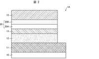
- Modification 2A light emitting device 1A as a modification of the light emitting device 1 in the first embodiment will be described.
- the light emitting device 1Adiffers from the light emitting device 1 in the structure of the electron transport layer.
- FIG. 2is a diagram showing a schematic configuration of the light emitting device 1A. As shown in FIG. 2, the light emitting device 1 ⁇ / b> A includes an electron transport layer 20 instead of the electron transport layer 14 in the light emitting device 1.
- the electron transport layer 20is composed of a lower layer 20A and an upper layer 20B.
- Both lower layer 20 ⁇ / b> A and upper layer 20 ⁇ / b> Binclude a metal oxide in which the energy level at the lower end of the conduction band is equal to or lower than the energy level at the lower end of the conduction band of the quantum dots included in light emitting layer 13.
- the lower layer 20Aincludes the amorphous metal oxide
- the upper layer 20Bincludes the crystalline metal oxide.
- the lower layer 20 ⁇ / b> Ais adjacent to the light emitting layer 13.
- the lower layer 20A of the electron transport layer 20includes an amorphous metal oxide.
- the interface between the lower layer 20A of the electron transport layer 20 and the light emitting layer 13becomes flat, so that electrons can be efficiently injected into the light emitting layer 13.
- the upper layer 20B of the electron transport layer 20contains a crystalline metal oxide, the carrier mobility of the electron transport layer 20 can be improved.
- the electron transport layer 20may not be completely divided into two layers, and amorphous and crystalline layers may be laminated with a concentration gradient from the lower layer 20A to the upper layer 20B.
- amorphous and crystalline layersmay be laminated with a concentration gradient from the lower layer 20A to the upper layer 20B.
- firingis performed from the upper layer 20B side by irradiation using an excimer laser, a xenon lamp, or the like.
- the order in which the anode 11, the hole transport layer 12, the light emitting layer 13, the electron transport layer 14, and the cathode 15 are formed in the light emitting device 1B in the present embodimentis reversed from that in the light emitting device 1 in the first embodiment. Yes.
- FIG. 3is a diagram showing a schematic configuration of the light emitting device 1B.
- the light emitting device 1 ⁇ / b> Bincludes a substrate 10, a cathode 15, an electron transport layer 14, a light emitting layer 13, a hole transport layer 12, and an anode 11 from the lower side to the upper side in FIG. 3. In this order.
- the metal oxide containing In, Ga, and Zn contained in the electron transport layer 14 in the present embodimentis amorphous. Therefore, the upper surface of the electron transport layer 14 can be flattened. As a result, when the light emitting layer 13 is formed on the upper surface of the electron transport layer 14, the light emitting layer 13 can be flattened (in other words, the surface roughness can be suppressed). As a result, the light-emitting device 1B can emit light with higher surface uniformity compared to a light-emitting device in which the electron transport layer includes a crystalline oxide semiconductor in which crystal grains exist. Further, when the metal oxide is amorphous, there is no grain boundary, so that the interface between the electron transport layer 14 and the light emitting layer 13 becomes flat, and electrons can be efficiently injected into the light emitting layer 13.
- any structurecan be used as long as each pixel of the red pixel (R pixel), the green pixel (G pixel), and the blue pixel (B pixel) can be lit individually.
- the layer 14may be formed in units of a plurality of pixels, or may be formed in common for a plurality of pixels.
- Modification 3A light emitting device 1C as a modification of the light emitting device 1B in the second embodiment will be described.
- the light emitting device 1Cis different from the light emitting device 1B in the structure of the electron transport layer.
- FIG. 4is a diagram showing a schematic configuration of the light emitting device 1C. As shown in FIG. 4, the light emitting device 1C includes an electron transport layer 30 instead of the electron transport layer 14 in the light emitting device 1B.
- the electron transport layer 30is composed of a lower layer 30A and an upper layer 30B.
- Both lower layer 30 ⁇ / b> A and upper layer 30 ⁇ / b> Binclude a metal oxide in which the energy level at the lower end of the conduction band is equal to or lower than the energy level at the lower end of the conduction band of the quantum dots included in light emitting layer 13.
- the lower layer 30Aincludes the crystalline metal oxide
- the upper layer 30Bincludes the amorphous metal oxide.
- the upper layer 30 ⁇ / b> Bis adjacent to the light emitting layer 13.
- the upper layer 30B of the electron transport layer 30includes an amorphous metal oxide
- the upper surface of the electron transport layer 30can be flattened.
- the light emitting layer 13can be made flat.
- the light emitting device 1 ⁇ / b> Ccan emit light with higher surface uniformity as compared with a light emitting device in which an electron transport layer includes a crystalline oxide semiconductor in which crystal grains exist.
- the metal oxideis amorphous, there is no grain boundary, so that the interface between the electron transport layer 30B and the light emitting layer 13 becomes flat, and electrons can be efficiently injected into the light emitting layer 13.
- the lower layer 30A of the electron transport layer 30includes a crystalline metal oxide, the carrier mobility of the electron transport layer 30 can be improved.
- FIG. 5is a diagram showing a schematic configuration of a light emitting device as Example 1, and Example 2 and Comparative Example 1 used in this example.
- the light-emitting device in this examplehas a substrate 10, a cathode 15, an electron transport layer 14, a light-emitting layer 13, a hole transport layer 12, a hole from the bottom to the top in FIG. 5.
- the injection layer 16 and the anode 11are provided in this order.
- Example 1The light emitting devices of Example 1, Example 2 and Comparative Example 1 differ only in the structure of the electron transport layer 14, and the other configurations are the same.
- the substrate 10is a glass substrate.
- the cathode 15is IZO having a thickness of 100 nm formed by sputtering.
- the light emitting layer 13includes quantum dots made of Cd (Se, S) and is formed to have a film thickness of 20 nm.
- the hole transport layer 12was formed by vacuum deposition of 4,4′-bis (N-carbazolyl) -1,1′-biphenyl (CBP) having a thickness of 40 nm.
- CBP4,4′-bis (N-carbazolyl) -1,1′-biphenyl
- MoO 3having a film thickness of 10 nm was formed by vacuum deposition.
- the anode 11was formed by vacuum deposition of Al having a thickness of 100 nm. After film formation of each layer was completed, sealing was performed in a nitrogen atmosphere.
- the electron transport layer 14 in the light-emitting device in Example 1includes a metal oxide containing In, Ga, and Zn, and has an oxygen concentration such that the carrier density of the metal oxide is 4.1 ⁇ 10 19 cm ⁇ 3. Was controlled to form a film by sputtering.
- the film thickness of the electron transport layer 14was 70 nm.
- the electron transport layer 14 in the light-emitting device in Example 2includes a metal oxide containing In, Ga, and Zn, and has an oxygen concentration such that the carrier density of the metal oxide is 6.3 ⁇ 10 17 cm ⁇ 3. Was controlled to form a film by sputtering.
- the film thickness of the electron transport layer 14was 70 nm.
- the electron transport layer 14 in the light emitting device in Comparative Example 1was formed by sputtering ZnO.
- the film thickness of the electron transport layer 14was 70 nm.
- FIG. 6shows measurement results of voltage-current density characteristics.
- the light emitting device (1, 1A to 1C)emits light emitted from the light emitting layer (13) and the holes supplied from the anode between the anode (11) and the cathode (15).
- a light-emitting devicecomprising a hole transport layer (12) transported to a layer and an electron transport layer (14) transporting electrons supplied from the cathode to the light-emitting layer, wherein the light-emitting layer comprises holes,
- the electron transport layerincludes a metal oxide, and the energy level at the lower end of the conduction band of the metal oxide is the energy at the lower end of the conduction band of the quantum dot. Below the level.
- the light emitting device according to aspect 2 of the present inventionis the light emitting device according to aspect 1, wherein the energy level difference between the energy level at the lower end of the conduction band of the metal oxide and the energy level at the lower end of the conduction band of the quantum dot is 0 eV or more and less than 0.5 eV.
- the metal oxidecontains In, Ga, and Zn.
- the metal oxideis amorphous.
- the metal oxideis crystalline.
- the light-emitting device according to aspect 7 of the present inventionis the light-emitting device according to any one of the above aspects 1 to 4, wherein the electron transport layer is formed by laminating a layer containing an amorphous metal oxide and a layer containing a crystalline metal oxide. And the layer containing the amorphous metal oxide is adjacent to the light emitting layer.
- the thickness of the electron transport layeris 5 nm or more and 200 nm or less.
- the metal oxidehas a carrier density of 1.0 ⁇ 10 17 cm ⁇ 3 or more.
- the light-emitting device according to aspect 10 of the present inventionis the light-emitting device according to any one of the aspects 1 to 9, wherein the quantum dots are GaN, GaP, Ga 2 O 3 , Ga 2 S 3 , Ge, CdSe, CdS, CdTe, CdO, At least one material selected from the group consisting of InP, InN, In 2 S 3 , InGaN, AlInN, AlGaInN, and CuInGaSe.
Landscapes
- Engineering & Computer Science (AREA)
- Manufacturing & Machinery (AREA)
- Physics & Mathematics (AREA)
- Optics & Photonics (AREA)
- Electroluminescent Light Sources (AREA)
Abstract
Description
Translated fromJapanese本発明は、量子ドット(Quantum Dot,QD)を用いた発光デバイスに関する。The present invention relates to a light emitting device using a quantum dot (Quantum Dot, QD).
近年、例えば表示装置の光源として、QDドット(量子ドット粒子、半導体ナノ粒子、QDドーパントとも称される)を含む発光デバイスが用いられている。特許文献1には、そのような発光デバイスの一例が開示されている。特許文献1の発光デバイスは、第一電荷輸送層に電荷を導入するように配置された第一電極に接触している第一無機物質含有第一電荷輸送層、第二電極、及び該第一電極と該第二電極との間に配置された複数の半導体ナノクリスタルを含んでいる。In recent years, for example, light-emitting devices including QD dots (also referred to as quantum dot particles, semiconductor nanoparticles, or QD dopants) have been used as light sources for display devices.
しかしながら、特許文献1の技術では、半導体ナノクリスタル(量子ドット)への電子の注入の効率が低いという問題がある。However, the technique of
本発明の一態様は、量子ドットへの電子の注入の効率が高い発光デバイスを実現することを目的とする。An object of one embodiment of the present invention is to realize a light-emitting device with high efficiency of electron injection into quantum dots.
上記の課題を解決するために、本発明の一態様に係る発光デバイスは、陽極と陰極との間に、発光層と、前記陽極から供給された正孔を前記発光層に輸送する正孔輸送層と、前記陰極から供給された電子を前記発光層に輸送する電子輸送層とを含む発光デバイスであって、前記発光層は、正孔と電子との結合に伴って光を発する量子ドットを含み、前記電子輸送層は、金属酸化物を含み、前記金属酸化物の伝導帯下端のエネルギー準位が、前記量子ドットの伝導帯下端のエネルギー準位以下である。In order to solve the above problems, a light-emitting device according to one embodiment of the present invention includes a light-emitting layer and a hole transport that transports holes supplied from the anode to the light-emitting layer between an anode and a cathode. A light-emitting device comprising: a layer; and an electron transport layer that transports electrons supplied from the cathode to the light-emitting layer, wherein the light-emitting layer includes quantum dots that emit light in association with the combination of holes and electrons. The electron transport layer includes a metal oxide, and the energy level at the lower end of the conduction band of the metal oxide is equal to or lower than the energy level at the lower end of the conduction band of the quantum dot.
本発明の一態様に係る発光デバイスによれば、高い発光効率を有する発光デバイスを実現することができる。The light emitting device according to one embodiment of the present invention can realize a light emitting device having high light emission efficiency.
〔実施形態1〕
以下、本発明の実施形態1について図面を参照しながら詳細に説明する。以下においては、「同層」とは同一プロセスにて同材料で形成されていることを意味し、「下層」とは、比較対象の層よりも前のプロセスで形成されていることを意味し、「上層」とは比較対象の層よりも後のプロセスで形成されていることを意味する。また、各図面は、各部材の形状、構造、および位置関係を概略的に説明するものであり、必ずしもスケール通りに描かれていないことに留意されたい。
Hereinafter,
図1は、実施形態1の発光デバイス1の概略的な構成を示す図である。発光デバイス1は、表示装置(不図示)の光源として用いられる。つまり、表示装置は、発光デバイス1を光源として備えている。発光デバイス1が備える各部材のうち、実施形態1とは関係しない部材については説明を省略する。これらの説明を省略する部材は、公知のものと同様であると理解されてよい。FIG. 1 is a diagram illustrating a schematic configuration of a
(発光デバイス1の構成)
発光デバイス1は、上記表示装置の各画素(赤色画素(R画素)、緑色画素(G画素)、青色画素(B画素))を点灯させる光源である。実施形態1では、上記表示装置は、RGB(Red,Green,Blue)の複数の画素によって画像を表現する。(Configuration of light emitting device 1)
The
発光デバイス1は、陽極11(アノード)から供給された正孔(ホール)と陰極15(カソード)から供給された電子(自由電子)との結合に伴って光を発する量子ドット(QD蛍光体粒子)を含んでいる。より具体的には、量子ドットは、陽極11と陰極15との間に設けられた発光層13(QD蛍光体層)に含まれている。以下、陽極11から陰極15に向かう方向を上方向と称する。また、上方向とは反対の方向を下方向と称する。The light-
図1に示すように発光デバイス1は、図1の下側から上方向に向かって、基板10、陽極11、正孔輸送層(Hole Transport Layer,HTL)12、発光層13、電子輸送層(Electron Transport Layer,ETL)14、および陰極15を、この順に備えている。As shown in FIG. 1, the
陽極11~陰極15は、陽極11の下方に設けられた基板10によって支持されている。一例として、発光デバイス1を製造する場合には、基板10上に、陽極11、正孔輸送層12、発光層13、電子輸送層14、および陰極15が、この順で形成(成膜)される。The
基板10は、透光性の高い基板(例:ガラス基板)で構成される。本実施形態では、発光デバイス1が、発光層13から発せられた光が下方に向けて出射されるボトムエミッション構造の発光デバイスとして説明する。なお、発光デバイス1が発光層13から発せられた光が上方に向けて出射されるトップエミッション構造の発光デバイスである場合には、基板10は、透光性の低い基板(例:プラスチック基板)であってもよい。The
陽極11は、スズドープ酸化インジウム(ITO)、亜鉛ドープ酸化インジウム(IZO)、アルミニウムドープ酸化亜鉛(AZO)、ガリウムドープ酸化亜鉛(GZO)、アンチモンドープ酸化スズ(ATO)などの比較的仕事関数が大きな材料で構成されるが好ましい。陽極11の成膜には、スパッタリング、フィルム蒸着、真空蒸着、物理的気相法(PVD、physical vapor deposition)などが用いられる。陽極11は、発光層13から発せられた光を透過できるように透光性を有している。The
正孔輸送層12は、陽極11から供給された正孔を発光層13に輸送する層である。正孔輸送層12は、正孔輸送性に優れた材料を含む。当該材料は、有機材料であってもよく、無機材料であってもよい。当該材料が無機材料である場合、金属酸化物、金属硫化物などの半導体であればよく、例えば、NiOなどを用いることができる。また、正孔輸送層12は、単層であってもよく、積層であってもよい。正孔輸送層12の成膜には、スパッタリング、真空蒸着、物理的気相法、スピンコート、インクジェットなどが用いられる。The
発光層13は、陽極11から供給された正孔と、陰極15から供給された電子との結合に伴って光を発する量子ドットを含む。一例として、量子ドットの材料は、「GaN、GaP、Ga2O3、Ga2S3、Ge、CdSe、CdS、CdTe、CdO、InP、InN、In2S3、InGaN、AlInN、AlGaInN、CuInGaSe」からなる群から選択された少なくとも1種類の材料であってよい。より具体的には、上記材料のナノサイズの結晶が、QD蛍光体粒子の材料として用いられる。The
なお、量子ドットは、外周部に量子ドットを構成する材料とはバンドギャップが異なる材料で覆われたコア・シェル構造であってもよい。コア・シェル構造によれば、量子効率を向上させることができる。また、量子ドットは、表層に修飾基(リガンド)があることが好ましい。これにより、量子ドットの分散性を向上させることができる。The quantum dots may have a core / shell structure covered with a material having a band gap different from that of the material constituting the quantum dots on the outer peripheral portion. According to the core-shell structure, quantum efficiency can be improved. The quantum dot preferably has a modifying group (ligand) on the surface layer. Thereby, the dispersibility of a quantum dot can be improved.
発光層13の成膜は、スピンコート、インクジェット、フォトリソグラフィなどの手法を用いることが好ましい。The film formation of the
電子輸送層14は、陰極15から供給された電子を発光層13に輸送する層である。電子輸送層14は、伝導帯下端(最低空分子軌道、LUMO(lowest unoccupied molecular orbital)のエネルギー準位が、発光層13が含む量子ドットの伝導帯下端のエネルギー準位以下である金属酸化物を含む。The
本実施形態では、電子輸送層14は、前記金属酸化物として、In、GaおよびZnを含む金属酸化物を含む。より詳細には、前記金属酸化物は、In、GaおよびZnの組成比が、In:Ga:Zn=1:X:Y(0.8≦X≦1.2、0.4≦Y≦1.2)である。例えば、前記金属酸化物は、In:Ga:Zn:O=1:1:1:4、In:Ga:Zn:O=2:2:1:7の化学量論比を有しており、当該化学量論比から酸素が欠損することにより、キャリア移動度が変化する。また、必ずしも上記の化学量論比である必要はなく、In:Ga:Zn:O=1:1:1:4~In:Ga:Zn:O=2:2:1:7の間で線形的に組成が変化しても構わない。In the present embodiment, the
前記金属酸化物は、スパッタにより形成することができる。金属酸化物を形成する際に、スパッタガスの酸素濃度を変化させることにより、In、Ga、ZnおよびOの組成比を制御することができる。そのため、正孔輸送層12のキャリア密度を考慮してスパッタガスの酸素濃度を制御することにより、発光層13への電子の輸送量が適切になるように金属酸化物の組成比を制御することができる。The metal oxide can be formed by sputtering. When forming the metal oxide, the composition ratio of In, Ga, Zn, and O can be controlled by changing the oxygen concentration of the sputtering gas. Therefore, by controlling the oxygen concentration of the sputtering gas in consideration of the carrier density of the
発光層13に含まれる量子ドットを修飾しているリガンドは、熱や酸素プラズマによりダメージを受け易い。そのため、発光層13の上部に電子輸送層14を形成する際に、発光層の成膜状態が悪くなってしまうという問題がある。これに対して、本実施形態におけるIn、GaおよびZnを含む金属酸化物は、室温でのスパッタにより形成することができる。これにより、高周波スパッタリングに比べて、発光層13に含まれる量子ドットを修飾しているリガンドに対してスパッタ中に与えるダメージを低減させることができる。The ligand that modifies the quantum dots contained in the
また、従来の発光デバイスのように、電子輸送層に含まれる金属酸化物の伝導帯下端のエネルギー準位が、発光層13が含む量子ドットの伝導帯下端のエネルギー準位よりも大きい場合では、金属酸化物と量子ドットとのヘテロ結合によるバンド構造の曲がり(三角ポテンシャル)が生じる。このため、電圧の増加に対して電流密度変化が負性微分抵抗を示す領域が存在するので、電子輸送層から量子ドットへの電子の注入効率が低くなる。そのため、電子輸送層から量子ドットへ電子を注入するために電圧を高くする必要があるという問題がある。Moreover, in the case where the energy level at the lower end of the conduction band of the metal oxide included in the electron transport layer is larger than the energy level at the lower end of the conduction band of the quantum dots included in the
これに対して、本実施形態における前記金属酸化物は、上述したように伝導帯下端のエネルギー準位が量子ドットの伝導帯下端のエネルギー準位以下となっている。これにより、金属酸化物と量子ドットとのヘテロ結合によって生じる三角ポテンシャルの影響を低減することが可能である。その結果、電子輸送層14から量子ドットへ電子を効率良く注入することができる。したがって、低電圧で電子輸送層14から量子ドットへ電子を注入することができる。On the other hand, in the metal oxide according to the present embodiment, as described above, the energy level at the lower end of the conduction band is lower than the energy level at the lower end of the conduction band of the quantum dot. Thereby, it is possible to reduce the influence of the triangular potential generated by the heterobond between the metal oxide and the quantum dot. As a result, electrons can be efficiently injected from the
また、電子輸送層14に含まれる金属酸化物のキャリア密度は、1.0×1017cm-3以上であることが好ましい。これは、金属酸化物のキャリア密度が1.0×1017cm-3よりも小さい場合、バンドのヘテロ結合により生じる三角ポテンシャルが大きくなり、電圧印加に対して電流密度変化が負性微分抵抗を示す領域が存在しやすくなる。そのため、電子輸送層14から量子ドットへの電子の注入の効率が低下してしまうためである。なお、電子輸送層14に含まれる金属酸化物のキャリア密度は、1.0×1019cm-3以上であることがより好ましい。The carrier density of the metal oxide contained in the
上述したように、In、GaおよびZnを含む金属酸化物は、スパッタによる形成時においてIn、Ga、ZnおよびOの組成比を制御することができる。そのため、In、GaおよびZnを含む金属酸化物は、キャリア密度を制御することが容易である。これにより、In、GaおよびZnを含む金属酸化物は、伝導帯下端のエネルギー準位とフェルミ準位との差を小さくすることができる。その結果、ヘテロ接合した際に生じる三角ポテンシャルを小さくすることが可能であり、電子輸送層14から量子ドットへ電子を効率良く注入することができる。As described above, the metal oxide containing In, Ga, and Zn can control the composition ratio of In, Ga, Zn, and O when formed by sputtering. Therefore, the metal oxide containing In, Ga, and Zn can easily control the carrier density. Thereby, the metal oxide containing In, Ga, and Zn can reduce the difference between the energy level at the lower end of the conduction band and the Fermi level. As a result, the triangular potential generated when heterojunction can be reduced, and electrons can be efficiently injected from the
なお、本発明の一態様における発光デバイスでは、電子輸送層に含まれる金属酸化物のキャリア密度が1.0×1020cm-3となり、フェルミ準位が伝導帯中に入り込み、縮退していてもよい。Note that in the light-emitting device of one embodiment of the present invention, the carrier density of the metal oxide included in the electron-transport layer is 1.0 × 1020 cm−3 , and the Fermi level enters the conduction band and is degenerated. Also good.
また、本発明におけるIn、GaおよびZnを含む金属酸化物は、伝導帯下端のエネルギー準位と発光層13が含む量子ドットの伝導帯下端のエネルギー準位との差が0.5eV未満であることが好ましい。これは、金属酸化物の伝導帯下端のエネルギー準位と量子ドットの伝導帯下端のエネルギー準位との差が0.5eV以上になると、量子ドットに電子を注入する際に必要となる印加電圧が大きくなり、発光デバイスの駆動電圧が高くなってしまうからである。なお、本発明におけるIn、GaおよびZnを含む金属酸化物は、伝導帯下端のエネルギー準位と量子ドットの伝導帯下端のエネルギー準位との差が0.4eV未満であることがより好ましい。In the metal oxide containing In, Ga, and Zn in the present invention, the difference between the energy level at the lower end of the conduction band and the energy level at the lower end of the conduction band of the quantum dots included in the
本実施形態における発光デバイスでは、In、GaおよびZnを含む金属酸化物は、結晶質であっても、アモルファスであっても構わない。金属酸化物が結晶質である場合、電子輸送層14のキャリア移動度を向上させることができる。また、金属酸化物がアモルファスである場合、粒界が存在しないため、電子輸送層14と発光層13との界面が平坦となり、効率良く電子を注入することができる。In the light emitting device in this embodiment, the metal oxide containing In, Ga, and Zn may be crystalline or amorphous. When the metal oxide is crystalline, the carrier mobility of the
なお、本発明の一態様の発光デバイス1では、電子輸送層14に含まれる金属酸化物は、In、GaおよびZnを含む金属酸化物に限られず、伝導帯下端のエネルギー準位が、発光層13が含む量子ドットの伝導帯下端のエネルギー準位以下である金属酸化物であれば他の金属酸化物であってもよい。例えば、前記金属酸化物として、TiO2などを用いることができる。Note that in the light-emitting
電子輸送層14の膜厚は、5nm以上200nm以下であることが好ましい。電子輸送層14の膜厚が5nmよりも小さい場合、発光層13への電子の注入が十分に行えない。また、電子輸送層14の膜厚が200nmよりも大きい場合、電子輸送層14が抵抗となってしまい、発光層13への電子の注入がしにくくなる。The film thickness of the
陰極15は、Al、Ag、Ba、Yb、Ca、Li-Al合金、Mg-Al合金、Mg-Ag合金、Mg-In合金、Al-Al2O3合金など、比較的仕事関数が小さな材料によって構成されることが好ましい。陰極15の成膜には、スパッタリング、フィルム蒸着、真空蒸着、物理的気相法などが用いられる。陰極15は、発光層13から発せられた光を反射する反射性電極である。The
発光デバイス1では、陽極11と陰極15との間に順方向の電圧を印加する(陽極11を陰極15よりも高電位にする)ことにより、(i)陰極15から発光層13へと電子を供給するとともに、(ii)陽極11から発光層13へと正孔を供給できる。その結果、発光層13において、正孔と電子との結合に伴って光を発生させることができる。上記電圧の印加は、不図示のTFT(Thin Film Transistor,薄膜トランジスタ)によって制御されてよい。In the
以上のように、本実施形態における発光デバイス1は、陽極11と陰極15との間に、正孔と電子との結合に伴って光を発する量子ドットを含む発光層13と、正孔輸送層12と、電子輸送層14とを含む発光デバイスである。そして、電子輸送層14が、金属酸化物の伝導帯下端のエネルギー準位が、前記量子ドットの伝導帯下端のエネルギー準位以下である金属酸化物を含む。As described above, the light-emitting
上記の構成によれば、電子輸送層14に含まれる金属属酸化物と、発光層13に含まれる含む量子ドットとのヘテロ結合によって生じる三角ポテンシャルの影響を低減することが可能である。その結果、電子輸送層14から量子ドットへ電子を効率良く注入することができる。したがって、低電圧で電子輸送層14から量子ドットへ電子を注入することができる。According to the above configuration, it is possible to reduce the influence of the triangular potential generated by the hetero-bonding between the metal group oxide contained in the
なお、本発明の一態様の発光デバイス1では、発光層13への正孔の注入を抑制する正孔ブロッキング層(HBL、Hole Blocking Layer)を備えていてもよい。これにより、発光層13へ供給されるキャリア(すなわち、正孔および電子)のバランスを調整することができる。Note that the light-emitting
また、本発明の一態様の発光デバイス1では、発光層13への電子の注入を抑制する電子ブロッキング層(EBL、Electron Blocking Layer)を備えていてもよい。これにより、発光層13へ供給されるキャリア(すなわち、正孔および電子)のバランスを調整することができる。The light-emitting
また、本発明の一態様の発光デバイス1では、陰極15までの成膜が完了した後に封止されることが好ましい。発光デバイスを封止する部材(封止部材)は、ガラス、プラスチックなどであればよく、凹状であることが好ましい。具体的には、上記封止部材と、基板10との間に封止接着剤(例えば、エポキシ系の接着剤)を塗布し、窒素雰囲気下で封止を行う。In the light-emitting
また、本発明の一態様の発光デバイス1では、赤色画素(R画素)、緑色画素(G画素)、および青色画素(B画素)のそれぞれの画素を個別に点灯できる構成であれば、電子輸送層14が複数の画素単位で成膜されてもよく、また複数の画素に対して共通で成膜されてもよい。In the light-emitting
(変形例1)
発光デバイス1は、トップエミッション型の発光デバイスとして構成されてもよい。つまり、発光デバイス1は、発光層13から発せられた光を上方向に出射するように構成されてもよい。具体的には、陽極11として反射性電極を、陰極15として透光性電極をそれぞれ用いることにより、トップエミッション型の発光デバイス1を実現できる。(Modification 1)
The
(変形例2)
実施形態1における発光デバイス1の変形例としての発光デバイス1Aについて説明する。発光デバイス1Aは、発光デバイス1とは電子輸送層の構造が異なっている。(Modification 2)
A
図2は、発光デバイス1Aの概略的な構成を示す図である。図2に示すように、発光デバイス1Aは、発光デバイス1における電子輸送層14に代えて電子輸送層20を備えている。FIG. 2 is a diagram showing a schematic configuration of the
電子輸送層20は、下層20Aと、上層20Bとからなっている。下層20Aおよび上層20Bはともに、伝導帯下端のエネルギー準位が、発光層13が含む量子ドットの伝導帯下端のエネルギー準位以下である金属酸化物を含む。本実施形態における発光デバイス1Aでは、下層20Aがアモルファスの上記金属酸化物を含み、上層20Bが結晶質の上記金属酸化物を含む。下層20Aは、発光層13に隣接している。The
上記の構成によれば、電子輸送層20の下層20Aがアモルファスの金属酸化物を含むため、粒界が存在しない。その結果、発光デバイス1Aでは、電子輸送層20の下層20Aと発光層13との界面が平坦となるので、発光層13へ効率良く電子を注入することができる。さらに、電子輸送層20の上層20Bが結晶質の金属酸化物を含むので、電子輸送層20のキャリア移動度を向上させることができる。According to the above configuration, there is no grain boundary because the
なお、電子輸送層20は、完全に2層に分かれていなくてもよく、アモルファスと結晶質とが下層20Aから上層20Bにかけて濃度勾配をもって積層していても構わない。アモルファスの上に結晶質を積層させる際には、金属酸化物を成膜した後に、上層20B側からエキシマレーザーやキセノンランプなどを用いた照射によって焼成することが好ましい。The
〔実施形態2〕
本発明の他の実施形態について説明すれば、以下のとおりである。なお、説明の便宜上、前記実施形態にて説明した部材と同じ機能を有する部材については、同じ符号を付記し、その説明を省略する。[Embodiment 2]
The following will describe another embodiment of the present invention. For convenience of explanation, members having the same functions as those described in the embodiment are given the same reference numerals, and descriptions thereof are omitted.
本実施形態における発光デバイス1Bは、実施形態1における発光デバイス1とは、陽極11、正孔輸送層12、発光層13、電子輸送層14、および陰極15が形成される順序が逆になっている。The order in which the
図3は、発光デバイス1Bの概略的な構成を示す図である。図3に示すように、発光デバイス1Bは、図3の下側から上方向に向かって、基板10、陰極15、電子輸送層14、発光層13、正孔輸送層12、および陽極11を、この順に備えている。FIG. 3 is a diagram showing a schematic configuration of the
本実施形態における電子輸送層14に含まれるIn、GaおよびZnを含む金属酸化物は、アモルファスとなっている。そのため、電子輸送層14の上面を平坦にすることができる。その結果、電子輸送層14の上面に発光層13を形成する際に、発光層13を平坦にすることができる(換言すれば、表面粗さを抑えることができる)。その結果、発光デバイス1Bは、電子輸送層が結晶粒の存在する結晶質の酸化物半導体を含む発光デバイスと比較して場合と比較して、面均一性が高い発光を行うことができる。また、金属酸化物がアモルファスである場合、粒界が存在しないため、電子輸送層14と発光層13との界面が平坦となり、発光層13に効率良く電子を注入することができる。The metal oxide containing In, Ga, and Zn contained in the
また、本発明の一態様の発光デバイス1Bでは、赤色画素(R画素)、緑色画素(G画素)、および青色画素(B画素)のそれぞれの画素を個別に点灯できる構成であれば、電子輸送層14が複数の画素単位で成膜されてもよく、また複数の画素に対して共通で成膜されてもよい。In the light-emitting
(変形例3)
実施形態2における発光デバイス1Bの変形例としての発光デバイス1Cについて説明する。発光デバイス1Cは、発光デバイス1Bとは電子輸送層の構造が異なっている。(Modification 3)
A
図4は、発光デバイス1Cの概略的な構成を示す図である。図4に示すように、発光デバイス1Cは、発光デバイス1Bにおける電子輸送層14に代えて電子輸送層30を備えている。FIG. 4 is a diagram showing a schematic configuration of the
電子輸送層30は、下層30Aと、上層30Bとからなっている。下層30Aおよび上層30Bはともに、伝導帯下端のエネルギー準位が、発光層13が含む量子ドットの伝導帯下端のエネルギー準位以下である金属酸化物を含む。本実施形態における発光デバイス1Cでは、下層30Aが結晶質の上記金属酸化物を含み、上層30Bがアモルファスの上記金属酸化物を含む。上層30Bは、発光層13に隣接している。The
上記の構成によれば、電子輸送層30の上層30Bがアモルファスの金属酸化物を含むので、電子輸送層30の上面を平坦にすることができる。これにより、電子輸送層30の上面に発光層13を形成する際に、発光層13を平坦にすることができる。その結果、発光デバイス1Cは、電子輸送層が結晶粒の存在する結晶質の酸化物半導体を含む発光デバイスと比較して場合と比較して、面均一性が高い発光を行うことができる。また、金属酸化物がアモルファスである場合、粒界が存在しないため、電子輸送層30Bと発光層13との界面が平坦となり、発光層13に効率良く電子を注入することができる。さらに、電子輸送層30の下層30Aが結晶質の金属酸化物を含むので、電子輸送層30のキャリア移動度を向上させることができる。According to the above configuration, since the
次に、本発明の発光デバイスの実施例について説明する。Next, examples of the light emitting device of the present invention will be described.
図5は、本実施例で用いる実施例1、および実施例2および比較例1としての発光デバイスの概略的な構成を示す図である。本実施例における発光デバイスは、図5に示すように、図5の下側から上方向に向かって、基板10、陰極15、電子輸送層14、発光層13、正孔輸送層12、正孔注入層16および陽極11を、この順に備えている。FIG. 5 is a diagram showing a schematic configuration of a light emitting device as Example 1, and Example 2 and Comparative Example 1 used in this example. As shown in FIG. 5, the light-emitting device in this example has a
実施例1、および実施例2および比較例1の発光デバイスは、電子輸送層14の構造のみが異なっており、その他の構成については同様である。The light emitting devices of Example 1, Example 2 and Comparative Example 1 differ only in the structure of the
基板10は、ガラス基板にてなっている。陰極15は、スパッタにより形成された膜厚が100nmのIZOである。発光層13は、Cd(Se、S)からなる量子ドットを含み、膜厚が20nmとなるように形成した。正孔輸送層12は、膜厚が40nmの4,4‘-ビス(N-カルバゾリル)-1,1’-ビフェニル(CBP)を真空蒸着により形成した。正孔注入層16は、膜厚が10nmのMoO3を真空蒸着により形成した。陽極11は、膜厚が100nmのAlを真空蒸着により成膜した。各層の成膜が完了した後に窒素雰囲気下で封止を行った。The
実施例1における発光デバイスにおける電子輸送層14は、In、GaおよびZnを含む金属酸化物を含み、かつ、金属酸化物のキャリア密度が4.1×1019cm-3となるように酸素濃度を制御してスパッタにより成膜した。電子輸送層14の膜厚は、70nmとした。The
実施例2における発光デバイスにおける電子輸送層14は、In、GaおよびZnを含む金属酸化物を含み、かつ、金属酸化物のキャリア密度が6.3×1017cm-3となるように酸素濃度を制御してスパッタにより成膜した。電子輸送層14の膜厚は、70nmとした。The
比較例1における発光デバイスにおける電子輸送層14は、ZnOをスパッタにより成膜した。電子輸送層14の膜厚は、70nmとした。The
実施例1、および実施例2および比較例1としての発光デバイスに対して0~10Vの電圧を印加した際の電流密度の変化(電圧-電流密度特性)を測定した。図6は、電圧-電流密度特性の測定結果である。Changes in current density (voltage-current density characteristics) when a voltage of 0 to 10 V was applied to the light emitting devices as Example 1, Example 2, and Comparative Example 1 were measured. FIG. 6 shows measurement results of voltage-current density characteristics.
図6に示すように、比較例1の発光デバイスでは、電圧の増加に対して電流が低下する領域があり、電流密度変化が負性微分抵抗を示す領域が存在することが確認できた。一方で、実施例1および実施例2の発光デバイスでは、電圧の増加に対して電流密度が単調に増加しており、電流密度変化が負性微分抵抗を示す領域が存在しなかった。すなわち、実施例1および実施例2の発光デバイスでは、実施例1および実施例2の発光デバイスでは、電子輸送層14から量子ドットへ電子を効率良く注入することができ、発光効率が高かった。As shown in FIG. 6, in the light emitting device of Comparative Example 1, it was confirmed that there was a region where the current decreased with increasing voltage, and there was a region where the current density change showed negative differential resistance. On the other hand, in the light emitting devices of Example 1 and Example 2, the current density monotonously increased with increasing voltage, and there was no region where the current density change showed negative differential resistance. That is, in the light emitting devices of Example 1 and Example 2, in the light emitting devices of Example 1 and Example 2, electrons could be efficiently injected from the
〔まとめ〕
本発明の態様1に係る発光デバイス(1、1A~1C)は、陽極(11)と陰極(15)との間に、発光層(13)と、前記陽極から供給された正孔を前記発光層に輸送する正孔輸送層(12)と、前記陰極から供給された電子を前記発光層に輸送する電子輸送層(14)とを含む発光デバイスであって、前記発光層は、正孔と電子との結合に伴って光を発する量子ドットを含み、前記電子輸送層は、金属酸化物を含み、前記金属酸化物の伝導帯下端のエネルギー準位が、前記量子ドットの伝導帯下端のエネルギー準位以下である。[Summary]
The light emitting device (1, 1A to 1C) according to the first aspect of the present invention emits light emitted from the light emitting layer (13) and the holes supplied from the anode between the anode (11) and the cathode (15). A light-emitting device comprising a hole transport layer (12) transported to a layer and an electron transport layer (14) transporting electrons supplied from the cathode to the light-emitting layer, wherein the light-emitting layer comprises holes, A quantum dot that emits light when combined with an electron; and the electron transport layer includes a metal oxide, and the energy level at the lower end of the conduction band of the metal oxide is the energy at the lower end of the conduction band of the quantum dot. Below the level.
上記の構成によれば、金属酸化物と量子ドットとのヘテロ結合によって生じる三角ポテンシャルの影響を低減することが可能である。その結果、電子輸送層から量子ドットへ電子を効率良く注入することができる。したがって、低電圧で電子輸送層から量子ドットへ電子を注入することができる。According to the above configuration, it is possible to reduce the influence of the triangular potential generated by the hetero-bonding between the metal oxide and the quantum dot. As a result, electrons can be efficiently injected from the electron transport layer into the quantum dots. Therefore, electrons can be injected from the electron transport layer to the quantum dots at a low voltage.
本発明の態様2に係る発光デバイスは、上記態様1において、前記金属酸化物の伝導帯下端のエネルギー準位と、前記量子ドットの伝導帯下端のエネルギー準位とのエネルギー準位の差が、0eV以上0.5eV未満である。The light emitting device according to
本発明の態様3に係る発光デバイスは、上記態様1または2において、前記金属酸化物が、In、Ga、およびZnを含む。In the light emitting device according to
本発明の態様4に係る発光デバイスは、上記態様3において、前記金属酸化物におけるIn、Ga、およびZnの組成比が、In:Ga:Zn=1:X:Y(0.8≦X≦1.2、0.4≦Y≦1.2)である。The light-emitting device according to
本発明の態様5に係る発光デバイスは、上記態様1~4のいずれかにおいて、前記金属酸化物が、アモルファスである。In the light emitting device according to
本発明の態様6に係る発光デバイスは、上記態様1~4のいずれかにおいて、前記金属酸化物が、結晶質である。In the light emitting device according to
本発明の態様7に係る発光デバイスは、上記態様1~4のいずれかにおいて、前記電子輸送層は、アモルファスの金属酸化物を含む層と、結晶質の金属酸化物を含む層が積層されており、前記アモルファスの金属酸化物を含む層が、前記発光層に隣接する。The light-emitting device according to
本発明の態様8に係る発光デバイスは、上記態様1~7のいずれかにおいて、前記電子輸送層の膜厚が、5nm以上200nm以下である。In the light emitting device according to
本発明の態様9に係る発光デバイスは、上記態様1~8のいずれかにおいて、前記金属酸化物のキャリア密度が、1.0×1017cm-3以上である。In the light emitting device according to
本発明の態様10に係る発光デバイスは、上記態様1~9のいずれかにおいて、前記量子ドットが、GaN、GaP、Ga2O3、Ga2S3、Ge、CdSe、CdS、CdTe、CdO、InP、InN、In2S3、InGaN、AlInN、AlGaInN、CuInGaSeからなる群から選択された少なくとも1種類の材料である。The light-emitting device according to
〔付記事項〕
本発明は上述した各実施形態に限定されるものではなく、請求項に示した範囲で種々の変更が可能であり、異なる実施形態にそれぞれ開示された技術的手段を適宜組み合わせて得られる実施形態についても本発明の技術的範囲に含まれる。さらに、各実施形態にそれぞれ開示された技術的手段を組み合わせることにより、新しい技術的特徴を形成できる。[Additional Notes]
The present invention is not limited to the above-described embodiments, and various modifications are possible within the scope shown in the claims, and embodiments obtained by appropriately combining technical means disclosed in different embodiments. Is also included in the technical scope of the present invention. Furthermore, a new technical feature can be formed by combining the technical means disclosed in each embodiment.
1、1A~1C 発光デバイス
11 陽極
12 正孔輸送層
13 発光層
14、20、30 電子輸送層
15 陰極1, 1A to 1C Light-emitting
Claims (10)
Translated fromJapanese前記発光層は、正孔と電子との結合に伴って光を発する量子ドットを含み、
前記電子輸送層は、金属酸化物を含み、
前記金属酸化物の伝導帯下端のエネルギー準位が、前記量子ドットの伝導帯下端のエネルギー準位以下であることを特徴とする発光デバイス。Between the anode and the cathode, a light emitting layer, a hole transport layer that transports holes supplied from the anode to the light emitting layer, and an electron transport layer that transports electrons supplied from the cathode to the light emitting layer A light emitting device comprising:
The light-emitting layer includes quantum dots that emit light in association with the combination of holes and electrons,
The electron transport layer includes a metal oxide,
The light emitting device, wherein the energy level at the lower end of the conduction band of the metal oxide is equal to or lower than the energy level at the lower end of the conduction band of the quantum dot.
前記アモルファスの金属酸化物を含む層が、前記発光層に隣接することを特徴とする請求項1~4のいずれか1項に記載の発光デバイス。The electron transport layer includes a layer containing an amorphous metal oxide and a layer containing a crystalline metal oxide,
5. The light emitting device according to claim 1, wherein the layer containing the amorphous metal oxide is adjacent to the light emitting layer.
Priority Applications (2)
| Application Number | Priority Date | Filing Date | Title |
|---|---|---|---|
| PCT/JP2018/004808WO2019159216A1 (en) | 2018-02-13 | 2018-02-13 | Light-emitting device |
| US16/968,543US11289667B2 (en) | 2018-02-13 | 2018-02-13 | Light-emitting device with high electron injection efficiency |
Applications Claiming Priority (1)
| Application Number | Priority Date | Filing Date | Title |
|---|---|---|---|
| PCT/JP2018/004808WO2019159216A1 (en) | 2018-02-13 | 2018-02-13 | Light-emitting device |
Publications (1)
| Publication Number | Publication Date |
|---|---|
| WO2019159216A1true WO2019159216A1 (en) | 2019-08-22 |
Family
ID=67621000
Family Applications (1)
| Application Number | Title | Priority Date | Filing Date |
|---|---|---|---|
| PCT/JP2018/004808CeasedWO2019159216A1 (en) | 2018-02-13 | 2018-02-13 | Light-emitting device |
Country Status (2)
| Country | Link |
|---|---|
| US (1) | US11289667B2 (en) |
| WO (1) | WO2019159216A1 (en) |
Cited By (1)
| Publication number | Priority date | Publication date | Assignee | Title |
|---|---|---|---|---|
| WO2021176987A1 (en)* | 2020-03-03 | 2021-09-10 | シャープ株式会社 | Light-emitting element and method for manufacturing same |
Families Citing this family (2)
| Publication number | Priority date | Publication date | Assignee | Title |
|---|---|---|---|---|
| US11114517B2 (en)* | 2018-03-28 | 2021-09-07 | Sakai Display Products Corporation | Organic EL display apparatus and method of manufacturing organic EL display apparatus |
| CN117941485A (en)* | 2022-08-24 | 2024-04-26 | 北京京东方技术开发有限公司 | Display substrate, manufacturing method thereof and display device |
Citations (7)
| Publication number | Priority date | Publication date | Assignee | Title |
|---|---|---|---|---|
| JP2008533735A (en)* | 2005-03-17 | 2008-08-21 | サムスン エレクトロニクス カンパニー リミテッド | Quantum dot light-emitting diodes containing inorganic electron transport layers |
| JP2010199067A (en)* | 2009-02-23 | 2010-09-09 | Samsung Electronics Co Ltd | Quantum point light emitting element with multiple quantum point layer |
| JP2012509591A (en)* | 2008-11-21 | 2012-04-19 | グレイセル・ディスプレイ・インコーポレーテッド | Electroluminescent device using electroluminescent compound as luminescent material |
| JP2014078382A (en)* | 2012-10-10 | 2014-05-01 | Konica Minolta Inc | Electroluminescent device |
| US20150228850A1 (en)* | 2012-09-26 | 2015-08-13 | Univerity Of Florida Research Foundaton, Inc. | Transparent quantum dot light-emitting diodes with dielectric/metal/dielectric electrode |
| JP2016028459A (en)* | 2005-03-31 | 2016-02-25 | ザ、トラスティーズ オブ プリンストン ユニバーシティ | OLED using direct injection into triplet state |
| WO2017082216A1 (en)* | 2015-11-13 | 2017-05-18 | シャープ株式会社 | Organic electroluminescent element, organic electroluminescent display device and method for manufacturing organic electroluminescent element |
Family Cites Families (12)
| Publication number | Priority date | Publication date | Assignee | Title |
|---|---|---|---|---|
| EP2546192B1 (en) | 2005-02-16 | 2019-12-18 | Massachusetts Institute Of Technology | Light emitting device including semiconductor nanocrystals |
| KR20080020676A (en)* | 2005-06-10 | 2008-03-05 | 스미또모 가가꾸 가부시키가이샤 | Polyarylene |
| US20110079273A1 (en)* | 2008-01-10 | 2011-04-07 | Massachusetts Institute Of Technology | Photovoltaic devices |
| US8525022B2 (en)* | 2008-01-11 | 2013-09-03 | Massachusetts Institute Of Technology | High efficiency multi-layer photovoltaic devices |
| JP2012506129A (en)* | 2008-10-17 | 2012-03-08 | ブルーミンセンス エルエルシー | Transparent polarized light emitting device |
| WO2011147522A1 (en)* | 2010-05-27 | 2011-12-01 | Merck Patent Gmbh | Compositions comprising quantum dots |
| JP5761199B2 (en)* | 2010-10-22 | 2015-08-12 | コニカミノルタ株式会社 | Organic electroluminescence device |
| JP5439418B2 (en)* | 2011-03-15 | 2014-03-12 | 株式会社東芝 | Organic thin film solar cell module and submodule |
| JP6002264B1 (en)* | 2015-03-19 | 2016-10-05 | 株式会社東芝 | Solar cell module |
| US9768404B1 (en)* | 2016-03-17 | 2017-09-19 | Apple Inc. | Quantum dot spacing for high efficiency quantum dot LED displays |
| US10700236B2 (en)* | 2016-03-17 | 2020-06-30 | Apple Inc. | Quantum dot spacing for high efficiency quantum dot LED displays |
| CN106920827B (en)* | 2017-03-08 | 2019-11-01 | 京东方科技集团股份有限公司 | A kind of light emitting diode, array substrate, luminescent device and display device |
- 2018
- 2018-02-13WOPCT/JP2018/004808patent/WO2019159216A1/ennot_activeCeased
- 2018-02-13USUS16/968,543patent/US11289667B2/enactiveActive
Patent Citations (7)
| Publication number | Priority date | Publication date | Assignee | Title |
|---|---|---|---|---|
| JP2008533735A (en)* | 2005-03-17 | 2008-08-21 | サムスン エレクトロニクス カンパニー リミテッド | Quantum dot light-emitting diodes containing inorganic electron transport layers |
| JP2016028459A (en)* | 2005-03-31 | 2016-02-25 | ザ、トラスティーズ オブ プリンストン ユニバーシティ | OLED using direct injection into triplet state |
| JP2012509591A (en)* | 2008-11-21 | 2012-04-19 | グレイセル・ディスプレイ・インコーポレーテッド | Electroluminescent device using electroluminescent compound as luminescent material |
| JP2010199067A (en)* | 2009-02-23 | 2010-09-09 | Samsung Electronics Co Ltd | Quantum point light emitting element with multiple quantum point layer |
| US20150228850A1 (en)* | 2012-09-26 | 2015-08-13 | Univerity Of Florida Research Foundaton, Inc. | Transparent quantum dot light-emitting diodes with dielectric/metal/dielectric electrode |
| JP2014078382A (en)* | 2012-10-10 | 2014-05-01 | Konica Minolta Inc | Electroluminescent device |
| WO2017082216A1 (en)* | 2015-11-13 | 2017-05-18 | シャープ株式会社 | Organic electroluminescent element, organic electroluminescent display device and method for manufacturing organic electroluminescent element |
Cited By (2)
| Publication number | Priority date | Publication date | Assignee | Title |
|---|---|---|---|---|
| WO2021176987A1 (en)* | 2020-03-03 | 2021-09-10 | シャープ株式会社 | Light-emitting element and method for manufacturing same |
| WO2021176543A1 (en)* | 2020-03-03 | 2021-09-10 | シャープ株式会社 | Light emitting element and method for producing same |
Also Published As
| Publication number | Publication date |
|---|---|
| US20210050543A1 (en) | 2021-02-18 |
| US11289667B2 (en) | 2022-03-29 |
Similar Documents
| Publication | Publication Date | Title |
|---|---|---|
| US12274111B2 (en) | Light-emitting element and light-emitting device | |
| CN101405888B (en) | Nanostructured electroluminescent device and display | |
| WO2020140760A1 (en) | Quantum dot light emitting diode device and manufacturing method therefor | |
| CN110224071B (en) | Light-emitting device and preparation method thereof, and display device | |
| KR101777136B1 (en) | Quantum-dot light emitting diode and method for fabricating the same | |
| CN105206715B (en) | A kind of QLED and preparation method thereof of exciton confinement structure | |
| KR102156760B1 (en) | Quantum dot light emitting display device and method for fabricating the same | |
| CN105552244A (en) | Light-emitting device and preparation method thereof as well as display device | |
| US11417851B2 (en) | Light-emitting element, light-emitting device, and device for producing light-emitting element | |
| WO2020174594A1 (en) | Light-emitting device, display device | |
| WO2021002021A1 (en) | Light-emitting element, light-emitting device, and method for manufacturing light-emitting element | |
| WO2019159216A1 (en) | Light-emitting device | |
| WO2020134147A1 (en) | Quantum dot light emitting diode | |
| WO2019187064A1 (en) | Light emitting element, light emitting device and method for producing light emitting element | |
| US20250248206A1 (en) | Light-emitting element and display device | |
| WO2020134161A1 (en) | Quantum dot light emitting diode and preparation method thereof | |
| WO2021033257A1 (en) | Light-emitting element and light-emitting device | |
| CN111384274B (en) | A kind of quantum dot light-emitting diode and preparation method thereof | |
| US12209214B2 (en) | Light-emitting element having a hole transport layer containing LaNiO.sub.3 for luminous efficiency | |
| CN209912898U (en) | Quantum Dot Light Emitting Diode | |
| CN114695689A (en) | Display device | |
| US20220020898A1 (en) | Light-emitting element and light-emitting device | |
| US12414430B2 (en) | Photoelectric conversion element, display device, and method of manufacturing photoelectric conversion element | |
| CN114695721B (en) | Quantum dot light-emitting diode and preparation method thereof | |
| KR102343881B1 (en) | Light emitting device and method of manufacturing light emitting device |
Legal Events
| Date | Code | Title | Description |
|---|---|---|---|
| 121 | Ep: the epo has been informed by wipo that ep was designated in this application | Ref document number:18906520 Country of ref document:EP Kind code of ref document:A1 | |
| NENP | Non-entry into the national phase | Ref country code:DE | |
| 122 | Ep: pct application non-entry in european phase | Ref document number:18906520 Country of ref document:EP Kind code of ref document:A1 | |
| NENP | Non-entry into the national phase | Ref country code:JP |