WO2019113837A1 - Method for determining control parameters for offset branch, and device and touch detection device thereof - Google Patents
Method for determining control parameters for offset branch, and device and touch detection device thereofDownload PDFInfo
- Publication number
- WO2019113837A1 WO2019113837A1PCT/CN2017/115935CN2017115935WWO2019113837A1WO 2019113837 A1WO2019113837 A1WO 2019113837A1CN 2017115935 WCN2017115935 WCN 2017115935WWO 2019113837 A1WO2019113837 A1WO 2019113837A1
- Authority
- WO
- WIPO (PCT)
- Prior art keywords
- branch
- self
- signal
- output signal
- capacitance
- Prior art date
- Legal status (The legal status is an assumption and is not a legal conclusion. Google has not performed a legal analysis and makes no representation as to the accuracy of the status listed.)
- Ceased
Links
Images


Classifications
- G—PHYSICS
- G01—MEASURING; TESTING
- G01R—MEASURING ELECTRIC VARIABLES; MEASURING MAGNETIC VARIABLES
- G01R27/00—Arrangements for measuring resistance, reactance, impedance, or electric characteristics derived therefrom
- G01R27/02—Measuring real or complex resistance, reactance, impedance, or other two-pole characteristics derived therefrom, e.g. time constant
- G01R27/26—Measuring inductance or capacitance; Measuring quality factor, e.g. by using the resonance method; Measuring loss factor; Measuring dielectric constants ; Measuring impedance or related variables
- G01R27/2605—Measuring capacitance
- G—PHYSICS
- G06—COMPUTING OR CALCULATING; COUNTING
- G06F—ELECTRIC DIGITAL DATA PROCESSING
- G06F3/00—Input arrangements for transferring data to be processed into a form capable of being handled by the computer; Output arrangements for transferring data from processing unit to output unit, e.g. interface arrangements
- G06F3/01—Input arrangements or combined input and output arrangements for interaction between user and computer
- G06F3/03—Arrangements for converting the position or the displacement of a member into a coded form
- G06F3/041—Digitisers, e.g. for touch screens or touch pads, characterised by the transducing means
- G06F3/0416—Control or interface arrangements specially adapted for digitisers
- G06F3/0418—Control or interface arrangements specially adapted for digitisers for error correction or compensation, e.g. based on parallax, calibration or alignment
- G—PHYSICS
- G06—COMPUTING OR CALCULATING; COUNTING
- G06F—ELECTRIC DIGITAL DATA PROCESSING
- G06F3/00—Input arrangements for transferring data to be processed into a form capable of being handled by the computer; Output arrangements for transferring data from processing unit to output unit, e.g. interface arrangements
- G06F3/01—Input arrangements or combined input and output arrangements for interaction between user and computer
- G06F3/03—Arrangements for converting the position or the displacement of a member into a coded form
- G06F3/041—Digitisers, e.g. for touch screens or touch pads, characterised by the transducing means
- G06F3/044—Digitisers, e.g. for touch screens or touch pads, characterised by the transducing means by capacitive means
Definitions
- the embodiments of the present inventionrelate to the field of circuit technologies, and in particular, to a method, device, and touch detection device for determining control parameters of an offset branch.
- Touch controlsuch as application on electronic products such as smart terminals, allows the user to operate the terminal by gesture operation, and get rid of the traditional mechanical keyboard, making human-computer interaction more straightforward.
- the capacitive touch technologySince the touch control can be realized directly based on the influence of the human body on the electric field, the capacitive touch technology has become one of the main means for implementing touch control on electronic products.
- someare based on mutual-capacitive touch, and some are based on self-capacitive touch. Due to the self-capacitance touch, it can improve the functions of waterproofing, anti-interference and power consumption, and has been widely used. Therefore, most touch control systems are integrated into mutual capacitance detection and self-capacity detection.
- one of the technical problems to be solved by the embodiments of the present inventionis to provide a method for determining a control parameter of an offset branch, a device thereof, and a touch detection device for overcoming or relieving the above-mentioned technical defects in the prior art.
- the embodiment of the present applicationprovides a method for determining a control parameter of an offset branch, which includes:
- the back-end processing circuit of the self-capacitance detection branchperforms at least differential processing on the output signal of the cancellation branch and the output signal of the self-capacitance detection branch to obtain a second output signal;
- a control parameter of the cancellation branchis determined based on the sum of the phase delays and a phase delay generated by the back end processing circuit in response to the second excitation signal.
- the first constant signalis a first DC bias signal
- the second constant signalis a second DC bias signal
- the first excitation signal and the second excitation signalhave the same frequency and starting phase.
- control parameter of the offset branchincludes a resistance of the adjustable resistor and a capacitance of the adjustable capacitor, and the adjustable resistor and the adjustable capacitor are used The original reference value of the resistance of the front end RC network and the self-capacitance to be detected in the self-capacitance detection branch is cancelled or reduced.
- setting the RC network in the offset branchto be pure when determining a phase delay generated when the backend processing circuit responds to the second excitation signal Impedance network or near pure impedance network.
- determining, according to the first output signal, that the self-capacitance detection branch and the back-end processing circuit of the self-capacitance detection branch respond to the first excitation signalincludes:
- determining, according to the first output signal, that the self-capacitance detection branch and the back-end processing circuit of the self-capacitance detection branch respond to the first excitation signalalso includes:
- determining, according to the second output signal, a phase delay generated when the backend processing circuit responds to the second excitation signalincludes:
- a phase delay generated by the back end processing circuit in response to the second excitation signalis determined based on a magnitude and a phase of the second output signal.
- determining the back according to the second output signalincludes:
- determining a control parameter of the cancellation branch according to the sum of the phase delays and a phase delay generated by the backend processing circuit in response to the second excitation signalinclude:
- determining, according to a phase delay generated by the self-capacitance detection branch in response to the first excitation signal, determining a control parameter of the cancellation branchincludes:
- control parameter of the cancellation branchincludes a first control parameter and a second control parameter, and correspondingly, according to the self-capacitance detection branch, the front end RC network and the Determining the association relationship of the RC network in the branch, and determining the control parameters of the offset branch includes:
- the backend processing circuitincludes at least one of the following: an amplifier, a filter, an analog to digital converter, and the amplifier is configured to use the self-detecting branch
- the output signal of the path and the output signal of the canceling branchare subjected to differential processing
- the filteris used for filtering processing on the differentially processed signal
- the analog-to-digital converteris configured to perform modulating the filtered signal Number conversion processing.
- the embodiment of the present applicationfurther provides an apparatus for determining a control parameter of an offset branch, which includes: a first phase delay determining unit, a second phase delay determining unit, and a control parameter determining unit, where:
- the back-end processing circuit of the self-capacitance detecting branchperforms at least differential processing on an output signal of the canceling branch and an output signal of the self-capacitance detecting branch to obtain a first output signal, the first phase delay determining unit And determining, according to the first output signal, a sum of phase delays generated when the self-capacitance detection branch and the back-end processing circuit of the self-capacitance detection branch respond to the first excitation signal;
- the output signal of the self-capacitance detecting branchis at least differentially processed to obtain a second output signal
- the second phase delay determining unitis configured to determine, according to the second output signal, the response generated by the back-end processing circuit in response to the second excitation signal Phase delay
- the control parameter determining unitis configured to determine a control parameter of the canceling branch according to the phase delay sum and a phase delay generated by the back end processing circuit in response to the second excitation signal.
- the embodiment of the present applicationfurther provides a touch detection device, including: a self-capacitance detection branch, an offset branch, a back-end processing circuit, and the above-mentioned device for determining a control parameter of an offset branch, the self-capacitance detection Forming a self-capacitance to be detected between the branch and the system ground, the canceling branch is configured to offset at least the original reference value of the self-detecting self-capacitance according to the determined control parameter; the back-end processing circuit is configured to The self-capacitance detection branch and the output signal of the cancellation branch are at least differentially processed to implement touch detection.
- the back-end processing circuit of the self-capacitance detection branchpairs the offset branch
- the output signal of the path and the output signal of the self-capacitance detection branchare at least differentially processed to obtain a first output signal; determining, according to the first output signal, a self-capacitance detection branch and a back end processing of the self-capacitance detection branch And summing a phase delay generated by the circuit in response to the first excitation signal; inputting a second constant signal to the self-capacitance detection branch, and inputting a second excitation signal to the cancellation branch, correspondingly, the self-capacitance detection branch
- the back end processing circuit of the circuitperforms at least differential processing on the output signal of the canceling branch and the output signal of the self-capacitance detecting branch to obtain a second output signal; determining, according to the second output signal
- FIG. 1is a schematic structural diagram of a touch detection apparatus according to an embodiment of the present application.
- FIG. 2is a schematic flowchart of a method for determining control parameters of an offset branch in Embodiment 2 of the present application;
- FIG. 3is a schematic diagram showing the dynamic structure of the circuit of FIG. 1 when step S101 is performed in Embodiment 3 of the present application;
- step S102 in Embodiment 4 of the present applicationis an exemplary schematic diagram of step S102 in Embodiment 4 of the present application.
- FIG. 5is a schematic diagram showing the dynamic structure of the circuit of FIG. 1 when step S103 is performed in Embodiment 5 of the present application;
- FIG. 6is an exemplary schematic diagram of step S104 in Embodiment 6 of the present application.
- FIG. 7is a schematic structural diagram of an apparatus for determining control parameters of an offset branch in Embodiment 7 of the present application.
- FIG. 1is a schematic structural diagram of a touch detection apparatus according to an embodiment of the present invention; as shown in FIG. 1 , the method specifically includes: a self-capacitance detection branch, an offset branch, a back-end processing circuit, and offset by the determination in FIG. 7 described below.
- a device for controlling parameters of the branch(not shown in FIG. 1), a self-capacitance to be detected is formed between the self-capacitance detecting branch and the system ground, and the canceling branch is used for offsetting or subtracting according to the determined control parameter
- the original reference value of the self-capacitance to be detectedis small;
- the back-end processing circuitis configured to perform at least differential processing on the output signals of the self-capacitance detection branch and the cancellation branch to implement touch detection.
- the self-capacitance detection branchincludes: a resistor R0, a resistor R of the front-end RC network, and a self-capacitance C to be detected, and the front-end RC network also includes a self-capacitance C to be detected.
- the resistor R0is specifically, for example, an output impedance of a touch chip or other chip.
- the offset branchincludes: a resistor R1, and an offset branch formed by the adjustable resistor R_cancle and the adjustable capacitor C_cancle (also referred to as a cancle circuit), and the adjustable resistor R_cancle and the adjustable capacitor C_cancle can be The value is adjusted to offset or reduce the resistance R of the front-end RC network in the self-capacitance detection branch, and the original reference value of the self-capacitance to be detected.
- the cancellation or reductioncan be understood as two possibilities.
- the adjustable resistor R_canclecancels or reduces the resistance R of the front-end RC network, and the adjustable capacitor C_cancle cancels or reduces the original reference value of the self-capacitance to be detected, or
- the original reference value of the self-capacitance to be detectedis, for example, a capacitance value formed between the self-capacitance detection branch and the system ground when the touch detection device is shipped. Due to the process or environment or human factors, the capacitance values formed between the different self-capacitance detection branches and the system ground may be different. Therefore, the values of the adjustable resistor R_cancle and the adjustable capacitor C_cancle for the purpose of cancellation or reduction are It can also be different.
- the back-end processing circuitincludes: an amplifier, a filter, and an analog-to-digital converter (ADC), and the amplifier is used to output an output signal of the self-detection branch. And performing differential processing on the output signal of the canceling branch, wherein the filter is further configured to perform filtering processing on the differentially processed signal, and the analog-to-digital converter is configured to perform analog-to-digital conversion processing on the filtered signal.
- ADCanalog-to-digital converter
- the amplifiermay be a Programble Gain Amplifier (PGA), and the filter may be an Anti-alias Filter (AAF).
- PGAProgramble Gain Amplifier
- AAFAnti-alias Filter
- the sequence of signal processing by each circuit in the back-end processing circuitis, for example, first performing differential processing, then performing filtering processing, and finally performing analog-to-digital conversion processing.
- the order of signal processing hereinis merely an example and is not a limitation.
- the output signals of the self-capacitance detection branch and the cancellation branchare input to the back-end processing circuit for at least differential processing, so that the offset branch cancels or reduces the to-be-detected in the self-capacitance detection branch.
- the original reference value of the self capacitanceis the original reference value of the self capacitance.
- a resistor R1is provided in the canceling branch to correspond to the resistor R0 in the self-capacitance detecting branch.
- the resistor R1may not be provided in the offset branch in other embodiments.
- FIG. 2is a schematic flowchart of a method for determining a control parameter of an offset branch in the second embodiment of the present application; for any self-capacitance detection branch, as shown in FIG. 2, the method includes the following steps S101-S105:
- the first constant signalis a first DC bias signal, for example, the value of the first DC bias signal is equal to an average value V cmi of the excitation signal used in touch detection.
- the first excitation signal TX1has a set frequency and phase, such as a frequency of ⁇ and a phase of zero.
- FIG. 3is a schematic diagram showing the dynamic structure of the circuit of FIG. 1 when step S101 is performed in the third embodiment of the present application; as shown in FIG. 3, a first constant signal (such as the mean value V cmi of the excitation signal) is input to the canceling branch, and the The self-capacitance detection branch inputs a first excitation signal TX1 having a frequency of w and a starting phase of zero.
- a first constant signalsuch as the mean value V cmi of the excitation signal
- step S102when the self-capacitance detection branch and the back-end processing circuit of the self-capacitance detection branch respond to the first excitation signal, the phase delay sum is generated according to the first output signal. Specifically, determining, according to the amplitude and phase of the first output signal, a sum of phase delays generated by the self-capacitance detection branch and the back-end processing circuit in response to the first excitation signal.
- step S102may specifically include step S112 and step S132.
- FIG. 4it is an exemplary schematic diagram of step S102 in the fourth embodiment of the present application:
- the first excitation signal TX1is processed by the self-capacitance detection circuit, and then sequentially amplified by the amplifier in the back-end processing circuit with the first constant signal, and the filter processing and the mode of the filter are performed.
- the analog to digital conversion process of the digital converterresults in a first output signal.
- the first output signalis processed by the back-end processing circuit, and the first output signal is subjected to demodulation integration processing to obtain two orthogonal signals: a first in-phase signal. (also referred to as the first I signal: I 1 ) and the first quadrature signal (also referred to as the first Q signal: Q 1 ).
- S122Determine, according to the first in-phase signal and the first orthogonal signal, a magnitude and a phase of the first output signal.
- S132Determine, according to the amplitude and phase of the first output signal, a sum of phase delays generated by the self-capacitance detection branch and the back-end processing circuit in response to the first excitation signal.
- phase delay of the first excitation signal TX1 after the self-capacitance detection of the DC front-end RC networkis The phase delay caused by the processing of the amplifier and filter in the processing circuit is After the analog-to-digital conversion process, after the demodulation integral operation, the first in-phase signal I 1 and the first quadrature signal Q 1 can be obtained, and the phase delay sum can be specifically determined by the following formula (1).
- the second constant signalis a second DC bias signal, for example, the value of the second DC bias signal is also equal to the average value of the excitation signal used in the touch detection, in other words, the first constant signal and
- the second constant signalsmay be multiplexed with each other.
- the second excitation signal TX2has a set frequency and a starting phase, for example, the frequency of the first excitation signal TX1 is w, and the initial phase is 0.
- the frequency and the initial phase of the first excitation signal TX1 and the second excitation signal TX2are respectively the same, so that when the phase delay and the phase delay are determined in the correlation step, the equivalent is substantially equivalent.
- the excitation signalis based on the same attribute, thereby saving the calculation amount of data processing.
- the initial phase of the first excitation signal TX1 and the second excitation signal TX2is preferably 0.
- the frequency and the starting phase of the first excitation signal TX1 and the second excitation signal TX2may also be different.
- FIG. 5is a schematic diagram showing the dynamic structure of the circuit of FIG. 1 when step S103 is performed in the fifth embodiment of the present application; as shown in FIG. 5, a second constant signal (such as the mean value of the excitation signal V cmi ) is input to the self-capacitance detection branch, and The canceling branch input frequency is ⁇ , and the starting phase is 0, the second excitation signal TX2.
- a second constant signalsuch as the mean value of the excitation signal V cmi
- the RC network in the cancellation branchis set to be an approximately pure impedance network or a pure impedance network, thereby avoiding phase delay caused by the RC network in the cancellation branch.
- the productioncan be set to an approximately pure impedance network by adjusting the adjustable resistance and the adjustable capacitance in the RC network in the cancellation branch to a minimum value.
- the amplitude and phase of the second output signalmay be determined according to the second output signal.
- the phase delay generated by the back end processing circuit in response to the second excitation signalmay be determined according to the second output signal.
- step S104may specifically include S114 and step S134, as shown in FIG. 6, which is an exemplary schematic diagram of step S104 in Embodiment 6 of the present application:
- the second excitation signal TX2is subjected to the offset branch processing and then sequentially subjected to differential amplification with the second constant signal through the amplifier in the back-end processing circuit, filtering processing of the filter, and modulus.
- the analog to digital conversion process of the converterresults in a second output signal.
- the RC network in the offset branchis approximately a pure impedance network, so that the phase delay is not caused to the second excitation signal TX2 from the perspective of the phase delay caused. Only the back end processing circuit causes a phase delay to the second excitation signal TX2. Pure impedance networks are the easiest to handle, and engineering practices do the same. In fact, since R1R_cancel and C_cancel are known, the phase and amplitude of the second output signal can be calculated and still processed. The following examples are still exemplified by the simplest pure impedance network.
- the second output signalis subjected to demodulation integration processing to obtain two orthogonal signals: a second in-phase signal (also referred to as a second I signal: I 2 ) and a second Quadrature signal (also referred to as second Q signal: Q 2 ).
- a second in-phase signalalso referred to as a second I signal: I 2
- a second Quadrature signalalso referred to as second Q signal: Q 2
- the effects of the self-capacitance detection branch and the back-end processing circuit on the amplitude and phase of the first excitation signal TX1are reflected by the second in-phase signal and the second quadrature signal.
- the second in-phase signal I 2 and the second quadrature signal Q 2can be obtained, and the phase delay is determined by the following formula (2).
- S105Determine a control parameter of the cancellation branch according to a sum of phase delays caused by the self-capacitance detection branch and the back-end processing circuit and a phase delay caused by the back-end processing circuit.
- the offset branchactually includes an adjustable resistor and a tunable capacitor.
- the control parameters of the offset branchinclude the value of the adjustable resistor and the value of the adjustable capacitor.
- the adjustable resistor and the adjustable capacitorare sized to cancel or reduce the resistance of the front end RC network in the self-capacitance detection branch and the original reference value of the self-capacitance to be detected.
- step S105may specifically include the following steps S115 to S125:
- determining the control parameters of the cancellation branch in step S125may include:
- control parameter of the offset branchincludes a first control parameter and a second control parameter, and correspondingly, according to the relationship between the front end RC network in the self-capacitance detection branch and the RC network in the offset branch, Determining, by the self-capacitance detection branch, a control relationship between the front end RC network and the RC network in the offset branch, and presetting a first control parameter of the offset branch, A second control parameter of the cancellation branch is determined.
- the first control parameter preset in the cancellation branchis located in a set value range, and the set value range is determined according to an original reference value of the self-capacitance to be detected.
- the experience valueis determined.
- the empirical valueis determined by statistically summarizing original reference values in touch detection devices in different processes and environments.
- the step S105is further exemplarily explained in conjunction with the above formulas (1) and (2).
- phase delay caused by the front-end RC network on the self-capacitance detection pathSatisfy the following formula (4):
- the corresponding resistance and capacitance productthat is, the RC parameter
- the constant valueis calculated according to the first I signal I 1 , the first Q signal Q 1 , the second I signal I 2 , the second Q signal Q 2 , and the frequency ⁇
- the self-capacitance detectionis established by the constant value.
- the adjustable gears of the adjustable resistors R_cancle and C_cancleare known, and therefore, as long as the adjustable resistor R_cancle And the value of C_cancle is such that the product of the original reference value of the self-capacitance to be detected after the addition of the resistor R and the resistor R0 (ie, C(R+R 0 )) is equal to the sum of the resistor R0 and the adjustable resistor R_cancle and the adjustable capacitor C_cancle The product (ie (R1+R_cancel)C_cancel) is equal.
- a constant value constcan be obtained by the above steps, and then a value of the adjustable capacitor C_cancle is set by the gear selection, and then an adjustable one is obtained by calculating the formula (5).
- the theoretical value of the capacitance R_cancleis the closest value to determine the control parameters in the above-mentioned offset branch.
- the adjustable capacitor C_cancleis selected. Considering the symmetry of the adjustable capacitor C_cancle and the self-capacitance to be detected on the circuit, the value range can be selected in combination to further reduce the data processing, thereby at least canceling or reducing the original reference value of the self-capacitance to be detected. At the same time, and further improve the performance of detecting the auto-coupling capacitor.
- the values of the adjustable resistor R_cancle and the adjustable capacitor C_canclemay also be determined by looking up the table. Specifically, for example, an adjustable resistor R_cancle and a tunable capacitor C_cancle can be performed. The traversal selection of the values, and the calculation of (R1 + R_cancel) C_cancel values and the values are stored in the form of a table inside the chip. After the constant value const is calculated according to the above formula (5), a value satisfying (R1+R_cancel)C_cancel is selected from the stored table to be closest to or completely equal to the corresponding adjustable resistor R_cancle and the adjustable capacitor. The value of C_cancle can at least cancel or reduce the original reference value of the self-capacitance to be detected, and further improve the performance of detecting the auto-coupling capacitor.
- the timing relationship between the foregoing steps S101-S104is only an example. In other embodiments, the timing relationship of the foregoing steps S101-S104 can also be flexibly adjusted, for example, the foregoing steps S103 and S104 are performed first, and then executed. Steps S101 and S102.
- FIG. 7is a schematic structural diagram of an apparatus for determining a control parameter of an offset branch in Embodiment 7 of the present application; as shown in FIG. 7, the method includes: a first phase delay determining unit 701, a second phase delay determining unit 702, and a control parameter determining unit. 703; where:
- An output signal of the back-end processing circuit of the self-capacitance detecting branch to the canceling branch and the self-capacitance when a first constant signal is input to the canceling branch and a first excitation signal is input to the self-capacitance detecting branchThe output signal of the detection branch is subjected to differential processing to obtain a first output signal, and the first phase delay determining unit 701 is configured to determine, according to the first output signal, a self-capacitance detection branch and a back end processing of the self-capacitance detection branch. The sum of the phase delays produced by the circuit in response to the first excitation signal;
- phase delay determining unit 702is configured to determine, according to the second output signal, that the back-end processing circuit generates a response to the second excitation signal.
- the control parameter determining unit 703is configured to determine a control parameter of the canceling branch according to the phase delay sum and a phase delay generated by the back end processing circuit in response to the second excitation signal.
- the original reference value of the self-capacitance to be detectedis offset or reduced by the technical solution of the above embodiment, and the rate of change of the self-capacitance is increased. Further, since the rate of change of the capacitance is increased, the back-end processing single channel is avoided. It is easy to achieve saturation, further increasing the dynamic range of the detection signal and improving the signal to noise ratio.
- the device embodiments described aboveare merely illustrative, wherein the modules described as separate components may or may not be physically separate, and the components displayed as modules may or may not be physical modules, ie may be located A place, or it can be distributed to multiple network modules. Some or all of the modules may be selected according to actual needs to achieve the purpose of the solution of the embodiment. Those of ordinary skill in the art can understand and implement without deliberate labor.
- a machine-readable mediumincludes read only memory (ROM), random access memory (RAM), magnetic disk storage media, optical storage media, flash storage media, electrical, optical, acoustic, or other forms of propagation signals (eg, carrier waves) , an infrared signal, a digital signal, etc., etc., the computer software product comprising instructions for causing a computer device (which may be a personal computer, server, or network device, etc.) to perform the various embodiments or portions of the embodiments described Methods.
- ROMread only memory
- RAMrandom access memory
- magnetic disk storage mediae.g., magnetic disks, magnetic disk storage media, optical storage media, flash storage media, electrical, optical, acoustic, or other forms of propagation signals (eg, carrier waves) , an infrared signal, a digital signal, etc., etc.
- the computer software productcomprising instructions for causing a computer device (which may be a personal computer, server, or network device, etc.) to perform the various embodiments or portions of the embodiment
- embodiments of the embodiments of the inventionmay be provided as a method, apparatus (device), or computer program product.
- embodiments of the inventionmay be in the form of an entirely hardware embodiment, an entirely software embodiment, or a combination of software and hardware.
- embodiments of the inventionmay take the form of a computer program product embodied on one or more computer usable storage media (including but not limited to disk storage, CD-ROM, optical storage, etc.) including computer usable program code.
- Embodiments of the inventionare described with reference to flowchart illustrations and/or block diagrams of methods, apparatus, and computer program products according to embodiments of the invention. It will be understood that each flow and/or block of the flowchart illustrations and/or FIG.
- These computer program instructionscan be provided to a processor of a general purpose computer, special purpose computer, embedded processor, or other programmable data processing device to produce a machine for the execution of instructions for execution by a processor of a computer or other programmable data processing device.
- the computer program instructionscan also be stored in a computer readable memory that can direct a computer or other programmable data processing device to operate in a particular manner, such that the instructions stored in the computer readable memory produce an article of manufacture comprising the instruction device.
- the deviceis implemented in a flow or a flow of a flow chart The functions specified in a block or blocks of a block and/or block diagram.
- These computer program instructionscan also be loaded onto a computer or other programmable data processing device such that a series of operational steps are performed on a computer or other programmable device to produce computer-implemented processing for execution on a computer or other programmable device.
- the instructionsprovide steps for implementing the functions specified in one or more of the flow or in a block or blocks of a flow diagram.
Landscapes
- Engineering & Computer Science (AREA)
- General Engineering & Computer Science (AREA)
- Theoretical Computer Science (AREA)
- Physics & Mathematics (AREA)
- General Physics & Mathematics (AREA)
- Human Computer Interaction (AREA)
- Electronic Switches (AREA)
- Measurement Of Resistance Or Impedance (AREA)
Abstract
Description
Translated fromChinese本申请实施例涉及电路技术领域,尤其涉及一种确定抵消支路的控制参数的方法及其装置、触控检测装置。The embodiments of the present invention relate to the field of circuit technologies, and in particular, to a method, device, and touch detection device for determining control parameters of an offset branch.
触控控制如应用在电子产品如智能终端上,可以让使用者只要通过手势操作即可实现终端的操作,摆脱了传统的机械键盘,使人机交互更为直截了当。Touch control, such as application on electronic products such as smart terminals, allows the user to operate the terminal by gesture operation, and get rid of the traditional mechanical keyboard, making human-computer interaction more straightforward.
由于可以直接基于人体对电场的影响实现触控控制,因此,电容触控技术成为目前在电子产品上实现触控控制的主要手段之一。在电容触控技术中,部分是基于互容触控,部分是基于自容触控。由于自容触控,可以提高防水、抗干扰、降低功耗等作用,得到了较为广泛的应用。因此,大多数触摸控制系统是互容检测与自容检测是一体的。Since the touch control can be realized directly based on the influence of the human body on the electric field, the capacitive touch technology has become one of the main means for implementing touch control on electronic products. In the capacitive touch technology, some are based on mutual-capacitive touch, and some are based on self-capacitive touch. Due to the self-capacitance touch, it can improve the functions of waterproofing, anti-interference and power consumption, and has been widely used. Therefore, most touch control systems are integrated into mutual capacitance detection and self-capacity detection.
在自容检测中,由于待检测的自电容由检测通道与系统地之间形成,往往存在较大的原始基准值,当有触控发生时,待检测的自电容的电容值的变化量较小或者又称为变化率较小,可能进一步导致触控检测的准确率较低,用户体验差。In self-capacity detection, since the self-capacitance to be detected is formed between the detection channel and the system ground, there is often a large original reference value. When a touch occurs, the capacitance value of the self-capacitance to be detected is changed. Small or also known as a small rate of change may further lead to lower accuracy of touch detection and poor user experience.
发明内容Summary of the invention
有鉴于此,本发明实施例所解决的技术问题之一在于提供一种确定抵消支路的控制参数的方法及其装置、触控检测装置,用以克服或者缓解现有技术中上述技术缺陷。In view of this, one of the technical problems to be solved by the embodiments of the present invention is to provide a method for determining a control parameter of an offset branch, a device thereof, and a touch detection device for overcoming or relieving the above-mentioned technical defects in the prior art.
本申请实施例提供了一种确定抵消支路的控制参数的方法,其包括:The embodiment of the present application provides a method for determining a control parameter of an offset branch, which includes:
向抵消支路输入第一恒定信号,且向自电容检测支路输入第一激励信号,对应地,所述自电容检测支路的后端处理电路对所述抵消支路的输出信号和所述自电容检测支路的输出信号至少进行差分处理得到第一输出信号;Inputting a first constant signal to the canceling branch, and inputting a first excitation signal to the self-capacitance detecting branch, correspondingly, an output signal of the back-end processing circuit of the self-capacitance detecting branch to the canceling branch and the The output signal of the self-capacitance detection branch is at least differentially processed to obtain a first output signal;
根据所述第一输出信号确定自电容检测支路以及所述自电容检测支路的后端处理电路对第一激励信号响应时产生的相位延迟总和;Determining, according to the first output signal, a sum of phase delays generated when the self-capacitance detection branch and the back-end processing circuit of the self-capacitance detection branch respond to the first excitation signal;
向所述自电容检测支路输入第二恒定信号,且向所述抵消支路输入第二激励信号,对应地,所述自电容检测支路的后端处理电路对所述抵消支路的输出信号和所述自电容检测支路的输出信号至少进行差分处理得到第二输出信号;Inputting a second constant signal to the self-capacitance detection branch, and inputting a second excitation to the cancellation branchThe excitation signal, correspondingly, the back-end processing circuit of the self-capacitance detection branch performs at least differential processing on the output signal of the cancellation branch and the output signal of the self-capacitance detection branch to obtain a second output signal;
根据第二输出信号确定所述后端处理电路对第二激励信号响应时产生的相位延迟;Determining, according to the second output signal, a phase delay generated when the backend processing circuit responds to the second excitation signal;
根据所述相位延迟总和以及所述后端处理电路对所述第二激励信号响应时产生的相位延迟,确定所述抵消支路的控制参数。A control parameter of the cancellation branch is determined based on the sum of the phase delays and a phase delay generated by the back end processing circuit in response to the second excitation signal.
可选地,在本申请的任一实施例中,所述第一恒定信号为第一直流偏置信号,和/或,所述第二恒定信号为第二直流偏置信号。Optionally, in any embodiment of the present application, the first constant signal is a first DC bias signal, and/or the second constant signal is a second DC bias signal.
可选地,在本申请的任一实施例中,所述第一激励信号和所述第二激励信号具有相同的频率和起始相位。Optionally, in any embodiment of the present application, the first excitation signal and the second excitation signal have the same frequency and starting phase.
可选地,在本申请的任一实施例中,所述抵消支路的控制参数包括可调电阻的阻值以及可调电容的容值,所述可调电阻和所述可调电容用于抵消或者减小所述自电容检测支路中前端RC网络的电阻和待检测自电容的原始基准值。Optionally, in any embodiment of the present application, the control parameter of the offset branch includes a resistance of the adjustable resistor and a capacitance of the adjustable capacitor, and the adjustable resistor and the adjustable capacitor are used The original reference value of the resistance of the front end RC network and the self-capacitance to be detected in the self-capacitance detection branch is cancelled or reduced.
可选地,在本申请的任一实施例中,在确定所述后端处理电路对所述第二激励信号进行响应时产生的相位延迟时,将所述抵消支路中RC网络设置为纯阻抗网络或者近似纯阻抗网络。Optionally, in any embodiment of the present application, setting the RC network in the offset branch to be pure when determining a phase delay generated when the backend processing circuit responds to the second excitation signal Impedance network or near pure impedance network.
可选地,在本申请的任一实施例中,根据所述第一输出信号,确定所述自电容检测支路以及所述自电容检测支路的后端处理电路对第一激励信号响应时产生的相位延迟总和包括:Optionally, in any embodiment of the present application, determining, according to the first output signal, that the self-capacitance detection branch and the back-end processing circuit of the self-capacitance detection branch respond to the first excitation signal The resulting phase delay sum includes:
根据所述第一输出信号的幅值和相位,确定所述自电容检测支路以及所述后端处理电路对所述第一激励信号响应时产生的相位延迟总和。And determining, according to the amplitude and phase of the first output signal, a sum of phase delays generated by the self-capacitance detection branch and the back-end processing circuit in response to the first excitation signal.
可选地,在本申请的任一实施例中,根据所述第一输出信号,确定自电容检测支路以及所述自电容检测支路的后端处理电路对所述第一激励信号响应时产生的相位延迟总和,还包括:Optionally, in any embodiment of the present application, determining, according to the first output signal, that the self-capacitance detection branch and the back-end processing circuit of the self-capacitance detection branch respond to the first excitation signal The sum of the phase delays produced also includes:
对所述第一输出信号进行解调积分处理得到第一同相信号和第一正交信号;Performing demodulation integration processing on the first output signal to obtain a first in-phase signal and a first quadrature signal;
根据所述第一同相信号和所述第一正交信号,确定所述第一输出信号的幅值和相位。Determining a magnitude and a phase of the first output signal based on the first in-phase signal and the first quadrature signal.
可选地,在本申请的任一实施例中,根据所述第二输出信号,确定所述后端处理电路对所述第二激励信号响应时产生的相位延迟包括;Optionally, in any embodiment of the present application, determining, according to the second output signal, a phase delay generated when the backend processing circuit responds to the second excitation signal includes:
根据第二输出信号的幅值和相位确定所述后端处理电路对所述第二激励信号响应时产生的相位延迟。A phase delay generated by the back end processing circuit in response to the second excitation signal is determined based on a magnitude and a phase of the second output signal.
可选地,在本申请的任一实施例中,根据所述第二输出信号,确定所述后端处理电路对所述第二激励信号响应时产生的相位延迟包括:Optionally, in any embodiment of the present application, determining the back according to the second output signalThe phase delay generated by the end processing circuit in response to the second excitation signal includes:
对所述第二输出信号进行解调积分处理得到第二同相信号和第二正交信号;Performing demodulation integration processing on the second output signal to obtain a second in-phase signal and a second orthogonal signal;
根据所述第二同相信号和第二正交信号,确定所述第二输出信号的幅值和相位。And determining a magnitude and a phase of the second output signal according to the second in-phase signal and the second quadrature signal.
可选地,在本申请的任一实施例中,根据所述相位延迟总和以及所述后端处理电路对所述第二激励信号响应时产生的相位延迟,确定所述抵消支路的控制参数包括:Optionally, in any embodiment of the present application, determining a control parameter of the cancellation branch according to the sum of the phase delays and a phase delay generated by the backend processing circuit in response to the second excitation signal include:
根据所述相位延迟总和以及所述后端处理电路对所述第二激励信号响应产生的相位延迟,确定所述自电容检测支路对所述第一激励信号响应时产生的相位延迟;Determining a phase delay generated by the self-capacitance detection branch in response to the first excitation signal according to a sum of the phase delays and a phase delay generated by the back-end processing circuit in response to the second excitation signal;
根据所述自电容检测支路对所述第一激励信号响应时产生的相位延迟,确定所述抵消支路的控制参数。Determining a control parameter of the cancellation branch according to a phase delay generated when the self-capacitance detection branch responds to the first excitation signal.
可选地,在本申请的任一实施例中,根据所述自电容检测支路对所述第一激励信号响应时产生的相位延迟,确定所述抵消支路的控制参数包括:Optionally, in any embodiment of the present application, determining, according to a phase delay generated by the self-capacitance detection branch in response to the first excitation signal, determining a control parameter of the cancellation branch includes:
根据所述自电容检测支路对所述第一激励信号响应时产生的相位延迟,建立所述自电容检测支路中前端RC网络与所述抵消支路中RC网络的关联关系;And establishing, according to a phase delay generated by the self-capacitance detection branch in response to the first excitation signal, establishing an association relationship between a front-end RC network in the self-capacitance detection branch and an RC network in the cancellation branch;
根据所述自电容检测支路中前端RC网络与所述抵消支路中RC网络的关联关系,确定所述抵消支路的控制参数。Determining a control parameter of the offset branch according to an association relationship between the front end RC network in the self-capacitance detection branch and the RC network in the offset branch.
可选地,在本申请的任一实施例中,所述抵消支路的控制参数包括第一控制参数和第二控制参数,对应地,根据所述自电容检测支路中前端RC网络与所述抵消支路中RC网络的关联关系,确定所述抵消支路的控制参数包括:Optionally, in any embodiment of the present application, the control parameter of the cancellation branch includes a first control parameter and a second control parameter, and correspondingly, according to the self-capacitance detection branch, the front end RC network and the Determining the association relationship of the RC network in the branch, and determining the control parameters of the offset branch includes:
根据所述自电容检测支路中前端RC网络与所述抵消支路中RC网络的关联关系,以及预置所述抵消支路的第一控制参数,确定所述抵消支路的第二控制参数。Determining, according to the relationship between the front end RC network in the self-capacitance detecting branch and the RC network in the canceling branch, and the first control parameter presetting the canceling branch, determining the second control parameter of the canceling branch .
可选地,在本申请的任一实施例中,所述后端处理电路包括如下中的至少一种电路:放大器、滤波器、模数转换器,所述放大器用于对所述自检测支路的输出信号和所述抵消支路的输出信号进行差分处理,所述滤波器用于所述差分处理后的信号进行滤波处理,所述模数转换器用于对所述滤波处理后的信号进行模数转换处理。Optionally, in any embodiment of the present application, the backend processing circuit includes at least one of the following: an amplifier, a filter, an analog to digital converter, and the amplifier is configured to use the self-detecting branch The output signal of the path and the output signal of the canceling branch are subjected to differential processing, the filter is used for filtering processing on the differentially processed signal, and the analog-to-digital converter is configured to perform modulating the filtered signal Number conversion processing.
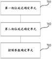
本申请实施例还提供一种确定抵消支路的控制参数的装置,其包括:第一相位延迟确定单元、第二相位延迟确定单元、控制参数确定单元,其中:The embodiment of the present application further provides an apparatus for determining a control parameter of an offset branch, which includes: a first phase delay determining unit, a second phase delay determining unit, and a control parameter determining unit, where:
在向抵消支路输入第一恒定信号且向自电容检测支路输入第一激励信号时,所述自电容检测支路的后端处理电路对所述抵消支路的输出信号和所述自电容检测支路的输出信号至少进行差分处理得到第一输出信号,所述第一相位延迟确定单元用于根据所述第一输出信号确定自电容检测支路以及所述自电容检测支路的后端处理电路对第一激励信号响应时产生的相位延迟总和;When a first constant signal is input to the cancellation branch and a first excitation signal is input to the self-capacitance detection branch,The back-end processing circuit of the self-capacitance detecting branch performs at least differential processing on an output signal of the canceling branch and an output signal of the self-capacitance detecting branch to obtain a first output signal, the first phase delay determining unit And determining, according to the first output signal, a sum of phase delays generated when the self-capacitance detection branch and the back-end processing circuit of the self-capacitance detection branch respond to the first excitation signal;
在向所述自电容检测支路输入第二恒定信号且向所述抵消支路输入第二激励信号时,所述自电容检测支路的后端处理电路对所述抵消支路的输出信号和所述自电容检测支路的输出信号至少进行差分处理得到第二输出信号,第二相位延迟确定单元用于以及根据第二输出信号确定所述后端处理电路对第二激励信号响应时产生的相位延迟;And outputting a second constant signal to the self-capacitance detecting branch and inputting a second excitation signal to the canceling branch, the output signal of the back-end processing circuit of the self-capacitance detecting branch to the canceling branch The output signal of the self-capacitance detecting branch is at least differentially processed to obtain a second output signal, and the second phase delay determining unit is configured to determine, according to the second output signal, the response generated by the back-end processing circuit in response to the second excitation signal Phase delay
所述控制参数确定单元用于根据所述相位延迟总和以及所述后端处理电路对所述第二激励信号响应时产生的相位延迟,确定所述抵消支路的控制参数。The control parameter determining unit is configured to determine a control parameter of the canceling branch according to the phase delay sum and a phase delay generated by the back end processing circuit in response to the second excitation signal.
本申请实施例还提供一种触控检测装置,其包括:自电容检测支路、抵消支路、后端处理电路及上述所述的确定抵消支路的控制参数的装置,所述自电容检测支路与系统地之间形成待检测自电容,所述抵消支路用于根据确定出的控制参数至少抵消所述待检测自电容的原始基准值;所述后端处理电路用于对所述自电容检测支路以及所述抵消支路的输出信号至少进行差分处理以实现触控检测。The embodiment of the present application further provides a touch detection device, including: a self-capacitance detection branch, an offset branch, a back-end processing circuit, and the above-mentioned device for determining a control parameter of an offset branch, the self-capacitance detection Forming a self-capacitance to be detected between the branch and the system ground, the canceling branch is configured to offset at least the original reference value of the self-detecting self-capacitance according to the determined control parameter; the back-end processing circuit is configured to The self-capacitance detection branch and the output signal of the cancellation branch are at least differentially processed to implement touch detection.
本申请实施例中,通过向抵消支路输入第一恒定信号,且向自电容检测支路输入第一激励信号,对应地,所述自电容检测支路的后端处理电路对所述抵消支路的输出信号和所述自电容检测支路的输出信号至少进行差分处理得到第一输出信号;根据所述第一输出信号确定自电容检测支路以及所述自电容检测支路的后端处理电路对第一激励信号响应时产生的相位延迟总和;向所述自电容检测支路输入第二恒定信号,且向所述抵消支路输入第二激励信号,对应地,所述自电容检测支路的后端处理电路对所述抵消支路的输出信号和所述自电容检测支路的输出信号至少进行差分处理得到第二输出信号;根据第二输出信号确定所述后端处理电路对第二激励信号响应时产生的相位延迟;根据所述相位延迟总和以及所述后端处理电路对所述第二激励信号响应时产生的相位延迟,确定所述抵消支路的控制参数,以至少抵消或者减小了待检测自电容的原始基准值,提高了自电容的电容值的变化量或者变化率,可增加触控检测的准确率,进一步地,还可以提高检测自耦电容的性能,从而提高了用户体验。In the embodiment of the present application, by inputting a first constant signal to the cancellation branch and inputting a first excitation signal to the self-capacitance detection branch, correspondingly, the back-end processing circuit of the self-capacitance detection branch pairs the offset branch The output signal of the path and the output signal of the self-capacitance detection branch are at least differentially processed to obtain a first output signal; determining, according to the first output signal, a self-capacitance detection branch and a back end processing of the self-capacitance detection branch And summing a phase delay generated by the circuit in response to the first excitation signal; inputting a second constant signal to the self-capacitance detection branch, and inputting a second excitation signal to the cancellation branch, correspondingly, the self-capacitance detection branch The back end processing circuit of the circuit performs at least differential processing on the output signal of the canceling branch and the output signal of the self-capacitance detecting branch to obtain a second output signal; determining, according to the second output signal, the back end processing circuit pair a phase delay generated when the excitation signal is responsive; generating according to the sum of the phase delays and the response of the back end processing circuit to the second excitation signal The phase delay determines the control parameter of the cancellation branch to at least cancel or reduce the original reference value of the self-capacitance to be detected, and increases the variation or rate of change of the capacitance value of the self-capacitance, thereby increasing the accuracy of the touch detection. In addition, the performance of the detection of the auto-coupling capacitor can be improved, thereby improving the user experience.
后文将参照附图以示例性而非限制性的方式详细描述本申请实施例的一些具体实施例。附图中相同的附图标记标示了相同或类似的部件或部分。本领域技术人员应该理解,这些附图未必是按比例绘制的。附图中:Some specific embodiments of the embodiments of the present application will be described in detail, by way of example, and not limitation, The same reference numbers in the drawings identify the same or similar parts. Those skilled in the art should understand that the drawings are not necessarily drawn to scale. In the figure:
图1为本申请实施例一种触控检测装置的结构示意图;1 is a schematic structural diagram of a touch detection apparatus according to an embodiment of the present application;
图2为本申请实施例二中确定抵消支路的控制参数的方法流程示意图;2 is a schematic flowchart of a method for determining control parameters of an offset branch in Embodiment 2 of the present application;
图3为本申请实施例三中执行步骤S101时图1的电路结构动态示意图;3 is a schematic diagram showing the dynamic structure of the circuit of FIG. 1 when step S101 is performed in Embodiment 3 of the present application;
图4为本申请实施例四中步骤S102的示例性示意图;4 is an exemplary schematic diagram of step S102 in Embodiment 4 of the present application;
图5为本申请实施例五中执行步骤S103时图1的电路结构动态示意图;5 is a schematic diagram showing the dynamic structure of the circuit of FIG. 1 when step S103 is performed in Embodiment 5 of the present application;
图6为本申请实施例六中步骤S104的示例性示意图;FIG. 6 is an exemplary schematic diagram of step S104 in Embodiment 6 of the present application;
图7为本申请实施例七中确定抵消支路的控制参数的装置结构示意图。FIG. 7 is a schematic structural diagram of an apparatus for determining control parameters of an offset branch in Embodiment 7 of the present application.
实施本发明实施例的任一技术方案必不一定需要同时达到以上的所有优点。Any technical solution for implementing the embodiments of the present invention necessarily does not necessarily need to achieve all of the above advantages at the same time.
为了使本领域的人员更好地理解本发明实施例中的技术方案,下面将结合本发明实施例中的附图,对本发明实施例中的技术方案进行清楚、完整地描述,显然,所描述的实施例仅是本发明实施例一部分实施例,而不是全部的实施例。基于本发明实施例中的实施例,本领域普通技术人员所获得的所有其他实施例,都应当属于本发明实施例保护的范围。For a better understanding of the technical solutions in the embodiments of the present invention, the technical solutions in the embodiments of the present invention will be clearly and completely described in conjunction with the accompanying drawings in the embodiments of the present invention. The embodiments are only a part of the embodiments of the embodiments of the invention, and not all of the embodiments. All other embodiments obtained by those skilled in the art should be within the scope of protection of the embodiments of the present invention based on the embodiments in the embodiments of the present invention.
下面结合本发明实施例附图进一步说明本发明实施例具体实现。The specific implementation of the embodiments of the present invention is further described below in conjunction with the accompanying drawings.
图1为本申请实施例一种触控检测装置的结构示意图;如图1所示,其具体包括:自电容检测支路、抵消支路、后端处理电路以及以下述图7中的确定抵消支路的控制参数的装置(图1中未示出),所述自电容检测支路与系统地之间形成待检测自电容,所述抵消支路用于根据确定出的控制参数抵消或减小所述待检测自电容的原始基准值;所述后端处理电路用于对所述自电容检测支路以及所述抵消支路的输出信号至少进行差分处理以实现触控检测。FIG. 1 is a schematic structural diagram of a touch detection apparatus according to an embodiment of the present invention; as shown in FIG. 1 , the method specifically includes: a self-capacitance detection branch, an offset branch, a back-end processing circuit, and offset by the determination in FIG. 7 described below. a device for controlling parameters of the branch (not shown in FIG. 1), a self-capacitance to be detected is formed between the self-capacitance detecting branch and the system ground, and the canceling branch is used for offsetting or subtracting according to the determined control parameter The original reference value of the self-capacitance to be detected is small; the back-end processing circuit is configured to perform at least differential processing on the output signals of the self-capacitance detection branch and the cancellation branch to implement touch detection.
具体地,本实施例中,自电容检测支路包括:电阻R0、前端RC网络的电阻R以及待检测自电容C,前端RC网络也包括待检测自电容C。电阻R0具体比如为触控芯片或者其他芯片的输出阻抗。Specifically, in this embodiment, the self-capacitance detection branch includes: a resistor R0, a resistor R of the front-end RC network, and a self-capacitance C to be detected, and the front-end RC network also includes a self-capacitance C to be detected. The resistor R0 is specifically, for example, an output impedance of a touch chip or other chip.
具体地,本实施例中,抵消支路包括:电阻R1、及由可调电阻R_cancle和可调电容C_cancle形成的抵消支路(又称cancle电路),可调电阻R_cancle和可调电容C_cancle可以根据需求进行数值大小的调整,以抵消或者减小自电容检测支路中前端RC网络的电阻R、所述待检测自电容的原始基准值。这里,抵消或者减小可以理解为两种可能,可调电阻R_cancle抵消或者减小前端RC网络的电阻R,可调电容C_cancle抵消或者减小所述待检测自电容的原始基准值,或者,可调电阻R_cancle和可调电容C_cancle作为整体、前端RC网络的电阻R、所述待检测自电容的原始基准值作为整体,这两个整体之间形成抵消或者减小关系。Specifically, in this embodiment, the offset branch includes: a resistor R1, and an offset branch formed by the adjustable resistor R_cancle and the adjustable capacitor C_cancle (also referred to as a cancle circuit), and the adjustable resistor R_cancle and the adjustable capacitor C_cancle can be The value is adjusted to offset or reduce the resistance R of the front-end RC network in the self-capacitance detection branch, and the original reference value of the self-capacitance to be detected. Here, the cancellation or reduction can be understood as two possibilities. The adjustable resistor R_cancle cancels or reduces the resistance R of the front-end RC network, and the adjustable capacitor C_cancle cancels or reduces the original reference value of the self-capacitance to be detected, or The adjustment resistor R_cancle and the adjustable capacitor C_cancle as a whole, the resistance R of the front end RC network, and the original reference value of the self-capacitance to be detected as a whole, form an offset or decrease relationship between the two.
需要说明的是,本实施例中,待检测自电容的原始基准值比如为触控检测装置出厂时自电容检测支路与系统地之间形成的电容值。由于工艺或者环境或者人为因素,不同自电容检测支路与系统地之间形成的电容值可能存在差异,因此,起到所述抵消或者减小目的的可调电阻R_cancle和可调电容C_cancle的值也可以不同。It should be noted that, in this embodiment, the original reference value of the self-capacitance to be detected is, for example, a capacitance value formed between the self-capacitance detection branch and the system ground when the touch detection device is shipped. Due to the process or environment or human factors, the capacitance values formed between the different self-capacitance detection branches and the system ground may be different. Therefore, the values of the adjustable resistor R_cancle and the adjustable capacitor C_cancle for the purpose of cancellation or reduction are It can also be different.
具体地,本实施例中,所述后端处理电路包括:放大器、滤波器、模数转换器(Analog-to-Digital Converter,简称ADC),所述放大器用于对自检测支路的输出信号和抵消支路的输出信号进行差分处理,所述滤波器用于进一步对差分处理后的信号进行滤波处理,所述模数转换器用于对滤波后的信号进行模数转换处理。Specifically, in this embodiment, the back-end processing circuit includes: an amplifier, a filter, and an analog-to-digital converter (ADC), and the amplifier is used to output an output signal of the self-detection branch. And performing differential processing on the output signal of the canceling branch, wherein the filter is further configured to perform filtering processing on the differentially processed signal, and the analog-to-digital converter is configured to perform analog-to-digital conversion processing on the filtered signal.
具体地,放大器可以为可编程增益放大器(Programble Gain Amplifier,简称PGA),滤波器具体可以为抗混叠滤波器(Anti-alias Filter,简称AAF)。所述后端处理电路中各个电路进行信号处理的先后顺序比如为:先进行差分处理,再进行滤波处理,最后进行模数转换处理。但是,这里的信号处理顺序仅仅是示例,并非唯一性限定。Specifically, the amplifier may be a Programble Gain Amplifier (PGA), and the filter may be an Anti-alias Filter (AAF). The sequence of signal processing by each circuit in the back-end processing circuit is, for example, first performing differential processing, then performing filtering processing, and finally performing analog-to-digital conversion processing. However, the order of signal processing herein is merely an example and is not a limitation.
本实施例中,自电容检测支路、抵消支路的输出信号输入到所述后端处理电路中至少进行差分处理,以使得抵消支路抵消或者减小所述自电容检测支路中待检测自电容的原始基准值。In this embodiment, the output signals of the self-capacitance detection branch and the cancellation branch are input to the back-end processing circuit for at least differential processing, so that the offset branch cancels or reduces the to-be-detected in the self-capacitance detection branch. The original reference value of the self capacitance.
在图1所示的实施例中,为了与自电容检测支路形成对称的结构,在抵消支路中设置了电阻R1,以与自电容检测支路中的电阻R0对应。但是,需要说的是,由于在抵消支路中存在可调电阻,因此,在其他实施例中抵消支路中也可以不用设置电阻R1。In the embodiment shown in FIG. 1, in order to form a symmetrical structure with the self-capacitance detecting branch, a resistor R1 is provided in the canceling branch to correspond to the resistor R0 in the self-capacitance detecting branch. However, it should be noted that since there is an adjustable resistance in the offset branch, the resistor R1 may not be provided in the offset branch in other embodiments.
结合上述图1所示的触控检测装置示意图,下述实施例对本申请中如何确定抵消支路的控制参数进行示例性说明。In combination with the above-described schematic diagram of the touch detection device shown in FIG. 1, how the following embodiments are true in the present applicationThe control parameters of the offset branch are exemplified.
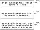
图2为本申请实施例二中确定抵消支路的控制参数的方法流程示意图;对于任一自电容检测支路来说,如图2所示,其包括如下步骤S101-S105:2 is a schematic flowchart of a method for determining a control parameter of an offset branch in the second embodiment of the present application; for any self-capacitance detection branch, as shown in FIG. 2, the method includes the following steps S101-S105:
S101、向抵消支路输入第一恒定信号,且向自电容检测支路输入第一激励信号,对应地,所述自电容检测支路的后端处理电路对所述抵消支路的输出信号和所述自电容检测支路的输出信号至少进行差分处理得到第一输出信号;S101. Input a first constant signal to the cancellation branch, and input a first excitation signal to the self-capacitance detection branch. Correspondingly, the output signal of the cancellation circuit of the back-end processing circuit of the self-capacitance detection branch is The output signal of the self-capacitance detecting branch is at least differentially processed to obtain a first output signal;
本实施例中,所述第一恒定信号为第一直流偏置信号,比如该第一直流偏置信号的值等于在触控检测时使用的激励信号的均值Vcmi。所述第一激励信号TX1具有设定的频率和相位,比如频率为ω,相位为0。In this embodiment, the first constant signal is a first DC bias signal, for example, the value of the first DC bias signal is equal to an average value Vcmi of the excitation signal used in touch detection. The first excitation signal TX1 has a set frequency and phase, such as a frequency of ω and a phase of zero.
图3为本申请实施例三中执行步骤S101时图1的电路结构动态示意图;如图3所示,向抵消支路输入第一恒定信号(如激励信号的均值Vcmi),同时向所述自电容检测支路输入频率为w、起始相位为0的第一激励信号TX1。3 is a schematic diagram showing the dynamic structure of the circuit of FIG. 1 when step S101 is performed in the third embodiment of the present application; as shown in FIG. 3, a first constant signal (such as the mean value Vcmi of the excitation signal) is input to the canceling branch, and the The self-capacitance detection branch inputs a first excitation signal TX1 having a frequency of w and a starting phase of zero.
S102、根据所述第一输出信号确定所述自电容检测支路以及所述自电容检测支路的后端处理电路对第一激励信号TX1响应时产生的相位延迟总和;S102. Determine, according to the first output signal, a sum of phase delays generated when the self-capacitance detection branch and the back-end processing circuit of the self-capacitance detection branch respond to the first excitation signal TX1;
本实施例中,步骤S102中在根据所述第一输出信号确定所述自电容检测支路以及所述自电容检测支路的后端处理电路对第一激励信号响应时产生的相位延迟总和时,具体可以根据所述第一输出信号的幅值和相位,确定所述自电容检测支路以及所述后端处理电路对所述第一激励信号响应时产生的相位延迟总和。In this embodiment, in step S102, when the self-capacitance detection branch and the back-end processing circuit of the self-capacitance detection branch respond to the first excitation signal, the phase delay sum is generated according to the first output signal. Specifically, determining, according to the amplitude and phase of the first output signal, a sum of phase delays generated by the self-capacitance detection branch and the back-end processing circuit in response to the first excitation signal.
对应地,上述步骤S102可具体包括步骤S112和步骤S132,具体如图4所示,为本申请实施例四中步骤S102的示例性示意图:Correspondingly, the foregoing step S102 may specifically include step S112 and step S132. Specifically, as shown in FIG. 4, it is an exemplary schematic diagram of step S102 in the fourth embodiment of the present application:
S112、对所述第一输出信号进行解调积分处理得到第一同相信号和第一正交信号;S112. Perform demodulation integration processing on the first output signal to obtain a first in-phase signal and a first orthogonal signal.
本实施例中,参见上述图3所示,第一激励信号TX1经过自电容检测电路处理后再与第一恒定信号依次经过后端处理电路中的放大器进行差分放大、滤波器的滤波处理、模数转换器的模数转换处理,从而得到第一输出信号。In this embodiment, as shown in FIG. 3 above, the first excitation signal TX1 is processed by the self-capacitance detection circuit, and then sequentially amplified by the amplifier in the back-end processing circuit with the first constant signal, and the filter processing and the mode of the filter are performed. The analog to digital conversion process of the digital converter results in a first output signal.
本实施例中,经过所述后端处理电路处理得到第一输出信号,所述第一输出信号经过解调积分处理之后得到两路正交的信号即:第一同相(In-phase)信号(又记为第一I信号:I1)以及第一正交(Quadrature)信号(又记为第一Q信号:Q1)。In this embodiment, the first output signal is processed by the back-end processing circuit, and the first output signal is subjected to demodulation integration processing to obtain two orthogonal signals: a first in-phase signal. (also referred to as the first I signal: I1 ) and the first quadrature signal (also referred to as the first Q signal: Q1 ).
S122、根据所述第一同相信号和所述第一正交信号,确定所述第一输出信号的幅值和相位;S122. Determine, according to the first in-phase signal and the first orthogonal signal, a magnitude and a phase of the first output signal.
S132、根据所述第一输出信号的幅值和相位,确定所述自电容检测支路以及所述后端处理电路对所述第一激励信号响应时产生的相位延迟总和。S132. Determine, according to the amplitude and phase of the first output signal, a sum of phase delays generated by the self-capacitance detection branch and the back-end processing circuit in response to the first excitation signal.
本实施例中,假设第一激励信号TX1经过自电容检测直流中前端RC网络(即由R0+R,C组成的RC网络)后的相位延迟为


S103、向所述自电容检测支路输入第二恒定信号,且向所述抵消支路输入第二激励信号,对应地,所述自电容检测支路的后端处理电路对所述抵消支路的输出信号和所述自电容检测支路的输出信号至少进行差分处理得到第二输出信号;S103. Input a second constant signal to the self-capacitance detection branch, and input a second excitation signal to the cancellation branch. Correspondingly, the back-end processing circuit of the self-capacitance detection branch pairs the offset branch And outputting the output signal of the self-capacitance detection branch to at least differential processing to obtain a second output signal;
本实施例中,所述第二恒定信号为第二直流偏置信号,比如该第二直流偏置信号的值同样等于在触控检测时使用的激励信号的均值,换言之,第一恒定信号和所述第二恒定信号之间可以相互复用。所述第二激励信号TX2具有设定的频率和起始相位,比如与第一激励信号TX1的频率同为w,起始相位同为0。In this embodiment, the second constant signal is a second DC bias signal, for example, the value of the second DC bias signal is also equal to the average value of the excitation signal used in the touch detection, in other words, the first constant signal and The second constant signals may be multiplexed with each other. The second excitation signal TX2 has a set frequency and a starting phase, for example, the frequency of the first excitation signal TX1 is w, and the initial phase is 0.
本实施例中,优选第一激励信号TX1和第二激励信号TX2的频率和起始相位分别相同,以使得上述相关步骤中在确定所述相位延迟和、所述相位延迟时时,本质上相当于基于同一属性的激励信号,从而节省数据处理的计算量。In this embodiment, it is preferable that the frequency and the initial phase of the first excitation signal TX1 and the second excitation signal TX2 are respectively the same, so that when the phase delay and the phase delay are determined in the correlation step, the equivalent is substantially equivalent. The excitation signal is based on the same attribute, thereby saving the calculation amount of data processing.
另外,为了进一步节省数据处理的计算量,或者降低数据计算的复杂度,第一激励信号TX1和第二激励信号TX2的起始相位优选为0。In addition, in order to further save the calculation amount of data processing or reduce the complexity of data calculation, the initial phase of the first excitation signal TX1 and the second excitation signal TX2 is preferably 0.
当然,在其他实施例中,第一激励信号TX1和第二激励信号TX2的频率和起始相位也可以不同。Of course, in other embodiments, the frequency and the starting phase of the first excitation signal TX1 and the second excitation signal TX2 may also be different.
图5为本申请实施例五中执行步骤S103时图1的电路结构动态示意图;如图5所示,向自电容检测支路输入第二恒定信号(如激励信号的均值Vcmi),同时向所述抵消支路输入频率为ω、起始相位为0的第二激励信号TX2。5 is a schematic diagram showing the dynamic structure of the circuit of FIG. 1 when step S103 is performed in the fifth embodiment of the present application; as shown in FIG. 5, a second constant signal (such as the mean value of the excitation signal Vcmi ) is input to the self-capacitance detection branch, and The canceling branch input frequency is ω, and the starting phase is 0, the second excitation signal TX2.
另外,在步骤S103中,为了确定后端处理电路导致的相位延迟,将所述抵消支路中RC网络设置成近似纯阻抗网络或者纯阻抗网络,从而避免了抵消支路中RC网络导致相位延迟的产生。比如,可以通过将抵消支路中RC网络中的可调电阻和可调电容调整成最小值,以实现将所述抵消支路中RC网络设置成近似纯阻抗网络。In addition, in step S103, in order to determine the phase delay caused by the back-end processing circuit, the RC network in the cancellation branch is set to be an approximately pure impedance network or a pure impedance network, thereby avoiding phase delay caused by the RC network in the cancellation branch. The production. For example, the RC network in the cancellation branch can be set to an approximately pure impedance network by adjusting the adjustable resistance and the adjustable capacitance in the RC network in the cancellation branch to a minimum value.
S104、根据第二输出信号确定所述后端处理电路在对所述第二激励信号TX2响应时产生的相位延迟;S104. Determine, according to the second output signal, a phase delay generated by the backend processing circuit when responding to the second excitation signal TX2.
本实施例中,步骤S104中在根据第二输出信号确定所述后端处理电路在对所述第二激励信号TX2响应时产生的相位延迟时,可以根据第二输出信号的幅值和相位确定所述后端处理电路对所述第二激励信号响应时产生的相位延迟。In this embodiment, when the phase delay generated by the back-end processing circuit in response to the second excitation signal TX2 is determined according to the second output signal, the amplitude and phase of the second output signal may be determined according to the second output signal. The phase delay generated by the back end processing circuit in response to the second excitation signal.
具体地,本实施例中,步骤S104具体可以包括S114和步骤S134,如图6所示,为本申请实施例六中步骤S104的示例性示意图:Specifically, in this embodiment, step S104 may specifically include S114 and step S134, as shown in FIG. 6, which is an exemplary schematic diagram of step S104 in Embodiment 6 of the present application:
S114、对所述第二输出信号进行解调积分处理得到第二同相信号和第二正交信号;S114. Perform demodulation integration processing on the second output signal to obtain a second in-phase signal and a second orthogonal signal.
本实施例中,参见上述图5所示,第二激励信号TX2经过抵消支路处理后再与第二恒定信号依次经过后端处理电路中的放大器进行差分放大、滤波器的滤波处理、模数转换器的模数转换处理,从而得到第二输出信号。In this embodiment, as shown in FIG. 5 above, the second excitation signal TX2 is subjected to the offset branch processing and then sequentially subjected to differential amplification with the second constant signal through the amplifier in the back-end processing circuit, filtering processing of the filter, and modulus. The analog to digital conversion process of the converter results in a second output signal.
需要说明的是,由于在本实施例中,抵消支路中的RC网络近似为纯阻抗网络,因此,从是否导致的相位延迟的角度来看,不会对第二激励信号TX2造成相位延迟,而仅有后端处理电路对第二激励信号TX2造成了相位延迟。纯阻抗网络处理起来是最简单,工程实践会这样去做。实际上,由于R1R_cancel和C_cancel是可知,可以计算出第二输出信号的相位及幅值,依旧可以处理。下面的实例仍以最简单的纯阻抗网络举例。It should be noted that, in this embodiment, the RC network in the offset branch is approximately a pure impedance network, so that the phase delay is not caused to the second excitation signal TX2 from the perspective of the phase delay caused. Only the back end processing circuit causes a phase delay to the second excitation signal TX2. Pure impedance networks are the easiest to handle, and engineering practices do the same. In fact, since R1R_cancel and C_cancel are known, the phase and amplitude of the second output signal can be calculated and still processed. The following examples are still exemplified by the simplest pure impedance network.
S124、根据所述第二同相信号和第二正交信号,确定所述第二输出信号的幅值和相位。S124. Determine a magnitude and a phase of the second output signal according to the second in-phase signal and the second quadrature signal.
S134、根据第二输出信号的幅值和相位确定所述后端处理电路对所述第二激励信号响应时产生的相位延迟。S134. Determine a phase delay generated by the backend processing circuit in response to the second excitation signal according to a magnitude and a phase of the second output signal.
本实施例中,所述第二输出信号经过解调积分处理之后得到两路正交的信号即:第二同相(In-phase)信号(又记为第二I信号:I2)以及第二正交(Quadrature)信号(又记为第二Q信号:Q2)。通过所述第二同相信号和第二正交信号反应自电容检测支路以及后端处理电路对第一激励信号TX1的幅值和相位的影响。In this embodiment, the second output signal is subjected to demodulation integration processing to obtain two orthogonal signals: a second in-phase signal (also referred to as a second I signal: I2 ) and a second Quadrature signal (also referred to as second Q signal: Q2 ). The effects of the self-capacitance detection branch and the back-end processing circuit on the amplitude and phase of the first excitation signal TX1 are reflected by the second in-phase signal and the second quadrature signal.
调节可调电阻R_cancel和可调电容C_cancel到最小值,让抵消支路中的RC网络尽可能近似为纯阻抗网络,这样等效认为后端处理电路中的放大器、滤波器导致了相位延时


S105、根据所述自电容检测支路以及后端处理电路导致的相位延迟总和以及所述后端处理电路导致的相位延迟,确定所述抵消支路的控制参数。S105. Determine a control parameter of the cancellation branch according to a sum of phase delays caused by the self-capacitance detection branch and the back-end processing circuit and a phase delay caused by the back-end processing circuit.
本实施例中,如前所述,所述抵消支路实际上包括可调电阻和可调电容,对应地,抵消支路的控制参数包括可调电阻的值以及可调电容的值,通过调整可调电阻和可调电容的大小,从而抵消或者减小所述自电容检测支路中前端RC网络的电阻和待检测自电容的原始基准值。In this embodiment, as described above, the offset branch actually includes an adjustable resistor and a tunable capacitor. Correspondingly, the control parameters of the offset branch include the value of the adjustable resistor and the value of the adjustable capacitor. The adjustable resistor and the adjustable capacitor are sized to cancel or reduce the resistance of the front end RC network in the self-capacitance detection branch and the original reference value of the self-capacitance to be detected.
本实施例中,步骤S105具体可以包括如下步骤S115至S125:In this embodiment, step S105 may specifically include the following steps S115 to S125:
S115、根据所述相位延迟总和以及所述后端处理电路对所述第二激励信号响应产生的相位延迟,确定所述自电容检测支路对所述第一激励信号响应时产生的相位延迟;S115. Determine, according to the sum of the phase delays and a phase delay generated by the backend processing circuit in response to the second excitation signal, a phase delay generated when the self-capacitance detection branch responds to the first excitation signal;
S125、根据所述自电容检测支路对所述第一激励信号响应时产生的相位延迟,确定所述抵消支路的控制参数。S125. Determine a control parameter of the cancellation branch according to a phase delay generated when the self-capacitance detection branch responds to the first excitation signal.
具体地,本实施例中,步骤S125中确定所述抵消支路的控制参数可以包括:Specifically, in this embodiment, determining the control parameters of the cancellation branch in step S125 may include:
根据所述自电容检测支路对所述第一激励信号响应时产生的相位延迟,建立所述自电容检测支路中前端RC网络与所述抵消支路中RC网络的关联关系;And establishing, according to a phase delay generated by the self-capacitance detection branch in response to the first excitation signal, establishing an association relationship between a front-end RC network in the self-capacitance detection branch and an RC network in the cancellation branch;
根据所述自电容检测支路中前端RC网络与所述抵消支路中RC网络的关联关系,确定所述抵消支路的控制参数。Determining a control parameter of the offset branch according to an association relationship between the front end RC network in the self-capacitance detection branch and the RC network in the offset branch.
进一步地,所述抵消支路的控制参数包括第一控制参数和第二控制参数,对应地,根据所述自电容检测支路中前端RC网络与所述抵消支路中RC网络的关联关系,确定所述抵消支路的控制参数包括:根据所述自电容检测支路中前端RC网络与所述抵消支路中RC网络的关联关系,以及预置所述抵消支路的第一控制参数,确定所述抵消支路的第二控制参数。Further, the control parameter of the offset branch includes a first control parameter and a second control parameter, and correspondingly, according to the relationship between the front end RC network in the self-capacitance detection branch and the RC network in the offset branch, Determining, by the self-capacitance detection branch, a control relationship between the front end RC network and the RC network in the offset branch, and presetting a first control parameter of the offset branch, A second control parameter of the cancellation branch is determined.
可选地,在本申请的任一实施例中,预置所述抵消支路中的第一控制参数位于设定的数值范围,所述设定的数值范围根据待检测自电容的原始基准值的经验值确定。比如,通过对不同工艺、不同环境下的触控检测装置中的原始基准值进行统计汇总,确定出所述经验值。Optionally, in any embodiment of the present application, the first control parameter preset in the cancellation branch is located in a set value range, and the set value range is determined according to an original reference value of the self-capacitance to be detected. The experience value is determined. For example, the empirical value is determined by statistically summarizing original reference values in touch detection devices in different processes and environments.
结合上述公式(1)、(2)对步骤S105做进一步示例性解释。The step S105 is further exemplarily explained in conjunction with the above formulas (1) and (2).
根据上述公式(1)和(2)得到如下公式(3):According to the above formulas (1) and (2), the following formula (3) is obtained:

由上述公式(3)可见,通过所述相位延迟和


另外,自电容检测通路上前端RC网络导致的相位延迟

根据上述公式(3)和(4)得到如下公式(5):According to the above formulas (3) and (4), the following formula (5) is obtained:

参照上述公式(5)可见,通过上述步骤中得到了第一I信号I1、第一Q信号Q1、第二I信号I2、第二Q信号Q2,同时频率ω也是已知的,从而可以计算得到一个常数值const。Referring to the above formula (5), it can be seen that the first I signal I1 , the first Q signal Q1 , the second I signal I2 , and the second Q signal Q2 are obtained through the above steps, and the frequency ω is also known. Thus a constant value const can be calculated.
对于自电容检测支路和抵消支路来说,其对应电阻和电容乘积即RC参数均等于上述常数值const。即根据第一I信号I1、第一Q信号Q1、第二I信号I2、第二Q信号Q2、频率ω计算得到该常数值,通过所述常数值建立了所述自电容检测支路中前端RC网络与所述抵消支路中RC网络的关联关系,进而根据所述关联关系确定抵消支路中满足可用于抵消或者减小电阻R和待检测自电容的原始基准值的可调电阻和可调电容的值。For the self-capacitance detection branch and the cancellation branch, the corresponding resistance and capacitance product, that is, the RC parameter, is equal to the above constant value const. That is, the constant value is calculated according to the first I signal I1 , the first Q signal Q1 , the second I signal I2 , the second Q signal Q2 , and the frequency ω, and the self-capacitance detection is established by the constant value. Correlating relationship between the front end RC network in the branch circuit and the RC network in the offset branch, and determining, according to the association relationship, that the offset reference branch satisfies an original reference value that can be used to cancel or reduce the resistance R and the self-capacitance to be detected. Adjust the value of the resistor and the adjustable capacitor.
在上述公式(5)中,由于电阻R和电阻R0的电阻值已知,而电阻R1的电阻值已知,可调电阻R_cancle和C_cancle的可调档位已知,因此,只要可调电阻R_cancle和C_cancle的值使得电阻R和电阻R0加和后与待检测自电容的原始基准值乘积(即C(R+R0))等于电阻R0和可调电阻R_cancle加和后与可调电容C_cancle的乘积(即(R1+R_cancel)C_cancel)相等即可。In the above formula (5), since the resistance values of the resistor R and the resistor R0 are known, and the resistance value of the resistor R1 is known, the adjustable gears of the adjustable resistors R_cancle and C_cancle are known, and therefore, as long as the adjustable resistor R_cancle And the value of C_cancle is such that the product of the original reference value of the self-capacitance to be detected after the addition of the resistor R and the resistor R0 (ie, C(R+R0 )) is equal to the sum of the resistor R0 and the adjustable resistor R_cancle and the adjustable capacitor C_cancle The product (ie (R1+R_cancel)C_cancel) is equal.
进一步地,在具体实施时,可以通过上述步骤分别得到计算得到一个常数值const,再通过档位选择设定一个可调电容C_cancle的值,再选择一个与通过公式(5)计算得到的可调电容R_cancle的理论值最接近的值,从而确定出上述抵消支路中的控制参数。Further, in a specific implementation, a constant value const can be obtained by the above steps, and then a value of the adjustable capacitor C_cancle is set by the gear selection, and then an adjustable one is obtained by calculating the formula (5). The theoretical value of the capacitance R_cancle is the closest value to determine the control parameters in the above-mentioned offset branch.
如前所述,由于在实际情况中,待检测自电容的原始基准值虽然由于工艺或者环境会有不同,但是,其基本上会处于可预知的数值范围内,因此,在选择可调电容C_cancle时,考虑到可调电容C_cancle与待检测自电容在电路上的对称性,可以结合该数值范围进行选择,从而进一步缩减数据处理,从而可至少抵消或者减小待检测自电容的原始基准值的同时,并进一步提高检测自耦电容的性能。As mentioned above, since the original reference value of the self-capacitance to be detected may be different in the process or environment due to the actual situation, it is basically in a predictable value range. Therefore, the adjustable capacitor C_cancle is selected. Considering the symmetry of the adjustable capacitor C_cancle and the self-capacitance to be detected on the circuit, the value range can be selected in combination to further reduce the data processing, thereby at least canceling or reducing the original reference value of the self-capacitance to be detected. At the same time, and further improve the performance of detecting the auto-coupling capacitor.
进一步地,也可以通过查表的方式确定上述可调电阻R_cancle和可调电容C_cancle的值。具体地,比如,可以进行可调电阻R_cancle和可调电容C_cancle的值的遍历选择,并及计算(R1+R_cancel)C_cancel的值并将这些值以表格的方式存储在芯片内部。当按照上述公式(5)计算得到常数值const后,从存储的表中选择一个满足(R1+R_cancel)C_cancel的值与该常数值const最接近或者完全等于对应的可调电阻R_cancle和可调电容C_cancle的值,从而可至少抵消或者减小待检测自电容的原始基准值的同时,进一步提高检测自耦电容的性能。Further, the values of the adjustable resistor R_cancle and the adjustable capacitor C_cancle may also be determined by looking up the table. Specifically, for example, an adjustable resistor R_cancle and a tunable capacitor C_cancle can be performed.The traversal selection of the values, and the calculation of (R1 + R_cancel) C_cancel values and the values are stored in the form of a table inside the chip. After the constant value const is calculated according to the above formula (5), a value satisfying (R1+R_cancel)C_cancel is selected from the stored table to be closest to or completely equal to the corresponding adjustable resistor R_cancle and the adjustable capacitor. The value of C_cancle can at least cancel or reduce the original reference value of the self-capacitance to be detected, and further improve the performance of detecting the auto-coupling capacitor.
在其他实施例中,上述步骤S101-S104之间的时序关系仅仅是示例,在其他实施例中,上述步骤S101-S104的时序关系也可以灵活调整,比如先执行上述步骤S103、S104,再执行步骤S101、S102。In other embodiments, the timing relationship between the foregoing steps S101-S104 is only an example. In other embodiments, the timing relationship of the foregoing steps S101-S104 can also be flexibly adjusted, for example, the foregoing steps S103 and S104 are performed first, and then executed. Steps S101 and S102.
图7为本申请实施例七中确定抵消支路的控制参数的装置结构示意图;如图7所示,其包括:第一相位延迟确定单元701、第二相位延迟确定单元702、控制参数确定单元703;其中:7 is a schematic structural diagram of an apparatus for determining a control parameter of an offset branch in Embodiment 7 of the present application; as shown in FIG. 7, the method includes: a first phase
在向抵消支路输入第一恒定信号且向自电容检测支路输入第一激励信号时,所述自电容检测支路的后端处理电路对所述抵消支路的输出信号和所述自电容检测支路的输出信号至少进行差分处理得到第一输出信号,第一相位延迟确定单元701用于根据所述第一输出信号确定自电容检测支路以及所述自电容检测支路的后端处理电路对第一激励信号响应时产生的相位延迟总和;An output signal of the back-end processing circuit of the self-capacitance detecting branch to the canceling branch and the self-capacitance when a first constant signal is input to the canceling branch and a first excitation signal is input to the self-capacitance detecting branch The output signal of the detection branch is subjected to differential processing to obtain a first output signal, and the first phase
在向所述自电容检测支路输入第二恒定信号且向所述抵消支路输入第二激励信号时,所述自电容检测支路的后端处理电路对所述抵消支路的输出信号和所述自电容检测支路的输出信号至少进行差分处理得到第二输出信号,第二相位延迟确定单元702用于以及根据第二输出信号确定所述后端处理电路对第二激励信号响应时产生的相位延迟;And outputting a second constant signal to the self-capacitance detecting branch and inputting a second excitation signal to the canceling branch, the output signal of the back-end processing circuit of the self-capacitance detecting branch to the canceling branch The output signal of the self-capacitance detecting branch is at least differentially processed to obtain a second output signal, and the second phase
所述控制参数确定单元703用于根据所述相位延迟总和以及所述后端处理电路对所述第二激励信号响应时产生的相位延迟,确定所述抵消支路的控制参数。The control
在上述实施例中,通过上述实施例的技术方案抵消或者减小待检测自电容的原始基准值,提高自电容的变化率外,进一步由于电容的变化率变大,避免了后端处理单路容易达到饱和,进一步增加了检测信号的动态范围,提高了信噪比。In the above embodiment, the original reference value of the self-capacitance to be detected is offset or reduced by the technical solution of the above embodiment, and the rate of change of the self-capacitance is increased. Further, since the rate of change of the capacitance is increased, the back-end processing single channel is avoided. It is easy to achieve saturation, further increasing the dynamic range of the detection signal and improving the signal to noise ratio.
以上所描述的装置实施例仅仅是示意性的,其中所述作为分离部件说明的模块可以是或者也可以不是物理上分开的,作为模块显示的部件可以是或者也可以不是物理模块,即可以位于一个地方,或者也可以分布到多个网络模块上。可以根据实际的需要选择其中的部分或者全部模块来实现本实施例方案的目的。本领域普通技术人员在不付出创造性的劳动的情况下,即可以理解并实施。The device embodiments described above are merely illustrative, wherein the modules described as separate components may or may not be physically separate, and the components displayed as modules may or may not be physical modules, ie may be located A place, or it can be distributed to multiple network modules. Some or all of the modules may be selected according to actual needs to achieve the purpose of the solution of the embodiment.Those of ordinary skill in the art can understand and implement without deliberate labor.
通过以上的实施方式的描述,本领域的技术人员可以清楚地了解到各实施方式可借助软件加必需的通用硬件平台的方式来实现,当然也可以通过硬件。基于这样的理解,上述技术方案本质上或者说对现有技术做出贡献的部分可以以软件产品的形式体现出来,该计算机软件产品可以存储在计算机可读存储介质中,所述计算机可读记录介质包括用于以计算机(例如计算机)可读的形式存储或传送信息的任何机制。例如,机器可读介质包括只读存储器(ROM)、随机存取存储器(RAM)、磁盘存储介质、光存储介质、闪速存储介质、电、光、声或其他形式的传播信号(例如,载波、红外信号、数字信号等)等,该计算机软件产品包括若干指令用以使得一台计算机设备(可以是个人计算机,服务器,或者网络设备等)执行各个实施例或者实施例的某些部分所述的方法。Through the description of the above embodiments, those skilled in the art can clearly understand that the various embodiments can be implemented by means of software plus a necessary general hardware platform, and of course, by hardware. Based on such an understanding, portions of the above technical solutions that contribute substantially or to the prior art may be embodied in the form of a software product that may be stored in a computer readable storage medium, the computer readable record The medium includes any mechanism for storing or transmitting information in a form readable by a computer (eg, a computer). For example, a machine-readable medium includes read only memory (ROM), random access memory (RAM), magnetic disk storage media, optical storage media, flash storage media, electrical, optical, acoustic, or other forms of propagation signals (eg, carrier waves) , an infrared signal, a digital signal, etc., etc., the computer software product comprising instructions for causing a computer device (which may be a personal computer, server, or network device, etc.) to perform the various embodiments or portions of the embodiments described Methods.
最后应说明的是:以上实施例仅用以说明本申请实施例的技术方案,而非对其限制;尽管参照前述实施例对本申请进行了详细的说明,本领域的普通技术人员应当理解:其依然可以对前述各实施例所记载的技术方案进行修改,或者对其中部分技术特征进行等同替换;而这些修改或者替换,并不使相应技术方案的本质脱离本申请各实施例技术方案的精神和范围。Finally, it should be noted that the above embodiments are only used to explain the technical solutions of the embodiments of the present application, and are not limited thereto; although the present application is described in detail with reference to the foregoing embodiments, those skilled in the art should understand that The technical solutions described in the foregoing embodiments may be modified, or some of the technical features may be equivalently replaced; and the modifications or substitutions do not deviate from the spirit of the technical solutions of the embodiments of the present application. range.
本领域的技术人员应明白,本发明实施例的实施例可提供为方法、装置(设备)、或计算机程序产品。因此,本发明实施例可采用完全硬件实施例、完全软件实施例、或结合软件和硬件方面的实施例的形式。而且,本发明实施例可采用在一个或多个其中包含有计算机可用程序代码的计算机可用存储介质(包括但不限于磁盘存储器、CD-ROM、光学存储器等)上实施的计算机程序产品的形式。Those skilled in the art will appreciate that embodiments of the embodiments of the invention may be provided as a method, apparatus (device), or computer program product. Thus, embodiments of the invention may be in the form of an entirely hardware embodiment, an entirely software embodiment, or a combination of software and hardware. Moreover, embodiments of the invention may take the form of a computer program product embodied on one or more computer usable storage media (including but not limited to disk storage, CD-ROM, optical storage, etc.) including computer usable program code.
本发明实施例是参照根据本发明实施例的方法、装置(设备)和计算机程序产品的流程图和/或方框图来描述的。应理解可由计算机程序指令实现流程图和/或方框图中的每一流程和/或方框、以及流程图和/或方框图中的流程和/或方框的结合。可提供这些计算机程序指令到通用计算机、专用计算机、嵌入式处理机或其他可编程数据处理设备的处理器以产生一个机器,使得通过计算机或其他可编程数据处理设备的处理器执行的指令产生用于实现在流程图一个流程或多个流程和/或方框图一个方框或多个方框中指定的功能的装置。Embodiments of the invention are described with reference to flowchart illustrations and/or block diagrams of methods, apparatus, and computer program products according to embodiments of the invention. It will be understood that each flow and/or block of the flowchart illustrations and/or FIG. These computer program instructions can be provided to a processor of a general purpose computer, special purpose computer, embedded processor, or other programmable data processing device to produce a machine for the execution of instructions for execution by a processor of a computer or other programmable data processing device. Means for implementing the functions specified in one or more of the flow or in a block or blocks of the flow chart.
这些计算机程序指令也可存储在能引导计算机或其他可编程数据处理设备以特定方式工作的计算机可读存储器中,使得存储在该计算机可读存储器中的指令产生包括指令装置的制造品,该指令装置实现在流程图一个流程或多个流程和/或方框图一个方框或多个方框中指定的功能。The computer program instructions can also be stored in a computer readable memory that can direct a computer or other programmable data processing device to operate in a particular manner, such that the instructions stored in the computer readable memory produce an article of manufacture comprising the instruction device. The device is implemented in a flow or a flow of a flow chartThe functions specified in a block or blocks of a block and/or block diagram.
这些计算机程序指令也可装载到计算机或其他可编程数据处理设备上,使得在计算机或其他可编程设备上执行一系列操作步骤以产生计算机实现的处理,从而在计算机或其他可编程设备上执行的指令提供用于实现在流程图一个流程或多个流程和/或方框图一个方框或多个方框中指定的功能的步骤。These computer program instructions can also be loaded onto a computer or other programmable data processing device such that a series of operational steps are performed on a computer or other programmable device to produce computer-implemented processing for execution on a computer or other programmable device. The instructions provide steps for implementing the functions specified in one or more of the flow or in a block or blocks of a flow diagram.
Claims (15)
Translated fromChinesePriority Applications (4)
| Application Number | Priority Date | Filing Date | Title |
|---|---|---|---|
| PCT/CN2017/115935WO2019113837A1 (en) | 2017-12-13 | 2017-12-13 | Method for determining control parameters for offset branch, and device and touch detection device thereof |
| EP17931826.6AEP3531143B1 (en) | 2017-12-13 | 2017-12-13 | Method for determining control parameters for offset branch, and device and touch detection device thereof |
| CN201780002250.0ACN108124464B (en) | 2017-12-13 | 2017-12-13 | Method and device for determining control parameters of cancelling branch, and touch detection device |
| US16/421,477US10852888B2 (en) | 2017-12-13 | 2019-05-24 | Method and apparatus for determining control parameters of cancellation branch, and touch control detection apparatus |
Applications Claiming Priority (1)
| Application Number | Priority Date | Filing Date | Title |
|---|---|---|---|
| PCT/CN2017/115935WO2019113837A1 (en) | 2017-12-13 | 2017-12-13 | Method for determining control parameters for offset branch, and device and touch detection device thereof |
Related Child Applications (1)
| Application Number | Title | Priority Date | Filing Date |
|---|---|---|---|
| US16/421,477ContinuationUS10852888B2 (en) | 2017-12-13 | 2019-05-24 | Method and apparatus for determining control parameters of cancellation branch, and touch control detection apparatus |
Publications (1)
| Publication Number | Publication Date |
|---|---|
| WO2019113837A1true WO2019113837A1 (en) | 2019-06-20 |
Family
ID=62233657
Family Applications (1)
| Application Number | Title | Priority Date | Filing Date |
|---|---|---|---|
| PCT/CN2017/115935CeasedWO2019113837A1 (en) | 2017-12-13 | 2017-12-13 | Method for determining control parameters for offset branch, and device and touch detection device thereof |
Country Status (4)
| Country | Link |
|---|---|
| US (1) | US10852888B2 (en) |
| EP (1) | EP3531143B1 (en) |
| CN (1) | CN108124464B (en) |
| WO (1) | WO2019113837A1 (en) |
Families Citing this family (6)
| Publication number | Priority date | Publication date | Assignee | Title |
|---|---|---|---|---|
| EP3798808B1 (en) | 2019-08-01 | 2022-10-12 | Shenzhen Goodix Technology Co., Ltd. | Capacitance detection circuit, touch chip, and electronic device |
| CN112689817B (en)* | 2019-08-01 | 2023-01-24 | 深圳市汇顶科技股份有限公司 | Capacitance detection method |
| CN111289805A (en)* | 2020-03-23 | 2020-06-16 | 深圳市汇顶科技股份有限公司 | Measuring circuit |
| EP4020143B1 (en) | 2020-06-15 | 2023-05-03 | Shenzhen Goodix Technology Co., Ltd. | Coding method, coding device, and touch chip |
| CN112363634B (en)* | 2020-06-15 | 2022-05-03 | 深圳市汇顶科技股份有限公司 | Code printing method, code printing device and touch chip |
| CN113567756B (en)* | 2021-09-24 | 2021-12-07 | 深圳飞骧科技股份有限公司 | Dielectric constant measuring device based on differential oscillator |
Citations (9)
| Publication number | Priority date | Publication date | Assignee | Title |
|---|---|---|---|---|
| CN102955608A (en)* | 2011-08-09 | 2013-03-06 | 爱特梅尔公司 | Parasitic capacitive canceling in sensor interface |
| CN103713784A (en)* | 2013-04-12 | 2014-04-09 | 深圳市汇春科技有限公司 | Capacitive touch detecting circuit, device and identification method capable of preventing mistakes caused by stains |
| CN103914197A (en)* | 2013-01-07 | 2014-07-09 | 株式会社东海理化电机制作所 | Touch type input device |
| CN104020914A (en)* | 2014-06-06 | 2014-09-03 | 深圳市汇顶科技股份有限公司 | Self-capacitance touch detection circuit |
| CN104049822A (en)* | 2014-06-18 | 2014-09-17 | 深圳贝特莱电子科技有限公司 | Detection system of touch screen control circuit |
| US20150035787A1 (en)* | 2013-07-31 | 2015-02-05 | Apple Inc. | Self capacitance touch sensing |
| US20150227232A1 (en)* | 2014-02-07 | 2015-08-13 | Apple Inc. | Frequency independent offset cancellation scheme in touch receiver channel |
| CN106257387A (en)* | 2015-06-22 | 2016-12-28 | 三星电子株式会社 | Touch screen controller, touch-sensing equipment and touch-sensing method |
| CN107436703A (en)* | 2016-05-26 | 2017-12-05 | 爱特梅尔公司 | Touch sensor compensation circuit |
Family Cites Families (25)
| Publication number | Priority date | Publication date | Assignee | Title |
|---|---|---|---|---|
| US8321174B1 (en)* | 2008-09-26 | 2012-11-27 | Cypress Semiconductor Corporation | System and method to measure capacitance of capacitive sensor array |
| US8031094B2 (en)* | 2009-09-11 | 2011-10-04 | Apple Inc. | Touch controller with improved analog front end |
| US8890840B2 (en)* | 2012-04-30 | 2014-11-18 | Mediatek Inc. | Method and apparatus for using oscillation signals with different phases to detect capacitance values at capacitive sensing nodes of touch panel |
| CN103376968B (en)* | 2012-04-30 | 2016-12-28 | 联发科技股份有限公司 | Method for detecting capacitance value and corresponding touch controller |
| US20130285943A1 (en)* | 2012-04-30 | 2013-10-31 | Mediatek Inc. | Apparatus and method for executing touch controller firmware downloaded from external host to control touch panel |
| US9389256B2 (en)* | 2012-09-14 | 2016-07-12 | Stmicroelectronics Asia Pacific Pte Ltd | High signal to noise ratio capacitive sensing analog front-end |
| US9582123B2 (en)* | 2012-11-26 | 2017-02-28 | Qualcomm Incorporated | Dual-mode capacitance sensing in a touch panel sensor |
| KR101963317B1 (en)* | 2013-04-08 | 2019-03-28 | 주식회사 지2터치 | Capacitive type touch detecting means and method |
| US9001066B2 (en)* | 2013-05-06 | 2015-04-07 | Rajkumari Mohindra | PAPR optimized OFDM touch engine with tone spaced windowed demodulation |
| TWI543051B (en)* | 2013-09-18 | 2016-07-21 | 義隆電子股份有限公司 | Scanning method having adjustable sampling frequency and touch device using the same |
| WO2015178920A1 (en)* | 2014-05-22 | 2015-11-26 | Onamp Research Llc | Panel bootstrapping architectures for in-cell self-capacitance |
| TWI544743B (en)* | 2014-12-10 | 2016-08-01 | 原相科技股份有限公司 | Capacitive switch having high accuracy |
| JP2018502291A (en)* | 2014-12-12 | 2018-01-25 | コリア リサーチ インスティチュート オブ スタンダーズ アンド サイエンス | Magnetic field sensor and magnetic field measuring device |
| CN106155435B (en)* | 2015-04-07 | 2019-06-14 | 原相科技股份有限公司 | High-sensitivity capacitive touch device and operation method thereof |
| CN106249937B (en)* | 2015-06-05 | 2019-02-26 | 株式会社日本显示器 | Display device and display system with touch detection function |
| JP6175698B1 (en)* | 2015-12-28 | 2017-08-09 | 凸版印刷株式会社 | Liquid crystal display |
| WO2017214901A1 (en)* | 2016-06-15 | 2017-12-21 | 深圳市汇顶科技股份有限公司 | Pressure detection apparatus and method, touch control device and electronic terminal |
| WO2018049639A1 (en)* | 2016-09-17 | 2018-03-22 | 深圳市汇顶科技股份有限公司 | Pressure detection apparatus and intelligent terminal |
| KR102623873B1 (en)* | 2016-11-02 | 2024-01-12 | 삼성전자주식회사 | Controller of touch pannel |
| JP6667012B2 (en)* | 2016-12-21 | 2020-03-18 | アルプスアルパイン株式会社 | Capacitance detection device and input device |
| KR101908286B1 (en)* | 2017-02-23 | 2018-10-16 | (주)멜파스 | Capacitance detection method and capacitance detection apparatus using the same |
| US11531424B2 (en)* | 2017-09-07 | 2022-12-20 | Cypress Semiconductor Corporation | Nano-power capacitance-to-digital converter |
| CN107690584B (en)* | 2017-09-11 | 2020-01-03 | 深圳市汇顶科技股份有限公司 | Capacitance detection circuit, capacitance detection method, touch detection device and terminal equipment |
| US11086463B2 (en)* | 2017-09-29 | 2021-08-10 | Apple Inc. | Multi modal touch controller |
| CN107980115B (en)* | 2017-11-08 | 2021-01-29 | 深圳市汇顶科技股份有限公司 | Capacitance detection device, touch device and terminal equipment |
- 2017
- 2017-12-13WOPCT/CN2017/115935patent/WO2019113837A1/ennot_activeCeased
- 2017-12-13CNCN201780002250.0Apatent/CN108124464B/enactiveActive
- 2017-12-13EPEP17931826.6Apatent/EP3531143B1/ennot_activeNot-in-force
- 2019
- 2019-05-24USUS16/421,477patent/US10852888B2/ennot_activeExpired - Fee Related
Patent Citations (9)
| Publication number | Priority date | Publication date | Assignee | Title |
|---|---|---|---|---|
| CN102955608A (en)* | 2011-08-09 | 2013-03-06 | 爱特梅尔公司 | Parasitic capacitive canceling in sensor interface |
| CN103914197A (en)* | 2013-01-07 | 2014-07-09 | 株式会社东海理化电机制作所 | Touch type input device |
| CN103713784A (en)* | 2013-04-12 | 2014-04-09 | 深圳市汇春科技有限公司 | Capacitive touch detecting circuit, device and identification method capable of preventing mistakes caused by stains |
| US20150035787A1 (en)* | 2013-07-31 | 2015-02-05 | Apple Inc. | Self capacitance touch sensing |
| US20150227232A1 (en)* | 2014-02-07 | 2015-08-13 | Apple Inc. | Frequency independent offset cancellation scheme in touch receiver channel |
| CN104020914A (en)* | 2014-06-06 | 2014-09-03 | 深圳市汇顶科技股份有限公司 | Self-capacitance touch detection circuit |
| CN104049822A (en)* | 2014-06-18 | 2014-09-17 | 深圳贝特莱电子科技有限公司 | Detection system of touch screen control circuit |
| CN106257387A (en)* | 2015-06-22 | 2016-12-28 | 三星电子株式会社 | Touch screen controller, touch-sensing equipment and touch-sensing method |
| CN107436703A (en)* | 2016-05-26 | 2017-12-05 | 爱特梅尔公司 | Touch sensor compensation circuit |
Non-Patent Citations (1)
| Title |
|---|
| See also references ofEP3531143A4* |
Also Published As
| Publication number | Publication date |
|---|---|
| EP3531143A1 (en) | 2019-08-28 |
| US20190278424A1 (en) | 2019-09-12 |
| CN108124464B (en) | 2019-12-03 |
| US10852888B2 (en) | 2020-12-01 |
| CN108124464A (en) | 2018-06-05 |
| EP3531143B1 (en) | 2022-02-02 |
| EP3531143A4 (en) | 2019-12-25 |
Similar Documents
| Publication | Publication Date | Title |
|---|---|---|
| WO2019113837A1 (en) | Method for determining control parameters for offset branch, and device and touch detection device thereof | |
| US9071268B1 (en) | Multi-path analog front end and analog-to-digital converter for a signal processing system | |
| WO2018116706A1 (en) | Capacitance detection device and input device | |
| US20140376753A1 (en) | Crosstalk reduction in a headset | |
| US9754575B2 (en) | Area-sound reproduction system and area-sound reproduction method | |
| CN107682802B (en) | Method and device for debugging sound effect of audio equipment | |
| WO2021175267A1 (en) | Method for implementing active noise cancellation, apparatus, and electronic device | |
| CN114866716A (en) | Readout circuit, processor, noise suppression method, device and computer equipment | |
| WO2024001919A1 (en) | Method for controlling range extender, and related device | |
| US10585499B2 (en) | Device and method of detecting pointer | |
| CN108809272A (en) | Multinomial kalman filter method and filter | |
| RU2015144486A (en) | METHOD AND DEVICE FOR AUDIO PROCESSING | |
| CN117457018A (en) | Howling suppression method and howling suppression device | |
| CN109119097B (en) | Pitch detection method, device, storage medium and mobile terminal | |
| WO2019023922A1 (en) | Method for determining touch position and touch control chip | |
| US10408870B2 (en) | Capacitor sensor apparatus and sensing method thereof | |
| TWI526906B (en) | Signal processing method | |
| WO2022052064A1 (en) | Capacitance measurement circuit, touch chip, and electronic device | |
| US11888455B2 (en) | Machine learning glitch prediction | |
| CN111323652B (en) | Self-mutual capacitance detection circuit, method, chip and device | |
| KR101419433B1 (en) | Method for dynamically controlling gain of parametric equalizer according to input signal and daynamic parametric equalizer employing the same | |
| KR102309737B1 (en) | Pvdf sensor having excellent noise removal function | |
| JPH04181898A (en) | Microphone | |
| WO2018126459A1 (en) | Capacitance measurement circuit and electronic device | |
| TW201732509A (en) | Touch detection method |
Legal Events
| Date | Code | Title | Description |
|---|---|---|---|
| ENP | Entry into the national phase | Ref document number:2017931826 Country of ref document:EP Effective date:20190523 | |
| 121 | Ep: the epo has been informed by wipo that ep was designated in this application | Ref document number:17931826 Country of ref document:EP Kind code of ref document:A1 | |
| NENP | Non-entry into the national phase | Ref country code:DE |