WO2019107083A1 - Image capturing device - Google Patents
Image capturing deviceDownload PDFInfo
- Publication number
- WO2019107083A1 WO2019107083A1PCT/JP2018/041078JP2018041078WWO2019107083A1WO 2019107083 A1WO2019107083 A1WO 2019107083A1JP 2018041078 WJP2018041078 WJP 2018041078WWO 2019107083 A1WO2019107083 A1WO 2019107083A1
- Authority
- WO
- WIPO (PCT)
- Prior art keywords
- diffusion region
- region
- transistor
- imaging device
- semiconductor substrate
- Prior art date
- Legal status (The legal status is an assumption and is not a legal conclusion. Google has not performed a legal analysis and makes no representation as to the accuracy of the status listed.)
- Ceased
Links
Images


Classifications
- H—ELECTRICITY
- H10—SEMICONDUCTOR DEVICES; ELECTRIC SOLID-STATE DEVICES NOT OTHERWISE PROVIDED FOR
- H10F—INORGANIC SEMICONDUCTOR DEVICES SENSITIVE TO INFRARED RADIATION, LIGHT, ELECTROMAGNETIC RADIATION OF SHORTER WAVELENGTH OR CORPUSCULAR RADIATION
- H10F39/00—Integrated devices, or assemblies of multiple devices, comprising at least one element covered by group H10F30/00, e.g. radiation detectors comprising photodiode arrays
- H10F39/80—Constructional details of image sensors
- H10F39/803—Pixels having integrated switching, control, storage or amplification elements
- H10F39/8037—Pixels having integrated switching, control, storage or amplification elements the integrated elements comprising a transistor
- H—ELECTRICITY
- H10—SEMICONDUCTOR DEVICES; ELECTRIC SOLID-STATE DEVICES NOT OTHERWISE PROVIDED FOR
- H10F—INORGANIC SEMICONDUCTOR DEVICES SENSITIVE TO INFRARED RADIATION, LIGHT, ELECTROMAGNETIC RADIATION OF SHORTER WAVELENGTH OR CORPUSCULAR RADIATION
- H10F39/00—Integrated devices, or assemblies of multiple devices, comprising at least one element covered by group H10F30/00, e.g. radiation detectors comprising photodiode arrays
- H10F39/80—Constructional details of image sensors
- H10F39/803—Pixels having integrated switching, control, storage or amplification elements
- H10F39/8033—Photosensitive area
- H—ELECTRICITY
- H04—ELECTRIC COMMUNICATION TECHNIQUE
- H04N—PICTORIAL COMMUNICATION, e.g. TELEVISION
- H04N25/00—Circuitry of solid-state image sensors [SSIS]; Control thereof
- H04N25/50—Control of the SSIS exposure
- H04N25/57—Control of the dynamic range
- H—ELECTRICITY
- H04—ELECTRIC COMMUNICATION TECHNIQUE
- H04N—PICTORIAL COMMUNICATION, e.g. TELEVISION
- H04N25/00—Circuitry of solid-state image sensors [SSIS]; Control thereof
- H04N25/60—Noise processing, e.g. detecting, correcting, reducing or removing noise
- H04N25/63—Noise processing, e.g. detecting, correcting, reducing or removing noise applied to dark current
- H—ELECTRICITY
- H04—ELECTRIC COMMUNICATION TECHNIQUE
- H04N—PICTORIAL COMMUNICATION, e.g. TELEVISION
- H04N25/00—Circuitry of solid-state image sensors [SSIS]; Control thereof
- H04N25/60—Noise processing, e.g. detecting, correcting, reducing or removing noise
- H04N25/65—Noise processing, e.g. detecting, correcting, reducing or removing noise applied to reset noise, e.g. KTC noise related to CMOS structures by techniques other than CDS
- H—ELECTRICITY
- H04—ELECTRIC COMMUNICATION TECHNIQUE
- H04N—PICTORIAL COMMUNICATION, e.g. TELEVISION
- H04N25/00—Circuitry of solid-state image sensors [SSIS]; Control thereof
- H04N25/70—SSIS architectures; Circuits associated therewith
- H04N25/76—Addressed sensors, e.g. MOS or CMOS sensors
- H—ELECTRICITY
- H04—ELECTRIC COMMUNICATION TECHNIQUE
- H04N—PICTORIAL COMMUNICATION, e.g. TELEVISION
- H04N25/00—Circuitry of solid-state image sensors [SSIS]; Control thereof
- H04N25/70—SSIS architectures; Circuits associated therewith
- H04N25/76—Addressed sensors, e.g. MOS or CMOS sensors
- H04N25/78—Readout circuits for addressed sensors, e.g. output amplifiers or A/D converters
- H—ELECTRICITY
- H10—SEMICONDUCTOR DEVICES; ELECTRIC SOLID-STATE DEVICES NOT OTHERWISE PROVIDED FOR
- H10D—INORGANIC ELECTRIC SEMICONDUCTOR DEVICES
- H10D89/00—Aspects of integrated devices not covered by groups H10D84/00 - H10D88/00
- H10D89/60—Integrated devices comprising arrangements for electrical or thermal protection, e.g. protection circuits against electrostatic discharge [ESD]
- H10D89/601—Integrated devices comprising arrangements for electrical or thermal protection, e.g. protection circuits against electrostatic discharge [ESD] for devices having insulated gate electrodes, e.g. for IGFETs or IGBTs
- H10D89/911—Integrated devices comprising arrangements for electrical or thermal protection, e.g. protection circuits against electrostatic discharge [ESD] for devices having insulated gate electrodes, e.g. for IGFETs or IGBTs using passive elements as protective elements
- H—ELECTRICITY
- H10—SEMICONDUCTOR DEVICES; ELECTRIC SOLID-STATE DEVICES NOT OTHERWISE PROVIDED FOR
- H10F—INORGANIC SEMICONDUCTOR DEVICES SENSITIVE TO INFRARED RADIATION, LIGHT, ELECTROMAGNETIC RADIATION OF SHORTER WAVELENGTH OR CORPUSCULAR RADIATION
- H10F39/00—Integrated devices, or assemblies of multiple devices, comprising at least one element covered by group H10F30/00, e.g. radiation detectors comprising photodiode arrays
- H10F39/10—Integrated devices
- H10F39/12—Image sensors
- H10F39/18—Complementary metal-oxide-semiconductor [CMOS] image sensors; Photodiode array image sensors
- H—ELECTRICITY
- H10—SEMICONDUCTOR DEVICES; ELECTRIC SOLID-STATE DEVICES NOT OTHERWISE PROVIDED FOR
- H10F—INORGANIC SEMICONDUCTOR DEVICES SENSITIVE TO INFRARED RADIATION, LIGHT, ELECTROMAGNETIC RADIATION OF SHORTER WAVELENGTH OR CORPUSCULAR RADIATION
- H10F39/00—Integrated devices, or assemblies of multiple devices, comprising at least one element covered by group H10F30/00, e.g. radiation detectors comprising photodiode arrays
- H10F39/80—Constructional details of image sensors
- H10F39/802—Geometry or disposition of elements in pixels, e.g. address-lines or gate electrodes
- H—ELECTRICITY
- H10—SEMICONDUCTOR DEVICES; ELECTRIC SOLID-STATE DEVICES NOT OTHERWISE PROVIDED FOR
- H10F—INORGANIC SEMICONDUCTOR DEVICES SENSITIVE TO INFRARED RADIATION, LIGHT, ELECTROMAGNETIC RADIATION OF SHORTER WAVELENGTH OR CORPUSCULAR RADIATION
- H10F39/00—Integrated devices, or assemblies of multiple devices, comprising at least one element covered by group H10F30/00, e.g. radiation detectors comprising photodiode arrays
- H10F39/80—Constructional details of image sensors
- H10F39/811—Interconnections
Definitions
- the present disclosurerelates to an imaging device.
- a CCD (Charge Coupled Device) image sensor and a CMOS (Complementary Metal Oxide Semiconductor) image sensorare widely used in digital cameras and the like. As well known, these image sensors have photodiodes formed on a semiconductor substrate.
- Patent Document 1In such an image sensor, in order to form a photoelectric conversion unit such as a photodiode and its peripheral circuit on a semiconductor substrate, a device for reducing the pixel size while realizing a dynamic range has been made (Patent Document 1).
- An imaging deviceincludes: a semiconductor region including an impurity of a first conductivity type; and an impurity of a second conductivity type different from the first conductivity type in contact with the semiconductor region and charging incident light
- a semiconductor substrateincluding: a first diffusion region to be converted into a second diffusion region; and a second diffusion region containing an impurity of the second conductivity type and storing at least a part of the charges flowing from the first diffusion region;
- a first transistorincluding a first gate electrode located on a substrate, the second diffusion region being one of a source and a drain, a contact plug electrically connected to the second diffusion region, and one end of the contact
- a second transitionincluding a capacitive element electrically connected to a plug and a second gate electrode located on the semiconductor substrate, wherein the second gate electrode is electrically connected to the one end of the capacitive element Equipped with data and, the.
- the general or specific aspectsmay be realized in an element, a device, a module, a system or a method. Also, the comprehensive or specific aspects may be realized by any combination of elements, devices, modules, systems and methods.
- an imaging devicecapable of realizing expansion of a dynamic range while reducing dark current.
- FIG. 1is a diagram showing a circuit configuration of an imaging device according to the embodiment.
- FIG. 2is a diagram for explaining the configuration of the pixels of the imaging device according to the embodiment.
- FIG. 3is a diagram for explaining the configuration of the pixel in the first modification of the embodiment.
- FIG. 4is a diagram for explaining the configuration of the pixel in the second modification of the embodiment.
- FIG. 5is a diagram for explaining the configuration of the pixel in the third modification of the embodiment.
- FIG. 6is a diagram for explaining the configuration of the pixel in the fourth modification of the embodiment.
- FIG. 7is a diagram showing an example in which a feedback transistor is provided in a pixel.
- FIG. 8is a diagram showing an example of a circuit configuration of a pixel cell provided with two pixels having different sensitivities.
- FIG. 9is a diagram for explaining the configuration of a pixel of an imaging device according to another embodiment.
- the dynamic rangeis expanded by arranging a pixel circuit such as a signal detection circuit in a layer different from that of the photodiode.
- a pixel circuitsuch as a signal detection circuit
- the imaging device described in Patent Document 1can expand the dynamic range while reducing the dark current. It is desirable to realize an increase in dynamic range while reducing dark current.
- the semiconductor substrateincludes a well region including an impurity of the first conductivity type, The imaging device according to Item 1, wherein the second diffusion region is located in the well region.
- the first separation areaincludes a second separation area, The imaging device according to Item 4, wherein a concentration of the first conductivity type impurity in the second separation region is larger than a concentration of the first conductivity type impurity in the third diffusion region.
- the semiconductor substrateincludes a fifth diffusion region containing an impurity of the second conductivity type
- the first transistorincludes the fifth diffusion region as the other of the source and the drain,
- the semiconductor substrateincludes a fifth diffusion region containing an impurity of the second conductivity type
- the first transistorincludes the fifth diffusion region as the other of the source and the drain
- the imaging deviceaccording to any one of items 1 to 8, wherein when viewed in a direction perpendicular to the semiconductor substrate, an area of the second diffusion region is smaller than an area of the 5 diffusion region.
- An imaging deviceincludes: a semiconductor substrate having a first surface; and a second surface opposite to the first surface; and located in the semiconductor substrate and including an impurity of a first conductivity type.
- Contact plug connected to the second diffusion regionComprises a capacitive element which is connected to the second diffusion region and electrically via the contact plug, a second transistor whose gate is electrically connected to the capaci
- the third diffusion regionis disposed between the first diffusion region and the first surface of the semiconductor substrate, thereby causing defects at the interface between the first diffusion region and the semiconductor substrate. Dark current that may occur is pinned in the third diffusion region. Thereby, the dark current at the interface between the first diffusion region and the semiconductor substrate can be more effectively reduced.
- the first diffusion region and the second diffusion regionboth contain an impurity of the second conductivity type, and the second diffusion region is electrically connected to the first diffusion region, whereby the charge generated in the first diffusion region is generated. Can be stored directly in the second diffusion region. Therefore, a transfer transistor for transferring the charge generated by the photoelectric conversion from the first diffusion region to the second diffusion region is unnecessary. When charge is transferred through the transfer transistor, dark current is generated due to the transfer transistor.
- the first diffusion region of the photoelectric conversion unit and the second diffusion region for storing chargeare directly electrically connected, the dark current at the time of charge storage can be reduced. It can be reduced.
- the transfer transistorsince the transfer transistor is unnecessary, the pixel circuit can be downsized. As a result, the photoelectric conversion portion can be formed large, so that the dynamic range of the imaging device can be expanded.
- the second diffusion regioncan obtain a larger capacitance value by electrically connecting the second diffusion region that stores charge and the capacitive element. Therefore, the dynamic range can be further expanded.
- the imaging devicemay include a first separation region that electrically insulates the second diffusion region and the third diffusion region.
- the dark current generated between the third diffusion region containing the impurity of the first conductivity type and the second diffusion region containing the impurity of the second conductivity typecan be reduced.
- an imaging deviceincludes a second separation region located around the first separation region and including an impurity of the first conductivity type at a higher concentration than the third diffusion region. It is also good.
- the imaging deviceincludes the periphery of the first separation region, for example, the interface between the first separation region and the third diffusion region, and the first separation region and the second diffusion region.
- the interfaceincludes a second separation region including an impurity of the first conductivity type higher in concentration than the impurity of the first conductivity type of the third diffusion region.
- the imaging devicemay include a fourth diffusion region including an impurity of the second conductivity type in contact with the first diffusion region and the second diffusion region.
- the first diffusion region and the second diffusion regionare electrically connected reliably via the fourth diffusion region.
- the first diffusion region and the second diffusion regionmay face each other via the well region.
- the well regionacts as a potential region, and when the charge accumulated in the first diffusion region reaches a certain amount or more, it flows into the third region.
- the second diffusion regionmay have a concentration of the impurity of the second conductivity type smaller than the other of the source and the drain of the first transistor.
- the impurity concentration of the second conductivity type included in the second diffusion regionis smaller than the impurity concentration of the second conductivity type than the other of the source and the drain of the first transistor, the second diffusion region and the well region The junction concentration at the junction of Therefore, the dark current in the second diffusion region can be reduced.
- the second diffusion regionmay have a smaller area than the other of the source and the drain of the first transistor when viewed in a direction perpendicular to the semiconductor substrate.
- the dark current in the second diffusion regioncan be reduced by reducing the area of the second diffusion region.
- the light receiving side of the imaging deviceis referred to as “upper”, and the side opposite to the light receiving side is referred to as “lower”.
- the surface facing the light receiving side of the imaging deviceis the “upper surface”
- the surface facing the opposite side to the light receiving sideis the “lower surface”.
- the terms “upper”, “lower”, “upper surface” and “lower surface”are used only to designate the mutual arrangement between members, and are intended to limit the posture when using the imaging device. Absent.
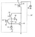
- FIG. 1is a diagram showing a circuit configuration of an imaging device 100A according to the present embodiment.
- An imaging device 100A illustrated in FIG. 1includes a plurality of pixels 10A and a peripheral circuit.
- the plurality of pixels 10Aare two-dimensionally arranged on the semiconductor substrate to form a pixel region.
- the plurality of pixels 10Aare arranged in the row direction and the column direction.
- the row direction and the column directionrefer to the direction in which the row and the column extend, respectively. That is, in the drawing, the vertical direction in the drawing is the column direction, and the horizontal direction is the row direction.
- the plurality of pixels 10Amay be arranged in one dimension.
- each of the pixels 10Ais connected to the power supply wiring 50.
- a predetermined power supply voltage Vddis supplied to each pixel 10A through the power supply wiring 50.
- each of the pixels 10Aincludes a photoelectric conversion unit 12 (hereinafter referred to as a photodiode 12) located in the semiconductor substrate.
- the photoelectric conversion unit 12includes a first diffusion region 2 (see FIG. 2) that converts incident light into charge.
- the imaging device 100Aincludes an accumulation control line 51 for applying a voltage to the anodes of all the photoelectric conversion units 12 at a constant level.
- the peripheral circuits of the imaging device 100Ainclude a vertical scanning circuit 30 (also called “row scanning circuit”), a load circuit 42, a column signal processing circuit 43 (also called “row signal storage circuit”), and a horizontal signal readout circuit 40. (Also referred to as “column scan circuit”) and an inverting amplifier 45.
- the column signal processing circuit 43, the load circuit 42, and the inverting amplifier 45are arranged for each column of the pixels 10A arranged in a two-dimensional manner. That is, in this example, the peripheral circuit includes a plurality of column signal processing circuits 43, a plurality of load circuits 42, and a plurality of inverting amplifiers 45.
- An address signal line 31 and a reset signal line 32are connected to the vertical scanning circuit 30.
- the vertical scanning circuit 30outputs a predetermined voltage to the address signal line 31 to select the plurality of pixels 10A arranged in each row in units of rows. Thereby, the readout of the signal voltage of the selected pixel 10A and the reset of the pixel electrode described later are executed.
- the pixels 10A arranged in each columnare electrically connected to the column signal processing circuit 43 via the vertical signal line 41 corresponding to each column.
- a load circuit 42is connected to the vertical signal line 41.
- the column signal processing circuit 43performs noise suppression signal processing represented by correlated double sampling, analog-digital conversion (AD conversion), and the like.
- Horizontal signal readout circuits 40are connected to the plurality of column signal processing circuits 43 provided corresponding to the columns of the pixels 10A.
- the horizontal signal readout circuit 40sequentially reads out signals from the plurality of column signal processing circuits 43 to the horizontal common signal line 44.
- a plurality of inverting amplifiers 45are provided corresponding to each column.
- the negative input terminal of the inverting amplifier 45is connected to the corresponding vertical signal line 41.
- a predetermined voltageis supplied to the positive input terminal of the inverting amplifier 45.
- the predetermined voltageis, for example, a positive voltage near 1 V or 1 V.
- the output terminal of the inverting amplifier 45is connected to the plurality of pixels 10A having a connection with the negative input terminal of the inverting amplifier 45 through the feedback line 46 provided corresponding to each column.
- the inverting amplifier 45constitutes a part of a feedback circuit 47 that negatively feeds back the output from the pixel 10A.
- the inverting amplifier 45may be called a feedback amplifier.
- the photodiode 12is a photoelectric conversion region that receives incident light and generates positive and negative charges, that is, hole-electron pairs.
- the photodiode 12is constituted of, for example, a photodiode of a PN junction.
- the photodiode 12has a connection with the storage control line 51, and a predetermined voltage is applied to the storage control line 51 when the imaging device 100A operates. By applying a predetermined voltage to the storage control line 51, one of positive and negative charges generated by photoelectric conversion is used as a signal charge.
- Each pixel 10Aincludes a signal detection circuit electrically connected to the photodiode 12.
- the signal detection circuitincludes an amplification transistor 22 and a reset transistor 23.
- the signal detection circuitfurther includes an address transistor 21.
- the amplification transistor 22, the reset transistor 23, and the address transistor 21 of the signal detection circuitare typically field effect transistors (FETs) formed on a semiconductor substrate.
- FETsfield effect transistors
- N-channel MOSMetal Oxide Semiconductor
- Each pixel 10Afurther includes a capacitive element 60.
- the capacitive element 60has a structure in which a dielectric layer such as an insulating film is sandwiched between the electrodes.
- the electrodeis not limited to an electrode formed of metal, but is broadly interpreted as including a polysilicon layer or the like.
- the electrode in the present specificationmay be part of a semiconductor substrate.
- the second diffusion region 3(see FIG. 2) and one electrode of the capacitive element 60 constitute a charge storage region.
- the gate of the amplification transistor 22also constitutes a charge storage region.
- the charge storage regionis also called a floating diffusion node.
- the floating diffusion nodeelectrically connects the drain of the reset transistor 23, an electrode of the capacitive element 60 not connected to the reference voltage PVDD, the gate of the amplification transistor 22, and the cathode of the photodiode 2. Wiring and the second diffusion region 3.
- the charge generated by the photodiode 2is accumulated in the charge accumulation region.
- the second diffusion region 3is a drain of the reset transistor 23.
- the second diffusion region 3may be one of the source and the drain of a transistor other than the reset transistor.
- the drain of the amplification transistor 22is connected to a power supply wiring 50 that supplies a predetermined power supply voltage Vdd (for example, about 3.3 V) to each pixel 10A when the imaging device 100A operates.
- Vdda predetermined power supply voltage
- the source of the amplification transistor 22is connected to the drain of the address transistor 21.
- the vertical signal line 41is connected to the source of the address transistor 21. As illustrated, the vertical signal line 41 is provided for each column of the plurality of pixels 10A, and the load circuit 42 and the column signal processing circuit 43 are connected to each of the vertical signal lines 41.
- the load circuit 42forms a source follower circuit together with the amplification transistor 22.
- An address signal line 31is connected to the gate of the address transistor 21.
- the address signal line 31is provided for each row of the plurality of pixels 10A.
- the address signal line 31is connected to the vertical scanning circuit 30, and the vertical scanning circuit 30 applies, to the address signal line 31, a row selection signal that controls the on / off of the address transistor 21.
- the row to be readis scanned in the vertical direction (column direction), and the row to be read is selected.
- the vertical scanning circuit 30can read the output of the amplification transistor 22 of the selected pixel 10A to the corresponding vertical signal line 41 by controlling the on and off of the address transistor 21 through the address signal line 31.
- the arrangement of the address transistor 21is not limited to the example shown in FIG. 1 and may be between the drain of the amplification transistor 22 and the power supply wiring 50.
- the signal voltage from the pixel 10Awhich is output to the vertical signal line 41 via the address transistor 21, is output from the plurality of column signal processing circuits 43 provided for each column of the plurality of pixels 10A corresponding to the vertical signal line 41.
- the corresponding column signal processing circuit 43is input.
- the reset signal line 32 having a connection with the vertical scanning circuit 30is connected to the gate of the reset transistor 23. Similar to the address signal line 31, the reset signal line 32 is provided for each row of the plurality of pixels 10A.
- the vertical scanning circuit 30can select the pixels 10A to be reset on a row basis by applying a row selection signal to the address signal line 31. Also, the vertical scanning circuit 30 applies a reset signal for controlling the on and off of the reset transistor 23 to the gate of the reset transistor 23 through the reset signal line 32, thereby turning on the reset transistor 23 of the selected row. It can be done.
- the reset transistor 23is turned on to reset the potential of the charge storage region.
- the source of the reset transistor 23is connected to one of the feedback lines 46 provided for each column of the plurality of pixels 10A. That is, in this example, the voltage of the feedback line 46 is supplied to the charge storage region as a reset voltage for initializing the charge of the photodiode 12.
- the above-mentioned feedback line 46is connected to the output terminal of the corresponding one of the inverting amplifiers 45 provided for each column of the plurality of pixels 10A.
- the input terminal of the inverting amplifier 45is connected to the vertical signal line 41 of that column. Further, the output terminal of the inverting amplifier 45 and one or more pixels 10A belonging to the column are connected via a feedback line 46.
- a predetermined voltage Vref(for example, a positive voltage of 1 V or near 1 V) is supplied to the non-inverting input terminal of the inverting amplifier 45.
- the imaging device 100Aincludes the feedback circuit 47 including the inverting amplifier 45 in a part of the feedback path.
- thermal noise called kTC noiseoccurs when the transistor is turned on or off.
- Noise generated as the reset transistor is turned on or offis called reset noise.
- reset noise generated by turning off the reset transistor 23remains in the charge accumulation region before accumulation of the signal charge.
- the AC component of the kTC noiseis fed back to the source of the reset transistor 23 due to the formation of the feedback path.
- the reset noise generated as the reset transistor 23 is turned offcan be reduced.
- FIG. 2is a diagram for explaining the configuration of the pixel 10A of the imaging device 100A according to the present embodiment.
- the transistoris an N-channel MOS transistor. Therefore, in the present specification, the first conductivity type is hereinafter referred to as p-type and the second conductivity type is referred to as n-type.
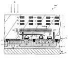
- An imaging device 100Aincludes a semiconductor substrate 1 and a plurality of pixels 10A.
- Semiconductor substrate 1includes a p-type region 90 and an n-type region 80.
- the semiconductor substrate 1also has a first surface 1 a and a second surface 1 b opposite to the first surface 1 a.
- the first surface 1 ais a surface in contact with the insulating layer 7.
- the contact plugs 8a and 8b, the contact plugs 18a and 18b, the first wiring 71, the second wiring 72, the third wiring 73, the fourth wiring 74, and the likeare arranged.
- Each of the plurality of pixels 10Aincludes, in a p-type region 90, a well region 11 including a p-type impurity, a photoelectric conversion unit 12 for converting incident light into charge, and a second diffusion region 3 for storing charge. Equipped with
- the photoelectric conversion unit 12includes a first diffusion region 2 and a third diffusion region 6.
- the first diffusion region 2is in contact with the p-type region 90 and the well region 11 and includes an n-type impurity different from the p-type.
- the third diffusion region 6covers the upper surface of the first diffusion region.
- the third diffusion region 6is exposed to the first surface 1 a of the semiconductor substrate 1, is in contact with the first diffusion region 2, and contains a p-type impurity.
- the first diffusion region 2 and the third diffusion region 6constitute a photodiode.
- the third diffusion region 6is disposed between the first diffusion region 2 and the first surface 1 a of the semiconductor substrate 1, whereby the first diffusion region 2 and the p-type region 90 are formed.
- the dark current that may be generated due to the defects at the interface withis pinned. Thereby, the dark current at the interface between the first diffusion region 2 and the p-type region 90 can be reduced more effectively.
- the second diffusion region 3is exposed to the first surface 1 a of the semiconductor substrate 1, is located in the well region 11, is electrically connected to the first diffusion region 2 in the p-type region 90, and contains n-type impurities. Contain and store charge.
- the transfer transistoris disposed between the photodiode and the charge storage region.
- dark currentis generated due to the transfer transistor.
- the pixel circuitsince the first diffusion region 2 and the charge storage region are directly electrically connected, the dark current at the time of charge storage can be reduced. Thereby, the charge storage efficiency can be improved.
- the pixel circuitsince the pixel circuit does not include the transfer transistor, the pixel circuit can be made smaller. As a result, the photoelectric conversion portion can be formed large, so that the dynamic range of the imaging device can be expanded.
- Each of the plurality of pixels 10Aincludes a first transistor (hereinafter, reset transistor 23) including the second diffusion region 3 as one of a source and a drain, a contact plug 8a connected to the second diffusion region 3, and a contact plug 8a. And a second transistor (hereinafter, amplification transistor 22) whose gate is electrically connected to the capacitance element 60.
- reset transistor 23including the second diffusion region 3 as one of a source and a drain, a contact plug 8a connected to the second diffusion region 3, and a contact plug 8a.
- a second transistorhereinafter, amplification transistor 22 whose gate is electrically connected to the capacitance element 60.
- the reset transistor 23includes the second diffusion region 3, the gate electrode 4, and the n-type impurity region 5 a.
- the second diffusion region 3is one of the source and the drain of the reset transistor 23, and the n-type impurity region 5a is the other of the source and the drain.
- the n-type impurity region 5 ais electrically connected to the feedback line 46, and the gate electrode 4 is electrically connected to the reset signal line 32.
- the amplification transistor 22includes an n-type impurity region 5 b, a gate electrode 4 and an n-type impurity region 5 c.
- the n-type impurity region 5 bis one of the source and the drain of the amplification transistor 22, and the n-type impurity region 5 c is the other of the source and the drain.
- the n-type impurity region 5bis electrically connected to a predetermined power supply voltage Vdd, and the gate electrode 4 is electrically connected to the capacitive element 60 through the contact plug 8b.
- the address transistor 21includes an n-type impurity region 5c, a gate electrode 4 and an n-type impurity region 5d.
- the n-type impurity region 5cis one of the source and the drain of the address transistor 21, and the n-type impurity region 5d is the other of the source and the drain.
- the n-type impurity region 5 dis electrically connected to the vertical signal line 41 via the contact plug 18 a, and the gate electrode 4 is electrically connected to the address signal line 31.
- the capacitive element 60may be disposed in the semiconductor substrate 1, or may be disposed in a layer other than the semiconductor substrate 1, for example, in the insulating layer 7 stacked on the semiconductor substrate 1. In the present embodiment, the capacitive element 60 is disposed in the insulating layer 7 stacked above the semiconductor substrate 1.
- the capacitive element 60includes an upper electrode 161, a lower electrode 163, and a dielectric film 162 located between the upper electrode 161 and the lower electrode 163.
- the upper electrode 161is connected to the reference voltage PVDD of the capacitive element 60.
- the lower electrode 163is connected to the contact plug 18 b.
- the capacitive element 60is connected to the second diffusion region 3 through the contact plug 18b and the contact plug 8a, and to the gate electrode 4 of the amplification transistor 22 through the contact plug 18b, the first wiring 71 and the contact plug 8b. It is connected.
- the capacitive element 60is a dielectric (here, the dielectric film 162) between two electrodes (here, the upper electrode 161 and the lower electrode 163) formed of a metal or a metal compound. ) Is sandwiched.
- a structure in which a dielectric is sandwiched between two electrodes formed of a metal or a metal compoundmay be referred to as a “MIM (Metal-Insulator-Metal) structure”.
- capacitive element 60is formed as a so-called capacitive element 60 having an MIM structure.
- the capacitance element 60has a MIM structure and a dielectric sandwiched between two electrodes of the upper electrode 161 and the lower electrode 163.
- the relative dielectric constant of the body film 162may be 10 or more.
- the dielectric film having a dielectric constant of 10 or moreinclude a film of hafnium oxide.
- the relative dielectric constant of hafnium oxideis about 20.
- the relative dielectric constant of silicon oxide used as the material of the dielectric film of the conventional MIM structureis about 3.8 to 4.
- Each of the plurality of pixels 10Aincludes a signal detection circuit electrically connected to the photoelectric conversion unit 12.
- the signal detection circuitincludes an address transistor 21, an amplification transistor 22, and a reset transistor 23.
- the reset transistor 23includes the second diffusion region 3 and the n-type impurity region 5a, a part of the gate insulating film (not shown), and the gate electrode 4 on the gate insulating film.
- the second diffusion region 3 and the n-type impurity region 5afunction as a drain region and a source region of the reset transistor 23, respectively.
- the second diffusion region 3is a region that temporarily accumulates the signal charge generated by the first diffusion region 2 of the photoelectric conversion unit 12.
- the reset transistor 23is disposed in the well region 11.
- Well region 11has a p-type impurity concentration (p) slightly higher than the p-type impurity concentration (p ⁇ ) contained in p-type region 90.
- the concentration of the n-type impurity in the second diffusion region 3is smaller than that of the n-type impurity region 5 a which is the other of the source and the drain of the reset transistor 23.
- the junction concentration at the junction between the second diffusion region 3 and the well region 11is reduced, so the dark current at the interface between the second diffusion region 3 and the well region 11 is reduced.
- the second diffusion region 3when viewed in the direction perpendicular to the semiconductor substrate 1, the second diffusion region 3 has a smaller area than the n-type impurity region 5 a which is the other of the source and the drain of the reset transistor 23.
- the areas of the second diffusion region 3 and the n-type impurity region 5 aare the second diffusion region 3 and the n-type impurity region 5 a respectively when viewed from the direction perpendicular to the semiconductor substrate 1. It may be an area excluding the overlapping portion. That is, the area of each of the second diffusion region 3 and the n-type impurity region 5 a may be the area of a portion not overlapping the gate electrode 4 of the reset transistor 23 when viewed from the direction perpendicular to the semiconductor substrate 1.
- the dark current in the second diffusion region 3can be reduced.
- the separation region 9when viewed in the direction perpendicular to the semiconductor substrate 1, the separation region 9 is disposed between the adjacent pixels 10A so as to surround the periphery of each pixel 10A. .
- the separation region 9is an insulating film that electrically separates adjacent pixels 10A, and is disposed in the p-type region 90.
- the signal detection circuitscan be electrically separated from each other between the pixels 10A adjacent to each other. With such a configuration, color mixing and blooming in the semiconductor substrate 1 between adjacent pixels 10A can be suppressed.
- the separation region 9not only electrically separates the adjacent pixels 10A, but also, for example, may be disposed so as to electrically separate the adjacent elements disposed in each pixel 10A. Good.
- the separation region 9is provided around the address transistor 21 and around the set of the amplification transistor 22 and the reset transistor 23.
- the isolation region 9is formed using an oxide such as silicon dioxide.
- the isolation region 9may be further coated with a high concentration of p-type impurities. Thereby, the dark current generated at the interface between the separation region 9 and the adjacent substrate or element can be reduced.
- FIG. 3is a diagram for explaining the configuration of the pixel 10B in the present modification.
- the circuit configuration of the imaging device according to the present modificationis the same as that of the embodiment shown in FIG.
- the plurality of pixels 10 ⁇ / b> Bincludes a first separation region 19 that electrically insulates the third diffusion region 6 and the second diffusion region 3.
- the dark current generated between the third diffusion region 6 including the p-type impurity and the second diffusion region 3 including the n-type impuritycan be reduced.
- the first separation region 19is formed using an oxide such as silicon dioxide as in the case of the separation region 9 described above.
- FIG. 4is a diagram for explaining the configuration of the pixel 10C in the present modification.
- the plurality of pixels 10Care provided around the first separation region 19 and include the second separation region 20 including p-type impurities at a higher concentration than the third diffusion region 6.
- the first isolation region 19is formed using an oxide such as silicon dioxide. Defects may occur at the interface between the first separation region 19 and the second diffusion region 3, and dark current may occur due to defects at the interface. Therefore, a potential barrier is formed between the third diffusion region 6 and the second diffusion region 3 by covering the first separation region 19 with the second separation region 20 formed of high concentration p-type impurities. , Can be more electrically insulated. Thereby, the dark current generated between the third diffusion region 6 and the second diffusion region 3 can be further reduced.
- FIG. 5is a diagram for explaining the configuration of the pixel 10D in the present modification.
- the plurality of pixels 10Dare in contact with the first diffusion region 2 and the second diffusion region 3 and include a fourth diffusion region (hereinafter, connection region 13) containing n-type impurities. Therefore, in the imaging device according to the present modification, the first diffusion region 2 and the second diffusion region 3 are reliably electrically connected via the connection region 13. Therefore, the charge generated in the first diffusion region 2 directly flows into the connection region 13 and is accumulated in the charge accumulation region including the second diffusion region 3.
- connection region 13fourth diffusion region
- FIG. 6is a diagram for explaining the configuration of the pixel 10E in the present modification.
- the first diffusion region 2 and the second diffusion region 3face each other via the well region 11.
- the well region 11contains p-type impurities.
- the p-type impurity regionfunctions as a potential barrier. Therefore, when the charge generated in the first diffusion region 2 reaches a certain amount or more, the charges flow from the first diffusion region 2 into the second diffusion region 3.
- imaging device 100Aincludes inverting amplifier 45 (see FIG. 1) in the circuit configuration as described above, feedback transistor may be provided instead of inverting amplifier 45.
- FIG. 7is a diagram showing an example in which the feedback transistor 24 is provided in the pixel 10F. Here, only the configuration different from the pixel 10A shown in FIG. 1 will be described.
- the pixel 10Fis different from the pixel 10A in that the feedback transistor 24 and the second capacitive element 61 are provided.
- the vertical scanning circuit 30(see FIG. 1) is also connected to a feedback control line (not shown).
- the gate of the feedback transistor 24is connected to a feedback control line (not shown).
- Feedbackthat causes the output of the signal detection circuit to be fed back to the second diffusion region 3 via the second capacitive element 61 or the reset transistor 23 by the vertical scanning circuit 30 applying a predetermined voltage to a feedback control line (not shown)
- a circuitcan be formed.
- the second capacitive element 61is a so-called coupling capacitor.
- each of the plurality of pixels 10Aincludes a contact plug 8a connected to the second diffusion region 3 and a contact plug (not shown) connected to the n-type impurity region 5a.
- the contact plug(not shown) is connected to the feedback line 46.
- the distance between the contact plug 8a of the second diffusion region 3 and the gate electrode 4 of the reset transistor 23is greater than the distance between the contact plug (not shown) of the n-type impurity region 5a and the gate electrode 4 of the reset transistor 23. small.
- the distance from the contact plug 8a of the second diffusion region 3 to the gate electrode 4 of the reset transistor 23is shortened, so that the increase in the resistance value of the second diffusion region 3 can be reduced.
- each of the address transistor 21, the amplification transistor 22 and the reset transistor 23 described abovemay be an N channel MOS or a P channel MOS.
- the impurity of the second conductivity typeis a p-type impurity
- the impurity of the first conductivity typeis an n-type impurity. It is not necessary that all of these transistors be unified into either N channel MOS or P channel MOS.
- the arrangement of the source and the drain in each of these transistorsmay be interchanged with each other.
- each of the plurality of pixelsmay include two pixels with different sensitivities.
- FIG. 8is a diagram showing an example of a circuit configuration of a pixel cell 10G provided with two pixels 110A and 110B having different sensitivities.
- the pixel cell 10Gincludes a first photoelectric conversion unit 120A, a first transfer transistor 121, a second photoelectric conversion unit 120B, a second transfer transistor 123, a charge storage unit 124, a switch transistor 125, a reset transistor 126, and an amplification transistor. And 127, a first charge storage region 128 and a second charge storage region 129.
- the high sensitivity pixel 110A surrounded by a broken line in FIG. 8corresponds to the first photoelectric conversion unit 120A, the first charge storage region 128, and the first transfer transistor 121.
- the low sensitivity pixel 110 ⁇ / b> Bcorresponds to the second photoelectric conversion unit 120 ⁇ / b> B, the second charge storage region 129, the second transfer transistor 123, and the charge storage unit 124.
- the first photoelectric conversion unit 120A(hereinafter also referred to as a first photodiode 120A) is a photodiode formed on a semiconductor substrate, and converts light into signal charge.
- the first transfer transistor 121is turned on, for example, when the transfer control line TGL is at high level. As a result, the first transfer transistor 121 transfers the signal charge photoelectrically converted by the first photoelectric conversion unit 120A to the first charge accumulation region 128.
- the second photoelectric conversion unit 120B(hereinafter, also referred to as a second photodiode 120B) is a photodiode formed on a semiconductor substrate, has a light receiving area smaller than that of the first photodiode 120A, and transmits light as a signal. Convert to charge.
- the second transfer transistor 123is turned on, for example, when the transfer control line TGS is at high level. As a result, the second transfer transistor 123 transfers the signal charge, which is photoelectrically converted by the second photoelectric conversion unit 120 B and stored in the charge storage unit 124, to the second charge storage region 129.
- the second diffusion region for storing the charge generated by the second photodiode 120 ⁇ / b> Bis the drain of the second transfer transistor 123.
- the second diffusion regionis electrically connected to the second photodiode 120B, and can directly store the charge generated by the second photodiode 120B in the second diffusion region.
- the charge storage unit 124is a capacitive element that stores the signal charge generated by photoelectric conversion in the second photoelectric conversion unit 120B.
- the charge storage portion 124is formed as an MIM structure and has two electrode portions. One of the two electrode parts is connected to the power supply voltage PVDD, and the other electrode part is connected to the drain of the second transfer transistor 123.
- the charge storage unit 124stores the signal charge generated by the photoelectric conversion of the second photoelectric conversion unit 120B.
- the signal charges stored in the charge storage unit 124are transferred to the second charge storage region 129 by the second transfer transistor 123 when the transfer control line TGS is at high level.
- the charge storage unit 124plays a role of greatly increasing the maximum storage capacity of the signal charge generated by the photoelectric conversion of the second photodiode 120B (that is, the saturation signal charge amount).
- the charge storage unit 124can have the same configuration as that of the capacitive element 60 (see, for example, FIG. 2).
- the switch transistor 125electrically connects the first charge storage region 128 and the second charge storage region 129, for example, when the switch control line SW is at high level.
- the reset transistor 126resets the second charge storage region 129 to high level, for example, when the reset control line RS is at high level.
- the amplification transistor 127forms a source follower circuit as a pair with a constant current source in the constant current source circuit, converts the potential of the first charge storage region 128 into a voltage, and outputs the voltage to the vertical signal line VL.
- the first charge storage region 128includes a floating diffusion layer formed in the semiconductor substrate, and holds the signal charge transferred by the first transfer transistor 121.
- the second charge storage region 129includes a floating diffusion layer formed in the semiconductor substrate, and holds the signal charge transferred by the second transfer transistor 123.
- the low sensitivity pixel 110Bcan realize a wide dynamic range.
- an image with a wide dynamic rangecan be obtained by mainly capturing a low illuminance image with the high sensitivity pixel 110A and capturing a high illuminance image with the low sensitivity pixel 110B.
- the low sensitivity pixel 110B of the present pixel cell 10Ggenerates the above-described kTC noise, it mainly picks up a high illuminance image, so there are more signal components compared to the kTC noise and the influence of the kTC noise is minor .
- the high sensitivity pixel 110A and the low sensitivity pixel 110Bshare the switch transistor 125, the reset transistor 126, and the amplification transistor 127. That is, the high sensitivity pixel 110A includes an element that performs photoelectric conversion, for example, the first photodiode 120A and the first transfer transistor 121.
- the low sensitivity pixel 110 ⁇ / b> Bincludes a second photodiode 120 ⁇ / b> B, a second transfer transistor 123, and a charge storage unit 124.
- the pixel cell 10Gincludes a switch transistor 125 shared by the high sensitivity pixel 110A and the low sensitivity pixel 110B, a reset transistor 126, and an amplification transistor 127.
- a switch transistor 125shared by the high sensitivity pixel 110A and the low sensitivity pixel 110B
- a reset transistor 126for example, an N channel MOS transistor may be used.
- the N channel MOS transistoris turned on when the gate potential is at "High" level and turned off at "Low” level. Further, it is assumed that the P-channel MOS transistor is turned on when the gate potential is at "Low” level and turned off at "High” level.
- FIG. 8shows an example in which each of the transistors 121 to 127 is an N channel MOS transistor.
- the first transfer transistor 121is connected between the cathode electrode of the first photodiode 120A and the first charge storage region 128.
- the transfer control line TGLis connected to the gate electrode of the first transfer transistor 121.
- “High” levelis given to the gate electrode of the first transfer transistor 121 from the transfer control line TGL as a transfer pulse from the transfer control line TGL, the first transfer transistor 121 is turned on and photoelectrically converted by the first photodiode 120A.
- the signal charge stored in the first photodiode 120Ais transferred to the first charge storage region 128.
- the signal chargeis an electron.
- the second transfer transistor 123is connected between an electrode connected to the semiconductor substrate of the charge storage portion 124 and the second charge storage region 129.
- the transfer control line TGSis connected to the gate electrode of the second transfer transistor 123.
- a “High” levelis given to the gate electrode of the second transfer transistor 123 from the transfer control line TGS as a transfer pulse from the transfer control line TGS, the second transfer transistor 123 is turned on and photoelectrically converted by the second photodiode 120B.
- the signal charge stored in the second photodiode 120 B and the signal charge stored between the semiconductor substrate and the electrode portion in the charge storage portion 124are transferred to the second charge storage region 129.
- the reset control line RSis connected to the gate electrode, the power supply voltage VDDC is applied to the drain electrode through the power supply wiring, and the second charge storage region 129 is connected to the source electrode.
- the switch control line SWis connected to the gate electrode, the second charge storage region 129 is connected to the drain electrode, and the first charge storage region 128 is connected to the source electrode.
- the reset control line RSis transmitted to the gate electrode of the reset transistor 126, and a “High” level is given by the reset pulse ⁇ RS. Further, the switch control line SW is transmitted to the gate electrode of the switch transistor 125 to give a “High” level as a switch pulse. Thus, the reset transistor 126 and the switch transistor 125 are turned on. As a result, the potentials of the first charge storage region 128 and the second charge storage region 129 are reset to the power supply voltage VDDC.
- a “High” levelis applied to the gate electrode of the reset transistor 126 by a reset pulse, and the gate electrode of the switch transistor 125 is Gives a "low” level at the switch pulse.
- the first charge storage region 128is in a state where the reset operation is completed.
- the gate electrodeis connected to the first charge storage region 128, the power supply voltage VDDC is applied to the drain electrode via the power supply wiring, and the source electrode is connected to the vertical signal line VL.
- the amplification transistor 127outputs the potential of the first charge storage region 128 after being reset by the reset transistor 126 and the switch transistor 125 as the reset level to the vertical signal line VL, and further, the signal charge by the first transfer transistor 121
- the potential of the first charge storage region 128 after the transfer of the signal V.sub.2is output to the vertical signal line VL as the signal level.
- the reset transistor 126 and the switch transistor 125are turned on to form the first charge storage region 128 and the second charge storage region 129.
- the potentialis reset to the power supply voltage VDDC.
- the “Low” levelis applied to the gate electrode of the reset transistor by the reset pulse ⁇ RS.
- "High” levelis given to the gate electrode of the switch transistor by switch pulse.
- the amplification transistor 127outputs the potentials of the first charge storage region 128 and the second charge storage region 129 after being reset by the reset transistor 126 and the switch transistor 125 to the vertical signal line VL as a reset level. Furthermore, the amplification transistor 127 outputs the potentials of the first charge storage region 128 and the second charge storage region 129 after the signal charge is transferred by the second transfer transistor 123 to the vertical signal line VL as the signal level. .
- the first charge storage region 128 and the second charge storage region 129a voltage corresponding to the signal charge amount is transmitted to the amplification transistor 127.
- the conversion efficiency ⁇is determined by the capacitance value C of the first charge storage region 128 and the second charge storage region 129.
- the conversion efficiency ⁇ of the low sensitivity pixel 110Bis lower than the conversion efficiency ⁇ of the high sensitivity pixel 110A.
- the conversion efficiency ⁇is higher, the signal charge amount can be efficiently converted to a voltage, and the voltage value of the signal amplitude can be increased.
- the ratio S / N of the pixel signal S to the noise component N generated in the constant current source circuit or the readout circuit connected to the vertical signal line VLcan be improved, and a high quality image can be obtained.
- the high sensitivity pixel 110Aacquires image data of a subject under a low illuminance environment
- the low sensitivity pixel 110Bacquires an image of a subject under a high illuminance environment.
- An imaging deviceis required to generate a high quality image so as to obtain an image under various environments.
- higher conversion efficiency ⁇is required in order to obtain a high quality image in a low illuminance environment, particularly under 1 lux. Then, in order to realize higher conversion efficiency, it is necessary to reduce the capacitance value C of the first charge storage region 128.
- the charge storage unit 124needs to store a larger amount of signal charge in order to obtain a high quality image in a high illuminance environment, particularly in an environment exposed to direct sunlight. is there. Therefore, lower conversion efficiency ⁇ is obtained. Then, in order to realize lower conversion efficiency, it is necessary to increase the capacitance value C of the second charge storage region 129.
- switch transistor 125is provided between first charge storage region 128 and second charge storage region 129, and amplification transistor 127 is connected to first charge storage region 128. .
- the switch transistor 125When reading out the signal charge of the high sensitivity pixel 110A, the switch transistor 125 is turned off. As a result, the gate electrode of the amplification transistor 127 is connected only to the first charge accumulation region 128, and higher conversion efficiency ⁇ can be obtained.
- the switch transistor 125is turned on. As a result, the first charge storage region 128 and the second charge storage region 129 are connected to the gate electrode of the amplification transistor 127, and a lower conversion efficiency ⁇ can be obtained.
- a capacitancemay be provided to the second charge accumulation region 129.
- the high sensitivity pixel 110Aturns off the switch transistor 125 and reads out the signal charge, there is no influence on the conversion efficiency ⁇ of the high sensitivity pixel 110A, and high image quality can be maintained.
- the reset transistor 126When the switch transistor 125 is turned on in the read operation of the high sensitivity pixel 110A as in the read operation of the low sensitivity pixel 110B, the reset transistor 126 may be turned off. Thereby, the conversion efficiency ⁇ of the first charge storage region 128 and the second charge storage region 129 can be lowered to read out the signal charge.
- the signal charge amount stored in the first photodiode 120A of the high sensitivity pixel 110Ais larger than the signal charge amount when imaging an object under a low illuminance environment. Therefore, the above method is effective as means for preventing the voltage ⁇ V of the charge signal amount from exceeding the dynamic range of the vertical signal line VL.
- the pixel cell 10Gis configured such that one high sensitivity pixel 110A and one low sensitivity pixel 110B share the switch transistor 125, the reset transistor 126, and the amplification transistor 127.
- the sensitivity pixel 110A and the two low sensitivity pixels 110Bmay share the switch transistor 125, the reset transistor 126, and the amplification transistor 127 for use.
- a selection transistor for selecting a row corresponding to the read out row of the pixel array between the source of the amplification transistor 127 and the vertical signal line VLis connected between the amplification transistor 127 and the vertical signal line VL. It is also good.
- FIG. 9is a view for explaining the configuration of a pixel 10H of an imaging device according to another embodiment.
- points different from the pixel in the above embodiment and modificationwill be described in comparison.
- the front side illumination type imaging devicefor example, light enters the photoelectric conversion unit 12 from the wiring side as in the pixels 10A to 10E shown in FIGS. 2 to 6, respectively.
- the backside illumination type imaging devicefor example, as shown in FIG.
- the photoelectric conversion unit 12 and the wiringso that the incident light to the photoelectric conversion unit 12 is not blocked by the wiring. Therefore, it is difficult to make the light receiving area of the photoelectric conversion unit 12 larger than a certain level.
- the space for arranging the wiringis also limited.
- the backside illumination type imaging deviceas shown in FIG.
- the wiringis disposed on the side opposite to the side where light is incident on the photoelectric conversion unit 12, the incident light on the photoelectric conversion unit 12 is blocked by the wiring. I can not. Therefore, the light receiving area of the photoelectric conversion unit 12 can be increased. Also, the wiring can be arranged freely. For example, also in FIG. 9, the second wiring 72, the third wiring 73, and the fourth wiring 74 are disposed on the photoelectric conversion unit 12. In the imaging device shown in FIG. 9, the n-type region 80 may be formed thin. This makes it easier for light to be incident on the photoelectric conversion unit 12.
- an imaging devicecapable of imaging with high image quality.
- the imaging device of the present disclosureis useful for, for example, an image sensor, a digital camera, and the like.
- the imaging device of the present disclosurecan be used as a medical camera, a robot camera, a security camera, a camera mounted on a vehicle, and the like.
Landscapes
- Engineering & Computer Science (AREA)
- Multimedia (AREA)
- Signal Processing (AREA)
- Solid State Image Pick-Up Elements (AREA)
- Transforming Light Signals Into Electric Signals (AREA)
Abstract
Description
Translated fromJapanese本開示は、撮像装置に関する。The present disclosure relates to an imaging device.
デジタルカメラなどにCCD(Charge Coupled Device)イメージセンサ及びCMOS(Complementary Metal Oxide Semiconductor)イメージセンサが広く用いられている。よく知られているように、これらのイメージセンサは、半導体基板に形成されたフォトダイオードを有する。A CCD (Charge Coupled Device) image sensor and a CMOS (Complementary Metal Oxide Semiconductor) image sensor are widely used in digital cameras and the like. As well known, these image sensors have photodiodes formed on a semiconductor substrate.
このようなイメージセンサでは、半導体基板にフォトダイオードなどの光電変換部及びその周辺回路を形成するため、ダイナミックレンジを実現しつつ、画素サイズを小さくする工夫がなされている(特許文献1)。In such an image sensor, in order to form a photoelectric conversion unit such as a photodiode and its peripheral circuit on a semiconductor substrate, a device for reducing the pixel size while realizing a dynamic range has been made (Patent Document 1).
暗電流を低減しつつ、ダイナミックレンジの拡大を実現することが望まれている。It is desirable to realize an increase in dynamic range while reducing dark current.
本開示の一態様に係る撮像装置は、第1導電型の不純物を含む半導体領域と、前記半導体領域に接し、前記第1導電型とは異なる第2導電型の不純物を含み、入射光を電荷に変換する第1拡散領域と、前記第2導電型の不純物を含み、前記第1拡散領域から流入する前記電荷の少なくとも一部を蓄積する第2拡散領域と、を含む半導体基板と、前記半導体基板上に位置する第1ゲート電極を含み、前記第2拡散領域をソース及びドレインの一方として含む第1トランジスタと、前記第2拡散領域に電気的に接続されるコンタクトプラグと、一端が前記コンタクトプラグに電気的に接続される容量素子と、前記半導体基板上に位置する第2ゲート電極を含み、前記第2ゲート電極が前記容量素子の前記一端に電気的に接続される第2トランジスタと、を備える。An imaging device according to an aspect of the present disclosure includes: a semiconductor region including an impurity of a first conductivity type; and an impurity of a second conductivity type different from the first conductivity type in contact with the semiconductor region and charging incident light A semiconductor substrate including: a first diffusion region to be converted into a second diffusion region; and a second diffusion region containing an impurity of the second conductivity type and storing at least a part of the charges flowing from the first diffusion region; A first transistor including a first gate electrode located on a substrate, the second diffusion region being one of a source and a drain, a contact plug electrically connected to the second diffusion region, and one end of the contact A second transition including a capacitive element electrically connected to a plug and a second gate electrode located on the semiconductor substrate, wherein the second gate electrode is electrically connected to the one end of the capacitive element Equipped with data and, the.
包括的又は具体的な態様は、素子、デバイス、モジュール、システム又は方法で実現されてもよい。また、包括的又は具体的な態様は、素子、デバイス、モジュール、システム及び方法の任意の組み合わせによって実現されてもよい。The general or specific aspects may be realized in an element, a device, a module, a system or a method. Also, the comprehensive or specific aspects may be realized by any combination of elements, devices, modules, systems and methods.
開示された実施形態の追加的な効果及び利点は、明細書及び図面から明らかになる。効果及び/又は利点は、明細書及び図面に開示の様々な実施形態又は特徴によって個々に提供され、これらの1つ以上を得るために全てを必要とはしない。Additional advantages and benefits of the disclosed embodiments will become apparent from the description and the drawings. The advantages and / or advantages may be individually provided by the various embodiments or features disclosed in the description and the drawings, and not all may be required to obtain one or more of these.
本開示によれば、暗電流を低減しつつ、ダイナミックレンジの拡大を実現することができる撮像装置を提供できる。According to the present disclosure, it is possible to provide an imaging device capable of realizing expansion of a dynamic range while reducing dark current.
上記した特許文献1に記載の撮像装置では、信号検出回路などの画素回路をフォトダイオードと異なる層に配置することで、ダイナミックレンジの拡大を図っている。しかしながら、特許文献1に記載の撮像装置は、暗電流を低減しつつ、ダイナミックレンジを拡大できているとは言い難い。暗電流を低減しつつ、ダイナミックレンジの拡大を実現することが望まれている。In the imaging device described in
本開示の一態様の概要は以下のとおりである。The outline of one aspect of the present disclosure is as follows.
[項目1]
第1導電型の不純物を含む半導体領域と、
前記半導体領域に接し、前記第1導電型とは異なる第2導電型の不純物を含み、入射光を電荷に変換する第1拡散領域と、
前記第2導電型の不純物を含み、前記第1拡散領域から流入する前記電荷の少なくとも一部を蓄積する第2拡散領域と、
を含む半導体基板と、
前記半導体基板上に位置する第1ゲート電極を含み、前記第2拡散領域をソース及びドレインの一方として含む第1トランジスタと、
前記第2拡散領域に電気的に接続されるコンタクトプラグと、
一端が前記コンタクトプラグに電気的に接続される容量素子と、
前記半導体基板上に位置する第2ゲート電極を含み、前記第2ゲート電極が前記容量素子の前記一端に電気的に接続される第2トランジスタと、
を備える、撮像装置。[Item 1]
A semiconductor region containing an impurity of the first conductivity type;
A first diffusion region which is in contact with the semiconductor region, contains an impurity of a second conductivity type different from the first conductivity type, and converts incident light into charge;
A second diffusion region that contains an impurity of the second conductivity type and stores at least a part of the charge flowing from the first diffusion region;
A semiconductor substrate including
A first transistor including a first gate electrode located on the semiconductor substrate, and including the second diffusion region as one of a source and a drain;
A contact plug electrically connected to the second diffusion region;
A capacitive element of which one end is electrically connected to the contact plug;
A second transistor including a second gate electrode located on the semiconductor substrate, the second gate electrode being electrically connected to the one end of the capacitive element;
An imaging device comprising:
[項目2]
前記半導体基板は、前記第1拡散領域の上面を覆い、前記第1導電型の不純物を含む第3拡散領域を含む、項目1に記載の撮像装置。[Item 2]
The imaging device according to
[項目3]
前記半導体基板は、前記第1導電型の不純物を含むウェル領域を含み、
前記第2拡散領域は、前記ウェル領域内に位置する、項目1に記載の撮像装置。[Item 3]
The semiconductor substrate includes a well region including an impurity of the first conductivity type,
The imaging device according to
[項目4]
前記半導体基板は、前記第2拡散領域と前記第3拡散領域とを電気的に絶縁する第1分離領域を含む、項目2に記載の撮像装置。[Item 4]
The imaging device according to Item 2, wherein the semiconductor substrate includes a first separation region electrically insulating the second diffusion region and the third diffusion region.
[項目5]
前記第1分離領域は、第2分離領域を含み、
前記第2分離領域における前記第1導電型の不純物の濃度は、前記第3拡散領域における前記第1導電型の不純物の濃度よりも大きい、項目4に記載の撮像装置。[Item 5]
The first separation area includes a second separation area,
The imaging device according to Item 4, wherein a concentration of the first conductivity type impurity in the second separation region is larger than a concentration of the first conductivity type impurity in the third diffusion region.
[項目6]
前記半導体基板は、前記第1拡散領域および前記第2拡散領域に接し、前記第2導電型の不純物を含む第4拡散領域を含む、項目1に記載の撮像装置。[Item 6]
The imaging device according to
[項目7]
前記第2拡散領域は、前記ウェル領域を介して前記第1拡散領域に対向している、項目3に記載の撮像装置。[Item 7]
The imaging device according to Item 3, wherein the second diffusion area is opposed to the first diffusion area via the well area.
[項目8]
前記半導体基板は、前記第2導電型の不純物を含む第5拡散領域を含み、
前記第1トランジスタは、前記第5拡散領域をソース及びドレインの他方として含み、
前記第2拡散領域における前記第2導電型の不純物の濃度は、前記第5拡散領域における前記第2導電型の不純物の濃度よりも小さい、項目1から項目7のいずれか一項に記載の撮像装置。[Item 8]
The semiconductor substrate includes a fifth diffusion region containing an impurity of the second conductivity type,
The first transistor includes the fifth diffusion region as the other of the source and the drain,
The imaging according to any one of
[項目9]
前記半導体基板は、前記第2導電型の不純物を含む第5拡散領域を含み、
前記第1トランジスタは、前記第5拡散領域をソース及びドレインの他方として含み、
前記半導体基板に垂直な方向から見たとき、前記第2拡散領域の面積は、前記5拡散領域の面積よりも小さい、項目1から項目8のいずれか一項に記載の撮像装置。[Item 9]
The semiconductor substrate includes a fifth diffusion region containing an impurity of the second conductivity type,
The first transistor includes the fifth diffusion region as the other of the source and the drain,
The imaging device according to any one of
また、本開示の一態様の概要は以下のとおりである。In addition, an outline of one aspect of the present disclosure is as follows.
本開示の一態様に係る撮像装置は、第1面と、前記第1面に対向する第2面と、を有する半導体基板と、前記半導体基板中に位置し、第1導電型の不純物を含むウェル領域と、前記ウェル領域に接し、前記第1導電型とは異なる第2導電型の不純物を含む第1拡散領域と、前記第1面に露出し、前記第1拡散領域に接し、前記第1導電型の不純物を含む第3拡散領域と、を含み、入射光を電荷に変換する光電変換部と、前記第1面に露出し、前記ウェル領域中に位置し、前記半導体基板内において前記第1拡散領域に電気的に接続され、前記第2導電型の不純物を含み、前記電荷を蓄積する第2拡散領域と、前記第2拡散領域をソース及びドレインの一方として備える第1トランジスタと、前記第2拡散領域に接続されたコンタクトプラグと、前記コンタクトプラグを介して前記第2拡散領域と電気的に接続される容量素子と、ゲートが前記容量素子に電気的に接続された第2トランジスタと、を備える。An imaging device according to an aspect of the present disclosure includes: a semiconductor substrate having a first surface; and a second surface opposite to the first surface; and located in the semiconductor substrate and including an impurity of a first conductivity type. A well region, a first diffusion region in contact with the well region and containing an impurity of a second conductivity type different from the first conductivity type, and exposed on the first surface and in contact with the first diffusion region; And a third diffusion region containing an impurity of one conductivity type, the photoelectric conversion portion converting incident light into electric charge, exposed to the first surface, and located in the well region, in the semiconductor substrate A second diffusion region electrically connected to the first diffusion region, containing an impurity of the second conductivity type, and storing the charge, and a first transistor including the second diffusion region as one of a source and a drain; Contact plug connected to the second diffusion region Comprises a capacitive element which is connected to the second diffusion region and electrically via the contact plug, a second transistor whose gate is electrically connected to the capacitive element.
このように、光電変換部において、第3拡散領域が第1拡散領域と半導体基板の第1面との間に配置されることにより、第1拡散領域と半導体基板との界面での欠陥に起因して生じ得る暗電流が第3拡散領域においてピニングされる。これにより、第1拡散領域と半導体基板との界面における暗電流をより効果的に低減することができる。Thus, in the photoelectric conversion portion, the third diffusion region is disposed between the first diffusion region and the first surface of the semiconductor substrate, thereby causing defects at the interface between the first diffusion region and the semiconductor substrate. Dark current that may occur is pinned in the third diffusion region. Thereby, the dark current at the interface between the first diffusion region and the semiconductor substrate can be more effectively reduced.
また、第1拡散領域と第2拡散領域とが共に第2導電型の不純物を含み、第2拡散領域が第1拡散領域に電気的に接続されることにより、第1拡散領域で発生した電荷を第2拡散領域に直接蓄積することができる。そのため、光電変換により発生した電荷を第1拡散領域から第2拡散領域に転送する転送トランジスタが不要となる。転送トランジスタを介して電荷を移動させると、転送トランジスタに起因して暗電流が発生する。しかしながら、本開示の一態様に係る撮像装置では、光電変換部の第1拡散領域と、電荷を蓄積する第2拡散領域とが直接電気的に接続されているため、電荷蓄積時における暗電流を低減することができる。また、転送トランジスタが不要であるため、画素回路を小さくすることができる。これにより、光電変換部を大きく形成することができるため、撮像装置のダイナミックレンジの拡大を実現することができる。In addition, the first diffusion region and the second diffusion region both contain an impurity of the second conductivity type, and the second diffusion region is electrically connected to the first diffusion region, whereby the charge generated in the first diffusion region is generated. Can be stored directly in the second diffusion region. Therefore, a transfer transistor for transferring the charge generated by the photoelectric conversion from the first diffusion region to the second diffusion region is unnecessary. When charge is transferred through the transfer transistor, dark current is generated due to the transfer transistor. However, in the imaging device according to one aspect of the present disclosure, since the first diffusion region of the photoelectric conversion unit and the second diffusion region for storing charge are directly electrically connected, the dark current at the time of charge storage can be reduced. It can be reduced. In addition, since the transfer transistor is unnecessary, the pixel circuit can be downsized. As a result, the photoelectric conversion portion can be formed large, so that the dynamic range of the imaging device can be expanded.
また、電荷を蓄積する第2拡散領域と容量素子とが電気的に接続されることにより、第2拡散領域は、より大きな容量値を得ることができる。そのため、ダイナミックレンジのさらなる拡大を実現することができる。In addition, the second diffusion region can obtain a larger capacitance value by electrically connecting the second diffusion region that stores charge and the capacitive element. Therefore, the dynamic range can be further expanded.
例えば、本開示の一態様に係る撮像装置は、前記第2拡散領域と前記第3拡散領域とを電気的に絶縁する第1分離領域を備えてもよい。For example, the imaging device according to an aspect of the present disclosure may include a first separation region that electrically insulates the second diffusion region and the third diffusion region.
これにより、第1導電型の不純物を含む第3拡散領域と第2導電型の不純物を含む第2拡散領域との間に生じる暗電流を低減することができる。Thereby, the dark current generated between the third diffusion region containing the impurity of the first conductivity type and the second diffusion region containing the impurity of the second conductivity type can be reduced.
例えば、本開示の一態様に係る撮像装置は、前記第1分離領域の周辺に位置し、前記第1導電型の不純物を前記第3拡散領域よりも高い濃度で含む第2分離領域を備えてもよい。For example, an imaging device according to an aspect of the present disclosure includes a second separation region located around the first separation region and including an impurity of the first conductivity type at a higher concentration than the third diffusion region. It is also good.
このように、本開示の一態様に係る撮像装置は、第1分離領域の周囲、例えば、第1分離領域と第3拡散領域との界面、及び、第1分離領域と第2拡散領域との界面に、第3拡散領域の第1導電型の不純物より高い濃度の第1導電型の不純物を含む第2分離領域を備える。これにより、第2拡散領域と第3拡散領域との間にポテンシャル障壁が形成され、電気的により強く絶縁することができる。そのため、第2拡散領域と第3拡散領域との間に生じる暗電流をさらに低減することができる。As described above, the imaging device according to one aspect of the present disclosure includes the periphery of the first separation region, for example, the interface between the first separation region and the third diffusion region, and the first separation region and the second diffusion region. The interface includes a second separation region including an impurity of the first conductivity type higher in concentration than the impurity of the first conductivity type of the third diffusion region. Thereby, a potential barrier is formed between the second diffusion region and the third diffusion region, and electrical insulation can be made stronger. Therefore, the dark current generated between the second diffusion region and the third diffusion region can be further reduced.
例えば、本開示の一態様に係る撮像装置は、前記第1拡散領域と前記第2拡散領域とに接し、前記第2導電型の不純物を含む第4拡散領域を備えてもよい。For example, the imaging device according to an aspect of the present disclosure may include a fourth diffusion region including an impurity of the second conductivity type in contact with the first diffusion region and the second diffusion region.
このような構成を有することにより、第1拡散領域と第2拡散領域とが第4拡散領域を介して確実に電気的に接続される。By having such a configuration, the first diffusion region and the second diffusion region are electrically connected reliably via the fourth diffusion region.
例えば、本開示の一態様に係る撮像装置では、前記第1拡散領域と前記第2拡散領域とが、前記ウェル領域を介して対向していてもよい。For example, in the imaging device according to an aspect of the present disclosure, the first diffusion region and the second diffusion region may face each other via the well region.
このような構成を有することにより、ウェル領域がポテンシャル領域として働き、第1拡散領域にたまった電荷が一定量以上になると第3領域に流入する。With such a configuration, the well region acts as a potential region, and when the charge accumulated in the first diffusion region reaches a certain amount or more, it flows into the third region.
例えば、本開示の一態様に係る撮像装置では、前記第2拡散領域は、前記第1トランジスタのソース及びドレインの他方よりも前記第2導電型の不純物の濃度が小さくてもよい。For example, in the imaging device according to the aspect of the present disclosure, the second diffusion region may have a concentration of the impurity of the second conductivity type smaller than the other of the source and the drain of the first transistor.
このように、第2拡散領域に含まれる第2導電型の不純物濃度が、第1トランジスタのソース及びドレインの他方よりも第2導電型の不純物濃度が小さいため、第2拡散領域とウェル領域との接合部における接合濃度が小さくなる。そのため、第2拡散領域における暗電流を低減することができる。As described above, since the impurity concentration of the second conductivity type included in the second diffusion region is smaller than the impurity concentration of the second conductivity type than the other of the source and the drain of the first transistor, the second diffusion region and the well region The junction concentration at the junction of Therefore, the dark current in the second diffusion region can be reduced.
例えば、本開示の一態様に係る撮像装置では、前記半導体基板に垂直な方向から見たとき、前記第2拡散領域は、前記第1トランジスタのソース及びドレインの他方よりも面積が小さくてもよい。For example, in the imaging device according to one aspect of the present disclosure, the second diffusion region may have a smaller area than the other of the source and the drain of the first transistor when viewed in a direction perpendicular to the semiconductor substrate. .
このように、第2拡散領域の面積を小さくすることにより、第2拡散領域における暗電流を低減することができる。Thus, the dark current in the second diffusion region can be reduced by reducing the area of the second diffusion region.
以下、図面を参照しながら、本開示の実施の形態を詳細に説明する。なお、以下で説明する実施形態は、いずれも包括的又は具体的な例を示す。以下の実施形態で示される数値、形状、材料、構成要素、構成要素の配置及び接続形態、ステップ、ステップの順序などは、一例であり、本開示を限定する主旨ではない。本明細書において説明される種々の態様は、矛盾が生じない限り互いに組み合わせることが可能である。また、以下の実施の形態における構成要素のうち、最上位概念を示す独立請求項に記載されていない構成要素については、任意の構成要素として説明される。各図において、実質的に同じ機能を有する構成要素は共通の参照符号で示し、重複する説明を省略又は簡略化することがある。Hereinafter, embodiments of the present disclosure will be described in detail with reference to the drawings. The embodiments described below all show comprehensive or specific examples. Numerical values, shapes, materials, components, arrangements and connection forms of components, steps, order of steps, and the like described in the following embodiments are merely examples, and are not intended to limit the present disclosure. The various aspects described herein can be combined with one another as long as no contradiction arises. Further, among the components in the following embodiments, components not described in the independent claim indicating the highest concept are described as arbitrary components. In the drawings, components having substantially the same functions are denoted by the same reference numerals, and overlapping descriptions may be omitted or simplified.
また、図面に示す各種の要素は、本開示の理解のために模式的に示したにすぎず、寸法比及び外観などは実物と異なり得る。In addition, various elements shown in the drawings are merely schematically shown for the understanding of the present disclosure, and dimensional ratios, appearances, and the like may be different from those in the real thing.
なお、本明細書において、撮像装置の受光側を「上方」とし、受光側と反対側を「下方」とする。各部材の「上面」、「下面」についても同様に、撮像装置の受光側に対向する面を「上面」とし、受光側と反対側に対向する面を「下面」とする。なお、「上方」、「下方」、「上面」及び「下面」などの用語は、あくまでも部材間の相互の配置を指定するために用いており、撮像装置の使用時における姿勢を限定する意図ではない。In the present specification, the light receiving side of the imaging device is referred to as “upper”, and the side opposite to the light receiving side is referred to as “lower”. Similarly, regarding the “upper surface” and the “lower surface” of each member, the surface facing the light receiving side of the imaging device is the “upper surface”, and the surface facing the opposite side to the light receiving side is the “lower surface”. The terms "upper", "lower", "upper surface" and "lower surface" are used only to designate the mutual arrangement between members, and are intended to limit the posture when using the imaging device. Absent.
(実施の形態)
図1は、本実施の形態に係る撮像装置100Aの回路構成を示す図である。Embodiment
FIG. 1 is a diagram showing a circuit configuration of an
図1に示す撮像装置100Aは、複数の画素10Aと周辺回路とを備える。複数の画素10Aは、半導体基板上に2次元に配置されることにより、画素領域を形成している。An
図1に示す例では、複数の画素10Aは、行方向及び列方向に配置されている。本明細書において、行方向及び列方向とは、行及び列がそれぞれ延びる方向をいう。つまり、図面中、紙面における垂直方向が列方向であり、水平方向が行方向である。なお、複数の画素10Aは、1次元に配置されていてもよい。In the example shown in FIG. 1, the plurality of
画素10Aのそれぞれは、電源配線50に接続されている。各画素10Aには、電源配線50を介して所定の電源電圧Vddが供給される。後に詳しく説明するように、画素10Aのそれぞれは、半導体基板中に位置する光電変換部12(以下、フォトダイオード12)を備える。なお、光電変換部12は、入射光を電荷に変換する第1拡散領域2(図2参照)を含む。また、図示するように、撮像装置100Aは、全ての光電変換部12のアノードに一定に電圧を印加するための蓄積制御線51を有する。Each of the
撮像装置100Aの周辺回路は、垂直走査回路30(「行走査回路」とも呼ばれる)と、負荷回路42と、カラム信号処理回路43(「行信号蓄積回路」とも呼ばれる)と、水平信号読み出し回路40(「列走査回路」とも呼ばれる)と、反転増幅器45とを含む。図示する構成において、カラム信号処理回路43、負荷回路42及び反転増幅器45は、2次元に配置された画素10Aの列毎に配置されている。つまり、この例では、周辺回路は、複数のカラム信号処理回路43と、複数の負荷回路42と、複数の反転増幅器45とを含む。The peripheral circuits of the
垂直走査回路30には、アドレス信号線31及びリセット信号線32が接続されている。垂直走査回路30は、アドレス信号線31に所定の電圧を出力することにより、各行に配置された複数の画素10Aを行単位で選択する。これにより、選択された画素10Aの信号電圧の読み出しと、後述する画素電極のリセットとが実行される。An
各列に配置された画素10Aは、各列に応じた垂直信号線41を介してカラム信号処理回路43に電気的に接続されている。垂直信号線41には、負荷回路42が接続されている。カラム信号処理回路43は、相関2重サンプリングに代表される雑音抑圧信号処理及びアナログ-デジタル変換(AD変換)などを行う。画素10Aの列に対応して設けられた複数のカラム信号処理回路43には、水平信号読み出し回路40が接続されている。水平信号読み出し回路40は、複数のカラム信号処理回路43から水平共通信号線44に信号を順次読み出す。The
図1に例示する構成では、複数の反転増幅器45が各列に対応して設けられている。反転増幅器45の負側の入力端子は、対応する垂直信号線41に接続されている。反転増幅器45の正側の入力端子には、所定の電圧が供給される。所定の電圧は、例えば1V又は1V近傍の正電圧である。また、反転増幅器45の出力端子は、各列に対応して設けられたフィードバック線46を介して、その反転増幅器45の負側の入力端子との接続を有する複数の画素10Aに接続されている。反転増幅器45は、画素10Aからの出力を負帰還させるフィードバック回路47の一部を構成する。反転増幅器45をフィードバックアンプと呼んでもよい。In the configuration illustrated in FIG. 1, a plurality of inverting
フォトダイオード12は、光の入射を受けて正及び負の電荷、つまり、正孔-電子対を発生させる光電変換領域である。フォトダイオード12は、例えば、PN接合のフォトダイオードから構成される。フォトダイオード12は、蓄積制御線51との接続を有しており、撮像装置100Aの動作時に、蓄積制御線51には所定の電圧が印加される。所定の電圧を蓄積制御線51に印加することにより、光電変換により生成された正及び負の電荷のうち、一方の電荷を信号電荷として利用する。The
各画素10Aは、フォトダイオード12に電気的に接続された信号検出回路を含む。図1に例示する構成において、信号検出回路は、増幅トランジスタ22及びリセットトランジスタ23を含む。この例では、信号検出回路は、さらに、アドレストランジスタ21を含んでいる。信号検出回路の増幅トランジスタ22、リセットトランジスタ23及びアドレストランジスタ21は、典型的には、半導体基板に形成された電界効果トランジスタ(FET:Field Effect Transistor)である。以下では、特段の断りのない限り、トランジスタとしてNチャネルMOS(Metal Oxide Semiconductor)トランジスタを用いる例を説明する。なお、FETの2つの拡散層のうちどちらがソース及びドレインに該当するかは、FETの極性及びその時点での電位の高低によって決定される。そのため、どちらかがソース及びドレインであるかはFETの作動状態によって変動し得る。Each
また、各画素10Aは、さらに、容量素子60を備える。容量素子60は、電極間に絶縁膜などの誘電体層が挟まれた構造を有する。本明細書では、電極は、金属から形成された電極に限定されず、ポリシリコン層などを広く含むように解釈される。なお、本明細書における電極は、半導体基板の一部であってもよい。Each
図1に例示する構成において、第2拡散領域3(図2参照)及び容量素子60の一方の電極は、電荷蓄積領域を構成している。また、増幅トランジスタ22のゲートも、電荷蓄積領域を構成している。電荷蓄積領域は、フローティングディフュージョンノードとも呼ばれる。ここで、フローティングディフュージョンノードとは、リセットトランジスタ23のドレインと、容量素子60の基準電圧PVDDと接続されない側の電極と、増幅トランジスタ22のゲートと、フォトダイオード2のカソードとを電気的に接続している配線及び第2拡散領域3をいう。フォトダイオード2によって生成された電荷は、電荷蓄積領域に蓄積される。図1において、第2拡散領域3はリセットトランジスタ23のドレインである。第2拡散領域3は、リセットトランジスタ以外のトランジスタのソース及びドレインの一方であってもよい。In the configuration illustrated in FIG. 1, the second diffusion region 3 (see FIG. 2) and one electrode of the
増幅トランジスタ22のドレインは、撮像装置100Aの動作時に各画素10Aに所定の電源電圧Vdd(例えば、3.3V程度)を供給する電源配線50に接続される。換言すれば、増幅トランジスタ22は、フォトダイオード2によって生成された信号電荷の量に応じた信号電圧を出力する。増幅トランジスタ22のソースは、アドレストランジスタ21のドレインに接続される。The drain of the
アドレストランジスタ21のソースには、垂直信号線41が接続される。図示するように、垂直信号線41は、複数の画素10Aの列毎に設けられており、垂直信号線41の各々には、負荷回路42及びカラム信号処理回路43が接続されている。負荷回路42は、増幅トランジスタ22と共にソースフォロア回路を形成する。The
アドレストランジスタ21のゲートには、アドレス信号線31が接続されている。アドレス信号線31は、複数の画素10Aの行毎に設けられている。アドレス信号線31は、垂直走査回路30に接続されており、垂直走査回路30は、アドレストランジスタ21のオン及びオフを制御する行選択信号をアドレス信号線31に印加する。これにより、読み出し対象の行が垂直方向(列方向)に走査され、読み出し対象の行が選択される。垂直走査回路30は、アドレス信号線31を介してアドレストランジスタ21のオン及びオフを制御することにより、選択した画素10Aの増幅トランジスタ22の出力を、対応する垂直信号線41に読み出すことができる。アドレストランジスタ21の配置は、図1に示す例に限定されず、増幅トランジスタ22のドレインと電源配線50との間であってもよい。An
アドレストランジスタ21を介して垂直信号線41に出力された、画素10Aからの信号電圧は、垂直信号線41に対応して複数の画素10Aの列毎に設けられた複数のカラム信号処理回路43のうち、対応するカラム信号処理回路43に入力される。The signal voltage from the
リセットトランジスタ23のゲートには、垂直走査回路30との接続を有するリセット信号線32が接続される。リセット信号線32は、アドレス信号線31と同様に複数の画素10Aの行毎に設けられる。垂直走査回路30は、アドレス信号線31に行選択信号を印加することにより、リセットの対象となる画素10Aを行単位で選択することができる。また、垂直走査回路30は、リセットトランジスタ23のオン及びオフを制御するリセット信号を、リセット信号線32を介してリセットトランジスタ23のゲートに印加することにより、選択された行のリセットトランジスタ23をオンとすることができる。リセットトランジスタ23がオンとされることにより、電荷蓄積領域の電位がリセットされる。The
この例では、リセットトランジスタ23のソースが複数の画素10Aの列毎に設けられたフィードバック線46のうちの1つに接続されている。すなわち、この例では、フォトダイオード12の電荷を初期化するリセット電圧として、フィードバック線46の電圧が電荷蓄積領域に供給される。ここでは、上述のフィードバック線46は、複数の画素10Aの列毎に設けられた反転増幅器45のうちの対応する1つにおける出力端子に接続されている。In this example, the source of the
複数の画素10Aの列のうちの1つに注目する。図示するように、反転増幅器45の入力端子は、その列の垂直信号線41に接続されている。また、反転増幅器45の出力端子と、その列に属する1以上の画素10Aとが、フィードバック線46を介して接続されている。撮像装置100Aの動作時、反転増幅器45の非反転入力端子には、所定の電圧Vref(例えば1V又は1V近傍の正電圧)が供給される。その列に属する1以上の画素10Aのうち1つを選択し、アドレストランジスタ21及びリセットトランジスタ23をオンとすることにより、その画素10Aの出力を負帰還させる帰還経路を形成することができる。帰還経路の形成により、垂直信号線41の電圧が、反転増幅器45の非入力端子への入力電圧Vrefに拘束される。換言すれば、帰還経路の形成により、電荷蓄積領域の電圧は、垂直信号線41の電圧がVrefとなるような電圧にリセットされる。電圧Vrefとしては、電源電圧(例えば3.3V)及び接地電圧(0V)の範囲内の任意の大きさの電圧を用い得る。このように、撮像装置100Aは、反転増幅器45を帰還経路の一部に含むフィードバック回路47を有する。Attention is paid to one of the columns of the plurality of
よく知られているように、トランジスタのオン又はオフに伴い、kTCノイズと呼ばれる熱ノイズが発生する。リセットトランジスタのオン又はオフに伴って発生するノイズは、リセットノイズと呼ばれる。電荷蓄積領域のリセット後、リセットトランジスタ23をオフとすることによって発生したリセットノイズは、信号電荷の蓄積前の電荷蓄積領域に残留してしまう。しかしながら、図1に例示する構成では、帰還経路の形成により、kTCノイズの交流成分がリセットトランジスタ23のソースにフィードバックされる。図1に例示する構成では、リセットトランジスタ23のオフの直前まで帰還経路が形成されるので、リセットトランジスタ23のオフに伴って発生するリセットノイズを低減することができる。As well known, thermal noise called kTC noise occurs when the transistor is turned on or off. Noise generated as the reset transistor is turned on or off is called reset noise. After the charge accumulation region is reset, reset noise generated by turning off the
次に、実施の形態における画素10Aの構成について、図2を用いて説明する。図2は、本実施の形態に係る撮像装置100Aの画素10Aの構成を説明する図である。Next, the configuration of the
なお、本実施の形態では、トランジスタはNチャネルMOSトランジスタである例を示しているため、以下、本明細書においては、第1導電型をp型、第2導電型をn型と称する。In the present embodiment, an example in which the transistor is an N-channel MOS transistor is described. Therefore, in the present specification, the first conductivity type is hereinafter referred to as p-type and the second conductivity type is referred to as n-type.
本実施の形態に係る撮像装置100Aは、半導体基板1と、複数の画素10Aとを備える。半導体基板1は、p型領域90と、n型領域80と、を含む。また、半導体基板1は、第1面1aと、第1面1aに対向する第2面1bと、を有する。第1面1aは、絶縁層7と接する面である。絶縁層7には、コンタクトプラグ8a及び8b、コンタクトプラグ18a及び18b、並びに、第1配線71、第2配線72、第3配線73及び第4配線74などが配置されている。An
複数の画素10Aのそれぞれは、p型領域90内に、p型の不純物を含むウェル領域11と、入射光を電荷に変換する光電変換部12と、電荷を蓄積する第2拡散領域3と、を備える。Each of the plurality of
光電変換部12は、第1拡散領域2と、第3拡散領域6とを含む。第1拡散領域2は、p型領域90およびウェル領域11に接し、p型とは異なるn型の不純物を含む。第3拡散領域6は、第1拡散領域の上面を覆う。第3拡散領域6は、半導体基板1の第1面1aに露出し、第1拡散領域2に接し、p型の不純物を含む。第1拡散領域2と第3拡散領域6とは、フォトダイオードを構成する。The
このように、光電変換部12において、第3拡散領域6が第1拡散領域2と半導体基板1の第1面1aとの間に配置されることにより、第1拡散領域2とp型領域90との界面での欠陥に起因して生じ得る暗電流がピニングされる。これにより、第1拡散領域2とp型領域90との界面における暗電流をより効果的に低減することができる。Thus, in the
第2拡散領域3は、半導体基板1の第1面1aに露出し、ウェル領域11中に位置し、p型領域90内において第1拡散領域2に電気的に接続され、n型の不純物を含み、電荷を蓄積する。The second diffusion region 3 is exposed to the
これにより、第1拡散領域2で発生した電荷を電荷蓄積領域に直接蓄積することができる。従来の構成では、フォトダイオードと電荷蓄積領域との間に転送トランジスタが配置されている。従来の構成では、転送トランジスタに起因して暗電流が発生する。しかしながら、本開示に係る撮像装置では、第1拡散領域2と電荷蓄積領域とが直接電気的に接続されているため、電荷蓄積時における暗電流を低減することができる。これにより、電荷蓄積効率を向上させることができる。また、画素回路に転送トランジスタを含まないため、画素回路を小さくすることができる。これにより、光電変換部を大きく形成することができるため、撮像装置のダイナミックレンジの拡大を実現することができる。Thereby, the charge generated in the first diffusion region 2 can be directly stored in the charge storage region. In the conventional configuration, the transfer transistor is disposed between the photodiode and the charge storage region. In the conventional configuration, dark current is generated due to the transfer transistor. However, in the imaging device according to the present disclosure, since the first diffusion region 2 and the charge storage region are directly electrically connected, the dark current at the time of charge storage can be reduced. Thereby, the charge storage efficiency can be improved. Further, since the pixel circuit does not include the transfer transistor, the pixel circuit can be made smaller. As a result, the photoelectric conversion portion can be formed large, so that the dynamic range of the imaging device can be expanded.
複数の画素10Aのそれぞれは、第2拡散領域3をソース及びドレインの一方として備える第1トランジスタ(以下、リセットトランジスタ23)と、第2拡散領域3に接続されたコンタクトプラグ8aと、コンタクトプラグ8aを介して第2拡散領域3と電気的に接続される容量素子60と、ゲートが容量素子60に電気的に接続された第2トランジスタ(以下、増幅トランジスタ22)と、を備える。Each of the plurality of
図1及び図2に示す例では、リセットトランジスタ23は、第2拡散領域3と、ゲート電極4と、n型不純物領域5aとを備える。第2拡散領域3は、リセットトランジスタ23のソース及びドレインの一方であり、n型不純物領域5aはソース及びドレインの他方である。n型不純物領域5aは、フィードバック線46に電気的に接続され、ゲート電極4は、リセット信号線32に電気的に接続されている。増幅トランジスタ22は、n型不純物領域5bと、ゲート電極4と、n型不純物領域5cとを備える。n型不純物領域5bは、増幅トランジスタ22のソース及びドレインの一方であり、n型不純物領域5cはソース及びドレインの他方である。n型不純物領域5bは、所定の電源電圧Vddと電気的に接続され、ゲート電極4は、コンタクトプラグ8bを介して容量素子60と電気的に接続されている。アドレストランジスタ21は、n型不純物領域5cと、ゲート電極4と、n型不純物領域5dとを備える。n型不純物領域5cは、アドレストランジスタ21のソース及びドレインの一方であり、n型不純物領域5dは、ソース及びドレインの他方である。n型不純物領域5dは、コンタクトプラグ18aを介して垂直信号線41に電気的に接続され、ゲート電極4は、アドレス信号線31と電気的に接続されている。In the example shown in FIGS. 1 and 2, the
なお、容量素子60は、半導体基板1内に配置されてもよく、半導体基板1以外の層、例えば、半導体基板1上に積層された絶縁層7内に配置されてもよい。本実施の形態では、容量素子60は、半導体基板1の上方に積層された絶縁層7内に配置される。容量素子60は、上部電極161と、下部電極163と、上部電極161及び下部電極163の間に位置する誘電体膜162と、を備える。上部電極161は、容量素子60の基準電圧PVDDと接続されている。下部電極163がコンタクトプラグ18bと接続されている。これにより、容量素子60は、コンタクトプラグ18b及びコンタクトプラグ8aを介して第2拡散領域3に接続され、コンタクトプラグ18b、第1配線71及びコンタクトプラグ8bを介して増幅トランジスタ22のゲート電極4に接続されている。The
図1にて上述したように、容量素子60は、金属又は金属化合物から形成された2つの電極(ここでは、上部電極161及び下部電極163)の間に誘電体(ここでは、誘電体膜162)が挟まれた構造を有する。以下、金属又は金属化合物から形成された2つの電極の間に誘電体が挟まれた構造を「MIM(Metal-Insulator-Metal)構造」と呼ぶことがある。本実施の形態では、容量素子60は、いわゆる、MIM構造を有する容量素子60として形成される。このように形成された第2拡散領域3と容量素子60とが電気的に接続されることにより、電荷蓄積領域は、より大きな容量値を得ることができる。そのため、本開示に係る撮像装置は、さらに、ダイナミックレンジの拡大を実現することができる。As described above in FIG. 1, the
また、例えば、容量素子60の容量値を第2拡散領域3の容量値の2倍以上とすることにより、画素10A内の飽和性能をさらに向上させることができる。容量素子60の容量値を第2拡散領域3の容量値の2倍以上とするためには、例えば、容量素子60をMIM構造とし、上部電極161及び下部電極163の2つの電極に挟まれる誘電体膜162の比誘電率を10以上とすればよい。比誘電率が10以上である誘電体膜としては、例えば、ハフニウム酸化物の膜が挙げられる。ハフニウム酸化物の比誘電率は、20程度である。なお、従来のMIM構造の誘電体膜の材料として用いられるシリコン酸化物の比誘電率は、3.8~4程度である。このように、誘電体膜162の比誘電率を大きくすることにより、容量素子60の容量値を大きくすることができる。In addition, for example, by setting the capacitance value of the
複数の画素10Aのそれぞれは、光電変換部12に電気的に接続された信号検出回路を含む。図2に例示する構成において、信号検出回路は、アドレストランジスタ21、増幅トランジスタ22、及びリセットトランジスタ23を含む。図2に示すように、リセットトランジスタ23は、第2拡散領域3及びn型不純物領域5aと、ゲート絶縁膜(不図示)の一部と、ゲート絶縁膜上のゲート電極4とを含んでいる。第2拡散領域3及びn型不純物領域5aは、リセットトランジスタ23のドレイン領域及びソース領域としてそれぞれ機能する。第2拡散領域3は、光電変換部12の第1拡散領域2によって生成された信号電荷を一時的に蓄積する領域である。Each of the plurality of
また、本実施の形態では、リセットトランジスタ23は、ウェル領域11中に配置されている。ウェル領域11は、p型領域90に含まれるp型不純物濃度(p-)よりもわずかに高いp型不純物濃度(p)を有する。Further, in the present embodiment, the
さらに、本実施の形態では、第2拡散領域3は、リセットトランジスタ23のソース及びドレインの他方であるn型不純物領域5aよりもn型の不純物の濃度が小さい。これにより、第2拡散領域3とウェル領域11との接合部における接合濃度が小さくなるため、第2拡散領域3とウェル領域11との界面における暗電流が低減される。Furthermore, in the present embodiment, the concentration of the n-type impurity in the second diffusion region 3 is smaller than that of the n-type impurity region 5 a which is the other of the source and the drain of the
また、半導体基板1に垂直な方向から見たとき、第2拡散領域3は、リセットトランジスタ23のソース及びドレインの他方であるn型不純物領域5aよりも面積が小さい。このとき、第2拡散領域3及びn型不純物領域5aの面積は、半導体基板1に垂直な方向から見たとき、第2拡散領域3及びn型不純物領域5aがそれぞれリセットトランジスタ23のゲート電極4と重なる部分を除く面積であってもよい。すなわち、第2拡散領域3及びn型不純物領域5aのそれぞれの面積は、半導体基板1に垂直な方向から見たとき、リセットトランジスタ23のゲート電極4と重ならない部分の面積であってもよい。Further, when viewed in the direction perpendicular to the
このように、第2拡散領域3の面積を小さくすることにより、第2拡散領域3における暗電流を低減することができる。Thus, by reducing the area of the second diffusion region 3, the dark current in the second diffusion region 3 can be reduced.
本実施の形態に係る撮像装置100Aでは、半導体基板1に対して垂直な方向から見たとき、隣接する画素10Aの間に、各画素10Aの周囲を囲むように分離領域9が配置されている。分離領域9は、隣接する画素10Aの間を電気的に分離する絶縁膜であり、p型領域90内に配置される。これにより、互いに隣接する画素10Aの間で、信号検出回路同士を電気的に分離することができる。このような構成により、隣接する画素10Aの間の半導体基板1内での混色及びブルーミングを抑制することができる。In the
また、分離領域9は、隣接する画素10Aの間を電気的に分離するだけでなく、例えば、各画素10A内に配置された隣接する素子の間を電気的に分離するように配置されてもよい。この場合、例えば、分離領域9は、アドレストランジスタ21の周囲と、増幅トランジスタ22及びリセットトランジスタ23の組の周囲とに設けられる。Also, the separation region 9 not only electrically separates the
分離領域9は、二酸化シリコンなどの酸化物を用いて形成される。分離領域9は、さらに、高濃度のp型不純物で被覆されてもよい。これにより、分離領域9と隣接する基板又は素子との界面で発生する暗電流を低減することができる。The isolation region 9 is formed using an oxide such as silicon dioxide. The isolation region 9 may be further coated with a high concentration of p-type impurities. Thereby, the dark current generated at the interface between the separation region 9 and the adjacent substrate or element can be reduced.
(変形例1)
次に、本実施の形態の変形例1における画素の構成について、図3を用いて説明する。図3は、本変形例における画素10Bの構成を説明する図である。なお、本変形例に係る撮像装置の回路構成は、図1に示す実施の形態と同じである。(Modification 1)
Next, the configuration of the pixel in the
以下、実施の形態と異なる構成について説明する。Hereinafter, configurations different from the embodiment will be described.
本変形例に係る撮像装置では、複数の画素10Bは、第3拡散領域6と第2拡散領域3とを電気的に絶縁する第1分離領域19を備える。これにより、p型不純物を含む第3拡散領域6と、n型不純物を含む第2拡散領域3との間に生じる暗電流を低減することができる。In the imaging device according to the present modification, the plurality of pixels 10 </ b> B includes a
なお、第1分離領域19は、上述した分離領域9と同様、二酸化シリコンなどの酸化物を用いて形成される。The
(変形例2)
次に、本実施の形態の変形例2における画素の構成について、図4を用いて説明する。図4は、本変形例における画素10Cの構成を説明する図である。(Modification 2)
Next, the configuration of the pixel in the modification 2 of the present embodiment will be described using FIG. FIG. 4 is a diagram for explaining the configuration of the
以下、実施の形態及び変形例1と異なる構成について説明する。Hereinafter, configurations different from the embodiment and the first modification will be described.
本変形例に係る撮像装置では、複数の画素10Cは、第1分離領域19の周辺に位置し、p型の不純物を第3拡散領域6よりも高い濃度で含む第2分離領域20を備える。In the imaging device according to the present modification, the plurality of
上述したように、第1分離領域19は、二酸化シリコンなどの酸化物を用いて形成される。第1分離領域19と第2拡散領域3との界面に欠陥が生じる場合があり、界面の欠陥に起因して暗電流が生じることがある。したがって、第1分離領域19の周囲に高濃度のp型不純物から形成された第2分離領域20で覆うことにより、第3拡散領域6と第2拡散領域3との間にポテンシャル障壁が形成され、電気的により強く絶縁することができる。これにより、第3拡散領域6と第2拡散領域3との間に生じる暗電流をさらに低減することができる。As mentioned above, the
(変形例3)
次に、本実施の形態の変形例3における画素の構成について、図5を用いて説明する。図5は、本変形例における画素10Dの構成を説明する図である。(Modification 3)
Next, the configuration of the pixel in the modification 3 of the present embodiment will be described using FIG. FIG. 5 is a diagram for explaining the configuration of the
以下、実施の形態と異なる構成について説明する。Hereinafter, configurations different from the embodiment will be described.
本変形例に係る撮像装置では、複数の画素10Dは、第1拡散領域2と第2拡散領域3とに接し、n型の不純物を含む第4拡散領域(以下、接続領域13)を備える。そのため、本変形例に係る撮像装置では、第1拡散領域2と第2拡散領域3とが接続領域13を介して確実に電気的に接続される。したがって、第1拡散領域2で生じた電荷は、直接、接続領域13に流入し、第2拡散領域3を含む電荷蓄積領域に蓄積される。In the imaging device according to the present modification, the plurality of
(変形例4)
次に、本実施の形態の変形例4における画素の構成について、図6を用いて説明する。図6は、本変形例における画素10Eの構成を説明する図である。(Modification 4)
Next, the configuration of the pixel in the modification 4 of the present embodiment will be described using FIG. FIG. 6 is a diagram for explaining the configuration of the
以下、実施の形態と異なる構成について説明する。Hereinafter, configurations different from the embodiment will be described.
本変形例に係る撮像装置では、複数の画素10Eは、第1拡散領域2と第2拡散領域3とが、ウェル領域11を介して対向している。上述したように、ウェル領域11は、p型不純物を含んでいる。このように、n型不純物領域である第1拡散領域2及び第2拡散領域3の間にp型不純物領域が挟まれた構造では、p型不純物領域がポテンシャル障壁として機能する。そのため、第1拡散領域2で発生した電荷がある一定量以上になると、第1拡散領域2から第2拡散領域3に電荷が流入する。In the imaging device according to the present modification, in the plurality of
以上、本開示に係る撮像装置について、実施の形態及び変形例に基づいて説明したが、本開示は、これらの実施の形態及び変形例に限定されるものではない。本開示の主旨を逸脱しない限り、当業者が思いつく各種変形を実施の形態及び変形例に施したものや、実施の形態及び変形例における一部の構成要素を組み合わせて構築される別の形態も、本開示の範囲に含まれる。As mentioned above, although the imaging device concerning this indication was explained based on an embodiment and a modification, this disclosure is not limited to these embodiments and a modification. As long as the gist of the present disclosure is not deviated, various modifications that can be conceived by those skilled in the art are applied to the embodiment and the modification, and another embodiment constructed by combining some components in the embodiment and the modification is also possible. , Included in the scope of the present disclosure.
なお、本実施の形態に係る撮像装置100Aは、上述のように、回路構成に反転増幅器45(図1参照)を有するが、反転増幅器45の代わりに、フィードバックトランジスタを備える構成であってもよい。図7は、画素10F内にフィードバックトランジスタ24を備える例を示す図である。ここでは、図1に示す画素10Aと異なる構成についてのみ説明する。Although
画素10Fは、フィードバックトランジスタ24及び第2容量素子61を備える点で画素10Aと異なる。図7に図示する構成では、垂直走査回路30(図1参照)は、フィードバック制御線(不図示)にも接続されている。フィードバックトランジスタ24のゲートは、フィードバック制御線(不図示)に接続されている。垂直走査回路30がフィードバック制御線(不図示)に所定の電圧を印加することにより、信号検出回路の出力を、第2容量素子61又はリセットトランジスタ23を介して第2拡散領域3にフィードバックさせるフィードバック回路を形成することができる。なお、第2容量素子61は、いわゆる、カップリングコンデンサである。The
また、図2を再び参照すると、本実施の形態では、半導体基板1に垂直な方向から見たときの、第2拡散領域3及びn型不純物領域5aのそれぞれの面積を比較したが、第2拡散領域3及びn型不純物領域5aのそれぞれに接続されるコンタクトプラグとゲート電極4との距離を比較してもよい。ここで、複数の画素10Aのそれぞれは、第2拡散領域3に接続されるコンタクトプラグ8aと、n型不純物領域5aに接続されるコンタクトプラグ(不図示)と、を備えている。コンタクトプラグ(不図示)は、フィードバック線46に接続される。この場合、第2拡散領域3のコンタクトプラグ8aとリセットトランジスタ23のゲート電極4との距離は、n型不純物領域5aのコンタクトプラグ(不図示)とリセットトランジスタ23のゲート電極4との距離よりも小さい。Referring again to FIG. 2, in the present embodiment, the areas of the second diffusion region 3 and the n-type impurity region 5 a are compared when viewed from the direction perpendicular to the
これにより、第2拡散領域3のコンタクトプラグ8aからリセットトランジスタ23のゲート電極4までの距離が短くなるため、第2拡散領域3の抵抗値の上昇を低減することができる。As a result, the distance from the
また、本開示の実施形態及び変形例によれば、暗電流による影響を低減し得るので、高画質で撮像を行うことが可能な撮像装置が提供される。なお、上述のアドレストランジスタ21、増幅トランジスタ22、リセットトランジスタ23の各々は、NチャネルMOSであってもよいし、PチャネルMOSであってもよい。各トランジスタがPチャネルMOSである場合、第2導電型の不純物がp型不純物であり、第1導電型の不純物がn型不純物である。これらのトランジスタの全てがNチャネルMOS又はPチャネルMOSのいずれかに統一されている必要もない。画素中のトランジスタの各々をNチャネルMOSとし、信号電荷として電子を用いる場合には、これらのトランジスタの各々におけるソース及びドレインの配置を互いに入れ替えればよい。Further, according to the embodiment and the modified example of the present disclosure, the influence of the dark current can be reduced, so that an imaging device capable of performing imaging with high image quality is provided. Each of the
なお、本実施の形態に係る撮像装置100Aは、複数の画素のそれぞれが感度の等しい光電変換部を備えるが、感度の異なる2つの画素を備えていてもよい。Note that although the
図8は、感度の異なる2つの画素110A及び110Bを備える画素セル10Gの回路構成の一例を示す図である。画素セル10Gは、第1の光電変換部120A、第1の転送トランジスタ121、第2の光電変換部120B、第2の転送トランジスタ123、電荷蓄積部124、スイッチトランジスタ125、リセットトランジスタ126、増幅トランジスタ127、第1の電荷蓄積領域128、第2の電荷蓄積領域129を備える。図8中の破線で囲った高感度画素110Aは、第1の光電変換部120A、第1の電荷蓄積領域128及び第1の転送トランジスタ121に対応する。低感度画素110Bは、第2の光電変換部120B、第2の電荷蓄積領域129、第2の転送トランジスタ123及び電荷蓄積部124に対応する。FIG. 8 is a diagram showing an example of a circuit configuration of a
第1の光電変換部120A(以下、第1のフォトダイオード120Aとも記す)は、半導体基板に形成されたフォトダイオードであり、光を信号電荷に電変換する。The first
第1の転送トランジスタ121は、例えば、転送制御線TGLがハイレベルのとき、オン状態になる。その結果、第1の転送トランジスタ121は、第1の光電変換部120Aによって光電変換された信号電荷を第1の電荷蓄積領域128に転送する。The
第2の光電変換部120B(以下、第2のフォトダイオード120Bとも記す)は、半導体基板に形成されたフォトダイオードであり、第1のフォトダイオード120Aよりも小さい受光面積を有し、光を信号電荷に電変換する。The second
第2の転送トランジスタ123は、例えば転送制御線TGSがハイレベルのとき、オン状態になる。その結果、第2の転送トランジスタ123は、第2の光電変換部120Bによって光電変換されて電荷蓄積部124に蓄積された信号電荷を第2の電荷蓄積領域129に転送する。なお、図8に示す構成では、第2のフォトダイオード120Bで発生した電荷を蓄積する第2拡散領域は、第2の転送トランジスタ123のドレインである。第2拡散領域は、第2のフォトダイオード120Bに電気的に接続され、第2のフォトダイオード120Bで発生した電荷を第2拡散領域に直接蓄積することができる。The
電荷蓄積部124は、第2の光電変換部120Bにおいて光電変換により生成された信号電荷を蓄積する容量素子である。電荷蓄積部124は、MIM構造として形成され、2つの電極部を有する。2つの電極部のうち一方の電極部は電源電圧PVDDに接続され、もう一方の電極部は第2の転送トランジスタ123のドレインに接続されている。電荷蓄積部124は、第2の光電変換部120Bの光電変換により生成された信号電荷を蓄積する。電荷蓄積部124に蓄積された信号電荷は、転送制御線TGSがハイレベルのとき、第2の転送トランジスタ123によって第2の電荷蓄積領域129に転送される。電荷蓄積部124は、第2のフォトダイオード120Bの光電変換により生成された信号電荷の最大蓄積容量(つまり飽和信号電荷量)を大きく増大させる役割を果たす。なお、電荷蓄積部124は、容量素子60(例えば、図2参照)と同様の構成とすることができる。The
スイッチトランジスタ125は、例えは、スイッチ制御線SWがハイレベルのとき、第1の電荷蓄積領域128と第2の電荷蓄積領域129とを導通させる。The
リセットトランジスタ126は、例えば、リセット制御線RSがハイレベルのとき、第2の電荷蓄積領域129をハイレベルにリセットする。The
増幅トランジスタ127は、定電流源回路内の定電流源と対になってソースフォロア回路を構成し、第1の電荷蓄積領域128の電位を電圧に変換し、垂直信号線VLに出力する。The
第1の電荷蓄積領域128は、半導体基板に形成された浮遊拡散層を含み、第1の転送トランジスタ121によって転送された信号電荷を保持する。The first
第2の電荷蓄積領域129は、半導体基板に形成された浮遊拡散層を含み、第2の転送トランジスタ123によって転送された信号電荷を保持する。The second
上記のように第1の光電変換部120Aより受光面積が小さい第2の光電変換部120Bに電荷蓄積部124を付加することで、第1の光電変換部120Aよりも感度が小さいながらも、飽和電荷量を大きくすることができる。そのため、低感度画素110Bは、広ダイナミックレンジを実現できる。これにより、高感度画素110Aで主に低照度画像を撮像し、低感度画素110Bで高照度画像を撮像することで、広ダイナミックレンジの画像を得ることができる。また、本画素セル10Gの低感度画素110Bは前述したkTCノイズが発生するが、主に高照度画像を撮像するため、kTCノイズと比較して信号成分が多く、kTCノイズの影響は軽微である。As described above, by adding the
次に、図8に示した画素セル10Gの回路例について、その動作を具体的に説明する。Next, the operation of the circuit example of the
図8に示すように、本回路例に係る画素セル10Gは、高感度画素110Aと低感度画素110Bとがスイッチトランジスタ125、リセットトランジスタ126、増幅トランジスタ127を共有する。すなわち、高感度画素110Aは、光電変換を行う素子、例えば第1のフォトダイオード120Aと第1の転送トランジスタ121とを有する。低感度画素110Bは、第2のフォトダイオード120Bと第2の転送トランジスタ123と電荷蓄積部124を有する。また、画素セル10Gは、高感度画素110Aと低感度画素110Bが共有して使用するスイッチトランジスタ125と、リセットトランジスタ126と、及び増幅トランジスタ127を有している。各トランジスタ121、123、125、126及び127(以下、各トランジスタ121~127と記す)としては、例えばNチャネルMOSトランジスタを用いてもよい。なお、NチャネルMOSトランジスタは、ゲート電位が“High”レベルでオン状態となり、“Low”レベルでオフ状態になるとする。また、PチャネルMOSトランジスタは、ゲート電位が“Low”レベルでオン状態となり、“High”レベルでオフ状態となるとする。図8では、各トランジスタ121~127は、NチャネルMOSトランジスタである例を示している。As shown in FIG. 8, in the
第1の転送トランジスタ121は、第1のフォトダイオード120Aのカソード電極と第1の電荷蓄積領域128との間に接続されている。第1の転送トランジスタ121のゲート電極には転送制御線TGLが接続されている。第1の転送トランジスタ121のゲート電極に転送制御線TGLから転送パルスにて“High”レベルが与えられると、第1の転送トランジスタ121がオン状態となり、第1のフォトダイオード120Aで光電変換されて第1のフォトダイオード120Aに蓄積された信号電荷が第1の電荷蓄積領域128へ転送される。この例では、信号電荷は電子である。The
第2の転送トランジスタ123は、電荷蓄積部124の半導体基板に接続する電極部と第2の電荷蓄積領域129との間に接続されている。第2の転送トランジスタ123のゲート電極には転送制御線TGSが接続されている。第2の転送トランジスタ123のゲート電極に転送制御線TGSから転送パルスにて“High”レベルが与えられると、第2の転送トランジスタ123がオン状態となり、第2のフォトダイオード120Bで光電変換されて第2のフォトダイオード120Bに蓄積された信号電荷と電荷蓄積部124において半導体基板と電極部の間に蓄積された信号電荷が第2の電荷蓄積領域129へ転送される。The
リセットトランジスタ126については、ゲート電極にリセット制御線RSが接続され、ドレイン電極に電源配線を介して電源電圧VDDCが印加され、ソース電極に第2の電荷蓄積領域129が接続されている。また、スイッチトランジスタ125については、ゲート電極にスイッチ制御線SWが接続され、ドレイン電極に第2の電荷蓄積領域129が接続され、ソース電極に第1の電荷蓄積領域128が接続されている。For the
まず、高感度画素110Aの読み出し制御について述べる。First, the readout control of the
第1のフォトダイオード120Aから第1の電荷蓄積領域128へ信号電荷を転送する前に、リセットトランジスタ126のゲート電極にリセット制御線RSを伝達してリセットパルスφRSにて“High”レベルを与える。またスイッチトランジスタ125のゲート電極にスイッチ制御線SWを伝達してスイッチパルスにて“High”レベルを与える。これにより、リセットトランジスタ126とスイッチトランジスタ125がオン状態となる。これにより、第1の電荷蓄積領域128と第2の電荷蓄積領域129の電位が電源電圧VDDCにリセットされる。第1の電荷蓄積領域128と第2の電荷蓄積領域129とを電源電圧VDDCにリセットした後、リセットトランジスタ126のゲート電極にリセットパルスにて“High”レベルを与え、スイッチトランジスタ125のゲート電極にはスイッチパルスにて“Low”レベルを与える。これにより、第1の電荷蓄積領域128はリセット動作が完了した状態となる。Before the signal charge is transferred from the
増幅トランジスタ127については、ゲート電極が第1の電荷蓄積領域128と接続され、ドレイン電極に電源配線を介して電源電圧VDDCが印加され、ソース電極が垂直信号線VLと接続されている。増幅トランジスタ127は、リセットトランジスタ126とスイッチトランジスタ125によってリセットされた後の第1の電荷蓄積領域128の電位をリセットレベルとして垂直信号線VLへ出力し、さらに、第1の転送トランジスタ121によって信号電荷が転送された後の第1の電荷蓄積領域128の電位を信号レベルとして垂直信号線VLへ出力する。In the
次に、低感度画素110Bの読み出し制御について述べる。電荷蓄積部124から第2の電荷蓄積領域129へ信号電荷を転送する前に、リセットトランジスタ126とスイッチトランジスタ125とをオン状態として、第1の電荷蓄積領域128と第2の電荷蓄積領域129の電位を電源電圧VDDCにリセットする。第1の電荷蓄積領域128と第2の電荷蓄積領域129を電源電圧VDDCにリセットした後、リセットトランジスタのゲート電極にリセットパルスφRSにて“Low”レベルを与える。またスイッチトランジスタのゲート電極にはスイッチパルスにて“High”レベルを与える。これにより、電気的に第1の電荷蓄積領域128及び第2の電荷蓄積領域129が接続した状態で、リセット動作が完了する。Next, readout control of the
増幅トランジスタ127は、リセットトランジスタ126とスイッチトランジスタ125によってリセットされた後の第1の電荷蓄積領域128及び第2の電荷蓄積領域129の電位をリセットレベルとして垂直信号線VLへ出力する。さらに、増幅トランジスタ127は、第2の転送トランジスタ123によって信号電荷が転送された後の第1の電荷蓄積領域128及び第2の電荷蓄積領域129の電位を信号レベルとして垂直信号線VLへ出力する。The
ここで、第1の電荷蓄積領域128及び第2の電荷蓄積領域129では、信号電荷量に応じた電圧を、増幅トランジスタ127に伝達する。この信号電荷量から電圧への変換式はΔV=Q/Cとなり、変換効率ηはη=1/Cで表される。変換効率ηは、第1の電荷蓄積領域128及び第2の電荷蓄積領域129の容量値Cで決定される。低感度画素110Bの信号電荷を読み出すときは、増幅トランジスタ127のゲート電極に第1の電荷蓄積領域128と第2の電荷蓄積領域129とが接続した状態となっている。一方、高感度画素110Aの信号電圧を読み出すときは、増幅トランジスタ127のゲート電極に第1の電荷蓄積領域128のみが接続された状態となっている。そのため、低感度画素110Bの変換効率ηは、高感度画素110Aの変換効率ηに比べて低くなる。Here, in the first
ここで、変換効率ηが高いほど信号電荷量を電圧に効率よく変換することができ、信号振幅の電圧値を大きくすることができる。これにより垂直信号線VLに接続する定電流源回路や読み出し回路で発生するノイズ成分Nに対する画素信号Sの比率S/Nを向上することができ、高画質の画像を得ることができる。Here, as the conversion efficiency η is higher, the signal charge amount can be efficiently converted to a voltage, and the voltage value of the signal amplitude can be increased. As a result, the ratio S / N of the pixel signal S to the noise component N generated in the constant current source circuit or the readout circuit connected to the vertical signal line VL can be improved, and a high quality image can be obtained.
高感度画素110Aは、低照度の環境下における被写体の画像データを取得し、低感度画素110Bは高照度の環境下における被写体の画像を取得する。このように、感度の異なる2つの画素から得られる画像データを合成することで、単一の感度を有する画素から得られる画像データよりも広ダイナミックレンジの画像データを得ることができる。The
撮像装置は、様々な環境下での画像の取得が可能なように、高画質の画像を生成することが求められる。高感度画素110Aでは、低照度の環境下、特に1lux未満の環境下で高画質の画像を得るために、より高い変換効率ηが求められる。そして、より高い変換効率を実現するには、第1の電荷蓄積領域128の容量値Cを小さくする必要がある。An imaging device is required to generate a high quality image so as to obtain an image under various environments. In the
一方、低感度画素110Bでは、高照度の環境下、特に直射日光に晒された環境下で高画質の画像を得るために、電荷蓄積部124は、より多くの信号電荷量を蓄積する必要がある。そのため、より低い変換効率ηが求められる。そして、より低い変換効率を実現するためには、第2の電荷蓄積領域129の容量値Cを大きくする必要がある。On the other hand, in the
図8に示す構成では、第1の電荷蓄積領域128と第2の電荷蓄積領域129の間にスイッチトランジスタ125が設けられており、第1の電荷蓄積領域128に増幅トランジスタ127が接続されている。高感度画素110Aの信号電荷を読み出す際には、スイッチトランジスタ125をオフ状態にする。これにより、増幅トランジスタ127のゲート電極は第1の電荷蓄積領域128のみに接続した状態となり、より高い変換効率ηが得られる。また、低感度画素110Bの信号電荷を読み出す際には、スイッチトランジスタ125をオン状態にする。これにより、増幅トランジスタ127のゲート電極には第1の電荷蓄積領域128と第2の電荷蓄積領域129とが接続された状態となり、より低い変換効率ηが得られる。In the configuration shown in FIG. 8,
ここで、低感度画素110Bに対して所望の変換効率ηを得るため、第2の電荷蓄積領域129に容量を付与してもよい。このとき、高感度画素110Aはスイッチトランジスタ125をオフ状態として信号電荷の読み出しを行うため、高感度画素110Aの変換効率ηへの影響はなく、高画質を維持できる。Here, in order to obtain a desired conversion efficiency η for the
なお、高感度画素110Aの読み出し動作において、低感度画素110Bの読み出し動作と同様に、スイッチトランジスタ125をオン状態とした場合、リセットトランジスタ126をオフ状態にするとよい。これにより、第1の電荷蓄積領域128及び第2の電荷蓄積領域129の変換効率ηを低くして信号電荷の読み出しを行うことができる。高照度の環境下で被写体を撮像するとき、高感度画素110Aの第1のフォトダイオード120Aに蓄積した信号電荷量は、低照度の環境下で被写体を撮像したときの信号電荷量よりも多い。そのため、上記の手法は、電荷信号量の電圧ΔVが垂直信号線VLのダイナミックレンジを越えるのを防ぐ手段として有効である。When the
また、画素セル10Gは、1つの高感度画素110Aと1つの低感度画素110Bとがスイッチトランジスタ125、リセットトランジスタ126、及び増幅トランジスタ127を共有して使用する構成になっているが、2つの高感度画素110Aと2つの低感度画素110Bとがスイッチトランジスタ125、リセットトランジスタ126、及び増幅トランジスタ127を共有して使用する構成になってもよい。The
また、増幅トランジスタ127のソースと垂直信号線VLの間に画素アレイの読み出し行に該当する行を選択状態にするための選択トランジスタが増幅トランジスタ127と垂直信号線VLとの間に接続されていてもよい。Further, a selection transistor for selecting a row corresponding to the read out row of the pixel array between the source of the
なお、上記実施の形態及び変形例では、光が第2配線72~第4配線74(以下、配線)側から光電変換部12に入射する態様、つまり、表面照射型の撮像装置について説明したが、図9に示すような裏面照射型の撮像装置であってもよい。図9は、他の実施の形態に係る撮像装置の画素10Hの構成を説明する図である。以下、上記実施の形態及び変形例における画素と異なる点について対比しながら説明する。In the above-described embodiment and modification, the aspect in which light is incident on the
表面照射型の撮像装置では、例えば、図2~図6のそれぞれに示す画素10A~10Eのように、光が配線側から光電変換部12に入射する。一方、裏面照射型の撮像装置では、例えば、図9に示すように、光は、半導体基板1側から光電変換部12に入射する。表面照射型の撮像装置では、光電変換部12への入射光が配線によって遮られないように、光電変換部12と配線とを配置する必要がある。そのため、光電変換部12の受光面積を一定以上に大きくすることが難しい。また、配線を配置するスペースも制限される。一方、図9に示すような裏面照射型の撮像装置では、光が光電変換部12に入射する側と反対側に配線が配置されているため、光電変換部12への入射光が配線によって遮られない。したがって、光電変換部12の受光面積を大きくすることができる。また、配線を自由に配置することができる。例えば図9においても、光電変換部12の上に第2配線72、第3配線73、および第4配線74が配置されている。図9に示す撮像装置において、n型領域80を薄く形成してもよい。このことにより、光電変換部12に光を入射させやすくなる。In the front side illumination type imaging device, for example, light enters the
本開示によれば、暗電流を低減しつつ、ダイナミックレンジの拡大を実現できるため、高画質で撮像が可能な撮像装置が提供される。本開示の撮像装置は、例えばイメージセンサ、デジタルカメラなどに有用である。本開示の撮像装置は、医療用カメラ、ロボット用カメラ、セキュリティカメラ、車両に搭載されて使用されるカメラなどに用いることができる。According to the present disclosure, since the dynamic range can be expanded while reducing the dark current, an imaging device capable of imaging with high image quality is provided. The imaging device of the present disclosure is useful for, for example, an image sensor, a digital camera, and the like. The imaging device of the present disclosure can be used as a medical camera, a robot camera, a security camera, a camera mounted on a vehicle, and the like.
1 半導体基板
1a 第1面
1b 第2面
2 第1拡散領域
3 第2拡散領域
4 ゲート電極
5、5a、5b、5c、5d n型不純物領域
6 第3拡散領域
7 絶縁層
8a、8b コンタクトプラグ
9 分離領域
10A、10B、10C、10D、10E、10F、10H 画素
10G 画素セル
11 ウェル領域
12 光電変換部(フォトダイオード)
13 第4拡散領域(接続領域)
18a、18b コンタクトプラグ
19 第1分離領域
20 第2分離領域
21 アドレストランジスタ
22 増幅トランジスタ
23 リセットトランジスタ
24 フィードバックトランジスタ
30 垂直走査回路
31 アドレス信号線
32 リセット信号線
40 水平信号読み出し回路
41 垂直信号線
42 負荷回路
43 カラム信号処理回路
44 水平共通信号線
45 反転増幅器
46 フィードバック線
47 フィードバック回路
50 電源配線
51 蓄積制御線
60 容量素子
61 第2容量素子
71 第1配線
72 第2配線
73 第3配線
74 第4配線
80 n型領域
90 p型領域
100A 撮像装置
110A 高感度画素
110B 低感度画素
120A 第1の光電変換部(第1のフォトダイオード)
120B 第2の光電変換部(第2のフォトダイオード)
121 第1の転送トランジスタ
123 第2の転送トランジスタ
124 電荷蓄積部
125 スイッチトランジスタ
126 リセットトランジスタ
127 増幅トランジスタ
128 第1の電荷蓄積領域
129 第2の電荷蓄積領域
161 上部電極
162 誘電体膜
163 下部電極
RS リセット制御線
SW スイッチ制御線
TGL 転送制御線
TGS 転送制御線
VL 垂直信号線
13 Fourth diffusion area (connection area)
18a,
120 B Second photoelectric conversion unit (second photodiode)
121
Claims (9)
Translated fromJapanese前記半導体領域に接し、前記第1導電型とは異なる第2導電型の不純物を含み、入射光を電荷に変換する第1拡散領域と、
前記第2導電型の不純物を含み、前記第1拡散領域から流入する前記電荷の少なくとも一部を蓄積する第2拡散領域と、
を含む半導体基板と、
前記半導体基板上に位置する第1ゲート電極を含み、前記第2拡散領域をソース及びドレインの一方として含む第1トランジスタと、
前記第2拡散領域に電気的に接続されるコンタクトプラグと、
一端が前記コンタクトプラグに電気的に接続される容量素子と、
前記半導体基板上に位置する第2ゲート電極を含み、前記第2ゲート電極が前記容量素子の前記一端に電気的に接続される第2トランジスタと、
を備える、撮像装置。A semiconductor region containing an impurity of the first conductivity type;
A first diffusion region which is in contact with the semiconductor region, contains an impurity of a second conductivity type different from the first conductivity type, and converts incident light into charge;
A second diffusion region that contains an impurity of the second conductivity type and stores at least a part of the charge flowing from the first diffusion region;
A semiconductor substrate including
A first transistor including a first gate electrode located on the semiconductor substrate, and including the second diffusion region as one of a source and a drain;
A contact plug electrically connected to the second diffusion region;
A capacitive element of which one end is electrically connected to the contact plug;
A second transistor including a second gate electrode located on the semiconductor substrate, the second gate electrode being electrically connected to the one end of the capacitive element;
An imaging device comprising:
前記第2拡散領域は、前記ウェル領域内に位置する、請求項1に記載の撮像装置。The semiconductor substrate includes a well region including an impurity of the first conductivity type,
The imaging device according to claim 1, wherein the second diffusion region is located in the well region.
前記第2分離領域における前記第1導電型の不純物の濃度は、前記第3拡散領域における前記第1導電型の不純物の濃度よりも大きい、請求項4に記載の撮像装置。The first separation area includes a second separation area,
The imaging device according to claim 4, wherein a concentration of the first conductivity type impurity in the second separation region is larger than a concentration of the first conductivity type impurity in the third diffusion region.
前記第1トランジスタは、前記第5拡散領域をソース及びドレインの他方として含み、
前記第2拡散領域における前記第2導電型の不純物の濃度は、前記第5拡散領域における前記第2導電型の不純物の濃度よりも小さい、請求項1から請求項7のいずれか一項に記載の撮像装置。The semiconductor substrate includes a fifth diffusion region containing an impurity of the second conductivity type,
The first transistor includes the fifth diffusion region as the other of the source and the drain,
The concentration of the impurity of the second conductivity type in the second diffusion region is smaller than the concentration of the impurity of the second conductivity type in the fifth diffusion region, according to any one of claims 1 to 7. Imaging device.
前記第1トランジスタは、前記第5拡散領域をソース及びドレインの他方として含み、
前記半導体基板に垂直な方向から見たとき、前記第2拡散領域の面積は、前記5拡散領域の面積よりも小さい、請求項1から請求項8のいずれか一項に記載の撮像装置。The semiconductor substrate includes a fifth diffusion region containing an impurity of the second conductivity type,
The first transistor includes the fifth diffusion region as the other of the source and the drain,
9. The imaging device according to claim 1, wherein an area of the second diffusion region is smaller than an area of the 5 diffusion region when viewed in a direction perpendicular to the semiconductor substrate.
Priority Applications (5)
| Application Number | Priority Date | Filing Date | Title |
|---|---|---|---|
| EP18882474.2AEP3719840A4 (en) | 2017-11-30 | 2018-11-06 | IMAGE CAPTURE DEVICE |
| CN201880057803.7ACN111095560A (en) | 2017-11-30 | 2018-11-06 | Image pickup apparatus |
| JP2019557096AJP7249552B2 (en) | 2017-11-30 | 2018-11-06 | Imaging device |
| US16/878,667US11393858B2 (en) | 2017-11-30 | 2020-05-20 | Imaging device |
| US17/838,911US12094895B2 (en) | 2017-11-30 | 2022-06-13 | Imaging device with multiple diffusion regions and capacitor element |
Applications Claiming Priority (4)
| Application Number | Priority Date | Filing Date | Title |
|---|---|---|---|
| JP2017230275 | 2017-11-30 | ||
| JP2017-230275 | 2017-11-30 | ||
| JP2018-128337 | 2018-07-05 | ||
| JP2018128337 | 2018-07-05 |
Related Child Applications (1)
| Application Number | Title | Priority Date | Filing Date |
|---|---|---|---|
| US16/878,667ContinuationUS11393858B2 (en) | 2017-11-30 | 2020-05-20 | Imaging device |
Publications (1)
| Publication Number | Publication Date |
|---|---|
| WO2019107083A1true WO2019107083A1 (en) | 2019-06-06 |
Family
ID=66664052
Family Applications (1)
| Application Number | Title | Priority Date | Filing Date |
|---|---|---|---|
| PCT/JP2018/041078CeasedWO2019107083A1 (en) | 2017-11-30 | 2018-11-06 | Image capturing device |
Country Status (5)
| Country | Link |
|---|---|
| US (2) | US11393858B2 (en) |
| EP (1) | EP3719840A4 (en) |
| JP (1) | JP7249552B2 (en) |
| CN (1) | CN111095560A (en) |
| WO (1) | WO2019107083A1 (en) |
Cited By (1)
| Publication number | Priority date | Publication date | Assignee | Title |
|---|---|---|---|---|
| JP2022036438A (en)* | 2020-08-24 | 2022-03-08 | タワー パートナーズ セミコンダクター株式会社 | Solid-state image sensor |
Families Citing this family (4)
| Publication number | Priority date | Publication date | Assignee | Title |
|---|---|---|---|---|
| WO2022102126A1 (en)* | 2020-11-16 | 2022-05-19 | 株式会社 東芝 | Photoelectric conversion element and method for producing same |
| EP4280592A4 (en)* | 2021-01-15 | 2024-08-14 | Panasonic Intellectual Property Management Co., Ltd. | Imaging device |
| JP2024518759A (en)* | 2021-04-22 | 2024-05-02 | クアンタム-エスアイ インコーポレイテッド | Photodetector circuit using indirect drain coupling |
| JP2023178687A (en)* | 2022-06-06 | 2023-12-18 | キヤノン株式会社 | Photoelectric conversion device, and photoelectric conversion system |
Citations (10)
| Publication number | Priority date | Publication date | Assignee | Title |
|---|---|---|---|---|
| JPH1098175A (en)* | 1996-09-19 | 1998-04-14 | Toshiba Corp | MOS solid-state imaging device and driving method thereof |
| JPH10209422A (en)* | 1997-01-17 | 1998-08-07 | Eastman Kodak Co | Partially pinned photodiode for solid-state image sensors |
| JPH11345957A (en)* | 1998-03-30 | 1999-12-14 | Nec Corp | Solid-state imaging device |
| JP2002016243A (en)* | 2000-04-28 | 2002-01-18 | Hynix Semiconductor Inc | CMOS image sensor and method of manufacturing the same |
| JP2002094042A (en)* | 2000-06-20 | 2002-03-29 | Pixelplus Co Ltd | CMOS active pixel |
| JP2003264278A (en)* | 2002-03-12 | 2003-09-19 | Mitsubishi Electric Corp | Semiconductor device and manufacturing method thereof |
| JP2003282857A (en)* | 2001-11-16 | 2003-10-03 | Hynix Semiconductor Inc | Image sensor and method of manufacturing the same |
| JP2006514446A (en)* | 2003-02-07 | 2006-04-27 | リー・ドヨン | Image receiving device with wide dynamic range |
| JP2015233122A (en) | 2014-05-16 | 2015-12-24 | ソニー株式会社 | Solid-state imaging device, manufacturing method of solid-state imaging device, and electronic apparatus |
| JP2016076921A (en)* | 2014-10-08 | 2016-05-12 | パナソニックIpマネジメント株式会社 | Imaging apparatus and driving method thereof |
Family Cites Families (57)
| Publication number | Priority date | Publication date | Assignee | Title |
|---|---|---|---|---|
| US5268576A (en)* | 1991-04-04 | 1993-12-07 | Texas Instruments Incorporated | Infrared focal plane array processor with integration and low pass filter per pixel |
| US5939742A (en)* | 1997-02-10 | 1999-08-17 | Lucent Technologies Inc. | Field-effect photo-transistor |
| US6677613B1 (en)* | 1999-03-03 | 2004-01-13 | Semiconductor Energy Laboratory Co., Ltd. | Semiconductor device and method of fabricating the same |
| US6204524B1 (en)* | 1999-07-14 | 2001-03-20 | Micron Technology, Inc. | CMOS imager with storage capacitor |
| JP4481464B2 (en)* | 2000-09-20 | 2010-06-16 | 株式会社東芝 | Semiconductor memory device and manufacturing method thereof |
| JP4575616B2 (en)* | 2001-04-26 | 2010-11-04 | ルネサスエレクトロニクス株式会社 | Semiconductor device and manufacturing method thereof |
| JP2004140329A (en)* | 2002-08-19 | 2004-05-13 | Seiko Epson Corp | Substrate device and method of manufacturing the same, electro-optical device and electronic equipment |
| US7525168B2 (en)* | 2002-08-27 | 2009-04-28 | E-Phocus, Inc. | CMOS sensor with electrodes across photodetectors at approximately equal potential |
| US6744084B2 (en)* | 2002-08-29 | 2004-06-01 | Micro Technology, Inc. | Two-transistor pixel with buried reset channel and method of formation |
| JP3891126B2 (en)* | 2003-02-21 | 2007-03-14 | セイコーエプソン株式会社 | Solid-state imaging device |
| US7071505B2 (en) | 2003-06-16 | 2006-07-04 | Micron Technology, Inc. | Method and apparatus for reducing imager floating diffusion leakage |
| US6780666B1 (en)* | 2003-08-07 | 2004-08-24 | Micron Technology, Inc. | Imager photo diode capacitor structure with reduced process variation sensitivity |
| JP2005101864A (en) | 2003-09-24 | 2005-04-14 | Sony Corp | Drive method of solid-state image pickup element and solid-state imaging device |
| US7026596B2 (en)* | 2003-10-30 | 2006-04-11 | Micron Technology, Inc. | High-low sensitivity pixel |
| US7193257B2 (en)* | 2004-01-29 | 2007-03-20 | Victor Company Of Japan, Ltd. | Solid state image sensing device and manufacturing and driving methods thereof |
| JP4763242B2 (en) | 2004-02-05 | 2011-08-31 | 旭化成エレクトロニクス株式会社 | Solid-state imaging device and manufacturing method thereof |
| US7214974B2 (en)* | 2004-06-04 | 2007-05-08 | Samsung Electronics Co., Ltd. | Image sensors for reducing dark current and methods of manufacturing the same |
| US7535042B2 (en)* | 2004-07-01 | 2009-05-19 | Aptina Imaging Corporation | Pixel cell with a controlled output signal knee characteristic response |
| US7667171B2 (en)* | 2004-07-06 | 2010-02-23 | Panasonic Corporation | Solid-state imaging device |
| JP4878123B2 (en)* | 2005-02-07 | 2012-02-15 | 浜松ホトニクス株式会社 | Solid-state imaging device |
| US7718459B2 (en)* | 2005-04-15 | 2010-05-18 | Aptina Imaging Corporation | Dual conversion gain pixel using Schottky and ohmic contacts to the floating diffusion region and methods of fabrication and operation |
| US7804117B2 (en)* | 2005-08-24 | 2010-09-28 | Aptina Imaging Corporation | Capacitor over red pixel |
| JP4779781B2 (en)* | 2006-04-11 | 2011-09-28 | 日本ビクター株式会社 | Solid-state imaging device and manufacturing method thereof |
| JP3996618B1 (en)* | 2006-05-11 | 2007-10-24 | 総吉 廣津 | Semiconductor image sensor |
| JP4699408B2 (en)* | 2006-08-24 | 2011-06-08 | 富士通株式会社 | Electronic device and manufacturing method thereof |
| JP2008166607A (en)* | 2006-12-28 | 2008-07-17 | Sony Corp | Solid-state imaging apparatus, its manufacturing method, semiconductor device and its manufacturing method |
| JP2009060424A (en)* | 2007-08-31 | 2009-03-19 | Rohm Co Ltd | Photoelectric conversion circuit and solid-state imaging device using the same |
| US7901974B2 (en)* | 2008-02-08 | 2011-03-08 | Omnivision Technologies, Inc. | Masked laser anneal during fabrication of backside illuminated image sensors |
| US20090201400A1 (en)* | 2008-02-08 | 2009-08-13 | Omnivision Technologies, Inc. | Backside illuminated image sensor with global shutter and storage capacitor |
| JP5369779B2 (en)* | 2009-03-12 | 2013-12-18 | ソニー株式会社 | Solid-state imaging device, driving method of solid-state imaging device, and electronic apparatus |
| JP2010278654A (en)* | 2009-05-27 | 2010-12-09 | Fujifilm Corp | Solid-state imaging device, imaging apparatus, and imaging method |
| US8569807B2 (en)* | 2009-09-01 | 2013-10-29 | Taiwan Semiconductor Manufacturing Company, Ltd. | Backside illuminated image sensor having capacitor on pixel region |
| JP2011204797A (en)* | 2010-03-24 | 2011-10-13 | Sony Corp | Solid-state imaging apparatus, method of manufacturing the same, and electronic equipment |
| US9200956B2 (en)* | 2010-06-27 | 2015-12-01 | Sri International | Readout transistor circuits for CMOS imagers |
| JP2013540259A (en)* | 2010-06-30 | 2013-10-31 | ライフ テクノロジーズ コーポレーション | Array column integrator |
| JP5697371B2 (en)* | 2010-07-07 | 2015-04-08 | キヤノン株式会社 | Solid-state imaging device and imaging system |
| JP5557795B2 (en)* | 2011-03-28 | 2014-07-23 | 富士フイルム株式会社 | Solid-state imaging device and imaging apparatus |
| US8604407B2 (en)* | 2011-04-29 | 2013-12-10 | Aptina Imaging Corporation | Dual conversion gain pixel methods, systems, and apparatus |
| TWI505453B (en)* | 2011-07-12 | 2015-10-21 | Sony Corp | Solid-state imaging device, method for driving the same, method for manufacturing the same, and electronic device |
| WO2013021577A1 (en)* | 2011-08-08 | 2013-02-14 | パナソニック株式会社 | Solid-state image pickup device and method for driving solid-state image pickup device |
| US8471316B2 (en)* | 2011-09-07 | 2013-06-25 | Omnivision Technologies, Inc. | Isolation area between semiconductor devices having additional active area |
| US9728667B1 (en)* | 2011-10-21 | 2017-08-08 | Radiation Monitoring Devices, Inc. | Solid state photomultiplier using buried P-N junction |
| JP2014022795A (en)* | 2012-07-13 | 2014-02-03 | Sony Corp | Image sensor and image pickup method |
| US20140263947A1 (en)* | 2013-03-15 | 2014-09-18 | Caeleste Cvba | Enhanced dynamic range imaging |
| US9305907B2 (en)* | 2013-03-22 | 2016-04-05 | Stmicroelectronics S.R.L. | Optoelectronic integrated device including a photodetector and a MOSFET transistor, and manufacturing process thereof |
| JP6159184B2 (en)* | 2013-07-25 | 2017-07-05 | キヤノン株式会社 | Photoelectric conversion device and imaging system |
| WO2015015700A1 (en)* | 2013-08-02 | 2015-02-05 | シャープ株式会社 | Semiconductor device for radiation detection |
| TW201601300A (en)* | 2014-06-26 | 2016-01-01 | 原相科技股份有限公司 | Back-sensing semiconductor structure with semiconductor capacitor connected to floating diffusion region |
| US9967501B2 (en) | 2014-10-08 | 2018-05-08 | Panasonic Intellectual Property Management Co., Ltd. | Imaging device |
| JP6307771B2 (en)* | 2014-12-26 | 2018-04-11 | パナソニックIpマネジメント株式会社 | Imaging device |
| JP2016139936A (en)* | 2015-01-27 | 2016-08-04 | 株式会社東芝 | Solid-state imaging device |
| JPWO2016147885A1 (en) | 2015-03-16 | 2017-12-28 | ソニー株式会社 | Solid-state imaging device, driving method of solid-state imaging device, and electronic apparatus |
| US9490282B2 (en)* | 2015-03-19 | 2016-11-08 | Omnivision Technologies, Inc. | Photosensitive capacitor pixel for image sensor |
| JP6555468B2 (en)* | 2015-04-02 | 2019-08-07 | パナソニックIpマネジメント株式会社 | Imaging device |
| CN108878462B (en)* | 2017-05-12 | 2023-08-15 | 松下知识产权经营株式会社 | Camera device and camera system |
| CN109494302B (en)* | 2017-09-12 | 2024-04-05 | 松下知识产权经营株式会社 | Capacitive element, image sensor, and method for manufacturing capacitive element |
| CN118507500A (en)* | 2017-12-13 | 2024-08-16 | 松下知识产权经营株式会社 | Image pickup apparatus |
- 2018
- 2018-11-06WOPCT/JP2018/041078patent/WO2019107083A1/ennot_activeCeased
- 2018-11-06EPEP18882474.2Apatent/EP3719840A4/ennot_activeWithdrawn
- 2018-11-06CNCN201880057803.7Apatent/CN111095560A/enactivePending
- 2018-11-06JPJP2019557096Apatent/JP7249552B2/enactiveActive
- 2020
- 2020-05-20USUS16/878,667patent/US11393858B2/enactiveActive
- 2022
- 2022-06-13USUS17/838,911patent/US12094895B2/enactiveActive
Patent Citations (10)
| Publication number | Priority date | Publication date | Assignee | Title |
|---|---|---|---|---|
| JPH1098175A (en)* | 1996-09-19 | 1998-04-14 | Toshiba Corp | MOS solid-state imaging device and driving method thereof |
| JPH10209422A (en)* | 1997-01-17 | 1998-08-07 | Eastman Kodak Co | Partially pinned photodiode for solid-state image sensors |
| JPH11345957A (en)* | 1998-03-30 | 1999-12-14 | Nec Corp | Solid-state imaging device |
| JP2002016243A (en)* | 2000-04-28 | 2002-01-18 | Hynix Semiconductor Inc | CMOS image sensor and method of manufacturing the same |
| JP2002094042A (en)* | 2000-06-20 | 2002-03-29 | Pixelplus Co Ltd | CMOS active pixel |
| JP2003282857A (en)* | 2001-11-16 | 2003-10-03 | Hynix Semiconductor Inc | Image sensor and method of manufacturing the same |
| JP2003264278A (en)* | 2002-03-12 | 2003-09-19 | Mitsubishi Electric Corp | Semiconductor device and manufacturing method thereof |
| JP2006514446A (en)* | 2003-02-07 | 2006-04-27 | リー・ドヨン | Image receiving device with wide dynamic range |
| JP2015233122A (en) | 2014-05-16 | 2015-12-24 | ソニー株式会社 | Solid-state imaging device, manufacturing method of solid-state imaging device, and electronic apparatus |
| JP2016076921A (en)* | 2014-10-08 | 2016-05-12 | パナソニックIpマネジメント株式会社 | Imaging apparatus and driving method thereof |
Non-Patent Citations (1)
| Title |
|---|
| See also references ofEP3719840A4 |
Cited By (2)
| Publication number | Priority date | Publication date | Assignee | Title |
|---|---|---|---|---|
| JP2022036438A (en)* | 2020-08-24 | 2022-03-08 | タワー パートナーズ セミコンダクター株式会社 | Solid-state image sensor |
| JP7656409B2 (en) | 2020-08-24 | 2025-04-03 | タワー パートナーズ セミコンダクター株式会社 | Solid-state imaging device |
Also Published As
| Publication number | Publication date |
|---|---|
| EP3719840A1 (en) | 2020-10-07 |
| JPWO2019107083A1 (en) | 2020-10-08 |
| US11393858B2 (en) | 2022-07-19 |
| CN111095560A (en) | 2020-05-01 |
| EP3719840A4 (en) | 2021-02-24 |
| US12094895B2 (en) | 2024-09-17 |
| US20200286934A1 (en) | 2020-09-10 |
| US20220310673A1 (en) | 2022-09-29 |
| JP7249552B2 (en) | 2023-03-31 |
Similar Documents
| Publication | Publication Date | Title |
|---|---|---|
| US11322535B2 (en) | Solid-state imaging device and camera | |
| US11631707B2 (en) | Imaging device | |
| US11532653B2 (en) | Imaging device | |
| JP7249552B2 (en) | Imaging device | |
| US10593714B2 (en) | Imaging device | |
| CN109300924B (en) | Image pickup apparatus | |
| JP2018195803A (en) | Imaging apparatus and camera system | |
| US20190280031A1 (en) | Dual conversion gain circuitry with buried channels | |
| JPWO2019009023A1 (en) | Imaging device | |
| JP2016127058A (en) | Image pickup device | |
| JP6775206B2 (en) | Imaging device | |
| CN113016071A (en) | Image pickup apparatus | |
| WO2025047329A1 (en) | Imaging device |
Legal Events
| Date | Code | Title | Description |
|---|---|---|---|
| 121 | Ep: the epo has been informed by wipo that ep was designated in this application | Ref document number:18882474 Country of ref document:EP Kind code of ref document:A1 | |
| ENP | Entry into the national phase | Ref document number:2019557096 Country of ref document:JP Kind code of ref document:A | |
| NENP | Non-entry into the national phase | Ref country code:DE | |
| ENP | Entry into the national phase | Ref document number:2018882474 Country of ref document:EP Effective date:20200630 |