WO2019077747A1 - Semiconductor storage circuit - Google Patents
Semiconductor storage circuitDownload PDFInfo
- Publication number
- WO2019077747A1 WO2019077747A1PCT/JP2017/038036JP2017038036WWO2019077747A1WO 2019077747 A1WO2019077747 A1WO 2019077747A1JP 2017038036 WJP2017038036 WJP 2017038036WWO 2019077747 A1WO2019077747 A1WO 2019077747A1
- Authority
- WO
- WIPO (PCT)
- Prior art keywords
- memory cell
- cell array
- row decoder
- inter
- array
- Prior art date
- Legal status (The legal status is an assumption and is not a legal conclusion. Google has not performed a legal analysis and makes no representation as to the accuracy of the status listed.)
- Ceased
Links
Images


Classifications
- G—PHYSICS
- G11—INFORMATION STORAGE
- G11C—STATIC STORES
- G11C11/00—Digital stores characterised by the use of particular electric or magnetic storage elements; Storage elements therefor
- G11C11/21—Digital stores characterised by the use of particular electric or magnetic storage elements; Storage elements therefor using electric elements
- G11C11/34—Digital stores characterised by the use of particular electric or magnetic storage elements; Storage elements therefor using electric elements using semiconductor devices
- G11C11/40—Digital stores characterised by the use of particular electric or magnetic storage elements; Storage elements therefor using electric elements using semiconductor devices using transistors
- G11C11/401—Digital stores characterised by the use of particular electric or magnetic storage elements; Storage elements therefor using electric elements using semiconductor devices using transistors forming cells needing refreshing or charge regeneration, i.e. dynamic cells
- G11C11/4063—Auxiliary circuits, e.g. for addressing, decoding, driving, writing, sensing or timing
- G11C11/407—Auxiliary circuits, e.g. for addressing, decoding, driving, writing, sensing or timing for memory cells of the field-effect type
- G11C11/408—Address circuits
- G11C11/4087—Address decoders, e.g. bit - or word line decoders; Multiple line decoders
- G—PHYSICS
- G11—INFORMATION STORAGE
- G11C—STATIC STORES
- G11C8/00—Arrangements for selecting an address in a digital store
- G11C8/12—Group selection circuits, e.g. for memory block selection, chip selection, array selection
- G—PHYSICS
- G11—INFORMATION STORAGE
- G11C—STATIC STORES
- G11C11/00—Digital stores characterised by the use of particular electric or magnetic storage elements; Storage elements therefor
- G11C11/21—Digital stores characterised by the use of particular electric or magnetic storage elements; Storage elements therefor using electric elements
- G11C11/34—Digital stores characterised by the use of particular electric or magnetic storage elements; Storage elements therefor using electric elements using semiconductor devices
- G11C11/40—Digital stores characterised by the use of particular electric or magnetic storage elements; Storage elements therefor using electric elements using semiconductor devices using transistors
- G11C11/401—Digital stores characterised by the use of particular electric or magnetic storage elements; Storage elements therefor using electric elements using semiconductor devices using transistors forming cells needing refreshing or charge regeneration, i.e. dynamic cells
- G11C11/4063—Auxiliary circuits, e.g. for addressing, decoding, driving, writing, sensing or timing
- G11C11/407—Auxiliary circuits, e.g. for addressing, decoding, driving, writing, sensing or timing for memory cells of the field-effect type
- G11C11/408—Address circuits
- G11C11/4082—Address Buffers; level conversion circuits
- G—PHYSICS
- G11—INFORMATION STORAGE
- G11C—STATIC STORES
- G11C11/00—Digital stores characterised by the use of particular electric or magnetic storage elements; Storage elements therefor
- G11C11/21—Digital stores characterised by the use of particular electric or magnetic storage elements; Storage elements therefor using electric elements
- G11C11/34—Digital stores characterised by the use of particular electric or magnetic storage elements; Storage elements therefor using electric elements using semiconductor devices
- G11C11/40—Digital stores characterised by the use of particular electric or magnetic storage elements; Storage elements therefor using electric elements using semiconductor devices using transistors
- G11C11/401—Digital stores characterised by the use of particular electric or magnetic storage elements; Storage elements therefor using electric elements using semiconductor devices using transistors forming cells needing refreshing or charge regeneration, i.e. dynamic cells
- G11C11/4063—Auxiliary circuits, e.g. for addressing, decoding, driving, writing, sensing or timing
- G11C11/407—Auxiliary circuits, e.g. for addressing, decoding, driving, writing, sensing or timing for memory cells of the field-effect type
- G11C11/408—Address circuits
- G11C11/4085—Word line control circuits, e.g. word line drivers, - boosters, - pull-up, - pull-down, - precharge
- G—PHYSICS
- G11—INFORMATION STORAGE
- G11C—STATIC STORES
- G11C11/00—Digital stores characterised by the use of particular electric or magnetic storage elements; Storage elements therefor
- G11C11/21—Digital stores characterised by the use of particular electric or magnetic storage elements; Storage elements therefor using electric elements
- G11C11/34—Digital stores characterised by the use of particular electric or magnetic storage elements; Storage elements therefor using electric elements using semiconductor devices
- G11C11/40—Digital stores characterised by the use of particular electric or magnetic storage elements; Storage elements therefor using electric elements using semiconductor devices using transistors
- G11C11/401—Digital stores characterised by the use of particular electric or magnetic storage elements; Storage elements therefor using electric elements using semiconductor devices using transistors forming cells needing refreshing or charge regeneration, i.e. dynamic cells
- G11C11/4063—Auxiliary circuits, e.g. for addressing, decoding, driving, writing, sensing or timing
- G11C11/407—Auxiliary circuits, e.g. for addressing, decoding, driving, writing, sensing or timing for memory cells of the field-effect type
- G11C11/409—Read-write [R-W] circuits
- G11C11/4099—Dummy cell treatment; Reference voltage generators
- G—PHYSICS
- G11—INFORMATION STORAGE
- G11C—STATIC STORES
- G11C11/00—Digital stores characterised by the use of particular electric or magnetic storage elements; Storage elements therefor
- G11C11/21—Digital stores characterised by the use of particular electric or magnetic storage elements; Storage elements therefor using electric elements
- G11C11/34—Digital stores characterised by the use of particular electric or magnetic storage elements; Storage elements therefor using electric elements using semiconductor devices
- G11C11/40—Digital stores characterised by the use of particular electric or magnetic storage elements; Storage elements therefor using electric elements using semiconductor devices using transistors
- G11C11/41—Digital stores characterised by the use of particular electric or magnetic storage elements; Storage elements therefor using electric elements using semiconductor devices using transistors forming static cells with positive feedback, i.e. cells not needing refreshing or charge regeneration, e.g. bistable multivibrator or Schmitt trigger
- G11C11/413—Auxiliary circuits, e.g. for addressing, decoding, driving, writing, sensing, timing or power reduction
- G11C11/417—Auxiliary circuits, e.g. for addressing, decoding, driving, writing, sensing, timing or power reduction for memory cells of the field-effect type
- G11C11/418—Address circuits
- G—PHYSICS
- G11—INFORMATION STORAGE
- G11C—STATIC STORES
- G11C8/00—Arrangements for selecting an address in a digital store
- G11C8/10—Decoders
- H—ELECTRICITY
- H10—SEMICONDUCTOR DEVICES; ELECTRIC SOLID-STATE DEVICES NOT OTHERWISE PROVIDED FOR
- H10B—ELECTRONIC MEMORY DEVICES
- H10B10/00—Static random access memory [SRAM] devices
- H10B10/18—Peripheral circuit regions
- H—ELECTRICITY
- H10—SEMICONDUCTOR DEVICES; ELECTRIC SOLID-STATE DEVICES NOT OTHERWISE PROVIDED FOR
- H10D—INORGANIC ELECTRIC SEMICONDUCTOR DEVICES
- H10D89/00—Aspects of integrated devices not covered by groups H10D84/00 - H10D88/00
- H10D89/10—Integrated device layouts
- G—PHYSICS
- G11—INFORMATION STORAGE
- G11C—STATIC STORES
- G11C5/00—Details of stores covered by group G11C11/00
- G11C5/02—Disposition of storage elements, e.g. in the form of a matrix array
- G11C5/025—Geometric lay-out considerations of storage- and peripheral-blocks in a semiconductor storage device
Definitions
- the present disclosurerelates to a semiconductor memory circuit, and more particularly to the layout structure thereof.
- semiconductor memory circuitssuch as static random access memories (SRAMs) occupy a large area. Therefore, it is important for the semiconductor memory circuit to keep high performance and to suppress an increase in area.
- semiconductor memory circuitWith the progress of miniaturization, wiring resistance increases, and wiring delay due to this increases. Deterioration of performance due to wiring delay is one of the problems.
- Patent Document 1discloses a configuration for transmitting an address outputted from an address buffer to a gate provided in a row decoder in an SRAM memory.
- Patent Document 2discloses a configuration in which a buffer circuit is inserted in the SRAM memory to transmit various control signals supplied to the memory.
- JP-A-6-89584Japanese Patent Application Laid-Open No. 10-269765
- Patent Document 1when the number of rows in the memory increases, the wiring delay increases due to the wiring resistance of the wiring to which the address is transmitted, and there is a problem that the performance of the memory is degraded. Further, in the configuration of Patent Document 2, although the problem of the wiring delay is solved by the buffer insertion, the increase in the area by the buffer insertion is not examined in detail.
- An object of the present disclosureis to suppress an increase in area in a semiconductor memory circuit while suppressing a performance deterioration due to an increase in wiring delay caused by a wiring resistance.
- a semiconductor memory circuitincludes a first memory cell array having a plurality of memory cells aligned in the XY direction, and a plurality of memory cells aligned in the XY direction, and the first memory cell array in the Y direction
- a plurality of first row decoderseach including a plurality of word line drivers corresponding to a second memory cell array and a plurality of word line drivers respectively corresponding to the respective rows of the first memory cell array, and a plurality corresponding to each row of the second memory cell array
- a second row decoderincluding a word line driver and spaced apart from the first row decoder in the Y direction, a control circuit generating a control signal to be supplied to the first and second row decoders, and It is provided between a row decoder and the second row decoder, and buffers control signals supplied to the second row decoder.
- a relay buffer, and an inter-array blockprovided between the first memory cell array and the second memory cell array, and configured by at least one
- the relay buffer that buffers the control signal supplied to the second row decoderis provided between the first row decoder and the second row decoder.
- the relay buffersuppresses the wiring delay related to the control signal supplied to the second row decoder.
- the inter-array block between the first memory cell array and the second memory cell arrayis configured by at least one of a tap cell and a dummy memory cell.
- the relay buffer and the inter-array blockhave the same position and size in the Y direction. For this reason, useless dead space does not occur between the relay buffer and the first and second row decoders. Therefore, in the semiconductor memory circuit, it is possible to suppress the increase in area while suppressing the performance deterioration due to the increase in the wiring delay due to the wiring resistance.
- a semiconductor memory circuitincludes a first memory cell array having a plurality of memory cells aligned in the XY direction, and a plurality of memory cells aligned in the XY direction, and the first memory cell array in the Y direction
- a plurality of first row decoderseach including a plurality of word line drivers corresponding to a second memory cell array and a plurality of word line drivers respectively corresponding to the respective rows of the first memory cell array, and a plurality corresponding to each row of the second memory cell array
- a second row decoderincluding a word line driver and spaced apart from the first row decoder in the Y direction, a control circuit generating a control signal to be supplied to the first and second row decoders, and It is provided between a row decoder and the second row decoder, and buffers control signals supplied to the second row decoder.
- a relay buffer, and an inter-array blockprovided between the first memory cell array and the second memory cell array and configured by at least one of a tap cell and a dummy memory cell;
- the region between the decoder and the second row decoderhas the same position and size in the Y direction as the inter-array block.
- the relay buffer that buffers the control signal supplied to the second row decoderis provided between the first row decoder and the second row decoder.
- the relay buffersuppresses the wiring delay related to the control signal supplied to the second row decoder.
- the inter-array block between the first memory cell array and the second memory cell arrayis configured by at least one of a tap cell and a dummy memory cell.
- the region between the first row decoder and the second row decoderhas the same position and size in the Y direction as the inter-array block. For this reason, useless dead space does not occur between the relay buffer and the first and second row decoders. Therefore, in the semiconductor memory circuit, it is possible to suppress the increase in area while suppressing the performance deterioration due to the increase in the wiring delay due to the wiring resistance.
- the semiconductor memory circuitit is possible to suppress the increase in area while suppressing the performance deterioration due to the increase in the wiring delay due to the wiring resistance.
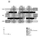
- FIG. 1is an image diagram showing the entire layout of the semiconductor memory circuit according to the embodiment.
- the semiconductor memory circuit 100 of FIG. 1includes first and second memory cell arrays 11 and 12 each having a plurality of memory cells 10 aligned in the X and Y directions.
- the first memory cell array 11 and the second memory cell array 12are arranged side by side in the Y direction with a space.
- each of the first and second memory cell arrays 11 and 12has 256 rows
- the semiconductor memory circuit 100has a total of 512 rows of memory.
- the first and second memory cell arrays 11 and 12are provided with word lines WL * (*: 0 to 511) extending in the X direction and bit line pairs BL / BLB extending in the Y direction.
- Each 10is connected to one of the word lines WL * and one of the bit line pair BL / BLB.
- An inter-array block 50is provided between the first memory cell array 11 and the second memory cell array 12.
- FIG. 2is a diagram showing a circuit configuration of the memory cell 10.
- the memory cell 10is a 6Tr-SRAM, that is, an SRAM (Static Random Access Memory) cell composed of six transistors. Between the VDD and the VSS, a P-type transistor P1 and an N-type transistor N1 connected in series and a P-type transistor P2 and an N-type transistor N2 connected in series are provided. The gates of the P-type transistor P1 and the N-type transistor N1 are connected to the drains of the P-type transistor P2 and the N-type transistor N2.
- the gates of the P-type transistor P2 and the N-type transistor N2are connected to the drains of the P-type transistor P1 and the N-type transistor N1.
- An N-type transistor N3 serving as a transfer gateis provided between the bit line BL and the drains of the P-type transistor P1 and the N-type transistor N1.
- An N-type transistor N4 serving as a transfer gateis provided between the bit line BLB and the drains of the P-type transistor P2 and the N-type transistor N2.
- the word line WLis connected to the gates of the N-type transistors N3 and N4.
- the semiconductor memory circuit 100includes an I / O circuit 15, first and second row decoders 21 and 22, and a control circuit 30 as peripheral circuits.
- the I / O circuit 15is a circuit for writing and reading data to and from the first and second memory cell arrays 11 and 12, and is connected to each pair of bit lines BL and BLB.
- the first row decoder 21includes a plurality of word line drivers 20 respectively corresponding to the respective rows of the first memory cell array 11, and drives the word lines WL0 to WL255.
- the second row decoder 22includes a plurality of word line drivers 20 respectively corresponding to the respective rows of the second memory cell array 12, and drives the word lines WL256 to WL511.
- the second row decoder 22is arranged side by side with the first row decoder 21 in the Y direction.
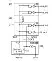
- Control circuit 30receives address signal Address and clock signal Clock from the outside of semiconductor memory circuit 100.
- the control circuit 30includes a row address decoder 31.
- the row address decoder 31receives an address signal Address and generates a plurality of (here, 512 bits) decoded address signal SAD.
- the bit signals of the decode address signal SADare sent to the word line drivers 20 included in the first and second row decoders 21 and 22, respectively.
- the control circuit 30also receives the clock signal Clock and generates a clock signal SCK.
- the clock signal SCKis sent to each word line driver 20 included in the first and row decoders 21 and 22.
- the clock signal SCKis an example of a control signal in the present disclosure.
- a relay buffer 40is provided between the first row decoder 21 and the second row decoder 22 for buffering the clock signal SCK and outputting it as the clock signal SCKa supplied to the second row decoder 22.
- Each word line driver 20 of the first row decoder 21directly receives the clock signal SCK output from the control circuit 30.
- each word line driver 20 of the second row decoder 22receives the clock signal SCKa via the relay buffer 40.
- the inter-array block 50is composed of tap cells and dummy memory cells.
- a tap cellis a cell that supplies a potential to a substrate or a well.
- the dummy memory cellis a cell having a circuit structure similar to that of the memory cell 10 but not operating as a memory cell.
- the relay buffer 40 and the inter-array block 50face each other in the X direction, and the position and size in the Y direction are the same.
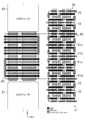
- FIG. 3is a diagram showing a detailed layout in which a part of FIG. 1 is enlarged.
- FIG. 3the boundary portion between the first memory cell array 11, the second memory cell array 12, the first row decoder 21, and the second row decoder 22 is shown.
- FIG. 4is a view of FIG. 3 from which the metal wiring layer is omitted.
- FIGS. 3 and 4the internal layout of the first and second row decoders 21 and 22 is omitted. The same applies to the subsequent figures.
- two memory cells 10 included in the first memory cell array 11are respectively supplied with word line signals WL254 and WL255 from the first row decoder 21.
- the word line signals WL256 and WL257are supplied from the second row decoder 22 to the two memory cells 10 included in the second memory cell array 12, respectively.
- FIG. 5is an enlarged view of the layout of the memory cell 10. As shown in FIG. 5, the P-type transistors P1 and P2 and the N-type transistors N1, N2, N3 and N4 described in the circuit configuration of FIG. 2 are respectively arranged. The height (size in the Y direction) of the memory cell 10 is twice the gate pitch.
- a relay buffer 40is provided between the first row decoder 21 and the second row decoder 22 for buffering the clock signal SCK and outputting it as a clock signal SCKa.
- the height of the relay buffer 40is eight times the gate pitch.
- FIG. 6is a circuit diagram of a dummy memory cell.
- the layout of dummy memory cells 51a and 51bis the same as the layout of 10 in FIG. However, in the dummy memory cells 51a and 51b, the word line WL is supplied with VSS.
- the heights of the dummy memory cells 51a and 51bare the same as those of the memory cell 10, and are twice the gate pitch.
- FIG. 7is an enlarged view of the layout of the tap cell 52.
- the tap cell 52supplies VSS, which is supplied via a metal wire (Metal 2) extending in the X direction, to the diffusion regions 521 and 522. Further, the tap cell 52 supplies the diffusion region 523 with VDD, which is supplied via the metal wire (Metal 1) extending in the Y direction. Then, VDD and VSS are supplied to the substrate or well through the diffusion regions 521, 522 and 523.
- the height of the tap cell 52is four times the gate pitch.
- the tap cell 52is not connected to the bit lines BL and BLB.
- dummy memory cells 51a and 51b and tap cells 52are arranged in the Y direction in the inter-array block 50 facing in the X direction with respect to the relay buffer 40 having a height eight times the gate pitch. It is arranged side by side. Since the heights of the dummy memory cells 51a and 51b are twice the gate pitch and the heights of the tap cells 52 are four times the gate pitch, the height of the inter-array block 50 is eight times the gate pitch. That is, the relay buffer 40 and the inter-array block 50 have the same position and size in the Y direction. In other words, it can be said that the region between the first row decoder 21 and the second row decoder 22 has the same position and size as the inter-array block 50 in the Y direction.
- the first memory cell array 11, the inter-array block 50, and the second memory cell array 12each have a plurality of gates extending in the X direction, and the first memory cell array 11, the array In the intermediate block 50 and the second memory cell array 12, the gate pitch in the Y direction is uniform.
- the bit lines BL and BLBextend over the first memory cell array 11, the inter-array block 50, and the second memory cell array 12 in the Y direction.
- the memory cell array that occupies most of the semiconductor memory circuitis designed to have the smallest possible area.
- the memory cell arrayadopts a design rule different from that of other circuit parts, and the area reduction is achieved by this unique design rule.
- optical dummyhas a shape that simulates the layout of the memory cell array, but does not contribute to the operation of the memory cell.
- the inter-array block 50 between the first memory cell array 11 and the second memory cell array 12is configured by the dummy memory cells 51 a and 51 b and the tap cell 52.
- the dummy memory cells 51a and 51b and the tap cell 52adopt the same design rule as the first and second memory cell arrays 11 and 12, so that the first memory cell array 11, the inter-array block 50, and the second memory cell array 12 As a whole, the memory cell array is substantially single. That is, it is not necessary to arrange a space as an optical dummy or a buffer zone between the first memory cell array 11 and the second memory cell array 12 as in the above-described comparative example. Therefore, the generation of dead space around the relay buffer 40 can be suppressed.
- the number of dummy memory cells and tap cells arranged in the inter-array block 50can be adjusted in accordance with the size of the relay buffer 40.
- two dummy memory cells having a height twice the gate pitch and four times the gate pitchare higher than the relay buffer 40 having a height eight times the gate pitch.
- One tap cell having a small sizeis arranged in the inter-array block 50 to match the size in the Y direction. Besides this, for example, when the relay buffer 40 has a height four times the gate pitch, two dummy memory cells having a height twice the gate pitch, or a height four times the gate pitch
- One tap cell having themay be arranged in the inter-array block 50.
- the relay buffer 40When the relay buffer 40 has a height 16 times the gate pitch, for example, four dummy memory cells having a height twice the gate pitch and a tap cell having a height 4 times the gate pitch. Two may be arranged in the inter-array block 50. Therefore, even when the load capacity to be driven by the relay buffer 40 changes and it is desired to change the size, it is possible to flexibly cope with the size change of the relay buffer 40.
- the clock signal SCKis buffered between the first row decoder 21 and the second row decoder 22 and the clock signal SCKa supplied to the second row decoder 22 is output.
- a relay buffer 40is provided.
- the relay buffer 40suppresses the wiring delay relating to the clock signal SCKa supplied to the second row decoder 22.
- the inter-array block 50 between the first memory cell array 11 and the second memory cell array 12is composed of the tap cells 52 and the dummy memory cells 51a and 51b.
- the relay buffer 40 and the inter-array block 50have the same position and size in the Y direction.
- the region between the first row decoder 21 and the second row decoder 22has the same position and size as the inter-array block 50 in the Y direction. For this reason, useless dead space does not occur between the relay buffer 40 and the first and second row decoders 21 and 22. Therefore, in the semiconductor memory circuit 100, it is possible to suppress the increase in area while suppressing the performance deterioration due to the increase in wiring delay due to the wiring resistance.
- FIG. 8is a diagram showing a detailed layout in the modification. Further, FIG. 9 is a view in which the metal wiring layer is omitted from FIG. FIGS. 8 and 9 show the same parts as the detailed layouts of FIGS. 3 and 4, and common components are denoted by the same reference numerals.
- the inter-array block 50 between the first memory cell array 11 and the second memory cell array 12is constituted by only dummy memory cells. That is, in the inter-array block 50, dummy memory cells 51a, 51b, 51c, 51d are provided.
- dummy memory cells 51a, 51b, 51c, 51dare arranged in the Y direction in the inter-array block 50 facing in the X direction with respect to the relay buffer 40 having a height eight times the gate pitch. It is arranged side by side. Since the heights of the dummy memory cells 51a, 51b, 51c, and 51d are twice the gate pitch, the height of the inter-array block 50 is eight times the gate pitch. That is, the relay buffer 40 and the inter-array block 50 have the same position and size in the Y direction.
- the region between the first row decoder 21 and the second row decoder 22has the same position and size as the inter-array block 50 in the Y direction. Therefore, also in this modification, the same operation and effect as those of the above-described embodiment can be obtained.
- the relay buffer 40buffers the clock signal SCK supplied to the first row decoder 21 and supplies the clock signal SCK to the second row decoder 22.
- the control circuit 30generates the clock signal SCK2 separately from the clock signal SCK1 supplied to the first row decoder 21, and the relay buffer 40 directly transmits the clock signal SCK2 from the control circuit 30. It may be received, buffered and supplied to the second row decoder 22. Thereby, the propagation of the clock signals SCK1 and SCK2 to the word line drivers 20 is speeded up.
- the bit line pair BL, BLBis arranged to continuously extend from the first memory cell array 11 to the inter-array block 50 and the second memory cell array 12.
- the bit line pair connected to the first memory cell array 11 and the bit line pair connected to the second memory cell array 12are not directly connected without arranging the bit line pair on the inter-array block 50. It is good also as composition. In this configuration, the load capacitance due to the dummy memory cell of inter-array block 50 is not added to any bit line pair, so the operation of the semiconductor memory circuit is more stable.
- the inter-array block 50is configured by the dummy memory cells and the tap cells, and in the modification, the inter-array block 50 is configured only by the dummy memory cells. May be constituted by only tap cells.
- the semiconductor memory circuit 100includes two memory cell arrays 11 and 12, the number of rows of each of the memory cell arrays 11 and 12 is 256, and the number of rows of the entire semiconductor memory circuit 100 is 512.
- the number of memory cell arrays in the semiconductor memory circuit and the sizes of the memory cell array and the semiconductor memory circuitare not limited to those described in the above embodiment.
- the semiconductor memory circuitmay include three memory cell arrays arranged in the Y direction, and the configuration as described above may be employed for two inter-array blocks between the memory cell arrays.
- the memory cellis a 6 Tr 1-port memory cell as shown in FIG. 2.
- the configuration of the memory cellis not limited to this. For example, even if it is a 2-port memory cell Good.
- SYMBOLS 10memory cell 11 1st memory cell array 12 2nd memory cell array 20 word line driver 21 1st row decoder 22 2nd row decoder 30 control circuit 40 relay buffer 50 inter-array block 51a, 51b, 51c, 51d dummy memory cell 52 tap cell 100
Landscapes
- Engineering & Computer Science (AREA)
- Microelectronics & Electronic Packaging (AREA)
- Computer Hardware Design (AREA)
- Static Random-Access Memory (AREA)
- Semiconductor Memories (AREA)
Abstract
Translated fromJapaneseDescription
Translated fromJapanese本開示は、半導体記憶回路に関し、特にそのレイアウト構造に関する。The present disclosure relates to a semiconductor memory circuit, and more particularly to the layout structure thereof.
近年の半導体集積回路において、SRAM(Static Random Access Memory)等の半導体記憶回路はその多くの領域を占めている。このため、半導体記憶回路について、性能を高く保つとともに、面積の増大を抑制することが重要である。また、微細化の進展に伴い、配線抵抗が増大し、これによる配線遅延が増加している。配線遅延による性能の劣化が問題の1つとなっている。In recent semiconductor integrated circuits, semiconductor memory circuits such as static random access memories (SRAMs) occupy a large area. Therefore, it is important for the semiconductor memory circuit to keep high performance and to suppress an increase in area. In addition, with the progress of miniaturization, wiring resistance increases, and wiring delay due to this increases. Deterioration of performance due to wiring delay is one of the problems.
特許文献1では、SRAMメモリにおいて、アドレスバッファから出力されたアドレスをロウデコーダに備えられたゲートに伝達する構成が開示されている。特許文献2では、SRAMメモリにおいて、メモリに供給される各種制御信号を伝達するためにバッファ回路が挿入される構成が開示されている。
特許文献1の構成では、メモリのロウ数が増えると、アドレスが伝達される配線の配線抵抗により配線遅延が増加し、メモリの性能が劣化するという問題がある。また、特許文献2の構成では、バッファ挿入によって配線遅延の問題は解決されているが、バッファ挿入による面積の増加については詳細には検討されていない。In the configuration of
本開示は、半導体記憶回路において、配線抵抗に起因した配線遅延の増加による性能劣化を抑制しつつ、面積の増加を抑制することを目的とする。An object of the present disclosure is to suppress an increase in area in a semiconductor memory circuit while suppressing a performance deterioration due to an increase in wiring delay caused by a wiring resistance.
本開示の第1態様では、半導体記憶回路は、XY方向に並ぶ複数のメモリセルを有する第1メモリセルアレイと、XY方向に並ぶ複数のメモリセルを有し、Y方向において前記第1メモリセルアレイと離間して並ぶ、第2メモリセルアレイと、前記第1メモリセルアレイの各ロウにそれぞれ対応する複数のワード線ドライバを含む、第1ロウデコーダと、前記第2メモリセルアレイの各ロウにそれぞれ対応する複数のワード線ドライバを含み、Y方向において前記第1ロウデコーダと離間して並ぶ、第2ロウデコーダと、前記第1および第2ロウデコーダに供給する制御信号を生成する制御回路と、前記第1ロウデコーダと前記第2ロウデコーダとの間に設けられており、前記第2ロウデコーダに供給される制御信号をバッファリングする中継バッファと、前記第1メモリセルアレイと前記第2メモリセルアレイとの間に設けられており、タップセルまたはダミーメモリセルのうち少なくともいずれか一方によって構成されたアレイ間ブロックとを備え、前記中継バッファと前記アレイ間ブロックとは、Y方向における位置とサイズが同一である。In a first aspect of the present disclosure, a semiconductor memory circuit includes a first memory cell array having a plurality of memory cells aligned in the XY direction, and a plurality of memory cells aligned in the XY direction, and the first memory cell array in the Y direction A plurality of first row decoders, each including a plurality of word line drivers corresponding to a second memory cell array and a plurality of word line drivers respectively corresponding to the respective rows of the first memory cell array, and a plurality corresponding to each row of the second memory cell array A second row decoder including a word line driver and spaced apart from the first row decoder in the Y direction, a control circuit generating a control signal to be supplied to the first and second row decoders, and It is provided between a row decoder and the second row decoder, and buffers control signals supplied to the second row decoder. A relay buffer, and an inter-array block provided between the first memory cell array and the second memory cell array, and configured by at least one of a tap cell and a dummy memory cell; The inter-array block has the same position and size in the Y direction.
この態様によると、第1ロウデコーダと第2ロウデコーダとの間に、第2ロウデコーダに供給される制御信号をバッファリングする中継バッファが設けられている。この中継バッファによって、第2ロウデコーダに供給される制御信号に係る配線遅延が抑制される。また、第1メモリセルアレイと第2メモリセルアレイとの間にあるアレイ間ブロックは、タップセルまたはダミーメモリセルのうち少なくともいずれか一方によって構成されている。そして、中継バッファとアレイ間ブロックとは、Y方向における位置とサイズが同一である。このため、中継バッファと第1および第2ロウデコーダとの間には、無駄なデッドスペースが生じない。したがって、半導体記憶回路において、配線抵抗に起因した配線遅延の増加による性能劣化を抑制しつつ、面積の増加を抑制することができる。According to this aspect, the relay buffer that buffers the control signal supplied to the second row decoder is provided between the first row decoder and the second row decoder. The relay buffer suppresses the wiring delay related to the control signal supplied to the second row decoder. Further, the inter-array block between the first memory cell array and the second memory cell array is configured by at least one of a tap cell and a dummy memory cell. The relay buffer and the inter-array block have the same position and size in the Y direction. For this reason, useless dead space does not occur between the relay buffer and the first and second row decoders. Therefore, in the semiconductor memory circuit, it is possible to suppress the increase in area while suppressing the performance deterioration due to the increase in the wiring delay due to the wiring resistance.
本開示の第2態様では、半導体記憶回路は、XY方向に並ぶ複数のメモリセルを有する第1メモリセルアレイと、XY方向に並ぶ複数のメモリセルを有し、Y方向において前記第1メモリセルアレイと離間して並ぶ、第2メモリセルアレイと、前記第1メモリセルアレイの各ロウにそれぞれ対応する複数のワード線ドライバを含む、第1ロウデコーダと、前記第2メモリセルアレイの各ロウにそれぞれ対応する複数のワード線ドライバを含み、Y方向において前記第1ロウデコーダと離間して並ぶ、第2ロウデコーダと、前記第1および第2ロウデコーダに供給する制御信号を生成する制御回路と、前記第1ロウデコーダと前記第2ロウデコーダとの間に設けられており、前記第2ロウデコーダに供給される制御信号をバッファリングする中継バッファと、前記第1メモリセルアレイと前記第2メモリセルアレイとの間に設けられており、タップセルまたはダミーメモリセルのうち少なくともいずれか一方によって構成されたアレイ間ブロックとを備え、前記第1ロウデコーダと前記第2ロウデコーダとの間の領域は、前記アレイ間ブロックと、Y方向における位置とサイズが同一である。In a second aspect of the present disclosure, a semiconductor memory circuit includes a first memory cell array having a plurality of memory cells aligned in the XY direction, and a plurality of memory cells aligned in the XY direction, and the first memory cell array in the Y direction A plurality of first row decoders, each including a plurality of word line drivers corresponding to a second memory cell array and a plurality of word line drivers respectively corresponding to the respective rows of the first memory cell array, and a plurality corresponding to each row of the second memory cell array A second row decoder including a word line driver and spaced apart from the first row decoder in the Y direction, a control circuit generating a control signal to be supplied to the first and second row decoders, and It is provided between a row decoder and the second row decoder, and buffers control signals supplied to the second row decoder. A relay buffer, and an inter-array block provided between the first memory cell array and the second memory cell array and configured by at least one of a tap cell and a dummy memory cell; The region between the decoder and the second row decoder has the same position and size in the Y direction as the inter-array block.
この態様によると、第1ロウデコーダと第2ロウデコーダとの間に、第2ロウデコーダに供給される制御信号をバッファリングする中継バッファが設けられている。この中継バッファによって、第2ロウデコーダに供給される制御信号に係る配線遅延が抑制される。また、第1メモリセルアレイと第2メモリセルアレイとの間にあるアレイ間ブロックは、タップセルまたはダミーメモリセルのうち少なくともいずれか一方によって構成されている。そして、第1ロウデコーダと第2ロウデコーダとの間の領域は、アレイ間ブロックと、Y方向における位置とサイズが同一である。このため、中継バッファと第1および第2ロウデコーダとの間には、無駄なデッドスペースが生じない。したがって、半導体記憶回路において、配線抵抗に起因した配線遅延の増加による性能劣化を抑制しつつ、面積の増加を抑制することができる。According to this aspect, the relay buffer that buffers the control signal supplied to the second row decoder is provided between the first row decoder and the second row decoder. The relay buffer suppresses the wiring delay related to the control signal supplied to the second row decoder. Further, the inter-array block between the first memory cell array and the second memory cell array is configured by at least one of a tap cell and a dummy memory cell. The region between the first row decoder and the second row decoder has the same position and size in the Y direction as the inter-array block. For this reason, useless dead space does not occur between the relay buffer and the first and second row decoders. Therefore, in the semiconductor memory circuit, it is possible to suppress the increase in area while suppressing the performance deterioration due to the increase in the wiring delay due to the wiring resistance.
本開示によると、半導体記憶回路において、配線抵抗に起因した配線遅延の増加による性能劣化を抑制しつつ、面積の増加を抑制することができる。According to the present disclosure, in the semiconductor memory circuit, it is possible to suppress the increase in area while suppressing the performance deterioration due to the increase in the wiring delay due to the wiring resistance.
以下、実施の形態について、図面を参照して説明する。Embodiments will be described below with reference to the drawings.
図1は実施形態に係る半導体記憶回路の全体レイアウトを示すイメージ図である。図1の半導体記憶回路100は、XY方向に並ぶ複数のメモリセル10を有する第1および第2メモリセルアレイ11,12を備える。第1メモリセルアレイ11と第2メモリセルアレイ12はY方向において離間して並べて配置されている。本実施形態では、第1および第2メモリセルアレイ11,12はそれぞれ256ロウを有し、半導体記憶回路100は全体で512ロウのメモリを備える。第1および第2メモリセルアレイ11,12には、X方向に延びるワード線WL*(*は0~511)と、Y方向に延びるビット線対BL/BLBとが設けられており、各メモリセル10はそれぞれ、ワード線WL*のいずれかとビット線対BL/BLBのいずれかとに接続されている。そして、第1メモリセルアレイ11と第2メモリセルアレイ12との間に、アレイ間ブロック50が設けられている。FIG. 1 is an image diagram showing the entire layout of the semiconductor memory circuit according to the embodiment. The
図2はメモリセル10の回路構成を示す図である。図2に示すように、メモリセル10は6Tr-SRAM、すなわち6個のトランジスタからなるSRAM(Static Random Access Memory)セルである。VDDとVSSとの間に、直列に接続されたP型トランジスタP1およびN型トランジスタN1と、直列に接続されたP型トランジスタP2およびN型トランジスタN2とが設けられている。P型トランジスタP1およびN型トランジスタN1のゲートが、P型トランジスタP2およびN型トランジスタN2のドレインと接続されている。P型トランジスタP2およびN型トランジスタN2のゲートが、P型トランジスタP1およびN型トランジスタN1のドレインと接続されている。ビット線BLとP型トランジスタP1およびN型トランジスタN1のドレインとの間に、トランスファーゲートとなるN型トランジスタN3が設けられている。ビット線BLBとP型トランジスタP2およびN型トランジスタN2のドレインとの間に、トランスファーゲートとなるN型トランジスタN4が設けられている。ワード線WLがN型トランジスタN3,N4のゲートと接続されている。FIG. 2 is a diagram showing a circuit configuration of the
図1に戻り、半導体記憶回路100は、周辺回路として、I/O回路15、第1および第2ロウデコーダ21,22、および、制御回路30を備える。I/O回路15は第1および第2メモリセルアレイ11,12に対してデータの書き込みおよび読み出しを行う回路であり、各ビット線対BL,BLBと接続されている。第1ロウデコーダ21は第1メモリセルアレイ11の各ロウにそれぞれ対応する複数のワード線ドライバ20を含み、ワード線WL0~WL255を駆動する。第2ロウデコーダ22は、第2メモリセルアレイ12の各ロウにそれぞれ対応する複数のワード線ドライバ20を含み、ワード線WL256~WL511を駆動する。第2ロウデコーダ22はY方向において第1ロウデコーダ21と離間して並べて配置されている。Returning to FIG. 1, the
制御回路30は半導体記憶回路100の外部からアドレス信号Addressとクロック信号Clockを受ける。制御回路30はロウアドレスデコーダ31を備えており、ロウアドレスデコーダ31はアドレス信号Addressを受けて、複数ビット(ここでは512ビット)のデコードアドレス信号SADを生成する。デコードアドレス信号SADの各ビット信号は、第1および第2ロウデコーダ21,22に含まれる各ワード線ドライバ20にそれぞれ送られる。また、制御回路30はクロック信号Clockを受けて、クロック信号SCKを生成する。クロック信号SCKが第1およびロウデコーダ21,22に含まれる各ワード線ドライバ20に送られる。クロック信号SCKは本開示における制御信号の一例である。
また、第1ロウデコーダ21と第2ロウデコーダ22との間に、クロック信号SCKをバッファリングして、第2ロウデコーダ22に供給されるクロック信号SCKaとして出力する中継バッファ40が設けられている。第1ロウデコーダ21の各ワード線ドライバ20は、制御回路30から出力されたクロック信号SCKを直接受ける。一方、第2ロウデコーダ22の各ワード線ドライバ20は、中継バッファ40を介してクロック信号SCKaを受ける。Further, a
本実施形態では、アレイ間ブロック50はタップセルおよびダミーメモリセルによって構成されている。タップセルとは、基板またはウェルに電位を供給するセルである。ダミーメモリセルとは、回路構造はメモリセル10と同様であるが、メモリセルとしての動作を行わないセルである。そして、中継バッファ40とアレイ間ブロック50とは、X方向において対向しており、Y方向における位置とサイズが同一である。In the present embodiment, the
図3は図1の一部を拡大した詳細レイアウトを示す図である。図3では、第1メモリセルアレイ11,第2メモリセルアレイ12,第1ロウデコーダ21,第2ロウデコーダ22の境界部分について示している。また、図4は図3からメタル配線層を省いた図である。なお、図3および図4では、第1および第2ロウデコーダ21,22の内部レイアウトは図示を省略している。以降の図も同様である。FIG. 3 is a diagram showing a detailed layout in which a part of FIG. 1 is enlarged. In FIG. 3, the boundary portion between the first
図3および図4において、第1メモリセルアレイ11に含まれる2個のメモリセル10には、第1ロウデコーダ21からワード線信号WL254,WL255がそれぞれ供給されている。第2メモリセルアレイ12に含まれる2個のメモリセル10には、第2ロウデコーダ22からワード線信号WL256,WL257がそれぞれ供給されている。In FIGS. 3 and 4, two
図5はメモリセル10のレイアウトの拡大図である。図5に示すように、図2の回路構成で説明したP型トランジスタP1,P2およびN型トランジスタN1,N2,N3,N4が、それぞれ配置されている。そして、メモリセル10の高さ(Y方向におけるサイズ)はゲートピッチの2倍である。FIG. 5 is an enlarged view of the layout of the
そして、第1ロウデコーダ21と第2ロウデコーダ22との間に、クロック信号SCKをバッファリングしてクロック信号SCKaとして出力する中継バッファ40が設けられている。図3および図4の構成では、中継バッファ40の高さはゲートピッチの8倍になっている。A
また、第1メモリセルアレイ11と第2メモリセルアレイ12との間のアレイ間ブロック50では、ダミーメモリセル51a,51bと、タップセル52とが設けられている。図6はダミーメモリセルの回路構成図である。ダミーメモリセル51a,51bのレイアウトは図5の10のレイアウトと同様である。ただし、ダミーメモリセル51a,51bでは、ワード線WLにVSSが供給される。ダミーメモリセル51a,51bの高さはメモリセル10と同じであり、ゲートピッチの2倍である。In the
図7はタップセル52のレイアウトの拡大図である。図7に示すように、タップセル52は、X方向に延びるメタル配線(Metal 2)を介して供給されるVSSを、拡散領域521,522に供給する。また、タップセル52は、Y方向に延びるメタル配線(Metal 1)を介して供給されるVDDを、拡散領域523に供給する。そして拡散領域521,522,523を介して基板またはウェルにVDD,VSSが供給される。タップセル52の高さはゲートピッチの4倍である。なお、タップセル52は、ビット線BL,BLBとは接続されていない。FIG. 7 is an enlarged view of the layout of the
図3および図4の構成では、ゲートピッチの8倍の高さを持つ中継バッファ40に対して、X方向に対向するアレイ間ブロック50に、ダミーメモリセル51a,51bおよびタップセル52がY方向に並べて配置されている。ダミーメモリセル51a,51bの高さはゲートピッチの2倍であり、タップセル52の高さはゲートピッチの4倍であるので、アレイ間ブロック50の高さはゲートピッチの8倍である。すなわち、中継バッファ40とアレイ間ブロック50とは、Y方向における位置とサイズが同一である。これは言い換えると、第1ロウデコーダ21と第2ロウデコーダ22との間の領域は、アレイ間ブロック50と、Y方向における位置とサイズが同一である、といえる。In the configurations of FIGS. 3 and 4,
また、図3および図4の構成では、第1メモリセルアレイ11、アレイ間ブロック50、および、第2メモリセルアレイ12は、それぞれ、X方向に延びる複数のゲートを備え、第1メモリセルアレイ11、アレイ間ブロック50、および、第2メモリセルアレイ12において、Y方向におけるゲートピッチは、均一である。また、ビット線BL,BLBは、Y方向において、第1メモリセルアレイ11、アレイ間ブロック50、および、第2メモリセルアレイ12にわたって延びている。Further, in the configurations of FIGS. 3 and 4, the first
ここで、半導体集積回路では一般に、SRAM等の半導体記憶回路が占める面積の割合は大きい。このため、半導体記憶回路の大部分を占めるメモリセルアレイについて、面積ができるだけ小さくなるように設計している。具体的には、メモリセルアレイについて他の回路部分と異なるデザインルールを採用し、この独自のデザインルールによって小面積化を図っている。Here, in the semiconductor integrated circuit, generally, the ratio of the area occupied by the semiconductor storage circuit such as the SRAM is large. Therefore, the memory cell array that occupies most of the semiconductor memory circuit is designed to have the smallest possible area. Specifically, the memory cell array adopts a design rule different from that of other circuit parts, and the area reduction is achieved by this unique design rule.
一方、デザインルールの相違に起因して、メモリセルアレイと他の回路部分との境界領域において、緩衝地帯としてのスペースを設けなくてはならない場合がある。さらに、メモリセルアレイの周囲には、光学ダミーと呼ばれるダミーパタンを配置する必要がある。光学ダミーは、メモリセルアレイのレイアウトを模した形状を有するが、メモリセルの動作には寄与しない。On the other hand, due to the difference in design rules, it may be necessary to provide a space as a buffer zone in the boundary region between the memory cell array and the other circuit portion. Furthermore, it is necessary to arrange a dummy pattern called an optical dummy around the memory cell array. The optical dummy has a shape that simulates the layout of the memory cell array, but does not contribute to the operation of the memory cell.
対比例として、第1ロウデコーダ21と第2ロウデコーダ22との間に中継バッファ40を設けるために、第1メモリセルアレイ11と第2メモリセルアレイ12との間に単純にスペースを設けた構成を想定する。この場合には、第1メモリセルアレイ11の第2メモリセルアレイ12側の境界に光学ダミーを配置するとともに、第2メモリセルアレイ12の第1メモリセルアレイ11側の境界に光学ダミーを配置し、さらに第1メモリセルアレイ11と第2メモリセルアレイ12との間に緩衝地帯としてのスペースを設ける必要がある。これら光学ダミーとスペースを合わせた合計のサイズが中継バッファ40のサイズよりも大きい場合には、中継バッファ40と第1および第2ロウデコーダ21,22との間に、デッドスペースが発生してしまう。このことは半導体記憶回路のレイアウト面積の増大につながってしまうので好ましくない。As a comparative example, in order to provide the
これに対して本実施形態では、第1メモリセルアレイ11と第2メモリセルアレイ12との間のアレイ間ブロック50は、ダミーメモリセル51a,51bおよびタップセル52によって構成されている。ダミーメモリセル51a,51bおよびタップセル52は、第1および第2メモリセルアレイ11,12と同一のデザインルールが採用されるため、第1メモリセルアレイ11,アレイ間ブロック50,および第2メモリセルアレイ12は、全体として、実質的に単一のメモリセルアレイとなる。すなわち、上述の対比例のように、光学ダミーや緩衝地帯としてのスペースを第1メモリセルアレイ11と第2メモリセルアレイ12との間に配置する必要がない。したがって、中継バッファ40の周囲におけるデッドスペースの発生を抑制することができる。On the other hand, in the present embodiment, the
また、本実施形態では、中継バッファ40のサイズに合わせて、アレイ間ブロック50に配置するダミーメモリセルやタップセルの個数を調整することができる。図3および図4の例では、ゲートピッチの8倍の高さを持つ中継バッファ40に対して、ゲートピッチの2倍の高さを持つダミーメモリセルを2個、ゲートピッチの4倍の高さを持つタップセルを1個、アレイ間ブロック50に配置して、Y方向におけるサイズを合わせている。この他にも例えば、中継バッファ40がゲートピッチの4倍の高さを持つ場合は、ゲートピッチの2倍の高さを持つダミーメモリセルを2個、あるいは、ゲートピッチの4倍の高さを持つタップセルを1個、アレイ間ブロック50に配置すればよい。また、中継バッファ40がゲートピッチの16倍の高さを持つ場合は、例えば、ゲートピッチの2倍の高さを持つダミーメモリセルを4個、ゲートピッチの4倍の高さを持つタップセルを2個、アレイ間ブロック50に配置すればよい。したがって、中継バッファ40が駆動すべき負荷容量が変化し、そのサイズを変更したい場合であっても、中継バッファ40のサイズ変更に対して柔軟に対応することができる。Further, in the present embodiment, the number of dummy memory cells and tap cells arranged in the
以上のように本実施形態によると、第1ロウデコーダ21と第2ロウデコーダ22との間に、クロック信号SCKをバッファリングして、第2ロウデコーダ22に供給されるクロック信号SCKaを出力する中継バッファ40が設けられている。この中継バッファ40によって、第2ロウデコーダ22に供給されるクロック信号SCKaに係る配線遅延が抑制される。また、第1メモリセルアレイ11と第2メモリセルアレイ12との間にあるアレイ間ブロック50は、タップセル52およびダミーメモリセル51a,51bによって構成されている。そして、中継バッファ40とアレイ間ブロック50とは、Y方向における位置とサイズが同一である。あるいは、第1ロウデコーダ21と第2ロウデコーダ22との間の領域は、アレイ間ブロック50と、Y方向における位置とサイズが同一である。このため、中継バッファ40と第1および第2ロウデコーダ21,22との間には、無駄なデッドスペースが生じない。したがって、半導体記憶回路100において、配線抵抗に起因した配線遅延の増加による性能劣化を抑制しつつ、面積の増加を抑制することができる。As described above, according to the present embodiment, the clock signal SCK is buffered between the
(変形例)
図8は変形例における詳細レイアウトを示す図である。また、図9は図8からメタル配線層を省いた図である。図8および図9は図3および図4の詳細レイアウトと同じ部分を示しており、共通の構成要素には同一の符号を付している。(Modification)
FIG. 8 is a diagram showing a detailed layout in the modification. Further, FIG. 9 is a view in which the metal wiring layer is omitted from FIG. FIGS. 8 and 9 show the same parts as the detailed layouts of FIGS. 3 and 4, and common components are denoted by the same reference numerals.
図8および図9では、第1メモリセルアレイ11と第2メモリセルアレイ12との間のアレイ間ブロック50は、ダミーメモリセルのみによって構成されている。すなわち、アレイ間ブロック50では、ダミーメモリセル51a,51b,51c,51dが設けられている。In FIGS. 8 and 9, the
図8および図9の構成では、ゲートピッチの8倍の高さを持つ中継バッファ40に対して、X方向に対向するアレイ間ブロック50に、ダミーメモリセル51a,51b,51c,51dがY方向に並べて配置されている。ダミーメモリセル51a,51b,51c,51dの高さはゲートピッチの2倍であるので、アレイ間ブロック50の高さはゲートピッチの8倍である。すなわち、中継バッファ40とアレイ間ブロック50とは、Y方向における位置とサイズが同一である。これは言い換えると、第1ロウデコーダ21と第2ロウデコーダ22との間の領域は、アレイ間ブロック50と、Y方向における位置とサイズが同一である、といえる。したがって、本変形例においても、上述の実施形態と同様の作用効果を得ることができる。In the configurations of FIGS. 8 and 9,
(他の構成)
上述の実施形態では、中継バッファ40は、第1ロウデコーダ21に供給された後のクロック信号SCKをバッファリングして、第2ロウデコーダ22に供給するものとした。これに代えて、図10に示すように、制御回路30は第1ロウデコーダ21に供給するクロック信号SCK1と別個にクロック信号SCK2を生成し、中継バッファ40はクロック信号SCK2を制御回路30から直接受けて、バッファリングして第2ロウデコーダ22に供給する構成としてもよい。これにより、各ワード線ドライバ20へのクロック信号SCK1,SCK2の伝搬が高速化される。(Other configuration)
In the above-described embodiment, the
また、上述の実施形態では、ビット線対BL,BLBは、第1メモリセルアレイ11からアレイ間ブロック50、第2メモリセルアレイ12にかけて連続して延びるように配置されていた。これに対して、アレイ間ブロック50上にはビット線対を配置しないで、第1メモリセルアレイ11に接続されたビット線対と第2メモリセルアレイ12に接続されたビット線対とが、直接つながらない構成としてもよい。この構成の場合には、アレイ間ブロック50のダミーメモリセルによる負荷容量がいずれのビット線対にも付加されないので、半導体記憶回路の動作がより安定する。Further, in the above-described embodiment, the bit line pair BL, BLB is arranged to continuously extend from the first
また、上述の実施形態では、アレイ間ブロック50は、ダミーメモリセルとタップセルによって構成されており、変形例では、アレイ間ブロック50はダミーメモリセルのみによって構成されるとしたが、アレイ間ブロック50はタップセルのみによって構成されるとしてもよい。In the above embodiment, the
また、上述の実施形態では、半導体記憶回路100は2個のメモリセルアレイ11,12を備えており、メモリセルアレイ11,12それぞれのロウ数は256であり、半導体記憶回路100全体のロウ数は512とした。ただし、半導体記憶回路におけるメモリセルアレイの個数や、メモリセルアレイや半導体記憶回路のサイズについては、上述の実施形態で示したものに限られるものではない。例えば、半導体記憶回路がY方向に並ぶ3個のメモリセルアレイを備えており、メモリセルアレイ同士の間の2個のアレイ間ブロックについて、上述の実施形態のような構成を採用してもよい。Further, in the above embodiment, the
また、上述の実施形態では、メモリセルは図2に示すような6Trの1ポートメモリセルとしたが、メモリセルの構成はこれに限られるものではなく、例えば2ポートメモリセル等であってもよい。In the above embodiment, the memory cell is a 6 Tr 1-port memory cell as shown in FIG. 2. However, the configuration of the memory cell is not limited to this. For example, even if it is a 2-port memory cell Good.
10 メモリセル
11 第1メモリセルアレイ
12 第2メモリセルアレイ
20 ワード線ドライバ
21 第1ロウデコーダ
22 第2ロウデコーダ
30 制御回路
40 中継バッファ
50 アレイ間ブロック
51a,51b,51c,51d ダミーメモリセル
52 タップセル
100 半導体記憶回路
BL,BLB ビット線
SCK,SCKa,SCK1,SCK2 クロック信号(制御信号)DESCRIPTION OF
Claims (10)
Translated fromJapaneseXY方向に並ぶ複数のメモリセルを有し、Y方向において前記第1メモリセルアレイと離間して並ぶ、第2メモリセルアレイと、
前記第1メモリセルアレイの各ロウにそれぞれ対応する複数のワード線ドライバを含む、第1ロウデコーダと、
前記第2メモリセルアレイの各ロウにそれぞれ対応する複数のワード線ドライバを含み、Y方向において前記第1ロウデコーダと離間して並ぶ、第2ロウデコーダと、
前記第1および第2ロウデコーダに供給する制御信号を生成する制御回路と、
前記第1ロウデコーダと前記第2ロウデコーダとの間に設けられており、前記第2ロウデコーダに供給される制御信号をバッファリングする中継バッファと、
前記第1メモリセルアレイと前記第2メモリセルアレイとの間に設けられており、タップセルまたはダミーメモリセルのうち少なくともいずれか一方によって構成されたアレイ間ブロックとを備え、
前記中継バッファと前記アレイ間ブロックとは、Y方向における位置とサイズが同一である
ことを特徴とする半導体記憶回路。A first memory cell array having a plurality of memory cells arranged in the XY direction;
A second memory cell array having a plurality of memory cells aligned in the XY direction, and spaced apart from the first memory cell array in the Y direction;
A first row decoder including a plurality of word line drivers respectively corresponding to the respective rows of the first memory cell array;
A second row decoder including a plurality of word line drivers respectively corresponding to the respective rows of the second memory cell array, and arranged separately from the first row decoder in the Y direction;
A control circuit generating a control signal to be supplied to the first and second row decoders;
A relay buffer provided between the first row decoder and the second row decoder, for buffering control signals supplied to the second row decoder;
An inter-array block provided between the first memory cell array and the second memory cell array, and configured by at least one of a tap cell and a dummy memory cell;
The semiconductor memory circuit, wherein the relay buffer and the block between the arrays have the same position and size in the Y direction.
前記アレイ間ブロックは、ダミーメモリセルのみによって構成されている
ことを特徴とする半導体記憶回路。In the semiconductor memory circuit according to claim 1,
A semiconductor memory circuit characterized in that the inter-array block is constituted only by dummy memory cells.
前記第1メモリセルアレイ、前記アレイ間ブロックおよび前記第2メモリセルアレイは、それぞれ、X方向に延びる複数のゲートを備え、
前記第1メモリセルアレイ、前記アレイ間ブロックおよび前記第2メモリセルアレイにおいて、Y方向におけるゲートピッチは、均一である
ことを特徴とする半導体記憶回路。In the semiconductor memory circuit according to claim 1,
Each of the first memory cell array, the inter-array block, and the second memory cell array includes a plurality of gates extending in an X direction,
A semiconductor memory circuit characterized in that, in the first memory cell array, the inter-array block, and the second memory cell array, gate pitches in the Y direction are uniform.
前記アレイ間ブロックを構成するダミーメモリセルは、前記第1および第2メモリセルアレイのメモリセルと同一のレイアウトを有する
ことを特徴とする半導体記憶回路。In the semiconductor memory circuit according to claim 1,
A semiconductor memory circuit characterized in that the dummy memory cells forming the inter-array block have the same layout as the memory cells of the first and second memory cell arrays.
Y方向において、前記第1メモリセルアレイ、前記アレイ間ブロックおよび前記第2メモリセルアレイにわたって延びるビット線を備える
ことを特徴とする半導体記憶回路。In the semiconductor memory circuit according to claim 1,
A semiconductor memory circuit comprising a bit line extending over the first memory cell array, the inter-array block, and the second memory cell array in the Y direction.
XY方向に並ぶ複数のメモリセルを有し、Y方向において前記第1メモリセルアレイと離間して並ぶ、第2メモリセルアレイと、
前記第1メモリセルアレイの各ロウにそれぞれ対応する複数のワード線ドライバを含む、第1ロウデコーダと、
前記第2メモリセルアレイの各ロウにそれぞれ対応する複数のワード線ドライバを含み、Y方向において前記第1ロウデコーダと離間して並ぶ、第2ロウデコーダと、
前記第1および第2ロウデコーダに供給する制御信号を生成する制御回路と、
前記第1ロウデコーダと前記第2ロウデコーダとの間に設けられており、前記第2ロウデコーダに供給される制御信号をバッファリングする中継バッファと、
前記第1メモリセルアレイと前記第2メモリセルアレイとの間に設けられており、タップセルまたはダミーメモリセルのうち少なくともいずれか一方によって構成されたアレイ間ブロックとを備え、
前記第1ロウデコーダと前記第2ロウデコーダとの間の領域は、前記アレイ間ブロックと、Y方向における位置とサイズが同一である
ことを特徴とする半導体記憶回路。A first memory cell array having a plurality of memory cells arranged in the XY direction;
A second memory cell array having a plurality of memory cells aligned in the XY direction, and spaced apart from the first memory cell array in the Y direction;
A first row decoder including a plurality of word line drivers respectively corresponding to the respective rows of the first memory cell array;
A second row decoder including a plurality of word line drivers respectively corresponding to the respective rows of the second memory cell array, and arranged separately from the first row decoder in the Y direction;
A control circuit generating a control signal to be supplied to the first and second row decoders;
A relay buffer provided between the first row decoder and the second row decoder, for buffering control signals supplied to the second row decoder;
An inter-array block provided between the first memory cell array and the second memory cell array, and configured by at least one of a tap cell and a dummy memory cell;
A semiconductor memory circuit characterized in that a region between the first row decoder and the second row decoder has the same position and size in the Y direction as the inter-array block.
前記アレイ間ブロックは、ダミーメモリセルのみによって構成されている
ことを特徴とする半導体記憶回路。In the semiconductor memory circuit according to claim 6,
A semiconductor memory circuit characterized in that the inter-array block is constituted only by dummy memory cells.
前記第1メモリセルアレイ、前記アレイ間ブロックおよび前記第2メモリセルアレイは、それぞれ、X方向に延びる複数のゲートを備え、
前記第1メモリセルアレイ、前記アレイ間ブロックおよび前記第2メモリセルアレイにおいて、Y方向におけるゲートピッチは、均一である
ことを特徴とする半導体記憶回路。In the semiconductor memory circuit according to claim 6,
Each of the first memory cell array, the inter-array block, and the second memory cell array includes a plurality of gates extending in an X direction,
A semiconductor memory circuit characterized in that, in the first memory cell array, the inter-array block, and the second memory cell array, gate pitches in the Y direction are uniform.
前記アレイ間ブロックを構成するダミーメモリセルは、前記第1および第2メモリセルアレイのメモリセルと同一のレイアウトを有する
ことを特徴とする半導体記憶回路。In the semiconductor memory circuit according to claim 6,
A semiconductor memory circuit characterized in that the dummy memory cells forming the inter-array block have the same layout as the memory cells of the first and second memory cell arrays.
Y方向において、前記第1メモリセルアレイ、前記アレイ間ブロックおよび前記第2メモリセルアレイにわたって延びるビット線を備える
ことを特徴とする半導体記憶回路。In the semiconductor memory circuit according to claim 6,
A semiconductor memory circuit comprising a bit line extending over the first memory cell array, the inter-array block, and the second memory cell array in the Y direction.
Priority Applications (2)
| Application Number | Priority Date | Filing Date | Title |
|---|---|---|---|
| PCT/JP2017/038036WO2019077747A1 (en) | 2017-10-20 | 2017-10-20 | Semiconductor storage circuit |
| US16/847,551US10943643B2 (en) | 2017-10-20 | 2020-04-13 | Semiconductor storage circuit |
Applications Claiming Priority (1)
| Application Number | Priority Date | Filing Date | Title |
|---|---|---|---|
| PCT/JP2017/038036WO2019077747A1 (en) | 2017-10-20 | 2017-10-20 | Semiconductor storage circuit |
Related Child Applications (1)
| Application Number | Title | Priority Date | Filing Date |
|---|---|---|---|
| US16/847,551ContinuationUS10943643B2 (en) | 2017-10-20 | 2020-04-13 | Semiconductor storage circuit |
Publications (1)
| Publication Number | Publication Date |
|---|---|
| WO2019077747A1true WO2019077747A1 (en) | 2019-04-25 |
Family
ID=66172895
Family Applications (1)
| Application Number | Title | Priority Date | Filing Date |
|---|---|---|---|
| PCT/JP2017/038036CeasedWO2019077747A1 (en) | 2017-10-20 | 2017-10-20 | Semiconductor storage circuit |
Country Status (2)
| Country | Link |
|---|---|
| US (1) | US10943643B2 (en) |
| WO (1) | WO2019077747A1 (en) |
Cited By (2)
| Publication number | Priority date | Publication date | Assignee | Title |
|---|---|---|---|---|
| JP2021077431A (en)* | 2019-11-11 | 2021-05-20 | ルネサスエレクトロニクス株式会社 | Semiconductor storage device |
| JP7432782B1 (en) | 2022-11-17 | 2024-02-16 | 旺宏電子股▲ふん▼有限公司 | memory device |
Families Citing this family (2)
| Publication number | Priority date | Publication date | Assignee | Title |
|---|---|---|---|---|
| JP7594192B2 (en)* | 2019-12-19 | 2024-12-04 | 株式会社ソシオネクスト | Semiconductor memory device |
| US11562994B2 (en)* | 2021-06-29 | 2023-01-24 | Qualcomm Incorporated | Dummy cell and tap cell layout structure |
Citations (5)
| Publication number | Priority date | Publication date | Assignee | Title |
|---|---|---|---|---|
| JP2001028401A (en)* | 1999-05-12 | 2001-01-30 | Hitachi Ltd | Semiconductor integrated circuit device |
| JP2001068635A (en)* | 1999-08-27 | 2001-03-16 | Mitsubishi Electric Corp | Semiconductor device |
| JP2006172541A (en)* | 2004-12-13 | 2006-06-29 | Fujitsu Ltd | Semiconductor memory device |
| WO2010150432A1 (en)* | 2009-06-24 | 2010-12-29 | パナソニック株式会社 | Semiconductor storage device |
| JP2013258165A (en)* | 2012-06-08 | 2013-12-26 | Renesas Electronics Corp | Semiconductor device |
Family Cites Families (5)
| Publication number | Priority date | Publication date | Assignee | Title |
|---|---|---|---|---|
| JPH0689584A (en) | 1992-09-09 | 1994-03-29 | Nippon Telegr & Teleph Corp <Ntt> | Semiconductor memory |
| JPH10269765A (en) | 1997-03-24 | 1998-10-09 | Mitsubishi Electric Corp | Semiconductor storage device |
| JP4998970B2 (en)* | 2005-01-26 | 2012-08-15 | ルネサスエレクトロニクス株式会社 | Static semiconductor memory device |
| US7236396B2 (en)* | 2005-06-30 | 2007-06-26 | Texas Instruments Incorporated | Area efficient implementation of small blocks in an SRAM array |
| US8625334B2 (en)* | 2011-12-16 | 2014-01-07 | Taiwan Semiconductor Manufacturing Company, Ltd. | Memory cell |
- 2017
- 2017-10-20WOPCT/JP2017/038036patent/WO2019077747A1/ennot_activeCeased
- 2020
- 2020-04-13USUS16/847,551patent/US10943643B2/enactiveActive
Patent Citations (5)
| Publication number | Priority date | Publication date | Assignee | Title |
|---|---|---|---|---|
| JP2001028401A (en)* | 1999-05-12 | 2001-01-30 | Hitachi Ltd | Semiconductor integrated circuit device |
| JP2001068635A (en)* | 1999-08-27 | 2001-03-16 | Mitsubishi Electric Corp | Semiconductor device |
| JP2006172541A (en)* | 2004-12-13 | 2006-06-29 | Fujitsu Ltd | Semiconductor memory device |
| WO2010150432A1 (en)* | 2009-06-24 | 2010-12-29 | パナソニック株式会社 | Semiconductor storage device |
| JP2013258165A (en)* | 2012-06-08 | 2013-12-26 | Renesas Electronics Corp | Semiconductor device |
Cited By (4)
| Publication number | Priority date | Publication date | Assignee | Title |
|---|---|---|---|---|
| JP2021077431A (en)* | 2019-11-11 | 2021-05-20 | ルネサスエレクトロニクス株式会社 | Semiconductor storage device |
| TWI875857B (en)* | 2019-11-11 | 2025-03-11 | 日商瑞薩電子股份有限公司 | Semiconductor memory device |
| JP7432782B1 (en) | 2022-11-17 | 2024-02-16 | 旺宏電子股▲ふん▼有限公司 | memory device |
| US12094518B2 (en) | 2022-11-17 | 2024-09-17 | Macronix International Co., Ltd. | Memory device |
Also Published As
| Publication number | Publication date |
|---|---|
| US10943643B2 (en) | 2021-03-09 |
| US20200243128A1 (en) | 2020-07-30 |
Similar Documents
| Publication | Publication Date | Title |
|---|---|---|
| US10867681B2 (en) | SRAM memory having subarrays with common IO block | |
| JP5146695B2 (en) | Semiconductor memory device | |
| WO2019077747A1 (en) | Semiconductor storage circuit | |
| US20080049484A1 (en) | Semiconductor memory device where write and read disturbances have been improved | |
| KR101972206B1 (en) | Memory array with sectional bit-lines | |
| JP4791855B2 (en) | Semiconductor memory device | |
| US20110134706A1 (en) | Semiconductor memory device | |
| TW201237868A (en) | Semiconductor device | |
| JP5259376B2 (en) | Semiconductor memory device | |
| JP2007220262A (en) | Semiconductor memory device | |
| KR100804431B1 (en) | Stackable Random Access Memory with Global Bitline | |
| JP2009016809A (en) | Semiconductor memory device | |
| US20210241817A1 (en) | Semiconductor memory device | |
| JP5684079B2 (en) | Semiconductor memory device | |
| JP3366216B2 (en) | Semiconductor storage device | |
| US8134861B2 (en) | Memory access method and semiconductor memory device | |
| JP2006093696A (en) | Integrated circuit memory device | |
| CN111814418B (en) | A FPGA configuration memory | |
| US20130088925A1 (en) | Layout of memory cells | |
| EP1990836A1 (en) | Method manufacturing of semiconductor device, and semiconductor memory device | |
| US20130148442A1 (en) | Memory control circuit and memory circuit | |
| JP2008146734A (en) | Semiconductor memory device | |
| US20230298635A1 (en) | Memory device and method for forming sense amplifiers of memory device | |
| US20240312493A1 (en) | Integrated circuit including backside wiring and method of designing the same | |
| EP1471535B1 (en) | Distributed memory and logic circuits |
Legal Events
| Date | Code | Title | Description |
|---|---|---|---|
| 121 | Ep: the epo has been informed by wipo that ep was designated in this application | Ref document number:17929141 Country of ref document:EP Kind code of ref document:A1 | |
| NENP | Non-entry into the national phase | Ref country code:DE | |
| 122 | Ep: pct application non-entry in european phase | Ref document number:17929141 Country of ref document:EP Kind code of ref document:A1 | |
| NENP | Non-entry into the national phase | Ref country code:JP |