WO2019069546A1 - Antenna module and method for inspecting antenna module - Google Patents
Antenna module and method for inspecting antenna moduleDownload PDFInfo
- Publication number
- WO2019069546A1 WO2019069546A1PCT/JP2018/028714JP2018028714WWO2019069546A1WO 2019069546 A1WO2019069546 A1WO 2019069546A1JP 2018028714 WJP2018028714 WJP 2018028714WWO 2019069546 A1WO2019069546 A1WO 2019069546A1
- Authority
- WO
- WIPO (PCT)
- Prior art keywords
- antenna
- feed line
- circuit
- inspection
- antenna module
- Prior art date
- Legal status (The legal status is an assumption and is not a legal conclusion. Google has not performed a legal analysis and makes no representation as to the accuracy of the status listed.)
- Ceased
Links
Images


Classifications
- H—ELECTRICITY
- H01—ELECTRIC ELEMENTS
- H01Q—ANTENNAS, i.e. RADIO AERIALS
- H01Q1/00—Details of, or arrangements associated with, antennas
- H01Q1/12—Supports; Mounting means
- H01Q1/22—Supports; Mounting means by structural association with other equipment or articles
- H01Q1/2283—Supports; Mounting means by structural association with other equipment or articles mounted in or on the surface of a semiconductor substrate as a chip-type antenna or integrated with other components into an IC package
- G—PHYSICS
- G01—MEASURING; TESTING
- G01R—MEASURING ELECTRIC VARIABLES; MEASURING MAGNETIC VARIABLES
- G01R31/00—Arrangements for testing electric properties; Arrangements for locating electric faults; Arrangements for electrical testing characterised by what is being tested not provided for elsewhere
- G01R31/50—Testing of electric apparatus, lines, cables or components for short-circuits, continuity, leakage current or incorrect line connections
- G01R31/54—Testing for continuity
- H—ELECTRICITY
- H01—ELECTRIC ELEMENTS
- H01Q—ANTENNAS, i.e. RADIO AERIALS
- H01Q1/00—Details of, or arrangements associated with, antennas
- H01Q1/36—Structural form of radiating elements, e.g. cone, spiral, umbrella; Particular materials used therewith
- H01Q1/38—Structural form of radiating elements, e.g. cone, spiral, umbrella; Particular materials used therewith formed by a conductive layer on an insulating support
- H—ELECTRICITY
- H01—ELECTRIC ELEMENTS
- H01Q—ANTENNAS, i.e. RADIO AERIALS
- H01Q1/00—Details of, or arrangements associated with, antennas
- H01Q1/48—Earthing means; Earth screens; Counterpoises
- H—ELECTRICITY
- H01—ELECTRIC ELEMENTS
- H01Q—ANTENNAS, i.e. RADIO AERIALS
- H01Q21/00—Antenna arrays or systems
- H01Q21/06—Arrays of individually energised antenna units similarly polarised and spaced apart
- H01Q21/061—Two dimensional planar arrays
- H01Q21/065—Patch antenna array
- H—ELECTRICITY
- H01—ELECTRIC ELEMENTS
- H01Q—ANTENNAS, i.e. RADIO AERIALS
- H01Q3/00—Arrangements for changing or varying the orientation or the shape of the directional pattern of the waves radiated from an antenna or antenna system
- H01Q3/26—Arrangements for changing or varying the orientation or the shape of the directional pattern of the waves radiated from an antenna or antenna system varying the relative phase or relative amplitude of energisation between two or more active radiating elements; varying the distribution of energy across a radiating aperture
- H01Q3/267—Phased-array testing or checking devices
- H—ELECTRICITY
- H01—ELECTRIC ELEMENTS
- H01Q—ANTENNAS, i.e. RADIO AERIALS
- H01Q5/00—Arrangements for simultaneous operation of antennas on two or more different wavebands, e.g. dual-band or multi-band arrangements
- H01Q5/30—Arrangements for providing operation on different wavebands
- H01Q5/378—Combination of fed elements with parasitic elements
- H—ELECTRICITY
- H01—ELECTRIC ELEMENTS
- H01Q—ANTENNAS, i.e. RADIO AERIALS
- H01Q9/00—Electrically-short antennas having dimensions not more than twice the operating wavelength and consisting of conductive active radiating elements
- H01Q9/04—Resonant antennas
- H01Q9/0407—Substantially flat resonant element parallel to ground plane, e.g. patch antenna
- H01Q9/0414—Substantially flat resonant element parallel to ground plane, e.g. patch antenna in a stacked or folded configuration
- H—ELECTRICITY
- H01—ELECTRIC ELEMENTS
- H01Q—ANTENNAS, i.e. RADIO AERIALS
- H01Q9/00—Electrically-short antennas having dimensions not more than twice the operating wavelength and consisting of conductive active radiating elements
- H01Q9/04—Resonant antennas
- H01Q9/0407—Substantially flat resonant element parallel to ground plane, e.g. patch antenna
- H01Q9/0428—Substantially flat resonant element parallel to ground plane, e.g. patch antenna radiating a circular polarised wave
- H01Q9/0435—Substantially flat resonant element parallel to ground plane, e.g. patch antenna radiating a circular polarised wave using two feed points
- H—ELECTRICITY
- H01—ELECTRIC ELEMENTS
- H01L—SEMICONDUCTOR DEVICES NOT COVERED BY CLASS H10
- H01L2223/00—Details relating to semiconductor or other solid state devices covered by the group H01L23/00
- H01L2223/58—Structural electrical arrangements for semiconductor devices not otherwise provided for
- H01L2223/64—Impedance arrangements
- H01L2223/66—High-frequency adaptations
- H01L2223/6661—High-frequency adaptations for passive devices
- H01L2223/6677—High-frequency adaptations for passive devices for antenna, e.g. antenna included within housing of semiconductor device
- H—ELECTRICITY
- H01—ELECTRIC ELEMENTS
- H01L—SEMICONDUCTOR DEVICES NOT COVERED BY CLASS H10
- H01L2224/00—Indexing scheme for arrangements for connecting or disconnecting semiconductor or solid-state bodies and methods related thereto as covered by H01L24/00
- H01L2224/01—Means for bonding being attached to, or being formed on, the surface to be connected, e.g. chip-to-package, die-attach, "first-level" interconnects; Manufacturing methods related thereto
- H01L2224/10—Bump connectors; Manufacturing methods related thereto
- H01L2224/15—Structure, shape, material or disposition of the bump connectors after the connecting process
- H01L2224/16—Structure, shape, material or disposition of the bump connectors after the connecting process of an individual bump connector
- H01L2224/161—Disposition
- H01L2224/16151—Disposition the bump connector connecting between a semiconductor or solid-state body and an item not being a semiconductor or solid-state body, e.g. chip-to-substrate, chip-to-passive
- H01L2224/16221—Disposition the bump connector connecting between a semiconductor or solid-state body and an item not being a semiconductor or solid-state body, e.g. chip-to-substrate, chip-to-passive the body and the item being stacked
- H01L2224/16225—Disposition the bump connector connecting between a semiconductor or solid-state body and an item not being a semiconductor or solid-state body, e.g. chip-to-substrate, chip-to-passive the body and the item being stacked the item being non-metallic, e.g. insulating substrate with or without metallisation
- H01L2224/16227—Disposition the bump connector connecting between a semiconductor or solid-state body and an item not being a semiconductor or solid-state body, e.g. chip-to-substrate, chip-to-passive the body and the item being stacked the item being non-metallic, e.g. insulating substrate with or without metallisation the bump connector connecting to a bond pad of the item
- H—ELECTRICITY
- H01—ELECTRIC ELEMENTS
- H01L—SEMICONDUCTOR DEVICES NOT COVERED BY CLASS H10
- H01L2924/00—Indexing scheme for arrangements or methods for connecting or disconnecting semiconductor or solid-state bodies as covered by H01L24/00
- H01L2924/15—Details of package parts other than the semiconductor or other solid state devices to be connected
- H01L2924/151—Die mounting substrate
- H01L2924/1517—Multilayer substrate
- H01L2924/15192—Resurf arrangement of the internal vias
- H—ELECTRICITY
- H01—ELECTRIC ELEMENTS
- H01L—SEMICONDUCTOR DEVICES NOT COVERED BY CLASS H10
- H01L2924/00—Indexing scheme for arrangements or methods for connecting or disconnecting semiconductor or solid-state bodies as covered by H01L24/00
- H01L2924/15—Details of package parts other than the semiconductor or other solid state devices to be connected
- H01L2924/151—Die mounting substrate
- H01L2924/153—Connection portion
- H01L2924/1531—Connection portion the connection portion being formed only on the surface of the substrate opposite to the die mounting surface
- H01L2924/15311—Connection portion the connection portion being formed only on the surface of the substrate opposite to the die mounting surface being a ball array, e.g. BGA
- H—ELECTRICITY
- H01—ELECTRIC ELEMENTS
- H01L—SEMICONDUCTOR DEVICES NOT COVERED BY CLASS H10
- H01L2924/00—Indexing scheme for arrangements or methods for connecting or disconnecting semiconductor or solid-state bodies as covered by H01L24/00
- H01L2924/15—Details of package parts other than the semiconductor or other solid state devices to be connected
- H01L2924/151—Die mounting substrate
- H01L2924/153—Connection portion
- H01L2924/1531—Connection portion the connection portion being formed only on the surface of the substrate opposite to the die mounting surface
- H01L2924/15313—Connection portion the connection portion being formed only on the surface of the substrate opposite to the die mounting surface being a land array, e.g. LGA
Definitions
- the present inventionrelates to an antenna module and an inspection method of the antenna module.
- Patent Document 1describes a communication device provided with an antenna member and an inspection method of the communication device.
- the communication device of Patent Document 1includes an antenna conductor and an antenna terminal connected to the antenna conductor.
- the antenna conductoris covered by a covering layer.
- the antenna terminalis a terminal for continuity inspection not covered by the covering layer.
- the communication device of Patent Document 1performs a continuity test by bringing a probe into contact with an antenna terminal and a ground terminal as an inspection of the communication device.
- An object of the present inventionis to provide an antenna module and an inspection method of the antenna module capable of easily performing a continuity test.
- An antenna moduleincludes a base, an antenna having a radiating element provided on the base, a first feed line and a second feed line connected to the radiating element, and the first feed line. And a control circuit connected to the radiation element via the second feed line, wherein the control circuit is a signal processing circuit connected to the antenna via the first feed line or the second feed line. And an antenna inspection circuit that inspects conduction of a conduction path to which the first feed line, the radiation element, and the second feed line are connected.
- the continuity inspectioncan be easily performed.
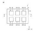
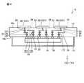
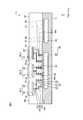
- FIG. 1is a plan view of the antenna module according to the first embodiment.
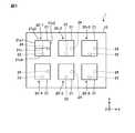
- FIG. 2is a cross-sectional view taken along the line II-II 'of FIG.
- FIG. 3is a cross-sectional view taken along the line III-III 'of FIG.
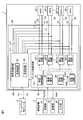
- FIG. 4is a block diagram showing a configuration example of the antenna module according to the first embodiment.
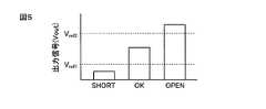
- FIG. 5is a graph schematically showing the relationship between the output signal and the conductive state of the antenna.
- FIG. 6is a flowchart showing the continuity inspection method of the antenna module according to the first embodiment.
- FIG. 7is a flow chart showing another example of the continuity inspection method of the antenna module of the first embodiment.
- FIG. 8is a block diagram showing a configuration example of an antenna module according to a modification of the first embodiment.
- FIG. 1is a plan view of the antenna module according to the first embodiment.
- FIG. 2is a cross-sectional view taken along the line II-II 'of FIG.
- FIG. 3
- FIG. 9is a plan view showing a radiating element of the antenna module according to the second embodiment.
- FIG. 10is a block diagram showing a configuration example of the antenna module according to the second embodiment.
- FIG. 11is a flowchart showing the continuity inspection method of the antenna module according to the second embodiment.
- FIG. 12is a cross-sectional view showing an antenna module according to the third embodiment.
- FIG. 13is a cross-sectional view showing an antenna module according to a first modification of the third embodiment.
- FIG. 14is a cross-sectional view showing an antenna module according to a second modification of the third embodiment.
- FIG. 15is a cross-sectional view showing an antenna module according to a third modification of the third embodiment.
- FIG. 16is a cross-sectional view showing an antenna module according to a fourth modification of the third embodiment.
- FIG. 17is a block diagram showing a configuration example of an antenna module according to the fourth embodiment.
- FIG. 18is a block diagram showing a configuration example of an antenna module according to a first modified example of the fourth embodiment.
- FIG. 19is a block diagram showing a configuration example of an antenna module according to a second modified example of the fourth embodiment.
- FIG. 20is a block diagram showing a configuration example of an antenna module according to a third modified example of the fourth embodiment.
- FIG. 21is a cross-sectional view showing an antenna module according to the fifth embodiment.
- FIG. 1is a plan view of the antenna module according to the first embodiment.
- FIG. 2is a cross-sectional view taken along the line II-II ′ of FIG.
- FIG. 3is a cross-sectional view taken along the line III-III ′ of FIG.
- the antenna module 1 of the present embodimentincludes a base 10, a plurality of first antennas 20-1, a second antenna 20-2, a third antenna 20-3, and a fourth antenna 20-4. And a fifth antenna 20-5 and a sixth antenna 20-6.
- the first antenna 20-1, the second antenna 20-2, the third antenna 20-3, the fourth antenna 20-4, the fifth antenna 20-5, and the sixth antenna 20-6are divided.
- the antennas 20each include a radiation element 21 (not shown) and a parasitic element 22.
- one direction in a plane parallel to the first surface 10 a of the base 10is taken as an X direction.
- a direction orthogonal to the X directionis taken as a Y direction.
- a direction orthogonal to each of the X direction and the Y directionis taken as a Z direction.
- the present inventionis not limited to this, and the Y direction may intersect with the X direction at an angle other than 90 °.
- the Z directionmay intersect the X and Y directions at an angle other than 90 °.
- the plurality of antennas 20are arranged in a matrix. That is, a plurality of antennas 20 are arranged in the X direction, and a plurality of antennas 20 are arranged in the Y direction.
- the antenna module 1is an array antenna including a plurality of antennas 20.
- the antenna module 1further includes a control circuit 30, a first feed line 33, and a second feed line 34.
- the base 10has a first surface 10 a and a second surface 10 b opposite to the first surface 10 a.
- a low temperature co-fired ceramic multilayer substrateLTCC (Low Temperature Co-fired Ceramics) multilayer substrate
- the base 10has a plurality of insulating layers stacked in the Z direction. Each insulating layer is formed in a thin layer using a ceramic material that can be fired at a low temperature of 1000 ° C. or less.
- the substrate 10may be a multilayer resin substrate formed by laminating a plurality of resin layers composed of resins such as epoxy and polyimide.
- the substrate 10may be formed using a liquid crystal polymer (Lquid Crystal Polymer: LCP) or a fluorine-based resin having a lower dielectric constant.
- the substrate 10may be a ceramic multilayer substrate.
- the substrate 10may be a flexible substrate having flexibility or a rigid substrate having thermoplasticity.
- the antenna 20is, for example, a patch antenna used for a 60 GHz high frequency signal used in WiGig (Wireless Gigabit).
- the antennas 20each include a radiation element 21 and a parasitic element 22.
- the radiation element 21is provided in the inner layer of the base 10.
- the parasitic element 22is provided on the first surface 10 a of the base 10 so as to face the radiation element 21.
- the parasitic element 22is disposed overlapping the radiation element 21 via the insulating layer of the base 10. That is, the parasitic element 22 is in a state of being insulated from the radiating element 21.
- the radiation element 21 and the parasitic element 22are formed using a conductive metal material such as copper, silver, gold, or an alloy material containing these.
- a plurality of parasitic elements 22are arranged in the X direction, and a plurality of the parasitic elements 22 are arranged in the Y direction.
- a plurality of radiation elements 21are also arranged in the X direction and a plurality in the Y direction.
- each of the radiation element 21 and the parasitic element 22has a rectangular shape in plan view, and has the same shape.
- the radiation element 21 and the parasitic element 22are not limited to the square shape, and may have other shapes such as a circular shape and a polygonal shape. In addition, the radiation element 21 and the parasitic element 22 may have different shapes.
- one end of a first feed line 33 and one end of a second feed line 34are connected to the radiation element 21.
- the other end of the first feed line 33 and the other end of the second feed line 34are connected to the control circuit 30 via the connection terminal 31.
- the first feed line 33 and the second feed line 34respectively include a via 27, a pad 28 and a wire 29.
- the vias 27are formed as columnar conductors penetrating each insulating layer of the base 10 in the Z direction. Specifically, the via 27 is provided with a conductive metal material inside the through hole penetrating the insulating layer.
- the pads 28are provided between the insulating layers, and connect the vias 27 adjacent to each other in the Z direction, or connect the vias 27 and the wiring 29.
- the wires 29are provided in the inner layer of the base 10 and connect a plurality of vias 27 at different positions in plan view. Similar to the radiating element 21, the via 27, the pad 28 and the wiring 29 use a metallic material having conductivity.
- a portion where the first feed line 33 is connected to the radiation element 21is a first port 23. Further, a portion where the second feed line 34 is connected to the radiation element 21 is the second port 24. As shown in FIG. 3, the first port 23 is disposed at a position shifted from the center 21 c of the antenna 20 in the Y direction.
- the radiation element 21has two sides 21s1 and 21s2 facing in the X direction, and two sides 21s3 and 21s4 between the side 21s1 and the side 21s2.
- the center 21ccoincides with an intersection point of a virtual line connecting the middle point of the side 21s1 and a middle point of the side 21s2, and a virtual line connecting the middle point of the side 21s3 and the middle point of the side 21s4.
- the first port 23is disposed in the vicinity of the side 21s4 of the radiation element 21 along the X direction.
- the second port 24is disposed at a position shifted from the center 21 c of the antenna 20 in the X direction.
- the second port 24is disposed in the vicinity of the side 21s2 of the radiating element 21 along the Y direction.
- the control circuit 30is mounted on the second surface 10 b of the base 10 via the connection terminal 31.
- the connection terminal 31is, for example, a solder ball bump.
- the control circuit 30is sealed by the sealing resin 11.
- the control circuit 30is a circuit that controls transmission and reception of signals via the antenna 20 and controls the continuity inspection of the first feed line 33, the radiation element 21 of the antenna 20, and the second feed line 34.
- the control circuit 30is, for example, a radio frequency integrated circuit (RFIC).
- the control circuit 30 and each antenna 20are electrically connected. Specifically, in the antenna module 1, the first feed line 33, the radiation element 21 of the antenna 20, and the second feed line 34 are connected to the control circuit 30 via the connection terminal 31. Thus, in the antenna module 1, the conduction path to which the first feed line 33, the radiating element 21 of the antenna 20, and the second feed line 34 are connected forms a closed loop circuit.
- the signal processing circuit 50(see FIG. 4) of the control circuit 30 supplies a high frequency signal to the first port 23, a current flows in the Y direction in the radiation element 21. The current flowing in the Y direction radiates polarized waves parallel to the Y direction. Further, when the signal processing circuit 50 of the control circuit 30 supplies a high frequency signal to the second port 24, a current flows in the X direction in the radiation element 21. The current flowing in the X direction radiates polarized waves parallel to the X direction. Thus, the polarization of the antenna 20 can be switched by supplying the high frequency signal to any one of the first port 23 and the second port 24.
- the radiation element 21is electromagnetically coupled to the parasitic element 22 when excited.
- the antenna 20has two resonance modes different in resonance frequency. For this reason, compared with the case where the passive element 22 is omitted, the antenna 20 can be broadened.
- the plurality of antennas 20form an array antenna, and the desired radiation pattern (directivity) can be obtained by controlling the arrangement of the radiation elements 21 of the antenna 20 and the amplitude and phase of the high frequency signal to be excited. can get.
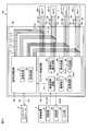
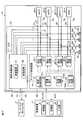
- FIG. 4is a block diagram showing a configuration example of the antenna module according to the first embodiment.
- FIG. 5is a graph schematically showing the relationship between the output signal and the conductive state of the antenna.
- the antenna module 1includes n antennas 20. That is, as shown in FIG. 4, the antenna module 1 includes a first antenna (ANT1) 20-1, a second antenna (ANT2) 20-2, ..., an n-1st antenna (ANT n-1) 20- (n). -1) and the n-th antenna (ANTn) 20-n.
- the control circuit 30includes a signal processing circuit 50 and an antenna inspection circuit 60.
- the signal processing circuit 50is connected to the antenna 20 via the first feed line 33 and the second feed line 34.
- the signal processing circuit 50contributes to transmission and reception of signals through the antenna 20.
- the antenna inspection circuit 60is a circuit that inspects the conduction of the conduction path including the first feed line 33, the radiating element 21 (see FIG. 2) of the antenna 20, and the second feed line.
- the control circuit 30can switch and execute the communication mode and the inspection mode. In the communication mode, the control circuit 30 transmits and receives signals via the antenna 20 by the operation of the signal processing circuit 50 in accordance with an external control signal. In the inspection mode, the control circuit 30 inspects the conduction of the antenna 20 by the operation of the antenna inspection circuit 60.
- the antenna inspection circuit 60is electrically connected to the first feed line 33 and the second feed line 34 via the first connection lines L1 and L2, respectively.
- the second connection wirings L11 and L12are branched and connected to the first connection wirings L1 and L2, respectively.
- the signal processing circuit 50is electrically connected to the first feed line 33 and the second feed line 34 via the second connection lines L11 and L12. That is, each antenna 20 is electrically connected to the signal processing circuit 50 and the antenna inspection circuit 60.
- the signal processing circuit 50includes a transmission circuit 51 and a reception circuit 52.
- the baseband module 2supplies the baseband signal Va to the transmission circuit 51.
- the transmission circuit 51modulates the baseband signal Va into a high frequency signal (for example, 60 GHz). Then, the transmission circuit 51 supplies a high frequency signal to each antenna 20 via the first feed line 33 and the second feed line 34. Further, at the time of reception, high frequency signals from the respective antennas 20 are supplied to the reception circuit 52.
- the receiving circuit 52demodulates the received high frequency signal to a baseband signal Vb, and supplies the baseband signal Vb to the baseband module 2.
- the receiving circuit 52may output an intermediate frequency signal having a frequency higher than that of the baseband signal Vb.
- the external inspection device 4 connected to the control circuit 30is, for example, a tester, a data logger, a personal computer or the like.
- the inspection device 4includes a control unit 41, a storage unit 42, and an input unit 43.
- the control unit 41is, for example, an arithmetic processing unit configured by a CPU (Central Processing Unit) or the like.
- the storage unit 42stores various information such as a software program used to control the continuity test, and a continuity test result of each antenna 20.
- the storage unit 42is a circuit that functions as a non-volatile storage device such as a flash memory, for example.
- the input unit 43is an input device such as a keyboard or a touch panel, for example. The operator inputs information on the continuity check from the input unit 43.
- the antenna module 1includes the antenna inspection circuit 60. Therefore, the configuration of the external inspection device 4 can be simplified. Moreover, even if the number of antennas 20 is different, the continuity test can be performed by the general-purpose inspection apparatus 4.
- the antenna inspection circuit 60determines the inspection control circuit 61, the power supply terminal 62, the memory circuit 63, and the plurality of detection circuits 65-1, 65-2, ..., 65- (n-1), 65-n. And a circuit 66.
- the detection circuits 65-1, 65-2,..., 65- (n-1), 65-nare referred to as the detection circuit 65 when it is not necessary to distinguish them.
- the inspection control circuit 61is a control circuit that controls the operation of the power supply terminal 62, the storage circuit 63, the plurality of detection circuits 65, and the determination circuit 66.
- the inspection control circuit 61controls the continuity inspection based on the control signal Vc from the inspection device 4 and the inspection start signal Vst.
- the inspection control circuit 61further outputs a control signal Vd to the signal processing circuit 50 based on the control signal Vc.
- the signal processing circuit 50stops the operation based on the control signal Vd, and stops the power supply to the antenna 20 and the input / output of the signal when conducting the continuity check.
- the power supply terminal 62supplies an input signal Vin for continuity check to each antenna 20 through the detection circuit 65.
- the detection circuits 65-1, 65-2, ..., 65- (n-1), 65-nrespectively receive the first antenna 20-1, the second antenna 20-2 via the first connection wirings L1, L2.
- the n-1st antenna 20- (n-1) and the nth antenna 20-nare electrically connected.
- the detection circuit 65is a circuit that detects the output signal Vout from the first feed line 33, the antenna 20, and the second feed line 34.
- the detection circuit 65detects an inter-terminal voltage between the connection terminal 31 to which the first feed line 33 is connected and the connection terminal 31 to which the second feed line 34 is connected as an output signal Vout.
- the detection circuit 65outputs the output signal Vout to the determination circuit 66.
- the detection circuit 65can also employ
- the determination circuit 66is a circuit that determines conduction of the first feed line 33, the radiation element 21 of the antenna 20, and the second feed line 34 based on the output signal Vout.
- the determination circuit 66is a circuit including, for example, a comparator.
- the determination circuit 66supplies the inspection signal Adet according to the conduction state to the storage circuit 63 as a digital signal for each of the antennas 20.
- the determination circuit 66outputs “1” as the inspection signal Adet when the conduction of the antenna 20 is good, and outputs “0” as the inspection signal Adet when the conduction of the antenna 20 is defective. .
- the determination circuit 66compares the output signal Vout with the reference signals Vref1 and Vref2.
- the reference signals Vref1 and Vref2are voltage signals based on the reference value stored in the storage unit 42 of the inspection apparatus 4.
- the determination circuit 66when the output signal Vout is equal to or higher than the reference signal Vref1 and equal to or lower than the reference signal Vref2, the conduction of the closed loop circuit formed by the first feed line 33, the radiating element 21 of the antenna 20, and the second feed line 34 is good. It determines that it is (OK). In this case, the determination circuit 66 outputs “1” as the inspection signal Adet. On the other hand, in the determination circuit 66, when the output signal Vout is smaller than the reference signal Vref1, a part of the closed loop circuit formed by the first feed line 33, the radiating element 21 of the antenna 20 and the second feed line 34 is shorted (SHORT) ) Is determined.
- the determination circuit 66breaks a portion of the closed loop circuit formed by the first feed line 33, the radiating element 21 of the antenna 20, and the second feed line 34 (OPEN ) Is determined.
- the determination circuit 66outputs “0” as the inspection signal Adet when it determines that it is a short circuit (SHORT) or a disconnection (OPEN).
- the memory circuit 63is a circuit that holds the inspection signal Adet for each of the antennas 20.
- the inspection control circuit 61outputs an inspection signal Adet to the inspection device 4 when the continuity inspection is completed. Thereby, the conduction of the antenna 20 can be inspected.
- the configuration of the antenna inspection circuit 60 shown in FIG. 4is merely an example, and can be changed as appropriate. For example, some functions of the antenna inspection circuit 60 such as the memory circuit 63 may be included in the external inspection device 4.
- the antenna module 1 of the present embodimentincludes the radiation element 21 provided in the inner layer of the base 10 using the first feed line 33 and the second feed line 34 used for transmission and reception of signals through the antenna 20. Can be conducted. If a terminal, a wiring, or the like for a continuity test is provided separately from the first feed line 33 and the second feed line 34, the performance of the antenna 20 may change in transmission and reception of a millimeter wave in the 60 GHz band. In the present embodiment, since it is not necessary to provide a terminal, a wiring, or the like for a continuity test, it is possible to suppress a change in performance of the antenna 20.
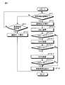
- FIG. 6is a flowchart showing the continuity inspection method of the antenna module according to the first embodiment.
- the control circuit 30determines whether the inspection start signal Vst has been input (step ST1).
- the control circuit 30determines whether the communication control signal is input (step ST8).
- the communication control signalis a signal for controlling the transmission / reception function of the signal through the antenna, and is supplied from, for example, a control board (not shown).
- the control circuit 30executes the communication mode (step ST9).
- the signal processing circuit 50transmits and receives signals via the antenna 20.
- the control circuit 30does not execute the communication mode or the inspection mode, and returns to step ST1.
- the control circuit 30executes the inspection mode (step ST2).
- the inspection control circuit 61uses the inspection start signal Vst as a trigger to start the operations of the power supply terminal 62, the storage circuit 63, the plurality of detection circuits 65, and the determination circuit 66.
- the test control circuit 61executes a continuity test of the first antenna 20-1 (step ST3).
- the operation of the power supply terminal 62, the detection circuit 65-1, and the determination circuit 66causes the storage circuit 63 to hold the inspection signal Adet according to the conduction state of the first antenna 20-1.
- the test control circuit 61executes the continuity test of the second antenna 20-2 (step ST4).
- the inspection control circuit 61sequentially performs a continuity test of each antenna 20, and performs a (n-1) th antenna 20- (n-1) continuity test (step ST5), and an n-th antenna 20- A continuity test of n is performed (step ST6).
- the inspection control circuit 61sequentially inspects the plurality of antennas 20 for conduction. Then, the inspection signal Adet of all the inspected antennas 20 is held in the storage circuit 63. When the inspection is completed for all the antennas 20, the inspection control circuit 61 outputs the inspection result to the inspection device 4 (step ST7).
- the inspection result supplied to the inspection device 4is the inspection signal Adet for every antenna 20. Thereby, the antenna 20 in which the conduction abnormality has occurred can be specified among the plurality of antennas 20.
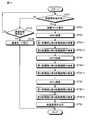
- FIG. 7is a flow chart showing another example of the continuity inspection method of the antenna module of the first embodiment. As shown in FIG. 7, the method (steps ST11, ST12, ST17, ST18) for switching between the communication mode and the inspection mode for execution is the same as the example shown in FIG.
- the inspection control circuit 61uses the inspection start signal Vst as a trigger to first perform a continuity inspection of the first antenna 20-1 (step ST13-1).
- the determination circuit 66determines whether or not the conduction of the first antenna 20-1 is good (step ST13-2).
- the inspection control circuit 61ends the conduction inspection based on the inspection signal Adet from the determination circuit 66.
- the inspection resultis output to the inspection device 4 (step ST16).
- the inspection result in this caseindicates that the conduction failure occurs in the antenna module 1.
- the inspection control circuit 61performs a conduction inspection of the second antenna 20-2 (step ST14-1).
- the determination circuit 66determines whether the conduction of the second antenna 20-2 is good (step ST14-2).
- the inspection control circuit 61ends the conduction inspection, and outputs the inspection result to the inspection device 4 (step ST16).
- the conduction of the second antenna 20-2is good (step ST14-2, Yes)
- the conduction inspection of the antenna 20is sequentially performed.
- the test control circuit 61executes a continuity test of the n-th antenna 20-n (step ST15-1).
- the determination circuit 66determines whether the conduction of the n-th antenna 20-n is good (step ST15-2).
- the inspection control circuit 61ends the conduction inspection and outputs the inspection result to the inspection device 4 (step ST16).
- the inspection control circuit 61ends the conduction inspection, and inspects the inspection result indicating that the conduction of all the antennas 20 is good. It outputs to the apparatus 4 (step ST16).
- the conduction failurewhen the conduction failure is detected in any one of the plurality of antennas 20, it is determined that the conduction failure occurs in the antenna module 1, and the continuity test is performed. Finish. Therefore, since the inspection is finished when even one defective antenna 20 is found, the continuity inspection can be performed in a short time as compared with the method of judging after examining all the antennas 20. Moreover, since it is not necessary to hold
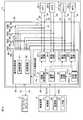
- FIG. 8is a block diagram showing a configuration example of an antenna module according to a modification of the first embodiment.
- the antenna inspection circuit 60further includes a connection switching circuit 64. Further, only one detection circuit 65 is provided.
- the connection switching circuit 64is a switch circuit that switches the connection between the detection circuit 65 and each of the antennas 20 according to a control signal from the inspection control circuit 61.
- the inspection control circuit 61connects the detection circuit 65 and the first antenna 20-1 by the operation of the connection switching circuit 64, and executes the continuity inspection of the first antenna 20-1.
- the test control circuit 61connects the detection circuit 65 and the second antenna 20-2 by the operation of the connection switching circuit 64, and executes a continuity test of the second antenna 20-2.
- the connection switching circuit 64sequentially connects the detection circuit 65 and the respective antennas 20 in a time-division manner.
- the antenna module 1Acan perform the continuity test of all the antennas 20 similarly to the continuity test method shown in FIG.
- connection switching circuit 64since the connection switching circuit 64 is provided, it is not necessary to provide the detection circuit 65 for each antenna 20. Therefore, when the number of antennas 20 is large, the circuit scale of the antenna inspection circuit 60 can be reduced.
- the antenna modules 1 and 1A of the present embodimentinclude the base 10, the antenna 20 having the radiation element 21 provided in the inner layer of the base 10, and the first feed line 33 connected to the radiation element 21. And a second feed line 34, and a control circuit 30 connected to the radiation element 21 via the first feed line 33 and the second feed line 34.
- the control circuit 30includes a signal processing circuit 50 connected to the antenna 20 via the first feed line 33 or the second feed line 34, and a conduction path including the first feed line 33, the radiation element 21 and the second feed line 34.
- an antenna inspection circuit 60for inspecting the continuity of the circuit.
- the conduction inspection of the radiation element 21 provided in the inner layer of the base 10can be performed using the first feed line 33 and the second feed line 34 used for transmission and reception of signals via the antenna 20. Moreover, since it is not necessary to provide a terminal, wiring, etc. for a continuity test, it is possible to suppress a change in transmission / reception performance of a signal through the antenna 20. Further, since the control circuit 30 includes the antenna inspection circuit 60 for inspecting the conduction of each antenna 20, the conduction inspection can be easily performed without contacting the probes with each antenna 20.
- the control circuit 30checks the communication mode in which signals are transmitted and received through the antenna 20 by the operation of the signal processing circuit 50, and the conduction of the conduction path by the operation of the antenna inspection circuit 60. Switch to the inspection mode to execute. According to this, it is possible to share the first feed line 33 and the second feed line 34 in the communication mode and the inspection mode. Further, since the inspection mode is performed in a period different from the communication mode, it is possible to suppress a change in transmission / reception performance of a signal through the antenna 20.
- the antenna inspection circuit 60is based on the detection circuit 65 that detects the output signal Vout from the first feed line 33, the radiation element 21 and the second feed line 34, and the output signal Vout. And a determination circuit 66 which determines the conduction of the conduction path. According to this, it can be checked from the determination result of the determination circuit 66 whether the conduction is good or abnormal. Further, since the antenna inspection circuit 60 includes the detection circuit 65 and the determination circuit 66, the configuration of the inspection apparatus 4 for continuity inspection connected to the antenna modules 1 and 1A can be simplified.
- the base 10is provided with the plurality of antennas 20, and the antenna inspection circuit 60 sequentially inspects the conduction of the conduction path for the plurality of antennas 20 and is inspected. The inspection results of all the antennas 20 are output. According to this, among the plurality of antennas 20, the antenna 20 in which the conduction abnormality has occurred can be easily identified.
- the base 10is provided with a plurality of antennas 20, and the antenna inspection circuit 60 sequentially inspects the conduction of the conduction paths for the plurality of antennas 20. The inspection is ended when a continuity abnormality is detected. According to this, it is not necessary to test all the antennas 20, and the continuity test can be performed in a short time.
- the base 10has a first surface 10a and a second surface 10b opposite to the first surface 10a, and the antenna 20 further faces the radiation element 21.
- the control circuit 30is mounted on the second surface 10 b of the base 10, and includes the parasitic element 22 provided on the first surface 10 a. According to this, the antenna 20 can be broadened.
- the control circuit 30executes an inspection mode for inspecting the conduction of the conduction path, and the antenna inspection circuit 60 sequentially performs the first feed line 33 for the plurality of antennas 20. , And check the conduction of the radiation element 21 and the second feed line 34.
- the configuration of the antenna modules 1 and 1Acan be changed as appropriate.
- the configurations of the antenna 20, the first feed line 33, the second feed line 34, and the control circuit 30are schematically shown, and the configuration of the antenna module 1 is It is not limited to the configuration of FIGS. 1 to 3.
- the arrangement and number of the antennas 20can be changed as appropriate.
- the present inventionis not limited to the case where a plurality of antennas 20 are provided, and one antenna 20 may be provided.
- the base 10may be provided with an antenna or a circuit element different from the antenna 20.
- a ground layer or the likemay be provided on the inner layer of the base 10.
- the antenna 20may have only the radiating element 21 without the parasitic element 22.
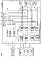
- FIG. 9is a plan view showing a radiating element of the antenna module according to the second embodiment.
- FIG. 10is a block diagram showing a configuration example of the antenna module according to the second embodiment.
- each antenna 20in addition to the first port 23 and the second port 24, each antenna 20 is provided with a third port 25 and a fourth port 26.
- the third port 25is provided on the opposite side of the second port 24 with respect to the center of the antenna 20.
- the fourth port 26is provided on the opposite side of the first port 23 with respect to the center of the antenna 20.
- the first feed line 33, the second feed line 34, the third feed line 35, and the fourth feed line 36are connected to each antenna 20.
- the first feed line 33is connected to the first port 23 shown in FIG.
- the second feed line 34is connected to the second port 24.
- the third feed line 35is connected to the third port 25.
- the fourth feed line 36is connected to the fourth port 26.
- the first feed line 33, the second feed line 34, the third feed line 35, and the fourth feed line 36are electrically connected to the antenna inspection circuit 60 via the first connection wires L1, L2, L3, and L4, respectively. Ru.
- the first feed line 33, the second feed line 34, the third feed line 35, and the fourth feed line 36are electrically connected to the signal processing circuit 50 via the second connection lines L11, L12, L13, and L14, respectively.
- the signal processing circuit 50can supply a high frequency signal to the antenna 20 via the first feed line 33, the second feed line 34, the third feed line 35, and the fourth feed line 36. Even when any one of the first feed line 33, the second feed line 34, the third feed line 35, and the fourth feed line 36 is disconnected, transmission and reception of signals can be performed via the antenna 20.
- the conduction inspectioncan be performed using the first feed line 33, the second feed line 34, the third feed line 35, and the fourth feed line 36.
- FIG. 10shows a configuration in which the connection switching circuit 64 switches the connection between the detection circuit 65 and each antenna 20, the present invention is not limited to this. Also in the present embodiment, as in FIG. 4, a configuration in which a plurality of detection circuits 65 are provided corresponding to each antenna 20 can be adopted.
- FIG. 11is a flowchart showing the continuity inspection method of the antenna module according to the second embodiment. As shown in FIG. 11, the method (steps ST21, ST22, ST27, ST28) for switching between the communication mode and the inspection mode for execution is the same as the example shown in FIG.
- the inspection control circuit 61uses the inspection start signal Vst as a trigger to first perform a continuity inspection of the first antenna 20-1 (step ST23).
- the inspection control circuit 61performs a conduction inspection between the first feed line 33 and the second feed line 34 of the first antenna 20-1 (step ST23-1).
- the detection circuit 65detects the output signal Vout output from the first feed line 33, the radiating element 21 of the first antenna 20-1, and the second feed line.
- the determination circuit 66determines conduction of the first feed line 33, the radiating element 21 of the first antenna 20-1, and the second feed line 34 based on the output signal Vout. Thereby, the continuity test between the first feed line 33 and the second feed line 34 is performed.
- the inspection control circuit 61performs a conduction inspection between the third feed line 35 and the fourth feed line 36 of the first antenna 20-1 (step ST23-2).
- the determination circuit 66has good conduction between the first feed line 33 and the second feed line 34, and good conduction between the third feed line 35 and the fourth feed line 36. It is determined that the conduction of the first antenna 20-1 is good.
- the first antenna 20is used. It is determined that there is a -1 conduction failure.
- the inspection control circuit 61sequentially performs continuity inspection of the second antenna 20-2 to the n-th antenna 20-n (steps ST24, ST24-1, ST24-2, ST25, ST25-1, ST25- 2).
- the inspection control circuit 61outputs the inspection result to the inspection device 4 (step ST26).
- the inspection result supplied to the inspection apparatus 4may be the inspection signal Adet for each of all the antennas 20, or may be the inspection signal Adet between the respective feed lines. Thereby, among the plurality of antennas 20, the antenna 20 in which the conduction abnormality has occurred can be easily identified.
- the two feed lines selectedcan be changed as appropriate. For example, the conduction test between the first feed line 33 and the third feed line 35 may be performed, and the conduction test between the second feed line 34 and the fourth feed line 36 may be performed.
- FIG. 12is a cross-sectional view showing an antenna module according to the third embodiment.
- each antenna 20has a radiation element 21.
- the radiation element 21is provided on the first surface 10 a (surface) of the base 10 and exposed from the base 10.
- the antenna module 1Ccan simplify the configuration of each antenna 20 as compared to the first embodiment and the second embodiment.
- the configuration shown in the third embodimentcan also be applied to the antenna modules 1, 1A and 1B of the first and second embodiments.
- FIG. 13is a cross-sectional view showing an antenna module according to a first modification of the third embodiment.
- the protective layer 12is provided on the first surface 10 a (surface) of the base 10 to cover each of the radiation elements 21.
- the protective layer 12is made of, for example, a resin material used as a solder resist.
- the structure which provides the protective layer 12 shown to the 1st modification of 3rd Embodimentis applicable also to antenna module 1, 1A, 1B of 1st Embodiment and 2nd Embodiment.
- FIG. 14is a cross-sectional view showing an antenna module according to a second modification of the third embodiment.
- the shield member 13is provided on the second surface 10 b of the base 10 so as to cover the control circuit 30.
- the shield member 13is formed of a conductive metal material and connected to the ground potential of the base 10. Thereby, the shield member 13 electromagnetically shields the control circuit 30.
- the shield member 13has a flat plate opposed to the second surface 10 b and a side plate surrounding the periphery of the control circuit 30.
- the antenna module 1Ecan protect the control circuit 30 by the shield member 13 and suppress interference between the signal radiated from the antenna 20 and the control circuit 30.
- the inside of shield member 13is hollow, it is not limited to this.
- the sealing resin 11may be provided inside the shield member 13.
- the configuration shown in the second modification of the third embodimentalso applies to the antenna modules 1 and 1A to 1D of the first to third embodiments and the first and second modifications of the third embodiment. Applicable
- FIG. 15is a cross-sectional view showing an antenna module according to a third modification of the third embodiment.
- the circuit board 14has a first surface 14 a and a second surface 14 b opposite to the first surface 14 a.
- the first surface 14 a of the circuit board 14is provided to face the second surface 10 b of the base 10.
- the circuit board 14 and the base 10are electrically connected via the connection terminal 16.
- the circuit board 14is provided with a plurality of signal paths 15, and the first feed line 33 and the second feed line 34 of the base 10 are connected to the signal path 15 via the connection terminals 16 respectively.
- the control circuit 30is mounted on the second surface 14 b of the circuit board 14, that is, the surface opposite to the surface facing the base 10. Thereby, the first feed line 33 and the second feed line 34 are electrically connected to the control circuit 30 via the plurality of signal paths 15 of the circuit board 14.
- the sealing resin 11is provided on the second surface 14 b of the circuit board 14 so as to cover the control circuit 30.
- the thickness of the circuit board 14is thinner than the thickness of the substrate 10.
- the antenna module 1Fcan achieve a wider band of the antenna 20 while suppressing an increase in the overall thickness.
- the arrangement pitch of the connection terminals 31 of the control circuit 30 and the arrangement pitch of the connection terminals 16 of the circuit board 14are different. Therefore, the antenna module 1F can increase the freedom of arrangement of the connection terminals 31 of the control circuit 30 and the freedom of routing the first feed line 33 and the second feed line 34. That is, even when the routing of the first feed line 33 and the second feed line 34 is changed, the change of the connection terminal 31 of the control circuit 30 is performed by changing the connection terminal 16 and the signal path 15 of the circuit board 14. Is unnecessary. Alternatively, even when the arrangement of the connection terminals 31 of the control circuit 30 is changed, the circuit board 14 is changed in accordance with the control circuit 30 so that the first feed line 33 and the second feed line 34 of the base 10 are changed. No change is required.
- the configuration shown in the third modification of the third embodimentis also applicable to the antenna modules 1, 1A to 1E of the first to third embodiments and the first to third modifications of the third embodiment. Applicable
- FIG. 16is a cross-sectional view showing an antenna module according to a fourth modification of the third embodiment.
- the control circuit 30 and the base 10are mounted on the same surface of the circuit board 14A.
- the configuration to be usedwill be described.
- the circuit board 14Ahas an area larger than that of the base 10 in a plan view.
- the control circuit 30 and the base 10are mounted on the first surface 14Aa of the circuit board 14A.
- No circuit or componentis mounted on the second surface 14Ab of the circuit board 14A.
- the first feed line 33 and the second feed line 34 and the control circuit 30are electrically connected via the signal path 15 provided on the circuit board 14A.
- the configuration shown in the fourth modification of the third embodimentalso applies to the antenna modules 1, 1A to 1E of the first to third embodiments and the first to third modifications of the third embodiment. Applicable
- FIG. 17is a block diagram showing a configuration example of an antenna module according to the fourth embodiment.
- the control circuit 30has a ground terminal 68 and a switch SW.
- the switch SWhas a first connection wiring L2 and a ground terminal 68 based on a control signal from the inspection control circuit 61. Switch between connection and disconnection. One end of the switch SW is connected to the first connection wiring L2 between the connection point of the first connection wiring L2 and the second connection wiring L12 and the detection circuit 65.
- the other end of the switch SWis connected to the ground terminal 68.
- the ground terminal 68is electrically connected to, for example, the ground layer of the base 10. All the first connection wirings L2 corresponding to the respective antennas 20 can be connected to the ground terminal 68 via the switch SW. Note that one end of the switch SW may be connected to the first connection wiring L1.
- the control circuit 30turns on the switch SW, for example, after the inspection mode shown in FIG. 6 is finished.
- the first connection wirings L1 and L2 and the second connection wirings L11 and L12are electrically connected to the ground terminal 68.
- the static electricity accumulated in the first connection wirings L1 and L2 and the second connection wirings L11 and L12 in the inspection modeflows to the ground layer through the switch SW and the ground terminal 68.
- the antenna module 1Hsuppresses charging of the first connection wirings L1 and L2 and the second connection wirings L11 and L12, which makes it possible to take measures against electrostatic discharge (ESD: Electro-Static Discharge).
- ESDElectro-Static Discharge
- FIG. 18is a block diagram showing a configuration example of an antenna module according to a first modified example of the fourth embodiment.
- one end of the switch SWis connected to the connection between the first connection wiring L2 and the second connection wiring L12 and the second feed line 34.
- the structure connected to the 1st connection wiring L2 between the connection terminals 31 to be connectedis demonstrated.
- static electricity accumulated in the first connection wirings L1 and L2 and the second connection wirings L11 and L12 in the inspection modeflows to the ground layer via the switch SW and the ground terminal 68.
- the antenna module 1Ican perform the ESD countermeasure.
- one end of the switch SWis connected to the first connection wiring L1 between the connection point of the first connection wiring L1 and the second connection wiring L11 and the connection terminal 31 to which the first feed line 33 is connected. May be
- FIG. 19is a block diagram showing a configuration example of an antenna module according to a second modified example of the fourth embodiment.
- the second modified example of the fourth embodimentunlike the first modified example of the fourth and fourth embodiments, a configuration in which the second connection wiring L11 is connected to the ground terminal 68 will be described.
- one end of the switch SWis connected to the second connection wiring L11, and the other end of the switch SW is connected to the ground terminal 68.
- the switch SWswitches connection and disconnection between the second connection wiring L11 and the ground terminal 68.
- the static electricity accumulated in the first connection wirings L1 and L2 and the second connection wirings L11 and L12 in the inspection modeflows to the ground layer through the switch SW and the ground terminal 68.
- the antenna module 1Jcan perform the ESD countermeasure.
- FIG. 20is a block diagram showing a configuration example of an antenna module according to a third modified example of the fourth embodiment.
- the second connection wiring L11includes a ground layer 67 via the inductance element 100. The configuration to be connected to will be described. As shown in FIG. 19, the second connection wiring L11 is connected to the ground terminal 68. The ground terminal 68 is connected to the ground layer 67 via an inductance element 100 provided outside the control circuit 30.
- the plurality of first connection wirings L1 and L2 and the plurality of second connection wirings L11 and L12are electrically connected to the ground terminal 68.
- the inductance element 100may be provided on the base 10 (see FIG. 2) or may be provided on the circuit board 14 (see FIG. 15).
- the inductance element 100may be provided in the control circuit 30.
- the static electricity accumulated in the first connection wirings L1 and L2 and the second connection wirings L11 and L12 in the inspection modeflows to the ground layer 67 via the inductance element 100.
- the antenna module 1 Kcan perform the ESD countermeasure.
- the inductance element 100has sufficiently high impedance to the signal transmitted from the signal processing circuit 50 and the signal received by the antenna 20. Therefore, in the communication mode, the signal output from the signal processing circuit 50 and the signal received by the antenna 20 are not supplied to the ground layer 67.
- the inductance element 100is not limited to being provided outside the control circuit 30. Like the switch SW shown in FIG. 19, it may be provided inside the control circuit 30.
- FIG. 21is a cross-sectional view showing an antenna module according to the fifth embodiment.
- the signal processing circuit 50 and the antenna inspection circuit 60are respectively formed of individual ICs.
- the signal processing circuit 50 and the antenna inspection circuit 60are respectively provided on the second surface 10b of the base 10.
- One end of the first feed line 33 and one end of the second feed line 34are respectively connected to the radiation element 21, and the other end of the first feed line 33 and the other end of the second feed line 34 are signals via the connection terminal 50a. It is connected to the processing circuit 50.
- One end of the first connection line 37is connected to the first feed line 33, and the other end of the first connection line 37 is connected to the antenna inspection circuit 60 via the connection terminal 60a.
- One end of the second connection line 38is connected to the second feed line 34, and the other end of the second connection line 38 is connected to the antenna inspection circuit 60 via the connection terminal 60a.
- the antenna inspection circuit 60has a conduction path including the first connection line 37, the first feed line 33, the radiating element 21 of the antenna 20, the second feed line 34, and the second connection line 38.
- the continuitycan be checked.
- the signal processing circuit 50 and the antenna inspection circuit 60are respectively formed of individual ICs, optimization of their circuit configurations is easy.
- the configuration of the fifth embodimentcan also be applied to the antenna modules 1 and 1A-1K of the first to fourth embodiments described above.
Landscapes
- Engineering & Computer Science (AREA)
- Microelectronics & Electronic Packaging (AREA)
- Physics & Mathematics (AREA)
- General Physics & Mathematics (AREA)
- Variable-Direction Aerials And Aerial Arrays (AREA)
- Waveguide Aerials (AREA)
Abstract
Description
Translated fromJapanese本発明は、アンテナモジュール及びアンテナモジュールの検査方法に関する。The present invention relates to an antenna module and an inspection method of the antenna module.
特許文献1には、アンテナ部材を備えた通信装置と通信装置の検査方法が記載されている。特許文献1の通信装置は、アンテナ導体と、アンテナ導体に接続されたアンテナ端子とを備える。アンテナ導体は、被覆層によって覆われている。また、アンテナ端子は、被覆層に覆われていない導通検査用の端子である。特許文献1の通信装置は、通信装置の検査として、アンテナ端子とグランド端子とにプローブを接触させて導通検査を行う。
特許文献1の導通検査方法では、各アンテナ端子にプローブを接触させなければならず、例えば、多数の通信装置の検査を行う場合や、多数のアンテナ導体を含む通信装置において容易に導通検査を行うことができない可能性がある。In the continuity inspection method of
本発明は、容易に導通検査を行うことができるアンテナモジュール及びアンテナモジュールの検査方法を提供することを目的とする。An object of the present invention is to provide an antenna module and an inspection method of the antenna module capable of easily performing a continuity test.
本発明の一態様に係るアンテナモジュールは、基体と、前記基体に設けられた放射素子を有するアンテナと、前記放射素子に接続された第1給電線路及び第2給電線路と、前記第1給電線路及び前記第2給電線路を介して前記放射素子と接続された制御回路とを備え、前記制御回路は、前記第1給電線路又は前記第2給電線路を介して前記アンテナに接続された信号処理回路と、前記第1給電線路と、前記放射素子と、前記第2給電線路とが接続された導通経路の導通を検査するアンテナ検査回路と、を含む。An antenna module according to one aspect of the present invention includes a base, an antenna having a radiating element provided on the base, a first feed line and a second feed line connected to the radiating element, and the first feed line. And a control circuit connected to the radiation element via the second feed line, wherein the control circuit is a signal processing circuit connected to the antenna via the first feed line or the second feed line. And an antenna inspection circuit that inspects conduction of a conduction path to which the first feed line, the radiation element, and the second feed line are connected.
本発明のアンテナモジュール及びアンテナモジュールの検査方法によれば、容易に導通検査を行うことができる。According to the antenna module and the inspection method of the antenna module of the present invention, the continuity inspection can be easily performed.
本発明を実施するための実施形態について、図面を参照しつつ詳細に説明する。以下の実施形態に記載した内容により本発明が限定されるものではない。また、以下に記載した構成要素には、当業者が容易に想定できるもの、実質的に同一のもの、いわゆる均等の範囲のものが含まれる。さらに、以下に記載した構成要素は適宜組み合わせることが可能である。また、一部の構成要素は用いられない場合もある。Embodiments for carrying out the present invention will be described in detail with reference to the drawings. The present invention is not limited by the contents described in the following embodiments. In addition, the components described below include components that can be easily conceived by those skilled in the art, substantially the same components, and so-called equivalent ranges. Furthermore, the components described below can be combined as appropriate. Also, some components may not be used.
(第1実施形態)
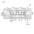
図1は、第1実施形態に係るアンテナモジュールの平面図である。図2は、図1のII-II’線に沿う断面図である。図3は、図2のIII-III’線に沿う断面図である。図1に示すように、本実施形態のアンテナモジュール1は、基体10と、複数の第1アンテナ20-1、第2アンテナ20-2、第3アンテナ20-3、第4アンテナ20-4、第5アンテナ20-5及び第6アンテナ20-6とを含む。なお、以下の説明において、第1アンテナ20-1、第2アンテナ20-2、第3アンテナ20-3、第4アンテナ20-4、第5アンテナ20-5、第6アンテナ20-6を区別して説明する必要がない場合には、アンテナ20と表す。アンテナ20は、それぞれ放射素子21(図示せず)と、無給電素子22とを備える。First Embodiment
FIG. 1 is a plan view of the antenna module according to the first embodiment. FIG. 2 is a cross-sectional view taken along the line II-II ′ of FIG. FIG. 3 is a cross-sectional view taken along the line III-III ′ of FIG. As shown in FIG. 1, the
以下の説明において、基体10の第1面10aに平行な面内の一方向をX方向とする。また、第1面10aに平行な面内においてX方向と直交する方向をY方向とする。また、X方向及びY方向のそれぞれと直交する方向をZ方向とする。なお、これに限定されず、Y方向はX方向に対して90°以外の角度で交差してもよい。Z方向は、X方向及びY方向に対して90°以外の角度で交差してもよい。In the following description, one direction in a plane parallel to the
図1に示すように、複数のアンテナ20は、行列状に配置される。すなわち、アンテナ20は、X方向に複数配列され、かつ、Y方向に複数配列される。アンテナモジュール1は、複数のアンテナ20を含むアレイアンテナである。As shown in FIG. 1, the plurality of
図2に示すように、アンテナモジュール1は、さらに、制御回路30と、第1給電線路33と、第2給電線路34とを含む。基体10は、第1面10aと、第1面10aとは反対側の第2面10bとを有する。基体10は、例えば低温同時焼成セラミックス多層基板(LTCC(Low Temperature Co-fired Ceramics)多層基板)が用いられる。基体10は、Z方向に積層された複数の絶縁層を有している。各絶縁層は、1000℃以下の低温で焼成可能なセラミックス材料が用いられ、薄い層状に形成される。なお、これに限定されず、基体10は、エポキシ、ポリイミドなどの樹脂から構成される樹脂層を複数積層して形成された多層樹脂基板であってもよい。また、より低い誘電率を有する液晶ポリマー(Liquid Crystal Polymer:LCP)あるいはフッ素系樹脂を用いて基体10を形成してもよい。あるいは、基体10は、セラミックス多層基板であってもよい。基体10は、可撓性を有するフレキシブル基板であっても、熱可塑性を有するリジッド基板であってもよい。As shown in FIG. 2, the
アンテナ20は、例えばWiGig(Wireless Gigabit)で使用される60GHz帯の高周波信号に用いられるパッチアンテナである。アンテナ20は、それぞれ放射素子21と、無給電素子22とを備える。放射素子21は、基体10の内層に設けられる。無給電素子22は、放射素子21と対向して、基体10の第1面10aに設けられる。無給電素子22は、基体10の絶縁層を介して放射素子21と重なって配置される。すなわち、無給電素子22は、放射素子21と絶縁された状態である。放射素子21及び無給電素子22は、銅、銀、金、又はこれらを含む合金材料等の導電性を有する金属材料を用いて形成される。The
図1に示すように、無給電素子22は、X方向に複数配列され、かつ、Y方向に複数配列される。また、図3に示すように、放射素子21も同様に、X方向に複数配列され、かつ、Y方向に複数配列される。図1及び図3に示すように、放射素子21と無給電素子22とは、いずれも平面視で四角形状であり、同一形状である。なお、放射素子21及び無給電素子22は、四角形状に限定されず、円形状、多角形状等、他の形状であってもよい。また、放射素子21と無給電素子22とは、互いに異なる形状を有していてもよい。As shown in FIG. 1, a plurality of
図2に示すように、放射素子21には、第1給電線路33の一端及び第2給電線路34の一端が接続される。第1給電線路33の他端及び第2給電線路34の他端は、接続端子31を介して制御回路30に接続される。As shown in FIG. 2, one end of a
第1給電線路33及び第2給電線路34は、それぞれビア27、パッド28及び配線29を含む。ビア27は、基体10の各絶縁層をZ方向に貫通する柱状の導体に形成される。具体的には、ビア27は、絶縁層を貫通する貫通孔の内部に、導電性を有する金属材料が設けられる。パッド28は、絶縁層の間に設けられ、Z方向に隣り合うビア27どうしを接続し、あるいはビア27と配線29とを接続する。配線29は、基体10の内層に設けられ、平面視で異なる位置の複数のビア27を接続する。ビア27、パッド28及び配線29は、放射素子21と同様に、導電性を有する金属材料が用いられる。The
第1給電線路33が放射素子21に接続される部分が第1ポート23である。また、第2給電線路34が放射素子21に接続される部分が第2ポート24である。図3に示すように、第1ポート23は、アンテナ20の中心21cからY方向にずれた位置に配置される。ここで、放射素子21は、X方向に対向する2つの辺21s1、21s2と、辺21s1と、辺21s2との間の2つの辺21s3、21s4と、を有する。中心21cは、辺21s1の中点と辺21s2の中点とを結ぶ仮想線と、辺21s3の中点と辺21s4の中点とを結ぶ仮想線との交点と一致する。第1ポート23は、放射素子21の、X方向に沿った辺21s4の近傍に配置される。また、第2ポート24は、アンテナ20の中心21cからX方向にずれた位置に配置される。第2ポート24は、放射素子21の、Y方向に沿った辺21s2の近傍に配置される。A portion where the
図2に示すように、制御回路30は、接続端子31を介して基体10の第2面10bに実装される。接続端子31は、例えば、はんだボールバンプである。制御回路30は、封止樹脂11により封止される。制御回路30は、アンテナ20を介した信号の送受信を制御するとともに、第1給電線路33、アンテナ20の放射素子21及び第2給電線路34の導通検査を制御する回路である。制御回路30は、例えばRFIC(Radio Frequency Integrated Circuit)である。As shown in FIG. 2, the
このような構成により、アンテナモジュール1は、制御回路30と各アンテナ20とが電気的に接続される。具体的には、アンテナモジュール1は、第1給電線路33と、アンテナ20の放射素子21と、第2給電線路34とが、接続端子31を介して、制御回路30に接続される。これにより、アンテナモジュール1は、第1給電線路33と、アンテナ20の放射素子21と、第2給電線路34とが接続された導通経路が、閉ループ回路となる。With such a configuration, in the
制御回路30の信号処理回路50(図4参照)が、第1ポート23に高周波信号を供給すると、放射素子21にはY方向に電流が流れる。Y方向に流れる電流により、Y方向に平行な偏波が放射される。また、制御回路30の信号処理回路50が、第2ポート24に高周波信号を供給すると、放射素子21にはX方向に電流が流れる。X方向に流れる電流により、X方向に平行な偏波が放射される。これにより、第1ポート23、第2ポート24のいずれかに高周波信号を供給することで、アンテナ20の偏波を切り替えることができる。When the signal processing circuit 50 (see FIG. 4) of the
放射素子21は、励振されると、無給電素子22と電磁界結合する。この場合、アンテナ20は共振周波数が異なる2つの共振モードを有する。このため、無給電素子22を省いた場合と比較して、アンテナ20の広帯域化を図ることができる。また、複数のアンテナ20は、アレイアンテナを構成しており、アンテナ20の放射素子21の配置や、励振される高周波信号の振幅、位相を制御することにより、所望の放射パターン(指向性)が得られる。The
次に、制御回路30の構成について説明する。図4は、第1実施形態に係るアンテナモジュールの構成例を示すブロック図である。図5は、出力信号と、アンテナの導通状態との関係を模式的に示すグラフである。なお、図4では、アンテナモジュール1が、n個のアンテナ20を含む例を説明する。すなわち、図4に示すように、アンテナモジュール1は、第1アンテナ(ANT1)20-1、第2アンテナ(ANT2)20-2、…、第n-1アンテナ(ANTn-1)20-(n-1)、第nアンテナ(ANTn)20-nを含む。Next, the configuration of
図4に示すように、制御回路30は、信号処理回路50と、アンテナ検査回路60とを含む。信号処理回路50は、第1給電線路33及び第2給電線路34を介してアンテナ20に接続される。信号処理回路50は、アンテナ20を介して、信号の送受信に寄与する。アンテナ検査回路60は、第1給電線路33、アンテナ20の放射素子21(図2参照)及び第2給電線路34を含む導通経路の導通を検査する回路である。制御回路30は、通信モードと、検査モードとを切り換えて実行することができる。通信モードでは、制御回路30は、外部からの制御信号に応じて、信号処理回路50の動作によりアンテナ20を介して信号の送受信を行う。検査モードでは、制御回路30は、アンテナ検査回路60の動作によりアンテナ20の導通を検査する。As shown in FIG. 4, the
アンテナ検査回路60は、第1接続配線L1、L2を介して、それぞれ第1給電線路33、第2給電線路34と電気的に接続される。第1接続配線L1、L2には、それぞれ第2接続配線L11、L12が分岐して接続される。信号処理回路50は、第2接続配線L11、L12を介して、第1給電線路33、第2給電線路34と電気的に接続される。つまり、各アンテナ20は、信号処理回路50及びアンテナ検査回路60と電気的に接続される。The
信号処理回路50は、送信回路51と受信回路52とを含む。送信の際には、ベースバンドモジュール2は、ベースバンド信号Vaを送信回路51に供給する。送信回路51は、ベースバンド信号Vaを高周波信号(例えば60GHz)に変調する。そして、送信回路51は、第1給電線路33及び第2給電線路34を介して高周波信号を各アンテナ20に供給する。また、受信の際には、各アンテナ20からの高周波信号が受信回路52に供給される。受信回路52は、受信した高周波信号をベースバンド信号Vbに復調して、ベースバンド信号Vbをベースバンドモジュール2に供給する。なお、受信回路52は、ベースバンド信号Vbよりも高い周波数を有する中間周波数信号を出力してもよい。The
制御回路30に接続される外部の検査装置4は、例えば、テスター、データロガー、パーソナルコンピュータ等である。検査装置4は、制御部41と、記憶部42と、入力部43とを備える。制御部41は、例えば、CPU(Central Processing Unit)等で構成された演算処理装置である。記憶部42は、導通検査の制御に用いられるソフトウェアプログラムや、各アンテナ20の導通検査結果等の各種情報を記憶する。記憶部42は、例えば、フラッシュメモリ(Flash Memory)など、不揮発性の記憶装置として機能する回路である。入力部43は、例えばキーボードやタッチパネルなどの入力装置である。操作者は、入力部43から、導通検査に関する情報を入力する。本実施形態では、アンテナモジュール1がアンテナ検査回路60を含んでいる。このため、外部の検査装置4の構成を簡易にすることができる。また、アンテナ20の数が異なる場合であっても、汎用の検査装置4で導通検査を行うことができる。The
アンテナ検査回路60は、検査制御回路61と、電源端子62と、記憶回路63と、複数の検出回路65-1、65-2、…、65-(n-1)、65-nと、判定回路66とを含む。なお、以下の説明において、検出回路65-1、65-2、…、65-(n-1)、65-nを区別して説明する必要がない場合には、検出回路65と表す。The
検査制御回路61は、電源端子62、記憶回路63、複数の検出回路65及び判定回路66の動作を制御する制御回路である。検査制御回路61は、検査装置4からの制御信号Vc、検査開始信号Vstに基づいて、導通検査を制御する。検査制御回路61は、さらに、制御信号Vcに基づいて、信号処理回路50に制御信号Vdを出力する。信号処理回路50は、制御信号Vdに基づいて動作を停止して、導通検査を行う際にアンテナ20への給電と信号の入出力を停止する。The
電源端子62は、導通検査用の入力信号Vinを、検出回路65を介して各アンテナ20に供給する。The
検出回路65-1、65-2、…、65-(n-1)、65-nは、それぞれ第1接続配線L1、L2を介して、第1アンテナ20-1、第2アンテナ20-2、…、第n-1アンテナ20-(n-1)、第nアンテナ20-nと電気的に接続される。検出回路65は、第1給電線路33、アンテナ20及び第2給電線路34からの出力信号Voutを検出する回路である。検出回路65は、第1給電線路33が接続される接続端子31と、第2給電線路34が接続される接続端子31との間の端子間電圧を出力信号Voutとして検出する。検出回路65は、出力信号Voutを判定回路66に出力する。なお、これに限定されず、検出回路65は、第1給電線路33、アンテナ20及び第2給電線路34に流れる電流を検出する構成を採用することもできる。The detection circuits 65-1, 65-2, ..., 65- (n-1), 65-n respectively receive the first antenna 20-1, the second antenna 20-2 via the first connection wirings L1, L2. The n-1st antenna 20- (n-1) and the nth antenna 20-n are electrically connected. The
判定回路66は、出力信号Voutに基づいて、第1給電線路33、アンテナ20の放射素子21及び第2給電線路34の導通を判定する回路である。判定回路66は、例えばコンパレータを含む回路である。判定回路66は、アンテナ20ごとに、導通状態に応じた検査信号Adetをデジタル信号として記憶回路63に供給する。判定回路66は、アンテナ20の導通が良好である場合には、検査信号Adetとして「1」を出力し、アンテナ20の導通が不良である場合には、検査信号Adetとして「0」を出力する。The
図5に判定回路66の判定方法の一例を示す。判定回路66は、出力信号Voutと基準信号Vref1、Vref2とを比較する。基準信号Vref1、Vref2は、検査装置4の記憶部42に記憶された基準値に基づく電圧信号である。An example of the determination method of the
判定回路66は、出力信号Voutが基準信号Vref1以上、基準信号Vref2以下である場合、第1給電線路33、アンテナ20の放射素子21及び第2給電線路34で形成される閉ループ回路の導通が良好(OK)であると判定する。この場合、判定回路66は、検査信号Adetとして「1」を出力する。一方、判定回路66は、出力信号Voutが基準信号Vref1よりも小さい場合、第1給電線路33、アンテナ20の放射素子21及び第2給電線路34で形成される閉ループ回路の一部が短絡(SHORT)していると判定する。また、判定回路66は、出力信号Voutが基準信号Vref2よりも大きい場合、第1給電線路33、アンテナ20の放射素子21及び第2給電線路34で形成される閉ループ回路の一部が断線(OPEN)していると判定する。判定回路66は、短絡(SHORT)又は断線(OPEN)と判定した場合、検査信号Adetとして「0」を出力する。In the
記憶回路63は、アンテナ20ごとに検査信号Adetを保持する回路である。検査制御回路61は、導通検査が終了した場合、検査信号Adetを検査装置4に出力する。これにより、アンテナ20の導通を検査することができる。なお、図4に示すアンテナ検査回路60の構成は、あくまで一例であり、適宜変更することができる。例えば、記憶回路63などの、アンテナ検査回路60の一部の機能は、外部の検査装置4に含まれていてもよい。The
このように、本実施形態のアンテナモジュール1は、アンテナ20を介した信号の送受信に用いられる第1給電線路33及び第2給電線路34を用いて、基体10の内層に設けられた放射素子21の導通検査を行うことができる。仮に、第1給電線路33及び第2給電線路34とは別に、導通検査用の端子や配線等を設けた場合、60GHz帯のミリ波の送受信ではアンテナ20の性能が変化する可能性がある。本実施形態では、導通検査用の端子や配線等を設ける必要がないため、アンテナ20の性能の変化を抑制できる。Thus, the
次に、図4から図6を参照して、アンテナモジュール1の導通検査方法について説明する。図6は、第1実施形態に係るアンテナモジュールの導通検査方法を示すフローチャートである。図6に示すように、制御回路30は、検査開始信号Vstが入力されたかどうかを判定する(ステップST1)。検査開始信号Vstが入力されていない場合(ステップST1、No)、制御回路30は、通信制御信号が入力されたかどうかを判定する(ステップST8)。通信制御信号は、アンテナを介した信号の送受信機能を制御する信号であり、例えば図示しない制御基板から供給される。通信制御信号が入力された場合(ステップST8、Yes)、制御回路30は通信モードを実行する(ステップST9)。これにより、信号処理回路50はアンテナ20を介して信号の送受信を行う。通信制御信号が入力されていない場合(ステップST8、No)、制御回路30は、通信モードも検査モードも実行せず、ステップST1に戻る。Next, the continuity inspection method of the
検査開始信号Vstが入力された場合(ステップST1、Yes)、制御回路30は、検査モードを実行する(ステップST2)。検査制御回路61は、検査開始信号Vstをトリガとして、電源端子62、記憶回路63、複数の検出回路65及び判定回路66の動作を開始させる。まず、検査制御回路61は、第1アンテナ20-1の導通検査を実行する(ステップST3)。電源端子62、検出回路65-1、判定回路66の動作により、第1アンテナ20-1の導通状態に応じた検査信号Adetが記憶回路63に保持される。検査制御回路61は、第1アンテナ20-1の導通検査が終了すると、第2アンテナ20-2の導通検査を実行する(ステップST4)。同様に、検査制御回路61は、順次各アンテナ20の導通検査を実行し、第(n-1)アンテナ20-(n-1)の導通検査を実行し(ステップST5)、第nアンテナ20-nの導通検査を実行する(ステップST6)。When the inspection start signal Vst is input (Yes in step ST1), the
このように、検査制御回路61は、複数のアンテナ20について順次、導通を検査する。そして、検査された全てのアンテナ20の検査信号Adetが記憶回路63に保持される。全てのアンテナ20について検査が終了すると、検査制御回路61は、検査結果を検査装置4に出力する(ステップST7)。本実施形態では、検査装置4に供給される検査結果は、全てのアンテナ20ごとの検査信号Adetである。これにより、複数のアンテナ20のうち、導通異常が発生したアンテナ20を特定することができる。As described above, the
図6に示す導通検査方法は、あくまで一例であり、適宜変更することができる。図7は、第1実施形態のアンテナモジュールの導通検査方法の他の例を示すフローチャートである。図7に示すように、通信モードと検査モードとを切り換えて実行する方法(ステップST11、ST12、ST17、ST18)は、図6に示す例と同様である。The continuity inspection method shown in FIG. 6 is merely an example, and can be changed as appropriate. FIG. 7 is a flow chart showing another example of the continuity inspection method of the antenna module of the first embodiment. As shown in FIG. 7, the method (steps ST11, ST12, ST17, ST18) for switching between the communication mode and the inspection mode for execution is the same as the example shown in FIG.
検査制御回路61は、検査開始信号Vstをトリガとして、まず、第1アンテナ20-1の導通検査を実行する(ステップST13-1)。判定回路66は、第1アンテナ20-1の導通が良好かどうかを判断する(ステップST13-2)。第1アンテナ20-1の導通が不良(短絡又は断線)である場合(ステップST13-2、No)、検査制御回路61は、判定回路66からの検査信号Adetに基づいて、導通検査を終了し、検査結果を検査装置4に出力する(ステップST16)。この場合の検査結果は、アンテナモジュール1に導通不良が発生していることを示すものである。The
第1アンテナ20-1の導通が良好である場合(ステップST13-2、Yes)、検査制御回路61は第2アンテナ20-2の導通検査を実行する(ステップST14-1)。判定回路66は、第2アンテナ20-2の導通が良好かどうかを判断する(ステップST14-2)。第2アンテナ20-2の導通が不良(短絡又は断線)である場合(ステップST14-2、No)、検査制御回路61は導通検査を終了し、検査結果を検査装置4に出力する(ステップST16)。第2アンテナ20-2の導通が良好である場合(ステップST14-2、Yes)、同様に、順次アンテナ20の導通検査を実行する。If the conduction of the first antenna 20-1 is good (Yes in step ST13-2), the
検査制御回路61は第nアンテナ20-nの導通検査を実行する(ステップST15-1)。判定回路66は、第nアンテナ20-nの導通が良好かどうかを判断する(ステップST15-2)。第nアンテナ20-nの導通が不良(短絡又は断線)である場合(ステップST15-2、No)、検査制御回路61は導通検査を終了し、検査結果を検査装置4に出力する(ステップST16)。第nアンテナ20-nの導通が良好である場合(ステップST15-2、Yes)、検査制御回路61は導通検査を終了し、全てのアンテナ20の導通が良好であることを示す検査結果を検査装置4に出力する(ステップST16)。The
このように、本願実施例における他の例では、複数のアンテナ20のうちいずれか一つのアンテナ20で導通不良が検出されると、アンテナモジュール1に導通不良が発生していると判断し導通検査を終了する。このため、不良アンテナ20を1つでも見つけた時点で検査が終わるため、全てのアンテナ20を検査してから判断する方法に比べて、導通検査を短時間に行うことができる。また、個別のアンテナ20の検査信号Adetを保持する必要がないため、記憶回路63の規模を小さくすることができる。As described above, in the other example in the embodiment of the present application, when the conduction failure is detected in any one of the plurality of
(変形例)
図8は、第1実施形態の変形例に係るアンテナモジュールの構成例を示すブロック図である。本実施形態のアンテナモジュール1Aにおいて、アンテナ検査回路60は、さらに接続切り換え回路64を含む。また、検出回路65は、一つのみ設けられている。接続切り換え回路64は、検査制御回路61からの制御信号に応じて、検出回路65と、各アンテナ20との接続を切り換えるスイッチ回路である。(Modification)
FIG. 8 is a block diagram showing a configuration example of an antenna module according to a modification of the first embodiment. In the antenna module 1A of the present embodiment, the
検査モードにおいて、検査制御回路61は、接続切り換え回路64の動作により、検出回路65と、第1アンテナ20-1とを接続し、第1アンテナ20-1の導通検査を実行する。次に、検査制御回路61は、接続切り換え回路64の動作により、検出回路65と、第2アンテナ20-2とを接続し、第2アンテナ20-2の導通検査を実行する。このように、接続切り換え回路64は、検出回路65と、各アンテナ20とを時分割で順次接続する。これにより、アンテナモジュール1Aは、図6に示す導通検査方法と同様に、全てのアンテナ20の導通検査を実行できる。In the inspection mode, the
本変形例では、接続切り換え回路64が設けられているため、アンテナ20ごとに検出回路65を設ける必要がない。このため、アンテナ20の数が多い場合には、アンテナ検査回路60の回路規模を小さくすることができる。In the present modification, since the
以上説明したように、本実施形態のアンテナモジュール1、1Aは、基体10と、基体10の内層に設けられた放射素子21を有するアンテナ20と、放射素子21に接続された第1給電線路33及び第2給電線路34と、第1給電線路33及び第2給電線路34を介して放射素子21と接続された制御回路30とを備える。制御回路30は、第1給電線路33又は第2給電線路34を介してアンテナ20に接続された信号処理回路50と、第1給電線路33、放射素子21及び第2給電線路34を含む導通経路の導通を検査するアンテナ検査回路60と、を含む。As described above, the
これによれば、アンテナ20を介した信号の送受信に用いられる第1給電線路33及び第2給電線路34を用いて、基体10の内層に設けられた放射素子21の導通検査を行うことができる。また、導通検査用の端子や配線等を設ける必要がないため、アンテナ20を介した信号の送受信性能が変化することを抑制できる。また、制御回路30が、各アンテナ20の導通を検査するアンテナ検査回路60を含んでいるため、各アンテナ20にプローブを接触させずに容易に導通検査を行うことができる。According to this, the conduction inspection of the
本実施形態のアンテナモジュール1、1Aにおいて、制御回路30は、信号処理回路50の動作によりアンテナ20を介して信号の送受信を行う通信モードと、アンテナ検査回路60の動作により導通経路の導通を検査する検査モードとを切り換えて実行する。これによれば、通信モード及び検査モードにおいて第1給電線路33及び第2給電線路34を共用することができる。また、通信モードとは異なる期間に検査モードを行うため、アンテナ20を介した信号の送受信性能が変化することを抑制できる。In the
本実施形態のアンテナモジュール1、1Aにおいて、アンテナ検査回路60は、第1給電線路33、放射素子21及び第2給電線路34からの出力信号Voutを検出する検出回路65と、出力信号Voutに基づいて、導通経路の導通を判定する判定回路66とを含む。これによれば、判定回路66の判定結果から、導通が良好であるか異常であるか検査できる。また、アンテナ検査回路60が検出回路65及び判定回路66を含むため、アンテナモジュール1、1Aに接続される導通検査用の検査装置4の構成を簡易にすることができる。In the
本実施形態のアンテナモジュール1、1Aにおいて、基体10には、複数のアンテナ20が設けられており、アンテナ検査回路60は、複数のアンテナ20について順次、導通経路の導通を検査し、検査された全てのアンテナ20の検査結果を出力する。これによれば、複数のアンテナ20のうち、導通異常が発生したアンテナ20を容易に特定することができる。In the
本実施形態のアンテナモジュール1、1Aにおいて、基体10には、複数のアンテナ20が設けられており、アンテナ検査回路60は、複数のアンテナ20について順次、導通経路の導通を検査し、アンテナ20の導通異常が検出された場合に検査を終了する。これによれば、全てのアンテナ20の検査を行う必要がなく、導通検査を短時間に行うことができる。In the
本実施形態のアンテナモジュール1、1Aにおいて、基体10は、第1面10aと、第1面10aとは反対側の第2面10bとを有し、アンテナ20は、さらに、放射素子21と対向して第1面10aに設けられた無給電素子22を有し、制御回路30は、基体10の第2面10bに実装されている。これによれば、アンテナ20の広帯域化を図ることができる。In the
本実施形態のアンテナモジュール1、1Aの検査方法において、制御回路30は、導通経路の導通を検査する検査モードを実行し、アンテナ検査回路60は、複数のアンテナ20について順次、第1給電線路33、放射素子21及び第2給電線路34の導通を検査する。In the inspection method of the
なお、アンテナモジュール1、1Aの構成は適宜変更することができる。例えば、図1から図3では説明をわかりやすくするために、アンテナ20、第1給電線路33、第2給電線路34及び制御回路30の構成を模式的に示しており、アンテナモジュール1の構成は図1から図3の構成に限定されない。例えば、アンテナ20の配置や数は適宜変更できる。アンテナ20が複数設けられる場合に限定されず、1つのアンテナ20が設けられていてもよい。また、基体10には、アンテナ20とは別のアンテナや回路素子が設けられていてもよい。また、基体10の内層には接地層などが設けられていてもよい。また、アンテナ20は、無給電素子22が設けられず放射素子21のみであってもよい。The configuration of the
(第2実施形態)
図9は、第2実施形態に係るアンテナモジュールの、放射素子を示す平面図である。図10は、第2実施形態に係るアンテナモジュールの構成例を示すブロック図である。図9に示すように、本実施形態のアンテナモジュール1Bにおいて、各アンテナ20は、第1ポート23、第2ポート24に加え、第3ポート25と第4ポート26とが設けられている。第3ポート25は、アンテナ20の中心に対して第2ポート24の反対側に設けられる。また、第4ポート26は、アンテナ20の中心に対して第1ポート23の反対側に設けられる。Second Embodiment
FIG. 9 is a plan view showing a radiating element of the antenna module according to the second embodiment. FIG. 10 is a block diagram showing a configuration example of the antenna module according to the second embodiment. As shown in FIG. 9, in the
図10に示すように、各アンテナ20には、第1給電線路33、第2給電線路34、第3給電線路35及び第4給電線路36が接続される。第1給電線路33は、図9に示す第1ポート23に接続される。同様に、第2給電線路34は、第2ポート24に接続される。第3給電線路35は、第3ポート25に接続される。また、第4給電線路36は、第4ポート26に接続される。As shown in FIG. 10, the
第1給電線路33、第2給電線路34、第3給電線路35及び第4給電線路36は、それぞれ第1接続配線L1、L2、L3、L4を介してアンテナ検査回路60に電気的に接続される。また、第1給電線路33、第2給電線路34、第3給電線路35及び第4給電線路36は、それぞれ第2接続配線L11、L12、L13、L14を介して信号処理回路50に電気的に接続される。The
通信モードにおいて、信号処理回路50は、第1給電線路33、第2給電線路34、第3給電線路35及び第4給電線路36を介して、高周波信号をアンテナ20に供給することができる。第1給電線路33、第2給電線路34、第3給電線路35及び第4給電線路36のいずれか一つに断線が生じた場合でも、アンテナ20を介して信号の送受信が可能である。In the communication mode, the
本実施形態においても、第1給電線路33、第2給電線路34、第3給電線路35及び第4給電線路36を用いて導通検査を行うことができる。なお、図10は、接続切り換え回路64により、検出回路65と各アンテナ20との接続を切り換える構成を示しているが、これに限定されない。本実施形態においても図4と同様に、各アンテナ20に対応して複数の検出回路65を設ける構成を採用することができる。Also in the present embodiment, the conduction inspection can be performed using the
図11は、第2実施形態に係るアンテナモジュールの導通検査方法を示すフローチャートである。図11に示すように、通信モードと検査モードとを切り換えて実行する方法(ステップST21、ST22、ST27、ST28)は、図6に示す例と同様である。FIG. 11 is a flowchart showing the continuity inspection method of the antenna module according to the second embodiment. As shown in FIG. 11, the method (steps ST21, ST22, ST27, ST28) for switching between the communication mode and the inspection mode for execution is the same as the example shown in FIG.
検査制御回路61は、検査開始信号Vstをトリガとして、まず、第1アンテナ20-1の導通検査を実行する(ステップST23)。検査制御回路61は、第1アンテナ20-1の第1給電線路33と第2給電線路34との間の導通検査を行う(ステップST23-1)。具体的には、検出回路65は、第1給電線路33、第1アンテナ20-1の放射素子21及び第2給電線路34から出力される出力信号Voutを検出する。判定回路66は、出力信号Voutに基づいて、第1給電線路33、第1アンテナ20-1の放射素子21及び第2給電線路34の導通を判定する。これにより、第1給電線路33と第2給電線路34との間の導通検査が行われる。The
同様に、検査制御回路61は、第1アンテナ20-1の第3給電線路35と第4給電線路36との間の導通検査を行う(ステップST23-2)。判定回路66は、第1給電線路33と第2給電線路34との間の導通が良好であり、かつ、第3給電線路35と第4給電線路36との間の導通が良好である場合に、第1アンテナ20-1の導通が良好であると判定する。また、第1給電線路33と第2給電線路34との間の導通、又は第3給電線路35と第4給電線路36との間の導通の、少なくとも一方が不良である場合、第1アンテナ20-1の導通不良であると判定する。Similarly, the
同様に、検査制御回路61は、順次、第2アンテナ20-2から第nアンテナ20-nの導通検査を実行する(ステップST24、ST24-1、ST24-2、ST25、ST25-1、ST25-2)。全てのアンテナ20の検査が終了すると、検査制御回路61は、検査結果を検査装置4に出力する(ステップST26)。本実施形態では、検査装置4に供給される検査結果は、全てのアンテナ20ごとの検査信号Adetであってもよいし、各給電線路間での検査信号Adetであってもよい。これにより、複数のアンテナ20のうち、導通異常が発生したアンテナ20を容易に特定することができる。Similarly, the
なお、図11に示す例に限定されず、いずれかのアンテナ20で導通不良が検出された場合に、アンテナモジュール1に導通不良が発生していると判断し導通検査を終了してもよい。また、1つのアンテナ20の導通検査において、選択される2つの給電線路は適宜変更することができる。例えば、第1給電線路33と第3給電線路35との間の導通検査を行い、第2給電線路34と第4給電線路36との間の導通検査を行ってもよい。In addition, it is not limited to the example shown in FIG. 11, when a conduction failure is detected in any of the
(第3実施形態)
図12は、第3実施形態に係るアンテナモジュールを示す断面図である。第3実施形態では、上記実施形態とは異なり、無給電素子22が設けられていない構成について説明する。図12に示すように、各アンテナ20は、放射素子21を有する。放射素子21は、基体10の第1面10a(表面)に設けられており、基体10から露出する。このような構成により、アンテナモジュール1Cは、第1実施形態及び第2実施形態に比べて、各アンテナ20の構成を簡易にすることができる。Third Embodiment
FIG. 12 is a cross-sectional view showing an antenna module according to the third embodiment. In the third embodiment, unlike the above embodiment, a configuration in which the
なお、第3実施形態に示す構成は、第1実施形態及び第2実施形態のアンテナモジュール1、1A、1Bにも適用できる。The configuration shown in the third embodiment can also be applied to the
図13は、第3実施形態の第1変形例に係るアンテナモジュールを示す断面図である。第3実施形態の第1変形例では、上記第3実施形態とは異なり、保護層12が設けられている構成について説明する。図13に示すように、保護層12は、各放射素子21を覆って基体10の第1面10a(表面)に設けられる。保護層12は、例えばソルダーレジストとして使用される樹脂材料が用いられる。このような構成により、アンテナモジュール1Dは、第3実施形態に比べて、保護層12によりアンテナ20を保護して、アンテナ20が損傷することを抑制できる。FIG. 13 is a cross-sectional view showing an antenna module according to a first modification of the third embodiment. In the first modification of the third embodiment, unlike the third embodiment, a configuration in which the
なお、第3実施形態の第1変形例に示す保護層12を設ける構成は、第1実施形態及び第2実施形態のアンテナモジュール1、1A、1Bにも適用できる。In addition, the structure which provides the
図14は、第3実施形態の第2変形例に係るアンテナモジュールを示す断面図である。第3実施形態の第2変形例では、上記第3実施形態及び第1変形例とは異なり、シールド部材13が設けられている構成について説明する。図14に示すように、シールド部材13は、制御回路30を覆って基体10の第2面10bに設けられている。シールド部材13は、導電性を有する金属材料で形成され、基体10のグランド電位に接続されている。これにより、シールド部材13は制御回路30を電磁的に遮蔽する。シールド部材13は、第2面10bと対向する平板と、制御回路30の周囲を囲む側板とを有する。このような構成により、アンテナモジュール1Eは、シールド部材13により制御回路30を保護するとともに、アンテナ20から放射される信号と、制御回路30との干渉を抑制することができる。なお、シールド部材13の内部は中空であるが、これに限定されない。例えば、シールド部材13の内部に封止樹脂11が設けられていてもよい。FIG. 14 is a cross-sectional view showing an antenna module according to a second modification of the third embodiment. In the second modification of the third embodiment, unlike the third embodiment and the first modification, a configuration in which the
なお、第3実施形態の第2変形例に示す構成は、第1実施形態から第3実施形態及び第3実施形態の第1変形例、第2変形例のアンテナモジュール1、1Aから1Dにも適用できる。The configuration shown in the second modification of the third embodiment also applies to the
図15は、第3実施形態の第3変形例に係るアンテナモジュールを示す断面図である。第3実施形態の第3変形例では、上記第3実施形態、第3実施形態の第1変形例及び第2変形例とは異なり、回路基板14が設けられている構成について説明する。図14に示すように、回路基板14は、第1面14aと、第1面14aと反対側の第2面14bとを有する。回路基板14の第1面14aは、基体10の第2面10bと対向して設けられる。回路基板14と基体10とは、接続端子16を介して電気的に接続される。回路基板14には、複数の信号経路15が設けられており、基体10の第1給電線路33及び第2給電線路34は、それぞれ接続端子16を介して信号経路15に接続される。FIG. 15 is a cross-sectional view showing an antenna module according to a third modification of the third embodiment. In the third modification of the third embodiment, unlike the third embodiment and the first and second modifications of the third embodiment, a configuration in which the
制御回路30は、回路基板14の第2面14b、すなわち、基体10と対向する面と反対側の面に実装される。これにより、第1給電線路33及び第2給電線路34は、回路基板14の複数の信号経路15を介して、制御回路30に電気的に接続される。封止樹脂11は、制御回路30を覆って回路基板14の第2面14bに設けられる。The
回路基板14の厚さは、基体10の厚さよりも薄い。これにより、アンテナモジュール1Fは、全体の厚さの増大を抑制しつつ、アンテナ20の広帯域化を図ることができる。また、制御回路30の接続端子31の配置ピッチと、回路基板14の接続端子16の配置ピッチが異なる。このため、アンテナモジュール1Fは、制御回路30の接続端子31の配置の自由度及び第1給電線路33及び第2給電線路34の引き回しの自由度を高めることができる。つまり、第1給電線路33及び第2給電線路34の引き回しを変更した場合であっても、回路基板14の接続端子16及び信号経路15を変更することで、制御回路30の接続端子31の変更が不要である。又は、制御回路30の接続端子31の配置を変更した場合であっても、回路基板14を制御回路30に合わせて変更することで、基体10の第1給電線路33及び第2給電線路34の変更が不要である。The thickness of the
なお、第3実施形態の第3変形例に示す構成は、第1実施形態から第3実施形態及び第3実施形態の第1変形例から第3変形例のアンテナモジュール1、1Aから1Eにも適用できる。The configuration shown in the third modification of the third embodiment is also applicable to the
図16は、第3実施形態の第4変形例に係るアンテナモジュールを示す断面図である。第3実施形態の第4変形例では、上記第3実施形態及び第3実施形態の第1変形例から第3変形例とは異なり、回路基板14Aの同じ面に制御回路30及び基体10が実装される構成について説明する。図16に示すように、回路基板14Aは、平面視で基体10よりも大きい面積を有する。制御回路30及び基体10は、回路基板14Aの第1面14Aaに実装される。回路基板14Aの第2面14Abには、回路や部品が実装されていない。第1給電線路33及び第2給電線路34と、制御回路30とは、回路基板14Aに設けられた信号経路15を介して電気的に接続される。このような構成により、アンテナモジュール1Gの製造工程において、制御回路30及び基体10が回路基板14Aの同じ面に実装されるので、制御回路30及び基体10の実装工程を容易に行うことができる。FIG. 16 is a cross-sectional view showing an antenna module according to a fourth modification of the third embodiment. In the fourth modification of the third embodiment, unlike the first to third modifications of the third embodiment and the third embodiment, the
なお、第3実施形態の第4変形例に示す構成は、第1実施形態から第3実施形態及び第3実施形態の第1変形例から第3変形例のアンテナモジュール1、1Aから1Eにも適用できる。The configuration shown in the fourth modification of the third embodiment also applies to the
(第4実施形態)
図17は、第4実施形態に係るアンテナモジュールの構成例を示すブロック図である。第4実施形態では、上記第1実施形態から第3実施形態とは異なり、第1接続配線L1、L2及び第2接続配線L11、L12がグランド端子68に接続可能に設けられる構成について説明する。図17に示すように、制御回路30は、グランド端子68と、スイッチSWとを有する、スイッチSWは、検査制御回路61からの制御信号に基づいて、第1接続配線L2とグランド端子68との接続と遮断とを切り換える。スイッチSWの一端は、第1接続配線L2と第2接続配線L12との接続箇所と、検出回路65との間の第1接続配線L2に接続される。また、スイッチSWの他端は、グランド端子68に接続される。グランド端子68は、例えば、基体10のグランド層に電気的に接続される。各アンテナ20に対応する全ての第1接続配線L2は、スイッチSWを介してグランド端子68に接続可能となっている。なお、スイッチSWの一端は、第1接続配線L1に接続されてもよい。Fourth Embodiment
FIG. 17 is a block diagram showing a configuration example of an antenna module according to the fourth embodiment. In the fourth embodiment, unlike the first embodiment to the third embodiment, a configuration in which the first connection wirings L1 and L2 and the second connection wirings L11 and L12 are provided so as to be connectable to the
このような構成により、制御回路30は、例えば図6に示す検査モードが終了した後に、スイッチSWをオンにする。これにより、第1接続配線L1、L2及び第2接続配線L11、L12はグランド端子68に電気的に接続される。検査モードにおいて第1接続配線L1、L2及び第2接続配線L11、L12にたまった静電気は、スイッチSW及びグランド端子68を介してグランド層に流れる。これにより、アンテナモジュール1Hは、第1接続配線L1、L2及び第2接続配線L11、L12の帯電を抑制して、静電気放電(ESD:Electro-Static Discharge)対策が可能となる。通信モードでは、制御回路30は、スイッチSWをオフにする。これにより、第1接続配線L1、L2及び第2接続配線L11、L12はグランド端子68と遮断される。With such a configuration, the
図18は、第4実施形態の第1変形例に係るアンテナモジュールの構成例を示すブロック図である。第4実施形態の第1変形例では、上記第4実施形態とは異なり、スイッチSWの一端が、第1接続配線L2と第2接続配線L12との接続箇所と、第2給電線路34が接続される接続端子31との間の第1接続配線L2に接続される構成について説明する。このような構成であっても、検査モードにおいて第1接続配線L1、L2及び第2接続配線L11、L12にたまった静電気は、スイッチSW及びグランド端子68を介してグランド層に流れる。これにより、アンテナモジュール1Iは、ESD対策が可能となる。なお、スイッチSWの一端は、第1接続配線L1と第2接続配線L11との接続箇所と、第1給電線路33が接続される接続端子31との間の第1接続配線L1に接続されていてもよい。FIG. 18 is a block diagram showing a configuration example of an antenna module according to a first modified example of the fourth embodiment. In the first modification of the fourth embodiment, unlike the fourth embodiment, one end of the switch SW is connected to the connection between the first connection wiring L2 and the second connection wiring L12 and the
図19は、第4実施形態の第2変形例に係るアンテナモジュールの構成例を示すブロック図である。第4実施形態の第2変形例では、上記第4実施形態及び第4実施形態の第1変形例とは異なり、第2接続配線L11がグランド端子68に接続される構成について説明する。図19に示すように、スイッチSWの一端は第2接続配線L11に接続され、スイッチSWの他端はグランド端子68に接続される。これにより、スイッチSWは第2接続配線L11とグランド端子68との接続と遮断とを切り換える。検査モードにおいて第1接続配線L1、L2及び第2接続配線L11、L12にたまった静電気は、スイッチSW及びグランド端子68を介してグランド層に流れる。これにより、アンテナモジュール1Jは、ESD対策が可能となる。FIG. 19 is a block diagram showing a configuration example of an antenna module according to a second modified example of the fourth embodiment. In the second modified example of the fourth embodiment, unlike the first modified example of the fourth and fourth embodiments, a configuration in which the second connection wiring L11 is connected to the
図20は、第4実施形態の第3変形例に係るアンテナモジュールの構成例を示すブロック図である。第4実施形態の第3変形例では、上記第4実施形態、第4実施形態の第1変形例及び第2変形例とは異なり、第2接続配線L11がインダクタンス素子100を介してグランド層67に接続される構成について説明する。図19に示すように、第2接続配線L11は、グランド端子68に接続される。グランド端子68は、制御回路30の外部に設けられたインダクタンス素子100を介してグランド層67に接続される。これにより、複数の第1接続配線L1、L2及び複数の第2接続配線L11、L12は、グランド端子68と電気的に接続される。FIG. 20 is a block diagram showing a configuration example of an antenna module according to a third modified example of the fourth embodiment. In the third modification of the fourth embodiment, unlike the fourth embodiment and the first modification and the second modification of the fourth embodiment, the second connection wiring L11 includes a
インダクタンス素子100は、基体10(図2参照)に設けられていてもよく、あるいは回路基板14(図15参照)に設けられていてもよい。インダクタンス素子100は、制御回路30内に設けられてもよい。検査モードにおいて第1接続配線L1、L2及び第2接続配線L11、L12にたまった静電気は、インダクタンス素子100を介してグランド層67に流れる。これにより、アンテナモジュール1Kは、ESD対策が可能となる。また、インダクタンス素子100は、信号処理回路50から送信される信号及びアンテナ20が受信する信号に対して、十分に高いインピーダンスを有する。このため、通信モードでは、信号処理回路50から出力される信号及びアンテナ20で受信した信号は、グランド層67に供給されない。The
なお、インダクタンス素子100は、制御回路30の外部に設けられる場合に限定されない。図19に示すスイッチSWと同様に、制御回路30の内部に設けられていてもよい。The
なお、第4実施形態及び各変形例に示す構成は、第1実施形態から第3実施形態のアンテナモジュール1、1Aから1Gにも適用できる。The configurations shown in the fourth embodiment and the modifications can also be applied to the
(第5実施形態)
図21は、第5実施形態に係るアンテナモジュールを示す断面図である。第5実施形態では、上記第1実施形態から第4実施形態とは異なり、信号処理回路50とアンテナ検査回路60が、それぞれ個別のICで構成される構成について説明する。図21に示すように、アンテナモジュール1Lにおいて、信号処理回路50及びアンテナ検査回路60は、それぞれ基体10の第2面10bに設けられる。第1給電線路33の一端及び第2給電線路34の一端はそれぞれ放射素子21に接続され、第1給電線路33の他端及び第2給電線路34の他端は、接続端子50aを介して信号処理回路50に接続される。第1接続線路37の一端は、それぞれ第1給電線路33に接続され、第1接続線路37の他端は、接続端子60aを介してアンテナ検査回路60に接続される。第2接続線路38の一端は、それぞれ第2給電線路34に接続され、第2接続線路38の他端は、接続端子60aを介してアンテナ検査回路60に接続される。Fifth Embodiment
FIG. 21 is a cross-sectional view showing an antenna module according to the fifth embodiment. In the fifth embodiment, unlike the first to fourth embodiments, a configuration will be described in which the
このような構成であっても、アンテナ検査回路60は、第1接続線路37、第1給電線路33、アンテナ20の放射素子21、第2給電線路34及び第2接続線路38を含む導通経路の導通を検査することができる。本実施形態では、信号処理回路50とアンテナ検査回路60が、それぞれ個別のICで構成されるので、それぞれの回路構成の最適化が容易である。Even in such a configuration, the
なお、第5実施形態の構成は、上述した第1実施形態から第4実施形態のアンテナモジュール1、1A-1Kにも適用できる。The configuration of the fifth embodiment can also be applied to the
1、1A-1L アンテナモジュール
2 ベースバンドモジュール
4 検査装置
10 基体
10a 第1面
10b 第2面
11 封止樹脂
12 保護層
13 シールド部材
14、14A 回路基板
15 信号経路
16 接続端子
20 アンテナ
21 放射素子
22 無給電素子
23 第1ポート
24 第2ポート
25 第3ポート
26 第4ポート
27 ビア
28 パッド
29 配線
30 制御回路
31 接続端子
33 第1給電線路
34 第2給電線路
35 第3給電線路
36 第4給電線路
41 制御部
42 記憶部
43 入力部
50 信号処理回路
51 送信回路
52 受信回路
60 アンテナ検査回路
61 検査制御回路
62 電源端子
63 記憶回路
64 接続切り換え回路
65 検出回路
66 判定回路DESCRIPTION OF
Claims (20)
Translated fromJapanese前記基体に設けられた放射素子を有するアンテナと、
前記放射素子に接続された第1給電線路及び第2給電線路と、
前記第1給電線路及び前記第2給電線路を介して前記放射素子と接続された制御回路とを備え、
前記制御回路は、
前記第1給電線路及び前記第2給電線路を介して前記アンテナに接続された信号処理回路と、
前記第1給電線路と、前記放射素子と、前記第2給電線路とが接続された導通経路の導通を検査するアンテナ検査回路と、を含むアンテナモジュール。A substrate,
An antenna having a radiating element provided on the substrate;
A first feed line and a second feed line connected to the radiation element;
A control circuit connected to the radiation element via the first feed line and the second feed line;
The control circuit
A signal processing circuit connected to the antenna via the first feed line and the second feed line;
An antenna module including: an antenna inspection circuit which inspects conduction of a conduction path to which the first feed line, the radiation element, and the second feed line are connected.
前記アンテナ検査回路は、複数の前記アンテナについて順次、前記導通経路の導通を検査し、検査された全ての前記アンテナの検査結果を出力する請求項1から請求項3のいずれか1項に記載のアンテナモジュール。The substrate is provided with a plurality of the antennas,
The antenna inspection circuit according to any one of claims 1 to 3, wherein the antenna inspection circuit sequentially inspects the conduction of the conduction path for a plurality of the antennas and outputs inspection results of all the inspected antennas. Antenna module.
前記アンテナ検査回路は、複数の前記アンテナについて順次、前記導通経路の導通を検査し、前記アンテナの導通異常が検出された場合に検査を終了する請求項1から請求項3のいずれか1項に記載のアンテナモジュール。The substrate is provided with a plurality of the antennas,
4. The antenna inspection circuit according to any one of claims 1 to 3, wherein the antenna inspection circuit sequentially inspects the conduction of the conduction path for a plurality of the antennas, and ends the inspection when a conduction abnormality of the antenna is detected. Antenna module as described.
請求項6に記載のアンテナモジュール。The antenna module according to claim 6, wherein the antenna further includes a parasitic element provided on the surface of the base so as to face the radiation element.
前記放射素子を覆って前記基体の表面に設けられた保護層を有する請求項1から請求項5のいずれか1項に記載のアンテナモジュール。The radiation element is provided on the surface of the substrate,
The antenna module according to any one of claims 1 to 5, further comprising a protective layer provided on the surface of the base to cover the radiation element.
前記アンテナは、前記第1面側に設けられ、
前記制御回路は、前記基体の前記第2面に実装される請求項1から請求項8のいずれか1項に記載のアンテナモジュール。The substrate has a first surface and a second surface opposite to the first surface,
The antenna is provided on the first surface side,
The antenna module according to any one of claims 1 to 8, wherein the control circuit is mounted on the second surface of the base.
前記制御回路は、前記回路基板の前記基体と対向する面と反対側の面に実装される請求項1から請求項8のいずれか1項に記載のアンテナモジュール。It has a circuit board provided opposite to the substrate and electrically connected to the substrate,
The antenna module according to any one of claims 1 to 8, wherein the control circuit is mounted on the surface of the circuit board opposite to the surface facing the base.
前記制御回路及び前記基体は、前記回路基板の同じ面に実装される請求項1から請求項8のいずれか1項に記載のアンテナモジュール。It has a circuit board provided opposite to the substrate and electrically connected to the substrate,
The antenna module according to any one of claims 1 to 8, wherein the control circuit and the base are mounted on the same surface of the circuit board.
前記第1給電線路及び前記第2給電線路と、前記アンテナ検査回路とをそれぞれ接続する複数の第1接続配線と、
前記第1給電線路及び前記第2給電線路と、前記信号処理回路とを接続する複数の第2接続配線と、
グランド端子と、
前記第1接続配線とグランド端子との接続と遮断とを切り換えるスイッチとを有する請求項1から請求項13のいずれか1項に記載のアンテナモジュール。The control circuit
A plurality of first connection wires respectively connecting the first feed line and the second feed line, and the antenna inspection circuit;
A plurality of second connection wires that connect the first feed line, the second feed line, and the signal processing circuit;
With the ground terminal,
The antenna module according to any one of claims 1 to 13, further comprising: a switch configured to switch connection and disconnection between the first connection wiring and the ground terminal.
前記第1給電線路及び前記第2給電線路と、前記アンテナ検査回路とをそれぞれ接続する複数の第1接続配線と、
前記第1給電線路及び前記第2給電線路と、前記信号処理回路とを接続する複数の第2接続配線と、
グランド端子と、
前記第2接続配線とグランド端子との接続と遮断とを切り換えるスイッチとを有する請求項1から請求項13のいずれか1項に記載のアンテナモジュール。The control circuit
A plurality of first connection wires respectively connecting the first feed line and the second feed line, and the antenna inspection circuit;
A plurality of second connection wires that connect the first feed line, the second feed line, and the signal processing circuit;
With the ground terminal,
The antenna module according to any one of claims 1 to 13, further comprising: a switch that switches between connection and disconnection of the second connection wiring and the ground terminal.
前記第1給電線路及び前記第2給電線路と、前記アンテナ検査回路とをそれぞれ接続する複数の第1接続配線と、
前記第1給電線路及び前記第2給電線路と、前記信号処理回路とを接続する複数の第2接続配線と、
複数の前記第2接続配線と接続されたグランド端子と、を有し、
前記グランド端子は、前記制御回路の外部に設けられたインダクタンス素子を介してグランド層に接続される請求項1から請求項13のいずれか1項に記載のアンテナモジュール。The control circuit
A plurality of first connection wires respectively connecting the first feed line and the second feed line, and the antenna inspection circuit;
A plurality of second connection wires that connect the first feed line, the second feed line, and the signal processing circuit;
And a ground terminal connected to the plurality of second connection wires,
The antenna module according to any one of claims 1 to 13, wherein the ground terminal is connected to a ground layer via an inductance element provided outside the control circuit.
前記第1給電線路及び前記第2給電線路と、前記アンテナ検査回路とをそれぞれ接続する複数の第1接続配線と、
前記第1給電線路及び前記第2給電線路と、前記信号処理回路とを接続する複数の第2接続配線と、
グランド端子と、
前記第1接続配線又は前記第2接続配線と、前記グランド端子との間に設けられたインダクタンス素子とを有する請求項1から請求項13のいずれか1項に記載のアンテナモジュール。The control circuit
A plurality of first connection wires respectively connecting the first feed line and the second feed line, and the antenna inspection circuit;
A plurality of second connection wires that connect the first feed line, the second feed line, and the signal processing circuit;
With the ground terminal,
The antenna module according to any one of claims 1 to 13, further comprising an inductance element provided between the first connection wiring or the second connection wiring, and the ground terminal.
前記制御回路は、前記導通経路の導通を検査する検査モードを実行し、前記アンテナ検査回路は、複数の前記アンテナについて順次、前記第1給電線路と、前記放射素子と、前記第2給電線路とが接続された前記導通経路の導通を検査するアンテナモジュールの検査方法。The antenna module inspection method according to any one of claims 1 to 19, wherein
The control circuit executes an inspection mode for inspecting the conduction of the conduction path, and the antenna inspection circuit sequentially operates the first feed line, the radiating element, and the second feed line for a plurality of the antennas. The inspection method of the antenna module which test | inspects conduction | electrical_connection of the said conduction path to which it connected.
Priority Applications (5)
| Application Number | Priority Date | Filing Date | Title |
|---|---|---|---|
| JP2019546548AJP6881591B2 (en) | 2017-10-03 | 2018-07-31 | Antenna module and antenna module inspection method |
| CN201880064300.2ACN111183554B (en) | 2017-10-03 | 2018-07-31 | Antenna module and method for inspecting antenna module |
| TW107133425ATWI695543B (en) | 2017-10-03 | 2018-09-21 | Antenna module and inspection method of antenna module |
| US16/837,375US11495874B2 (en) | 2017-10-03 | 2020-04-01 | Antenna module and method for inspecting antenna module |
| US17/938,082US12142816B2 (en) | 2017-10-03 | 2022-10-05 | Antenna module and method for inspecting antenna module |
Applications Claiming Priority (2)
| Application Number | Priority Date | Filing Date | Title |
|---|---|---|---|
| JP2017193499 | 2017-10-03 | ||
| JP2017-193499 | 2017-10-03 |
Related Child Applications (1)
| Application Number | Title | Priority Date | Filing Date |
|---|---|---|---|
| US16/837,375ContinuationUS11495874B2 (en) | 2017-10-03 | 2020-04-01 | Antenna module and method for inspecting antenna module |
Publications (1)
| Publication Number | Publication Date |
|---|---|
| WO2019069546A1true WO2019069546A1 (en) | 2019-04-11 |
Family
ID=65995169
Family Applications (1)
| Application Number | Title | Priority Date | Filing Date |
|---|---|---|---|
| PCT/JP2018/028714CeasedWO2019069546A1 (en) | 2017-10-03 | 2018-07-31 | Antenna module and method for inspecting antenna module |
Country Status (5)
| Country | Link |
|---|---|
| US (2) | US11495874B2 (en) |
| JP (1) | JP6881591B2 (en) |
| CN (1) | CN111183554B (en) |
| TW (1) | TWI695543B (en) |
| WO (1) | WO2019069546A1 (en) |
Cited By (3)
| Publication number | Priority date | Publication date | Assignee | Title |
|---|---|---|---|---|
| CN112400255A (en)* | 2019-04-24 | 2021-02-23 | 株式会社村田制作所 | Antenna module and communication device having the same mounted thereon |
| WO2021132143A1 (en)* | 2019-12-24 | 2021-07-01 | 京セラ株式会社 | Antenna, wireless communication module, and wireless communication device |
| WO2022091600A1 (en)* | 2020-10-28 | 2022-05-05 | 株式会社デンソー | Communication machine |
Families Citing this family (5)
| Publication number | Priority date | Publication date | Assignee | Title |
|---|---|---|---|---|
| US20200212536A1 (en)* | 2018-12-31 | 2020-07-02 | Texas Instruments Incorporated | Wireless communication device with antenna on package |
| TWI754335B (en)* | 2020-07-28 | 2022-02-01 | 矽品精密工業股份有限公司 | Detection device |
| US12206175B2 (en)* | 2021-01-12 | 2025-01-21 | Samsung Electronics Co., Ltd. | Antenna and electronic device including the same |
| US12424751B2 (en)* | 2023-01-23 | 2025-09-23 | Advanced Semiconductor Engineering, Inc. | Electronic devices |
| EP4556927A1 (en)* | 2023-11-20 | 2025-05-21 | Deutsche Telekom AG | Method for checking the connection between a radio unit and an antenna entity or functionality, antenna entity or functionality, radio unit, program and computer-readable medium |
Citations (5)
| Publication number | Priority date | Publication date | Assignee | Title |
|---|---|---|---|---|
| JP2003234000A (en)* | 2002-02-08 | 2003-08-22 | Matsushita Electric Ind Co Ltd | Semiconductor integrated circuit device, IC card, and inspection device |
| JP2006154923A (en)* | 2004-11-25 | 2006-06-15 | Denso Wave Inc | Non-contact ic card reader-writer |
| WO2013065410A1 (en)* | 2011-10-31 | 2013-05-10 | シャープ株式会社 | Housing having electricity conduction pattern formed thereon, antenna device, electricity conduction testing method, electricity conduction testing jig, and antenna device manufacturing method |
| JP2013118594A (en)* | 2011-12-05 | 2013-06-13 | Tokai Rika Co Ltd | Antenna device and inspection method of the same |
| JP2016072654A (en)* | 2014-09-26 | 2016-05-09 | 京セラ株式会社 | Portable terminal |
Family Cites Families (41)
| Publication number | Priority date | Publication date | Assignee | Title |
|---|---|---|---|---|
| US4115782A (en)* | 1976-06-21 | 1978-09-19 | Ford Motor Company | Microwave antenna system |
| US4442437A (en)* | 1982-01-25 | 1984-04-10 | Bell Telephone Laboratories, Incorporated | Small dual frequency band, dual-mode feedhorn |
| US4623894A (en)* | 1984-06-22 | 1986-11-18 | Hughes Aircraft Company | Interleaved waveguide and dipole dual band array antenna |
| US5003321A (en)* | 1985-09-09 | 1991-03-26 | Sts Enterprises, Inc. | Dual frequency feed |
| US4783639A (en)* | 1985-11-21 | 1988-11-08 | Hughes Aircraft Company | Wideband microwave diplexer including band pass and band stop resonators |
| US5006859A (en)* | 1990-03-28 | 1991-04-09 | Hughes Aircraft Company | Patch antenna with polarization uniformity control |
| US5461394A (en)* | 1992-02-24 | 1995-10-24 | Chaparral Communications Inc. | Dual band signal receiver |
| US5410318A (en)* | 1994-03-25 | 1995-04-25 | Trw Inc. | Simplified wide-band autotrack traveling wave coupler |
| US6593893B2 (en)* | 2000-03-06 | 2003-07-15 | Hughes Electronics Corporation | Multiple-beam antenna employing dielectric filled feeds for multiple and closely spaced satellites |
| US6396453B2 (en)* | 2000-04-20 | 2002-05-28 | Ems Technologies Canada, Ltd. | High performance multimode horn |
| JP3414698B2 (en)* | 2000-05-17 | 2003-06-09 | 日本電気株式会社 | Array antenna transceiver |
| US8385977B2 (en)* | 2001-05-02 | 2013-02-26 | Trex Enterprises Corp | Cellular communication system with high speed content distribution |
| JP2002335117A (en)* | 2001-05-08 | 2002-11-22 | Murata Mfg Co Ltd | Antenna structure and communication device equipped therewith |
| US6473053B1 (en)* | 2001-05-17 | 2002-10-29 | Trw Inc. | Dual frequency single polarization feed network |
| US6700548B1 (en)* | 2002-09-27 | 2004-03-02 | Victory Industrial Corporation | Dual band antenna feed using an embedded waveguide structure |
| DE10334061B8 (en)* | 2003-07-25 | 2008-07-24 | Siemens Ag | Circuit arrangement and method for the diagnosis of an antenna circuit |
| US20060125706A1 (en)* | 2004-12-14 | 2006-06-15 | Eric Amyotte | High performance multimode horn for communications and tracking |
| US20060220962A1 (en)* | 2005-02-28 | 2006-10-05 | D Hont Loek J | Circularly polorized square patch antenna |
| US20070075909A1 (en)* | 2005-10-03 | 2007-04-05 | Andrew Corporation | Integrated Satellite Communications Outdoor Unit |
| JP2007166388A (en)* | 2005-12-15 | 2007-06-28 | Alps Electric Co Ltd | On-vehicle antenna device |
| CN101093911A (en)* | 2006-06-20 | 2007-12-26 | 阿尔卑斯电气株式会社 | Antenna device having high reception sensitivity over wide band |
| US7450053B2 (en)* | 2006-09-13 | 2008-11-11 | Hexion Specialty Chemicals, Inc. | Logging device with down-hole transceiver for operation in extreme temperatures |
| US8299967B2 (en)* | 2008-05-28 | 2012-10-30 | Tyco Electronics Services Gmbh | Non-planar metamaterial antenna structures |
| US8547286B2 (en)* | 2008-08-22 | 2013-10-01 | Tyco Electronics Services Gmbh | Metamaterial antennas for wideband operations |
| WO2010056609A2 (en)* | 2008-11-11 | 2010-05-20 | Viasat, Inc. | Integrated orthomode transducer |
| WO2010105230A2 (en)* | 2009-03-12 | 2010-09-16 | Rayspan Corporation | Multiband composite right and left handed (crlh) slot antenna |
| US8587492B2 (en)* | 2009-04-13 | 2013-11-19 | Viasat, Inc. | Dual-polarized multi-band, full duplex, interleaved waveguide antenna aperture |
| CN102023254B (en)* | 2009-09-16 | 2012-11-21 | 启碁科技股份有限公司 | Antenna Detection Circuit and Its Related Digital Broadcasting Receiver |
| US8816912B2 (en)* | 2009-12-30 | 2014-08-26 | Tyco Electronics Services Gmbh | Antenna devices having frequency-dependent connection to electrical ground |
| US8537068B2 (en)* | 2010-01-26 | 2013-09-17 | Raytheon Company | Method and apparatus for tri-band feed with pseudo-monopulse tracking |
| US8730119B2 (en)* | 2010-02-22 | 2014-05-20 | Viasat, Inc. | System and method for hybrid geometry feed horn |
| CN201859943U (en)* | 2010-10-13 | 2011-06-08 | 浙江嘉康电子股份有限公司 | Wideband multi-frequency antenna |
| US9104184B2 (en)* | 2011-09-16 | 2015-08-11 | Varentec, Inc. | Systems and methods for switch-controlled VAR sources coupled to a power grid |
| US9134746B2 (en)* | 2011-09-16 | 2015-09-15 | Varentec, Inc. | Systems and methods for harmonic resonance control |
| JP2014011746A (en) | 2012-07-02 | 2014-01-20 | Sharp Corp | Antenna member, communication device, and conduction inspection method |
| JP2014096666A (en)* | 2012-11-08 | 2014-05-22 | Murata Mfg Co Ltd | Antenna module, and communication device having the same |
| US9130278B2 (en)* | 2012-11-26 | 2015-09-08 | Raytheon Company | Dual linear and circularly polarized patch radiator |
| CN103297157B (en)* | 2013-05-08 | 2016-05-18 | 岳流锋 | A kind of antenna detection method of many antennas super high frequency electronic label read/write |
| JP2015171108A (en)* | 2014-03-10 | 2015-09-28 | 富士通株式会社 | patch antenna |
| CN207460167U (en)* | 2017-10-20 | 2018-06-05 | 兰州工业学院 | A kind of communication check device that can remotely check |
| DE102019200603B3 (en)* | 2019-01-17 | 2020-07-09 | Vitesco Technologies GmbH | Device and method for functional testing of an antenna system for foreign metal detection |
- 2018
- 2018-07-31WOPCT/JP2018/028714patent/WO2019069546A1/ennot_activeCeased
- 2018-07-31JPJP2019546548Apatent/JP6881591B2/enactiveActive
- 2018-07-31CNCN201880064300.2Apatent/CN111183554B/enactiveActive
- 2018-09-21TWTW107133425Apatent/TWI695543B/enactive
- 2020
- 2020-04-01USUS16/837,375patent/US11495874B2/enactiveActive
- 2022
- 2022-10-05USUS17/938,082patent/US12142816B2/enactiveActive
Patent Citations (5)
| Publication number | Priority date | Publication date | Assignee | Title |
|---|---|---|---|---|
| JP2003234000A (en)* | 2002-02-08 | 2003-08-22 | Matsushita Electric Ind Co Ltd | Semiconductor integrated circuit device, IC card, and inspection device |
| JP2006154923A (en)* | 2004-11-25 | 2006-06-15 | Denso Wave Inc | Non-contact ic card reader-writer |
| WO2013065410A1 (en)* | 2011-10-31 | 2013-05-10 | シャープ株式会社 | Housing having electricity conduction pattern formed thereon, antenna device, electricity conduction testing method, electricity conduction testing jig, and antenna device manufacturing method |
| JP2013118594A (en)* | 2011-12-05 | 2013-06-13 | Tokai Rika Co Ltd | Antenna device and inspection method of the same |
| JP2016072654A (en)* | 2014-09-26 | 2016-05-09 | 京セラ株式会社 | Portable terminal |
Cited By (6)
| Publication number | Priority date | Publication date | Assignee | Title |
|---|---|---|---|---|
| CN112400255A (en)* | 2019-04-24 | 2021-02-23 | 株式会社村田制作所 | Antenna module and communication device having the same mounted thereon |
| WO2021132143A1 (en)* | 2019-12-24 | 2021-07-01 | 京セラ株式会社 | Antenna, wireless communication module, and wireless communication device |
| JP2021103813A (en)* | 2019-12-24 | 2021-07-15 | 京セラ株式会社 | Antenna, radio communication module, and radio communication apparatus |
| JP7499574B2 (en) | 2019-12-24 | 2024-06-14 | 京セラ株式会社 | Antennas, wireless communication modules and wireless communication devices |
| US12126097B2 (en) | 2019-12-24 | 2024-10-22 | Kyocera Corporation | Antenna, wireless communication module, and wireless communication device |
| WO2022091600A1 (en)* | 2020-10-28 | 2022-05-05 | 株式会社デンソー | Communication machine |
Also Published As
| Publication number | Publication date |
|---|---|
| JPWO2019069546A1 (en) | 2020-10-22 |
| TW201924145A (en) | 2019-06-16 |
| JP6881591B2 (en) | 2021-06-02 |
| TWI695543B (en) | 2020-06-01 |
| CN111183554B (en) | 2021-09-17 |
| US12142816B2 (en) | 2024-11-12 |
| US11495874B2 (en) | 2022-11-08 |
| US20200227832A1 (en) | 2020-07-16 |
| CN111183554A (en) | 2020-05-19 |
| US20230022871A1 (en) | 2023-01-26 |
Similar Documents
| Publication | Publication Date | Title |
|---|---|---|
| JP6881591B2 (en) | Antenna module and antenna module inspection method | |
| JP7047918B2 (en) | Antenna module | |
| US10734332B2 (en) | High aspect ratio interconnects in air gap of antenna package | |
| US7616015B2 (en) | Wafer type probe card, method for fabricating the same, and semiconductor test apparatus having the same | |
| KR102755015B1 (en) | Test apparatus, automated test equipment and method for testing a device under test including an antenna | |
| US20150234003A1 (en) | High frequency module | |
| JP2009025870A (en) | Radio ic device, inspection system thereof, and method for manufacturing radio ic device by using the inspection system | |
| US12418096B2 (en) | Antenna array architecture with electrically conductive columns between substrates | |
| WO2005074029A1 (en) | Module and mounting structure using the same | |
| CN110679039A (en) | Multi-axis antenna, wireless communication module, and wireless communication device | |
| US11726122B2 (en) | Antenna testing device and method for high frequency antennas | |
| CN112652878A (en) | Chip antenna | |
| KR102417495B1 (en) | Connecting Probe Card Using FPCB | |
| TWI734061B (en) | Multi-antenna system and electronic device thereof | |
| CN223284251U (en) | Probe card and probe head for circuit probe test system | |
| JP5365631B2 (en) | Semiconductor inspection apparatus and semiconductor inspection method | |
| US20250047012A1 (en) | Multi-layer feedboard for 8t8r antenna array within compact antenna | |
| US20250300368A1 (en) | Antenna module and communication apparatus equipped with the same | |
| WO2025134451A1 (en) | Semiconductor package | |
| WO2023037799A1 (en) | High-frequency module | |
| KR20220064773A (en) | Chip antenna | |
| CN117293536A (en) | Phased array antenna with independent signal calibration | |
| CN117293537A (en) | Method and system for testing phased array antennas with independent signal calibration | |
| JP2014146990A (en) | Radio apparatus, and inspection method and manufacturing method thereof |
Legal Events
| Date | Code | Title | Description |
|---|---|---|---|
| 121 | Ep: the epo has been informed by wipo that ep was designated in this application | Ref document number:18864703 Country of ref document:EP Kind code of ref document:A1 | |
| ENP | Entry into the national phase | Ref document number:2019546548 Country of ref document:JP Kind code of ref document:A | |
| NENP | Non-entry into the national phase | Ref country code:DE | |
| 122 | Ep: pct application non-entry in european phase | Ref document number:18864703 Country of ref document:EP Kind code of ref document:A1 |