WO2019061555A1 - Electronic paper display screen and manufacturing method therefor - Google Patents
Electronic paper display screen and manufacturing method thereforDownload PDFInfo
- Publication number
- WO2019061555A1 WO2019061555A1PCT/CN2017/105462CN2017105462WWO2019061555A1WO 2019061555 A1WO2019061555 A1WO 2019061555A1CN 2017105462 WCN2017105462 WCN 2017105462WWO 2019061555 A1WO2019061555 A1WO 2019061555A1
- Authority
- WO
- WIPO (PCT)
- Prior art keywords
- electronic paper
- display screen
- pixel electrode
- layer
- transparent electrode
- Prior art date
- Legal status (The legal status is an assumption and is not a legal conclusion. Google has not performed a legal analysis and makes no representation as to the accuracy of the status listed.)
- Ceased
Links
Images


Classifications
- G—PHYSICS
- G02—OPTICS
- G02F—OPTICAL DEVICES OR ARRANGEMENTS FOR THE CONTROL OF LIGHT BY MODIFICATION OF THE OPTICAL PROPERTIES OF THE MEDIA OF THE ELEMENTS INVOLVED THEREIN; NON-LINEAR OPTICS; FREQUENCY-CHANGING OF LIGHT; OPTICAL LOGIC ELEMENTS; OPTICAL ANALOGUE/DIGITAL CONVERTERS
- G02F1/00—Devices or arrangements for the control of the intensity, colour, phase, polarisation or direction of light arriving from an independent light source, e.g. switching, gating or modulating; Non-linear optics
- G02F1/01—Devices or arrangements for the control of the intensity, colour, phase, polarisation or direction of light arriving from an independent light source, e.g. switching, gating or modulating; Non-linear optics for the control of the intensity, phase, polarisation or colour
- G02F1/165—Devices or arrangements for the control of the intensity, colour, phase, polarisation or direction of light arriving from an independent light source, e.g. switching, gating or modulating; Non-linear optics for the control of the intensity, phase, polarisation or colour based on translational movement of particles in a fluid under the influence of an applied field
- G02F1/1675—Constructional details
- G—PHYSICS
- G02—OPTICS
- G02F—OPTICAL DEVICES OR ARRANGEMENTS FOR THE CONTROL OF LIGHT BY MODIFICATION OF THE OPTICAL PROPERTIES OF THE MEDIA OF THE ELEMENTS INVOLVED THEREIN; NON-LINEAR OPTICS; FREQUENCY-CHANGING OF LIGHT; OPTICAL LOGIC ELEMENTS; OPTICAL ANALOGUE/DIGITAL CONVERTERS
- G02F1/00—Devices or arrangements for the control of the intensity, colour, phase, polarisation or direction of light arriving from an independent light source, e.g. switching, gating or modulating; Non-linear optics
- G02F1/01—Devices or arrangements for the control of the intensity, colour, phase, polarisation or direction of light arriving from an independent light source, e.g. switching, gating or modulating; Non-linear optics for the control of the intensity, phase, polarisation or colour
- G02F1/13—Devices or arrangements for the control of the intensity, colour, phase, polarisation or direction of light arriving from an independent light source, e.g. switching, gating or modulating; Non-linear optics for the control of the intensity, phase, polarisation or colour based on liquid crystals, e.g. single liquid crystal display cells
- G02F1/133—Constructional arrangements; Operation of liquid crystal cells; Circuit arrangements
- G02F1/1333—Constructional arrangements; Manufacturing methods
- G02F1/1343—Electrodes
- G02F1/13439—Electrodes characterised by their electrical, optical, physical properties; materials therefor; method of making
- G—PHYSICS
- G02—OPTICS
- G02F—OPTICAL DEVICES OR ARRANGEMENTS FOR THE CONTROL OF LIGHT BY MODIFICATION OF THE OPTICAL PROPERTIES OF THE MEDIA OF THE ELEMENTS INVOLVED THEREIN; NON-LINEAR OPTICS; FREQUENCY-CHANGING OF LIGHT; OPTICAL LOGIC ELEMENTS; OPTICAL ANALOGUE/DIGITAL CONVERTERS
- G02F1/00—Devices or arrangements for the control of the intensity, colour, phase, polarisation or direction of light arriving from an independent light source, e.g. switching, gating or modulating; Non-linear optics
- G02F1/01—Devices or arrangements for the control of the intensity, colour, phase, polarisation or direction of light arriving from an independent light source, e.g. switching, gating or modulating; Non-linear optics for the control of the intensity, phase, polarisation or colour
- G02F1/165—Devices or arrangements for the control of the intensity, colour, phase, polarisation or direction of light arriving from an independent light source, e.g. switching, gating or modulating; Non-linear optics for the control of the intensity, phase, polarisation or colour based on translational movement of particles in a fluid under the influence of an applied field
- G02F1/166—Devices or arrangements for the control of the intensity, colour, phase, polarisation or direction of light arriving from an independent light source, e.g. switching, gating or modulating; Non-linear optics for the control of the intensity, phase, polarisation or colour based on translational movement of particles in a fluid under the influence of an applied field characterised by the electro-optical or magneto-optical effect
- G02F1/167—Devices or arrangements for the control of the intensity, colour, phase, polarisation or direction of light arriving from an independent light source, e.g. switching, gating or modulating; Non-linear optics for the control of the intensity, phase, polarisation or colour based on translational movement of particles in a fluid under the influence of an applied field characterised by the electro-optical or magneto-optical effect by electrophoresis
- G—PHYSICS
- G02—OPTICS
- G02F—OPTICAL DEVICES OR ARRANGEMENTS FOR THE CONTROL OF LIGHT BY MODIFICATION OF THE OPTICAL PROPERTIES OF THE MEDIA OF THE ELEMENTS INVOLVED THEREIN; NON-LINEAR OPTICS; FREQUENCY-CHANGING OF LIGHT; OPTICAL LOGIC ELEMENTS; OPTICAL ANALOGUE/DIGITAL CONVERTERS
- G02F1/00—Devices or arrangements for the control of the intensity, colour, phase, polarisation or direction of light arriving from an independent light source, e.g. switching, gating or modulating; Non-linear optics
- G02F1/01—Devices or arrangements for the control of the intensity, colour, phase, polarisation or direction of light arriving from an independent light source, e.g. switching, gating or modulating; Non-linear optics for the control of the intensity, phase, polarisation or colour
- G02F1/165—Devices or arrangements for the control of the intensity, colour, phase, polarisation or direction of light arriving from an independent light source, e.g. switching, gating or modulating; Non-linear optics for the control of the intensity, phase, polarisation or colour based on translational movement of particles in a fluid under the influence of an applied field
- G02F1/1675—Constructional details
- G02F1/16757—Microcapsules
- G—PHYSICS
- G02—OPTICS
- G02F—OPTICAL DEVICES OR ARRANGEMENTS FOR THE CONTROL OF LIGHT BY MODIFICATION OF THE OPTICAL PROPERTIES OF THE MEDIA OF THE ELEMENTS INVOLVED THEREIN; NON-LINEAR OPTICS; FREQUENCY-CHANGING OF LIGHT; OPTICAL LOGIC ELEMENTS; OPTICAL ANALOGUE/DIGITAL CONVERTERS
- G02F1/00—Devices or arrangements for the control of the intensity, colour, phase, polarisation or direction of light arriving from an independent light source, e.g. switching, gating or modulating; Non-linear optics
- G02F1/01—Devices or arrangements for the control of the intensity, colour, phase, polarisation or direction of light arriving from an independent light source, e.g. switching, gating or modulating; Non-linear optics for the control of the intensity, phase, polarisation or colour
- G02F1/165—Devices or arrangements for the control of the intensity, colour, phase, polarisation or direction of light arriving from an independent light source, e.g. switching, gating or modulating; Non-linear optics for the control of the intensity, phase, polarisation or colour based on translational movement of particles in a fluid under the influence of an applied field
- G02F1/1675—Constructional details
- G02F1/1676—Electrodes
- G—PHYSICS
- G02—OPTICS
- G02F—OPTICAL DEVICES OR ARRANGEMENTS FOR THE CONTROL OF LIGHT BY MODIFICATION OF THE OPTICAL PROPERTIES OF THE MEDIA OF THE ELEMENTS INVOLVED THEREIN; NON-LINEAR OPTICS; FREQUENCY-CHANGING OF LIGHT; OPTICAL LOGIC ELEMENTS; OPTICAL ANALOGUE/DIGITAL CONVERTERS
- G02F1/00—Devices or arrangements for the control of the intensity, colour, phase, polarisation or direction of light arriving from an independent light source, e.g. switching, gating or modulating; Non-linear optics
- G02F1/01—Devices or arrangements for the control of the intensity, colour, phase, polarisation or direction of light arriving from an independent light source, e.g. switching, gating or modulating; Non-linear optics for the control of the intensity, phase, polarisation or colour
- G02F1/165—Devices or arrangements for the control of the intensity, colour, phase, polarisation or direction of light arriving from an independent light source, e.g. switching, gating or modulating; Non-linear optics for the control of the intensity, phase, polarisation or colour based on translational movement of particles in a fluid under the influence of an applied field
- G02F1/1685—Operation of cells; Circuit arrangements affecting the entire cell
- G—PHYSICS
- G02—OPTICS
- G02F—OPTICAL DEVICES OR ARRANGEMENTS FOR THE CONTROL OF LIGHT BY MODIFICATION OF THE OPTICAL PROPERTIES OF THE MEDIA OF THE ELEMENTS INVOLVED THEREIN; NON-LINEAR OPTICS; FREQUENCY-CHANGING OF LIGHT; OPTICAL LOGIC ELEMENTS; OPTICAL ANALOGUE/DIGITAL CONVERTERS
- G02F1/00—Devices or arrangements for the control of the intensity, colour, phase, polarisation or direction of light arriving from an independent light source, e.g. switching, gating or modulating; Non-linear optics
- G02F1/01—Devices or arrangements for the control of the intensity, colour, phase, polarisation or direction of light arriving from an independent light source, e.g. switching, gating or modulating; Non-linear optics for the control of the intensity, phase, polarisation or colour
- G02F1/165—Devices or arrangements for the control of the intensity, colour, phase, polarisation or direction of light arriving from an independent light source, e.g. switching, gating or modulating; Non-linear optics for the control of the intensity, phase, polarisation or colour based on translational movement of particles in a fluid under the influence of an applied field
- G02F1/1675—Constructional details
- G02F1/1679—Gaskets; Spacers; Sealing of cells; Filling or closing of cells
- G02F1/1681—Gaskets; Spacers; Sealing of cells; Filling or closing of cells having two or more microcells partitioned by walls, e.g. of microcup type
- G—PHYSICS
- G02—OPTICS
- G02F—OPTICAL DEVICES OR ARRANGEMENTS FOR THE CONTROL OF LIGHT BY MODIFICATION OF THE OPTICAL PROPERTIES OF THE MEDIA OF THE ELEMENTS INVOLVED THEREIN; NON-LINEAR OPTICS; FREQUENCY-CHANGING OF LIGHT; OPTICAL LOGIC ELEMENTS; OPTICAL ANALOGUE/DIGITAL CONVERTERS
- G02F1/00—Devices or arrangements for the control of the intensity, colour, phase, polarisation or direction of light arriving from an independent light source, e.g. switching, gating or modulating; Non-linear optics
- G02F1/01—Devices or arrangements for the control of the intensity, colour, phase, polarisation or direction of light arriving from an independent light source, e.g. switching, gating or modulating; Non-linear optics for the control of the intensity, phase, polarisation or colour
- G02F1/165—Devices or arrangements for the control of the intensity, colour, phase, polarisation or direction of light arriving from an independent light source, e.g. switching, gating or modulating; Non-linear optics for the control of the intensity, phase, polarisation or colour based on translational movement of particles in a fluid under the influence of an applied field
- G02F1/1675—Constructional details
- G02F2001/1678—Constructional details characterised by the composition or particle type
- G—PHYSICS
- G02—OPTICS
- G02F—OPTICAL DEVICES OR ARRANGEMENTS FOR THE CONTROL OF LIGHT BY MODIFICATION OF THE OPTICAL PROPERTIES OF THE MEDIA OF THE ELEMENTS INVOLVED THEREIN; NON-LINEAR OPTICS; FREQUENCY-CHANGING OF LIGHT; OPTICAL LOGIC ELEMENTS; OPTICAL ANALOGUE/DIGITAL CONVERTERS
- G02F2201/00—Constructional arrangements not provided for in groups G02F1/00 - G02F7/00
- G02F2201/12—Constructional arrangements not provided for in groups G02F1/00 - G02F7/00 electrode
- G02F2201/123—Constructional arrangements not provided for in groups G02F1/00 - G02F7/00 electrode pixel
- G—PHYSICS
- G02—OPTICS
- G02F—OPTICAL DEVICES OR ARRANGEMENTS FOR THE CONTROL OF LIGHT BY MODIFICATION OF THE OPTICAL PROPERTIES OF THE MEDIA OF THE ELEMENTS INVOLVED THEREIN; NON-LINEAR OPTICS; FREQUENCY-CHANGING OF LIGHT; OPTICAL LOGIC ELEMENTS; OPTICAL ANALOGUE/DIGITAL CONVERTERS
- G02F2202/00—Materials and properties
- G02F2202/28—Adhesive materials or arrangements
Definitions
- the inventionrelates to an electronic paper display screen and a manufacturing method thereof, and belongs to the technical field of electronic display screens.
- Electrophoresisshows the phenomenon that the charged colloidal particles migrate under the action of an electric field, and the electrophoretic particles with different photoelectric properties are driven by the electric field to realize the display of images and characters.
- the electrophoretic displayhas the following characteristics: flexibility Easy to bend, light weight, thin thickness, high contrast, low energy consumption, large viewing angle, readable under sunlight, image bistable, easy to produce in large areas.
- Electrophoretic display technologywas first proposed in the 1970s. The preparation of an electrophoretic display material comprising at least one electrophoretic particle is disclosed in US Pat. No. 3,892,568. An electrophoretic display system comprising at least one electrophoretic particle and the electrophoresis fluid coated with microcapsules is disclosed in the patent JP 1086116. An electrophoretic display unit coated with a microcup structure is disclosed in US Pat. No. 6,930,818.
- the common micro-cup type electronic paper displaymainly includes an upper transparent electrode, a micro cup electrophoretic display layer, a sealing layer, a glue layer, and a pixel electrode. Microencapsulated electrophoretic display units are disclosed in the patents US 593 0026, US Pat. No. 5,961, 804, US Pat.
- the common microcapsule type electronic paper display screenis mainly divided into an upper transparent electrode, a microcapsule electrophoretic display layer, a glue layer and a pixel electrode, as shown in FIG. 1 and FIG. 2 .
- the glue layeris mainly used to strengthen the adhesion between the pixel electrode layer and the electrophoretic display layer, so that the display effect of the electronic paper display screen is uniform.
- the negative effects of the presence of the glue layer on the electrophoretic displayare also obvious:
- the main component of the glue layeris polymer resin.
- the polymer resinis mostly a good insulator.
- the volume resistivityis high and cannot be directly used as the glue layer for electrophoresis display. Therefore, it is necessary to add electrolyte to reduce the volume resistivity, and the addition of electrolyte is reduced.
- the pixel electrodethe lifetime of the electrophoretic display layer.
- the glue layerneeds to be pre-applied with glue or laminating film to the electrophoretic display layer, which needs to be prepared by adhesive preparation or film preparation, and multiple times to remove the protective film.
- the process complexity of this processis greatly Increased defective products, reduced product yield and increased costs.
- the glue layeris easy to absorb the moisture in the environment, the display edge sealing requirements are extremely high, increasing the environmental testing risk, increasing the production cost, reducing the product yield, reducing the product life, while the glue layer absorbs moisture,
- the display screenis blurred, the contrast and resolution are reduced, and the performance of the product is significantly reduced.
- the object of the present inventionis to overcome the deficiencies in the prior art, to provide an electronic paper display screen and a manufacturing method thereof, which eliminates the traditional glue layer, simplifies the production process and structure, and also displays the electronic paper.
- the display screenprovides better display uniformity and also creates an electronic paper display with better performance.
- the electronic paper display screenis characterized in that: the electronic paper display screen is composed of a transparent electrode substrate, an upper transparent electrode, an electrophoretic display layer and a pixel electrode which are disposed in order from top to bottom. And sealing with a waterproof glue; a conductive silver paste is disposed between the upper transparent electrode and the pixel electrode, and the conductive silver paste is electrically connected to the upper transparent electrode and the pixel electrode.
- an IC moduleis disposed on the pixel electrode outside the waterproof glue, and the IC module is solidified by blue glue.
- the electrophoretic display layeris a single layer microcapsule array, a multilayer microcapsule array, or a single layer microcup array.
- microcapsule or the microcupcontains two, three or even three or more electrophoretic particles having different photoelectric properties.
- the microcapsuleshave a thickness of between 5 and 150 microns, preferably a thickness of from 15 to 60 microns; a single microcapsule has a diameter of between 5 and 300 microns, preferably a single microcapsule having a diameter in the range of 30 to 100 Micron.
- the thickness of the microcup layeris between 5 and 180 micrometers, preferably between 15 and 80 micrometers; the size of a single microcup planar structure is between 5 and 300 micrometers, and the size of a preferred single microcup planar structure is 30. -150 microns between.
- the methodfurther includes the step (4) of inserting the IC module at a predetermined position exposed on the pixel electrode, and sealing the IC module with the blue glue.
- the electronic paper arrayis fabricated by coating, printing, printing or infusion to form a micro-capsule electronic paper array, or the micro-cup electronic paper array is fabricated by micro-embossing or flat etching.
- the curing methodadopts moisture curing, photo curing, pressure sensitivity, heat curing, reversible heat curing or hot melt pressure sensitivity.
- the electronic paper display screen of the inventioneliminates the traditional glue layer, and does not need to paste the electrophoretic display layer and the pixel electrode through the glue layer; the production process is simplified, the display structure is simple, the thickness of the electrophoretic display layer is uniformly controllable, the display effect is improved, etc. Features; the traditional glue layer is removed, which improves production efficiency and yield, while improving display performance.
- the inventionis applicable to electronic paper of microcapsule or microcup structure, wherein the microcapsule or the microcup can include two kinds, three or more kinds of electrophoretic particles having different photoelectric properties, and can realize black and white, single color, double color, and more Display in color and true color.
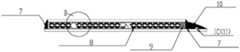
- FIG. 1is a schematic cross-sectional view of a prior art electronic paper display screen.
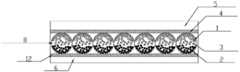
- FIG. 2is an enlarged view of B of FIG. 1.
- FIG. 2is an enlarged view of B of FIG. 1.
- FIG. 3is a cross-sectional view of the electronic paper display screen of the present invention.
- Fig. 4is an enlarged view of Fig. 3;
- the electronic paper display screen of the present inventionis composed of a transparent electrode substrate 5, an upper transparent electrode 4, an electrophoretic display layer 8 and a pixel electrode 6 which are disposed in order from top to bottom, and is made of waterproof glue. 7 is sealed; a conductive silver paste 9 is disposed between the upper transparent electrode 4 and the pixel electrode 6, the conductive silver paste 9 is electrically connected to the upper transparent electrode 4 and the pixel electrode 6, and the conductive silver paste 9 can also be made of conductive beads; An IC module 11 is disposed on the pixel electrode 6 outside the waterproof glue 7, and the IC module 11 is sealed by the blue glue 10.
- the electrophoretic display layer 8may be a single layer microcapsule array, a multilayer microcapsule array, or a single layer microcup array, preferably a single layer microcapsule array and a single layer microcup array.
- the microcapsules or microcupscontain two, three or even more than three different electrophoretic particles of different optoelectronic properties, thereby achieving black-white, single-color, multi-color and true color display.
- Preferred colors of the electrophoretic particlesinclude white, black, red, green, blue, and yellow.
- microcapsulesare elastically deformable, having a water content of less than 5%; microcapsules having a thickness of between 5 and 150 microns, preferably having a thickness in the range of from 15 to 60 microns; and a single microcapsule having a diameter of between 5 and 300 microns, preferably a single The microcapsules range in diameter from 30 to 100 microns.
- the microcup planar structuremay be various shapes such as a hexagon, a triangle, a diamond, a rectangle, a circle, and the like.
- the microcup layerhas a thickness between 5 and 180 microns, preferably between 15 and 80 microns.
- the single microcup planar structureis between 5 and 300 microns in size, and the preferred single microcup planar structure is between 30 and 150 microns in size.
- the inventionutilizes the adhesion of the electrophoretic display layer itself to achieve adhesion to the pixel electrode by the curing method, thereby avoiding many defects caused by the use of the glue layer in the prior art.
- the contrastis increased by more than 10%, the response time is reduced to less than 80 milliseconds, the driving voltage is reduced to between plus and minus 1.5-3V, and the operating temperature range is widened to -25-70 degrees.
- the microcapsule electronic paper arraycan be formed by coating, printing, printing, pouring, etc., wherein a preferred manner is to form a single layer microcapsule array by ODF infusion.
- Microcup electronic paper arrayscan be fabricated by microembossing and plate etching.
- the microcup structurecan be prepared by photocuring or reversible heat curing, and the sealing material of the microcup can be sealed with hot melt adhesive.
- Microcapsules or microcupscontain two, three or more than three different electrophoretic particles of different optoelectronic properties, thereby achieving black-white, single-color, multi-color and true color display. Where electrophoretic particles are preferred Colors include white, black, red, green, blue, and yellow.
- Embodiment 2Method of manufacturing electronic paper display screen
- the multi-particle microcapsule electronic inkis firstly coated on the pixel electrode 6 by a dispenser, and thermally cured to form a microcapsule electrophoretic display layer 8, which contains white particles 1 and black particles. 2.
- a conductive silver paste 9 or a conductive beadis spot-coated on the pixel electrode 6, and the upper transparent electrode 4 and the transparent electrode substrate 5 are pressed onto the microcapsule electrophoretic display layer 8.
- the corresponding upper transparent electrode 4 and the transparent electrode substrate 5are cut off by laser, the predetermined position of the IC module 11 on the pixel electrode 6 is exposed, and then the waterproof glue is applied to the spot by the dispensing machine.
- the pixel electrode 6includes a segment code and a dot matrix, and the material of the pixel electrode 6 is glass or plastic, and the plastic includes PI, PEN or PET.
- the multi-particle microcapsule electronic inkcomprises white particles 1, black particles 2 and other particles 3 to achieve black-white, single-color, multi-color and true color display, and the other particles 3 are generally yellow particles or/and red particles.
- the curing of the electrophoretic display layer in this embodimentmay also adopt a reversible heat curing method, which is a reversible process in which repeated bonding and peeling can be repeated by heating, and the temperature range of the reversible heat curing bonding and peeling is 60 to 150 ° C, preferably 80 to 120 ° C; the heating time is in the range of 0 to 30 minutes, preferably the heating time is 2 to 20 minutes, and more preferably the heating time is 5 to 10 minutes.
- a reversible heat curing methodwhich is a reversible process in which repeated bonding and peeling can be repeated by heating
- the temperature range of the reversible heat curing bonding and peelingis 60 to 150 ° C, preferably 80 to 120 ° C
- the heating timeis in the range of 0 to 30 minutes, preferably the heating time is 2 to 20 minutes, and more preferably the heating time is 5 to 10 minutes.
- the advantage of the reversible heat curingis that the electronic paper can be reused, cost-saving, and environmentally friendly.
Landscapes
- Physics & Mathematics (AREA)
- Nonlinear Science (AREA)
- General Physics & Mathematics (AREA)
- Optics & Photonics (AREA)
- Chemical & Material Sciences (AREA)
- Life Sciences & Earth Sciences (AREA)
- Health & Medical Sciences (AREA)
- Chemical Kinetics & Catalysis (AREA)
- Electrochemistry (AREA)
- Molecular Biology (AREA)
- Mathematical Physics (AREA)
- Crystallography & Structural Chemistry (AREA)
- Electrochromic Elements, Electrophoresis, Or Variable Reflection Or Absorption Elements (AREA)
Abstract
Description
Translated fromChinese本发明涉及一种电子纸显示屏及其制造方法,属于电子显示屏技术领域。The invention relates to an electronic paper display screen and a manufacturing method thereof, and belongs to the technical field of electronic display screens.
电泳显示利用带电的胶体颗粒在电场作用下发生泳动的现象,通过电场驱动不同光电性能的电泳粒子来实现图像和文字的显示,与已知的显示技术相比,电泳显示具备如下特点:柔性易弯曲,重量轻,厚度薄,对比度高,能耗低,可视角度大,阳光下可读,具备图像双稳态,容易大面积生产等特点。Electrophoresis shows the phenomenon that the charged colloidal particles migrate under the action of an electric field, and the electrophoretic particles with different photoelectric properties are driven by the electric field to realize the display of images and characters. Compared with the known display technology, the electrophoretic display has the following characteristics: flexibility Easy to bend, light weight, thin thickness, high contrast, low energy consumption, large viewing angle, readable under sunlight, image bistable, easy to produce in large areas.
电泳显示技术最初在上世纪70年代被提出。在专利US3892568中公开了至少包含一种电泳粒子的电泳显示材料的制备过程。在专利JP1086116中公开了至少含有一种电泳粒子,并且电泳液被微胶囊包覆的电泳显示系统。在US6930818中公开了使用微杯结构包覆的电泳显示单元。常见的微杯型电子纸显示屏主要包括上层透明电极,微杯电泳显示层,密封层,胶水层,像素电极。在专利US5930026,US5961804,US6017584和US6120588中,公开了微胶囊包覆的电泳显示单元,其中电泳显示液包含两种或者两种以上不同光电性能的电泳粒子。常见的微胶囊型电子纸显示屏主要分为上层透明电极,微胶囊电泳显示层,胶水层,像素电极,如图1、图2所示。其中胶水层主要用来加强像素电极层和电泳显示层之间的粘合,使得电子纸显示屏的显示效果均匀一致。但是胶水层的存在对电泳显示屏带来的负面效果也显而易见:Electrophoretic display technology was first proposed in the 1970s. The preparation of an electrophoretic display material comprising at least one electrophoretic particle is disclosed in US Pat. No. 3,892,568. An electrophoretic display system comprising at least one electrophoretic particle and the electrophoresis fluid coated with microcapsules is disclosed in the patent JP 1086116. An electrophoretic display unit coated with a microcup structure is disclosed in US Pat. No. 6,930,818. The common micro-cup type electronic paper display mainly includes an upper transparent electrode, a micro cup electrophoretic display layer, a sealing layer, a glue layer, and a pixel electrode. Microencapsulated electrophoretic display units are disclosed in the patents US 593 0026, US Pat. No. 5,961, 804, US Pat. No. 6,017, 584, and US Pat. No. 6,120,588, wherein the electrophoretic display liquid contains two or more electrophoretic particles of different optoelectronic properties. The common microcapsule type electronic paper display screen is mainly divided into an upper transparent electrode, a microcapsule electrophoretic display layer, a glue layer and a pixel electrode, as shown in FIG. 1 and FIG. 2 . The glue layer is mainly used to strengthen the adhesion between the pixel electrode layer and the electrophoretic display layer, so that the display effect of the electronic paper display screen is uniform. However, the negative effects of the presence of the glue layer on the electrophoretic display are also obvious:
1、增加了透明电极和像素电极之间的距离,降低了电极之间的电场强度,减低了电场对于电泳粒子的驱动力,反应在电泳显示的效果上就是对比度降低,响应时间变慢,驱动电压过高,温度适用范围变窄(0-50度)等,严重压缩了电子纸的适用环境和产品应用范围。1. Increasing the distance between the transparent electrode and the pixel electrode, reducing the electric field strength between the electrodes, reducing the driving force of the electric field on the electrophoretic particles, and the effect of the electrophoretic display is that the contrast is lowered, the response time is slow, and the driving is slowed. The voltage is too high, the temperature application range is narrowed (0-50 degrees), etc., which seriously compresses the applicable environment and product application range of the electronic paper.
2、胶水层主要成分为高分子树脂,高分子树脂大多为好的绝缘体,体积电阻率高,不能直接用作电泳显示的胶水层,因此需要添加电解质降低体积电阻率,而电解质的添加降低了像素电极,电泳显示层的使用寿命。2. The main component of the glue layer is polymer resin. The polymer resin is mostly a good insulator. The volume resistivity is high and cannot be directly used as the glue layer for electrophoresis display. Therefore, it is necessary to add electrolyte to reduce the volume resistivity, and the addition of electrolyte is reduced. The pixel electrode, the lifetime of the electrophoretic display layer.
3、胶水层需要预先涂覆胶水或覆合胶膜到电泳显示层,需要经过粘合剂调配或胶膜制备,以及多次覆离型保护膜等步骤,这一过程的工艺的复杂性大大增加了不良品,降低了产品的良率,增加了成本。3, the glue layer needs to be pre-applied with glue or laminating film to the electrophoretic display layer, which needs to be prepared by adhesive preparation or film preparation, and multiple times to remove the protective film. The process complexity of this process is greatly Increased defective products, reduced product yield and increased costs.
4、胶水层容易吸收环境中的水分,对于显示屏封边要求极高,增加了环境测试风险,增加了生产成本,降低了产品良率,降低了产品使用寿命,同时胶水层吸收水分,会使得显示屏幕模糊,对比度和分辨率降低,显著降低产品性能。4, the glue layer is easy to absorb the moisture in the environment, the display edge sealing requirements are extremely high, increasing the environmental testing risk, increasing the production cost, reducing the product yield, reducing the product life, while the glue layer absorbs moisture, The display screen is blurred, the contrast and resolution are reduced, and the performance of the product is significantly reduced.
发明内容Summary of the invention
本发明的目的是克服现有技术中存在的不足,提供一种电子纸显示屏及其制造方法,省去了传统的胶水层,简化生产工艺和结构,同时还会给电子纸显示屏带来更好地显示均一性,也为了制造性能更优良的电子纸显示屏。The object of the present invention is to overcome the deficiencies in the prior art, to provide an electronic paper display screen and a manufacturing method thereof, which eliminates the traditional glue layer, simplifies the production process and structure, and also displays the electronic paper.The display screen provides better display uniformity and also creates an electronic paper display with better performance.
按照本发明提供的技术方案,所述电子纸显示屏,其特征是:所述电子纸显示屏由从上至下依次设置的透明电极基材、上层透明电极、电泳显示层和像素电极组成,并由防水胶水进行封边;在所述上层透明电极和像素电极之间设置导电银浆,导电银浆与上层透明电极和像素电极电连接。According to the technical solution provided by the present invention, the electronic paper display screen is characterized in that: the electronic paper display screen is composed of a transparent electrode substrate, an upper transparent electrode, an electrophoretic display layer and a pixel electrode which are disposed in order from top to bottom. And sealing with a waterproof glue; a conductive silver paste is disposed between the upper transparent electrode and the pixel electrode, and the conductive silver paste is electrically connected to the upper transparent electrode and the pixel electrode.
进一步的,在所述像素电极上位于防水胶水外侧布置IC模块,IC模块由蓝胶固封。Further, an IC module is disposed on the pixel electrode outside the waterproof glue, and the IC module is solidified by blue glue.
进一步的,所述电泳显示层为单层微胶囊阵列、多层微胶囊阵列、或者是单层微杯阵列。Further, the electrophoretic display layer is a single layer microcapsule array, a multilayer microcapsule array, or a single layer microcup array.
进一步的,所述微胶囊或者微杯中包含两种、三种甚至三种以上的不同光电性能的电泳粒子。Further, the microcapsule or the microcup contains two, three or even three or more electrophoretic particles having different photoelectric properties.
进一步的,所述微胶囊的厚度为5-150微米之间,优选厚度范围为15-60微米;单个微胶囊的直径在5-300微米之间,优选单个微胶囊的直径范围为30-100微米。Further, the microcapsules have a thickness of between 5 and 150 microns, preferably a thickness of from 15 to 60 microns; a single microcapsule has a diameter of between 5 and 300 microns, preferably a single microcapsule having a diameter in the range of 30 to 100 Micron.
进一步的,所述微杯层厚度在5-180微米之间,优选厚度为15-80微米;单个微杯平面结构大小在5-300微米之间,优选的单个微杯平面结构的大小在30-150微米之间。Further, the thickness of the microcup layer is between 5 and 180 micrometers, preferably between 15 and 80 micrometers; the size of a single microcup planar structure is between 5 and 300 micrometers, and the size of a preferred single microcup planar structure is 30. -150 microns between.
所述电子纸显示屏的制造方法,其特征是,包括以下步骤:The manufacturing method of the electronic paper display screen is characterized in that it comprises the following steps:
(1)在像素电极上制作电子纸阵列,进行固化形成电泳显示层,使电泳显示层与像素电极粘合;或者直接在像素电极上压合已经固化的电泳显示层;(1) forming an electronic paper array on the pixel electrode, curing to form an electrophoretic display layer, bonding the electrophoretic display layer to the pixel electrode; or directly pressing the cured electrophoretic display layer on the pixel electrode;
(2)在像素电极上滴点涂覆导电银浆或导电珠,将上层透明电极和透明电极基材压合在电泳显示层上;(2) dropping a conductive silver paste or a conductive bead on the pixel electrode, and pressing the upper transparent electrode and the transparent electrode substrate on the electrophoretic display layer;
(3)切割掉相应的上层透明电极和透明电极基材,露出像素电极上IC模块的预定位置;采用防水胶水进行封边,进行紫外光照射固化。(3) Cutting off the corresponding upper transparent electrode and transparent electrode substrate to expose the predetermined position of the IC module on the pixel electrode; sealing with a waterproof glue, and curing by ultraviolet light.
进一步的,还包括步骤(4),在像素电极上露出的预定位置处打上IC模块,用蓝胶将IC模块固封。Further, the method further includes the step (4) of inserting the IC module at a predetermined position exposed on the pixel electrode, and sealing the IC module with the blue glue.
进一步的,所述步骤(1)中电子纸阵列通过涂布、印刷、打印或灌注的方式制作微胶囊电子纸阵列,或者通过微压印、或平板蚀刻法制作微杯电子纸阵列。Further, in the step (1), the electronic paper array is fabricated by coating, printing, printing or infusion to form a micro-capsule electronic paper array, or the micro-cup electronic paper array is fabricated by micro-embossing or flat etching.
进一步的,所述步骤(1)中,固化的方式采用湿气固化、光固化、压敏、热固化、可逆热固化或热熔压敏。Further, in the step (1), the curing method adopts moisture curing, photo curing, pressure sensitivity, heat curing, reversible heat curing or hot melt pressure sensitivity.
本发明所述电子纸显示屏省去了传统的胶水层,无需通过胶水层来粘贴电泳显示层和像素电极;具有生产工艺简化,显示结构简单,电泳显示层厚度均一可控,显示效果提升等特点;去除了传统的胶水层,使得生产效率提高和良率提升,同时提高了显示性能。本发明适用于微胶囊或微杯结构的电子纸,其中微胶囊或微杯中可以包括两种,三种甚至三种以上光电性能不同的电泳粒子,可以实现黑白、单彩色、双彩色、多彩色和真彩色等显示。The electronic paper display screen of the invention eliminates the traditional glue layer, and does not need to paste the electrophoretic display layer and the pixel electrode through the glue layer; the production process is simplified, the display structure is simple, the thickness of the electrophoretic display layer is uniformly controllable, the display effect is improved, etc. Features; the traditional glue layer is removed, which improves production efficiency and yield, while improving display performance. The invention is applicable to electronic paper of microcapsule or microcup structure, wherein the microcapsule or the microcup can include two kinds, three or more kinds of electrophoretic particles having different photoelectric properties, and can realize black and white, single color, double color, and more Display in color and true color.
图1为现有技术电子纸显示屏的剖面示意图。1 is a schematic cross-sectional view of a prior art electronic paper display screen.
图2为图1的B放大图。FIG. 2 is an enlarged view of B of FIG. 1. FIG.
图3为本发明所述电子纸显示屏的剖面示意图。3 is a cross-sectional view of the electronic paper display screen of the present invention.
图4为图3的A放大图。Fig. 4 is an enlarged view of Fig. 3;
附图标记说明:1-白色粒子、2-黑色粒子、3-其他粒子、4-上层透明电极、5-透明电极基材、6-像素电极、7-防水胶水、8-电泳显示层、9-导电银浆、10-蓝胶、11-IC模块、12-胶水层。DESCRIPTION OF REFERENCE NUMERALS 1 - white particles, 2-black particles, 3-other particles, 4-upper transparent electrode, 5-transparent electrode substrate, 6-pixel electrode, 7-waterproof glue, 8-electrophoretic display layer, 9 - Conductive silver paste, 10-blue glue, 11-IC module, 12-glue layer.
下面结合具体附图对本发明作进一步说明。The invention will now be further described with reference to the specific drawings.
实施例1:Example 1:
如图3、图4所示,本发明所述电子纸显示屏由从上至下依次设置的透明电极基材5、上层透明电极4、电泳显示层8和像素电极6组成,并由防水胶水7进行封边;在所述上层透明电极4和像素电极6之间设置导电银浆9,导电银浆9与上层透明电极4和像素电极6电连接,导电银浆9也可以采用导电珠;在所述像素电极6上位于防水胶水7外侧布置IC模块11,IC模块11由蓝胶10固封。As shown in FIG. 3 and FIG. 4, the electronic paper display screen of the present invention is composed of a
所述电泳显示层8可以是单层微胶囊阵列、多层微胶囊阵列、也可以是单层微杯阵列,优选为单层微胶囊阵列和单层微杯阵列。所述微胶囊或者微杯中包含两种、三种甚至三种以上的不同光电性能的电泳粒子,从而实现黑白色,单彩色,多彩色和真彩色的显示。其中电泳粒子优选的颜色包括白色,黑色,红色,绿色,蓝色和黄色等。The
所述微胶囊弹性可变形,含水量低于5%;微胶囊厚度在5-150微米之间,优选厚度范围为15-60微米;单个微胶囊的直径在5-300微米之间,优选单个微胶囊的直径范围为30-100微米。The microcapsules are elastically deformable, having a water content of less than 5%; microcapsules having a thickness of between 5 and 150 microns, preferably having a thickness in the range of from 15 to 60 microns; and a single microcapsule having a diameter of between 5 and 300 microns, preferably a single The microcapsules range in diameter from 30 to 100 microns.
所述微杯平面结构可以是六边形、三角形、菱形、长方形、圆形等各种形状。微杯层厚度在5-180微米之间,优选厚度为15-80微米。单个微杯平面结构大小在5-300微米之间,优选的单个微杯平面结构的大小在30-150微米之间。The microcup planar structure may be various shapes such as a hexagon, a triangle, a diamond, a rectangle, a circle, and the like. The microcup layer has a thickness between 5 and 180 microns, preferably between 15 and 80 microns. The single microcup planar structure is between 5 and 300 microns in size, and the preferred single microcup planar structure is between 30 and 150 microns in size.
无论是单层微胶囊还是单层微杯电泳显示层,自身都具有粘附性,这种粘附性可以通过湿气固化,光固化,压敏,热固化,热熔压敏等作用来实现。其中热固化优选可逆热固化的方式。本发明利用电泳显示层自身的粘附性通过固化方式实现和像素电极的粘合,避免了现有技术中使用胶水层所带来的诸多缺陷。Whether it is a single-layer microcapsule or a single-layer micro-cup electrophoretic display layer, it has its own adhesion. This adhesion can be achieved by moisture curing, photocuring, pressure sensitivity, heat curing, hot melt varistor, etc. . Among them, thermal curing is preferably a reversible heat curing method. The invention utilizes the adhesion of the electrophoretic display layer itself to achieve adhesion to the pixel electrode by the curing method, thereby avoiding many defects caused by the use of the glue layer in the prior art.
相较于传统的电子纸显示屏,对比度提高10%以上,响应时间降到80毫秒以下,驱动电压降低到正负1.5-3V之间,工作温度范围拓宽为-25-70度。Compared with the traditional electronic paper display, the contrast is increased by more than 10%, the response time is reduced to less than 80 milliseconds, the driving voltage is reduced to between plus and minus 1.5-3V, and the operating temperature range is widened to -25-70 degrees.
可以通过涂布、印刷、打印、灌注等方式形成微胶囊电子纸阵列,其中优选的方式是通过ODF灌注方式形成单层微胶囊阵列。The microcapsule electronic paper array can be formed by coating, printing, printing, pouring, etc., wherein a preferred manner is to form a single layer microcapsule array by ODF infusion.
可以通过微压印和平板蚀刻法制造微杯电子纸阵列。其中微杯结构可以用光固化或可逆热固化的材料制备,微杯的封口材料可以用热熔胶封口。Microcup electronic paper arrays can be fabricated by microembossing and plate etching. The microcup structure can be prepared by photocuring or reversible heat curing, and the sealing material of the microcup can be sealed with hot melt adhesive.
微胶囊或者微杯中包含两种,三种甚至三种以上的不同光电性能的电泳粒子,从而实现黑白色,单彩色,多彩色和真彩色的显示。其中电泳粒子优选的颜色包括白色,黑色,红色,绿色,蓝色和黄色等。Microcapsules or microcups contain two, three or more than three different electrophoretic particles of different optoelectronic properties, thereby achieving black-white, single-color, multi-color and true color display. Where electrophoretic particles are preferredColors include white, black, red, green, blue, and yellow.
实施例2:电子纸显示屏的制造方法Embodiment 2: Method of manufacturing electronic paper display screen
如图3、图4所示,首先通过点胶机在像素电极6上滴点涂覆多粒子微胶囊电子墨水,热固化形成微胶囊电泳显示层8,微胶囊内含有白色粒子1和黑色粒子2,接下来在像素电极6上滴点涂覆导电银浆9或导电珠,将上层透明电极4和透明电极基材5压合在微胶囊电泳显示层8上。再根据设计图纸,通过激光切割掉相应的上层透明电极4和透明电极基材5,露出像素电极6上IC模块11绑定的预定位置,然后用点胶机滴点涂覆点防水胶水7封边,进行紫外光照射固化,在通过COG工艺打上IC模块11,最后使用蓝胶工艺印好蓝胶10,完成电子纸显示屏的制造。所述像素电极6包括段码和点矩阵,所述像素电极6的材料为玻璃或塑料,所述塑料包括PI、PEN或PET。所述多粒子微胶囊电子墨水包括白色粒子1、黑色粒子2和其他粒子3,从而实现黑白色,单彩色,多彩色和真彩色的显示,其他粒子3一般为黄色粒子或/和红色粒子。As shown in FIG. 3 and FIG. 4, the multi-particle microcapsule electronic ink is firstly coated on the
本实施例中电泳显示层的固化也可以采用可逆热固化的方式,所述可逆热固化方式即可以通过加热反复多次粘结和剥离的可逆过程,可逆热固化粘结和剥离的温度范围为60~150℃,优选温度为80~120℃;加热时间范围为0~30分钟,优选加热时间是2~20分钟,更优选的加热时间5~10分钟。具体过程如下:The curing of the electrophoretic display layer in this embodiment may also adopt a reversible heat curing method, which is a reversible process in which repeated bonding and peeling can be repeated by heating, and the temperature range of the reversible heat curing bonding and peeling is 60 to 150 ° C, preferably 80 to 120 ° C; the heating time is in the range of 0 to 30 minutes, preferably the heating time is 2 to 20 minutes, and more preferably the heating time is 5 to 10 minutes. The specific process is as follows:
1、将加热层压设备温度设置为100℃,当设备到达设定温度,设定加热时间为5分钟,这时将微胶囊电子纸薄膜与TFT玻璃对齐贴合在一起,把贴合好的玻璃和薄膜一起通过层压设备,完成层压,使得微胶囊薄膜和TFT玻璃通过热固化粘合在一起,待冷却到室温即可完成显示屏的完全固化粘合;1. Set the temperature of the heating laminating equipment to 100 ° C. When the equipment reaches the set temperature, set the heating time to 5 minutes. At this time, align the microcapsule electronic paper film with the TFT glass and fit it together. The glass and the film are laminated together through a laminating apparatus, so that the microcapsule film and the TFT glass are bonded together by heat curing, and the fully cured bonding of the display screen is completed after cooling to room temperature;
2、将固化粘合好的显示屏,重新加热到100度,加热10分钟,然后通过剥离设备慢慢地将微胶囊电子纸薄膜从TFT玻璃表面剥离完整开来,再冷却到室温,就得到一个完好无损的微胶囊电子纸薄膜。可重复利用,下次需要时再将该微胶囊电子纸薄膜压合到像素电极6上。2. Curing the bonded display, reheating to 100 degrees, heating for 10 minutes, then slowly peeling off the microcapsule electronic paper film from the surface of the TFT glass by a stripping device, and then cooling to room temperature, An intact microcapsule electronic paper film. It can be reused, and the microcapsule electronic paper film is pressed onto the
所述可逆热固化的优点是:电子纸可重复利用,节约成本,绿色环保。The advantage of the reversible heat curing is that the electronic paper can be reused, cost-saving, and environmentally friendly.
尽管上面结合实施例描述了本发明,但对本领域技术人员显而易见的是,在本发明的权利要求的保护范围内,可以对上述实施例进行各种修改。While the invention has been described in connection with the embodiments thereof, it will be apparent to those skilled in the art that various modifications of the above-described embodiments are possible within the scope of the appended claims.
Claims (10)
Translated fromChinesePriority Applications (5)
| Application Number | Priority Date | Filing Date | Title |
|---|---|---|---|
| US16/334,765US11347125B2 (en) | 2017-09-26 | 2017-10-10 | Electronic paper display screen and manufacturing method thereof |
| KR1020197002972AKR20190053173A (en) | 2017-09-26 | 2017-10-10 | Electronic paper display device and manufacturing method thereof |
| KR1020217018663AKR102467078B1 (en) | 2017-09-26 | 2017-10-10 | Electronic paper display screen and manufacturing method therefor |
| JP2019520979AJP6935874B2 (en) | 2017-09-26 | 2017-10-10 | Electronic paper display and its manufacturing method |
| EP17926727.3AEP3521918B1 (en) | 2017-09-26 | 2017-10-10 | Electronic paper display screen and manufacturing method therefor |
Applications Claiming Priority (2)
| Application Number | Priority Date | Filing Date | Title |
|---|---|---|---|
| CN201710881471.1 | 2017-09-26 | ||
| CN201710881471.1ACN107656408A (en) | 2017-09-26 | 2017-09-26 | Electronic-paper display screen and its manufacture method |
Publications (1)
| Publication Number | Publication Date |
|---|---|
| WO2019061555A1true WO2019061555A1 (en) | 2019-04-04 |
Family
ID=61130355
Family Applications (1)
| Application Number | Title | Priority Date | Filing Date |
|---|---|---|---|
| PCT/CN2017/105462CeasedWO2019061555A1 (en) | 2017-09-26 | 2017-10-10 | Electronic paper display screen and manufacturing method therefor |
Country Status (7)
| Country | Link |
|---|---|
| US (1) | US11347125B2 (en) |
| EP (1) | EP3521918B1 (en) |
| JP (1) | JP6935874B2 (en) |
| KR (2) | KR102467078B1 (en) |
| CN (1) | CN107656408A (en) |
| TW (1) | TWI662351B (en) |
| WO (1) | WO2019061555A1 (en) |
Cited By (1)
| Publication number | Priority date | Publication date | Assignee | Title |
|---|---|---|---|---|
| CN111999955A (en)* | 2020-09-16 | 2020-11-27 | 恩利克(浙江)显示科技有限公司 | Flexible touch electronic paper display module and manufacturing method thereof |
Families Citing this family (17)
| Publication number | Priority date | Publication date | Assignee | Title |
|---|---|---|---|---|
| CN110262154A (en)* | 2019-07-22 | 2019-09-20 | 成都捷翼电子科技有限公司 | A kind of structure and manufacturing method of color display module |
| KR102731215B1 (en)* | 2019-11-04 | 2024-11-15 | 이 잉크 코포레이션 | Three-dimensional, color-changing objects comprising a light-transmitting substrate and an electrophoretic medium |
| CN111290189B (en)* | 2020-04-08 | 2025-02-07 | 成都捷翼电子科技有限公司 | A color display module and a manufacturing method thereof |
| CN111965914A (en)* | 2020-08-13 | 2020-11-20 | 电子科技大学中山学院 | Color electronic ink screen and display method thereof |
| CN112083614A (en)* | 2020-08-24 | 2020-12-15 | 广州融捷显示科技有限公司 | Electrophoretic display liquid, electrophoretic color display device and manufacturing method |
| US11413394B1 (en)* | 2021-02-19 | 2022-08-16 | Fresenius Kabi Deutschland Gmbh | Display for wearable drug delivery device |
| CN113253536B (en)* | 2021-06-08 | 2022-09-27 | 佛山宜视智联科技有限公司 | Method and device for attaching color electronic paper, electronic equipment and storage medium |
| CN113448134B (en)* | 2021-06-11 | 2024-05-24 | 江西兴泰科技股份有限公司 | Electronic paper module manufacturing method |
| CN113960846B (en)* | 2021-09-30 | 2024-10-22 | 中国科学院重庆绿色智能技术研究院 | Flexible electronic paper and preparation and application thereof |
| CN114527611B (en)* | 2021-12-30 | 2023-09-26 | 广东志慧芯屏科技有限公司 | Manufacturing method of electronic paper display device |
| CN114236937B (en)* | 2021-12-30 | 2024-12-06 | 广东志慧芯屏科技有限公司 | Method for manufacturing an electronic paper display device |
| CN114265256B (en)* | 2021-12-30 | 2023-04-28 | 广东志慧芯屏科技有限公司 | Manufacturing method of electronic paper display equipment |
| US20240103310A1 (en)* | 2022-09-27 | 2024-03-28 | Amazon Technologies, Inc. | Front-lit displays and indicators having uniform brightness |
| CN115857244A (en)* | 2022-12-01 | 2023-03-28 | 固安翌光科技有限公司 | Electronic paper and manufacturing method thereof |
| WO2025097255A1 (en)* | 2023-11-10 | 2025-05-15 | Vuereal Inc. | Microdevice integration and transparency |
| CN118562383B (en)* | 2024-06-03 | 2025-09-16 | 江汉大学 | Composition for quick-response microcup type electrophoresis electronic paper and electronic paper processing method |
| CN119091813A (en)* | 2024-09-03 | 2024-12-06 | 福州大学 | A low-light image restoration and display optimization method for electronic paper display |
Citations (14)
| Publication number | Priority date | Publication date | Assignee | Title |
|---|---|---|---|---|
| US3892568A (en) | 1969-04-23 | 1975-07-01 | Matsushita Electric Industrial Co Ltd | Electrophoretic image reproduction process |
| JPH1086116A (en) | 1996-09-18 | 1998-04-07 | Matsushita Electric Works Ltd | Inorganic cement board and manufacture thereof |
| US5930026A (en) | 1996-10-25 | 1999-07-27 | Massachusetts Institute Of Technology | Nonemissive displays and piezoelectric power supplies therefor |
| US5961804A (en) | 1997-03-18 | 1999-10-05 | Massachusetts Institute Of Technology | Microencapsulated electrophoretic display |
| US6017584A (en) | 1995-07-20 | 2000-01-25 | E Ink Corporation | Multi-color electrophoretic displays and materials for making the same |
| US6120588A (en) | 1996-07-19 | 2000-09-19 | E Ink Corporation | Electronically addressable microencapsulated ink and display thereof |
| US6930818B1 (en) | 2000-03-03 | 2005-08-16 | Sipix Imaging, Inc. | Electrophoretic display and novel process for its manufacture |
| JP2010151897A (en)* | 2008-12-24 | 2010-07-08 | Citizen Holdings Co Ltd | Electric display and method of manufacturing the same |
| CN102062984A (en)* | 2010-11-29 | 2011-05-18 | 广州奥熠电子科技有限公司 | Electrophoretic display device and manufacturing method thereof |
| CN103559841A (en)* | 2013-11-21 | 2014-02-05 | 深圳晶华显示器材有限公司 | Flexible electronic paper display device and manufacturing method thereof |
| WO2014030336A1 (en)* | 2012-08-21 | 2014-02-27 | 凸版印刷株式会社 | Reflection-type display panel and process for producing same |
| CN203909444U (en)* | 2014-06-18 | 2014-10-29 | 无锡威峰科技有限公司 | EPD flexible display screen based on segment code |
| US20150205178A1 (en)* | 2014-01-17 | 2015-07-23 | E Ink Corporation | Controlled polymeric material conductivity for use in a two-phase electrode layer |
| CN206311871U (en)* | 2017-01-04 | 2017-07-07 | 京东方科技集团股份有限公司 | A kind of display device of electronic paper |
Family Cites Families (27)
| Publication number | Priority date | Publication date | Assignee | Title |
|---|---|---|---|---|
| US5049978A (en)* | 1990-09-10 | 1991-09-17 | General Electric Company | Conductively enclosed hybrid integrated circuit assembly using a silicon substrate |
| US7110164B2 (en)* | 2002-06-10 | 2006-09-19 | E Ink Corporation | Electro-optic displays, and processes for the production thereof |
| JP4265757B2 (en)* | 2003-07-25 | 2009-05-20 | シャープ株式会社 | Display module and manufacturing method thereof |
| JP2005049704A (en)* | 2003-07-30 | 2005-02-24 | Plus Vision Corp | Electronic display device using electronic paper |
| JP4507531B2 (en)* | 2003-08-25 | 2010-07-21 | セイコーエプソン株式会社 | Method for manufacturing electrophoretic display device |
| JP2005156759A (en)* | 2003-11-21 | 2005-06-16 | Toppan Printing Co Ltd | Electrophoretic display device |
| JP4516481B2 (en)* | 2004-06-02 | 2010-08-04 | セイコーエプソン株式会社 | Electrophoretic particles, method for producing the same, and use thereof |
| JP4644472B2 (en)* | 2004-11-16 | 2011-03-02 | セイコーエプソン株式会社 | Manufacturing method of display device |
| JP4508160B2 (en)* | 2005-10-14 | 2010-07-21 | セイコーエプソン株式会社 | Display device and electronic device |
| JP5167624B2 (en)* | 2005-12-28 | 2013-03-21 | セイコーエプソン株式会社 | Electrophoretic display device and electronic apparatus |
| KR20080023913A (en)* | 2006-09-12 | 2008-03-17 | 삼성전자주식회사 | Electrophoretic display device and driving method thereof |
| US20110090143A1 (en)* | 2009-10-20 | 2011-04-21 | Seung-Han Paek | Electrophoretic display device and fabrication method thereof |
| KR101738452B1 (en)* | 2009-10-20 | 2017-06-08 | 엘지디스플레이 주식회사 | Electrophoretic display deivce and method of fabrication thereof |
| CN102093785B (en)* | 2010-12-20 | 2013-12-11 | 广州奥熠电子科技有限公司 | Electrophoretic display coating fluid and preparation method thereof |
| US9146439B2 (en)* | 2011-01-31 | 2015-09-29 | E Ink California, Llc | Color electrophoretic display |
| KR101224696B1 (en)* | 2011-07-15 | 2013-01-21 | 삼성전기주식회사 | Electronic paper display device and manufacturing method thereof |
| JP5862212B2 (en)* | 2011-11-09 | 2016-02-16 | セイコーエプソン株式会社 | Electrophoretic display device |
| EP2853940B1 (en)* | 2012-08-22 | 2019-09-11 | Toppan Printing Co., Ltd. | Method for inspecting an electrophoretic display substrate |
| CN103834285B (en)* | 2012-11-20 | 2016-05-11 | 广州奥翼电子科技有限公司 | Electrophoresis coating fluid and electrophoresis showed layer and their preparation method |
| TWI534520B (en)* | 2013-10-11 | 2016-05-21 | 電子墨水加利福尼亞有限責任公司 | Color display device |
| JP2015194535A (en)* | 2014-03-31 | 2015-11-05 | 大日本印刷株式会社 | Method for manufacturing reflective display device |
| CN104317130B (en)* | 2014-10-17 | 2017-05-03 | 深圳晶华显示器材有限公司 | Waterproof electronic paper and making method thereof |
| KR20160126788A (en)* | 2015-04-24 | 2016-11-02 | 삼성전기주식회사 | electronic paper display |
| CN205139544U (en)* | 2015-11-13 | 2016-04-06 | 南京华日触控显示科技有限公司 | Passive form electron ink display screen |
| JP2017102403A (en)* | 2015-12-04 | 2017-06-08 | 大日本印刷株式会社 | Reflective display device |
| CN106168726A (en)* | 2016-08-31 | 2016-11-30 | 广州奥翼电子科技股份有限公司 | Display device of electronic paper |
| CN107357109B (en)* | 2017-08-21 | 2019-03-08 | 无锡威峰科技股份有限公司 | A kind of electric ink display screen and manufacturing method |
- 2017
- 2017-09-26CNCN201710881471.1Apatent/CN107656408A/enactivePending
- 2017-10-10WOPCT/CN2017/105462patent/WO2019061555A1/ennot_activeCeased
- 2017-10-10KRKR1020217018663Apatent/KR102467078B1/enactiveActive
- 2017-10-10USUS16/334,765patent/US11347125B2/enactiveActive
- 2017-10-10KRKR1020197002972Apatent/KR20190053173A/ennot_activeCeased
- 2017-10-10JPJP2019520979Apatent/JP6935874B2/enactiveActive
- 2017-10-10EPEP17926727.3Apatent/EP3521918B1/enactiveActive
- 2017-11-29TWTW106141554Apatent/TWI662351B/enactive
Patent Citations (14)
| Publication number | Priority date | Publication date | Assignee | Title |
|---|---|---|---|---|
| US3892568A (en) | 1969-04-23 | 1975-07-01 | Matsushita Electric Industrial Co Ltd | Electrophoretic image reproduction process |
| US6017584A (en) | 1995-07-20 | 2000-01-25 | E Ink Corporation | Multi-color electrophoretic displays and materials for making the same |
| US6120588A (en) | 1996-07-19 | 2000-09-19 | E Ink Corporation | Electronically addressable microencapsulated ink and display thereof |
| JPH1086116A (en) | 1996-09-18 | 1998-04-07 | Matsushita Electric Works Ltd | Inorganic cement board and manufacture thereof |
| US5930026A (en) | 1996-10-25 | 1999-07-27 | Massachusetts Institute Of Technology | Nonemissive displays and piezoelectric power supplies therefor |
| US5961804A (en) | 1997-03-18 | 1999-10-05 | Massachusetts Institute Of Technology | Microencapsulated electrophoretic display |
| US6930818B1 (en) | 2000-03-03 | 2005-08-16 | Sipix Imaging, Inc. | Electrophoretic display and novel process for its manufacture |
| JP2010151897A (en)* | 2008-12-24 | 2010-07-08 | Citizen Holdings Co Ltd | Electric display and method of manufacturing the same |
| CN102062984A (en)* | 2010-11-29 | 2011-05-18 | 广州奥熠电子科技有限公司 | Electrophoretic display device and manufacturing method thereof |
| WO2014030336A1 (en)* | 2012-08-21 | 2014-02-27 | 凸版印刷株式会社 | Reflection-type display panel and process for producing same |
| CN103559841A (en)* | 2013-11-21 | 2014-02-05 | 深圳晶华显示器材有限公司 | Flexible electronic paper display device and manufacturing method thereof |
| US20150205178A1 (en)* | 2014-01-17 | 2015-07-23 | E Ink Corporation | Controlled polymeric material conductivity for use in a two-phase electrode layer |
| CN203909444U (en)* | 2014-06-18 | 2014-10-29 | 无锡威峰科技有限公司 | EPD flexible display screen based on segment code |
| CN206311871U (en)* | 2017-01-04 | 2017-07-07 | 京东方科技集团股份有限公司 | A kind of display device of electronic paper |
Non-Patent Citations (1)
| Title |
|---|
| See also references ofEP3521918A4 |
Cited By (1)
| Publication number | Priority date | Publication date | Assignee | Title |
|---|---|---|---|---|
| CN111999955A (en)* | 2020-09-16 | 2020-11-27 | 恩利克(浙江)显示科技有限公司 | Flexible touch electronic paper display module and manufacturing method thereof |
Also Published As
| Publication number | Publication date |
|---|---|
| EP3521918B1 (en) | 2023-05-10 |
| KR20210077012A (en) | 2021-06-24 |
| JP6935874B2 (en) | 2021-09-15 |
| TW201915579A (en) | 2019-04-16 |
| US20210333680A1 (en) | 2021-10-28 |
| KR102467078B1 (en) | 2022-11-14 |
| KR20190053173A (en) | 2019-05-17 |
| US11347125B2 (en) | 2022-05-31 |
| TWI662351B (en) | 2019-06-11 |
| CN107656408A (en) | 2018-02-02 |
| EP3521918A4 (en) | 2020-06-17 |
| JP2019537051A (en) | 2019-12-19 |
| EP3521918A1 (en) | 2019-08-07 |
Similar Documents
| Publication | Publication Date | Title |
|---|---|---|
| WO2019061555A1 (en) | Electronic paper display screen and manufacturing method therefor | |
| KR102242277B1 (en) | Electronic ink display device and manufacturing method | |
| TWI691775B (en) | Closed display plasma module and manufacturing method thereof | |
| TWI774884B (en) | A dual-layer microstructure display plasma module and its manufacturing method | |
| JP2012063630A (en) | Microcapsule type electrophoresis display device and manufacturing method thereof | |
| WO2021217688A1 (en) | Display module with reflection structure, and method for manufacturing same | |
| WO2019140717A1 (en) | Display plasma module and fabrication method therefor | |
| CN210270463U (en) | Electronic paper display screen | |
| TWI740040B (en) | Patterned structure display plasma module and manufacturing method thereof | |
| CN212083869U (en) | Display module with reflection structure | |
| JP2012040522A (en) | Method for manufacturing base material provided with adhesive layer | |
| JP5406786B2 (en) | Method for manufacturing electrophoretic display medium | |
| CN114296289A (en) | Electrophoretic display and preparation method thereof | |
| JP2011242471A (en) | Electrophoretic display device and method for manufacturing the same | |
| JP2012032638A (en) | Method for manufacturing electrophoretic display device | |
| JP2015172619A (en) | Reflective display device and method of manufacturing reflective display device | |
| JP2012032705A (en) | Method for manufacturing electrophoretic display device | |
| JP2014206689A (en) | Manufacturing method of reflection display device |
Legal Events
| Date | Code | Title | Description |
|---|---|---|---|
| ENP | Entry into the national phase | Ref document number:20197002972 Country of ref document:KR Kind code of ref document:A | |
| ENP | Entry into the national phase | Ref document number:2019520979 Country of ref document:JP Kind code of ref document:A | |
| ENP | Entry into the national phase | Ref document number:2017926727 Country of ref document:EP Effective date:20190430 | |
| 121 | Ep: the epo has been informed by wipo that ep was designated in this application | Ref document number:17926727 Country of ref document:EP Kind code of ref document:A1 | |
| NENP | Non-entry into the national phase | Ref country code:DE |