WO2019059589A1 - Electrode substrate for transparent light-emitting device display, and manufacturing method therefor - Google Patents
Electrode substrate for transparent light-emitting device display, and manufacturing method thereforDownload PDFInfo
- Publication number
- WO2019059589A1 WO2019059589A1PCT/KR2018/010830KR2018010830WWO2019059589A1WO 2019059589 A1WO2019059589 A1WO 2019059589A1KR 2018010830 WKR2018010830 WKR 2018010830WWO 2019059589 A1WO2019059589 A1WO 2019059589A1
- Authority
- WO
- WIPO (PCT)
- Prior art keywords
- transparent
- pattern
- copper foil
- electrode
- resin composition
- Prior art date
- Legal status (The legal status is an assumption and is not a legal conclusion. Google has not performed a legal analysis and makes no representation as to the accuracy of the status listed.)
- Ceased
Links
Images


Classifications
- H—ELECTRICITY
- H10—SEMICONDUCTOR DEVICES; ELECTRIC SOLID-STATE DEVICES NOT OTHERWISE PROVIDED FOR
- H10H—INORGANIC LIGHT-EMITTING SEMICONDUCTOR DEVICES HAVING POTENTIAL BARRIERS
- H10H20/00—Individual inorganic light-emitting semiconductor devices having potential barriers, e.g. light-emitting diodes [LED]
- H10H20/80—Constructional details
- H10H20/85—Packages
- H10H20/857—Interconnections, e.g. lead-frames, bond wires or solder balls
- H—ELECTRICITY
- H01—ELECTRIC ELEMENTS
- H01B—CABLES; CONDUCTORS; INSULATORS; SELECTION OF MATERIALS FOR THEIR CONDUCTIVE, INSULATING OR DIELECTRIC PROPERTIES
- H01B13/00—Apparatus or processes specially adapted for manufacturing conductors or cables
- H01B13/0026—Apparatus for manufacturing conducting or semi-conducting layers, e.g. deposition of metal
- H—ELECTRICITY
- H01—ELECTRIC ELEMENTS
- H01L—SEMICONDUCTOR DEVICES NOT COVERED BY CLASS H10
- H01L21/00—Processes or apparatus adapted for the manufacture or treatment of semiconductor or solid state devices or of parts thereof
- H01L21/02—Manufacture or treatment of semiconductor devices or of parts thereof
- H01L21/02104—Forming layers
- H01L21/02365—Forming inorganic semiconducting materials on a substrate
- H01L21/02367—Substrates
- H—ELECTRICITY
- H05—ELECTRIC TECHNIQUES NOT OTHERWISE PROVIDED FOR
- H05K—PRINTED CIRCUITS; CASINGS OR CONSTRUCTIONAL DETAILS OF ELECTRIC APPARATUS; MANUFACTURE OF ASSEMBLAGES OF ELECTRICAL COMPONENTS
- H05K1/00—Printed circuits
- H05K1/02—Details
- H05K1/0274—Optical details, e.g. printed circuits comprising integral optical means
- H—ELECTRICITY
- H05—ELECTRIC TECHNIQUES NOT OTHERWISE PROVIDED FOR
- H05K—PRINTED CIRCUITS; CASINGS OR CONSTRUCTIONAL DETAILS OF ELECTRIC APPARATUS; MANUFACTURE OF ASSEMBLAGES OF ELECTRICAL COMPONENTS
- H05K3/00—Apparatus or processes for manufacturing printed circuits
- H05K3/0073—Masks not provided for in groups H05K3/02 - H05K3/46, e.g. for photomechanical production of patterned surfaces
- H05K3/0082—Masks not provided for in groups H05K3/02 - H05K3/46, e.g. for photomechanical production of patterned surfaces characterised by the exposure method of radiation-sensitive masks
- H—ELECTRICITY
- H05—ELECTRIC TECHNIQUES NOT OTHERWISE PROVIDED FOR
- H05K—PRINTED CIRCUITS; CASINGS OR CONSTRUCTIONAL DETAILS OF ELECTRIC APPARATUS; MANUFACTURE OF ASSEMBLAGES OF ELECTRICAL COMPONENTS
- H05K3/00—Apparatus or processes for manufacturing printed circuits
- H05K3/02—Apparatus or processes for manufacturing printed circuits in which the conductive material is applied to the surface of the insulating support and is thereafter removed from such areas of the surface which are not intended for current conducting or shielding
- H05K3/06—Apparatus or processes for manufacturing printed circuits in which the conductive material is applied to the surface of the insulating support and is thereafter removed from such areas of the surface which are not intended for current conducting or shielding the conductive material being removed chemically or electrolytically, e.g. by photo-etch process
- H05K3/067—Etchants
- H—ELECTRICITY
- H05—ELECTRIC TECHNIQUES NOT OTHERWISE PROVIDED FOR
- H05K—PRINTED CIRCUITS; CASINGS OR CONSTRUCTIONAL DETAILS OF ELECTRIC APPARATUS; MANUFACTURE OF ASSEMBLAGES OF ELECTRICAL COMPONENTS
- H05K3/00—Apparatus or processes for manufacturing printed circuits
- H05K3/22—Secondary treatment of printed circuits
- H05K3/28—Applying non-metallic protective coatings
- H05K3/285—Permanent coating compositions
- H05K3/287—Photosensitive compositions
- H—ELECTRICITY
- H05—ELECTRIC TECHNIQUES NOT OTHERWISE PROVIDED FOR
- H05K—PRINTED CIRCUITS; CASINGS OR CONSTRUCTIONAL DETAILS OF ELECTRIC APPARATUS; MANUFACTURE OF ASSEMBLAGES OF ELECTRICAL COMPONENTS
- H05K3/00—Apparatus or processes for manufacturing printed circuits
- H05K3/30—Assembling printed circuits with electric components, e.g. with resistor
- H05K3/32—Assembling printed circuits with electric components, e.g. with resistor electrically connecting electric components or wires to printed circuits
- H05K3/34—Assembling printed circuits with electric components, e.g. with resistor electrically connecting electric components or wires to printed circuits by soldering
- H05K3/3452—Solder masks
- H—ELECTRICITY
- H10—SEMICONDUCTOR DEVICES; ELECTRIC SOLID-STATE DEVICES NOT OTHERWISE PROVIDED FOR
- H10H—INORGANIC LIGHT-EMITTING SEMICONDUCTOR DEVICES HAVING POTENTIAL BARRIERS
- H10H20/00—Individual inorganic light-emitting semiconductor devices having potential barriers, e.g. light-emitting diodes [LED]
- H10H20/80—Constructional details
- H10H20/83—Electrodes
- H10H20/832—Electrodes characterised by their material
- H10H20/833—Transparent materials
- H—ELECTRICITY
- H10—SEMICONDUCTOR DEVICES; ELECTRIC SOLID-STATE DEVICES NOT OTHERWISE PROVIDED FOR
- H10H—INORGANIC LIGHT-EMITTING SEMICONDUCTOR DEVICES HAVING POTENTIAL BARRIERS
- H10H29/00—Integrated devices, or assemblies of multiple devices, comprising at least one light-emitting semiconductor element covered by group H10H20/00
- H10H29/10—Integrated devices comprising at least one light-emitting semiconductor component covered by group H10H20/00
- H10H29/14—Integrated devices comprising at least one light-emitting semiconductor component covered by group H10H20/00 comprising multiple light-emitting semiconductor components
- H10H29/142—Two-dimensional arrangements, e.g. asymmetric LED layout
- H—ELECTRICITY
- H01—ELECTRIC ELEMENTS
- H01L—SEMICONDUCTOR DEVICES NOT COVERED BY CLASS H10
- H01L25/00—Assemblies consisting of a plurality of semiconductor or other solid state devices
- H01L25/03—Assemblies consisting of a plurality of semiconductor or other solid state devices all the devices being of a type provided for in a single subclass of subclasses H10B, H10D, H10F, H10H, H10K or H10N, e.g. assemblies of rectifier diodes
- H01L25/04—Assemblies consisting of a plurality of semiconductor or other solid state devices all the devices being of a type provided for in a single subclass of subclasses H10B, H10D, H10F, H10H, H10K or H10N, e.g. assemblies of rectifier diodes the devices not having separate containers
- H01L25/075—Assemblies consisting of a plurality of semiconductor or other solid state devices all the devices being of a type provided for in a single subclass of subclasses H10B, H10D, H10F, H10H, H10K or H10N, e.g. assemblies of rectifier diodes the devices not having separate containers the devices being of a type provided for in group H10H20/00
- H01L25/0753—Assemblies consisting of a plurality of semiconductor or other solid state devices all the devices being of a type provided for in a single subclass of subclasses H10B, H10D, H10F, H10H, H10K or H10N, e.g. assemblies of rectifier diodes the devices not having separate containers the devices being of a type provided for in group H10H20/00 the devices being arranged next to each other
- H—ELECTRICITY
- H05—ELECTRIC TECHNIQUES NOT OTHERWISE PROVIDED FOR
- H05K—PRINTED CIRCUITS; CASINGS OR CONSTRUCTIONAL DETAILS OF ELECTRIC APPARATUS; MANUFACTURE OF ASSEMBLAGES OF ELECTRICAL COMPONENTS
- H05K2201/00—Indexing scheme relating to printed circuits covered by H05K1/00
- H05K2201/01—Dielectrics
- H05K2201/0104—Properties and characteristics in general
- H05K2201/0108—Transparent
- H—ELECTRICITY
- H05—ELECTRIC TECHNIQUES NOT OTHERWISE PROVIDED FOR
- H05K—PRINTED CIRCUITS; CASINGS OR CONSTRUCTIONAL DETAILS OF ELECTRIC APPARATUS; MANUFACTURE OF ASSEMBLAGES OF ELECTRICAL COMPONENTS
- H05K2201/00—Indexing scheme relating to printed circuits covered by H05K1/00
- H05K2201/01—Dielectrics
- H05K2201/0183—Dielectric layers
- H05K2201/0195—Dielectric or adhesive layers comprising a plurality of layers, e.g. in a multilayer structure
- H—ELECTRICITY
- H05—ELECTRIC TECHNIQUES NOT OTHERWISE PROVIDED FOR
- H05K—PRINTED CIRCUITS; CASINGS OR CONSTRUCTIONAL DETAILS OF ELECTRIC APPARATUS; MANUFACTURE OF ASSEMBLAGES OF ELECTRICAL COMPONENTS
- H05K2201/00—Indexing scheme relating to printed circuits covered by H05K1/00
- H05K2201/09—Shape and layout
- H05K2201/09209—Shape and layout details of conductors
- H05K2201/09654—Shape and layout details of conductors covering at least two types of conductors provided for in H05K2201/09218 - H05K2201/095
- H05K2201/09681—Mesh conductors, e.g. as a ground plane
- H—ELECTRICITY
- H05—ELECTRIC TECHNIQUES NOT OTHERWISE PROVIDED FOR
- H05K—PRINTED CIRCUITS; CASINGS OR CONSTRUCTIONAL DETAILS OF ELECTRIC APPARATUS; MANUFACTURE OF ASSEMBLAGES OF ELECTRICAL COMPONENTS
- H05K2201/00—Indexing scheme relating to printed circuits covered by H05K1/00
- H05K2201/09—Shape and layout
- H05K2201/09818—Shape or layout details not covered by a single group of H05K2201/09009 - H05K2201/09809
- H05K2201/099—Coating over pads, e.g. solder resist partly over pads
- H—ELECTRICITY
- H05—ELECTRIC TECHNIQUES NOT OTHERWISE PROVIDED FOR
- H05K—PRINTED CIRCUITS; CASINGS OR CONSTRUCTIONAL DETAILS OF ELECTRIC APPARATUS; MANUFACTURE OF ASSEMBLAGES OF ELECTRICAL COMPONENTS
- H05K2201/00—Indexing scheme relating to printed circuits covered by H05K1/00
- H05K2201/10—Details of components or other objects attached to or integrated in a printed circuit board
- H05K2201/10007—Types of components
- H05K2201/10106—Light emitting diode [LED]
- H—ELECTRICITY
- H05—ELECTRIC TECHNIQUES NOT OTHERWISE PROVIDED FOR
- H05K—PRINTED CIRCUITS; CASINGS OR CONSTRUCTIONAL DETAILS OF ELECTRIC APPARATUS; MANUFACTURE OF ASSEMBLAGES OF ELECTRICAL COMPONENTS
- H05K2201/00—Indexing scheme relating to printed circuits covered by H05K1/00
- H05K2201/10—Details of components or other objects attached to or integrated in a printed circuit board
- H05K2201/10007—Types of components
- H05K2201/10128—Display
- H—ELECTRICITY
- H05—ELECTRIC TECHNIQUES NOT OTHERWISE PROVIDED FOR
- H05K—PRINTED CIRCUITS; CASINGS OR CONSTRUCTIONAL DETAILS OF ELECTRIC APPARATUS; MANUFACTURE OF ASSEMBLAGES OF ELECTRICAL COMPONENTS
- H05K2201/00—Indexing scheme relating to printed circuits covered by H05K1/00
- H05K2201/20—Details of printed circuits not provided for in H05K2201/01 - H05K2201/10
- H05K2201/2072—Anchoring, i.e. one structure gripping into another
- H—ELECTRICITY
- H10—SEMICONDUCTOR DEVICES; ELECTRIC SOLID-STATE DEVICES NOT OTHERWISE PROVIDED FOR
- H10H—INORGANIC LIGHT-EMITTING SEMICONDUCTOR DEVICES HAVING POTENTIAL BARRIERS
- H10H20/00—Individual inorganic light-emitting semiconductor devices having potential barriers, e.g. light-emitting diodes [LED]
- H10H20/01—Manufacture or treatment
- H10H20/036—Manufacture or treatment of packages
- H10H20/0364—Manufacture or treatment of packages of interconnections
- H—ELECTRICITY
- H10—SEMICONDUCTOR DEVICES; ELECTRIC SOLID-STATE DEVICES NOT OTHERWISE PROVIDED FOR
- H10H—INORGANIC LIGHT-EMITTING SEMICONDUCTOR DEVICES HAVING POTENTIAL BARRIERS
- H10H20/00—Individual inorganic light-emitting semiconductor devices having potential barriers, e.g. light-emitting diodes [LED]
- H10H20/80—Constructional details
- H10H20/81—Bodies
Definitions
- the present applicationrelates to an electrode substrate for a transparent light emitting element display and a method of manufacturing the same.
- the transparent LED display using ITO transparent electrode materialhas an advantage of being able to produce a luxurious display by applying LED between glass and glass or attaching transparent film with LED on one side of glass.
- itis being used for interior decoration of hotels, department stores, etc., and its importance is increasing in the implementation of the media facade on the exterior walls of buildings.
- Transparent electrodeswhich are transparent and used for touch screens, have explosively increased in demand due to the spread of smart devices.
- the most widely used transparent electrodesare indium tin oxide (ITO), which is an oxide of indium and tin.
- ITOindium tin oxide
- indiumwhich is the main material of ITO transparent electrode material, is not produced in a large amount of reserves all over the world and is produced only in some countries such as China, and its production cost is high.
- the resistance valueis not constantly applied, there is a disadvantage that the LED light to be displayed is not constant.
- transparent LEDs using ITOare limited to be used as high-performance and low-cost transparent electrode materials.
- Transparent electrode materialsthat are attracting attention as the next generation of new materials include metal meshes, nanowires, carbon nanotubes (CNTs), conductive polymers, and graphene.
- metal meshis a new material that occupies 85% of ITO substitute materials, and has low cost and high conductivity.
- Transparent LED display using metal meshis easier to maintain than conventional ITO transparent display, can save resources and prevent environmental pollution, and is economical because it reduces manufacturing cost. In addition, it is applicable to various products as a new transparent electrode material because it can be applied to various applications.
- the present applicationis intended to provide an electrode substrate for a transparent light emitting device display and a method of manufacturing the same.
- the present inventionalso provides a method of manufacturing an electrode substrate for a transparent light emitting device display.
- An adhesive layerprovided on the transparent substrate
- a copper foil patternprovided on the adhesive layer
- the transparent photosensitive resin composition layeris not provided on at least a part of the area of the copper foil pattern,
- the electrode substrate for the transparent light emitting element displayhas a haze of not more than 5% in a region where the copper foil pattern is not provided.
- another embodiment of the present applicationprovides a transparent light emitting device display including the electrode substrate for the transparent light emitting element display.
- a raw material costcan be reduced in manufacturing an electrode substrate for a transparent light emitting device display.
- At least a part of the transparent photosensitive resin composition layer provided on the copper foil patternis removed to expose at least a part of the copper foil pattern, whereby an electrode pad A sub-pattern can be formed.
- FIG. 1 and 2are schematic views of an electrode substrate for a transparent light emitting element display according to an embodiment of the present application.
- FIG 3is a view schematically showing a method of manufacturing an electrode substrate for a transparent light emitting element display according to an embodiment of the present application.
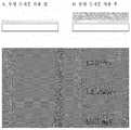
- FIG. 4schematically shows the haze evaluation result according to whether or not the transparent photosensitive resin composition layer is applied.
- FIG. 5is a view schematically showing an electrode substrate for a transparent light emitting device display depending on whether or not a transparent photosensitive resin composition layer is applied.
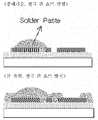
- FIG. 6is a view schematically showing whether a short circuit occurs between electrodes during a solder paste process of a transparent light emitting device display.
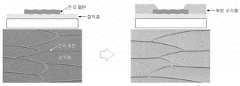
- Example 7is a view showing the surface of the copper foil in contact with the adhesive layer of Example 1, the surface of the adhesive layer from which the copper foil is removed after the formation of the copper foil pattern, and the surface of the transparent photosensitive resin composition layer.
- FIG. 8is a view showing a structure, an SEM image and a transmittance photograph of an electrode substrate for a transparent light emitting device display according to Example 1.
- FIG. 9is a diagram showing a structure, an SEM image and a transmittance photograph of an electrode substrate for a transparent light-emitting element display of Comparative Example 1.
- transparentmeans to have a transmittance characteristic of about 80% or more in the visible light region (400 nm to 700 nm).
- a transparent electrode substrate to be applied to a transparent LED displayshould have a low resistance property of 1 ohm / sq or less, and a metal layer such as a Cu layer of 2 ⁇ or more is required in order to secure low resistance and high transmittance.
- a sputtering methodis used to form the metal layer.
- the sputtering methodit is difficult to secure the adhesion between the transparent substrate and the metal layer, and the cost of the transparent electrode substrate rises sharply with an increase in the deposition time .
- an electrode substrate for a transparent light-emitting element display using a copper foil with an extremely low price as a metal layer and a method of manufacturing the sameare provided in order to secure price competitiveness.
- a method of manufacturing an electrode substrate for a transparent light-emitting element displaycomprising: laminating a copper foil on a transparent substrate; Etching the copper foil to form a copper foil pattern; Forming a transparent photosensitive resin composition layer on the entire surface of the transparent substrate and the copper foil pattern; And removing at least a part of the transparent photosensitive resin composition layer provided on the copper foil pattern to expose at least a part of the copper foil pattern.
- a method of manufacturing an electrode substrate for a transparent light emitting element display according to an embodiment of the present applicationincludes a step of bonding a copper foil on a transparent substrate.
- the transparent substratemay be a glass substrate or a transparent plastic substrate having excellent transparency, surface smoothness, ease of handling, and waterproofness, but is not limited thereto and is not limited as long as it is a transparent substrate ordinarily used in electronic devices.
- the transparent substratemay be glass; Urethane resin; Polyimide resin; Polyester resin; (Meth) acrylate-based polymer resin; A polyolefin-based resin such as polyethylene or polypropylene, or the like.
- the copper foilmay be made of materials known in the art, and the thickness of the copper foil may be 2 ⁇ to 15 ⁇ , but is not limited thereto.
- the step of laminating the copper foil on the transparent substratemay use an adhesive layer. More specifically, the step of laminating the copper foil on the transparent substrate may include a step of forming an adhesive layer on the transparent substrate, and a step of forming a copper foil on the adhesive layer.
- the adhesive layeris positioned between the transparent substrate and the copper foil to provide an adhesive force, and the refractive index may be 1.45 to 1.55. More specifically, the adhesive layer may be formed by a method such as an acrylic resin, a silicone resin, an epoxy resin, a polyimide resin or the like having a refractive index of 1.45 to 1.55 by a method such as comma coating or slot die coating But the present invention is not limited thereto.
- a method of manufacturing an electrode substrate for a transparent light emitting element displayincludes a step of etching the copper foil to form a copper foil pattern.
- the copper foilmay be etched by a method known in the art. More specifically, the method of etching the copper foil may include, but is not limited to, etching the copper foil after forming a resist pattern on the copper foil, and peeling the resist pattern.
- the copper foil patternsmay include two or more kinds of copper foil patterns having different line widths from each other.
- the copper foil patternmay include two kinds of copper foil patterns having different line widths, the line width of one kind of copper foil pattern may be 3 mu m to 30 mu m, and the line width of another kind of copper foil pattern may be 50 mu m or more.
- the copper foil pattern having a line width of 3 mu m to 30 mu mcan serve as an electrode pattern and the copper foil pattern having a line width of 50 mu m or more can serve as an electrode pad pattern for connecting external terminals. That is, the copper foil pattern may include an electrode pattern and an electrode pad pattern.
- a light emitting devicemay be mounted on the electrode pad portion pattern.
- the line width of the electrode patternmay be 3 ⁇ to 30 ⁇ , may be 3 ⁇ to 20 ⁇ , and may be 3 ⁇ to 10 ⁇ , but is not limited thereto.
- the line width of the electrode pad portion patternmay be 50 ⁇ ⁇ or more and 50 ⁇ ⁇ to 100 ⁇ ⁇ , but is not limited thereto.
- the electrode patternmay include a metal mesh pattern.
- the metal mesh pattern constituting the electrode patternmay have the same line width and line width.
- the same line width of the metal mesh patternmeans that the standard deviation of the line width is 20% or less, preferably 10% or less, more preferably 5% or less.
- the same sentence of the metal mesh patternmeans that the standard deviation of sentence is 10% or less, preferably 5% or less, more preferably 2% or less.
- the metal mesh patternmay be provided in the entire region of the effective screen portion on the transparent substrate except for the electrode pad portion pattern. More specifically, the metal mesh pattern may be provided in an area of 80% or more of the total area of the transparent substrate, and may be provided in an area of 99.5% or less. In addition, the metal mesh pattern may be provided in an area of 80% or more of the area excluding the FPCB pad area and the electrode pad pattern area provided on the transparent substrate based on the total area of the transparent substrate, % Or less.
- the FPCB pad regionmay include an FPCB pad portion for applying an external power source, and the area thereof may be at least three times the total area of the FPCB pad portion and not more than three times the entire area of the FPCB pad portion.
- the metal mesh patterna pattern shape in the art can be used. More specifically, the metal mesh pattern may include a polygonal pattern including at least one of triangular, rectangular, pentagonal, hexagonal, and octagonal shapes.
- the metal mesh patternmay include a straight line, a curved line, or a closed curve formed by a straight line or a curved line.
- the transparent photosensitive resin composition layermay be provided on the electrode pattern, and the transparent photosensitive resin composition layer may not be provided on at least part of the electrode pad pattern.
- a method of manufacturing an electrode substrate for a transparent light emitting element displayincludes a step of forming a transparent photosensitive resin composition layer on the entire surface of the transparent substrate and the copper foil pattern.
- the transparent photosensitive resin composition layercan be formed by applying a transparent photosensitive resin composition to the entire surface of the transparent substrate and the copper foil pattern.
- the surface roughness of the copper foilmay be transferred to the surface of the adhesive layer to increase the haze of the final product.
- a method of applying a transparent resin having a refractive index similar to that of the adhesive layer to the top of the adhesive layermay be considered.
- an electrode pad pattern for connecting external terminalsA problem may be caused that the transparent resin layer is insulated.
- the transparent photosensitive resin composition layer having photosensitivityis formed on the entire surface of the transparent substrate and the copper foil pattern, the surface roughness of the adhesive layer can be reduced, and at least A part of the electrode pad portion is exposed through a back exposure and development method to connect an external terminal or to expose an electrode pad portion pattern for mounting the light emitting element.
- the transparent photosensitive resin compositionis a negative-type transparent photosensitive resin composition and has a refractive index difference of 0.05 or less, preferably 0.02 or less with respect to an adhesive layer provided on a transparent substrate. More specifically, the transparent photosensitive resin composition may use an acrylic UV curable resin having a refractive index of 1.45 to 1.52.
- the thickness of the transparent photosensitive resin composition layermay differ depending on the thickness of the copper foil pattern provided on the adhesive layer. More specifically, the thickness of the transparent photosensitive resin composition layer is preferably 10 ⁇ ⁇ or less in thickness from the copper foil pattern when ease of post-processing such as LED packaging and FPCB bonding is considered. For example, when the thickness of the copper foil pattern is 5 mu m or less, the thickness of the transparent photosensitive resin composition layer may be 15 mu m or less. When the difference between the thickness of the copper foil pattern and the thickness of the transparent photosensitive resin composition layer is more than 10 mu m, there is a high possibility of LED breakage when a tolerance is generated in the LED packaging process, and when an excessive step is generated in FPCB bonding, A problem may arise.
- the results of the haze evaluation depending on whether or not the transparent photosensitive resin composition layer is appliedare schematically shown in Fig. As shown in FIG. 4, when the transparent photosensitive resin composition layer is not applied, the roughness of the surface of the copper foil is transferred to the adhesive layer to increase the haze. When the transparent photosensitive resin composition layer is applied as in the present application, It can be seen that the haze decreases through the refractive index matching.
- the method of manufacturing an electrode substrate for a transparent light emitting device displayincludes a step of removing at least a part of the transparent photosensitive resin composition layer provided on the copper foil pattern to expose at least a part of the copper foil pattern do.
- the step of removing at least a part of the transparent photosensitive resin composition layer provided on the copper foil patternmay include a step of back exposure and development with the lower surface of the transparent substrate.
- the copper foil pattern provided on the adhesive layerfunctions as a photomask, thereby eliminating the need for a separate photomask, There is an advantage that can be removed fundamentally.
- the backside exposuremay be parallel light exposure or scattered light exposure.
- both the electrode pattern and the electrode pad patternmay be exposed, which is schematically shown in FIG.
- the electrode pad patternmay be exposed, which is schematically shown in FIG.
- FIG. 1A method of manufacturing an electrode substrate for a transparent light-emitting element display according to an embodiment of the present application is schematically shown in Fig.
- one embodiment of the present applicationrelates to a transparent substrate; An adhesive layer provided on the transparent substrate; A copper foil pattern provided on the adhesive layer; And a transparent photosensitive resin composition layer provided on the adhesive layer and the copper foil pattern, wherein the transparent photosensitive resin composition layer is not provided on at least a part of the surface of the copper foil pattern, And a haze of a region of the electrode substrate for a display not including the copper foil pattern is 5% or less.
- the haze of the area of the electrode substrate for the transparent light-emitting element display not including the copper foil patternmay be 2% or less and may be 1% or less.
- the transparent substrate, the adhesive layer, the copper foil pattern, the transparent photosensitive resin composition layer, and the likeare the same as those described above in the electrode substrate for a transparent light emitting element display according to one embodiment of the present application, and a detailed description thereof will be omitted do.
- FIG. 5An electrode substrate for a transparent light emitting device display according to whether or not the transparent photosensitive resin composition layer is applied is schematically shown in FIG. 5, according to one embodiment of the present application, the transparent photosensitive resin composition layer is formed on the transparent substrate and the copper foil pattern to prevent the haze of the electrode substrate for a transparent light-emitting element display from increasing according to the roughness of the surface of the copper foil And the haze of the electrode substrate for a transparent light emitting device display can be reduced by controlling the refractive index of the transparent photosensitive resin composition layer.
- the electrode substrate for a transparent light emitting device displaycan be applied as a transparent electrode of a transparent light emitting device display.
- one embodiment of the present applicationprovides a transparent light emitting device display including the electrode substrate for the transparent light emitting device display.
- a short circuitmay occur between electrodes during a solder paste process for mounting a light emitting device on an electrode pad pattern.
- the solder paste process for mounting the light emitting element on the electrode pad portion patternthere is a feature that a short circuit between the electrodes can be prevented by the transparent photosensitive resin composition layer.
- a urethane acryl-based transparent adhesivewas applied on a 250 ⁇ thick PET film using a comma coater, and then dried by hot air at 100 ⁇ for 5 minutes to form an adhesive layer having a thickness of 10 ⁇ .
- the PET film provided with the transparent adhesive layer and a copper foil having a thickness of 3 ⁇were hot rolled under the conditions of 120 ⁇ and 1.4 mpm (meter per minute).
- a dry film resist (DFR)was laminated on the copper foil of the copper foil laminated film, and a Voronoi DFR pattern having a line width of 20 ⁇ was formed through exposure and development processes.
- the exposed copper foilwas removed by using a ferric chloride copper etchant and the DFR pattern was peeled off to form a Voronoi type copper foil pattern. At this time, the haze of the area not provided with the copper foil pattern was 40%.
- a negative transparent photosensitive resin compositionwas coated on the substrate having the copper foil pattern using a comma coater and then dried at 120 DEG C for 5 minutes to form a negative transparent photosensitive resin composition layer having a thickness of 5 mu m.
- the transparent photosensitive resin compositionwas prepared by mixing 16 g of an acrylate resin having a weight average molecular weight of 10,100 g / mol, an acid value of 77 mgKOH / g and an acrylic reactor proportion of 30 mol%, 7.5 g of dipentaerythritol hexaacrylate, -02 and 0.5 g of Glide-410 surfactant were dissolved in 75 g of PGMEA (PGMEA) and filtered through a filter having a size of 0.1 ⁇ to prepare a transparent photosensitive resin composition.
- PGMEAPGMEA
- a light amount of 100 mJ / cm 2was irradiated from the back surface of the surface provided with the above-mentioned transparent photosensitive resin composition layer using a parallel light exposure device (Karl Suss MA-8), and then developed to form a transparent photosensitive transparent resin The composition layer was selectively removed. At this time, the haze of the area not provided with the copper foil pattern was 0.8%.
- FIG. 7shows the surface of the copper foil of Example 1 in contact with the adhesive layer, the surface of the adhesive layer from which the copper foil was removed after the formation of the copper foil pattern, and the surface of the transparent photosensitive resin composition layer.
- a surface of the copper foil in contact with the adhesive layeris formed with a nodule on the surface thereof in order to maximize adhesion with the adhesive layer.
- the surface of the adhesive layer from which the copper foil was removed after the formation of the copper foil patternwas reflected on the adhesive layer by a nodule, and the surface roughness of the adhesive layer was increased. Further, it can be confirmed that after the transparent photosensitive resin composition layer is formed, the surface roughness decreases according to the transparent photosensitive resin composition layer.
- Example 1The procedure of Example 1 was repeated except that the transparent photosensitive resin composition layer was not formed in Example 1. At this time, the haze of the region where the copper foil pattern was not provided was 88.4%.
- FIG. 1A structure, an SEM image and a transmittance photograph of the electrode substrate for a transparent light emitting device display of Comparative Example 1 are shown in FIG.
- a raw material costcan be reduced in manufacturing an electrode substrate for a transparent light emitting device display.
- At least a part of the transparent photosensitive resin composition layer provided on the copper foil patternis removed to expose at least a part of the copper foil pattern, whereby an electrode pad A sub-pattern can be formed.
Landscapes
- Engineering & Computer Science (AREA)
- Manufacturing & Machinery (AREA)
- Microelectronics & Electronic Packaging (AREA)
- Physics & Mathematics (AREA)
- Condensed Matter Physics & Semiconductors (AREA)
- General Physics & Mathematics (AREA)
- Computer Hardware Design (AREA)
- Power Engineering (AREA)
- Electroluminescent Light Sources (AREA)
- Devices For Indicating Variable Information By Combining Individual Elements (AREA)
- Led Device Packages (AREA)
Abstract
Translated fromKoreanDescription
Translated fromKorean본 출원은 2017년 9월 19일에 한국특허청에 제출된 한국 특허 출원 제10-2017-0120348호의 출원일의 이익을 주장하며, 그 내용 전부는 본 명세서에 포함된다.This application claims the benefit of Korean Patent Application No. 10-2017-0120348 filed on September 19, 2017, filed with the Korean Intellectual Property Office, the entire contents of which are incorporated herein by reference.
본 출원은 투명 발광소자 디스플레이용 전극 기판 및 이의 제조방법에 관한 것이다.The present application relates to an electrode substrate for a transparent light emitting element display and a method of manufacturing the same.
최근 우리나라는 첨단 ICT 기술과 LED 기술의 융합을 통해 화려한 간판뿐만 아니라 공원 및 도심지 내에 다양한 경관 조명을 연출하여 도시민에게 정보 및 볼거리를 제공하고 있다. 특히, ITO 투명 전극 소재를 사용한 투명 LED 디스플레이는 Glass와 Glass 사이에 LED를 적용하거나 LED가 적용된 투명 필름을 Glass의 일면에 부착한 것으로써, 전선이 보이지 않아 고급스러운 연출이 가능한 장점이 있다. 이로 인해 호텔, 백화점 등의 실내 인테리어에 활용되고 있으며, 건물 외벽의 미디어 파사드 구현에 있어 그 중요성이 커지고 있다.In recent years, Korea has been providing various information and sightseeing to urban people by presenting various landscape lighting in parks and downtown areas as well as colorful signboards through the fusion of advanced ICT technology and LED technology. In particular, the transparent LED display using ITO transparent electrode material has an advantage of being able to produce a luxurious display by applying LED between glass and glass or attaching transparent film with LED on one side of glass. As a result, it is being used for interior decoration of hotels, department stores, etc., and its importance is increasing in the implementation of the media facade on the exterior walls of buildings.
투명하면서도 전기가 흘러 터치스크린 등에 사용되는 투명 전극은 스마트기기가 보급되면서 그 수요가 폭발적으로 늘어났으며, 그 중 가장 많이 사용하는 투명 전극은 인듐과 주석의 산화물인 ITO(Indium Tin Oxide) 이다. 그러나, ITO 투명 전극 소재의 주원료인 인듐은 전 세계적으로 매장량이 많지 않고, 중국 등 일부 국가에서만 생산되고 있으며 생산비용이 고가이다. 또한, 저항값이 일정하게 적용되지 않아 표출되는 LED 불빛이 일정하지 않다는 단점을 갖고 있다. 이로 인해 ITO를 활용한 투명 LED는 고성능 저비용의 투명 전극 소재로 활용하기에는 한계가 있다.Transparent electrodes, which are transparent and used for touch screens, have explosively increased in demand due to the spread of smart devices. The most widely used transparent electrodes are indium tin oxide (ITO), which is an oxide of indium and tin. However, indium, which is the main material of ITO transparent electrode material, is not produced in a large amount of reserves all over the world and is produced only in some countries such as China, and its production cost is high. Also, since the resistance value is not constantly applied, there is a disadvantage that the LED light to be displayed is not constant. As a result, transparent LEDs using ITO are limited to be used as high-performance and low-cost transparent electrode materials.
투명 전극 소재로서 ITO가 가장 많은 비중을 차지하며 사용되어 온 것은 사실이나, 경제성, 제한적 성능 등 한계로 인하여 새로운 소재를 활용한 연구와 기술개발이 지속적으로 이루어지고 있다. 차세대 신소재로 주목받고 있는 투명 전극 소재로는 메탈메쉬(Metal Mesh), 나노 와이어(Ag Nanowire), 탄소나노튜브(CNT), 전도성 고분자, 그래핀(Graphene) 등이 있다. 그 중 메탈메쉬는 ITO를 대체한 물질의 85%를 차지하는 신소재로서 저비용 고전도도를 갖고 있어 그 활용도 측면에서 시장이 확대되고 있다.It is true that ITO is the most widely used transparent electrode material, but due to limitations such as economical efficiency and limited performance, research and technology development using new materials are continuously being carried out. Transparent electrode materials that are attracting attention as the next generation of new materials include metal meshes, nanowires, carbon nanotubes (CNTs), conductive polymers, and graphene. Among them, metal mesh is a new material that occupies 85% of ITO substitute materials, and has low cost and high conductivity.
메탈메쉬를 활용한 투명 LED 디스플레이는 기존 ITO 투명 디스플레이보다 유지보수가 용이하고, 자원절약, 환경오염방지를 대폭 줄일 수 있을 뿐만 아니라 제조원가 절감으로 경제적이다. 또한, 다양한 용도로 확대 적용이 가능하여 새로운 투명전극 소재로서 다양한 제품에 적용 및 활용에 가능성을 갖고 있다.Transparent LED display using metal mesh is easier to maintain than conventional ITO transparent display, can save resources and prevent environmental pollution, and is economical because it reduces manufacturing cost. In addition, it is applicable to various products as a new transparent electrode material because it can be applied to various applications.
본 출원은 투명 발광소자 디스플레이용 전극 기판 및 이의 제조방법을 제공하고자 한다.The present application is intended to provide an electrode substrate for a transparent light emitting device display and a method of manufacturing the same.
본 출원의 일 실시상태는,In one embodiment of the present application,
투명 기재 상에 동박(copper foil)을 합지하는 단계;Bonding a copper foil to a transparent substrate;
상기 동박을 식각하여, 동박 패턴을 형성하는 단계;Etching the copper foil to form a copper foil pattern;
상기 투명 기재 및 동박 패턴 상의 전면에 투명 감광성 수지층을 형성하는 단계; 및Forming a transparent photosensitive resin layer on the entire surface of the transparent substrate and the copper foil pattern; And
상기 동박 패턴 상에 구비된 투명 감광성 수지층의 적어도 일부를 제거하여, 동박 패턴의 적어도 일부를 노출시키는 단계Removing at least a part of the transparent photosensitive resin layer provided on the copper foil pattern to expose at least a part of the copper foil pattern
를 포함하는 투명 발광소자 디스플레이용 전극 기판의 제조방법을 제공한다.The present invention also provides a method of manufacturing an electrode substrate for a transparent light emitting device display.
또한, 본 출원의 일 실시상태는,Further, in one embodiment of the present application,
투명 기재;Transparent substrate;
상기 투명 기재 상에 구비된 접착층;An adhesive layer provided on the transparent substrate;
상기 접착층 상에 구비된 동박 패턴; 및A copper foil pattern provided on the adhesive layer; And
상기 접착층 및 동박 패턴 상에 구비된 투명 감광성 수지 조성물층을 포함하는 투명 발광소자 디스플레이용 전극 기판이고,And a transparent photosensitive resin composition layer provided on the adhesive layer and the copper foil pattern,
상기 동박 패턴 상의 적어도 일부 영역에는 상기 투명 감광성 수지 조성물층이 구비되지 않으며,The transparent photosensitive resin composition layer is not provided on at least a part of the area of the copper foil pattern,
상기 투명 발광소자 디스플레이용 전극 기판의 동박 패턴이 구비되지 않은 영역의 헤이즈가 5% 이하인 것인 투명 발광소자 디스플레이용 전극 기판을 제공한다.Wherein the electrode substrate for the transparent light emitting element display has a haze of not more than 5% in a region where the copper foil pattern is not provided.
또한, 본 출원의 다른 실시상태는, 상기 투명 발광소자 디스플레이용 전극 기판을 포함하는 투명 발광소자 디스플레이를 제공한다.Further, another embodiment of the present application provides a transparent light emitting device display including the electrode substrate for the transparent light emitting element display.
본 출원의 일 실시상태에 따르면, 저가의 동박을 이용하여 금속 패턴을 형성하므로 투명 발광소자 디스플레이용 전극 기판의 제조시 원재료비가 절감될 수 있는 특징이 있다. 특히, 본 출원의 일 실시상태에 따르면, 투명 기재 및 동박 패턴 상에 투명 감광성 수지 조성물층을 형성함으로써, 동박 표면의 조도에 따른 투명 발광소자 디스플레이용 전극 기판의 헤이즈가 증가하는 것을 방지할 수 있으며, 상기 투명 감광성 수지 조성물층의 굴절율을 조절하여 투명 발광소자 디스플레이용 전극 기판의 헤이즈를 감소시킬 수 있는 특징이 있다.According to one embodiment of the present application, since a metal pattern is formed using a low-priced copper foil, a raw material cost can be reduced in manufacturing an electrode substrate for a transparent light emitting device display. In particular, according to one embodiment of the present application, it is possible to prevent the haze of the electrode substrate for a transparent light-emitting element display from increasing according to the roughness of the surface of the copper foil by forming the transparent photosensitive resin composition layer on the transparent substrate and the copper foil pattern , And the haze of the electrode substrate for a transparent light emitting device display can be reduced by controlling the refractive index of the transparent photosensitive resin composition layer.
또한, 본 출원의 일 실시상태에 따르면, 동박 패턴 상에 구비된 투명 감광성 수지 조성물층의 적어도 일부를 제거하여, 동박 패턴의 적어도 일부를 노출시킴으로써, 외부 단자와 연결되거나 발광소자가 실장되는 전극 패드부 패턴을 형성할 수 있다.According to an embodiment of the present application, at least a part of the transparent photosensitive resin composition layer provided on the copper foil pattern is removed to expose at least a part of the copper foil pattern, whereby an electrode pad A sub-pattern can be formed.
도 1 및 도 2는 각각 본 출원의 일 실시상태에 따른 투명 발광소자 디스플레이용 전극 기판을 개략적으로 나타낸 도이다.1 and 2 are schematic views of an electrode substrate for a transparent light emitting element display according to an embodiment of the present application.
도 3은 본 출원의 일 실시상태에 따른 투명 발광소자 디스플레이용 전극 기판의 제조방법을 개략적으로 나타낸 도이다.3 is a view schematically showing a method of manufacturing an electrode substrate for a transparent light emitting element display according to an embodiment of the present application.
도 4는 투명 감광성 수지 조성물층의 적용 여부에 따른 헤이즈 평가결과를 개략적으로 나타낸 도이다.FIG. 4 schematically shows the haze evaluation result according to whether or not the transparent photosensitive resin composition layer is applied.
도 5는 투명 감광성 수지 조성물층의 적용 여부에 따른 투명 발광소자 디스플레이용 전극 기판을 개략적으로 나타낸 도이다.5 is a view schematically showing an electrode substrate for a transparent light emitting device display depending on whether or not a transparent photosensitive resin composition layer is applied.
도 6은 투명 발광소자 디스플레이의 솔더 페이스트 공정시, 전극 간 쇼트 여부를 개략적으로 나타낸 도이다.6 is a view schematically showing whether a short circuit occurs between electrodes during a solder paste process of a transparent light emitting device display.
도 7은 실시예 1의 동박의 접착층과 접하는 면, 동박 패턴 형성 후에 동박이 제거된 접착층의 표면, 및 투명 감광성 수지 조성물층의 표면을 나타낸 도이다.7 is a view showing the surface of the copper foil in contact with the adhesive layer of Example 1, the surface of the adhesive layer from which the copper foil is removed after the formation of the copper foil pattern, and the surface of the transparent photosensitive resin composition layer.
도 8은 실시예 1의 투명 발광소자 디스플레이용 전극 기판의 구조, SEM 이미지 및 투과도 사진을 나타낸 도이다.8 is a view showing a structure, an SEM image and a transmittance photograph of an electrode substrate for a transparent light emitting device display according to Example 1. Fig.
도 9는 비교예 1의 투명 발광소자 디스플레이용 전극 기판의 구조, SEM 이미지 및 투과도 사진을 나타낸 도이다.9 is a diagram showing a structure, an SEM image and a transmittance photograph of an electrode substrate for a transparent light-emitting element display of Comparative Example 1. Fig.
[부호의 설명][Description of Symbols]
10: 투명 기재10: transparent substrate
20: 동박20: Copper foil
30: 동박 패턴30: Copper pattern
40: 투명 감광성 수지층40: transparent photosensitive resin layer
50: 접착층50: Adhesive layer
60: 레지스트 패턴60: Resist pattern
이하 본 출원에 대하여 상세히 설명한다.The present application will be described in detail below.
본 출원에 있어서, "투명"은 가시광선 영역(400nm 내지 700nm)에서 약 80% 이상의 투과율 특성을 갖는 것을 의미하기로 한다.In the present application, " transparent " means to have a transmittance characteristic of about 80% or more in the visible light region (400 nm to 700 nm).
통상적으로, 투명 LED 디스플레이에 적용되는 투명 전극 기판은 1 ohm/sq 이하의 저저항 특성이 확보되어야 하고, 저저항 및 높은 투과도를 확보하기 위해서는 2㎛ 이상의 Cu층과 같은 금속층이 요구된다. 종래에는 상기 금속층을 형성하기 위하여 스퍼터링 방법을 이용하였으나, 상기 스퍼터링 방법을 이용하는 경우에는 투명 기재와 금속층의 부착력 확보가 어렵고, 과도한 증착시간 증가에 따라 투명 전극 기판의 가격이 급격하게 상승하는 문제가 있다.Typically, a transparent electrode substrate to be applied to a transparent LED display should have a low resistance property of 1 ohm / sq or less, and a metal layer such as a Cu layer of 2 탆 or more is required in order to secure low resistance and high transmittance. Conventionally, a sputtering method is used to form the metal layer. However, when the sputtering method is used, it is difficult to secure the adhesion between the transparent substrate and the metal layer, and the cost of the transparent electrode substrate rises sharply with an increase in the deposition time .
이에 본 출원에서는, 가격 경쟁력을 확보하기 위하여, 금속층으로써 초저가의 동박을 이용하는 투명 발광소자 디스플레이용 전극 기판 및 이의 제조방법을 제공하고자 한다.Thus, in the present application, an electrode substrate for a transparent light-emitting element display using a copper foil with an extremely low price as a metal layer and a method of manufacturing the same are provided in order to secure price competitiveness.
본 출원의 일 실시상태에 따른 투명 발광소자 디스플레이용 전극 기판의 제조방법은, 투명 기재 상에 동박을 합지하는 단계; 상기 동박을 식각하여, 동박 패턴을 형성하는 단계; 상기 투명 기재 및 동박 패턴 상의 전면에 투명 감광성 수지 조성물층을 형성하는 단계; 및 상기 동박 패턴 상에 구비된 투명 감광성 수지 조성물층의 적어도 일부를 제거하여, 동박 패턴의 적어도 일부를 노출시키는 단계를 포함한다.According to an embodiment of the present invention, there is provided a method of manufacturing an electrode substrate for a transparent light-emitting element display, comprising: laminating a copper foil on a transparent substrate; Etching the copper foil to form a copper foil pattern; Forming a transparent photosensitive resin composition layer on the entire surface of the transparent substrate and the copper foil pattern; And removing at least a part of the transparent photosensitive resin composition layer provided on the copper foil pattern to expose at least a part of the copper foil pattern.
본 출원의 일 실시상태에 따른 투명 발광소자 디스플레이용 전극 기판의 제조방법은 투명 기재 상에 동박을 합지하는 단계를 포함한다.A method of manufacturing an electrode substrate for a transparent light emitting element display according to an embodiment of the present application includes a step of bonding a copper foil on a transparent substrate.
상기 투명 기재는 투명성, 표면평활성, 취급용이성 및 방수성이 우수한 유리 기재 또는 투명 플라스틱 기재가 될 수 있으나, 이에 한정되지 않으며, 전자 소자에 통상적으로 사용되는 투명 기재이면 제한되지 않는다. 구체적으로, 상기 투명 기재로는 유리; 우레탄 수지; 폴리이미드 수지; 폴리에스테르수지; (메타)아크릴레이트계 고분자 수지; 폴리에틸렌 또는 폴리프로필렌 등의 폴리올레핀계 수지 등으로 이루어진 것이 될 수 있다.The transparent substrate may be a glass substrate or a transparent plastic substrate having excellent transparency, surface smoothness, ease of handling, and waterproofness, but is not limited thereto and is not limited as long as it is a transparent substrate ordinarily used in electronic devices. Specifically, the transparent substrate may be glass; Urethane resin; Polyimide resin; Polyester resin; (Meth) acrylate-based polymer resin; A polyolefin-based resin such as polyethylene or polypropylene, or the like.
상기 동박은 당 기술분야에 알려진 재료를 이용할 수 있고, 상기 동박의 두께는 2㎛ 내지 15㎛ 일 수 있으나, 이에만 한정되는 것은 아니다.The copper foil may be made of materials known in the art, and the thickness of the copper foil may be 2 탆 to 15 탆, but is not limited thereto.
상기 투명 기재 상에 동박을 합지하는 단계는 접착층을 이용할 수 있다. 보다 구체적으로, 상기 투명 기재 상에 동박을 합지하는 단계는, 투명 기재 상에 접착층을 형성하는 단계, 및 상기 접착층 상에 동박을 형성하는 단계를 포함할 수 있다.The step of laminating the copper foil on the transparent substrate may use an adhesive layer. More specifically, the step of laminating the copper foil on the transparent substrate may include a step of forming an adhesive layer on the transparent substrate, and a step of forming a copper foil on the adhesive layer.
상기 접착층은 투명 기재와 동박 사이에 위치하여 접착력을 제공하는 것으로서, 굴절율이 1.45 내지 1.55 일 수 있다. 보다 구체적으로, 상기 접착층은 굴절율이 1.45 내지 1.55인 아크릴계 수지, 실리콘계 수지, 에폭시계 수지, 폴리이미드계 수지 등을 이용하고, 콤마 코팅, 슬롯다이 코팅 등의 방법으로 5㎛ 내지 30㎛의 두께범위로 형성할 수 있으나, 이에만 한정되는 것은 아니다.The adhesive layer is positioned between the transparent substrate and the copper foil to provide an adhesive force, and the refractive index may be 1.45 to 1.55. More specifically, the adhesive layer may be formed by a method such as an acrylic resin, a silicone resin, an epoxy resin, a polyimide resin or the like having a refractive index of 1.45 to 1.55 by a method such as comma coating or slot die coating But the present invention is not limited thereto.
본 출원의 일 실시상태에 따른 투명 발광소자 디스플레이용 전극 기판의 제조방법은 상기 동박을 식각하여, 동박 패턴을 형성하는 단계를 포함한다.According to an embodiment of the present invention, a method of manufacturing an electrode substrate for a transparent light emitting element display includes a step of etching the copper foil to form a copper foil pattern.
상기 동박을 식각하는 방법은 당 기술분야에 알려진 방법을 이용할 수 있다. 보다 구체적으로, 상기 동박을 식각하는 방법은 동박 상에 레지스트 패턴을 형성한 후 상기 동박을 식각하는 단계, 및 상기 레지스트 패턴을 박리하는 단계를 포함할 수 있으나, 이에만 한정되는 것은 아니다.The copper foil may be etched by a method known in the art. More specifically, the method of etching the copper foil may include, but is not limited to, etching the copper foil after forming a resist pattern on the copper foil, and peeling the resist pattern.
상기 동박 패턴은 서로 선폭이 상이한 2종 이상의 동박 패턴을 포함할 수 있다. 또한, 상기 동박 패턴은 서로 선폭이 상이한 2종의 동박 패턴을 포함하고, 1종의 동박 패턴의 선폭은 3㎛ 내지 30㎛ 이고, 다른 1종의 동박 패턴의 선폭은 50㎛ 이상일 수 있다. 상기 선폭이 3㎛ 내지 30㎛인 동박 패턴은 전극 패턴의 역할을 수행할 수 있고, 상기 선폭이 50㎛ 이상인 동박 패턴은 외부 단자를 연결하기 위한 전극 패드부 패턴의 역할을 수행할 수 있다. 즉, 상기 동박 패턴은 전극 패턴 및 전극 패드부 패턴을 포함할 수 있다. 또한, 상기 전극 패드부 패턴 상에는 발광소자가 실장될 수 있다.The copper foil patterns may include two or more kinds of copper foil patterns having different line widths from each other. The copper foil pattern may include two kinds of copper foil patterns having different line widths, the line width of one kind of copper foil pattern may be 3 mu m to 30 mu m, and the line width of another kind of copper foil pattern may be 50 mu m or more. The copper foil pattern having a line width of 3 mu m to 30 mu m can serve as an electrode pattern and the copper foil pattern having a line width of 50 mu m or more can serve as an electrode pad pattern for connecting external terminals. That is, the copper foil pattern may include an electrode pattern and an electrode pad pattern. A light emitting device may be mounted on the electrode pad portion pattern.
상기 전극 패턴의 선폭은 3㎛ 내지 30㎛ 일 수 있고, 3㎛ 내지 20㎛ 일 수 있으며, 3㎛ 내지 10㎛ 일 수 있으나, 이에만 한정되는 것은 아니다. 또한, 상기 전극 패드부 패턴의 선폭은 50㎛ 이상일 수 있고, 50㎛ 내지 100㎛ 일 수 있으나, 이에만 한정되는 것은 아니다.The line width of the electrode pattern may be 3 탆 to 30 탆, may be 3 탆 to 20 탆, and may be 3 탆 to 10 탆, but is not limited thereto. In addition, the line width of the electrode pad portion pattern may be 50 占 퐉 or more and 50 占 퐉 to 100 占 퐉, but is not limited thereto.
본 출원의 일 실시상태에 있어서, 상기 전극 패턴은 메탈메쉬 패턴을 포함할 수 있다. 상기 전극 패턴을 구성하는 메탈메쉬 패턴은 선폭 및 선고가 동일할 수 있다. 본 출원의 일 실시상태에 있어서, 상기 메탈메쉬 패턴의 선폭이 동일하다는 것은 선폭의 표준편차가 20% 이하, 바람직하게는 10% 이하, 더욱 바람직하게는 5% 이하인 것을 의미한다. 또한, 본 출원의 일 실시상태에 있어서, 상기 메탈메쉬 패턴의 선고가 동일하다는 것은 선고의 표준편차가 10% 이하, 바람직하게는 5% 이하, 더욱 바람직하게는 2% 이하인 것을 의미한다.In one embodiment of the present application, the electrode pattern may include a metal mesh pattern. The metal mesh pattern constituting the electrode pattern may have the same line width and line width. In the embodiment of the present application, the same line width of the metal mesh pattern means that the standard deviation of the line width is 20% or less, preferably 10% or less, more preferably 5% or less. In addition, in the embodiment of the present application, the same sentence of the metal mesh pattern means that the standard deviation of sentence is 10% or less, preferably 5% or less, more preferably 2% or less.
또한, 상기 메탈메쉬 패턴은 상기 전극 패드부 패턴을 제외한 투명 기재 상의 유효화면부 전체 영역에 구비될 수 있다. 보다 구체적으로, 상기 메탈메쉬 패턴은 상기 투명 기재 상의 전체 면적 대비 80% 이상의 면적의 영역에 구비될 수 있고, 99.5% 이하의 면적에 구비될 수 있다. 또한, 상기 메탈메쉬 패턴은 상기 투명 기재 상의 전체 면적을 기준으로, 투명 기재 상에 구비되는 FPCB 패드부 영역과 전극 패드부 패턴 영역을 제외한 면적의 80% 이상의 면적의 영역에 구비될 수 있고, 99.5% 이하의 면적에 구비될 수 있다. 본 출원에 있어서, 상기 FPCB 패드부 영역은 외부 전원을 인가하는 FPCB 패드부를 포함하고, 그 면적은 FPCB 패드부의 전체 면적 이상, FPCB 패드부의 전체 면적의 3배 이하일 수 있다.In addition, the metal mesh pattern may be provided in the entire region of the effective screen portion on the transparent substrate except for the electrode pad portion pattern. More specifically, the metal mesh pattern may be provided in an area of 80% or more of the total area of the transparent substrate, and may be provided in an area of 99.5% or less. In addition, the metal mesh pattern may be provided in an area of 80% or more of the area excluding the FPCB pad area and the electrode pad pattern area provided on the transparent substrate based on the total area of the transparent substrate, % Or less. In this application, the FPCB pad region may include an FPCB pad portion for applying an external power source, and the area thereof may be at least three times the total area of the FPCB pad portion and not more than three times the entire area of the FPCB pad portion.
상기 메탈메쉬 패턴은 당 기술분야의 패턴 형태가 사용될 수 있다. 보다 구체적으로, 상기 메탈메쉬 패턴은 삼각형, 사각형, 오각형, 육각형 및 팔각형 중 하나 이상의 형태를 포함하는 다각형 패턴을 포함할 수 있다. 상기 메탈메쉬 패턴은 직선, 곡선, 또는 직선이나 곡선으로 이루어진 폐곡선을 포함할 수 있다.As the metal mesh pattern, a pattern shape in the art can be used. More specifically, the metal mesh pattern may include a polygonal pattern including at least one of triangular, rectangular, pentagonal, hexagonal, and octagonal shapes. The metal mesh pattern may include a straight line, a curved line, or a closed curve formed by a straight line or a curved line.
또한, 상기 전극 패턴 상에는 상기 투명 감광성 수지 조성물층이 구비되고, 상기 전극 패드부 패턴 상의 적어도 일부에는 상기 투명 감광성 수지 조성물층이 구비되지 않을 수 있다.In addition, the transparent photosensitive resin composition layer may be provided on the electrode pattern, and the transparent photosensitive resin composition layer may not be provided on at least part of the electrode pad pattern.
본 출원의 일 실시상태에 따른 투명 발광소자 디스플레이용 전극 기판의 제조방법은, 상기 투명 기재 및 동박 패턴 상의 전면에 투명 감광성 수지 조성물층을 형성하는 단계를 포함한다. 상기 투명 감광성 수지 조성물층은 상기 투명 기재 및 동박 패턴 상의 전면에 투명 감광성 수지 조성물을 도포함으로써 형성할 수 있다.A method of manufacturing an electrode substrate for a transparent light emitting element display according to an embodiment of the present application includes a step of forming a transparent photosensitive resin composition layer on the entire surface of the transparent substrate and the copper foil pattern. The transparent photosensitive resin composition layer can be formed by applying a transparent photosensitive resin composition to the entire surface of the transparent substrate and the copper foil pattern.
투명 기재 상에 접착층을 구비시킨 후 저가의 동박을 합지하는 경우에는, 동박의 표면 조도가 접착층 표면에 전사되어 최종 제품의 헤이즈가 증가되는 문제가 발생할 수 있다. 상기 접착층 표면의 조도를 감소시키기 위하여 접착층과 유사한 굴절율을 갖는 투명 수지를 접착층 상부에 추가로 도포시키는 방법을 고려할 수 있으나, 이러한 경우에는 외부 단자를 연결하거나 발광소자를 실장하기 위한 전극 패드부 패턴이 투명 수지층에 의하여 절연되는 문제가 발생할 수 있다. 따라서, 본 출원에서는 감광성을 갖는 투명 감광성 수지 조성물층을 상기 투명 기재 및 동박 패턴 상의 전면에 형성함으로써, 접착층 표면의 조도를 감소시킬 수 있을 뿐만 아니라, 후술하는 바와 같이 상기 투명 감광성 수지 조성물층의 적어도 일부를 배면 노광 및 현상방법을 통하여 제거함으로써 외부 단자를 연결하거나 발광소자를 실장하기 위한 전극 패드부 패턴을 노출시킬 수 있는 특징이 있다.When the low-priced copper foil is laminated after the adhesive layer is provided on the transparent substrate, the surface roughness of the copper foil may be transferred to the surface of the adhesive layer to increase the haze of the final product. In order to reduce the illuminance of the surface of the adhesive layer, a method of applying a transparent resin having a refractive index similar to that of the adhesive layer to the top of the adhesive layer may be considered. In this case, an electrode pad pattern for connecting external terminals, A problem may be caused that the transparent resin layer is insulated. Therefore, in the present application, since the transparent photosensitive resin composition layer having photosensitivity is formed on the entire surface of the transparent substrate and the copper foil pattern, the surface roughness of the adhesive layer can be reduced, and at least A part of the electrode pad portion is exposed through a back exposure and development method to connect an external terminal or to expose an electrode pad portion pattern for mounting the light emitting element.
상기 투명 감광성 수지 조성물은 네거티브(negative) 타입의 투명 감광성 수지 조성물이며, 투명 기재 상에 구비되어 있는 접착층과의 굴절률 차이가 0.05 이내, 바람직하게는 0.02 이내인 것을 특징으로 한다. 보다 구체적으로, 상기 투명 감광성 수지 조성물은 굴절율이 1.45 내지 1.52인 아크릴계 UV 경화형 수지를 사용할 수 있다.The transparent photosensitive resin composition is a negative-type transparent photosensitive resin composition and has a refractive index difference of 0.05 or less, preferably 0.02 or less with respect to an adhesive layer provided on a transparent substrate. More specifically, the transparent photosensitive resin composition may use an acrylic UV curable resin having a refractive index of 1.45 to 1.52.
상기 투명 감광성 수지 조성물층의 두께는 상기 접착층 상에 구비되어 있는 동박 패턴의 두께에 따라 상이할 수 있다. 보다 구체적으로, 상기 투명 감광성 수지 조성물층의 두께는 LED 실장 및 FPCB 본딩 등의 후공정 용이성을 고려하였을 때, 동박 패턴과의 두께 차이가 10㎛ 이내인 것이 바람직하다. 예컨대, 상기 동박 패턴의 두께가 5㎛ 이하인 경우에는, 상기 투명 감광성 수지 조성물층의 두께는 15㎛ 이하일 수 있다. 상기 동박 패턴과 투명 감광성 수지 조성물층의 두께 차이가 10㎛를 초과하는 경우에는, LED 실장 공정 중 공차 발생시 LED 파손 가능성이 높고, FPCB 본딩에서도 과도한 단차 발생시 도전볼이 압력이 전달되지 않아 통전이 불가능하게 되는 문제점이 발생할 수 있다.The thickness of the transparent photosensitive resin composition layer may differ depending on the thickness of the copper foil pattern provided on the adhesive layer. More specifically, the thickness of the transparent photosensitive resin composition layer is preferably 10 占 퐉 or less in thickness from the copper foil pattern when ease of post-processing such as LED packaging and FPCB bonding is considered. For example, when the thickness of the copper foil pattern is 5 mu m or less, the thickness of the transparent photosensitive resin composition layer may be 15 mu m or less. When the difference between the thickness of the copper foil pattern and the thickness of the transparent photosensitive resin composition layer is more than 10 mu m, there is a high possibility of LED breakage when a tolerance is generated in the LED packaging process, and when an excessive step is generated in FPCB bonding, A problem may arise.
투명 감광성 수지 조성물층의 적용 여부에 따른 헤이즈 평가결과를 하기 도 4에 개략적으로 나타내었다. 하기 도 4와 같이 투명 감광성 수지 조성물층을 적용하지 않은 경우에는 동박 표면의 조도가 접착층에 전사되어 헤이즈가 증가함을 알 수 있고, 본 출원과 같이 투명 감광성 수지 조성물층을 적용한 경우에는 접착층과의 굴절율 매칭을 통하여 헤이즈가 감소함을 알 수 있다.The results of the haze evaluation depending on whether or not the transparent photosensitive resin composition layer is applied are schematically shown in Fig. As shown in FIG. 4, when the transparent photosensitive resin composition layer is not applied, the roughness of the surface of the copper foil is transferred to the adhesive layer to increase the haze. When the transparent photosensitive resin composition layer is applied as in the present application, It can be seen that the haze decreases through the refractive index matching.
본 출원의 일 실시상태에 따른 투명 발광소자 디스플레이용 전극 기판의 제조방법은, 상기 동박 패턴 상에 구비된 투명 감광성 수지 조성물층의 적어도 일부를 제거하여, 동박 패턴의 적어도 일부를 노출시키는 단계를 포함한다.The method of manufacturing an electrode substrate for a transparent light emitting device display according to an embodiment of the present application includes a step of removing at least a part of the transparent photosensitive resin composition layer provided on the copper foil pattern to expose at least a part of the copper foil pattern do.
상기 동박 패턴 상에 구비된 투명 감광성 수지 조성물층의 적어도 일부를 제거하는 단계는, 상기 투명 기재의 하부면으로 배면 노광 및 현상하는 단계를 포함할 수 있다.The step of removing at least a part of the transparent photosensitive resin composition layer provided on the copper foil pattern may include a step of back exposure and development with the lower surface of the transparent substrate.
상기와 같이, 투명 기재의 하부면으로 배면 노광을 수행하는 경우에는, 접착층 상에 구비되어 있는 동박 패턴이 포토 마스크 역할을 수행하여 별도의 포토 마스크가 불필요하게 되며, 얼라인 오류로 인한 불량발생을 근본적으로 제거할 수 있는 장점이 있다.As described above, when the backside exposure is performed on the lower surface of the transparent substrate, the copper foil pattern provided on the adhesive layer functions as a photomask, thereby eliminating the need for a separate photomask, There is an advantage that can be removed fundamentally.
상기 배면 노광은 평행광 노광 또는 산란광 노광을 진행할 수 있다. 상기 배면 노광시 평행광 노광을 진행하는 경우에는 전극 패턴 및 전극 패드부 패턴 모두가 노출될 수 있으며, 이를 하기 도 1에 개략적으로 나타내었다. 또한, 상기 배면 노광시 산란광 노광을 진행하는 경우에는 전극 패드부 패턴이 노출될 수 있으며, 이를 하기 도 2에 개략적으로 나타내었다.The backside exposure may be parallel light exposure or scattered light exposure. When the parallel light exposure is performed during the back exposure, both the electrode pattern and the electrode pad pattern may be exposed, which is schematically shown in FIG. In addition, in the case of performing the scattered light exposure during the back exposure, the electrode pad pattern may be exposed, which is schematically shown in FIG.
또한, 본 출원의 일 실시상태에 따른 투명 발광소자 디스플레이용 전극 기판의 제조방법을 하기 도 3에 개략적으로 나타내었다.A method of manufacturing an electrode substrate for a transparent light-emitting element display according to an embodiment of the present application is schematically shown in Fig.
또한, 본 출원의 일 실시상태는, 투명 기재; 상기 투명 기재 상에 구비된 접착층; 상기 접착층 상에 구비된 동박 패턴; 및 상기 접착층 및 동박 패턴 상에 구비된 투명 감광성 수지 조성물층을 포함하는 투명 발광소자 디스플레이용 전극 기판이고, 상기 동박 패턴 상의 적어도 일부 영역에는 상기 투명 감광성 수지 조성물층이 구비되지 않으며, 상기 투명 발광소자 디스플레이용 전극 기판의 동박 패턴이 구비되지 않은 영역의 헤이즈가 5% 이하인 것인 투명 발광소자 디스플레이용 전극 기판을 제공한다.Further, one embodiment of the present application relates to a transparent substrate; An adhesive layer provided on the transparent substrate; A copper foil pattern provided on the adhesive layer; And a transparent photosensitive resin composition layer provided on the adhesive layer and the copper foil pattern, wherein the transparent photosensitive resin composition layer is not provided on at least a part of the surface of the copper foil pattern, And a haze of a region of the electrode substrate for a display not including the copper foil pattern is 5% or less.
상기 투명 발광소자 디스플레이용 전극 기판의 동박 패턴이 구비되지 않은 영역의 헤이즈는 2% 이하일 수 있고, 1% 이하일 수 있다.The haze of the area of the electrode substrate for the transparent light-emitting element display not including the copper foil pattern may be 2% or less and may be 1% or less.
본 출원의 일 실시상태에 따른 투명 발광소자 디스플레이용 전극 기판에 있어서, 상기 투명 기재, 접착층, 동박 패턴, 투명 감광성 수지 조성물층 등에 대한 내용은 전술한 내용과 동일하므로, 이의 구체적인 설명은 생략하기로 한다.The transparent substrate, the adhesive layer, the copper foil pattern, the transparent photosensitive resin composition layer, and the like are the same as those described above in the electrode substrate for a transparent light emitting element display according to one embodiment of the present application, and a detailed description thereof will be omitted do.
상기 투명 감광성 수지 조성물층의 적용 여부에 따른 투명 발광소자 디스플레이용 전극 기판을 하기 도 5에 개략적으로 나타내었다. 도 5와 같이, 본 출원의 일 실시상태에 따르면, 투명 기재 및 동박 패턴 상에 투명 감광성 수지 조성물층을 형성함으로써, 동박 표면의 조도에 따른 투명 발광소자 디스플레이용 전극 기판의 헤이즈가 증가하는 것을 방지할 수 있으며, 상기 투명 감광성 수지 조성물층의 굴절율을 조절하여 투명 발광소자 디스플레이용 전극 기판의 헤이즈를 감소시킬 수 있는 특징이 있다.An electrode substrate for a transparent light emitting device display according to whether or not the transparent photosensitive resin composition layer is applied is schematically shown in FIG. 5, according to one embodiment of the present application, the transparent photosensitive resin composition layer is formed on the transparent substrate and the copper foil pattern to prevent the haze of the electrode substrate for a transparent light-emitting element display from increasing according to the roughness of the surface of the copper foil And the haze of the electrode substrate for a transparent light emitting device display can be reduced by controlling the refractive index of the transparent photosensitive resin composition layer.
본 출원의 일 실시상태에 따른 투명 발광소자 디스플레이용 전극 기판은 투명 발광소자 디스플레이의 투명 전극으로 적용될 수 있다.The electrode substrate for a transparent light emitting device display according to an embodiment of the present application can be applied as a transparent electrode of a transparent light emitting device display.
또한, 본 출원의 일 실시상태는 상기 투명 발광소자 디스플레이용 전극 기판을 포함하는 투명 발광소자 디스플레이를 제공한다.In addition, one embodiment of the present application provides a transparent light emitting device display including the electrode substrate for the transparent light emitting device display.
하기 도 6과 같이, 종래의 투명 발광소자 디스플레이에서는 전극 패드부 패턴 상에 발광소자를 실장하기 위한 솔더 페이스트 공정시, 전극 간 쇼트가 발생할 수 있었다. 그러나, 본 출원의 일 실시상태에 따르면, 전극 패드부 패턴 상에 발광소자를 실장하기 위한 솔더 페이스트 공정시, 투명 감광성 수지 조성물층에 의하여 전극 간 쇼트를 방지할 수 있는 특징이 있다.As shown in FIG. 6, in a conventional transparent light emitting device display, a short circuit may occur between electrodes during a solder paste process for mounting a light emitting device on an electrode pad pattern. However, according to one embodiment of the present application, in the solder paste process for mounting the light emitting element on the electrode pad portion pattern, there is a feature that a short circuit between the electrodes can be prevented by the transparent photosensitive resin composition layer.
이하, 실시예를 통하여 본 명세서에 기재된 실시상태를 예시한다. 그러나, 이하의 실시예에 의하여 상기 실시상태들의 범위가 한정되는 것을 의도하는 것은 아니다.Hereinafter, an embodiment of the present invention will be described by way of example. However, it is not intended that the scope of the embodiments be limited by the following embodiments.
<실시예><Examples>
<실시예 1>≪ Example 1 >
250㎛ 두께의 PET 필름 상에 콤마 코터를 이용하여 우레탄 아크릴계 투명 접착제를 도포한 후 100℃에서 5분간 열풍 건조하여 10㎛ 두께의 접착층을 형성하였다. 상기 투명 접착층이 구비된 PET 필름과 3㎛ 두께의 동박을 120℃, 1.4mpm(meter per minute) 조건으로 핫롤(Hot Roll) 합지하였다.A urethane acryl-based transparent adhesive was applied on a 250 탆 thick PET film using a comma coater, and then dried by hot air at 100 캜 for 5 minutes to form an adhesive layer having a thickness of 10 탆. The PET film provided with the transparent adhesive layer and a copper foil having a thickness of 3 탆 were hot rolled under the conditions of 120 캜 and 1.4 mpm (meter per minute).
상기 동박 합지 필름의 동박 면에 DFR(Dry Film Resist)를 합지한 후 노광 및 현상 공정을 통해 20㎛ 선폭의 Voronoi 형태의 DFR 패턴을 형성하였다.A dry film resist (DFR) was laminated on the copper foil of the copper foil laminated film, and a Voronoi DFR pattern having a line width of 20 탆 was formed through exposure and development processes.
염화제2철계 구리 식각액을 이용하여 노출된 동박을 제거하고 DFR 패턴을 박리하여 Voronoi 형태의 동박 패턴을 형성하였다. 이 때, 동박 패턴이 구비되어 있지 않은 영역의 헤이즈는 40% 였다.The exposed copper foil was removed by using a ferric chloride copper etchant and the DFR pattern was peeled off to form a Voronoi type copper foil pattern. At this time, the haze of the area not provided with the copper foil pattern was 40%.
상기 동박 패턴이 구비되어 있는 기재 상부에 네거티브 투명 감광성 수지 조성물을 콤마 코터를 이용하여 도포한 후 120℃에서 5분간 건조하여 5㎛ 두께의 네거티브 투명 감광성 수지 조성물층을 형성하였다.A negative transparent photosensitive resin composition was coated on the substrate having the copper foil pattern using a comma coater and then dried at 120 DEG C for 5 minutes to form a negative transparent photosensitive resin composition layer having a thickness of 5 mu m.
상기 투명 감광성 수지 조성물은 중량 평균 분자량이 10,100 g/mol, 산가 77 mgKOH/g, 아크릴반응기 비율이 30 mol%인 아크릴레이트 수지 16g, 디펜타에리쓰리톨 헥사아크릴레이트 7.5g, 광개시제로서 BASF사 OXE-02 1g, Glide-410 계면활성제 0.5g을 PGMEA(Propylene Glycol Mnomethyl Ether Acetate) 75g에 용해한 후 0.1㎛ 크기의 필터로 여과하여 투명 감광성 수지 조성물을 제조하였다.The transparent photosensitive resin composition was prepared by mixing 16 g of an acrylate resin having a weight average molecular weight of 10,100 g / mol, an acid value of 77 mgKOH / g and an acrylic reactor proportion of 30 mol%, 7.5 g of dipentaerythritol hexaacrylate, -02 and 0.5 g of Glide-410 surfactant were dissolved in 75 g of PGMEA (PGMEA) and filtered through a filter having a size of 0.1 탆 to prepare a transparent photosensitive resin composition.
상기 투명 감광성 수지 조성물층이 구비되어 있는 면의 배면에서 평행광 노광기(Karl Suss MA-8)를 활용하여 100 mJ/cm2의 광량을 조사한 후 현상하여 동박 패턴 상에 도포되어 있는 투명 감광성 투명 수지 조성물층을 선택적으로 제거하였다. 이 때, 동박 패턴이 구비되어 있지 않은 영역의 헤이즈는 0.8% 였다.A light amount of 100 mJ / cm2 was irradiated from the back surface of the surface provided with the above-mentioned transparent photosensitive resin composition layer using a parallel light exposure device (Karl Suss MA-8), and then developed to form a transparent photosensitive transparent resin The composition layer was selectively removed. At this time, the haze of the area not provided with the copper foil pattern was 0.8%.
상기 실시예 1의 동박의 접착층과 접하는 면, 동박 패턴 형성 후에 동박이 제거된 접착층의 표면, 및 투명 감광성 수지 조성물층의 표면을 하기 도 7에 나타내었다. 하기 도 7과 같이, 동박의 접착층과 접하는 면은 접착층과의 밀착력을 극대화시키기 위하여 표면에 노둘(nodule)이 형성되어 있다. 또한, 상기 동박 패턴 형성 후에 동박이 제거된 접착층의 표면은 노둘(nodule)이 접착층에 반영되어 접착층의 표면 조도가 증가하였다. 또한, 상기 투명 감광성 수지 조성물층을 형성한 후에는 투명 감광성 수지 조성물층에 따라 표면 조도가 감소하였음을 확인할 수 있다.7 shows the surface of the copper foil of Example 1 in contact with the adhesive layer, the surface of the adhesive layer from which the copper foil was removed after the formation of the copper foil pattern, and the surface of the transparent photosensitive resin composition layer. As shown in FIG. 7, a surface of the copper foil in contact with the adhesive layer is formed with a nodule on the surface thereof in order to maximize adhesion with the adhesive layer. In addition, the surface of the adhesive layer from which the copper foil was removed after the formation of the copper foil pattern was reflected on the adhesive layer by a nodule, and the surface roughness of the adhesive layer was increased. Further, it can be confirmed that after the transparent photosensitive resin composition layer is formed, the surface roughness decreases according to the transparent photosensitive resin composition layer.
또한, 상기 실시예 1의 투명 발광소자 디스플레이용 전극 기판의 구조, SEM 이미지 및 투과도 사진을 하기 도 8에 나타내었다.The structure, SEM image, and transmission chart of the electrode substrate for the transparent light emitting device display of Example 1 are shown in FIG.
<비교예 1>≪ Comparative Example 1 &
실시예 1에서 투명 감광성 수지 조성물층을 형성하지 않은 것을 제외하고는, 실시예 1과 동일하게 수행하였다. 이 때, 동박 패턴이 구비되어 있지 않은 영역의 헤이즈는 88.4% 였다.The procedure of Example 1 was repeated except that the transparent photosensitive resin composition layer was not formed in Example 1. At this time, the haze of the region where the copper foil pattern was not provided was 88.4%.
상기 비교예 1의 투명 발광소자 디스플레이용 전극 기판의 구조, SEM 이미지 및 투과도 사진을 하기 도 9에 나타내었다.A structure, an SEM image and a transmittance photograph of the electrode substrate for a transparent light emitting device display of Comparative Example 1 are shown in FIG.
상기 결과와 같이, 본 출원의 일 실시상태에 따르면, 저가의 동박을 이용하여 금속 패턴을 형성하므로 투명 발광소자 디스플레이용 전극 기판의 제조시 원재료비가 절감될 수 있는 특징이 있다. 특히, 본 출원의 일 실시상태에 따르면, 투명 기재 및 동박 패턴 상에 투명 감광성 수지 조성물층을 형성함으로써, 동박 표면의 조도에 따른 투명 발광소자 디스플레이용 전극 기판의 헤이즈가 증가하는 것을 방지할 수 있으며, 상기 투명 감광성 수지 조성물층의 굴절율을 조절하여 투명 발광소자 디스플레이용 전극 기판의 헤이즈를 감소시킬 수 있는 특징이 있다.As described above, according to one embodiment of the present application, since a metal pattern is formed using a low-priced copper foil, a raw material cost can be reduced in manufacturing an electrode substrate for a transparent light emitting device display. In particular, according to one embodiment of the present application, it is possible to prevent the haze of the electrode substrate for a transparent light-emitting element display from increasing according to the roughness of the surface of the copper foil by forming the transparent photosensitive resin composition layer on the transparent substrate and the copper foil pattern , And the haze of the electrode substrate for a transparent light emitting device display can be reduced by controlling the refractive index of the transparent photosensitive resin composition layer.
또한, 본 출원의 일 실시상태에 따르면, 동박 패턴 상에 구비된 투명 감광성 수지 조성물층의 적어도 일부를 제거하여, 동박 패턴의 적어도 일부를 노출시킴으로써, 외부 단자와 연결되거나 발광소자가 실장되는 전극 패드부 패턴을 형성할 수 있다.According to an embodiment of the present application, at least a part of the transparent photosensitive resin composition layer provided on the copper foil pattern is removed to expose at least a part of the copper foil pattern, whereby an electrode pad A sub-pattern can be formed.
Claims (21)
Translated fromKoreanPriority Applications (4)
| Application Number | Priority Date | Filing Date | Title |
|---|---|---|---|
| US16/619,056US10868229B2 (en) | 2017-09-19 | 2018-09-14 | Electrode substrate for transparent light-emitting device display, and manufacturing method therefor |
| JP2019563208AJP6821060B2 (en) | 2017-09-19 | 2018-09-14 | Electrode substrate for transparent light emitting element display and its manufacturing method |
| EP18857644.1AEP3686905A4 (en) | 2017-09-19 | 2018-09-14 | ELECTRODE SUBSTRATE FOR A TRANSPARENT LIGHT EMITTING DEVICE DISPLAY AND MANUFACTURING METHOD FOR IT |
| CN201880031975.7ACN110637345B (en) | 2017-09-19 | 2018-09-14 | Electrode substrate for transparent light-emitting device display and method of making the same |
Applications Claiming Priority (2)
| Application Number | Priority Date | Filing Date | Title |
|---|---|---|---|
| KR20170120348 | 2017-09-19 | ||
| KR10-2017-0120348 | 2017-09-19 |
Publications (1)
| Publication Number | Publication Date |
|---|---|
| WO2019059589A1true WO2019059589A1 (en) | 2019-03-28 |
Family
ID=65811347
Family Applications (1)
| Application Number | Title | Priority Date | Filing Date |
|---|---|---|---|
| PCT/KR2018/010830CeasedWO2019059589A1 (en) | 2017-09-19 | 2018-09-14 | Electrode substrate for transparent light-emitting device display, and manufacturing method therefor |
Country Status (7)
| Country | Link |
|---|---|
| US (1) | US10868229B2 (en) |
| EP (1) | EP3686905A4 (en) |
| JP (1) | JP6821060B2 (en) |
| KR (1) | KR102129675B1 (en) |
| CN (1) | CN110637345B (en) |
| TW (1) | TWI675244B (en) |
| WO (1) | WO2019059589A1 (en) |
Families Citing this family (6)
| Publication number | Priority date | Publication date | Assignee | Title |
|---|---|---|---|---|
| US11316438B2 (en) | 2019-01-07 | 2022-04-26 | Delta Eletronics (Shanghai) Co., Ltd. | Power supply module and manufacture method for same |
| CN113630982A (en)* | 2020-05-07 | 2021-11-09 | 深圳市晶泓科技有限公司 | Transparent LED circuit board and preparation method of transparent LED display screen |
| CN112752413B (en)* | 2020-12-03 | 2022-05-31 | 深圳市晶泓科技有限公司 | Transparent LED circuit board and preparation method of transparent LED display screen |
| WO2025143924A1 (en)* | 2023-12-29 | 2025-07-03 | 동우 화인켐 주식회사 | Optical laminate, transparent display comprising same, and manufacturing method therefor |
| KR102807618B1 (en)* | 2023-12-29 | 2025-05-19 | 동우 화인켐 주식회사 | OPTICAL LAMINATE, transparent display COMPRISING THE SAME, AND MANUFACTURING METHOD FOR THE SAME |
| KR102730429B1 (en)* | 2024-01-22 | 2024-11-15 | 주식회사 에이지에이세미콘 | Method for connecting electrode pads of micro led and display apparatus manufactured by the same |
Citations (6)
| Publication number | Priority date | Publication date | Assignee | Title |
|---|---|---|---|---|
| JPH09270573A (en)* | 1996-03-29 | 1997-10-14 | Cmk Corp | Printed wiring board and manufacturing method thereof |
| JP2000148043A (en)* | 1998-09-10 | 2000-05-26 | Sharp Corp | Electrode substrate, method of manufacturing the same, and liquid crystal display element |
| JP2015157392A (en)* | 2014-02-24 | 2015-09-03 | パナソニックIpマネジメント株式会社 | Laminate for see-through type electrode and production method for the same, see-through type electrode material and device |
| KR20160126192A (en)* | 2015-04-23 | 2016-11-02 | 대덕지디에스 주식회사 | Method of manufacturing transparent printed circuit board |
| JP2017045855A (en)* | 2015-08-26 | 2017-03-02 | 大日本印刷株式会社 | Flexible transparent substrate and see-through type LED display device using the same |
| KR20170120348A (en) | 2016-04-21 | 2017-10-31 | 주식회사 씨엔플러스 | Plug Connector Assembly |
Family Cites Families (26)
| Publication number | Priority date | Publication date | Assignee | Title |
|---|---|---|---|---|
| JP2653458B2 (en)* | 1988-03-26 | 1997-09-17 | 旭化成工業株式会社 | Photosensitive resin composition for letterpress printing plates |
| JPH10282513A (en) | 1997-04-07 | 1998-10-23 | Sharp Corp | Method for manufacturing electrode substrate and liquid crystal display element |
| JPH10335064A (en)* | 1997-05-19 | 1998-12-18 | Minnesota Mining & Mfg Co <3M> | Electroluminescent element and its manufacture |
| KR100326535B1 (en) | 1999-02-09 | 2002-03-25 | 구자홍 | Electrodes Of Plasma Display Panel And Fabrication Method Thereof |
| CN101506298B (en) | 2006-10-31 | 2011-10-05 | 日立化成工业株式会社 | Optical resin composition, optical resin material using the same, optical filter for image display device, and image display device |
| JP2009200432A (en)* | 2008-02-25 | 2009-09-03 | Sumitomo Metal Mining Co Ltd | Flexible wiring substrate and its manufacturing method |
| KR100992187B1 (en)* | 2008-08-28 | 2010-11-04 | 삼성전기주식회사 | Printed Circuit Board and Manufacturing Method Thereof |
| JP2011114194A (en) | 2009-11-27 | 2011-06-09 | Alps Electric Co Ltd | Method of forming transparent electrode pattern |
| GB201105364D0 (en) | 2011-03-30 | 2011-05-11 | Cambridge Display Tech Ltd | Surface planarisation |
| KR20120138287A (en) | 2011-06-14 | 2012-12-26 | 삼성전기주식회사 | Touch panel and method of manufacturing the same |
| CN102315290B (en)* | 2011-09-23 | 2013-01-30 | 中国科学院光电技术研究所 | Full-spectrum absorption enhanced hydrogenated amorphous silicon thin-film solar cell |
| JP6162891B2 (en)* | 2013-06-14 | 2017-07-12 | エルジー・ケム・リミテッド | Organic solar cell and manufacturing method thereof |
| AU2014310703B2 (en)* | 2013-08-19 | 2018-09-27 | Basf Se | Optical detector |
| KR20150033169A (en) | 2013-09-23 | 2015-04-01 | 엘지디스플레이 주식회사 | Light emitting diode package and liquid crystal display device using the same |
| KR101639519B1 (en) | 2014-02-13 | 2016-07-13 | 주식회사 엘지화학 | Methode for manufacturing conductive mesh pattern, mesh electrode manufactured by the methode and laminate |
| JP6333780B2 (en) | 2014-08-12 | 2018-05-30 | 富士フイルム株式会社 | Transfer film, transfer film manufacturing method, laminate, laminate manufacturing method, capacitive input device, and image display device |
| KR101791299B1 (en)* | 2014-09-29 | 2017-10-27 | 주식회사 엘지화학 | method for manufacturing a electrode comprising auxiliary electrode through roll-to-roll consecutive process, electrode manufactured by the same, and electric device comprising the same |
| WO2016088609A1 (en)* | 2014-12-03 | 2016-06-09 | 富士フイルム株式会社 | Transfer film, manufacturing method for film sensor, film sensor, front-plate-integrated-type sensor, and image display apparatus |
| JP6230559B2 (en)* | 2014-12-03 | 2017-11-15 | 富士フイルム株式会社 | Transfer film, film sensor manufacturing method, film sensor, front plate integrated sensor, and image display device |
| EP3035122B1 (en)* | 2014-12-16 | 2019-03-20 | ATOTECH Deutschland GmbH | Method for fine line manufacturing |
| KR101784406B1 (en)* | 2015-02-25 | 2017-10-12 | 금호전기주식회사 | Transparent light emitting apparatus |
| KR20170029838A (en) | 2015-09-08 | 2017-03-16 | 재단법인대구경북과학기술원 | Conducting film, method for preparing the same and electrode comprising the same |
| KR102102668B1 (en)* | 2015-11-05 | 2020-04-22 | 주식회사 엘지화학 | Adhesive composition for optical use and the adhesive film for optical use |
| WO2017090386A1 (en) | 2015-11-27 | 2017-06-01 | 三井金属鉱業株式会社 | Method for manufacturing resin laminate with wiring pattern |
| WO2017115712A1 (en)* | 2015-12-28 | 2017-07-06 | 東芝ホクト電子株式会社 | Light-emitting module |
| JP2018017996A (en)* | 2016-07-29 | 2018-02-01 | 日東電工株式会社 | Polarizing plate with retardation layer and organic EL display device |
- 2018
- 2018-09-14WOPCT/KR2018/010830patent/WO2019059589A1/ennot_activeCeased
- 2018-09-14CNCN201880031975.7Apatent/CN110637345B/enactiveActive
- 2018-09-14USUS16/619,056patent/US10868229B2/enactiveActive
- 2018-09-14JPJP2019563208Apatent/JP6821060B2/enactiveActive
- 2018-09-14KRKR1020180110118Apatent/KR102129675B1/enactiveActive
- 2018-09-14EPEP18857644.1Apatent/EP3686905A4/enactivePending
- 2018-09-18TWTW107132717Apatent/TWI675244B/enactive
Patent Citations (6)
| Publication number | Priority date | Publication date | Assignee | Title |
|---|---|---|---|---|
| JPH09270573A (en)* | 1996-03-29 | 1997-10-14 | Cmk Corp | Printed wiring board and manufacturing method thereof |
| JP2000148043A (en)* | 1998-09-10 | 2000-05-26 | Sharp Corp | Electrode substrate, method of manufacturing the same, and liquid crystal display element |
| JP2015157392A (en)* | 2014-02-24 | 2015-09-03 | パナソニックIpマネジメント株式会社 | Laminate for see-through type electrode and production method for the same, see-through type electrode material and device |
| KR20160126192A (en)* | 2015-04-23 | 2016-11-02 | 대덕지디에스 주식회사 | Method of manufacturing transparent printed circuit board |
| JP2017045855A (en)* | 2015-08-26 | 2017-03-02 | 大日本印刷株式会社 | Flexible transparent substrate and see-through type LED display device using the same |
| KR20170120348A (en) | 2016-04-21 | 2017-10-31 | 주식회사 씨엔플러스 | Plug Connector Assembly |
Non-Patent Citations (1)
| Title |
|---|
| See also references ofEP3686905A4 |
Also Published As
| Publication number | Publication date |
|---|---|
| EP3686905A4 (en) | 2020-11-04 |
| KR20190032212A (en) | 2019-03-27 |
| JP2020523623A (en) | 2020-08-06 |
| CN110637345A (en) | 2019-12-31 |
| US20200091392A1 (en) | 2020-03-19 |
| TW201921066A (en) | 2019-06-01 |
| JP6821060B2 (en) | 2021-01-27 |
| TWI675244B (en) | 2019-10-21 |
| CN110637345B (en) | 2021-10-29 |
| KR102129675B1 (en) | 2020-07-02 |
| US10868229B2 (en) | 2020-12-15 |
| EP3686905A1 (en) | 2020-07-29 |
Similar Documents
| Publication | Publication Date | Title |
|---|---|---|
| WO2019059589A1 (en) | Electrode substrate for transparent light-emitting device display, and manufacturing method therefor | |
| WO2010095798A1 (en) | Method for manufacturing touch screen panel of capacitive touch screen | |
| WO2019066336A1 (en) | Electrode substrate for transparent light-emitting diode display and method for manufacturing same | |
| CN111837237B (en) | Electrode substrate for transparent light emitting diode display device and transparent light emitting diode display device including the same | |
| WO2019022500A1 (en) | Transparent light emitting element display | |
| WO2019177319A1 (en) | Embedded-type transparent electrode substrate and method for manufacturing same | |
| WO2018030712A1 (en) | Metal mesh-type transparent conductive film manufacturing method using photoresist intaglio pattern and surface modification and transparent conductive film manufactured thereby | |
| WO2011149199A2 (en) | Touch panel using a metal thin film, and method for manufacturing same | |
| WO2020040518A1 (en) | Embedded electrode substrate for transparent light-emitting element display, and method for manufacturing same | |
| CN102541368A (en) | Capacitive touch panel and manufacturing method thereof | |
| WO2013162241A1 (en) | Touch panel and method of manufacturing the same | |
| WO2020197112A1 (en) | Transparent light-emitting device display | |
| WO2011043580A2 (en) | Method for fabricating a plastic electrode film | |
| WO2019066379A1 (en) | Transparent light emitting device display | |
| KR20180045712A (en) | Method for manufacturing sensor for touch screen sensor, and sensor for touch screen panel | |
| CN204480210U (en) | Touch-screen | |
| WO2014017691A1 (en) | Interface panel for display and method for manufacturing same | |
| WO2022139203A1 (en) | Led board using transparent substrate, and manufacturing method therefor | |
| KR102361783B1 (en) | Embedded transparent electrode substrate and method for manufacturing thereof | |
| WO2009131364A2 (en) | Printed circuit board for electronic devices and method of manufacturing the same | |
| CN106155369A (en) | Touch-screen and preparation method thereof | |
| CN112038334A (en) | Transparent flexible mini LED module and preparation method thereof | |
| WO2013172508A1 (en) | Interface panel for display and method for manufacturing same | |
| WO2014200202A1 (en) | Method for manufacturing touch panel sensor and touch panel sensor | |
| WO2015037919A1 (en) | Method for manufacturing touch panel sensor |
Legal Events
| Date | Code | Title | Description |
|---|---|---|---|
| 121 | Ep: the epo has been informed by wipo that ep was designated in this application | Ref document number:18857644 Country of ref document:EP Kind code of ref document:A1 | |
| ENP | Entry into the national phase | Ref document number:2019563208 Country of ref document:JP Kind code of ref document:A | |
| NENP | Non-entry into the national phase | Ref country code:DE | |
| ENP | Entry into the national phase | Ref document number:2018857644 Country of ref document:EP Effective date:20200420 |