WO2019044440A1 - Vapor-phase growth device and vapor-phase growth method - Google Patents
Vapor-phase growth device and vapor-phase growth methodDownload PDFInfo
- Publication number
- WO2019044440A1 WO2019044440A1PCT/JP2018/029783JP2018029783WWO2019044440A1WO 2019044440 A1WO2019044440 A1WO 2019044440A1JP 2018029783 WJP2018029783 WJP 2018029783WWO 2019044440 A1WO2019044440 A1WO 2019044440A1
- Authority
- WO
- WIPO (PCT)
- Prior art keywords
- process gas
- substrate
- gas
- wafer
- region
- Prior art date
- Legal status (The legal status is an assumption and is not a legal conclusion. Google has not performed a legal analysis and makes no representation as to the accuracy of the status listed.)
- Ceased
Links
Images


Classifications
- C—CHEMISTRY; METALLURGY
- C30—CRYSTAL GROWTH
- C30B—SINGLE-CRYSTAL GROWTH; UNIDIRECTIONAL SOLIDIFICATION OF EUTECTIC MATERIAL OR UNIDIRECTIONAL DEMIXING OF EUTECTOID MATERIAL; REFINING BY ZONE-MELTING OF MATERIAL; PRODUCTION OF A HOMOGENEOUS POLYCRYSTALLINE MATERIAL WITH DEFINED STRUCTURE; SINGLE CRYSTALS OR HOMOGENEOUS POLYCRYSTALLINE MATERIAL WITH DEFINED STRUCTURE; AFTER-TREATMENT OF SINGLE CRYSTALS OR A HOMOGENEOUS POLYCRYSTALLINE MATERIAL WITH DEFINED STRUCTURE; APPARATUS THEREFOR
- C30B25/00—Single-crystal growth by chemical reaction of reactive gases, e.g. chemical vapour-deposition growth
- C30B25/02—Epitaxial-layer growth
- C30B25/14—Feed and outlet means for the gases; Modifying the flow of the reactive gases
- H—ELECTRICITY
- H01—ELECTRIC ELEMENTS
- H01L—SEMICONDUCTOR DEVICES NOT COVERED BY CLASS H10
- H01L21/00—Processes or apparatus adapted for the manufacture or treatment of semiconductor or solid state devices or of parts thereof
- H01L21/02—Manufacture or treatment of semiconductor devices or of parts thereof
- H01L21/02104—Forming layers
- H01L21/02365—Forming inorganic semiconducting materials on a substrate
- H01L21/02367—Substrates
- H01L21/0237—Materials
- H01L21/02373—Group 14 semiconducting materials
- H01L21/02378—Silicon carbide
- C—CHEMISTRY; METALLURGY
- C23—COATING METALLIC MATERIAL; COATING MATERIAL WITH METALLIC MATERIAL; CHEMICAL SURFACE TREATMENT; DIFFUSION TREATMENT OF METALLIC MATERIAL; COATING BY VACUUM EVAPORATION, BY SPUTTERING, BY ION IMPLANTATION OR BY CHEMICAL VAPOUR DEPOSITION, IN GENERAL; INHIBITING CORROSION OF METALLIC MATERIAL OR INCRUSTATION IN GENERAL
- C23C—COATING METALLIC MATERIAL; COATING MATERIAL WITH METALLIC MATERIAL; SURFACE TREATMENT OF METALLIC MATERIAL BY DIFFUSION INTO THE SURFACE, BY CHEMICAL CONVERSION OR SUBSTITUTION; COATING BY VACUUM EVAPORATION, BY SPUTTERING, BY ION IMPLANTATION OR BY CHEMICAL VAPOUR DEPOSITION, IN GENERAL
- C23C16/00—Chemical coating by decomposition of gaseous compounds, without leaving reaction products of surface material in the coating, i.e. chemical vapour deposition [CVD] processes
- C23C16/22—Chemical coating by decomposition of gaseous compounds, without leaving reaction products of surface material in the coating, i.e. chemical vapour deposition [CVD] processes characterised by the deposition of inorganic material, other than metallic material
- C23C16/30—Deposition of compounds, mixtures or solid solutions, e.g. borides, carbides, nitrides
- C23C16/32—Carbides
- C23C16/325—Silicon carbide
- C—CHEMISTRY; METALLURGY
- C23—COATING METALLIC MATERIAL; COATING MATERIAL WITH METALLIC MATERIAL; CHEMICAL SURFACE TREATMENT; DIFFUSION TREATMENT OF METALLIC MATERIAL; COATING BY VACUUM EVAPORATION, BY SPUTTERING, BY ION IMPLANTATION OR BY CHEMICAL VAPOUR DEPOSITION, IN GENERAL; INHIBITING CORROSION OF METALLIC MATERIAL OR INCRUSTATION IN GENERAL
- C23C—COATING METALLIC MATERIAL; COATING MATERIAL WITH METALLIC MATERIAL; SURFACE TREATMENT OF METALLIC MATERIAL BY DIFFUSION INTO THE SURFACE, BY CHEMICAL CONVERSION OR SUBSTITUTION; COATING BY VACUUM EVAPORATION, BY SPUTTERING, BY ION IMPLANTATION OR BY CHEMICAL VAPOUR DEPOSITION, IN GENERAL
- C23C16/00—Chemical coating by decomposition of gaseous compounds, without leaving reaction products of surface material in the coating, i.e. chemical vapour deposition [CVD] processes
- C23C16/44—Chemical coating by decomposition of gaseous compounds, without leaving reaction products of surface material in the coating, i.e. chemical vapour deposition [CVD] processes characterised by the method of coating
- C23C16/455—Chemical coating by decomposition of gaseous compounds, without leaving reaction products of surface material in the coating, i.e. chemical vapour deposition [CVD] processes characterised by the method of coating characterised by the method used for introducing gases into reaction chamber or for modifying gas flows in reaction chamber
- C23C16/45563—Gas nozzles
- C23C16/45565—Shower nozzles
- C—CHEMISTRY; METALLURGY
- C23—COATING METALLIC MATERIAL; COATING MATERIAL WITH METALLIC MATERIAL; CHEMICAL SURFACE TREATMENT; DIFFUSION TREATMENT OF METALLIC MATERIAL; COATING BY VACUUM EVAPORATION, BY SPUTTERING, BY ION IMPLANTATION OR BY CHEMICAL VAPOUR DEPOSITION, IN GENERAL; INHIBITING CORROSION OF METALLIC MATERIAL OR INCRUSTATION IN GENERAL
- C23C—COATING METALLIC MATERIAL; COATING MATERIAL WITH METALLIC MATERIAL; SURFACE TREATMENT OF METALLIC MATERIAL BY DIFFUSION INTO THE SURFACE, BY CHEMICAL CONVERSION OR SUBSTITUTION; COATING BY VACUUM EVAPORATION, BY SPUTTERING, BY ION IMPLANTATION OR BY CHEMICAL VAPOUR DEPOSITION, IN GENERAL
- C23C16/00—Chemical coating by decomposition of gaseous compounds, without leaving reaction products of surface material in the coating, i.e. chemical vapour deposition [CVD] processes
- C23C16/44—Chemical coating by decomposition of gaseous compounds, without leaving reaction products of surface material in the coating, i.e. chemical vapour deposition [CVD] processes characterised by the method of coating
- C23C16/455—Chemical coating by decomposition of gaseous compounds, without leaving reaction products of surface material in the coating, i.e. chemical vapour deposition [CVD] processes characterised by the method of coating characterised by the method used for introducing gases into reaction chamber or for modifying gas flows in reaction chamber
- C23C16/45563—Gas nozzles
- C23C16/45574—Nozzles for more than one gas
- C—CHEMISTRY; METALLURGY
- C23—COATING METALLIC MATERIAL; COATING MATERIAL WITH METALLIC MATERIAL; CHEMICAL SURFACE TREATMENT; DIFFUSION TREATMENT OF METALLIC MATERIAL; COATING BY VACUUM EVAPORATION, BY SPUTTERING, BY ION IMPLANTATION OR BY CHEMICAL VAPOUR DEPOSITION, IN GENERAL; INHIBITING CORROSION OF METALLIC MATERIAL OR INCRUSTATION IN GENERAL
- C23C—COATING METALLIC MATERIAL; COATING MATERIAL WITH METALLIC MATERIAL; SURFACE TREATMENT OF METALLIC MATERIAL BY DIFFUSION INTO THE SURFACE, BY CHEMICAL CONVERSION OR SUBSTITUTION; COATING BY VACUUM EVAPORATION, BY SPUTTERING, BY ION IMPLANTATION OR BY CHEMICAL VAPOUR DEPOSITION, IN GENERAL
- C23C16/00—Chemical coating by decomposition of gaseous compounds, without leaving reaction products of surface material in the coating, i.e. chemical vapour deposition [CVD] processes
- C23C16/44—Chemical coating by decomposition of gaseous compounds, without leaving reaction products of surface material in the coating, i.e. chemical vapour deposition [CVD] processes characterised by the method of coating
- C23C16/455—Chemical coating by decomposition of gaseous compounds, without leaving reaction products of surface material in the coating, i.e. chemical vapour deposition [CVD] processes characterised by the method of coating characterised by the method used for introducing gases into reaction chamber or for modifying gas flows in reaction chamber
- C23C16/45587—Mechanical means for changing the gas flow
- C23C16/45591—Fixed means, e.g. wings, baffles
- C—CHEMISTRY; METALLURGY
- C23—COATING METALLIC MATERIAL; COATING MATERIAL WITH METALLIC MATERIAL; CHEMICAL SURFACE TREATMENT; DIFFUSION TREATMENT OF METALLIC MATERIAL; COATING BY VACUUM EVAPORATION, BY SPUTTERING, BY ION IMPLANTATION OR BY CHEMICAL VAPOUR DEPOSITION, IN GENERAL; INHIBITING CORROSION OF METALLIC MATERIAL OR INCRUSTATION IN GENERAL
- C23C—COATING METALLIC MATERIAL; COATING MATERIAL WITH METALLIC MATERIAL; SURFACE TREATMENT OF METALLIC MATERIAL BY DIFFUSION INTO THE SURFACE, BY CHEMICAL CONVERSION OR SUBSTITUTION; COATING BY VACUUM EVAPORATION, BY SPUTTERING, BY ION IMPLANTATION OR BY CHEMICAL VAPOUR DEPOSITION, IN GENERAL
- C23C16/00—Chemical coating by decomposition of gaseous compounds, without leaving reaction products of surface material in the coating, i.e. chemical vapour deposition [CVD] processes
- C23C16/44—Chemical coating by decomposition of gaseous compounds, without leaving reaction products of surface material in the coating, i.e. chemical vapour deposition [CVD] processes characterised by the method of coating
- C23C16/458—Chemical coating by decomposition of gaseous compounds, without leaving reaction products of surface material in the coating, i.e. chemical vapour deposition [CVD] processes characterised by the method of coating characterised by the method used for supporting substrates in the reaction chamber
- C23C16/4582—Rigid and flat substrates, e.g. plates or discs
- C23C16/4583—Rigid and flat substrates, e.g. plates or discs the substrate being supported substantially horizontally
- C23C16/4584—Rigid and flat substrates, e.g. plates or discs the substrate being supported substantially horizontally the substrate being rotated
- C—CHEMISTRY; METALLURGY
- C23—COATING METALLIC MATERIAL; COATING MATERIAL WITH METALLIC MATERIAL; CHEMICAL SURFACE TREATMENT; DIFFUSION TREATMENT OF METALLIC MATERIAL; COATING BY VACUUM EVAPORATION, BY SPUTTERING, BY ION IMPLANTATION OR BY CHEMICAL VAPOUR DEPOSITION, IN GENERAL; INHIBITING CORROSION OF METALLIC MATERIAL OR INCRUSTATION IN GENERAL
- C23C—COATING METALLIC MATERIAL; COATING MATERIAL WITH METALLIC MATERIAL; SURFACE TREATMENT OF METALLIC MATERIAL BY DIFFUSION INTO THE SURFACE, BY CHEMICAL CONVERSION OR SUBSTITUTION; COATING BY VACUUM EVAPORATION, BY SPUTTERING, BY ION IMPLANTATION OR BY CHEMICAL VAPOUR DEPOSITION, IN GENERAL
- C23C16/00—Chemical coating by decomposition of gaseous compounds, without leaving reaction products of surface material in the coating, i.e. chemical vapour deposition [CVD] processes
- C23C16/44—Chemical coating by decomposition of gaseous compounds, without leaving reaction products of surface material in the coating, i.e. chemical vapour deposition [CVD] processes characterised by the method of coating
- C23C16/46—Chemical coating by decomposition of gaseous compounds, without leaving reaction products of surface material in the coating, i.e. chemical vapour deposition [CVD] processes characterised by the method of coating characterised by the method used for heating the substrate
- C—CHEMISTRY; METALLURGY
- C23—COATING METALLIC MATERIAL; COATING MATERIAL WITH METALLIC MATERIAL; CHEMICAL SURFACE TREATMENT; DIFFUSION TREATMENT OF METALLIC MATERIAL; COATING BY VACUUM EVAPORATION, BY SPUTTERING, BY ION IMPLANTATION OR BY CHEMICAL VAPOUR DEPOSITION, IN GENERAL; INHIBITING CORROSION OF METALLIC MATERIAL OR INCRUSTATION IN GENERAL
- C23C—COATING METALLIC MATERIAL; COATING MATERIAL WITH METALLIC MATERIAL; SURFACE TREATMENT OF METALLIC MATERIAL BY DIFFUSION INTO THE SURFACE, BY CHEMICAL CONVERSION OR SUBSTITUTION; COATING BY VACUUM EVAPORATION, BY SPUTTERING, BY ION IMPLANTATION OR BY CHEMICAL VAPOUR DEPOSITION, IN GENERAL
- C23C16/00—Chemical coating by decomposition of gaseous compounds, without leaving reaction products of surface material in the coating, i.e. chemical vapour deposition [CVD] processes
- C23C16/44—Chemical coating by decomposition of gaseous compounds, without leaving reaction products of surface material in the coating, i.e. chemical vapour deposition [CVD] processes characterised by the method of coating
- C23C16/52—Controlling or regulating the coating process
- C—CHEMISTRY; METALLURGY
- C23—COATING METALLIC MATERIAL; COATING MATERIAL WITH METALLIC MATERIAL; CHEMICAL SURFACE TREATMENT; DIFFUSION TREATMENT OF METALLIC MATERIAL; COATING BY VACUUM EVAPORATION, BY SPUTTERING, BY ION IMPLANTATION OR BY CHEMICAL VAPOUR DEPOSITION, IN GENERAL; INHIBITING CORROSION OF METALLIC MATERIAL OR INCRUSTATION IN GENERAL
- C23C—COATING METALLIC MATERIAL; COATING MATERIAL WITH METALLIC MATERIAL; SURFACE TREATMENT OF METALLIC MATERIAL BY DIFFUSION INTO THE SURFACE, BY CHEMICAL CONVERSION OR SUBSTITUTION; COATING BY VACUUM EVAPORATION, BY SPUTTERING, BY ION IMPLANTATION OR BY CHEMICAL VAPOUR DEPOSITION, IN GENERAL
- C23C28/00—Coating for obtaining at least two superposed coatings either by methods not provided for in a single one of groups C23C2/00 - C23C26/00 or by combinations of methods provided for in subclasses C23C and C25C or C25D
- C23C28/04—Coating for obtaining at least two superposed coatings either by methods not provided for in a single one of groups C23C2/00 - C23C26/00 or by combinations of methods provided for in subclasses C23C and C25C or C25D only coatings of inorganic non-metallic material
- C—CHEMISTRY; METALLURGY
- C30—CRYSTAL GROWTH
- C30B—SINGLE-CRYSTAL GROWTH; UNIDIRECTIONAL SOLIDIFICATION OF EUTECTIC MATERIAL OR UNIDIRECTIONAL DEMIXING OF EUTECTOID MATERIAL; REFINING BY ZONE-MELTING OF MATERIAL; PRODUCTION OF A HOMOGENEOUS POLYCRYSTALLINE MATERIAL WITH DEFINED STRUCTURE; SINGLE CRYSTALS OR HOMOGENEOUS POLYCRYSTALLINE MATERIAL WITH DEFINED STRUCTURE; AFTER-TREATMENT OF SINGLE CRYSTALS OR A HOMOGENEOUS POLYCRYSTALLINE MATERIAL WITH DEFINED STRUCTURE; APPARATUS THEREFOR
- C30B25/00—Single-crystal growth by chemical reaction of reactive gases, e.g. chemical vapour-deposition growth
- C30B25/02—Epitaxial-layer growth
- C30B25/10—Heating of the reaction chamber or the substrate
- C—CHEMISTRY; METALLURGY
- C30—CRYSTAL GROWTH
- C30B—SINGLE-CRYSTAL GROWTH; UNIDIRECTIONAL SOLIDIFICATION OF EUTECTIC MATERIAL OR UNIDIRECTIONAL DEMIXING OF EUTECTOID MATERIAL; REFINING BY ZONE-MELTING OF MATERIAL; PRODUCTION OF A HOMOGENEOUS POLYCRYSTALLINE MATERIAL WITH DEFINED STRUCTURE; SINGLE CRYSTALS OR HOMOGENEOUS POLYCRYSTALLINE MATERIAL WITH DEFINED STRUCTURE; AFTER-TREATMENT OF SINGLE CRYSTALS OR A HOMOGENEOUS POLYCRYSTALLINE MATERIAL WITH DEFINED STRUCTURE; APPARATUS THEREFOR
- C30B25/00—Single-crystal growth by chemical reaction of reactive gases, e.g. chemical vapour-deposition growth
- C30B25/02—Epitaxial-layer growth
- C30B25/12—Substrate holders or susceptors
- C—CHEMISTRY; METALLURGY
- C30—CRYSTAL GROWTH
- C30B—SINGLE-CRYSTAL GROWTH; UNIDIRECTIONAL SOLIDIFICATION OF EUTECTIC MATERIAL OR UNIDIRECTIONAL DEMIXING OF EUTECTOID MATERIAL; REFINING BY ZONE-MELTING OF MATERIAL; PRODUCTION OF A HOMOGENEOUS POLYCRYSTALLINE MATERIAL WITH DEFINED STRUCTURE; SINGLE CRYSTALS OR HOMOGENEOUS POLYCRYSTALLINE MATERIAL WITH DEFINED STRUCTURE; AFTER-TREATMENT OF SINGLE CRYSTALS OR A HOMOGENEOUS POLYCRYSTALLINE MATERIAL WITH DEFINED STRUCTURE; APPARATUS THEREFOR
- C30B29/00—Single crystals or homogeneous polycrystalline material with defined structure characterised by the material or by their shape
- C30B29/10—Inorganic compounds or compositions
- C30B29/36—Carbides
- C—CHEMISTRY; METALLURGY
- C30—CRYSTAL GROWTH
- C30B—SINGLE-CRYSTAL GROWTH; UNIDIRECTIONAL SOLIDIFICATION OF EUTECTIC MATERIAL OR UNIDIRECTIONAL DEMIXING OF EUTECTOID MATERIAL; REFINING BY ZONE-MELTING OF MATERIAL; PRODUCTION OF A HOMOGENEOUS POLYCRYSTALLINE MATERIAL WITH DEFINED STRUCTURE; SINGLE CRYSTALS OR HOMOGENEOUS POLYCRYSTALLINE MATERIAL WITH DEFINED STRUCTURE; AFTER-TREATMENT OF SINGLE CRYSTALS OR A HOMOGENEOUS POLYCRYSTALLINE MATERIAL WITH DEFINED STRUCTURE; APPARATUS THEREFOR
- C30B29/00—Single crystals or homogeneous polycrystalline material with defined structure characterised by the material or by their shape
- C30B29/60—Single crystals or homogeneous polycrystalline material with defined structure characterised by the material or by their shape characterised by shape
- C30B29/68—Crystals with laminate structure, e.g. "superlattices"
- H—ELECTRICITY
- H01—ELECTRIC ELEMENTS
- H01L—SEMICONDUCTOR DEVICES NOT COVERED BY CLASS H10
- H01L21/00—Processes or apparatus adapted for the manufacture or treatment of semiconductor or solid state devices or of parts thereof
- H01L21/02—Manufacture or treatment of semiconductor devices or of parts thereof
- H01L21/02104—Forming layers
- H01L21/02365—Forming inorganic semiconducting materials on a substrate
- H01L21/02436—Intermediate layers between substrates and deposited layers
- H01L21/02439—Materials
- H01L21/02441—Group 14 semiconducting materials
- H01L21/02447—Silicon carbide
- H—ELECTRICITY
- H01—ELECTRIC ELEMENTS
- H01L—SEMICONDUCTOR DEVICES NOT COVERED BY CLASS H10
- H01L21/00—Processes or apparatus adapted for the manufacture or treatment of semiconductor or solid state devices or of parts thereof
- H01L21/02—Manufacture or treatment of semiconductor devices or of parts thereof
- H01L21/02104—Forming layers
- H01L21/02365—Forming inorganic semiconducting materials on a substrate
- H01L21/02518—Deposited layers
- H01L21/02521—Materials
- H01L21/02524—Group 14 semiconducting materials
- H01L21/02529—Silicon carbide
- H—ELECTRICITY
- H01—ELECTRIC ELEMENTS
- H01L—SEMICONDUCTOR DEVICES NOT COVERED BY CLASS H10
- H01L21/00—Processes or apparatus adapted for the manufacture or treatment of semiconductor or solid state devices or of parts thereof
- H01L21/02—Manufacture or treatment of semiconductor devices or of parts thereof
- H01L21/02104—Forming layers
- H01L21/02365—Forming inorganic semiconducting materials on a substrate
- H01L21/02518—Deposited layers
- H01L21/0257—Doping during depositing
- H01L21/02573—Conductivity type
- H01L21/02576—N-type
- H—ELECTRICITY
- H01—ELECTRIC ELEMENTS
- H01L—SEMICONDUCTOR DEVICES NOT COVERED BY CLASS H10
- H01L21/00—Processes or apparatus adapted for the manufacture or treatment of semiconductor or solid state devices or of parts thereof
- H01L21/02—Manufacture or treatment of semiconductor devices or of parts thereof
- H01L21/02104—Forming layers
- H01L21/02365—Forming inorganic semiconducting materials on a substrate
- H01L21/02612—Formation types
- H01L21/02617—Deposition types
- H01L21/0262—Reduction or decomposition of gaseous compounds, e.g. CVD
- H—ELECTRICITY
- H01—ELECTRIC ELEMENTS
- H01L—SEMICONDUCTOR DEVICES NOT COVERED BY CLASS H10
- H01L21/00—Processes or apparatus adapted for the manufacture or treatment of semiconductor or solid state devices or of parts thereof
- H01L21/02—Manufacture or treatment of semiconductor devices or of parts thereof
- H01L21/04—Manufacture or treatment of semiconductor devices or of parts thereof the devices having potential barriers, e.g. a PN junction, depletion layer or carrier concentration layer
- H01L21/18—Manufacture or treatment of semiconductor devices or of parts thereof the devices having potential barriers, e.g. a PN junction, depletion layer or carrier concentration layer the devices having semiconductor bodies comprising elements of Group IV of the Periodic Table or AIIIBV compounds with or without impurities, e.g. doping materials
- H01L21/20—Deposition of semiconductor materials on a substrate, e.g. epitaxial growth solid phase epitaxy
- H—ELECTRICITY
- H10—SEMICONDUCTOR DEVICES; ELECTRIC SOLID-STATE DEVICES NOT OTHERWISE PROVIDED FOR
- H10D—INORGANIC ELECTRIC SEMICONDUCTOR DEVICES
- H10D62/00—Semiconductor bodies, or regions thereof, of devices having potential barriers
- H10D62/80—Semiconductor bodies, or regions thereof, of devices having potential barriers characterised by the materials
- H10D62/83—Semiconductor bodies, or regions thereof, of devices having potential barriers characterised by the materials being Group IV materials, e.g. B-doped Si or undoped Ge
- H10D62/832—Semiconductor bodies, or regions thereof, of devices having potential barriers characterised by the materials being Group IV materials, e.g. B-doped Si or undoped Ge being Group IV materials comprising two or more elements, e.g. SiGe
- H10D62/8325—Silicon carbide
- H—ELECTRICITY
- H10—SEMICONDUCTOR DEVICES; ELECTRIC SOLID-STATE DEVICES NOT OTHERWISE PROVIDED FOR
- H10D—INORGANIC ELECTRIC SEMICONDUCTOR DEVICES
- H10D62/00—Semiconductor bodies, or regions thereof, of devices having potential barriers
- H10D62/80—Semiconductor bodies, or regions thereof, of devices having potential barriers characterised by the materials
- H10D62/83—Semiconductor bodies, or regions thereof, of devices having potential barriers characterised by the materials being Group IV materials, e.g. B-doped Si or undoped Ge
- H10D62/834—Semiconductor bodies, or regions thereof, of devices having potential barriers characterised by the materials being Group IV materials, e.g. B-doped Si or undoped Ge further characterised by the dopants
- C—CHEMISTRY; METALLURGY
- C23—COATING METALLIC MATERIAL; COATING MATERIAL WITH METALLIC MATERIAL; CHEMICAL SURFACE TREATMENT; DIFFUSION TREATMENT OF METALLIC MATERIAL; COATING BY VACUUM EVAPORATION, BY SPUTTERING, BY ION IMPLANTATION OR BY CHEMICAL VAPOUR DEPOSITION, IN GENERAL; INHIBITING CORROSION OF METALLIC MATERIAL OR INCRUSTATION IN GENERAL
- C23C—COATING METALLIC MATERIAL; COATING MATERIAL WITH METALLIC MATERIAL; SURFACE TREATMENT OF METALLIC MATERIAL BY DIFFUSION INTO THE SURFACE, BY CHEMICAL CONVERSION OR SUBSTITUTION; COATING BY VACUUM EVAPORATION, BY SPUTTERING, BY ION IMPLANTATION OR BY CHEMICAL VAPOUR DEPOSITION, IN GENERAL
- C23C16/00—Chemical coating by decomposition of gaseous compounds, without leaving reaction products of surface material in the coating, i.e. chemical vapour deposition [CVD] processes
- C23C16/44—Chemical coating by decomposition of gaseous compounds, without leaving reaction products of surface material in the coating, i.e. chemical vapour deposition [CVD] processes characterised by the method of coating
- C23C16/455—Chemical coating by decomposition of gaseous compounds, without leaving reaction products of surface material in the coating, i.e. chemical vapour deposition [CVD] processes characterised by the method of coating characterised by the method used for introducing gases into reaction chamber or for modifying gas flows in reaction chamber
- C—CHEMISTRY; METALLURGY
- C30—CRYSTAL GROWTH
- C30B—SINGLE-CRYSTAL GROWTH; UNIDIRECTIONAL SOLIDIFICATION OF EUTECTIC MATERIAL OR UNIDIRECTIONAL DEMIXING OF EUTECTOID MATERIAL; REFINING BY ZONE-MELTING OF MATERIAL; PRODUCTION OF A HOMOGENEOUS POLYCRYSTALLINE MATERIAL WITH DEFINED STRUCTURE; SINGLE CRYSTALS OR HOMOGENEOUS POLYCRYSTALLINE MATERIAL WITH DEFINED STRUCTURE; AFTER-TREATMENT OF SINGLE CRYSTALS OR A HOMOGENEOUS POLYCRYSTALLINE MATERIAL WITH DEFINED STRUCTURE; APPARATUS THEREFOR
- C30B25/00—Single-crystal growth by chemical reaction of reactive gases, e.g. chemical vapour-deposition growth
- C30B25/02—Epitaxial-layer growth
- C30B25/16—Controlling or regulating
- C30B25/165—Controlling or regulating the flow of the reactive gases
Definitions
- the present inventionrelates to a vapor phase growth apparatus that supplies a gas to form a film, and a vapor phase growth method.
- a method of forming a high quality semiconductor filmthere is an epitaxial growth technique of growing a single crystal film on a substrate such as a wafer by vapor phase growth.
- a waferis mounted on a substrate holding unit in a reaction chamber held at normal pressure or reduced pressure.
- a process gassuch as a source gas as a raw material for film formation is supplied from the upper part of the reaction chamber to the wafer surface in the reaction chamber.
- a thermal reaction of the source gasoccurs on the wafer surface, and an epitaxial single crystal film is formed on the wafer surface.
- An impurity serving as a dopantmay be introduced into the epitaxial single crystal film.
- an impurity serving as a dopantmay be introduced into the epitaxial single crystal film.
- Patent Document 1discloses that when forming an epitaxial single crystal film of silicon carbide (SiC), C (carbon) / Si (silicon) different in the central portion and the outer peripheral portion of the substrate in order to make the concentration distribution of impurities uniform. A method of supplying a ratio of process gas is described.
- the problem to be solved by the present inventionis to provide a vapor phase growth apparatus and a vapor phase growth method capable of improving the uniformity of the concentration distribution of impurities in a film.
- a vapor deposition apparatusis provided in a reaction chamber and the reaction chamber, and a substrate can be mounted thereon, and a holding wall capable of holding the outer periphery of the substrate with a predetermined gap.
- a first regionprovided on the reaction chamber and capable of supplying a first process gas to the reaction chamber; and a first process provided on the periphery of the first region.
- a second regioncapable of supplying a second process gas having a carbon / silicon atomic ratio higher than that of the gas to the reaction chamber, wherein an inner circumferential diameter of the second region is 75% of a diameter of the holding wall Provided in a region between the process gas supply unit and the substrate holding unit in the reaction chamber, wherein the process gas supply unit having a percentage of 130% or less and the inner peripheral diameter is the outer peripheral diameter of the second region Side wall which is at least 110% and at most 200% of the And comprising a first heater and a second heater provided between the side wall and the inner wall of the reaction chamber, and a rotation drive mechanism for rotating the substrate holder.
- the inner circumferential diameter of the second regionis preferably 100% or more of the diameter of the holding wall.
- the inner circumferential diameter of the side wallis preferably 105% or more and 200% or less of the diameter of the substrate holding unit.
- the rotary drive mechanismpreferably rotates the substrate at a rotational speed of 300 rpm or more and 3000 rpm or less.
- the process gas supply unitis provided around the second region, and can supply a third process gas to the region between the sidewall and the second heater. It is preferable that the side wall has a third region, and the side wall has a gas passage hole that allows the third process gas to pass from the outside of the side wall to the inside of the side wall.
- the third process gasis preferably argon gas.
- a substrateis rotated at a rotational speed of 300 rpm or more, the substrate is heated, and a first process gas is supplied toward the substrate at a first flow rate.
- the flow velocity, the second flow velocity, and the rotational velocityare controlled to form a flow in which the second process gas is drawn toward the center of the substrate, thereby forming a silicon carbide film on the surface of the substrate.
- a substrateis rotated at a rotational speed of 300 rpm or more, the substrate is heated, and carbon, silicon, and n-type impurities are directed to the substrate. And supplying carbon, silicon, and n-type impurities in a region outside the region where the first process gas is supplied toward the substrate, and the first process gas is supplied to the substrate. And supplying a second process gas having a high carbon / silicon atomic ratio to the surface of the substrate while the effective carbon / silicon atomic ratio of the process gas directly above the surface of the substrate is less than one.
- a third process gas containing carbon, silicon and n-type impuritiesis supplied to the substrate, and the third process gas is supplied to the substrate Area outside the area
- a second silicon carbide film having an n-type impurity concentration lower than that of the first silicon carbide filmis formed on the surface of the substrate in a state where the carbon / silicon atomic ratio is 1 or more.
- a vapor phase growth apparatus and a vapor phase growth methodcapable of improving the uniformity of the concentration distribution of impurities in a film.
- FIG. 6is a schematic cross-sectional view showing another specific example of the process gas supply unit of the first embodiment. Explanatory drawing of the dimension of the member of the vapor phase growth apparatus of 1st Embodiment. Explanatory drawing of the flow in the reaction chamber of the process gas of the vapor phase growth method of 1st Embodiment. Explanatory drawing of the problem at the time of forming a SiC film.
- FIG. 6is a view showing the relationship between the parameters of the vapor phase growth method of the first embodiment and the distribution of impurity concentration in the wafer surface.
- the gravity direction in the state where the vapor deposition apparatus is installed so as to be able to form a filmis defined as “down”, and the opposite direction is defined as “up”. Therefore, “lower” means the position in the direction of gravity with respect to the reference, and “lower” means the direction of gravity with respect to the reference. And “upper part” means a position opposite to the gravity direction with respect to the reference, and “upper” means the opposite direction to the gravity direction with respect to the reference. Also, “longitudinal direction” is the direction of gravity.
- process gasis a general term for gases used for film formation on a substrate, and for example, source gas, assist gas, dopant gas, carrier gas, and mixtures thereof It is a concept that includes gas.
- the vapor phase growth apparatusis provided in a reaction chamber and a reaction chamber, has a holding wall which can hold a substrate and can hold the outer periphery of the substrate with a predetermined gap.
- a substrate holding portiona first region provided above the reaction chamber and capable of supplying a first process gas to the reaction chamber, and carbon / silicon provided around the first region and being higher than the first process gas
- a second regioncapable of supplying a second process gas having a high atomic ratio to the reaction chamber, wherein the inner peripheral diameter of the second region is 75% or more and 130% or less of the diameter of the holding wall
- a sidewallprovided in an area between the process gas supply unit and the substrate holding unit in the reaction chamber and having an inner diameter of 110% or more and 200% or less of an outer diameter of the second region;
- a first heater provided below the holding portion, and a first heater provided between the side wall and the inner wall of the reaction chamberComprising a heater, and a rotary drive mechanism for rotating the substrate holding portion.
- the substrateis rotated at a rotational speed of 300 rpm or more, the substrate is heated, the first process gas is supplied toward the substrate at the first flow rate, and the substrate is A second process gas having a carbon / silicon atomic ratio higher than the first process gas at a second flow rate in a region outside the first process gas,
- the flow rate of 2 and the rotational speedare controlled to form a flow in which the second process gas is drawn toward the center of the substrate to form a silicon carbide film on the surface of the substrate.
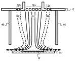
- FIG. 1is a schematic cross-sectional view of the vapor phase growth apparatus of the first embodiment.
- the vapor phase growth apparatus 100 of the first embodimentis, for example, a single wafer type epitaxial growth apparatus for epitaxially growing a single crystal SiC film on a single crystal SiC substrate.
- the vapor phase growth apparatus 100 of the first embodimentincludes a reaction chamber 10 and a process gas supply unit 12.
- the reaction chamber 10includes a susceptor 14 (substrate holding unit), a rotating body 16, a rotating shaft 18, a rotation drive mechanism 20, a first heater 22, a reflector 28, a support column 30, a fixing base 32, a fixing shaft 34, a hood 40 ( Side wall, a second heater 42, and a gas outlet 44.
- the process gas supply unit 12includes a first gas supply port 52, a second gas supply port 54, a first gas injection hole 56, and a second gas injection hole 58.
- the circular area where the first gas injection holes 56 of the process gas supply unit 12 are providedis the first area 12a
- the annular area where the second gas injection holes 58 are providedis the second area 12b. It is.
- the process gas supply unit 12is provided on the reaction chamber 10.
- the process gas supply unit 12has a function of supplying a process gas to the reaction chamber 10.
- the first gas supply port 52 and the second gas supply port 54are provided in the upper part of the process gas supply unit 12.
- the first gas supply port 52supplies, for example, the first process gas G1 into the process gas supply unit 12.
- the second gas supply port 54supplies, for example, the second process gas G2 into the process gas supply unit 12.
- the first gas injection holes 56 and the second gas injection holes 58are provided in the lower part of the process gas supply unit 12.
- the first gas injection holes 56 and the second gas injection holes 58are provided to face the reaction chamber 10.
- the second gas injection holes 58are provided around the first gas injection holes 56.
- the area where the first gas injection holes 56 of the process gas supply unit 12 are providedis the first area 12a, and the area where the second gas injection holes 58 are provided is the second area 12b. Therefore, the second area 12b is provided around the first area 12a.
- the first process gas G1is supplied from the first gas injection holes 56 into the reaction chamber 10.
- the second process gas G2is supplied into the reaction chamber 10 from the second gas injection holes 58.
- the first process gas G1is supplied from the first region 12a into the reaction chamber 10
- the second process gas G2is supplied from the second region 12b into the reaction chamber 10.
- the process gas supply unit 12can supply process gases having different compositions to the central portion and the outer peripheral portion of the wafer W at different flow rates. ing.
- the flow velocityis determined by the flow rate of the gas introduced from the gas supply port or the flow rate of the gas passing through the gas injection holes divided by the cross-sectional area of the corresponding gas injection holes.
- the first process gas G1is, for example, a mixture gas containing a source gas of silicon (Si), a source gas of carbon (C), a dopant gas of n-type impurities, an assist gas that suppresses clustering of silicon, and a carrier gas. It is a gas.
- the source gas of siliconis, for example, silane (SiH 4 ).
- the source gas of carbonis, for example, propane (C 3 H 8 ).
- the dopant gas of the n-type impurityis, for example, nitrogen gas.
- the assist gasis, for example, hydrogen chloride (HCl).
- the carrier gasis, for example, argon gas or hydrogen gas.
- the second process gas G2is, for example, a mixed gas containing a silicon source gas, a carbon source gas, an n-type impurity dopant gas, an assist gas, and a carrier gas.
- the source gas of siliconis, for example, silane.
- the source gas of carbonis, for example, propane.
- the dopant gas of the n-type impurityis, for example, nitrogen gas.
- the assist gasis, for example, hydrogen chloride (HCl).
- the carrier gasis, for example, argon gas or hydrogen gas.
- the carbon / silicon atomic ratio (hereinafter also described as C / Si ratio) of the second process gas G2is higher than the carbon / silicon atomic ratio of the first process gas G1.
- the ratio of the source gas of silicon contained in the second process gas G2 to the source gas of carbonis lower than the ratio of the source gas of silicon contained in the first process gas G1 to the source gas of carbon
- the C / Si ratio of the second process gas G2is set to the first process gas G1 by not including the silicon source gas in the second process gas G2 and using only the carbon source gas as the source gas. It is possible to make it higher than the C / Si ratio of
- the respective process gasesare all mixed to form the first process gas G1 and the second process gas G2. doing.
- the process gasesmay be mixed in the process gas supply unit 12 or may be mixed after being supplied to the reaction chamber 10.
- all or part of the silicon source gas, the carbon source gas, the dopant gas of n-type impurities, and the assist gasmay be separated until being supplied to the reaction chamber 10.
- the first gas injection holes 56it is possible to provide a plurality of types of gas injection holes as the first gas injection holes 56, and to supply different types of process gases from the respective gas injection holes.
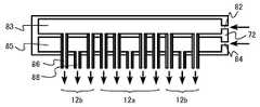
- FIG. 2is a schematic cross-sectional view showing another specific example of the process gas supply unit of the first embodiment.
- the process gas supply unit 72includes a silicon source gas supply port 82, a carbon source gas supply port 84, a first separation chamber 83, a second separation chamber 85, a silicon source gas injection hole 86, and a carbon source gas injection. It has a hole 88.
- the silicon source gas and the carbon source gasare mixed in the reaction chamber 10 after being supplied.
- the C / Si ratio introduced into the reaction chamber 10can be changed by adjusting the flow rate of the gas supplied to the source gas injection holes 88 of carbon and the source gas injection holes 86 of silicon. It is possible. Further, by changing the density (the number of gas injection holes per unit area) of the source gas injection holes 88 of carbon and the source gas injection holes 86 of silicon in the first region 12a and the second region 12b, the first It is possible to change the C / Si ratio in the region 12a and the second region 12b (make the C / Si ratio of the second region 12b higher than the C / Si ratio of the first region 12a).
- the cross-sectional area of the silicon source gas injection holes 86 of the carbon source gas injection holes 88 in the first area 12 a and the second area 12 bis adjusted to make the first areas 12 a and the second It is possible to change the C / Si ratio in the region 12b (make the C / Si ratio in the second region 12b higher than the C / Si ratio in the first region 12a).
- the reaction chamber 10is made of, for example, stainless steel.
- the reaction chamber 10has a cylindrical inner wall 10a.
- a SiC filmis formed on the wafer W.
- the susceptor 14is provided inside the reaction chamber 10.
- a wafer Wwhich is an example of a substrate, can be mounted on the susceptor 14.
- the susceptor 14may have an opening at its center.
- the susceptor 14has a holding wall 14 a that can hold the outer periphery of the wafer W with a predetermined gap.
- the holding wall 14 asuppresses the horizontal movement of the wafer W.
- the difference between the diameter of the holding wall 14a and the diameter of the wafer Wis, for example, 3 mm or less.
- the susceptor 14is formed of, for example, a highly heat resistant material such as SiC or carbon or carbon coated with SiC or TaC.
- the susceptor 14is fixed to the top of the rotating body 16.
- the rotating body 16is fixed to the rotating shaft 18.
- the susceptor 14is indirectly fixed to the rotating shaft 18.
- the rotation shaft 18is rotatable by the rotation drive mechanism 20.
- the rotation drive mechanism 20can rotate the susceptor 14 by rotating the rotation shaft 18.
- the wafer W placed on the susceptor 14can be rotated by rotating the susceptor 14.
- the wafer Wis rotated at a rotational speed of 300 rpm or more and 3000 rpm or less.
- the rotation drive mechanism 20is configured of, for example, a motor and a bearing.
- the first heater 22is provided below the susceptor 14.
- the first heater 22is provided in the rotating body 16.
- the first heater 22heats the wafer W held by the susceptor 14 from below.
- the first heater 22is, for example, a resistance heater.
- the first heater 22is, for example, a disk-shaped to which a comb-shaped pattern is applied.
- the reflector 28is provided below the first heater 22.
- a first heater 22is provided between the reflector 28 and the susceptor 14.
- the reflector 28reflects the heat radiated downward from the first heater 22 to improve the heating efficiency of the wafer W. Also, the reflector 28 prevents the members below the reflector 28 from being heated.
- the reflector 28has, for example, a disk shape.
- the reflector 28is formed of, for example, a highly heat resistant material such as carbon coated with SiC.
- the reflector 28is fixed to the fixed base 32 by, for example, a plurality of support posts 30.
- the fixed base 32is supported by, for example, a fixed shaft 34.
- a push-up pin(not shown) is provided in the rotating body 16 in order to detach the susceptor 14 from the rotating body 16.
- the push-up pinpenetrates, for example, the reflector 28 and the first heater 22.
- the second heater 42is provided between the hood 40 and the inner wall 10 a of the reaction chamber 10.
- the second heater 42heats the wafer W held by the susceptor 14 from above.
- the second heater 42is, for example, a resistance heater.
- the hood 40is provided in an area between the process gas supply unit 12 and the susceptor 14 in the reaction chamber 10.
- the hood 40is, for example, cylindrical.
- the hood 40has a function of preventing the first process gas G1 and the second process gas G2 from coming into contact with the second heater 42.
- the hood 40is formed of, for example, a highly heat resistant material such as carbon coated with SiC.
- the gas outlet 44is provided at the bottom of the reaction chamber 10.
- the gas discharge port 44discharges the excess reaction product after the source gas has reacted on the surface of the wafer W and the excess process gas to the outside of the reaction chamber 10.
- the gas discharge port 44is connected to, for example, a vacuum pump (not shown).
- reaction chamber 10is provided with a wafer inlet / outlet and a gate valve (not shown).
- the wafer Wcan be carried into the reaction chamber 10 or carried out of the reaction chamber 10 by the wafer inlet / outlet and the gate valve.
- FIG. 3is an explanatory view of dimensions of members of the vapor phase growth apparatus of the first embodiment.
- FIG. 3shows a part of the process gas supply unit 12, the hood 40, the susceptor 14, and the wafer W mounted on the susceptor 14.
- the upper view of FIG. 3is a sectional view, and the lower view is a plan view.
- the first area 12a and the second area 12bare hatched.
- the wafer W in which the orientation flat and the notch are omittedis indicated by a dotted line.
- the inner circumferential diameter of the second region 12bis d1.
- the inner circumferential diameter of the second region 12 bis defined by the diameter of a circle inscribed in the innermost injection hole of the second gas injection holes 58.
- the outer peripheral diameter of the second region 12bis d2.
- the outer peripheral diameter of the second region 12 bis defined by the diameter of a circle circumscribed to the outermost one of the second gas ejection holes 58.
- the diameter of the holding wall 14a of the susceptor 14is d3.
- the diameter of the susceptor 14is d4.
- the inner circumferential diameter of the hood 40is d5.
- the inner circumferential diameter d1 of the second region 12bis 75% or more and 130% or less of the diameter d3 of the holding wall 14a.
- the outer peripheral diameter d2 of the second region 12bis, for example, larger than the diameter d3 of the holding wall 14a.
- the inner diameter d5 of the hood 40is 110% or more and 200% or less of the outer diameter d2 of the second region 12b.
- the inner diameter d5 of the hood 40is preferably 105% or more and 200% or less of the diameter d4 of the susceptor 14.
- the vapor phase growth method of the first embodimentuses the epitaxial growth apparatus shown in FIG. A case where a single crystal SiC film doped with nitrogen as an n-type impurity is formed on the surface of a single crystal SiC wafer will be described as an example.
- Wafer Wis single crystal SiC.
- the wafer Wis rotated by the rotation drive mechanism 20 at a rotational speed of 300 rpm or more. Then, the wafer W is heated by the first heater 22 and the second heater 42.
- the first process gas G1is supplied from the first region 12a of the process gas supply unit 12 toward the central portion of the surface of the wafer W at a first flow rate.
- the first process gas G1 ejected from the first gas ejection holes 56forms a laminar flow from the process gas supply unit 12 toward the surface of the wafer W.
- the second process gas G2is supplied from the second area 12b of the process gas supply unit 12 at a second flow rate toward the area outside the central portion of the wafer W.
- the second process gas G2is supplied to an area outside the wafer W than the first process gas G1.
- the second process gas G2 ejected from the second gas ejection holes 58forms a laminar flow from the process gas supply unit 12 toward the surface of the wafer W.
- the first flow velocity and the second flow velocityare, for example, 0.2 m / sec or more and 1.0 m / sec or less.
- the first process gas G1is, for example, a mixed gas containing a silicon source gas, a carbon source gas, an n-type impurity dopant gas, an assist gas, and a carrier gas.
- the source gas of siliconis, for example, silane (SiH 4 ).
- the source gas of carbonis, for example, propane (C 3 H 8 ).
- the dopant gas of the n-type impurityis, for example, nitrogen gas.
- the assist gasis, for example, hydrogen chloride (HCl) gas.
- the carrier gasis, for example, argon gas or hydrogen gas.
- the second process gas G2is, for example, a mixed gas containing a silicon source gas, a carbon source gas, an n-type impurity dopant gas, and a carrier gas.
- the source gas of siliconis, for example, silane.
- the source gas of carbonis, for example, propane.
- the dopant gas of the n-type impurityis, for example, nitrogen gas.
- the carrier gasis, for example, argon gas or hydrogen gas.
- the C / Si ratio of the second process gas G2 supplied from the process gas supply unit 12 to the reaction chamber 10is higher than the C / Si ratio of the first process gas G1.
- a single crystal SiC film doped with nitrogenwhich is an n-type impurity, is formed on the surface of the wafer W.
- the second processis performed by controlling the first flow rate of the first process gas G1, the second flow rate of the second process gas G2, and the rotation speed of the wafer W.
- the gas G2is controlled to form a flow drawn toward the center of the wafer W.
- the first flow ratecan be controlled, for example, by changing the flow rate of the process gas supplied to the first gas injection holes 56 with a mass flow controller (not shown).
- the second flow velocitycan be controlled, for example, by changing the flow rate of the process gas supplied to the second gas injection holes 58 by a mass flow controller (not shown).
- the rotational speed of the wafer Wcan be controlled by the rotational drive mechanism 20.
- FIG. 4is an explanatory view of the flow of the process gas in the reaction chamber of the vapor phase growth method of the first embodiment.
- the first process gas G1 ejected as a laminar flow in the vertical direction from the first region 12ais a horizontal flow toward the outside of the wafer W on the surface of the wafer W It becomes.
- the second process gas G2 ejected from the second region 12b as a laminar flow in the vertical directionflows so as to be drawn toward the center of the wafer W, and then horizontally on the surface of the wafer W toward the outside of the wafer W It becomes a flow of direction.
- the direction of flow of the second process gas G2has a component directed toward the center of the wafer W before reaching the surface of the wafer W.
- the heating by the first heater 22 and the second heater 42is stopped to lower the temperature of the wafer W. Thereafter, the wafer W is unloaded from the reaction chamber 10 together with the susceptor 14.
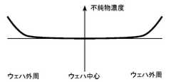
- FIG. 5is an explanatory view of a problem when forming a SiC film.
- FIG. 5shows the in-plane distribution of the impurity concentration when a SiC film doped with nitrogen as an n-type impurity is formed on a wafer.
- the concentration of nitrogen in the SiC filmbecomes high at the outer peripheral portion of the wafer W.
- the concentration distribution of n-type impurities in the SiC filmbecomes nonuniform, and the in-plane resistance distribution of the wafer W becomes nonuniform.
- Silicon sublimated from the deposit containing silicon adhering to the surface of the susceptor 14 outside the wafer Wmixes in the process gas of the outer periphery of the wafer W as a factor contributing to the increase of nitrogen concentration in the outer periphery of the wafer W It is conceivable.
- the C / Si ratio in the process gas supplied to the outer peripheral portion of the wafer Wbecomes low. Nitrogen is incorporated into the crystal by entering a carbon lattice position in the SiC crystal. For this reason, when the C / Si ratio in the process gas is low, carbon is reduced, and nitrogen easily enters the carbon lattice position in the SiC crystal. Therefore, the concentration of nitrogen in the outer peripheral portion is higher than that in the central portion of the wafer W.
- the second process gas G2 having a high C / Si ratiois supplied to the outer peripheral portion of the wafer W. Furthermore, the first flow velocity of the first process gas G1 supplied to the central portion of the wafer W, the second flow velocity of the second process gas G2 supplied to the outer peripheral portion of the wafer W, and the rotation speed of the wafer W By controlling, the uniformity of the concentration distribution of n-type impurities in the SiC film is improved.
- FIG. 6is a view showing the relationship between the parameters of the vapor phase growth method of the first embodiment and the distribution of the impurity concentration in the wafer surface.
- 6 (a)shows the C / Si ratio of the second process gas G2 as the parameter
- FIG. 6 (b)shows the rotational speed of the wafer W as the parameter
- FIG. 6 (c)shows the second process gas as the parameter This is the case of the second flow rate of G2.
- the second processhas a carbon / silicon atomic ratio higher than that of the first process gas G1 in a region outside the first process gas G1.
- Supply process gas G2.Then, by controlling the first flow velocity of the first process gas G1, the second flow velocity of the second process gas G2 supplied to the outer peripheral portion of the wafer W, and the rotation speed of the wafer W, the second A flow in which the process gas G2 is drawn in toward the center of the wafer W is formed to form a SiC film. Thereby, the uniformity of the concentration distribution of n-type impurities in the SiC film is improved.
- the concentration distribution of the second process gas G2only by the C / Si ratio is obtained. It is possible to improve the uniformity of the impurity concentration distribution with higher accuracy than the adjustment.
- the inner diameter d1 of the second region 12b of the vapor deposition apparatus 100is And 75% or more and 130% or less of the diameter d3 of the holding wall 14a. If the above range is exceeded, the impurity concentration in the central portion of the wafer W may be lowered, and the impurity concentration distribution may become nonuniform. If the above range is exceeded, the amount of drawing in of the second process gas G2 may be insufficient, and the concentration distribution of impurities may be uneven.
- the inner peripheral diameter d1 of the second region 12bis preferably 100% or more of the diameter d3 of the holding wall 14a from the viewpoint of suppressing the decrease in the impurity concentration in the central portion of the wafer W.
- the inner circumferential diameter d1 of the second region 12bis preferably less than 100% of the diameter d3 of the holding wall 14a from the viewpoint of suppressing the shortage of the amount of drawing of the second process gas G2.
- the flow of the second process gas G2 toward the center of the wafer Wis realized, and the impurity concentration distribution with high uniformity is realized, the inside of the hood 40
- the circumferential diameter d5needs to be 110% or more and 200% or less of the outer circumferential diameter d2 of the second region 12b, and preferably 110% or more and 150% or less. Below the above range, the laminar flow of the second process gas G2 in the vertical direction may be disturbed by the influence of the hood 40. When the above range is exceeded, the second process gas G2 flows toward the hood 40, and it becomes difficult to realize the flow of the second process gas G2 toward the center of the wafer W.
- the inner circumferential diameter d5 of the hood 40is equal to the diameter d4 of the susceptor 14 And 105% or more and 200% or less.
- the rotation speed of the wafer Wneeds to be 300 rpm or more. If the rotational speed is less than 300 rpm, the amount of drawing of the second process gas G2 toward the center of the wafer W may not be sufficient.
- first flow velocity and the second flow velocityare preferably 0.2 m / sec or more and 1.0 m / sec or less, and more preferably 0.2 m / sec or more and 0.5 m / sec or less. preferable.
- the first process gas G1 and the second process gas G2are easily mixed, and the function of the first embodiment can not be exhibited. If the above range is exceeded, the flow of the second process gas G2 in the vertical direction becomes too fast, and the amount of drawing of the second process gas G2 toward the center of the wafer W may not be sufficient.
- the second flow rate of the second process gas G2is 50% or more of the first flow rate of the first process gas G1. And 200% or less. From the viewpoint of increasing the drawing amount of the second process gas G2 toward the center of the wafer W, the second flow velocity of the second process gas G2 is smaller than the first flow velocity of the first process gas G1. It is preferable to do. Further, from the viewpoint of suppressing the drawing amount of the second process gas G2 toward the center of the wafer W, the second flow velocity of the second process gas G2 is higher than the first flow velocity of the first process gas G1. It is preferable to make the
- the uniformity of the concentration distribution of n-type impurities in the SiC filmcan be improved. It is possible. For example, in the case of reducing the diameter of the wafer W, it is preferable to reduce the inner peripheral diameter d1 of the second region 12b of the process gas supply unit 12 to increase the C / Si ratio of the outer peripheral part of the wafer W. It is not easy because the design change or replacement of the part 12 is necessary.
- FIG. 7is an explanatory view of the flow of the process gas in the reaction chamber of the vapor phase growth method of the first embodiment.
- FIG. 7shows the case where a film is formed on a wafer W having a diameter of about two thirds of the wafer W of FIG.
- the second process gas G2 toward the center of the wafer Wis formed by increasing the rotational speed of the wafer W or reducing the second flow rate of the second process gas G2. It is possible to increase the amount of retraction. Therefore, even when the diameter of the wafer W changes, it is easy to improve the uniformity of the concentration distribution of n-type impurities in the SiC film.
- the uniformity of the concentration distribution of n-type impurities in the SiC filmis improved.
- the vapor phase growth apparatus of the second embodimentis the same as that of the first embodiment except that the process gas supply unit further includes a third region, and a gas passage hole is provided on the side wall. Therefore, the contents overlapping with the first embodiment will not be partially described.
- FIG. 8is a schematic cross-sectional view of the vapor phase growth apparatus of the second embodiment.
- the vapor phase growth apparatus of the second embodimentis, for example, a single wafer type epitaxial growth apparatus in which a single crystal SiC film is epitaxially grown on a single crystal SiC substrate.
- the vapor phase growth apparatus 200 of the second embodimentincludes a reaction chamber 10 and a process gas supply unit 12.
- the reaction chamber 10includes a susceptor 14 (substrate holding unit), a rotating body 16, a rotating shaft 18, a rotation drive mechanism 20, a first heater 22, a reflector 28, a support column 30, a fixing base 32, a fixing shaft 34, a hood 40 ( Side wall, a second heater 42, and a gas outlet 44.
- the process gas supply unit 12includes a first gas supply port 52, a second gas supply port 54, a third gas supply port 55, a first gas injection hole 56, a second gas injection hole 58, and a third gas injection hole 58.
- a gas injection hole 59is provided.
- the region where the first gas injection holes 56 of the process gas supply unit 12 are providedis the first region 12a
- the region where the second gas injection holes 58 are providedis the second region 12b
- the third The area in which the gas injection holes 59 are providedis the third area 12c.
- the first gas supply port 52, the second gas supply port 54, and the third gas supply port 55are provided on the upper portion of the process gas supply unit 12.
- the first gas supply port 52supplies, for example, the first process gas G1 into the process gas supply unit 12.
- the second gas supply port 54supplies, for example, the second process gas G2 into the process gas supply unit 12.
- the third gas supply port 55supplies, for example, the third process gas G3 into the process gas supply unit 12.
- the first gas injection holes 56, the second gas injection holes 58, and the third gas injection holes 59are provided in the lower part of the process gas supply unit 12.
- the first gas injection holes 56, the second gas injection holes 58, and the third gas injection holes 59are provided to face the reaction chamber 10.
- the second gas injection holes 58are provided around the first gas injection holes 56.
- the third gas injection holes 59are provided around the second gas injection holes 58.
- the region where the first gas injection holes 56 of the process gas supply unit 12 are providedis the first region 12a
- the region where the second gas injection holes 58 are providedis the second region 12b
- the third The area where the gas injection holes 59 are providedis the third area 12c.
- the third gas injection holes 59supply the third process gas G3 to the region between the hood 40 and the second heater 42.
- the third process gas G3is, for example, argon gas.
- the hood 40has a gas passage hole 60.
- the gas passage hole 60is provided to allow the third process gas G3 to pass from the second heater 42 side to the wafer W side.
- FIG. 9is an explanatory view of the flow of the process gas in the reaction chamber of the vapor phase growth method of the second embodiment.
- the third process gas G3passes through the gas passage holes 60 and flows to the wafer W side. Then, the flow of the second process gas can be pushed out toward the center of the wafer W by the flow of the third process gas G3. As a result, the amount of drawing of the second process gas G2 toward the center of the wafer W is increased.
- the vapor deposition apparatus of the second embodiment and the vapor deposition methodit is possible to adjust the amount of drawing of the second process gas G2 toward the center of the wafer W by the third process gas G3. Become. Therefore, the uniformity of the concentration distribution of n-type impurities in the SiC film is further improved.
- the substrateis rotated at a rotational speed of 300 rpm or more, the substrate is heated, and the first process gas containing carbon, silicon, and the n-type impurity directed to the substrate.
- the substratecontaining carbon and the n-type impurity in a region outside the region where the first process gas is supplied, and having a carbon / silicon atomic ratio than that of the first process gas.
- a first silicon carbide filmis formed on the surface of the substrate while supplying a high second process gas and the effective carbon / silicon atomic ratio of the process gas directly above the surface of the substrate is less than 1; Supplying a third process gas containing carbon, silicon and the n-type impurity toward the substrate, carbon in a region outside the region where the third process gas is supplied toward the substrate, and A third of said n-type impurities
- the fourth process gas having a carbon / silicon atomic ratio higher than the process gasis supplied, and the first surface of the substrate is processed with the effective carbon / silicon atomic ratio of the process gas directly above the surface of the substrate being 1 or more.
- the vapor phase growth method of the third embodimentis characterized in that the first silicon carbide film and the second silicon carbide film having different n-type impurity concentrations are formed on the substrate. It is different from the phase growth method.
- the description overlapping with the vapor phase growth apparatus and the vapor phase growth method of the first embodimentwill be partially omitted.
- the vapor deposition method of the third embodimentuses the epitaxial growth apparatus shown in FIG. Further, the vapor phase growth method of the third embodiment uses an epitaxial growth apparatus having a process gas supply unit shown in FIG.
- the case where the n-type impurity is nitrogenwill be described as an example.
- FIG. 10is a cross-sectional view of a silicon carbide film formed by the vapor deposition method of the third embodiment.
- a buffer film 501first silicon carbide film
- an n-type film 502second silicon carbide film
- the substrate 500is a wafer of single crystal SiC.
- the substrate 500contains nitrogen as an n-type impurity.
- the nitrogen concentration of the substrate 500is, for example, 1 ⁇ 10 17 cm ⁇ 3 or more and 1 ⁇ 10 19 cm ⁇ 3 or less.
- the buffer film 501is a single crystal SiC film.
- the buffer film 501has a function of suppressing propagation of basal plane dislocation (BPD) included in the substrate 500 to the n-type film 502. During the growth of the buffer film 501, for example, basal plane dislocations are converted to other dislocations.
- BPDbasal plane dislocation
- the buffer film 501contains nitrogen as an n-type impurity.
- the nitrogen concentration of the buffer film 501is, for example, 1 ⁇ 10 17 cm ⁇ 3 or more and 1 ⁇ 10 19 cm ⁇ 3 or less.
- the thickness of the buffer film 501is, for example, 0.5 ⁇ m or more and 2 ⁇ m or less.
- the nitrogen concentration of the buffer film 501is preferably 1 ⁇ 10 17 cm ⁇ 3 or more.
- the n-type film 502is a single crystal SiC film.
- the n-type film 502contains nitrogen as an n-type impurity.
- the nitrogen concentration of the n-type film 502is, for example, not less than 1 ⁇ 10 14 cm ⁇ 3 and not more than 1 ⁇ 10 16 cm ⁇ 3 .
- the nitrogen concentration of the n-type film 502is lower than the nitrogen concentration of the buffer film 501.
- the thickness of the n-type film 502is, for example, 10 ⁇ m or more and 300 ⁇ m or less.
- the n-type film 502is used, for example, as a drift layer of a high breakdown voltage device such as a transistor or a diode.
- the n-type film 502preferably reduces the amount of carbon vacancies that work as a lifetime killer, from the viewpoint of prolonging the lifetime of minority carriers.
- the nitrogen concentration of the n-type film 502is preferably 1 ⁇ 10 16 cm ⁇ 3 or less from the viewpoint of realizing a high breakdown voltage in the transistor or the diode.
- Wafer Wis single crystal SiC.
- the wafer Wis rotated by the rotation drive mechanism 20 at a rotational speed of 300 rpm or more. Then, the wafer W is heated by the first heater 22 and the second heater 42.
- the first process gas G1is supplied from the first region 12a of the process gas supply unit 12 toward the central portion of the surface of the wafer W.
- the first process gas G1 ejected from the first gas ejection holes 56forms a laminar flow from the process gas supply unit 12 toward the surface of the wafer W.
- the first process gascomprises carbon, silicon and nitrogen.
- the second process gas G2is supplied from the second area 12b of the process gas supply unit 12 toward the area outside the central portion of the wafer W.
- the second process gas G2is supplied to an area outside the wafer W than the first process gas G1.
- the second process gas G2 ejected from the second gas ejection holes 58forms a laminar flow from the process gas supply unit 12 toward the surface of the wafer W.
- the second process gascontains carbon and nitrogen.
- the first process gas G1is, for example, a mixed gas containing a silicon source gas, a carbon source gas, an n-type impurity dopant gas, an assist gas, and a carrier gas.
- the source gas of siliconis, for example, silane (SiH 4 ).
- the source gas of carbonis, for example, propane (C 3 H 8 ).
- the dopant gas of the n-type impurityis nitrogen gas.
- the assist gasis, for example, hydrogen chloride (HCl) gas.
- the carrier gasis, for example, argon gas or hydrogen gas.
- the second process gas G2is, for example, a mixed gas containing a silicon source gas, a carbon source gas, an n-type impurity dopant gas, and a carrier gas.
- the source gas of siliconis, for example, silane.
- the source gas of carbonis, for example, propane.
- the dopant gas of the n-type impurityis nitrogen gas.
- the carrier gasis, for example, argon gas or hydrogen gas.
- the C / Si ratio of the second process gas G2 supplied from the process gas supply unit 12 to the reaction chamber 10is higher than the C / Si ratio of the first process gas G1.
- a buffer film 501 containing nitrogen as an n-type impurityis formed on the surface of the wafer W.
- the nitrogen concentration of the buffer film 501is, for example, 1 ⁇ 10 17 cm ⁇ 3 or more.
- the thickness of the buffer film 501is, for example, 0.5 ⁇ m or more and 2 ⁇ m or less.
- the buffer film 501is formed in a state in which the effective carbon / silicon atomic ratio of the process gas right above the surface of the wafer W is less than one.
- the effective carbon / silicon atomic ratio directly above the surface of the wafer W in the central portion of the wafer W and the region of the outer peripheral portion of the wafer Wis less than one.
- the effective carbon / silicon atomic ratiois hereinafter referred to as "effective C / Si ratio".
- the wafer center portionmeans, for example, a region within 5 mm from the wafer W center.
- the wafer outer peripheral portionmeans, for example, a region 5 mm inside from the outer peripheral end of the wafer W.
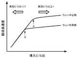
- FIG. 11is an explanatory view of the vapor phase growth method of the third embodiment.
- FIG. 11is an explanatory view showing the relationship between the introduced C / Si ratio and the film growth rate of the SiC film on the substrate.
- the “introduced C / Si ratio”is the carbon / silicon atomic ratio of the process gas introduced into the process supply unit shown in FIG. More specifically, it is a carbon / silicon atomic ratio of silicon in the silicon source gas introduced into the source gas supply port 82 and carbon in the carbon source gas introduced into the source gas supply port 84.
- the amount of silicon in the source gas of silicon introduced into the source gas supply port 82is fixed, and the amount of carbon in the source gas of carbon introduced into the source gas supply port 84 is changed to introduce C.
- the case where / Si ratio is changedis shown.
- the film growth ratesaturates.
- the saturation point A at the wafer centeris the position of the arrow A in FIG.
- the saturation point B of the wafer outer peripheral portionis the position of the arrow B in FIG.
- the process gasis controlled so that the C / Si ratio toward the wafer outer peripheral part is higher than the wafer central part. Therefore, the saturation point B of the wafer outer peripheral part However, the introduced C / Si ratio is lower than the saturation point A at the wafer center.
- the effective C / Si ratiois 1 or more at the introduced C / Si ratio above the saturation point A, and the effective C / Si ratio is less than 1 at the introduced C / Si ratio below the saturation point A.
- the effective C / Si ratiois 1 or more at the introduced C / Si ratio above the saturation point B, and the effective C / Si ratio is less than 1 at the introduced C / Si ratio below the saturation point B.
- the introduced C / Si ratio at or above the saturation point Ais required.
- the introduced C / Si ratio less than the saturation point Bis required.
- a third process gasis supplied from the first region 12 a of the process gas supply unit 12 toward the center of the surface of the wafer W.
- the third process gas ejected from the first gas ejection holes 56forms a laminar flow from the process gas supply unit 12 toward the surface of the wafer W.
- the third process gascomprises carbon, silicon and nitrogen.
- the fourth process gasis supplied from the second area 12 b of the process gas supply unit 12 toward the area outside the center of the wafer W.
- the fourth process gasis supplied to an area outside the wafer W than the third process gas.
- the fourth process gas ejected from the second gas ejection holes 58forms a laminar flow from the process gas supply unit 12 toward the surface of the wafer W.
- the fourth process gascontains carbon and nitrogen.
- the third process gasis, for example, a mixed gas containing a silicon source gas, a carbon source gas, an n-type impurity dopant gas, an assist gas, and a carrier gas.
- the source gas of siliconis, for example, silane.
- the source gas of carbonis, for example, propane.
- the dopant gas of the n-type impurityis nitrogen gas.
- the assist gasis, for example, hydrogen chloride gas.
- the carrier gasis, for example, argon gas or hydrogen gas.
- the fourth process gasis, for example, a mixed gas containing a silicon source gas, a carbon source gas, an n-type impurity dopant gas, and a carrier gas.
- the source gas of siliconis, for example, silane.
- the source gas of carbonis, for example, propane.
- the dopant gas of the n-type impurityis nitrogen gas.
- the carrier gasis, for example, argon gas or hydrogen gas.
- the C / Si ratio of the fourth process gas supplied from the process gas supply unit 12 to the reaction chamber 10is higher than the C / Si ratio of the third process gas.
- an n-type film 502 containing nitrogenis formed on the surface of the wafer W.
- the nitrogen concentration of the n-type film 502is, for example, 1 ⁇ 10 16 cm ⁇ 3 or less.
- the thickness of the n-type film 502is, for example, 10 ⁇ m or more and 300 ⁇ m or less.
- the n-type film 502is formed in a state where the effective carbon / silicon atomic ratio of the process gas directly above the surface of the wafer W, that is, the effective C / Si ratio is 1 or more.
- the effective C / Si ratio in the region of the process gas directly above the surface of the wafer W and 5 mm from the center of the wafer W and the outer periphery of the wafer Wis 1 or more.
- the introduced C / Si ratiois set so that the effective C / Si ratio is 1 or more.
- the heating by the first heater 22 and the second heater 42is stopped to lower the temperature of the wafer W. Thereafter, the wafer W is unloaded from the reaction chamber 10 together with the susceptor 14.
- FIG. 12is an explanatory view of the operation and the effect of the vapor phase growth method of the third embodiment.
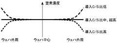
- FIG. 12is a diagram showing the relationship between the introduced C / Si ratio and the distribution shape of the nitrogen concentration in the wafer W plane.
- FIG. 12is a diagram qualitatively explaining only the shape change of the nitrogen concentration distribution between the conditions, and does not explain the change in the nitrogen concentration between the conditions.
- the nitrogen concentration in the outer peripheral portion of the wafer Wis higher than the nitrogen concentration in the central portion of the wafer W.
- the ratio increases from low to medium to medium (introduced C / Si ratio)the nitrogen concentration in the outer peripheral portion of the wafer W decreases, and the nitrogen concentration distribution in the SiC film becomes uniform.
- the introduced C / Si ratio is increased to a high statethe nitrogen concentration in the outer peripheral portion of the wafer W further decreases, and the uniformity of the nitrogen concentration distribution in the SiC film decreases.
- the introduced C / Si ratiois further increased to a very high state (introduced C / Si ratio ultra high)
- the in-plane effective C / Si ratio of the wafer Wis sufficiently lower than 1. Further, at the introduced C / Si ratio high, the effective C / Si ratio at the central portion of the wafer W is sufficiently lower than 1, and the effective C / Si ratio at the outer peripheral portion of the wafer W is near 1. Furthermore, when the introduced C / Si ratio is extremely high, the in-plane effective C / Si ratio of the wafer W is in a state sufficiently higher than one.
- the reduction rate of the nitrogen concentration in the SiC filmis large with the increase of the effective C / Si ratio, and in the region where the effective C / Si ratio is higher than 1, the effective C / Si ratio The decrease rate of nitrogen concentration in the SiC film becomes smaller with the increase of.
- the effective C / Si ratio of the outer peripheral part of the wafer W and the effective C / Si ratio of the central part of the wafer Ware lower than the nitrogen concentration in the central portion of the wafer W because the rate of decrease in the nitrogen concentration in the SiC film is large with the increase of the effective C / Si ratio. It will be easier.
- the introduced C / Si ratiois increased from the introduced C / Si ratio high to the introduced C / Si ratio ultra high, the introduced C / Si ratio is slightly increased at the peripheral portion of the wafer W, and the effective C / Si is increased.
- the ratioexceeds 1 and the reduction rate of the nitrogen concentration in the SiC film decreases, the wafer C can not have the effective C / Si ratio above 1 unless the introduced C / Si ratio is significantly increased at the center of the wafer W.
- the nitrogen concentration in the central portion of the wafer Wtends to be lower than the nitrogen concentration in the outer peripheral portion of the wafer W. For this reason, a change in the nitrogen concentration distribution shape in the SiC film as shown in FIG. 12 occurs.
- FIG. 13is an explanatory view of the operation and the effect of the vapor phase growth method of the third embodiment.
- the measured values of the relationship between the introduced C / Si ratio and the film growth rateare shown.
- the saturation point A at the center of the waferis at a position where the introduced C / Si ratio is about 1.65.
- the saturation point B of the wafer outer peripheral portionis at a position where the introduced C / Si ratio is about 1.5.
- the introduced C / Si ratio of the saturation point A or morethat is, the introduced C / Si ratio of 1.65 or more is required.
- the introduced C / Si ratio less than the saturation point Bthat is, the introduced C / Si ratio less than 1.5 is required.
- FIG. 14is an explanatory view of the operation and the effect of the vapor phase growth method of the third embodiment.
- FIG. 14shows the nitrogen concentration distribution in the surface of the wafer W with the introduced C / Si ratio as a parameter under the same process conditions as FIG. The introduced C / Si ratio is varied between 1.20 and 1.95.
- FIG. 14shows a measurement result using a wafer W having a diameter of 150 mm.
- the distribution of nitrogen concentration in the wafer W surfacebecomes uniform when the introduced C / Si ratio is 1.35 and the introduced C / Si ratio is 1.80 or more.
- Eachcorresponds to the case where the effective C / Si ratio is less than 1 and the case where the effective C / Si ratio is 1 or more.
- the effective C / Si ratio of the surface of the wafer Wis set to less than 1 in the formation of the buffer film 501 having a high nitrogen concentration.
- the effective C / Si ratio of the surface of the wafer Wis set to 1 or more. As a result, it is possible to form an n-type film 502 having a low nitrogen concentration and high in-plane uniformity of the wafer W in the nitrogen concentration.
- the effective C / Si ratio of the surface of the wafer Wis 1 or more in the formation of the n-type film 502, it is possible to reduce the amount of carbon vacancies in the film. Since the effective C / Si ratio is 1 or more, excess carbon is present, so the generation of carbon vacancies in the film is suppressed.
- the vapor phase growth method of the third embodimentit is possible to form a silicon carbide film suitable for manufacturing high breakdown voltage devices such as transistors and diodes.
- a single crystal SiC waferis described as an example of a substrate, but the substrate is not limited to a single crystal SiC wafer.
- the descriptionis omitted for the device configuration, the manufacturing method, and the parts that are not directly required for the description of the present invention, but the required device configuration, the manufacturing method, and the like can be appropriately selected and used.
- all vapor deposition apparatuses, annular holders, and vapor deposition methodsthat include elements of the present invention and whose design can be modified as appropriate by those skilled in the art are included in the scope of the present invention. It is intended that the scope of the invention be defined by the claims appended hereto and their equivalents.
Landscapes
- Chemical & Material Sciences (AREA)
- Engineering & Computer Science (AREA)
- Materials Engineering (AREA)
- Metallurgy (AREA)
- Organic Chemistry (AREA)
- Chemical Kinetics & Catalysis (AREA)
- General Chemical & Material Sciences (AREA)
- Mechanical Engineering (AREA)
- Crystallography & Structural Chemistry (AREA)
- Physics & Mathematics (AREA)
- Condensed Matter Physics & Semiconductors (AREA)
- General Physics & Mathematics (AREA)
- Manufacturing & Machinery (AREA)
- Computer Hardware Design (AREA)
- Microelectronics & Electronic Packaging (AREA)
- Power Engineering (AREA)
- Inorganic Chemistry (AREA)
- Chemical Vapour Deposition (AREA)
- Crystals, And After-Treatments Of Crystals (AREA)
Abstract
Description
Translated fromJapanese本発明は、ガスを供給して成膜を行う気相成長装置、及び、気相成長方法に関する。The present invention relates to a vapor phase growth apparatus that supplies a gas to form a film, and a vapor phase growth method.
高品質な半導体膜を成膜する方法として、ウェハ等の基板に気相成長により単結晶膜を成長させるエピタキシャル成長技術がある。エピタキシャル成長技術を用いる気相成長装置では、常圧又は減圧に保持された反応室内の基板保持部にウェハを載置する。As a method of forming a high quality semiconductor film, there is an epitaxial growth technique of growing a single crystal film on a substrate such as a wafer by vapor phase growth. In a vapor phase growth apparatus using an epitaxial growth technique, a wafer is mounted on a substrate holding unit in a reaction chamber held at normal pressure or reduced pressure.
そして、このウェハを加熱しながら、成膜の原料となるソースガス等のプロセスガスを、反応室上部から反応室内のウェハ表面に供給する。ウェハ表面ではソースガスの熱反応が生じ、ウェハ表面にエピタキシャル単結晶膜が成膜される。Then, while heating the wafer, a process gas such as a source gas as a raw material for film formation is supplied from the upper part of the reaction chamber to the wafer surface in the reaction chamber. A thermal reaction of the source gas occurs on the wafer surface, and an epitaxial single crystal film is formed on the wafer surface.
エピタキシャル単結晶膜にドーパントとなる不純物を導入する場合がある。エピタキシャル単結晶膜の抵抗分布を均一にするためには、不純物の濃度分布を均一にする必要がある。An impurity serving as a dopant may be introduced into the epitaxial single crystal film. In order to make the resistance distribution of the epitaxial single crystal film uniform, it is necessary to make the concentration distribution of impurities uniform.
特許文献1には、炭化珪素(SiC)のエピタキシャル単結晶膜の成膜に際し、不純物の濃度分布を均一にするために、基板の中心部と外周部に異なるC(炭素)/Si(シリコン)比のプロセスガスを供給する方法が記載されている。Patent Document 1 discloses that when forming an epitaxial single crystal film of silicon carbide (SiC), C (carbon) / Si (silicon) different in the central portion and the outer peripheral portion of the substrate in order to make the concentration distribution of impurities uniform. A method of supplying a ratio of process gas is described.
本発明が解決しようとする課題は、膜中の不純物の濃度分布の均一性を向上できる気相成長装置、及び、気相成長方法を提供することにある。The problem to be solved by the present invention is to provide a vapor phase growth apparatus and a vapor phase growth method capable of improving the uniformity of the concentration distribution of impurities in a film.
本発明の一態様の気相成長装置は、反応室と、前記反応室の中に設けられ、基板が載置可能であり、前記基板の外周を所定の間隙を有して保持可能な保持壁を有する基板保持部と、前記反応室の上に設けられ、第1のプロセスガスを前記反応室に供給可能な第1の領域と、前記第1の領域の周囲に設けられ前記第1のプロセスガスよりも炭素/シリコン原子比の高い第2のプロセスガスを前記反応室に供給可能な第2の領域とを有し、前記第2の領域の内周直径が前記保持壁の直径の75%以上130%以下であるプロセスガス供給部と、前記反応室の中の、前記プロセスガス供給部と前記基板保持部との間の領域に設けられ、内周直径が前記第2の領域の外周直径の110%以上200%以下である側壁と、前記基板保持部の下に設けられた第1のヒータと、前記側壁と前記反応室の内壁との間に設けられた第2のヒータと、前記基板保持部を回転させる回転駆動機構と、を備える。A vapor deposition apparatus according to one aspect of the present invention is provided in a reaction chamber and the reaction chamber, and a substrate can be mounted thereon, and a holding wall capable of holding the outer periphery of the substrate with a predetermined gap. A first region provided on the reaction chamber and capable of supplying a first process gas to the reaction chamber; and a first process provided on the periphery of the first region. And a second region capable of supplying a second process gas having a carbon / silicon atomic ratio higher than that of the gas to the reaction chamber, wherein an inner circumferential diameter of the second region is 75% of a diameter of the holding wall Provided in a region between the process gas supply unit and the substrate holding unit in the reaction chamber, wherein the process gas supply unit having a percentage of 130% or less and the inner peripheral diameter is the outer peripheral diameter of the second region Side wall which is at least 110% and at most 200% of the And comprising a first heater and a second heater provided between the side wall and the inner wall of the reaction chamber, and a rotation drive mechanism for rotating the substrate holder.
上記態様の気相成長装置において、前記第2の領域の内周直径が前記保持壁の直径の100%以上であることが好ましい。In the vapor phase growth apparatus according to the above aspect, the inner circumferential diameter of the second region is preferably 100% or more of the diameter of the holding wall.
上記態様の気相成長装置において、前記側壁の内周直径が前記基板保持部の直径の105%以上200%以下であることが好ましい。In the vapor phase growth apparatus according to the above aspect, the inner circumferential diameter of the side wall is preferably 105% or more and 200% or less of the diameter of the substrate holding unit.
上記態様の気相成長装置において、前記回転駆動機構は、前記基板を300rpm以上3000rpm以下の回転速度で回転させることが好ましい。In the vapor phase growth apparatus according to the above aspect, the rotary drive mechanism preferably rotates the substrate at a rotational speed of 300 rpm or more and 3000 rpm or less.
上記態様の気相成長装置において、前記プロセスガス供給部は、前記第2の領域の周囲に設けられ、前記側壁と前記第2のヒータとの間の領域に第3のプロセスガスを供給可能な第3の領域を有し、前記側壁は、前記第3のプロセスガスを前記側壁の外側から前記側壁の内側へ通過させるガス通過孔を有することが好ましい。In the vapor phase growth apparatus according to the above aspect, the process gas supply unit is provided around the second region, and can supply a third process gas to the region between the sidewall and the second heater. It is preferable that the side wall has a third region, and the side wall has a gas passage hole that allows the third process gas to pass from the outside of the side wall to the inside of the side wall.
上記態様の気相成長装置において、前記第3のプロセスガスはアルゴンガスであることが好ましい。In the vapor phase growth apparatus according to the above aspect, the third process gas is preferably argon gas.
本発明の一態様の気相成長方法は、基板を300rpm以上の回転速度で回転させ、前記基板を加熱し、前記基板に向けて第1の流速で第1のプロセスガスを供給し、前記基板に向けて、前記第1のプロセスガスよりも外側の領域に、第2の流速で前記第1のプロセスガスよりも炭素/シリコン原子比の高い第2のプロセスガスを供給し、前記第1の流速、前記第2の流速、及び、前記回転速度を制御して、前記第2のプロセスガスが前記基板の中心方向に引き込まれる流れを形成し、前記基板の表面に炭化珪素膜を形成する。In the vapor phase growth method according to one aspect of the present invention, a substrate is rotated at a rotational speed of 300 rpm or more, the substrate is heated, and a first process gas is supplied toward the substrate at a first flow rate. A second process gas having a carbon / silicon atomic ratio higher than that of the first process gas at a second flow rate in a region outside the first process gas toward the second process gas; The flow velocity, the second flow velocity, and the rotational velocity are controlled to form a flow in which the second process gas is drawn toward the center of the substrate, thereby forming a silicon carbide film on the surface of the substrate.
本発明の別の一態様の気相成長方法は、基板を300rpm以上の回転速度で回転させ、前記基板を加熱し、前記基板に向けて、炭素、シリコン、及び、n型不純物を含む第1のプロセスガスを供給し、前記基板に向けて、前記第1のプロセスガスが供給される領域よりも外側の領域に、炭素、シリコン、及び、n型不純物を含み、前記第1のプロセスガスよりも炭素/シリコン原子比の高い第2のプロセスガスを供給し、前記基板の表面の直上のプロセスガスの実効的な炭素/シリコン原子比が1未満となる状態で、前記基板の表面に第1の炭化珪素膜を形成し、前記基板に向けて、炭素、シリコン、及び、n型不純物を含む第3のプロセスガスを供給し、前記基板に向けて、前記第3のプロセスガスが供給される領域よりも外側の領域に、炭素、シリコン、及び、n型不純物を含み、前記第3のプロセスガスよりも炭素/シリコン原子比の高い第4のプロセスガスを供給し、前記基板の表面の直上のプロセスガスの実効的な炭素/シリコン原子比が1以上となる状態で、前記基板の表面に前記第1の炭化珪素膜よりもn型不純物濃度の低い第2の炭化珪素膜を形成する。In a vapor phase growth method according to another aspect of the present invention, a substrate is rotated at a rotational speed of 300 rpm or more, the substrate is heated, and carbon, silicon, and n-type impurities are directed to the substrate. And supplying carbon, silicon, and n-type impurities in a region outside the region where the first process gas is supplied toward the substrate, and the first process gas is supplied to the substrate. And supplying a second process gas having a high carbon / silicon atomic ratio to the surface of the substrate while the effective carbon / silicon atomic ratio of the process gas directly above the surface of the substrate is less than one. A third process gas containing carbon, silicon and n-type impurities is supplied to the substrate, and the third process gas is supplied to the substrate Area outside the area A fourth process gas containing carbon, silicon and n-type impurities and having a carbon / silicon atomic ratio higher than that of the third process gas, and an effective process gas directly on the surface of the substrate A second silicon carbide film having an n-type impurity concentration lower than that of the first silicon carbide film is formed on the surface of the substrate in a state where the carbon / silicon atomic ratio is 1 or more.
本発明によれば、膜中の不純物の濃度分布の均一性を向上できる気相成長装置、及び、気相成長方法を提供することが可能となる。According to the present invention, it is possible to provide a vapor phase growth apparatus and a vapor phase growth method capable of improving the uniformity of the concentration distribution of impurities in a film.
以下、本発明の実施形態について図面を参照しつつ説明する。Hereinafter, embodiments of the present invention will be described with reference to the drawings.
本明細書中、同一又は類似の部材について、同一の符号を付す場合がある。In the present specification, the same or similar members may be denoted by the same reference numerals.
本明細書中、気相成長装置が成膜可能に設置された状態での重力方向を「下」と定義し、その逆方向を「上」と定義する。したがって、「下部」とは、基準に対し重力方向の位置、「下方」とは基準に対し重力方向を意味する。そして、「上部」とは、基準に対し重力方向と逆方向の位置、「上方」とは基準に対し重力方向と逆方向を意味する。また、「縦方向」とは重力方向である。In the present specification, the gravity direction in the state where the vapor deposition apparatus is installed so as to be able to form a film is defined as “down”, and the opposite direction is defined as “up”. Therefore, “lower” means the position in the direction of gravity with respect to the reference, and “lower” means the direction of gravity with respect to the reference. And "upper part" means a position opposite to the gravity direction with respect to the reference, and "upper" means the opposite direction to the gravity direction with respect to the reference. Also, "longitudinal direction" is the direction of gravity.
また、本明細書中、「プロセスガス」とは、基板上への成膜のために用いられるガスの総称であり、例えば、ソースガス、アシストガス、ドーパントガス、キャリアガス、及び、それらの混合ガスを含む概念とする。Further, in the present specification, “process gas” is a general term for gases used for film formation on a substrate, and for example, source gas, assist gas, dopant gas, carrier gas, and mixtures thereof It is a concept that includes gas.
(第1の実施形態)
第1の実施形態の気相成長装置は、反応室と、反応室の中に設けられ、基板が載置可能であり、基板の外周を所定の間隙を有して保持可能な保持壁を有する基板保持部と、反応室の上に設けられ、第1のプロセスガスを反応室に供給可能な第1の領域と、第1の領域の周囲に設けられ第1のプロセスガスよりも炭素/シリコン原子比の高い第2のプロセスガスを反応室に供給可能な第2の領域とを有し、第2の領域の内周直径が保持壁の直径の75%以上130%以下であるプロセスガス供給部と、反応室の中の、プロセスガス供給部と基板保持部との間の領域に設けられ、内周直径が第2の領域の外周直径の110%以上200%以下である側壁と、基板保持部の下に設けられた第1のヒータと、側壁と反応室の内壁との間に設けられた第2のヒータと、基板保持部を回転させる回転駆動機構と、を備える。First Embodiment
The vapor phase growth apparatus according to the first embodiment is provided in a reaction chamber and a reaction chamber, has a holding wall which can hold a substrate and can hold the outer periphery of the substrate with a predetermined gap. A substrate holding portion, a first region provided above the reaction chamber and capable of supplying a first process gas to the reaction chamber, and carbon / silicon provided around the first region and being higher than the first process gas And a second region capable of supplying a second process gas having a high atomic ratio to the reaction chamber, wherein the inner peripheral diameter of the second region is 75% or more and 130% or less of the diameter of the holding wall And a sidewall provided in an area between the process gas supply unit and the substrate holding unit in the reaction chamber and having an inner diameter of 110% or more and 200% or less of an outer diameter of the second region; A first heater provided below the holding portion, and a first heater provided between the side wall and the inner wall of the reaction chamber Comprising a heater, and a rotary drive mechanism for rotating the substrate holding portion.
また、第1の実施形態の気相成長方法は、基板を300rpm以上の回転速度で回転させ、基板を加熱し、基板に向けて第1の流速で第1のプロセスガスを供給し、基板に向けて、第1のプロセスガスよりも外側の領域に、第2の流速で前記第1のプロセスガスよりも炭素/シリコン原子比の高い第2のプロセスガスを供給し、第1の流速、第2の流速、及び、回転速度を制御して、第2のプロセスガスが基板の中心方向に引き込まれる流れを形成し、基板の表面に炭化珪素膜を形成する。In the vapor phase growth method of the first embodiment, the substrate is rotated at a rotational speed of 300 rpm or more, the substrate is heated, the first process gas is supplied toward the substrate at the first flow rate, and the substrate is A second process gas having a carbon / silicon atomic ratio higher than the first process gas at a second flow rate in a region outside the first process gas, The flow rate of 2 and the rotational speed are controlled to form a flow in which the second process gas is drawn toward the center of the substrate to form a silicon carbide film on the surface of the substrate.
図1は、第1の実施形態の気相成長装置の模式断面図である。第1の実施形態の気相成長装置100は、例えば、単結晶のSiC基板上に単結晶のSiC膜をエピタキシャル成長させる枚葉型のエピタキシャル成長装置である。FIG. 1 is a schematic cross-sectional view of the vapor phase growth apparatus of the first embodiment. The vapor
第1の実施形態の気相成長装置100は、反応室10、及び、プロセスガス供給部12を備える。反応室10は、サセプタ14(基板保持部)、回転体16、回転軸18、回転駆動機構20、第1のヒータ22、リフレクタ28、支持柱30、固定台32、固定軸34、フード40(側壁)、第2のヒータ42、ガス排出口44を備える。プロセスガス供給部12は、第1のガス供給口52、第2のガス供給口54、第1のガス噴出孔56、第2のガス噴出孔58を備える。プロセスガス供給部12の第1のガス噴出孔56が設けられた円形状の領域が第1の領域12aであり、第2のガス噴出孔58が設けられた環状の領域が第2の領域12bである。The vapor
以下、気相成長装置100を用いて、単結晶SiCのウェハ上に単結晶のSiC膜をエピタキシャル成長させる場合を例に説明する。Hereinafter, a case where a single crystal SiC film is epitaxially grown on a single crystal SiC wafer using the vapor
プロセスガス供給部12は、反応室10の上に設けられる。プロセスガス供給部12は、反応室10にプロセスガスを供給する機能を備える。The process
第1のガス供給口52、及び、第2のガス供給口54は、プロセスガス供給部12の上部に設けられる。第1のガス供給口52は、例えば、プロセスガス供給部12内に、第1のプロセスガスG1を供給する。第2のガス供給口54は、例えば、プロセスガス供給部12内に第2のプロセスガスG2を供給する。The first
第1のガス噴出孔56、及び、第2のガス噴出孔58は、プロセスガス供給部12の下部に設けられる。第1のガス噴出孔56、及び、第2のガス噴出孔58は、反応室10に面して設けられる。The first gas injection holes 56 and the second gas injection holes 58 are provided in the lower part of the process
第2のガス噴出孔58は、第1のガス噴出孔56の周囲に設けられる。プロセスガス供給部12の第1のガス噴出孔56が設けられた領域が第1の領域12aであり、第2のガス噴出孔58が設けられた領域が第2の領域12bである。したがって、第2の領域12bは、第1の領域12aの周囲に設けられる。The second gas injection holes 58 are provided around the first gas injection holes 56. The area where the first gas injection holes 56 of the process
第1のガス噴出孔56から反応室10内に第1のプロセスガスG1が供給される。第2のガス噴出孔58から反応室10内に第2のプロセスガスG2が供給される。言い換えれば、第1の領域12aから反応室10内に第1のプロセスガスG1が供給され、第2の領域12bから反応室10内に第2のプロセスガスG2が供給される。The first process gas G1 is supplied from the first gas injection holes 56 into the
プロセスガス供給部12は、第1の領域12aと第2の領域12bを備えることで、ウェハWの中心部と外周部に、それぞれ異なる組成のプロセスガスを、それぞれ異なる流速で供給できるようになっている。なお、本明細書において、流速は、 ガス供給口から導入したガス流量、又は、ガス噴出孔を通過するガス流量を、対応するガス噴出孔の断面積で除した値によって求められる。By providing the
第1のプロセスガスG1は、例えば、シリコン(Si)のソースガス、炭素(C)のソースガス、n型不純物のドーパントガス、シリコンのクラスター化を抑制するアシストガス、及び、キャリアガスを含む混合ガスである。シリコンのソースガスは、例えば、シラン(SiH4)である。炭素のソースガスは、例えば、プロパン(C3H8)である。n型不純物のドーパントガスは、例えば、窒素ガスである。アシストガスは、例えば、塩化水素(HCl)である。キャリアガスは、例えば、アルゴンガス、又は、水素ガスである。The first process gas G1 is, for example, a mixture gas containing a source gas of silicon (Si), a source gas of carbon (C), a dopant gas of n-type impurities, an assist gas that suppresses clustering of silicon, and a carrier gas. It is a gas. The source gas of silicon is, for example, silane (SiH4 ). The source gas of carbon is, for example, propane (C3 H8 ). The dopant gas of the n-type impurity is, for example, nitrogen gas. The assist gas is, for example, hydrogen chloride (HCl). The carrier gas is, for example, argon gas or hydrogen gas.
第2のプロセスガスG2は、例えば、シリコンのソースガス、炭素のソースガス、n型不純物のドーパントガス、アシストガス、及び、キャリアガスを含む混合ガスである。シリコンのソースガスは、例えば、シランである。炭素のソースガスは、例えば、プロパンである。n型不純物のドーパントガスは、例えば、窒素ガスである。アシストガスは、例えば、塩化水素(HCl)である。キャリアガスは、例えば、アルゴンガス、又は、水素ガスである。The second process gas G2 is, for example, a mixed gas containing a silicon source gas, a carbon source gas, an n-type impurity dopant gas, an assist gas, and a carrier gas. The source gas of silicon is, for example, silane. The source gas of carbon is, for example, propane. The dopant gas of the n-type impurity is, for example, nitrogen gas. The assist gas is, for example, hydrogen chloride (HCl). The carrier gas is, for example, argon gas or hydrogen gas.
第2のプロセスガスG2の炭素/シリコン原子比(以下、C/Si比とも記載)は、第1のプロセスガスG1の炭素/シリコン原子比よりも高い。例えば、第2のプロセスガスG2に含まれるシリコンのソースガスの炭素のソースガスに対する割合を、第1のプロセスガスG1に含まれるシリコンのソースガスの炭素のソースガスに対する割合よりも低くすることで、第2のプロセスガスG2のC/Si比を第1のプロセスガスG1のC/Si比よりも高くすることが可能である。また、例えば、第2のプロセスガスG2にシリコンのソースガスを含めず、ソースガスを炭素のソースガスのみとすることで、第2のプロセスガスG2のC/Si比を第1のプロセスガスG1のC/Si比よりも高くすることが可能である。The carbon / silicon atomic ratio (hereinafter also described as C / Si ratio) of the second process gas G2 is higher than the carbon / silicon atomic ratio of the first process gas G1. For example, the ratio of the source gas of silicon contained in the second process gas G2 to the source gas of carbon is lower than the ratio of the source gas of silicon contained in the first process gas G1 to the source gas of carbon It is possible to make the C / Si ratio of the second process gas G2 higher than the C / Si ratio of the first process gas G1. Also, for example, the C / Si ratio of the second process gas G2 is set to the first process gas G1 by not including the silicon source gas in the second process gas G2 and using only the carbon source gas as the source gas. It is possible to make it higher than the C / Si ratio of
なお、ここでは、プロセスガス供給部12にプロセスガスが供給される前に、各プロセスガスを全て混合して第1のプロセスガスG1、及び、第2のプロセスガスG2とする形態を例に説明している。しかし、各プロセスガスは、プロセスガス供給部12内で混合される形態でも、反応室10に供給された後に混合される形態であっても構わない。Here, before the process gas is supplied to the process
例えば、反応室10に供給されるまで、シリコンのソースガス、炭素のソースガス、及び、n型不純物のドーパントガス、アシストガスの全て、あるいは、一部が分離されていても構わない。For example, all or part of the silicon source gas, the carbon source gas, the dopant gas of n-type impurities, and the assist gas may be separated until being supplied to the
例えば、第1のガス噴出孔56として複数種のガス噴出孔を設け、各ガス噴出孔から異なる種類のプロセスガスを供給することが可能である。第2のガス噴出孔58についても同様である。For example, it is possible to provide a plurality of types of gas injection holes as the first gas injection holes 56, and to supply different types of process gases from the respective gas injection holes. The same applies to the second gas injection holes 58.
図2は、第1の実施形態のプロセスガス供給部の別の具体例を示す模式断面図である。プロセスガス供給部72は、シリコンのソースガス供給口82、炭素のソースガス供給口84、第1の分離室83、第2の分離室85、シリコンのソースガス噴出孔86、炭素のソースガス噴出孔88を有する。プロセスガス供給部72を用いた場合、シリコンのソースガスと炭素のソースガスは、反応室10に供給された後に混合される。FIG. 2 is a schematic cross-sectional view showing another specific example of the process gas supply unit of the first embodiment. The process
このような構成において、炭素のソースガス噴出孔88とシリコンのソースガス噴出孔86とに供給するガスの流量を調整することで、反応室10に導入されるC/Si比を変化させることが可能である。また、第1の領域12aと第2の領域12bとにおける炭素のソースガス噴出孔88とシリコンのソースガス噴出孔86の密度(単位面積あたりのガス噴出孔の個数)を変えることで、第1の領域12aと第2の領域12bとにおけるC/Si比を変化させる(第2の領域12bのC/Si比を第1の領域12aのC/Si比より高くする)ことが可能である。また、例えば、第1の領域12aと第2の領域12bとにおける炭素のソースガス噴出孔88とのシリコンのソースガス噴出孔86の断面積を調整して、第1の領域12aと第2の領域12bとにおけるC/Si比を変化させる(第2の領域12bのC/Si比を第1の領域12aのC/Si比より高くする)ことが可能である。In such a configuration, the C / Si ratio introduced into the
反応室10は、例えば、ステンレス製である。反応室10は、円筒状の内壁10aを有する。反応室10内で、ウェハW上にSiC膜を成膜する。The
サセプタ14は、反応室10の内部に設けられる。サセプタ14には、基板の一例であるウェハWが載置可能である。サセプタ14には、中心部に開口部が設けられていても構わない。The
サセプタ14は、ウェハWの外周を所定の間隙を有して保持可能な保持壁14aを有する。保持壁14aにより、ウェハWの水平方向の動きが抑制される。保持壁14aの直径と、ウェハWの直径との差は、例えば、3mm以下である。The
サセプタ14は、例えば、SiCやカーボン、又は、SiCやTaCでコートしたカーボン等の耐熱性の高い材料で形成される。The
サセプタ14は、回転体16の上部に固定される。回転体16は、回転軸18に固定される。サセプタ14は、間接的に回転軸18に固定される。The
回転軸18は、回転駆動機構20によって回転可能である。回転駆動機構20により、回転軸18を回転させることによりサセプタ14を回転させることが可能である。サセプタ14を回転させることにより、サセプタ14に載置されたウェハWを回転させることが可能である。The
例えば、ウェハWを300rpm以上3000rpm以下の回転速度で回転させる。回転駆動機構20は、例えば、モータとベアリングで構成される。For example, the wafer W is rotated at a rotational speed of 300 rpm or more and 3000 rpm or less. The
第1のヒータ22は、サセプタ14の下に設けられる。第1のヒータ22は、回転体16内に設けられる。第1のヒータ22は、サセプタ14に保持されたウェハWを下方から加熱する。第1のヒータ22は、例えば、抵抗加熱ヒータである。第1のヒータ22は、例えば、櫛形のパターンが施された円板状である。The
リフレクタ28は、第1のヒータ22の下に設けられる。リフレクタ28とサセプタ14との間に、第1のヒータ22が設けられる。The
リフレクタ28は、第1のヒータ22から下方に放射される熱を反射し、ウェハWの加熱効率を向上させる。また、リフレクタ28は、リフレクタ28より下方の部材が加熱されるのを防止する。リフレクタ28は、例えば、円板状である。リフレクタ28は、例えば、SiCで被覆したカーボン等の耐熱性の高い材料で形成される。The
リフレクタ28は、例えば、複数の支持柱30によって、固定台32に固定される。固定台32は、例えば、固定軸34によって支持される。The
回転体16内には、サセプタ14を回転体16から脱着させるために、突き上げピン(図示せず)が設けられる。突き上げピンは、例えば、リフレクタ28、及び、第1のヒータ22を貫通する。A push-up pin (not shown) is provided in the
第2のヒータ42は、フード40と反応室10の内壁10aとの間に設けられる。第2のヒータ42は、サセプタ14に保持されたウェハWを上方から加熱する。ウェハWを第1のヒータ22に加えて第2のヒータ42で加熱することにより、ウェハWをSiC膜の成長に必要とされる温度、例えば、1500℃以上の温度に加熱することが可能となる。第2のヒータ42は、例えば、抵抗加熱ヒータである。The
フード40は、反応室10の中のプロセスガス供給部12とサセプタ14との間の領域に設けられる。フード40は、例えば、円筒状である。フード40は、第2のヒータ42に第1のプロセスガスG1や第2のプロセスガスG2が接することを防ぐ機能を備える。フード40は、例えば、SiCで被覆したカーボン等の耐熱性の高い材料で形成される。The
ガス排出口44は、反応室10の底部に設けられる。ガス排出口44は、ウェハW表面でソースガスが反応した後の余剰の反応生成物、及び、余剰のプロセスガスを反応室10の外部に排出する。ガス排出口44は、例えば、図示しない真空ポンプに接続される。The
また、反応室10には、図示しないウェハ出入口及びゲートバルブが設けられている。ウェハ出入口及びゲートバルブにより、ウェハWを反応室10内に搬入したり、反応室10外に搬出したりすることが可能である。Further, the
図3は、第1の実施形態の気相成長装置の部材の寸法の説明図である。図3には、プロセスガス供給部12の一部、フード40、サセプタ14、及び、サセプタ14に載置されたウェハWを示す。FIG. 3 is an explanatory view of dimensions of members of the vapor phase growth apparatus of the first embodiment. FIG. 3 shows a part of the process
図3の上図は断面図、下図は平面図である。平面図では、第1の領域12a及び第2の領域12bにハッチングを施している。平面図では、オリエンテーション・フラットやノッチを省略したウェハWを点線で示す。The upper view of FIG. 3 is a sectional view, and the lower view is a plan view. In the plan view, the
第2の領域12bの内周直径をd1とする。第2の領域12bの内周直径は、第2のガス噴出孔58の内、最も内側に存在する噴出孔に内接する円の直径で定義する。第2の領域12bの外周直径をd2とする。第2の領域12bの外周直径は、第2のガス噴出孔58の内、最も外側に存在する噴出孔に外接する円の直径で定義する。The inner circumferential diameter of the
サセプタ14の保持壁14aの直径をd3とする。サセプタ14の直径をd4とする。また、フード40の内周直径をd5とする。The diameter of the holding
第2の領域12bの内周直径d1は、保持壁14aの直径d3の75%以上130%以下である。第2の領域12bの外周直径d2は、例えば、保持壁14aの直径d3よりも大きい。The inner circumferential diameter d1 of the
フード40の内周直径d5は、第2の領域12bの外周直径d2の110%以上200%以下である。また、フード40の内周直径をd5は、サセプタ14の直径d4の、105%以上200%以下であることが好ましい。The inner diameter d5 of the
次に、第1の実施形態の気相成長方法について説明する。第1の実施形態の気相成長方法は、図1に示すエピタキシャル成長装置を用いる。単結晶SiCのウェハの表面に、窒素がn型不純物としてドーピングされた単結晶のSiC膜を形成する場合を例に説明する。Next, the vapor phase growth method of the first embodiment will be described. The vapor phase growth method of the first embodiment uses the epitaxial growth apparatus shown in FIG. A case where a single crystal SiC film doped with nitrogen as an n-type impurity is formed on the surface of a single crystal SiC wafer will be described as an example.
最初に、ウェハWを載置したサセプタ14を、反応室10内に搬入する。ウェハWは、単結晶SiCである。First, the
次に、ウェハWを回転駆動機構20により300rpm以上の回転速度で回転させる。そして、ウェハWを第1のヒータ22、及び、第2のヒータ42により加熱する。Next, the wafer W is rotated by the
次に、ウェハWの表面の中心部に向けて、プロセスガス供給部12の第1の領域12aから第1のプロセスガスG1を、第1の流速で供給する。第1のガス噴出孔56から噴出された第1のプロセスガスG1は、プロセスガス供給部12からウェハWの表面に向かう層流となる。Next, the first process gas G1 is supplied from the
また、ウェハWの中心部よりも外側の領域に向けて、プロセスガス供給部12の第2の領域12bから第2のプロセスガスG2を、第2の流速で供給する。第2のプロセスガスG2は、第1のプロセスガスG1よりもウェハWの外側の領域に供給される。第2のガス噴出孔58から噴出された第2のプロセスガスG2は、プロセスガス供給部12からウェハWの表面に向かう層流となる。Further, the second process gas G2 is supplied from the
第1の流速及び第2の流速は、例えば、0.2m/sec以上1.0m/sec以下である。The first flow velocity and the second flow velocity are, for example, 0.2 m / sec or more and 1.0 m / sec or less.
第1のプロセスガスG1は、例えば、シリコンのソースガス、炭素のソースガス、n型不純物のドーパントガス、アシストガス、及び、キャリアガスを含む混合ガスである。シリコンのソースガスは、例えば、シラン(SiH4)である。炭素のソースガスは、例えば、プロパン(C3H8)である。n型不純物のドーパントガスは、例えば、窒素ガスである。アシストガスは、例えば、塩化水素(HCl)ガスである。キャリアガスは、例えば、アルゴンガス、又は、水素ガスである。The first process gas G1 is, for example, a mixed gas containing a silicon source gas, a carbon source gas, an n-type impurity dopant gas, an assist gas, and a carrier gas. The source gas of silicon is, for example, silane (SiH4 ). The source gas of carbon is, for example, propane (C3 H8 ). The dopant gas of the n-type impurity is, for example, nitrogen gas. The assist gas is, for example, hydrogen chloride (HCl) gas. The carrier gas is, for example, argon gas or hydrogen gas.
第2のプロセスガスG2は、例えば、シリコンのソースガス、炭素のソースガス、n型不純物のドーパントガス、及び、キャリアガスを含む混合ガスである。シリコンのソースガスは、例えば、シランである。炭素のソースガスは、例えば、プロパンである。n型不純物のドーパントガスは、例えば、窒素ガスである。キャリアガスは、例えば、アルゴンガス、又は、水素ガスである。The second process gas G2 is, for example, a mixed gas containing a silicon source gas, a carbon source gas, an n-type impurity dopant gas, and a carrier gas. The source gas of silicon is, for example, silane. The source gas of carbon is, for example, propane. The dopant gas of the n-type impurity is, for example, nitrogen gas. The carrier gas is, for example, argon gas or hydrogen gas.
プロセスガス供給部12から反応室10に供給される第2のプロセスガスG2のC/Si比は、第1のプロセスガスG1のC/Si比よりも高い。The C / Si ratio of the second process gas G2 supplied from the process
第1のプロセスガスG1と第2のプロセスガスG2をウェハWの表面に供給することにより、ウェハWの表面にn型不純物である窒素がドーピングされた単結晶のSiC膜を形成する。単結晶のSiC膜を形成する際、第1のプロセスガスG1の第1の流速、第2のプロセスガスG2の第2の流速、及び、ウェハWの回転速度を制御して、第2のプロセスガスG2がウェハWの中心方向に引き込まれる流れを形成するよう制御する。By supplying the first process gas G1 and the second process gas G2 to the surface of the wafer W, a single crystal SiC film doped with nitrogen, which is an n-type impurity, is formed on the surface of the wafer W. When forming a single crystal SiC film, the second process is performed by controlling the first flow rate of the first process gas G1, the second flow rate of the second process gas G2, and the rotation speed of the wafer W. The gas G2 is controlled to form a flow drawn toward the center of the wafer W.
第1の流速は、例えば、第1のガス噴出孔56へ供給されるプロセスガスの流量を、図示しないマスフローコントローラで変更することで、制御が可能である。また、第2の流速は、例えば、第2のガス噴出孔58へ供給されるプロセスガスの流量を、図示しないマスフローコントローラで変更することで、制御が可能である。また、ウェハWの回転速度は、回転駆動機構20により制御することが可能である。The first flow rate can be controlled, for example, by changing the flow rate of the process gas supplied to the first gas injection holes 56 with a mass flow controller (not shown). The second flow velocity can be controlled, for example, by changing the flow rate of the process gas supplied to the second gas injection holes 58 by a mass flow controller (not shown). Further, the rotational speed of the wafer W can be controlled by the
図4は、第1の実施形態の気相成長方法のプロセスガスの反応室内での流れの説明図である。単結晶のSiC膜の成膜の際、第1の領域12aから、鉛直方向に層流として噴出した第1のプロセスガスG1は、ウェハWの表面で、ウェハWの外側に向かう水平方向の流れとなる。第2の領域12bから、鉛直方向に層流として噴出した第2のプロセスガスG2は、ウェハWの中心方向に引き込まれるように流れた後、ウェハWの表面で、ウェハWの外側に向かう水平方向の流れとなる。言い換えれば、第2のプロセスガスG2の流れの方向は、ウェハWの表面に達する前にウェハWの中心方向に向かう成分を有する。FIG. 4 is an explanatory view of the flow of the process gas in the reaction chamber of the vapor phase growth method of the first embodiment. At the time of film formation of a single crystal SiC film, the first process gas G1 ejected as a laminar flow in the vertical direction from the
単結晶のSiC膜を形成した後、第1のヒータ22、及び、第2のヒータ42による加熱を停止し、ウェハWの温度を下げる。その後、サセプタ14とともにウェハWを反応室10から搬出する。After the single crystal SiC film is formed, the heating by the
次に、第1の実施形態の気相成長装置、及び、気相成長方法の作用及び効果について説明する。Next, the operation and effects of the vapor deposition apparatus of the first embodiment and the vapor deposition method will be described.
図5は、SiC膜を形成する際の問題点の説明図である。図5は、ウェハ上にn型不純物として窒素をドーピングしたSiC膜を形成した際の不純物濃度の面内分布を示す。FIG. 5 is an explanatory view of a problem when forming a SiC film. FIG. 5 shows the in-plane distribution of the impurity concentration when a SiC film doped with nitrogen as an n-type impurity is formed on a wafer.
図5に示すようにウェハWの外周部で、SiC膜中の窒素の濃度が高くなる。このためSiC膜中のn型不純物の濃度分布が不均一となり、ウェハWの面内抵抗分布が不均一となる。As shown in FIG. 5, the concentration of nitrogen in the SiC film becomes high at the outer peripheral portion of the wafer W. As a result, the concentration distribution of n-type impurities in the SiC film becomes nonuniform, and the in-plane resistance distribution of the wafer W becomes nonuniform.
ウェハWの外周部で窒素の濃度が高くなる一因として、ウェハWの外側のサセプタ14表面に付着したシリコンを含む付着物から昇華したシリコンが、ウェハWの外周部のプロセスガス中に混入することが考えられる。昇華したシリコンが、ウェハWの外周部のプロセスガス中に混入することで、ウェハWの外周部に供給されるプロセスガス中のC/Si比が低くなる。窒素は、SiC結晶中の炭素格子位置に入ることで、結晶中に取り込まれる。このため、プロセスガス中のC/Si比が低くなると炭素が少なくなり、SiC結晶中の炭素格子位置に窒素が入りやすくなる。したがって、ウェハWの中心部より外周部の窒素の濃度が高くなる。Silicon sublimated from the deposit containing silicon adhering to the surface of the
第1の実施形態の気相成長装置、及び、気相成長方法では、まず、ウェハWの外周部にC/Si比の高い第2のプロセスガスG2を供給する。さらに、ウェハWの中心部に供給する第1のプロセスガスG1の第1の流速と、ウェハWの外周部に供給する第2のプロセスガスG2の第2の流速と、ウェハWの回転速度を制御することにより、SiC膜中のn型不純物の濃度分布の均一性を向上させる。In the vapor deposition apparatus and the vapor deposition method of the first embodiment, first, the second process gas G2 having a high C / Si ratio is supplied to the outer peripheral portion of the wafer W. Furthermore, the first flow velocity of the first process gas G1 supplied to the central portion of the wafer W, the second flow velocity of the second process gas G2 supplied to the outer peripheral portion of the wafer W, and the rotation speed of the wafer W By controlling, the uniformity of the concentration distribution of n-type impurities in the SiC film is improved.
図6は、第1の実施形態の気相成長方法のパラメータとウェハ面内の不純物濃度の分布との関係を示す図である。図6(a)は、パラメータが第2のプロセスガスG2のC/Si比、図6(b)は、パラメータがウェハWの回転速度、図6(c)は、パラメータが第2のプロセスガスG2の第2の流速の場合である。FIG. 6 is a view showing the relationship between the parameters of the vapor phase growth method of the first embodiment and the distribution of the impurity concentration in the wafer surface. 6 (a) shows the C / Si ratio of the second process gas G2 as the parameter, FIG. 6 (b) shows the rotational speed of the wafer W as the parameter, and FIG. 6 (c) shows the second process gas as the parameter This is the case of the second flow rate of G2.
図6(a)に示すように、第2のプロセスガスG2のC/Si比を高くするとウェハWの外周部の窒素の濃度が低くなり、C/Si比を低くするとウェハWの外周部の窒素の濃度が高くなる。これは、G2のC/Si比を高くするとウェハWの外周部でC/Si比が高くなり、SiC結晶中に窒素が入りにくくなるためと考えられる。また、G2のC/Si比を低くするとウェハWの外周部でC/Si比が低くなり、SiC結晶中に窒素が入りやすくなるためと考えられる。As shown in FIG. 6A, when the C / Si ratio of the second process gas G2 is increased, the concentration of nitrogen in the outer peripheral portion of the wafer W decreases, and when the C / Si ratio is reduced, the outer peripheral portion of the wafer W The concentration of nitrogen increases. It is considered that this is because when the C / Si ratio of G2 is increased, the C / Si ratio becomes high at the outer peripheral portion of the wafer W, and nitrogen hardly enters the SiC crystal. In addition, when the C / Si ratio of G2 is lowered, it is considered that the C / Si ratio decreases at the outer peripheral portion of the wafer W, and nitrogen easily enters the SiC crystal.
また、図6(b)に示すように、ウェハWの回転速度を大きくするとウェハWの外周部の窒素の濃度が低くなり、ウェハWの回転速度を小さくするとウェハWの外周部の窒素の濃度が高くなる。これは、ウェハWの回転速度を大きくすることで、第2のプロセスガスG2のウェハWの中心方向への引き込み量が大きくなるからであると考えられる。C/Si比の高い第2のプロセスガスG2の引き込み量が大きくなることで、ウェハWの外周部でC/Si比が高くなり、SiC結晶中に窒素が入りにくくなると考えられる。逆に、ウェハWの回転速度を小さくすることで、C/Si比の高い第2のプロセスガスG2の引き込み量が小さくなり、ウェハWの外周部でC/Si比が低くなるため、SiC結晶中に窒素が入りやすくなると考えられる。Further, as shown in FIG. 6B, when the rotational speed of the wafer W is increased, the concentration of nitrogen in the outer peripheral portion of the wafer W decreases, and when the rotational speed of the wafer W is reduced, the concentration of nitrogen in the outer peripheral portion of the wafer W Becomes higher. This is considered to be because the amount of drawing in of the second process gas G2 toward the center of the wafer W is increased by increasing the rotational speed of the wafer W. It is considered that the C / Si ratio becomes high at the outer peripheral portion of the wafer W by the increase of the drawn amount of the second process gas G2 having a high C / Si ratio, and nitrogen hardly enters the SiC crystal. Conversely, by reducing the rotation speed of the wafer W, the amount of drawing in the second process gas G2 having a high C / Si ratio decreases, and the C / Si ratio decreases at the outer peripheral portion of the wafer W. It is thought that nitrogen can easily enter inside.
また、図6(c)に示すように、第2のプロセスガスG2の第2の流速を大きくするとウェハWの外周部の窒素の濃度が高くなり、第2のプロセスガスG2の第2の流速を小さくするとウェハWの外周部の窒素の濃度が低くなる。これは、第2のプロセスガスG2の第2の流速を大きくすると第2のプロセスガスG2のウェハWの中心方向への引き込み量が小さくなり、ウェハWの外周部でSiC結晶中に窒素が入りやすいからであると考えられる。逆に、第2のプロセスガスG2の第2の流速を小さくすると第2のプロセスガスG2のウェハWの中心方向への引き込み量が大きくなり、ウェハWの外周部でSiC結晶中に窒素が入りにくくなると考えられる。Further, as shown in FIG. 6C, when the second flow velocity of the second process gas G2 is increased, the concentration of nitrogen in the outer peripheral portion of the wafer W becomes high, and the second flow velocity of the second process gas G2 The concentration of nitrogen in the outer peripheral portion of the wafer W is lowered. This is because, if the second flow velocity of the second process gas G2 is increased, the amount of drawing of the second process gas G2 toward the center of the wafer W becomes smaller, and nitrogen enters the SiC crystal at the periphery of the wafer W It is thought that it is easy. Conversely, if the second flow velocity of the second process gas G2 is decreased, the amount of drawing of the second process gas G2 toward the center of the wafer W increases, and nitrogen enters the SiC crystal at the outer peripheral portion of the wafer W It will be difficult.
第1の実施形態の気相成長装置100、及び、気相成長方法では、第1のプロセスガスG1よりも外側の領域に、第1のプロセスガスG1よりも炭素/シリコン原子比の高い第2のプロセスガスG2を供給する。そして、第1のプロセスガスG1の第1の流速と、ウェハWの外周部に供給する第2のプロセスガスG2の第2の流速と、ウェハWの回転速度を制御することにより、第2のプロセスガスG2がウェハWの中心方向に引き込まれる流れを形成して、SiC膜を成膜する。これにより、SiC膜中のn型不純物の濃度分布の均一性が向上する。In the vapor
特に、第2のプロセスガスG2の第2の流速と、ウェハWの回転速度を変化させることによる濃度分布の調整が加わることにより、第2のプロセスガスG2のC/Si比だけによる濃度分布の調整よりも、更に高い精度で不純物の濃度分布の均一性を向上させることが可能となる。In particular, by adding the second flow velocity of the second process gas G2 and adjustment of the concentration distribution by changing the rotational speed of the wafer W, the concentration distribution of the second process gas G2 only by the C / Si ratio is obtained. It is possible to improve the uniformity of the impurity concentration distribution with higher accuracy than the adjustment.
第2のプロセスガスG2のウェハWの中心方向に向かう流れを実現し、均一性の高い不純物の濃度分布を実現する観点から、気相成長装置100の第2の領域12bの内周直径d1は、保持壁14aの直径d3の75%以上130%以下である必要がある。上記範囲を下回ると、ウェハWの中心部の不純物濃度が低くなり不純物の濃度分布が不均一になるおそれがある。また、上記範囲を上回ると、第2のプロセスガスG2の引き込み量が不足し不純物の濃度分布が不均一になるおそれがある。From the viewpoint of realizing the flow of the second process gas G2 toward the center of the wafer W and realizing the distribution of highly uniform impurities, the inner diameter d1 of the
第2の領域12bの内周直径d1は、保持壁14aの直径d3の100%以上であることが、ウェハWの中心部の不純物濃度の低下を抑制する観点から好ましい。一方、第2の領域12bの内周直径d1は、保持壁14aの直径d3の100%未満であることが、第2のプロセスガスG2の引き込み量の不足を抑制する観点から好ましい。The inner peripheral diameter d1 of the
第1の実施形態の気相成長装置100において、第2のプロセスガスG2のウェハWの中心方向に向かう流れを実現し、均一性の高い不純物の濃度分布を実現する観点から、フード40の内周直径d5は、第2の領域12bの外周直径d2の110%以上200%以下である必要があり、110%以上150%以下であることが好ましい。上記範囲を下回ると第2のプロセスガスG2の鉛直方向に向かう層流がフード40の影響で乱れるおそれがある。また、上記範囲を上回ると、第2のプロセスガスG2がフード40側に向かって流れ、第2のプロセスガスG2のウェハWの中心方向に向かう流れが実現しにくくなる。In the vapor
また、第2のプロセスガスG2のウェハWの中心方向に向かう流れを実現し、均一性の高い不純物の濃度分布を実現する観点から、フード40の内周直径d5は、サセプタ14の直径d4の、105%以上200%以下であることが好ましい。Further, from the viewpoint of realizing the flow of the second process gas G2 in the direction of the center of the wafer W and realizing the concentration distribution of impurities with high uniformity, the inner circumferential diameter d5 of the
第1の実施形態の気相成長方法において、ウェハWの回転速度を300rpm以上とする必要がある。回転速度が300rpmより小さくなると、第2のプロセスガスG2のウェハWの中心方向への引き込み量が十分でなくなるおそれがある。In the vapor phase growth method of the first embodiment, the rotation speed of the wafer W needs to be 300 rpm or more. If the rotational speed is less than 300 rpm, the amount of drawing of the second process gas G2 toward the center of the wafer W may not be sufficient.
また、第1の流速、及び、第2の流速は、0.2m/sec以上1.0m/sec以下であることが好ましく、0.2m/sec以上0.5m/sec以下であることがより好ましい。上記範囲を下回ると第1のプロセスガスG1と第2のプロセスガスG2とが混合されやすくなり、第1の実施形態の作用が発現できなくなる。また、上記範囲を上回ると、第2のプロセスガスG2の鉛直方向への流れが速くなりすぎ、第2のプロセスガスG2のウェハWの中心方向への引き込み量が十分でなくなるおそれがある。Further, the first flow velocity and the second flow velocity are preferably 0.2 m / sec or more and 1.0 m / sec or less, and more preferably 0.2 m / sec or more and 0.5 m / sec or less. preferable. Below the range, the first process gas G1 and the second process gas G2 are easily mixed, and the function of the first embodiment can not be exhibited. If the above range is exceeded, the flow of the second process gas G2 in the vertical direction becomes too fast, and the amount of drawing of the second process gas G2 toward the center of the wafer W may not be sufficient.
第2のプロセスガスG2のウェハWの中心方向への引き込み量を制御する観点から、第2のプロセスガスG2の第2の流速が、第1のプロセスガスG1の第1の流速の50%以上、200%以下であることが好ましい。第2のプロセスガスG2のウェハWの中心方向への引き込み量を大きくする観点からは、第2のプロセスガスG2の第2の流速が、第1のプロセスガスG1の第1の流速よりも小さくすることが好ましい。また、第2のプロセスガスG2のウェハWの中心方向への引き込み量を抑制する観点からは、第2のプロセスガスG2の第2の流速が、第1のプロセスガスG1の第1の流速よりも大きくすることが好ましい。From the viewpoint of controlling the drawing amount of the second process gas G2 toward the center of the wafer W, the second flow rate of the second process gas G2 is 50% or more of the first flow rate of the first process gas G1. And 200% or less. From the viewpoint of increasing the drawing amount of the second process gas G2 toward the center of the wafer W, the second flow velocity of the second process gas G2 is smaller than the first flow velocity of the first process gas G1. It is preferable to do. Further, from the viewpoint of suppressing the drawing amount of the second process gas G2 toward the center of the wafer W, the second flow velocity of the second process gas G2 is higher than the first flow velocity of the first process gas G1. It is preferable to make the
また、第1の実施形態の気相成長装置、及び、気相成長方法では、ウェハWの直径を変更する場合においても、SiC膜中のn型不純物の濃度分布の均一性を向上させることが可能である。例えば、ウェハWの直径を小さくする場合、プロセスガス供給部12の第2の領域12bの内周直径d1を小さくしてウェハWの外周部のC/Si比を高くすることは、プロセスガス供給部12の設計変更又は交換が必要となり容易ではない。Further, in the vapor phase growth apparatus and vapor phase growth method of the first embodiment, even when the diameter of the wafer W is changed, the uniformity of the concentration distribution of n-type impurities in the SiC film can be improved. It is possible. For example, in the case of reducing the diameter of the wafer W, it is preferable to reduce the inner peripheral diameter d1 of the
図7は、第1の実施形態の気相成長方法のプロセスガスの反応室内での流れの説明図である。図7では、図4のウェハWに対し直径が約3分の2になったウェハWに成膜する場合を示している。FIG. 7 is an explanatory view of the flow of the process gas in the reaction chamber of the vapor phase growth method of the first embodiment. FIG. 7 shows the case where a film is formed on a wafer W having a diameter of about two thirds of the wafer W of FIG.
図7に示すように、ウェハWの回転速度を大きくするか、あるいは、第2のプロセスガスG2の第2の流速を小さくすることにより、第2のプロセスガスG2のウェハWの中心方向への引き込み量を大きくすることが可能となる。したがって、ウェハWの直径が変化した場合でも、SiC膜中のn型不純物の濃度分布の均一性を向上させることが容易である。As shown in FIG. 7, the second process gas G2 toward the center of the wafer W is formed by increasing the rotational speed of the wafer W or reducing the second flow rate of the second process gas G2. It is possible to increase the amount of retraction. Therefore, even when the diameter of the wafer W changes, it is easy to improve the uniformity of the concentration distribution of n-type impurities in the SiC film.
以上、第1の実施形態の気相成長装置、及び、気相成長方法によれば、SiC膜中のn型不純物の濃度分布の均一性が向上する。As described above, according to the vapor deposition apparatus and the vapor deposition method of the first embodiment, the uniformity of the concentration distribution of n-type impurities in the SiC film is improved.
(第2の実施形態)
第2の実施形態の気相成長装置は、プロセスガス供給部が第3の領域を、更に有し、側壁にガス通過孔が設けられる点以外は、第1の実施形態と同様である。したがって、第1の実施形態と重複する内容については一部記述を省略する。Second Embodiment
The vapor phase growth apparatus of the second embodiment is the same as that of the first embodiment except that the process gas supply unit further includes a third region, and a gas passage hole is provided on the side wall. Therefore, the contents overlapping with the first embodiment will not be partially described.
図8は、第2の実施形態の気相成長装置の模式断面図である。第2の実施形態の気相成長装置は、例えば、単結晶のSiC基板上に単結晶のSiC膜をエピタキシャル成長させる枚葉型のエピタキシャル成長装置である。FIG. 8 is a schematic cross-sectional view of the vapor phase growth apparatus of the second embodiment. The vapor phase growth apparatus of the second embodiment is, for example, a single wafer type epitaxial growth apparatus in which a single crystal SiC film is epitaxially grown on a single crystal SiC substrate.
第2の実施形態の気相成長装置200は、反応室10、及び、プロセスガス供給部12を備える。反応室10は、サセプタ14(基板保持部)、回転体16、回転軸18、回転駆動機構20、第1のヒータ22、リフレクタ28、支持柱30、固定台32、固定軸34、フード40(側壁)、第2のヒータ42、ガス排出口44を備える。プロセスガス供給部12は、第1のガス供給口52、第2のガス供給口54、第3のガス供給口55、第1のガス噴出孔56、第2のガス噴出孔58、第3のガス噴出孔59を備える。プロセスガス供給部12の第1のガス噴出孔56が設けられた領域が第1の領域12aであり、第2のガス噴出孔58が設けられた領域が第2の領域12bであり、第3のガス噴出孔59が設けられた領域が第3の領域12cである。The vapor
第1のガス供給口52、第2のガス供給口54、及び、第3のガス供給口55は、プロセスガス供給部12の上部に設けられる。第1のガス供給口52は、例えば、プロセスガス供給部12内に、第1のプロセスガスG1を供給する。第2のガス供給口54は、例えば、プロセスガス供給部12内に第2のプロセスガスG2を供給する。第3のガス供給口55は、例えば、プロセスガス供給部12内に第3のプロセスガスG3を供給する。The first
第1のガス噴出孔56、第2のガス噴出孔58、及び、第3のガス噴出孔59は、プロセスガス供給部12の下部に設けられる。第1のガス噴出孔56、第2のガス噴出孔58、及び、第3のガス噴出孔59は、反応室10に面して設けられる。The first gas injection holes 56, the second gas injection holes 58, and the third gas injection holes 59 are provided in the lower part of the process
第2のガス噴出孔58は、第1のガス噴出孔56の周囲に設けられる。第3のガス噴出孔59は、第2のガス噴出孔58の周囲に設けられる。プロセスガス供給部12の第1のガス噴出孔56が設けられた領域が第1の領域12aであり、第2のガス噴出孔58が設けられた領域が第2の領域12bであり、第3のガス噴出孔59設けられた領域が第3の領域12cである。The second gas injection holes 58 are provided around the first gas injection holes 56. The third gas injection holes 59 are provided around the second gas injection holes 58. The region where the first gas injection holes 56 of the process
第3のガス噴出孔59は、フード40と第2のヒータ42との間の領域に、第3のプロセスガスG3を供給する。第3のプロセスガスG3は、例えば、アルゴンガスである。The third gas injection holes 59 supply the third process gas G3 to the region between the
フード40は、ガス通過孔60を有する。ガス通過孔60は第3のプロセスガスG3が第2のヒータ42側からウェハW側へと通過することが可能となるように設けられる。The
図9は、第2の実施形態の気相成長方法のプロセスガスの反応室内での流れの説明図である。図9に示すように、第3のプロセスガスG3はガス通過孔60を通過して、ウェハW側へと流れる。そして、第3のプロセスガスG3の流れにより、第2のプロセスガスの流れを、ウェハWの中心方向へと押し出すことが可能となる。結果的に、第2のプロセスガスG2のウェハWの中心方向への引き込み量が大きくなる。FIG. 9 is an explanatory view of the flow of the process gas in the reaction chamber of the vapor phase growth method of the second embodiment. As shown in FIG. 9, the third process gas G3 passes through the gas passage holes 60 and flows to the wafer W side. Then, the flow of the second process gas can be pushed out toward the center of the wafer W by the flow of the third process gas G3. As a result, the amount of drawing of the second process gas G2 toward the center of the wafer W is increased.
第2の実施形態の気相成長装置、及び、気相成長方法によれば、第3のプロセスガスG3により、第2のプロセスガスG2のウェハWの中心方向への引き込み量の調整が可能となる。したがって、SiC膜中のn型不純物の濃度分布の均一性が更に向上する。According to the vapor deposition apparatus of the second embodiment and the vapor deposition method, it is possible to adjust the amount of drawing of the second process gas G2 toward the center of the wafer W by the third process gas G3. Become. Therefore, the uniformity of the concentration distribution of n-type impurities in the SiC film is further improved.
(第3の実施形態)
第3の実施形態の気相成長方法は、基板を300rpm以上の回転速度で回転させ、基板を加熱し、基板に向けて、炭素、シリコン、及び、前記n型不純物を含む第1のプロセスガスを供給し、基板に向けて、第1のプロセスガスが供給される領域よりも外側の領域に、炭素、及び、前記n型不純物を含み、第1のプロセスガスよりも炭素/シリコン原子比の高い第2のプロセスガスを供給し、基板の表面の直上のプロセスガスの実効的な炭素/シリコン原子比が1未満となる状態で、基板の表面に第1の炭化珪素膜を形成し、基板に向けて、炭素、シリコン、及び、前記n型不純物を含む第3のプロセスガスを供給し、基板に向けて、第3のプロセスガスが供給される領域よりも外側の領域に、炭素、及び、前記n型不純物を含み、第3のプロセスガスよりも炭素/シリコン原子比の高い第4のプロセスガスを供給し、基板の表面の直上のプロセスガスの実効的な炭素/シリコン原子比が1以上となる状態で、基板の表面に第1の炭化珪素膜よりも前記n型不純物濃度の低い第2の炭化珪素膜を形成する。Third Embodiment
In the vapor phase growth method according to the third embodiment, the substrate is rotated at a rotational speed of 300 rpm or more, the substrate is heated, and the first process gas containing carbon, silicon, and the n-type impurity directed to the substrate. To the substrate, containing carbon and the n-type impurity in a region outside the region where the first process gas is supplied, and having a carbon / silicon atomic ratio than that of the first process gas. A first silicon carbide film is formed on the surface of the substrate while supplying a high second process gas and the effective carbon / silicon atomic ratio of the process gas directly above the surface of the substrate is less than 1; Supplying a third process gas containing carbon, silicon and the n-type impurity toward the substrate, carbon in a region outside the region where the third process gas is supplied toward the substrate, and A third of said n-type impurities The fourth process gas having a carbon / silicon atomic ratio higher than the process gas is supplied, and the first surface of the substrate is processed with the effective carbon / silicon atomic ratio of the process gas directly above the surface of the substrate being 1 or more. Forming a second silicon carbide film having a lower n-type impurity concentration than the silicon carbide film of
第3の実施形態の気相成長方法は、基板の上に前記n型不純物濃度の異なる第1の炭化珪素膜と第2の炭化珪素膜とを形成する点で、第1の実施形態の気相成長方法と異なっている。以下、第1の実施形態の気相成長装置及び気相成長方法と重複する内容については一部記述を省略する。The vapor phase growth method of the third embodiment is characterized in that the first silicon carbide film and the second silicon carbide film having different n-type impurity concentrations are formed on the substrate. It is different from the phase growth method. Hereinafter, the description overlapping with the vapor phase growth apparatus and the vapor phase growth method of the first embodiment will be partially omitted.
第3の実施形態の気相成長方法は、図1に示すエピタキシャル成長装置を用いる。また、第3の実施形態の気相成長方法は、図2に示すプロセスガス供給部を有するエピタキシャル成長装置を用いる。以下、n型不純物が窒素である場合を例に説明する。The vapor deposition method of the third embodiment uses the epitaxial growth apparatus shown in FIG. Further, the vapor phase growth method of the third embodiment uses an epitaxial growth apparatus having a process gas supply unit shown in FIG. Hereinafter, the case where the n-type impurity is nitrogen will be described as an example.
図10は、第3の実施形態の気相成長方法で形成される炭化珪素膜の断面図である。基板500の上に、バッファ膜501(第1の炭化珪素膜)及びn型膜502(第2の炭化珪素膜)が形成される。FIG. 10 is a cross-sectional view of a silicon carbide film formed by the vapor deposition method of the third embodiment. A buffer film 501 (first silicon carbide film) and an n-type film 502 (second silicon carbide film) are formed on the
基板500は、単結晶SiCのウェハである。基板500は、窒素をn型不純物として含む。基板500の窒素濃度は、例えば、1×1017cm-3以上1×1019cm-3以下である。The
バッファ膜501は、単結晶のSiC膜である。バッファ膜501は、基板500に含まれる基底面転位(Basal Plane Dislocation:BPD)の、n型膜502への伝搬を抑制する機能を有する。バッファ膜501の成長中に、例えば、基底面転位を他の転位に変換する。The buffer film 501 is a single crystal SiC film. The buffer film 501 has a function of suppressing propagation of basal plane dislocation (BPD) included in the
バッファ膜501は、窒素をn型不純物として含む。バッファ膜501の窒素濃度は、例えば、1×1017cm-3以上1×1019cm-3以下である。バッファ膜501の厚さは、例えば、0.5μm以上2μm以下である。The buffer film 501 contains nitrogen as an n-type impurity. The nitrogen concentration of the buffer film 501 is, for example, 1 × 1017 cm−3 or more and 1 × 1019 cm−3 or less. The thickness of the buffer film 501 is, for example, 0.5 μm or more and 2 μm or less.
基底面転位の、n型膜502への伝搬を抑制する観点から、バッファ膜501の窒素濃度は、1×1017cm-3以上であることが好ましい。From the viewpoint of suppressing the propagation of basal plane dislocation to the n-
n型膜502は、単結晶のSiC膜である。n型膜502は、窒素をn型不純物として含む。n型膜502の窒素濃度は、例えば、1×1014cm-3以上1×1016cm-3以下である。n型膜502の窒素濃度は、バッファ膜501の窒素濃度より低い。n型膜502の厚さは、例えば、10μm以上300μm以下である。The n-
n型膜502は、例えば、トランジスタやダイオードなどの高耐圧デバイスのドリフト層として用いられる。n型膜502は、少数キャリアのライフタイムを長くする観点から、ライフタイムキラーとして働く炭素空孔の量を少なくすることが好ましい。The n-
トランジスタやダイオードにおいて高耐圧を実現する観点から、n型膜502の窒素濃度は、1×1016cm-3以下であることが好ましい。The nitrogen concentration of the n-
最初に、ウェハWを載置したサセプタ14を、反応室10内に搬入する。ウェハWは、単結晶SiCである。First, the
次に、ウェハWを回転駆動機構20により300rpm以上の回転速度で回転させる。そして、ウェハWを第1のヒータ22、及び、第2のヒータ42により加熱する。Next, the wafer W is rotated by the
次に、ウェハWの表面の中心部に向けて、プロセスガス供給部12の第1の領域12aから第1のプロセスガスG1を供給する。第1のガス噴出孔56から噴出された第1のプロセスガスG1は、プロセスガス供給部12からウェハWの表面に向かう層流となる。第1のプロセスガスは、炭素、シリコン、及び、窒素を含む。Next, the first process gas G1 is supplied from the
また、ウェハWの中心部よりも外側の領域に向けて、プロセスガス供給部12の第2の領域12bから第2のプロセスガスG2を供給する。第2のプロセスガスG2は、第1のプロセスガスG1よりもウェハWの外側の領域に供給される。第2のガス噴出孔58から噴出された第2のプロセスガスG2は、プロセスガス供給部12からウェハWの表面に向かう層流となる。第2のプロセスガスは、炭素、及び、窒素を含む。Further, the second process gas G2 is supplied from the
第1のプロセスガスG1は、例えば、シリコンのソースガス、炭素のソースガス、n型不純物のドーパントガス、アシストガス、及び、キャリアガスを含む混合ガスである。シリコンのソースガスは、例えば、シラン(SiH4)である。炭素のソースガスは、例えば、プロパン(C3H8)である。n型不純物のドーパントガスは、窒素ガスである。アシストガスは、例えば、塩化水素(HCl)ガスである。キャリアガスは、例えば、アルゴンガス、又は、水素ガスである。The first process gas G1 is, for example, a mixed gas containing a silicon source gas, a carbon source gas, an n-type impurity dopant gas, an assist gas, and a carrier gas. The source gas of silicon is, for example, silane (SiH4 ). The source gas of carbon is, for example, propane (C3 H8 ). The dopant gas of the n-type impurity is nitrogen gas. The assist gas is, for example, hydrogen chloride (HCl) gas. The carrier gas is, for example, argon gas or hydrogen gas.
第2のプロセスガスG2は、例えば、シリコンのソースガス、炭素のソースガス、n型不純物のドーパントガス、及び、キャリアガスを含む混合ガスである。シリコンのソースガスは、例えば、シランである。炭素のソースガスは、例えば、プロパンである。n型不純物のドーパントガスは、窒素ガスである。キャリアガスは、例えば、アルゴンガス、又は、水素ガスである。The second process gas G2 is, for example, a mixed gas containing a silicon source gas, a carbon source gas, an n-type impurity dopant gas, and a carrier gas. The source gas of silicon is, for example, silane. The source gas of carbon is, for example, propane. The dopant gas of the n-type impurity is nitrogen gas. The carrier gas is, for example, argon gas or hydrogen gas.
プロセスガス供給部12から反応室10に供給される第2のプロセスガスG2のC/Si比は、第1のプロセスガスG1のC/Si比よりも高い。The C / Si ratio of the second process gas G2 supplied from the process
第1のプロセスガスG1と第2のプロセスガスG2をウェハWの表面に供給することにより、ウェハWの表面に窒素をn型不純物として含むバッファ膜501が形成される。バッファ膜501の窒素濃度は、例えば、1×1017cm-3以上である。バッファ膜501の厚さは、例えば、0.5μm以上2μm以下である。By supplying the first process gas G1 and the second process gas G2 to the surface of the wafer W, a buffer film 501 containing nitrogen as an n-type impurity is formed on the surface of the wafer W. The nitrogen concentration of the buffer film 501 is, for example, 1 × 1017 cm−3 or more. The thickness of the buffer film 501 is, for example, 0.5 μm or more and 2 μm or less.
バッファ膜501は、ウェハWの表面の直上のプロセスガスの実効的な炭素/シリコン原子比が1未満となる状態で形成される。例えば、バッファ膜501を形成する際にウェハWの中心部及びウェハWの外周部の領域のウェハWの表面の直上の実効的な炭素/シリコン原子比が1未満となるようにする。実効的な炭素/シリコン原子比を、以下、「実効C/Si比」と称する。The buffer film 501 is formed in a state in which the effective carbon / silicon atomic ratio of the process gas right above the surface of the wafer W is less than one. For example, when the buffer film 501 is formed, the effective carbon / silicon atomic ratio directly above the surface of the wafer W in the central portion of the wafer W and the region of the outer peripheral portion of the wafer W is less than one. The effective carbon / silicon atomic ratio is hereinafter referred to as "effective C / Si ratio".
なお、ウェハ中心部とは、例えば、ウェハW中心から5mm以内の領域を意味する。また、ウェハ外周部とは、例えば、ウェハWの外周端から5mm内側の領域を意味する。The wafer center portion means, for example, a region within 5 mm from the wafer W center. In addition, the wafer outer peripheral portion means, for example, a region 5 mm inside from the outer peripheral end of the wafer W.
図11は、第3の実施形態の気相成長方法の説明図である。図11は、導入C/Si比と、基板の上のSiC膜の膜成長速度との関係を示す説明図である。FIG. 11 is an explanatory view of the vapor phase growth method of the third embodiment. FIG. 11 is an explanatory view showing the relationship between the introduced C / Si ratio and the film growth rate of the SiC film on the substrate.
ここで、「導入C/Si比」とは、図2に示すプロセス供給部に導入されるプロセスガスの炭素/シリコン原子比である。より具体的には、ソースガス供給口82に導入されるシリコンのソースガス中のシリコンと、ソースガス供給口84に導入される炭素のソースガス中の炭素との炭素/シリコン原子比である。Here, the “introduced C / Si ratio” is the carbon / silicon atomic ratio of the process gas introduced into the process supply unit shown in FIG. More specifically, it is a carbon / silicon atomic ratio of silicon in the silicon source gas introduced into the source
図11は、ソースガス供給口82に導入されるシリコンのソースガス中のシリコンの量は固定し、ソースガス供給口84に導入される炭素のソースガス中の炭素の量を変化させて導入C/Si比を変化させる場合を示す。11, the amount of silicon in the source gas of silicon introduced into the source
導入C/Si比が増加し、所定の値を超えると膜成長速度が飽和する。膜成長速度が飽和する点を飽和点と称する。膜成長速度の飽和は、基板の表面の直上のプロセスガスの実効C/Si比が1となる点で生じる。言い換えれば、炭素:シリコン=1:1となる点で生じる。SiC膜中のC/Si比は1であるため、基板の表面の直上のプロセスガスの実効C/Si比が1以上となると、膜成長速度が飽和する。As the introduced C / Si ratio increases and exceeds a predetermined value, the film growth rate saturates. The point at which the film growth rate is saturated is referred to as the saturation point. Saturation of the film growth rate occurs at a point where the effective C / Si ratio of the process gas directly above the surface of the substrate is unity. In other words, it occurs at the point where carbon: silicon = 1: 1. Since the C / Si ratio in the SiC film is 1, the film growth rate is saturated when the effective C / Si ratio of the process gas directly above the surface of the substrate is 1 or more.
ウェハ中心部の飽和点Aは、図11中のAの矢印の位置である。ウェハ外周部の飽和点Bは、図11中のBの矢印の位置である。第3の実施形態の気相成長装置では、ウェハ中心部に対してウェハ外周部に向かうC/Si比が高くなるようにプロセスガスを制御しているため、ウェハ外周部の飽和点Bの方がウェハ中心部の飽和点Aよりも導入C/Si比が低くなる。The saturation point A at the wafer center is the position of the arrow A in FIG. The saturation point B of the wafer outer peripheral portion is the position of the arrow B in FIG. In the vapor phase growth apparatus according to the third embodiment, the process gas is controlled so that the C / Si ratio toward the wafer outer peripheral part is higher than the wafer central part. Therefore, the saturation point B of the wafer outer peripheral part However, the introduced C / Si ratio is lower than the saturation point A at the wafer center.
ウェハ中心部では、飽和点A以上の導入C/Si比で実効C/Si比が1以上、飽和点A未満の導入C/Si比で実効C/Si比が1未満となる。また、ウェハ外周部では、飽和点B以上の導入C/Si比で実効C/Si比が1以上、飽和点B未満の導入C/Si比で実効C/Si比が1未満となる。At the central portion of the wafer, the effective C / Si ratio is 1 or more at the introduced C / Si ratio above the saturation point A, and the effective C / Si ratio is less than 1 at the introduced C / Si ratio below the saturation point A. In the outer peripheral portion of the wafer, the effective C / Si ratio is 1 or more at the introduced C / Si ratio above the saturation point B, and the effective C / Si ratio is less than 1 at the introduced C / Si ratio below the saturation point B.
ウェハ中心部、ウェハ外周部ともに実効C/Si比を1以上とするには、飽和点A以上の導入C/Si比が必要となる。一方、ウェハ中心部、ウェハ外周部ともに実効C/Si比を1未満とするには、飽和点B未満の導入C/Si比が必要となる。In order to set the effective C / Si ratio to 1 or more at both the wafer central portion and the wafer outer peripheral portion, the introduced C / Si ratio at or above the saturation point A is required. On the other hand, in order to make the effective C / Si ratio less than 1 at both the wafer center and the wafer outer periphery, the introduced C / Si ratio less than the saturation point B is required.
適切な導入C/Si比を設定することで、所望のウェハW表面位置での所望の実効C/Si比が実現できる。By setting an appropriate introduced C / Si ratio, a desired effective C / Si ratio at a desired wafer W surface position can be realized.
バッファ膜501を形成した後、ウェハWの表面の中心部に向けて、プロセスガス供給部12の第1の領域12aから第3のプロセスガスを供給する。第1のガス噴出孔56から噴出された第3のプロセスガスは、プロセスガス供給部12からウェハWの表面に向かう層流となる。第3のプロセスガスは、炭素、シリコン、及び、窒素を含む。After the buffer film 501 is formed, a third process gas is supplied from the
また、ウェハWの中心部よりも外側の領域に向けて、プロセスガス供給部12の第2の領域12bから第4のプロセスガスを供給する。第4のプロセスガスは、第3のプロセスガスよりもウェハWの外側の領域に供給される。第2のガス噴出孔58から噴出された第4のプロセスガスは、プロセスガス供給部12からウェハWの表面に向かう層流となる。第4のプロセスガスは、炭素、及び、窒素を含む。Further, the fourth process gas is supplied from the
第3のプロセスガスは、例えば、シリコンのソースガス、炭素のソースガス、n型不純物のドーパントガス、アシストガス、及び、キャリアガスを含む混合ガスである。シリコンのソースガスは、例えば、シランである。炭素のソースガスは、例えば、プロパンである。n型不純物のドーパントガスは、窒素ガスである。アシストガスは、例えば、塩化水素ガスである。キャリアガスは、例えば、アルゴンガス、又は、水素ガスである。The third process gas is, for example, a mixed gas containing a silicon source gas, a carbon source gas, an n-type impurity dopant gas, an assist gas, and a carrier gas. The source gas of silicon is, for example, silane. The source gas of carbon is, for example, propane. The dopant gas of the n-type impurity is nitrogen gas. The assist gas is, for example, hydrogen chloride gas. The carrier gas is, for example, argon gas or hydrogen gas.
第4のプロセスガスは、例えば、シリコンのソースガス、炭素のソースガス、n型不純物のドーパントガス、及び、キャリアガスを含む混合ガスである。シリコンのソースガスは、例えば、シランである。炭素のソースガスは、例えば、プロパンである。n型不純物のドーパントガスは、窒素ガスである。キャリアガスは、例えば、アルゴンガス、又は、水素ガスである。The fourth process gas is, for example, a mixed gas containing a silicon source gas, a carbon source gas, an n-type impurity dopant gas, and a carrier gas. The source gas of silicon is, for example, silane. The source gas of carbon is, for example, propane. The dopant gas of the n-type impurity is nitrogen gas. The carrier gas is, for example, argon gas or hydrogen gas.
プロセスガス供給部12から反応室10に供給される第4のプロセスガスのC/Si比は、第3のプロセスガスのC/Si比よりも高い。The C / Si ratio of the fourth process gas supplied from the process
第3のプロセスガスと第4のプロセスガスをウェハWの表面に供給することにより、ウェハWの表面に窒素を含むn型膜502が形成される。n型膜502の窒素濃度は、例えば、1×1016cm-3以下である。n型膜502の厚さは、例えば、10μm以上300μm以下である。By supplying the third process gas and the fourth process gas to the surface of the wafer W, an n-
n型膜502は、ウェハWの表面の直上のプロセスガスの実効的な炭素/シリコン原子比、すなわち、実効C/Si比が1以上となる状態で形成される。n型膜502を形成する際にウェハWの中心及びウェハWの外周から5mm内側のウェハWの表面の直上のプロセスガスの領域の実効C/Si比が1以上となるようにする。実効C/Si比が1以上となるように、導入C/Si比を設定する。The n-
バッファ膜501、n型膜502を形成した後、第1のヒータ22、及び、第2のヒータ42による加熱を停止し、ウェハWの温度を下げる。その後、サセプタ14とともにウェハWを反応室10から搬出する。After the buffer film 501 and the n-
次に、第3の実施形態の気相成長方法の作用及び効果について説明する。Next, the operation and effects of the vapor phase growth method of the third embodiment will be described.
図12は、第3の実施形態の気相成長方法の作用及び効果の説明図である。図12は、導入C/Si比とウェハW面内の窒素濃度の分布形状との関係を示す図である。なお、図12は、各条件間での窒素濃度分布の形状変化のみを定性的に説明する図であり、各条件間での窒素濃度の高低変化を説明するものではない。FIG. 12 is an explanatory view of the operation and the effect of the vapor phase growth method of the third embodiment. FIG. 12 is a diagram showing the relationship between the introduced C / Si ratio and the distribution shape of the nitrogen concentration in the wafer W plane. FIG. 12 is a diagram qualitatively explaining only the shape change of the nitrogen concentration distribution between the conditions, and does not explain the change in the nitrogen concentration between the conditions.
図12に示すように、導入C/Si比が低い状態(導入C/Si比低)では、ウェハWの外周部の窒素濃度がウェハWの中心部の窒素濃度より高くなっており、導入C/Si比低から中程度の状態(導入C/Si比中)まで増加すると、ウェハWの外周部の窒素濃度が下がり、SiC膜中の窒素濃度分布が均一になる。また、導入C/Si比を高い状態(導入C/Si高)に増加させると、ウェハWの外周部の窒素濃度が更に下がり、SiC膜中の窒素濃度分布の均一性は低下する。そして、さらに導入C/Si比を非常に高い状態(導入C/Si比超高)に増加させると、再度窒素濃度分布が均一になる。 As shown in FIG. 12, in the state where the introduced C / Si ratio is low (introduced C / Si ratio is low), the nitrogen concentration in the outer peripheral portion of the wafer W is higher than the nitrogen concentration in the central portion of the wafer W. When the ratio increases from low to medium to medium (introduced C / Si ratio), the nitrogen concentration in the outer peripheral portion of the wafer W decreases, and the nitrogen concentration distribution in the SiC film becomes uniform. In addition, when the introduced C / Si ratio is increased to a high state (introduced C / Si high), the nitrogen concentration in the outer peripheral portion of the wafer W further decreases, and the uniformity of the nitrogen concentration distribution in the SiC film decreases. When the introduced C / Si ratio is further increased to a very high state (introduced C / Si ratio ultra high), the nitrogen concentration distribution becomes uniform again.
導入C/Si比低から導入C/Si比中にかけては、ウェハWの面内の実効C/Si比が1よりも十分に低い状態にある。また、導入C/Si比高ではウェハWの中心部の実効C/Si比が1よりも十分に低い状態にあり、ウェハWの外周部の実効C/Si比は1に近い状態にある。更に、導入C/Si比超高ではウェハWの面内の実効C/Si比が1よりも十分に高い状態にある。実効C/Si比が1より低い領域では、実効C/Si比の増加に伴うSiC膜中の窒素濃度の減少率が大きく、実効C/Si比が1より高い領域では、実効C/Si比の増加に伴うSiC膜中の窒素濃度の減少率が小さくなる。すなわち、導入C/Si比低から導入C/Si比高にかけて導入C/Si比を増加させると、ウェハWの外周部の実効C/Si比と、ウェハWの中心部の実効C/Si比との差が大きくなり、且つ、実効C/Si比の増加に伴うSiC膜中の窒素濃度の減少率が大きいため、ウェハWの外周部の窒素濃度がウェハWの中心部の窒素濃度より下がりやすくなる。一方、導入C/Si比高から導入C/Si比超高にかけて導入C/Si比を増加させると、ウェハWの外周部では導入C/Si比を僅かに増加させただけで実効C/Si比が1を上回り、SiC膜中の窒素濃度の減少率が低下するが、ウェハWの中心部では導入C/Si比を大きく増加させないと実効C/Si比は1を超えないため、ウェハWの中心部の窒素濃度がウェハWの外周部の窒素濃度より下がりやすくなる。このような理由により、図12のようなSiC膜中の窒素濃度分布形状の変化が生じることになる。From the low introduced C / Si ratio to the low introduced C / Si ratio, the in-plane effective C / Si ratio of the wafer W is sufficiently lower than 1. Further, at the introduced C / Si ratio high, the effective C / Si ratio at the central portion of the wafer W is sufficiently lower than 1, and the effective C / Si ratio at the outer peripheral portion of the wafer W is near 1. Furthermore, when the introduced C / Si ratio is extremely high, the in-plane effective C / Si ratio of the wafer W is in a state sufficiently higher than one. In the region where the effective C / Si ratio is lower than 1, the reduction rate of the nitrogen concentration in the SiC film is large with the increase of the effective C / Si ratio, and in the region where the effective C / Si ratio is higher than 1, the effective C / Si ratio The decrease rate of nitrogen concentration in the SiC film becomes smaller with the increase of. That is, when the introduced C / Si ratio is increased from the introduced C / Si ratio low to the introduced C / Si ratio high, the effective C / Si ratio of the outer peripheral part of the wafer W and the effective C / Si ratio of the central part of the wafer W And the nitrogen concentration in the outer peripheral portion of the wafer W is lower than the nitrogen concentration in the central portion of the wafer W because the rate of decrease in the nitrogen concentration in the SiC film is large with the increase of the effective C / Si ratio. It will be easier. On the other hand, when the introduced C / Si ratio is increased from the introduced C / Si ratio high to the introduced C / Si ratio ultra high, the introduced C / Si ratio is slightly increased at the peripheral portion of the wafer W, and the effective C / Si is increased. Although the ratio exceeds 1 and the reduction rate of the nitrogen concentration in the SiC film decreases, the wafer C can not have the effective C / Si ratio above 1 unless the introduced C / Si ratio is significantly increased at the center of the wafer W. The nitrogen concentration in the central portion of the wafer W tends to be lower than the nitrogen concentration in the outer peripheral portion of the wafer W. For this reason, a change in the nitrogen concentration distribution shape in the SiC film as shown in FIG. 12 occurs.
図13は、第3の実施形態の気相成長方法の作用及び効果の説明図である。導入C/Si比と膜成長速度の関係の実測値を示す。ウェハ中心部の飽和点Aは、導入C/Si比が1.65程度の位置にある。ウェハ外周部の飽和点Bは、導入C/Si比が1.5程度の位置にある。FIG. 13 is an explanatory view of the operation and the effect of the vapor phase growth method of the third embodiment. The measured values of the relationship between the introduced C / Si ratio and the film growth rate are shown. The saturation point A at the center of the wafer is at a position where the introduced C / Si ratio is about 1.65. The saturation point B of the wafer outer peripheral portion is at a position where the introduced C / Si ratio is about 1.5.
ウェハ中心部、ウェハ外周部ともに実効C/Si比を1以上とするには、飽和点A以上の導入C/Si比、すなわち、導入C/Si比1.65以上が必要となる。一方、ウェハ中心部、ウェハ外周部ともに実効C/Si比を1未満とするには、飽和点B未満の導入C/Si比、すなわち導入C/Si比1.5未満が必要となる。In order to set the effective C / Si ratio to 1 or more at both the wafer central portion and the wafer outer peripheral portion, the introduced C / Si ratio of the saturation point A or more, that is, the introduced C / Si ratio of 1.65 or more is required. On the other hand, in order to set the effective C / Si ratio to less than 1 at both the wafer central portion and the wafer outer peripheral portion, the introduced C / Si ratio less than the saturation point B, that is, the introduced C / Si ratio less than 1.5 is required.
図14は、第3の実施形態の気相成長方法の作用及び効果の説明図である。図14は、図13と同様のプロセス条件での、導入C/Si比をパラメータとしてウェハW面内の窒素濃度分布を示す。導入C/Si比は、1.20から1.95の間で変化させている。図14は、直径150mmのウェハWを用いた測定結果である。FIG. 14 is an explanatory view of the operation and the effect of the vapor phase growth method of the third embodiment. FIG. 14 shows the nitrogen concentration distribution in the surface of the wafer W with the introduced C / Si ratio as a parameter under the same process conditions as FIG. The introduced C / Si ratio is varied between 1.20 and 1.95. FIG. 14 shows a measurement result using a wafer W having a diameter of 150 mm.
図14から明らかなように、導入C/Si比1.35と導入C/Si比1.80以上で窒素濃度のウェハW面内の分布が均一になる。それぞれ、実効C/Si比が1未満の場合と、実効C/Si比が1以上の場合に対応する。As apparent from FIG. 14, the distribution of nitrogen concentration in the wafer W surface becomes uniform when the introduced C / Si ratio is 1.35 and the introduced C / Si ratio is 1.80 or more. Each corresponds to the case where the effective C / Si ratio is less than 1 and the case where the effective C / Si ratio is 1 or more.
第3の実施形態の気相成長方法では、窒素濃度の高いバッファ膜501の形成において、ウェハWの表面の実効C/Si比を1未満とする。これにより、窒素濃度が高く、かつ、窒素濃度のウェハW面内均一性の高いバッファ膜501が形成可能となる。また、窒素濃度の低いn型膜502の形成において、ウェハWの表面の実効C/Si比を1以上とする。これにより、窒素濃度が低く、かつ、窒素濃度のウェハW面内均一性の高いn型膜502が形成可能となる。In the vapor phase growth method of the third embodiment, the effective C / Si ratio of the surface of the wafer W is set to less than 1 in the formation of the buffer film 501 having a high nitrogen concentration. As a result, it is possible to form a buffer film 501 having a high nitrogen concentration and a high uniformity of the wafer W in the surface of the nitrogen concentration. Further, in the formation of the n-
そして、n型膜502の形成において、ウェハWの表面の実効C/Si比を1以上とすることにより、膜内の炭素空孔の量を少なくすることが可能となる。実効C/Si比が1以上であることから、炭素が余剰に存在するため、膜内の炭素空孔の発生が抑制される。Then, by setting the effective C / Si ratio of the surface of the wafer W to 1 or more in the formation of the n-
第3の実施形態の気相成長方法によれば、トランジスタやダイオードなどの高耐圧デバイスの製造に適した炭化珪素膜の形成が可能となる。According to the vapor phase growth method of the third embodiment, it is possible to form a silicon carbide film suitable for manufacturing high breakdown voltage devices such as transistors and diodes.
以上、具体例を参照しつつ本発明の実施形態について説明した。上記、実施形態はあくまで、例として挙げられているだけであり、本発明を限定するものではない。また、各実施形態の構成要素を適宜組み合わせてもかまわない。The embodiments of the present invention have been described above with reference to specific examples. The embodiments described above are merely given as examples, and do not limit the present invention. Further, the components of each embodiment may be combined as appropriate.
実施形態では、単結晶のSiC膜を形成する場合を例に説明したが、多結晶又はアモルファスのSiC膜の形成にも本発明を適用することが可能である。In the embodiment, the case of forming a single crystal SiC film has been described as an example, but the present invention can be applied to the formation of a polycrystalline or amorphous SiC film.
また、実施形態では、単結晶SiCのウェハを基板の一例として説明したが、基板は単結晶SiCのウェハに限定されるものではない。In the embodiment, a single crystal SiC wafer is described as an example of a substrate, but the substrate is not limited to a single crystal SiC wafer.
また、実施形態では、n型不純物として窒素を例に説明したが、n型不純物として、例えば、リン(P)を適用することも可能である。Moreover, although nitrogen was demonstrated to an example as an n-type impurity in embodiment, it is also possible to apply phosphorus (P) as an n-type impurity, for example.
実施形態では、装置構成や製造方法等、本発明の説明に直接必要としない部分等については記載を省略したが、必要とされる装置構成や製造方法等を適宜選択して用いることができる。その他、本発明の要素を具備し、当業者が適宜設計変更しうる全ての気相成長装置、環状ホルダ、及び、気相成長方法は、本発明の範囲に包含される。本発明の範囲は、特許請求の範囲及びその均等物の範囲によって定義されるものである。In the embodiment, the description is omitted for the device configuration, the manufacturing method, and the parts that are not directly required for the description of the present invention, but the required device configuration, the manufacturing method, and the like can be appropriately selected and used. In addition, all vapor deposition apparatuses, annular holders, and vapor deposition methods that include elements of the present invention and whose design can be modified as appropriate by those skilled in the art are included in the scope of the present invention. It is intended that the scope of the invention be defined by the claims appended hereto and their equivalents.
10 反応室
10a 内壁
12 プロセスガス供給部
12a 第1の領域
12b 第2の領域
14 サセプタ(基板保持部)
14a 保持壁
20 回転駆動機構
22 第1のヒータ
40 フード(側壁)
42 第2のヒータ
100 気相成長装置
G1 第1のプロセスガス
G2 第2のプロセスガス
W ウェハ(基板)
d1 第2の領域の内周直径
d2 第2の領域の外周直径
d3 保持壁の直径
d5 フード(側壁)の内周直径DESCRIPTION OF
42
d1 Inner peripheral diameter of second region d2 Outer peripheral diameter of second region d3 Diameter of holding wall d5 Inner peripheral diameter of hood (side wall)
Claims (15)
Translated fromJapanese前記反応室の中に設けられ、基板が載置可能であり、前記基板の外周を所定の間隙を有して保持可能な保持壁を有する基板保持部と、
前記反応室の上に設けられ、第1のプロセスガスを前記反応室に供給可能な第1の領域と、前記第1の領域の周囲に設けられ前記第1のプロセスガスよりも炭素/シリコン原子比の高い第2のプロセスガスを前記反応室に供給可能な第2の領域とを有し、前記第2の領域の内周直径が前記保持壁の直径の75%以上130%以下であるプロセスガス供給部と、
前記反応室の中の、前記プロセスガス供給部と前記基板保持部との間の領域に設けられ、内周直径が前記第2の領域の外周直径の110%以上200%以下である側壁と、
前記基板保持部の下に設けられた第1のヒータと、
前記側壁と前記反応室の内壁との間に設けられた第2のヒータと、
前記基板保持部を回転させる回転駆動機構と、
を備える気相成長装置。Reaction chamber,
A substrate holding unit provided in the reaction chamber, capable of mounting a substrate, and having a holding wall capable of holding the outer periphery of the substrate with a predetermined gap;
A first region provided on the reaction chamber and capable of supplying a first process gas to the reaction chamber, and a carbon / silicon atom provided around the first region and being more than the first process gas And a second region capable of supplying a second process gas having a high ratio to the reaction chamber, wherein the inner circumferential diameter of the second region is 75% or more and 130% or less of the diameter of the holding wall A gas supply unit,
A sidewall provided in an area between the process gas supply unit and the substrate holding unit in the reaction chamber and having an inner circumferential diameter of 110% or more and 200% or less of an outer circumferential diameter of the second region;
A first heater provided below the substrate holder;
A second heater provided between the side wall and the inner wall of the reaction chamber;
A rotational drive mechanism that rotates the substrate holding unit;
Vapor phase growth apparatus comprising:
前記側壁は、前記第3のプロセスガスを前記側壁の外側から前記側壁の内側へ通過させるガス通過孔を有する請求項1記載の気相成長装置。The process gas supply unit is provided around the second area, and has a third area capable of supplying a third process gas to an area between the sidewall and the second heater.
The vapor deposition apparatus according to claim 1, wherein the side wall has a gas passage hole through which the third process gas passes from the outside of the side wall to the inside of the side wall.
前記基板を加熱し、
前記基板に向けて第1の流速で第1のプロセスガスを供給し、
前記基板に向けて、前記第1のプロセスガスが供給される領域よりも外側の領域に、第2の流速で前記第1のプロセスガスよりも炭素/シリコン原子比の高い第2のプロセスガスを供給し、
前記第1の流速、前記第2の流速、及び、前記回転速度を制御して、前記第2のプロセスガスが前記基板の中心方向に引き込まれる流れを形成し、前記基板の表面に炭化珪素膜を形成する気相成長方法。Rotate the substrate at a rotational speed of 300 rpm or more,
Heating the substrate;
Supplying a first process gas at a first flow rate towards the substrate;
A second process gas having a carbon / silicon atomic ratio higher than the first process gas at a second flow rate in a region outside the region where the first process gas is supplied toward the substrate Supply
The first flow rate, the second flow rate, and the rotational speed are controlled to form a flow in which the second process gas is drawn toward the center of the substrate, and a silicon carbide film is formed on the surface of the substrate Vapor phase growth method to form
前記基板を加熱し、
前記基板に向けて、炭素、シリコン、及び、n型不純物を含む第1のプロセスガスを供給し、
前記基板に向けて、前記第1のプロセスガスが供給される領域よりも外側の領域に、炭素、及び、n型不純物を含み、前記第1のプロセスガスよりも炭素/シリコン原子比の高い第2のプロセスガスを供給し、
前記基板の表面の直上のプロセスガスの実効的な炭素/シリコン原子比が1未満となる状態で、前記基板の表面に第1の炭化珪素膜を形成し、
前記基板に向けて、炭素、シリコン、及び、n型不純物を含む第3のプロセスガスを供給し、
前記基板に向けて、前記第3のプロセスガスが供給される領域よりも外側の領域に、炭素、及び、n型不純物を含み、前記第3のプロセスガスよりも炭素/シリコン原子比の高い第4のプロセスガスを供給し、
前記基板の表面の直上のプロセスガスの実効的な炭素/シリコン原子比が1以上となる状態で、前記基板の表面に前記第1の炭化珪素膜よりもn型不純物の低い第2の炭化珪素膜を形成する気相成長方法。Rotate the substrate at a rotational speed of 300 rpm or more,
Heating the substrate;
Supplying a first process gas containing carbon, silicon and n-type impurities to the substrate;
A region containing carbon and n-type impurities in a region outside the region to which the first process gas is supplied toward the substrate, wherein the carbon / silicon atomic ratio is higher than the first process gas; 2 process gas supply,
Forming a first silicon carbide film on the surface of the substrate, with an effective carbon / silicon atomic ratio of the process gas directly above the surface of the substrate being less than 1;
Supplying a third process gas containing carbon, silicon and n-type impurities to the substrate;
A region containing carbon and n-type impurities in a region outside the region to which the third process gas is supplied toward the substrate, wherein a carbon / silicon atomic ratio is higher than the third process gas; 4 process gas supply,
Second silicon carbide having a lower n-type impurity than the first silicon carbide film on the surface of the substrate in a state where the effective carbon / silicon atomic ratio of the process gas right above the surface of the substrate is 1 or more Vapor phase growth method to form a film.
前記第2の炭化珪素膜を形成する際に前記基板の中心部及び前記基板の外周部の前記基板の表面の直上のプロセスガスの実効的な炭素/シリコン原子比が1以上となる請求項12記載の気相成長方法。When forming the first silicon carbide film, the effective carbon / silicon atomic ratio of the process gas immediately above the surface of the substrate in the center of the substrate and the periphery of the substrate is less than 1;
When forming the second silicon carbide film, the effective carbon / silicon atomic ratio of the process gas immediately above the surface of the substrate in the central portion of the substrate and the outer peripheral portion of the substrate is 1 or more. Vapor phase growth method as described.
The vapor growth method according to claim 12, wherein the n-type impurity is nitrogen.
Priority Applications (6)
| Application Number | Priority Date | Filing Date | Title |
|---|---|---|---|
| CN201880056079.6ACN111052308A (en) | 2017-09-01 | 2018-08-08 | Vapor phase growth apparatus and vapor phase growth method |
| KR1020207005711AKR102342034B1 (en) | 2017-09-01 | 2018-08-08 | Vapor growth apparatus and vapor phase growth method |
| EP18849841.4AEP3678164A4 (en) | 2017-09-01 | 2018-08-08 | STEAM PHASE GROWTH DEVICE AND STEAM PHASE GROWTH METHOD |
| JP2019539147AJP6792083B2 (en) | 2017-09-01 | 2018-08-08 | Vapor phase growth device and vapor phase growth method |
| US16/781,261US11299821B2 (en) | 2017-09-01 | 2020-02-04 | Vapor phase growth apparatus and vapor phase growth method |
| US17/690,604US11749525B2 (en) | 2017-09-01 | 2022-03-09 | Vapor phase growth apparatus and vapor phase growth method |
Applications Claiming Priority (2)
| Application Number | Priority Date | Filing Date | Title |
|---|---|---|---|
| JP2017-168508 | 2017-09-01 | ||
| JP2017168508 | 2017-09-01 |
Related Child Applications (1)
| Application Number | Title | Priority Date | Filing Date |
|---|---|---|---|
| US16/781,261ContinuationUS11299821B2 (en) | 2017-09-01 | 2020-02-04 | Vapor phase growth apparatus and vapor phase growth method |
Publications (1)
| Publication Number | Publication Date |
|---|---|
| WO2019044440A1true WO2019044440A1 (en) | 2019-03-07 |
Family
ID=65525400
Family Applications (1)
| Application Number | Title | Priority Date | Filing Date |
|---|---|---|---|
| PCT/JP2018/029783CeasedWO2019044440A1 (en) | 2017-09-01 | 2018-08-08 | Vapor-phase growth device and vapor-phase growth method |
Country Status (7)
| Country | Link |
|---|---|
| US (2) | US11299821B2 (en) |
| EP (1) | EP3678164A4 (en) |
| JP (1) | JP6792083B2 (en) |
| KR (1) | KR102342034B1 (en) |
| CN (1) | CN111052308A (en) |
| TW (1) | TWI681074B (en) |
| WO (1) | WO2019044440A1 (en) |
Cited By (7)
| Publication number | Priority date | Publication date | Assignee | Title |
|---|---|---|---|---|
| JP2021143081A (en)* | 2020-03-10 | 2021-09-24 | 住友金属鉱山株式会社 | Method for manufacturing silicon carbide single crystal substrate |
| JP2021187697A (en)* | 2020-05-28 | 2021-12-13 | 住友金属鉱山株式会社 | Method for Manufacturing Silicon Carbide Single Crystal Substrate |
| JPWO2022097456A1 (en)* | 2020-11-09 | 2022-05-12 | ||
| CN114622181A (en)* | 2020-12-14 | 2022-06-14 | 纽富来科技股份有限公司 | Vapor phase growth apparatus and vapor phase growth method |
| WO2022130926A1 (en)* | 2020-12-14 | 2022-06-23 | 株式会社ニューフレアテクノロジー | Vapor-phase growth apparatus and vapor-phase growth method |
| WO2023081008A1 (en)* | 2021-11-03 | 2023-05-11 | Applied Materials, Inc. | Injection module for a process chamber |
| EP4148768A4 (en)* | 2020-05-08 | 2024-06-05 | NuFlare Technology, Inc. | SEPARATION DEVICE AND PLATE |
Families Citing this family (2)
| Publication number | Priority date | Publication date | Assignee | Title |
|---|---|---|---|---|
| CN117107216A (en)* | 2023-07-11 | 2023-11-24 | 芯三代半导体科技(苏州)有限公司 | Silicon carbide epitaxial equipment and control method |
| CN117448955B (en)* | 2023-12-21 | 2024-03-29 | 南京百识电子科技有限公司 | Preparation method of silicon carbide epitaxial structure |
Citations (8)
| Publication number | Priority date | Publication date | Assignee | Title |
|---|---|---|---|---|
| JP2010037157A (en)* | 2008-08-06 | 2010-02-18 | Central Res Inst Of Electric Power Ind | Film deposition method of single crystal |
| JP2011014682A (en)* | 2009-07-01 | 2011-01-20 | Toshiba Corp | Susceptor, film forming apparatus, and film forming method |
| JP2012054327A (en)* | 2010-08-31 | 2012-03-15 | Nuflare Technology Inc | Semiconductor manufacturing method |
| JP2013128086A (en)* | 2011-03-24 | 2013-06-27 | Nuflare Technology Inc | Film formation apparatus and film formation method |
| JP2013225665A (en)* | 2012-03-22 | 2013-10-31 | Nuflare Technology Inc | Silicon carbide deposition apparatus and silicon carbide deposition method |
| JP2015005658A (en)* | 2013-06-21 | 2015-01-08 | 株式会社デンソー | Silicon carbide semiconductor film forming apparatus and film forming method using the same |
| JP2015073000A (en)* | 2013-10-02 | 2015-04-16 | 株式会社ニューフレアテクノロジー | Film forming apparatus and film forming method |
| JP2015191960A (en)* | 2014-03-27 | 2015-11-02 | 株式会社ニューフレアテクノロジー | Film forming apparatus, film forming method, and reflector unit |
Family Cites Families (13)
| Publication number | Priority date | Publication date | Assignee | Title |
|---|---|---|---|---|
| JPH05265985A (en) | 1992-03-19 | 1993-10-15 | Mitsubishi Electric Corp | Data management method |
| EP0854210B1 (en)* | 1996-12-19 | 2002-03-27 | Toshiba Ceramics Co., Ltd. | Vapor deposition apparatus for forming thin film |
| JPH1154496A (en)* | 1997-08-07 | 1999-02-26 | Tokyo Electron Ltd | Heat treatment system and gas processing system |
| JPH1167675A (en)* | 1997-08-21 | 1999-03-09 | Toshiba Ceramics Co Ltd | High-speed rotating gas-phase thin film forming apparatus and high-speed rotating gas-phase thin film forming method using the same |
| JP2001351864A (en)* | 2000-06-09 | 2001-12-21 | Toshiba Ceramics Co Ltd | Thin film vapor phase growth method and thin film vapor phase growth apparatus used in the method |
| US7052546B1 (en)* | 2003-08-28 | 2006-05-30 | Cape Simulations, Inc. | High-purity crystal growth |
| JP2007039271A (en) | 2005-08-03 | 2007-02-15 | Furukawa Co Ltd | Hydride vapor growth system, method for producing group iii nitride semiconductor substrate and group iii nitride semiconductor substrate |
| JP5732284B2 (en)* | 2010-08-27 | 2015-06-10 | 株式会社ニューフレアテクノロジー | Film forming apparatus and film forming method |
| JP6043546B2 (en)* | 2011-10-21 | 2016-12-14 | 株式会社日立国際電気 | Semiconductor device manufacturing method, substrate processing method, substrate processing apparatus, and program |
| JP6134522B2 (en)* | 2013-01-30 | 2017-05-24 | 株式会社ニューフレアテクノロジー | Vapor growth apparatus and vapor growth method |
| JP6198584B2 (en)* | 2013-11-21 | 2017-09-20 | アプライド マテリアルズ インコーポレイテッドApplied Materials,Incorporated | Epitaxial film formation method and epitaxial growth apparatus |
| JP2017157577A (en)* | 2014-06-17 | 2017-09-07 | 古河機械金属株式会社 | Vapor growth device and deposition method |
| JP6386901B2 (en)* | 2014-12-17 | 2018-09-05 | 株式会社ニューフレアテクノロジー | Vapor growth apparatus and vapor growth method |
- 2018
- 2018-08-08WOPCT/JP2018/029783patent/WO2019044440A1/ennot_activeCeased
- 2018-08-08KRKR1020207005711Apatent/KR102342034B1/enactiveActive
- 2018-08-08EPEP18849841.4Apatent/EP3678164A4/enactivePending
- 2018-08-08JPJP2019539147Apatent/JP6792083B2/enactiveActive
- 2018-08-08CNCN201880056079.6Apatent/CN111052308A/enactivePending
- 2018-08-20TWTW107128907Apatent/TWI681074B/enactive
- 2020
- 2020-02-04USUS16/781,261patent/US11299821B2/enactiveActive
- 2022
- 2022-03-09USUS17/690,604patent/US11749525B2/enactiveActive
Patent Citations (9)
| Publication number | Priority date | Publication date | Assignee | Title |
|---|---|---|---|---|
| JP2010037157A (en)* | 2008-08-06 | 2010-02-18 | Central Res Inst Of Electric Power Ind | Film deposition method of single crystal |
| JP5265985B2 (en) | 2008-08-06 | 2013-08-14 | 一般財団法人電力中央研究所 | Single crystal deposition method |
| JP2011014682A (en)* | 2009-07-01 | 2011-01-20 | Toshiba Corp | Susceptor, film forming apparatus, and film forming method |
| JP2012054327A (en)* | 2010-08-31 | 2012-03-15 | Nuflare Technology Inc | Semiconductor manufacturing method |
| JP2013128086A (en)* | 2011-03-24 | 2013-06-27 | Nuflare Technology Inc | Film formation apparatus and film formation method |
| JP2013225665A (en)* | 2012-03-22 | 2013-10-31 | Nuflare Technology Inc | Silicon carbide deposition apparatus and silicon carbide deposition method |
| JP2015005658A (en)* | 2013-06-21 | 2015-01-08 | 株式会社デンソー | Silicon carbide semiconductor film forming apparatus and film forming method using the same |
| JP2015073000A (en)* | 2013-10-02 | 2015-04-16 | 株式会社ニューフレアテクノロジー | Film forming apparatus and film forming method |
| JP2015191960A (en)* | 2014-03-27 | 2015-11-02 | 株式会社ニューフレアテクノロジー | Film forming apparatus, film forming method, and reflector unit |
Non-Patent Citations (1)
| Title |
|---|
| See also references ofEP3678164A4 |
Cited By (16)
| Publication number | Priority date | Publication date | Assignee | Title |
|---|---|---|---|---|
| JP2021143081A (en)* | 2020-03-10 | 2021-09-24 | 住友金属鉱山株式会社 | Method for manufacturing silicon carbide single crystal substrate |
| JP7392526B2 (en) | 2020-03-10 | 2023-12-06 | 住友金属鉱山株式会社 | Method for manufacturing silicon carbide single crystal substrate |
| EP4148768A4 (en)* | 2020-05-08 | 2024-06-05 | NuFlare Technology, Inc. | SEPARATION DEVICE AND PLATE |
| JP2021187697A (en)* | 2020-05-28 | 2021-12-13 | 住友金属鉱山株式会社 | Method for Manufacturing Silicon Carbide Single Crystal Substrate |
| JP7567210B2 (en) | 2020-05-28 | 2024-10-16 | 住友金属鉱山株式会社 | Method for manufacturing silicon carbide single crystal substrate |
| JP7440660B2 (en) | 2020-11-09 | 2024-02-28 | 株式会社ニューフレアテクノロジー | Vapor phase growth equipment |
| JPWO2022097456A1 (en)* | 2020-11-09 | 2022-05-12 | ||
| WO2022097456A1 (en)* | 2020-11-09 | 2022-05-12 | 株式会社ニューフレアテクノロジー | Vapor phase growth apparatus |
| KR102669071B1 (en) | 2020-11-09 | 2024-05-27 | 가부시키가이샤 뉴플레어 테크놀로지 | vapor phase growth device |
| KR20230074248A (en)* | 2020-11-09 | 2023-05-26 | 가부시키가이샤 뉴플레어 테크놀로지 | vapor growth device |
| TWI806273B (en)* | 2020-12-14 | 2023-06-21 | 日商紐富來科技股份有限公司 | Vapor phase growth device and gas phase growth method |
| JP7440666B2 (en) | 2020-12-14 | 2024-02-28 | 株式会社ニューフレアテクノロジー | Vapor phase growth apparatus and vapor phase growth method |
| CN114622181B (en)* | 2020-12-14 | 2024-05-24 | 纽富来科技股份有限公司 | Vapor phase growth device and vapor phase growth method |
| WO2022130926A1 (en)* | 2020-12-14 | 2022-06-23 | 株式会社ニューフレアテクノロジー | Vapor-phase growth apparatus and vapor-phase growth method |
| CN114622181A (en)* | 2020-12-14 | 2022-06-14 | 纽富来科技股份有限公司 | Vapor phase growth apparatus and vapor phase growth method |
| WO2023081008A1 (en)* | 2021-11-03 | 2023-05-11 | Applied Materials, Inc. | Injection module for a process chamber |
Also Published As
| Publication number | Publication date |
|---|---|
| US11299821B2 (en) | 2022-04-12 |
| EP3678164A4 (en) | 2021-09-15 |
| JPWO2019044440A1 (en) | 2020-01-16 |
| US20220195618A1 (en) | 2022-06-23 |
| EP3678164A1 (en) | 2020-07-08 |
| CN111052308A (en) | 2020-04-21 |
| KR102342034B1 (en) | 2021-12-22 |
| US20200190692A1 (en) | 2020-06-18 |
| JP6792083B2 (en) | 2020-11-25 |
| KR20200036898A (en) | 2020-04-07 |
| TWI681074B (en) | 2020-01-01 |
| TW201920762A (en) | 2019-06-01 |
| US11749525B2 (en) | 2023-09-05 |
Similar Documents
| Publication | Publication Date | Title |
|---|---|---|
| TWI681074B (en) | Vapor phase growth device and vapor phase growth method | |
| JP6097681B2 (en) | SiC epitaxial wafer manufacturing apparatus and SiC epitaxial wafer manufacturing method | |
| JP7365761B2 (en) | Vapor phase growth equipment | |
| US20070218664A1 (en) | Vapor-phase epitaxial growth method and vapor-phase epitaxy apparatus | |
| JP6101591B2 (en) | Epitaxial wafer manufacturing apparatus and manufacturing method | |
| JP5341706B2 (en) | Semiconductor manufacturing apparatus and semiconductor manufacturing method | |
| US10930492B2 (en) | Method for producing SiC epitaxial wafer and apparatus for producing SiC epitaxial wafer | |
| CN107004583B (en) | Wafer support table, chemical vapor deposition apparatus, epitaxial wafer and method for manufacturing the same | |
| US11692266B2 (en) | SiC chemical vapor deposition apparatus | |
| JP2019169743A (en) | Manufacturing method of sic epitaxial wafer | |
| WO2021225047A1 (en) | Deposition device and plate | |
| CN113287188B (en) | Vapor phase growth device | |
| JP7440666B2 (en) | Vapor phase growth apparatus and vapor phase growth method | |
| JP2011151118A (en) | Apparatus and method for manufacturing semiconductor | |
| HK40026229A (en) | Vapor-phase growth device and vapor-phase growth method | |
| CN110685009A (en) | Epitaxial growth apparatus and epitaxial growth method | |
| JP2009071017A (en) | Vapor growth apparatus and vapor growth method | |
| US20250250714A1 (en) | Vapor phase growth apparatus and vapor phase growth method |
Legal Events
| Date | Code | Title | Description |
|---|---|---|---|
| 121 | Ep: the epo has been informed by wipo that ep was designated in this application | Ref document number:18849841 Country of ref document:EP Kind code of ref document:A1 | |
| ENP | Entry into the national phase | Ref document number:2019539147 Country of ref document:JP Kind code of ref document:A | |
| ENP | Entry into the national phase | Ref document number:20207005711 Country of ref document:KR Kind code of ref document:A | |
| NENP | Non-entry into the national phase | Ref country code:DE | |
| ENP | Entry into the national phase | Ref document number:2018849841 Country of ref document:EP Effective date:20200401 |