WO2019042003A1 - Parallel battery charging circuit and charging method thereof - Google Patents
Parallel battery charging circuit and charging method thereofDownload PDFInfo
- Publication number
- WO2019042003A1 WO2019042003A1PCT/CN2018/093571CN2018093571WWO2019042003A1WO 2019042003 A1WO2019042003 A1WO 2019042003A1CN 2018093571 WCN2018093571 WCN 2018093571WWO 2019042003 A1WO2019042003 A1WO 2019042003A1
- Authority
- WO
- WIPO (PCT)
- Prior art keywords
- voltage
- battery
- circuit
- output
- charging
- Prior art date
- Legal status (The legal status is an assumption and is not a legal conclusion. Google has not performed a legal analysis and makes no representation as to the accuracy of the status listed.)
- Ceased
Links
Images


Classifications
- H—ELECTRICITY
- H02—GENERATION; CONVERSION OR DISTRIBUTION OF ELECTRIC POWER
- H02J—CIRCUIT ARRANGEMENTS OR SYSTEMS FOR SUPPLYING OR DISTRIBUTING ELECTRIC POWER; SYSTEMS FOR STORING ELECTRIC ENERGY
- H02J7/00—Circuit arrangements for charging or depolarising batteries or for supplying loads from batteries
- H02J7/34—Parallel operation in networks using both storage and other DC sources, e.g. providing buffering
- H02J7/345—Parallel operation in networks using both storage and other DC sources, e.g. providing buffering using capacitors as storage or buffering devices
- H—ELECTRICITY
- H02—GENERATION; CONVERSION OR DISTRIBUTION OF ELECTRIC POWER
- H02J—CIRCUIT ARRANGEMENTS OR SYSTEMS FOR SUPPLYING OR DISTRIBUTING ELECTRIC POWER; SYSTEMS FOR STORING ELECTRIC ENERGY
- H02J7/00—Circuit arrangements for charging or depolarising batteries or for supplying loads from batteries
- H02J7/0013—Circuit arrangements for charging or depolarising batteries or for supplying loads from batteries acting upon several batteries simultaneously or sequentially
- H—ELECTRICITY
- H01—ELECTRIC ELEMENTS
- H01M—PROCESSES OR MEANS, e.g. BATTERIES, FOR THE DIRECT CONVERSION OF CHEMICAL ENERGY INTO ELECTRICAL ENERGY
- H01M10/00—Secondary cells; Manufacture thereof
- H01M10/42—Methods or arrangements for servicing or maintenance of secondary cells or secondary half-cells
- H01M10/425—Structural combination with electronic components, e.g. electronic circuits integrated to the outside of the casing
- H—ELECTRICITY
- H01—ELECTRIC ELEMENTS
- H01M—PROCESSES OR MEANS, e.g. BATTERIES, FOR THE DIRECT CONVERSION OF CHEMICAL ENERGY INTO ELECTRICAL ENERGY
- H01M10/00—Secondary cells; Manufacture thereof
- H01M10/42—Methods or arrangements for servicing or maintenance of secondary cells or secondary half-cells
- H01M10/44—Methods for charging or discharging
- H01M10/441—Methods for charging or discharging for several batteries or cells simultaneously or sequentially
- H—ELECTRICITY
- H02—GENERATION; CONVERSION OR DISTRIBUTION OF ELECTRIC POWER
- H02J—CIRCUIT ARRANGEMENTS OR SYSTEMS FOR SUPPLYING OR DISTRIBUTING ELECTRIC POWER; SYSTEMS FOR STORING ELECTRIC ENERGY
- H02J7/00—Circuit arrangements for charging or depolarising batteries or for supplying loads from batteries
- H02J7/007—Regulation of charging or discharging current or voltage
- H02J7/00711—Regulation of charging or discharging current or voltage with introduction of pulses during the charging process
- H—ELECTRICITY
- H02—GENERATION; CONVERSION OR DISTRIBUTION OF ELECTRIC POWER
- H02J—CIRCUIT ARRANGEMENTS OR SYSTEMS FOR SUPPLYING OR DISTRIBUTING ELECTRIC POWER; SYSTEMS FOR STORING ELECTRIC ENERGY
- H02J7/00—Circuit arrangements for charging or depolarising batteries or for supplying loads from batteries
- H02J7/007—Regulation of charging or discharging current or voltage
- H02J7/00712—Regulation of charging or discharging current or voltage the cycle being controlled or terminated in response to electric parameters
- H02J7/00714—Regulation of charging or discharging current or voltage the cycle being controlled or terminated in response to electric parameters in response to battery charging or discharging current
- H—ELECTRICITY
- H02—GENERATION; CONVERSION OR DISTRIBUTION OF ELECTRIC POWER
- H02J—CIRCUIT ARRANGEMENTS OR SYSTEMS FOR SUPPLYING OR DISTRIBUTING ELECTRIC POWER; SYSTEMS FOR STORING ELECTRIC ENERGY
- H02J7/00—Circuit arrangements for charging or depolarising batteries or for supplying loads from batteries
- H02J7/007—Regulation of charging or discharging current or voltage
- H02J7/00712—Regulation of charging or discharging current or voltage the cycle being controlled or terminated in response to electric parameters
- H02J7/007182—Regulation of charging or discharging current or voltage the cycle being controlled or terminated in response to electric parameters in response to battery voltage
- Y—GENERAL TAGGING OF NEW TECHNOLOGICAL DEVELOPMENTS; GENERAL TAGGING OF CROSS-SECTIONAL TECHNOLOGIES SPANNING OVER SEVERAL SECTIONS OF THE IPC; TECHNICAL SUBJECTS COVERED BY FORMER USPC CROSS-REFERENCE ART COLLECTIONS [XRACs] AND DIGESTS
- Y02—TECHNOLOGIES OR APPLICATIONS FOR MITIGATION OR ADAPTATION AGAINST CLIMATE CHANGE
- Y02E—REDUCTION OF GREENHOUSE GAS [GHG] EMISSIONS, RELATED TO ENERGY GENERATION, TRANSMISSION OR DISTRIBUTION
- Y02E60/00—Enabling technologies; Technologies with a potential or indirect contribution to GHG emissions mitigation
- Y02E60/10—Energy storage using batteries
Definitions
- the present inventionrelates to battery charging technology, and more particularly to a parallel battery charging circuit and a charging method thereof.
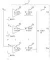
- FIG. 1shows a first charging method in the prior art. After the voltage conversion front end 1 is regulated and output, a charging management circuit 2 is connected to charge a plurality of parallel batteries 3 .
- the disadvantage of this type of charging methodis that even if a battery with a very similar voltage and internal resistance is selected for parallel connection at the factory, after several tens or even hundreds of cycles of charging and discharging, the internal resistance of a plurality of parallel batteries is no longer maintained. Consistent, and the specific value of the increase in internal resistance of the battery is also difficult to predict.
- the internal resistance of the batteryis 50 milliohms at the factory, after two years of normal circulation after hundreds of charge/discharge/heating and cold, especially after the battery ages, The internal resistance of the battery rises to nearly 200 milliohms or more, and some batteries do not rise significantly, only 60 milliohms, but the user is completely unaware.
- the current distribution of the chargingwill be greatly deviated from the factory.
- the charging currentis often divided equally among multiple batteries (such as the current popular fast charge 5A).
- the two sectionsare 2500 mAh at the factory, the batteries are simply connected in parallel, and the battery is connected in parallel.
- the charging currentis 2.5A each, and 1C charging is performed. It is no problem to select a 1C battery cell at the factory.
- the internal resistance of the batterychanges, the charging current of each battery will not be evenly divided.
- the changeis very large (3.85A and 1.15A respectively); for the 2500 mAh battery of 1C, the charging current is 3.85A, and the charging current is much larger than The normal value (1.5 times the normal value) has exceeded the battery's rated safe charging current range.
- each battery 3has its own independent charging management circuit 2, after the voltage conversion front end is regulated and output, after an independent charging management circuit
- Each batteryis independently charged.
- the voltage difference between the output voltage of the voltage conversion front end and each battery voltageis large, resulting in low charging efficiency of the battery, and is not suitable for charging with a large current, otherwise the heat will be severe.
- each battery 3is provided with a separate voltage conversion front end 1 and a charging management circuit 2 to Achieve charging of the battery.
- this charging methodcan solve the problems of the first and second modes, since each battery has an independent voltage conversion front end, multiple independent voltage conversion front end circuits and corresponding components are required, and further This leads to the problem of occupying a large space. For the already tight internal space of the mobile phone, this is undoubtedly sacrificing the battery space or the size of the mobile phone, and correspondingly increasing the cost.
- an object of the present inventionis to provide a parallel battery charging circuit and a charging method thereof for solving the problem that the existing charging circuit has serious battery heat generation, low charging efficiency, large space occupation and high cost. problem.
- the present inventionprovides a parallel battery charging circuit, the charging circuit comprising:
- a voltage conversion circuitfor adjusting a output voltage according to a maximum error result of the feedback voltage selection circuit, such that a voltage difference between the output voltage and a battery voltage corresponding to the maximum error result is a set pressure difference, and further Realize charging from the lowest voltage battery;
- a voltage detecting circuitrespectively connected to the output end of the voltage converting circuit and the anode of the N-cell battery for sampling the battery voltage of the N-cell battery, and according to the set pressure difference value, the output voltage and the N
- the battery voltagesare respectively subjected to error detection, and N error results are generated and output;
- a feedback voltage selection circuithaving an input terminal connected to the voltage detecting circuit and an output terminal connected to the voltage conversion circuit for comparing the N error results output by the voltage detecting circuit, and The maximum error result is output;
- N charging current control circuitseach of which is connected to an output end of the voltage conversion circuit and a positive electrode of a battery for sampling a battery voltage or a battery current of the rechargeable battery, and sampling the battery voltage Or the battery current is compared with the set pressure difference value or the set current value for error detection, thereby adjusting the charging current of the rechargeable battery, so that the charging current is equal to the set current value, and achieving constant current charging;
- Nis an integer greater than or equal to 2.
- the voltage conversion circuitcomprises:
- a pulse width modulation circuitcoupled to the feedback voltage selection circuit for adjusting a duty cycle of an output signal of the pulse width modulation circuit according to a maximum error result of the feedback voltage selection circuit output;
- An output voltage adjustment circuitcoupled to the pulse width modulation circuit for adjusting the output voltage according to an output signal of the pulse width modulation circuit such that the output voltage is between a battery voltage corresponding to the maximum error result
- the pressure differenceis the set pressure difference.
- the pulse width modulation circuitcomprises: a first error amplifier, a first input end of the first error amplifier is connected to a reference voltage, a second input end of the first error amplifier and the feedback voltage selection circuit The output terminal is connected, the output of the first error amplifier is connected to the first input end of the first comparator, and the second input end of the first comparator is connected to the ramp generator, the first comparator The output is coupled to the input of a pulse width modulator, the output of which is the output of the pulse width modulation circuit.
- the output voltage adjustment circuitincludes: a driving circuit, an input end of the driving circuit is connected to an output end of the pulse width modulator, and an output end of the driving circuit is respectively connected to an input end of the inverter and a gate of the MOS transistor is connected, an output end of the inverter is connected to a gate of the second MOS transistor, and a first connection end of the second MOS transistor is connected to a voltage V dd , the second MOS transistor
- the second connection endis connected to the first connection end of the first MOS tube, and is connected to the first connection end of the first inductor, and the second connection end of the first MOS tube is connected to the reference ground, the first The second connection end of the inductor is connected to the first connection end of the first capacitor, and at the same time as the output end of the output voltage regulation circuit, the second connection end of the first capacitor is connected to the reference ground.
- the pulse width modulation circuitis implemented using a microprocessor.
- the output voltage adjustment circuitincludes: a third MOS transistor, a gate of the third MOS transistor is connected to the microprocessor, and a first connection end of the third MOS transistor is connected to a voltage V dd
- the second connection end of the third MOS transistoris connected to the first connection end of the fourth MOS tube, and is connected to the first connection end of the second inductor, the gate of the fourth MOS tube and the microprocessor Connecting, the second connection end of the fourth MOS transistor is connected to a reference ground, and the second connection end of the second inductor is connected to the first connection end of the second capacitor, and serves as the output voltage regulation circuit At the output end, the second connection end of the second capacitor is connected to the reference ground.
- the voltage detecting circuitcomprises N voltage detecting units having the same circuit structure, each voltage detecting unit is connected to an output end of the voltage converting circuit and a battery; wherein the voltage detecting unit comprises: first a voltage source, a cathode of the first voltage source is connected to an output end of the voltage conversion circuit, a cathode of the first voltage source is connected to a first input end of the second error amplifier, and a second error amplifier is connected The two input terminals are connected to a positive electrode of the battery, and the output end of the second error amplifier is used as an output end of the voltage detecting unit, wherein the voltage of the first voltage source is a set pressure difference value.
- the voltage detecting circuitcomprises: N third error amplifiers, wherein the first input ends of the N third error amplifiers are connected to the output end of the voltage converting circuit, and the N third error amplifiers
- the second input endsare respectively connected to the positive poles of the N parallel batteries
- the output ends of the N third error amplifiersare respectively connected to the input ends of the first analog-to-digital conversion circuit, and the N first analog-to-digital conversion circuits
- the output endsare all connected to the first microprocessor, wherein the first microprocessor is configured to compare the N output signals output by the first analog-to-digital conversion circuit with the set pressure difference values, and generate N Error result.
- the voltage detecting circuitcomprises: N fourth error amplifiers, wherein the first input terminals of the N fourth error amplifiers are connected to the output end of the voltage conversion circuit, and the N fourth error amplifiers
- the second input endsare respectively connected to the positive poles of the N parallel batteries, and the output ends of the N fourth error amplifiers are respectively connected to the strobe terminals of a strobe switch, and the connection end and the second mode of the strobe switch
- An input end of the number conversion circuitis connected, an output end of the second analog to digital conversion circuit is connected to a second microprocessor, and the second microprocessor is further connected to a control end of the gating switch, wherein The second microprocessor is configured to compare the N output signals output by the second analog to digital conversion circuit with the set pressure difference values, and generate N error results.
- the feedback voltage selection circuitcomprises: a second comparator and N switches, wherein the second comparator comprises N inputs and N outputs, N inputs of the second comparator Connected to the N output terminals of the voltage detecting circuit in one-to-one correspondence, and respectively connected to the first connecting ends of the N switches, the N output terminals of the second comparator and the N switches respectively The control terminals are connected, and the second terminals of the N switches are connected to each other as an output terminal of the feedback voltage selection circuit.
- the feedback voltage selection circuitis implemented by a microprocessor.
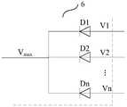
- the feedback voltage selection circuitincludes: N diodes, wherein anodes of the N diodes are respectively connected in one-to-one correspondence with N output terminals of the voltage detecting circuit, and anodes of the N diodes are connected to each other as the The output of the feedback voltage selection circuit.
- the charging current control circuitincludes: a fifth MOS transistor, a sixth MOS transistor, a fifth error amplifier, and a first resistor, wherein the first connection end of the fifth MOS transistor and the sixth MOS transistor The first connection end is connected to the output end of the voltage conversion circuit, the second connection end of the fifth MOS tube is connected to a battery positive pole, and the second connection end of the sixth MOS tube is respectively The first input end of the fifth error amplifier is connected to the first connection end of the first resistor, the second connection end of the first resistor is connected to the reference ground, and the second input terminal of the fifth error amplifier is set. And a current value, a gate of the fifth MOS transistor is connected to a gate of the sixth MOS transistor, and is connected to an output end of the fifth error amplifier.
- the charging current control circuitincludes: a seventh MOS transistor, a first connection end of the seventh MOS tube is connected to an output end of the voltage conversion circuit, and a second connection end of the seventh MOS tube is respectively Connected to the first connection end of the positive electrode and the second resistor of the second voltage source, the negative electrode of the second voltage source is connected to the first input end of the sixth error amplifier, and the second connection end of the second resistor Connected to a second positive terminal of the battery positive electrode and the sixth error amplifier, respectively, the output end of the sixth error amplifier is connected to the gate of the seventh MOS transistor, wherein the voltage of the second voltage source is set Constant pressure difference.
- the inventionalso provides a charging method of the parallel battery, the charging method comprising:
- the charging methodfurther includes: a constant voltage charging mode, in which the battery voltage is continuously increased to a battery full charging voltage, the charging current is gradually decreased; when the charging current is reduced to When the set charge cutoff current is set, the battery is fully charged.
- a constant voltage charging modein which the battery voltage is continuously increased to a battery full charging voltage, the charging current is gradually decreased; when the charging current is reduced to When the set charge cutoff current is set, the battery is fully charged.
- a parallel battery charging circuit and a charging method thereof according to the present inventionhave the following beneficial effects:
- the design of the charging circuit of the present inventionis such that the voltage difference between the output voltage and the battery voltage corresponding to the maximum error result is a set pressure difference value, so that charging starts from the battery with the lowest voltage, and at the same time, Since the set pressure difference is small, the pressure difference between the charging voltage and the battery voltage is made as small as possible, thereby ensuring fast and efficient charging of the battery and less heat generation.
- the inventionprovides a charging current control circuit for each battery to accurately control the charging current of each battery, so as to prevent the charging current of a certain battery from being too large due to the internal resistance change after the battery ages, thereby causing the battery to heat up. Serious, even the problem of security risks.
- the circuit of the present inventionincludes only a single voltage conversion circuit, the circuit integration is higher, and the peripheral components of the chip are less, which greatly saves space and cost.
- Figure 1shows a block diagram of the circuit of the first charging method.
- Figure 2shows a circuit block diagram of the prior second charging method.
- Figure 3shows a block diagram of the current third charging method.
- FIG. 4is a circuit block diagram of the charging circuit of the present invention.
- FIG. 5shows a circuit implementation of the voltage conversion circuit of the present invention.
- FIG. 6shows another circuit implementation of the voltage conversion circuit of the present invention.
- Figure 7shows a circuit implementation of the voltage detection circuit of the present invention.
- FIG. 8shows another circuit implementation of the voltage detecting circuit of the present invention.
- Figure 9shows another circuit implementation of the voltage detection circuit of the present invention.
- FIG. 10shows a circuit implementation of the feedback voltage selection circuit of the present invention.
- FIG. 11shows another circuit implementation of the feedback voltage selection circuit of the present invention.
- Figure 12shows a circuit implementation of the charge current control circuit of the present invention.
- Figure 13shows another circuit implementation of the charge current control circuit of the present invention.
- the embodimentprovides a parallel battery charging circuit, and the charging circuit includes:
- a voltage conversion circuit 4configured to adjust an output voltage according to a maximum error result of the feedback voltage selection circuit, such that a voltage difference between the output voltage and a battery voltage corresponding to the maximum error result is a set pressure difference value, In turn, charging is started from the battery with the lowest voltage;
- a voltage detecting circuit 5is respectively connected to the output end of the voltage converting circuit 4 and the anode of the N-cell battery for sampling the battery voltage of the N-cell battery, and is configured to the output voltage according to the set voltage difference value. Error detection with N battery voltages respectively, generating N error results and outputting;
- a feedback voltage selection circuit 6having an input terminal connected to the voltage detecting circuit 5 and an output terminal connected to the voltage conversion circuit 4 for comparing the N error results output by the voltage detecting circuit And output the maximum error result;
- Nis an integer greater than or equal to 2.
- the voltage conversion circuit 4includes:
- a pulse width modulation circuit 41connected to the feedback voltage selection circuit 6 for adjusting a duty ratio of an output signal of the pulse width modulation circuit according to a maximum error result output by the feedback voltage selection circuit;
- An output voltage adjustment circuit 42coupled to the pulse width modulation circuit 41 for adjusting the output voltage according to an output signal of the pulse width modulation circuit such that the output voltage corresponds to a battery voltage corresponding to the maximum error result
- the pressure difference between themis the set pressure difference.
- the pulse width modulation circuit 41includes a first error amplifier 411, a first input end of the first error amplifier 411 is connected to a reference voltage, and a first error amplifier 411
- the second inputis connected to the output of the feedback voltage selection circuit 6
- the output of the first error amplifier 411is connected to the first input of the first comparator 412
- the second input of the first comparator 412is The end is connected to the ramp generator 413
- the output of the first comparator 412is connected to the input of the pulse width modulator 414
- the output of the pulse width modulator 414is used as the output of the pulse width modulation circuit 41. end.
- the output voltage adjusting circuit 42includes a driving circuit 421, an input end of the driving circuit 421 is connected to an output end of the pulse width modulator 414, and an output of the driving circuit 421
- the terminalsare respectively connected to the input end of the inverter 422 and the gate of the first MOS transistor M1, the output end of the inverter 422 is connected to the gate of the second MOS transistor M2, and the second MOS transistor M2 is a connection terminal is connected to the voltage V dd , and a second connection end of the second MOS transistor M2 is connected to the first connection end of the first MOS transistor M1 and is connected to the first connection end of the first inductor L1.
- the second connection end of the first MOS transistor M1is connected to the reference ground, and the second connection end of the first inductor L1 is connected to the first connection end of the first capacitor C1 as the output of the output voltage adjustment circuit 42
- the second connection end of the first capacitor C1is connected to a reference ground.
- the pulse width modulation circuitperforms error amplification by the first error amplifier to output a dynamic error related to the maximum error result V max , and then outputs the dynamic error and the oblique wave generator.
- the waveis compared and PWM modulated to output a square wave signal, wherein a duty ratio of the square wave signal is related to a maximum error result V max ; and the square wave signal controls an on time of the second MOS pipe, and further
- the charging time of the first inductoris controlled to adjust the output voltage, so that the difference between the output voltage and the battery voltage is constant as the set pressure difference value Vs.
- the reference voltage V refis a constant voltage value for error amplification with the maximum error result V max output by the feedback voltage selection circuit, thereby obtaining a dynamic error of the system.
- the pulse width modulation circuit 41is implemented using a microprocessor.
- the output voltage adjusting circuit 42includes: a third MOS transistor M3, a gate of the third MOS transistor M3 is connected to the microprocessor, and the third MOS transistor The first connection end of the M3 is connected to the voltage V dd , and the second connection end of the third MOS tube M3 is connected to the first connection end of the fourth MOS tube M4 and is connected to the first connection end of the second inductor L2.
- a gate of the fourth MOS transistor M4is connected to the microprocessor, a second connection end of the fourth MOS transistor M4 is connected to a reference ground, and a second connection end of the second inductor L2 is opposite to the first
- the first connection end of the second capacitor C2is connected as the output end of the output voltage adjustment circuit 42, and the second connection end of the second capacitor C2 is connected to the reference ground.
- the pulse width modulation circuitadjusts the duty ratio of the output signal by performing a correlation operation by the microprocessor, and controls the conduction time of the third MOS transistor to control the charging time of the second inductor L2. adjusting the output voltage V out of the difference between the output voltage and the battery voltage is set to a constant pressure value Vs.
- the voltage detecting circuit 5includes N voltage detecting units 51 having the same circuit structure, and each voltage detecting unit is connected to an output end of the voltage converting circuit 4 and a battery;
- the voltage detecting unit 51includes a first voltage source 511, and a positive pole of the first voltage source 511 is connected to an output end of the voltage converting circuit 4, and a negative pole of the first voltage source 511 and a second error amplifier 512.
- the first input terminalis connected, the second input terminal of the second error amplifier 512 is connected to a battery positive terminal, and the output terminal of the second error amplifier 512 is used as an output terminal of the voltage detecting unit 51, wherein the The voltage of the first voltage source 511 is a set pressure difference.
- the voltage detecting unitby the difference between the battery voltage of the output voltage V out with the set pressure value Vs subtraction for error amplification, and thus give the corresponding error in the result.
- the voltage detecting circuit 5includes: N third error amplifiers 52, and the first input terminals of the N third error amplifiers 52 are connected to the voltage converting circuit 4 The output ends are connected, the second input ends of the N third error amplifiers 52 are respectively connected to the positive poles of the N parallel batteries, and the output ends of the N third error amplifiers 52 are respectively connected to the first analog-to-digital conversion circuit 53 The input terminals are connected, and the outputs of the N first analog-to-digital conversion circuits 53 are connected to the first microprocessor 54, wherein the first microprocessor 54 is configured to convert the first analog-to-digital conversion circuit 53.
- the output N output signalsare respectively compared with the set pressure difference values, and N error results are generated.
- the voltage detection circuitperforms error amplification by a third error amplifier output voltage V out of the voltage of the battery 8, and by the first analog to digital conversion circuit converts the output signal of said third error amplifier
- the digital signalis input to the first microprocessor, and the first microprocessor compares the N digital signals with the set pressure difference value to generate N error results.
- the value range of the set pressure difference valueis 1 mV to 900 mV; further preferably, in the embodiment, the set pressure difference value is 50 mV.
- the voltage detecting circuit 5includes: N fourth error amplifiers 55, and the first input terminals of the N fourth error amplifiers 55 are both connected to the voltage converting circuit 4 The output ends are connected, the second input ends of the N fourth error amplifiers 55 are respectively connected to the positive poles of the N parallel batteries, and the output ends of the N fourth error amplifiers 55 are respectively strobed with a strobe switch K1.
- connection end of the strobe switch K1is connected to the input end of the second analog-to-digital conversion circuit 56, and the output end of the second analog-to-digital conversion circuit 56 is connected to the second microprocessor 57, the second The microprocessor 57 is also connected to the control terminal of the strobe switch K1, wherein the second microprocessor 57 is configured to respectively set the N output signals output by the second analog-to-digital conversion circuit 56 to the set pressure difference Compare and generate N error results.
- the voltage error amplification circuit for detecting the output voltage V out to the battery voltage via a fourth error amplifier, and the output signal of the N fourth error amplifierare time-division by the switching gate Outputting and converting to a digital signal by a second analog-to-digital conversion circuit and inputting to a second microprocessor, the second microprocessor comparing the N digital signals with a set pressure difference value, thereby generating N Error result.
- the feedback voltage selection circuit 6includes a second comparator 61 and N switches S1 to Sn, wherein the second comparator 61 includes N inputs and N outputs.
- the N input ends of the second comparator 61are respectively connected to the N output ends of the voltage detecting circuit 5 in one-to-one correspondence, and are respectively connected to the first connecting ends of the N switches S1 SSn one by one.
- the N output ends of the second comparator 61are respectively connected to the control ends of the N switches S1 to Sn, and the second terminals of the N switches S1 to Sn are connected to each other as the output end of the feedback voltage selection circuit 6. .
- the maximum error resultAs shown in FIG. 10, after the second comparator compares the N error results, the maximum error result generates a control signal, and controls the switch corresponding to the output end thereof to be closed, thereby realizing the output of the maximum error result Vmax .
- the feedback voltage selection circuit 6is implemented using a microprocessor.
- V maxthe output of the maximum error result V max is achieved by inputting the N error results to the microprocessor and comparing the N error results by the microprocessor.
- the voltage conversion circuit, the voltage detection circuit, and the feedback voltage selection circuitare implemented by a microprocessor
- the voltage conversion circuit, the voltage detection circuit, and the feedback voltage selection circuitmay share a microprocessor.
- the feedback voltage selection circuit 6includes: N diodes D1 to Dn, wherein the anodes of the N diodes D1 to Dn and the N outputs of the voltage detecting circuit 5, respectively.
- the cathodes of the N diodes D1 to Dnare connected to each other as an output terminal of the feedback voltage selection circuit 6.
- the diode of the branch in which the maximum error result is locatedis turned on, thereby achieving the output of the maximum error result.
- the charging current control circuit 7includes a fifth MOS transistor M5, a sixth MOS transistor M6, a fifth error amplifier 71, and a first resistor R1, wherein the fifth MOS transistor M5
- the first connection endis connected to the first connection end of the sixth MOS tube M6, and is connected to the output end of the voltage conversion circuit 4, and the second connection end of the fifth MOS tube M5 is connected to a battery positive terminal.
- the second connection end of the sixth MOS transistor M6is respectively connected to the first input end of the fifth error amplifier 71 and the first connection end of the first resistor R1, and the second connection end of the first resistor R1 Connected to the reference ground, the second input terminal of the fifth error amplifier 71 is connected to the set current value, the gate of the fifth MOS transistor M5 is connected to the gate of the sixth MOS transistor M6, and The output of the fifth error amplifier 71 is connected.
- the charging current control circuitsamples the charging current of the rechargeable battery through the fifth MOS transistor M5 and the sixth MOS transistor M6, and inputs the charging current to the fifth error amplifier, the fifth error amplifier.
- the batteryis subjected to constant current charging with a set current value Is by performing error amplification of the charging current and the set current value Is.
- the charging current control circuit 7includes a seventh MOS transistor M7, and a first connection end of the seventh MOS transistor M7 is connected to an output end of the voltage conversion circuit 4,
- the second connection end of the seventh MOS transistor M7is respectively connected to the positive terminal of the second voltage source 72 and the first connection end of the second resistor R2, and the negative electrode of the second voltage source 72 and the sixth error amplifier 73
- the second input end of the second resistor R2is respectively connected to a battery positive pole and a second input end of the sixth error amplifier 73.
- the output end of the sixth error amplifier 73 and the first The gate of the seventh MOS transistor M7is connected, wherein the voltage of the second voltage source 72 is a set pressure difference.
- the set pressure difference value Vsis equal to the product of the set current value Is and the second resistance R2.
- the sixth error amplifierperforms error amplification on the battery voltage and the set voltage difference value Vs, and controls the on-resistance of the seventh MOS transistor M7 according to the error amplification result thereof, thereby realizing The battery is subjected to constant current charging with a set current value Is.
- the embodimentprovides a charging method of the parallel battery charging circuit, and the charging method includes:
- the constant current charging modei.e., when the battery voltage is less than the full battery charge voltage
- the voltage detecting circuitin accordance with the value Vs of the set pressure, respectively, the output of the battery voltage V out with N parallel battery will be Error detection, and generating N error results V1 - Vn
- the feedback voltage selection circuitobtains a maximum error result V max by comparing N error results V1 - Vn
- the voltage conversion circuitis based on the maximum error result V max , adjusting the difference between output voltage V out, so that the maximum output voltage V out and the resulting error voltage corresponding to the battery (i.e., the minimum cell voltage) between the set pressure value constant at Vs, the charge from the beginning to achieve the lowest voltage of the battery.
- the charging current control circuitrealizes constant current charging by adjusting the charging current so that the charging current is equal to the set current value I s .
- the voltage of the batteryrises, and the voltage outputted by the voltage conversion circuit is adjusted by the voltage regulation loop formed by the voltage detection circuit, the feedback voltage selection circuit, and the voltage conversion circuit.
- the output voltage V out outputted by the voltage conversion circuitrises to a battery higher than the second low voltage
- charging of the second low voltage batterybegins, at this time, the lowest voltage battery and the second low
- the output voltage Vout outputted by the voltage conversion circuitfollows the rise, and when the output voltage rises to a battery higher than the third low voltage At the same time, charging of the third low voltage battery is started.
- the lowest voltage battery, the second low voltage battery, and the third low voltage batteryare simultaneously charged; and so on, as the charging progresses, the output voltage of the voltage conversion circuit follows Rising, when the output voltage is higher than all battery voltages, N parallel batteries will be simultaneously charged quickly.
- the pressure difference between the output voltage of the unique voltage conversion circuit and the battery voltage of the battery to be chargeddoes not exceed the set pressure difference, that is, less than or equal to The pressure difference is set, thereby reducing the charging loss, reducing the heat generation of the battery during the charging process, thereby improving the charging efficiency.
- the charging methodfurther includes: a constant voltage charging mode, in which the battery voltage is continuously increased to a battery full charging voltage, the charging current is gradually decreased; when the charging current is reduced to When the set charge cutoff current is set, the battery is fully charged.
- the battery currentis charged, the battery voltage is increased, and the battery charging is charged by the constant current into the constant voltage charging mode (ie, when the battery voltage is close to the battery full charging voltage), the error output by the voltage detecting circuit The result is no longer used as the feedback amount in the feedback loop.
- the loop feedback amounthas become the battery voltage, and as the battery voltage continuously approaches the battery full charge voltage, the difference between the output voltage and the battery voltage is continuously reduced. Small, the charging current of each battery is also gradually reduced, and when the charging current of each battery is reduced to the set charging off current, the charging of each battery ends.
- Voltage difference ( ⁇ V) output to the feedback voltage selection circuitoutput voltage (V out ) - battery voltage (V BAT )
- Equation (1)can evolve into:
- V outV BAT + ⁇ V (2)
- the difference feedback loopis similar to the battery voltage V BAT feedback loop, that is, the voltage difference between the output voltage V out of the voltage conversion circuit and the battery voltage V BAT is fed back to The loop stability of the entire charging system is not affected in the loop. It can be seen that the differential feedback loop of the present invention is stable, feasible, and easy to implement.
- the parallel battery charging circuit and the charging method thereofhave the following beneficial effects:
- the design of the charging circuit of the present inventionis such that the voltage difference between the output voltage and the battery voltage corresponding to the maximum error result is a set pressure difference value, so that charging starts from the battery with the lowest voltage, and at the same time, Since the set pressure difference is small, the pressure difference between the charging voltage and the battery voltage is made as small as possible, thereby ensuring fast and efficient charging of the battery and less heat generation.
- the inventionprovides a charging current control circuit for each battery to accurately control the charging current of each battery, so as to prevent the charging current of a certain battery from being too large due to the internal resistance change after the battery ages, thereby causing the battery to heat up. Serious, even the problem of security risks.
- the circuit of the present inventionincludes only a single voltage conversion circuit, the circuit integration is higher, and the peripheral components of the chip are less, which greatly saves space and cost.
- the present inventioneffectively overcomes various shortcomings in the prior art and has high industrial utilization value.
Landscapes
- Engineering & Computer Science (AREA)
- Power Engineering (AREA)
- Manufacturing & Machinery (AREA)
- Chemical & Material Sciences (AREA)
- Chemical Kinetics & Catalysis (AREA)
- Electrochemistry (AREA)
- General Chemical & Material Sciences (AREA)
- Microelectronics & Electronic Packaging (AREA)
- Secondary Cells (AREA)
- Charge And Discharge Circuits For Batteries Or The Like (AREA)
Abstract
Description
Translated fromChinese本发明涉及电池充电技术,特别是涉及一种并行电池充电电路及其充电方法。The present invention relates to battery charging technology, and more particularly to a parallel battery charging circuit and a charging method thereof.
随着手机等便携式充电设备的功能越来越强大,便携式设备的功耗也越来越大,而客户体验式消费也就决定了便携式设备的电池容量越来越大;但由于电池材料性能提升很难立竿见影地满足大容量电池的要求,因此,如何实现大电池容量和高充电速度是现在便携式设备在消费市场中占有有利地位的关键。As the functions of portable charging devices such as mobile phones become more and more powerful, the power consumption of portable devices is also increasing, and customer experience consumption determines the battery capacity of portable devices is increasing; It is difficult to meet the requirements of large-capacity batteries immediately. Therefore, how to achieve large battery capacity and high charging speed is the key to the current favorable position of portable devices in the consumer market.
图1为现有的第一种充电方式,电压转换前端1稳压输出后,连接一充电管理电路2,实现对多个并行电池3进行充电。此种充电方式存在的弊端在于:即使在出厂时选择非常近似的电压和内阻的电池进行并联,但经过数十乃至数百次循环充放电后,并联的多个电池的内阻不再保持一致,而且由于电池内阻增加的具体数值也难以预测,如出厂时电池内阻50毫欧,在两年后经数百次充放电/发热遇冷等正常循环后,尤其电池老化后,有的电池内阻上升到近200毫欧或更大,有些电池则上升不明显,仅到60毫欧,但使用者完全无法察觉。FIG. 1 shows a first charging method in the prior art. After the voltage conversion front end 1 is regulated and output, a
此时若对多个并行的电池进行充电,充电的电流分配将与出厂时产生很大偏差。出厂时,由于多个并行电池的内阻相近,充电电流往往在多个电池间作均分(如现时流行的快充5A,出厂时两节各2500毫安时电池简单并联充电,电池并联后容量达到5000毫安时,充电电流各2.5A,进行1C充电,其在出厂时选择1C的电芯做电池是没有问题)。但当电池的内阻发生变化后,每个电池的充电电流将不再作均分,对于内阻小的电池,在直接并行充电中分配较大电流;若内阻变得差异较大,则会导致绝大部分充电电流都流向内阻小的电池,导致该电池发热异常,使得充电存在安全隐患(如电池的内阻原来出厂时都为50毫欧,经反复使用老化后,电池的内阻分别变为60毫欧和200毫欧,电池的充电电流在两个电池间将变为5A*200/(200+60)=3.85A和5A*60/(200+60)=1.15A,电池的充电电流与出厂时(都为2.5A对比)对比,变化非常大(分别变为3.85A和1.15A);对于1C的2500毫安时电芯来说,充电3.85A,充电电流远大于正常值(是正常值的1.5倍),已超出电池的额定安全充电电流范围。At this time, if a plurality of parallel batteries are charged, the current distribution of the charging will be greatly deviated from the factory. When shipped from the factory, because the internal resistance of multiple parallel batteries is similar, the charging current is often divided equally among multiple batteries (such as the current popular fast charge 5A). When the two sections are 2500 mAh at the factory, the batteries are simply connected in parallel, and the battery is connected in parallel. When it reaches 5000 mAh, the charging current is 2.5A each, and 1C charging is performed. It is no problem to select a 1C battery cell at the factory. However, when the internal resistance of the battery changes, the charging current of each battery will not be evenly divided. For a battery with a small internal resistance, a large current is distributed in the direct parallel charging; if the internal resistance becomes a large difference, then It will cause most of the charging current to flow to the battery with low internal resistance, resulting in abnormal heating of the battery, which makes the charging have safety hazards (such as the internal resistance of the battery is 50 milliohms at the factory, after repeated use of aging, the inside of the battery The resistance becomes 60 milliohms and 200 milliohms respectively, and the charging current of the battery will become 5A*200/(200+60)=3.85A and 5A*60/(200+60)=1.15A between the two batteries. The charging current of the battery is very different from that of the factory (both 2.5A). The change is very large (3.85A and 1.15A respectively); for the 2500 mAh battery of 1C, the charging current is 3.85A, and the charging current is much larger than The normal value (1.5 times the normal value) has exceeded the battery's rated safe charging current range.
图2为现有的第二种充电方式,使用同一电压转换前端1,但每个电池3都有自己独立的充电管理电路2,电压转换前端稳压输出后,经过一个独立的充电管理电路给每个电池进行独立充电。但由于充电管理电路与电压转换前端之间没有任何的反馈,电压转换前端的输 出电压与各电池电压的压差较大,导致电池充电效率很低,不适合大电流充电,否则会发热严重。2 is a conventional second charging method, using the same voltage conversion front end 1, but each
图3为现有的第三种充电方式,为解决第二种充电方式存在的发热和低效率的问题,将每个电池3都设置一独立的电压转换前端1和一充电管理电路2,以实现对该电池进行充电。虽然此种充电方式能解决第一、第二种方式存在的问题,但由于每个电池都有独立的电压转换前端,因此也就需要多个独立的电压转换前端电路及相应的元器件,进而导致占用空间大的问题,对于已经非常紧张的手机内部空间来说,这无疑是牺牲了电池空间或手机尺寸,同时也相应地增加了成本。3 is a third charging method in the prior art. To solve the problem of heat generation and low efficiency in the second charging mode, each
鉴于此,有必要设计一种新的并行电池充电电路及其充电方法用以解决上述技术问题。In view of this, it is necessary to design a new parallel battery charging circuit and a charging method thereof to solve the above technical problems.
发明内容Summary of the invention
鉴于以上所述现有技术的缺点,本发明的目的在于提供一种并行电池充电电路及其充电方法,用于解决现有充电电路存在电池发热严重、充电效率低、占用空间大及成本高的问题。In view of the above disadvantages of the prior art, an object of the present invention is to provide a parallel battery charging circuit and a charging method thereof for solving the problem that the existing charging circuit has serious battery heat generation, low charging efficiency, large space occupation and high cost. problem.
为实现上述目的及其他相关目的,本发明提供一种并行电池充电电路,所述充电电路包括:To achieve the above and other related objects, the present invention provides a parallel battery charging circuit, the charging circuit comprising:
一电压转换电路,用于根据反馈电压选择电路输出的最大误差结果,调节输出电压,使得所述输出电压与所述最大误差结果对应的电池电压之间的压差为设定压差值,进而实现从电压最低的电池开始充电;a voltage conversion circuit for adjusting a output voltage according to a maximum error result of the feedback voltage selection circuit, such that a voltage difference between the output voltage and a battery voltage corresponding to the maximum error result is a set pressure difference, and further Realize charging from the lowest voltage battery;
一电压检测电路,分别与所述电压转换电路的输出端及N节电池的正极连接,用于采样N节电池的电池电压,并根据所述设定压差值,对所述输出电压和N个电池电压分别进行误差检测,产生N个误差结果并输出;a voltage detecting circuit respectively connected to the output end of the voltage converting circuit and the anode of the N-cell battery for sampling the battery voltage of the N-cell battery, and according to the set pressure difference value, the output voltage and the N The battery voltages are respectively subjected to error detection, and N error results are generated and output;
一反馈电压选择电路,其输入端分别与所述电压检测电路连接,其输出端与所述电压转换电路连接,用于将所述电压检测电路输出的N个所述误差结果进行比较,并将最大误差结果进行输出;a feedback voltage selection circuit having an input terminal connected to the voltage detecting circuit and an output terminal connected to the voltage conversion circuit for comparing the N error results output by the voltage detecting circuit, and The maximum error result is output;
N个充电电流控制电路,每一充电电流控制电路均与所述电压转换电路的输出端及一电池的正极连接,用于对充电电池的电池电压或电池电流进行采样,并将所述电池电压或电池电流与设定压差值或设定电流值进行误差检测,进而调节所述充电电池的充电电流,使所述充电电流等于设定电流值,实现恒流充电;N charging current control circuits, each of which is connected to an output end of the voltage conversion circuit and a positive electrode of a battery for sampling a battery voltage or a battery current of the rechargeable battery, and sampling the battery voltage Or the battery current is compared with the set pressure difference value or the set current value for error detection, thereby adjusting the charging current of the rechargeable battery, so that the charging current is equal to the set current value, and achieving constant current charging;
其中,N为大于等于2的整数。Where N is an integer greater than or equal to 2.
优选地,所述电压转换电路包括:Preferably, the voltage conversion circuit comprises:
脉宽调制电路,与所述反馈电压选择电路连接,用于根据所述反馈电压选择电路输出的最大误差结果,调整所述脉宽调制电路的输出信号的占空比;以及a pulse width modulation circuit coupled to the feedback voltage selection circuit for adjusting a duty cycle of an output signal of the pulse width modulation circuit according to a maximum error result of the feedback voltage selection circuit output;
输出电压调节电路,与所述脉宽调制电路连接,用于根据所述脉宽调制电路的输出信号调节所述输出电压,使得所述输出电压与所述最大误差结果对应的电池电压之间的压差为设定压差值。An output voltage adjustment circuit coupled to the pulse width modulation circuit for adjusting the output voltage according to an output signal of the pulse width modulation circuit such that the output voltage is between a battery voltage corresponding to the maximum error result The pressure difference is the set pressure difference.
优选地,所述脉宽调制电路包括:第一误差放大器,所述第一误差放大器的第一输入端与参考电压连接,所述第一误差放大器的第二输入端与所述反馈电压选择电路的输出端连接,所述第一误差放大器的输出端与第一比较器的第一输入端连接,所述第一比较器的第二输入端与斜波发生器连接,所述第一比较器的输出端与脉宽调制器的输入端连接,所述脉宽调制器的输出端作为所述脉宽调制电路的输出端。Preferably, the pulse width modulation circuit comprises: a first error amplifier, a first input end of the first error amplifier is connected to a reference voltage, a second input end of the first error amplifier and the feedback voltage selection circuit The output terminal is connected, the output of the first error amplifier is connected to the first input end of the first comparator, and the second input end of the first comparator is connected to the ramp generator, the first comparator The output is coupled to the input of a pulse width modulator, the output of which is the output of the pulse width modulation circuit.
优选地,所述输出电压调节电路包括:驱动电路,所述驱动电路的输入端与所述脉宽调制器的输出端连接,所述驱动电路的输出端分别与反相器的输入端及第一MOS管的栅极连接,所述反相器的输出端与第二MOS管的栅极连接,所述第二MOS管的第一连接端与电压Vdd连接,所述第二MOS管的第二连接端与所述第一MOS管的第一连接端连接,同时与第一电感的第一连接端连接,所述第一MOS管的第二连接端与参考地连接,所述第一电感的第二连接端与第一电容的第一连接端连接,同时作为所述输出电压调节电路的输出端,所述第一电容的第二连接端与参考地连接。Preferably, the output voltage adjustment circuit includes: a driving circuit, an input end of the driving circuit is connected to an output end of the pulse width modulator, and an output end of the driving circuit is respectively connected to an input end of the inverter and a gate of the MOS transistor is connected, an output end of the inverter is connected to a gate of the second MOS transistor, and a first connection end of the second MOS transistor is connected to a voltage Vdd , the second MOS transistor The second connection end is connected to the first connection end of the first MOS tube, and is connected to the first connection end of the first inductor, and the second connection end of the first MOS tube is connected to the reference ground, the first The second connection end of the inductor is connected to the first connection end of the first capacitor, and at the same time as the output end of the output voltage regulation circuit, the second connection end of the first capacitor is connected to the reference ground.
优选地,所述脉宽调制电路采用微处理器实现。Preferably, the pulse width modulation circuit is implemented using a microprocessor.
优选地,所述输出电压调节电路包括:第三MOS管,所述第三MOS管的栅极与所述微处理器连接,所述第三MOS管的第一连接端与电压Vdd连接,所述第三MOS管的第二连接端与第四MOS管的第一连接端连接,同时与第二电感的第一连接端连接,所述第四MOS管的栅极与所述微处理器连接,所述第四MOS管的第二连接端与参考地连接,所述第二电感的第二连接端与所述第二电容的第一连接端连接,同时作为所述输出电压调节电路的输出端,所述第二电容的第二连接端与参考地连接。Preferably, the output voltage adjustment circuit includes: a third MOS transistor, a gate of the third MOS transistor is connected to the microprocessor, and a first connection end of the third MOS transistor is connected to a voltage Vdd The second connection end of the third MOS transistor is connected to the first connection end of the fourth MOS tube, and is connected to the first connection end of the second inductor, the gate of the fourth MOS tube and the microprocessor Connecting, the second connection end of the fourth MOS transistor is connected to a reference ground, and the second connection end of the second inductor is connected to the first connection end of the second capacitor, and serves as the output voltage regulation circuit At the output end, the second connection end of the second capacitor is connected to the reference ground.
优选地,所述电压检测电路包括N个电路结构相同的电压检测单元,每一电压检测单元均与所述电压转换电路的输出端及一电池连接;其中,所述电压检测单元包括:第一电压源,所述第一电压源的正极与所述电压转换电路的输出端连接,所述第一电压源的负极与第二误差放大器的第一输入端连接,所述第二误差放大器的第二输入端与一电池正极连接,所述第二误差放大器的输出端作为所述电压检测单元的输出端,其中,所述第一电压源的电压为设定压差值。Preferably, the voltage detecting circuit comprises N voltage detecting units having the same circuit structure, each voltage detecting unit is connected to an output end of the voltage converting circuit and a battery; wherein the voltage detecting unit comprises: first a voltage source, a cathode of the first voltage source is connected to an output end of the voltage conversion circuit, a cathode of the first voltage source is connected to a first input end of the second error amplifier, and a second error amplifier is connected The two input terminals are connected to a positive electrode of the battery, and the output end of the second error amplifier is used as an output end of the voltage detecting unit, wherein the voltage of the first voltage source is a set pressure difference value.
优选地,所述电压检测电路包括:N个第三误差放大器,N个所述第三误差放大器的第一输入端均与所述电压转换电路的输出端连接,N个所述第三误差放大器的第二输入端分别与N个并行电池的正极连接,N个所述第三误差放大器的输出端分别与第一模数转换电路的输入端连接,N个所述第一模数转换电路的输出端均与第一微处理器连接,其中,所述第一微处理器用于将所述第一模数转换电路输出的N个输出信号分别与设定压差值进行比较,并产生N个误差结果。Preferably, the voltage detecting circuit comprises: N third error amplifiers, wherein the first input ends of the N third error amplifiers are connected to the output end of the voltage converting circuit, and the N third error amplifiers The second input ends are respectively connected to the positive poles of the N parallel batteries, and the output ends of the N third error amplifiers are respectively connected to the input ends of the first analog-to-digital conversion circuit, and the N first analog-to-digital conversion circuits The output ends are all connected to the first microprocessor, wherein the first microprocessor is configured to compare the N output signals output by the first analog-to-digital conversion circuit with the set pressure difference values, and generate N Error result.
优选地,所述电压检测电路包括:N个第四误差放大器,N个所述第四误差放大器的第一输入端均与所述电压转换电路的输出端连接,N个所述第四误差放大器的第二输入端分别与N个并行电池的正极连接,N个所述第四误差放大器的输出端分别与一选通开关的选通端连接,所述选通开关的连接端与第二模数转换电路的输入端连接,所述第二模数转换电路的输出端与第二微处理器连接,所述第二微处理器还与所述选通开关的控制端连接,其中,所述第二微处理器用于将第二模数转换电路输出的N个输出信号分别与设定压差值进行比较,并产生N个误差结果。Preferably, the voltage detecting circuit comprises: N fourth error amplifiers, wherein the first input terminals of the N fourth error amplifiers are connected to the output end of the voltage conversion circuit, and the N fourth error amplifiers The second input ends are respectively connected to the positive poles of the N parallel batteries, and the output ends of the N fourth error amplifiers are respectively connected to the strobe terminals of a strobe switch, and the connection end and the second mode of the strobe switch An input end of the number conversion circuit is connected, an output end of the second analog to digital conversion circuit is connected to a second microprocessor, and the second microprocessor is further connected to a control end of the gating switch, wherein The second microprocessor is configured to compare the N output signals output by the second analog to digital conversion circuit with the set pressure difference values, and generate N error results.
优选地,所述反馈电压选择电路包括:第二比较器及N个开关,其中,所述第二比较器包括N个输入端和N个输出端,所述第二比较器的N个输入端分别与所述电压检测电路的N个输出端一一对应连接,同时分别与N个开关的第一连接端一一对应连接,所述第二比较器的N个输出端分别与N个开关的控制端连接,N个开关的第二连接端彼此相连,作为所述反馈电压选择电路的输出端。Preferably, the feedback voltage selection circuit comprises: a second comparator and N switches, wherein the second comparator comprises N inputs and N outputs, N inputs of the second comparator Connected to the N output terminals of the voltage detecting circuit in one-to-one correspondence, and respectively connected to the first connecting ends of the N switches, the N output terminals of the second comparator and the N switches respectively The control terminals are connected, and the second terminals of the N switches are connected to each other as an output terminal of the feedback voltage selection circuit.
优选地,所述反馈电压选择电路采用微处理器实现。Preferably, the feedback voltage selection circuit is implemented by a microprocessor.
优选地,所述反馈电压选择电路包括:N个二极管,其中,N个二极管的正极分别与所述电压检测电路的N个输出端一一对应连接,N个二极管的负极彼此相连,作为所述反馈电压选择电路的输出端。Preferably, the feedback voltage selection circuit includes: N diodes, wherein anodes of the N diodes are respectively connected in one-to-one correspondence with N output terminals of the voltage detecting circuit, and anodes of the N diodes are connected to each other as the The output of the feedback voltage selection circuit.
优选地,所述充电电流控制电路包括:第五MOS管、第六MOS管、第五误差放大器及第一电阻,其中,所述第五MOS管的第一连接端与所述第六MOS管的第一连接端连接,同时与所述电压转换电路的输出端连接,所述第五MOS管的第二连接端与一电池正极连接,所述第六MOS管的第二连接端分别与所述第五误差放大器的第一输入端及第一电阻的第一连接端连接,所述第一电阻的第二连接端与参考地连接,所述第五误差放大器的第二输入端接设定电流值,所述第五MOS管的栅极与所述第六MOS管的栅极连接,且与所述第五误差放大器的输出端连接。Preferably, the charging current control circuit includes: a fifth MOS transistor, a sixth MOS transistor, a fifth error amplifier, and a first resistor, wherein the first connection end of the fifth MOS transistor and the sixth MOS transistor The first connection end is connected to the output end of the voltage conversion circuit, the second connection end of the fifth MOS tube is connected to a battery positive pole, and the second connection end of the sixth MOS tube is respectively The first input end of the fifth error amplifier is connected to the first connection end of the first resistor, the second connection end of the first resistor is connected to the reference ground, and the second input terminal of the fifth error amplifier is set. And a current value, a gate of the fifth MOS transistor is connected to a gate of the sixth MOS transistor, and is connected to an output end of the fifth error amplifier.
优选地,所述充电电流控制电路包括:第七MOS管,所述第七MOS管的第一连接端与 所述电压转换电路的输出端连接,所述第七MOS管的第二连接端分别与所述第二电压源的正极及第二电阻的第一连接端连接,所述第二电压源的负极与第六误差放大器的第一输入端连接,所述第二电阻的第二连接端分别与一电池正极及第六误差放大器的第二输入端连接,所述第六误差放大器的输出端与所述第七MOS管的栅极连接,其中,所述第二电压源的电压为设定压差值。Preferably, the charging current control circuit includes: a seventh MOS transistor, a first connection end of the seventh MOS tube is connected to an output end of the voltage conversion circuit, and a second connection end of the seventh MOS tube is respectively Connected to the first connection end of the positive electrode and the second resistor of the second voltage source, the negative electrode of the second voltage source is connected to the first input end of the sixth error amplifier, and the second connection end of the second resistor Connected to a second positive terminal of the battery positive electrode and the sixth error amplifier, respectively, the output end of the sixth error amplifier is connected to the gate of the seventh MOS transistor, wherein the voltage of the second voltage source is set Constant pressure difference.
本发明还提供一种所述并行电池的充电方法,所述充电方法包括:The invention also provides a charging method of the parallel battery, the charging method comprising:
采样N节并行电池的电池电压,并根据设定压差值,分别对输出电压和电池电压进行误差检测,进而产生N个误差结果;Sampling the battery voltage of the N-section parallel battery, and performing error detection on the output voltage and the battery voltage according to the set pressure difference value, thereby generating N error results;
对N个所述误差结果进行比较,并根据最大误差结果,调节所述输出电压,使得所述输出电压与所述最大误差结果对应的电池电压之间的压差为设定压差值,以实现从电压最低的电池开始充电;Comparing the N error results, and adjusting the output voltage according to a maximum error result, such that a voltage difference between the output voltage and a battery voltage corresponding to the maximum error result is a set pressure difference, Realize charging from the lowest voltage battery;
同时,采样充电电池的电池电压或电池电流,并将所述电池电压或电池电流与设定压差值或设定电流值进行误差检测,进而调节所述充电电池的充电电流,使所述充电电流等于设定电流值,实现恒流充电,其中,N为大于等于2的整数。Simultaneously, sampling the battery voltage or the battery current of the rechargeable battery, and performing error detection on the battery voltage or the battery current and the set pressure difference value or the set current value, thereby adjusting the charging current of the rechargeable battery to enable the charging The current is equal to the set current value to achieve constant current charging, wherein N is an integer greater than or equal to 2.
优选地,所述充电方法还包括:恒压充电模式,在恒压充电模式下,所述电池电压不断增加至电池满充电压,所述充电电流逐渐减小;当所述充电电流减小至设定的充电截止电流时,电池完成充电。Preferably, the charging method further includes: a constant voltage charging mode, in which the battery voltage is continuously increased to a battery full charging voltage, the charging current is gradually decreased; when the charging current is reduced to When the set charge cutoff current is set, the battery is fully charged.
如上所述,本发明的一种并行电池充电电路及其充电方法,具有以下有益效果:As described above, a parallel battery charging circuit and a charging method thereof according to the present invention have the following beneficial effects:
1、通过本发明所述充电电路的设计,使得所述输出电压与所述最大误差结果对应的电池电压之间的压差为设定压差值,实现从电压最低的电池开始充电,同时,由于所述设定压差值较小,即使得充电电压与电池电压之间的压差值尽可能地小,从而保证电池的快速高效充电,及较少发热。1. The design of the charging circuit of the present invention is such that the voltage difference between the output voltage and the battery voltage corresponding to the maximum error result is a set pressure difference value, so that charging starts from the battery with the lowest voltage, and at the same time, Since the set pressure difference is small, the pressure difference between the charging voltage and the battery voltage is made as small as possible, thereby ensuring fast and efficient charging of the battery and less heat generation.
2、本发明通过为每节电池设置一充电电流控制电路,使每节电池的充电电流实现精准控制,避免电池老化后因内阻变化而使某节电池的充电电流过大,进而导致电池发热严重,甚至出现安全隐患的问题。2. The invention provides a charging current control circuit for each battery to accurately control the charging current of each battery, so as to prevent the charging current of a certain battery from being too large due to the internal resistance change after the battery ages, thereby causing the battery to heat up. Serious, even the problem of security risks.
3、本发明所述电路仅包括唯一一个电压转换电路,电路集成度更高,并且芯片外围器件更少,大大节约了空间和成本。3. The circuit of the present invention includes only a single voltage conversion circuit, the circuit integration is higher, and the peripheral components of the chip are less, which greatly saves space and cost.
图1显示为现有第一种充电方式的电路框图。Figure 1 shows a block diagram of the circuit of the first charging method.
图2显示为现有第二种充电方式的电路框图。Figure 2 shows a circuit block diagram of the prior second charging method.
图3显示为现有第三种充电方式的电路框图。Figure 3 shows a block diagram of the current third charging method.
图4显示为本发明所述充电电路的电路框图。4 is a circuit block diagram of the charging circuit of the present invention.
图5显示为本发明所述电压转换电路的一种电路实现方式。FIG. 5 shows a circuit implementation of the voltage conversion circuit of the present invention.
图6显示为本发明所述电压转换电路的另一种电路实现方式。FIG. 6 shows another circuit implementation of the voltage conversion circuit of the present invention.
图7显示为本发明所述电压检测电路的一种电路实现方式。Figure 7 shows a circuit implementation of the voltage detection circuit of the present invention.
图8显示为本发明所述电压检测电路的另一种电路实现方式。FIG. 8 shows another circuit implementation of the voltage detecting circuit of the present invention.
图9显示为本发明所述电压检测电路的另一种电路实现方式。Figure 9 shows another circuit implementation of the voltage detection circuit of the present invention.
图10显示为本发明所述反馈电压选择电路的一种电路实现方式。FIG. 10 shows a circuit implementation of the feedback voltage selection circuit of the present invention.
图11显示为本发明所述反馈电压选择电路的另一种电路实现方式。FIG. 11 shows another circuit implementation of the feedback voltage selection circuit of the present invention.
图12显示为本发明所述充电电流控制电路的一种电路实现方式。Figure 12 shows a circuit implementation of the charge current control circuit of the present invention.
图13显示为本发明所述充电电流控制电路的另一种电路实现方式。Figure 13 shows another circuit implementation of the charge current control circuit of the present invention.
元件标号说明Component label description
1 电压转换前端1 voltage conversion front end
2 充电管理电路2 charge management circuit
3 电池3 battery
4 电压转换电路4 voltage conversion circuit
41 脉宽调制电路41 pulse width modulation circuit
411 第一误差放大器411 first error amplifier
412 第一比较器412 first comparator
413 斜波发生器413 ramp generator
414 脉宽调制器414 pulse width modulator
42 输出电压调节电路42 output voltage regulation circuit
421 驱动电路421 drive circuit
422 反相器422 inverter
5 电压检测电路5 voltage detection circuit
51 电压检测单元51 voltage detection unit
511 第一电压源511 first voltage source
512 第二误差放大器512 second error amplifier
52 第三误差放大器52 third error amplifier
53 第一模数转换电路53 first analog to digital conversion circuit
54 第一微处理器54 first microprocessor
55 第四误差放大器55 fourth error amplifier
56 第二模数转换器56 second analog to digital converter
57 第二微处理器57 second microprocessor
6 反馈电压选择电路6 feedback voltage selection circuit
61 第二比较器61 second comparator
7 充电电流控制电路7 charging current control circuit
71 第五误差放大器71 fifth error amplifier
72 第二电压源72 second voltage source
73 第六误差放大器73 sixth error amplifier
M1 第一MOS管M1 first MOS tube
M2 第二MOS管M2 second MOS tube
M3 第三MOS管M3 third MOS tube
M4 第四MOS管M4 fourth MOS tube
M5 第五MOS管M5 fifth MOS tube
M6 第六MOS管M6 sixth MOS tube
M7 第七MOS管M7 seventh MOS tube
L1 第一电感L1 first inductor
L2 第二电感L2 second inductor
C1 第一电容C1 first capacitor
C2 第二电容C2 second capacitor
R1 第一电阻R1 first resistor
R2 第二电阻R2 second resistor
K1 选通开关K1 gate switch
S1~Sn 第一~第n开关S1~Sn first to nth switch
D1~Dn 第一~第n二极管D1~Dn first to nth diode
以下通过特定的具体实例说明本发明的实施方式,本领域技术人员可由本说明书所揭露的内容轻易地了解本发明的其他优点与功效。本发明还可以通过另外不同的具体实施方式加以实施或应用,本说明书中的各项细节也可以基于不同观点与应用,在没有背离本发明的精神下进行各种修饰或改变。The embodiments of the present invention are described below by way of specific examples, and those skilled in the art can readily understand other advantages and effects of the present invention from the disclosure of the present disclosure. The present invention may be embodied or applied in various other specific embodiments, and various modifications and changes can be made without departing from the spirit and scope of the invention.
请参阅图4至图13。需要说明的是,本实施例中所提供的图示仅以示意方式说明本发明的基本构想,遂图式中仅显示与本发明中有关的组件而非按照实际实施时的组件数目、形状及尺寸绘制,其实际实施时各组件的型态、数量及比例可为一种随意的改变,且其组件布局型态也可能更为复杂。Please refer to Figures 4 to 13. It should be noted that the illustrations provided in the present embodiment merely illustrate the basic concept of the present invention in a schematic manner, and only the components related to the present invention are shown in the drawings, instead of the number and shape of components in actual implementation. Dimensional drawing, the actual type of implementation of each component's type, number and proportion can be a random change, and its component layout can be more complicated.
实施例一Embodiment 1
如图4所示,本实施例提供一种并行电池充电电路,所述充电电路包括:As shown in FIG. 4, the embodiment provides a parallel battery charging circuit, and the charging circuit includes:
一电压转换电路4,用于根据反馈电压选择电路输出的最大误差结果,调节输出电压,使得所述输出电压与所述最大误差结果对应的电池电压之间的压差为设定压差值,进而实现从电压最低的电池开始充电;a
一电压检测电路5,分别与所述电压转换电路4的输出端及N节电池的正极连接,用于采样N节电池的电池电压,并根据所述设定压差值,对所述输出电压和N个电池电压分别进行误差检测,产生N个误差结果并输出;a
一反馈电压选择电路6,其输入端分别与所述电压检测电路5连接,其输出端与所述电压转换电路4连接,用于将所述电压检测电路输出的N个所述误差结果进行比较,并将最大误差结果进行输出;a feedback
N个充电电流控制电路7,每一充电电流控制电路7均与所述电压转换电路4的输出端及一电池的正极连接,用于对充电电池的电池电压或电池电流进行采样,并将所述电池电压或电池电流与设定压差值或设定电流值进行误差检测,进而调节所述充电电池的充电电流,使所述充电电流等于设定电流值,实现恒流充电;N charging
其中,N为大于等于2的整数。Where N is an integer greater than or equal to 2.
作为示例,如图4所示,所述电压转换电路4包括:As an example, as shown in FIG. 4, the
脉宽调制电路41,与所述反馈电压选择电路6连接,用于根据所述反馈电压选择电路输出的最大误差结果,调整所述脉宽调制电路的输出信号的占空比;以及a pulse
输出电压调节电路42,与所述脉宽调制电路41连接,用于根据所述脉宽调制电路的输出信号调节所述输出电压,使得所述输出电压与所述最大误差结果对应的电池电压之间的压 差为设定压差值。An output
作为示例,如图5所示,所述脉宽调制电路41包括:第一误差放大器411,所述第一误差放大器411的第一输入端与参考电压连接,所述第一误差放大器411的第二输入端与所述反馈电压选择电路6的输出端连接,所述第一误差放大器411的输出端与第一比较器412的第一输入端连接,所述第一比较器412的第二输入端与斜波发生器413连接,所述第一比较器412的输出端与脉宽调制器414的输入端连接,所述脉宽调制器414的输出端作为所述脉宽调制电路41的输出端。As an example, as shown in FIG. 5, the pulse
作为示例,如图5所示,所述输出电压调节电路42包括:驱动电路421,所述驱动电路421的输入端与所述脉宽调制器414的输出端连接,所述驱动电路421的输出端分别与反相器422的输入端及第一MOS管M1的栅极连接,所述反相器422的输出端与第二MOS管M2的栅极连接,所述第二MOS管M2的第一连接端与电压Vdd连接,所述第二MOS管M2的第二连接端与所述第一MOS管M1的第一连接端连接,同时与第一电感L1的第一连接端连接,所述第一MOS管M1的第二连接端与参考地连接,所述第一电感L1的第二连接端与第一电容C1的第一连接端连接,同时作为所述输出电压调节电路42的输出端,所述第一电容C1的第二连接端与参考地连接。As an example, as shown in FIG. 5, the output
如图5所示,所述脉宽调制电路通过所述第一误差放大器进行误差放大后输出一与最大误差结果Vmax相关的动态误差,然后将输出的动态误差与斜波发生器产生的斜波进行比较并经过PWM调制后输出一方波信号,其中,该方波信号的占空比与最大误差结果Vmax相关;通过所述方波信号控制所述第二MOS管道的导通时间,进而控制第一电感的充电时间,实现输出电压的调节,使输出电压与电池电压的差值恒为设定压差值Vs。As shown in FIG. 5, the pulse width modulation circuit performs error amplification by the first error amplifier to output a dynamic error related to the maximum error result Vmax , and then outputs the dynamic error and the oblique wave generator. The wave is compared and PWM modulated to output a square wave signal, wherein a duty ratio of the square wave signal is related to a maximum error result Vmax ; and the square wave signal controls an on time of the second MOS pipe, and further The charging time of the first inductor is controlled to adjust the output voltage, so that the difference between the output voltage and the battery voltage is constant as the set pressure difference value Vs.
需要说明的是,所述参考电压Vref为一恒定电压值,用于与所述反馈电压选择电路输出的最大误差结果Vmax进行误差放大,进而得到系统的动态误差。It should be noted that the reference voltage Vref is a constant voltage value for error amplification with the maximum error result Vmax output by the feedback voltage selection circuit, thereby obtaining a dynamic error of the system.
作为另一示例,如图6所示,所述脉宽调制电路41采用微处理器实现。As another example, as shown in FIG. 6, the pulse
作为另一示例,如图6所示,所述输出电压调节电路42包括:第三MOS管M3,所述第三MOS管M3的栅极与所述微处理器连接,所述第三MOS管M3的第一连接端与电压Vdd连接,所述第三MOS管M3的第二连接端与第四MOS管M4的第一连接端连接,同时与第二电感L2的第一连接端连接,所述第四MOS管M4的栅极与所述微处理器连接,所述第四MOS管M4的第二连接端与参考地连接,所述第二电感L2的第二连接端与所述第二电容C2的第一连接端连接,同时作为所述输出电压调节电路42的输出端,所述第二电容C2的第二连接端与参考地连接。As another example, as shown in FIG. 6, the output
如图6所示,所述脉宽调制电路通过微处理器进行相关运算调整其输出信号的占空比,通过控制第三MOS管的导通时间,进而控制第二电感L2的充电时间,实现输出电压Vout的调节,使输出电压与电池电压的差值恒为设定压差值Vs。As shown in FIG. 6, the pulse width modulation circuit adjusts the duty ratio of the output signal by performing a correlation operation by the microprocessor, and controls the conduction time of the third MOS transistor to control the charging time of the second inductor L2. adjusting the output voltage Vout of the difference between the output voltage and the battery voltage is set to a constant pressure value Vs.
作为示例,如图7所示,所述电压检测电路5包括N个电路结构相同的电压检测单元51,每一电压检测单元均与所述电压转换电路4的输出端及一电池连接;其中,所述电压检测单元51包括:第一电压源511,所述第一电压源511的正极与所述电压转换电路4的输出端连接,所述第一电压源511的负极与第二误差放大器512的第一输入端连接,所述第二误差放大器512的第二输入端与一电池正极连接,所述第二误差放大器512的输出端作为所述电压检测单元51的输出端,其中,所述第一电压源511的电压为设定压差值。As an example, as shown in FIG. 7, the
如图7所示,所述电压检测单元通过将所述输出电压Vout与设定压差值Vs相减后的差值与电池电压进行误差放大,进而得到与之对应的误差结果。As shown in FIG 7, the voltage detecting unit by the difference between the battery voltage of the output voltage Vout with the set pressure value Vs subtraction for error amplification, and thus give the corresponding error in the result.
作为另一示例,如图8所示,所述电压检测电路5包括:N个第三误差放大器52,N个所述第三误差放大器52的第一输入端均与所述电压转换电路4的输出端连接,N个所述第三误差放大器52的第二输入端分别与N个并行电池的正极连接,N个所述第三误差放大器52的输出端分别与第一模数转换电路53的输入端连接,N个所述第一模数转换电路53的输出端均与第一微处理器54连接,其中,所述第一微处理器54用于将所述第一模数转换电路53输出的N个输出信号分别与设定压差值进行比较,并产生N个误差结果。As another example, as shown in FIG. 8, the
如图8所示,所述电压检测电路通过第三误差放大器对所述输出电压Vout与电池电压进行误差放大,然后通过第一模数转换电路将所述第三误差放大器的输出信号转换为数字信号,并将N个数字信号输入到第一微处理器中,所述第一微处理器将N个数字信号分别与设定压差值进行比较,进而产生N个误差结果。As shown, the voltage detection circuit performs error amplification by a third error amplifier output voltage Vout of the voltage of the battery 8, and by the first analog to digital conversion circuit converts the output signal of said third error amplifier The digital signal is input to the first microprocessor, and the first microprocessor compares the N digital signals with the set pressure difference value to generate N error results.
优选地,所述设定压差值的数值范围包括1mV~900mV;进一步优选地,在本实施例中,所述设定压差值为50mV。Preferably, the value range of the set pressure difference value is 1 mV to 900 mV; further preferably, in the embodiment, the set pressure difference value is 50 mV.
作为另一示例,如图9所示,所述电压检测电路5包括:N个第四误差放大器55,N个所述第四误差放大器55的第一输入端均与所述电压转换电路4的输出端连接,N个所述第四误差放大器55的第二输入端分别与N个并行电池的正极连接,N个所述第四误差放大器55的输出端分别与一选通开关K1的选通端连接,所述选通开关K1的连接端与第二模数转换电路56的输入端连接,所述第二模数转换电路56的输出端与第二微处理器57连接,所述第二微处理器57还与所述选通开关K1的控制端连接,其中,所述第二微处理器57用于将第二模数转换电路56输出的N个输出信号分别与设定压差值进行比较,并产生N个误差结果。As another example, as shown in FIG. 9, the
如图9所示,所述电压检测电路通过第四误差放大器对所述输出电压Vout与电池电压进行误差放大,然后通过选通开关分时地将N个第四误差放大器的输出信号分别进行输出,并通过第二模数转换电路转换为数字信号,并输入到第二微处理器,所述第二微处理器将N个数字信号分别与设定压差值进行比较,进而产生N个误差结果。9, the voltage error amplification circuit for detecting the output voltage Vout to the battery voltage via a fourth error amplifier, and the output signal of the N fourth error amplifier are time-division by the switching gate Outputting and converting to a digital signal by a second analog-to-digital conversion circuit and inputting to a second microprocessor, the second microprocessor comparing the N digital signals with a set pressure difference value, thereby generating N Error result.
作为示例,如图10所示,所述反馈电压选择电路6包括:第二比较器61及N个开关S1~Sn,其中,所述第二比较器61包括N个输入端和N个输出端,所述第二比较器61的N个输入端分别与所述电压检测电路5的N个输出端一一对应连接,同时分别与N个开关S1~Sn的第一连接端一一对应连接,所述第二比较器61的N个输出端分别与N个开关S1~Sn的控制端连接,N个开关S1~Sn的第二连接端彼此相连,作为所述反馈电压选择电路6的输出端。As an example, as shown in FIG. 10, the feedback
如图10所示,所述第二比较器将N个误差结果进行比较后,最大误差结果产生一控制信号,控制其所在输出端对应的开关闭合,实现最大误差结果Vmax的输出。As shown in FIG. 10, after the second comparator compares the N error results, the maximum error result generates a control signal, and controls the switch corresponding to the output end thereof to be closed, thereby realizing the output of the maximum error resultVmax .
作为另一示例,所述反馈电压选择电路6采用微处理器实现。As another example, the feedback
需要说明的是,通过将N个所述误差结果输入到微处理器,并通过微处理器对N个所述误差结果进行比较,以实现最大误差结果Vmax的输出。It should be noted that the output of the maximum error result Vmax is achieved by inputting the N error results to the microprocessor and comparing the N error results by the microprocessor.
需要说明的是,若所述电压转换电路、电压检测电路及反馈电压选择电路均采用微处理器实现时,所述电压转换电路、电压检测电路及反馈电压选择电路可共用一微处理器。It should be noted that, when the voltage conversion circuit, the voltage detection circuit, and the feedback voltage selection circuit are implemented by a microprocessor, the voltage conversion circuit, the voltage detection circuit, and the feedback voltage selection circuit may share a microprocessor.
作为另一示例,如图11所示,所述反馈电压选择电路6包括:N个二极管D1~Dn,其中,N个二极管D1~Dn的正极分别与所述电压检测电路5的N个输出端一一对应连接,N个二极管D1~Dn的负极彼此相连,作为所述反馈电压选择电路6的输出端。As another example, as shown in FIG. 11, the feedback
如图11所示,当所述多个电压同时作用于二极管的正极时,最大误差结果所在支路的二极管导通,进而实现最大误差结果的输出。As shown in FIG. 11, when the plurality of voltages simultaneously act on the anode of the diode, the diode of the branch in which the maximum error result is located is turned on, thereby achieving the output of the maximum error result.
作为示例,如图12所示,所述充电电流控制电路7包括:第五MOS管M5、第六MOS管M6、第五误差放大器71及第一电阻R1,其中,所述第五MOS管M5的第一连接端与所述第六MOS管M6的第一连接端连接,同时与所述电压转换电路4的输出端连接,所述第五MOS管M5的第二连接端与一电池正极连接,所述第六MOS管M6的第二连接端分别与所述第五误差放大器71的第一输入端及第一电阻R1的第一连接端连接,所述第一电阻R1的第二连接端与参考地连接,所述第五误差放大器71的第二输入端接设定电流值,所述第五MOS管M5的栅极与所述第六MOS管M6的栅极连接,且与所述第五误差放大器71的输出端连接。As an example, as shown in FIG. 12, the charging
如图12所示,所述充电电流控制电路通过第五MOS管M5和第六MOS管M6采样充电电池的充电电流,并将所述充电电流输入到第五误差放大器,所述第五误差放大器通过将所述充电电流与所述设定电流值Is进行误差放大,实现所述电池以设定电流值Is进行恒流充电。As shown in FIG. 12, the charging current control circuit samples the charging current of the rechargeable battery through the fifth MOS transistor M5 and the sixth MOS transistor M6, and inputs the charging current to the fifth error amplifier, the fifth error amplifier. The battery is subjected to constant current charging with a set current value Is by performing error amplification of the charging current and the set current value Is.
作为另一示例,如图13所示,所述充电电流控制电路7包括:第七MOS管M7,所述第七MOS管M7的第一连接端与所述电压转换电路4的输出端连接,所述第七MOS管M7的第二连接端分别与所述第二电压源72的正极及第二电阻R2的第一连接端连接,所述第二电压源72的负极与第六误差放大器73的第一输入端连接,所述第二电阻R2的第二连接端分别与一电池正极及第六误差放大器73的第二输入端连接,所述第六误差放大器73的输出端与所述第七MOS管M7的栅极连接,其中,所述第二电压源72的电压为设定压差值。As another example, as shown in FIG. 13, the charging
作为示例,所述设定压差值Vs等于所述设定电流值Is与第二电阻R2的乘积。As an example, the set pressure difference value Vs is equal to the product of the set current value Is and the second resistance R2.
如图13所示,所述第六误差放大器对所述电池电压和设定压差值Vs进行误差放大,并根据其误差放大结果,控制所述第七MOS管M7的导通电阻,进而实现所述电池以设定电流值Is进行恒流充电。As shown in FIG. 13, the sixth error amplifier performs error amplification on the battery voltage and the set voltage difference value Vs, and controls the on-resistance of the seventh MOS transistor M7 according to the error amplification result thereof, thereby realizing The battery is subjected to constant current charging with a set current value Is.
实施例二
本实施例提供一种所述并行电池充电电路的充电方法,所述充电方法包括:The embodiment provides a charging method of the parallel battery charging circuit, and the charging method includes:
采样N节并行电池的电池电压,并根据设定压差值,分别对输出电压和电池电压进行误差检测,进而产生N个误差结果;Sampling the battery voltage of the N-section parallel battery, and performing error detection on the output voltage and the battery voltage according to the set pressure difference value, thereby generating N error results;
对N个所述误差结果进行比较,并根据最大误差结果,调节所述输出电压,使得所述输出电压与所述最大误差结果对应的电池电压之间的压差为设定压差值,以实现从电压最低的电池开始充电;Comparing the N error results, and adjusting the output voltage according to a maximum error result, such that a voltage difference between the output voltage and a battery voltage corresponding to the maximum error result is a set pressure difference, Realize charging from the lowest voltage battery;
同时,采样充电电池的电池电压或电池电流,并将所述电池电压或电池电流与设定压差值或设定电流值进行误差检测,进而调节所述充电电池的充电电流,使所述充电电流等于设定电流值,实现恒流充电,其中,N为大于等于2的整数。Simultaneously, sampling the battery voltage or the battery current of the rechargeable battery, and performing error detection on the battery voltage or the battery current and the set pressure difference value or the set current value, thereby adjusting the charging current of the rechargeable battery to enable the charging The current is equal to the set current value to achieve constant current charging, wherein N is an integer greater than or equal to 2.
作为示例,在恒流充电模式下(即当电池电压小于电池满充电压时),所述电压检测电路根据设定压差值Vs,分别将输出电压Vout与N个并行电池的电池电压进行误差检测,并产生N个误差结果V1~Vn;所述反馈电压选择电路通过对N个误差结果V1~Vn进行比较,得到最大误差结果Vmax;所述电压转换电路根据最大误差结果Vmax,调整输出电压Vout,使输出电压Vout与最大误差结果对应的电池电压(即最低的电池电压)之间的差值恒为设定压差值Vs,实现从电压最低的电池开始充电。同时,所述充电电流控制电路通过调节充电电流, 使充电电流等于设定电流值Is,实现恒流充电。As an example, the constant current charging mode (i.e., when the battery voltage is less than the full battery charge voltage), the voltage detecting circuit in accordance with the value Vs of the set pressure, respectively, the output of the battery voltage Vout with N parallel battery will be Error detection, and generating N error results V1 - Vn; the feedback voltage selection circuit obtains a maximum error result Vmax by comparing N error results V1 - Vn; the voltage conversion circuit is based on the maximum error result Vmax , adjusting the difference between output voltage Vout, so that the maximum output voltage Vout and the resulting error voltage corresponding to the battery (i.e., the minimum cell voltage) between the set pressure value constant at Vs, the charge from the beginning to achieve the lowest voltage of the battery. At the same time, the charging current control circuit realizes constant current charging by adjusting the charging current so that the charging current is equal to the set current value Is .
具体为当最低电压的电池充入电流后,该电池电压上升,并在由电压检测电路、反馈电压选择电路及电压转换电路形成的电压调节环路的作用下,调节电压转换电路输出的电压,使其随着升高;当电压转换电路输出的输出电压Vout上升到高于第二低电压的电池时,开始对第二低电压的电池充电,此时,最低电压的电池和第二低电压的电池同时充电;随着电池的继续充电,最低电压电池和第二低电压电池的电压上升,电压转换电路输出的输出电压Vout跟随上升,当输出电压上升到高于第三低电压的电池时,开始对第三低电压的电池充电,此时,最低电压电池、第二低电压电池和第三低电压电池同时充电;以此类推,随着充电的进行,电压转换电路的输出电压跟随上升,当所述输出电压高于所有电池电压时,将对N节并行电池同时进行快速充电。Specifically, when the battery of the lowest voltage is charged with current, the voltage of the battery rises, and the voltage outputted by the voltage conversion circuit is adjusted by the voltage regulation loop formed by the voltage detection circuit, the feedback voltage selection circuit, and the voltage conversion circuit. When it is raised; when the output voltage Vout outputted by the voltage conversion circuit rises to a battery higher than the second low voltage, charging of the second low voltage battery begins, at this time, the lowest voltage battery and the second low The voltage battery is simultaneously charged; as the battery continues to charge, the voltage of the lowest voltage battery and the second low voltage battery rises, the output voltage Vout outputted by the voltage conversion circuit follows the rise, and when the output voltage rises to a battery higher than the third low voltage At the same time, charging of the third low voltage battery is started. At this time, the lowest voltage battery, the second low voltage battery, and the third low voltage battery are simultaneously charged; and so on, as the charging progresses, the output voltage of the voltage conversion circuit follows Rising, when the output voltage is higher than all battery voltages, N parallel batteries will be simultaneously charged quickly.
需要说明的是,通过优先对电压最低的电池开始充电,保证了该唯一电压转换电路输出电压与被充电电池的电池电压之间的压差值最大不超过设定压差值,即小于或等于设定压差值,从而减小了充电的损耗,降低了充电过程中电池的发热,进而提高了充电效率。It should be noted that, by preferentially charging the battery with the lowest voltage, it is ensured that the pressure difference between the output voltage of the unique voltage conversion circuit and the battery voltage of the battery to be charged does not exceed the set pressure difference, that is, less than or equal to The pressure difference is set, thereby reducing the charging loss, reducing the heat generation of the battery during the charging process, thereby improving the charging efficiency.
作为示例,所述充电方法还包括:恒压充电模式,在恒压充电模式下,所述电池电压不断增加至电池满充电压,所述充电电流逐渐减小;当所述充电电流减小至设定的充电截止电流时,电池完成充电。As an example, the charging method further includes: a constant voltage charging mode, in which the battery voltage is continuously increased to a battery full charging voltage, the charging current is gradually decreased; when the charging current is reduced to When the set charge cutoff current is set, the battery is fully charged.
需要说明的是,随着电池电流的充入,电池电压升高,电池充电由恒流充电进入恒压充电模式(即电池电压接近电池满充电压时),所述电压检测电路所输出的误差结果不再作为反馈环路中的反馈量,此时环路反馈量已变为电池电压,而随着电池电压不断接近电池满充电压,所述输出电压与电池电压之间的差值不断减小,导致各电池的充电电流也逐渐减小,当各电池的充电电流减小至设定的充电截止电流时,各电池充电结束。It should be noted that as the battery current is charged, the battery voltage is increased, and the battery charging is charged by the constant current into the constant voltage charging mode (ie, when the battery voltage is close to the battery full charging voltage), the error output by the voltage detecting circuit The result is no longer used as the feedback amount in the feedback loop. At this time, the loop feedback amount has become the battery voltage, and as the battery voltage continuously approaches the battery full charge voltage, the difference between the output voltage and the battery voltage is continuously reduced. Small, the charging current of each battery is also gradually reduced, and when the charging current of each battery is reduced to the set charging off current, the charging of each battery ends.
下面对电压转换电路、充电电流控制电路及反馈电压选择电路组成的差值反馈回路进行稳定性和可行性分析,具体分析如下:The stability and feasibility analysis of the difference feedback loop composed of the voltage conversion circuit, the charging current control circuit and the feedback voltage selection circuit are as follows:
输出到所述反馈电压选择电路的电压差值(ΔV)=输出电压(Vout)–电池电压(VBAT)Voltage difference (ΔV) output to the feedback voltage selection circuit = output voltage (Vout ) - battery voltage (VBAT )
即ΔV=Vout–VBAT (1)That is, ΔV=Vout–VBAT (1)
形成反馈的目的是得到和维持电压差值为一更小的直流恒定值ΔV,从而提升电池的充电效率和减小发热。即ΔV为直流恒定值,如50毫伏。此条件下,等式(1)可演变为:The purpose of forming the feedback is to obtain and maintain a voltage difference of a smaller DC constant value ΔV, thereby improving the charging efficiency of the battery and reducing heat generation. That is, ΔV is a constant value of DC, such as 50 millivolts. Under this condition, equation (1) can evolve into:
Vout=VBAT+ΔV (2)Vout =VBAT +ΔV (2)
其中,ΔV为一直流恒定值,对等式两边进行动态小信号分析,等式(2)两边同时进行 微分运算,其中直流恒定值ΔV的微分值为零。等式(2)的微分运算结果为:Where ΔV is a constant current constant value, dynamic small signal analysis is performed on both sides of the equation, and differential operation is performed on both sides of equation (2), wherein the differential value of the DC constant value ΔV is zero. The differential operation result of equation (2) is:
Δνout=ΔνBAT (3)Δνout =ΔνBAT (3)
从上述等式(3)可以清楚地知道,差值反馈回路与电池电压VBAT反馈回路相类似,即所述电压转换电路的输出电压Vout与电池电压VBAT之间的电压差值反馈至回路中并不影响整个充电系统的环路稳定性,可见,本发明所述差值反馈回路是稳定、可行的,且是易于实现的。It is clear from the above equation (3) that the difference feedback loop is similar to the battery voltage VBAT feedback loop, that is, the voltage difference between the output voltage Vout of the voltage conversion circuit and the battery voltage VBAT is fed back to The loop stability of the entire charging system is not affected in the loop. It can be seen that the differential feedback loop of the present invention is stable, feasible, and easy to implement.
综上所述,本发明的一种并行电池充电电路及其充电方法,具有以下有益效果:In summary, the parallel battery charging circuit and the charging method thereof have the following beneficial effects:
1、通过本发明所述充电电路的设计,使得所述输出电压与所述最大误差结果对应的电池电压之间的压差为设定压差值,实现从电压最低的电池开始充电,同时,由于所述设定压差值较小,即使得充电电压与电池电压之间的压差值尽可能地小,从而保证电池的快速高效充电,及较少发热。1. The design of the charging circuit of the present invention is such that the voltage difference between the output voltage and the battery voltage corresponding to the maximum error result is a set pressure difference value, so that charging starts from the battery with the lowest voltage, and at the same time, Since the set pressure difference is small, the pressure difference between the charging voltage and the battery voltage is made as small as possible, thereby ensuring fast and efficient charging of the battery and less heat generation.
2、本发明通过为每节电池设置一充电电流控制电路,使每节电池的充电电流实现精准控制,避免电池老化后因内阻变化而使某节电池的充电电流过大,进而导致电池发热严重,甚至出现安全隐患的问题。2. The invention provides a charging current control circuit for each battery to accurately control the charging current of each battery, so as to prevent the charging current of a certain battery from being too large due to the internal resistance change after the battery ages, thereby causing the battery to heat up. Serious, even the problem of security risks.
3、本发明所述电路仅包括唯一一个电压转换电路,电路集成度更高,并且芯片外围器件更少,大大节约了空间和成本。3. The circuit of the present invention includes only a single voltage conversion circuit, the circuit integration is higher, and the peripheral components of the chip are less, which greatly saves space and cost.
所以,本发明有效克服了现有技术中的种种缺点而具高度产业利用价值。Therefore, the present invention effectively overcomes various shortcomings in the prior art and has high industrial utilization value.
上述实施例仅例示性说明本发明的原理及其功效,而非用于限制本发明。任何熟悉此技术的人士皆可在不违背本发明的精神及范畴下,对上述实施例进行修饰或改变。因此,举凡所属技术领域中具有通常知识者在未脱离本发明所揭示的精神与技术思想下所完成的一切等效修饰或改变,仍应由本发明的权利要求所涵盖。The above-described embodiments are merely illustrative of the principles of the invention and its effects, and are not intended to limit the invention. Modifications or variations of the above-described embodiments may be made by those skilled in the art without departing from the spirit and scope of the invention. Therefore, all equivalent modifications or changes made by those skilled in the art without departing from the spirit and scope of the invention are still to be covered by the appended claims.
Claims (16)
Translated fromChinesePriority Applications (1)
| Application Number | Priority Date | Filing Date | Title |
|---|---|---|---|
| US16/789,447US11177684B2 (en) | 2017-08-31 | 2020-02-13 | Parallel battery charging circuit and charging method thereof |
Applications Claiming Priority (4)
| Application Number | Priority Date | Filing Date | Title |
|---|---|---|---|
| CN201710770527.6 | 2017-08-31 | ||
| CN201721106948.0UCN207442474U (en) | 2017-08-31 | 2017-08-31 | A kind of parallel cells charging circuit |
| CN201710770527.6ACN107394856B (en) | 2017-08-31 | 2017-08-31 | Parallel battery charging circuit and charging method thereof |
| CN201721106948.0 | 2017-08-31 |
Related Child Applications (1)
| Application Number | Title | Priority Date | Filing Date |
|---|---|---|---|
| US16/789,447Continuation-In-PartUS11177684B2 (en) | 2017-08-31 | 2020-02-13 | Parallel battery charging circuit and charging method thereof |
Publications (1)
| Publication Number | Publication Date |
|---|---|
| WO2019042003A1true WO2019042003A1 (en) | 2019-03-07 |
Family
ID=65526143
Family Applications (1)
| Application Number | Title | Priority Date | Filing Date |
|---|---|---|---|
| PCT/CN2018/093571CeasedWO2019042003A1 (en) | 2017-08-31 | 2018-06-29 | Parallel battery charging circuit and charging method thereof |
Country Status (2)
| Country | Link |
|---|---|
| US (1) | US11177684B2 (en) |
| WO (1) | WO2019042003A1 (en) |
Families Citing this family (1)
| Publication number | Priority date | Publication date | Assignee | Title |
|---|---|---|---|---|
| KR102500690B1 (en)* | 2017-09-18 | 2023-02-17 | 삼성전자주식회사 | Battery status based charging control method and appratus thereof |
Citations (4)
| Publication number | Priority date | Publication date | Assignee | Title |
|---|---|---|---|---|
| CN1764035A (en)* | 2004-10-19 | 2006-04-26 | 永淮电子有限公司 | Charger capable of equalizing charging and charging method thereof |
| CN102593916A (en)* | 2012-03-07 | 2012-07-18 | 德龙伟创科技(深圳)有限公司 | Active charge equalizing system and method of lithium battery pack |
| CN104124734A (en)* | 2014-07-22 | 2014-10-29 | 深圳市富满电子有限公司 | Charging system and charging method |
| CN107394856A (en)* | 2017-08-31 | 2017-11-24 | 上海汇瑞半导体科技有限公司 | A kind of parallel cells charging circuit and its charging method |
Family Cites Families (5)
| Publication number | Priority date | Publication date | Assignee | Title |
|---|---|---|---|---|
| JP3323832B2 (en)* | 1999-06-08 | 2002-09-09 | インターナショナル・ビジネス・マシーンズ・コーポレーション | Method of controlling charge and discharge of multiple batteries |
| US8427113B2 (en)* | 2007-08-01 | 2013-04-23 | Intersil Americas LLC | Voltage converter with combined buck converter and capacitive voltage divider |
| KR20150072141A (en)* | 2013-12-19 | 2015-06-29 | 삼성전자주식회사 | Apparatus and method for conrolling charging of electronic deviece |
| KR102295182B1 (en)* | 2014-07-29 | 2021-09-01 | 삼성전자주식회사 | Dc-dc converting circuit and power management chip package |
| MY181704A (en)* | 2016-02-05 | 2021-01-04 | Guangdong Oppo Mobile Telecommunications Corp Ltd | Charge method, adapter and mobile terminal |
- 2018
- 2018-06-29WOPCT/CN2018/093571patent/WO2019042003A1/ennot_activeCeased
- 2020
- 2020-02-13USUS16/789,447patent/US11177684B2/enactiveActive
Patent Citations (4)
| Publication number | Priority date | Publication date | Assignee | Title |
|---|---|---|---|---|
| CN1764035A (en)* | 2004-10-19 | 2006-04-26 | 永淮电子有限公司 | Charger capable of equalizing charging and charging method thereof |
| CN102593916A (en)* | 2012-03-07 | 2012-07-18 | 德龙伟创科技(深圳)有限公司 | Active charge equalizing system and method of lithium battery pack |
| CN104124734A (en)* | 2014-07-22 | 2014-10-29 | 深圳市富满电子有限公司 | Charging system and charging method |
| CN107394856A (en)* | 2017-08-31 | 2017-11-24 | 上海汇瑞半导体科技有限公司 | A kind of parallel cells charging circuit and its charging method |
Also Published As
| Publication number | Publication date |
|---|---|
| US11177684B2 (en) | 2021-11-16 |
| US20200185956A1 (en) | 2020-06-11 |
Similar Documents
| Publication | Publication Date | Title |
|---|---|---|
| RU2659817C2 (en) | Charger device for various sources of electricity | |
| US20160226266A1 (en) | Fast charging power bank | |
| US10216211B2 (en) | Control method and control circuit for voltage switch circuit and usb power delivery | |
| US11579203B1 (en) | Current detection circuit and method | |
| JP2011501639A (en) | Two-stage equal charge method and apparatus for series connected battery strings | |
| CN105659181B (en) | Solar power generation device and control method of solar power generation device | |
| CN110235300B (en) | Charging device | |
| CN107394856B (en) | Parallel battery charging circuit and charging method thereof | |
| CN107659149A (en) | Mixed type direct current energy converting means and method | |
| WO2022218100A1 (en) | Battery charging and discharging system, circuit, and method | |
| CN113746178A (en) | Battery charging device, method and controller | |
| JP6696819B6 (en) | Operating point control circuit device for series connected solar cells or other power sources | |
| CN206370776U (en) | Mixed type direct current energy converting means | |
| CN113794373A (en) | Multilevel DC Converter and Power Supply System | |
| WO2022007524A1 (en) | Battery charging and discharging control circuit | |
| CN204376478U (en) | Mobile power unit with fast charging function | |
| TW201440376A (en) | Circuit in an electronic device and method for powering | |
| WO2019042003A1 (en) | Parallel battery charging circuit and charging method thereof | |
| JP2017169446A (en) | Power control device, power control system, power control method, and storage battery | |
| KR20140066055A (en) | Maximum power point tracking converter and method thereof | |
| CN110707945A (en) | Rectifier circuit, wireless charging device, power supply equipment and wireless charging system | |
| US20230275445A1 (en) | Battery Power Supply Device and Battery Power Supply System | |
| KR20140143237A (en) | Apparatus for balancing of battery voltage using fuzzy algorism | |
| CN107742974B (en) | Discharging device and energy storage device discharging system | |
| CN212111711U (en) | Battery linear charging and discharging test equipment |
Legal Events
| Date | Code | Title | Description |
|---|---|---|---|
| 121 | Ep: the epo has been informed by wipo that ep was designated in this application | Ref document number:18852597 Country of ref document:EP Kind code of ref document:A1 | |
| NENP | Non-entry into the national phase | Ref country code:DE | |
| 32PN | Ep: public notification in the ep bulletin as address of the adressee cannot be established | Free format text:NOTING OF LOSS OF RIGHTS PURSUANT TO RULE 112(1) EPC (EPO FORM 1205A DATED 14/08/2020) | |
| 122 | Ep: pct application non-entry in european phase | Ref document number:18852597 Country of ref document:EP Kind code of ref document:A1 |