WO2019035278A1 - Flexible printed wiring board - Google Patents
Flexible printed wiring boardDownload PDFInfo
- Publication number
- WO2019035278A1 WO2019035278A1PCT/JP2018/023921JP2018023921WWO2019035278A1WO 2019035278 A1WO2019035278 A1WO 2019035278A1JP 2018023921 WJP2018023921 WJP 2018023921WWO 2019035278 A1WO2019035278 A1WO 2019035278A1
- Authority
- WO
- WIPO (PCT)
- Prior art keywords
- printed wiring
- flexible printed
- wiring board
- base film
- conductive pattern
- Prior art date
- Legal status (The legal status is an assumption and is not a legal conclusion. Google has not performed a legal analysis and makes no representation as to the accuracy of the status listed.)
- Ceased
Links
Images


Classifications
- H—ELECTRICITY
- H05—ELECTRIC TECHNIQUES NOT OTHERWISE PROVIDED FOR
- H05K—PRINTED CIRCUITS; CASINGS OR CONSTRUCTIONAL DETAILS OF ELECTRIC APPARATUS; MANUFACTURE OF ASSEMBLAGES OF ELECTRICAL COMPONENTS
- H05K1/00—Printed circuits
- H05K1/02—Details
- H05K1/0277—Bendability or stretchability details
- H05K1/028—Bending or folding regions of flexible printed circuits
- H05K1/0281—Reinforcement details thereof
- H—ELECTRICITY
- H05—ELECTRIC TECHNIQUES NOT OTHERWISE PROVIDED FOR
- H05K—PRINTED CIRCUITS; CASINGS OR CONSTRUCTIONAL DETAILS OF ELECTRIC APPARATUS; MANUFACTURE OF ASSEMBLAGES OF ELECTRICAL COMPONENTS
- H05K2201/00—Indexing scheme relating to printed circuits covered by H05K1/00
- H05K2201/05—Flexible printed circuits [FPCs]
- H05K2201/052—Branched
- H—ELECTRICITY
- H05—ELECTRIC TECHNIQUES NOT OTHERWISE PROVIDED FOR
- H05K—PRINTED CIRCUITS; CASINGS OR CONSTRUCTIONAL DETAILS OF ELECTRIC APPARATUS; MANUFACTURE OF ASSEMBLAGES OF ELECTRICAL COMPONENTS
- H05K3/00—Apparatus or processes for manufacturing printed circuits
- H05K3/30—Assembling printed circuits with electric components, e.g. with resistor
- H05K3/32—Assembling printed circuits with electric components, e.g. with resistor electrically connecting electric components or wires to printed circuits
- H05K3/34—Assembling printed circuits with electric components, e.g. with resistor electrically connecting electric components or wires to printed circuits by soldering
- H05K3/3405—Edge mounted components, e.g. terminals
Definitions
- the present disclosurerelates to a flexible printed wiring board.
- This applicationclaims priority based on Japanese Patent Application No. 2017-156507 filed on Aug. 14, 2017, and incorporates all the contents described in the aforementioned Japanese application.
- Such a flexible printed wiring boardhas flexibility. Therefore, in the connection terminal portion of the flexible printed wiring board connected to the conductor pattern of the electronic device, in order to prevent bending and bending, for example, a reinforcing plate is laminated and used on the outer surface as a reinforcing portion (International Publication No. 2010 / 004439)).
- a flexible printed wiring boardincludes a base film having an insulating property, and a conductive pattern laminated on one side of the base film, and a terminal connection region on one end edge side of the conductive pattern.
- a flexible printed wiring boardhaving a reinforcement portion laminated on at least a terminal connection region of the other surface of the base film, the thickness of the reinforcement portion being stepwise toward the one end edge side Or it is increasing gradually.
- FIG. 1is a schematic side view of a flexible printed wiring board according to an aspect of the present disclosure.
- FIG. 2is a schematic back view of the flexible printed wiring board of FIG.
- FIG. 3is a schematic side view of a flexible printed wiring board according to an aspect different from FIG.
- FIG. 4is a schematic side view of a flexible printed wiring board according to an aspect different from FIGS. 1 and 3.
- FIG. 5is a schematic rear view of the flexible printed wiring board according to an aspect different from FIGS. 1, 3 and 4.
- This indicationis made based on the above situations, and makes it a subject to provide a flexible printed wiring board which can prevent a fracture by stress concentration resulting from a reinforcement part.
- the flexible printed wiring board of the present disclosurecan prevent breakage due to stress concentration caused by the reinforcing portion.
- a lexible printed wiring boardincludes a base film having insulation properties, and a conductive pattern laminated on one side of the base film, and a terminal connection region on one end side of the conductive pattern.
- a flexible printed wiring boardhaving a reinforcement portion laminated on at least a terminal connection region of the other surface of the base film, the thickness of the reinforcement portion being stepwise toward the one end edge side Or it is increasing gradually.
- the thickness of the reinforcing portiongradually or gradually increases toward the one end side.
- the flexible printed wiring boardis hardened stepwise or gradually toward the one end side in the terminal connection area where the reinforcing portions are stacked to face each other.
- the reinforcing portionbe constituted by a plurality of laminated reinforcing layers, and the thickness be increased stepwise according to the number of laminated reinforcing layers.
- the reinforcing portioncan be manufactured more easily and inexpensively by configuring the reinforcing portion with a plurality of reinforcing layers and gradually increasing the thickness according to the number of laminated reinforcing layers.
- the plurality of reinforcing layersmay be two layers of an inner layer and an outer layer, and the outer layer may cover the inner layer.
- the outer layermay cover the inner layer.
- the cover layeris laminated on one surface of the base film or the conductive pattern and removed in the terminal connection area, and the edge of the cover lay on the one end edge side and the conductive pattern of the plurality of reinforcing layers
- the respective end edges on the other end sidemay not overlap in plan view.
- the terminal connection areamay have one or more connection terminals, and the connection terminals may be made of metal.
- the flexible printed wiring boardis particularly effective in preventing stress concentration in connection with a highly rigid metal connection terminal.
- the thickness of a reinforcement part increases in steps toward one end edge sidemeans that the thickness of a reinforcement part increases in the end edge side, changing in steps.
- the thickness of the reinforcing portion gradually increases toward the one end edgemeans that the thickness of the reinforcing portion is equal to or increases toward the one end edge, that is, a portion that decreases toward the one end edge I say that there is no.
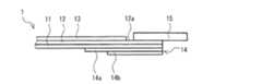
- a flexible printed wiring board 1according to an aspect of the present disclosure shown in FIGS. 1 and 2 includes: a base film 11 having insulation properties; a conductive pattern 12 laminated on one side of the base film 11; A cover lay 13 laminated on one surface of the film 11 or the conductive pattern 12 and a reinforcing portion 14 laminated on the other surface of the base film 11 are provided.
- the flexible printed wiring board 1has a terminal connection area 12 a on one end edge side of the conductive pattern 12 and a plurality of connection terminals 15 in the terminal connection area 12 a.
- the base film 11is a member for supporting the conductive pattern 12 and is a structural material for securing the strength of the flexible printed wiring board 1.
- the main component of the base film 11is, for example, polyimide, a liquid crystal polymer represented by liquid crystal polyester, polyethylene terephthalate, polyethylene naphthalate, polyphenylene ether, soft materials such as fluorine resin, paper phenol, paper epoxy, glass composite, glass epoxy
- a hard materialsuch as a glass substrate, a rigid flexible material in which a soft material and a hard material are combined, or the like can be used.
- polyimide excellent in heat resistanceis preferable.
- the base film 11may be porous, or may contain a filler, an additive, and the like.
- the thickness of the said base film 11is not specifically limited, As a minimum of the average thickness of the base film 11, 5 micrometers is preferable and 12 micrometers is more preferable. Moreover, as an upper limit of the average thickness of the base film 11, 500 micrometers is preferable and 200 micrometers is more preferable. If the average thickness of the base film 11 is less than the above lower limit, the strength of the base film 11 may be insufficient. On the other hand, when the average thickness of the base film 11 exceeds the upper limit, the flexibility of the flexible printed wiring board 1 may be insufficient.
- the conductive pattern 12constitutes a structure such as an electrical wiring structure, a ground, and a shield.
- the material for forming the conductive pattern 12is not particularly limited as long as it is a material having conductivity.
- metalssuch as copper, aluminum, nickel and the like can be mentioned.
- copperwhich is relatively inexpensive and has high conductivity is Used.
- the conductive pattern 12may be plated on the surface.
- the upper limit of the average thickness of the conductive pattern 12is preferably 100 ⁇ m, and more preferably 70 ⁇ m. If the average thickness of the conductive pattern 12 is less than the above lower limit, the conductivity of the conductive pattern 12 may be insufficient. On the contrary, when the average thickness of the conductive pattern 12 exceeds the upper limit, the flexible printed wiring board 1 may be unnecessarily thick.
- a terminal connection area 12 a which the flexible printed wiring board 1 has on one end edge side of the conductive pattern 12is an area for connecting to another electronic device or the like through a connection terminal 15 described later.
- a cover lay 13 described lateris removed.
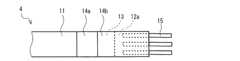
- the shape of the terminal connection area 12ais a comb tooth shape in which the one end side is branched as shown in FIG.
- One connection terminal 15is provided on each of the teeth of the comb teeth.
- the terminal connection area provided with the connection terminals 15 to which the stress applied by the individual connection terminals 15 is adjacentSince it can be made hard to be 12a, the stress added to the said flexible printed wiring board 1 via the connection terminal 15 can be reduced.
- each tooth portion of the terminal connection area 12ais appropriately determined according to the size of the connection terminal 15.
- the average widthcan be 0.5 mm or more and 3 mm or less, and the average length 3 mm or more and 50 mm or less.
- the number of teethis determined corresponding to the number of connection terminals 15.
- the width of the base film 11is constant including the terminal connection area 12a, but depending on the number of connection terminals 15, the width may not be within the width of the base film 11 excluding the terminal connection area 12a. In such a case, for example, as shown in FIG. 2, the number of teeth can be secured by widening the width of the base film 11 on one end side.
- the cover lay 13protects the conductive pattern 12 from external force, moisture and the like.
- the cover lay 13has a cover film and an adhesive layer.
- the cover layer 13is formed by laminating a cover film on the surface of the conductive pattern 12 opposite to the base film 11 through the adhesive layer.
- Cover filmAlthough it does not restrict
- the average thickness of a cover filmAs a minimum of average thickness of a cover film, 5 micrometers is preferred and 10 micrometers is more preferred. On the other hand, as an upper limit of the average thickness of a cover film, 50 micrometers is preferred and 30 micrometers is more preferred. If the average thickness of the cover film is less than the above lower limit, the insulation may be insufficient. Conversely, when the average thickness of the cover film exceeds the above upper limit, the flexibility of the flexible printed wiring board 1 may be impaired.
- the adhesive layerfixes the cover film to the conductive pattern 12 and the base film 11.
- the material of the adhesive layeris not particularly limited as long as the cover film can be fixed to the conductive pattern 12 and the base film 11, but those excellent in flexibility and heat resistance are preferable, for example, polyimide, polyamide, epoxy, butyral , Acrylic and the like. Further, in view of heat resistance, thermosetting resins are preferable.
- the average thickness of the adhesive layer of the cover lay 13is not particularly limited, but the lower limit of the average thickness of the adhesive layer is, for example, preferably 5 ⁇ m and more preferably 10 ⁇ m.
- the upper limit of the average thickness of the adhesive layeris, for example, preferably 100 ⁇ m, and more preferably 80 ⁇ m. If the average thickness of the adhesive layer is less than the above lower limit, adhesion may be insufficient. Conversely, when the average thickness of the adhesive layer exceeds the upper limit, the flexibility of the flexible printed wiring board 1 may be impaired.
- the reinforcing portion 14is laminated so as to face at least the terminal connection area 12 a of the other surface of the base film 11.
- the reinforcing portion 14is formed of two reinforcing layers, an inner layer 14a laminated on the other surface of the base film 11 and an outer layer 14b laminated on the surface of the inner layer 14a opposite to the base film 11. .
- the reinforcing portion 14As a material of the reinforcing portion 14, one having excellent mechanical strength is used. Among them, as a material of the reinforcing portion 14, one having resin as a main component is preferable. Thus, by using the reinforcing portion 14 containing a resin as a main component, the flexible printed wiring board 1 can be reinforced while securing its flexibility. As said resin, an epoxy resin, polyester, a polyimide etc. can be mentioned, for example. Further, as the material of the reinforcing portion 14, it is also possible to use a resin reinforced with glass fiber or paper, such as a glass epoxy resin.
- the "main component"is a component contained most, and means a component having a content of 50% by mass or more.
- the edge on the one end side of the inner layer 14 a and the outer layer 14 bcoincides with the edge on the one end side of the base film 11.
- the average length of the inner layer 14ais larger than the average length of the outer layer 14b, and the edge of the outer layer 14b on the other end side of the conductive pattern 12 is the one end side of the edge of the inner layer 14a on the other end side Located in Therefore, the number of stacked layers of the reinforcing portion 14 increases from 1 to 2 toward the one end edge side, whereby the thickness of the reinforcing portion 14 gradually increases toward the one end edge side.
- the reinforcing portion 14can be manufactured more easily and inexpensively by configuring the reinforcing portion 14 with two reinforcing layers and gradually increasing the thickness of the reinforcing portion 14 depending on the number of laminated layers. .
- the respective end edges on the other end side of the inner layer 14 a and the outer layer 14 bmay not overlap with the end edge on the one end side of the cover lay 13 in a plan view.
- the end edge of the outer layer 14 b on the other end edge sidemay be located closer to the other end edge than the end edge of the connection terminal 15 on the other end edge side. Furthermore, the edge on the other end edge side of the outer layer 14 b may be located closer to the other end edge than the edge on the one end edge side of the cover lay 13.
- the lower limit of the average thickness of the laminated portion of the reinforcing portion 14(the average thickness of the portion where the inner layer 14a and the outer layer 14b are laminated) is preferably 100 ⁇ m, and more preferably 150 ⁇ m.
- an upper limit of the average thickness of the lamination part of reinforcement part 14500 micrometers is preferred and 300 micrometers is more preferred.
- the average thickness of the laminated portion of the reinforcing portion 14is less than the above lower limit, a sufficient reinforcing effect can not be obtained, and bending or bending of the flexible printed wiring board 1 may easily occur.
- stacking part of the reinforcement part 14exceeds the said upper limit, there exists a possibility that the said flexible printed wiring board 1 may become thick unnecessarily.
- the average thickness of the inner layer 14a and the average thickness of the outer layer 14bare preferably equal. By equalizing the average thickness of the inner layer 14a and the average thickness of the outer layer 14b, the stress can be dispersed more effectively, so the fracture prevention effect can be enhanced.
- the lower limit of the average separation distance between the edge on the other end edge side of the inner layer 14a and the edge on the other end edge side of the outer layer 14bis preferably 1 mm, more preferably 3 mm.
- an upper limit of the above-mentioned average separation distance20 mm is preferred and 12 mm is more preferred. If the average separation distance is less than the lower limit, stress may not be sufficiently dispersed, and the fracture prevention effect may be insufficient. On the contrary, when the above-mentioned average separation distance exceeds the above-mentioned upper limit, it becomes difficult to appropriately locate a structure for gradually increasing the thickness of the reinforcing portion 14 at a location where stress tends to concentrate, There is a fear.
- the lower limit of the average separation distance between the edge on the other end edge side of the outer layer 14b and the edge on the other end edge side of the connection terminal 15is preferably 1 mm, more preferably 3 mm.
- an upper limit of the above-mentioned average separation distance20 mm is preferred and 12 mm is more preferred. If the average separation distance is less than the lower limit, it may be difficult to properly position the structure for increasing the thickness of the reinforcing portion 14 stepwise at a location where stress is likely to be concentrated, and the fracture prevention effect may be insufficient. is there.
- the average separation distance between the edge and the edgeis equal.
- the inner layer 14a and the base film 11 and the outer layer 14b and the inner layer 14acan be fixed, for example, via an adhesive layer.
- the inner layer 14a and the outer layer 14bcan be formed on the surface of the base film 11 in this order by coating or the like.
- the material of the adhesive layeris not particularly limited as long as the reinforcing portion 14 can be fixed, but the same adhesive layer for fixing a cover film may be used. it can.
- the average thickness of the said contact bonding layer5 micrometers is preferable and 10 micrometers is more preferable.
- an upper limit of the average thickness of the above-mentioned adhesion layer100 micrometers is preferred and 70 micrometers is more preferred. If the average thickness of the adhesive layer is less than the lower limit, the adhesion of the reinforcing portion 14 may be insufficient. In contrast, when the average thickness of the adhesive layer exceeds the upper limit, the flexible printed wiring board 1 may be unnecessarily thick.
- connection terminal 15is a component for connecting the flexible printed wiring board 1 to another electronic device or the like.
- connection terminal 15is not particularly limited as long as it has conductivity, but it is preferable that the connection terminal 15 be made of metal.
- the flexible printed wiring board 1is particularly effective in preventing stress concentration in connection with the highly rigid metal connection terminal 15.
- the metalinclude soft copper, brass, phosphor bronze and the like.
- the platinginclude Sn plating, Ni plating, Au plating and the like. Among them, Ni plating which is inexpensive and excellent in corrosion resistance is preferable.
- connection terminal 15is appropriately determined according to the terminal shape of the electronic device to be connected, etc.
- connection terminal 15is mounted on the terminal connection area 12 a and electrically connected to the conductive pattern 12.
- the said flexible printed wiring board 1can be manufactured by the manufacturing method provided with a flexible printed wiring board main body formation process, a reinforcement part formation process, and a connection terminal mounting process, for example.
- Flexiblecomprising a base film 11 having an insulating property, a conductive pattern 12 laminated on one side of the base film 11, and a cover lay 13 laminated on one side of the base film 11 or the conductive pattern 12 Form a printed wiring board body. Specifically, follow the procedure below.
- a conductor layeris formed on one side of the base film 11.
- the conductor layercan be formed, for example, by adhering a foil-like conductor using an adhesive or by a known film forming method.
- the conductorinclude copper, silver, gold, nickel and the like.
- the adhesiveis not particularly limited as long as the conductor can be adhered to the base film 11, and various known adhesives can be used.
- a film forming methodfor example, vapor deposition, plating and the like can be mentioned.
- the conductor layeris preferably formed by adhering a copper foil to the base film 11 using a polyimide adhesive.
- the conductive layeris patterned to form a conductive pattern 12.
- the patterning of the conductor layercan be performed by a known method such as photoetching.
- the photoetchingis performed by forming a resist film having a predetermined pattern on one surface of the conductor layer, treating the conductor layer exposed from the resist film with an etching solution, and removing the resist film.
- the cover lay 13is laminated so as to cover the conductive pattern 12 except for the terminal connection region 12 a on one end side of the conductive pattern 12.
- an adhesive layeris laminated on the surface of the base film 11 on which the conductive pattern 12 is formed, and a cover film is laminated on the adhesive layer.
- an adhesive layermay be laminated on the cover film in advance, and the surface of the cover film on which the adhesive layer is laminated may be adhered to face the conductive pattern 12.
- Adhesion of the cover film using an adhesivecan usually be carried out by thermocompression bonding.
- the temperature and pressure at the time of thermocompression bondingmay be appropriately determined in accordance with the type and composition of the adhesive used. Note that this thermocompression bonding may be performed together with the thermocompression bonding of the reinforcing portion 14 in the reinforcing portion forming step described later.
- the reinforcing portion 14is laminated on the other surface of the base film 11 of the flexible printed wiring board main body.
- the reinforcing portion 14 of the flexible printed wiring board 1is composed of two reinforcing layers, the inner layer 14a and the outer layer 14b, so the inner layer 14a and the outer layer 14b are laminated on the other surface of the base film 11 in this order.
- the laminating methodfor example, after the inner layer 14a is cut into a desired size, an adhesive layer is formed on the surface of the inner layer 14a, and laminated on the other surface of the base film 11 through the adhesive layer. it can.
- the outer layer 14bcan also be laminated on the surface of the inner layer 14a in the same manner as the inner layer 14a.
- the inner layer 14a and the outer layer 14bare thermocompression bonded by pressure heating. This thermocompression bonding may be performed once after laminating the outer layer 14b, or may be performed separately on the inner layer 14a and the outer layer 14b. Moreover, the thermocompression bonding of the cover lay 13 may be performed simultaneously.
- connection terminal mounting processIn the connection terminal mounting step, the connection terminal 15 is mounted on the terminal connection area 12a.
- the mounting method of the connection terminal 15is not particularly limited as long as the connection terminal 15 is conductively fixed to the terminal connection region 12 a.
- solderis provided in the terminal connection region 12 a of the conductive pattern 12, one end side of the connection terminal 15 is placed on the solder, the solder is melted by reflow, and the connection terminal 15 is soldered to the conductive pattern 12
- the thickness of the reinforcing portion 14gradually increases toward one end edge of the conductive pattern 12. For this reason, the flexible printed wiring board 1 is hardened in stages toward the one end edge side in the terminal connection area 12a in which the reinforcing portions 14 are stacked to face each other. By thus gradually hardening the flexible printed wiring board 1 toward the one end edge side, the stress is easily dispersed, so that the flexible printed wiring board 1 is affected by the stress concentration due to the reinforcing portion 14. Breakage can be prevented.
- a flexible printed wiring board 2according to an aspect different from FIG. 1 of the present disclosure shown in FIG. 3 includes: a base film 11 having insulation properties; a conductive pattern 12 laminated on one surface of the base film 11; A cover lay 13 laminated on one surface of the base film 11 or the conductive pattern 12 and a reinforcing portion 14 laminated on the other surface of the base film 11 are provided.
- the flexible printed wiring board 1has a terminal connection area 12 a on one end edge side of the conductive pattern 12 and a plurality of connection terminals 15 in the terminal connection area 12 a.
- the configurations of the base film 11, the conductive pattern 12, the cover lay 13 and the connection terminal 15 in the flexible printed wiring board 2 of FIG. 3are the same as the base film 11, the conductive pattern 12, the cover lay 13 and the connection in the flexible printed wiring board 1 of FIG.
- the configuration of each of the terminals 15can be the same.
- the configuration of the reinforcing portion 14 in the flexible printed wiring board 2 of FIG. 3is the reinforcing portion 14 in the flexible printed wiring board 1 of FIG. 1 except for the feature based on the average length of the inner layer 14c and the outer layer 14d described below. It is similar to the configuration of For this reason, the description which overlaps with the flexible printed wiring board 1 of FIG. 1 about the flexible printed wiring board 2 of FIG. 3 is abbreviate
- the average length of the inner layer 14cis smaller than the average length of the outer layer 14d.
- the outer layer 14 dis configured to cover the inner layer 14 c, and a portion longer than the inner layer 14 c of the outer layer 14 d is laminated on the surface of the base film 11.
- the end edge of the inner layer 14c on the other end edge side of the conductive pattern 12is positioned closer to the one end edge than the end edge of the outer layer 14d on the other end edge side. Further, it is preferable that the respective end edges on the other end side of the inner layer 14c and the outer layer 14d do not overlap with the end edge on the one end side of the cover lay 13 in a plan view.
- the edge on the other end edge side of the inner layer 14 cmay be located closer to the other end edge than the edge on the one end edge side of the cover lay 13. Further, the end edge of the inner layer 14 c on the other end edge side may be located closer to the other end edge than the end edge of the connection terminal 15 on the other end edge side.
- the inner layer 14c and the base film 11, the inner layer 14c and the outer layer 14d, and the outer layer 14d and the base film 11can be fixed, for example, via an adhesive layer.
- the said flexible printed wiring board 2can be manufactured by the manufacturing method provided with a flexible printed wiring board main body formation process, a reinforcement part formation process, and a connection terminal mounting process, for example.
- the flexible printed wiring board main body forming step, the reinforcing portion forming step, and the connection terminal mounting stepcan be the same as the steps of the method for manufacturing the flexible printed wiring board 1 of FIG. Since the outer layer 14d to be laminated is longer than the inner layer 14c in the reinforcing portion forming step, the portion of the outer layer 14d longer than the inner layer 14c is adhered to the surface of the base film 11.
- the end of the inner layer 14 cis not exposed to the outside of the flexible printed wiring board 2 by configuring the reinforcing portion 14 so that the outer layer 14 d covers the inner layer 14 c.
- step difference on the other surface side of the board 2can be reduced. Accordingly, in the flexible printed wiring board 2, the reinforcing portion 14 can be made difficult to peel off.
- the number of reinforcement layersis not limited to two layers, Three or more layers may be sufficient.
- the stress relaxation effectcan be further enhanced by increasing the number of reinforcing portions stepwise toward the one end side by three or more reinforcing layers.
- stackingsfive layers are preferable from the relationship between a manufacturing cost and the effect obtained.
- the number of reinforcing layersis three or more, it is preferable to equalize the average separation distance between the adjacent edges on the other end side of the conductive pattern of each reinforcing layer. By equalizing the average separation distance between the adjacent edges in this way, the stress can be dispersed more effectively, so the fracture prevention effect can be enhanced.
- the said flexible printed wiring board 3can also comprise a reinforcement part by the reinforcement board of 1 sheet.
- the thickness of the reinforcing plate 14 eis gradually increased toward one end of the conductive pattern 12.
- FIG. 4shows the case where the thickness of the reinforcing plate 14e is linearly increased, the method of increasing the thickness of the reinforcing plate 14e is not particularly limited as long as it is gradual.
- the shape of a terminal connection fieldis not limited to the shape of a comb tooth.
- the terminal connection area 12amay be square in a plan view.
- the width of the terminal connection area 12ais equal to the width of the base film 11 excluding the terminal connection area 12a is illustrated in FIG. 5, the flexible printed wiring of FIG. Like the board 1, the width of the base film 11 at one end may be expanded.
- a coverlayis not an essential component and can be abbreviate
- one side of the base film or the conductive patternmay be coated, for example, with an insulating layer of another configuration.
- connection terminalis not an essential component and can be abbreviate
- a connection terminalfor example, by directly bonding it to another flexible printed wiring board, it can be connected to another electronic device or the like.
Landscapes
- Engineering & Computer Science (AREA)
- Microelectronics & Electronic Packaging (AREA)
- Structure Of Printed Boards (AREA)
- Printing Elements For Providing Electric Connections Between Printed Circuits (AREA)
- Non-Metallic Protective Coatings For Printed Circuits (AREA)
Abstract
Description
Translated fromJapanese本開示は、フレキシブルプリント配線板に関する。本出願は、2017年8月14日出願の日本出願第2017‐156507号に基づく優先権を主張し、前記日本出願に記載された全ての記載内容を援用するものである。The present disclosure relates to a flexible printed wiring board. This application claims priority based on Japanese Patent Application No. 2017-156507 filed on Aug. 14, 2017, and incorporates all the contents described in the aforementioned Japanese application.
近年、電子機器の小型化及び軽量化の要請から、電子機器分野では様々なフレキシブルプリント配線板が使用されている。このようなフレキシブルプリント配線板として、一般に、ベースとなるベースフィルムと、このベースフィルムの表面に積層された銅箔等により形成された導電パターンとを備えるフレキシブルプリント配線板が使用されている。In recent years, various flexible printed wiring boards have been used in the field of electronic devices because of the demand for smaller and lighter electronic devices. Generally as such a flexible printed wiring board, the flexible printed wiring board provided with the base film used as a base, and the conductive pattern formed with the copper foil etc. which were laminated | stacked on the surface of this base film is used.
このようなフレキシブルプリント配線板は可撓性を有している。そのため、電子機器の導体パターンに接続するフレキシブルプリント配線板の接続端子部には、折れ曲がりや撓みを防止するために、例えば外面に補強部として補強板が積層されて使用される(国際公開第2010/004439号参照)。Such a flexible printed wiring board has flexibility. Therefore, in the connection terminal portion of the flexible printed wiring board connected to the conductor pattern of the electronic device, in order to prevent bending and bending, for example, a reinforcing plate is laminated and used on the outer surface as a reinforcing portion (International Publication No. 2010 / 004439)).
本開示の一態様に係るフレキシブルプリント配線板は、絶縁性を有するベースフィルムと、このベースフィルムの一方の面側に積層される導電パターンとを備え、上記導電パターンの一端縁側に端子接続領域を有するフレキシブルプリント配線板であって、上記ベースフィルムの他方の面のうち少なくとも端子接続領域に対向して積層される補強部を備え、上記補強部の厚さが、上記一端縁側へ向かって段階的又は漸進的に増大している。A flexible printed wiring board according to an aspect of the present disclosure includes a base film having an insulating property, and a conductive pattern laminated on one side of the base film, and a terminal connection region on one end edge side of the conductive pattern. A flexible printed wiring board having a reinforcement portion laminated on at least a terminal connection region of the other surface of the base film, the thickness of the reinforcement portion being stepwise toward the one end edge side Or it is increasing gradually.
[本開示が解決しようとする課題]
補強部により補強されたフレキシブルプリント配線板では、補強部が積層されている部分と積層されていない部分との境界に応力が集中し易く、この境界で破断が発生し易い。[Problems to be solved by the present disclosure]
In the flexible printed wiring board reinforced by the reinforcing portion, stress is likely to be concentrated at the boundary between the portion where the reinforcing portion is stacked and the portion where the reinforcing portion is not stacked, and breakage easily occurs at this boundary.
特に、近年電子機器の小型化が進み、これに伴ってフレキシブルプリント配線板の導電パターンが細線化し、フレキシブルプリント配線板の曲げ半径も小さくなってきている。このため、応力集中によるフレキシブルプリント配線板の導電パターンの破断がより大きな問題となってきている。In particular, in recent years, the miniaturization of electronic devices has progressed, and along with this, the conductive pattern of the flexible printed wiring board has become thinner, and the bending radius of the flexible printed wiring board has also become smaller. For this reason, breakage of the conductive pattern of the flexible printed wiring board due to stress concentration has become a larger problem.
本開示は、上述のような事情に基づいてなされたものであり、補強部に起因した応力集中による破断を防止できるフレキシブルプリント配線板を提供することを課題とする。This indication is made based on the above situations, and makes it a subject to provide a flexible printed wiring board which can prevent a fracture by stress concentration resulting from a reinforcement part.
[本開示の効果]
本開示のフレキシブルプリント配線板は、補強部に起因した応力集中による破断を防止できる。[Effect of the present disclosure]
The flexible printed wiring board of the present disclosure can prevent breakage due to stress concentration caused by the reinforcing portion.
[本開示の実施形態の説明]
本開示の一態様に係るレキシブルプリント配線板は、絶縁性を有するベースフィルムと、このベースフィルムの一方の面側に積層される導電パターンとを備え、上記導電パターンの一端縁側に端子接続領域を有するフレキシブルプリント配線板であって、上記ベースフィルムの他方の面のうち少なくとも端子接続領域に対向して積層される補強部を備え、上記補強部の厚さが、上記一端縁側へ向かって段階的又は漸進的に増大している。[Description of the embodiment of the present disclosure]
A lexible printed wiring board according to an aspect of the present disclosure includes a base film having insulation properties, and a conductive pattern laminated on one side of the base film, and a terminal connection region on one end side of the conductive pattern. A flexible printed wiring board having a reinforcement portion laminated on at least a terminal connection region of the other surface of the base film, the thickness of the reinforcement portion being stepwise toward the one end edge side Or it is increasing gradually.
当該フレキシブルプリント配線板は、補強部の厚さが、上記一端縁側へ向かって段階的又は漸進的に増大している。このため、当該フレキシブルプリント配線板は、補強部が対向して積層されている端子接続領域において上記一端縁側へ向かって段階的又は漸進的に硬くされている。このように当該フレキシブルプリント配線板を上記一端縁側へ向かって徐々に硬くしていくことで、応力が分散し易くなるため、当該フレキシブルプリント配線板は、補強部に起因した応力集中による破断を防止できる。In the flexible printed wiring board, the thickness of the reinforcing portion gradually or gradually increases toward the one end side. For this reason, the flexible printed wiring board is hardened stepwise or gradually toward the one end side in the terminal connection area where the reinforcing portions are stacked to face each other. By thus gradually hardening the flexible printed wiring board toward the one end, the stress is easily dispersed, so that the flexible printed wiring board prevents breakage due to stress concentration due to the reinforcing portion. it can.
上記補強部が、積層される複数の補強層から構成され、上記補強層の積層数により厚さを段階的に増大させるとよい。このように上記補強部を複数の補強層で構成し、補強層の積層数により厚さを段階的に増大させることで、より容易かつ安価に補強部を製造することができる。It is preferable that the reinforcing portion be constituted by a plurality of laminated reinforcing layers, and the thickness be increased stepwise according to the number of laminated reinforcing layers. Thus, the reinforcing portion can be manufactured more easily and inexpensively by configuring the reinforcing portion with a plurality of reinforcing layers and gradually increasing the thickness according to the number of laminated reinforcing layers.
上記複数の補強層が、内層及び外層の2層であり、上記外層が上記内層を被覆するとよい。このように外層が内層を被覆するように補強部を構成することで、内層の端縁が当該フレキシブルプリント配線板の外部に露出しないので、当該フレキシブルプリント配線板の他方の面側の段差を低減できる。従って、補強部を剥がれ難くすることができる。The plurality of reinforcing layers may be two layers of an inner layer and an outer layer, and the outer layer may cover the inner layer. Thus, by forming the reinforcing portion so that the outer layer covers the inner layer, the edge of the inner layer is not exposed to the outside of the flexible printed wiring board, and thus, the step on the other surface of the flexible printed wiring board is reduced. it can. Therefore, it is possible to make the reinforcing portion difficult to peel off.
上記ベースフィルム又は導電パターンの一方の面に積層され、上記端子接続領域では除去されているカバーレイを備え、上記カバーレイの上記一端縁側の端縁と、複数の上記補強層の上記導電パターンの他端縁側のそれぞれの端縁とが平面視で重ならないとよい。このようにカバーレイの上記端縁と補強層の上記端縁とを平面視で重ならないようにすることで、より効果的に応力を分散できるので、破断防止効果を高められる。The cover layer is laminated on one surface of the base film or the conductive pattern and removed in the terminal connection area, and the edge of the cover lay on the one end edge side and the conductive pattern of the plurality of reinforcing layers The respective end edges on the other end side may not overlap in plan view. As described above, by not overlapping the edge of the coverlay and the edge of the reinforcing layer in plan view, the stress can be dispersed more effectively, so that the fracture preventing effect can be enhanced.
上記端子接続領域に1又は複数の接続端子を有し、上記接続端子が金属製であるとよい。当該フレキシブルプリント配線板は、剛性の高い金属製の接続端子との接続において特に応力集中の防止効果が高い。The terminal connection area may have one or more connection terminals, and the connection terminals may be made of metal. The flexible printed wiring board is particularly effective in preventing stress concentration in connection with a highly rigid metal connection terminal.
なお、「補強部の厚さが一端縁側へ向かって段階的に増大する」とは、補強部の厚さが階段状に変化しながら、一端縁側へ向かって増大することをいう。また、「補強部の厚さが一端縁側へ向かって漸進的に増大する」とは、補強部の厚さが一端縁側へ向かって等しい又は増大すること、つまり、一端縁側へ向かって減少する部分がないことをいう。In addition, "the thickness of a reinforcement part increases in steps toward one end edge side" means that the thickness of a reinforcement part increases in the end edge side, changing in steps. In addition, “the thickness of the reinforcing portion gradually increases toward the one end edge” means that the thickness of the reinforcing portion is equal to or increases toward the one end edge, that is, a portion that decreases toward the one end edge I say that there is no.
[本開示の実施形態の詳細]
以下、本開示に係るフレキシブルプリント配線板の各実施形態について図面を参照しつつ詳説する。Details of Embodiments of the Present Disclosure
Hereinafter, embodiments of a flexible printed wiring board according to the present disclosure will be described in detail with reference to the drawings.
[第一実施形態]
図1及び図2に示す本開示の一態様に係るフレキシブルプリント配線板1は、絶縁性を有するベースフィルム11と、このベースフィルム11の一方の面側に積層される導電パターン12と、上記ベースフィルム11又は導電パターン12の一方の面に積層されるカバーレイ13と、上記ベースフィルム11の他方の面に積層される補強部14を備える。
また、当該フレキシブルプリント配線板1は、上記導電パターン12の一端縁側に端子接続領域12aを有し、上記端子接続領域12aに複数の接続端子15を有する。First Embodiment
A flexible printed wiring board 1 according to an aspect of the present disclosure shown in FIGS. 1 and 2 includes: a
The flexible printed wiring board 1 has a
<ベースフィルム>
ベースフィルム11は、導電パターン12を支持する部材であって、当該フレキシブルプリント配線板1の強度を担保する構造材である。<Base film>
The
このベースフィルム11の主成分としては、例えばポリイミド、液晶ポリエステルに代表される液晶ポリマー、ポリエチレンテレフタレート、ポリエチレンナフタレート、ポリフェニレンエーテル、フッ素樹脂等の軟質材、紙フェノール、紙エポキシ、ガラスコンポジット、ガラスエポキシ、ガラス基材等の硬質材、軟質材と硬質材とを複合したリジッドフレキシブル材などを用いることができる。これらの中でも耐熱性に優れるポリイミドが好ましい。なお、ベースフィルム11は、多孔化されたものでもよく、また、充填材、添加剤等を含んでもよい。The main component of the
上記ベースフィルム11の厚さは、特に限定されないが、ベースフィルム11の平均厚さの下限としては、5μmが好ましく、12μmがより好ましい。また、ベースフィルム11の平均厚さの上限としては、500μmが好ましく、200μmがより好ましい。ベースフィルム11の平均厚さが上記下限未満であると、ベースフィルム11の強度が不十分となるおそれがある。一方、ベースフィルム11の平均厚さが上記上限を超えると、当該フレキシブルプリント配線板1の可撓性が不十分となるおそれがある。Although the thickness of the said
<導電パターン>
導電パターン12は、電気配線構造、グラウンド、シールドなどの構造を構成するものである。<Conductive pattern>
The
導電パターン12を形成する材料としては、導電性を有する材料であれば特に限定されないが、例えば銅、アルミニウム、ニッケル等の金属が挙げられ、一般的には比較的安価で導電率が大きい銅が用いられる。また、導電パターン12は、表面にめっき処理が施されてもよい。The material for forming the
導電パターン12の平均厚さの下限としては、2μmが好ましく、5μmがより好ましい。一方、導電パターン12の平均厚さの上限としては、100μmが好ましく、70μmがより好ましい。導電パターン12の平均厚さが上記下限未満の場合、導電パターン12の導電性が不十分となるおそれがある。逆に、導電パターン12の平均厚さが上記上限を超える場合、当該フレキシブルプリント配線板1が不必要に厚くなるおそれがある。As a minimum of average thickness of
当該フレキシブルプリント配線板1が上記導電パターン12の一端縁側に有する端子接続領域12aは、後述する接続端子15を介して他の電子機器等と接続するための領域である。端子接続領域12aでは、後述するカバーレイ13は取り除かれている。A
上記端子接続領域12aの形状は、図1に示すように上記一端縁側が枝分かれした櫛の歯状である。この櫛の歯の各歯部には、それぞれ1の接続端子15が設けられる。このように上記端子接続領域12aでの当該フレキシブルプリント配線板1の形状を櫛の歯状に構成することで、個々の接続端子15によりかかる応力が隣接する接続端子15が設けられた端子接続領域12aに及び難くすることができるので、当該フレキシブルプリント配線板1に接続端子15を介して加わる応力を低減できる。The shape of the
上記端子接続領域12aの各歯部の大きさは、接続端子15の大きさにより適宜決定されるが、例えば平均幅0.5mm以上3mm以下、平均長さ3mm以上50mm以下とできる。また、歯部の数は接続端子15の数に対応して決定される。通常、端子接続領域12aを含めてベースフィルム11の幅は一定とされるが、接続端子15の数によっては、上記端子接続領域12aを除くベースフィルム11の幅に収まらない場合が生じる。このような場合には例えば図2に示すように一端側のベースフィルム11の幅を広げることで歯部の数を確保できる。The size of each tooth portion of the
<カバーレイ>
カバーレイ13は、導電パターン12を外力や水分等から保護するものである。カバーレイ13は、カバーフィルム及び接着層を有する。カバーレイ13は、この接着層を介して上記導電パターン12のベースフィルム11と反対側の面にカバーフィルムが積層されたものである。<Coverlay>
The cover lay 13 protects the
(カバーフィルム)
カバーフィルムの材質としては、特に制限されるものではないが、例えばベースフィルム11を構成する樹脂と同様のものを用いることができる。(Cover film)
Although it does not restrict | limit especially as a material of a cover film, For example, the thing similar to resin which comprises the
カバーフィルムの平均厚さの下限としては、5μmが好ましく、10μmがより好ましい。一方、カバーフィルムの平均厚さの上限としては、50μmが好ましく、30μmがより好ましい。カバーフィルムの平均厚さが上記下限未満であると、絶縁性が不十分となるおそれがある。逆に、カバーフィルムの平均厚さが上記上限を超えると、当該フレキシブルプリント配線板1の可撓性が損なわれるおそれがある。As a minimum of average thickness of a cover film, 5 micrometers is preferred and 10 micrometers is more preferred. On the other hand, as an upper limit of the average thickness of a cover film, 50 micrometers is preferred and 30 micrometers is more preferred. If the average thickness of the cover film is less than the above lower limit, the insulation may be insufficient. Conversely, when the average thickness of the cover film exceeds the above upper limit, the flexibility of the flexible printed wiring board 1 may be impaired.
(接着層)
接着層は、カバーフィルムを導電パターン12及びベースフィルム11に固定するものである。接着層の材質としては、カバーフィルムを導電パターン12及びベースフィルム11に固定できる限り特に限定されるものではないが、柔軟性や耐熱性に優れたものが好ましく、例えばポリイミド、ポリアミド、エポキシ、ブチラール、アクリル等が挙げられる。また、耐熱性の点において、熱硬化性樹脂が好ましい。(Adhesive layer)
The adhesive layer fixes the cover film to the
カバーレイ13の接着層の平均厚さは、特に限定されるものではないが、接着層の平均厚さの下限としては、例えば5μmが好ましく、10μmがより好ましい。一方、接着層の平均厚さの上限としては、例えば100μmが好ましく、80μmがより好ましい。接着層の平均厚さが上記下限未満であると、接着性が不十分となるおそれがある。逆に、接着層の平均厚さが上記上限を超えると、当該フレキシブルプリント配線板1の可撓性が損なわれるおそれがある。The average thickness of the adhesive layer of the cover lay 13 is not particularly limited, but the lower limit of the average thickness of the adhesive layer is, for example, preferably 5 μm and more preferably 10 μm. On the other hand, the upper limit of the average thickness of the adhesive layer is, for example, preferably 100 μm, and more preferably 80 μm. If the average thickness of the adhesive layer is less than the above lower limit, adhesion may be insufficient. Conversely, when the average thickness of the adhesive layer exceeds the upper limit, the flexibility of the flexible printed wiring board 1 may be impaired.
<補強部>
補強部14は、上記ベースフィルム11の他方の面のうち少なくとも端子接続領域12aに対向して積層される。また、補強部14は、ベースフィルム11の他方の面に積層される内層14aと、内層14aのベースフィルム11とは反対側の面に積層される外層14bとの2つの補強層から構成される。<Reinforcement part>
The reinforcing
補強部14の材質には、機械的強度に優れたものが使用される。中でも補強部14の材質としては、樹脂を主成分とするものがよい。このように、樹脂を主成分とする補強部14を用いることで、当該フレキシブルプリント配線板1の可撓性を確保しつつ補強することができる。上記樹脂としては、例えばエポキシ樹脂、ポリエステル、ポリイミド等を挙げることができる。また、補強部14の材質には、ガラス繊維や紙で補強された樹脂、例えばガラスエポキシ樹脂を用いることもできる。ここで、「主成分」とは、最も多く含まれる成分であり、含有量が50質量%以上の成分を意味する。As a material of the reinforcing
内層14a及び外層14bの上記一端縁側の端縁は、ベースフィルム11の上記一端縁側の端縁と一致している。また、内層14aの平均長さは、外層14bの平均長さよりも大きく、外層14bの上記導電パターン12の他端縁側の端縁は、内層14aの上記他端縁側の端縁よりも上記一端縁側に位置する。このため、上記補強部14は上記一端縁側に向かって積層数が1から2へと増大し、これにより補強部14の厚さが上記一端縁側へ向かって段階的に増大している。このように補強部14を2つの補強層で構成し、補強層の積層数により補強部14の厚さを段階的に増大させることで、より容易かつ安価に補強部14を製造することができる。The edge on the one end side of the
また、内層14a及び外層14bの上記他端縁側のそれぞれの端縁は、上記カバーレイ13の上記一端縁側の端縁と平面視で重ならないとよい。このようにカバーレイ13の上記端縁と補強層の上記端縁とを平面視で重ならないようにすることで、より効果的に応力を分散できるので、破断防止効果を高められる。Further, the respective end edges on the other end side of the
また、外層14bの上記他端縁側の端縁は、接続端子15の上記他端縁側の端縁よりも上記他端縁側に位置するとよい。さらに、外層14bの上記他端縁側の端縁は、上記カバーレイ13の上記一端縁側の端縁よりも上記他端縁側に位置するとよい。このように外層14bの上記他端縁側の端縁を位置させることで、応力のかかり易い部分をより確実に保護することができる。Further, the end edge of the
補強部14の積層部分の平均厚さ(内層14aと外層14bとが積層されている部分の平均厚さ)の下限としては、100μmが好ましく、150μmがより好ましい。一方、補強部14の積層部分の平均厚さの上限としては、500μmが好ましく、300μmがより好ましい。補強部14の積層部分の平均厚さが上記下限未満であると、十分な補強効果が得られず、当該フレキシブルプリント配線板1の折れ曲がりや撓みが生じ易くなるおそれがある。逆に、補強部14の積層部分の平均厚さが上記上限を超えると、当該フレキシブルプリント配線板1が不必要に厚くなるおそれがある。The lower limit of the average thickness of the laminated portion of the reinforcing portion 14 (the average thickness of the portion where the
また、内層14aの平均厚さと外層14bの平均厚さとは、等しいことが好ましい。内層14aの平均厚さと外層14bの平均厚さとを等しくすることで、より効果的に応力を分散できるので、破断防止効果を高められる。Further, the average thickness of the
内層14aの上記他端縁側の端縁と外層14bの上記他端縁側の端縁との間の平均離間距離の下限としては、1mmが好ましく、3mmがより好ましい。一方、上記平均離間距離の上限としては、20mmが好ましく、12mmがより好ましい。上記平均離間距離が上記下限未満であると、応力が十分に分散されず破断防止効果が不足するおそれがある。
逆に、上記平均離間距離が上記上限を超えると、応力が集中し易い箇所に補強部14の厚さを段階的に増大させる構造を適切に位置させることが困難となり、破断防止効果が不足するおそれがある。The lower limit of the average separation distance between the edge on the other end edge side of the
On the contrary, when the above-mentioned average separation distance exceeds the above-mentioned upper limit, it becomes difficult to appropriately locate a structure for gradually increasing the thickness of the reinforcing
また、外層14bの上記他端縁側の端縁と接続端子15の上記他端縁側の端縁との間の平均離間距離の下限としては、1mmが好ましく、3mmがより好ましい。一方、上記平均離間距離の上限としては、20mmが好ましく、12mmがより好ましい。上記平均離間距離が上記下限未満であると、応力が集中し易い箇所に補強部14の厚さを段階的に増大させる構造を適切に位置させることが困難となり、破断防止効果が不足するおそれがある。逆に、上記平均離間距離が上記上限を超えると、応力が十分に分散されず破断防止効果が不足するおそれがある。なお、内層14aの上記他端縁側の端縁と外層14bの上記他端縁側の端縁との間の平均離間距離と、外層14bの上記他端縁側の端縁と接続端子15の上記他端縁側の端縁との間の平均離間距離とは等しくすることが好ましい。The lower limit of the average separation distance between the edge on the other end edge side of the
上記内層14aとベースフィルム11との間、及び上記外層14bと内層14aとの間は例えば接着層を介して固定できる。あるいは、内層14a及び外層14bをベースフィルム11の表面にこの順で塗工等により形成することもできる。The
内層14a及び外層14bを接着層を介して固定する場合、上記接着層の材質としては、補強部14を固定できる限り特に限定されないが、カバーフィルムを固定する接着層と同様のものを用いることができる。また、上記接着層の平均厚さの下限としては、5μmが好ましく、10μmがより好ましい。一方、上記接着層の平均厚さの上限としては、100μmが好ましく、70μmがより好ましい。上記接着層の平均厚さが上記下限未満であると、補強部14の接着性が不十分となるおそれがある。逆に、上記接着層の平均厚さが上記上限を超えると、当該フレキシブルプリント配線板1が不必要に厚くなるおそれがある。When the
<接続端子>
接続端子15は、当該フレキシブルプリント配線板1を他の電子機器等と接続するための部品である。<Connection terminal>
The
接続端子15の材質は、導電性を有する限り特に限定されないが、接続端子15が金属製であるとよい。当該フレキシブルプリント配線板1は、剛性の高い金属製の接続端子15との接続において特に応力集中の防止効果が高い。上記金属としては、例えば軟銅、黄銅、リン青銅等を挙げることができる。また、接続端子15の表面は、酸化を防ぐために、めっきを施すことが好ましい。上記めっきとしては、Snめっき、Niめっき、Auめっき等を挙げることができる。中でも安価でかつ防蝕性に優れるNiめっきが好ましい。The material of the
上記接続端子15の形状は、接続する電子機器等の端子形状等に応じて適宜決定されるが、例えば平均幅0.5mm以上3mm以下、平均長さ3mm以上50mm以下、平均高さ0.1mm以上3mm以下の板状又は成形加工された立体形状とできる。The shape of the
上記接続端子15は、端子接続領域12aに実装され、導電パターン12と電気的に接続される。The
<フレキシブルプリント配線板の製造方法>
当該フレキシブルプリント配線板1は、例えばフレキシブルプリント配線板本体形成工程と、補強部形成工程と、接続端子実装工程とを備える製造方法により製造することができる。<Method of manufacturing flexible printed wiring board>
The said flexible printed wiring board 1 can be manufactured by the manufacturing method provided with a flexible printed wiring board main body formation process, a reinforcement part formation process, and a connection terminal mounting process, for example.
(フレキシブルプリント配線板本体形成工程)
絶縁性を有するベースフィルム11と、このベースフィルム11の一方の面側に積層される導電パターン12と、上記ベースフィルム11又は導電パターン12の一方の面に積層されるカバーレイ13とを備えるフレキシブルプリント配線板本体を形成する。具体的には以下の手順による。(Flexible printed wiring board main body formation process)
Flexible comprising a
まず、ベースフィルム11の一方の面に導体層を形成する。First, a conductor layer is formed on one side of the
導体層は、例えば接着剤を用いて箔状の導体を接着することにより、あるいは公知の成膜手法により形成できる。導体としては、例えば、銅、銀、金、ニッケル等が挙げられる。接着剤としては、ベースフィルム11に導体を接着できるものであれば特に制限はなく、公知の種々のものを使用することができる。成膜手法としては、例えば蒸着、メッキ等が挙げられる。導体層は、ポリイミド接着剤を用いて銅箔をベースフィルム11に接着して形成することが好ましい。The conductor layer can be formed, for example, by adhering a foil-like conductor using an adhesive or by a known film forming method. Examples of the conductor include copper, silver, gold, nickel and the like. The adhesive is not particularly limited as long as the conductor can be adhered to the
次に、この導体層をパターニングして導電パターン12を形成する。Next, the conductive layer is patterned to form a
導体層のパターニングは、公知の方法、例えばフォトエッチングにより行うことができる。フォトエッチングは、導体層の一方の面に所定のパターンを有するレジスト膜を形成した後に、レジスト膜から露出する導体層をエッチング液で処理し、レジスト膜を除去することにより行われる。The patterning of the conductor layer can be performed by a known method such as photoetching. The photoetching is performed by forming a resist film having a predetermined pattern on one surface of the conductor layer, treating the conductor layer exposed from the resist film with an etching solution, and removing the resist film.
最後に、導電パターン12の一端縁側の端子接続領域12aを除いて、導電パターン12を覆うようにカバーレイ13を積層する。具体的には、導電パターン12を形成したベースフィルム11の表面に接着剤層を積層し、接着剤層の上にカバーフィルムを積層する。または、予めカバーフィルムに接着剤層を積層しておき、そのカバーフィルムの接着剤層が積層されている側の面を導電パターン12に対面させて接着してもよい。Finally, the cover lay 13 is laminated so as to cover the
接着剤を使用したカバーフィルムの接着は、通常、熱圧着により行うことができる。熱圧着する際の温度及び圧力は、使用する接着剤の種類や組成等に応じて適宜決定すればよい。なお、この熱圧着は、後述する補強部形成工程で補強部14の熱圧着とまとめて行ってもよい。Adhesion of the cover film using an adhesive can usually be carried out by thermocompression bonding. The temperature and pressure at the time of thermocompression bonding may be appropriately determined in accordance with the type and composition of the adhesive used. Note that this thermocompression bonding may be performed together with the thermocompression bonding of the reinforcing
(補強部形成工程)
補強部形成工程では、補強部14を上記フレキシブルプリント配線板本体のベースフィルム11の他方の面に積層する。当該フレキシブルプリント配線板1の補強部14は、内層14aと外層14bとの2つの補強層から構成されるので、内層14a及び外層14bをこの順にベースフィルム11の他方の面に積層する。(Reinforcement part formation process)
In the reinforcing portion forming step, the reinforcing
上記積層方法としては、例えば内層14aを所望の大きさに切断した後、内層14aの表面に接着層を形成し、ベースフィルム11の他方の面に接着層を介して積層する方法を用いることができる。外層14bについても内層14aと同様の方法で内層14aの表面に積層することができる。そして、加圧加熱により内層14a及び外層14bを熱圧着する。この熱圧着は、外層14bを積層した後に一度に行ってもよいし、内層14aと外層14bとに対して別々に行ってもよい。また、カバーレイ13の熱圧着を同時に行ってもよい。As the laminating method, for example, after the
(接続端子実装工程)
接続端子実装工程では、接続端子15を端子接続領域12aに実装する。接続端子15の実装方法としては、接続端子15が端子接続領域12aに導通可能に固定される限り特に限定されない。例えば、導電パターン12の端子接続領域12aに半田を設け、この半田の上に接続端子15の一端側を載置し、リフローにより半田を溶融させて、導電パターン12に接続端子15を半田付けする方法、接続端子15毎にベースフィルム11をかしめて接続をとる方法、接続端子15を上から押圧することで端子接続領域12aに導通を取りつつ圧着する方法などを用いることができる。これにより、接続端子15が実装されて、当該フレキシブルプリント配線板1が形成される。(Connection terminal mounting process)
In the connection terminal mounting step, the
<利点>
当該フレキシブルプリント配線板1は、補強部14の厚さが、導電パターン12の一端縁側へ向かって段階的に増大している。このため、当該フレキシブルプリント配線板1は、補強部14が対向して積層されている端子接続領域12aにおいて上記一端縁側へ向かって段階的に硬くされている。このように当該フレキシブルプリント配線板1を上記一端縁側へ向かって徐々に硬くしていくことで、応力が分散し易くなるため、当該フレキシブルプリント配線板1は、補強部14に起因した応力集中による破断を防止できる。<Advantage>
In the flexible printed wiring board 1, the thickness of the reinforcing
[第二実施形態]
図3に示す本開示の図1とは異なる態様に係るフレキシブルプリント配線板2は、絶縁性を有するベースフィルム11と、このベースフィルム11の一方の面側に積層される導電パターン12と、上記ベースフィルム11又は導電パターン12の一方の面に積層されるカバーレイ13と、上記ベースフィルム11の他方の面に積層される補強部14を備える。また、当該フレキシブルプリント配線板1は、上記導電パターン12の一端縁側に端子接続領域12aを有し、上記端子接続領域12aに複数の接続端子15を有する。Second Embodiment
A flexible printed
図3のフレキシブルプリント配線板2におけるベースフィルム11、導電パターン12、カバーレイ13及び接続端子15の構成は、図1のフレキシブルプリント配線板1におけるベースフィルム11、導電パターン12、カバーレイ13及び接続端子15の構成とそれぞれ同様とすることができる。また、図3のフレキシブルプリント配線板2における補強部14の構成は、以下に説明する内層14c及び外層14dの平均長さに基づく特徴を除いて、図1のフレキシブルプリント配線板1における補強部14の構成と同様である。このため、図3のフレキシブルプリント配線板2について図1のフレキシブルプリント配線板1と重複する説明は省略する。The configurations of the
<補強部>
当該フレキシブルプリント配線板2では、内層14cの平均長さは、外層14dの平均長さよりも小さい。このため、外層14dが内層14cを被覆するように構成され、外層14dの内層14cより長い部分は、ベースフィルム11の表面に積層されている。この構成により、上記補強部14は上記一端縁側に向かって積層数が1から2へと増大し、これにより補強部14の厚さが上記一端縁側へ向かって段階的に増大している。<Reinforcement part>
In the flexible printed
当該フレキシブルプリント配線板2では、内層14cの上記導電パターン12の他端縁側の端縁は、外層14dの上記他端縁側の端縁よりも上記一端縁側に位置する。また、内層14c及び外層14dの上記他端縁側のそれぞれの端縁は、カバーレイ13の上記一端縁側の端縁と平面視で重ならないとよい。In the flexible printed
さらに、内層14cの上記他端縁側の端縁は、上記カバーレイ13の上記一端縁側の端縁よりも上記他端縁側に位置するとよい。また、内層14cの上記他端縁側の端縁は、接続端子15の上記他端縁側の端縁よりも上記他端縁側に位置するとよい。このように内層14cの上記他端縁側の端縁を位置させることで、応力のかかり易い部分をより確実に保護することができる。Furthermore, the edge on the other end edge side of the
上記内層14cとベースフィルム11との間、上記内層14cと外層14dとの間、及び上記外層14dとベースフィルム11との間は、例えば接着層を介して固定できる。The
<フレキシブルプリント配線板の製造方法>
当該フレキシブルプリント配線板2は、例えばフレキシブルプリント配線板本体形成工程と、補強部形成工程と、接続端子実装工程とを備える製造方法により製造することができる。<Method of manufacturing flexible printed wiring board>
The said flexible printed
上記フレキシブルプリント配線板本体形成工程、補強部形成工程、及び接続端子実装工程は、図1のフレキシブルプリント配線板1の製造方法の各工程と同様とできる。なお、補強部形成工程において、積層される外層14dは内層14cよりも長いため、外層14dの内層14cより長い部分は、ベースフィルム11の表面に接着する。The flexible printed wiring board main body forming step, the reinforcing portion forming step, and the connection terminal mounting step can be the same as the steps of the method for manufacturing the flexible printed wiring board 1 of FIG. Since the
<利点>
当該フレキシブルプリント配線板2では、外層14dが内層14cを被覆するように補強部14を構成することで、内層14cの端縁が当該フレキシブルプリント配線板2の外部に露出しないので、当該フレキシブルプリント配線板2の他方の面側の段差を低減できる。従って、当該フレキシブルプリント配線板2では、補強部14を剥がれ難くすることができる。<Advantage>
In the flexible printed
[その他の実施形態]
今回開示された実施の形態はすべての点で例示であって制限的なものではないと考えられるべきである。本発明の範囲は、上記実施形態の構成に限定されるものではなく、特許請求の範囲によって示され、特許請求の範囲と均等の意味及び範囲内での全ての変更が含まれることが意図される。Other Embodiments
It should be understood that the embodiments disclosed herein are illustrative and non-restrictive in every respect. The scope of the present invention is not limited to the configurations of the above embodiments, but is indicated by the claims, and is intended to include all modifications within the meaning and scope equivalent to the claims. Ru.
上記実施形態では、補強部が2層の補強層により構成される場合を説明したが、補強層の数は2層に限定されず、3層以上であってもよい。3層以上の補強層により補強部を一端縁側へ向かって段階的に増加させることで、応力の緩和効果をさらに高めることができる。なお、製造コストと得られる効果との関係から、積層数の上限としては、5層が好ましい。Although the said embodiment demonstrated the case where a reinforcement part was comprised by the reinforcement layer of two layers, the number of reinforcement layers is not limited to two layers, Three or more layers may be sufficient. The stress relaxation effect can be further enhanced by increasing the number of reinforcing portions stepwise toward the one end side by three or more reinforcing layers. In addition, as a maximum of the number of lamination | stackings, five layers are preferable from the relationship between a manufacturing cost and the effect obtained.
また、補強層が3層以上である場合、各補強層の上記導電パターンの他端縁側の隣接する端縁間の平均離間距離を等しくするとよい。このように隣接する端縁間の平均離間距離を等しくすることで、より効果的に応力を分散できるので、破断防止効果を高められる。In addition, when the number of reinforcing layers is three or more, it is preferable to equalize the average separation distance between the adjacent edges on the other end side of the conductive pattern of each reinforcing layer. By equalizing the average separation distance between the adjacent edges in this way, the stress can be dispersed more effectively, so the fracture prevention effect can be enhanced.
上記実施形態では、補強部が複数の補強層により構成される場合を説明したが、図4に示すように当該フレキシブルプリント配線板3は、補強部を1枚の補強板で構成することもできる。この場合、補強板14eの厚さを導電パターン12の一端縁側へ向かって漸進的に増大させる。図4では補強板14eの厚さを線形的に増大させる場合を示したが、補強板14eの厚さの増え方は漸進的であれば特に限定されない。Although the said embodiment demonstrated the case where a reinforcement part was comprised by the several reinforcement layer, as shown in FIG. 4, the said flexible printed wiring board 3 can also comprise a reinforcement part by the reinforcement board of 1 sheet. . In this case, the thickness of the reinforcing
上記実施形態では、端子接続領域が櫛の歯状である場合を説明したが、端子接続領域の形状は櫛の歯状に限定されない。例えば図5に示すフレキシブルプリント配線板4のように端子接続領域12aは平面視方形状であってもよい。なお、図5では端子接続領域12aの幅が、端子接続領域12aを除くベースフィルム11の幅と等しい場合を図示しているが、例えば接続端子15が収まらない場合等、図2のフレキシブルプリント配線板1のように一端側のベースフィルム11の幅を広げた構成としてもよい。Although the above-mentioned embodiment explained the case where a terminal connection field was the shape of a comb tooth, the shape of a terminal connection field is not limited to the shape of a comb tooth. For example, as in the case of the flexible printed wiring board 4 shown in FIG. 5, the
上記実施形態では、カバーレイを備えるフレキシブルプリント配線板について説明したが、カバーレイは必須の構成要素ではなく、省略可能である。あるいは、例えば他の構成の絶縁層でベースフィルム又は導電パターンの一方の面を被覆してもよい。Although the said embodiment demonstrated the flexible printed wiring board provided with a coverlay, a coverlay is not an essential component and can be abbreviate | omitted. Alternatively, one side of the base film or the conductive pattern may be coated, for example, with an insulating layer of another configuration.
上記実施形態では、接続端子を備えるフレキシブルプリント配線板について説明したが、接続端子は必須の構成要素ではなく、省略可能である。接続端子を備えないフレキシブルプリント配線板では、例えば他のフレキシブルプリント配線板と直接貼り合わせることで、他の電子機器等と接続できる。Although the said embodiment demonstrated the flexible printed wiring board provided with a connection terminal, a connection terminal is not an essential component and can be abbreviate | omitted. In the case of a flexible printed wiring board which does not have connection terminals, for example, by directly bonding it to another flexible printed wiring board, it can be connected to another electronic device or the like.
1、2、3、4 フレキシブルプリント配線板
11 ベースフィルム
12 導電パターン
12a 端子接続領域
13 カバーレイ
14 補強部
14a、14c 内層
14b、14d 外層
14e 補強板
15 接続端子1, 2, 3, 4 flexible printed
Claims (5)
Translated fromJapanese上記ベースフィルムの他方の面のうち少なくとも端子接続領域に対向して積層される補強部を備え、
上記補強部の厚さが、上記一端縁側へ向かって段階的又は漸進的に増大しているフレキシブルプリント配線板。A flexible printed wiring board comprising: a base film having insulation properties; and a conductive pattern laminated on one side of the base film, wherein the flexible printed wiring board has a terminal connection region at one end of the conductive pattern,
A reinforcing portion which is laminated to face at least a terminal connection region of the other surface of the base film,
The flexible printed wiring board in which the thickness of the said reinforcement part is increasing gradually or gradually toward the said one end edge side.
上記補強層の積層数により厚さを段階的に増大させる請求項1に記載のフレキシブルプリント配線板。The above-mentioned reinforcement part is constituted from a plurality of reinforcement layers laminated,
The flexible printed wiring board according to claim 1, wherein the thickness is gradually increased by the number of laminated reinforcing layers.
上記外層が上記内層を被覆する請求項2に記載のフレキシブルプリント配線板。The plurality of reinforcing layers are two layers of an inner layer and an outer layer,
The flexible printed wiring board according to claim 2, wherein the outer layer covers the inner layer.
上記カバーレイの上記一端縁側の端縁と、複数の上記補強層の上記導電パターンの他端縁側のそれぞれの端縁とが平面視で重ならない請求項2又は請求項3に記載のフレキシブルプリント配線板。The cover film laminated on one surface of the base film or the conductive pattern and removed in the terminal connection area;
4. The flexible printed wiring according to claim 2, wherein the end edge on the one end side of the cover lay and the end edge on the other end side of the conductive pattern of the plurality of reinforcing layers do not overlap in plan view. Board.
上記接続端子が金属製である請求項1から請求項4のいずれか1項に記載のフレキシブルプリント配線板。
One or more connection terminals in the terminal connection area;
The flexible printed wiring board according to any one of claims 1 to 4, wherein the connection terminal is made of metal.
Priority Applications (2)
| Application Number | Priority Date | Filing Date | Title |
|---|---|---|---|
| CN201880050759.7ACN111034371A (en) | 2017-08-14 | 2018-06-25 | Flexible printed circuit board |
| US16/618,253US11051399B2 (en) | 2017-08-14 | 2018-06-25 | Flexible printed circuit board |
Applications Claiming Priority (2)
| Application Number | Priority Date | Filing Date | Title |
|---|---|---|---|
| JP2017-156507 | 2017-08-14 | ||
| JP2017156507AJP2019036616A (en) | 2017-08-14 | 2017-08-14 | Flexible printed wiring board |
Publications (1)
| Publication Number | Publication Date |
|---|---|
| WO2019035278A1true WO2019035278A1 (en) | 2019-02-21 |
Family
ID=65362320
Family Applications (1)
| Application Number | Title | Priority Date | Filing Date |
|---|---|---|---|
| PCT/JP2018/023921CeasedWO2019035278A1 (en) | 2017-08-14 | 2018-06-25 | Flexible printed wiring board |
Country Status (4)
| Country | Link |
|---|---|
| US (1) | US11051399B2 (en) |
| JP (1) | JP2019036616A (en) |
| CN (1) | CN111034371A (en) |
| WO (1) | WO2019035278A1 (en) |
Cited By (2)
| Publication number | Priority date | Publication date | Assignee | Title |
|---|---|---|---|---|
| WO2021134404A1 (en)* | 2019-12-31 | 2021-07-08 | 瑞声声学科技(深圳)有限公司 | Electrically conductive connector |
| CN114097309A (en)* | 2019-07-10 | 2022-02-25 | 住友电工印刷电路株式会社 | Flexible printed wiring board, battery wiring module, and method for manufacturing flexible printed wiring board |
Families Citing this family (3)
| Publication number | Priority date | Publication date | Assignee | Title |
|---|---|---|---|---|
| KR102161215B1 (en)* | 2019-11-06 | 2020-09-29 | 고려전자주식회사 | Temperature Sensor for Battery Module and Battery Module including the same |
| WO2021090974A1 (en)* | 2019-11-06 | 2021-05-14 | 고려전자주식회사 | Temperature sensor for battery module, and battery module including same |
| CN113597090B (en)* | 2021-07-28 | 2024-03-26 | 京东方科技集团股份有限公司 | Flexible circuit boards, display panels and display devices |
Citations (5)
| Publication number | Priority date | Publication date | Assignee | Title |
|---|---|---|---|---|
| JPH05235498A (en)* | 1992-02-24 | 1993-09-10 | Nitto Denko Corp | Printed circuit board with protruding electrodes and bonding method |
| JPH06216487A (en)* | 1993-01-18 | 1994-08-05 | Matsushita Electric Ind Co Ltd | Connecting terminal part of flexible pattern |
| JP2005294746A (en)* | 2004-04-05 | 2005-10-20 | Alps Electric Co Ltd | Printed-circuit board and its manufacturing method |
| JP2012174855A (en)* | 2011-02-21 | 2012-09-10 | Fujitsu Frontech Ltd | Flexible printed board |
| JP2016018787A (en)* | 2014-07-04 | 2016-02-01 | キヤノン株式会社 | Imaging device |
Family Cites Families (11)
| Publication number | Priority date | Publication date | Assignee | Title |
|---|---|---|---|---|
| JPH0223001Y2 (en)* | 1984-09-29 | 1990-06-21 | ||
| JPS63158711A (en)* | 1986-12-22 | 1988-07-01 | 帝国通信工業株式会社 | Terminal construction for flexible printed circuit board |
| JPH0737328Y2 (en)* | 1991-02-08 | 1995-08-23 | 住友電気工業株式会社 | Flexible printed wiring board |
| JPH0685341B2 (en)* | 1991-09-27 | 1994-10-26 | 帝国通信工業株式会社 | Flexible board terminal structure |
| JPH0538934U (en)* | 1991-10-28 | 1993-05-25 | 松下電器産業株式会社 | Printed wiring board |
| WO2008035416A1 (en)* | 2006-09-21 | 2008-03-27 | Daisho Denshi Co., Ltd. | Flex-rigid printed circuit board, and method for manufacturing the flex-rigid printed circuit board |
| JP5020899B2 (en) | 2008-06-20 | 2012-09-05 | モレックス インコーポレイテド | Electrical connector |
| TW201101611A (en)* | 2009-06-26 | 2011-01-01 | Adv Flexible Circuits Co Ltd | Circuit flat cable having positioning and insertion structure |
| JP2014229631A (en)* | 2013-05-17 | 2014-12-08 | 住友電工プリントサーキット株式会社 | Flexible printed wiring board |
| US20150252990A1 (en)* | 2014-03-10 | 2015-09-10 | Lustrous Technology Ltd. | Light emitting module and lamp bulb structure |
| JP6460444B2 (en)* | 2014-07-17 | 2019-01-30 | 住友電工プリントサーキット株式会社 | Flexible printed circuit board and flexible printed circuit board |
- 2017
- 2017-08-14JPJP2017156507Apatent/JP2019036616A/enactivePending
- 2018
- 2018-06-25USUS16/618,253patent/US11051399B2/enactiveActive
- 2018-06-25CNCN201880050759.7Apatent/CN111034371A/enactivePending
- 2018-06-25WOPCT/JP2018/023921patent/WO2019035278A1/ennot_activeCeased
Patent Citations (5)
| Publication number | Priority date | Publication date | Assignee | Title |
|---|---|---|---|---|
| JPH05235498A (en)* | 1992-02-24 | 1993-09-10 | Nitto Denko Corp | Printed circuit board with protruding electrodes and bonding method |
| JPH06216487A (en)* | 1993-01-18 | 1994-08-05 | Matsushita Electric Ind Co Ltd | Connecting terminal part of flexible pattern |
| JP2005294746A (en)* | 2004-04-05 | 2005-10-20 | Alps Electric Co Ltd | Printed-circuit board and its manufacturing method |
| JP2012174855A (en)* | 2011-02-21 | 2012-09-10 | Fujitsu Frontech Ltd | Flexible printed board |
| JP2016018787A (en)* | 2014-07-04 | 2016-02-01 | キヤノン株式会社 | Imaging device |
Cited By (2)
| Publication number | Priority date | Publication date | Assignee | Title |
|---|---|---|---|---|
| CN114097309A (en)* | 2019-07-10 | 2022-02-25 | 住友电工印刷电路株式会社 | Flexible printed wiring board, battery wiring module, and method for manufacturing flexible printed wiring board |
| WO2021134404A1 (en)* | 2019-12-31 | 2021-07-08 | 瑞声声学科技(深圳)有限公司 | Electrically conductive connector |
Also Published As
| Publication number | Publication date |
|---|---|
| CN111034371A (en) | 2020-04-17 |
| JP2019036616A (en) | 2019-03-07 |
| US20210037642A1 (en) | 2021-02-04 |
| US11051399B2 (en) | 2021-06-29 |
Similar Documents
| Publication | Publication Date | Title |
|---|---|---|
| WO2019035278A1 (en) | Flexible printed wiring board | |
| WO2019035248A1 (en) | Flexible printed wiring board | |
| JP7090622B2 (en) | Flexible printed wiring board | |
| US20150282314A1 (en) | Method for manufacturing printed wiring board with conductive post and printed wiring board with conductive post | |
| CN217721588U (en) | Laminated body | |
| CN108811523B (en) | Flexible printed circuit board, method for manufacturing connector, and connector | |
| JP7020754B2 (en) | Flexible printed wiring board | |
| JPWO2016117122A1 (en) | Wiring board manufacturing method and wiring board | |
| JP2019021863A (en) | Multilayer substrate | |
| JP7478732B2 (en) | Flexible printed wiring board and battery wiring module | |
| JP6863244B2 (en) | Electronic components and manufacturing methods for electronic components | |
| US11245237B2 (en) | Method of manufacturing flexible printed interconnect board | |
| WO2021006325A1 (en) | Flexible printed wiring board, battery wiring module, and method for manufacturing flexible printed wiring board | |
| JP2014229631A (en) | Flexible printed wiring board | |
| US20220272836A1 (en) | Flexible printed wiring board and battery wiring module | |
| KR102561936B1 (en) | Printed circuit board | |
| WO2011061969A1 (en) | Partially multilayer wiring board and method for producing same | |
| JP5800076B2 (en) | Electronic device and electronic device mounting structure | |
| JP2011243796A (en) | Electronic equipment and attachment structure of electronic equipment | |
| JP2019149417A (en) | Electronic component mounting substrate | |
| WO2017061374A1 (en) | Printed circuit board and electronic component | |
| JP2015005616A (en) | Flexible printed wiring board, and method for manufacturing flexible printed wiring board |
Legal Events
| Date | Code | Title | Description |
|---|---|---|---|
| 121 | Ep: the epo has been informed by wipo that ep was designated in this application | Ref document number:18846481 Country of ref document:EP Kind code of ref document:A1 | |
| NENP | Non-entry into the national phase | Ref country code:DE | |
| 122 | Ep: pct application non-entry in european phase | Ref document number:18846481 Country of ref document:EP Kind code of ref document:A1 |