WO2019021846A1 - Wavelength conversion member and light emitting device - Google Patents
Wavelength conversion member and light emitting deviceDownload PDFInfo
- Publication number
- WO2019021846A1 WO2019021846A1PCT/JP2018/026353JP2018026353WWO2019021846A1WO 2019021846 A1WO2019021846 A1WO 2019021846A1JP 2018026353 WJP2018026353 WJP 2018026353WWO 2019021846 A1WO2019021846 A1WO 2019021846A1
- Authority
- WO
- WIPO (PCT)
- Prior art keywords
- wavelength conversion
- conversion member
- light
- light emitting
- glass
- Prior art date
- Legal status (The legal status is an assumption and is not a legal conclusion. Google has not performed a legal analysis and makes no representation as to the accuracy of the status listed.)
- Ceased
Links
Images

Classifications
- G—PHYSICS
- G02—OPTICS
- G02B—OPTICAL ELEMENTS, SYSTEMS OR APPARATUS
- G02B5/00—Optical elements other than lenses
- G02B5/02—Diffusing elements; Afocal elements
- G02B5/0205—Diffusing elements; Afocal elements characterised by the diffusing properties
- G02B5/021—Diffusing elements; Afocal elements characterised by the diffusing properties the diffusion taking place at the element's surface, e.g. by means of surface roughening or microprismatic structures
- G02B5/0221—Diffusing elements; Afocal elements characterised by the diffusing properties the diffusion taking place at the element's surface, e.g. by means of surface roughening or microprismatic structures the surface having an irregular structure
- G—PHYSICS
- G02—OPTICS
- G02B—OPTICAL ELEMENTS, SYSTEMS OR APPARATUS
- G02B5/00—Optical elements other than lenses
- G02B5/20—Filters
- H—ELECTRICITY
- H10—SEMICONDUCTOR DEVICES; ELECTRIC SOLID-STATE DEVICES NOT OTHERWISE PROVIDED FOR
- H10H—INORGANIC LIGHT-EMITTING SEMICONDUCTOR DEVICES HAVING POTENTIAL BARRIERS
- H10H20/00—Individual inorganic light-emitting semiconductor devices having potential barriers, e.g. light-emitting diodes [LED]
- H10H20/80—Constructional details
- H10H20/85—Packages
- H10H20/851—Wavelength conversion means
- H10H20/8514—Wavelength conversion means characterised by their shape, e.g. plate or foil
- C—CHEMISTRY; METALLURGY
- C03—GLASS; MINERAL OR SLAG WOOL
- C03C—CHEMICAL COMPOSITION OF GLASSES, GLAZES OR VITREOUS ENAMELS; SURFACE TREATMENT OF GLASS; SURFACE TREATMENT OF FIBRES OR FILAMENTS MADE FROM GLASS, MINERALS OR SLAGS; JOINING GLASS TO GLASS OR OTHER MATERIALS
- C03C14/00—Glass compositions containing a non-glass component, e.g. compositions containing fibres, filaments, whiskers, platelets, or the like, dispersed in a glass matrix
- C03C14/006—Glass compositions containing a non-glass component, e.g. compositions containing fibres, filaments, whiskers, platelets, or the like, dispersed in a glass matrix the non-glass component being in the form of microcrystallites, e.g. of optically or electrically active material
- G—PHYSICS
- G02—OPTICS
- G02B—OPTICAL ELEMENTS, SYSTEMS OR APPARATUS
- G02B1/00—Optical elements characterised by the material of which they are made; Optical coatings for optical elements
- G02B1/10—Optical coatings produced by application to, or surface treatment of, optical elements
- G02B1/11—Anti-reflection coatings
- G02B1/113—Anti-reflection coatings using inorganic layer materials only
- G02B1/115—Multilayers
- G—PHYSICS
- G02—OPTICS
- G02B—OPTICAL ELEMENTS, SYSTEMS OR APPARATUS
- G02B5/00—Optical elements other than lenses
- G02B5/02—Diffusing elements; Afocal elements
- G02B5/0273—Diffusing elements; Afocal elements characterized by the use
- G02B5/0278—Diffusing elements; Afocal elements characterized by the use used in transmission
- H—ELECTRICITY
- H10—SEMICONDUCTOR DEVICES; ELECTRIC SOLID-STATE DEVICES NOT OTHERWISE PROVIDED FOR
- H10H—INORGANIC LIGHT-EMITTING SEMICONDUCTOR DEVICES HAVING POTENTIAL BARRIERS
- H10H20/00—Individual inorganic light-emitting semiconductor devices having potential barriers, e.g. light-emitting diodes [LED]
- H10H20/80—Constructional details
- H10H20/85—Packages
- H10H20/851—Wavelength conversion means
- H10H20/8511—Wavelength conversion means characterised by their material, e.g. binder
- H10H20/8512—Wavelength conversion materials
- H—ELECTRICITY
- H10—SEMICONDUCTOR DEVICES; ELECTRIC SOLID-STATE DEVICES NOT OTHERWISE PROVIDED FOR
- H10H—INORGANIC LIGHT-EMITTING SEMICONDUCTOR DEVICES HAVING POTENTIAL BARRIERS
- H10H20/00—Individual inorganic light-emitting semiconductor devices having potential barriers, e.g. light-emitting diodes [LED]
- H10H20/80—Constructional details
- H10H20/85—Packages
- H10H20/855—Optical field-shaping means, e.g. lenses
- H10H20/856—Reflecting means
- C—CHEMISTRY; METALLURGY
- C03—GLASS; MINERAL OR SLAG WOOL
- C03C—CHEMICAL COMPOSITION OF GLASSES, GLAZES OR VITREOUS ENAMELS; SURFACE TREATMENT OF GLASS; SURFACE TREATMENT OF FIBRES OR FILAMENTS MADE FROM GLASS, MINERALS OR SLAGS; JOINING GLASS TO GLASS OR OTHER MATERIALS
- C03C2214/00—Nature of the non-vitreous component
- C03C2214/16—Microcrystallites, e.g. of optically or electrically active material
- C—CHEMISTRY; METALLURGY
- C03—GLASS; MINERAL OR SLAG WOOL
- C03C—CHEMICAL COMPOSITION OF GLASSES, GLAZES OR VITREOUS ENAMELS; SURFACE TREATMENT OF GLASS; SURFACE TREATMENT OF FIBRES OR FILAMENTS MADE FROM GLASS, MINERALS OR SLAGS; JOINING GLASS TO GLASS OR OTHER MATERIALS
- C03C2217/00—Coatings on glass
- C03C2217/20—Materials for coating a single layer on glass
- C03C2217/21—Oxides
- C03C2217/212—TiO2
- C—CHEMISTRY; METALLURGY
- C03—GLASS; MINERAL OR SLAG WOOL
- C03C—CHEMICAL COMPOSITION OF GLASSES, GLAZES OR VITREOUS ENAMELS; SURFACE TREATMENT OF GLASS; SURFACE TREATMENT OF FIBRES OR FILAMENTS MADE FROM GLASS, MINERALS OR SLAGS; JOINING GLASS TO GLASS OR OTHER MATERIALS
- C03C2217/00—Coatings on glass
- C03C2217/20—Materials for coating a single layer on glass
- C03C2217/21—Oxides
- C03C2217/213—SiO2
- C—CHEMISTRY; METALLURGY
- C03—GLASS; MINERAL OR SLAG WOOL
- C03C—CHEMICAL COMPOSITION OF GLASSES, GLAZES OR VITREOUS ENAMELS; SURFACE TREATMENT OF GLASS; SURFACE TREATMENT OF FIBRES OR FILAMENTS MADE FROM GLASS, MINERALS OR SLAGS; JOINING GLASS TO GLASS OR OTHER MATERIALS
- C03C2217/00—Coatings on glass
- C03C2217/20—Materials for coating a single layer on glass
- C03C2217/21—Oxides
- C03C2217/214—Al2O3
- C—CHEMISTRY; METALLURGY
- C03—GLASS; MINERAL OR SLAG WOOL
- C03C—CHEMICAL COMPOSITION OF GLASSES, GLAZES OR VITREOUS ENAMELS; SURFACE TREATMENT OF GLASS; SURFACE TREATMENT OF FIBRES OR FILAMENTS MADE FROM GLASS, MINERALS OR SLAGS; JOINING GLASS TO GLASS OR OTHER MATERIALS
- C03C2217/00—Coatings on glass
- C03C2217/20—Materials for coating a single layer on glass
- C03C2217/21—Oxides
- C03C2217/218—V2O5, Nb2O5, Ta2O5
- H—ELECTRICITY
- H10—SEMICONDUCTOR DEVICES; ELECTRIC SOLID-STATE DEVICES NOT OTHERWISE PROVIDED FOR
- H10H—INORGANIC LIGHT-EMITTING SEMICONDUCTOR DEVICES HAVING POTENTIAL BARRIERS
- H10H20/00—Individual inorganic light-emitting semiconductor devices having potential barriers, e.g. light-emitting diodes [LED]
- H10H20/80—Constructional details
- H10H20/85—Packages
- H10H20/852—Encapsulations
- H10H20/854—Encapsulations characterised by their material, e.g. epoxy or silicone resins
- H—ELECTRICITY
- H10—SEMICONDUCTOR DEVICES; ELECTRIC SOLID-STATE DEVICES NOT OTHERWISE PROVIDED FOR
- H10H—INORGANIC LIGHT-EMITTING SEMICONDUCTOR DEVICES HAVING POTENTIAL BARRIERS
- H10H20/00—Individual inorganic light-emitting semiconductor devices having potential barriers, e.g. light-emitting diodes [LED]
- H10H20/80—Constructional details
- H10H20/882—Scattering means
Definitions
- the present inventionrelates to a wavelength conversion member for converting a wavelength of light emitted from a light emitting diode (LED: Light Emitting Diode) or a laser diode (LD: Laser Diode) to another wavelength, and a light emitting device using the same.
- LEDLight Emitting Diode
- LDLaser Diode
- a light emitting devicein which an LED emitting blue light and a wavelength conversion member absorbing a part of the light from the LED and converting it into yellow light are combined.
- the light emitting deviceemits white light which is a composite light of blue light emitted from the LED and yellow light emitted from the wavelength conversion member.
- Patent Document 1proposes a wavelength conversion member in which inorganic phosphor powder is dispersed in a glass matrix as an example of a wavelength conversion member.
- the above wavelength conversion memberhas a problem that the light extraction efficiency is inferior and sufficient light emission intensity can not be obtained.
- an object of the present inventionis to propose a wavelength conversion member having a high light extraction efficiency and an excellent emission intensity, and a light emitting device using the same.
- the wavelength conversion member of the present inventionis a plate-like wavelength conversion member containing a phosphor, and has a light incident surface and a light emitting surface facing the light incident surface, and the surface roughness of the light incident surface the Ra in, if the surface roughness of the light exit surface was set to Ra out, and characterized in that Ra in the 0.01 ⁇ 0.05 .mu.m and,, Ra out -Ra in is 0.01 ⁇ 0.2 [mu] m Do.
- the surface roughness Ra out of the light emitting surfaceis preferably 0.06 ⁇ m or more. This can further improve the light extraction efficiency.
- the phosphor powderis preferably dispersed in a glass matrix.
- the wavelength conversion member of the present inventionpreferably has a thickness of 0.01 to 1 mm.
- a light emitting deviceis characterized by comprising the above-described wavelength conversion member, and a light emitting element for irradiating the wavelength conversion member with excitation light.
- the light incident surface of the wavelength conversion member and the light emitting elementbe bonded by an adhesive layer.
- a reflection layerbe disposed around the wavelength conversion member and the light emitting element.
- the present inventionit is possible to propose a wavelength conversion member having high light extraction efficiency and excellent light emission intensity, and a light emitting device using the same.
- FIG. 1is a schematic cross-sectional view showing a wavelength conversion member according to an embodiment of the present invention.
- the wavelength conversion member 1is, for example, a rectangular plate.
- the wavelength conversion member 1contains a phosphor and has a light incident surface 1a and a light emitting surface 1b facing the light incident surface 1a.
- the excitation light for exciting the phosphor contained in the wavelength conversion member 1is made incident from the light incident surface 1 a of the wavelength conversion member 1 as the incident light Lin.
- the incident light L inis the fluorescence wavelength is converted by the phosphor.
- the fluorescence and, the combined light of the incident light L in the wavelength has not been convertedis emitted from the light emitting surface 1b as an outgoing light L out.
- the incident light L inis blue light, if the fluorescence is yellow light, white light is a composite light of blue light and yellow light is emitted as L out.
- Ra inis 0.01 to 0.05 ⁇ m
- the incident light L in the straight resistancebecause a light emitted from the LED and LD (orientation) is high, because a large proportion of the vertical direction of the light with respect to the light receiving surface 1a .
- the light extraction efficiency of the outgoing light L outcan be improved by making the surface roughness Ra out of the light emitting surface 1 b relatively large with respect to Ra in . Since the wavelength conversion member 1 is essentially light scatterers, the incident light L in and fluorescence is scattered inside of the wavelength conversion member 1, it is oriented in all directions. Therefore, when the surface roughness Ra out of the light emitting surface 1 b is small, the light component exceeding the critical angle tends to be large, and the light extraction efficiency tends to be low. Therefore, the light reflection suppressing effect on the scattered light can be enhanced by increasing the surface roughness Ra out of the light emitting surface 1 b.
- Ra inis too large, the incident light L in tends to be scattered on the surface of the light incident surface 1 a, and the incident efficiency into the inside of the wavelength conversion member 1 tends to be low. As a result, the light extraction efficiency of the wavelength conversion member is reduced, and the emission intensity is easily reduced.
- Ra inis too small, it is difficult to obtain an anchor effect when adhering to a light emitting element (described later), and the adhesive strength is likely to be reduced.
- the wavelength conversion member 1peels even a part from the light emitting element due to the decrease in adhesive strength, an air layer having a low refractive index is formed between the wavelength conversion member 1 and the light emitting element. in the efficiency of incidence tends to decrease significantly.
- the preferred range of Ra inis 0.015 ⁇ 0.045 ⁇ m.
- Ra out -Ra inis too small, the emitted light L out is likely to be reflected by the light exit surface 1 b, and the light extraction efficiency tends to be reduced. On the other hand, if Ra out -Ra in is too large, the scattering of the emitted light L out on the light emitting surface 1 b becomes large, and the light extraction efficiency tends to be reduced.
- the preferred range of Ra out -Ra inis 0.02 to 0.18 ⁇ m, and the more preferred range is 0.05 to 0.17 ⁇ m.
- the Ra outis preferably 0.06 ⁇ m or more, 0.07 ⁇ m or more, particularly preferably 0.08 ⁇ m or more, and more preferably 0.25 ⁇ m or less, 0.23 ⁇ m or less, particularly preferably 0.22 ⁇ m or less. If Ra out is too small, the emitted light L out is likely to be reflected by the light emitting surface 1 b, and the light extraction efficiency tends to be reduced. On the other hand, when Ra out is too large, the scattering of the emitted light L out on the light emitting surface 1 b becomes large, and the light extraction efficiency tends to be reduced.
- the wavelength conversion member 1is made of, for example, phosphor glass containing a glass matrix and phosphor powder dispersed in the glass matrix.
- the glass matrixis not particularly limited as long as it can be used as a dispersion medium for phosphor powders such as inorganic phosphors.
- borosilicate glassSiO 2 30 to 85%, Al 2 O 3 0 to 30%, B 2 O 3 0 to 50%, Li 2 O + Na 2 O + K 2 O 0 to 10%, and% by mass And MgO + CaO + SrO + BaO 0 to 50%.
- tin phosphate glassesinclude those containing 30 to 90% of SnO and 1 to 70% of P 2 O 5 in mol%.
- TeO 2at 50% or more, ZnO 0 to 45%, RO (at least one selected from Ca, Sr and Ba) at 0% to 50%, and La 2 O 3 in mole% What contains 0 to 50% of + Gd 2 O 3 + Y 2 O 3 is mentioned.
- the softening point of the glass matrixis preferably 250 ° C. to 1000 ° C., more preferably 300 ° C. to 950 ° C., and still more preferably in the range of 500 ° C. to 900 ° C. If the softening point of the glass matrix is too low, the mechanical strength and the chemical durability of the wavelength conversion member 1 may be reduced. In addition, since the heat resistance of the glass matrix itself is low, there is a possibility that the heat generated from the phosphor causes softening and deformation. On the other hand, if the softening point of the glass matrix is too high, if a firing step is included during manufacture, the phosphor may be degraded and the emission intensity of the wavelength conversion member 1 may be reduced.
- the softening point of the glass matrixis 500 ° C. or more, 600 ° C. or more, 700 ° C. or more, 800 ° C. or more, particularly 850 ° C. or more from the viewpoint of enhancing the chemical stability and mechanical strength of the wavelength conversion member 1 preferable.
- Such glassesinclude borosilicate glasses.
- the softening point of the glass matrixis preferably 550 ° C. or less, 530 ° C. or less, 500 ° C. or less, 480 ° C. or less, particularly 460 ° C. or less. Examples of such glass include tin phosphate glass, bismuth acid salt glass and tellurite glass.
- the phosphoris not particularly limited as long as it emits fluorescence upon incidence of excitation light.
- Specific examples of the phosphorinclude, for example, oxide phosphors, nitride phosphors, oxynitride phosphors, chloride phosphors, acid chloride phosphors, sulfide phosphors, acid sulfide phosphors, and halides.
- a phosphor that emits green light, yellow light or red light as fluorescencecan be used.
- the average particle size of the phosphor powderis preferably 1 ⁇ m to 50 ⁇ m, and more preferably 5 ⁇ m to 25 ⁇ m. If the average particle size of the phosphor powder is too small, the emission intensity may decrease. On the other hand, if the average particle size of the phosphor powder is too large, the luminescent color may be nonuniform.
- the content of the phosphor powder in the wavelength conversion member 1is preferably 1% by volume or more, 1.5% by volume or more, particularly preferably 2% by volume, 70% by volume or less, 50% by volume or less, 30% by volume It is preferable that it is the following. If the content of the phosphor powder is too small, it is necessary to increase the thickness of the wavelength conversion member 1 in order to obtain a desired emission color, and as a result, the internal scattering of the wavelength conversion member 1 increases. Efficiency may be reduced. On the other hand, when the content of the phosphor powder is too large, it is necessary to make the thickness of the wavelength conversion member 1 thin in order to obtain a desired emission color, so the mechanical strength of the wavelength conversion member 1 may decrease.
- the thickness of the wavelength conversion member 1is preferably 0.01 mm or more, 0.03 mm or more, 0.05 mm or more, 0.075 mm or more, particularly preferably 0.08 mm or more, 1 mm or less, 0.5 mm or less, 0.35 mm
- the thicknessis preferably 0.3 mm or less, 0.25 mm or less, 0.15 mm or less, particularly preferably 0.12 mm or less.
- the refractive index (nd) of the wavelength conversion member 1is preferably 1.40 or more, 1.45 or more, 1.50 or more, and is 1.90 or less, 1.80 or less, 1.70 or less preferable.
- the refractive index difference of the conversion member 1may be large, and the light extraction efficiency may be low at each interface.
- An anti-reflection filmmay be provided on the light emitting surface 1 b of the wavelength conversion member 1. In this way, it is possible to suppress a decrease in light extraction efficiency due to the difference in refractive index between the wavelength conversion member 1 and air when fluorescence or excitation light is emitted from the light emission surface 1 b.
- the antireflective filminclude single-layer or multilayer dielectric films composed of SiO 2 , Al 2 O 3 , TiO 2 , Nb 2 O 5 , Ta 2 O 5 or the like.
- An antireflection filmmay be provided on the light incident surface 1 a of the wavelength conversion member 1. In this way, when the excitation light is incident on the wavelength conversion member 1, it is possible to suppress a decrease in the excitation light incidence efficiency due to the difference in refractive index between the adhesive layer and the wavelength conversion member 1.
- the wavelength conversion member 1consists of fluorescent substance glass
- the refractive index of the glass matrix in the wavelength conversion member 1is considered, and an anti-reflective film is designed.
- the phosphor powderwhen the phosphor powder is exposed on the light emitting surface 1b of the wavelength conversion member 1, the phosphor powder has a relatively high refractive index, and hence the anti-reflection film formed on the phosphor powder portion is an appropriate film. It is not designed and there is a possibility that a sufficient antireflection function can not be obtained. Therefore, it is preferable to provide a glass layer (a glass layer not containing phosphor powder) on the light emitting surface 1b of the wavelength conversion member 1 so as to cover the exposed phosphor powder.
- the refractive index of the light emitting surface 1b of the wavelength conversion member 1becomes uniform, and the effect of the anti-reflection film can be enhanced.
- the glass constituting the glass layeris preferably the same as the glass constituting the glass matrix in the wavelength conversion member 1. In this way, the difference in refractive index between the glass matrix and the glass layer in the wavelength conversion member 1 disappears, and light reflection loss at both interfaces can be suppressed.
- the surface roughness of the glass layer surfacesatisfy
- the thickness of the glass layeris preferably 0.003 to 0.1 mm, 0.005 to 0.03 mm, and particularly 0.01 to 0.02 mm. If the thickness of the glass layer is too small, the exposed phosphor powder may not be sufficiently coated. On the other hand, when the thickness of the glass layer is too large, there is a possibility that the excitation light and the fluorescence are absorbed and the luminous efficiency is lowered.
- the wavelength conversion member 1may be one made of ceramics such as YAG ceramics, or one made of resin in which phosphor powder is dispersed, other than one made of phosphor glass.
- the wavelength conversion member 1can be manufactured as follows. First, a plate-like wavelength conversion member precursor is produced.
- the wavelength conversion member precursorcan be produced, for example, by cutting a sintered body of a mixture of phosphor powder and glass powder.
- the wavelength conversion member 1is obtained by polishing both principal surfaces of the wavelength conversion member precursor, that is, the light incident surface and the light emission surface so as to have a desired surface roughness.
- the surface roughness of both main surfaces of the wavelength conversion member 1is adjusted by appropriately selecting the polishing pad and the abrasive grains. Both principal surfaces of the wavelength conversion member precursor may be polished simultaneously, or one side by side may be sequentially polished (the light incident surface is polished and then the light output surface is polished, or the light output surface is polished and then the light incident surface Polishing).
- the light incident surfaceis polished by a single-side polisher, or the light incidence surface of the wavelength conversion member 1 and light by a single-side polisher
- the emitting surfaceis sequentially polished on one side using different abrasive grains.
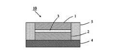
- FIG. 2is a schematic cross-sectional view showing a light emitting device according to an embodiment of the present invention.
- the light emitting device 10is formed by bonding the wavelength conversion member 1 and the light emitting element 2 by the adhesive layer 3.
- the light emitting element 2is disposed on the substrate 4.
- a reflective layer 5is disposed around the wavelength conversion member 1, the light emitting element 2, and the adhesive layer 3. By disposing the reflective layer 5, it is possible to suppress excitation light and fluorescence from being reflected and leaking to the outside, and it is possible to enhance the light extraction efficiency.
- the light emitting element 2has substantially the same shape and the same area as the wavelength conversion member 1 in plan view. However, the shapes and areas of the wavelength conversion member 1 and the light emitting element 2 may be different. For example, one wavelength conversion member 1 may be adhered to a plurality of light emitting elements 2 arranged side by side so as to cover the plurality of light emitting elements 2.
- the light emitting element 2for example, a light source such as an LED light source which emits blue light or an LD light source is used.
- an adhesive agent which comprises the adhesive bond layer 3a silicone resin type, an epoxy resin type, a vinyl resin type, an acrylic resin type etc. are mentioned, for example.
- the adhesive constituting the adhesive layer 3preferably has a refractive index close to that of the wavelength conversion member 1. If so, the excitation light emitted from the light emitting element 2 can be efficiently incident on the wavelength conversion member 1.
- the substrate 4for example, a white low temperature co-fired ceramic (LTC) or the like capable of efficiently reflecting a light beam emitted from the light emitting element 2 is used.
- LTCwhite low temperature co-fired ceramic
- a sintered body of an inorganic powder such as aluminum oxide, titanium oxide, niobium oxide and the like and a glass powdercan be mentioned.
- a ceramic substratesuch as aluminum oxide or aluminum nitride can be used.
- a resin composition or glass ceramicscan be used.
- the resin compositiona mixture of a resin and ceramic powder or glass powder can be used.
- glass ceramicsLTCC etc. are mentioned.
- a material of glass ceramicsmixed powder of glass powder and ceramic powder, or crystalline glass powder can be used.
- Table 1shows Examples 1 and 2 and Comparative Examples 1 to 3.
- a YAG phosphor powder(average particle size D 50 : 15 ⁇ m) was mixed with a borosilicate glass powder (average particle size D 50 : 2 ⁇ m, softening point 850 ° C.) to obtain a mixed powder.
- the content of YAG phosphor powderwas 8.3% by volume in the mixed powder.
- the mixed powderwas pressure-molded with a mold, and sintered near the softening point to obtain a sintered body.
- a plate-like wavelength conversion member precursor of 30 mm ⁇ 30 mm ⁇ 0.3 mmwas obtained by cutting the obtained sintered body.
- the wavelength conversion member precursoris polished by changing the polishing abrasives on each side using a single-side polishing machine so that the light incident surface and the light emitting surface each have a predetermined surface roughness. Made. The obtained wavelength conversion member was cut into an outer dimension of 1 mm ⁇ 1 mm to obtain a small wavelength conversion member.
- the luminous flux value of the obtained small wavelength conversion memberwas measured as follows. A silicone resin is applied to the surface of an LED chip with an excitation wavelength of 450 nm, a small piece of wavelength conversion member is adhered, and a highly reflective silicone resin is applied to the outer peripheral part of the LED chip and the small piece of wavelength conversion member to obtain a measurement sample. The The light emitted from the light emitting surface of the small wavelength conversion member was taken into the integrating sphere, and then guided to a calibrated spectroscope by a standard light source, and the energy distribution spectrum of the light was measured. The luminous flux value was calculated from the obtained energy distribution spectrum. The luminous flux values in Table 1 are shown as relative values with the luminous flux value of Example 1 being 1.
- the wavelength conversion members of Examples 1 and 2had a relative luminous flux value of 0.99 or more
- the wavelength conversion members of Comparative Examples 1 to 3had a relative luminous flux value of 0.95 or less. And was inferior.
Landscapes
- Physics & Mathematics (AREA)
- General Physics & Mathematics (AREA)
- Optics & Photonics (AREA)
- Chemical & Material Sciences (AREA)
- Engineering & Computer Science (AREA)
- Dispersion Chemistry (AREA)
- Crystallography & Structural Chemistry (AREA)
- Ceramic Engineering (AREA)
- Inorganic Chemistry (AREA)
- Life Sciences & Earth Sciences (AREA)
- Chemical Kinetics & Catalysis (AREA)
- General Chemical & Material Sciences (AREA)
- Geochemistry & Mineralogy (AREA)
- Materials Engineering (AREA)
- Organic Chemistry (AREA)
- Led Device Packages (AREA)
Abstract
Description
Translated fromJapanese本発明は、発光ダイオード(LED:Light Emitting Diode)やレーザーダイオード(LD:Laser Diode)等の発する光の波長を別の波長に変換する波長変換部材及びそれを用いた発光装置に関するものである。The present invention relates to a wavelength conversion member for converting a wavelength of light emitted from a light emitting diode (LED: Light Emitting Diode) or a laser diode (LD: Laser Diode) to another wavelength, and a light emitting device using the same.
近年、蛍光ランプや白熱灯に変わる次世代の光源として、LEDやLDを用いた発光装置等に対する注目が高まってきている。そのような次世代光源の一例として、青色光を出射するLEDと、LEDからの光の一部を吸収して黄色光に変換する波長変換部材とを組み合わせた発光装置が開示されている。この発光装置は、LEDから出射された青色光と、波長変換部材から出射された黄色光との合成光である白色光を発する。特許文献1には、波長変換部材の一例として、ガラスマトリクス中に無機蛍光体粉末を分散させた波長変換部材が提案されている。BACKGROUND ART In recent years, attention has been focused on light-emitting devices and the like using LEDs and LDs as light sources of the next generation in place of fluorescent lamps and incandescent lamps. As an example of such a next-generation light source, a light emitting device is disclosed in which an LED emitting blue light and a wavelength conversion member absorbing a part of the light from the LED and converting it into yellow light are combined. The light emitting device emits white light which is a composite light of blue light emitted from the LED and yellow light emitted from the wavelength conversion member.
上記波長変換部材は、光取出し効率に劣り、十分な発光強度が得られないという問題がある。The above wavelength conversion member has a problem that the light extraction efficiency is inferior and sufficient light emission intensity can not be obtained.
従って、本発明は、光取出し効率が高く、発光強度に優れた波長変換部材と、それを用いた発光装置を提案することを目的とする。Therefore, an object of the present invention is to propose a wavelength conversion member having a high light extraction efficiency and an excellent emission intensity, and a light emitting device using the same.
本発明者等が鋭意検討した結果、波長変換部材の光入射面と光出射面における表面粗さを特定範囲に規制することで、光取出し効率を向上させることができ、発光強度に優れた波長変換部材を得ることができることを見出した。As a result of intensive investigations by the present inventors, it is possible to improve the light extraction efficiency by restricting the surface roughness on the light incident surface and the light emission surface of the wavelength conversion member to a specific range, and a wavelength excellent in emission intensity. It has been found that a conversion member can be obtained.
即ち、本発明の波長変換部材は、蛍光体を含む板状の波長変換部材であって、光入射面と、光入射面と対向する光出射面とを有し、光入射面の表面粗さをRain、光出射面の表面粗さをRaoutとした場合、Rainが0.01~0.05μm、かつ、Raout-Rainが0.01~0.2μmであることを特徴とする。That is, the wavelength conversion member of the present invention is a plate-like wavelength conversion member containing a phosphor, and has a light incident surface and a light emitting surface facing the light incident surface, and the surface roughness of the light incident surface theRa in, if the surface roughness of the light exit surface was set toRa out, and characterized in thatRa in the 0.01 ~ 0.05 .mu.mand,, Ra out-Ra in is 0.01 ~ 0.2 [mu] m Do.
本発明の波長変換部材は、光出射面の表面粗さRaoutが0.06μm以上であることが好ましい。このようにすれば、光取出し効率をより一層向上させることができる。In the wavelength conversion member of the present invention, the surface roughness Raout of the light emitting surface is preferably 0.06 μm or more. This can further improve the light extraction efficiency.
本発明の波長変換部材は、ガラスマトリクス中に蛍光体粉末が分散してなることが好ましい。In the wavelength conversion member of the present invention, the phosphor powder is preferably dispersed in a glass matrix.
本発明の波長変換部材は、厚みが0.01~1mmであることが好ましい。The wavelength conversion member of the present invention preferably has a thickness of 0.01 to 1 mm.
本発明の発光装置は、上記の波長変換部材と、波長変換部材に励起光を照射する発光素子と、を備えることを特徴とする。A light emitting device according to the present invention is characterized by comprising the above-described wavelength conversion member, and a light emitting element for irradiating the wavelength conversion member with excitation light.
本発明の発光装置は、波長変換部材における光入射面と、発光素子とが接着剤層により接着されていることが好ましい。In the light emitting device of the present invention, it is preferable that the light incident surface of the wavelength conversion member and the light emitting element be bonded by an adhesive layer.
本発明の発光装置は、波長変換部材と発光素子の周囲に反射層が配置されていることが好ましい。In the light emitting device of the present invention, it is preferable that a reflection layer be disposed around the wavelength conversion member and the light emitting element.
本発明によれば、光取出し効率が高く、発光強度に優れた波長変換部材と、それを用いた発光装置を提案することができる。According to the present invention, it is possible to propose a wavelength conversion member having high light extraction efficiency and excellent light emission intensity, and a light emitting device using the same.
以下、好ましい実施形態について説明する。但し、以下の実施形態は単なる例示であり、本発明は以下の実施形態に限定されるものではない。また、各図面において、実質的に同一の機能を有する部材は同一の符号で参照する場合がある。Hereinafter, preferred embodiments will be described. However, the following embodiments are merely illustrative, and the present invention is not limited to the following embodiments. In each drawing, members having substantially the same functions may be referred to by the same reference numerals.
図1は本発明の一実施形態に係る波長変換部材を示す模式的断面図である。波長変換部材1は例えば矩形の板状である。波長変換部材1は蛍光体を含有しており、光入射面1aと、光入射面1aと対向する光出射面1bとを有する。波長変換部材1に含まれる蛍光体を励起させるための励起光を、入射光Linとして波長変換部材1の光入射面1aから入射させる。入射光Linは蛍光体により波長変換されて蛍光となる。当該蛍光と、波長変換されなかった入射光Linとの合成光が出射光Loutとして光出射面1bから出射する。例えば、入射光Linが青色光であり、蛍光が黄色光である場合、青色光と黄色光の合成光である白色光がLoutとして出射される。FIG. 1 is a schematic cross-sectional view showing a wavelength conversion member according to an embodiment of the present invention. The
波長変換部材1における光入射面1aの表面粗さをRain、光出射面1bの表面粗さをRaoutとした場合、Rainが0.01~0.05μm、かつ、Raout-Rainが0.01~0.2μmを満たす。このようにすることで、光取出し効率を向上させることが可能となる。この理由は以下のように推察される。光入射面1aの表面粗さRainを比較的小さくすることにより、入射光Linが光入射面1a表面で散乱されにくく、波長変換部材1内部への入射効率が高くなる。これは、通常、入射光LinはLEDやLDから発せられる光であるため直進性(配向性)が高く、光入射面1aに対して垂直方向の光の割合が大きいためであると考えられる。一方、光出射面1bの表面粗さRaoutをRainに対して相対的に大きくすることにより、出射光Loutの光取出し効率を向上させることができる。波長変換部材1は基本的に光散乱体であるため、入射光Linや蛍光は波長変換部材1の内部で散乱され、あらゆる方向に配向している。したがって、光出射面1bの表面粗さRaoutが小さいと、臨界角を超える光成分が多くなり、光取出し効率が低くなる傾向がある。そこで、光出射面1bの表面粗さRaoutを大きくすることにより、散乱光に対する光反射抑制効果を高めることができる。When the surface roughness of the light incident surface 1a of the
Rainが大きすぎると、入射光Linが光入射面1a表面で散乱され、波長変換部材1内部への入射効率が低くなる傾向がある。結果として、波長変換部材の光取出し効率が低下し、発光強度が低下しやすくなる。一方、Rainが小さすぎると、発光素子(後述)と接着する際にアンカー効果が得られにくく、接着強度が低下しやすくなる。なお、接着強度低下に起因して、波長変換部材1が発光素子から一部でも剥離すると、波長変換部材1と発光素子との間に屈折率が低い空気層が形成されるため、入射光Linの入射効率が著しく低下する傾向がある。Rainの好ましい範囲は0.015~0.045μmである。If Rain is too large, the incident light Lin tends to be scattered on the surface of the light incident surface 1 a, and the incident efficiency into the inside of the
Raout-Rainが小さすぎると、出射光Loutが光出射面1bで反射されやすくなり、光取出し効率が低下しやすくなる。一方、Raout-Rainが大きすぎると、出射光Loutの光出射面1bでの散乱が大きくなり、かえって光取出し効率が低下しやすくなる。Raout-Rainの好ましい範囲は0.02~0.18μmであり、より好ましい範囲は0.05~0.17μmである。If Raout -Rain is too small, the emitted light Lout is likely to be reflected by the light exit surface 1 b, and the light extraction efficiency tends to be reduced. On the other hand, if Raout -Rain is too large, the scattering of the emitted light Lout on the light emitting surface 1 b becomes large, and the light extraction efficiency tends to be reduced. The preferred range of Raout -Rain is 0.02 to 0.18 μm, and the more preferred range is 0.05 to 0.17 μm.
なお、Raoutは0.06μm以上、0.07μm以上、特に0.08μm以上であることが好ましく、0.25μm以下、0.23μm以下、特に0.22μm以下であることが好ましい。Raoutが小さすぎると、出射光Loutが光出射面1bで反射されやすくなり、光取出し効率が低下しやすくなる。一方、Raoutが大きすぎると、出射光Loutの光出射面1bでの散乱が大きくなり、光取出し効率が低下しやすくなる。The Raout is preferably 0.06 μm or more, 0.07 μm or more, particularly preferably 0.08 μm or more, and more preferably 0.25 μm or less, 0.23 μm or less, particularly preferably 0.22 μm or less. If Raout is too small, the emitted light Lout is likely to be reflected by the light emitting surface 1 b, and the light extraction efficiency tends to be reduced. On the other hand, when Raout is too large, the scattering of the emitted light Lout on the light emitting surface 1 b becomes large, and the light extraction efficiency tends to be reduced.
波長変換部材1は、例えばガラスマトリクスと、当該ガラスマトリクスに分散された蛍光体粉末とを含む蛍光体ガラスからなる。The
ガラスマトリクスは、無機蛍光体等の蛍光体粉末の分散媒として用いることができるものであれば特に限定されない。例えば、ホウ珪酸塩系ガラス、リン酸塩系ガラス、スズリン酸塩系ガラス、ビスマス酸塩系ガラス、テルライト系ガラスなどを用いることができる。ホウ珪酸塩系ガラスとしては、質量%で、SiO2 30~85%、Al2O3 0~30%、B2O3 0~50%、Li2O+Na2O+K2O 0~10%、及び、MgO+CaO+SrO+BaO 0~50%を含有するものが挙げられる。スズリン酸塩系ガラスとしては、モル%で、SnO 30~90%、P2O5 1~70%を含有するものが挙げられる。テルライト系ガラスとしては、モル%で、TeO2 50%以上、ZnO 0~45%、RO(RはCa、Sr及びBaから選択される少なくとも1種)0~50%、及び、La2O3+Gd2O3+Y2O3 0~50%を含有するものが挙げられる。The glass matrix is not particularly limited as long as it can be used as a dispersion medium for phosphor powders such as inorganic phosphors. For example, borosilicate glass, phosphate glass, tin phosphate glass, bismuth salt glass, tellurite glass, and the like can be used. As a borosilicate glass, SiO2 30 to 85%, Al2 O3 0 to 30%, B2 O3 0 to 50%, Li2 O + Na2 O + K2 O 0 to 10%, and% by mass And MgO + CaO + SrO + BaO 0 to 50%. Examples of tin phosphate glasses include those containing 30 to 90% of SnO and 1 to 70% of P2 O5 in mol%. As tellurite glass, TeO2 at 50% or more, ZnO 0 to 45%, RO (at least one selected from Ca, Sr and Ba) at 0% to 50%, and La2 O3 in mole% What contains 0 to 50% of + Gd2 O3 + Y2 O3 is mentioned.
ガラスマトリクスの軟化点は、250℃~1000℃であることが好ましく、300℃~950℃であることがより好ましく、500℃~900℃の範囲内であることがさらに好ましい。ガラスマトリクスの軟化点が低すぎると、波長変換部材1の機械的強度や化学的耐久性が低下する場合がある。また、ガラスマトリクス自体の耐熱性が低いため、蛍光体から発生する熱により軟化変形するおそれがある。一方、ガラスマトリクスの軟化点が高すぎると、製造時に焼成工程が含まれる場合、蛍光体が劣化して、波長変換部材1の発光強度が低下する場合がある。また、ガラスマトリクスの軟化点が高くなると、焼成温度も高くなり、結果として製造コストが高くなる傾向がある。なお、波長変換部材1の化学的安定性及び機械的強度を高める観点からはガラスマトリクスの軟化点は500℃以上、600℃以上、700℃以上、800℃以上、特に850℃以上であることが好ましい。そのようなガラスとしては、ホウ珪酸塩系ガラスが挙げられる。一方、波長変換部材1を安価に製造する観点からは、ガラスマトリクスの軟化点は550℃以下、530℃以下、500℃以下、480℃以下、特に460℃以下であることが好ましい。そのようなガラスとしては、スズリン酸塩系ガラス、ビスマス酸塩系ガラス、テルライト系ガラスが挙げられる。The softening point of the glass matrix is preferably 250 ° C. to 1000 ° C., more preferably 300 ° C. to 950 ° C., and still more preferably in the range of 500 ° C. to 900 ° C. If the softening point of the glass matrix is too low, the mechanical strength and the chemical durability of the
蛍光体は、励起光の入射により蛍光を出射するものであれば、特に限定されるものではない。蛍光体の具体例としては、例えば、酸化物蛍光体、窒化物蛍光体、酸窒化物蛍光体、塩化物蛍光体、酸塩化物蛍光体、硫化物蛍光体、酸硫化物蛍光体、ハロゲン化物蛍光体、カルコゲン化物蛍光体、アルミン酸塩蛍光体、ハロリン酸塩化物蛍光体及びガーネット系化合物蛍光体から選ばれた1種以上等が挙げられる。励起光として青色光を用いる場合、例えば、緑色光、黄色光または赤色光を蛍光として出射する蛍光体を用いることができる。The phosphor is not particularly limited as long as it emits fluorescence upon incidence of excitation light. Specific examples of the phosphor include, for example, oxide phosphors, nitride phosphors, oxynitride phosphors, chloride phosphors, acid chloride phosphors, sulfide phosphors, acid sulfide phosphors, and halides. One or more selected from a phosphor, a chalcogenide phosphor, an aluminate phosphor, a halophosphate chloride phosphor, and a garnet-based compound phosphor. When blue light is used as excitation light, for example, a phosphor that emits green light, yellow light or red light as fluorescence can be used.
蛍光体粉末の平均粒子径は1μm~50μmであることが好ましく、5μm~25μmであることがより好ましい。蛍光体粉末の平均粒子径が小さすぎると、発光強度が低下する場合がある。一方、蛍光体粉末の平均粒子径が大きすぎると、発光色が不均一になる場合がある。The average particle size of the phosphor powder is preferably 1 μm to 50 μm, and more preferably 5 μm to 25 μm. If the average particle size of the phosphor powder is too small, the emission intensity may decrease. On the other hand, if the average particle size of the phosphor powder is too large, the luminescent color may be nonuniform.
波長変換部材1中での蛍光体粉末の含有量は、1体積%以上、1.5体積%以上、特に2体積%であることが好ましく、70体積%以下、50体積%以下、30体積%以下であることが好ましい。蛍光体粉末の含有量が少なすぎると、所望の発光色を得るために波長変換部材1の厚みを厚くする必要があり、その結果、波長変換部材1の内部散乱が増加することで、光取り出し効率が低下する場合がある。一方、蛍光体粉末の含有量が多すぎると、所望の発光色を得るために波長変換部材1の厚みを薄くする必要があるため、波長変換部材1の機械的強度が低下する場合がある。The content of the phosphor powder in the
波長変換部材1の厚みは、0.01mm以上、0.03mm以上、0.05mm以上、0.075mm以上、特に0.08mm以上であることが好ましく、1mm以下、0.5mm以下、0.35mm以下、0.3mm以下、0.25mm以下、0.15mm以下、特に0.12mm以下であることが好ましい。波長変換部材1の厚みが厚すぎると、波長変換部材1における光の散乱や吸収が大きくなりすぎ、光取り出し効率が低くなる場合がある。波長変換部材1の厚みが薄すぎると、十分な発光強度が得られにくくなる場合がある。また、波長変換部材1の機械的強度が不十分になる場合がある。The thickness of the
波長変換部材1の屈折率(nd)は、1.40以上、1.45以上、1.50以上であることが好ましく、1.90以下、1.80以下、1.70以下であることが好ましい。波長変換部材1の屈折率が高すぎると、波長変換部材1と光出射側の媒質(例えば空気層(nd=1.0))との屈折率差が大きくなることで、光出射面1bでの全反射が発生しやすく、光取り出し効率が低くなる場合がある。波長変換部材1の屈折率が低すぎると、発光素子(たとえばフリップチップ実装型のLED。出射面はサファイアnd=1.76)との屈折率差が大きくなる。そのため、波長変換部材1と発光素子の間に接着剤層を設け、当該接着剤層により屈折率差を調整した場合でも、発光素子と接着剤層の屈折率差及び/または接着剤層と波長変換部材1の屈折率差が大きくなってしまい、各々の界面で光取り出し効率が低くなる場合がある。The refractive index (nd) of the
波長変換部材1の光出射面1bに反射防止膜を設けても構わない。このようにすれば、蛍光や励起光が光出射面1bから出射する際、波長変換部材1と空気との屈折率差に起因する光取り出し効率の低下を抑制することができる。反射防止膜としては、SiO2、Al2O3、TiO2、Nb2O5、Ta2O5等から構成される単層または多層の誘電体膜が挙げられる。An anti-reflection film may be provided on the light emitting surface 1 b of the
波長変換部材1の光入射面1aに反射防止膜を設けても構わない。このようにすれば、励起光が波長変換部材1に入射する際、接着剤層と波長変換部材1との屈折率差に起因する励起光入射効率の低下を抑制することができる。An antireflection film may be provided on the light incident surface 1 a of the
なお、波長変換部材1が蛍光体ガラスからなる場合、通常、波長変換部材1におけるガラスマトリクスの屈折率を考慮して反射防止膜の設計を行う。ここで、波長変換部材1の光出射面1bに蛍光体粉末が露呈していると、蛍光体粉末は屈折率が比較的高いため、蛍光体粉末部分に形成された反射防止膜は適切な膜設計とはならず、十分な反射防止機能が得られないおそれがある。そこで、波長変換部材1の光出射面1bに、露出した蛍光体粉末が被覆されるようにガラス層(蛍光体粉末を含まないガラス層)を設けることが好ましい。このようにすれば、波長変換部材1の光出射面1bの屈折率が一様となり、反射防止膜による効果を高めることができる。なお、波長変換部材1の光入射面1aにも、上述のように反射防止効果を高める目的のためガラス層を設けることが好ましい。In addition, when the
ガラス層を構成するガラスは、波長変換部材1におけるガラスマトリクスを構成するガラスと同じであることが好ましい。このようにすれば、波長変換部材1におけるガラスマトリクスとガラス層との屈折率差がなくなり、両界面での光反射ロスを抑制することができる。なお、ガラス層を設ける場合は、ガラス層表面の表面粗さが、上述の表面粗さRaoutの範囲を満たすことが好ましい。ガラス層の厚みは0.003~0.1mm、0.005~0.03mm、特に0.01~0.02mmであることが好ましい。ガラス層の厚みが小さすぎると、露出した蛍光体粉末を十分に被覆できないおそれがある。一方、ガラス層の厚みが大きすぎると、励起光や蛍光が吸収されて発光効率が低下するおそれがある。The glass constituting the glass layer is preferably the same as the glass constituting the glass matrix in the
なお、波長変換部材1は蛍光体ガラスからなるもの以外にも、YAGセラミックス等のセラミックスからなるものや、樹脂中に蛍光体粉末が分散したものであってもよい。The
波長変換部材1は以下のようにして作製することができる。まず、板状の波長変換部材前駆体を作製する。波長変換部材前駆体は、例えば蛍光体粉末とガラス粉末の混合物の焼結体を切削することにより作製することができる。次に、波長変換部材前駆体の両主面、即ち光入射面及び光出射面を所望の表面粗さとなるように研磨することにより、波長変換部材1を得る。ここで、研磨パッドや研磨砥粒を適宜選択することにより、波長変換部材1の両主面の表面粗さを調整する。波長変換部材前駆体の両主面を同時に研磨してもよいし、片面ずつ順番に研磨(光入射面を研磨した後光出射面を研磨、あるいは、光出射面を研磨した後光入射面を研磨)してもよい。例えば、両面研磨機にて波長変換部材1の両面に粗研磨を実施した後、片面研磨機にて光入射面を研磨する方法や、片面研磨機にて波長変換部材1の光入射面と光出射面を、異なる研磨砥粒を使用して片面ずつ順番に研磨する方法が挙げられる。The
図2は、本発明の一実施形態に係る発光装置を示す模式的断面図である。発光装置10は、波長変換部材1と発光素子2とが接着剤層3により接着されてなるものである。本実施形態において、発光素子2は基板4の上に設置されている。また、波長変換部材1、発光素子2、及び接着剤層3の周囲には反射層5が配置されている。反射層5を配置することにより、励起光及び蛍光を反射して外部に漏れるのを抑制することができ、光の取り出し効率を高めることができる。発光素子2は、平面視において波長変換部材1と略同一形状、同一面積である。ただし、波長変換部材1と発光素子2の形状及び面積は異なっていても構わない。例えば、並べて設置された複数の発光素子2に対し、当該複数の発光素子2を覆うように1枚の波長変換部材1を接着してもよい。FIG. 2 is a schematic cross-sectional view showing a light emitting device according to an embodiment of the present invention. The
発光素子2としては、例えば、青色光を発するLED光源やLD光源などの光源が用いられる。接着剤層3を構成する接着剤としては、例えば、シリコーン樹脂系、エポキシ樹脂系、ビニル系樹脂系、アクリル樹脂系などが挙げられる。接着剤層3を構成する接着剤は、波長変換部材1の屈折率と近似した屈折率であることが好ましい。そのようにすれば、発光素子2より発せられた励起光を効率よく波長変換部材1へ入射させることができる。基板4としては、例えば、発光素子2から発せられた光線を効率良く反射させることができる白色のLTCC(Low Temperature Co-fired Ceramics)などが用いられる。具体的には、酸化アルミニウム、酸化チタン、酸化ニオブ等の無機粉末と、ガラス粉末との焼結体が挙げられる。あるいは、酸化アルミニウムや窒化アルミニウム等のセラミック基板を使用することができる。反射層6としては、樹脂組成物またはガラスセラミックスを用いることができる。樹脂組成物としては、樹脂と、セラミック粉末またはガラス粉末の混合物を用いることができる。ガラスセラミックスとしては、LTCC等が挙げられる。ガラスセラミックスの材料としては、ガラス粉末及びセラミックス粉末の混合粉末、又は結晶性ガラス粉末を用いることができる。As the
以下に本発明の波長変換部材を実施例により詳細に説明するが、本発明は以下の実施例に限定されるものではない。Hereinafter, the wavelength conversion member of the present invention will be described in detail by way of examples, but the present invention is not limited to the following examples.
表1は実施例1、2及び比較例1~3を示す。Table 1 shows Examples 1 and 2 and Comparative Examples 1 to 3.

ホウ珪酸塩系ガラス粉末(平均粒子径D50:2μm、軟化点850℃)にYAG蛍光体粉末(平均粒子径D50:15μm)を混合して混合粉末を得た。YAG蛍光体粉末の含有量は混合粉末中に8.3体積%とした。混合粉末を金型で加圧成型し、軟化点付近で焼成することにより焼結体を得た。得られた焼結体を切削することにより30mm×30mm×0.3mmの板状の波長変換部材前駆体を得た。波長変換部材前駆体に対し、光入射面及び光出射面を各々所定の表面粗さとなるように、片面研磨機を用いて、研磨砥粒を片面毎に変えて研磨することにより波長変換部材を作製した。得られた波長変換部材を外形寸法1mm×1mmに切断し小片の波長変換部材を得た。A YAG phosphor powder (average particle size D50 : 15 μm) was mixed with a borosilicate glass powder (average particle size D50 : 2 μm, softening point 850 ° C.) to obtain a mixed powder. The content of YAG phosphor powder was 8.3% by volume in the mixed powder. The mixed powder was pressure-molded with a mold, and sintered near the softening point to obtain a sintered body. A plate-like wavelength conversion member precursor of 30 mm × 30 mm × 0.3 mm was obtained by cutting the obtained sintered body. With respect to the wavelength conversion member precursor, the wavelength conversion member is polished by changing the polishing abrasives on each side using a single-side polishing machine so that the light incident surface and the light emitting surface each have a predetermined surface roughness. Made. The obtained wavelength conversion member was cut into an outer dimension of 1 mm × 1 mm to obtain a small wavelength conversion member.
得られた小片の波長変換部材について、以下のようにして光束値を測定した。励起波長450nmのLEDチップ表面にシリコーン樹脂を塗布し、小片の波長変換部材を接着させ、LEDチップ及び小片の波長変換部材の外周部に高反射性のシリコーン樹脂を塗布して測定用サンプルを得た。小片の波長変換部材の光出射面から発せられる光を積分球内部に取り込んだ後、標準光源によって校正された分光器へ導光し、光のエネルギー分布スペクトルを測定した。得られたエネルギー分布スペクトルから光束値を算出した。なお表1の光束値は、実施例1の光束値を1とした相対値で示している。The luminous flux value of the obtained small wavelength conversion member was measured as follows. A silicone resin is applied to the surface of an LED chip with an excitation wavelength of 450 nm, a small piece of wavelength conversion member is adhered, and a highly reflective silicone resin is applied to the outer peripheral part of the LED chip and the small piece of wavelength conversion member to obtain a measurement sample. The The light emitted from the light emitting surface of the small wavelength conversion member was taken into the integrating sphere, and then guided to a calibrated spectroscope by a standard light source, and the energy distribution spectrum of the light was measured. The luminous flux value was calculated from the obtained energy distribution spectrum. The luminous flux values in Table 1 are shown as relative values with the luminous flux value of Example 1 being 1.
表1に示すように、実施例1、2の波長変換部材は相対光束値が0.99以上であったのに対し、比較例1~3の波長変換部材は相対光束値が0.95以下と劣っていた。As shown in Table 1, while the wavelength conversion members of Examples 1 and 2 had a relative luminous flux value of 0.99 or more, the wavelength conversion members of Comparative Examples 1 to 3 had a relative luminous flux value of 0.95 or less. And was inferior.
1 波長変換部材
1a 光入射面
1b 光出射面
2 発光素子
3 接着剤層
10 発光装置
Claims (7)
Translated fromJapanese光入射面と、前記光入射面と対向する光出射面とを有し、
前記光入射面の表面粗さをRain、前記光出射面の表面粗さをRaoutとした場合、Rainが0.01~0.05μm、かつ、Raout-Rainが0.01~0.2μmであることを特徴とする波長変換部材。A plate-like wavelength conversion member containing a phosphor,
A light incident surface, and a light emitting surface facing the light incident surface;
Assuming that the surface roughness of the light incident surface is Rain and the surface roughness of the light emission surface is Raout , Rain is 0.01 to 0.05 μm, and Raout -Rain is 0.01 to A wavelength conversion member characterized in that it is 0.2 μm.
前記波長変換部材に励起光を照射する発光素子と、
を備えることを特徴とする発光装置。A wavelength conversion member according to any one of claims 1 to 4;
A light emitting element for irradiating the wavelength conversion member with excitation light;
A light emitting device comprising:
Priority Applications (4)
| Application Number | Priority Date | Filing Date | Title |
|---|---|---|---|
| CN201880020681.4ACN110494776B (en) | 2017-07-27 | 2018-07-12 | Wavelength conversion member and light-emitting device |
| US16/629,578US20210091274A1 (en) | 2017-07-27 | 2018-07-12 | Wavelength conversion member and light emitting device |
| KR1020197021586AKR102621944B1 (en) | 2017-07-27 | 2018-07-12 | Wavelength conversion member and light emitting device |
| DE112018003792.4TDE112018003792T5 (en) | 2017-07-27 | 2018-07-12 | Wavelength conversion element and light emitting device |
Applications Claiming Priority (4)
| Application Number | Priority Date | Filing Date | Title |
|---|---|---|---|
| JP2017145157 | 2017-07-27 | ||
| JP2017-145157 | 2017-07-27 | ||
| JP2018-101969 | 2018-05-29 | ||
| JP2018101969AJP7090842B2 (en) | 2017-07-27 | 2018-05-29 | Wavelength conversion member and light emitting device |
Publications (1)
| Publication Number | Publication Date |
|---|---|
| WO2019021846A1true WO2019021846A1 (en) | 2019-01-31 |
Family
ID=65039605
Family Applications (1)
| Application Number | Title | Priority Date | Filing Date |
|---|---|---|---|
| PCT/JP2018/026353CeasedWO2019021846A1 (en) | 2017-07-27 | 2018-07-12 | Wavelength conversion member and light emitting device |
Country Status (2)
| Country | Link |
|---|---|
| TW (1) | TWI757521B (en) |
| WO (1) | WO2019021846A1 (en) |
Cited By (2)
| Publication number | Priority date | Publication date | Assignee | Title |
|---|---|---|---|---|
| JP2020154012A (en)* | 2019-03-18 | 2020-09-24 | 日本電気硝子株式会社 | Wavelength conversion member, its manufacturing method, and light emitting device |
| CN113728254A (en)* | 2019-04-25 | 2021-11-30 | 京瓷株式会社 | Optical component |
Citations (6)
| Publication number | Priority date | Publication date | Assignee | Title |
|---|---|---|---|---|
| JP2007161944A (en)* | 2005-12-16 | 2007-06-28 | Nippon Electric Glass Co Ltd | Phosphor |
| JP2009218274A (en)* | 2008-03-07 | 2009-09-24 | Stanley Electric Co Ltd | Semiconductor light-emitting device |
| JP2011122067A (en)* | 2009-12-11 | 2011-06-23 | Nippon Electric Glass Co Ltd | Wavelength conversion member and method for manufacturing the same |
| WO2012014360A1 (en)* | 2010-07-26 | 2012-02-02 | 株式会社小糸製作所 | Light-emitting module |
| JP2014112635A (en)* | 2012-11-09 | 2014-06-19 | Nichia Chem Ind Ltd | Method for manufacturing light-emitting device, and light-emitting device |
| JP2014157856A (en)* | 2013-02-14 | 2014-08-28 | Asahi Glass Co Ltd | Optical conversion member, and illumination light source having the same |
Family Cites Families (1)
| Publication number | Priority date | Publication date | Assignee | Title |
|---|---|---|---|---|
| WO2016010116A1 (en)* | 2014-07-18 | 2016-01-21 | 凸版印刷株式会社 | Protective film for wavelength conversion sheet, wavelength conversion sheet and backlight unit |
- 2018
- 2018-07-09TWTW107123659Apatent/TWI757521B/enactive
- 2018-07-12WOPCT/JP2018/026353patent/WO2019021846A1/ennot_activeCeased
Patent Citations (6)
| Publication number | Priority date | Publication date | Assignee | Title |
|---|---|---|---|---|
| JP2007161944A (en)* | 2005-12-16 | 2007-06-28 | Nippon Electric Glass Co Ltd | Phosphor |
| JP2009218274A (en)* | 2008-03-07 | 2009-09-24 | Stanley Electric Co Ltd | Semiconductor light-emitting device |
| JP2011122067A (en)* | 2009-12-11 | 2011-06-23 | Nippon Electric Glass Co Ltd | Wavelength conversion member and method for manufacturing the same |
| WO2012014360A1 (en)* | 2010-07-26 | 2012-02-02 | 株式会社小糸製作所 | Light-emitting module |
| JP2014112635A (en)* | 2012-11-09 | 2014-06-19 | Nichia Chem Ind Ltd | Method for manufacturing light-emitting device, and light-emitting device |
| JP2014157856A (en)* | 2013-02-14 | 2014-08-28 | Asahi Glass Co Ltd | Optical conversion member, and illumination light source having the same |
Cited By (5)
| Publication number | Priority date | Publication date | Assignee | Title |
|---|---|---|---|---|
| JP2020154012A (en)* | 2019-03-18 | 2020-09-24 | 日本電気硝子株式会社 | Wavelength conversion member, its manufacturing method, and light emitting device |
| WO2020189338A1 (en)* | 2019-03-18 | 2020-09-24 | 日本電気硝子株式会社 | Wavelength conversion member and method for manufacturing same, and light emission device |
| JP7480472B2 (en) | 2019-03-18 | 2024-05-10 | 日本電気硝子株式会社 | Wavelength conversion member, manufacturing method thereof, and light emitting device |
| CN113728254A (en)* | 2019-04-25 | 2021-11-30 | 京瓷株式会社 | Optical component |
| CN113728254B (en)* | 2019-04-25 | 2023-08-22 | 京瓷株式会社 | optical components |
Also Published As
| Publication number | Publication date |
|---|---|
| TW201910287A (en) | 2019-03-16 |
| TWI757521B (en) | 2022-03-11 |
Similar Documents
| Publication | Publication Date | Title |
|---|---|---|
| EP3690497B1 (en) | Optical wavelength converter and composite optical device | |
| US7800123B2 (en) | Electroluminescence device | |
| US10580944B2 (en) | Wavelength conversion member, light-emitting device, and method for manufacturing wavelength conversion member | |
| JP7212319B2 (en) | Wavelength conversion member and light emitting device | |
| TWI715784B (en) | Wavelength conversion member and light-emitting device using the same | |
| JPWO2018074132A1 (en) | Wavelength conversion member, light emitting device, and method of manufacturing wavelength conversion member | |
| EP3830216B1 (en) | Reflective color correction for phosphor illumination systems | |
| WO2018225424A1 (en) | Wavelength converter and method of manufacture therefor, and light-emitting device using wavelength converter | |
| WO2019021846A1 (en) | Wavelength conversion member and light emitting device | |
| KR102621944B1 (en) | Wavelength conversion member and light emitting device | |
| WO2020059499A1 (en) | Powder material for wavelength conversion member | |
| US12438336B2 (en) | Phosphor element, phosphor device, and illumination apparatus | |
| WO2018025671A1 (en) | Wavelength conversion member and production method therefor | |
| JP7480472B2 (en) | Wavelength conversion member, manufacturing method thereof, and light emitting device | |
| US11674652B2 (en) | Phosphor element, phosphor device, and illumination device | |
| WO2025047649A1 (en) | Wavelength conversion member | |
| JP2025036060A (en) | Wavelength conversion material | |
| WO2018025670A1 (en) | Wavelength conversion member and production method therefor | |
| WO2020246239A1 (en) | Wavelength-conversion member and light-emitting device |
Legal Events
| Date | Code | Title | Description |
|---|---|---|---|
| 121 | Ep: the epo has been informed by wipo that ep was designated in this application | Ref document number:18839466 Country of ref document:EP Kind code of ref document:A1 | |
| ENP | Entry into the national phase | Ref document number:20197021586 Country of ref document:KR Kind code of ref document:A | |
| 122 | Ep: pct application non-entry in european phase | Ref document number:18839466 Country of ref document:EP Kind code of ref document:A1 |