WO2019009232A1 - Load drive - Google Patents
Load driveDownload PDFInfo
- Publication number
- WO2019009232A1 WO2019009232A1PCT/JP2018/025023JP2018025023WWO2019009232A1WO 2019009232 A1WO2019009232 A1WO 2019009232A1JP 2018025023 WJP2018025023 WJP 2018025023WWO 2019009232 A1WO2019009232 A1WO 2019009232A1
- Authority
- WO
- WIPO (PCT)
- Prior art keywords
- terminal
- input
- current
- driving device
- load driving
- Prior art date
- Legal status (The legal status is an assumption and is not a legal conclusion. Google has not performed a legal analysis and makes no representation as to the accuracy of the status listed.)
- Ceased
Links
Images


Classifications
- H—ELECTRICITY
- H05—ELECTRIC TECHNIQUES NOT OTHERWISE PROVIDED FOR
- H05B—ELECTRIC HEATING; ELECTRIC LIGHT SOURCES NOT OTHERWISE PROVIDED FOR; CIRCUIT ARRANGEMENTS FOR ELECTRIC LIGHT SOURCES, IN GENERAL
- H05B45/00—Circuit arrangements for operating light-emitting diodes [LED]
- H05B45/30—Driver circuits
- B—PERFORMING OPERATIONS; TRANSPORTING
- B60—VEHICLES IN GENERAL
- B60Q—ARRANGEMENT OF SIGNALLING OR LIGHTING DEVICES, THE MOUNTING OR SUPPORTING THEREOF OR CIRCUITS THEREFOR, FOR VEHICLES IN GENERAL
- B60Q1/00—Arrangement of optical signalling or lighting devices, the mounting or supporting thereof or circuits therefor
- B60Q1/02—Arrangement of optical signalling or lighting devices, the mounting or supporting thereof or circuits therefor the devices being primarily intended to illuminate the way ahead or to illuminate other areas of way or environments
- B60Q1/04—Arrangement of optical signalling or lighting devices, the mounting or supporting thereof or circuits therefor the devices being primarily intended to illuminate the way ahead or to illuminate other areas of way or environments the devices being headlights
- B60Q1/14—Arrangement of optical signalling or lighting devices, the mounting or supporting thereof or circuits therefor the devices being primarily intended to illuminate the way ahead or to illuminate other areas of way or environments the devices being headlights having dimming means
- B60Q1/1407—General lighting circuits comprising dimming circuits
- B—PERFORMING OPERATIONS; TRANSPORTING
- B60—VEHICLES IN GENERAL
- B60Q—ARRANGEMENT OF SIGNALLING OR LIGHTING DEVICES, THE MOUNTING OR SUPPORTING THEREOF OR CIRCUITS THEREFOR, FOR VEHICLES IN GENERAL
- B60Q1/00—Arrangement of optical signalling or lighting devices, the mounting or supporting thereof or circuits therefor
- B60Q1/26—Arrangement of optical signalling or lighting devices, the mounting or supporting thereof or circuits therefor the devices being primarily intended to indicate the vehicle, or parts thereof, or to give signals, to other traffic
- B60Q1/34—Arrangement of optical signalling or lighting devices, the mounting or supporting thereof or circuits therefor the devices being primarily intended to indicate the vehicle, or parts thereof, or to give signals, to other traffic for indicating change of drive direction
- G—PHYSICS
- G05—CONTROLLING; REGULATING
- G05F—SYSTEMS FOR REGULATING ELECTRIC OR MAGNETIC VARIABLES
- G05F1/00—Automatic systems in which deviations of an electric quantity from one or more predetermined values are detected at the output of the system and fed back to a device within the system to restore the detected quantity to its predetermined value or values, i.e. retroactive systems
- G05F1/10—Regulating voltage or current
- G05F1/46—Regulating voltage or current wherein the variable actually regulated by the final control device is DC
- G05F1/56—Regulating voltage or current wherein the variable actually regulated by the final control device is DC using semiconductor devices in series with the load as final control devices
- H—ELECTRICITY
- H02—GENERATION; CONVERSION OR DISTRIBUTION OF ELECTRIC POWER
- H02M—APPARATUS FOR CONVERSION BETWEEN AC AND AC, BETWEEN AC AND DC, OR BETWEEN DC AND DC, AND FOR USE WITH MAINS OR SIMILAR POWER SUPPLY SYSTEMS; CONVERSION OF DC OR AC INPUT POWER INTO SURGE OUTPUT POWER; CONTROL OR REGULATION THEREOF
- H02M3/00—Conversion of DC power input into DC power output
- H02M3/02—Conversion of DC power input into DC power output without intermediate conversion into AC
- H02M3/04—Conversion of DC power input into DC power output without intermediate conversion into AC by static converters
- H02M3/10—Conversion of DC power input into DC power output without intermediate conversion into AC by static converters using discharge tubes with control electrode or semiconductor devices with control electrode
- H02M3/145—Conversion of DC power input into DC power output without intermediate conversion into AC by static converters using discharge tubes with control electrode or semiconductor devices with control electrode using devices of a triode or transistor type requiring continuous application of a control signal
- H02M3/155—Conversion of DC power input into DC power output without intermediate conversion into AC by static converters using discharge tubes with control electrode or semiconductor devices with control electrode using devices of a triode or transistor type requiring continuous application of a control signal using semiconductor devices only
- H02M3/156—Conversion of DC power input into DC power output without intermediate conversion into AC by static converters using discharge tubes with control electrode or semiconductor devices with control electrode using devices of a triode or transistor type requiring continuous application of a control signal using semiconductor devices only with automatic control of output voltage or current, e.g. switching regulators
- H—ELECTRICITY
- H05—ELECTRIC TECHNIQUES NOT OTHERWISE PROVIDED FOR
- H05B—ELECTRIC HEATING; ELECTRIC LIGHT SOURCES NOT OTHERWISE PROVIDED FOR; CIRCUIT ARRANGEMENTS FOR ELECTRIC LIGHT SOURCES, IN GENERAL
- H05B45/00—Circuit arrangements for operating light-emitting diodes [LED]
- H05B45/40—Details of LED load circuits
- H05B45/44—Details of LED load circuits with an active control inside an LED matrix
- H05B45/46—Details of LED load circuits with an active control inside an LED matrix having LEDs disposed in parallel lines
- H—ELECTRICITY
- H05—ELECTRIC TECHNIQUES NOT OTHERWISE PROVIDED FOR
- H05B—ELECTRIC HEATING; ELECTRIC LIGHT SOURCES NOT OTHERWISE PROVIDED FOR; CIRCUIT ARRANGEMENTS FOR ELECTRIC LIGHT SOURCES, IN GENERAL
- H05B47/00—Circuit arrangements for operating light sources in general, i.e. where the type of light source is not relevant
- H05B47/10—Controlling the light source
- H—ELECTRICITY
- H10—SEMICONDUCTOR DEVICES; ELECTRIC SOLID-STATE DEVICES NOT OTHERWISE PROVIDED FOR
- H10H—INORGANIC LIGHT-EMITTING SEMICONDUCTOR DEVICES HAVING POTENTIAL BARRIERS
- H10H20/00—Individual inorganic light-emitting semiconductor devices having potential barriers, e.g. light-emitting diodes [LED]
- H10H20/80—Constructional details
- H—ELECTRICITY
- H02—GENERATION; CONVERSION OR DISTRIBUTION OF ELECTRIC POWER
- H02M—APPARATUS FOR CONVERSION BETWEEN AC AND AC, BETWEEN AC AND DC, OR BETWEEN DC AND DC, AND FOR USE WITH MAINS OR SIMILAR POWER SUPPLY SYSTEMS; CONVERSION OF DC OR AC INPUT POWER INTO SURGE OUTPUT POWER; CONTROL OR REGULATION THEREOF
- H02M1/00—Details of apparatus for conversion
- H02M1/0003—Details of control, feedback or regulation circuits
- H02M1/0032—Control circuits allowing low power mode operation, e.g. in standby mode
Definitions
- the invention disclosed hereinrelates to a load drive device.
- FIG. 17is a diagram showing a conventional example of a load drive device.
- the load driving device X of this conventional exampleis a semiconductor integrated circuit device (so-called driver IC) which receives the input voltage Vin from the power supply E and outputs the output voltage Vout and the output current Iout to the load Z.
- driver ICsemiconductor integrated circuit device
- patent document 1can be mentioned as an example of the prior art relevant to the above.
- FIG. 18is a diagram showing the output behavior of the load drive device X, and from top to bottom, the relationship between the input voltage Vin and the output voltage Vout, the relationship between the input voltage Vin and the output current Iout, and the input voltage Vin and the consumption The relationship with the power Pc is shown.
- the load driving device Xperforms output feedback control so that the output current Iout always has a constant value regardless of the input voltage Vin.
- the output voltage Voutis determined by the characteristics of the load Z (for example, when the load Z is an LED [light emitting diode], its forward drop voltage).
- the power consumption Pcis obtained by the product of the input / output voltage difference (Vin ⁇ Vout) and the output current Iout.
- the power consumption Pcincreases with the increase of the input voltage Vin, and the amount of heat generation thereof increases. Therefore, in order to sufficiently dissipate the heat from the load driving device X, the area of the printed wiring board on which the load driving device X must be mounted must be increased, which makes it difficult to incorporate the device into a small module.
- the invention disclosed in the present specificationaims at providing a load drive device capable of distributing power consumption inside the device, in view of the above-mentioned problems found by the inventors of the present application.
- the load driving device disclosed in the present specificationincludes a first input terminal for receiving an input of a first input current from a power supply, and a first input terminal for receiving an input of a second input current from the power supply via an external resistor. 2 input terminals, an output terminal for outputting an output current to a load, a current distribution unit which adds the first input current and the second input current at a predetermined distribution ratio to generate the output current, And a control unit that controls the distribution ratio (first configuration).
- the current distribution unitincludes a first transistor in a path through which the first input current flows, and the control unit controls the on resistance value of the first transistor.
- Configuration(second configuration).
- the current distribution unitfurther includes a second transistor in a path through which the second input current flows, and the control unit includes the first transistor and the second transistor. It is good to make it the structure (3rd structure) which carries out differential control of each on resistance value.
- the control unitsets a difference value between the first terminal voltage appearing at the second input terminal and the second terminal voltage appearing at the output terminal. It is preferable that the distribution ratio be controlled accordingly (fourth configuration).
- the control unitIn the load driving device having the fourth configuration, the control unit generates an input detection unit that generates a first differential input voltage from the first terminal voltage, and a second differential input from the second terminal voltage.
- a configurationincluding an output detection unit that generates a voltage, and a differential amplifier that generates a control signal of the current distribution unit according to a difference value between the first differential input voltage and the second differential input voltage ( It is good to set it as the 5th composition).
- the input detection unitsubtracts the predetermined threshold voltage from the first terminal voltage to generate the first differential input signal (sixth configuration) You should
- the output detection unitoutputs the highest value of the plurality of second terminal voltages as the second differential input signal (seventh configuration It is good to be).
- the output detection unitoutputs an average value of the plurality of second terminal voltages as the second differential input signal (eighth configuration ) May be used.
- the control unitdynamically operates the distribution ratio according to a difference value between a terminal voltage of the second input terminal and a predetermined reference voltage. It is good to set it as the structure (9th structure) controlled to.
- the load driving device having any one of the first to ninth configurationsmay further include a current driver configured to perform constant current control of the output current (10th configuration).
- the current distribution unitis integrated on the first side of the semiconductor chip in a plan view of the semiconductor chip, and the current drive unit is the semiconductor
- the chipmay be integrated on a second side opposite to the first side of the chip (an eleventh structure).
- the current driving unitincludes a plurality of constant current sources respectively connected between the current distribution unit and the plurality of output terminals 12) is good.
- the plurality of constant current sourcesare arranged in a direction along the second side in a plan view of the semiconductor chip (a thirteenth configuration). It is good to do.
- the current distribution unitis configured such that, from a position adjacent to the constant current source closest to the third side of the semiconductor chip in the plan view of the semiconductor chip
- the configurationmay be integrated (fourteenth configuration) between a side and a position adjacent to the farthest constant current source.
- the terminal connected to the power supply and the terminal adjacent theretohave a withstand voltage that can withstand connection to the power supply (fifteenth embodiment Configuration).
- the first transistoris provided with a source region, a source pad provided in the immediate vicinity of the source region and wire-bonded to the first input terminal, a drain region And a drain pad provided in the immediate vicinity of the drain region and wire-bonded to the second input terminal.
- the first input terminal and the second input terminalmay be arranged adjacent to each other (a seventeenth configuration).
- an external terminal whose high withstand voltage is easier to design than other external terminalsis provided next to the first input terminal or the second input terminal. It is good to make it the structure currently arranged (18th structure).
- the first input terminalreceives an input of the first input current directly from the power supply (a nineteenth configuration). It is good to do.
- control unitmay be configured to control the distribution ratio dynamically (a twentieth configuration).
- the load driving device having any one of the first to twentieth configurationsbe configured to be integrated in a semiconductor device (twenty-first configuration).
- control unitmay be configured to dynamically control the on-resistance value of the first transistor (a twenty-second configuration).
- control unitmay be configured to dynamically differentially control the on resistance values of the first transistor and the second transistor (a twenty-third configuration). Good.
- control unitdynamically controls the distribution ratio in accordance with a difference value between the first terminal voltage and the second terminal voltage. Configuration).
- the electric device disclosed in the present specificationincludes the load drive device having any one of the first to twenty-fourth configurations, and between the first input terminal and the second input terminal of the load drive device.
- An external resistor connected and a load connected to an output terminal of the load driving deviceare configured (25th configuration).
- the load drive devicehaving any one of the above-described first to twenty-fourth configurations, and the first input terminal and the second input terminal of the load drive device.
- An external resistor connected and a light source connected as a load to the output terminal of the load driving deviceare configured (sixth configuration).
- a vehicle disclosed in the present specificationhas a configuration (a twenty-seventh configuration) including a lamp module having the above-described twenty-sixth configuration, and a battery serving as a power source of the lamp module.
- the lamp modulemay be a headlamp module, a rear lamp module, or a winker lamp module (a twenty-eighth configuration).
- a diagram showing an entire configuration of an electric device provided with a load drive deviceA diagram showing a first embodiment of an LED driver IC A diagram showing an example of power consumption distributed control in the first embodiment
- the figure which shows 2nd Embodiment of LED driver ICA diagram showing an example of power consumption distributed control in the second embodiment
- the figure which shows 3rd Embodiment of LED driver ICA figure showing an example of power consumption distributed control in a 3rd embodiment
- Terminal arrangement (16 pins) of LED driver IC(first example)
- the figure which shows the terminal arrangement (16 pins) of LED driver ICthe 2nd example
- Terminal arrangement (16 pins) of LED driver ICfourth example
- FIG. 1is a diagram showing an entire configuration of an electric device provided with a load driving device.
- the electric device 1 of this configuration examplehas a load driving device 100 and an external resistor R and a load Z externally attached thereto.
- the load driving device 100is a semiconductor integrated circuit device (so-called driver IC) which receives the input voltage Vin from the power supply E and outputs the output voltage Vout and the output current Iout to the load Z, and is electrically connected to the outside of the device. In order to establish a connection, it has a first input terminal IN1, a second input terminal IN2 and an output terminal OUT. Of course, the load driving device 100 may be provided with an external terminal other than the above as needed.
- driver ICsemiconductor integrated circuit device
- the negative terminal of the power source Eis connected to the ground terminal.
- the second end of the external resistor Ris connected to the second input terminal IN2 of the load drive device 100.
- the external resistor Ris connected between the first input terminal IN1 and the second input terminal IN2 of the load driving device 100.
- the load driving device 100 and the external resistor Rmay be mounted on a common printed wiring board, or may be mounted on separate printed wiring boards. Further, the external resistance R is not limited to a single resistive element, and may be a resistive element group in which a plurality of resistive elements are connected in series or in parallel.
- the second end of the load Zis connected to the ground end.
- the load driving device 100integrates the current distribution unit 110, the control unit 120, and the current drive unit 130 in addition to the first input terminal IN1, the second input terminal IN2, and the output terminal OUT. It consists of
- the first input terminal IN1is an external terminal for receiving an input of the first input current Iin1 directly from the power supply E.
- the second input terminal IN2is an external terminal for receiving an input of the second input current Iin2 from the power source E via the external resistor R.
- the output terminal OUTis an external terminal for outputting the output voltage Vout and the output current Iout to the load Z.
- the current distribution unit 110adds the first input current Iin1 and the second input current Iin2 at a predetermined distribution ratio based on the control signal Sc from the control unit 120 to generate an output current Iout.
- the distribution ratiois dynamically controlled by generating a control signal Sc so that the detected value does not exceed a predetermined upper limit value. Specifically, until the difference value Vx-Vy reaches a predetermined upper limit, basically only the first input current Iin1 flows to interrupt the second input current Iin2, while the difference value Vx-Vy is predetermined After reaching the upper limit value of the above, the distribution ratio is automatically and smoothly adjusted so as to reduce the first input current Iin1 and increase the second input current Iin2.
- the detection of the second terminal voltage Vycan be omitted. Such a modification will be described in detail in a third embodiment (FIG. 6) described later.
- the current driver 130performs constant current control of the output current Iout. That is, the current driver 130 performs the output feedback control so that the output current Iout always has a constant value regardless of the input voltage Vin.
- the load driving device 100 of this configuration exampleis provided on the outside (input side) of a part of the excess power consumed conventionally inside the device when the input voltage Vin rises. It has a function (hereinafter, referred to as “power consumption distribution function”) to intentionally cause loss by the external resistor R.
- power consumption distribution functiona function to intentionally cause loss by the external resistor R.
- the power consumption inside the devicecan always be kept at or below the predetermined upper limit value, so that the heat generation of the load drive device 100 can be suppressed. Therefore, there is sufficient allowance for the allowable loss of the load driving device 100, and there is no need to increase the area of the printed wiring board on which the load driving device 100 is mounted unnecessarily, so that incorporation into a small module is facilitated.
- the external resistance R which is a discrete elementhas high heat resistance compared with the load drive apparatus 100 which is a semiconductor element, even if there is some heat generation, no particular trouble occurs.
- FIG. 2is a diagram showing a first embodiment of the LED driver IC.
- the electric device 1 described aboveis configured as an LED lamp module
- the load drive device 100is configured as a four-channel LED driver IC including output terminals OUT1 to OUT4.
- a batteryis used as the power source E
- an LED light source provided with LED strings Z1 to Z4 in parallelis used as the load Z.
- the electric device 1 described above, the load drive device 100, the power source E, and the load Zare respectively replaced with the LED lamp module 1, the LED driver IC 100, the battery E, and the LED light source Z.
- the LED lamp module 1the LED driver IC 100, the battery E, and the LED light source Z.
- the LED driver IC 100may be provided as the LED lamp module 1 together with the LED light source Z to be driven, or may be provided as an IC alone independently of the LED light source Z May be
- the current distribution unit 110includes P-channel MOS (metal oxide semiconductor) field effect transistors 111 and 112 as means for dynamically differentially controlling the distribution ratio of the first input current Iin1 and the second input current Iin2.
- the transistor 111corresponds to a first transistor provided in a path (a direct path) in which the first input current Iin1 flows.
- the drains of the transistors 111 and 112are connected to each other, and the connection node is connected to the current driver 130 in the subsequent stage as an output end of the output current Iout.
- the first control signal Sc1is input to the gate of the transistor 111. Therefore, the higher the first control signal Sc1, the larger the on-resistance value of the transistor 111, and the smaller the first input current Iin1. Conversely, the lower the first control signal Sc1, the smaller the on-resistance value of the transistor 111, and the first input current Iin1 increases.
- the second control signal Sc2is input to the gate of the transistor 112. Therefore, the higher the second control signal Sc2, the larger the on-resistance value of the transistor 112, and the second input current Iin2 decreases. Conversely, the lower the second control signal Sc2, the smaller the on-resistance value of the transistor 112, and the second input current Iin2 increases.
- a voltage clamp elementmay be connected between the gate and the source of each of the transistors 111 and 112.
- the control unit 120includes the input detection unit 121, the output detection unit 122, and the differential amplifier 123, and generates the first control signal Sc1 and the second control signal Sc2 as the control signal Sc described above. , And differentially control the on-resistance values of the transistors 111 and 112 dynamically.
- the input detection unit 121includes a resistor 121a and a current source 121b connected in series between the second input terminal IN2 and the ground terminal, and generates a predetermined threshold voltage Vth (first threshold voltage Vth) from the first terminal voltage Vx appearing at the second input terminal IN2.
- Vthfirst threshold voltage
- Vx ′Vx ⁇ Vth
- the output detection unit 122generates a second differential input voltage Vy ′ from the second terminal voltages Vy1 to Vy4 (corresponding to the above-described second terminal voltage Vy) appearing at the output terminals OUT1 to OUT4, respectively.
- the second terminal voltages Vy1 to Vy4are determined by the forward voltage drop of each of the LED strings Z1 to Z4, respectively.
- the output detection unit 122may be configured to output the highest value of the second terminal voltages Vy1 to Vy4 as the second differential input voltage Vy '.
- the above-described power consumption distribution functiondoes not work until the first differential input voltage Vx 'reaches the maximum value of the second terminal voltages Vy1 to Vy4. Therefore, even if the number of LED series stages or the forward voltage drop of each of the LED strings Z1 to Z4 varies, it is possible to reliably light all of them.
- the output detection unit 122may be configured to output the average value of the second terminal voltages Vy1 to Vy4 as the second differential input voltage Vy '.
- the differential amplifier 123is a difference value Vx between the first differential input voltage Vx ′ input to the non-inverting input terminal (+) and the second differential input voltage Vy ′ input to the inverting input terminal ( ⁇ ).
- the first control signal Sc1 and the second control signal Sc2are generated according to '-Vy'.
- An electrostatic protection elementmay be connected to the input stage of the differential amplifier 123.
- the operation of the differential amplifier 123will be specifically described.
- Vx'-Vy ' ⁇ 0that is, Vx-Vy ⁇ Vth
- the first control signal Sc1 output from the inverting output terminal (-) of the differential amplifier 123is stuck at a low level
- the differential amplifier 123is
- the second control signal Sc2 output from the non-inverted output terminal (+) of the signalis stuck at a high level.
- the transistor 111is fully turned on, and the transistor 112 is fully turned off, that is, only the direct input first input current Iin1 flows and the loss input second input current Iin2 is blocked. It becomes.
- the distribution ratio of the first input current Iin1 and the second input current Iin2dynamically changes according to the difference value Vx-Vy between the first terminal voltage Vx and the second terminal voltage Vy. Dynamic control.
- the current driver 130includes constant current sources 131 to 134 connected in parallel to one another.
- the current driver 130may include a logic unit or the like as a main body that performs output feedback control of each of the constant currents I1 to I4.
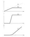
- FIG. 3is a view showing an example of power consumption distribution control in the LED driver IC 100 according to the first embodiment (FIG. 2), and the relationship between the input voltage Vin and various voltages (Vx, Vy) in order from the top, the input The relationship between the voltage Vin and various currents (Iin1, Iin2, Iout) and the relationship between the input voltage Vin and various power consumptions (Pc1, Pc2, Pc) are shown.
- Pc1represents the internal power consumption consumed by the LED driver IC 100
- the first terminal voltage Vx and the second terminal voltage Vyrise as the input voltage Vin rises.
- the second terminal voltage Vydoes not exceed the forward voltage drop of the LED light source Z (more precisely, the lowest value of the forward voltage drop of each of the LED strings Z1 to Z4).
- the current Ioutdoes not flow. Therefore, the first input current Iin1 and the second input current Iin2 both have zero values, and both the internal power consumption Pc1 and the external power consumption Pc2 also have zero values.
- the second terminal voltage Vybecomes higher than the forward drop voltage of the LED light source Z, and the output current Iout starts to increase.
- the second voltage rangesince Vx-Vy ⁇ Vth, the power consumption distribution function does not work, and the second input current Iin2 does not flow. Therefore, the output current Iout is entirely covered by the first input current Iin1.
- the internal power consumption Pc1starts to increase, but the external power consumption Pc2 is maintained at a zero value.
- the output current Ioutreaches the target value (for example, 450 mA) and the second terminal voltage Vy stops rising. Therefore, with the increase of the input voltage Vin, the first terminal voltage The difference between Vx and the second terminal voltage Vy starts to open.
- the power consumption distribution functiondoes not work and the second input current Iin2 does not flow. Therefore, while the internal power consumption Pc1 further increases, the external power consumption Pc2 remains at the zero value.
- the internal power consumption Pc1can be maintained at a substantially constant value (about 1/6 of the conventional value), which leads to downsizing of the printed wiring board on which the LED driver IC 100 is mounted and large current output of the LED driver IC 100 Can be realized.
- the input voltage Vintends to be unstable and there is a high possibility of exceeding the allowable loss of the LED driver IC 100, so the internal power consumption Pc1 is regulated by the power consumption distribution function. The thing is very effective.
- the characteristic of the output current Iout generated by adding the first input current Iin1 and the second input current Iin2is equivalent to that of the conventional one (FIG. 18). Therefore, it is not necessary to redesign the current driver 130 when introducing the power consumption distribution function.
- FIG. 4is a view showing a second embodiment of the LED driver IC.
- the transistor 112 of the current distribution unit 110is omitted while the first embodiment (FIG. 2) described above is based, and the control unit 120 controls only the first control signal Sc1.
- the on resistance value of the transistor 111is dynamically controlled. According to this configuration, it is possible to easily implement a power consumption distribution function substantially equivalent to that of the first embodiment.
- FIG. 5is a diagram showing an example of power consumption distribution control in the LED driver IC 100 of the second embodiment, and as in the case of FIG. 3 above, the relationship between the input voltage Vin and various voltages (Vx, Vy) in order from the top
- the relationship between the input voltage Vin and the various currents (Iin1, Iin2, Iout) and the relationship between the input voltage Vin and the various power consumptions (Pc1, Pc2, Pc)are shown.
- the transistor 112is omitted, so the second input current Iin2 flows in the loss path even in the input voltage range (V21 ⁇ Vin ⁇ V23) in which the power consumption distribution function does not work.
- the first input current Iin1decreases by that amount.
- the resistance value of the external resistor Ris set to a sufficiently large value (about 10 ⁇ ) with respect to the ON resistance value (about 0.5 ⁇ ) of the transistor 111 at the full on time, the second input current Iin2 is sufficiently Therefore, the operation of the LED driver IC 100 is not disturbed.
- FIG. 6is a diagram showing a third embodiment of the LED driver IC.
- the input detection unit 121 and the output detection unit 122 of the control unit 120are both omitted while the first embodiment (FIG. 2) described above is based.
- the distribution ratio between the first input current Iin1 and the second input current Iin2is dynamically controlled according to the difference value Vx-Vref between the first terminal voltage Vx and the predetermined reference voltage Vref. According to this configuration, it is possible to easily implement a power consumption distribution function substantially equivalent to that of the first embodiment.
- the reference voltage Vrefmay be set to a voltage value higher than the assumed value of the second terminal voltage Vy by the threshold voltage Vth earlier.
- FIG. 7is a diagram showing an example of power consumption distribution control in the LED driver IC 100 of the third embodiment, and as in the case of FIG. 3 above, the relationship between the input voltage Vin and various voltages (Vx, Vy) in order from the top
- the relationship between the input voltage Vin and the various currents (Iin1, Iin2, Iout) and the relationship between the input voltage Vin and the various power consumptions (Pc1, Pc2, Pc)are shown.
- the power consumption distribution functionis not effective according to the comparison result of the first terminal voltage Vx and the reference voltage Vref, not the comparison result of the difference value Vx-Vy and the threshold voltage Vth. Disabled is switched. Therefore, in the description of the first embodiment, “Vx ⁇ Vy ⁇ Vth” may be read as “Vx ⁇ Vref”, and “Vx ⁇ Vy> Vth” may be read as “Vx> Vref”. .
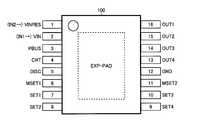
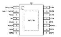
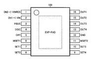
- 8A to 8Dare diagrams showing the terminal arrangement (16 pins) of the LED driver IC 100, respectively.
- HTSSOPheat-sink thin shrink small outline package
- the VINRES terminal (pin 1)is a power distribution resistor connection terminal, and corresponds to the above-mentioned second input terminal IN2.
- the VIN terminal (pin 2)is a power supply voltage input terminal and corresponds to the first input terminal IN1.
- the PBUS terminal (pin 3)is an abnormal state flag output / output current off control input terminal.
- the CRT terminal (pin 4) and the DISC terminal (pin 5)are CR timer setting terminals.
- the MSET1 terminal (6th pin) and the MSET2 terminal (11)are mode setting terminals.
- the SET 1 terminal (7 pin), the SET 2 terminal (8 pin), the SET 3 terminal (10 pin), and the SET 4 terminal (9 pin)are output current setting terminals for 4 channels.
- the GND terminal (pin 12)is a ground terminal.
- the OUT1 terminal (16th pin), the OUT2 terminal (15th pin), the OUT3 terminal (14th pin), and the OUT4 terminal (13th pin)are current output terminals for four channels.
- the broken EXP-PAD terminalfunctions as a heat radiation pad.
- the VINRES and VIN terminalsmay be arranged adjacent to one another as shown in FIGS. 8A-8D. However, as can be seen by comparing FIG. 8A and FIG. 8B (or FIG. 8D), the arrangement order of both terminals may be reversed. Similarly, the CRT terminals and the DISC terminals may be arranged adjacent to each other as shown in FIGS. 8A to 8D. However, as can be seen by comparing FIG. 8A and FIG. 8C (or FIG. 8D), the arrangement order of both terminals may be reversed.
- the four external terminals(VINRES, VIN, CRT, and DISC) are all connected to the power supply E (battery). Therefore, it is desirable that these four external terminals (VINRES, VIN, CRT, and DISC) be designed to have a higher breakdown voltage than other external terminals so that they can withstand connection to the power supply E.
- the external terminals(PBUS, GND, MSET1 and MSET2, SET1 to SET4, and OUT1 to OUT4) other than the four terminals are not connected to the power supply E. Therefore, these external terminals (PBUS, GND, MSET1 and MSET2, SET1 to SET4 and OUT1 to OUT4) basically have a lower withstand voltage design than other external terminals.
- ⁇ Chip layout> 9 to 12are diagrams showing layout examples of the semiconductor chip sealed in the LED driver IC 100, respectively.
- the semiconductor chip 200is a member cut out in a rectangular shape in a plan view, and in addition to the current distribution unit 110, the control unit 120, and the current drive unit 130 described above, the constant current I1 of each channel
- a current setting unit 140 for setting I4 and other circuit units 150are integrated.
- the left side in the drawingis the first side 201
- the right side opposite theretois the second side 202
- the upper sideis the third side 203.
- the lower side opposite to thisis defined as a fourth side 204.
- Such pad arrangementwill be described in detail later.
- the current distribution unit 110 and the current drive unit 130are separately disposed on the first side 201 side and the second side 202 of the semiconductor chip 200.
- the pins on the power supply input sidefor example, pins 1, 2, 4 and 5 in FIG. 8 of the semiconductor chip 200
- the pins on the power output sideare collected on the second side 202 of the semiconductor chip 200 while collecting on the first side 201 and extending in the first direction. It can extend in a second direction opposite to the one direction.
- the wiring connected to the pin on the power input side and the wiring connected to the pin on the power output sidedo not cross each other, so the layout of the PCB [printed circuit board] on which the LED driver IC 100 is mounted is simplified. It is possible to
- the current driver 130also includes constant current sources 131 to 134 connected between the current distributor 110 and the output terminals OUT1 to OUT4, as shown in FIG.
- another circuit unit 150may be interposed between the constant current sources 131 to 134.
- the current distribution unit 110is closest to the third side 203 from the position adjacent to the constant current source 131 closest to the third side 203 of the semiconductor chip 200 (see FIG. 9). It may be integrated to a position adjacent to the distant constant current source 134 (see FIG. 11), and more preferably, near the center position between both ends in the arrangement direction (x-axis direction) of the constant current sources 131 to 134 It is desirable to integrate them (see FIG. 10 and FIG. 12).
- the maximum value of the resistance component of the wire L1 laid from the current distribution unit 110 to the constant current sources 131 to 134is compared with the layout of FIG. Wiring resistance to the constant current source farthest from the current distribution unit 110 can be reduced.
- the wiring resistance to the constant current source 131 adjacent to the current distribution unit 110can be minimized, but the wiring resistance to the constant current source 134 farthest from the current distribution unit 110 is very It becomes bigger.
- the wiring resistance to the constant current source 134 adjacent to the current distribution unit 110can be minimized, but the wiring resistance to the constant current source 131 farthest from the current distribution unit 110 is very large. It gets bigger.
- the LED driver IC 100is required to reduce the voltage between input and output as much as possible. To that end, it is important to reduce the on resistance of the transistor 111 (or 112) forming the current distribution unit 110 and to reduce the wiring resistance to the constant current source farthest from the current distribution unit 110. In view of this, it is desirable to adopt the layout of FIG. 10 and FIG. 12 among the layouts of FIG. 9 to FIG. 12 mentioned above.
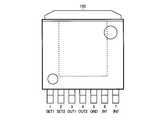
- FIG. 14is a diagram showing the terminal arrangement (7 pins) of the LED driver IC 100. As shown in FIG. Although the 16-pin HTS SOP package was taken as an example in FIG. 8 mentioned above, when the number of output channels is small, a package in which pins are derived in only one direction may be employed as shown in this figure. .
- the SET 1 terminal (pin 1) and the SET 2 terminal (pin 2)are output current setting terminals for two channels.
- the OUT1 terminal (pin 3) and the OUT2 terminal (pin 4)are current output terminals for two channels.
- the GND terminal (pin 5)is a ground terminal.
- the IN1 terminal (pin 6)is a power supply voltage input terminal and corresponds to the first input terminal IN1.
- the IN2 terminal (7th pin)is a resistor connection terminal for power distribution, and corresponds to the above-mentioned second input terminal IN2.
- the IN1 terminal and the IN2 terminalmay be arranged adjacent to each other. However, the arrangement order of both terminals may be reversed. It is desirable that the two external terminals (IN1, IN2) be designed to have a high withstand voltage so as to withstand the connection to the power supply E.
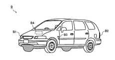
- FIG. 15is an external view of a motorcycle.
- A3(more specifically, LED headlamp module A1, LED rear lamp module A2, and LED blinker lamp module A3) and a battery A4 serving as their power source.
- FIG. 16is an external view of a four-wheeled vehicle.
- the four-wheeled vehicle B in this figureincludes LED lamp modules B1 to BLED lamp modules B1 to B3 (more specifically, LED headlamp module B1, LED rear lamp module B2, and LED blinker lamp module B3), and the like. And a battery A4 serving as a power supply.
- the mounting positions of the LED lamp modules A1 to A3 and B1 to B3 and the batteries A4 and B4 in the drawingsmay differ from the actual ones for convenience of illustration.
- the LED lamp module 1As described above, in the case of the LED lamp module 1 (see FIG. 2, FIG. 4, and FIG. 6) using the LED driver IC 100 with the power consumption distribution function, the printed wiring board is unnecessarily enlarged. There is no need to Therefore, the LED lamp module 1 can be suitably used for any of the LED headlamp module A1 and B1, the LED rear lamp module A2 and B2, and the LED blinker lamp module A3 and B3 having a limited substrate area.
- the first terminal for receiving the input of the first current from the power supply and the second terminal for receiving the input of the second current from the power supply via the external resistormay be provided on the first side of the package.
- the first terminalmay be provided at the end of the first side, and the second terminal may be provided adjacent to the first terminal.
- the second terminalmay be provided at the end of the first side, and the first terminal may be provided adjacent to the second terminal.
- a third terminal connected to the power supplymay be further provided on the first side.
- a fourth terminal not connected to the power supplymay be further provided on the first side.
- the fifth terminal for outputting current to the loadmay be provided on a second side different from the first side among the four sides of the package.
- the second sidemay be a side facing the first side.
- a plurality of the fifth terminalsmay be provided.
- the plurality of fifth terminalsmay be provided adjacent to each other.
- the fifth terminalmay be provided at an end of the second side.
- a sixth terminal for connecting a ground endmay be provided next to the fifth terminal.
- a seventh terminal for heat dissipationmay be provided on the back surface of the package.
- the current distribution unit and the current drive unitmay be separately disposed on the first side of the semiconductor chip and the second side opposite to the first side.
- the plurality of constant current sources included in the current drivermay be arranged in a direction along the second side in plan view of the semiconductor chip.
- the current distribution unitis from the position adjacent to the constant current source closest to the third side of the semiconductor chip to the position adjacent to the constant current source farthest from the third side in a plan view of the semiconductor chip It is good to integrate between
- a reference power supply unitthat generates an internal reference voltage; It is preferable to integrate other circuit units including a CR timer unit for control, a protect bus control unit for exchanging abnormality signals with the outside of the apparatus, various protection circuits, and the like.
- the current distribution unitmay be integrated at a position sandwiched by the plurality of other circuit units.
- At least a part of the other circuit portionmay be integrated at a position sandwiched by the plurality of constant current sources.
- the current distribution unit, the current drive unit, and the other circuit unitare disposed on the third side, and a control unit that generally controls the operation of the semiconductor chip, and an output supplied to a load
- the current setting unit for setting the current value of the currentmay be disposed on the fourth side opposite to the third side.
- the current setting unitmay be provided at a position closer to the fourth side than the control unit.
- a first pad connected to a source regionmay be disposed on the first side, and a pad connected to a drain region may be disposed on the third side.
- the first wire connecting the first pad and the first terminalmay be shorter than a second wire connecting the second pad and the second terminal.
- the first wireextends from the first pad in a direction parallel to the third side and is connected to the first terminal
- the second wireis the second pad It is preferable to extend in a direction parallel to the third side and connect to the second terminal.
- the second terminalmay be provided at one end of the one side, and the first terminal may be provided adjacent to the second terminal.
- the first terminalmay be provided at one end of the one side, and the second terminal may be provided adjacent to the first terminal.
- a third terminal for connecting a ground endmay be provided next to the first terminal or the second terminal.
- the third terminalmay be provided between the first terminal or the second terminal and a fourth terminal for outputting a current to a load.
- a plurality of the fourth terminalsmay be provided.
- the plurality of fourth terminalsmay be provided adjacent to each other.
- the fifth terminal not connected to the power supplymay be provided at the other end of the one side.
- the configuration using the LED as the light emitting elementis described as an example, but it is also possible to use, for example, an organic EL [electro-luminescence] element as the light emitting element.
- the invention disclosed in the present specificationcan be used, for example, for a multi-channel LED driver IC incorporated in an LED lamp module for vehicles (for motorcycles and four-wheeled vehicles).
- Circuit portion 200Semiconductor chip 201 First side 202 Second side 203 Third side 204 Fourth side A Motorcycle (vehicle) B Four-wheeled vehicle (vehicle) A1, B1 LED headlamp module A2, B2 LED rear lamp module A3, B3 LED blinker lamp module A4, B4 battery D drain area E power (battery) IN1, IN2 input terminal L1 wiring (current path) OUT, OUT1 to OUT4 output terminals P11 pad (source pad) P12 pad (drain pad) P31, P32, P33, P34 Pad R External resistance S Source area W1, W2 Wire Z Load (LED light source) Z1-Z4 LED String
Landscapes
- Engineering & Computer Science (AREA)
- Mechanical Engineering (AREA)
- Power Engineering (AREA)
- Radar, Positioning & Navigation (AREA)
- Electromagnetism (AREA)
- General Physics & Mathematics (AREA)
- Physics & Mathematics (AREA)
- Automation & Control Theory (AREA)
- Continuous-Control Power Sources That Use Transistors (AREA)
- Circuit Arrangement For Electric Light Sources In General (AREA)
- Manufacturing & Machinery (AREA)
- Lighting Device Outwards From Vehicle And Optical Signal (AREA)
- Led Devices (AREA)
- Electronic Switches (AREA)
Abstract
Translated fromJapaneseDescription
Translated fromJapanese本明細書中に開示されている発明は、負荷駆動装置に関する。The invention disclosed herein relates to a load drive device.
図17は、負荷駆動装置の一従来例を示す図である。本従来例の負荷駆動装置Xは、電源Eから入力電圧Vinの入力を受けて、負荷Zに出力電圧Vout及び出力電流Ioutを出力する半導体集積回路装置(いわゆるドライバIC)である。FIG. 17 is a diagram showing a conventional example of a load drive device. The load driving device X of this conventional example is a semiconductor integrated circuit device (so-called driver IC) which receives the input voltage Vin from the power supply E and outputs the output voltage Vout and the output current Iout to the load Z.
なお、上記に関連する従来技術の一例としては、特許文献1を挙げることができる。In addition,
図18は、負荷駆動装置Xの出力挙動を示す図であり、上から順に、入力電圧Vinと出力電圧Voutとの関係、入力電圧Vinと出力電流Ioutとの関係、及び、入力電圧Vinと消費電力Pcとの関係が示されている。FIG. 18 is a diagram showing the output behavior of the load drive device X, and from top to bottom, the relationship between the input voltage Vin and the output voltage Vout, the relationship between the input voltage Vin and the output current Iout, and the input voltage Vin and the consumption The relationship with the power Pc is shown.
本図で示したように、負荷駆動装置Xは、入力電圧Vinに依ることなく、出力電流Ioutが常に一定値となるように出力帰還制御を行う。このとき、出力電圧Voutは、負荷Zの特性(例えば、負荷ZがLED[light emitting diode]である場合には、その順方向降下電圧)によって決定される。また、消費電力Pcは、入出力電圧差(Vin-Vout)と出力電流Ioutとの積により求められる。As shown in the figure, the load driving device X performs output feedback control so that the output current Iout always has a constant value regardless of the input voltage Vin. At this time, the output voltage Vout is determined by the characteristics of the load Z (for example, when the load Z is an LED [light emitting diode], its forward drop voltage). Further, the power consumption Pc is obtained by the product of the input / output voltage difference (Vin−Vout) and the output current Iout.
従って、負荷駆動装置Xでは、入力電圧Vinの上昇に伴って消費電力Pcが増大し、その発熱量が大きくなる。そのため、負荷駆動装置Xを十分に放熱するためには、これを実装するプリント配線基板の面積を大きくしなければならず、小型のモジュールに組み込むことが難しかった。Therefore, in the load driving device X, the power consumption Pc increases with the increase of the input voltage Vin, and the amount of heat generation thereof increases. Therefore, in order to sufficiently dissipate the heat from the load driving device X, the area of the printed wiring board on which the load driving device X must be mounted must be increased, which makes it difficult to incorporate the device into a small module.
本明細書中に開示されている発明は、本願の発明者らが見出した上記の課題に鑑み、装置内部での消費電力を分散することのできる負荷駆動装置を提供することを目的とする。The invention disclosed in the present specification aims at providing a load drive device capable of distributing power consumption inside the device, in view of the above-mentioned problems found by the inventors of the present application.
本明細書中に開示されている負荷駆動装置は、電源から第1入力電流の入力を受け付けるための第1入力端子と、前記電源から外部抵抗経由で第2入力電流の入力を受け付けるための第2入力端子と、負荷に出力電流を出力するための出力端子と、前記第1入力電流と前記第2入力電流を所定の分配比率で足し合わせて前記出力電流を生成する電流分配部と、前記分配比率を制御する制御部と、を有する構成(第1の構成)とされている。The load driving device disclosed in the present specification includes a first input terminal for receiving an input of a first input current from a power supply, and a first input terminal for receiving an input of a second input current from the power supply via an external resistor. 2 input terminals, an output terminal for outputting an output current to a load, a current distribution unit which adds the first input current and the second input current at a predetermined distribution ratio to generate the output current, And a control unit that controls the distribution ratio (first configuration).
なお、上記第1の構成から成る負荷駆動装置において、前記電流分配部は、前記第1入力電流の流れる経路に第1トランジスタを含み、前記制御部は、前記第1トランジスタのオン抵抗値を制御する構成(第2の構成)にするとよい。In the load driving device having the first configuration, the current distribution unit includes a first transistor in a path through which the first input current flows, and the control unit controls the on resistance value of the first transistor. Configuration (second configuration).
また、上記第2の構成から成る負荷駆動装置において、前記電流分配部は、前記第2入力電流の流れる経路に第2トランジスタをさらに含み、前記制御部は、前記第1トランジスタと前記第2トランジスタそれぞれのオン抵抗値を差動制御する構成(第3の構成)にするとよい。Further, in the load driving device having the second configuration, the current distribution unit further includes a second transistor in a path through which the second input current flows, and the control unit includes the first transistor and the second transistor. It is good to make it the structure (3rd structure) which carries out differential control of each on resistance value.
また、上記第1~第3いずれかの構成から成る負荷駆動装置において、前記制御部は、前記第2入力端子に現れる第1端子電圧と前記出力端子に現れる第2端子電圧との差分値に応じて前記分配比率を制御する構成(第4の構成)にするとよい。Further, in the load driving device having any one of the first to third configurations, the control unit sets a difference value between the first terminal voltage appearing at the second input terminal and the second terminal voltage appearing at the output terminal. It is preferable that the distribution ratio be controlled accordingly (fourth configuration).
また、上記第4の構成から成る負荷駆動装置において、前記制御部は、前記第1端子電圧から第1差動入力電圧を生成する入力検出部と、前記第2端子電圧から第2差動入力電圧を生成する出力検出部と、前記第1差動入力電圧と前記第2差動入力電圧との差分値に応じて前記電流分配部の制御信号を生成する差動アンプと、を含む構成(第5の構成)にするとよい。In the load driving device having the fourth configuration, the control unit generates an input detection unit that generates a first differential input voltage from the first terminal voltage, and a second differential input from the second terminal voltage. A configuration including an output detection unit that generates a voltage, and a differential amplifier that generates a control signal of the current distribution unit according to a difference value between the first differential input voltage and the second differential input voltage ( It is good to set it as the 5th composition).
また、上記第5の構成から成る負荷駆動装置において、前記入力検出部は、前記第1端子電圧から所定の閾値電圧を差し引いて前記第1差動入力信号を生成する構成(第6の構成)にするとよい。Further, in the load driving device having the fifth configuration, the input detection unit subtracts the predetermined threshold voltage from the first terminal voltage to generate the first differential input signal (sixth configuration) You should
また、上記第5または第6の構成から成る負荷駆動装置において、前記出力検出部は、複数の前記第2端子電圧の最高値を前記第2差動入力信号として出力する構成(第7の構成)にするとよい。Further, in the load driving device having the fifth or sixth configuration, the output detection unit outputs the highest value of the plurality of second terminal voltages as the second differential input signal (seventh configuration It is good to be).
また、上記第5または第6の構成から成る負荷駆動装置において、前記出力検出部は、複数の前記第2端子電圧の平均値を前記第2差動入力信号として出力する構成(第8の構成)にしてもよい。Further, in the load driving device having the fifth or sixth configuration, the output detection unit outputs an average value of the plurality of second terminal voltages as the second differential input signal (eighth configuration ) May be used.
また、上記第1~第3いずれかの構成から成る負荷駆動装置において、前記制御部は、前記第2入力端子の端子電圧と所定の基準電圧との差分値に応じて前記分配比率を動的に制御する構成(第9の構成)にするとよい。Further, in the load driving device having any one of the first to third configurations, the control unit dynamically operates the distribution ratio according to a difference value between a terminal voltage of the second input terminal and a predetermined reference voltage. It is good to set it as the structure (9th structure) controlled to.
また、上記第1~第9いずれかの構成から成る負荷駆動装置は、前記出力電流の定電流制御を行う電流駆動部をさらに有する構成(第10の構成)にするとよい。The load driving device having any one of the first to ninth configurations may further include a current driver configured to perform constant current control of the output current (10th configuration).
また、上記第10の構成から成る負荷駆動装置において、前記電流分配部は、半導体チップの平面視において、前記半導体チップの第1辺側に集積化されており、前記電流駆動部は、前記半導体チップの前記第1辺と対向する第2辺側に集積化されている構成(第11の構成)にするとよい。In the load driving device having the tenth configuration, the current distribution unit is integrated on the first side of the semiconductor chip in a plan view of the semiconductor chip, and the current drive unit is the semiconductor The chip may be integrated on a second side opposite to the first side of the chip (an eleventh structure).
また、上記第11の構成から成る負荷駆動装置において、前記電流駆動部は、前記電流分配部と複数設けられた前記出力端子との間にそれぞれ接続された複数の定電流源を含む構成(第12の構成)にするとよい。In the load driving device having the eleventh configuration, the current driving unit includes a plurality of constant current sources respectively connected between the current distribution unit and the plurality of output terminals 12) is good.
また、上記第12の構成から成る負荷駆動装置において、前記複数の定電流源は、前記半導体チップの平面視において、前記第2辺に沿う方向に配列されている構成(第13の構成)にするとよい。Further, in the load driving device having the twelfth configuration, the plurality of constant current sources are arranged in a direction along the second side in a plan view of the semiconductor chip (a thirteenth configuration). It is good to do.
また、上記第13の構成から成る負荷駆動装置において、前記電流分配部は、前記半導体チップの平面視において、前記半導体チップの第3辺に最も近い定電流源に隣接する位置から、前記第3辺から最も遠い定電流源に隣接する位置までの間に集積化されている構成(第14の構成)にするとよい。Further, in the load driving device having the thirteenth configuration, the current distribution unit is configured such that, from a position adjacent to the constant current source closest to the third side of the semiconductor chip in the plan view of the semiconductor chip The configuration may be integrated (fourteenth configuration) between a side and a position adjacent to the farthest constant current source.
また、上記第1~第14いずれかの構成から成る負荷駆動装置において、前記電源に接続される端子とこれに隣接する端子は、前記電源への接続に耐え得る耐圧を持つ構成(第15の構成)にするとよい。Further, in the load driving device having any one of the first to fourteenth configurations, the terminal connected to the power supply and the terminal adjacent thereto have a withstand voltage that can withstand connection to the power supply (fifteenth embodiment Configuration).
また、上記第2の構成から成る負荷駆動装置において、前記第1トランジスタは、ソース領域と、前記ソース領域の直近に設けられて前記第1入力端子にワイヤボンディングされるソースパッドと、ドレイン領域と、前記ドレイン領域の直近に設けられて前記第2入力端子にワイヤボンディングされるドレインパッドと、を備える構成(第16の構成)にするとよい。Further, in the load driving device having the second configuration, the first transistor is provided with a source region, a source pad provided in the immediate vicinity of the source region and wire-bonded to the first input terminal, a drain region And a drain pad provided in the immediate vicinity of the drain region and wire-bonded to the second input terminal.
また、上記第1~第16いずれかの構成から成る負荷駆動装置において、前記第1入力端子と前記第2入力端子は、互いに隣接して配列されている構成(第17の構成)にするとよい。In the load driving device having any one of the first to sixteenth configurations, the first input terminal and the second input terminal may be arranged adjacent to each other (a seventeenth configuration). .
また、上記第1~第17いずれかの構成から成る負荷駆動装置において、前記第1入力端子または前記第2入力端子の隣には、他の外部端子よりも高耐圧設計の容易な外部端子が配列されている構成(第18の構成)にするとよい。Further, in the load driving device having any one of the first to seventeenth configurations, an external terminal whose high withstand voltage is easier to design than other external terminals is provided next to the first input terminal or the second input terminal. It is good to make it the structure currently arranged (18th structure).
また、上記した第1~第18いずれかの構成から成る負荷駆動装置において、前記第1入力端子は、前記電源から直接的に前記第1入力電流の入力を受け付ける構成(第19の構成)にするとよい。Further, in the load driving device having any one of the first to eighteenth configurations described above, the first input terminal receives an input of the first input current directly from the power supply (a nineteenth configuration). It is good to do.
また、上記した第1~第19いずれかの構成から成る負荷駆動装置において、前記制御部は、前記分配比率を動的に制御する構成(第20の構成)にするとよい。Further, in the load driving device having any one of the first to nineteenth configurations described above, the control unit may be configured to control the distribution ratio dynamically (a twentieth configuration).
また、上記第1~第20いずれかの構成から成る負荷駆動装置は、半導体装置に集積化されている構成(第21の構成)にするとよい。Further, it is preferable that the load driving device having any one of the first to twentieth configurations be configured to be integrated in a semiconductor device (twenty-first configuration).
また、上記第2の構成から成る負荷駆動装置において、前記制御部は、前記第1トランジスタのオン抵抗値を動的に制御する構成(第22の構成)にするとよい。Further, in the load driving device having the second configuration, the control unit may be configured to dynamically control the on-resistance value of the first transistor (a twenty-second configuration).
また、上記第3の構成から成る負荷駆動装置において、前記制御部は、前記第1トランジスタと前記第2トランジスタそれぞれのオン抵抗値を動的に差動制御する構成(第23の構成)にするとよい。In the load driving device having the third configuration, the control unit may be configured to dynamically differentially control the on resistance values of the first transistor and the second transistor (a twenty-third configuration). Good.
また、上記第4の構成から成る負荷駆動装置において、前記制御部は、前記第1端子電圧と前記第2端子電圧との差分値に応じて前記分配比率を動的に制御する構成(第24の構成)にするとよい。Further, in the load driving device having the fourth configuration, the control unit dynamically controls the distribution ratio in accordance with a difference value between the first terminal voltage and the second terminal voltage. Configuration).
また、本明細書中に開示されている電気機器は、上記第1~第24いずれかの構成から成る負荷駆動装置と、前記負荷駆動装置の第1入力端子と第2入力端子との間に接続される外部抵抗と、前記負荷駆動装置の出力端子に接続される負荷と、を有する構成(第25の構成)とされている。Further, the electric device disclosed in the present specification includes the load drive device having any one of the first to twenty-fourth configurations, and between the first input terminal and the second input terminal of the load drive device. An external resistor connected and a load connected to an output terminal of the load driving device are configured (25th configuration).
また、本明細書中に開示されているランプモジュールは、上記第1~第24いずれかの構成から成る負荷駆動装置と、前記負荷駆動装置の第1入力端子と第2入力端子との間に接続される外部抵抗と、前記負荷駆動装置の出力端子に負荷として接続される光源と、を有する構成(第26の構成)とされている。Further, in the lamp module disclosed in the present specification, the load drive device having any one of the above-described first to twenty-fourth configurations, and the first input terminal and the second input terminal of the load drive device. An external resistor connected and a light source connected as a load to the output terminal of the load driving device are configured (sixth configuration).
また、本明細書中に開示されている車両は、上記第26の構成から成るランプモジュールと、前記ランプモジュールの電源となるバッテリと、を有する構成(第27の構成)とされている。Further, a vehicle disclosed in the present specification has a configuration (a twenty-seventh configuration) including a lamp module having the above-described twenty-sixth configuration, and a battery serving as a power source of the lamp module.
なお、上記第27の構成から成る車両において、前記ランプモジュールは、ヘッドランプモジュール、リアランプモジュール、若しくは、ウィンカーランプモジュールである構成(第28の構成)にするとよい。In the vehicle having the twenty-seventh configuration, the lamp module may be a headlamp module, a rear lamp module, or a winker lamp module (a twenty-eighth configuration).
本明細書中に開示されている発明によれば、装置内部での消費電力を分散することのできる負荷駆動装置を提供することが可能となる。According to the invention disclosed in the present specification, it is possible to provide a load drive device capable of distributing power consumption inside the device.
<電気機器>
図1は、負荷駆動装置を備えた電気機器の全体構成を示す図である。本構成例の電気機器1は、負荷駆動装置100と、これに外付けされる外部抵抗R及び負荷Zを有する。<Electric equipment>
FIG. 1 is a diagram showing an entire configuration of an electric device provided with a load driving device. The
負荷駆動装置100は、電源Eから入力電圧Vinの入力を受けて、負荷Zに出力電圧Vout及び出力電流Ioutを出力する半導体集積回路装置(いわゆるドライバIC)であり、装置外部との電気的な接続を確立するために、第1入力端子IN1と、第2入力端子IN2と、出力端子OUTと、を有する。もちろん、負荷駆動装置100には、必要に応じて、上記以外の外部端子を設けても構わない。The
外部抵抗Rの第1端は、電源Eの正極端(=入力電圧Vinの印加端)と負荷駆動装置100の第1入力端子IN1に接続されている。電源Eの負極端は、接地端に接続されている。外部抵抗Rの第2端は、負荷駆動装置100の第2入力端子IN2に接続されている。このように、外部抵抗Rは、負荷駆動装置100の第1入力端子IN1と第2入力端子IN2との間に接続されている。なお、負荷駆動装置100と外部抵抗Rは、いずれも共通のプリント配線基板上に実装してもよいし、或いは、それぞれを別々のプリント配線基板上に実装してもよい。また、外部抵抗Rは、単一の抵抗素子に限らず、複数の抵抗素子を直列または並列に接続した抵抗素子群であってもよい。The first end of the external resistor R is connected to the positive electrode end of the power source E (= application end of the input voltage Vin) and the first input terminal IN1 of the
負荷Zの第1端は、負荷駆動装置100の出力端子OUT(=出力電圧Voutの印加端)に接続されている。負荷Zの第2端は、接地端に接続されている。The first end of the load Z is connected to the output terminal OUT of the load driving device 100 (= application end of output voltage Vout). The second end of the load Z is connected to the ground end.
<負荷駆動装置>
引き続き、図1を参照しながら、負荷駆動装置100の内部構成について説明する。負荷駆動装置100は、先に述べた第1入力端子IN1、第2入力端子IN2、及び、出力端子OUTのほか、電流分配部110と、制御部120と、電流駆動部130と、を集積化して成る。<Load drive device>
Subsequently, the internal configuration of the
第1入力端子IN1は、電源Eから直接的に第1入力電流Iin1の入力を受け付けるための外部端子である。The first input terminal IN1 is an external terminal for receiving an input of the first input current Iin1 directly from the power supply E.
第2入力端子IN2は、電源Eから外部抵抗R経由で第2入力電流Iin2の入力を受け付けるための外部端子である。The second input terminal IN2 is an external terminal for receiving an input of the second input current Iin2 from the power source E via the external resistor R.
出力端子OUTは、負荷Zに出力電圧Vout及び出力電流Ioutを出力するための外部端子である。The output terminal OUT is an external terminal for outputting the output voltage Vout and the output current Iout to the load Z.
電流分配部110は、制御部120からの制御信号Scに基づき第1入力電流Iin1と第2入力電流Iin2を所定の分配比率で足し合わせて出力電流Ioutを生成する。The
制御部120は、第2入力端子IN2に現れる第1端子電圧Vxと、出力端子OUTに現れる第2端子電圧Vyとの差分値Vx-Vy(=入出力端子間の電圧降下に相当)を連続的に検出し、その検出値が所定の上限値を超えないように制御信号Scを生成することで、上記の分配比率を動的に制御する。具体的に述べると、差分値Vx-Vyが所定の上限値に達するまでは、基本的に第1入力電流Iin1のみを流して第2入力電流Iin2を遮断する一方、差分値Vx-Vyが所定の上限値に達して以降は、第1入力電流Iin1を減らして第2入力電流Iin2を増やすように、上記の分配比率が自動的かつスムーズに調整される。なお、第2端子電圧Vyの検出については、これを割愛することも可能である。このような変形例については、後出の第3実施形態(図6)で詳細に説明する。The
電流駆動部130は、出力電流Ioutの定電流制御を行う。すなわち、電流駆動部130は、入力電圧Vinに依ることなく、出力電流Ioutが常に一定値となるように、その出力帰還制御を行う。The
このように、本構成例の負荷駆動装置100は、例えば、入力電圧Vinの上昇時において、従来、装置内部で消費されていた過剰電力の一部を、装置外部(入力側)に設けられた外部抵抗Rにより意図的に損失させる機能(以下では「消費電力分散機能」と呼ぶ)を備えている。As described above, the
当該構成を採用すれば、装置内部の消費電力を常に所定の上限値以下に保つことができるので、負荷駆動装置100の発熱を抑制することが可能となる。従って、負荷駆動装置100の許容損失に十分な余裕ができ、これを実装するプリント配線基板の面積を不必要に大きくする必要がなくなるので、小型のモジュールへの組み込みも容易となる。If the configuration is adopted, the power consumption inside the device can always be kept at or below the predetermined upper limit value, so that the heat generation of the
また、負荷駆動装置100の入力ダイナミックレンジ(=入力電圧Vinの入力可能範囲)が広がるので、例えば、入力電圧Vinの不安定なバッテリを電源Eとして用いることも可能となる。In addition, since the input dynamic range of the load driving device 100 (= the input possible range of the input voltage Vin) is expanded, it is also possible to use, for example, an unstable battery of the input voltage Vin as the power supply E.
また、本構成例の負荷駆動装置100であれば、装置内部に過剰電力が掛からなくなるので、内部素子に加わるストレスを軽減し、信頼性の向上や製品の高寿命化に寄与することが可能となる。Further, with the
なお、ディスクリート素子である外部抵抗Rは、半導体素子である負荷駆動装置100と比べて熱耐性が高いので、多少の発熱があっても特段の支障は生じない。In addition, since the external resistance R which is a discrete element has high heat resistance compared with the
以下、種々の実施形態では、多チャンネルLEDドライバICへの適用例を挙げて、より具体的に説明する。Hereinafter, in various embodiments, application examples to multi-channel LED driver ICs will be described more specifically.
<第1実施形態>
図2は、LEDドライバICの第1実施形態を示す図である。本実施形態では、先に説明した電気機器1がLEDランプモジュールとして構成されており、負荷駆動装置100は、出力端子OUT1~OUT4を備えた4チャンネルのLEDドライバICとして構成されている。また、電源Eとしては、バッテリが用いられており、負荷Zとしては、LEDストリングZ1~Z4を並列に備えたLED光源が用いられている。First Embodiment
FIG. 2 is a diagram showing a first embodiment of the LED driver IC. In the present embodiment, the
そこで、以下では、先出の電気機器1、負荷駆動装置100、電源E、並びに、負荷Zを、それぞれ、LEDランプモジュール1、LEDドライバIC100、バッテリE、並びに、LED光源Zと読み替えて、詳細な説明を行う。Therefore, in the following, the
なお、LEDドライバIC100は、その駆動対象となるLED光源Zと共にLEDランプモジュール1として提供されるものであってもよいし、或いは、LED光源Zとは独立にIC単体として提供されるものであってもよい。The
まず、LEDドライバIC100の構成要素のうち、電流分配部110について説明する。電流分配部110は、第1入力電流Iin1と第2入力電流Iin2の分配比率を動的に差動制御する手段として、Pチャネル型MOS[metal oxide semiconductor]電界効果トランジスタ111及び112を含む。なお、トランジスタ111は、第1入力電流Iin1の流れる経路(=直接パス)に設けられた第1トランジスタに相当する。一方、トランジスタ112は、第2入力電流Iin2の流れる経路(=損失パス)に設けられた第2トランジスタに相当する。First, among the components of the
それぞれの接続関係について具体的に説明する。トランジスタ111のソースとバックゲートは、第1入力端子IN1(=第1入力電流Iin1の入力端)に接続されている。トランジスタ112のソースとバックゲートは、第2入力端子IN2(=第2入力電流Iin2の入力端)に接続されている。トランジスタ111及び112それぞれのドレインは、互いに接続されており、その接続ノードは、出力電流Ioutの出力端として、後段の電流駆動部130に接続されている。Each connection relationship will be specifically described. The source and back gate of the
また、トランジスタ111のゲートには、第1制御信号Sc1が入力されている。従って、第1制御信号Sc1が高いほど、トランジスタ111のオン抵抗値が大きくなり、第1入力電流Iin1が減少する。逆に、第1制御信号Sc1が低いほど、トランジスタ111のオン抵抗値が小さくなり、第1入力電流Iin1が増大する。In addition, the first control signal Sc1 is input to the gate of the
一方、トランジスタ112のゲートには、第2制御信号Sc2が入力されている。従って、第2制御信号Sc2が高いほど、トランジスタ112のオン抵抗値が大きくなり、第2入力電流Iin2が減少する。逆に、第2制御信号Sc2が低いほど、トランジスタ112のオン抵抗値が小さくなり、第2入力電流Iin2が増大する。On the other hand, the second control signal Sc2 is input to the gate of the
なお、トランジスタ111及び112それぞれのゲート・ソース間には、電圧クランプ素子を接続してもよい。Note that a voltage clamp element may be connected between the gate and the source of each of the
次に、制御部120について説明する。制御部120は、入力検出部121と、出力検出部122と、差動アンプ123と、を含み、先出の制御信号Scとして、第1制御信号Sc1と第2制御信号Sc2を生成することにより、トランジスタ111及び112のオン抵抗値を動的に差動制御する。Next, the
入力検出部121は、第2入力端子IN2と接地端との間に直列接続された抵抗121aと電流源121bを含み、第2入力端子IN2に現れる第1端子電圧Vxから所定の閾値電圧Vth(=抵抗121aの両端間電圧)を差し引いた第1差動入力電圧Vx’(=Vx-Vth)を生成する。なお、閾値電圧Vthを任意に調整するためには、例えば、電流源121bとして可変電流源を用いることが望ましい。The
出力検出部122は、出力端子OUT1~OUT4それぞれに現れる第2端子電圧Vy1~Vy4(先出の第2端子電圧Vyに相当)から第2差動入力電圧Vy’を生成する。なお、第2端子電圧Vy1~Vy4は、それぞれ、LEDストリングZ1~Z4毎の順方向降下電圧によって決定される。The
例えば、出力検出部122は、第2端子電圧Vy1~Vy4の最高値を第2差動入力電圧Vy’として出力する構成にするとよい。このような構成であれば、第1差動入力電圧Vx’が第2端子電圧Vy1~Vy4の最高値に達するまで、先述の消費電力分散機能は働かない。従って、LEDストリングZ1~Z4毎のLED直列段数や順方向降下電圧にばらつきがあっても、その全てを確実に点灯させることが可能となる。For example, the
また、例えば、出力検出部122は、第2端子電圧Vy1~Vy4の平均値を第2差動入力電圧Vy’として出力する構成としてもよい。このような構成であれば、第1差動入力電圧Vx’が第2端子電圧Vy1~Vy4の平均値に達した時点で、先述の消費電力分散機能が働き始める。従って、LEDストリングZ1~Z4毎のLED直列段数や順方向降下電圧にばらつきがあっても、それぞれに過大な電圧が印加されにくくなる。Also, for example, the
差動アンプ123は、非反転入力端(+)に入力される第1差動入力電圧Vx’と、反転入力端(-)に入力される第2差動入力電圧Vy’との差分値Vx’-Vy’に応じて第1制御信号Sc1及び第2制御信号Sc2を生成する。なお、差動アンプ123の入力段には、静電保護素子を接続してもよい。The
差動アンプ123の動作について具体的に述べる。Vx’-Vy’≦0(すなわち、Vx-Vy≦Vth)であるときには、差動アンプ123の反転出力端(-)から出力される第1制御信号Sc1がローレベルに張り付き、差動アンプ123の非反転出力端(+)から出力される第2制御信号Sc2がハイレベルに張り付く。従って、電流分配部110は、トランジスタ111がフルオンされて、トランジスタ112がフルオフされた状態、すなわち、直接パスの第1入力電流Iin1のみを流して、損失パスの第2入力電流Iin2を遮断した状態となる。The operation of the
一方、Vx’-Vy’>0(すなわち、Vx-Vy>Vth)になると、ローレベルに張り付いていた第1制御信号Sc1が上昇し、ハイレベルに張り付いていた第2制御信号Sc2が低下するので、トランジスタ111のオン抵抗値が最低値から引き上げられて、トランジスタ112のオン抵抗値が最高値から引き下げられる。その結果、電流分配部110では、第1入力電流Iin1を減らして、第2入力電流Iin2を増やすように、それぞれの分配比率が自動的かつスムーズに調整される。On the other hand, when Vx'-Vy '> 0 (ie, Vx-Vy> Vth), the first control signal Sc1 stuck to the low level rises, and the second control signal Sc2 stuck to the high level becomes As it falls, the on resistance value of the
このように、制御部120では、第1端子電圧Vxと第2端子電圧Vyとの差分値Vx-Vyに応じて、第1入力電流Iin1と第2入力電流Iin2の分配比率が動的に差動制御される。Thus, in the
次に、電流駆動部130について説明する。電流駆動部130は、互いに並列接続された定電流源131~134を含む。定電流源131~134は、それぞれ、所定の定電流I1~I4を生成し、これを出力端子OUT1~OUT4に出力する。従って、電流分配部110から電流駆動部130に供給される出力電流Ioutは、全ての定電流I1~I4を足し合わせた合算電流(Iout=I1+I2+I3+I4)となる。なお、本図では明示されていないが、電流駆動部130は、定電流I1~I4それぞれの出力帰還制御を行う主体として、ロジック部などを含んでいてもよい。Next, the
図3は、第1実施形態(図2)のLEDドライバIC100における消費電力分散制御の一例を示す図であり、上から順番に、入力電圧Vinと各種電圧(Vx,Vy)との関係、入力電圧Vinと各種電流(Iin1,Iin2,Iout)との関係、及び、入力電圧Vinと各種消費電力(Pc1,Pc2,Pc)との関係が示されている。なお、Pc1は、LEDドライバIC100で消費される内部消費電力を示しており、Pc2は、外部抵抗Rで消費される外部消費電力を示している。また、Pcは、従来の消費電力(=消費電力分散制御を行わない場合の内部消費電力に相当)を示している。FIG. 3 is a view showing an example of power consumption distribution control in the
第1の電圧範囲(0≦Vin<V11)では、入力電圧Vinの上昇に伴い、第1端子電圧Vxと第2端子電圧Vyがそれぞれ上昇していく。ただし、第1の電圧範囲では、第2端子電圧VyがLED光源Zの順方向降下電圧(より正確にはLEDストリングZ1~Z4それぞれの順方向降下電圧の最低値)を上回っていないので、出力電流Ioutが流れない。従って、第1入力電流Iin1と第2入力電流Iin2は、いずれもゼロ値のままであり、内部消費電力Pc1と外部消費電力Pc2も共にゼロ値となる。In the first voltage range (0 ≦ Vin <V11), the first terminal voltage Vx and the second terminal voltage Vy rise as the input voltage Vin rises. However, in the first voltage range, the second terminal voltage Vy does not exceed the forward voltage drop of the LED light source Z (more precisely, the lowest value of the forward voltage drop of each of the LED strings Z1 to Z4). The current Iout does not flow. Therefore, the first input current Iin1 and the second input current Iin2 both have zero values, and both the internal power consumption Pc1 and the external power consumption Pc2 also have zero values.
第2の電圧範囲(V11≦Vin<V12)では、第2端子電圧VyがLED光源Zの順方向降下電圧よりも高くなり、出力電流Ioutが増大し始める。ただし、第2の電圧範囲では、Vx-Vy<Vthであるから、消費電力分散機能が働かず、第2入力電流Iin2は流れない。従って、出力電流Ioutは、第1入力電流Iin1により全て賄われる。その結果、内部消費電力Pc1は増大し始めるが、外部消費電力Pc2はゼロ値に維持される。In the second voltage range (V11 ≦ Vin <V12), the second terminal voltage Vy becomes higher than the forward drop voltage of the LED light source Z, and the output current Iout starts to increase. However, in the second voltage range, since Vx-Vy <Vth, the power consumption distribution function does not work, and the second input current Iin2 does not flow. Therefore, the output current Iout is entirely covered by the first input current Iin1. As a result, the internal power consumption Pc1 starts to increase, but the external power consumption Pc2 is maintained at a zero value.
第3の電圧範囲(V12≦Vin<V13)では、出力電流Ioutが目標値(例えば450mA)に達して第2端子電圧Vyの上昇が止まるので、入力電圧Vinの上昇に伴い、第1端子電圧Vxと第2端子電圧Vyとの差が開き始める。ただし、第3の電圧範囲では、未だVx-Vy<Vthであるから、先に説明した第2の電圧範囲と同様、消費電力分散機能が働かず、第2入力電流Iin2は流れない。従って、内部消費電力Pc1がさらに増大する一方、外部消費電力Pc2はゼロ値に維持されたままとなる。In the third voltage range (V12 ≦ Vin <V13), the output current Iout reaches the target value (for example, 450 mA) and the second terminal voltage Vy stops rising. Therefore, with the increase of the input voltage Vin, the first terminal voltage The difference between Vx and the second terminal voltage Vy starts to open. However, in the third voltage range, since Vx−Vy <Vth, as in the second voltage range described above, the power consumption distribution function does not work and the second input current Iin2 does not flow. Therefore, while the internal power consumption Pc1 further increases, the external power consumption Pc2 remains at the zero value.
第4の電圧範囲(V13≦Vin<V14)では、Vx-Vy>Vthとなり、消費電力分散機能が働き始める。より具体的に述べると、第4の電圧範囲では、Vx-Vy=Vthとなるようにトランジスタ111及び112が動作し、入力電圧Vinが高いほど、第1入力電流Iin1を減らして第2入力電流Iin2を増やすように、それぞれの分配比率が自動的かつスムーズに調整される。In the fourth voltage range (V13 ≦ Vin <V14), Vx−Vy> Vth, and the power consumption distribution function starts to work. More specifically, in the fourth voltage range, the
このような消費電力分散機能を具備することにより、バッテリEから供給される過剰電力の一部を、外部消費電力Pc2として意図的に損失させることができる。従って、内部消費電力Pc1をほぼ一定値(従来の1/6程度)に保つことが可能となり、延いては、LEDドライバIC100を実装するプリント配線基板の小型化や、LEDドライバIC100の大電流出力化を実現することが可能となる。By providing such a power consumption distribution function, part of the excess power supplied from the battery E can be intentionally lost as the external power consumption Pc2. Therefore, the internal power consumption Pc1 can be maintained at a substantially constant value (about 1/6 of the conventional value), which leads to downsizing of the printed wiring board on which the
特に、バッテリEを電源とするLEDモジュール1では、入力電圧Vinが不安定となりやすく、LEDドライバIC100の許容損失を超過するおそれが高いので、消費電力分散機能により、内部消費電力Pc1をレギュレートすることは、非常に有効である。In particular, in the
また、本図で示したように、第1入力電流Iin1と第2入力電流Iin2とを足し合わせて生成される出力電流Ioutの特性は、従来(図18)のそれと同等である。従って、消費電力分散機能の導入に際し、電流駆動部130を再設計する必要はない。Also, as shown in the figure, the characteristic of the output current Iout generated by adding the first input current Iin1 and the second input current Iin2 is equivalent to that of the conventional one (FIG. 18). Therefore, it is not necessary to redesign the
<第2実施形態>
図4は、LEDドライバICの第2実施形態を示す図である。本実施形態のLEDドライバIC100では、先出の第1実施形態(図2)をベースとしつつ、電流分配部110のトランジスタ112が割愛されており、制御部120では、第1制御信号Sc1のみを用いることにより、トランジスタ111のオン抵抗値が動的に制御される。本構成によれば、第1実施形態とほぼ同等の消費電力分散機能を簡易に実装することが可能となる。Second Embodiment
FIG. 4 is a view showing a second embodiment of the LED driver IC. In the
図5は、第2実施形態のLEDドライバIC100における消費電力分散制御の一例を示す図であり、先の図3と同様、上から順に、入力電圧Vinと各種電圧(Vx,Vy)との関係、入力電圧Vinと各種電流(Iin1,Iin2,Iout)との関係、並びに、入力電圧Vinと各種消費電力(Pc1,Pc2,Pc)との関係が示されている。FIG. 5 is a diagram showing an example of power consumption distribution control in the
本実施形態の基本動作は、先に述べた通りであり、図3の電圧値V11~V14をそれぞれ、本図の電圧値V21~V24と読み替えて理解すれば足りる。The basic operation of this embodiment is as described above, and it is sufficient to replace the voltage values V11 to V14 of FIG. 3 with the voltage values V21 to V24 of FIG.
なお、本実施形態のLEDドライバIC100では、トランジスタ112が割愛されているので、消費電力分散機能が働かない入力電圧範囲(V21<Vin<V23)でも、損失パスに第2入力電流Iin2が流れ、その分だけ第1入力電流Iin1が減少する。In the
ただし、フルオン時におけるトランジスタ111のオン抵抗値(0.5Ω程度)に対して、外部抵抗Rの抵抗値を十分に大きい値(10Ω程度)に設定しておけば、第2入力電流Iin2を十分に絞ることができるので、LEDドライバIC100の動作に支障を生じることはない。However, if the resistance value of the external resistor R is set to a sufficiently large value (about 10 Ω) with respect to the ON resistance value (about 0.5 Ω) of the
<第3実施形態>
図6は、LEDドライバICの第3実施形態を示す図である。本実施形態のLEDドライバIC100では、先出の第1実施形態(図2)をベースとしつつ、制御部120の入力検出部121と出力検出部122がいずれも割愛されており、制御部120では、第1端子電圧Vxと所定の基準電圧Vrefとの差分値Vx-Vrefに応じて、第1入力電流Iin1と第2入力電流Iin2との分配比率が動的に制御される。本構成によれば、第1実施形態とほぼ同等の消費電力分散機能を簡易に実装することが可能となる。Third Embodiment
FIG. 6 is a diagram showing a third embodiment of the LED driver IC. In the
なお、基準電圧Vrefは、第2端子電圧Vyの想定値よりも先出の閾値電圧Vthだけ高い電圧値に設定すればよい。The reference voltage Vref may be set to a voltage value higher than the assumed value of the second terminal voltage Vy by the threshold voltage Vth earlier.
図7は、第3実施形態のLEDドライバIC100における消費電力分散制御の一例を示す図であり、先の図3と同様、上から順に、入力電圧Vinと各種電圧(Vx,Vy)との関係、入力電圧Vinと各種電流(Iin1,Iin2,Iout)との関係、並びに、入力電圧Vinと各種消費電力(Pc1,Pc2,Pc)との関係が示されている。FIG. 7 is a diagram showing an example of power consumption distribution control in the
本実施形態の基本動作は、先に述べた通りであり、図3の電圧値V11~V14をそれぞれ、本図の電圧値V31~V34と読み替えて理解すれば足りる。The basic operation of this embodiment is as described above, and it is sufficient to replace the voltage values V11 to V14 of FIG. 3 with the voltage values V31 to V34 of FIG.
ただし、本実施形態のLEDドライバIC100では、差分値Vx-Vyと閾値電圧Vthとの比較結果ではなく、第1端子電圧Vxと基準電圧Vrefとの比較結果に応じて消費電力分散機能の有効/無効が切り替えられる。従って、第1実施形態における説明のうち、「Vx-Vy<Vth」については「Vx<Vref」に読み替えればよく、「Vx-Vy>Vth」については「Vx>Vref」に読み替えればよい。However, in the
また、本実施形態では、第1実施形態(図2)をベースとした例を挙げたが、第2実施形態(図4)をベースとしても構わない。すなわち、本実施形態のLEDモジュール1において、電流分配部110のトランジスタ112をさらに割愛することも任意である。Moreover, although the example based on 1st Embodiment (FIG. 2) was mentioned in this embodiment, it does not matter as a base based on 2nd Embodiment (FIG. 4). That is, in the
<端子配置(16ピン)>
図8A~図8Dは、それぞれ、LEDドライバIC100の端子配置(16ピン)を示す図である。各図のLEDドライバIC100は、パッケージとして16ピンのHTSSOP[heat-sink thin shrink small outline package]を採用している。本パッケージでは、対向する2辺から2方向(=紙面左右方向)に8本ずつ、合計16本のピンが導出されている。以下、基本的には、図8Aを参照しながら、端子配置の説明を行う。<Terminal arrangement (16 pins)>
8A to 8D are diagrams showing the terminal arrangement (16 pins) of the
VINRES端子(1ピン)は、電力分散用抵抗接続端子であり、先の第2入力端子IN2に相当する。VIN端子(2ピン)は、電源電圧入力端子であり、先の第1入力端子IN1に相当する。PBUS端子(3ピン)は、異常状態フラグ出力/出力電流オフ制御入力端子である。CRT端子(4ピン)とDISC端子(5ピン)は、CRタイマ設定端子である。MSET1端子(6ピン)とMSET2端子(11)は、モード設定端子である。SET1端子(7ピン)、SET2端子(8ピン)、SET3端子(10ピン)、並びに、SET4端子(9ピン)は、4チャンネル分の出力電流設定端子である。GND端子(12ピン)は、接地端子である。OUT1端子(16ピン)、OUT2端子(15ピン)、OUT3端子(14ピン)、並びに、OUT4端子(13ピン)は、4チャンネル分の電流出力端子である。破線のEXP-PAD端子は、放熱パッドとして機能する。The VINRES terminal (pin 1) is a power distribution resistor connection terminal, and corresponds to the above-mentioned second input terminal IN2. The VIN terminal (pin 2) is a power supply voltage input terminal and corresponds to the first input terminal IN1. The PBUS terminal (pin 3) is an abnormal state flag output / output current off control input terminal. The CRT terminal (pin 4) and the DISC terminal (pin 5) are CR timer setting terminals. The MSET1 terminal (6th pin) and the MSET2 terminal (11) are mode setting terminals. The
VINRES端子とVIN端子は、図8A~図8Dで示すように、互いに隣接して配列するとよい。ただし、図8Aと図8B(または図8D)を比べれば分かるように、両端子の配列順序は逆でも構わない。同様に、CRT端子とDISC端子は、図8A~図8Dで示すように、互いに隣接して配列するとよい。ただし、図8Aと図8C(または図8D)を比べれば分かるように、両端子の配列順序は逆でも構わない。The VINRES and VIN terminals may be arranged adjacent to one another as shown in FIGS. 8A-8D. However, as can be seen by comparing FIG. 8A and FIG. 8B (or FIG. 8D), the arrangement order of both terminals may be reversed. Similarly, the CRT terminals and the DISC terminals may be arranged adjacent to each other as shown in FIGS. 8A to 8D. However, as can be seen by comparing FIG. 8A and FIG. 8C (or FIG. 8D), the arrangement order of both terminals may be reversed.
なお、上記4本の外部端子(VINRES、VIN、CRT、及び、DISC)は、いずれも、電源E(バッテリ)に接続される。従って、これら4本の外部端子(VINRES、VIN、CRT、及び、DISC)は、電源Eへの接続に耐え得るように、他の外部端子よりも高耐圧設計としておくことが望ましい。The four external terminals (VINRES, VIN, CRT, and DISC) are all connected to the power supply E (battery). Therefore, it is desirable that these four external terminals (VINRES, VIN, CRT, and DISC) be designed to have a higher breakdown voltage than other external terminals so that they can withstand connection to the power supply E.
一方、上記4本以外の外部端子(PBUS、GND、MSET1及びMSET2、SET1~SET4、並びに、OUT1~OUT4)は、電源Eに接続されない。従って、これらの外部端子(PBUS、GND、MSET1及びMSET2、SET1~SET4、並びに、OUT1~OUT4)は、基本的に他の外部端子よりも低耐圧設計で足りる。On the other hand, the external terminals (PBUS, GND, MSET1 and MSET2, SET1 to SET4, and OUT1 to OUT4) other than the four terminals are not connected to the power supply E. Therefore, these external terminals (PBUS, GND, MSET1 and MSET2, SET1 to SET4 and OUT1 to OUT4) basically have a lower withstand voltage design than other external terminals.
ただし、上記4本の外部端子(VINRES、VIN、CRT、及び、DISC)と隣接する外部端子(PBUS、MSET1)については、隣接端子間ショート対策として、他の外部端子よりも高耐圧設計としておくことが望ましい。However, for the external terminals (PBUS, MSET1) adjacent to the above four external terminals (VINRES, VIN, CRT, and DISC), design with a higher breakdown voltage than other external terminals as a measure against shorting between adjacent terminals. Is desirable.
すなわち、上記4本の外部端子(VINRES、VIN、CRT、及び、DISC)と隣接する外部端子としては、高耐圧設計が比較的容易な外部端子(例えばPBUS、MSET1、または、MSET2)を選択することが望ましい。That is, as the external terminals adjacent to the above four external terminals (VINRES, VIN, CRT, and DISC), select an external terminal (for example, PBUS, MSET1, or MSET2) which is relatively easy in high withstand voltage design. Is desirable.
<チップレイアウト>
図9~図12は、それぞれ、LEDドライバIC100に封止される半導体チップのレイアウト例を示す図である。半導体チップ200は、その平面視において、矩形状に切り出された部材であり、先に説明した電流分配部110、制御部120、及び、電流駆動部130のほかに、各チャンネルの定電流I1~I4を設定する電流設定部140や他回路部150(基準電源部、CRタイマ部、プロテクトバス制御部、各種保護回路など)が集積化されている。<Chip layout>
9 to 12 are diagrams showing layout examples of the semiconductor chip sealed in the
なお、以下の説明では、半導体チップ200の外縁を形成する4つの辺について、紙面上における左辺を第1辺201とし、これと対向する右辺を第2辺202とし、上辺を第3辺203とし、これと対向する下辺を第4辺204として定義する。In the following description, regarding the four sides forming the outer edge of the
本レイアウトにおいて、電流分配部110は、半導体チップ200の平面視において、半導体チップ200の第1辺201側(=電流駆動部130よりも第1辺201寄り)に集積化されている。なお、本レイアウトでは、電流分配部110のパッドP11(=第1入力端子IN1にワイヤボンディングされるトランジスタ111のソースパッドに相当)が第1辺201近傍に設けられており、パッドP12(=第2入力端子IN2にワイヤボンディングされるトランジスタ111のドレインパッドに相当)が第3辺203近傍に設けられている。このようなパッド配置については、後ほど詳述する。In this layout, the
一方、本レイアウトにおいて、電流駆動部130は、半導体チップ200の平面視において、半導体チップ200の第2辺側202側(=電流分配部110よりも第2辺202寄り)に集積化されている。On the other hand, in the present layout,
すなわち、電流分配部110と電流駆動部130は、半導体チップ200の第1辺201側と第2辺側202にそれぞれ分離して配置されている。That is, the
このようなチップレイアウトを採用すれば、LEDドライバIC100に設けられる複数のピンのうち、電源入力側のピン(例えば、図8の1ピン、2ピン、4ピン、5ピン)を半導体チップ200の第1辺201側に集めて第1方向に延出する一方、電源出力側のピン(例えば、図8の13ピン~16ピン)を半導体チップ200の第2辺202側に集めて上記の第1方向とは反対向きの第2方向に延出することができる。その結果、電源入力側のピンに接続される配線と、電源出力側のピンに接続される配線が互いに交差しなくなるので、LEDドライバIC100が搭載されるPCB[printed circuit board]のレイアウトを簡易化することが可能となる。If such a chip layout is adopted, among the plurality of pins provided in the
また、電流駆動部130は、先出の図2などでも示したように、電流分配部110と出力端子OUT1~OUT4との間にそれぞれ接続された定電流源131~134を含む。特に、本レイアウトにおいて、定電流源131~134は、半導体チップ200の平面視において、第2辺202に沿う方向(=x軸方向)に配列されている。なお、定電流源131~134それぞれのパッドP31~P34(=出力端子OUT1~OUT4にそれぞれワイヤボンディングされる出力パッド)は、いずれも第2辺202近傍に設けられている。また、図12で示すように、定電流源131~134の相互間には、他回路部150が介在してもよい。The
ここで、電流分配部110は、半導体チップ200の平面視において、半導体チップ200の第3辺203に最も近い定電流源131に隣接する位置(図9を参照)から、第3辺203から最も遠い定電流源134に隣接する位置(図11を参照)までの間に集積化すればよく、より好ましくは、定電流源131~134の配列方向(x軸方向)における両端間の中央位置近傍(図10や図12を参照)に集積化することが望ましい。Here, in the plan view of the
特に、図10や図12のレイアウトによれば、図9や図11のレイアウトと比べて、電流分配部110から定電流源131~134に敷設された配線L1の抵抗成分について、その最大値(=電流分配部110から最も離れた定電流源への配線抵抗)を低減することができる。In particular, according to the layout of FIG. 10 and FIG. 12, the maximum value of the resistance component of the wire L1 laid from the
例えば、図9のレイアウトであれば、電流分配部110と隣接する定電流源131への配線抵抗を最小限に抑えられるが、電流分配部110から最も遠い定電流源134への配線抵抗が非常に大きくなってしまう。逆に、図11のレイアウトでは、電流分配部110と隣接する定電流源134への配線抵抗を最小限に抑えられるが、電流分配部110から最も遠い定電流源131への配線抵抗が非常に大きくなってしまう。For example, in the layout of FIG. 9, the wiring resistance to the constant
一方、図10や図12のレイアウトによれば、図9や図11のレイアウトと比べて、電流分配部110から最も離れた定電流源131及び134への配線長を短縮することができるので、その配線抵抗を低減することが可能となる。On the other hand, according to the layouts of FIGS. 10 and 12, since the wiring lengths to the constant
なお、LEDドライバIC100には、その入出力間電圧をできるだけ低減することが要求されている。そのためには、電流分配部110を形成するトランジスタ111(または112)のオン抵抗を下げるほか、電流分配部110から最も離れた定電流源への配線抵抗を低減することが重要となる。これを鑑みると、先出の図9~図12のレイアウトのうち、特に、図10や図12のレイアウトを採用することが望ましいと言える。The
<パッド配置>
図13は、図4の電流分配部110(=トランジスタ111)におけるパッドの配置を示す図である。本図で示すように、トランジスタ111は、ソース領域Sと、ソース領域Sの直近に設けられてVIN端子(=第1入力端子IN1)にワイヤ1でボンディングされるソースパッドP11と、ドレイン領域Dと、ドレイン領域Dの直近に設けられてVINRES端子(=第2入力端子IN2)にワイヤW2でボンディングされるドレインパッドP12と、を備える。<Pad arrangement>
FIG. 13 is a diagram showing the arrangement of pads in current distribution unit 110 (= transistor 111) in FIG. As shown in the figure, the
このように、トランジスタ111のソースパッドP11及びドレインパッドP12については、半導体チップ200内での配線を不必要に長く引き回すことなく、ソース領域S及びドレイン領域Dそれぞれの直近に設け、各パッドからリードフレーム(=VIN端子やVINRES端子)にワイヤボンディングを行うことが望ましい。As described above, the source pad P11 and the drain pad P12 of the
<端子配置(7ピン)>
図14は、LEDドライバIC100の端子配置(7ピン)を示す図である。先出の図8では、16ピンのHTSSOPパッケージを例に挙げたが、出力チャンネル数が少ない場合には、本図のように、一方向のみにピンが導出されたパッケージを採用してもよい。<Terminal arrangement (7 pins)>
FIG. 14 is a diagram showing the terminal arrangement (7 pins) of the
なお、SET1端子(1ピン)とSET2端子(2ピン)は、2チャンネル分の出力電流設定端子である。OUT1端子(3ピン)とOUT2端子(4ピン)は、2チャンネル分の電流出力端子である。GND端子(5ピン)は、接地端子である。IN1端子(6ピン)は、電源電圧入力端子であり、先の第1入力端子IN1に相当する。IN2端子(7ピン)は、電力分散用抵抗接続端子であり、先の第2入力端子IN2に相当する。The
IN1端子とIN2端子は、隣接して配列するとよい。ただし、両端子の配列順序は逆でも構わない。なお、これら2本の外部端子(IN1、IN2)は、電源Eへの接続に耐え得るように高耐圧設計としておくことが望ましい。The IN1 terminal and the IN2 terminal may be arranged adjacent to each other. However, the arrangement order of both terminals may be reversed. It is desirable that the two external terminals (IN1, IN2) be designed to have a high withstand voltage so as to withstand the connection to the power supply E.
一方、上記2本以外の外部端子(SET1、SET2、OUT1、OUT2、GND)は、基本的に低耐圧設計で足りる。ただし、上記2本の外部端子(IN1、IN2)と隣接する外部端子(GND)については、隣接端子間ショート対策として、高耐圧設計としておくことが望ましい。On the other hand, low withstand voltage design is sufficient basically for the external terminals (SET1, SET2, OUT1, OUT2, GND) other than the two mentioned above. However, for the external terminals (GND) adjacent to the two external terminals (IN1, IN2), it is desirable to design with high withstand voltage as a measure against shorting between adjacent terminals.
すなわち、上記2本の外部端子(IN1、IN2)と隣接する外部端子としては、高耐圧設計が比較的容易な外部端子(例えばGND)を選択することが望ましい。That is, as the external terminals adjacent to the two external terminals (IN1, IN2), it is desirable to select an external terminal (for example, GND) whose high withstand voltage design is relatively easy.
<車両(自動二輪車、四輪車)>
図15は、自動二輪車の外観図である。本図の自動二輪車Aは、いわゆる中型二輪(=日本の道路交通法において、排気量50cc超400cc以下の車両区分に属する普通自動二輪車に相当)と呼ばれる車両の一種であり、LEDランプモジュールA1~A3(より具体的には、LEDヘッドランプモジュールA1、LEDリアランプモジュールA2、及び、LEDウィンカーランプモジュールA3)と、それらの電源となるバッテリA4とを有する。<Vehicle (motorcycle, four-wheeled vehicle)>
FIG. 15 is an external view of a motorcycle. The motorcycle A shown in this figure is a type of vehicle called a so-called medium-sized motorcycle (= equivalent to a regular motorcycle belonging to a vehicle category with a displacement of 50 cc or more and 400 cc or less under the Road Traffic Law of Japan). A3 (more specifically, LED headlamp module A1, LED rear lamp module A2, and LED blinker lamp module A3) and a battery A4 serving as their power source.
また、図16は、四輪車の外観図である。本図の四輪車Bは、LEDランプモジュールB1~BLEDランプモジュールB1~B3(より具体的には、LEDヘッドランプモジュールB1、LEDリアランプモジュールB2、及び、LEDウィンカーランプモジュールB3)と、それらの電源となるバッテリA4と、を有する。FIG. 16 is an external view of a four-wheeled vehicle. The four-wheeled vehicle B in this figure includes LED lamp modules B1 to BLED lamp modules B1 to B3 (more specifically, LED headlamp module B1, LED rear lamp module B2, and LED blinker lamp module B3), and the like. And a battery A4 serving as a power supply.
なお、各図におけるLEDランプモジュールA1~A3及びB1~B3、並びに、バッテリA4及びB4の搭載位置については、図示の便宜上、実際と異なる場合がある。The mounting positions of the LED lamp modules A1 to A3 and B1 to B3 and the batteries A4 and B4 in the drawings may differ from the actual ones for convenience of illustration.
これまでに説明してきた通り、消費電力分散機能付きのLEDドライバIC100を用いたLEDランプモジュール1(図2、図4、図6を参照)であれば、そのプリント配線基板を不必要に大型化する必要がない。従って、基板面積に制約のあるLEDヘッドランプモジュールA1及びB1、LEDリアランプモジュールA2及びB2、並びに、LEDウィンカーランプモジュールA3及びB3のいずれにも、LEDランプモジュール1を好適に用いることができる。As described above, in the case of the LED lamp module 1 (see FIG. 2, FIG. 4, and FIG. 6) using the
<付記A>
先出の図8A~図8Dについて付記する。電源から第1電流の入力を受け付けるための第1端子と、前記電源から外部抵抗経由で第2電流の入力を受け付けるための第2端子については、いずれもパッケージの第1辺に設けるとよい。<Supplementary Note A>
Additional notes on FIG. 8A to FIG. 8D described above are given. The first terminal for receiving the input of the first current from the power supply and the second terminal for receiving the input of the second current from the power supply via the external resistor may be provided on the first side of the package.
なお、前記第1端子を前記第1辺の端に設け、前記第2端子を前記第1端子に隣接して設けるとよい。The first terminal may be provided at the end of the first side, and the second terminal may be provided adjacent to the first terminal.
或いは、前記第2端子を前記第1辺の端に設け、前記第1端子を前記第2端子に隣接して設けてもよい。Alternatively, the second terminal may be provided at the end of the first side, and the first terminal may be provided adjacent to the second terminal.
また、前記第1辺には、前記第1端子及び前記第2端子のほかに、前記電源に接続される第3端子をさらに設けてもよい。In addition to the first terminal and the second terminal, a third terminal connected to the power supply may be further provided on the first side.
また、前記第1辺には、前記第1端子~前記第3端子のほかに、前記電源に接続されない第4端子をさらに設けてもよい。In addition to the first to third terminals, a fourth terminal not connected to the power supply may be further provided on the first side.
また、負荷に電流を出力するための第5端子は、前記パッケージの4つの辺のうち、前記第1辺とは異なる第2辺に設けるとよい。Further, the fifth terminal for outputting current to the load may be provided on a second side different from the first side among the four sides of the package.
なお、前記第2辺は、前記第1辺と対向する辺であるとよい。The second side may be a side facing the first side.
また、前記第5端子は、複数設けてもよい。Further, a plurality of the fifth terminals may be provided.
また、複数の前記第5端子は、互いに隣接して設けるとよい。Further, the plurality of fifth terminals may be provided adjacent to each other.
また、前記第5端子は、前記第2辺の端に設けるとよい。Further, the fifth terminal may be provided at an end of the second side.
また、前記第5端子の隣には、接地端を接続するための第6端子を設けるとよい。Further, a sixth terminal for connecting a ground end may be provided next to the fifth terminal.
また、前記パッケージの裏面には、放熱用の第7端子を設けるとよい。Further, a seventh terminal for heat dissipation may be provided on the back surface of the package.
<付記B>
次に、先出の図9~図13について付記する。電流分配部と電流駆動部は、半導体チップの第1辺側と、これに対向する第2辺側とにそれぞれ分離して配置するとよい。<Supplementary Note B>
Next, the above-mentioned FIGS. 9 to 13 will be additionally described. The current distribution unit and the current drive unit may be separately disposed on the first side of the semiconductor chip and the second side opposite to the first side.
なお、前記電流駆動部に含まれる複数の定電流源は、前記半導体チップの平面視において、前記第2辺に沿う方向に配列するとよい。The plurality of constant current sources included in the current driver may be arranged in a direction along the second side in plan view of the semiconductor chip.
また、前記電流分配部は、前記半導体チップの平面視において、前記半導体チップの第3辺に最も近い定電流源に隣接する位置から、前記第3辺から最も遠い定電流源に隣接する位置までの間に集積化するとよい。The current distribution unit is from the position adjacent to the constant current source closest to the third side of the semiconductor chip to the position adjacent to the constant current source farthest from the third side in a plan view of the semiconductor chip It is good to integrate between
また、前記半導体チップの平面視において、前記電流分配部と前記電流駆動部の双方に隣接する領域には、内部基準電圧を生成する基準電源部、前記負荷への出力電流をPWM[pulse width modulation]制御するためのCRタイマ部、装置外部と異常信号のやり取りを行うプロテクトバス制御部、各種保護回路などを含む他回路部を集積化するとよい。Further, in a plan view of the semiconductor chip, in a region adjacent to both the current distribution unit and the current drive unit, a reference power supply unit that generates an internal reference voltage; It is preferable to integrate other circuit units including a CR timer unit for control, a protect bus control unit for exchanging abnormality signals with the outside of the apparatus, various protection circuits, and the like.
また、前記半導体チップの平面視において、前記電流分配部は、複数に分割された前記他回路部に挟まれた位置に集積化するとよい。Further, in a plan view of the semiconductor chip, the current distribution unit may be integrated at a position sandwiched by the plurality of other circuit units.
また、前記半導体チップの平面視において、前記他回路部の少なくとも一部は、前記複数の定電流源に挟まれた位置に集積化するとよい。Further, in the plan view of the semiconductor chip, at least a part of the other circuit portion may be integrated at a position sandwiched by the plurality of constant current sources.
また、前記電流分配部、前記電流駆動部、及び、前記他回路部は、前記第3辺側に配置し、前記半導体チップの動作を統括的に制御する制御部、及び、負荷に供給する出力電流の電流値を設定する電流設定部は、前記第3辺と対向する第4辺側に配置するとよい。Further, the current distribution unit, the current drive unit, and the other circuit unit are disposed on the third side, and a control unit that generally controls the operation of the semiconductor chip, and an output supplied to a load The current setting unit for setting the current value of the current may be disposed on the fourth side opposite to the third side.
なお、前記電流設定部は、前記制御部よりも前記第4辺に近い位置に設けるとよい。The current setting unit may be provided at a position closer to the fourth side than the control unit.
また、前記電流分配部を形成するトランジスタについては、ソース領域に接続される第1パッドを前記第1辺側に配置し、ドレイン領域に接続されるパッドを前記第3辺側に配置するとよい。In the transistor forming the current distribution unit, a first pad connected to a source region may be disposed on the first side, and a pad connected to a drain region may be disposed on the third side.
また、前記第1パッドと前記第1端子とを接続する第1ワイヤは、前記第2パッドと前記第2端子とを接続する第2ワイヤよりも短いとよい。The first wire connecting the first pad and the first terminal may be shorter than a second wire connecting the second pad and the second terminal.
また、前記半導体チップの平面視において、前記第1ワイヤは、前記第1パッドから前記第3辺と平行な向きに伸ばして前記第1端子に接続し、前記第2ワイヤは、前記第2パッドから前記第3辺と平行な向きに伸ばして前記第2端子に接続するとよい。Further, in a plan view of the semiconductor chip, the first wire extends from the first pad in a direction parallel to the third side and is connected to the first terminal, and the second wire is the second pad It is preferable to extend in a direction parallel to the third side and connect to the second terminal.
<付記C>
次に、先出の図14について付記する。電源から第1電流の入力を受け付けるための第1端子と、前記電源から外部抵抗経由で第2電流の入力を受け付けるための第2端子を含む全ての端子をパッケージの一辺に設けるとよい。<Appendix C>
Next, the preceding FIG. 14 will be added. It is preferable to provide all the terminals including the first terminal for receiving the input of the first current from the power supply and the second terminal for receiving the input of the second current from the power supply via the external resistor on one side of the package.
なお、前記第2端子を前記一辺の一方の端に設け、前記第1端子を前記第2端子に隣接して設けるとよい。The second terminal may be provided at one end of the one side, and the first terminal may be provided adjacent to the second terminal.
或いは、前記第1端子を前記一辺の一方の端に設け、前記第2端子を前記第1端子に隣接して設けてもよい。Alternatively, the first terminal may be provided at one end of the one side, and the second terminal may be provided adjacent to the first terminal.
また、前記第1端子または前記第2端子の隣には、接地端を接続するための第3端子を設けるとよい。Further, a third terminal for connecting a ground end may be provided next to the first terminal or the second terminal.
また、前記第3端子は、前記第1端子または前記第2端子と、負荷に電流を出力するための第4端子との間に設けるとよい。The third terminal may be provided between the first terminal or the second terminal and a fourth terminal for outputting a current to a load.
また、前記第4端子は、複数設けてもよい。Further, a plurality of the fourth terminals may be provided.
また、複数の前記第4端子は、互いに隣接して設けるとよい。The plurality of fourth terminals may be provided adjacent to each other.
また、前記電源に接続されない第5端子は、前記一辺の他方の端に設けるとよい。Further, the fifth terminal not connected to the power supply may be provided at the other end of the one side.
<その他の変形例>
なお、上記の実施形態では、多チャンネルLEDドライバICへの適用例を挙げたが、本発明の適用対象は、何らこれに限定されるものではなく、装置内部での消費電力を制限する必要のある負荷駆動装置全般に広く適用することが可能である。<Other Modifications>
In the above embodiment, although an application example to a multi-channel LED driver IC is given, the application target of the present invention is not limited to this, and it is necessary to limit the power consumption inside the device. It can be widely applied to certain load drive devices in general.
また、上記の実施形態では、発光素子としてLEDを用いた構成を例に挙げたが、例えば、発光素子として有機EL[electro-luminescence]素子を用いることも可能である。Further, in the above embodiment, the configuration using the LED as the light emitting element is described as an example, but it is also possible to use, for example, an organic EL [electro-luminescence] element as the light emitting element.
このように、本明細書中に開示されている種々の技術的特徴は、上記実施形態のほか、その技術的創作の主旨を逸脱しない範囲で種々の変更を加えることが可能である。すなわち、上記実施形態は、全ての点で例示であって制限的なものではないと考えられるべきであり、本発明の技術的範囲は、上記実施形態に限定されるものではなく、特許請求の範囲と均等の意味及び範囲内に属する全ての変更が含まれると理解されるべきである。Thus, various technical features disclosed in the present specification can be modified in various ways without departing from the spirit of the technical creation in addition to the above embodiment. That is, the above embodiment should be considered as illustrative in all points and not restrictive, and the technical scope of the present invention is not limited to the above embodiment, and claims It is to be understood that the scope and equivalent meaning and all modifications that fall within the scope are included.
本明細書中に開示されている発明は、例えば、車両用(自動二輪車用や四輪車用)のLEDランプモジュールに組み込まれる多チャンネルLEDドライバICに利用することが可能である。The invention disclosed in the present specification can be used, for example, for a multi-channel LED driver IC incorporated in an LED lamp module for vehicles (for motorcycles and four-wheeled vehicles).
1 電気機器(LEDランプモジュール)
100 負荷駆動装置(多チャンネルLEDドライバIC)
110 電流分配部
111、112 Pチャネル型MOS電界効果トランジスタ
120 制御部
121 入力検出部
121a 抵抗
121b 電流源
122 出力検出部
123 差動アンプ
130 電流駆動部
131~134 定電流源
140 電流設定部
150 他回路部
200 半導体チップ
201 第1辺
202 第2辺
203 第3辺
204 第4辺
A 自動二輪車(車両)
B 四輪車(車両)
A1、B1 LEDヘッドランプモジュール
A2、B2 LEDリアランプモジュール
A3、B3 LEDウィンカーランプモジュール
A4、B4 バッテリ
D ドレイン領域
E 電源(バッテリ)
IN1、IN2 入力端子
L1 配線(電流経路)
OUT、OUT1~OUT4 出力端子
P11 パッド(ソースパッド)
P12 パッド(ドレインパッド)
P31、P32、P33、P34 パッド
R 外部抵抗
S ソース領域
W1、W2 ワイヤ
Z 負荷(LED光源)
Z1~Z4 LEDストリング1 Electrical equipment (LED lamp module)
100 Load driver (multi-channel LED driver IC)
110
B Four-wheeled vehicle (vehicle)
A1, B1 LED headlamp module A2, B2 LED rear lamp module A3, B3 LED blinker lamp module A4, B4 battery D drain area E power (battery)
IN1, IN2 input terminal L1 wiring (current path)
OUT, OUT1 to OUT4 output terminals P11 pad (source pad)
P12 pad (drain pad)
P31, P32, P33, P34 Pad R External resistance S Source area W1, W2 Wire Z Load (LED light source)
Z1-Z4 LED String
Claims (28)
Translated fromJapanese前記電源から外部抵抗経由で第2入力電流の入力を受け付けるための第2入力端子と、
負荷に出力電流を出力するための出力端子と、
前記第1入力電流と前記第2入力電流を所定の分配比率で足し合わせて前記出力電流を生成する電流分配部と、
前記分配比率を制御する制御部と、
を有することを特徴とする負荷駆動装置。A first input terminal for receiving an input of a first input current from the power supply;
A second input terminal for receiving an input of a second input current from the power supply via an external resistor;
An output terminal for outputting an output current to a load,
A current distribution unit that adds the first input current and the second input current at a predetermined distribution ratio to generate the output current;
A control unit that controls the distribution ratio;
A load driving device characterized by having:
前記第1端子電圧から第1差動入力電圧を生成する入力検出部と、
前記第2端子電圧から第2差動入力電圧を生成する出力検出部と、
前記第1差動入力電圧と前記第2差動入力電圧との差分値に応じて前記電流分配部の制御信号を生成する差動アンプと、
を含むことを特徴とする請求項4に記載の負荷駆動装置。The control unit
An input detection unit that generates a first differential input voltage from the first terminal voltage;
An output detection unit that generates a second differential input voltage from the second terminal voltage;
A differential amplifier that generates a control signal of the current distribution unit according to a difference value between the first differential input voltage and the second differential input voltage;
The load driving device according to claim 4, comprising:
前記負荷駆動装置の第1入力端子と第2入力端子との間に接続される外部抵抗と、
前記負荷駆動装置の出力端子に接続される負荷と、
を有することを特徴とする電気機器。A load driving device according to any one of claims 1 to 24;
An external resistor connected between the first input terminal and the second input terminal of the load driver;
A load connected to the output terminal of the load driving device;
An electrical apparatus comprising:
前記負荷駆動装置の第1入力端子と第2入力端子との間に接続される外部抵抗と、
前記負荷駆動装置の出力端子に負荷として接続される光源と、
を有することを特徴とするランプモジュール。A load driving device according to any one of claims 1 to 24;
An external resistor connected between the first input terminal and the second input terminal of the load driver;
A light source connected as a load to an output terminal of the load driving device;
A lamp module characterized by having:
前記ランプモジュールの電源となるバッテリと、
を有することを特徴とする車両。A lamp module according to claim 26;
A battery serving as a power source of the lamp module;
A vehicle characterized by having:
Priority Applications (6)
| Application Number | Priority Date | Filing Date | Title |
|---|---|---|---|
| US16/628,136US11438981B2 (en) | 2017-07-04 | 2018-07-02 | Load drive device |
| DE112018003004.0TDE112018003004B4 (en) | 2017-07-04 | 2018-07-02 | Load driving device, electrical device, lamp module and vehicle |
| JP2019527689AJP6765533B2 (en) | 2017-07-04 | 2018-07-02 | Load drive |
| CN201880044218.3ACN110832426B (en) | 2017-07-04 | 2018-07-02 | load drive |
| US17/879,123US11758629B2 (en) | 2017-07-04 | 2022-08-02 | Load drive device |
| US18/364,017US12432829B2 (en) | 2017-07-04 | 2023-08-02 | Load drive device |
Applications Claiming Priority (2)
| Application Number | Priority Date | Filing Date | Title |
|---|---|---|---|
| JP2017130768 | 2017-07-04 | ||
| JP2017-130768 | 2017-07-04 |
Related Child Applications (2)
| Application Number | Title | Priority Date | Filing Date |
|---|---|---|---|
| US16/628,136A-371-Of-InternationalUS11438981B2 (en) | 2017-07-04 | 2018-07-02 | Load drive device |
| US17/879,123ContinuationUS11758629B2 (en) | 2017-07-04 | 2022-08-02 | Load drive device |
Publications (1)
| Publication Number | Publication Date |
|---|---|
| WO2019009232A1true WO2019009232A1 (en) | 2019-01-10 |
Family
ID=64951030
Family Applications (1)
| Application Number | Title | Priority Date | Filing Date |
|---|---|---|---|
| PCT/JP2018/025023CeasedWO2019009232A1 (en) | 2017-07-04 | 2018-07-02 | Load drive |
Country Status (5)
| Country | Link |
|---|---|
| US (3) | US11438981B2 (en) |
| JP (1) | JP6765533B2 (en) |
| CN (1) | CN110832426B (en) |
| DE (1) | DE112018003004B4 (en) |
| WO (1) | WO2019009232A1 (en) |
Families Citing this family (5)
| Publication number | Priority date | Publication date | Assignee | Title |
|---|---|---|---|---|
| WO2019009232A1 (en) | 2017-07-04 | 2019-01-10 | ローム株式会社 | Load drive |
| KR20220037280A (en)* | 2020-09-17 | 2022-03-24 | 삼성전자주식회사 | Power supply method and electronic device usint the same |
| CN113265689A (en)* | 2021-05-11 | 2021-08-17 | 中国科学院上海硅酸盐研究所 | High throughput electrochemical treatment system |
| CN114096040B (en)* | 2021-11-17 | 2024-09-17 | 启攀微电子(上海)有限公司 | Dual-path independent control flash lamp driving structure |
| KR102640052B1 (en)* | 2023-11-06 | 2024-02-23 | 주식회사 서연이화 | Vehicle mood lamp control system |
Citations (3)
| Publication number | Priority date | Publication date | Assignee | Title |
|---|---|---|---|---|
| WO2010073401A1 (en)* | 2008-12-26 | 2010-07-01 | 三菱電機株式会社 | Analog current output circuit |
| JP2014215733A (en)* | 2013-04-24 | 2014-11-17 | 新日本無線株式会社 | Constant-current protective circuit |
| JP2016058229A (en)* | 2014-09-09 | 2016-04-21 | 株式会社デンソー | Light emitting device |
Family Cites Families (19)
| Publication number | Priority date | Publication date | Assignee | Title |
|---|---|---|---|---|
| JPS5897768U (en) | 1981-12-21 | 1983-07-02 | 東芝テック株式会社 | Floppy disk track position adjustment device |
| US5528127A (en) | 1994-05-17 | 1996-06-18 | National Semiconductor Corporation | Controlling power dissipation within a linear voltage regulator circuit |
| JP4256136B2 (en)* | 2002-10-01 | 2009-04-22 | 株式会社小糸製作所 | Vehicle lighting |
| JP4337711B2 (en)* | 2004-11-17 | 2009-09-30 | 株式会社デンソー | Semiconductor element control device |
| JP2008010572A (en)* | 2006-06-28 | 2008-01-17 | Tokai Rika Co Ltd | Semiconductor integrated circuit for driving load |
| CN100555617C (en)* | 2008-05-04 | 2009-10-28 | 北京巨数数字技术开发有限公司 | The chip for driving of a kind of LED |
| CN201374835Y (en) | 2009-02-23 | 2009-12-30 | 张征 | LED lamp linear constant current driving module |
| US8791674B2 (en)* | 2010-07-16 | 2014-07-29 | Analog Devices, Inc. | Voltage regulating circuit and a method for producing a regulated DC output voltage from an unregulated DC input voltage |
| ES2671599T3 (en) | 2010-11-25 | 2018-06-07 | Philips Lighting Holding B.V. | Lighting system comprising a plurality of LEDs |
| DE102010054899B4 (en) | 2010-12-17 | 2018-07-12 | Austriamicrosystems Ag | Control circuit arrangement, circuit arrangement and method for controlling a current source coupled to a load |
| DE102011112188A1 (en)* | 2011-09-01 | 2013-03-07 | Austriamicrosystems Ag | Driver circuit and method for driving an electrical load |
| JP6096332B2 (en)* | 2013-11-25 | 2017-03-15 | フィリップス ライティング ホールディング ビー ヴィ | Method for controlling lighting device, lighting controller and lighting system |
| EP3086377B1 (en) | 2013-12-17 | 2019-08-14 | Shindengen Electric Manufacturing Co., Ltd. | Led driver circuit and method of controlling led driver circuit |
| KR20150140905A (en) | 2014-06-09 | 2015-12-17 | 김진국 | Separate control LED lamp driving device, and the LED lamp comprising the driving device. |
| JP6470083B2 (en) | 2015-03-20 | 2019-02-13 | ローム株式会社 | Switch drive device, light emitting device, vehicle |
| JP6487280B2 (en)* | 2015-06-11 | 2019-03-20 | ルネサスエレクトロニクス株式会社 | Semiconductor device |
| US10206252B2 (en)* | 2016-09-08 | 2019-02-12 | Infineon Technologies Ag | Driving several light sources |
| WO2019009232A1 (en) | 2017-07-04 | 2019-01-10 | ローム株式会社 | Load drive |
| DE112018006777B4 (en)* | 2018-01-05 | 2022-06-15 | Rohm Co., Ltd. | MULTIPLE DELIVERY LOAD DRIVER DEVICE |
- 2018
- 2018-07-02WOPCT/JP2018/025023patent/WO2019009232A1/ennot_activeCeased
- 2018-07-02JPJP2019527689Apatent/JP6765533B2/enactiveActive
- 2018-07-02USUS16/628,136patent/US11438981B2/enactiveActive
- 2018-07-02DEDE112018003004.0Tpatent/DE112018003004B4/enactiveActive
- 2018-07-02CNCN201880044218.3Apatent/CN110832426B/enactiveActive
- 2022
- 2022-08-02USUS17/879,123patent/US11758629B2/enactiveActive
- 2023
- 2023-08-02USUS18/364,017patent/US12432829B2/enactiveActive
Patent Citations (3)
| Publication number | Priority date | Publication date | Assignee | Title |
|---|---|---|---|---|
| WO2010073401A1 (en)* | 2008-12-26 | 2010-07-01 | 三菱電機株式会社 | Analog current output circuit |
| JP2014215733A (en)* | 2013-04-24 | 2014-11-17 | 新日本無線株式会社 | Constant-current protective circuit |
| JP2016058229A (en)* | 2014-09-09 | 2016-04-21 | 株式会社デンソー | Light emitting device |
Also Published As
| Publication number | Publication date |
|---|---|
| US20230380032A1 (en) | 2023-11-23 |
| CN110832426A (en) | 2020-02-21 |
| DE112018003004B4 (en) | 2021-10-28 |
| JP6765533B2 (en) | 2020-10-07 |
| US11758629B2 (en) | 2023-09-12 |
| US20200133320A1 (en) | 2020-04-30 |
| CN110832426B (en) | 2021-03-19 |
| JPWO2019009232A1 (en) | 2020-04-02 |
| DE112018003004T5 (en) | 2020-03-05 |
| US20220394830A1 (en) | 2022-12-08 |
| US11438981B2 (en) | 2022-09-06 |
| US12432829B2 (en) | 2025-09-30 |
Similar Documents
| Publication | Publication Date | Title |
|---|---|---|
| WO2019009232A1 (en) | Load drive | |
| JP6479320B2 (en) | Battery monitoring system and battery monitoring chip | |
| US7385278B2 (en) | Strobe light control circuit and IGBT device | |
| JP2004282058A (en) | Semiconductor integrated circuit device and method of designing semiconductor integrated circuit device | |
| EP1434268A2 (en) | Electronic substrate, power module and motor driver | |
| CN107579062A (en) | Electronic switch and reverse polarity protection circuit | |
| US20080150359A1 (en) | Semiconductor device and power supply for the same | |
| CN111556987B (en) | Multi-output load driving device | |
| CN101650381A (en) | Power conversion device and current detection device thereof | |
| US8368247B2 (en) | Semiconductor body and method for voltage regulation | |
| JP2903946B2 (en) | Multi-chip semiconductor device | |
| JPH11121683A (en) | Semiconductor integrated circuit | |
| US6820241B2 (en) | Semiconductor device with voltage down circuit changing power supply voltage to operating voltage | |
| JP3019918B2 (en) | Semiconductor integrated circuit and power supply circuit thereof | |
| US20230411311A1 (en) | Semiconductor chip and semiconductor device | |
| CN101621056B (en) | Multi-chip module for power supply circuit and voltage regulator using multi-chip module | |
| US20210080492A1 (en) | Semiconductor device and power device | |
| US7855447B2 (en) | Semiconductor integrated circuit device, PDP driver, and plasma display panel | |
| JP2945101B2 (en) | Rush current prevention device | |
| CN111106077A (en) | Integrated Circuit (IC) chip device | |
| LED | NCP5604A, NCP5604B | |
| Implemented et al. | High Efficiency Ultra Small Thinnest White LED Driver | |
| JP2011146641A (en) | Semiconductor integrated circuit | |
| JP2011119401A (en) | Semiconductor device and electronic apparatus |
Legal Events
| Date | Code | Title | Description |
|---|---|---|---|
| 121 | Ep: the epo has been informed by wipo that ep was designated in this application | Ref document number:18828749 Country of ref document:EP Kind code of ref document:A1 | |
| ENP | Entry into the national phase | Ref document number:2019527689 Country of ref document:JP Kind code of ref document:A | |
| 122 | Ep: pct application non-entry in european phase | Ref document number:18828749 Country of ref document:EP Kind code of ref document:A1 |