WO2019008817A1 - Short-circuit protection circuit for semiconductor switching element - Google Patents
Short-circuit protection circuit for semiconductor switching elementDownload PDFInfo
- Publication number
- WO2019008817A1 WO2019008817A1PCT/JP2018/006359JP2018006359WWO2019008817A1WO 2019008817 A1WO2019008817 A1WO 2019008817A1JP 2018006359 WJP2018006359 WJP 2018006359WWO 2019008817 A1WO2019008817 A1WO 2019008817A1
- Authority
- WO
- WIPO (PCT)
- Prior art keywords
- gate
- circuit
- terminal
- potential
- semiconductor switching
- Prior art date
- Legal status (The legal status is an assumption and is not a legal conclusion. Google has not performed a legal analysis and makes no representation as to the accuracy of the status listed.)
- Ceased
Links
Images


Classifications
- H—ELECTRICITY
- H02—GENERATION; CONVERSION OR DISTRIBUTION OF ELECTRIC POWER
- H02M—APPARATUS FOR CONVERSION BETWEEN AC AND AC, BETWEEN AC AND DC, OR BETWEEN DC AND DC, AND FOR USE WITH MAINS OR SIMILAR POWER SUPPLY SYSTEMS; CONVERSION OF DC OR AC INPUT POWER INTO SURGE OUTPUT POWER; CONTROL OR REGULATION THEREOF
- H02M1/00—Details of apparatus for conversion
- H02M1/32—Means for protecting converters other than automatic disconnection
- H—ELECTRICITY
- H02—GENERATION; CONVERSION OR DISTRIBUTION OF ELECTRIC POWER
- H02H—EMERGENCY PROTECTIVE CIRCUIT ARRANGEMENTS
- H02H1/00—Details of emergency protective circuit arrangements
- H02H1/0007—Details of emergency protective circuit arrangements concerning the detecting means
- H—ELECTRICITY
- H02—GENERATION; CONVERSION OR DISTRIBUTION OF ELECTRIC POWER
- H02H—EMERGENCY PROTECTIVE CIRCUIT ARRANGEMENTS
- H02H3/00—Emergency protective circuit arrangements for automatic disconnection directly responsive to an undesired change from normal electric working condition with or without subsequent reconnection ; integrated protection
- H02H3/08—Emergency protective circuit arrangements for automatic disconnection directly responsive to an undesired change from normal electric working condition with or without subsequent reconnection ; integrated protection responsive to excess current
- H—ELECTRICITY
- H02—GENERATION; CONVERSION OR DISTRIBUTION OF ELECTRIC POWER
- H02H—EMERGENCY PROTECTIVE CIRCUIT ARRANGEMENTS
- H02H7/00—Emergency protective circuit arrangements specially adapted for specific types of electric machines or apparatus or for sectionalised protection of cable or line systems, and effecting automatic switching in the event of an undesired change from normal working conditions
- H02H7/20—Emergency protective circuit arrangements specially adapted for specific types of electric machines or apparatus or for sectionalised protection of cable or line systems, and effecting automatic switching in the event of an undesired change from normal working conditions for electronic equipment
- H02H7/205—Emergency protective circuit arrangements specially adapted for specific types of electric machines or apparatus or for sectionalised protection of cable or line systems, and effecting automatic switching in the event of an undesired change from normal working conditions for electronic equipment for controlled semi-conductors which are not included in a specific circuit arrangement
- H—ELECTRICITY
- H02—GENERATION; CONVERSION OR DISTRIBUTION OF ELECTRIC POWER
- H02H—EMERGENCY PROTECTIVE CIRCUIT ARRANGEMENTS
- H02H9/00—Emergency protective circuit arrangements for limiting excess current or voltage without disconnection
- H02H9/04—Emergency protective circuit arrangements for limiting excess current or voltage without disconnection responsive to excess voltage
- H02H9/041—Emergency protective circuit arrangements for limiting excess current or voltage without disconnection responsive to excess voltage using a short-circuiting device
- H—ELECTRICITY
- H02—GENERATION; CONVERSION OR DISTRIBUTION OF ELECTRIC POWER
- H02M—APPARATUS FOR CONVERSION BETWEEN AC AND AC, BETWEEN AC AND DC, OR BETWEEN DC AND DC, AND FOR USE WITH MAINS OR SIMILAR POWER SUPPLY SYSTEMS; CONVERSION OF DC OR AC INPUT POWER INTO SURGE OUTPUT POWER; CONTROL OR REGULATION THEREOF
- H02M1/00—Details of apparatus for conversion
- H02M1/08—Circuits specially adapted for the generation of control voltages for semiconductor devices incorporated in static converters
- H02M1/088—Circuits specially adapted for the generation of control voltages for semiconductor devices incorporated in static converters for the simultaneous control of series or parallel connected semiconductor devices
- H—ELECTRICITY
- H03—ELECTRONIC CIRCUITRY
- H03F—AMPLIFIERS
- H03F3/00—Amplifiers with only discharge tubes or only semiconductor devices as amplifying elements
- H03F3/45—Differential amplifiers
- H03F3/45071—Differential amplifiers with semiconductor devices only
- H03F3/45076—Differential amplifiers with semiconductor devices only characterised by the way of implementation of the active amplifying circuit in the differential amplifier
- H03F3/45475—Differential amplifiers with semiconductor devices only characterised by the way of implementation of the active amplifying circuit in the differential amplifier using IC blocks as the active amplifying circuit
- H—ELECTRICITY
- H03—ELECTRONIC CIRCUITRY
- H03K—PULSE TECHNIQUE
- H03K17/00—Electronic switching or gating, i.e. not by contact-making and –breaking
- H03K17/08—Modifications for protecting switching circuit against overcurrent or overvoltage
- H03K17/082—Modifications for protecting switching circuit against overcurrent or overvoltage by feedback from the output to the control circuit
- H03K17/0822—Modifications for protecting switching circuit against overcurrent or overvoltage by feedback from the output to the control circuit in field-effect transistor switches
- H—ELECTRICITY
- H02—GENERATION; CONVERSION OR DISTRIBUTION OF ELECTRIC POWER
- H02M—APPARATUS FOR CONVERSION BETWEEN AC AND AC, BETWEEN AC AND DC, OR BETWEEN DC AND DC, AND FOR USE WITH MAINS OR SIMILAR POWER SUPPLY SYSTEMS; CONVERSION OF DC OR AC INPUT POWER INTO SURGE OUTPUT POWER; CONTROL OR REGULATION THEREOF
- H02M1/00—Details of apparatus for conversion
- H02M1/0003—Details of control, feedback or regulation circuits
- H02M1/0009—Devices or circuits for detecting current in a converter
- H—ELECTRICITY
- H03—ELECTRONIC CIRCUITRY
- H03K—PULSE TECHNIQUE
- H03K2217/00—Indexing scheme related to electronic switching or gating, i.e. not by contact-making or -breaking covered by H03K17/00
- H03K2217/0027—Measuring means of, e.g. currents through or voltages across the switch
Definitions
- the present disclosurerelates to a short circuit protection circuit for stopping driving and protecting a semiconductor switching element when a short occurs during driving of the semiconductor switching element.
- a semiconductor switching elementparticularly a power semiconductor switching element used for power control
- when a short circuit occurs during driving of the elementit is necessary to turn off the semiconductor switching element by quickly stopping the driving. In order to realize this, it is necessary to both detect the short circuit without delay and to stop the drive without delay due to the detection.
- An RTC (Real-Time Control) circuitis known as a circuit for detecting the occurrence of a short circuit.
- the RTC circuitmonitors the current flowing through the sense cell for extracting a part of the current in the semiconductor switching element, and immediately reduces the gate voltage of the semiconductor switching element when the sense cell current is excessive.
- Japanese Patent Application Laid-Open No. 2008-112147describes an existing technique for judging whether the RTC circuit has operated or not by monitoring the gate current and stopping driving of the semiconductor switching element.
- This disclosuretakes the above problems into consideration, and its main object is to provide a short circuit protection circuit capable of promptly detecting the occurrence of a short circuit and protecting the semiconductor switching element without delay. is there.
- the first semiconductor switching device protected by the short circuit protection circuithas a first gate terminal, and the potential of the first power supply is supplied from the first output node of the gate driver to the first gate terminal. Is turned on.
- the short circuit protection circuitincludes a first gate resistor, a first real time control circuit, and an operation monitoring circuit.
- the first gate resistoris connected between the first output node of the gate driver and the first gate terminal.
- the first real-time control circuitoperates to reduce the potential of the first gate terminal when detecting that a short circuit current is flowing to the first semiconductor switching element.
- the operation monitoring circuitincludes a differential voltage circuit configured to output a potential difference between a potential proportional to a potential difference between both ends of the first gate resistor and a potential of the first power supply. The operation monitoring circuit monitors whether or not the first real-time control circuit is operating based on the output of the differential voltage circuit.
- the short circuit protection circuit of another embodimentfurther protects the second semiconductor switching element.
- the second semiconductor switching elementhas a second gate terminal, and is turned on by the potential of the first power supply being supplied from the first output node of the gate driver to the second gate terminal.
- the short circuit protection circuitfurther includes a second gate resistor and a second real time control circuit.
- the second gate resistoris connected between the first output node of the gate driver and the second gate terminal.
- the second real-time control circuitoperates to decrease the potential of the second gate terminal when detecting that a short circuit current is flowing to the second semiconductor switching element.
- the differential voltage circuitis further configured to output a potential difference between a potential proportional to the potential difference across the second gate resistor and the potential of the first power supply.
- the in-phase component of the potential across the gate resistordoes not affect the operation of the differential voltage circuit, almost no operation delay due to charge and discharge of the parasitic capacitance occurs. Therefore, the occurrence of a short circuit of the semiconductor switching element can be detected without delay and the protection operation can be performed promptly.
- the gate resistanceis provided for each semiconductor switching element, and the operation of the corresponding real-time control circuit can be monitored based on the potential difference between both ends of each gate resistance. Therefore, even when a plurality of semiconductor switching elements are connected in parallel, the semiconductor switching elements can be protected at high speed.
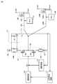
- FIG. 6is a circuit diagram showing a configuration of a short circuit protection circuit of a semiconductor switching element as Comparative Example 1
- FIG. 7is a circuit diagram showing a configuration of a short circuit protection circuit of a semiconductor switching element as Comparative Example 2.
- FIG. 3is a circuit diagram showing a configuration in which semiconductor switching elements are parallelized in FIG. 2
- FIG. 1is a circuit diagram showing a configuration of a semiconductor system to which a short circuit protection circuit according to a first embodiment is applied.
- FIG. 5is a circuit diagram showing an example of an RTC circuit of FIG. 4; It is a circuit diagram which shows an example of a detailed structure of the differential amplifier of FIG. It is the circuit diagram which took out and showed the difference voltage circuit of FIG. 4 and its periphery part.
- FIG. 7is a circuit diagram showing a configuration of a semiconductor system to which a short circuit protection circuit according to a second embodiment is applied. It is a circuit diagram which shows the structure of the modification of the difference voltage circuit of FIG.
- FIG. 13is a circuit diagram showing a configuration of a semiconductor system provided with a short circuit protection circuit according to a third embodiment.
- FIG. 16is a circuit diagram showing a configuration of a semiconductor system provided with a short circuit protection circuit according to a fourth embodiment.
- FIG. 18is a circuit diagram showing a configuration of a semiconductor system provided with a short circuit protection circuit according to a fifth embodiment.
- FIGS. 1 to 3problems of the short circuit protection circuit described in Patent Document 1 will be described.
- the circuit diagrams of FIGS. 1 to 3are intended to be comparative examples for comparison with the respective embodiments of the present application, and are related to the short circuit protection circuit disclosed in Patent Document 1. However, it is not identical to the circuit disclosed in the same document.
- FIG. 1is a circuit diagram showing a configuration of a short circuit protection circuit of a semiconductor switching element as Comparative Example 1.
- the circuit diagram of FIG. 1corresponds to FIG. 7 of Patent Document 1.
- drive signal DS output from drive circuit 101is input to gate driver 127.
- the gate driver 127has gate output transistors 102 and 103.
- the transistor 102is an N-channel MOSFET (Metal Oxide Semiconductor Field Effect Transistor), and its drain terminal is connected to a positive power supply 106.
- the transistor 103is a P-channel MOSFET, and its drain terminal is connected to the negative power supply 107.
- connection node 150The source terminal of transistor 102 and the source terminal of transistor 103 are coupled to each other via connection node 150.
- the connection node 150is connected to the gate terminal 140 of the semiconductor switching element 109 via the gate wiring 108.
- a gate resistor 112is provided on the gate wiring 108.
- the semiconductor switching element 109incorporates a sense cell.
- Sense cellsare also referred to as sense electrodes.
- a real-time control (RTC) circuit 110 as a first protection circuitis connected to this sense cell.
- the RTC circuit 110operates to lower the gate voltage of the semiconductor switching element when judging the magnitude of the current flowing through the sense cell and judging that the current is an overcurrent.
- the RTC circuit 110prevents the breakdown of the semiconductor switching element 109 by reducing the gate voltage urgently. Therefore, although the short circuit current of the semiconductor switching element 109 is limited but not completely cut off by the RTC circuit 110, the semiconductor switching element 109 may overheat and be destroyed as it is. Therefore, a shutoff circuit 116 for detecting the operation of the RTC circuit 110 to shut off the drive signal DS and an emergency stop circuit 117 for finally stopping the drive circuit 101 are provided. The shutoff circuit 116 and the emergency stop circuit 117 need to operate immediately after the operation of the RTC circuit 110.
- the RTC circuit 110may issue an SC (Short Circuit) signal to notify the above-described shutoff circuit 116 and the emergency stop circuit 117 that a short circuit has been detected.
- SC signalsare susceptible to noise and require filters to eliminate the noise. In a noisy environment where it is necessary to increase the time constant of the filter, determination of the SC signal takes time and the protection operation is delayed.
- the operation monitoring circuit 111is prepared as a second protection circuit, and the terminals at both ends of the gate resistor 112 are respectively connected to the base terminal and the emitter terminal of the PNP transistor 113 therein. Furthermore, a resistive element 114 having a relatively large resistance value is connected between the base and the emitter of the PNP transistor 113.
- the specific operation of the operation monitoring circuit 111is as follows. Since the base potential is pulled up to the emitter potential by the resistive element 114, the PNP transistor 113 is normally off. When a short circuit occurs in the semiconductor switching element 109 and the RTC circuit 110 operates, the gate potential of the semiconductor switching element 109 is forcibly pulled down, so that the gate current increases. The increased gate current increases the potential difference across the gate resistor 112. As a result, the potential difference between the base and the emitter of the PNP transistor 113 connected to the gate resistor 112 also increases, and as a result, the PNP transistor 113 is turned on.
- the voltage Vs of the positive power source 106is input to the shutoff circuit 116 and the emergency stop circuit 117 via the collector terminal 115 of the PNP transistor 113.
- the blocking circuit 116 and the emergency stop circuit 117 to which the positive voltage Vs is inputoperate to block the driving signal DS and stop the driving circuit 101.
- the short circuit protection circuit of FIG. 1has a problem that the protection operation is delayed. The reason is that, as described above, when the semiconductor switching element 109 is in the OFF state, the entire potential of the operation monitoring circuit 111 is lowered to ⁇ Vs which is the potential of the negative power supply 107. The short circuit failure occurs when the semiconductor switching element 109 is in the on state, and generally, the short circuit starts from the time of turn on when the semiconductor switching element 109 changes from the off state to the on state. In the short circuit protection circuit of FIG.
- the emitter terminal of the PNP transistor 113 of the operation monitoring circuit 111is connected to the positive power supply 106 at the moment of turning on the semiconductor switching element 109, but the potential of the other portion of the operation monitoring circuit 111 is It does not rise immediately because of parasitic capacitance. For this reason, it takes time for the operation monitoring circuit 111 to shift to a normal operation state, and as a result, the protection operation by the short circuit protection circuit is delayed. In other words, this problem is caused by the fact that the potential of each part of the operation monitoring circuit 111 fluctuates with the in-phase component of the potential across the gate resistor 112.
- FIG. 2is a circuit diagram showing a configuration of a short circuit protection circuit of a semiconductor switching element as Comparative Example 2. This circuit corresponds to FIG. 10 of Patent Document 1.
- a gate resistor 104connected between the drain terminal of the transistor 102 and the positive power supply 106, and between the drain terminal of the transistor 103 and the negative power supply 107.
- This circuitdiffers from the circuit of FIG. 1 in that it includes a connected gate resistor 105.
- the circuit of FIG. 2is different from the circuit of FIG. 1 in that the base terminal and the emitter terminal of the PNP transistor 113 constituting the operation monitoring circuit 111 are respectively connected to the terminals at both ends of the gate resistor 104.
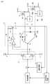
- FIG. 3is a circuit diagram showing a configuration in which the semiconductor switching elements are parallelized in FIG.
- a semiconductor switching element 109 ⁇ / b> Bis disposed in parallel with the semiconductor switching element 109.
- the gate terminal 140B of the semiconductor switching element 109Bis coupled to the gate terminal 140 of the semiconductor switching element 109.
- the semiconductor switching element 109 and the semiconductor switching element 109Bare simultaneously driven by the gate driver 127.
- the semiconductor switching element 109Bis provided with a second RTC circuit 110B having the same configuration as that of the first RTC circuit 110.
- the second RTC circuit 110Boperates to forcibly lower the gate voltage of the semiconductor switching element 109B when the semiconductor switching element 109B is in a short circuit state.
- a short circuitoccurs simultaneously in the semiconductor switching element 109 and the semiconductor switching element 109B in operation.
- Such a simultaneous short circuitoccurs, for example, when an on drive signal DS is issued when it should not be turned on due to an error in the setting of the drive signal DS.
- the RTC circuits 110 and 110Boperate simultaneously. Then, the ability to lower the potential of the gate wiring 108 is twice that in the case of FIG. Therefore, the gate current flowing through the gate resistor 104 is also twice that in the case of FIG. Therefore, even if the resistance value of the gate resistor 104 of FIG. 3 is only half that of FIG. 2, the voltage generated at the gate resistor 104 of FIG. 3 is the same as that of FIG. As a result, since the operation detection speed of the RTC circuits 110 and 110B by the operation monitoring circuit 111 is the same as in the case of FIG. 2, no delay occurs in the short circuit protection operation.
- the situationis different when only one of the semiconductor switching elements 109 and 109B causes a short circuit.
- the semiconductor switching element 109is shorted and the semiconductor switching element 109B is not shorted.
- Such unbalanced short circuitmay occur due to overheating of the device.
- the RTC circuit 110When only the semiconductor switching element 109 is shorted, the RTC circuit 110 operates but the RTC circuit 110B does not operate. This means that the gate wiring 108 has only the same ability to lower the potential as in FIG. However, since the size of the gate resistor 104 in FIG. 3 is half that of the gate resistor 102 in FIG. 2, the voltage generated in the gate resistor 104 is half that in FIG. 2. As a result, the operation of the operation monitoring circuit 111 is delayed, and the operations of the shutoff circuit 116 and the emergency stop circuit 117 are also delayed. Such a delay in the short circuit protection operation may cause destruction of the semiconductor switching element 109, which is a serious problem.
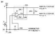
- FIG. 4is a circuit diagram showing a configuration of a semiconductor system to which the short circuit protection circuit according to the first embodiment is applied.
- the short circuit protection circuitprotects semiconductor switching element 9.
- the short circuit protection circuitincludes a real time control (RTC) circuit 10, an operation monitoring circuit 11, a shutoff circuit 16, an emergency stop circuit 17, and a gate resistor 12.
- RTCreal time control
- the semiconductor switching element 9is a self-arc-extinguishing type semiconductor switching element, and is driven and controlled by the drive circuit 1.
- the type of the semiconductor switching element 9is not particularly limited.
- the semiconductor switching element 9may be an N-channel MOSFET shown in the figure, an IGBT (Insulated Gate Bipolar Transistor), or a bipolar transistor.
- the drive signal DS output from the drive circuit 1is input to the gate driver 27, and the semiconductor switching element 9 is driven by the gate driver 27.
- the gate driver 27has gate output transistors 2 and 3.
- the transistor 2is an N-channel MOSFET, and its drain terminal is connected to the positive power supply 6.
- the transistor 3is a P-channel MOSFET, and its drain terminal is connected to the negative power supply 7.
- the channel polarity of the transistors 2 and 3 constituting the gate driver 27is not limited to that shown in FIG. 4.
- bothmay be N-channel MOSFETs.
- the drive signal DS input to the gate terminal of one of the transistorsis obtained by inverting the logic level of the drive signal DS input to the gate terminal of the other transistor.
- the type of the transistors 2 and 3is not limited to the MOSFET.
- a bipolar transistormay be used instead of the MOSFET.
- the source terminal of transistor 2 and the source terminal of transistor 3are coupled to each other via a connection node (hereinafter referred to as output node 50 of gate driver 27).
- the output node 50is connected to the gate terminal 40 of the semiconductor switching element 9 via the gate wiring 8.
- the gate wiring 12is provided with a gate resistor 12.
- the semiconductor switching element 9incorporates a sense cell.
- the RTC circuit 10is connected to this sense cell.
- the RTC circuit 10operates to lower the gate voltage of the semiconductor switching element 9 when judging the magnitude of the current flowing through the sense cell and judging that the current is an overcurrent.
- FIG. 5is a circuit diagram showing an example of the RTC circuit of FIG. Referring to FIG. 5, RTC circuit 10 includes resistance elements 43 and 45, a detection circuit 42 for detecting a short circuit current, a diode 44 and a transistor 46.
- Resistive element 43is connected between sense cell 41 of semiconductor switching element 9 and a node for applying reference potential Gnd. Resistance element 43 is used as a current sense resistor for detecting sense current Is.
- the diode 44, the resistive element 45, and the transistor 46are connected in series between the gate wiring 8 and a node for applying the reference potential Gnd so that the polarity of the diode 44 is forward in this order.
- the transistor 46may be, for example, a MOSFET or a bipolar transistor.
- FIG. 4exemplifies the case where the transistor 46 is an NPN bipolar transistor.
- the control electrode (gate or base) of the transistor 46is connected to the detection circuit 42.
- the detection circuit 42detects a voltage between both ends of the resistance element 43, and determines whether the detected voltage exceeds a threshold.
- the detection circuit 42switches the transistor 46 from the off state to the on state when the voltage of the resistance element 43 exceeds the threshold. As a result, the gate current Ig flows through the diode 44, the resistive element 45, and the transistor 46.
- the gate terminal 40 of the semiconductor switching element 9is connected to the positive power supply 6 through the transistor 2 in the on state. Therefore, although the RTC circuit 10 can limit the short circuit current flowing through the semiconductor switching element 9 by urgently lowering the potential of the gate terminal 40 of the semiconductor switching element 9, the semiconductor switching element 9 is completely turned off. It is not possible.
- operation monitoring circuit 11detects the operation of RTC circuit 10 by monitoring the gate current flowing through gate resistor 12. Specifically, the operation monitoring circuit 11 detects a potential difference between both ends of the gate resistor 12 when the semiconductor switching element 9 is on.
- the operation monitoring circuit 11includes a differential voltage circuit 20 and a PNP bipolar transistor (PNP transistor) 13.
- PNP transistorPNP bipolar transistor
- the differential voltage circuit 20takes out the potential difference between both ends of the gate resistor 12 and outputs it. In other words, the in-phase component of the potential across the gate resistor 12 is removed, and only the differential component is extracted.
- the absolute value of the differential component extracted by the differential voltage circuit 20is output between the emitter terminal and the base terminal of the PNP transistor 13. Since the emitter terminal of the PNP transistor 13 is connected to the positive power supply 6, the difference voltage circuit 20 eventually determines the potential difference between the potential proportional to the potential difference across the gate resistor 12 and the potential of the positive power supply 6 or A voltage proportional to the potential difference is output between the emitter terminal and the base terminal of the PNP transistor 13.
- the operation monitoring circuit 11is further provided with a resistive element 14.
- the resistive element 14is connected between the base terminal and the emitter terminal of the PNP transistor 13. Further, the collector terminal of the PNP transistor 13 is connected to the shutoff circuit 16 and the emergency stop circuit 17.
- the base potentialis pulled up to the emitter potential (that is, the potential + Vs of the positive power supply 6) by the resistance element 14, and the PNP transistor 13 is normally off It is.
- the gate potential of the semiconductor switching element 9is forcibly pulled down, so that the gate current increases.
- the increased gate currentincreases the potential difference across the gate resistor 12.
- the output voltage of the differential voltage circuit 20increases, so the potential difference between the base and the emitter of the PNP transistor 13 also increases, and as a result, the PNP transistor 13 is turned on.
- the PNP transistor 13is turned on, the potential Vs of the positive power source 6 is input to the shutoff circuit 16 and the emergency stop circuit 17 via the collector terminal 15 of the PNP transistor 13.
- the emitter terminal of the PNP transistor 13is connected to the positive power supply 6 and not connected to one end of the gate resistor 12.
- the operation monitoring circuit 11 of FIG. 4differs from the operation monitoring circuit 111 of FIG. 1 in this point. Therefore, unlike the case of FIG. 1, even when the semiconductor switching element 9 is in the OFF state, the entire potential of the operation monitoring circuit 11 does not decrease to ⁇ Vs which is the potential of the negative power supply 7. Therefore, charge and discharge of parasitic capacitances do not occur in the operation monitoring circuit 11 when the semiconductor switching element 9 is turned on and off, and no delay occurs in the operation. Further, since the potential of the operation monitoring circuit 11 does not change, the diode 118 as shown in FIG. 1 is unnecessary on the collector terminal side of the PNP transistor 13.
- the blocking circuit 16blocks the drive signal DS when it receives a signal of the positive voltage + Vs from the operation monitoring circuit 11.
- the blocking circuit 16fixes the potential of the wiring connecting the output node of the drive circuit 1 and the input node of the gate driver 27 to ⁇ Vs which is the potential of the negative power supply 7.
- the emergency stop circuit 17controls the drive circuit 1 so that the logic level of the drive signal DS is fixed to the low level (L level) when receiving the signal of the positive voltage + Vs from the operation monitoring circuit 11.
- the differential voltage circuit 20includes a first differential amplifier 21 and a second differential amplifier 22.
- Each of the differential amplifiers 21 and 22has two input terminals, a positive side input terminal and a negative side input terminal, and outputs the potential difference between the terminals as an absolute value from the output terminal Out.
- the positive side input terminal (also referred to as a high potential side input terminal VinH) of the differential amplifier 21is connected to a connection node between the gate resistor 12 and the gate driver 27.
- the negative side input terminal (also referred to as low potential side input terminal VinL) of the differential amplifier 21is connected to a connection node between the gate resistor 12 and the gate terminal 40 of the semiconductor switching element 9.
- the output terminal Out of the differential amplifier 21is connected to the negative input terminal of the differential amplifier 22.
- the positive input terminal of the differential amplifier 22is connected to the positive power supply 6.
- the output terminal Out of the differential amplifier 22is connected to the base terminal of the PNP transistor 13.
- FIG. 6is a circuit diagram showing an example of a detailed configuration of the differential amplifier of FIG. As shown in FIG. 5, each of differential amplifiers 21 and 22 in FIG. 4 can be configured using operational amplifier OPA and resistance elements R1, R2, R3 and R4.
- the positive side input terminal of the operational amplifier OPAis connected to the high potential side input terminal VinH via the resistor element R3, and connected to the reference terminal Ref via the resistor element R4.
- the negative input terminal of the operational amplifier OPAis connected to the low potential side input terminal VinL via the resistor element R1, and connected to the output terminal of the operational amplifier OPA via the resistor element R2.
- the output terminal of the operational amplifier OPAis connected to the output terminal Out of the differential amplifier.
- the potentials of the high potential side input terminal VinH, the low potential side input terminal VinL, the output terminal Out, and the reference terminal Refare denoted as VinH, VinL, Out, and Ref, respectively.
- Out(VinH ⁇ VinL) ⁇ R2 / R1 + Ref (1) Is true.
- the potential of the output terminal Out of the differential amplifieris the potential of the high potential side input terminal VinH minus the potential of the low potential side input terminal VinL. It is equal to the sum of the potentials.
- FIG. 7is a circuit diagram showing the differential voltage circuit of FIG. 4 and its peripheral portion.
- reference numeralsare attached to the input side and the output side of the differential amplifiers 21 and 22 constituting the differential voltage circuit 20.
- FIG. 8is a diagram showing voltage waveforms in each part of FIG. Specifically, the graph of FIG. 8A shows the positive input potential 26A of the differential amplifier 21, the negative input potential 26B of the differential amplifier 21, and the output potential 26D of the differential amplifier 21.
- the positive input potential 26 A of the differential amplifier 21is equal to the potential of the output node 50 of the gate driver 27.
- the negative input potential 26 B of the differential amplifier 21is equal to the gate potential of the semiconductor switching element 9.
- the graph of FIG. 8Bshows the positive input potential 26E of the differential amplifier 22, the output potential 26F of the differential amplifier 22, and the potential difference 26G between the gate and the emitter of the PNP transistor 13.
- the positive input potential 26 E of the differential amplifier 22is equal to + Vs, which is the potential of the positive power supply 6.
- transistor 2is turned on at time t0 in FIG.
- the RTC circuit 10operates at time t1
- the gate potential of the semiconductor switching element 9that is, the negative input potential 26B of the differential amplifier 21 is forced by the RTC circuit 10. Be pulled down.
- a difference voltage obtained by subtracting the negative input potential 26B from the positive input potential 26A of the differential amplifier 21is equal to the output potential 26D of the differential amplifier 21 (the amplification factor of the differential amplifier 21 is 1).
- the output potential 26D of the differential amplifier 21is input to the low potential side input terminal VinL of the differential amplifier 22.
- the potential difference + Vs of the positive power supply 6, that is, the difference between the positive input potential 26E of the differential amplifier 22 and the output potential 26D of the differential amplifier 21is equal to the output potential 26F of the differential amplifier 22 (differential The amplification factor of the amplifier 22 is 1).
- the potential difference 26Gwhich is the base-emitter voltage of the PNP transistor 13 is obtained by subtracting the potential Vs (equal to 26E) of the positive power supply 6 from the output potential 26F of the differential amplifier 22.
- the potential difference 26Gis pulled negative when the RTC circuit 10 operates, and the PNP transistor 13 is turned on. Thereby, the protection operation by the shutoff circuit 16 and the emergency stop circuit 17 of FIG. 4 is performed. Since this protection operation does not charge / discharge the parasitic capacitance of the operation monitoring circuit 11, no delay occurs.
- the configuration of the differential voltage circuit 20 of FIG. 7is devised so that the potential of the reference terminal Ref of each of the differential amplifiers 21 and 22 becomes 0 V, and high accuracy operation of voltage output is guaranteed. There is.
- FIG. 9is a circuit diagram showing a configuration of a modification of the differential voltage circuit of FIG.
- the differential voltage circuit 20A of FIG. 9differs from the differential voltage circuit 20 of FIG. 7 in that it includes only the differential amplifier 21 and does not include the differential amplifier 22.
- the connection of the positive side input terminal, the negative side input terminal, and the reference terminal Ref of the differential amplifier 21is different from that of the differential voltage circuit 20 of FIG.
- the positive side input terminal of the differential amplifier 21is connected to the connection node between the gate resistor 12 and the gate terminal 40 of the semiconductor switching element 9.
- the negative input terminal of the differential amplifier 21is connected to the connection node between the gate resistor 12 and the gate driver 27.
- the differential amplifier 22since the output terminal Out of the differential amplifier 21 can be connected to the gate of the PNP transistor 13, the differential amplifier 22 becomes unnecessary, and the cost of the differential amplifier 22 can be reduced. Since the other points in FIG. 9 are the same as those in FIG. 7, the same or corresponding portions are denoted by the same reference characters and description thereof will not be repeated. Next, the operation of the differential voltage circuit 20A of FIG. 9 will be described.
- FIG. 10is a diagram showing voltage waveforms in each part of FIG. Specifically, the graph of FIG. 10A shows the positive side input potential 26B of the differential amplifier 21, the negative side input potential 26A of the differential amplifier 21, and their potential difference (ie, 26B-26A).
- the negative input potential 26A of the differential amplifier 21is equal to the potential of the output node 50 of the gate driver 27.
- the positive input potential 26 B of the differential amplifier 21is equal to the gate potential of the semiconductor switching element 9.
- the graph of FIG. 10Bshows the output potential 26D of the differential amplifier 21 and the potential difference 26G between the gate and the emitter of the PNP transistor 13.
- transistor 2is turned on at time t0 in FIG.
- the RTC circuit 10operates at time t1
- the gate potential of the semiconductor switching element 9, that is, the positive side input potential 26B of the differential amplifier 21is forced by the RTC circuit 10. Be pulled down.
- the differential voltage(shown by a broken line in FIG. 10A) obtained by subtracting the negative input potential 26A from the positive input potential 26B of the differential amplifier 21 is added with + Vs, which is the potential of the reference terminal Ref of the differential amplifier 21.
- the resulting voltageis output as the output potential 26D of the differential amplifier 21 (the amplification factor of the differential amplifier 21 is 1).
- the potential difference 26Gwhich is the voltage between the base and the emitter of the PNP transistor 13 is obtained by subtracting the potential Vs (equal to 26E) of the positive power supply 6 from the output potential 26D of the differential amplifier 21.
- the potential difference 26Gis pulled negative when the RTC circuit 10 operates, and the PNP transistor 13 is turned on. Thereby, the protection operation by the shutoff circuit 16 and the emergency stop circuit 17 of FIG. 4 is performed.
- a comparator for comparing the output of the differential amplifier 21 with the reference voltageis provided in the operation monitoring circuit 11, and the output of this comparator is cut off. It may be transmitted to the circuit 16 and the emergency stop circuit 17.
- the second embodimentdeals with the case where a plurality of semiconductor switching elements are connected in parallel in order to increase the power to be controlled. As described in the second comparative example, if the gate resistance is reduced so as not to reduce the driving speed when driving the semiconductor switching elements connected in parallel, this causes a delay in detection of a short circuit failure of the semiconductor switching elements. In order to avoid this problem, unlike the case of FIG. 3, in the second embodiment, the gate resistance is provided between the gate driver 27 and each semiconductor switching element. Therefore, the second embodiment is an extension of the first embodiment.
- Embodiment 1differences from Embodiment 1 will be mainly described.
- the parts in common with the first embodimentmay be assigned the same reference numerals and the description may not be repeated.
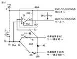
- FIG. 11is a circuit diagram showing a configuration of a semiconductor system to which a short circuit protection circuit according to a second embodiment is applied. Although the case of two semiconductor switching elements 9 and 9B connected in parallel is dealt with in FIG. 11 for simplicity, the case where more semiconductor switching elements are connected in parallel can be handled similarly.
- the semiconductor switching elements 9 and 9Bare self-arc-extinguishing type semiconductor switching elements, and are driven and controlled by the common drive circuit 1.
- the drive signal DS output from the drive circuit 1is input to the common gate driver 27. Therefore, semiconductor switching elements 9 and 9B are simultaneously driven by receiving common drive voltage (ie, + Vs which is the potential of positive power supply 6 and ⁇ Vs which is the potential of negative power supply 7) from gate driver 27.
- common drive voltageie, + Vs which is the potential of positive power supply 6 and ⁇ Vs which is the potential of negative power supply
- Gate resistor 12is connected between output node 50 of gate driver 27 and gate terminal 40 of semiconductor switching element 9, and gate resistor 12B is connected between output node 50 of gate driver 27 and gate terminal 40B of semiconductor switching element 9B. Is connected. That is, the gate line extending from output node 50 of gate driver 27 branches at branch point 52, gate resistor 12 is provided on gate line 8 for semiconductor switching element 9, and gate line 8B for semiconductor switching element 9B. A gate resistor 12B is provided. Therefore, the gate resistors 12 and 12B are provided for each of the semiconductor switching elements 9 and 9B.
- the short circuit protection circuitincludes an RTC circuit 10 for the semiconductor switching element 9, an RTC circuit 10B for the semiconductor switching element 9B, an operation monitoring circuit 11, a shutoff circuit 16, an emergency stop circuit 17, and the gate resistance described above. 12, 12B and a diode 19, 19B.
- the operation monitoring circuit 11, the blocking circuit 16, and the emergency stop circuit 17are provided commonly to the semiconductor switching elements 9, 9B.
- the RTC circuit 10is connected to the sense cell of the semiconductor switching element 9 and operates to lower the gate voltage of the semiconductor switching element 9 when judging the magnitude of the current flowing through the sense cell and determining that the current is an overcurrent.
- the RTC circuit 10Bis connected to the sense cell of the semiconductor switching element 9B, and operates to lower the gate voltage of the semiconductor switching element 9B when judging the magnitude of the current flowing through the sense cell and determining that it is an overcurrent. Since the configuration example of the RTC circuits 10 and 10B is the same as that of the first embodiment, the description will not be repeated.
- the operation monitoring circuit 11detects the operation of the RTC circuit 10 by monitoring the gate current flowing through the gate resistor 12, and detects the operation of the RTC circuit 10B by monitoring the gate current flowing through the gate resistor 12B. Specifically, the operation monitoring circuit 11 detects a voltage generated in the gate resistor 12 when the semiconductor switching device 9 is on, and detects a voltage generated in the gate resistor 12B when the semiconductor switching device 9B is on.
- the operation monitoring circuit 11includes a differential voltage circuit 20, a PNP transistor 13, and a resistive element 14. Furthermore, the differential voltage circuit 20 includes differential amplifiers 21 and 22.
- connection relationship between the operation monitoring circuit 11 and the gate resistors 12 and 12Bis different from the case of FIGS. 4 and 7 of the first embodiment.
- diodes 19 and 19Bare provided to allow the operation monitoring circuit 11 to simultaneously monitor the voltage generated in each of the gate resistors 12 and 12B.
- the cathode terminal of the diode 19is connected to the connection node 51 between the gate resistor 12 and the gate terminal 40 of the semiconductor switching element 9.
- the cathode terminal of the diode 19Bis connected to a connection node 51B between the gate resistor 12B and the gate terminal 40B of the semiconductor switching element 9B.
- the anode terminal of the diode 19 and the anode terminal of the diode 19Bare connected to the negative input terminal of the differential amplifier 21 via the connection node 53 on the anode side. Further, the positive side input terminal of the differential amplifier 21 is connected between the output node 50 of the gate driver 27 and the branch point 52 of the gate wiring.
- the RTC circuit 10when the RTC circuit 10 operates due to a short circuit failure of the semiconductor switching element 9, a gate current of the gate resistance 12 flows because the gate voltage of the semiconductor switching element 9 decreases. In this case, the potential of the connection node 51 on the cathode side of the diode 19 decreases, and the potential of the connection node 53 on the anode side of the diode 19 also decreases accordingly.
- the semiconductor switching element 9Bdoes not have a short circuit failure, the potential of the connection node 51B on the cathode side of the diode 19B is higher than the potential of the connection node 53 on the anode side. It is blocked by the diode 19B. Therefore, even if the RTC circuit 10 operates due to a short circuit failure of the semiconductor switching element 9, the potential of the gate terminal 40B of the semiconductor switching element 9B does not decrease.
- the normal operating speed of the semiconductor system of FIG. 11 and the protection speed at the time of failureare the same as those of the first embodiment of FIG.
- the resistance value of each of the gate resistors 12 and 12B in FIG. 11is equal to the resistance value of the gate resistor 12 in FIG.
- the magnitudes of the potential (+ Vs) of the positive power supply 6 and the potential (-Vs) of the negative power supply 7 in FIG. 11are the same as in the case of FIG.
- the current flowing to the gate resistors 12 and 12B when the semiconductor switching elements 9 and 9B are turned on in FIG. 11is the same as the current flowing to the single gate resistor 12 of FIG. This is because the same potential of the positive power supply 6 as in the case of FIG. 4 is applied to each of the gate resistors 12 and 12B connected in parallel. Therefore, there is no difference in the operation speed between the case where the semiconductor switching elements 9 are connected in parallel as shown in FIG. 11 and the case of a single semiconductor switching element 9 as shown in FIG.
- the speed of failure detection by the short circuit protection circuitwill be described.
- one of the semiconductor switching elements 9has a short circuit failure
- only the RTC circuit 10operates.
- the gate terminal whose potential is loweredis only the gate terminal 40 of the semiconductor switching element 9, and the potential of the gate terminal 40B of the semiconductor switching element 9B is not lowered.
- the increased gate currentflows only through the gate resistor 12 and increases the potential difference across the gate resistor 12.
- the voltage generated in the gate resistor 12is the embodiment. This is the same as the case of FIG. Therefore, there is no difference in the short circuit detection capability of the operation monitoring circuit 11 between the case of FIG. 11 and the case of FIG. 4, and the protection speed of the semiconductor switching element is the same.
- a differential voltage circuit 20A including only the differential amplifier 21may be provided instead of the differential voltage circuit 20.
- the connection in this casewill be described below.
- FIG. 12is a circuit diagram showing a configuration of a modification of the differential voltage circuit of FIG. Differential voltage circuit 20A of FIG. 12 differs from differential voltage circuit 20 of FIG. 11 in that it includes only differential amplifier 21 and does not include differential amplifier 22.
- the connection of the positive side input terminal, the negative side input terminal, and the reference terminal Ref of the differential amplifier 21is different from that of the differential voltage circuit 20 of FIG. Specifically, in the case of the differential voltage circuit 20A of FIG. 12, the positive side input terminal of the differential amplifier 21 is connected to the connection node 53 on the anode side of the diodes 19 and 19B. The negative input terminal of differential amplifier 21 is connected between output node 50 of gate driver 27 and branch point 52 of the gate wiring. These connection relationships are the reverse of those in FIG. Further, the reference terminal Ref of the differential amplifier 21 is connected to the positive power supply 6.
- the differential amplifier 22since the output terminal Out of the differential amplifier 21 can be connected to the gate of the PNP transistor 13, the differential amplifier 22 becomes unnecessary, and the cost of the differential amplifier 22 can be reduced. Since the other points in FIG. 12 are the same as those in FIG. 11, the same or corresponding portions are denoted by the same reference characters and description thereof will not be repeated.
- the operation of the differential voltage circuit 20A of FIG. 12is different in that the voltage generated in one of the gate resistors 12 and 12B is inputted to the positive input terminal of the differential amplifier 21, but the other points Is the same as that described in FIG. Therefore, the detailed description will not be repeated.
- FIG. 13is a circuit diagram showing a configuration of a semiconductor system provided with a short circuit protection circuit according to a third embodiment.
- the short circuit protection circuit of the third embodimentis configured such that the resistance values of the gate resistors 12 and 12B of the semiconductor switching elements 9 and 9B become different values at turn-on and at turn-off. Therefore, the short circuit protection circuit of the third embodiment further includes gate resistors 23 and 23B in addition to the gate resistors 12 and 12B.
- gate resistor 12 for turn-on and gate resistor 23 for turn-offare provided in parallel between output node 50 of gate driver 27 and gate terminal 40 of semiconductor switching element 9.
- Be A diode 24is connected in series with the gate resistor 12 so that the gate terminal 40 of the semiconductor switching element 9 is on the cathode side.
- a diode 25is connected in series with the gate resistor 23 so that the gate terminal 40 of the semiconductor switching element 9 is on the anode side.
- a gate resistor 12B for turn-on and a gate resistor 23B for turn-offare provided in parallel.
- the diode 24Bis connected in series with the gate resistor 12B such that the gate terminal 40B of the semiconductor switching element 9B is on the cathode side.
- a diode 25Bis connected in series with the gate resistor 23B such that the gate terminal 40B of the semiconductor switching element 9B is on the anode side.
- the optimum switching speedcan be individually selected for turn-on and turn-off while adjusting the trade-off between the switching loss and the surge voltage of the semiconductor switching element. As a result, downsizing of the device and reduction of power consumption can be realized.
- FIG. 13The other points in FIG. 13 are the same as those in FIG. 11, so the same or corresponding portions are denoted by the same reference characters and description thereof will not be repeated.
- the circuit of the modification of the differential voltage circuit 20 described with reference to FIG. 12is also applicable to the case of FIG.
- the short circuit protection circuit of the fourth embodimentfurther includes a gate resistor 5 in addition to the gate resistors 12 and 12B.
- FIG. 14is a circuit diagram showing a configuration of a semiconductor system provided with a short circuit protection circuit according to a fourth embodiment. Hereinafter, features of the semiconductor system of FIG. 14 will be described.
- the semiconductor system of FIG. 14differs from the semiconductor systems of FIGS. 11 and 13 in that the gate driver 27 has two output nodes 55 and 55B. Output node 55 is connected to positive power supply 6 through transistor 2. Output node 55 B is connected to negative power supply 7 through transistor 3.
- the semiconductor system of FIG. 14differs from the semiconductor systems of FIGS. 11 and 13 in that a gate resistor 5 for turn-off is provided in series with the transistor 3 between the output node 55B and the negative power supply 7.
- the gate resistors 5are parallelized according to the number of parallel semiconductor switching elements 9 and 9B, and the size thereof is reduced. As a result, since the turn-off speed is determined by the common gate resistor 5 when the semiconductor switching elements 9, 9B are turned off, there is an advantage that it is not affected by variations in the resistance value of the gate resistors.
- the turn-off gate resistors 23 and 23Bare provided for each of the semiconductor switching elements 9 and 9B, if the size of the gate resistance varies due to manufacturing conditions There is also a disadvantage that a disarrangement will occur. According to the fourth embodiment of FIG. 14, such a variation does not occur. As a result, the turn-off speed can be made uniform, the occurrence of current imbalance can be prevented, and the occurrence of temperature difference due to uneven heat generation of the element and fatigue failure can be prevented.
- the output node 55 of the gate driver 27(that is, the source terminal of the transistor 2) is connected to the gate terminal 40 of the semiconductor switching element 9 via the gate resistor 12 for turn on. It is connected with the gate terminal 40B of the semiconductor switching element 9B via the gate resistance 12B for the purpose.
- This configurationeliminates the need for diodes connected in series to the turn-on gate resistors 12 and 12B. This means that the resistance values of the turn-on gate resistors 12 and 12B can be maintained large.
- the current direction limiting diodes 24 and 24Bare connected in series with the turn-on gate resistors 12 and 12B. Therefore, in order not to change the switching speed at turn-on, it is necessary to reduce the resistance value of the turn-on gate resistors 12 and 12B. The reason is that in order for the transient forward voltage drop of the diode to exhibit the same effect as the gate resistance, it is necessary to reduce the resistance value of the gate resistance by that amount. However, since the forward voltage drop of the diode in the steady state is smaller than that of the transient, the RTC circuit 10 or 10B operates after the turn-on operation of the semiconductor switching elements 9, 9B is completed.
- the positive side input terminal of the differential amplifier 21 constituting the differential voltage circuit 20is between the connection node 54 to which the gate resistors 12 and 12B are connected in common and the output node 55 of the gate driver 27. Connected to
- the diode 25is provided between the output node 55 B of the gate driver 27 and the gate terminal 40 of the semiconductor switching element 9 such that the gate terminal 40 is on the anode side. Furthermore, a diode 25B is provided between the output node 55B of the gate driver 27 and the gate terminal 40B of the semiconductor switching element 9B such that the gate terminal 40B is on the anode side.
- the diodes 25 and 25Bare not for the purpose of controlling the current direction at the time of switching, and only one of the RTC circuits 10 and 10B operates, and the potential of the corresponding one of the gate terminals is lowered. In order to prevent the influence from spreading.
- short circuit protection of the semiconductor switching elementcan be realized at high speed and with high accuracy. In this case, even when only a part of the semiconductor switching elements in the semiconductor switching elements connected in parallel is shorted, short circuit protection can be realized without delay even when all the semiconductor switching elements are simultaneously shorted. Furthermore, according to the semiconductor system of the fourth embodiment, it is possible to suppress the current unbalance at turn-off and make the heat generation uniform.
- FIG. 15is a circuit diagram showing a configuration of a semiconductor system provided with a short circuit protection circuit according to a fifth embodiment.
- the semiconductor system of FIG. 15differs from the semiconductor system of FIG. 14 in that a gate resistor 4 for turn-on is further provided in series with the transistor 2 between the positive power supply 6 and the output node 55 of the gate driver 27. That is, in the semiconductor system of FIG. 15, the gate resistance for turn-on is divided, a part is connected to the gate terminals 40 and 40B of the semiconductor switching elements 9 and 9B as the gate resistances 12 and 12B, and the remaining part is the gate driver. Is connected as a gate resistor 4 to the positive power supply 6 of FIG.
- the above-mentioned reasonis that, when there is a sufficient margin in the speed of the short circuit protection circuit, a part of the gate resistance for turn-on is integrated so as to be shared by the semiconductor switching elements 9 and 9B. This is to reduce the influence of the variation.
- the variationis made uniform, and since it works in common to all the semiconductor switching elements, it does not cause current imbalance. As a result, the magnitude of the gate resistors 12 and 12B can be reduced to the minimum necessary value, and the current unbalance occurring at the turn-on switching can be minimized.
- FIG. 15The other points in FIG. 15 are the same as in FIG. 14, so the same or corresponding portions are denoted by the same reference characters and description thereof will not be repeated.
- the circuit of the modification of the differential voltage circuit 20 described with reference to FIG. 12is also applicable to the case of FIG.
- the current unbalance at turn-oncan be minimized.
Landscapes
- Engineering & Computer Science (AREA)
- Power Engineering (AREA)
- Power Conversion In General (AREA)
- Protection Of Static Devices (AREA)
- Electronic Switches (AREA)
Abstract
Description
Translated fromJapanese本開示は、半導体スイッチング素子の駆動時に短絡が発生した場合に駆動を停止し半導体スイッチング素子を保護するための短絡保護回路に関する。The present disclosure relates to a short circuit protection circuit for stopping driving and protecting a semiconductor switching element when a short occurs during driving of the semiconductor switching element.
半導体スイッチング素子、特に電力制御に使用されるパワー半導体スイッチング素子では、素子の駆動時に短絡が発生した場合、素早く駆動を停止することで半導体スイッチング素子をオフにすることが必要である。これを実現するためには、短絡の発生時にそれを遅滞なく検出することと、その検出によって駆動を遅滞なく停止させることとの両方が必要である。In a semiconductor switching element, particularly a power semiconductor switching element used for power control, when a short circuit occurs during driving of the element, it is necessary to turn off the semiconductor switching element by quickly stopping the driving. In order to realize this, it is necessary to both detect the short circuit without delay and to stop the drive without delay due to the detection.
短絡の発生を検出する回路として、RTC(Real-Time Control)回路が知られている。RTC回路は、半導体スイッチング素子内の電流の一部を取り出すためのセンスセルを流れる電流を監視し、センスセル電流が過大な場合に、即座に半導体スイッチング素子のゲート電圧を引き下げるものである。そして、そのRTC回路が動作したか否かをゲート電流の監視により判断して半導体スイッチング素子の駆動を停止する既存技術が特許文献1に記載されている。An RTC (Real-Time Control) circuit is known as a circuit for detecting the occurrence of a short circuit. The RTC circuit monitors the current flowing through the sense cell for extracting a part of the current in the semiconductor switching element, and immediately reduces the gate voltage of the semiconductor switching element when the sense cell current is excessive. Japanese Patent Application Laid-Open No. 2008-112147 describes an existing technique for judging whether the RTC circuit has operated or not by monitoring the gate current and stopping driving of the semiconductor switching element.
本願発明者は、上記の特許文献1に開示された短絡保護回路を検討した結果、半導体スイッチング素子がオフ状態からオン状態へ切り替わる際に短絡故障が発生した場合に、短絡の検出が遅れるために保護動作が遅くなり、必要な時間内に半導体スイッチング素子を保護できない場合があることを見出した。As a result of examining the short circuit protection circuit disclosed in
また、上記の特許文献1では、半導体スイッチング素子を並列接続する場合について検討されていない。本願発明者は、上記の特許文献1に記載された短絡保護回路を単純に並列接続された半導体スイッチング素子に適用しようとすると、ゲート抵抗に生じる電圧が小さくなるために短絡の検出が遅れ、結果として保護動作が遅れる場合があることを見出した。Moreover, in said
本願発明者による上記の検討結果については、以下の発明の詳細な説明において詳しく述べる。この開示は、上記の問題点を考慮したものであり、その主な目的は、遅滞なく短絡の発生を検知して半導体スイッチング素子を速やかに保護することが可能な短絡保護回路を提供することである。The above examination results by the inventor of the present invention will be described in detail in the detailed description of the invention below. This disclosure takes the above problems into consideration, and its main object is to provide a short circuit protection circuit capable of promptly detecting the occurrence of a short circuit and protecting the semiconductor switching element without delay. is there.
一実施形態の短絡保護回路によって保護される第1の半導体スイッチング素子は、第1のゲート端子を有し、ゲートドライバの第1の出力ノードから第1のゲート端子に第1電源の電位が供給されることによってターンオンする。短絡保護回路は、第1のゲート抵抗と、第1のリアルタイム制御回路と、動作監視回路とを備える。第1のゲート抵抗は、ゲートドライバの第1の出力ノードと第1のゲート端子との間に接続される。第1のリアルタイム制御回路は、第1の半導体スイッチング素子に短絡電流が流れていることを検出した場合に、第1のゲート端子の電位を減少させるように動作する。動作監視回路は、第1のゲート抵抗の両端の電位差に比例した電位と第1電源の電位との電位差を出力するように構成された差電圧回路を含む。動作監視回路は、差電圧回路の出力に基づいて第1のリアルタイム制御回路が動作しているか否かを監視する。The first semiconductor switching device protected by the short circuit protection circuit according to one embodiment has a first gate terminal, and the potential of the first power supply is supplied from the first output node of the gate driver to the first gate terminal. Is turned on. The short circuit protection circuit includes a first gate resistor, a first real time control circuit, and an operation monitoring circuit. The first gate resistor is connected between the first output node of the gate driver and the first gate terminal. The first real-time control circuit operates to reduce the potential of the first gate terminal when detecting that a short circuit current is flowing to the first semiconductor switching element. The operation monitoring circuit includes a differential voltage circuit configured to output a potential difference between a potential proportional to a potential difference between both ends of the first gate resistor and a potential of the first power supply. The operation monitoring circuit monitors whether or not the first real-time control circuit is operating based on the output of the differential voltage circuit.
他の実施形態の短絡保護回路は、さらに第2の半導体スイッチング素子を保護する。第2の半導体スイッチング素子は、第2のゲート端子を有し、ゲートドライバの第1の出力ノードから第2のゲート端子に第1電源の電位が供給されることによってターンオンする。この場合、短絡保護回路は、さらに、第2のゲート抵抗と、第2のリアルタイム制御回路とを備える。第2のゲート抵抗は、ゲートドライバの第1の出力ノードと第2のゲート端子との間に接続される。第2のリアルタイム制御回路は、第2の半導体スイッチング素子に短絡電流が流れていることを検出した場合に、第2のゲート端子の電位を減少させるように動作する。差電圧回路は、さらに、第2のゲート抵抗の両端の電位差に比例した電位と第1電源の電位との電位差を出力するように構成される。The short circuit protection circuit of another embodiment further protects the second semiconductor switching element. The second semiconductor switching element has a second gate terminal, and is turned on by the potential of the first power supply being supplied from the first output node of the gate driver to the second gate terminal. In this case, the short circuit protection circuit further includes a second gate resistor and a second real time control circuit. The second gate resistor is connected between the first output node of the gate driver and the second gate terminal. The second real-time control circuit operates to decrease the potential of the second gate terminal when detecting that a short circuit current is flowing to the second semiconductor switching element. The differential voltage circuit is further configured to output a potential difference between a potential proportional to the potential difference across the second gate resistor and the potential of the first power supply.
上記の一実施形態によれば、差電圧回路の動作には、ゲート抵抗の両端電位の同相成分が影響しないので、寄生容量の充放電に起因する動作遅延がほとんど生じない。したがって、半導体スイッチング素子の短絡の発生を遅滞なく検知して速やかに保護動作を行うことができる。According to the above embodiment, since the in-phase component of the potential across the gate resistor does not affect the operation of the differential voltage circuit, almost no operation delay due to charge and discharge of the parasitic capacitance occurs. Therefore, the occurrence of a short circuit of the semiconductor switching element can be detected without delay and the protection operation can be performed promptly.
上記の他の実施形態によれば、ゲート抵抗が半導体スイッチング素子ごとに設けられ、各ゲート抵抗の両端の電位差に基づいてそれぞれに対応するリアルタイム制御回路の動作を監視することができる。したがって、複数の半導体スイッチング素子が並列に接続されている場合であっても、高速に半導体スイッチング素子を保護することができる。According to the other embodiment described above, the gate resistance is provided for each semiconductor switching element, and the operation of the corresponding real-time control circuit can be monitored based on the potential difference between both ends of each gate resistance. Therefore, even when a plurality of semiconductor switching elements are connected in parallel, the semiconductor switching elements can be protected at high speed.
以下、各実施の形態について図面を参照して詳しく説明する。なお、同一または相当する部分には同一の参照符号を付して、その説明を繰り返さない場合がある。Hereinafter, each embodiment will be described in detail with reference to the drawings. The same or corresponding parts may be denoted by the same reference numerals, and the description thereof may not be repeated.
序論.
まず、図1~図3を参照して、特許文献1に記載された短絡保護回路の問題点について説明する。なお、図1~図3の回路図は、本願の各実施の形態と対比するための比較例とすることを意図したものであり、特許文献1に開示された短絡保護回路に関連しているが、同文献に開示された回路と同一ではない。Introduction.
First, with reference to FIGS. 1 to 3, problems of the short circuit protection circuit described in
[比較例1]
図1は、比較例1としての半導体スイッチング素子の短絡保護回路の構成を示す回路図である。図1の回路図は、特許文献1の図7に対応するものである。Comparative Example 1
FIG. 1 is a circuit diagram showing a configuration of a short circuit protection circuit of a semiconductor switching element as Comparative Example 1. The circuit diagram of FIG. 1 corresponds to FIG. 7 of
図1を参照して、駆動回路101から出力された駆動信号DSはゲートドライバ127に入力される。ゲートドライバ127はゲート出力用トランジスタ102,103を有する。トランジスタ102はNチャネルMOSFET(Metal Oxide Semiconductor Field Effect Transistor)であり、そのドレイン端子は正電源106に接続されている。トランジスタ103はPチャネルMOSFETであり、そのドレイン端子は負電源107に接続されている。Referring to FIG. 1, drive signal DS output from
トランジスタ102のソース端子とトランジスタ103のソース端子とは接続ノード150を介して互いに結合される。接続ノード150は、半導体スイッチング素子109のゲート端子140とゲート配線108を介して接続されている。ゲート配線108にはゲート抵抗112が設けられている。The source terminal of
半導体スイッチング素子109にはセンスセルが内蔵されている。センスセルはセンス電極とも称する。第1の保護回路としてのリアルタイム制御(RTC:Real-Time Control)回路110はこのセンスセルと接続される。RTC回路110は、センスセルを流れる電流の大小を判定し過電流であると判断した場合に半導体スイッチング素子のゲート電圧を引き下げるように動作する。The
RTC回路110は、緊急的にゲート電圧を引き下げることで半導体スイッチング素子109の破壊を防止するものである。したがって、RTC回路110によって半導体スイッチング素子109の短絡電流は制限されるものの完全には遮断されないので、そのままではやがて半導体スイッチング素子109は過熱し破壊に至るおそれがある。このため、RTC回路110の動作を検知して駆動信号DSの遮断を行う遮断回路116と、最終的に駆動回路101を停止させる非常停止回路117とが用意されている。遮断回路116と非常停止回路117とはRTC回路110の動作後直ちに動作する必要がある。The
一般にRTC回路110には、短絡を検知したことを上記の遮断回路116および非常停止回路117に知らせるためのSC(Short Circuit)信号を発報するものがある。しかし、SC信号はノイズに汚染されやすく、ノイズを排除するためにフィルタを必要とする。フィルタの時定数を大きくしなければならないほどにノイズの多い環境下ではSC信号の判定に時間がかかり保護動作が遅くなってしまう。In general, the
上記の問題を避けるためにゲート電流を監視することでRTC回路110の動作を検知する方法があり、この方法が特許文献1に記載されている。ゲート電流は強力な正電源106で駆動されているためノイズの影響を受けにくい。ゲート電流を監視する方法として、半導体スイッチング素子109がオンのときにゲート抵抗112に生じる電圧を監視する方法がある。In order to avoid the above problems, there is a method of detecting the operation of the
この方法では第2の保護回路として動作監視回路111が用意されており、その中のPNPトランジスタ113のベース端子およびエミッタ端子にゲート抵抗112の両端の端子がそれぞれ接続されている。さらに、PNPトランジスタ113のベース・エミッタ間には比較的大きな抵抗値の抵抗素子114が接続されている。In this method, the
動作監視回路111の具体的動作は以下のとおりである。抵抗素子114によって、ベース電位はエミッタ電位にプルアップされているためにPNPトランジスタ113は通常時はオフ状態である。半導体スイッチング素子109に短絡が生じRTC回路110が動作すると、半導体スイッチング素子109のゲート電位が強制的に引き下げられるためゲート電流が増加する。この増加したゲート電流はゲート抵抗112の両端間の電位差を大きくする。これによって、ゲート抵抗112に接続されたPNPトランジスタ113のベース・エミッタ間の電位差も大きくなり、結果としてPNPトランジスタ113がオン状態になる。PNPトランジスタ113がオンになると、正電源106の電圧VsがPNPトランジスタ113のコレクタ端子115を介して遮断回路116と非常停止回路117に入力される。正電圧Vsが入力された遮断回路116と非常停止回路117はそれぞれ動作して駆動信号DSを遮断し、駆動回路101を停止させる。The specific operation of the
図1の回路では、半導体スイッチング素子109がオフ状態のときは、トランジスタ103がオン状態であるので、半導体スイッチング素子109のゲート電位は負電源107の電位である-Vsまで低下している。このため、ゲート抵抗112の両端とも負電源107の電位(-Vs)であり、これによりPNPトランジスタ113のエミッタ端子、ベース端子とも負電源107の電位(-Vs)に等しい。この場合、遮断回路116および非常停止回路117の各々の入力ノードの電位よりもPNPトランジスタ113のコレクタ端子の電位が下がるとPNPトランジスタ113は逆バイアス状態となり破壊のおそれがある。したがって、これを防ぐ目的で、ダイオード118が、PNPトランジスタ113のコレクタ端子と、遮断回路116および非常停止回路117の各々の入力ノードとの間に設けられている。In the circuit of FIG. 1, when the
ところが、図1の短絡保護回路には保護動作の遅れという問題がある。この理由は、上述のように半導体スイッチング素子109がオフ状態のときに、動作監視回路111の全体の電位が負電源107の電位である-Vsまで低下するからである。短絡故障が発生するのは半導体スイッチング素子109がオン状態のときであり、一般に半導体スイッチング素子109がオフ状態からオン状態に変化するターンオンの時点から短絡が開始する。図1の短絡保護回路では半導体スイッチング素子109のターンオンの瞬間には、動作監視回路111のPNPトランジスタ113のエミッタ端子は正電源106に接続されるものの、動作監視回路111の他の部分の電位は寄生容量のためにすぐには上昇しない。このため、動作監視回路111が正常な動作状態に移行するまでに時間がかかり、結果として短絡保護回路による保護動作が遅延する。換言すると、この問題は、動作監視回路111の各部の電位が、ゲート抵抗112の両端の電位の同相成分とともに変動することに起因する。However, the short circuit protection circuit of FIG. 1 has a problem that the protection operation is delayed. The reason is that, as described above, when the
以下の実施の形態1では、上記の比較例1における問題点を回避可能な短絡保護回路の構成について説明する。In the following first embodiment, a configuration of a short circuit protection circuit capable of avoiding the problems in the above comparative example 1 will be described.
[比較例2]
図2は、比較例2としての半導体スイッチング素子の短絡保護回路の構成を示す回路図である。この回路は、特許文献1の図10に対応するものである。Comparative Example 2
FIG. 2 is a circuit diagram showing a configuration of a short circuit protection circuit of a semiconductor switching element as Comparative Example 2. This circuit corresponds to FIG. 10 of
図2の回路は、図1のゲート抵抗112に代えて、トランジスタ102のドレイン端子と正電源106との間に接続されたゲート抵抗104と、トランジスタ103のドレイン端子と負電源107との間に接続されたゲート抵抗105とを備える点で図1の回路と異なる。さらに、図2の回路は、動作監視回路111を構成するPNPトランジスタ113のベース端子およびエミッタ端子がゲート抵抗104の両端の端子にそれぞれ接続されている点で図1の回路と異なる。In the circuit of FIG. 2, instead of the
図2の回路の場合には、半導体スイッチング素子109のオンオフにかかわらず、すなわち、トランジスタ102,103のオンオフにかかわらず、動作監視回路111の各部の電位は、正電源106の電位である+Vsにほぼ等しい。したがって、図1の回路の場合に生じたような保護動作の遅延は図2の回路の場合には生じない。しかしながら、複数の半導体スイッチング素子109を並列接続して制御できる電力を増やそうとした場合、図2の短絡保護回路の場合には保護動作が遅くなるという問題がある。以下、図3を参照してさらに説明する。In the case of the circuit of FIG. 2, regardless of whether the
図3は、図2において半導体スイッチング素子が並列化された構成を示す回路図である。図3において、半導体スイッチング素子109と並列に半導体スイッチング素子109Bが設置される。半導体スイッチング素子109Bのゲート端子140Bは半導体スイッチング素子109のゲート端子140と結合されている。これにより半導体スイッチング素子109と半導体スイッチング素子109Bとはゲートドライバ127によって同時に駆動される。FIG. 3 is a circuit diagram showing a configuration in which the semiconductor switching elements are parallelized in FIG. In FIG. 3, a
半導体スイッチング素子109Bには、第1のRTC回路110と同じ構成の第2のRTC回路110Bが設置されている。第2のRTC回路110Bは、半導体スイッチング素子109Bが短絡状態となった場合に半導体スイッチング素子109Bのゲート電圧を強制的に引き下げるように動作する。The
さて、図3の並列駆動回路において、半導体スイッチング素子109および109Bの通常動作時の駆動速度を、図2の単独駆動の場合の半導体スイッチング素子109の駆動速度と同じにするためには、ゲート抵抗104を流れる電流を2倍にしなければならない。なぜならば、図3の半導体スイッチング素子109,109Bの各々のゲート端子を流れるゲート電流は、図2の場合と同じにしなければならないからである。このため、ゲート抵抗104,105の各々の抵抗値を図2の場合の半分にする必要がある。図3の場合には、図2の場合と同じ抵抗値を有する抵抗素子を並列化することによって、ゲート抵抗104,105の各々の抵抗値を図2の場合の半分にしている。Now, in the parallel drive circuit of FIG. 3, in order to make the drive speed in normal operation of the
しかしながら、図3のように、ゲート抵抗104の抵抗値を半分にすると、RTC回路110,110Bの動作の検知が遅れ、短絡保護動作が遅れる原因となる場合がある。以下、図3を参照して具体的に説明する。However, as shown in FIG. 3, when the resistance value of the
まず、駆動中の半導体スイッチング素子109と半導体スイッチング素子109Bとに同時に短絡が発生したとする。このような同時短絡は、駆動信号DSの設定の誤りによってオンすべきでないときにオンの駆動信号DSが発せられた場合などに生じる。First, it is assumed that a short circuit occurs simultaneously in the
このような同時短絡の場合、RTC回路110,110Bは同時に動作する。そうすると、ゲート配線108の電位を引き下げる能力は図2の場合の2倍になる。そのため、ゲート抵抗104を流れるゲート電流も図2の場合の2倍になる。したがって、図3のゲート抵抗104の抵抗値が図2の場合の半分しかなくても、図3のゲート抵抗104に生じる電圧は図2の場合と同じである。この結果、動作監視回路111によるRTC回路110,110Bの動作検知速度は図2の場合と同じであるので、短絡保護動作に遅れは生じない。In the case of such a simultaneous short circuit, the
一方、半導体スイッチング素子109,109Bのうちの一方の半導体スイッチング素子のみが短絡を起こした場合には、事情が異なる。たとえば、半導体スイッチング素子109のみが短絡し、半導体スイッチング素子109Bは短絡しなかった場合について考える。このようなアンバランスな短絡は素子の過熱により発生することがある。On the other hand, the situation is different when only one of the
半導体スイッチング素子109のみが短絡した場合、RTC回路110は動作するがRTC回路110Bは動作しない。このことは、ゲート配線108の電位を引き下げる能力が図2の場合と同じだけしかないことを意味する。しかるに図3のゲート抵抗104の大きさは図2のゲート抵抗102の半分にしてあるので、ゲート抵抗104に生じる電圧は図2の場合の半分になる。この結果、動作監視回路111の動作が遅れ、遮断回路116および非常停止回路117の動作も遅れることになる。このような短絡保護動作の遅れは半導体スイッチング素子109の破壊を引き起こすことがあり、大きな問題である。When only the
以下の実施の形態2では、上記の比較例2における問題点を回避可能な短絡保護回路の構成について説明する。In the second embodiment described below, the configuration of a short circuit protection circuit capable of avoiding the problems in the above comparative example 2 will be described.
実施の形態1.
[短絡保護回路を含む半導体システムの全体構成]
図4は、実施の形態1による短絡保護回路が適用された半導体システムの構成を示す回路図である。
[Overall Configuration of Semiconductor System Including Short Circuit Protection Circuit]
FIG. 4 is a circuit diagram showing a configuration of a semiconductor system to which the short circuit protection circuit according to the first embodiment is applied.
図4を参照して、短絡保護回路は、半導体スイッチング素子9を保護するものである。短絡保護回路は、リアルタイム制御(RTC:Real-Time Control)回路10と、動作監視回路11と、遮断回路16と、非常停止回路17と、ゲート抵抗12とを備える。Referring to FIG. 4, the short circuit protection circuit protects
半導体スイッチング素子9は、自己消弧型の半導体スイッチング素子であり、駆動回路1によって駆動制御される。半導体スイッチング素子9の種類は特に限定されない。たとえば、半導体スイッチング素子9は、図に示すNチャネルMOSFETであってもよいし、IGBT(Insulated Gate Bipolar Transistor)であってもよいし、バイポーラトランジスタであってもよい。The
駆動回路1から出力された駆動信号DSはゲートドライバ27に入力され、ゲートドライバ27によって半導体スイッチング素子9が駆動される。ゲートドライバ27はゲート出力用トランジスタ2,3を有する。トランジスタ2はNチャネルMOSFETであり、そのドレイン端子は正電源6に接続されている。トランジスタ3はPチャネルMOSFETであり、そのドレイン端子は負電源7に接続されている。The drive signal DS output from the
なお、ゲートドライバ27を構成するトランジスタ2,3のチャネル極性は図4に限るものではなく、たとえば、両方ともNチャネルMOSFETであってもよい。この場合、一方のトランジスタのゲート端子に入力される駆動信号DSは、他方のトランジスタのゲート端子に入力される駆動信号DSの論理レベルを反転したものとなっている。また、トランジスタ2,3の種類はMOSFETに限るものではない。たとえば、MOSFETに代えてバイポーラトランジスタであってもよい。The channel polarity of the
トランジスタ2のソース端子とトランジスタ3のソース端子とは接続ノード(以下、ゲートドライバ27の出力ノード50と称する)を介して互いに結合される。出力ノード50は、半導体スイッチング素子9のゲート端子40とゲート配線8を介して接続されている。ゲート配線8にはゲート抵抗12が設けられている。The source terminal of
半導体スイッチング素子9にはセンスセルが内蔵されている。RTC回路10はこのセンスセルと接続される。RTC回路10は、センスセルを流れる電流の大小を判定し過電流であると判断した場合に半導体スイッチング素子9のゲート電圧を引き下げるように動作する。The
図5は、図4のRTC回路の一例を示す回路図である。図5を参照して、RTC回路10は、抵抗素子43,45と、短絡電流を検出する検出回路42と、ダイオード44と、トランジスタ46とを含む。FIG. 5 is a circuit diagram showing an example of the RTC circuit of FIG. Referring to FIG. 5,
抵抗素子43は、半導体スイッチング素子9のセンスセル41と基準電位Gndを与えるノードとの間に接続される。抵抗素子43は、センス電流Isを検出するための電流センス抵抗として用いられる。
ダイオード44、抵抗素子45、およびトランジスタ46は、この並び順でダイオード44の極性が順方向となるように、ゲート配線8と基準電位Gndを与えるノードとの間に直列に接続される。トランジスタ46は、たとえば、MOSFETでも、バイポーラトランジスタでもよい。図4には、トランジスタ46がNPN型のバイポーラトランジスタである場合が例示されている。トランジスタ46の制御電極(ゲートまたはベース)は、検出回路42と接続される。The
検出回路42は、抵抗素子43の両端間の電圧を検出し、検出した電圧が閾値を超えるか否かを判定する。検出回路42は、抵抗素子43の電圧が閾値を超えた場合に、トランジスタ46をオフ状態からオン状態に切り替える。これによって、ダイオード44、抵抗素子45、およびトランジスタ46を介してゲート電流Igが流れるようになる。The
なお、半導体スイッチング素子9のゲート端子40はオン状態のトランジスタ2を介して正電源6に接続されている。したがって、RTC回路10は、半導体スイッチング素子9のゲート端子40の電位を緊急的に引き下げることによって半導体スイッチング素子9を流れる短絡電流を制限することはできても、半導体スイッチング素子9を完全にオフすることはできない。The
再び、図4を参照して、動作監視回路11は、ゲート抵抗12を流れるゲート電流を監視することでRTC回路10の動作を検知する。具体的には、動作監視回路11は、半導体スイッチング素子9がオンのときにゲート抵抗12の両端間の電位差を検出する。Again referring to FIG. 4,
図4に示すように、動作監視回路11は、差電圧回路20と、PNP型のバイポーラトランジスタ(PNPトランジスタ)13とを含む。As shown in FIG. 4, the
差電圧回路20は、ゲート抵抗12の両端の電位差を取り出して出力する。言い替えると、ゲート抵抗12の両端の電位のうち同相成分は除去され、差動成分のみが取り出される。差電圧回路20によって取り出された差動成分の絶対値は、PNPトランジスタ13のエミッタ端子とベース端子との間に出力される。PNPトランジスタ13のエミッタ端子は正電源6に接続されているので、結局のところ、差電圧回路20は、ゲート抵抗12の両端の電位差に比例した電位と正電源6の電位との電位差、もしくはこの電位差に比例した電圧を、PNPトランジスタ13のエミッタ端子とベース端子との間に出力する。The
動作監視回路11にはさらに抵抗素子14が設けられている。抵抗素子14は、PNPトランジスタ13のベース端子とエミッタ端子との間に接続される。また、PNPトランジスタ13のコレクタ端子は、遮断回路16および非常停止回路17に接続される。The
上記の動作監視回路11の回路構成によれば、抵抗素子14によって、ベース電位はエミッタ電位(すなわち、正電源6の電位+Vs)にプルアップされているためにPNPトランジスタ13は通常時はオフ状態である。半導体スイッチング素子9に短絡が生じRTC回路10が動作すると、半導体スイッチング素子9のゲート電位が強制的に引き下げられるためゲート電流が増加する。この増加したゲート電流はゲート抵抗12の両端間の電位差を大きくする。これによって、差電圧回路20の出力電圧が増加するので、PNPトランジスタ13のベース・エミッタ間の電位差も大きくなり、結果としてPNPトランジスタ13がオン状態になる。PNPトランジスタ13がオンになると、正電源6の電位VsがPNPトランジスタ13のコレクタ端子15を介して遮断回路16と非常停止回路17に入力される。According to the circuit configuration of the
上記のように、PNPトランジスタ13のエミッタ端子は正電源6に接続され、ゲート抵抗12の一端に接続されていない。この点で図4の動作監視回路11は、図1の動作監視回路111と異なる。したがって、図1の場合と異なり、半導体スイッチング素子9がオフ状態になっている場合でも動作監視回路11の全体の電位が負電源7の電位である-Vsまで低下してしまうことがない。このため、半導体スイッチング素子9のターンオンおよびターンオフ時に動作監視回路11では寄生容量の充放電が発生せず、動作に遅延が生じることはない。また、動作監視回路11の電位は変動しないので、PNPトランジスタ13のコレクタ端子側に図1に示したようなダイオード118は不要である。As described above, the emitter terminal of the
遮断回路16は、動作監視回路11から正電圧+Vsの信号を受けたときに、駆動信号DSの遮断を行う。たとえば、遮断回路16は、駆動回路1の出力ノードとゲートドライバ27の入力ノードとを接続する配線の電位を負電源7の電位である-Vsに固定する。The blocking
非常停止回路17は、動作監視回路11から正電圧+Vsの信号を受けたときに、駆動信号DSの論理レベルがローレベル(Lレベル)に固定されるように、駆動回路1を制御する。The
[差電圧回路の構成]
以下、差電圧回路20の構成についてさらに詳しく説明する。図4に示すように、差電圧回路20は、第1の差動増幅器21と、第2の差動増幅器22とを含む。差動増幅器21,22の各々は、2つの入力端子である正側入力端子および負側入力端子を有し、その端子間の電位差を絶対値として出力端子Outから出力する。[Configuration of differential voltage circuit]
Hereinafter, the configuration of the
差動増幅器21の正側入力端子(高電位側入力端子VinHとも称する)は、ゲート抵抗12とゲートドライバ27との接続ノードに接続される。差動増幅器21の負側入力端子(低電位側入力端子VinLとも称する)は、ゲート抵抗12と半導体スイッチング素子9のゲート端子40との接続ノードに接続される。差動増幅器21の出力端子Outは、差動増幅器22の負側入力端子と接続される。差動増幅器22の正側入力端子は正電源6と接続される。差動増幅器22の出力端子Outは、PNPトランジスタ13のベース端子と接続される。The positive side input terminal (also referred to as a high potential side input terminal VinH) of the
図6は、図4の差動増幅器の詳細な構成の一例を示す回路図である。図5に示すように、図4の差動増幅器21,22の各々は、演算増幅器OPAと抵抗素子R1,R2,R3,R4と用いて構成することができる。FIG. 6 is a circuit diagram showing an example of a detailed configuration of the differential amplifier of FIG. As shown in FIG. 5, each of
図6に示すように、演算増幅器OPAの正側入力端子は、高電位側入力端子VinHと抵抗素子R3を介して接続され、参照端子Refと抵抗素子R4を介して接続される。演算増幅器OPAの負側入力端子は、低電位側入力端子VinLと抵抗素子R1を介して接続され、演算増幅器OPAの出力端子と抵抗素子R2を介して接続される。演算増幅器OPAの出力端子は、差動増幅器の出力端子Outと接続される。As shown in FIG. 6, the positive side input terminal of the operational amplifier OPA is connected to the high potential side input terminal VinH via the resistor element R3, and connected to the reference terminal Ref via the resistor element R4. The negative input terminal of the operational amplifier OPA is connected to the low potential side input terminal VinL via the resistor element R1, and connected to the output terminal of the operational amplifier OPA via the resistor element R2. The output terminal of the operational amplifier OPA is connected to the output terminal Out of the differential amplifier.
ここで、抵抗素子R1,R2,R3,R4の抵抗値をR1,R2,R3,R4とし、R1=R3かつR2=R4とする。さらに、高電位側入力端子VinH、低電位側入力端子VinL、出力端子Out、および参照端子Refの電位をそれぞれ、VinH、VinL、Out、Refとする。そうすると、
Out=(VinH-VinL)×R2/R1+Ref …(1)
が成り立つ。特にR1=R2=R3=R4とすれば、差動増幅器の出力端子Outの電位は、高電位側入力端子VinHの電位から低電位側入力端子VinLの電位を差し引いたものに、参照端子Refの電位を加算したものに等しくなる。Here, the resistance values of the resistance elements R1, R2, R3 and R4 are R1, R2, R3 and R4, respectively, and R1 = R3 and R2 = R4. Further, the potentials of the high potential side input terminal VinH, the low potential side input terminal VinL, the output terminal Out, and the reference terminal Ref are denoted as VinH, VinL, Out, and Ref, respectively. Then,
Out = (VinH−VinL) × R2 / R1 + Ref (1)
Is true. In particular, assuming that R1 = R2 = R3 = R4, the potential of the output terminal Out of the differential amplifier is the potential of the high potential side input terminal VinH minus the potential of the low potential side input terminal VinL. It is equal to the sum of the potentials.
[動作監視回路の動作]
次に、動作監視回路11の動作について説明する。[Operation of operation monitoring circuit]
Next, the operation of the
図7は、図4の差電圧回路とその周辺部を取り出して示した回路図である。図7では、差電圧回路20を構成する差動増幅器21,22の入力側および出力側の各部に参照符号が付されている。FIG. 7 is a circuit diagram showing the differential voltage circuit of FIG. 4 and its peripheral portion. In FIG. 7, reference numerals are attached to the input side and the output side of the
図8は、図7の各部における電圧波形を示す図である。具体的に、図8(A)のグラフは、差動増幅器21の正側入力電位26A、差動増幅器21の負側入力電位26B、および差動増幅器21の出力電位26Dを示す。差動増幅器21の正側入力電位26Aは、ゲートドライバ27の出力ノード50の電位に等しい。差動増幅器21の負側入力電位26Bは、半導体スイッチング素子9のゲート電位に等しい。FIG. 8 is a diagram showing voltage waveforms in each part of FIG. Specifically, the graph of FIG. 8A shows the positive input potential 26A of the
図8(B)のグラフは、差動増幅器22の正側入力電位26E、差動増幅器22の出力電位26F、およびPNPトランジスタ13のゲート・エミッタ間の電位差26Gを示す。差動増幅器22の正側入力電位26Eは、正電源6の電位である+Vsに等しい。The graph of FIG. 8B shows the positive input potential 26E of the
図7および図8を参照して、図8の時刻t0においてトランジスタ2がターンオンする。半導体スイッチング素子9に短絡が発生している場合、時刻t1においてRTC回路10が動作し、半導体スイッチング素子9のゲート電位、すなわち、差動増幅器21の負側入力電位26Bは、RTC回路10によって強制的に引き下げられる。差動増幅器21の正側入力電位26Aから負側入力電位26Bを引き去った差電圧は、差動増幅器21の出力電位26Dに等しい(差動増幅器21の増幅率を1としている)。Referring to FIGS. 7 and 8,
この差動増幅器21の出力電位26Dは、差動増幅器22の低電位側入力端子VinLに入力される。正電源6の電位である+Vs、すなわち、差動増幅器22の正側入力電位26Eから差動増幅器21の出力電位26Dを減じた差電圧は、差動増幅器22の出力電位26Fに等しい(差動増幅器22の増幅率を1としている)。The output potential 26D of the
よって、PNPトランジスタ13のベース・エミッタ間電圧である電位差26Gは、差動増幅器22の出力電位26Fから正電源6の電位Vs(26Eに等しい)を引き去ったものである。この電位差26Gは、RTC回路10が動作すると負に引き下げられ、PNPトランジスタ13はオンする。これにより、図4の遮断回路16および非常停止回路17による保護動作が行われる。この保護動作は、動作監視回路11の寄生容量の充放電がないため遅延は生じない。Therefore, the
また、図7の差電圧回路20の構成は、差動増幅器21、22のそれぞれの参照端子Refの電位が0Vとなるように工夫したものであり、電圧出力の高精度な動作を保証している。Further, the configuration of the
[差電圧回路の他の構成例]
保護速度に余裕があり、差動増幅器21の参照端子Refの電位を高電圧にできる場合、差電圧回路20を構成する差動増幅器を1個に削減することができる。[Another configuration example of the differential voltage circuit]
When there is a margin for protection speed and the potential of the reference terminal Ref of the
図9は、図7の差電圧回路の変形例の構成を示す回路図である。図9の差電圧回路20Aは、差動増幅器21のみを含み、差動増幅器22を含まない点で図7の差電圧回路20と異なる。FIG. 9 is a circuit diagram showing a configuration of a modification of the differential voltage circuit of FIG. The
さらに、図9の差電圧回路20Aは、差動増幅器21の正側入力端子、負側入力端子、および参照端子Refの接続が図7の差電圧回路20の場合と異なる。具体的に、図9の差電圧回路20Aの場合には、差動増幅器21の正側入力端子はゲート抵抗12と半導体スイッチング素子9のゲート端子40との接続ノードに接続される。差動増幅器21の負側入力端子はゲート抵抗12とゲートドライバ27との接続ノードに接続される。これらの接続関係は図7の場合と逆である。さらに、差動増幅器21の参照端子Refは正電源6と接続される。Furthermore, in the
上記の構成によって、差動増幅器21の出力端子OutをPNPトランジスタ13のゲートに接続することできるので、差動増幅器22が不要となり、差動増幅器22のコストを削減することができる。図9のその他の点は図7と同様であるので、同一または相当する部分には同一の参照符号を付して説明を繰り返さない。次に、図9の差電圧回路20Aの動作について説明する。According to the above configuration, since the output terminal Out of the
図10は、図9の各部における電圧波形を示す図である。具体的に、図10(A)のグラフは、差動増幅器21の正側入力電位26B、差動増幅器21の負側入力電位26A、および、これらの電位差(すなわち、26B-26A)を示す。差動増幅器21の負側入力電位26Aは、ゲートドライバ27の出力ノード50の電位に等しい。差動増幅器21の正側入力電位26Bは、半導体スイッチング素子9のゲート電位に等しい。FIG. 10 is a diagram showing voltage waveforms in each part of FIG. Specifically, the graph of FIG. 10A shows the positive side input potential 26B of the
図10(B)のグラフは、差動増幅器21の出力電位26D、およびPNPトランジスタ13のゲート・エミッタ間の電位差26Gを示す。The graph of FIG. 10B shows the output potential 26D of the
図9および図10を参照して、図10の時刻t0においてトランジスタ2がターンオンする。半導体スイッチング素子9に短絡が発生している場合、時刻t1においてRTC回路10が動作し、半導体スイッチング素子9のゲート電位、すなわち、差動増幅器21の正側入力電位26Bは、RTC回路10によって強制的に引き下げられる。差動増幅器21の正側入力電位26Bから負側入力電位26Aを引き去った差電圧(図10(A)の破線で示す)に、差動増幅器21の参照端子Refの電位である+Vsを加算した電圧が、差動増幅器21の出力電位26Dとして出力される(差動増幅器21の増幅率を1としている)。Referring to FIGS. 9 and 10,
よって、PNPトランジスタ13のベース・エミッタ間電圧である電位差26Gは、差動増幅器21の出力電位26Dから正電源6の電位Vs(26Eに等しい)を引き去ったものである。この電位差26Gは、RTC回路10が動作すると負に引き下げられ、PNPトランジスタ13はオンする。これにより、図4の遮断回路16および非常停止回路17による保護動作が行われる。Therefore, the
[効果]
以上のとおり、実施の形態1の短絡保護回路によれば、比較例1の場合と異なり、半導体スイッチング素子9のターンオン時およびターンオフ時に動作監視回路11の充放電が生じないので、比較例1の場合に比べて高速に保護動作を実現することができる。さらに、次の実施の形態2で説明するように、実施の形態1の短絡保護回路の構成は、半導体スイッチング素子9が並列化された場合にも容易に適用することができる。[effect]
As described above, according to the short circuit protection circuit of the first embodiment, unlike the case of Comparative Example 1, charge and discharge of the
なお、ノイズ対策が施されていれば、PNPトランジスタ13に代えて、たとえば、差動増幅器21の出力と参照電圧とを比較する比較器を動作監視回路11に設け、この比較器の出力が遮断回路16および非常停止回路17に伝達されるようにしてもよい。If the noise countermeasure is taken, instead of the
実施の形態2.
実施の形態2では、制御する電力を増やすために複数個の半導体スイッチング素子を並列に接続した場合を取り扱う。比較例2で説明したように、並列接続された半導体スイッチング素子を駆動する場合に駆動速度を落とさないようにゲート抵抗を減少させると、半導体スイッチング素子の短絡故障の検知の遅れの原因となる。この問題を回避するために、図3の場合と異なり、実施の形態2ではゲート抵抗は、ゲートドライバ27と各半導体スイッチング素子との間に設置される。したがって、実施の形態2は実施の形態1を拡張したものとなっている。Second Embodiment
The second embodiment deals with the case where a plurality of semiconductor switching elements are connected in parallel in order to increase the power to be controlled. As described in the second comparative example, if the gate resistance is reduced so as not to reduce the driving speed when driving the semiconductor switching elements connected in parallel, this causes a delay in detection of a short circuit failure of the semiconductor switching elements. In order to avoid this problem, unlike the case of FIG. 3, in the second embodiment, the gate resistance is provided between the
以下では、実施の形態1と異なる点を中心に説明する。実施の形態1と共通する部分については同一の参照符号を付して説明を繰り返さない場合がある。In the following, differences from
[短絡保護回路を含む半導体システムの全体構成]
図11は、実施の形態2による短絡保護回路が適用された半導体システムの構成を示す回路図である。図11では、簡単のために並列接続された2個の半導体スイッチング素子9,9Bの場合を取り扱うが、より多くの半導体スイッチング素子が並列に接続された場合も同様に取り扱うことができる。[Overall Configuration of Semiconductor System Including Short Circuit Protection Circuit]
FIG. 11 is a circuit diagram showing a configuration of a semiconductor system to which a short circuit protection circuit according to a second embodiment is applied. Although the case of two
半導体スイッチング素子9,9Bは、実施の形態1の場合と同様に、自己消弧型の半導体スイッチング素子であり、共通の駆動回路1によって駆動制御される。駆動回路1から出力された駆動信号DSは共通のゲートドライバ27に入力される。したがって、半導体スイッチング素子9,9Bは、ゲートドライバ27から共通の駆動電圧(すなわち、正電源6の電位である+Vsおよび負電源7の電位である-Vs)を受けることによって同時に駆動される。ゲートドライバ27の具体的構成例は図4の場合と同じであるので説明を繰り返さない。As in the first embodiment, the
ゲートドライバ27の出力ノード50と半導体スイッチング素子9のゲート端子40との間にゲート抵抗12が接続され、ゲートドライバ27の出力ノード50と半導体スイッチング素子9Bのゲート端子40Bとの間にゲート抵抗12Bが接続される。すなわち、ゲートドライバ27の出力ノード50から延在するゲート配線は分岐点52において分岐し、半導体スイッチング素子9用のゲート配線8にゲート抵抗12が設けられ、半導体スイッチング素子9B用のゲート配線8Bにゲート抵抗12Bが設けられる。したがって、ゲート抵抗12,12Bは半導体スイッチング素子9,9Bごとにそれぞれ設けられている。
短絡保護回路は、半導体スイッチング素子9のためのRTC回路10と、半導体スイッチング素子9BのためのRTC回路10Bと、動作監視回路11と、遮断回路16と、非常停止回路17と、上記のゲート抵抗12,12Bと、ダイオード19,19Bとを備える。動作監視回路11、遮断回路16、および非常停止回路17は、半導体スイッチング素子9,9Bに対して共通に設けられている。The short circuit protection circuit includes an
RTC回路10は半導体スイッチング素子9のセンスセルと接続され、センスセルを流れる電流の大小を判定し過電流であると判断した場合に半導体スイッチング素子9のゲート電圧を引き下げるように動作する。同様に、RTC回路10Bは半導体スイッチング素子9Bのセンスセルと接続され、センスセルを流れる電流の大小を判定し過電流であると判断した場合に半導体スイッチング素子9Bのゲート電圧を引き下げるように動作する。RTC回路10,10Bの構成例は実施の形態1の場合と同様であるので説明を繰り返さない。The
動作監視回路11は、ゲート抵抗12を流れるゲート電流を監視することでRTC回路10の動作を検知するとともに、ゲート抵抗12Bを流れるゲート電流を監視することでRTC回路10Bの動作を検知する。具体的には、動作監視回路11は、半導体スイッチング素子9がオンのときにゲート抵抗12に生じる電圧を検出するとともに、半導体スイッチング素子9Bがオンのときにゲート抵抗12Bに生じる電圧を検出する。The
動作監視回路11の具体的構成例は実施の形態1の場合と同じである。具体的に図4および図7で説明したように、動作監視回路11は、差電圧回路20と、PNPトランジスタ13と、抵抗素子14とを含む。さらに、差電圧回路20は、差動増幅器21,22を含む。A specific configuration example of the
動作監視回路11とゲート抵抗12,12Bとの接続関係は、実施の形態1の図4および図7の場合と異なる。図11の場合には、動作監視回路11によってゲート抵抗12,12Bの各々に生じる電圧を同時に監視可能にするために、ダイオード19,19Bが設けられている。具体的に、ダイオード19のカソード端子は、ゲート抵抗12と半導体スイッチング素子9のゲート端子40との間の接続ノード51に接続される。ダイオード19Bのカソード端子は、ゲート抵抗12Bと半導体スイッチング素子9Bのゲート端子40Bとの間の接続ノード51Bに接続される。ダイオード19のアノード端子とダイオード19Bのアノード端子は、アノード側の接続ノード53を介して差動増幅器21の負側入力端子と接続される。また、差動増幅器21の正側入力端子は、ゲートドライバ27の出力ノード50とゲート配線の分岐点52との間に接続される。The connection relationship between the
[動作監視回路の動作について]
上記の動作監視回路11とゲート抵抗12,12Bとの接続によれば、互いに影響を及ぼすことなく、半導体スイッチング素子9,9Bの各々が短絡故障の場合を検出することができる。[About operation of operation monitoring circuit]
According to the connection between the
たとえば、半導体スイッチング素子9が短絡故障したためにRTC回路10が動作すると、半導体スイッチング素子9のゲート電圧が低下するためにゲート抵抗12にゲート電流が流れる。この場合、ダイオード19のカソード側の接続ノード51の電位が低下し、これに伴ってダイオード19のアノード側の接続ノード53の電位も低下する。しかしながら、半導体スイッチング素子9Bが短絡故障していない場合には、ダイオード19Bのカソード側の接続ノード51Bの電位は、アノード側の接続ノード53の電位よりも高いので、接続ノード53の電位低下は、ダイオード19Bによってブロックされる。したがって、半導体スイッチング素子9が短絡故障したためにRTC回路10が動作したとしても、半導体スイッチング素子9Bのゲート端子40Bの電位が低下することはない。For example, when the
また、図11の半導体システムの通常時の動作速度および故障時の保護速度は、図4の実施の形態1の場合と同じである。ここで、図11のゲート抵抗12,12Bの各々の抵抗値は、図4のゲート抵抗12の抵抗値に等しいとする。図11の正電源6の電位(+Vs)および負電源7の電位(-Vs)の大きさは、図4の場合と同じとする。Further, the normal operating speed of the semiconductor system of FIG. 11 and the protection speed at the time of failure are the same as those of the first embodiment of FIG. Here, it is assumed that the resistance value of each of the
まず、通常時の動作速度に関して説明する。図11において半導体スイッチング素子9,9Bのターンオン時にゲート抵抗12,12Bに流れる電流は、図4の単一のゲート抵抗12に流れる電流と同じである。なぜなら、並列接続されたゲート抵抗12,12Bの各々には、図4の場合と同じ正電源6の電位が印加されているからである。したがって、図11のように半導体スイッチング素子9が並列接続された場合と、図4のように単一の半導体スイッチング素子9の場合とで動作速度に違いはない。First, the operation speed at the normal time will be described. The current flowing to the
次に、短絡保護回路による故障検知の速度について説明する。まず、いずれか一方の半導体スイッチング素子9が短絡故障した場合、たとえば、半導体スイッチング素子9のみが短絡故障した場合、RTC回路10のみが動作する。この場合、電位が引き下げられるゲート端子は、半導体スイッチング素子9のゲート端子40のみであり、半導体スイッチング素子9Bのゲート端子40Bの電位は引き下げられない。このため、増加したゲート電流はゲート抵抗12のみを流れ、ゲート抵抗12の両端間の電位差を増大させる。このように、図11の場合において、単一のRTC回路10によってゲート電圧が引き下げられることによって生じたゲート電流が単一のゲート抵抗12のみを流れるので、ゲート抵抗12に生じる電圧は実施の形態1の図4の場合と同じである。したがって、図11の場合と図4の場合とで、動作監視回路11の短絡検知能力に差が生じず、半導体スイッチング素子の保護速度は同じである。Next, the speed of failure detection by the short circuit protection circuit will be described. First, when one of the
次に両方の半導体スイッチング素子9,9Bが同時に短絡故障した場合について説明する。この場合、RTC回路10,10Bの両方とも動作するので、RTC回路10によって半導体スイッチング素子9のゲート端子40の電位が引き下げられ、RTC回路10Bによって半導体スイッチング素子9Bのゲート端子40Bの電位が引き下げられる。これによって、ゲート抵抗12,12Bの各々の両端の電位差が増大するので、ゲート抵抗12,12Bの各々に生じる電圧は実施の形態1の図4の場合と同じである。したがって、図11の場合と図4の場合とで、動作監視回路11の短絡検知能力に差が生じず、半導体スイッチング素子の保護速度は同じである。Next, a case where both
[差電圧回路の変形例]
図9で説明したように、差電圧回路20に代えて差動増幅器21のみを含む差電圧回路20Aを設けてもよい。この場合の接続について以下に説明する。[Modification of differential voltage circuit]
As described in FIG. 9, a
図12は、図11の差電圧回路の変形例の構成を示す回路図である。図12の差電圧回路20Aは、差動増幅器21のみを含み、差動増幅器22を含まない点で図11の差電圧回路20と異なる。FIG. 12 is a circuit diagram showing a configuration of a modification of the differential voltage circuit of FIG.
さらに、図12の差電圧回路20Aは、差動増幅器21の正側入力端子、負側入力端子、および参照端子Refの接続が図11の差電圧回路20の場合と異なる。具体的に、図12の差電圧回路20Aの場合には、差動増幅器21の正側入力端子はダイオード19,19Bのアノード側の接続ノード53に接続される。差動増幅器21の負側入力端子はゲートドライバ27の出力ノード50とゲート配線の分岐点52との間に接続される。これらの接続関係は図11の場合と逆である。さらに、差動増幅器21の参照端子Refは正電源6と接続される。Further, in the
上記の構成によって、差動増幅器21の出力端子OutをPNPトランジスタ13のゲートに接続することできるので、差動増幅器22が不要となり、差動増幅器22のコストを削減することができる。図12のその他の点は図11と同様であるので、同一または相当する部分には同一の参照符号を付して説明を繰り返さない。According to the above configuration, since the output terminal Out of the
また、図12の差電圧回路20Aの動作に関して、ゲート抵抗12,12Bのいずれか一方に生じた電圧が差動増幅器21の正側入力端子に入力される点で違いがあるものの、その他の点は図10で説明したものと同様である。したがって、詳しい説明を繰り返さない。Further, the operation of the
[効果]
このように実施の形態2の短絡保護回路を備えた半導体システムによれば、複数の半導体スイッチング素子を並列に接続して駆動する場合において、一部の素子のみが短絡した場合であっても、全部の素子が同時に短絡した場合であっても、遅滞なく高速に半導体スイッチング素子を保護することができる。[effect]
As described above, according to the semiconductor system provided with the short circuit protection circuit of the second embodiment, even in the case where a plurality of semiconductor switching elements are connected in parallel and driven, even when only a part of the elements is shorted, Even when all the elements are shorted simultaneously, the semiconductor switching elements can be protected at high speed without delay.
実施の形態3.
図13は、実施の形態3による短絡保護回路を備えた半導体システムの構成を示す回路図である。実施の形態3の短絡保護回路は、半導体スイッチング素子9,9Bのゲート抵抗12,12Bの抵抗値が、ターンオン時とターンオフ時とで異なる値となるように構成されている。このため、実施の形態3の短絡保護回路は、ゲート抵抗12,12Bに加えて、ゲート抵抗23,23Bをさらに備える。Third Embodiment
FIG. 13 is a circuit diagram showing a configuration of a semiconductor system provided with a short circuit protection circuit according to a third embodiment. The short circuit protection circuit of the third embodiment is configured such that the resistance values of the
具体的に図13を参照して、ゲートドライバ27の出力ノード50と半導体スイッチング素子9のゲート端子40との間には、ターンオン用のゲート抵抗12とターンオフ用のゲート抵抗23とが並列に設けられる。ゲート抵抗12と直列に半導体スイッチング素子9のゲート端子40がカソード側となるように、ダイオード24が接続されている。また、ゲート抵抗23と直列に半導体スイッチング素子9のゲート端子40がアノード側となるようにダイオード25が接続されている。Specifically, referring to FIG. 13,
同様に、ゲートドライバ27の出力ノード50と半導体スイッチング素子9Bのゲート端子40Bとの間には、ターンオン用のゲート抵抗12Bとターンオフ用のゲート抵抗23Bとが並列に設けられる。ゲート抵抗12Bと直列に半導体スイッチング素子9Bのゲート端子40Bがカソード側となるように、ダイオード24Bが接続されている。また、ゲート抵抗23Bと直列に半導体スイッチング素子9Bのゲート端子40Bがアノード側となるようにダイオード25Bが接続されている。Similarly, between the
ターンオン時には、ダイオード25,25Bによって電流が阻止されるので、ゲート抵抗12,12Bにのみ電流が流れる。ターンオフ時には、ダイオード24,24Bによって電流が阻止されるので、ゲート抵抗23,23Bにのみ電流が流れる。At turn-on, current flows only through the
上記の構成により、半導体スイッチング素子9,9Bの駆動時のターンオン速度とターンオフ速度を個別に制御できる。すなわち、半導体スイッチング素子のスイッチング損失とサージ電圧のトレードオフを調整しながら最適なスイッチング速度をターンオンとターンオフで個別に選択できる。これにより装置の小型化、低消費電力化が実現される。According to the above configuration, it is possible to individually control the turn-on speed and the turn-off speed when the
図13のその他の点は図11の場合と同様であるので、同一または相当する部分には同一の参照符号を付して説明を繰り返さない。また、図12で説明した差電圧回路20の変形例の回路は、図13の場合にも適用可能である。The other points in FIG. 13 are the same as those in FIG. 11, so the same or corresponding portions are denoted by the same reference characters and description thereof will not be repeated. The circuit of the modification of the
実施の形態4.
実施の形態4においてもゲート抵抗の構成を変更した例について説明する。実施の形態4の短絡保護回路は、ゲート抵抗12,12Bに加えてゲート抵抗5をさらに備える。Fourth Embodiment
Also in the fourth embodiment, an example in which the configuration of the gate resistance is changed will be described. The short circuit protection circuit of the fourth embodiment further includes a
図14は、実施の形態4による短絡保護回路を備えた半導体システムの構成を示す回路図である。以下、図14の半導体システムの特徴について説明する。FIG. 14 is a circuit diagram showing a configuration of a semiconductor system provided with a short circuit protection circuit according to a fourth embodiment. Hereinafter, features of the semiconductor system of FIG. 14 will be described.
(i) 図14の半導体システムは、ゲートドライバ27が2個の出力ノード55,55Bを有する点で、図11および図13の半導体システムと異なる。出力ノード55はトランジスタ2を介して正電源6と接続される。出力ノード55Bはトランジスタ3を介して負電源7と接続される。(I) The semiconductor system of FIG. 14 differs from the semiconductor systems of FIGS. 11 and 13 in that the
(ii) 図14の半導体システムは、出力ノード55Bと負電源7との間にトランジスタ3と直列にターンオフ用のゲート抵抗5が設けられる点で図11および図13の半導体システムと異なる。ゲート抵抗5は半導体スイッチング素子9,9Bの並列数に応じて並列化され、その大きさが小さくなるように構成される。これにより、半導体スイッチング素子9,9Bのターンオフ時には共通のゲート抵抗5によってターンオフ速度が決定されるので、ゲート抵抗の抵抗値のバラつきによる影響を受けないというメリットがある。(Ii) The semiconductor system of FIG. 14 differs from the semiconductor systems of FIGS. 11 and 13 in that a
これに対して、図13の実施の形態3ではターンオフ用ゲート抵抗23、23Bが半導体スイッチング素子9,9Bごとに設置されていたため、ゲート抵抗の大きさに製造条件によるバラつきがあるとターンオフ速度にもバラつきが生じてしまうというディメリットがあった。図14の実施の形態4によればそのようなバラつきは発生しない。これによりターンオフ速度を均一化し、電流アンバランスの発生を防ぎ、素子の発熱不均一による温度差の発生や疲労破壊を防ぐことができる。On the other hand, in the third embodiment of FIG. 13, since the turn-
(iii) 図14の半導体システムでは、ゲートドライバ27の出力ノード55(すなわち、トランジスタ2のソース端子)は、ターンオン用のゲート抵抗12を介して半導体スイッチング素子9のゲート端子40と接続され、ターンオン用のゲート抵抗12Bを介して半導体スイッチング素子9Bのゲート端子40Bと接続される。この構成により、ターンオン用のゲート抵抗12、12Bとそれぞれに直列に接続されていたダイオードは不要となる。このことは、ターンオン用ゲート抵抗12、12Bの抵抗値を大きく維持できることを意味する。(iii) In the semiconductor system of FIG. 14, the
より詳しく説明すると、図13の実施の形態3の場合には、ターンオン用のゲート抵抗12、12Bと直列に電流方向制限用のダイオード24、24Bがそれぞれ接続されていた。このため、ターンオン時のスイッチング速度を変えないためにはターンオン用のゲート抵抗12、12Bの抵抗値を小さくしなければならなかった。なぜなら、ダイオードの過渡的な順方向電圧降下がゲート抵抗と同様の効果を発揮するため、その分だけゲート抵抗の抵抗値をあらかじめ小さくしておく必要があるからである。ところが、定常状態におけるダイオードの順方向電圧降下は過渡的なものよりも小さいため、半導体スイッチング素子9,9Bのターンオン動作が終わった後にRTC回路10または10Bが動作して半導体スイッチング素子9または9Bのゲート電圧を引き下げた場合には、動作監視回路に入力される電位差は実質的に過渡状態の場合よりも小さくなってしまう。これによって保護動作の遅れがもたらされる。これに対して、図14の実施の形態4の場合には、電流方向制限用のダイオード24,24Bが設けられていないので、ターンオン用のゲート抵抗12、12Bの抵抗値を小さくする必要がない。よって保護動作の遅延は発生しない。More specifically, in the case of the third embodiment of FIG. 13, the current
なお、図14の場合、差電圧回路20を構成する差動増幅器21の正側入力端子は、ゲート抵抗12,12Bが共通に接続される接続ノード54とゲートドライバ27の出力ノード55との間に接続される。In the case of FIG. 14, the positive side input terminal of the
(iv) 図14の半導体システムでは、ゲートドライバ27の出力ノード55Bと半導体スイッチング素子9のゲート端子40との間に、ゲート端子40がアノード側となるようにダイオード25が設けられる。さらに、ゲートドライバ27の出力ノード55Bと半導体スイッチング素子9Bのゲート端子40Bとの間に、ゲート端子40Bがアノード側となるようにダイオード25Bが設けられる。(Iv) In the semiconductor system of FIG. 14, the
このダイオード25、25Bはスイッチング時の電流方向を制御する目的のものではなく、RTC回路10,10Bの一方のみが動作し、対応する一方のゲート端子の電位が引き下げられた場合に他方のゲート端子にその影響が波及することがないようにするためのものである。The
図14のその他の点は図11の場合と同様であるので、同一または相当する部分には同一の参照符号を付して説明を繰り返さない。また、図12で説明した動作監視回路11の差電圧回路20の変形例の回路は、図14の場合にも適用可能である。The other points in FIG. 14 are the same as in FIG. 11, so the same or corresponding portions are denoted by the same reference characters and description thereof will not be repeated. The circuit of the modification of the
このように実施の形態4の半導体システムによれば、半導体スイッチング素子の短絡保護が高速かつ精度良く実現できる。この場合、並列接続された半導体スイッチング素子のうちの一部の半導体スイッチング素子のみが短絡した場合でも全部の半導体スイッチング素子が同時に短絡した場合でも遅延なく短絡保護を実現できる。さらに、実施の形態4の半導体システムによれば、ターンオフ時の電流アンバランスを抑制し発熱を均一化できる。As described above, according to the semiconductor system of the fourth embodiment, short circuit protection of the semiconductor switching element can be realized at high speed and with high accuracy. In this case, even when only a part of the semiconductor switching elements in the semiconductor switching elements connected in parallel is shorted, short circuit protection can be realized without delay even when all the semiconductor switching elements are simultaneously shorted. Furthermore, according to the semiconductor system of the fourth embodiment, it is possible to suppress the current unbalance at turn-off and make the heat generation uniform.
実施の形態5.
図15は、実施の形態5による短絡保護回路を備えた半導体システムの構成を示す回路図である。
FIG. 15 is a circuit diagram showing a configuration of a semiconductor system provided with a short circuit protection circuit according to a fifth embodiment.
図15の半導体システムは、正電源6とゲートドライバ27の出力ノード55との間にトランジスタ2と直列にターンオン用のゲート抵抗4がさらに設けられる点で図14の半導体システムと異なる。すなわち、図15の半導体システムでは、ターンオン用のゲート抵抗が分割され、一部は半導体スイッチング素子9,9Bのゲート端子40,40Bにゲート抵抗12、12Bとして接続され、残りの一部がゲートドライバの正電源6にゲート抵抗4として接続されている。The semiconductor system of FIG. 15 differs from the semiconductor system of FIG. 14 in that a gate resistor 4 for turn-on is further provided in series with the
上記の理由は、短絡保護回路の速度に十分な余裕がある場合に、ターンオン用のゲート抵抗の一部を、半導体スイッチング素子9,9Bで共用されるように集約することでゲート抵抗の値のバラつきの影響を小さくするためである。集約されたゲート抵抗4ではバラつきが均一化されるとともにすべての半導体スイッチング素子に共通に働くため電流アンバランスの原因とならない。これにより必要最小限な値にゲート抵抗12、12Bの大きさを抑え、ターンオンのスイッチング時に生じる電流アンバランスを最小限に抑えられる。The above-mentioned reason is that, when there is a sufficient margin in the speed of the short circuit protection circuit, a part of the gate resistance for turn-on is integrated so as to be shared by the
図15のその他の点は図14の場合と同様であるので、同一または相当する部分には同一の参照符号を付して説明を繰り返さない。また、図12で説明した差電圧回路20の変形例の回路は、図15の場合にも適用可能である。The other points in FIG. 15 are the same as in FIG. 14, so the same or corresponding portions are denoted by the same reference characters and description thereof will not be repeated. The circuit of the modification of the
このように実施の形態5の半導体システムによれば、実施の形態4の効果に加えて、ターンオン時の電流アンバランスも最小限に抑えることができる。As described above, according to the semiconductor system of the fifth embodiment, in addition to the effects of the fourth embodiment, the current unbalance at turn-on can be minimized.
今回開示された実施の形態はすべての点で例示であって制限的なものでないと考えられるべきである。この発明の範囲は上記した説明ではなくて請求の範囲によって示され、請求の範囲と均等の意味および範囲内でのすべての変更が含まれることが意図される。It should be understood that the embodiment disclosed herein is illustrative and non-restrictive in every respect. The scope of the present invention is shown not by the above description but by the scope of claims, and is intended to include all modifications within the scope and meaning equivalent to the scope of claims.
2,3 ゲート出力用トランジスタ、4,5,12,12B,23,23B ゲート抵抗、6 正電源、7 負電源、8,8B ゲート配線、9,9B,109,109B 半導体スイッチング素子、10,10B RTC回路、11 動作監視回路、13 PNPトランジスタ、14 抵抗素子、15 コレクタ端子、16 遮断回路、17 非常停止回路、19,19B,24,24B,25,25B ダイオード、20,20A 差電圧回路、21 第1の差動増幅器、22 第2の差動増幅器、27 ゲートドライバ、40,40B ゲート端子、41 センスセル、50,55,55B 出力ノード、53 接続ノード、OPA 演算増幅器、Out 出力端子、Ref 参照端子、VinH 高電位側入力端子(正側入力端子)、VinL 低電位側入力端子(負側入力端子)。2, 3 gate output transistor, 4, 5, 12, 12B, 23, 23B gate resistance, 6 positive power supply, 7 negative power supply, 8, 8B gate wiring, 9, 9B, 109, 109B semiconductor switching element, 10, 10B RTC circuit, 11 operation monitoring circuit, 13 PNP transistor, 14 resistance element, 15 collector terminal, 16 shut-off circuit, 17 emergency stop circuit, 19, 19B, 24, 24B, 25, 25B diode, 20, 20A differential voltage circuit, 21 First differential amplifier, 22 Second differential amplifier, 27 gate driver, 40, 40 B gate terminal, 41 sense cell, 50, 55, 55 B output node, 53 connection node, OPA operational amplifier, Out output terminal, Ref reference Terminal, VinH High potential side input terminal (positive side input terminal , VinL low potential side input terminal (negative input terminal).
Claims (10)
Translated fromJapanese前記短絡保護回路によって保護される第1の半導体スイッチング素子は、第1のゲート端子を有し、ゲートドライバの第1の出力ノードから前記第1のゲート端子に第1電源の電位が供給されることによってターンオンし、
前記短絡保護回路は、
前記ゲートドライバの前記第1の出力ノードと前記第1のゲート端子との間に接続された第1のゲート抵抗と、
前記第1の半導体スイッチング素子に短絡電流が流れていることを検出した場合に、前記第1のゲート端子の電位を減少させるように動作する第1のリアルタイム制御回路と、
動作監視回路とを備え、
前記動作監視回路は、前記第1のゲート抵抗の両端の電位差に比例した電位と前記第1電源の電位との電位差を出力するように構成された差電圧回路を含み、前記差電圧回路の出力に基づいて前記第1のリアルタイム制御回路が動作しているか否かを監視する、半導体スイッチング素子の短絡保護回路。A short circuit protection circuit for a semiconductor switching element,
The first semiconductor switching element protected by the short circuit protection circuit has a first gate terminal, and a potential of a first power supply is supplied to the first gate terminal from a first output node of a gate driver. Turn on by
The short circuit protection circuit is
A first gate resistor connected between the first output node of the gate driver and the first gate terminal;
A first real-time control circuit operable to decrease the potential of the first gate terminal when it is detected that a short circuit current is flowing to the first semiconductor switching element;
Operation monitoring circuit,
The operation monitoring circuit includes a differential voltage circuit configured to output a potential difference between a potential proportional to a potential difference between both ends of the first gate resistor and a potential of the first power supply, and an output of the differential voltage circuit A short circuit protection circuit of a semiconductor switching device, which monitors whether or not the first real time control circuit is operating based on
前記短絡保護回路は、さらに、
前記ゲートドライバの前記第1の出力ノードと前記第2のゲート端子との間に接続された第2のゲート抵抗と、
前記第2の半導体スイッチング素子に短絡電流が流れていることを検出した場合に、前記第2のゲート端子の電位を減少させるように動作する第2のリアルタイム制御回路とを備え、
前記差電圧回路は、さらに、前記第2のゲート抵抗の両端の電位差に比例した電位と前記第1電源の電位との電位差を出力するように構成される、請求項1に記載の半導体スイッチング素子の短絡保護回路。The second semiconductor switching element protected by the short circuit protection circuit has a second gate terminal, and the potential of the first power supply is transferred from the first output node of the gate driver to the second gate terminal. Turn on by being supplied,
The short circuit protection circuit further includes
A second gate resistor connected between the first output node of the gate driver and the second gate terminal;
A second real-time control circuit operable to decrease the potential of the second gate terminal when it is detected that a short circuit current is flowing through the second semiconductor switching element;
The semiconductor switching device according to claim 1, wherein the differential voltage circuit is further configured to output a potential difference between a potential proportional to a potential difference between both ends of the second gate resistor and a potential of the first power supply. Short circuit protection circuit.
前記第1のゲート端子がカソード側になるように前記第1のゲート端子に接続された第1のダイオードと、
前記第2のゲート端子がカソード側になるように前記第2のゲート端子に接続された第2のダイオードと、
前記第1のダイオードのアノードと前記第2のダイオードのアノードとが共通に接続された接続ノードとをさらに備え、
前記差電圧回路は、前記ゲートドライバの前記第1の出力ノードと、前記接続ノードとの電位差に比例した電圧を前記第1電源との電位差として出力するように構成される、請求項2に記載の半導体スイッチング素子の短絡保護回路。The short circuit protection circuit is
A first diode connected to the first gate terminal such that the first gate terminal is on the cathode side;
A second diode connected to the second gate terminal such that the second gate terminal is on the cathode side;
And a connection node to which the anode of the first diode and the anode of the second diode are connected in common,
The differential voltage circuit according to claim 2, wherein the differential voltage circuit is configured to output a voltage proportional to a potential difference between the first output node of the gate driver and the connection node as a potential difference between the first power supply and the first power source. Short circuit protection circuit for semiconductor switching devices.
前記ゲートドライバの第1の出力ノードに接続された正側入力端子と、前記接続ノードに接続された負側入力端子と、前記正側入力端子の電位から前記負側入力端子の電位を減じた電位差を出力する出力端子とを有する第1の差動増幅器と、
前記第1電源に接続された正側入力端子と、前記第1の差動増幅器の前記出力端子に接続された負側入力端子と、前記正側入力端子の電位から前記負側入力端子の電位を減じた電位差の定数倍を出力する出力端子とを有する第2の差動増幅器とを含み、
前記動作監視回路は、前記第2の差動増幅器の前記出力端子の電位に基づいて、前記第1のリアルタイム制御回路が動作しているか否かを監視する、請求項3に記載の半導体スイッチング素子の短絡保護回路。The differential voltage circuit is
The potential of the negative side input terminal is reduced from the potential of the positive side input terminal connected to the first output node of the gate driver, the negative side input terminal connected to the connection node, and the positive side input terminal A first differential amplifier having an output terminal for outputting a potential difference;
The potential of the negative side input terminal from the potential of the positive side input terminal connected to the positive side input terminal connected to the first power supply, the negative side input terminal connected to the output terminal of the first differential amplifier, and the positive side input terminal And a second differential amplifier having an output terminal for outputting a constant multiple of the potential difference obtained by subtracting
The semiconductor switching device according to claim 3, wherein said operation monitoring circuit monitors whether or not said first real-time control circuit is operating based on the potential of said output terminal of said second differential amplifier. Short circuit protection circuit.
前記第2の差動増幅器の前記出力端子に接続されたベース端子と、前記第1電源に接続されたエミッタ端子とを有するPNPトランジスタをさらに含み、
前記PNPトランジスタのコレクタ端子から、前記第1および第2のリアルタイム制御回路が動作状態か否かを表す信号が出力される、請求項4に記載の半導体スイッチング素子の短絡保護回路。The operation monitoring circuit
And a PNP transistor having a base terminal connected to the output terminal of the second differential amplifier and an emitter terminal connected to the first power supply,
5. The short circuit protection circuit of a semiconductor switching element according to claim 4, wherein a signal indicating whether or not the first and second real time control circuits are in operation is output from a collector terminal of the PNP transistor.
前記ゲートドライバの第1の出力ノードに接続された負側入力端子と、前記接続ノードに接続された正側入力端子と、前記第1電源と接続された参照端子と、前記正側入力端子の電位から前記負側入力端子の電位を減じた電位差の定数倍に前記参照端子の電位を加算した電位を出力する出力端子とを有する第1の差動増幅器を含み、
前記動作監視回路は、前記第1の差動増幅器の前記出力端子の電位に基づいて、前記第1のリアルタイム制御回路が動作しているか否かを監視する、請求項3に記載の半導体スイッチング素子の短絡保護回路。The differential voltage circuit is
The negative side input terminal connected to the first output node of the gate driver, the positive side input terminal connected to the connection node, the reference terminal connected to the first power source, and the positive side input terminal A first differential amplifier having an output terminal for outputting a potential obtained by adding the potential of the reference terminal to a constant multiple of the potential difference obtained by subtracting the potential of the negative side input terminal from the potential;
The semiconductor switching device according to claim 3, wherein said operation monitoring circuit monitors whether or not said first real-time control circuit is operating based on the potential of said output terminal of said first differential amplifier. Short circuit protection circuit.
前記第1の差動増幅器の前記出力端子に接続されたベース端子と、前記第1電源に接続されたエミッタ端子とを有するPNPトランジスタをさらに含み、
前記PNPトランジスタのコレクタ端子から、前記第1および第2のリアルタイム制御回路が動作状態か否かを表す信号が出力される、請求項6に記載の半導体スイッチング素子の短絡保護回路。The operation monitoring circuit
And a PNP transistor having a base terminal connected to the output terminal of the first differential amplifier and an emitter terminal connected to the first power supply,
7. The short circuit protection circuit for a semiconductor switching element according to claim 6, wherein a signal indicating whether or not the first and second real time control circuits are in operation is output from a collector terminal of the PNP transistor.
前記ゲートドライバの前記第1の出力ノードと前記第1のゲート端子との間に、前記第1のゲート抵抗と並列に接続された第3のゲート抵抗と、
前記ゲートドライバの前記第1の出力ノードと前記第2のゲート端子との間に、前記第2のゲート抵抗と並列に接続された第4のゲート抵抗と、
前記ゲートドライバの前記第1の出力ノードと前記第1のゲート端子との間に、前記第1のゲート端子がカソード側となるように前記第1のゲート抵抗と直列に接続された第3のダイオードと、
前記ゲートドライバの前記第1の出力ノードと前記第1のゲート端子との間に、前記第1のゲート端子がアノード側となるように前記第3のゲート抵抗と直列に接続された第4のダイオードと、
前記ゲートドライバの前記第1の出力ノードと前記第2のゲート端子との間に、前記第2のゲート端子がカソード側となるように前記第2のゲート抵抗と直列に接続された第5のダイオードと、
前記ゲートドライバの前記第1の出力ノードと前記第2のゲート端子との間に、前記第2のゲート端子がアノード側となるように前記第4のゲート抵抗と直列に接続された第6のダイオードとをさらに備える、請求項2~7のいずれか1項に記載の半導体スイッチング素子の短絡保護回路。The short circuit protection circuit is
A third gate resistor connected in parallel with the first gate resistor, between the first output node of the gate driver and the first gate terminal;
A fourth gate resistor connected in parallel with the second gate resistor between the first output node of the gate driver and the second gate terminal;
A third transistor is connected in series with the first gate resistor such that the first gate terminal is on the cathode side between the first output node of the gate driver and the first gate terminal. A diode,
A fourth transistor is connected in series with the third gate resistor such that the first gate terminal is on the anode side between the first output node of the gate driver and the first gate terminal. A diode,
A fifth transistor is connected in series with the second gate resistor such that the second gate terminal is on the cathode side between the first output node of the gate driver and the second gate terminal. A diode,
A sixth transistor is connected in series with the fourth gate resistor such that the second gate terminal is on the anode side between the first output node of the gate driver and the second gate terminal. The short circuit protection circuit of a semiconductor switching element according to any one of claims 2 to 7, further comprising a diode.
前記第1の出力ノードと、
前記第1の出力ノードと前記第1電源との間に接続された第1のトランジスタと、
前記第1の出力ノードと異なる第2の出力ノードと、
前記第2の出力ノードと第2電源との間に接続された第2のトランジスタとを含み、
前記短絡保護回路は、さらに、
前記第2の出力ノードと前記第2電源との間に前記第2のトランジスタと直列に接続された第5のゲート抵抗と、
前記第1のゲート端子と前記第2の出力ノードとの間に前記第1のゲート端子がアノード側となるように接続された第7のダイオードと、
前記第2のゲート端子と前記第2の出力ノードとの間に前記第2のゲート端子がアノード側となるように接続された第8のダイオードとを備える、請求項2~7のいずれか1項に記載の半導体スイッチング素子の短絡保護回路。The gate driver is
The first output node;
A first transistor connected between the first output node and the first power supply;
A second output node different from the first output node;
A second transistor connected between the second output node and a second power supply,
The short circuit protection circuit further includes
A fifth gate resistor connected in series with the second transistor between the second output node and the second power supply;
A seventh diode connected between the first gate terminal and the second output node such that the first gate terminal is on the anode side;
The eighth diode according to any one of claims 2 to 7, further comprising an eighth diode connected between the second gate terminal and the second output node such that the second gate terminal is on the anode side. The short circuit protection circuit of the semiconductor switching element as described in a term.
Priority Applications (4)
| Application Number | Priority Date | Filing Date | Title |
|---|---|---|---|
| JP2019528346AJP6755399B2 (en) | 2017-07-03 | 2018-02-22 | Short circuit protection circuit for semiconductor switching elements |
| DE112018003410.0TDE112018003410B4 (en) | 2017-07-03 | 2018-02-22 | Short-circuit protection circuit for a semiconductor switching element |
| US16/607,102US10992124B2 (en) | 2017-07-03 | 2018-02-22 | Short circuit protection circuit for semiconductor switching element |
| CN201880038917.7ACN110785933B (en) | 2017-07-03 | 2018-02-22 | Short circuit protection circuit for semiconductor switching elements |
Applications Claiming Priority (2)
| Application Number | Priority Date | Filing Date | Title |
|---|---|---|---|
| JP2017-130149 | 2017-07-03 | ||
| JP2017130149 | 2017-07-03 |
Publications (1)
| Publication Number | Publication Date |
|---|---|
| WO2019008817A1true WO2019008817A1 (en) | 2019-01-10 |
Family
ID=64950761
Family Applications (1)
| Application Number | Title | Priority Date | Filing Date |
|---|---|---|---|
| PCT/JP2018/006359CeasedWO2019008817A1 (en) | 2017-07-03 | 2018-02-22 | Short-circuit protection circuit for semiconductor switching element |
Country Status (5)
| Country | Link |
|---|---|
| US (1) | US10992124B2 (en) |
| JP (1) | JP6755399B2 (en) |
| CN (1) | CN110785933B (en) |
| DE (1) | DE112018003410B4 (en) |
| WO (1) | WO2019008817A1 (en) |
Cited By (4)
| Publication number | Priority date | Publication date | Assignee | Title |
|---|---|---|---|---|
| WO2020200780A1 (en)* | 2019-03-29 | 2020-10-08 | Robert Bosch Gmbh | Protection apparatus for a driver circuit, and method for protecting a driver circuit |
| CN114597863A (en)* | 2022-03-07 | 2022-06-07 | 潍柴动力股份有限公司 | Power supply protection circuit |
| CN114667680A (en)* | 2019-09-24 | 2022-06-24 | 罗伯特·博世有限公司 | Circuit arrangement for actuating a plurality of semiconductor switches connected in parallel |
| WO2023007569A1 (en)* | 2021-07-27 | 2023-02-02 | 三菱電機株式会社 | Switching element drive circuit |
Families Citing this family (5)
| Publication number | Priority date | Publication date | Assignee | Title |
|---|---|---|---|---|
| US10284191B2 (en)* | 2015-07-31 | 2019-05-07 | Texas Instruments Incorporated | Protective circuit enabling different bias levels responsive to event faults |
| JP7294084B2 (en)* | 2019-11-25 | 2023-06-20 | 株式会社デンソー | Short circuit detection device |
| CN113659532B (en)* | 2021-09-09 | 2025-07-18 | 珠海格力电器股份有限公司 | Short circuit detection circuit, short circuit protection circuit and switching power supply circuit |
| JP7267376B1 (en)* | 2021-10-22 | 2023-05-01 | 三菱電機株式会社 | Short circuit detection circuit |
| DE102022207192A1 (en)* | 2022-07-14 | 2024-01-25 | Robert Bosch Gesellschaft mit beschränkter Haftung | Monitoring device and method for monitoring a flyback converter, flyback converter |
Citations (5)
| Publication number | Priority date | Publication date | Assignee | Title |
|---|---|---|---|---|
| JP2003143833A (en)* | 2001-11-01 | 2003-05-16 | Hitachi Ltd | Gate drive device for semiconductor switching element |
| JP2011071174A (en)* | 2009-09-24 | 2011-04-07 | Renesas Electronics Corp | Semiconductor device and method of detecting characteristic degradation of semiconductor device |
| JP2013183541A (en)* | 2012-03-02 | 2013-09-12 | Denso Corp | Switching element driving device |
| WO2016038717A1 (en)* | 2014-09-11 | 2016-03-17 | 三菱電機株式会社 | Short-circuit protection circuit for self-arc-extinguishing semiconductor element |
| WO2017026367A1 (en)* | 2015-08-07 | 2017-02-16 | 三菱電機株式会社 | Power switching apparatus |
Family Cites Families (27)
| Publication number | Priority date | Publication date | Assignee | Title |
|---|---|---|---|---|
| JPH0287930A (en)* | 1988-09-21 | 1990-03-28 | New Japan Radio Co Ltd | Protective circuit for stabilized power source |
| IT1264619B1 (en)* | 1992-06-18 | 1996-10-04 | Int Rectifier Corp | METHOD AND DEVICE FOR SHORT-CIRCUIT PROTECTION OF POWER TRANSISTOR DEVICES |
| JP3125622B2 (en)* | 1995-05-16 | 2001-01-22 | 富士電機株式会社 | Semiconductor device |
| JP3963597B2 (en)* | 1998-10-06 | 2007-08-22 | 新日本無線株式会社 | Short circuit protection circuit |
| JP2002094363A (en)* | 2000-09-18 | 2002-03-29 | Toshiba Corp | Gate drive circuit for insulated gate type semiconductor element, insulated gate type semiconductor element, and power converter using them |
| US6741116B2 (en)* | 2001-10-15 | 2004-05-25 | Semikron Elekronik Gmbh | Semiconductor component for direct gate control and monitoring of power semiconductor switches |
| US7310213B2 (en)* | 2003-09-26 | 2007-12-18 | Matsushita Electric Industrial Co., Ltd. | Semiconductor device provided with overheat protection circuit and electronic circuit using the same |
| JP2007318418A (en)* | 2006-05-25 | 2007-12-06 | Denso Corp | Transistor protection circuit and switch circuit |
| JP2008154372A (en) | 2006-12-18 | 2008-07-03 | Toshiba Mitsubishi-Electric Industrial System Corp | Power device short-circuit detecting circuit |
| JP2008276611A (en)* | 2007-05-01 | 2008-11-13 | Nec Electronics Corp | Overcurrent protection circuit |
| JP4752811B2 (en)* | 2007-06-06 | 2011-08-17 | 日産自動車株式会社 | Drive circuit for voltage-driven element |
| JP5487746B2 (en)* | 2009-06-15 | 2014-05-07 | 富士電機株式会社 | IGBT overcurrent protection circuit with reverse breakdown voltage |
| WO2011129263A1 (en)* | 2010-04-14 | 2011-10-20 | 本田技研工業株式会社 | Short-circuit protection method |
| WO2013190752A1 (en)* | 2012-06-22 | 2013-12-27 | 富士電機株式会社 | Overcurrent detecting apparatus, and intelligent power module using same |
| JP5983274B2 (en)* | 2012-10-09 | 2016-08-31 | 富士電機株式会社 | Gate drive circuit having failure detection circuit of semiconductor switch element |
| JP6255766B2 (en)* | 2013-07-23 | 2018-01-10 | 日新電機株式会社 | Gate drive circuit |
| JP6264379B2 (en)* | 2013-09-06 | 2018-01-24 | 三菱電機株式会社 | Semiconductor device |
| JP6299177B2 (en) | 2013-11-25 | 2018-03-28 | シンフォニアテクノロジー株式会社 | Semiconductor device |
| JP6294061B2 (en)* | 2013-11-29 | 2018-03-14 | ローム株式会社 | Short circuit protection circuit |
| JP2015136234A (en)* | 2014-01-17 | 2015-07-27 | セイコーエプソン株式会社 | Short circuit protection circuit, power supply circuit and power supply device |
| US10700678B2 (en)* | 2015-06-16 | 2020-06-30 | Mitsubishi Electric Corporation | Drive control circuit for power semiconductor element |
| JP6663103B2 (en)* | 2015-08-24 | 2020-03-11 | ミツミ電機株式会社 | Semiconductor integrated circuit for regulator |
| CN108475912B (en)* | 2016-01-15 | 2019-10-29 | 株式会社自动网络技术研究所 | Power supply control apparatus |
| JP6753697B2 (en)* | 2016-05-23 | 2020-09-09 | ローム株式会社 | CMOS output circuit |
| US10175706B2 (en)* | 2016-06-17 | 2019-01-08 | Qualcomm Incorporated | Compensated low dropout with high power supply rejection ratio and short circuit protection |
| CN106099864B (en)* | 2016-07-19 | 2018-04-24 | 东南大学 | A kind of short-circuit protection method and its circuit of IGBT device for power switching |
| DE112017007641T5 (en)* | 2017-06-13 | 2020-04-02 | Mitsubishi Electric Corporation | DRIVER CIRCUIT FOR A SEMICONDUCTOR ELEMENT |
- 2018
- 2018-02-22WOPCT/JP2018/006359patent/WO2019008817A1/ennot_activeCeased
- 2018-02-22USUS16/607,102patent/US10992124B2/enactiveActive
- 2018-02-22JPJP2019528346Apatent/JP6755399B2/enactiveActive
- 2018-02-22CNCN201880038917.7Apatent/CN110785933B/enactiveActive
- 2018-02-22DEDE112018003410.0Tpatent/DE112018003410B4/enactiveActive
Patent Citations (5)
| Publication number | Priority date | Publication date | Assignee | Title |
|---|---|---|---|---|
| JP2003143833A (en)* | 2001-11-01 | 2003-05-16 | Hitachi Ltd | Gate drive device for semiconductor switching element |
| JP2011071174A (en)* | 2009-09-24 | 2011-04-07 | Renesas Electronics Corp | Semiconductor device and method of detecting characteristic degradation of semiconductor device |
| JP2013183541A (en)* | 2012-03-02 | 2013-09-12 | Denso Corp | Switching element driving device |
| WO2016038717A1 (en)* | 2014-09-11 | 2016-03-17 | 三菱電機株式会社 | Short-circuit protection circuit for self-arc-extinguishing semiconductor element |
| WO2017026367A1 (en)* | 2015-08-07 | 2017-02-16 | 三菱電機株式会社 | Power switching apparatus |
Cited By (7)
| Publication number | Priority date | Publication date | Assignee | Title |
|---|---|---|---|---|
| WO2020200780A1 (en)* | 2019-03-29 | 2020-10-08 | Robert Bosch Gmbh | Protection apparatus for a driver circuit, and method for protecting a driver circuit |
| CN114667680A (en)* | 2019-09-24 | 2022-06-24 | 罗伯特·博世有限公司 | Circuit arrangement for actuating a plurality of semiconductor switches connected in parallel |
| EP4035268A1 (en)* | 2019-09-24 | 2022-08-03 | Robert Bosch GmbH | Circuit arrangement for controlling a plurality of semiconductor switches connected in parallel |
| WO2023007569A1 (en)* | 2021-07-27 | 2023-02-02 | 三菱電機株式会社 | Switching element drive circuit |
| JP7566161B2 (en) | 2021-07-27 | 2024-10-11 | 三菱電機株式会社 | Switching element drive circuit |
| CN114597863A (en)* | 2022-03-07 | 2022-06-07 | 潍柴动力股份有限公司 | Power supply protection circuit |
| CN114597863B (en)* | 2022-03-07 | 2024-02-20 | 潍柴动力股份有限公司 | Power protection circuit |
Also Published As
| Publication number | Publication date |
|---|---|
| CN110785933B (en) | 2023-10-13 |
| JPWO2019008817A1 (en) | 2020-05-21 |
| DE112018003410T5 (en) | 2020-03-12 |
| CN110785933A (en) | 2020-02-11 |
| DE112018003410B4 (en) | 2025-07-03 |
| US20200395747A1 (en) | 2020-12-17 |
| JP6755399B2 (en) | 2020-09-16 |
| US10992124B2 (en) | 2021-04-27 |
Similar Documents
| Publication | Publication Date | Title |
|---|---|---|
| JP6755399B2 (en) | Short circuit protection circuit for semiconductor switching elements | |
| US11217989B2 (en) | Drive device, power supply system, and method of testing drive device | |
| JP4295928B2 (en) | Semiconductor protection circuit | |
| US8466734B2 (en) | Gate driving circuit for power semiconductor element | |
| JP4963891B2 (en) | Load drive circuit | |
| CN100517902C (en) | Drive circuits for power semiconductor components | |
| JP4473927B2 (en) | Short circuit protection device | |
| EP2827160B1 (en) | Detecting faults in hot-swap applications | |
| JP4836694B2 (en) | Power supply control device | |
| JP4398312B2 (en) | Semiconductor switch control device | |
| JP2019165347A (en) | Drive device and power module | |
| KR19980087505A (en) | Abnormal current detection circuit and load driving circuit including the same | |
| US20210184668A1 (en) | Semiconductor device | |
| KR20160025849A (en) | Gate driver protection apparatus of insulated gate bipolar transistor | |
| JPWO2015104921A1 (en) | In-vehicle electronic control unit | |
| JP2007294513A (en) | Semiconductor protection circuit | |
| JP2006060971A (en) | Semiconductor switch control device | |
| JP3599084B2 (en) | Power supply | |
| JPH10336876A (en) | Current breaker | |
| JP2020129867A (en) | Overcurrent detection circuit and current output circuit | |
| TW202105876A (en) | Redundant power supply device and exception protection control method thereof capable of preventing abnormal voltage rising at output port due to component aging issue | |
| JP2012080488A (en) | Gate drive circuit | |
| JP2018170586A (en) | Switching element drive circuit | |
| JP2017108244A (en) | Control circuit for semiconductor device | |
| JPH06276071A (en) | Overcurrent protection circuit for power transistor |
Legal Events
| Date | Code | Title | Description |
|---|---|---|---|
| 121 | Ep: the epo has been informed by wipo that ep was designated in this application | Ref document number:18829063 Country of ref document:EP Kind code of ref document:A1 | |
| ENP | Entry into the national phase | Ref document number:2019528346 Country of ref document:JP Kind code of ref document:A | |
| WWP | Wipo information: published in national office | Ref document number:112018003410 Country of ref document:DE | |
| 122 | Ep: pct application non-entry in european phase | Ref document number:18829063 Country of ref document:EP Kind code of ref document:A1 | |
| WWG | Wipo information: grant in national office | Ref document number:112018003410 Country of ref document:DE |