WO2018235225A1 - Imaging device, imaging method and program - Google Patents
Imaging device, imaging method and programDownload PDFInfo
- Publication number
- WO2018235225A1 WO2018235225A1PCT/JP2017/023018JP2017023018WWO2018235225A1WO 2018235225 A1WO2018235225 A1WO 2018235225A1JP 2017023018 WJP2017023018 WJP 2017023018WWO 2018235225 A1WO2018235225 A1WO 2018235225A1
- Authority
- WO
- WIPO (PCT)
- Prior art keywords
- light
- image data
- light source
- near infrared
- unit
- Prior art date
- Legal status (The legal status is an assumption and is not a legal conclusion. Google has not performed a legal analysis and makes no representation as to the accuracy of the status listed.)
- Ceased
Links
Images


Classifications
- H—ELECTRICITY
- H04—ELECTRIC COMMUNICATION TECHNIQUE
- H04N—PICTORIAL COMMUNICATION, e.g. TELEVISION
- H04N23/00—Cameras or camera modules comprising electronic image sensors; Control thereof
- H04N23/10—Cameras or camera modules comprising electronic image sensors; Control thereof for generating image signals from different wavelengths
- H04N23/12—Cameras or camera modules comprising electronic image sensors; Control thereof for generating image signals from different wavelengths with one sensor only
- H—ELECTRICITY
- H04—ELECTRIC COMMUNICATION TECHNIQUE
- H04N—PICTORIAL COMMUNICATION, e.g. TELEVISION
- H04N23/00—Cameras or camera modules comprising electronic image sensors; Control thereof
- H04N23/80—Camera processing pipelines; Components thereof
- H04N23/84—Camera processing pipelines; Components thereof for processing colour signals
- H—ELECTRICITY
- H04—ELECTRIC COMMUNICATION TECHNIQUE
- H04N—PICTORIAL COMMUNICATION, e.g. TELEVISION
- H04N23/00—Cameras or camera modules comprising electronic image sensors; Control thereof
- H04N23/10—Cameras or camera modules comprising electronic image sensors; Control thereof for generating image signals from different wavelengths
- H04N23/11—Cameras or camera modules comprising electronic image sensors; Control thereof for generating image signals from different wavelengths for generating image signals from visible and infrared light wavelengths
- H—ELECTRICITY
- H04—ELECTRIC COMMUNICATION TECHNIQUE
- H04N—PICTORIAL COMMUNICATION, e.g. TELEVISION
- H04N23/00—Cameras or camera modules comprising electronic image sensors; Control thereof
- H04N23/10—Cameras or camera modules comprising electronic image sensors; Control thereof for generating image signals from different wavelengths
- H04N23/13—Cameras or camera modules comprising electronic image sensors; Control thereof for generating image signals from different wavelengths with multiple sensors
- H04N23/16—Optical arrangements associated therewith, e.g. for beam-splitting or for colour correction
- H—ELECTRICITY
- H04—ELECTRIC COMMUNICATION TECHNIQUE
- H04N—PICTORIAL COMMUNICATION, e.g. TELEVISION
- H04N23/00—Cameras or camera modules comprising electronic image sensors; Control thereof
- H04N23/70—Circuitry for compensating brightness variation in the scene
- H04N23/71—Circuitry for evaluating the brightness variation
- H—ELECTRICITY
- H04—ELECTRIC COMMUNICATION TECHNIQUE
- H04N—PICTORIAL COMMUNICATION, e.g. TELEVISION
- H04N23/00—Cameras or camera modules comprising electronic image sensors; Control thereof
- H04N23/70—Circuitry for compensating brightness variation in the scene
- H04N23/73—Circuitry for compensating brightness variation in the scene by influencing the exposure time
- H—ELECTRICITY
- H04—ELECTRIC COMMUNICATION TECHNIQUE
- H04N—PICTORIAL COMMUNICATION, e.g. TELEVISION
- H04N23/00—Cameras or camera modules comprising electronic image sensors; Control thereof
- H04N23/70—Circuitry for compensating brightness variation in the scene
- H04N23/74—Circuitry for compensating brightness variation in the scene by influencing the scene brightness using illuminating means
- H—ELECTRICITY
- H04—ELECTRIC COMMUNICATION TECHNIQUE
- H04N—PICTORIAL COMMUNICATION, e.g. TELEVISION
- H04N25/00—Circuitry of solid-state image sensors [SSIS]; Control thereof
- H04N25/10—Circuitry of solid-state image sensors [SSIS]; Control thereof for transforming different wavelengths into image signals
- H04N25/11—Arrangement of colour filter arrays [CFA]; Filter mosaics
- H04N25/13—Arrangement of colour filter arrays [CFA]; Filter mosaics characterised by the spectral characteristics of the filter elements
- H04N25/131—Arrangement of colour filter arrays [CFA]; Filter mosaics characterised by the spectral characteristics of the filter elements including elements passing infrared wavelengths
- H—ELECTRICITY
- H04—ELECTRIC COMMUNICATION TECHNIQUE
- H04N—PICTORIAL COMMUNICATION, e.g. TELEVISION
- H04N25/00—Circuitry of solid-state image sensors [SSIS]; Control thereof
- H04N25/10—Circuitry of solid-state image sensors [SSIS]; Control thereof for transforming different wavelengths into image signals
- H04N25/11—Arrangement of colour filter arrays [CFA]; Filter mosaics
- H04N25/13—Arrangement of colour filter arrays [CFA]; Filter mosaics characterised by the spectral characteristics of the filter elements
- H04N25/135—Arrangement of colour filter arrays [CFA]; Filter mosaics characterised by the spectral characteristics of the filter elements based on four or more different wavelength filter elements
Definitions
- the present inventionrelates to an imaging device, an imaging method, and a program for capturing a visible light image and a near infrared image.
- an imaging devicesuch as a digital camera
- a technology capable of capturing a color image and a monochrome imagesee Patent Document 1.
- a first pixel that receives both visible light and infrared light and a second pixel that receives infrared lightare provided in the imaging device, and a signal output from the first pixel is used to generate a second image.
- a signal output from the first pixelis used to generate a second image.
- the present inventionhas been made in view of the above, and it is an object of the present invention to provide an imaging device, an imaging method, and a program capable of acquiring a plurality of near-infrared images in near-infrared regions different from visible light images. I assume.
- an imaging deviceis an imaging device that generates image data by receiving and photoelectrically converting a plurality of pixels arranged in a two-dimensional grid shape.
- a filtera first light source unit for emitting the visible light to the subject, a second light source unit for emitting the near infrared light to the subject, the first light source unit, and the second light source unit
- a light source control unitthat controls an irradiation timing, and a first image pickup element that picks up an image of the subject when the light source control unit irradiates the first light source unit with the visible light; Image data, and second image data generated by the imaging device capturing an image of the subject when the light source control unit simultaneously irradiates the first light source unit and the second light source unit.
- a generatorconfigured to generate a plurality of near-infrared image data having different near-infrared regions.
- an imaging elementthat generates image data by receiving and photoelectrically converting a plurality of pixels arranged in a two-dimensional grid shape is visible in different visible wavelength bands in a visible region
- a color filterformed by arranging a filter unit composed of a plurality of filters transmitting near infrared rays of different wavelength bands in the light and near infrared regions in correspondence with the plurality of pixels, and irradiating the object with the visible light
- An imaging method performed by an imaging apparatuscomprising: a light source unit according to claim 1; and a second light source unit irradiating the subject with the near-infrared light, the first light source unit irradiating the visible light
- a second irradiation stepof simultaneously irradiating the light source unit and the second light source unit; and imaging the object irradiated with the visible light and the near-infrared
- an image pickup devicethat generates image data by receiving and photoelectrically converting a plurality of pixels arranged in a two-dimensional grid shape respectively and visible light of different wavelength bands in the visible region And a color filter formed by arranging a filter unit consisting of a plurality of filters transmitting near infrared rays of different wavelength bands in the near infrared region in correspondence with the plurality of pixels, and irradiating the object with the visible light
- the second generation stepof causing the image pickup device to image the object irradiated with the visible light and the near-infrared light to generate second image data
- the present inventionit is possible to obtain a plurality of near infrared images in the near infrared region different from the visible light image.
- FIG. 1is a block diagram showing a functional configuration of the imaging device according to the first embodiment.
- FIG. 2is a view schematically showing a configuration of an image pickup element provided in the image pickup apparatus according to the first embodiment.
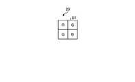
- FIG. 3is a view schematically showing the configuration of a color filter provided in the imaging device according to the first embodiment.
- FIG. 4is a diagram showing spectral sensitivity characteristics of each pixel provided in the imaging device according to the first embodiment.
- FIG. 5is a flowchart showing an outline of processing performed by the imaging device according to the first embodiment.
- FIG. 6is a block diagram showing a functional configuration of an imaging device according to a modification of the first embodiment.
- FIG. 7is a flowchart showing an outline of processing performed by the imaging device according to the modification of the first embodiment.
- FIG. 1is a block diagram showing a functional configuration of the imaging device according to the first embodiment.
- FIG. 2is a view schematically showing a configuration of an image pickup element provided in the image pickup apparatus according
- FIG. 8is a block diagram showing a functional configuration of the imaging device according to the second embodiment.
- FIG. 9is a diagram showing spectral sensitivity characteristics of each pixel provided in the imaging device according to the second embodiment.
- FIG. 10is a block diagram showing a functional configuration of the imaging device according to the third embodiment.
- FIG. 11is a view schematically showing a configuration of a color filter provided in the imaging device according to the third embodiment.
- FIG. 12is a diagram showing spectral sensitivity characteristics of each pixel provided in the imaging device according to the third embodiment.
- FIG. 1is a block diagram showing a functional configuration of the imaging device according to the first embodiment.
- An imaging device 1 shown in FIG. 1includes an imaging unit 2 that images a subject to generate image data, a first light source unit 3 that emits visible light, and a second light source unit 4 that emits near infrared light.
- a recording unit 5for recording various information
- a control unit 6for overall control of each unit of the imaging device 1, and various image processing on image data generated by the imaging unit 2 to an external display device etc.
- an image processing unit 7for outputting.
- the imaging apparatus 1is provided with an input unit for receiving an input from an external operation, and a display unit for displaying an image corresponding to image data subjected to image processing by the image processing unit 7. It is also good.
- the imaging unit 2includes an optical system 21, an imaging device 22, a color filter 23, and an A / D conversion unit 24.
- the optical system 21forms an image of a subject on the light receiving surface of the image sensor 22.
- the optical system 21is configured using one or more lenses, and has a zoom function and a focus function.
- the optical system 21changes the zoom magnification and the focus position by moving on the optical axis L by a drive unit such as a motor (not shown).
- the imaging element 22is provided perpendicular to the optical axis L of the optical system 21, and receives an object image formed by the optical system 21 under the control of the control unit 6 to perform photoelectric conversion by photoelectric conversion. A signal (image signal) is generated, and this electrical signal is output to the A / D conversion unit 24.
- the imaging device 22is realized using an image sensor such as a charge coupled device (CCD) or a complementary metal oxide semiconductor (CMOS).
- FIG. 2is a view schematically showing the configuration of the imaging device 22.
- a plurality of pixels P for receiving light from the optical system 21are arranged in a two-dimensional grid (two-dimensional matrix).
- Each pixel Preceives the light incident from the optical system 21 through the color filter 23 and performs photoelectric conversion to generate an electric signal.
- the electrical signalincludes the pixel value (brightness value) of each pixel, positional information (pixel address) of the pixel, and the like.
- the pixel arranged in the i-th row and the j-th columnis expressed as a pixel P ij .
- the color filter 23is disposed on the light receiving surface of the imaging device 22, and includes a plurality of filters that transmit visible light in different wavelength bands in the visible region and near infrared rays in different wavelength bands in the near infrared region.
- the plurality of filtersare obtained by arranging filter units U1 in a Bayer array consisting of four filters arranged in a two-dimensional grid of 2 ⁇ 2 in accordance with the arrangement of the pixels P ij .
- the pixel P ij provided with the filterreceives the light of the wavelength band transmitted through the filter.
- the configuration of the color filter 23 and the transmission characteristics of each filterwill be described later.
- the A / D conversion unit 24performs A / D conversion on the analog electrical signal input from the imaging device 22 to generate digital image data, and the image processing unit 7. Output to
- the first light source unit 3emits visible light (white light) to the subject under the control of the control unit 6. Specifically, the first light source unit 3 irradiates the subject with white light (for example, a wavelength band of 390 nm to 700 nm) including a red wavelength band, a green wavelength band and a blue wavelength band.
- white lightfor example, a wavelength band of 390 nm to 700 nm
- the first light source unit 3is realized using a white LED (Light Emitting Diode), a xenon lamp, or the like.
- the second light source unit 4emits near-infrared light (for example, a wavelength band of 700 nm to 1000 nm) to the subject under the control of the control unit 6.
- the second light source unit 4is realized using an infrared lamp, a near infrared LED, or the like.
- the recording unit 5records various programs executed by the imaging device 1, data being processed, and the like.
- the recording unit 5is configured using a flash memory, a synchronous dynamic random access memory (SDRAM), or the like.
- SDRAMsynchronous dynamic random access memory
- the recording unit 5includes a program information recording unit 51 that records various programs executed by the imaging device 1.
- the control unit 6centrally controls the respective units of the imaging device 1.
- the control unit 6is configured using a general-purpose processor such as a central processing unit (CPU) or a dedicated processor such as various arithmetic circuits that execute specific functions such as an application specific integrated circuit (ASIC) or a field programmable gate array (FPGA). Be done.
- a general-purpose processorsuch as a central processing unit (CPU) or a dedicated processor such as various arithmetic circuits that execute specific functions such as an application specific integrated circuit (ASIC) or a field programmable gate array (FPGA).
- ASICapplication specific integrated circuit
- FPGAfield programmable gate array
- the various units stored in the recording unit 5are read to transmit instructions and data to each unit constituting the imaging device 1 and to control the overall operation of the imaging device 1.
- ControlWhen the control unit 6 is a dedicated processor, the processor may independently execute various processes, or by using various data stored in the recording unit 5, the processor and the recording unit 5 cooperate or Various processes may be performed in
- the light source control unit 61controls the irradiation timing of the first light source unit 3 and the second light source unit 4. Specifically, the light source control unit 61 causes the first light source unit 3 to emit white light based on the frame rate of the imaging device 22. Further, the light source control unit 61 simultaneously irradiates each of the first light source unit 3 and the second light source unit 4.
- the imaging control unit 62controls imaging of the imaging unit 2. Specifically, the imaging control unit 62 controls the exposure amount of the imaging device 22, the imaging timing (for example, exposure time) of the imaging device 22, the frame rate of the imaging device 22, and the like.
- the display control unit 63outputs an image corresponding to the image data generated by the image processing unit 7 to an external display device (not shown). Specifically, the display control unit 63 assigns image data to each input channel (RGB channel) of the display device (not shown) and causes the image processing unit 7 to output the image data.
- RGB channelRGB channel
- the image processing unit 7performs predetermined image processing on the image data input from the imaging unit 2 under the control of the display control unit 63 and outputs the image data to a display device (not shown).
- the image processing unit 7is configured using a dedicated processor such as a GPU (Graphics Processing Unit) or various arithmetic circuits that execute a specific function such as an ASIC or an FPGA.
- the image processing unit 7includes a generation unit 71.
- the generation unit 71generates first image data (visible light image data) generated by the imaging device 22 receiving visible light when the light source control unit 61 causes the first light source unit 3 to emit visible light;
- the image pickup device 22receives the visible light and the near infrared light and generates a second
- a plurality of near infrared image data in different near infrared regionsare generated based on the image data (visible light + near infrared image data) of Further, the generation unit 71 subtracts the pixel value of each pixel of the first image corresponding to the first image data from the pixel value of each pixel of the second image corresponding to the second image data.
- a plurality of near-infrared image datais generated by interpolating pixel values from pixel values of peripheral pixels of a type.
- FIG. 3is a diagram schematically showing the configuration of the color filter 23. As shown in FIG.
- the color filter 23is formed by arranging filter units U1 in a Bayer array arranged in a two-dimensional grid form of 2 ⁇ 2 according to the arrangement of the pixels P ij .
- the R filter (first filter), the G filter (second filter), the G filter and the B filter (third filter)are arranged side by side according to the arrangement of the pixels P ij It is The pixel P ij provided with the filter receives the light of the wavelength band transmitted through the filter.
- the pixel P ijprovided with the filter R that transmits visible light in the red wavelength band, which is the first visible area, and near-infrared light in the first near-infrared area, in the first visible area It receives visible light in a certain red wavelength band and near infrared light in a first near infrared region.
- a pixel P ij that receives visible light in a red wavelength band, which is a first visible area, and near-infrared light in a first near-infrared areais referred to as a first pixel PR1 .
- a G filter for transmitting visible light in the green wavelength band, which is the second visible area, and near infrared light in the second near infrared areais provided, and visible light in the green wavelength band, which is the second visible area
- a pixel P ij receiving light and near infrared light in the second near infrared regionis a second pixel P G1 , visible light in a blue wavelength band which is a third visible region, and a near light in the third near infrared region
- a pixel P ij provided with a B filter that transmits infrared light and receiving visible light in a blue wavelength band, which is a third visible region, and near infrared light in a third near infrared regionis referred to as a third pixel PB1 .
- FIG. 4is a diagram showing spectral sensitivity characteristics of each pixel.
- the spectral sensitivity curveis simulated and standardized so that the maximum values of the spectral sensitivity of each pixel become equal.
- curve L B1represents a spectral sensitivity curve of the third pixel P B1
- curve L G1denotes spectral sensitivity curve of the second pixel P G1
- curve L R1is first pixel P R1 Shows a spectral sensitivity curve of Further, in FIG.
- the horizontal axisindicates the wavelength (nm), and the vertical axis indicates the spectral sensitivity (transmittance). Further, in the following description, the visible region is set to 390 nm to 700 nm, and the near infrared region is set to 700 nm to 1000 nm.
- the first pixel PR1is a visible light R 1 in a red wavelength band (a wavelength band of 600 nm to 700 nm) which is a first visible area and a near infrared ray in a first near infrared area. It has sensitivity to R 2 (the rising position of the wavelength band on the short wavelength side is 900 nm).
- the second pixel P G1the wavelength of the second visible light G 1 in the green wavelength band in the visible region (500nm ⁇ 600nm) and near infrared G 2 (the short wavelength side of the second near-infrared region It is sensitive to the rising position of the band at 800 nm).
- a third pixel P B1the wavelength of the third visible light B 1 (390nm ⁇ 500nm) of the blue wavelength band is a visible region and a third near-infrared region of the near infrared B 2 (the short wavelength side It is sensitive to the rising position of the band at 700 nm).
- each of the first pixel P R1 , the second pixel P G1, and the third pixel P B1has sensitivity in different visible regions and has sensitivity in different near infrared regions.
- the imaging device 22captures an image when the subject is irradiated with visible light by the first light source unit 3
- the first pixel P R1 , the second pixel P G1, and the third pixel P B1Becomes the following equations (1) to (3) as shown in FIG. 4 described above.
- First pixel P R1R 1 (1)
- Second pixel P G1G 1 (2)
- Third pixel P B1B 1 (3)
- the first pixel P R1R 1 + R 2 (4)
- Second pixel P G1G 1 + G 2 (5)
- Third pixel P B1B 1 + B 2 (6)
- the spectral sensitivities of each of the first pixel P R1 , the second pixel P G1, and the third pixel P B1clearly indicate an ideal shape.
- Some of the near infrared rays R 2 , G 2 and B 2may be included.
- the pixel valuesare expressed by characters, but in actuality, they are values obtained by receiving each light. For example, R 1 indicates a pixel value (luminance value) that has received the first visible light.
- FIG. 5is a flowchart showing an outline of processing performed by the imaging device 1.
- the light source control unit 61causes the first light source unit 3 to emit visible light to the subject (step S101).
- the imaging control unit 62causes the imaging element 22 to capture an object on which the first light source unit 3 emits visible light (step S102).
- the imaging element 22outputs the first image data having received visible light to the image processing unit 7 via the A / D conversion unit 24.
- the light source control unit 61causes the first light source unit 3 to simultaneously emit visible light and the second light source unit 4 to near infrared rays to the subject (step S103).
- the imaging control unit 62causes the imaging device 22 to capture an object on which each of the first light source unit 3 and the second light source unit 4 emits visible light and near infrared light (step S104).
- the imaging element 22outputs, to the image processing unit 7 via the A / D conversion unit 24, second image data obtained by receiving visible light and near-infrared light.
- the generation unit 71generates a plurality of different near infrared image data based on the first image data and the second image data (step S105). Specifically, the generation unit 71 subtracts the first image corresponding to the first image data from the second image corresponding to the second image data to generate a plurality of different near infrared image data different from each other. Generate corresponding multiple near infrared images. More specifically, the generation unit 71 generates three types of near-infrared images by subtracting the pixel value of each pixel in the first image at the same coordinates from the pixel value of each pixel in the second image. .
- the generating unit 71from the equation (4) described above with reference to equation (1), the pixel of the first pixel P R1 in the first image from the pixel value of the first pixel P R1 in the second image By subtracting the values, the components (pixel values) of the visible region are excluded.
- the generation unit 71generates three types of near-infrared images by performing demosaicing processing of interpolating mosaic images of three types of near-infrared images from pixel values of peripheral pixels of the same type.
- the demosaicing processingis either bilinear interpolation processing, interpolation processing using a guide image, or ACPI interpolation processing.
- the generation unit 71subtracts the first image corresponding to the first image data from the second image corresponding to the second image data, thereby to correspond to a plurality of different near-infrared image data different from each other.
- the spectral sensitivity characteristics (shape) of each of the first pixel P R1 , the second pixel P G1, and the third pixel P B1are generated, but not limited thereto, although near-infrared images of various types are generated.
- the pixel value of each pixelmay be multiplied by a factor and subtracted.
- the generation unit 71may generate color image data, which is visible light image data, by performing demosaicing processing on the first image data.
- the display control unit 63causes the three types of near-infrared image data generated by the generation unit 71 to be output to each input channel of an external display device (not shown) (step S106). Thereby, the display can be displayed as a false color image. As a result, the visibility of the near-infrared image can be improved.
- step S107: Yesthe imaging device 1 ends the present process.
- step S107: Nothe imaging device 1 returns to the above-described step S101.
- the generation unit 71since the generation unit 71 generates a plurality of different near infrared image data based on the first image data and the second image data, visible light in the visible region is generated.
- Image datacolor image data
- three types of near infrared image data different from each other in the near infrared regioncan be acquired.
- the second light source unit 4is intermittently irradiated with the near infrared light only when the light source control unit 61 acquires the near infrared image data, unnecessary irradiation is prevented. Can.
- Modification of Embodiment 1a modification of the first embodiment will be described.
- the modification of the first embodimentdiffers from the imaging device 1 according to the first embodiment described above in the configuration and in the processing to be executed. Specifically, in the modification of the first embodiment, the amount of light emitted from each of the first light source unit and the second light source unit is adjusted according to the saturation state of the pixel value of each pixel.
- processing performed by the imaging apparatus according to the modification of the first embodimentwill be described.
- the same components as those of the imaging device 1 according to the first embodiment described aboveare assigned the same reference numerals and descriptions thereof will be omitted.
- FIG. 6is a block diagram showing a functional configuration of an imaging device according to a modification of the first embodiment.
- the imaging device 1a illustrated in FIG. 6includes a control unit 6a and an image processing unit 7a in place of the control unit 6 and the image processing unit 7 of the imaging device 1 according to the first embodiment described above.
- Control unit 6 afurther includes determination unit 64 in addition to the configuration of control unit 6 according to the first embodiment described above.
- the determination unit 64determines whether or not each pixel of the image sensor 22 is saturated based on the calculation result of the brightness calculation unit 72 of the image processing unit 7a described later.
- the image processing unit 7afurther includes a brightness calculation unit 72 in addition to the configuration of the image processing unit 7 according to the first embodiment described above.
- the brightness calculation unit 72is based on the visible light irradiated by the first light source unit 3 and the near infrared light irradiated by the second light source unit 4 based on the three types of near infrared image data generated by the generation unit 71. The brightness is calculated, and the calculation result is output to the control unit 6a.
- FIG. 7is a flowchart showing an outline of processing performed by the imaging device 1a.
- steps S201 to S206correspond to steps S101 to S106 in FIG. 5 described above.
- step S207the brightness calculation unit 72 is irradiated by the visible light irradiated by the first light source unit 3 and the second light source unit 4 based on the three types of near-infrared image data generated by the generation unit 71.
- the brightnessfor example, luminance value
- the determination unit 64determines whether the pixel value of each pixel of the imaging device 22 is saturated based on the calculation result of the brightness calculation unit 72 (step S208). When it is determined by the determination unit 64 that the pixel value of each pixel of the imaging element 22 is saturated (step S208: Yes), the imaging device 1a proceeds to step S209 described later. On the other hand, when the determination unit 64 determines that the pixel value of each pixel of the imaging device 22 is not saturated (step S208: No), the imaging device 1a proceeds to step S210 described later.
- step S209the light source control unit 61 adjusts the amount of light emitted by each of the first light source unit 3 and the second light source unit 4. Specifically, the light source control unit 61 adjusts the light amount such that the light amount of the light emitted by each of the first light source unit 3 and the second light source unit 4 becomes an appropriate exposure amount. In this case, the light source control unit 61 may perform control such that the light amount of near-infrared light emitted by the second light source unit 4 becomes smaller than the light amount of visible light emitted by the first light source unit 3. The amount of visible light emitted by the light source unit 3 and the amount of near infrared light emitted by the second light source unit 4 may be controlled to be reduced.
- the imaging device 1aproceeds to step S210 described later.
- step S210when the imaging of the subject is ended (step S210: Yes), the imaging device 1a ends the present process. On the other hand, when the imaging of the subject is not finished (step S210: No), the imaging device 1a returns to step S201 described above.
- the light emitted by each of the first light source unit 3 and the second light source unit 4Since the light amount is adjusted so that the light amount is an appropriate exposure amount, saturation of the pixel can be prevented.
- the light source control unit 61controls the light amount of the light emitted by each of the first light source unit 3 and the second light source unit 4;
- the pixel 62may be prevented from being saturated by controlling the exposure time of the image sensor 22.
- the imaging control unit 62may control the exposure time of the imaging element 22 in accordance with the determination result of the determination unit 64.
- the determination unit 64determines whether the pixel value of each pixel of the image sensor 22 is saturated based on the calculation result of the brightness calculation unit 72. Not only it may be determined whether or not the pixel value of each pixel is saturated, for example, it may be determined based on whether or not the number of saturated pixel values is equal to or greater than a preset threshold value.
- the imaging device according to the second embodimentdiffers in configuration from the imaging device 1 according to the first embodiment described above. Specifically, the imaging device according to the second embodiment differs in the spectral sensitivities of the color filters and in the generation method of the plurality of types of near-infrared images by the generation unit.
- a method of generating a plurality of near-infrared images by the generating unitwill be described.
- the same components as those of the imaging device 1 according to the first embodiment described aboveare assigned the same reference numerals and descriptions thereof will be omitted.
- FIG. 8is a block diagram showing a functional configuration of the imaging device according to the second embodiment.
- the imaging device 1b illustrated in FIG. 8includes an imaging unit 2a in place of the imaging unit 2 of the imaging device 1 according to the first embodiment described above.
- the imaging unit 2aincludes a color filter 23b in place of the color filter 23 of the imaging unit 2 according to the first embodiment described above.
- the color filter 23 bis disposed on the light receiving surface of the imaging element 22 and includes a plurality of filters each transmitting light of a wavelength band individually set.
- the plurality of filtersare obtained by arranging filter units U1 in a Bayer array consisting of four filters arranged in a two-dimensional grid of 2 ⁇ 2 in accordance with the arrangement of the pixels P ij .
- the pixel P ij provided with the filterreceives the light of the wavelength band transmitted through the filter.
- a pixel P ijprovided with an R filter that transmits visible light in a red wavelength band, which is a first visible area, and near-infrared rays in a first near-infrared area in the first visible area It receives visible light in a certain red wavelength band and near infrared light in a first near infrared region.
- the pixel P ij that receives visible light in the red wavelength band, which is the first visible area, and near-infrared light in the first near-infrared areais referred to as a first pixel PR2 .
- a pixel P ij receiving visible light in a green wavelength bandwhich is a second visible area, and near infrared rays in a second near infrared area, is a second pixel P G2 , and blue which is a third visible area
- the pixel P ij that receives visible light in the wavelength band of 1 and near-infrared light in the third near-infrared regionis referred to as a third pixel PB2 .
- the configuration of the color filter 23bis the same as that of the first embodiment described above, and only the spectral sensitivity is different, so the detailed configuration will be omitted.
- FIG. 9is a diagram showing spectral sensitivity characteristics of each pixel.
- the spectral sensitivity curveis simulated and normalized so that the maximum values of the spectral sensitivity of the respective pixels become equal.
- a curve LB2indicates the spectral sensitivity curve of the third pixel PB2
- a curve LG2indicates the spectral sensitivity curve of the second pixel PG2
- a curve LR2indicates the first pixel PR2. Shows a spectral sensitivity curve of Further, in FIG. 9, the horizontal axis indicates the wavelength (nm), and the vertical axis indicates the spectral sensitivity (transmittance).
- the third pixel PB2is a visible light B 1 (390 nm to 500 nm) in the blue wavelength band, which is the third visible region, and a near of the third near infrared region (NIR 3 ). It has sensitivity to infrared rays B 2 (the rise of the wavelength band on the short wavelength side is 900 nm).
- the second pixel P G2visible light G 1 in the green wavelength band which is the second in the visible region (500 nm ⁇ 600 nm), near-infrared third near-infrared region (NIR 3) and a second It is sensitive to the near infrared region (NIR 2 ) in the near infrared region (NIR 2 ) (the rising of the wavelength band on the short wavelength side is 800 nm).
- the first pixel P R2from the visible light R 1 in the red wavelength band which is the first visible (wavelength band 600 nm ⁇ 700 nm), near infrared of the first near-infrared region (NIR 1) , And is sensitive to near-infrared radiation including the second near-infrared region (NIR 2 ) near-infrared radiation and the third near-infrared region (NIR 3 ).
- Each of the first pixel P R2 , the second pixel P G2, and the third pixel P B2 in which the color filter 23 b having such spectral sensitivity characteristics is disposedhas sensitivity to different wavelength bands of visible light. In addition, they are sensitive to different near-infrared wavelength bands.
- the imaging element 22captures an image when the subject is irradiated with visible light by the first light source unit 3, the first pixel P R2 , the second pixel P G2, and the third pixel P B2
- the following equations (7) to (9)become as shown in FIG. 9 described above.
- First pixel P R2R 1 (7)
- Second pixel P G2G 1 (8)
- Third pixel P B2B 1 (9)
- the first pixel P R2R 1 + NIR 1 + NIR 2 + NIR 3 (10)
- Second pixel P G1G 1 + NIR 2 + NIR 3 (11)
- Third pixel P B1B 1 + NIR 3 (12)
- the spectral sensitivities of the first pixel P R2 , the second pixel P G2, and the third pixel P B2clearly indicate an ideal shape, but, for example, the near infrared region Some of the near infrared rays R 2 , G 2 and B 2 may be included.
- pixel valuesare expressed by characters, but in actuality, they are values obtained by receiving each light. For example, R 1 indicates a pixel value (luminance value) that has received the first visible light.
- the generation unit 71generates the first image data generated by the imaging device 22 when the first light source unit 3 applies visible light to the subject, and the first image data generated by the first light source unit 3.
- a plurality of different near-infrared image dataare generated based on the second image data generated by imaging by the imaging device 22 when the near-infrared light and the near-infrared light are simultaneously irradiated to the subject by the light source unit 4 of FIG.
- the generation unit 71subtracts the first image corresponding to the first image data from the second image corresponding to the second image data to generate a plurality of different near infrared image data different from each other.
- the generation unit 71Generate corresponding multiple near infrared images. More specifically, the generation unit 71 generates three types of near-infrared images by subtracting the pixel value of each pixel in the first image at the same coordinates from the pixel value of each pixel in the second image. . In this case, the generation unit 71 generates three types of near-infrared images by performing demosaicing processing of interpolating mosaic images of three types of near-infrared images from pixel values of peripheral pixels of the same type.
- the demosaicing processingis either bilinear interpolation processing, interpolation processing using a guide image, or ACPI interpolation processing.
- the generation unit 71subtracts the first image corresponding to the first image data from the second image corresponding to the second image data, thereby generating a plurality of corresponding to a plurality of different near infrared image data different from each other.
- the first pixel P R2 , the second pixel P G2, and the third pixel P B2respectively, in the characteristics (shapes) of the spectral sensitivities of the first pixel P R2 , the second pixel P G2, and the third pixel P B2. Accordingly, the pixel value of each pixel may be multiplied by a coefficient and subtracted.
- the generation unit 71may generate visible light image data by performing demosaicing processing on the first image data.
- the imaging device according to the third embodimentdiffers in configuration from the imaging device 1 according to the first embodiment described above. Specifically, the imaging apparatus according to the third embodiment differs in the configuration of the color filter.
- the configuration of the imaging device according to the third embodimentwill be described below. The same components as those of the imaging device 1 according to the first embodiment described above are assigned the same reference numerals and descriptions thereof will be omitted.
- FIG. 10is a block diagram showing a functional configuration of the imaging device according to the third embodiment.
- the imaging device 1c shown in FIG. 10includes an imaging unit 2c in place of the imaging unit 2 of the imaging device 1 according to the first embodiment described above.
- the imaging unit 2cincludes a color filter 23c instead of the color filter 23 of the imaging unit 2 according to the first embodiment described above.
- FIG. 11is a view schematically showing the configuration of the color filter 23c.
- the color filter 23 cis disposed on the light receiving surface of the imaging element 22 and includes a plurality of filters each transmitting light of a wavelength band individually set.
- the plurality of filtersare obtained by arranging filter units U2 each consisting of four filters arranged in a two-dimensional lattice by 2 ⁇ 2 in accordance with the arrangement of the pixels P ij .
- the pixel P ij provided with the filterreceives the light of the wavelength band transmitted through the filter.
- the color filter 23chas an IR filter (fourth filter) for transmitting near-infrared light in the near-infrared region, in addition to the R filter, the G filter, and the B filter in the first embodiment described above.
- a pixel P ij provided with an IR filter that transmits near-infrared light in the near-infrared regionreceives near-infrared light in the near-infrared region.
- the pixel P ij that receives near-infrared light in the near-infrared regionis referred to as a fourth pixel P IR .
- FIG. 12is a diagram showing spectral sensitivity characteristics of each pixel.
- the spectral sensitivity curveis simulated and normalized so that the maximum values of the spectral sensitivity of the respective pixels become equal. Further, in FIG.
- the curve L B1represents a spectral sensitivity curve of the third pixel P B1
- curve L G1denotes spectral sensitivity curve of the second pixel P G1
- curve L R1is first pixel P R1 It shows the spectral sensitivity curve of the curve LIR shows the spectral sensitivity curve of the fourth pixel P IR.
- the horizontal axisindicates the wavelength (nm), and the vertical axis indicates the spectral sensitivity (transmittance).
- the fourth pixel P IRhas a sensitivity in the entire region (wavelength band 700 nm ⁇ 900 nm) in the near infrared region. That is, the IR filter transmits near infrared rays of each of the R filter, the G filter, and the B filter.
- each of the first pixel P R1 , the second pixel P G1, and the third pixel P B1has sensitivity in different visible light wavelength bands and sensitivity in different near infrared wavelength bands.
- the fourth pixel PIRhas sensitivity in the entire region in the near infrared region.
- visible light image data and one type of near-infrared image dataare simultaneously acquired only by irradiating visible light and near-infrared light onto the subject only once at a time and imaging. be able to.
- near-infrared image dataimage data of a fourth near-infrared region
- the generation unit 71generates the first image data generated by imaging the imaging device 22 when the first light source unit 3 applies visible light to the subject, and the first light source unit 3 generates visible light.
- the second light source unit 4when the subject simultaneously emits near-infrared light to the subject, the third image different from the fourth pixel P IR based on the second image data generated by imaging by the imaging device 22.
- the fourth pixel P IRWhen near infrared image data is generated by demosaicing processing, since the fourth pixel P IR has a correlation with the spectral distribution in the near infrared region of each of the three types of pixels, the fourth pixel P IR is used as a guide Mosaicing processing may be performed. Thereby, high-precision three types of near-infrared image data can be acquired.
- Various inventionscan be formed by appropriately combining a plurality of components disclosed in the above-described first to third embodiments. For example, some components may be deleted from all the components described in the first to third embodiments described above. Furthermore, the components described in the first to third embodiments may be combined as appropriate.
- the imaging device and the display deviceare separate but may be integrally formed.
- control unitcan be read as control means or a control circuit.
- the imaging devicetransmits to the display device via the transmission cable, it does not have to be wired, for example, and may be wireless.
- image data and the likemay be transmitted from the imaging device to the display device in accordance with a predetermined wireless communication standard (for example, Wi-Fi (registered trademark) or Bluetooth (registered trademark)).
- a predetermined wireless communication standardfor example, Wi-Fi (registered trademark) or Bluetooth (registered trademark)
- wireless communicationmay be performed in accordance with other wireless communication standards.
- the imaging apparatusis used.
- a flexible or rigid endoscope inserted into a subjecta capsule endoscope, a video microscope for imaging a subject, an imaging function
- the present inventioncan also be applied to a mobile phone having an H.264 and a tablet type terminal having an imaging function.
Landscapes
- Engineering & Computer Science (AREA)
- Multimedia (AREA)
- Signal Processing (AREA)
- Physics & Mathematics (AREA)
- Spectroscopy & Molecular Physics (AREA)
- Color Television Image Signal Generators (AREA)
- Studio Devices (AREA)
Abstract
Description
Translated fromJapanese本発明は、可視光画像と近赤外線画像を撮像する撮像装置、撮像方法およびプログラムに関する。The present invention relates to an imaging device, an imaging method, and a program for capturing a visible light image and a near infrared image.
従来、デジタルカメラ等の撮像装置において、カラー画像とモノクロ画像とを撮像することができる技術が知られている(特許文献1参照)。この技術では、可視光と赤外線の両方を受光する第1の画素と、赤外線を受光する第2の画素と、を撮像素子に設け、第1の画素より出力された信号から第2の画像より出力された信号に係数を乗じた信号を減算することによって、色再現性のよいカラー画像と感度の高いモノクロ画像を取得する。Conventionally, in an imaging device such as a digital camera, there is known a technology capable of capturing a color image and a monochrome image (see Patent Document 1). In this technology, a first pixel that receives both visible light and infrared light and a second pixel that receives infrared light are provided in the imaging device, and a signal output from the first pixel is used to generate a second image. By subtracting the signal obtained by multiplying the output signal by a coefficient, a color image with high color reproducibility and a monochrome image with high sensitivity are obtained.
しかしながら、上述した特許文献1では、近赤外領域を1つのモノクロ画像として取得しているため、互いに異なる近赤外領域における複数の近赤外線画像を取得することができないという問題点があった。However, in the
本発明は、上記に鑑みてなされたものであって、可視光画像と互いに異なる近赤外領域における複数の近赤外線画像を取得することができる撮像装置、撮像方法およびプログラムを提供することを目的とする。The present invention has been made in view of the above, and it is an object of the present invention to provide an imaging device, an imaging method, and a program capable of acquiring a plurality of near-infrared images in near-infrared regions different from visible light images. I assume.
上述した課題を解決し、目的を達成するために、本発明に係る撮像装置は、2次元格子状に配置されてなる複数の画素がそれぞれ受光して光電変換することによって画像データを生成する撮像素子と、可視領域において互いに異なる波長帯域の可視光および近赤外領域において互いに異なる波長帯域の近赤外線を透過する複数のフィルタからなるフィルタユニットを前記複数の画素に対応させて配置してなるカラーフィルタと、被写体に前記可視光を照射する第1の光源部と、前記被写体に前記近赤外線を照射する第2の光源部と、前記第1の光源部と前記第2の光源部の各々の照射タイミングを制御する光源制御部と、前記光源制御部が前記第1の光源部に前記可視光を照射させた際に前記撮像素子が前記被写体を撮像して生成した第1の画像データと、前記光源制御部が前記第1の光源部と前記第2の光源部とを同時に照射させた際に前記撮像素子が前記被写体を撮像して生成した第2の画像データと、に基づいて、互いに近赤外領域が異なる複数の近赤外線画像データを生成する生成部と、を備えることを特徴とする。In order to solve the problems described above and to achieve the object, an imaging device according to the present invention is an imaging device that generates image data by receiving and photoelectrically converting a plurality of pixels arranged in a two-dimensional grid shape. A color formed by arranging a filter unit including a plurality of filters transmitting elements and visible light in different wavelength bands in the visible region and near infrared rays in different wavelength bands in the near infrared region in correspondence with the plurality of pixels. A filter, a first light source unit for emitting the visible light to the subject, a second light source unit for emitting the near infrared light to the subject, the first light source unit, and the second light source unit A light source control unit that controls an irradiation timing, and a first image pickup element that picks up an image of the subject when the light source control unit irradiates the first light source unit with the visible light; Image data, and second image data generated by the imaging device capturing an image of the subject when the light source control unit simultaneously irradiates the first light source unit and the second light source unit. And a generator configured to generate a plurality of near-infrared image data having different near-infrared regions.
また、本発明に係る撮像方法は、2次元格子状に配置されてなる複数の画素がそれぞれ受光して光電変換することによって画像データを生成する撮像素子と、可視領域において互いに異なる波長帯域の可視光および近赤外領域において互いに異なる波長帯域の近赤外線を透過する複数のフィルタからなるフィルタユニットを前記複数の画素に対応させて配置してなるカラーフィルタと、被写体に前記可視光を照射する第1の光源部と、前記被写体に前記近赤外線を照射する第2の光源部と、を備えた撮像装置が実行する撮像方法であって、前記第1の光源部に前記可視光を照射させる第1の照射ステップと、前記撮像素子に前記可視光が照射された前記被写体を撮像させて第1の画像データを生成させる第1の生成ステップと、前記第1の光源部と前記第2の光源部とを同時に照射させる第2の照射ステップと、前記撮像素子に前記可視光および前記近赤外線が照射された前記被写体を撮像させて第2の画像データを生成させる第2の生成ステップと、前記第1の画像データと前記第2の画像データとに基づいて、互いに近赤外領域が異なる複数の近赤外線画像データを生成する第3の生成ステップと、を含むことを特徴とする。Further, in the imaging method according to the present invention, an imaging element that generates image data by receiving and photoelectrically converting a plurality of pixels arranged in a two-dimensional grid shape is visible in different visible wavelength bands in a visible region A color filter formed by arranging a filter unit composed of a plurality of filters transmitting near infrared rays of different wavelength bands in the light and near infrared regions in correspondence with the plurality of pixels, and irradiating the object with the visible light An imaging method performed by an imaging apparatus comprising: a light source unit according to
また、本発明に係るプログラムは、2次元格子状に配置されてなる複数の画素がそれぞれ受光して光電変換することによって画像データを生成する撮像素子と、可視領域において互いに異なる波長帯域の可視光および近赤外領域において互いに異なる波長帯域の近赤外線を透過する複数のフィルタからなるフィルタユニットを前記複数の画素に対応させて配置してなるカラーフィルタと、被写体に前記可視光を照射する第1の光源部と、前記被写体に前記近赤外線を照射する第2の光源部と、を備えた撮像装置に、前記第1の光源部に前記可視光を照射させる第1の照射ステップと、前記撮像素子に前記可視光が照射された前記被写体を撮像させて第1の画像データを生成させる第1の生成ステップと、前記第1の光源部と前記第2の光源部とを同時に照射させる第2の照射ステップと、前記撮像素子に前記可視光および前記近赤外線が照射された前記被写体を撮像させて第2の画像データを生成させる第2の生成ステップと、前記第1の画像データと前記第2の画像データとに基づいて、互いに近赤外領域が異なる複数の近赤外線画像データを生成する第3の生成ステップと、を実行させることを特徴とする。Further, in the program according to the present invention, an image pickup device that generates image data by receiving and photoelectrically converting a plurality of pixels arranged in a two-dimensional grid shape respectively and visible light of different wavelength bands in the visible region And a color filter formed by arranging a filter unit consisting of a plurality of filters transmitting near infrared rays of different wavelength bands in the near infrared region in correspondence with the plurality of pixels, and irradiating the object with the visible light A first irradiation step of irradiating the first light source unit with the visible light to an imaging apparatus including the light source unit of the second light source unit for irradiating the subject with the near-infrared light; A first generation step of causing an element to image the subject irradiated with the visible light to generate first image data; and the first light source unit and the second light source And the second generation step of causing the image pickup device to image the object irradiated with the visible light and the near-infrared light to generate second image data; And a third generation step of generating a plurality of near-infrared image data having different near-infrared regions based on the one image data and the second image data.
本発明によれば、可視光画像と互いに異なる近赤外領域における複数の近赤外線画像を取得することができるという効果を奏する。According to the present invention, it is possible to obtain a plurality of near infrared images in the near infrared region different from the visible light image.
以下、本発明を実施するための形態(以下、「実施の形態」という)を説明する。本実施の形態では、被写体に光を照射して撮像することによって画像データを生成する撮像装置について説明する。また、この実施の形態により、本発明が限定されるものではない。さらに、図面の記載において、同一部分には同一の符号を付して説明する。Hereinafter, modes for carrying out the present invention (hereinafter, referred to as “embodiments”) will be described. In the present embodiment, an imaging device that generates image data by imaging a subject by emitting light will be described. Further, the present invention is not limited by the embodiment. Furthermore, in the description of the drawings, the same parts will be described with the same reference numerals.
(実施の形態1)
〔撮像装置の構成〕
図1は、本実施の形態1に係る撮像装置の機能構成を示すブロック図である。図1に示す撮像装置1は、被写体を撮像して画像データを生成する撮像部2と、可視光を照射する第1の光源部3と、近赤外線を照射する第2の光源部4と、各種情報を記録する記録部5と、撮像装置1の各部を統括的に制御する制御部6と、撮像部2が生成した画像データに対して各種の画像処理を行って外部の表示装置等へ出力する画像処理部7と、を備える。なお、本実施の形態1では、撮像装置1に、外部の操作からの入力を受け付ける入力部および画像処理部7が画像処理を施した画像データに対応する画像を表示する表示部等を設けてもよい。
[Configuration of Imaging Device]
FIG. 1 is a block diagram showing a functional configuration of the imaging device according to the first embodiment. An
撮像部2は、光学系21と、撮像素子22と、カラーフィルタ23と、A/D変換部24と、を有する。The
光学系21は、被写体像を撮像素子22の受光面に結像する。光学系21は、1または複数のレンズを用いて構成され、ズーム機能およびフォーカス機能を有する。光学系21は、図示しないモータ等の駆動ユニットによって光軸L上を移動することによって、ズーム倍率やフォーカス位置を変更する。The
撮像素子22は、光学系21の光軸Lに対して垂直に設けられ、制御部6の制御のもと、光学系21によって結像された被写体像を受光して光電変換を行うことによって電気信号(画像信号)を生成し、この電気信号をA/D変換部24へ出力する。撮像素子22は、CCD(Charge Coupled Device)やCMOS(Complementary Metal Oxide Semiconductor)等のイメージセンサを用いて実現される。The
図2は、撮像素子22の構成を模式的に示す図である。図2に示すように、撮像素子22は、光学系21からの光を受光する複数の画素Pが2次元格子状(2次元マトリックス状)に配置されてなる。各画素Pは、カラーフィルタ23を介して光学系21から入射された光を受光して光電変換を行うことによって電気信号を生成する。この電気信号には、各画素の画素値(輝度値)および画素の位置情報(画素アドレス)等が含まれる。図2において、i行j列目に配置されてなる画素を画素Pijと記して表現する。FIG. 2 is a view schematically showing the configuration of the
カラーフィルタ23は、撮像素子22の受光面上に配置されており、可視領域において互いに異なる波長帯域の可視光および近赤外領域において互いに異なる波長帯域の近赤外線を透過する複数のフィルタを有する。複数のフィルタは、2×2で2次元格子状に並べられた4個のフィルタからなるベイヤー配列のフィルタユニットU1を画素Pijの配置に応じて並べて配置したものである。フィルタが設けられた画素Pijは、フィルタを透過した波長帯域の光を受光する。なお、カラーフィルタ23の構成および各フィルタの透過特性については後述する。The
A/D変換部24は、制御部6の制御のもと、撮像素子22から入力されたアナログの電気信号に対してA/D変換を行ってデジタルの画像データを生成して画像処理部7へ出力する。Under the control of the
第1の光源部3は、制御部6の制御のもと、可視光(白色光)を被写体に照射する。具体的には、第1の光源部3は、赤色の波長帯域、緑色の波長帯域および青色の波長帯域を含む白色光(例えば波長帯域が390nm~700nm)を被写体に照射する。第1の光源部3は、白色LED(Light Emitting Diode)やキセノンランプ等を用いて実現される。The first
第2の光源部4は、制御部6の制御のもと、近赤外線(例えば波長帯域が700nm~1000nm)を被写体に照射する。第2の光源部4は、赤外線ランプや近赤外線LED等を用いて実現される。The second
記録部5は、撮像装置1が実行する各種プログラムや処理中のデータ等を記録する。記録部5は、FlashメモリやSDRAM(Synchronous Dynamic Random Access Memory)等を用いて構成される。記録部5は、撮像装置1が実行する各種プログラムを記録するプログラム情報記録部51を有する。The
制御部6は、撮像装置1の各部を統括的に制御する。制御部6は、CPU(Central Processing Unit)等の汎用プロセッサまたはASIC(Application Specific Integrated Circuit)やFPGA(Field Programmable Gate Array)等の特定の機能を実行する各種演算回路等の専用プロセッサを用いて構成される。制御部6が汎用プロセッサである場合、記録部5が記憶する各種プログラムを読み込むことによって撮像装置1を構成する各部への指示やデータの転送等を行い、撮像装置1全体の動作を統括して制御する。また、制御部6が専用プロセッサである場合、プロセッサが単独で種々の処理を実行しても良いし、記録部5が記憶する各種データ等を用いることで、プロセッサと記録部5が協働または結合して種々の処理を実行してもよい。制御部6は、光源制御部61と、撮像制御部62と、表示制御部63と、を有する。The
光源制御部61は、第1の光源部3および第2の光源部4の照射タイミングを制御する。具体的には、光源制御部61は、第1の光源部3に白色光を撮像素子22のフレームレートに基づいて照射させる。また、光源制御部61は、第1の光源部3および第2の光源部4それぞれを同時に照射させる。The light
撮像制御部62は、撮像部2の撮像を制御する。具体的には、撮像制御部62は、撮像素子22の露光量、撮像素子22の撮像タイミング(例えば露光時間)および撮像素子22のフレームレート等を制御する。The
表示制御部63は、画像処理部7が生成した画像データに対応する画像を図示しない外部の表示装置へ出力させる。具体的には、表示制御部63は、図示しない表示装置の各入力チャンネル(RGBチャンネル)に画像データを割り当てて画像処理部7に出力させる。The
画像処理部7は、表示制御部63の制御のもと、撮像部2から入力された画像データに対して所定の画像処理を行って図示しない表示装置へ出力する。画像処理部7は、GPU(Graphics Processing Unit)またはASICやFPGA等の特定の機能を実行する各種演算回路等の専用プロセッサを用いて構成される。画像処理部7は、生成部71を有する。The image processing unit 7 performs predetermined image processing on the image data input from the
生成部71は、光源制御部61が第1の光源部3に可視光を照射させた際に撮像素子22が可視光を受光して生成した第1の画像データ(可視光画像データ)と、光源制御部61が第1の光源部3に可視光と第2の光源部4に近赤外線とを同時に照射させた際に撮像素子22が可視光と近赤外線とを受光して生成した第2の画像データ(可視光+近赤外線画像データ)と、に基づいて、互いに異なる近赤外領域における複数の近赤外線画像データを生成する。また、生成部71は、第2の画像データに対応する第2の画像の各画素の画素値から第1の画像データに対応する第1の画像の各画素の画素値を減算した後に、同一種類の周辺画素の画素値から画素値を補間することによって、複数の近赤外線画像データを生成する。The
〔カラーフィルタの構成〕
次に、カラーフィルタ23の詳細な構成について説明する。図3は、カラーフィルタ23の構成を模式的に示す図である。[Configuration of color filter]
Next, the detailed configuration of the
図3に示すように、カラーフィルタ23は、2×2で2次元格子状に並べられたベイヤー配列のフィルタユニットU1を画素Pijの配置に応じて並べて配置したものである。具体的には、カラーフィルタ23は、Rフィルタ(第1のフィルタ)、Gフィルタ(第2のフィルタ)、GフィルタおよびBフィルタ(第3のフィルタ)を画素Pijの配置に応じて並べて配置したものである。フィルタが設けられた画素Pijは、フィルタを透過した波長帯域の光を受光する。具体的には、第1の可視領域である赤色の波長帯域の可視光および第1の近赤外領域の近赤外線を透過するフィルタRが設けられた画素Pijは、第1の可視領域である赤色の波長帯域の可視光および第1の近赤外領域の近赤外線を受光する。以下、第1の可視領域である赤色の波長帯域の可視光および第1の近赤外領域の近赤外線を受光する画素Pijを第1の画素PR1という。同様に、第2の可視領域である緑色の波長帯域の可視光および第2の近赤外領域の近赤外線を透過するGフィルタが設けられ、第2の可視領域である緑色の波長帯域の可視光および第2の近赤外領域の近赤外線を受光する画素Pijを第2の画素PG1、第3の可視領域である青色の波長帯域の可視光および第3の近赤外領域の近赤外線を透過するBフィルタが設けられ、第3の可視領域である青色の波長帯域の可視光および第3の近赤外領域の近赤外線を受光する画素Pijを第3の画素PB1という。As shown in FIG. 3, the
〔各画素の分光感度の特性〕
次に、上述したカラーフィルタ23が受光面に配置された各画素の分光感度特性(透過特性)について説明する。図4は、各画素の分光感度特性を示す図である。図4においては、各画素の分光感度の最大値が等しくなるように分光感度曲線を模擬的に規格化している。また、図4において、曲線LB1が第3の画素PB1の分光感度曲線を示し、曲線LG1が第2の画素PG1の分光感度曲線を示し、曲線LR1が第1の画素PR1の分光感度曲線を示す。また、図4において、横軸が波長(nm)を示し、縦軸が分光感度(透過率)を示す。さらに、以下において、可視領域を390nm~700nmとし、近赤外領域を700nm~1000nmとして説明する。[Characteristics of spectral sensitivity of each pixel]
Next, the spectral sensitivity characteristic (transmission characteristic) of each pixel in which the
図4に示すように、第1の画素PR1は、第1の可視領域である赤色の波長帯域の可視光R1(波長帯域が600nm~700nm)および第1の近赤外領域の近赤外線R2(短波長側の波長帯域の立ち上がり位置が900nm)に感度を有する。また、第2の画素PG1は、第2の可視領域である緑色の波長帯域の可視光G1(500nm~600nm)および第2の近赤外領域の近赤外線G2(短波長側の波長帯域の立ち上がり位置が800nm)に感度を有する。さらに、第3の画素PB1は、第3の可視領域である青色の波長帯域の可視光B1(390nm~500nm)および第3の近赤外領域の近赤外線B2(短波長側の波長帯域の立ち上がり位置が700nm)に感度を有する。As shown in FIG. 4, the first pixelPR1 is a visible light R1 in a red wavelength band (a wavelength band of 600 nm to 700 nm) which is a first visible area and a near infrared ray in a first near infrared area. It has sensitivity to R2 (the rising position of the wavelength band on the short wavelength side is 900 nm). The second pixelP G1, the wavelength of the second
このように、第1の画素PR1、第2の画素PG1および第3の画素PB1の各々は、互いに異なる可視領域に感度を有するとともに、互いに異なる近赤外領域に感度を有する。具体的には、第1の光源部3によって可視光が被写体に照射された際に撮像素子22が撮像した場合、第1の画素PR1、第2の画素PG1および第3の画素PB1は、上述の図4に示すように以下の式(1)~(3)となる。
第1の画素PR1=R1 ・・・(1)
第2の画素PG1=G1 ・・・(2)
第3の画素PB1=B1 ・・・(3)Thus, each of the first pixel PR1 , the second pixel PG1, and the third pixel PB1 has sensitivity in different visible regions and has sensitivity in different near infrared regions. Specifically, when the
First pixel PR1 = R1 (1)
Second pixel PG1 = G1 (2)
Third pixel PB1 = B1 (3)
また、第1の光源部3によって可視光と第2の光源部4によって近赤外線とが同時に被写体に照射された際に撮像素子22が撮像した場合、第1の画素PR1、第2の画素PG1および第3の画素PB1は、上述の図4に示すように以下の式(4)~(6)となる。
第1の画素PR1=R1+R2 ・・・(4)
第2の画素PG1=G1+G2 ・・・(5)
第3の画素PB1=B1+B2 ・・・(6)When the
First pixel PR1 = R1 + R2 (4)
Second pixel PG1 = G1 + G2 (5)
Third pixel PB1 = B1 + B2 (6)
なお、図4においては、第1の画素PR1、第2の画素PG1および第3の画素PB1の各々の分光感度は、理想的な形状を明示しているが、例えば近赤外領域の近赤外線R2、G2およびB2の一部が包含されていてもよい。また、上述した式(1)~式(6)では、説明を簡略化するため、画素値を文字で表現しているが、実際には各光を受光した値である。例えば、R1は、第1の可視光を受光した画素値(輝度値)を示す。In FIG. 4, the spectral sensitivities of each of the first pixel PR1 , the second pixel PG1, and the third pixel PB1 clearly indicate an ideal shape. Some of the near infrared rays R2 , G2 and B2 may be included. Further, in the above formulas (1) to (6), in order to simplify the explanation, the pixel values are expressed by characters, but in actuality, they are values obtained by receiving each light. For example, R1 indicates a pixel value (luminance value) that has received the first visible light.
〔撮像装置の処理〕
次に、撮像装置1が実行する処理について説明する。図5は、撮像装置1が実行する処理の概要を示すフローチャートである。[Processing of Imaging Device]
Next, processing performed by the
図5に示すように、まず、光源制御部61は、第1の光源部3に可視光を被写体へ照射させる(ステップS101)。As shown in FIG. 5, first, the light
続いて、撮像制御部62は、第1の光源部3が可視光を照射した被写体を撮像素子22に撮像させる(ステップS102)。この場合、撮像素子22は、A/D変換部24を介して画像処理部7へ可視光を受光した第1の画像データを出力する。Subsequently, the
その後、光源制御部61は、第1の光源部3に可視光と第2の光源部4に近赤外線とを同時に被写体へ照射させる(ステップS103)。Thereafter, the light
続いて、撮像制御部62は、第1の光源部3および第2の光源部4の各々が可視光および近赤外線を照射した被写体を撮像素子22に撮像させる(ステップS104)。この場合、撮像素子22は、A/D変換部24を介して画像処理部7へ可視光および近赤外線を受光した第2の画像データを出力する。Subsequently, the
その後、生成部71は、第1の画像データと第2の画像データとに基づいて、互いに異なる複数の近赤外線画像データを生成する(ステップS105)。具体的には、生成部71は、第2の画像データに対応する第2の画像から第1の画像データに対応する第1の画像を減算することによって、互いに異なる複数の近赤外線画像データに対応する複数の近赤外線画像を生成する。より具体的には、生成部71は、第2の画像における各画素の画素値から同じ座標の第1の画像における各画素の画素値を減算することによって、3種類の近赤外線画像を生成する。例えば、生成部71は、上述した式(4)から式(1)を用いて、第2の画像における第1の画素PR1の画素値から第1の画像における第1の画素PR1の画素値を減算することによって、可視領域の成分(画素値)を除外する。この場合、生成部71は、3種類の近赤外線画像のモザイク画像を、同一種類の周辺画素の画素値から補間するデモザイキング処理を行うことによって、3種類の近赤外線画像を生成する。ここで、デモザイキング処理としては、バイリニア補間処理やガイド画像を用いた補間処理およびACPI補間処理のいずれかである。なお、生成部71は、第2の画像データに対応する第2の画像から第1の画像データに対応する第1の画像を減算することによって、互いに異なる複数の近赤外線画像データに対応する3種類の近赤外線画像を生成しているが、これに限定されることなく、第1の画素PR1、第2の画素PG1および第3の画素PB1の各々の分光感度の特性(形状)に応じて、各画素の画素値に係数を乗算して減算してもよい。もちろん、生成部71は、第1の画像データに対してデモザイキング処理を行うことによって、可視光画像データであるカラー画像データを生成してもよい。Thereafter, the
続いて、表示制御部63は、生成部71が生成した3種類の近赤外線画像データを、外部の図示しない表示装置の各入力チャンネルに出力させる(ステップS106)。これにより、表示装置は、フォールスカラー画像として表示することができる。この結果、近赤外線画像の視認性を向上させることができる。Subsequently, the
その後、被写体の撮像を終了する場合(ステップS107:Yes)、撮像装置1は、本処理を終了する。これに対して、被写体の撮像を終了しない場合(ステップS107:No)、撮像装置1は、上述したステップS101へ戻る。Thereafter, when the imaging of the subject is ended (step S107: Yes), the
以上説明した本実施の形態1によれば、生成部71が第1の画像データと第2の画像データとに基づいて、互いに異なる複数の近赤外線画像データを生成するので、可視領域の可視光画像データ(カラー画像データ)と互いに近赤外領域が異なる3種類の近赤外線画像データを取得することができる。According to the first embodiment described above, since the
また、本実施の形態1によれば、光源制御部61が近赤外線画像データを取得するときのみ、第2の光源部4に近赤外線を間欠的に照射させるので、無駄な照射を防止することができる。Further, according to the first embodiment, since the second
(実施の形態1の変形例)
次に、本実施の形態1の変形例について説明する。本実施の形態1の変形例は、上述した実施の形態1に係る撮像装置1と構成が異なるうえ、実行する処理が異なる。具体的には、本実施の形態1の変形例では、各画素の画素値の飽和状態に応じて、第1の光源部および第2の光源部の各々が照射する光の光量を調整する。以下においては、本実施の形態1の変形例に係る撮像装置の構成を説明後、本実施の形態1の変形例に係る撮像装置が実行する処理について説明する。なお、上述した実施の形態1に係る撮像装置1と同一の構成には同一の符号を付して説明を省略する。(Modification of Embodiment 1)
Next, a modification of the first embodiment will be described. The modification of the first embodiment differs from the
〔撮像装置の構成〕
図6は、本実施の形態1の変形例に係る撮像装置の機能構成を示すブロック図である。図6に示す撮像装置1aは、上述した実施の形態1に係る撮像装置1の制御部6および画像処理部7に換えて、制御部6aおよび画像処理部7aを備える。[Configuration of Imaging Device]
FIG. 6 is a block diagram showing a functional configuration of an imaging device according to a modification of the first embodiment. The
制御部6aは、上述した実施の形態1に係る制御部6の構成に加えて、判定部64をさらに備える。判定部64は、後述する画像処理部7aの明るさ算出部72の算出結果に基づいて、撮像素子22の各画素が飽和しているか否かを判定する。
画像処理部7aは、上述した実施の形態1に係る画像処理部7の構成に加えて、明るさ算出部72をさらに有する。明るさ算出部72は、生成部71が生成した3種類の近赤外線画像データに基づいて、第1の光源部3によって照射された可視光および第2の光源部4によって照射された近赤外線による明るさを算出し、この算出結果を制御部6aへ出力する。The image processing unit 7a further includes a brightness calculation unit 72 in addition to the configuration of the image processing unit 7 according to the first embodiment described above. The brightness calculation unit 72 is based on the visible light irradiated by the first
〔撮像装置の処理〕
次に、撮像装置1aが実行する処理について説明する。図7は、撮像装置1aが実行する処理の概要を示すフローチャートである。図7において、ステップS201~ステップS206は、上述した図5のステップS101~ステップS106それぞれに対応する。[Processing of Imaging Device]
Next, processing performed by the
ステップS207において、明るさ算出部72は、生成部71が生成した3種類の近赤外線画像データに基づいて、第1の光源部3によって照射された可視光および第2の光源部4によって照射された近赤外線による明るさ(例えば輝度値)を算出する。In step S207, the brightness calculation unit 72 is irradiated by the visible light irradiated by the first
続いて、判定部64は、明るさ算出部72の算出結果に基づいて、撮像素子22の各画素の画素値が飽和しているか否かを判定する(ステップS208)。判定部64によって撮像素子22の各画素の画素値が飽和していると判定された場合(ステップS208:Yes)、撮像装置1aは、後述するステップS209へ移行する。これに対して、判定部64によって撮像素子22の各画素の画素値が飽和していないと判定された場合(ステップS208:No)、撮像装置1aは、後述するステップS210へ移行する。Subsequently, the
ステップS209において、光源制御部61は、第1の光源部3および第2の光源部4の各々が照射する光の光量を調整する。具体的には、光源制御部61は、第1の光源部3および第2の光源部4の各々が照射する光の光量が適正な露光量となるように光量を調整する。この場合、光源制御部61は、第1の光源部3が照射する可視光の光量より第2の光源部4が照射する近赤外線の光量が小さくなるように制御してもよいし、第1の光源部3が照射する可視光の光量および第2の光源部4が照射する近赤外線の光量の各々を下げるように制御してもよい。ステップS209の後、撮像装置1aは、後述するステップS210へ移行する。In step S209, the light
ステップS210において、被写体の撮像を終了する場合(ステップS210:Yes)、撮像装置1aは、本処理を終了する。これに対して、被写体の撮像を終了しない場合(ステップS210:No)、撮像装置1aは、上述したステップS201へ戻る。In step S210, when the imaging of the subject is ended (step S210: Yes), the
以上説明した本実施の形態1の変形例によれば、光源制御部61が判定部64の判定結果に応じて、第1の光源部3および第2の光源部4の各々が照射する光の光量が適正な露光量となるように光量を調整するので、画素の飽和を防止することができる。According to the modification of the first embodiment described above, according to the determination result of the
なお、本実施の形態1の変形例では、光源制御部61が第1の光源部3および第2の光源部4の各々によって照射される光の光量を制御していたが、例えば撮像制御部62が撮像素子22の露光時間を制御することによって、画素の飽和を防止してもよい。この場合、撮像制御部62は、光源制御部61と同様に、判定部64の判定結果に応じて、撮像素子22の露光時間を制御するようにすればよい。In the modification of the first embodiment, the light
また、本実施の形態1の変形例では、判定部64が明るさ算出部72の算出結果に基づいて、撮像素子22の各画素の画素値が飽和しているか否かを判定しているが、各画素の画素値に対して飽和しているか否かを判定するだけでなく、例えば画素値が飽和した数が予め設定された閾値以上であるか否かによって判定してもよい。Further, in the modification of the first embodiment, the
(実施の形態2)
次に、本実施の形態2について説明する。本実施の形態2に係る撮像装置は、上述した実施の形態1に係る撮像装置1と構成が異なる。具体的には、本実施の形態2に係る撮像装置は、カラーフィルタの分光感度が異なるうえ、生成部による複数種類の近赤外線画像の生成方法が異なる。以下においては、本実施の形態2に係る撮像装置の構成を説明後、生成部による複数種類の近赤外線画像の生成方法について説明する。なお、上述した実施の形態1に係る撮像装置1と同一の構成には同一の符号を付して説明を省略する。Second Embodiment
Next, the second embodiment will be described. The imaging device according to the second embodiment differs in configuration from the
〔撮像装置の構成〕
図8は、本実施の形態2に係る撮像装置の機能構成を示すブロック図である。図8に示す撮像装置1bは、上述した実施の形態1に係る撮像装置1の撮像部2に換えて、撮像部2aを備える。撮像部2aは、上述した実施の形態1に係る撮像部2のカラーフィルタ23に換えて、カラーフィルタ23bを備える。[Configuration of Imaging Device]
FIG. 8 is a block diagram showing a functional configuration of the imaging device according to the second embodiment. The imaging device 1b illustrated in FIG. 8 includes an imaging unit 2a in place of the
カラーフィルタ23bは、撮像素子22の受光面上に配置されており、各々が個別に設定された波長帯域の光を透過する複数のフィルタを有する。複数のフィルタは、2×2で2次元格子状に並べられた4個のフィルタからなるベイヤー配列のフィルタユニットU1を画素Pijの配置に応じて並べて配置したものである。フィルタが設けられた画素Pijは、フィルタを透過した波長帯域の光を受光する。具体的には、第1の可視領域である赤色の波長帯域の可視光および第1の近赤外領域の近赤外線を透過するRフィルタが設けられた画素Pijは、第1の可視領域である赤色の波長帯域の可視光および第1の近赤外領域の近赤外線を受光する。以下、第1の可視領域である赤色の波長帯域の可視光および第1の近赤外領域の近赤外線を受光する画素Pijを第1の画素PR2という。同様に、第2の可視領域である緑色の波長帯域の可視光および第2の近赤外領域の近赤外線を受光する画素Pijを第2の画素PG2、第3の可視領域である青色の波長帯域の可視光および第3の近赤外領域の近赤外線を受光する画素Pijを第3の画素PB2という。なお、カラーフィルタ23bの構成は、上述した実施の形態1と同様であり、分光感度のみが異なるため、詳細な構成は省略する。The
〔各画素の分光感度の特性〕
次に、上述した受光面にカラーフィルタ23bが配置された各画素の分光感度特性(透過特性)について説明する。図9は、各画素の分光感度特性を示す図である。図9においては、各画素の分光感度の最大値が等しくなるように分光感度曲線を模擬的に規格化している。また、図9において、曲線LB2が第3の画素PB2の分光感度曲線を示し、曲線LG2が第2の画素PG2の分光感度曲線を示し、曲線LR2が第1の画素PR2の分光感度曲線を示す。また、図9において、横軸が波長(nm)を示し、縦軸が分光感度(透過率)を示す。[Characteristics of spectral sensitivity of each pixel]
Next, the spectral sensitivity characteristic (transmission characteristic) of each pixel in which the
図9に示すように、第3の画素PB2は、第3の可視領域である青色の波長帯域の可視光B1(390nm~500nm)および第3の近赤外領域(NIR3)の近赤外線B2(短波長側の波長帯域の立ち上がりが900nm)に感度を有する。また、第2の画素PG2は、第2の可視領域である緑色の波長帯域の可視光G1(500nm~600nm)と、第3の近赤外領域(NIR3)の近赤外線および第2の近赤外領域(NIR2)を含む近赤外線(短波長側の波長帯域の立ち上がりが800nm)に感度を有する。さらに、第1の画素PR2は、第1の可視領域である赤色の波長帯域の可視光R1(波長帯域が600nm~700nm)から、第1の近赤外領域(NIR1)の近赤外線、第2の近赤外領域(NIR2)の近赤外線および第3の近赤外領域(NIR3)を含む近赤外線に感度を有する。As shown in FIG. 9, the third pixelPB2 is a visible light B1 (390 nm to 500 nm) in the blue wavelength band, which is the third visible region, and a near of the third near infrared region (NIR3 ). It has sensitivity to infrared rays B2 (the rise of the wavelength band on the short wavelength side is 900 nm). Further, the second pixelP G2,
このような分光感度特性を有するカラーフィルタ23bが配置された第1の画素PR2、第2の画素PG2および第3の画素PB2の各々は、互いに異なる可視光の波長帯域に感度を有するとともに、互いに異なる近赤外線の波長帯域に感度を有する。具体的には、第1の光源部3によって可視光が被写体に照射された際に撮像素子22が撮像した場合、第1の画素PR2、第2の画素PG2および第3の画素PB2は、上述の図9に示すように以下の式(7)~(9)となる。
第1の画素PR2=R1 ・・・(7)
第2の画素PG2=G1 ・・・(8)
第3の画素PB2=B1 ・・・(9)Each of the first pixel PR2 , the second pixel PG2, and the third pixel PB2 in which the
First pixel PR2 = R1 (7)
Second pixel PG2 = G1 (8)
Third pixel PB2 = B1 (9)
また、第1の光源部3によって可視光と第2の光源部4によって近赤外線とが同時に被写体に照射された際に撮像素子22が撮像した場合、第1の画素PR2、第2の画素PG2および第3の画素PB2は、上述の図9に示すように以下の式(10)~(12)となる。
第1の画素PR1=R1+NIR1+NIR2+NIR3 ・・・(10)
第2の画素PG1=G1+NIR2+NIR3 ・・・(11)
第3の画素PB1=B1+NIR3 ・・・(12)When the
First pixel PR1 = R1 + NIR1 + NIR2 + NIR3 (10)
Second pixel PG1 = G1 + NIR2 + NIR3 (11)
Third pixel PB1 = B1 + NIR3 (12)
なお、図9においては、第1の画素PR2、第2の画素PG2および第3の画素PB2の各々の分光感度は、理想的な形状を明示しているが、例えば近赤外領域の近赤外線R2、G2およびB2の一部が包含されていてもよい。また、上述した式(7)~式(12)では、説明を簡略化するため、画素値を文字で表現しているが、実際には各光を受光した値である。例えば、R1は、第1の可視光を受光した画素値(輝度値)を示す。In FIG. 9, the spectral sensitivities of the first pixel PR2 , the second pixel PG2, and the third pixel PB2 clearly indicate an ideal shape, but, for example, the near infrared region Some of the near infrared rays R2 , G2 and B2 may be included. Further, in the above formulas (7) to (12), in order to simplify the explanation, pixel values are expressed by characters, but in actuality, they are values obtained by receiving each light. For example, R1 indicates a pixel value (luminance value) that has received the first visible light.
次に、生成部71による3種類の近赤外線画像の生成方法について説明する。
生成部71は、第1の光源部3によって可視光が被写体に照射された際に撮像素子22が撮像して生成した第1の画像データと、第1の光源部3によって可視光と第2の光源部4によって近赤外線とが同時に被写体に照射された際に撮像素子22が撮像して生成した第2の画像データとに基づいて、互いに異なる複数の近赤外線画像データを生成する。具体的には、生成部71は、第2の画像データに対応する第2の画像から第1の画像データに対応する第1の画像を減算することによって、互いに異なる複数の近赤外線画像データに対応する複数の近赤外線画像を生成する。より具体的には、生成部71は、第2の画像における各画素の画素値から同じ座標の第1の画像における各画素の画素値を減算することによって、3種類の近赤外線画像を生成する。この場合、生成部71は、3種類の近赤外線画像のモザイク画像を、同一種類の周辺画素の画素値から補間するデモザイキング処理を行うことによって、3種類の近赤外線画像を生成する。ここで、デモザイキング処理としては、バイリニア補間処理やガイド画像を用いた補間処理およびACPI補間処理のいずれかである。なお、生成部71は、第2の画像データに対応する第2の画像から第1の画像データに対応する第1の画像を減算することによって、互いに異なる複数の近赤外線画像データに対応する複数の近赤外線画像を生成しているが、これに限定されることなく、第1の画素PR2、第2の画素PG2および第3の画素PB2の各々の分光感度の特性(形状)に応じて、各画素の画素値に係数を乗算して減算してもよい。もちろん、生成部71は、第1の画像データに対してデモザイキング処理を行うことによって可視光画像データを生成してもよい。Next, a method of generating three types of near-infrared images by the
The
以上説明した本実施の形態2によれば、実現可能性の高い分光感度で互いに異なる近赤外領域の3種類の近赤外線画像データを取得することができる。According to the second embodiment described above, it is possible to acquire three types of near-infrared image data in different near-infrared regions with spectral sensitivity with high feasibility.
(実施の形態3)
次に、本実施の形態3について説明する。本実施の形態3に係る撮像装置は、上述した実施の形態1に係る撮像装置1と構成が異なる。具体的には、本実施の形態3に係る撮像装置は、カラーフィルタの構成が異なる。以下においては、本実施の形態3に係る撮像装置の構成を説明する。なお、上述した実施の形態1に係る撮像装置1と同一の構成には同一の符号を付して説明を省略する。Third Embodiment
Next, the third embodiment will be described. The imaging device according to the third embodiment differs in configuration from the
〔撮像装置の構成〕
図10は、本実施の形態3に係る撮像装置の機能構成を示すブロック図である。図10に示す撮像装置1cは、上述した実施の形態1に係る撮像装置1の撮像部2に換えて、撮像部2cを備える。撮像部2cは、上述した実施の形態1に係る撮像部2のカラーフィルタ23に換えて、カラーフィルタ23cを備える。[Configuration of Imaging Device]
FIG. 10 is a block diagram showing a functional configuration of the imaging device according to the third embodiment. The
図11は、カラーフィルタ23cの構成を模式的に示す図である。図11に示すように、カラーフィルタ23cは、撮像素子22の受光面上に配置されており、各々が個別に設定された波長帯域の光を透過する複数のフィルタを有する。複数のフィルタは、2×2で2次元格子状に並べられた4個のフィルタからなるフィルタユニットU2を画素Pijの配置に応じて並べて配置したものである。フィルタが設けられた画素Pijは、フィルタを透過した波長帯域の光を受光する。具体的には、カラーフィルタ23cは、上述した実施の形態1のRフィルタ、GフィルタおよびBフィルタ以外に、近赤外領域における近赤外線を透過するIRフィルタ(第4のフィルタ)を有する。近赤外領域である近赤外線を透過するIRフィルタが設けられた画素Pijは、近赤外領域である近赤外線を受光する。以下、近赤外領域である近赤外線を受光する画素Pijを第4の画素PIRという。FIG. 11 is a view schematically showing the configuration of the
〔各画素の分光感度の特性〕
次に、上述したカラーフィルタ23cが受光面に配置された各画素の分光感度特性(透過特性)について説明する。図12は、各画素の分光感度特性を示す図である。図12においては、各画素の分光感度の最大値が等しくなるように分光感度曲線を模擬的に規格化している。また、図12において、曲線LB1が第3の画素PB1の分光感度曲線を示し、曲線LG1が第2の画素PG1の分光感度曲線を示し、曲線LR1が第1の画素PR1の分光感度曲線を示し、曲線LIRが第4の画素PIRの分光感度曲線を示す。また、図12において、横軸が波長(nm)を示し、縦軸が分光感度(透過率)を示す。[Characteristics of spectral sensitivity of each pixel]
Next, the spectral sensitivity characteristic (transmission characteristic) of each pixel in which the
図12に示すように、第4の画素PIRは、近赤外領域における全領域(波長帯域が700nm~900nm)において感度を有する。即ち、IRフィルタは、Rフィルタ、GフィルタおよびBフィルタの各々の近赤外線を透過する。As shown in FIG. 12, the fourth pixelP IR has a sensitivity in the entire region (
このように、第1の画素PR1、第2の画素PG1および第3の画素PB1の各々は、互いに異なる可視光の波長帯域に感度を有するとともに、互いに異なる近赤外線の波長帯域に感度を有する。さらに、第4の画素PIRは、近赤外領域における全領域において感度を有する。これにより、撮像装置1cは、光源制御部61が第1の光源部3および第2の光源部4を同時に1回だけ被写体に照射させた際に、撮像制御部62が撮像素子22に撮像させて画像データを生成させる。この場合、生成部71は、撮像素子22が生成した画像データに対してデモザイキング処理を行うことによって、可視光画像データと、1種類の近赤外線画像データと、を生成することができる。この場合、生成部71は、第4の画素PIRの画素値を周辺の第4の画素PIRの画素値を用いてデモザイキング処理を行うことによって近赤外線画像データを生成する。Thus, each of the first pixel PR1 , the second pixel PG1, and the third pixel PB1 has sensitivity in different visible light wavelength bands and sensitivity in different near infrared wavelength bands. Have. Furthermore, the fourth pixelPIR has sensitivity in the entire region in the near infrared region. Thus, when the light
以上説明した本実施の形態3によれば、可視光および近赤外線を同時に1回だけ被写体に照射して撮像するだけで、可視光画像データと、1種類の近赤外線画像データと、同時に取得することができる。According to the third embodiment described above, visible light image data and one type of near-infrared image data are simultaneously acquired only by irradiating visible light and near-infrared light onto the subject only once at a time and imaging. be able to.
なお、本実施の形態3では、1種類の近赤外線画像データを取得していたが、これに限定することなく、上述した実施の形態1,2のように互いに近赤外領域が異なる3種類の近赤外線画像データ(第4の近赤外領域の画像データ)を取得してもよい。この場合、生成部71は、第1の光源部3によって可視光が被写体に照射された際に撮像素子22が撮像して生成した第1の画像データと、第1の光源部3によって可視光と第2の光源部4によって近赤外線とが同時に被写体に照射された際に撮像素子22が撮像して生成した第2の画像データとに基づいて、第4の画素PIRと異なる3種類の近赤外線画像データをデモザイキング処理によって生成する場合、第4の画素PIRが3種類の画素それぞれの近赤外領域における分光分布に相関を持つため、第4の画素PIRをガイドにしてデモザイキング処理を行ってもよい。これにより、高精度な3種類の近赤外線画像データを取得することができる。In the third embodiment, one type of near-infrared image data is obtained, but the present invention is not limited to this, and three types of different near-infrared regions as in the first and second embodiments described above are used. Near-infrared image data (image data of a fourth near-infrared region) may be acquired. In this case, the
(その他の実施の形態)
上述した実施の形態1~3に開示されている複数の構成要素を適宜組み合わせることによって、種々の発明を形成することができる。例えば、上述した実施の形態1~3に記載した全構成要素からいくつかの構成要素を削除してもよい。さらに、上述した実施の形態1~3で説明した構成要素を適宜組み合わせてもよい。(Other embodiments)
Various inventions can be formed by appropriately combining a plurality of components disclosed in the above-described first to third embodiments. For example, some components may be deleted from all the components described in the first to third embodiments described above. Furthermore, the components described in the first to third embodiments may be combined as appropriate.
また、本実施の形態1~3では、撮像装置と表示装置とが別体であったが、一体的に形成してもよい。Further, in the first to third embodiments, the imaging device and the display device are separate but may be integrally formed.
また、本実施の形態では、上述してきた「部」は、「手段」や「回路」などに読み替えることができる。例えば、制御部は、制御手段や制御回路に読み替えることができる。Further, in the present embodiment, the “parts” described above can be read as “means” or “circuit”. For example, the control unit can be read as control means or a control circuit.
また、本実施の形態では、伝送ケーブルを介して撮像装置から表示装置へ送信していたが、例えば有線である必要はなく、無線であってもよい。この場合、所定の無線通信規格(例えばWi-Fi(登録商標)やBluetooth(登録商標))に従って、撮像装置から画像データ等を表示装置へ送信するようにすればよい。もちろん、他の無線通信規格に従って無線通信を行ってもよい。Further, in the present embodiment, although the imaging device transmits to the display device via the transmission cable, it does not have to be wired, for example, and may be wireless. In this case, image data and the like may be transmitted from the imaging device to the display device in accordance with a predetermined wireless communication standard (for example, Wi-Fi (registered trademark) or Bluetooth (registered trademark)). Of course, wireless communication may be performed in accordance with other wireless communication standards.
また、本実施の形態では、撮像装置であったが、例えば被検体に挿入される軟性型や硬性型の内視鏡、カプセル型の内視鏡、被検体を撮像するビデオマイクロスコープ、撮像機能を有する携帯電話および撮像機能を有するタブレット型端末であっても適用することができる。In the present embodiment, the imaging apparatus is used. For example, a flexible or rigid endoscope inserted into a subject, a capsule endoscope, a video microscope for imaging a subject, an imaging function The present invention can also be applied to a mobile phone having an H.264 and a tablet type terminal having an imaging function.
なお、本明細書におけるフローチャートの説明では、「まず」、「その後」、「続いて」等の表現を用いて各処理の前後関係を明示していたが、本発明を実施するために必要な処理の順序は、それらの表現によって一意的に定められるわけではない。即ち、本明細書で記載したフローチャートにおける処理の順序は、矛盾のない範囲で変更することができる。In the description of the flowchart in the present specification, the anteroposterior relationship of each processing is clearly indicated using expressions such as "first", "after", "following", etc., but it is necessary to carry out the present invention. The order of processing is not uniquely determined by their representation. That is, the order of processing in the flowcharts described herein can be changed without contradiction.
以上、本願の実施の形態のいくつかを図面に基づいて詳細に説明したが、これらは例示であり、発明の開示の欄に記載の態様を始めとして、当業者の知識に基づいて種々の変形、改良を施した他の形態で本発明を実施することが可能である。Although some of the embodiments of the present application have been described in detail based on the drawings, these are merely examples, and various modifications can be made based on the knowledge of those skilled in the art, including the aspects described in the section of the disclosure of the invention. It is possible to implement the invention in other, improved forms.
1,1a,1b,1c 撮像装置
2,2a,2c 撮像部
3 第1の光源部
4 第2の光源部
5 記録部
6,6a 制御部
7,7a 画像処理部
21 光学系
22 撮像素子
23,23b,23c カラーフィルタ
24 A/D変換部
51 プログラム情報記録部
61 光源制御部
62 撮像制御部
63 表示制御部
64 判定部
71 生成部
72 明るさ算出部
PR1,PR2 第1の画素
PG1,PG2 第2の画素
PB1,PB2 第3の画素
PIR 第4の画素
U1,U2 フィルタユニット1, 1a, 1b,
Claims (13)
Translated fromJapanese可視領域において互いに異なる波長帯域の可視光および近赤外領域において互いに異なる波長帯域の近赤外線を透過する複数のフィルタからなるフィルタユニットを前記複数の画素に対応させて配置してなるカラーフィルタと、
被写体に前記可視光を照射する第1の光源部と、
前記被写体に前記近赤外線を照射する第2の光源部と、
前記第1の光源部と前記第2の光源部の各々の照射タイミングを制御する光源制御部と、
前記光源制御部が前記第1の光源部に前記可視光を照射させた際に前記撮像素子が前記被写体を撮像して生成した第1の画像データと、前記光源制御部が前記第1の光源部と前記第2の光源部とを同時に照射させた際に前記撮像素子が前記被写体を撮像して生成した第2の画像データと、に基づいて、互いに近赤外領域が異なる複数の近赤外線画像データを生成する生成部と、
を備えることを特徴とする撮像装置。An imaging element that generates image data by receiving and photoelectrically converting a plurality of pixels arranged in a two-dimensional grid, respectively;
A color filter in which a filter unit composed of a plurality of filters transmitting visible light in different wavelength bands in the visible region and near infrared light in different wavelength bands in the near infrared region is arranged corresponding to the plurality of pixels;
A first light source unit that emits the visible light to a subject;
A second light source unit that irradiates the subject with the near-infrared light;
A light source control unit that controls the irradiation timing of each of the first light source unit and the second light source unit;
First image data generated by the imaging device capturing an image of the subject when the light source control unit irradiates the visible light to the first light source unit, and the light source control unit controls the first light source A plurality of near infrared regions different from each other on the basis of second image data generated by imaging the subject by the imaging device when the light source unit and the second light source unit are irradiated at the same time A generation unit that generates image data;
An imaging apparatus comprising:
前記算出部が算出した算出結果に基づいて、前記第2の画像データに対応する第2の画像の各画素の画素値が飽和しているか否かを判定する判定部と、
をさらに備え、
前記光源制御部は、前記判定部によって前記各画素の画素値が飽和していると判定された場合、前記第1の光源部が照射する前記可視光と前記第2の光源部が照射する前記近赤外線とを含む光量を低下させることを特徴とする請求項1~3のいずれか1つに記載の撮像装置。A calculator configured to calculate the brightness of the visible light and the near infrared light based on the second image data;
A determination unit that determines whether the pixel value of each pixel of the second image corresponding to the second image data is saturated based on the calculation result calculated by the calculation unit;
And further
The light source control unit is configured to emit the visible light emitted by the first light source unit and the second light source unit when the determination unit determines that the pixel value of each pixel is saturated. The image pickup apparatus according to any one of claims 1 to 3, wherein the amount of light including near infrared rays is reduced.
前記算出部が算出した算出結果に基づいて、前記第2の画像データに対応する第2の画像の各画素の画素値が飽和しているか否かを判定する判定部と、
前記判定部によって前記各画素の画素値が飽和していると判定された場合、前記撮像素子の露光時間を短くする撮像制御部と、
をさらに備えることを特徴とする請求項1~3のいずれか1つに記載の撮像装置。A calculator configured to calculate the brightness of the visible light and the near infrared light based on the second image data;
A determination unit that determines whether the pixel value of each pixel of the second image corresponding to the second image data is saturated based on the calculation result calculated by the calculation unit;
An imaging control unit that shortens the exposure time of the imaging element when the determination unit determines that the pixel value of each pixel is saturated;
The image pickup apparatus according to any one of claims 1 to 3, further comprising:
第1の可視領域の可視光および第1の近赤外領域の近赤外線を透過する第1のフィルタと、
第2の可視領域の可視光および第2の近赤外領域の近赤外線を透過する第2のフィルタと、
第3の可視領域の可視光および第3の近赤外領域の近赤外線を透過する第3のフィルタと、
有することを特徴とする請求項1~6のいずれか1つに記載の撮像装置。The filter unit is
A first filter that transmits visible light in a first visible range and near infrared rays in a first near infrared range;
A second filter transmitting visible light in a second visible region and near infrared light in a second near infrared region;
A third filter transmitting visible light in a third visible region and near-infrared light in a third near-infrared region;
The imaging device according to any one of claims 1 to 6, characterized in that
第1の可視領域の可視光および第1の近赤外領域の近赤外線を透過する第1のフィルタと、
第2の可視領域の可視光、前記第1の近赤外領域の近赤外線および第2の近赤外領域の近赤外線を透過する第2のフィルタと、
第3の可視領域の可視光、前記第1の近赤外領域の近赤外線、前記第2の近赤外領域の近赤外線および第3の近赤外領域の近赤外線を透過する第3のフィルタと、
を有することを特徴とする請求項1~6のいずれか1つに記載の撮像装置。The filter unit is
A first filter that transmits visible light in a first visible range and near infrared rays in a first near infrared range;
A second filter transmitting visible light in a second visible range, near infrared rays in the first near infrared range, and near infrared rays in the second near infrared range;
Third filter transmitting visible light in a third visible range, near infrared rays in the first near infrared range, near infrared rays in the second near infrared range, and near infrared rays in the third near infrared range When,
The image pickup apparatus according to any one of claims 1 to 6, characterized in that
第1の可視領域の可視光および第1の近赤外領域の近赤外線を透過する第1のフィルタと、
第2の可視領域の可視光および第2の近赤外領域の近赤外線を透過する第2のフィルタと、
第3の可視領域の可視光および第3の近赤外領域の近赤外線を透過する第3のフィルタと、
第1の近赤外領域、第2の近赤外領域および第3の近赤外領域を含む第4の近赤外領域の近赤外線を透過する第4のフィルタと、
を有することを特徴とする請求項1~6のいずれか1つに記載の撮像装置。The filter unit is
A first filter that transmits visible light in a first visible range and near infrared rays in a first near infrared range;
A second filter transmitting visible light in a second visible region and near infrared light in a second near infrared region;
A third filter transmitting visible light in a third visible region and near-infrared light in a third near-infrared region;
A fourth filter transmitting near infrared light in a fourth near infrared region including the first near infrared region, the second near infrared region, and the third near infrared region;
The image pickup apparatus according to any one of claims 1 to 6, characterized in that
前記第1の光源部に前記可視光を照射させる第1の照射ステップと、
前記撮像素子に前記可視光が照射された前記被写体を撮像させて第1の画像データを生成させる第1の生成ステップと、
前記第1の光源部と前記第2の光源部とを同時に照射させる第2の照射ステップと、
前記撮像素子に前記可視光および前記近赤外線が照射された前記被写体を撮像させて第2の画像データを生成させる第2の生成ステップと、
前記第1の画像データと前記第2の画像データとに基づいて、互いに近赤外領域が異なる複数の近赤外線画像データを生成する第3の生成ステップと、
を含むことを特徴とする撮像方法。A plurality of pixels arranged in a two-dimensional grid form receive light and photoelectrically convert the light into an image sensor to generate image data, and different wavelengths in visible light and near infrared regions of different wavelength bands in the visible region A color filter formed by arranging a filter unit composed of a plurality of filters transmitting near-infrared rays in a band in correspondence with the plurality of pixels, a first light source unit for irradiating the subject with the visible light, and the subject with the subject And a second light source unit for emitting near-infrared light.
A first irradiation step of irradiating the first light source unit with the visible light;
A first generation step of causing the image pickup element to image the subject irradiated with the visible light to generate first image data;
A second irradiation step of irradiating the first light source unit and the second light source unit simultaneously;
A second generation step of causing the image pickup element to image the subject irradiated with the visible light and the near infrared light to generate second image data;
A third generation step of generating a plurality of near-infrared image data having different near-infrared regions based on the first image data and the second image data;
An imaging method comprising:
前記第1の光源部に前記可視光を照射させる第1の照射ステップと、
前記撮像素子に前記可視光が照射された前記被写体を撮像させて第1の画像データを生成させる第1の生成ステップと、
前記第1の光源部と前記第2の光源部とを同時に照射させる第2の照射ステップと、
前記撮像素子に前記可視光および前記近赤外線が照射された前記被写体を撮像させて第2の画像データを生成させる第2の生成ステップと、
前記第1の画像データと前記第2の画像データとに基づいて、互いに近赤外領域が異なる複数の近赤外線画像データを生成する第3の生成ステップと、
を実行させることを特徴とするプログラム。A plurality of pixels arranged in a two-dimensional grid form receive light and photoelectrically convert the light into an image sensor to generate image data, and different wavelengths in visible light and near infrared regions of different wavelength bands in the visible region A color filter formed by arranging a filter unit composed of a plurality of filters transmitting near-infrared rays in a band in correspondence with the plurality of pixels, a first light source unit for irradiating the subject with the visible light, and the subject with the subject And a second light source unit for emitting near infrared light.
A first irradiation step of irradiating the first light source unit with the visible light;
A first generation step of causing the image pickup element to image the subject irradiated with the visible light to generate first image data;
A second irradiation step of irradiating the first light source unit and the second light source unit simultaneously;
A second generation step of causing the image pickup element to image the subject irradiated with the visible light and the near infrared light to generate second image data;
A third generation step of generating a plurality of near-infrared image data having different near-infrared regions based on the first image data and the second image data;
A program characterized by causing
Priority Applications (2)
| Application Number | Priority Date | Filing Date | Title |
|---|---|---|---|
| PCT/JP2017/023018WO2018235225A1 (en) | 2017-06-22 | 2017-06-22 | Imaging device, imaging method and program |
| US16/714,898US11146760B2 (en) | 2017-06-22 | 2019-12-16 | Imaging apparatus, imaging method, and computer readable recording medium |
Applications Claiming Priority (1)
| Application Number | Priority Date | Filing Date | Title |
|---|---|---|---|
| PCT/JP2017/023018WO2018235225A1 (en) | 2017-06-22 | 2017-06-22 | Imaging device, imaging method and program |
Related Child Applications (1)
| Application Number | Title | Priority Date | Filing Date |
|---|---|---|---|
| US16/714,898ContinuationUS11146760B2 (en) | 2017-06-22 | 2019-12-16 | Imaging apparatus, imaging method, and computer readable recording medium |
Publications (1)
| Publication Number | Publication Date |
|---|---|
| WO2018235225A1true WO2018235225A1 (en) | 2018-12-27 |
Family
ID=64736148
Family Applications (1)
| Application Number | Title | Priority Date | Filing Date |
|---|---|---|---|
| PCT/JP2017/023018CeasedWO2018235225A1 (en) | 2017-06-22 | 2017-06-22 | Imaging device, imaging method and program |
Country Status (2)
| Country | Link |
|---|---|
| US (1) | US11146760B2 (en) |
| WO (1) | WO2018235225A1 (en) |
Cited By (1)
| Publication number | Priority date | Publication date | Assignee | Title |
|---|---|---|---|---|
| CN110412827A (en)* | 2019-08-09 | 2019-11-05 | 中国空气动力研究与发展中心超高速空气动力研究所 | Ultrahigh speed imaging sequences method based on the light splitting of pulsed light beam different wave length |
Families Citing this family (4)
| Publication number | Priority date | Publication date | Assignee | Title |
|---|---|---|---|---|
| JP7477158B2 (en)* | 2020-07-31 | 2024-05-01 | i-PRO株式会社 | 3-chip camera |
| WO2022257084A1 (en)* | 2021-06-10 | 2022-12-15 | Guangdong Oppo Mobile Telecommunications Corp., Ltd. | Imaging apparatus, imaging system and method for enhancing expected color, and medium storing software for implementing the method |
| JP2023104713A (en)* | 2022-01-18 | 2023-07-28 | キヤノン株式会社 | Image processing device, control method for the same, and program |
| US12099896B2 (en)* | 2022-03-17 | 2024-09-24 | Ricoh Company, Ltd. | Image reading apparatus, image reading method, and non-transitory recording medium |
Citations (3)
| Publication number | Priority date | Publication date | Assignee | Title |
|---|---|---|---|---|
| JPH09305820A (en)* | 1996-05-15 | 1997-11-28 | Toshiba Corp | Color image pickup device |
| JP2008099039A (en)* | 2006-10-12 | 2008-04-24 | Sanyo Electric Co Ltd | Imaging apparatus, and imaging method |
| WO2017069134A1 (en)* | 2015-10-21 | 2017-04-27 | シャープ株式会社 | Solid-state imaging element |
Family Cites Families (4)
| Publication number | Priority date | Publication date | Assignee | Title |
|---|---|---|---|---|
| JP4420917B2 (en) | 2005-12-27 | 2010-02-24 | 三洋電機株式会社 | Imaging device |
| AU2009246917A1 (en)* | 2008-05-13 | 2009-11-19 | Spectral Image, Inc. | Systems and methods for hyperspectral medical imaging using real-time projection of spectral information |
| JP2010212306A (en)* | 2009-03-06 | 2010-09-24 | Panasonic Corp | Solid-state image device |
| JP6664122B2 (en)* | 2014-08-20 | 2020-03-13 | パナソニックIpマネジメント株式会社 | Solid-state imaging device and camera |
- 2017
- 2017-06-22WOPCT/JP2017/023018patent/WO2018235225A1/ennot_activeCeased
- 2019
- 2019-12-16USUS16/714,898patent/US11146760B2/enactiveActive
Patent Citations (3)
| Publication number | Priority date | Publication date | Assignee | Title |
|---|---|---|---|---|
| JPH09305820A (en)* | 1996-05-15 | 1997-11-28 | Toshiba Corp | Color image pickup device |
| JP2008099039A (en)* | 2006-10-12 | 2008-04-24 | Sanyo Electric Co Ltd | Imaging apparatus, and imaging method |
| WO2017069134A1 (en)* | 2015-10-21 | 2017-04-27 | シャープ株式会社 | Solid-state imaging element |
Cited By (1)
| Publication number | Priority date | Publication date | Assignee | Title |
|---|---|---|---|---|
| CN110412827A (en)* | 2019-08-09 | 2019-11-05 | 中国空气动力研究与发展中心超高速空气动力研究所 | Ultrahigh speed imaging sequences method based on the light splitting of pulsed light beam different wave length |
Also Published As
| Publication number | Publication date |
|---|---|
| US11146760B2 (en) | 2021-10-12 |
| US20200120314A1 (en) | 2020-04-16 |
Similar Documents
| Publication | Publication Date | Title |
|---|---|---|
| WO2018235225A1 (en) | Imaging device, imaging method and program | |
| JP6134879B2 (en) | Imaging system with transparent filter pixels | |
| AU2013295553B2 (en) | Continuous video in a light deficient environment | |
| US8902330B2 (en) | Method for correcting image data from an image sensor having image pixels and non-image pixels, and image sensor implementing same | |
| US11006055B2 (en) | Imaging device and method for driving the same, and imaging apparatus | |
| JP2020060599A (en) | Imaging device assembly, three-dimensional shape measuring device and motion detection device, and method of measuring three-dimensional shape | |
| EP3270587A1 (en) | Image processing device, image processing method, and program | |
| JP6758747B2 (en) | Solid-state image sensor and electronic equipment | |
| US10560638B2 (en) | Imaging apparatus and imaging method | |
| JP2010093472A (en) | Imaging apparatus, and signal processing circuit for the same | |
| CN112738493B (en) | Image processing method, image processing apparatus, electronic device, and readable storage medium | |
| EP3270586A1 (en) | Image processing device, image processing method, and program | |
| CN107431793A (en) | Image processing apparatus and image processing method and program | |
| WO2017002544A1 (en) | Image processing apparatus and imaging system | |
| JP5375168B2 (en) | ADJUSTING DEVICE, ADJUSTING METHOD, AND IMAGING DEVICE | |
| CN105635702A (en) | Imaging method, image sensor, imaging device and electronic device | |
| CN105934941B (en) | Camera device, video signal processing method, and storage medium | |
| TWI672951B (en) | Generating a monochrome image | |
| JP2016189557A (en) | Imaging element, driving method for the same and electronic equipment | |
| JP5108013B2 (en) | Color imaging device, imaging device using the same, and filter | |
| WO2020059050A1 (en) | Imaging element, imaging device, imaging method, and program | |
| WO2016147901A1 (en) | Solid-state image-capturing element, image-capturing device, and electronic instrument | |
| TWI536765B (en) | Imaging systems with clear filter pixels | |
| KR20140032744A (en) | Imaging camera module | |
| JP2012010276A (en) | Image processing apparatus, image processing method, and image processing program |
Legal Events
| Date | Code | Title | Description |
|---|---|---|---|
| 121 | Ep: the epo has been informed by wipo that ep was designated in this application | Ref document number:17915175 Country of ref document:EP Kind code of ref document:A1 | |
| NENP | Non-entry into the national phase | Ref country code:DE | |
| 122 | Ep: pct application non-entry in european phase | Ref document number:17915175 Country of ref document:EP Kind code of ref document:A1 | |
| NENP | Non-entry into the national phase | Ref country code:JP |