WO2018227973A1 - Display panel and manufacturing method therefor, and display device - Google Patents
Display panel and manufacturing method therefor, and display deviceDownload PDFInfo
- Publication number
- WO2018227973A1 WO2018227973A1PCT/CN2018/073430CN2018073430WWO2018227973A1WO 2018227973 A1WO2018227973 A1WO 2018227973A1CN 2018073430 WCN2018073430 WCN 2018073430WWO 2018227973 A1WO2018227973 A1WO 2018227973A1
- Authority
- WO
- WIPO (PCT)
- Prior art keywords
- display substrate
- display
- flip chip
- signal line
- conductive material
- Prior art date
- Legal status (The legal status is an assumption and is not a legal conclusion. Google has not performed a legal analysis and makes no representation as to the accuracy of the status listed.)
- Ceased
Links
Images


Classifications
- G—PHYSICS
- G06—COMPUTING OR CALCULATING; COUNTING
- G06F—ELECTRIC DIGITAL DATA PROCESSING
- G06F1/00—Details not covered by groups G06F3/00 - G06F13/00 and G06F21/00
- G06F1/16—Constructional details or arrangements
- G06F1/1613—Constructional details or arrangements for portable computers
- G06F1/1633—Constructional details or arrangements of portable computers not specific to the type of enclosures covered by groups G06F1/1615 - G06F1/1626
- G06F1/1656—Details related to functional adaptations of the enclosure, e.g. to provide protection against EMI, shock, water, or to host detachable peripherals like a mouse or removable expansions units like PCMCIA cards, or to provide access to internal components for maintenance or to removable storage supports like CDs or DVDs, or to mechanically mount accessories
- H—ELECTRICITY
- H01—ELECTRIC ELEMENTS
- H01L—SEMICONDUCTOR DEVICES NOT COVERED BY CLASS H10
- H01L24/00—Arrangements for connecting or disconnecting semiconductor or solid-state bodies; Methods or apparatus related thereto
- H01L24/01—Means for bonding being attached to, or being formed on, the surface to be connected, e.g. chip-to-package, die-attach, "first-level" interconnects; Manufacturing methods related thereto
- H01L24/26—Layer connectors, e.g. plate connectors, solder or adhesive layers; Manufacturing methods related thereto
- H01L24/31—Structure, shape, material or disposition of the layer connectors after the connecting process
- H01L24/32—Structure, shape, material or disposition of the layer connectors after the connecting process of an individual layer connector
- G—PHYSICS
- G06—COMPUTING OR CALCULATING; COUNTING
- G06F—ELECTRIC DIGITAL DATA PROCESSING
- G06F1/00—Details not covered by groups G06F3/00 - G06F13/00 and G06F21/00
- G06F1/16—Constructional details or arrangements
- G06F1/18—Packaging or power distribution
- G06F1/189—Power distribution
- G—PHYSICS
- G06—COMPUTING OR CALCULATING; COUNTING
- G06F—ELECTRIC DIGITAL DATA PROCESSING
- G06F1/00—Details not covered by groups G06F3/00 - G06F13/00 and G06F21/00
- G06F1/16—Constructional details or arrangements
- G06F1/1613—Constructional details or arrangements for portable computers
- G06F1/1626—Constructional details or arrangements for portable computers with a single-body enclosure integrating a flat display, e.g. Personal Digital Assistants [PDAs]
- G—PHYSICS
- G06—COMPUTING OR CALCULATING; COUNTING
- G06F—ELECTRIC DIGITAL DATA PROCESSING
- G06F1/00—Details not covered by groups G06F3/00 - G06F13/00 and G06F21/00
- G06F1/16—Constructional details or arrangements
- G06F1/1613—Constructional details or arrangements for portable computers
- G06F1/1633—Constructional details or arrangements of portable computers not specific to the type of enclosures covered by groups G06F1/1615 - G06F1/1626
- G06F1/1656—Details related to functional adaptations of the enclosure, e.g. to provide protection against EMI, shock, water, or to host detachable peripherals like a mouse or removable expansions units like PCMCIA cards, or to provide access to internal components for maintenance or to removable storage supports like CDs or DVDs, or to mechanically mount accessories
- G06F1/1658—Details related to functional adaptations of the enclosure, e.g. to provide protection against EMI, shock, water, or to host detachable peripherals like a mouse or removable expansions units like PCMCIA cards, or to provide access to internal components for maintenance or to removable storage supports like CDs or DVDs, or to mechanically mount accessories related to the mounting of internal components, e.g. disc drive or any other functional module
- H—ELECTRICITY
- H01—ELECTRIC ELEMENTS
- H01L—SEMICONDUCTOR DEVICES NOT COVERED BY CLASS H10
- H01L24/00—Arrangements for connecting or disconnecting semiconductor or solid-state bodies; Methods or apparatus related thereto
- H01L24/80—Methods for connecting semiconductor or other solid state bodies using means for bonding being attached to, or being formed on, the surface to be connected
- H01L24/83—Methods for connecting semiconductor or other solid state bodies using means for bonding being attached to, or being formed on, the surface to be connected using a layer connector
- H—ELECTRICITY
- H01—ELECTRIC ELEMENTS
- H01L—SEMICONDUCTOR DEVICES NOT COVERED BY CLASS H10
- H01L25/00—Assemblies consisting of a plurality of semiconductor or other solid state devices
- H01L25/18—Assemblies consisting of a plurality of semiconductor or other solid state devices the devices being of the types provided for in two or more different main groups of the same subclass of H10B, H10D, H10F, H10H, H10K or H10N
- H—ELECTRICITY
- H10—SEMICONDUCTOR DEVICES; ELECTRIC SOLID-STATE DEVICES NOT OTHERWISE PROVIDED FOR
- H10D—INORGANIC ELECTRIC SEMICONDUCTOR DEVICES
- H10D86/00—Integrated devices formed in or on insulating or conducting substrates, e.g. formed in silicon-on-insulator [SOI] substrates or on stainless steel or glass substrates
- H10D86/40—Integrated devices formed in or on insulating or conducting substrates, e.g. formed in silicon-on-insulator [SOI] substrates or on stainless steel or glass substrates characterised by multiple TFTs
- H10D86/441—Interconnections, e.g. scanning lines
- H—ELECTRICITY
- H10—SEMICONDUCTOR DEVICES; ELECTRIC SOLID-STATE DEVICES NOT OTHERWISE PROVIDED FOR
- H10D—INORGANIC ELECTRIC SEMICONDUCTOR DEVICES
- H10D86/00—Integrated devices formed in or on insulating or conducting substrates, e.g. formed in silicon-on-insulator [SOI] substrates or on stainless steel or glass substrates
- H10D86/40—Integrated devices formed in or on insulating or conducting substrates, e.g. formed in silicon-on-insulator [SOI] substrates or on stainless steel or glass substrates characterised by multiple TFTs
- H10D86/60—Integrated devices formed in or on insulating or conducting substrates, e.g. formed in silicon-on-insulator [SOI] substrates or on stainless steel or glass substrates characterised by multiple TFTs wherein the TFTs are in active matrices
- H—ELECTRICITY
- H01—ELECTRIC ELEMENTS
- H01L—SEMICONDUCTOR DEVICES NOT COVERED BY CLASS H10
- H01L2224/00—Indexing scheme for arrangements for connecting or disconnecting semiconductor or solid-state bodies and methods related thereto as covered by H01L24/00
- H01L2224/01—Means for bonding being attached to, or being formed on, the surface to be connected, e.g. chip-to-package, die-attach, "first-level" interconnects; Manufacturing methods related thereto
- H01L2224/02—Bonding areas; Manufacturing methods related thereto
- H01L2224/023—Redistribution layers [RDL] for bonding areas
- H01L2224/0231—Manufacturing methods of the redistribution layers
- H—ELECTRICITY
- H01—ELECTRIC ELEMENTS
- H01L—SEMICONDUCTOR DEVICES NOT COVERED BY CLASS H10
- H01L2224/00—Indexing scheme for arrangements for connecting or disconnecting semiconductor or solid-state bodies and methods related thereto as covered by H01L24/00
- H01L2224/01—Means for bonding being attached to, or being formed on, the surface to be connected, e.g. chip-to-package, die-attach, "first-level" interconnects; Manufacturing methods related thereto
- H01L2224/02—Bonding areas; Manufacturing methods related thereto
- H01L2224/023—Redistribution layers [RDL] for bonding areas
- H01L2224/0233—Structure of the redistribution layers
- H—ELECTRICITY
- H01—ELECTRIC ELEMENTS
- H01L—SEMICONDUCTOR DEVICES NOT COVERED BY CLASS H10
- H01L2224/00—Indexing scheme for arrangements for connecting or disconnecting semiconductor or solid-state bodies and methods related thereto as covered by H01L24/00
- H01L2224/01—Means for bonding being attached to, or being formed on, the surface to be connected, e.g. chip-to-package, die-attach, "first-level" interconnects; Manufacturing methods related thereto
- H01L2224/02—Bonding areas; Manufacturing methods related thereto
- H01L2224/023—Redistribution layers [RDL] for bonding areas
- H01L2224/0237—Disposition of the redistribution layers
- H01L2224/02381—Side view
- H—ELECTRICITY
- H01—ELECTRIC ELEMENTS
- H01L—SEMICONDUCTOR DEVICES NOT COVERED BY CLASS H10
- H01L2224/00—Indexing scheme for arrangements for connecting or disconnecting semiconductor or solid-state bodies and methods related thereto as covered by H01L24/00
- H01L2224/01—Means for bonding being attached to, or being formed on, the surface to be connected, e.g. chip-to-package, die-attach, "first-level" interconnects; Manufacturing methods related thereto
- H01L2224/26—Layer connectors, e.g. plate connectors, solder or adhesive layers; Manufacturing methods related thereto
- H01L2224/31—Structure, shape, material or disposition of the layer connectors after the connecting process
- H01L2224/32—Structure, shape, material or disposition of the layer connectors after the connecting process of an individual layer connector
- H01L2224/321—Disposition
- H01L2224/32135—Disposition the layer connector connecting between different semiconductor or solid-state bodies, i.e. chip-to-chip
- H01L2224/32145—Disposition the layer connector connecting between different semiconductor or solid-state bodies, i.e. chip-to-chip the bodies being stacked
- H01L2224/32146—Disposition the layer connector connecting between different semiconductor or solid-state bodies, i.e. chip-to-chip the bodies being stacked the layer connector connecting to a via connection in the semiconductor or solid-state body
- H—ELECTRICITY
- H01—ELECTRIC ELEMENTS
- H01L—SEMICONDUCTOR DEVICES NOT COVERED BY CLASS H10
- H01L2224/00—Indexing scheme for arrangements for connecting or disconnecting semiconductor or solid-state bodies and methods related thereto as covered by H01L24/00
- H01L2224/80—Methods for connecting semiconductor or other solid state bodies using means for bonding being attached to, or being formed on, the surface to be connected
- H01L2224/83—Methods for connecting semiconductor or other solid state bodies using means for bonding being attached to, or being formed on, the surface to be connected using a layer connector
Definitions
- the present disclosurerelates to a display panel, a method of fabricating the same, and a display device.
- a display product with a narrow bezelattracts a large number of consumers because it allows users to have a better viewing experience.
- a display panelincludes: a display substrate, a flip chip disposed on a side facing away from a display surface of the display substrate, and a side of the flip chip facing away from the display substrate An integrated circuit chip; wherein, in a peripheral area of the display substrate, a plurality of signal lines located on a display surface of the display substrate, and an insulating layer between the signal line and the display substrate are disposed at least a plurality of connection holes of the display substrate, the signal line and the insulating layer, and a conductive material filled in the connection hole; the signal line is connected to the flip chip by the conductive material a connection terminal; the insulating layer has a recess surrounding the connection hole, and the conductive material contacts the surface of the signal line at the recess.
- the display panelfurther includes: an adhesive layer disposed between the display substrate and the flip chip; the flip chip is fixed to the display substrate by the adhesive to face away from the display One side of the face.
- a surface of the conductive material in contact with the signal lineis flush with a surface of the signal line located outside the recess.
- the electrically conductive materialis a nano metallic material.
- the nanometal materialis a nanosilver material.
- each of the connection holeshas a pore diameter greater than or equal to 25 ⁇ m; and the nanosilver material has a diameter of less than 3 ⁇ m.
- the adhesiveis an anisotropic conductive paste; the connection hole only penetrates the display substrate, the signal line, and the insulating layer; the connection terminal is disposed on the flip chip surface One side of the display substrate; the signal line is connected to the connection terminal through the conductive material and the anisotropic conductive paste.
- connection holepenetrates through the display substrate, the signal line, the insulating layer, and the adhesive; the connection terminal is disposed on a side of the flip chip facing the display substrate .
- connection holepenetrates the display substrate, the signal line, the insulating layer, the adhesive, and the flip chip; the connection terminal is disposed on the flip chip away from the substrate One side of the substrate is shown.
- connection holesare in one-to-one correspondence with the connection terminals; and the connection terminals have a size larger than an aperture of the connection holes.
- the display panelfurther includes: a flexible circuit board bound to a side of the flip chip that faces away from the display substrate.
- Another embodiment of the present disclosureprovides a display device comprising the display panel of any of the above.
- Another embodiment of the present disclosureprovides a method of fabricating a display panel, comprising: forming an insulating layer around a display surface of a display substrate, and forming a plurality of recesses on a surface of the insulating layer; displaying on the display substrate Forming a plurality of signal lines on the insulating layer around the surface; mounting an integrated circuit chip on the flip chip; bonding the flip chip on a side facing away from the display surface of the display substrate; a side of the display film facing away from the display substrate; forming a plurality of connection holes penetrating at least the display substrate, the signal line and the insulating layer in a peripheral region of the display substrate, and each of the recesses Surrounding each of the connection holes; filling the connection hole with a conductive material such that the signal line is connected to the connection terminal disposed on the flip chip by the conductive material, and the conductive material is in the recess Contacting the surface of the signal line.
- filling the connection hole with the conductive materialcomprises: injecting the nano metal slurry material from the display surface side of the display substrate into the connection hole by using a nozzle dropping type or an inkjet printing type; The display substrate is subjected to a cooling treatment to cure the nano-metal slurry material in the connection holes.
- the filling the conductive material in the connection holecomprises: forming a nano metal slurry material in a peripheral region of a display surface of the display substrate by coating or screen printing, so that Filling the connection hole with the nano metal slurry material; performing cooling treatment on the connection hole of the display substrate to cure the nano metal slurry material in the connection hole; removing the connection hole The nano metal slurry material outside.
- the flip chipis attached to the display substrate by an anisotropic conductive material, and the plurality of connection holes are formed before the flip chip is attached to the display substrate, the dissimilar The conductive material is in a conductive state only in the extending direction of the connection hole.
- FIG. 1a and 1bare schematic structural views of a display panel in the prior art
- FIGS. 2a to 2dare schematic structural views of a display panel according to an embodiment of the present disclosure.
- connection hole and connection terminalare a schematic structural view of a connection hole and a connection terminal according to an embodiment of the present disclosure
- 3bis a schematic diagram showing a connection relationship between a signal line around a display surface of a display substrate and a connection terminal disposed on a flip chip according to an embodiment of the present disclosure
- FIG. 4is a schematic perspective structural view of a display panel according to an embodiment of the present disclosure.
- FIG. 5is a flowchart of a method for manufacturing a display panel according to an embodiment of the present disclosure
- FIG. 6is a schematic structural diagram of a display panel corresponding to each step in the method for fabricating a display panel according to an embodiment of the present disclosure.
- each film layer in the drawingsdo not reflect the true scale of the display panel, and are merely intended to illustrate the disclosure.
- a display product having a narrow bezelcan be realized by bending a connection terminal.
- the connection terminal bending processthere are many yield problems with display products made by the connection terminal bending process.
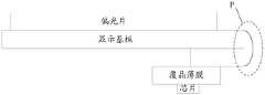
- the inorganic insulating layer connecting the bent portion P of the terminal as shown in FIG. 1bis liable to cause cracks, which may cause display failure.
- an inorganic insulating layer connecting the bent portion P of the terminalcan be removed by adding a mask process; and then an organic insulating layer is formed in the bent portion P of the connecting terminal by adding another Mask process to avoid The inorganic insulating layer connecting the bent portion P of the terminal generates a display failure phenomenon caused by cracks.
- the two Mask processesare added, which increases the process difficulty and the manufacturing cost, and reduces the production efficiency.
- the formation of the bent portion P of the connection terminalrequires an increase in space, and the utilization ratio of the display product produced by the connection terminal bending process to the base substrate is relatively higher than that of the display product of the same size without the connection terminal bending process. low. Therefore, how to obtain a display product having a narrow bezel under the condition that the connection terminal bending process is omitted is a technical problem that needs to be solved at present.
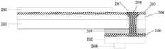
- a display panelas shown in FIG. 2a, includes a display substrate 201, a flip chip 202 disposed on a side of the display surface facing away from the display substrate 201, and a display substrate 201 and a flip chip 202.
- the adhesive 203 between the twois fixed to the integrated circuit chip 204 on the side of the flip chip 202 facing away from the display substrate 201.
- the flip chip 202is fixed to the side of the display substrate 201 facing away from the display surface by the adhesive 203.
- a plurality of signal lines 205are disposed around the display surface of the display substrate 201, and an insulating layer 206 between the signal lines 205 and the display substrate 201 extends through at least a plurality of connection holes of the display substrate 201, the signal lines 205, and the insulating layer 206.
- the insulating layer 206has a plurality of recesses a surrounding the respective connection holes 207, and the conductive material 208 is in contact with the surface of the signal line 205 at the recesses a.
- the flip chip 202is attached to the side facing away from the display surface of the display substrate 201 by using the adhesive 203, it is disposed at least through the display substrate 201.
- the conductive material 208 in each of the plurality of connection holes 207 of the signal line 205 and the insulating layer 206can realize the connection between the signal line 205 around the display surface of the display substrate 201 and the connection terminal 209 provided on the flip chip 202, and therefore, The connection terminal bending process is removed, so that there is no connection terminal bending area around the display panel, so that the display panel has a narrower frame.
- a plurality of recesses a surrounding the respective connection holes 207are provided in the insulating layer 206, it is ensured that the conductive material 208 is in contact with the surface of the signal line 205 at the recess a, increasing the contact area of the conductive material 208 with the signal line 205. It can prevent the risk of punching and filling of the conductive material 208, thereby increasing the yield of the product.
- the flip chipis attached to the display substrate by the adhesive layer in the above embodiment, the embodiment according to the present disclosure is not limited thereto.
- the surface b and the signal of the conductive material 208 in contact with the signal line 205may be
- the surface c of the line 205 located outside the recess ais flush, that is, the surface of the conductive material 208 on the side of the display substrate 201 is flush with the surface of the signal line 205. That is, the upper surface of the conductive material 208 located at the recess is flush with the upper surface of the portion of the signal line outside the recess.
- the conductive material 208may be a metal material having a small resistivity and a good electrical conductivity. Moreover, in order to improve the yield of the conductive material 208 filled into the connection hole 207, the conductive material 208 may select the nano metal material, because on the one hand, the nano metal material has a smaller particle diameter, and the filling property in the connection hole 205 is better. It is not easy to have an open circuit problem. On the other hand, for example, a nano metal material can be selected as the conductive material 208, so that when the conductive material 208 is used to fill the connection hole 205, the thermoplastic liquid nano metal slurry material can be filled into the connection hole 205 in a specific manner.
- the conductive material 208can be quickly and seamlessly filled into the connection hole 205, and then solidified and formed by cooling treatment to achieve filling and conduction of the conductive material 208.
- An example in which the nano metal material is filled into the connection hole 205will be described in detail in the method of manufacturing the display panel described below, and will not be described herein.
- the conductive material 208can select a nano silver material with better fluidity and better electrical conductivity.
- the aperture of each connection holeis generally greater than or equal to 25 ⁇ m; and the diameter of the nano silver material is generally less than 3 ⁇ m. Therefore, the nano silver material is
- the connection hole 205has excellent filling property, and there is no problem of disconnection.
- the adhesive film 203 for fixing the flip chip 202 to the side of the display substrate 201 facing away from the display surfacemay be, for example, an insulating glue or an anisotropic conductive material. Glue, not limited here.
- connection hole 207 disposed on the periphery of the display surface of the display substrate 201 and the connection terminal 209 disposed in the flip chip 202may be A variety of settings and production processes are described below.
- the connection hole 207may be disposed to penetrate only the display substrate 201, the respective signal lines 205, and the insulating layer 206.
- connection terminal 209may be disposed on a side of the flip chip 202 facing the display substrate 201.
- connection terminal 209is generally located directly below the connection hole 207;
- the signal line 205is connected to the connection terminal 209 through the conductive material 208 and the anisotropic conductive paste.
- connection hole 207 and the connection terminal 209the periphery of the display surface of the display substrate 201 can be perforated to form the connection hole 207 before the flip chip 202 and the display substrate 201 are bonded together.
- the operation of separately performing the display substrate 201 in the actual manufacturing processrequires less operation and less production cost. High production efficiency.
- the display substrate 201may be punctured after the flip chip 202 is bonded to the display substrate 201, and is not limited thereto.
- the periphery of the display surface of the display substrate 201is perforated, and the aperture of each of the connection holes 207 and the size of the connected connection terminal 209 are not different from each other. influences. That is, the aperture of each connection hole 207 may be greater than, equal to, or smaller than the size of the connected connection terminal 209, which is not limited herein.
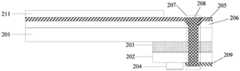
- connection hole 207may also be disposed through the display substrate 201, Each of the signal lines 205, the insulating layer 206, and the adhesive 203.
- connection terminal 209should be disposed on the side of the flip chip 202 facing the display substrate 201; for example, the connection terminal 209 is generally located directly below the connection hole 207.
- connection hole 207 and the connection terminal 209After the flip chip 202 and the display substrate 201 are bonded together, the periphery of the display surface of the display substrate 201 can be punched to form the connection hole 207.
- connection hole 207may also be disposed through the display substrate 201, Each of the signal lines 205, the insulating layer 206, the adhesive 203, and the flip chip 202.
- connection terminal 209should be disposed on the side of the flip chip 202 facing away from the display substrate 201; for example, the connection terminal 209 is generally located directly below the connection hole 207.
- connection hole 207 and the connection terminal 209after the flip chip 202 and the display substrate 201 are bonded together, the periphery of the display surface of the display substrate 201 may be perforated to form the connection hole 207, or The side of the flip chip 202 is perforated, which is not limited herein.
- connection hole 207In the above display panel provided by the embodiment of the present disclosure, in the case where the connection hole 207 penetrates the adhesive 203, the connection terminal 209 of the signal line 205 and the flip chip 202 around the display surface of the display substrate 201 is facilitated.
- Electrical connectionas shown in Figures 3a and 3b, the connection holes 207 generally correspond one-to-one with the connection terminals 209; and the size D of the connection terminals 209 is generally larger than the aperture d of the connection holes 207.
- connection terminal 209may be any shape, such as a triangle, a square, or a circle, which is not limited herein. Moreover, when the shape of the connection terminal 209 is circular, the diameter of the connection terminal 209 should be larger than the aperture d of the connection hole 207; when the shape of the connection terminal 209 is square, as shown in FIG. 3a, the side length of the connection terminal 209 is larger than The aperture d of the connection hole 207.
- a terminal(shown as a hatched portion in the figure) connected to the pin of the integrated circuit chip 204 may be further included.
- the terminal M connected to the connection terminal 209 through a wireis generally disposed in the same layer as the connection terminal 209; the terminal N not connected to the connection terminal 209 may be disposed in the same layer as the connection terminal 209, or may be disposed separately from the connection terminal 209. , not limited here.
- connection holes 207corresponding to the connection terminals 209
- a lasercan be used. Punching process. Also, by controlling the diameter and energy of the laser, a connection hole 207 having a desired aperture and hole depth is obtained.
- the connection hole 207can also be formed by other punching processes known to those skilled in the art, which is not limited herein.
- the aperture d of each of the connection holes 207is greater than or equal to 25 ⁇ m, that is, the minimum value of the aperture d of each of the connection holes 207 may be 25 ⁇ m.
- the display substrate 201may be a flexible display substrate or a rigid display substrate.
- the display substrate 201is a flexible display substrate, such as an organic light emitting substrate (Organic Light Emitting). Diodes, OLEDs, or Quantum Dot Light Emitting Diodes (QLEDs) are not limited herein.
- the flip chip 202is disposed on a peripheral region of the display substrate 201 facing away from the side of the display surface.
- the peripheral areacorresponds to the non-display area of the display substrate 201.
- the electric charge and the control signal required for the pixel driving in the display panelare all from an external flexible printed circuit (FPC), and are transmitted to the signal line 205 of the display panel through the flip chip 202, and thus,
- FPCflexible printed circuit
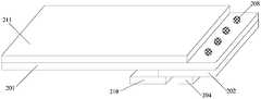
- the flexible display board 210 bound to the side of the flip chip 210 facing away from the display substrate 201may be further included.
- the display panelmay be further included with the display area of the display surface of the display substrate 201.
- Polarizer 211may be further included with the display area of the display surface of the display substrate 201.
- an embodiment of the present disclosureprovides a method for fabricating the above display panel.
- the principle of the method for solving the problemis similar to the principle of the problem of the display panel. Therefore, the method for manufacturing the method provided by the embodiment of the present disclosure is
- the implementation of the above display panel provided by the embodiment of the present disclosuremay be referred to, and the repeated description is omitted.
- the embodiment of the present disclosureprovides a method for manufacturing a display panel. As shown in FIG. 5, for example, the following steps S501-S506 may be included.
- an insulating layer 206is formed on the periphery of the display surface of the display substrate 201, and the insulating layer 206 has a plurality of recessed portions a.
- a plurality of signal lines 205are formed on the insulating layer 206 around the display surface of the display substrate 201, as shown in Fig. 6a.
- the flip chip 202is bonded to the side of the display surface facing away from the display substrate 201 by the adhesive 203; the integrated circuit chip 204 is located on the side of the flip chip 203 facing away from the display substrate 201, as shown in FIG. 6b.
- connection holes 207forming a plurality of connection holes 207 extending through at least the display substrate 201, the signal lines 205, and the insulating layer 206 around the display surface of the display substrate 201; and each recessed portion a surrounds each of the connection holes 207, as shown in FIG. 6c.
- connection holes 207at least in each of the connection holes 207 is filled with a conductive material 208, so that the signal line 205 is connected to the connection terminal 209 disposed on the flip chip 202 through the conductive material 208, and the conductive material 208 is in contact with the surface of the signal line 205 at the recess a. , as shown in Figure 6d.
- the conductive material 208can be ensured to be in contact with the surface of the signal line 205 at the recessed portion a.
- the large contact area of the conductive material 208 with the signal line 205prevents the risk of failure of the hole and the conductive material 208, thereby increasing the yield of the product.
- a nano metal materialis generally used as the conductive material 208.
- the step S506is filled with the conductive material 208 at least in each of the connection holes 207, which can be specifically implemented as follows: Since the nano metal slurry material has a certain fluidity, the nano metal slurry material can be injected into the connection hole 207 from the side of the display substrate 201 by nozzle dropping type or ink jet printing type; and, in order to accelerate the nano metal slurry material The fluidity and the improvement of the production efficiency can heat the nano metal slurry material; after that, since the nozzle dropping type or the ink jet printing type can precisely control the injection position of the liquid, no conductive is left in the area of the non-connection hole 207.
- the display panelmay be cooled afterwards to cure the nano-metal slurry material in the connection hole 207 without fluidity, thereby passing the signal line 205 through the cured nano-metal slurry material.
- the connection terminal 209is turned on.
- the step S506is filled with the conductive material 208 at least in each of the connection holes 207, which may be specifically implemented as follows: First, since the nano metal slurry material has a certain fluidity, The nano metal slurry material may be formed on the periphery of the display surface of the display substrate 201 by coating or screen printing, so that the nano metal slurry material is filled in the connection hole 207, and the connection hole 207 may be present at the periphery of the display surface.
- a part of the nano-metal slurry materialremains in the area other than the surface; and, in order to accelerate the fluidity of the nano-metal slurry material and improve the production efficiency, the nano-metal slurry material may be heat-treated; thereafter, the periphery of the display surface is cooled to be
- the nano metal slurry material in the connection hole 207is solidified and formed; at this time, a part of the nano metal slurry material remaining in the region outside the connection hole 207 at the periphery of the display surface may be solidified or retained in a liquid state; finally, washed with water. Or airflow to remove the nano-metal slurry material outside the connection hole 207 to prevent non- Interference attachment hole 208 of the short-circuit region 207 of conductive material.
- an embodiment of the present disclosurefurther provides a display device, which includes the above display panel provided by the embodiment of the present disclosure, and the display device may be: a mobile phone, a tablet computer, a television, a display, a notebook computer, a digital photo frame, Any product or component with a display function, such as a navigator, smart watch, fitness wristband, personal digital assistant, etc.
- the display devicereference may be made to the embodiment of the above display panel, and the repeated description is omitted.
- the display panel, the manufacturing method thereof and the display device provided by the embodiments of the present disclosureare configured by bonding the flip chip to the side facing away from the display surface of the display substrate by using an adhesive, and then passing through at least the display substrate.
- the conductive material in the connection hole of the signal line and the insulating layercan realize the connection between the signal line around the display surface of the display substrate and the connection terminal disposed on the flip chip, thereby eliminating the bending process of the connection terminal, so that the display is performed There is no bending area of the connection terminal around the periphery of the panel, so that the frame of the display panel is narrower.
- the conductive materialcan be ensured to be in contact with the surface of the signal line at the recessed portion, thereby increasing the contact area of the conductive material and the signal line, thereby preventing punching and conductive materials. Fill the risk of failure, thereby increasing the yield of the product.
Landscapes
- Engineering & Computer Science (AREA)
- Computer Hardware Design (AREA)
- Theoretical Computer Science (AREA)
- Power Engineering (AREA)
- Microelectronics & Electronic Packaging (AREA)
- Physics & Mathematics (AREA)
- General Engineering & Computer Science (AREA)
- General Physics & Mathematics (AREA)
- Human Computer Interaction (AREA)
- Condensed Matter Physics & Semiconductors (AREA)
- Devices For Indicating Variable Information By Combining Individual Elements (AREA)
Abstract
Description
Translated fromChinese本公开涉及一种显示面板、其制作方法及显示装置。The present disclosure relates to a display panel, a method of fabricating the same, and a display device.
随着显示技术的不断进步,显示面板在显示产品中的运用越来越广泛。具有窄边框(Narrow Bezel)的显示产品因其可以使用户获得较好的观看体验,吸引了大量的消费者。With the continuous advancement of display technology, display panels are increasingly used in display products. A display product with a narrow bezel (Narrow Bezel) attracts a large number of consumers because it allows users to have a better viewing experience.
发明内容Summary of the invention
根据本公开的一个实施例提供一种显示面板,包括:显示基板,设置于背离所述显示基板的显示面一侧的覆晶薄膜,以及固定于所述覆晶薄膜背离所述显示基板一侧的集成电路芯片;其中,在所述显示基板的周边区域设置有:位于所述显示基板的显示面的多条信号线,位于所述信号线与所述显示基板之间的绝缘层,至少贯穿所述显示基板、所述信号线和所述绝缘层的多个连接孔,以及填充于所述连接孔内的导电材料;所述信号线通过所述导电材料连接于设置在所述覆晶薄膜上的连接端子;所述绝缘层具有围绕所述连接孔的凹陷部,所述导电材料在所述凹陷部与所述信号线的表面接触。According to an embodiment of the present disclosure, a display panel includes: a display substrate, a flip chip disposed on a side facing away from a display surface of the display substrate, and a side of the flip chip facing away from the display substrate An integrated circuit chip; wherein, in a peripheral area of the display substrate, a plurality of signal lines located on a display surface of the display substrate, and an insulating layer between the signal line and the display substrate are disposed at least a plurality of connection holes of the display substrate, the signal line and the insulating layer, and a conductive material filled in the connection hole; the signal line is connected to the flip chip by the conductive material a connection terminal; the insulating layer has a recess surrounding the connection hole, and the conductive material contacts the surface of the signal line at the recess.
在一些示例中,显示面板还包括:设置于所述显示基板与所述覆晶薄膜之间的粘胶层,所述覆晶薄膜通过所述粘结胶固定于所述显示基板背离所述显示面的一侧。In some examples, the display panel further includes: an adhesive layer disposed between the display substrate and the flip chip; the flip chip is fixed to the display substrate by the adhesive to face away from the display One side of the face.
在一些示例中,与所述信号线接触的所述导电材料的表面与所述信号线位于所述凹陷部之外区域的表面齐平。In some examples, a surface of the conductive material in contact with the signal line is flush with a surface of the signal line located outside the recess.
在一些示例中,所述导电材料为纳米金属材料。In some examples, the electrically conductive material is a nano metallic material.
在一些示例中,所述纳米金属材料为纳米银材料。In some examples, the nanometal material is a nanosilver material.
在一些示例中,各所述连接孔的孔径大于或等于25μm;所述纳米银材料的直径小于3μm。In some examples, each of the connection holes has a pore diameter greater than or equal to 25 μm; and the nanosilver material has a diameter of less than 3 μm.
在一些示例中,所述粘结胶为异方性导电胶;所述连接孔仅贯穿所述显 示基板、所述信号线和所述绝缘层;所述连接端子设置于所述覆晶薄膜面向所述显示基板的一侧;所述信号线通过所述导电材料和所述异方性导电胶连接于所述连接端子。In some examples, the adhesive is an anisotropic conductive paste; the connection hole only penetrates the display substrate, the signal line, and the insulating layer; the connection terminal is disposed on the flip chip surface One side of the display substrate; the signal line is connected to the connection terminal through the conductive material and the anisotropic conductive paste.
在一些示例中,所述连接孔贯穿所述显示基板、所述信号线、所述绝缘层和所述粘结胶;所述连接端子设置于所述覆晶薄膜面向所述显示基板的一侧。In some examples, the connection hole penetrates through the display substrate, the signal line, the insulating layer, and the adhesive; the connection terminal is disposed on a side of the flip chip facing the display substrate .
在一些示例中,所述连接孔贯穿所述显示基板、所述信号线、所述绝缘层、所述粘结胶和所述覆晶薄膜;所述连接端子设置于所述覆晶薄膜背离所述显示基板的一侧。In some examples, the connection hole penetrates the display substrate, the signal line, the insulating layer, the adhesive, and the flip chip; the connection terminal is disposed on the flip chip away from the substrate One side of the substrate is shown.
在一些示例中,所述连接孔与所述连接端子一一对应;且所述连接端子的尺寸大于所述连接孔的孔径。In some examples, the connection holes are in one-to-one correspondence with the connection terminals; and the connection terminals have a size larger than an aperture of the connection holes.
在一些示例中,显示面板还包括:绑定于所述覆晶薄膜背离所述显示基板一侧的柔性电路板。In some examples, the display panel further includes: a flexible circuit board bound to a side of the flip chip that faces away from the display substrate.
本公开的另一个实施例提供一种显示装置,包括如上述任一项所述的显示面板。Another embodiment of the present disclosure provides a display device comprising the display panel of any of the above.
本公开的另一个实施例提供一种显示面板的制作方法,包括:在显示基板的显示面周边形成绝缘层,并在所述绝缘层的表面形成多个凹陷部;在所述显示基板的显示面周边的所述绝缘层上形成多条信号线;在覆晶薄膜上安装集成电路芯片;在背离所述显示基板的显示面一侧贴合所述覆晶薄膜;所述集成电路芯片位于所述覆晶薄膜背离所述显示基板的一侧;在所述显示基板的周边区域形成至少贯穿所述显示基板、所述信号线和所述绝缘层的多个连接孔,且各所述凹陷部围绕各所述连接孔;在所述连接孔内填充导电材料,以使所述信号线通过所述导电材料连接于设置在所述覆晶薄膜的连接端子,所述导电材料在所述凹陷部与所述信号线的表面接触。Another embodiment of the present disclosure provides a method of fabricating a display panel, comprising: forming an insulating layer around a display surface of a display substrate, and forming a plurality of recesses on a surface of the insulating layer; displaying on the display substrate Forming a plurality of signal lines on the insulating layer around the surface; mounting an integrated circuit chip on the flip chip; bonding the flip chip on a side facing away from the display surface of the display substrate; a side of the display film facing away from the display substrate; forming a plurality of connection holes penetrating at least the display substrate, the signal line and the insulating layer in a peripheral region of the display substrate, and each of the recesses Surrounding each of the connection holes; filling the connection hole with a conductive material such that the signal line is connected to the connection terminal disposed on the flip chip by the conductive material, and the conductive material is in the recess Contacting the surface of the signal line.
在一些示例中,在所述连接孔内填充导电材料包括:采用喷嘴滴下式或喷墨打印式,将纳米金属浆液材料从所述显示基板的显示面一侧注入所述连接孔处;对所述显示基板进行冷却处理,以使在所述连接孔内的所述纳米金属浆液材料固化。In some examples, filling the connection hole with the conductive material comprises: injecting the nano metal slurry material from the display surface side of the display substrate into the connection hole by using a nozzle dropping type or an inkjet printing type; The display substrate is subjected to a cooling treatment to cure the nano-metal slurry material in the connection holes.
在一些示例中,所述在所述连接孔内填充导电材料包括:采用涂布式或丝网印刷式,将纳米金属浆液材料形成在所述显示基板的显示面的周边区域, 以使所述纳米金属浆液材料填充于所述连接孔处;对所述显示基板的所述连接孔处进行冷却处理,以使在所述连接孔内的所述纳米金属浆液材料固化;去掉所述连接孔之外的所述纳米金属浆液材料。In some examples, the filling the conductive material in the connection hole comprises: forming a nano metal slurry material in a peripheral region of a display surface of the display substrate by coating or screen printing, so that Filling the connection hole with the nano metal slurry material; performing cooling treatment on the connection hole of the display substrate to cure the nano metal slurry material in the connection hole; removing the connection hole The nano metal slurry material outside.
在一些示例中,所述覆晶薄膜通过异方性导电材料贴合到所述显示基板,且在将覆晶薄膜贴合到所述显示基板之前形成所述多个连接孔,所述异方性导电材料仅在所述连接孔的延伸方向上处于导电状态。In some examples, the flip chip is attached to the display substrate by an anisotropic conductive material, and the plurality of connection holes are formed before the flip chip is attached to the display substrate, the dissimilar The conductive material is in a conductive state only in the extending direction of the connection hole.
为了更清楚地说明本公开实施例的技术方案,下面将对实施例的附图作简单地介绍,显而易见地,下面描述中的附图仅仅涉及本公开的一些实施例,而非对本公开的限制。In order to more clearly illustrate the technical solutions of the embodiments of the present disclosure, the drawings of the embodiments will be briefly described below. It is obvious that the drawings in the following description relate only to some embodiments of the present disclosure, and are not to limit the disclosure. .
图1a和图1b分别为现有技术中显示面板的结构示意图;1a and 1b are schematic structural views of a display panel in the prior art;
图2a至图2d分别为本公开实施例提供的显示面板的结构示意图;2a to 2d are schematic structural views of a display panel according to an embodiment of the present disclosure;
图3a为本公开实施例提供的连接孔与连接端子的结构示意图;3a is a schematic structural view of a connection hole and a connection terminal according to an embodiment of the present disclosure;
图3b为本公开实施例提供的显示基板的显示面周边的信号线与设置在覆晶薄膜的连接端子的连接关系示意图;3b is a schematic diagram showing a connection relationship between a signal line around a display surface of a display substrate and a connection terminal disposed on a flip chip according to an embodiment of the present disclosure;
图4为本公开实施例提供的显示面板的立体结构示意图;4 is a schematic perspective structural view of a display panel according to an embodiment of the present disclosure;
图5为本公开实施例提供的显示面板的制作方法的流程图;FIG. 5 is a flowchart of a method for manufacturing a display panel according to an embodiment of the present disclosure;
图6a至图6d分别为实施本公开实施例提供的显示面板的制作方法中的各步骤对应的显示面板的结构示意图。FIG. 6 is a schematic structural diagram of a display panel corresponding to each step in the method for fabricating a display panel according to an embodiment of the present disclosure.
为使本公开实施例的目的、技术方案和优点更加清楚,下面将结合本公开实施例的附图,对本公开实施例的技术方案进行清楚、完整地描述。显然,所描述的实施例是本公开的一部分实施例,而不是全部的实施例。基于所描述的本公开的实施例,本领域普通技术人员在无需创造性劳动的前提下所获得的所有其他实施例,都属于本公开保护的范围。The technical solutions of the embodiments of the present disclosure will be clearly and completely described below in conjunction with the drawings of the embodiments of the present disclosure. It is apparent that the described embodiments are part of the embodiments of the present disclosure, and not all of the embodiments. All other embodiments obtained by a person of ordinary skill in the art based on the described embodiments of the present disclosure without departing from the scope of the invention are within the scope of the disclosure.
附图中各膜层的厚度和形状大小不反映显示面板的真实比例,目的只是示意说明本公开内容。The thickness and shape of each film layer in the drawings do not reflect the true scale of the display panel, and are merely intended to illustrate the disclosure.
具有窄边框的显示产品可以通过连接端子弯折来实现。但是采用连接端 子弯折工艺制作的显示产品的良率问题较多。例如,在将如图1a所示的显示产品进行弯折时,如图1b所示连接端子弯折区域P的无机绝缘层容易产生裂纹,会导致显示失效。例如,可以通过增加一道掩膜(Mask)工艺,以去除连接端子弯折区域P的无机绝缘层;之后再通过增加另一道Mask工艺,在连接端子弯折区域P形成一有机绝缘层,以避免连接端子弯折区域P的无机绝缘层产生裂纹导致的显示失效现象。如此,虽然在一定程度上避免无机绝缘层产生裂纹导致的显示失效现象,但增加了两道Mask工艺,增加了工艺难度和制造成本,降低了生产效率。此外,连接端子弯折区域P的形成需要增加空间,并且相对于相同尺寸的不经过连接端子弯折工艺制作的显示产品,采用连接端子弯折工艺制作的显示产品对衬底基板的利用率较低。因此,如何在省去连接端子弯折工艺的条件下,获得具有窄边框的显示产品,是目前亟需解决的技术问题。A display product having a narrow bezel can be realized by bending a connection terminal. However, there are many yield problems with display products made by the connection terminal bending process. For example, when the display product shown in FIG. 1a is bent, the inorganic insulating layer connecting the bent portion P of the terminal as shown in FIG. 1b is liable to cause cracks, which may cause display failure. For example, an inorganic insulating layer connecting the bent portion P of the terminal can be removed by adding a mask process; and then an organic insulating layer is formed in the bent portion P of the connecting terminal by adding another Mask process to avoid The inorganic insulating layer connecting the bent portion P of the terminal generates a display failure phenomenon caused by cracks. Thus, although the display failure phenomenon caused by the crack of the inorganic insulating layer is avoided to some extent, the two Mask processes are added, which increases the process difficulty and the manufacturing cost, and reduces the production efficiency. In addition, the formation of the bent portion P of the connection terminal requires an increase in space, and the utilization ratio of the display product produced by the connection terminal bending process to the base substrate is relatively higher than that of the display product of the same size without the connection terminal bending process. low. Therefore, how to obtain a display product having a narrow bezel under the condition that the connection terminal bending process is omitted is a technical problem that needs to be solved at present.
本公开实施例提供的一种显示面板,如图2a所示,包括:显示基板201,设置于背离显示基板201的显示面一侧的覆晶薄膜202,设置于显示基板201与覆晶薄膜202之间的粘结胶203,以及固定于覆晶薄膜202背离显示基板201一侧的集成电路芯片204。A display panel, as shown in FIG. 2a, includes a
覆晶薄膜202通过粘结胶203固定于显示基板201背离显示面的一侧。The
在显示基板201的显示面周边设置有多条信号线205,位于信号线205与显示基板201之间的绝缘层206,至少贯穿显示基板201、各信号线205和绝缘层206的多个连接孔207,以及至少填充于各连接孔207内的导电材料208;信号线205通过导电材料208连接于设置在覆晶薄膜202的连接端子209。A plurality of
绝缘层206具有围绕各连接孔207的多个凹陷部a,导电材料208在凹陷部a与信号线205的表面接触。The
例如,在本公开实施例提供的上述显示面板中,由于采用粘结胶203将覆晶薄膜202贴合在背离显示基板201的显示面的一侧后,再通过设置在至少贯穿显示基板201、各信号线205和绝缘层206的多个连接孔207内的导电材料208,可以实现显示基板201的显示面周边的信号线205与设置在覆晶薄膜202的连接端子209的连接,因此,省去了连接端子弯折工艺,以致在显示面板的周边不会存在连接端子弯折区域,从而使得显示面板的边框更 窄。并且,由于在绝缘层206设置围绕各连接孔207的多个凹陷部a,可以保证导电材料208在凹陷部a与信号线205的表面接触,增大了导电材料208与信号线205的接触面积,可防止打孔和导电材料208填充失效的风险,从而提高产品的良率。For example, in the above display panel provided by the embodiment of the present disclosure, after the
例如,虽然在上述实施例中以通过粘胶层将覆晶薄膜贴合到显示基板,但根据本公开的实施例不限于此。For example, although the flip chip is attached to the display substrate by the adhesive layer in the above embodiment, the embodiment according to the present disclosure is not limited thereto.
例如,在本公开实施例提供的上述显示面板中,为了将导电材料208与信号线205的接触面积最大化,如图2b所示,可以将导电材料208与信号线205接触的表面b与信号线205位于凹陷部a之外区域的表面c齐平设置,即导电材料208在显示基板201一侧的表面与信号线205的表面齐平。也就是说,位于凹陷处的导电材料208的上表面与信号线的位于凹陷部之外的部分的上表面齐平。这样可以最大化的增加导电材料208与信号线205的接触面积,从而最大限度的减小导电材料208与信号线205接触不良的风险,从而提高产品良率。For example, in the above display panel provided by the embodiment of the present disclosure, in order to maximize the contact area of the
例如,在本公开实施例提供的上述显示面板中,导电材料208可以为电阻率较小、导电性能较好的金属材料。并且,为了提高导电材料208填充至连接孔207的良率,导电材料208可以选择纳米金属材料,这是由于一方面纳米金属材料的粒径较小,在连接孔205内的填充性较好,不容易出现断路的问题。另一方面,例如可以选择纳米金属材料作为导电材料208,这样,在采用导电材料208填充至连接孔205时,可以将具有热塑性的液态的纳米金属浆液材料以特定的方式填充至连接孔205中,使导电材料208可以快速且无缝隙的填充至连接孔205中,之后在冷却处理使之固化成型,实现导电材料208的填充导通。对于纳米金属材料填充至连接孔205的示例会在下述显示面板的制作方法中详细介绍,在此不作赘述。For example, in the above display panel provided by the embodiment of the present disclosure, the
例如,在本公开实施例提供的上述显示面板中,导电材料208可以选择流动性较佳且导电性能较好的纳米银材料。For example, in the above display panel provided by the embodiment of the present disclosure, the
进一步地,在本公开实施例提供的上述显示面板中,根据打孔工艺的限制,各连接孔的孔径一般大于或等于25μm;而纳米银材料的直径一般会小于3μm,因此,纳米银材料在连接孔205内具有优良的填充性,不会出现断路的问题。Further, in the above display panel provided by the embodiment of the present disclosure, according to the limitation of the punching process, the aperture of each connection hole is generally greater than or equal to 25 μm; and the diameter of the nano silver material is generally less than 3 μm. Therefore, the nano silver material is The
例如,在本公开实施例提供的上述显示面板中,用于将覆晶薄膜202固定于显示基板201背离显示面一侧的粘结胶203,例如可以选用绝缘胶,也可以选用异方性导电胶,在此不做限定。For example, in the above display panel provided by the embodiment of the present disclosure, the
例如,在本公开实施例提供的上述显示面板中,根据粘结胶203选择的材料,在显示基板201的显示面周边设置的连接孔207以及在覆晶薄膜202中匹配设置的连接端子209可以由多种设置方式和制作工序,下面具体举例介绍。For example, in the above display panel provided by the embodiment of the present disclosure, according to the material selected by the adhesive 203, the
例如,当选择异方性导电胶作为粘结胶203时,由于异方性导电胶仅在沿连接孔207的延伸方向上处于导电状态,在垂直于连接孔207的延伸方向上处于绝缘状态,此时,在本公开实施例提供的上述显示面板中,如图2a和图2b所示,连接孔207可以设置为仅贯穿显示基板201、各信号线205和绝缘层206。For example, when the anisotropic conductive paste is selected as the adhesive 203, since the anisotropic conductive paste is in a conductive state only in the extending direction of the connecting
连接端子209可以设置于覆晶薄膜202面向显示基板201的一侧。例如,连接端子209一般位于连接孔207的正下方;The
此时,信号线205通过导电材料208和异方性导电胶连接于连接端子209。At this time, the
根据上述连接孔207和连接端子209的设置方式,在制作时可以在将覆晶薄膜202与显示基板201贴合之前,对显示基板201的显示面周边进行打孔以形成连接孔207。相较于在贴合覆晶薄膜202后对显示基板201进行打孔,显然,在实际制作过程中,单独对显示基板201进行打孔的方式,所需的操作较简单,生产成本较少,生产效率较高。当然,根据上述连接孔207和连接端子209的设置方式,也可以在将覆晶薄膜202与显示基板201贴合之后,对显示基板201进行打孔,在此不做限定。According to the manner in which the
并且,在将覆晶薄膜202与显示基板201贴合之前,对显示基板201的显示面周边进行打孔的方式,得到的各连接孔207的孔径与连接的连接端子209的尺寸相互之间不影响。即各连接孔207的孔径可以大于、等于或小于连接的连接端子209的尺寸,在此不做限定。Further, before the flip-
又如,不管选择异方性导电胶还是绝缘胶作为粘结胶203时,在本公开实施例提供的上述显示面板中,如图2c所示,连接孔207也可以设置为贯穿显示基板201、各信号线205、绝缘层206和粘结胶203。For example, in the above display panel provided by the embodiment of the present disclosure, as shown in FIG. 2c, the
对应地,连接端子209应设置于覆晶薄膜202面向显示基板201的一侧;例如,连接端子209一般位于连接孔207的正下方。Correspondingly, the
根据上述连接孔207和连接端子209的设置方式,在制作时可以在将覆晶薄膜202与显示基板201贴合之后,对显示基板201的显示面周边进行打孔以形成连接孔207。According to the arrangement of the
再如,不管选择异方性导电胶还是绝缘胶作为粘结胶203时,在本公开实施例提供的上述显示面板中,如图2d所示,连接孔207还可以设置为贯穿显示基板201、各信号线205、绝缘层206、粘结胶203和覆晶薄膜202。For example, in the above display panel provided by the embodiment of the present disclosure, as shown in FIG. 2d, the
对应地,连接端子209应设置于覆晶薄膜202背离显示基板201的一侧;例如,连接端子209一般位于连接孔207的正下方。Correspondingly, the
根据上述连接孔207和连接端子209的设置方式,在制作时可以在将覆晶薄膜202与显示基板201贴合之后,对显示基板201的显示面周边进行打孔以形成连接孔207,或者在覆晶薄膜202一侧进行打孔,在此不做限定。According to the arrangement of the
例如,在本公开实施例提供的上述显示面板中,在连接孔207贯穿粘结胶203的情况下,为了便于实现显示基板201的显示面周边的信号线205与覆晶薄膜202的连接端子209电连接,如图3a和图3b所示,连接孔207一般与连接端子209一一对应;并且连接端子209的尺寸D一般大于连接孔207的孔径d。For example, in the above display panel provided by the embodiment of the present disclosure, in the case where the
需要说明的是,在本公开实施例提供的上述显示面板中,连接端子209可以为任意形状,例如三角形、方形或圆形,在此不做限定。并且,当连接端子209的形状为圆形时,连接端子209的直径应大于连接孔207的孔径d;当连接端子209的形状为方形时,如图3a所示,连接端子209的边长大于连接孔207的孔径d。It should be noted that, in the above display panel provided by the embodiment of the present disclosure, the
此外,在本公开实施例提供的上述显示面板中,如图3a所示,还可以包括与集成电路芯片204的管脚连接的端子(如图中阴影部分所示)。其中,通过导线与连接端子209相连的端子M,一般与连接端子209同层设置;未与连接端子209相连的端子N,可以与连接端子209同层设置,也可以与连接端子209异层设置,在此不做限定。In addition, in the above display panel provided by the embodiment of the present disclosure, as shown in FIG. 3a, a terminal (shown as a hatched portion in the figure) connected to the pin of the
一般地,覆晶薄膜202的连接端子209的数量多、密度高,为了高效快速地制作与连接端子209一一对应的连接孔207,在本公开实施例提供的上 述显示面板中,可以采用激光打孔工艺。并且,通过控制激光的直径和能量,获得具有所需孔径和孔深的连接孔207。当然,还可以通过本领域技术人员公知的其他打孔工艺制作连接孔207,在此不做限定。Generally, the number of the
例如,在本公开实施例提供的上述显示面板中,如图3a所示,各连接孔207的孔径d大于或等于25μm,即各连接孔207的孔径d的最小值可以为25μm。For example, in the above display panel provided by the embodiment of the present disclosure, as shown in FIG. 3a, the aperture d of each of the connection holes 207 is greater than or equal to 25 μm, that is, the minimum value of the aperture d of each of the connection holes 207 may be 25 μm.
例如,在本公开实施例提供的上述显示面板中,显示基板201具体可以为柔性显示基板或刚性显示基板,较佳地,显示基板201为柔性显示基板,例如电致发光显示基板(Organic Light Emitting Diodes,OLED),或量子点显示基板(Quantum Dot Light Emitting Diodes,QLED),在此不做限定。For example, in the above display panel provided by the embodiment of the present disclosure, the
例如,在本公开实施例提供的上述显示面板中,覆晶薄膜202设置于显示基板201背离所述显示面一侧的周边区域。例如,周边区域与显示基板201的非显示区域相对应。For example, in the above display panel provided by the embodiment of the present disclosure, the
一般地,显示面板中像素驱动所需要的电荷以及控制信号,都来自于外接的柔性电路板(Flexible Printed Circuit,FPC),且需经过覆晶薄膜202传输至显示面板的信号线205,于是,在本公开实施例提供的上述显示面板中,如图4所示,还可以包括:绑定于覆晶薄膜202背离显示基板201一侧的柔性电路板210。Generally, the electric charge and the control signal required for the pixel driving in the display panel are all from an external flexible printed circuit (FPC), and are transmitted to the
例如,为了能使显示面板成像,在本公开实施例提供的上述显示面板中,如图2a至图2d和图4所示,还可以包括:与显示基板201的显示面的显示区域贴合的偏光片(Polarizer)211。For example, in order to enable the display panel to be imaged, in the above display panel provided by the embodiment of the present disclosure, as shown in FIG. 2a to FIG. 2d and FIG. 4, the display panel may be further included with the display area of the display surface of the
基于同一发明构思,本公开实施例提供了一种上述显示面板的制作方法,由于该制作方法解决问题的原理与上述显示面板解决问题的原理相似,因此,本公开实施例提供的该制作方法的实施可以参见本公开实施例提供的上述显示面板的实施,重复之处不再赘述。Based on the same inventive concept, an embodiment of the present disclosure provides a method for fabricating the above display panel. The principle of the method for solving the problem is similar to the principle of the problem of the display panel. Therefore, the method for manufacturing the method provided by the embodiment of the present disclosure is For the implementation, the implementation of the above display panel provided by the embodiment of the present disclosure may be referred to, and the repeated description is omitted.
本公开实施例提供了一种显示面板的制作方法,如图5所示,例如可以包括以下步骤S501-S506。The embodiment of the present disclosure provides a method for manufacturing a display panel. As shown in FIG. 5, for example, the following steps S501-S506 may be included.
S501、在显示基板201的显示面周边形成绝缘层206,绝缘层206具有多个凹陷部a。S501, an insulating
S502、在显示基板201的显示面周边的绝缘层206上形成多条信号线 205,如图6a所示。S502, a plurality of
S503、在覆晶薄膜202上安装集成电路芯片204。S503, mounting an
S504、在背离显示基板201的显示面一侧通过粘结胶203贴合覆晶薄膜202;集成电路芯片204位于覆晶薄膜203背离显示基板201的一侧,如图6b所示。S504, the
S505、在显示基板201的显示面周边形成至少贯穿显示基板201、各信号线205和绝缘层206的多个连接孔207;且各凹陷部a围绕各连接孔207,如图6c所示。S505, forming a plurality of connection holes 207 extending through at least the
S506、至少在各连接孔207内填充导电材料208,以使信号线205通过导电材料208连接于设置在覆晶薄膜202的连接端子209,导电材料208在凹陷部a与信号线205的表面接触,如图6d所示。S506, at least in each of the connection holes 207 is filled with a
例如,在本公开实施例提供的上述制作方法中,由于在绝缘层206制作围绕各连接孔207的多个凹陷部a,可以保证导电材料208在凹陷部a与信号线205的表面接触,增大了导电材料208与信号线205的接触面积,可防止打孔和导电材料208填充失效的风险,从而提高产品的良率。For example, in the above manufacturing method provided by the embodiment of the present disclosure, since the plurality of recesses a surrounding the respective connection holes 207 are formed in the insulating
例如,在本公开实施例提供的上述制作方法中,一般采用纳米金属材料作为导电材料208,基于此,步骤S506至少在各连接孔207内填充导电材料208,具体可以采用如下方式实现:首先,由于纳米金属浆液材料具有一定的流动性,因此,可以采用喷嘴滴下式或喷墨打印式,将纳米金属浆液材料从显示基板201一侧注入连接孔207处;并且,为了加快纳米金属浆液材料的流动性,提高制作效率,可以对纳米金属浆液材料进行加热处理;之后,由于喷嘴滴下式或喷墨打印式可以精准的控制液体的注入位置,因此在非连接孔207的区域不会留有导电材料208,基于此,之后可以对显示面板进行冷却处理,以使在连接孔207内的纳米金属浆液材料固化成型,而不具备流动性,从而通过固化后的纳米金属浆液材料将信号线205与连接端子209导通。For example, in the above manufacturing method provided by the embodiment of the present disclosure, a nano metal material is generally used as the
或者,在本公开实施例提供的上述制作方法中,步骤S506至少在各连接孔207内填充导电材料208,具体可以采用如下方式实现:首先,由于纳米金属浆液材料具有一定的流动性,因此,可以采用涂布式或丝网印刷式,将纳米金属浆液材料形成在显示基板201的显示面周边,以使纳米金属浆液材料填充于连接孔207处,此时在显示面周边会在连接孔207之外的区域残 留有部分纳米金属浆液材料;并且,为了加快纳米金属浆液材料的流动性,提高制作效率,可以对纳米金属浆液材料进行加热处理;之后,对显示面周边冷却处理,以使在连接孔207内的纳米金属浆液材料固化成型;此时,在显示面周边会在连接孔207之外的区域残留的部分纳米金属浆液材料也可能会被固化成型或保留液态状态;最后,采用水洗或气流去掉连接孔207之外的纳米金属浆液材料,以防止非连接孔207区域的导电材料208短路的干扰。Alternatively, in the above manufacturing method provided by the embodiment of the present disclosure, the step S506 is filled with the
基于同一发明构思,本公开实施例还提供了一种显示装置,包括本公开实施例提供的上述显示面板,该显示装置可以为:手机、平板电脑、电视机、显示器、笔记本电脑、数码相框、导航仪、智能手表、健身腕带、个人数字助理等任何具有显示功能的产品或部件。该显示装置的实施可以参见上述显示面板的实施例,重复之处不再赘述。Based on the same inventive concept, an embodiment of the present disclosure further provides a display device, which includes the above display panel provided by the embodiment of the present disclosure, and the display device may be: a mobile phone, a tablet computer, a television, a display, a notebook computer, a digital photo frame, Any product or component with a display function, such as a navigator, smart watch, fitness wristband, personal digital assistant, etc. For the implementation of the display device, reference may be made to the embodiment of the above display panel, and the repeated description is omitted.
本公开实施例提供的上述显示面板、其制作方法及显示装置,由于采用粘结胶将覆晶薄膜贴合在背离显示基板的显示面的一侧后,再通过设置在至少贯穿显示基板、各信号线和绝缘层的连接孔内的导电材料,可以实现显示基板的显示面周边的信号线与设置在覆晶薄膜的连接端子的连接,因此,省去了连接端子弯折工艺,以致在显示面板的周边不会存在连接端子弯折区域,从而使得显示面板的边框更窄。并且,由于在绝缘层设置围绕各连接孔的多个凹陷部,可以保证导电材料在凹陷部与信号线的表面接触,增大了导电材料与信号线的接触面积,可防止打孔和导电材料填充失效的风险,从而提高产品的良率。The display panel, the manufacturing method thereof and the display device provided by the embodiments of the present disclosure are configured by bonding the flip chip to the side facing away from the display surface of the display substrate by using an adhesive, and then passing through at least the display substrate. The conductive material in the connection hole of the signal line and the insulating layer can realize the connection between the signal line around the display surface of the display substrate and the connection terminal disposed on the flip chip, thereby eliminating the bending process of the connection terminal, so that the display is performed There is no bending area of the connection terminal around the periphery of the panel, so that the frame of the display panel is narrower. Moreover, since a plurality of recessed portions surrounding the respective connection holes are provided in the insulating layer, the conductive material can be ensured to be in contact with the surface of the signal line at the recessed portion, thereby increasing the contact area of the conductive material and the signal line, thereby preventing punching and conductive materials. Fill the risk of failure, thereby increasing the yield of the product.
以上所述仅是本公开的示范性实施方式,而非用于限制本公开的保护范围,本公开的保护范围由所附的权利要求确定。The above description is only an exemplary embodiment of the present disclosure, and is not intended to limit the scope of the disclosure. The scope of the disclosure is determined by the appended claims.
本申请要求于2017年6月16日递交的中国专利申请第201710456618.2号的优先权,在此全文引用上述中国专利申请公开的内容以作为本申请的一部分。The present application claims the priority of the Chinese Patent Application No. 20171045661, filed on Jun.
Claims (16)
Translated fromChinesePriority Applications (1)
| Application Number | Priority Date | Filing Date | Title |
|---|---|---|---|
| US16/070,427US11099615B2 (en) | 2017-06-16 | 2018-01-19 | Display panel, manufacturing method thereof and display device |
Applications Claiming Priority (2)
| Application Number | Priority Date | Filing Date | Title |
|---|---|---|---|
| CN201710456618.2 | 2017-06-16 | ||
| CN201710456618.2ACN107039377B (en) | 2017-06-16 | 2017-06-16 | A display panel, its manufacturing method and display device |
Publications (1)
| Publication Number | Publication Date |
|---|---|
| WO2018227973A1true WO2018227973A1 (en) | 2018-12-20 |
Family
ID=59541294
Family Applications (1)
| Application Number | Title | Priority Date | Filing Date |
|---|---|---|---|
| PCT/CN2018/073430CeasedWO2018227973A1 (en) | 2017-06-16 | 2018-01-19 | Display panel and manufacturing method therefor, and display device |
Country Status (3)
| Country | Link |
|---|---|
| US (1) | US11099615B2 (en) |
| CN (1) | CN107039377B (en) |
| WO (1) | WO2018227973A1 (en) |
Families Citing this family (26)
| Publication number | Priority date | Publication date | Assignee | Title |
|---|---|---|---|---|
| CN107037647B (en) | 2017-05-27 | 2022-06-17 | 京东方科技集团股份有限公司 | Display panel, display device and manufacturing method of display panel |
| CN106973520A (en) | 2017-05-27 | 2017-07-21 | 京东方科技集团股份有限公司 | A kind of preparation method of display panel, display device and display panel |
| CN107039377B (en)* | 2017-06-16 | 2019-10-25 | 京东方科技集团股份有限公司 | A display panel, its manufacturing method and display device |
| CN109559643A (en)* | 2017-09-26 | 2019-04-02 | 上海和辉光电有限公司 | A kind of display panel |
| CN109658837A (en)* | 2017-10-12 | 2019-04-19 | 群创光电股份有限公司 | Semiconductor device and the method for driving semiconductor device |
| US10909914B2 (en) | 2017-10-12 | 2021-02-02 | Innolux Corporation | Display device and driving method thereof having a display area in a peripheral region |
| CN107670914B (en)* | 2017-10-19 | 2019-06-07 | 福建闽航电子有限公司 | A kind of inner wall printing process of insulated terminal |
| CN109727534A (en)* | 2017-10-27 | 2019-05-07 | 京东方科技集团股份有限公司 | Binding method and display device |
| CN108447891B (en)* | 2018-05-07 | 2021-03-16 | 京东方科技集团股份有限公司 | Display panel manufacturing method, display panel and pad printing device |
| KR102645335B1 (en)* | 2018-06-27 | 2024-03-11 | 삼성디스플레이 주식회사 | Display module, display device and method of manufactirong display module |
| CN108877501A (en)* | 2018-07-02 | 2018-11-23 | 京东方科技集团股份有限公司 | Display panel and preparation method thereof, display device |
| CN109493745B (en)* | 2018-11-28 | 2020-06-16 | 武汉华星光电技术有限公司 | Display device and manufacturing method thereof |
| CN109638040B (en)* | 2018-11-28 | 2021-06-25 | 武汉华星光电半导体显示技术有限公司 | Display structure and manufacturing method thereof |
| CN109671352A (en)* | 2018-12-15 | 2019-04-23 | 惠州Tcl移动通信有限公司 | Display component and preparation method thereof |
| CN109817659B (en)* | 2019-02-15 | 2021-08-06 | 京东方科技集团股份有限公司 | Display substrate, manufacturing method thereof, and display device |
| CN109917593B (en)* | 2019-02-22 | 2022-05-13 | 京东方科技集团股份有限公司 | A display panel, method for producing the same, and display device |
| CN109887948B (en)* | 2019-03-08 | 2021-11-09 | 京东方科技集团股份有限公司 | Array substrate, manufacturing method thereof and display device |
| CN109979316A (en)* | 2019-03-22 | 2019-07-05 | 维沃移动通信有限公司 | Display screen of terminal equipment, preparation method of display screen and terminal equipment |
| CN110109297B (en)* | 2019-03-29 | 2021-06-22 | 武汉华星光电技术有限公司 | Display panel and method for manufacturing the same |
| CN110047899B (en)* | 2019-04-26 | 2021-10-22 | 京东方科技集团股份有限公司 | Display panel, display device, and manufacturing method |
| TWI707490B (en)* | 2019-08-12 | 2020-10-11 | 友達光電股份有限公司 | Display panel and display panel menufacturing method |
| CN111158522B (en)* | 2019-12-30 | 2023-10-03 | 上海摩软通讯技术有限公司 | Flexible circuit board, touch component and electronic equipment |
| CN111294434A (en)* | 2020-02-17 | 2020-06-16 | Oppo广东移动通信有限公司 | Folding screen module, mobile terminal and bonding method of folding screen module |
| CN111430421B (en)* | 2020-04-02 | 2023-08-15 | 京东方科技集团股份有限公司 | Display device and manufacturing method thereof |
| CN113257143A (en)* | 2021-03-29 | 2021-08-13 | 北海惠科光电技术有限公司 | Display panel, display device and manufacturing method of display panel |
| TWI773541B (en)* | 2021-09-27 | 2022-08-01 | 友達光電股份有限公司 | Manufacturing method of active device substrate |
Citations (5)
| Publication number | Priority date | Publication date | Assignee | Title |
|---|---|---|---|---|
| JPH08298285A (en)* | 1995-04-27 | 1996-11-12 | Oki Electric Ind Co Ltd | Semiconductor element and its manufacture |
| US20100013060A1 (en)* | 2008-06-22 | 2010-01-21 | Taiwan Semiconductor Manufacturing Company, Ltd. | Method of forming a conductive trench in a silicon wafer and silicon wafer comprising such trench |
| CN104904327A (en)* | 2013-01-03 | 2015-09-09 | 苹果公司 | Narrow border displays for electronic devices |
| CN105829996A (en)* | 2016-03-23 | 2016-08-03 | 深圳信炜科技有限公司 | Electronic device |
| CN107039377A (en)* | 2017-06-16 | 2017-08-11 | 京东方科技集团股份有限公司 | A kind of display panel, its preparation method and display device |
Family Cites Families (11)
| Publication number | Priority date | Publication date | Assignee | Title |
|---|---|---|---|---|
| KR100445820B1 (en)* | 1999-07-22 | 2004-08-30 | 세이코 엡슨 가부시키가이샤 | Electro-optical device, method of manufacture thereof, and electronic device |
| JP2002040472A (en)* | 2000-07-31 | 2002-02-06 | Seiko Epson Corp | Liquid crystal device manufacturing method, liquid crystal device and electronic equipment |
| KR100889553B1 (en) | 2007-07-23 | 2009-03-23 | 주식회사 동부하이텍 | System in package and method for fabricating the same |
| RU2464647C1 (en)* | 2008-11-26 | 2012-10-20 | Шарп Кабусики Кайся | Display device |
| US8586470B2 (en)* | 2010-04-27 | 2013-11-19 | Stmicroelectronics S.R.L. | Multilevel interconnect structures and methods of fabricating same |
| CN103474435A (en)* | 2013-09-17 | 2013-12-25 | 京东方科技集团股份有限公司 | Array substrate and manufacturing method thereof |
| CN104035253A (en)* | 2014-05-26 | 2014-09-10 | 京东方科技集团股份有限公司 | Array substrate, preparation method of array substrate and display panel |
| KR102258746B1 (en)* | 2014-08-13 | 2021-06-01 | 삼성전자주식회사 | Chip-on-film package having bending part |
| CN104851892A (en)* | 2015-05-12 | 2015-08-19 | 深圳市华星光电技术有限公司 | Narrow frame flexible display device and manufacturing method thereof |
| KR102397387B1 (en)* | 2015-08-10 | 2022-05-13 | 삼성전자주식회사 | Electronic apparatus and assembling method of the same |
| CN108666286B (en) | 2017-03-31 | 2019-12-03 | 京东方科技集团股份有限公司 | A kind of production method of display panel, display device and display panel |
- 2017
- 2017-06-16CNCN201710456618.2Apatent/CN107039377B/enactiveActive
- 2018
- 2018-01-19WOPCT/CN2018/073430patent/WO2018227973A1/ennot_activeCeased
- 2018-01-19USUS16/070,427patent/US11099615B2/enactiveActive
Patent Citations (5)
| Publication number | Priority date | Publication date | Assignee | Title |
|---|---|---|---|---|
| JPH08298285A (en)* | 1995-04-27 | 1996-11-12 | Oki Electric Ind Co Ltd | Semiconductor element and its manufacture |
| US20100013060A1 (en)* | 2008-06-22 | 2010-01-21 | Taiwan Semiconductor Manufacturing Company, Ltd. | Method of forming a conductive trench in a silicon wafer and silicon wafer comprising such trench |
| CN104904327A (en)* | 2013-01-03 | 2015-09-09 | 苹果公司 | Narrow border displays for electronic devices |
| CN105829996A (en)* | 2016-03-23 | 2016-08-03 | 深圳信炜科技有限公司 | Electronic device |
| CN107039377A (en)* | 2017-06-16 | 2017-08-11 | 京东方科技集团股份有限公司 | A kind of display panel, its preparation method and display device |
Also Published As
| Publication number | Publication date |
|---|---|
| CN107039377A (en) | 2017-08-11 |
| CN107039377B (en) | 2019-10-25 |
| US20210208644A1 (en) | 2021-07-08 |
| US11099615B2 (en) | 2021-08-24 |
Similar Documents
| Publication | Publication Date | Title |
|---|---|---|
| WO2018227973A1 (en) | Display panel and manufacturing method therefor, and display device | |
| US10993330B2 (en) | Display panel, display device, and method for manufacturing display panel | |
| US11222939B2 (en) | Display panel, display device and method for manufacturing display panel | |
| US11264551B2 (en) | Display panel, display device and method for manufacturing display panel | |
| US9818732B2 (en) | Chip-on-film package and device assembly including the same | |
| KR101753501B1 (en) | Narrow border displays for electronic devices | |
| WO2018176742A1 (en) | Display panel, display device, and method for manufacturing display panel | |
| US9332649B2 (en) | Flexible printed circuit board for packaging semiconductor device and method of producing the same | |
| CN111399290B (en) | Display panel and display device | |
| JP4292424B2 (en) | WIRING BOARD, MANUFACTURING METHOD THEREOF, AND ELECTRONIC DEVICE | |
| JP2015125249A (en) | Display element and method of manufacturing the same | |
| CN105826298A (en) | Semiconductor package and package module using same | |
| JP2017215499A (en) | Manufacturing method of display device | |
| CN107658320A (en) | Function panel and its manufacture method, display device | |
| JP4273551B2 (en) | Video apparatus and manufacturing method thereof | |
| CN111900184A (en) | Display device and method of making the same | |
| CN108803928A (en) | A kind of display panel and preparation method thereof, display device | |
| CN106653749A (en) | Display module and preparation method thereof | |
| CN105657971B (en) | Embedded component packaging structure and manufacturing method thereof | |
| JP2007067237A (en) | Circuit substrate, circuit arrangement, and flexible board | |
| JP2004186472A (en) | Mounting structure and manufacturing method thereof, electro-optical device, and electronic apparatus | |
| WO2023241244A1 (en) | Mask plate, and electronic device and manufacturing method therefor | |
| KR20240147152A (en) | Display device using light emitting device | |
| CN109992140A (en) | Touch device, manufacturing method of touch device, and electronic device | |
| JP2014197627A (en) | Semiconductor package substrate and method of manufacturing the same |
Legal Events
| Date | Code | Title | Description |
|---|---|---|---|
| 121 | Ep: the epo has been informed by wipo that ep was designated in this application | Ref document number:18818436 Country of ref document:EP Kind code of ref document:A1 | |
| NENP | Non-entry into the national phase | Ref country code:DE | |
| 32PN | Ep: public notification in the ep bulletin as address of the adressee cannot be established | Free format text:NOTING OF LOSS OF RIGHTS PURSUANT TO RULE 112(1) EPC (EPO FORM 1205A DATED 03-06-2020) | |
| 122 | Ep: pct application non-entry in european phase | Ref document number:18818436 Country of ref document:EP Kind code of ref document:A1 |