WO2018221026A1 - Optical device, image display device, and display device - Google Patents
Optical device, image display device, and display deviceDownload PDFInfo
- Publication number
- WO2018221026A1 WO2018221026A1PCT/JP2018/015247JP2018015247WWO2018221026A1WO 2018221026 A1WO2018221026 A1WO 2018221026A1JP 2018015247 WJP2018015247 WJP 2018015247WWO 2018221026 A1WO2018221026 A1WO 2018221026A1
- Authority
- WO
- WIPO (PCT)
- Prior art keywords
- light
- guide member
- light guide
- semi
- parallel
- Prior art date
- Legal status (The legal status is an assumption and is not a legal conclusion. Google has not performed a legal analysis and makes no representation as to the accuracy of the status listed.)
- Ceased
Links
Images


Classifications
- G—PHYSICS
- G02—OPTICS
- G02B—OPTICAL ELEMENTS, SYSTEMS OR APPARATUS
- G02B27/00—Optical systems or apparatus not provided for by any of the groups G02B1/00 - G02B26/00, G02B30/00
- G02B27/02—Viewing or reading apparatus
- G—PHYSICS
- G02—OPTICS
- G02B—OPTICAL ELEMENTS, SYSTEMS OR APPARATUS
- G02B6/00—Light guides; Structural details of arrangements comprising light guides and other optical elements, e.g. couplings
- G02B6/0001—Light guides; Structural details of arrangements comprising light guides and other optical elements, e.g. couplings specially adapted for lighting devices or systems
- G02B6/0011—Light guides; Structural details of arrangements comprising light guides and other optical elements, e.g. couplings specially adapted for lighting devices or systems the light guides being planar or of plate-like form
- G02B6/0033—Means for improving the coupling-out of light from the light guide
- G02B6/0035—Means for improving the coupling-out of light from the light guide provided on the surface of the light guide or in the bulk of it
- G—PHYSICS
- G02—OPTICS
- G02B—OPTICAL ELEMENTS, SYSTEMS OR APPARATUS
- G02B26/00—Optical devices or arrangements for the control of light using movable or deformable optical elements
- G02B26/08—Optical devices or arrangements for the control of light using movable or deformable optical elements for controlling the direction of light
- G02B26/10—Scanning systems
- G02B26/101—Scanning systems with both horizontal and vertical deflecting means, e.g. raster or XY scanners
- G—PHYSICS
- G02—OPTICS
- G02B—OPTICAL ELEMENTS, SYSTEMS OR APPARATUS
- G02B27/00—Optical systems or apparatus not provided for by any of the groups G02B1/00 - G02B26/00, G02B30/00
- G02B27/01—Head-up displays
- G02B27/017—Head mounted
- G02B27/0172—Head mounted characterised by optical features
- G—PHYSICS
- G02—OPTICS
- G02B—OPTICAL ELEMENTS, SYSTEMS OR APPARATUS
- G02B27/00—Optical systems or apparatus not provided for by any of the groups G02B1/00 - G02B26/00, G02B30/00
- G02B27/10—Beam splitting or combining systems
- G02B27/106—Beam splitting or combining systems for splitting or combining a plurality of identical beams or images, e.g. image replication
- G—PHYSICS
- G02—OPTICS
- G02B—OPTICAL ELEMENTS, SYSTEMS OR APPARATUS
- G02B27/00—Optical systems or apparatus not provided for by any of the groups G02B1/00 - G02B26/00, G02B30/00
- G02B27/10—Beam splitting or combining systems
- G02B27/14—Beam splitting or combining systems operating by reflection only
- G02B27/145—Beam splitting or combining systems operating by reflection only having sequential partially reflecting surfaces
- G—PHYSICS
- G02—OPTICS
- G02B—OPTICAL ELEMENTS, SYSTEMS OR APPARATUS
- G02B27/00—Optical systems or apparatus not provided for by any of the groups G02B1/00 - G02B26/00, G02B30/00
- G02B27/28—Optical systems or apparatus not provided for by any of the groups G02B1/00 - G02B26/00, G02B30/00 for polarising
- G02B27/283—Optical systems or apparatus not provided for by any of the groups G02B1/00 - G02B26/00, G02B30/00 for polarising used for beam splitting or combining
- G—PHYSICS
- G02—OPTICS
- G02B—OPTICAL ELEMENTS, SYSTEMS OR APPARATUS
- G02B5/00—Optical elements other than lenses
- G02B5/04—Prisms
- G—PHYSICS
- G02—OPTICS
- G02B—OPTICAL ELEMENTS, SYSTEMS OR APPARATUS
- G02B6/00—Light guides; Structural details of arrangements comprising light guides and other optical elements, e.g. couplings
- G02B6/0001—Light guides; Structural details of arrangements comprising light guides and other optical elements, e.g. couplings specially adapted for lighting devices or systems
- G02B6/0011—Light guides; Structural details of arrangements comprising light guides and other optical elements, e.g. couplings specially adapted for lighting devices or systems the light guides being planar or of plate-like form
- G02B6/0013—Means for improving the coupling-in of light from the light source into the light guide
- G02B6/0023—Means for improving the coupling-in of light from the light source into the light guide provided by one optical element, or plurality thereof, placed between the light guide and the light source, or around the light source
- G02B6/0028—Light guide, e.g. taper
- H—ELECTRICITY
- H04—ELECTRIC COMMUNICATION TECHNIQUE
- H04N—PICTORIAL COMMUNICATION, e.g. TELEVISION
- H04N5/00—Details of television systems
- H04N5/64—Constructional details of receivers, e.g. cabinets or dust covers
- G—PHYSICS
- G02—OPTICS
- G02B—OPTICAL ELEMENTS, SYSTEMS OR APPARATUS
- G02B27/00—Optical systems or apparatus not provided for by any of the groups G02B1/00 - G02B26/00, G02B30/00
- G02B27/01—Head-up displays
- G02B27/0101—Head-up displays characterised by optical features
- G02B2027/0123—Head-up displays characterised by optical features comprising devices increasing the field of view
- G02B2027/0125—Field-of-view increase by wavefront division
- G—PHYSICS
- G02—OPTICS
- G02B—OPTICAL ELEMENTS, SYSTEMS OR APPARATUS
- G02B27/00—Optical systems or apparatus not provided for by any of the groups G02B1/00 - G02B26/00, G02B30/00
- G02B27/01—Head-up displays
- G02B27/017—Head mounted
- G02B27/0172—Head mounted characterised by optical features
- G02B2027/0174—Head mounted characterised by optical features holographic
- G—PHYSICS
- G02—OPTICS
- G02B—OPTICAL ELEMENTS, SYSTEMS OR APPARATUS
- G02B27/00—Optical systems or apparatus not provided for by any of the groups G02B1/00 - G02B26/00, G02B30/00
- G02B27/01—Head-up displays
- G02B27/017—Head mounted
- G02B2027/0178—Eyeglass type
Definitions
- the present disclosurerelates to an optical device, an image display device provided with such an optical device, and a display device provided with such an image display device, more specifically, a head-mounted display (HMD, Head Mounted Display).
- the present inventionrelates to a display device used.
- HMDhead-mounted display
- Various types of head-mounted displayshave been studied, but a wide angle of display image is strongly demanded for providing more realistic images to the head-mounted display.
- a head-mounted display in which two deflecting means are arranged on a light guide plate constituting an optical deviceis known from, for example, FIG. 16 of JP-T-2005-521099.
- an input waveis coupled into the first LOE 20a by the first reflecting surface 16a and propagated along the ⁇ axis.
- the Selective reflective surface 22acouples light out of 20a, which is then coupled into second LOE 20b by second reflective surface 16b. This light is propagated along the ⁇ -axis and then coupled out of 20b by the selective reflection surface 22b.
- the technique disclosed in the above-mentioned patent publicationhas a problem that stray light is included in the light emitted from the first LOE 20a toward the second LOE 20b and only a low-quality image can be obtained.
- an object of the present disclosureis to provide an optical device that can provide a high-quality image, an image display device including the optical device, and a display device including the image display device.
- an optical device of the present disclosureis provided.
- a first light guide membercomprising one deflection means, and A seventh surface, an eighth surface, a ninth surface facing the seventh surface, a tenth surface facing the eighth surface, an eleventh surface, and a twelfth surface facing the eleventh surface;
- a second light guide membercomprising two deflection means, With The first surface and the third surface are parallel, The second surface and the fourth surface are parallel and orthogonal to the first surface and the third surface, The seventh surface and the ninth surface are parallel to the XY plane in the XYZ orthogonal coordinate system, The light incident from the fifth surface is totally reflected inside the first light guide member, is deflected by the first deflecting means, is emitted from the third surface, and is incident on the eighth surface disposed away from the third surface.
- the first deflecting meansincludes a plurality of first semi-transmissive layers spaced apart and arranged in parallel,
- the value of ⁇is a value exceeding 0 degrees.
- the value of ⁇is a value exceeding 0 degree.
- an image display apparatusincludes an image forming apparatus and an optical apparatus, and the optical apparatus includes the optical apparatus of the present disclosure.
- the image display apparatusincludes the image forming apparatus and the optical apparatus according to the present disclosure.
- a display deviceaccording to the first aspect or the second aspect of the present disclosure.
- the image display deviceincludes an image forming device and an optical device,
- the optical deviceis composed of the above-described optical device of the present disclosure, or alternatively, the display device is A frame attached to the observer's head; and
- the image display apparatusincludes an image forming apparatus and the above-described optical device of the present disclosure.
- optical device of the present disclosurean optical device constituting the image display device according to the first aspect to the second aspect of the present disclosure, or a display device according to the first aspect to the second aspect of the present disclosure
- the value of ⁇is greater than 0 degrees
- the value of ⁇is also 0 degrees.
- FIG. 1is a diagram schematically illustrating the arrangement of the first light guide member and the second light guide member in the optical device of Example 1 together with the behavior of light.
- 2Ais a diagram schematically illustrating the arrangement of the first light guide member and the second light guide member in the optical device according to the first embodiment illustrated in FIG. 1, and FIG. 2B is a direction of a white arrow in FIG. 2A.
- 2Cis a side view of the first light guide member and the second light guide member when the first light guide member and the second light guide member are viewed from FIG. 2C, and FIG. 2C is the first light guide from the direction of the black arrow in FIG. 2A.
- FIG. 3is a diagram schematically showing the arrangement of the first light guide member and the second light guide member when the optical device of Example 1 shown in FIG. 1 is applied to a binocular display device.
- 4A and 4Bare diagrams schematically illustrating an arrangement state of the first light guide member and the second light guide member in the display devices according to the first and second embodiments.
- 5A, 5B, and 5Care diagrams for explaining how the formation of an image by stray light changes depending on the angle ⁇ .
- FIGS. 7A and 7Bshow the diagonal field value (unit: degree) of the effective visual field range emitted from the first light guide member when the angle ⁇ and the angle ⁇ are changed in the optical apparatus of the first embodiment. It is a figure which shows the result.
- FIGS. 7A and 7Bshow the diagonal field value (unit: degree) of the effective visual field range emitted from the first light guide member when the angle ⁇ and the angle ⁇ are changed in the optical apparatus of the first embodiment. It is a figure which shows the result.
- (A), (B), (C), (D), (E), and (F) of FIG. 8show the refractive index n of the material constituting the first light guide member in the optical device of Example 1.
- FIG. 9is a schematic view of the display device of Example 1 as viewed from above.
- FIG. 10is a schematic view of the display device of Example 1 as viewed from the front.
- FIGS. 11A and 11Dare schematic views of the display device of the first embodiment and a modified example viewed from the side, and
- FIGS. 11B and 11Care schematic cross-sectional views of the first light guide member and the like.
- 12A, 12B, and 12Care diagrams schematically illustrating a display device of the present disclosure or an image forming apparatus in the image display device.
- FIG. 9is a schematic view of the display device of Example 1 as viewed from above.
- FIG. 10is a schematic view of the display device of Example 1 as viewed from the front.
- FIGS. 11A and 11Dare schematic views of the display device of the first embodiment and a modified example viewed from the side
- FIGS. 11B and 11Care schematic cross-sectional views of the first light guide member and the like.
- FIG. 13is a diagram schematically showing the arrangement of the first light guide member and the second light guide member in the optical device of Example 2 together with the behavior of light, the image forming apparatus, and the observer.
- FIG. 14is a diagram schematically illustrating the arrangement of the first light guide member and the second light guide member in the optical device according to the second embodiment illustrated in FIG. 13.
- FIG. 15A and FIG. 15Bare diagrams for explaining the relationship between the first light guide member and the image unevenness constituting the optical devices of the third and first embodiments.
- FIG. 16is a schematic cross-sectional view of a light incident portion of a second light guide member that constitutes the optical device according to the third embodiment.
- 17A, 17B, and 17Care schematic perspective views of the first light guide member that constitutes the optical device of Example 3.
- FIG. 18A and 18Bare a schematic diagram of a light incident surface of a first light guide member and a schematic diagram of image unevenness constituting the optical device of Example 1 and the optical device of Example 3, respectively.
- FIG. 19A and FIG. 19Bare a schematic diagram of a light incident surface of a first light guide member and a schematic diagram of image unevenness constituting a modification of the optical device of Example 3.
- FIG. 20is a schematic cross-sectional view of the light incident portion of the first light guide member that constitutes the optical device according to the fourth embodiment.
- FIG. 21is a schematic cross-sectional view of the light incident portion of the first light guide member that constitutes the optical device of Example 1.
- FIGS. 22A and 22Bare diagrams illustrating the light emission state in each area in the first light guide member of the optical device of Example 5, and the relationship between the reflection angle and the light reflectance. .
- Example 1Optical Device of Present Disclosure, Image Display Device According to First to Second Aspects of Present Disclosure, Display Device According to First to Second Aspects of Present Disclosure
- Example 2Modification of Example 1 4).
- Example 3Modification of Examples 1 and 2) 5).
- Example 4Modification of Examples 1 to 3) 6).
- Example 5Modification of Examples 1 to 4) 7).
- the first light guide memberincludes A semi-transmissive mirror film disposed parallel to the first surface and the third surface is disposed, or A semi-transmissive mirror film disposed parallel to the second surface and the fourth surface is disposed, or A semi-transparent mirror film disposed in parallel with the first surface and the third surface and a semi-transparent mirror film disposed in parallel with the second surface and the fourth surface may be disposed.
- the semi-transmissive mirror film disposed parallel to the first surface and the third surface inside the first light guide memberis a part of a region located at the same distance from the first surface and the third surface. It can be set as the structure arrange
- the semi-transmissive mirror film disposed on the first light guide member in parallel with the first surface and the third surfaceis disposed in a partial region on the first surface or a partial region on the third surface. It can be set as the installed structure.
- the semi-transmissive mirror film disposed in the first light guide member in parallel with the second surface and the fourth surfaceis disposed in a part of the region located at the same distance from the second surface and the fourth surface. It can be set as the installed structure.
- the semi-transmissive mirror film disposed on the first light guide member in parallel with the second surface and the fourth surfaceis arranged in a partial region on the second surface or a partial region on the fourth surface. It can be set as the installed structure.
- the semi-transmissive mirror filmBy arranging the semi-transmissive mirror film on the first light guide member, it is possible to prevent unevenness (brightness or darkness) from occurring in the image emitted from the third surface of the first light guide member. be able to.
- the semi-transmissive mirror filmis disposed in a part of the region on the first surface or a part of the region on the third surface, or alternatively, a part of the region on the second surface or the one on the fourth surface.
- the protective memberis disposed in the region, it is preferable that a protective member is disposed on the surface of the semi-transmissive mirror film that is not in contact with the first light guide member. What is necessary is just to select a protection member suitably from the material which comprises the light guide member mentioned later.
- first surface, the second surface, the third surface, and the fourth surface of the first light guide memberregardless of whether the semi-transmissive mirror film is disposed or not disposed. It is preferable that at least one surface of the entire surface is covered with a protective member.
- the second light guide memberhas a configuration in which a semi-transmissive mirror film disposed in parallel with the seventh surface and the ninth surface is disposed. can do.
- the semi-transmissive mirror film disposed parallel to the seventh surface and the ninth surface inside the second light guide memberis a part of the region located at the same distance from the seventh surface and the ninth surface.
- the semi-transparent mirror film disposed on the second light guide member in parallel with the seventh surface and the ninth surfaceis a part of the seventh surface. It can be set as the structure arrange
- the semi-transmissive mirror filmis disposed in a partial area on the seventh surface or a partial area on the ninth surface, the semi-transmissive mirror film is protected on the surface of the semi-transmissive mirror film that is not in contact with the second light guide member. It is preferable that a member is provided. What is necessary is just to select a protection member suitably from the material which comprises the light guide member mentioned later. Even if the semi-transparent mirror film is provided or not provided, at least one of the seventh surface and the ninth surface of the second light guide member, the entire surface It is preferable that it is covered with a protective member.
- the cross-sectional area of the light incident on the fifth surfaceis enlarged near the fifth surface.
- the second light guideis provided.
- the membermay have a configuration in which a second cross-sectional area / enlargement portion for enlarging a cross-sectional area of light incident on the eighth surface is disposed in the vicinity of the eighth surface.
- the width of the light beam incident on the first light guide membercan be increased, and the width of the light beam incident on the second light guide member can be increased.
- the cross-sectional area / enlarged portionis configured by incorporating a prism member in the vicinity of the light incident portion (fifth surface) of the first light guide member and the light incident portion (eighth surface) of the second light guide member.
- itcan be formed by processing the light incident portion (fifth surface) of the first light guide member and the light incident portion (eighth surface) of the second light guide member into a prism shape.
- the cross-sectional area / enlarged portionis composed of the fifth surface of the prism-shaped first light guide member
- the second cross-sectional area / enlarged portionis composed of the eighth surface of the prism-shaped second light guide member. It can be.
- the value of the tilt angle of the light incident surface of the cross-sectional area / enlarged portionis the tilt angle (YZ of the fifth surface of the first light guide member).
- the angle formed by the plane and the fifth surfacemay be smaller (or different from the value of the inclination angle of the fifth surface of the first light guide member), and the second cross-sectional area / enlarged portion
- the angle of inclination of the light incident surfaceis the angle of inclination of the eighth surface of the second light guide member (the XZ plane and the eighth surface).
- the anglecan be different (or smaller than the value of the inclination angle of the eighth surface of the second light guide member).
- the light emitted from the central portion of the image forming apparatusis perpendicular to the fifth surface of the first light guide member (if the cross-sectional area / enlarged portion is provided, the light incident surface of the cross-sectional area / enlarged portion) (Perpendicular to).
- light emitted from the central portion of the image forming apparatusis guided in the first light guide member, emitted from the third surface of the first light guide member, and perpendicular to the eighth surface of the second light guide member.
- the second cross-sectional area / enlarged portionit is preferable that the light be incident perpendicularly to the light incident surface of the second cross-sectional area / enlarged portion).
- the second deflection unithas a configuration in which a plurality of second semi-transmissive layers are spaced apart and arranged in parallel.
- the first semi-transmissive layermay be made of a dielectric multilayer film
- the second semi-transmissive layermay be made of a dielectric multilayer film.
- the plurality of first semi-transmissive layers constituting the first deflecting unitare located far from the fifth surface.
- the first semi-transmissive layer that has a higher light reflectance (lower light transmittance) than the first semi-transmissive layer located near the fifth surfacecan be used. And by setting it as such a form, the uniformity of the brightness of the image radiate
- the second semi-transmissive layer located far from the eighth surfaceis the second semi-transmissive layer located near the eighth surface.
- the first semi-transmissive layerhas an angle (reflection angle) formed between the normal line of the first semi-transmissive layer and the light beam reflected by the first semi-transmissive layer, depending on the distance from the fifth surface.
- the relationship with the light reflectancecan be defined, and the second deflecting unit is formed by arranging a plurality of second semi-transmissive layers apart from each other in parallel.
- the relationship between the normal line of the second semi-transmissive layer and the angle (reflection angle) between the light beam reflected by the second semi-transmissive layer and the light reflectanceis defined. It can be set as a form.
- the inventionis not limited. 20 (degrees) ⁇ ⁇ ⁇ 30 (degrees) 55 (degrees) ⁇ ⁇ ⁇ 65 (degrees) Is preferably satisfied.
- the third surface and the eighth surfacecan be configured to be parallel.
- An air layermay be present between the third surface and the eighth surface, or the third surface and the eighth surface may be bonded using an adhesive.
- the first light guide memberis arranged such that light propagating in the first light guide member is totally reflected at the interface between the third surface and the adhesive.
- the refractive index value of the material constituting the adhesiveis required to be smaller than the refractive index value of the constituting material.
- the first and third surfaces of the first light guide membermay intersect with the XZ plane at an angle of 0 degrees, and the second and fourth surfaces may intersect with the XY plane at an angle of 0 degrees.
- the third surface and the XZ planemay intersect at an angle ( ⁇ ) other than 0 degrees, and the second and fourth surfaces and the XY plane may intersect at an angle ( ⁇ ) other than 0 degrees.
- the parallel light propagated through the first light guide member by total reflectionis reflected (or diffracted) a plurality of times, and the first light guide member is reflected.
- the lightis emitted from the optical member in a parallel light state.
- the parallel light propagated through the second light guide member by total reflectionis reflected (or diffracted) a plurality of times and emitted from the second light guide member in the state of parallel light.
- the first light guide member and the second light guide memberare fixed to the support member with a gap therebetween. That is, a space is provided between the light guide member and the support member 31.
- the outer shape of the first light guide memberinclude a rod shape (specifically, a cross-sectional shape when the first light guide member is cut in a virtual plane orthogonal to the axis of the first light guide member is rectangular).
- the outer shape of the second light guide membermay be a flat plate (the normal direction of the total reflection surface is the thickness direction).
- the refractive index of the material constituting the first light guide member and the second light guide memberis 1.5 or more, preferably 1.6 or more.
- the material having a refractive index of 1.5 or moreinclude BK7, polycarbonate resin, amorphous polypropylene resin, and styrene resin including AS resin, and acrylic as a material having a refractive index of 1.6 or more. Examples of such resins are listed below. An acrylic resin having a refractive index of 1.6 or less is also available.
- the first semi-transmissive layer and the second semi-transmissive layercan be composed of a dielectric multilayer film, a half mirror, a polarization beam splitter, and a hologram diffraction grating film.
- a dielectric multilayer filmfor example, Si, Mg, Al, Hf, Nb, Zr, Sc, Ta can be used as the dielectric material constituting the dielectric multilayer film.
- Ga, Zn, Y, B, Ti and other oxides, nitrides (for example, AlN, AlGaN, GaN, BN, etc.), fluorides, and the likecan be given.
- a dielectric multilayer filmcan be obtained by alternately laminating two or more kinds of dielectric films made of dielectric materials having different refractive indexes among these dielectric materials.
- SiO 2 / SiNis SiO 2 / Nb 2 O 5, SiO 2 / TiO 2, SiO 2 / ZrO 2, SiO 2 / AlN , etc. multilayer preferred.
- each dielectric filmIn order to obtain a desired light transmittance (light reflectance), the material constituting each dielectric film, the film thickness, the number of stacked layers, the number of layers of the multilayer film, and the like may be appropriately selected.
- the thickness of each dielectric filmcan be adjusted as appropriate depending on the material used, and is determined by the wavelength ⁇ of the incident light and the refractive index n 0 at the wavelength ⁇ of the material used. Specifically, an odd multiple of ⁇ / (4n 0 ) is preferable.
- the number of stacked layersis 2 or more, preferably about 5 to 20.
- the semi-transmissive mirror filmmay also be composed of the dielectric multilayer film described above.
- the optical deviceis a transflective type (see-through type). Specifically, at least a portion of the optical device (second light guide member) facing the observer's eyeball (pupil) is made semi-transmissive (see-through), and an outside scene can be viewed through this portion of the optical device.
- the term “semi-transmissive”does not mean that half (50%) of the incident light is transmitted or reflected, but a part of the incident light is transmitted and the rest is reflected. Used to mean. “Semi-transmissive” in the semi-transmissive layer and the semi-transmissive mirror film is also used in the same meaning.
- the image display device or the display device of the present disclosurecan perform single color (for example, green) image display or color image display.
- the image forming devicemay have a plurality of pixels arranged in a two-dimensional matrix. . Note that such a configuration of the image forming apparatus is referred to as a “first image forming apparatus” for convenience.
- an image forming apparatus having the first configurationfor example, an image forming apparatus including a reflective spatial light modulator and a light source; an image forming apparatus including a transmissive spatial light modulator and a light source; an organic EL (Electro-Luminescence) element And an image forming apparatus composed of a light emitting element such as an inorganic EL element, a light emitting diode (LED), a semiconductor laser element, etc., among others, an image forming apparatus composed of a reflective spatial light modulator and a light source, Or it is preferable to set it as the image forming apparatus comprised from the organic EL element.
- the spatial light modulatorexamples include a light valve, for example, a transmissive or reflective liquid crystal display device such as LCOS (Liquid Crystal On On Silicon), a digital micromirror device (DMD), and a light emitting element as a light source. be able to.
- the reflective spatial light modulatorreflects a part of light from the liquid crystal display device and the light source to the liquid crystal display device, and passes a part of the light reflected by the liquid crystal display device.
- a polarization beam splitterthat leads to the optical system can be used.
- Examples of the light emitting element that constitutes the light sourceinclude a red light emitting element, a green light emitting element, a blue light emitting element, and a white light emitting element, or red light emitted from the red light emitting element, the green light emitting element, and the blue light emitting element.
- white lightmay be obtained by mixing green light and blue light with a light pipe and performing luminance uniformity.
- Examples of the light emitting elementinclude a semiconductor laser element, a solid state laser, and an LED.
- the number of pixelsmay be determined based on specifications required for the image display device. Specific values of the number of pixels are 320 ⁇ 240, 432 ⁇ 240, 640 ⁇ 480, 1024 ⁇ 768, 1920 ⁇ 1080, and the like. Can be illustrated.
- the image forming deviceincludes a light source and a scanning unit that scans the parallel light emitted from the light source. It can be set as the provided form. Note that such a configuration of the image forming apparatus is referred to as a “second configuration image forming apparatus” for convenience.
- Examples of the light source in the image forming apparatus having the second configurationinclude a light emitting element, and specifically include a red light emitting element, a green light emitting element, a blue light emitting element, and a white light emitting element, or a red light emitting element.
- White lightmay be obtained by mixing red light, green light, and blue light emitted from the element, the green light emitting element, and the blue light emitting element by using a light pipe and performing luminance equalization.
- Examples of the light emitting elementinclude a semiconductor laser element, a solid state laser, and an LED.
- the number of pixels (virtual pixels) in the image forming apparatus having the second configurationmay be determined based on specifications required for the image display apparatus.
- the number of pixels320 ⁇ 240, 432 ⁇ 240, 640 ⁇ 480, 1024 ⁇ 768, 1920 ⁇ 1080 and the like can be exemplified.
- the scanning unitinclude a MEMS (Micro Electro Mechanical Systems) or a galvano mirror that performs micro scanning that can rotate in a two-dimensional direction.
- an optical systemwhich is an optical system that converts the emitted light from the image forming apparatus into parallel light, may be referred to as a “parallel light emitting optical system”, Specifically, for example, a plurality of parallel light beams are incident on the first light guide member by a collimating optical system or a relay optical system). This is based on the fact that the light wavefront information when the light enters the first light guide member needs to be preserved even after being emitted from the second light guide member via the first deflecting means and the second deflecting means. .
- the light emitting part of the image forming apparatusmay be positioned at the position (position) of the focal length in the parallel light emitting optical system, for example. .
- the parallel light emission optical systemhas a function of converting pixel position information into angle information in the optical system of the optical device.
- an optical system having a positive optical power as a wholewhich is a single lens or a combination of a convex lens, a concave lens, a free-form surface prism, and a hologram lens, can be exemplified.
- a light blocking portion having an openingis disposed between the parallel light emitting optical system and the first light guide member so that undesired light is emitted from the parallel light emitting optical system and does not enter the first light guide member. May be. Also, an opening is provided between the first light guide member and the second light guide member so that undesired light from the light emitted from the first light guide member does not enter the second light guide member.
- the framemay include a front portion disposed in front of the observer and two temple portions that are rotatably attached to both ends of the front portion via hinges. it can. A modern portion is attached to the tip of each temple portion.
- the image display deviceis attached to the frame, specifically, for example, the image forming device may be attached to the temple portion.
- the front part and the two temple partscan be integrated. That is, when the entire display device of the present disclosure is viewed, the frame has substantially the same structure as normal glasses.
- the material constituting the frame including the pad portioncan be made of the same material as that constituting normal glasses such as metal, alloy, plastic, and a combination thereof.
- the nose padcan be set as the structure by which the nose pad is attached to the front part. That is, when the entire display device of the present disclosure is viewed, the assembly of the frame (including the rim) and the nose pad has substantially the same structure as normal glasses.
- the nose padcan also have a known configuration and structure.
- each image forming apparatusincludes a headphone section, and the headphone section wiring from each image forming apparatus is routed from the tip of the modern section to the headphone section via the temple section and the interior of the modern section. It can also be made into the extended form.
- the headphone unitinclude an inner ear type headphone unit and a canal type headphone unit.
- the headphone part wiringpreferably has a form extending from the tip part of the modern part to the headphone part so as to wrap around the back side of the auricle (ear shell). Moreover, it can also be set as the form by which the imaging device was attached to the center part of the front part.
- the imaging apparatusis configured by a solid-state imaging device and a lens, for example, which are a CCD or a CMOS sensor.
- the wiring from the imaging devicemay be connected to, for example, one image display device (or image forming device) via the front portion, and is further included in the wiring extending from the image display device (or image forming device). That's fine.
- the image display devicemay include a light control device. That is, the second light guide member may overlap at least a part of the light control device.
- the light control deviceA first substrate, A second substrate facing the first substrate; A first transparent electrode provided on the facing surface of the first substrate facing the second substrate; A second transparent electrode provided on the facing surface of the second substrate facing the first substrate, and A light control layer sandwiched between the first transparent electrode and the second transparent electrode, It can be set as the form which consists of. Note that a higher voltage than that of the second transparent electrode is applied to the first transparent electrode, for example, during the operation of the dimmer.
- the light control layermay be formed of an optical shutter that applies a color change of a substance generated by a redox reaction of an inorganic or organic electrochromic material.
- the light control layercan be in a form containing an inorganic or organic electrochromic material.
- the light control layercan be formed from the first transparent electrode side by a WO 3 layer / Ta 2 O 5 layer /
- a laminated structure of an inorganic electrochromic material layersuch as an Ir x Sn 1-x O layer or a laminated structure of an inorganic electrochromic material layer such as a WO 3 layer / Ta 2 O 5 layer / IrO x layer is adopted. it can.
- a MoO 3 layer or a V 2 O 5 layercan be used instead of the WO 3 layer.
- a ZrO 2 layer and a zirconium phosphate layercan be used, or a Prussian blue complex / nickel-substituted Prussian blue complex or the like can also be used.
- the organic electrochromic materialfor example, the electrochromic material disclosed in Japanese Patent Application Laid-Open Nos. 2014-111710 and 2014-159385 can be used.
- the light control layercan be configured to contain an electrophoretic dispersion, and the light control device can apply an electrodeposition / dissociation phenomenon generated by a reversible oxidation-reduction reaction of a metal (for example, silver particles).
- the light shutter by the electrodeposition methodelectroposition / field deposition
- the light control layercan also be configured to include an electrolyte containing metal ions.
- the electrophoretic dispersion liquidis composed of a large number of charged electrophoretic particles and a dispersion medium having a color different from that of the electrophoretic particles.
- the electrophoretic particlesare negatively charged, relative to the first transparent electrode
- the negatively charged electrophoretic particlesmigrate so as to cover the second transparent electrode. Therefore, the light shielding rate in the light control device is a high value.
- the electrophoretic particlescover the first transparent electrode. Run. Therefore, the light shielding rate in the light control device is a low value.
- the voltagemay be a direct current or an alternating current.
- the shape of the patterned first transparent electrodeis such that when the electrophoretic particles migrate so as to cover the first transparent electrode and the light shielding rate in the light control device becomes a low value, the value of the light shielding rate in the light control device is optimum. It is sufficient to make it a shape that can be realized, and it may be determined by performing various tests.
- an insulating layermay be formed on the transparent electrode.
- the material constituting the insulating layerinclude a colorless and transparent insulating resin.
- an acrylic resin, an epoxy resin, a fluorine resin, a silicone resin, a polyimide resinexamples thereof include polystyrene resins.
- a transparent glass substratesuch as soda lime glass and white plate glass
- a plastic substratesuch as soda lime glass and white plate glass
- a plastic substratesuch as soda lime glass and white plate glass
- a plastic substratesuch as soda lime glass and white plate glass
- a plastic substratesuch as soda lime glass and white plate glass
- a plastic substratesuch as soda lime glass and white plate glass
- a plastic substratesuch as soda lime glass and white plate glass
- a plastic substratesuch as soda lime glass and white plate glass
- plastic substratesuch as soda lime glass and white plate glass
- plastic substratesuch as soda lime glass and white plate glass
- plastic substratesuch as soda lime glass and white plate glass
- plastic substratesuch as soda lime glass and white plate glass
- plastic substratesuch as soda lime glass and white plate glass
- plastic substratesuch as soda lime glass and white plate glass
- plastic substratesuch as soda lime glass and white plate glass
- plastic substratesuch as soda lime glass and white plate glass
- plastic substratesuch as soda lime glass and white plate glass
- plastic substratesuch as soda lime glass and white plate glass
- plastic substratesuch
- Polyetherssuch as polyether, polyacetal, polystyrene, polyethylene, polypropylene, methylpentene polymer, polyimides such as polyamideimide or polyetherimide, polyamide, polyethersulfone, polyphenylene sulfide, polyvinylidene fluoride, tetraacetylcellulose, brominated phenoxy, Examples include polyarylate and polysulfone.
- the plastic sheet and the plastic filmmay have a rigidity that does not easily bend, or may have flexibility.
- a barrier layermade of an inorganic material or an organic material may be formed on the inner surface of the substrate.
- sealing membersalso called sealing agents, epoxy resins, urethane resins, acrylic resins, vinyl acetate resins, ene-thiol resins, silicone resins, modified polymer resins, etc.
- sealing agentsalso called sealing agents, epoxy resins, urethane resins, acrylic resins, vinyl acetate resins, ene-thiol resins, silicone resins, modified polymer resins, etc.
- Various resinssuch as a moisture curable type and an anaerobic curable type can be used.
- the weight of the entire display devicecan be reduced, and there is no possibility of making the user of the display device feel uncomfortable.
- the first transparent electrodemay be patterned or may not be patterned.
- the second transparent electrodemay also be patterned or may not be patterned.
- indium-tin composite oxideincluding ITO, Indium Tin Oxide, Sn-doped In 2 O 3 , crystalline ITO, and amorphous ITO is used as a material constituting the first transparent electrode and the second transparent electrode.
- Fluorine-doped SnO 2FTO
- IFOF-doped In 2 O 3
- antimony-doped SnO 2ATO
- SnO 2ZnO (including Al-doped ZnO and B-doped ZnO), indium-zinc composite
- oxidesIZO, Indium Zinc Oxide
- spinel oxidesoxides having a YbFe 2 O 4 structure
- conductive polymerssuch as polyaniline, polypyrrole, and polythiophene.
- two or more of thesecan be used in combination.
- the first transparent electrode and the second transparent electrodeare formed based on a physical vapor deposition method (PVD method) such as a vacuum vapor deposition method or a sputtering method, various chemical vapor deposition methods (CVD method), various coating methods, and the like.
- PVD methodphysical vapor deposition method
- CVD methodchemical vapor deposition methods
- Patterningcan be performed by an arbitrary method such as an etching method, a lift-off method, or a method using various masks.
- the light control devicemay be arranged in the front part. And in this case, the front part has a rim; the light control device can be configured to be fitted into the rim. Moreover, in the display device of the present disclosure including the various preferable embodiments described above, the second light guide member and the light control device may be arranged in this order from the observer side, or the light control device and the second light guide device. You may arrange in order of a member.
- An illuminance sensorthat measures the illuminance of the environment where the display device is placed is further provided; a mode for controlling the light shielding rate of the light control device based on the measurement result of the illuminance sensor (environmental illuminance measurement sensor) It can be.
- itfurther includes an illuminance sensor (environmental illuminance measurement sensor) for measuring the illuminance of the environment where the display device is placed; formed by the image forming apparatus based on the measurement result of the illuminance sensor (environmental illuminance measurement sensor). It is possible to control the luminance of the image.
- the apparatusfurther includes a second illuminance sensor (sometimes referred to as “transmitted light illuminance measurement sensor” for convenience) that measures illuminance based on light transmitted through the light control device from the external environment; Based on the measurement result of the (transmitted light illuminance measurement sensor), the light shielding rate of the light control device can be controlled.
- the apparatusfurther includes a second illuminance sensor (transmitted light illuminance measurement sensor) that measures illuminance based on light transmitted through the light control device from the external environment; measurement result of the second illuminance sensor (transmitted light illuminance measurement sensor) Based on the above, it is possible to control the luminance of the image formed by the image forming apparatus.
- the second illuminance sensor(transmitted light illuminance measurement sensor) is arranged closer to the viewer than the optical device.
- At least two second illuminance sensors(transmitted light illuminance measurement sensors) are arranged to measure illuminance based on light that has passed through a portion with a high light shielding rate, and to measure illuminance based on light that has passed through a portion with a low light shielding rate. You may go. These forms may be combined. Furthermore, you may combine these forms and the form which controls based on the measurement result of said illuminance sensor (environmental illuminance measurement sensor).
- the illuminance sensor(environmental illuminance measurement sensor, transmitted light illuminance measurement sensor) may be configured from a known illuminance sensor, and the illuminance sensor may be controlled based on a known control circuit.
- the maximum light transmittance of the light control devicecan be 50% or more, and the minimum light transmittance of the light control device can be 30% or less.
- the upper limit value of the maximum light transmittance of the light control devicecan be 99%, and the lower limit value of the minimum light transmittance of the light control device can be 1%.
- a control circuit(a light control device / control circuit for controlling the light shielding rate of the light control device) by attaching a connector to the light control device (specifically, a connector attached to the first transparent electrode or the second transparent electrode)
- the light control devicemay be electrically connected to the control device for controlling the image forming apparatus via the connector and the wiring.
- the light passing through the light control devicemay be colored to a desired color by the light control device.
- the color colored by the light control devicecan be variable, or the color colored by the light control device can be fixed.
- a light control device colored in red, a light control device colored in green, and a light control device colored in bluemay be stacked.
- the color to be colored by the light control deviceis not limited, but can be exemplified by brown.
- the observerobserves the brightness of the light that has passed through the light control device and the optical device, and the observer manually controls and adjusts the light blocking rate by operating switches, buttons, dials, sliders, knobs, etc.
- the light shielding rateis controlled and adjusted based on the measurement result of the second illuminance sensor (transmitted light illuminance measurement sensor) that measures the illuminance based on the light transmitted through the light control device from the external environment. be able to.
- the control and adjustment of the light shielding ratemay be performed by controlling the voltage applied to the first transparent electrode and the second transparent electrode.
- At least two second illuminance sensorsare arranged to measure illuminance based on light that has passed through a portion with a high light shielding rate, and to measure illuminance based on light that has passed through a portion with a low light shielding rate. You may go.
- the display devicemay include one image display device or two image display devices. When two image display devices are provided, the voltage applied to the first transparent electrode and the second transparent electrode is adjusted in each of the one light control device and the other light control device, so that one of the light control devices And the light shielding rate of the other light control device can be equalized.
- the light blocking rate in one light control device and the light blocking rate in the other light control deviceare, for example, a second illuminance sensor (transmitted light illuminance measurement sensor) that measures illuminance based on the light transmitted through the light control device from the external environment described above. Or the brightness of the light passing through one light control device and the optical device and the light brightness passing through the other light control device and the optical device.
- the observercan also control and adjust manually by operating switches, buttons, dials, sliders, knobs, and the like.
- a test patternmay be displayed on the optical device.
- a head-mounted displaycan be configured by the display device of the present disclosure. This makes it possible to reduce the weight and size of the display device, significantly reduce discomfort when the display device is mounted, and further reduce the manufacturing cost.
- the image display device of the present disclosurecan be applied to a head-up display (HUD) provided in a cockpit of a vehicle or an aircraft.
- HUDhead-up display
- the virtual image formation region where a virtual image is formed based on the light emitted from the image forming apparatuscan be a HUD disposed on a windshield of a cockpit of a vehicle or an aircraft, or image formation
- a combiner having a virtual image forming area in which a virtual image is formed based on light emitted from the apparatusmay be a HUD arranged on a windshield of a vehicle or an aircraft cockpit.
- Example 1relates to an optical device of the present disclosure, an image display device according to the first to second aspects of the present disclosure, and a display device according to the first to second aspects of the present disclosure.
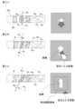
- the arrangement of the first light guide member and the second light guide member in the optical device of Example 1is schematically shown in FIG. 1 together with the behavior of light, the image forming device, and the pupil of the observer.
- the arrangement of the two light guide membersis schematically shown in FIG. 2A.
- 2Ais a side view of the first light guide member and the second light guide member when the first light guide member and the second light guide member are viewed from the direction of the white arrow B in FIG. 2A and the black arrow C in FIG. 2A. Is shown in FIGS. 2B and 2C. Further, FIG.
- FIG. 3schematically shows the arrangement of the first light guide member and the second light guide member when the optical device of the first embodiment shown in FIG. 1 is applied to a binocular display device.
- the arrangement state of the first light guide member and the second light guide member in the display deviceis schematically shown in FIG. 4A.
- FIG. 9the schematic diagram which looked at the display apparatus of Example 1 from the top is shown in FIG. 9, the schematic diagram seen from the front is shown in FIG. 10, and the schematic diagram which looked at the display apparatus of Example 1 from the side is shown in FIG.
- FIG. 11Bshows a schematic cross-sectional view of the first light guide member and the like.
- “R”is added to the reference number for the optical device for the right eye
- “L”is added to the reference number for the optical device for the left eye.
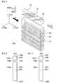
- the optical device 30 of Example 1is The first surface 40A, the second surface 40B, the third surface 40C facing the first surface 40A, the fourth surface 40D facing the second surface 40B, the fifth surface 40E, and the sixth surface facing the fifth surface 40E.
- a first light guide member 40having a surface 40F and having first deflection means 41 therein;
- a second light guide member 50having a surface 50F and having second deflecting means 51 therein; It has.
- the first surface 40A and the third surface 40Care parallel
- the second surface 40B and the fourth surface 40Dare parallel and orthogonal to the first surface 40A and the third surface 40C
- the seventh surface 50A and the ninth surface 50Care parallel to the XY plane in the XYZ orthogonal coordinate system
- Light incident from the fifth surface 40E(may be indicated by white arrows R and black arrows L) is totally reflected inside the first light guide member 40, deflected by the first deflecting means 41, and third.
- the lightis emitted from the surface 40C, is incident on the eighth surface 50B arranged away from the third surface 40C, is totally reflected between the seventh surface 50A and the ninth surface 50C, and is deflected by the second deflecting means 51.
- the first deflecting means 41includes a plurality of first semi-transmissive layers 42 that are spaced apart and arranged in parallel.
- the value of ⁇is a value exceeding 0 degrees.
- the value of ⁇is a value exceeding 0 degree.
- the image display apparatusincludes an image forming apparatus 60 and an optical apparatus, and the optical apparatus includes the optical apparatus 30 according to the first embodiment.
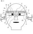
- the display device of Example 1is a head-mounted display (HMD), A frame 10 (for example, a glasses-type frame 10) attached to the head of the observer 20, and An image display device attached to the frame 10, With
- the image display deviceincludes an image forming device 60 and an optical device,
- the optical deviceincludes the optical device 30 of the first embodiment.
- the image forming apparatus 60displays a color image (virtual image) composed of, for example, three primary colors of red, green, and blue.
- the system composed of the first light guide member 40, the second light guide member 50, and the support member 31 for fixing these light guide membersis a semi-transmissive type (see-through type).
- a spaceis provided between the light guide member and the support member 31.
- a binocular type including two image display devicesis used, but a single-eye type including one image display device may be used.
- the image forming apparatus 60may be fixedly attached to the frame 10 or may be detachably attached.
- the second deflecting unit 51includes a plurality of second semi-transmissive layers 52 that are spaced apart and arranged in parallel.
- the first semi-transmissive layer 42 and the second semi-transmissive layerare made of a dielectric multilayer film.
- the dielectric multilayer filmhas, for example, a structure in which SiO 2 films (refractive index 1.462) and Nb 2 O 5 films (refractive index 2.378) are alternately laminated, or For example, it has a structure in which SiO 2 films and TiO 2 films (refractive index: 2.493) are alternately stacked.
- the normal line of the second semi-transmissive layer 52is included in the YZ plane.
- the third surface 40C and the eighth surface 50Bare parallel.
- the light emitted from the central portion of the image forming apparatus 60is preferably incident on the fifth surface 40E of the first light guide member 40 perpendicularly. Further, the light emitted from the central portion of the image forming apparatus 60 is guided in the first light guide member 40, emitted from the third surface 40 ⁇ / b> C of the first light guide member 40, and the second light guide member 50. It is preferable to enter the eighth surface 50B perpendicularly.
- the image emitted from the image forming apparatus 60enters the fifth surface 40 ⁇ / b> E of the first light guide member 40 at a certain angle.
- a light beam emitted from the image forming apparatus 60 and incident on the fifth surface 40E of the first light guide member 40is denoted by “R 0 ”.
- Light that penetrates into the first light guide member 40 and travels (propagates) as a whole in the X directionis transmitted through the first surface 40A, the second surface 40B, the third surface 40C, and the first surface of the first light guide member 40. It collides with the four surfaces 40D, repeats total reflection on these surfaces 40A, 40B, 40C, and 40D, and proceeds toward the sixth surface 40F.
- a part of the light impinging on the first semi-transparent layer 42is transmitted through the first semitransparent layer 42, a portion is reflected by the first semitransparent layer 42 is deflected, light R 1 from the third surface 40C Is emitted.
- Light emitted from the central portion of the image forming apparatus 60is guided in the first light guide member 40, emitted from the third surface 40C of the first light guide member 40, and from the eighth surface 50B to the second light guide member. When entering 50, this light is included in the YZ plane.
- the parallel light flux that has entered the first light guide member 40is emitted from the third surface 40C, and the light beam width is expanded (expanded) in the X direction by the first light guide member 40.
- FIG. 1FIG. 1
- the light incident surface (fifth surface 40E) of the first light guide member 40is guided in the light guide direction for simplification of the drawings.
- the display deviceit is illustrated as a plane perpendicular to a certain X axis, it is preferable to design the display device appropriately tilted according to the arrangement of the entire display device and the tilt of the first semi-transmissive layer 42. That is, in FIGS.
- first surface 40A and the third surface 40C of the light guide member 40are included in the XZ plane
- second surface 40B and the fourth surface 40Dare included in the XY plane
- first surface 40A and the third surface 40Care illustrated.
- the three surfaces 40C and the XZ planemay intersect at an angle ( ⁇ ) other than 0 degrees
- the second surface 40B and the fourth surface 40D and the XY planemay intersect at an angle ( ⁇ ) other than 0 degrees.
- a light-shielding portion having an openingis disposed between the image forming device 60 and the first light guide member 40 so that undesired light is emitted from the image forming device 60 and does not enter the first light guide member 40. May be.
- the light beam R 1 emitted from the third surface 40 ⁇ / b> C of the first light guide member 40is incident on the eighth surface 50 ⁇ / b> B of the second light guide member 50.
- the light entering the inside of the second light guide member 50 and traveling in the Y direction as a wholecollides with the seventh surface 50A and the ninth surface 50C of the second light guide member 50, and all of these surfaces 50A, 50C
- the reflectionis repeated and proceeds toward the tenth surface 50D.
- a part of the light colliding with the second semi-transmissive layer 52is transmitted through the second semi-transmissive layer 52, and a part is reflected and deflected by the second semi-transmissive layer 52, and the light ray R 2 from the seventh surface 50A.
- the optical device 30can take out the incident light flux in a two-dimensional manner. Between the first light guide member 40 and the second light guide member 50, so that undesired light of the light emitted from the first light guide member 40 does not enter the second light guide member 50, You may arrange
- the light incident surfaceis illustrated as a surface perpendicular to the Y axis that is the light guide direction
- the light incident surface (eighth surface 50B)is appropriately inclined according to the arrangement of the entire display device and the inclination of the second semi-transmissive layer 52. It is preferable to design.
- the first light guide member 40is a material having a desired thickness constituting the first light guide member 40 (hereinafter referred to as “light guide material” for convenience, for example, a glass material BK7 having a refractive index of 1.517 or a refractive material).
- a first semi-transmissive layer 42is formed on the first light-transmitting layer 42, and a light-guiding material having a desired thickness is bonded to the first semi-transmissive layer 42.
- the process of forming the first semi-transmissive layer 42is repeated a desired number of times to obtain a block in which the first semi-transmissive layer 42 having the desired thickness and the desired number of layers is formed. Can be obtained by cutting out the angles ⁇ and ⁇ so as to have desired values.
- the 2nd light guide member 50can also be manufactured by the same method.
- the first light guide member 40has a structure in which a first semi-transmissive layer 42 and a light guide material are laminated
- the second light guide member 50has a structure in which a second semi-transmissive layer 52 and a light guide material are laminated.
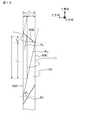
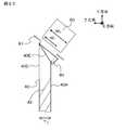
- FIG. 5A, FIG. 5B, and FIG. 5Cschematically show light rays that propagate (propagate) inside the first light guide member 40 when the first light guide member 40 is viewed from above.
- ⁇0 degrees.
- the angle ⁇is 0 degree, and light rays at the upper end of the image (indicated by solid lines R U1 and R U2 ) propagating in the ⁇ X axis direction and light rays at the lower end of the image (indicated by broken lines R D and R U2) .
- the angle ⁇is set to a value exceeding 0 degree.
- the angle ⁇is a value exceeding 0 degree (however, an angle larger than that shown in FIG. 5B).
- the emission direction of the light beam R U1 and the stray light beam R D2 corresponding to the signal light beamcan be more reliably separated, and the emission direction of the light beam R D1 and the stray light beam R U2 corresponding to the signal light beam.
- an output image by the signal light beam(indicated by a white upward arrow in the right hand side view of FIG. 5B) and an output image by the stray light (indicated by a gray right downward arrow in the right hand side diagram of FIG. 5B). ) are displayed in a completely separated manner, so that the quality of the display image can be further improved.
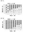
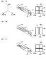
- FIGS. 6A, 6B, 7A and 7Bshow the results of FIGS. 6A, 6B, 7A and 7B.
- the vertical axisindicates the effective visual field range by the field diagonal value (unit: degree)
- the horizontal axisindicates the angle ⁇ (unit: degree). ⁇ is changed every 5 degrees.
- “A”indicates the field diagonal value of the effective field region
- “B”indicates the field diagonal value where stray light is generated
- “C”.Indicates a field diagonal value in which the effective field region is limited because it exceeds the total reflection limit of the first light guide member. The wider the area of “A”, the larger the viewing diagonal value of the effective viewing area, which is preferable.
- the optical device of Example 1is not limited, 20 (degrees) ⁇ ⁇ ⁇ 30 (degrees) 55 (degrees) ⁇ ⁇ ⁇ 65 (degrees) It is understood that it is preferable to satisfy
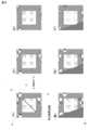
- FIG. 8shows a result of simulating the effective visual field range emitted from the first light guide member 40 when the refractive index n of the material constituting the first light guide member 40 is changed.
- the relationship between each figure in FIG. 8 and the refractive indexis as follows. Note that image light (light for image display) having a diagonal angle of 65 degrees was incident on the first light guide member 40.
- the first light guideis formed when the inclination ( ⁇ , ⁇ ) of the first semi-transmissive layer 42 is (25 degrees, 60 degrees).
- the stray light output image(indicated by “A”) escapes from the effective visual field range to the outside as the value of the refractive index n of the material constituting the member increases. This is because when the stray light generated inside the first light guide member 40 is emitted from the first light guide member 40, the greater the difference in refractive index between the first light guide member 40 and the air, the stronger the light is refracted. is there. Further, in FIGS.
- the first semi-transmissive layer 42has a slope ( ⁇ , ⁇ ) that is (25 degrees, 65 degrees). It can be confirmed that the vignetting due to the total reflection limit (indicated by “B”) decreases as the value of the refractive index n of the material constituting the light guide member 40 increases.
- the image forming apparatus 60includes an image forming apparatus having a first configuration. Specifically, as illustrated in a conceptual diagram in FIG. 12A, the image forming apparatus 60A includes a spatial light including an organic EL display device. A modulation device 62 is included. The image emitted from the spatial light modulation device 62 passes through a lens system (optical system) 61 composed of, for example, a convex lens, becomes parallel light, and travels toward the fifth surface 40E of the first light guide member 40.
- the entire image forming apparatus 60Ais housed in a housing (not shown). The housing is attached to the temple portion 13 by the attachment member 19.
- the spatial light modulator 62includes a plurality of (for example, 640 ⁇ 480) pixels (organic EL elements) arranged in a two-dimensional matrix.
- the image forming apparatus 60Bincludes the image forming apparatus having the first configuration. Specifically, the reflective spatial light modulator and the light emitting diode that emits white light. It is comprised from the light source 63 which consists of.
- Each image forming apparatus 60B as a wholeis housed in a housing (not shown).
- the housingis provided with an opening (not shown), and an optical system (parallel light) is provided through the opening. Light is emitted from an emission optical system (collimating optical system) 61.
- the housingis attached to the temple portion 13 by the attachment member 19.
- the reflective spatial light modulatorcomprises a liquid crystal display (LCD) 64 made of LCOS as a light valve.
- LCDliquid crystal display
- a polarizing beam splitter 65 for guidingis provided.
- the liquid crystal display device 64includes a plurality of (for example, 640 ⁇ 480) pixels (liquid crystal cells) arranged in a two-dimensional matrix.
- the polarization beam splitter 65has a known configuration and structure. The unpolarized light emitted from the light source 63 collides with the polarization beam splitter 65. In the polarization beam splitter 65, the P-polarized light component passes and is emitted out of the system.
- the S-polarized componentis reflected by the polarization beam splitter 65, enters the liquid crystal display device 64, is reflected inside the liquid crystal display device 64, and is emitted from the liquid crystal display device 64.
- the light emitted from the liquid crystal display device 64contains a lot of P-polarized light components, and the light emitted from the pixel displaying “black” is S-polarized light. Contains many ingredients.
- the P-polarized componentpasses through the polarization beam splitter 65 and travels toward the fifth surface 40 ⁇ / b> E of the first light guide member 40.
- the S polarization componentis reflected by the polarization beam splitter 65 and returned to the light source 63.
- the optical system 61is composed of, for example, a convex lens, and an image forming device 60B (more specifically, a liquid crystal display device 64) is disposed at a focal position (position) in the optical system 61 in order to generate parallel light. Has been.
- the image forming apparatus 60Cincludes the image forming apparatus having the second configuration, and specifically scans the light source 66 and the light emitted from the light source 66.
- a scanning unit 69 for forming an imageis provided.
- the image forming apparatus 60 ⁇ / b> Cincludes a laser light source 66 and a MEMS mirror 69. The light emitted from the MEMS mirror 69 passes through the lens system 61 and enters the fifth surface 40E of the first light guide member 40.
- the laser light source 66is composed of a light emitting element that emits green light.
- the light emitted from the light source 66is converted into parallel light by the lens 67, the optical path is changed by the reflecting mirror 68, the micromirror can be rotated in two dimensions, and the incident parallel light is scanned two-dimensionally.
- Horizontal scanning and vertical scanningare performed by the scanning means 69 composed of a MEMS mirror that can be converted into a kind of two-dimensional image, and virtual pixels (number of pixels, for example, 640 ⁇ 480) are generated.
- the light from the virtual pixel (scanning means 69 corresponding to the image emitting unit)passes through the lens system (optical system) 61 having a positive optical power, and the collimated light beam is the first light guide.
- the lightenters the fifth surface 40E of the member 40.
- the entire image forming apparatus 60Cis housed in a housing (not shown).
- luminance unevennessmay occur in the effective visual field region due to the uneven density of the outgoing light bundle emitted from the light guide member.
- a parallel light beamis incident on the first light guide member 40 with a wide light beam width. is there. Therefore, the exit pupil diameter of the first light guide member 40 corresponds to the position of the exit pupil of the optical system 61 (the fifth surface 40E), and the exit pupil diameter is that of the light entrance surface (the fifth surface 40E). It is preferable to design to cover the entire area.
- the frame 10includes a front portion 11 disposed in front of the observer 20, two temple portions 13 rotatably attached to both ends of the front portion 11 via hinges 12, and tip portions of the temple portions 13.
- a nose pad 10 'is attached. That is, the assembly of the frame 10 and the nose pad 10 'basically has substantially the same structure as normal glasses.
- each housingis attached to the temple portion 13 by an attachment member 19.
- the frame 10is made of metal or plastic. Each housing may be detachably attached to the temple portion 13 by the attachment member 19.
- each housingmay be detachably attached to the temple portion 13 of the frame 10 of the glasses owned by the observer by the attachment member 19.
- Each housingmay be attached to the outside of the temple portion 13 or may be attached to the inside of the temple portion 13.
- the support member 31may be fitted into the rim 11 ′′ (shown only in FIGS. 11B and 11C) provided in the front portion 11.
- a wiring (a signal line, a power supply line, etc.) 15 extending from one image forming apparatus 60extends from the distal end portion of the modern portion 14 to the outside via the temple portion 13 and the interior of the modern portion 14 and is controlled. It is connected to a device (control circuit, control means) 18.
- each image forming apparatus 60includes a headphone unit 16, and a headphone unit wiring 16 ′ extending from each image forming device 60 is connected to the modern unit 14 via the temple unit 13 and the modern unit 14. Extends from the front end of the headphone unit 16 to the headphone unit 16.
- the headphone unit wiring 16 ′extends from the tip of the modern unit 14 to the headphone unit 16 so as to wrap around the back side of the auricle (ear shell).
- the wiring (signal line, power supply line, etc.) 15is connected to the control device (control circuit) 18 as described above, and the control device 18 performs processing for image display.
- the control device 18can be composed of a known circuit.
- a signal from the imaging device 17is sent to a control device (control circuit) 18 via a wiring (not shown) extending from the imaging device 17.
- the value of ⁇is greater than 0 degrees, and the value of ⁇ is also greater than 0 degrees, so that the light is emitted from the first light guide member.
- the first light guide memberhas an action of expanding the beam bundle width in the X direction
- the exit pupil of the observation systemis expanded in the X direction
- the second light guide memberexpands the beam bundle width in the Y direction. Therefore, the exit pupil of the observation system is enlarged in the Y direction. Therefore, since the exit pupil of the observation system can be enlarged two-dimensionally by the optical device, the optical system can be reduced in size, which is extremely advantageous in designing a display device with a wide field of view.
- Example 2is a modification of Example 1.
- the arrangement of the first light guide member and the second light guide member in the optical device of Example 2is schematically shown in FIG. 13 together with the behavior of light, the image forming device, and the pupil of the observer.
- the arrangement of the two light guide membersis schematically shown in FIG. 14 is a side view of the first light guide member and the second light guide member when the first light guide member and the second light guide member are viewed from the direction of the white arrow B in FIG. 14 and the black arrow C in FIG. Is the same as shown in FIGS. 2B and 2C.
- Example 1the rod-shaped first light guide member 40 extends in the horizontal direction.
- Example 2the rod-shaped first light guide member 40 extends in the vertical direction.
- the optical device, the image display device, and the display device of the second embodimentcan be the same as the optical device, the image display device, and the display device described in the first embodiment, and thus detailed description thereof is omitted. .
- the third embodimentis a modification of the first and second embodiments.
- the width of the light beam propagating through the light guide memberis not sufficiently wide, the density of the light beam emitted from the light guide member may be biased.
- the width of the light beam propagating through the light guide memberis widened by disposing the semi-transmissive mirror film on the light guide member. That is, in the example of the optical device of Example 1 shown in FIG. 15B, the light flux width R ′ 0 limited by the width of the light incident surface (eighth surface 50B) may be insufficient. There may be a case where the light beam emitted from the seventh surface 50A of the optical member 50 is missing (shown by hatching in FIG. 15B).
- the semi-transmission parallel to the seventh surface 50A and the ninth surface 50C (total reflection surfaces 50A and 50C) of the second light guide member 50is formed in the vicinity of the light incident surface (eighth surface 50B), and the light beam width can be widened by branching the light beam colliding with the semi-transmissive mirror film 71 in the transmission direction and the reflection direction. is there. As a result, the density of the light beam emitted from the second light guide member 50 can be made uniform. This state is illustrated on the right hand side of FIG. 15A.
- the arrow “A”indicates the light bundle width that defines the light bundle width for guiding the second light guide member 50 (the maximum width of the light bundle width emitted from the semi-transmissive mirror film 71). ).
- FIG. 16shows an enlarged view of the state where the semi-transmissive mirror film 71 is formed in the vicinity of the light incident surface (eighth surface 50B).
- the maximum value L max of the length of the semi-transmissive mirror film 71 in the Y directionis It is preferable to satisfy the following values.
- the parallel light beamis propagated in the most shallow angle of the second light guide member 50, the light rays corresponding to the one end of the incident surface R 3, when a light beam corresponding to the other end was R 4, half-mirror
- the maximum length L max of the film 71is desirably a value at which the light ray R 4 collides with the semi-transmissive mirror film 71 at least once.
- the thickness (Z-direction thickness) of the second light guide member 50is T
- the inclination angle (angle formed with the XZ plane) of the light incident surface (eighth surface 50B) of the second light guide member 50is ⁇
- the total reflection angle of the light beam propagating through the second light guide member 50 at the shallowest angleis ⁇ s
- the distance from the semi-transmissive mirror film 71 to the ninth surface 50C of the second light guide member 50is T ⁇ r
- the first light guide member 40has a cross section with a close aspect ratio, and the parallel light flux of the image light has two sets of parallel opposing side surfaces (the first surface 40A and the third surface).
- the lightis guided while repeating the total reflection surface between the surface 40C and the second surface 40B and the fourth surface 40D). Therefore, when the thickness (width) of the light bundle limited by the area of the light incident surface (the fifth surface 40E) is not sufficient, the two light beams are emitted toward the second light guide member 50 in two total reflection directions. There may be a deviation in the density of the resulting outgoing light bundle.
- the first light guide member 40includes: A semi-transmissive mirror film 72 disposed in parallel with the first surface 40A and the third surface 40C is disposed (see FIG. 17C), or A semi-transmissive mirror film 71 disposed in parallel with the second surface 40B and the fourth surface 40D is disposed (see FIG. 17B), or A semi-transmissive mirror film 72 disposed parallel to the first surface 40A and the third surface 40C and a semi-transmissive mirror film 71 disposed parallel to the second surface 40B and the fourth surface 40D are disposed ( FIG. 17A).
- the semi-transmissive mirror film 72disposed parallel to the first surface 40A and the third surface 40C, and the semi-transmissive mirror disposed parallel to the second surface 40B and the fourth surface 40D.
- membrane 71is arrange
- a semi-transmissive mirror film 71is disposed in parallel with the second surface 40B and the fourth surface 40D, and is totally reflected by the second surface 40B and the fourth surface 40D.
- the density of the outgoing light bundle corresponding to the directionis made uniform.
- FIG. 17Athe semi-transmissive mirror film 72 disposed parallel to the first surface 40A and the third surface 40C, and the semi-transmissive mirror disposed parallel to the second surface 40B and the fourth surface 40D.
- membrane 71is arrange
- a semi-transmissive mirror film 71is disposed
- the semi-transmissive mirror film 72is provided in parallel with the first surface 40A and the third surface 40C, and is in the direction of total reflection on the first surface 40A and the third surface 40C.
- the density of the corresponding outgoing light bundleis made uniform.
- the semi-transmissive mirror film 72 disposed in the first light guide member 40 in parallel with the first surface 40A and the third surface 40Cis an area located at the same distance from the first surface 40A and the third surface 40C. (See FIG. 17C).
- the semi-transmissive mirror film 75 disposed on the first light guide member 40 in parallel with the first surface 40A and the third surface 40Cmay be a partial region on the first surface 40A or the third surface 40C. It can be set as the structure arrange
- the semi-transmissive mirror film 71 disposed in the first light guide member 40 in parallel with the second surface 40B and the fourth surface 40Dis located at the same distance from the second surface 40B and the fourth surface 40D. It can be set as the structure arrange
- the semi-transmissive mirror film 73 disposed on the first light guide member 40 in parallel with the second surface 40B and the fourth surface 40Dmay be a partial region on the second surface 40B or the fourth surface 40D.
- a configurationmay be employed in which a part of the region is disposed (see FIGS. 18B and 19B).
- FIG. 18A, FIG. 18B, FIG. 19A, and FIG. 19Bschematically show a state where unevenness (brightness or darkness) occurs in the image on the right hand side.
- unevennessunevenness or darkness
- the strip-shaped luminance unevenness caused by the two total reflection directionsintersect each other.
- a grid-like brightness non-uniformityis generated overlapping the pattern.
- the transflective mirror film 73is formed, and the width of the light bundle that is totally reflected by the second surface 40B and the fourth surface 40D is widened.
- Unevennessis suppressed, and only brightness unevenness corresponding to the Z direction occurs.
- the semi-transmissive mirror film 75is formed, and the width of the light beam totally reflected by the first surface 40A and the third surface 40C is widened. The luminance unevenness is suppressed, and only the luminance unevenness corresponding to the Y direction occurs.
- semi-transmissive mirror films 73 and 75are formed, and the light flux width totally reflected by the second surface 40B and the fourth surface 40D and the first surface 40A and the third surface 40C are all reflected. Since the width of the reflected light bundle is widened, the band-like luminance unevenness corresponding to the total reflection direction is suppressed, and a state without luminance unevenness is achieved.
- the semi-transmissive mirror filmWhen the semi-transmissive mirror film is disposed in a partial region on the first surface 40A or a partial region on the third surface 40C, or alternatively, a partial region or the fourth surface on the second surface 40B.
- protective members 74 and 76When disposed in a partial region on 40D, it is preferable that protective members 74 and 76 are disposed on the surface of the semi-transmissive mirror film that is not in contact with the first light guide member 40.
- the protection members 74 and 76may be appropriately selected from materials constituting the light guide member.
- the second light guide member 50may have a configuration in which the semi-transmissive mirror film disposed in parallel with the seventh surface 50A and the ninth surface 50C is disposed.
- the semi-transmissive mirror film disposed parallel to the seventh surface 50A and the ninth surface 50C inside the second light guide member 50is located at the same distance from the seventh surface 50A and the ninth surface 50C.
- the semi-transmissive mirror filmAs described above, by disposing the semi-transmissive mirror film on the second light guide member 50, it is possible to prevent the image emitted from the seventh surface 50A of the second light guide member 50 from becoming uneven (brightness or darkness). can do.
- the semi-transmissive mirror filmis disposed in a partial region on the seventh surface 50A or a partial region on the ninth surface 50C, the surface of the semi-transmissive mirror film that is not in contact with the second light guide member 50 It is preferable that a protective member is disposed on the. What is necessary is just to select a protective member suitably from the material which comprises a light guide member.
- the light guide member provided with the semi-transmissive mirror films 73 and 75 shown in FIGS. 18B, 19A, and 19Bis the light guide member provided with the semi-transmissive mirror films 71 and 72 shown in FIGS. 17A, 17B, and 17C. It is very useful because it can be expected to produce a sufficient effect while being much easier to manufacture.
- the first light guide member 40 and the second light guide member 50include the first semi-transmissive layer 42 and the second semi-transmissive layer 52 which are discontinuous boundaries inside the light guide member.
- a protective memberthat has the same refractive index as that of the light guide material and is thinner than the light guide member on one or more side surfaces of the light guide member, regardless of whether or not the semi-transmissive mirror film is provided.
- 74 and 76are preferably pasted.
- the fourth embodimentis a modification of the first to third embodiments.
- a schematic cross-sectional view of the light incident portion of the first light guide memberis located near the fifth surface 40 ⁇ / b> E in the first light guide member 40.
- a cross-sectional area / expansion portion 80that increases the cross-sectional area of the light incident on the fifth surface 40E is provided.
- a second cross-sectional area / enlargement portionthat enlarges the cross-sectional area of the light incident on the eighth surface 50B is disposed.
- the thickness of the first light guide member 40can be reduced, and the thickness of the second light guide member in the Z direction is reduced. It becomes possible. It shows the thickness T 0 of the light flux width W 0 and the first light guide member 40 entering the fifth surface 40E of the first light guide member 40 when the cross-sectional area and expanding part 80 are arranged in FIG. 20
- FIG. 20also shows the beam bundle width W 1 incident on the fifth surface 40E of the first light guide member 40 when the cross-sectional area / enlarged portion 80 is not provided.
- a schematic cross-sectional view of the light incident portion of the optical device in which the cross-sectional area / enlargement portion 80 is not providedis shown in FIG. 21, and the light flux width W incident on the fifth surface 40 E of the first light guide member 40. 1 and the thickness T 0 of the first light guide member 40 are also shown in FIG.
- the cross-sectional area / enlarged portion 80is formed in the vicinity of the light incident portion (fifth surface 40E) of the first light guide member 40 and the light incident portion (eighth surface 50B) of the second light guide member. It can be configured by incorporating a prism member having the same refractive index, or alternatively, the light incident part (fifth surface 40E) of the first light guide member 40 or the light incident part (eighth of the second light guide member). It can be formed by processing the surface 50B) into a prism shape.
- the value of the inclination angle of the light incident surface of the cross-sectional area / enlargement portion 80may be smaller than the value of the inclination angle of the fifth surface 40E of the first light guide member 40, or the second section
- the inclination angle value of the light incident surface of the area / enlarged portionmay be smaller than the inclination angle value of the eighth surface 50B of the second light guide member 50 (see also FIG. 16).
- the light emitted from the central portion of the image forming apparatus 60is preferably incident on the light incident surface of the cross-sectional area / enlarged portion 80 perpendicularly. Further, when the light emitted from the central portion of the image forming apparatus 60 is guided in the first light guide member 40 and emitted from the third surface 40C of the first light guide member 40, the second cross-sectional area / enlargement is performed. It is preferable to enter perpendicularly to the light incident surface of the part.
- a light shielding unithaving an opening between the image forming apparatus 60 and the first light guide member 40 so that undesired light is emitted from the image forming apparatus 60 and does not enter the first light guide member 40.
- a light shielding unithaving an opening between the image forming apparatus 60 and the first light guide member 40 so that undesired light is emitted from the image forming apparatus 60 and does not enter the first light guide member 40.
- 81is arranged.
- the first light guide member 40 and the second light guide member 50 so that undesired lightdoes not enter the second light guide member 50 among the light emitted from the first light guide member 40.
- Example 5is a modification of Example 1 to Example 4.
- the intensity of the light beam guided while repeating total reflectionis increased every time the first semi-transmissive layer 42 is transmitted. It attenuates according to the transmittance.
- the light reflectance of the first semi-transmissive layer 42is corrected so as to correct the intensity attenuation. Should be designed with a higher level. This design is effective for both the first light guide member 40 and the second light guide member 50.
- the first semi-transmissive layer 42 located far from the fifth surface 40Eis It has a higher light reflectance (lower light transmittance) than the first semi-transmissive layer 42 located near the fifth surface 40E.
- the second semi-transmissive layer 52 located far from the eighth surface 50Bis located near the eighth surface 50B.
- the second semi-transmissive layer 52has a higher light reflectance (lower light transmittance).
- the observer 20when the geometrical arrangement of the first semi-transmissive layer 42 is determined, among the light rays reflected by a certain first semi-transmissive layer 42 and emitted from the first light guide member 40, the observer 20 The angle component of the light ray incident on the pupil 21 is determined according to the distance from the light incident surface (fifth surface 40E) of the first light guide member 40 to the first semi-transmissive layer 42.
- the angle characteristic of the light reflectance of each first semi-transmissive layer 42may be appropriately designed.
- the first semi-transmissive layer 42depends on the distance from the fifth surface, and the angle (reflection angle) between the normal line of the first semi-transmissive layer 42 and the light beam reflected by the first semi-transmissive layer 42.
- the light reflectanceare preferably defined.
- the second semi-transmissive layer 52has an angle (reflection) between the normal line of the second semi-transmissive layer 52 and the light beam reflected by the second semi-transmissive layer 52. It is preferable that the relationship between the angle and the light reflectance is defined.
- the inclination ( ⁇ , ⁇ ) of the plurality of first semi-transmissive layers 42was set to (25 degrees, 60 degrees), and the effective visual field area of the output image was set to 78 degrees diagonally.
- BK7reffractive index: 1.517
- the light guide material of the first light guide member 40is used as the light guide material of the first light guide member 40.
- the light emission state in each area in the first light guide member of the optical device of Example 5is shown in FIG. 22A, and the relationship between the reflection angle and the light reflectance is shown in FIG.
- the first light guide member 40is divided into a plurality of areas [specifically, three areas 43, 44, 45 (first area 43, second area) from the light incident surface side. 44, the third area 45)], and shows the result of designing the first semi-transmissive layer 42 included in each area with different light reflectance.
- the exit cone R 6is output from the entire area of the light exit surface (third surface 40C) of the first light guide member 40.
- the angular ranges reaching the pupil 21 of the observer 20are I 1 , I 2 , respectively. , I 3 .
- outgoing light rays in the angle ranges of I 1 , I 2 , and I 3are reflected at a predetermined angle in the first semi-transmissive layer 42 and emitted from the first light guide member 40. That is, the reflection angle formed by the outgoing light beam in the angle range I 1 is 39 to 55 degrees with the normal line of the first semi-transmissive layer 42, and the outgoing light beam in the angle range I 2 is the normal line of the first semi-transmissive layer 42.
- the reflection angle formedis 23 ° to 45 °
- the reflection angle of outgoing light angle range I 3makes with the normal line of the first semi-transparent layer 42 is 10 degrees to 32 degrees.
- the light reflectance of the first semi-transmissive layer 42 existing in the three areas 43, 44, and 45is converted into only the angle component incident on the pupil 21 of the observer 20. It was designed based on the angle dependence so that it was reflected and taken out, and other angle components were transmitted.
- the first semi-transmissive layer 42 of the area 43with the light reflectance 43 ′ having angle dependency, the light beam corresponding to the angle range I 1 can be efficiently extracted and correspond to the angle ranges I 2 and I 3 .
- losscan be reduced and high light guide efficiency can be obtained.
- the first semi-transmissive layer 42 in the area 44 with the light reflectivity 44 ′ having angle dependencyby providing the first semi-transmissive layer 42 in the area 44 with the light reflectivity 44 ′ having angle dependency, light rays corresponding to the angle range I 2 can be efficiently extracted, and corresponding to the angle range I 3 .
- the light beam corresponding to the angle range I 3can be efficiently extracted.
- the light reflectivity 43 ', 44', 45 'of the first semi-transmissive layer 42 located in the areas 43, 44, 45has an angle dependency, and the rear area has a higher light reflectivity. Design to be. This is to correct the intensity attenuation that occurs every time the signal light beam propagating through the first light guide member 40 passes through the first semi-transmissive layer 42. As a result, the signal light beam is uniform over the entire effective visual field region. Luminance can be realized and light guide efficiency can be increased.
- the optical device, the image display device, and the display device of the present disclosurehave been described based on the preferred embodiments. However, the optical device, the image display device, and the display device of the present disclosure are not limited to these embodiments.
- the enlargement direction of the exit pupilis not limited to the direction shown in FIGS. 1 and 13, and may be any direction in which the image enlargement directions by the first light guide member and the second light guide member are orthogonal to each other.
- the optical device 30may further include a diopter correction lens. That is, even if the diopter correction lens 22 corresponding to the diopter of the observer 20 is arranged in the optical path from the optical device 30 to the pupil 21 of the observer 20 as shown in a schematic cross-sectional view in FIG. 11C. Good.
- the output image from the optical deviceis projected at infinity in principle. Therefore, in order to observe the output image with high resolution, the diopter correction lens 22 corresponding to the diopter of the observer 20 may be inserted into the optical path from the second light guide member 50 to the pupil 21 of the observer 20.
- FIG. 11Da schematic diagram of a modification of the display device of Example 1 viewed from the side, the light control device 23 described above is provided on the viewer side or the viewer side of the optical device 30. May be provided.
- this indicationcan also take the following structures.
- ⁇ Optical device>> A first surface, a second surface, a third surface facing the first surface, a fourth surface facing the second surface, a fifth surface, and a sixth surface facing the fifth surface;
- a first light guide membercomprising one deflection means, and A seventh surface, an eighth surface, a ninth surface facing the seventh surface, a tenth surface facing the eighth surface, an eleventh surface, and a twelfth surface facing the eleventh surface;
- a second light guide membercomprising two deflection means,
- An optical devicecomprising: The first surface and the third surface are parallel, The second surface and the fourth surface are parallel and orthogonal to the first surface and the third surface, The seventh surface and the ninth surface are parallel to the XY plane in the XYZ orthogonal coordinate system, The light incident from the fifth surface is totally reflected inside the first light guide member, is deflected by the first deflecting means, is emitted from the third surface, and is incident on the eighth surface
- the first deflecting meansincludes a plurality of first semi-transmissive layers spaced apart and arranged in parallel, When the angle formed with the X axis when the normal line of the first semi-transmissive layer is projected onto the XZ plane is ⁇ , the value of ⁇ is a value exceeding 0 degrees.
- the first light guide memberis provided with a semi-transmissive mirror film disposed in parallel with the first surface and the third surface, or disposed in parallel with the second surface and the fourth surface. Or a semi-transparent mirror film disposed parallel to the first and third surfaces and a semi-transparent film disposed parallel to the second and fourth surfaces.
- the optical device according to [A01]in which a mirror film is provided.
- the semi-transmissive mirror film disposed in the first light guide member in parallel with the first surface and the third surfaceis disposed in a part of a region located at the same distance from the first surface and the third surface.
- the semi-transmissive mirror film disposed on the first light guide member in parallel with the first surface and the third surfaceis disposed in a partial region on the first surface or a partial region on the third surface.
- the semi-transmissive mirror film disposed in the first light guide member in parallel with the second surface and the fourth surfaceis disposed in a part of the region located at the same distance from the second surface and the fourth surface.
- the semi-transmissive mirror film disposed on the first light guide member in parallel with the second surface and the fourth surfaceis disposed in a partial region on the second surface or a partial region on the fourth surface.
- the second light guide memberincludes a semi-transmissive mirror film disposed in parallel with the seventh surface and the ninth surface, according to any one of [A01] to [A06].
- Optical device.[A08] The semi-transmissive mirror film disposed in the second light guide member in parallel with the seventh surface and the ninth surface is disposed in a part of the region located at the same distance from the seventh surface and the ninth surface. The optical device according to [A07].
- the semi-transmissive mirror film disposed on the second light guide member in parallel with the seventh surface and the ninth surfaceis arranged in a partial region on the seventh surface or a partial region on the ninth surface.
- a cross-sectional area / enlarged portion for enlarging the cross-sectional area of light incident on the fifth surfaceis arranged.
- [A12]The optical device according to [A10], in which the cross-sectional area / enlargement portion includes the fifth surface of the prism-shaped first light guide member.
- the first semi-transmissive layeris made of a dielectric multilayer film
- the first semi-transmissive layer located far from the fifth surfaceis the first semi-transmissive layer located near the fifth surface.
- the first semi-transmissive layerhas an angle (reflection angle) formed between the normal line of the first semi-transmissive layer and the light beam reflected by the first semi-transmissive layer, depending on the distance from the fifth surface.
- the optical deviceaccording to any one of [A01] to [A20], wherein a relationship with light reflectance is defined.
- the second deflecting meansincludes a plurality of second semi-transmissive layers spaced apart in parallel, Depending on the distance from the eighth surface, the second semi-transmissive layer has an angle (reflection angle) between the normal line of the second semi-transmissive layer and the light beam reflected by the second semi-transmissive layer and the light reflectance.
- [A23] 20 (degrees) ⁇ ⁇ ⁇ 30 (degrees) 55 (degrees) ⁇ ⁇ ⁇ 65 (degrees)The optical device according to any one of [A01] to [A22], wherein: [A24] The optical device according to any one of [A01] to [A23], wherein the third surface and the eighth surface are parallel.
- [A25]The optical device according to any one of [A01] to [A24], in which an air layer exists between the third surface and the eighth surface.
- [A28]The optical device according to any one of [A01] to [A27], wherein at least one of the seventh surface and the ninth surface of the second light guide member is entirely covered with a protective member.
- [A30]Light enters the fifth surface of the first light guide member via the optical system; Any one of [A01] to [A29] at the position of the fifth surface of the first light guide member corresponding to the position of the exit pupil of the optical system and the exit pupil diameter covering the entire area of the fifth surface.
- Image display devicecomprising an image forming device and an optical device, The optical device A first surface, a second surface, a third surface facing the first surface, a fourth surface facing the second surface, a fifth surface, and a sixth surface facing the fifth surface; A first light guide member comprising one deflection means, and A seventh surface, an eighth surface, a ninth surface facing the seventh surface, a tenth surface facing the eighth surface, an eleventh surface, and a twelfth surface facing the eleventh surface; A second light guide member comprising two deflection means, An optical device comprising: The first surface and the third surface are parallel, The second surface and the fourth surface are parallel and orthogonal to the first surface and the third surface, The seventh surface and the ninth surface are parallel to the XY plane in the XYZ orthogonal coordinate system, The light incident from the fifth surface is totally reflected inside the first light guide member, is deflected by the first deflecting means, is emitted from the third surface, and
- the first deflecting meansincludes a plurality of first semi-transmissive layers spaced apart and arranged in parallel, When the angle formed with the X axis when the normal line of the first semi-transmissive layer is projected onto the XZ plane is ⁇ , the value of ⁇ is a value exceeding 0 degrees.
- An image display devicein which ⁇ is a value exceeding 0 degree, where ⁇ is an angle formed with the X axis when the normal line of the first semi-transmissive layer is projected onto the XY plane.
- Image display devicesecond aspect >> An image display apparatus comprising an image forming apparatus and the optical apparatus according to any one of [A01] to [A31].
- a display devicecomprising: The image display device includes an image forming device and an optical device, The optical device A first surface, a second surface, a third surface facing the first surface, a fourth surface facing the second surface, a fifth surface, and a sixth surface facing the fifth surface; A first light guide member comprising one deflection means, and A seventh surface, an eighth surface, a ninth surface facing the seventh surface, a tenth surface facing the eighth surface, an eleventh surface, and a twelfth surface facing the eleventh surface; A second light guide member comprising two deflection means, An optical device comprising: The first surface and the third surface are parallel, The second surface and the fourth surface are parallel and orthogonal to the first surface and the third surface, The
- the first deflecting meansincludes a plurality of first semi-transmissive layers spaced apart and arranged in parallel, When the angle formed with the X axis when the normal line of the first semi-transmissive layer is projected onto the XZ plane is ⁇ , the value of ⁇ is a value exceeding 0 degrees.
- Display devicesecond aspect >> A frame attached to the observer's head; and An image display device attached to the frame, A display device comprising: The image display device includes an image forming device and the optical device according to any one of [A01] to [A31].
- first light guide member3rd surface, 40D ... 4th surface of 1st light guide member, 40E ... 5th surface of 1st light guide member, 40F ... 1st light guide member
- 2nd deflection means, 52... 2nd semi-transmissive 60, 60A, 60B, 60C ... image forming apparatus, 61 ... lens system (optical system, parallel light emitting optical system, collimating optical system), 62 ... spatial light modulator, 63 ... Light source, 64 ... Liquid crystal display (LCD), 65 ... Polarizing beam splitter, 66 ... Light source, 67 ... Lens, 68 ... Reflector, 69.
- - scanning means71,72,73,75 ... semi-transparent mirror film, 74, 76 ... protective member, 80 ... cross-sectional area and expansion unit, 81 ... light shielding unit, R 0 ...
- R '0 ⁇ ⁇ ⁇ lightis limited by the width of the entrance surface the light beam width is emitted from the third surface of the R 1 ⁇ ⁇ ⁇ first light guide member rays, light rays emitted from the seventh surface of R 2 ⁇ ⁇ ⁇ second light guide member, R U1, R U2, R D, R U2, R 3, R 4, ⁇ light, R 5 ⁇ ⁇ ⁇ Incident cone, R 6 , R 6-43 , R 6-44 , R 6-45 ... Exit cone
Landscapes
- Physics & Mathematics (AREA)
- General Physics & Mathematics (AREA)
- Optics & Photonics (AREA)
- Engineering & Computer Science (AREA)
- Multimedia (AREA)
- Signal Processing (AREA)
- Optical Elements Other Than Lenses (AREA)
- Control Of Indicators Other Than Cathode Ray Tubes (AREA)
- Devices For Indicating Variable Information By Combining Individual Elements (AREA)
Abstract
Description
Translated fromJapanese本開示は、光学装置、斯かる光学装置を備えた画像表示装置、及び、斯かる画像表示装置を備えた表示装置、より具体的には、頭部装着型ディスプレイ(HMD,Head Mounted Display)に用いられる表示装置に関する。The present disclosure relates to an optical device, an image display device provided with such an optical device, and a display device provided with such an image display device, more specifically, a head-mounted display (HMD, Head Mounted Display). The present invention relates to a display device used.
近年、観察者の目の前に配置した光学装置に画像形成装置からの画像を表示させる頭部装着型ディスプレイ(HMD)の開発が、鋭意、進められている。そして、種々の形式の頭部装着型ディスプレイが検討されているが、頭部装着型ディスプレイに対して、一層リアリティーのある画像を提供するために表示画像の広画角化が強く求められている。このような要求に対処するために、光学装置を構成する導光板に2つの偏向手段を配置した頭部装着型ディスプレイが、例えば、特表2005-521099号公報の図16から周知である。この頭部装着型ディスプレイにあっては、この特許公表公報の段落番号[0059]に記載されたとおり、入力波が第1反射面16aによって第1LOE20a内に結合され、ξ軸に沿って伝搬される。選択的反射面22aは光を20a外へ結合し、その後、この光は第2反射面16bによって第2LOE20b内に結合される。そして、この光はη軸に沿って伝搬された後、選択的反射面22bによって20b外へ結合される。In recent years, development of a head-mounted display (HMD) that displays an image from an image forming apparatus on an optical device arranged in front of an observer's eyes is eagerly advanced. Various types of head-mounted displays have been studied, but a wide angle of display image is strongly demanded for providing more realistic images to the head-mounted display. . In order to cope with such a demand, a head-mounted display in which two deflecting means are arranged on a light guide plate constituting an optical device is known from, for example, FIG. 16 of JP-T-2005-521099. In this head-mounted display, as described in paragraph [0059] of this patent publication, an input wave is coupled into the first LOE 20a by the first reflecting surface 16a and propagated along the ξ axis. The Selective reflective surface 22a couples light out of 20a, which is then coupled into second LOE 20b by second reflective surface 16b. This light is propagated along the η-axis and then coupled out of 20b by the selective reflection surface 22b.
しかしながら、上記の特許公表公報に開示された技術にあっては、第1LOE20aから第2LOE20bに向けて出射される光に迷光が含まれ、低い画質の画像しか得られないといった問題がある。However, the technique disclosed in the above-mentioned patent publication has a problem that stray light is included in the light emitted from the first LOE 20a toward the second LOE 20b and only a low-quality image can be obtained.
従って、本開示の目的は、高い画質の画像を提供し得る光学装置、斯かる光学装置を備えた画像表示装置、及び、斯かる画像表示装置を備えた表示装置を提供することにある。Therefore, an object of the present disclosure is to provide an optical device that can provide a high-quality image, an image display device including the optical device, and a display device including the image display device.
上記の目的を達成するための本開示の光学装置は、
第1面、第2面、第1面と対向した第3面、第2面と対向した第4面、第5面、及び、第5面と対向した第6面を有し、内部に第1偏向手段を備えた第1導光部材、並びに、
第7面、第8面、第7面と対向した第9面、第8面と対向した第10面、第11面、及び、第11面と対向した第12面を有し、内部に第2偏向手段を備えた第2導光部材、
を備えており、
第1面及び第3面は平行であり、
第2面及び第4面は平行であり、且つ、第1面及び第3面と直交しており、
第7面及び第9面は、XYZ直交座標系におけるXY平面と平行であり、
第5面から入射した光は、第1導光部材の内部を全反射し、第1偏向手段によって偏向され、第3面から出射され、第3面と離間して配置された第8面に入射し、第7面と第9面との間で全反射され、第2偏向手段によって偏向され、第7面から出射され、
第1偏向手段は、複数の第1半透過層が離間して平行に配設されて成り、
第1半透過層の法線をXZ平面に射影したときのX軸と成す角度をαとしたとき、αの値は0度を超える値であり、
第1半透過層の法線をXY平面に射影したときのX軸と成す角度をβとしたとき、βの値は0度を超える値である。In order to achieve the above object, an optical device of the present disclosure is provided.
A first surface, a second surface, a third surface facing the first surface, a fourth surface facing the second surface, a fifth surface, and a sixth surface facing the fifth surface; A first light guide member comprising one deflection means, and
A seventh surface, an eighth surface, a ninth surface facing the seventh surface, a tenth surface facing the eighth surface, an eleventh surface, and a twelfth surface facing the eleventh surface; A second light guide member comprising two deflection means,
With
The first surface and the third surface are parallel,
The second surface and the fourth surface are parallel and orthogonal to the first surface and the third surface,
The seventh surface and the ninth surface are parallel to the XY plane in the XYZ orthogonal coordinate system,
The light incident from the fifth surface is totally reflected inside the first light guide member, is deflected by the first deflecting means, is emitted from the third surface, and is incident on the eighth surface disposed away from the third surface. Incident, totally reflected between the seventh surface and the ninth surface, deflected by the second deflecting means, emitted from the seventh surface,
The first deflecting means includes a plurality of first semi-transmissive layers spaced apart and arranged in parallel,
When the angle formed with the X axis when the normal line of the first semi-transmissive layer is projected onto the XZ plane is α, the value of α is a value exceeding 0 degrees.
When the angle formed with the X axis when the normal line of the first semi-transmissive layer is projected onto the XY plane is β, the value of β is a value exceeding 0 degree.
上記の目的を達成するための本開示の第1の態様あるいは第2の態様に係る画像表示装置は、画像形成装置及び光学装置を備えており、光学装置は上記の本開示の光学装置から成り、あるいは又、画像表示装置は、画像形成装置及び上記の本開示の光学装置を備えている。In order to achieve the above object, an image display apparatus according to the first or second aspect of the present disclosure includes an image forming apparatus and an optical apparatus, and the optical apparatus includes the optical apparatus of the present disclosure. Alternatively, the image display apparatus includes the image forming apparatus and the optical apparatus according to the present disclosure.
上記の目的を達成するための本開示の第1の態様あるいは第2の態様に係る表示装置は、
観察者の頭部に装着されるフレーム、及び、
フレームに取り付けられた画像表示装置、
を備えており、
画像表示装置は、画像形成装置及び光学装置を備えており、
光学装置は、上記の本開示の光学装置から成り、あるいは又、表示装置は、
観察者の頭部に装着されるフレーム、及び、
フレームに取り付けられた画像表示装置、
を備えており、
画像表示装置は、画像形成装置及び上記の本開示の光学装置を備えている。In order to achieve the above object, a display device according to the first aspect or the second aspect of the present disclosure is provided.
A frame attached to the observer's head; and
An image display device attached to the frame,
With
The image display device includes an image forming device and an optical device,
The optical device is composed of the above-described optical device of the present disclosure, or alternatively, the display device is
A frame attached to the observer's head; and
An image display device attached to the frame,
With
The image display apparatus includes an image forming apparatus and the above-described optical device of the present disclosure.
本開示の光学装置、本開示の第1の態様~第2の態様に係る画像表示装置を構成する光学装置、あるいは又、本開示の第1の態様~第2の態様に係る表示装置を構成する光学装置(以下、これらの光学装置を総称して、『本開示の光学装置等』と呼ぶ)にあっては、αの値は0度を超える値であり、βの値も0度を超える値であるが故に、第1導光部材から出射される光(画像)に迷光が含まれることを抑制(低下)させることができる結果、高画質の画像を提供することができる。尚、本明細書に記載された効果はあくまで例示であって限定されるものでは無く、また、付加的な効果があってもよい。An optical device of the present disclosure, an optical device constituting the image display device according to the first aspect to the second aspect of the present disclosure, or a display device according to the first aspect to the second aspect of the present disclosure In the optical device (hereinafter, these optical devices are collectively referred to as “optical device of the present disclosure”), the value of α is greater than 0 degrees, and the value of β is also 0 degrees. As a result, it is possible to suppress (decrease) stray light from being included in the light (image) emitted from the first light guide member, so that a high-quality image can be provided. Note that the effects described in the present specification are merely examples and are not limited, and may have additional effects.
以下、図面を参照して、実施例に基づき本開示を説明するが、本開示は実施例に限定されるものではなく、実施例における種々の数値や材料は例示である。尚、説明は、以下の順序で行う。
1.本開示の光学装置、本開示の第1の態様~第2の態様に係る画像表示装置、本開示の第1の態様~第2の態様に係る表示装置、全般に関する説明
2.実施例1(本開示の光学装置、本開示の第1の態様~第2の態様に係る画像表示装置、本開示の第1の態様~第2の態様に係る表示装置)
3.実施例2(実施例1の変形)
4.実施例3(実施例1~実施例2の変形)
5.実施例4(実施例1~実施例3の変形)
6.実施例5(実施例1~実施例4の変形)
7.その他Hereinafter, although this indication is explained based on an example with reference to drawings, this indication is not limited to an example and various numerical values and materials in an example are illustrations. The description will be given in the following order.
1. 1. Optical device of the present disclosure, image display device according to first to second aspects of the present disclosure, display device according to first to second aspects of the present disclosure, and general description Example 1 (Optical Device of Present Disclosure, Image Display Device According to First to Second Aspects of Present Disclosure, Display Device According to First to Second Aspects of Present Disclosure)
3. Example 2 (Modification of Example 1)
4). Example 3 (Modification of Examples 1 and 2)
5). Example 4 (Modification of Examples 1 to 3)
6). Example 5 (Modification of Examples 1 to 4)
7). Other
本開示の光学装置等において、第1導光部材には、
第1面及び第3面と平行に配設された半透過ミラー膜が配設されており、又は、
第2面及び第4面と平行に配設された半透過ミラー膜が配設されており、又は、
第1面及び第3面と平行に配設された半透過ミラー膜及び第2面及び第4面と平行に配設された半透過ミラー膜が配設されている構成とすることができる。そして、この場合、第1導光部材の内部に第1面及び第3面と平行に配設された半透過ミラー膜は、第1面及び第3面と等距離に位置する領域の一部に配設されている構成とすることができる。あるいは又、第1導光部材に第1面及び第3面と平行に配設された半透過ミラー膜は、第1面上の一部の領域又は第3面上の一部の領域に配設されている構成とすることができる。あるいは又、第1導光部材の内部に第2面及び第4面と平行に配設された半透過ミラー膜は、第2面及び第4面と等距離に位置する領域の一部に配設されている構成とすることができる。あるいは又、第1導光部材に第2面及び第4面と平行に配設された半透過ミラー膜は、第2面上の一部の領域又は第4面上の一部の領域に配設されている構成とすることができる。そして、このように、第1導光部材に半透過ミラー膜を配設することで、第1導光部材の第3面から出射される画像にムラ(明暗あるいは濃淡)が生じることを防止することができる。半透過ミラー膜を、第1面上の一部の領域又は第3面上の一部の領域に配設する場合、あるいは又、第2面上の一部の領域又は第4面上の一部の領域に配設する場合、第1導光部材と接していない半透過ミラー膜の面上には保護部材が配設されていることが好ましい。保護部材は、後述する導光部材を構成する材料から、適宜、選択すればよい。尚、半透過ミラー膜を配設する場合であっても、半透過ミラー膜を配設しない場合であっても、第1導光部材の第1面、第2面、第3面及び第4面の少なくとも1面、全体は、保護部材によって被覆されていることが好ましい。In the optical device or the like of the present disclosure, the first light guide member includes
A semi-transmissive mirror film disposed parallel to the first surface and the third surface is disposed, or
A semi-transmissive mirror film disposed parallel to the second surface and the fourth surface is disposed, or
A semi-transparent mirror film disposed in parallel with the first surface and the third surface and a semi-transparent mirror film disposed in parallel with the second surface and the fourth surface may be disposed. In this case, the semi-transmissive mirror film disposed parallel to the first surface and the third surface inside the first light guide member is a part of a region located at the same distance from the first surface and the third surface. It can be set as the structure arrange | positioned. Alternatively, the semi-transmissive mirror film disposed on the first light guide member in parallel with the first surface and the third surface is disposed in a partial region on the first surface or a partial region on the third surface. It can be set as the installed structure. Alternatively, the semi-transmissive mirror film disposed in the first light guide member in parallel with the second surface and the fourth surface is disposed in a part of the region located at the same distance from the second surface and the fourth surface. It can be set as the installed structure. Alternatively, the semi-transmissive mirror film disposed on the first light guide member in parallel with the second surface and the fourth surface is arranged in a partial region on the second surface or a partial region on the fourth surface. It can be set as the installed structure. In this way, by arranging the semi-transmissive mirror film on the first light guide member, it is possible to prevent unevenness (brightness or darkness) from occurring in the image emitted from the third surface of the first light guide member. be able to. When the semi-transmissive mirror film is disposed in a part of the region on the first surface or a part of the region on the third surface, or alternatively, a part of the region on the second surface or the one on the fourth surface. In the case where the protective member is disposed in the region, it is preferable that a protective member is disposed on the surface of the semi-transmissive mirror film that is not in contact with the first light guide member. What is necessary is just to select a protection member suitably from the material which comprises the light guide member mentioned later. Note that the first surface, the second surface, the third surface, and the fourth surface of the first light guide member, regardless of whether the semi-transmissive mirror film is disposed or not disposed. It is preferable that at least one surface of the entire surface is covered with a protective member.
上記の好ましい形態、構成を含む本開示の光学装置等において、第2導光部材には、第7面及び第9面と平行に配設された半透過ミラー膜が配設されている構成とすることができる。そして、この場合、第2導光部材の内部に第7面及び第9面と平行に配設された半透過ミラー膜は、第7面及び第9面と等距離に位置する領域の一部に配設されている構成とすることができ、あるいは又、第2導光部材に第7面及び第9面と平行に配設された半透過ミラー膜は、第7面上の一部の領域又は第9面上の一部の領域に配設されている構成とすることができる。そして、このように、第2導光部材に半透過ミラー膜を配設することで、第2導光部材の第7面から出射される画像にムラ(明暗あるいは濃淡)が生じることを防止することができる。半透過ミラー膜を、第7面上の一部の領域又は第9面上の一部の領域に配設する場合、第2導光部材と接していない半透過ミラー膜の面上には保護部材が配設されていることが好ましい。保護部材は、後述する導光部材を構成する材料から、適宜、選択すればよい。尚、半透過ミラー膜を配設する場合であっても、半透過ミラー膜を配設しない場合であっても、第2導光部材の第7面及び第9面の少なくとも1面、全体は、保護部材によって被覆されていることが好ましい。In the optical device and the like of the present disclosure including the above-described preferable modes and configurations, the second light guide member has a configuration in which a semi-transmissive mirror film disposed in parallel with the seventh surface and the ninth surface is disposed. can do. In this case, the semi-transmissive mirror film disposed parallel to the seventh surface and the ninth surface inside the second light guide member is a part of the region located at the same distance from the seventh surface and the ninth surface. Alternatively, the semi-transparent mirror film disposed on the second light guide member in parallel with the seventh surface and the ninth surface is a part of the seventh surface. It can be set as the structure arrange | positioned in the area | region or the one part area | region on the 9th surface. In this way, by arranging the semi-transmissive mirror film on the second light guide member, it is possible to prevent unevenness (brightness or darkness) from occurring in the image emitted from the seventh surface of the second light guide member. be able to. When the semi-transmissive mirror film is disposed in a partial area on the seventh surface or a partial area on the ninth surface, the semi-transmissive mirror film is protected on the surface of the semi-transmissive mirror film that is not in contact with the second light guide member. It is preferable that a member is provided. What is necessary is just to select a protection member suitably from the material which comprises the light guide member mentioned later. Even if the semi-transparent mirror film is provided or not provided, at least one of the seventh surface and the ninth surface of the second light guide member, the entire surface It is preferable that it is covered with a protective member.
以上に説明した各種の好ましい形態、構成を含む本開示の光学装置等にあっては、第1導光部材において、第5面の近傍には、第5面に入射する光の断面積を拡大させる断面積・拡大部が配設されている構成とすることができるし、更には、以上に説明した各種の好ましい形態、構成を含む本開示の光学装置等にあっては、第2導光部材において、第8面の近傍には、第8面に入射する光の断面積を拡大させる第2断面積・拡大部が配設されている構成とすることができる。このように、断面積・拡大部を配設することで、第1導光部材の厚さを薄くすることが可能となるし、第2導光部材の厚さを薄くすることが可能となる。あるいは又、第1導光部材に入射する光線束幅を広げることが可能となるし、第2導光部材に入射する光線束幅を広げることが可能となる。断面積・拡大部は、例えば、第1導光部材の光入射部(第5面)や第2導光部材の光入射部(第8面)の近傍にプリズム部材を組み込むことで構成することができるし、あるいは又、第1導光部材の光入射部(第5面)や第2導光部材の光入射部(第8面)をプリズム状に加工することで形成することができる。即ち、断面積・拡大部は、プリズム状の第1導光部材の第5面から成り、また、第2断面積・拡大部は、プリズム状の第2導光部材の第8面から成る構成とすることができる。あるいは又、断面積・拡大部の光入射面の傾斜角(YZ平面と断面積・拡大部の光入射面の成す角度)の値は、第1導光部材の第5面の傾斜角(YZ平面と第5面の成す角度)の値よりも小さい(あるいは又、第1導光部材の第5面の傾斜角の値と異なる)形態とすることができるし、第2断面積・拡大部の光入射面の傾斜角(XZ平面と第2断面積・拡大部の光入射面の成す角度)の値は、第2導光部材の第8面の傾斜角(XZ平面と第8面の成す角度)の値と異なる(あるいは又、第2導光部材の第8面の傾斜角の値よりも小さい)形態とすることができる。画像形成装置の中心部から出射された光は、第1導光部材の第5面に垂直に(断面積・拡大部が配設されている場合には、断面積・拡大部の光入射面に垂直に)入射することが好ましい。また、画像形成装置の中心部から出射された光が、第1導光部材内で導光され、第1導光部材の第3面から出射され、第2導光部材の第8面に垂直に(第2断面積・拡大部が配設されている場合には、第2断面積・拡大部の光入射面に垂直に)入射することが好ましい。In the optical device of the present disclosure including the various preferable modes and configurations described above, in the first light guide member, the cross-sectional area of the light incident on the fifth surface is enlarged near the fifth surface. In addition, in the optical device of the present disclosure including the various preferable modes and configurations described above, the second light guide is provided. The member may have a configuration in which a second cross-sectional area / enlargement portion for enlarging a cross-sectional area of light incident on the eighth surface is disposed in the vicinity of the eighth surface. Thus, by providing the cross-sectional area / enlarged portion, the thickness of the first light guide member can be reduced, and the thickness of the second light guide member can be reduced. . Alternatively, the width of the light beam incident on the first light guide member can be increased, and the width of the light beam incident on the second light guide member can be increased. For example, the cross-sectional area / enlarged portion is configured by incorporating a prism member in the vicinity of the light incident portion (fifth surface) of the first light guide member and the light incident portion (eighth surface) of the second light guide member. Alternatively, it can be formed by processing the light incident portion (fifth surface) of the first light guide member and the light incident portion (eighth surface) of the second light guide member into a prism shape. That is, the cross-sectional area / enlarged portion is composed of the fifth surface of the prism-shaped first light guide member, and the second cross-sectional area / enlarged portion is composed of the eighth surface of the prism-shaped second light guide member. It can be. Alternatively, the value of the tilt angle of the light incident surface of the cross-sectional area / enlarged portion (the angle formed by the YZ plane and the light incident surface of the cross-sectional area / enlarged portion) is the tilt angle (YZ of the fifth surface of the first light guide member). The angle formed by the plane and the fifth surface may be smaller (or different from the value of the inclination angle of the fifth surface of the first light guide member), and the second cross-sectional area / enlarged portion The angle of inclination of the light incident surface (the angle formed by the XZ plane and the light incident surface of the second cross-sectional area / enlarged portion) is the angle of inclination of the eighth surface of the second light guide member (the XZ plane and the eighth surface). The angle can be different (or smaller than the value of the inclination angle of the eighth surface of the second light guide member). The light emitted from the central portion of the image forming apparatus is perpendicular to the fifth surface of the first light guide member (if the cross-sectional area / enlarged portion is provided, the light incident surface of the cross-sectional area / enlarged portion) (Perpendicular to). In addition, light emitted from the central portion of the image forming apparatus is guided in the first light guide member, emitted from the third surface of the first light guide member, and perpendicular to the eighth surface of the second light guide member. (When the second cross-sectional area / enlarged portion is provided, it is preferable that the light be incident perpendicularly to the light incident surface of the second cross-sectional area / enlarged portion).
更には、以上に説明した各種の好ましい形態、構成を含む本開示の光学装置等において、第2偏向手段は、複数の第2半透過層が離間して平行に配設されて成る形態とすることができ、この場合、第1半透過層は誘電体多層膜から成り、第2半透過層は誘電体多層膜から成る形態とすることができる。Furthermore, in the optical device and the like of the present disclosure including the various preferable modes and configurations described above, the second deflection unit has a configuration in which a plurality of second semi-transmissive layers are spaced apart and arranged in parallel. In this case, the first semi-transmissive layer may be made of a dielectric multilayer film, and the second semi-transmissive layer may be made of a dielectric multilayer film.
更には、以上に説明した各種の好ましい形態、構成を含む本開示の光学装置等において、第1偏向手段を構成する複数の第1半透過層にあっては、第5面から遠い所に位置する第1半透過層は、第5面から近い所に位置する第1半透過層よりも高い光反射率(低い光透過率)を有する形態とすることができる。そして、このような形態とすることで、第1導光部材の第3面から出射される画像の明るさの均一化を図ることができる。同様に、第2偏向手段を構成する複数の第2半透過層にあっては、第8面から遠い所に位置する第2半透過層は、第8面から近い所に位置する第2半透過層よりも高い光反射率(低い光透過率)を有する形態とすることができる。そして、このような形態とすることで、第2導光部材の第7面から出射される画像の明るさの均一化を図ることができる。あるいは又、第1半透過層は、第5面からの距離に依存して、第1半透過層の法線と、第1半透過層によって反射される光線との成す角度(反射角)と光反射率との関係が規定されている形態とすることができるし、第2偏向手段は、複数の第2半透過層が離間して平行に配設されて成り、第2半透過層は、第8面からの距離に依存して、第2半透過層の法線と、第2半透過層によって反射される光線との成す角度(反射角)と光反射率との関係が規定されている形態とすることができる。Furthermore, in the optical device of the present disclosure including the various preferable modes and configurations described above, the plurality of first semi-transmissive layers constituting the first deflecting unit are located far from the fifth surface. The first semi-transmissive layer that has a higher light reflectance (lower light transmittance) than the first semi-transmissive layer located near the fifth surface can be used. And by setting it as such a form, the uniformity of the brightness of the image radiate | emitted from the 3rd surface of a 1st light guide member can be achieved. Similarly, in the plurality of second semi-transmissive layers constituting the second deflecting means, the second semi-transmissive layer located far from the eighth surface is the second semi-transmissive layer located near the eighth surface. It can be set as the form which has a higher light reflectance (low light transmittance) than a transmissive layer. And by setting it as such a form, the uniformity of the brightness of the image radiate | emitted from the 7th surface of a 2nd light guide member can be achieved. Alternatively, the first semi-transmissive layer has an angle (reflection angle) formed between the normal line of the first semi-transmissive layer and the light beam reflected by the first semi-transmissive layer, depending on the distance from the fifth surface. The relationship with the light reflectance can be defined, and the second deflecting unit is formed by arranging a plurality of second semi-transmissive layers apart from each other in parallel. Depending on the distance from the eighth surface, the relationship between the normal line of the second semi-transmissive layer and the angle (reflection angle) between the light beam reflected by the second semi-transmissive layer and the light reflectance is defined. It can be set as a form.
更には、以上に説明した各種の好ましい形態、構成を含む本開示の光学装置等において、限定するものではないが、
20(度)≦α≦30(度)
55(度)≦β≦65(度)
を満足することが好ましい。Furthermore, in the optical device of the present disclosure including the various preferable modes and configurations described above, the invention is not limited.
20 (degrees) ≤ α ≤ 30 (degrees)
55 (degrees) ≤ β ≤ 65 (degrees)
Is preferably satisfied.
更には、以上に説明した各種の好ましい形態、構成を含む本開示の光学装置等において、第3面と第8面とは平行である構成とすることができる。第3面と第8面との間には空気層が存在する形態とすることもできるし、第3面と第8面とは接着剤を用いて接着されている形態とすることもできる。第3面と第8面とを接着剤を用いて接着する場合、第1導光部材内を伝播する光が第3面と接着剤の界面で全反射するように、第1導光部材を構成する材料の屈折率の値よりも接着剤を構成する材料の屈折率の値の方が小さいことが要求される。Furthermore, in the optical device and the like of the present disclosure including the various preferable modes and configurations described above, the third surface and the eighth surface can be configured to be parallel. An air layer may be present between the third surface and the eighth surface, or the third surface and the eighth surface may be bonded using an adhesive. When the third surface and the eighth surface are bonded using an adhesive, the first light guide member is arranged such that light propagating in the first light guide member is totally reflected at the interface between the third surface and the adhesive. The refractive index value of the material constituting the adhesive is required to be smaller than the refractive index value of the constituting material.
第1導光部材の第1面及び第3面とXZ平面とは0度の角度で交わり、第2面及び第4面とXY平面とは0度の角度で交わる構成とすることができるし、第3面とXZ平面とは0度以外の角度(γ)で交わり、第2面及び第4面とXY平面とは0度以外の角度(γ)で交わる構成とすることができる。The first and third surfaces of the first light guide member may intersect with the XZ plane at an angle of 0 degrees, and the second and fourth surfaces may intersect with the XY plane at an angle of 0 degrees. The third surface and the XZ plane may intersect at an angle (γ) other than 0 degrees, and the second and fourth surfaces and the XY plane may intersect at an angle (γ) other than 0 degrees.
以上に説明した各種の好ましい形態、構成を含む本開示の光学装置等において、第1導光部材の内部を全反射により伝播した平行光が複数回に亙り反射(又は回折)され、第1導光部材から平行光の状態で出射される。同様に、第2導光部材の内部を全反射により伝播した平行光が複数回に亙り反射(又は回折)され、第2導光部材から平行光の状態で出射される。In the optical device and the like of the present disclosure including the various preferable forms and configurations described above, the parallel light propagated through the first light guide member by total reflection is reflected (or diffracted) a plurality of times, and the first light guide member is reflected. The light is emitted from the optical member in a parallel light state. Similarly, the parallel light propagated through the second light guide member by total reflection is reflected (or diffracted) a plurality of times and emitted from the second light guide member in the state of parallel light.
第1導光部材及び第2導光部材は、隙間を空けて、支持部材に固定されている。即ち、これらの導光部材と支持部材31との間には空間が設けられている。The first light guide member and the second light guide member are fixed to the support member with a gap therebetween. That is, a space is provided between the light guide member and the
第1導光部材、第2導光部材、支持部材及び保護部材を構成する材料を構成する材料として、石英ガラスやBK7等の光学ガラスを含むガラス、又は、プラスチック材料(例えば、PMMA、ポリカーボネート樹脂、アクリル系樹脂、非晶性のポリプロピレン系樹脂、AS樹脂を含むスチレン系樹脂)を挙げることができる。第1導光部材の外形形状として棒状(具体的には、第1導光部材の軸線と直交する仮想平面で第1導光部材を切断したときの断面形状が矩形)を挙げることができるし、第2導光部材の外形形状として平板状(全反射面の法線方向が厚さ方向)を挙げることができる。第1導光部材、第2導光部材を構成する材料の屈折率は1.5以上、好ましくは1.6以上であることが望ましい。屈折率が1.5以上の材料として、BK7、ポリカーボネート樹脂、非晶性のポリプロピレン系樹脂、AS樹脂を含むスチレン系樹脂を例示することができるし、屈折率が1.6以上の材料としてアクリル系樹脂を例示することができる。尚、屈折率1.6以下のアクリル系樹脂も入手可能である。As a material constituting the material constituting the first light guide member, the second light guide member, the support member, and the protection member, glass containing optical glass such as quartz glass or BK7, or a plastic material (for example, PMMA, polycarbonate resin) , Acrylic resins, amorphous polypropylene resins, styrene resins including AS resins). Examples of the outer shape of the first light guide member include a rod shape (specifically, a cross-sectional shape when the first light guide member is cut in a virtual plane orthogonal to the axis of the first light guide member is rectangular). The outer shape of the second light guide member may be a flat plate (the normal direction of the total reflection surface is the thickness direction). The refractive index of the material constituting the first light guide member and the second light guide member is 1.5 or more, preferably 1.6 or more. Examples of the material having a refractive index of 1.5 or more include BK7, polycarbonate resin, amorphous polypropylene resin, and styrene resin including AS resin, and acrylic as a material having a refractive index of 1.6 or more. Examples of such resins are listed below. An acrylic resin having a refractive index of 1.6 or less is also available.
第1半透過層及び第2半透過層を、誘電体多層膜や、ハーフミラー、偏光ビームスプリッター、ホログラム回折格子膜から構成することができる。第1半透過層及び第2半透過層を誘電体多層膜から構成する場合、誘電体多層膜を構成する誘電体材料として、例えば、Si、Mg、Al、Hf、Nb、Zr、Sc、Ta、Ga、Zn、Y、B、Ti等の酸化物、窒化物(例えば、AlN、AlGaN、GaN、BN等)、又は、フッ化物等を挙げることができる。具体的には、SiO2、TiO2、Nb2O5、ZrO2、Ta2O5、ZnO、Al2O3、HfO2、AlN等を例示することができる。そして、これらの誘電体材料の内、屈折率が異なる誘電体材料から成る2種類以上の誘電体膜を交互に積層することにより、誘電体多層膜を得ることができる。例えば、SiO2/SiN、SiO2/Nb2O5、SiO2/TiO2、SiO2/ZrO2、SiO2/AlN等の多層膜が好ましい。所望の光透過率(光反射率)を得るために、各誘電体膜を構成する材料、膜厚、積層数、多層膜の層数等を、適宜、選択すればよい。各誘電体膜の厚さは、用いる材料等により、適宜、調整することができ、入射光の波長λ、用いる材料の波長λでの屈折率n0によって決定される。具体的には、λ/(4n0)の奇数倍とすることが好ましい。積層数は、2以上、好ましくは5乃至20程度を例示することができる。半透過ミラー膜も、以上に説明した誘電体多層膜から構成すればよい。The first semi-transmissive layer and the second semi-transmissive layer can be composed of a dielectric multilayer film, a half mirror, a polarization beam splitter, and a hologram diffraction grating film. When the first semi-transmissive layer and the second semi-transmissive layer are composed of a dielectric multilayer film, for example, Si, Mg, Al, Hf, Nb, Zr, Sc, Ta can be used as the dielectric material constituting the dielectric multilayer film. , Ga, Zn, Y, B, Ti and other oxides, nitrides (for example, AlN, AlGaN, GaN, BN, etc.), fluorides, and the like can be given.Specifically, there can be mentionedSiO 2, TiO 2, Nb 2
以上に説明した好ましい形態、構成を含む本開示の光学装置等において、光学装置は半透過型(シースルー型)である。具体的には、少なくとも観察者の眼球(瞳)に対向する光学装置の部分(第2導光部材)を半透過(シースルー)とし、光学装置のこの部分を通して外景を眺めることができる。ここで、「半透過」という用語を、入射する光の1/2(50%)を透過し、あるいは反射することを意味するのではなく、入射する光の一部を透過し、残部を反射するといった意味で用いる。半透過層、半透過ミラー膜における「半透過」も、同様の意味で用いる。In the optical device and the like of the present disclosure including the preferable modes and configurations described above, the optical device is a transflective type (see-through type). Specifically, at least a portion of the optical device (second light guide member) facing the observer's eyeball (pupil) is made semi-transmissive (see-through), and an outside scene can be viewed through this portion of the optical device. Here, the term “semi-transmissive” does not mean that half (50%) of the incident light is transmitted or reflected, but a part of the incident light is transmitted and the rest is reflected. Used to mean. “Semi-transmissive” in the semi-transmissive layer and the semi-transmissive mirror film is also used in the same meaning.
本開示の画像表示装置あるいは表示装置によって、単色(例えば、緑色)の画像表示を行うことができるし、カラーの画像表示を行うこともできる。The image display device or the display device of the present disclosure can perform single color (for example, green) image display or color image display.
以上に説明した各種好ましい形態、構成を含む本開示の画像表示装置あるいは表示装置における画像表示装置において、画像形成装置は、2次元マトリクス状に配列された複数の画素を有する形態とすることができる。尚、このような画像形成装置の構成を、便宜上、『第1構成の画像形成装置』と呼ぶ。In the image display device of the present disclosure including the various preferable modes and configurations described above, or the image display device in the display device, the image forming device may have a plurality of pixels arranged in a two-dimensional matrix. . Note that such a configuration of the image forming apparatus is referred to as a “first image forming apparatus” for convenience.
第1構成の画像形成装置として、例えば、反射型空間光変調装置及び光源から構成された画像形成装置;透過型空間光変調装置及び光源から構成された画像形成装置;有機EL(Electro Luminescence)素子、無機EL素子、発光ダイオード(LED)、半導体レーザ素子等の発光素子から構成された画像形成装置を挙げることができるが、中でも、反射型空間光変調装置及び光源から構成された画像形成装置、あるいは、有機EL素子から構成された画像形成装置とすることが好ましい。空間光変調装置として、ライト・バルブ、例えば、LCOS(Liquid Crystal On Silicon)等の透過型あるいは反射型の液晶表示装置、デジタルマイクロミラーデバイス(DMD)を挙げることができ、光源として発光素子を挙げることができる。更には、反射型空間光変調装置は、液晶表示装置、及び、光源からの光の一部を反射して液晶表示装置へと導き、且つ、液晶表示装置によって反射された光の一部を通過させて光学系へと導く偏光ビームスプリッターから成る構成とすることができる。光源を構成する発光素子として、赤色発光素子、緑色発光素子、青色発光素子、白色発光素子を挙げることができるし、あるいは又、赤色発光素子、緑色発光素子及び青色発光素子から出射された赤色光、緑色光及び青色光をライトパイプを用いて混色、輝度均一化を行うことで白色光を得てもよい。発光素子として、例えば、半導体レーザ素子や固体レーザ、LEDを例示することができる。画素の数は、画像表示装置に要求される仕様に基づき決定すればよく、画素の数の具体的な値として、320×240、432×240、640×480、1024×768、1920×1080等を例示することができる。As an image forming apparatus having the first configuration, for example, an image forming apparatus including a reflective spatial light modulator and a light source; an image forming apparatus including a transmissive spatial light modulator and a light source; an organic EL (Electro-Luminescence) element And an image forming apparatus composed of a light emitting element such as an inorganic EL element, a light emitting diode (LED), a semiconductor laser element, etc., among others, an image forming apparatus composed of a reflective spatial light modulator and a light source, Or it is preferable to set it as the image forming apparatus comprised from the organic EL element. Examples of the spatial light modulator include a light valve, for example, a transmissive or reflective liquid crystal display device such as LCOS (Liquid Crystal On On Silicon), a digital micromirror device (DMD), and a light emitting element as a light source. be able to. Furthermore, the reflective spatial light modulator reflects a part of light from the liquid crystal display device and the light source to the liquid crystal display device, and passes a part of the light reflected by the liquid crystal display device. In this case, a polarization beam splitter that leads to the optical system can be used. Examples of the light emitting element that constitutes the light source include a red light emitting element, a green light emitting element, a blue light emitting element, and a white light emitting element, or red light emitted from the red light emitting element, the green light emitting element, and the blue light emitting element. Alternatively, white light may be obtained by mixing green light and blue light with a light pipe and performing luminance uniformity. Examples of the light emitting element include a semiconductor laser element, a solid state laser, and an LED. The number of pixels may be determined based on specifications required for the image display device. Specific values of the number of pixels are 320 × 240, 432 × 240, 640 × 480, 1024 × 768, 1920 × 1080, and the like. Can be illustrated.
あるいは又、以上に説明した好ましい形態、構成を含む本開示の画像表示装置あるいは表示装置における画像表示装置において、画像形成装置は、光源、及び、光源から出射された平行光を走査する走査手段を備えた形態とすることができる。尚、このような画像形成装置の構成を、便宜上、『第2構成の画像形成装置』と呼ぶ。Alternatively, in the image display device of the present disclosure including the preferable mode and configuration described above, or the image display device in the display device, the image forming device includes a light source and a scanning unit that scans the parallel light emitted from the light source. It can be set as the provided form. Note that such a configuration of the image forming apparatus is referred to as a “second configuration image forming apparatus” for convenience.
第2構成の画像形成装置における光源として発光素子を挙げることができ、具体的には、赤色発光素子、緑色発光素子、青色発光素子、白色発光素子を挙げることができるし、あるいは又、赤色発光素子、緑色発光素子及び青色発光素子から出射された赤色光、緑色光及び青色光をライトパイプを用いて混色、輝度均一化を行うことで白色光を得てもよい。発光素子として、例えば、半導体レーザ素子や固体レーザ、LEDを例示することができる。第2構成の画像形成装置における画素(仮想の画素)の数も、画像表示装置に要求される仕様に基づき決定すればよく、画素(仮想の画素)の数の具体的な値として、320×240、432×240、640×480、1024×768、1920×1080等を例示することができる。また、カラーの画像表示を行う場合であって、光源を赤色発光素子、緑色発光素子、青色発光素子から構成する場合、例えば、クロスプリズムを用いて色合成を行うことが好ましい。走査手段として、光源から出射された光を水平走査及び垂直走査する、例えば、二次元方向に回転可能なマイクロミラーを有するMEMS(Micro Electro Mechanical Systems)やガルバノ・ミラーを挙げることができる。Examples of the light source in the image forming apparatus having the second configuration include a light emitting element, and specifically include a red light emitting element, a green light emitting element, a blue light emitting element, and a white light emitting element, or a red light emitting element. White light may be obtained by mixing red light, green light, and blue light emitted from the element, the green light emitting element, and the blue light emitting element by using a light pipe and performing luminance equalization. Examples of the light emitting element include a semiconductor laser element, a solid state laser, and an LED. The number of pixels (virtual pixels) in the image forming apparatus having the second configuration may be determined based on specifications required for the image display apparatus. As a specific value of the number of pixels (virtual pixels), 320 × 240, 432 × 240, 640 × 480, 1024 × 768, 1920 × 1080 and the like can be exemplified. In addition, when color image display is performed and the light source is composed of a red light emitting element, a green light emitting element, and a blue light emitting element, it is preferable to perform color composition using, for example, a cross prism. Examples of the scanning unit include a MEMS (Micro Electro Mechanical Systems) or a galvano mirror that performs micro scanning that can rotate in a two-dimensional direction.
第1構成の画像形成装置あるいは第2構成の画像形成装置において、光学系(画像形成装置からの出射光を平行光とする光学系であり、『平行光出射光学系』と呼ぶ場合があり、具体的には、例えば、コリメート光学系やリレー光学系)にて複数の平行光とされた光を第1導光部材に入射させるが、このような、平行光であることの要請は、これらの光が第1導光部材へ入射したときの光波面情報が、第1偏向手段及び第2偏向手段を介して第2導光部材から出射された後も保存される必要があることに基づく。尚、複数の平行光を生成させるためには、具体的には、例えば、平行光出射光学系における焦点距離の所(位置)に、例えば、画像形成装置の光出射部を位置させればよい。平行光出射光学系は、画素の位置情報を光学装置の光学系における角度情報に変換する機能を有する。平行光出射光学系として、凸レンズ、凹レンズ、自由曲面プリズム、ホログラムレンズを、単独、若しくは、組み合わせた、全体として正の光学的パワーを持つ光学系を例示することができる。平行光出射光学系から不所望の光が出射されて第1導光部材に入射しないように、平行光出射光学系と第1導光部材との間には、開口部を有する遮光部を配置してもよい。また、第1導光部材から出射された光の内、不所望の光が第2導光部材に入射しないように、第1導光部材と第2導光部材との間には、開口部を有する遮光部を配置してもよい。In the image forming apparatus having the first configuration or the image forming apparatus having the second configuration, an optical system (which is an optical system that converts the emitted light from the image forming apparatus into parallel light, may be referred to as a “parallel light emitting optical system”, Specifically, for example, a plurality of parallel light beams are incident on the first light guide member by a collimating optical system or a relay optical system). This is based on the fact that the light wavefront information when the light enters the first light guide member needs to be preserved even after being emitted from the second light guide member via the first deflecting means and the second deflecting means. . In order to generate a plurality of parallel lights, specifically, for example, the light emitting part of the image forming apparatus may be positioned at the position (position) of the focal length in the parallel light emitting optical system, for example. . The parallel light emission optical system has a function of converting pixel position information into angle information in the optical system of the optical device. As the parallel light emitting optical system, an optical system having a positive optical power as a whole, which is a single lens or a combination of a convex lens, a concave lens, a free-form surface prism, and a hologram lens, can be exemplified. A light blocking portion having an opening is disposed between the parallel light emitting optical system and the first light guide member so that undesired light is emitted from the parallel light emitting optical system and does not enter the first light guide member. May be. Also, an opening is provided between the first light guide member and the second light guide member so that undesired light from the light emitted from the first light guide member does not enter the second light guide member. A light shielding portion having
本開示の表示装置において、フレームは、観察者の正面に配置されるフロント部と、フロント部の両端に蝶番を介して回動自在に取り付けられた2つのテンプル部とから成る構成とすることができる。尚、各テンプル部の先端部にはモダン部が取り付けられている。画像表示装置はフレームに取り付けられているが、具体的には、例えば、画像形成装置をテンプル部に取り付ければよい。また、フロント部と2つのテンプル部とが一体となった構成とすることもできる。即ち、本開示の表示装置の全体を眺めたとき、フレームは、概ね通常の眼鏡と略同じ構造を有する。パッド部を含むフレームを構成する材料は、金属や合金、プラスチック、これらの組合せといった、通常の眼鏡を構成する材料と同じ材料から構成することができる。更には、フロント部にノーズパッドが取り付けられている構成とすることができる。即ち、本開示の表示装置の全体を眺めたとき、フレーム(リムを含む)及びノーズパッドの組立体は、通常の眼鏡と略同じ構造を有する。ノーズパッドも周知の構成、構造とすることができる。In the display device according to the present disclosure, the frame may include a front portion disposed in front of the observer and two temple portions that are rotatably attached to both ends of the front portion via hinges. it can. A modern portion is attached to the tip of each temple portion. Although the image display device is attached to the frame, specifically, for example, the image forming device may be attached to the temple portion. Alternatively, the front part and the two temple parts can be integrated. That is, when the entire display device of the present disclosure is viewed, the frame has substantially the same structure as normal glasses. The material constituting the frame including the pad portion can be made of the same material as that constituting normal glasses such as metal, alloy, plastic, and a combination thereof. Furthermore, it can be set as the structure by which the nose pad is attached to the front part. That is, when the entire display device of the present disclosure is viewed, the assembly of the frame (including the rim) and the nose pad has substantially the same structure as normal glasses. The nose pad can also have a known configuration and structure.
また、本開示の表示装置にあっては、デザイン上、あるいは、装着の容易性といった観点から、1つあるいは2つの画像形成装置からの配線(信号線や電源線等)が、テンプル部、及び、モダン部の内部を介して、モダン部の先端部から外部に延び、制御装置(制御回路あるいは制御手段)に接続されている形態とすることが望ましい。更には、各画像形成装置はヘッドホン部を備えており、各画像形成装置からのヘッドホン部用配線が、テンプル部、及び、モダン部の内部を介して、モダン部の先端部からヘッドホン部へと延びている形態とすることもできる。ヘッドホン部として、例えば、インナーイヤー型のヘッドホン部、カナル型のヘッドホン部を挙げることができる。ヘッドホン部用配線は、より具体的には、モダン部の先端部から、耳介(耳殻)の後ろ側を回り込むようにしてヘッドホン部へと延びている形態とすることが好ましい。また、フロント部の中央部分に撮像装置が取り付けられている形態とすることもできる。撮像装置は、具体的には、例えば、CCDあるいはCMOSセンサから成る固体撮像素子とレンズから構成されている。撮像装置からの配線は、例えば、フロント部を介して、一方の画像表示装置(あるいは画像形成装置)に接続すればよく、更には、画像表示装置(あるいは画像形成装置)から延びる配線に含ませればよい。In the display device according to the present disclosure, from the viewpoint of design or ease of mounting, wiring from one or two image forming apparatuses (a signal line, a power line, etc.) is connected to the temple unit, and It is desirable that the modern portion extends outside from the front end portion of the modern portion and is connected to a control device (control circuit or control means). Furthermore, each image forming apparatus includes a headphone section, and the headphone section wiring from each image forming apparatus is routed from the tip of the modern section to the headphone section via the temple section and the interior of the modern section. It can also be made into the extended form. Examples of the headphone unit include an inner ear type headphone unit and a canal type headphone unit. More specifically, the headphone part wiring preferably has a form extending from the tip part of the modern part to the headphone part so as to wrap around the back side of the auricle (ear shell). Moreover, it can also be set as the form by which the imaging device was attached to the center part of the front part. Specifically, the imaging apparatus is configured by a solid-state imaging device and a lens, for example, which are a CCD or a CMOS sensor. The wiring from the imaging device may be connected to, for example, one image display device (or image forming device) via the front portion, and is further included in the wiring extending from the image display device (or image forming device). That's fine.
画像表示装置は調光装置を備えていてもよい。即ち、第2導光部材は、調光装置の少なくとも一部分と重なっていてもよい。The image display device may include a light control device. That is, the second light guide member may overlap at least a part of the light control device.
調光装置は、具体的には、
第1基板、
第1基板と対向する第2基板、
第2基板と対向する第1基板の対向面に設けられた第1透明電極、
第1基板と対向する第2基板の対向面に設けられた第2透明電極、及び、
第1透明電極と第2透明電極とによって挟まれた調光層、
から成る形態とすることができる。尚、調光装置の動作時、調光装置の動作時、例えば、第1透明電極には第2透明電極よりも高い電圧が印加される。Specifically, the light control device
A first substrate,
A second substrate facing the first substrate;
A first transparent electrode provided on the facing surface of the first substrate facing the second substrate;
A second transparent electrode provided on the facing surface of the second substrate facing the first substrate, and
A light control layer sandwiched between the first transparent electrode and the second transparent electrode,
It can be set as the form which consists of. Note that a higher voltage than that of the second transparent electrode is applied to the first transparent electrode, for example, during the operation of the dimmer.
調光層は、無機又は有機のエレクトロクロミック材料の酸化還元反応によって発生する物質の色変化を応用した光シャッタから成る形態とすることができる。具体的には、調光層は無機又は有機のエレクトロクロミック材料を含む形態とすることができ、更には、調光層は、第1透明電極側から、WO3層/Ta2O5層/IrXSn1-XO層といった無機エレクトロクロミック材料層の積層構造、あるいは又、WO3層/Ta2O5層/IrOx層といった無機エレクトロクロミック材料層の積層構造を有する形態とすることができる。WO3層の代わりに、MoO3層やV2O5層を用いることができる。また、IrOx層の代わりに、ZrO2層、リン酸ジルコニウム層を用いることができるし、あるいは又、プルシアンブルー錯体/ニッケル置換プルシアンブルー錯体等を用いることもできる。有機のエレクトロクロミック材料として、例えば、特開2014-111710号公報や特開2014-159385号公報に開示されたエレクトロクロミック材料を用いることもできる。The light control layer may be formed of an optical shutter that applies a color change of a substance generated by a redox reaction of an inorganic or organic electrochromic material. Specifically, the light control layer can be in a form containing an inorganic or organic electrochromic material. Further, the light control layer can be formed from the first transparent electrode side by a WO3 layer / Ta2 O5 layer / A laminated structure of an inorganic electrochromic material layer such as an Irx Sn1-x O layer or a laminated structure of an inorganic electrochromic material layer such as a WO3 layer / Ta2 O5 layer / IrOx layer is adopted. it can. A MoO3 layer or a V2 O5 layer can be used instead of the WO3 layer. Instead of the IrOx layer, a ZrO2 layer and a zirconium phosphate layer can be used, or a Prussian blue complex / nickel-substituted Prussian blue complex or the like can also be used. As the organic electrochromic material, for example, the electrochromic material disclosed in Japanese Patent Application Laid-Open Nos. 2014-111710 and 2014-159385 can be used.
あるいは又、調光層は電気泳動分散液を含む形態とすることができるし、調光装置を、金属(例えば、銀粒子)の可逆的な酸化還元反応によって発生する電着・解離現象を応用した電着方式(エレクトロデポジション・電界析出)による光シャッタ、即ち、調光層は金属イオンを含む電解質を含む形態とすることもできる。Alternatively, the light control layer can be configured to contain an electrophoretic dispersion, and the light control device can apply an electrodeposition / dissociation phenomenon generated by a reversible oxidation-reduction reaction of a metal (for example, silver particles). The light shutter by the electrodeposition method (electrodeposition / field deposition), that is, the light control layer, can also be configured to include an electrolyte containing metal ions.
ここで、電気泳動分散液は、帯電した多数の電気泳動粒子、及び、電気泳動粒子とは異なる色の分散媒から構成される。例えば、第1透明電極にパターニングを施し、第2透明電極にはパターニングを施さない場合(所謂ベタ電極構成)であって、電気泳動粒子を負に帯電させた場合、第1透明電極に相対的に負の電圧を印加し、第2透明電極に相対的に正の電圧を印加すると、負に帯電している電気泳動粒子は第2透明電極を覆うように泳動する。従って、調光装置における遮光率は高い値となる。一方、これとは逆に、第1透明電極に相対的に正の電圧を印加し、第2透明電極に相対的に負の電圧を印加すると、電気泳動粒子は第1透明電極を覆うように泳動する。従って、調光装置における遮光率は低い値となる。このような透明電極への印加を適切に行うことで、調光装置における遮光率の制御を行うことができる。電圧は直流であってもよいし、交流であってもよい。パターニングされた第1透明電極の形状は、電気泳動粒子が第1透明電極を覆うように泳動し、調光装置における遮光率が低い値となったとき、調光装置における遮光率の値の最適化を図れるような形状とすればよく、種々の試験を行い決定すればよい。必要に応じて、透明電極の上に絶縁層を形成してもよい。係る絶縁層を構成する材料として、例えば、無色透明な絶縁性樹脂を挙げることができ、具体的には、例えば、アクリル系樹脂、エポキシ系樹脂、フッ素系樹脂、シリコーン系樹脂、ポリイミド系樹脂、ポリスチレン系樹脂等を挙げることができる。Here, the electrophoretic dispersion liquid is composed of a large number of charged electrophoretic particles and a dispersion medium having a color different from that of the electrophoretic particles. For example, when patterning is performed on the first transparent electrode and patterning is not performed on the second transparent electrode (so-called solid electrode configuration), and when the electrophoretic particles are negatively charged, relative to the first transparent electrode When a negative voltage is applied to the second transparent electrode and a relatively positive voltage is applied to the second transparent electrode, the negatively charged electrophoretic particles migrate so as to cover the second transparent electrode. Therefore, the light shielding rate in the light control device is a high value. On the other hand, when a relatively positive voltage is applied to the first transparent electrode and a relatively negative voltage is applied to the second transparent electrode, the electrophoretic particles cover the first transparent electrode. Run. Therefore, the light shielding rate in the light control device is a low value. By appropriately applying such a transparent electrode, it is possible to control the light blocking rate in the light control device. The voltage may be a direct current or an alternating current. The shape of the patterned first transparent electrode is such that when the electrophoretic particles migrate so as to cover the first transparent electrode and the light shielding rate in the light control device becomes a low value, the value of the light shielding rate in the light control device is optimum. It is sufficient to make it a shape that can be realized, and it may be determined by performing various tests. If necessary, an insulating layer may be formed on the transparent electrode. Examples of the material constituting the insulating layer include a colorless and transparent insulating resin. Specifically, for example, an acrylic resin, an epoxy resin, a fluorine resin, a silicone resin, a polyimide resin, Examples thereof include polystyrene resins.
調光装置を構成する透明な第1基板及び第2基板を構成する材料として、具体的には、ソーダライムガラス、白板ガラス等の透明なガラス基板や、プラスチック基板、プラスチック・シート、プラスチック・フィルムを挙げることができる。ここで、プラスチックとして、ポリエチレンテレフタレート、ポリエチレンナフタレート、ポリカーボネート、酢酸セルロース等のセルロースエステル、ポリフッ化ビニリデンあるいはポリテトラフルオロエチレンとヘキサフルオロプロピレンとの共重合体等のフッ素系ポリマー、ポリオキシメチレン等のポリエーテル、ポリアセタール、ポリスチレン、ポリエチレン、ポリプロピレン、メチルペンテンポリマー等のポリオレフィン、ポリアミドイミドあるいはポリエーテルイミド等のポリイミド、ポリアミド、ポリエーテルサルフォン、ポリフェニレンサルファイド、ポリフッ化ビニリデン、テトラアセチルセルロース、ブロム化フェノキシ、ポリアリレート、ポリスルフォン等を挙げることができる。プラスチック・シート、プラスチック・フィルムは、容易に曲がらない剛性を有していてもよいし、可撓性を有していてもよい。第1基板及び第2基板を透明なプラスチック基板から構成する場合、基板内面に無機材料あるいは有機材料から成るバリア層を形成しておいてもよい。As a material constituting the transparent first substrate and the second substrate constituting the light control device, specifically, a transparent glass substrate such as soda lime glass and white plate glass, a plastic substrate, a plastic sheet, and a plastic film Can be mentioned. Here, as plastics, polyethylene terephthalate, polyethylene naphthalate, polycarbonate, cellulose ester such as cellulose acetate, polyvinylidene fluoride or fluorine-based polymer such as polytetrafluoroethylene-hexafluoropropylene copolymer, polyoxymethylene, etc. Polyethers such as polyether, polyacetal, polystyrene, polyethylene, polypropylene, methylpentene polymer, polyimides such as polyamideimide or polyetherimide, polyamide, polyethersulfone, polyphenylene sulfide, polyvinylidene fluoride, tetraacetylcellulose, brominated phenoxy, Examples include polyarylate and polysulfone. The plastic sheet and the plastic film may have a rigidity that does not easily bend, or may have flexibility. When the first substrate and the second substrate are made of transparent plastic substrates, a barrier layer made of an inorganic material or an organic material may be formed on the inner surface of the substrate.
第1基板と第2基板とは、外縁部において封止部材によって封止され、接着されている。シール剤とも呼ばれる封止部材として、エポキシ系樹脂、ウレタン系樹脂、アクリル系樹脂、酢酸ビニル系樹脂、エン-チオール系樹脂、シリコーン系樹脂、変性ポリマー樹脂等の、熱硬化型、光硬化型、湿気硬化型、嫌気硬化型等の各種樹脂を用いることができる。The first substrate and the second substrate are sealed and adhered by a sealing member at the outer edge portion. As sealing members, also called sealing agents, epoxy resins, urethane resins, acrylic resins, vinyl acetate resins, ene-thiol resins, silicone resins, modified polymer resins, etc. Various resins such as a moisture curable type and an anaerobic curable type can be used.
調光装置を構成する基板の一方が第2導光部材を兼ねる構成とすれば、表示装置全体の重量の減少を図ることができ、表示装置の使用者に不快感を感じさせる虞が無い。If one of the substrates constituting the light control device also serves as the second light guide member, the weight of the entire display device can be reduced, and there is no possibility of making the user of the display device feel uncomfortable.
第1透明電極は、パターニングされていてもよいし、パターニングされていなくともよい。第2透明電極も、パターニングされていてもよいし、パターニングされていなくともよい。第1透明電極及び第2透明電極を構成する材料として、具体的には、インジウム-スズ複合酸化物(ITO,Indium Tin Oxide,SnドープのIn2O3、結晶性ITO及びアモルファスITOを含む)、フッ素ドープSnO2(FTO)、IFO(FドープのIn2O3)、アンチモンドープSnO2(ATO)、SnO2、ZnO(AlドープのZnOやBドープのZnOを含む)、インジウム-亜鉛複合酸化物(IZO,Indium Zinc Oxide)、スピネル型酸化物、YbFe2O4構造を有する酸化物、ポリアニリン、ポリピロール、ポリチオフェン等の導電性高分子等を挙げることができるが、これらに限定されるものではなく、また、これらを2種類以上組み合わせて用いることもできる。第1透明電極や第2透明電極は、真空蒸着法やスパッタリング法等の物理的気相成長法(PVD法)、各種化学的気相成長法(CVD法)、各種塗布法等に基づき形成することができるし、パターニングは、エッチング法、リフトオフ法、各種マスクを用いる方法等、任意の方法で行うことができる。The first transparent electrode may be patterned or may not be patterned. The second transparent electrode may also be patterned or may not be patterned. Specifically, indium-tin composite oxide (including ITO, Indium Tin Oxide, Sn-doped In2 O3 , crystalline ITO, and amorphous ITO) is used as a material constituting the first transparent electrode and the second transparent electrode. , Fluorine-doped SnO2 (FTO), IFO (F-doped In2 O3 ), antimony-doped SnO2 (ATO), SnO2 , ZnO (including Al-doped ZnO and B-doped ZnO), indium-zinc composite Examples thereof include, but are not limited to, oxides (IZO, Indium Zinc Oxide), spinel oxides, oxides having a YbFe2 O4 structure, conductive polymers such as polyaniline, polypyrrole, and polythiophene. In addition, two or more of these can be used in combination. The first transparent electrode and the second transparent electrode are formed based on a physical vapor deposition method (PVD method) such as a vacuum vapor deposition method or a sputtering method, various chemical vapor deposition methods (CVD method), various coating methods, and the like. Patterning can be performed by an arbitrary method such as an etching method, a lift-off method, or a method using various masks.
調光装置はフロント部に配設されている形態とすることができる。そして、この場合、フロント部はリムを有し;調光装置はリムに嵌め込まれている形態とすることができる。また、以上に説明した種々の好ましい形態を含む本開示の表示装置において、観察者側から、第2導光部材、調光装置の順に配してもよいし、調光装置、第2導光部材の順に配してもよい。The light control device may be arranged in the front part. And in this case, the front part has a rim; the light control device can be configured to be fitted into the rim. Moreover, in the display device of the present disclosure including the various preferable embodiments described above, the second light guide member and the light control device may be arranged in this order from the observer side, or the light control device and the second light guide device. You may arrange in order of a member.
表示装置の置かれた環境の照度を測定する照度センサ(環境照度測定センサ)を更に備えており;照度センサ(環境照度測定センサ)の測定結果に基づき、調光装置の遮光率を制御する形態とすることができる。あるいは又、表示装置の置かれた環境の照度を測定する照度センサ(環境照度測定センサ)を更に備えており;照度センサ(環境照度測定センサ)の測定結果に基づき、画像形成装置によって形成される画像の輝度を制御する形態とすることができる。これらの形態を組み合わせてもよい。An illuminance sensor (environmental illuminance measurement sensor) that measures the illuminance of the environment where the display device is placed is further provided; a mode for controlling the light shielding rate of the light control device based on the measurement result of the illuminance sensor (environmental illuminance measurement sensor) It can be. Alternatively, it further includes an illuminance sensor (environmental illuminance measurement sensor) for measuring the illuminance of the environment where the display device is placed; formed by the image forming apparatus based on the measurement result of the illuminance sensor (environmental illuminance measurement sensor). It is possible to control the luminance of the image. These forms may be combined.
あるいは又、外部環境から調光装置を透過した光に基づく照度を測定する第2の照度センサ(便宜上、『透過光照度測定センサ』と呼ぶ場合がある)を更に備えており;第2の照度センサ(透過光照度測定センサ)の測定結果に基づき、調光装置の遮光率を制御する形態とすることができる。あるいは又、外部環境から調光装置を透過した光に基づく照度を測定する第2の照度センサ(透過光照度測定センサ)を更に備えており;第2の照度センサ(透過光照度測定センサ)の測定結果に基づき、画像形成装置によって形成される画像の輝度を制御する形態とすることができる。尚、第2の照度センサ(透過光照度測定センサ)は、光学装置よりも観察者側に配置されている形態とすることが望ましい。第2の照度センサ(透過光照度測定センサ)を、少なくとも2つ、配置し、高遮光率の部分を通過した光に基づく照度の測定、低遮光率の部分を通過した光に基づく照度の測定を行ってもよい。これらの形態を組み合わせてもよい。更には、これらの形態と、上記の照度センサ(環境照度測定センサ)の測定結果に基づき制御を行う形態とを組み合わせてもよい。Alternatively, it further includes a second illuminance sensor (sometimes referred to as “transmitted light illuminance measurement sensor” for convenience) that measures illuminance based on light transmitted through the light control device from the external environment; Based on the measurement result of the (transmitted light illuminance measurement sensor), the light shielding rate of the light control device can be controlled. Alternatively, the apparatus further includes a second illuminance sensor (transmitted light illuminance measurement sensor) that measures illuminance based on light transmitted through the light control device from the external environment; measurement result of the second illuminance sensor (transmitted light illuminance measurement sensor) Based on the above, it is possible to control the luminance of the image formed by the image forming apparatus. It is desirable that the second illuminance sensor (transmitted light illuminance measurement sensor) is arranged closer to the viewer than the optical device. At least two second illuminance sensors (transmitted light illuminance measurement sensors) are arranged to measure illuminance based on light that has passed through a portion with a high light shielding rate, and to measure illuminance based on light that has passed through a portion with a low light shielding rate. You may go. These forms may be combined. Furthermore, you may combine these forms and the form which controls based on the measurement result of said illuminance sensor (environmental illuminance measurement sensor).
照度センサ(環境照度測定センサ、透過光照度測定センサ)は、周知の照度センサから構成すればよいし、照度センサの制御は周知の制御回路に基づき行えばよい。The illuminance sensor (environmental illuminance measurement sensor, transmitted light illuminance measurement sensor) may be configured from a known illuminance sensor, and the illuminance sensor may be controlled based on a known control circuit.
調光装置の最高光透過率は50%以上であり、調光装置の最低光透過率は30%以下である構成とすることができる。尚、調光装置の最高光透過率の上限値として99%を挙げることができるし、調光装置の最低光透過率の下限値として1%を挙げることができる。ここで、
(光透過率)=1-(遮光率)
の関係にある。The maximum light transmittance of the light control device can be 50% or more, and the minimum light transmittance of the light control device can be 30% or less. The upper limit value of the maximum light transmittance of the light control device can be 99%, and the lower limit value of the minimum light transmittance of the light control device can be 1%. here,
(Light transmittance) = 1- (Light blocking rate)
Are in a relationship.
調光装置にコネクタを取り付け(具体的には、第1透明電極や第2透明電極にコネクタを取り付け)、調光装置の遮光率を制御するための制御回路(調光装置・制御回路であり、例えば、画像形成装置を制御するための制御装置に含まれている)にこのコネクタ及び配線を介して調光装置を電気的に接続すればよい。A control circuit (a light control device / control circuit for controlling the light shielding rate of the light control device) by attaching a connector to the light control device (specifically, a connector attached to the first transparent electrode or the second transparent electrode) For example, the light control device may be electrically connected to the control device for controlling the image forming apparatus via the connector and the wiring.
場合によっては、調光装置を通過する光は調光装置によって所望の色に着色される構成とすることができる。そして、この場合、調光装置によって着色される色は可変である形態とすることができるし、あるいは又、調光装置によって着色される色は固定である形態とすることができる。尚、前者の場合、例えば、赤色に着色される調光装置と、緑色に着色される調光装置と、青色に着色される調光装置とを積層する形態とすればよい。また、後者の場合、調光装置によって着色される色として、限定するものではないが、茶色を例示することができる。In some cases, the light passing through the light control device may be colored to a desired color by the light control device. In this case, the color colored by the light control device can be variable, or the color colored by the light control device can be fixed. In the former case, for example, a light control device colored in red, a light control device colored in green, and a light control device colored in blue may be stacked. In the latter case, the color to be colored by the light control device is not limited, but can be exemplified by brown.
観察者が、調光装置及び光学装置を通過した光の明るさを観察し、観察者が、スイッチやボタン、ダイアル、スライダ、ノブ等を操作することで手動にて遮光率を制御、調整することができるし、あるいは又、前述した外部環境から調光装置を透過した光に基づく照度を測定する第2の照度センサ(透過光照度測定センサ)の測定結果に基づき、遮光率を制御、調整することができる。尚、遮光率の制御、調整は、具体的には、第1透明電極及び第2透明電極に印加する電圧を制御すればよい。第2の照度センサ(透過光照度測定センサ)を、少なくとも2つ、配置し、高遮光率の部分を通過した光に基づく照度の測定、低遮光率の部分を通過した光に基づく照度の測定を行ってもよい。表示装置は、画像表示装置を1つ備えていてもよいし、2つ備えていてもよい。画像表示装置を2つ備えている場合、一方の調光装置と他方の調光装置のそれぞれにおいて、第1透明電極及び第2透明電極に印加する電圧を調整することで、一方の調光装置における遮光率及び他方の調光装置における遮光率の均等化を図ることができる。一方の調光装置における遮光率及び他方の調光装置における遮光率は、例えば、前述した外部環境から調光装置を透過した光に基づく照度を測定する第2の照度センサ(透過光照度測定センサ)の測定結果に基づき、制御することができるし、あるいは又、観察者が、一方の調光装置及び光学装置を通過した光の明るさ及び他方の調光装置及び光学装置を通過した光の明るさを観察し、観察者が、スイッチやボタン、ダイアル、スライダ、ノブ等を操作することで手動にて制御、調整することもできる。遮光率の調整を行う場合、光学装置にテストパターンを表示してもよい。The observer observes the brightness of the light that has passed through the light control device and the optical device, and the observer manually controls and adjusts the light blocking rate by operating switches, buttons, dials, sliders, knobs, etc. Alternatively, the light shielding rate is controlled and adjusted based on the measurement result of the second illuminance sensor (transmitted light illuminance measurement sensor) that measures the illuminance based on the light transmitted through the light control device from the external environment. be able to. Note that the control and adjustment of the light shielding rate may be performed by controlling the voltage applied to the first transparent electrode and the second transparent electrode. At least two second illuminance sensors (transmitted light illuminance measurement sensors) are arranged to measure illuminance based on light that has passed through a portion with a high light shielding rate, and to measure illuminance based on light that has passed through a portion with a low light shielding rate. You may go. The display device may include one image display device or two image display devices. When two image display devices are provided, the voltage applied to the first transparent electrode and the second transparent electrode is adjusted in each of the one light control device and the other light control device, so that one of the light control devices And the light shielding rate of the other light control device can be equalized. The light blocking rate in one light control device and the light blocking rate in the other light control device are, for example, a second illuminance sensor (transmitted light illuminance measurement sensor) that measures illuminance based on the light transmitted through the light control device from the external environment described above. Or the brightness of the light passing through one light control device and the optical device and the light brightness passing through the other light control device and the optical device. The observer can also control and adjust manually by operating switches, buttons, dials, sliders, knobs, and the like. When adjusting the light shielding rate, a test pattern may be displayed on the optical device.
本開示の表示装置によって、例えば、頭部装着型ディスプレイ(HMD)を構成することができる。そして、これによって、表示装置の軽量化、小型化を図ることができるし、表示装置装着時の不快感を大幅に軽減させることが可能となり、更には、製造コストダウンを図ることも可能となる。あるいは又、車両や航空機のコックピット等に備えられるヘッドアップディスプレイ(HUD)に本開示の画像表示装置を適用することができる。具体的には、画像形成装置から出射された光に基づき虚像が形成される虚像形成領域が車両や航空機のコックピット等のフロントガラスに配されたHUDとすることができるし、あるいは又、画像形成装置から出射された光に基づき虚像が形成される虚像形成領域を有するコンバイナが車両や航空機のコックピット等のフロントガラスに配されたHUDとすることもできる。For example, a head-mounted display (HMD) can be configured by the display device of the present disclosure. This makes it possible to reduce the weight and size of the display device, significantly reduce discomfort when the display device is mounted, and further reduce the manufacturing cost. . Alternatively, the image display device of the present disclosure can be applied to a head-up display (HUD) provided in a cockpit of a vehicle or an aircraft. Specifically, the virtual image formation region where a virtual image is formed based on the light emitted from the image forming apparatus can be a HUD disposed on a windshield of a cockpit of a vehicle or an aircraft, or image formation A combiner having a virtual image forming area in which a virtual image is formed based on light emitted from the apparatus may be a HUD arranged on a windshield of a vehicle or an aircraft cockpit.
実施例1は、本開示の光学装置、本開示の第1の態様~第2の態様に係る画像表示装置及び本開示の第1の態様~第2の態様に係る表示装置に関する。実施例1の光学装置における第1導光部材及び第2導光部材の配置を、光の挙動、画像形成装置、観察者の瞳と共に図1に模式的に示し、第1導光部材及び第2導光部材の配置を図2Aに模式的に示す。また、図2Aの白抜きの矢印B及び図2Aの黒矢印Cの方向から第1導光部材及び第2導光部材を眺めたときの第1導光部材及び第2導光部材の側面図を図2B及び図2Cに示す。更には、図1に示す実施例1の光学装置を両眼型の表示装置に適用したときの第1導光部材及び第2導光部材の配置を図3に模式的に示し、実施例1の表示装置における第1導光部材及び第2導光部材の配置状態を図4Aに模式的に示す。また、実施例1の表示装置を上から眺めた模式図を図9に示し、正面から眺めた模式図を図10に示し、実施例1の表示装置を側面から眺めた模式図を図11Aに示し、第1導光部材等の模式的な断面図を図11Bに示す。尚、図面において、右眼用の光学装置等には参照番号に「R」を付し、左眼用の光学装置等には参照番号に「L」を付した。Example 1 relates to an optical device of the present disclosure, an image display device according to the first to second aspects of the present disclosure, and a display device according to the first to second aspects of the present disclosure. The arrangement of the first light guide member and the second light guide member in the optical device of Example 1 is schematically shown in FIG. 1 together with the behavior of light, the image forming device, and the pupil of the observer. The arrangement of the two light guide members is schematically shown in FIG. 2A. 2A is a side view of the first light guide member and the second light guide member when the first light guide member and the second light guide member are viewed from the direction of the white arrow B in FIG. 2A and the black arrow C in FIG. 2A. Is shown in FIGS. 2B and 2C. Further, FIG. 3 schematically shows the arrangement of the first light guide member and the second light guide member when the optical device of the first embodiment shown in FIG. 1 is applied to a binocular display device. The arrangement state of the first light guide member and the second light guide member in the display device is schematically shown in FIG. 4A. Moreover, the schematic diagram which looked at the display apparatus of Example 1 from the top is shown in FIG. 9, the schematic diagram seen from the front is shown in FIG. 10, and the schematic diagram which looked at the display apparatus of Example 1 from the side is shown in FIG. FIG. 11B shows a schematic cross-sectional view of the first light guide member and the like. In the drawings, “R” is added to the reference number for the optical device for the right eye, and “L” is added to the reference number for the optical device for the left eye.
実施例1の光学装置30は、
第1面40A、第2面40B、第1面40Aと対向した第3面40C、第2面40Bと対向した第4面40D、第5面40E、及び、第5面40Eと対向した第6面40Fを有し、内部に第1偏向手段41を備えた第1導光部材40、並びに、
第7面50A、第8面50B、第7面50Aと対向した第9面50C、第8面50Bと対向した第10面50D、第11面50E、及び、第11面50Eと対向した第12面50Fを有し、内部に第2偏向手段51を備えた第2導光部材50、
を備えている。そして、
第1面40A及び第3面40Cは平行であり、
第2面40B及び第4面40Dは平行であり、且つ、第1面40A及び第3面40Cと直交しており、
第7面50A及び第9面50Cは、XYZ直交座標系におけるXY平面と平行であり、
第5面40Eから入射した光(白抜きの矢印R及び黒矢印Lで示す場合がある)は、第1導光部材40の内部を全反射し、第1偏向手段41によって偏向され、第3面40Cから出射され、第3面40Cと離間して配置された第8面50Bに入射し、第7面50Aと第9面50Cとの間で全反射され、第2偏向手段51によって偏向され、第7面50Aから出射され、
第1偏向手段41は、複数の第1半透過層42が離間して平行に配設されて成り、
第1半透過層42の法線をXZ平面に射影したときのX軸と成す角度をαとしたとき、αの値は0度を超える値であり、
第1半透過層42の法線をXY平面に射影したときのX軸と成す角度をβとしたとき、βの値は0度を超える値である。The
The
The
It has. And
The
The
The
Light incident from the
The first deflecting means 41 includes a plurality of first
When the angle formed with the X axis when the normal line of the first
When the angle formed with the X axis when the normal line of the first
実施例1の画像表示装置は、画像形成装置60及び光学装置を備えており、光学装置は実施例1の光学装置30から成る。実施例1の表示装置は、より具体的には、頭部装着型ディスプレイ(HMD)であり、
観察者20の頭部に装着されるフレーム10(例えば、眼鏡型のフレーム10)、及び、
フレーム10に取り付けられた画像表示装置、
を備えており、
画像表示装置は、画像形成装置60及び光学装置を備えており、
光学装置は、実施例1の光学装置30から成る。The image display apparatus according to the first embodiment includes an
A frame 10 (for example, a glasses-type frame 10) attached to the head of the
An image display device attached to the
With
The image display device includes an
The optical device includes the
画像形成装置60は、例えば、赤色、緑色、青色の3原色から構成されるカラー画像(虚像)を表示する。第1導光部材40、第2導光部材50、及び、これらの導光部材を固定する支持部材31から構成された系は、半透過型(シースルー型)である。尚、これらの導光部材と支持部材31との間には空間が設けられている。実施例にあっては、具体的には、2つの画像表示装置を備えた両眼型としたが、1つ備えた片眼型としてもよい。画像形成装置60は、フレーム10に、固定して取り付けられていてもよいし、着脱自在に取り付けられていてもよい。The
ここで、第2偏向手段51は、複数の第2半透過層52が離間して平行に配設されて成る。そして、第1半透過層42及び第2半透過層は誘電体多層膜から成る。具体的には、誘電体多層膜は、例えば、SiO2膜(屈折率1.462)及びNb2O5膜(屈折率2.378)が交互に積層された構造を有し、あるいは又、例えば、SiO2膜及びTiO2膜(屈折率2.493)が交互に積層された構造を有する。第2半透過層52の法線はYZ平面に含まれる。Here, the
また、第3面40Cと第8面50Bとは平行である。画像形成装置60の中心部から出射された光は、第1導光部材40の第5面40Eに垂直に入射することが好ましい。また、画像形成装置60の中心部から出射された光が、第1導光部材40内で導光され、第1導光部材40の第3面40Cから出射され、第2導光部材50の第8面50Bに垂直に入射することが好ましい。The
図1に示すように、画像形成装置60から出射された画像は、或る角度をもって第1導光部材40の第5面40Eに入射する。画像形成装置60から出射され、第1導光部材40の第5面40Eに入射する光線を「R0」で示す。第1導光部材40の内部に侵入し、全体としてX方向に進行(伝搬、伝播)する光は、第1導光部材40の第1面40A、第2面40B、第3面40C、第4面40Dに衝突し、これらの面40A,40B,40C,40Dで全反射を繰り返し、第6面40Fに向かって進行する。そして、第1半透過層42に衝突した光の一部は第1半透過層42を透過し、一部は第1半透過層42によって反射され、偏向され、第3面40Cから光線R1として出射される。画像形成装置60の中心部から出射された光が第1導光部材40内で導光され、第1導光部材40の第3面40Cから出射され、第8面50Bから第2導光部材50に入射したとき、この光はYZ平面に含まれる。こうして、第1導光部材40に入射した平行光束は、第3面40Cから出射されるが、第1導光部材40によって光線束幅がX方向に拡大(伸長)される。図1、図2A、図3、図4A、図4B、図13、図14では図面の簡素化のため、第1導光部材40の光入射面(第5面40E)を、導光方向であるX軸に対して垂直な面として図示したが、表示装置全体の配置や第1半透過層42の傾きに応じて、適切に傾けて設計することが好ましい。即ち、図1、図2A、図2B、図2C、図3、図4A、図4B、図10、図11B、図11C、図13、図14、図17A、図17B、図17Cでは、第1導光部材40の第1面40A及び第3面40CがXZ平面に含まれ、第2面40B及び第4面40DがXY平面に含まれるように図示しているが、第1面40A及び第3面40CとXZ平面とは0度以外の角度(γ)で交わり、第2面40B及び第4面40DとXY平面とは0度以外の角度(γ)で交わる構成とすることもできる。画像形成装置60から不所望の光が出射されて第1導光部材40に入射しないように、画像形成装置60と第1導光部材40との間には、開口部を有する遮光部を配置してもよい。As shown in FIG. 1, the image emitted from the
第1導光部材40の第3面40Cから出射した光線R1は、第2導光部材50の第8面50Bに入射する。第2導光部材50の内部に侵入し、全体としてY方向に進行する光は、第2導光部材50の第7面50A及び第9面50Cに衝突し、これらの面50A,50Cで全反射を繰り返し、第10面50Dに向かって進行する。そして、第2半透過層52に衝突した光の一部は第2半透過層52を透過し、一部は第2半透過層52によって反射され、偏向され、第7面50Aから光線R2として出射され、観察者20の瞳21に到達する。こうして、第2導光部材50に入射した平行光束は、第7面50Aから出射されるが、第2導光部材50によって光線束幅がY方向に拡大(伸長)される。従って、光学装置30により、入射光線束を2次元的に拡大して取り出すことが可能となる。第1導光部材40から出射された光の内、不所望の光が第2導光部材50に入射しないように、第1導光部材40と第2導光部材50との間には、開口部を有する遮光部を配置してもよい。図1、図2A、図2B、図2C、図3、図4A、図4B、図10、図11B、図11C、図13、図14では図面の簡素化のため、第2導光部材50の光入射面(第8面50B)を、導光方向であるY軸に対して垂直な面として図示したが、表示装置全体の配置や第2半透過層52の傾きに応じて、適切に傾けて設計することが好ましい。The light beam R1 emitted from the
第1導光部材40は、第1導光部材40を構成する所望の厚さを有する材料(以下、便宜上、『導光材料』と呼び、例えば、屈折率1.517のガラス材料BK7や屈折率1.525のアクリル系樹脂から成る)上に第1半透過層42を形成し、第1半透過層42に所望の厚さを有する導光材料を貼り合わせ、貼り合わされた導光材料上に第1半透過層42を形成を形成するといった工程を所望の回数繰り返し、所望の厚さ、所望の層数の第1半透過層42が内部に形成されたブロックを得た後、このブロックを、角度α,βが所望の値となるように切り出すことで得ることができる。第2導光部材50も、同様の方法で製造することができる。第1導光部材40は、第1半透過層42と導光材料が積層された構造を有し、第2導光部材50は、第2半透過層52と導光材料が積層された構造を有する。The first
以下、第1半透過層42の傾きを制御して迷光を回避する手段を説明する。第1導光部材40を上方から見たときの第1導光部材40の内部を伝搬(伝播)する光線を模式的に図5A、図5B、図5Cに示す。尚、これらの図面に基づく説明では、β=0度としている。Hereinafter, means for avoiding stray light by controlling the inclination of the first
図5Aに示す例では、角度αが0度であり、-X軸方向に伝搬する画像上端の光線(実線RU1,RU2で示す)と、画像下端の光線(破線RD,RU2で示す)は、第1導光部材40及び第1半透過層42の対称性により、同一角度(但し、角度の符号は正及び負)で第1半透過層42に衝突する光線が存在する。このとき、第1半透過層42からは、画像信号に基づく光線(『信号光光線』と呼ぶ)に相当する光線RU1,RD1と迷光光線RU2,RD2が対称的に出射される。その結果、有効視野領域(図5Cの右手側の図を参照)において、信号光光線による出力画像(図5Aの右手側の図において白抜きの上向きの矢印で示す)と、迷光による出力画像(図5Aの右手側の図において灰色の下向きの矢印で示す)とが、反転像(鏡像)として重なって表示されるため、表示画像の品質低下を招く。In the example shown in FIG. 5A, the angle α is 0 degree, and light rays at the upper end of the image (indicated by solidlines RU1 and RU2 ) propagating in the −X axis direction and light rays at the lower end of the image (indicated by brokenlines RD and RU2) . In the figure, there is a light ray that collides with the first
これに対して、図5Bでは角度αを0度を超える値としている。こうすることで、信号光光線に相当する光線RU1と迷光光線RD2の出射方向を分離することができるし、信号光光線に相当する光線RD1と迷光光線RU2の出射方向を分離することができる。その結果、信号光光線による出力画像(図5Bの右手側の図において白抜きの上向きの矢印で示す)と、迷光による出力画像(図5Bの右手側の図において灰色の右下向きの矢印で示す)とが、分離されて表示されるため、表示画像の品質の向上を図ることができる。On the other hand, in FIG. 5B, the angle α is set to a value exceeding 0 degree. By doing so, it is possible to separate the emission directions of the light beam RU1 and the stray light beam RD2 corresponding to the signal light beam, and to separate the emission directions of the light beam RD1 and the stray light beam RU2 corresponding to the signal light beam. be able to. As a result, an output image by the signal light beam (indicated by a white upward arrow in the right hand side view of FIG. 5B) and an output image by the stray light (indicated by a gray right downward arrow in the right hand side diagram of FIG. 5B). ) Are displayed separately, so that the quality of the display image can be improved.
図5Cでは角度αを0度を超える値(但し、図5Bに示したよりも大きな角度)としている。こうすることで、信号光光線に相当する光線RU1と迷光光線RD2の出射方向をより確実に分離することができるし、信号光光線に相当する光線RD1と迷光光線RU2の出射方向をより確実に分離することができる。その結果、信号光光線による出力画像(図5Bの右手側の図において白抜きの上向きの矢印で示す)と、迷光による出力画像(図5Bの右手側の図において灰色の右下向きの矢印で示す)とが、完全に分離されて表示されるため、表示画像の品質の一層の向上を図ることができる。In FIG. 5C, the angle α is a value exceeding 0 degree (however, an angle larger than that shown in FIG. 5B). In this way, the emission direction of the light beam RU1 and the stray light beam RD2 corresponding to the signal light beam can be more reliably separated, and the emission direction of the light beam RD1 and the stray light beam RU2 corresponding to the signal light beam. Can be more reliably separated. As a result, an output image by the signal light beam (indicated by a white upward arrow in the right hand side view of FIG. 5B) and an output image by the stray light (indicated by a gray right downward arrow in the right hand side diagram of FIG. 5B). ) Are displayed in a completely separated manner, so that the quality of the display image can be further improved.
次に、角度α及び角度βを変化させたときの第1導光部材40から出射される有効視野範囲を、視野対角値(単位:度)として、シミュレーションに基づき評価した。その結果を、図6A、図6B、図7A及び図7Bに示す。尚、図6Aはβ=55度の結果を示し、図6Bはβ=60度の結果を示し、図7Aはβ=65度の結果を示し、図7Bはβ=70度の結果を示す。ここで、図6A、図6B、図7A及び図7Bにおいて、縦軸は、有効視野範囲を視野対角値(単位:度)で示し、横軸は角度α(単位:度)であり、角度αを5度刻みで変化させている。また、図6A、図6B、図7A及び図7Bにおいて、「A」は、有効視野領域の視野対角値を示し、「B」は、迷光が発生する視野対角値を示し、「C」は、第1導光部材の全反射限界を超えるため、有効視野領域が制限される視野対角値を示す。「A」の領域が広いほど、有効視野領域の視野対角値が大きくなり、好ましい。Next, the effective visual field range emitted from the first
図6A及び図6Bに示すように、それぞれの角度βにおいて角度αを調整することで、迷光を回避しつつ、有効視野範囲を広く確保することができる。特に、角度βを60度とし、角度αを20度乃至30度の範囲に選ぶことで、対角60度以上の広視野な表示装置を実現することができる。一方、図7A及び図7Bに示すように、角度βが60度を超える付近から、第1導光部材の全反射限界を超えるため、有効視野領域が制限されることが判る。As shown in FIGS. 6A and 6B, by adjusting the angle α at each angle β, it is possible to ensure a wide effective visual field range while avoiding stray light. In particular, by setting the angle β to 60 degrees and the angle α in the range of 20 degrees to 30 degrees, a display device having a wide field of view with a diagonal angle of 60 degrees or more can be realized. On the other hand, as shown in FIGS. 7A and 7B, it can be seen that the effective visual field region is limited since the angle β exceeds 60 degrees and exceeds the total reflection limit of the first light guide member.
以上の結果から、実施例1の光学装置において、限定するものではないが、
20(度)≦α≦30(度)
55(度)≦β≦65(度)
を満足することが好ましいことが判る。From the above results, the optical device of Example 1 is not limited,
20 (degrees) ≤ α ≤ 30 (degrees)
55 (degrees) ≤ β ≤ 65 (degrees)
It is understood that it is preferable to satisfy
次に、第1導光部材40を構成する材料の屈折率nを変えたときの第1導光部材40から出射される有効視野範囲をシミュレーションした結果を、図8に示す。ここで、図8の各図と屈折率等の関係は以下のとおりである。尚、第1導光部材40には対角65度の画像光(画像表示のための光)を入射させた。Next, FIG. 8 shows a result of simulating the effective visual field range emitted from the first
n α β
図8の(A) 1.487 25度 60度
図8の(B) 1.487 25度 65度
図8の(C) 1.517 25度 60度
図8の(D) 1.517 25度 65度
図8の(E) 1.607 25度 60度
図8の(F) 1.607 25度 65度n α β
8 (A) 1.487 25
図8の(A)、図8の(C)及び図8の(E)において、第1半透過層42の傾き(α,β)が(25度,60度)のとき、第1導光部材を構成する材料の屈折率nの値が高くなるほど、迷光の出力画像(「A」で示す)が、有効視野範囲から外側に逃げていくことが判る。これは、第1導光部材40の内部で生じた迷光が第1導光部材40から出射されるとき、第1導光部材40と空気の屈折率差が大きいほど、強く屈折されるためである。更に、図8の(B)、図8の(D)及び図8の(F)において、第1半透過層42の傾き(α,β)が(25度,65度)のとき、第1導光部材40を構成する材料の屈折率nの値が高くなるほど、全反射限界によるケラレ(「B」で示す)が小さくなっていく様子が確認できる。In FIGS. 8A, 8C, and 8E, the first light guide is formed when the inclination (α, β) of the first
実施例1において、画像形成装置60は、第1構成の画像形成装置から成り、具体的には、図12Aに概念図を示すように、画像形成装置60Aは、有機EL表示装置から成る空間光変調装置62から構成されている。空間光変調装置62から出射され画像は、例えば凸レンズから構成されたレンズ系(光学系)61を通過し、平行光となって、第1導光部材40の第5面40Eへと向かう。画像形成装置60Aの全体は、筐体(図示せず)内に納められている。筐体が、取付け部材19によってテンプル部13に取り付けられている。空間光変調装置62は、2次元マトリクス状に配列された複数(例えば、640×480個)の画素(有機EL素子)を備えている。In the first embodiment, the
あるいは又、図12Bに概念図を示すように、画像形成装置60Bは、第1構成の画像形成装置から成り、具体的には、反射型空間光変調装置、及び、白色光を出射する発光ダイオードから成る光源63から構成されている。各画像形成装置60B全体は、筐体(図示せず)内に納められており、係る筐体には開口部(図示せず)が設けられており、開口部を介して光学系(平行光出射光学系、コリメート光学系)61から光が出射される。筐体が、取付け部材19によってテンプル部13に取り付けられている。反射型空間光変調装置は、ライト・バルブとしてのLCOSから成る液晶表示装置(LCD)64から成る。更には、光源63からの光の一部を反射して液晶表示装置64へと導き、且つ、液晶表示装置64によって反射された光の一部を通過させてレンズ系(光学系)61へと導く偏光ビームスプリッター65が備えられている。液晶表示装置64は、2次元マトリクス状に配列された複数(例えば、640×480個)の画素(液晶セル)を備えている。偏光ビームスプリッター65は、周知の構成、構造を有する。光源63から出射された無偏光の光は、偏光ビームスプリッター65に衝突する。偏光ビームスプリッター65において、P偏光成分は通過し、系外に出射される。一方、S偏光成分は、偏光ビームスプリッター65において反射され、液晶表示装置64に入射し、液晶表示装置64の内部で反射され、液晶表示装置64から出射される。ここで、液晶表示装置64から出射した光の内、「白」を表示する画素から出射した光にはP偏光成分が多く含まれ、「黒」を表示する画素から出射した光にはS偏光成分が多く含まれる。従って、液晶表示装置64から出射され、偏光ビームスプリッター65に衝突する光の内、P偏光成分は、偏光ビームスプリッター65を通過し、第1導光部材40の第5面40Eへと向かう。一方、S偏光成分は、偏光ビームスプリッター65において反射され、光源63に戻される。光学系61は、例えば、凸レンズから構成され、平行光を生成させるために、光学系61における焦点距離の所(位置)に画像形成装置60B(より具体的には、液晶表示装置64)が配置されている。Alternatively, as shown in the conceptual diagram of FIG. 12B, the
あるいは又、図12Cに概念図を示すように、画像形成装置60Cは、第2構成の画像形成装置から成り、具体的には、光源66、及び、光源66から出射された光を走査して画像を形成する走査手段69を備えている。より具体的には、画像形成装置60Cは、レーザ光源66及びMEMSミラー69から成る。MEMSミラー69から出射された光はレンズ系61を通過して、第1導光部材40の第5面40Eに入射する。具体的には、レーザ光源66は、緑色を発光する発光素子から構成されている。そして、光源66から出射された光は、レンズ67によって平行光とされ、反射鏡68によって光路を変えられ、マイクロミラーを二次元方向に回転自在とし、入射した平行光を2次元的に走査することができるMEMSミラーから成る走査手段69によって水平走査及び垂直走査が行われ、一種の2次元画像化され、仮想の画素(画素数は、例えば、640×480)が生成される。そして、仮想の画素(画像出射部に該当する走査手段69)からの光は、正の光学的パワーを持つレンズ系(光学系)61を通過し、平行光とされた光束が第1導光部材40の第5面40Eに入射する。尚、画像形成装置60Cの全体は筐体(図示せず)内に納められている。Alternatively, as shown in a conceptual diagram in FIG. 12C, the
後述するように、導光部材から出射される出射光線束の密度の偏りにより、有効視野領域内に輝度ムラが生じる虞がある。輝度ムラを防ぐためには、導光部材内を導光される光線束幅を広く確保する必要があり、そのためには、第1導光部材40に広い光線束幅をもって平行光束を入射させることである。従って、光学系61の有する射出瞳の位置に相当する第1導光部材40の光入射面(第5面40E)の位置にあって、射出瞳径が光入射面(第5面40E)の全域を覆うように設計することが好ましい。As will be described later, luminance unevenness may occur in the effective visual field region due to the uneven density of the outgoing light bundle emitted from the light guide member. In order to prevent uneven brightness, it is necessary to secure a wide width of the light beam guided in the light guide member. For that purpose, a parallel light beam is incident on the first
フレーム10は、観察者20の正面に配置されるフロント部11と、フロント部11の両端に蝶番12を介して回動自在に取り付けられた2つのテンプル部13と、各テンプル部13の先端部に取り付けられたモダン部(先セル、耳あて、イヤーパッドとも呼ばれる)14から成る。また、ノーズパッド10’が取り付けられている。即ち、フレーム10及びノーズパッド10’の組立体は、基本的には、通常の眼鏡と略同じ構造を有する。更には、各筐体が、取付け部材19によってテンプル部13に取り付けられている。フレーム10は、金属又はプラスチックから作製されている。尚、各筐体は、取付け部材19によってテンプル部13に着脱自在に取り付けられていてもよい。また、眼鏡を所有し、装着している観察者に対しては、観察者の所有する眼鏡のフレーム10のテンプル部13に、各筐体を取付け部材19によって着脱自在に取り付けてもよい。各筐体を、テンプル部13の外側に取り付けてもよいし、テンプル部13の内側に取り付けてもよい。あるいは又、フロント部11に備えられたリム11”(図11B、図11Cのみに図示)に支持部材31を嵌め込んでもよい。The
更には、一方の画像形成装置60から延びる配線(信号線や電源線等)15が、テンプル部13、及び、モダン部14の内部を介して、モダン部14の先端部から外部に延び、制御装置(制御回路、制御手段)18に接続されている。更には、各画像形成装置60はヘッドホン部16を備えており、各画像形成装置60から延びるヘッドホン部用配線16’が、テンプル部13、及び、モダン部14の内部を介して、モダン部14の先端部からヘッドホン部16へと延びている。ヘッドホン部用配線16’は、より具体的には、モダン部14の先端部から、耳介(耳殻)の後ろ側を回り込むようにしてヘッドホン部16へと延びている。このような構成にすることで、ヘッドホン部16やヘッドホン部用配線16’が乱雑に配置されているといった印象を与えることがなく、すっきりとした表示装置とすることができる。Furthermore, a wiring (a signal line, a power supply line, etc.) 15 extending from one
配線(信号線や電源線等)15は、上述したとおり、制御装置(制御回路)18に接続されており、制御装置18において画像表示のための処理がなされる。制御装置18は周知の回路から構成することができる。The wiring (signal line, power supply line, etc.) 15 is connected to the control device (control circuit) 18 as described above, and the
フロント部11の中央部分11’に、必要に応じて、CCDあるいはCMOSセンサから成る固体撮像素子とレンズ(これらは図示せず)とから構成された撮像装置(カメラ)17が、適切な取付部材(図示せず)によって取り付けられている。撮像装置17からの信号は、撮像装置17から延びる配線(図示せず)を介して制御装置(制御回路)18に送出される。An image pickup device (camera) 17 including a solid-state image pickup element made of a CCD or CMOS sensor and a lens (these are not shown) is attached to an appropriate mounting member on the
以上に説明した通り、実施例1の光学装置にあっては、αの値は0度を超える値であり、βの値も0度を超える値であるが故に、第1導光部材から出射される光(画像)に迷光が含まれることを抑制(低下)させることができる結果、高画質の画像を提供することができる。また、第1導光部材はX方向に光線束幅を拡大する作用を有するため、観察系の射出瞳がX方向に拡大されるし、第2導光部材はY方向に光線束幅を拡大する作用を有するため、観察系の射出瞳がY方向に拡大される。従って、光学装置によって観察系の射出瞳を2次元的に拡大することができるが故に、光学系を小型化することができ、広視野な表示装置を設計する上で極めて有利である。As described above, in the optical device of Example 1, the value of α is greater than 0 degrees, and the value of β is also greater than 0 degrees, so that the light is emitted from the first light guide member. As a result, it is possible to suppress (decrease) stray light from being included in the light (image), so that a high-quality image can be provided. In addition, since the first light guide member has an action of expanding the beam bundle width in the X direction, the exit pupil of the observation system is expanded in the X direction, and the second light guide member expands the beam bundle width in the Y direction. Therefore, the exit pupil of the observation system is enlarged in the Y direction. Therefore, since the exit pupil of the observation system can be enlarged two-dimensionally by the optical device, the optical system can be reduced in size, which is extremely advantageous in designing a display device with a wide field of view.
実施例2は、実施例1の変形である。実施例2の光学装置における第1導光部材及び第2導光部材の配置を、光の挙動、画像形成装置、観察者の瞳と共に模式的に図13に示し、第1導光部材及び第2導光部材の配置を模式的に図14に示す。尚、図14の白抜きの矢印B及び図14の黒矢印Cの方向から第1導光部材及び第2導光部材を眺めたときの第1導光部材及び第2導光部材の側面図は、図2B及び図2Cに示したと同様である。Example 2 is a modification of Example 1. The arrangement of the first light guide member and the second light guide member in the optical device of Example 2 is schematically shown in FIG. 13 together with the behavior of light, the image forming device, and the pupil of the observer. The arrangement of the two light guide members is schematically shown in FIG. 14 is a side view of the first light guide member and the second light guide member when the first light guide member and the second light guide member are viewed from the direction of the white arrow B in FIG. 14 and the black arrow C in FIG. Is the same as shown in FIGS. 2B and 2C.
実施例1にあっては、棒状の第1導光部材40は水平方向に延びている。一方、実施例2にあっては、棒状の第1導光部材40は垂直方向に延びている。この点を除き、実施例2の光学装置、画像表示装置、表示装置は、実施例1において説明した光学装置、画像表示装置、表示装置と同様とすることができるので、詳細な説明は省略する。In Example 1, the rod-shaped first
実施例3は実施例1~実施例2の変形である。光学装置において、導光部材内を伝搬する光線束幅が十分に広くない場合、導光部材から出射される光線束の密度に偏りが生じる虞がある。実施例3の光学装置にあっては、導光部材に半透過ミラー膜を配設することで、導光部材内を伝搬する光線束幅を広げている。即ち、図15Bに示す実施例1の光学装置の例では、光入射面(第8面50B)の幅で制限された光線束幅R’0が不足する場合があり、その結果、第2導光部材50の第7面50Aから出射される光線束に抜け(図15Bでは斜線を付して示す)が生じる場合がある。この状態を、図15Bの右手側に図示する。即ち、光入射面(第8面50B)の幅(厚さ)で制限された光線束幅が十分ではないために、第2導光部材50から出射される光線束の密度に偏りが生じ、観察者20の瞳21に入る光量が垂直方向の画角に応じて周期的に変化する結果、帯状の輝度ムラが発生する場合がある。The third embodiment is a modification of the first and second embodiments. In the optical device, when the width of the light beam propagating through the light guide member is not sufficiently wide, the density of the light beam emitted from the light guide member may be biased. In the optical device according to the third embodiment, the width of the light beam propagating through the light guide member is widened by disposing the semi-transmissive mirror film on the light guide member. That is, in the example of the optical device of Example 1 shown in FIG. 15B, the light flux width R ′0 limited by the width of the light incident surface (
一方、図15Aに示す実施例3の光学装置における第2導光部材50では、第2導光部材50の第7面50A及び第9面50C(全反射面50A,50C)と平行な半透過ミラー膜71が光入射面(第8面50B)の近傍に形成されており、半透過ミラー膜71に衝突した光線を透過方向と反射方向に分岐させることで光線束幅を広げることが可能である。その結果、第2導光部材50から出射される光線束の密度の均一化を図ることができる。この状態を、図15Aの右手側に図示する。即ち、半透過ミラー膜71に衝突した光線を透過方向と反射方向に分岐させることで、第2導光部材50で広い光線束幅を得ることができる結果、第2導光部材50から出射される光線束が観察者20の瞳21に均一に入射するため、輝度ムラを抑制することができる。尚、図15A及び図15Bにおいて、矢印「A」は、第2導光部材50を導光する光線束幅を規定する光線束幅(半透過ミラー膜71から出射される光線束幅の最大幅)である。On the other hand, in the second
光入射面(第8面50B)の近傍に半透過ミラー膜71が形成された状態を拡大した図を図16に示すが、半透過ミラー膜71のY方向の長さの最大値Lmaxは以下の値を満足することが好ましい。ここで、第2導光部材50内を最も浅い角度で伝搬される平行光束において、入射面の一端に相当する光線をR3、他端に相当する光線をR4としたとき、半透過ミラー膜71の最大長さLmaxは、光線R4が少なくとも1度は半透過ミラー膜71に衝突する値であることが望ましい。FIG. 16 shows an enlarged view of the state where the
即ち、第2導光部材50の厚さ(Z方向の厚さ)をT、第2導光部材50の光入射面(第8面50B)の傾斜角(XZ平面と成す角度)をγ、第2導光部材50内を最も浅い角度で伝搬する光線の全反射角をθs、半透過ミラー膜71から第2導光部材50の第9面50Cまでの距離をT・r、半透過ミラー膜71から第2導光部材50の第7面50Aまでの距離を(1-r)Tとすると、
L1=(1-r)・T・tan(γ)
L2=(1-r)・T・tan・(θs)
となる。従って、
Lmax=L1+L2=(1-r)・T・{tan(γ)+tan・(θs)}
となる。That is, the thickness (Z-direction thickness) of the second
L1 = (1−r) · T · tan (γ)
L2 = (1−r) · T · tan · (θs )
It becomes. Therefore,
L max = L 1 + L 2 = (1-r) · T · {tan (γ) + tan · (θ s)}
It becomes.
以上の第2導光部材50に対する議論を、第1導光部材40に適用することができることは云うまでもない。Needless to say, the above discussion on the second
第1導光部材40は、図1に示したように、縦横のアスペクト比が近い断面を有し、画像光の平行光束は、2組の平行に対向する側面(第1面40Aと第3面40C、及び、第2面40Bと第4面40D)との間で全反射面を繰り返しながら導光される。そのため、光入射面(第5面40E)の面積で制限された光線束の太さ(幅)が十分ではない場合、第2導光部材50に向かって出射される、2つの全反射方向に起因した出射光線束の密度に偏りが生じる場合がある。As shown in FIG. 1, the first
実施例3の光学装置において、第1導光部材40には、
第1面40A及び第3面40Cと平行に配設された半透過ミラー膜72が配設されており(図17C参照)、又は、
第2面40B及び第4面40Dと平行に配設された半透過ミラー膜71が配設されており(図17B参照)、又は、
第1面40A及び第3面40Cと平行に配設された半透過ミラー膜72及び第2面40B及び第4面40Dと平行に配設された半透過ミラー膜71が配設されている(図17A参照)。In the optical device of Example 3, the first
A
A
A
即ち、図17Aに示す例では、第1面40A及び第3面40Cと平行に配設された半透過ミラー膜72及び第2面40B及び第4面40Dと平行に配設された半透過ミラー膜71が十文字に配設されており、2次元的に光線束幅を広げることが可能である。また、図17Bに示す例では、第2面40B及び第4面40Dと平行に配設された半透過ミラー膜71が配設されており、第2面40B及び第4面40Dで全反射する方向に対応する出射光線束の密度が均一化される。図17Cに示す例では、第1面40A及び第3面40Cと平行に配設された半透過ミラー膜72が配設されており、第1面40A及び第3面40Cで全反射する方向に対応する出射光線束の密度が均一化される。That is, in the example shown in FIG. 17A, the
尚、第1導光部材40の内部に第1面40A及び第3面40Cと平行に配設された半透過ミラー膜72は、第1面40A及び第3面40Cと等距離に位置する領域の一部に配設されている構成とすることができる(図17C参照)。あるいは又、第1導光部材40に第1面40A及び第3面40Cと平行に配設された半透過ミラー膜75は、第1面40A上の一部の領域又は第3面40C上の一部の領域(図示した例では、第1面40A上の一部の領域)に配設されている構成とすることができる(図19A、図19B参照)。あるいは又、第1導光部材40の内部に第2面40B及び第4面40Dと平行に配設された半透過ミラー膜71は、第2面40B及び第4面40Dと等距離に位置する領域の一部に配設されている構成とすることができる(図17B参照)。あるいは又、第1導光部材40に第2面40B及び第4面40Dと平行に配設された半透過ミラー膜73は、第2面40B上の一部の領域又は第4面40D上の一部の領域に配設されている構成とすることができる(図18B、図19B参照)。このように、第1導光部材40に半透過ミラー膜71,72を配設することで、第1導光部材40の第3面40Cから出射される画像にムラ(明暗あるいは濃淡)が生じることを防止することができる。尚、図18Aには、半透過ミラー膜71,72を配設されていない第1導光部材40を示す。The
図18A、図18B、図19A及び図19Bの右手側に、画像にムラ(明暗あるいは濃淡)が生じた状態を模式的に示す。図18Aに示す例では、光入射面(第5面40E)の面積で制限された光線束の太さが十分ではないため、2つの全反射方向に起因した帯状の輝度ムラがそれぞれ交差するように重なって格子状の輝度ムラが生じている。一方、図18Bに示す例では、半透過ミラー膜73が形成されており、第2面40B及び第4面40Dで全反射する光線束幅が広がるため、この全反射方向に対応する帯状の輝度ムラが抑制され、Z方向に対応した輝度ムラのみが生じる。更には、図19Aに示す例では、半透過ミラー膜75が形成されており、第1面40A及び第3面40Cで全反射する光線束幅が広がるため、この全反射方向に対応する帯状の輝度ムラが抑制され、Y方向に対応した輝度ムラのみが生じる。また、図19Bに示す例では、半透過ミラー膜73,75が形成されており、第2面40B及び第4面40Dで全反射する光線束幅及び第1面40A及び第3面40Cで全反射する光線束幅が広がるため、これらの全反射方向に対応する帯状の輝度ムラが抑制され、輝度ムラの無い状態が達成される。FIG. 18A, FIG. 18B, FIG. 19A, and FIG. 19B schematically show a state where unevenness (brightness or darkness) occurs in the image on the right hand side. In the example shown in FIG. 18A, since the thickness of the light beam limited by the area of the light incident surface (
半透過ミラー膜を、第1面40A上の一部の領域又は第3面40C上の一部の領域に配設する場合、あるいは又、第2面40B上の一部の領域又は第4面40D上の一部の領域に配設する場合、第1導光部材40と接していない半透過ミラー膜の面上には保護部材74,76が配設されていることが好ましい。保護部材74,76は、導光部材を構成する材料から、適宜、選択すればよい。When the semi-transmissive mirror film is disposed in a partial region on the
同様に、第2導光部材50には、前述したとおり、第7面50A及び第9面50Cと平行に配設された半透過ミラー膜が配設されている構成とすることができる。そして、この場合、第2導光部材50の内部に第7面50A及び第9面50Cと平行に配設された半透過ミラー膜は、第7面50A及び第9面50Cと等距離に位置する領域の一部に配設されている構成とすることができ、あるいは又、第2導光部材50に第7面50A及び第9面50Cと平行に配設された半透過ミラー膜は、第7面50A上の一部の領域又は第9面50C上の一部の領域に配設されている構成とすることができる。このように、第2導光部材50に半透過ミラー膜を配設することで、第2導光部材50の第7面50Aから出射される画像にムラ(明暗あるいは濃淡)が生じることを防止することができる。半透過ミラー膜を、第7面50A上の一部の領域又は第9面50C上の一部の領域に配設する場合、第2導光部材50と接していない半透過ミラー膜の面上には保護部材が配設されていることが好ましい。保護部材は、導光部材を構成する材料から、適宜、選択すればよい。Similarly, as described above, the second
図18B、図19A、図19Bに示した半透過ミラー膜73,75を備えた導光部材は、図17A、図17B、図17Cに示した半透過ミラー膜71,72を備えた導光部材よりも遙かに製造が容易でありながら、十分な効果を期待できるため、非常に有用である。The light guide member provided with the
以上に説明した実施例の光学装置において、第1導光部材40及び第2導光部材50には、導光部材内部に不連続境界となる第1半透過層42、第2半透過層52が形成されており、外部からの衝撃により第1導光部材40及び第2導光部材50が破壊される虞がある。従って、半透過ミラー膜の配設の有無に拘わらず、導光部材の1つ以上の側面に、導光材料と同じ屈折率を有し、且つ、導光部材よりも薄い保護部材(カバープレート)74,76を貼り付けることが好ましい。導光材料と保護部材の屈折率を等しくすることで、全反射条件を維持したまま、導光部材の信頼性を高めることができる。In the optical device according to the embodiment described above, the first
実施例4は、実施例1~実施例3の変形である。実施例4の光学装置にあっては、第1導光部材の光入射部分の模式的な断面図を図20に示すように、第1導光部材40において、第5面40Eの近傍には、第5面40Eに入射する光の断面積を拡大させる断面積・拡大部80が配設されている。また、図示しないが、第2導光部材において、第8面50Bの近傍には、第8面50Bに入射する光の断面積を拡大させる第2断面積・拡大部が配設されている。このように、断面積・拡大部80を配設することで、第1導光部材40の厚さを薄くすることが可能となるし、第2導光部材のZ方向の厚さを薄くすることが可能となる。断面積・拡大部80が配設されているときの第1導光部材40の第5面40Eに入射する光線束幅W0及び第1導光部材40の厚さT0を図20に示し、併せて、断面積・拡大部80が配設されていない場合の第1導光部材40の第5面40Eに入射する光線束幅W1も図20に示す。尚、断面積・拡大部80が配設されていない光学装置の光入射部分の模式的な断面図を図21に示し、第1導光部材40の第5面40Eに入射する光線束幅W1、第1導光部材40の厚さT0も図21に示す。The fourth embodiment is a modification of the first to third embodiments. In the optical device of Example 4, as shown in FIG. 20, a schematic cross-sectional view of the light incident portion of the first light guide member is located near the
断面積・拡大部80は、例えば、第1導光部材40の光入射部(第5面40E)や第2導光部材の光入射部(第8面50B)の近傍に、導光材料と等しい屈折率を有するプリズム部材を組み込むことで構成することができるし、あるいは又、第1導光部材40の光入射部(第5面40E)や第2導光部材の光入射部(第8面50B)をプリズム状に加工することで形成することができる。あるいは又、断面積・拡大部80の光入射面の傾斜角の値は、第1導光部材40の第5面40Eの傾斜角の値よりも小さい形態とすることができるし、第2断面積・拡大部の光入射面の傾斜角の値は、第2導光部材50の第8面50Bの傾斜角(図16も参照)の値よりも小さい形態とすることができる。そして、これらによって、第1導光部材40に結合される光線の角度成分を維持したまま、断面積・拡大部80を有していない光学装置よりも入射光線束幅を広げることができる。For example, the cross-sectional area /
尚、画像形成装置60の中心部から出射された光は、断面積・拡大部80の光入射面に垂直に入射することが好ましい。また、画像形成装置60の中心部から出射された光が第1導光部材40内で導光され、第1導光部材40の第3面40Cから出射されるとき、第2断面積・拡大部の光入射面に垂直に入射することが好ましい。The light emitted from the central portion of the
また、画像形成装置60から不所望の光が出射されて第1導光部材40に入射しないように、画像形成装置60と第1導光部材40との間には、開口部を有する遮光部81が配置されている。同様に、第1導光部材40から出射された光の内、不所望の光が第2導光部材50に入射しないように、第1導光部材40と第2導光部材50との間には、開口部を有する遮光部を配置してもよい。Further, a light shielding unit having an opening between the
実施例5は、実施例1~実施例4の変形である。互いに平行に並ぶ複数の第1半透過層42を備えた第1導光部材40において、全反射を繰り返しながら導光される光線の強度は、第1半透過層42を透過する毎にその光透過率に応じて減衰する。第1導光部材40の光出射面(第3面40C)の全域において出来るだけ均一な出射光線束密度を得るためには、強度減衰を補正するように第1半透過層42の光反射率を高めて設計すればよい。この設計は、第1導光部材40と第2導光部材50のいずれに対しても効果的である。Example 5 is a modification of Example 1 to Example 4. In the first
即ち、実施例5の光学装置において、第1偏向手段41を構成する複数の第1半透過層42にあっては、第5面40Eから遠い所に位置する第1半透過層42は、第5面40Eから近い所に位置する第1半透過層42よりも高い光反射率(低い光透過率)を有する。また、第2偏向手段51を構成する複数の第2半透過層52にあっては、第8面50Bから遠い所に位置する第2半透過層52は、第8面50Bから近い所に位置する第2半透過層52よりも高い光反射率(低い光透過率)を有する。That is, in the optical device of Example 5, in the plurality of first
光学装置において、第1半透過層42の幾何学的な配置が決まったとき、或る第1半透過層42で反射して第1導光部材40から出射される光線のうち、観察者20の瞳21に入射する光線の角度成分は、第1導光部材40の光入射面(第5面40E)から第1半透過層42までの距離に応じて決まる。光学装置の導光効率を高めるためには、それぞれの第1半透過層42が有する光反射率の角度特性を適切に設計すればよい。即ち、第1半透過層42は、第5面からの距離に依存して、第1半透過層42の法線と、第1半透過層42によって反射される光線との成す角度(反射角)と光反射率との関係が規定されていることが好ましい。同様に、第2半透過層52は、第8面からの距離に依存して、第2半透過層52の法線と、第2半透過層52によって反射される光線との成す角度(反射角)と光反射率との関係が規定されていることが好ましい。これによって、観察者20の瞳21に入射する角度成分は、光反射率を高めて効率良く取り出され、それ以外の角度成分は、逆に光反射率を下げて透過させることで損失を減らし、高い導光効率を得ることができる。この設計は、第1導光部材40と第2導光部材50のいずれに対しても効果的である。In the optical device, when the geometrical arrangement of the first
実施例5の光学装置において、複数の第1半透過層42の傾き(α,β)を(25度,60度)とし、出力画像の有効視野領域を対角78度に設定した。また、第1導光部材40の導光材料としてBK7(屈折率:1.517)を使用するとした。In the optical device of Example 5, the inclination (α, β) of the plurality of first
実施例5の光学装置の第1導光部材における各エリアでの光の出射状態を図22の(A)に示し、反射角と光反射率の関係を図22の(B)に示す。図22の(A)に示すように、第1導光部材40を、光入射面側から複数のエリア[具体的には、3つのエリア43,44,45(第1エリア43、第2エリア44、第3エリア45)]に分割し、それぞれのエリアに含まれる第1半透過層42を異なる光反射率で設計した結果を示す。第1導光部材40の入射面40Eに入射コーンR5が入射されたとき、第1導光部材40の光出射面(第3面40C)の全域からは出射コーンR6が出力されるが、3つのエリア43,44,45から出力される出射コーンR6-43,R6-44,R6-45のうち、観察者20の瞳21に到達する角度範囲はそれぞれI1,I2,I3に限られる。このとき、I1,I2,I3の角度範囲にある出射光線は、第1半透過層42において、それぞれ、所定の角度で反射されて、第1導光部材40から出射される。即ち、角度範囲I1の出射光線が第1半透過層42の法線と成す反射角は39度~55度であり、角度範囲I2の出射光線が第1半透過層42の法線と成す反射角は23度~45度であり、角度範囲I3の出射光線が第1半透過層42の法線と成す反射角は10度~32度である。The light emission state in each area in the first light guide member of the optical device of Example 5 is shown in FIG. 22A, and the relationship between the reflection angle and the light reflectance is shown in FIG. As shown in FIG. 22 (A), the first
従って、図22の(B)に示すように、3つのエリア43,44,45内に存在する第1半透過層42の光反射率を、観察者20の瞳21に入射する角度成分のみを反射して取り出し、それ以外の角度成分を透過するように、角度依存性に基づき設計した。例えば、エリア43の第1半透過層42に角度依存性を有する光反射率43’を与えることで、角度範囲I1に相当する光線を効率良く取り出し、角度範囲I2,I3に相当する光線を後方のエリア44,45に透過させることで、損失を減らして高い導光効率を得ることができる。同様に、例えば、エリア44の第1半透過層42に角度依存性を有する光反射率44’を与えることで、角度範囲I2に相当する光線を効率良く取り出し、角度範囲I3に相当する光線を後方のエリア,45に透過させることで、損失を減らして高い導光効率を得ることができる。また、例えば、エリア45の第1半透過層42に角度依存性を有する光反射率45’を与えることで、角度範囲I3に相当する光線を効率良く取り出すことができる。Accordingly, as shown in FIG. 22B, the light reflectance of the first
更に、エリア43,44,45に位置する第1半透過層42の光反射率43’,44’,45’を、角度依存性を有するように、しかも、後方のエリアほど光反射率が高くなるように設計する。これは、第1導光部材40内を伝搬する信号光光線が、第1半透過層42を透過する毎に生じる強度減衰を補正するためであり、結果として、有効視野領域の全域で均一な輝度を実現し、且つ、導光効率を高めることが可能である。Furthermore, the light reflectivity 43 ', 44', 45 'of the first
以上、本開示の光学装置、画像表示装置及び表示装置を好ましい実施例に基づき説明したが、本開示の光学装置、画像表示装置及び表示装置は、これらの実施例に限定するものではない。射出瞳の拡大方向は図1、図13に示される方向に限定されるものではなく、第1導光部材及び第2導光部材による画像拡大方向が互いに直交するような方向であればよい。The optical device, the image display device, and the display device of the present disclosure have been described based on the preferred embodiments. However, the optical device, the image display device, and the display device of the present disclosure are not limited to these embodiments. The enlargement direction of the exit pupil is not limited to the direction shown in FIGS. 1 and 13, and may be any direction in which the image enlargement directions by the first light guide member and the second light guide member are orthogonal to each other.
光学装置30は、視度補正レンズを更に備えていてもよい。即ち、光学装置30から観察者20の瞳21までの光路内に、図11Cに模式的な断面図を示すように、観察者20の視度に応じた視度補正レンズ22を配置してもよい。表示装置にあっては、光学装置からの出力画像は原理的に無限遠に投影される。従って、出力画像を解像度良く観察するためには、第2導光部材50から観察者20の瞳21までの光路内に観察者20の視度に応じた視度補正レンズ22を挿入することが好ましい。また、図11Dに実施例1の表示装置の変形例を側面から眺めた模式図を示すように、光学装置30の観察者側あるいは観察者側とは反対側には、前述した調光装置23を配設してもよい。The
尚、本開示は、以下のような構成を取ることもできる。
[A01]《光学装置》
第1面、第2面、第1面と対向した第3面、第2面と対向した第4面、第5面、及び、第5面と対向した第6面を有し、内部に第1偏向手段を備えた第1導光部材、並びに、
第7面、第8面、第7面と対向した第9面、第8面と対向した第10面、第11面、及び、第11面と対向した第12面を有し、内部に第2偏向手段を備えた第2導光部材、
を備えた光学装置であって、
第1面及び第3面は平行であり、
第2面及び第4面は平行であり、且つ、第1面及び第3面と直交しており、
第7面及び第9面は、XYZ直交座標系におけるXY平面と平行であり、
第5面から入射した光は、第1導光部材の内部を全反射し、第1偏向手段によって偏向され、第3面から出射され、第3面と離間して配置された第8面に入射し、第7面と第9面との間で全反射され、第2偏向手段によって偏向され、第7面から出射され、
第1偏向手段は、複数の第1半透過層が離間して平行に配設されて成り、
第1半透過層の法線をXZ平面に射影したときのX軸と成す角度をαとしたとき、αの値は0度を超える値であり、
第1半透過層の法線をXY平面に射影したときのX軸と成す角度をβとしたとき、βの値は0度を超える値である光学装置。
[A02]第1導光部材には、第1面及び第3面と平行に配設された半透過ミラー膜が配設されており、又は、第2面及び第4面と平行に配設された半透過ミラー膜が配設されており、又は、第1面及び第3面と平行に配設された半透過ミラー膜及び第2面及び第4面と平行に配設された半透過ミラー膜が配設されている[A01]に記載の光学装置。
[A03]第1導光部材の内部に第1面及び第3面と平行に配設された半透過ミラー膜は、第1面及び第3面と等距離に位置する領域の一部に配設されている[A02]に記載の光学装置。
[A04]第1導光部材に第1面及び第3面と平行に配設された半透過ミラー膜は、第1面上の一部の領域又は第3面上の一部の領域に配設されている[A02]に記載の光学装置。
[A05]第1導光部材の内部に第2面及び第4面と平行に配設された半透過ミラー膜は、第2面及び第4面と等距離に位置する領域の一部に配設されている[A02]に記載の光学装置。
[A06]第1導光部材に第2面及び第4面と平行に配設された半透過ミラー膜は、第2面上の一部の領域又は第4面上の一部の領域に配設されている[A02]に記載の光学装置。
[A07]第2導光部材には、第7面及び第9面と平行に配設された半透過ミラー膜が配設されている[A01]乃至[A06]のいずれか1項に記載の光学装置。
[A08]第2導光部材の内部に第7面及び第9面と平行に配設された半透過ミラー膜は、第7面及び第9面と等距離に位置する領域の一部に配設されている[A07]に記載の光学装置。
[A09]第2導光部材に第7面及び第9面と平行に配設された半透過ミラー膜は、第7面上の一部の領域又は第9面上の一部の領域に配設されている[A07]に記載の光学装置。
[A10]第1導光部材において、第5面の近傍には、第5面に入射する光の断面積を拡大させる断面積・拡大部が配設されている[A01]乃至[A09]のいずれか1項に記載の光学装置。
[A11]断面積・拡大部は、第1導光部材の第5面の近傍にプリズム部材を組み込むことで構成されている[A10]に記載の光学装置。
[A12]断面積・拡大部は、プリズム状の第1導光部材の第5面から成る[A10]に記載の光学装置。
[A13]断面積・拡大部の光入射面の傾斜角の値は、第1導光部材の第5面の傾斜角の値よりも小さい[A10]に記載の光学装置。
[A14]第2導光部材において、第8面の近傍には、第8面に入射する光の断面積を拡大させる第2断面積・拡大部が配設されている[A01]乃至[A10]のいずれか1項に記載の光学装置。
[A15]第2断面積・拡大部は、第2導光部材の第9面の近傍にプリズム部材を組み込むことで構成されている[A14]に記載の光学装置。
[A16]第2断面積・拡大部は、プリズム状の第2導光部材の第8面から成る[A14]に記載の光学装置。
[A17]第2断面積・拡大部の光入射面の傾斜角の値は、第2導光部材の第8面の傾斜角の値よりも小さい[A14]に記載の光学装置。
[A18]第2偏向手段は、複数の第2半透過層が離間して平行に配設されて成る[A01]乃至[A17]のいずれか1項に記載の光学装置。
[A19]第1半透過層は誘電体多層膜から成り、
第2半透過層は誘電体多層膜から成る[A18]に記載の光学装置。
[A20]第1偏向手段を構成する複数の第1半透過層にあっては、第5面から遠い所に位置する第1半透過層は、第5面から近い所に位置する第1半透過層よりも高い光反射率を有する[A01]乃至[A19]のいずれか1項に記載の光学装置。
[A21]第1半透過層は、第5面からの距離に依存して、第1半透過層の法線と、第1半透過層によって反射される光線との成す角度(反射角)と光反射率との関係が規定されている[A01]乃至[A20]のいずれか1項に記載の光学装置。
[A22]第2偏向手段は、複数の第2半透過層が離間して平行に配設されて成り、
第2半透過層は、第8面からの距離に依存して、第2半透過層の法線と、第2半透過層によって反射される光線との成す角度(反射角)と光反射率との関係が規定されている[A01]乃至[A21]のいずれか1項に記載の光学装置。
[A23]20(度)≦α≦30(度)
55(度)≦β≦65(度)
を満足する[A01]乃至[A22]のいずれか1項に記載の光学装置。
[A24]第3面と第8面とは平行である[A01]乃至[A23]のいずれか1項に記載の光学装置。
[A25]第3面と第8面との間には空気層が存在する[A01]乃至[A24]のいずれか1項に記載の光学装置。
[A26]第3面と第8面とは接着剤を用いて接着されている[A01]乃至[A24]のいずれか1項に記載の光学装置。
[A27]第1導光部材の第1面、第2面、第3面及び第4面の少なくとも1面、全体は、保護部材によって被覆されている[A01]乃至[A26]のいずれか1項に記載の光学装置。
[A28]第2導光部材の第7面及び第9面の少なくとも1面、全体は、保護部材によって被覆されている[A01]乃至[A27]のいずれか1項に記載の光学装置。
[A29]保護部材は、導光部材を構成する材料から成る[A27]又は[A28]に記載の光学装置。
[A30]第1導光部材の第5面には光学系を介して光が入射し、
光学系の有する射出瞳の位置に相当する第1導光部材の第5面の位置にあって、射出瞳径が第5面の全域を覆っている[A01]乃至[A29]のいずれか1項に記載の光学装置。
[A31]視度補正レンズを更に備えている[A01]乃至[A30]のいずれか1項に記載の光学装置。
[B01]《画像表示装置:第1の態様》
画像形成装置及び光学装置を備えた画像表示装置であって、
光学装置は、
第1面、第2面、第1面と対向した第3面、第2面と対向した第4面、第5面、及び、第5面と対向した第6面を有し、内部に第1偏向手段を備えた第1導光部材、並びに、
第7面、第8面、第7面と対向した第9面、第8面と対向した第10面、第11面、及び、第11面と対向した第12面を有し、内部に第2偏向手段を備えた第2導光部材、
を備えた光学装置であって、
第1面及び第3面は平行であり、
第2面及び第4面は平行であり、且つ、第1面及び第3面と直交しており、
第7面及び第9面は、XYZ直交座標系におけるXY平面と平行であり、
第5面から入射した光は、第1導光部材の内部を全反射し、第1偏向手段によって偏向され、第3面から出射され、第3面と離間して配置された第8面に入射し、第7面と第9面との間で全反射され、第2偏向手段によって偏向され、第7面から出射され、
第1偏向手段は、複数の第1半透過層が離間して平行に配設されて成り、
第1半透過層の法線をXZ平面に射影したときのX軸と成す角度をαとしたとき、αの値は0度を超える値であり、
第1半透過層の法線をXY平面に射影したときのX軸と成す角度をβとしたとき、βの値は0度を超える値である画像表示装置。
[B02]《画像表示装置:第2の態様》
画像形成装置、及び、[A01]乃至[A31]のいずれか1項に記載の光学装置を備えている画像表示装置。
[C01]《表示装置:第1の態様》
観察者の頭部に装着されるフレーム、及び、
フレームに取り付けられた画像表示装置、
を備えた表示装置であって、
画像表示装置は、画像形成装置及び光学装置を備えており、
光学装置は、
第1面、第2面、第1面と対向した第3面、第2面と対向した第4面、第5面、及び、第5面と対向した第6面を有し、内部に第1偏向手段を備えた第1導光部材、並びに、
第7面、第8面、第7面と対向した第9面、第8面と対向した第10面、第11面、及び、第11面と対向した第12面を有し、内部に第2偏向手段を備えた第2導光部材、
を備えた光学装置であって、
第1面及び第3面は平行であり、
第2面及び第4面は平行であり、且つ、第1面及び第3面と直交しており、
第7面及び第9面は、XYZ直交座標系におけるXY平面と平行であり、
第5面から入射した光は、第1導光部材の内部を全反射し、第1偏向手段によって偏向され、第3面から出射され、第3面と離間して配置された第8面に入射し、第7面と第9面との間で全反射され、第2偏向手段によって偏向され、第7面から出射され、
第1偏向手段は、複数の第1半透過層が離間して平行に配設されて成り、
第1半透過層の法線をXZ平面に射影したときのX軸と成す角度をαとしたとき、αの値は0度を超える値であり、
第1半透過層の法線をXY平面に射影したときのX軸と成す角度をβとしたとき、βの値は0度を超える値である表示装置。
[C02]《表示装置:第2の態様》
観察者の頭部に装着されるフレーム、及び、
フレームに取り付けられた画像表示装置、
を備えた表示装置であって、
画像表示装置は、画像形成装置、及び、[A01]乃至[A31]のいずれか1項に記載の光学装置を備えている表示装置。In addition, this indication can also take the following structures.
[A01] << Optical device >>
A first surface, a second surface, a third surface facing the first surface, a fourth surface facing the second surface, a fifth surface, and a sixth surface facing the fifth surface; A first light guide member comprising one deflection means, and
A seventh surface, an eighth surface, a ninth surface facing the seventh surface, a tenth surface facing the eighth surface, an eleventh surface, and a twelfth surface facing the eleventh surface; A second light guide member comprising two deflection means,
An optical device comprising:
The first surface and the third surface are parallel,
The second surface and the fourth surface are parallel and orthogonal to the first surface and the third surface,
The seventh surface and the ninth surface are parallel to the XY plane in the XYZ orthogonal coordinate system,
The light incident from the fifth surface is totally reflected inside the first light guide member, is deflected by the first deflecting means, is emitted from the third surface, and is incident on the eighth surface disposed away from the third surface. Incident, totally reflected between the seventh surface and the ninth surface, deflected by the second deflecting means, emitted from the seventh surface,
The first deflecting means includes a plurality of first semi-transmissive layers spaced apart and arranged in parallel,
When the angle formed with the X axis when the normal line of the first semi-transmissive layer is projected onto the XZ plane is α, the value of α is a value exceeding 0 degrees.
An optical device in which the value of β is greater than 0 degrees, where β is the angle formed with the X axis when the normal line of the first semi-transmissive layer is projected onto the XY plane.
[A02] The first light guide member is provided with a semi-transmissive mirror film disposed in parallel with the first surface and the third surface, or disposed in parallel with the second surface and the fourth surface. Or a semi-transparent mirror film disposed parallel to the first and third surfaces and a semi-transparent film disposed parallel to the second and fourth surfaces. The optical device according to [A01], in which a mirror film is provided.
[A03] The semi-transmissive mirror film disposed in the first light guide member in parallel with the first surface and the third surface is disposed in a part of a region located at the same distance from the first surface and the third surface. The optical device according to [A02].
[A04] The semi-transmissive mirror film disposed on the first light guide member in parallel with the first surface and the third surface is disposed in a partial region on the first surface or a partial region on the third surface. The optical device according to [A02].
[A05] The semi-transmissive mirror film disposed in the first light guide member in parallel with the second surface and the fourth surface is disposed in a part of the region located at the same distance from the second surface and the fourth surface. The optical device according to [A02].
[A06] The semi-transmissive mirror film disposed on the first light guide member in parallel with the second surface and the fourth surface is disposed in a partial region on the second surface or a partial region on the fourth surface. The optical device according to [A02].
[A07] The second light guide member includes a semi-transmissive mirror film disposed in parallel with the seventh surface and the ninth surface, according to any one of [A01] to [A06]. Optical device.
[A08] The semi-transmissive mirror film disposed in the second light guide member in parallel with the seventh surface and the ninth surface is disposed in a part of the region located at the same distance from the seventh surface and the ninth surface. The optical device according to [A07].
[A09] The semi-transmissive mirror film disposed on the second light guide member in parallel with the seventh surface and the ninth surface is arranged in a partial region on the seventh surface or a partial region on the ninth surface. The optical device according to [A07].
[A10] In the first light guide member, in the vicinity of the fifth surface, a cross-sectional area / enlarged portion for enlarging the cross-sectional area of light incident on the fifth surface is arranged. [A01] to [A09] The optical device according to any one of the above.
[A11] The optical device according to [A10], wherein the cross-sectional area / enlargement portion is configured by incorporating a prism member in the vicinity of the fifth surface of the first light guide member.
[A12] The optical device according to [A10], in which the cross-sectional area / enlargement portion includes the fifth surface of the prism-shaped first light guide member.
[A13] The optical device according to [A10], wherein the value of the inclination angle of the light incident surface of the cross-sectional area / enlarged portion is smaller than the value of the inclination angle of the fifth surface of the first light guide member.
[A14] In the second light guide member, in the vicinity of the eighth surface, a second cross-sectional area / enlargement portion that enlarges the cross-sectional area of light incident on the eighth surface is disposed [A01] to [A10. ] The optical apparatus of any one of.
[A15] The optical device according to [A14], wherein the second cross-sectional area / enlargement portion is configured by incorporating a prism member in the vicinity of the ninth surface of the second light guide member.
[A16] The optical device according to [A14], wherein the second cross-sectional area / enlargement portion includes the eighth surface of the prism-shaped second light guide member.
[A17] The optical device according to [A14], wherein the value of the inclination angle of the light incident surface of the second cross-sectional area / enlarged portion is smaller than the value of the inclination angle of the eighth surface of the second light guide member.
[A18] The optical device according to any one of [A01] to [A17], wherein the second deflecting unit includes a plurality of second semi-transmissive layers spaced apart and arranged in parallel.
[A19] The first semi-transmissive layer is made of a dielectric multilayer film,
The optical device according to [A18], wherein the second semi-transmissive layer is formed of a dielectric multilayer film.
[A20] In the plurality of first semi-transmissive layers constituting the first deflecting means, the first semi-transmissive layer located far from the fifth surface is the first semi-transmissive layer located near the fifth surface. The optical device according to any one of [A01] to [A19], which has a light reflectance higher than that of the transmission layer.
[A21] The first semi-transmissive layer has an angle (reflection angle) formed between the normal line of the first semi-transmissive layer and the light beam reflected by the first semi-transmissive layer, depending on the distance from the fifth surface. The optical device according to any one of [A01] to [A20], wherein a relationship with light reflectance is defined.
[A22] The second deflecting means includes a plurality of second semi-transmissive layers spaced apart in parallel,
Depending on the distance from the eighth surface, the second semi-transmissive layer has an angle (reflection angle) between the normal line of the second semi-transmissive layer and the light beam reflected by the second semi-transmissive layer and the light reflectance. The optical device according to any one of [A01] to [A21], wherein the relationship is defined.
[A23] 20 (degrees) ≦ α ≦ 30 (degrees)
55 (degrees) ≤ β ≤ 65 (degrees)
The optical device according to any one of [A01] to [A22], wherein:
[A24] The optical device according to any one of [A01] to [A23], wherein the third surface and the eighth surface are parallel.
[A25] The optical device according to any one of [A01] to [A24], in which an air layer exists between the third surface and the eighth surface.
[A26] The optical device according to any one of [A01] to [A24], in which the third surface and the eighth surface are bonded using an adhesive.
[A27] Any one of [A01] to [A26], in which at least one of the first surface, the second surface, the third surface, and the fourth surface of the first light guide member is entirely covered with a protective member. The optical device according to Item.
[A28] The optical device according to any one of [A01] to [A27], wherein at least one of the seventh surface and the ninth surface of the second light guide member is entirely covered with a protective member.
[A29] The optical device according to [A27] or [A28], wherein the protection member is made of a material constituting the light guide member.
[A30] Light enters the fifth surface of the first light guide member via the optical system;
Any one of [A01] to [A29] at the position of the fifth surface of the first light guide member corresponding to the position of the exit pupil of the optical system and the exit pupil diameter covering the entire area of the fifth surface. The optical device according to Item.
[A31] The optical device according to any one of [A01] to [A30], further including a diopter correction lens.
[B01] << Image display device: first aspect >>
An image display device comprising an image forming device and an optical device,
The optical device
A first surface, a second surface, a third surface facing the first surface, a fourth surface facing the second surface, a fifth surface, and a sixth surface facing the fifth surface; A first light guide member comprising one deflection means, and
A seventh surface, an eighth surface, a ninth surface facing the seventh surface, a tenth surface facing the eighth surface, an eleventh surface, and a twelfth surface facing the eleventh surface; A second light guide member comprising two deflection means,
An optical device comprising:
The first surface and the third surface are parallel,
The second surface and the fourth surface are parallel and orthogonal to the first surface and the third surface,
The seventh surface and the ninth surface are parallel to the XY plane in the XYZ orthogonal coordinate system,
The light incident from the fifth surface is totally reflected inside the first light guide member, is deflected by the first deflecting means, is emitted from the third surface, and is incident on the eighth surface disposed away from the third surface. Incident, totally reflected between the seventh surface and the ninth surface, deflected by the second deflecting means, emitted from the seventh surface,
The first deflecting means includes a plurality of first semi-transmissive layers spaced apart and arranged in parallel,
When the angle formed with the X axis when the normal line of the first semi-transmissive layer is projected onto the XZ plane is α, the value of α is a value exceeding 0 degrees.
An image display device in which β is a value exceeding 0 degree, where β is an angle formed with the X axis when the normal line of the first semi-transmissive layer is projected onto the XY plane.
[B02] << Image display device: second aspect >>
An image display apparatus comprising an image forming apparatus and the optical apparatus according to any one of [A01] to [A31].
[C01] << Display device: first aspect >>
A frame attached to the observer's head; and
An image display device attached to the frame,
A display device comprising:
The image display device includes an image forming device and an optical device,
The optical device
A first surface, a second surface, a third surface facing the first surface, a fourth surface facing the second surface, a fifth surface, and a sixth surface facing the fifth surface; A first light guide member comprising one deflection means, and
A seventh surface, an eighth surface, a ninth surface facing the seventh surface, a tenth surface facing the eighth surface, an eleventh surface, and a twelfth surface facing the eleventh surface; A second light guide member comprising two deflection means,
An optical device comprising:
The first surface and the third surface are parallel,
The second surface and the fourth surface are parallel and orthogonal to the first surface and the third surface,
The seventh surface and the ninth surface are parallel to the XY plane in the XYZ orthogonal coordinate system,
The light incident from the fifth surface is totally reflected inside the first light guide member, is deflected by the first deflecting means, is emitted from the third surface, and is incident on the eighth surface disposed away from the third surface. Incident, totally reflected between the seventh surface and the ninth surface, deflected by the second deflecting means, emitted from the seventh surface,
The first deflecting means includes a plurality of first semi-transmissive layers spaced apart and arranged in parallel,
When the angle formed with the X axis when the normal line of the first semi-transmissive layer is projected onto the XZ plane is α, the value of α is a value exceeding 0 degrees.
A display device in which β is a value exceeding 0 degrees, where β is an angle formed with the X axis when the normal line of the first semi-transmissive layer is projected onto the XY plane.
[C02] << Display device: second aspect >>
A frame attached to the observer's head; and
An image display device attached to the frame,
A display device comprising:
The image display device includes an image forming device and the optical device according to any one of [A01] to [A31].
10・・・フレーム、10’・・・ノーズパッド、11・・・フロント部、11’・・・フロント部の中央部分、12・・・蝶番、13・・・テンプル部、14・・・モダン部、15・・・配線、16・・・ヘッドホン部、16’・・・ヘッドホン部用配線、17・・・撮像装置(カメラ)、18・・・制御装置(制御回路、制御手段)、19・・・取付け部材、20・・・観察者、21・・・観察者の瞳、22・・・視度補正レンズ、23・・・調光装置、30・・・光学装置、31・・・支持部材、40・・・第1導光部材、40A・・・第1導光部材の第1面、40B・・・第1導光部材の第2面、40C・・・第1導光部材の第3面、40D・・・第1導光部材の第4面、40E・・・第1導光部材の第5面、40F・・・第1導光部材の第6面、41・・・第1偏向手段、42・・・第1半透過層、43,44,45・・・第1導光部材のエリア、50・・・第2導光部材、50A・・・第2導光部材の第7面、50B・・・第2導光部材の第8面、50C・・・第2導光部材の第9面、50D・・・第2導光部材の第10面、50E・・・第2導光部材の第11面、50E・・・第2導光部材の第12面、51・・・第2偏向手段、52・・・第2半透過層、60,60A,60B,60C・・・画像形成装置、61・・・レンズ系(光学系、平行光出射光学系、コリメート光学系)、62・・・空間光変調装置、63・・・光源、64・・・液晶表示装置(LCD)、65・・・偏光ビームスプリッター、66・・・光源、67・・・レンズ、68・・・反射鏡、69・・・走査手段、71,72,73,75・・・半透過ミラー膜、74,76・・保護部材、80・・・断面積・拡大部、81・・・遮光部、R0・・・第1導光部材の第5面に入射する光線、R’0・・・光入射面の幅で制限された光線束幅、R1・・・第1導光部材の第3面から出射される光線、R2・・・第2導光部材の第7面から出射される光線、RU1,RU2,RD,RU2,R3,R4、・・・光線、R5・・・入射コーン、R6,R6-43,R6-44,R6-45・・・出射コーンDESCRIPTION OF
Claims (20)
Translated fromJapanese第7面、第8面、第7面と対向した第9面、第8面と対向した第10面、第11面、及び、第11面と対向した第12面を有し、内部に第2偏向手段を備えた第2導光部材、
を備えた光学装置であって、
第1面及び第3面は平行であり、
第2面及び第4面は平行であり、且つ、第1面及び第3面と直交しており、
第7面及び第9面は、XYZ直交座標系におけるXY平面と平行であり、
第5面から入射した光は、第1導光部材の内部を全反射し、第1偏向手段によって偏向され、第3面から出射され、第3面と離間して配置された第8面に入射し、第7面と第9面との間で全反射され、第2偏向手段によって偏向され、第7面から出射され、
第1偏向手段は、複数の第1半透過層が離間して平行に配設されて成り、
第1半透過層の法線をXZ平面に射影したときのX軸と成す角度をαとしたとき、αの値は0度を超える値であり、
第1半透過層の法線をXY平面に射影したときのX軸と成す角度をβとしたとき、βの値は0度を超える値である光学装置。A first surface, a second surface, a third surface facing the first surface, a fourth surface facing the second surface, a fifth surface, and a sixth surface facing the fifth surface; A first light guide member comprising one deflection means, and
A seventh surface, an eighth surface, a ninth surface facing the seventh surface, a tenth surface facing the eighth surface, an eleventh surface, and a twelfth surface facing the eleventh surface; A second light guide member comprising two deflection means,
An optical device comprising:
The first surface and the third surface are parallel,
The second surface and the fourth surface are parallel and orthogonal to the first surface and the third surface,
The seventh surface and the ninth surface are parallel to the XY plane in the XYZ orthogonal coordinate system,
The light incident from the fifth surface is totally reflected inside the first light guide member, is deflected by the first deflecting means, is emitted from the third surface, and is incident on the eighth surface disposed away from the third surface. Incident, totally reflected between the seventh surface and the ninth surface, deflected by the second deflecting means, emitted from the seventh surface,
The first deflecting means includes a plurality of first semi-transmissive layers spaced apart and arranged in parallel,
When the angle formed with the X axis when the normal line of the first semi-transmissive layer is projected onto the XZ plane is α, the value of α is a value exceeding 0 degrees.
An optical device in which the value of β is greater than 0 degrees, where β is the angle formed with the X axis when the normal line of the first semi-transmissive layer is projected onto the XY plane.
第2半透過層は誘電体多層膜から成る請求項12に記載の光学装置。The first semi-transmissive layer is made of a dielectric multilayer film,
The optical device according to claim 12, wherein the second semi-transmissive layer is made of a dielectric multilayer film.
55(度)≦β≦65(度)
を満足する請求項1に記載の光学装置。20 (degrees) ≤ α ≤ 30 (degrees)
55 (degrees) ≤ β ≤ 65 (degrees)
The optical device according to claim 1, wherein:
光学装置は、
第1面、第2面、第1面と対向した第3面、第2面と対向した第4面、第5面、及び、第5面と対向した第6面を有し、内部に第1偏向手段を備えた第1導光部材、並びに、
第7面、第8面、第7面と対向した第9面、第8面と対向した第10面、第11面、及び、第11面と対向した第12面を有し、内部に第2偏向手段を備えた第2導光部材、
を備えた光学装置であって、
第1面及び第3面は平行であり、
第2面及び第4面は平行であり、且つ、第1面及び第3面と直交しており、
第7面及び第9面は、XYZ直交座標系におけるXY平面と平行であり、
第5面から入射した光は、第1導光部材の内部を全反射し、第1偏向手段によって偏向され、第3面から出射され、第3面と離間して配置された第8面に入射し、第7面と第9面との間で全反射され、第2偏向手段によって偏向され、第7面から出射され、
第1偏向手段は、複数の第1半透過層が離間して平行に配設されて成り、
第1半透過層の法線をXZ平面に射影したときのX軸と成す角度をαとしたとき、αの値は0度を超える値であり、
第1半透過層の法線をXY平面に射影したときのX軸と成す角度をβとしたとき、βの値は0度を超える値である画像表示装置。An image display device comprising an image forming device and an optical device,
The optical device
A first surface, a second surface, a third surface facing the first surface, a fourth surface facing the second surface, a fifth surface, and a sixth surface facing the fifth surface; A first light guide member comprising one deflection means, and
A seventh surface, an eighth surface, a ninth surface facing the seventh surface, a tenth surface facing the eighth surface, an eleventh surface, and a twelfth surface facing the eleventh surface; A second light guide member comprising two deflection means,
An optical device comprising:
The first surface and the third surface are parallel,
The second surface and the fourth surface are parallel and orthogonal to the first surface and the third surface,
The seventh surface and the ninth surface are parallel to the XY plane in the XYZ orthogonal coordinate system,
The light incident from the fifth surface is totally reflected inside the first light guide member, is deflected by the first deflecting means, is emitted from the third surface, and is incident on the eighth surface disposed away from the third surface. Incident, totally reflected between the seventh surface and the ninth surface, deflected by the second deflecting means, emitted from the seventh surface,
The first deflecting means includes a plurality of first semi-transmissive layers spaced apart and arranged in parallel,
When the angle formed with the X axis when the normal line of the first semi-transmissive layer is projected onto the XZ plane is α, the value of α is a value exceeding 0 degrees.
An image display device in which β is a value exceeding 0 degree, where β is an angle formed with the X axis when the normal line of the first semi-transmissive layer is projected onto the XY plane.
フレームに取り付けられた画像表示装置、
を備えた表示装置であって、
画像表示装置は、画像形成装置及び光学装置を備えており、
光学装置は、
第1面、第2面、第1面と対向した第3面、第2面と対向した第4面、第5面、及び、第5面と対向した第6面を有し、内部に第1偏向手段を備えた第1導光部材、並びに、
第7面、第8面、第7面と対向した第9面、第8面と対向した第10面、第11面、及び、第11面と対向した第12面を有し、内部に第2偏向手段を備えた第2導光部材、
を備えた光学装置であって、
第1面及び第3面は平行であり、
第2面及び第4面は平行であり、且つ、第1面及び第3面と直交しており、
第7面及び第9面は、XYZ直交座標系におけるXY平面と平行であり、
第5面から入射した光は、第1導光部材の内部を全反射し、第1偏向手段によって偏向され、第3面から出射され、第3面と離間して配置された第8面に入射し、第7面と第9面との間で全反射され、第2偏向手段によって偏向され、第7面から出射され、
第1偏向手段は、複数の第1半透過層が離間して平行に配設されて成り、
第1半透過層の法線をXZ平面に射影したときのX軸と成す角度をαとしたとき、αの値は0度を超える値であり、
第1半透過層の法線をXY平面に射影したときのX軸と成す角度をβとしたとき、βの値は0度を超える値である表示装置。A frame attached to the observer's head; and
An image display device attached to the frame,
A display device comprising:
The image display device includes an image forming device and an optical device,
The optical device
A first surface, a second surface, a third surface facing the first surface, a fourth surface facing the second surface, a fifth surface, and a sixth surface facing the fifth surface; A first light guide member comprising one deflection means, and
A seventh surface, an eighth surface, a ninth surface facing the seventh surface, a tenth surface facing the eighth surface, an eleventh surface, and a twelfth surface facing the eleventh surface; A second light guide member comprising two deflection means,
An optical device comprising:
The first surface and the third surface are parallel,
The second surface and the fourth surface are parallel and orthogonal to the first surface and the third surface,
The seventh surface and the ninth surface are parallel to the XY plane in the XYZ orthogonal coordinate system,
The light incident from the fifth surface is totally reflected inside the first light guide member, is deflected by the first deflecting means, is emitted from the third surface, and is incident on the eighth surface disposed away from the third surface. Incident, totally reflected between the seventh surface and the ninth surface, deflected by the second deflecting means, emitted from the seventh surface,
The first deflecting means includes a plurality of first semi-transmissive layers spaced apart and arranged in parallel,
When the angle formed with the X axis when the normal line of the first semi-transmissive layer is projected onto the XZ plane is α, the value of α is a value exceeding 0 degrees.
A display device in which β is a value exceeding 0 degrees, where β is an angle formed with the X axis when the normal line of the first semi-transmissive layer is projected onto the XY plane.
フレームに取り付けられた画像表示装置、
を備えた表示装置であって、
画像表示装置は、画像形成装置、及び、請求項1乃至請求項16のいずれか1項に記載の光学装置を備えている表示装置。A frame attached to the observer's head; and
An image display device attached to the frame,
A display device comprising:
An image display device includes an image forming device and the optical device according to any one of claims 1 to 16.
Priority Applications (5)
| Application Number | Priority Date | Filing Date | Title |
|---|---|---|---|
| CN201880029066.XACN110612470B (en) | 2017-05-30 | 2018-04-11 | Optical device, image display device, and display device |
| US16/609,546US11249237B2 (en) | 2017-05-30 | 2018-04-11 | Optical device, image display device, and display device |
| DE112018002804.6TDE112018002804B4 (en) | 2017-05-30 | 2018-04-11 | OPTICAL DEVICE, IMAGE DISPLAY DEVICE AND DISPLAY DEVICE |
| JP2019522004AJPWO2018221026A1 (en) | 2017-05-30 | 2018-04-11 | Optical device, image display device and display device |
| KR1020197032065AKR102606084B1 (en) | 2017-05-30 | 2018-04-11 | Optics, image displays and display devices |
Applications Claiming Priority (2)
| Application Number | Priority Date | Filing Date | Title |
|---|---|---|---|
| JP2017-106459 | 2017-05-30 | ||
| JP2017106459 | 2017-05-30 |
Publications (1)
| Publication Number | Publication Date |
|---|---|
| WO2018221026A1true WO2018221026A1 (en) | 2018-12-06 |
Family
ID=64454999
Family Applications (1)
| Application Number | Title | Priority Date | Filing Date |
|---|---|---|---|
| PCT/JP2018/015247CeasedWO2018221026A1 (en) | 2017-05-30 | 2018-04-11 | Optical device, image display device, and display device |
Country Status (6)
| Country | Link |
|---|---|
| US (1) | US11249237B2 (en) |
| JP (1) | JPWO2018221026A1 (en) |
| KR (1) | KR102606084B1 (en) |
| CN (1) | CN110612470B (en) |
| DE (1) | DE112018002804B4 (en) |
| WO (1) | WO2018221026A1 (en) |
Cited By (16)
| Publication number | Priority date | Publication date | Assignee | Title |
|---|---|---|---|---|
| KR20200094604A (en)* | 2019-01-30 | 2020-08-07 | 삼성전자주식회사 | Grating device and screen including the same and method of manufacturing screen and display apparatus for augmented reality and/or virtual reality including screen |
| EP3709072A1 (en)* | 2019-03-14 | 2020-09-16 | Coretronic Corporation | Near-eye display device |
| WO2021148892A1 (en)* | 2020-01-20 | 2021-07-29 | Ricoh Company, Ltd. | Light guide and virtual-image display device |
| JPWO2021182598A1 (en)* | 2020-03-13 | 2021-09-16 | ||
| JP2021149008A (en)* | 2020-03-19 | 2021-09-27 | 株式会社リコー | Light guide body and virtual image display device |
| JP2022039127A (en)* | 2020-08-28 | 2022-03-10 | 株式会社日立エルジーデータストレージ | Head-mounted display |
| CN114450621A (en)* | 2019-10-29 | 2022-05-06 | 日立乐金光科技株式会社 | head mounted display |
| WO2022145208A1 (en)* | 2020-12-28 | 2022-07-07 | 富士フイルム株式会社 | Light guide and image display device |
| WO2022176406A1 (en)* | 2021-02-18 | 2022-08-25 | 株式会社日立エルジーデータストレージ | Head mounted display |
| JP2023507948A (en)* | 2019-12-30 | 2023-02-28 | ルーマス リミテッド | Optical system including two-dimensional magnifying light guiding optical element |
| JP2023512929A (en)* | 2020-02-02 | 2023-03-30 | ルーマス リミテッド | Method for producing light guiding optics |
| JP2023519788A (en)* | 2020-04-05 | 2023-05-15 | ルーマス リミテッド | Optical system including two-dimensional magnifying light guiding optical element |
| JP2023527616A (en)* | 2020-06-01 | 2023-06-30 | ルーマス リミテッド | Virtual image delivery system for near-eye display |
| JP2023528564A (en)* | 2020-05-24 | 2023-07-05 | ルムス エルティーディー. | Composite light guiding optical element |
| JP2024506106A (en)* | 2021-02-25 | 2024-02-08 | ルーマス リミテッド | Optical aperture multiplier with rectangular waveguide |
| JP2024164106A (en)* | 2019-01-24 | 2024-11-26 | ルムス エルティーディー. | Optical system including a light directing optical element with two-dimensional magnification - Patents.com |
Families Citing this family (17)
| Publication number | Priority date | Publication date | Assignee | Title |
|---|---|---|---|---|
| EP3757656B1 (en)* | 2018-02-23 | 2023-12-13 | Panasonic Intellectual Property Management Co., Ltd. | Head-up display and moving body equipped with head-up display |
| EP3822694B1 (en)* | 2018-07-10 | 2024-01-31 | Shimadzu Corporation | Image display device |
| US11448918B2 (en)* | 2019-01-30 | 2022-09-20 | Samsung Electronics Co., Ltd. | Grating device, screen including the grating device, method of manufacturing the screen and display apparatus for augmented reality and/or virtual reality including the screen |
| KR20230148324A (en) | 2021-03-01 | 2023-10-24 | 루머스 리미티드 | Optical system with compact coupling from projector to waveguide |
| FR3121760B1 (en)* | 2021-04-12 | 2023-12-29 | Commissariat Energie Atomique | REFLECTOR DEVICE INTENDED TO EMIT A PLURALITY OF REFLECTED BEAMS FROM A SINGLE MAIN LIGHT BEAM |
| EP4621476A2 (en) | 2021-06-07 | 2025-09-24 | Lumus Ltd. | Methods of fabrication of optical aperture multipliers having rectangular waveguide |
| WO2023025149A1 (en)* | 2021-08-23 | 2023-03-02 | 未来(北京)黑科技有限公司 | Light guide device, light source device, display system, and transportation vehicle |
| KR20240046489A (en) | 2021-08-23 | 2024-04-09 | 루머스 리미티드 | Method for manufacturing composite light guiding optical elements with embedded coupling-in reflector |
| JP7551584B2 (en)* | 2021-09-14 | 2024-09-17 | 株式会社日立エルジーデータストレージ | Head-mounted display |
| TW202319790A (en)* | 2021-10-01 | 2023-05-16 | 美商元平台技術有限公司 | Geometrical waveguide illuminator and display based thereon |
| US12259553B2 (en) | 2021-10-01 | 2025-03-25 | Meta Platforms Technologies, Llc | Geometrical waveguide illuminator and display based thereon |
| US12282158B2 (en) | 2021-10-29 | 2025-04-22 | Lightspace Technologies, SIA | Optical element for expanding and uniforming beam of light |
| US12085781B2 (en)* | 2021-12-23 | 2024-09-10 | Mloptic Corp. | Complex reflector device to generate arbitrary number of output beams in angular space through same exit pupil |
| IL313871A (en)* | 2022-01-07 | 2024-08-01 | Lumus Ltd | Optical system for directing an image for viewing |
| US12242060B2 (en) | 2022-02-08 | 2025-03-04 | Optinvent | Multi-pupil expansion light guide assembly with rod |
| CN115602090B (en)* | 2022-08-25 | 2025-05-02 | 惠科股份有限公司 | Display device, display device control method and control circuit, and storage medium |
| TW202503323A (en)* | 2023-07-05 | 2025-01-16 | 以色列商魯姆斯有限公司 | Improved color uniformity in displays having lightguide optical elements |
Citations (9)
| Publication number | Priority date | Publication date | Assignee | Title |
|---|---|---|---|---|
| JPH0315815A (en)* | 1989-05-23 | 1991-01-24 | Thomson Csf | Device for introducing collimation image to visual field of obserber |
| JP2001264681A (en)* | 2000-03-22 | 2001-09-26 | Matsushita Electric Ind Co Ltd | Display device |
| JP2003195019A (en)* | 2001-10-19 | 2003-07-09 | Matsushita Electric Ind Co Ltd | Optical element, method of manufacturing optical element, and optical head using this optical element |
| JP2004526202A (en)* | 2001-04-07 | 2004-08-26 | ケンブリッジ フラット プロジェクション ディスプレイズ リミテッド | Far field display |
| WO2006061927A1 (en)* | 2004-12-06 | 2006-06-15 | Nikon Corporation | Image display optical system, image display unit, lighting optical system, and liquid crystral display unit |
| JP2010533316A (en)* | 2007-07-10 | 2010-10-21 | マイクロビジョン,インク. | Substrate guide relay for use with a scanning beam image source |
| JP2012252091A (en)* | 2011-06-01 | 2012-12-20 | Sony Corp | Display apparatus |
| US20150138451A1 (en)* | 2012-05-21 | 2015-05-21 | Lumus Ltd. | Head-mounted display with an eyeball-tracker integrated system |
| JP2015529833A (en)* | 2012-06-12 | 2015-10-08 | マイクロソフト コーポレーション | Wide-field virtual image projector |
Family Cites Families (19)
| Publication number | Priority date | Publication date | Assignee | Title |
|---|---|---|---|---|
| GB108838A (en) | 1917-05-17 | 1917-08-23 | David Melvin Arthur | Improvements in and relating to Adjustable Gauges or Templets. |
| EP1304586A3 (en) | 2001-10-19 | 2004-01-07 | Matsushita Electric Industrial Co., Ltd. | Optical element, method of manufacturing the optical element and optical head using the optical element |
| IL148804A (en) | 2002-03-21 | 2007-02-11 | Yaacov Amitai | Optical device |
| US7418170B2 (en)* | 2004-03-29 | 2008-08-26 | Sony Corporation | Optical device and virtual image display device |
| US20120249797A1 (en)* | 2010-02-28 | 2012-10-04 | Osterhout Group, Inc. | Head-worn adaptive display |
| JP2012008356A (en)* | 2010-06-25 | 2012-01-12 | Sony Corp | Optical element, image display apparatus and head-mounted display |
| FR2973889B1 (en)* | 2011-04-05 | 2014-01-03 | Optinvent | OPTICAL GUIDING DEVICE AND METHOD OF MANUFACTURING SUCH A DEVICE |
| JP2013083745A (en)* | 2011-10-07 | 2013-05-09 | Seiko Epson Corp | Virtual image display device, and method of manufacturing virtual image display device |
| US8736963B2 (en) | 2012-03-21 | 2014-05-27 | Microsoft Corporation | Two-dimensional exit-pupil expansion |
| JP6255711B2 (en) | 2012-11-01 | 2018-01-10 | 株式会社リコー | Electrochromic compound, electrochromic composition, and display element |
| FR2999301B1 (en) | 2012-12-12 | 2015-01-09 | Thales Sa | OPTICAL GUIDE OF COLLIMATE IMAGES WITH OPTICAL BEAM DEDOLDER AND OPTICAL DEVICE THEREFOR |
| JP2014159385A (en) | 2013-02-19 | 2014-09-04 | Ricoh Co Ltd | Electrochromic compound, electrochromic composition, and display element |
| JP6520209B2 (en)* | 2015-02-27 | 2019-05-29 | セイコーエプソン株式会社 | Image display device |
| US10162412B2 (en)* | 2015-03-27 | 2018-12-25 | Seiko Epson Corporation | Display, control method of display, and program |
| TWI574046B (en)* | 2015-09-30 | 2017-03-11 | 中強光電股份有限公司 | Optical module and head mounted display |
| WO2017077934A1 (en)* | 2015-11-06 | 2017-05-11 | シャープ株式会社 | Light guide and virtual image display device |
| CN107290816B (en)* | 2016-03-30 | 2020-04-24 | 中强光电股份有限公司 | Optical waveguide element and head-mounted display device having the same |
| US20170343810A1 (en)* | 2016-05-24 | 2017-11-30 | Osterhout Group, Inc. | Pre-assembled solid optical assembly for head worn computers |
| US9910284B1 (en)* | 2016-09-08 | 2018-03-06 | Osterhout Group, Inc. | Optical systems for head-worn computers |
- 2018
- 2018-04-11DEDE112018002804.6Tpatent/DE112018002804B4/enactiveActive
- 2018-04-11WOPCT/JP2018/015247patent/WO2018221026A1/ennot_activeCeased
- 2018-04-11KRKR1020197032065Apatent/KR102606084B1/enactiveActive
- 2018-04-11USUS16/609,546patent/US11249237B2/enactiveActive
- 2018-04-11JPJP2019522004Apatent/JPWO2018221026A1/enactivePending
- 2018-04-11CNCN201880029066.XApatent/CN110612470B/enactiveActive
Patent Citations (9)
| Publication number | Priority date | Publication date | Assignee | Title |
|---|---|---|---|---|
| JPH0315815A (en)* | 1989-05-23 | 1991-01-24 | Thomson Csf | Device for introducing collimation image to visual field of obserber |
| JP2001264681A (en)* | 2000-03-22 | 2001-09-26 | Matsushita Electric Ind Co Ltd | Display device |
| JP2004526202A (en)* | 2001-04-07 | 2004-08-26 | ケンブリッジ フラット プロジェクション ディスプレイズ リミテッド | Far field display |
| JP2003195019A (en)* | 2001-10-19 | 2003-07-09 | Matsushita Electric Ind Co Ltd | Optical element, method of manufacturing optical element, and optical head using this optical element |
| WO2006061927A1 (en)* | 2004-12-06 | 2006-06-15 | Nikon Corporation | Image display optical system, image display unit, lighting optical system, and liquid crystral display unit |
| JP2010533316A (en)* | 2007-07-10 | 2010-10-21 | マイクロビジョン,インク. | Substrate guide relay for use with a scanning beam image source |
| JP2012252091A (en)* | 2011-06-01 | 2012-12-20 | Sony Corp | Display apparatus |
| US20150138451A1 (en)* | 2012-05-21 | 2015-05-21 | Lumus Ltd. | Head-mounted display with an eyeball-tracker integrated system |
| JP2015529833A (en)* | 2012-06-12 | 2015-10-08 | マイクロソフト コーポレーション | Wide-field virtual image projector |
Cited By (30)
| Publication number | Priority date | Publication date | Assignee | Title |
|---|---|---|---|---|
| JP2024164106A (en)* | 2019-01-24 | 2024-11-26 | ルムス エルティーディー. | Optical system including a light directing optical element with two-dimensional magnification - Patents.com |
| KR102820518B1 (en)* | 2019-01-30 | 2025-06-13 | 삼성전자주식회사 | Grating device and screen including the same and method of manufacturing screen and display apparatus for augmented reality and/or virtual reality including screen |
| KR20200094604A (en)* | 2019-01-30 | 2020-08-07 | 삼성전자주식회사 | Grating device and screen including the same and method of manufacturing screen and display apparatus for augmented reality and/or virtual reality including screen |
| CN111694150A (en)* | 2019-03-14 | 2020-09-22 | 中强光电股份有限公司 | Near-to-eye display device |
| EP3709072A1 (en)* | 2019-03-14 | 2020-09-16 | Coretronic Corporation | Near-eye display device |
| CN114450621A (en)* | 2019-10-29 | 2022-05-06 | 日立乐金光科技株式会社 | head mounted display |
| US12298510B2 (en) | 2019-10-29 | 2025-05-13 | Hitachi-Lg Data Storage, Inc. | Head-mounted display |
| CN114450621B (en)* | 2019-10-29 | 2024-06-11 | 日立乐金光科技株式会社 | Head-mounted display |
| JP2023507948A (en)* | 2019-12-30 | 2023-02-28 | ルーマス リミテッド | Optical system including two-dimensional magnifying light guiding optical element |
| WO2021148892A1 (en)* | 2020-01-20 | 2021-07-29 | Ricoh Company, Ltd. | Light guide and virtual-image display device |
| JP2023512929A (en)* | 2020-02-02 | 2023-03-30 | ルーマス リミテッド | Method for producing light guiding optics |
| JPWO2021182598A1 (en)* | 2020-03-13 | 2021-09-16 | ||
| JP2021149008A (en)* | 2020-03-19 | 2021-09-27 | 株式会社リコー | Light guide body and virtual image display device |
| JP2023519788A (en)* | 2020-04-05 | 2023-05-15 | ルーマス リミテッド | Optical system including two-dimensional magnifying light guiding optical element |
| JP7563781B2 (en) | 2020-04-05 | 2024-10-08 | ルーマス リミテッド | Optical system including two-dimensionally magnified light-guiding optical element |
| JP2023528564A (en)* | 2020-05-24 | 2023-07-05 | ルムス エルティーディー. | Composite light guiding optical element |
| JP7730564B2 (en) | 2020-05-24 | 2025-08-28 | ルムス エルティーディー. | Composite light-guiding optical element |
| JP2023527616A (en)* | 2020-06-01 | 2023-06-30 | ルーマス リミテッド | Virtual image delivery system for near-eye display |
| JP7684713B2 (en) | 2020-06-01 | 2025-05-28 | ルーマス リミテッド | Virtual image delivery system for near-eye displays |
| JP2022039127A (en)* | 2020-08-28 | 2022-03-10 | 株式会社日立エルジーデータストレージ | Head-mounted display |
| WO2022145208A1 (en)* | 2020-12-28 | 2022-07-07 | 富士フイルム株式会社 | Light guide and image display device |
| JP7499921B2 (en) | 2020-12-28 | 2024-06-14 | 富士フイルム株式会社 | Light guide and image display device |
| JPWO2022145208A1 (en)* | 2020-12-28 | 2022-07-07 | ||
| JP2023162246A (en)* | 2020-12-28 | 2023-11-08 | 富士フイルム株式会社 | Light guide and video display device |
| JP7331274B2 (en) | 2020-12-28 | 2023-08-22 | 富士フイルム株式会社 | Light guide and image display device |
| WO2022176406A1 (en)* | 2021-02-18 | 2022-08-25 | 株式会社日立エルジーデータストレージ | Head mounted display |
| JP7465830B2 (en) | 2021-02-18 | 2024-04-11 | 株式会社日立エルジーデータストレージ | Head-mounted display |
| JP2022126537A (en)* | 2021-02-18 | 2022-08-30 | 株式会社日立エルジーデータストレージ | head mounted display |
| JP7490286B2 (en) | 2021-02-25 | 2024-05-27 | ルーマス リミテッド | Optical aperture multiplier with rectangular waveguide. |
| JP2024506106A (en)* | 2021-02-25 | 2024-02-08 | ルーマス リミテッド | Optical aperture multiplier with rectangular waveguide |
Also Published As
| Publication number | Publication date |
|---|---|
| DE112018002804T5 (en) | 2020-03-05 |
| US11249237B2 (en) | 2022-02-15 |
| CN110612470A (en) | 2019-12-24 |
| US20200150332A1 (en) | 2020-05-14 |
| KR20200014739A (en) | 2020-02-11 |
| KR102606084B1 (en) | 2023-11-23 |
| CN110612470B (en) | 2022-10-28 |
| DE112018002804B4 (en) | 2022-10-20 |
| JPWO2018221026A1 (en) | 2020-04-02 |
Similar Documents
| Publication | Publication Date | Title |
|---|---|---|
| US11249237B2 (en) | Optical device, image display device, and display device | |
| US10540822B2 (en) | Display instrument and image display method | |
| JP6391952B2 (en) | Display device and optical device | |
| US10302946B2 (en) | Display apparatus | |
| JP7063328B2 (en) | Optical device, image display device and display device | |
| KR102747280B1 (en) | Optical devices, image display devices and display devices | |
| JP7207406B2 (en) | Display device | |
| US12135428B2 (en) | Optical device, image display device, and display device | |
| US20220214550A1 (en) | Image display apparatus and display apparatus |
Legal Events
| Date | Code | Title | Description |
|---|---|---|---|
| 121 | Ep: the epo has been informed by wipo that ep was designated in this application | Ref document number:18809349 Country of ref document:EP Kind code of ref document:A1 | |
| ENP | Entry into the national phase | Ref document number:20197032065 Country of ref document:KR Kind code of ref document:A | |
| ENP | Entry into the national phase | Ref document number:2019522004 Country of ref document:JP Kind code of ref document:A | |
| 122 | Ep: pct application non-entry in european phase | Ref document number:18809349 Country of ref document:EP Kind code of ref document:A1 |