WO2018163931A1 - Etching device - Google Patents
Etching deviceDownload PDFInfo
- Publication number
- WO2018163931A1 WO2018163931A1PCT/JP2018/007503JP2018007503WWO2018163931A1WO 2018163931 A1WO2018163931 A1WO 2018163931A1JP 2018007503 WJP2018007503 WJP 2018007503WWO 2018163931 A1WO2018163931 A1WO 2018163931A1
- Authority
- WO
- WIPO (PCT)
- Prior art keywords
- gas
- bcl
- etching
- plasma
- bias
- Prior art date
- Legal status (The legal status is an assumption and is not a legal conclusion. Google has not performed a legal analysis and makes no representation as to the accuracy of the status listed.)
- Ceased
Links
Images


Classifications
- H—ELECTRICITY
- H01—ELECTRIC ELEMENTS
- H01L—SEMICONDUCTOR DEVICES NOT COVERED BY CLASS H10
- H01L21/00—Processes or apparatus adapted for the manufacture or treatment of semiconductor or solid state devices or of parts thereof
- H01L21/02—Manufacture or treatment of semiconductor devices or of parts thereof
- H01L21/04—Manufacture or treatment of semiconductor devices or of parts thereof the devices having potential barriers, e.g. a PN junction, depletion layer or carrier concentration layer
- H01L21/18—Manufacture or treatment of semiconductor devices or of parts thereof the devices having potential barriers, e.g. a PN junction, depletion layer or carrier concentration layer the devices having semiconductor bodies comprising elements of Group IV of the Periodic Table or AIIIBV compounds with or without impurities, e.g. doping materials
- H01L21/30—Treatment of semiconductor bodies using processes or apparatus not provided for in groups H01L21/20 - H01L21/26
- H01L21/302—Treatment of semiconductor bodies using processes or apparatus not provided for in groups H01L21/20 - H01L21/26 to change their surface-physical characteristics or shape, e.g. etching, polishing, cutting
- H01L21/306—Chemical or electrical treatment, e.g. electrolytic etching
- H01L21/3065—Plasma etching; Reactive-ion etching
Definitions
- the technical field of this specificationrelates to an etching apparatus for etching a group III nitride semiconductor.
- III-group nitride semiconductors represented by GaNare applied to LEDs, for example.
- the III-group nitride semiconductorhas high dielectric strength, high heat resistance, and high speed operation. Therefore, application as a power device is expected.
- Patent Document 1discloses a technique for performing dry etching using a gas containing Cl 2 at a substrate temperature of 200 ° C. to 600 ° C.
- the technology of this specificationhas been made to solve the problems of the conventional technology described above.
- the problemis to provide an etching apparatus that is intended to suppress over-etching of the group III nitride semiconductor.
- An etching apparatusincludes a processing chamber for etching a group III nitride semiconductor, a substrate holding unit for holding a group III nitride semiconductor, and a gas supply unit for supplying a first gas into the processing chamber. And a plasma generating unit that converts the first gas into plasma, and a first potential applying unit that applies a high-frequency potential to the substrate holding unit.
- the first gasis a chlorine-based mixed gas containing Cl 2 and BCl 3 .
- the first potential applying unitapplies a bias having a smaller absolute value to the substrate holding unit as the volume ratio of BCl 3 in the first gas is larger.
- the first potential applying unitis Vpp ⁇ -1200 ⁇ X + 480 Vpp ⁇ -1200 ⁇ X + 290 0.01 ⁇ X ⁇ 0.4
- the first potential applying unitapplies a bias having a smaller absolute value to the substrate holding unit as the volume ratio of BCl 3 in the first gas increases. Therefore, there is almost no possibility of over-etching the group III nitride semiconductor directly under the mask. That is, the width of the group III nitride semiconductor directly under the mask is almost the same as the width of the mask.
- an etching apparatuswhich is intended to suppress over-etching of a group III group nitride semiconductor.
- FIG. 1is a diagram showing a schematic configuration of an etching apparatus 1000 according to the first embodiment.
- the etching apparatus 1000includes a processing chamber 1001, a susceptor 1100, a susceptor support 1110, a heating unit 1120, a SiC plate 1130, a first potential applying unit 1200, a first matching unit 1210, and a plasma generating unit. 1300, a second potential applying unit 1400, a second matching unit 1410, a gas supply unit 1500, a gas supply pipe 1510, a shower plate 1600, an exhaust port 1700, and a spare chamber 1800.
- the processing chamber 1001is a reaction chamber for etching the III-group nitride semiconductor of the substrate S1.
- the substrate S1has a III-group nitride semiconductor.
- the processing chamber 1001includes a susceptor 1100 that supports the substrate S1, a susceptor support 1110, an SiC plate 1130, a plasma generator 1300, a shower plate 1600, and an exhaust port 1700.
- the susceptor 1100is a substrate holding part for supporting the substrate S1 having a group III nitride semiconductor.
- the material of the susceptor 1100is, for example, SiC. Further, a carbon material may be coated with SiC.
- the susceptor support portion 1110is a support base for supporting the susceptor 1100.
- the heating unit 1120is for heating the susceptor 1100. The heating unit 1120 heats the substrate S1 through the susceptor 1100.
- the first potential applying unit 1200is for applying a high frequency potential to the susceptor 1100. Therefore, the first potential applying unit 1200 can apply a potential to the substrate S1 through the susceptor 1100.
- the frequency of the high-frequency potential in the first potential applying unit 1200is, for example, 13.56 MHz. Of course, other frequencies may be used.
- the first matching unit 1210is disposed between the first potential applying unit 1200 and the susceptor 1100. That is, the first potential application unit 1200 is connected to the susceptor 1100 via the first matching unit 1210.
- the plasma generator 1300is for generating plasma at a position inside the processing chamber 1001 and facing the susceptor 1100.
- the plasma generator 1300converts the first gas described later into plasma.
- the plasma generator 1300is an ICP unit that generates inductively coupled plasma (ICP).
- the second potential applying unit 1400is for applying a high frequency potential to the plasma generating unit 1300.
- the frequency of the high-frequency potential in the second potential applying unit 1400is, for example, 27.12 MHz. Of course, other frequencies may be used.
- the second matching unit 1410is disposed between the second potential applying unit 1400 and the plasma generating unit 1300. That is, the second potential applying unit 1400 is connected to the plasma generating unit 1300 via the second matching unit 1410.
- the gas supply unit 1500is for supplying a first gas into the processing chamber 1001.
- the first gasis a mixed gas of Cl 2 and BCl 3 .
- the gas supply pipe 1510is a flow path for connecting the gas supply unit 1500 and the processing chamber 1001.
- the gas supply unit 1500supplies the first gas to the preliminary chamber 1800. Thereafter, the first gas passes through the shower plate 1600 from the preliminary chamber 1800 and reaches the location of the plasma generation unit 1300.
- the shower plate 1600is a rectifying plate that rectifies the first gas.
- the exhaust port 1700is for exhausting gas from the processing chamber 1001.
- the etching apparatus 1000is used. First, the substrate S1 is placed on the susceptor 1100 of the etching apparatus 1000. Next, the etching apparatus 1000 is evacuated. Then, the gas supply unit 1500 supplies a first gas, which is a mixed gas of Cl 2 and BCl 3 , into the processing chamber 1001. Then, the first potential applying unit 1200 applies a high-frequency bias Vpp to the susceptor 1100. The second potential applying unit 1400 applies a high frequency potential to the plasma generating unit 1300. As a result, the plasma generator 1300 generates plasma inside the processing chamber 1001. Then, the first gas is turned into plasma, and a plasma product is generated from the plasma generation region. The plasma product includes ions and radicals derived from B and Cl, and ultraviolet rays. Such ions and radicals etch the group III nitride semiconductor of the substrate S1.
- the etching conditionsare shown in Table 1.
- the gas supply unit 1500supplies the first gas to the inside of the processing chamber 1001.
- the first gasis a chlorine-based mixed gas. More specifically, the first gas is a mixed gas of Cl 2 and BCl 3 .
- the volume ratio of BCl 3 in the first gasis 0.01 or more and 0.4 or less.
- the volume ratio of BCl 3 in the first gasis the same as the flow ratio of BCl 3 in the first gas introduced into the processing chamber 1001.
- the internal pressure of the processing chamber 1001is 1 Pa or more and 10 Pa or less. When the internal pressure of the processing chamber 1001 is within this range, the plasma generated by the plasma generator 1300 is inductively coupled plasma.
- the bias Vppis 0V or more and 468V or less.
- the frequency of the bias Vppis about 1 MHz to 100 MHz.
- the output of the plasma generator 1300is about 200 W to 800 W.
- the substrate temperatureis 300 ° C. or higher and 500 ° C. or lower.
- Etching condition 2The larger the volume ratio of BCl 3 occupying the first gas, the smaller the absolute value of the bias Vpp applied to the susceptor 1100 by the first potential applying unit 1200.
- the first potential applying unit 1200applies a bias Vpp that satisfies the following expression to the susceptor 1100.
- Xvolume ratio of BCl 3 in the first gas
- the III-group nitride semiconductoris preferably etched. There is almost no risk that the group III nitride semiconductor is over-etched.
- the volume ratio of BCl 3 in the first gasis more preferably 2% or more and 30% or less. That is, the first gas supplied by the gas supply unit 1500 satisfies the following formula. 0.02 ⁇ X ⁇ 0.3
- the III-group nitride semiconductoris more preferably etched. There is almost no risk that the group III nitride semiconductor is over-etched.
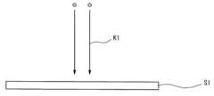
- FIG. 2is a diagram schematically showing the behavior of Cl 2 ⁇ ions.
- Cl - ionsare negatively charged. Therefore, Cl ⁇ ions are accelerated toward the substrate S1 by the bias Vpp. That is, the Cl ⁇ ion moves in the direction of the arrow K1 in FIG. Therefore, Cl ⁇ ions mainly etch the group III nitride semiconductor of the substrate S1 in the vertical direction.
- the vertical directionis a direction perpendicular to the plate surface of the substrate S1.
- FIG. 3is a diagram schematically showing the behavior of Cl radicals.
- the Cl radicalis electrically neutral. Therefore, it is not affected by the surrounding electric field. Therefore, Cl radicals move radially regardless of the bias Vpp. That is, the Cl radical moves in the direction of the arrow K2 in FIG. Therefore, the Cl radicals etch the group III nitride semiconductor of the substrate S1 not only in the vertical direction but also in the horizontal direction.
- the horizontal directionis a direction parallel to the plate surface of the substrate S1. Therefore, it is considered that this radical is involved in the overetching of the group III nitride semiconductor.
- the bias Vppis adjusted according to the state of the plasma product generated in the plasma generation region. As a result, the balance between ions and radicals that reach the substrate S1 is adjusted. This suppresses the narrowing of the group III nitride semiconductor just under the mask.
- B in BCl 3may be bonded to the group III nitride semiconductor at the side surface of the recess of the group III nitride semiconductor.
- the Bmay suppress over-etching on the surface of the group III nitride semiconductor.
- the bias Vppmay be reduced as the flow rate of BCl 3 increases. This is because even if the bias Vpp is reduced and the contribution of radicals is increased, B in BCl 3 is considered to suppress side etching of the group III nitride semiconductor.
- the etching apparatus 1000 according to this embodimentcan etch a group III nitride semiconductor while suppressing overetching. That is, the width of the mask is almost equal to the width of the group III nitride semiconductor below the mask.
- the gas supply unit 1500supplies a first gas that is a chlorine-based mixed gas.
- the first gasis a mixed gas of Cl 2 and BCl 3 .
- the gas supply unit 1500may supply a second gas obtained by mixing a gas containing at least one of a nitrogen gas and a rare gas to the inside of the processing chamber 1001.
- the volume ratio X occupied by the BCl 3is the volume of BCl 3 in the total volume of Cl 2 and BCl 3.
- the plasma generation unit 1300is located inside the processing chamber 1001.
- the plasma generator 1300may be disposed inside a separate chamber outside the processing chamber 1001. However, it is preferable that the plasma generation unit 1300 is arranged at a position not far from the susceptor 1100 on which the substrate S1 is arranged.
- the plasma generator 1300is an ICP unit. However, other plasma generators may be used as the plasma generator 1300.
- the plasma generator 1300may be any one of capacitively coupled plasma (CCP), electron cyclotron resonance plasma (ECR), helicon wave excited plasma (HWP), and microwave excited surface wave plasma (SWP). There may be.
- the susceptor 1100may be rotatable.
- the etching apparatus 1000adjusts the high-frequency potential that the first potential applying unit 1200 applies to the susceptor 1100.
- a first gaswhich is a mixed gas of Cl 2 and BCl 3 is supplied as a plasma gas. Then, the bias applied by the first potential applying unit 1200 is adjusted in accordance with the volume ratio of BCl 3 in the first gas. Thereby, the etching apparatus 1000 can suppress the narrowing of the width of the group III nitride semiconductor immediately below the mask.
- FIG. 4is a scanning micrograph (part 1) showing a cross section of an etched GaN substrate.
- a GaN substrate having a mask formed thereonwas used as the substrate.
- the substrate temperaturewas 400 ° C.
- the output of the plasma generatorwas 400W.
- the frequency of the biaswas 3.2 MHz.
- the bias Vppwas 228V.
- the volume ratio of BCl 3 in the supplied gaswas 0.1.
- the internal pressure of the processing chamber 1001was 5 Pa.
- the etching timewas 30 seconds. In this case, conditional expressions (1) and (2) are satisfied.
- the lateral width of the maskis almost equal to the lateral width of GaN in the lower layer of the mask.
- FIG. 5is a scanning micrograph (part 2) showing a cross section of the etched GaN substrate.
- a GaN substrate having a mask formed thereonwas used as the substrate.
- the substrate temperaturewas 400 ° C.
- the output of the plasma generatorwas 400W.
- the frequency of the biaswas 3.2 MHz.
- the bias Vppwas 228V.
- the only gas suppliedwas chlorine gas.
- the internal pressure of the processing chamber 1001was 5 Pa.
- the etching timewas 10 minutes. In this case, conditional expressions (1) and (2) are not satisfied.
- GaN below the maskis over-etched. That is, the width of a part of GaN below the mask is smaller than the width of the mask.
- FIG. 6is a graph showing the surface roughness of the GaN substrate with respect to the volume ratio of BCl 3 in the first gas.
- the horizontal axis in FIG. 6represents the volume ratio of BCl 3 in the supplied gas. 6 represents the surface roughness of the GaN substrate.
- a GaN substrate having a mask formed thereonwas used as the substrate.
- the substrate temperaturewas 400 ° C.
- the output of the plasma generatorwas 400W.
- the frequency of the biaswas 3.2 MHz.
- the bias Vppwas 230V.
- the internal pressure of the processing chamber 1001was 5 Pa.
- the etching timewas 1 minute.
- the surface roughness when using a mixed gas of Cl 2 and BCl 3is smaller than the surface roughness when using only Cl 2 .
- the volume ratio of BCl 3 in the supplied gasis 0%, the surface roughness is 8 nm.
- the volume ratio of BCl 3 in the supplied gasis 10%, the surface roughness is as small as 1.5 nm.
- the volume ratio of BCl 3 in the mixed gasis 20%, the surface roughness is 4 nm. Therefore, under this condition, the volume ratio of BCl 3 in the mixed gas is preferably about 10%.
- the volume ratio of BCl 3 in the mixed gasis preferably 5% or more and 15% or less.
- FIG. 7is a graph showing the photoluminescence intensity with respect to the volume ratio of BCl 3 in the first gas.
- the horizontal axis in FIG. 7represents the volume ratio of BCl 3 in the supplied gas.
- the vertical axis in FIG. 7is the photoluminescence intensity.
- a GaN substrate having a mask formed thereonwas used as the substrate.
- the substrate temperaturewas 400 ° C.
- the output of the plasma generatorwas 400W.
- the frequency of the biaswas 3.2 MHz.
- the bias Vppwas 230V.
- the internal pressure of the processing chamber 1001was 5 Pa.
- the etching timewas 1 minute.
- the photoluminescence intensitywas about 0.7 regardless of the volume ratio of BCl 3 in the supplied gas.
- FIG. 8is a graph showing the relationship between the volume ratio of BCl 3 in the first gas and the bias Vpp.
- the horizontal axis in FIG. 8is the volume ratio of BCl 3 in the first gas.
- the vertical axis in FIG. 8is the bias Vpp.
- the internal pressure of the processing chamber 1001is 5 Pa.
- the mark “ ⁇ ”indicates that the horizontal etching rate with respect to the vertical etching rate is ⁇ 15% or more and 15% or less.
- the “+” markindicates that the horizontal etching rate with respect to the vertical etching rate is greater than 15%.
- the horizontal etching rate with respect to the vertical etching rateis a positive value, overetching has occurred.
- the horizontal etching rate with respect to the vertical etching rateis a negative value, under-etching has occurred.
- the over-etchingis not so large inside the region R1.
- the horizontal etching rate with respect to the vertical etching rateis ⁇ 15% or more and 15% or less.
- the region R1is represented by the formulas (1) and (2).
- Conditional expressions (1) and (2)are considered applicable when the internal pressure of the processing chamber 1001 is 1 Pa or more and 10 Pa or less.
- DESCRIPTION OF SYMBOLS 1000... Etching apparatus 1001 ... Processing chamber 1100 ... Susceptor 1110 ... Susceptor support part 1120 ... Heating part 1130 ... SiC plate 1200 ... 1st electric potential provision part 1210 ... 1st matching device 1300 ... Plasma generation part 1400 ... 2nd electric potential Giving unit 1410 ... second matching unit 1500 ... gas supply unit 1510 ... gas supply pipe 1600 ... shower plate 1700 ... exhaust port
Landscapes
- Engineering & Computer Science (AREA)
- Physics & Mathematics (AREA)
- Plasma & Fusion (AREA)
- Condensed Matter Physics & Semiconductors (AREA)
- General Physics & Mathematics (AREA)
- Manufacturing & Machinery (AREA)
- Computer Hardware Design (AREA)
- Microelectronics & Electronic Packaging (AREA)
- Power Engineering (AREA)
- Drying Of Semiconductors (AREA)
Abstract
Description
Translated fromJapanese本明細書の技術分野は、III 族窒化物半導体をエッチングするエッチング装置に関する。The technical field of this specification relates to an etching apparatus for etching a group III nitride semiconductor.
GaNに代表されるIII 族窒化物半導体は、例えば、LEDに応用されている。また、III 族窒化物半導体は、高い絶縁破壊強度と、高い耐熱性と、高速動作性と、を備えている。そのため、パワーデバイスとしての応用が期待されている。III-group nitride semiconductors represented by GaN are applied to LEDs, for example. The III-group nitride semiconductor has high dielectric strength, high heat resistance, and high speed operation. Therefore, application as a power device is expected.
III 族窒化物半導体をパワーデバイスに応用する際には、III 族窒化物半導体をエッチングすることがある。その一例として例えば、III 族窒化物半導体にトレンチを形成する場合が挙げられる。そのため、III 族窒化物半導体をエッチングする技術が開発されてきている。例えば、特許文献1には、基板温度を200℃以上600℃以下としてCl2 を含むガスを用いてドライエッチングを行う技術が開示されている。When a group III nitride semiconductor is applied to a power device, the group III nitride semiconductor may be etched. One example is the case where a trench is formed in a group III nitride semiconductor. Therefore, a technique for etching a group III nitride semiconductor has been developed. For example,
しかし、特許文献1の技術では、III 族窒化物半導体がオーバーエッチングするおそれがある。つまり、マスクの下層のIII 族窒化物半導体がやせ細ってしまう。この場合には、その細い箇所の機械的強度は弱い。また、その細い箇所に電界が集中するおそれもある。したがって、III 族窒化物半導体のオーバーエッチングを抑制することが好ましい。However, in the technique of
本明細書の技術は、前述した従来の技術が有する問題点を解決するためになされたものである。その課題とは、III 族窒化物半導体のオーバーエッチングを抑制することを図ったエッチング装置を提供することである。The technology of this specification has been made to solve the problems of the conventional technology described above. The problem is to provide an etching apparatus that is intended to suppress over-etching of the group III nitride semiconductor.
第1の態様におけるエッチング装置は、III 族窒化物半導体をエッチングする処理室と、III 族窒化物半導体を保持する基板保持部と、処理室の内部に第1のガスを供給するガス供給部と、第1のガスをプラズマ化するプラズマ発生部と、基板保持部に高周波電位を付与する第1の電位付与部と、を有する。第1のガスは、Cl2 とBCl3 とを含む塩素系混合ガスである。第1の電位付与部は、第1のガスに占めるBCl3 の体積比が大きいほど、絶対値が小さいバイアスを基板保持部に付与するものである。第1の電位付与部は、
Vpp ≦ -1200・X + 480
Vpp ≧ -1200・X + 290
0.01 ≦ X ≦ 0.4
Vpp:バイアス(V)
X :第1のガスに占めるBCl3 の体積比
を満たすようにバイアスを基板保持部に付与する。An etching apparatus according to a first aspect includes a processing chamber for etching a group III nitride semiconductor, a substrate holding unit for holding a group III nitride semiconductor, and a gas supply unit for supplying a first gas into the processing chamber. And a plasma generating unit that converts the first gas into plasma, and a first potential applying unit that applies a high-frequency potential to the substrate holding unit. The first gas is a chlorine-based mixed gas containing Cl2 and BCl3 . The first potential applying unit applies a bias having a smaller absolute value to the substrate holding unit as the volume ratio of BCl3 in the first gas is larger. The first potential applying unit is
Vpp ≤ -1200 ・ X + 480
Vpp ≧ -1200 ・ X + 290
0.01 ≤ X ≤ 0.4
Vpp: Bias (V)
X: A bias is applied to the substrate holder so as to satisfy the volume ratio of BCl3 in the first gas.
このエッチング装置においては、第1の電位付与部は、第1のガスに占めるBCl3 の体積比が大きいほど、絶対値が小さいバイアスを基板保持部に付与する。そのため、マスク直下のIII 族窒化物半導体をオーバーエッチングするおそれがほとんどない。つまり、マスク直下のIII 族窒化物半導体の幅は、マスクの幅とほとんど同じである。In this etching apparatus, the first potential applying unit applies a bias having a smaller absolute value to the substrate holding unit as the volume ratio of BCl3 in the first gas increases. Therefore, there is almost no possibility of over-etching the group III nitride semiconductor directly under the mask. That is, the width of the group III nitride semiconductor directly under the mask is almost the same as the width of the mask.
本明細書では、III 族窒化物半導体のオーバーエッチングを抑制することを図ったエッチング装置が提供されている。In this specification, there is provided an etching apparatus which is intended to suppress over-etching of a group III group nitride semiconductor.
以下、具体的な実施形態について、エッチング装置を例に挙げて図を参照しつつ説明する。Hereinafter, a specific embodiment will be described with an etching apparatus as an example with reference to the drawings.
(第1の実施形態)
1.エッチング装置
図1は、第1の実施形態のエッチング装置1000の概略構成を示す図である。エッチング装置1000は、処理室1001と、サセプター1100と、サセプター支持部1110と、加熱部1120と、SiCプレート1130と、第1の電位付与部1200と、第1の整合器1210と、プラズマ発生部1300と、第2の電位付与部1400と、第2の整合器1410と、ガス供給部1500と、ガス供給管1510と、シャワープレート1600と、排気口1700と、予備室1800と、を有する。(First embodiment)
1. Etching Apparatus FIG. 1 is a diagram showing a schematic configuration of an
処理室1001は、基板S1のIII 族窒化物半導体をエッチングするための反応室である。基板S1は、III 族窒化物半導体を有する。処理室1001は、基板S1を支持するサセプター1100と、サセプター支持部1110と、SiCプレート1130と、プラズマ発生部1300と、シャワープレート1600と、排気口1700と、を有する。The
サセプター1100は、III 族窒化物半導体を有する基板S1を支持するための基板保持部である。サセプター1100の材質は、例えばSiCである。また、炭素材料にSiCのコーティングを施したものであってもよい。サセプター支持部1110は、サセプター1100を支持するための支持台である。加熱部1120は、サセプター1100を加熱するためのものである。加熱部1120は、サセプター1100を介して基板S1を加熱することとなる。The
第1の電位付与部1200は、サセプター1100に高周波電位を付与するためのものである。そのため、第1の電位付与部1200は、サセプター1100を介して基板S1に電位を付与することができる。第1の電位付与部1200における高周波電位の周波数は、例えば、13.56MHzである。もちろん、これ以外の周波数であってもよい。第1の整合器1210は、第1の電位付与部1200とサセプター1100との間に配置されている。つまり、第1の電位付与部1200は、第1の整合器1210を介してサセプター1100に接続されている。The first
プラズマ発生部1300は、処理室1001の内部であってサセプター1100と対面する位置にプラズマを発生させるためのものである。プラズマ発生部1300は、後述する第1のガスをプラズマ化する。プラズマ発生部1300は、誘導結合プラズマ(ICP)を発生させるICPユニットである。The
第2の電位付与部1400は、プラズマ発生部1300に高周波電位を付与するためのものである。第2の電位付与部1400における高周波電位の周波数は、例えば、27.12MHzである。もちろん、これ以外の周波数であってもよい。第2の整合器1410は、第2の電位付与部1400とプラズマ発生部1300との間に配置されている。つまり、第2の電位付与部1400は、第2の整合器1410を介してプラズマ発生部1300に接続されている。The second
ガス供給部1500は、処理室1001の内部に第1のガスを供給するためのものである。ここで、第1のガスは、Cl2 とBCl3 との混合ガスである。ガス供給管1510は、ガス供給部1500と処理室1001とを連結するための流路である。ガス供給部1500は、第1のガスを予備室1800に供給する。その後、第1のガスは、予備室1800からシャワープレート1600を通過してプラズマ発生部1300の箇所に到達する。シャワープレート1600は、第1のガスを整流する整流板である。排気口1700は、処理室1001からガスを排出するためのものである。The
2.エッチング方法
第1の実施形態のエッチング装置1000を用いる。まず、エッチング装置1000のサセプター1100に基板S1を配置する。次に、エッチング装置1000を真空引きする。そして、ガス供給部1500が、Cl2 とBCl3 との混合ガスである第1のガスを処理室1001の内部に供給する。そして、第1の電位付与部1200が、サセプター1100に高周波のバイアスVppを付与する。第2の電位付与部1400が、プラズマ発生部1300に高周波電位を付与する。これにより、プラズマ発生部1300が処理室1001の内部にプラズマを発生させる。そして、第1のガスはプラズマ化され、プラズマ生成領域からプラズマ生成物が発生する。プラズマ生成物とは、BおよびClに由来するイオンおよびラジカルと、紫外線とを含む。そして、このようなイオンおよびラジカルが基板S1のIII 族窒化物半導体をエッチングする。2. Etching Method The
2-1.エッチング条件1
エッチング条件を表1に示す。ガス供給部1500は、第1のガスを処理室1001の内部に供給する。ここで、第1のガスは、塩素系混合ガスである。より具体的には、第1のガスは、Cl2 とBCl3 との混合ガスである。この第1のガスに占めるBCl3 の体積比は、0.01以上0.4以下である。ここで、第1のガスに占めるBCl3 の体積比は、処理室1001に導入する第1のガスに占めるBCl3 の流量比と同じである。処理室1001の内圧は1Pa以上10Pa以下である。処理室1001の内圧がこの範囲内のときには、プラズマ発生部1300により発生されるプラズマは誘導結合プラズマである。バイアスVppは、0V以上468V以下である。バイアスVppの周波数は、1MHz以上100MHz以下の程度である。プラズマ発生部1300の出力は、200W以上800W以下の程度である。基板温度は、300℃以上500℃以下である。2-1.
The etching conditions are shown in Table 1. The
[表1]
内圧 1Pa以上 10Pa以下
BCl3 の体積比 0.01以上 0.4以下
バイアス 0V以上 468V以下[Table 1]
2-2.エッチング条件2
第1のガスに占めるBCl3 の体積比が大きいほど、第1の電位付与部1200がサセプター1100に付与するバイアスVppの絶対値は小さい。2-2.
The larger the volume ratio of BCl3 occupying the first gas, the smaller the absolute value of the bias Vpp applied to the
第1の電位付与部1200は、次式を満たすバイアスVppをサセプター1100に付与する。
Vpp ≦ -1200・X + 480 ………(1)
Vpp ≧ -1200・X + 290 ………(2)
0.01 ≦ X ≦ 0.4
Vpp:バイアス(V)
X :第1のガスに占めるBCl3 の体積比The first
Vpp ≤ -1200 · X + 480 (1)
Vpp ≧ −1200 · X + 290 (2)
0.01 ≤ X ≤ 0.4
Vpp: Bias (V)
X: volume ratio of BCl3 in the first gas
この場合に、III 族窒化物半導体は好適にエッチングされる。III 族窒化物半導体がオーバーエッチングされるおそれはほとんどない。In this case, the III-group nitride semiconductor is preferably etched. There is almost no risk that the group III nitride semiconductor is over-etched.
2-3.エッチング条件3
ガス供給部1500は、第1のガスに占めるBCl3 の体積比を2%以上30%以下とするとなおよい。つまり、ガス供給部1500が供給する第1のガスは次式を満たす。
0.02 ≦ X ≦ 0.32-3. Etching condition 3
In the
0.02 ≤ X ≤ 0.3
この場合に、III 族窒化物半導体はさらに好適にエッチングされる。III 族窒化物半導体がオーバーエッチングされるおそれはほとんどない。In this case, the III-group nitride semiconductor is more preferably etched. There is almost no risk that the group III nitride semiconductor is over-etched.
3.プラズマ生成物とバイアスとの関係
ここで、プラズマ生成物とバイアスとの関係について説明する。プラズマ生成物のうち、イオンとラジカルとについて説明する。イオンを代表してCl- について説明する。ラジカルを代表してClラジカルについて説明する。3. Relationship between Plasma Product and Bias Here, the relationship between the plasma product and the bias will be described. Among the plasma products, ions and radicals will be described. Cl- will be described as a representative of ions. The Cl radical will be described as a representative of the radical.
3-1.イオンの振る舞い
図2は、Cl- イオンの振る舞いを模式的に示す図である。Cl- イオンは、負に帯電している。そのため、バイアスVppにより、Cl- イオンは基板S1に向かって加速される。つまり、Cl- イオンは、図2の矢印K1の向きに移動する。そのため、Cl- イオンは、基板S1のIII 族窒化物半導体を主に縦方向にエッチングする。ここで縦方向とは、基板S1の板面に垂直な方向である。3-1. Ion Behavior FIG. 2 is a diagram schematically showing the behavior of
3-2.ラジカルの振る舞い
図3は、Clラジカルの振る舞いを模式的に示す図である。Clラジカルは、電気的に中性である。そのため、周囲の電界の影響を受けない。したがって、Clラジカルは、バイアスVppによらず放射状に移動する。つまり、Clラジカルは、図3の矢印K2の向きに移動する。そのため、Clラジカルは、基板S1のIII 族窒化物半導体を縦方向のみならず横方向にエッチングする。ここで横方向とは、基板S1の板面に平行な方向である。したがって、このラジカルがIII 族窒化物半導体のオーバーエッチングに関与していると考えられる。3-2. Radical Behavior FIG. 3 is a diagram schematically showing the behavior of Cl radicals. The Cl radical is electrically neutral. Therefore, it is not affected by the surrounding electric field. Therefore, Cl radicals move radially regardless of the bias Vpp. That is, the Cl radical moves in the direction of the arrow K2 in FIG. Therefore, the Cl radicals etch the group III nitride semiconductor of the substrate S1 not only in the vertical direction but also in the horizontal direction. Here, the horizontal direction is a direction parallel to the plate surface of the substrate S1. Therefore, it is considered that this radical is involved in the overetching of the group III nitride semiconductor.
3-3.バイアスとエッチング
本実施形態では、プラズマ生成領域で発生するプラズマ生成物の状態に応じて、バイアスVppを調整する。これにより、基板S1に到達するイオンとラジカルとのバランスを調整する。これにより、マスク直下のIII 族窒化物半導体の幅が狭くなることを抑制する。3-3. Bias and Etching In this embodiment, the bias Vpp is adjusted according to the state of the plasma product generated in the plasma generation region. As a result, the balance between ions and radicals that reach the substrate S1 is adjusted. This suppresses the narrowing of the group III nitride semiconductor just under the mask.
3-4.BCl3 の作用
また、エッチングにおいて、BCl3 のBがIII 族窒化物半導体の凹部の側面でIII 族窒化物半導体と結合する可能性がある。そして、そのBがIII 族窒化物半導体の表面でオーバーエッチングを抑制している可能性がある。そのため、BCl3 の流量が多いほど、バイアスVppを小さくしてもよいと考えられる。バイアスVppを小さくしてラジカルの寄与を大きくしても、BCl3 のBがIII 族窒化物半導体のサイドエッチングを抑制すると考えられるからである。または、BCl3 の流量が多いほど、Cl- イオンが多く発生すると考えられる。そのため、バイアスVppをそれほど大きくする必要がないと考えられる。3-4. Effect of BCl3 In etching, B in BCl3 may be bonded to the group III nitride semiconductor at the side surface of the recess of the group III nitride semiconductor. The B may suppress over-etching on the surface of the group III nitride semiconductor. For this reason, it is considered that the bias Vpp may be reduced as the flow rate of BCl3 increases. This is because even if the bias Vpp is reduced and the contribution of radicals is increased, B in BCl3 is considered to suppress side etching of the group III nitride semiconductor. Alternatively, it is considered that as the flow rate of BCl3 increases, more Cl− ions are generated. Therefore, it is considered that it is not necessary to increase the bias Vpp so much.
4.本実施形態の効果
本実施形態のエッチング装置1000は、オーバーエッチングを抑制しつつIII 族窒化物半導体をエッチングすることができる。つまり、マスクの幅と、マスクより下層のIII 族窒化物半導体の幅とが、ほとんど等しい。4). Effects of this Embodiment The
5.変形例
5-1.希ガスまたは窒素ガス
ガス供給部1500は、塩素系混合ガスである第1のガスを供給する。第1のガスはCl2 とBCl3 との混合ガスである。ガス供給部1500は、第1のガスに窒素ガスと希ガスとの少なくとも一方を含むガスを混合した第2のガスを処理室1001の内部に供給してもよい。ただし、BCl3 が占める体積比Xは、Cl2 とBCl3 との合計の体積に占めるBCl3 の体積である。5). Modified example 5-1. Rare gas or nitrogen gas The
5-2.プラズマ発生部の位置
本実施形態では、プラズマ発生部1300は、処理室1001の内部に位置している。プラズマ発生部1300は、処理室1001の外部の別室の内部に配置されていてもよい。ただし、プラズマ発生部1300は、基板S1を配置するサセプター1100からそれほど遠くない位置に配置されていることが好ましい。5-2. Position of Plasma Generation Unit In the present embodiment, the
5-3.プラズマ発生部の種類
本実施形態では、プラズマ発生部1300はICPユニットである。しかし、プラズマ発生部1300としてその他のプラズマ発生装置を用いてもよい。例えば、プラズマ発生部1300は、容量結合型プラズマ(CCP)と、電子サイクロトロン共鳴プラズマ(ECR)と、ヘリコン波励起プラズマ(HWP)と、マイクロ波励起表面波プラズマ(SWP)と、のいずれかであってもよい。5-3. Types of Plasma Generator In this embodiment, the
5-4.サセプター
サセプター1100は、回転できるようになっていてもよい。5-4. Susceptor The
5-5.組み合わせ
上記の変形例を自由に組み合わせてもよい。5-5. Combination The above modification examples may be freely combined.
6.本実施形態のまとめ
本実施形態のエッチング装置1000は、第1の電位付与部1200がサセプター1100に付与する高周波電位を調整する。プラズマガスとしてCl2 とBCl3 との混合ガスである第1のガスを供給する。そして、この第1のガスに占めるBCl3 の体積比に応じて、第1の電位付与部1200が付与するバイアスを調整する。これにより、エッチング装置1000は、マスクの直下のIII 族窒化物半導体の幅が狭くなることを抑制することができる。6). Summary of this Embodiment The
1.実験1(オーバーエッチングがない場合)
図4は、エッチングしたGaN基板の断面を示す走査型顕微鏡写真(その1)である。基板としてマスクを形成済みのGaN基板を用いた。基板温度は400℃であった。プラズマ発生部の出力は400Wであった。バイアスの周波数は3.2MHzであった。バイアスVppは228Vであった。供給するガスにおけるBCl3 の体積比は0.1であった。また、処理室1001の内圧は5Paであった。エッチング時間は30秒であった。この場合には、条件式(1)、(2)を満たしている。1. Experiment 1 (when there is no overetching)
FIG. 4 is a scanning micrograph (part 1) showing a cross section of an etched GaN substrate. A GaN substrate having a mask formed thereon was used as the substrate. The substrate temperature was 400 ° C. The output of the plasma generator was 400W. The frequency of the bias was 3.2 MHz. The bias Vpp was 228V. The volume ratio of BCl3 in the supplied gas was 0.1. Moreover, the internal pressure of the
図4に示すようにこの場合には、マスクの横幅と、マスクの下層のGaNの横幅と、がほとんど等しい。As shown in FIG. 4, in this case, the lateral width of the mask is almost equal to the lateral width of GaN in the lower layer of the mask.
2.実験2(オーバーエッチングがある場合)
図5は、エッチングしたGaN基板の断面を示す走査型顕微鏡写真(その2)である。基板としてマスクを形成済みのGaN基板を用いた。基板温度は400℃であった。プラズマ発生部の出力は400Wであった。バイアスの周波数は3.2MHzであった。バイアスVppは228Vであった。供給するガスは、塩素ガスのみであった。また、処理室1001の内圧は5Paであった。エッチング時間は10分であった。この場合には、条件式(1)、(2)を満たしていない。2. Experiment 2 (when there is over-etching)
FIG. 5 is a scanning micrograph (part 2) showing a cross section of the etched GaN substrate. A GaN substrate having a mask formed thereon was used as the substrate. The substrate temperature was 400 ° C. The output of the plasma generator was 400W. The frequency of the bias was 3.2 MHz. The bias Vpp was 228V. The only gas supplied was chlorine gas. Moreover, the internal pressure of the
図5に示すように、この場合には、マスクより下層のGaNがオーバーエッチングされている。つまり、マスクより下層のGaNの一部の幅が、マスクの幅より小さい。As shown in FIG. 5, in this case, GaN below the mask is over-etched. That is, the width of a part of GaN below the mask is smaller than the width of the mask.
3.実験3(表面粗さ)
図6は、第1のガスに占めるBCl3 の体積比に対するGaN基板の表面粗さを示すグラフである。図6の横軸は供給するガスに占めるBCl3 の体積比である。図6の縦軸はGaN基板の表面粗さである。基板としてマスクを形成済みのGaN基板を用いた。基板温度は400℃であった。プラズマ発生部の出力は400Wであった。バイアスの周波数は3.2MHzであった。バイアスVppは230Vであった。また、処理室1001の内圧は5Paであった。エッチング時間は1分であった。3. Experiment 3 (Surface roughness)
FIG. 6 is a graph showing the surface roughness of the GaN substrate with respect to the volume ratio of BCl3 in the first gas. The horizontal axis in FIG. 6 represents the volume ratio of BCl3 in the supplied gas. 6 represents the surface roughness of the GaN substrate. A GaN substrate having a mask formed thereon was used as the substrate. The substrate temperature was 400 ° C. The output of the plasma generator was 400W. The frequency of the bias was 3.2 MHz. The bias Vpp was 230V. Moreover, the internal pressure of the
図6に示すように、Cl2 とBCl3 との混合ガスを用いた場合の表面粗さは、Cl2 のみを用いた場合の表面粗さよりも小さい。供給するガスに占めるBCl3 の体積比が0%の場合に、表面粗さが8nmである。供給するガスに占めるBCl3 の体積比が10%の場合に、表面粗さが1.5nmと最も小さい。混合ガスに占めるBCl3 の体積比が20%の場合に、表面粗さが4nmである。そのため、この条件下では、混合ガスに占めるBCl3 の体積比を10%程度とすることが好ましい。例えば、混合ガスに占めるBCl3 の体積比を5%以上15%以下とすることが好ましい。As shown in FIG. 6, the surface roughness when using a mixed gas of Cl2 and BCl3 is smaller than the surface roughness when using only Cl2 . When the volume ratio of BCl3 in the supplied gas is 0%, the surface roughness is 8 nm. When the volume ratio of BCl3 in the supplied gas is 10%, the surface roughness is as small as 1.5 nm. When the volume ratio of BCl3 in the mixed gas is 20%, the surface roughness is 4 nm. Therefore, under this condition, the volume ratio of BCl3 in the mixed gas is preferably about 10%. For example, the volume ratio of BCl3 in the mixed gas is preferably 5% or more and 15% or less.
4.実験4(フォトルミネッセンス)
図7は、第1のガスに占めるBCl3 の体積比に対するフォトルミネッセンス強度を示すグラフである。図7の横軸は供給するガスに占めるBCl3 の体積比である。図7の縦軸はフォトルミネッセンス強度である。基板としてマスクを形成済みのGaN基板を用いた。基板温度は400℃であった。プラズマ発生部の出力は400Wであった。バイアスの周波数は3.2MHzであった。バイアスVppは230Vであった。また、処理室1001の内圧は5Paであった。エッチング時間は1分であった。4). Experiment 4 (Photoluminescence)
FIG. 7 is a graph showing the photoluminescence intensity with respect to the volume ratio of BCl3 in the first gas. The horizontal axis in FIG. 7 represents the volume ratio of BCl3 in the supplied gas. The vertical axis in FIG. 7 is the photoluminescence intensity. A GaN substrate having a mask formed thereon was used as the substrate. The substrate temperature was 400 ° C. The output of the plasma generator was 400W. The frequency of the bias was 3.2 MHz. The bias Vpp was 230V. Moreover, the internal pressure of the
図7に示すように、供給するガスに占めるBCl3 の体積比によらず、フォトルミネッセンス強度はおよそ0.7程度であった。As shown in FIG. 7, the photoluminescence intensity was about 0.7 regardless of the volume ratio of BCl3 in the supplied gas.
5.実験5(バイアス)
5-1.5Paの場合
図8は、第1のガスに占めるBCl3 の体積比とバイアスVppとの間の関係を示すグラフである。図8の横軸は第1のガスに占めるBCl3 の体積比である。図8の縦軸はバイアスVppである。このときの処理室1001の内圧は5Paである。5). Experiment 5 (bias)
In the case of 5-1.5 Pa FIG. 8 is a graph showing the relationship between the volume ratio of BCl3 in the first gas and the bias Vpp. The horizontal axis in FIG. 8 is the volume ratio of BCl3 in the first gas. The vertical axis in FIG. 8 is the bias Vpp. At this time, the internal pressure of the
図8において、「○」印は、縦エッチングレートに対する横エッチングレートが-15%以上15%以下である点を示している。「+」印は、縦エッチングレートに対する横エッチングレートが15%より大きい点を示している。ここで、縦エッチングレートに対する横エッチングレートが正の値の場合には、オーバーエッチングが生じている。縦エッチングレートに対する横エッチングレートが負の値の場合には、アンダーエッチングが生じている。図8に示すように、領域R1の内部ではオーバーエッチングはそれほど大きくない。領域R1においては、縦エッチングレートに対する横エッチングレートは、-15%以上15%以下である。領域R1は、式(1)、(2)で表される。In FIG. 8, the mark “◯” indicates that the horizontal etching rate with respect to the vertical etching rate is −15% or more and 15% or less. The “+” mark indicates that the horizontal etching rate with respect to the vertical etching rate is greater than 15%. Here, when the horizontal etching rate with respect to the vertical etching rate is a positive value, overetching has occurred. When the horizontal etching rate with respect to the vertical etching rate is a negative value, under-etching has occurred. As shown in FIG. 8, the over-etching is not so large inside the region R1. In the region R1, the horizontal etching rate with respect to the vertical etching rate is −15% or more and 15% or less. The region R1 is represented by the formulas (1) and (2).
条件式(1)、(2)は、処理室1001の内圧が1Pa以上10Pa以下の場合に適用できると考えられる。Conditional expressions (1) and (2) are considered applicable when the internal pressure of the
1000…エッチング装置
1001…処理室
1100…サセプター
1110…サセプター支持部
1120…加熱部
1130…SiCプレート
1200…第1の電位付与部
1210…第1の整合器
1300…プラズマ発生部
1400…第2の電位付与部
1410…第2の整合器
1500…ガス供給部
1510…ガス供給管
1600…シャワープレート
1700…排気口
DESCRIPTION OF
Claims (3)
Translated fromJapanese前記III 族窒化物半導体を保持する基板保持部と、
前記処理室の内部に第1のガスを供給するガス供給部と、
前記第1のガスをプラズマ化するプラズマ発生部と、
前記基板保持部に高周波電位を付与する第1の電位付与部と、
を有し、
前記第1のガスは、
Cl2 とBCl3 とを含む塩素系混合ガスであり、
前記第1の電位付与部は、
前記第1のガスに占めるBCl3 の体積比が大きいほど、
絶対値が小さいバイアスを前記基板保持部に付与するものであり、
前記第1の電位付与部は、
Vpp ≦ -1200・X + 480
Vpp ≧ -1200・X + 290
0.01 ≦ X ≦ 0.4
Vpp:バイアス(V)
X :第1のガスに占めるBCl3 の体積比
を満たすようにバイアスを前記基板保持部に付与すること
を特徴とするエッチング装置。A processing chamber for etching a group III nitride semiconductor;
A substrate holder for holding the group III nitride semiconductor;
A gas supply unit for supplying a first gas into the processing chamber;
A plasma generating section for converting the first gas into plasma;
A first potential applying unit that applies a high-frequency potential to the substrate holding unit;
Have
The first gas is
A chlorine-based mixed gas containing Cl2 and BCl3 ;
The first potential applying unit includes:
The larger the volume ratio of BCl3 in the first gas,
A bias having a small absolute value is applied to the substrate holder,
The first potential applying unit includes:
Vpp ≤ -1200 ・ X + 480
Vpp ≧ -1200 ・ X + 290
0.01 ≤ X ≤ 0.4
Vpp: Bias (V)
X: An etching apparatus that applies a bias to the substrate holder so as to satisfy a volume ratio of BCl3 in the first gas.
前記ガス供給部は、
0.02 ≦ X ≦ 0.3
を満たすように前記第1のガスを前記処理室の内部に供給すること
を特徴とするエッチング装置。The etching apparatus according to claim 1,
The gas supply unit
0.02 ≤ X ≤ 0.3
An etching apparatus, wherein the first gas is supplied into the processing chamber so as to satisfy the condition.
前記ガス供給部は、
前記第1のガスにN2 と希ガスとの少なくとも一方を含むガスを混合した第2のガスを前記処理室の内部に供給すること
を特徴とするエッチング装置。
The etching apparatus according to claim 1 or 2,
The gas supply unit
An etching apparatus, wherein a second gas obtained by mixing the first gas with a gas containing at least one of N2 and a rare gas is supplied into the processing chamber.
Priority Applications (1)
| Application Number | Priority Date | Filing Date | Title |
|---|---|---|---|
| CN201880017000.9ACN110402480B (en) | 2017-03-10 | 2018-02-28 | Etching apparatus |
Applications Claiming Priority (2)
| Application Number | Priority Date | Filing Date | Title |
|---|---|---|---|
| JP2017046325AJP6871550B2 (en) | 2017-03-10 | 2017-03-10 | Etching device |
| JP2017-046325 | 2017-03-10 |
Publications (1)
| Publication Number | Publication Date |
|---|---|
| WO2018163931A1true WO2018163931A1 (en) | 2018-09-13 |
Family
ID=63448198
Family Applications (1)
| Application Number | Title | Priority Date | Filing Date |
|---|---|---|---|
| PCT/JP2018/007503CeasedWO2018163931A1 (en) | 2017-03-10 | 2018-02-28 | Etching device |
Country Status (3)
| Country | Link |
|---|---|
| JP (1) | JP6871550B2 (en) |
| CN (1) | CN110402480B (en) |
| WO (1) | WO2018163931A1 (en) |
Citations (5)
| Publication number | Priority date | Publication date | Assignee | Title |
|---|---|---|---|---|
| JPH09129930A (en)* | 1995-08-31 | 1997-05-16 | Toshiba Corp | Method for manufacturing blue light emitting device using compound semiconductor |
| JP2004022974A (en)* | 2002-06-19 | 2004-01-22 | Hitachi High-Technologies Corp | Etching method |
| JP2006108268A (en)* | 2004-10-04 | 2006-04-20 | Oki Electric Ind Co Ltd | Ferroelectric capacitor structure and manufacturing method thereof |
| US20110243520A1 (en)* | 2007-07-31 | 2011-10-06 | Gayle Murdoch | Optical waveguide structure and method of manufacture thereof |
| JP2017022368A (en)* | 2015-06-05 | 2017-01-26 | ラム リサーチ コーポレーションLam Research Corporation | Atomic layer etching of GaN and other III-V materials |
Family Cites Families (6)
| Publication number | Priority date | Publication date | Assignee | Title |
|---|---|---|---|---|
| KR100268640B1 (en)* | 1996-01-22 | 2000-10-16 | 모리시타 요이찌 | Dry etching method of aluminum alloy film and etching gas used in the method |
| JP3520919B2 (en)* | 2001-03-27 | 2004-04-19 | 士郎 酒井 | Method for manufacturing nitride semiconductor device |
| CN103854992A (en)* | 2012-11-30 | 2014-06-11 | 北京北方微电子基地设备工艺研究中心有限责任公司 | Substrate etching method |
| JP6153755B2 (en)* | 2013-04-03 | 2017-06-28 | 東京エレクトロン株式会社 | Plasma processing method and plasma processing apparatus |
| JP5927543B2 (en)* | 2013-07-24 | 2016-06-01 | パナソニックIpマネジメント株式会社 | Device isolation method of GaN layer |
| CN104201104A (en)* | 2014-09-09 | 2014-12-10 | 电子科技大学 | Manufacturing method for gallium nitride-based enhanced device |
- 2017
- 2017-03-10JPJP2017046325Apatent/JP6871550B2/enactiveActive
- 2018
- 2018-02-28WOPCT/JP2018/007503patent/WO2018163931A1/ennot_activeCeased
- 2018-02-28CNCN201880017000.9Apatent/CN110402480B/enactiveActive
Patent Citations (5)
| Publication number | Priority date | Publication date | Assignee | Title |
|---|---|---|---|---|
| JPH09129930A (en)* | 1995-08-31 | 1997-05-16 | Toshiba Corp | Method for manufacturing blue light emitting device using compound semiconductor |
| JP2004022974A (en)* | 2002-06-19 | 2004-01-22 | Hitachi High-Technologies Corp | Etching method |
| JP2006108268A (en)* | 2004-10-04 | 2006-04-20 | Oki Electric Ind Co Ltd | Ferroelectric capacitor structure and manufacturing method thereof |
| US20110243520A1 (en)* | 2007-07-31 | 2011-10-06 | Gayle Murdoch | Optical waveguide structure and method of manufacture thereof |
| JP2017022368A (en)* | 2015-06-05 | 2017-01-26 | ラム リサーチ コーポレーションLam Research Corporation | Atomic layer etching of GaN and other III-V materials |
Also Published As
| Publication number | Publication date |
|---|---|
| CN110402480B (en) | 2023-03-10 |
| CN110402480A (en) | 2019-11-01 |
| JP6871550B2 (en) | 2021-05-12 |
| JP2018152415A (en) | 2018-09-27 |
Similar Documents
| Publication | Publication Date | Title |
|---|---|---|
| JP6449674B2 (en) | Plasma processing method and plasma processing apparatus | |
| CN106067418B (en) | Etching treatment method | |
| JP4388020B2 (en) | Semiconductor plasma processing apparatus and method | |
| TW202022917A (en) | Apparatus and process for electron beam mediated plasma etch and deposition processes | |
| JPH1041281A (en) | Plasma treating apparatus | |
| JP2013131587A (en) | Plasma processing method | |
| TW202316520A (en) | Etching method and etching device | |
| CN105810582A (en) | Etching method | |
| CN113053745B (en) | Etching method and etching apparatus | |
| JP2022115719A (en) | Plasma processing apparatus and plasma processing method | |
| WO2018163931A1 (en) | Etching device | |
| TW202412101A (en) | Etching method and plasma treatment device | |
| JP5774356B2 (en) | Plasma processing method | |
| JP7184252B2 (en) | Etching method and etching apparatus | |
| JP2022158811A (en) | Etching method and etching processing apparatus | |
| CN105810579A (en) | Etching method | |
| JP7737401B2 (en) | Plasma processing method and plasma processing apparatus | |
| TWI897888B (en) | Methods and apparatus for processing a substrate | |
| JP5918886B2 (en) | Plasma processing method | |
| KR100800726B1 (en) | Wafer Plasma Etch Chamber and Etching Method Using the Same | |
| TW202333224A (en) | Etching method and plasma processing apparatus | |
| TW202147925A (en) | Plasma processing apparatus and plasma processing | |
| WO2024070578A1 (en) | Plasma processing device and power supply system | |
| TW202121933A (en) | Methods and apparatus for processing a substrate | |
| JP2023032693A (en) | Etching method and plasma etching device |
Legal Events
| Date | Code | Title | Description |
|---|---|---|---|
| 121 | Ep: the epo has been informed by wipo that ep was designated in this application | Ref document number:18763169 Country of ref document:EP Kind code of ref document:A1 | |
| NENP | Non-entry into the national phase | Ref country code:DE | |
| 122 | Ep: pct application non-entry in european phase | Ref document number:18763169 Country of ref document:EP Kind code of ref document:A1 |