WO2018150478A1 - Substrate inspection probe and substrate inspection device, and substrate inspection method using same - Google Patents
Substrate inspection probe and substrate inspection device, and substrate inspection method using sameDownload PDFInfo
- Publication number
- WO2018150478A1 WO2018150478A1PCT/JP2017/005415JP2017005415WWO2018150478A1WO 2018150478 A1WO2018150478 A1WO 2018150478A1JP 2017005415 WJP2017005415 WJP 2017005415WWO 2018150478 A1WO2018150478 A1WO 2018150478A1
- Authority
- WO
- WIPO (PCT)
- Prior art keywords
- contact
- inspection
- probe
- substrate
- substrate inspection
- Prior art date
- Legal status (The legal status is an assumption and is not a legal conclusion. Google has not performed a legal analysis and makes no representation as to the accuracy of the status listed.)
- Ceased
Links
Images


Classifications
- G—PHYSICS
- G01—MEASURING; TESTING
- G01R—MEASURING ELECTRIC VARIABLES; MEASURING MAGNETIC VARIABLES
- G01R31/00—Arrangements for testing electric properties; Arrangements for locating electric faults; Arrangements for electrical testing characterised by what is being tested not provided for elsewhere
- G01R31/50—Testing of electric apparatus, lines, cables or components for short-circuits, continuity, leakage current or incorrect line connections
- G—PHYSICS
- G01—MEASURING; TESTING
- G01R—MEASURING ELECTRIC VARIABLES; MEASURING MAGNETIC VARIABLES
- G01R1/00—Details of instruments or arrangements of the types included in groups G01R5/00 - G01R13/00 and G01R31/00
- G01R1/02—General constructional details
- G01R1/06—Measuring leads; Measuring probes
- G01R1/067—Measuring probes
Definitions
- the present inventionrelates to a substrate inspection probe, a substrate inspection apparatus, and a substrate inspection method using the same, and in particular, a substrate inspection probe and a substrate in which a tip is brought into direct contact with terminal electrodes of small surface-mounted components.
- the present inventionrelates to an inspection apparatus and a substrate inspection method using them.
- the circuit board inspection apparatushas a test land of a predetermined area and shape in a pattern connected to a mounted device (hereinafter, also referred to as “part to be inspected”) of a circuit board to be inspected (hereinafter, also referred to as “inspection board”). Is provided. By bringing the probe of the substrate inspection apparatus into contact with the test land, the inspection circuit connected to the probe and the part to be inspected are connected in an inspectable manner.
- the circuit boardsave a space for installing a test land.
- the portion where the electrode of the inspected part is mounted by the solder 16is a contact portion replaced with the test land.
- the solder 16 for that electrodeThe area, that is, the area where the fillet can be viewed in plan. It is easy and reliable to contact the probe as a contact that replaces the fillet with a test land. According to the current technology, it is possible to bring the probe into contact with the fillet connected to the electrode up to "1005" (planar view 1.0 mm ⁇ 0.5 mm).
- the filletsbecome so small that they can not be viewed in a plan view. Therefore, the fillets are used as contact portions instead of test lands. Contacting the probe with the probe is difficult and uncertain.
- the number of test substrates on which a large number of ultra-small chip parts (planar view 0.4 mm ⁇ 0.2 mm) and (planar view 0.2 mm ⁇ 0.1 mm) are adoptedis also increasing. Furthermore, if the microminiaturization is performed to the extent of "0.42" (0.4 mm.times.0.2 mm) or "0201" (0.2 mm.times.0.1 mm), the fillet will be hidden. In this case, it is impossible to bring the probe into contact as a contact in place of the test land.
- the probe unitis disposed on one side of the circuit board, the probe unit is disposed on the other side of the circuit board, and the probe unit is disposed on the contact point defined on the wiring pattern. It is configured to contact two corresponding ones of the probes.
- the corresponding two of the probes of the probe unitare brought into contact with the contact points defined on the wiring pattern, and the probes brought into contact with the contact points are shorted.
- circuit board inspection method and circuit board inspection apparatus described in Patent Document 1is a technique for improving the inspection accuracy for a circuit board including through holes, and easily and reliably contacts electrodes of a microminiature chip component. It is not a possible substrate inspection probe, a substrate inspection apparatus, and a substrate inspection method using them.
- the configurationincludes a current supply needle pin and a voltage measurement needle pin each formed with a tip surface that intersects with the axis of each needle pin at an angle, and a holding member that holds the needle pins together. Further, the holding member holds the current supply needle pin and the voltage measurement needle pin in parallel with a minute interval, and is disposed in the direction in which the tops of the tip surfaces are adjacent to each other.
- the substrate inspection probe described in Patent Document 2 and the substrate inspection apparatus using themalso use the substrate inspection probe, the substrate inspection apparatus, and the like that can easily and reliably contact the electrode of the microminiature chip component. It was not a board inspection method.
- circuit board inspection apparatuscapable of inspecting the mounting state of a chip component such as a bypass capacitor by merely bringing a probe into contact with the chip component without using expensive equipment such as image processing ( See, for example, Patent Document 3).
- a circuit board inspection apparatuscapable of inspecting the mounting state of a chip component such as a bypass capacitor by merely bringing a probe into contact with the chip component without using expensive equipment such as image processing ( See, for example, Patent Document 3).
- the first probeis configured to include a cylindrical probe selectively connected to the measuring means via the switch means, and a probe pin inserted into the cylindrical probe and biased by a spring.
- the cylindrical probeis connected to the measuring means by the switch means described above, and the inclined surface is brought into contact with one of the lead electrodes of the chip part and the second probe is brought into contact with the wiring pattern connected to the solder pad on the lead electrode side.
- the measuring meansmeasures the electrical state between the tubular probe and the second probe.
- the circuit board inspection apparatus described in Patent Document 3is a technology for inspecting whether chip components are mounted on solder pads on the circuit substrate side, and is easy to use for electrodes of microminiature chip components. And it was not the probe for board
- the present inventionhas been made in view of such circumstances, and an object of the present invention is to provide a substrate inspection probe which can be easily and reliably brought into contact with an electrode of a very small surface-mounted component. More specifically, the surface has been miniaturized to a certain extent (for example, 0.6 mm ⁇ 0.3 mm in plan view for chip parts, and 0.4 mm between terminals for QFP in QFP), and the surface has become so small that the fillet can not be viewed in plan It is an object of the present invention to provide a substrate inspection probe, a substrate inspection apparatus, and a substrate inspection method using them, wherein the electrode of the mounted component is a contact portion replaced with a test land and the probe can be easily and reliably contacted. Do.
- the present inventionhas been made to achieve such an object, and the invention according to claim 1 is a contact member (10, 20, 30, 40) a substrate inspection probe (77, 78, 79, 80) electrically connected to the inspection circuit (90) by contact with the inspection circuit (90),
- the contact body (10, 20, 30, 40)is a tip (13, 14, 23, 24, 32, 33, 34) of each of a pair of contact members (11, 12, 21, 22, 21, 31, 42, 41).
- the convex portion (18) or the concave portion (17)is a terminal electrode (1, 2, 51, 52) of the surface mounted component (50, R1, C1, R2, C2) mounted on the inspection substrate (70).
- the contact body (10)is attached to the surface mounted component (50, R1, C1, R2, C2) As well as being positioned against A substrate inspection probe (77, 78, 79) configured such that the contact electrode (12) is in electrical contact with the other of the terminal electrodes (1, 2, 51, 52) to be electrically connected to the inspection circuit (90). , 80).
- the invention according to claim 2is the substrate inspection probe (77) according to claim 1, wherein the contact body (20) is a tip (23, 24) of each of a pair of contact members (21, 22) A mountain-shaped convex portion (18) is formed in the vicinity, A gap (G) is provided in the center of the mountain-shaped convex portion (18) in the direction from the tip (23, 24) to the base (15) of the joint of the pair of contact members (21, 22) And The gap (G) is configured to be elastically narrowed by the inclined end surfaces (3, 4) being in contact with the terminal electrodes (51, 52) and being pressed.
- the contact portion (10)which is inserted into the sheath portion (87) and resiliently advanced and retracted contacts the target portion of the inspection substrate (70) and the inspection circuit ( 90) a substrate inspection probe (80) electrically connected to
- the contact body (10)advances and retracts so as to hold the opening width (X) of the recess (17) formed by bifurcating the tips (13, 14) of the pair of contact members (11, 12) Configured to One of the pair of contact members (11, 12) is an insulator (11), and the other is a contact electrode (12) of a good conductor,
- a V-shaped gradient (M)is formed which narrows as it goes from the tip (13, 14) to the base (15),
- the V-shaped gradient (M)can hold terminal electrodes (1, 2) located at both ends of the surface mounted components (50, R1, C1, R2, C2) mounted on the inspection substrate (70)
- the opening width (X)is wider than the maximum outer length (L) including both ends of
- the invention according to claim 4relates to the substrate inspection probe (80) according to claim 3, wherein the surface mounted components (R1, C1, R2, C2) are rectangular chip components (small square surface mounted devices) Parts).
- the size of the rectangular parallelepipedis 1.6 mm ⁇ 0.8 mm or less in plan view in the mounted state.
- the invention according to claim 6is the substrate inspection probe (78, 79) according to any one of claims 1 to 5, wherein the contact body (30, 40) is subjected to a longitudinal stress.
- the main bodyis made of a wire of an elastic material that can be restored to a straight initial shape from a curved state within the elastic limit, and the proximal end (15) of the wire performs the disengaging operation to the inspection substrate (70) It is implanted in the probe base (88).
- the invention according to claim 7is a substrate inspection apparatus (100) provided with the substrate inspection probe (77, 78, 79, 80) according to any one of claims 1 to 5.
- the invention according to claim 8is a substrate inspection apparatus (100) including the substrate inspection probe (79, 80) according to claim 6.
- the substrate inspection probe (80)is electrically connected to the inspection circuit (90) by bringing the substrate inspection probe (80) into contact with the test points (6 to 9) of the inspection substrate (70). It is a substrate inspection method which inspects,
- the test electrodes (6 to 9)are terminal electrodes (1, 2) themselves positioned at both ends in the longitudinal direction of the surface mounted components (50, R1, C1, R2, C2) mounted on the inspection substrate (70).
- Test point setting step (S10)to be set to A moving standby step of moving and waiting for the elastically moveable contactor (10) inserted into the sheath (87) of the substrate inspection probe (80) above each of the test points (6 to 9) (S20), Recesses (17) formed by at least a part of the inner side by the insulator (11) and the contact electrode (12) of a good conductor are both longitudinal ends of the surface mounted component (50, R1, C1, R2, C2) Open with a width (X) wider than the maximum outer length (L) including the terminal electrodes (1, 2) located in the direction from the tip (13, 14) of the recess (17) to the base (15) Probe lowering step (S30) of lowering the contact body (10) on which the V-shaped gradient (M) is formed to be narrowed as the contact point is dropped to the test point (6 to 9); The recess (17) sandwiches both ends of the terminal electrode (1, 2) from the outside while the insulator (11) resiliently abuts on one (1) of the terminal electrode (1,
- a substrate inspection probecapable of easily and reliably contacting electrodes of a microminiature surface mounting component. More specifically, the surface mounting is made to a certain extent (for example, in a chip part, 0.6 mm ⁇ 0.3 mm in plan view, and in QFP, an inter-terminal pitch of 0.4 mm) or less, and surface mounts so small that the fillet can not be viewed in plan. It is possible to provide a substrate inspection probe, a substrate inspection apparatus, and a substrate inspection method using them, wherein the electrode of the part is a contact portion replaced with a test land, and the probe can be easily and reliably contacted.
- FIG. 5 (A)is a plan view
- FIG. 5 (B)is a partially enlarged plan view
- FIG. 5 (A)is a plan view
- FIG. 5 (B)is a partially enlarged plan view
- FIG. 5 (C)is a side sectional view
- FIG. 5 (D)is a diagram for explaining the mounting state of the QFP.
- FIG. 5 (E)is a partially enlarged front view of the present probe in use. It is a schematic diagram for demonstrating schematic structure and the actual condition of use of the probe (also abbreviated as “this probe") which concerns on 2nd Example of this invention.
- FIG. 7Ais a front view for explaining a schematic configuration of a probe (also abbreviated as “this probe”) according to a third embodiment of the present invention, and FIG. 7A shows a state immediately after the tip reaches a test point; FIG. 7 (B) shows the state of pressure contact. It is a schematic diagram for demonstrating the contact body which forms this probe based on 3rd Example, FIG. 8 (A) is a shape of a recessed part, FIG.8 (B) is a shape of a convex part.
- FIG. 1is a circuit diagram for explaining the outline of the present probe, the present apparatus, and the present method.
- the present apparatus 100is configured to include a present probe 80 and an inspection circuit 90, and inspects a substrate to be inspected (hereinafter also referred to as "circuit board” or simply "substrate”) 70. It is.
- the inspection circuit 90includes a signal source 91, a detector 92, and changeover switches SW1 to SW4 (hereinafter, also simply referred to as "SW1 to SW4").
- SW1 to SW4changeover switches SW1 to SW4
- terminal electrodes 1 and 2themselves located at both ends in the longitudinal direction of surface mounted components (hereinafter also referred to as “chip components”) R1, C1, R2 and C2 mounted on the substrate 70 are test points 6 to 9 respectively. It is set.
- Wiring patterns 71 to 75are disposed on the substrate 70, and chip components R1, C1, R2, and C2 are mounted with solder 16 at predetermined positions of the wiring patterns 71 to 75.
- Terminal electrodes 1 and 2are formed at both ends of each of the chip parts R1, C1, R2 and C2.
- the terminal electrode 1 of the chip part R1is mounted on the wiring pattern 71 by the solder 16, and the terminal electrode 2 of the chip part R1 is mounted on the wiring pattern 72 by the solder 16.
- the terminal electrode 1 of the chip part C1is mounted on the wiring pattern 72 by the solder 16, and the terminal electrode 2 of the chip part C1 is mounted on the wiring pattern 73 by the solder 16.
- the terminal electrode 2 of the chip part R2is mounted on the wiring pattern 73 by the solder 16, and the terminal electrode 1 of the chip part R2 is mounted on the wiring pattern 74 by the solder 16.
- FIG. 2is a schematic view for explaining a schematic configuration of the present apparatus, which facilitates the inspection of only the chip part C1.
- any one of the chip components R1, C1, R2 and C2(C2 is omitted in FIGS. 2 and 3) mounted on the substrate 70, of SW1 to SW4 of the inspection circuit 90.
- the signal source 91 and the detector 92are electrically connected through the probe 80.
- the chip component C1detects the signal source 91 and the signal via the probe 80.
- any of chip components R1, R2 and C2 other than chip component C1electrical connection is made to signal source 91 and detector 92 through this probe 80 by switching SW1 to SW4 appropriately. It is possible. For example, in FIG. 1, for the chip part R1, SW1 is set to P, SW2 to Q, and SW3 and 4 to N. Similarly, for the chip component R2, SW3 is set to P, SW4 is set to Q, and SW1 and SW2 are set to N.
- the chip part C2can not be closed circuited to the inspection circuit 90, it is merely a restriction on the drawing and it is similar to the chip parts R1, C1 and R2. It goes without saying that a closed circuit can be formed in the inspection circuit 90.
- the present probe 80is telescopically configured by a sheath-like portion 87 and a contact member 10 which is inserted into the sheath-like portion 87 and resiliently retractable.
- the contact body 10abuts on an arbitrarily set target portion on the inspection substrate 70 to electrically connect to the inspection circuit 90. That is, the present probe 80 contacts the inspection object set in any one of the chip components R1, C1, R2 and C2 mounted on the inspection substrate 70 and electrically connects to the inspection circuit 90.
- the reason set to any oneis only for convenience of description, and the setting which test
- the contact body 10is configured by integrally connecting a pair of contact members 11 and 12.
- the contact body 10is supported so as to be able to move forward and backward in the inserted sheath portion 87.
- One of the pair of contact members 11 and 12is the insulator 11, and the other is the contact electrode 12 of a good conductor.
- the respective distal ends 13 and 14are bifurcated to form a concave portion 17.
- the contact body 10is configured to move forward and backward while holding the opening width X of the recess 17.
- the opening width Xis wider than the maximum outer length L including both ends of the surface mounted components R1, C1 and R2 (C2 is omitted in FIGS. 2 and 3).
- a V-shaped gradient Mis formed on the inner side of the recess 17 so as to narrow inward as it goes from the distal end 13, 14 to the proximal end 15.
- the V-shaped gradient Mcan hold the terminal electrodes 1 and 2 located at both ends of the surface mounted components R1, C1 and R2 mounted on the inspection substrate 70.
- the contact body 10is configured by the pair of contact members 11, 12 in which the V-shaped gradient M is formed inside the recess 17. For this reason, when the insulator 11, which is one contact member 11 of the contact member 10, abuts on one of the terminal electrodes 1 of the surface mount components R1, R2, the contact member 10 has a length of the surface mount components R1, R2. It is positioned with respect to the direction.
- the contact electrode 12 which is the other contact member 12 of the contact body 10thus positioned contacts the other terminal electrode 2 of each of the surface mounted components R1 and R2 so as to be electrically connected to the inspection circuit 90. At this time, "to be positioned" may be called self-alignment.
- the V-shaped slope M formed on the inner side of the recess 17is set to have an opening width X wider than the length L at the tips 13 and 14 and is narrowed toward the proximal end 15.
- the length Lis the maximum outer length L including the terminal electrodes 1 and 2 located at both ends in the longitudinal direction of each of the surface mounted components R1, C1 and R2.
- the recess 17has an opening width X larger than the length L, and the front end 13 of the V-shaped gradient M on the inner side holds an opening width X wider than the length L. Therefore, the terminal electrode 1 of each of the surface mounted components R1, C1 and R2 is , 2 can be reliably held from both sides in the longitudinal direction.
- the present probe 80has such a recess 17, when the insulator 11 abuts on one of the terminal electrodes 1 and 2, positioning of the surface mount components R 1 and R 2 of the contact body 10 in the longitudinal direction can be performed. Further, in the present probe 80, the contact electrode 12 is in direct contact with the other of the terminal electrodes 1 and 2 and electrically connected to the inspection circuit 90 by the concave portion 17 positioned.
- the surface mounted components R1, C1, R2, and C2are chip components of a rectangular parallelepiped.
- This length Lis the length of the both ends in which both electrodes 1 and 2 of surface mounting components R1, C1, R2, and C2 were formed.
- the front ends 13 and 14 of the concave portion 17hold the opening width X wider than the length L of both ends in the longitudinal direction of the chip components R1, C1, R2, and C2, and A letter-shaped gradient M is formed. Therefore, the tips 13 and 14 of the recess 17 can easily and reliably hold the terminal electrodes 1 and 2 of the chip components R1, C1, R2 and C2 mounted on the inspection substrate 70.
- the probe 80brings the contact body 10 close to the inspection substrate 70, and sandwiches both electrodes 1 and 2 of the surface mounted components R1, C1, R2 and C2 by the pair of contact members 11 and 12. As a result, the contact members 11 and 12 respectively abut on the electrodes 1 and 2. However, since one of the contact members 11 and 12 is the insulator 11 and the other is the contact electrode 12 of a good conductor, only one of the electrodes 1 and 2 is electrically connected to the inspection circuit 90. At this time, the insulator 11 in contact with one of the terminal electrodes 1 exhibits a function of positioning the contact body 10 in the longitudinal direction of the surface mounted components R1, R2.
- the chip component C1can generate a signal source 91 via the probe 80. And to the detector 92. This connection form will be described in more detail.
- the terminal electrode 1 of the chip part C1is connected to the terminal electrode 2 of the chip part R1 via the wiring pattern 72.
- the terminal electrode 2 of the chip part C1is connected to the terminal electrode 2 of the chip part R2 through the wiring pattern 73.
- the single-piece function of the chip part C1it is necessary to electrically connect both of the terminal electrodes 1 and 2 of the chip part C1 to the inspection circuit 90 to form a closed circuit.
- the tips 13 and 14 of one main probe 80are not directly connected to the terminal electrodes 1 and 2 of the chip component C1, other chip components R1 connected via the wiring patterns 72 and 73 , R2 may be connected to the terminal electrodes 2 respectively. More specifically, it is as follows.
- the signal source 91 of the inspection circuit 90is connected to the proximal end 15 of the contact electrode 12 of the present probe 80 located on the left side of FIG.
- the V-shaped gradient M formed narrowly from the tip 14 of the contact electrode 12is brought into contact with the terminal electrode 2 of the chip part R1.
- the terminal electrode 2 of the chip part R1is connected to the terminal electrode 1 of the chip part C1 via the wiring pattern 72.
- the terminal electrode 1 of the chip part C1is connected to the signal source 91 of the inspection circuit 90 through such a path.
- the signal source 91 of the inspection circuit 90is connected in series to the detector 92 via the connection line 93, and from the detector 92 to the contact electrode 12 of the present probe 80 located on the right in FIG. It is connected to the proximal end 15.
- the V-shaped gradient M formed narrowly from the tip 14 of the contact electrode 12is brought into contact with the terminal electrode 2 of the chip part R2.
- the terminal electrode 2 of the chip part R2is connected to the terminal electrode 2 of the chip part C1 via the wiring pattern 73.
- the terminal electrode 2 of the chip part C1is connected to the detector 92 of the inspection circuit 90 through such a path.
- any one of the chip components R1, R2, and C2 other than the chip component C1can be appropriately switched via SW1 to SW4 through the present probe 80. Electrical connection to the signal source 91 and the detector 92 is possible. Furthermore, in the description range of FIG. 1 to FIG. 3, the mounting surface of the substrate 70 is moved in parallel after the probe 80 is not in contact with any of the chip components R1, R2 and C2 other than the chip component C1. By doing so, an appropriate connection form can be realized.
- a more detailed embodiment of the present probe 80will be described with reference to FIG.
- FIG. 3is a front view, partly in perspective or partly in section, in order to explain the configurations of the present apparatus and the present probe more practically.
- the present apparatus 100approaches (in the direction of arrow D) and separates (arrow U) while maintaining a parallel facing posture with respect to the substrate 70 horizontally placed on the inspection table (not shown).
- Probe base 88which makes the movement of the direction) freely.
- both sides of the substrate 70may be component mounting surfaces, and the probe base 88 may cover from both the upper and lower sides.
- a probe mounting hole 89is formed in the vertically movable probe base 88 at an appropriate distance.
- a cylindrical sheath-like portion 87 forming the base of the present probe 80is closely fitted in the probe implantation hole 89, and can be replaced as appropriate.
- the present probe 80has a telescopic configuration by the sheath portion 87 and the contact member 10 inserted therein for resiliently advancing and retracting.
- a coil spring 81is disposed which biases the proximal end of the contact member 10 in the direction of pushing it out.
- the sheath portion 87 and the contact body 10are both in close electrical contact with the conductive portion.
- a radially projecting locking projection 82is provided on the circumferential surface of the contact member 10, and a pivoting guide long hole 83 for slidably receiving this is a sheath-like portion 87. It is drilled in the axial direction on the circumferential surface.
- the contact body 10is constituted by a pair of contact members 11 and 12 and is supported so as to be able to move forward and backward in a sheath 87 in which these are inserted.
- One of the pair of contact members 11 and 12is the insulator 11, and the other is the contact electrode 12 of a good conductor.
- a recess 17is formed between the insulator 11 and the contact electrode 12 so as to be surrounded by both.
- the recess 17is formed by a V-shaped gradient M which narrows as it goes from the distal end 13 or 14 where each of the contact members 11 and 12 is bifurcated to the proximal end 15.
- the V-shaped gradient Mis opened with a width X larger than the length L by the tips 13 and 14 and is narrowed toward the proximal end 15.
- the contact body 10is in electrical contact by flexibly abutting on the component mounting surface of the substrate 70 due to the telescopic configuration.
- the contact body 10 in electrical contactis configured to be able to maintain the conduction state between the inspection object and the inspection circuit 90. More specifically, it is electrically connected to the inspection circuit 90 in contact with any of the chip components R1, C1, R2 and C2 mounted on the inspection substrate 70 in the manner described above with reference to FIG.
- the present probe 80is mainly configured by a contact body 10 which is in contact with the target portion of the inspection substrate 70 and electrically connected to the inspection circuit 90.
- the contact body 10has a telescopic configuration which is inserted into the sheath-like portion 87 to be elastically advanced and retracted.
- the contact body 10has a bifurcated structure in which one insulator 11 and the other contact electrode 12 are joined at the base end 15 and separated at the tips 13 and 14.
- the tips 13 and 14 of the bifurcated structureform a recess 17 which holds the opening width X and advances and retracts together.
- the inner side of the recess 17forms a V-shaped gradient M which narrows toward the proximal end 15 from the distal ends 13 and 14.
- the concave portion 17can hold terminal electrodes 1 and 2 located at both ends of the surface mounted components R1 and R2 mounted on the inspection substrate 70 in contact with the V-shaped gradient M and hold them between the forks. It is possible.
- the bifurcated opening width Xis wider than the maximum outer length L including both ends of the surface mounted components R1 and R2.
- the present probe 80which can contact the electrodes 1 and 2 of the microminiature chip components R1, C1, R2 and C2 easily and reliably. More specifically, the electrodes 1 and 2 of the chip components R1, C1, R2 and C2 which are ultra-compacted to a certain extent (in plan view 0.6 mm ⁇ 0.3 mm) or less and the fillet is too small to be viewed in plan are tested. It is possible to provide the present probe 80, the substrate inspection apparatus 100, and the substrate inspection method (present method) using them, which can be easily and reliably made to contact the probe 80 by using the contact portion instead of the land. Hereinafter, the procedure of this method will be described with reference to FIG.
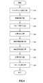
- FIG. 4is a flowchart for explaining the procedure of this method.
- the present methodis a method of electrically connecting to the inspection circuit 90 by bringing the present probe 80 into contact with the test points 6 to 9 of the inspection substrate 70 to perform a predetermined inspection.
- the methodincludes a test point setting step (S10), a movement standby step (S20), a probe lowering step (S30), a positioning step (S40), and an inspection circuit connecting step (S50).
- test point setting step (S10)the terminal electrodes 1, 2 themselves positioned at both ends in the longitudinal direction of the surface mounted components R1, C1, R2, C2 mounted on the inspection substrate 70 are used as test points 6-9.
- the contactor 10is caused to move and stand by above the test points 6 to 9.
- the contact body 10is inserted into the sheath 7 of the present probe 80 and is resiliently movable back and forth.
- the contact body 10 of the present probe 80is lowered to the test points 6 to 9 (FIG. 1).
- a recess 17is formed on the tip side. At least a part of the inside of the recess 17 is formed by the insulator 11 and the contact electrode 12 made of a good conductor. Further, a V-shaped gradient M is formed which narrows as it goes from the distal end 13, 14 of the recess 17 to the proximal end 15.
- the open tip 13 and 14 of the recess 17has an opening width X larger than the maximum outer length L including the terminal electrodes 1 and 2 located at both ends in the longitudinal direction of the chip components R1, C1, R2 and C2. ing.
- the insulator 11resiliently abuts one of the terminal electrodes 1.
- the recess 17is placed so as to sandwich the both ends of the terminal electrodes 1 and 2 from the outside.
- the contact body 10is positioned with respect to the longitudinal direction of the surface mounted components R1, R2.
- the inspection circuit connecting step (S50)the contact electrode 12 paired with the insulator 11 among the positioned contact members 10 is electrically connected to the inspection circuit 90 so as to be in contact with the other terminal electrode 2 .
- the inspection signal circulation step (S60)the inspection signal is circulated from the inspection circuit 90 to the surface mounted components R1, C1, R2, C2 via the test points 6 to 9 (FIG. 1).
- the result determination step (S70)the inspection circuit 90 determines the result of circulating the inspection signal.
- the probe raising step (S80)the probe 80 is raised so as to separate the contact body 10 from the test points 6 to 9 (FIG. 1). As shown in the above procedure, according to this method, the present probe 80 can be easily and reliably brought into contact with the electrodes 1 and 2 of the microminiature chip parts R1, C1, R2 and C2.
- FIG. 5is a view for explaining the mounting state of the QFP
- FIG. 5 (A)is a plan view
- FIG. 5 (B)is a partially enlarged plan view
- FIG. 5 (C)is a side sectional view
- FIG. (D)is a partially enlarged side sectional view
- FIG. 5 (E)is a partially enlarged front view of the present probe in use.
- the QFPis, as its name suggests, a surface mount electronic device in which a large-scale integration (LSI) is stored in a thin flat package having a substantially rectangular plan view in FIG. 5A. That is, as shown in FIG. 5 (C) and FIG. 5 (D), the QFP has a large number of terminals projecting closely from the four sides at almost equal intervals, and is mounted on the surface of the printed wiring board by soldering. Ru.
- LSIlarge-scale integration
- a minimum pitch of 0.4 mmis known at present. If the pitch between the terminals is 0.4 mm, the gap between the terminals is narrower.
- the probe 77has a pair of contact members 21 and 22 and chevrons 18 near the respective tips 23 and 24.
- the contact 20is provided.
- the convex portion 18has inclined end faces 3 and 4 that are substantially symmetrical on both shoulders of the mountain shape. Such angled beveled end faces 3 and 4 abut against the narrow gap between the terminals 51 and 52 of the QFP so as to push and spread.
- a gap Gis provided at the center of the mountain-shaped convex portion 18 in the direction from the distal end 23, 24 of the pair of contact members 21, 22 to the proximal end 15. That is, a noncontact portion is provided at the joint between the pair of contact members 21 and 22, and the noncontact portion forms a gap G.
- the inclined end faces 3 and 4abut the terminal electrodes 51 and 52 and are pressed. At this time, the angled end faces 3 and 4 are pressed from both sides in the direction of the arrow J, so the gap G is elastically narrowed. Conversely, when the probe 77 is raised in the direction of the arrow U, the inclined end faces 3 and 4 are separated from the terminal electrodes 51 and 52 and released. At this time, in the angled end faces 3 and 4 of the mountain, the gap G is expanded in the direction shown by the arrow K by the original elastic force of the insulator (contact member) 21 and the material of the contact electrode 22 (see FIG. 6). ).
- FIG. 6is a schematic view for explaining the schematic configuration and the actual use of the present probe according to the second embodiment.
- a recess 17is formed in the end side.
- the contact portion 20 forming the present probe 77 according to the second embodiment shown in FIG. 6not the recess but the chevron 18 is formed at the tip.
- a convex portion 18is provided by a combination of inclined end faces 3 and 4 formed in the vicinity of the tip ends 23 and 24 of the pair of contact members 21 and 22, respectively.
- At least one of the inclined end faces 3 of the pair of contact members 21 and 22is an insulator 21 and the other is a contact electrode 22 of a good conductor.
- the convex portion 18can contact the terminal electrodes 51 and 52 of the surface mounted component 50 (hereinafter, also referred to as “QFT 50”) mounted on the inspection substrate 70 at the inclined end faces 3 and 4.
- the contact body 10is positioned with respect to the QFT 50 when the insulator 21 forming one inclined end face 3 of the pair of contact members 21 and 22 abuts on the one terminal electrode 41. Then, the contact electrode 12 forming the other inclined end surface 4 of the pair of contact members 21 and 22 is electrically connected to the other terminal electrode 42 and electrically connected to the inspection circuit 90.
- FIG. 7 and 8a third embodiment suitable for a quad flat package (QFP) will be described in detail with reference to FIGS. 7 and 8.
- FIG. 7 and 8The proximal ends 15 of the contact members 10 and 20 according to the first and second embodiments described above are telescopically configured to be inserted into the sheath-like portion 87 to be elastically advanced and retracted.
- the contact body of the third embodiment shown in FIGS. 7 and 8is a so-called wire probe which is constituted by a high elastic wire alone with a pointed tip. The wire probe is configured to be elastically deformed in a bow shape to obtain a proper pressing force and to make a good electrical contact.
- FIG. 7is a front view for explaining a schematic configuration of the present probes 78 and 79 according to the third embodiment, and FIG. 7A shows a point immediately after the tip reaches the test points 6 to 9 (see also FIG. 1).
- FIG. 7 (B)shows a state of pressure contact, respectively.
- the contact members 30, 40 constituting the present probes 78, 79are made of a wire made of an elastic material embedded in the probe base 88.
- FIG. 7Athe contact members 30, 40 constituting the present probes 78, 79 are made of a wire made of an elastic material embedded in the probe base 88.
- the contact members 30 and 40are made of an elastic material, for example, a wire made of piano wire or the like, which can be restored from a curved state within the elastic limit to a straight initial shape with respect to a longitudinal compression stress.
- the proximal end 15 of the wireis implanted in the probe base 88, and the distal end of the wire is inserted into a guide hole 86 drilled in the guide plate 85.
- the wire probeshit the test points 6 to 9 according to the mechanical accuracy of the probe base 88 and the guide plate 85 which support a large number and perform the disengaging operation on the inspection substrate 70 collectively. Furthermore, by managing the stroke limit and using it within the range not exceeding the elastic limit, the wire probe can return from the bent state to the straight standby shape even if bending and stretching operations are continuous, so that the pinpoint does not deviate.
- the wire probecan cope with a narrow pitch such as the terminals 51 and 52 of the QFP 50 shown in FIG.
- a narrow pitchsuch as the terminals 51 and 52 of the QFP 50 shown in FIG.
- the wire⁇ 0.07 mm, it can correspond to 110 ⁇ m pitch.
- the tip end of the contacts 30, 40comes in contact with the test points 6 to 9 by the lowering operation of the probe base 88, and contact conduction is made and electrical connection to the inspection circuit 90 is made. Be done.
- the middle of the wireis in a curved state within the elastic limit, and high pin pressure can be obtained even when used at a narrow pitch.
- the electrical resistance valueis stable.
- a coil springsince a coil spring is not used, it has a long life, and for example, a contact durability performance of about one million times is known.
- the curved shape shown by arrow T in FIG. 7Bis exaggerated for the sake of explanation, and the stroke of the probe base 88 is limited to such an extent that they do not contact each other.
- the guide plate 85since the guide plate 85 has a smaller stroke than the probe base 88, the guide plate 85 stands by in the vicinity of the test points 6 to 9 of the inspection substrate 70, and the contact members 30, 40 inserted in the guide holes 86 are horizontal. Guide the position.
- FIG. 8is a schematic view for explaining a contact body forming the present probe according to the third embodiment, and FIG. 8 (A) shows the shape of a recess and FIG. 8 (B) shows the shape of a protrusion.
- the present probe 78is, for example, a tip-shaped insulator 31 inclined at an angle of 45 degrees with respect to the tip of the contact electrode 32 inclined at an angle of 45 degrees. Bonding from the back side) constitutes a contact body 30 having a recess 17 with a V-shaped gradient M on the inner periphery.
- the manner in which the recess 17 of the contact body 30 contacts the terminals 1 and 2 of the chip part R1is the same as that of the contact body 10 according to the first embodiment shown in FIGS.
- the inclined end face 3is formed by covering the insulator 41 with the tip of the contact electrode 42 formed in a mountain shape at an inclination angle of 45 degrees.
- the insulator 41has a shape in which the base end side is released, and the inclined end face 4 on one side is configured to expose the contact electrode 42 of a good conductor. Therefore, the contact body 40 has a pair configuration in which one inclined end face 3 is the insulator 41 and the other inclined end face 4 is the contact electrode 42 of a good conductor.
- the manner in which the convex portion 18 of the contact body 40 contacts the terminals 51 and 52 of the QFP 50is the same as that of the contact body 20 according to the second embodiment shown in FIGS. 5 and 6.
- the convex part 18 shown to FIG. 8 (B)comprises by coat
- the insulator 41forms an insulating oxide film on the tip of the contact electrode 42 without covering the contact electrode 42 with another member, and polishes the inclined end face 4 on one side, etc. May be exposed.
- the present inventionit is possible to provide a substrate inspection probe which can easily and reliably contact the electrode of a very small surface-mounted component. More specifically, the surface mounting is made to a certain extent (for example, in a chip part, 0.6 mm ⁇ 0.3 mm in plan view, and in QFP, an inter-terminal pitch of 0.4 mm) or less, and surface mounts so small that the fillet can not be viewed in plan It is possible to provide a substrate inspection probe, a substrate inspection apparatus, and a substrate inspection method using them, wherein the electrode of the part is a contact portion replaced with a test land, and the probe can be easily and reliably contacted.
- the substrate inspection probe, the substrate inspection apparatus, and the substrate inspection method using them according to the present inventionare ultra-compact surface-mounted components soldered to a printed circuit board constituting any electronic device, particularly chip components, QFP and LSI There is a possibility that it may be adopted in an inspection device for and an inspection method using them.
Landscapes
- Physics & Mathematics (AREA)
- General Physics & Mathematics (AREA)
- Measuring Leads Or Probes (AREA)
- Tests Of Electronic Circuits (AREA)
Abstract
Description
Translated fromJapanese本発明は、基板検査用プローブ、基板検査装置、及びそれらを用いた基板検査方法に関し、特に小型の表面実装部品の端子電極に対し、直接に突端を接触させるようにした基板検査用プローブ、基板検査装置、及びそれらを用いた基板検査方法に関する。The present invention relates to a substrate inspection probe, a substrate inspection apparatus, and a substrate inspection method using the same, and in particular, a substrate inspection probe and a substrate in which a tip is brought into direct contact with terminal electrodes of small surface-mounted components. The present invention relates to an inspection apparatus and a substrate inspection method using them.
回路基板検査装置は、検査対象となる回路基板(以下、「被検査基板」ともいう)の実装デバイス(以下、「被検査部品」ともいう)につながるパターンに、所定の面積及び形状のテストランドが配設されている。そのテストランドに基板検査装置のプローブを接触させることにより、プローブにつながる検査回路と、被検査部品とを検査可能に接続する。The circuit board inspection apparatus has a test land of a predetermined area and shape in a pattern connected to a mounted device (hereinafter, also referred to as “part to be inspected”) of a circuit board to be inspected (hereinafter, also referred to as “inspection board”). Is provided. By bringing the probe of the substrate inspection apparatus into contact with the test land, the inspection circuit connected to the probe and the part to be inspected are connected in an inspectable manner.
また、携帯電話を始めとするような小型化を追求される商品において、その回路基板にはテストランドを配設するスペースを節約することが求められる。このような場合、被検査部品の電極を半田16で実装された箇所が、テストランドに代えた接触部とされる。In addition, in products that are pursued to be miniaturized, such as mobile phones, it is required that the circuit board save a space for installing a test land. In such a case, the portion where the electrode of the inspected part is mounted by the
また、小型の角型表面実装部品、いわゆるチップ部品は小型化を追及され続ける傾向にある。チップ部品の外形は直方体であり、その直方体の大きさを、基板実装面の平面視における「長さL×幅W」を(mm)の単位で表示し呼称される。例えば、「長さL×幅W」=(1.6mm×0.8mm)であれば、「1608」と呼ばれる。同様に、(1.0mm×0.5mm)を「1005」、(0.6mm×0.3mm)を「0603」、(0.4mm×0.2mm)を「0402」、(0.2mm×0.1mm)を「0201」、と呼ばれている。In addition, small square surface-mounted components, so-called chip components, tend to continue to be miniaturized. The external shape of the chip part is a rectangular solid, and the size of the rectangular solid is referred to by displaying “length L × width W” in units of (mm) in plan view of the substrate mounting surface. For example, if “length L × width W” = (1.6 mm × 0.8 mm), it is called “1608”. Similarly, (100 mm × 0.5 mm) is “1005”, (0.6 mm × 0.3 mm) is “0603”, and (0.4 mm × 0.2 mm) is “0402”, (0.2 mm × 0.1 mm) is called "0201".
異なる大きさのチップ部品を上述したなかで、「長さL×幅W」=(1.6mm×0.8mm)の「1608」以上の大きさであれば、その電極に対する半田16で実装の箇所、すなわちフィレットが平面視できる程度の面積である。そのフィレットを、テストランドに代えた接触部として、プローブを接触させることが容易かつ確実である。現状の技術では、「1005」(平面視1.0mm×0.5mm)までならば、その電極につながるフィレットに、プローブを接触させることが可能である。Among the chip components of different sizes described above, if the size is “1608” or more of “length L × width W” = (1.6 mm × 0.8 mm), the
ところが、チップ部品も、ある程度(0.6mm×0.3mm)の「0603」以下にまで小型化されると、フィレットが平面視できない程に小さくなるので、テストランドに代えた接触部として、フィレットにプローブを接触させることは困難かつ不確実となる。However, when the chip parts are also miniaturized to a certain degree (0.6 mm × 0.3 mm) or less of “0603” or less, the fillets become so small that they can not be viewed in a plan view. Therefore, the fillets are used as contact portions instead of test lands. Contacting the probe with the probe is difficult and uncertain.
一方、(平面視0.4mm×0.2mm)や(平面視0.2mm×0.1mm)の超小型チップ部品も多数採用された被検査基板も多くなりつつある。さらに、(0.4mm×0.2mm)の「0402」や(0.2mm×0.1mm)の「0201」といった程度にまで超小型化されると、フィレットが隠れてしまう。この場合、テストランドに代えた接触部として、プローブを接触させることは不可能である。On the other hand, the number of test substrates on which a large number of ultra-small chip parts (planar view 0.4 mm × 0.2 mm) and (planar view 0.2 mm × 0.1 mm) are adopted is also increasing. Furthermore, if the microminiaturization is performed to the extent of "0.42" (0.4 mm.times.0.2 mm) or "0201" (0.2 mm.times.0.1 mm), the fillet will be hidden. In this case, it is impossible to bring the probe into contact as a contact in place of the test land.
また、検査精度を向上させるようにした回路基板検査装置及びそれを用いた検査方法が知られている(例えば、特許文献1を参照)。その回路基板検査装置は、プローブユニットを回路基板の一方の面側に配設してプローブユニットを回路基板の他方の面側に配設し、配線パターン上に規定された接触ポイントにプローブユニットのプローブのうちの対応する2本を接触させるように構成されたものである。Further, there is known a circuit board inspection apparatus and an inspection method using the circuit board inspection apparatus for improving inspection accuracy (see, for example, Patent Document 1). In the circuit board inspection apparatus, the probe unit is disposed on one side of the circuit board, the probe unit is disposed on the other side of the circuit board, and the probe unit is disposed on the contact point defined on the wiring pattern. It is configured to contact two corresponding ones of the probes.
その回路基板検査装置を用いた検査方法は、配線パターン上に規定された接触ポイントにプローブユニットのプローブのうちの対応する2本を接触させ、接触ポイントに接触されているプローブを短絡させ、プローブを使用して内部導体に測定電流を供給し、プローブを使用して測定した接触ポイント間の電圧、及び測定電流に基づいて内部導体の抵抗を四端子法で測定して内部導体の検査を行う、という検査方法である。In the inspection method using the circuit board inspection apparatus, the corresponding two of the probes of the probe unit are brought into contact with the contact points defined on the wiring pattern, and the probes brought into contact with the contact points are shorted. Supply a measurement current to the inner conductor using the probe and measure the resistance of the inner conductor with the four-terminal method based on the voltage between the contact points measured using the probe and the measurement current to inspect the inner conductor It is an inspection method called.
しかしながら、特許文献1に記載の回路基板検査方法及び回路基板検査装置は、スルーホールを含む回路基板に対する検査精度を向上させるための技術であって、超小型チップ部品の電極に容易かつ確実に接触可能な基板検査用プローブ、基板検査装置、及びそれらを用いた基板検査方法ではなかった。However, the circuit board inspection method and circuit board inspection apparatus described in
また、微細な検査点に二つの端子を接触させることが容易な基板検査用プローブ、基板検査装置、及びそれらを用いた基板検査方法も知られている(例えば、特許文献2を参照)。その構成は、各ニードルピンの軸線と傾斜して交差する先端面がそれぞれ形成された電流供給用ニードルピン及び電圧測定用ニードルピンと、各ニードルピンを一体に保持する保持部材と、を備える。また、保持部材は、電流供給用ニードルピンと電圧測定用ニードルピンとを平行に微小間隔を有して保持すると共に、先端面の頂部が相隣接する方向に配設されている、というものである。There is also known a substrate inspection probe, a substrate inspection apparatus, and a substrate inspection method using them, in which two terminals can be easily brought into contact with a minute inspection point (see, for example, Patent Document 2). The configuration includes a current supply needle pin and a voltage measurement needle pin each formed with a tip surface that intersects with the axis of each needle pin at an angle, and a holding member that holds the needle pins together. Further, the holding member holds the current supply needle pin and the voltage measurement needle pin in parallel with a minute interval, and is disposed in the direction in which the tops of the tip surfaces are adjacent to each other.
しかしながら、特許文献2に記載の基板検査用プローブ、及びそれらを用いた基板検査装置も、超小型チップ部品の電極に容易かつ確実に接触可能な基板検査用プローブ、基板検査装置、及びそれらを用いた基板検査方法ではなかった。However, the substrate inspection probe described in
また、画像処理などの高価な設備を用いることなく、プローブをチップ部品に接触させるだけの操作で、バイパスコンデンサなどのチップ部品の実装状態を検査可能とする回路基板検査装置も知られている(例えば、特許文献3を参照)。具体的には、チップ部品が回路基板側のハンダパッド上に実装されているかどうかを検査するため、第1,第2のプローブと、各プローブ間の電気的状態を計測する計測手段とを含み、第1プローブは、スイッチ手段を介して計測手段に選択的に接続される筒状プローブと、筒状プローブ内に挿通されバネ付勢されているプローブピンと、を備えた構成である。There is also known a circuit board inspection apparatus capable of inspecting the mounting state of a chip component such as a bypass capacitor by merely bringing a probe into contact with the chip component without using expensive equipment such as image processing ( See, for example, Patent Document 3). Specifically, in order to inspect whether or not the chip component is mounted on the solder pad on the circuit board side, it includes first and second probes and measurement means for measuring the electrical condition between the probes. The first probe is configured to include a cylindrical probe selectively connected to the measuring means via the switch means, and a probe pin inserted into the cylindrical probe and biased by a spring.
また、上述したスイッチ手段により筒状プローブを計測手段に接続し、その傾斜面をチップ部品の一方のリード電極に接触させると共に、第2プローブをリード電極側のハンダパッドに連なる配線パターンに接触させ、計測手段にて筒状プローブと第2プローブとの間の電気的状態を計測する、というものである。Further, the cylindrical probe is connected to the measuring means by the switch means described above, and the inclined surface is brought into contact with one of the lead electrodes of the chip part and the second probe is brought into contact with the wiring pattern connected to the solder pad on the lead electrode side. The measuring means measures the electrical state between the tubular probe and the second probe.
しかしながら、特許文献3に記載の回路基板検査装置は、チップ部品が、回路基板側のハンダパッド上に実装されているかどうか、を検査するための技術であって、超小型チップ部品の電極に容易かつ確実に接触可能な基板検査用プローブ、基板検査装置、及びそれらを用いた基板検査方法ではなかった。However, the circuit board inspection apparatus described in
本発明は、このような実情に鑑みてなされたもので、その目的とするところは、超小型の表面実装部品の電極に容易かつ確実に接触可能な基板検査用プローブを提供することにある。より詳しくは、ある程度(例えば、チップ部品では平面視0.6mm×0.3mm、QFPでは端子間ピッチが0.4mm)以下にまで超小型化され、フィレットが平面視できない程に小さくなった表面実装部品の電極を、テストランドに代えた接触部とし、プローブを接触させることが容易かつ確実にできる基板検査用プローブ、基板検査装置、及びそれらを用いた基板検査方法を提供することを目的とする。The present invention has been made in view of such circumstances, and an object of the present invention is to provide a substrate inspection probe which can be easily and reliably brought into contact with an electrode of a very small surface-mounted component. More specifically, the surface has been miniaturized to a certain extent (for example, 0.6 mm × 0.3 mm in plan view for chip parts, and 0.4 mm between terminals for QFP in QFP), and the surface has become so small that the fillet can not be viewed in plan It is an object of the present invention to provide a substrate inspection probe, a substrate inspection apparatus, and a substrate inspection method using them, wherein the electrode of the mounted component is a contact portion replaced with a test land and the probe can be easily and reliably contacted. Do.
本発明は、このような目的を達成するためになされたもので、請求項1に記載の発明は、被検査基板(70)の対象部に離接可能な接触体(10,20,30,40)が当接することにより検査回路(90)へ電気接続する基板検査用プローブ(77,78,79,80)であって、
前記接触体(10,20,30,40)は、一対の接触部材(11,12,21,22,31,32,41,42)それぞれの先端(13,14,23,24,33,34)近傍に形成された傾斜端面(3,4)の組み合わせにより凸部(18)又は凹部(17)を設け、
前記一対の接触部材(11,12,21,22,31,32,41,42)のうち、一方は少なくとも前記傾斜端面(3)が絶縁体(11,21,31,41)であり、他方は良導体による接触電極(12,22,32,42,42)で構成され、
前記凸部(18)又は凹部(17)は、前記被検査基板(70)に実装された表面実装部品(50,R1,C1,R2,C2)の端子電極(1,2,51,52)に前記傾斜端面(3,4)で接触可能であり、
前記絶縁体(11)が前記端子電極(1,2,51,52)の一方に当接することにより、前記接触体(10)は前記表面実装部品(50,R1,C1,R2,C2)に対して位置決めをされると共に、
前記接触電極(12)が前記端子電極(1,2,51,52)の他方に接触導通して検査回路(90)へ電気接続するように構成された基板検査用プローブ(77,78,79,80)。The present invention has been made to achieve such an object, and the invention according to
The contact body (10, 20, 30, 40) is a tip (13, 14, 23, 24, 32, 33, 34) of each of a pair of contact members (11, 12, 21, 22, 21, 31, 42, 41). B) providing a projection (18) or a recess (17) by a combination of inclined end faces (3, 4) formed in the vicinity,
At least one of the inclined end faces (3) of the pair of contact members (11, 12, 21, 22, 21, 31, 32, 41, 42) is an insulator (11, 21, 31, 41), Is composed of contact electrodes (12, 22, 32, 42, 42) with good conductors,
The convex portion (18) or the concave portion (17) is a terminal electrode (1, 2, 51, 52) of the surface mounted component (50, R1, C1, R2, C2) mounted on the inspection substrate (70). Contact with the inclined end face (3, 4),
When the insulator (11) abuts on one of the terminal electrodes (1, 2, 51, 52), the contact body (10) is attached to the surface mounted component (50, R1, C1, R2, C2) As well as being positioned against
A substrate inspection probe (77, 78, 79) configured such that the contact electrode (12) is in electrical contact with the other of the terminal electrodes (1, 2, 51, 52) to be electrically connected to the inspection circuit (90). , 80).
また、請求項2に記載の発明は、請求項1記載の基板検査用プローブ(77)において、前記接触体(20)は、一対の接触部材(21,22)それぞれの先端(23,24)近傍に山形の凸部(18)が形成され、
該山形の凸部(18)の中心には、前記一対の接触部材(21,22)の合わせ目にそれぞれの先端(23,24)から基端(15)の方向へ隙間(G)が設けられ、
該隙間(G)は前記傾斜端面(3,4)が前記端子電極(51,52)に当接して押圧されることで弾力的に狭められる構成である。The invention according to
A gap (G) is provided in the center of the mountain-shaped convex portion (18) in the direction from the tip (23, 24) to the base (15) of the joint of the pair of contact members (21, 22) And
The gap (G) is configured to be elastically narrowed by the inclined end surfaces (3, 4) being in contact with the terminal electrodes (51, 52) and being pressed.
また、請求項3に記載の発明は、鞘状部(87)に挿通されて弾力的に進退自在の接触体(10)が、被検査基板(70)の対象部に当接して検査回路(90)へ電気接続する基板検査用プローブ(80)であって、
前記接触体(10)は、一対の接触部材(11,12)それぞれの先端(13,14)が二股に分かれて形成された凹部(17)の開口幅(X)を保持して進退するように構成され、
前記一対の接触部材(11,12)のうち、一方が絶縁体(11)であり、他方は良導体による接触電極(12)で構成され、
前記凹部(17)の内側には、前記先端(13,14)から基端(15)へ向かうにつれて奥細りするV字型勾配(M)が形成され、
該V字型勾配(M)は、前記被検査基板(70)に実装された表面実装部品(50,R1,C1,R2,C2)の両端に位置する端子電極(1,2)を挟持可能であり、
前記開口幅(X)は前記表面実装部品(R1,C1,R2,C2)の両端を含む最大外形長さ(L)よりも広く、
前記絶縁体(11)が前記端子電極(1,2)の一方に当接することにより、前記接触体(10)は前記表面実装部品(50,R1,C1,R2,C2)の長手方向に対して位置決めをされると共に、
前記接触電極(12)が前記端子電極(1,2)の他方に接触導通して検査回路(90)へ電気接続するものである。In the invention according to
The contact body (10) advances and retracts so as to hold the opening width (X) of the recess (17) formed by bifurcating the tips (13, 14) of the pair of contact members (11, 12) Configured to
One of the pair of contact members (11, 12) is an insulator (11), and the other is a contact electrode (12) of a good conductor,
Inside the recess (17), a V-shaped gradient (M) is formed which narrows as it goes from the tip (13, 14) to the base (15),
The V-shaped gradient (M) can hold terminal electrodes (1, 2) located at both ends of the surface mounted components (50, R1, C1, R2, C2) mounted on the inspection substrate (70) And
The opening width (X) is wider than the maximum outer length (L) including both ends of the surface mounted components (R1, C1, R2, C2),
When the insulator (11) abuts on one of the terminal electrodes (1, 2), the contact (10) is in the longitudinal direction of the surface mounted components (50, R1, C1, R2, C2). While being positioned
The contact electrode (12) is electrically connected to the other of the terminal electrodes (1, 2) to be electrically connected to the inspection circuit (90).
また、請求項4に記載の発明は、請求項3記載の基板検査用プローブ(80)において、前記表面実装部品(R1,C1,R2,C2)は直方体のチップ部品(小型の角型表面実装部品)である。The invention according to
また、請求項5に記載の発明は、請求項4記載の基板検査用プローブ(80)において、前記直方体の大きさが実装状態における平面視1.6mm×0.8mm以下とするものである。According to the fifth aspect of the present invention, in the board inspection probe (80) according to the fourth aspect, the size of the rectangular parallelepiped is 1.6 mm × 0.8 mm or less in plan view in the mounted state.
また、請求項6に記載の発明は、請求項1~5の何れかに記載の基板検査用プローブ(78,79)において、前記接触体(30,40)は、長手方向の縮み応力に対し弾性限界内の湾曲状態から真っ直ぐな初期形状に復元可能な弾性素材のワイヤーで本体が構成され、該ワイヤーの基端部(15)が、前記被検査基板(70)への離接動作を行う前記プローブ基台(88)に植設されたものである。The invention according to
また、請求項7に記載の発明は、請求項1~5の何れかに記載の基板検査用プローブ(77,78,79,80)を備えた基板検査装置(100)である。The invention according to
また、請求項8に記載の発明は、請求項6に記載の基板検査用プローブ(79,80)を備えた基板検査装置(100)である。The invention according to
また、請求項9に記載の発明は、基板検査用プローブ(80)を被検査基板(70)のテストポイント(6~9)に当接することにより検査回路(90)へ電気接続して所定の検査を行う基板検査方法であって、
前記被検査基板(70)に実装された表面実装部品(50,R1,C1,R2,C2)の長手方向の両端に位置する端子電極(1,2)そのものを前記テストポイント(6~9)に設定するテストポイント設定工程(S10)と、
前記基板検査用プローブ(80)の鞘状部(87)に挿通されて弾力的に進退自在の接触体(10)を、前記テストポイント(6~9)それぞれの上方に移動待機させる移動待機工程(S20)と、
少なくとも内側の一部が絶縁体(11)と良導体による接触電極(12)とによって形成された凹部(17)が、前記表面実装部品(50,R1,C1,R2,C2)の長手方向の両端に位置する端子電極(1,2)を含む最大外形長さ(L)よりも広い幅(X)で開口し、該凹部(17)の先端(13,14)から基端(15)へ向かうにつれて奥細りするV字型勾配(M)が形成された前記接触体(10)を、前記テストポイント(6~9)に降下させるプローブ降下工程(S30)と、
前記端子電極(1,2)の一方(1)に前記絶縁体(11)が弾力的に当接しながら、前記凹部(17)が前記端子電極(1,2)の両端を外側から挟持することにより前記接触体(10)が前記表面実装部品(50,R1,C1,R2,C2)の長手方向に対して位置決めする位置決め工程(S40)と、
前記位置決めされた前記接触体(10)のうち前記絶縁体(11)と対をなす前記接触電極(12)が前記端子電極(1,2)の他方(2)に接触導通して検査回路(90)へ電気接続される検査回路接続工程(S50)と、
前記表面実装部品(50,R1,C1,R2,C2)に前記テストポイント(6~9)経由で前記検査回路(90)から検査信号を巡らせる検査信号巡回工程(S60)と、
前記検査信号を巡らせた結果を検査回路(90)により判定する結果判定工程(S70)と、
前記接触体(10)を前記テストポイント(6~9)から離間させるように前記基板検査用プローブ(80)を上昇させるプローブ上昇工程(S80)と、
を有するものである。In the invention according to
The test electrodes (6 to 9) are terminal electrodes (1, 2) themselves positioned at both ends in the longitudinal direction of the surface mounted components (50, R1, C1, R2, C2) mounted on the inspection substrate (70). Test point setting step (S10) to be set to
A moving standby step of moving and waiting for the elastically moveable contactor (10) inserted into the sheath (87) of the substrate inspection probe (80) above each of the test points (6 to 9) (S20),
Recesses (17) formed by at least a part of the inner side by the insulator (11) and the contact electrode (12) of a good conductor are both longitudinal ends of the surface mounted component (50, R1, C1, R2, C2) Open with a width (X) wider than the maximum outer length (L) including the terminal electrodes (1, 2) located in the direction from the tip (13, 14) of the recess (17) to the base (15) Probe lowering step (S30) of lowering the contact body (10) on which the V-shaped gradient (M) is formed to be narrowed as the contact point is dropped to the test point (6 to 9);
The recess (17) sandwiches both ends of the terminal electrode (1, 2) from the outside while the insulator (11) resiliently abuts on one (1) of the terminal electrode (1, 2) Positioning step (S40) of positioning the contact body (10) in the longitudinal direction of the surface mounted components (50, R1, C1, R2, C2) by
The contact electrode (12) paired with the insulator (11) of the positioned contact body (10) is brought into contact with the other (2) of the terminal electrodes (1, 2) to make an inspection circuit ( 90) a test circuit connection step (S50) electrically connected to
An inspection signal circulating step (S60) for circulating an inspection signal from the inspection circuit (90) to the surface mounted components (50, R1, C1, R2, C2) via the test points (6 to 9);
A result determination step (S70) of determining the result of the inspection signal by the inspection circuit (90);
Probe raising step (S80) of raising the substrate inspection probe (80) so as to separate the contact body (10) from the test point (6 to 9);
The
本発明によれば、超小型の表面実装部品の電極に容易かつ確実に接触可能な基板検査用プローブを提供できる。より詳しくは、ある程度(例えば、チップ部品では平面視0.6mm×0.3mm、QFPでは端子間ピッチが0.4mm)以下にまで超小型され、フィレットが平面視できない程に小さくなった表面実装部品の電極を、テストランドに代えた接触部とし、プローブを接触させることが容易かつ確実にできる基板検査用プローブ、基板検査装置、及びそれらを用いた基板検査方法を提供できる。According to the present invention, it is possible to provide a substrate inspection probe capable of easily and reliably contacting electrodes of a microminiature surface mounting component. More specifically, the surface mounting is made to a certain extent (for example, in a chip part, 0.6 mm × 0.3 mm in plan view, and in QFP, an inter-terminal pitch of 0.4 mm) or less, and surface mounts so small that the fillet can not be viewed in plan It is possible to provide a substrate inspection probe, a substrate inspection apparatus, and a substrate inspection method using them, wherein the electrode of the part is a contact portion replaced with a test land, and the probe can be easily and reliably contacted.
[第1実施例]
以下、第1実施例に係る本装置及び本方法について、図1~図4を用いて詳細に説明する。なお、各図に亘って、同一効果の部材及び工程には、同一符号を付して説明の重複を避ける。図1は、本プローブ、本装置、及び本方法の概略を説明するための回路図である。図1に示すように、本装置100は、本プローブ80と、検査回路90を備えて構成され、被検査基板(以下、「回路基板」、又は単に「基板」ともいう)70を検査するものである。[First embodiment]
Hereinafter, the present apparatus and the present method according to the first embodiment will be described in detail with reference to FIGS. 1 to 4. In addition, the same code | symbol is attached | subjected to the member and process of the same effect over each figure, and duplication of description is avoided. FIG. 1 is a circuit diagram for explaining the outline of the present probe, the present apparatus, and the present method. As shown in FIG. 1, the
本プローブ80については、より詳細に後述する。検査回路90は、信号源91と、検出器92と、切り替えスイッチSW1~SW4(以下、単に「SW1~SW4」ともいう)と、を備えて構成されている。また、基板70に実装された表面実装部品(以下、「チップ部品」ともいう)R1,C1,R2,C2の長手方向の両端に位置する端子電極1,2そのものが、テストポイント6~9に設定されている。The
基板70には配線パターン71~75が配設され、それら配線パターン71~75の所定位置に、チップ部品R1,C1,R2,C2が半田16で実装されている。これらのチップ部品R1,C1,R2,C2は、それぞれの両端に端子電極1,2が形成されている。チップ部品R1の端子電極1は、配線パターン71に半田16で実装され、チップ部品R1の端子電極2は、配線パターン72に半田16で実装されている。
その配線パターン72には、チップ部品C1の端子電極1が半田16で実装され、チップ部品C1の端子電極2は、配線パターン73に半田16で実装されている。その配線パターン73には、チップ部品R2の端子電極2が半田16で実装され、チップ部品R2の端子電極1は、配線パターン74に半田16で実装されている。The
図2は、本装置の概略構成を説明するための模式図であり、チップ部品C1だけの検査について説明し易くしたものである。図1及び図2に示すように、基板70に実装されたチップ部品R1,C1,R2,C2(図2,図3ではC2を省略)の何れかに対し、検査回路90のSW1~SW4の操作により、本プローブ80を介して、信号源91及び検出器92が電気接続される。例えば、SW1をN(ニュートラル)、SW2をP(端子)、SW3をQ(端子)、SW4をN、に設定することにより、チップ部品C1が、本プローブ80を介して、信号源91及び検出器92に電気接続される。FIG. 2 is a schematic view for explaining a schematic configuration of the present apparatus, which facilitates the inspection of only the chip part C1. As shown in FIGS. 1 and 2, any one of the chip components R1, C1, R2 and C2 (C2 is omitted in FIGS. 2 and 3) mounted on the
チップ部品C1以外のチップ部品R1,R2,C2の何れかに対しては、SW1~SW4を適切に切り替え操作することにより、本プローブ80を介して、信号源91及び検出器92に電気接続することが可能である。例えば、図1において、チップ部品R1に対しては、SW1をP、SW2をQ、SW3,4をNに設定する。同様に、チップ部品R2に対しては、SW3をP、SW4をQ、SW1,2をNに設定する。For any of chip components R1, R2 and C2 other than chip component C1, electrical connection is made to signal
なお、図1及び図2の記載範囲において、チップ部品C2を検査回路90に閉回路構成することはできないが、単なる図面描写の制約に過ぎず、チップ部品R1,C1,R2と類似の方法で検査回路90に閉回路構成できることはいうまでもない。In the range described in FIGS. 1 and 2, although the chip part C2 can not be closed circuited to the
本プローブ80は、鞘状部87と、その鞘状部87に挿通されて弾力的に進退自在の接触体10と、によりテレスコピック構成されている。このように構成された本プローブ80は、接触体10が被検査基板70において、任意に設定された対象部に当接して検査回路90へ電気接続する。すなわち、本プローブ80は、被検査基板70に実装されたチップ部品R1,C1,R2,C2の何れか1つに設定された検査対象に当接して検査回路90へ電気接続する。なお、何れか1つに設定する理由は、単に説明の便宜上のことであり、複数の検査対象を同時に検査する設定でも構わない。その場合は、検査回路90を相応に充実させる必要がある。The
以下、主に図2を用いて、接触体10をより詳細に説明する。接触体10は、一対の接触部材11,12を一体結合することにより構成されている。この接触体10は、挿通された鞘状部87の中で、揃って進退動作可能に支承されている。これら一対の接触部材11,12のうち、一方が絶縁体11であり、他方は良導体による接触電極12で構成されている。Hereinafter, the
また、基端15から大部分を一体に結合された接触部材11,12は、それぞれの先端13,14が、二股に分かれて凹部17を形成している。接触体10は、この凹部17の開口幅Xを保持して進退するように構成されている。この開口幅Xは表面実装部品R1,C1,R2(図2,図3ではC2を省略)の両端を含む最大外形長さLよりも広い。Further, in the
また、凹部17の内側には、先端13,14から基端15へ向かうにつれて奥細りするV字型勾配Mが形成されている。このV字型勾配Mは、被検査基板70に実装された表面実装部品R1,C1,R2の両端に位置する端子電極1,2を挟持することが可能である。Further, a V-shaped gradient M is formed on the inner side of the
本プローブ80は、上述のように、凹部17の内側にV字型勾配Mが形成された一対の接触部材11,12により接触体10が構成されている。このため、接触体10の一方の接触部材11である絶縁体11が、表面実装部品R1,R2それぞれの一方の端子電極1に当接することにより、接触体10は表面実装部品R1,R2の長手方向に対して位置決めをされる。このように位置決めされた接触体10の他方の接触部材12である接触電極12が、表面実装部品R1,R2それぞれの他方の端子電極2に接触導通して検査回路90へ電気接続する。なお、このとき「位置決めされる」ことをセルフアライメント(Self-alignment)と呼ぶ場合もある。In the
凹部17の内側に形成されたV字型勾配Mは、先端13,14が、長さLよりも広い開口幅Xに設定され、基端15へ向かうにつれて奥細りしている。長さLとは、表面実装部品R1,C1,R2それぞれの長手方向の両端に位置する端子電極1,2を含む最大外形長さLである。凹部17は、その内側のV字型勾配Mの先端13,14の間口が、長さLよりも広い開口幅Xを保持しているので、表面実装部品R1,C1,R2それぞれの端子電極1,2を、長手方向の両側から確実に挟持することが可能である。The V-shaped slope M formed on the inner side of the
本プローブ80は、このような凹部17を有するので、端子電極1,2の一方に対して絶縁体11が当接することにより接触体10の表面実装部品R1,R2の長手方向に対する位置決めできる。さらに、本プローブ80は、位置決めされた凹部17により、端子電極1,2の他方に対し、接触電極12が直接に接触導通して検査回路90へ電気接続する。Since the
表面実装部品R1,C1,R2,C2は、直方体のチップ部品である。その直方体の大きさは、基板実装面の平面視において(長さL×幅W)=(1.6mm×0.8mm)以下である。この長さLは、表面実装部品R1,C1,R2,C2の両電極1,2が形成された両端の長さである。上述のように、凹部17の先端13,14は、チップ部品R1,C1,R2,C2の長手方向の両端の長さLよりも広い開口幅Xが保持され、内側には、奥細りのV字型勾配Mが形成されている。このため、凹部17の先端13,14は、被検査基板70に実装されたチップ部品R1,C1,R2,C2の端子電極1,2を、容易かつ確実に挟持することが可能である。The surface mounted components R1, C1, R2, and C2 are chip components of a rectangular parallelepiped. The size of the rectangular parallelepiped is (length L × width W) = (1.6 mm × 0.8 mm) or less in plan view of the substrate mounting surface. This length L is the length of the both ends in which both
また、本プローブ80は、接触体10を被検査基板70に接近し、表面実装部品R1,C1,R2,C2の両電極1,2を、一対の接触部材11,12により挟持する。その結果、両電極1,2には、接触部材11,12がそれぞれ当接する。ただし、接触部材11,12の一方が絶縁体11であり、他方は良導体による接触電極12であるため、両電極1,2のうち片方のみが検査回路90へ電気接続される。このとき、一方の端子電極1に当接した絶縁体11は、接触体10を表面実装部品R1,R2の長手方向に対して位置決めする機能を発揮する。Further, the
図1及び図2に示して上述したように、SW1をN、SW2をP、SW3をQ、SW4をN、に設定することにより、チップ部品C1が、本プローブ80を介して、信号源91及び検出器92に電気接続される。この接続形態について、より詳細に説明する。By setting SW1 to N, SW2 to P, SW3 to Q, and SW4 to N as described above with reference to FIGS. 1 and 2, the chip component C1 can generate a
図2に示すように、チップ部品C1の端子電極1は、配線パターン72を介してチップ部品R1の端子電極2に接続されている。また、チップ部品C1の端子電極2は、配線パターン73を介してチップ部品R2の端子電極2に接続されている。ここで、チップ部品C1の単品機能を検査する場合、チップ部品C1の端子電極1,2を、両方共に検査回路90に電気接続して閉回路を形成する必要がある。これに対し、チップ部品C1の端子電極1,2に、1つの本プローブ80の先端13,14を直接に接続しなくても、配線パターン72,73を介して接続された他のチップ部品R1,R2それぞれの端子電極2に接続すれば良い。より具体的には以下のとおりである。As shown in FIG. 2, the
まず、検査回路90の信号源91から接続線94を介して図2左側に位置する本プローブ80の接触電極12の基端15まで接続されている。接触電極12の先端14から奥細りに形成されているV字型勾配Mが、チップ部品R1の端子電極2に接触導通する。チップ部品R1の端子電極2は、配線パターン72を介してチップ部品C1の端子電極1に接続されている。このような経路で、チップ部品C1の端子電極1は、検査回路90の信号源91に接続されている。First, the
一方、検査回路90の信号源91は接続線93を介して検出器92に直列接続され、その検出器92から、接続線95を介して図2右側に位置する本プローブ80の接触電極12の基端15まで接続されている。接触電極12の先端14から奥細りに形成されているV字型勾配Mが、チップ部品R2の端子電極2に接触導通する。チップ部品R2の端子電極2は、配線パターン73を介してチップ部品C1の端子電極2に接続されている。このような経路で、チップ部品C1の端子電極2は、検査回路90の検出器92に接続されている。On the other hand, the
また、上述のように、図1において、チップ部品C1以外のチップ部品R1,R2,C2の何れかに対しては、SW1~SW4を適切に切り替え操作することにより、本プローブ80を介して、信号源91及び検出器92に電気接続することが可能である。さらに、図1~図3の記載範囲において、チップ部品C1以外のチップ部品R1,R2,C2の何れかに対しては、本プローブ80を非接触状態にしてから基板70の実装面を平行移動することにより、適切な接続形態を実現できる。以下、図3を用いて本プローブ80のより詳細な実施形態を説明する。In addition, as described above, in FIG. 1, any one of the chip components R1, R2, and C2 other than the chip component C1 can be appropriately switched via SW1 to SW4 through the
図3は本装置及び本プローブの構成をより実態的に説明するため一部透視又は一部断面による正面図である。図3に例示するように、本装置100は、不図示の検査台上に水平に載置された基板70に対し、平行な対面姿勢を維持しながら接近(矢印D方向)と離間(矢印U方向)の動作を自在にするプローブ基台88を備えている。FIG. 3 is a front view, partly in perspective or partly in section, in order to explain the configurations of the present apparatus and the present probe more practically. As illustrated in FIG. 3, the
なお、図2及び図3では、基板70の上面を部品実装面として、その上方からプローブ基台88が覆い被さる形態を例示しているが、これに限定するものではない。すなわち、本装置100は、基板70の両面が部品実装面であり、その上下両方からプローブ基台88が覆い被さる形態であっても構わない。2 and 3 illustrate the form in which the
図3の上方において、上下動作可能なプローブ基台88には、適切な間隔をおいてプローブ植設孔89が穿設されている。このプローブ植設孔89には、本プローブ80の基部を形成する円筒形の鞘状部87が密嵌装着されており、適宜交換可能である。本プローブ80は、鞘状部87と、それに挿通されて弾力的に進退自在の接触体10と、によりテレスコピック構成をなしている。また、鞘状部87の奥には、接触体10の基端部を押し出す方向に付勢するコイルバネ81が配設されている。鞘状部87と、接触体10とは何れも導電部で密に電気接触を維持されている。At the upper side of FIG. 3, a
本プローブ80は、接触体10の周面に、半径方向に突出する回り止め突起82が突設されており、これを摺動自在に受容する回り止めガイド長孔83が、鞘状部87の周面で軸方向に穿設されている。多数の本プローブ80が林立するプローブ基台88を上下動作させると、本プローブ80の先端を形成する接触体10も一体的に上下動作する。本プローブ80を矢印U,D方向に昇降動作すれば、接触体10を基板70の部品実装面に離間と近接させることができる。In this
接触体10は、一対の接触部材11,12により構成されており、これらが挿通された鞘状部87の中で、揃って進退動作可能に支承されている。これら一対の接触部材11,12のうち、一方が絶縁体11であり、他方は良導体による接触電極12で構成されている。The
絶縁体11と接触電極12との間には、両者に囲まれるように凹部17が形成されている。凹部17は、接触部材11,12が二股に分かれたそれぞれの先端13,14から基端15へ向かうにつれて奥細りするV字型勾配Mにより形成されている。このV字型勾配Mは、先端13,14が長さLよりも広く幅Xで開口し、基端15へ向かうにつれて奥細りしている。A
接触体10は、テレスコピック構成のため、基板70の部品実装面に柔軟に当接することにより電気接触する。電気接触した接触体10は、検査対象と検査回路90との導通状態を維持できるように構成されている。より具体的には、図2を用いて上述した要領で、被検査基板70に実装されたチップ部品R1,C1,R2,C2の何れかに当接して検査回路90へ電気接続する。以下に、図2を用いて本発明の典型例である第1実施例について、要点のみを簡略に説明する。The
本プローブ80は、被検査基板70の対象部に当接して検査回路90へ電気接続する接触体10で主要構成されている。この接触体10は、鞘状部87に挿通されて弾力的に進退自在のテレスコピック構成である。また、接触体10は、一方の絶縁体11と他方の接触電極12それぞれが、基端15で結合して先端13,14で分かれた二股構造である。その二股構造の先端13,14が、開口幅Xを保持して一体的に進退する凹部17を形成している。この凹部17の内側は、先端13,14から基端15へ向かうにつれて奥細りするV字型勾配Mを形成している。The
この凹部17は、被検査基板70に実装された表面実装部品R1,R2の両端に位置する端子電極1,2を、V字型勾配Mに当接させて、二股の間に挟持することが可能である。この二股の開口幅Xは、表面実装部品R1,R2の両端を含む最大外形長さLより広い。一方の端子電極1に絶縁体11が当接すれば、その絶縁体11を含んで一体構成の接触体10は、表面実装部品R1,R2の長手方向に対して位置決めされる。すると、一体構成の接触体10に含まれる接触電極12が、他方の端子電極2に接触導通して検査回路90へ容易かつ確実に電気接続される。The
本発明によれば、超小型チップ部品R1,C1,R2,C2の電極1,2に容易かつ確実に接触可能な基板検査用プローブ(本プローブ)80を提供できる。より詳しくは、ある程度(平面視0.6mm×0.3mm)以下にまで超小型され、フィレットが平面視できない程に小さくなったチップ部品R1,C1,R2,C2の電極1,2を、テストランドに代えた接触部とし、プローブ80を接触させることが容易かつ確実にできる本プローブ80、基板検査装置100、及びそれらを用いた基板検査方法(本方法)を提供できる。以下、図4を用いて本方法の手順を説明する。According to the present invention, it is possible to provide a substrate inspection probe (the present probe) 80 which can contact the
図4は、本方法の手順を説明するためのフローチャートである。本方法は、本プローブ80を被検査基板70のテストポイント6~9に当接することにより検査回路90へ電気接続して所定の検査を行う方法である。図4に示すように、本方法には、テストポイント設定工程(S10)と、移動待機工程(S20)と、プローブ降下工程(S30)と、位置決め工程(S40)と、検査回路接続工程(S50)と、検査信号巡回工程(S60)と、結果判定工程(S70)と、プローブ上昇工程(S80)と、を有している。FIG. 4 is a flowchart for explaining the procedure of this method. The present method is a method of electrically connecting to the
まず、テストポイント設定工程(S10)では、被検査基板70に実装された表面実装部品R1,C1,R2,C2の長手方向の両端に位置する端子電極1,2そのものをテストポイント6~9に設定する。つぎに、移動待機工程(S20)では、接触体10をテストポイント6~9それぞれの上方に移動待機させる。接触体10は、本プローブ80の鞘状部7に挿通されて弾力的に進退自在である。First, in the test point setting step (S10), the
つぎに、プローブ降下工程(S30)では、本プローブ80の接触体10を、テストポイント6~9(図1)に降下させる。この接触体10は、その先の方に凹部17が形成されている。この凹部17は、少なくとも内側の一部が、絶縁体11と、良導体による接触電極12と、によって形成されている。また、凹部17の先端13,14から基端15へ向かうにつれて奥細りするV字型勾配Mが形成されている。凹部17の開口された先端13,14は、チップ部品R1,C1,R2,C2の長手方向の両端に位置する端子電極1,2を含む最大外形長さLよりも広い開口幅Xが保持されている。Next, in the probe lowering step (S30), the
つぎに、位置決め工程(S40)では、一方の端子電極1に絶縁体11が弾力的に当接される。このとき、凹部17が端子電極1,2の両端を外側から挟持するように被さる。ここで、接触体10が表面実装部品R1,R2の長手方向に対して位置決めされる。つぎに、検査回路接続工程(S50)では、位置決めされた接触体10のうち絶縁体11と対をなす接触電極12が、他方の端子電極2に接触導通して検査回路90へ電気接続される。Next, in the positioning step (S40), the
つぎに、検査信号巡回工程(S60)では、表面実装部品R1,C1,R2,C2にテストポイント6~9(図1)経由で検査回路90から検査信号を巡らせる。つぎに、結果判定工程(S70)では、検査信号を巡らせた結果を検査回路90により判定する。最後に、プローブ上昇工程(S80)では、接触体10をテストポイント6~9(図1)から離間させるように本プローブ80を上昇させる。以上の手順に示したとおり、本方法によれば、超小型チップ部品R1,C1,R2,C2の電極1,2に対して、本プローブ80を容易かつ確実に接触可能である。Next, in the inspection signal circulation step (S60), the inspection signal is circulated from the
[第2実施例]
以下、QFP(Quad Flat Package)に好適な第2実施例に係る本プローブについて、図5及び図6を用いて詳細に説明する。図5は、QFPの実装状態を説明するための図であり、図5(A)は平面図、図5(B)は一部拡大平面図、図5(C)は側断面図、図5(D)は一部拡大側断面図、図5(E)は使用状態の本プローブの一部拡大正面図、である。Second Embodiment
Hereinafter, the present probe according to the second embodiment suitable for a quad flat package (QFP) will be described in detail with reference to FIGS. 5 and 6. FIG. 5 is a view for explaining the mounting state of the QFP, FIG. 5 (A) is a plan view, FIG. 5 (B) is a partially enlarged plan view, FIG. 5 (C) is a side sectional view, FIG. (D) is a partially enlarged side sectional view, and FIG. 5 (E) is a partially enlarged front view of the present probe in use.
QFPは、その名の示すとおり、図5(A)における平面視が概ね方形の薄型フラットパッケージにLSI(large-scale integration)が格納された表面実装型の電子デバイスである。すなわち、図5(C)及び図5(D)に示すように、QFPは、4辺から多数の端子がほぼ等間隔かつ緻密に突き出されており、プリント配線板の表面に半田付けで実装される。The QFP is, as its name suggests, a surface mount electronic device in which a large-scale integration (LSI) is stored in a thin flat package having a substantially rectangular plan view in FIG. 5A. That is, as shown in FIG. 5 (C) and FIG. 5 (D), the QFP has a large number of terminals projecting closely from the four sides at almost equal intervals, and is mounted on the surface of the printed wiring board by soldering. Ru.
図5(B)に示すように、このQFPの端子間ピッチ、すなわち、隣接する端子それぞれの中心どうしの間隔については、現在のところ最小ピッチとして、0.4mmのものが知られている。端子間ピッチが0.4mmであれば、端子間の隙間はさらに狭い。As shown in FIG. 5 (B), as for the pitch between terminals of this QFP, that is, the distance between the centers of adjacent terminals, a minimum pitch of 0.4 mm is known at present. If the pitch between the terminals is 0.4 mm, the gap between the terminals is narrower.
図6を用いてより詳しく後述するが、図5(E)に示すように、本プローブ77は、一対の接触部材21,22、それぞれの先端23,24近傍に山形の凸部18が形成された接触体20を備えている。この凸部18は、山形の両肩に概ね左右対称の傾斜端面3,4を有している。このような山形の傾斜端面3,4が、QFPの端子51,52間の狭い隙間に割り込んで押し広げるように当接する。As will be described in more detail with reference to FIG. 6, as shown in FIG. 5E, the
また、山形の凸部18の中心には、一対の接触部材21,22、それぞれの先端23,24から基端15の方向へ隙間Gが設けられている。すなわち、一対の接触部材21,22の合わせ目に、非接触部分が設けられ、その非接触部分が隙間Gを形成している。Further, a gap G is provided at the center of the mountain-shaped
本プローブ77を矢印D方向に下降させると、傾斜端面3,4が端子電極51,52に当接して押圧される。このとき、山形の傾斜端面3,4は、両側から矢印J方向に押圧されるので、隙間Gは弾力的に狭められる。逆に、本プローブ77を矢印U方向に上昇させると、傾斜端面3,4が端子電極51,52から離間して解放される。このとき、山形の傾斜端面3,4は、絶縁体(接触部材)21、及び接触電極22の素材が備える本来の弾性力によって、矢印Kに示す方向へと隙間Gが広げられる(図6参照)。When the
図6は、第2実施例に係る本プローブの概略構成及び使用実態を説明するための模式図である。上述した第1実施例の接触体10は、その先の方に凹部17が形成されている。これに対し、図6に示す第2実施例に係る本プローブ77を形成する接触部20は、その先の方に、凹部でなく山形の凸部18が形成されている。FIG. 6 is a schematic view for explaining the schematic configuration and the actual use of the present probe according to the second embodiment. In the
被検査基板70の対象部に離接可能な本プローブ77の接触体20が、端子51,52に当接することによって、検査回路90に電気接続する要領は、第1実施例により上述したとおりなので説明を省略する。接触体20は、一対の接触部材21,22それぞれの先端23,24の近傍に形成された傾斜端面3,4の組み合わせにより凸部18が設けられている。The procedure for electrically connecting the
これら一対の接触部材21,22のうち、少なくとも、一方の傾斜端面3は、絶縁体21であり、他方は良導体による接触電極22で構成されている。凸部18は、被検査基板70に実装された表面実装部品50(以下、「QFT50」ともいう)の端子電極51,52に傾斜端面3,4で接触可能である。At least one of the inclined end faces 3 of the pair of
一対の接触部材21,22のうち、一方の傾斜端面3をなす絶縁体21が、一方の端子電極41に当接することにより、接触体10はQFT50に対して位置決めをされる。すると、一対の接触部材21,22のうち、他方の傾斜端面4をなす接触電極12が、他方の端子電極42に接触導通して検査回路90へ電気接続される。The
[第3実施例]
以下、QFP(Quad Flat Package)に好適な第3実施例について図7及び図8を用いて詳細に説明する。上述した第1,2実施形態の接触体10,20は、その基端部15は、鞘状部87に挿通されて弾力的に進退自在とするようにテレスコピック構成されている。これに対し、図7及び図8に示す第3実施例の接触体は、先端をとがらせた高弾性のワイヤー単独で構成された、いわゆるワイヤープローブ(wire Probe)である。このワイヤープローブは、自身が弓なりに弾性変形することにより、適正な押圧力が得られて良好に電気接触するように構成されている。Third Embodiment
Hereinafter, a third embodiment suitable for a quad flat package (QFP) will be described in detail with reference to FIGS. 7 and 8. FIG. The proximal ends 15 of the
図7は、第3実施例に係る本プローブ78,79の概略構成を説明するための正面図であり、図7(A)は先端がテストポイント6~9(図1も参照)に到達直後の状態、図7(B)は圧接する状態、をそれぞれ示している。図7(A)に示すように、本プローブ78,79を構成する接触体30,40は、プローブ基台88に植設された弾性素材のワイヤーにより構成されている。FIG. 7 is a front view for explaining a schematic configuration of the present probes 78 and 79 according to the third embodiment, and FIG. 7A shows a point immediately after the tip reaches the
なお、本プローブ78と、本プローブ79と、の違い、及び接触体30と、接触体40との違いについては、図8を用いて後述するが、図7に係る説明の段階において、両者は同等である。また、テストポイント6~9と、検査回路90との接続については、図1を用いて説明したとおりである。The difference between the
接触体30,40は、長手方向の縮み応力に対し、弾性限界内の湾曲状態から真っ直ぐな初期形状に復元可能な弾性素材、例えばピアノ線等によるワイヤーで構成されている。また、ワイヤーの基端部15が、プローブ基台88に植設され、ワイヤーの先端部は、ガイド板85に穿設されたガイド孔86に挿通されている。The
なお、このワイヤープローブは、多数を支持して被検査基板70への離接動作を一括して行うプローブ基台88及びガイド板85の機械的精度によって、テストポイント6~9に命中する。さらに、このワイヤープローブは、ストローク限度を管理し、弾性限界を超えない範囲で用いることにより、屈伸動作が連続しても、湾曲状態から真っ直ぐな待機形状に戻れるのでピンポイントの的を外さない。The wire probes hit the
ワイヤープローブは、図5に示したQFP50の端子51,52のような狭ピッチへの対応が可能である。例えば、ワイヤーφ0.07mmならば、110μmピッチに対応可能である。図7(B)の矢印Tに示すように、プローブ基台88の下降動作より、接触体30,40は、先端がテストポイント6~9に当接し、接触導通して検査回路90へ電気接続される。このとき、ワイヤーの中腹は、弾性限界内の湾曲状態であり、狭ピッチで使用しても高いピン圧力が得られる。さらに一体構造であるため、電気抵抗値が安定している。また、コイルバネを使用していないため、長寿命であり、例えば、100万回程度の当接耐久性能が知られている。The wire probe can cope with a narrow pitch such as the
なお、図7(B)の矢印Tに示した湾曲形状は、説明のために誇張しており、相互に接触しない程度にプローブ基台88のストロークが制限されている。また、プローブ基台88に比べて、ガイド板85は少ないストロークであるため、被検査基板70のテストポイント6~9の近傍に待機し、ガイド孔86に挿通された接触体30,40の水平位置を案内する。The curved shape shown by arrow T in FIG. 7B is exaggerated for the sake of explanation, and the stroke of the
図8は、第3実施例に係る本プローブを形成する接触体を説明するための模式図であり、図8(A)は凹部の形状、図8(B)は凸部の形状である。図8(A)に示すように、本プローブ78は、例えば45度の角度で傾斜した接触電極32の先端に対し、同様に45度の角度で傾斜した先端形状の絶縁体31を(紙面の裏側から)接着することにより、内周にV字型勾配Mの凹部17を有する接触体30を構成している。接触体30の凹部17がチップ部品R1の端子1,2に接触する要領は、図2及び図3に示した第1実施例に係る接触体10と同様である。FIG. 8 is a schematic view for explaining a contact body forming the present probe according to the third embodiment, and FIG. 8 (A) shows the shape of a recess and FIG. 8 (B) shows the shape of a protrusion. As shown in FIG. 8A, the
また、図8(B)に示すように、45度の傾斜角で山形に形成された接触電極42の先端に対し、絶縁体41を被覆することにより、傾斜端面3を形成している。絶縁体41は基端側を解放した形状であるほか、片側の傾斜端面4は良導体による接触電極42を露出させる構成である。このため、接触体40は、一方の傾斜端面3が絶縁体41で、他方の傾斜端面4は良導体による接触電極42という一対構成をなす。接触体40の凸部18がQFP50の端子51,52に接触する要領は、図5及び図6に示した第2実施例に係る接触体20と同様である。Further, as shown in FIG. 8B, the
なお、図8(B)に示した凸部18について、例えば、山形の帽子形状の樹脂製部材における片側斜面に孔を開けた絶縁体41を、接触体40の先端に被覆することにより構成している。しかし、絶縁体41は、接触電極42に対して別部材を被覆することなく、接触電極42の先端に絶縁酸化被膜を形成し、片側の傾斜端面4を研磨するなどして良導体による接触電極42を露出させる構成にしても良い。In addition, about the
以上、説明したように、本発明によれば、超小型の表面実装部品の電極に容易かつ確実に接触可能な基板検査用プローブを提供できる。より詳しくは、ある程度(例えば、チップ部品では平面視0.6mm×0.3mm、QFPでは端子間ピッチが0.4mm)以下にまで超小型され、フィレットが平面視できない程に小さくなった表面実装部品の電極を、テストランドに代えた接触部とし、プローブを接触させることが容易かつ確実にできる基板検査用プローブ、基板検査装置、及びそれらを用いた基板検査方法を提供できる。As described above, according to the present invention, it is possible to provide a substrate inspection probe which can easily and reliably contact the electrode of a very small surface-mounted component. More specifically, the surface mounting is made to a certain extent (for example, in a chip part, 0.6 mm × 0.3 mm in plan view, and in QFP, an inter-terminal pitch of 0.4 mm) or less, and surface mounts so small that the fillet can not be viewed in plan It is possible to provide a substrate inspection probe, a substrate inspection apparatus, and a substrate inspection method using them, wherein the electrode of the part is a contact portion replaced with a test land, and the probe can be easily and reliably contacted.
本発明に係る基板検査用プローブ、基板検査装置、及びそれらを用いた基板検査方法は、あらゆる電子機器を構成するプリント基板に半田付けされた超小型の表面実装部品、特にチップ部品やQFP・LSIに対する検査装置及びそれらを用いた検査方法に採用される可能性がある。The substrate inspection probe, the substrate inspection apparatus, and the substrate inspection method using them according to the present invention are ultra-compact surface-mounted components soldered to a printed circuit board constituting any electronic device, particularly chip components, QFP and LSI There is a possibility that it may be adopted in an inspection device for and an inspection method using them.
1,41 (表面実装部品の一方の)端子電極、2,42 (表面実装部品の他方の)端子電極、3,4 傾斜端面、6~9 テストポイント、10,20,30,40 接触体、11,21,31,41 絶縁体(接触部材)、12,22,32,42 接触電極(接触部材)、13,14,23,24,33,34 (接触部材の)先端、15 (表面実装部品の両電極の)基端、16 半田、17 凹部、18 凸部、50(QFP),R1,C1,R2,C2 表面実装部品、70 被検査基板、71~75 配線パターン、77,78,79,80 基板検査用プローブ(本プローブ)、81 コイルバネ、82 回り止め突起、83 回り止めガイド長孔、85 ガイド板、86 ガイド孔、87 (基板検査用プローブ80の)鞘状部、88 プローブ基台、89 プローブ植設孔、90 検査回路、91 信号源、92 検出器、93~95 接続線、100 基板検査装置(本装置)、D,J,K,U 矢印、G 隙間、L (表面実装部品の両電極1,2を含む最大外形の)長さ、M V字型勾配、S10 テストポイント設定工程、S20 移動待機工程、S30 プローブ降下工程、S40 位置決め工程、S50 回路接続工程、S60 検査信号巡回工程、S70 結果判定工程、S80 プローブ上昇工程、W (表面実装部品の両電極間の)幅、X (凹部17の)開口幅、Y (プローブ基台88とガイド板85との)間隔1, 41 terminal electrode (one of the surface mounted parts), 2, 42 terminal electrode of the other (surface mounted parts), 3, 4 inclined end face, 6 to 9 test points, 10, 20, 30, 40 contacts, 11, 21, 31, 41 Insulator (contact member), 12, 22, 32, 42 contact electrode (contact member), 13, 14, 23, 24, 33, 34 (for contact member) tip, 15 (surface mounting Bases of both electrodes of parts, 16 solder, 17 concave parts, 18 convex parts, 50 (QFP), R1, C1, R2, C2 surface mounted parts, 70 boards to be inspected, 71 to 75 wiring patterns, 77, 78, 79, 80 Board inspection probe (this probe), 81 coil spring, 82 detent projection, 83 detent guide long hole, 85 guide plate, 86 guide hole, 87 (for board inspection probe 80 Sheath, 88 probe base, 89 probe implantation hole, 90 inspection circuit, 91 signal source, 92 detector, 93 to 95 connection line, 100 board inspection device (this device), D, J, K, U arrow , G gap, L (of the maximum outer shape including both electrodes 1 and 2 of surface mounted parts), M V-shaped slope, S10 test point setting process, S20 movement standby process, S30 probe lowering process, S40 positioning process, S50 circuit connection process, S60 inspection signal circulation process, S70 result determination process, S80 probe elevation process, W (width between both electrodes of surface mounted parts), X (recess 17) opening width, Y (probe base 88 and Distance between the guide plate 85
Claims (9)
Translated fromJapanese前記接触体は、一対の接触部材それぞれの先端近傍に形成された傾斜端面の組み合わせにより凸部又は凹部を設け、
前記一対の接触部材のうち、一方は少なくとも前記傾斜端面が絶縁体であり、他方は良導体による接触電極で構成され、
前記凸部又は凹部は、前記被検査基板に実装された表面実装部品の端子電極に前記傾斜端面で接触可能であり、
前記絶縁体が前記端子電極の一方に当接することにより、前記接触体は前記表面実装部品に対して位置決めをされると共に、
前記接触電極が前記端子電極の他方に接触導通して検査回路へ電気接続するように構成された基板検査用プローブ。A substrate inspection probe electrically connected to an inspection circuit by contacting a contactable member that can be separated and approached to a target portion of a substrate to be inspected,
The contact body is provided with a projection or a recess by a combination of inclined end surfaces formed in the vicinity of the tip of each of the pair of contact members,
At least one of the inclined end surfaces of the pair of contact members is an insulator, and the other is a contact electrode of a good conductor,
The convex portion or the concave portion can be in contact with the terminal electrode of the surface mounted component mounted on the inspection substrate at the inclined end surface,
When the insulator abuts one of the terminal electrodes, the contact body is positioned with respect to the surface mount component, and
The substrate inspection probe, wherein the contact electrode is in contact conduction with the other of the terminal electrodes to electrically connect to the inspection circuit.
該山形の凸部の中心には、前記一対の接触部材の合わせ目にそれぞれの先端から基端の方向へ隙間が設けられ、
該隙間は前記傾斜端面が前記端子電極に当接して押圧されることで弾力的に狭められる構成である請求項1記載の基板検査用プローブ。In the contact body, a mountain-shaped convex portion is formed in the vicinity of the tip of each of the pair of contact members,
At the center of the mountain-like convex portion, a gap is provided in the direction from the distal end to the proximal end of the joint of the pair of contact members,
The substrate inspection probe according to claim 1, wherein the gap is elastically narrowed when the inclined end surface abuts against the terminal electrode and is pressed.
前記接触体は、一対の接触部材それぞれの先端が二股に分かれて形成された凹部の開口幅を保持して進退するように構成され、
前記一対の接触部材のうち、一方が絶縁体であり、他方は良導体による接触電極で構成され、
前記凹部の内側には、前記先端から基端へ向かうにつれて奥細りするV字型勾配が形成され、
該V字型勾配は、前記被検査基板に実装された表面実装部品の両端に位置する端子電極を挟持可能であり、
前記開口幅は前記表面実装部品の両端を含む最大外形長さよりも広く、
前記絶縁体が前記端子電極の一方に当接することにより、前記接触体は前記表面実装部品の長手方向に対して位置決めをされると共に、
前記接触電極が前記端子電極の他方に接触導通して検査回路へ電気接続するように構成された基板検査用プローブ。A contact probe inserted into the sheath and resiliently advancing and retracting is a probe for testing a substrate which contacts the target portion of the substrate to be tested and electrically connects to the test circuit,
The contact body is configured to move forward and backward while holding the opening width of a recess formed by dividing the tip of each of the pair of contact members into two.
One of the pair of contact members is an insulator, and the other is a contact electrode of a good conductor,
Inside the recess, a V-shaped slope is formed which narrows from the tip to the proximal end,
The V-shaped gradient can hold terminal electrodes located at both ends of the surface mounted component mounted on the inspection substrate,
The opening width is wider than the maximum outer length including both ends of the surface mount component,
When the insulator abuts one of the terminal electrodes, the contact body is positioned with respect to the longitudinal direction of the surface mount component, and
The substrate inspection probe, wherein the contact electrode is in contact conduction with the other of the terminal electrodes to electrically connect to the inspection circuit.
前記被検査基板に実装された表面実装部品の長手方向の両端に位置する端子電極そのものを前記テストポイントに設定するテストポイント設定工程と、
前記基板検査用プローブの鞘状部に挿通されて弾力的に進退自在の接触体を、前記テストポイントそれぞれの上方に移動待機させる移動待機工程と、
少なくとも内側の一部が絶縁体と良導体による接触電極とによって形成された凹部が、前記表面実装部品の長手方向の両端に位置する端子電極を含む最大外形長さよりも広い幅で開口し、該凹部の先端から基端へ向かうにつれて奥細りするV字型勾配が形成された前記接触体を、前記テストポイントに降下させるプローブ降下工程と、
前記端子電極の一方に前記絶縁体が弾力的に当接しながら、前記凹部が前記端子電極の両端を外側から挟持することにより前記接触体が前記表面実装部品の長手方向に対して位置決めする位置決め工程と、
前記位置決めされた前記接触体のうち前記絶縁体と対をなす前記接触電極が前記端子電極の他方に接触導通して検査回路へ電気接続される検査回路接続工程と、
前記表面実装部品に前記テストポイント経由で前記検査回路から検査信号を巡らせる検査信号巡回工程と、
前記検査信号を巡らせた結果を検査回路により判定する結果判定工程と、
前記接触体を前記テストポイントから離間させるように前記基板検査用プローブを上昇させるプローブ上昇工程と、
を有する基板検査方法。A substrate inspection method for performing a predetermined inspection by electrically connecting a substrate inspection probe to a test circuit by bringing the substrate inspection probe into contact with a test point of the substrate to be inspected,
A test point setting step of setting, as the test point, terminal electrodes themselves positioned at both ends in the longitudinal direction of the surface mounted component mounted on the inspection substrate;
A moving standby step of moving and waiting a contact member which is inserted into the sheath of the substrate inspection probe to be elastically advanced and retracted above each of the test points;
A recess formed by at least a portion of the inner side by an insulator and a contact electrode made of a good conductor is opened with a width wider than the maximum outer length including terminal electrodes located at both ends in the longitudinal direction of the surface mounted component A probe lowering step of lowering the contact body having a V-shaped slope which narrows down from the tip to the proximal end of the tip to the test point;
Positioning step in which the contact member is positioned with respect to the longitudinal direction of the surface mount component by the recess holding the both ends of the terminal electrode from the outside while the insulator is elastically in contact with one of the terminal electrodes When,
An inspection circuit connecting step in which the contact electrode paired with the insulator among the positioned contact members is electrically connected to the other of the terminal electrodes and electrically connected to the inspection circuit;
An inspection signal circulating step of causing the surface mounting component to circulate an inspection signal from the inspection circuit via the test point;
A result judgment step of judging by the inspection circuit the result of circulating the inspection signal;
A probe raising step of raising the substrate inspection probe so as to separate the contact body from the test point;
A substrate inspection method having:
Priority Applications (2)
| Application Number | Priority Date | Filing Date | Title |
|---|---|---|---|
| JP2017541723AJP6233947B1 (en) | 2017-02-15 | 2017-02-15 | Substrate inspection probe, substrate inspection apparatus, and substrate inspection method using them |
| PCT/JP2017/005415WO2018150478A1 (en) | 2017-02-15 | 2017-02-15 | Substrate inspection probe and substrate inspection device, and substrate inspection method using same |
Applications Claiming Priority (1)
| Application Number | Priority Date | Filing Date | Title |
|---|---|---|---|
| PCT/JP2017/005415WO2018150478A1 (en) | 2017-02-15 | 2017-02-15 | Substrate inspection probe and substrate inspection device, and substrate inspection method using same |
Publications (1)
| Publication Number | Publication Date |
|---|---|
| WO2018150478A1true WO2018150478A1 (en) | 2018-08-23 |
Family
ID=60417443
Family Applications (1)
| Application Number | Title | Priority Date | Filing Date |
|---|---|---|---|
| PCT/JP2017/005415CeasedWO2018150478A1 (en) | 2017-02-15 | 2017-02-15 | Substrate inspection probe and substrate inspection device, and substrate inspection method using same |
Country Status (2)
| Country | Link |
|---|---|
| JP (1) | JP6233947B1 (en) |
| WO (1) | WO2018150478A1 (en) |
Families Citing this family (1)
| Publication number | Priority date | Publication date | Assignee | Title |
|---|---|---|---|---|
| CN113884860B (en)* | 2021-10-29 | 2022-07-12 | 百强电子(深圳)有限公司 | Printed circuit board testing device and testing method thereof |
Citations (5)
| Publication number | Priority date | Publication date | Assignee | Title |
|---|---|---|---|---|
| JPH07248337A (en)* | 1994-03-11 | 1995-09-26 | Okano Denki Kk | Contact probe |
| JPH08313556A (en)* | 1995-05-17 | 1996-11-29 | Fujitsu Ltd | Probe, probe adapter and probe positioning jig |
| US20030189438A1 (en)* | 2000-07-31 | 2003-10-09 | Lecroy Corporation | Electrical test probe wedge tip |
| JP2004170360A (en)* | 2002-11-22 | 2004-06-17 | Kanto Tsusoku Kiki Kk | Stacked probe and contact |
| JP2008185598A (en)* | 2008-04-28 | 2008-08-14 | Hioki Ee Corp | Circuit board inspection equipment |
- 2017
- 2017-02-15WOPCT/JP2017/005415patent/WO2018150478A1/ennot_activeCeased
- 2017-02-15JPJP2017541723Apatent/JP6233947B1/ennot_activeExpired - Fee Related
Patent Citations (5)
| Publication number | Priority date | Publication date | Assignee | Title |
|---|---|---|---|---|
| JPH07248337A (en)* | 1994-03-11 | 1995-09-26 | Okano Denki Kk | Contact probe |
| JPH08313556A (en)* | 1995-05-17 | 1996-11-29 | Fujitsu Ltd | Probe, probe adapter and probe positioning jig |
| US20030189438A1 (en)* | 2000-07-31 | 2003-10-09 | Lecroy Corporation | Electrical test probe wedge tip |
| JP2004170360A (en)* | 2002-11-22 | 2004-06-17 | Kanto Tsusoku Kiki Kk | Stacked probe and contact |
| JP2008185598A (en)* | 2008-04-28 | 2008-08-14 | Hioki Ee Corp | Circuit board inspection equipment |
Also Published As
| Publication number | Publication date |
|---|---|
| JPWO2018150478A1 (en) | 2019-02-21 |
| JP6233947B1 (en) | 2017-11-22 |
Similar Documents
| Publication | Publication Date | Title |
|---|---|---|
| JP5016892B2 (en) | Inspection apparatus and inspection method | |
| JP5695637B2 (en) | Conductive Kelvin contacts for microcircuit testers | |
| JP6395936B2 (en) | Test socket | |
| JPH06151532A (en) | Prober | |
| JP2012524905A5 (en) | ||
| KR20120135520A (en) | Inspection contact element and inspection jig | |
| KR100787829B1 (en) | Probe card test device and test method | |
| US20070202714A1 (en) | Test contact system for testing integrated circuits with packages having an array of signal and power contacts | |
| JP2017036997A (en) | Inspection apparatus and inspection method for double-sided circuit board | |
| JP4489106B2 (en) | Failure analysis device | |
| WO2018150478A1 (en) | Substrate inspection probe and substrate inspection device, and substrate inspection method using same | |
| JP7393873B2 (en) | Electrical contacts and probe cards | |
| JP5836872B2 (en) | Semiconductor device characteristic evaluation system | |
| JP2014127407A (en) | Electric contact and socket for electric component | |
| JPH0789126B2 (en) | Method for testing electrical characteristics of hybrid integrated circuit board | |
| JP4886422B2 (en) | Four-terminal measurement probe | |
| JP2008185598A (en) | Circuit board inspection equipment | |
| KR20150130506A (en) | Board inspection method | |
| JP7309219B2 (en) | Probe terminals, evaluation sockets, and device evaluation methods | |
| JPH0385456A (en) | Prober | |
| JP6647811B2 (en) | Electrical connection device and inspection method | |
| JP6685526B1 (en) | Prober device and measuring jig | |
| JP2006294281A (en) | Inspection equipment for semiconductor devices | |
| JP2014235114A (en) | Probe inspection device and probe inspection method | |
| JPH10190181A (en) | Printed circuit board and its inspection method |
Legal Events
| Date | Code | Title | Description |
|---|---|---|---|
| ENP | Entry into the national phase | Ref document number:2017541723 Country of ref document:JP Kind code of ref document:A | |
| 121 | Ep: the epo has been informed by wipo that ep was designated in this application | Ref document number:17896414 Country of ref document:EP Kind code of ref document:A1 | |
| NENP | Non-entry into the national phase | Ref country code:DE | |
| 122 | Ep: pct application non-entry in european phase | Ref document number:17896414 Country of ref document:EP Kind code of ref document:A1 |