WO2018137164A1 - Fingerprint recognition system - Google Patents
Fingerprint recognition systemDownload PDFInfo
- Publication number
- WO2018137164A1 WO2018137164A1PCT/CN2017/072524CN2017072524WWO2018137164A1WO 2018137164 A1WO2018137164 A1WO 2018137164A1CN 2017072524 WCN2017072524 WCN 2017072524WWO 2018137164 A1WO2018137164 A1WO 2018137164A1
- Authority
- WO
- WIPO (PCT)
- Prior art keywords
- signal
- voltage
- amplitude
- level shifting
- floating
- Prior art date
- Legal status (The legal status is an assumption and is not a legal conclusion. Google has not performed a legal analysis and makes no representation as to the accuracy of the status listed.)
- Ceased
Links
Images


Classifications
- G—PHYSICS
- G06—COMPUTING OR CALCULATING; COUNTING
- G06V—IMAGE OR VIDEO RECOGNITION OR UNDERSTANDING
- G06V40/00—Recognition of biometric, human-related or animal-related patterns in image or video data
- G06V40/10—Human or animal bodies, e.g. vehicle occupants or pedestrians; Body parts, e.g. hands
- G06V40/12—Fingerprints or palmprints
- G06V40/13—Sensors therefor
- G06V40/1318—Sensors therefor using electro-optical elements or layers, e.g. electroluminescent sensing
- G—PHYSICS
- G06—COMPUTING OR CALCULATING; COUNTING
- G06V—IMAGE OR VIDEO RECOGNITION OR UNDERSTANDING
- G06V40/00—Recognition of biometric, human-related or animal-related patterns in image or video data
- G06V40/10—Human or animal bodies, e.g. vehicle occupants or pedestrians; Body parts, e.g. hands
- G06V40/12—Fingerprints or palmprints
- G06V40/13—Sensors therefor
- G06V40/1306—Sensors therefor non-optical, e.g. ultrasonic or capacitive sensing
- H—ELECTRICITY
- H03—ELECTRONIC CIRCUITRY
- H03K—PULSE TECHNIQUE
- H03K3/00—Circuits for generating electric pulses; Monostable, bistable or multistable circuits
- H03K3/02—Generators characterised by the type of circuit or by the means used for producing pulses
- H03K3/027—Generators characterised by the type of circuit or by the means used for producing pulses by the use of logic circuits, with internal or external positive feedback
- H03K3/037—Bistable circuits
Definitions
- the present applicationrelates to a fingerprint identification system, and more particularly to a fingerprint identification system that can generate a high voltage signal.
- a square wave signal with a high voltage amplitudeFor fingerprint recognition systems, it is necessary to use a square wave signal with a high voltage amplitude to enhance the fingerprint signal.
- a high voltage semiconductor processis required to produce a semiconductor component having a high withstand voltage, and a signal generating circuit is formed using a semiconductor component having a high withstand voltage.
- the production cost of the high-voltage semiconductor processis high, and the production cost required for the electronic product to which the fingerprint identification circuit system is applied is increased.
- a fingerprint recognition systemthat can include a low voltage component process and that can generate high voltage signals.
- the present applicationprovides a fingerprint identification system including a fingerprint sensing circuit having a power supply end and a floating ground for generating a fingerprint signal and a first signal, wherein the fingerprint The identification system determines a fingerprint according to the fingerprint signal; and a signal generating circuit having a first output end and a second output end, the first output end being coupled to the power supply end, the second output
- the signalis coupled to the floating ground, the signal generating circuit is configured to generate a floating power signal to the power supply terminal according to the first signal, and generate a floating ground signal according to the first signal to the a floating ground terminal, wherein the floating power signal has a floating source amplitude, the floating ground signal has a floating amplitude; wherein the signal generating circuit has a withstand voltage, the floating source amplitude and the floating amplitude Both are greater than the withstand voltage.
- the signal generating circuitincludes an amplitude reducing circuit coupled to the fingerprint sensing circuit for generating a second signal according to the first signal, wherein the first signal has a first amplitude, The second signal has a second amplitude, the second amplitude being less than the first amplitude, and the second amplitude being less than or equal to the withstand voltage.
- a first level shifting circuitis coupled to the amplitude reduction circuit for translating the second signal by a first amount of translation to generate a first control signal; a second level shifting a circuit coupled to the amplitude reduction circuit for translating the second signal by a second amount of translation to generate a second control signal; a first switch module having a first voltage received at one end and the other end Coupling to the first output end, the first switch module is controlled by the first control signal; a second switch module, One end receives a second voltage, the other end is coupled to the second output end, the second switch module is controlled by the second control signal; and a third switch module receives one third voltage at one end, and another One end is coupled to the second output end, the third switch module is controlled by a third control signal; and a capacitor is coupled between the first output end and the second output end; The third control signal is related to the second signal.
- the signal generating circuitincludes a third level shifting circuit coupled to the amplitude reducing circuit for generating the third control signal according to the second signal.
- a low potential of the second signalis the same as a low potential of the first signal.
- the amplitudes of the first control signal, the second control signal, and the third control signalare the same as the second amplitude.
- the first switch module and the second switch moduleare turned on, and the first output end outputs the floating power signal as the first voltage, and the second output end And outputting the floating ground signal to the second voltage, the third switch module is turned on at a second time, and the second output terminal outputs the floating ground signal as the third voltage.
- the third voltageis a negative 2 times the first voltage
- the second voltageis a ground voltage
- the amplitude reduction circuitincludes a plurality of transistors connected in series to form a transistor, a first end of the transistor sequence receives the first signal, and a second end of the transistor sequence outputs the second signal And a resistor coupled to the second end of the transistor sequence.
- the first level shifting circuitincludes a first voltage level shifting unit and a second voltage level shifting unit, and the first voltage level shifting unit is configured to use the second level signal Translating a third amount of translation upward to generate a third signal, the second voltage level shifting unit is configured to The third signal translates the third amount of translation upward, the third amount of translation being the same as the second amplitude.
- the second level shifting circuitincludes a third voltage level shifting unit, and the third voltage level shifting unit is configured to translate the second signal upward by the second amount of translation.
- the second amount of translationis the same as the second amplitude.
- the second level shifting circuitfurther includes a first dummy level shifting unit coupled to the third voltage level shifting unit.
- the third level shifting circuitincludes a second dummy level shifting unit and a third dummy level shifting unit, and the second dummy level shifting unit receives the second signal.
- the third dummy level shifting unitoutputs the third control signal, the second signal and the third control signal have the same high potential, and the second signal and the third control signal have the same Low potential.
- the first signalis the floating power signal
- the first signalis the floating ground signal
- the signal generating circuit of the present applicationcan utilize a signal generating circuit produced by a low voltage process to generate a floating power signal having a high voltage amplitude and a floating ground signal to increase the intensity of the fingerprint signal. Compared with the prior art, the present application has the advantage of reducing production costs.
- FIG. 1is a schematic diagram of a fingerprint identification system according to an embodiment of the present application.
- FIG. 2is a diagram of a plurality of signal waveforms in the embodiment of the present application.
- FIG. 3is a schematic diagram of a signal generating circuit according to an embodiment of the present application.
- FIG. 4is a schematic diagram of an amplitude reduction circuit according to an embodiment of the present application.
- FIG. 5is a schematic diagram of an amplitude reduction circuit according to an embodiment of the present application.
- FIG. 6is a schematic diagram of a voltage level shifting unit according to an embodiment of the present application.
- FIG. 7is a schematic diagram of a dummy level shifting unit according to an embodiment of the present application.
- FIG. 8is a schematic diagram of a plurality of switch modules according to an embodiment of the present application.
- FIG. 9is a diagram of a plurality of signal waveforms in the embodiment of the present application.
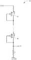
- FIG. 1is a schematic diagram of a fingerprint identification system 10 according to an embodiment of the present application.
- the fingerprint identification system 10includes a fingerprint sensing circuit 102 and a signal generating circuit 104.
- the fingerprint sensing circuit 102can generate a fingerprint signal, and the fingerprint identification system 10 can determine a fingerprint according to the fingerprint signal.
- the fingerprint sensing circuit 102can receive a floating power signal SVDD having a floating source amplitude and a floating ground signal SGND having a floating amplitude, and the intensity of the fingerprint signal is related to the floating source amplitude/floating amplitude That is, the larger the floating source amplitude or the floating amplitude, the more significant the fingerprint signal.
- the signal generating circuit 104is configured to generate a floating power signal SVDD having a large floating source amplitude and a floating ground signal SGND having a large floating amplitude, and provide the same to the fingerprint sensing circuit 102; specifically, the fingerprint sensing circuit 102 has a power source
- the signal generating circuit 104has an output terminal Out_A and an output terminal Out_B, and the output terminal Out_A is used to output the floating power signal SVDD generated by the signal generating circuit 104 to the power supply terminal PWR.
- the output terminal Out_Bis used to output the floating ground signal SGND generated by the signal generating circuit 104 to the floating ground terminal FGD.
- the signal generating circuit 104is a circuit fabricated by using a low voltage process, which has a Breakdown Voltage BV. In other words, when the voltage across the signal generating circuit 104 exceeds the withstand voltage BV, it will result in The semiconductor component inside the signal generating circuit 104 is broken down, causing the signal generating circuit 104 to be damaged. Under the premise that the signal generating circuit 104 has a withstand voltage BV, the signal generating circuit 104 can generate a floating power signal SVDD having a floating source amplitude greater than the withstand voltage BV and a floating ground signal SGND having a floating amplitude greater than the withstand voltage BV. Generally, the withstand voltage BV of the semiconductor component inside the signal generating circuit 104 is slightly larger than (or equal to) a voltage AVDD.
- the fingerprint sensing circuit 102can generate an excitation signal TX to the signal generating circuit 104, and the signal generating circuit 104 can generate the floating power signal SVDD and the floating ground signal SGND according to the excitation signal TX.
- FIG. 2is a waveform diagram of signals of an excitation signal TX, a floating power signal SVDD, and a floating ground signal SGND according to an embodiment of the present application. As can be seen from FIG.
- the floating power signal SVDD and the floating ground signal SGNDare both square waves, a high potential of the floating power signal SVDD is the voltage AVDD, and the low potential of the floating power signal SVDD is a negative voltage - AVDD, the floating ground signal SGND A high potential is a ground voltage GND, and the low potential of the floating ground signal SGND is one to two times the negative voltage -2AVDD (the negative of the voltage AVDD is twice).
- the fingerprint sensing circuit 102can generate a high potential of the excitation signal TX to a high potential of the floating power signal SVDD (ie, electricity) Voltage AVDD); In a second time interval, the fingerprint sensing circuit 102 can generate a low potential of the excitation signal TX to a low potential of the floating ground signal SGND (ie, twice the negative voltage - 2AVDD). In addition, there is a fixed voltage difference between the floating ground signal SGND and the floating ground signal SGND, that is, AVDD.
- the floating source amplitude of the floating power signal SVDDis 2AVDD (that is, twice the voltage AVDD)
- the floating ground amplitude of the floating ground signal SGNDis also 2AVDD, that is, the floating source amplitude of the floating power signal SVDD and
- the floating ground amplitude of the floating ground signal SGNDis greater than the withstand voltage BV of the semiconductor component inside the signal generating circuit 104.
- the present applicationcan utilize a low voltage component to generate a high voltage signal.
- the present applicationcan utilize a signal generating circuit 104 whose component withstand voltage BV is only slightly greater than (or equal to) the voltage AVDD, resulting in a voltage having a magnitude of 2 times AVDD.
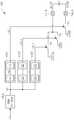
- FIG. 3is a schematic diagram of a signal generating circuit 304 according to an embodiment of the present application.
- the signal generating circuit 304can be used to implement a signal generating circuit 104, which is a circuit fabricated by a low voltage process and has a voltage slightly greater than or equal to a voltage AVDD. Withstand voltage BV.
- the signal generating circuit 304includes an amplitude reducing circuit VLS, a first level shifting circuit VDS1, a second level shifting circuit VDS2, a third level shifting circuit VDS3, and a first switching module. S1, a second switch module S2, a third switch module S3, and a capacitor C.
- the capacitor Cis coupled between the output terminal Out_A of the signal generating circuit 304 and the output terminal Out_B.
- the amplitude reduction circuit VLSis coupled to the fingerprint sensing circuit 102 to receive the excitation signal TX, which is used to increase the amplitude of the excitation signal TX.
- 3AVDDwhich is 3 times the voltage AVDD, is reduced to the voltage AVDD to generate an initial control signal ctrl, wherein an amplitude of the initial control signal ctrl is the voltage AVDD, and a low potential of the initial control signal ctrl and the low potential of the excitation signal TX Same (all It is -2AVDD), that is, a high potential of the initial control signal ctrl is -AVDD.
- FIG. 4is a schematic diagram of an amplitude reduction circuit 40 according to an embodiment of the present application.
- the amplitude reduction circuit 40can be used to implement the amplitude reduction circuit VLS.
- the amplitude reduction circuit 40includes transistors 41 to 4n and a resistor R. The gates of the transistors 41 to 4n are connected to the source thereof, and the transistors 41 to 4n are connected.
- a first end of the transistor sequenceis used to receive the excitation signal TX
- a second end of the transistor sequenceis used to output an initial control signal ctrl
- one end of the resistor Ris coupled to the second end of the transistor sequence, and One end receives twice the negative voltage -2AVDD.
- the excitation signal TXis at a high potential (voltage AVDD)
- the transistors 41 to 4nare turned on/on, and the initial control signal ctrl output from the amplitude reduction circuit 40 is a negative voltage -AVDD.
- the transistors 41 to 4nare turned off/off, and the initial control signal ctrl output from the amplitude reduction circuit 40 is twice the negative voltage - 2 AVDD.
- FIG. 5is a schematic diagram of an amplitude reduction circuit 50 according to an embodiment of the present application.
- the amplitude reduction circuit 50can be used to implement the amplitude reduction circuit VLS.
- the amplitude reduction circuit 50is similar to the amplitude reduction circuit 40.
- the amplitude reduction circuit 50includes diodes 51 to 5n, and the diodes 51 to 5n are connected in series to form a diode.
- the sequence, a first end of the diode sequenceis used to receive the excitation signal TX, and a second end of the diode sequence is used to output the initial control signal ctrl.
- the operation principle of the amplitude reduction circuit 50is similar to that of the amplitude reduction circuit 40, and thus will not be described herein.
- first level shifting circuit VDS1, the second level shifting circuit VDS2, and the third level shifting circuit VDS3are all coupled to the amplitude reducing circuit VLS, which are respectively used to translate the initial control signal ctrl upward and downward.
- a first control signal ctrl_1, a second control signal ctrl_2, and a third control signal ctrl_3are generated.
- the amplitudes of the first control signal ctrl_1, the second control signal ctrl_2, and the third control signal ctrl_3are all related to the initial control signal ctrl. The amplitudes are the same (all voltage AVDD).
- the shift amount ⁇ V1may be a double voltage 2AVDD (ie, 2 times the voltage AVDD), the shift amount ⁇ V2 may be the voltage AVDD, and the shift amount ⁇ V3 may be 0 (ie, the third level shift circuit VDS3) The voltage level of the initial control signal ctrl is not shifted).
- FIG. 9is a signal waveform diagram of an initial control signal ctrl, a first control signal ctrl_1, a second control signal ctrl_2, and a third control signal ctrl_3 according to an embodiment of the present application. As can be seen from FIG. 9
- the initial control signal ctrlis a square wave having a low potential of -2AVDD and a high potential of -AVDD
- the first control signal ctrl_1is a square wave having a low potential of the ground voltage GND and a high potential of the voltage AVDD
- the second control The signal ctrl_2is a square wave having a low potential of -AVDD and a high potential of the ground voltage GND
- the third control signal ctrl_3is also a square wave having a low potential of -2AVDD and a high potential of -AVDD.
- the first switch module S1, the second switch module S2, and the third switch module S3are respectively controlled by the first control signal ctrl_1, the second control signal ctrl_2, and the third control signal ctrl_3; and the control signals ctrl_1, ctrl_2, ctrl_3
- the switch modules S1, S2, S3, the signal generating circuit 304can generate the floating power signal SVDD and the floating ground signal SGND.
- the first switch module S1is coupled to the output terminal Out_A of the signal generating circuit 304, and the other end is coupled to the output of the signal generating circuit 304.
- the end of the third switch module S3receives twice the negative voltage -2AVDD, and the other end is coupled to the output terminal Out_B of the signal generating circuit 304.
- Control the switching modules S1, S2, S3 with the control signals ctrl_1, ctrl_2, ctrl_3The method of generating the floating power signal SVDD and the floating ground signal SGND is not limited.
- the control signals ctrl_1, ctrl_2, ctrl_3are all low, the first control signal ctrl_1 is the ground voltage GND, the second control signal ctrl_2 is the negative voltage -AVDD, and the third control signal ctrl_3 is the double negative voltage - 2AVDD, the first switch module S1 and the second switch module S2 are turned on/ON, and the third switch module S3 is open/OFF, and the signal generating circuit 304 outputs the floating power signal SVDD to the output terminal Out_A as the voltage AVDD, which corresponds to the floating power supply.
- the signal generating circuit 304outputs the floating ground signal SGND to the ground voltage GND at the output terminal Out_B, which corresponds to the high potential of the floating ground signal SGND.
- the control signals ctrl_1, ctrl_2, ctrl_3are all high, the first control signal ctrl_1 is the voltage AVDD, the second control signal ctrl_2 is the ground voltage GND, and the third control signal ctrl_3 is the negative voltage -AVDD, the first The switch module S1 and the second switch module S2 are open/OFF, and the third switch module S3 is turned on/ON, and the signal generating circuit 304 outputs the floating ground signal SGND to the output terminal Out_B to be twice the negative voltage -2AVDD.
- the capacitance C between the output terminal Out_A and the output terminal Out_Bcan maintain a fixed voltage difference between the output terminal Out_A and the output terminal Out_B, when the floating ground signal SGND is instantaneously dropped from its high potential (ground voltage GND) to its low potential (2 times negative voltage -2AVDD), that is, the potential of the output terminal Out_B drops 2AVDD instantaneously.
- the capacitor Calso pulls the output terminal Out_A down 2AVDD, that is, the floating power signal SVDD will drop 2AVDD from its high potential (voltage AVDD). Reach its low potential (negative voltage -AVDD).
- the signal generating circuit 304can generate the floating power signal SVDD and the floating ground signal SGND as shown in FIG. 2.
- the first level shifting circuit VDS1, the second level shifting circuit VDS2, and the third level shifting circuit VDS3are not limited to being implemented by a specific circuit configuration.
- the first place The quasi-shift circuit VDS1may include voltage level shifting units 311, 312, and the second level shifting circuit VDS2 may include a voltage level shifting unit 321 and a dummy level shifting unit 322, and the third level shifting The bit circuit VDS3 may include dummy level shifting units 331, 332.
- the voltage level shifting unit 311, 312, 321can shift its input signal by a shift amount ⁇ V
- the dummy level shifting unit 322, 331, 332maintains the level of its input signal, wherein the shift amount ⁇ V can be a voltage AVDD.
- the voltage level shifting unit 311can shift the initial control signal ctrl upward by the shift amount ⁇ V (ie, voltage AVDD) to generate a signal ctrl', and the voltage level shifting unit 312 can turn the signal ctrl' up again.
- the shift circuit VDS2can output the second control signal ctrl_2.
- the voltage level shifting units 311, 312, 321 and the dummy level shifting units 322, 331, 332are not limited to being implemented with a specific circuit.
- FIG. 6 and FIG. 7are schematic diagrams of a voltage level shifting unit 60 and a dummy level shifting unit 70 according to an embodiment of the present application.
- the voltage level shifting unit 60can be used to implement voltage level shifting units 311, 312, 321 which can be used to implement the dummy level shifting units 322, 331, 332.
- the voltage level shifting unit 60can generate an output signal out, and the output signal out is intermediate to the intermediate voltage.
- the dummy bit shiftsWhen the input signal input of the bit cell 70 is between a low voltage VL7 and a high voltage VH7, the dummy level shifting unit 70 can generate an output signal out which is also between the low voltage VL7 and the high voltage VH7. Details of the operation of the voltage level shifting unit 60 and the dummy level shifting unit 70 are well known to those skilled in the art, and thus will not be described herein.
- FIG. 8is a schematic diagram of a first switch module S1, a second switch module S2, and a third switch module S3 according to an embodiment of the present application.
- the first switching module S1includes transistors PP0, PP1, NP2, wherein the transistors PP0 and PP1 are PMOS transistors, and the transistor NP2 is an NMOS transistor.
- a source of the transistor PP0receives the voltage AVDD
- a gate of the transistor PP0receives the first control signal ctrl_1
- a drain of the transistor PP0is coupled to the output terminal Out_A through the transistor PP1.
- the transistors PP0 and PP1are turned on/ON, and the transistor NP2 is turned off/OFF; when the first control signal ctrl_1 is high (voltage AVDD), the transistor PP0 PP1 is open/OFF, and transistor NP2 is on/off.
- the second switching module S2includes transistors P0, P1, N2, wherein the transistors P0 and P1 are PMOS transistors, and the transistor N2 is an NMOS transistor.
- a source of the transistor P0receives the ground voltage GND, a gate of the transistor P0 receives the second control signal ctrl_2, and a drain of the transistor P0 is coupled to the output terminal Out_B through the transistor P1.
- the third switch module S3includes transistors N0, N1, P2, wherein the transistors N0 and N1 are NMOS transistors, and the transistor P2 is PMOS transistor.
- a source of the transistor N0receives a two-fold negative voltage -2AVDD
- a gate of the transistor N0receives a third control signal ctrl_3, and a drain of the transistor N0 is coupled to the output terminal Out_B through the transistor N1.
- the third control signal ctrl_3is at a high potential (negative voltage -AVDD)
- the transistors N0, N1are turned ON/ON, and the transistor P2 is turned off/OFF; when the third control signal ctrl_3 is low (double undervoltage - 2AVDD)
- the transistors N0 and N1are open/OFF, the transistor P2 is turned on/on.
- the signal generating circuit 304can generate the floating power signal SVDD and the floating ground signal SGND as shown in FIG. 2.
- the present applicationutilizes the signal generating circuits 104, 304 whose component withstand voltage BV is only slightly larger than (or equal to) the voltage AVDD, and generates the floating power signal SVDD and the floating ground signal SGND having a voltage twice the amplitude AVDD, while avoiding
- a signal generation circuit(used to generate a floating power signal and a floating ground signal) is fabricated using a high voltage process to reduce the production cost of the fingerprint identification system.
- fingerprint sensing circuit 102 and signal generating circuit 104can be fabricated using the same semiconductor process, or can be formed in a single integrated circuit.
- the present applicationcan utilize a signal generating circuit produced by a low voltage process to generate a floating power signal having a high voltage amplitude and a floating ground signal to increase the intensity of the fingerprint signal.
- the present applicationhas the advantage of reducing production costs.
Landscapes
- Engineering & Computer Science (AREA)
- Human Computer Interaction (AREA)
- Physics & Mathematics (AREA)
- General Physics & Mathematics (AREA)
- Multimedia (AREA)
- Theoretical Computer Science (AREA)
- Logic Circuits (AREA)
- Image Input (AREA)
- Semiconductor Integrated Circuits (AREA)
Abstract
Description
Translated fromChinese本申请涉及一种指纹辨识系统,尤其涉及一种可产生高压信号的指纹辨识系统。The present application relates to a fingerprint identification system, and more particularly to a fingerprint identification system that can generate a high voltage signal.
随着科技日新月异,移动电话、数字相机、平板计算机、笔记本电脑等越来越多携带型电子装置已经成为了人们生活中必备的工具。由于携带型电子装置一般为个人使用,而具有一定的隐私性,因此其内部储存的数据,例如电话簿、相片、个人信息等等为私人所有。若电子装置一旦丢失,则这些数据可能会被他人所利用,而造成不必要的损失。虽然目前已有利用密码保护的方式来避免电子装置为他人所使用,但密码容易泄露或遭到破解,具有较低的安全性。并且,用户需记住密码才能使用电子装置,若忘记密码,则会带给使用者许多不便。因此,目前发展出利用个人指纹识别系统的方式来达到身份认证的目的,以提升数据安全性。With the rapid development of technology, more and more portable electronic devices such as mobile phones, digital cameras, tablet computers, and notebook computers have become essential tools in people's lives. Since portable electronic devices are generally used by individuals and have certain privacy, their internally stored data, such as phone books, photos, personal information, etc., are privately owned. If the electronic device is lost, the data may be used by others and cause unnecessary losses. Although password protection has been used to prevent electronic devices from being used by others, passwords are easily leaked or cracked, and have low security. Moreover, the user needs to remember the password in order to use the electronic device, and if the password is forgotten, it will bring a lot of inconvenience to the user. Therefore, the use of personal fingerprint identification systems to achieve identity authentication has been developed to improve data security.
对于指纹辨识系统来说,需要利用具有高压振幅的方波信号来增强指纹信号。然而,为了产生高压振幅的方波信号,需利用一高压半导体制程来生产具有高耐压的半导体组件,并利用具有高耐压的半导体组件形成其信号产生电路。然而,高压半导体制程的生产成本较高,而导致应用指纹辨识电路系统的电子产品所需的生产成本增加。For fingerprint recognition systems, it is necessary to use a square wave signal with a high voltage amplitude to enhance the fingerprint signal. However, in order to generate a square wave signal of a high voltage amplitude, a high voltage semiconductor process is required to produce a semiconductor component having a high withstand voltage, and a signal generating circuit is formed using a semiconductor component having a high withstand voltage. However, the production cost of the high-voltage semiconductor process is high, and the production cost required for the electronic product to which the fingerprint identification circuit system is applied is increased.
因此,如何利用低压制程生产制造的半导体组件来产生高压振幅方波,即为业界所努力的目标之一。Therefore, how to produce a high-voltage amplitude square wave by using a low-voltage process to manufacture a semiconductor component,It is one of the goals of the industry.
发明内容Summary of the invention
因此,本发明部分实施例主要目的即在于提供一种可包含有以低压组件制程且可产生高压信号的指纹辨识系统。Accordingly, it is a primary object of some embodiments of the present invention to provide a fingerprint recognition system that can include a low voltage component process and that can generate high voltage signals.
为了解决上述技术问题,本申请提供了一种指纹辨识系统,包括一指纹感测电路,具有一电源供应端以及一浮动接地端,用来产生一指纹信号以及一第一信号,其中所述指纹辨识系统根据所述指纹信号判断一指纹;以及一信号产生电路,具有一第一输出端以及一第二输出端,所述第一输出端耦接于所述电源供应端,所述第二输出端耦接于所述浮动接地端,所述信号产生电路用来根据所述第一信号产生一浮动电源信号至所述电源供应端,并根据所述第一信号产生一浮动接地信号至所述浮动接地端,其中所述浮动电源信号具有一浮源振幅,所述浮动接地信号具有一浮地振幅;其中,所述信号产生电路具有一耐压,所述浮源振幅及所述浮地振幅皆大于所述耐压。In order to solve the above technical problem, the present application provides a fingerprint identification system including a fingerprint sensing circuit having a power supply end and a floating ground for generating a fingerprint signal and a first signal, wherein the fingerprint The identification system determines a fingerprint according to the fingerprint signal; and a signal generating circuit having a first output end and a second output end, the first output end being coupled to the power supply end, the second output The signal is coupled to the floating ground, the signal generating circuit is configured to generate a floating power signal to the power supply terminal according to the first signal, and generate a floating ground signal according to the first signal to the a floating ground terminal, wherein the floating power signal has a floating source amplitude, the floating ground signal has a floating amplitude; wherein the signal generating circuit has a withstand voltage, the floating source amplitude and the floating amplitude Both are greater than the withstand voltage.
例如,所述信号产生电路包含一振幅缩小电路,耦接于所述指纹感测电路,用来根据所述第一信号产生一第二信号,其中所述第一信号具有一第一振幅,所述第二信号具有一第二振幅,所述第二振幅小于所述第一振幅,所述第二振幅小于或等于所述耐压。For example, the signal generating circuit includes an amplitude reducing circuit coupled to the fingerprint sensing circuit for generating a second signal according to the first signal, wherein the first signal has a first amplitude, The second signal has a second amplitude, the second amplitude being less than the first amplitude, and the second amplitude being less than or equal to the withstand voltage.
例如,一第一位准移位电路,耦接于所述振幅缩小电路,用来将所述第二信号平移一第一平移量,以产生一第一控制信号;一第二位准移位电路,耦接于所述振幅缩小电路,用来将所述第二信号平移一第二平移量,以产生一第二控制信号;一第一开关模块,其一端接收一第一电压,另一端耦接于所述第一输出端,所述第一开关模块受控于所述第一控制信号;一第二开关模块,其一端接收一第二电压,另一端耦接于所述第二输出端,所述第二开关模块受控于所述第二控制信号;一第三开关模块,其一端接收一第三电压,另一端耦接于所述第二输出端,所述第三开关模块受控于一第三控制信号;以及一电容,耦接于所述第一输出端与所述第二输出端之间;其中,所述第三控制信号相关于所述第二信号。For example, a first level shifting circuit is coupled to the amplitude reduction circuit for translating the second signal by a first amount of translation to generate a first control signal; a second level shifting a circuit coupled to the amplitude reduction circuit for translating the second signal by a second amount of translation to generate a second control signal; a first switch module having a first voltage received at one end and the other end Coupling to the first output end, the first switch module is controlled by the first control signal; a second switch module,One end receives a second voltage, the other end is coupled to the second output end, the second switch module is controlled by the second control signal; and a third switch module receives one third voltage at one end, and another One end is coupled to the second output end, the third switch module is controlled by a third control signal; and a capacitor is coupled between the first output end and the second output end; The third control signal is related to the second signal.
例如,所述信号产生电路包含一第三位准移位电路,耦接于所述振幅缩小电路,用来根据所述第二信号产生所述第三控制信号。For example, the signal generating circuit includes a third level shifting circuit coupled to the amplitude reducing circuit for generating the third control signal according to the second signal.
例如,所述第二信号的一低电位与所述第一信号的一低电位相同。For example, a low potential of the second signal is the same as a low potential of the first signal.
例如,所述第一控制信号、所述第二控制信号及所述第三控制信号的振幅与所述第二振幅相同。For example, the amplitudes of the first control signal, the second control signal, and the third control signal are the same as the second amplitude.
例如,于一第一时间,所述第一开关模块及所述第二开关模块为导通,所述第一输出端输出所述浮动电源信号为所述第一电压,所述第二输出端输出所述浮动接地信号为所述第二电压,于一第二时间,所述第三开关模块导通,所述第二输出端输出所述浮动接地信号为所述第三电压。For example, in a first time, the first switch module and the second switch module are turned on, and the first output end outputs the floating power signal as the first voltage, and the second output end And outputting the floating ground signal to the second voltage, the third switch module is turned on at a second time, and the second output terminal outputs the floating ground signal as the third voltage.
例如,所述第三电压为所述第一电压的负2倍,所述第二电压为一接地电压。For example, the third voltage is a negative 2 times the first voltage, and the second voltage is a ground voltage.
例如,所述振幅缩小电路包含有复数个晶体管,串接成一晶体管序列,所述晶体管序列的一第一端接收所述第一信号,所述晶体管序列的一第二端输出所述第二信号;以及一电阻,耦接于所述晶体管序列的所述第二端。For example, the amplitude reduction circuit includes a plurality of transistors connected in series to form a transistor, a first end of the transistor sequence receives the first signal, and a second end of the transistor sequence outputs the second signal And a resistor coupled to the second end of the transistor sequence.
例如,所述第一位准移位电路包含一第一电压位准移位单元以及一第二电压位准移位单元,所述第一电压位准移位单元用来将所述第二信号向上平移一第三平移量,以产生一第三信号,所述第二电压位准移位单元用来将所述第三信号向上平移所述第三平移量,所述第三平移量与所述第二振幅相同。For example, the first level shifting circuit includes a first voltage level shifting unit and a second voltage level shifting unit, and the first voltage level shifting unit is configured to use the second level signal Translating a third amount of translation upward to generate a third signal, the second voltage level shifting unit is configured toThe third signal translates the third amount of translation upward, the third amount of translation being the same as the second amplitude.
例如,所述第二位准移位电路包含一第三电压位准移位单元,所述第三电压位准移位单元用来将所述第二信号向上平移所述第二平移量,所述第二平移量与所述第二振幅相同。For example, the second level shifting circuit includes a third voltage level shifting unit, and the third voltage level shifting unit is configured to translate the second signal upward by the second amount of translation. The second amount of translation is the same as the second amplitude.
例如,所述第二位准移位电路另包含一第一虚设位准移位单元,耦接于所述第三电压位准移位单元。For example, the second level shifting circuit further includes a first dummy level shifting unit coupled to the third voltage level shifting unit.
例如,所述第三位准移位电路包含一第二虚设位准移位单元以及一第三虚设位准移位单元,所述第二虚设位准移位单元接收所述第二信号,所述第三虚设位准移位单元输出所述第三控制信号,所述第二信号与所述第三控制信号具有相同的高电位,所述第二信号与所述第三控制信号具有相同的低电位。For example, the third level shifting circuit includes a second dummy level shifting unit and a third dummy level shifting unit, and the second dummy level shifting unit receives the second signal. The third dummy level shifting unit outputs the third control signal, the second signal and the third control signal have the same high potential, and the second signal and the third control signal have the same Low potential.
例如,在一第一时间,所述第一信号为所述浮动电源信号,在一第二时间,所述第一信号为所述浮动接地信号。For example, at a first time, the first signal is the floating power signal, and at a second time, the first signal is the floating ground signal.
例如,所述浮动电源信号与所述浮动接地信号之间具有一固定电压差。For example, there is a fixed voltage difference between the floating power signal and the floating ground signal.
本申请的信号产生电路可利用以低压制程所生产的信号产生电路来产生具有高压振幅的浮动电源信号及浮动接地信号,以增加指纹信号的强度。相较于现有技术,本申请具有降低生产成本的优点。The signal generating circuit of the present application can utilize a signal generating circuit produced by a low voltage process to generate a floating power signal having a high voltage amplitude and a floating ground signal to increase the intensity of the fingerprint signal. Compared with the prior art, the present application has the advantage of reducing production costs.
一个或多个实施例通过与之对应的附图中的图片进行示例性说明,这些示例性说明并不构成对实施例的限定,附图中具有相同参考数字标号的元件表示为类似的元件,除非有特别申明,附图中的图不构成比例限制。The one or more embodiments are exemplified by the accompanying drawings in the accompanying drawings, and FIG. The figures in the drawings do not constitute a scale limitation unless otherwise stated.
图1为本申请实施例一指纹辨识系统的示意图。FIG. 1 is a schematic diagram of a fingerprint identification system according to an embodiment of the present application.
图2为本申请实施例复数个信号波形图。FIG. 2 is a diagram of a plurality of signal waveforms in the embodiment of the present application.
图3为本申请实施例一信号产生电路的示意图。FIG. 3 is a schematic diagram of a signal generating circuit according to an embodiment of the present application.
图4为本申请实施例一振幅缩小电路的示意图。FIG. 4 is a schematic diagram of an amplitude reduction circuit according to an embodiment of the present application.
图5为本申请实施例一振幅缩小电路的示意图。FIG. 5 is a schematic diagram of an amplitude reduction circuit according to an embodiment of the present application.
图6为本申请实施例一电压位准移位单元的示意图。FIG. 6 is a schematic diagram of a voltage level shifting unit according to an embodiment of the present application.
图7为本申请实施例一虚设位准移位单元的示意图。FIG. 7 is a schematic diagram of a dummy level shifting unit according to an embodiment of the present application.
图8为本申请实施例复数个开关模块的示意图。FIG. 8 is a schematic diagram of a plurality of switch modules according to an embodiment of the present application.
图9为本申请实施例复数个信号波形图。FIG. 9 is a diagram of a plurality of signal waveforms in the embodiment of the present application.
为了使本申请的目的、技术方案及优点更加清楚明白,以下结合附图及实施例,对本申请进行进一步详细说明。应当理解,此处所描述的具体实施例仅仅用以解释本申请,并不用于限定本申请。In order to make the objects, technical solutions, and advantages of the present application more comprehensible, the present application will be further described in detail below with reference to the accompanying drawings and embodiments. It is understood that the specific embodiments described herein are merely illustrative of the application and are not intended to be limiting.
请参考图1,图1为本申请实施例一指纹辨识系统10的示意图。指纹辨识系统10包含一指纹感测电路102以及一信号产生电路104,指纹感测电路102可产生一指纹信号,而指纹辨识系统10可根据指纹信号判断一指纹。为了增强指纹信号,指纹感测电路102可接收具有一浮源振幅的一浮动电源信号SVDD以及具有一浮地振幅的一浮动接地信号SGND,而指纹信号的强度与浮源振幅/浮地振幅相关,也就是说,当浮源振幅或浮地振幅越大时,指纹信号就越显著。信号产生电路104用来产生具有大浮源振幅的浮动电源信号SVDD以及具有大浮地振幅的浮动接地信号SGND,并提供至指纹感测电路102;具体来说,指纹感测电路102具有一电源供应端PWR以及一浮动接地端FGD,而信号产生电路104具有一输出端Out_A以及一输出端Out_B,输出端Out_A用来将信号产生电路104所产生的浮动电源信号SVDD输出至电源供应端PWR,输出端Out_B用来将信号产生电路104所产生的浮动接地信号SGND输出至浮动接地端FGD。Please refer to FIG. 1. FIG. 1 is a schematic diagram of a
需注意的是,信号产生电路104为利用一低压制程所制造的电路,其具有一耐压(Breakdown Voltage)BV,换句话说,当信号产生电路104的跨压超过耐压BV时,将导致信号产生电路104内部的半导体组件击穿/崩溃(Breakdown),而导致信号产生电路104损坏。在信号产生电路104具有耐压BV的前提之下,信号产生电路104可产生浮源振幅大于耐压BV的浮动电源信号SVDD以及浮地振幅大于耐压BV的浮动接地信号SGND。一般来说,信号产生电路104内部半导体组件的耐压BV略大于(或等于)一电压AVDD。It should be noted that the
更进一步地,指纹感测电路102可产生一激励信号TX至信号产生电路104,而信号产生电路104可根据激励信号TX产生浮动电源信号SVDD以及浮动接地信号SGND。举例来说,请参考图2,图2为本申请实施例激励信号TX、浮动电源信号SVDD及浮动接地信号SGND的信号波形图。由图2可知,浮动电源信号SVDD及浮动接地信号SGND皆为方波,浮动电源信号SVDD的一高电位为电压AVDD,浮动电源信号SVDD的低电位为一负电压-AVDD,浮动接地信号SGND的一高电位为一接地电压GND,浮动接地信号SGND的低电位为一二倍负压-2AVDD(电压AVDD的负二倍)。在一第一时间区间中,指纹感测电路102可产生激励信号TX的一高电位为浮动电源信号SVDD的一高电位(即为电压AVDD);在一第二时间区间中,指纹感测电路102可产生激励信号TX的一低电位为浮动接地信号SGND的一低电位(即为二倍负压-2AVDD)。另外,浮动接地信号SGND与浮动接地信号SGND之间具有一固定电压差,即为AVDD。Further, the
另一方面,由图2可知,浮动电源信号SVDD的浮源振幅为2AVDD(即电压AVDD的二倍),浮动接地信号SGND的浮地振幅亦为2AVDD,即浮动电源信号SVDD的浮源振幅及浮动接地信号SGND的浮地振幅皆大于信号产生电路104内部半导体组件的耐压BV。换句话说,本申请可利用低压组件产生高压信号,更具体地,本申请可利用其组件耐压BV仅略大于(或等于)电压AVDD的信号产生电路104,产生具有振幅为2倍电压AVDD的浮动电源信号SVDD及浮动接地信号SGND。On the other hand, as shown in FIG. 2, the floating source amplitude of the floating power signal SVDD is 2AVDD (that is, twice the voltage AVDD), and the floating ground amplitude of the floating ground signal SGND is also 2AVDD, that is, the floating source amplitude of the floating power signal SVDD and The floating ground amplitude of the floating ground signal SGND is greater than the withstand voltage BV of the semiconductor component inside the
请参考图3,图3为本申请实施例一信号产生电路304的示意图,信号产生电路304可用来实现信号产生电路104,其为以低压制程所制造的电路,具有略大于或等于电压AVDD的耐压BV。信号产生电路304包含一振幅缩小电路VLS、一第一位准移位(Level Shifter)电路VDS1、一第二位准移位电路VDS2、一第三位准移位电路VDS3、一第一开关模块S1、一第二开关模块S2、一第三开关模块S3以及一电容C。电容C耦接于信号产生电路304的输出端Out_A与输出端Out_B之间,振幅缩小电路VLS耦接于指纹感测电路102以接收激励信号TX,其用来将激励信号TX的振幅(其为3AVDD,即电压AVDD的3倍)缩小至电压AVDD,以产生一初始控制信号ctrl,其中初始控制信号ctrl的一振幅为电压AVDD,而初始控制信号ctrl的一低电位与激励信号TX的低电位相同(皆为-2AVDD),即初始控制信号ctrl的一高电位为-AVDD。Please refer to FIG. 3. FIG. 3 is a schematic diagram of a
另外,振幅缩小电路VLS不限于利用特定电路结构来实现。举例来说,请参考图4,图4为本申请实施例一振幅缩小电路40的示意图。振幅缩小电路40可用来实现振幅缩小电路VLS,振幅缩小电路40包含晶体管41~4n以及一电阻R,晶体管41~4n的栅极(Gate)与其源极(Source)相接,晶体管41~4n串接成一晶体管序列,晶体管序列的一第一端用来接收激励信号TX,晶体管序列的一第二端用来输出初始控制信号ctrl,而电阻R的一端耦接于晶体管序列的第二端,另一端接收二倍负压-2AVDD。当激励信号TX为高电位(电压AVDD)时,晶体管41~4n为导通/ON,振幅缩小电路40输出的初始控制信号ctrl为负电压-AVDD。当激励信号TX为低电位(二倍负压-2AVDD)时,晶体管41~4n为断路/OFF,振幅缩小电路40输出的初始控制信号ctrl为二倍负压-2AVDD。In addition, the amplitude reduction circuit VLS is not limited to being realized by a specific circuit configuration. For example, please refer to FIG. 4. FIG. 4 is a schematic diagram of an
另外,请参考图5,图5为本申请实施例一振幅缩小电路50的示意图。振幅缩小电路50可用来实现振幅缩小电路VLS,振幅缩小电路50与振幅缩小电路40类似,与振幅缩小电路40不同的是,振幅缩小电路50包含二极管51~5n,二极管51~5n串接成一二极管序列,二极管序列的一第一端用来接收激励信号TX,二极管序列的一第二端用来输出初始控制信号ctrl。振幅缩小电路50的操作原理与振幅缩小电路40类似,故于此不再赘述。In addition, please refer to FIG. 5. FIG. 5 is a schematic diagram of an
另外,第一位准移位电路VDS1、第二位准移位电路VDS2及第三位准移位电路VDS3均耦接于振幅缩小电路VLS,其分别用来将初始控制信号ctrl向上平移一平移量ΔV1、一平移量ΔV2及一平移量ΔV3,以分别产生一第一控制信号ctrl_1、一第二控制信号ctrl_2以及一第三控制信号ctrl_3,其中,第一控制信号ctrl_1、第二控制信号ctrl_2以及第三控制信号ctrl_3的振幅皆与初始控制信号ctrl的振幅相同(皆为电压AVDD)。在一实施例中,平移量ΔV1可为二倍电压2AVDD(即为电压AVDD的2倍),平移量ΔV2可为电压AVDD,而平移量ΔV3可为0(即第三位准移位电路VDS3不对初始控制信号ctrl的电压位准进行移位)。In addition, the first level shifting circuit VDS1, the second level shifting circuit VDS2, and the third level shifting circuit VDS3 are all coupled to the amplitude reducing circuit VLS, which are respectively used to translate the initial control signal ctrl upward and downward. The amount ΔV1, a translation amount ΔV2, and a translation amount ΔV3,A first control signal ctrl_1, a second control signal ctrl_2, and a third control signal ctrl_3 are generated. The amplitudes of the first control signal ctrl_1, the second control signal ctrl_2, and the third control signal ctrl_3 are all related to the initial control signal ctrl. The amplitudes are the same (all voltage AVDD). In one embodiment, the shift amount ΔV1 may be a double voltage 2AVDD (ie, 2 times the voltage AVDD), the shift amount ΔV2 may be the voltage AVDD, and the shift amount ΔV3 may be 0 (ie, the third level shift circuit VDS3) The voltage level of the initial control signal ctrl is not shifted).
请参考图9,图9为本申请实施例初始控制信号ctrl、第一控制信号ctrl_1、第二控制信号ctrl_2及第三控制信号ctrl_3的信号波形图。由图9可知,初始控制信号ctrl为低电位为-2AVDD且高电位为-AVDD的方波,第一控制信号ctrl_1为低电位为接地电压GND且高电位为电压AVDD的方波,第二控制信号ctrl_2为低电位为-AVDD且高电位为接地电压GND的方波,第三控制信号ctrl_3亦为低电位为-2AVDD且高电位为-AVDD的方波。Please refer to FIG. 9. FIG. 9 is a signal waveform diagram of an initial control signal ctrl, a first control signal ctrl_1, a second control signal ctrl_2, and a third control signal ctrl_3 according to an embodiment of the present application. As can be seen from FIG. 9, the initial control signal ctrl is a square wave having a low potential of -2AVDD and a high potential of -AVDD, and the first control signal ctrl_1 is a square wave having a low potential of the ground voltage GND and a high potential of the voltage AVDD, and the second control The signal ctrl_2 is a square wave having a low potential of -AVDD and a high potential of the ground voltage GND, and the third control signal ctrl_3 is also a square wave having a low potential of -2AVDD and a high potential of -AVDD.
另外,第一开关模块S1、第二开关模块S2及第三开关模块S3可分别受控于第一控制信号ctrl_1、第二控制信号ctrl_2及第三控制信号ctrl_3;通过控制信号ctrl_1、ctrl_2、ctrl_3以及开关模块S1、S2、S3,信号产生电路304可产生浮动电源信号SVDD及浮动接地信号SGND。其中,第一开关模块S1的一端接收电压AVDD,另一端耦接于信号产生电路304的输出端Out_A;第二开关模块S2的一端接收接地电压GND,另一端耦接于信号产生电路304的输出端Out_B;第三开关模块S3的一端接收二倍负压-2AVDD,另一端耦接于信号产生电路304的输出端Out_B。In addition, the first switch module S1, the second switch module S2, and the third switch module S3 are respectively controlled by the first control signal ctrl_1, the second control signal ctrl_2, and the third control signal ctrl_3; and the control signals ctrl_1, ctrl_2, ctrl_3 And the switch modules S1, S2, S3, the
利用控制信号ctrl_1、ctrl_2、ctrl_3控制开关模块S1、S2、S3以产生浮动电源信号SVDD及浮动接地信号SGND的方式并未有所限。举例来说,当控制信号ctrl_1、ctrl_2、ctrl_3皆为低电位时,第一控制信号ctrl_1为接地电压GND,第二控制信号ctrl_2为负电压-AVDD,第三控制信号ctrl_3为二倍负压-2AVDD,第一开关模块S1及第二开关模块S2为导通/ON,第三开关模块S3为断路/OFF,信号产生电路304于输出端Out_A输出浮动电源信号SVDD为电压AVDD,其对应浮动电源信号SVDD的高电位,信号产生电路304于输出端Out_B输出浮动接地信号SGND为接地电压GND,其对应浮动接地信号SGND的高电位。另一方面,当控制信号ctrl_1、ctrl_2、ctrl_3皆为高电位时,第一控制信号ctrl_1为电压AVDD,第二控制信号ctrl_2为接地电压GND,第三控制信号ctrl_3为负电压-AVDD,第一开关模块S1及第二开关模块S2为断路/OFF,第三开关模块S3为导通/ON,信号产生电路304于输出端Out_B输出浮动接地信号SGND为二倍负压-2AVDD。另外,由于输出端Out_A与输出端Out_B之间电容C可维持输出端Out_A与输出端Out_B之间固定的电压差,当浮动接地信号SGND由其高电位(接地电压GND)瞬间下降至其低电位(二倍负压-2AVDD)时,即输出端Out_B的电位瞬间下降2AVDD,此时电容C亦将输出端Out_A拉下2AVDD,即浮动电源信号SVDD会由其高电位(电压AVDD)下降2AVDD而达到其低电位(负电压-AVDD)。如此一来,信号产生电路304即可产生如图2所示的浮动电源信号SVDD及浮动接地信号SGND。Control the switching modules S1, S2, S3 with the control signals ctrl_1, ctrl_2, ctrl_3The method of generating the floating power signal SVDD and the floating ground signal SGND is not limited. For example, when the control signals ctrl_1, ctrl_2, ctrl_3 are all low, the first control signal ctrl_1 is the ground voltage GND, the second control signal ctrl_2 is the negative voltage -AVDD, and the third control signal ctrl_3 is the double negative voltage - 2AVDD, the first switch module S1 and the second switch module S2 are turned on/ON, and the third switch module S3 is open/OFF, and the
另外,第一位准移位电路VDS1、第二位准移位电路VDS2及第三位准移位电路VDS3不限于利用特定电路结构来实现。举例来说,第一位准移位电路VDS1可包含电压位准移位单元311、312,第二位准移位电路VDS2可包含一电压位准移位单元321以及一虚设位准移位单元322,第三位准移位电路VDS3可包含虚设位准移位单元331、332。电压位准移位单元311、312、321可将其输入信号平移一平移量ΔV,而虚设位准移位单元322、331、332则维持其输入信号的位准,其中平移量ΔV可为电压AVDD。换句话说,电压位准移位单元311可将初始控制信号ctrl向上平移平移量ΔV(即电压AVDD),以产生一信号ctrl’,而电压位准移位单元312可将信号ctrl’再次向上平移平移量ΔV,以产生第一控制信号ctrl_1(ΔV1=2ΔV),同样地,电压位准移位单元321可将初始控制信号ctrl向上平移平移量ΔV(ΔV2=ΔV),而第二位准移位电路VDS2即可输出第二控制信号ctrl_2。In addition, the first level shifting circuit VDS1, the second level shifting circuit VDS2, and the third level shifting circuit VDS3 are not limited to being implemented by a specific circuit configuration. For example, the first placeThe quasi-shift circuit VDS1 may include voltage
电压位准移位单元311、312、321及虚设位准移位单元322、331、332不限于利用特定电路来实现。举例来说,请参考图6及图7,图6及图7分别为本申请实施例一电压位准移位单元60及一虚设位准移位单元70的示意图。电压位准移位单元60可用来实现电压位准移位单元311、312、321,虚设位准移位单元70可用来实现虚设位准移位单元322、331、332。当电压位准移位单元60的一输入信号input介于一低电压VL与一中间电压VM之间时,电压位准移位单元60可产生一输出信号out,而输出信号out介于中间电压VM与一高电压VH之间,另外,电压位准移位单元60可接收第一参考电压Vrefp、第二参考电压Vrefn来进行偏压,其中电压VL、VM、VH、Vrefp、Vrefn具有VL<Vrefn<VM<Vrefp<VH且VH-VM=VM-VL=Vrefp-Vrefn=ΔV的关系。另外,当虚设位准移位单元70的输入信号input介于一低电压VL7与一高电压VH7之间时,虚设位准移位单元70可产生同样介于低电压VL7与高电压VH7之间的输出信号out。关于电压位准移位单元60及虚设位准移位单元70的操作细节,为本领域一般技术人员所熟知,故于此不再赘述。The voltage
另外,第一开关模块S1、第二开关模块S2及第三开关模块S3不限于利用特定电路结构来实现。举例来说,请参考图8,图8为本申请实施例第一开关模块S1、第二开关模块S2及第三开关模块S3的示意图。第一开关模块S1包含晶体管PP0、PP1、NP2,其中晶体管PP0和PP1为PMOS晶体管,晶体管NP2为NMOS晶体管。晶体管PP0的一源极(Source)接收电压AVDD,晶体管PP0的一栅极(Gate)接收第一控制信号ctrl_1,晶体管PP0的一漏极(Drain)通过晶体管PP1耦接于输出端Out_A。当第一控制信号ctrl_1为低电位(接地电压GND)时,晶体管PP0、PP1为导通/ON,晶体管NP2为断路/OFF;当第一控制信号ctrl_1为高电位(电压AVDD)时,晶体管PP0、PP1为断路/OFF,晶体管NP2为导通/ON。第二开关模块S2包含晶体管P0、P1、N2,其中晶体管P0和P1为PMOS晶体管,晶体管N2为NMOS晶体管。晶体管P0的一源极接收接地电压GND,晶体管P0的一栅极接收第二控制信号ctrl_2,晶体管P0的一漏极(Drain)通过晶体管P1耦接于输出端Out_B。当第二控制信号ctrl_2为低电位(接地电压GND)时,晶体管P0、P1为导通/ON,晶体管N2为断路/OFF;当第二控制信号ctrl_2为高电位(电压AVDD)时,晶体管P0、P1为断路/OFF,晶体管N2为导通/ON。第三开关模块S3包含晶体管N0、N1、P2,其中晶体管N0和N1为NMOS晶体管,晶体管P2为PMOS晶体管。晶体管N0的一源极接收一二倍负压-2AVDD,晶体管N0的一栅极接收第三控制信号ctrl_3,晶体管N0的一漏极(Drain)通过晶体管N1耦接于输出端Out_B。当第三控制信号ctrl_3为高电位(负电压-AVDD)时,晶体管N0、N1为导通/ON,晶体管P2为断路/OFF;当第三控制信号ctrl_3为低电位(二倍负压-2AVDD)时,晶体管N0、N1为断路/OFF,晶体管P2为导通/ON。如此一来,信号产生电路304即可产生如图2所示的浮动电源信号SVDD及浮动接地信号SGND。In addition, the first switch module S1, the second switch module S2, and the third switch module S3 are not limited to being implemented by using a specific circuit configuration. For example, please refer to FIG. 8. FIG. 8 is a schematic diagram of a first switch module S1, a second switch module S2, and a third switch module S3 according to an embodiment of the present application. The first switching module S1 includes transistors PP0, PP1, NP2, wherein the transistors PP0 and PP1 are PMOS transistors, and the transistor NP2 is an NMOS transistor. A source of the transistor PP0 receives the voltage AVDD, a gate of the transistor PP0 receives the first control signal ctrl_1, and a drain of the transistor PP0 is coupled to the output terminal Out_A through the transistor PP1. When the first control signal ctrl_1 is low (ground voltage GND), the transistors PP0 and PP1 are turned on/ON, and the transistor NP2 is turned off/OFF; when the first control signal ctrl_1 is high (voltage AVDD), the transistor PP0 PP1 is open/OFF, and transistor NP2 is on/off. The second switching module S2 includes transistors P0, P1, N2, wherein the transistors P0 and P1 are PMOS transistors, and the transistor N2 is an NMOS transistor. A source of the transistor P0 receives the ground voltage GND, a gate of the transistor P0 receives the second control signal ctrl_2, and a drain of the transistor P0 is coupled to the output terminal Out_B through the transistor P1. When the second control signal ctrl_2 is at a low potential (ground voltage GND), the transistors P0 and P1 are turned on/ON, and the transistor N2 is turned off/OFF; when the second control signal ctrl_2 is at a high potential (voltage AVDD), the transistor P0 P1 is open/OFF, and transistor N2 is on/off. The third switch module S3 includes transistors N0, N1, P2, wherein the transistors N0 and N1 are NMOS transistors, and the transistor P2 isPMOS transistor. A source of the transistor N0 receives a two-fold negative voltage -2AVDD, a gate of the transistor N0 receives a third control signal ctrl_3, and a drain of the transistor N0 is coupled to the output terminal Out_B through the transistor N1. When the third control signal ctrl_3 is at a high potential (negative voltage -AVDD), the transistors N0, N1 are turned ON/ON, and the transistor P2 is turned off/OFF; when the third control signal ctrl_3 is low (double undervoltage - 2AVDD) When the transistors N0 and N1 are open/OFF, the transistor P2 is turned on/on. In this way, the
由上述可知,本申请利用其组件耐压BV仅略大于(或等于)电压AVDD的信号产生电路104、304,产生具有振幅为2倍电压AVDD的浮动电源信号SVDD及浮动接地信号SGND,而避免利用高压制程来制造(用来产生浮动电源信号及浮动接地信号)的信号产生电路,降低指纹辨识系统的生产成本。例如,指纹感测电路102与信号产生电路104可利用相同的半导体制程来制造,亦可形成于单一集成电路中。As can be seen from the above, the present application utilizes the
综上所述,本申请可利用以低压制程所生产的信号产生电路来产生具有高压振幅的浮动电源信号及浮动接地信号,以增加指纹信号的强度。相较于现有技术,本申请具有降低生产成本的优点。In summary, the present application can utilize a signal generating circuit produced by a low voltage process to generate a floating power signal having a high voltage amplitude and a floating ground signal to increase the intensity of the fingerprint signal. Compared with the prior art, the present application has the advantage of reducing production costs.
以上所述仅为本申请的部分实施例而已,并不用以限制本发明,凡在本发明的精神和原则之内所作的任何修改、等同替换和改进等,均应包含在本发明的保护范围之内。The above description is only a part of the embodiments of the present application, and is not intended to limit the present invention. Any modifications, equivalent substitutions and improvements made within the spirit and principles of the present invention should be included in the scope of the present invention. within.
Claims (16)
Translated fromChinesePriority Applications (4)
| Application Number | Priority Date | Filing Date | Title |
|---|---|---|---|
| PCT/CN2017/072524WO2018137164A1 (en) | 2017-01-24 | 2017-01-24 | Fingerprint recognition system |
| CN201780000062.4ACN107077618B (en) | 2017-01-24 | 2017-01-24 | Fingerprint identification system |
| EP17894238.9AEP3416093B1 (en) | 2017-01-24 | 2017-01-24 | Fingerprint recognition system |
| US16/123,639US10650216B2 (en) | 2017-01-24 | 2018-09-06 | Fingerprint identification system |
Applications Claiming Priority (1)
| Application Number | Priority Date | Filing Date | Title |
|---|---|---|---|
| PCT/CN2017/072524WO2018137164A1 (en) | 2017-01-24 | 2017-01-24 | Fingerprint recognition system |
Related Child Applications (1)
| Application Number | Title | Priority Date | Filing Date |
|---|---|---|---|
| US16/123,639ContinuationUS10650216B2 (en) | 2017-01-24 | 2018-09-06 | Fingerprint identification system |
Publications (1)
| Publication Number | Publication Date |
|---|---|
| WO2018137164A1true WO2018137164A1 (en) | 2018-08-02 |
Family
ID=59613893
Family Applications (1)
| Application Number | Title | Priority Date | Filing Date |
|---|---|---|---|
| PCT/CN2017/072524CeasedWO2018137164A1 (en) | 2017-01-24 | 2017-01-24 | Fingerprint recognition system |
Country Status (4)
| Country | Link |
|---|---|
| US (1) | US10650216B2 (en) |
| EP (1) | EP3416093B1 (en) |
| CN (1) | CN107077618B (en) |
| WO (1) | WO2018137164A1 (en) |
Families Citing this family (1)
| Publication number | Priority date | Publication date | Assignee | Title |
|---|---|---|---|---|
| CN113761984B (en)* | 2020-06-05 | 2025-06-17 | 比亚迪半导体股份有限公司 | Fingerprint detection device and electronic device |
Citations (4)
| Publication number | Priority date | Publication date | Assignee | Title |
|---|---|---|---|---|
| WO2001001330A1 (en)* | 1999-06-25 | 2001-01-04 | Cross Match Technologies, Inc. | Rechargeable mobile hand-held fingerprint scanner with a data and power communication interface |
| CN1467914A (en)* | 2002-06-06 | 2004-01-14 | 三菱电机株式会社 | current switch circuit |
| CN104573649A (en)* | 2014-12-30 | 2015-04-29 | 深圳市汇顶科技股份有限公司 | Fingerprint recognition sensor and terminal equipment |
| CN205490115U (en)* | 2016-01-05 | 2016-08-17 | 广州视源电子科技股份有限公司 | Switching power supply circuit |
Family Cites Families (13)
| Publication number | Priority date | Publication date | Assignee | Title |
|---|---|---|---|---|
| CN1996753B (en)* | 2005-12-29 | 2010-05-26 | 崇贸科技股份有限公司 | High-side transistor driver with high-speed high-side transistor driving capability |
| CN101989855B (en)* | 2009-08-07 | 2013-01-09 | 胜华科技股份有限公司 | Level shift circuit |
| US9078314B2 (en)* | 2009-08-17 | 2015-07-07 | Point Tek Inc. | Light-emitting diode driving circuit capable of controlling current of light-emitting diode on a full time basis |
| JP2012134690A (en)* | 2010-12-21 | 2012-07-12 | Mitsumi Electric Co Ltd | Level shift circuit and switching power supply device |
| US9852322B2 (en)* | 2012-05-04 | 2017-12-26 | Apple Inc. | Finger biometric sensing device including series coupled error compensation and drive signal nulling circuitry and related methods |
| WO2015005855A1 (en)* | 2013-07-09 | 2015-01-15 | Fingerprint Cards Ab | Fingerprint sensing system and method |
| US9151792B1 (en)* | 2014-05-29 | 2015-10-06 | Cyress Semiconductor Corporation | High-voltage, high-sensitivity self-capacitance sensing |
| EP3090384B1 (en)* | 2014-10-13 | 2024-02-14 | Shenzhen Goodix Technology Co., Ltd. | Sensor pixel circuitry for fingerprint identification |
| CN105335737B (en)* | 2015-12-02 | 2019-03-15 | 苏州迈瑞微电子有限公司 | Capacitive fingerprint sensor |
| CN105426865B (en)* | 2015-12-07 | 2019-10-25 | 湖南融创微电子有限公司 | Fingerprint detection circuit, fingerprint sensor and fingerprint detection method |
| CN106155197A (en)* | 2016-02-24 | 2016-11-23 | 深圳信炜科技有限公司 | The manufacture method of electronic equipment, mobile terminal and electronic equipment |
| SE539640C2 (en)* | 2016-06-30 | 2017-10-24 | Fingerprint Cards Ab | Fingerprint sensing and body area network communication system |
| CN106130526B (en)* | 2016-08-31 | 2022-12-30 | 北京集创北方科技股份有限公司 | Power supply signal generating device and control method thereof |
- 2017
- 2017-01-24WOPCT/CN2017/072524patent/WO2018137164A1/ennot_activeCeased
- 2017-01-24CNCN201780000062.4Apatent/CN107077618B/enactiveActive
- 2017-01-24EPEP17894238.9Apatent/EP3416093B1/enactiveActive
- 2018
- 2018-09-06USUS16/123,639patent/US10650216B2/enactiveActive
Patent Citations (4)
| Publication number | Priority date | Publication date | Assignee | Title |
|---|---|---|---|---|
| WO2001001330A1 (en)* | 1999-06-25 | 2001-01-04 | Cross Match Technologies, Inc. | Rechargeable mobile hand-held fingerprint scanner with a data and power communication interface |
| CN1467914A (en)* | 2002-06-06 | 2004-01-14 | 三菱电机株式会社 | current switch circuit |
| CN104573649A (en)* | 2014-12-30 | 2015-04-29 | 深圳市汇顶科技股份有限公司 | Fingerprint recognition sensor and terminal equipment |
| CN205490115U (en)* | 2016-01-05 | 2016-08-17 | 广州视源电子科技股份有限公司 | Switching power supply circuit |
Non-Patent Citations (1)
| Title |
|---|
| See also references ofEP3416093A4* |
Also Published As
| Publication number | Publication date |
|---|---|
| US20190019001A1 (en) | 2019-01-17 |
| CN107077618B (en) | 2019-03-08 |
| EP3416093A4 (en) | 2019-04-03 |
| US10650216B2 (en) | 2020-05-12 |
| EP3416093A1 (en) | 2018-12-19 |
| CN107077618A (en) | 2017-08-18 |
| EP3416093B1 (en) | 2024-01-03 |
Similar Documents
| Publication | Publication Date | Title |
|---|---|---|
| CN206601715U (en) | Fingerprint Identification sensor and terminal device | |
| TWI621123B (en) | Non-volatile memory drive circuit | |
| TWI764210B (en) | Control method for optical fingerprint sensor and related control circuit | |
| CN105117684B (en) | Fingerprint detection circuit and fingerprint identification system | |
| Myny et al. | Flexible thin-film NFC tags | |
| US10496869B2 (en) | Fingerprint detection circuit and fingerprint recognition system | |
| WO2018035759A1 (en) | Capacitance interpretation circuit and fingerprint recognition system | |
| WO2017206217A1 (en) | Direct-current voltage conversion circuit and liquid crystal display device | |
| TWI694323B (en) | Reconfigurable voltage regulator | |
| US10298235B2 (en) | Low power integrated clock gating cell using controlled inverted clock | |
| WO2016089555A1 (en) | Biasing scheme for buffer circuits | |
| US20140289504A1 (en) | Computer with starting up keyboard | |
| US10534489B2 (en) | Capacitive discharge circuit for touch sensitive screen | |
| US9207697B2 (en) | Control chip and connection module utilizing the same | |
| WO2018137164A1 (en) | Fingerprint recognition system | |
| CN105870903A (en) | High voltage tolerant output/input circuit and related device | |
| US20140266371A1 (en) | Multi-phase generator | |
| CN112087130B (en) | Voltage conversion device, chip and electronic device | |
| US20160349826A1 (en) | Electronic device and storage device thereof | |
| US10521638B2 (en) | Fingerprint identification system | |
| JP2005102488A (en) | Semiconductor device | |
| CN101588173A (en) | Clock energy-removing circuit and voltage-stabilizing structure of shift buffer |
Legal Events
| Date | Code | Title | Description |
|---|---|---|---|
| WWE | Wipo information: entry into national phase | Ref document number:2017894238 Country of ref document:EP | |
| ENP | Entry into the national phase | Ref document number:2017894238 Country of ref document:EP Effective date:20180910 | |
| 121 | Ep: the epo has been informed by wipo that ep was designated in this application | Ref document number:17894238 Country of ref document:EP Kind code of ref document:A1 | |
| NENP | Non-entry into the national phase | Ref country code:DE |