WO2017208807A1 - Etching method - Google Patents
Etching methodDownload PDFInfo
- Publication number
- WO2017208807A1 WO2017208807A1PCT/JP2017/018347JP2017018347WWO2017208807A1WO 2017208807 A1WO2017208807 A1WO 2017208807A1JP 2017018347 WJP2017018347 WJP 2017018347WWO 2017208807 A1WO2017208807 A1WO 2017208807A1
- Authority
- WO
- WIPO (PCT)
- Prior art keywords
- gas
- region
- frequency power
- etching
- plasma
- Prior art date
- Legal status (The legal status is an assumption and is not a legal conclusion. Google has not performed a legal analysis and makes no representation as to the accuracy of the status listed.)
- Ceased
Links
Images


Classifications
- H—ELECTRICITY
- H01—ELECTRIC ELEMENTS
- H01J—ELECTRIC DISCHARGE TUBES OR DISCHARGE LAMPS
- H01J37/00—Discharge tubes with provision for introducing objects or material to be exposed to the discharge, e.g. for the purpose of examination or processing thereof
- H01J37/32—Gas-filled discharge tubes
- H01J37/32009—Arrangements for generation of plasma specially adapted for examination or treatment of objects, e.g. plasma sources
- H01J37/32082—Radio frequency generated discharge
- H01J37/32091—Radio frequency generated discharge the radio frequency energy being capacitively coupled to the plasma
- H—ELECTRICITY
- H01—ELECTRIC ELEMENTS
- H01L—SEMICONDUCTOR DEVICES NOT COVERED BY CLASS H10
- H01L21/00—Processes or apparatus adapted for the manufacture or treatment of semiconductor or solid state devices or of parts thereof
- H01L21/02—Manufacture or treatment of semiconductor devices or of parts thereof
- H01L21/04—Manufacture or treatment of semiconductor devices or of parts thereof the devices having potential barriers, e.g. a PN junction, depletion layer or carrier concentration layer
- H01L21/18—Manufacture or treatment of semiconductor devices or of parts thereof the devices having potential barriers, e.g. a PN junction, depletion layer or carrier concentration layer the devices having semiconductor bodies comprising elements of Group IV of the Periodic Table or AIIIBV compounds with or without impurities, e.g. doping materials
- H01L21/30—Treatment of semiconductor bodies using processes or apparatus not provided for in groups H01L21/20 - H01L21/26
- H01L21/302—Treatment of semiconductor bodies using processes or apparatus not provided for in groups H01L21/20 - H01L21/26 to change their surface-physical characteristics or shape, e.g. etching, polishing, cutting
- H01L21/306—Chemical or electrical treatment, e.g. electrolytic etching
- H01L21/3065—Plasma etching; Reactive-ion etching
- H—ELECTRICITY
- H01—ELECTRIC ELEMENTS
- H01J—ELECTRIC DISCHARGE TUBES OR DISCHARGE LAMPS
- H01J37/00—Discharge tubes with provision for introducing objects or material to be exposed to the discharge, e.g. for the purpose of examination or processing thereof
- H01J37/32—Gas-filled discharge tubes
- H01J37/32431—Constructional details of the reactor
- H01J37/3244—Gas supply means
- H01J37/32449—Gas control, e.g. control of the gas flow
- H—ELECTRICITY
- H01—ELECTRIC ELEMENTS
- H01L—SEMICONDUCTOR DEVICES NOT COVERED BY CLASS H10
- H01L21/00—Processes or apparatus adapted for the manufacture or treatment of semiconductor or solid state devices or of parts thereof
- H01L21/02—Manufacture or treatment of semiconductor devices or of parts thereof
- H01L21/04—Manufacture or treatment of semiconductor devices or of parts thereof the devices having potential barriers, e.g. a PN junction, depletion layer or carrier concentration layer
- H01L21/18—Manufacture or treatment of semiconductor devices or of parts thereof the devices having potential barriers, e.g. a PN junction, depletion layer or carrier concentration layer the devices having semiconductor bodies comprising elements of Group IV of the Periodic Table or AIIIBV compounds with or without impurities, e.g. doping materials
- H01L21/30—Treatment of semiconductor bodies using processes or apparatus not provided for in groups H01L21/20 - H01L21/26
- H01L21/31—Treatment of semiconductor bodies using processes or apparatus not provided for in groups H01L21/20 - H01L21/26 to form insulating layers thereon, e.g. for masking or by using photolithographic techniques; After treatment of these layers; Selection of materials for these layers
- H01L21/3105—After-treatment
- H01L21/311—Etching the insulating layers by chemical or physical means
- H01L21/31105—Etching inorganic layers
- H01L21/31111—Etching inorganic layers by chemical means
- H01L21/31116—Etching inorganic layers by chemical means by dry-etching
- H—ELECTRICITY
- H01—ELECTRIC ELEMENTS
- H01L—SEMICONDUCTOR DEVICES NOT COVERED BY CLASS H10
- H01L21/00—Processes or apparatus adapted for the manufacture or treatment of semiconductor or solid state devices or of parts thereof
- H01L21/02—Manufacture or treatment of semiconductor devices or of parts thereof
- H01L21/04—Manufacture or treatment of semiconductor devices or of parts thereof the devices having potential barriers, e.g. a PN junction, depletion layer or carrier concentration layer
- H01L21/18—Manufacture or treatment of semiconductor devices or of parts thereof the devices having potential barriers, e.g. a PN junction, depletion layer or carrier concentration layer the devices having semiconductor bodies comprising elements of Group IV of the Periodic Table or AIIIBV compounds with or without impurities, e.g. doping materials
- H01L21/30—Treatment of semiconductor bodies using processes or apparatus not provided for in groups H01L21/20 - H01L21/26
- H01L21/31—Treatment of semiconductor bodies using processes or apparatus not provided for in groups H01L21/20 - H01L21/26 to form insulating layers thereon, e.g. for masking or by using photolithographic techniques; After treatment of these layers; Selection of materials for these layers
- H01L21/3105—After-treatment
- H01L21/311—Etching the insulating layers by chemical or physical means
- H01L21/31127—Etching organic layers
- H01L21/31133—Etching organic layers by chemical means
- H01L21/31138—Etching organic layers by chemical means by dry-etching
- H—ELECTRICITY
- H01—ELECTRIC ELEMENTS
- H01L—SEMICONDUCTOR DEVICES NOT COVERED BY CLASS H10
- H01L21/00—Processes or apparatus adapted for the manufacture or treatment of semiconductor or solid state devices or of parts thereof
- H01L21/02—Manufacture or treatment of semiconductor devices or of parts thereof
- H01L21/04—Manufacture or treatment of semiconductor devices or of parts thereof the devices having potential barriers, e.g. a PN junction, depletion layer or carrier concentration layer
- H01L21/18—Manufacture or treatment of semiconductor devices or of parts thereof the devices having potential barriers, e.g. a PN junction, depletion layer or carrier concentration layer the devices having semiconductor bodies comprising elements of Group IV of the Periodic Table or AIIIBV compounds with or without impurities, e.g. doping materials
- H01L21/30—Treatment of semiconductor bodies using processes or apparatus not provided for in groups H01L21/20 - H01L21/26
- H01L21/31—Treatment of semiconductor bodies using processes or apparatus not provided for in groups H01L21/20 - H01L21/26 to form insulating layers thereon, e.g. for masking or by using photolithographic techniques; After treatment of these layers; Selection of materials for these layers
- H01L21/3105—After-treatment
- H01L21/311—Etching the insulating layers by chemical or physical means
- H01L21/31144—Etching the insulating layers by chemical or physical means using masks
- H—ELECTRICITY
- H01—ELECTRIC ELEMENTS
- H01L—SEMICONDUCTOR DEVICES NOT COVERED BY CLASS H10
- H01L21/00—Processes or apparatus adapted for the manufacture or treatment of semiconductor or solid state devices or of parts thereof
- H01L21/02—Manufacture or treatment of semiconductor devices or of parts thereof
- H01L21/04—Manufacture or treatment of semiconductor devices or of parts thereof the devices having potential barriers, e.g. a PN junction, depletion layer or carrier concentration layer
- H01L21/18—Manufacture or treatment of semiconductor devices or of parts thereof the devices having potential barriers, e.g. a PN junction, depletion layer or carrier concentration layer the devices having semiconductor bodies comprising elements of Group IV of the Periodic Table or AIIIBV compounds with or without impurities, e.g. doping materials
- H01L21/30—Treatment of semiconductor bodies using processes or apparatus not provided for in groups H01L21/20 - H01L21/26
- H01L21/31—Treatment of semiconductor bodies using processes or apparatus not provided for in groups H01L21/20 - H01L21/26 to form insulating layers thereon, e.g. for masking or by using photolithographic techniques; After treatment of these layers; Selection of materials for these layers
- H01L21/3205—Deposition of non-insulating-, e.g. conductive- or resistive-, layers on insulating layers; After-treatment of these layers
- H01L21/321—After treatment
- H01L21/3213—Physical or chemical etching of the layers, e.g. to produce a patterned layer from a pre-deposited extensive layer
- H01L21/32133—Physical or chemical etching of the layers, e.g. to produce a patterned layer from a pre-deposited extensive layer by chemical means only
- H01L21/32135—Physical or chemical etching of the layers, e.g. to produce a patterned layer from a pre-deposited extensive layer by chemical means only by vapour etching only
- H01L21/32136—Physical or chemical etching of the layers, e.g. to produce a patterned layer from a pre-deposited extensive layer by chemical means only by vapour etching only using plasmas
- H01L21/32137—Physical or chemical etching of the layers, e.g. to produce a patterned layer from a pre-deposited extensive layer by chemical means only by vapour etching only using plasmas of silicon-containing layers
- H—ELECTRICITY
- H01—ELECTRIC ELEMENTS
- H01L—SEMICONDUCTOR DEVICES NOT COVERED BY CLASS H10
- H01L21/00—Processes or apparatus adapted for the manufacture or treatment of semiconductor or solid state devices or of parts thereof
- H01L21/67—Apparatus specially adapted for handling semiconductor or electric solid state devices during manufacture or treatment thereof; Apparatus specially adapted for handling wafers during manufacture or treatment of semiconductor or electric solid state devices or components ; Apparatus not specifically provided for elsewhere
- H01L21/67005—Apparatus not specifically provided for elsewhere
- H01L21/67011—Apparatus for manufacture or treatment
- H01L21/67017—Apparatus for fluid treatment
- H01L21/67063—Apparatus for fluid treatment for etching
- H01L21/67069—Apparatus for fluid treatment for etching for drying etching
- H—ELECTRICITY
- H01—ELECTRIC ELEMENTS
- H01L—SEMICONDUCTOR DEVICES NOT COVERED BY CLASS H10
- H01L21/00—Processes or apparatus adapted for the manufacture or treatment of semiconductor or solid state devices or of parts thereof
- H01L21/70—Manufacture or treatment of devices consisting of a plurality of solid state components formed in or on a common substrate or of parts thereof; Manufacture of integrated circuit devices or of parts thereof
- H01L21/71—Manufacture of specific parts of devices defined in group H01L21/70
- H01L21/768—Applying interconnections to be used for carrying current between separate components within a device comprising conductors and dielectrics
- H01L21/76897—Formation of self-aligned vias or contact plugs, i.e. involving a lithographically uncritical step
- H—ELECTRICITY
- H01—ELECTRIC ELEMENTS
- H01J—ELECTRIC DISCHARGE TUBES OR DISCHARGE LAMPS
- H01J2237/00—Discharge tubes exposing object to beam, e.g. for analysis treatment, etching, imaging
- H01J2237/32—Processing objects by plasma generation
- H01J2237/33—Processing objects by plasma generation characterised by the type of processing
- H01J2237/334—Etching
- H—ELECTRICITY
- H01—ELECTRIC ELEMENTS
- H01L—SEMICONDUCTOR DEVICES NOT COVERED BY CLASS H10
- H01L21/00—Processes or apparatus adapted for the manufacture or treatment of semiconductor or solid state devices or of parts thereof
- H01L21/67—Apparatus specially adapted for handling semiconductor or electric solid state devices during manufacture or treatment thereof; Apparatus specially adapted for handling wafers during manufacture or treatment of semiconductor or electric solid state devices or components ; Apparatus not specifically provided for elsewhere
- H01L21/67005—Apparatus not specifically provided for elsewhere
- H01L21/67011—Apparatus for manufacture or treatment
- H01L21/67098—Apparatus for thermal treatment
- H01L21/67109—Apparatus for thermal treatment mainly by convection
- H—ELECTRICITY
- H01—ELECTRIC ELEMENTS
- H01L—SEMICONDUCTOR DEVICES NOT COVERED BY CLASS H10
- H01L21/00—Processes or apparatus adapted for the manufacture or treatment of semiconductor or solid state devices or of parts thereof
- H01L21/67—Apparatus specially adapted for handling semiconductor or electric solid state devices during manufacture or treatment thereof; Apparatus specially adapted for handling wafers during manufacture or treatment of semiconductor or electric solid state devices or components ; Apparatus not specifically provided for elsewhere
- H01L21/683—Apparatus specially adapted for handling semiconductor or electric solid state devices during manufacture or treatment thereof; Apparatus specially adapted for handling wafers during manufacture or treatment of semiconductor or electric solid state devices or components ; Apparatus not specifically provided for elsewhere for supporting or gripping
- H01L21/6831—Apparatus specially adapted for handling semiconductor or electric solid state devices during manufacture or treatment thereof; Apparatus specially adapted for handling wafers during manufacture or treatment of semiconductor or electric solid state devices or components ; Apparatus not specifically provided for elsewhere for supporting or gripping using electrostatic chucks
Definitions
- the embodiment of the present inventionrelates to an etching method.
- a process of forming an opening such as a hole or a trenchmay be performed on a region formed of silicon oxide (SiO 2 ).
- SiO 2silicon oxide
- an object to be processedis exposed to a fluorocarbon gas plasma, and the region is etched.
- a technique for selectively etching a first region made of silicon oxide with respect to a second region made of silicon nitrideis known.
- a SAC (Self-Aligned Contact) techniqueis known.
- the SAC techniqueis described in Patent Document 2.
- a target object to be processed by the SAC techniquehas a first region made of silicon oxide, a second region made of silicon nitride, and a mask.
- the second regionis provided so as to define a concave portion
- the first regionis provided so as to fill the concave portion and cover the second region
- the maskis provided on the first region. And provides an opening over the recess.
- plasma of a processing gas containing a fluorocarbon gas, an oxygen gas, and a rare gasis used for etching the first region. By exposing the object to be processed to the plasma of the processing gas, the first region is etched in the portion exposed from the opening of the mask to form the upper opening.
- the portion surrounded by the second region, that is, the first region in the recessis etched in a self-aligned manner. Thereby, a lower opening continuous with the upper opening is formed in a self-aligning manner.
- Patent Document 3A technique using an organic film as an etching target (Patent Document 3), a technique using silicon as an etching target (Patent Document 4), and a technique of etching SiO 2 after pulse etching of an organic film (Patent Document 5) are known. ing.
- the first etching methodis a method of selectively etching a first region made of silicon oxide with respect to a second region made of silicon nitride by a plasma treatment on an object to be processed.
- the processing bodyincludes the second region that defines a recess, the first region that is provided so as to fill the recess and cover the second region, and a mask that is provided on the first region.
- the maskprovides an opening having a width larger than the width of the concave portion on the concave portion, and the method uses plasma of a processing gas containing a fluorocarbon gas in a processing container containing the object to be processed.
- This methodincludes the second step of selectively etching the first region made of silicon oxide by the fluorocarbon radical, so that the first region is etched and the second region made of silicon nitride is etched. Scraping is suppressed.
- a depositis formed by plasma of a processing gas containing a fluorocarbon gas or a processing gas containing a fluorocarbon gas and an inert gas. Moreover, the amount of deposits is moderately reduced by the active species of oxygen due to the active species of oxygen.
- the sputtered silicon oxidecan escape to the outside of the recess during the OFF period when no pulse is applied, so that the silicon oxide reattaches in the recess. Is suppressed, and etching can be performed with high accuracy.
- the pulse OFF periodis present, excessive ion acceleration can be suppressed, and therefore, excessive etching on the opening end face of the recess can be suppressed.
- the etching in the second stepis performed by a processing gas that does not substantially contain oxygen.
- a processing gas that does not substantially contain oxygenIn this method, selective etching of the first region with respect to the second region is efficiently performed.
- substantially not containing oxygenmeans that oxygen is not intentionally introduced into the processing gas.
- the plasma in the first stepis a plasma of a processing gas containing a fluorocarbon gas, an oxygen-containing gas, and an inert gas.
- the plasma of these gasescan form a deposit on the first region and the second region, and the silicon oxide can be selectively etched by applying energy to the deposit.
- a first high-frequency power for generating plasmais applied to an upper electrode provided on an upper part of the object to be processed in the processing container, and a lower part of the object to be processed is provided.
- a second high-frequency power for ion attractionto the lower electrode provided, and performing a modulation that alternately switches a period in which the first high-frequency power and the second high-frequency power are turned on and a period in which the second high-frequency power is turned off, Generates pulsed high frequency power.
- a ratio (duty ratio) with respect to a pulse period of the period in which the pulsed high-frequency power is turned onis 10% or more and 70% or less. In this case, the amount of silicon nitride located on the opening end face (shoulder) of the recess can be suppressed.
- the ratio (duty ratio) to the pulse period of the period in which the high frequency power in the pulse waveform is ONis 50% or more and 60% or less. In this case, the amount of silicon nitride located on the opening end face (shoulder) of the recess can be further suppressed.
- the first regioncan be selectively etched with high accuracy.
- FIG. 1is a flowchart showing an etching method according to an embodiment.
- FIG. 2is a cross-sectional view illustrating a target object to which the etching method according to an embodiment is applied.
- FIG. 3is a diagram schematically showing an example of a plasma processing apparatus that can be used to implement the method shown in FIG.
- FIG. 4is a cross-sectional view showing an object to be processed in an intermediate stage of the method shown in FIG.
- FIG. 5is a cross-sectional view showing an object to be processed in an intermediate stage of the method shown in FIG.
- FIG. 6is a cross-sectional view showing an object to be processed in an intermediate stage of the method shown in FIG.
- FIG. 1is a flowchart showing an etching method according to an embodiment.
- FIG. 2is a cross-sectional view illustrating a target object to which the etching method according to an embodiment is applied.
- FIG. 3is a diagram schematically showing an example of a plasma processing apparatus that can be used
- FIG. 7is a cross-sectional view showing an object to be processed in an intermediate stage of the method shown in FIG.
- FIG. 8is a cross-sectional view showing an object to be processed in an intermediate stage of the method shown in FIG.
- FIG. 9is a cross-sectional view showing an object to be processed in an intermediate stage of the implementation of the method shown in FIG.
- FIG. 10is a cross-sectional view showing an object to be processed in an intermediate stage of the method shown in FIG.
- FIG. 11is a cross-sectional view showing an object to be processed in an intermediate stage of the method shown in FIG.
- FIG. 12is a cross-sectional view showing an object to be processed in an intermediate stage of the method shown in FIG. FIG.
- FIG. 13is a cross-sectional view showing an object to be processed in an intermediate stage of the method shown in FIG.
- FIG. 14is a cross-sectional view showing an object to be processed in an intermediate stage of the method shown in FIG.
- FIG. 15is a cross-sectional view showing an object to be processed in an intermediate stage of the method shown in FIG.
- FIG. 16is a cross-sectional view showing an object to be processed for explaining a comparative example.
- FIG. 17summarizes the experimental results.
- FIG. 1is a flowchart showing an etching method according to an embodiment.
- a method MT shown in FIG. 1is a method of selectively etching a first region made of silicon oxide with respect to a second region made of silicon nitride by plasma treatment for an object to be processed.
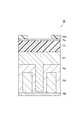
- FIG. 2is a cross-sectional view illustrating a target object to which an etching method according to an embodiment is applied.
- the object to be processedthat is, the wafer W has a substrate SB, a first region R1, a second region R2, and an organic film OL that later constitutes a mask.
- the wafer Wis obtained during the manufacturing of the fin-type field effect transistor, and further includes a raised region RA, a silicon-containing antireflection film AL, and a resist mask RM.
- the raised area RAis provided so as to rise from the substrate SB.
- the raised area RAcan constitute, for example, a gate area.
- the second region R2is made of silicon nitride (Si 3 N 4 ), and is provided on the surface of the raised region RA and the surface of the substrate SB. As shown in FIG. 2, the second region R2 extends so as to define a recess. In one example, the depth of the recess is about 150 nm and the width of the recess is about 20 nm.
- the first region R1is made of silicon oxide (SiO 2 ) and is provided on the second region R2. Specifically, the first region R1 is provided so as to fill a concave portion defined by the second region R2 and cover the second region R2.
- the organic film OLis provided on the first region R1.
- the organic film OLcan be made of an organic material such as amorphous carbon.
- the antireflection film ALis provided on the organic film OL.
- the resist mask RMis provided on the antireflection film AL.
- the resist mask RMprovides an opening having a width wider than the width of the recess on the recess defined by the second region R2.
- the width of the opening of the resist mask RMis, for example, 60 nm.
- Such a pattern of the resist mask RMis formed by a photolithography technique.
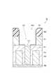
- FIG. 3is a diagram schematically showing an example of a plasma processing apparatus that can be used to implement the method shown in FIG.
- a plasma processing apparatus 10 shown in FIG. 3is a capacitively coupled plasma etching apparatus, and includes a substantially cylindrical processing container 12.
- the inner wall surface of the processing container 12is made of anodized aluminum, for example.
- the processing container 12is grounded for safety.
- a substantially cylindrical support portion 14is provided on the bottom of the processing vessel 12.
- the support part 14is comprised from the insulating material, for example.
- the support portion 14extends in the vertical direction from the bottom of the processing container 12 in the processing container 12.
- a mounting table PDis provided in the processing container 12. The mounting table PD is supported by the support unit 14.
- the mounting table PDholds the wafer W on the upper surface thereof.
- the mounting table PDincludes a lower electrode LE and an electrostatic chuck ESC.
- the lower electrode LEincludes a first plate 18a and a second plate 18b.
- the first plate 18a and the second plate 18bare made of a metal such as aluminum, for example, and have a substantially disk shape.
- the second plate 18bis provided on the first plate 18a and is electrically connected to the first plate 18a.
- An electrostatic chuck ESCis provided on the second plate 18b.
- the electrostatic chuck ESChas a structure in which an electrode which is a conductive film is disposed between a pair of insulating layers or insulating sheets.
- a DC power source 22is electrically connected to the electrode of the electrostatic chuck ESC via a switch 23.
- the electrostatic chuck ESCattracts the wafer W by an electrostatic force such as a Coulomb force generated by a DC voltage from the DC power supply 22. Thereby, the electrostatic chuck ESC can hold the wafer W.
- a focus ring FRis disposed on the periphery of the second plate 18b so as to surround the edge of the wafer W and the electrostatic chuck ESC.
- the focus ring FRis provided in order to improve the etching uniformity.
- the focus ring FRis made of a material appropriately selected according to the material of the film to be etched, and can be made of, for example, quartz.
- a coolant channel 24is provided inside the second plate 18b.
- the refrigerant flow path 24constitutes a temperature adjustment mechanism.
- Refrigerantis supplied to the refrigerant flow path 24 from a chiller unit provided outside the processing container 12 via a pipe 26a.
- the refrigerant supplied to the refrigerant flow path 24is returned to the chiller unit via the pipe 26b. In this way, the refrigerant is circulated between the refrigerant flow path 24 and the chiller unit.
- the temperature of the wafer W supported by the electrostatic chuck ESCis controlled.
- the plasma processing apparatus 10is provided with a gas supply line 28.
- the gas supply line 28supplies the heat transfer gas from the heat transfer gas supply mechanism, for example, He gas, between the upper surface of the electrostatic chuck ESC and the back surface of the wafer W.
- the plasma processing apparatus 10includes an upper electrode 30.
- the upper electrode 30is disposed above the mounting table PD so as to face the mounting table PD.
- the lower electrode LE and the upper electrode 30are provided substantially parallel to each other.
- a processing space S for performing plasma processing on the wafer Wis provided between the upper electrode 30 and the lower electrode LE.
- the upper electrode 30is supported on the upper part of the processing container 12 through an insulating shielding member 32.
- the upper electrode 30may be configured such that the distance in the vertical direction from the upper surface of the mounting table PD, that is, the wafer mounting surface, is variable.
- the upper electrode 30can include an electrode plate 34 and an electrode support 36.
- the electrode plate 34faces the processing space S, and the electrode plate 34 is provided with a plurality of gas discharge holes 34a.
- the electrode plate 34is made of silicon.
- the electrode support 36supports the electrode plate 34 in a detachable manner and can be made of a conductive material such as aluminum.
- the electrode support 36may have a water cooling structure.
- a gas diffusion chamber 36 ais provided inside the electrode support 36.
- a plurality of gas flow holes 36b communicating with the gas discharge holes 34aextend downward from the gas diffusion chamber 36a.
- the electrode support 36is formed with a gas introduction port 36c that guides the processing gas to the gas diffusion chamber 36a, and a gas supply pipe 38 is connected to the gas introduction port 36c.
- a gas source group 40is connected to the gas supply pipe 38 via a valve group 42 and a flow rate controller group 44.
- the gas source group 40includes a plurality of gas sources.
- the gas source group 40includes one or more fluorocarbon gas sources, rare gas sources, nitrogen gas (N 2 gas) sources, hydrogen gas (H 2 gas) sources, and oxygen-containing gas sources.
- the source of one or more fluorocarbon gasesmay include, in one example, a source of C 4 F 8 gas, a source of CF 4 gas, and a source of C 4 F 6 gas.
- the source of noble gascan be any noble gas source such as He gas, Ne gas, Ar gas, Kr gas, Xe gas, and in one example is a source of Ar gas.
- the source of the oxygen-containing gasmay be a source of oxygen gas (O 2 gas) in one example.
- the oxygen-containing gasmay be any gas containing oxygen, for example, a carbon oxide gas such as CO gas or CO 2 gas.
- the valve group 42includes a plurality of valves
- the flow rate controller group 44includes a plurality of flow rate controllers such as a mass flow controller.
- the plurality of gas sources of the gas source group 40are connected to the gas supply pipe 38 via the corresponding valve of the valve group 42 and the corresponding flow rate controller of the flow rate controller group 44, respectively.
- a deposition shield 46is detachably provided along the inner wall of the processing container 12.
- the deposition shield 46is also provided on the outer periphery of the support portion 14.
- the deposition shield 46prevents the etching byproduct (depot) from adhering to the processing container 12 and can be configured by coating an aluminum material with ceramics such as Y 2 O 3 .
- An exhaust plate 48is provided on the bottom side of the processing container 12 and between the support 14 and the side wall of the processing container 12.
- the exhaust plate 48can be configured by, for example, coating an aluminum material with ceramics such as Y 2 O 3 .
- An exhaust port 12 eis provided below the exhaust plate 48 and in the processing container 12.
- An exhaust device 50is connected to the exhaust port 12e via an exhaust pipe 52.
- the exhaust device 50has a vacuum pump such as a turbo molecular pump, and can depressurize the space in the processing container 12 to a desired degree of vacuum.
- a loading / unloading port 12 g for the wafer Wis provided on the side wall of the processing container 12, and the loading / unloading port 12 g can be opened and closed by a gate valve 54.
- the plasma processing apparatus 10further includes a first high frequency power supply 62 and a second high frequency power supply 64.
- the first high-frequency power source 62is a power source that generates high-frequency power for plasma generation, and generates high-frequency power having a frequency of 27 to 100 MHz, for example.
- the first high frequency power supply 62is connected to the upper electrode 30 via the matching unit 66.
- the matching unit 66is a circuit for matching the output impedance of the first high-frequency power source 62 with the input impedance on the load side (upper electrode 30 side). Note that the first high-frequency power source 62 may be connected to the lower electrode LE via the matching unit 66.
- the second high-frequency power source 64is a power source that generates high-frequency bias power for drawing ions into the wafer W.
- the second high-frequency power source 64generates high-frequency bias power having a frequency in the range of 400 kHz to 40 MHz.
- the second high frequency power supply 64is connected to the lower electrode LE via the matching unit 68.
- the matching unit 68is a circuit for matching the output impedance of the second high-frequency power source 64 with the input impedance on the load side (lower electrode LE side).
- the first high-frequency power for plasma generationis supplied from the first high-frequency power source 62 to the upper electrode 30 provided on the upper portion of the target object in the processing container.
- the second high-frequency power for ion attractionis supplied from the second high-frequency power supply 64 to the lower electrode LE provided at the lower portion of the object to be processed, and the first high-frequency power and the second high-frequency power are turned on.
- the modulation which switches the period which becomes OFFalternately performs pulse wave-like high frequency electric power.
- the above-described first high-frequency poweris applied as a continuous wave (CW).
- the first high-frequency power and the first powerare supplied.
- Two high frequency powersare turned on for the same period, and are modulated by being turned off for the same period to generate pulsed high frequency power.
- the first high-frequency power and the second high-frequency powerare modulated by the pulse signal and applied to the upper electrode 30 and the lower electrode LE, respectively.
- a square wave or the likecan be used as the shape of the pulse signal.
- the repetition frequency of the pulse signal used for modulationis 5 kHz in this example, but the same effect can be obtained even when a repetition frequency of 0.1 kHz or more and 50 kHz or less is used.
- the plasma processing apparatus 10further includes a power source 70.
- the power source 70is connected to the upper electrode 30.
- the power source 70applies a voltage to the upper electrode 30 for drawing positive ions present in the processing space S into the electrode plate 34.
- the power source 70is a DC power source that generates a negative DC voltage.
- the power source 70may be an AC power source that generates an AC voltage having a relatively low frequency.
- the voltage applied from the power source 70 to the upper electrodemay be a voltage of ⁇ 150V or less. That is, the voltage applied to the upper electrode 30 by the power source 70 may be a negative voltage having an absolute value of 150 or more.
- the plasma processing apparatus 10may further include a control unit Cnt.
- the control unit Cntis a computer including a processor, a storage unit, an input device, a display device, and the like, and controls each unit of the plasma processing apparatus 10.
- an operatorcan perform a command input operation and the like to manage the plasma processing apparatus 10 using the input device, and the operating status of the plasma processing apparatus 10 is visualized by the display device. Can be displayed.
- the storage unit of the control unit Cnthas a control program for controlling various processes executed by the plasma processing apparatus 10 by the processor, and causes each part of the plasma processing apparatus 10 to execute processes according to processing conditions.
- a program, that is, a processing recipeis stored.
- FIGS. 2 and 4 to 16 executed in time serieswill be referred to as appropriate.
- 4 to 15are cross-sectional views showing the object to be processed in the middle of the implementation of the method MT
- FIG. 16is a diagram for explaining a comparative example.
- FIG. 16is a diagram for explaining a comparative example.
- the wafer W shown in FIG. 2is carried into the plasma processing apparatus 10, and the wafer W is placed on the mounting table PD and held by the mounting table PD.
- step ST1is then performed.
- step ST1the antireflection film AL is etched.
- processing gasis supplied in processing container 12 from a gas source selected among a plurality of gas sources of gas source group 40.
- This processing gascontains a fluorocarbon gas.
- the fluorocarbon gascan include, for example, one or more of C 4 F 8 gas and CF 4 gas.
- the processing gasmay further include a rare gas, for example, Ar gas.
- exhaust device 50is operated and the pressure in processing container 12 is set as a predetermined pressure.
- step ST1the high frequency power from the first high frequency power supply 62 and the high frequency bias power from the second high frequency power supply 64 are supplied to the lower electrode LE.
- Processing vessel pressure10 mTorr (1.33 Pa) to 50 mTorr (6.65 Pa)
- Process gas / C 4 F 8 gas10 sccm to 30 sccm CF 4 gas: 150 sccm to 300 sccm
- Ar gas200 sccm to 500 sccm
- High frequency power for plasma generation300W to 1000W
- High frequency bias power200W to 500W
- step ST1plasma of the processing gas is generated, and the antireflection film AL is etched in the portion exposed from the opening of the resist mask RM by the active species of fluorocarbon.
- the portion exposed from the opening of the resist mask RMis removed from the entire region of the antireflection film AL. That is, the pattern of the resist mask RM is transferred to the antireflection film AL, and a pattern providing an opening is formed in the antireflection film AL.
- movement of each part of the plasma processing apparatus 10 mentioned above in process ST1can be controlled by the control part Cnt.
- processing gasis supplied in processing container 12 from a gas source selected among a plurality of gas sources of gas source group 40.
- the processing gascan include hydrogen gas and nitrogen gas.
- the processing gas used in step ST2may be another gas, for example, a processing gas containing oxygen gas, as long as it can etch the organic film.
- the exhaust apparatus 50is operated and the pressure in the processing container 12 is set to a predetermined pressure. Further, in step ST2, the high frequency power from the first high frequency power supply 62 and the high frequency bias power from the second high frequency power supply 64 are supplied to the lower electrode LE.
- Processing container pressure50 mTorr (6.65 Pa) to 200 mTorr (26.6 Pa)
- Process gas / N 2 gas200 sccm to 400 sccm ⁇ H 2 gas: 200 sccm to 400 sccm
- High frequency power for plasma generation500W to 2000W
- High frequency bias power200W to 500W
- step ST2plasma of a processing gas is generated, and the organic film OL is etched in a portion exposed from the opening of the antireflection film AL.
- the resist mask RMis also etched.
- the resist mask RMis removed, and the portion exposed from the opening of the antireflection film AL is removed from the entire region of the organic film OL. That is, the pattern of the antireflection film AL is transferred to the organic film OL, the pattern that provides the opening MO is formed in the organic film OL, and the mask MK is generated from the organic film OL.
- movement of each part of the plasma processing apparatus 10 mentioned above in process ST2can be controlled by the control part Cnt.
- step ST3is performed after step ST2.
- the first region R1is etched until just before the second region R2 is exposed. That is, the first region R1 is etched until the first region R1 remains slightly on the second region R2.
- process gasis supplied in process container 12 from a gas source selected among a plurality of gas sources of gas source group 40.
- This processing gascontains a fluorocarbon gas.
- the processing gasmay further include a rare gas, for example, Ar gas.
- the processing gasmay further include oxygen gas.
- the exhaust apparatus 50is operated and the pressure in the processing container 12 is set to a predetermined pressure. Further, in step ST3, the high frequency power from the first high frequency power supply 62 and the high frequency bias power from the second high frequency power supply 64 are supplied to the lower electrode LE.
- step ST3plasma of the processing gas is generated, and the first region R1 is etched by the active species of fluorocarbon in the portion exposed from the opening of the mask MK.
- the processing time of this step ST3is set so that the first region R1 is left with a predetermined film thickness on the second region R2 at the end of the step ST3.
- the upper opening UOis partially formed as shown in FIG.
- operation of each part of the plasma processing apparatus 10 mentioned above in process ST3can be controlled by the control part Cnt.
- a mode in which the formation of a deposit containing fluorocarbon is more advantageous on the surface of the wafer W including the first region R1 than the etching of the first region R1, that is, the deposition modeis set.
- a conditionis selected.
- the fluorocarbon gas to be utilized in step ST3may include one or more of the C 4 F 8 gas and CF 4 gas.
- the fluorocarbon gas in this examplehas a ratio of the number of fluorine atoms to the number of carbon atoms (that is, the number of fluorine atoms / the number of carbon atoms) (that is, the number of fluorine atoms / the number of carbon atoms) of the fluorocarbon gas used in step ST11 (that is, the number of carbon atoms). , Fluorine carbon number / carbon atom number).
- the high frequency power for plasma generation used in step ST3can be set to a higher power than the high frequency power for plasma generation used in step ST11. According to these examples, the etching mode can be realized.
- the high-frequency bias power used in step ST3can also be set to be higher than the high-frequency bias power in step ST11. According to this example, the energy of ions drawn into the wafer W is increased, and the first region R1 can be etched at a high speed.
- Processing vessel pressure10 mTorr (1.33 Pa) to 50 mTorr (6.65 Pa)
- Process gas / C 4 F 8 gas10 sccm to 30 sccm CF 4 gas: 50 sccm to 150 sccm
- Ar gas500 sccm to 1000 sccm ⁇ O 2 gas: 10 sccm to 30 sccm
- High frequency power for plasma generation500W to 2000W
- High frequency bias power500W to 2000W
- step ST4is then performed.
- plasma of a processing gas containing an oxygen-containing gasis generated in the processing container 12.
- process gasis supplied in process container 12 from a gas source selected among a plurality of gas sources of gas source group 40.
- the processing gasmay include oxygen gas as the oxygen-containing gas.
- the processing gasmay further include an inert gas such as a rare gas (for example, Ar gas) or nitrogen gas.
- the exhaust apparatus 50is operated and the pressure in the processing container 12 is set to a predetermined pressure.
- high frequency power from the first high frequency power supply 62is supplied to the lower electrode LE.
- the high frequency bias power from the second high frequency power supply 64may not be supplied to the lower electrode LE.
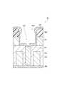
- step ST4active species of oxygen are generated, and the opening MO of the mask MK is widened at the upper end portion by the active species of oxygen. Specifically, as shown in FIG. 7, etching is performed so that the upper shoulder portion of the mask MK that defines the upper end portion of the opening MO has a tapered shape. Thereby, even if the deposit generated in the subsequent process adheres to the surface defining the opening MO of the mask MK, the reduction amount of the width of the opening MO can be reduced.
- movement of each part of the plasma processing apparatus 10 mentioned above in process ST4can be controlled by the control part Cnt.
- step ST11 described lateris also a step of reducing a small amount of deposit formed in each sequence, and it is necessary to suppress an excessive decrease in the deposit.
- step ST4the process is performed to increase the width of the upper end portion of the opening MO of the mask MK, and a short processing time is required.
- Processing container pressure30 mTorr (3.99 Pa) to 200 mTorr (26.6 Pa)
- Processing gas / O 2 gas50 sccm to 500 sccm
- Ar gas200 sccm to 1500 sccm
- High frequency power for plasma generation100W to 500W
- High frequency bias power0W to 200W
- sequence SQ1are executed, and then one or more sequences SQ2 are executed.
- sequence SQ3may be performed one or more times as needed.
- the sequence SQ1, the sequence SQ2, and the sequence SQ3are executed for etching the first region R1.
- Each of sequence SQ1, sequence SQ2, and sequence SQ3includes step ST11 and step ST12.
- step ST11is first executed as the first step.
- plasma of a processing gas containing a fluorocarbon gas, an oxygen-containing gas, and an inert gasis generated in the processing container 12 in which the wafer W is accommodated.
- process gasis supplied in process container 12 from a gas source selected among a plurality of gas sources of gas source group 40.
- the processing gasincludes a fluorocarbon gas, an oxygen-containing gas, and an inert gas.
- the conditions for the deposition modeare selected as described above, and therefore, in one example, C 4 F 6 gas is used as the fluorocarbon gas.
- the oxygen-containing gasincludes, for example, oxygen gas
- the inert gasincludes a rare gas such as Ar gas.
- the inert gasmay be nitrogen gas.
- the exhaust apparatus 50is operated and the pressure in the processing container 12 is set to a predetermined pressure. Further, in step ST11, high frequency power from the first high frequency power supply 62 may be supplied to the lower electrode LE.
- step ST11plasma of a processing gas containing a fluorocarbon gas or a processing gas containing a fluorocarbon gas and an inert gas is generated, so that the dissociated fluorocarbon is deposited on the surface of the wafer W to form a deposit DP.
- the operation of each part of the above-described plasma processing apparatus 10 in the step ST11can be controlled by the control unit Cnt.
- the active species of oxygenare generated overlapping the period in which the deposit DP is formed by the fluorocarbon, and the amount of the deposit DP on the wafer W is moderately reduced by the active species of oxygen (See FIGS. 9, 12, and 15). These states shown in FIGS. 8 and 9 occur simultaneously in step ST11. As a result, the opening MO and the upper opening UO are prevented from being blocked by the excessive deposit DP. Further, in the processing gas used in step ST11, since the oxygen gas is diluted with the inert gas, it is possible to suppress the deposit DP from being excessively removed.
- the operation of each part of the above-described plasma processing apparatus 10 in the step ST11can be controlled by the control unit Cnt.
- Processing vessel pressure10-50 mTorr Process gas / C 4 F 6 gas flow rate: 1 to 20 sccm Ar gas flow rate: 200 sccm to 1500 sccm ⁇ O 2 gas flow rate: 1 ⁇ 20sccm
- High frequency power of the first high frequency power supply 6240 MHz, 50 W to 500 W
- High frequency power (bias power) of the second high frequency power supply 6413 MHz, 0 W to 50 W DC voltage of power supply 70: 0V to -500V No modulation of high frequency power (CW (continuous wave))
- step ST11 of each sequencethat is, one step ST11 is executed for 2 seconds or more, for example, 2.5 seconds to 3 seconds.
- the deposition time in the process ST11was set to 3 seconds in the first sequence SQ1, and 2.5 seconds shorter than this in the second sequence SQ2.
- the amount of increase in the thickness of the protective film on the silicon nitridecan be appropriately controlled, and there is an effect of improving the detachability. If the etching rate of the deposit DP in such a long period is too high, the deposit for protecting the second region R2 may be excessively removed. For this reason, in step ST11, the deposit DP is etched at a rate of 1 nm / second or less.
- the rate of etching of the deposit DP in the process ST11 of 1 nm / second or lessis the pressure in the processing container, the degree of dilution of the oxygen in the processing gas with the rare gas, that is, the oxygen concentration, and the high frequency for plasma generation. Power can be achieved by selecting from the conditions described above.
- the process ST11when the fluorocarbon gas, the inert gas, and the oxygen gas are supplied within the overlapping period (same period), the process is compared with the case where the fluorocarbon gas and the oxygen gas are supplied in separate periods. There is no need to consider the stabilization time associated with gas switching and the discharge stabilization time.
- the throughputis improved.
- the molar ratio of the fluorocarbon gas to the oxygen gas in such a deposition processis preferably about 1: 0.25 to 1: 2, and in this case, the optimum deposit thickness for the specified power is set. The effect of improving the microloading and detachability can be obtained.
- planar shapecan be made into circular, a rectangle, a slit, and a long hole shape. Further, it was confirmed that the formed opening could be patterned as designed without being greatly distorted.
- step ST12is then executed.
- step ST12the first region R1 is etched.
- process gasis supplied in process container 12 from a gas source selected among a plurality of gas sources of gas source group 40.
- This processing gascontains an inert gas.
- the inert gasmay be a noble gas such as Ar gas.
- the inert gasmay be nitrogen gas.
- the etching in step ST12is performed with a processing gas that does not substantially contain oxygen. Note that substantially not containing oxygen means that oxygen is not intentionally introduced into the processing gas.
- the exhaust apparatus 50is operated and the pressure in the processing container 12 is set to a predetermined pressure.
- step ST12high frequency power from the first high frequency power supply 62 is supplied to the lower electrode LE.
- the high frequency bias power from the second high frequency power supply 64is supplied to the lower electrode LE.
- Processing vessel pressure10-50 mTorr Process gas / Ar gas: 200 sccm to 1500 sccm
- High frequency power of the first high frequency power supply 6240 MHz
- High frequency power (bias power) of the second high frequency power supply 6413 MHz
- 25 W to 500 W DC voltage of power supply 700V to -500V
- step ST12plasma of an inert gas is generated and ions are drawn into the wafer W. Then, the first region R1 is etched by the fluorocarbon radicals contained in the deposit DP (see FIGS. 10, 13, and 15).
- the operation of each part of the above-described plasma processing apparatus 10 in step ST12can be controlled by the control unit Cnt.
- step ST11 of sequence SQ1deposit DP is formed on wafer W as shown in FIG. FIG. 8 shows a state in which the etching of the first region R1 proceeds, the second region R2 is exposed, and the deposit DP is formed on the second region R2. This deposit DP protects the second region R2.
- step ST11 of sequence SQ1as shown in FIG. 9, the amount of deposit DP formed in the same step ST11 is reduced.
- step ST12 of sequence SQ1the first region R1 is etched by radicals of fluorocarbon contained in the deposit DP.
- the second region R2is exposed and the first region R1 in the recess provided by the second region R2 is etched while the second region R2 is protected by the deposit DP. Thereby, as shown in FIG. 10, the lower opening LO is gradually formed.
- step STaafter the execution of step ST12, it is determined in step STa whether the stop condition is satisfied.
- the stop conditionis determined to be satisfied when the sequence SQ1 is executed a predetermined number of times.
- step STawhen it is determined that the stop condition is not satisfied, the sequence SQ1 is executed from step ST11.
- sequence SQ2is executed.
- the high frequency bias power of the second high frequency power supply 64can be lowered in the second sequence as compared with the first sequence SQ1.
- the etching time in the second sequence SQ2can be set longer than the etching time in the first sequence SQ1.
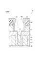
- step ST11 of sequence SQ2a deposit DP is formed on the wafer W as shown in FIG. Then, in step ST11 of sequence SQ2, as shown in FIG. 12, the amount of deposit DP formed in the same step ST11 is further reduced.
- step ST12 of sequence SQ2the first region R1 is etched by radicals of fluorocarbon contained in the deposit DP. By this sequence SQ2, the first region R1 in the recess provided by the second region R2 is further etched while the second region R2 is protected by the deposit DP. Thereby, as shown in FIG. 13, the depth of the lower opening LO is further increased.
- the methodincludes a second step of selectively etching the first region made of silicon oxide with a fluorocarbon radical, so that the first region is etched and the second region made of silicon nitride is used. Scraping of the two regions is suppressed.
- the deposit DPis formed by the plasma of the processing gas containing the fluorocarbon gas or the processing gas containing the fluorocarbon gas and the inert gas.
- the amount of the deposit DP on the wafer Wis moderately reduced by the active species of oxygen due to the active species of oxygen.
- the formation of the deposit DP and the moderate reduction in the amount of the deposit DPare performed in the same process, and it is not necessary to switch the processing gas. Therefore, it is not necessary to consider the discharge stabilization time associated with the switching of the processing gas.
- the etching in the second stepis performed with a processing gas that does not substantially contain oxygen.
- a processing gas that does not substantially contain oxygenIn this method, selective etching of the first region with respect to the second region is efficiently performed.
- the sequence SQ2is repeated once or more, and is repeated 39 times in one example. Therefore, as shown in FIG. 1, after the execution of step ST12, it is determined in step STb whether the stop condition is satisfied.
- the stop conditionis determined to be satisfied when the sequence SQ2 is executed a predetermined number of times.
- the sequence SQ2is executed from the process ST11. On the other hand, when it is determined in step STb that the stop condition is satisfied, the execution of sequence SQ2 is then terminated.
- the processing conditions of the sequence SQ1are set so that the amount of etching of the first region R1 in each sequence SQ1 is smaller than the amount of etching of the first region R1 in each sequence SQ2.
- the execution time length of each sequence SQ1is set shorter than the execution time length of each sequence SQ2.
- the ratio of the execution time length of the process ST11 and the execution time length of the process ST12 in the sequence SQ1can be set similarly to the ratio of the execution time length of the process ST11 and the execution time length of the process ST13 in the sequence SQ2.
- the execution time length of the process ST11is selected from a time length in the range of 2 seconds to 5 seconds, and the execution time length of the process ST12 is selected from a time length in the range of 5 seconds to 10 seconds.
- the execution time length of step ST11is selected from a time length in the range of 2 seconds to 10 seconds, and the execution time length of step ST12 is selected from a time length in the range of 5 seconds to 20 seconds.
- the active species of the fluorocarbon generated in the process ST11is deposited on the second region R2 to protect the second region R2, but when the first region R1 is etched and the second region R2 is exposed, the second region R2 is exposed. Region R2 may be etched. Therefore, in the method MT, one or more sequences SQ1 are executed in the period in which the second region R2 is exposed. Thereby, the deposit DP is formed on the wafer W while the etching amount is suppressed, and the second region R2 is protected by the deposit DP. Thereafter, one or more sequences SQ2 with a large etching amount are executed. Therefore, according to the method MT, it is possible to etch the first region R1 while suppressing the scraping of the second region R2.
- the scraping of the second region R2can be suppressed even if the etching amount in each sequence SQ2 is increased.
- the etching rate of the first region R1 in the method MTcan be improved by increasing the etching amount of each sequence SQ2 more than the etching amount of each sequence SQ1.
- the sequence SQ3can be further executed as necessary after the execution of the sequence SQ2.
- region R1is etched by the radical of the fluorocarbon contained in deposit DP by Ar sputter
- the first region R1 in the recess provided by the second region R2is further etched while the second region R2 is protected by the deposit DP.
- FIG. 16is a diagram illustrating a state according to a comparative example corresponding to FIG. 15 and illustrates a case where pulse modulation is not performed in the second step (continuous wave (CW)).
- CWcontinuous wave
- the sputtered silicon oxide molecules Eare reattached to the inner surface of the recess. Further, excessive etching occurs on the opening end face (shoulder portion) of the recess, and the shoulder portion is partially missing.
- the high frequency poweris applied in the form of pulse waves in the second step.
- the sputtered silicon oxidecan escape to the outside of the recess during the OFF period in which no pulse is applied, the reattachment of silicon oxide in the recess is suppressed, and etching can be performed with high accuracy. It becomes like this.
- the pulse OFF periodis present, excessive ion acceleration can be suppressed, and therefore, excessive etching on the opening end face (shoulder portion) of the recess can be suppressed.
- Sequence SQ3is repeated one or more times. Therefore, as shown in FIG. 1, after the execution of step ST12, it is determined in step STc whether or not the stop condition is satisfied.
- the stop conditionis determined to be satisfied when the sequence SQ3 is executed a predetermined number of times.
- step STcwhen it is determined that the stop condition is not satisfied, the sequence SQ3 is executed from step ST11.
- the execution of the method MTis finished. Note that the settings of all sequences may be the same.
- the high frequency bias powermay be set to be larger than the high frequency bias power used in step ST12 of sequence SQ1 and sequence SQ2.
- the high frequency bias poweris set to 20 W to 100 W
- the high frequency bias poweris set to power of 100 W to 300 W.
- the execution time length of the step ST11is selected from a time length in the range of 2 seconds to 10 seconds
- the execution time length of the step ST12is selected from a time length in the range of 5 seconds to 15 seconds. .
- the amount of the deposit DP on the wafer Wis considerably increased after the execution of the sequence SQ1 and the sequence SQ2.
- the width of the opening MO, the upper opening UO, and the lower opening LOmay be narrowed by the deposit DP.
- a relatively large high-frequency bias power Is usedthe energy of ions attracted to the wafer W is increased, and even if the lower opening LO is deep, ions can be supplied to the deep part of the lower opening LO.
- the first region R1is made of silicon oxide (SiO 2 )
- the second region R2is made of silicon nitride (Si 3 N 4 ).
- Various conditionssuch as the process vessel internal pressure in the process ST11 and the process ST12 are the same as the above-described conditions.
- the deposit DPis formed on the first region R1 and the second region R2 by the plasma of the processing gas including the fluorocarbon gas and the oxygen gas.
- the processing gas in step ST11may contain a rare gas such as Ar gas.
- the amount of the deposit DP on the wafer Wis moderately reduced by the active species of oxygen due to the active species of oxygen further contained in the processing gas.
- step ST12is performed on the wafer.
- the wafer W after the process ST11is exposed to a rare gas plasma.
- the rare gasincludes, for example, Ar gas.
- the first region R1is etched by the fluorocarbon radicals contained in the deposit DP.
- step ST12active species of rare gas atoms, for example, ions of Ar gas atoms collide with the deposit DP.
- the fluorocarbon radicals in the deposit DPadvance the etching of the first region R1 and reduce the thickness of the first region R1.
- the film thickness of the deposit DPdecreases.
- the second region R2although the thickness of the deposit DP is reduced, the etching of the second region R2 is suppressed, so the amount of decrease in the thickness of the second region R2 is the thickness of the first region R1. Is significantly smaller than the amount of decrease.
- the processing vessel internal pressure, the C 4 F 6 gas flow rate, the Ar flow rate, and the power of the first and second high-frequency power sources used for obtaining this dataare 8 sccm and 1100 sccm within the above numerical range.
- 100 W, 0 W, and the Ar gas flow rate in the second step ST12is 1100 sccm in the above numerical range, and the range of various conditions produces the same effect even when these parameters are changed.
- the range to obtainis shown.
- the etching amount of the second region (silicon nitride) on the opening end face of the recess and the presence or absence of a defect in the recessare as follows.
- omission defectrepresents the case where it can confirm that the deposit has adhered in the recessed part, when observing the inside of a recessed part with an electron microscope.
- Experimental example 111.1 nm (good omission)
- Experimental example 27.5 nm (missing defect)
- Experimental example 36.8 nm (missing defect)
- Experimental example 411.1 nm (good omission)
- Experimental example 510.2 nm (good omission)
- Experimental example 67.5 nm (missing defect)
- -Experiment example 74.3 nm (missing defect)
- Experimental Example 88.6 nm (good omission)
- Experimental example 96.8 nm (good omission)
- Experimental example 105.7 nm (defective omission)
- Experimental example 113.9 nm (missing defect)
- Experimental Example 137.7 nm (good omission)
- Experimental example 146.4 nm (good omission)
- Experimental example 154.5 nm (missing defect)
- FIG. 17is a diagram summarizing the experimental results.
- the first region made of silicon oxideis selectively etched with respect to the second region made of silicon nitride by the plasma treatment for the object to be processed.
- the object to be processedincludes a second region that defines a recess, a first region that is provided to fill the recess and cover the second region, and a mask that is provided on the first region.
- the maskprovides an opening having a width larger than the width of the concave portion on the concave portion, and the method generates a plasma of a processing gas containing a fluorocarbon gas in a processing container containing the object to be processed.
- a deposit containing fluorocarbonis formed on an object to be processed, and the first region is etched by radicals of fluorocarbon contained in the deposit.
- the second stephigh-frequency power is applied in the form of a pulse wave, so that the sputtered silicon oxide can escape to the outside of the recess during the OFF period when no pulse is applied. Re-adhesion is suppressed and etching can be performed with high accuracy. Therefore, as shown in the above experimental results, the probability of occurrence of missing defects decreases as the duty ratio is lowered.
- the plasma in the first stepis a plasma of a processing gas containing a fluorocarbon gas, an oxygen-containing gas, and an inert gas.
- the plasma of these gasescan form a deposit on the first region and the second region, and the silicon oxide can be selectively etched by applying energy to the deposit.
- the first high-frequency power for generating plasmais applied to the upper electrode provided on the upper part of the object to be processed in the processing container, and is provided on the lower part of the object to be processed.
- a second high-frequency power for ion attractionto the lower electrode, and performing a modulation that alternately switches between a period in which the first high-frequency power and the second high-frequency power are turned on and a period in which the first high-frequency power is turned off, Is generated.
- omission defectsare reduced by pulse modulation.
- the ratio (duty ratio) to the pulse period of the period in which the high frequency power in the form of pulse wave is ONis 10% or more and 70% or less.
- the omission defectis reduced as compared with the case where the duty ratio exceeds 70%. That is, the amount of silicon nitride that is located on the opening end face (shoulder) of the recess can be suppressed.
- the ratio (duty ratio) to the pulse period of the period in which the high frequency power in the form of pulse wave is ONis 50% or more and 60% or less. In this case, it has been found that the duty ratio is lost and the defect is further reduced.
- DESCRIPTION OF SYMBOLS 10Plasma processing apparatus, 12 ... Processing container, 30 ... Upper electrode, PD ... Mounting stage, LE ... Lower electrode, ESC ... Electrostatic chuck, 40 ... Gas source group, 42 ... Valve group, 44 ... Flow controller group, DESCRIPTION OF SYMBOLS 50 ... Exhaust device, 62 ... 1st high frequency power supply, 64 ... 2nd high frequency power supply, Cnt ... Control part, W ... Wafer, W1 ... Wafer, R1 ... 1st area
Landscapes
- Engineering & Computer Science (AREA)
- Physics & Mathematics (AREA)
- Manufacturing & Machinery (AREA)
- Computer Hardware Design (AREA)
- Power Engineering (AREA)
- Microelectronics & Electronic Packaging (AREA)
- Condensed Matter Physics & Semiconductors (AREA)
- General Physics & Mathematics (AREA)
- Chemical & Material Sciences (AREA)
- Plasma & Fusion (AREA)
- Chemical Kinetics & Catalysis (AREA)
- General Chemical & Material Sciences (AREA)
- Analytical Chemistry (AREA)
- Inorganic Chemistry (AREA)
- Drying Of Semiconductors (AREA)
- Plasma Technology (AREA)
- Electrodes Of Semiconductors (AREA)
- Internal Circuitry In Semiconductor Integrated Circuit Devices (AREA)
Abstract
Description
Translated fromJapanese本発明の実施形態は、エッチング方法に関するものである。The embodiment of the present invention relates to an etching method.
電子デバイスの製造においては、酸化シリコン(SiO2)から構成された領域に対してホール又はトレンチといった開口を形成する処理が行われることがある。このような処理では、特許文献1に記載されているように、一般的には、フルオロカーボンガスのプラズマに被処理体が晒されて、当該領域がエッチングされる。In manufacturing an electronic device, a process of forming an opening such as a hole or a trench may be performed on a region formed of silicon oxide (SiO2 ). In such a process, as described in Patent Document 1, generally, an object to be processed is exposed to a fluorocarbon gas plasma, and the region is etched.
また、酸化シリコンから構成された第1領域を、窒化シリコンから構成された第2領域に対して選択的にエッチングする技術が知られている。このような技術の一例としては、SAC(Self-Aligned Contact)技術が知られている。SAC技術については、特許文献2に記載されている。Also, a technique for selectively etching a first region made of silicon oxide with respect to a second region made of silicon nitride is known. As an example of such a technique, a SAC (Self-Aligned Contact) technique is known. The SAC technique is described in
SAC技術の処理対象である被処理体は、酸化シリコン製の第1領域、窒化シリコン製の第2領域、及びマスクを有している。第2領域は、凹部を画成するように設けられており、第1領域は、当該凹部を埋め、且つ、第2領域を覆うように設けられており、マスクは、第1領域上に設けられており、凹部の上に開口を提供している。従来のSAC技術では、特許文献2に記載されているように、第1領域のエッチングのために、フルオロカーボンガス、酸素ガス、及び希ガスを含む処理ガスのプラズマが用いられる。この処理ガスのプラズマに被処理体を晒すことにより、マスクの開口から露出した部分において第1領域がエッチングされて上部開口が形成される。さらに、処理ガスのプラズマに被処理体が晒されることにより、第2領域によって囲まれた部分、即ち凹部内の第1領域が自己整合的にエッチングされる。これにより、上部開口に連続する下部開口が自己整合的に形成される。A target object to be processed by the SAC technique has a first region made of silicon oxide, a second region made of silicon nitride, and a mask. The second region is provided so as to define a concave portion, the first region is provided so as to fill the concave portion and cover the second region, and the mask is provided on the first region. And provides an opening over the recess. In the conventional SAC technique, as described in
なお、エッチング対象として有機膜を用いた技術(特許文献3)、エッチング対象をシリコンとした技術(特許文献4)、有機膜のパルスエッチング後にSiO2をエッチングする技術(特許文献5)が知られている。A technique using an organic film as an etching target (Patent Document 3), a technique using silicon as an etching target (Patent Document 4), and a technique of etching SiO2 after pulse etching of an organic film (Patent Document 5) are known. ing.
本願発明者らの知見によれば、上述した従来の技術では、酸化シリコンから構成された第1領域を選択エッチングする際に、凹部内に堆積物が再付着し、凹部内を高精度にエッチングすることができにくく、選択エッチングができる状態で、第1領域を高精度にエッチングすることが求められている。According to the knowledge of the inventors of the present application, in the conventional technique described above, when the first region composed of silicon oxide is selectively etched, deposits are reattached in the recess, and the interior of the recess is etched with high accuracy. Therefore, it is demanded to etch the first region with high accuracy in a state where selective etching is difficult.
第1のエッチング方法においては、被処理体に対するプラズマ処理によって、酸化シリコンから構成された第1領域を窒化シリコンから構成された第2領域に対して選択的にエッチングする方法であって、前記被処理体は、凹部を画成する前記第2領域、該凹部を埋め、且つ前記第2領域を覆うように設けられた前記第1領域、及び、前記第1領域上に設けられたマスクを有し、該マスクは、前記凹部の上に該凹部の幅よりも広い幅を有する開口を提供し、該方法は、前記被処理体を収容した処理容器内においてフルオロカーボンガスを含む処理ガスのプラズマを生成する第1工程であり、前記被処理体上にフルオロカーボンを含む堆積物を形成する、該第1工程と、前記堆積物に含まれるフルオロカーボンのラジカルによって前記第1領域をエッチングする第2工程であり、前記プラズマの形成に寄与する高周波電力をパルス波状に印加する、該第2工程と、を含み、前記第1工程、及び前記第2工程を含むシーケンスが繰り返して実行される。The first etching method is a method of selectively etching a first region made of silicon oxide with respect to a second region made of silicon nitride by a plasma treatment on an object to be processed. The processing body includes the second region that defines a recess, the first region that is provided so as to fill the recess and cover the second region, and a mask that is provided on the first region. The mask provides an opening having a width larger than the width of the concave portion on the concave portion, and the method uses plasma of a processing gas containing a fluorocarbon gas in a processing container containing the object to be processed. A first step of generating a deposit containing a fluorocarbon on the object to be processed, and the first region by a radical of the fluorocarbon contained in the deposit. And a second step of applying a high-frequency power that contributes to the formation of the plasma in the form of a pulse wave, and the sequence including the first step and the second step is repeated. Executed.
この方法では、フルオロカーボンのラジカルによって、酸化シリコンから構成された第1領域を選択的にエッチングする第2工程を含むので、第1領域がエッチングされると共に、窒化シリコンから構成された第2領域の削れが抑制される。This method includes the second step of selectively etching the first region made of silicon oxide by the fluorocarbon radical, so that the first region is etched and the second region made of silicon nitride is etched. Scraping is suppressed.
また、第1工程では、フルオロカーボンガス含む処理ガス、又はフルオロカーボンガス及び不活性ガスを含む処理ガスのプラズマにより、堆積物が形成される。また、酸素の活性種により、堆積物の量が、当該酸素の活性種によって適度に減少される。Also, in the first step, a deposit is formed by plasma of a processing gas containing a fluorocarbon gas or a processing gas containing a fluorocarbon gas and an inert gas. Moreover, the amount of deposits is moderately reduced by the active species of oxygen due to the active species of oxygen.
第2工程において、高周波電力をパルス波状に印加すると、パルスを印加していないOFF期間において、スパッタされた酸化シリコンが凹部の外側へ抜けることが可能となるため、凹部内における酸化シリコンの再付着が抑制され、高精度にエッチングができるようになる。また、パルスのOFF期間が存在することで、過剰なイオンの加速を抑制することができるため、凹部の開口端面における過剰なエッチングを抑制することも可能となる。In the second step, when high frequency power is applied in the form of a pulse wave, the sputtered silicon oxide can escape to the outside of the recess during the OFF period when no pulse is applied, so that the silicon oxide reattaches in the recess. Is suppressed, and etching can be performed with high accuracy. In addition, since the pulse OFF period is present, excessive ion acceleration can be suppressed, and therefore, excessive etching on the opening end face of the recess can be suppressed.
第2のエッチング方法においては、前記第2工程の前記エッチングは、実質的に酸素を含まない処理ガスによって行われる。この方法では、第2領域に対する第1領域の選択的なエッチングが効率よく行われる。なお、実質的に酸素を含まないとは、意図的に処理ガス内に酸素を導入しないという意味である。In the second etching method, the etching in the second step is performed by a processing gas that does not substantially contain oxygen. In this method, selective etching of the first region with respect to the second region is efficiently performed. Note that substantially not containing oxygen means that oxygen is not intentionally introduced into the processing gas.
第3エッチング方法においては、前記第1工程のプラズマは、フルオロカーボンガス、酸素含有ガス及び不活性ガスを含む処理ガスのプラズマである。これらのガスのプラズマは、第1領域及び第2領域上に堆積物を形成することができ、堆積物にエネルギーを与えることで、酸化シリコンを選択的にエッチングすることができる。In the third etching method, the plasma in the first step is a plasma of a processing gas containing a fluorocarbon gas, an oxygen-containing gas, and an inert gas. The plasma of these gases can form a deposit on the first region and the second region, and the silicon oxide can be selectively etched by applying energy to the deposit.
第4のエッチング方法においては、前記第2工程において、前記処理容器内の前記被処理体の上部に設けられた上部電極にプラズマ生成用の第1高周波電力を与え、前記被処理体の下部に設けられた下部電極にイオン引き込み用の第2高周波電力を与え、前記第1高周波電力及び前記第2高周波電力がONとなる期間と、OFFとなる期間を交互に切り替える変調を行うことにより、前記パルス波状の高周波電力を生成する。この場合、イオンの過剰な加速を抑制するとともに、OFFとなる期間にエッチングによって生じた副生成物の排気を促進する効果がある。In the fourth etching method, in the second step, a first high-frequency power for generating plasma is applied to an upper electrode provided on an upper part of the object to be processed in the processing container, and a lower part of the object to be processed is provided. By applying a second high-frequency power for ion attraction to the lower electrode provided, and performing a modulation that alternately switches a period in which the first high-frequency power and the second high-frequency power are turned on and a period in which the second high-frequency power is turned off, Generates pulsed high frequency power. In this case, there are effects of suppressing excessive acceleration of ions and promoting exhaust of by-products generated by etching during the OFF period.
第5のエッチング方法においては、前記パルス波状の前記高周波電力のONとなる期間のパルス周期に対する比率(デューティ比)は、10%以上70%以下であることが好ましい。この場合、凹部の開口端面(肩部)に位置する窒化シリコンが削られる量を抑制することができる。In the fifth etching method, it is preferable that a ratio (duty ratio) with respect to a pulse period of the period in which the pulsed high-frequency power is turned on is 10% or more and 70% or less. In this case, the amount of silicon nitride located on the opening end face (shoulder) of the recess can be suppressed.
第6のエッチング方法においては、前記パルス波状の前記高周波電力のONとなる期間のパルス周期に対する比率(デューティ比)は、50%以上60%以下であることが更に好ましい。この場合、凹部の開口端面(肩部)に位置する窒化シリコンが削られる量をさらに抑制することができる。In the sixth etching method, it is more preferable that the ratio (duty ratio) to the pulse period of the period in which the high frequency power in the pulse waveform is ON is 50% or more and 60% or less. In this case, the amount of silicon nitride located on the opening end face (shoulder) of the recess can be further suppressed.
このエッチング方法においては、第1領域を高精度に選択エッチングすることができる。In this etching method, the first region can be selectively etched with high accuracy.
以下、図面を参照して種々の実施形態について詳細に説明する。なお、各図面において同一又は相当の部分に対しては同一の符号を附すこととする。Hereinafter, various embodiments will be described in detail with reference to the drawings. In the drawings, the same or corresponding parts are denoted by the same reference numerals.
図1は、一実施形態に係るエッチング方法を示す流れ図である。図1に示す方法MTは、被処理体に対するプラズマ処理によって、酸化シリコンから構成された第1領域を、窒化シリコンから構成された第2領域に対して選択的にエッチングする方法である。FIG. 1 is a flowchart showing an etching method according to an embodiment. A method MT shown in FIG. 1 is a method of selectively etching a first region made of silicon oxide with respect to a second region made of silicon nitride by plasma treatment for an object to be processed.
図2は、一実施形態に係るエッチング方法の適用対象である被処理体を例示する断面図である。図2に示すように、被処理体、即ちウエハWは、基板SB、第1領域R1、第2領域R2、及び、後にマスクを構成する有機膜OLを有している。一例では、ウエハWは、フィン型電界効果トランジスタの製造途中に得られるものであり、更に、隆起領域RA、シリコン含有の反射防止膜AL、及び、レジストマスクRMを有している。FIG. 2 is a cross-sectional view illustrating a target object to which an etching method according to an embodiment is applied. As shown in FIG. 2, the object to be processed, that is, the wafer W has a substrate SB, a first region R1, a second region R2, and an organic film OL that later constitutes a mask. In one example, the wafer W is obtained during the manufacturing of the fin-type field effect transistor, and further includes a raised region RA, a silicon-containing antireflection film AL, and a resist mask RM.
隆起領域RAは、基板SBから隆起するように設けられている。この隆起領域RAは、例えば、ゲート領域を構成し得る。第2領域R2は、窒化シリコン(Si3N4)から構成されており、隆起領域RAの表面、及び、基板SBの表面上に設けられている。この第2領域R2は、図2に示すように、凹部を画成するように延在している。一例では、凹部の深さは、約150nmであり、凹部の幅は、約20nmである。The raised area RA is provided so as to rise from the substrate SB. The raised area RA can constitute, for example, a gate area. The second region R2 is made of silicon nitride (Si3 N4 ), and is provided on the surface of the raised region RA and the surface of the substrate SB. As shown in FIG. 2, the second region R2 extends so as to define a recess. In one example, the depth of the recess is about 150 nm and the width of the recess is about 20 nm.
第1領域R1は、酸化シリコン(SiO2)から構成されており、第2領域R2上に設けられている。具体的に、第1領域R1は、第2領域R2によって画成される凹部を埋め、当該第2領域R2を覆うように設けられている。The first region R1 is made of silicon oxide (SiO2 ) and is provided on the second region R2. Specifically, the first region R1 is provided so as to fill a concave portion defined by the second region R2 and cover the second region R2.
有機膜OLは、第1領域R1上に設けられている。有機膜OLは、有機材料、例えば、アモルファスカーボンから構成され得る。反射防止膜ALは、有機膜OL上に設けられている。レジストマスクRMは、反射防止膜AL上に設けられている。レジストマスクRMは、第2領域R2によって画成される凹部上に当該凹部の幅よりも広い幅を有する開口を提供している。レジストマスクRMの開口の幅は、例えば、60nmである。このようなレジストマスクRMのパターンは、フォトリソグラフィ技術により形成される。The organic film OL is provided on the first region R1. The organic film OL can be made of an organic material such as amorphous carbon. The antireflection film AL is provided on the organic film OL. The resist mask RM is provided on the antireflection film AL. The resist mask RM provides an opening having a width wider than the width of the recess on the recess defined by the second region R2. The width of the opening of the resist mask RM is, for example, 60 nm. Such a pattern of the resist mask RM is formed by a photolithography technique.
方法MTでは、図2に示すウエハWのような被処理体がプラズマ処理装置内において処理される。図3は、図1に示す方法の実施に用いることが可能なプラズマ処理装置の一例を概略的に示す図である。図3に示すプラズマ処理装置10は、容量結合型プラズマエッチング装置であり、略円筒状の処理容器12を備えている。処理容器12の内壁面は、例えば、陽極酸化処理されたアルミニウムから構成されている。この処理容器12は保安接地されている。In the method MT, an object to be processed such as the wafer W shown in FIG. 2 is processed in the plasma processing apparatus. FIG. 3 is a diagram schematically showing an example of a plasma processing apparatus that can be used to implement the method shown in FIG. A
処理容器12の底部上には、略円筒状の支持部14が設けられている。支持部14は、例えば、絶縁材料から構成されている。支持部14は、処理容器12内において、処理容器12の底部から鉛直方向に延在している。また、処理容器12内には、載置台PDが設けられている。載置台PDは、支持部14によって支持されている。A substantially
載置台PDは、その上面においてウエハWを保持する。載置台PDは、下部電極LE及び静電チャックESCを有している。下部電極LEは、第1プレート18a及び第2プレート18bを含んでいる。第1プレート18a及び第2プレート18bは、例えばアルミニウムといった金属から構成されており、略円盤形状をなしている。第2プレート18bは、第1プレート18a上に設けられており、第1プレート18aに電気的に接続されている。The mounting table PD holds the wafer W on the upper surface thereof. The mounting table PD includes a lower electrode LE and an electrostatic chuck ESC. The lower electrode LE includes a first plate 18a and a
第2プレート18b上には、静電チャックESCが設けられている。静電チャックESCは、導電膜である電極を一対の絶縁層又は絶縁シート間に配置した構造を有している。静電チャックESCの電極には、直流電源22がスイッチ23を介して電気的に接続されている。この静電チャックESCは、直流電源22からの直流電圧により生じたクーロン力等の静電力によりウエハWを吸着する。これにより、静電チャックESCは、ウエハWを保持することができる。An electrostatic chuck ESC is provided on the
第2プレート18bの周縁部上には、ウエハWのエッジ及び静電チャックESCを囲むようにフォーカスリングFRが配置されている。フォーカスリングFRは、エッチングの均一性を向上させるために設けられている。フォーカスリングFRは、エッチング対象の膜の材料によって適宜選択される材料から構成されており、例えば、石英から構成され得る。A focus ring FR is disposed on the periphery of the
第2プレート18bの内部には、冷媒流路24が設けられている。冷媒流路24は、温調機構を構成している。冷媒流路24には、処理容器12の外部に設けられたチラーユニットから配管26aを介して冷媒が供給される。冷媒流路24に供給された冷媒は、配管26bを介してチラーユニットに戻される。このように、冷媒流路24とチラーユニットとの間では、冷媒が循環される。この冷媒の温度を制御することにより、静電チャックESCによって支持されたウエハWの温度が制御される。A
また、プラズマ処理装置10には、ガス供給ライン28が設けられている。ガス供給ライン28は、伝熱ガス供給機構からの伝熱ガス、例えばHeガスを、静電チャックESCの上面とウエハWの裏面との間に供給する。Further, the
また、プラズマ処理装置10は、上部電極30を備えている。上部電極30は、載置台PDの上方において、当該載置台PDと対向配置されている。下部電極LEと上部電極30とは、互いに略平行に設けられている。上部電極30と下部電極LEとの間には、ウエハWにプラズマ処理を行うための処理空間Sが提供されている。In addition, the
上部電極30は、絶縁性遮蔽部材32を介して、処理容器12の上部に支持されている。一実施形態では、上部電極30は、載置台PDの上面、即ち、ウエハ載置面からの鉛直方向における距離が可変であるように構成され得る。上部電極30は、電極板34及び電極支持体36を含み得る。電極板34は処理空間Sに面しており、当該電極板34には複数のガス吐出孔34aが設けられている。この電極板34は、一実施形態では、シリコンから構成されている。The
電極支持体36は、電極板34を着脱自在に支持するものであり、例えばアルミニウムといった導電性材料から構成され得る。この電極支持体36は、水冷構造を有し得る。電極支持体36の内部には、ガス拡散室36aが設けられている。このガス拡散室36aからは、ガス吐出孔34aに連通する複数のガス通流孔36bが下方に延びている。また、電極支持体36には、ガス拡散室36aに処理ガスを導くガス導入口36cが形成されており、このガス導入口36cには、ガス供給管38が接続されている。The
ガス供給管38には、バルブ群42及び流量制御器群44を介して、ガスソース群40が接続されている。ガスソース群40は、複数のガスソースを含んでいる。一例では、ガスソース群40は、一以上のフルオロカーボンガスのソース、希ガスのソース、窒素ガス(N2ガス)のソース、水素ガス(H2ガス)のソース、及び、酸素含有ガスのソースを含んでいる。一以上のフルオロカーボンガスのソースは、一例では、C4F8ガスのソース、CF4ガスのソース、及び、C4F6ガスのソースを含み得る。希ガスのソースは、Heガス、Neガス、Arガス、Krガス、Xeガスといった任意の希ガスのソースであることができ、一例では、Arガスのソースである。また、酸素含有ガスのソースは、一例では、酸素ガス(O2ガス)のソースであり得る。なお、酸素含有ガスは、酸素を含有する任意のガスであってもよく、例えば、COガス又はCO2ガスといった酸化炭素ガスであってもよい。A
バルブ群42は複数のバルブを含んでおり、流量制御器群44はマスフローコントローラといった複数の流量制御器を含んでいる。ガスソース群40の複数のガスソースはそれぞれ、バルブ群42の対応のバルブ及び流量制御器群44の対応の流量制御器を介して、ガス供給管38に接続されている。The
また、プラズマ処理装置10では、処理容器12の内壁に沿ってデポシールド46が着脱自在に設けられている。デポシールド46は、支持部14の外周にも設けられている。デポシールド46は、処理容器12にエッチング副生物(デポ)が付着することを防止するものであり、アルミニウム材にY2O3等のセラミックスを被覆することにより構成され得る。In the
処理容器12の底部側、且つ、支持部14と処理容器12の側壁との間には排気プレート48が設けられている。排気プレート48は、例えば、アルミニウム材にY2O3等のセラミックスを被覆することにより構成され得る。この排気プレート48の下方、且つ、処理容器12には、排気口12eが設けられている。排気口12eには、排気管52を介して排気装置50が接続されている。排気装置50は、ターボ分子ポンプなどの真空ポンプを有しており、処理容器12内の空間を所望の真空度まで減圧することができる。また、処理容器12の側壁にはウエハWの搬入出口12gが設けられており、この搬入出口12gはゲートバルブ54により開閉可能となっている。An
また、プラズマ処理装置10は、第1の高周波電源62及び第2の高周波電源64を更に備えている。第1の高周波電源62は、プラズマ生成用の高周波電力を発生する電源であり、例えば、27~100MHzの周波数の高周波電力を発生する。第1の高周波電源62は、整合器66を介して上部電極30に接続されている。整合器66は、第1の高周波電源62の出力インピーダンスと負荷側(上部電極30側)の入力インピーダンスを整合させるための回路である。なお、第1の高周波電源62は、整合器66を介して下部電極LEに接続されていてもよい。The
第2の高周波電源64は、ウエハWにイオンを引き込むための高周波バイアス電力を発生する電源であり、例えば、400kHz~40MHzの範囲内の周波数の高周波バイアス電力を発生する。第2の高周波電源64は、整合器68を介して下部電極LEに接続されている。整合器68は、第2の高周波電源64の出力インピーダンスと負荷側(下部電極LE側)の入力インピーダンスを整合させるための回路である。The second high-
なお、第2工程(Arプラズマエッチング)におけるエッチング処理においては、処理容器内の被処理体の上部に設けられた上部電極30に、第1の高周波電源62から、プラズマ生成用の第1高周波電力を与え、被処理体の下部に設けられた下部電極LEに、第2の高周波電源64から、イオン引き込み用の第2高周波電力を与え、第1高周波電力及び第2高周波電力がONとなる期間と、OFFとなる期間を交互に切り替える変調を行うことにより、パルス波状の高周波電力を生成する。In the etching process in the second step (Ar plasma etching), the first high-frequency power for plasma generation is supplied from the first high-
すなわち、第1工程(堆積物の形成)におけるプラズマ処理においては、上述の第1高周波電力が、連続波(CW)として与えられるが、第2工程のエッチング処理においては、第1高周波電力及び第2高周波電力を同じ期間の間、ON状態とし、同じ期間の間、OFF状態することで変調を行い、パルス波状の高周波電力を生成している。換言すれば、第1高周波電力と第2高周波電力を、パルス信号で変調して、上部電極30及び下部電極LEにそれぞれ与えている。パルス信号の形状としては、方形波などを用いることができる。変調に用いるパルス信号の繰り返し周波数は、本例では、5kHzであるが、0.1kHz以上、50kHz以下の繰り返し周波数を用いても、同様の効果を奏することができる。That is, in the plasma process in the first step (deposition formation), the above-described first high-frequency power is applied as a continuous wave (CW). In the etching process in the second step, the first high-frequency power and the first power are supplied. Two high frequency powers are turned on for the same period, and are modulated by being turned off for the same period to generate pulsed high frequency power. In other words, the first high-frequency power and the second high-frequency power are modulated by the pulse signal and applied to the
また、プラズマ処理装置10は、電源70を更に備えている。電源70は、上部電極30に接続されている。電源70は、処理空間S内に存在する正イオンを電極板34に引き込むための電圧を、上部電極30に印加する。一例においては、電源70は、負の直流電圧を発生する直流電源である。別の一例において、電源70は、比較的低周波の交流電圧を発生する交流電源であってもよい。電源70から上部電極に印加される電圧は、-150V以下の電圧であり得る。即ち、電源70によって上部電極30に印加される電圧は、絶対値が150以上の負の電圧であり得る。このような電圧が電源70から上部電極30に印加されると、処理空間Sに存在する正イオンが、電極板34に衝突する。これにより、電極板34から二次電子及び/又はシリコンが放出される。放出されたシリコンは、処理空間S内に存在するフッ素の活性種と結合し、フッ素の活性種の量を低減させる。The
また、一実施形態においては、プラズマ処理装置10は、制御部Cntを更に備え得る。この制御部Cntは、プロセッサ、記憶部、入力装置、表示装置等を備えるコンピュータであり、プラズマ処理装置10の各部を制御する。この制御部Cntでは、入力装置を用いて、オペレータがプラズマ処理装置10を管理するためにコマンドの入力操作等を行うことができ、また、表示装置により、プラズマ処理装置10の稼働状況を可視化して表示することができる。さらに、制御部Cntの記憶部には、プラズマ処理装置10で実行される各種処理をプロセッサにより制御するための制御プログラムや、処理条件に応じてプラズマ処理装置10の各部に処理を実行させるためのプログラム、即ち、処理レシピが格納される。In one embodiment, the
以下、再び図1を参照して、方法MTについて詳細に説明する。以下の説明では、時系列に実行される図2、図4~図16を適宜参照する。図4~図15は、方法MTの実施の途中段階における被処理体を示す断面図であり、図16は比較例について説明する図である。なお、以下の説明では、方法MTにおいて図2に示すウエハWが図3に示す一つのプラズマ処理装置10を用いて処理される例について説明する。Hereinafter, the method MT will be described in detail with reference to FIG. 1 again. In the following description, FIGS. 2 and 4 to 16 executed in time series will be referred to as appropriate. 4 to 15 are cross-sectional views showing the object to be processed in the middle of the implementation of the method MT, and FIG. 16 is a diagram for explaining a comparative example. In the following description, an example in which the wafer W shown in FIG. 2 is processed using one
まず、方法MTでは、プラズマ処理装置10内に図2に示すウエハWが搬入され、当該ウエハWが載置台PD上に載置されて、当該載置台PDによって保持される。First, in the method MT, the wafer W shown in FIG. 2 is carried into the
方法MTでは、次いで、工程ST1が実行される。工程ST1では、反射防止膜ALがエッチングされる。このため、工程ST1では、ガスソース群40の複数のガスソースのうち選択されたガスソースから処理容器12内に処理ガスが供給される。この処理ガスは、フルオロカーボンガスを含む。フルオロカーボンガスは、例えば、C4F8ガス及びCF4ガスのうち一種以上を含み得る。また、この処理ガスは、希ガス、例えば、Arガスを更に含み得る。また、工程ST1では、排気装置50が作動され、処理容器12内の圧力が所定の圧力に設定される。さらに、工程ST1では、第1の高周波電源62からの高周波電力、及び、第2の高周波電源64からの高周波バイアス電力が下部電極LEに対して供給される。In the method MT, step ST1 is then performed. In step ST1, the antireflection film AL is etched. For this reason, in process ST1, processing gas is supplied in
以下に、工程ST1における各種条件を例示する。
処理容器内圧力:10mTorr(1.33Pa)~50mTorr(6.65Pa)
処理ガス
・C4F8ガス:10sccm~30sccm
・CF4ガス:150sccm~300sccm
・Arガス:200sccm~500sccm
プラズマ生成用の高周波電力:300W~1000W
高周波バイアス電力:200W~500WBelow, various conditions in process ST1 are illustrated.
Processing vessel pressure: 10 mTorr (1.33 Pa) to 50 mTorr (6.65 Pa)
Process gas / C4 F8 gas: 10 sccm to 30 sccm
CF4 gas: 150 sccm to 300 sccm
Ar gas: 200 sccm to 500 sccm
High frequency power for plasma generation: 300W to 1000W
High frequency bias power: 200W to 500W
工程ST1では、処理ガスのプラズマが生成され、フルオロカーボンの活性種によって、レジストマスクRMの開口から露出されている部分において反射防止膜ALがエッチングされる。その結果、図4に示すように、反射防止膜ALの全領域のうち、レジストマスクRMの開口から露出されている部分が除去される。即ち、反射防止膜ALにレジストマスクRMのパターンが転写され、反射防止膜ALに開口を提供するパターンが形成される。なお、工程ST1における上述したプラズマ処理装置10の各部の動作は制御部Cntによって制御され得る。In step ST1, plasma of the processing gas is generated, and the antireflection film AL is etched in the portion exposed from the opening of the resist mask RM by the active species of fluorocarbon. As a result, as shown in FIG. 4, the portion exposed from the opening of the resist mask RM is removed from the entire region of the antireflection film AL. That is, the pattern of the resist mask RM is transferred to the antireflection film AL, and a pattern providing an opening is formed in the antireflection film AL. In addition, operation | movement of each part of the
続く工程ST2では、有機膜OLがエッチングされる。このため、工程ST2では、ガスソース群40の複数のガスソースのうち選択されたガスソースから処理容器12内に処理ガスが供給される。この処理ガスは、水素ガス及び窒素ガスを含み得る。なお、工程ST2において用いられる処理ガスは、有機膜をエッチングし得るものであれば、他のガス、例えば、酸素ガスを含む処理ガスであってもよい。また、工程ST2では、排気装置50が作動され、処理容器12内の圧力が所定の圧力に設定される。さらに、工程ST2では、第1の高周波電源62からの高周波電力、及び、第2の高周波電源64からの高周波バイアス電力が下部電極LEに対して供給される。In the subsequent step ST2, the organic film OL is etched. For this reason, in process ST2, processing gas is supplied in
以下に、工程ST2における各種条件を例示する。
処理容器内圧力:50mTorr(6.65Pa)~200mTorr(26.6Pa)
処理ガス
・N2ガス:200sccm~400sccm
・H2ガス:200sccm~400sccm
プラズマ生成用の高周波電力:500W~2000W
高周波バイアス電力:200W~500WBelow, various conditions in process ST2 are illustrated.
Processing container pressure: 50 mTorr (6.65 Pa) to 200 mTorr (26.6 Pa)
Process gas / N2 gas: 200 sccm to 400 sccm
・ H2 gas: 200 sccm to 400 sccm
High frequency power for plasma generation: 500W to 2000W
High frequency bias power: 200W to 500W
工程ST2では、処理ガスのプラズマが生成され、反射防止膜ALの開口から露出されている部分において有機膜OLがエッチングされる。また、レジストマスクRMもエッチングされる。その結果、図5に示すように、レジストマスクRMが除去され、有機膜OLの全領域のうち、反射防止膜ALの開口から露出されている部分が除去される。即ち、有機膜OLに反射防止膜ALのパターンが転写され、有機膜OLに開口MOを提供するパターンが形成され、当該有機膜OLからマスクMKが生成される。なお、工程ST2における上述したプラズマ処理装置10の各部の動作は制御部Cntによって制御され得る。In step ST2, plasma of a processing gas is generated, and the organic film OL is etched in a portion exposed from the opening of the antireflection film AL. The resist mask RM is also etched. As a result, as shown in FIG. 5, the resist mask RM is removed, and the portion exposed from the opening of the antireflection film AL is removed from the entire region of the organic film OL. That is, the pattern of the antireflection film AL is transferred to the organic film OL, the pattern that provides the opening MO is formed in the organic film OL, and the mask MK is generated from the organic film OL. In addition, operation | movement of each part of the
一実施形態においては、工程ST2の実行後に工程ST3が実行される。工程ST3では、第1領域R1が、第2領域R2が露出する直前までエッチングされる。即ち、第2領域R2上に第1領域R1が僅かに残されるまで、当該第1領域R1がエッチングされる。このため、工程ST3では、ガスソース群40の複数のガスソースのうち選択されたガスソースから処理容器12内に処理ガスが供給される。この処理ガスは、フルオロカーボンガスを含む。また、この処理ガスは、希ガス、例えば、Arガスを更に含み得る。また、この処理ガスは、酸素ガスを更に含み得る。また、工程ST3では、排気装置50が作動され、処理容器12内の圧力が所定の圧力に設定される。さらに、工程ST3では、第1の高周波電源62からの高周波電力、及び、第2の高周波電源64からの高周波バイアス電力が下部電極LEに対して供給される。In one embodiment, step ST3 is performed after step ST2. In step ST3, the first region R1 is etched until just before the second region R2 is exposed. That is, the first region R1 is etched until the first region R1 remains slightly on the second region R2. For this reason, in process ST3, process gas is supplied in
工程ST3では、処理ガスのプラズマが生成され、マスクMKの開口から露出されている部分において第1領域R1が、フルオロカーボンの活性種によってエッチングされる。この工程ST3の処理時間は、当該工程ST3の終了時に、第2領域R2上に第1領域R1が所定の膜厚で残されるように、設定される。この工程ST3の実行の結果、図6に示すように、上部開口UOが部分的に形成される。なお、工程ST3における上述したプラズマ処理装置10の各部の動作は制御部Cntによって制御され得る。In step ST3, plasma of the processing gas is generated, and the first region R1 is etched by the active species of fluorocarbon in the portion exposed from the opening of the mask MK. The processing time of this step ST3 is set so that the first region R1 is left with a predetermined film thickness on the second region R2 at the end of the step ST3. As a result of the execution of this step ST3, the upper opening UO is partially formed as shown in FIG. In addition, operation | movement of each part of the
ここで、後述する工程ST11では、第1領域R1のエッチングよりも、第1領域R1を含むウエハWの表面上へのフルオロカーボンを含む堆積物の形成が優位となるモード、即ち、堆積モードとなる条件が選択される。一方、工程ST3では、堆積物の形成よりも第1領域R1のエッチングが優位となるモード、即ち、エッチングモードとなる条件が選択される。このため、一例では、工程ST3において利用されるフルオロカーボンガスは、C4F8ガス及びCF4ガスのうち一種以上を含み得る。この例のフルオロカーボンガスは、工程ST11において利用されるフルオロカーボンガスの炭素原子数に対するフッ素原子数の比(即ち、フッ素原子数/炭素原子数)よりも、炭素原子数に対するフッ素原子数の比(即ち、フッ素原子数/炭素原子数)が高いフルオロカーボンガスである。また、一例では、フルオロカーボンガスの解離度を高めるために、工程ST3において利用されるプラズマ生成用の高周波電力は、工程ST11において利用されるプラズマ生成用の高周波電力よりも大きい電力に設定され得る。これら例によれば、エッチングモードを実現することが可能となる。また、一例では、工程ST3において利用される高周波バイアス電力も、工程ST11の高周波バイアス電力よりも大きい電力に設定され得る。この例によれば、ウエハWに対して引き込まれるイオンのエネルギーが高められ、第1領域R1を高速にエッチングすることが可能となる。Here, in step ST11 to be described later, a mode in which the formation of a deposit containing fluorocarbon is more advantageous on the surface of the wafer W including the first region R1 than the etching of the first region R1, that is, the deposition mode is set. A condition is selected. On the other hand, in the process ST3, a mode in which the etching of the first region R1 is superior to the formation of the deposit, that is, a condition for the etching mode is selected. Thus, in one example, the fluorocarbon gas to be utilized in step ST3 may include one or more of the C4 F8 gas and CF4 gas. The fluorocarbon gas in this example has a ratio of the number of fluorine atoms to the number of carbon atoms (that is, the number of fluorine atoms / the number of carbon atoms) (that is, the number of fluorine atoms / the number of carbon atoms) of the fluorocarbon gas used in step ST11 (that is, the number of carbon atoms). , Fluorine carbon number / carbon atom number). In one example, in order to increase the degree of dissociation of the fluorocarbon gas, the high frequency power for plasma generation used in step ST3 can be set to a higher power than the high frequency power for plasma generation used in step ST11. According to these examples, the etching mode can be realized. In one example, the high-frequency bias power used in step ST3 can also be set to be higher than the high-frequency bias power in step ST11. According to this example, the energy of ions drawn into the wafer W is increased, and the first region R1 can be etched at a high speed.
以下に、工程ST3における各種条件を例示する。
処理容器内圧力:10mTorr(1.33Pa)~50mTorr(6.65Pa)
処理ガス
・C4F8ガス:10sccm~30sccm
・CF4ガス:50sccm~150sccm
・Arガス:500sccm~1000sccm
・O2ガス:10sccm~30sccm
プラズマ生成用の高周波電力:500W~2000W
高周波バイアス電力:500W~2000WBelow, various conditions in process ST3 are illustrated.
Processing vessel pressure: 10 mTorr (1.33 Pa) to 50 mTorr (6.65 Pa)
Process gas / C4 F8 gas: 10 sccm to 30 sccm
CF4 gas: 50 sccm to 150 sccm
Ar gas: 500 sccm to 1000 sccm
・ O2 gas: 10 sccm to 30 sccm
High frequency power for plasma generation: 500W to 2000W
High frequency bias power: 500W to 2000W
一実施形態では、次いで、工程ST4が実行される。工程ST4では、処理容器12内において酸素含有ガスを含む処理ガスのプラズマが生成される。このため、工程ST4では、ガスソース群40の複数のガスソースのうち選択されたガスソースから処理容器12内に処理ガスが供給される。この処理ガスは、一例では、酸素含有ガスとして、酸素ガスを含み得る。また、処理ガスは、希ガス(例えば、Arガス)又は窒素ガスといった不活性ガスを更に含み得る。また、工程ST4では、排気装置50が作動され、処理容器12内の圧力が所定の圧力に設定される。さらに、工程ST4では、第1の高周波電源62からの高周波電力が下部電極LEに対して供給される。なお、工程ST4では、第2の高周波電源64からの高周波バイアス電力が下部電極LEに供給されなくてもよい。In one embodiment, step ST4 is then performed. In step ST4, plasma of a processing gas containing an oxygen-containing gas is generated in the
工程ST4では、酸素の活性種が生成され、当該酸素の活性種によってマスクMKの開口MOがその上端部分において広げられる。具体的には、図7に示すように、開口MOの上端部分を画成するマスクMKの上側肩部がテーパ形状を呈するように、エッチングされる。これにより、以後の工程で生成される堆積物がマスクMKの開口MOを画成する面に付着しても、当該開口MOの幅の縮小量を低減させることができる。なお、工程ST4における上述したプラズマ処理装置10の各部の動作は制御部Cntによって制御され得る。In step ST4, active species of oxygen are generated, and the opening MO of the mask MK is widened at the upper end portion by the active species of oxygen. Specifically, as shown in FIG. 7, etching is performed so that the upper shoulder portion of the mask MK that defines the upper end portion of the opening MO has a tapered shape. Thereby, even if the deposit generated in the subsequent process adheres to the surface defining the opening MO of the mask MK, the reduction amount of the width of the opening MO can be reduced. In addition, operation | movement of each part of the
ここで、後述する工程ST11は、各シーケンスにおいて形成される微量の堆積物を減少させる工程でもあり、堆積物の過剰な減少を抑制する必要がある。一方、工程ST4では、マスクMKの開口MOの上端部分の幅を広げるために実行されるものであり、その処理時間の短さが要求される。Here, step ST11 described later is also a step of reducing a small amount of deposit formed in each sequence, and it is necessary to suppress an excessive decrease in the deposit. On the other hand, in step ST4, the process is performed to increase the width of the upper end portion of the opening MO of the mask MK, and a short processing time is required.
以下に、工程ST4における各種条件を例示する。
処理容器内圧力:30mTorr(3.99Pa)~200mTorr(26.6Pa)
処理ガス
・O2ガス:50sccm~500sccm
・Arガス:200sccm~1500sccm
プラズマ生成用の高周波電力:100W~500W
高周波バイアス電力:0W~200WBelow, various conditions in process ST4 are illustrated.
Processing container pressure: 30 mTorr (3.99 Pa) to 200 mTorr (26.6 Pa)
Processing gas / O2 gas: 50 sccm to 500 sccm
Ar gas: 200 sccm to 1500 sccm
High frequency power for plasma generation: 100W to 500W
High frequency bias power: 0W to 200W
次いで、方法MTでは、一回以上のシーケンスSQ1が実行され、しかる後に、一回以上のシーケンスSQ2が実行される。また、一実施形態では、一回以上のシーケンスSQ2の実行の後に、必要に応じて、一回以上のシーケンスSQ3を実行することもできる。これらシーケンスSQ1、シーケンスSQ2、及び、シーケンスSQ3は、第1領域R1をエッチングするために実行されるものである。シーケンスSQ1、シーケンスSQ2、及び、シーケンスSQ3の各々は、工程ST11及び工程ST12を含んでいる。以下、シーケンスSQ1、シーケンスSQ2、及び、シーケンスSQ3の全てに共通する工程ST1及び工程ST2の詳細について説明し、次いで、シーケンスSQ1、シーケンスSQ2、及び、シーケンスSQ3の相違について説明する。Next, in the method MT, one or more sequences SQ1 are executed, and then one or more sequences SQ2 are executed. In one embodiment, after execution of sequence SQ2 one or more times, sequence SQ3 may be performed one or more times as needed. The sequence SQ1, the sequence SQ2, and the sequence SQ3 are executed for etching the first region R1. Each of sequence SQ1, sequence SQ2, and sequence SQ3 includes step ST11 and step ST12. Hereinafter, details of step ST1 and step ST2 common to all of sequence SQ1, sequence SQ2, and sequence SQ3 will be described, and then differences between sequence SQ1, sequence SQ2, and sequence SQ3 will be described.
各シーケンスでは、まず、第1工程として、工程ST11が実行される。工程ST11では、ウエハWが収容された処理容器12内で、フルオロカーボンガス、酸素含有ガス及び不活性ガスを含む処理ガスのプラズマが生成される。このため、工程ST11では、ガスソース群40の複数のガスソースのうち選択されたガスソースから処理容器12内に処理ガスが供給される。この処理ガスは、フルオロカーボンガス、酸素含有ガス及び不活性ガスを含む。工程ST11では、上述したように堆積モードとなる条件が選択されるので、一例では、フルオロカーボンガスとして、C4F6ガスが利用される。酸素含有ガスは、例えば、酸素ガスを含み、不活性ガスは、Arガスといった希ガスを含む。不活性ガスは、窒素ガスであってもよい。また、工程ST11では、排気装置50が作動され、処理容器12内の圧力が所定の圧力に設定される。さらに、工程ST11では、第1の高周波電源62からの高周波電力が下部電極LEに対して供給されてもよい。In each sequence, step ST11 is first executed as the first step. In step ST11, plasma of a processing gas containing a fluorocarbon gas, an oxygen-containing gas, and an inert gas is generated in the
工程ST11では、フルオロカーボンガス含む処理ガス、又はフルオロカーボンガス及び不活性ガスを含む処理ガスのプラズマが生成されるので、解離したフルオロカーボンが、ウエハWの表面上に堆積して、堆積物DPを形成する(図8、図11、及び図14を参照)。かかる工程ST11における上述したプラズマ処理装置10の各部の動作は制御部Cntによって制御され得る。In step ST11, plasma of a processing gas containing a fluorocarbon gas or a processing gas containing a fluorocarbon gas and an inert gas is generated, so that the dissociated fluorocarbon is deposited on the surface of the wafer W to form a deposit DP. (See FIGS. 8, 11, and 14). The operation of each part of the above-described
工程ST11では、フルオロカーボンによって堆積物DPが形成される期間に重複して、酸素の活性種が生成され、ウエハW上の堆積物DPの量が、当該酸素の活性種によって適度に減少される(図9、図12、及び図15を参照)。これらの図8及び図9に示す状態が工程ST11において同時に生じる。その結果、過剰な堆積物DPによって開口MO及び上部開口UOが閉塞されることが防止される。また、工程ST11で利用される処理ガスでは、酸素ガスが不活性ガスによって希釈されているので、堆積物DPが過剰に除去されることを抑制することができる。かかる工程ST11における上述したプラズマ処理装置10の各部の動作は制御部Cntによって制御され得る。In the process ST11, the active species of oxygen are generated overlapping the period in which the deposit DP is formed by the fluorocarbon, and the amount of the deposit DP on the wafer W is moderately reduced by the active species of oxygen ( (See FIGS. 9, 12, and 15). These states shown in FIGS. 8 and 9 occur simultaneously in step ST11. As a result, the opening MO and the upper opening UO are prevented from being blocked by the excessive deposit DP. Further, in the processing gas used in step ST11, since the oxygen gas is diluted with the inert gas, it is possible to suppress the deposit DP from being excessively removed. The operation of each part of the above-described
以下に、工程ST11における各種条件を例示する。
処理容器内圧力:10~50mTorr
処理ガス
・C4F6ガス流量:1~20sccm
・Arガス流量:200sccm~1500sccm
・O2ガス流量:1~20sccm
第1の高周波電源62の高周波電力:40MHz、50W~500W
第2の高周波電源64の高周波電力(バイアス電力):13MHz、0W~50W
電源70の直流電圧:0V~-500V
高周波電力の変調は無し(CW(連続波))Below, various conditions in process ST11 are illustrated.
Processing vessel pressure: 10-50 mTorr
Process gas / C4 F6 gas flow rate: 1 to 20 sccm
Ar gas flow rate: 200 sccm to 1500 sccm
・ O2 gas flow rate: 1 ~ 20sccm
High frequency power of the first high frequency power supply 62: 40 MHz, 50 W to 500 W
High frequency power (bias power) of the second high frequency power supply 64: 13 MHz, 0 W to 50 W
DC voltage of power supply 70: 0V to -500V
No modulation of high frequency power (CW (continuous wave))
一実施形態では、各シーケンスの工程ST11、即ち一回の工程ST11は2秒以上、例えば、2.5秒~3秒間実行される。工程ST11による堆積時間は、第1シーケンスSQ1では3秒、第2シーケンスSQ2では、これよりも短い2.5秒に設定した。これにより、窒化シリコン上の保護膜の膜厚増加量を適切に制御することができ、抜け性を改善するという効果がある。このような時間長の期間における堆積物DPのエッチングのレートが高すぎると、第2領域R2を保護するための堆積物が過剰に除去され得る。このため、工程ST11においては、1nm/秒以下のレートで堆積物DPがエッチングされる。これにより、ウエハW上に形成されている堆積物DPの量を適度に調整することが可能となる。なお、工程ST11における堆積物DPのエッチングの1nm/秒以下のレートは、処理容器内の圧力、処理ガス中の酸素の希ガスによる希釈の度合い、即ち、酸素濃度、及び、プラズマ生成用の高周波電力を、上述した条件から選択することによって達成され得る。なお、工程ST11において、フルオロカーボンガス、不活性ガス、酸素ガスを重複期間内(同一期間)内に供給する場合、フロオロカーボンガスと酸素ガスを別々の期間に供給する場合と比較して、処理ガスの切り換えに伴う安定時間、及び放電の安定時間を考慮する必要がない。つまり、処理ガスの交換に伴う安定時間、放電の安定時間が不要となり、スループットが改善される効果がある。また、このような堆積工程におけるフルオロカーボンガスと酸素ガスのモル比は、1:0.25から1:2程度であることが好ましく、この場合には、指定電力に対する最適な堆積物の厚さを形成し、マイクロローディングの改善や抜け性の改善効果が得られる。また、堆積物を用いて開口形状を形成する場合、平面形状は、円形、長方形、スリット、長穴形状とすることができる。また、形成した開口は、大きく歪んだりすることなく、設計通りにパターニングできることが確認できた。In one embodiment, step ST11 of each sequence, that is, one step ST11 is executed for 2 seconds or more, for example, 2.5 seconds to 3 seconds. The deposition time in the process ST11 was set to 3 seconds in the first sequence SQ1, and 2.5 seconds shorter than this in the second sequence SQ2. As a result, the amount of increase in the thickness of the protective film on the silicon nitride can be appropriately controlled, and there is an effect of improving the detachability. If the etching rate of the deposit DP in such a long period is too high, the deposit for protecting the second region R2 may be excessively removed. For this reason, in step ST11, the deposit DP is etched at a rate of 1 nm / second or less. Thereby, the amount of the deposit DP formed on the wafer W can be adjusted appropriately. Note that the rate of etching of the deposit DP in the process ST11 of 1 nm / second or less is the pressure in the processing container, the degree of dilution of the oxygen in the processing gas with the rare gas, that is, the oxygen concentration, and the high frequency for plasma generation. Power can be achieved by selecting from the conditions described above. In the process ST11, when the fluorocarbon gas, the inert gas, and the oxygen gas are supplied within the overlapping period (same period), the process is compared with the case where the fluorocarbon gas and the oxygen gas are supplied in separate periods. There is no need to consider the stabilization time associated with gas switching and the discharge stabilization time. In other words, there is no need for a stabilization time associated with the replacement of the processing gas and a discharge stabilization time, and the throughput is improved. Further, the molar ratio of the fluorocarbon gas to the oxygen gas in such a deposition process is preferably about 1: 0.25 to 1: 2, and in this case, the optimum deposit thickness for the specified power is set. The effect of improving the microloading and detachability can be obtained. Moreover, when forming opening shape using a deposit, planar shape can be made into circular, a rectangle, a slit, and a long hole shape. Further, it was confirmed that the formed opening could be patterned as designed without being greatly distorted.
各シーケンスでは、次いで、工程ST12が実行される。工程ST12では、第1領域R1がエッチングされる。このため、工程ST12では、ガスソース群40の複数のガスソースのうち選択されたガスソースから処理容器12内に処理ガスが供給される。この処理ガスは、不活性ガスを含む。不活性ガスは、一例では、Arガスといった希ガスであり得る。或いは、不活性ガスは、窒素ガスであってもよい。工程ST12のエッチングは、実質的に酸素を含まない処理ガスによって行われる。なお、実質的に酸素を含まないとは、意図的に処理ガス内に酸素を導入しないという意味である。また、工程ST12では、排気装置50が作動され、処理容器12内の圧力が所定の圧力に設定される。さらに、工程ST12では、第1の高周波電源62からの高周波電力が下部電極LEに対して供給される。また、工程ST12では、第2の高周波電源64からの高周波バイアス電力が下部電極LEに供給される。In each sequence, step ST12 is then executed. In step ST12, the first region R1 is etched. For this reason, in process ST12, process gas is supplied in
以下に、工程ST12における各種条件を例示する。
処理容器内圧力:10~50mTorr
処理ガス
・Arガス:200sccm~1500sccm
第1の高周波電源62の高周波電力:40MHz、50W~500W
第2の高周波電源64の高周波電力(バイアス電力):13MHz、25W~500W
電源70の直流電圧:0V~-500VBelow, various conditions in process ST12 are illustrated.
Processing vessel pressure: 10-50 mTorr
Process gas / Ar gas: 200 sccm to 1500 sccm
High frequency power of the first high frequency power supply 62: 40 MHz, 50 W to 500 W
High frequency power (bias power) of the second high frequency power supply 64: 13 MHz, 25 W to 500 W
DC voltage of power supply 70: 0V to -500V
工程ST12では、不活性ガスのプラズマが生成され、イオンがウエハWに対して引き込まれる。そして、堆積物DPに含まれるフルオロカーボンのラジカルによって第1領域R1がエッチングされる(図10、図13、及び図15を参照)。かかる工程ST12における上述したプラズマ処理装置10の各部の動作は制御部Cntによって制御され得る。In step ST12, plasma of an inert gas is generated and ions are drawn into the wafer W. Then, the first region R1 is etched by the fluorocarbon radicals contained in the deposit DP (see FIGS. 10, 13, and 15). The operation of each part of the above-described
方法MTでは、シーケンスSQ1は、第2領域R2が露出するときを含む期間において実行される。シーケンスSQ1の工程ST11では、図8に示すように、ウエハW上に堆積物DPが形成される。なお、図8には、第1領域R1のエッチングが進行して、第2領域R2が露出し、当該第2領域R2上に堆積物DPが形成されている状態が示されている。この堆積物DPは、第2領域R2を保護する。そして、シーケンスSQ1の工程ST11では、図9に示すように、同じ工程ST11で形成された堆積物DPの量が減少される。そして、シーケンスSQ1の工程ST12では、堆積物DPに含まれるフルオロカーボンのラジカルによって第1領域R1がエッチングされる。このシーケンスSQ1により、第2領域R2が露出され、第2領域R2が堆積物DPによって保護されつつ、第2領域R2によって提供される凹部内の第1領域R1がエッチングされる。これにより、図10に示すように、下部開口LOが徐々に形成される。In the method MT, the sequence SQ1 is executed in a period including the time when the second region R2 is exposed. In step ST11 of sequence SQ1, deposit DP is formed on wafer W as shown in FIG. FIG. 8 shows a state in which the etching of the first region R1 proceeds, the second region R2 is exposed, and the deposit DP is formed on the second region R2. This deposit DP protects the second region R2. In step ST11 of sequence SQ1, as shown in FIG. 9, the amount of deposit DP formed in the same step ST11 is reduced. In step ST12 of sequence SQ1, the first region R1 is etched by radicals of fluorocarbon contained in the deposit DP. By this sequence SQ1, the second region R2 is exposed and the first region R1 in the recess provided by the second region R2 is etched while the second region R2 is protected by the deposit DP. Thereby, as shown in FIG. 10, the lower opening LO is gradually formed.
シーケンスSQ1は、一回以上繰り返され、一例では、39回繰り返される。したがって、図1に示すように、工程ST12の実行の後、工程STaにおいて、停止条件が満たされるか否かが判定される。停止条件はシーケンスSQ1が所定回数実行されている場合に満たされるものと判定される。工程STaにおいて、停止条件が満たされないと判定される場合には、工程ST11からシーケンスSQ1が実行される。一方、工程STaにおいて、停止条件が満たされると判定される場合には、次いで、シーケンスSQ2が実行される。また、第2の高周波電源64の高周波バイアス電力は、第1シーケンスSQ1よりも、第2シーケンスにおいて低下させることもできる。第1シーケンスSQ1におけるエッチング時間よりも、第2シーケンスSQ2におけるエッチング時間は、長く設定することができる。これにより、抜け性を維持した状態で、窒化シリコンの削れを抑制する効果がある。The sequence SQ1 is repeated once or more, and is repeated 39 times in one example. Therefore, as shown in FIG. 1, after the execution of step ST12, it is determined in step STa whether the stop condition is satisfied. The stop condition is determined to be satisfied when the sequence SQ1 is executed a predetermined number of times. In step STa, when it is determined that the stop condition is not satisfied, the sequence SQ1 is executed from step ST11. On the other hand, if it is determined in step STa that the stop condition is satisfied, then sequence SQ2 is executed. Further, the high frequency bias power of the second high
シーケンスSQ2の工程ST11では、図11に示すように、ウエハW上に堆積物DPが形成される。そして、シーケンスSQ2の工程ST11では、図12に示すように、更に、同じ工程ST11で形成された堆積物DPの量が減少される。そして、シーケンスSQ2の工程ST12では、堆積物DPに含まれるフルオロカーボンのラジカルによって第1領域R1がエッチングされる。このシーケンスSQ2により、第2領域R2が堆積物DPによって保護されつつ、第2領域R2によって提供される凹部内の第1領域R1が更にエッチングされる。これにより、図13に示すように、下部開口LOの深さが更に深くなる。In step ST11 of sequence SQ2, a deposit DP is formed on the wafer W as shown in FIG. Then, in step ST11 of sequence SQ2, as shown in FIG. 12, the amount of deposit DP formed in the same step ST11 is further reduced. In step ST12 of sequence SQ2, the first region R1 is etched by radicals of fluorocarbon contained in the deposit DP. By this sequence SQ2, the first region R1 in the recess provided by the second region R2 is further etched while the second region R2 is protected by the deposit DP. Thereby, as shown in FIG. 13, the depth of the lower opening LO is further increased.
一実施形態の方法では、フルオロカーボンのラジカルによって、酸化シリコンから構成された第1領域を選択的にエッチングする第2工程を含むので、第1領域がエッチングされると共に、窒化シリコンから構成された第2領域の削れが抑制される。また、工程ST11では、フルオロカーボンガス含む処理ガス、又はフルオロカーボンガス及び不活性ガスを含む処理ガスのプラズマにより、堆積物DPが形成される。また、これと共に、同工程において、酸素の活性種により、ウエハW上の堆積物DPの量が、当該酸素の活性種によって適度に減少される。堆積物DPの形成と堆積物DP量の適度な減少とが、同じ工程で行われ、処理ガスの切り換えを要さないので、処理ガスの切り換えに伴う放電の安定時間を考慮する必要がない。In one embodiment, the method includes a second step of selectively etching the first region made of silicon oxide with a fluorocarbon radical, so that the first region is etched and the second region made of silicon nitride is used. Scraping of the two regions is suppressed. In step ST11, the deposit DP is formed by the plasma of the processing gas containing the fluorocarbon gas or the processing gas containing the fluorocarbon gas and the inert gas. At the same time, in the same step, the amount of the deposit DP on the wafer W is moderately reduced by the active species of oxygen due to the active species of oxygen. The formation of the deposit DP and the moderate reduction in the amount of the deposit DP are performed in the same process, and it is not necessary to switch the processing gas. Therefore, it is not necessary to consider the discharge stabilization time associated with the switching of the processing gas.
また、一実施形態の方法では、第2工程のエッチングは、実質的に酸素を含まない処理ガスによって行われる。この方法では、第2領域に対する第1領域の選択的なエッチングが効率よく行われる。Also, in the method of one embodiment, the etching in the second step is performed with a processing gas that does not substantially contain oxygen. In this method, selective etching of the first region with respect to the second region is efficiently performed.
シーケンスSQ2は、一回以上繰り返され、一例では、39回繰り返される。したがって、図1に示すように、工程ST12の実行の後、工程STbにおいて、停止条件が満たされるか否かが判定される。停止条件はシーケンスSQ2が所定回数実行されている場合に満たされるものと判定される。工程STbにおいて、停止条件が満たされないと判定される場合には、工程ST11からシーケンスSQ2が実行される。一方、工程STbにおいて、停止条件が満たされると判定される場合には、次いで、シーケンスSQ2の実行が終了する。The sequence SQ2 is repeated once or more, and is repeated 39 times in one example. Therefore, as shown in FIG. 1, after the execution of step ST12, it is determined in step STb whether the stop condition is satisfied. The stop condition is determined to be satisfied when the sequence SQ2 is executed a predetermined number of times. In the process STb, when it is determined that the stop condition is not satisfied, the sequence SQ2 is executed from the process ST11. On the other hand, when it is determined in step STb that the stop condition is satisfied, the execution of sequence SQ2 is then terminated.
方法MTでは、各回のシーケンスSQ1において第1領域R1がエッチングされる量が、各回のシーケンスSQ2において第1領域R1がエッチングされる量よりも少なくなるように、シーケンスSQ1の処理条件が設定される。一例においては、各回のシーケンスSQ1の実行時間長が、各回のシーケンスSQ2の実行時間長よりも短く設定される。この例では、シーケンスSQ1における工程ST11の実行時間長及び工程ST12の実行時間長の比は、シーケンスSQ2における工程ST11の実行時間長及び工程ST13の実行時間長の比と同様に設定され得る。例えば、シーケンスSQ1では、工程ST11の実行時間長は2秒~5秒の範囲の時間長から選択され、工程ST12の実行時間長は5秒~10秒の範囲の時間長から選択される。また、シーケンスSQ2では、工程ST11の実行時間長は2秒~10秒の範囲の時間長から選択され、工程ST12の実行時間長は5秒~20秒の範囲の時間長から選択される。In the method MT, the processing conditions of the sequence SQ1 are set so that the amount of etching of the first region R1 in each sequence SQ1 is smaller than the amount of etching of the first region R1 in each sequence SQ2. . In one example, the execution time length of each sequence SQ1 is set shorter than the execution time length of each sequence SQ2. In this example, the ratio of the execution time length of the process ST11 and the execution time length of the process ST12 in the sequence SQ1 can be set similarly to the ratio of the execution time length of the process ST11 and the execution time length of the process ST13 in the sequence SQ2. For example, in the sequence SQ1, the execution time length of the process ST11 is selected from a time length in the range of 2 seconds to 5 seconds, and the execution time length of the process ST12 is selected from a time length in the range of 5 seconds to 10 seconds. In sequence SQ2, the execution time length of step ST11 is selected from a time length in the range of 2 seconds to 10 seconds, and the execution time length of step ST12 is selected from a time length in the range of 5 seconds to 20 seconds.
工程ST11で生成されるフルオロカーボンの活性種は、第2領域R2上に堆積して当該第2領域R2を保護するが、第1領域R1がエッチングされて第2領域R2が露出したときには、第2領域R2をエッチングし得る。そこで、方法MTでは、第2領域R2が露出する期間において一回以上のシーケンスSQ1が実行される。これにより、エッチング量が抑えられつつ堆積物DPがウエハW上に形成され、当該堆積物DPによって第2領域R2が保護される。しかる後に、エッチング量の多い一回以上のシーケンスSQ2が実行される。したがって、方法MTによれば、第2領域R2の削れを抑制しつつ、第1領域R1をエッチングすることが可能となる。The active species of the fluorocarbon generated in the process ST11 is deposited on the second region R2 to protect the second region R2, but when the first region R1 is etched and the second region R2 is exposed, the second region R2 is exposed. Region R2 may be etched. Therefore, in the method MT, one or more sequences SQ1 are executed in the period in which the second region R2 is exposed. Thereby, the deposit DP is formed on the wafer W while the etching amount is suppressed, and the second region R2 is protected by the deposit DP. Thereafter, one or more sequences SQ2 with a large etching amount are executed. Therefore, according to the method MT, it is possible to etch the first region R1 while suppressing the scraping of the second region R2.
また、シーケンスSQ1において第2領域R2上に堆積物DPが既に形成されているので、各回のシーケンスSQ2におけるエッチング量を増加させても、第2領域R2の削れを抑制することができる。このように、各回のシーケンスSQ2のエッチング量を各回のシーケンスSQ1のエッチング量よりも増加させることにより、方法MTにおける第1領域R1のエッチングレートを向上させることができる。In addition, since the deposit DP has already been formed on the second region R2 in the sequence SQ1, the scraping of the second region R2 can be suppressed even if the etching amount in each sequence SQ2 is increased. Thus, the etching rate of the first region R1 in the method MT can be improved by increasing the etching amount of each sequence SQ2 more than the etching amount of each sequence SQ1.
一実施形態の方法MTでは、シーケンスSQ2の実行の後、必要に応じて、シーケンスSQ3を更に実行することができる。シーケンスSQ3の工程ST11では、図14に示すように、ウエハW上に堆積物DPが形成されつつ、堆積物DPの量が減少される。そして、シーケンスSQ3の工程ST12では、Arスパッタにより、堆積物DPに含まれるフルオロカーボンのラジカルによって第1領域R1がエッチングされる。このシーケンスSQ3により、第2領域R2が堆積物DPによって保護されつつ、第2領域R2によって提供される凹部内の第1領域R1が更にエッチングされる。In the method MT of one embodiment, the sequence SQ3 can be further executed as necessary after the execution of the sequence SQ2. In step ST11 of sequence SQ3, as shown in FIG. 14, the amount of deposit DP is reduced while deposit DP is formed on wafer W. And in process ST12 of sequence SQ3, 1st area | region R1 is etched by the radical of the fluorocarbon contained in deposit DP by Ar sputter | spatter. By this sequence SQ3, the first region R1 in the recess provided by the second region R2 is further etched while the second region R2 is protected by the deposit DP.
図16は、図15に対応する比較例に係る状態を示す図であり、第2工程においてパルス変調を行わなかった場合(連続波(CW))を示す。この場合、スパッタされた酸化シリコンの分子Eが、凹部の内面に再付着する。また、凹部の開口端面(肩部)における過剰なエッチングが生じ、肩部が一部欠けている。FIG. 16 is a diagram illustrating a state according to a comparative example corresponding to FIG. 15 and illustrates a case where pulse modulation is not performed in the second step (continuous wave (CW)). In this case, the sputtered silicon oxide molecules E are reattached to the inner surface of the recess. Further, excessive etching occurs on the opening end face (shoulder portion) of the recess, and the shoulder portion is partially missing.
一方、図15の実施形態においては、第2工程において、高周波電力をパルス波状に印加している。この場合、パルスを印加していないOFF期間において、スパッタされた酸化シリコンが、凹部の外側へ抜けることが可能となるため、凹部内における酸化シリコンの再付着が抑制され、高精度にエッチングができるようになる。また、パルスのOFF期間が存在することで、過剰なイオンの加速を抑制することができるため、凹部の開口端面(肩部)における過剰なエッチングを抑制することも可能となる。On the other hand, in the embodiment of FIG. 15, the high frequency power is applied in the form of pulse waves in the second step. In this case, since the sputtered silicon oxide can escape to the outside of the recess during the OFF period in which no pulse is applied, the reattachment of silicon oxide in the recess is suppressed, and etching can be performed with high accuracy. It becomes like this. In addition, since the pulse OFF period is present, excessive ion acceleration can be suppressed, and therefore, excessive etching on the opening end face (shoulder portion) of the recess can be suppressed.
シーケンスSQ3は、一回以上繰り返される。したがって、図1に示すように、工程ST12の実行の後、工程STcにおいて、停止条件が満たされるか否かが判定される。停止条件はシーケンスSQ3が所定回数実行されている場合に満たされるものと判定される。工程STcにおいて、停止条件が満たされないと判定される場合には、工程ST11からシーケンスSQ3が実行される。一方、工程STcにおいて、停止条件が満たされると判定される場合には、方法MTの実施が終了する。なお、全てのシーケンスの設定は、同一であってもよい。Sequence SQ3 is repeated one or more times. Therefore, as shown in FIG. 1, after the execution of step ST12, it is determined in step STc whether or not the stop condition is satisfied. The stop condition is determined to be satisfied when the sequence SQ3 is executed a predetermined number of times. In step STc, when it is determined that the stop condition is not satisfied, the sequence SQ3 is executed from step ST11. On the other hand, when it is determined in the step STc that the stop condition is satisfied, the execution of the method MT is finished. Note that the settings of all sequences may be the same.
シーケンスSQ3の工程ST12では、高周波バイアス電力が、シーケンスSQ1及びシーケンスSQ2の工程ST12において利用される高周波バイアス電力よりも、大きい電力に設定されてもよい。例えば、シーケンスSQ1及びシーケンスSQ2の工程ST12では、高周波バイアス電力が20W~100Wの電力に設定され、シーケンスSQ3の工程ST12では、高周波バイアス電力が100W~300Wの電力に設定される。なお、一例のシーケンスSQ3では、工程ST11の実行時間長は2秒~10秒の範囲の時間長から選択され、工程ST12の実行時間長は5秒~15秒の範囲の時間長から選択される。In step ST12 of sequence SQ3, the high frequency bias power may be set to be larger than the high frequency bias power used in step ST12 of sequence SQ1 and sequence SQ2. For example, in step ST12 of sequence SQ1 and sequence SQ2, the high frequency bias power is set to 20 W to 100 W, and in step ST12 of sequence SQ3, the high frequency bias power is set to power of 100 W to 300 W. In the example sequence SQ3, the execution time length of the step ST11 is selected from a time length in the range of 2 seconds to 10 seconds, and the execution time length of the step ST12 is selected from a time length in the range of 5 seconds to 15 seconds. .
図14に示すように、シーケンスSQ1及びシーケンスSQ2の実行後には、ウエハW上の堆積物DPの量が相当に多くなる。堆積物DPの量が多くなると、開口MOの幅、上部開口UO、及び下部開口LOの幅が堆積物DPによって狭められる場合があるが、例えば、シーケンスSQ3の工程ST12では比較的大きい高周波バイアス電力が利用されると、ウエハWに引きつけられるイオンのエネルギーが高められ、下部開口LOが深くても、当該下部開口LOの深部までイオンを供給することが可能となる。As shown in FIG. 14, the amount of the deposit DP on the wafer W is considerably increased after the execution of the sequence SQ1 and the sequence SQ2. When the amount of the deposit DP increases, the width of the opening MO, the upper opening UO, and the lower opening LO may be narrowed by the deposit DP. For example, in step ST12 of the sequence SQ3, a relatively large high-frequency bias power Is used, the energy of ions attracted to the wafer W is increased, and even if the lower opening LO is deep, ions can be supplied to the deep part of the lower opening LO.
なお、被処理体の第1領域及び第2領域のエッチング技術について説明する。基板上に第1領域R1及び第2領域R2を形成したウエハW1を用いた場合、第1領域R1は、酸化シリコン(SiO2)から構成され、第2領域R2は、窒化シリコン(Si3N4)から構成されている。工程ST11及び工程ST12の処理容器内圧力といった各種条件は、上述の条件と同様である。An etching technique for the first region and the second region of the object to be processed will be described. When the wafer W1 having the first region R1 and the second region R2 formed on the substrate is used, the first region R1 is made of silicon oxide (SiO2 ), and the second region R2 is made of silicon nitride (Si3 N4 ). Various conditions such as the process vessel internal pressure in the process ST11 and the process ST12 are the same as the above-described conditions.
第1工程では、ウエハに対して工程ST11を実行すると、フルオロカーボンガス及び酸素ガスを含む処理ガスのプラズマにより、堆積物DPが、第1領域R1上及び第2領域R2上に形成される。一例では、フルオロカーボンガスとして、C4F6ガスが利用される。工程ST11の処理ガスには、Arガスといった希ガスが含まれていてもよい。工程ST11では、処理ガスに更に含まれる酸素の活性種により、ウエハW上の堆積物DPの量が、当該酸素の活性種によって適度に減少している。In the first process, when the process ST11 is performed on the wafer, the deposit DP is formed on the first region R1 and the second region R2 by the plasma of the processing gas including the fluorocarbon gas and the oxygen gas. In one example, C4 F6 gas is used as the fluorocarbon gas. The processing gas in step ST11 may contain a rare gas such as Ar gas. In step ST11, the amount of the deposit DP on the wafer W is moderately reduced by the active species of oxygen due to the active species of oxygen further contained in the processing gas.
第2工程では、ウエハに対して工程ST12を実行する。工程ST11の処理後のウエハWが、希ガスのプラズマに晒される、希ガスは、例えば、Arガスを含む。工程ST12の処理後は、堆積物DPに含まれるフルオロカーボンのラジカルにより、第1領域R1がエッチングされる。In the second step, step ST12 is performed on the wafer. The wafer W after the process ST11 is exposed to a rare gas plasma. The rare gas includes, for example, Ar gas. After the process ST12, the first region R1 is etched by the fluorocarbon radicals contained in the deposit DP.
工程ST12では、希ガス原子の活性種、例えば、Arガス原子のイオンが、堆積物DPに衝突する。これにより、堆積物DP中のフルオロカーボンラジカルが、第1領域R1のエッチングを進行させ、第1領域R1の厚さを減少させる。また、第1領域R1では、堆積物DPの膜厚が減少する。一方、第2領域R2では、堆積物DPの膜厚が減少するものの、第2領域R2のエッチングが抑制されるので、第2領域R2の厚さの減少量は、第1領域R1の厚さの減少量に比べて大幅に小さい。In step ST12, active species of rare gas atoms, for example, ions of Ar gas atoms collide with the deposit DP. As a result, the fluorocarbon radicals in the deposit DP advance the etching of the first region R1 and reduce the thickness of the first region R1. In the first region R1, the film thickness of the deposit DP decreases. On the other hand, in the second region R2, although the thickness of the deposit DP is reduced, the etching of the second region R2 is suppressed, so the amount of decrease in the thickness of the second region R2 is the thickness of the first region R1. Is significantly smaller than the amount of decrease.
上述の第1工程と第2工程を行い上述の凹部を形成する実験を行った。実験条件は、上述の実施形態において、以下の通りである。なお、第2工程におけるパルス変調のデューティ比が小さくなるにしたがって、高周波電力の大きさを増加させ、全体の印加電力が全ての実験例で同一となるように設定した。シーケンスのサイクル数は39回である。
(共通条件)
(1)第1工程ST11(3秒)
処理容器内圧力:10~50mTorr
処理ガス
・C4F6ガス流量:1~20sccm
・Arガス流量:200sccm~1500sccm
・第1の高周波電源62の高周波電力:40MHz、50W~500W
・第2の高周波電源64の高周波電力(バイアス電力):13MHz、0W~50W
・電源70の直流電圧:0V~-500V
(2)第2工程ST12(9秒)
処理容器内圧力:(3.99Pa) 10~50mTorr
処理ガス
・Arガス:(酸素を含まず)200sccm~1500sccm
第1の高周波電源62の高周波電力:40MHz、50W~500W
第2の高周波電源64の高周波電力(バイアス電力):13MHz、25W~500W
電源70の直流電圧:0V~-500VAn experiment was conducted in which the first step and the second step described above were performed to form the concave portion described above. Experimental conditions are as follows in the above-described embodiment. In addition, the magnitude of the high frequency power was increased as the duty ratio of the pulse modulation in the second step was decreased, and the entire applied power was set to be the same in all experimental examples. The number of sequence cycles is 39.
(Common conditions)
(1) 1st process ST11 (3 seconds)
Processing vessel pressure: 10-50 mTorr
Process gas / C4 F6 gas flow rate: 1 to 20 sccm
Ar gas flow rate: 200 sccm to 1500 sccm
High frequency power of the first high frequency power supply 62: 40 MHz, 50 W to 500 W
High frequency power (bias power) of the second high frequency power supply 64: 13 MHz, 0 W to 50 W
・ DC voltage of power supply 70: 0V to -500V
(2) Second step ST12 (9 seconds)
Processing container pressure: (3.99 Pa) 10-50 mTorr
Process gas / Ar gas: (not including oxygen) 200 sccm to 1500 sccm
High frequency power of the first high frequency power supply 62: 40 MHz, 50 W to 500 W
High frequency power (bias power) of the second high frequency power supply 64: 13 MHz, 25 W to 500 W
DC voltage of power supply 70: 0V to -500V
このデータを得るために用いた第1工程S11の処理容器内圧力、C4F6ガス流量、Ar流量、第1及び第2の高周波電源の電力は、上記の数値範囲の中の8sccm、1100sccm、100W、0Wであり、第2工程ST12におけるArガス流量は、上述の数値範囲の中の1100sccmであり、各種条件の範囲は、これらのパラメータを変化させた場合にも、同様の効果を起こし得る範囲を示している。The processing vessel internal pressure, the C4 F6 gas flow rate, the Ar flow rate, and the power of the first and second high-frequency power sources used for obtaining this data are 8 sccm and 1100 sccm within the above numerical range. , 100 W, 0 W, and the Ar gas flow rate in the second step ST12 is 1100 sccm in the above numerical range, and the range of various conditions produces the same effect even when these parameters are changed. The range to obtain is shown.
なお、パラメータを変化させた場合の実験例の条件は、以下の通りである。
(実験例1)
・第1工程において、O2ガス流量:7sccm
・第2工程において、第1の高周波電源62の高周波電力:100W
・第2工程において、第2の高周波電源64の高周波電力(バイアス電力):50W
・第2工程において、高周波電力のパルス変調は無し(CW(連続波))
(実験例2)
・実験例1の第1工程において、O2ガス流量:6sccm
(実験例3)
・実験例1の第1工程において、O2ガス流量:5sccm
(実験例4)
・第1工程において、O2ガス流量:7sccm
・第2工程において、第1の高周波電源62の高周波電力:143W
・第2工程において、第2の高周波電源64の高周波電力(バイアス電力):71W
・第2工程において、高周波電力のパルス変調は有り(デューティ比=70%)(実験例5)
・実験例4の第1工程において、O2ガス流量:6sccm
(実験例6)
・実験例4の第1工程において、O2ガス流量:5sccm
(実験例7)
・実験例4の第1工程において、O2ガス流量:4sccm
(実施例8)
・第1工程において、O2ガス流量:5sccm
・第2工程において、第1の高周波電源62の高周波電力:200W
・第2工程において、第2の高周波電源64の高周波電力(バイアス電力):100W
・第2工程において、高周波電力のパルス変調は有り(デューティ比=50%)
(実験例9)
・実験例8の第1工程において、O2ガス流量:4sccm
(実験例10)
・実験例8の第1工程において、O2ガス流量:3sccm
(実験例11)
・実験例8の第1工程において、O2ガス流量:2sccm
(実験例12)
・第1工程において、O2ガス流量:5sccm
・第2工程において、第1の高周波電源62の高周波電力:333W
・第2工程において、第2の高周波電源64の高周波電力(バイアス電力):167W
・第2工程において、高周波電力のパルス変調は有り(デューティ比=30%)
(実験例13)
・実施例12の第1工程において、O2ガス流量:4sccm
(実験例14)
・実施例12の第1工程において、O2ガス流量:3sccm
(実験例15)
・実験例12の第1工程において、O2ガス流量:2sccm
(実験結果)The conditions of the experimental example when the parameters are changed are as follows.
(Experimental example 1)
-In the first step, the O2 gas flow rate: 7 sccm
In the second step, the high frequency power of the first high frequency power supply 62: 100W
In the second step, the high frequency power (bias power) of the second high frequency power supply 64: 50 W
・ No pulse modulation of high-frequency power in the second step (CW (continuous wave))
(Experimental example 2)
In the first step of Experimental Example 1, the O2 gas flow rate: 6 sccm
(Experimental example 3)
In the first step of Experimental Example 1, the O2 gas flow rate: 5 sccm
(Experimental example 4)
-In the first step, O2 gas flow rate: 7 sccm
In the second step, the high frequency power of the first high
In the second step, high frequency power (bias power) of the second high frequency power supply 64: 71 W
In the second step, there is pulse modulation of high frequency power (duty ratio = 70%) (Experimental Example 5)
In the first step of Experimental Example 4, the O2 gas flow rate: 6 sccm
(Experimental example 6)
In the first step of Experimental Example 4, the O2 gas flow rate: 5 sccm
(Experimental example 7)
In the first step of Experimental Example 4, the O2 gas flow rate: 4 sccm
(Example 8)
-In the first step, O2 gas flow rate: 5 sccm
In the second step, the high frequency power of the first high frequency power supply 62: 200 W
In the second step, the high frequency power (bias power) of the second high frequency power supply 64: 100 W
-In the second step, there is pulse modulation of high frequency power (duty ratio = 50%)
(Experimental example 9)
In the first step of Experimental Example 8, the O2 gas flow rate: 4 sccm
(Experimental example 10)
In the first step of Experimental Example 8, the O2 gas flow rate: 3 sccm
(Experimental example 11)
In the first step of Experimental Example 8, the O2 gas flow rate:2 sccm
(Experimental example 12)
-In the first step, O2 gas flow rate: 5 sccm
In the second step, the high frequency power of the first high frequency power supply 62: 333 W
In the second step, high frequency power (bias power) of the second high frequency power supply 64: 167 W
-In the second step, there is pulse modulation of high frequency power (duty ratio = 30%)
(Experimental example 13)
In the first step of Example 12, the O2 gas flow rate: 4 sccm
(Experimental example 14)
In the first step of Example 12, the O2 gas flow rate: 3 sccm
(Experimental example 15)
In the first step of Experimental Example 12, the O2 gas flow rate:2 sccm
(Experimental result)
実験例において、凹部の開口端面の第2領域(窒化シリコン)のエッチング量及び凹部内の抜け不良の有無は、以下の通りである。なお、抜け不良は、電子顕微鏡で凹部内を観察した場合に、凹部内に堆積物が付着していることが確認できた場合を表す。
・実験例1:11.1nm(抜け良好)
・実験例2:7.5nm(抜け不良)
・実験例3:6.8nm(抜け不良)
・実験例4:11.1nm(抜け良好)
・実験例5:10.2nm(抜け良好)
・実験例6:7.5nm(抜け不良)
・実験例7:4.3nm(抜け不良)
・実験例8:8.6nm(抜け良好)
・実験例9:6.8nm(抜け良好)
・実験例10:5.7nm(抜け不良)
・実験例11:3.9nm(抜け不良)
・実験例12.8nm(抜け良好)
・実験例13:7.7nm(抜け良好)
・実験例14:6.4nm(抜け良好)
・実験例15:4.5nm(抜け不良)In the experimental example, the etching amount of the second region (silicon nitride) on the opening end face of the recess and the presence or absence of a defect in the recess are as follows. In addition, omission defect represents the case where it can confirm that the deposit has adhered in the recessed part, when observing the inside of a recessed part with an electron microscope.
Experimental example 1: 11.1 nm (good omission)
Experimental example 2: 7.5 nm (missing defect)
Experimental example 3: 6.8 nm (missing defect)
Experimental example 4: 11.1 nm (good omission)
Experimental example 5: 10.2 nm (good omission)
Experimental example 6: 7.5 nm (missing defect)
-Experiment example 7: 4.3 nm (missing defect)
Experimental Example 8: 8.6 nm (good omission)
Experimental example 9: 6.8 nm (good omission)
Experimental example 10: 5.7 nm (defective omission)
Experimental example 11: 3.9 nm (missing defect)
Experimental example 12.8 nm (good omission)
Experimental Example 13: 7.7 nm (good omission)
Experimental example 14: 6.4 nm (good omission)
Experimental example 15: 4.5 nm (missing defect)
図17は、上記実験結果を纏めた図である。FIG. 17 is a diagram summarizing the experimental results.
上述の実施例では、パルス変調を行うことにより、第1工程の酸素流量によらず、抜け不良が生じる場合が減少することが分かる。また、第2工程のディーティ比を小さくすると、抜け不良(UE)がさらに減少することが分かる。第1工程の酸素流量が少ない場合は、開口端面における窒化シリコンの除去量が減少し、選択エッチング性が向上することが分かる。なお、実施例1の場合は、凹部の肩部において、過剰なエッチングが行われ、窒化シリコンの欠けが観察されたが、実施例10においては、観察されなかった。In the above-described embodiment, it can be seen that by performing pulse modulation, the number of cases in which omission defects occur is reduced regardless of the oxygen flow rate in the first step. Further, it can be seen that when the duty ratio in the second step is reduced, the omission defect (UE) is further reduced. It can be seen that when the oxygen flow rate in the first step is small, the amount of silicon nitride removed at the opening end face is reduced and the selective etching property is improved. In the case of Example 1, excessive etching was performed on the shoulder portion of the recess, and chipping of silicon nitride was observed, but in Example 10, it was not observed.
以上、説明したように、上記エッチング方法においては、被処理体に対するプラズマ処理によって、酸化シリコンから構成された第1領域を窒化シリコンから構成された第2領域に対して選択的にエッチングする方法であって、被処理体は、凹部を画成する第2領域、該凹部を埋め、且つ第2領域を覆うように設けられた第1領域、及び、第1領域上に設けられたマスクを有し、該マスクは、凹部の上に該凹部の幅よりも広い幅を有する開口を提供し、該方法は、被処理体を収容した処理容器内においてフルオロカーボンガスを含む処理ガスのプラズマを生成する第1工程であり、被処理体上にフルオロカーボンを含む堆積物を形成する、該第1工程と、堆積物に含まれるフルオロカーボンのラジカルによって前記第1領域をエッチングする第2工程であり、プラズマの形成に寄与する高周波電力をパルス波状に印加する、該第2工程と、を含み、前記第1工程、及び前記第2工程を含むシーケンスが繰り返して実行される。As described above, in the above etching method, the first region made of silicon oxide is selectively etched with respect to the second region made of silicon nitride by the plasma treatment for the object to be processed. The object to be processed includes a second region that defines a recess, a first region that is provided to fill the recess and cover the second region, and a mask that is provided on the first region. The mask provides an opening having a width larger than the width of the concave portion on the concave portion, and the method generates a plasma of a processing gas containing a fluorocarbon gas in a processing container containing the object to be processed. In the first step, a deposit containing fluorocarbon is formed on an object to be processed, and the first region is etched by radicals of fluorocarbon contained in the deposit. A second step, applying a high-frequency power contribute to the formation of a plasma in the pulse wave, comprising: a second step, the said first step, and a sequence containing the second step are performed repeatedly.
この方法では、第2工程において、高周波電力をパルス波状に印加するので、パルスを印加していないOFF期間において、スパッタされた酸化シリコンが凹部の外側へ抜けることが可能となり、凹部内における酸化シリコンの再付着が抑制され、高精度にエッチングができるようになる。したがって、上記の実験結果の如く、デューティ比を下げるほど、抜け不良の発生確率が減少する。In this method, in the second step, high-frequency power is applied in the form of a pulse wave, so that the sputtered silicon oxide can escape to the outside of the recess during the OFF period when no pulse is applied. Re-adhesion is suppressed and etching can be performed with high accuracy. Therefore, as shown in the above experimental results, the probability of occurrence of missing defects decreases as the duty ratio is lowered.
また、パルスのOFF期間が存在することで、過剰なイオンの加速を抑制することができるため、凹部の開口端面における過剰なエッチングを抑制できている。Moreover, since the acceleration of excessive ions can be suppressed due to the existence of the pulse OFF period, excessive etching at the opening end face of the recess can be suppressed.
また、上記エッチング方法においては、第1工程のプラズマは、フルオロカーボンガス、酸素含有ガス及び不活性ガスを含む処理ガスのプラズマである。これらのガスのプラズマは、第1領域及び第2領域上に堆積物を形成することができ、堆積物にエネルギーを与えることで、酸化シリコンを選択的にエッチングすることができる。In the etching method, the plasma in the first step is a plasma of a processing gas containing a fluorocarbon gas, an oxygen-containing gas, and an inert gas. The plasma of these gases can form a deposit on the first region and the second region, and the silicon oxide can be selectively etched by applying energy to the deposit.
また、上記エッチング方法においては、第2工程において、処理容器内の前記被処理体の上部に設けられた上部電極にプラズマ生成用の第1高周波電力を与え、被処理体の下部に設けられた下部電極にイオン引き込み用の第2高周波電力を与え、第1高周波電力及び第2高周波電力がONとなる期間と、OFFとなる期間を交互に切り替える変調を行うことにより、パルス波状の高周波電力を生成している。この方法によれば、パルス変調により、抜け不良が減少している。Further, in the etching method, in the second step, the first high-frequency power for generating plasma is applied to the upper electrode provided on the upper part of the object to be processed in the processing container, and is provided on the lower part of the object to be processed. By applying a second high-frequency power for ion attraction to the lower electrode, and performing a modulation that alternately switches between a period in which the first high-frequency power and the second high-frequency power are turned on and a period in which the first high-frequency power is turned off, Is generated. According to this method, omission defects are reduced by pulse modulation.
また、パルス波状の上記高周波電力のONとなる期間のパルス周期に対する比率(デューティ比)は、10%以上70%以下であることが好ましい。この場合、デューティ比が70%を超えた場合よりも、抜け不良が減少する。すなわち、凹部の開口端面(肩部)に位置する窒化シリコンが削られる量を抑制することができる。Further, it is preferable that the ratio (duty ratio) to the pulse period of the period in which the high frequency power in the form of pulse wave is ON is 10% or more and 70% or less. In this case, the omission defect is reduced as compared with the case where the duty ratio exceeds 70%. That is, the amount of silicon nitride that is located on the opening end face (shoulder) of the recess can be suppressed.
また、パルス波状の前記高周波電力のONとなる期間のパルス周期に対する比率(デューティ比)は、50%以上60%以下であることが更に好ましい。この場合、デューティ比が抜け不良が更に減少することが判明した。Further, it is more preferable that the ratio (duty ratio) to the pulse period of the period in which the high frequency power in the form of pulse wave is ON is 50% or more and 60% or less. In this case, it has been found that the duty ratio is lost and the defect is further reduced.
10…プラズマ処理装置、12…処理容器、30…上部電極、PD…載置台、LE…下部電極、ESC…静電チャック、40…ガスソース群、42…バルブ群、44…流量制御器群、50…排気装置、62…第1の高周波電源、64…第2の高周波電源、Cnt…制御部、W…ウエハ、W1…ウエハ、R1…第1領域、R2…第2領域、OL…有機膜、AL…シリコン含有反射防止膜、MK…マスク、DP…堆積物。
DESCRIPTION OF
Claims (6)
Translated fromJapanese前記被処理体は、凹部を画成する前記第2領域、該凹部を埋め、且つ前記第2領域を覆うように設けられた前記第1領域、及び、前記第1領域上に設けられたマスクを有し、該マスクは、前記凹部の上に該凹部の幅よりも広い幅を有する開口を提供し、
該方法は、
前記被処理体を収容した処理容器内においてフルオロカーボンガスを含む処理ガスのプラズマを生成する第1工程であり、前記被処理体上にフルオロカーボンを含む堆積物を形成する、該第1工程と、
前記堆積物に含まれるフルオロカーボンのラジカルによって前記第1領域をエッチングする第2工程であり、前記プラズマの形成に寄与する高周波電力をパルス波状に印加する、該第2工程と、を含み、
前記第1工程、及び前記第2工程を含むシーケンスが繰り返して実行される、エッチング方法。A method of selectively etching a first region composed of silicon oxide with respect to a second region composed of silicon nitride by a plasma treatment on an object to be processed,
The object to be processed includes the second region that defines a concave portion, the first region that is provided to fill the concave portion and cover the second region, and a mask that is provided on the first region. The mask provides an opening on the recess having a width wider than the width of the recess;
The method
A first step of generating plasma of a processing gas containing a fluorocarbon gas in a processing container containing the processing target, and forming a deposit containing the fluorocarbon on the processing target;
A second step of etching the first region with fluorocarbon radicals contained in the deposit, and applying a high-frequency power that contributes to the formation of the plasma in the form of a pulse wave, and
An etching method in which a sequence including the first step and the second step is repeatedly executed.
請求項1に記載のエッチング方法。The etching in the second step is performed by a processing gas that does not substantially contain oxygen.
The etching method according to claim 1.
請求項1又は2に記載のエッチング方法。The plasma in the first step is a plasma of a processing gas containing a fluorocarbon gas, an oxygen-containing gas, and an inert gas.
The etching method according to claim 1 or 2.
前記処理容器内の前記被処理体の上部に設けられた上部電極にプラズマ生成用の第1高周波電力を与え、
前記被処理体の下部に設けられた下部電極にイオン引き込み用の第2高周波電力を与え、
前記第1高周波電力及び前記第2高周波電力がONとなる期間と、OFFとなる期間を交互に切り替える変調を行うことにより、前記パルス波状の高周波電力を生成する、
請求項1乃至3のいずれか一項に記載のエッチング方法。In the second step,
Applying a first high-frequency power for plasma generation to an upper electrode provided on an upper portion of the object in the processing container;
Applying a second high-frequency power for ion attraction to a lower electrode provided at a lower portion of the object to be processed;
The pulse wave-shaped high-frequency power is generated by performing modulation that alternately switches a period in which the first high-frequency power and the second high-frequency power are turned on and a period in which the second high-frequency power is turned off.
The etching method as described in any one of Claims 1 thru | or 3.
請求項1乃至4のいずれか一項に記載のエッチング方法。The ratio (duty ratio) to the pulse period of the period in which the high-frequency power in the pulse waveform is ON is 10% or more and 70% or less.
The etching method as described in any one of Claims 1 thru | or 4.
請求項1乃至4のいずれか一項に記載のエッチング方法。
The ratio (duty ratio) to the pulse period of the period in which the high frequency power in the pulse waveform is ON is 50% or more and 60% or less.
The etching method as described in any one of Claims 1 thru | or 4.
Priority Applications (3)
| Application Number | Priority Date | Filing Date | Title |
|---|---|---|---|
| US16/069,757US10658189B2 (en) | 2016-05-30 | 2017-05-16 | Etching method |
| KR1020187019992AKR102460164B1 (en) | 2016-05-30 | 2017-05-16 | Etching method |
| CN201780034555.XACN109219867B (en) | 2016-05-30 | 2017-05-16 | etching method |
Applications Claiming Priority (2)
| Application Number | Priority Date | Filing Date | Title |
|---|---|---|---|
| JP2016107370AJP6689674B2 (en) | 2016-05-30 | 2016-05-30 | Etching method |
| JP2016-107370 | 2016-05-30 |
Publications (1)
| Publication Number | Publication Date |
|---|---|
| WO2017208807A1true WO2017208807A1 (en) | 2017-12-07 |
Family
ID=60479619
Family Applications (1)
| Application Number | Title | Priority Date | Filing Date |
|---|---|---|---|
| PCT/JP2017/018347CeasedWO2017208807A1 (en) | 2016-05-30 | 2017-05-16 | Etching method |
Country Status (6)
| Country | Link |
|---|---|
| US (1) | US10658189B2 (en) |
| JP (1) | JP6689674B2 (en) |
| KR (1) | KR102460164B1 (en) |
| CN (1) | CN109219867B (en) |
| TW (1) | TWI761345B (en) |
| WO (1) | WO2017208807A1 (en) |
Cited By (18)
| Publication number | Priority date | Publication date | Assignee | Title |
|---|---|---|---|---|
| WO2019151024A1 (en)* | 2018-02-02 | 2019-08-08 | 東京エレクトロン株式会社 | Semiconductor device and method for manufacturing same |
| WO2019151018A1 (en)* | 2018-02-02 | 2019-08-08 | 東京エレクトロン株式会社 | Method for manufacturing semiconductor device |
| WO2019151022A1 (en)* | 2018-02-02 | 2019-08-08 | 東京エレクトロン株式会社 | Semiconductor device and method for manufacturing same |
| US11476145B2 (en) | 2018-11-20 | 2022-10-18 | Applied Materials, Inc. | Automatic ESC bias compensation when using pulsed DC bias |
| US11699572B2 (en) | 2019-01-22 | 2023-07-11 | Applied Materials, Inc. | Feedback loop for controlling a pulsed voltage waveform |
| US11791138B2 (en) | 2021-05-12 | 2023-10-17 | Applied Materials, Inc. | Automatic electrostatic chuck bias compensation during plasma processing |
| US11798790B2 (en) | 2020-11-16 | 2023-10-24 | Applied Materials, Inc. | Apparatus and methods for controlling ion energy distribution |
| US11848176B2 (en) | 2020-07-31 | 2023-12-19 | Applied Materials, Inc. | Plasma processing using pulsed-voltage and radio-frequency power |
| US11887813B2 (en) | 2021-06-23 | 2024-01-30 | Applied Materials, Inc. | Pulsed voltage source for plasma processing |
| US11901157B2 (en) | 2020-11-16 | 2024-02-13 | Applied Materials, Inc. | Apparatus and methods for controlling ion energy distribution |
| US11948780B2 (en) | 2021-05-12 | 2024-04-02 | Applied Materials, Inc. | Automatic electrostatic chuck bias compensation during plasma processing |
| US11967483B2 (en) | 2021-06-02 | 2024-04-23 | Applied Materials, Inc. | Plasma excitation with ion energy control |
| US11972924B2 (en) | 2022-06-08 | 2024-04-30 | Applied Materials, Inc. | Pulsed voltage source for plasma processing applications |
| US12106938B2 (en) | 2021-09-14 | 2024-10-01 | Applied Materials, Inc. | Distortion current mitigation in a radio frequency plasma processing chamber |
| US12198966B2 (en) | 2017-09-20 | 2025-01-14 | Applied Materials, Inc. | Substrate support with multiple embedded electrodes |
| US12261019B2 (en) | 2021-08-24 | 2025-03-25 | Applied Materials, Inc. | Voltage pulse time-domain multiplexing |
| US12272524B2 (en) | 2022-09-19 | 2025-04-08 | Applied Materials, Inc. | Wideband variable impedance load for high volume manufacturing qualification and on-site diagnostics |
| US12315732B2 (en) | 2022-06-10 | 2025-05-27 | Applied Materials, Inc. | Method and apparatus for etching a semiconductor substrate in a plasma etch chamber |
Families Citing this family (19)
| Publication number | Priority date | Publication date | Assignee | Title |
|---|---|---|---|---|
| JP6592400B2 (en)* | 2016-05-19 | 2019-10-16 | 東京エレクトロン株式会社 | Etching method |
| US10555412B2 (en) | 2018-05-10 | 2020-02-04 | Applied Materials, Inc. | Method of controlling ion energy distribution using a pulse generator with a current-return output stage |
| JP7110034B2 (en)* | 2018-08-24 | 2022-08-01 | 東京エレクトロン株式会社 | Etching method and plasma processing apparatus |
| JP7101096B2 (en)* | 2018-10-12 | 2022-07-14 | 東京エレクトロン株式会社 | Plasma processing method and plasma processing equipment |
| JP7174634B2 (en)* | 2019-01-18 | 2022-11-17 | 東京エレクトロン株式会社 | Method for etching a film |
| US11508554B2 (en) | 2019-01-24 | 2022-11-22 | Applied Materials, Inc. | High voltage filter assembly |
| JP7398915B2 (en)* | 2019-10-01 | 2023-12-15 | 東京エレクトロン株式会社 | Substrate processing method, semiconductor device manufacturing method, and plasma processing apparatus |
| JP2021163839A (en) | 2020-03-31 | 2021-10-11 | 東京エレクトロン株式会社 | Etching method and plasma processing equipment |
| JP2021174902A (en)* | 2020-04-27 | 2021-11-01 | 東京エレクトロン株式会社 | Processing method and substrate-processing device |
| US11495470B1 (en) | 2021-04-16 | 2022-11-08 | Applied Materials, Inc. | Method of enhancing etching selectivity using a pulsed plasma |
| US20220399185A1 (en) | 2021-06-09 | 2022-12-15 | Applied Materials, Inc. | Plasma chamber and chamber component cleaning methods |
| US12394596B2 (en) | 2021-06-09 | 2025-08-19 | Applied Materials, Inc. | Plasma uniformity control in pulsed DC plasma chamber |
| US11810760B2 (en) | 2021-06-16 | 2023-11-07 | Applied Materials, Inc. | Apparatus and method of ion current compensation |
| US11776788B2 (en) | 2021-06-28 | 2023-10-03 | Applied Materials, Inc. | Pulsed voltage boost for substrate processing |
| US11694876B2 (en) | 2021-12-08 | 2023-07-04 | Applied Materials, Inc. | Apparatus and method for delivering a plurality of waveform signals during plasma processing |
| WO2024043185A1 (en)* | 2022-08-23 | 2024-02-29 | 東京エレクトロン株式会社 | Plasma treatment method and plasma treatment system |
| US12111341B2 (en) | 2022-10-05 | 2024-10-08 | Applied Materials, Inc. | In-situ electric field detection method and apparatus |
| WO2025053182A1 (en)* | 2023-09-08 | 2025-03-13 | 東京エレクトロン株式会社 | Etching method and plasma treatment device |
| WO2025053183A1 (en)* | 2023-09-08 | 2025-03-13 | 東京エレクトロン株式会社 | Etching method and plasma treatment device |
Citations (4)
| Publication number | Priority date | Publication date | Assignee | Title |
|---|---|---|---|---|
| JP2015216208A (en)* | 2014-05-09 | 2015-12-03 | 東京エレクトロン株式会社 | Etching method |
| JP2016027594A (en)* | 2014-07-01 | 2016-02-18 | 東京エレクトロン株式会社 | Method for processing an object |
| JP2016048771A (en)* | 2014-08-28 | 2016-04-07 | 東京エレクトロン株式会社 | Etching method |
| JP2016058590A (en)* | 2014-09-11 | 2016-04-21 | 株式会社日立ハイテクノロジーズ | Plasma processing method |
Family Cites Families (9)
| Publication number | Priority date | Publication date | Assignee | Title |
|---|---|---|---|---|
| US5562801A (en)* | 1994-04-28 | 1996-10-08 | Cypress Semiconductor Corporation | Method of etching an oxide layer |
| JP2000307001A (en) | 1999-04-22 | 2000-11-02 | Sony Corp | Manufacture of semiconductor device |
| US7056830B2 (en)* | 2003-09-03 | 2006-06-06 | Applied Materials, Inc. | Method for plasma etching a dielectric layer |
| US7708859B2 (en) | 2004-04-30 | 2010-05-04 | Lam Research Corporation | Gas distribution system having fast gas switching capabilities |
| US20130024439A1 (en) | 2011-07-20 | 2013-01-24 | Microsoft Corporation | Modeling search in a social graph |
| US20140051256A1 (en) | 2012-08-15 | 2014-02-20 | Lam Research Corporation | Etch with mixed mode pulsing |
| US9129902B2 (en) | 2013-05-01 | 2015-09-08 | Lam Research Corporation | Continuous plasma ETCH process |
| US9105700B2 (en) | 2013-12-12 | 2015-08-11 | Lam Research Corporation | Method for forming self-aligned contacts/vias with high corner selectivity |
| JP2015170965A (en) | 2014-03-06 | 2015-09-28 | エスアイアイ・クリスタルテクノロジー株式会社 | Piezoelectric vibration piece and piezoelectric vibrator |
- 2016
- 2016-05-30JPJP2016107370Apatent/JP6689674B2/enactiveActive
- 2017
- 2017-05-16CNCN201780034555.XApatent/CN109219867B/enactiveActive
- 2017-05-16KRKR1020187019992Apatent/KR102460164B1/enactiveActive
- 2017-05-16WOPCT/JP2017/018347patent/WO2017208807A1/ennot_activeCeased
- 2017-05-16USUS16/069,757patent/US10658189B2/enactiveActive
- 2017-05-22TWTW106116819Apatent/TWI761345B/enactive
Patent Citations (4)
| Publication number | Priority date | Publication date | Assignee | Title |
|---|---|---|---|---|
| JP2015216208A (en)* | 2014-05-09 | 2015-12-03 | 東京エレクトロン株式会社 | Etching method |
| JP2016027594A (en)* | 2014-07-01 | 2016-02-18 | 東京エレクトロン株式会社 | Method for processing an object |
| JP2016048771A (en)* | 2014-08-28 | 2016-04-07 | 東京エレクトロン株式会社 | Etching method |
| JP2016058590A (en)* | 2014-09-11 | 2016-04-21 | 株式会社日立ハイテクノロジーズ | Plasma processing method |
Cited By (25)
| Publication number | Priority date | Publication date | Assignee | Title |
|---|---|---|---|---|
| US12198966B2 (en) | 2017-09-20 | 2025-01-14 | Applied Materials, Inc. | Substrate support with multiple embedded electrodes |
| WO2019151024A1 (en)* | 2018-02-02 | 2019-08-08 | 東京エレクトロン株式会社 | Semiconductor device and method for manufacturing same |
| WO2019151022A1 (en)* | 2018-02-02 | 2019-08-08 | 東京エレクトロン株式会社 | Semiconductor device and method for manufacturing same |
| JPWO2019151018A1 (en)* | 2018-02-02 | 2021-01-07 | 東京エレクトロン株式会社 | Manufacturing method of semiconductor devices |
| WO2019151018A1 (en)* | 2018-02-02 | 2019-08-08 | 東京エレクトロン株式会社 | Method for manufacturing semiconductor device |
| US11476145B2 (en) | 2018-11-20 | 2022-10-18 | Applied Materials, Inc. | Automatic ESC bias compensation when using pulsed DC bias |
| US11699572B2 (en) | 2019-01-22 | 2023-07-11 | Applied Materials, Inc. | Feedback loop for controlling a pulsed voltage waveform |
| US12057292B2 (en) | 2019-01-22 | 2024-08-06 | Applied Materials, Inc. | Feedback loop for controlling a pulsed voltage waveform |
| US11848176B2 (en) | 2020-07-31 | 2023-12-19 | Applied Materials, Inc. | Plasma processing using pulsed-voltage and radio-frequency power |
| US12237148B2 (en) | 2020-07-31 | 2025-02-25 | Applied Materials, Inc. | Plasma processing assembly using pulsed-voltage and radio-frequency power |
| US11798790B2 (en) | 2020-11-16 | 2023-10-24 | Applied Materials, Inc. | Apparatus and methods for controlling ion energy distribution |
| US11901157B2 (en) | 2020-11-16 | 2024-02-13 | Applied Materials, Inc. | Apparatus and methods for controlling ion energy distribution |
| US12183557B2 (en) | 2020-11-16 | 2024-12-31 | Applied Materials, Inc. | Apparatus and methods for controlling ion energy distribution |
| US11791138B2 (en) | 2021-05-12 | 2023-10-17 | Applied Materials, Inc. | Automatic electrostatic chuck bias compensation during plasma processing |
| US11948780B2 (en) | 2021-05-12 | 2024-04-02 | Applied Materials, Inc. | Automatic electrostatic chuck bias compensation during plasma processing |
| US11967483B2 (en) | 2021-06-02 | 2024-04-23 | Applied Materials, Inc. | Plasma excitation with ion energy control |
| US12347647B2 (en) | 2021-06-02 | 2025-07-01 | Applied Materials, Inc. | Plasma excitation with ion energy control |
| US12125673B2 (en) | 2021-06-23 | 2024-10-22 | Applied Materials, Inc. | Pulsed voltage source for plasma processing applications |
| US11887813B2 (en) | 2021-06-23 | 2024-01-30 | Applied Materials, Inc. | Pulsed voltage source for plasma processing |
| US12261019B2 (en) | 2021-08-24 | 2025-03-25 | Applied Materials, Inc. | Voltage pulse time-domain multiplexing |
| US12106938B2 (en) | 2021-09-14 | 2024-10-01 | Applied Materials, Inc. | Distortion current mitigation in a radio frequency plasma processing chamber |
| US11972924B2 (en) | 2022-06-08 | 2024-04-30 | Applied Materials, Inc. | Pulsed voltage source for plasma processing applications |
| US12368020B2 (en) | 2022-06-08 | 2025-07-22 | Applied Materials, Inc. | Pulsed voltage source for plasma processing applications |
| US12315732B2 (en) | 2022-06-10 | 2025-05-27 | Applied Materials, Inc. | Method and apparatus for etching a semiconductor substrate in a plasma etch chamber |
| US12272524B2 (en) | 2022-09-19 | 2025-04-08 | Applied Materials, Inc. | Wideband variable impedance load for high volume manufacturing qualification and on-site diagnostics |
Also Published As
| Publication number | Publication date |
|---|---|
| CN109219867A (en) | 2019-01-15 |
| JP2017216284A (en) | 2017-12-07 |
| TWI761345B (en) | 2022-04-21 |
| KR102460164B1 (en) | 2022-10-28 |
| KR20190015174A (en) | 2019-02-13 |
| JP6689674B2 (en) | 2020-04-28 |
| US10658189B2 (en) | 2020-05-19 |
| TW201801180A (en) | 2018-01-01 |
| CN109219867B (en) | 2023-07-07 |
| US20190080917A1 (en) | 2019-03-14 |
Similar Documents
| Publication | Publication Date | Title |
|---|---|---|
| KR102460164B1 (en) | Etching method | |
| US20220051904A1 (en) | Etching method | |
| KR102513051B1 (en) | Etching method | |
| JP6592400B2 (en) | Etching method | |
| JP2015216208A (en) | Etching method | |
| JP6550278B2 (en) | Etching method | |
| US11264246B2 (en) | Plasma etching method for selectively etching silicon oxide with respect to silicon nitride | |
| JP6521848B2 (en) | Etching method | |
| WO2017199958A1 (en) | Etching method | |
| US9754797B2 (en) | Etching method for selectively etching silicon oxide with respect to silicon nitride | |
| US9633864B2 (en) | Etching method |
Legal Events
| Date | Code | Title | Description |
|---|---|---|---|
| ENP | Entry into the national phase | Ref document number:20187019992 Country of ref document:KR Kind code of ref document:A | |
| NENP | Non-entry into the national phase | Ref country code:DE | |
| 121 | Ep: the epo has been informed by wipo that ep was designated in this application | Ref document number:17806365 Country of ref document:EP Kind code of ref document:A1 | |
| 122 | Ep: pct application non-entry in european phase | Ref document number:17806365 Country of ref document:EP Kind code of ref document:A1 |