WO2017188785A1 - Pressurization type method for manufacturing metal monoatomic layer, metal monoatomic layer structure, and pressurization type apparatus for manufacturing metal monoatomic layer - Google Patents
Pressurization type method for manufacturing metal monoatomic layer, metal monoatomic layer structure, and pressurization type apparatus for manufacturing metal monoatomic layerDownload PDFInfo
- Publication number
- WO2017188785A1 WO2017188785A1PCT/KR2017/004579KR2017004579WWO2017188785A1WO 2017188785 A1WO2017188785 A1WO 2017188785A1KR 2017004579 WKR2017004579 WKR 2017004579WWO 2017188785 A1WO2017188785 A1WO 2017188785A1
- Authority
- WO
- WIPO (PCT)
- Prior art keywords
- pressure
- dosing
- metal precursor
- gas
- sub
- Prior art date
- Legal status (The legal status is an assumption and is not a legal conclusion. Google has not performed a legal analysis and makes no representation as to the accuracy of the status listed.)
- Ceased
Links
Images


Classifications
- C—CHEMISTRY; METALLURGY
- C23—COATING METALLIC MATERIAL; COATING MATERIAL WITH METALLIC MATERIAL; CHEMICAL SURFACE TREATMENT; DIFFUSION TREATMENT OF METALLIC MATERIAL; COATING BY VACUUM EVAPORATION, BY SPUTTERING, BY ION IMPLANTATION OR BY CHEMICAL VAPOUR DEPOSITION, IN GENERAL; INHIBITING CORROSION OF METALLIC MATERIAL OR INCRUSTATION IN GENERAL
- C23C—COATING METALLIC MATERIAL; COATING MATERIAL WITH METALLIC MATERIAL; SURFACE TREATMENT OF METALLIC MATERIAL BY DIFFUSION INTO THE SURFACE, BY CHEMICAL CONVERSION OR SUBSTITUTION; COATING BY VACUUM EVAPORATION, BY SPUTTERING, BY ION IMPLANTATION OR BY CHEMICAL VAPOUR DEPOSITION, IN GENERAL
- C23C16/00—Chemical coating by decomposition of gaseous compounds, without leaving reaction products of surface material in the coating, i.e. chemical vapour deposition [CVD] processes
- C23C16/44—Chemical coating by decomposition of gaseous compounds, without leaving reaction products of surface material in the coating, i.e. chemical vapour deposition [CVD] processes characterised by the method of coating
- C23C16/455—Chemical coating by decomposition of gaseous compounds, without leaving reaction products of surface material in the coating, i.e. chemical vapour deposition [CVD] processes characterised by the method of coating characterised by the method used for introducing gases into reaction chamber or for modifying gas flows in reaction chamber
- C23C16/45557—Pulsed pressure or control pressure
- B—PERFORMING OPERATIONS; TRANSPORTING
- B01—PHYSICAL OR CHEMICAL PROCESSES OR APPARATUS IN GENERAL
- B01J—CHEMICAL OR PHYSICAL PROCESSES, e.g. CATALYSIS OR COLLOID CHEMISTRY; THEIR RELEVANT APPARATUS
- B01J3/00—Processes of utilising sub-atmospheric or super-atmospheric pressure to effect chemical or physical change of matter; Apparatus therefor
- B01J3/006—Processes utilising sub-atmospheric pressure; Apparatus therefor
- B—PERFORMING OPERATIONS; TRANSPORTING
- B01—PHYSICAL OR CHEMICAL PROCESSES OR APPARATUS IN GENERAL
- B01J—CHEMICAL OR PHYSICAL PROCESSES, e.g. CATALYSIS OR COLLOID CHEMISTRY; THEIR RELEVANT APPARATUS
- B01J3/00—Processes of utilising sub-atmospheric or super-atmospheric pressure to effect chemical or physical change of matter; Apparatus therefor
- B01J3/02—Feed or outlet devices therefor
- B—PERFORMING OPERATIONS; TRANSPORTING
- B01—PHYSICAL OR CHEMICAL PROCESSES OR APPARATUS IN GENERAL
- B01J—CHEMICAL OR PHYSICAL PROCESSES, e.g. CATALYSIS OR COLLOID CHEMISTRY; THEIR RELEVANT APPARATUS
- B01J3/00—Processes of utilising sub-atmospheric or super-atmospheric pressure to effect chemical or physical change of matter; Apparatus therefor
- B01J3/03—Pressure vessels, or vacuum vessels, having closure members or seals specially adapted therefor
- C—CHEMISTRY; METALLURGY
- C23—COATING METALLIC MATERIAL; COATING MATERIAL WITH METALLIC MATERIAL; CHEMICAL SURFACE TREATMENT; DIFFUSION TREATMENT OF METALLIC MATERIAL; COATING BY VACUUM EVAPORATION, BY SPUTTERING, BY ION IMPLANTATION OR BY CHEMICAL VAPOUR DEPOSITION, IN GENERAL; INHIBITING CORROSION OF METALLIC MATERIAL OR INCRUSTATION IN GENERAL
- C23C—COATING METALLIC MATERIAL; COATING MATERIAL WITH METALLIC MATERIAL; SURFACE TREATMENT OF METALLIC MATERIAL BY DIFFUSION INTO THE SURFACE, BY CHEMICAL CONVERSION OR SUBSTITUTION; COATING BY VACUUM EVAPORATION, BY SPUTTERING, BY ION IMPLANTATION OR BY CHEMICAL VAPOUR DEPOSITION, IN GENERAL
- C23C16/00—Chemical coating by decomposition of gaseous compounds, without leaving reaction products of surface material in the coating, i.e. chemical vapour deposition [CVD] processes
- C23C16/06—Chemical coating by decomposition of gaseous compounds, without leaving reaction products of surface material in the coating, i.e. chemical vapour deposition [CVD] processes characterised by the deposition of metallic material
- C23C16/08—Chemical coating by decomposition of gaseous compounds, without leaving reaction products of surface material in the coating, i.e. chemical vapour deposition [CVD] processes characterised by the deposition of metallic material from metal halides
- C23C16/14—Deposition of only one other metal element
- C—CHEMISTRY; METALLURGY
- C23—COATING METALLIC MATERIAL; COATING MATERIAL WITH METALLIC MATERIAL; CHEMICAL SURFACE TREATMENT; DIFFUSION TREATMENT OF METALLIC MATERIAL; COATING BY VACUUM EVAPORATION, BY SPUTTERING, BY ION IMPLANTATION OR BY CHEMICAL VAPOUR DEPOSITION, IN GENERAL; INHIBITING CORROSION OF METALLIC MATERIAL OR INCRUSTATION IN GENERAL
- C23C—COATING METALLIC MATERIAL; COATING MATERIAL WITH METALLIC MATERIAL; SURFACE TREATMENT OF METALLIC MATERIAL BY DIFFUSION INTO THE SURFACE, BY CHEMICAL CONVERSION OR SUBSTITUTION; COATING BY VACUUM EVAPORATION, BY SPUTTERING, BY ION IMPLANTATION OR BY CHEMICAL VAPOUR DEPOSITION, IN GENERAL
- C23C16/00—Chemical coating by decomposition of gaseous compounds, without leaving reaction products of surface material in the coating, i.e. chemical vapour deposition [CVD] processes
- C23C16/44—Chemical coating by decomposition of gaseous compounds, without leaving reaction products of surface material in the coating, i.e. chemical vapour deposition [CVD] processes characterised by the method of coating
- C23C16/4401—Means for minimising impurities, e.g. dust, moisture or residual gas, in the reaction chamber
- C23C16/4408—Means for minimising impurities, e.g. dust, moisture or residual gas, in the reaction chamber by purging residual gases from the reaction chamber or gas lines
- C—CHEMISTRY; METALLURGY
- C23—COATING METALLIC MATERIAL; COATING MATERIAL WITH METALLIC MATERIAL; CHEMICAL SURFACE TREATMENT; DIFFUSION TREATMENT OF METALLIC MATERIAL; COATING BY VACUUM EVAPORATION, BY SPUTTERING, BY ION IMPLANTATION OR BY CHEMICAL VAPOUR DEPOSITION, IN GENERAL; INHIBITING CORROSION OF METALLIC MATERIAL OR INCRUSTATION IN GENERAL
- C23C—COATING METALLIC MATERIAL; COATING MATERIAL WITH METALLIC MATERIAL; SURFACE TREATMENT OF METALLIC MATERIAL BY DIFFUSION INTO THE SURFACE, BY CHEMICAL CONVERSION OR SUBSTITUTION; COATING BY VACUUM EVAPORATION, BY SPUTTERING, BY ION IMPLANTATION OR BY CHEMICAL VAPOUR DEPOSITION, IN GENERAL
- C23C16/00—Chemical coating by decomposition of gaseous compounds, without leaving reaction products of surface material in the coating, i.e. chemical vapour deposition [CVD] processes
- C23C16/44—Chemical coating by decomposition of gaseous compounds, without leaving reaction products of surface material in the coating, i.e. chemical vapour deposition [CVD] processes characterised by the method of coating
- C23C16/455—Chemical coating by decomposition of gaseous compounds, without leaving reaction products of surface material in the coating, i.e. chemical vapour deposition [CVD] processes characterised by the method of coating characterised by the method used for introducing gases into reaction chamber or for modifying gas flows in reaction chamber
- C23C16/45523—Pulsed gas flow or change of composition over time
- C23C16/45525—Atomic layer deposition [ALD]
- C23C16/45527—Atomic layer deposition [ALD] characterized by the ALD cycle, e.g. different flows or temperatures during half-reactions, unusual pulsing sequence, use of precursor mixtures or auxiliary reactants or activations
- C23C16/45534—Use of auxiliary reactants other than used for contributing to the composition of the main film, e.g. catalysts, activators or scavengers
- C—CHEMISTRY; METALLURGY
- C23—COATING METALLIC MATERIAL; COATING MATERIAL WITH METALLIC MATERIAL; CHEMICAL SURFACE TREATMENT; DIFFUSION TREATMENT OF METALLIC MATERIAL; COATING BY VACUUM EVAPORATION, BY SPUTTERING, BY ION IMPLANTATION OR BY CHEMICAL VAPOUR DEPOSITION, IN GENERAL; INHIBITING CORROSION OF METALLIC MATERIAL OR INCRUSTATION IN GENERAL
- C23C—COATING METALLIC MATERIAL; COATING MATERIAL WITH METALLIC MATERIAL; SURFACE TREATMENT OF METALLIC MATERIAL BY DIFFUSION INTO THE SURFACE, BY CHEMICAL CONVERSION OR SUBSTITUTION; COATING BY VACUUM EVAPORATION, BY SPUTTERING, BY ION IMPLANTATION OR BY CHEMICAL VAPOUR DEPOSITION, IN GENERAL
- C23C16/00—Chemical coating by decomposition of gaseous compounds, without leaving reaction products of surface material in the coating, i.e. chemical vapour deposition [CVD] processes
- C23C16/44—Chemical coating by decomposition of gaseous compounds, without leaving reaction products of surface material in the coating, i.e. chemical vapour deposition [CVD] processes characterised by the method of coating
- C23C16/455—Chemical coating by decomposition of gaseous compounds, without leaving reaction products of surface material in the coating, i.e. chemical vapour deposition [CVD] processes characterised by the method of coating characterised by the method used for introducing gases into reaction chamber or for modifying gas flows in reaction chamber
- C23C16/45523—Pulsed gas flow or change of composition over time
- C23C16/45525—Atomic layer deposition [ALD]
- C23C16/45553—Atomic layer deposition [ALD] characterized by the use of precursors specially adapted for ALD
- C—CHEMISTRY; METALLURGY
- C23—COATING METALLIC MATERIAL; COATING MATERIAL WITH METALLIC MATERIAL; CHEMICAL SURFACE TREATMENT; DIFFUSION TREATMENT OF METALLIC MATERIAL; COATING BY VACUUM EVAPORATION, BY SPUTTERING, BY ION IMPLANTATION OR BY CHEMICAL VAPOUR DEPOSITION, IN GENERAL; INHIBITING CORROSION OF METALLIC MATERIAL OR INCRUSTATION IN GENERAL
- C23C—COATING METALLIC MATERIAL; COATING MATERIAL WITH METALLIC MATERIAL; SURFACE TREATMENT OF METALLIC MATERIAL BY DIFFUSION INTO THE SURFACE, BY CHEMICAL CONVERSION OR SUBSTITUTION; COATING BY VACUUM EVAPORATION, BY SPUTTERING, BY ION IMPLANTATION OR BY CHEMICAL VAPOUR DEPOSITION, IN GENERAL
- C23C16/00—Chemical coating by decomposition of gaseous compounds, without leaving reaction products of surface material in the coating, i.e. chemical vapour deposition [CVD] processes
- C23C16/44—Chemical coating by decomposition of gaseous compounds, without leaving reaction products of surface material in the coating, i.e. chemical vapour deposition [CVD] processes characterised by the method of coating
- C23C16/455—Chemical coating by decomposition of gaseous compounds, without leaving reaction products of surface material in the coating, i.e. chemical vapour deposition [CVD] processes characterised by the method of coating characterised by the method used for introducing gases into reaction chamber or for modifying gas flows in reaction chamber
- C23C16/45559—Diffusion of reactive gas to substrate
- C—CHEMISTRY; METALLURGY
- C23—COATING METALLIC MATERIAL; COATING MATERIAL WITH METALLIC MATERIAL; CHEMICAL SURFACE TREATMENT; DIFFUSION TREATMENT OF METALLIC MATERIAL; COATING BY VACUUM EVAPORATION, BY SPUTTERING, BY ION IMPLANTATION OR BY CHEMICAL VAPOUR DEPOSITION, IN GENERAL; INHIBITING CORROSION OF METALLIC MATERIAL OR INCRUSTATION IN GENERAL
- C23C—COATING METALLIC MATERIAL; COATING MATERIAL WITH METALLIC MATERIAL; SURFACE TREATMENT OF METALLIC MATERIAL BY DIFFUSION INTO THE SURFACE, BY CHEMICAL CONVERSION OR SUBSTITUTION; COATING BY VACUUM EVAPORATION, BY SPUTTERING, BY ION IMPLANTATION OR BY CHEMICAL VAPOUR DEPOSITION, IN GENERAL
- C23C16/00—Chemical coating by decomposition of gaseous compounds, without leaving reaction products of surface material in the coating, i.e. chemical vapour deposition [CVD] processes
- C23C16/44—Chemical coating by decomposition of gaseous compounds, without leaving reaction products of surface material in the coating, i.e. chemical vapour deposition [CVD] processes characterised by the method of coating
- C23C16/455—Chemical coating by decomposition of gaseous compounds, without leaving reaction products of surface material in the coating, i.e. chemical vapour deposition [CVD] processes characterised by the method of coating characterised by the method used for introducing gases into reaction chamber or for modifying gas flows in reaction chamber
- C23C16/45585—Compression of gas before it reaches the substrate
- C—CHEMISTRY; METALLURGY
- C23—COATING METALLIC MATERIAL; COATING MATERIAL WITH METALLIC MATERIAL; CHEMICAL SURFACE TREATMENT; DIFFUSION TREATMENT OF METALLIC MATERIAL; COATING BY VACUUM EVAPORATION, BY SPUTTERING, BY ION IMPLANTATION OR BY CHEMICAL VAPOUR DEPOSITION, IN GENERAL; INHIBITING CORROSION OF METALLIC MATERIAL OR INCRUSTATION IN GENERAL
- C23C—COATING METALLIC MATERIAL; COATING MATERIAL WITH METALLIC MATERIAL; SURFACE TREATMENT OF METALLIC MATERIAL BY DIFFUSION INTO THE SURFACE, BY CHEMICAL CONVERSION OR SUBSTITUTION; COATING BY VACUUM EVAPORATION, BY SPUTTERING, BY ION IMPLANTATION OR BY CHEMICAL VAPOUR DEPOSITION, IN GENERAL
- C23C16/00—Chemical coating by decomposition of gaseous compounds, without leaving reaction products of surface material in the coating, i.e. chemical vapour deposition [CVD] processes
- C23C16/44—Chemical coating by decomposition of gaseous compounds, without leaving reaction products of surface material in the coating, i.e. chemical vapour deposition [CVD] processes characterised by the method of coating
- C23C16/52—Controlling or regulating the coating process
- C—CHEMISTRY; METALLURGY
- C23—COATING METALLIC MATERIAL; COATING MATERIAL WITH METALLIC MATERIAL; CHEMICAL SURFACE TREATMENT; DIFFUSION TREATMENT OF METALLIC MATERIAL; COATING BY VACUUM EVAPORATION, BY SPUTTERING, BY ION IMPLANTATION OR BY CHEMICAL VAPOUR DEPOSITION, IN GENERAL; INHIBITING CORROSION OF METALLIC MATERIAL OR INCRUSTATION IN GENERAL
- C23C—COATING METALLIC MATERIAL; COATING MATERIAL WITH METALLIC MATERIAL; SURFACE TREATMENT OF METALLIC MATERIAL BY DIFFUSION INTO THE SURFACE, BY CHEMICAL CONVERSION OR SUBSTITUTION; COATING BY VACUUM EVAPORATION, BY SPUTTERING, BY ION IMPLANTATION OR BY CHEMICAL VAPOUR DEPOSITION, IN GENERAL
- C23C2222/00—Aspects relating to chemical surface treatment of metallic material by reaction of the surface with a reactive medium
- C23C2222/20—Use of solutions containing silanes
Definitions
- the present inventionrelates to a pressurized metal monolayer layer manufacturing method, a metal monolayer layer structure, and a pressurized metal monolayer layer manufacturing apparatus, and a pressurized metal monolayer layer manufacturing method for forming a conformal metal monolayer by high-pressure dosing a metal precursor and A pressurized metal monolayer layer manufacturing apparatus and a metal monolayer layer structure formed thereby.
- PVDPhysical Vapor Deposition
- CVDChemical Vapor Deposition
- ALDatomic layer deposition
- the existing development method through the miniaturization of the MOSFEThas a difficulty in the miniaturization technology itself that the reliability of the device is degraded due to high temperature generation. Therefore, the conventional approach through down scaling is estimated to have a fundamental limitation.
- the inventors of the present inventionhave invented a metal monoatomic layer through atomic layer deposition to secure future-oriented device technology starting from the material level.
- One technical problem to be solved by the present inventionis to provide a metal monoatomic layer structure consisting of a monomagnetic layer, a pressurized metal monolayer layer manufacturing method and a manufacturing apparatus for providing the same.
- Another technical problem to be solved by the present inventionis to provide a metal monomagnetic layer structure having a high surface coverage, a pressurized metal monolayer layer manufacturing method and a manufacturing apparatus for providing the same.
- Another technical problem to be solved by the present inventionis to provide a metal monolayer layer structure having a low surface roughness, a pressurized metal monolayer layer manufacturing method and a manufacturing apparatus for providing the same.
- the technical problem to be solved by the present inventionis not limited to the above.
- the present inventionprovides a method for producing a metal monoatomic layer, a metal monoatomic layer structure and a metal monoatomic layer manufacturing apparatus manufactured using the same.
- a metal precursor gas made of a metal precursor in a sealed state in a chamber in which a substrate is providedby providing a metal precursor gas made of a metal precursor in a sealed state in a chamber in which a substrate is provided, the pressure in the chamber is increased to provide the metal precursor.
- the pressure in the chambermay be 0.3 Torr to 100 Torr.
- the surface coverage of the metal precursor gas adsorbed on the substratemay be 90% or more.
- the metal precursor gas pressurized dosing stepmay include a subpurging step between at least two sub pressurized dosing steps and the at least two sub pressurized steps.
- the magnitude of each pressure of the at least two sub-pressurized dosing stepsmay increase with the number of sub-pressurized dosing steps.
- the pressures of the at least two sub-pressurized dosing stepsmay be equal to each other.
- the pressure in the chamber in the subpurging stepmay be higher than the pressure in the chamber in the main purging step.
- the pressure in the chamber in the subpurging stepmay be the same as the pressure in the chamber in the main purging step.
- the sub-pressurizing dosing stepmay include four or more sub-pressurizing dosing steps.
- the process temperature in the metal precursor pressure dosing step, the main purging step and the reaction gas dosing stepmay be the same.
- the process temperaturemay be 100 to 200 degrees.
- the reactive gas dosing stepmay include a subpurging step between at least two sub-pressurized dosing steps and the at least two sub-pressurized dosing steps.
- the metal precursor gasmay include tungsten hexafluoride (WF 6), the reaction gas may include disilane (Si 2 H 6), and the metal monoatomic layer may be made of tungsten (W). .
- the metal precursor gasmay include molybdenum hexafluoride (MoF 6), the reaction gas may include disilane (Si 2 H 6), and the metal monoatomic layer may be formed of molybdenum (Mo). .
- Metal monolayer layer structure according to an embodiment of the present inventioncan be manufactured by the metal monolayer layer manufacturing method.
- an apparatus for manufacturing a metal monoatomic layermay include an inlet provided with a metal precursor gas, an inert gas, a reactive gas, and an inert gas sequentially formed of a metal precursor, a chamber in communication with the inlet, and receiving a substrate.
- the outlet port through which the gas introduced into the chamber is discharged and the metal precursor gas are provided into the chamberthe pressure in the chamber is increased by closing the outlet port to seal the inside of the chamber in which the substrate is accommodated, thereby preventing the metal precursor gas.
- Itmay be made to include a control unit for adsorbing to the substrate.
- the controllermay control the pressure in the chamber to 0.3 Torr to 100 Torr.
- the surface coverage of the metal precursor gas adsorbed on the substratemay be 90% or more.
- the controllerwhen providing the metal precursor gas into the chamber, may provide a sub purging pressure between at least two sub pressurized dosing pressures and the at least two sub pressurized dosing pressures.
- the magnitude of the at least two sub-pressurized dosing pressuremay increase with the number of sub-pressurized dosing.
- each of the at least two sub-pressurized dosing pressuresmay be equal to each other.
- the controllermay control the subpurging pressure to be higher than the main purging pressure of supplying the inert gas into the chamber.
- the controllermay control the subpurging pressure to be the same as the main purging pressure in which the inert gas is supplied into the chamber.
- the metal precursor gasmay include tungsten hexafluoride (WF 6), the reaction gas may include disilane (Si 2 H 6), and the metal monoatomic layer may be made of tungsten (W). .
- the metal precursor gasmay include molybdenum hexafluoride (MoF 6), the reaction gas may include disilane (Si 2 H 6), and the metal monoatomic layer may be formed of molybdenum (Mo). .
- a metal precursor gas made of a metal precursor in a sealed state in a chamber in which a substrate is providedby providing a metal precursor gas made of a metal precursor in a sealed state in a chamber in which a substrate is provided, the pressure in the chamber is increased to provide the metal precursor.
- the metal precursor gasis provided in a high pressure atmosphere, the substrate adsorption rate of the metal precursor can be remarkably improved. Accordingly, it is possible to provide a metal monoatomic layer structure composed of only the conformal monoatomic layer.
- FIG. 1is a flowchart illustrating a method of manufacturing a pressurized metal monoatomic layer according to an embodiment of the present invention.
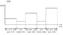
- FIG. 2is a view for explaining a pressure profile according to an embodiment of the present invention.
- FIG. 3is a conceptual diagram illustrating a method of manufacturing a pressurized metal monolayer layer according to an embodiment of the present invention.
- step S100is a view for explaining a first deformation pressure profile in step S100 of the present invention.
- FIG. 5is a conceptual diagram illustrating a method of manufacturing a pressurized metal monolayer layer according to a first strain pressure profile of the present invention.
- FIG 6is another diagram for explaining the second deformation pressure profile in step S100 of the present invention.
- FIG. 7is a diagram for explaining a first deformation pressure profile in step S120 of the present invention.
- step S120 of the present inventionis another diagram for explaining the second deformation pressure profile in step S120 of the present invention.
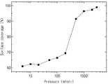
- FIG. 9is a graph illustrating a surface coverage test result according to a tungsten metal precursor gas dosing pressure according to an exemplary embodiment of the present invention.
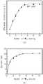
- FIG. 10is a graph showing the XPS and the current test results according to the number of sub-dozing of the tungsten metal precursor gas according to an embodiment of the present invention.
- 11is a graph showing the XPS and the current test results according to the number of times of sub-pressurized dosing of the reaction gas according to an embodiment of the present invention.
- FIG. 12is a photograph showing surface roughness change according to the number of times of sub-pressurized dosing of a tungsten metal precursor gas according to an embodiment of the present invention.
- FIG. 13is a TEM photograph of a tungsten monoatomic layer structure according to an embodiment of the present invention.
- FIG. 14is a graph illustrating a surface coverage test result according to a dosing pressure of molybdenum metal precursor gas according to an exemplary embodiment of the present invention.
- FIG. 15is a graph illustrating XPS and current test results according to the number of sub-dosings of the molybdenum metal precursor gas according to an exemplary embodiment.
- 16is a graph illustrating XPS and current test results according to the number of times of sub-pressurized dosing of a reaction gas according to an exemplary embodiment of the present invention.
- 17is a photograph showing the surface roughness of the molybdenum monoatomic layer structure according to an embodiment of the present invention.
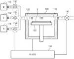
- FIG. 18is a view for explaining a metal monolayer layer manufacturing apparatus according to an embodiment of the present invention.
- first, second, and thirdare used to describe various components, but these components should not be limited by these terms. These terms are only used to distinguish one component from another. Thus, what is referred to as a first component in one embodiment may be referred to as a second component in another embodiment.
- first componentin one embodiment may be referred to as a second component in another embodiment.
- second componentin another embodiment.
- Each embodiment described and illustrated hereinalso includes its complementary embodiment.
- the term 'and / or'is used herein to include at least one of the components listed before and after.
- connectionis used herein to mean both indirectly connecting a plurality of components, and directly connecting.
- FIG. 1is a flowchart illustrating a method of manufacturing a pressurized metal monolayer layer according to an embodiment of the present invention
- FIG. 2is a view for explaining a pressure profile according to an embodiment of the present invention
- FIG. A conceptual diagram illustrating a method of manufacturing a pressurized metal monoatomic layer according to an embodimentis shown.
- a metal precursor gasis provided to increase a pressure in the chamber in a state in which a chamber in which a substrate is provided is sealed.
- a main purge step of purging after the reactant gas dosing step and the reactant gas dosing stepwill be described in detail.
- Step S100is to pressurize and doze the metal precursor gas to adsorb the metal precursor gas to the substrate.
- the metal precursor gasis not particularly limited and may be selected according to the metal monoatomic layer to be deposited.
- the metal precursor gasmay be made of tungsten hexafluoride (WF6).
- the metal precursor gasmay be made of molybdenum hexafluoride (MoF6).
- the substrateis also not particularly limited, and may be, for example, made of a silicon substrate.
- the metal precursor gasmeans tungsten hexafluoride gas, and the substrate may be understood to mean a silicon substrate.
- Pressing and dosing the metal precursor gasmay specifically include evaluating the carrier gas, supplying and maintaining the pressure by supplying the metal precursor into the chamber, and reducing the pressure in the chamber.
- Removing the carrier gasis removing impurities such as inert gas that may be present in the chamber. Removing the carrier gas is not necessarily an essential step, but may be an optional step. Hereinafter, the step of removing the carrier gas will be omitted and described.
- Supplying the metal precursor gas into the chamber to increase and maintain the pressuremay be performed in a sealed state in the chamber in which the substrate is provided. For example, by supplying the metal precursor gas into the chamber while the outlet valve of the chamber is closed, the inside of the chamber can be led to high pressure and the induced high pressure can be maintained. By maintaining the high pressure for a predetermined time, the metal precursor gas can be induced to be adsorbed on the surface of the substrate in the high pressure atmosphere.
- the pressure in the chamber in step S100may be preferably maintained at 0.3 Torr to 100 Torr. If the pressure in the chamber is lower than 0.3 Torr, the adsorption rate of the metal precursor gas is significantly lowered. More specifically, when the pressure in the chamber is lower than 0.3 Torr, the spacing between the adsorbed metal precursors is narrowed by the spatial volume occupied by the metal precursors adsorbed first on the surface of the substrate. Subsequently, the metal precursors to be adsorbed do not penetrate into the narrow gaps between the already adsorbed metal precursors. That is, the spatial volume occupied by the pre-adsorbed metal precursors acts as an obstacle to adsorption of the metal precursors to be adsorbed later. Thus, surface coverage is significantly lower when the pressure in the chamber is less than 0.3 Torr.
- the metal precursorwhen the pressure in the chamber is 0.3 Torr or more, even if the metal precursors adsorbed on the substrate are present, the metal precursor may be adsorbed on the surface of the substrate because of the high driving force.
- the substrate surfacemay be damaged by the metal precursor gas.
- the pressure range in the chambercan be formed from 0.3 Torr to 100 Torr, which is a high pressure.
- step S100as shown in FIG. 3, the metal precursor M may be adsorbed onto the substrate S surface.
- a purging main purge stepmay be performed (S110).
- Inert gasmay be used in the main purging step, and the inert gas may be made of, for example, argon (Ar) or nitrogen (N 2) gas.
- the pressure in the chamber by the main purging stepmay be formed lower than the step S100, as shown in FIG.
- step S110as illustrated in FIG. 3, excess metal precursor gas that is not adsorbed on the surface of the substrate may be removed.
- the reactive gas dosing step of reducing the metal precursor adsorbed on the substrate to the metal monoatomic layer by providing the reactive gasmay be performed (S120).
- the reaction gasmay be made of a material for reducing the metal precursor gas to the metal.
- the metal precursoris tungsten hexafluoride (WF6) or molybdenum hexafluoride (MoF6)
- the reaction gasmay be made of disilane (Si2H6).
- the reaction gasmay mean a disilane (Si 2 H 6) gas.
- Dosing the reactant gasmay also include evacuating carrier gas, supplying the reactant gas into the chamber to increase and maintain pressure, and reducing the pressure in the chamber.
- evacuating carrier gassupplying the reactant gas into the chamber to increase and maintain pressure
- reducing the pressure in the chamberreducing the pressure in the chamber.
- the supplying of the reaction gasmay be performed while the chamber is sealed, or may be performed even when the chamber is open.
- step S100when providing the reaction gas in the closed state, as described above in step S100, by supplying the reaction gas into the chamber while the outlet valve of the chamber is closed, the reaction gas is supplied to the substrate in a high pressure atmosphere. It can be induced to reduce the metal precursor adsorbed to.
- the pressure in the chamber in step S120may be maintained at 0.3 Torr to 100 Torr.
- the performing pressure of step S110may be the same as step S100, as shown in FIG. 2.
- the lamina flowcan be formed by supplying the reaction gas into the chamber while the outlet valve of the chamber is opened. Thereby, the reaction gas can be induced to reduce the metal precursor adsorbed on the substrate.
- the reaction gas Rmay react with the metal precursor M adsorbed on the surface of the substrate S.
- a main purging stepmay be performed (S140).
- Inert gasmay be used in the main purging step, and the inert gas may be made of, for example, argon (Ar) or nitrogen (N 2) gas.
- the pressure in the chamber by the main purging stepmay be formed as low as step S110, as shown in FIG.
- step S110as shown in FIG. 3, the excess reaction gas which is not adsorbed on the surface of the substrate is removed and only the metal monoatomic M 'remains.
- the method of manufacturing a metal monoatomic layer according to an embodiment of the present inventionAccording to the metal monolayer layer manufacturing method according to an embodiment of the present invention, a metal monolayer layer structure having high uniformity and low surface roughness may be provided.
- the method for manufacturing a metal monoatomic layerby providing a metal precursor gas in a closed state of the chamber, it is possible to maintain the pressure in the chamber at a high pressure. Accordingly, the metal precursor can be induced to be easily adsorbed on the surface of the substrate.
- the conventional atomic layer deposition methodby providing a precursor gas in an open state without closing the chamber, the precursor is adsorbed onto the substrate surface at a low pressure in the chamber. That is, according to the conventional atomic layer deposition method, a laminar flow is formed on the surface of the substrate with the precursor gas to adsorb the precursor gas onto the substrate surface. According to this conventional atomic layer deposition method, since the pressure in the chamber is low, the metal precursor gas cannot be formed to have high uniformity and low surface roughness on the substrate.
- the method for manufacturing a metal monoatomic layermay provide a high pressure atmosphere by providing a metal precursor gas in a state where the chamber is sealed, so that the metal precursor gas may be adsorbed to the substrate with high surface coverage.
- steps S100 to S130may be performed at the same temperature with each other, in particular, at a low temperature.
- Low temperatureas used herein means 200 degrees or less, preferably 100 degrees or more and 200 degrees or less.
- agglomerationmay occur because of the high reactivity of the metal monoatomic layer. Therefore, by keeping the temperature of the process at a low temperature of 100 degrees or more and 200 degrees or less, the aggregation phenomenon of the metal monoatomic layer can be prevented.
- FIGS. 4 and 5is a view for explaining a first deformation pressure profile in step S100 of the present invention
- Figure 5shows a conceptual diagram for explaining a method for producing a pressurized metal monolayer layer according to step S100 of the present invention.
- steps S110 to S130may be applied as it is.
- Step S100may include a sub purging step provided between at least two sub press dosing steps and two sub press dosing steps. As shown in FIG. 4, step S100 may include three sub-pressure dosing steps and two sub dosing steps therebetween. Accordingly, step S100 may provide multi dosing of the metal precursor gas. Preferably, step S100 may consist of four sub-pressurizing dosing steps and three sub-purging steps therebetween. Alternatively, step S100 may include five sub-pressurizing dosing steps and four sub-purging steps therebetween.
- the chamber pressure in the sub-pressurized dosing stepmay be 0.3 Torr or more and 10 Torr or less.
- the chamber pressure of the subpurging stepmay be equal to or higher than the pressure of the main purging step described with reference to steps S110 and S130.
- FIG. 5to describe in detail the adsorption process of the metal precursor gas according to the application of the pressure profile shown in FIG. 4.
- a metal precursor gas Mmay be provided to the substrate S by a sub-pressurized dosing step. At this time, even if the metal precursor gas is provided at a high pressure, only a part of the metal precursor gas may be adsorbed onto the substrate S.
- a metal purge gas that is not adsorbed onto the substratemay be removed by the subpurging step.
- an inert gasmay also be used in the subpurging step.
- the pressure in the chambercan be made higher than the main purging step. This allows the metal precursor gas, even if not adsorbed, to the substrate to be recycled in a subsequent subpressurized dosing step.
- the sub-pressurizing dosing stepmay be performed again.
- more metal precursors Mmay be adsorbed onto the substrate S than the metal precursors illustrated in FIG. 5A.
- the metal precursor gas which is not adsorbed by the sub pressurizing step according to FIG. 5 (c)may be removed by the sub purging step.
- the pressure in the chambermay be set higher than that of the main purging step so that even metal precursor gas which is not adsorbed on the substrate may be reused in the subsequent sub-pressurizing dosing step.
- the subpressurized dosing stepmay be performed again.
- more metal precursors Mmay be adsorbed onto the substrate S than the metal precursors illustrated in FIG. 5C.
- the substrate adsorption rate of the metal precursor gascan be further increased.
- the sub-pressurizing dosing stepis repeated three times. However, this is merely for convenience of description, and the sub-pressurizing dosing step may be two or four or more times. Can be.
- step S100is another diagram for explaining the second deformation pressure profile in step S100 of the present invention.
- Step S100may include a sub purging step provided between at least two sub press dosing steps and two sub press dosing steps. As shown in FIG. 6, step S100 may include two sub dosing steps between the first to third sub pressurized dosing steps and the respective sub pressurized dosing steps.
- the chamber pressure of the subpurging stepmay be equal to or higher than the pressure of the main purging step described with reference to steps S110 and S130.
- the pressure of the three sub-pressurizing dosing stephas a technical feature in that the pressure increases from the first sub-pressurizing dosing step to the third sub-pressing step that follows.
- the increase in the pressure in the sub-pressurizing dosing stepmeans not only when the pressures in the first, second, and third sub-pressurizing dosing steps are sequentially increased, but also the pressure in the second sub-pressurizing dosing step is the first.
- the pressure of the third sub-pressurizing dosing stepis higher than the pressure of the first sub-pressurizing dosing step.
- the chamber pressure of each sub-pressurizing dosing stepmay be implemented to increase within a section of 0.3 Torr or more and 10 Torr or less.
- the pressure of the subsequent sub-pressurization stepis higher than the pressure of the previously-progressed sub-pressurization step even at the site where the metal precursor was not adsorbed to the substrate in the first sub-pressurization step.
- the metal precursorcan be adsorbed.
- the first and second deformation pressure profiles in step S100 of the present inventionhave been described.
- the first and second strain pressure profilesmay provide a technical significance of improving the substrate adsorption rate of the metal precursor gas.
- step S120 of the present inventionwill be described with reference to FIGS. 7 and 8.
- FIG. 7is a diagram for explaining a first deformation pressure profile in step S120 of the present invention.
- the first deformation pressure profile in step S120 of the present inventionmay have the same pressure profile as the first deformation pressure profile in step S100 of the present invention described with reference to FIG. 4.
- step S120may include a subpurging step provided between at least two subpressurized dosing steps and two subpressurized dosing steps when reacting gas is doped. Accordingly, step S120 may provide multi dosing of the reaction gas.
- step S120may consist of four sub-pressurizing dosing steps and three sub-purging steps therebetween.
- step S100may include five sub-pressurizing dosing steps and four sub-purging steps therebetween.
- the chamber pressure of the sub-pressurizing dosing stepmay be 0.3 Torr or more and 10 Torr or less.
- the chamber pressure of the sub purging stepmay be equal to or higher than the pressure of the main purging step.
- reaction gascan react with the metal precursor adsorbed on the substrate more easily.
- step S120is a view for explaining the second deformation pressure profile in step S120 of the present invention.
- the second deformation pressure profile in step S120 of the present inventionmay have the same pressure profile as the second deformation pressure profile in step S100 of the present invention described with reference to FIG. 6.
- step S120may include at least two sub-pressurizing dosing steps and a sub-purging step between the sub-pressurizing dosing steps during reaction visible dosing, wherein the pressure in the sub-pressurizing dosing step may be increased.
- the chamber pressure of the sub-pressurizing dosing stepmay be configured to increase with the number of sub-pressurizing dosing steps in the range of 0.3 Torr or more and 10 Torr or less.
- the chamber pressure of the sub purging stepmay be equal to or higher than the pressure of the main purging step.
- FIG. 9is a graph illustrating a surface coverage test result according to a tungsten metal precursor gas dosing pressure according to an exemplary embodiment of the present invention.
- step 9is a result of measuring the surface coverage while increasing the dosing pressure of step S100 (see FIG. 2) of FIG. 1 using tungsten hexafluoride gas as the metal precursor gas.
- the surface coverageis 61%, 62.5, 62, 65, 66.5, 69.5, Improved to 91.5, 96.5, 97.5, and 99.
- the surface coveragewas as low as about 70%.
- the dosing pressure of the metal precursor gaswas increased to 0.3 Torr or more, the surface coverage was remarkably excellent, about 90%.
- the substrate surface adsorption rate of the metal precursor gasis significantly increased.
- FIG. 10is a graph showing the results of the XPS and the current experiment according to the number of sub-dosing of the tungsten metal precursor gas according to an embodiment of the present invention
- Figure 11is a number of sub-dosing of the reaction gas according to an embodiment of the present invention It is a graph showing the results of XPS and current experiment.
- tungsten hexafluoride gaswas used as the metal precursor gas and disilane (Si 2 H 6) was used as the reaction gas.
- the supply pressure of the metal precursor gaswas applied to the first strain pressure profile of step S100 shown in FIG.
- the supply pressure of the reaction gasis applied to the first strain pressure profile of step S100 shown in Figure 7, but the number of sub-pressurized dosing was fixed five times.
- the graph shown in FIG. 10looks at the XPS and the current magnitude according to the number of times of sub-pressurized dosing of the tungsten metal precursor gas. At this time, the number of times of sub pressurized dosing of the reaction gas was fixed five times. The overall process temperature was also maintained at 100 degrees. The pressure during each subpressurized dosing of the metal precursor gas and the reactant gas was set to 1 Torr and the holding time was 30 seconds.
- the XPS peak intensityis 18653, 31341, 42347, 50189, It increased to 55861, 56896, and 57134. That is, as the number of times of pressurized dosing of the metal precursor gas increases, the XPS peak intensity also increases. In particular, when the number of times of pressurized dosing of the metal precursor gas is 5 times, the saturation state is reached.
- the intensity of the currentis 12.3, 15.9, 17.8, and 19.4. , 20.2, 20.4, and 20.7nA. That is, as the number of times of pressurizing the sub-pressurized metal precursor gas increases, the current intensity also increases. In particular, when the number of times of pressurizing the sub-pressurized metal precursor gas is 5 times, the saturation state is reached.
- the graph shown in FIG. 11shows a case in which tungsten hexafluoride gas is used as the metal precursor gas and disilane (Si 2 H 6) is used as the reaction gas, and the first strain pressure profile of step S120 shown in FIG. 7 is applied.
- the experimental resultsare shown. At this time, the supply pressure of the metal precursor gas was applied to the first strain pressure profile of step S100 shown in FIG. 4, but the number of sub-pressurized dosing was fixed to five times.
- the graph shown in FIG. 11looks at the XPS and the current magnitude according to the number of times of sub pressurized dosing of the reaction gas. At this time, the number of times of sub-pressurized dosing of the metal precursor gas was fixed five times. The overall process temperature was also maintained at 100 degrees. The pressure during each subpressurized dosing of the metal precursor gas and the reactant gas was set to 1 Torr and the holding time was 30 seconds.
- the XPS peak intensityis 23415, 47123, 54123, 55997, 56324, 57011, It was found to increase to 57023. That is, as the number of times of sub pressurizing dosing of the reaction gas increases, the XPS peak intensity also increases. In particular, when the number of times of sub pressurizing dosing of the reaction gas occurs, the saturation state is reached.
- the current intensityis 12.3, 17.6, 19.8, 20.1, 20.2, 20.4, It was found to increase to 20.5 nA. That is, as the number of times of pressurization of the reactive gas increases, the current intensity also increases. In particular, when the number of times of pressurization of the reactive gas is 5 times, the saturation state is reached.
- FIG. 12is a photograph showing surface roughness change according to the number of times of sub-pressurized dosing of a tungsten metal precursor gas according to an embodiment of the present invention.
- the graph shown in FIG. 12shows a case where tungsten hexafluoride gas is used as the metal precursor gas and disilane (Si 2 H 6) is used as the reaction gas, and the first strain pressure profile of step S100 shown in FIG. 4 is applied.
- the experimental resultsare shown.
- the graph shown in FIG. 12looks at the surface roughness according to the number of times of sub-pressurized dosing of the metal precursor gas. At this time, the number of times of sub pressurized dosing of the reaction gas was fixed five times. The overall process temperature was also maintained at 100 degrees. The pressure during each subpressurized dosing of the metal precursor gas and the reactant gas was set to 1 Torr and the holding time was 30 seconds.
- FIG. 13is a TEM photograph of a tungsten metal monoatomic layer structure according to an embodiment of the present invention.
- the TEM photograph shown in FIG. 13is a photograph when the metal monoatomic layer structure is formed 5 times of the metal precursor gas subpressive dosing and 5 times of the reaction gas subdozing. Other conditions were the same as those described above.
- the metal monoatomic layeris formed with a thin thickness of 0.8 nm.
- FIG. 14is a graph illustrating a surface coverage test result according to a dosing pressure of molybdenum metal precursor gas according to an exemplary embodiment of the present invention.
- the graph shown in FIG. 14is a result of measuring the surface coverage while increasing the dosing pressure of step S100 (see FIG. 2) of FIG. 1 using molybdenum hexafluoride gas as the metal precursor gas.
- the surface coverageis 68, 69, 70, 72, 73, 92, 94, Increased to 95, 98, 98%.
- the surface coveragewas slightly lower than about 75%.
- the dosing pressure of the metal precursor gaswas increased to 0.3 mTorr or more, the surface coverage was remarkably excellent at about 90%.
- the substrate surface adsorption rate of the metal precursor gasis significantly increased.
- FIG. 15is a graph illustrating XPS and current test results according to the number of sub-dosings of the molybdenum metal precursor gas according to an embodiment of the present invention
- FIG. 16is a graph showing the number of times of sub-pressurization of the reactive gas according to an embodiment of the present invention. It is a graph showing the XPS and the current experimental results.
- molybdenum hexafloid gaswas used as the metal precursor gas and disilane (Si 2 H 6) was used as the reaction gas.
- the supply pressure of the metal precursor gaswas applied to the first strain pressure profile of step S100 shown in FIG.
- the supply pressure of the reaction gasis applied to the first strain pressure profile of step S100 shown in Figure 7, but the number of sub-pressurized dosing was fixed five times.
- the graph shown in FIG. 15looks at the XPS and the current magnitude according to the number of times of sub-pressurized dosing of the molybdenum metal precursor gas. At this time, the number of times of sub pressurized dosing of the reaction gas was fixed four times. The overall process temperature was also maintained at 100 degrees. The pressure at each sub dosing of the metal precursor gas and the reactant gas was set to 1 Torr and the holding time was 30 seconds.
- the current intensityis 21.4, 39, 43, 48.3. , 48.4, 49.1, 48.8. That is, as the number of times of sub-pressurizing dosing of the metal precursor gas increases, the current intensity also increases. In particular, when the number of times of sub-pressurizing dosing of the metal precursor gas occurs, the saturation state is reached.
- the XPS peak intensityis 23859, 37784, 43680, 46833. , 47299, 47249, and 47593.
- the XPS peak intensityalso increases.
- the saturation stateis reached.
- the substrate surface adsorption degree of the metal precursorhas reached a saturation state.
- the graph shown in FIG. 16shows a case where molybdenum hexafluoride gas is used as the metal precursor gas and disilane (Si 2 H 6) is used as the reaction gas and the first strain pressure profile of step S120 shown in FIG. 7 is applied.
- the experimental resultsare shown. At this time, the supply pressure of the metal precursor gas was applied to the first strain pressure profile of step S100 shown in FIG. 4, but the number of sub-pressurized dosing was fixed to five times.
- the graph shown in FIG. 16looks at the XPS and the current magnitude according to the number of sub-pressurized dosing of the reaction gas. At this time, the number of times of sub-pressurizing dosing of the metal precursor gas was fixed four times. The overall process temperature was also maintained at 100 degrees. The pressure during each subpressurized dosing of the metal precursor gas and the reactant gas was set to 1 Torr and the holding time was 30 seconds.
- the current intensityis 35, 41, 45, 48.5, 48.6, It increased to 49.1, 49. That is, as the number of times of pressurization of the reactive gas increases, the current intensity also increases. In particular, when the number of times of pressurization of the reactive gas is four times, the saturation state is reached.
- the XPS peak intensityis 36168, 43431, 45174, 46669, 46931, 47586, It increased to 47513.
- the XPS peak intensityalso increases.
- the saturation stateis reached.
- FIG. 17is a photograph showing the surface roughness of the molybdenum monoatomic layer structure according to an embodiment of the present invention.
- the number of times of sub pressurized dosing of the reaction gaswas fixed four times.
- the overall process temperaturewas also maintained at 100 degrees.
- the pressurewas set at 1 Torr and the holding time was 30 seconds.
- the surface roughnessappears to be significantly small, 1.64 angstroms. This means that a uniform metal monoatomic layer can be formed by a plurality of sub-pressurized dosing steps.
- FIG. 18is a view for explaining a metal monolayer layer manufacturing apparatus according to an embodiment of the present invention.
- the metal monolayer layer manufacturing apparatus according to an embodiment of the present invention described with reference to FIG. 18may be applied to the method of manufacturing the metal monolayer layer described above.
- each configuration of the metal monolayer layer manufacturing apparatus according to an embodiment of the present inventionwill be described.
- the metal monolayer layer manufacturing apparatusmay include a chamber 100.
- the chamber 100may provide an accommodation space to accommodate a substrate on which the metal monoatomic layer is to be formed.
- a stage 102 on which a substrate is mountedmay be provided in the accommodation space of the chamber 100.
- the chamber 100may further include an inlet port 120 for sequentially supplying a metal precursor gas, an inert gas, a reaction gas, and an inert gas, and an outlet 140 for outflowing the introduced gas.
- the outlet 140may be provided with an outlet valve 142 for controlling the amount of outflow.
- the metal monoatomic layer manufacturing apparatusfor storing the metal precursor gas, the inert gas storage unit 112 for storing the inert gas and the reaction gas storage unit for storing the reaction gas 110 may further include.
- the metal precursor gas storage unit 110stores tungsten hexafluoride (WF6) or molybdenum hexafluoride (MoF6)
- the inert gas storage unit 112stores argon or nitrogen gas, and stores the reaction gas.
- the unit 110may store a disilane (Si 2 H 6) gas.
- the metal precursor gas stored in the metal precursor gas storage 110may be provided to the inlet 120 of the chamber 100 through the metal precursor gas control valve 130.
- the inert gas stored in the inert gas storage 112may be provided to the inlet 120 of the chamber 100 through the inert gas control valve 132.
- the reaction gas stored in the reaction gas storage unit 114may be provided to the inlet 120 of the chamber 100 through the reaction gas control valve 134.
- the metal monolayer layer manufacturing apparatusmay further include a controller 150.
- the controller 150may implement a method of manufacturing a metal monoatomic layer according to an embodiment of the present invention by controlling each component.
- the metal precursor reaction gas and the inert gasare introduced into the inlet 120 of the chamber 100.
- the gas, the reaction gas and the inert gascan be controlled to be sequentially supplied.
- the controller 150may seal the inside of the chamber 100 by opening the metal precursor gas control valve 130 and closing the outlet valve 142. have.
- the controller 150may improve the surface coverage of the metal precursor gas adsorbed on the substrate to 90% or more by controlling the pressure in the chamber.
- the controller 150opens the metal precursor gas control valve 130 in the sub pressurizing step of the metal precursor gas to implement the first deformation pressure profile of step S100 shown in FIG. 142 may be closed.
- the inert gas control valve 132 and the outlet valve 142may be opened together.
- the controller 150may provide a sub purging pressure between at least two sub pressurized dosing pressures and the at least two sub pressurized dosing pressures. At this time, each of the at least two sub-pressurized dosing pressures may be equal to each other.
- the controller 150may control the subpurging pressure to be greater than or equal to the main purging pressure supplied with the inert gas into the chamber.
- controller 150may implement the second deformation pressure profile of step S100 illustrated in FIG. 6 by controlling the opening and closing degree of each valve. At this time, the magnitude of the at least two sub-pressurized dosing pressure may increase with the number of sub-pressurized dosing. In addition, the controller 150 may control the subpurging pressure to be greater than or equal to the main purging pressure supplied with the inert gas into the chamber.
- the controller 150opens the reaction gas control valve 134 in the sub-pressurization step of the reaction gas to implement the first deformation pressure profile of step S120 shown in FIG. 7, and the outlet valve 142. Can be closed.
- the inert gas control valve 132 and the outlet valve 142may be opened together.
- controller 150may implement the second deformation pressure profile of step S120 illustrated in FIG. 8 by controlling the opening and closing degree of each valve.
- the controller 150may maintain a constant temperature in the chamber while supplying the metal precursor gas, the inert gas, or the reactive gas into the chamber.
- the controller 150may control the temperature in the chamber to 100 degrees to 200 degrees.
Landscapes
- Chemical & Material Sciences (AREA)
- Organic Chemistry (AREA)
- Chemical Kinetics & Catalysis (AREA)
- General Chemical & Material Sciences (AREA)
- Engineering & Computer Science (AREA)
- Materials Engineering (AREA)
- Mechanical Engineering (AREA)
- Metallurgy (AREA)
- Chemical Vapour Deposition (AREA)
- Electrodes Of Semiconductors (AREA)
- Internal Circuitry In Semiconductor Integrated Circuit Devices (AREA)
Abstract
Description
Translated fromKorean본 발명은 가압식 금속 단원자층 제조 방법, 금속 단원자층 구조체 및 가압식 금속 단원자층 제조 장치에 관련된 것으로서, 금속 전구체를 고압 도징하여 컨포멀(conformal)한 금속 단원자층을 형성하는 가압식 금속 단원자층 제조 방법 및 가압식 금속 단원자층 제조 장치 그리고 그에 의하여 형성된 금속 단원자층 구조체에 관련된 것이다.The present invention relates to a pressurized metal monolayer layer manufacturing method, a metal monolayer layer structure, and a pressurized metal monolayer layer manufacturing apparatus, and a pressurized metal monolayer layer manufacturing method for forming a conformal metal monolayer by high-pressure dosing a metal precursor and A pressurized metal monolayer layer manufacturing apparatus and a metal monolayer layer structure formed thereby.
지금까지는 반도체 소자 제조에 PVD(Physical Vapor Deposition, 물리기상증착법) 또는 CVD(Chemical Vapor Deposition, 화학기상증착법) 기술이 이용되었으나, 이러한 기존의 기술은 나노급 초고집적 소자 제조에 적용하기에는 한계가 있다.Until now, PVD (Physical Vapor Deposition) or CVD (Chemical Vapor Deposition) techniques have been used to manufacture semiconductor devices. However, these conventional techniques have limitations in applying to nanoscale ultra-high density devices.
그러나, 원자층 증착(ALD)의 경우, 복잡한 형상의 3차원 구조에서도 뛰어난 균일도를 가지는 나노 두께의 박막 증착이 가능하기 때문에 나노급 반도체 소자 제조의 필수적인 증착기술로 주목받고 있다.However, in the case of atomic layer deposition (ALD), since it is possible to deposit a thin film of nano-thickness having excellent uniformity even in a complicated three-dimensional structure, it is attracting attention as an essential deposition technology for manufacturing a nano-class semiconductor device.
한편, 최근 들어, 스마트 기기, 인공 지능 컴퓨터 기술의 발전에 따라 고성능화, 다기능화와 같은 보다 높은 성능의 소자에 대한 요구가 급격히 증가하고 있다.On the other hand, in recent years, with the development of smart devices and artificial intelligence computer technology, the demand for higher performance devices such as high performance and multifunction has increased rapidly.
그러나, 기존의 MOSFET 미세화를 통한 개발 방법은, 고온 발생으로 인하여 소자의 신뢰성이 열화 된다는 미세화 기술 자체의 어려움을 가지고 있다. 따라서, 다운 스케일링(down scaling)을 통한 종래의 접근 방식은 근본적인 한계를 가지고 있는 것으로 평가된다.However, the existing development method through the miniaturization of the MOSFET has a difficulty in the miniaturization technology itself that the reliability of the device is degraded due to high temperature generation. Therefore, the conventional approach through down scaling is estimated to have a fundamental limitation.
이에 본 발명자들은, 소재 차원에서 시작하여 미래 지향적인 소자 기술을 확보하고자, 원자층 증착법을 통하여 금속 단원자층을 발명하게 되었다.Accordingly, the inventors of the present invention have invented a metal monoatomic layer through atomic layer deposition to secure future-oriented device technology starting from the material level.
본 발명이 해결하고자 하는 일 기술적 과제는, 단원자층으로 이루어진 금속 단원자층 구조체, 이를 제공하기 위한 가압식 금속 단원자층 제조 방법 및 제조 장치를 제공하는 데 있다.One technical problem to be solved by the present invention is to provide a metal monoatomic layer structure consisting of a monomagnetic layer, a pressurized metal monolayer layer manufacturing method and a manufacturing apparatus for providing the same.
본 발명이 해결하고자 하는 다른 기술적 과제는, 높은 표면 커버리지를 가지는 금속 단원자층 구조체, 이를 제공하기 위한 가압식 금속 단원자층 제조 방법 및 제조 장치를 제공하는 데 있다.Another technical problem to be solved by the present invention is to provide a metal monomagnetic layer structure having a high surface coverage, a pressurized metal monolayer layer manufacturing method and a manufacturing apparatus for providing the same.
본 발명이 해결하고자 하는 또 다른 기술적 과제는, 표면 거칠기가 낮은 금속 단원자층 구조체, 이를 제공하기 위한 가압식 금속 단원자층 제조 방법 및 제조 장치를 제공하는 데 있다.Another technical problem to be solved by the present invention is to provide a metal monolayer layer structure having a low surface roughness, a pressurized metal monolayer layer manufacturing method and a manufacturing apparatus for providing the same.
본 발명이 해결하고자 하는 기술적 과제는 상술된 것에 제한되지 않는다.The technical problem to be solved by the present invention is not limited to the above.
상기 기술적 과제를 해결하기 위해, 본 발명은 금속 단원자층 제조 방법, 이를 이용하여 제조된 금속 단원자층 구조체 및 금속 단원자층 제조 장치를 제공한다.In order to solve the above technical problem, the present invention provides a method for producing a metal monoatomic layer, a metal monoatomic layer structure and a metal monoatomic layer manufacturing apparatus manufactured using the same.
본 발명의 일 실시 예에 따른 금속 단원자층 제조 방법은, 기판이 마련된 챔버 내를 밀폐시킨 상태에서, 금속 전구체로 이루어진 금속 전구체 가스를 제공함으로써, 상기 챔버 내의 압력을 증가시켜, 상기 금속 전구체를 상기 기판에 흡착시키는 금속 전구체 가스 가압 도징(dosing) 단계, 상기 금속 전구체 가압 도징 단계 이후, 퍼지시키는 메인 퍼징(main purging) 단계, 상기 메인 퍼징 단계 후에, 반응 가스를 제공하여, 상기 기판에 흡착된 금속 전구체를 금속 단원자층으로 환원하는 반응 가스 도징 단계 및 상기 반응 가스 도징 단계 이후, 퍼지시키는 메인 퍼징 단계를 포함하여 이루어질 수 있다.In the method of manufacturing a metal monoatomic layer according to an embodiment of the present invention, by providing a metal precursor gas made of a metal precursor in a sealed state in a chamber in which a substrate is provided, the pressure in the chamber is increased to provide the metal precursor. A metal precursor gas pressurized dosing step adsorbed onto a substrate, a main purging step of purging after the metal precursor pressurizing dosing step, and after the main purging step, a reaction gas is provided to provide a metal adsorbed onto the substrate. It may include a reactant gas dosing step of reducing the precursor to the metal monoatomic layer and a main purging step after the reactant gas dosing step.
일 실시 예에 따르면, 상기 금속 전구체 가스 가압 도징 단계에서, 상기 챔버 내의 압력은, 0.3Torr 내지 100Torr일 수 있다.According to an embodiment, in the metal precursor gas pressurized dosing step, the pressure in the chamber may be 0.3 Torr to 100 Torr.
일 실시 예에 따르면, 상기 금속 전구체 가스 가압 도징 단계에서, 상기 기판에 흡착된 금속 전구체 가스의 표면 커버리지는 90% 이상일 수 있다.According to one embodiment, in the metal precursor gas pressurized dosing step, the surface coverage of the metal precursor gas adsorbed on the substrate may be 90% or more.
일 실시 예에 따르면, 상기 금속 전구체 가스 가압 도징 단계는, 적어도 두 번의 서브 가압 도징 단계 및 상기 적어도 두 번의 서브 가압 단계 사이의 서브 퍼징 단계로 이루어질 수 있다.According to an embodiment, the metal precursor gas pressurized dosing step may include a subpurging step between at least two sub pressurized dosing steps and the at least two sub pressurized steps.
일 실시 예에 따르면, 상기 적어도 두 번의 서브 가압 도징 단계의 각각의 압력의 크기는 서브 가압 도징 단계의 횟수에 따라 증가할 수 있다.According to one embodiment, the magnitude of each pressure of the at least two sub-pressurized dosing steps may increase with the number of sub-pressurized dosing steps.
일 실시 예에 따르면, 상기 적어도 두 번의 서브 가압 도징 단계의 각각의 압력은 서로 동일할 수 있다.According to one embodiment, the pressures of the at least two sub-pressurized dosing steps may be equal to each other.
일 실시 예에 따르면, 상기 서브 퍼징 단계에서의 상기 챔버 내의 압력은, 상기 메인 퍼징 단계에서의 상기 챔버 내의 압력보다 높을 수 있다.According to an embodiment, the pressure in the chamber in the subpurging step may be higher than the pressure in the chamber in the main purging step.
일 실시 예에 따르면, 상기 서브 퍼징 단계에서의 상기 챔버 내의 압력은, 상기 메인 퍼징 단계에서의 상기 챔버 내의 압력과 같을 수 있다.According to an embodiment, the pressure in the chamber in the subpurging step may be the same as the pressure in the chamber in the main purging step.
일 실시 예에 따르면, 상기 서브 가압 도징 단계는 4번 이상의 서브 가압 도징 단계로 이루어질 수 있다.According to an embodiment, the sub-pressurizing dosing step may include four or more sub-pressurizing dosing steps.
일 실시 예에 따르면, 상기 금속 전구체 가압 도징 단계, 상기 메인 퍼징 단계들 및 상기 반응 가스 도징 단계에서의 공정 온도는 서로 동일할 수 있다.According to one embodiment, the process temperature in the metal precursor pressure dosing step, the main purging step and the reaction gas dosing step may be the same.
일 실시 예에 따르면, 상기 공정 온도는 100도 내지 200도일 수 있다.According to one embodiment, the process temperature may be 100 to 200 degrees.
일 실시 예에 따르면, 상기 반응 가스 도징 단계는, 적어도 두 번의 서브 가압 도징 단계 및 상기 적어도 두 번의 서브 가압 도징 단계 사이의 서브 퍼징 단계로 이루어질 수 있다.According to one embodiment, the reactive gas dosing step may include a subpurging step between at least two sub-pressurized dosing steps and the at least two sub-pressurized dosing steps.
일 실시 예에 따르면, 상기 금속 전구체 가스는, 텅스텐 헥사플로라이드(WF6)를 포함하며, 상기 반응 가스는, 다이실란(Si2H6)를 포함하며, 상기 금속 단원자층은 텅스텐(W)으로 이루어질 수 있다.According to an embodiment, the metal precursor gas may include tungsten hexafluoride (WF 6), the reaction gas may include disilane (Si 2 H 6), and the metal monoatomic layer may be made of tungsten (W). .
일 실시 예에 따르면, 상기 금속 전구체 가스는, 몰리브덴 헥사플로라이드(MoF6)를 포함하며, 상기 반응 가스는, 다이실란(Si2H6)를 포함하며, 상기 금속 단원자층은 몰리브덴(Mo)으로 이루어질 수 있다.According to an embodiment, the metal precursor gas may include molybdenum hexafluoride (MoF 6), the reaction gas may include disilane (Si 2 H 6), and the metal monoatomic layer may be formed of molybdenum (Mo). .
본 발명의 일 실시 예에 따른 금속 단원자층 구조체는 상기 금속 단원자층 제조 방법에 의하여 제조될 수 있다.Metal monolayer layer structure according to an embodiment of the present invention can be manufactured by the metal monolayer layer manufacturing method.
본 발명의 일 실시 예에 따른 금속 단원자층 제조 장치는, 금속 전구체로 이루어진 금속 전구체 가스, 불활성 가스, 반응 가스 및 불활성 가스가 순차적으로 제공되는 유입구, 상기 유입구와 연통하고 기판이 수용되는 챔버, 상기 챔버로 유입된 가스가 배출되는 유출구 및 상기 금속 전구체 가스가 상기 챔버 내로 제공되는 경우, 상기 유출구를 닫아서 상기 기판이 수용된 챔버 내를 밀폐시킨 상태에서, 상기 챔버 내의 압력을 증가시켜, 상기 금속 전구체 가스를 상기 기판에 흡착시키는 제어부를 포함하여 이루어질 수 있다.According to an embodiment of the present disclosure, an apparatus for manufacturing a metal monoatomic layer may include an inlet provided with a metal precursor gas, an inert gas, a reactive gas, and an inert gas sequentially formed of a metal precursor, a chamber in communication with the inlet, and receiving a substrate. When the outlet port through which the gas introduced into the chamber is discharged and the metal precursor gas are provided into the chamber, the pressure in the chamber is increased by closing the outlet port to seal the inside of the chamber in which the substrate is accommodated, thereby preventing the metal precursor gas. It may be made to include a control unit for adsorbing to the substrate.
일 실시 예에 따르면, 상기 제어부는 상기 금속 전구체 가스가 상기 챔버 내로 제공되는 경우, 상기 챔버 내의 압력을 0.3Torr 내지 100Torr로 제어할 수 있다.According to an embodiment, when the metal precursor gas is provided into the chamber, the controller may control the pressure in the chamber to 0.3 Torr to 100 Torr.
일 실시 예에 따르면, 상기 챔버 내의 압력에 의하여, 상기 기판에 흡착된 금속 전구체 가스의 표면 커버리지는 90% 이상일 수 있다.According to one embodiment, by the pressure in the chamber, the surface coverage of the metal precursor gas adsorbed on the substrate may be 90% or more.
일 실시 예에 따르면, 상기 제어부는, 상기 금속 전구체 가스를 상기 챔버 내로 제공하는 경우, 적어도 두 번의 서브 가압 도징 압력과 상기 적어도 두 번의 서브 가압 도징 압력 사이에 서브 퍼징 압력을 제공할 수 있다.According to an embodiment of the present disclosure, when providing the metal precursor gas into the chamber, the controller may provide a sub purging pressure between at least two sub pressurized dosing pressures and the at least two sub pressurized dosing pressures.
일 실시 예에 따르면, 상기 적어도 두 번의 서브 가압 도징 압력의 크기는 서브 가압 도징 횟수에 따라 증가할 수 있다.According to one embodiment, the magnitude of the at least two sub-pressurized dosing pressure may increase with the number of sub-pressurized dosing.
일 실시 예에 따르면, 상기 적어도 두 번의 서브 가압 도징 압력의 각각의 압력은 서로 동일할 수 있다.According to one embodiment, each of the at least two sub-pressurized dosing pressures may be equal to each other.
일 실시 예에 따르면, 상기 제어부는, 상기 서브 퍼징 압력이 상기 불활성 가스가 상기 챔버 내로 공급되는 메인 퍼징 압력보다 높도록 제어할 수 있다.According to an embodiment of the present disclosure, the controller may control the subpurging pressure to be higher than the main purging pressure of supplying the inert gas into the chamber.
일 실시 예에 따르면, 상기 제어부는, 상기 서브 퍼징 압력이 상기 불활성 가스가 상기 챔버 내로 공급되는 메인 퍼징 압력과 같도록 제어할 수 있다.According to an embodiment of the present disclosure, the controller may control the subpurging pressure to be the same as the main purging pressure in which the inert gas is supplied into the chamber.
일 실시 예에 따르면, 상기 금속 전구체 가스는, 텅스텐 헥사플로라이드(WF6)를 포함하며, 상기 반응 가스는, 다이실란(Si2H6)를 포함하며, 상기 금속 단원자층은 텅스텐(W)으로 이루어질 수 있다.According to an embodiment, the metal precursor gas may include tungsten hexafluoride (WF 6), the reaction gas may include disilane (Si 2 H 6), and the metal monoatomic layer may be made of tungsten (W). .
일 실시 예에 따르면, 상기 금속 전구체 가스는, 몰리브덴 헥사플로라이드(MoF6)를 포함하며, 상기 반응 가스는, 다이실란(Si2H6)를 포함하며, 상기 금속 단원자층은 몰리브덴(Mo)으로 이루어질 수 있다.According to an embodiment, the metal precursor gas may include molybdenum hexafluoride (MoF 6), the reaction gas may include disilane (Si 2 H 6), and the metal monoatomic layer may be formed of molybdenum (Mo). .
본 발명의 일 실시 예에 따른 금속 단원자층 제조 방법은, 기판이 마련된 챔버 내를 밀폐시킨 상태에서, 금속 전구체로 이루어진 금속 전구체 가스를 제공함으로써, 상기 챔버 내의 압력을 증가시켜, 상기 금속 전구체를 상기 기판에 흡착시키는 금속 전구체 가스 가압 도징(dosing) 단계, 상기 금속 전구체 가압 도징 단계 이후, 퍼지시키는 메인 퍼징(main purging) 단계, 상기 메인 퍼징 단계 후에, 반응 가스를 제공하여, 상기 기판에 흡착된 금속 전구체를 금속 단원자층으로 환원하는 반응 가스 도징 단계 및 상기 반응 가스 도징 단계 이후, 퍼지시키는 메인 퍼징 단계를 포함하여 이루어질 수 있다.In the method of manufacturing a metal monoatomic layer according to an embodiment of the present invention, by providing a metal precursor gas made of a metal precursor in a sealed state in a chamber in which a substrate is provided, the pressure in the chamber is increased to provide the metal precursor. A metal precursor gas pressurized dosing step adsorbed onto a substrate, a main purging step of purging after the metal precursor pressurizing dosing step, and after the main purging step, a reaction gas is provided to provide a metal adsorbed onto the substrate. It may include a reactant gas dosing step of reducing the precursor to the metal monoatomic layer and a main purging step after the reactant gas dosing step.
금속 전구체 가스를 고압 분위기에서 제공하기 때문에, 금속 전구체의 기판 흡착율을 현저히 향상시킬 수 있다. 이에 따라 컨포멀한 단원자층 만으로 이루어진 금속 단원자층 구조체를 제공할 수 있다.Since the metal precursor gas is provided in a high pressure atmosphere, the substrate adsorption rate of the metal precursor can be remarkably improved. Accordingly, it is possible to provide a metal monoatomic layer structure composed of only the conformal monoatomic layer.
도 1은 본 발명의 일 실시 예에 따른 가압식 금속 단원자층 제조 방법의 순서도를 도시한다.1 is a flowchart illustrating a method of manufacturing a pressurized metal monoatomic layer according to an embodiment of the present invention.
도 2는 본 발명의 일 실시 예에 따른 압력 프로파일을 설명하기 위한 도면이다.2 is a view for explaining a pressure profile according to an embodiment of the present invention.
도 3은 본 발명의 일 실시 예에 따른 가압식 금속 단원자층 제조 방법을 설명하기 위한 개념도를 도시한다.3 is a conceptual diagram illustrating a method of manufacturing a pressurized metal monolayer layer according to an embodiment of the present invention.
도 4는 본 발명의 단계 S100에서의 제1 변형 압력 프로파일을 설명하기 위한 도면이다.4 is a view for explaining a first deformation pressure profile in step S100 of the present invention.
도 5는 본 발명의 제1 변형 압력 프로파일에 따른 가압식 금속 단원자층 제조 방법을 설명하기 위한 개념도를 도시한다.5 is a conceptual diagram illustrating a method of manufacturing a pressurized metal monolayer layer according to a first strain pressure profile of the present invention.
도 6은 본 발명의 단계 S100에서의 제2 변형 압력 프로파일을 설명하기 위한 다른 도면이다.6 is another diagram for explaining the second deformation pressure profile in step S100 of the present invention.
도 7은 본 발명의 단계 S120에서의 제1 변형 압력 프로파일을 설명하기 위한 도면이다.FIG. 7 is a diagram for explaining a first deformation pressure profile in step S120 of the present invention. FIG.
도 8은 본 발명의 단계 S120에서의 제2 변형 압력 프로파일을 설명하기 위한 다른 도면이다.8 is another diagram for explaining the second deformation pressure profile in step S120 of the present invention.
도 9는 본 발명의 일 실시 예에 따른 텅스텐 금속 전구체 가스 도징 압력에 따른 표면 커버리지 실험 결과를 나타내는 그래프이다.9 is a graph illustrating a surface coverage test result according to a tungsten metal precursor gas dosing pressure according to an exemplary embodiment of the present invention.
도 10은 본 발명의 일 실시 예에 따른 텅스텐 금속 전구체 가스의 서브 도징 횟수에 따른 XPS 및 전류 실험 결과를 나타내는 그래프이다.10 is a graph showing the XPS and the current test results according to the number of sub-dozing of the tungsten metal precursor gas according to an embodiment of the present invention.
도 11은 본 발명의 일 실시 예에 따른 반응 가스의 서브 가압 도징 횟수에 따른 XPS 및 전류 실험 결과를 나타내는 그래프이다.11 is a graph showing the XPS and the current test results according to the number of times of sub-pressurized dosing of the reaction gas according to an embodiment of the present invention.
도 12는 본 발명의 일 실시 예에 따른 텅스텐 금속 전구체 가스의 서브 가압 도징 횟수에 따른 표면 거칠기 변화를 나타내는 사진이다.12 is a photograph showing surface roughness change according to the number of times of sub-pressurized dosing of a tungsten metal precursor gas according to an embodiment of the present invention.
도 13은 본 발명의 일 실시 예에 따른 텅스텐 단원자층 구조체의 TEM 사진을 나타낸다.13 is a TEM photograph of a tungsten monoatomic layer structure according to an embodiment of the present invention.
도 14는 본 발명의 일 실시 예에 따른 몰리브덴 금속 전구체 가스의 도징 압력에 따른 표면 커버리지 실험 결과를 나타내는 그래프이다.14 is a graph illustrating a surface coverage test result according to a dosing pressure of molybdenum metal precursor gas according to an exemplary embodiment of the present invention.
도 15는 본 발명의 일 실시 예에 따른 몰리브덴 금속 전구체 가스의 서브 도징 횟수에 따른 XPS 및 전류 실험 결과를 나타내는 그래프이다.FIG. 15 is a graph illustrating XPS and current test results according to the number of sub-dosings of the molybdenum metal precursor gas according to an exemplary embodiment.
도 16은 본 발명의 일 실시 예에 따른 반응 가스의 서브 가압 도징 횟수에 따른 XPS 및 전류 실험 결과를 나타내는 그래프이다.16 is a graph illustrating XPS and current test results according to the number of times of sub-pressurized dosing of a reaction gas according to an exemplary embodiment of the present invention.
도 17은 본 발명의 일 실시 예에 따른 몰리브덴 단원자층 구조체의 표면 거칠기를 나타내는 사진이다.17 is a photograph showing the surface roughness of the molybdenum monoatomic layer structure according to an embodiment of the present invention.
도 18은 본 발명의 일 실시 예에 따른 금속 단원자층 제조 장치를 설명하기 위한 도면이다.18 is a view for explaining a metal monolayer layer manufacturing apparatus according to an embodiment of the present invention.
이하, 첨부된 도면들을 참조하여 본 발명의 바람직한 실시 예를 상세히 설명할 것이다. 그러나 본 발명의 기술적 사상은 여기서 설명되는 실시 예에 한정되지 않고 다른 형태로 구체화 될 수도 있다. 오히려, 여기서 소개되는 실시 예는 개시된 내용이 철저하고 완전해질 수 있도록 그리고 당업자에게 본 발명의 사상이 충분히 전달될 수 있도록 하기 위해 제공되는 것이다.Hereinafter, exemplary embodiments of the present invention will be described in detail with reference to the accompanying drawings. However, the technical idea of the present invention is not limited to the exemplary embodiments described herein and may be embodied in other forms. Rather, the embodiments introduced herein are provided to ensure that the disclosed contents are thorough and complete, and that the spirit of the present invention can be sufficiently delivered to those skilled in the art.
본 명세서에서, 어떤 구성요소가 다른 구성요소 상에 있다고 언급되는 경우에 그것은 다른 구성요소 상에 직접 형성될 수 있거나 또는 그들 사이에 제 3의 구성요소가 개재될 수도 있다는 것을 의미한다. 또한, 도면들에 있어서, 막 및 영역들의 두께는 기술적 내용의 효과적인 설명을 위해 과장된 것이다.In the present specification, when a component is mentioned to be on another component, it means that it may be formed directly on the other component or a third component may be interposed therebetween. In addition, in the drawings, the thicknesses of films and regions are exaggerated for effective explanation of technical contents.
또한, 본 명세서의 다양한 실시 예 들에서 제1, 제2, 제3 등의 용어가 다양한 구성요소들을 기술하기 위해서 사용되었지만, 이들 구성요소들이 이 같은 용어들에 의해서 한정되어서는 안 된다. 이들 용어들은 단지 어느 구성요소를 다른 구성요소와 구별시키기 위해서 사용되었을 뿐이다. 따라서, 어느 한 실시 예에 제 1 구성요소로 언급된 것이 다른 실시 예에서는 제 2 구성요소로 언급될 수도 있다. 여기에 설명되고 예시되는 각 실시 예는 그것의 상보적인 실시 예도 포함한다. 또한, 본 명세서에서 '및/또는'은 전후에 나열한 구성요소들 중 적어도 하나를 포함하는 의미로 사용되었다.In addition, in various embodiments of the present specification, terms such as first, second, and third are used to describe various components, but these components should not be limited by these terms. These terms are only used to distinguish one component from another. Thus, what is referred to as a first component in one embodiment may be referred to as a second component in another embodiment. Each embodiment described and illustrated herein also includes its complementary embodiment. In addition, the term 'and / or' is used herein to include at least one of the components listed before and after.
명세서에서 단수의 표현은 문맥상 명백하게 다르게 뜻하지 않는 한 복수의 표현을 포함한다. 또한, "포함하다" 또는 "가지다" 등의 용어는 명세서상에 기재된 특징, 숫자, 단계, 구성요소 또는 이들을 조합한 것이 존재함을 지정하려는 것이지, 하나 또는 그 이상의 다른 특징이나 숫자, 단계, 구성요소 또는 이들을 조합한 것들의 존재 또는 부가 가능성을 배제하는 것으로 이해되어서는 안 된다. 또한, 본 명세서에서 "연결"은 복수의 구성 요소를 간접적으로 연결하는 것, 및 직접적으로 연결하는 것을 모두 포함하는 의미로 사용된다.In the specification, the singular encompasses the plural unless the context clearly indicates otherwise. In addition, the terms "comprise" or "having" are intended to indicate that there is a feature, number, step, element, or combination thereof described in the specification, and one or more other features or numbers, steps, configurations It should not be understood to exclude the possibility of the presence or the addition of elements or combinations thereof. In addition, the term "connection" is used herein to mean both indirectly connecting a plurality of components, and directly connecting.
명세서에서 A 내지 B라고 기재하는 경우, 이는 특별한 사정이 없는 한 A이상 B이하를 의미하는 것으로 이해될 수 있다.When described in the specification as A to B, it can be understood to mean A or more and B or less, unless there is a special situation.
또한, 하기에서 본 발명을 설명함에 있어 관련된 공지 기능 또는 구성에 대한 구체적인 설명이 본 발명의 요지를 불필요하게 흐릴 수 있다고 판단되는 경우에는 그 상세한 설명은 생략할 것이다.In addition, in the following description of the present invention, if it is determined that a detailed description of a related known function or configuration may unnecessarily obscure the subject matter of the present invention, the detailed description thereof will be omitted.
도 1은 본 발명의 일 실시 예에 따른 가압식 금속 단원자층 제조 방법의 순서도를 도시하고, 도 2는 본 발명의 일 실시 예에 따른 압력 프로파일을 설명하기 위한 도면이고, 도 3은 본 발명의 일 실시 예에 따른 가압식 금속 단원자층 제조 방법을 설명하기 위한 개념도를 도시한다.1 is a flowchart illustrating a method of manufacturing a pressurized metal monolayer layer according to an embodiment of the present invention, FIG. 2 is a view for explaining a pressure profile according to an embodiment of the present invention, and FIG. A conceptual diagram illustrating a method of manufacturing a pressurized metal monoatomic layer according to an embodiment is shown.
도 1을 참조하면, 본 발명의 일 실시 예에 따른 가압식 금속 단원자층 제조 방법은, 기판이 마련된 챔버 내를 밀폐시킨 상태에서, 금속 전구체 가스를 제공하여 상기 챔버 내의 압력을 증가시켜, 상기 금속 전구체 가스를 상기 기판에 흡착시키는 금속 전구체 가스 가압 도징(dosing) 단계, 금속 전구체 도징 단계 이후 퍼지시키는 메인 퍼징 단계, 메인 퍼징 단계 이후, 반응 가스를 제공하여 기판에 흡착된 금속 전구체를 금속 단원자층으로 환원시키는 반응 가스 도징 단계 및 반응 가스 도징 단계 이후 퍼지시키는 메인 퍼징 단계 중 적어도 하나의 단계를 포함하여 이루어질 수 있다. 이하 각 단계에 대하여 상술하기로 한다.Referring to FIG. 1, in the method of manufacturing a pressurized metal monolayer layer according to an embodiment of the present disclosure, a metal precursor gas is provided to increase a pressure in the chamber in a state in which a chamber in which a substrate is provided is sealed. A metal precursor gas pressurizing dosing step of adsorbing gas to the substrate, a main purging step of purging after the metal precursor dosing step, and a main purging step, followed by providing a reaction gas to reduce the metal precursor adsorbed on the substrate to the metal monoatomic layer. And a main purge step of purging after the reactant gas dosing step and the reactant gas dosing step. Hereinafter, each step will be described in detail.
단계 S100Step S100
단계 S100는, 금속 전구체 가스를 가압 도징하여 기판에 금속 전구체 가스를 흡착시키는 단계이다.Step S100 is to pressurize and doze the metal precursor gas to adsorb the metal precursor gas to the substrate.
이 때, 금속 전구체 가스는 특별한 제한은 없으며, 증착하고자 하는 금속 단원자층에 따라 선택될 수 있다. 예를 들어, 텅스텐 금속 단원자층을 증착하고자 하는 경우, 금속 전구체 가스는 텅스텐 헥사플로라이드(WF6)로 이루어질 수 있다. 또한 몰리브덴 금속 단원자층을 증착하고자 하는 경우, 금속 전구체 가스는, 몰르브덴 헥사플로라이드(MoF6)로 이루어질 수 있다. 또한 기판도 특별한 제한은 없으며, 예를 들어, 실리콘 기판으로 이루어질 수 있다. 이하에서는 특별한 설명이 없는 한 금속 전구체 가스는 텅스텐 헥사플로라이드 가스를 의미하며, 기판은 실리콘 기판을 의미하는 것으로 이해될 수 있다.At this time, the metal precursor gas is not particularly limited and may be selected according to the metal monoatomic layer to be deposited. For example, when the tungsten metal monoatomic layer is to be deposited, the metal precursor gas may be made of tungsten hexafluoride (WF6). In addition, when the molybdenum metal monoatomic layer is to be deposited, the metal precursor gas may be made of molybdenum hexafluoride (MoF6). The substrate is also not particularly limited, and may be, for example, made of a silicon substrate. Hereinafter, unless otherwise stated, the metal precursor gas means tungsten hexafluoride gas, and the substrate may be understood to mean a silicon substrate.
금속 전구체 가스를 가압 도징하는 단계는, 구체적으로 캐리어 가스를 제거하는(evacuation) 단계, 금속 전구체를 챔버 내로 공급하여 압력을 증가시키고 유지하는 단계, 및 챔버 내 압력을 줄이는 단계로 이루어질 수 있다.Pressing and dosing the metal precursor gas may specifically include evaluating the carrier gas, supplying and maintaining the pressure by supplying the metal precursor into the chamber, and reducing the pressure in the chamber.
캐리어 가스를 제거하는 단계는, 챔버 내에 존재할 수도 있는 불활성 가스와 같은 불순물을 제거하는 단계이다. 상기 캐리어 가스를 제거하는 단계는 반드시 필수적인 단계는 아니며, 임의적인 단계일 수 있다. 이하에서는 개리어 가스를 제거하는 단계는 생략하고 설명하기로 한다.Removing the carrier gas is removing impurities such as inert gas that may be present in the chamber. Removing the carrier gas is not necessarily an essential step, but may be an optional step. Hereinafter, the step of removing the carrier gas will be omitted and described.
금속 전구체 가스를 챔버 내로 공급하여 압력을 증가시키고 유지하는 단계는, 기판이 마련된 챔버 내를 밀폐시킨 상태에서 수행될 수 있다. 예를 들어, 챔버의 유출 밸브를 닫은 상태에서, 금속 전구체 가스를 챔버 내로 공급함으로써, 챔버 내를 고압으로 유도하고 유도된 고압을 유지할 수 있다. 고압을 소정 시간 유지함으로써, 고압의 분위기에서 금속 전구체 가스가 기판의 표면에 흡착되도록 유도할 수 있다.Supplying the metal precursor gas into the chamber to increase and maintain the pressure may be performed in a sealed state in the chamber in which the substrate is provided. For example, by supplying the metal precursor gas into the chamber while the outlet valve of the chamber is closed, the inside of the chamber can be led to high pressure and the induced high pressure can be maintained. By maintaining the high pressure for a predetermined time, the metal precursor gas can be induced to be adsorbed on the surface of the substrate in the high pressure atmosphere.
일 실시 예에 따르면, 단계 S100에서의 챔버 내의 압력은 0.3Torr 내지 100Torr로 유지되는 것이 바람직할 수 있다. 만약, 챔버 내의 압력이 0.3 Torr 보다 낮은 경우에는 금속 전구체 가스의 흡착율이 현저히 떨어지게 된다. 보다 구체적으로 챔버 내의 압력이 0.3 Torr 보다 낮은 경우, 기판의 표면에 먼저 흡착된 금속 전구체들이 차지하는 공간적인 부피에 의하여 흡착된 금속 전구체들 사이의 간격이 좁아지게 된다. 뒤 이어 흡착되고자 하는 금속 전구체들은 이미 흡착된 금속 전구체들 사이의 좁은 간격으로 침투하지 못하게 된다. 즉, 선 흡착된 금속 전구체들이 차지하는 공간적인 부피가 후 흡착되고자 하는 금속 전구체들의 흡착을 방해하는 요소로 작용하는 것이다. 따라서, 챔버 내의 압력이 0.3Torr 보다 작은 경우 표면 커버리지(surface coverage)가 현저히 낮게 된다.According to one embodiment, the pressure in the chamber in step S100 may be preferably maintained at 0.3 Torr to 100 Torr. If the pressure in the chamber is lower than 0.3 Torr, the adsorption rate of the metal precursor gas is significantly lowered. More specifically, when the pressure in the chamber is lower than 0.3 Torr, the spacing between the adsorbed metal precursors is narrowed by the spatial volume occupied by the metal precursors adsorbed first on the surface of the substrate. Subsequently, the metal precursors to be adsorbed do not penetrate into the narrow gaps between the already adsorbed metal precursors. That is, the spatial volume occupied by the pre-adsorbed metal precursors acts as an obstacle to adsorption of the metal precursors to be adsorbed later. Thus, surface coverage is significantly lower when the pressure in the chamber is less than 0.3 Torr.
이와 달리, 챔버 내의 압력이 0.3 Torr 이상인 경우에는, 먼저 기판에 흡착된 금속 전구체들이 존재하더라도, 고압의 구동력driving force)이 존재하므로 금속 전구체가 기판의 표면에 흡착될 수 있다.On the contrary, when the pressure in the chamber is 0.3 Torr or more, even if the metal precursors adsorbed on the substrate are present, the metal precursor may be adsorbed on the surface of the substrate because of the high driving force.
다만, 챔버 내의 압력이 100Torr보다 큰 경우에는 금속 전구체 가스에 의하여 기판 표면이 손상될 우려가 있다.However, when the pressure in the chamber is greater than 100 Torr, the substrate surface may be damaged by the metal precursor gas.
따라서, 단계 S100에서, 챔버 내의 압력의 범위는 고압인 0.3Torr 내지 100Torr로 형성될 수 있다.Therefore, in step S100, the pressure range in the chamber can be formed from 0.3 Torr to 100 Torr, which is a high pressure.
이에 따라, 단계 S100에서는, 도 3에 도시된 바와 같이, 금속 전구체(M)가 기판(S) 표면에 흡착될 수 있다.Accordingly, in step S100, as shown in FIG. 3, the metal precursor M may be adsorbed onto the substrate S surface.
단계 S110Step S110
금속 전구체 가스 가압 도징 단계 이후, 퍼지시키는 메인 퍼징 단계가 수행될 수 있다(S110). 메인 퍼징 단계에서는 불활성 가스가 이용될 수 있으며, 불활성 가스는 예를 들어, 아르곤(Ar), 또는 질소(N2) 가스로 이루어질 수 있다.After the metal precursor gas pressurized dosing step, a purging main purge step may be performed (S110). Inert gas may be used in the main purging step, and the inert gas may be made of, for example, argon (Ar) or nitrogen (N 2) gas.
이 때, 메인 퍼징 단계에 의하여 챔버 내의 압력은 도 2에 도시된 바와 같이, 단계 S100 보다 낮게 형성될 수 있다.At this time, the pressure in the chamber by the main purging step may be formed lower than the step S100, as shown in FIG.
이에 따라, 단계 S110에서는, 도 3에 도시된 바와 같이, 기판의 표면에 흡착되지 못한 과잉 금속 전구체 가스가 제거될 수 있다.Accordingly, in step S110, as illustrated in FIG. 3, excess metal precursor gas that is not adsorbed on the surface of the substrate may be removed.
단계 S120Step S120
반응 가스를 제공하여 기판에 흡착된 금속 전구체를 금속 단원자층으로 환원하는 반응 가스 도징 단계가 수행될 수 있다(S120).The reactive gas dosing step of reducing the metal precursor adsorbed on the substrate to the metal monoatomic layer by providing the reactive gas may be performed (S120).
반응 가스는, 금속 전구체 가스를 금속으로 환원시키기 위한 물질로 이루어질 수 있다. 예를 들어, 금속 전구체가 텅스텐 헥사플로라이드(WF6) 또는 몰리브덴 헥사플로라이드(MoF6)인 경우, 반응 가스는 다이실란(Si2H6)으로 이루어질 수 있다. 이하에서는 특별한 설명이 없는 한 반응 가스는 다이실란(Si2H6) 가스를 의미할 수 있다.The reaction gas may be made of a material for reducing the metal precursor gas to the metal. For example, when the metal precursor is tungsten hexafluoride (WF6) or molybdenum hexafluoride (MoF6), the reaction gas may be made of disilane (Si2H6). Hereinafter, unless otherwise specified, the reaction gas may mean a disilane (Si 2 H 6) gas.
상기 반응 가스를 도징하는 단계도, 캐리어 가스를 제거하는(evacuation) 단계, 반응 가스를 챔버 내로 공급하여 압력을 증가시키고 유지하는 단계, 및 챔버 내 압력을 줄이는 단계로 이루어질 수 있다. 이하에서는 캐리어 가스를 제거하는 단계는 생략하고 설명하기로 한다.Dosing the reactant gas may also include evacuating carrier gas, supplying the reactant gas into the chamber to increase and maintain pressure, and reducing the pressure in the chamber. Hereinafter, the step of removing the carrier gas will be omitted and described.
반응 가스를 공급하는 단계는, 챔버를 밀폐시킨 상태에서 수행될 수도 있고, 챔버를 오픈시킨 상태에서도 수행될 수도 있다.The supplying of the reaction gas may be performed while the chamber is sealed, or may be performed even when the chamber is open.
예를 들어, 반응 가스를 챔버를 밀폐시킨 상태에서 제공하는 경우에는 앞서 단계 S100에서 설명한 바와 같이, 챔버의 유출 밸브를 닫은 상태에서, 반응 가스를 챔버 내로 공급함으로써, 고압의 분위기에서 반응 가스가 기판에 흡착된 금속 전구체를 환원시키도록 유도할 수 있다. 일 실시 예에 따르면, 단계 S120에서의 챔버 내의 압력은 0.3Torr 내지 100Torr로 유지될 수 있다. 예를 들어, 단계 S110의 수행 압력은 도 2에 도시된 바와 같이, 단계 S100과 동일할 수 있다.For example, when providing the reaction gas in the closed state, as described above in step S100, by supplying the reaction gas into the chamber while the outlet valve of the chamber is closed, the reaction gas is supplied to the substrate in a high pressure atmosphere. It can be induced to reduce the metal precursor adsorbed to. According to an embodiment, the pressure in the chamber in step S120 may be maintained at 0.3 Torr to 100 Torr. For example, the performing pressure of step S110 may be the same as step S100, as shown in FIG. 2.
이와 달리, 반응 가스를 챔버를 오픈시킨 상태에서 제공하는 경우에는 챔버의 유출 밸브를 열은 상태에서 반응 가스를 챔버 내로 공급함으로써, 라미나 플로우(laminar flow)를 형성할 수 있다. 이로써, 반응 가스가 기판에 흡착된 금속 전구체를 환원시키도록 유도할 수 있다.On the other hand, when providing the reaction gas in the open state, the lamina flow can be formed by supplying the reaction gas into the chamber while the outlet valve of the chamber is opened. Thereby, the reaction gas can be induced to reduce the metal precursor adsorbed on the substrate.
단계 S120에 의하여, 도 3에 도시된 바와 같이, 반응 가스(R)가 기판(S) 표면에 흡착된 금속 전구체(M)와 반응할 수 있다.As illustrated in FIG. 3, the reaction gas R may react with the metal precursor M adsorbed on the surface of the substrate S.
단계 S140Step S140
반응 가스 도징 단계 이후 퍼지시키는 메인 퍼징 단계가 수행될 수 있다(S140). 메인 퍼징 단계에서는 불활성 가스가 이용될 수 있으며, 불활성 가스는 예를 들어, 아르곤(Ar), 또는 질소(N2) 가스로 이루어질 수 있다.After the reactive gas dosing step, a main purging step may be performed (S140). Inert gas may be used in the main purging step, and the inert gas may be made of, for example, argon (Ar) or nitrogen (N 2) gas.
일 실시 예에 따르면, 메인 퍼징 단계에 의하여 챔버 내의 압력은 도 2에 도시된 바와 같이, 단계 S110 처럼 낮게 형성될 수 있다.According to one embodiment, the pressure in the chamber by the main purging step may be formed as low as step S110, as shown in FIG.
이에 따라, 단계 S110에서는, 도 3에 도시된 바와 같이, 기판의 표면에 흡착되지 못한 과잉 반응 가스가 제거되고 금속 단원자(M')만 남게 된다.Accordingly, in step S110, as shown in FIG. 3, the excess reaction gas which is not adsorbed on the surface of the substrate is removed and only the metal monoatomic M 'remains.
이상 도 1 내지 도 3을 참조하며, 본 발명의 일 실시 예에 따른 금속 단원자층 제조 방법을 설명하였다. 본 발명의 일 실시 예에 따른 금속 단원자층 제조 방법에 따라 높은 균일도 및 낮은 표면 거칠기를 가지는 금속 단원자층 구조체가 제공될 수 있다.1 to 3, the method of manufacturing a metal monoatomic layer according to an embodiment of the present invention. According to the metal monolayer layer manufacturing method according to an embodiment of the present invention, a metal monolayer layer structure having high uniformity and low surface roughness may be provided.
특히 본 발명의 일 실시 예에 따른 금속 단원자층 제조 방법은, 챔버를 밀폐시킨 상태에서 금속 전구체 가스를 제공함으로써, 챔버 내 압력을 고압으로 유지시킬 수 있다. 이에 따라 금속 전구체가 기판의 표면에 용이하게 흡착되도록 유도할 수 있다.In particular, the method for manufacturing a metal monoatomic layer according to an embodiment of the present invention, by providing a metal precursor gas in a closed state of the chamber, it is possible to maintain the pressure in the chamber at a high pressure. Accordingly, the metal precursor can be induced to be easily adsorbed on the surface of the substrate.
한편, 종래의 원자층 증착 방법에 따르면, 챔버를 밀폐시키지 않고 오픈시킨 상태에서 전구체 가스를 제공함으로써, 챔버 내 압력이 저압인 상태에서 기판 표면에 전구체를 흡착시켰다. 즉, 종래의 원자층 증착 방법에 따르면, 기판 표면에 전구체 가스로 라미나 플로우(laminar flow)를 형성시켜 전구체 가스를 기판 표면에 흡착시켰다. 이러한 종래의 원자층 증착 방법에 따르면, 챔버 내 압력이 낮기 때문에 금속 전구체 가스를 기판에 높은 균일도 및 낮은 표면 거칠기를 가지도록 형성할 수가 없었다.On the other hand, according to the conventional atomic layer deposition method, by providing a precursor gas in an open state without closing the chamber, the precursor is adsorbed onto the substrate surface at a low pressure in the chamber. That is, according to the conventional atomic layer deposition method, a laminar flow is formed on the surface of the substrate with the precursor gas to adsorb the precursor gas onto the substrate surface. According to this conventional atomic layer deposition method, since the pressure in the chamber is low, the metal precursor gas cannot be formed to have high uniformity and low surface roughness on the substrate.
또한, 종래의 기술 상식으로는 챔버 내 압력을 높이는 경우, 높아진 압력이 전구체 가스의 라미나 플로우를 방해할 수 있기 때문에 챔버 내 압력을 높힌다는 발상은 어려움이 있었다.In addition, in the related art, when the pressure in the chamber is increased, the idea of increasing the pressure in the chamber has been difficult because the increased pressure may interfere with the lamina flow of the precursor gas.
그러나, 본 발명의 일 실시 예에 따른 금속 단원자층 제조 방법은, 챔버를 밀폐시킨 상태에서 금속 전구체 가스를 제공함으로써, 금속 전구체 가스가 기판에 높은 표면 커버리지로 흡착될 수 있도록 고압 분위기를 제공할 수 있다.However, the method for manufacturing a metal monoatomic layer according to an embodiment of the present invention may provide a high pressure atmosphere by providing a metal precursor gas in a state where the chamber is sealed, so that the metal precursor gas may be adsorbed to the substrate with high surface coverage. have.
특히, 단계 S100 내지 S130을 한 번씩 수행함에 따라 수 옹스트롱 단위의 금속 단원자 만으로 이루어진 금속 단원자층 구조체를 제공할 수 있다.In particular, by performing the steps S100 to S130 once may provide a metal monoatomic layer structure consisting of only a metal monoatomic unit of a few Angstrom units.
또한, 일 실시 예에 따르면 단계 S100 내지 S130은 서로 동일한 온도에서 수행될 수 있으며 특히 저온에서 수행될 수 있다. 본 명세서에서 의미하는 저온이라 함은 200도 이하를 의미하는 것으로 바람직하게는 100도 이상 200도 이하를 의미할 수 있다. 통상적으로 금속 단원자층의 경우 반응성이 크기 때문에 뭉침 현상이 발생할 수 있다. 따라서, 공정의 온도를 100도 이상 200도 이하의 저온으로 유지함으로써, 금속 단원자층의 뭉침 현상을 방지할 수 있다.In addition, according to one embodiment, steps S100 to S130 may be performed at the same temperature with each other, in particular, at a low temperature. Low temperature as used herein means 200 degrees or less, preferably 100 degrees or more and 200 degrees or less. In general, agglomeration may occur because of the high reactivity of the metal monoatomic layer. Therefore, by keeping the temperature of the process at a low temperature of 100 degrees or more and 200 degrees or less, the aggregation phenomenon of the metal monoatomic layer can be prevented.
이하 도 4 및 도 5를 참조하여, 본 발명의 단계 S100에서의 제1 변형 압력 프로파일을 설명하기로 한다. 도 4는 본 발명의 단계 S100에서의 제1 변형 압력 프로파일을 설명하기 위한 도면이고, 도 5는 본 발명의 단계 S100에 따른 가압식 금속 단원자층 제조 방법을 설명하기 위한 개념도를 도시한다. 도 4 및 도 5를 참조하여 설명하는 실시 예에서도 단계 S110 내지 S130은 그대로 적용될 수 있다.Hereinafter, the first deformation pressure profile in step S100 of the present invention will be described with reference to FIGS. 4 and 5. 4 is a view for explaining a first deformation pressure profile in step S100 of the present invention, Figure 5 shows a conceptual diagram for explaining a method for producing a pressurized metal monolayer layer according to step S100 of the present invention. In the embodiments described with reference to FIGS. 4 and 5, steps S110 to S130 may be applied as it is.
단계 S100은 적어도 두 번의 서브 가압 도징 단계와 두 번의 서브 가압 도징 단계 사이에 제공되는 서브 퍼징 단계를 포함할 수 있다. 도 4에 도시된 바와 같이 단계 S100은 3번의 서브 가압 도징 단계와 그 사이의 2번의 서브 도징 단계를 포함할 수 있다. 이에 따라 단계 S100은 금속 전구체 가스의 멀티 도징을 제공할 수 있다. 바람직하게는 단계 S100은 4번의 서브 가압 도징 단계와 그 사이의 3번의 서브 퍼징 단계로 이루어질 수 있다. 또는 단계 S100은 5번의 서브 가압 도징 단계와 그 사이의 4번의 서브 퍼징 단계로 이루어질 수 있다.Step S100 may include a sub purging step provided between at least two sub press dosing steps and two sub press dosing steps. As shown in FIG. 4, step S100 may include three sub-pressure dosing steps and two sub dosing steps therebetween. Accordingly, step S100 may provide multi dosing of the metal precursor gas. Preferably, step S100 may consist of four sub-pressurizing dosing steps and three sub-purging steps therebetween. Alternatively, step S100 may include five sub-pressurizing dosing steps and four sub-purging steps therebetween.
일 실시 예에 따르면 서브 가압 도징 단계의 챔버 압력은 0.3 Torr 이상 10 Torr 이하일 수 있다.According to an embodiment, the chamber pressure in the sub-pressurized dosing step may be 0.3 Torr or more and 10 Torr or less.
또한, 서브 퍼징 단계의 챔버 압력은 단계 S110 및 단계 S130을 참조하여 설명한 메인 퍼징 단계의 압력과 동일하거나 보다 높을 수 있다.In addition, the chamber pressure of the subpurging step may be equal to or higher than the pressure of the main purging step described with reference to steps S110 and S130.
도 4에 도시된 압력 프로파일의 적용에 따른 금속 전구체 가스의 흡착 과정을 상세히 설명하기 위하여 도 5를 참조하기로 한다.Reference will be made to FIG. 5 to describe in detail the adsorption process of the metal precursor gas according to the application of the pressure profile shown in FIG. 4.
도 5(a)를 참조하면, 서브 가압 도징 단계에 의하여 금속 전구체 가스(M)가 기판(S)에 제공될 수 있다. 이 때, 금속 전구체 가스가 고압으로 제공되더라도 금속 전구체 가스의 일부만이 기판(S)에 흡착될 수 있다.Referring to FIG. 5A, a metal precursor gas M may be provided to the substrate S by a sub-pressurized dosing step. At this time, even if the metal precursor gas is provided at a high pressure, only a part of the metal precursor gas may be adsorbed onto the substrate S.
도 5(b)를 참조하면, 서브 퍼징 단계에 의하여, 기판에 흡착되지 못한 금속 전구체 가스를 제거할 수 있다. 이 때, 서브 퍼징 단계에서도 불활성 가스가 이용될 수 있다. 또한, 서브 퍼징 단계에서는 챔버 내의 압력을 메인 퍼징 단계보다 높게 할 수 있다. 이에 의하여, 기판에 비록 흡착되지 못한 금속 전구체 가스도 후속하는 서브 가압 도징 단계에서 재 활용 되도록 할 수 있다.Referring to FIG. 5B, a metal purge gas that is not adsorbed onto the substrate may be removed by the subpurging step. At this time, an inert gas may also be used in the subpurging step. Further, in the subpurging step, the pressure in the chamber can be made higher than the main purging step. This allows the metal precursor gas, even if not adsorbed, to the substrate to be recycled in a subsequent subpressurized dosing step.
도 5(c)를 참조하면, 서브 가압 도징 단계를 다시 수행할 수 있다. 이에 의하여, 도 5(a)에 도시된 금속 전구체 보다 더 많은 금속 전구체(M)가 기판(S)에 흡착될 수 있다.Referring to FIG. 5C, the sub-pressurizing dosing step may be performed again. As a result, more metal precursors M may be adsorbed onto the substrate S than the metal precursors illustrated in FIG. 5A.
도 5(d)를 참조하면, 서브 퍼징 단계에 의하여 도 5(c)에 따른 서브 가압 단계에 의하여 흡착되지 못한 금속 전구체 가스를 제거할 수 있다. 이 때에도 챔버 내의 압력을 메인 퍼징 단계보다 높게 형성하여 기판에 비록 흡착되지 못한 금속 전구체 가스도 후속하는 서브 가압 도징 단계에서 재 활용 되도록 할 수 있다.Referring to FIG. 5 (d), the metal precursor gas which is not adsorbed by the sub pressurizing step according to FIG. 5 (c) may be removed by the sub purging step. At this time, the pressure in the chamber may be set higher than that of the main purging step so that even metal precursor gas which is not adsorbed on the substrate may be reused in the subsequent sub-pressurizing dosing step.
도 5(e)를 참조하면, 서브 가압 도징 단계를 다시 수행할 수 있다. 이에 의하여 도 5(c)에 의하여 도시된 금속 전구체 보다 더 많은 금속 전구체(M)가 기판(S)에 흡착될 수 있다.Referring to FIG. 5E, the subpressurized dosing step may be performed again. As a result, more metal precursors M may be adsorbed onto the substrate S than the metal precursors illustrated in FIG. 5C.
도 4 및 도 5를 참조하여 설명한 단계 S100의 제1 변형 압력 프로파일에 의하여, 반복되는 서브 가압 도징 단계를 제공함으로써, 금속 전구체 가스의 기판 흡착율을 더 증가시킬 수 있다.By providing the repeated pressurized dosing step by the first strain pressure profile of step S100 described with reference to FIGS. 4 and 5, the substrate adsorption rate of the metal precursor gas can be further increased.
한편, 도 4 및 도 5를 참조하여 설명한 제1 변형 압력 프로파일에서는 서브 가압 도징 단계가 3회 반복되는 것을 상정하였지만, 이는 설명의 편의를 위한 것일 뿐, 서브 가압 도징 단계는 2회 이거나 4회 이상일 수 있다.Meanwhile, in the first deformation pressure profile described with reference to FIGS. 4 and 5, it is assumed that the sub-pressurizing dosing step is repeated three times. However, this is merely for convenience of description, and the sub-pressurizing dosing step may be two or four or more times. Can be.
이하에서는 도 6을 참조하여 단계 S100의 제2 변형 압력 프로파일을 설명하기로 한다. 도 6은 본 발명의 단계 S100에서의 제2 변형 압력 프로파일을 설명하기 위한 다른 도면이다Hereinafter, the second deformation pressure profile of step S100 will be described with reference to FIG. 6. 6 is another diagram for explaining the second deformation pressure profile in step S100 of the present invention.
도 4 및 도 5를 참조하여 설명한 단계 S100의 제1 변형 압력 프로파일은 서브 가압 도징 단계 간 압력이 동일한 것을 상정하였지만, 도 6을 참조하여 설명할 제2 변형 압력 프로파일에서는 서브 가압 도징 단계 간 압력이 증가한다는 점에서 상이하다. 설명의 편의를 위하여 대별되는 구성을 위주로 설명하기로 한다.Although the first deformation pressure profile of step S100 described with reference to FIGS. 4 and 5 is assumed to be the same between the subpressurizing dosing steps, the second deformation pressure profile to be described with reference to FIG. It is different in that it increases. For convenience of explanation, a description will be given mainly of the configuration.
단계 S100은 적어도 두 번의 서브 가압 도징 단계와 두 번의 서브 가압 도징 단계 사이에 제공되는 서브 퍼징 단계를 포함할 수 있다. 도 6에 도시된 바와 같이 단계 S100은 제1 내지 제3의 서브 가압 도징 단계와 각각의 서브 가압 도징 단계 사이의 2번의 서브 도징 단계를 포함할 수 있다. 또한, 서브 퍼징 단계의 챔버 압력은 단계 S110 및 단계 S130을 참조하여 설명한 메인 퍼징 단계의 압력과 동일하거나 보다 높을 수 있다.Step S100 may include a sub purging step provided between at least two sub press dosing steps and two sub press dosing steps. As shown in FIG. 6, step S100 may include two sub dosing steps between the first to third sub pressurized dosing steps and the respective sub pressurized dosing steps. In addition, the chamber pressure of the subpurging step may be equal to or higher than the pressure of the main purging step described with reference to steps S110 and S130.
이 때, 3번의 서브 가압 도징 단계의 압력은 제1 서브 가압 도징 단계에서 후행하는 제3 서브 가압 단계로 갈수록 증가한다는 점에서 기술적 특징이 있다. 이 때, 서브 가압 도징 단계의 압력이 증가한다는 의미는, 제1, 제2, 제3 서브 가압 도징 단계의 압력이 순차적으로 증가하는 경우 뿐 만 아니라, 제2 서브 가압 도징 단계의 압력이 제1 서브 가압 도징 단계의 압력보다 낮더라도, 제3 서브 가압 도징 단계의 압력이 제1 서브 가압 도징 단계의 압력보다 높은 경우도 포함하는 개념으로 이해될 수 있다.At this time, the pressure of the three sub-pressurizing dosing step has a technical feature in that the pressure increases from the first sub-pressurizing dosing step to the third sub-pressing step that follows. In this case, the increase in the pressure in the sub-pressurizing dosing step means not only when the pressures in the first, second, and third sub-pressurizing dosing steps are sequentially increased, but also the pressure in the second sub-pressurizing dosing step is the first. Although lower than the pressure of the sub-pressurizing dosing step, it can be understood as a concept including the case where the pressure of the third sub-pressurizing dosing step is higher than the pressure of the first sub-pressurizing dosing step.
일 실시 예에 따르면 각 서브 가압 도징 단계의 챔버 압력은 0.3 Torr 이상 10 Torr 이하인 구간 내에서 증가하도록 구현될 수 있다.According to one embodiment, the chamber pressure of each sub-pressurizing dosing step may be implemented to increase within a section of 0.3 Torr or more and 10 Torr or less.
서브 가압 단계의 압력이 증가함에 따라, 먼저 진행된 서브 가압 단계에서 금속 전구체가 기판에 흡착되지 못했던 지점(site)에도 후속하는 서브 가압 단계의 압력이 먼저 진행된 서브 가압 단계의 압력보다 더 높은 경우, 용이하게 금속 전구체가 흡착될 수 있다는 기술적 의의가 있다.As the pressure of the sub-pressurization step increases, the pressure of the subsequent sub-pressurization step is higher than the pressure of the previously-progressed sub-pressurization step even at the site where the metal precursor was not adsorbed to the substrate in the first sub-pressurization step. There is a technical significance that the metal precursor can be adsorbed.
이상 도 4 내지 도 6을 참조하여, 본 발명의 단계 S100에서의 제1 및 제2 변형 압력 프로파일을 설명하였다. 상술한 바와 같이, 제1 및 제2 변형 압력 프로파일은 금속 전구체 가스의 기판 흡착율을 향상시킨다는 기술적 의의를 제공할 수 있다.4 to 6, the first and second deformation pressure profiles in step S100 of the present invention have been described. As described above, the first and second strain pressure profiles may provide a technical significance of improving the substrate adsorption rate of the metal precursor gas.
이하 도 7 및 도 8을 참조하여, 본 발명의 단계 S120에서의 제1 및 제2 변형 압력 프로파일을 설명하기로 한다.Hereinafter, the first and second deformation pressure profiles in step S120 of the present invention will be described with reference to FIGS. 7 and 8.
도 7은 본 발명의 단계 S120에서의 제1 변형 압력 프로파일을 설명하기 위한 도면이다.FIG. 7 is a diagram for explaining a first deformation pressure profile in step S120 of the present invention. FIG.
도 7을 참조하면, 본 발명의 단계 S120에서의 제1 변형 압력 프로파일은, 도 4를 참조하여 설명한 본 발명의 단계 S100에서의 제1 변형 압력 프로파일과 동일한 형태의 압력 프로파일을 가질 수 있다.Referring to FIG. 7, the first deformation pressure profile in step S120 of the present invention may have the same pressure profile as the first deformation pressure profile in step S100 of the present invention described with reference to FIG. 4.
즉, 단계 S120은, 반응 가스 도징 시에 적어도 두 번의 서브 가압 도징 단계와 두 번의 서브 가압 도징 단계 사이에 제공되는 서브 퍼징 단계를 포함할 수 있다. 이에 따라 단계 S120은 반응 가스의 멀티 도징을 제공할 수 있다.That is, step S120 may include a subpurging step provided between at least two subpressurized dosing steps and two subpressurized dosing steps when reacting gas is doped. Accordingly, step S120 may provide multi dosing of the reaction gas.
바람직하게는 단계 S120은 4번의 서브 가압 도징 단계와 그 사이의 3번의 서브 퍼징 단계로 이루어질 수 있다. 또는 단계 S100은 5번의 서브 가압 도징 단계와 그 사이의 4번의 서브 퍼징 단계로 이루어질 수 있다.Preferably, step S120 may consist of four sub-pressurizing dosing steps and three sub-purging steps therebetween. Alternatively, step S100 may include five sub-pressurizing dosing steps and four sub-purging steps therebetween.
이 때, 서브 가압 도징 단계의 챔버 압력은 0.3 Torr 이상 10 Torr 이하일 수 있다. 또한, 서브 퍼징 단계의 챔버 압력은 메인 퍼징 단계의 압력과 동일하거나 보다 높을 수 있다.At this time, the chamber pressure of the sub-pressurizing dosing step may be 0.3 Torr or more and 10 Torr or less. In addition, the chamber pressure of the sub purging step may be equal to or higher than the pressure of the main purging step.
이에 따라, 반응 가스가 보다 용이하게 기판에 흡착된 금속 전구체와 반응할 수 있다.Accordingly, the reaction gas can react with the metal precursor adsorbed on the substrate more easily.
도 8은 본 발명의 단계 S120에서의 제2 변형 압력 프로파일을 설명하기 위한 도면이다.8 is a view for explaining the second deformation pressure profile in step S120 of the present invention.
도 8을 참조하면, 본 발명의 단계 S120에서의 제2 변형 압력 프로파일은, 도 6을 참조하여 설명한 본 발명의 단계 S100에서의 제2 변형 압력 프로파일과 동일한 형태의 압력 프로파일을 가질 수 있다.Referring to FIG. 8, the second deformation pressure profile in step S120 of the present invention may have the same pressure profile as the second deformation pressure profile in step S100 of the present invention described with reference to FIG. 6.
즉, 단계 S120은, 반응 가시 도징 시에 적어도 두 번의 서브 가압 도징 단계와 서브 가압 도징 단계들 사이의 서브 퍼징 단계를 포함하되, 서브 가압 도징 단계의 압력은 증가하도록 구성될 수 있다. 즉, 서브 가압 도징 단계의 챔버 압력은 0.3 Torr 이상 10 Torr 이하의 범위에서 서브 가압 도징 단계의 횟수에 따라 증가하도록 구성될 수 있다. 또한, 서브 퍼징 단계의 챔버 압력은 메인 퍼징 단계의 압력과 동일하거나 보다 높을 수 있다.That is, step S120 may include at least two sub-pressurizing dosing steps and a sub-purging step between the sub-pressurizing dosing steps during reaction visible dosing, wherein the pressure in the sub-pressurizing dosing step may be increased. That is, the chamber pressure of the sub-pressurizing dosing step may be configured to increase with the number of sub-pressurizing dosing steps in the range of 0.3 Torr or more and 10 Torr or less. In addition, the chamber pressure of the sub purging step may be equal to or higher than the pressure of the main purging step.
이하에서는 도면을 참고하여 실험 결과를 설명하기로 한다.Hereinafter, the experimental results will be described with reference to the drawings.
도 9는 본 발명의 일 실시 예에 따른 텅스텐 금속 전구체 가스 도징 압력에 따른 표면 커버리지 실험 결과를 나타내는 그래프이다.9 is a graph illustrating a surface coverage test result according to a tungsten metal precursor gas dosing pressure according to an exemplary embodiment of the present invention.
도 9에 도시된 그래프는, 금속 전구체 가스로서, 텅스텐 헥사플로라이드 가스를 사용하여 도 1의 단계 S100(도 2 참조)의 도징 압력을 증가시켜 가면서 표면 커버리지를 측정한 결과이다.9 is a result of measuring the surface coverage while increasing the dosing pressure of step S100 (see FIG. 2) of FIG. 1 using tungsten hexafluoride gas as the metal precursor gas.
도 9를 참조하면, 압력이 각각 5mTorr에서 10, 20, 50, 100, 200, 00, 1000, 2000, 3000으로 증가시킨 경우, 표면 커버리지는 각각 61%, 62.5, 62, 65, 66.5, 69.5, 91.5, 96.5, 97.5, 99로 향상되었다.Referring to FIG. 9, when the pressure is increased from 5 mTorr to 10, 20, 50, 100, 200, 00, 1000, 2000, 3000, the surface coverage is 61%, 62.5, 62, 65, 66.5, 69.5, Improved to 91.5, 96.5, 97.5, and 99.
즉, 금속 전구체 가스의 도징 압력이 0.2mTorr로 저압인 경우, 표면 커버리지가 약 70%로 낮게 나타났다. 그러나, 금속 전구체 가스의 도징 압력을 0.3Torr 이상으로 증가시킨 경우, 표면 커버리지가 약 90%로 현저히 우수한 것으로 나타났다.That is, when the dosing pressure of the metal precursor gas was low at 0.2 mTorr, the surface coverage was as low as about 70%. However, when the dosing pressure of the metal precursor gas was increased to 0.3 Torr or more, the surface coverage was remarkably excellent, about 90%.
이는 앞서 설명한 바와 같이, 챔버를 밀폐시킨 상태에서 금속 전구체 가스를 공급하여 챔버 내 압력을 고압으로 형성하는 경우, 금속 전구체 가스의 기판 표면 흡착율이 현저히 증가하는 것을 의미한다.As described above, when the metal precursor gas is supplied in a closed state to form a high pressure in the chamber, the substrate surface adsorption rate of the metal precursor gas is significantly increased.
도 10은 본 발명의 일 실시 예에 따른 텅스텐 금속 전구체 가스의 서브 도징 횟수에 따른 XPS 및 전류 실험 결과를 나타내는 그래프이고, 도 11은 본 발명의 일 실시 예에 따른 반응 가스의 서브 도징 횟수에 따른 XPS 및 전류 실험 결과를 나타내는 그래프이다.10 is a graph showing the results of the XPS and the current experiment according to the number of sub-dosing of the tungsten metal precursor gas according to an embodiment of the present invention, Figure 11 is a number of sub-dosing of the reaction gas according to an embodiment of the present invention It is a graph showing the results of XPS and current experiment.
도 10에 도시된 그래프는, 금속 전구체 가스로서, 텅스텐 헥사플로라이드 가스를 사용하고 반응 가스로서, 다이실란(Si2H6)을 사용하였다. 또한, 금속 전구체 가스의 공급 압력은 도 4에 도시된 단계 S100의 제1 변형 압력 프로파일을 적용하였다. 또한, 반응 가스의 공급 압력은 도 7에 도시된 단계 S100의 제1 변형 압력 프로파일을 적용하되, 서브 가압 도징 횟수는 5회로 고정 하였다.In the graph shown in FIG. 10, tungsten hexafluoride gas was used as the metal precursor gas and disilane (Si 2 H 6) was used as the reaction gas. In addition, the supply pressure of the metal precursor gas was applied to the first strain pressure profile of step S100 shown in FIG. In addition, the supply pressure of the reaction gas is applied to the first strain pressure profile of step S100 shown in Figure 7, but the number of sub-pressurized dosing was fixed five times.
도 10에 도시된 그래프는, 텅스텐 금속 전구체 가스의 서브 가압 도징 횟수에 따라 XPS와 전류 크기를 살펴본 것이다. 이 때, 반응 가스의 서브 가압 도징 횟수는 5회로 고정하였다. 또한 전체 공정 온도는 100도로 유지하였다. 금속 전구체 가스 및 반응 가스의 각 서브 가압 도징 시 압력은 1 Torr, 유지 시간은 30초로 설정하였다.The graph shown in FIG. 10 looks at the XPS and the current magnitude according to the number of times of sub-pressurized dosing of the tungsten metal precursor gas. At this time, the number of times of sub pressurized dosing of the reaction gas was fixed five times. The overall process temperature was also maintained at 100 degrees. The pressure during each subpressurized dosing of the metal precursor gas and the reactant gas was set to 1 Torr and the holding time was 30 seconds.
도 10(a)의 그래프를 참조하면, 텅스텐 금속 전구체 가스의 서브 가압 도징 횟수가, 1, 2, 3, 45, 5, 8, 10으로 증가할수록 XPS 피크 강도는 18653, 31341, 42347, 50189, 55861, 56896, 57134으로 증가하였다. 즉, 금속 전구체 가스의 서브 가압 도징 횟수가 증가할수록 XPS 피크 강도도 높아지는 것으로 나타나며, 특히 금속 전구체 가스의 서브 가압 도징 횟수가 5회인 경우, 포화 상태에 이른 것으로 나타난다.Referring to the graph of FIG. 10A, as the number of sub-pressurized dosing of the tungsten metal precursor gas increases to 1, 2, 3, 45, 5, 8, 10, the XPS peak intensity is 18653, 31341, 42347, 50189, It increased to 55861, 56896, and 57134. That is, as the number of times of pressurized dosing of the metal precursor gas increases, the XPS peak intensity also increases. In particular, when the number of times of pressurized dosing of the metal precursor gas is 5 times, the saturation state is reached.
도 10(b)의 그래프를 참조하면, 텅스텐 금속 전구체 가스의 서브 가압 도징 횟수가, 1,2,3,4,5,8,10으로 증가할수록 전류의 세기는, 12.3, 15.9, 17.8, 19.4, 20.2, 20.4, 20.7nA로 증가하였다. 즉, 금속 전구체 가스의 서브 가압 도징 횟수가 증가할수록 전류의 세기도 증가하는 것으로 나타나며, 특히 금속 전구체 가스의 서브 가압 도징 횟수가 5회인 경우, 포화 상태에 이른 것으로 나타난다.Referring to the graph of FIG. 10 (b), as the number of times of sub-pressurized dosing of the tungsten metal precursor gas increases to 1,2,3,4,5,8,10, the intensity of the current is 12.3, 15.9, 17.8, and 19.4. , 20.2, 20.4, and 20.7nA. That is, as the number of times of pressurizing the sub-pressurized metal precursor gas increases, the current intensity also increases. In particular, when the number of times of pressurizing the sub-pressurized metal precursor gas is 5 times, the saturation state is reached.
이는, 금속 전구체 가스의 서브 가압 도징 횟수가 5회 이상인 경우, 금속 전구체의 기판 표면 흡착도가 포화 상태에 이른 것으로 이해될 수 있다.This may be understood that when the number of times of sub-pressurized dosing of the metal precursor gas is 5 or more times, the substrate surface adsorption degree of the metal precursor has reached a saturation state.
도 11에 도시된 그래프는, 금속 전구체 가스로서, 텅스텐 헥사플로라이드 가스를 사용하고 반응 가스로서, 다이실란(Si2H6)을 사용하고 도 7에 도시된 단계 S120의 제1 변형 압력 프로파일을 적용한 경우의 실험 결과를 나타낸다. 이 때, 금속 전구체 가스의 공급 압력은 도 4에 도시된 단계 S100의 제1 변형 압력 프로파일을 적용하되, 서브 가압 도징 횟수는 5회로 고정 설정하였다.The graph shown in FIG. 11 shows a case in which tungsten hexafluoride gas is used as the metal precursor gas and disilane (Si 2 H 6) is used as the reaction gas, and the first strain pressure profile of step S120 shown in FIG. 7 is applied. The experimental results are shown. At this time, the supply pressure of the metal precursor gas was applied to the first strain pressure profile of step S100 shown in FIG. 4, but the number of sub-pressurized dosing was fixed to five times.
도 11에 도시된 그래프는, 반응 가스의 서브 가압 도징 횟수에 따라 XPS와 전류 크기를 살펴본 것이다. 이 때, 금속 전구체 가스의 서브 가압 도징 횟수는 5회로 고정하였다. 또한 전체 공정 온도는 100도로 유지하였다. 금속 전구체 가스 및 반응 가스의 각 서브 가압 도징 시 압력은 1 Torr, 유지 시간은 30초로 설정하였다.The graph shown in FIG. 11 looks at the XPS and the current magnitude according to the number of times of sub pressurized dosing of the reaction gas. At this time, the number of times of sub-pressurized dosing of the metal precursor gas was fixed five times. The overall process temperature was also maintained at 100 degrees. The pressure during each subpressurized dosing of the metal precursor gas and the reactant gas was set to 1 Torr and the holding time was 30 seconds.
도 11(a)의 그래프를 참조하면, 반응 가스의 서브 도징 횟수가 1,2,3,4,5,8,10으로 증가할수록 XPS 피크 강도는 23415, 47123, 54123, 55997, 56324, 57011, 57023으로 증가하는 것으로 나타났다. 즉, 반응 가스의 서브 가압 도징 횟수가 증가할수록 XPS 피크 강도도 높아지는 것으로 나타나며, 특히 반응 가스의 서브 가압 도징 횟수가 5회인 경우, 포화 상태에 이른 것으로 나타난다.Referring to the graph of FIG. 11A, as the number of sub-dosing of the reaction gas increases to 1,2,3,4,5,8,10, the XPS peak intensity is 23415, 47123, 54123, 55997, 56324, 57011, It was found to increase to 57023. That is, as the number of times of sub pressurizing dosing of the reaction gas increases, the XPS peak intensity also increases. In particular, when the number of times of sub pressurizing dosing of the reaction gas occurs, the saturation state is reached.
도 11(b)의 그래프를 참조하면, 반응 가스의 서브 도징 횟수가 1,2,3,4,5,8,10으로 증가할수록 전류의 세기는 12.3, 17.6, 19.8, 20.1, 20.2, 20.4, 20.5nA으로 증가하는 것으로 나타났다. 즉, 반응 가스의 서브 가압 도징 횟수가 증가할수록 전류의 세기도 증가하는 것으로 나타나며, 특히 반응 가스의 서브 가압 도징 횟수가 5회인 경우, 포화 상태에 이른 것으로 나타난다.Referring to the graph of FIG. 11 (b), as the number of sub dosing of the reaction gas increases to 1,2,3,4,5,8,10, the current intensity is 12.3, 17.6, 19.8, 20.1, 20.2, 20.4, It was found to increase to 20.5 nA. That is, as the number of times of pressurization of the reactive gas increases, the current intensity also increases. In particular, when the number of times of pressurization of the reactive gas is 5 times, the saturation state is reached.
이는, 반응 가스의 서브 가압 도징 횟수가 5회 이상인 경우, 반응 가스의 기판 표면 흡착도가 포화 상태에 이르렀기 때문인 것으로 해석된다.This is interpreted to be because the substrate surface adsorption degree of the reaction gas has reached a saturation state when the number of times of sub-pressurization dosing of the reaction gas is five or more times.
도 12는 본 발명의 일 실시 예에 따른 텅스텐 금속 전구체 가스의 서브 가압 도징 횟수에 따른 표면 거칠기 변화를 나타내는 사진이다.12 is a photograph showing surface roughness change according to the number of times of sub-pressurized dosing of a tungsten metal precursor gas according to an embodiment of the present invention.
도 12에 도시된 그래프는, 금속 전구체 가스로서, 텅스텐 헥사플로라이드 가스를 사용하고 반응 가스로서, 다이실란(Si2H6)을 사용하고 도 4에 도시된 단계 S100의 제1 변형 압력 프로파일을 적용한 경우의 실험 결과를 나타낸다.The graph shown in FIG. 12 shows a case where tungsten hexafluoride gas is used as the metal precursor gas and disilane (Si 2 H 6) is used as the reaction gas, and the first strain pressure profile of step S100 shown in FIG. 4 is applied. The experimental results are shown.
도 12에 도시된 그래프는, 금속 전구체 가스의 서브 가압 도징 횟수에 따라 표면 거칠기를 살펴본 것이다. 이 때, 반응 가스의 서브 가압 도징 횟수는 5회로 고정하였다. 또한 전체 공정 온도는 100도로 유지하였다. 금속 전구체 가스 및 반응 가스의 각 서브 가압 도징 시 압력은 1 Torr, 유지 시간은 30초로 설정하였다.The graph shown in FIG. 12 looks at the surface roughness according to the number of times of sub-pressurized dosing of the metal precursor gas. At this time, the number of times of sub pressurized dosing of the reaction gas was fixed five times. The overall process temperature was also maintained at 100 degrees. The pressure during each subpressurized dosing of the metal precursor gas and the reactant gas was set to 1 Torr and the holding time was 30 seconds.
도 12를 살펴보면, 금속 전구체 가스의 서브 가압 도징 횟수가 증가할수록 표면 거칠기가 감소하는 것으로 나타난다. 이는 서브 가압 도징 횟수가 증가함에 따라 균일한 금속 단원자층이 형성될 수 있음을 의미한다.Referring to FIG. 12, it is shown that the surface roughness decreases as the number of sub-pressurized dosing of the metal precursor gas increases. This means that a uniform metal monoatomic layer can be formed as the number of sub-press dosing increases.
도 13은 본 발명의 일 실시 예에 따른 텅스텐 금속 단원자층 구조체의 TEM 사진을 나타낸다.13 is a TEM photograph of a tungsten metal monoatomic layer structure according to an embodiment of the present invention.
도 13에 도시된 TEM 사진은, 금속 전구체 가스 서브 가압 도징 횟수 5회, 반응 가스 서브 도징 횟수 5회로 금속 단원자층 구조체를 형성한 경우의 사진이다. 기타 다른 조건은 상기 설명한 조건과 동일하게 하였다.The TEM photograph shown in FIG. 13 is a photograph when the metal monoatomic layer structure is formed 5 times of the metal precursor gas subpressive dosing and 5 times of the reaction gas subdozing. Other conditions were the same as those described above.
도 13을 참조하면, 0.8nm의 얇은 두께로 금속 단원자층이 형성된 것을 확인할 수 있다.Referring to FIG. 13, it can be seen that the metal monoatomic layer is formed with a thin thickness of 0.8 nm.
도 14는 본 발명의 일 실시 예에 따른 몰리브덴 금속 전구체 가스의 도징 압력에 따른 표면 커버리지 실험 결과를 나타내는 그래프이다.14 is a graph illustrating a surface coverage test result according to a dosing pressure of molybdenum metal precursor gas according to an exemplary embodiment of the present invention.
도 14에 도시된 그래프는, 금속 전구체 가스로서, 몰리브덴 헥사플로라이드 가스를 사용하여, 도 1의 단계 S100(도 2 참조) 의 도징 압력을 증가시켜 가면서 표면 커버리지를 측정한 결과이다.The graph shown in FIG. 14 is a result of measuring the surface coverage while increasing the dosing pressure of step S100 (see FIG. 2) of FIG. 1 using molybdenum hexafluoride gas as the metal precursor gas.
도 14를 참조하면, 도징 압력이 각각 10, 20, 50, 100, 200, 300, 500, 1000, 2000, 3000mTorr인 경우, 표면 커버리지는 각각 68, 69, 70, 72, 73, 92, 94, 95, 98, 98%으로 증가하였다.Referring to FIG. 14, when the dosing pressure is 10, 20, 50, 100, 200, 300, 500, 1000, 2000, and 3000 mTorr, respectively, the surface coverage is 68, 69, 70, 72, 73, 92, 94, Increased to 95, 98, 98%.
즉, 금속 전구체 가스의 도징 압력이 0.2mTorr로 저압인 경우, 표면 커버리지는 약75% 보다 좀 더 낮게 나타났다. 그러나 금속 전구체 가스의 도징 압력을 0.3mTorr 이상으로 증가시킨 경우, 표면 커버리지가 약90%로 현저히 우수한 것으로 나타났다.That is, when the dosing pressure of the metal precursor gas was low at 0.2 mTorr, the surface coverage was slightly lower than about 75%. However, when the dosing pressure of the metal precursor gas was increased to 0.3 mTorr or more, the surface coverage was remarkably excellent at about 90%.
이는 앞서 설명한 바와 같이, 챔버를 밀폐시킨 상태에서 금속 전구체 가스를 공급하여 챔버 내 압력을 고압으로 형성하는 경우, 금속 전구체 가스의 기판 표면 흡착율이 현저히 증가하는 것을 의미한다.As described above, when the metal precursor gas is supplied in a closed state to form a high pressure in the chamber, the substrate surface adsorption rate of the metal precursor gas is significantly increased.
도 15는 본 발명의 일 실시 예에 따른 몰리브덴 금속 전구체 가스의 서브 도징 횟수에 따른 XPS 및 전류 실험 결과를 나타내는 그래프이고, 도 16은 본 발명의 일 실시 예에 따른 반응 가스의 서브 가압 도징 횟수에 따른 XPS 및 전류 실험 결과를 나타내는 그래프이다.FIG. 15 is a graph illustrating XPS and current test results according to the number of sub-dosings of the molybdenum metal precursor gas according to an embodiment of the present invention, and FIG. 16 is a graph showing the number of times of sub-pressurization of the reactive gas according to an embodiment of the present invention. It is a graph showing the XPS and the current experimental results.
도 15에 도시된 그래프는, 금속 전구체 가스로서, 몰리브덴 헥사플로이드 가스를 사용하고 반응 가스로서, 다이실란(Si2H6)을 사용하였다. 또한, 금속 전구체 가스의 공급 압력은 도 4에 도시된 단계 S100의 제1 변형 압력 프로파일을 적용하였다. 또한, 반응 가스의 공급 압력은 도 7에 도시된 단계 S100의 제1 변형 압력 프로파일을 적용하되, 서브 가압 도징 횟수는 5회로 고정 하였다.In the graph shown in FIG. 15, molybdenum hexafloid gas was used as the metal precursor gas and disilane (Si 2 H 6) was used as the reaction gas. In addition, the supply pressure of the metal precursor gas was applied to the first strain pressure profile of step S100 shown in FIG. In addition, the supply pressure of the reaction gas is applied to the first strain pressure profile of step S100 shown in Figure 7, but the number of sub-pressurized dosing was fixed five times.
도 15에 도시된 그래프는, 몰리브덴 금속 전구체 가스의 서브 가압 도징 횟수에 따라 XPS와 전류 크기를 살펴본 것이다. 이 때, 반응 가스의 서브 가압 도징 횟수는 4회로 고정하였다. 또한 전체 공정 온도는 100도로 유지하였다. 금속 전구체 가스 및 반응 가스의 각 서브 도징 시 압력은 1Torr, 유지 시간은 30초로 설정하였다.The graph shown in FIG. 15 looks at the XPS and the current magnitude according to the number of times of sub-pressurized dosing of the molybdenum metal precursor gas. At this time, the number of times of sub pressurized dosing of the reaction gas was fixed four times. The overall process temperature was also maintained at 100 degrees. The pressure at each sub dosing of the metal precursor gas and the reactant gas was set to 1 Torr and the holding time was 30 seconds.
도 15(a)의 그래프를 참조하면, 몰리브덴 금속 전구체 가스의 서브 가압 도징 횟수가, 1,2,3,4,5,8,10으로 증가할수록 전류의 세기는, 21.4, 39, 43, 48.3, 48.4, 49.1, 48.8으로 증가하는 것으로 나타났다. 즉, 금속 전구체 가스의 서브 가압 도징 횟수가 증가할수록 전류의 세기도 증가하는 것으로 나타나며, 특히 금속 전구체 가스의 서브 가압 도징 횟수가 4회인 경우, 포화 상태에 이른 것으로 나타난다.Referring to the graph of FIG. 15A, as the number of times of sub-pressurized dosing of the molybdenum metal precursor gas increases to 1,2,3,4,5,8,10, the current intensity is 21.4, 39, 43, 48.3. , 48.4, 49.1, 48.8. That is, as the number of times of sub-pressurizing dosing of the metal precursor gas increases, the current intensity also increases. In particular, when the number of times of sub-pressurizing dosing of the metal precursor gas occurs, the saturation state is reached.
도 15(b)의 그래프를 참조하면, 몰리브덴 금속 전구체 가스의 서브 가압 도징 횟수가, 1,2,3,4,5,8,10으로 증가할수록 XPS 피크 강도는, 23859, 37784, 43680, 46833, 47299, 47249, 47593으로 증가하는 것으로 나타났다. 즉, 금속 전구체 가스의 서브 가압 도징 횟수가 증가할수록 XPS 피크 강도도 높아지는 것으로 나타나며, 특히 금속 전구체 가스의 서브 가압 도징 횟수가 4회인 경우, 포화 상태에 이른 것으로 나타났다.Referring to the graph of FIG. 15B, as the number of times of sub-pressurized dosing of the molybdenum metal precursor gas increases to 1,2,3,4,5,8,10, the XPS peak intensity is 23859, 37784, 43680, 46833. , 47299, 47249, and 47593. In other words, as the number of times of pressurization of the metal precursor gas increases, the XPS peak intensity also increases. In particular, when the number of times of pressurization of the metal precursor gas is four times, the saturation state is reached.
이는, 금속 전구체 가스의 서브 가압 도징 횟수가 4회 이상인 경우, 금속 전구체의 기판 표면 흡착도가 포화 상태에 이른 것으로 이해될 수 있다.It can be understood that when the number of times of sub-pressurized dosing of the metal precursor gas is four or more times, the substrate surface adsorption degree of the metal precursor has reached a saturation state.
도 16에 도시된 그래프는, 금속 전구체 가스로서, 몰리브덴 헥사플로라이드 가스를 사용하고 반응 가스로서, 다이실란(Si2H6)을 사용하고 도 7에 도시된 단계 S120의 제1 변형 압력 프로파일을 적용한 경우의 실험 결과를 나타낸다. 이 때, 금속 전구체 가스의 공급 압력은 도 4에 도시된 단계 S100의 제1 변형 압력 프로파일을 적용하되, 서브 가압 도징 횟수는 5회로 고정 설정하였다.The graph shown in FIG. 16 shows a case where molybdenum hexafluoride gas is used as the metal precursor gas and disilane (Si 2 H 6) is used as the reaction gas and the first strain pressure profile of step S120 shown in FIG. 7 is applied. The experimental results are shown. At this time, the supply pressure of the metal precursor gas was applied to the first strain pressure profile of step S100 shown in FIG. 4, but the number of sub-pressurized dosing was fixed to five times.
도 16에 도시된 그래프는, 반응 가스의 서브 가압 도징 횟수에 따라 XPS와 전류 크기를 살펴본 것이다. 이 때, 금속 전구체 가스의 서브 가압 도징 횟수는 4회로 고정하였다. 또한 전체 공정 온도는 100도로 유지하였다. 금속 전구체 가스 및 반응 가스의 각 서브 가압 도징 시 압력은 1 Torr, 유지 시간은 30초로 설정하였다.The graph shown in FIG. 16 looks at the XPS and the current magnitude according to the number of sub-pressurized dosing of the reaction gas. At this time, the number of times of sub-pressurizing dosing of the metal precursor gas was fixed four times. The overall process temperature was also maintained at 100 degrees. The pressure during each subpressurized dosing of the metal precursor gas and the reactant gas was set to 1 Torr and the holding time was 30 seconds.
도 16(a)의 그래프를 참조하면, 반응 가스의 서브 도징 횟수가, 1,2,3,4,5,8,10으로 증가할수록 전류의 세기는, 35, 41, 45, 48.5, 48.6, 49.1, 49로 증가하는 것으로 나타났다. 즉, 반응 가스의 서브 가압 도징 횟수가 증가할수록 전류의 세기도 증가하는 것으로 나타나며, 특히 반응 가스의 서브 가압 도징 횟수가 4회인 경우, 포화 상태에 이른 것으로 나타난다.Referring to the graph of FIG. 16A, as the number of sub dosing of the reaction gas increases to 1,2,3,4,5,8,10, the current intensity is 35, 41, 45, 48.5, 48.6, It increased to 49.1, 49. That is, as the number of times of pressurization of the reactive gas increases, the current intensity also increases. In particular, when the number of times of pressurization of the reactive gas is four times, the saturation state is reached.
도 16(b)의 그래프를 참조하면, 반응 가스의 서브 도징 횟수가 1,2,3,4,5,8,10으로 증가할수록 XPS 피크 강도는 36168, 43431, 45174, 46669, 46931, 47586, 47513로 증가하는 것으로 나타났다. 즉, 반응 가스의 서브 가압 도징 횟수가 증가할수록 XPS 피크 강도도 높아지는 것으로 나타나며, 특히 반응 가스의 서브 가압 도징 횟수가 4회인 경우, 포화 상태에 이른 것으로 나타난다.Referring to the graph of FIG. 16 (b), as the number of sub dosing of the reaction gas increases to 1,2,3,4,5,8,10, the XPS peak intensity is 36168, 43431, 45174, 46669, 46931, 47586, It increased to 47513. In other words, as the number of times of pressurization of the reactive gas increases, the XPS peak intensity also increases. In particular, when the number of times of pressurization of the reactive gas is four times, the saturation state is reached.
이는, 반응 가스의 서브 가압 도징 횟수가 4회 이상인 경우, 반응 가스의 기판 표면 흡착도가 포화 상태에 이르렀기 때문인 것으로 해석된다.This is interpreted to be because the substrate surface adsorption degree of the reaction gas has reached a saturation state when the number of times of sub-pressurization dosing of the reaction gas is four or more times.
도 17은 본 발명의 일 실시 예에 따른 몰리브덴 단원자층 구조체의 표면 거칠기를 나타내는 사진이다. 이 때, 반응 가스의 서브 가압 도징 횟수는 4회로 고정하였다. 또한 전체 공정 온도는 100도로 유지하였다. 몰리브덴 헥사플로라이드 (MoF6) 및 다이실란(Si2H6)의 각 서브 가압 도징 시 압력은 1 Torr, 유지 시간은 30초로 설정하였다.17 is a photograph showing the surface roughness of the molybdenum monoatomic layer structure according to an embodiment of the present invention. At this time, the number of times of sub pressurized dosing of the reaction gas was fixed four times. The overall process temperature was also maintained at 100 degrees. At each subpressurized dosing of molybdenum hexafluoride (MoF6) and disilane (Si2H6), the pressure was set at 1 Torr and the holding time was 30 seconds.
도 17을 참조하면, 표면 거칠기가 1.64옹스트롱으로 현저히 작은 것으로 나타난다. 이는 복수의 서브 가압 도징 단계에 의하여, 균일한 금속 단원자층이 형성될 수 있음을 의미한다.Referring to FIG. 17, the surface roughness appears to be significantly small, 1.64 angstroms. This means that a uniform metal monoatomic layer can be formed by a plurality of sub-pressurized dosing steps.
이상, 도 1 내지 도 17을 참조하여 본 발명의 일 실시 예에 따른 금속 단원자층 제조 방법 및 그를 이용하여 제조된 금속 단원자층 구조체를 설명하였다. 이하에서는 도 18을 참조하여 본 발명의 일 실시 예에 따른 금속 단원자층 제조 장치를 설명하기로 한다.1 to 17, the method of manufacturing a metal monoatomic layer according to an embodiment of the present invention and the metal monoatomic layer structure manufactured using the same have been described. Hereinafter, with reference to FIG. 18 will be described a metal monolayer layer manufacturing apparatus according to an embodiment of the present invention.
도 18은 본 발명의 일 실시 예에 따른 금속 단원자층 제조 장치를 설명하기 위한 도면이다. 도 18을 참조하여 설명하는 본 발명의 일 실시 예에 따른 금속 단원자층 제조 장치는 앞서 설명한 금속 단원자층 제조 방법 실시에 적용될 수 있다. 이하 본 발명의 일 실시 예에 따른 금속 단원자층 제조 장치의 각 구성이 설명된다.18 is a view for explaining a metal monolayer layer manufacturing apparatus according to an embodiment of the present invention. The metal monolayer layer manufacturing apparatus according to an embodiment of the present invention described with reference to FIG. 18 may be applied to the method of manufacturing the metal monolayer layer described above. Hereinafter, each configuration of the metal monolayer layer manufacturing apparatus according to an embodiment of the present invention will be described.
도 18을 참조하면, 본 발명의 일 실시 예에 따른 금속 단원자층 제조 장치는, 챔버(100)를 포함할 수 있다. 상기 챔버(100)는 금속 단원자층이 형성될 기판이 수용될 수 있도록 수용 공간을 제공할 수 있다. 상기 챔버(100)의 수용 공간에는 기판이 안착되는 스테이지(102)가 제공될 수 있다.Referring to FIG. 18, the metal monolayer layer manufacturing apparatus according to the exemplary embodiment may include a
상기 챔버(100)는 금속 전구체 가스, 불활성 가스, 반응 가스, 불활성 가스를 순차적으로 공급받기 위한 유입구(120) 및 유입된 가스를 유출하는 유출구(140)를 더 포함할 수 있다. 또한 유출구(140)는 유출량을 제어하는 유출 밸브(142)가 마련될 수 있다.The
또한, 일 실시 예에 따른 금속 단원자층 제조 장치는 금속 전구체 가스를 저장하는 금속 전구체 가스 저장부(110), 불활성 가스를 저장하는 불활성 가스 저장부(112) 및 반응 가스를 저장하는 반응 가스 저장부(110)를 더 포함할 수 있다. 이 때, 금속 전구체 가스 저장부(110)는 텅스텐 헥사플로라이드(WF6) 또는 몰리브덴 헥사플로라이드(MoF6)를 저장하고, 불활성 가스 저장부(112)는 아르곤 또는 질소 가스를 저장하고, 반응 가스 저장부(110)는 다이실란(Si2H6) 가스를 저장할 수 있다.In addition, the metal monoatomic layer manufacturing apparatus according to an embodiment of the metal precursor
상기 금속 전구체 가스 저장부(110)에 저장된 금속 전구체 가스는, 금속 전구체 가스 제어 밸브(130)를 통하여 상기 챔버(100)의 유입구(120)로 제공될 수 있다. 상기 불활성 가스 저장부(112)에 저장된 불활성 가스는 불활성 가스 제어 벨브(132)를 통하여 상기 챔버(100)의 유입구(120)로 제공될 수 있다. 또한, 상기 반응 가스 저장부(114)에 저장된 반응 가스는 반응 가스 제어 밸브(134)를 통하여 상기 챔버(100)의 유입구(120)로 제공될 수 있다.The metal precursor gas stored in the metal
또한, 일 실시 예에 따른 금속 단원자층 제조 장치는 제어부(150)를 더 포함할 수 있다. 상기 제어부(150)는 각 구성을 제어하여 본 발명의 실시 예에 따른 금속 단원자층 제조 방법을 구현할 수 있다.In addition, the metal monolayer layer manufacturing apparatus according to an embodiment may further include a
보다 구체적으로는, 금속 전구체 가스 제어 밸브(130), 불활성 가스 제어 벨브(132), 반응 가스 제어 밸브(134)를 제어함으로써, 상기 챔버(100)의 유입구(120)로 금속 전구체 반응 가스, 불활성 가스, 반응 가스 및 불활성 가스가 순차적으로 공급되도록 제어할 수 있다. 또한, 상기 제어부(150)는 단계 S100(도 1 도시)의 경우, 상기 금속 전구체 가스 제어 밸브(130)를 오픈시키고 상기 유출 밸브(142)를 닫음으로써, 상기 챔버(100) 내부를 밀폐시킬 수 있다. 이로써, 상기 챔버(100) 내부를 고압(0.3Torr 이상 100Torr 이하)으로 유지할 수 있으므로 금속 전구체 가스의 흡착율을 현저히 향상시킬 수 있다. 즉, 상기 제어부(150)는 챔버 내의 압력을 제어함으로써, 기판에 흡착된 금속 전구체 가스의 표면 커버리지를 90% 이상으로 향상시킬 수 있다.More specifically, by controlling the metal precursor
또한, 상기 제어부(150)는 도 4에 도시된 단계 S100의 제1 변형 압력 프로파일을 구현하기 위하여, 금속 전구체 가스의 서브 가압 단계에서는, 상기 금속 전구체 가스 제어 밸브(130)를 열고, 유출 밸브(142)를 닫을 수 있다. 또한, 서브 퍼징 단계에서는, 상기 불활성 가스 제어 밸브(132)와 유출 밸브(142)를 함께 열 수 있다. 이로써, 상기 제어부(150)는 상기 금속 전구체 가스를 상기 챔버 내로 제공하는 경우, 적어도 두 번의 서브 가압 도징 압력과 상기 적어도 두 번의 서브 가압 도징 압력 사이에 서브 퍼징 압력을 제공할 수 있다. 이 때, 적어도 두 번의 서브 가압 도징 압력의 각각의 크기는 서로 동일할 수 있다. 또한, 상기 제어부(150)는 상기 서브 퍼징 압력이 상기 불활성 가스가 상기 챔버 내로 공급되는 메인 퍼징 압력보다 크거나 같도록 제어할 수 있다.In addition, the
또한, 상기 제어부(150)는 각 밸브의 개폐 정도를 제어함으로써, 도 6에 도시된 단계 S100의 제2 변형 압력 프로파일을 구현할 수 있다. 이 때, 적어도 두 번의 서브 가압 도징 압력의 크기는 서브 가압 도징 횟수에 따라 증가할 수 있다. 또한, 상기 제어부(150)는 상기 서브 퍼징 압력이 상기 불활성 가스가 상기 챔버 내로 공급되는 메인 퍼징 압력보다 크거나 같도록 제어할 수 있다.In addition, the
또한, 상기 제어부(150)는 도 7에 도시된 단계 S120의 제1 변형 압력 프로파일을 구현하기 위하여, 반응 가스의 서브 가압 단계에서는, 상기 반응 가스 제어 밸브(134)를 열고, 유출 밸브(142)를 닫을 수 있다. 또한, 서브 퍼징 단계에서는, 상기 불활성 가스 제어 밸브(132)와 유출 밸브(142)를 함께 열 수 있다.In addition, the
마찬가지로 상기 제어부(150)는 각 밸브의 개폐 정도를 제어함으로써, 도 8에 도시된 단계 S120의 제2 변형 압력 프로파일을 구현할 수 있다.Likewise, the
또한, 상기 제어부(150)는 금속 전구체 가스, 불활성 가스 또는 반응 가스를 챔버 내로 공급함에 있어서, 챔버 내의 온도를 일정하게 유지할 수 있다. 상기 제어부(150)는 예를 들어, 챔버 내의 온도를 100도 내지 200도로 제어할 수 있다.In addition, the
이상, 본 발명을 바람직한 실시 예를 사용하여 상세히 설명하였으나, 본 발명의 범위는 특정 실시 예에 한정되는 것은 아니며, 첨부된 특허청구범위에 의하여 해석되어야 할 것이다. 또한, 이 기술분야에서 통상의 지식을 습득한 자라면, 본 발명의 범위에서 벗어나지 않으면서도 많은 수정과 변형이 가능함을 이해하여야 할 것이다.As mentioned above, although this invention was demonstrated in detail using the preferable embodiment, the scope of the present invention is not limited to a specific embodiment, Comprising: It should be interpreted by the attached Claim. In addition, those skilled in the art should understand that many modifications and variations are possible without departing from the scope of the present invention.
Claims (20)
Translated fromKoreanPriority Applications (2)
| Application Number | Priority Date | Filing Date | Title |
|---|---|---|---|
| US16/172,179US10941488B2 (en) | 2016-04-29 | 2018-10-26 | Method for manufacturing elementary metal including metal precursor pressurization dosing operation |
| US17/154,093US11926898B2 (en) | 2016-04-29 | 2021-01-21 | Pressurization type method for manufacturing metal monoatomic layer, metal monoatomic layer structure, and pressurization type apparatus for manufacturing metal monoatomic layer |
Applications Claiming Priority (2)
| Application Number | Priority Date | Filing Date | Title |
|---|---|---|---|
| KR1020160052633AKR101820237B1 (en) | 2016-04-29 | 2016-04-29 | Pressurized manufacturing method for metal monolayer, Structure for metal monolayer, Pressurized manufacturing apparatus for metal monolayer |
| KR10-2016-0052633 | 2016-04-29 |
Related Child Applications (1)
| Application Number | Title | Priority Date | Filing Date |
|---|---|---|---|
| US16/172,179ContinuationUS10941488B2 (en) | 2016-04-29 | 2018-10-26 | Method for manufacturing elementary metal including metal precursor pressurization dosing operation |
Publications (1)
| Publication Number | Publication Date |
|---|---|
| WO2017188785A1true WO2017188785A1 (en) | 2017-11-02 |
Family
ID=60159969
Family Applications (1)
| Application Number | Title | Priority Date | Filing Date |
|---|---|---|---|
| PCT/KR2017/004579CeasedWO2017188785A1 (en) | 2016-04-29 | 2017-04-28 | Pressurization type method for manufacturing metal monoatomic layer, metal monoatomic layer structure, and pressurization type apparatus for manufacturing metal monoatomic layer |
Country Status (3)
| Country | Link |
|---|---|
| US (2) | US10941488B2 (en) |
| KR (1) | KR101820237B1 (en) |
| WO (1) | WO2017188785A1 (en) |
Cited By (4)
| Publication number | Priority date | Publication date | Assignee | Title |
|---|---|---|---|---|
| EP3686316A4 (en)* | 2017-10-18 | 2021-07-28 | IUCF-HYU (Industry-University Cooperation Foundation Hanyang University) | METHOD FOR MANUFACTURING LAYER AND DEVICE FOR MANUFACTURING THEREOF, METAL OXIDE TRANSISTOR AND METHOD FOR MANUFACTURING THEREOF |
| US11447861B2 (en)* | 2016-12-15 | 2022-09-20 | Asm Ip Holding B.V. | Sequential infiltration synthesis apparatus and a method of forming a patterned structure |
| US11732354B2 (en) | 2017-10-18 | 2023-08-22 | Iucf-Hyu (Industry-University Cooperation Foundation Hanyang University) | Method and apparatus for forming layer, metal oxide transistor and fabrication method thereof |
| US11948795B2 (en) | 2018-12-10 | 2024-04-02 | Iucf-Hyu (Industry-University Cooperation Foundation Hanyang University) | Method for manufacturing single-crystal semiconductor layer, structure comprising single-crystal semiconductor layer, and semiconductor device comprising structure |
Families Citing this family (307)
| Publication number | Priority date | Publication date | Assignee | Title |
|---|---|---|---|---|
| US9394608B2 (en) | 2009-04-06 | 2016-07-19 | Asm America, Inc. | Semiconductor processing reactor and components thereof |
| US8802201B2 (en) | 2009-08-14 | 2014-08-12 | Asm America, Inc. | Systems and methods for thin-film deposition of metal oxides using excited nitrogen-oxygen species |
| US20130023129A1 (en) | 2011-07-20 | 2013-01-24 | Asm America, Inc. | Pressure transmitter for a semiconductor processing environment |
| US9017481B1 (en) | 2011-10-28 | 2015-04-28 | Asm America, Inc. | Process feed management for semiconductor substrate processing |
| US10714315B2 (en) | 2012-10-12 | 2020-07-14 | Asm Ip Holdings B.V. | Semiconductor reaction chamber showerhead |
| US20160376700A1 (en) | 2013-02-01 | 2016-12-29 | Asm Ip Holding B.V. | System for treatment of deposition reactor |
| US11015245B2 (en) | 2014-03-19 | 2021-05-25 | Asm Ip Holding B.V. | Gas-phase reactor and system having exhaust plenum and components thereof |
| US10858737B2 (en) | 2014-07-28 | 2020-12-08 | Asm Ip Holding B.V. | Showerhead assembly and components thereof |
| US9890456B2 (en) | 2014-08-21 | 2018-02-13 | Asm Ip Holding B.V. | Method and system for in situ formation of gas-phase compounds |
| US10941490B2 (en) | 2014-10-07 | 2021-03-09 | Asm Ip Holding B.V. | Multiple temperature range susceptor, assembly, reactor and system including the susceptor, and methods of using the same |
| US10276355B2 (en) | 2015-03-12 | 2019-04-30 | Asm Ip Holding B.V. | Multi-zone reactor, system including the reactor, and method of using the same |
| US10458018B2 (en) | 2015-06-26 | 2019-10-29 | Asm Ip Holding B.V. | Structures including metal carbide material, devices including the structures, and methods of forming same |
| US10211308B2 (en) | 2015-10-21 | 2019-02-19 | Asm Ip Holding B.V. | NbMC layers |
| US11139308B2 (en) | 2015-12-29 | 2021-10-05 | Asm Ip Holding B.V. | Atomic layer deposition of III-V compounds to form V-NAND devices |
| US10529554B2 (en) | 2016-02-19 | 2020-01-07 | Asm Ip Holding B.V. | Method for forming silicon nitride film selectively on sidewalls or flat surfaces of trenches |
| US10343920B2 (en) | 2016-03-18 | 2019-07-09 | Asm Ip Holding B.V. | Aligned carbon nanotubes |
| US10865475B2 (en) | 2016-04-21 | 2020-12-15 | Asm Ip Holding B.V. | Deposition of metal borides and silicides |
| US10190213B2 (en) | 2016-04-21 | 2019-01-29 | Asm Ip Holding B.V. | Deposition of metal borides |
| US10367080B2 (en) | 2016-05-02 | 2019-07-30 | Asm Ip Holding B.V. | Method of forming a germanium oxynitride film |
| US11453943B2 (en) | 2016-05-25 | 2022-09-27 | Asm Ip Holding B.V. | Method for forming carbon-containing silicon/metal oxide or nitride film by ALD using silicon precursor and hydrocarbon precursor |
| US10612137B2 (en) | 2016-07-08 | 2020-04-07 | Asm Ip Holdings B.V. | Organic reactants for atomic layer deposition |
| US9859151B1 (en) | 2016-07-08 | 2018-01-02 | Asm Ip Holding B.V. | Selective film deposition method to form air gaps |
| US10714385B2 (en) | 2016-07-19 | 2020-07-14 | Asm Ip Holding B.V. | Selective deposition of tungsten |
| US9812320B1 (en) | 2016-07-28 | 2017-11-07 | Asm Ip Holding B.V. | Method and apparatus for filling a gap |
| US9887082B1 (en) | 2016-07-28 | 2018-02-06 | Asm Ip Holding B.V. | Method and apparatus for filling a gap |
| KR102532607B1 (en) | 2016-07-28 | 2023-05-15 | 에이에스엠 아이피 홀딩 비.브이. | Substrate processing apparatus and method of operating the same |
| US10643826B2 (en) | 2016-10-26 | 2020-05-05 | Asm Ip Holdings B.V. | Methods for thermally calibrating reaction chambers |
| US11532757B2 (en) | 2016-10-27 | 2022-12-20 | Asm Ip Holding B.V. | Deposition of charge trapping layers |
| US10714350B2 (en) | 2016-11-01 | 2020-07-14 | ASM IP Holdings, B.V. | Methods for forming a transition metal niobium nitride film on a substrate by atomic layer deposition and related semiconductor device structures |
| US10229833B2 (en) | 2016-11-01 | 2019-03-12 | Asm Ip Holding B.V. | Methods for forming a transition metal nitride film on a substrate by atomic layer deposition and related semiconductor device structures |
| KR102546317B1 (en) | 2016-11-15 | 2023-06-21 | 에이에스엠 아이피 홀딩 비.브이. | Gas supply unit and substrate processing apparatus including the same |
| KR102762543B1 (en) | 2016-12-14 | 2025-02-05 | 에이에스엠 아이피 홀딩 비.브이. | Substrate processing apparatus |
| US11581186B2 (en) | 2016-12-15 | 2023-02-14 | Asm Ip Holding B.V. | Sequential infiltration synthesis apparatus |
| KR102700194B1 (en) | 2016-12-19 | 2024-08-28 | 에이에스엠 아이피 홀딩 비.브이. | Substrate processing apparatus |
| US10269558B2 (en) | 2016-12-22 | 2019-04-23 | Asm Ip Holding B.V. | Method of forming a structure on a substrate |
| US10867788B2 (en) | 2016-12-28 | 2020-12-15 | Asm Ip Holding B.V. | Method of forming a structure on a substrate |
| US11390950B2 (en) | 2017-01-10 | 2022-07-19 | Asm Ip Holding B.V. | Reactor system and method to reduce residue buildup during a film deposition process |
| US10468261B2 (en) | 2017-02-15 | 2019-11-05 | Asm Ip Holding B.V. | Methods for forming a metallic film on a substrate by cyclical deposition and related semiconductor device structures |
| US10529563B2 (en) | 2017-03-29 | 2020-01-07 | Asm Ip Holdings B.V. | Method for forming doped metal oxide films on a substrate by cyclical deposition and related semiconductor device structures |
| KR102457289B1 (en) | 2017-04-25 | 2022-10-21 | 에이에스엠 아이피 홀딩 비.브이. | Method for depositing a thin film and manufacturing a semiconductor device |
| US10770286B2 (en) | 2017-05-08 | 2020-09-08 | Asm Ip Holdings B.V. | Methods for selectively forming a silicon nitride film on a substrate and related semiconductor device structures |
| US10892156B2 (en) | 2017-05-08 | 2021-01-12 | Asm Ip Holding B.V. | Methods for forming a silicon nitride film on a substrate and related semiconductor device structures |
| US10886123B2 (en) | 2017-06-02 | 2021-01-05 | Asm Ip Holding B.V. | Methods for forming low temperature semiconductor layers and related semiconductor device structures |
| US12040200B2 (en) | 2017-06-20 | 2024-07-16 | Asm Ip Holding B.V. | Semiconductor processing apparatus and methods for calibrating a semiconductor processing apparatus |
| US11306395B2 (en) | 2017-06-28 | 2022-04-19 | Asm Ip Holding B.V. | Methods for depositing a transition metal nitride film on a substrate by atomic layer deposition and related deposition apparatus |
| US10685834B2 (en) | 2017-07-05 | 2020-06-16 | Asm Ip Holdings B.V. | Methods for forming a silicon germanium tin layer and related semiconductor device structures |
| KR20190009245A (en) | 2017-07-18 | 2019-01-28 | 에이에스엠 아이피 홀딩 비.브이. | Methods for forming a semiconductor device structure and related semiconductor device structures |
| US11018002B2 (en) | 2017-07-19 | 2021-05-25 | Asm Ip Holding B.V. | Method for selectively depositing a Group IV semiconductor and related semiconductor device structures |
| US11374112B2 (en) | 2017-07-19 | 2022-06-28 | Asm Ip Holding B.V. | Method for depositing a group IV semiconductor and related semiconductor device structures |
| US10541333B2 (en) | 2017-07-19 | 2020-01-21 | Asm Ip Holding B.V. | Method for depositing a group IV semiconductor and related semiconductor device structures |
| US10590535B2 (en) | 2017-07-26 | 2020-03-17 | Asm Ip Holdings B.V. | Chemical treatment, deposition and/or infiltration apparatus and method for using the same |
| TWI815813B (en) | 2017-08-04 | 2023-09-21 | 荷蘭商Asm智慧財產控股公司 | Showerhead assembly for distributing a gas within a reaction chamber |
| US10692741B2 (en) | 2017-08-08 | 2020-06-23 | Asm Ip Holdings B.V. | Radiation shield |
| US10770336B2 (en) | 2017-08-08 | 2020-09-08 | Asm Ip Holding B.V. | Substrate lift mechanism and reactor including same |
| US11139191B2 (en) | 2017-08-09 | 2021-10-05 | Asm Ip Holding B.V. | Storage apparatus for storing cassettes for substrates and processing apparatus equipped therewith |
| US11769682B2 (en) | 2017-08-09 | 2023-09-26 | Asm Ip Holding B.V. | Storage apparatus for storing cassettes for substrates and processing apparatus equipped therewith |
| US11830730B2 (en) | 2017-08-29 | 2023-11-28 | Asm Ip Holding B.V. | Layer forming method and apparatus |
| US11295980B2 (en) | 2017-08-30 | 2022-04-05 | Asm Ip Holding B.V. | Methods for depositing a molybdenum metal film over a dielectric surface of a substrate by a cyclical deposition process and related semiconductor device structures |
| US11056344B2 (en) | 2017-08-30 | 2021-07-06 | Asm Ip Holding B.V. | Layer forming method |
| KR102491945B1 (en) | 2017-08-30 | 2023-01-26 | 에이에스엠 아이피 홀딩 비.브이. | Substrate processing apparatus |
| KR102401446B1 (en) | 2017-08-31 | 2022-05-24 | 에이에스엠 아이피 홀딩 비.브이. | Substrate processing apparatus |
| KR102630301B1 (en) | 2017-09-21 | 2024-01-29 | 에이에스엠 아이피 홀딩 비.브이. | Method of sequential infiltration synthesis treatment of infiltrateable material and structures and devices formed using same |
| US10844484B2 (en) | 2017-09-22 | 2020-11-24 | Asm Ip Holding B.V. | Apparatus for dispensing a vapor phase reactant to a reaction chamber and related methods |
| US10658205B2 (en) | 2017-09-28 | 2020-05-19 | Asm Ip Holdings B.V. | Chemical dispensing apparatus and methods for dispensing a chemical to a reaction chamber |
| US10403504B2 (en) | 2017-10-05 | 2019-09-03 | Asm Ip Holding B.V. | Method for selectively depositing a metallic film on a substrate |
| US10319588B2 (en) | 2017-10-10 | 2019-06-11 | Asm Ip Holding B.V. | Method for depositing a metal chalcogenide on a substrate by cyclical deposition |
| US10923344B2 (en) | 2017-10-30 | 2021-02-16 | Asm Ip Holding B.V. | Methods for forming a semiconductor structure and related semiconductor structures |
| US10910262B2 (en) | 2017-11-16 | 2021-02-02 | Asm Ip Holding B.V. | Method of selectively depositing a capping layer structure on a semiconductor device structure |
| US11022879B2 (en) | 2017-11-24 | 2021-06-01 | Asm Ip Holding B.V. | Method of forming an enhanced unexposed photoresist layer |
| WO2019103613A1 (en) | 2017-11-27 | 2019-05-31 | Asm Ip Holding B.V. | A storage device for storing wafer cassettes for use with a batch furnace |
| CN111344522B (en) | 2017-11-27 | 2022-04-12 | 阿斯莫Ip控股公司 | Including clean mini-environment device |
| US10872771B2 (en) | 2018-01-16 | 2020-12-22 | Asm Ip Holding B. V. | Method for depositing a material film on a substrate within a reaction chamber by a cyclical deposition process and related device structures |
| KR102695659B1 (en) | 2018-01-19 | 2024-08-14 | 에이에스엠 아이피 홀딩 비.브이. | Method for depositing a gap filling layer by plasma assisted deposition |
| TWI799494B (en) | 2018-01-19 | 2023-04-21 | 荷蘭商Asm 智慧財產控股公司 | Deposition method |
| US11018047B2 (en) | 2018-01-25 | 2021-05-25 | Asm Ip Holding B.V. | Hybrid lift pin |
| USD880437S1 (en) | 2018-02-01 | 2020-04-07 | Asm Ip Holding B.V. | Gas supply plate for semiconductor manufacturing apparatus |
| US11081345B2 (en) | 2018-02-06 | 2021-08-03 | Asm Ip Holding B.V. | Method of post-deposition treatment for silicon oxide film |
| US10896820B2 (en) | 2018-02-14 | 2021-01-19 | Asm Ip Holding B.V. | Method for depositing a ruthenium-containing film on a substrate by a cyclical deposition process |
| WO2019158960A1 (en) | 2018-02-14 | 2019-08-22 | Asm Ip Holding B.V. | A method for depositing a ruthenium-containing film on a substrate by a cyclical deposition process |
| US10731249B2 (en) | 2018-02-15 | 2020-08-04 | Asm Ip Holding B.V. | Method of forming a transition metal containing film on a substrate by a cyclical deposition process, a method for supplying a transition metal halide compound to a reaction chamber, and related vapor deposition apparatus |
| KR102636427B1 (en) | 2018-02-20 | 2024-02-13 | 에이에스엠 아이피 홀딩 비.브이. | Substrate processing method and apparatus |
| US10975470B2 (en) | 2018-02-23 | 2021-04-13 | Asm Ip Holding B.V. | Apparatus for detecting or monitoring for a chemical precursor in a high temperature environment |
| US11473195B2 (en) | 2018-03-01 | 2022-10-18 | Asm Ip Holding B.V. | Semiconductor processing apparatus and a method for processing a substrate |
| US11629406B2 (en) | 2018-03-09 | 2023-04-18 | Asm Ip Holding B.V. | Semiconductor processing apparatus comprising one or more pyrometers for measuring a temperature of a substrate during transfer of the substrate |
| US11114283B2 (en) | 2018-03-16 | 2021-09-07 | Asm Ip Holding B.V. | Reactor, system including the reactor, and methods of manufacturing and using same |
| KR102646467B1 (en) | 2018-03-27 | 2024-03-11 | 에이에스엠 아이피 홀딩 비.브이. | Method of forming an electrode on a substrate and a semiconductor device structure including an electrode |
| US11230766B2 (en) | 2018-03-29 | 2022-01-25 | Asm Ip Holding B.V. | Substrate processing apparatus and method |
| US11088002B2 (en) | 2018-03-29 | 2021-08-10 | Asm Ip Holding B.V. | Substrate rack and a substrate processing system and method |
| KR102501472B1 (en) | 2018-03-30 | 2023-02-20 | 에이에스엠 아이피 홀딩 비.브이. | Substrate processing method |
| KR102600229B1 (en) | 2018-04-09 | 2023-11-10 | 에이에스엠 아이피 홀딩 비.브이. | Substrate supporting device, substrate processing apparatus including the same and substrate processing method |
| TWI811348B (en) | 2018-05-08 | 2023-08-11 | 荷蘭商Asm 智慧財產控股公司 | Methods for depositing an oxide film on a substrate by a cyclical deposition process and related device structures |
| US12025484B2 (en) | 2018-05-08 | 2024-07-02 | Asm Ip Holding B.V. | Thin film forming method |
| US12272527B2 (en) | 2018-05-09 | 2025-04-08 | Asm Ip Holding B.V. | Apparatus for use with hydrogen radicals and method of using same |
| KR20190129718A (en) | 2018-05-11 | 2019-11-20 | 에이에스엠 아이피 홀딩 비.브이. | Methods for forming a doped metal carbide film on a substrate and related semiconductor device structures |
| KR102596988B1 (en) | 2018-05-28 | 2023-10-31 | 에이에스엠 아이피 홀딩 비.브이. | Method of processing a substrate and a device manufactured by the same |
| US11718913B2 (en) | 2018-06-04 | 2023-08-08 | Asm Ip Holding B.V. | Gas distribution system and reactor system including same |
| TWI840362B (en) | 2018-06-04 | 2024-05-01 | 荷蘭商Asm Ip私人控股有限公司 | Wafer handling chamber with moisture reduction |
| US11286562B2 (en) | 2018-06-08 | 2022-03-29 | Asm Ip Holding B.V. | Gas-phase chemical reactor and method of using same |
| US10797133B2 (en) | 2018-06-21 | 2020-10-06 | Asm Ip Holding B.V. | Method for depositing a phosphorus doped silicon arsenide film and related semiconductor device structures |
| KR102568797B1 (en) | 2018-06-21 | 2023-08-21 | 에이에스엠 아이피 홀딩 비.브이. | Substrate processing system |
| KR102854019B1 (en) | 2018-06-27 | 2025-09-02 | 에이에스엠 아이피 홀딩 비.브이. | Periodic deposition method for forming a metal-containing material and films and structures comprising the metal-containing material |
| TWI873894B (en) | 2018-06-27 | 2025-02-21 | 荷蘭商Asm Ip私人控股有限公司 | Cyclic deposition methods for forming metal-containing material and films and structures including the metal-containing material |
| US10612136B2 (en) | 2018-06-29 | 2020-04-07 | ASM IP Holding, B.V. | Temperature-controlled flange and reactor system including same |
| KR102686758B1 (en) | 2018-06-29 | 2024-07-18 | 에이에스엠 아이피 홀딩 비.브이. | Method for depositing a thin film and manufacturing a semiconductor device |
| US10388513B1 (en) | 2018-07-03 | 2019-08-20 | Asm Ip Holding B.V. | Method for depositing silicon-free carbon-containing film as gap-fill layer by pulse plasma-assisted deposition |
| US10755922B2 (en) | 2018-07-03 | 2020-08-25 | Asm Ip Holding B.V. | Method for depositing silicon-free carbon-containing film as gap-fill layer by pulse plasma-assisted deposition |
| US10767789B2 (en) | 2018-07-16 | 2020-09-08 | Asm Ip Holding B.V. | Diaphragm valves, valve components, and methods for forming valve components |
| US11053591B2 (en) | 2018-08-06 | 2021-07-06 | Asm Ip Holding B.V. | Multi-port gas injection system and reactor system including same |
| US10883175B2 (en) | 2018-08-09 | 2021-01-05 | Asm Ip Holding B.V. | Vertical furnace for processing substrates and a liner for use therein |
| US10829852B2 (en) | 2018-08-16 | 2020-11-10 | Asm Ip Holding B.V. | Gas distribution device for a wafer processing apparatus |
| US11430674B2 (en) | 2018-08-22 | 2022-08-30 | Asm Ip Holding B.V. | Sensor array, apparatus for dispensing a vapor phase reactant to a reaction chamber and related methods |
| KR102707956B1 (en) | 2018-09-11 | 2024-09-19 | 에이에스엠 아이피 홀딩 비.브이. | Method for deposition of a thin film |
| US11024523B2 (en) | 2018-09-11 | 2021-06-01 | Asm Ip Holding B.V. | Substrate processing apparatus and method |
| US11049751B2 (en) | 2018-09-14 | 2021-06-29 | Asm Ip Holding B.V. | Cassette supply system to store and handle cassettes and processing apparatus equipped therewith |
| KR102053996B1 (en) | 2018-09-27 | 2019-12-09 | 한양대학교 산학협력단 | Barrier, the Barrier Manufacturing Method, Display comprising the Barrier, Display Manufacturing comprising the Barrier |
| CN110970344B (en) | 2018-10-01 | 2024-10-25 | Asmip控股有限公司 | Substrate holding apparatus, system comprising the same and method of using the same |
| US11232963B2 (en) | 2018-10-03 | 2022-01-25 | Asm Ip Holding B.V. | Substrate processing apparatus and method |
| KR102592699B1 (en) | 2018-10-08 | 2023-10-23 | 에이에스엠 아이피 홀딩 비.브이. | Substrate support unit and apparatuses for depositing thin film and processing the substrate including the same |
| US10847365B2 (en) | 2018-10-11 | 2020-11-24 | Asm Ip Holding B.V. | Method of forming conformal silicon carbide film by cyclic CVD |
| US10811256B2 (en) | 2018-10-16 | 2020-10-20 | Asm Ip Holding B.V. | Method for etching a carbon-containing feature |
| KR102546322B1 (en) | 2018-10-19 | 2023-06-21 | 에이에스엠 아이피 홀딩 비.브이. | Substrate processing apparatus and substrate processing method |
| KR102605121B1 (en) | 2018-10-19 | 2023-11-23 | 에이에스엠 아이피 홀딩 비.브이. | Substrate processing apparatus and substrate processing method |
| USD948463S1 (en) | 2018-10-24 | 2022-04-12 | Asm Ip Holding B.V. | Susceptor for semiconductor substrate supporting apparatus |
| US12378665B2 (en) | 2018-10-26 | 2025-08-05 | Asm Ip Holding B.V. | High temperature coatings for a preclean and etch apparatus and related methods |
| US11087997B2 (en) | 2018-10-31 | 2021-08-10 | Asm Ip Holding B.V. | Substrate processing apparatus for processing substrates |
| KR102748291B1 (en) | 2018-11-02 | 2024-12-31 | 에이에스엠 아이피 홀딩 비.브이. | Substrate support unit and substrate processing apparatus including the same |
| US11572620B2 (en) | 2018-11-06 | 2023-02-07 | Asm Ip Holding B.V. | Methods for selectively depositing an amorphous silicon film on a substrate |
| US11031242B2 (en) | 2018-11-07 | 2021-06-08 | Asm Ip Holding B.V. | Methods for depositing a boron doped silicon germanium film |
| US10818758B2 (en) | 2018-11-16 | 2020-10-27 | Asm Ip Holding B.V. | Methods for forming a metal silicate film on a substrate in a reaction chamber and related semiconductor device structures |
| US10847366B2 (en) | 2018-11-16 | 2020-11-24 | Asm Ip Holding B.V. | Methods for depositing a transition metal chalcogenide film on a substrate by a cyclical deposition process |
| KR102317815B1 (en)* | 2018-11-21 | 2021-10-27 | 한양대학교 산학협력단 | Method of modifying the surface of polymer pattern |
| US12040199B2 (en) | 2018-11-28 | 2024-07-16 | Asm Ip Holding B.V. | Substrate processing apparatus for processing substrates |
| US11217444B2 (en) | 2018-11-30 | 2022-01-04 | Asm Ip Holding B.V. | Method for forming an ultraviolet radiation responsive metal oxide-containing film |
| KR102636428B1 (en) | 2018-12-04 | 2024-02-13 | 에이에스엠 아이피 홀딩 비.브이. | A method for cleaning a substrate processing apparatus |
| KR102402779B1 (en)* | 2018-12-11 | 2022-05-30 | 한양대학교 산학협력단 | Method for preparing insulating layer including silicon precursor pressurized dosing step |
| US11158513B2 (en) | 2018-12-13 | 2021-10-26 | Asm Ip Holding B.V. | Methods for forming a rhenium-containing film on a substrate by a cyclical deposition process and related semiconductor device structures |
| TWI874340B (en) | 2018-12-14 | 2025-03-01 | 荷蘭商Asm Ip私人控股有限公司 | Method of forming device structure, structure formed by the method and system for performing the method |
| TWI866480B (en) | 2019-01-17 | 2024-12-11 | 荷蘭商Asm Ip 私人控股有限公司 | Methods of forming a transition metal containing film on a substrate by a cyclical deposition process |
| KR102727227B1 (en) | 2019-01-22 | 2024-11-07 | 에이에스엠 아이피 홀딩 비.브이. | Semiconductor processing device |
| CN111524788B (en) | 2019-02-01 | 2023-11-24 | Asm Ip私人控股有限公司 | Method for forming topologically selective films of silicon oxide |
| TWI838458B (en) | 2019-02-20 | 2024-04-11 | 荷蘭商Asm Ip私人控股有限公司 | Apparatus and methods for plug fill deposition in 3-d nand applications |
| TWI873122B (en) | 2019-02-20 | 2025-02-21 | 荷蘭商Asm Ip私人控股有限公司 | Method of filling a recess formed within a surface of a substrate, semiconductor structure formed according to the method, and semiconductor processing apparatus |
| TWI845607B (en) | 2019-02-20 | 2024-06-21 | 荷蘭商Asm Ip私人控股有限公司 | Cyclical deposition method and apparatus for filling a recess formed within a substrate surface |
| KR102626263B1 (en) | 2019-02-20 | 2024-01-16 | 에이에스엠 아이피 홀딩 비.브이. | Cyclical deposition method including treatment step and apparatus for same |
| TWI842826B (en) | 2019-02-22 | 2024-05-21 | 荷蘭商Asm Ip私人控股有限公司 | Substrate processing apparatus and method for processing substrate |
| KR20250011245A (en)* | 2019-02-28 | 2025-01-21 | 가부시키가이샤 코쿠사이 엘렉트릭 | Method for producing semiconductor device, substrate processing apparatus, and program |
| KR102782593B1 (en) | 2019-03-08 | 2025-03-14 | 에이에스엠 아이피 홀딩 비.브이. | Structure Including SiOC Layer and Method of Forming Same |
| KR102858005B1 (en) | 2019-03-08 | 2025-09-09 | 에이에스엠 아이피 홀딩 비.브이. | Method for Selective Deposition of Silicon Nitride Layer and Structure Including Selectively-Deposited Silicon Nitride Layer |
| US11742198B2 (en) | 2019-03-08 | 2023-08-29 | Asm Ip Holding B.V. | Structure including SiOCN layer and method of forming same |
| JP2020167398A (en) | 2019-03-28 | 2020-10-08 | エーエスエム・アイピー・ホールディング・ベー・フェー | Door openers and substrate processing equipment provided with door openers |
| KR102809999B1 (en) | 2019-04-01 | 2025-05-19 | 에이에스엠 아이피 홀딩 비.브이. | Method of manufacturing semiconductor device |
| KR20200123380A (en) | 2019-04-19 | 2020-10-29 | 에이에스엠 아이피 홀딩 비.브이. | Layer forming method and apparatus |
| KR20200125453A (en) | 2019-04-24 | 2020-11-04 | 에이에스엠 아이피 홀딩 비.브이. | Gas-phase reactor system and method of using same |
| US11289326B2 (en) | 2019-05-07 | 2022-03-29 | Asm Ip Holding B.V. | Method for reforming amorphous carbon polymer film |
| KR20200130121A (en) | 2019-05-07 | 2020-11-18 | 에이에스엠 아이피 홀딩 비.브이. | Chemical source vessel with dip tube |
| KR20200130652A (en) | 2019-05-10 | 2020-11-19 | 에이에스엠 아이피 홀딩 비.브이. | Method of depositing material onto a surface and structure formed according to the method |
| JP7612342B2 (en) | 2019-05-16 | 2025-01-14 | エーエスエム・アイピー・ホールディング・ベー・フェー | Wafer boat handling apparatus, vertical batch furnace and method |
| JP7598201B2 (en) | 2019-05-16 | 2024-12-11 | エーエスエム・アイピー・ホールディング・ベー・フェー | Wafer boat handling apparatus, vertical batch furnace and method |
| USD975665S1 (en) | 2019-05-17 | 2023-01-17 | Asm Ip Holding B.V. | Susceptor shaft |
| USD947913S1 (en) | 2019-05-17 | 2022-04-05 | Asm Ip Holding B.V. | Susceptor shaft |
| USD935572S1 (en) | 2019-05-24 | 2021-11-09 | Asm Ip Holding B.V. | Gas channel plate |
| USD922229S1 (en) | 2019-06-05 | 2021-06-15 | Asm Ip Holding B.V. | Device for controlling a temperature of a gas supply unit |
| KR20200141002A (en) | 2019-06-06 | 2020-12-17 | 에이에스엠 아이피 홀딩 비.브이. | Method of using a gas-phase reactor system including analyzing exhausted gas |
| KR20200141931A (en) | 2019-06-10 | 2020-12-21 | 에이에스엠 아이피 홀딩 비.브이. | Method for cleaning quartz epitaxial chambers |
| KR20200143254A (en) | 2019-06-11 | 2020-12-23 | 에이에스엠 아이피 홀딩 비.브이. | Method of forming an electronic structure using an reforming gas, system for performing the method, and structure formed using the method |
| USD944946S1 (en) | 2019-06-14 | 2022-03-01 | Asm Ip Holding B.V. | Shower plate |
| USD931978S1 (en) | 2019-06-27 | 2021-09-28 | Asm Ip Holding B.V. | Showerhead vacuum transport |
| KR20210005515A (en) | 2019-07-03 | 2021-01-14 | 에이에스엠 아이피 홀딩 비.브이. | Temperature control assembly for substrate processing apparatus and method of using same |
| JP7499079B2 (en) | 2019-07-09 | 2024-06-13 | エーエスエム・アイピー・ホールディング・ベー・フェー | Plasma device using coaxial waveguide and substrate processing method |
| CN112216646A (en) | 2019-07-10 | 2021-01-12 | Asm Ip私人控股有限公司 | Substrate supporting assembly and substrate processing device comprising same |
| KR20210010307A (en) | 2019-07-16 | 2021-01-27 | 에이에스엠 아이피 홀딩 비.브이. | Substrate processing apparatus |
| KR20210010816A (en) | 2019-07-17 | 2021-01-28 | 에이에스엠 아이피 홀딩 비.브이. | Radical assist ignition plasma system and method |
| KR102860110B1 (en) | 2019-07-17 | 2025-09-16 | 에이에스엠 아이피 홀딩 비.브이. | Methods of forming silicon germanium structures |
| US11643724B2 (en) | 2019-07-18 | 2023-05-09 | Asm Ip Holding B.V. | Method of forming structures using a neutral beam |
| KR20210010817A (en) | 2019-07-19 | 2021-01-28 | 에이에스엠 아이피 홀딩 비.브이. | Method of Forming Topology-Controlled Amorphous Carbon Polymer Film |
| TWI839544B (en) | 2019-07-19 | 2024-04-21 | 荷蘭商Asm Ip私人控股有限公司 | Method of forming topology-controlled amorphous carbon polymer film |
| TWI851767B (en) | 2019-07-29 | 2024-08-11 | 荷蘭商Asm Ip私人控股有限公司 | Methods for selective deposition utilizing n-type dopants and/or alternative dopants to achieve high dopant incorporation |
| CN112309899A (en) | 2019-07-30 | 2021-02-02 | Asm Ip私人控股有限公司 | Substrate processing apparatus |
| CN112309900A (en) | 2019-07-30 | 2021-02-02 | Asm Ip私人控股有限公司 | Substrate processing apparatus |
| US12169361B2 (en) | 2019-07-30 | 2024-12-17 | Asm Ip Holding B.V. | Substrate processing apparatus and method |
| US11587814B2 (en) | 2019-07-31 | 2023-02-21 | Asm Ip Holding B.V. | Vertical batch furnace assembly |
| US11227782B2 (en) | 2019-07-31 | 2022-01-18 | Asm Ip Holding B.V. | Vertical batch furnace assembly |
| US11587815B2 (en) | 2019-07-31 | 2023-02-21 | Asm Ip Holding B.V. | Vertical batch furnace assembly |
| CN112323048B (en) | 2019-08-05 | 2024-02-09 | Asm Ip私人控股有限公司 | Liquid level sensor for chemical source container |
| CN112342526A (en) | 2019-08-09 | 2021-02-09 | Asm Ip私人控股有限公司 | Heater assembly including cooling device and method of using same |
| USD965524S1 (en) | 2019-08-19 | 2022-10-04 | Asm Ip Holding B.V. | Susceptor support |
| USD965044S1 (en) | 2019-08-19 | 2022-09-27 | Asm Ip Holding B.V. | Susceptor shaft |
| JP2021031769A (en) | 2019-08-21 | 2021-03-01 | エーエスエム アイピー ホールディング ビー.ブイ. | Production apparatus of mixed gas of film deposition raw material and film deposition apparatus |
| USD940837S1 (en) | 2019-08-22 | 2022-01-11 | Asm Ip Holding B.V. | Electrode |
| USD930782S1 (en) | 2019-08-22 | 2021-09-14 | Asm Ip Holding B.V. | Gas distributor |
| USD949319S1 (en) | 2019-08-22 | 2022-04-19 | Asm Ip Holding B.V. | Exhaust duct |
| USD979506S1 (en) | 2019-08-22 | 2023-02-28 | Asm Ip Holding B.V. | Insulator |
| KR20210024423A (en) | 2019-08-22 | 2021-03-05 | 에이에스엠 아이피 홀딩 비.브이. | Method for forming a structure with a hole |
| KR20210024420A (en) | 2019-08-23 | 2021-03-05 | 에이에스엠 아이피 홀딩 비.브이. | Method for depositing silicon oxide film having improved quality by peald using bis(diethylamino)silane |
| US11286558B2 (en) | 2019-08-23 | 2022-03-29 | Asm Ip Holding B.V. | Methods for depositing a molybdenum nitride film on a surface of a substrate by a cyclical deposition process and related semiconductor device structures including a molybdenum nitride film |
| KR102806450B1 (en) | 2019-09-04 | 2025-05-12 | 에이에스엠 아이피 홀딩 비.브이. | Methods for selective deposition using a sacrificial capping layer |
| KR102733104B1 (en) | 2019-09-05 | 2024-11-22 | 에이에스엠 아이피 홀딩 비.브이. | Substrate processing apparatus |
| US11562901B2 (en) | 2019-09-25 | 2023-01-24 | Asm Ip Holding B.V. | Substrate processing method |
| CN112593212B (en) | 2019-10-02 | 2023-12-22 | Asm Ip私人控股有限公司 | Method for forming topologically selective silicon oxide film by cyclic plasma enhanced deposition process |
| TW202128273A (en) | 2019-10-08 | 2021-08-01 | 荷蘭商Asm Ip私人控股有限公司 | Gas injection system, reactor system, and method of depositing material on surface of substratewithin reaction chamber |
| KR20210042810A (en) | 2019-10-08 | 2021-04-20 | 에이에스엠 아이피 홀딩 비.브이. | Reactor system including a gas distribution assembly for use with activated species and method of using same |
| TWI846953B (en) | 2019-10-08 | 2024-07-01 | 荷蘭商Asm Ip私人控股有限公司 | Substrate processing device |
| TWI846966B (en) | 2019-10-10 | 2024-07-01 | 荷蘭商Asm Ip私人控股有限公司 | Method of forming a photoresist underlayer and structure including same |
| US12009241B2 (en) | 2019-10-14 | 2024-06-11 | Asm Ip Holding B.V. | Vertical batch furnace assembly with detector to detect cassette |
| TWI834919B (en) | 2019-10-16 | 2024-03-11 | 荷蘭商Asm Ip私人控股有限公司 | Method of topology-selective film formation of silicon oxide |
| US11637014B2 (en) | 2019-10-17 | 2023-04-25 | Asm Ip Holding B.V. | Methods for selective deposition of doped semiconductor material |
| KR102845724B1 (en) | 2019-10-21 | 2025-08-13 | 에이에스엠 아이피 홀딩 비.브이. | Apparatus and methods for selectively etching films |
| KR20210050453A (en) | 2019-10-25 | 2021-05-07 | 에이에스엠 아이피 홀딩 비.브이. | Methods for filling a gap feature on a substrate surface and related semiconductor structures |
| US11646205B2 (en) | 2019-10-29 | 2023-05-09 | Asm Ip Holding B.V. | Methods of selectively forming n-type doped material on a surface, systems for selectively forming n-type doped material, and structures formed using same |
| KR20210054983A (en) | 2019-11-05 | 2021-05-14 | 에이에스엠 아이피 홀딩 비.브이. | Structures with doped semiconductor layers and methods and systems for forming same |
| US11501968B2 (en) | 2019-11-15 | 2022-11-15 | Asm Ip Holding B.V. | Method for providing a semiconductor device with silicon filled gaps |
| KR102861314B1 (en) | 2019-11-20 | 2025-09-17 | 에이에스엠 아이피 홀딩 비.브이. | Method of depositing carbon-containing material on a surface of a substrate, structure formed using the method, and system for forming the structure |
| US11450529B2 (en) | 2019-11-26 | 2022-09-20 | Asm Ip Holding B.V. | Methods for selectively forming a target film on a substrate comprising a first dielectric surface and a second metallic surface |
| CN112951697B (en) | 2019-11-26 | 2025-07-29 | Asmip私人控股有限公司 | Substrate processing apparatus |
| CN112885692B (en) | 2019-11-29 | 2025-08-15 | Asmip私人控股有限公司 | Substrate processing apparatus |
| CN120432376A (en) | 2019-11-29 | 2025-08-05 | Asm Ip私人控股有限公司 | Substrate processing apparatus |
| JP7527928B2 (en) | 2019-12-02 | 2024-08-05 | エーエスエム・アイピー・ホールディング・ベー・フェー | Substrate processing apparatus and substrate processing method |
| KR20210070898A (en) | 2019-12-04 | 2021-06-15 | 에이에스엠 아이피 홀딩 비.브이. | Substrate processing apparatus |
| KR20210078405A (en) | 2019-12-17 | 2021-06-28 | 에이에스엠 아이피 홀딩 비.브이. | Method of forming vanadium nitride layer and structure including the vanadium nitride layer |
| KR20210080214A (en) | 2019-12-19 | 2021-06-30 | 에이에스엠 아이피 홀딩 비.브이. | Methods for filling a gap feature on a substrate and related semiconductor structures |
| JP7730637B2 (en) | 2020-01-06 | 2025-08-28 | エーエスエム・アイピー・ホールディング・ベー・フェー | Gas delivery assembly, components thereof, and reactor system including same |
| JP7636892B2 (en) | 2020-01-06 | 2025-02-27 | エーエスエム・アイピー・ホールディング・ベー・フェー | Channeled Lift Pins |
| US11993847B2 (en) | 2020-01-08 | 2024-05-28 | Asm Ip Holding B.V. | Injector |
| KR20210093163A (en) | 2020-01-16 | 2021-07-27 | 에이에스엠 아이피 홀딩 비.브이. | Method of forming high aspect ratio features |
| KR102675856B1 (en) | 2020-01-20 | 2024-06-17 | 에이에스엠 아이피 홀딩 비.브이. | Method of forming thin film and method of modifying surface of thin film |
| TWI889744B (en) | 2020-01-29 | 2025-07-11 | 荷蘭商Asm Ip私人控股有限公司 | Contaminant trap system, and baffle plate stack |
| TW202513845A (en) | 2020-02-03 | 2025-04-01 | 荷蘭商Asm Ip私人控股有限公司 | Semiconductor structures and methods for forming the same |
| KR20210100010A (en) | 2020-02-04 | 2021-08-13 | 에이에스엠 아이피 홀딩 비.브이. | Method and apparatus for transmittance measurements of large articles |
| US11776846B2 (en) | 2020-02-07 | 2023-10-03 | Asm Ip Holding B.V. | Methods for depositing gap filling fluids and related systems and devices |
| TW202146691A (en) | 2020-02-13 | 2021-12-16 | 荷蘭商Asm Ip私人控股有限公司 | Gas distribution assembly, shower plate assembly, and method of adjusting conductance of gas to reaction chamber |
| KR20210103956A (en) | 2020-02-13 | 2021-08-24 | 에이에스엠 아이피 홀딩 비.브이. | Substrate processing apparatus including light receiving device and calibration method of light receiving device |
| TWI855223B (en) | 2020-02-17 | 2024-09-11 | 荷蘭商Asm Ip私人控股有限公司 | Method for growing phosphorous-doped silicon layer |
| CN113410160A (en) | 2020-02-28 | 2021-09-17 | Asm Ip私人控股有限公司 | System specially used for cleaning parts |
| KR20210113043A (en) | 2020-03-04 | 2021-09-15 | 에이에스엠 아이피 홀딩 비.브이. | Alignment fixture for a reactor system |
| US11876356B2 (en) | 2020-03-11 | 2024-01-16 | Asm Ip Holding B.V. | Lockout tagout assembly and system and method of using same |
| KR20210116240A (en) | 2020-03-11 | 2021-09-27 | 에이에스엠 아이피 홀딩 비.브이. | Substrate handling device with adjustable joints |
| KR102775390B1 (en) | 2020-03-12 | 2025-02-28 | 에이에스엠 아이피 홀딩 비.브이. | Method for Fabricating Layer Structure Having Target Topological Profile |
| US12173404B2 (en) | 2020-03-17 | 2024-12-24 | Asm Ip Holding B.V. | Method of depositing epitaxial material, structure formed using the method, and system for performing the method |
| KR102755229B1 (en) | 2020-04-02 | 2025-01-14 | 에이에스엠 아이피 홀딩 비.브이. | Thin film forming method |
| TWI887376B (en) | 2020-04-03 | 2025-06-21 | 荷蘭商Asm Ip私人控股有限公司 | Method for manufacturing semiconductor device |
| TWI888525B (en) | 2020-04-08 | 2025-07-01 | 荷蘭商Asm Ip私人控股有限公司 | Apparatus and methods for selectively etching silcon oxide films |
| KR20210128343A (en) | 2020-04-15 | 2021-10-26 | 에이에스엠 아이피 홀딩 비.브이. | Method of forming chromium nitride layer and structure including the chromium nitride layer |
| US11821078B2 (en) | 2020-04-15 | 2023-11-21 | Asm Ip Holding B.V. | Method for forming precoat film and method for forming silicon-containing film |
| US11996289B2 (en) | 2020-04-16 | 2024-05-28 | Asm Ip Holding B.V. | Methods of forming structures including silicon germanium and silicon layers, devices formed using the methods, and systems for performing the methods |
| KR20210130646A (en) | 2020-04-21 | 2021-11-01 | 에이에스엠 아이피 홀딩 비.브이. | Method for processing a substrate |
| CN113555279A (en) | 2020-04-24 | 2021-10-26 | Asm Ip私人控股有限公司 | Methods of forming vanadium nitride-containing layers and structures comprising the same |
| KR20210132600A (en) | 2020-04-24 | 2021-11-04 | 에이에스엠 아이피 홀딩 비.브이. | Methods and systems for depositing a layer comprising vanadium, nitrogen, and a further element |
| KR102866804B1 (en) | 2020-04-24 | 2025-09-30 | 에이에스엠 아이피 홀딩 비.브이. | Vertical batch furnace assembly comprising a cooling gas supply |
| TW202208671A (en) | 2020-04-24 | 2022-03-01 | 荷蘭商Asm Ip私人控股有限公司 | Methods of forming structures including vanadium boride and vanadium phosphide layers |
| KR20210132612A (en) | 2020-04-24 | 2021-11-04 | 에이에스엠 아이피 홀딩 비.브이. | Methods and apparatus for stabilizing vanadium compounds |
| KR102783898B1 (en) | 2020-04-29 | 2025-03-18 | 에이에스엠 아이피 홀딩 비.브이. | Solid source precursor vessel |
| KR20210134869A (en) | 2020-05-01 | 2021-11-11 | 에이에스엠 아이피 홀딩 비.브이. | Fast FOUP swapping with a FOUP handler |
| JP7726664B2 (en) | 2020-05-04 | 2025-08-20 | エーエスエム・アイピー・ホールディング・ベー・フェー | Substrate processing system for processing a substrate |
| KR102788543B1 (en) | 2020-05-13 | 2025-03-27 | 에이에스엠 아이피 홀딩 비.브이. | Laser alignment fixture for a reactor system |
| TW202146699A (en) | 2020-05-15 | 2021-12-16 | 荷蘭商Asm Ip私人控股有限公司 | Method of forming a silicon germanium layer, semiconductor structure, semiconductor device, method of forming a deposition layer, and deposition system |
| KR20210143653A (en) | 2020-05-19 | 2021-11-29 | 에이에스엠 아이피 홀딩 비.브이. | Substrate processing apparatus |
| KR20210145079A (en) | 2020-05-21 | 2021-12-01 | 에이에스엠 아이피 홀딩 비.브이. | Flange and apparatus for processing substrates |
| KR102795476B1 (en) | 2020-05-21 | 2025-04-11 | 에이에스엠 아이피 홀딩 비.브이. | Structures including multiple carbon layers and methods of forming and using same |
| TWI873343B (en) | 2020-05-22 | 2025-02-21 | 荷蘭商Asm Ip私人控股有限公司 | Reaction system for forming thin film on substrate |
| KR20210146802A (en) | 2020-05-26 | 2021-12-06 | 에이에스엠 아이피 홀딩 비.브이. | Method for depositing boron and gallium containing silicon germanium layers |
| TWI876048B (en) | 2020-05-29 | 2025-03-11 | 荷蘭商Asm Ip私人控股有限公司 | Substrate processing device |
| TW202212620A (en) | 2020-06-02 | 2022-04-01 | 荷蘭商Asm Ip私人控股有限公司 | Apparatus for processing substrate, method of forming film, and method of controlling apparatus for processing substrate |
| TW202208659A (en) | 2020-06-16 | 2022-03-01 | 荷蘭商Asm Ip私人控股有限公司 | Method for depositing boron containing silicon germanium layers |
| TW202218133A (en) | 2020-06-24 | 2022-05-01 | 荷蘭商Asm Ip私人控股有限公司 | Method for forming a layer provided with silicon |
| TWI873359B (en) | 2020-06-30 | 2025-02-21 | 荷蘭商Asm Ip私人控股有限公司 | Substrate processing method |
| US12431354B2 (en) | 2020-07-01 | 2025-09-30 | Asm Ip Holding B.V. | Silicon nitride and silicon oxide deposition methods using fluorine inhibitor |
| TW202202649A (en) | 2020-07-08 | 2022-01-16 | 荷蘭商Asm Ip私人控股有限公司 | Substrate processing method |
| KR20220010438A (en) | 2020-07-17 | 2022-01-25 | 에이에스엠 아이피 홀딩 비.브이. | Structures and methods for use in photolithography |
| KR20220011092A (en) | 2020-07-20 | 2022-01-27 | 에이에스엠 아이피 홀딩 비.브이. | Method and system for forming structures including transition metal layers |
| TWI878570B (en) | 2020-07-20 | 2025-04-01 | 荷蘭商Asm Ip私人控股有限公司 | Method and system for depositing molybdenum layers |
| US12322591B2 (en) | 2020-07-27 | 2025-06-03 | Asm Ip Holding B.V. | Thin film deposition process |
| KR20220021863A (en) | 2020-08-14 | 2022-02-22 | 에이에스엠 아이피 홀딩 비.브이. | Method for processing a substrate |
| US12040177B2 (en) | 2020-08-18 | 2024-07-16 | Asm Ip Holding B.V. | Methods for forming a laminate film by cyclical plasma-enhanced deposition processes |
| TW202228863A (en) | 2020-08-25 | 2022-08-01 | 荷蘭商Asm Ip私人控股有限公司 | Method for cleaning a substrate, method for selectively depositing, and reaction system |
| US11725280B2 (en) | 2020-08-26 | 2023-08-15 | Asm Ip Holding B.V. | Method for forming metal silicon oxide and metal silicon oxynitride layers |
| TW202229601A (en) | 2020-08-27 | 2022-08-01 | 荷蘭商Asm Ip私人控股有限公司 | Method of forming patterned structures, method of manipulating mechanical property, device structure, and substrate processing system |
| TW202217045A (en) | 2020-09-10 | 2022-05-01 | 荷蘭商Asm Ip私人控股有限公司 | Methods for depositing gap filing fluids and related systems and devices |
| USD990534S1 (en) | 2020-09-11 | 2023-06-27 | Asm Ip Holding B.V. | Weighted lift pin |
| KR20220036866A (en) | 2020-09-16 | 2022-03-23 | 에이에스엠 아이피 홀딩 비.브이. | Silicon oxide deposition method |
| USD1012873S1 (en) | 2020-09-24 | 2024-01-30 | Asm Ip Holding B.V. | Electrode for semiconductor processing apparatus |
| TWI889903B (en) | 2020-09-25 | 2025-07-11 | 荷蘭商Asm Ip私人控股有限公司 | Semiconductor processing method |
| US12009224B2 (en) | 2020-09-29 | 2024-06-11 | Asm Ip Holding B.V. | Apparatus and method for etching metal nitrides |
| KR20220045900A (en) | 2020-10-06 | 2022-04-13 | 에이에스엠 아이피 홀딩 비.브이. | Deposition method and an apparatus for depositing a silicon-containing material |
| CN114293174A (en) | 2020-10-07 | 2022-04-08 | Asm Ip私人控股有限公司 | Gas supply unit and substrate processing apparatus including the same |
| TW202229613A (en) | 2020-10-14 | 2022-08-01 | 荷蘭商Asm Ip私人控股有限公司 | Method of depositing material on stepped structure |
| TW202232565A (en) | 2020-10-15 | 2022-08-16 | 荷蘭商Asm Ip私人控股有限公司 | Method of manufacturing semiconductor device, and substrate treatment apparatus using ether-cat |
| KR102584458B1 (en)* | 2020-10-20 | 2023-10-06 | 한국과학기술연구원 | Film and disply device comprisng thereof |
| TW202217037A (en) | 2020-10-22 | 2022-05-01 | 荷蘭商Asm Ip私人控股有限公司 | Method of depositing vanadium metal, structure, device and a deposition assembly |
| TW202223136A (en) | 2020-10-28 | 2022-06-16 | 荷蘭商Asm Ip私人控股有限公司 | Method for forming layer on substrate, and semiconductor processing system |
| KR102430533B1 (en)* | 2020-11-06 | 2022-08-08 | 한양대학교 산학협력단 | Semiconductor device including high dielectric constant aluminium oxide layer |
| TW202229620A (en) | 2020-11-12 | 2022-08-01 | 特文特大學 | Deposition system, method for controlling reaction condition, method for depositing |
| TW202229795A (en) | 2020-11-23 | 2022-08-01 | 荷蘭商Asm Ip私人控股有限公司 | A substrate processing apparatus with an injector |
| TW202235649A (en) | 2020-11-24 | 2022-09-16 | 荷蘭商Asm Ip私人控股有限公司 | Methods for filling a gap and related systems and devices |
| TW202235675A (en) | 2020-11-30 | 2022-09-16 | 荷蘭商Asm Ip私人控股有限公司 | Injector, and substrate processing apparatus |
| US12255053B2 (en) | 2020-12-10 | 2025-03-18 | Asm Ip Holding B.V. | Methods and systems for depositing a layer |
| TW202233884A (en) | 2020-12-14 | 2022-09-01 | 荷蘭商Asm Ip私人控股有限公司 | Method of forming structures for threshold voltage control |
| US11946137B2 (en) | 2020-12-16 | 2024-04-02 | Asm Ip Holding B.V. | Runout and wobble measurement fixtures |
| TW202232639A (en) | 2020-12-18 | 2022-08-16 | 荷蘭商Asm Ip私人控股有限公司 | Wafer processing apparatus with a rotatable table |
| TW202242184A (en) | 2020-12-22 | 2022-11-01 | 荷蘭商Asm Ip私人控股有限公司 | Precursor capsule, precursor vessel, vapor deposition assembly, and method of loading solid precursor into precursor vessel |
| TW202231903A (en) | 2020-12-22 | 2022-08-16 | 荷蘭商Asm Ip私人控股有限公司 | Transition metal deposition method, transition metal layer, and deposition assembly for depositing transition metal on substrate |
| TW202226899A (en) | 2020-12-22 | 2022-07-01 | 荷蘭商Asm Ip私人控股有限公司 | Plasma treatment device having matching box |
| USD1023959S1 (en) | 2021-05-11 | 2024-04-23 | Asm Ip Holding B.V. | Electrode for substrate processing apparatus |
| USD981973S1 (en) | 2021-05-11 | 2023-03-28 | Asm Ip Holding B.V. | Reactor wall for substrate processing apparatus |
| USD980814S1 (en) | 2021-05-11 | 2023-03-14 | Asm Ip Holding B.V. | Gas distributor for substrate processing apparatus |
| USD980813S1 (en) | 2021-05-11 | 2023-03-14 | Asm Ip Holding B.V. | Gas flow control plate for substrate processing apparatus |
| USD990441S1 (en) | 2021-09-07 | 2023-06-27 | Asm Ip Holding B.V. | Gas flow control plate |
| USD1060598S1 (en) | 2021-12-03 | 2025-02-04 | Asm Ip Holding B.V. | Split showerhead cover |
Citations (5)
| Publication number | Priority date | Publication date | Assignee | Title |
|---|---|---|---|---|
| KR20040038602A (en)* | 2002-10-30 | 2004-05-08 | 학교법인 한양학원 | Method for synthesizing quantum dot using the metal thin film |
| KR20070073464A (en)* | 2006-01-05 | 2007-07-10 | 재단법인서울대학교산학협력재단 | Quantum dot formation method using monoatomic layer deposition |
| JP2008537979A (en)* | 2005-03-21 | 2008-10-02 | 東京エレクトロン株式会社 | System and method for plasma accelerated atomic layer deposition |
| KR20090017073A (en)* | 2007-08-14 | 2009-02-18 | 주식회사 아이피에스 | Silicon dioxide thin film manufacturing method using atomic layer thin film deposition |
| KR20150018218A (en)* | 2013-08-09 | 2015-02-23 | 주식회사 엘지실트론 | An epitaxial reactor |
Family Cites Families (11)
| Publication number | Priority date | Publication date | Assignee | Title |
|---|---|---|---|---|
| US6713177B2 (en)* | 2000-06-21 | 2004-03-30 | Regents Of The University Of Colorado | Insulating and functionalizing fine metal-containing particles with conformal ultra-thin films |
| US6828218B2 (en)* | 2001-05-31 | 2004-12-07 | Samsung Electronics Co., Ltd. | Method of forming a thin film using atomic layer deposition |
| US6737313B1 (en)* | 2003-04-16 | 2004-05-18 | Micron Technology, Inc. | Surface treatment of an oxide layer to enhance adhesion of a ruthenium metal layer |
| US6844258B1 (en)* | 2003-05-09 | 2005-01-18 | Novellus Systems, Inc. | Selective refractory metal and nitride capping |
| US7135418B1 (en)* | 2005-03-09 | 2006-11-14 | Novellus Systems, Inc. | Optimal operation of conformal silica deposition reactors |
| US7273814B2 (en)* | 2005-03-16 | 2007-09-25 | Tokyo Electron Limited | Method for forming a ruthenium metal layer on a patterned substrate |
| US8017182B2 (en)* | 2007-06-21 | 2011-09-13 | Asm International N.V. | Method for depositing thin films by mixed pulsed CVD and ALD |
| US20090130466A1 (en)* | 2007-11-16 | 2009-05-21 | Air Products And Chemicals, Inc. | Deposition Of Metal Films On Diffusion Layers By Atomic Layer Deposition And Organometallic Precursor Complexes Therefor |
| JP6086942B2 (en)* | 2015-06-10 | 2017-03-01 | 株式会社日立国際電気 | Semiconductor device manufacturing method, substrate processing apparatus, and program |
| KR101790927B1 (en)* | 2016-04-21 | 2017-10-26 | 한양대학교 산학협력단 | Stabilized Metal Monolayer Structure and the Manufacturing Method Thereof |
| US11015243B2 (en)* | 2017-10-18 | 2021-05-25 | Iucf-Hyu (Industry-University Cooperation Foundation Hanyang University) | Method and apparatus for forming layer, metal oxide transistor and fabrication method thereof |
- 2016
- 2016-04-29KRKR1020160052633Apatent/KR101820237B1/enactiveActive
- 2017
- 2017-04-28WOPCT/KR2017/004579patent/WO2017188785A1/ennot_activeCeased
- 2018
- 2018-10-26USUS16/172,179patent/US10941488B2/enactiveActive
- 2021
- 2021-01-21USUS17/154,093patent/US11926898B2/enactiveActive
Patent Citations (5)
| Publication number | Priority date | Publication date | Assignee | Title |
|---|---|---|---|---|
| KR20040038602A (en)* | 2002-10-30 | 2004-05-08 | 학교법인 한양학원 | Method for synthesizing quantum dot using the metal thin film |
| JP2008537979A (en)* | 2005-03-21 | 2008-10-02 | 東京エレクトロン株式会社 | System and method for plasma accelerated atomic layer deposition |
| KR20070073464A (en)* | 2006-01-05 | 2007-07-10 | 재단법인서울대학교산학협력재단 | Quantum dot formation method using monoatomic layer deposition |
| KR20090017073A (en)* | 2007-08-14 | 2009-02-18 | 주식회사 아이피에스 | Silicon dioxide thin film manufacturing method using atomic layer thin film deposition |
| KR20150018218A (en)* | 2013-08-09 | 2015-02-23 | 주식회사 엘지실트론 | An epitaxial reactor |
Cited By (4)
| Publication number | Priority date | Publication date | Assignee | Title |
|---|---|---|---|---|
| US11447861B2 (en)* | 2016-12-15 | 2022-09-20 | Asm Ip Holding B.V. | Sequential infiltration synthesis apparatus and a method of forming a patterned structure |
| EP3686316A4 (en)* | 2017-10-18 | 2021-07-28 | IUCF-HYU (Industry-University Cooperation Foundation Hanyang University) | METHOD FOR MANUFACTURING LAYER AND DEVICE FOR MANUFACTURING THEREOF, METAL OXIDE TRANSISTOR AND METHOD FOR MANUFACTURING THEREOF |
| US11732354B2 (en) | 2017-10-18 | 2023-08-22 | Iucf-Hyu (Industry-University Cooperation Foundation Hanyang University) | Method and apparatus for forming layer, metal oxide transistor and fabrication method thereof |
| US11948795B2 (en) | 2018-12-10 | 2024-04-02 | Iucf-Hyu (Industry-University Cooperation Foundation Hanyang University) | Method for manufacturing single-crystal semiconductor layer, structure comprising single-crystal semiconductor layer, and semiconductor device comprising structure |
Also Published As
| Publication number | Publication date |
|---|---|
| US20210164102A1 (en) | 2021-06-03 |
| KR20170123752A (en) | 2017-11-09 |
| US11926898B2 (en) | 2024-03-12 |
| KR101820237B1 (en) | 2018-01-19 |
| US20190062917A1 (en) | 2019-02-28 |
| US10941488B2 (en) | 2021-03-09 |
Similar Documents
| Publication | Publication Date | Title |
|---|---|---|
| WO2017188785A1 (en) | Pressurization type method for manufacturing metal monoatomic layer, metal monoatomic layer structure, and pressurization type apparatus for manufacturing metal monoatomic layer | |
| WO2021060860A1 (en) | Method for manufacturing thin film | |
| WO2012047035A2 (en) | Substrate processing device for supplying reaction gas through symmetry-type inlet and outlet | |
| WO2021096326A1 (en) | Method for forming thin film using surface protection material | |
| WO2022010214A1 (en) | Growth inhibitor for forming pellicle protective thin film, method for forming pellicle protective thin film by using same, and mask manufactured therefrom | |
| WO2018021654A1 (en) | Thin film deposition method | |
| WO2022149854A1 (en) | Area-selective method for forming thin film by using nuclear growth retardation | |
| WO2019088722A1 (en) | Method for producing ruthenium-containing thin film, and ruthenium-containing thin film produced thereby | |
| WO2011019215A2 (en) | Apparatus for forming layer | |
| WO2025143647A1 (en) | Apparatus and method for magnetron sputtering of amorphous carbon film and amorphous carbon film for photoresist deposited using same | |
| WO2012047034A2 (en) | Substrate processing device equipped with semicircle shaped antenna | |
| JP3804913B2 (en) | Semiconductor device manufacturing method and semiconductor device manufacturing apparatus | |
| WO2023200142A1 (en) | High-pressure substrate processing apparatus and high-pressure chemical vapor deposition method for substrate using same | |
| WO2021025411A1 (en) | Sealing structure and manufacturing method therefor | |
| WO2022260478A1 (en) | Method of manufacturing power semiconductor element | |
| WO2021172682A1 (en) | Mold for forming glass lens and manufacturing method of same | |
| WO2020256515A1 (en) | Method for selectively manufacturing material layer and target pattern | |
| WO2025018599A1 (en) | Method for forming carbon-containing film | |
| WO2025018598A1 (en) | Method for forming graphene film | |
| WO2024076216A1 (en) | Activator, semiconductor substrate manufactured using same, and semiconductor device | |
| WO2019078652A1 (en) | Method for producing layer and apparatus for producing same, metal oxide transistor and method for producing same | |
| WO2025037954A1 (en) | Area selective atomic layer deposition method, apparatus therefor, and hzo material film structure manufactured thereby | |
| WO2021006600A1 (en) | Method for cleaning chamber of substrate processing apparatus | |
| WO2025095603A1 (en) | Ultrathin film, method for forming ultra-thin film, and semiconductor substrate and semiconductor device manufactured therefrom | |
| WO2019132113A1 (en) | Method of manufacturing a cobalt containing thin film |
Legal Events
| Date | Code | Title | Description |
|---|---|---|---|
| NENP | Non-entry into the national phase | Ref country code:DE | |
| 121 | Ep: the epo has been informed by wipo that ep was designated in this application | Ref document number:17789969 Country of ref document:EP Kind code of ref document:A1 | |
| 122 | Ep: pct application non-entry in european phase | Ref document number:17789969 Country of ref document:EP Kind code of ref document:A1 |