WO2017173672A1 - Liquid crystal display panel and cell processing method thereof - Google Patents
Liquid crystal display panel and cell processing method thereofDownload PDFInfo
- Publication number
- WO2017173672A1 WO2017173672A1PCT/CN2016/079804CN2016079804WWO2017173672A1WO 2017173672 A1WO2017173672 A1WO 2017173672A1CN 2016079804 WCN2016079804 WCN 2016079804WWO 2017173672 A1WO2017173672 A1WO 2017173672A1
- Authority
- WO
- WIPO (PCT)
- Prior art keywords
- color filter
- liquid crystal
- filter substrate
- crystal display
- tft array
- Prior art date
- Legal status (The legal status is an assumption and is not a legal conclusion. Google has not performed a legal analysis and makes no representation as to the accuracy of the status listed.)
- Ceased
Links
Images

Classifications
- G—PHYSICS
- G02—OPTICS
- G02F—OPTICAL DEVICES OR ARRANGEMENTS FOR THE CONTROL OF LIGHT BY MODIFICATION OF THE OPTICAL PROPERTIES OF THE MEDIA OF THE ELEMENTS INVOLVED THEREIN; NON-LINEAR OPTICS; FREQUENCY-CHANGING OF LIGHT; OPTICAL LOGIC ELEMENTS; OPTICAL ANALOGUE/DIGITAL CONVERTERS
- G02F1/00—Devices or arrangements for the control of the intensity, colour, phase, polarisation or direction of light arriving from an independent light source, e.g. switching, gating or modulating; Non-linear optics
- G02F1/01—Devices or arrangements for the control of the intensity, colour, phase, polarisation or direction of light arriving from an independent light source, e.g. switching, gating or modulating; Non-linear optics for the control of the intensity, phase, polarisation or colour
- G02F1/13—Devices or arrangements for the control of the intensity, colour, phase, polarisation or direction of light arriving from an independent light source, e.g. switching, gating or modulating; Non-linear optics for the control of the intensity, phase, polarisation or colour based on liquid crystals, e.g. single liquid crystal display cells
- G02F1/133—Constructional arrangements; Operation of liquid crystal cells; Circuit arrangements
- G02F1/1333—Constructional arrangements; Manufacturing methods
- G02F1/1335—Structural association of cells with optical devices, e.g. polarisers or reflectors
- G02F1/133509—Filters, e.g. light shielding masks
- G02F1/133512—Light shielding layers, e.g. black matrix
- G—PHYSICS
- G02—OPTICS
- G02F—OPTICAL DEVICES OR ARRANGEMENTS FOR THE CONTROL OF LIGHT BY MODIFICATION OF THE OPTICAL PROPERTIES OF THE MEDIA OF THE ELEMENTS INVOLVED THEREIN; NON-LINEAR OPTICS; FREQUENCY-CHANGING OF LIGHT; OPTICAL LOGIC ELEMENTS; OPTICAL ANALOGUE/DIGITAL CONVERTERS
- G02F1/00—Devices or arrangements for the control of the intensity, colour, phase, polarisation or direction of light arriving from an independent light source, e.g. switching, gating or modulating; Non-linear optics
- G02F1/01—Devices or arrangements for the control of the intensity, colour, phase, polarisation or direction of light arriving from an independent light source, e.g. switching, gating or modulating; Non-linear optics for the control of the intensity, phase, polarisation or colour
- G02F1/13—Devices or arrangements for the control of the intensity, colour, phase, polarisation or direction of light arriving from an independent light source, e.g. switching, gating or modulating; Non-linear optics for the control of the intensity, phase, polarisation or colour based on liquid crystals, e.g. single liquid crystal display cells
- G02F1/133—Constructional arrangements; Operation of liquid crystal cells; Circuit arrangements
- G02F1/1333—Constructional arrangements; Manufacturing methods
- G02F1/1335—Structural association of cells with optical devices, e.g. polarisers or reflectors
- G02F1/133509—Filters, e.g. light shielding masks
- G02F1/133514—Colour filters
- G—PHYSICS
- G02—OPTICS
- G02F—OPTICAL DEVICES OR ARRANGEMENTS FOR THE CONTROL OF LIGHT BY MODIFICATION OF THE OPTICAL PROPERTIES OF THE MEDIA OF THE ELEMENTS INVOLVED THEREIN; NON-LINEAR OPTICS; FREQUENCY-CHANGING OF LIGHT; OPTICAL LOGIC ELEMENTS; OPTICAL ANALOGUE/DIGITAL CONVERTERS
- G02F1/00—Devices or arrangements for the control of the intensity, colour, phase, polarisation or direction of light arriving from an independent light source, e.g. switching, gating or modulating; Non-linear optics
- G02F1/01—Devices or arrangements for the control of the intensity, colour, phase, polarisation or direction of light arriving from an independent light source, e.g. switching, gating or modulating; Non-linear optics for the control of the intensity, phase, polarisation or colour
- G02F1/13—Devices or arrangements for the control of the intensity, colour, phase, polarisation or direction of light arriving from an independent light source, e.g. switching, gating or modulating; Non-linear optics for the control of the intensity, phase, polarisation or colour based on liquid crystals, e.g. single liquid crystal display cells
- G02F1/133—Constructional arrangements; Operation of liquid crystal cells; Circuit arrangements
- G02F1/1333—Constructional arrangements; Manufacturing methods
- G02F1/1339—Gaskets; Spacers; Sealing of cells
- G—PHYSICS
- G02—OPTICS
- G02F—OPTICAL DEVICES OR ARRANGEMENTS FOR THE CONTROL OF LIGHT BY MODIFICATION OF THE OPTICAL PROPERTIES OF THE MEDIA OF THE ELEMENTS INVOLVED THEREIN; NON-LINEAR OPTICS; FREQUENCY-CHANGING OF LIGHT; OPTICAL LOGIC ELEMENTS; OPTICAL ANALOGUE/DIGITAL CONVERTERS
- G02F1/00—Devices or arrangements for the control of the intensity, colour, phase, polarisation or direction of light arriving from an independent light source, e.g. switching, gating or modulating; Non-linear optics
- G02F1/01—Devices or arrangements for the control of the intensity, colour, phase, polarisation or direction of light arriving from an independent light source, e.g. switching, gating or modulating; Non-linear optics for the control of the intensity, phase, polarisation or colour
- G02F1/13—Devices or arrangements for the control of the intensity, colour, phase, polarisation or direction of light arriving from an independent light source, e.g. switching, gating or modulating; Non-linear optics for the control of the intensity, phase, polarisation or colour based on liquid crystals, e.g. single liquid crystal display cells
- G02F1/133—Constructional arrangements; Operation of liquid crystal cells; Circuit arrangements
- G02F1/1333—Constructional arrangements; Manufacturing methods
- G02F1/1345—Conductors connecting electrodes to cell terminals
- G—PHYSICS
- G02—OPTICS
- G02F—OPTICAL DEVICES OR ARRANGEMENTS FOR THE CONTROL OF LIGHT BY MODIFICATION OF THE OPTICAL PROPERTIES OF THE MEDIA OF THE ELEMENTS INVOLVED THEREIN; NON-LINEAR OPTICS; FREQUENCY-CHANGING OF LIGHT; OPTICAL LOGIC ELEMENTS; OPTICAL ANALOGUE/DIGITAL CONVERTERS
- G02F1/00—Devices or arrangements for the control of the intensity, colour, phase, polarisation or direction of light arriving from an independent light source, e.g. switching, gating or modulating; Non-linear optics
- G02F1/01—Devices or arrangements for the control of the intensity, colour, phase, polarisation or direction of light arriving from an independent light source, e.g. switching, gating or modulating; Non-linear optics for the control of the intensity, phase, polarisation or colour
- G02F1/13—Devices or arrangements for the control of the intensity, colour, phase, polarisation or direction of light arriving from an independent light source, e.g. switching, gating or modulating; Non-linear optics for the control of the intensity, phase, polarisation or colour based on liquid crystals, e.g. single liquid crystal display cells
- G02F1/133—Constructional arrangements; Operation of liquid crystal cells; Circuit arrangements
- G02F1/136—Liquid crystal cells structurally associated with a semi-conducting layer or substrate, e.g. cells forming part of an integrated circuit
- G02F1/1362—Active matrix addressed cells
- G02F1/136286—Wiring, e.g. gate line, drain line
- G—PHYSICS
- G02—OPTICS
- G02F—OPTICAL DEVICES OR ARRANGEMENTS FOR THE CONTROL OF LIGHT BY MODIFICATION OF THE OPTICAL PROPERTIES OF THE MEDIA OF THE ELEMENTS INVOLVED THEREIN; NON-LINEAR OPTICS; FREQUENCY-CHANGING OF LIGHT; OPTICAL LOGIC ELEMENTS; OPTICAL ANALOGUE/DIGITAL CONVERTERS
- G02F1/00—Devices or arrangements for the control of the intensity, colour, phase, polarisation or direction of light arriving from an independent light source, e.g. switching, gating or modulating; Non-linear optics
- G02F1/01—Devices or arrangements for the control of the intensity, colour, phase, polarisation or direction of light arriving from an independent light source, e.g. switching, gating or modulating; Non-linear optics for the control of the intensity, phase, polarisation or colour
- G02F1/13—Devices or arrangements for the control of the intensity, colour, phase, polarisation or direction of light arriving from an independent light source, e.g. switching, gating or modulating; Non-linear optics for the control of the intensity, phase, polarisation or colour based on liquid crystals, e.g. single liquid crystal display cells
- G02F1/133—Constructional arrangements; Operation of liquid crystal cells; Circuit arrangements
- G02F1/136—Liquid crystal cells structurally associated with a semi-conducting layer or substrate, e.g. cells forming part of an integrated circuit
- G02F1/1362—Active matrix addressed cells
- G02F1/1368—Active matrix addressed cells in which the switching element is a three-electrode device
Definitions
- the present inventionrelates to the field of liquid crystal display technologies, and in particular, to a liquid crystal display panel and a method of forming the same.
- Liquid crystal displayis one of the most widely used flat panel displays.
- the liquid crystal panelis a core component of liquid crystal displays.
- a conventional liquid crystal display panelusually consists of a color filter (CF) substrate, a thin film transistor array substrate (TFT Array Substrate), and a liquid crystal layer disposed between the two substrates (Liquid Crystal). Layer), the working principle is to place liquid crystal molecules in two parallel glass substrates. There are many vertical and horizontal small wires between the two glass substrates. The liquid crystal molecules can be controlled to change direction by energizing or not. The light is refracted to produce a picture.
- the thin film transistor array substrateis provided with a thin film transistor (TFT) array for driving the rotation of the liquid crystal to control the display of each pixel, and the color filter substrate is provided with an RGB color filter layer for forming each pixel. color.
- TFTthin film transistor
- the driving voltage and data signals required for the pixel driving of the liquid crystal display panelare all supplied from a timing controller (TCON) externally connected to the liquid crystal display panel, and pass through a plurality of chip on film (Chip On Film,
- the COF)is transferred to the liquid crystal display panel to make the liquid crystal display panel work normally, and the COFs are connected by a wire on-line (WOA) disposed on the TFT array substrate.
- the WOAis used to transfer the signal between the two COFs, usually at the edge of the liquid crystal display panel.
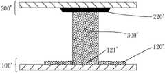
- FIG. 1is a schematic structural view of an edge position of a conventional liquid crystal display panel including a TFT array substrate 100 ′ and a color filter substrate 200 ′ disposed opposite to each other, and a TFT array substrate 100 ′ and color A sealant frame between the filter substrates 200'.
- the edge of the TFT array substrate 100'is provided with a WOA trace 120', and the edge of the color filter substrate 200' is provided with a black matrix 220'.
- the sealant frame 300'is disposed on the WOA trace 120' and the black light-shielding matrix 220'. between.
- a slitis provided in the middle of the WOA trace 120' through which the sealant frame passes (slit 121', so that ultraviolet light can be incident from the side of the TFT array substrate through the slit 121' and irradiated to the sealant frame Accelerate its cure on the 300'.
- the slit design of the WOA trace 120'increases the overall impedance of the WOA trace 120', and the width of the WOA trace 120' needs to be increased in order to maintain the same impedance.
- the narrow-framed liquid crystal displayhas high competitiveness in the market due to its high appearance and is one of the main development directions of the liquid crystal display.
- the width of the WOA traceis too large to limit the design of the narrow border of the liquid crystal display, which is not conducive to the development of the liquid crystal display in the direction of the narrow border.
- An object of the present inventionis to provide a liquid crystal display panel capable of reducing the impedance and area of a WOA trace, achieving a narrow bezel of the liquid crystal display panel, and improving product competitiveness.
- Another object of the present inventionis to provide a method for forming a liquid crystal display panel, which can reduce the impedance and area of the WOA trace, realize a narrow frame of the liquid crystal display panel, and improve product competitiveness.
- the present inventionfirstly provides a liquid crystal display panel comprising: a TFT array substrate, a color filter substrate disposed opposite to the TFT array substrate, and disposed between the TFT array substrate and the color filter substrate Sealant frame;
- the color filter substrate and the TFT array substrateboth include: an effective display area located in the middle and a peripheral area located at the periphery of the effective display area;
- the peripheral area of the TFT array substrateis provided with a plurality of WOA traces, and a peripheral area of the color filter substrate is provided with a black matrix surrounding the effective display area;
- the black matrixincludes: a slit region; and a non-slit region disposed on both sides of the slit region;
- the slit regionis formed with a plurality of slits penetrating the black matrix
- the sealant frameis disposed between the slit region of the black matrix and the plurality of WOA traces.
- the width of the slit regionis greater than the width of the sealant frame.
- the distance between the edge of the slit region on the same side and the edge of the seal frameis greater than or equal to 400 ⁇ m.
- a gapis formed between the adjacent two WOA traces, and the position of the slit formed on the color filter substrate does not overlap with the position corresponding to the void.
- the TFT array substrateis further formed with a plurality of TFTs arranged in an array, and the color filter substrate is further formed with a color filter layer.
- the inventionalso provides a method for forming a liquid crystal display panel, comprising the following steps:
- Step 1Providing a TFT array substrate and a color filter substrate
- the color filter substrate and the TFT array substrateboth include: an effective display area located in the middle and a peripheral area located at the periphery of the effective display area;
- the peripheral area of the TFT array substrateis provided with a plurality of WOA traces, and a peripheral area of the color filter substrate is provided with a black matrix surrounding the effective display area;
- the black matrixincludes: a slit region; and a non-slit region disposed on both sides of the slit region;
- the slit regionis formed with a plurality of slits penetrating the black matrix
- Step 2Apply a sealant on the slit region of the color filter substrate, and align the color filter substrate and the TFT array substrate, so that the sealant is located in the slit region of the black matrix. Between multiple WOA traces;
- Step 3irradiating the sealant with ultraviolet light on one side of the color filter substrate, the ultraviolet light passing through the color filter substrate, and a slit irradiating the sealant to make a sealant Curing to form a sealant frame, completing the process of forming a liquid crystal display panel.
- the width of the sealant frame formed in the step 3is smaller than the width of the slit region.
- the distance between the edge of the slit region on the same side and the edge of the seal frameis greater than or equal to 400 ⁇ m.
- a gapis formed between the adjacent two WOA traces, and the position of the slit formed on the color filter substrate does not overlap with the position corresponding to the void.
- the TFT array substrateis further formed with a plurality of TFTs arranged in an array, and the color filter substrate is further formed with a color filter layer.
- the present inventionfurther provides a liquid crystal display panel comprising: a TFT array substrate; a color filter substrate disposed opposite to the TFT array substrate; and a sealant frame disposed between the TFT array substrate and the color filter substrate;
- the color filter substrate and the TFT array substrateboth include: an effective display area located in the middle and a peripheral area located at the periphery of the effective display area;
- the peripheral area of the TFT array substrateis provided with a plurality of WOA traces, and a peripheral area of the color filter substrate is provided with a black matrix surrounding the effective display area;
- the black matrixincludes: a slit region; and a non-slit region disposed on both sides of the slit region;
- the slit regionis formed with a plurality of slits penetrating the black matrix
- the sealant frameis disposed between the slit region of the black matrix and the plurality of WOA traces;
- width of the slit regionis greater than the width of the sealant frame
- a gapis formed between the adjacent two WOA traces, and the position of the slit formed on the color filter substrate does not overlap with the position corresponding to the gap.
- the present inventionprovides a liquid crystal display panel comprising a TFT array substrate, a color filter substrate, and a sealant frame disposed between the TFT array substrate and the color filter substrate, and a periphery of the TFT array substrate.
- the areais provided with a WOA trace
- the peripheral region of the color filter substrateis provided with a black matrix
- the black matrixcomprises: a slit region, and a non-slit region disposed on both sides of the slit region, the slit region is formed a plurality of slits penetrating the black matrix, the sealant frame is disposed under the slit region of the black matrix, and the plurality of WOA traces are disposed under the sealant frame to accelerate the sealant
- the cured UV lightcan be irradiated onto the sealant through the slit on one side of the color filter substrate, without forming a slit on the WOA trace, that is, without increasing the WOA trace
- the impedancedoes not need to increase the width of the WOA trace.
- the impedance and area of the WOA tracecan be reduced, the narrow border of the liquid crystal display panel can be realized, and the product competitiveness can be improved.
- the method for forming a liquid crystal display panel provided by the inventioncan reduce the impedance and area of the WOA trace, realize a narrow frame of the liquid crystal display panel, and improve product competitiveness.
- FIG. 1is a schematic structural view of an edge position of a conventional liquid crystal display panel
- FIG. 2is a schematic structural view of a liquid crystal display panel of the present invention.
- FIG. 3is a flow chart showing a method of forming a liquid crystal display panel of the present invention.
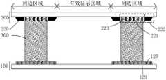
- the present inventionprovides a liquid crystal display panel comprising: a TFT array substrate 100, a color filter substrate 200 disposed opposite to the TFT array substrate, and a TFT array substrate 100 and a color filter substrate 200. Sealant frame 300 between.
- the color filter substrate 200 and the TFT array substrate 100each include: an effective display area located in the middle and a peripheral area located at the periphery of the effective display area.
- a plurality of TFTs arranged in an arrayare formed in an effective display region of the TFT array substrate 100, and a color filter layer is formed on an effective display region of the color filter substrate 200.
- a plurality of WOA traces 120are disposed in a peripheral region of the TFT array substrate 100, and a peripheral region of the color filter substrate 200 is provided with a black matrix 220 surrounding the effective display region;
- the black matrix 220includes: a slit region 221, and a non-slit region 222 disposed on both sides of the slit region 221;
- the slit region 221is formed with a plurality of slits 223 penetrating the black matrix 220.
- the regions other than the slits 223are blocked by the black matrix 220, and the black matrix 220 of the non-slit regions 222 is not.
- the WOA traces 120are all metal traces.
- the slit region 221is used for exposing the sealant frame 300 so as to be sealed.
- the sealant for forming the seal frame 300can be irradiated from the side of the color filter substrate 200 by ultraviolet light (Ultraviolet Rays) to accelerate the curing speed.
- the present inventiontransfers the slit for exposing the sealant frame from the WOA trace to the black matrix, thereby eliminating the need to form a slit on the WOA trace, that is, without increasing the impedance of the WOA trace. Therefore, there is no need to increase the area of the WOA trace, and the advantage is obvious when applied to a narrow-frame liquid crystal display.
- the width of the slit region 221may be further set to be larger than the width of the sealant frame 300, specifically, the edge of the slit region 221 of the same side and the seal bead frame 300 are provided.
- the distance between the edgesis greater than or equal to 400 ⁇ m.
- the plurality of WOA traces 120connect different COFs and transmit different signals, and a gap 121 is formed between the adjacent two WOA traces 120, and the position of the slit 223 is not formed on the color filter substrate 200.
- the gap 121 corresponding to the gap 121, that is, the gap 121 between the adjacent two WOA traces 120is covered by the black matrix 220, so that the backlight irradiated from the side of the TFT array substrate 100 is at least the WOA trace 120. And one of the black matrix 220 is occluded to avoid light leakage.
- ultraviolet lightis irradiated from the side of the color filter substrate 200 to the liquid crystal display panel, and the ultraviolet light passes through the color filter substrate 200 and the slit.
- the slit 223 in the zone 221is irradiated onto the sealant to be cured, thereby speeding up the curing of the sealant.
- the present inventionfurther provides a method for forming a liquid crystal display panel, comprising the following steps:
- Step 1providing a TFT array substrate 100 and a color filter substrate 200;
- the color filter substrate 200 and the TFT array substrate 100each include: an effective display area located in the middle and a peripheral area located at the periphery of the effective display area;
- the periphery of the TFT array substrate 100is provided with a plurality of WOA traces 120, the peripheral region of the color filter substrate 200 is provided with a black matrix 220 surrounding the effective display area;
- the black matrix 220includes: a slit region 221, and a non-slit region 222 disposed on both sides of the slit region 221;
- the slit region 221is formed with a plurality of slits 223 penetrating the black matrix 220.
- a plurality of TFTs arranged in an arrayare formed in an effective display region of the TFT array substrate 100, and a color filter layer is formed in an effective display region of the color filter substrate 200.
- the black matrix 220 of the non-slit region 222is a black matrix of a monolith without a pattern.
- the plurality of WOA traces 120connect different COFs and transmit different signals, and a gap 121 is formed between the adjacent two WOA traces 120.
- the color filter substrate 200is disposed on the color filter substrate 200.
- the position at which the slit 221 is formeddoes not overlap with the position corresponding to the gap 121, that is, the gap 121 between the adjacent two WOA traces 120 is covered by the black matrix 220 to ensure illumination from the side of the TFT array substrate 100.
- the backlightis at least blocked by one of the WOA trace 120 and the black matrix 220 to avoid light leakage.
- Step 2Apply a sealant on the slit region 221 of the color filter substrate 200, and align the color filter substrate 200 and the TFT array substrate 100 so that the sealant is located on the black matrix 220.
- the slit region 221is between the plurality of WOA traces 120.
- the width of the slit region 221is set to be larger than the width of the sealant frame 300, specifically, the edge of the slit region 221 of the same side and the edge of the sealant frame 300 are disposed. The distance between them is greater than or equal to 400 ⁇ m.
- Step 3irradiating the sealant with ultraviolet light on one side of the color filter substrate 200, and the ultraviolet light is irradiated onto the sealant through the color filter substrate 200 and the slit 223.
- the sealantis cured to form the sealant frame 300, and the process of forming the liquid crystal display panel is completed.
- the slit region 221is used for exposing the sealant frame 300, so that when the sealant frame 300 is cured, the sealant can be irradiated by ultraviolet light from the side of the color filter substrate 200. To speed up its curing speed.
- the present inventiontransfers the slit for exposing the sealant frame from the WOA trace to the black matrix, thereby eliminating the need to form a slit on the WOA trace, that is, without increasing the impedance of the WOA trace. Therefore, there is no need to increase the area of the WOA trace, and the advantage is obvious when applied to a narrow-frame liquid crystal display.
- the liquid crystal display panelcomprises a TFT array substrate, a color filter substrate, and a sealant frame disposed between the TFT array substrate and the color filter substrate, and a peripheral region of the TFT array substrate.
- a WOA traceis disposed, a peripheral region of the color filter substrate is provided with a black matrix, and the black matrix includes: a slit region, and a non-slit region disposed on both sides of the slit region, wherein the slit region is formed a plurality of slits penetrating the black matrix, the sealant frame is disposed under the slit region of the black matrix, and the plurality of WOA traces are disposed under the sealant frame to accelerate curing of the sealant
- the ultraviolet lightcan be irradiated onto the sealant through the slit on one side of the color filter substrate, without forming a slit on the WOA trace, that is, the impedance of the WOA trace is not increased, thereby eliminating the need to increase the WOA
Landscapes
- Physics & Mathematics (AREA)
- Nonlinear Science (AREA)
- Mathematical Physics (AREA)
- Chemical & Material Sciences (AREA)
- Crystallography & Structural Chemistry (AREA)
- General Physics & Mathematics (AREA)
- Optics & Photonics (AREA)
- Engineering & Computer Science (AREA)
- Microelectronics & Electronic Packaging (AREA)
- Liquid Crystal (AREA)
Abstract
Description
Translated fromChinese本发明涉及液晶显示技术领域,尤其涉及一种液晶显示面板及其成盒方法。The present invention relates to the field of liquid crystal display technologies, and in particular, to a liquid crystal display panel and a method of forming the same.
液晶显示器(Liquid Crystal Display,LCD)是目前最广泛使用的平板显示器之一,液晶面板是液晶显示器的核心组成部分。Liquid crystal display (LCD) is one of the most widely used flat panel displays. The liquid crystal panel is a core component of liquid crystal displays.
传统的液晶显示面板通常是由一彩色滤光片(Color Filter,CF)基板、一薄膜晶体管阵列基板(Thin Film Transistor Array Substrate,TFT Array Substrate)以及一配置于两基板间的液晶层(Liquid Crystal Layer)所构成,其工作原理是在两片平行的玻璃基板当中放置液晶分子,两片玻璃基板中间有许多垂直和水平的细小电线,通过通电与否来控制液晶分子改变方向,将背光模组的光线折射出来产生画面。其中薄膜晶体管阵列基板上制备有薄膜晶体管(TFT)阵列,用于驱动液晶的旋转,控制每个像素的显示,而彩色滤光片基板上设置RGB彩色滤光层,用于形成每个像素的色彩。A conventional liquid crystal display panel usually consists of a color filter (CF) substrate, a thin film transistor array substrate (TFT Array Substrate), and a liquid crystal layer disposed between the two substrates (Liquid Crystal). Layer), the working principle is to place liquid crystal molecules in two parallel glass substrates. There are many vertical and horizontal small wires between the two glass substrates. The liquid crystal molecules can be controlled to change direction by energizing or not. The light is refracted to produce a picture. The thin film transistor array substrate is provided with a thin film transistor (TFT) array for driving the rotation of the liquid crystal to control the display of each pixel, and the color filter substrate is provided with an RGB color filter layer for forming each pixel. color.
现有的液晶显示器中,液晶显示面板的像素驱动所需要的驱动电压及数据信号均来自于外接在液晶显示面板上的时序控制器(TCON)提供,并通过若干覆晶薄膜(Chip On Film,COF)传输至液晶显示面板中,使液晶显示面板正常工作,COF之间通过设置在TFT阵列基板上的金属走线(Wire On Array,WOA)相连。WOA用于传递两个COF之间的信号,通常设置在液晶显示面板的边缘。In the conventional liquid crystal display, the driving voltage and data signals required for the pixel driving of the liquid crystal display panel are all supplied from a timing controller (TCON) externally connected to the liquid crystal display panel, and pass through a plurality of chip on film (Chip On Film, The COF) is transferred to the liquid crystal display panel to make the liquid crystal display panel work normally, and the COFs are connected by a wire on-line (WOA) disposed on the TFT array substrate. The WOA is used to transfer the signal between the two COFs, usually at the edge of the liquid crystal display panel.
现有技术中,进行液晶显示面板的成盒制程时,在液晶显示面板的边缘位置涂覆用于贴合彩色滤光片基板与TFT阵列基板的密封胶框。如图1所示为现有的液晶显示面板边缘位置的结构示意图,该液晶显示面板包括相对设置的TFT阵列基板100’与彩色滤光片基板200’、及设置在TFT阵列基板100’与彩色滤光片基板200’之间的密封胶框。TFT阵列基板100’的边缘设有WOA走线120’,彩色滤光片基板200’的边缘设有黑色矩阵220’,密封胶框300’设置在WOA走线120’与黑色遮光矩阵220’之间。在成盒制程中,由于密封胶框300’需要进行紫外光(UV)的照射来提升其凝固速度,现有技术中,在有密封胶框经过的WOA走线120’中间设置狭缝(slit)121’,使紫外光可以通过狭缝121’从TFT阵列基板一侧入射并照射在密封胶框300’上加速其固化。WOA走线120’的狭缝设计会增加WOA走线120’整体的阻抗,为了维持相同的阻抗需要增大WOA走线120’的宽度。目前,窄边框的液晶显示器由于外观的美观性高,在市场中具有较高的竞争力,成为液晶显示器的主要发展方向之一。WOA走线的宽度过大会给液晶显示器的窄边框的设计带来限制,不利于液晶显示器向窄边框的方向发展。In the prior art, when a process of forming a liquid crystal display panel is performed, a sealant frame for bonding a color filter substrate and a TFT array substrate is applied to an edge position of the liquid crystal display panel. FIG. 1 is a schematic structural view of an edge position of a conventional liquid crystal display panel including a
发明内容Summary of the invention
本发明的目的在于提供一种液晶显示面板,能够降低WOA走线的阻抗和面积,实现液晶显示面板的窄边框,提升产品竞争力。An object of the present invention is to provide a liquid crystal display panel capable of reducing the impedance and area of a WOA trace, achieving a narrow bezel of the liquid crystal display panel, and improving product competitiveness.
本发明的另一目的在于提供一种液晶显示面板的成盒方法,能够降低WOA走线的阻抗和面积,实现液晶显示面板的窄边框,提升产品竞争力。Another object of the present invention is to provide a method for forming a liquid crystal display panel, which can reduce the impedance and area of the WOA trace, realize a narrow frame of the liquid crystal display panel, and improve product competitiveness.
为实现上述目的,本发明首先提供一种液晶显示面板,包括:TFT阵列基板、与所述TFT阵列基板相对设置的彩色滤光片基板、及设置在TFT阵列基板与彩色滤光片基板之间的密封胶框;In order to achieve the above object, the present invention firstly provides a liquid crystal display panel comprising: a TFT array substrate, a color filter substrate disposed opposite to the TFT array substrate, and disposed between the TFT array substrate and the color filter substrate Sealant frame;
所述彩色滤光片基板与TFT阵列基板均包括:位于中间的有效显示区域及位于有效显示区域外围的周边区域;The color filter substrate and the TFT array substrate both include: an effective display area located in the middle and a peripheral area located at the periphery of the effective display area;
所述TFT阵列基板的周边区域设有数条WOA走线,所述彩色滤光片基板的周边区域设有包围所述有效显示区域的黑色矩阵;The peripheral area of the TFT array substrate is provided with a plurality of WOA traces, and a peripheral area of the color filter substrate is provided with a black matrix surrounding the effective display area;
所述黑色矩阵包括:狭缝区、及设于所述狭缝区两边的非狭缝区;The black matrix includes: a slit region; and a non-slit region disposed on both sides of the slit region;
所述狭缝区形成有多个贯穿所述黑色矩阵的狭缝;The slit region is formed with a plurality of slits penetrating the black matrix;
所述密封胶框设于所述黑色矩阵的狭缝区与所述多条WOA走线之间。The sealant frame is disposed between the slit region of the black matrix and the plurality of WOA traces.
所述狭缝区的宽度大于密封胶框的宽度。The width of the slit region is greater than the width of the sealant frame.
同一侧的狭缝区边缘与密封胶框边缘之间的距离大于或等于400μm。The distance between the edge of the slit region on the same side and the edge of the seal frame is greater than or equal to 400 μm.
相邻的两WOA走线之间形成有空隙,所述彩色滤光片基板上形成狭缝的位置不与其对应所述空隙的位置重叠。A gap is formed between the adjacent two WOA traces, and the position of the slit formed on the color filter substrate does not overlap with the position corresponding to the void.
所述TFT阵列基板还形成有多个呈阵列排布的TFT,所述彩色滤光片基板还形成有彩色滤光层。The TFT array substrate is further formed with a plurality of TFTs arranged in an array, and the color filter substrate is further formed with a color filter layer.
本发明还提供一种液晶显示面板的成盒方法,包括以下步骤:The invention also provides a method for forming a liquid crystal display panel, comprising the following steps:
步骤1、提供一TFT阵列基板与一彩色滤光片基板;Step 1. Providing a TFT array substrate and a color filter substrate;
所述彩色滤光片基板与TFT阵列基板均包括:位于中间的有效显示区域及位于有效显示区域外围的周边区域;The color filter substrate and the TFT array substrate both include: an effective display area located in the middle and a peripheral area located at the periphery of the effective display area;
所述TFT阵列基板的周边区域设有数条WOA走线,所述彩色滤光片基板的周边区域设有包围所述有效显示区域的黑色矩阵;The peripheral area of the TFT array substrate is provided with a plurality of WOA traces, and a peripheral area of the color filter substrate is provided with a black matrix surrounding the effective display area;
所述黑色矩阵包括:狭缝区、及设于所述狭缝区两边的非狭缝区;The black matrix includes: a slit region; and a non-slit region disposed on both sides of the slit region;
所述狭缝区形成有多个贯穿所述黑色矩阵的狭缝;The slit region is formed with a plurality of slits penetrating the black matrix;
步骤2、在所述彩色滤光片基板的狭缝区上涂布密封胶,将彩色滤光片基板与TFT阵列基板对位贴合,使得密封胶位于所述黑色矩阵的狭缝区与所述多条WOA走线之间;Step 2: Apply a sealant on the slit region of the color filter substrate, and align the color filter substrate and the TFT array substrate, so that the sealant is located in the slit region of the black matrix. Between multiple WOA traces;
步骤3、在所述彩色滤光片基板一侧采用紫外光照射所述密封胶,所述紫外光穿过所述彩色滤光片基板、以及狭缝照射到所述密封胶上,使密封胶固化形成密封胶框,完成液晶显示面板的成盒制程。Step 3: irradiating the sealant with ultraviolet light on one side of the color filter substrate, the ultraviolet light passing through the color filter substrate, and a slit irradiating the sealant to make a sealant Curing to form a sealant frame, completing the process of forming a liquid crystal display panel.
所述步骤3中形成的密封胶框的宽度小于所述狭缝区的宽度。The width of the sealant frame formed in the
同一侧的狭缝区边缘与密封胶框边缘之间的距离大于或等于400μm。The distance between the edge of the slit region on the same side and the edge of the seal frame is greater than or equal to 400 μm.
相邻的两WOA走线之间形成有空隙,所述彩色滤光片基板上形成狭缝的位置不与其对应所述空隙的位置重叠。A gap is formed between the adjacent two WOA traces, and the position of the slit formed on the color filter substrate does not overlap with the position corresponding to the void.
所述TFT阵列基板还形成有多个呈阵列排布的TFT,所述彩色滤光片基板还形成有彩色滤光层。The TFT array substrate is further formed with a plurality of TFTs arranged in an array, and the color filter substrate is further formed with a color filter layer.
本发明还提供一种液晶显示面板,包括:TFT阵列基板、与所述TFT阵列基板相对设置的彩色滤光片基板、及设置在TFT阵列基板与彩色滤光片基板之间的密封胶框;The present invention further provides a liquid crystal display panel comprising: a TFT array substrate; a color filter substrate disposed opposite to the TFT array substrate; and a sealant frame disposed between the TFT array substrate and the color filter substrate;
所述彩色滤光片基板与TFT阵列基板均包括:位于中间的有效显示区域及位于有效显示区域外围的周边区域;The color filter substrate and the TFT array substrate both include: an effective display area located in the middle and a peripheral area located at the periphery of the effective display area;
所述TFT阵列基板的周边区域设有数条WOA走线,所述彩色滤光片基板的周边区域设有包围所述有效显示区域的黑色矩阵;The peripheral area of the TFT array substrate is provided with a plurality of WOA traces, and a peripheral area of the color filter substrate is provided with a black matrix surrounding the effective display area;
所述黑色矩阵包括:狭缝区、及设于所述狭缝区两边的非狭缝区;The black matrix includes: a slit region; and a non-slit region disposed on both sides of the slit region;
所述狭缝区形成有多个贯穿所述黑色矩阵的狭缝;The slit region is formed with a plurality of slits penetrating the black matrix;
所述密封胶框设于所述黑色矩阵的狭缝区与所述多条WOA走线之间;The sealant frame is disposed between the slit region of the black matrix and the plurality of WOA traces;
其中,所述狭缝区的宽度大于所述密封胶框的宽度;Wherein the width of the slit region is greater than the width of the sealant frame;
其中,相邻的两WOA走线之间形成有空隙,所述彩色滤光片基板上形成狭缝的位置不与其对应所述空隙的位置重叠。Wherein, a gap is formed between the adjacent two WOA traces, and the position of the slit formed on the color filter substrate does not overlap with the position corresponding to the gap.
本发明的有益效果:本发明提供的液晶显示面板,包括TFT阵列基板、彩色滤光片基板、及设置所述TFT阵列基板与彩色滤光片基板之间的密封胶框,TFT阵列基板的周边区域设有WOA走线,彩色滤光片基板的周边区域设有黑色矩阵,并且黑色矩阵包括:狭缝区、及设于所述狭缝区两边的非狭缝区,所述狭缝区形成有多个贯穿所述黑色矩阵的狭缝,所述密封胶框设于所述黑色矩阵的狭缝区的下方,所述多个WOA走线设于所述密封胶框的下方,加速密封胶固化的紫外光可通过彩色滤光片基板一侧的狭缝照射到密封胶上,无需在WOA走线上形成狭缝,也即不会增大WOA走线的阻抗,从而无需增大WOA走线的宽度,相比于现有技术,能够降低WOA走线的阻抗和面积,实现液晶显示面板的窄边框,提升产品竞争力。本发明提供的液晶显示面板的成盒方法,能够降低WOA走线的阻抗和面积,实现液晶显示面板的窄边框,提升产品竞争力。Advantageous Effects of Invention The present invention provides a liquid crystal display panel comprising a TFT array substrate, a color filter substrate, and a sealant frame disposed between the TFT array substrate and the color filter substrate, and a periphery of the TFT array substrate. The area is provided with a WOA trace, the peripheral region of the color filter substrate is provided with a black matrix, and the black matrix comprises: a slit region, and a non-slit region disposed on both sides of the slit region, the slit region is formed a plurality of slits penetrating the black matrix, the sealant frame is disposed under the slit region of the black matrix, and the plurality of WOA traces are disposed under the sealant frame to accelerate the sealant The cured UV light can be irradiated onto the sealant through the slit on one side of the color filter substrate, without forming a slit on the WOA trace, that is, without increasing the WOA traceThe impedance does not need to increase the width of the WOA trace. Compared with the prior art, the impedance and area of the WOA trace can be reduced, the narrow border of the liquid crystal display panel can be realized, and the product competitiveness can be improved. The method for forming a liquid crystal display panel provided by the invention can reduce the impedance and area of the WOA trace, realize a narrow frame of the liquid crystal display panel, and improve product competitiveness.
为了能更进一步了解本发明的特征以及技术内容,请参阅以下有关本发明的详细说明与附图,然而附图仅提供参考与说明用,并非用来对本发明加以限制。The detailed description of the present invention and the accompanying drawings are to be understood,
附图中,In the drawings,
图1为现有的液晶显示面板边缘位置的结构示意图;1 is a schematic structural view of an edge position of a conventional liquid crystal display panel;
图2为本发明的液晶显示面板的结构示意图;2 is a schematic structural view of a liquid crystal display panel of the present invention;
图3为本发明的液晶显示面板的成盒方法的流程图。3 is a flow chart showing a method of forming a liquid crystal display panel of the present invention.
为更进一步阐述本发明所采取的技术手段及其效果,以下结合本发明的优选实施例及其附图进行详细描述。In order to further clarify the technical means and effects of the present invention, the following detailed description will be made in conjunction with the preferred embodiments of the invention and the accompanying drawings.
请参阅图2,本发明提供一种液晶显示面板,包括:TFT阵列基板100、与TFT阵列基板相对设置的彩色滤光片基板200、及设置在TFT阵列基板100与彩色滤光片基板200之间的密封胶框300。Referring to FIG. 2, the present invention provides a liquid crystal display panel comprising: a
具体地,所述彩色滤光片基板200与TFT阵列基板100均包括:位于中间的有效显示区域及位于有效显示区域外围的周边区域。Specifically, the
进一步地,在所述TFT阵列基板100的有效显示区域形成有多个呈阵列式排布的TFT,在所述彩色滤光片基板200的有效显示区域形成有彩色滤光层。Further, a plurality of TFTs arranged in an array are formed in an effective display region of the
在所述TFT阵列基板100的周边区域设有数条WOA走线120,所述彩色滤光片基板200的周边区域设有包围所述有效显示区域的黑色矩阵220;所述黑色矩阵220包括:狭缝区221、及设于所述狭缝区221两边的非狭缝区222;A plurality of WOA traces 120 are disposed in a peripheral region of the
所述狭缝区221形成有多个贯穿所述黑色矩阵220的狭缝223,所述狭缝223以外的区域均被黑色矩阵220遮挡,而所述非狭缝区222的黑色矩阵220为没有图案的整块的黑色矩阵。所述WOA走线120均为整面金属走线。The
需要说明的是,狭缝区221用于暴露出所述密封胶框300,从而在密封胶框300固化时,能够从彩色滤光片基板200一侧通过紫外光(Ultraviolet Rays,UV光)对所述用于形成密封胶框300的密封胶进行照射,以加快其固化速度。相比于现有技术,本发明将用于暴露密封胶框的狭缝从WOA走线转移到黑色矩阵上,从而无需在WOA走线上形成狭缝,也即不会增加WOA走线的阻抗,从而无需增大WOA走线的面积,在应用于窄边框液晶显示器时优势明显。It should be noted that the
此外,为了给密封胶涂布提供足够的偏差值,还可以进一步设置所述狭缝区221的宽度大于密封胶框300宽度,具体地,设置同一侧的狭缝区221边缘与密封胶框300边缘之间的距离大于或等于400μm。In addition, in order to provide a sufficient deviation value for the sealant coating, the width of the
具体地,所述多个WOA走线120连接不同COF并传输不同信号,相邻的两WOA走线120之间形成有空隙121,所述彩色滤光片基板200上形成狭缝223的位置不与其对应所述空隙121的位置重叠,也即相邻的两WOA走线120之间的空隙121均被黑色矩阵220覆盖,保证从TFT阵列基板100一侧照射来的背光至少被WOA走线120和黑色矩阵220中的一个遮挡,避免产生漏光。Specifically, the plurality of WOA traces 120 connect different COFs and transmit different signals, and a
值得一提的是,所述液晶显示面板在进行成盒制程时,从彩色滤光片基板200一侧对液晶显示面板进行紫外光照射,紫外光穿过彩色滤光片基板200、以及狭缝区221中的狭缝223照射在需要固化的密封胶上,从而加快密封胶固化的速度。It is to be noted that, when the liquid crystal display panel is in the process of forming a box, ultraviolet light is irradiated from the side of the
请参阅图3,本发明还提供一种液晶显示面板的成盒方法,包括以下步骤:Referring to FIG. 3, the present invention further provides a method for forming a liquid crystal display panel, comprising the following steps:
步骤1、提供一TFT阵列基板100与一彩色滤光片基板200;Step 1, providing a
所述彩色滤光片基板200与TFT阵列基板100均包括:位于中间的有效显示区域及位于有效显示区域外围的周边区域;The
所述TFT阵列基板100的周边区域设有数条WOA走线120,所述彩色滤光片基板200的周边区域设有包围所述有效显示区域的黑色矩阵220;The periphery of the
所述黑色矩阵220包括:狭缝区221、及设于所述狭缝区221两边的非狭缝区222;The
所述狭缝区221形成有多个贯穿所述黑色矩阵220的狭缝223。The
具体地,在所述TFT阵列基板100的有效显示区域形成有多个呈阵列式排布的TFT,在所述彩色滤光片基板200的有效显示区域形成有彩色滤光层。所述非狭缝区222的黑色矩阵220为没有图案的整块的黑色矩阵。Specifically, a plurality of TFTs arranged in an array are formed in an effective display region of the
进一步地,所述多个WOA走线120连接不同COF并传输不同信号,相邻的两WOA走线120之间形成有空隙121,所述彩色滤光片基板200上形成狭缝221的位置不与其对应所述空隙121的位置重叠,也即相邻的两WOA走线120之间的空隙121均被黑色矩阵220覆盖,保证从TFT阵列基板100一侧照射来的背光至少被WOA走线120和黑色矩阵220中的一个遮挡,避免产生漏光。Further, the plurality of WOA traces 120 connect different COFs and transmit different signals, and a
步骤2、在所述彩色滤光片基板200的狭缝区221上涂布密封胶,将彩色滤光片基板200与TFT阵列基板100对位贴合,使得密封胶位于所述黑色矩阵220的狭缝区221与所述多条WOA走线120之间。Step 2: Apply a sealant on the
具体地,为了给密封胶涂布提供足够的偏差值,设置所述狭缝区221的宽度大于密封胶框300宽度,具体地,设置同一侧的狭缝区221边缘与密封胶框300边缘之间的距离大于或等于400μm。Specifically, in order to provide a sufficient deviation value for the sealant coating, the width of the
步骤3、在所述彩色滤光片基板200一侧采用紫外光照射所述密封胶,所述紫外光穿过所述彩色滤光片基板200、以及狭缝223照射到所述密封胶上,使密封胶固化形成密封胶框300,完成液晶显示面板的成盒制程。Step 3: irradiating the sealant with ultraviolet light on one side of the
需要说明的是,狭缝区221用于暴露出所述密封胶框300,从而在密封胶框300固化时,能够从彩色滤光片基板200一侧通过紫外光对所述密封胶进行照射,以加快其固化速度。相比于现有技术,本发明将用于暴露密封胶框的狭缝从WOA走线转移到黑色矩阵上,从而无需在WOA走线上形成狭缝,也即不会增加WOA走线的阻抗,从而无需增大WOA走线的面积,在应用于窄边框液晶显示器时优势明显。It should be noted that the
综上所述,本发明提供的液晶显示面板,包括TFT阵列基板、彩色滤光片基板、及设置所述TFT阵列基板与彩色滤光片基板之间的密封胶框,TFT阵列基板的周边区域设有WOA走线,彩色滤光片基板的周边区域设有黑色矩阵,并且黑色矩阵包括:狭缝区、及设于所述狭缝区两边的非狭缝区,所述狭缝区形成有多个贯穿所述黑色矩阵的狭缝,所述密封胶框设于所述黑色矩阵的狭缝区的下方,所述多个WOA走线设于所述密封胶框的下方,加速密封胶固化的紫外光可通过彩色滤光片基板一侧的狭缝照射到密封胶上,无需在WOA走线上形成狭缝,也即不会增大WOA走线的阻抗,从而无需增大WOA走线的宽度,相比于现有技术,能够降低WOA走线的阻抗和面积,实现液晶显示面板的窄边框,提升产品竞争力。本发明提供的液晶显示面板的成盒方法,能够降低WOA走线的阻抗和面积,实现液晶显示面板的窄边框,提升产品竞争力。In summary, the liquid crystal display panel provided by the present invention comprises a TFT array substrate, a color filter substrate, and a sealant frame disposed between the TFT array substrate and the color filter substrate, and a peripheral region of the TFT array substrate. a WOA trace is disposed, a peripheral region of the color filter substrate is provided with a black matrix, and the black matrix includes: a slit region, and a non-slit region disposed on both sides of the slit region, wherein the slit region is formed a plurality of slits penetrating the black matrix, the sealant frame is disposed under the slit region of the black matrix, and the plurality of WOA traces are disposed under the sealant frame to accelerate curing of the sealant The ultraviolet light can be irradiated onto the sealant through the slit on one side of the color filter substrate, without forming a slit on the WOA trace, that is, the impedance of the WOA trace is not increased, thereby eliminating the need to increase the WOA trace Compared with the prior art, the width of the WOA trace can be reduced, the narrow frame of the liquid crystal display panel can be realized, and the product competitiveness can be improved. The method for forming a liquid crystal display panel provided by the invention can reduce the impedance and area of the WOA trace, realize a narrow frame of the liquid crystal display panel, and improve product competitiveness.
以上所述,对于本领域的普通技术人员来说,可以根据本发明的技术方案和技术构思作出其他各种相应的改变和变形,而所有这些改变和变形都应属于本发明后附的权利要求的保护范围。In the above, various other changes and modifications can be made in accordance with the technical solutions and technical concept of the present invention, and all such changes and modifications should be included in the appended claims. The scope of protection.
Claims (13)
Translated fromChinesePriority Applications (1)
| Application Number | Priority Date | Filing Date | Title |
|---|---|---|---|
| US15/122,420US10324326B2 (en) | 2016-04-05 | 2016-04-21 | Liquid crystal display panel and cell method thereof |
Applications Claiming Priority (2)
| Application Number | Priority Date | Filing Date | Title |
|---|---|---|---|
| CN201610206334.3ACN105739165A (en) | 2016-04-05 | 2016-04-05 | Liquid crystal display panel and box forming method thereof |
| CN201610206334.3 | 2016-04-05 |
Publications (1)
| Publication Number | Publication Date |
|---|---|
| WO2017173672A1true WO2017173672A1 (en) | 2017-10-12 |
Family
ID=56252854
Family Applications (1)
| Application Number | Title | Priority Date | Filing Date |
|---|---|---|---|
| PCT/CN2016/079804CeasedWO2017173672A1 (en) | 2016-04-05 | 2016-04-21 | Liquid crystal display panel and cell processing method thereof |
Country Status (3)
| Country | Link |
|---|---|
| US (1) | US10324326B2 (en) |
| CN (1) | CN105739165A (en) |
| WO (1) | WO2017173672A1 (en) |
Cited By (1)
| Publication number | Priority date | Publication date | Assignee | Title |
|---|---|---|---|---|
| WO2019146439A1 (en)* | 2018-01-25 | 2019-08-01 | 株式会社ジャパンディスプレイ | Display device |
Families Citing this family (14)
| Publication number | Priority date | Publication date | Assignee | Title |
|---|---|---|---|---|
| CN106501991B (en)* | 2016-12-02 | 2019-07-02 | 深圳市华星光电技术有限公司 | Black matrix", the curing method of liquid crystal display panel frame adhesive and liquid crystal display panel |
| CN106646991A (en)* | 2016-12-02 | 2017-05-10 | 深圳市华星光电技术有限公司 | Liquid crystal display panel and manufacturing method thereof |
| CN106773252B (en)* | 2016-12-29 | 2019-05-14 | 惠科股份有限公司 | Liquid crystal panel and liquid crystal display |
| CN107357092A (en)* | 2017-07-25 | 2017-11-17 | 深圳市华星光电技术有限公司 | A kind of display panel and its manufacture method |
| CN108519699A (en)* | 2018-04-03 | 2018-09-11 | 深圳市华星光电技术有限公司 | Liquid crystal display panel and preparation method thereof, liquid crystal display |
| CN209486437U (en)* | 2018-10-31 | 2019-10-11 | 惠科股份有限公司 | Display panel and display device |
| CN111968992A (en)* | 2019-05-20 | 2020-11-20 | 瀚宇彩晶股份有限公司 | Display device |
| JP7691170B2 (en)* | 2020-03-19 | 2025-06-11 | ソニーセミコンダクタソリューションズ株式会社 | Display devices and electronic devices |
| CN111538192A (en)* | 2020-05-19 | 2020-08-14 | Tcl华星光电技术有限公司 | Array substrate and display device |
| CN113835260A (en)* | 2020-06-24 | 2021-12-24 | 深超光电(深圳)有限公司 | Liquid crystal display panel and manufacturing method thereof |
| CN113204143B (en)* | 2021-04-21 | 2022-09-27 | 滁州惠科光电科技有限公司 | Display module, display panel and display device |
| CN114967211A (en)* | 2022-04-07 | 2022-08-30 | 惠科股份有限公司 | Display panel and display device |
| CN115167038B (en)* | 2022-07-05 | 2023-10-13 | Tcl华星光电技术有限公司 | display panel |
| CN116300219B (en)* | 2023-03-23 | 2025-06-10 | 绵阳惠科光电科技有限公司 | Display panel, display device and manufacturing method of frame sealing glue assembly |
Citations (6)
| Publication number | Priority date | Publication date | Assignee | Title |
|---|---|---|---|---|
| US20090174630A1 (en)* | 2008-01-04 | 2009-07-09 | Tpo Displays Corp. | Organic light emitting display (OLED) devise, modules, and electronic devices |
| CN102681245A (en)* | 2012-03-15 | 2012-09-19 | 京东方科技集团股份有限公司 | Transflective liquid crystal display array substrate and manufacturing method thereof, and display device |
| CN102819154A (en)* | 2012-09-07 | 2012-12-12 | 京东方科技集团股份有限公司 | Liquid crystal panel and display device |
| CN202794780U (en)* | 2012-09-28 | 2013-03-13 | 京东方科技集团股份有限公司 | Liquid crystal panel and display device |
| CN203287658U (en)* | 2013-06-27 | 2013-11-13 | 京东方科技集团股份有限公司 | Color film substrate, liquid crystal panel and display device |
| CN104849905A (en)* | 2015-05-26 | 2015-08-19 | 京东方科技集团股份有限公司 | Color film substrate, display panel and display device |
Family Cites Families (5)
| Publication number | Priority date | Publication date | Assignee | Title |
|---|---|---|---|---|
| US20070273821A1 (en)* | 2006-05-24 | 2007-11-29 | Toppoly Optoelectronics Corp. | Displaying System Having a Sealing Structure |
| JP2012220792A (en)* | 2011-04-11 | 2012-11-12 | Japan Display East Co Ltd | Liquid crystal display device and method for manufacturing liquid crystal display device |
| CN103048828A (en)* | 2012-12-31 | 2013-04-17 | 友达光电股份有限公司 | Liquid crystal display device |
| CN103941460A (en)* | 2013-07-29 | 2014-07-23 | 武汉天马微电子有限公司 | Color filter substrate, manufacturing method and liquid crystal display panel |
| WO2016185643A1 (en)* | 2015-05-20 | 2016-11-24 | パナソニック液晶ディスプレイ株式会社 | Display panel |
- 2016
- 2016-04-05CNCN201610206334.3Apatent/CN105739165A/enactivePending
- 2016-04-21WOPCT/CN2016/079804patent/WO2017173672A1/ennot_activeCeased
- 2016-04-21USUS15/122,420patent/US10324326B2/ennot_activeExpired - Fee Related
Patent Citations (6)
| Publication number | Priority date | Publication date | Assignee | Title |
|---|---|---|---|---|
| US20090174630A1 (en)* | 2008-01-04 | 2009-07-09 | Tpo Displays Corp. | Organic light emitting display (OLED) devise, modules, and electronic devices |
| CN102681245A (en)* | 2012-03-15 | 2012-09-19 | 京东方科技集团股份有限公司 | Transflective liquid crystal display array substrate and manufacturing method thereof, and display device |
| CN102819154A (en)* | 2012-09-07 | 2012-12-12 | 京东方科技集团股份有限公司 | Liquid crystal panel and display device |
| CN202794780U (en)* | 2012-09-28 | 2013-03-13 | 京东方科技集团股份有限公司 | Liquid crystal panel and display device |
| CN203287658U (en)* | 2013-06-27 | 2013-11-13 | 京东方科技集团股份有限公司 | Color film substrate, liquid crystal panel and display device |
| CN104849905A (en)* | 2015-05-26 | 2015-08-19 | 京东方科技集团股份有限公司 | Color film substrate, display panel and display device |
Cited By (2)
| Publication number | Priority date | Publication date | Assignee | Title |
|---|---|---|---|---|
| WO2019146439A1 (en)* | 2018-01-25 | 2019-08-01 | 株式会社ジャパンディスプレイ | Display device |
| US11187936B2 (en) | 2018-01-25 | 2021-11-30 | Japan Display Inc. | Display apparatus having first and second light blocking films |
Also Published As
| Publication number | Publication date |
|---|---|
| US20180149910A1 (en) | 2018-05-31 |
| CN105739165A (en) | 2016-07-06 |
| US10324326B2 (en) | 2019-06-18 |
Similar Documents
| Publication | Publication Date | Title |
|---|---|---|
| WO2017173672A1 (en) | Liquid crystal display panel and cell processing method thereof | |
| KR100481903B1 (en) | Liquid crystal display device | |
| CN108139631A (en) | The manufacturing device of liquid crystal display panel, the manufacturing method of liquid crystal display panel and liquid crystal display panel | |
| JP4601269B2 (en) | Liquid crystal display device and manufacturing method thereof | |
| US20150146130A1 (en) | Liquid Crystal Display Panel and Manufacturing Method for the Same | |
| US20180173033A1 (en) | Method of producing display device, and display device | |
| KR20160032393A (en) | Liquid crystal display device | |
| WO2021051626A1 (en) | Liquid crystal display panel and manufacturing method therefor | |
| CN109143774A (en) | The production method of mask plate and metal wire | |
| CN104360547A (en) | Display panel as well as production method thereof and display device | |
| CN110320710A (en) | Liquid crystal display panel and its manufacturing method | |
| CN110320709B (en) | Liquid crystal panel and manufacturing method thereof | |
| CN105093806A (en) | Ultraviolet (UV) mask and exposure method thereof | |
| US10203556B2 (en) | Display substrate having pre-tilt angle for liquid crystal molecules | |
| WO2016185643A1 (en) | Display panel | |
| WO2020082718A1 (en) | Manufacturing method for sealant, and display panel | |
| US9696575B2 (en) | Display device and manufacturing method thereof | |
| CN103091916A (en) | Liquid crystal display device having a plurality of pixel electrodes | |
| US10962824B2 (en) | Color filter substrate, method of producing the same, and display panel | |
| CN110320715A (en) | Liquid crystal display panel and its manufacturing method | |
| WO2020191830A1 (en) | Liquid crystal display panel and pretilt angle forming method | |
| CN103676299B (en) | The manufacture method of color membrane substrates, display device and color membrane substrates | |
| US10031376B2 (en) | Liquid crystal display device | |
| CN101937149B (en) | Panel for liquid crystal display device | |
| JP2010145756A (en) | Liquid crystal display element and manufacturing method thereof |
Legal Events
| Date | Code | Title | Description |
|---|---|---|---|
| WWE | Wipo information: entry into national phase | Ref document number:15122420 Country of ref document:US | |
| NENP | Non-entry into the national phase | Ref country code:DE | |
| 121 | Ep: the epo has been informed by wipo that ep was designated in this application | Ref document number:16897606 Country of ref document:EP Kind code of ref document:A1 | |
| 122 | Ep: pct application non-entry in european phase | Ref document number:16897606 Country of ref document:EP Kind code of ref document:A1 |