WO2017170133A1 - Scanning antenna, method for inspecting scanning antenna, and method for manufacturing scanning antenna - Google Patents
Scanning antenna, method for inspecting scanning antenna, and method for manufacturing scanning antennaDownload PDFInfo
- Publication number
- WO2017170133A1 WO2017170133A1PCT/JP2017/011753JP2017011753WWO2017170133A1WO 2017170133 A1WO2017170133 A1WO 2017170133A1JP 2017011753 WJP2017011753 WJP 2017011753WWO 2017170133 A1WO2017170133 A1WO 2017170133A1
- Authority
- WO
- WIPO (PCT)
- Prior art keywords
- electrode
- inspection
- source
- liquid crystal
- gate
- Prior art date
- Legal status (The legal status is an assumption and is not a legal conclusion. Google has not performed a legal analysis and makes no representation as to the accuracy of the status listed.)
- Ceased
Links
Images


Classifications
- H—ELECTRICITY
- H01—ELECTRIC ELEMENTS
- H01Q—ANTENNAS, i.e. RADIO AERIALS
- H01Q3/00—Arrangements for changing or varying the orientation or the shape of the directional pattern of the waves radiated from an antenna or antenna system
- H01Q3/44—Arrangements for changing or varying the orientation or the shape of the directional pattern of the waves radiated from an antenna or antenna system varying the electric or magnetic characteristics of reflecting, refracting, or diffracting devices associated with the radiating element
- G—PHYSICS
- G01—MEASURING; TESTING
- G01R—MEASURING ELECTRIC VARIABLES; MEASURING MAGNETIC VARIABLES
- G01R29/00—Arrangements for measuring or indicating electric quantities not covered by groups G01R19/00 - G01R27/00
- G01R29/08—Measuring electromagnetic field characteristics
- G01R29/10—Radiation diagrams of antennas
- H—ELECTRICITY
- H01—ELECTRIC ELEMENTS
- H01Q—ANTENNAS, i.e. RADIO AERIALS
- H01Q1/00—Details of, or arrangements associated with, antennas
- H01Q1/36—Structural form of radiating elements, e.g. cone, spiral, umbrella; Particular materials used therewith
- H01Q1/38—Structural form of radiating elements, e.g. cone, spiral, umbrella; Particular materials used therewith formed by a conductive layer on an insulating support
- H—ELECTRICITY
- H01—ELECTRIC ELEMENTS
- H01Q—ANTENNAS, i.e. RADIO AERIALS
- H01Q1/00—Details of, or arrangements associated with, antennas
- H01Q1/44—Details of, or arrangements associated with, antennas using equipment having another main function to serve additionally as an antenna, e.g. means for giving an antenna an aesthetic aspect
- H—ELECTRICITY
- H01—ELECTRIC ELEMENTS
- H01Q—ANTENNAS, i.e. RADIO AERIALS
- H01Q15/00—Devices for reflection, refraction, diffraction or polarisation of waves radiated from an antenna, e.g. quasi-optical devices
- H01Q15/0006—Devices acting selectively as reflecting surface, as diffracting or as refracting device, e.g. frequency filtering or angular spatial filtering devices
- H01Q15/0086—Devices acting selectively as reflecting surface, as diffracting or as refracting device, e.g. frequency filtering or angular spatial filtering devices said selective devices having materials with a synthesized negative refractive index, e.g. metamaterials or left-handed materials
- H—ELECTRICITY
- H01—ELECTRIC ELEMENTS
- H01Q—ANTENNAS, i.e. RADIO AERIALS
- H01Q21/00—Antenna arrays or systems
- H01Q21/06—Arrays of individually energised antenna units similarly polarised and spaced apart
- H01Q21/061—Two dimensional planar arrays
- H01Q21/064—Two dimensional planar arrays using horn or slot aerials
- H—ELECTRICITY
- H01—ELECTRIC ELEMENTS
- H01Q—ANTENNAS, i.e. RADIO AERIALS
- H01Q3/00—Arrangements for changing or varying the orientation or the shape of the directional pattern of the waves radiated from an antenna or antenna system
- H01Q3/26—Arrangements for changing or varying the orientation or the shape of the directional pattern of the waves radiated from an antenna or antenna system varying the relative phase or relative amplitude of energisation between two or more active radiating elements; varying the distribution of energy across a radiating aperture
- H01Q3/30—Arrangements for changing or varying the orientation or the shape of the directional pattern of the waves radiated from an antenna or antenna system varying the relative phase or relative amplitude of energisation between two or more active radiating elements; varying the distribution of energy across a radiating aperture varying the relative phase between the radiating elements of an array
- H01Q3/34—Arrangements for changing or varying the orientation or the shape of the directional pattern of the waves radiated from an antenna or antenna system varying the relative phase or relative amplitude of energisation between two or more active radiating elements; varying the distribution of energy across a radiating aperture varying the relative phase between the radiating elements of an array by electrical means
- H01Q3/36—Arrangements for changing or varying the orientation or the shape of the directional pattern of the waves radiated from an antenna or antenna system varying the relative phase or relative amplitude of energisation between two or more active radiating elements; varying the distribution of energy across a radiating aperture varying the relative phase between the radiating elements of an array by electrical means with variable phase-shifters
- G—PHYSICS
- G01—MEASURING; TESTING
- G01R—MEASURING ELECTRIC VARIABLES; MEASURING MAGNETIC VARIABLES
- G01R29/00—Arrangements for measuring or indicating electric quantities not covered by groups G01R19/00 - G01R27/00
- G01R29/08—Measuring electromagnetic field characteristics
- G01R29/0864—Measuring electromagnetic field characteristics characterised by constructional or functional features
- G01R29/0871—Complete apparatus or systems; circuits, e.g. receivers or amplifiers
Definitions
- the present inventionrelates to a scanning antenna and a scanning antenna inspection method, and in particular, a scanning antenna (also referred to as a “liquid crystal array antenna”) in which an antenna unit (also referred to as an “element antenna”) has a liquid crystal capacity, and scanning.
- a scanning antennaalso referred to as a “liquid crystal array antenna”
- an antenna unitalso referred to as an “element antenna”
- the present inventionrelates to an antenna inspection method.
- Antennas for mobile communications and satellite broadcastingrequire a function to change the beam direction (referred to as “beam scanning” or “beam steering”).
- beam scanningAs an antenna having such a function (hereinafter referred to as a “scanned antenna”), a phased array antenna having an antenna unit is known.
- the conventional phased array antennais expensive and has become an obstacle to popularization in consumer products. In particular, as the number of antenna units increases, the cost increases significantly.
- Non-Patent Document 1Since the dielectric constant of the liquid crystal material has frequency dispersion, in this specification, the dielectric constant in the microwave frequency band (also referred to as “dielectric constant for microwave”) is particularly referred to as “dielectric constant M ( ⁇ M )”. Will be written.
- Patent Document 3 and Non-Patent Document 1describe that a low-cost scanning antenna can be obtained by utilizing the technology of a liquid crystal display device (hereinafter referred to as “LCD”).
- LCDliquid crystal display device
- an object of the present inventionis to provide a scanning antenna that can be mass-produced using a conventional LCD manufacturing technique, an inspection method thereof, and a manufacturing method thereof.
- a scanning antennais a scanning antenna having a transmission / reception region in which a plurality of antenna units are arranged and a non-transmission / reception region located in a region other than the transmission / reception region, and a first dielectric substrate;
- a TFT substratehaving a plurality of first TFTs supported by the first dielectric substrate, a plurality of patch electrodes, a plurality of gate bus lines, and a plurality of source bus lines, The plurality of first TFTs and the plurality of patch electrodes are respectively arranged corresponding to the plurality of antenna units, and in the non-transmission / reception area, each of the plurality of source bus lines is the non-transmission / reception area.
- the gate terminals arranged in the non-transmission / reception regionA slot substrate having a TFT substrate, a second dielectric substrate, and a slot electrode provided on the first main surface of the second dielectric substrate, the TFT substrate, and the slot A liquid crystal layer provided between the substrate and a reflective conductive plate disposed so as to face the second main surface opposite to the first main surface of the second dielectric substrate via the dielectric layer; A plurality of inspection electrode portions arranged so as not to overlap with the plurality of antenna units when viewed from the normal direction of the first dielectric substrate in the transmission / reception region, Each of the plurality of inspection electrode portions is supported by the TFT substrate, and the source electrode is one of the plurality of source bus lines.
- the transparent electrodeis connected via the second TFT in the vicinity of a terminal portion of the one source bus line opposite to the source terminal portion side.
- the area of the transparent electrodeis at least twice the area of the patch electrode when viewed from the normal direction of the first dielectric substrate.
- the transparent electrodeis thinner than the patch electrode.
- a portion of the slot electrode that faces the transparent electrode through the liquid crystal layerdoes not have a slot.
- each of the slot electrode and the patch electrodeis a metal electrode that does not have translucency.
- the TFT substratein the non-transmission / reception region, includes a source pad for inputting a voltage from the outside to the one source bus line and a gate pad for inputting a voltage from the outside to the one gate bus line. Further prepare.
- the one source bus lineis connected to the source pad via the source terminal portion
- the one gate bus lineis connected to the gate pad via the gate terminal portion
- the scanning antennafurther includes a switching element between the terminal portion and / or between the gate pad and the gate terminal portion.
- a scanning antenna inspection methodis the scanning antenna inspection method according to any one of the above, wherein the inspection electrode unit to be inspected is selected from the plurality of inspection electrode units ( A) When visible light is incident on the selected inspection electrode portion with a predetermined voltage applied to each of the slot electrode, the plurality of source bus lines, and the plurality of gate bus lines And (B) observing the reflected light from above the TFT substrate through the transparent electrode.
- the transparent electrode and the slot electrodeare selected in the selected inspection electrode portion. Is an observation region for observing the reflected light, and the selected inspection electrode portion is good depending on the intensity of the reflected light from the observation region. The judges.
- the TFT substrate of the scanning antennafurther includes a source pad connected to the plurality of source bus lines and a gate pad connected to the plurality of gate bus lines, and the step (B) The predetermined voltage is input from the source pad and the gate pad to the plurality of source bus lines and the plurality of gate bus lines.
- the methodfurther includes a step of separating a portion of the TFT substrate where the source pad and the gate pad are formed from the TFT substrate.
- a TFT substrateis a TFT substrate including a transmission / reception region including a plurality of antenna unit regions and a non-transmission / reception region located in a region other than the transmission / reception region, the first dielectric substrate, A plurality of first TFTs supported by the first dielectric substrate; a plurality of patch electrodes; a plurality of gate bus lines; and a plurality of source bus lines.
- One TFT and the plurality of patch electrodesare respectively arranged corresponding to the plurality of antenna units, and the plurality of patch electrodes are metal electrodes having no translucency, And a plurality of inspection electrode portions arranged so as not to overlap the plurality of antenna units when viewed from the normal direction of the first dielectric substrate, and each of the plurality of inspection electrode portions.
- Is supported by the TFT substratehas a source electrode connected to one source bus line of the plurality of source bus lines, and a gate electrode connected to one gate bus line of the plurality of gate bus lines.
- a second TFTconnected to the TFT substrate; and a transparent electrode supported by the TFT substrate and connected to a drain electrode of the second TFT.
- a method of manufacturing a scanning antennaincludes a step (a) of manufacturing the scanning antenna as an inspection antenna, and applying a predetermined voltage from the source pad and the gate pad of the inspection antenna.
- a scanning antennathat can be mass-produced using a conventional LCD manufacturing technique, an inspection method thereof, and a manufacturing method thereof are provided.
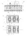
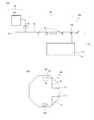
- FIG. 1It is sectional drawing which shows typically a part of scanning antenna 1000 of 1st Embodiment.
- A) And (b)is a typical top view which shows the TFT substrate 101 and the slot substrate 201 in the scanning antenna 1000, respectively.
- (A) And (b)is sectional drawing and the top view which show typically the antenna unit area
- (A) to (c)are cross-sectional views schematically showing the gate terminal portion GT, the source terminal portion ST, and the transfer terminal portion PT of the TFT substrate 101, respectively.
- 5is a diagram illustrating an example of a manufacturing process of the TFT substrate 101.
- FIG. 4is a cross-sectional view schematically showing an antenna unit region U and a terminal part IT in the slot substrate 201.
- FIG. 4is a schematic cross-sectional view for explaining a transfer portion in the TFT substrate 101 and the slot substrate 201.
- FIG. (A)-(c)is sectional drawing which respectively shows the gate terminal part GT of the TFT substrate 102 in 2nd Embodiment, the source terminal part ST, and the transfer terminal part PT.
- 5is a diagram illustrating an example of a manufacturing process of the TFT substrate 102.
- FIG. (A)-(c)is sectional drawing which respectively shows the gate terminal part GT of the TFT substrate 103 in 3rd Embodiment, the source terminal part ST, and the transfer terminal part PT.
- 5is a diagram illustrating an example of a manufacturing process of the TFT substrate 103.
- FIG. 4is a schematic cross-sectional view for explaining a transfer portion in the TFT substrate 103 and the slot substrate 203.
- FIG. (A)is a schematic plan view of the TFT substrate 104 having the heater resistance film 68
- (b)is a schematic plan view for explaining the sizes of the slot 57 and the patch electrode 15.
- (A) And (b)is a figure which shows the typical structure of resistance heating structure 80a and 80b, and electric current distribution.
- (A)-(c)is a figure which shows the typical structure and electric current distribution of resistance heating structure 80c-80e.
- (A)is typical sectional drawing of liquid crystal panel 100Pa which has the resistive film 68 for heaters
- (b)is typical sectional drawing of liquid crystal panel 100Pb which has the resistive film 68 for heaters. It is a figure which shows the equivalent circuit of one antenna unit of the scanning antenna by embodiment of this invention.
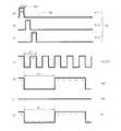
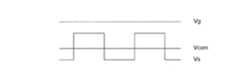
- (A)-(c), (e)-(g)is a figure which shows the example of the waveform of each signal used for the drive of the scanning antenna of embodiment, (d) performs dot inversion drive. It is a figure which shows the waveform of the display signal of the LCD panel.
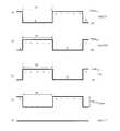
- (A)-(e)is a figure which shows the other example of the waveform of each signal used for the drive of the scanning antenna of embodiment.
- (A)-(e)is a figure which shows the further another example of the waveform of each signal used for the drive of the scanning antenna of embodiment.
- (A)is sectional drawing which shows typically the orientation state of the antenna unit in the scanning antenna 1000
- (b)is a top view which illustrates the result of having observed the orientation state of each antenna unit from the slot board
- (A)is sectional drawing which shows typically the orientation state of the antenna unit in the scanning antenna 1000
- (b)is a top view which illustrates the result of having observed the orientation state of each antenna unit from the TFT substrate 101 side. is there.
- (A) And (b)is the top view and enlarged plan view which illustrate the electrode shape of this embodiment
- (c)is a top view which shows the other example of an electrode shape.
- (A) And (b)is the top view and enlarged plan view which illustrate the other electrode shape of this embodiment
- (c)is a top view which shows the other example of an electrode shape.
- (A)is typical sectional drawing of the scanning antenna which does not have the transparent electrode for a test
- (b)is a typical top view which shows the result of having observed the liquid crystal orientation of the antenna unit.
- FIG. 1 and FIG. 1are a schematic cross-sectional view and a top view of a scanning antenna 1000A provided with a transparent electrode for inspection, respectively, and (c) shows the result of observing the liquid crystal alignment of the antenna unit. It is a typical top view. It is a typical sectional view showing a modification of scanning antenna 1000A provided with a transparent electrode for inspection. (A) And (b) is typical sectional drawing and top view which show other scanning antenna 1000B provided with the transparent electrode for a test
- FIG. 5is a schematic cross-sectional view illustrating a slot substrate 201 on which a transparent electrode for inspection is arranged. It is typical sectional drawing which illustrates TFT substrate 101 in which a transparent electrode for inspection is arranged.
- (A) And (b)is the top view which illustrates the reference position mark of the scanning antenna 1000, respectively, and the enlarged top view of a marker. It is a figure explaining an example of the inspection method of the liquid crystal alignment of this embodiment. It is a figure explaining the other example of the inspection method of the liquid crystal alignment of this embodiment. It is a top view which shows a part of scanning antenna for demonstrating an example of the method of selecting the antenna unit made into test object.
- FIG. 3is a schematic cross-sectional view illustrating a more specific configuration of a TFT substrate 106.
- FIG. 4is a schematic cross-sectional view illustrating a more specific configuration of the slot substrate 206.
- FIG.It is a schematic diagram which shows the drive circuit (drive circuit for test
- (A)is a schematic diagram which shows the structure of the conventional LCD900,
- TFT-LCDTFT type LCD
- description of items well known in the technical field of LCDmay be omitted.
- basic technology of TFT-LCDfor example, Liquid Crystals, Applications and Uses, Vol. 1-3 (Editor: Birenda Bahadur, Publisher: World Scientific Pub Co Inc).
- the entire disclosure content of the above documentsis incorporated herein by reference.
- LCDtransmissive TFT-LCD
- FIGS.an LCD 900 in a vertical electric field mode (for example, a TN mode or a vertical alignment mode) in which a voltage is applied in the thickness direction of the liquid crystal layer is illustrated.
- a vertical electric field modefor example, a TN mode or a vertical alignment mode
- the frame frequency (typically twice the polarity reversal frequency) of the voltage applied to the liquid crystal capacitance of the LCDis 240 Hz even when driven at 4 ⁇ speed, for example, and the dielectric constant ⁇ of the liquid crystal layer as the dielectric layer of the liquid crystal capacitance of the LCD Is different from the dielectric constant M ( ⁇ M ) for microwaves (for example, satellite broadcasting, Ku band (12 to 18 GHz), K band (18 to 26 GHz), Ka band (26 to 40 GHz)).
- the transmissive LCD 900includes a liquid crystal display panel 900a, a control circuit CNTL, a backlight (not shown), a power supply circuit (not shown), and the like.
- the liquid crystal display panel 900aincludes a liquid crystal display cell LCC and a drive circuit including a gate driver GD and a source driver SD.
- the drive circuitmay be mounted on the TFT substrate 910 of the liquid crystal display cell LCC, or a part or all of the drive circuit may be integrated (monolithic) on the TFT substrate 910.
- FIG. 49Bschematically shows a cross-sectional view of a liquid crystal display panel (hereinafter referred to as “LCD panel”) 900 a included in the LCD 900.
- the LCD panel 900aincludes a TFT substrate 910, a counter substrate 920, and a liquid crystal layer 930 provided therebetween.
- Both the TFT substrate 910 and the counter substrate 920have transparent substrates 911 and 921 such as glass substrates.
- a plastic substratemay be used in addition to a glass substrate.
- the plastic substrateis formed of, for example, a transparent resin (for example, polyester) and glass fiber (for example, a nonwoven fabric).
- the display area DR of the LCD panel 900ais composed of pixels P arranged in a matrix.
- a frame region FR that does not contribute to displayis formed around the display region DR.
- the liquid crystal materialis sealed in the display region DR by a seal portion (not shown) formed so as to surround the display region DR.
- the seal portionis formed by, for example, curing a sealing material including an ultraviolet curable resin and a spacer (for example, resin beads or silica beads), and adheres and fixes the TFT substrate 910 and the counter substrate 920 to each other.
- the spacer in the sealing materialcontrols the gap between the TFT substrate 910 and the counter substrate 920, that is, the thickness of the liquid crystal layer 930 to be constant.
- columnar spacersare formed using a UV curable resin in a light-shielded portion (for example, on the wiring) in the display region DR.
- a light-shielded portionfor example, on the wiring
- a TFT 912In the TFT substrate 910, a TFT 912, a gate bus line (scanning line) GL, a source bus line (display signal line) SL, a pixel electrode 914, an auxiliary capacitance electrode (not shown), a CS bus line (auxiliary capacitance) are formed on a transparent substrate 911. Line) (not shown) is formed.
- the CS bus lineis provided in parallel with the gate bus line.
- the next stage gate bus linemay be used as a CS bus line (CS on gate structure).
- the pixel electrode 914is covered with an alignment film (for example, a polyimide film) that controls the alignment of the liquid crystal.
- the alignment filmis provided in contact with the liquid crystal layer 930.
- the TFT substrate 910is often arranged on the backlight side (the side opposite to the observer).
- the counter substrate 920is often arranged on the viewer side of the liquid crystal layer 930.
- the counter substrate 920has a color filter layer (not shown), a counter electrode 924, and an alignment film (not shown) on the transparent substrate 921.
- the counter electrode 924is also referred to as a common electrode because it is provided in common to the plurality of pixels P constituting the display region DR.
- the color filter layerincludes a color filter (for example, a red filter, a green filter, and a blue filter) provided for each pixel P, and a black matrix (a light shielding layer) for shielding light unnecessary for display.
- the black matrixis disposed so as to shield light between the pixels P in the display region DR and the frame region FR, for example.
- the pixel electrode 914 of the TFT substrate 910, the counter electrode 924 of the counter substrate 920, and the liquid crystal layer 930 therebetweenconstitute a liquid crystal capacitor Clc.
- Each liquid crystal capacitorcorresponds to a pixel.
- an auxiliary capacitor CS electrically connected in parallel with the liquid crystal capacitor Clcis formed.
- the auxiliary capacitor CStypically includes an electrode having the same potential as the pixel electrode 914, an inorganic insulating layer (for example, a gate insulating layer (SiO 2 layer)), and an auxiliary capacitor electrode connected to the CS bus line. Composed.
- the same common voltage as that of the counter electrode 924is supplied from the CS bus line.
- Factors that cause the voltage (effective voltage) applied to the liquid crystal capacitance Clc to decreaseare (1) those based on the CR time constant, which is the product of the capacitance value C Clc of the liquid crystal capacitance Clc and the resistance value R, (2) There are interfacial polarization due to ionic impurities contained in the liquid crystal material and / or orientation polarization of liquid crystal molecules. Among these, the CR time constant contributes greatly to the liquid crystal capacitor Clc, and the CR time constant can be increased by providing the auxiliary capacitor CS electrically connected in parallel to the liquid crystal capacitor Clc.
- the volume resistivity of the liquid crystal layer 930which is a dielectric layer of the liquid crystal capacitance Clc, exceeds the order of 10 12 ⁇ ⁇ cm in the case of a widely used nematic liquid crystal material.
- the display signal supplied to the pixel electrode 914is the source bus line SL connected to the TFT 912 when the TFT 912 selected by the scanning signal supplied from the gate driver GD to the gate bus line GL is turned on.
- Thisis a display signal supplied to.
- the TFTs 912 connected to a certain gate bus line GLare simultaneously turned on, and at that time, a corresponding display signal is supplied from the source bus line SL connected to each TFT 912 of the pixel P in that row.
- the first rowfor example, the uppermost row of the display surface
- the mth rowfor example, the lowermost row of the display surface
- An image (frame)is written and displayed. If the pixels P are arranged in a matrix of m rows and n columns, at least one source bus line SL is provided corresponding to each pixel column, and a total of at least n source bus lines SL are provided.
- Such scanningis called line-sequential scanning, and the time until one pixel row is selected and the next row is selected is called a horizontal scanning period (1H).
- the time until a row is selectedis called the vertical scanning period (1V) or frame.
- 1V(or one frame) is obtained by adding a blanking period to a period m ⁇ H for selecting all m pixel rows.
- 1V1 frame of the conventional LCD panel
- 1V1 frame of the conventional LCD panel
- the NTSC signalis an interlace signal
- the frame frequencyis 30 Hz
- the field frequencyis 60 Hz.
- 1V(1/60) Drive in sec (60 Hz drive).
- the LCD panel 900ais so-called AC driven.
- frame inversion drivingis performed in which the polarity of the display signal is inverted every frame (every vertical scanning period). For example, in a conventional LCD panel, polarity inversion is performed every 1/60 sec (the polarity inversion period is 30 Hz).
- dot inversion driving or line inversion drivingis performed in order to uniformly distribute pixels having different polarities of applied voltages even within one frame. This is because it is difficult to completely match the magnitude of the effective voltage applied to the liquid crystal layer between the positive polarity and the negative polarity. For example, if the volume resistivity of the liquid crystal material is on the order of 10 12 ⁇ ⁇ cm, flicker is hardly visually recognized if dot inversion or line inversion driving is performed every 1/60 sec.
- the scanning signal and the display signal in the LCD panel 900aare supplied to the gate bus line GL and the source bus line SL from the gate driver GD and the source driver SD based on signals supplied from the control circuit CNTL to the gate driver GD and the source driver SD, respectively. Supplied.
- the gate driver GD and the source driver SDare each connected to corresponding terminals provided on the TFT substrate 910.
- the gate driver GD and the source driver SDmay be mounted as a driver IC in the frame region FR of the TFT substrate 910, or may be formed monolithically in the frame region FR of the TFT substrate 910.
- the counter electrode 924 of the counter substrate 920is electrically connected to a terminal (not shown) of the TFT substrate 910 via a conductive portion (not shown) called transfer.
- the transferis formed, for example, so as to overlap the seal portion or by imparting conductivity to a part of the seal portion. This is to narrow the frame area FR.
- a common voltageis directly or indirectly supplied to the counter electrode 924 from the control circuit CNTL. Typically, the common voltage is also supplied to the CS bus line as described above.
- a scanning antenna using an antenna unit that utilizes the anisotropy (birefringence) of a large dielectric constant M ( ⁇ M ) of a liquid crystal materialis a voltage applied to each liquid crystal layer of the antenna unit associated with a pixel of the LCD panel. Is controlled to change the effective dielectric constant M ( ⁇ M ) of the liquid crystal layer of each antenna unit, thereby forming a two-dimensional pattern for each antenna unit having a different capacitance (for displaying images on the LCD).
- a phase difference corresponding to the capacitance of each antenna unitis given to electromagnetic waves (for example, microwaves) emitted from or received by the antenna, and formed by antenna units having different capacitances.
- Non-Patent Documents 1 to 4 and Non-Patent Documents 1 and 2for the basic structure and operating principle of a scanning antenna using a liquid crystal material.
- Non-Patent Document 2discloses a basic structure of a scanning antenna in which spiral slots are arranged. For reference, the entire disclosures of Patent Documents 1 to 4 and Non-Patent Documents 1 and 2 are incorporated herein by reference.
- the antenna unit in the scanning antenna according to the embodiment of the present inventionis similar to the pixel of the LCD panel, the structure of the pixel of the LCD panel is different, and the arrangement of a plurality of antenna units is also different from the pixel of the LCD panel. The sequence is different.
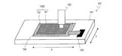
- a basic structure of a scanning antenna according to an embodiment of the present inventionwill be described with reference to FIG. 1 showing a scanning antenna 1000 of a first embodiment described in detail later.
- the scanning antenna 1000is a radial inline slot antenna in which slots are concentrically arranged.
- the scanning antenna according to the embodiment of the present inventionis not limited to this, and for example, the slot arrangement may be various known arrangements. Good.
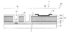
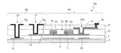
- FIG. 1is a cross-sectional view schematically showing a part of the scanning antenna 1000 of the present embodiment, from a feeding pin 72 (see FIG. 2B) provided near the center of the concentrically arranged slots. A part of cross section along a radial direction is shown typically.
- the scanning antenna 1000includes a TFT substrate 101, a slot substrate 201, a liquid crystal layer LC disposed therebetween, a slot substrate 201, and a reflective conductive plate 65 disposed so as to face each other with the air layer 54 interposed therebetween. It has.
- the scanning antenna 1000transmits and receives microwaves from the TFT substrate 101 side.
- the TFT substrate 101includes a dielectric substrate 1 such as a glass substrate, a plurality of patch electrodes 15 formed on the dielectric substrate 1, and a plurality of TFTs 10. Each patch electrode 15 is connected to the corresponding TFT 10. Each TFT 10 is connected to a gate bus line and a source bus line.
- the slot substrate 201has a dielectric substrate 51 such as a glass substrate, and a slot electrode 55 formed on the liquid crystal layer LC side of the dielectric substrate 51.
- the slot electrode 55has a plurality of slots 57.
- the reflective conductive plate 65is disposed so as to face the slot substrate 201 with the air layer 54 interposed therebetween.
- a layer formed of a dielectric having a low dielectric constant M with respect to microwavesfor example, a fluororesin such as PTFE
- the slot electrode 55, the reflective conductive plate 65, and the dielectric substrate 51 and the air layer 54 therebetweenfunction as the waveguide 301.
- the patch electrode 15, the portion of the slot electrode 55 including the slot 57, and the liquid crystal layer LC therebetweenconstitute an antenna unit U.
- one patch electrode 15is opposed to the portion of the slot electrode 55 including one slot 57 via the liquid crystal layer LC, thereby forming a liquid crystal capacitor.
- the structure in which the patch electrode 15 and the slot electrode 55 face each other through the liquid crystal layer LCis similar to the structure in which the pixel electrode 914 and the counter electrode 924 of the LCD panel 900a shown in FIG. 49 face each other through the liquid crystal layer 930. Yes. That is, the antenna unit U of the scanning antenna 1000 and the pixel P in the LCD panel 900a have a similar configuration.
- the antenna unithas a configuration similar to the pixel P in the LCD panel 900a in that it has an auxiliary capacitor (see FIGS. 13A and 17) electrically connected in parallel with the liquid crystal capacitor. ing. However, the scanning antenna 1000 has many differences from the LCD panel 900a.
- the performance required for the dielectric substrates 1 and 51 of the scanning antenna 1000is different from the performance required for the substrate of the LCD panel.
- the dielectric substrates 1 and 51 for the antennapreferably have a small dielectric loss with respect to the microwave (the dielectric loss tangent with respect to the microwave is represented as tan ⁇ M ).
- the tan ⁇ M of the dielectric substrates 1 and 51is preferably approximately 0.03 or less, and more preferably 0.01 or less.
- a glass substrate or a plastic substratecan be used.
- a glass substrateis superior to a plastic substrate in terms of dimensional stability and heat resistance, and is suitable for forming circuit elements such as TFTs, wirings, and electrodes using LCD technology.
- the material forming the waveguideis air and glass
- the glasshas a higher dielectric loss, so that the thinner the glass can reduce the waveguide loss, preferably 400 ⁇ m or less. And more preferably 300 ⁇ m or less.
- the conductive material used for the electrodesis also different.
- An ITO filmis often used as a transparent conductive film for pixel electrodes and counter electrodes of LCD panels.
- ITOhas a large tan ⁇ M for microwaves and cannot be used as a conductive layer in an antenna.
- the slot electrode 55functions as a wall of the waveguide 301 together with the reflective conductive plate 65. Therefore, in order to suppress transmission of microwaves through the wall of the waveguide 301, it is preferable that the thickness of the wall of the waveguide 301, that is, the thickness of the metal layer (Cu layer or Al layer) is large.
- the electromagnetic waveis known to be attenuated to 1/20 (-26 dB), and if it is 5 times, it is attenuated to 1/150 (-43 dB). ing. Therefore, if the thickness of the metal layer is 5 times the skin depth, the electromagnetic wave transmittance can be reduced to 1%. For example, for a microwave of 10 GHz, if a Cu layer having a thickness of 3.3 ⁇ m or more and an Al layer having a thickness of 4.0 ⁇ m or more are used, the microwave can be reduced to 1/150.
- the slot electrode 55is preferably formed of a relatively thick Cu layer or Al layer.
- the thickness of the Cu layer or Al layerthere is no particular upper limit to the thickness of the Cu layer or Al layer, and it can be set as appropriate in consideration of the film formation time and cost.
- Use of the Cu layerprovides the advantage that it can be made thinner than using the Al layer.
- the relatively thick Cu layer or Al layercan be formed not only by the thin film deposition method used in the LCD manufacturing process, but also by other methods such as attaching Cu foil or Al foil to the substrate.
- the thickness of the metal layeris, for example, 2 ⁇ m or more and 30 ⁇ m or less. When forming by using a thin film deposition method, the thickness of the metal layer is preferably 5 ⁇ m or less.
- an aluminum plate or a copper plate having a thickness of several millimeterscan be used as the reflective conductive plate 65.
- the patch electrode 15does not constitute the waveguide 301 like the slot electrode 55, a Cu layer or an Al layer having a thickness smaller than that of the slot electrode 55 can be used.
- the resistanceis low in order to avoid a loss that changes into heat when vibration of free electrons in the vicinity of the slot 57 of the slot electrode 55 induces vibration of free electrons in the patch electrode 15.
- the arrangement pitch of the antenna units Uis greatly different from the pixel pitch.
- the wavelength ⁇is 25 mm, for example.
- the pitch of the antenna unit Uis ⁇ / 4 or less and / or ⁇ / 5 or less, it is 6.25 mm or less and / or 5 mm or less. This is more than 10 times larger than the pixel pitch of the LCD panel. Therefore, the length and width of the antenna unit U are also about 10 times larger than the pixel length and width of the LCD panel.
- the arrangement of the antenna units Umay be different from the arrangement of the pixels in the LCD panel.
- an example in which concentric circles are arrangedfor example, see Japanese Patent Application Laid-Open No. 2002-217640
- the present inventionis not limited to this.
- theyare arranged in a spiral shape. Also good.
- theymay be arranged in a matrix.
- the characteristics required for the liquid crystal material of the liquid crystal layer LC of the scanning antenna 1000are different from the characteristics required for the liquid crystal material of the LCD panel.
- the LCD panelchanges the polarization state by giving a phase difference to the polarization of visible light (wavelength 380 nm to 830 nm) by changing the refractive index of the liquid crystal layer of the pixel (for example, rotating the polarization axis direction of linearly polarized light, or , Changing the degree of circular polarization of circularly polarized light).
- the scanning antenna 1000changes the phase of the microwave excited (re-radiated) from each patch electrode by changing the capacitance value of the liquid crystal capacitance of the antenna unit U.
- the liquid crystal layerpreferably has a large anisotropy ( ⁇ M ) of dielectric constant M ( ⁇ M ) with respect to microwaves, and preferably has a small tan ⁇ M.
- ⁇ Mis 4 or more and tan ⁇ M is 0.02 or less (both values are 19 Gz).
- Kuki, Polymer 55, August, pp.A liquid crystal material having a ⁇ M of 0.4 or more and a tan ⁇ M of 0.04 or less described in 599-602 (2006) can be used.
- the dielectric constant of a liquid crystal materialhas frequency dispersion, but the dielectric anisotropy ⁇ M for microwaves has a positive correlation with the refractive index anisotropy ⁇ n for visible light. Therefore, it can be said that the liquid crystal material for the antenna unit for the microwave is preferably a material having a large refractive index anisotropy ⁇ n for visible light.
- the refractive index anisotropy ⁇ n of the liquid crystal material for LCDis evaluated by the refractive index anisotropy with respect to light having a wavelength of 550 nm.
- nematic liquid crystal having ⁇ n of 0.3 or more, preferably 0.4 or moreis used for an antenna unit for microwaves.
- ⁇ nis preferably 0.4 or less.
- the thickness of the liquid crystal layeris, for example, 1 ⁇ m to 500 ⁇ m.
- FIG. 1is a schematic partial cross-sectional view near the center of the scanning antenna 1000 as described in detail.
- FIGS. 2A and 2Bshow the TFT substrate 101 and the slot substrate 201 in the scanning antenna 1000, respectively. It is a typical top view.
- the scanning antenna 1000has a plurality of antenna units U arranged two-dimensionally.
- a plurality of antenna unitsare arranged concentrically.
- the region of the TFT substrate 101 and the region of the slot substrate 201 corresponding to the antenna unit Uare referred to as “antenna unit region”, and the same reference symbol U as that of the antenna unit is given.
- an area defined by a plurality of antenna unit areas arranged two-dimensionally in the TFT substrate 101 and the slot substrate 201is referred to as a “transmission / reception area R1”.
- An area other than the transmission / reception area R1is referred to as a “non-transmission / reception area R2”.
- the non-transmission / reception region R2is provided with a terminal portion, a drive circuit, and the like.
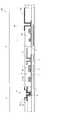
- FIG. 2Ais a schematic plan view showing the TFT substrate 101 in the scanning antenna 1000.
- the transmission / reception region R1has a donut shape when viewed from the normal direction of the TFT substrate 101.
- the non-transmission / reception region R2includes a first non-transmission / reception region R2a located at the center of the transmission / reception region R1 and a second non-transmission / reception region R2b located at the periphery of the transmission / reception region R1.
- the outer diameter of the transmission / reception region R1is, for example, 200 mm to 1500 mm, and is set according to the amount of communication.
- each antenna unit region Uincludes a TFT and a patch electrode electrically connected to the TFT.
- the source electrode of the TFTis electrically connected to the source bus line SL
- the gate electrodeis electrically connected to the gate bus line GL.
- the drain electrodeis electrically connected to the patch electrode.
- a seal area Rsis arranged so as to surround the transmission / reception area R1.
- a seal material(not shown) is applied to the seal region Rs. The sealing material adheres the TFT substrate 101 and the slot substrate 201 to each other and encloses liquid crystal between the substrates 101 and 201.
- a gate terminal portion GT, a gate driver GD, a source terminal portion ST, and a source driver SDare provided outside the seal region Rs in the non-transmission / reception region R2.
- Each of the gate bus lines GLis connected to the gate driver GD via the gate terminal portion GT.
- Each of the source bus lines SLis connected to the source driver SD via the source terminal portion ST.
- the source driver SD and the gate driver GDare formed on the dielectric substrate 1, but one or both of these drivers may be provided on another dielectric substrate.
- a plurality of transfer terminal portions PTare also provided.
- the transfer terminal portion PTis electrically connected to the slot electrode 55 (FIG. 2B) of the slot substrate 201.
- a connection portion between the transfer terminal portion PT and the slot electrode 55is referred to as a “transfer portion”.
- the transfer terminal portion PT(transfer portion) may be disposed in the seal region Rs.
- a resin containing conductive particlesmay be used as the sealing material.
- liquid crystalis sealed between the TFT substrate 101 and the slot substrate 201, and electrical connection between the transfer terminal portion PT and the slot electrode 55 of the slot substrate 201 can be secured.
- the transfer terminal portion PTis disposed in both the first non-transmission / reception region R2a and the second non-transmission / reception region R2b, but may be disposed in only one of them.
- the transfer terminal portion PT(transfer portion) may not be arranged in the seal region Rs.
- the non-transmission / reception region R2may be disposed outside the seal region Rs.
- FIG. 2Bis a schematic plan view illustrating the slot substrate 201 in the scanning antenna 1000, and shows the surface of the slot substrate 201 on the liquid crystal layer LC side.
- a slot electrode 55is formed on the dielectric substrate 51 over the transmission / reception region R1 and the non-transmission / reception region R2.
- a plurality of slots 57are arranged in the slot electrode 55.
- the slot 57is arranged corresponding to the antenna unit region U in the TFT substrate 101.
- the plurality of slots 57are arranged concentrically with a pair of slots 57 extending in directions substantially perpendicular to each other so as to constitute a radial inline slot antenna. Since the scanning antennas 1000 have slots that are substantially orthogonal to each other, the scanning antenna 1000 can transmit and receive circularly polarized waves.
- a plurality of terminal portions IT of the slot electrodes 55are provided in the non-transmission / reception region R2.
- the terminal portion ITis electrically connected to the transfer terminal portion PT (FIG. 2A) of the TFT substrate 101.
- the terminal portion ITis disposed in the seal region Rs, and is electrically connected to the corresponding transfer terminal portion PT by a seal material containing conductive particles.
- the power supply pins 72are arranged on the back side of the slot substrate 201.
- a microwaveis inserted into the waveguide 301 formed by the slot electrode 55, the reflective conductive plate 65, and the dielectric substrate 51 by the power supply pin 72.
- the power feeding pin 72is connected to the power feeding device 70. Power is supplied from the center of a concentric circle in which the slots 57 are arranged.
- the feeding methodmay be either a direct coupling feeding method or an electromagnetic coupling method, and a known feeding structure can be employed.
- FIGS. 3A and 3Bare a cross-sectional view and a plan view schematically showing the antenna unit region U of the TFT substrate 101, respectively.
- Each of the antenna unit regions Uis formed on a dielectric substrate (not shown), the TFT 10 supported on the dielectric substrate, the first insulating layer 11 covering the TFT 10, and the first insulating layer 11. Connected patch electrodes 15 and a second insulating layer 17 covering the patch electrodes 15.
- the TFT 10is disposed in the vicinity of the intersection of the gate bus line GL and the source bus line SL.
- the TFT 10includes a gate electrode 3, an island-shaped semiconductor layer 5, a gate insulating layer 4 disposed between the gate electrode 3 and the semiconductor layer 5, a source electrode 7S, and a drain electrode 7D.
- the structure of the TFT 10is not particularly limited.
- the TFT 10is a channel etch type TFT having a bottom gate structure.
- the gate electrode 3is electrically connected to the gate bus line GL and supplied with a scanning signal from the gate bus line GL.
- the source electrode 7Sis electrically connected to the source bus line SL, and is supplied with a data signal from the source bus line SL.
- the gate electrode 3 and the gate bus line GLmay be formed from the same conductive film (gate conductive film).
- the source electrode 7S, the drain electrode 7D, and the source bus line SLmay be formed of the same conductive film (source conductive film).
- the gate conductive film and the source conductive filmare, for example, metal films. In this specification, a layer (layer) formed using the gate conductive film may be referred to as a “gate metal layer”, and a layer formed using the source conductive film may be referred to as a “source metal layer”.
- the semiconductor layer 5is disposed so as to overlap the gate electrode 3 with the gate insulating layer 4 interposed therebetween.
- a source contact layer 6 ⁇ / b> S and a drain contact layer 6 ⁇ / b> Dare formed on the semiconductor layer 5.
- the source contact layer 6S and the drain contact layer 6Dare respectively disposed on both sides of a region (channel region) where a channel is formed in the semiconductor layer 5.
- the semiconductor layer 5may be an intrinsic amorphous silicon (ia-Si) layer, and the source contact layer 6S and the drain contact layer 6D may be n + -type amorphous silicon (n + -a-Si) layers.
- the source electrode 7Sis provided in contact with the source contact layer 6S, and is connected to the semiconductor layer 5 through the source contact layer 6S.
- the drain electrode 7Dis provided so as to be in contact with the drain contact layer 6D, and is connected to the semiconductor layer 5 through the drain contact layer 6D.
- the first insulating layer 11has a contact hole CH1 reaching the drain electrode 7D of the TFT 10.
- the patch electrode 15is provided on the first insulating layer 11 and in the contact hole CH1, and is in contact with the drain electrode 7D in the contact hole CH1.
- the patch electrode 15includes a metal layer.
- the patch electrode 15may be a metal electrode formed only from a metal layer.
- the material of the patch electrode 15may be the same as that of the source electrode 7S and the drain electrode 7D.
- the thickness of the metal layer in the patch electrode 15(the thickness of the patch electrode 15 when the patch electrode 15 is a metal electrode) is set to be larger than the thickness of the source electrode 7S and the drain electrode 7D.
- the thickness of the metal layer in the patch electrode 15is set to, for example, 0.5 ⁇ m or more when formed with an Al layer.
- the CS bus line CLmay be provided using the same conductive film as the gate bus line GL.
- the CS bus line CLmay be disposed so as to overlap the drain electrode (or an extended portion of the drain electrode) 7D with the gate insulating layer 4 interposed therebetween, and may constitute an auxiliary capacitor CS having the gate insulating layer 4 as a dielectric layer. .
- An alignment mark (for example, a metal layer) 21 and a base insulating film 2 covering the alignment mark 21may be formed closer to the dielectric substrate than the gate bus line GL.
- the alignment mark 21needs to be performed in a plurality of times when the number of photomasks is n (n ⁇ m). Arise.
- the number of photomasks (n)is smaller than the number of TFT substrates 101 (m) produced from one glass substrate 1, it is used for photomask alignment.
- the alignment mark 21can be omitted.
- the patch electrode 15is formed in a layer different from the source metal layer. Thereby, the following merits are obtained.
- the source metal layeris usually formed using a metal film, it is conceivable to form a patch electrode in the source metal layer (TFT substrate of a reference example).
- the patch electrodepreferably has a low resistance so as not to inhibit the vibration of electrons.
- the patch electrodeis formed of a relatively thick Al layer having a thickness of 0.5 ⁇ m or more. For this reason, in the TFT substrate of the reference example, the source bus line SL and the like are also formed from such a thick metal film, and there is a problem that the controllability of patterning at the time of forming the wiring is lowered.
- the patch electrode 15is formed separately from the source metal layer, so that the thickness of the source metal layer and the thickness of the patch electrode 15 can be controlled independently. Therefore, the patch electrode 15 having a desired thickness can be formed while ensuring controllability when forming the source metal layer.
- the thickness of the patch electrode 15can be set with a high degree of freedom separately from the thickness of the source metal layer. Since the size of the patch electrode 15 does not need to be controlled as strictly as the source bus line SL or the like, the line width shift (deviation from the design value) may be increased by increasing the thickness of the patch electrode 15. . The case where the thickness of the patch electrode 15 is equal to the thickness of the source metal layer is not excluded.
- the patch electrode 15may include a Cu layer or an Al layer as a main layer.
- the performance of the scanning antennacorrelates with the electric resistance of the patch electrode 15, and the thickness of the main layer is set so as to obtain a desired resistance. From the viewpoint of electrical resistance, there is a possibility that the thickness of the patch electrode 15 can be made smaller in the Cu layer than in the Al layer.
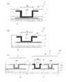
- -Gate terminal part GT, source terminal part ST and transfer terminal part PT 4A to 4Care cross-sectional views schematically showing the gate terminal portion GT, the source terminal portion ST, and the transfer terminal portion PT, respectively.
- the gate terminal portion GTincludes a gate bus line GL formed on the dielectric substrate, an insulating layer covering the gate bus line GL, and an upper connection portion 19g for the gate terminal.
- the gate terminal upper connection portion 19gis in contact with the gate bus line GL in the contact hole CH2 formed in the insulating layer.
- the insulating layer covering the gate bus line GLincludes the gate insulating layer 4, the first insulating layer 11, and the second insulating layer 17 from the dielectric substrate side.
- the gate terminal upper connection portion 19gis, for example, a transparent electrode formed from a transparent conductive film provided on the second insulating layer 17.
- the source terminal portion STincludes a source bus line SL formed on a dielectric substrate (here, on the gate insulating layer 4), an insulating layer covering the source bus line SL, and a source terminal upper connection portion 19s.
- the source terminal upper connection portion 19sis in contact with the source bus line SL in the contact hole CH3 formed in the insulating layer.
- the insulating layer covering the source bus line SLincludes the first insulating layer 11 and the second insulating layer 17.
- the source terminal upper connection portion 19 sis, for example, a transparent electrode formed from a transparent conductive film provided on the second insulating layer 17.
- the transfer terminal portion PThas a patch connection portion 15p formed on the first insulating layer 11, a second insulating layer 17 covering the patch connection portion 15p, and an upper connection portion 19p for transfer terminals.
- the transfer terminal upper connection portion 19pis in contact with the patch connection portion 15p in the contact hole CH4 formed in the second insulating layer 17.
- the patch connection portion 15pis formed of the same conductive film as the patch electrode 15.
- the transfer terminal upper connecting portion (also referred to as an upper transparent electrode) 19pis a transparent electrode formed from, for example, a transparent conductive film provided on the second insulating layer 17.
- the upper connection portions 19g, 19s, and 19p of each terminal portionare formed from the same transparent conductive film.
- the contact holes CH2, CH3, and CH4 of each terminal portioncan be formed simultaneously by an etching process after the second insulating layer 17 is formed. A detailed manufacturing process will be described later.
- the TFT substrate 101can be manufactured, for example, by the following method.
- FIG. 5is a diagram illustrating a manufacturing process of the TFT substrate 101.
- a metal filmfor example, Ti film
- a dielectric substratefor example, a glass substrate, a heat-resistant plastic substrate (resin substrate), or the like can be used.
- the base insulating film 2is formed so as to cover the alignment mark 21.
- a SiO 2 filmis used as the base insulating film 2.
- a gate metal layer including the gate electrode 3 and the gate bus line GLis formed on the base insulating film 2.
- the gate electrode 3can be formed integrally with the gate bus line GL.
- a gate conductive film(thickness: for example, not less than 50 nm and not more than 500 nm) is formed on the dielectric substrate by sputtering or the like.
- the gate electrode 3 and the gate bus line GLare obtained by patterning the gate conductive film.
- the material of the conductive film for gateis not particularly limited. A film containing a metal such as aluminum (Al), tungsten (W), molybdenum (Mo), tantalum (Ta), chromium (Cr), titanium (Ti), copper (Cu), or an alloy thereof, or a metal nitride thereof It can be used as appropriate.
- a laminated film in which MoN (thickness: for example, 50 nm), Al (thickness: for example, 200 nm) and MoN (thickness: for example, 50 nm) are laminated in this orderis formed as the gate conductive film.
- the gate insulating layer 4is formed so as to cover the gate metal layer.
- the gate insulating layer 4can be formed by a CVD method or the like.
- a silicon oxide (SiO 2 ) layer, a silicon nitride (SiNx) layer, a silicon oxynitride (SiOxNy; x> y) layer, a silicon nitride oxide (SiNxOy; x> y) layer, or the likeis appropriately used.
- the gate insulating layer 4may have a stacked structure.
- a SiNx layer(thickness: 410 nm, for example) is formed as the gate insulating layer 4.
- the semiconductor layer 5 and the contact layerare formed on the gate insulating layer 4.
- an intrinsic amorphous silicon filmthickness: for example, 125 nm
- an n + type amorphous silicon filmthickness: for example, 65 nm
- the semiconductor film used for the semiconductor layer 5is not limited to an amorphous silicon film.
- an oxide semiconductor layermay be formed as the semiconductor layer 5.
- a contact layermay not be provided between the semiconductor layer 5 and the source / drain electrodes.
- a conductive film for source(thickness: for example, 50 nm or more and 500 nm or less) is formed on the gate insulating layer 4 and the contact layer, and is patterned to form the source electrode 7S, the drain electrode 7D, and the source bus line SL.
- a source metal layeris formed.
- the contact layeris also etched to form the source contact layer 6S and the drain contact layer 6D which are separated from each other.
- the material of the source conductive filmis not particularly limited.
- a film containing a metalsuch as aluminum (Al), tungsten (W), molybdenum (Mo), tantalum (Ta), chromium (Cr), titanium (Ti), copper (Cu), or an alloy thereof, or a metal nitride thereof It can be used as appropriate.
- a stacked film in which MoN (thickness: for example, 30 nm), Al (thickness: for example, 200 nm), and MoN (thickness: for example, 50 nm) are stacked in this orderis formed as the source conductive film.
- Tithickness: for example 30 nm
- MoNthickness: for example 30 nm
- Althickness: for example 200 nm
- MoNthickness: for example 50 nm
- the source conductive filmis formed by sputtering, and the source conductive film is patterned (source / drain separation) by wet etching. Thereafter, by dry etching, for example, a portion of the contact layer located on the region to be the channel region of the semiconductor layer 5 is removed to form a gap portion, which is separated into the source contact layer 6S and the drain contact layer 6D. . At this time, the vicinity of the surface of the semiconductor layer 5 is also etched in the gap portion (overetching).
- the Al filmis patterned by wet etching using, for example, an aqueous solution of phosphoric acid, acetic acid and nitric acid, and then dried.
- the Ti film and the contact layer (n + type amorphous silicon layer) 6may be patterned simultaneously by etching.
- the source conductive film and the contact layercan be etched together.
- the etching amount of the gap portioncan be controlled more easily.
- the first insulating layer 11is formed so as to cover the TFT 10.
- the first insulating layer 11is disposed in contact with the channel region of the semiconductor layer 5. Further, a contact hole CH1 reaching the drain electrode 7D is formed in the first insulating layer 11 by known photolithography.
- the first insulating layer 11is an inorganic material such as a silicon oxide (SiO 2 ) film, a silicon nitride (SiNx) film, a silicon oxynitride (SiOxNy; x> y) film, or a silicon nitride oxide (SiNxOy; x> y) film.
- An insulating layermay be used.
- a SiNx layer having a thickness of, for example, 330 nmis formed by, eg, CVD.
- a patch conductive filmis formed on the first insulating layer 11 and in the contact hole CH1, and this is patterned.
- the patch electrode 15is formed in the transmission / reception region R1, and the patch connection portion 15p is formed in the non-transmission / reception region R2.
- the patch electrode 15is in contact with the drain electrode 7D in the contact hole CH1.
- a layer including the patch electrode 15 and the patch connection portion 15p formed from the conductive film for patchmay be referred to as a “patch metal layer”.
- the material for the conductive film for patchthe same material as the conductive film for gate or the conductive film for source can be used.
- the patch conductive filmis set to be thicker than the gate conductive film and the source conductive film. Thereby, it is possible to reduce the loss that the vibration of free electrons in the patch electrode changes into heat by suppressing the electromagnetic wave transmittance low and reducing the sheet resistance of the patch electrode.
- a suitable thickness of the patch conductive filmis, for example, not less than 1 ⁇ m and not more than 30 ⁇ m.
- the electromagnetic wave transmittancewill be about 30%, the sheet resistance will be 0.03 ⁇ / sq or more, and there is a possibility that the loss will increase, and if it is thick, the patterning property of the slot will deteriorate. Problems can arise.
- a laminated filmin which MoN (thickness: for example, 50 nm), Al (thickness: for example, 1000 nm) and MoN (thickness: for example, 50 nm) are laminated in this order as the conductive film for patch.
- a laminated filmin which Ti (thickness: for example 50 nm), MoN (thickness: for example 50 nm), Al (thickness: for example 2000 nm) and MoN (thickness: for example 50 nm) are laminated in this order.
- / Al / MoN / Timay be formed.
- a laminated filmin which Ti (thickness: for example 50 nm), MoN (thickness: for example 50 nm), Al (thickness: for example 500 nm) and MoN (thickness: for example 50 nm) are laminated in this order.
- / Al / MoN / Timay be formed.
- a laminated film in which a Ti film, a Cu film, and a Ti film are laminated in this orderTi / Cu / Ti
- a laminated film in which a Ti film and a Cu film are laminated in this orderCu / Ti
- a second insulating layer (thickness: 100 nm or more and 300 nm or less) 17is formed on the patch electrode 15 and the first insulating layer 11.
- the second insulating layer 17is not particularly limited, and for example, a silicon oxide (SiO 2 ) film, a silicon nitride (SiNx) film, a silicon oxynitride (SiOxNy; x> y) film, a silicon nitride oxide (SiNxOy; x> y).
- a film or the likecan be used as appropriate.
- the second insulating layer 17for example, a SiNx layer having a thickness of 200 nm is formed.
- the inorganic insulating film(the second insulating layer 17, the first insulating layer 11, and the gate insulating layer 4) is collectively etched by, for example, dry etching using a fluorine-based gas.
- the patch electrode 15, the source bus line SL, and the gate bus line GLfunction as an etch stop.
- a contact hole CH2 reaching the gate bus line GLis formed in the second insulating layer 17, the first insulating layer 11, and the gate insulating layer 4, and the source bus line is formed in the second insulating layer 17 and the first insulating layer 11.
- a contact hole CH3 reaching SLis formed.
- a contact hole CH4 reaching the patch connection portion 15pis formed in the second insulating layer 17.
- the side surfaces of the second insulating layer 17, the first insulating layer 11, and the gate insulating layer 4are aligned on the side wall of the obtained contact hole CH2, and the contact hole CH3
- the side walls of the second insulating layer 17 and the first insulating layer 11are aligned with each other.
- “side surfaces of two or more different layers in a contact hole”means that the side surfaces exposed in the contact hole in these layers are flush with each other in the vertical direction. It also includes a case where an inclined surface such as a tapered shape is continuously formed. Such a configuration can be obtained, for example, by etching these layers using the same mask, or by etching the other layer using one layer as a mask.
- a transparent conductive film(thickness: 50 nm or more and 200 nm or less) is formed on the second insulating layer 17 and in the contact holes CH2, CH3, and CH4 by, for example, sputtering.
- the transparent conductive filmfor example, an ITO (indium tin oxide) film, an IZO film, a ZnO film (zinc oxide film), or the like can be used.
- an ITO film having a thickness of, for example, 100 nmis used as the transparent conductive film.
- a gate terminal upper connection portion 19g, a source terminal upper connection portion 19s and a transfer terminal upper connection portion 19pare formed.
- the gate terminal upper connection portion 19g, the source terminal upper connection portion 19s, and the transfer terminal upper connection portion 19pare used to protect the electrodes or wiring exposed at each terminal portion.
- the gate terminal part GT, the source terminal part ST, and the transfer terminal part PTare obtained.
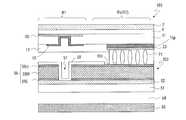
- FIG. 6is a cross-sectional view schematically showing the antenna unit region U and the terminal part IT in the slot substrate 201.
- the slot substrate 201includes a dielectric substrate 51 having a front surface and a back surface, a third insulating layer 52 formed on the surface of the dielectric substrate 51, a slot electrode 55 formed on the third insulating layer 52, and a slot electrode. And a fourth insulating layer 58 covering 55.
- the reflective conductive plate 65is disposed so as to face the back surface of the dielectric substrate 51 through a dielectric layer (air layer) 54.
- the slot electrode 55 and the reflective conductive plate 65function as walls of the waveguide 301.
- a plurality of slots 57are formed in the slot electrode 55 in the transmission / reception region R1.
- the slot 57is an opening that penetrates the slot electrode 55.
- one slot 57is arranged in each antenna unit region U.
- the fourth insulating layer 58is formed on the slot electrode 55 and in the slot 57.
- the material of the fourth insulating layer 58may be the same as the material of the third insulating layer 52.
- the slot electrode 55 and the liquid crystal layer LCare not in direct contact, so that the reliability can be improved.
- the slot electrode 55is formed of a Cu layer, Cu may be eluted into the liquid crystal layer LC.
- a voidmay be included in the Al layer.
- the fourth insulating layer 58can prevent the liquid crystal material from entering the voids of the Al layer. If the slot electrode 55 is produced by attaching an Al layer to the dielectric substrate 51 with an aluminum foil and bonding it, and then patterning it, the void problem can be avoided.
- the slot electrode 55includes a main layer 55M such as a Cu layer or an Al layer.
- the slot electrode 55may have a stacked structure including a main layer 55M and an upper layer 55U and a lower layer 55L arranged so as to sandwich the main layer 55M.
- the thickness of the main layer 55Mis set in consideration of the skin effect depending on the material, and may be, for example, 2 ⁇ m or more and 30 ⁇ m or less.
- the thickness of the main layer 55Mis typically larger than the thickness of the upper layer 55U and the lower layer 55L.
- the main layer 55Mis a Cu layer
- the upper layer 55U and the lower layer 55Lare Ti layers.
- the adhesion between the slot electrode 55 and the third insulating layer 52can be improved.
- the upper layer 55Ucorrosion of the main layer 55M (for example, Cu layer) can be suppressed.
- the reflective conductive plate 65constitutes the wall of the waveguide 301, the reflective conductive plate 65 preferably has a thickness of 3 times or more, preferably 5 times or more of the skin depth.
- the reflective conductive plate 65for example, an aluminum plate or a copper plate having a thickness of several millimeters produced by cutting can be used.
- a terminal portion ITis provided in the non-transmission / reception region R2.
- the terminal portion ITincludes a slot electrode 55, a fourth insulating layer 58 that covers the slot electrode 55, and an upper connection portion 60.
- the fourth insulating layer 58has an opening reaching the slot electrode 55.
- the upper connection portion 60is in contact with the slot electrode 55 in the opening.
- the terminal portion ITis disposed in the seal region Rs and is connected to the transfer terminal portion in the TFT substrate by a seal resin containing conductive particles (transfer portion).
- Transfer Part FIG. 7is a schematic cross-sectional view for explaining a transfer part that connects the transfer terminal part PT of the TFT substrate 101 and the terminal part IT of the slot substrate 201. In FIG. 7, the same components as those in FIGS. 1 to 4 are denoted by the same reference numerals.
- the upper connection part 60 of the terminal part ITis electrically connected to the transfer terminal upper connection part 19p of the transfer terminal part PT in the TFT substrate 101.
- the upper connection portion 60 and the transfer terminal upper connection portion 19pare connected via a resin (seal resin) 73 (also referred to as “seal portion 73”) including conductive beads 71.
- the upper connection portions 60 and 19pare both transparent conductive layers such as an ITO film and an IZO film, and an oxide film may be formed on the surface thereof.
- these transparent conductive layersare bonded via a resin containing conductive beads (for example, Au beads) 71, so even if a surface oxide film is formed, the conductive beads are on the surface.
- the conductive beads 71may penetrate not only the surface oxide film but also the upper connection portions 60 and 19p, which are transparent conductive layers, and may be in direct contact with the patch connection portion 15p and the slot electrode 55.
- the transfer partmay be disposed both at the center part and the peripheral part of the scanning antenna 1000 (that is, inside and outside the donut-shaped transmission / reception region R1 when viewed from the normal direction of the scanning antenna 1000), You may arrange
- the transfer partmay be disposed in the seal region Rs that encloses the liquid crystal, or may be disposed outside the seal region Rs (on the side opposite to the liquid crystal layer).
- the slot substrate 201can be manufactured, for example, by the following method.
- a third insulating layer (thickness: for example, 200 nm) 52is formed on a dielectric substrate.
- a substratesuch as a glass substrate or a resin substrate that has a high transmittance with respect to electromagnetic waves (small dielectric constant ⁇ M and dielectric loss tan ⁇ M ) can be used.
- the dielectric substrateis preferably thin in order to suppress attenuation of electromagnetic waves.
- the glass substratemay be thinned from the back side. Thereby, the thickness of a glass substrate can be reduced to 500 micrometers or less, for example.
- components such as TFTsmay be formed directly on the resin substrate, or may be formed on the resin substrate using a transfer method.
- a resin filmfor example, a polyimide film
- a constituent elementis formed on the resin film by a process described later, and then the resin film on which the constituent element is formed and the glass substrate are combined.
- a resinhas a smaller dielectric constant ⁇ M and dielectric loss tan ⁇ M than glass.
- the thickness of the resin substrateis, for example, 3 ⁇ m to 300 ⁇ m.
- the resin materialfor example, liquid crystal polymer can be used in addition to polyimide.
- the third insulating layer 52is not particularly limited, for example, silicon oxide (SiO 2) film, a silicon nitride (SiNx) film, silicon oxynitride (SiOxNy; x> y) film, a silicon nitride oxide (SiNxOy; x> y ) A film or the like can be used as appropriate.
- a metal filmis formed on the third insulating layer 52 and patterned to obtain a slot electrode 55 having a plurality of slots 57.
- a Cu film (or Al film) having a thickness of 2 ⁇ m to 5 ⁇ mmay be used.
- a laminated film in which a Ti film, a Cu film, and a Ti film are laminated in this orderis used.
- a laminated film in which Ti (thickness: for example, 50 nm) and Cu (thickness: for example, 5000 nm) are laminated in this ordermay be formed.
- a fourth insulating layer (thickness: for example, 100 nm or 200 nm) 58is formed on the slot electrode 55 and in the slot 57.
- the material of the fourth insulating layer 58may be the same as the material of the third insulating layer.
- an opening reaching the slot electrode 55is formed in the fourth insulating layer 58 in the non-transmission / reception region R2.
- a transparent conductive filmis formed on the fourth insulating layer 58 and in the opening of the fourth insulating layer 58, and this is patterned to form the upper connection portion 60 in contact with the slot electrode 55 in the opening. Thereby, the terminal part IT is obtained.
- a TFT having the semiconductor layer 5 as an active layeris used as a switching element disposed in each pixel.
- the semiconductor layer 5is not limited to an amorphous silicon layer, and may be a polysilicon layer or an oxide semiconductor layer.
- the oxide semiconductor included in the oxide semiconductor layermay be an amorphous oxide semiconductor or a crystalline oxide semiconductor having a crystalline portion.
- the crystalline oxide semiconductorinclude a polycrystalline oxide semiconductor, a microcrystalline oxide semiconductor, and a crystalline oxide semiconductor in which the c-axis is oriented substantially perpendicular to the layer surface.
- the oxide semiconductor layermay have a stacked structure of two or more layers.
- the oxide semiconductor layermay include an amorphous oxide semiconductor layer and a crystalline oxide semiconductor layer.
- a plurality of crystalline oxide semiconductor layers having different crystal structuresmay be included.
- a plurality of amorphous oxide semiconductor layersmay be included.
- the energy gap of the oxide semiconductor included in the upper layeris preferably larger than the energy gap of the oxide semiconductor included in the lower layer.
- the energy gap of the lower oxide semiconductormay be larger than the energy gap of the upper oxide semiconductor.
- the oxide semiconductor layermay contain at least one metal element of In, Ga, and Zn, for example.
- the oxide semiconductor layerincludes, for example, an In—Ga—Zn—O-based semiconductor (eg, indium gallium zinc oxide).
- Such an oxide semiconductor layercan be formed using an oxide semiconductor film containing an In—Ga—Zn—O-based semiconductor.
- a channel-etch TFT having an active layer containing an oxide semiconductor such as an In—Ga—Zn—O-based semiconductormay be referred to as a “CE-OS-TFT”.
- the In—Ga—Zn—O-based semiconductormay be amorphous or crystalline.
- a crystalline In—Ga—Zn—O-based semiconductor in which the c-axis is oriented substantially perpendicular to the layer surfaceis preferable.
- a TFT having an In—Ga—Zn—O-based semiconductor layerhas high mobility (more than 20 times that of an a-Si TFT) and low leakage current (less than one hundredth of that of an a-Si TFT).
- the TFTis suitably used as a driving TFT (for example, a TFT included in a driving circuit provided in a non-transmission / reception area) and a TFT provided in each antenna unit area.
- the oxide semiconductor layermay include another oxide semiconductor instead of the In—Ga—Zn—O-based semiconductor.
- an In—Sn—Zn—O-based semiconductoreg, In 2 O 3 —SnO 2 —ZnO; InSnZnO
- the In—Sn—Zn—O-based semiconductoris a ternary oxide of In (indium), Sn (tin), and Zn (zinc).
- the oxide semiconductor layerincludes an In—Al—Zn—O based semiconductor, an In—Al—Sn—Zn—O based semiconductor, a Zn—O based semiconductor, an In—Zn—O based semiconductor, and a Zn—Ti—O based semiconductor.
- Cd—Ge—O based semiconductorCd—Pb—O based semiconductor, CdO (cadmium oxide), Mg—Zn—O based semiconductor, In—Ga—Sn—O based semiconductor, In—Ga—O based semiconductor, A Zr—In—Zn—O based semiconductor, an Hf—In—Zn—O based semiconductor, an Al—Ga—Zn—O based semiconductor, a Ga—Zn—O based semiconductor, or the like may be included.
- the TFT 10is a channel etch type TFT having a bottom gate structure.
- the etch stop layeris not formed on the channel region, and the lower surfaces of the end portions on the channel side of the source and drain electrodes are arranged in contact with the upper surface of the semiconductor layer.
- the channel etch type TFTis formed, for example, by forming a conductive film for a source / drain electrode on a semiconductor layer and performing source / drain separation. In the source / drain separation step, the surface portion of the channel region may be etched.
- the TFT 10may be an etch stop type TFT in which an etch stop layer is formed on the channel region.
- the etch stop type TFTthe lower surfaces of the end portions on the channel side of the source and drain electrodes are located, for example, on the etch stop layer.
- an etch stop type TFTis formed by forming an etch stop layer that covers a portion of a semiconductor layer that becomes a channel region, and then forming a conductive film for a source / drain electrode on the semiconductor layer and the etch stop layer. Formed by performing separation.
- the TFT 10has a top contact structure in which the source and drain electrodes are in contact with the upper surface of the semiconductor layer, but the source and drain electrodes may be disposed in contact with the lower surface of the semiconductor layer (bottom contact structure). Further, the TFT 10 may have a bottom gate structure having a gate electrode on the dielectric substrate side of the semiconductor layer, or may have a top gate structure having a gate electrode above the semiconductor layer.
- the TFT substrate in the scanning antenna according to the present embodimentis different from the TFT substrate shown in FIG. 2 in that a transparent conductive layer serving as an upper connection portion of each terminal portion is provided between the first insulating layer and the second insulating layer in the TFT substrate. Different from the TFT substrate 101 shown in FIG.
- FIG. 8A to 8Care cross-sectional views showing the gate terminal portion GT, the source terminal portion ST, and the transfer terminal portion PT of the TFT substrate 102 in this embodiment, respectively.
- the gate terminal portion GT in the present embodimentincludes a gate bus line GL formed on a dielectric substrate, an insulating layer covering the gate bus line GL, and an upper connection portion 19g for gate terminals.
- the gate terminal upper connection portion 19gis in contact with the gate bus line GL in the contact hole CH2 formed in the insulating layer.
- the insulating layer covering the gate bus line GLincludes the gate insulating layer 4 and the first insulating layer 11.
- a second insulating layer 17is formed on the gate terminal upper connecting portion 19 g and the first insulating layer 11.
- the second insulating layer 17has an opening 18g exposing a part of the gate terminal upper connection portion 19g.
- the opening 18g of the second insulating layer 17may be arranged so as to expose the entire contact hole CH2.
- the source terminal portion STincludes a source bus line SL formed on a dielectric substrate (here, on the gate insulating layer 4), an insulating layer covering the source bus line SL, and a source terminal upper connection portion 19s.
- the source terminal upper connection portion 19sis in contact with the source bus line SL in the contact hole CH3 formed in the insulating layer.
- the insulating layer covering the source bus line SLincludes only the first insulating layer 11.
- the second insulating layer 17extends on the source terminal upper connecting portion 19 s and the first insulating layer 11.
- the second insulating layer 17has an opening 18s that exposes a part of the source terminal upper connection portion 19s.
- the opening 18s of the second insulating layer 17may be arranged so as to expose the entire contact hole CH3.
- the transfer terminal portion PTincludes a source connection wiring 7p formed of the same conductive film (source conductive film) as the source bus line SL, a first insulating layer 11 extending on the source connection wiring 7p, and a first insulation.
- the transfer terminal upper connection portion 19p and the patch connection portion 15pare formed on the layer 11.
- the first insulating layer 11is provided with contact holes CH5 and CH6 exposing the source connection wiring 7p.
- the transfer terminal upper connection portion 19pis disposed on the first insulating layer 11 and in the contact hole CH5, and is in contact with the source connection wiring 7p in the contact hole CH5.
- the patch connection portion 15pis disposed on the first insulating layer 11 and in the contact hole CH6, and is in contact with the source connection wiring 7p in the contact hole CH6.
- the transfer terminal upper connection portion 19pis a transparent electrode formed of a transparent conductive film.
- the patch connection portion 15pis formed of the same conductive film as the patch electrode 15.
- the upper connection portions 19g, 19s, and 19p of each terminal portionmay be formed of the same transparent conductive film.
- the second insulating layer 17extends on the transfer terminal upper connecting portion 19p, the patch connecting portion 15p, and the first insulating layer 11.
- the second insulating layer 17has an opening 18p that exposes a part of the transfer terminal upper connecting portion 19p.
- the opening 18p of the second insulating layer 17is disposed so as to expose the entire contact hole CH5.
- the patch connection portion 15 pis covered with the second insulating layer 17.
- the transfer terminal upper connection portion 19p of the transfer terminal portion PT and the patch connection portion 15pare electrically connected by the source connection wiring 7p formed in the source metal layer.
- the transfer terminal upper connecting portion 19pis connected to the slot electrode in the slot substrate 201 by a sealing resin containing conductive particles, as in the above-described embodiment.
- the contact holes CH1 to CH4 having different depthsare collectively formed after the second insulating layer 17 is formed.
- a relatively thick insulating layer(the gate insulating layer 4, the first insulating layer 11, and the second insulating layer 17) is etched on the gate terminal portion GT, whereas only the second insulating layer 17 is etched in the transfer terminal portion PT. Etch.
- a conductive filmfor example, a conductive film for a patch electrode serving as a base of a shallow contact hole may be greatly damaged during etching.
- the contact holes CH1 to CH3, CH5, and CH6are formed before the second insulating layer 17 is formed. Since these contact holes are formed only in the first insulating layer 11 or in the laminated film of the first insulating layer 11 and the gate insulating layer 4, the difference in the depth of the contact holes formed at a time is larger than that in the above embodiment. Can be reduced. Therefore, damage to the conductive film which is the base of the contact hole can be reduced.
- a cap layersuch as a MoN layer is formed on the Al film. There are things to do. In such a case, there is no need to increase the thickness of the cap layer in consideration of damage during etching, which is advantageous.
- the TFT substrate 102is manufactured by the following method, for example.
- FIG. 9is a diagram illustrating a manufacturing process of the TFT substrate 102. In the following description, description of the material, thickness, formation method, and the like of each layer is omitted when the TFT substrate 101 is the same as that described above.
- an alignment mark, a base insulating layer, a gate metal layer, a gate insulating layer, a semiconductor layer, a contact layer, and a source metal layerare formed on a dielectric substrate by a method similar to that for the TFT substrate 102 to obtain a TFT.
- the source connection wiring 7pis also formed from the source conductive film.
- the first insulating layer 11is formed so as to cover the source metal layer. Thereafter, the first insulating layer 11 and the gate insulating layer 4 are collectively etched to form contact holes CH1 to 3, CH5, and CH6. In the etching, the source bus line SL and the gate bus line GL function as an etch stop. Thus, a contact hole CH1 reaching the drain electrode of the TFT is formed in the first insulating layer 11 in the transmission / reception region R1. In the non-transmission / reception region R2, the contact hole CH2 reaching the gate bus line GL is formed in the first insulating layer 11 and the gate insulating layer 4, and the contact hole CH3 reaching the source bus line SL and the source connection wiring are formed in the first insulating layer 11. Contact holes CH5 and CH6 reaching 7p are formed. The contact hole CH5 may be disposed in the seal region Rs, and the contact hole CH6 may be disposed outside the seal region Rs. Or you may arrange
- a transparent conductive filmis formed on the first insulating layer 11 and in the contact holes CH1 to 3, CH5, and CH6 and patterned. Accordingly, the gate terminal upper connection portion 19g in contact with the gate bus line GL in the contact hole CH2, the source terminal upper connection portion 19s in contact with the source bus line SL in the contact hole CH3, and the source connection wiring in the contact hole CH5. An upper connection portion 19p for transfer terminal in contact with 7p is formed.
- a conductive film for a patch electrodeis formed on the first insulating layer 11, on the gate terminal upper connection portion 19g, the source terminal upper connection portion 19s, the transfer terminal upper connection portion 19p, and in the contact holes CH1 and CH6. Form and pattern.
- the patch electrode 15 in contact with the drain electrode 7D in the contact hole CH1is formed in the transmission / reception region R1
- the patch connection portion 15p in contact with the source connection wiring 7p in the contact hole CH6is formed in the non-transmission / reception region R2.
- the patch electrode conductive filmmay be patterned by wet etching.
- the transparent conductive filmcan function as an etch stop when patterning the patch electrode conductive film.
- the portions exposed by the contact holes CH2, CH3, and CH5are covered with the etch stop (transparent conductive film) and thus are not etched.
- the second insulating layer 17is formed. Thereafter, the second insulating layer 17 is patterned by, for example, dry etching using a fluorine-based gas. Thereby, the opening 18g exposing the gate terminal upper connection portion 19g, the opening 18s exposing the source terminal upper connection portion 19s, and the opening exposing the transfer terminal upper connection portion 19p are formed in the second insulating layer 17. 18p is provided. In this way, the TFT substrate 102 is obtained.
- a scanning antenna according to a third embodimentwill be described with reference to the drawings.
- the TFT substrate in the scanning antenna of this embodimentis different from the TFT substrate 102 shown in FIG. 8 in that an upper connection portion made of a transparent conductive film is not provided in the transfer terminal portion.
- 10A to 10Care cross-sectional views showing the gate terminal portion GT, the source terminal portion ST, and the transfer terminal portion PT of the TFT substrate 103 in the present embodiment, respectively.
- the structure of the gate terminal portion GT and the source terminal portion STis the same as the structure of the gate terminal portion and the source terminal portion of the TFT substrate 102 shown in FIG.
- the transfer terminal portion PThas a patch connection portion 15p formed on the first insulating layer 11, and a protective conductive layer 23 stacked on the patch connection portion 15p.
- the second insulating layer 17extends on the protective conductive layer 23 and has an opening 18 p that exposes a part of the protective conductive layer 23.
- the patch electrode 15is covered with a second insulating layer 17.
- the TFT substrate 103is manufactured by the following method, for example.
- FIG. 11is a diagram illustrating a manufacturing process of the TFT substrate 103. In the following description, description of the material, thickness, formation method, and the like of each layer is omitted when the TFT substrate 101 is the same as that described above.
- an alignment mark, a base insulating layer, a gate metal layer, a gate insulating layer, a semiconductor layer, a contact layer, and a source metal layerare formed on a dielectric substrate by a method similar to that for the TFT substrate 101 to obtain a TFT.
- the first insulating layer 11is formed so as to cover the source metal layer. Thereafter, the first insulating layer 11 and the gate insulating layer 4 are etched together to form contact holes CH1 to CH3.
- the source bus line SL and the gate bus line GLfunction as an etch stop.
- a contact hole CH1 reaching the drain electrode of the TFTis formed in the first insulating layer 11, and a contact hole CH2 reaching the gate bus line GL is formed in the first insulating layer 11 and the gate insulating layer 4.
- a contact hole CH3 reaching the source bus line SLis formed in the first insulating layer 11. No contact hole is formed in the region where the transfer terminal portion is formed.
- a transparent conductive filmis formed on the first insulating layer 11 and in the contact holes CH1, CH2, and CH3, and this is patterned.
- the gate terminal upper connection portion 19g in contact with the gate bus line GL in the contact hole CH2 and the source terminal upper connection portion 19s in contact with the source bus line SL in the contact hole CH3are formed.
- the transparent conductive filmis removed.
- a conductive film for patch electrodeis formed on the first insulating layer 11, on the upper connection portion 19g for the gate terminal and the upper connection portion 19s for the source terminal, and in the contact hole CH1, and patterned.
- the patch electrode 15 in contact with the drain electrode 7D in the contact hole CH1is formed in the transmission / reception region R1
- the patch connection portion 15pis formed in the non-transmission / reception region R2.
- an etchantthat can ensure an etching selectivity between the transparent conductive film (ITO or the like) and the patch electrode conductive film is used.
- the protective conductive layer 23is formed on the patch connection portion 15p.
- a Ti layer, an ITO layer, an IZO (indium zinc oxide) layer, or the likecan be used as the protective conductive layer 23.
- a Ti layerthickness: for example, 50 nm
- a protective conductive layermay be formed on the patch electrode 15.
- the second insulating layer 17is formed. Thereafter, the second insulating layer 17 is patterned by, for example, dry etching using a fluorine-based gas.
- the opening 18g exposing the gate terminal upper connection portion 19g, the opening 18s exposing the source terminal upper connection portion 19s, and the opening 18p exposing the protective conductive layer 23are formed in the second insulating layer 17.
- the TFT substrate 103is obtained.
- FIG. 12is a schematic cross-sectional view for explaining a transfer portion for connecting the transfer terminal portion PT of the TFT substrate 103 and the terminal portion IT of the slot substrate 203 in the present embodiment.
- the same reference numeralsare assigned to the same components as those in the above-described embodiment.
- the slot substrate 203includes a dielectric substrate 51, a third insulating layer 52 formed on the surface of the dielectric substrate 51, a slot electrode 55 formed on the third insulating layer 52, and a fourth covering the slot electrode 55. And an insulating layer 58.
- the reflective conductive plate 65is disposed so as to face the back surface of the dielectric substrate 51 through a dielectric layer (air layer) 54.
- the slot electrode 55 and the reflective conductive plate 65function as walls of the waveguide 301.
- the slot electrode 55has a laminated structure in which a Cu layer or an Al layer is a main layer 55M. In the transmission / reception region R1, the slot electrode 55 is formed with a plurality of slots 57.
- the structure of the slot electrode 55 in the transmission / reception region R1is the same as the structure of the slot substrate 201 described above with reference to FIG.
- a terminal section ITis provided in the non-transmission / reception area R2.
- an opening exposing the surface of the slot electrode 55is provided in the fourth insulating layer 58.
- the exposed region of the slot electrode 55becomes the contact surface 55c.
- the contact surface 55 c of the slot electrode 55is not covered with the fourth insulating layer 58.
- the protective conductive layer 23 covering the patch connection portion 15p in the TFT substrate 103 and the contact surface 55c of the slot electrode 55 in the slot substrate 203are connected via a resin (seal resin) including the conductive beads 71. .
- the transfer unit in the present embodimentmay be disposed at both the central portion and the peripheral portion of the scanning antenna, or may be disposed in only one of them, as in the above-described embodiment. Moreover, it may be arrange
- a transparent conductive filmis not provided on the contact surfaces of the transfer terminal portion PT and the terminal portion IT. Therefore, the protective conductive layer 23 and the slot electrode 55 of the slot substrate 203 can be connected via the sealing resin containing conductive particles.
- the difference in the depth of contact holes formed in a lumpis small compared to the first embodiment (FIGS. 3 and 4), so that damage to the conductive film underlying the contact holes is reduced. Can be reduced.
- the slot substrate 203is manufactured as follows. Since the material, thickness, and formation method of each layer are the same as those of the slot substrate 201, description thereof is omitted.
- the third insulating layer 52 and the slot electrode 55are formed on the dielectric substrate in the same manner as the slot substrate 201, and the plurality of slots 57 are formed in the slot electrode 55.
- a fourth insulating layer 58is formed on the slot electrode 55 and in the slot. Thereafter, an opening 18p is provided in the fourth insulating layer 58 so as to expose a region to be a contact surface of the slot electrode 55. In this way, the slot substrate 203 is manufactured.
- the dielectric anisotropy ⁇ M of the liquid crystal material used for the antenna unit of the antennais large.
- a liquid crystal material (nematic liquid crystal) having a large dielectric anisotropy ⁇ Mhas a large viscosity and a slow response speed.
- the viscosityincreases as the temperature decreases.
- the environmental temperature of the scanning antenna mounted on a moving bodyfor example, a ship, an aircraft, an automobile
- the temperature of the liquid crystal materialcan be adjusted to a certain level or higher, for example, 30 ° C. or higher, or 45 ° C. or higher.
- the set temperatureis preferably set so that the viscosity of the nematic liquid crystal material is approximately 10 cP (centipoise) or less.
- the scanning antenna according to the embodiment of the present inventionpreferably has an internal heater structure in addition to the above structure.
- the internal heateris preferably a resistance heating type heater using Joule heat.
- the material of the resistance film for the heateris not particularly limited.
- a conductive material having a relatively high specific resistancesuch as ITO or IZO can be used.
- the resistance filmmay be formed of a fine wire or mesh of metal (for example, nichrome, titanium, chromium, platinum, nickel, aluminum, copper). Fine wires and meshes such as ITO and IZO can also be used. What is necessary is just to set resistance value according to the emitted-heat amount calculated
- the resistance value of the resistance filmis set to 139 ⁇ and the current is set to 0.
- the power densitymay be 800 W / m 2 .
- the resistance value of the resistance filmis 82 ⁇ , the current is 1.2 A, and the power density is 1350 W / m 2. .
- the resistance film for the heatermay be provided anywhere as long as it does not affect the operation of the scanning antenna, but is preferably provided near the liquid crystal layer in order to efficiently heat the liquid crystal material.
- a resistance film 68may be formed on almost the entire surface of the dielectric substrate 1 as shown in the TFT substrate 104 shown in FIG.
- FIG. 13Ais a schematic plan view of the TFT substrate 104 having the heater resistance film 68.
- the resistance film 68is covered with, for example, the base insulating film 2 shown in FIG.
- the base insulating film 2is formed to have a sufficient withstand voltage.
- the resistance film 68preferably has openings 68a, 68b and 68c.
- the slot 57is positioned so as to face the patch electrode 15.
- the opening 68 ais arranged so that the resistive film 68 does not exist around the distance d from the edge of the slot 57.
- dis 0.5 mm.
- the opening 68bis also disposed below the auxiliary capacitor CS, and the opening 68c is also disposed below the TFT.
- the size of the antenna unit Uis, for example, 4 mm ⁇ 4 mm. 13B, for example, the width s2 of the slot 57 is 0.5 mm, the length s1 of the slot 57 is 3.3 mm, and the width p2 of the patch electrode 15 in the width direction of the slot 57 is 0.
- the width p1 of the patch electrode 15 in the length direction of the slotis 7 mm and 0.5 mm. Note that the size, shape, arrangement relationship, and the like of the antenna unit U, the slot 57, and the patch electrode 15 are not limited to the examples shown in FIGS.
- a shield conductive layermay be formed.
- the shield conductive layeris formed on the entire surface of the dielectric substrate 1 on the base insulating film 2. It is not necessary to provide the openings 68a and 68b in the shield conductive layer unlike the resistance film 68, but it is preferable to provide the openings 68c.
- the shield conductive layeris formed of, for example, an aluminum layer and is set to the ground potential.
- the resistance value of the resistance filmhas a distribution so that the liquid crystal layer can be heated uniformly.
- the maximum temperature ⁇ the minimum temperature (temperature unevenness)is, for example, 15 ° C. or less. If the temperature unevenness exceeds 15 ° C., the phase difference modulation may vary in the surface, and a problem that a good beam formation cannot be performed may occur. Further, when the temperature of the liquid crystal layer approaches the Tni point (for example, 125 ° C.), ⁇ M becomes small, which is not preferable.
- FIGS. 14A and 14B and FIGS. 15A to 15Cshow schematic structures and current distributions of the resistance heating structures 80a to 80e.
- the resistance heating structureincludes a resistance film and a heater terminal.
- the 14Ahas a first terminal 82a, a second terminal 84a, and a resistance film 86a connected to these.
- the first terminal 82ais disposed at the center of the circle, and the second terminal 84a is disposed along the entire circumference.
- the circlecorresponds to the transmission / reception region R1.
- a current IAradially flows from the first terminal 82a to the second terminal 84a. Therefore, the resistance film 86a can generate heat uniformly even if the in-plane resistance value is constant.
- the direction of current flowmay be the direction from the second terminal 84a toward the first terminal 82a.
- the resistance heating structure 80bhas a first terminal 82b, a second terminal 84b, and a resistance film 86b connected thereto.
- the first terminal 82b and the second terminal 84bare disposed adjacent to each other along the circumference.
- the resistance value of the resistance film 86bhas an in-plane distribution so that the amount of heat generated per unit area generated by the current IA flowing between the first terminal 82b and the second terminal 84b in the resistance film 86b is constant. Yes.
- the in-plane distribution of the resistance value of the resistance film 86bmay be adjusted by, for example, the thickness of the fine line or the density of the fine line when the resistance film 86 is constituted by a fine line.
- the resistance heating structure 80c shown in FIG. 15Ahas a first terminal 82c, a second terminal 84c, and a resistance film 86c connected thereto.
- the first terminal 82cis arranged along the circumference of the upper half of the circle
- the second terminal 84cis arranged along the circumference of the lower half of the circle.
- the resistance film 86cis configured by a thin line extending vertically between the first terminal 82c and the second terminal 84c, for example, near the center so that the amount of heat generated per unit area by the current IA is constant in the plane.
- the thickness and density of the fine wiresare adjusted to be high.
- the resistance heating structure 80d shown in FIG. 15 (b)has a first terminal 82d, a second terminal 84d, and a resistance film 86d connected thereto.
- the first terminal 82d and the second terminal 84dare provided so as to extend in the vertical direction and the horizontal direction, respectively, along the diameter of the circle.
- the first terminal 82d and the second terminal 84dare insulated from each other.
- the resistance heating structure 80e shown in FIG. 15Cincludes a first terminal 82e, a second terminal 84e, and a resistance film 86e connected thereto. Unlike the resistance heating structure 80d, the resistance heating structure 80e has four portions extending in four directions, up, down, left, and right, from the center of the circle, both of the first terminal 82e and the second terminal 84e. The portion of the first terminal 82e and the portion of the second terminal 84e that form 90 degrees with each other are arranged such that the current IA flows clockwise.
- the resistance heating structure 80d and the resistance heating structure 80efor example, the side closer to the circumference so that the current IA increases as the circumference is closer, so that the heat generation amount per unit area is uniform in the plane.
- the fine wiresare thicker and the density is adjusted to be higher.
- Such an internal heater structuremay be operated automatically when, for example, the temperature of the scanning antenna is detected and the temperature falls below a preset temperature. Of course, you may make it operate
- the scanning antenna according to the embodiment of the present inventionmay have an external heater structure instead of the internal heater structure or together with the internal heater structure.
- Various known heaterscan be used as the external heater, but a resistance heating type heater using Joule heat is preferable.
- the part of the heater that generates heatis called the heater part.
- the example which uses a resistance film as a heater partis demonstrated. In the following, the resistance film is denoted by reference numeral 68.
- the liquid crystal panels 100Pa and 100Pbhave the TFT substrate 101 of the scanning antenna 1000 shown in FIG. 1, the slot substrate 201, and the liquid crystal layer LC provided therebetween, and further the outside of the TFT substrate 101.
- a resistance heating structure including the resistance film 68is provided.
- the resistive film 68may be formed on the liquid crystal layer LC side of the dielectric substrate 1 of the TFT substrate 101, the manufacturing process of the TFT substrate 101 becomes complicated, so the outside of the TFT substrate 101 (on the side opposite to the liquid crystal layer LC). It is preferable to arrange in.
- a liquid crystal panel 100Pa shown in FIG. 16Aincludes a heater resistive film 68 formed on the outer surface of the dielectric substrate 1 of the TFT substrate 101, and a protective layer 69a covering the heater resistive film 68. Yes.
- the protective layer 69amay be omitted. Since the scanning antenna is accommodated in a plastic case, for example, the user does not touch the resistance film 68 directly.
- the resistance film 68can be formed on the outer surface of the dielectric substrate 1 using, for example, a known thin film deposition technique (for example, sputtering method, CVD method), coating method, or printing method.
- the resistance film 68is patterned as necessary. The patterning is performed by, for example, a photolithography process.
- the material of the resistance film 68 for the heateris not particularly limited as described above with respect to the internal heater structure, and for example, a conductive material having a relatively high specific resistance such as ITO or IZO can be used. Further, in order to adjust the resistance value, the resistance film 68 may be formed of a fine wire or mesh of metal (for example, nichrome, titanium, chromium, platinum, nickel, aluminum, copper). Fine wires and meshes such as ITO and IZO can also be used. What is necessary is just to set resistance value according to the emitted-heat amount calculated
- the protective layer 69 ais made of an insulating material and is formed so as to cover the resistance film 68.
- the resistance film 68is patterned, and the protective layer 69a may not be formed in the portion where the dielectric substrate 1 is exposed. As will be described later, the resistance film 68 is patterned so that the performance of the antenna does not deteriorate. When the performance of the antenna is deteriorated due to the presence of the material for forming the protective layer 69a, it is preferable to use the patterned protective layer 69a in the same manner as the resistance film 68.
- the protective layer 69amay be formed by either a wet process or a dry process.
- a liquid curable resin (or a resin precursor) or a solutionis applied to the surface of the dielectric substrate 1 on which the resistance film 68 is formed, and then the curable resin is cured.
- the liquid resin or resin solutionis applied to the surface of the dielectric substrate 1 so as to have a predetermined thickness by various coating methods (for example, using a slot coater, spin coater, spray) or various printing methods. Is done.
- the protective layer 69acan be formed with an insulating resin film by room temperature curing, heat curing, or photocuring.
- the insulating resin filmcan be patterned by, for example, a photolithography process.
- a curable resin materialcan be suitably used as the material for forming the protective layer 69a.
- the curable resin materialincludes a thermosetting type and a photocuring type.
- the thermosetting typeincludes a thermal crosslinking type and a thermal polymerization type.
- Examples of the heat-crosslinking type resin materialinclude a combination of an epoxy compound (for example, an epoxy resin) and an amine compound, a combination of an epoxy compound and a hydrazide compound, an epoxy compound and an alcohol compound (for example, a phenol resin).
- Combinationsincluding urethane resins, for example
- isocyanate compounds and carboxylic acid compoundscan be mentioned.
- Examples of the cationic polymerization type adhesiveinclude a combination of an epoxy compound and a cationic polymerization initiator (representative cationic polymerization initiator, aromatic sulfonium salt).
- examples of radical polymerization type resin materialsinclude combinations of monomers and / or oligomers containing vinyl groups such as various acrylic, methacrylic, urethane-modified acrylic (methacrylic) resins and radical polymerization initiators (typical radical polymerization initiators: Examples of azo compounds (for example, AIBN (azobisisobutyronitrile))) and ring-opening polymerization type resin materials include ethylene oxide compounds, ethyleneimine compounds, and siloxane compounds.
- maleimide resina combination of maleimide resin and amine, a combination of maleimide and methacrylic compound, bismaleimide-triazine resin and polyphenylene ether resin
- Polyimidecan also be preferably used.
- polyimideis used to include polyamic acid, which is a polyimide precursor. Polyimide is used in combination with, for example, an epoxy compound or an isocyanate compound.
- thermosetting resin materialFrom the viewpoint of heat resistance, chemical stability, and mechanical properties, it is preferable to use a thermosetting resin material.
- a resin material containing an epoxy resin or a polyimide resinis preferable, and a resin material containing a polyimide resin is preferable from the viewpoint of mechanical properties (particularly mechanical strength) and hygroscopicity.
- a mixture of polyimide resin and epoxy resincan also be used.
- rubber-modified onesmay be mixed as polyimide resins and / or epoxy resins. By mixing a thermoplastic resin or elastomer, flexibility and toughness can be improved. The same effect can be obtained even if rubber-modified one is used.
- the photocuring typecures by causing a crosslinking reaction and / or a polymerization reaction by ultraviolet light or visible light.
- the photocuring typeinclude a radical polymerization type and a cationic polymerization type.
- the radical polymerization typeis typically a combination of an acrylic resin (epoxy-modified acrylic resin, urethane-modified acrylic resin, silicone-modified acrylic resin) and a photopolymerization initiator.
- examples of the radical polymerization initiator for ultraviolet lightinclude acetophenone type and benzophenone type.
- Examples of the visible light radical polymerization initiatorinclude a benzyl type and a thioxanthone type.
- a typical cationic polymerization typeis a combination of an epoxy compound and a photocationic polymerization initiator.
- the photocationic polymerization initiatorinclude iodonium salt compounds.
- a resin material having both photocurability and thermosetting propertiescan also be used.
- a liquid crystal panel 100Pb shown in FIG. 16Bis different from the liquid crystal panel 100Pa in that an adhesive layer 67 is further provided between the resistance film 68 and the dielectric substrate 1. Another difference is that the protective layer 69b is formed using a polymer film or glass plate prepared in advance.
- the liquid crystal panel 100Pb in which the protective layer 69b is formed of a polymer filmis manufactured as follows.
- an insulating polymer film to be the protective layer 69bis prepared.
- the polymer filminclude polyester films such as polyethylene terephthalate and polyethylene naphthalate, polyphenylsulfone, and super engineering plastic films such as polyimide and polyamide.
- the thickness of the polymer film(that is, the thickness of the protective layer 69b) is, for example, not less than 5 ⁇ m and not more than 200 ⁇ m.
- a resistance film 68is formed on one surface of the polymer film.
- the resistance film 68can be formed by the method described above.
- the resistance film 68may be patterned, and the polymer film may be patterned as necessary.
- a polymer film on which the resistance film 68 is formed(that is, a member in which the protective layer 69b and the resistance film 68 are integrally formed) is attached to the dielectric substrate 1 using an adhesive.
- an adhesivea curable resin similar to the curable resin used for forming the protective layer 69a can be used.
- a hot-melt type resin material(adhesive) can also be used.
- a hot-melt type resin materialhas a thermoplastic resin as a main component, melts by heating, and solidifies by cooling. Examples include polyolefin (for example, polyethylene, polypropylene), polyamide, and ethylene vinyl acetate.
- a reactive urethane-based hot-melt resin material(adhesive) is also on the market. From the viewpoint of adhesion and durability, a reactive urethane system is preferred.
- the adhesive layer 67may be patterned in the same manner as the resistance film 68 and the protective layer (polymer film) 69b. However, the adhesive layer 67 may be smaller than the resistance film 68 and the protective layer 69b as long as the resistance film 68 and the protective layer 69b can be fixed to the dielectric substrate 1.
- the protective layer 69bcan be formed using a glass plate instead of the polymer film.
- the manufacturing processmay be the same as when a polymer film is used.
- the thickness of the glass plateis preferably 1 mm or less, and more preferably 0.7 mm or less.
- the lower limit of the thickness of the glass plateis not particularly limited, but the thickness of the glass plate is preferably 0.3 mm or more from the viewpoint of handling properties.
- the resistance film 68 formed on the protective layer (polymer film or glass plate) 69bis fixed to the dielectric substrate 1 via the adhesive layer 67.
- the resistive film 68 and the protective layer 69bare not necessarily fixed (adhered) to the dielectric substrate 1. That is, the adhesive layer 67 may be omitted.
- a polymer film in which the resistance film 68 is formedthat is, a member in which the protective layer 69b and the resistance film 68 are integrally formed
- the resistance film 68may be pressed against the dielectric substrate 1 in a case for housing the antenna.
- a polymer film on which the resistance film 68 is formedmay increase the contact thermal resistance. Therefore, it is preferable to reduce the contact thermal resistance by pressing the polymer film.
- a member in which the resistance film 68 and the protective layer (polymer film or glass plate) 69b are integrally formedcan be made removable.
- the resistance film 68 (and the protective layer 69b)is patterned as will be described later, it is preferable to fix the resistor film 68 (and the protective layer 69b) so that the position with respect to the TFT substrate does not shift so that the performance of the antenna does not deteriorate.
- the resistance film 68 for the heatermay be provided anywhere as long as it does not affect the operation of the scanning antenna, but is preferably provided near the liquid crystal layer in order to efficiently heat the liquid crystal material. Therefore, as shown in FIGS. 16A and 16B, it is preferable to provide the TFT substrate 101 outside. Further, as shown in FIG. 16A, when the resistance film 68 is provided directly outside the dielectric substrate 1 of the TFT substrate 101, the adhesive layer 67 is formed as shown in FIG. Therefore, it is preferable to provide the resistive film 68 outside the dielectric substrate 1 because it has higher energy efficiency and higher temperature controllability.
- the resistance film 68may be provided on almost the entire surface of the dielectric substrate 1 with respect to the TFT substrate 104 shown in FIG. As described above for the internal heater structure, the resistive film 68 preferably has openings 68a, 68b and 68c.
- the protective layers 69 a and 69 bmay be formed on the entire surface so as to cover the resistance film 68. As described above, when the protective layer 69a or 69b adversely affects the antenna characteristics, openings corresponding to the openings 68a, 68b and 68c of the resistance film 68 may be provided. In this case, the opening of the protective layer 69a or 69b is formed inside the openings 68a, 68b and 68c of the resistance film 68.
- a shield conductive layermay be formed.
- the shield conductive layeris formed, for example, on the dielectric substrate 1 side of the resistance film 68 via an insulating film.
- the shield conductive layeris formed on almost the entire surface of the dielectric substrate 1. It is not necessary to provide the openings 68a and 68b in the shield conductive layer unlike the resistance film 68, but it is preferable to provide the openings 68c.
- the shield conductive layeris formed of, for example, an aluminum layer and is set to the ground potential. Further, it is preferable that the resistance value of the resistance film has a distribution so that the liquid crystal layer can be heated uniformly. These are also as described above for the internal heater structure.
- the resistance filmonly needs to be able to heat the liquid crystal layer LC in the transmission / reception region R1, and as illustrated, the resistance film may be provided in a region corresponding to the transmission / reception region R1, but is not limited thereto.
- the resistance filmmay be provided in the corresponding region.
- the outer shape of the resistive filmis not limited to a rectangle, and may be any shape including the transmission / reception region R1.
- the resistance filmis arranged outside the TFT substrate 101.
- the resistance filmmay be arranged outside the slot substrate 201 (on the side opposite to the liquid crystal layer LC).
- a resistive filmmay be formed directly on the dielectric substrate 51 as in the liquid crystal panel 100Pa in FIG. 16A, or an adhesive layer as in the liquid crystal panel 100Pb in FIG.
- the resistance film formed on the protective layermay be fixed to the dielectric substrate 51 via Alternatively, the adhesive layer is omitted, and a protective layer on which the resistive film is formed (that is, a member in which the protective layer and the resistive film are integrally formed) is arranged so that the resistive film contacts the dielectric substrate 51. Also good.
- the resistive filmWhen the resistive film is disposed outside the slot substrate 201, it is preferable to provide an opening at a position corresponding to the slot 57 of the resistive film. Moreover, it is preferable that the resistance film has a thickness that can sufficiently transmit microwaves.
- a resistance filmis used as the heater unit.
- a nichrome wirefor example, a winding
- an infrared heater unitor the like can be used as the heater unit. Even in such a case, it is preferable to arrange the heater portion so as not to deteriorate the performance of the antenna.
- Such an external heater structuremay be operated automatically when, for example, the temperature of the scanning antenna is detected and falls below a preset temperature. Of course, you may make it operate
- the temperature control device for automatically operating the external heater structurefor example, various known thermostats can be used.
- a thermostat using a bimetalmay be connected between one of two terminals connected to the resistance film and the power source.
- an auxiliary capacitor CSis provided in parallel with the liquid crystal capacitor Clc, and the capacitance value C-Ccs of the auxiliary capacitor CS is sufficiently increased.
- the capacitance value C-Ccs of the auxiliary capacitor CSis preferably set as appropriate so that the voltage holding ratio of the liquid crystal capacitor Clc is 90% or more.
- the polarity inversion period of the voltage applied to the liquid crystal layermay be sufficiently shortened.
- the threshold voltage at which the DS effect occursincreases when the polarity inversion period of the applied voltage is shortened. Therefore, the polarity inversion frequency may be determined so that the maximum value of the voltage (absolute value) applied to the liquid crystal layer is less than the threshold voltage at which the DS effect occurs.
- the polarity inversion frequencyis 300 Hz or more, for example, a voltage having an absolute value of 10 V is applied to a liquid crystal layer having a specific resistance of 1 ⁇ 10 10 ⁇ ⁇ cm and a dielectric anisotropy ⁇ (@ 1 kHz) of about ⁇ 0.6.
- the polarity inversion frequencytypically the same as twice the frame frequency
- the upper limit of the polarity inversion periodis preferably about 5 kHz or less from the viewpoint of power consumption and the like.
- the temperature of the liquid crystal layeris preferably controlled as appropriate.
- the physical properties and driving conditions of the liquid crystal material described hereare values at the operating temperature of the liquid crystal layer. In other words, it is preferable to control the temperature of the liquid crystal layer so that it can be driven under the above conditions.
- FIG. 18Dshows the waveform of the display signal Vs (LCD) supplied to the source bus line of the LCD panel for comparison.
- FIG. 18Ashows the waveform of the scanning signal Vg supplied to the gate bus line GL1
- FIG. 18Bshows the waveform of the scanning signal Vg supplied to the gate bus line GL2
- FIG. 18Eshows the waveform of the scanning signal Vg supplied to the gate bus line GL3
- FIG. 18Eshows the waveform of the data signal Vda supplied to the source bus line
- FIG. 18Fshows the slot electrode of the slot substrate.
- the waveform of the slot voltage Vidc supplied to the (slot electrode)is shown
- FIG. 18Gshows the waveform of the voltage applied to the liquid crystal layer of the antenna unit.
- a period from the time when the voltage of the scanning signal Vg of a certain gate bus line is switched from the low level (VgL) to the high level (VgH) until the time when the voltage of the next gate bus line is switched from VgL to VgHis one horizontal. The scanning period (1H) is assumed.
- a period during which the voltage of each gate bus line is at a high level (VgH)is referred to as a selection period PS.
- the selection period PSthe TFT connected to each gate bus line is turned on, and the current voltage of the data signal Vda supplied to the source bus line is supplied to the corresponding patch electrode.
- the data signal Vdais, for example, ⁇ 15 V to +15 V (absolute value is 15 V).
- the data signal Vda having different absolute values corresponding to 12 gradations, preferably 16 gradationsis used.
- the case where the intermediate voltage in all antenna units is appliedis illustrated. That is, the voltage of the data signal Vda is assumed to be constant for all antenna units (suppose that they are connected to m gate bus lines). This corresponds to the case where the halftone which is the entire surface is displayed on the LCD panel. At this time, dot inversion driving is performed on the LCD panel. That is, in each frame, the display signal voltage is supplied so that the polarities of adjacent pixels (dots) are opposite to each other.
- FIG. 18Dshows the waveform of the display signal of the LCD panel that is performing dot inversion driving.
- the polarity of Vs (LCD)is reversed every 1H.
- the polarity of Vs (LCD) supplied to the source bus line adjacent to the source bus line to which Vs (LCD) having this waveform is suppliedis opposite to the polarity of Vs (LCD) shown in FIG. It has become.
- the polarity of the display signal supplied to all the pixelsis inverted every frame.
- pixels (dots) to which voltages having different polarities are appliedare spatially dispersed in each frame.
- pixels (dots) having different polaritiesare arranged in a checkered pattern.
- the flicker itselfis not a problem. That is, it is only necessary that the capacitance value of the liquid crystal capacitance is a desired value, and the spatial distribution of polarity in each frame does not matter. Therefore, from the viewpoint of low power consumption and the like, it is preferable to reduce the number of times of polarity inversion of the data signal Vda supplied from the source bus line, that is, to increase the period of polarity inversion.
- the polarity inversion periodmay be 10H (polarity inversion every 5H).
- the polarity inversion period of the data signal Vdais 2 m ⁇ H (m -Polarity inversion every H).
- the cycle of polarity inversion of the data signal Vdamay be equal to 2 frames (polarity inversion every frame).
- the polarity of the data signal Vda supplied from all the source bus linesmay be the same. Therefore, for example, in one frame, the positive data signal Vda may be supplied from all source bus lines, and in the next frame, the negative data signal Vda may be supplied from all source bus lines.
- the polarities of the data signals Vda supplied from the adjacent source bus linesmay be opposite to each other.
- a positive data signal Vdais supplied from an odd-numbered source bus line
- a negative data signal Vdais supplied from an even-numbered source bus line.
- the negative data signal Vdais supplied from the odd-numbered source bus lines
- the positive data signal Vdais supplied from the even-numbered source bus lines.
- Such a driving methodis called source line inversion driving in the LCD panel.
- the liquid crystalis connected by connecting (short-circuiting) the adjacent source bus lines before reversing the polarity of the data signal Vda supplied between frames.
- the charge charged in the capacitorcan be canceled between adjacent columns. Therefore, there is an advantage that the amount of charge supplied from the source bus line in each frame can be reduced.
- the slot electrode voltage Vidcis, for example, a DC voltage, typically a ground potential. Since the capacitance value of the capacitance (liquid crystal capacitance and auxiliary capacitance) for each antenna is larger than the capacitance value of the pixel capacitance of the LCD panel (for example, about 30 times that of a 20-inch LCD panel), the parasitic capacitance of the TFT The voltage supplied to the patch electrode is a positive / negative symmetric voltage even if the slot electrode voltage Vidc is a ground potential and the data signal Vda is a positive / negative symmetric voltage with respect to the ground potential. .
- the voltage of the counter electrode(common voltage) is adjusted in consideration of the pull-in voltage of the TFT, so that a positive / negative symmetrical voltage is applied to the pixel electrode. This is not necessary, and may be a ground potential. Although not shown in FIG. 18, the same voltage as the slot voltage Vidc is supplied to the CS bus line.
- the patch electrode voltagethat is, the voltage of the data signal Vda shown in FIG. 18E
- the slot electrode voltage Vidc(FIG. 18F)
- the slot voltage When Vidcis the ground potential, as shown in FIG. 18G, it matches the waveform of the data signal Vda shown in FIG.
- the waveform of the signal used for driving the scanning antennais not limited to the above example.
- a Viac having a vibration waveformmay be used as the voltage of the slot electrode.
- signals as illustrated in FIGS. 19A to 19Ecan be used.
- the waveform of the scanning signal Vg supplied to the gate bus lineis omitted, but the scanning signal Vg described with reference to FIGS. 18A to 18C is also used here.
- the case where the polarity of the waveform of the data signal Vda is inverted every 10H cycles (every 5H)is illustrated as in the case shown in FIG.
- is shown.
- the polarity of the waveform of the data signal Vdamay be inverted every two frames (one frame).
- the voltage Viac of the slot electrodeis an oscillating voltage having a polarity opposite to that of the data signal Vda (ON) and the same oscillation period.
- the amplitude of the voltage Viac of the slot electrodeis equal to the maximum amplitude
- the voltage Vlc applied to the liquid crystal capacitance of the antenna unitis the voltage of the patch electrode with respect to the voltage Viac (FIG. 19C) of the slot electrode (that is, the voltage of the data signal Vda (ON) shown in FIG. 19A). Therefore, when the amplitude of the data signal Vda is oscillating at ⁇ Vda max , the voltage applied to the liquid crystal capacitor has a waveform oscillating at twice the amplitude of Vda max as shown in FIG. . Therefore, the maximum amplitude of the data signal Vda necessary for setting the maximum amplitude of the voltage Vlc applied to the liquid crystal capacitance to ⁇ Vda max is ⁇ Vda max / 2.
- the maximum amplitude of the data signal Vdacan be halved.
- a general-purpose driver IC having a withstand voltage of 20 V or lesscan be used as the driver circuit that outputs the data signal Vda. Benefits are gained.
- the data signal Vda (OFF)is changed as shown in FIG. 19 (b).
- the waveformmay be the same as that of the slot voltage Viac.
- the Vda shown in FIG. 18Emay be 0 V, and the maximum amplitude of Vda (OFF) shown in FIG. And it is sufficient.
- the amplitude of the voltage Vlc applied to the liquid crystal capacitoris different from the amplitude of Vda, and therefore needs to be converted as appropriate.
- FIGS. 20A to 20ESignals as exemplified in FIGS. 20A to 20E can also be used.
- the signals shown in FIGS. 20 (a) to 20 (e)are similar to the signals shown in FIGS. 19 (a) to 19 (e), and the voltage Vac of the slot electrode is changed to the data signal Vda as shown in FIG. 20 (c). (ON) and a vibration voltage whose vibration phase is shifted by 180 °.
- the data signals Vda (ON), Vda (OFF) and the slot voltage Viacare all voltages oscillating between 0 V and a positive voltage.
- the amplitude of the voltage Viac of the slot electrodeis equal to the maximum amplitude
- the drive circuitWhen such a signal is used, the drive circuit only needs to output a positive voltage, which contributes to cost reduction. Even when a voltage that oscillates between 0 V and a positive voltage is used as described above, the voltage Vlc (ON) applied to the liquid crystal capacitor is inverted in polarity as shown in FIG. In the voltage waveform shown in FIG. 20D, + (positive) indicates that the voltage of the patch electrode is higher than the slot voltage, and ⁇ (negative) indicates that the voltage of the patch electrode is lower than the slot voltage. ing. That is, the direction (polarity) of the electric field applied to the liquid crystal layer is reversed as in the other examples. The amplitude of the voltage Vlc (ON) applied to the liquid crystal capacitor is Vda max .
- the data signal Vda (OFF)is changed as shown in FIG. 20 (b).
- the waveformmay be the same as that of the slot voltage Viac.
- the driving method for oscillating (reversing) the voltage Viac of the slot electrode described with reference to FIGS. 19 and 20corresponds to the driving method for inverting the counter voltage in terms of the LCD panel driving method (“common inversion”). Sometimes called "drive.") In the LCD panel, since the flicker cannot be sufficiently suppressed, the common inversion driving is not adopted. On the other hand, since the flicker is not a problem in the scanning antenna, the slot voltage can be reversed.
- the vibration (inversion)is performed, for example, for each frame (5H in FIGS. 19 and 20 is set to 1 V (vertical scanning period or frame)).
- a rowrefers to a set of patch electrodes connected to one gate bus line via a TFT. If the slot electrode is divided into a plurality of row portions in this manner, the polarity of the voltage of each portion of the slot electrode can be made independent of each other. For example, in any frame, the polarity of the voltage applied to the patch electrode can be reversed between the patch electrodes connected to the adjacent gate bus lines.
- the polarity of the voltage applied to the patch electrodeis the same in any frame, and the polarity is reversed every frame.
- antenna unit arrangement⁇ Example of antenna unit arrangement, gate bus line, source bus line connection>
- the antenna unitsare arranged concentrically, for example.
- nfor example, 30
- nxfor example, 620
- the number of antenna units connected to each gate bus lineis different. Also, m antenna units are connected to nx source bus lines connected to nx antenna units constituting the outermost circle, but connected to antenna units constituting the inner circle. The number of antenna units connected to the source bus line is smaller than m.
- the arrangement of antenna units in the scanning antennais different from the arrangement of pixels (dots) in the LCD panel, and the number of connected antenna units differs depending on the gate bus line and / or source bus line. Therefore, if the capacitance of all antenna units (liquid crystal capacitance + auxiliary capacitance) is made the same, the connected electrical load differs depending on the gate bus line and / or source bus line. Then, there is a problem that variation occurs in voltage writing to the antenna unit.
- each gate bus lineis adjusted by adjusting the capacitance value of the auxiliary capacitor or by adjusting the number of antenna units connected to the gate bus line and / or the source bus line. It is preferable that the electrical loads connected to the source bus lines are substantially the same.
- the voltage applied to the liquid crystal layer LCis controlled for each antenna unit U, and thereby the liquid crystal orientation of the antenna unit U is controlled to change the dielectric constant M for the microwave.
- the liquid crystal alignment of the antenna unit U connected to the wiringis not properly controlled, which causes a decrease in directivity, sensitivity, and the like of the scanning antenna.
- inspectionwhich detects the malfunctioning of a scanning antenna, it is preferable to evaluate the orientation state of a liquid crystal for every antenna unit U, and to detect the orientation defect.
- the pixel electrode 914 and the counter electrode 924 arranged with the liquid crystal layer 930 interposed therebetweenare transparent. Therefore, the alignment state of the liquid crystal layer 930 can be directly observed depending on whether or not visible light is transmitted.
- opaque metal electrodesare used as the patch electrodes 15 and the slot electrodes 55 that control the alignment of the liquid crystal. For this reason, it is difficult to directly observe the alignment state of the portion of the liquid crystal layer LC located between the patch electrode 15 and the portion of the slot electrode 55 other than the slot 57 (hereinafter referred to as “solid portion”). There is a problem that whether or not the orientation control of each antenna unit U can be easily detected.
- alignment inspection methoda method for easily and efficiently inspecting the liquid crystal alignment of the antenna unit U (hereinafter abbreviated as “alignment inspection method”).
- a transparent electrode for inspectionis arranged in the antenna unit U by observing the alignment state of liquid crystal molecules due to an oblique electric field generated between the patch electrode 15 and the solid part. By observing the alignment state of the liquid crystal molecules between the transparent electrode and the patch electrode 15 or the solid portion 56, the quality of the liquid crystal alignment is checked for each antenna unit U.
- an alignment inspection method using an oblique electric fieldis referred to as “alignment inspection I”
- an alignment inspection method using a transparent electrode for inspectionis referred to as “alignment inspection II”.
- the electrode positioned on the observation side in the orientation inspectionmay be referred to as “upper electrode UE” and the opposite electrode may be referred to as “lower electrode LE”. .
- FIG. 21Ais a cross-sectional view schematically showing the orientation state of each antenna unit in the scanning antenna 1000
- FIG. 21Bis a plan view illustrating the result of observing the orientation state of each antenna unit.
- the liquid crystal alignmentis observed from the slot substrate side.
- the scanning antenna 1000includes a plurality of antenna units.
- two antenna units U1 and U2are illustrated.
- the antenna unit U1is an example in which a voltage is applied to the liquid crystal layer LC and the liquid crystal molecules are well aligned, and the antenna unit U2 has no voltage applied to the liquid crystal layer LC for some reason, This is an example in which the molecule does not have a predetermined orientation (has orientation failure).
- the scanning antenna 1000includes a TFT substrate 101 including a plurality of TFTs (not shown), a plurality of patch electrodes 15, and the like, and a slot electrode 55 formed on the surface (first main surface).
- Slot substrate 201a liquid crystal layer LC provided between the TFT substrate 101 and the slot substrate 201, a reflective conductive plate (not shown) disposed on the second main surface (back surface) side of the slot substrate 201, and Is provided.
- the plurality of TFTs and the plurality of patch electrodes 15are associated with each antenna unit.
- the slot electrode 55has a plurality of slots (openings) 57 and a solid portion (portion other than the slots 57) 56 formed of a metal film.
- the plurality of slots 57are arranged corresponding to the patch electrodes 15.
- the patch electrode 15When viewed from the normal direction of the TFT substrate 101 and the slot substrate 201, in each of the antenna units U1 and U2, the patch electrode 15 is disposed so as to cross the slot 57 in the first direction x, and the slot 57 It overlaps with the solid part 56 on both sides.
- the first direction xmay be referred to as a slot width direction
- the second direction y orthogonal to the first direction xmay be referred to as a slot length direction.
- an Al electrode having a thickness of 5 ⁇ m or a Cu electrode having a thickness of 3 ⁇ mis used as the slot electrode 55, and an Al electrode having a thickness of 2 ⁇ m is used as the patch electrode 15.
- the thickness of the liquid crystal layer LC(here, the gap between the patch electrode 15 and the slot electrode 55) is, for example, 5 ⁇ m.
- the size of the antenna units U1 and U2is 3 mm ⁇ 4 mm
- the size of the slot 57 (width s2 ⁇ length s1)is 380 ⁇ m ⁇ 3100 ⁇ m
- the size of the patch electrode 15 (width p2 ⁇ length p1)is 318 ⁇ m ⁇ 584 ⁇ m. .
- the size of the antenna unit Umay be 3 mm ⁇ 4 mm
- the size of the slot 57 (width s2 ⁇ length s1)may be 458 ⁇ m ⁇ 3300 ⁇ m
- the size of the patch electrode 15 (width p2 ⁇ length p1)may be 508 ⁇ m ⁇ 660 ⁇ m.
- the thickness, size, and the like of each electrode or liquid crystal layerare not limited to the above, and can be set as appropriate depending on the frequency of the target microwave.
- a voltageis applied to the liquid crystal layer LC by the solid portion 56 that is the upper electrode UE and the patch electrode 15 that is the lower electrode LE.
- the liquid crystal moleculesare aligned in the vertical direction (that is, the thickness direction of the liquid crystal layer LC) in the portion of the liquid crystal layer LC located between the solid portion 56 and the patch electrode 15. To do. As described above, this orientation state cannot be observed from above the slot substrate 201 because it is covered with the upper electrode UE (solid portion 56) having no translucency.
- an oblique electric fieldmay be generated between the edge 56e of the solid portion 56 and the patch electrode 15. For this reason, a portion of the liquid crystal layer LC located between the edge 56e of the solid portion 56 and the patch electrode 15 is aligned in parallel to the oblique electric field.
- the oblique electric fieldis large to some extent, the alignment state (liquid crystal molecules are obliquely aligned) by the oblique electric field can be observed from the slot substrate 201 side.
- the liquid crystal moleculesare aligned substantially horizontally between the solid portion 56 and the patch electrode 15. Since no oblique electric field is generated between the edge 56e of the solid portion 56 and the patch electrode 15 in the liquid crystal layer LC, the liquid crystal molecules are aligned in a substantially horizontal direction (in-plane direction of the liquid crystal layer).
- observation region Ura region where the liquid crystal alignment can be observed from above the upper electrode UE in each antenna unit.
- the alignment inspection Ia region that is not covered with the upper electrode UE (here, the solid portion 56) among the portions where the liquid crystal molecules can be aligned by an oblique electric field becomes the observation region Ur.
- the antenna unit U1has two observation regions Ur1 extending in the slot length direction y.
- the antenna unit U2has two observation regions Ur2.
- the observation areas Ur1 and Ur2are areas that are located in the vicinity of the edge of the solid portion 56 in the slot 57 and overlap the patch electrode 15.
- the liquid crystal orientationis controlled in the antenna units by the intensity of reflected light from the observation regions Ur1 and Ur2 (or the brightness of the observation regions Ur1 and Ur2). Or not.
- the intensity of reflected light from the observation region Ur1is relatively high in the observation region Ur1 in which the liquid crystal molecules are aligned in an oblique direction. That is, the observation region Ur1 is in a “bright (or white)” state.
- the intensity of the reflected light from the observation region Ur2is small, and the observation region Ur2 is in a “dark (or black)” state.
- the state of the liquid crystal alignment of the antenna unitcan be known from the intensity of the reflected light from the observation region Ur (or the brightness of the observation region Ur), and it can be determined whether or not a voltage is applied to the liquid crystal layer LC.
- the reason why the intensity of reflected light changes depending on the liquid crystal orientationis considered to be that when the liquid crystal orientation changes, the refractive index of the liquid crystal layer changes, and as a result, the reflectance at the interface between the liquid crystal layer and the lower electrode changes.
- the brightness of the observation area Urcan be identified by visual observation or image processing.
- image processingan image obtained when no voltage is applied to the liquid crystal layer, or an image obtained when a voltage is applied is used as a reference image, A difference from the reference image may be calculated.
- the difference value calculated for each antenna unitBy comparing the difference value calculated for each antenna unit with the threshold value, it is possible to identify the brightness of the observation region Ur.
- images when the voltage is applied to the gate bus line and the source bus line and when no voltage is applied to these bus linesare acquired, and the observation region Ur in these images is acquired.
- the amount of change in luminancemay be calculated.
- the brightness of the observation region Urcan be identified by comparing the amount of change in luminance calculated for each antenna unit with a threshold value.
- the liquid crystal alignmentmay be observed from the TFT substrate 101 side.
- 22Ais a cross-sectional view schematically showing the orientation state of each antenna unit in the scanning antenna 1000
- FIG. 22Bis a plan view illustrating the result of observing the orientation state of each antenna unit. . Except that the liquid crystal alignment is observed from the TFT substrate 101 side, it is the same as the example shown in FIG.
- the patch electrode 15is the upper electrode UE
- the solid portion 56is the lower electrode LE.
- a change in liquid crystal alignment due to an oblique electric field generated between the edge 15e of the patch electrode 15 serving as the upper electrode UE and the solid portion 56 serving as the lower electrode LEis observed from the TFT substrate 101 side.
- the observation regions Ur1 and Ur2 in the antenna units U1 and U2are respectively on portions of the solid portion 56 that are not covered with the patch electrode 15 when viewed from the normal direction of the TFT substrate 101, and The region is located near the edge 15e of the patch electrode 15.
- the observation region Ur1is in a “bright” state
- the observation region Ur2is in a “dark” state
- the liquid crystal alignment due to the oblique electric field generated between the edge UEe of the upper electrode UE and the lower electrode LEis observed.
- the thicker the upper electrode UEthe larger the area of the side surface of the upper electrode UE that can generate an oblique electric field with the lower electrode LE, so that the oblique electric field can be increased.
- the thickness D1 of the upper electrode UEis preferably 2 ⁇ m or more, for example.
- the upper electrode UE and / or the lower electrode LEmay have a planar shape that increases the area of the observation region Ur in each antenna unit U. By enlarging the size of the observation region Ur, it is possible to keep the magnification and resolution necessary for the inspection apparatus low.
- substrate normal directionor “normal direction of the first dielectric substrate”
- the upper electrode UE and / or the lower electrodemay have a step (concave or convex).
- the periphery of the solid portion 56has a concave portion (first concave portion) in a portion overlapping the patch electrode 15 when viewed from the substrate normal direction.
- the periphery of the patch electrode 15may have a concave portion (second concave portion) in a portion overlapping the solid portion 56 when viewed from the substrate normal direction.
- FIG. 23Ais a plan view illustrating the electrode shape of this embodiment
- FIG. 23Bis an enlarged view of a part of FIG.
- FIG. 23Cis a plan view illustrating another electrode shape.
- the portionwhen viewed from the normal direction of the substrate, it overlaps the lower electrode LE (here, the patch electrode 15) of the edge UEe of the upper electrode UE (here, the solid portion 56).
- the portionmay have a slit (first recess) 81.
- the length of the portion of the edge UEe of the upper electrode UE that overlaps the lower electrode LEis increased, so that the region where the oblique electric field can be generated in the liquid crystal layer LC increases, and the size of the observation region Ur increases.
- the periphery of the solid portion 56is rectangular, and the recesses 81 are formed on two sides crossing the patch electrode 15, but the recesses 81 may be formed only on one side.
- the size of the slit 81is not particularly limited.
- the width 81w of the slit 81is 50% or less of the width p2 of the patch electrode 15 in the slot length direction y, and the depth of the slit 81 is reduced.
- 81dmay be 5% or less of the width s2 of the slot 57.
- the width 81w of the slit 81is preferably 10% or more of the width p2 of the patch electrode 15, and the depth 81d of the slit 81 is preferably 1% or more of the width s2 of the slot 57.
- a slit (second recess) 82may be provided in a portion of the edge 15e of the patch electrode 15 that overlaps the solid portion 56. Thereby, the observation area Ur can be enlarged.
- the peripheral edge of the patch electrode 15is rectangular, and the recesses 82 are formed on the two sides extending in the slot length direction y.
- the recesses 82may be formed only on one side.
- the electrode shape in the present embodimentis not limited to the example shown in FIG.
- a protrusionmay be provided on the periphery of the patch electrode 15 so that the width of the patch electrode 15 (width in the slot length direction y) is partially increased when viewed from the substrate normal direction.
- the patch electrode 15may be arranged so that the width of the patch electrode 15 is larger at least at one end of the patch electrode 15 than the other part.
- FIG. 24Ais a plan view illustrating another electrode shape of the present embodiment
- FIG. 24Bis an enlarged view of a part of FIG.
- FIG. 24Cis a plan view illustrating another electrode shape.
- the patch electrode 15when the solid portion 56 of the slot electrode 55 is the upper electrode UE, the patch electrode 15 has a width larger than the other portions in the vicinity of the edge of the upper electrode UE. It may have such a shape. Specifically, a portion of the peripheral edge of the patch electrode 15 extending in the slot width direction x has a convex portion (first convex portion) 83. The convex portion 83 is located in the vicinity of the edge 56 e of the solid portion 56. Thereby, in the slot 57, the width (maximum width) p3 of the portion of the patch electrode 15 located near the edge 56e of the solid portion 56 is larger than the width p2 of the other portion.
- the length of the portion of the solid portion 56 that overlaps the patch electrode 15can be increased, so that the size of the observation region Ur can be increased. That is, the length of the observation region Ur in the second direction is increased by the height of the convex portion 83 (equal to the width p3 of the patch electrode 15).
- the maximum width (width in the vicinity of the edge UEe) p3 of the patch electrode 15is 150% or less of the width p2 of other portions.
- the length s3 of the slot 57 in the width direction of the portion having the width p3may be 5% or less of the width s2 of the slot 57.
- the maximum width p3 of the patch electrode 15is 110% or more of the width p2 of the other part and the length s3 is 1% or more of the width s2 of the slot 57, the observation region Ur is more effectively used. Can be expanded.
- the portion extending in the slot width direction x on the periphery of the patch electrode 15has a width of the patch electrode 15 and the solid portion 56.
- the length of the portion of the edge 15e of the patch electrode 15 that overlaps the solid portion 56can be increased, so that the size of the observation region Ur can be increased. That is, the length of the observation region Ur in the slot length direction y is equal to the maximum width p3 of the patch electrode 15.
- the slits 81 and 82are disposed on both sides of the slot 57, but may be disposed only on one side. Further, instead of the slits 81 and 82, a protruding portion (convex portion) may be disposed.
- the widthis enlarged at both ends of the patch electrode 15, but the width may be enlarged more than the other part at only one end.
- the patch electrode 15is provided with a convex portion extending from the upper side of the patch electrode 15 and a convex portion extending from the lower side in the plan view shown in FIG. Only convex portions may be provided.
- the electrode of the present embodimentmay have two or more of the first concave portion, the second concave portion, and the first convex portion described with reference to FIGS.
- the slot electrode 55may have a slit 81 and the patch electrode 15 may have a convex portion 83.
- FIG. 23 and FIG. 24may be applied to all the antenna units U constituting the scanning antenna, or may be applied to only a part of the antenna units U that can be inspected. By selectively applying to some antenna units U, the influence on antenna performance can be further reduced.
- ⁇ Orientation inspection II>a liquid crystal alignment is observed by providing a transparent electrode (hereinafter referred to as “inspection transparent electrode”) so as to be in contact with an electrode (upper electrode) located on the viewer side of the patch electrode and the slot electrode.
- FIGS. 25A and 25Bare a schematic cross-sectional view of a scanning antenna that does not have a transparent electrode for inspection, and a schematic top view showing a result of observing the liquid crystal alignment of each antenna unit. is there.
- FIGS. 26A and 26Bare a schematic cross-sectional view and a top view, respectively, of a scanning antenna 1000A provided with a transparent electrode for inspection.
- FIG. 26Cis a schematic top view showing the result of observing the liquid crystal alignment of the antenna unit.
- the antenna unit U1is an example in which a voltage is applied to the liquid crystal layer LC, and the liquid crystal molecules are well aligned in the vertical direction (the thickness direction of the liquid crystal layer LC).
- the antenna unit U2is a liquid crystal due to some cause. In this example, no voltage is applied to the layer LC, and the liquid crystal molecules are aligned in the horizontal direction (in-plane direction of the liquid crystal layer LC) (defective alignment).
- the patch electrode 15 and the slot electrode 55are any metal electrodes, the alignment state of the portion located between these electrodes in the liquid crystal layer is determined by the TFT substrate. It cannot be observed from the 101 side or the slot substrate 201 side. Therefore, for example, when a change in liquid crystal alignment due to an oblique electric field is small, it is difficult to determine whether or not a voltage is applied to the liquid crystal layer.
- the upper electrode UE(here, the solid portion 56 of the slot electrode 55) is placed on the observation side substrate (here, the slot substrate 201).
- An inspection transparent electrode 92 thinner than the upper electrode UEis disposed so as to be in contact with the upper electrode UE.
- the scanning antenna 1000Aby applying a voltage to the liquid crystal layer LC by the upper electrode UE and the lower electrode LE, a portion of the liquid crystal layer LC sandwiched between the inspection transparent electrode 92 and the upper electrode UE and the lower electrode LE
- the orientation statecan be controlled.
- the liquid crystal alignment in a portion located between the inspection transparent electrode 92 and the lower electrode LE(here, the patch electrode 15) can be observed through the inspection transparent electrode 92 for each antenna unit U.
- the inspection transparent electrode 92is disposed on the slot substrate 201 so as to be in contact with the solid portion 56 of the slot electrode 55. When viewed from the substrate normal direction, the inspection transparent electrode 92 is disposed so as to protrude into the slot 57 from the edge of the solid portion 56. When viewed from the normal direction of the substrate, the inspection transparent electrode 92 does not overlap the upper electrode UE (here, the solid portion 56) and overlaps the lower electrode LE (here, the patch electrode 15) (alignment control region). Also called). Of the antenna unit U, a region defined by the alignment control region of the inspection transparent electrode 92 is an observation region Ur where the liquid crystal alignment can be observed.
- the scanning antenna 1000Ais DC driven or low frequency driven (for example, about 60 Hz). Thereby, it is possible to control the liquid crystal alignment even with the transparent electrode 92 for inspection having a relatively high resistance.
- the scanning antenna 1000Ais driven, in the antenna unit U1, a voltage is applied to the liquid crystal layer LC, and the liquid crystal molecules between the solid portion 56 and the inspection transparent electrode 92 and the patch electrode 15 are aligned in the vertical direction (the thickness of the liquid crystal layer LC). Orientation).
- no voltageis applied to the liquid crystal layer LC, and the liquid crystal molecules between the solid portion 56 and the inspection transparent electrode 92 and the patch electrode 15 do not have a predetermined alignment direction.
- the reflected light intensity from the observation region Ur1is relatively small in the antenna unit U1, as shown in FIG. Large, “bright” state.
- the intensity of reflected light from the observation region Ur2is small, and the “dark” state is obtained.
- the inspection transparent electrode 92when observing from the TFT substrate 101 side, the inspection transparent electrode 92 is disposed on the TFT substrate 101 so as to be in contact with the patch electrode 15. When viewed from the substrate normal direction, the inspection transparent electrode 92 may extend from the edge of the patch electrode 15 so as to overlap the solid portion 56. When viewed from the normal direction of the substrate, the inspection transparent electrode 92 has an orientation control region that does not overlap the patch electrode 15 and overlaps the solid portion 56. Of the antenna unit U, a region defined by the alignment control region of the inspection transparent electrode 92 is an observation region Ur where the liquid crystal alignment can be observed.
- the thickness of the transparent electrode 92 for inspectionis preferably less than the skin depth. Thereby, since the microwaves to be transmitted and received are transmitted through the inspection transparent electrode 92, it is possible to suppress deterioration in antenna performance due to the provision of the inspection transparent electrode 92.
- the thickness of the inspection transparent electrode 92may be, for example, 100 nm or less.
- the transparent electrode for inspection 92preferably has a higher electrical resistance than the upper electrode UE. More preferably, the electrical resistance of the inspection transparent electrode 92 is sufficiently higher than that of the upper electrode.
- the upper electrode UEaluminum (electrical resistance: 2.65 ⁇ 10 ⁇ 8 ⁇ m), copper (electrical resistance: 1.68 ⁇ 10 ⁇ 8 ⁇ m), silver (electrical resistance: 1.59 ⁇ 10 ⁇ 8 ⁇ m)
- the electrical resistance of the inspection transparent electrode 92may be 10 ⁇ 1 ⁇ m.
- the size of the inspection transparent electrode 92is not particularly limited.
- the length 92 y in the slot length direction y of the portion of the inspection transparent electrode 92 that does not overlap the solid portion 56 (portion located in the slot 57).May be more than 0% and 100% or less of the width P2 of the patch electrode.
- the length 92x in the slot width direction x of the above portion of the inspection transparent electrode 92may be 50% or less, which is more than 0% of the width s2 of the slot 57.
- the material of the inspection transparent electrode 92is not particularly limited, but for example, a metal oxide such as ITO or In—Ga—Zn—O can be used. Alternatively, a Si-based semiconductor such as amorphous silicon may be used. Moreover, it should just have the visible light transmittance of the grade which can observe liquid crystal orientation, and may be a metal thin film.
- the inspection transparent electrode 92may be formed using the same semiconductor film (for example, an In—Ga—Zn—O-based metal oxide film) as the active layer of the TFT in the TFT substrate. Further, the inspection transparent electrode 92 may be formed using a conductive film (for example, ITO film) for a terminal of the TFT substrate or the slot substrate.
- the dielectric of the liquid crystal layer LC at the intersection(hereinafter referred to as the slot portion) between the solid portion 56 and the patch electrode 15 in the liquid crystal layer LC.
- the rate changedoes not change.
- the pitch of the antenna unit Udoes not change depending on the arrangement of the inspection transparent electrodes 92.
- the scanning antenna 1000is driven at a high frequency. Therefore, it is considered that the antenna performance is hardly affected even if the inspection transparent electrode 92 is arranged.
- the arrangement of the inspection transparent electrode 92is not limited to the example shown in FIG.
- the inspection transparent electrode 92may be in contact with at least a part of the surface (side surface and upper surface) of the solid portion 56.
- the inspection transparent electrode 92may cover the entire portion of the solid portion 56 located between two adjacent slots 57.
- the inspection transparent electrode 92is disposed on the right and left edges of one slot 57, respectively, and two inspection transparent electrodes 92 are provided for each antenna unit. ing. On the other hand, only one inspection transparent electrode 92 may be provided in one antenna unit U.
- FIG. 28 (a) and 28 (b)are a cross-sectional view and a top view showing another arrangement example of the transparent electrode 92 for inspection.
- FIG. 28Cis a top view showing the observation result of the liquid crystal alignment.
- the inspection transparent electrode 92is disposed only on one edge (here, the right side) of the slot 57.
- One inspection transparent electrode 92is arranged in one antenna unit U.
- Other configurationsare the same as those shown in FIG. In the scanning antenna 1000B, for example, compared with the scanning antenna 1000A illustrated in FIGS. 26 and 27, the influence on the antenna operation due to the arrangement of the inspection transparent electrode 92 can be further reduced.
- 26 to 28show an example in which the inspection transparent electrode 92 is provided on the slot substrate 201. As described above, the inspection transparent electrode 92 is provided on the TFT substrate 101, and the liquid crystal alignment is performed from the TFT substrate 101 side. You may observe.
- FIGS. 29A and 29Bare a cross-sectional view and a top view showing still another arrangement example of the transparent electrode 92 for inspection.
- FIG. 29Cis a top view showing the observation result.
- the liquid crystal alignmentis observed from the TFT substrate 101 side. Accordingly, the patch electrode 15 is the upper electrode UE, and the solid portion 56 of the slot electrode 55 is the lower electrode LE.
- the inspection transparent electrode 92is disposed so as to be in contact with the patch electrode 15 and extends so as to overlap the solid portion 56 via the liquid crystal layer LC.
- the inspection transparent electrode 92has a slot length from a portion extending in the slot width direction x on the periphery of the patch electrode 15 so as not to affect the length (length in the slot width direction x) p1 of the patch electrode 15. It is preferable to extend in the direction y. Thereby, the influence on antenna performance can be reduced.
- the inspection transparent electrode 92when viewed from the normal direction of the substrate, has a region (orientation control region) that does not overlap the patch electrode 15 but overlaps the solid portion 56.
- the region defined by the orientation control regionis the observation region Ur.
- the inspection transparent electrode 92is preferably arranged so as not to overlap the slot 57.
- the length 92 y in the slot length direction y of the portion of the inspection transparent electrode 92 that does not overlap the patch electrode 15is the slot
- the length s1 of 57may be more than 0% and 30% or less.
- the length 92x of the portion of the inspection transparent electrode 92 in the slot width direction xmay be more than 0% and 30% or less of the width of the solid portion 56 (that is, the interval between two adjacent slots 57).
- FIGS. 30A and 30Bshow cross sections taken along lines BB and CC in FIG. 30C, respectively.
- FIG. 30Dis a top view showing the observation result of the liquid crystal alignment.
- the inspection transparent electrode 92is disposed on each of two sides extending in the slot width direction x in the peripheral edge of the patch electrode 15. Again, the inspection transparent electrode 92 extends from the edge of the patch electrode 15 in the slot length direction y. However, the length of the inspection transparent electrode 92 in the slot width direction x is smaller than the example shown in FIG. Therefore, substantially the entire inspection transparent electrode 92 is located between the straight line 94 including the side extending in the slot length direction y of the patch electrode 15 and the slot 57. Therefore, the influence of the inspection transparent electrode 92 on the length p1 of the patch electrode 15 in the slot width direction x can be further suppressed, so that the influence on the antenna performance can be further reduced.
- the inspection transparent electrode 92is in contact with the lower surface of the patch electrode 15, but may be in contact with the side surface or the upper surface of the patch electrode 15.
- FIG. 31is a schematic cross-sectional view illustrating a more specific configuration of the slot substrate 201 on which the inspection transparent electrode 92 is disposed.
- the upper connection portion 60 and the inspection transparent electrode 92are formed using a transparent conductive film (ITO film) for terminals. Since it has the same configuration as that of the slot substrate 201 shown in FIG. 6 except that the inspection transparent electrode 92 is provided, detailed description thereof is omitted.
- ITO filmtransparent conductive film
- FIG. 32is a schematic cross-sectional view illustrating a more specific configuration of the TFT substrate 101 on which the inspection transparent electrode 92 is disposed.
- the source terminal upper connection portion 19s, the gate terminal upper connection portion 19g, and the inspection transparent electrode 92are formed using a transparent conductive film for terminals. Since the configuration is the same as that of the TFT substrate 101 shown in FIG. 3 except that the inspection transparent electrode 92 is provided, detailed description thereof is omitted.
- the active layer of the TFT 10 and the inspection transparent electrode 92may be formed using a common oxide semiconductor film.
- FIG. 33is a schematic perspective view of an inspection apparatus 401 used for orientation inspection.
- the inspection apparatus 401enlarges and observes a predetermined area of the stage 181 on which the scanning antenna 1000 is mounted, a probing jig 189 for connecting the scanning antenna 1000 on the stage 181 to a power source, and the scanning antenna 1000 on the stage 181.
- a microscope 183a microscope 183.
- the stage 181is a movable stage, and is movable relative to the microscope 183 in two in-plane directions (X direction and Y direction orthogonal to the X direction). Instead, the head of the microscope 183 may be movable and movable relative to the stage 181 in the X and Y directions.
- the scanning antenna 1000has a transmission / reception area R1 including a plurality of antenna units U and a non-transmission / reception area R2 located in the vicinity thereof. Although not shown, a marker 190 which is a reference position mark is provided in the non-transmission / reception region R2.
- the antenna unit at the designated coordinatescan be arranged at the observation position of the microscope 183 based on the reference position mark provided on the scanning antenna 1000.
- FIG. 34is a schematic perspective view of another inspection apparatus 402.
- a camera system 185is provided in a microscope (coaxial white visible light microscope) 183. For this reason, an orientation inspection can be automatically performed by image processing.
- a guide pin 187 for holding the scanning antenna 1000 at a predetermined positionmay be provided on the stage 181.
- the inspection apparatus 402may further include a loader / unloader for installing / extracting the scanning antenna 1000 to be inspected from the inspection apparatus 402.
- Other configurationsare the same as those of the inspection apparatus 401.
- composition of reference position markIn the orientation inspection, it is preferable to manage the position of the antenna unit to be inspected with coordinates.
- the coordinatesmay be defined based on a reference position mark provided in the non-transmission / reception area of the scanning antenna 1000.
- 35 (a) and 35 (b)are a plan view illustrating a reference position mark of the scanning antenna 1000 and an enlarged top view of the marker, respectively.
- the scanning antenna 1000has a transmission / reception region R1 including a plurality of antenna units U and a non-transmission / reception region R2 located in the vicinity thereof.
- a plurality of markers 190A to 190Cwhich are reference position marks are provided.
- the markers 190A to 190Care arranged at the corners of the non-transmission / reception area R2.
- a straight line 191 passing through the markers 190A and 190Bis parallel to the long side of the outer shape of the scanning antenna 1000
- a straight line 192 passing through the markers 190A and 190Cis parallel to the short side of the outer shape of the scanning antenna 1000.
- Each marker 190A to 190Cmay have, for example, a cross-shaped pattern as shown in FIG. 35 (b). In this example, in a cross-shaped pattern, the width m1 of two intersecting lines is 100 ⁇ m and the length m2 is 400 ⁇ m.
- the markers 190A to 190Cmay be formed using, for example, the same conductive film as the gate wiring in the TFT substrate.
- an antenna unit to be inspectedis selected in advance from a plurality of antenna units constituting the scanning antenna.
- an antenna unittypically a plurality selected as an inspection target is referred to as a “basic inspection element”.
- a plurality of antenna unitsare divided into a plurality of groups according to the source bus lines or gate bus lines to which the antenna units are connected, and one or a plurality of antenna units are selected in advance as basic test elements in each group. May be.
- one of a plurality of basic inspection elements(referred to as “inspection target element”) is placed at the observation position of the microscope 183 to observe the liquid crystal alignment.
- one of the remaining basic inspection elementsis placed at the observation position of the microscope 183, and the liquid crystal alignment is similarly observed. In this way, the liquid crystal alignment of the plurality of basic test elements is observed sequentially. Thereafter, the defect rate for each antenna is calculated based on the observation result.
- a scanning antenna to be inspected(hereinafter referred to as “panel”) is placed on the stage 181 (step S1).
- the panelmay be placed manually, or a loader (not shown) may be used.
- the position of the panelis determined along the guide pin 187 on the stage 181 (step S2).
- a power sourceis connected to the source bus line and the gate bus line of the panel using the probing jig 189 (step S3).
- step S4the position of the panel is confirmed using a marker (FIG. 35) provided on the panel (step S4).
- a markerFOG. 35
- one of the basic inspection elementsis selected as an inspection target element, and the panel is moved relative to the microscope 183 on the basis of the coordinates (inspection element coordinates) corresponding to the inspection target element. Is arranged at a position observed by the microscope 183 (step S5).
- step S6voltage is applied to the source bus line.
- a voltage of about +2 to 10 Vis applied to the source bus line.
- the slot electrodeis connected to a reference potential (ground).
- the change in the liquid crystal alignment due to the on / off of the gate voltageis observed (step S6).
- + 18Vis applied to the gate bus line when the gate voltage is on.
- Observation of liquid crystal alignmentis performed as follows, for example. First, using a light source such as a white visible light source or a white LD (laser diode), the amount of visible light applied to the inspection target element is adjusted. Subsequently, visible light is incident on the inspection target element, and the intensity of reflected light from the observation region (region where the liquid crystal alignment can be observed) Ur is measured. By comparing the preset reference intensity of the reflected light with the measured intensity of the reflected light, it is determined whether or not the liquid crystal molecules are aligned in a predetermined direction by an oblique electric field.
- a light sourcesuch as a white visible light source or a white LD (laser diode)
- the intensity of the reflected lightis equal to or higher than the reference intensity (“bright” state)
- it is determined that an oblique electric field is generatedthat is, a predetermined voltage is applied to the liquid crystal layer of the inspection target element.
- an oblique electric fieldis not generated, that is, a predetermined voltage is not applied to the liquid crystal layer of the element to be inspected, and the liquid crystal molecules It is judged that it does not have a predetermined orientation (defective orientation).
- orientation failureit is considered that some kind of wiring failure or failure of a single element to be inspected (single element failure) occurs.
- the “bright” state or the “dark” statemay be determined by visual observation or image processing without measuring the intensity of the reflected light.
- automatic inspectioncan be performed.
- the following processcan be executed in step S6. First, an image of the inspection target element when the gate voltage is ON and OFF is acquired. Next, these images are compared, the amount of change at the point where the amount of change in luminance is maximum is measured, and the presence or absence of orientation failure is determined based on a preset reference value for the amount of change in luminance. For example, if the measured luminance change amount is less than a preset reference value, it is determined that an alignment defect has occurred in the inspection target element.
- steps S5 to S6are performed to observe the liquid crystal alignment. In this way, the liquid crystal alignment of all the basic test elements is observed sequentially.
- the proportion of antenna units having poor orientation(element failure rate) or the proportion of line defects (wiring disconnection, etc.) is calculated, and the operation failure of the entire panel (panel failure). The presence or absence of is determined.
- an antenna unit other than the basic inspection elementis selected as an additional inspection element, and the liquid crystal alignment of the additional inspection element is observed. You may go.
- FIG. 37is a diagram for explaining another process flow of the orientation inspection I. Steps S1 to S6 are the same as those described above with reference to FIG.
- step S6when it is determined that the element to be inspected does not have a predetermined liquid crystal alignment as a result of the observation of the liquid crystal alignment in step S6, a further inspection is performed to investigate the cause of the defect (step S7).
- another antenna unit Ug connected to a common gate bus line with an inspection target element(referred to as an “orientation defective element”) determined to be poorly aligned, and a common source bus line connected to a poorly aligned element.
- the liquid crystal alignment of the other antenna unit Usis observed by the same method as in steps S5 to S6. Thereby, it is possible to determine whether the source bus line or the gate bus line is disconnected or short-circuited (line failure) or a single device failure (single device failure). Specifically, if an orientation failure occurs in the antenna unit Ug, a disconnection or the like occurs in the gate bus line. If an orientation failure occurs in the antenna unit Us, a disconnection or the like occurs in the source bus line. Judge. Further, if both the antenna units Ug and Us have a predetermined liquid crystal alignment, it is determined that the misaligned element itself has a defect “single element defect”.
- step S7is performed to identify the cause of the orientation failure.
- the other basic test elementsare sequentially inspected by the same method to investigate the cause of the alignment failure.
- the single element defect rateis a ratio of the number of elements determined to be a single element defect to the total number of basic inspection elements.
- the upper limit value of the single element defect rate set in advancemay be, for example, 10%
- the upper limit value of the line defect rate (ratio of the number of line defects to the total number of lines)may be, for example, 1%.
- the “element failure rate”may be calculated from the single element failure rate and the number of line defects calculated from the observation results.
- the failure rate due to a line defectis calculated on the assumption that an operation failure has occurred in all the antenna units connected to the line.
- the total defect rate of the defect rate due to the line defect and the single element failure rateis defined as an “element failure rate”.
- the calculated element defect ratemay be compared with a preset upper limit value of the element defect ratio to determine whether or not there is a panel defect.
- the preset upper limit value of the element failure ratemay be 10%, for example.
- the alignment inspection I and the alignment inspection IIexemplify the process flow of the alignment inspection I, but the same process flow is applied even when the liquid crystal alignment is observed using the transparent electrode for inspection (alignment inspection II).
- the voltage for driving the panel during the alignment inspectionmay be the same or different.
- the alignment inspection IIwhen observing the liquid crystal alignment, for example, +2 to 10 V is applied to the source bus line, +18 V is applied to the gate bus line, and 0 V is applied to the slot electrode.
- FIG. 38is a schematic diagram showing a part of the antenna unit U of the scanning antenna 1000.
- a plurality of antenna units connected to the same wiringare regarded as one group and grouped.
- a plurality of source bus lines S (1) to S (3)extend in the row direction.
- Each source bus lineis connected to a plurality of antenna unit patch electrodes 15 via TFTs (not shown).
- a plurality of antenna units U (1a) to U (1g) patch electrodes 15 arranged in the row directionare connected to the source bus line S (1). These antenna units U (1a) to U (1g) are group 1. Similarly, a plurality of antenna units U (2a) to U (2g) having the patch electrode 15 connected to the source bus line S (2) are connected to the group 2, and the patch electrode 15 is connected to the source bus line S (3). A plurality of antenna units U (3a) to U (3g) are group 3.
- the element to be inspectedis set for each group.
- the antenna units U (1a), (1d), (1g) and the antenna units in the same columnmay be selected as the basic test elements.
- the number and arrangement of the basic test elementsare not limited to the illustrated example.
- FIG. 39is a diagram for explaining another method of selecting an inspection target element in this embodiment, and shows a part of the antenna unit U of the TFT substrate in the scanning antenna 1000.
- FIG. 39is a diagram for explaining another method of selecting an inspection target element in this embodiment, and shows a part of the antenna unit U of the TFT substrate in the scanning antenna 1000.
- a plurality of source bus lines S (1) to S (3)extend in the row direction, and a plurality of gate bus lines G (1) to G (3) extend in the column direction.
- a plurality of antenna unitsare arranged in the row direction and the column direction.
- the gate electrodes of the TFTs in the antenna unit in the same columnare connected to the same gate bus line, and the source electrodes of the TFTs in the antenna unit in the same row are connected to the same source bus line.
- an antenna unit having TFTs connected to the source bus line S (n) and the gate bus line G (m)is U (nm).
- the TFT of the antenna unit (1-1)is connected to the source bus line S (1) and the gate bus line G (1).
- the antenna units U (1-1), U (2-2), and U (3-3)are set as basic inspection elements. These antenna units are not connected to a common wiring (gate bus line and source bus line). If it is determined that the liquid crystal alignment of a certain basic test element is normal, it is determined that no defect has occurred in the source bus line and the gate bus line connected to the basic test element. According to this method, the number of basic inspection elements required for examining all line defects can be reduced, so that the inspection cost and inspection time can be further reduced.
- step S7 described abovemay be performed with reference to FIG. That is, even if the orientation inspection of another antenna unit connected to the common wiring is performed, it is determined whether the source bus line or the gate bus line is disconnected (line failure) or a single element failure. Good. For example, if it is determined that the antenna unit U (2-2) is poorly oriented, the other antenna units U (1-2), U () connected to the common gate bus line with the antenna unit U (2-2) will be described. 3-2) Inspect the liquid crystal alignment. Similarly, the liquid crystal alignment of other antenna units U (2-1), U (2-3), etc. connected to the common source bus line with the antenna unit U (2-2) is inspected. Thereby, the presence or absence of a gate bus line defect or a source bus line defect can be determined. If no line defect occurs, it is determined that the antenna unit U (2-2) itself has a defect (single element defect).
- the electrode structure of the basic test elementmay be different from the electrode structure of other antenna units so that the liquid crystal alignment in the observation region of the basic test element can be observed more easily.
- the observation region Urmay be enlarged by providing a concave portion or a convex portion on at least one of the upper electrode and the lower electrode of the basic inspection element (see FIGS. 21 to 24).
- the inspection transparent electrodemay be formed so as to be in contact with the upper electrode or the lower electrode of the basic inspection element (see FIGS. 26 to 32).
- an antenna unit(additional inspection element) that may be subject to orientation inspection is set in advance, and the electrode structure of the basic inspection element and the additional inspection element is set. It changes as mentioned above and may make it different from the electrode structure of other antenna units.
- orientation inspection IIIAnother orientation inspection method (hereinafter referred to as “orientation inspection III”) of the scanning antenna of this embodiment will be described.
- a transparent electrode for inspectionis arranged on the TFT substrate of the scanning antenna so as not to overlap the antenna unit, and the liquid crystal alignment is observed through the transparent electrode for inspection.
- the transparent electrode for inspectionis connected to the source bus line via a TFT (inspection TFT) in the transmission / reception region.
- the source bus linemay be connected in the vicinity of the terminal part (the terminal part opposite to the source terminal side, hereinafter referred to as “first terminal part”).
- the inspection transparent electrodeis disposed so as to face the slot electrode on the slot substrate through the liquid crystal layer.
- a voltageis applied to the liquid crystal layer by the transparent electrode for inspection and the slot electrode, and the alignment state of the liquid crystal is observed from the back side of the TFT substrate through the transparent electrode for inspection. Thereby, the quality of the liquid crystal alignment can be inspected.
- a unit region including an inspection TFT, an inspection transparent electrode, and a slot electrode arranged to face the inspection transparent electrode provided in the transmission / reception region of the scanning antennais referred to as an “inspection electrode portion”.
- the scanning antenna according to the present embodimentis typically provided with a plurality of inspection electrode portions.
- the inspection electrode unitmay have the same structure as the antenna unit, but a transparent electrode for inspection that can transmit visible light is disposed instead of the patch electrode that does not have translucency.
- a pad for inputting a voltage from the outside to the source bus line and the gate bus linemay be formed on the TFT substrate.
- “inputting a voltage from the outside”means inputting a voltage from an external power source to the source bus line or the gate bus line without going through the source driver or the gate driver. Thereby, an orientation test can be carried out more easily.
- the inspection padcan be arranged corresponding to one or a plurality of source bus lines or gate bus lines.
- the inspection padsmay be arranged in the vicinity of the terminal portion (referred to as “second terminal portion”) on the input terminal side of the source bus line or the gate bus line.
- the inspection padmay be disposed near the second terminal end of the source bus line, and the inspection transparent electrode may be disposed near the first terminal end. Thereby, the presence or absence of line defects such as disconnection of the source bus line can also be examined.
- the liquid crystal alignment generated by the oblique electric field or the liquid crystal alignment generated by providing the transparent electrode inside the antenna unit Uis observed for each antenna unit U. .
- the size (area) of the region (observation region) Ur in which the liquid crystal alignment can be observed from the normal direction of the scanning antennais small, and it may be difficult to visually determine the quality of the liquid crystal alignment.
- the orientation inspection IIIsince the inspection transparent electrode is arranged outside the antenna unit U, the inspection transparent electrode can be enlarged regardless of the size of the antenna unit U.
- the observation region Urcan be greatly enlarged as compared with the above-described alignment tests I and II, and the alignment state of the liquid crystal molecules can be observed more easily. It is also possible to visually determine the quality of the liquid crystal alignment (that is, the brightness of the observation region Ur).
- FIG. 40Ais a schematic enlarged plan view illustrating a part of the TFT substrate 106
- FIG. 40Bis a schematic plan view illustrating an example of the TFT substrate 106.
- 40 (a) and 40 (b)only a part of the source bus lines SL in the TFT substrate 106 is shown for the sake of simplicity, and illustration of components such as gate bus lines and patch electrodes is omitted.
- points different from the configuration of the TFT substrate 101 described abovewill be described with reference to FIGS. 1 and 3 and the like, and description of the same configuration as in FIGS. 1 and 3 will be omitted as appropriate.
- the TFT substrate 106includes a source bus line SL, an inspection pad (inspection source pad) 110 that applies a voltage to the source bus line SL at the time of alignment inspection, an inspection TFT 120, And a transparent electrode 130 for inspection.
- the source bus line SLextends from a source terminal portion (not shown) disposed in the non-transmission / reception region R2 to the transmission / reception region R1.
- a plurality of antenna unit U TFTsalso referred to as “first TFTs”) 10 and inspection TFTs (also referred to as “second TFTs”) 120 are electrically connected to the source bus line SL. It is connected to the.
- the source electrode of the inspection TFT 120is connected to the source bus line SL, and the drain electrode is connected to the inspection transparent electrode 130. Therefore, the inspection transparent electrode 130 is electrically connected to the source bus line SL via the inspection TFT 120.
- the region RE corresponding to the inspection electrode portion of the scanning antenna on the TFT substrate 106is also referred to as “inspection electrode portion”.
- the inspection electrode portion RE of the TFT substrate 106is provided corresponding to the source bus line SL, and includes an inspection TFT 120 and an inspection transparent electrode 130.
- the inspection electrode part REmay have the same structure as the antenna unit U, but the inspection transparent electrode 130 is arranged instead of the patch electrode.
- the inspection TFT 120 of the inspection electrode part REmay have the same structure as the TFT 10 of the antenna unit U.
- the inspection transparent electrode 130faces the slot electrode through the liquid crystal layer, as will be described later.
- a voltageis applied to the liquid crystal layer by the inspection transparent electrode 130 and the slot electrode, and the liquid crystal alignment changes. Accordingly, the quality of the liquid crystal alignment can be confirmed through the inspection transparent electrode 130.
- the observation region Ur where the liquid crystal alignment can be observedis a region (alignment control region) where the transparent electrode for inspection 130 and the solid portion of the slot electrode (portion where no slot is provided) overlap when viewed from the substrate normal direction. is there.
- the entire region where the inspection transparent electrode 130 is disposedbecomes an observation region Ur as shown in the figure. .
- the inspection electrode part REis disposed in the vicinity of the first terminal part (terminal part opposite to the source terminal part) t1 of the source bus line SL.
- the inspection source pad 110is disposed in the vicinity of the second terminal end (the terminal terminal side end) t2 of the source bus line SL.
- the inspection source pad 110may be connected to a source terminal portion (not shown), for example.
- the inspection source pad 110may be connected between the source terminal portion and the plurality of first TFTs in the source bus line SL.
- the inspection source pad 110may be connected to the source bus line SL via a changeover switch 116 such as a diode.
- a changeover switch 116such as a diode.
- the TFT substrate 106is typically provided with a plurality of inspection electrode portions RE.
- the inspection electrode unit REmay be connected to each of a plurality (here, two) of source bus lines SL.
- each source bus line SLextends from the inspection source pad 110 to the peripheral portion of the transmission / reception region R1, and is connected to the inspection transparent electrode 130 in the vicinity of the first termination portion.
- the inspection electrode part REmay be disposed on all of the plurality of source bus lines SL constituting the scanning antenna, or may be disposed only on a part of the source bus lines SL.
- the TFT substrate 106may further be provided with an inspection gate pad for applying a voltage to the gate bus line during alignment inspection.
- the inspection source pad 110may be formed of a metal film or a metal oxide film.
- the inspection source pad 110can be formed using the same conductive film as the patch electrode or the source bus line SL. Or you may form using the electrically conductive film (transparent electrically conductive film) for terminals.
- the inspection source pad 110includes, for example, a lower layer formed of the same conductive film as the patch electrode (for example, a MoN / Al / MoN film, a Ti / Cu / Ti film) and a terminal conductive film (for example, an ITO film). It may have a laminated structure including an upper layer formed by using.
- the size and shape of the inspection source pad 110are not particularly limited. In this example, when viewed from the normal direction of the substrate, the inspection source pad 110 is rectangular (for example, 400 ⁇ m ⁇ 400 ⁇ m).
- the inspection source pad 110may be provided for each source bus line SL. Alternatively, one inspection source pad 110 may be provided for a plurality of source bus lines SL.
- the inspection transparent electrode 130can be formed using the same material as the inspection transparent electrode 92 described above.
- a material of the inspection transparent electrode 130for example, a metal oxide such as ITO or In—Ga—Zn—O can be used.
- a Si-based semiconductorsuch as amorphous silicon may be used.
- the inspection transparent electrode 130may be formed using a conductive film for terminals of the TFT substrate 106 (for example, an ITO film).
- itmay be formed using the same semiconductor film (for example, an In—Ga—Zn—O-based metal oxide film) as the active layer of the TFT in the TFT substrate 106.
- the transparent electrode for inspection 130may have a higher electrical resistance than the patch electrode.
- the sheet resistance of the inspection transparent electrode 130is preferably, for example, 5.0 ⁇ / ⁇ or less.
- the transparent electrode 130 for inspectionpreferably has a size that allows easy observation of liquid crystal alignment.
- the area of the inspection transparent electrode 130may be larger than the area of the patch electrode, preferably at least twice the area of the patch electrode, more preferably at least four times.
- the width of the inspection transparent electrode 130may be, for example, 3 mm or more, preferably 5 mm or more.
- the width of the inspection transparent electrode 130may be 5 mm or less from the viewpoint of suppressing a decrease in antenna performance due to the provision of the inspection transparent electrode 130 and an increase in the area of the transmission / reception region R1.
- the inspection transparent electrode 130may have a size and shape that can be disposed between the two source bus lines SL. Good.
- the thickness of the transparent electrode for inspection 130is preferably less than the skin depth. Thereby, since the microwave which becomes the object of transmission / reception permeate
- the thickness of the inspection transparent electrode 130may be 100 nm or less, for example.
- the thickness of the inspection transparent electrode 130is, for example, 70 nm.
- FIG. 41Ais a schematic plan view illustrating the scanning antenna 1000E.
- the scanning antenna 1000Eincludes a TFT substrate 106, a slot substrate 206, and a liquid crystal layer (not shown) disposed between these substrates.
- the TFT substrate 106has the configuration described above with reference to FIGS. 40 (a) and 40 (b). Here, only two inspection electrode portions RE are illustrated, but the scanning antenna 1000E may include three or more inspection electrode portions RE.
- the slot substrate 206has a slot electrode 55 on the surface facing the TFT substrate 106.
- the slot electrode 55has a slot 57 for each antenna unit U.
- the slot 57is not provided in the portion of the slot electrode 55 located in the inspection electrode portion RE, particularly in the portion facing the inspection transparent electrode 130, and only the solid portion (portion other than the slot) 56 is provided. It is preferable to be configured. Thereby, at the time of alignment inspection, the liquid crystal alignment of the portion of the liquid crystal layer that overlaps the entire inspection transparent electrode 130 is controlled and can be observed from the TFT substrate 106 side, so that the size of the observation region Ur can be increased.
- the support substrate (first dielectric substrate) of the TFT substrate 106 in this embodimenthas a removable substrate region on the outer side (periphery side) than the source terminal portion and the gate terminal portion, and inspection is performed on this substrate region. Inspection pads such as the source pad 110 may be disposed. In this case, as illustrated in FIG. 41B, after the alignment inspection is completed, the substrate region is separated from the TFT substrate 106, and then an FPC (Flexible Printed Circuit) 117 on which a source driver and a gate driver are mounted is provided. It may be mounted on the TFT substrate 106.
- FPCFlexible Printed Circuit
- FIG. 42Ais an enlarged cross-sectional view schematically showing the alignment state of the inspection electrode part RE in the scanning antenna 1000E, and FIG. 42B illustrates the result of observing the liquid crystal alignment from above the TFT substrate 106.
- FIG. FIG. 42Ais an enlarged cross-sectional view schematically showing the alignment state of the inspection electrode part RE in the scanning antenna 1000E, and FIG. 42B illustrates the result of observing the liquid crystal alignment from above the TFT substrate 106.
- FIG. FIG. 42Ais an enlarged cross-sectional view schematically showing the alignment state of the inspection electrode part RE in the scanning antenna 1000E
- FIG. 42Billustrates the result of observing the liquid crystal alignment from above the TFT substrate 106.
- the scanning antenna 1000Ehas an inspection electrode portion RE including the inspection transparent electrode 130 separately from the antenna unit U.
- FIG. 42shows a single inspection electrode part RE and a part of the antenna units U adjacent to the inspection electrode part RE.
- the structures of the TFT substrate 106 and the slot substrate 206are the same as those described above with reference to FIGS.
- the liquid crystal moleculesare aligned in the vertical direction (that is, the thickness direction of the liquid crystal layer LC).
- the liquid crystal alignment of the inspection electrode part REcan be observed from above the TFT substrate 100A through the inspection transparent electrode 130.
- the size of the observation area Uris substantially the same as the size of the inspection transparent electrode 130.
- the liquid crystal alignmentcan be controlled even when the inspection transparent electrode 130 having a relatively high resistance is used.
- the observationis performed according to the intensity of reflected light from the observation region Ur (or the brightness of the observation region Ur) when magnified observation is performed with an episcopic microscope. Whether or not the liquid crystal alignment is controlled in the region Ur can be identified. Specifically, when the liquid crystal molecules are aligned in the vertical direction (the thickness direction of the liquid crystal layer) in the observation region Ur, the intensity of the reflected light from the observation region Ur is relatively high. That is, the observation region Ur is in a “bright (or white)” state.
- the state of the liquid crystal alignment of the antenna unitcan be known from the intensity of the reflected light from the observation region Ur (or the brightness of the observation region Ur), and it can be determined whether or not a voltage is applied to the liquid crystal layer LC.
- the orientation inspection IIIsince the size of the observation region Ur can be made relatively large, the brightness and darkness of the observation region Ur can be easily identified visually.
- image processingmay be used in the same manner as the other alignment inspections described above.
- the alignment inspection I using an oblique electric fieldas described with reference to FIG. 21 and FIG. 22, a part of the antenna unit U becomes an observation region Ur where the liquid crystal alignment can be observed. It is difficult to enlarge.
- the alignment inspection IIIsince the liquid crystal alignment is observed using the inspection transparent electrode 130 provided separately from the antenna unit U, the observation is performed depending on the size, shape, and arrangement of the inspection transparent electrode 130. The size (area), shape, arrangement, etc. of the region Ur can be freely changed. Accordingly, the observation region Ur can be enlarged to a size that allows the light and darkness to be determined visually, and the orientation inspection can be performed more easily. Further, if a dedicated inspection pad used for alignment inspection is provided on the TFT substrate 106, the inspection can be performed more easily.
- the alignment inspection III using the inspection electrode unit RE and the alignment inspection I using an oblique electric fieldmay be used in combination. For example, when a test electrode RE connected to a certain source bus line is judged to be in a “dark” state (orientation failure), an orientation using an oblique electric field is applied to each antenna unit connected to that source bus line. An inspection (see FIG. 22) may be further performed.
- FIG. 43is a schematic cross-sectional view illustrating a more specific configuration of the TFT substrate 106.
- the TFT substrate 106has a plurality of inspection electrode portions RE arranged in the transmission / reception region R1, and an inspection source pad 110 arranged in the non-transmission / reception region R2.
- the inspection TFT 120 and the inspection transparent electrode 130are arranged.
- the inspection TFT 120has the same configuration as the TFT 10 arranged in each antenna unit U in the transmission / reception region R1.
- the inspection transparent electrode 130is formed on the second insulating layer 17.
- the source terminal upper connection portion 19s (FIG. 3), the gate terminal upper connection portion 19g (FIG. 3), and the inspection transparent electrode 130are formed using a transparent conductive film for terminals.
- the inspection transparent electrode 130is connected to the drain electrode of the inspection TFT 120 in a contact hole provided in the first insulating layer 11 and the second insulating layer 17.
- the inspection source pad 110has, for example, a laminated structure including a lower layer 110L using the same conductive film as the patch electrode 15 and an upper layer 110U using a transparent conductive film for terminals.
- the lower layer 110 ⁇ / b> Lis in contact with the source bus line SL in the opening formed in the first insulating layer 11.
- the upper layer 110Uis in contact with the lower layer 110L in the opening formed in the second insulating layer 17.
- the inspection gate padmay have a similar laminated structure. However, the inspection gate pad is disposed so as to be in contact with the gate bus line in the opening formed in the first insulating layer 11 and the gate insulating layer 4.
- FIG. 44is a schematic cross-sectional view illustrating a more specific configuration of the slot substrate 206.
- the slot substrate 206includes a slot electrode 55 having a plurality of slots 57 and an insulating layer 58 covering the slot electrode 55.
- a slot 57is not formed in a portion of the slot electrode 55 located in the inspection electrode portion RE (or a portion facing the transparent electrode for inspection 130).
- FIG. 45is a schematic diagram showing a drive circuit (inspection drive circuit) used in the orientation inspection III.
- the inspection drive circuithas an inspection source pad 110, a source terminal portion ST, an inspection gate pad 112, a gate terminal portion GT, a source bus line SL, a gate bus line GL, and an inspection electrode portion RE.
- the source bus line SLextends from the source terminal portion ST to the transmission / reception region R1
- the gate bus line GLextends from the gate terminal portion GT to the transmission / reception region R1.
- the inspection source pad 110 for inputting the source voltage Vs to the source bus line SLis connected to the source terminal portion ST.
- the source voltage Vsis input from the inspection source pad 110 to the source terminal portion ST and the source bus line SL connected to the source terminal portion ST.
- an inspection gate pad 112 for inputting the gate voltage Vg to the gate bus line GLis connected to the gate terminal portion GT.
- the gate voltage Vgis input from the inspection gate pad 112 to the gate terminal portion GT and the gate bus line GL connected to the gate terminal portion GT.
- a changeover switch 116such as a diode may be provided between the inspection source pad 110 and the source terminal portion ST and between the inspection gate pad 112 and the gate terminal portion GT.
- the inspection electrode section REincludes an inspection TFT 120, an inspection transparent electrode 130, and a slot electrode 55.
- the voltage Vg from the inspection gate pad 112is applied to the gate electrode of the inspection TFT 120, and the voltage Vs from the inspection source pad 110 is applied to the source electrode.
- the slot electrode 55is set to a common potential Vcom, for example. Although not shown, an inspection common pad for applying the voltage Vcom to the slot electrode 55 may be further provided.
- FIG. 46is a diagram illustrating waveforms of signals at the time of orientation inspection.
- the gate voltage Vgis kept constant at a high level, and the TFT 10 and the inspection TFT 120 for each antenna unit are always maintained in an ON state.
- the source voltage Vsis changed in the plus direction and the minus direction with respect to the common potential Vcom.
- the inspection electrode portion REa change in liquid crystal alignment that occurs between the inspection transparent electrode 130 and the slot electrode 55 is confirmed by the potential difference between the source voltage Vs and the common potential Vcom.
- Each voltage value at the time of orientation inspectionis not particularly limited, but for example, the gate voltage Vg is set to + 18V and the common potential Vcom is set to 0V.
- the source voltage Vsis changed between a value Vs (H) larger than 0V and a value Vs (L) smaller than 0V.
- Vs (H)may be set to + 2V to + 10V and Vs (L) may be set to ⁇ 10V to ⁇ 2V.
- the predetermined voltageis simultaneously applied to all the source bus lines SL, all the gate bus lines GL, and the slot electrodes 55, and all the antenna units U and the inspection electrode portions RE (lines) are applied. May be driven except those having an operation failure such as a failure. Thereby, the quality of the liquid crystal alignment of all the inspection electrode portions RE can be determined in a shorter time.
- FIG. 47is a diagram illustrating an arrangement example of the inspection drive circuit and the inspection electrode unit RE in the scanning antenna 1000E.
- the scanning antenna 1000Ehas a TFT substrate 100A, a slot substrate 206, and a liquid crystal layer (not shown) disposed therebetween.
- the scanning antenna 1000Ealso includes a transmission / reception region R1 including a plurality of antenna units U arranged in a matrix, and a transmission / reception region R1 arranged around the transmission / reception region R1 (on the left side and the upper side in this example).
- the slot substrate 206is disposed at least in the transmission / reception region R1.
- the liquid crystal materialis sealed in the transmission / reception region R1 by a seal portion 73 formed so as to surround the transmission / reception region R1.
- an inspection source pad 110In the non-transmission / reception region R2, an inspection source pad 110, a plurality of source terminal portions ST, an inspection gate pad 112, a plurality of gate terminal portions GT, and an inspection common pad 111 are arranged on the TFT substrate 100A.
- Each of the plurality of source bus lines SL(here, S (1) to S (6)) is connected to the corresponding source terminal portion ST.
- Each of these source terminal portions STis connected to the inspection source pad 110 via a connection wiring.
- connection wiringsare electrically connected to each other and one inspection source pad 110 is connected.
- each of the plurality of gate bus lines GL(here, G (1) to G (7)) is connected to the corresponding gate terminal portion GT.
- Each of these gate terminal portions GTis connected to the inspection gate pad 112 via a connection wiring.
- connection wiringsare electrically connected to each other and connected to one inspection gate pad 112.
- the inspection common pad 111is connected to the slot electrode 55 of the slot substrate 201.
- connection wiring extending from the inspection common pad 111 and the slot electrode 55may be connected via a conductive resin such as silver paste, for example.
- a region 119s located between the source terminal portion ST and the inspection source pad 110is a region where the source driver is installed, and a region 119g located between the gate terminal portion GT and the inspection gate pad 112. Is an area where the gate driver is installed.
- the gate driver and the source drivermay be installed after the alignment inspection.
- Each of the plurality of source bus lines SLextends from the source terminal portion ST to the vicinity of the peripheral portion of the transmission / reception region R1, and is connected to the inspection electrode portion RE. Accordingly, a plurality of inspection electrode portions RE corresponding to the plurality of source bus lines SL are arranged in the vicinity of the peripheral portion of the transmission / reception region R1 (on the right side of the arranged antenna units U). Further, the gate bus line G (7) close to the inspection electrode part RE among the plurality of gate bus lines GL is connected to the inspection TFT 120 in the plurality of inspection electrode parts RE.
- a switching elementsuch as a diode may be provided as a changeover switch between the gate terminal portion GT and the inspection gate pad 112 and between the source terminal portion ST and the inspection source pad 110. Good.
- the source bus line SLextends in the row direction
- the gate bus line GLextends in the column direction
- the plurality of inspection electrode portions REare arranged in the column direction.
- the arrangement of the part REis not limited to the illustrated example.
- the inspection electrode part REmay be arranged so as to surround an area where the antenna units U are arranged.
- all the source bus lines SLare provided with the inspection electrode portions RE, but the inspection electrode portions RE may be provided only on some of the source bus lines SL.
- the inspection electrode unit REmay be arranged for every 5 to 10 source bus lines SL, for example.
- the inspection source pad 110, the inspection gate pad 112, and the inspectionare located on the outer side (peripheral side) from the source terminal portion ST and the gate terminal portion GT and are input pads for inspection.
- the portion where the common pad 111 is formedcan be separated from the TFT substrate 106 after the inspection is completed.
- the substratemay be divided between the inspection source pad 110 and the source driver installation region 119s and between the inspection gate pad 112 and the gate driver installation region 119g along the broken line 118 shown in FIG.
- the alignment inspectionmay be performed before the source driver and the gate driver are mounted on the TFT substrate 106. Thereby, it becomes easy to apply a voltage to each bus line at the time of orientation inspection using the source terminal portion and the gate terminal portion. After confirming that there is “no panel failure” in the alignment inspection, the inspection pad may be removed and the source driver and the gate driver may be mounted as described above.
- a predetermined voltagemay be applied by directly connecting an external power source to the source terminal portion of the source bus line to which the inspection electrode portion RE is connected and the gate terminal portion of the gate bus line during the alignment inspection.
- the inspection apparatuses 401 and 402 illustrated in FIGS. 33 and 34can be used.
- one of the plurality of inspection electrode parts RE(referred to as “inspection electrode part”) arranged on the scanning antenna is arranged at the observation position of the microscope 183 to observe the liquid crystal alignment.
- a polarizing platemay be used as necessary.
- one of the remaining inspection electrode portions REis arranged at the observation position of the microscope 183, and the liquid crystal alignment is similarly observed. In this way, the liquid crystal alignment of the plurality of inspection electrode portions RE is sequentially observed. Thereafter, a defect rate such as a line defect is calculated based on the observation result.
- a scanning antenna to be inspected(hereinafter referred to as “panel”) is placed on the stage 181 (step S11).
- the panelmay be placed manually, or a loader (not shown) may be used.
- the position of the panelis determined along the guide pin 187 on the stage 181 (step S12).
- a power sourceis connected to the inspection source pad and the inspection gate pad of the panel using the probing jig 189 (step S13).
- step S14the position of the panel is confirmed using a marker (FIG. 35) provided on the panel (step S14).
- one of the inspection electrode units REis selected as the inspection target electrode unit, and the panel is moved relative to the microscope 183 based on the coordinates corresponding to the inspection target electrode unit, so that the inspection target electrode unit is It arrange
- a gate voltage (+18 V here)is applied from the gate pad for inspection to the gate bus line in a state where the slot electrode is connected to a predetermined common potential Vcom and the common potential Vcom (0 V here) is kept unchanged. Input, all TFTs (including inspection TFTs) are turned on. Subsequently, a source voltage Vs is applied from the inspection source pad to the source bus line.
- the source voltage Vsis alternately changed in the positive direction and the negative direction, and the change in the liquid crystal alignment is observed (step S16).
- the liquid crystal alignmentis observed by the same method as described above with reference to FIG. For example, visible light is made incident on the inspection target electrode portion, and the intensity of reflected light from the observation region Ur (inspection electrode portion RE) is measured, or the observation region Ur is in a “bright” state or “dark” by visual observation. ”State. If it is in the “bright” state, it is determined that a predetermined voltage is applied to the liquid crystal layer of the electrode part to be inspected. On the other hand, if it is in the “dark” state, it is determined that a predetermined voltage is not applied to the liquid crystal layer of the electrode part to be inspected and the liquid crystal molecules do not have a predetermined alignment (alignment failure).
- one of the inspection electrode portions RE that has not yet been observed for the alignment stateis selected as a new inspection target electrode portion, and the liquid crystal alignment is similarly observed by performing steps S15 to S16. In this way, the liquid crystal alignment of all the inspection electrode portions RE is observed sequentially.
- the proportion of antenna units having poor orientation(element failure rate) or the proportion of line defects (wiring disconnection, etc.) is calculated, and the operation failure of the entire panel (panel failure). You may determine the presence or absence of.
- the scanning antenna according to the embodiment of the present inventionis accommodated in, for example, a plastic housing as necessary. It is preferable to use a material having a small dielectric constant ⁇ M that does not affect microwave transmission and reception for the housing. Moreover, you may provide a through-hole in the part corresponding to transmission / reception area
- the light shielding structurepropagates through the dielectric substrate 1 and / or 51 from the side surface of the dielectric substrate 1 of the TFT substrate 101 and / or the dielectric substrate 51 of the slot substrate 201 and shields light incident on the liquid crystal layer. Provide as follows.
- Some liquid crystal materials having a large dielectric anisotropy ⁇ Mare prone to light degradation, and it is preferable to shield not only ultraviolet rays but also short-wavelength blue light in visible light.
- the light shielding structurecan be easily formed at a necessary location by using a light shielding tape such as a black adhesive tape.
- the embodiment according to the present inventionis used for, for example, a scanning antenna for satellite communication or satellite broadcasting mounted on a mobile body (for example, a ship, an aircraft, an automobile) and an inspection thereof.
- a scanning antenna for satellite communication or satellite broadcastingmounted on a mobile body (for example, a ship, an aircraft, an automobile) and an inspection thereof.
- Dielectric substrate 2Base insulating film 3: Gate electrode 4: Gate insulating layer 5: Semiconductor layer 6D: Drain contact layer 6S: Source contact layer 7D: Drain electrode 7S: Source electrode 7p: Source connection wiring 11: First Insulating layer 15: Patch electrode 15e: Patch electrode edge 15p: Patch connecting portion 17: Second insulating layers 18g, 18s, 18p: Opening 19g: Gate terminal upper connecting portion 19p: Transfer terminal upper connecting portion 19s: Source Upper connection part 21 for terminals: Alignment mark 23: Protective conductive layer 51: Dielectric substrate 52: Third insulating layer 54: Dielectric layer (air layer) 55: Slot electrode 55L: Lower layer 55M: Main layer 55U: Upper layer 55c: Contact surface 56: Solid portion 56e: Solid portion edge 57: Slot 58: Fourth insulating layer 60: Upper connection portion 65: Reflective conductive plate 68: Heater Resistive film 70: Power feeding device 71: Conductive bead 72: Power feeding pin 73: Seal portion 81, 82: Slit
Landscapes
- Physics & Mathematics (AREA)
- Electromagnetism (AREA)
- General Physics & Mathematics (AREA)
- Waveguide Aerials (AREA)
- Variable-Direction Aerials And Aerial Arrays (AREA)
- Liquid Crystal (AREA)
Abstract
Description
Translated fromJapanese本発明は、走査アンテナならびに走査アンテナの検査方法に関し、特に、アンテナ単位(「素子アンテナ」ということもある。)が液晶容量を有する走査アンテナ(「液晶アレイアンテナ」ということもある。)ならびに走査アンテナの検査方法に関する。The present invention relates to a scanning antenna and a scanning antenna inspection method, and in particular, a scanning antenna (also referred to as a “liquid crystal array antenna”) in which an antenna unit (also referred to as an “element antenna”) has a liquid crystal capacity, and scanning. The present invention relates to an antenna inspection method.
移動体通信や衛星放送用のアンテナは、ビームの方向を変えられる(「ビーム走査」または「ビームステアリング」と言われる。)機能を必要とする。このような機能を有するアンテナ(以下、「走査アンテナ(scanned antenna)」という。)として、アンテナ単位を備えるフェイズドアレイアンテナが知られている。しかしながら、従来のフェイズドアレイアンテナは高価であり、民生品への普及の障害となっている。特に、アンテナ単位の数が増えると、コストが著しく上昇する。* Antennas for mobile communications and satellite broadcasting require a function to change the beam direction (referred to as “beam scanning” or “beam steering”). As an antenna having such a function (hereinafter referred to as a “scanned antenna”), a phased array antenna having an antenna unit is known. However, the conventional phased array antenna is expensive and has become an obstacle to popularization in consumer products. In particular, as the number of antenna units increases, the cost increases significantly.
そこで、液晶材料(ネマチック液晶、高分子分散液晶を含む)の大きな誘電異方性(複屈折率)を利用した走査アンテナが提案されている(特許文献1~4および非特許文献1)。液晶材料の誘電率は周波数分散を有するので、本明細書において、マイクロ波の周波数帯における誘電率(「マイクロ波に対する誘電率」ということもある。)を特に「誘電率M(εM)」と表記することにする。Therefore, scanning antennas using a large dielectric anisotropy (birefringence) of liquid crystal materials (including nematic liquid crystals and polymer dispersed liquid crystals) have been proposed (
特許文献3および非特許文献1には、液晶表示装置(以下、「LCD」という。)の技術を利用することによって低価格な走査アンテナが得られると記載されている。
上述したように、LCD技術を適用することによって低価格な走査アンテナを実現すると言うアイデアは知られてはいるものの、LCD技術を利用した走査アンテナの構造、その製造方法、その駆動方法およびその検査方法を具体的に記載した文献はない。As described above, although the idea of realizing a low-cost scanning antenna by applying LCD technology is known, the structure of a scanning antenna using LCD technology, its manufacturing method, its driving method, and its inspection There is no literature specifically describing the method.
そこで、本発明は、従来のLCDの製造技術を利用して量産することが可能な走査アンテナ、その検査方法およびその製造方法を提供することを目的とする。Therefore, an object of the present invention is to provide a scanning antenna that can be mass-produced using a conventional LCD manufacturing technique, an inspection method thereof, and a manufacturing method thereof.
本発明の一実施形態の走査アンテナは、複数のアンテナ単位が配列された送受信領域と、前記送受信領域以外の領域に位置する非送受信領域とを有する走査アンテナであって、第1誘電体基板と、前記第1誘電体基板に支持された複数の第1のTFTと、複数のパッチ電極と、複数のゲートバスラインと、複数のソースバスラインとを有するTFT基板であって、前記送受信領域において、前記複数の第1のTFTおよび前記複数のパッチ電極は、それぞれ、前記複数のアンテナ単位に対応して配置され、前記非送受信領域において、前記複数のソースバスラインのそれぞれは、前記非送受信領域に配置されたソース端子部から前記送受信領域に延び、前記複数のゲートバスラインのそれぞれは、前記非送受信領域に配置されたゲート端子部から前記送受信領域に延びている、TFT基板と、第2誘電体基板と、前記第2誘電体基板の第1主面に設けられたスロット電極とを有するスロット基板と、前記TFT基板と前記スロット基板との間に設けられた液晶層と、前記第2誘電体基板の前記第1主面と反対側の第2主面に誘電体層を介して対向するように配置された反射導電板と、前記送受信領域において、前記第1誘電体基板の法線方向から見たとき、前記複数のアンテナ単位と重ならないように配置された複数の検査電極部とを備え、前記スロット電極は、前記複数のパッチ電極に対応して配置された複数のスロットを有し、前記複数の検査電極部のそれぞれは、前記TFT基板に支持され、かつ、ソース電極が前記複数のソースバスラインのうちの1つのソースバスラインに接続され、ゲート電極が前記複数のゲートバスラインのうちの1つのゲートバスラインに接続された第2のTFTと、前記TFT基板に支持され、かつ、前記第2のTFTのドレイン電極に接続された透明電極と、前記液晶層を介して、前記透明電極と対向するように延設された前記スロット電極とを有する。A scanning antenna according to an embodiment of the present invention is a scanning antenna having a transmission / reception region in which a plurality of antenna units are arranged and a non-transmission / reception region located in a region other than the transmission / reception region, and a first dielectric substrate; A TFT substrate having a plurality of first TFTs supported by the first dielectric substrate, a plurality of patch electrodes, a plurality of gate bus lines, and a plurality of source bus lines, The plurality of first TFTs and the plurality of patch electrodes are respectively arranged corresponding to the plurality of antenna units, and in the non-transmission / reception area, each of the plurality of source bus lines is the non-transmission / reception area. Extending from the source terminal portion arranged in the transmission / reception region to each of the plurality of gate bus lines, the gate terminals arranged in the non-transmission / reception region A slot substrate having a TFT substrate, a second dielectric substrate, and a slot electrode provided on the first main surface of the second dielectric substrate, the TFT substrate, and the slot A liquid crystal layer provided between the substrate and a reflective conductive plate disposed so as to face the second main surface opposite to the first main surface of the second dielectric substrate via the dielectric layer; A plurality of inspection electrode portions arranged so as not to overlap with the plurality of antenna units when viewed from the normal direction of the first dielectric substrate in the transmission / reception region, Each of the plurality of inspection electrode portions is supported by the TFT substrate, and the source electrode is one of the plurality of source bus lines. Source rai And a second TFT connected to one gate bus line of the plurality of gate bus lines, supported by the TFT substrate, and connected to a drain electrode of the second TFT And the slot electrode extended so as to face the transparent electrode with the liquid crystal layer interposed therebetween.
ある実施形態において、前記透明電極は、前記1つのソースバスラインにおける前記ソース端子部側とは反対側の終端部の近傍に、前記第2のTFTを介して接続されている。In one embodiment, the transparent electrode is connected via the second TFT in the vicinity of a terminal portion of the one source bus line opposite to the source terminal portion side.
ある実施形態において、前記第1誘電体基板の法線方向から見たとき、前記透明電極の面積は、前記パッチ電極の面積の2倍以上である。In one embodiment, the area of the transparent electrode is at least twice the area of the patch electrode when viewed from the normal direction of the first dielectric substrate.
ある実施形態において、前記透明電極は前記パッチ電極よりも薄い。In one embodiment, the transparent electrode is thinner than the patch electrode.
ある実施形態において、前記スロット電極のうち前記液晶層を介して前記透明電極と対向する部分はスロットを有していない。In one embodiment, a portion of the slot electrode that faces the transparent electrode through the liquid crystal layer does not have a slot.
ある実施形態において、前記スロット電極および前記パッチ電極は、いずれも、透光性を有していない金属電極である。In one embodiment, each of the slot electrode and the patch electrode is a metal electrode that does not have translucency.
ある実施形態において、前記非送受信領域において、前記TFT基板は、前記1つのソースバスラインに外部から電圧を入力するソースパッドと、前記1つのゲートバスラインに外部から電圧を入力するゲートパッドとをさらに備える。In one embodiment, in the non-transmission / reception region, the TFT substrate includes a source pad for inputting a voltage from the outside to the one source bus line and a gate pad for inputting a voltage from the outside to the one gate bus line. Further prepare.
ある実施形態において、前記1つのソースバスラインは前記ソース端子部を介して前記ソースパッドに接続され、前記1つのゲートバスラインは前記ゲート端子部を介して前記ゲートパッドに接続されている。In one embodiment, the one source bus line is connected to the source pad via the source terminal portion, and the one gate bus line is connected to the gate pad via the gate terminal portion.
ある実施形態において、上記走査アンテナは、端子部との間、および/または、前記ゲートパッドと前記ゲート端子部との間に、スイッチング素子をさらに有する。In one embodiment, the scanning antenna further includes a switching element between the terminal portion and / or between the gate pad and the gate terminal portion.
本発明の一実施形態の走査アンテナの検査方法は、上記のいずれかに記載の走査アンテナの検査方法であって、前記複数の検査電極部から、検査対象とする検査電極部を選択する工程(A)と、前記スロット電極と、前記複数のソースバスラインおよび前記複数のゲートバスラインに、それぞれ、所定の電圧を印加した状態で、前記選択された検査電極部に可視光を入射させたときの反射光を、前記TFT基板の上方から前記透明電極越しに観察する工程(B)とを包含し、前記工程(B)では、前記選択された検査電極部において、前記透明電極と前記スロット電極とが前記液晶層を介して重なる領域が、前記反射光の観察を行う観察領域となり、前記観察領域からの前記反射光の強度の大きさによって、前記選択された検査電極部の良否を判断する。A scanning antenna inspection method according to an embodiment of the present invention is the scanning antenna inspection method according to any one of the above, wherein the inspection electrode unit to be inspected is selected from the plurality of inspection electrode units ( A) When visible light is incident on the selected inspection electrode portion with a predetermined voltage applied to each of the slot electrode, the plurality of source bus lines, and the plurality of gate bus lines And (B) observing the reflected light from above the TFT substrate through the transparent electrode. In the step (B), the transparent electrode and the slot electrode are selected in the selected inspection electrode portion. Is an observation region for observing the reflected light, and the selected inspection electrode portion is good depending on the intensity of the reflected light from the observation region. The judges.
ある実施形態において、前記走査アンテナの前記TFT基板は、前記複数のソースバスラインに接続されたソースパッドと、前記複数のゲートバスラインに接続されたゲートパッドとをさらに備え、前記工程(B)において、前記ソースパッドおよび前記ゲートパッドから前記複数のソースバスラインおよび前記複数のゲートバスラインに前記所定の電圧を入力する。In one embodiment, the TFT substrate of the scanning antenna further includes a source pad connected to the plurality of source bus lines and a gate pad connected to the plurality of gate bus lines, and the step (B) The predetermined voltage is input from the source pad and the gate pad to the plurality of source bus lines and the plurality of gate bus lines.
ある実施形態において、前記工程(B)の後で、前記TFT基板のうち前記ソースパッドおよび前記ゲートパッドが形成された部分を前記TFT基板か分離する工程をさらに包含する。In one embodiment, after the step (B), the method further includes a step of separating a portion of the TFT substrate where the source pad and the gate pad are formed from the TFT substrate.
本発明の一実施形態のTFT基板は、複数のアンテナ単位領域を含む送受信領域と、前記送受信領域以外の領域に位置する非送受信領域とを含むTFT基板であって、第1誘電体基板と、前記第1誘電体基板に支持された複数の第1のTFTと、複数のパッチ電極と、複数のゲートバスラインと、複数のソースバスラインとを有し、前記送受信領域において、前記複数の第1のTFTおよび前記複数のパッチ電極は、それぞれ、前記複数のアンテナ単位に対応して配置されており、前記複数のパッチ電極は透光性を有していない金属電極であり、前記送受信領域において、前記第1誘電体基板の法線方向から見たとき、前記複数のアンテナ単位と重ならないように配置された複数の検査電極部をさらに備え、前記複数の検査電極部のそれぞれは、前記TFT基板に支持され、かつ、ソース電極が前記複数のソースバスラインのうちの1つのソースバスラインに接続され、ゲート電極が前記複数のゲートバスラインのうちの1つのゲートバスラインに接続された第2のTFTと、前記TFT基板に支持され、かつ、前記第2のTFTのドレイン電極に接続された透明電極とを有する。A TFT substrate according to an embodiment of the present invention is a TFT substrate including a transmission / reception region including a plurality of antenna unit regions and a non-transmission / reception region located in a region other than the transmission / reception region, the first dielectric substrate, A plurality of first TFTs supported by the first dielectric substrate; a plurality of patch electrodes; a plurality of gate bus lines; and a plurality of source bus lines. One TFT and the plurality of patch electrodes are respectively arranged corresponding to the plurality of antenna units, and the plurality of patch electrodes are metal electrodes having no translucency, And a plurality of inspection electrode portions arranged so as not to overlap the plurality of antenna units when viewed from the normal direction of the first dielectric substrate, and each of the plurality of inspection electrode portions. Is supported by the TFT substrate, has a source electrode connected to one source bus line of the plurality of source bus lines, and a gate electrode connected to one gate bus line of the plurality of gate bus lines. A second TFT connected to the TFT substrate; and a transparent electrode supported by the TFT substrate and connected to a drain electrode of the second TFT.
本発明の一実施形態の走査アンテナを製造する方法は、検査用アンテナとして、上記の走査アンテナを製造する工程(a)と、前記検査用アンテナの前記ソースパッドおよび前記ゲートパッドから所定の電圧を入力して、前記複数の検査電極部における液晶配向の良否を検査する工程(b)と、前記工程(b)の後、前記TFT基板における前記ソースパッドおよび前記ゲートパッドが形成された領域を、前記TFT基板から分離させる工程(c)と、前記工程(c)の後、ソースドライバおよびゲートドライバを前記TFT基板に実装する工程(d)とを包含する。A method of manufacturing a scanning antenna according to an embodiment of the present invention includes a step (a) of manufacturing the scanning antenna as an inspection antenna, and applying a predetermined voltage from the source pad and the gate pad of the inspection antenna. Input the step (b) for inspecting the quality of the liquid crystal alignment in the plurality of inspection electrode portions, and after the step (b), the region where the source pad and the gate pad are formed in the TFT substrate, A step (c) of separating from the TFT substrate; and a step (d) of mounting a source driver and a gate driver on the TFT substrate after the step (c).
本発明のある実施形態によると、従来のLCDの製造技術を利用して量産することが可能な走査アンテナ、その検査方法およびその製造方法が提供される。According to an embodiment of the present invention, a scanning antenna that can be mass-produced using a conventional LCD manufacturing technique, an inspection method thereof, and a manufacturing method thereof are provided.
以下、図面を参照して、本発明の実施形態による走査アンテナおよびその製造方法を説明する。以下の説明においては、まず、公知のTFT型LCD(以下、「TFT-LCD」という。)の構造および製造方法を説明する。ただし、LCDの技術分野で周知の事項については説明を省略することがある。TFT-LCDの基本的な技術については、例えば、Liquid Crystals, Applications and Uses, Vol. 1-3(Editor: Birenda Bahadur, Publisher: World Scientific Pub Co Inc)などを参照されたい。参考のために、上記の文献の開示内容の全てを本明細書に援用する。Hereinafter, a scanning antenna and a manufacturing method thereof according to an embodiment of the present invention will be described with reference to the drawings. In the following description, the structure and manufacturing method of a known TFT type LCD (hereinafter referred to as “TFT-LCD”) will be described first. However, description of items well known in the technical field of LCD may be omitted. As for basic technology of TFT-LCD, for example, Liquid Crystals, Applications and Uses, Vol. 1-3 (Editor: Birenda Bahadur, Publisher: World Scientific Pub Co Inc). For reference purposes, the entire disclosure content of the above documents is incorporated herein by reference.
図31(a)および(b)を参照して、典型的な透過型のTFT-LCD(以下、単に「LCD」という。)900の構造および動作を説明する。ここでは、液晶層の厚さ方向に電圧を印加する縦電界モード(例えば、TNモードや垂直配向モード)のLCD900を例示する。LCDの液晶容量に印加される電圧のフレーム周波数(典型的には極性反転周波数の2倍)は例えば4倍速駆動でも240Hzであり、LCDの液晶容量の誘電体層としての液晶層の誘電率εは、マイクロ波(例えば、衛星放送やKuバンド(12~18GHz)、Kバンド(18~26GHz)、Kaバンド(26~40GHz))に対する誘電率M(εM)と異なる。The structure and operation of a typical transmissive TFT-LCD (hereinafter simply referred to as “LCD”) 900 will be described with reference to FIGS. Here, an
図49(a)に模式的に示すように、透過型のLCD900は、液晶表示パネル900aと、制御回路CNTLと、バックライト(不図示)と、電源回路(不図示)などを備えている。液晶表示パネル900aは、液晶表示セルLCCと、ゲートドライバGDおよびソースドライバSDを含む駆動回路とを含む。駆動回路は、例えば、液晶表示セルLCCのTFT基板910に実装されてもよいし、駆動回路の一部または全部は、TFT基板910に一体化(モノリシック化)されてもよい。49A, the
図49(b)に、LCD900が有する液晶表示パネル(以下、「LCDパネル」という。)900aの模式的に断面図を示す。LCDパネル900aは、TFT基板910と、対向基板920と、これらの間に設けられた液晶層930とを有している。TFT基板910および対向基板920は、いずれもガラス基板などの透明基板911、921を有している。透明基板911、921としては、ガラス基板の他、プラスチック基板が用いられることもある。プラスチック基板は、例えば、透明な樹脂(例えばポリエステル)とガラス繊維(例えば不織布)で形成される。FIG. 49B schematically shows a cross-sectional view of a liquid crystal display panel (hereinafter referred to as “LCD panel”) 900 a included in the
LCDパネル900aの表示領域DRは、マトリクス状に配列された画素Pによって構成されている。表示領域DRの周辺には表示に寄与しない額縁領域FRが形成されている。液晶材料は表示領域DRを包囲するように形成されたシール部(不図示)によって表示領域DR内に封止されている。シール部は、例えば、紫外線硬化性樹脂とスペーサ(例えば樹脂ビーズまたはシリカビーズ)とを含むシール材を硬化させることによって形成され、TFT基板910と対向基板920とを互いに接着、固定する。シール材中のスペーサは、TFT基板910と対向基板920との間隙、すなわち液晶層930の厚さを一定に制御する。液晶層930の厚さの面内ばらつきを抑制するために、表示領域DR内の遮光される部分(例えば配線上)に、柱状スペーサが紫外線硬化性樹脂を用いて形成される。近年、液晶テレビやスマートフォン用のLCDパネルに見られるように、表示に寄与しない額縁領域FRの幅は非常に狭くなっている。The display area DR of the
TFT基板910では、透明基板911上に、TFT912、ゲートバスライン(走査線)GL、ソースバスライン(表示信号線)SL、画素電極914、補助容量電極(不図示)、CSバスライン(補助容量線)(不図示)が形成されている。CSバスラインはゲートバスラインと平行に設けられる。あるいは、次段のゲートバスラインをCSバスラインとして用いることもある(CSオンゲート構造)。In the
画素電極914は、液晶の配向を制御する配向膜(例えばポリイミド膜)に覆われている。配向膜は、液晶層930と接するように設けられる。TFT基板910はバックライト側(観察者とは反対側)に配置されることが多い。The
対向基板920は、液晶層930の観察者側に配置されることが多い。対向基板920は、透明基板921上に、カラーフィルタ層(不図示)と、対向電極924と、配向膜(不図示)とを有している。対向電極924は、表示領域DRを構成する複数の画素Pに共通に設けられるので、共通電極とも呼ばれる。カラーフィルタ層は、画素P毎に設けられるカラーフィルタ(例えば、赤フィルタ、緑フィルタ、青フィルタ)と、表示に不要な光を遮光するためのブラックマトリクス(遮光層)とを含む。ブラックマトリクスは、例えば、表示領域DR内の画素Pの間、および額縁領域FRを遮光するように配置される。The
TFT基板910の画素電極914と、対向基板920の対向電極924と、これらの間の液晶層930が、液晶容量Clcを構成する。個々の液晶容量が画素に対応する。液晶容量Clcに印加された電圧を保持するために(いわゆる電圧保持率を高くするために)、液晶容量Clcと電気的に並列に接続された補助容量CSが形成されている。補助容量CSは、典型的には、画素電極914と同電位とされる電極と、無機絶縁層(例えばゲート絶縁層(SiO2層))と、CSバスラインに接続された補助容量電極とで構成される。CSバスラインからは、典型的には、対向電極924と同じ共通電圧が供給される。The
液晶容量Clcに印加された電圧(実効電圧)が低下する要因としては、(1)液晶容量Clcの容量値CClcと、抵抗値Rとの積であるCR時定数に基づくもの、(2)液晶材料中に含まれるイオン性不純物に起因する界面分極、および/または、液晶分子の配向分極などがある。これらのうち、液晶容量ClcのCR時定数による寄与が大きく、液晶容量Clcに電気的に並列に接続された補助容量CSを設けることによって、CR時定数を大きくすることができる。なお、液晶容量Clcの誘電体層である液晶層930の体積抵抗率は、汎用されているネマチック液晶材料の場合、1012Ω・cmのオーダを超えている。Factors that cause the voltage (effective voltage) applied to the liquid crystal capacitance Clc to decrease are (1) those based on the CR time constant, which is the product of the capacitance value CClc of the liquid crystal capacitanceClc and the resistance value R, (2) There are interfacial polarization due to ionic impurities contained in the liquid crystal material and / or orientation polarization of liquid crystal molecules. Among these, the CR time constant contributes greatly to the liquid crystal capacitor Clc, and the CR time constant can be increased by providing the auxiliary capacitor CS electrically connected in parallel to the liquid crystal capacitor Clc. The volume resistivity of the
画素電極914に供給される表示信号は、ゲートバスラインGLにゲートドライバGDから供給される走査信号によって選択されたTFT912がオン状態となったときに、そのTFT912に接続されているソースバスラインSLに供給されている表示信号である。したがって、あるゲートバスラインGLに接続されているTFT912が同時にオン状態となり、その時に、その行の画素PのそれぞれのTFT912に接続されているソースバスラインSLから対応する表示信号が供給される。この動作を、1行目(例えば表示面の最上行)からm行目(例えば表示面の最下行)まで順次に行うことによって、m行の画素行で構成された表示領域DRに1枚の画像(フレーム)が書き込まれ、表示される。画素Pがm行n列にマトリクス状に配列されているとすると、ソースバスラインSLは各画素列に対応して少なくとも1本、合計で少なくともn本設けられる。The display signal supplied to the
このような走査は線順次走査と呼ばれ、1つの画素行が選択されて、次の行が選択されるまでの時間は水平走査期間(1H)と呼ばれ、ある行が選択され、再びその行が選択されるまでの時間は垂直走査期間(1V)またはフレームと呼ばれる。なお、一般に、1V(または1フレーム)は、m本の画素行を全て選択する期間m・Hに、ブランキング期間を加えたものとなる。Such scanning is called line-sequential scanning, and the time until one pixel row is selected and the next row is selected is called a horizontal scanning period (1H). The time until a row is selected is called the vertical scanning period (1V) or frame. In general, 1V (or one frame) is obtained by adding a blanking period to a period m · H for selecting all m pixel rows.
例えば、入力映像信号がNTSC信号の場合、従来のLCDパネルの1V(=1フレーム)は、1/60sec(16.7msec)であった。NTSC信号はインターレース信号であり、フレーム周波数は30Hzで、フィールド周波数は60Hzであるが、LCDパネルにおいては各フィールドで全ての画素に表示信号を供給する必要があるので、1V=(1/60)secで駆動する(60Hz駆動)。なお、近年では、動画表示特性を改善するために、2倍速駆動(120Hz駆動、1V=(1/120)sec)で駆動されるLCDパネルや、3D表示のために4倍速(240Hz駆動、1V=(1/240)sec)で駆動されるLCDパネルもある。For example, when the input video signal is an NTSC signal, 1V (= 1 frame) of the conventional LCD panel is 1/60 sec (16.7 msec). The NTSC signal is an interlace signal, the frame frequency is 30 Hz, and the field frequency is 60 Hz. In the LCD panel, it is necessary to supply a display signal to all pixels in each field, so 1V = (1/60) Drive in sec (60 Hz drive). In recent years, LCD panels are driven at double speed drive (120 Hz drive, 1 V = (1/120) sec) to improve moving image display characteristics, and quadruple speed (240 Hz drive, 1 V for 3D display). Some LCD panels are driven at (= 1/240 sec).
液晶層930に直流電圧が印加されると実効電圧が低下し、画素Pの輝度が低下する。この実効電圧の低下には、上記の界面分極および/または配向分極の寄与があるので、補助容量CSを設けても完全に防止することは難しい。例えば、ある中間階調に対応する表示信号を全ての画素にフレーム毎に書き込むと、フレーム毎に輝度が変動し、フリッカーとして観察される。また、液晶層930に長時間にわたって直流電圧が印加されると液晶材料の電気分解が起こることがある。また、不純物イオンが片側の電極に偏析し、液晶層に実効的な電圧が印加されなくなり、液晶分子が動かなくなることもある。これらを防止するために、LCDパネル900aはいわゆる、交流駆動される。典型的には、表示信号の極性を1フレーム毎(1垂直走査期間毎)に反転する、フレーム反転駆動が行われる。例えば、従来のLCDパネルでは、1/60sec毎に極性反転が行われている(極性反転の周期は30Hz)。When a direct-current voltage is applied to the
また、1フレーム内においても印加される電圧の極性の異なる画素を均一に分布させるために、ドット反転駆動またはライン反転駆動などが行われている。これは、正極性と負極性とで、液晶層に印加される実効電圧の大きさを完全に一致させることが難しいからである。例えば、液晶材料の体積抵抗率が1012Ω・cmのオーダ超であれば、1/60sec毎に、ドット反転またはライン反転駆動を行えば、フリッカーはほとんど視認されない。In addition, dot inversion driving or line inversion driving is performed in order to uniformly distribute pixels having different polarities of applied voltages even within one frame. This is because it is difficult to completely match the magnitude of the effective voltage applied to the liquid crystal layer between the positive polarity and the negative polarity. For example, if the volume resistivity of the liquid crystal material is on the order of 1012 Ω · cm, flicker is hardly visually recognized if dot inversion or line inversion driving is performed every 1/60 sec.
LCDパネル900aにおける走査信号および表示信号は、制御回路CNTLからゲートドライバGDおよびソースドライバSDに供給される信号に基づいて、ゲートドライバGDおよびソースドライバSDがゲートバスラインGLおよびソースバスラインSLにそれぞれ供給される。例えば、ゲートドライバGDおよびソースドライバSDは、それぞれ、TFT基板910に設けられた対応する端子に接続されている。ゲートドライバGDおよびソースドライバSDは、例えば、ドライバICとしてTFT基板910の額縁領域FRに実装されることもあるし、TFT基板910の額縁領域FRにモノリシックに形成されることもある。The scanning signal and the display signal in the
対向基板920の対向電極924は、トランスファー(転移)と呼ばれる導電部(不図示)を介して、TFT基板910の端子(不図示)に電気的に接続される。トランスファーは、例えば、シール部と重なるように、あるいは、シール部の一部に導電性を付与することによって形成される。額縁領域FRを狭くするためである。対向電極924には、制御回路CNTLから、直接または間接的に共通電圧が供給される。典型的には、共通電圧は、上述したように、CSバスラインにも供給される。The
[走査アンテナの基本構造]
液晶材料の大きな誘電率M(εM)の異方性(複屈折率)を利用したアンテナ単位を用いた走査アンテナは、LCDパネルの画素に対応付けられるアンテナ単位の各液晶層に印加する電圧を制御し、各アンテナ単位の液晶層の実効的な誘電率M(εM)を変化させることによって、静電容量の異なるアンテナ単位で2次元的なパターンを形成する(LCDによる画像の表示に対応する。)。アンテナから出射される、または、アンテナによって受信される電磁波(例えば、マイクロ波)には、各アンテナ単位の静電容量に応じた位相差が与えられ、静電容量の異なるアンテナ単位によって形成された2次元的なパターンに応じて、特定の方向に強い指向性を有することになる(ビーム走査)。例えば、アンテナから出射される電磁波は、入力電磁波が各アンテナ単位に入射し、各アンテナ単位で散乱された結果得られる球面波を、各アンテナ単位によって与えられる位相差を考慮して積分することによって得られる。各アンテナ単位が、「フェイズシフター:phase shifter」として機能していると考えることもできる。液晶材料を用いた走査アンテナの基本的な構造および動作原理については、特許文献1~4および非特許文献1、2を参照されたい。非特許文献2は、らせん状のスロットが配列された走査アンテナの基本的な構造を開示している。参考のために、特許文献1~4および非特許文献1、2の開示内容の全てを本明細書に援用する。[Basic structure of scanning antenna]
A scanning antenna using an antenna unit that utilizes the anisotropy (birefringence) of a large dielectric constant M (εM ) of a liquid crystal material is a voltage applied to each liquid crystal layer of the antenna unit associated with a pixel of the LCD panel. Is controlled to change the effective dielectric constant M (εM ) of the liquid crystal layer of each antenna unit, thereby forming a two-dimensional pattern for each antenna unit having a different capacitance (for displaying images on the LCD). Corresponding.) A phase difference corresponding to the capacitance of each antenna unit is given to electromagnetic waves (for example, microwaves) emitted from or received by the antenna, and formed by antenna units having different capacitances. Depending on the two-dimensional pattern, it has a strong directivity in a specific direction (beam scanning). For example, the electromagnetic wave emitted from the antenna is integrated by taking into account the phase difference given by each antenna unit by integrating the spherical wave obtained as a result of the input electromagnetic wave entering each antenna unit and being scattered by each antenna unit. can get. It can be considered that each antenna unit functions as a “phase shifter”. Refer to
なお、本発明の実施形態による走査アンテナにおけるアンテナ単位はLCDパネルの画素に類似してはいるものの、LCDパネルの画素の構造とは異なっているし、複数のアンテナ単位の配列もLCDパネルにおける画素の配列とは異なっている。後に詳細に説明する第1の実施形態の走査アンテナ1000を示す図1を参照して、本発明の実施形態による走査アンテナの基本構造を説明する。走査アンテナ1000は、スロットが同心円状に配列されたラジアルインラインスロットアンテナであるが、本発明の実施形態による走査アンテナはこれに限られず、例えば、スロットの配列は、公知の種々の配列であってよい。Although the antenna unit in the scanning antenna according to the embodiment of the present invention is similar to the pixel of the LCD panel, the structure of the pixel of the LCD panel is different, and the arrangement of a plurality of antenna units is also different from the pixel of the LCD panel. The sequence is different. A basic structure of a scanning antenna according to an embodiment of the present invention will be described with reference to FIG. 1 showing a
図1は、本実施形態の走査アンテナ1000の一部を模式的に示す断面図であり、同心円状に配列されたスロットの中心近傍に設けられた給電ピン72(図2(b)参照)から半径方向に沿った断面の一部を模式的に示す。FIG. 1 is a cross-sectional view schematically showing a part of the
走査アンテナ1000は、TFT基板101と、スロット基板201と、これらの間に配置された液晶層LCと、スロット基板201と、空気層54を介して対向するように配置された反射導電板65とを備えている。走査アンテナ1000は、TFT基板101側からマイクロ波を送受信する。The
TFT基板101は、ガラス基板などの誘電体基板1と、誘電体基板1上に形成された複数のパッチ電極15と、複数のTFT10とを有している。各パッチ電極15は、対応するTFT10に接続されている。各TFT10は、ゲートバスラインとソースバスラインとに接続されている。The
スロット基板201は、ガラス基板などの誘電体基板51と、誘電体基板51の液晶層LC側に形成されたスロット電極55とを有している。スロット電極55は複数のスロット57を有している。The
スロット基板201と、空気層54を介して対向するように反射導電板65が配置されている。空気層54に代えて、マイクロ波に対する誘電率Mが小さい誘電体(例えば、PTFEなどのフッ素樹脂)で形成された層を用いることができる。スロット電極55と反射導電板65と、これらの間の誘電体基板51および空気層54とが導波路301として機能する。The reflective
パッチ電極15と、スロット57を含むスロット電極55の部分と、これらの間の液晶層LCとがアンテナ単位Uを構成する。各アンテナ単位Uにおいて、1つのパッチ電極15が1つのスロット57を含むスロット電極55の部分と液晶層LCを介して対向しており、液晶容量を構成している。パッチ電極15とスロット電極55とが液晶層LCを介して対向する構造は、図49に示したLCDパネル900aの画素電極914と対向電極924とが液晶層930を介して対向する構造と似ている。すなわち、走査アンテナ1000のアンテナ単位Uと、LCDパネル900aにおける画素Pとは似た構成を有している。また、アンテナ単位は、液晶容量と電気的に並列に接続された補助容量(図13(a)、図17参照)を有している点でもLCDパネル900aにおける画素Pと似た構成を有している。しかしながら、走査アンテナ1000は、LCDパネル900aと多くの相違点を有している。The
まず、走査アンテナ1000の誘電体基板1、51に求められる性能は、LCDパネルの基板に求められる性能と異なる。First, the performance required for the
一般にLCDパネルには、可視光に透明な基板が用いられ、例えば、ガラス基板またはプラスチック基板が用いられる。反射型のLCDパネルにおいては、背面側の基板には透明性が必要ないので、半導体基板が用いられることもある。これに対し、アンテナ用の誘電体基板1、51としては、マイクロ波に対する誘電損失(マイクロ波に対する誘電正接をtanδMと表すことにする。)が小さいことが好ましい。誘電体基板1、51のtanδMは、概ね0.03以下であることが好ましく、0.01以下がさらに好ましい。具体的には、ガラス基板またはプラスチック基板を用いることができる。ガラス基板はプラスチック基板よりも寸法安定性、耐熱性に優れ、TFT、配線、電極等の回路要素をLCD技術を用いて形成するのに適している。例えば、導波路を形成する材料が空気とガラスである場合、ガラスの方が上記誘電損失が大きいため、ガラスがより薄い方が導波ロスを減らすことができるとの観点から、好ましくは400μm以下であり、300μm以下がさらに好ましい。下限は特になく、製造プロセスにおいて、割れることなくハンドリングできればよい。Generally, a substrate transparent to visible light is used for the LCD panel, and for example, a glass substrate or a plastic substrate is used. In the reflection type LCD panel, since the substrate on the back side does not need transparency, a semiconductor substrate may be used. On the other hand, the
電極に用いられる導電材料も異なる。LCDパネルの画素電極や対向電極には透明導電膜としてITO膜が用いられることが多い。しかしながら、ITOはマイクロ波に対するtanδMが大きく、アンテナにおける導電層として用いることができない。スロット電極55は、反射導電板65とともに導波路301の壁として機能する。したがって、導波路301の壁におけるマイクロ波の透過を抑制するためには、導波路301の壁の厚さ、すなわち、金属層(Cu層またはAl層)の厚さは大きいことが好ましい。金属層の厚さが表皮深さの3倍であれば、電磁波は1/20(-26dB)に減衰され、5倍であれば1/150(-43dB)程度に減衰されることが知られている。したがって、金属層の厚さが表皮深さの5倍であれば、電磁波の透過率を1%に低減することができる。例えば、10GHzのマイクロ波に対しては、厚さが3.3μm以上のCu層、および厚さが4.0μm以上のAl層を用いると、マイクロ波を1/150まで低減することができる。また、30GHzのマイクロ波に対しては、厚さが1.9μm以上のCu層、および厚さが2.3μm以上のAl層を用いると、マイクロ波を1/150まで低減することができる。このように、スロット電極55は、比較的厚いCu層またはAl層で形成することが好ましい。Cu層またはAl層の厚さに上限は特になく、成膜時間やコストを考慮して、適宜設定され得る。Cu層を用いると、Al層を用いるよりも薄くできるという利点が得られる。比較的厚いCu層またはAl層の形成は、LCDの製造プロセスで用いられる薄膜堆積法だけでなく、Cu箔またはAl箔を基板に貼り付ける等、他の方法を採用することもできる。金属層の厚さは、例えば、2μm以上30μm以下である。薄膜堆積法を用いて形成する場合、金属層の厚さは5μm以下であることが好ましい。なお、反射導電板65は、例えば、厚さが数mmのアルミニウム板、銅板などを用いることができる。The conductive material used for the electrodes is also different. An ITO film is often used as a transparent conductive film for pixel electrodes and counter electrodes of LCD panels. However, ITO has a large tan δM for microwaves and cannot be used as a conductive layer in an antenna. The
パッチ電極15は、スロット電極55のように導波路301を構成する訳ではないので、スロット電極55よりも厚さが小さいCu層またはAl層を用いることができる。ただし、スロット電極55のスロット57付近の自由電子の振動がパッチ電極15内の自由電子の振動を誘起する際に熱に変わるロスを避けるために、抵抗が低い方が好ましい。量産性の観点からはCu層よりもAl層を用いることが好ましく、Al層の厚さは例えば0.5μm~2μmが好ましい。Since the
また、アンテナ単位Uの配列ピッチは、画素ピッチと大きく異なる。例えば、12GHz(Ku band)のマイクロ波用のアンテナを考えると、波長λは、例えば25mmである。そうすると、特許文献4に記載されているように、アンテナ単位Uのピッチはλ/4以下および/またはλ/5以下であるので、6.25mm以下および/または5mm以下ということになる。これはLCDパネルの画素のピッチと比べて10倍以上大きい。したがって、アンテナ単位Uの長さおよび幅もLCDパネルの画素長さおよび幅よりも約10倍大きいことになる。Also, the arrangement pitch of the antenna units U is greatly different from the pixel pitch. For example, considering a microwave antenna for 12 GHz (Ku band), the wavelength λ is 25 mm, for example. Then, as described in
もちろん、アンテナ単位Uの配列はLCDパネルにおける画素の配列と異なり得る。ここでは、同心円状に配列した例(例えば、特開2002-217640号公報参照)を示すが、これに限られず、例えば、非特許文献2に記載されているように、らせん状に配列されてもよい。さらに、特許文献4に記載されているようにマトリクス状に配列してもよい。Of course, the arrangement of the antenna units U may be different from the arrangement of the pixels in the LCD panel. Here, an example in which concentric circles are arranged (for example, see Japanese Patent Application Laid-Open No. 2002-217640) is shown, but the present invention is not limited to this. For example, as described in
走査アンテナ1000の液晶層LCの液晶材料に求められる特性は、LCDパネルの液晶材料に求められる特性と異なる。LCDパネルは画素の液晶層の屈折率変化によって、可視光(波長380nm~830nm)の偏光に位相差を与えることによって、偏光状態を変化させる(例えば、直線偏光の偏光軸方向を回転させる、または、円偏光の円偏光度を変化させる)ことによって、表示を行う。これに対して実施形態による走査アンテナ1000は、アンテナ単位Uが有する液晶容量の静電容量値を変化させることによって、各パッチ電極から励振(再輻射)されるマイクロ波の位相を変化させる。したがって、液晶層は、マイクロ波に対する誘電率M(εM)の異方性(ΔεM)が大きいことが好ましく、tanδMは小さいことが好ましい。例えば、M. Wittek et al., SID 2015 DIGESTpp.824-826に記載のΔεMが4以上で、tanδMが0.02以下(いずれも19Gzの値)を好適に用いることができる。この他、九鬼、高分子55巻8月号pp.599-602(2006)に記載のΔεMが0.4以上、tanδMが0.04以下の液晶材料を用いることができる。The characteristics required for the liquid crystal material of the liquid crystal layer LC of the
一般に液晶材料の誘電率は周波数分散を有するが、マイクロ波に対する誘電異方性ΔεMは、可視光に対する屈折率異方性Δnと正の相関がある。したがって、マイクロ波に対するアンテナ単位用の液晶材料は、可視光に対する屈折率異方性Δnが大きい材料が好ましいと言える。LCD用の液晶材料の屈折率異方性Δnは550nmの光に対する屈折率異方性で評価される。ここでも550nmの光に対するΔn(複屈折率)を指標に用いると、Δnが0.3以上、好ましくは0.4以上のネマチック液晶が、マイクロ波に対するアンテナ単位用に用いられる。Δnに特に上限はない。ただし、Δnが大きい液晶材料は極性が強い傾向にあるので、信頼性を低下させる恐れがある。信頼性の観点からは、Δnは0.4以下であることが好ましい。液晶層の厚さは、例えば、1μm~500μmである。In general, the dielectric constant of a liquid crystal material has frequency dispersion, but the dielectric anisotropy ΔεM for microwaves has a positive correlation with the refractive index anisotropy Δn for visible light. Therefore, it can be said that the liquid crystal material for the antenna unit for the microwave is preferably a material having a large refractive index anisotropy Δn for visible light. The refractive index anisotropy Δn of the liquid crystal material for LCD is evaluated by the refractive index anisotropy with respect to light having a wavelength of 550 nm. Here again, if Δn (birefringence) for light of 550 nm is used as an index, nematic liquid crystal having Δn of 0.3 or more, preferably 0.4 or more, is used for an antenna unit for microwaves. There is no particular upper limit to Δn. However, since the liquid crystal material having a large Δn tends to have a strong polarity, there is a risk that reliability may be lowered. From the viewpoint of reliability, Δn is preferably 0.4 or less. The thickness of the liquid crystal layer is, for example, 1 μm to 500 μm.
以下、本発明の実施形態による走査アンテナの構造および製造方法をより詳細に説明する。Hereinafter, the structure and manufacturing method of the scanning antenna according to the embodiment of the present invention will be described in more detail.
(第1の実施形態)
まず、図1および図2を参照する。図1は詳述した様に走査アンテナ1000の中心付近の模式的な部分断面図であり、図2(a)および(b)は、それぞれ、走査アンテナ1000におけるTFT基板101およびスロット基板201を示す模式的な平面図である。(First embodiment)
First, FIG. 1 and FIG. 2 will be referred to. FIG. 1 is a schematic partial cross-sectional view near the center of the
走査アンテナ1000は2次元に配列された複数のアンテナ単位Uを有しており、ここで例示する走査アンテナ1000では、複数のアンテナ単位が同心円状に配列されている。以下の説明においては、アンテナ単位Uに対応するTFT基板101の領域およびスロット基板201の領域を「アンテナ単位領域」と呼び、アンテナ単位と同じ参照符号Uを付すことにする。また、図2(a)および(b)に示す様に、TFT基板101およびスロット基板201において、2次元的に配列された複数のアンテナ単位領域によって画定される領域を「送受信領域R1」と呼び、送受信領域R1以外の領域を「非送受信領域R2」と呼ぶ。非送受信領域R2には、端子部、駆動回路などが設けられる。The
図2(a)は、走査アンテナ1000におけるTFT基板101を示す模式的な平面図である。FIG. 2A is a schematic plan view showing the
図示する例では、TFT基板101の法線方向から見たとき、送受信領域R1はドーナツ状である。非送受信領域R2は、送受信領域R1の中心部に位置する第1非送受信領域R2aと、送受信領域R1の周縁部に位置する第2非送受信領域R2bとを含む。送受信領域R1の外径は、例えば200mm~1500mmで、通信量などに応じて設定される。In the illustrated example, the transmission / reception region R1 has a donut shape when viewed from the normal direction of the
TFT基板101の送受信領域R1には、誘電体基板1に支持された複数のゲートバスラインGLおよび複数のソースバスラインSLが設けられ、これらの配線によってアンテナ単位領域Uが規定されている。アンテナ単位領域Uは、送受信領域R1において、例えば同心円状に配列されている。アンテナ単位領域Uのそれぞれは、TFTと、TFTに電気的に接続されたパッチ電極とを含んでいる。TFTのソース電極はソースバスラインSLに、ゲート電極はゲートバスラインGLにそれぞれ電気的に接続されている。また、ドレイン電極は、パッチ電極と電気的に接続されている。In the transmission / reception region R1 of the
非送受信領域R2(R2a、R2b)には、送受信領域R1を包囲するようにシール領域Rsが配置されている。シール領域Rsにはシール材(不図示)が付与されている。シール材は、TFT基板101およびスロット基板201を互いに接着させるとともに、これらの基板101、201の間に液晶を封入する。In the non-transmission / reception area R2 (R2a, R2b), a seal area Rs is arranged so as to surround the transmission / reception area R1. A seal material (not shown) is applied to the seal region Rs. The sealing material adheres the
非送受信領域R2のうちシール領域Rsの外側には、ゲート端子部GT、ゲートドライバGD、ソース端子部STおよびソースドライバSDが設けられている。ゲートバスラインGLのそれぞれはゲート端子部GTを介してゲートドライバGDに接続されている。ソースバスラインSLのそれぞれはソース端子部STを介してソースドライバSDに接続されている。なお、この例では、ソースドライバSDおよびゲートドライバGDは誘電体基板1上に形成されているが、これらのドライバの一方または両方は他の誘電体基板上に設けられていてもよい。A gate terminal portion GT, a gate driver GD, a source terminal portion ST, and a source driver SD are provided outside the seal region Rs in the non-transmission / reception region R2. Each of the gate bus lines GL is connected to the gate driver GD via the gate terminal portion GT. Each of the source bus lines SL is connected to the source driver SD via the source terminal portion ST. In this example, the source driver SD and the gate driver GD are formed on the
非送受信領域R2には、また、複数のトランスファー端子部PTが設けられている。トランスファー端子部PTは、スロット基板201のスロット電極55(図2(b))と電気的に接続される。本明細書では、トランスファー端子部PTとスロット電極55との接続部を「トランスファー部」と称する。図示するように、トランスファー端子部PT(トランスファー部)は、シール領域Rs内に配置されてもよい。この場合、シール材として導電性粒子を含有する樹脂を用いてもよい。これにより、TFT基板101とスロット基板201との間に液晶を封入させるとともに、トランスファー端子部PTとスロット基板201のスロット電極55との電気的な接続を確保できる。この例では、第1非送受信領域R2aおよび第2非送受信領域R2bの両方にトランスファー端子部PTが配置されているが、いずれか一方のみに配置されていてもよい。In the non-transmission / reception region R2, a plurality of transfer terminal portions PT are also provided. The transfer terminal portion PT is electrically connected to the slot electrode 55 (FIG. 2B) of the
なお、トランスファー端子部PT(トランスファー部)は、シール領域Rs内に配置されていなくてもよい。例えば非送受信領域R2のうちシール領域Rsの外側に配置されていてもよい。Note that the transfer terminal portion PT (transfer portion) may not be arranged in the seal region Rs. For example, the non-transmission / reception region R2 may be disposed outside the seal region Rs.
図2(b)は、走査アンテナ1000におけるスロット基板201を例示する模式的な平面図であり、スロット基板201の液晶層LC側の表面を示している。FIG. 2B is a schematic plan view illustrating the
スロット基板201では、誘電体基板51上に、送受信領域R1および非送受信領域R2に亘ってスロット電極55が形成されている。In the
スロット基板201の送受信領域R1では、スロット電極55には複数のスロット57が配置されている。スロット57は、TFT基板101におけるアンテナ単位領域Uに対応して配置されている。図示する例では、複数のスロット57は、ラジアルインラインスロットアンテナを構成するように、互いに概ね直交する方向に延びる一対のスロット57が同心円状に配列されている。互いに概ね直交するスロットを有するので、走査アンテナ1000は、円偏波を送受信することができる。In the transmission / reception region R1 of the
非送受信領域R2には、複数の、スロット電極55の端子部ITが設けられている。端子部ITは、TFT基板101のトランスファー端子部PT(図2(a))と電気的に接続される。この例では、端子部ITは、シール領域Rs内に配置されており、導電性粒子を含有するシール材によって対応するトランスファー端子部PTと電気的に接続される。In the non-transmission / reception region R2, a plurality of terminal portions IT of the
また、第1非送受信領域R2aにおいて、スロット基板201の裏面側に給電ピン72が配置されている。給電ピン72によって、スロット電極55、反射導電板65および誘電体基板51で構成された導波路301にマイクロ波が挿入される。給電ピン72は給電装置70に接続されている。給電は、スロット57が配列された同心円の中心から行う。給電の方式は、直結給電方式および電磁結合方式のいずれであってもよく、公知の給電構造を採用することができる。Further, in the first non-transmission / reception region R2a, the power supply pins 72 are arranged on the back side of the
以下、図面を参照して、走査アンテナ1000の各構成要素をより詳しく説明する。Hereinafter, each component of the
<TFT基板101の構造>
・アンテナ単位領域U
図3(a)および(b)は、それぞれ、TFT基板101のアンテナ単位領域Uを模式的に示す断面図および平面図である。<Structure of
・ Antenna unit area U
FIGS. 3A and 3B are a cross-sectional view and a plan view schematically showing the antenna unit region U of the
アンテナ単位領域Uのそれぞれは、誘電体基板(不図示)と、誘電体基板に支持されたTFT10と、TFT10を覆う第1絶縁層11と、第1絶縁層11上に形成され、TFT10に電気的に接続されたパッチ電極15と、パッチ電極15を覆う第2絶縁層17とを備える。TFT10は、例えば、ゲートバスラインGLおよびソースバスラインSLの交点近傍に配置されている。Each of the antenna unit regions U is formed on a dielectric substrate (not shown), the
TFT10は、ゲート電極3、島状の半導体層5、ゲート電極3と半導体層5との間に配置されたゲート絶縁層4、ソース電極7Sおよびドレイン電極7Dを備える。TFT10の構造は特に限定しない。この例では、TFT10は、ボトムゲート構造を有するチャネルエッチ型のTFTである。The
ゲート電極3は、ゲートバスラインGLに電気的に接続されており、ゲートバスラインGLから走査信号を供給される。ソース電極7Sは、ソースバスラインSLに電気的に接続されており、ソースバスラインSLからデータ信号を供給される。ゲート電極3およびゲートバスラインGLは同じ導電膜(ゲート用導電膜)から形成されていてもよい。ソース電極7S、ドレイン電極7DおよびソースバスラインSLは同じ導電膜(ソース用導電膜)から形成されていてもよい。ゲート用導電膜およびソース用導電膜は、例えば金属膜である。本明細書では、ゲート用導電膜を用いて形成された層(レイヤー)を「ゲートメタル層」、ソース用導電膜を用いて形成された層を「ソースメタル層」と呼ぶことがある。The
半導体層5は、ゲート絶縁層4を介してゲート電極3と重なるように配置されている。図示する例では、半導体層5上に、ソースコンタクト層6Sおよびドレインコンタクト層6Dが形成されている。ソースコンタクト層6Sおよびドレインコンタクト層6Dは、それぞれ、半導体層5のうちチャネルが形成される領域(チャネル領域)の両側に配置されている。半導体層5は真性アモルファスシリコン(i-a-Si)層であり、ソースコンタクト層6Sおよびドレインコンタクト層6Dはn+型アモルファスシリコン(n+-a-Si)層であってもよい。The
ソース電極7Sは、ソースコンタクト層6Sに接するように設けられ、ソースコンタクト層6Sを介して半導体層5に接続されている。ドレイン電極7Dは、ドレインコンタクト層6Dに接するように設けられ、ドレインコンタクト層6Dを介して半導体層5に接続されている。The
第1絶縁層11は、TFT10のドレイン電極7Dに達するコンタクトホールCH1を有している。The first insulating
パッチ電極15は、第1絶縁層11上およびコンタクトホールCH1内に設けられており、コンタクトホールCH1内で、ドレイン電極7Dと接している。パッチ電極15は、金属層を含む。パッチ電極15は、金属層のみから形成された金属電極であってもよい。パッチ電極15の材料は、ソース電極7Sおよびドレイン電極7Dと同じであってもよい。ただし、パッチ電極15における金属層の厚さ(パッチ電極15が金属電極の場合にはパッチ電極15の厚さ)は、ソース電極7Sおよびドレイン電極7Dの厚さよりも大きくなるように設定される。パッチ電極15における金属層の厚さは、Al層で形成する場合、例えば0.5μm以上に設定される。The
ゲートバスラインGLと同じ導電膜を用いて、CSバスラインCLが設けられていてもよい。CSバスラインCLは、ゲート絶縁層4を介してドレイン電極(またはドレイン電極の延長部分)7Dと重なるように配置され、ゲート絶縁層4を誘電体層とする補助容量CSを構成してもよい。The CS bus line CL may be provided using the same conductive film as the gate bus line GL. The CS bus line CL may be disposed so as to overlap the drain electrode (or an extended portion of the drain electrode) 7D with the
ゲートバスラインGLよりも誘電体基板側に、アライメントマーク(例えば金属層)21と、アライメントマーク21を覆う下地絶縁膜2とが形成されていてもよい。アライメントマーク21は、1枚のガラス基板から例えばm枚のTFT基板を作製する場合において、フォトマスク枚がn枚(n<m)であると、各露光工程を複数回に分けて行う必要が生じる。このようにフォトマスクの枚数(n枚)が1枚のガラス基板1から作製されるTFT基板101の枚数(m枚)よりも少ないとき、フォトマスクのアライメントに用いられる。アライメントマーク21は省略され得る。An alignment mark (for example, a metal layer) 21 and a
本実施形態では、ソースメタル層とは異なる層内にパッチ電極15を形成する。これにより、次のようなメリットが得られる。In this embodiment, the
ソースメタル層は、通常金属膜を用いて形成されることから、ソースメタル層内にパッチ電極を形成することも考えられる(参考例のTFT基板)。しかしながら、パッチ電極は、電子の振動を阻害しない程度に低抵抗であることが好ましく、例えば、厚さが0.5μm以上の比較的厚いAl層で形成される。このため、参考例のTFT基板では、そのような厚い金属膜からソースバスラインSLなども形成することになり、配線を形成する際のパターニングの制御性が低くなるという問題がある。これに対し、本実施形態では、ソースメタル層とは別個にパッチ電極15を形成するので、ソースメタル層の厚さとパッチ電極15の厚さとを独立して制御できる。したがって、ソースメタル層を形成する際の制御性を確保しつつ、所望の厚さのパッチ電極15を形成できる。Since the source metal layer is usually formed using a metal film, it is conceivable to form a patch electrode in the source metal layer (TFT substrate of a reference example). However, the patch electrode preferably has a low resistance so as not to inhibit the vibration of electrons. For example, the patch electrode is formed of a relatively thick Al layer having a thickness of 0.5 μm or more. For this reason, in the TFT substrate of the reference example, the source bus line SL and the like are also formed from such a thick metal film, and there is a problem that the controllability of patterning at the time of forming the wiring is lowered. On the other hand, in the present embodiment, the
本実施形態では、パッチ電極15の厚さを、ソースメタル層の厚さとは別個に、高い自由度で設定できる。なお、パッチ電極15のサイズは、ソースバスラインSL等ほど厳密に制御される必要がないので、パッチ電極15を厚くすることによって線幅シフト(設計値とのずれ)が大きくなっても構わない。なお、パッチ電極15の厚さとソースメタル層の厚さが等しい場合を排除するものではない。In the present embodiment, the thickness of the
パッチ電極15は、主層としてCu層またはAl層を含んでもよい。走査アンテナの性能はパッチ電極15の電気抵抗と相関があり、主層の厚さは、所望の抵抗が得られるように設定される。電気抵抗の観点から、Cu層の方がAl層よりもパッチ電極15の厚さを小さくできる可能性がある。The
・ゲート端子部GT、ソース端子部STおよびトランスファー端子部PT
図4(a)~(c)は、それぞれ、ゲート端子部GT、ソース端子部STおよびトランスファー端子部PTを模式的に示す断面図である。-Gate terminal part GT, source terminal part ST and transfer terminal part PT
4A to 4C are cross-sectional views schematically showing the gate terminal portion GT, the source terminal portion ST, and the transfer terminal portion PT, respectively.
ゲート端子部GTは、誘電体基板上に形成されたゲートバスラインGL、ゲートバスラインGLを覆う絶縁層、およびゲート端子用上部接続部19gを備えている。ゲート端子用上部接続部19gは、絶縁層に形成されたコンタクトホールCH2内で、ゲートバスラインGLと接している。この例では、ゲートバスラインGLを覆う絶縁層は、誘電体基板側からゲート絶縁層4、第1絶縁層11および第2絶縁層17を含む。ゲート端子用上部接続部19gは、例えば、第2絶縁層17上に設けられた透明導電膜から形成された透明電極である。The gate terminal portion GT includes a gate bus line GL formed on the dielectric substrate, an insulating layer covering the gate bus line GL, and an
ソース端子部STは、誘電体基板上(ここではゲート絶縁層4上)に形成されたソースバスラインSL、ソースバスラインSLを覆う絶縁層、およびソース端子用上部接続部19sを備えている。ソース端子用上部接続部19sは、絶縁層に形成されたコンタクトホールCH3内で、ソースバスラインSLと接している。この例では、ソースバスラインSLを覆う絶縁層は、第1絶縁層11および第2絶縁層17を含む。ソース端子用上部接続部19sは、例えば、第2絶縁層17上に設けられた透明導電膜から形成された透明電極である。The source terminal portion ST includes a source bus line SL formed on a dielectric substrate (here, on the gate insulating layer 4), an insulating layer covering the source bus line SL, and a source terminal
トランスファー端子部PTは、第1絶縁層11上に形成されたパッチ接続部15pと、パッチ接続部15pを覆う第2絶縁層17と、トランスファー端子用上部接続部19pとを有している。トランスファー端子用上部接続部19pは、第2絶縁層17に形成されたコンタクトホールCH4内で、パッチ接続部15pと接している。パッチ接続部15pは、パッチ電極15と同じ導電膜から形成されている。トランスファー端子用上部接続部(上部透明電極ともいう。)19pは、例えば、第2絶縁層17上に設けられた透明導電膜から形成された透明電極である。本実施形態では、各端子部の上部接続部19g、19sおよび19pは、同じ透明導電膜から形成されている。The transfer terminal portion PT has a
本実施形態では、第2絶縁層17を形成した後のエッチング工程により、各端子部のコンタクトホールCH2、CH3、CH4を同時に形成することができるという利点がある。詳細な製造プロセスは後述する。In the present embodiment, there is an advantage that the contact holes CH2, CH3, and CH4 of each terminal portion can be formed simultaneously by an etching process after the second insulating
<TFT基板101の製造方法>
TFT基板101は、例えば以下の方法で製造され得る。図5は、TFT基板101の製造工程を例示する図である。<Method for
The
まず、誘電体基板上に、金属膜(例えばTi膜)を形成し、これをパターニングすることにより、アライメントマーク21を形成する。誘電体基板としては、例えばガラス基板、耐熱性を有するプラスチック基板(樹脂基板)などを用いることができる。次いで、アライメントマーク21を覆うように、下地絶縁膜2を形成する。下地絶縁膜2として、例えばSiO2膜を用いる。First, a metal film (for example, Ti film) is formed on a dielectric substrate, and this is patterned to form an
続いて、下地絶縁膜2上に、ゲート電極3およびゲートバスラインGLを含むゲートメタル層を形成する。Subsequently, a gate metal layer including the
ゲート電極3は、ゲートバスラインGLと一体的に形成され得る。ここでは、誘電体基板上に、スパッタ法などによって、図示しないゲート用導電膜(厚さ:例えば50nm以上500nm以下)を形成する。次いで、ゲート用導電膜をパターニングすることにより、ゲート電極3およびゲートバスラインGLを得る。ゲート用導電膜の材料は特に限定しない。アルミニウム(Al)、タングステン(W)、モリブデン(Mo)、タンタル(Ta)、クロム(Cr)、チタン(Ti)、銅(Cu)等の金属またはその合金、若しくはその金属窒化物を含む膜を適宜用いることができる。ここでは、ゲート用導電膜として、MoN(厚さ:例えば50nm)、Al(厚さ:例えば200nm)およびMoN(厚さ:例えば50nm)をこの順で積層した積層膜を形成する。The
次いで、ゲートメタル層を覆うようにゲート絶縁層4を形成する。ゲート絶縁層4は、CVD法等によって形成され得る。ゲート絶縁層4としては、酸化珪素(SiO2)層、窒化珪素(SiNx)層、酸化窒化珪素(SiOxNy;x>y)層、窒化酸化珪素(SiNxOy;x>y)層等を適宜用いることができる。ゲート絶縁層4は積層構造を有していてもよい。ここでは、ゲート絶縁層4として、SiNx層(厚さ:例えば410nm)を形成する。Next, the
次いで、ゲート絶縁層4上に半導体層5およびコンタクト層を形成する。ここでは、真性アモルファスシリコン膜(厚さ:例えば125nm)およびn+型アモルファスシリコン膜(厚さ:例えば65nm)をこの順で形成し、パターニングすることにより、島状の半導体層5およびコンタクト層を得る。半導体層5に用いる半導体膜はアモルファスシリコン膜に限定されない。例えば、半導体層5として酸化物半導体層を形成してもよい。この場合には、半導体層5とソース・ドレイン電極との間にコンタクト層を設けなくてもよい。Next, the
次いで、ゲート絶縁層4上およびコンタクト層上にソース用導電膜(厚さ:例えば50nm以上500nm以下)を形成し、これをパターニングすることによって、ソース電極7S、ドレイン電極7DおよびソースバスラインSLを含むソースメタル層を形成する。このとき、コンタクト層もエッチングされ、互いに分離されたソースコンタクト層6Sとドレインコンタクト層6Dとが形成される。Next, a conductive film for source (thickness: for example, 50 nm or more and 500 nm or less) is formed on the
ソース用導電膜の材料は特に限定しない。アルミニウム(Al)、タングステン(W)、モリブデン(Mo)、タンタル(Ta)、クロム(Cr)、チタン(Ti)、銅(Cu)等の金属またはその合金、若しくはその金属窒化物を含む膜を適宜用いることができる。ここでは、ソース用導電膜として、MoN(厚さ:例えば30nm)、Al(厚さ:例えば200nm)およびMoN(厚さ:例えば50nm)をこの順で積層した積層膜を形成する。なお、代わりに、ソース用導電膜として、Ti(厚さ:例えば30nm)、MoN(厚さ:例えば30nm)、Al(厚さ:例えば200nm)およびMoN(厚さ:例えば50nm)をこの順で積層した積層膜を形成してもよい。The material of the source conductive film is not particularly limited. A film containing a metal such as aluminum (Al), tungsten (W), molybdenum (Mo), tantalum (Ta), chromium (Cr), titanium (Ti), copper (Cu), or an alloy thereof, or a metal nitride thereof It can be used as appropriate. Here, a stacked film in which MoN (thickness: for example, 30 nm), Al (thickness: for example, 200 nm), and MoN (thickness: for example, 50 nm) are stacked in this order is formed as the source conductive film. Instead, Ti (thickness: for example 30 nm), MoN (thickness: for example 30 nm), Al (thickness: for example 200 nm) and MoN (thickness: for example 50 nm) are used in this order as the source conductive film. A laminated film may be formed.
ここでは、例えば、スパッタ法でソース用導電膜を形成し、ウェットエッチングによりソース用導電膜のパターニング(ソース・ドレイン分離)を行う。この後、例えばドライエッチングにより、コンタクト層のうち、半導体層5のチャネル領域となる領域上に位置する部分を除去してギャップ部を形成し、ソースコンタクト層6Sおよびドレインコンタクト層6Dとに分離する。このとき、ギャップ部において、半導体層5の表面近傍もエッチングされる(オーバーエッチング)。Here, for example, the source conductive film is formed by sputtering, and the source conductive film is patterned (source / drain separation) by wet etching. Thereafter, by dry etching, for example, a portion of the contact layer located on the region to be the channel region of the
なお、例えばソース用導電膜としてTi膜およびAl膜をこの順で積層した積層膜を用いる場合には、例えばリン酸酢酸硝酸水溶液を用いて、ウェットエッチングでAl膜のパターニングを行った後、ドライエッチングでTi膜およびコンタクト層(n+型アモルファスシリコン層)6を同時にパターニングしてもよい。あるいは、ソース用導電膜およびコンタクト層を一括してエッチングすることも可能である。ただし、ソース用導電膜またはその下層とコンタクト層6とを同時にエッチングする場合には、基板全体における半導体層5のエッチング量(ギャップ部の掘れ量)の分布の制御が困難となる場合がある。これに対し、上述したように、ソース・ドレイン分離とギャップ部の形成と別個のエッチング工程で行うと、ギャップ部のエッチング量をより容易に制御できる。For example, when a laminated film in which a Ti film and an Al film are laminated in this order is used as the source conductive film, the Al film is patterned by wet etching using, for example, an aqueous solution of phosphoric acid, acetic acid and nitric acid, and then dried. The Ti film and the contact layer (n+ type amorphous silicon layer) 6 may be patterned simultaneously by etching. Alternatively, the source conductive film and the contact layer can be etched together. However, when the source conductive film or its lower layer and the
次に、TFT10を覆うように第1絶縁層11を形成する。この例では、第1絶縁層11は、半導体層5のチャネル領域と接するように配置される。また、公知のフォトリソグラフィにより、第1絶縁層11に、ドレイン電極7Dに達するコンタクトホールCH1を形成する。Next, the first insulating
第1絶縁層11は、例えば、酸化珪素(SiO2)膜、窒化珪素(SiNx)膜、酸化窒化珪素(SiOxNy;x>y)膜、窒化酸化珪素(SiNxOy;x>y)膜等の無機絶縁層であってもよい。ここでは、第1絶縁層11として、例えばCVD法により、厚さが例えば330nmのSiNx層を形成する。The first insulating
次いで、第1絶縁層11上およびコンタクトホールCH1内にパッチ用導電膜を形成し、これをパターニングする。これにより、送受信領域R1にパッチ電極15を形成し、非送受信領域R2にパッチ接続部15pを形成する。パッチ電極15は、コンタクトホールCH1内でドレイン電極7Dと接する。なお、本明細書では、パッチ用導電膜から形成された、パッチ電極15、パッチ接続部15pを含む層を「パッチメタル層」と呼ぶことがある。Next, a patch conductive film is formed on the first insulating
パッチ用導電膜の材料として、ゲート用導電膜またはソース用導電膜と同様の材料が用いられ得る。ただし、パッチ用導電膜は、ゲート用導電膜およびソース用導電膜よりも厚くなるように設定される。これにより、電磁波の透過率を低く抑えること、パッチ電極のシート抵抗を低減させることで、パッチ電極内の自由電子の振動が熱に変わるロスを低減させることが可能になる。パッチ用導電膜の好適な厚さは、例えば、1μm以上30μm以下である。これよりも薄いと、電磁波の透過率が30%程度となり、シート抵抗が0.03Ω/sq以上となり、ロスが大きくなるという問題が生じる可能性があり、厚いとスロットのパターニング性が悪化するという問題が生じる可能性がある。As the material for the conductive film for patch, the same material as the conductive film for gate or the conductive film for source can be used. However, the patch conductive film is set to be thicker than the gate conductive film and the source conductive film. Thereby, it is possible to reduce the loss that the vibration of free electrons in the patch electrode changes into heat by suppressing the electromagnetic wave transmittance low and reducing the sheet resistance of the patch electrode. A suitable thickness of the patch conductive film is, for example, not less than 1 μm and not more than 30 μm. If it is thinner than this, the electromagnetic wave transmittance will be about 30%, the sheet resistance will be 0.03 Ω / sq or more, and there is a possibility that the loss will increase, and if it is thick, the patterning property of the slot will deteriorate. Problems can arise.
ここでは、パッチ用導電膜として、MoN(厚さ:例えば50nm)、Al(厚さ:例えば1000nm)およびMoN(厚さ:例えば50nm)をこの順で積層した積層膜(MoN/Al/MoN)を形成する。なお、代わりに、Ti(厚さ:例えば50nm)、MoN(厚さ:例えば50nm)、Al(厚さ:例えば2000nm)およびMoN(厚さ:例えば50nm)をこの順で積層した積層膜(MoN/Al/MoN/Ti)を形成してもよい。あるいは、代わりに、Ti(厚さ:例えば50nm)、MoN(厚さ:例えば50nm)、Al(厚さ:例えば500nm)およびMoN(厚さ:例えば50nm)をこの順で積層した積層膜(MoN/Al/MoN/Ti)を形成してもよい。または、Ti膜、Cu膜およびTi膜をこの順で積層した積層膜(Ti/Cu/Ti)、あるいは、Ti膜およびCu膜をこの順で積層した積層膜(Cu/Ti)を用いてもよい。Here, a laminated film (MoN / Al / MoN) in which MoN (thickness: for example, 50 nm), Al (thickness: for example, 1000 nm) and MoN (thickness: for example, 50 nm) are laminated in this order as the conductive film for patch. Form. Instead, a laminated film (MoN) in which Ti (thickness: for example 50 nm), MoN (thickness: for example 50 nm), Al (thickness: for example 2000 nm) and MoN (thickness: for example 50 nm) are laminated in this order. / Al / MoN / Ti) may be formed. Alternatively, a laminated film (MoN) in which Ti (thickness: for example 50 nm), MoN (thickness: for example 50 nm), Al (thickness: for example 500 nm) and MoN (thickness: for example 50 nm) are laminated in this order. / Al / MoN / Ti) may be formed. Alternatively, a laminated film in which a Ti film, a Cu film, and a Ti film are laminated in this order (Ti / Cu / Ti), or a laminated film in which a Ti film and a Cu film are laminated in this order (Cu / Ti) may be used. Good.
次いで、パッチ電極15および第1絶縁層11上に第2絶縁層(厚さ:例えば100nm以上300nm以下)17を形成する。第2絶縁層17としては、特に限定されず、例えば酸化珪素(SiO2)膜、窒化珪素(SiNx)膜、酸化窒化珪素(SiOxNy;x>y)膜、窒化酸化珪素(SiNxOy;x>y)膜等を適宜用いることができる。ここでは、第2絶縁層17として、例えば厚さ200nmのSiNx層を形成する。Next, a second insulating layer (thickness: 100 nm or more and 300 nm or less) 17 is formed on the
この後、例えばフッ素系ガスを用いたドライエッチングにより、無機絶縁膜(第2絶縁層17、第1絶縁層11およびゲート絶縁層4)を一括してエッチングする。エッチングでは、パッチ電極15、ソースバスラインSLおよびゲートバスラインGLはエッチストップとして機能する。これにより、第2絶縁層17、第1絶縁層11およびゲート絶縁層4に、ゲートバスラインGLに達するコンタクトホールCH2が形成され、第2絶縁層17および第1絶縁層11に、ソースバスラインSLに達するコンタクトホールCH3が形成される。また、第2絶縁層17に、パッチ接続部15pに達するコンタクトホールCH4が形成される。Thereafter, the inorganic insulating film (the second insulating
この例では、無機絶縁膜を一括してエッチングするため、得られたコンタクトホールCH2の側壁では、第2絶縁層17、第1絶縁層11およびゲート絶縁層4の側面が整合し、コンタクトホールCH3の側壁では、第2絶縁層17および第1絶縁層11の側壁が整合する。なお、本明細書において、コンタクトホール内において、異なる2以上の層の「側面が整合する」とは、これらの層におけるコンタクトホール内に露出した側面が、垂直方向に面一である場合のみでなく、連続してテーパー形状などの傾斜面を構成する場合をも含む。このような構成は、例えば、同一のマスクを用いてこれらの層をエッチングする、あるいは、一方の層をマスクとして他方の層のエッチングを行うこと等によって得られる。In this example, since the inorganic insulating film is collectively etched, the side surfaces of the second insulating
次に、第2絶縁層17上、およびコンタクトホールCH2、CH3、CH4内に、例えばスパッタ法により透明導電膜(厚さ:50nm以上200nm以下)を形成する。透明導電膜として、例えばITO(インジウム・錫酸化物)膜、IZO膜、ZnO膜(酸化亜鉛膜)などを用いることができる。ここでは、透明導電膜として、厚さが例えば100nmのITO膜を用いる。Next, a transparent conductive film (thickness: 50 nm or more and 200 nm or less) is formed on the second insulating
次いで、透明導電膜をパターニングすることにより、ゲート端子用上部接続部19g、ソース端子用上部接続部19sおよびトランスファー端子用上部接続部19pを形成する。ゲート端子用上部接続部19g、ソース端子用上部接続部19sおよびトランスファー端子用上部接続部19pは、各端子部で露出した電極または配線を保護するために用いられる。このようにして、ゲート端子部GT、ソース端子部STおよびトランスファー端子部PTが得られる。Next, by patterning the transparent conductive film, a gate terminal
<スロット基板201の構造>
次いで、スロット基板201の構造をより具体的に説明する。<Structure of
Next, the structure of the
図6は、スロット基板201におけるアンテナ単位領域Uおよび端子部ITを模式的に示す断面図である。FIG. 6 is a cross-sectional view schematically showing the antenna unit region U and the terminal part IT in the
スロット基板201は、表面および裏面を有する誘電体基板51と、誘電体基板51の表面に形成された第3絶縁層52と、第3絶縁層52上に形成されたスロット電極55と、スロット電極55を覆う第4絶縁層58とを備える。反射導電板65が誘電体基板51の裏面に誘電体層(空気層)54を介して対向するように配置されている。スロット電極55および反射導電板65は導波路301の壁として機能する。The
送受信領域R1において、スロット電極55には複数のスロット57が形成されている。スロット57はスロット電極55を貫通する開口である。この例では、各アンテナ単位領域Uに1個のスロット57が配置されている。A plurality of
第4絶縁層58は、スロット電極55上およびスロット57内に形成されている。第4絶縁層58の材料は、第3絶縁層52の材料と同じであってもよい。第4絶縁層58でスロット電極55を覆うことにより、スロット電極55と液晶層LCとが直接接触しないので、信頼性を高めることができる。スロット電極55がCu層で形成されていると、Cuが液晶層LCに溶出することがある。また、スロット電極55を薄膜堆積技術を用いてAl層で形成すると、Al層にボイドが含まれることがある。第4絶縁層58は、Al層のボイドに液晶材料が侵入するのを防止することができる。なお、Al層をアルミ箔を接着材により誘電体基板51に貼り付け、これをパターニングすることによってスロット電極55を作製すれば、ボイドの問題を回避できる。The fourth insulating
スロット電極55は、Cu層、Al層などの主層55Mを含む。スロット電極55は、主層55Mと、それを挟むように配置された上層55Uおよび下層55Lとを含む積層構造を有していてもよい。主層55Mの厚さは、材料に応じて表皮効果を考慮して設定され、例えば2μm以上30μm以下であってもよい。主層55Mの厚さは、典型的には上層55Uおよび下層55Lの厚さよりも大きい。The
図示する例では、主層55MはCu層、上層55Uおよび下層55LはTi層である。主層55Mと第3絶縁層52との間に下層55Lを配置することにより、スロット電極55と第3絶縁層52との密着性を向上できる。また、上層55Uを設けることにより、主層55M(例えばCu層)の腐食を抑制できる。In the illustrated example, the
反射導電板65は、導波路301の壁を構成するので、表皮深さの3倍以上、好ましくは5倍以上の厚さを有することが好ましい。反射導電板65は、例えば、削り出しによって作製された厚さが数mmのアルミニウム板、銅板などを用いることができる。Since the reflective
非送受信領域R2には、端子部ITが設けられている。端子部ITは、スロット電極55と、スロット電極55を覆う第4絶縁層58と、上部接続部60とを備える。第4絶縁層58は、スロット電極55に達する開口を有している。上部接続部60は、開口内でスロット電極55に接している。本実施形態では、端子部ITは、シール領域Rs内に配置され、導電性粒子を含有するシール樹脂によって、TFT基板におけるトランスファー端子部と接続される(トランスファー部)。
・トランスファー部
図7は、TFT基板101のトランスファー端子部PTと、スロット基板201の端子部ITとを接続するトランスファー部を説明するための模式的な断面図である。図7では、図1~図4と同様の構成要素には同じ参照符号を付している。A terminal portion IT is provided in the non-transmission / reception region R2. The terminal portion IT includes a
Transfer Part FIG. 7 is a schematic cross-sectional view for explaining a transfer part that connects the transfer terminal part PT of the
トランスファー部では、端子部ITの上部接続部60は、TFT基板101におけるトランスファー端子部PTのトランスファー端子用上部接続部19pと電気的に接続される。本実施形態では、上部接続部60とトランスファー端子用上部接続部19pとを、導電性ビーズ71を含む樹脂(シール樹脂)73(「シール部73」ということもある。)を介して接続する。In the transfer part, the
上部接続部60、19pは、いずれも、ITO膜、IZO膜などの透明導電層であり、その表面に酸化膜が形成される場合がある。酸化膜が形成されると、透明導電層同士の電気的な接続が確保できず、コンタクト抵抗が高くなる可能性がある。これに対し、本実施形態では、導電性ビーズ(例えばAuビーズ)71を含む樹脂を介して、これらの透明導電層を接着させるので、表面酸化膜が形成されていても、導電性ビーズが表面酸化膜を突き破る(貫通する)ことにより、コンタクト抵抗の増大を抑えることが可能である。導電性ビーズ71は、表面酸化膜だけでなく、透明導電層である上部接続部60、19pをも貫通し、パッチ接続部15pおよびスロット電極55に直接接していてもよい。The
トランスファー部は、走査アンテナ1000の中心部および周縁部(すなわち、走査アンテナ1000の法線方向から見たとき、ドーナツ状の送受信領域R1の内側および外側)の両方に配置されていてもよいし、いずれか一方のみに配置されていてもよい。トランスファー部は、液晶を封入するシール領域Rs内に配置されていてもよいし、シール領域Rsの外側(液晶層と反対側)に配置されていてもよい。The transfer part may be disposed both at the center part and the peripheral part of the scanning antenna 1000 (that is, inside and outside the donut-shaped transmission / reception region R1 when viewed from the normal direction of the scanning antenna 1000), You may arrange | position only in either one. The transfer part may be disposed in the seal region Rs that encloses the liquid crystal, or may be disposed outside the seal region Rs (on the side opposite to the liquid crystal layer).
<スロット基板201の製造方法>
スロット基板201は、例えば以下の方法で製造され得る。<Method for
The
まず、誘電体基板上に第3絶縁層(厚さ:例えば200nm)52を形成する。誘電体基板としては、ガラス基板、樹脂基板などの、電磁波に対する透過率の高い(誘電率εMおよび誘電損失tanδMが小さい)基板を用いることができる。誘電体基板は電磁波の減衰を抑制するために薄い方が好ましい。例えば、ガラス基板の表面に後述するプロセスでスロット電極55などの構成要素を形成した後、ガラス基板を裏面側から薄板化してもよい。これにより、ガラス基板の厚さを例えば500μm以下に低減できる。First, a third insulating layer (thickness: for example, 200 nm) 52 is formed on a dielectric substrate. As the dielectric substrate, a substrate such as a glass substrate or a resin substrate that has a high transmittance with respect to electromagnetic waves (small dielectric constant εM and dielectric loss tan δM ) can be used. The dielectric substrate is preferably thin in order to suppress attenuation of electromagnetic waves. For example, after forming components such as the
誘電体基板として樹脂基板を用いる場合、TFT等の構成要素を直接、樹脂基板上に形成してもよいし、転写法を用いて樹脂基板上に形成してもよい。転写法によると、例えば、ガラス基板上に樹脂膜(例えばポリイミド膜)を形成し、樹脂膜上に後述するプロセスで構成要素を形成した後、構成要素が形成された樹脂膜とガラス基板とを分離させる。一般に、ガラスよりも樹脂の方が誘電率εMおよび誘電損失tanδMが小さい。樹脂基板の厚さは、例えば、3μm~300μmである。樹脂材料としては、ポリイミドの他、例えば、液晶高分子を用いることもできる。When a resin substrate is used as the dielectric substrate, components such as TFTs may be formed directly on the resin substrate, or may be formed on the resin substrate using a transfer method. According to the transfer method, for example, a resin film (for example, a polyimide film) is formed on a glass substrate, and a constituent element is formed on the resin film by a process described later, and then the resin film on which the constituent element is formed and the glass substrate are combined. Separate. Generally, a resin has a smaller dielectric constant εM and dielectric loss tan δM than glass. The thickness of the resin substrate is, for example, 3 μm to 300 μm. As the resin material, for example, liquid crystal polymer can be used in addition to polyimide.
第3絶縁層52としては、特に限定しないが、例えば酸化珪素(SiO2)膜、窒化珪素(SiNx)膜、酸化窒化珪素(SiOxNy;x>y)膜、窒化酸化珪素(SiNxOy;x>y)膜等を適宜用いることができる。As the third insulating
次いで、第3絶縁層52の上に金属膜を形成し、これをパターニングすることによって、複数のスロット57を有するスロット電極55を得る。金属膜としては、厚さが2μm~5μmのCu膜(またはAl膜)を用いてもよい。ここでは、Ti膜、Cu膜およびTi膜をこの順で積層した積層膜を用いる。なお、代わりに、Ti(厚さ:例えば50nm)およびCu(厚さ:例えば5000nm)をこの順で積層した積層膜を形成してもよい。Next, a metal film is formed on the third insulating
この後、スロット電極55上およびスロット57内に第4絶縁層(厚さ:例えば100nmまたは200nm)58を形成する。第4絶縁層58の材料は、第3絶縁層の材料と同じであってもよい。この後、非送受信領域R2において、第4絶縁層58に、スロット電極55に達する開口部を形成する。Thereafter, a fourth insulating layer (thickness: for example, 100 nm or 200 nm) 58 is formed on the
次いで、第4絶縁層58上および第4絶縁層58の開口部内に透明導電膜を形成し、これをパターニングすることにより、開口部内でスロット電極55と接する上部接続部60を形成する。これにより、端子部ITを得る。Next, a transparent conductive film is formed on the fourth insulating
<TFT10の材料および構造>
本実施形態では、各画素に配置されるスイッチング素子として、半導体層5を活性層とするTFTが用いられる。半導体層5はアモルファスシリコン層に限定されず、ポリシリコン層、酸化物半導体層であってもよい。<Material and structure of
In the present embodiment, a TFT having the
酸化物半導体層を用いる場合、酸化物半導体層に含まれる酸化物半導体は、アモルファス酸化物半導体であってもよいし、結晶質部分を有する結晶質酸化物半導体であってもよい。結晶質酸化物半導体としては、多結晶酸化物半導体、微結晶酸化物半導体、c軸が層面に概ね垂直に配向した結晶質酸化物半導体などが挙げられる。In the case of using an oxide semiconductor layer, the oxide semiconductor included in the oxide semiconductor layer may be an amorphous oxide semiconductor or a crystalline oxide semiconductor having a crystalline portion. Examples of the crystalline oxide semiconductor include a polycrystalline oxide semiconductor, a microcrystalline oxide semiconductor, and a crystalline oxide semiconductor in which the c-axis is oriented substantially perpendicular to the layer surface.
酸化物半導体層は、2層以上の積層構造を有していてもよい。酸化物半導体層が積層構造を有する場合には、酸化物半導体層は、非晶質酸化物半導体層と結晶質酸化物半導体層とを含んでいてもよい。あるいは、結晶構造の異なる複数の結晶質酸化物半導体層を含んでいてもよい。また、複数の非晶質酸化物半導体層を含んでいてもよい。酸化物半導体層が上層と下層とを含む2層構造を有する場合、上層に含まれる酸化物半導体のエネルギーギャップは、下層に含まれる酸化物半導体のエネルギーギャップよりも大きいことが好ましい。ただし、これらの層のエネルギーギャップの差が比較的小さい場合には、下層の酸化物半導体のエネルギーギャップが上層の酸化物半導体のエネルギーギャップよりも大きくてもよい。The oxide semiconductor layer may have a stacked structure of two or more layers. In the case where the oxide semiconductor layer has a stacked structure, the oxide semiconductor layer may include an amorphous oxide semiconductor layer and a crystalline oxide semiconductor layer. Alternatively, a plurality of crystalline oxide semiconductor layers having different crystal structures may be included. In addition, a plurality of amorphous oxide semiconductor layers may be included. In the case where the oxide semiconductor layer has a two-layer structure including an upper layer and a lower layer, the energy gap of the oxide semiconductor included in the upper layer is preferably larger than the energy gap of the oxide semiconductor included in the lower layer. However, when the difference in energy gap between these layers is relatively small, the energy gap of the lower oxide semiconductor may be larger than the energy gap of the upper oxide semiconductor.
非晶質酸化物半導体および上記の各結晶質酸化物半導体の材料、構造、成膜方法、積層構造を有する酸化物半導体層の構成などは、例えば特開2014-007399号公報に記載されている。参考のために、特開2014-007399号公報の開示内容の全てを本明細書に援用する。The material, structure, film forming method, and structure of an oxide semiconductor layer having a stacked structure of the amorphous oxide semiconductor and each crystalline oxide semiconductor described above are described in, for example, Japanese Patent Application Laid-Open No. 2014-007399. . For reference, the entire disclosure of Japanese Patent Application Laid-Open No. 2014-007399 is incorporated herein by reference.
酸化物半導体層は、例えば、In、GaおよびZnのうち少なくとも1種の金属元素を含んでもよい。本実施形態では、酸化物半導体層は、例えば、In-Ga-Zn-O系の半導体(例えば酸化インジウムガリウム亜鉛)を含む。ここで、In-Ga-Zn-O系の半導体は、In(インジウム)、Ga(ガリウム)、Zn(亜鉛)の三元系酸化物であって、In、GaおよびZnの割合(組成比)は特に限定されず、例えばIn:Ga:Zn=2:2:1、In:Ga:Zn=1:1:1、In:Ga:Zn=1:1:2等を含む。このような酸化物半導体層は、In-Ga-Zn-O系の半導体を含む酸化物半導体膜から形成され得る。なお、In-Ga-Zn-O系の半導体等、酸化物半導体を含む活性層を有するチャネルエッチ型のTFTを、「CE-OS-TFT」と呼ぶことがある。The oxide semiconductor layer may contain at least one metal element of In, Ga, and Zn, for example. In this embodiment, the oxide semiconductor layer includes, for example, an In—Ga—Zn—O-based semiconductor (eg, indium gallium zinc oxide). Here, the In—Ga—Zn—O-based semiconductor is a ternary oxide of In (indium), Ga (gallium), and Zn (zinc), and a ratio (composition ratio) of In, Ga, and Zn. Is not particularly limited, and includes, for example, In: Ga: Zn = 2: 2: 1, In: Ga: Zn = 1: 1: 1, In: Ga: Zn = 1: 1: 2, and the like. Such an oxide semiconductor layer can be formed using an oxide semiconductor film containing an In—Ga—Zn—O-based semiconductor. Note that a channel-etch TFT having an active layer containing an oxide semiconductor such as an In—Ga—Zn—O-based semiconductor may be referred to as a “CE-OS-TFT”.
In-Ga-Zn-O系の半導体は、アモルファスでもよいし、結晶質でもよい。結晶質In-Ga-Zn-O系の半導体としては、c軸が層面に概ね垂直に配向した結晶質In-Ga-Zn-O系の半導体が好ましい。The In—Ga—Zn—O-based semiconductor may be amorphous or crystalline. As the crystalline In—Ga—Zn—O-based semiconductor, a crystalline In—Ga—Zn—O-based semiconductor in which the c-axis is oriented substantially perpendicular to the layer surface is preferable.
なお、結晶質In-Ga-Zn-O系の半導体の結晶構造は、例えば、上述した特開2014-007399号公報、特開2012-134475号公報、特開2014-209727号公報などに開示されている。参考のために、特開2012-134475号公報および特開2014-209727号公報の開示内容の全てを本明細書に援用する。In-Ga-Zn-O系半導体層を有するTFTは、高い移動度(a-SiTFTに比べ20倍超)および低いリーク電流(a-SiTFTに比べ100分の1未満)を有しているので、駆動TFT(例えば、非送受信領域に設けられる駆動回路に含まれるTFT)および各アンテナ単位領域に設けられるTFTとして好適に用いられる。Note that the crystal structure of a crystalline In—Ga—Zn—O-based semiconductor is disclosed in, for example, the above-described Japanese Patent Application Laid-Open Nos. 2014-007399, 2012-134475, and 2014-209727. ing. For reference, the entire contents disclosed in Japanese Patent Application Laid-Open Nos. 2012-134475 and 2014-209727 are incorporated herein by reference. A TFT having an In—Ga—Zn—O-based semiconductor layer has high mobility (more than 20 times that of an a-Si TFT) and low leakage current (less than one hundredth of that of an a-Si TFT). The TFT is suitably used as a driving TFT (for example, a TFT included in a driving circuit provided in a non-transmission / reception area) and a TFT provided in each antenna unit area.
酸化物半導体層は、In-Ga-Zn-O系半導体の代わりに、他の酸化物半導体を含んでいてもよい。例えばIn-Sn-Zn-O系半導体(例えばIn2O3-SnO2-ZnO;InSnZnO)を含んでもよい。In-Sn-Zn-O系半導体は、In(インジウム)、Sn(スズ)およびZn(亜鉛)の三元系酸化物である。あるいは、酸化物半導体層は、In-Al-Zn-O系半導体、In-Al-Sn-Zn-O系半導体、Zn-O系半導体、In-Zn-O系半導体、Zn-Ti-O系半導体、Cd-Ge-O系半導体、Cd-Pb-O系半導体、CdO(酸化カドミウム)、Mg-Zn-O系半導体、In-Ga-Sn-O系半導体、In-Ga-O系半導体、Zr-In-Zn-O系半導体、Hf-In-Zn-O系半導体、Al-Ga-Zn-O系半導体、Ga-Zn-O系半導体などを含んでいてもよい。The oxide semiconductor layer may include another oxide semiconductor instead of the In—Ga—Zn—O-based semiconductor. For example, an In—Sn—Zn—O-based semiconductor (eg, In2 O3 —SnO2 —ZnO; InSnZnO) may be included. The In—Sn—Zn—O-based semiconductor is a ternary oxide of In (indium), Sn (tin), and Zn (zinc). Alternatively, the oxide semiconductor layer includes an In—Al—Zn—O based semiconductor, an In—Al—Sn—Zn—O based semiconductor, a Zn—O based semiconductor, an In—Zn—O based semiconductor, and a Zn—Ti—O based semiconductor. Semiconductor, Cd—Ge—O based semiconductor, Cd—Pb—O based semiconductor, CdO (cadmium oxide), Mg—Zn—O based semiconductor, In—Ga—Sn—O based semiconductor, In—Ga—O based semiconductor, A Zr—In—Zn—O based semiconductor, an Hf—In—Zn—O based semiconductor, an Al—Ga—Zn—O based semiconductor, a Ga—Zn—O based semiconductor, or the like may be included.
図3に示す例では、TFT10は、ボトムゲート構造を有するチャネルエッチ型のTFTである。「チャネルエッチ型のTFT」では、チャネル領域上にエッチストップ層が形成されておらず、ソースおよびドレイン電極のチャネル側の端部下面は、半導体層の上面と接するように配置されている。チャネルエッチ型のTFTは、例えば半導体層上にソース・ドレイン電極用の導電膜を形成し、ソース・ドレイン分離を行うことによって形成される。ソース・ドレイン分離工程において、チャネル領域の表面部分がエッチングされる場合がある。In the example shown in FIG. 3, the
なお、TFT10は、チャネル領域上にエッチストップ層が形成されたエッチストップ型TFTであってもよい。エッチストップ型TFTでは、ソースおよびドレイン電極のチャネル側の端部下面は、例えばエッチストップ層上に位置する。エッチストップ型のTFTは、例えば半導体層のうちチャネル領域となる部分を覆うエッチストップ層を形成した後、半導体層およびエッチストップ層上にソース・ドレイン電極用の導電膜を形成し、ソース・ドレイン分離を行うことによって形成される。Note that the
また、TFT10は、ソースおよびドレイン電極が半導体層の上面と接するトップコンタクト構造を有するが、ソースおよびドレイン電極は半導体層の下面と接するように配置されていてもよい(ボトムコンタクト構造)。さらに、TFT10は、半導体層の誘電体基板側にゲート電極を有するボトムゲート構造であってもよいし、半導体層の上方にゲート電極を有するトップゲート構造であってもよい。The
(第2の実施形態)
図面を参照しながら、第2の実施形態の走査アンテナを説明する。本実施形態の走査アンテナにおけるTFT基板は、各端子部の上部接続部となる透明導電層が、TFT基板における第1絶縁層と第2絶縁層との間に設けられている点で、図2に示すTFT基板101と異なる。(Second Embodiment)
A scanning antenna according to a second embodiment will be described with reference to the drawings. The TFT substrate in the scanning antenna according to the present embodiment is different from the TFT substrate shown in FIG. 2 in that a transparent conductive layer serving as an upper connection portion of each terminal portion is provided between the first insulating layer and the second insulating layer in the TFT substrate. Different from the
図8(a)~(c)は、それぞれ、本実施形態におけるTFT基板102のゲート端子部GT、ソース端子部STおよびトランスファー端子部PTを示す断面図である。図4と同様の構成要素には同じ参照符号を付し、説明を省略する。なお、アンテナ単位領域Uの断面構造は前述の実施形態(図3)と同様であるので図示および説明を省略する。8A to 8C are cross-sectional views showing the gate terminal portion GT, the source terminal portion ST, and the transfer terminal portion PT of the
本実施形態におけるゲート端子部GTは、誘電体基板上に形成されたゲートバスラインGL、ゲートバスラインGLを覆う絶縁層、およびゲート端子用上部接続部19gを備えている。ゲート端子用上部接続部19gは、絶縁層に形成されたコンタクトホールCH2内で、ゲートバスラインGLと接している。この例では、ゲートバスラインGLを覆う絶縁層は、ゲート絶縁層4および第1絶縁層11を含む。ゲート端子用上部接続部19gおよび第1絶縁層11上には第2絶縁層17が形成されている。第2絶縁層17は、ゲート端子用上部接続部19gの一部を露出する開口部18gを有している。この例では、第2絶縁層17の開口部18gは、コンタクトホールCH2全体を露出するように配置されていてもよい。The gate terminal portion GT in the present embodiment includes a gate bus line GL formed on a dielectric substrate, an insulating layer covering the gate bus line GL, and an
ソース端子部STは、誘電体基板上(ここではゲート絶縁層4上)に形成されたソースバスラインSL、ソースバスラインSLを覆う絶縁層、およびソース端子用上部接続部19sを備えている。ソース端子用上部接続部19sは、絶縁層に形成されたコンタクトホールCH3内で、ソースバスラインSLと接している。この例では、ソースバスラインSLを覆う絶縁層は、第1絶縁層11のみを含む。第2絶縁層17は、ソース端子用上部接続部19sおよび第1絶縁層11上に延設されている。第2絶縁層17は、ソース端子用上部接続部19sの一部を露出する開口部18sを有している。第2絶縁層17の開口部18sは、コンタクトホールCH3全体を露出するように配置されていてもよい。The source terminal portion ST includes a source bus line SL formed on a dielectric substrate (here, on the gate insulating layer 4), an insulating layer covering the source bus line SL, and a source terminal
トランスファー端子部PTは、ソースバスラインSLと同じ導電膜(ソース用導電膜)から形成されたソース接続配線7pと、ソース接続配線7p上に延設された第1絶縁層11と、第1絶縁層11上に形成されたトランスファー端子用上部接続部19pおよびパッチ接続部15pとを有している。The transfer terminal portion PT includes a
第1絶縁層11には、ソース接続配線7pを露出するコンタクトホールCH5およびCH6が設けられている。トランスファー端子用上部接続部19pは、第1絶縁層11上およびコンタクトホールCH5内に配置され、コンタクトホールCH5内で、ソース接続配線7pと接している。パッチ接続部15pは、第1絶縁層11上およびコンタクトホールCH6内に配置され、コンタクトホールCH6内でソース接続配線7pと接している。トランスファー端子用上部接続部19pは、透明導電膜から形成された透明電極である。パッチ接続部15pは、パッチ電極15と同じ導電膜から形成されている。なお、各端子部の上部接続部19g、19sおよび19pは、同じ透明導電膜から形成されていてもよい。The first insulating
第2絶縁層17は、トランスファー端子用上部接続部19p、パッチ接続部15pおよび第1絶縁層11上に延設されている。第2絶縁層17は、トランスファー端子用上部接続部19pの一部を露出する開口部18pを有している。この例では、第2絶縁層17の開口部18pは、コンタクトホールCH5全体を露出するように配置されている。一方、パッチ接続部15pは、第2絶縁層17で覆われている。The second insulating
このように、本実施形態では、ソースメタル層に形成されたソース接続配線7pによって、トランスファー端子部PTのトランスファー端子用上部接続部19pと、パッチ接続部15pとを電気的に接続している。図示していないが、前述の実施形態と同様に、トランスファー端子用上部接続部19pは、スロット基板201におけるスロット電極と、導電性粒子を含有するシール樹脂によって接続される。Thus, in the present embodiment, the transfer terminal
前述した実施形態では、第2絶縁層17の形成後に、深さが異なるコンタクトホールCH1~CH4を一括して形成する。例えばゲート端子部GT上では、比較的厚い絶縁層(ゲート絶縁層4、第1絶縁層11および第2絶縁層17)をエッチングするのに対し、トランスファー端子部PTでは、第2絶縁層17のみをエッチングする。このため、浅いコンタクトホールの下地となる導電膜(例えばパッチ電極用導電膜)がエッチング時に大きなダメージを受ける可能性がある。In the above-described embodiment, the contact holes CH1 to CH4 having different depths are collectively formed after the second insulating
これに対し、本実施形態では、第2絶縁層17を形成する前にコンタクトホールCH1~3、CH5、CH6を形成する。これらのコンタクトホールは第1絶縁層11のみ、または第1絶縁層11およびゲート絶縁層4の積層膜に形成されるので、前述の実施形態よりも、一括形成されるコンタクトホールの深さの差を低減できる。したがって、コンタクトホールの下地となる導電膜へのダメージを低減できる。特に、パッチ電極用導電膜にAl膜を用いる場合には、ITO膜とAl膜とを直接接触させると良好なコンタクトが得られないことから、Al膜の上層にMoN層などのキャップ層を形成することがある。このような場合に、エッチングの際のダメージを考慮してキャップ層の厚さを大きくする必要がないので有利である。In contrast, in the present embodiment, the contact holes CH1 to CH3, CH5, and CH6 are formed before the second insulating
<TFT基板102の製造方法>
TFT基板102は、例えば次のような方法で製造される。図9は、TFT基板102の製造工程を例示する図である。なお、以下では、各層の材料、厚さ、形成方法などが、前述したTFT基板101と同様である場合には説明を省略する。<Method for
The
まず、TFT基板102と同様の方法で、誘電体基板上に、アライメントマーク、下地絶縁層、ゲートメタル層、ゲート絶縁層、半導体層、コンタクト層およびソースメタル層を形成し、TFTを得る。ソースメタル層を形成する工程では、ソース用導電膜から、ソースおよびドレイン電極、ソースバスラインに加えて、ソース接続配線7pも形成する。First, an alignment mark, a base insulating layer, a gate metal layer, a gate insulating layer, a semiconductor layer, a contact layer, and a source metal layer are formed on a dielectric substrate by a method similar to that for the
次に、ソースメタル層を覆うように第1絶縁層11を形成する。この後、第1絶縁層11およびゲート絶縁層4を一括してエッチングし、コンタクトホールCH1~3、CH5、CH6を形成する。エッチングでは、ソースバスラインSLおよびゲートバスラインGLはエッチストップとして機能する。これにより、送受信領域R1において、第1絶縁層11に、TFTのドレイン電極に達するコンタクトホールCH1が形成される。また、非送受信領域R2において、第1絶縁層11およびゲート絶縁層4に、ゲートバスラインGLに達するコンタクトホールCH2、第1絶縁層11に、ソースバスラインSLに達するコンタクトホールCH3およびソース接続配線7pに達するコンタクトホールCH5、CH6が形成される。コンタクトホールCH5をシール領域Rsに配置し、コンタクトホールCH6をシール領域Rsの外側に配置してもよい。あるいは、両方ともシール領域Rsの外部に配置してもよい。Next, the first insulating
次いで、第1絶縁層11上およびコンタクトホールCH1~3、CH5、CH6に透明導電膜を形成し、これをパターニングする。これにより、コンタクトホールCH2内でゲートバスラインGLと接するゲート端子用上部接続部19g、コンタクトホールCH3内でソースバスラインSLと接するソース端子用上部接続部19s、およびコンタクトホールCH5内でソース接続配線7pと接するトランスファー端子用上部接続部19pを形成する。Next, a transparent conductive film is formed on the first insulating
次に、第1絶縁層11上、ゲート端子用上部接続部19g、ソース端子用上部接続部19s、トランスファー端子用上部接続部19p上、およびコンタクトホールCH1、CH6内に、パッチ電極用導電膜を形成し、パターニングを行う。これにより、送受信領域R1に、コンタクトホールCH1内でドレイン電極7Dと接するパッチ電極15、非送受信領域R2に、コンタクトホールCH6内でソース接続配線7pと接するパッチ接続部15pを形成する。パッチ電極用導電膜のパターニングは、ウェットエッチングによって行ってもよい。ここでは、透明導電膜(ITOなど)とパッチ電極用導電膜(例えばAl膜)とのエッチング選択比を大きくできるエッチャントを用いる。これにより、パッチ電極用導電膜のパターニングの際に、透明導電膜をエッチストップとして機能させることができる。ソースバスラインSL、ゲートバスラインGLおよびソース接続配線7pのうちコンタクトホールCH2、CH3、CH5で露出された部分は、エッチストップ(透明導電膜)で覆われているため、エッチングされない。Next, a conductive film for a patch electrode is formed on the first insulating
続いて、第2絶縁層17を形成する。この後、例えばフッ素系ガスを用いたドライエッチングにより、第2絶縁層17のパターニングを行う。これにより、第2絶縁層17に、ゲート端子用上部接続部19gを露出する開口部18g、ソース端子用上部接続部19sを露出する開口部18sおよびトランスファー端子用上部接続部19pを露出する開口部18pを設ける。このようにして、TFT基板102を得る。Subsequently, the second insulating
(第3の実施形態)
図面を参照しながら、第3の実施形態の走査アンテナを説明する。本実施形態の走査アンテナにおけるTFT基板は、透明導電膜からなる上部接続部をトランスファー端子部に設けない点で、図8に示すTFT基板102と異なる。(Third embodiment)
A scanning antenna according to a third embodiment will be described with reference to the drawings. The TFT substrate in the scanning antenna of this embodiment is different from the
図10(a)~(c)は、それぞれ、本実施形態におけるTFT基板103のゲート端子部GT、ソース端子部STおよびトランスファー端子部PTを示す断面図である。図8と同様の構成要素には同じ参照符号を付し、説明を省略する。なお、アンテナ単位領域Uの構造は前述の実施形態(図3)と同様であるので図示および説明を省略する。10A to 10C are cross-sectional views showing the gate terminal portion GT, the source terminal portion ST, and the transfer terminal portion PT of the
ゲート端子部GTおよびソース端子部STの構造は、図8に示すTFT基板102のゲート端子部およびソース端子部の構造と同様である。The structure of the gate terminal portion GT and the source terminal portion ST is the same as the structure of the gate terminal portion and the source terminal portion of the
トランスファー端子部PTは、第1絶縁層11上に形成されたパッチ接続部15pと、パッチ接続部15p上に積み重ねられた保護導電層23とを有している。第2絶縁層17は、保護導電層23上に延設され、保護導電層23の一部を露出する開口部18pを有している。一方、パッチ電極15は、第2絶縁層17で覆われている。The transfer terminal portion PT has a
<TFT基板103の製造方法>
TFT基板103は、例えば次のような方法で製造される。図11は、TFT基板103の製造工程を例示する図である。なお、以下では、各層の材料、厚さ、形成方法などが、前述したTFT基板101と同様である場合には説明を省略する。<Method for
The
まず、TFT基板101と同様の方法で、誘電体基板上に、アライメントマーク、下地絶縁層、ゲートメタル層、ゲート絶縁層、半導体層、コンタクト層およびソースメタル層を形成し、TFTを得る。First, an alignment mark, a base insulating layer, a gate metal layer, a gate insulating layer, a semiconductor layer, a contact layer, and a source metal layer are formed on a dielectric substrate by a method similar to that for the
次に、ソースメタル層を覆うように第1絶縁層11を形成する。この後、第1絶縁層11およびゲート絶縁層4を一括してエッチングし、コンタクトホールCH1~3を形成する。エッチングでは、ソースバスラインSLおよびゲートバスラインGLはエッチストップとして機能する。これにより、第1絶縁層11に、TFTのドレイン電極に達するコンタクトホールCH1が形成されるとともに、第1絶縁層11およびゲート絶縁層4に、ゲートバスラインGLに達するコンタクトホールCH2が形成され、第1絶縁層11に、ソースバスラインSLに達するコンタクトホールCH3が形成される。トランスファー端子部が形成される領域にはコンタクトホールを形成しない。Next, the first insulating
次いで、第1絶縁層11上およびコンタクトホールCH1、CH2、CH3内に透明導電膜を形成し、これをパターニングする。これにより、コンタクトホールCH2内でゲートバスラインGLと接するゲート端子用上部接続部19g、およびコンタクトホールCH3内でソースバスラインSLと接するソース端子用上部接続部19sを形成する。トランスファー端子部が形成される領域では、透明導電膜は除去される。Next, a transparent conductive film is formed on the first insulating
次に、第1絶縁層11上、ゲート端子用上部接続部19gおよびソース端子用上部接続部19s上、およびコンタクトホールCH1内にパッチ電極用導電膜を形成し、パターニングを行う。これにより、送受信領域R1に、コンタクトホールCH1内でドレイン電極7Dと接するパッチ電極15を形成し、非送受信領域R2に、パッチ接続部15pを形成する。前述の実施形態と同様に、パッチ電極用導電膜のパターニングには、透明導電膜(ITOなど)とパッチ電極用導電膜とのエッチング選択比を確保できるエッチャントを用いる。Next, a conductive film for patch electrode is formed on the first insulating
続いて、パッチ接続部15p上に保護導電層23を形成する。保護導電層23として、Ti層、ITO層およびIZO(インジウム亜鉛酸化物)層など(厚さ:例えば50nm以上100nm以下)を用いることができる。ここでは、保護導電層23として、Ti層(厚さ:例えば50nm)を用いる。なお、保護導電層をパッチ電極15の上に形成してもよい。Subsequently, the protective
次いで、第2絶縁層17を形成する。この後、例えばフッ素系ガスを用いたドライエッチングにより、第2絶縁層17のパターニングを行う。これにより、第2絶縁層17に、ゲート端子用上部接続部19gを露出する開口部18g、ソース端子用上部接続部19sを露出する開口部18s、および保護導電層23を露出する開口部18pを設ける。このようにして、TFT基板103を得る。Next, the second insulating
<スロット基板203の構造>
図12は、本実施形態における、TFT基板103のトランスファー端子部PTと、スロット基板203の端子部ITとを接続するトランスファー部を説明するための模式的な断面図である。図12では、前述の実施形態と同様の構成要素には同じ参照符号を付している。<Structure of
FIG. 12 is a schematic cross-sectional view for explaining a transfer portion for connecting the transfer terminal portion PT of the
まず、本実施形態におけるスロット基板203を説明する。スロット基板203は、誘電体基板51と、誘電体基板51の表面に形成された第3絶縁層52と、第3絶縁層52上に形成されたスロット電極55と、スロット電極55を覆う第4絶縁層58とを備える。反射導電板65が誘電体基板51の裏面に誘電体層(空気層)54を介して対向するように配置されている。スロット電極55および反射導電板65は導波路301の壁として機能する。First, the
スロット電極55は、Cu層またはAl層を主層55Mとする積層構造を有している。送受信領域R1において、スロット電極55には複数のスロット57が形成されている。送受信領域R1におけるスロット電極55の構造は、図6を参照しながら前述したスロット基板201の構造と同じである。The
非送受信領域R2には、端子部ITが設けられている。端子部ITでは、第4絶縁層58に、スロット電極55の表面を露出する開口が設けられている。スロット電極55の露出した領域がコンタクト面55cとなる。このように、本実施形態では、スロット電極55のコンタクト面55cは、第4絶縁層58で覆われていない。A terminal section IT is provided in the non-transmission / reception area R2. In the terminal portion IT, an opening exposing the surface of the
トランスファー部では、TFT基板103におけるパッチ接続部15pを覆う保護導電層23と、スロット基板203におけるスロット電極55のコンタクト面55cとを、導電性ビーズ71を含む樹脂(シール樹脂)を介して接続する。In the transfer portion, the protective
本実施形態におけるトランスファー部は、前述の実施形態と同様に、走査アンテナの中心部および周縁部の両方に配置されていてもよいし、いずれか一方のみに配置されていてもよい。また、シール領域Rs内に配置されていてもよいし、シール領域Rsの外側(液晶層と反対側)に配置されていてもよい。The transfer unit in the present embodiment may be disposed at both the central portion and the peripheral portion of the scanning antenna, or may be disposed in only one of them, as in the above-described embodiment. Moreover, it may be arrange | positioned in the seal | sticker area | region Rs and may be arrange | positioned on the outer side (opposite side to a liquid crystal layer) of the seal | sticker area | region Rs.
本実施形態では、トランスファー端子部PTおよび端子部ITのコンタクト面に透明導電膜を設けない。このため、保護導電層23と、スロット基板203のスロット電極55とを、導電性粒子を含有するシール樹脂を介して接続させることができる。In this embodiment, a transparent conductive film is not provided on the contact surfaces of the transfer terminal portion PT and the terminal portion IT. Therefore, the protective
また、本実施形態では、第1の実施形態(図3および図4)と比べて、一括形成されるコンタクトホールの深さの差が小さいので、コンタクトホールの下地となる導電膜へのダメージを低減できる。Also, in this embodiment, the difference in the depth of contact holes formed in a lump is small compared to the first embodiment (FIGS. 3 and 4), so that damage to the conductive film underlying the contact holes is reduced. Can be reduced.
<スロット基板203の製造方法>
スロット基板203は、次のようにして製造される。各層の材料、厚さおよび形成方法は、スロット基板201と同様であるので、説明を省略する。<Method for
The
まず、スロット基板201と同様の方法で、誘電体基板上に、第3絶縁層52およびスロット電極55を形成し、スロット電極55に複数のスロット57を形成する。次いで、スロット電極55上およびスロット内に第4絶縁層58を形成する。この後、スロット電極55のコンタクト面となる領域を露出するように、第4絶縁層58に開口部18pを設ける。このようにして、スロット基板203が製造される。First, the third insulating
<内部ヒーター構造>
上述したように、アンテナのアンテナ単位に用いられる液晶材料の誘電異方性ΔεMは大きいことが好ましい。しかしながら、誘電異方性ΔεMが大きい液晶材料(ネマチック液晶)の粘度は大きく、応答速度が遅いという問題がある。特に、温度が低下すると、粘度は上昇する。移動体(例えば、船舶、航空機、自動車)に搭載された走査アンテナの環境温度は変動する。したがって、液晶材料の温度をある程度以上、例えば30℃以上、あるいは45℃以上に調整できることが好ましい。設定温度は、ネマチック液晶材料の粘度が概ね10cP(センチポアズ)以下となるように設定することが好ましい。<Internal heater structure>
As described above, it is preferable that the dielectric anisotropy ΔεM of the liquid crystal material used for the antenna unit of the antenna is large. However, there is a problem that a liquid crystal material (nematic liquid crystal) having a large dielectric anisotropy ΔεM has a large viscosity and a slow response speed. In particular, the viscosity increases as the temperature decreases. The environmental temperature of the scanning antenna mounted on a moving body (for example, a ship, an aircraft, an automobile) varies. Therefore, it is preferable that the temperature of the liquid crystal material can be adjusted to a certain level or higher, for example, 30 ° C. or higher, or 45 ° C. or higher. The set temperature is preferably set so that the viscosity of the nematic liquid crystal material is approximately 10 cP (centipoise) or less.
本発明の実施形態の走査アンテナは、上記の構造に加えて、内部ヒーター構造を有することが好ましい。内部ヒーターとしては、ジュール熱を利用する抵抗加熱方式のヒーターが好ましい。ヒーター用の抵抗膜の材料としては、特に限定されないが、例えば、ITOやIZOなど比較的比抵抗の高い導電材料を用いることができる。また、抵抗値の調整のために、金属(例えば、ニクロム、チタン、クロム、白金、ニッケル、アルミニウム、銅)の細線やメッシュで抵抗膜を形成してもよい。ITOやIZOなどの細線やメッシュを用いることもできる。求められる発熱量に応じて、抵抗値を設定すればよい。The scanning antenna according to the embodiment of the present invention preferably has an internal heater structure in addition to the above structure. The internal heater is preferably a resistance heating type heater using Joule heat. The material of the resistance film for the heater is not particularly limited. For example, a conductive material having a relatively high specific resistance such as ITO or IZO can be used. In order to adjust the resistance value, the resistance film may be formed of a fine wire or mesh of metal (for example, nichrome, titanium, chromium, platinum, nickel, aluminum, copper). Fine wires and meshes such as ITO and IZO can also be used. What is necessary is just to set resistance value according to the emitted-heat amount calculated | required.
例えば、直径が340mmの円の面積(約90、000mm2)を100V交流(60Hz)で、抵抗膜の発熱温度を30℃にするためには、抵抗膜の抵抗値を139Ω、電流を0.7Aで、電力密度を800W/m2とすればよい。同じ面積を100V交流(60Hz)で、抵抗膜の発熱温度を45℃にするためには、抵抗膜の抵抗値を82Ω、電流を1.2Aで、電力密度を1350W/m2とすればよい。For example, in order to set the area of a circle having a diameter of 340 mm (about 90,000 mm2 ) to 100 V alternating current (60 Hz) and the heat generation temperature of the resistance film to 30 ° C., the resistance value of the resistance film is set to 139Ω and the current is set to 0. At 7A, the power density may be 800 W / m2 . In order to set the same area to 100 V alternating current (60 Hz) and the resistance film heat generation temperature to 45 ° C., the resistance value of the resistance film is 82Ω, the current is 1.2 A, and the power density is 1350 W / m2. .
ヒーター用の抵抗膜は、走査アンテナの動作に影響を及ぼさない限りどこに設けてもよいが、液晶材料を効率的に加熱するためには、液晶層の近くに設けることが好ましい。例えば、図13(a)に示すTFT基板104に示す様に、誘電体基板1のほぼ全面に抵抗膜68を形成してもよい。図13(a)は、ヒーター用抵抗膜68を有するTFT基板104の模式的な平面図である。抵抗膜68は、例えば、図3に示した下地絶縁膜2で覆われる。下地絶縁膜2は、十分な絶縁耐圧を有するように形成される。The resistance film for the heater may be provided anywhere as long as it does not affect the operation of the scanning antenna, but is preferably provided near the liquid crystal layer in order to efficiently heat the liquid crystal material. For example, a
抵抗膜68は、開口部68a、68bおよび68cを有することが好ましい。TFT基板104とスロット基板とが貼り合せられたとき、パッチ電極15と対向するようにスロット57が位置する。このときに、スロット57のエッジから距離dの周囲には抵抗膜68が存在しないよう開口部68aを配置する。dは例えば0.5mmである。また、補助容量CSの下部にも開口部68bを配置し、TFTの下部にも開口部68cを配置することが好ましい。The
なお、アンテナ単位Uのサイズは、例えば4mm×4mmである。また、図13(b)に示すように、例えば、スロット57の幅s2は0.5mm、スロット57の長さs1は3.3mm、スロット57の幅方向のパッチ電極15の幅p2は0.7mm、スロットの長さ方向のパッチ電極15の幅p1は0.5mmである。なお、アンテナ単位U、スロット57およびパッチ電極15のサイズ、形状、配置関係などは図13(a)および(b)に示す例に限定されない。Note that the size of the antenna unit U is, for example, 4 mm × 4 mm. 13B, for example, the width s2 of the
ヒーター用抵抗膜68からの電界の影響をさらに低減するために、シールド導電層を形成してもよい。シールド導電層は、例えば、下地絶縁膜2の上に誘電体基板1のほぼ全面に形成される。シールド導電層には、抵抗膜68のように開口部68a、68bを設ける必要はないが、開口部68cを設けることが好ましい。シールド導電層は、例えば、アルミニウム層で形成され、接地電位とされる。In order to further reduce the influence of the electric field from the
また、液晶層を均一に加熱できるように、抵抗膜の抵抗値に分布を持たせることが好ましい。液晶層の温度分布は、最高温度-最低温度(温度むら)が、例えば15℃以下となることが好ましい。温度むらが15℃を超えると、位相差変調が面内でばらつき、良好なビーム形成ができなくなるという不具合が発生することがある。また、液晶層の温度がTni点(例えば125℃)に近づくと、ΔεMが小さくなるので好ましくない。Further, it is preferable that the resistance value of the resistance film has a distribution so that the liquid crystal layer can be heated uniformly. As for the temperature distribution of the liquid crystal layer, it is preferable that the maximum temperature−the minimum temperature (temperature unevenness) is, for example, 15 ° C. or less. If the temperature unevenness exceeds 15 ° C., the phase difference modulation may vary in the surface, and a problem that a good beam formation cannot be performed may occur. Further, when the temperature of the liquid crystal layer approaches the Tni point (for example, 125 ° C.), ΔεM becomes small, which is not preferable.
図14(a)、(b)および図15(a)~(c)を参照して、抵抗膜における抵抗値の分布を説明する。図14(a)、(b)および図15(a)~(c)に、抵抗加熱構造80a~80eの模式的な構造と電流の分布を示す。抵抗加熱構造は、抵抗膜と、ヒーター用端子とを備えている。Referring to FIGS. 14A and 14B and FIGS. 15A to 15C, the distribution of resistance values in the resistance film will be described. FIGS. 14A and 14B and FIGS. 15A to 15C show schematic structures and current distributions of the
図14(a)に示す抵抗加熱構造80aは、第1端子82aと第2端子84aとこれらに接続された抵抗膜86aとを有している。第1端子82aは、円の中心に配置され、第2端子84aは円周の全体に沿って配置されている。ここで円は、送受信領域R1に対応する。第1端子82aと第2端子84aとの間に直流電圧を供給すると、例えば、第1端子82aから第2端子84aに放射状に電流IAが流れる。したがって、抵抗膜86aは面内の抵抗値は一定であっても、均一に発熱することができる。もちろん、電流の流れる向きは、第2端子84aから第1端子82aに向かう方向でもよい。14A has a
図14(b)に抵抗加熱構造80bは、第1端子82bと第2端子84bとこれらに接続された抵抗膜86bとを有している。第1端子82bおよび第2端子84bは円周に沿って互いに隣接して配置されている。抵抗膜86bにおける第1端子82bと第2端子84bとの間を流れる電流IAによって発生する単位面積当たりの発熱量が一定になるように、抵抗膜86bの抵抗値は面内分布を有している。抵抗膜86bの抵抗値の面内分布は、例えば、抵抗膜86を細線で構成する場合、細線の太さや、細線の密度で調整すればよい。14B, the
図15(a)に示す抵抗加熱構造80cは、第1端子82cと第2端子84cとこれらに接続された抵抗膜86cとを有している。第1端子82cは、円の上側半分の円周に沿って配置されており、第2端子84cは円の下側半分の円周に沿って配置されている。抵抗膜86cを例えば第1端子82cと第2端子84cとの間を上下に延びる細線で構成する場合、電流IAによる単位面積あたりの発熱量が面内で一定になるように、例えば、中央付近の細線の太さや密度が高くなるように調整されている。The
図15(b)に示す抵抗加熱構造80dは、第1端子82dと第2端子84dとこれらに接続された抵抗膜86dとを有している。第1端子82dと第2端子84dとは、それぞれ円の直径に沿って上下方向、左右方向に延びるように設けられている。図では簡略化しているが、第1端子82dと第2端子84dとは互いに絶縁されている。The
また、図15(c)に示す抵抗加熱構造80eは、第1端子82eと第2端子84eとこれらに接続された抵抗膜86eとを有している。抵抗加熱構造80eは、抵抗加熱構造80dと異なり、第1端子82eおよび第2端子84eのいずれも円の中心から上下左右の4つの方向に延びる4つの部分を有している。互いに90度を成す第1端子82eの部分と第2端子84eの部分とは、電流IAが、時計回りに流れるように配置されている。Further, the
抵抗加熱構造80dおよび抵抗加熱構造80eのいずれにおいても、単位面積当たりの発熱量が面内で均一になるように、円周に近いほど電流IAが多くなるように、例えば、円周に近い側の細線を太く、密度が高くなるように調整されている。In either of the
このような内部ヒーター構造は、例えば、走査アンテナの温度を検出して、予め設定された温度を下回ったときに自動的に動作するようにしてもよい。もちろん、使用者の操作に呼応して動作するようにしてもよい。Such an internal heater structure may be operated automatically when, for example, the temperature of the scanning antenna is detected and the temperature falls below a preset temperature. Of course, you may make it operate | move in response to a user's operation.
<外部ヒーター構造>
本発明の実施形態の走査アンテナは、上記の内部ヒーター構造に代えて、あるいは、内部ヒーター構造とともに、外部ヒーター構造を有してもよい。外部ヒーターとしては、公知の種々のヒーターを用いることができるが、ジュール熱を利用する抵抗加熱方式のヒーターが好ましい。ヒーターの内、発熱する部分をヒーター部ということにする。以下では、ヒーター部として抵抗膜を用いる例を説明する。以下でも、抵抗膜は参照符号68で示す。<External heater structure>
The scanning antenna according to the embodiment of the present invention may have an external heater structure instead of the internal heater structure or together with the internal heater structure. Various known heaters can be used as the external heater, but a resistance heating type heater using Joule heat is preferable. The part of the heater that generates heat is called the heater part. Below, the example which uses a resistance film as a heater part is demonstrated. In the following, the resistance film is denoted by
例えば、図16(a)および(b)に示す液晶パネル100Paまたは100Pbの様に、ヒーター用の抵抗膜68を配置することが好ましい。ここで、液晶パネル100Paおよび100Pbは、図1に示した走査アンテナ1000のTFT基板101と、スロット基板201と、これらの間に設けられた液晶層LCとを有し、さらにTFT基板101の外側に、抵抗膜68を含む抵抗加熱構造を有している。抵抗膜68をTFT基板101の誘電体基板1の液晶層LC側に形成してよいが、TFT基板101の製造プロセスが煩雑化するので、TFT基板101の外側(液晶層LCとは反対側)に配置することが好ましい。For example, it is preferable to dispose a
図16(a)に示す液晶パネル100Paは、TFT基板101の誘電体基板1の外側の表面に形成されたヒーター用抵抗膜68と、ヒーター用抵抗膜68を覆う保護層69aとを有している。保護層69aは省略してもよい。走査アンテナは、例えばプラスチック製のケースに収容されるので、抵抗膜68にユーザが直接触れることはない。A liquid crystal panel 100Pa shown in FIG. 16A includes a heater
抵抗膜68は、誘電体基板1の外側の表面に、例えば、公知の薄膜堆積技術(例えば、スパッタ法、CVD法)、塗布法または印刷法を用いて形成することができる。抵抗膜68は、必要に応じてパターニングされている。パターニングは、例えば、フォトリソグラフィプロセスで行われる。The
ヒーター用の抵抗膜68の材料としては、内部ヒーター構造について上述したように、特に限定されず、例えば、ITOやIZOなど比較的比抵抗の高い導電材料を用いることができる。また、抵抗値の調整のために、金属(例えば、ニクロム、チタン、クロム、白金、ニッケル、アルミニウム、銅)の細線やメッシュで抵抗膜68を形成してもよい。ITOやIZOなどの細線やメッシュを用いることもできる。求められる発熱量に応じて、抵抗値を設定すればよい。The material of the
保護層69aは、絶縁材料で形成されており、抵抗膜68を覆うように形成されている。抵抗膜68がパターニングされており、誘電体基板1が露出されている部分には保護層69aを形成しなくてもよい。抵抗膜68は、後述するように、アンテナの性能が低下しないようにパターニングされる。保護層69aを形成する材料が存在することによって、アンテナの性能が低下する場合には、抵抗膜68と同様に、パターニングされた保護層69aを用いることが好ましい。The
保護層69aは、ウェットプロセス、ドライプロセスのいずれで形成してもよい。例えば、抵抗膜68が形成された誘電体基板1の表面に、液状の硬化性樹脂(または樹脂の前駆体)または溶液を付与した後、硬化性樹脂を硬化させることによって形成される。液状の樹脂または樹脂の溶液は、種々の塗布法(例えば、スロットコータ―、スピンコーター、スプレイを用いて)または種々の印刷法で、所定の厚さとなるように誘電体基板1の表面に付与される。その後、樹脂の種類に応じて、室温硬化、加熱硬化、または光硬化することによって、絶縁性樹脂膜で保護層69aを形成することができる。絶縁性樹脂膜は、例えば、フォトリソグラフィプロセスでパターニングされ得る。The
保護層69aを形成する材料としては、硬化性樹脂材料を好適に用いることができる。硬化性樹脂材料は、熱硬化タイプおよび光硬化タイプを含む。また、熱硬化タイプは、熱架橋タイプおよび熱重合タイプを含む。As the material for forming the
熱架橋タイプの樹脂材料としては、例えば、エポキシ系化合物(例えばエポキシ樹脂)とアミン系化合物の組合せ、エポキシ系化合物とヒドラジド系化合物の組み合わせ、エポキシ系化合物とアルコール系化合物(例えばフェノール樹脂を含む)の組み合わせ、エポキシ系化合物とカルボン酸系化合物(例えば酸無水物を含む)の組み合わせ、イソシアネート系化合物とアミン系化合物の組み合わせ、イソシアネート系化合物とヒドラジド系化合物の組み合わせ、イソシアネート系化合物とアルコール系化合物の組み合わせ(例えばウレタン樹脂を含む)、イソシアネート系化合物とカルボン酸系化合物の組み合わせが挙げられる。また、カチオン重合タイプ接着材としては、例えば、エポキシ系化合物とカチオン重合開始剤の組み合わせ(代表的なカチオン重合開始剤、芳香族スルホニウム塩)が挙げられる。ラジカル重合タイプの樹脂材料としては、例えば、各種アクリル、メタクリル、ウレタン変性アクリル(メタクリル)樹脂等のビニル基を含むモノマーおよび/またはオリゴマーとラジカル重合開始剤の組み合わせ(代表的なラジカル重合開始剤:アゾ系化合物(例えば、AIBN(アゾビスイソブチロニトリル)))、開環重合タイプの樹脂材料としては、例えば、エチレンオキシド系化合物、エチレンイミン系化合物、シロキサン系化合物が挙げられる。この他、マレイミド樹脂、マレイミド樹脂とアミンの組合せ、マレイミドとメタクリル化合物の組合せ、ビスマレイミド-トリアジン樹脂およびポリフェニレンエーテル樹脂を用いることができる。また、ポリイミドも好適に用いることができる。なお、「ポリイミド」は、ポリイミドの前駆体であるポリアミック酸を含む意味で用いる。ポリイミドは、例えば、エポキシ系化合物またはイソシアネート系化合物と組み合わせて用いられる。Examples of the heat-crosslinking type resin material include a combination of an epoxy compound (for example, an epoxy resin) and an amine compound, a combination of an epoxy compound and a hydrazide compound, an epoxy compound and an alcohol compound (for example, a phenol resin). A combination of an epoxy compound and a carboxylic acid compound (including an acid anhydride), a combination of an isocyanate compound and an amine compound, a combination of an isocyanate compound and a hydrazide compound, an isocyanate compound and an alcohol compound Combinations (including urethane resins, for example), and combinations of isocyanate compounds and carboxylic acid compounds can be mentioned. Examples of the cationic polymerization type adhesive include a combination of an epoxy compound and a cationic polymerization initiator (representative cationic polymerization initiator, aromatic sulfonium salt). Examples of radical polymerization type resin materials include combinations of monomers and / or oligomers containing vinyl groups such as various acrylic, methacrylic, urethane-modified acrylic (methacrylic) resins and radical polymerization initiators (typical radical polymerization initiators: Examples of azo compounds (for example, AIBN (azobisisobutyronitrile))) and ring-opening polymerization type resin materials include ethylene oxide compounds, ethyleneimine compounds, and siloxane compounds. In addition, maleimide resin, a combination of maleimide resin and amine, a combination of maleimide and methacrylic compound, bismaleimide-triazine resin and polyphenylene ether resin can be used. Polyimide can also be preferably used. The term “polyimide” is used to include polyamic acid, which is a polyimide precursor. Polyimide is used in combination with, for example, an epoxy compound or an isocyanate compound.
耐熱性、化学的安定性、機械特性の観点から、熱硬化性タイプの樹脂材料を用いることが好ましい。特に、エポキシ樹脂またはポリイミド樹脂を含む樹脂材料が好ましく、機械特性(特に機械強度)および吸湿性の観点から、ポリイミド樹脂を含む樹脂材料が好ましい。ポリイミド樹脂とエポキシ樹脂とを混合して用いることもできる。また、ポリイミド樹脂および/またはエポキシ樹脂に熱可塑性樹脂および/またはエラストマを混合してもよい。さらに、ポリイミド樹脂および/またはエポキシ樹脂として、ゴム変性したものを混合してもよい。熱可塑性樹脂またはエラストマを混合することによって、柔軟性や靱性(タフネス)を向上させることができる。ゴム変性したものを用いても同様の効果を得ることができる。From the viewpoint of heat resistance, chemical stability, and mechanical properties, it is preferable to use a thermosetting resin material. In particular, a resin material containing an epoxy resin or a polyimide resin is preferable, and a resin material containing a polyimide resin is preferable from the viewpoint of mechanical properties (particularly mechanical strength) and hygroscopicity. A mixture of polyimide resin and epoxy resin can also be used. Moreover, you may mix a thermoplastic resin and / or an elastomer with a polyimide resin and / or an epoxy resin. Furthermore, rubber-modified ones may be mixed as polyimide resins and / or epoxy resins. By mixing a thermoplastic resin or elastomer, flexibility and toughness can be improved. The same effect can be obtained even if rubber-modified one is used.
光硬化タイプは、紫外線または可視光によって、架橋反応および/または重合反応を起こし、硬化する。光硬化タイプには、例えば、ラジカル重合タイプとカチオン重合タイプがある。ラジカル重合タイプとしては、アクリル樹脂(エポキシ変性アクリル樹脂、ウレタン変性アクリル樹脂、シリコーン変性アクリル樹脂)と光重合開始剤との組み合わせが代表的である。紫外光用ラジカル重合開始剤としては、例えば、アセトフェノン型およびベンゾフェノン型が挙げられる。可視光用ラジカル重合開始剤としては、例えば、ベンジル型およびチオキサントン型を挙げることができる。カチオン重合タイプとしては、エポキシ系化合物と光カチオン重合開始剤との組合せが代表的である。光カチオン重合開始剤は、例えば、ヨードニウム塩系化合物を挙げることができる。なお、光硬化性と熱硬化性とを併せ持つ樹脂材料を用いることもできる。The photocuring type cures by causing a crosslinking reaction and / or a polymerization reaction by ultraviolet light or visible light. Examples of the photocuring type include a radical polymerization type and a cationic polymerization type. The radical polymerization type is typically a combination of an acrylic resin (epoxy-modified acrylic resin, urethane-modified acrylic resin, silicone-modified acrylic resin) and a photopolymerization initiator. Examples of the radical polymerization initiator for ultraviolet light include acetophenone type and benzophenone type. Examples of the visible light radical polymerization initiator include a benzyl type and a thioxanthone type. A typical cationic polymerization type is a combination of an epoxy compound and a photocationic polymerization initiator. Examples of the photocationic polymerization initiator include iodonium salt compounds. A resin material having both photocurability and thermosetting properties can also be used.
図16(b)に示す液晶パネル100Pbは、抵抗膜68と誘電体基板1との間に接着層67をさらに有している点で、液晶パネル100Paと異なる。また、保護層69bが予め作製された高分子フィルムまたはガラス板を用いて形成される点が異なる。A liquid crystal panel 100Pb shown in FIG. 16B is different from the liquid crystal panel 100Pa in that an adhesive layer 67 is further provided between the
例えば、保護層69bが高分子フィルムで形成された液晶パネル100Pbは、以下の様にして製造される。For example, the liquid crystal panel 100Pb in which the
まず、保護層69bとなる絶縁性の高分子フィルムを用意する。高分子フィルムとしては、例えば、ポリエチレンテレフタレート、ポリエチレンナフタレート等のポリエステルフィルム、ポリフェニルスルホン、および、ポリイミド、ポリアミド等のスーパーエンジニアリングプラスチックのフィルムが用いられる。高分子フィルムの厚さ(すなわち、保護層69bの厚さ)は、例えば、5μm以上200μm以下である。First, an insulating polymer film to be the
この高分子フィルムの一方の表面の上に、抵抗膜68を形成する。抵抗膜68は、上述の方法で形成され得る。抵抗膜68はパターニングされてもよく、高分子フィルムも必要に応じてパターニングされてもよい。A
抵抗膜68が形成された高分子フィルム(すなわち、保護層69bと抵抗膜68とが一体に形成された部材)を、接着材を用いて、誘電体基板1に貼り付ける。接着材としては、上記の保護層69aの形成に用いられる硬化性樹脂と同様の硬化性樹脂を用いることができる。さらに、ホットメルトタイプの樹脂材料(接着材)を用いることもできる。ホットメルトタイプの樹脂材料は、熱可塑性樹脂を主成分とし、加熱により溶融し、冷却により固化する。ポリオレフィン系(例えば、ポリエチレン、ポリプロピレン)、ポリアミド系、エチレン酢酸ビニル系が例示される。また、反応性を有するウレタン系のホットメルト樹脂材料(接着材)も販売されている。接着性および耐久性の観点からは、反応性のウレタン系が好ましい。A polymer film on which the
また、接着層67は、抵抗膜68および保護層(高分子フィルム)69bと同様にパターニングされてもよい。ただし、接着層67は、抵抗膜68および保護層69bを誘電体基板1に固定できればよいので、抵抗膜68および保護層69bよりも小さくてもよい。Further, the adhesive layer 67 may be patterned in the same manner as the
高分子フィルムに代えて、ガラス板を用いて保護層69bを形成することもできる。製造プロセスは、高分子フィルムを用いる場合と同様であってよい。ガラス板の厚さは、1mm以下が好ましく、0.7mm以下がさらに好ましい。ガラス板の厚さの下限は特にないが、ハンドリング性の観点から、ガラス板の厚さは0.3mm以上であることが好ましい。The
図16(b)に示した液晶パネル100Pbでは、保護層(高分子フィルムまたはガラス板)69bに形成された抵抗膜68を誘電体基板1に接着層67を介して固定したが、抵抗膜68を誘電体基板1に接触するように配置すればよく、抵抗膜68および保護層69bを誘電体基板1に固定(接着)する必要は必ずしもない。すなわち、接着層67を省略してもよい。例えば、抵抗膜68が形成された高分子フィルム(すなわち、保護層69bと抵抗膜68とが一体に形成された部材)を、抵抗膜68が誘電体基板1に接触するように配置し、走査アンテナを収容するケースで、抵抗膜68を誘電体基板1に押し当てるようにしてもよい。例えば、抵抗膜68が形成された高分子フィルムを単純に置くだけでは、接触熱抵抗が高くなるおそれがあるので、押し当てることによって接触熱抵抗を低下させることが好ましい。このような構成を採用すると、抵抗膜68および保護層(高分子フィルムまたはガラス板)69bが一体として形成された部材を取り外し可能にできる。In the liquid crystal panel 100Pb shown in FIG. 16B, the
なお、抵抗膜68(および保護層69b)が後述するようにパターニングされている場合には、アンテナの性能が低下しないように、TFT基板に対する位置がずれない程度に固定することが好ましい。In addition, when the resistance film 68 (and the
ヒーター用の抵抗膜68は、走査アンテナの動作に影響を及ぼさない限りどこに設けてもよいが、液晶材料を効率的に加熱するためには、液晶層の近くに設けることが好ましい。したがって、図16(a)および(b)に示したように、TFT基板101の外側に設けることが好ましい。また、図16(a)に示したように、TFT基板101の誘電体基板1の外側に直接、抵抗膜68を設けた方が、図16(b)に示したように、接着層67を介して抵抗膜68を誘電体基板1の外側に設けるよりも、エネルギー効率が高く、かつ、温度の制御性も高いので好ましい。The
抵抗膜68は、例えば、図13(a)に示すTFT基板104に対して、誘電体基板1のほぼ全面に設けてもよい。内部ヒーター構造について上述したように、抵抗膜68は、開口部68a、68bおよび68cを有することが好ましい。The
保護層69aおよび69bは、抵抗膜68を覆うように全面に形成してもよい。上述したように、保護層69aまたは69bがアンテナ特性に悪影響を及ぼす場合には、抵抗膜68の開口部68a、68bおよび68cに対応する開口部を設けてもよい。この場合、保護層69aまたは69bの開口部は、抵抗膜68の開口部68a、68bおよび68cの内側に形成される。The protective layers 69 a and 69 b may be formed on the entire surface so as to cover the
ヒーター用抵抗膜68からの電界の影響をさらに低減するために、シールド導電層を形成してもよい。シールド導電層は、例えば、抵抗膜68の誘電体基板1側に絶縁膜を介して形成される。シールド導電層は、誘電体基板1のほぼ全面に形成される。シールド導電層には、抵抗膜68のように開口部68a、68bを設ける必要はないが、開口部68cを設けることが好ましい。シールド導電層は、例えば、アルミニウム層で形成され、接地電位とされる。また、液晶層を均一に加熱できるように、抵抗膜の抵抗値に分布を持たせることが好ましい。これらも内部ヒーター構造について上述した通りである。In order to further reduce the influence of the electric field from the
抵抗膜は、送受信領域R1の液晶層LCを加熱できればよいので、例示したように、送受信領域R1に対応する領域に抵抗膜を設ければよいが、これに限られない。例えば、図2に示したように、TFT基板101が、送受信領域R1を含む矩形の領域を画定することができるような外形を有している場合には、送受信領域R1を含む矩形の領域に対応する領域に抵抗膜を設けてもよい。勿論、抵抗膜の外形は、矩形に限られず、送受信領域R1を含む、任意の形状であってよい。The resistance film only needs to be able to heat the liquid crystal layer LC in the transmission / reception region R1, and as illustrated, the resistance film may be provided in a region corresponding to the transmission / reception region R1, but is not limited thereto. For example, as shown in FIG. 2, when the
上記の例では、TFT基板101の外側に抵抗膜を配置したが、スロット基板201の外側(液晶層LCとは反対側)に、抵抗膜を配置してもよい。この場合にも、図16(a)の液晶パネル100Paと同様に、誘電体基板51に直接、抵抗膜を形成してもよいし、図16(b)の液晶パネル100Pbと同様に、接着層を介して、保護層(高分子フィルムまたはガラス板)に形成された抵抗膜を誘電体基板51に固定してもよい。あるいは、接着層を省略して、抵抗膜が形成された保護層(すなわち、保護層と抵抗膜とが一体に形成された部材)を抵抗膜が誘電体基板51に接触するように配置してもよい。例えば、抵抗膜が形成された高分子フィルムを単純に置くだけでは、接触熱抵抗が高くなるおそれがあるので、押し当てることによって接触熱抵抗を低下させることが好ましい。このような構成を採用すると、抵抗膜および保護層(高分子フィルムまたはガラス板)が一体として形成された部材を取り外し可能にできる。なお、抵抗膜(および保護層)がパターニングされている場合には、アンテナの性能が低下しないように、スロット基板に対する位置がずれない程度に固定することが好ましい。In the above example, the resistance film is arranged outside the
スロット基板201の外側に抵抗膜を配置する場合には、抵抗膜のスロット57に対応する位置に開口部を設けることが好ましい。また、抵抗膜はマイクロ波を十分に透過できる厚さであることが好ましい。When the resistive film is disposed outside the
ここでは、ヒーター部として抵抗膜を用いた例を説明したが、ヒーター部として、この他に、例えば、ニクロム線(例えば巻線)、赤外線ヒーター部などを用いることができる。このような場合にも、アンテナの性能を低下させないように、ヒーター部を配置することが好ましい。Here, an example in which a resistance film is used as the heater unit has been described. However, for example, a nichrome wire (for example, a winding), an infrared heater unit, or the like can be used as the heater unit. Even in such a case, it is preferable to arrange the heater portion so as not to deteriorate the performance of the antenna.
このような外部ヒーター構造は、例えば、走査アンテナの温度を検出して、予め設定された温度を下回ったときに自動的に動作するようにしてもよい。もちろん、使用者の操作に呼応して動作するようにしてもよい。Such an external heater structure may be operated automatically when, for example, the temperature of the scanning antenna is detected and falls below a preset temperature. Of course, you may make it operate | move in response to a user's operation.
外部ヒーター構造を自動的に動作させるための温度制御装置として、例えば、公知の種々のサーモスタットを用いることができる。例えば、抵抗膜に接続された2つの端子の一方と電源との間に、バイメタルを用いたサーモスタットを接続すればよい。もちろん、温度検出器を用いて、予め設定した温度を下回らないように、外部ヒーター構造に電源から電流を供給するような温度制御装置を用いてもよい。As the temperature control device for automatically operating the external heater structure, for example, various known thermostats can be used. For example, a thermostat using a bimetal may be connected between one of two terminals connected to the resistance film and the power source. Of course, you may use the temperature control apparatus which supplies an electric current from an electric power source to an external heater structure so that it may not fall below the preset temperature using a temperature detector.
<駆動方法>
本発明の実施形態による走査アンテナが有するアンテナ単位のアレイは、LCDパネルと類似した構造を有しているので、LCDパネルと同様に線順次駆動を行う。しかしながら、従来のLCDパネルの駆動方法を適用すると、以下の問題が発生する恐れがある。図17に示す、走査アンテナの1つのアンテナ単位の等価回路図を参照しつつ、走査アンテナに発生し得る問題点を説明する。<Driving method>
Since the array of antenna units included in the scanning antenna according to the embodiment of the present invention has a structure similar to that of the LCD panel, line-sequential driving is performed in the same manner as the LCD panel. However, when the conventional LCD panel driving method is applied, the following problems may occur. Problems that may occur in the scanning antenna will be described with reference to the equivalent circuit diagram of one antenna unit of the scanning antenna shown in FIG.
まず、上述したように、マイクロ波領域の誘電異方性ΔεM(可視光に対する複屈折Δn)が大きい液晶材料の比抵抗は低いので、LCDパネルの駆動方法をそのまま適用すると、液晶層に印加される電圧を十分に保持できない。そうすると、液晶層に印加される実効電圧が低下し、液晶容量の静電容量値が目標値に到達しない。First, as described above, since the specific resistance of a liquid crystal material having a large dielectric anisotropy ΔεM (birefringence Δn for visible light) in the microwave region is low, if the LCD panel driving method is applied as it is, it is applied to the liquid crystal layer. Can not hold enough voltage. If it does so, the effective voltage applied to a liquid-crystal layer will fall, and the electrostatic capacitance value of a liquid-crystal capacity will not reach a target value.
このように液晶層に印加された電圧が所定の値からずれると、アンテナのゲインが最大となる方向が所望する方向からずれることになる。そうすると、例えば、通信衛星を正確に追尾できないことになる。これを防止するために、液晶容量Clcと電気的に並列に補助容量CSを設け、補助容量CSの容量値C-Ccsを十分に大きくする。補助容量CSの容量値C-Ccsは、液晶容量Clcの電圧保持率が90%以上となるように適宜設定することが好ましい。Thus, when the voltage applied to the liquid crystal layer deviates from a predetermined value, the direction in which the antenna gain becomes maximum deviates from the desired direction. Then, for example, the communication satellite cannot be accurately tracked. In order to prevent this, an auxiliary capacitor CS is provided in parallel with the liquid crystal capacitor Clc, and the capacitance value C-Ccs of the auxiliary capacitor CS is sufficiently increased. The capacitance value C-Ccs of the auxiliary capacitor CS is preferably set as appropriate so that the voltage holding ratio of the liquid crystal capacitor Clc is 90% or more.
また、比抵抗が低い液晶材料を用いると、界面分極および/または配向分極による電圧低下も起こる。これらの分極による電圧低下を防止するために、電圧降下分を見込んだ十分に高い電圧を印加することが考えられる。しかしながら、比抵抗が低い液晶層に高い電圧を印加すると、動的散乱効果(DS効果)が起こる恐れがある。DS効果は、液晶層中のイオン性不純物の対流に起因し、液晶層の誘電率εMは平均値((εM∥+2εM⊥)/3)に近づく。また、液晶層の誘電率εMを多段階(多階調)で制御するためには、常に十分に高い電圧を印加することもできない。In addition, when a liquid crystal material having a low specific resistance is used, a voltage drop due to interface polarization and / or orientation polarization also occurs. In order to prevent a voltage drop due to these polarizations, it is conceivable to apply a sufficiently high voltage in consideration of the voltage drop. However, when a high voltage is applied to the liquid crystal layer having a low specific resistance, a dynamic scattering effect (DS effect) may occur. The DS effect is caused by convection of ionic impurities in the liquid crystal layer, and the dielectric constant εM of the liquid crystal layer approaches an average value ((εM ∥ + 2εM ⊥) / 3). Also, a sufficiently high voltage cannot always be applied in order to control the dielectric constant εM of the liquid crystal layer in multiple steps (multi-gradation).
上記のDS効果および/または分極による電圧降下を抑制するためには、液晶層に印加する電圧の極性反転周期を十分に短くすればよい。よく知られているように、印加電圧の極性反転周期を短くするとDS効果が起こるしきい値電圧が高くなる。したがって、液晶層に印加する電圧(絶対値)の最大値が、DS効果が起こるしきい値電圧未満となるように、極性反転周波数を決めればよい。極性反転周波数が300Hz以上であれば、例えば比抵抗が1×1010Ω・cm、誘電異方性Δε(@1kHz)が-0.6程度の液晶層に絶対値が10Vの電圧を印加しても、良好な動作を確保することができる。また、極性反転周波数(典型的にはフレーム周波数の2倍と同じ)が300Hz以上であれば、上記の分極に起因する電圧降下も抑制される。極性反転周期の上限は、消費電力などの観点から約5kHz以下であることが好ましい。In order to suppress the voltage drop due to the DS effect and / or polarization, the polarity inversion period of the voltage applied to the liquid crystal layer may be sufficiently shortened. As is well known, the threshold voltage at which the DS effect occurs increases when the polarity inversion period of the applied voltage is shortened. Therefore, the polarity inversion frequency may be determined so that the maximum value of the voltage (absolute value) applied to the liquid crystal layer is less than the threshold voltage at which the DS effect occurs. If the polarity inversion frequency is 300 Hz or more, for example, a voltage having an absolute value of 10 V is applied to a liquid crystal layer having a specific resistance of 1 × 10¹⁰ Ω · cm and a dielectric anisotropy Δε (@ 1 kHz) of about −0.6. However, it is possible to ensure a good operation. In addition, when the polarity inversion frequency (typically the same as twice the frame frequency) is 300 Hz or more, the voltage drop due to the polarization is also suppressed. The upper limit of the polarity inversion period is preferably about 5 kHz or less from the viewpoint of power consumption and the like.
上述したように液晶材料の粘度は温度に依存するので、液晶層の温度は適宜制御されることが好ましい。ここで述べた液晶材料の物性および駆動条件は、液晶層の動作温度における値である。逆に言うと、上記の条件で駆動できるように、液晶層の温度を制御することが好ましい。As described above, since the viscosity of the liquid crystal material depends on the temperature, the temperature of the liquid crystal layer is preferably controlled as appropriate. The physical properties and driving conditions of the liquid crystal material described here are values at the operating temperature of the liquid crystal layer. In other words, it is preferable to control the temperature of the liquid crystal layer so that it can be driven under the above conditions.
図18(a)~(g)を参照して、走査アンテナの駆動に用いられる信号の波形の例を説明する。なお、図18(d)に、比較のために、LCDパネルのソースバスラインに供給される表示信号Vs(LCD)の波形を示している。An example of a waveform of a signal used for driving the scanning antenna will be described with reference to FIGS. FIG. 18D shows the waveform of the display signal Vs (LCD) supplied to the source bus line of the LCD panel for comparison.
図18(a)はゲートバスラインG-L1に供給される走査信号Vgの波形、図18(b)はゲートバスラインG-L2に供給される走査信号Vgの波形、図18(c)はゲートバスラインG-L3に供給される走査信号Vgの波形を示し、図18(e)はソースバスラインに供給されるデータ信号Vdaの波形を示し、図18(f)はスロット基板のスロット電極(スロット電極)に供給されるスロット電圧Vidcの波形を示し、図18(g)はアンテナ単位の液晶層に印加される電圧の波形を示す。18A shows the waveform of the scanning signal Vg supplied to the gate bus line GL1, FIG. 18B shows the waveform of the scanning signal Vg supplied to the gate bus line GL2, and FIG. FIG. 18E shows the waveform of the scanning signal Vg supplied to the gate bus line GL3, FIG. 18E shows the waveform of the data signal Vda supplied to the source bus line, and FIG. 18F shows the slot electrode of the slot substrate. The waveform of the slot voltage Vidc supplied to the (slot electrode) is shown, and FIG. 18G shows the waveform of the voltage applied to the liquid crystal layer of the antenna unit.
図18(a)~(c)に示す様に、ゲートバスラインに供給される走査信号Vgの電圧が、順次、ローレベル(VgL)からハイレベル(VgH)に切替わる。VgLおよびVgHは、TFTの特性に応じて適宜設定され得る。例えば、VgL=-5V~0V、Vgh=+20Vである。また、VgL=-20V、Vgh=+20Vとしてもよい。あるゲートバスラインの走査信号Vgの電圧がローレベル(VgL)からハイレベル(VgH)に切替わる時刻から、その次のゲートバスラインの電圧がVgLからVgHに切替わる時刻までの期間を1水平走査期間(1H)ということにする。また、各ゲートバスラインの電圧がハイレベル(VgH)になっている期間を選択期間PSという。この選択期間PSにおいて、各ゲートバスラインに接続されたTFTがオン状態となり、ソースバスラインに供給されているデータ信号Vdaのその時の電圧が、対応するパッチ電極に供給される。データ信号Vdaは例えば-15V~+15V(絶対値が15V)であり、例えば、12階調、好ましくは16階調に対応する絶対値の異なるデータ信号Vdaを用いる。As shown in FIGS. 18A to 18C, the voltage of the scanning signal Vg supplied to the gate bus line is sequentially switched from the low level (VgL) to the high level (VgH). VgL and VgH can be appropriately set according to the characteristics of the TFT. For example, VgL = −5V to 0V and Vgh = + 20V. Further, VgL = −20V and Vgh = + 20V may be set. A period from the time when the voltage of the scanning signal Vg of a certain gate bus line is switched from the low level (VgL) to the high level (VgH) until the time when the voltage of the next gate bus line is switched from VgL to VgH is one horizontal. The scanning period (1H) is assumed. A period during which the voltage of each gate bus line is at a high level (VgH) is referred to as a selection period PS. In the selection period PS, the TFT connected to each gate bus line is turned on, and the current voltage of the data signal Vda supplied to the source bus line is supplied to the corresponding patch electrode. The data signal Vda is, for example, −15 V to +15 V (absolute value is 15 V). For example, the data signal Vda having different absolute values corresponding to 12 gradations, preferably 16 gradations is used.
ここでは、全てのアンテナ単位にある中間電圧を印加している場合を例示する。すなわち、データ信号Vdaの電圧は、全てのアンテナ単位(m本のゲートバスラインに接続されているとする。)に対して一定であるとする。これはLCDパネルにおいて全面である中間調を表示している場合に対応する。このとき、LCDパネルでは、ドット反転駆動が行われる。すなわち、各フレームにおいて、互いに隣接する画素(ドット)の極性が互いに逆になるように、表示信号電圧が供給される。Here, the case where the intermediate voltage in all antenna units is applied is illustrated. That is, the voltage of the data signal Vda is assumed to be constant for all antenna units (suppose that they are connected to m gate bus lines). This corresponds to the case where the halftone which is the entire surface is displayed on the LCD panel. At this time, dot inversion driving is performed on the LCD panel. That is, in each frame, the display signal voltage is supplied so that the polarities of adjacent pixels (dots) are opposite to each other.
図18(d)はドット反転駆動を行っているLCDパネルの表示信号の波形を示している。図18(d)に示したように、1H毎にVs(LCD)の極性が反転している。この波形を有するVs(LCD)が供給されているソースバスラインに隣接するソースバスラインに供給されるVs(LCD)の極性は、図18(d)に示すVs(LCD)の極性と逆になっている。また、全ての画素に供給される表示信号の極性は、フレーム毎に反転する。LCDパネルでは、正極性と負極性とで、液晶層に印加される実効電圧の大きさを完全に一致させることが難しく、かつ、実効電圧の差が輝度の差となり、フリッカーとして観察される。このフリッカーを観察され難くするために、各フレームにおいて極性の異なる電圧が印加される画素(ドット)を空間的に分散させている。典型的には、ドット反転駆動を行うことによって、極性が異なる画素(ドット)を市松模様に配列させる。FIG. 18D shows the waveform of the display signal of the LCD panel that is performing dot inversion driving. As shown in FIG. 18D, the polarity of Vs (LCD) is reversed every 1H. The polarity of Vs (LCD) supplied to the source bus line adjacent to the source bus line to which Vs (LCD) having this waveform is supplied is opposite to the polarity of Vs (LCD) shown in FIG. It has become. Further, the polarity of the display signal supplied to all the pixels is inverted every frame. In the LCD panel, it is difficult to completely match the magnitude of the effective voltage applied to the liquid crystal layer due to the positive polarity and the negative polarity, and the difference in effective voltage becomes a luminance difference, which is observed as flicker. In order to make this flicker difficult to observe, pixels (dots) to which voltages having different polarities are applied are spatially dispersed in each frame. Typically, by performing dot inversion driving, pixels (dots) having different polarities are arranged in a checkered pattern.
これに対して、走査アンテナにおいては、フリッカー自体は問題とならない。すなわち、液晶容量の静電容量値が所望の値でありさえすればよく、各フレームにおける極性の空間的な分布は問題とならない。したがって、低消費電力等の観点から、ソースバスラインから供給されるデータ信号Vdaの極性反転の回数を少なくする、すなわち、極性反転の周期を長くすることが好ましい。例えば、図18(e)に示す様に、極性反転の周期を10H(5H毎に極性反転)にすればよい。もちろん、各ソースバスラインに接続されているアンテナ単位の数(典型的には、ゲートバスラインの本数に等しい。)をm個とすると、データ信号Vdaの極性反転の周期を2m・H(m・H毎に極性反転)としてもよい。データ信号Vdaの極性反転の周期は、2フレーム(1フレーム毎に極性反転)と等しくてもよい。On the other hand, in the scanning antenna, the flicker itself is not a problem. That is, it is only necessary that the capacitance value of the liquid crystal capacitance is a desired value, and the spatial distribution of polarity in each frame does not matter. Therefore, from the viewpoint of low power consumption and the like, it is preferable to reduce the number of times of polarity inversion of the data signal Vda supplied from the source bus line, that is, to increase the period of polarity inversion. For example, as shown in FIG. 18E, the polarity inversion period may be 10H (polarity inversion every 5H). Of course, if the number of antenna units connected to each source bus line (typically equal to the number of gate bus lines) is m, the polarity inversion period of the data signal Vda is 2 m · H (m -Polarity inversion every H). The cycle of polarity inversion of the data signal Vda may be equal to 2 frames (polarity inversion every frame).
また、全てのソースバスラインから供給するデータ信号Vdaの極性を同じにしてもよい。したがって、例えば、あるフレームでは、全てのソースバスラインから正極性のデータ信号Vdaを供給し、次にフレームでは、全てのソースバスラインから負極性のデータ信号Vdaを供給してもよい。Further, the polarity of the data signal Vda supplied from all the source bus lines may be the same. Therefore, for example, in one frame, the positive data signal Vda may be supplied from all source bus lines, and in the next frame, the negative data signal Vda may be supplied from all source bus lines.
あるいは、互いに隣接するソースバスラインから供給するデータ信号Vdaの極性を互いに逆極性にしてもよい。例えば、あるフレームでは、奇数列のソースバスラインからは正極性のデータ信号Vdaを供給し、偶数列のソースバスラインからは負極性のデータ信号Vdaを供給する。そして、次のフレームでは、奇数列のソースバスラインからは負極性のデータ信号Vdaを供給し、偶数列のソースバスラインからは正極性のデータ信号Vdaを供給する。このような駆動方法は、LCDパネルでは、ソースライン反転駆動と呼ばれる。隣接するソースバスラインから供給するデータ信号Vdaを逆極性にすると、フレーム間で供給するデータ信号Vdaの極性を反転させる前に、隣接するソースバスラインを互いに接続する(ショートさせる)ことによって、液晶容量に充電された電荷を隣接する列間でキャンセルさせることができる。したがって、各フレームにおいてソースバスラインから供給する電荷の量を少なくできるという利点が得られる。Alternatively, the polarities of the data signals Vda supplied from the adjacent source bus lines may be opposite to each other. For example, in a certain frame, a positive data signal Vda is supplied from an odd-numbered source bus line, and a negative data signal Vda is supplied from an even-numbered source bus line. In the next frame, the negative data signal Vda is supplied from the odd-numbered source bus lines, and the positive data signal Vda is supplied from the even-numbered source bus lines. Such a driving method is called source line inversion driving in the LCD panel. When the data signal Vda supplied from the adjacent source bus line has a reverse polarity, the liquid crystal is connected by connecting (short-circuiting) the adjacent source bus lines before reversing the polarity of the data signal Vda supplied between frames. The charge charged in the capacitor can be canceled between adjacent columns. Therefore, there is an advantage that the amount of charge supplied from the source bus line in each frame can be reduced.
スロット電極の電圧Vidcは図18(f)に示す様に、例えば、DC電圧であり、典型的にはグランド電位である。アンテナ単位の容量(液晶容量および補助容量)の容量値は、LCDパネルの画素容量の容量値よりも大きい(例えば、20型程度のLCDパネルと比較して約30倍)ので、TFTの寄生容量に起因する引込電圧の影響がなく、スロット電極の電圧Vidcをグランド電位として、データ信号Vdaをグランド電位を基準に正負対称な電圧としても、パッチ電極に供給される電圧は正負対称な電圧となる。LCDパネルにおいては、TFTの引込電圧を考慮して、対向電極の電圧(共通電圧)を調整することによって、画素電極に正負対称な電圧が印加されるようにしているが、走査アンテナのスロット電圧についてはその必要がなく、グランド電位であってよい。また、図18に図示しないが、CSバスラインには、スロット電圧Vidcと同じ電圧が供給される。As shown in FIG. 18F, the slot electrode voltage Vidc is, for example, a DC voltage, typically a ground potential. Since the capacitance value of the capacitance (liquid crystal capacitance and auxiliary capacitance) for each antenna is larger than the capacitance value of the pixel capacitance of the LCD panel (for example, about 30 times that of a 20-inch LCD panel), the parasitic capacitance of the TFT The voltage supplied to the patch electrode is a positive / negative symmetric voltage even if the slot electrode voltage Vidc is a ground potential and the data signal Vda is a positive / negative symmetric voltage with respect to the ground potential. . In the LCD panel, the voltage of the counter electrode (common voltage) is adjusted in consideration of the pull-in voltage of the TFT, so that a positive / negative symmetrical voltage is applied to the pixel electrode. This is not necessary, and may be a ground potential. Although not shown in FIG. 18, the same voltage as the slot voltage Vidc is supplied to the CS bus line.
アンテナ単位の液晶容量に印加される電圧は、スロット電極の電圧Vidc(図18(f))に対するパッチ電極の電圧(すなわち、図18(e)に示したデータ信号Vdaの電圧)なので、スロット電圧Vidcがグランド電位のとき、図18(g)に示す様に、図18(e)に示したデータ信号Vdaの波形と一致する。Since the voltage applied to the liquid crystal capacitance of each antenna unit is the patch electrode voltage (that is, the voltage of the data signal Vda shown in FIG. 18E) with respect to the slot electrode voltage Vidc (FIG. 18F), the slot voltage When Vidc is the ground potential, as shown in FIG. 18G, it matches the waveform of the data signal Vda shown in FIG.
走査アンテナの駆動に用いられる信号の波形は、上記の例に限られない。例えば、図19および図20を参照して以下に説明するように、スロット電極の電圧として振動波形を有するViacを用いてもよい。The waveform of the signal used for driving the scanning antenna is not limited to the above example. For example, as described below with reference to FIGS. 19 and 20, a Viac having a vibration waveform may be used as the voltage of the slot electrode.
例えば、図19(a)~(e)に例示する様な信号を用いることができる。図19では、ゲートバスラインに供給される走査信号Vgの波形を省略しているが、ここでも、図18(a)~(c)を参照して説明した走査信号Vgを用いる。For example, signals as illustrated in FIGS. 19A to 19E can be used. In FIG. 19, the waveform of the scanning signal Vg supplied to the gate bus line is omitted, but the scanning signal Vg described with reference to FIGS. 18A to 18C is also used here.
図19(a)に示す様に、図18(e)に示したのと同様に、データ信号Vdaの波形が10H周期(5H毎)で極性反転している場合を例示する。ここでは、データ信号Vdaとして、振幅が最大値|Vdamax|の場合を示す。上述したように、データ信号Vdaの波形は、2フレーム周期(1フレーム毎)で極性反転させてもよい。As shown in FIG. 19A, the case where the polarity of the waveform of the data signal Vda is inverted every 10H cycles (every 5H) is illustrated as in the case shown in FIG. Here, a case where the amplitude of the data signal Vda is the maximum value | Vdamax | is shown. As described above, the polarity of the waveform of the data signal Vda may be inverted every two frames (one frame).
ここで、スロット電極の電圧Viacは、図19(c)に示す様に、データ信号Vda(ON)と極性が逆で、振動の周期は同じ、振動電圧とする。スロット電極の電圧Viacの振幅は、データ信号Vdaの振幅の最大値|Vdamax|と等しい。すなわち、スロット電圧Viacは、データ信号Vda(ON)と極性反転の周期は同じで、極性が逆(位相が180°異なる)で、-Vdamaxと+Vdamaxとの間を振動する電圧とする。Here, as shown in FIG. 19C, the voltage Viac of the slot electrode is an oscillating voltage having a polarity opposite to that of the data signal Vda (ON) and the same oscillation period. The amplitude of the voltage Viac of the slot electrode is equal to the maximum amplitude | Vdamax | of the data signal Vda. That is, the slot voltage Viac is a voltage that has the same polarity reversal period as the data signal Vda (ON), has the opposite polarity (the phase is 180 ° different), and oscillates between −Vdamax and + Vdamax .
アンテナ単位の液晶容量に印加される電圧Vlcは、スロット電極の電圧Viac(図19(c))に対するパッチ電極の電圧(すなわち、図19(a)に示したデータ信号Vda(ON)の電圧)なので、データ信号Vdaの振幅が±Vdamaxで振動しているとき、液晶容量に印加される電圧は、図19(d)に示す様に、Vdamaxの2倍の振幅で振動する波形となる。したがって、液晶容量に印加される電圧Vlcの最大振幅を±Vdamaxとするために必要なデータ信号Vdaの最大振幅は、±Vdamax/2となる。The voltage Vlc applied to the liquid crystal capacitance of the antenna unit is the voltage of the patch electrode with respect to the voltage Viac (FIG. 19C) of the slot electrode (that is, the voltage of the data signal Vda (ON) shown in FIG. 19A). Therefore, when the amplitude of the data signal Vda is oscillating at ± Vdamax , the voltage applied to the liquid crystal capacitor has a waveform oscillating at twice the amplitude of Vdamax as shown in FIG. . Therefore, the maximum amplitude of the data signal Vda necessary for setting the maximum amplitude of the voltage Vlc applied to the liquid crystal capacitance to ± Vdamax is ± Vdamax / 2.
このようなスロット電圧Viacを用いることによって、データ信号Vdaの最大振幅を半分にできるので、データ信号Vdaを出力するドライバ回路として、例えば、耐圧が20V以下の汎用のドライバICを用いることができるという利点が得られる。By using such a slot voltage Viac, the maximum amplitude of the data signal Vda can be halved. For example, a general-purpose driver IC having a withstand voltage of 20 V or less can be used as the driver circuit that outputs the data signal Vda. Benefits are gained.
なお、図19(e)に示す様に、アンテナ単位の液晶容量に印加される電圧Vlc(OFF)をゼロとするとために、図19(b)に示す様に、データ信号Vda(OFF)をスロット電圧Viacと同じ波形にすればよい。As shown in FIG. 19 (e), in order to make the voltage Vlc (OFF) applied to the liquid crystal capacitance of the antenna unit zero, the data signal Vda (OFF) is changed as shown in FIG. 19 (b). The waveform may be the same as that of the slot voltage Viac.
例えば、液晶容量に印加される電圧Vlcの最大振幅を±15Vとする場合を考える。スロット電圧として、図18(f)に示したVidcを用い、Vidc=0Vとすると、図18(e)に示したVdaの最大振幅は、±15Vとなる。これに対して、スロット電圧として、図19(c)に示したViacを用い、Viacの最大振幅を±7.5Vとすると、図19(a)に示したVda(ON)の最大振幅は、±7.5Vとなる。For example, consider a case where the maximum amplitude of the voltage Vlc applied to the liquid crystal capacitor is ± 15V. If Vidc shown in FIG. 18 (f) is used as the slot voltage and Vidc = 0V, the maximum amplitude of Vda shown in FIG. 18 (e) is ± 15V. On the other hand, when the Viac shown in FIG. 19C is used as the slot voltage and the maximum amplitude of Vac is ± 7.5 V, the maximum amplitude of Vda (ON) shown in FIG. ± 7.5V.
液晶容量に印加される電圧Vlcを0Vとする場合、図18(e)に示したVdaを0Vとすればよく、図19(b)に示したVda(OFF)の最大振幅は±7.5Vとすればよい。When the voltage Vlc applied to the liquid crystal capacitor is 0 V, the Vda shown in FIG. 18E may be 0 V, and the maximum amplitude of Vda (OFF) shown in FIG. And it is sufficient.
図19(c)に示したViacを用いる場合は、液晶容量に印加される電圧Vlcの振幅は、Vdaの振幅とは異なるので、適宜変換する必要がある。When the Viac shown in FIG. 19C is used, the amplitude of the voltage Vlc applied to the liquid crystal capacitor is different from the amplitude of Vda, and therefore needs to be converted as appropriate.
図20(a)~(e)に例示する様な信号を用いることもできる。図20(a)~(e)に示す信号は、図19(a)~(e)に示した信号と同様に、スロット電極の電圧Viacを図20(c)に示す様に、データ信号Vda(ON)と振動の位相が180°ずれた振動電圧とする。ただし、図20(a)~(c)にそれぞれ示す様に、データ信号Vda(ON)、Vda(OFF)およびスロット電圧Viacをいずれも0Vと正の電圧との間で振動する電圧としている。スロット電極の電圧Viacの振幅は、データ信号Vdaの振幅の最大値|Vdamax|と等しい。Signals as exemplified in FIGS. 20A to 20E can also be used. The signals shown in FIGS. 20 (a) to 20 (e) are similar to the signals shown in FIGS. 19 (a) to 19 (e), and the voltage Vac of the slot electrode is changed to the data signal Vda as shown in FIG. 20 (c). (ON) and a vibration voltage whose vibration phase is shifted by 180 °. However, as shown in FIGS. 20A to 20C, the data signals Vda (ON), Vda (OFF) and the slot voltage Viac are all voltages oscillating between 0 V and a positive voltage. The amplitude of the voltage Viac of the slot electrode is equal to the maximum amplitude | Vdamax | of the data signal Vda.
このような信号を用いると、駆動回路は正の電圧だけを出力すればよく、低コスト化に寄与する。このように0Vと正の電圧との間で振動する電圧を用いても、図20(d)に示すように、液晶容量に印加される電圧Vlc(ON)は、極性反転する。図20(d)に示す電圧波形において、+(正)は、パッチ電極の電圧がスロット電圧よりも高いことを示し、-(負)は、パッチ電極の電圧がスロット電圧よりも低いことを示している。すなわち、液晶層に印加される電界の向き(極性)は、他の例と同様に反転している。液晶容量に印加される電圧Vlc(ON)の振幅はVdamaxである。When such a signal is used, the drive circuit only needs to output a positive voltage, which contributes to cost reduction. Even when a voltage that oscillates between 0 V and a positive voltage is used as described above, the voltage Vlc (ON) applied to the liquid crystal capacitor is inverted in polarity as shown in FIG. In the voltage waveform shown in FIG. 20D, + (positive) indicates that the voltage of the patch electrode is higher than the slot voltage, and − (negative) indicates that the voltage of the patch electrode is lower than the slot voltage. ing. That is, the direction (polarity) of the electric field applied to the liquid crystal layer is reversed as in the other examples. The amplitude of the voltage Vlc (ON) applied to the liquid crystal capacitor is Vdamax .
なお、図20(e)に示す様に、アンテナ単位の液晶容量に印加される電圧Vlc(OFF)をゼロとするとために、図20(b)に示す様に、データ信号Vda(OFF)をスロット電圧Viacと同じ波形にすればよい。As shown in FIG. 20 (e), in order to make the voltage Vlc (OFF) applied to the liquid crystal capacitance of the antenna unit zero, the data signal Vda (OFF) is changed as shown in FIG. 20 (b). The waveform may be the same as that of the slot voltage Viac.
図19および図20を参照して説明したスロット電極の電圧Viacを振動させる(反転させる)駆動方法は、LCDパネルの駆動方法でいうと、対向電圧を反転させる駆動方法に対応する(「コモン反転駆動」といわれることがある。)。LCDパネルでは、フリッカーを十分に抑制できないことから、コモン反転駆動は採用されていない。これに対し、走査アンテナでは、フリッカーは問題とならないので、スロット電圧を反転させることができる。振動(反転)は、例えば、フレーム毎に行われる(図19および図20における5Hを1V(垂直走査期間またはフレーム)とする)。The driving method for oscillating (reversing) the voltage Viac of the slot electrode described with reference to FIGS. 19 and 20 corresponds to the driving method for inverting the counter voltage in terms of the LCD panel driving method (“common inversion”). Sometimes called "drive.") In the LCD panel, since the flicker cannot be sufficiently suppressed, the common inversion driving is not adopted. On the other hand, since the flicker is not a problem in the scanning antenna, the slot voltage can be reversed. The vibration (inversion) is performed, for example, for each frame (5H in FIGS. 19 and 20 is set to 1 V (vertical scanning period or frame)).
上記の説明では、スロット電極の電圧Viacは1つの電圧が印加される例、すなわち、全てのパッチ電極に対して共通のスロット電極が設けられている例を説明したが、スロット電極を、パッチ電極の1行、または、2以上の行に対応して分割してもよい。ここで、行とは、1つのゲートバスラインにTFTを介して接続されたパッチ電極の集合を指す。このようにスロット電極を複数の行部分に分割すれば、スロット電極の各部分の電圧の極性を互いに独立にできる。例えば、任意のフレームにおいて、パッチ電極に印加される電圧の極性を、隣接するゲートバスラインに接続されたパッチ電極間で互いに逆にできる。このように、パッチ電極の1行毎に極性を反転させる行反転(1H反転)だけでなく、2以上の行毎に極性を反転させるm行反転(mH反転)を行うことができる。もちろん、行反転とフレーム反転とは組合せられる。In the above description, an example in which one voltage is applied as the voltage Viac of the slot electrode, that is, an example in which a common slot electrode is provided for all patch electrodes has been described. It may be divided corresponding to one line or two or more lines. Here, a row refers to a set of patch electrodes connected to one gate bus line via a TFT. If the slot electrode is divided into a plurality of row portions in this manner, the polarity of the voltage of each portion of the slot electrode can be made independent of each other. For example, in any frame, the polarity of the voltage applied to the patch electrode can be reversed between the patch electrodes connected to the adjacent gate bus lines. In this manner, not only row inversion (1H inversion) for inverting the polarity for each row of patch electrodes, but also m row inversion (mH inversion) for inverting the polarity for every two or more rows can be performed. Of course, row inversion and frame inversion are combined.
駆動の単純さの観点からは、任意のフレームにおいて、パッチ電極に印加される電圧の極性を全て同じにし、フレーム毎に極性が反転する駆動が好ましい。From the viewpoint of simplicity of driving, it is preferable that the polarity of the voltage applied to the patch electrode is the same in any frame, and the polarity is reversed every frame.
<アンテナ単位の配列、ゲートバスライン、ソースバスラインの接続の例>
本発明の実施形態の走査アンテナにおいて、アンテナ単位は例えば、同心円状に配列される。<Example of antenna unit arrangement, gate bus line, source bus line connection>
In the scanning antenna according to the embodiment of the present invention, the antenna units are arranged concentrically, for example.
例えば、m個の同心円に配列されている場合、ゲートバスラインは例えば、各円に対して1本ずつ設けられ、合計m本のゲートバスラインが設けられる。送受信領域R1の外径を、例えば800mmとすると、mは例えば、200である。最も内側のゲートバスラインを1番目とすると、1番目のゲートバスラインには、n個(例えば30個)のアンテナ単位が接続され、m番目のゲートバスラインにはnx個(例えば620個)のアンテナ単位が接続されている。For example, when arranged in m concentric circles, for example, one gate bus line is provided for each circle, and a total of m gate bus lines are provided. If the outer diameter of the transmission / reception region R1 is 800 mm, for example, m is 200, for example. Assuming that the innermost gate bus line is the first, n (for example, 30) antenna units are connected to the first gate bus line, and nx (for example, 620) to the mth gate bus line. The antenna unit is connected.
このような配列では、各ゲートバスラインに接続されているアンテナ単位の数が異なる。また、最も外側の円を構成するnx個のアンテナ単位に接続されているnx本のソースバスラインには、m個のアンテナ単位が接続されているが、内側の円を構成するアンテナ単位に接続されているソースバスラインに接続されているアンテナ単位の数はmよりも小さくなる。In this arrangement, the number of antenna units connected to each gate bus line is different. Also, m antenna units are connected to nx source bus lines connected to nx antenna units constituting the outermost circle, but connected to antenna units constituting the inner circle. The number of antenna units connected to the source bus line is smaller than m.
このように、走査アンテナにおけるアンテナ単位の配列は、LCDパネルにおける画素(ドット)の配列とは異なり、ゲートバスラインおよび/またはソースバスラインによって、接続されているアンテナ単位の数が異なる。したがって、全てのアンテナ単位の容量(液晶容量+補助容量)を同じにすると、ゲートバスラインおよび/またはソースバスラインによって、接続されている電気的な負荷が異なることになる。そうすると、アンテナ単位への電圧の書き込みにばらつきが生じるという問題がある。Thus, the arrangement of antenna units in the scanning antenna is different from the arrangement of pixels (dots) in the LCD panel, and the number of connected antenna units differs depending on the gate bus line and / or source bus line. Therefore, if the capacitance of all antenna units (liquid crystal capacitance + auxiliary capacitance) is made the same, the connected electrical load differs depending on the gate bus line and / or source bus line. Then, there is a problem that variation occurs in voltage writing to the antenna unit.
そこで、これを防止するために、例えば、補助容量の容量値を調整することによって、あるいは、ゲートバスラインおよび/またはソースバスラインに接続するアンテナ単位の数を調整することによって、各ゲートバスラインおよび各ソースバスラインに接続されている電気的な負荷を略同一にすることが好ましい。Therefore, in order to prevent this, for example, each gate bus line is adjusted by adjusting the capacitance value of the auxiliary capacitor or by adjusting the number of antenna units connected to the gate bus line and / or the source bus line. It is preferable that the electrical loads connected to the source bus lines are substantially the same.
[走査アンテナの検査方法]
続いて、走査アンテナの動作不良を検出する検査方法を説明する。[Scanning antenna inspection method]
Next, an inspection method for detecting a malfunction of the scanning antenna will be described.
上述してきたように、走査アンテナでは、アンテナ単位Uごとに液晶層LCに印加する電圧を制御し、これによって、そのアンテナ単位Uの液晶配向を制御することでマイクロ波に対する誘電率Mを変化させる。例えば配線の短絡、断線などが生じていると、その配線に接続されたアンテナ単位Uの液晶配向が適切に制御されず、走査アンテナの指向性、感度などを低下させる要因となる。このため、走査アンテナの動作不良を検出する検査では、アンテナ単位Uごとに液晶の配向状態を評価し、配向不良を検出することが好ましい。As described above, in the scanning antenna, the voltage applied to the liquid crystal layer LC is controlled for each antenna unit U, and thereby the liquid crystal orientation of the antenna unit U is controlled to change the dielectric constant M for the microwave. . For example, if a wiring is short-circuited or disconnected, the liquid crystal alignment of the antenna unit U connected to the wiring is not properly controlled, which causes a decrease in directivity, sensitivity, and the like of the scanning antenna. For this reason, in the test | inspection which detects the malfunctioning of a scanning antenna, it is preferable to evaluate the orientation state of a liquid crystal for every antenna unit U, and to detect the orientation defect.
透過型のLCD900(図49)では、液晶層930を挟んで配置される画素電極914および対向電極924は透明である。このため、液晶層930の配向状態を、可視光を透過させるか否かによって直接観察することが可能である。しかしながら、本実施形態の走査アンテナ1000(図1)では、液晶の配向を制御するパッチ電極15およびスロット電極55として、不透明な金属電極が用いられる。このため、液晶層LCのうちパッチ電極15と、スロット電極55におけるスロット57以外の部分(以下、「ソリッド部」と称する)との間に位置する部分の配向状態を直接観察することが難しく、各アンテナ単位Uの配向制御の可否を容易に検出できないという問題がある。In the transmissive LCD 900 (FIG. 49), the
これに対し、本発明者は、容易かつ効率的にアンテナ単位Uの液晶配向を検査する方法(以下、「配向検査方法」と略す)を見出した。On the other hand, the present inventor has found a method for easily and efficiently inspecting the liquid crystal alignment of the antenna unit U (hereinafter abbreviated as “alignment inspection method”).
本実施形態の配向検査方法では、パッチ電極15とソリッド部との間に生成される斜め電界による液晶分子の配向状態を観察することによって、あるいは、アンテナ単位Uに検査用の透明電極を配置し、透明電極とパッチ電極15またはソリッド部56との間の液晶分子の配向状態を観察することによって、アンテナ単位Uごとに液晶配向の良否を検査する。以下、斜め電界を利用する配向検査方法を「配向検査I」、検査用の透明電極を利用する配向検査方法を「配向検査II」と称する。In the alignment inspection method of the present embodiment, a transparent electrode for inspection is arranged in the antenna unit U by observing the alignment state of liquid crystal molecules due to an oblique electric field generated between the
<配向検査I>
以下の説明では、パッチ電極15およびスロット電極55のソリッド部のうち、配向検査において観察側に位置する電極を「上部電極UE」、その反対側の電極を「下部電極LE」と呼ぶことがある。<Orientation inspection I>
In the following description, of the solid portions of the
図21(a)は、走査アンテナ1000におけるアンテナ単位の配向状態を模式的に示す断面図であり、図21(b)は、各アンテナ単位の配向状態を観察した結果を例示する平面図である。ここでは、スロット基板側から液晶配向を観察する例を説明する。FIG. 21A is a cross-sectional view schematically showing the orientation state of each antenna unit in the
走査アンテナ1000は、複数のアンテナ単位を含んでいる。図21では、2個のアンテナ単位U1、U2を例示している。アンテナ単位U1は、液晶層LCに電圧が印加され、液晶分子が良好に配向している例であり、アンテナ単位U2は、何等かの原因で液晶層LCに電圧が印加されておらず、液晶分子が所定の配向を有していない(配向不良を有する)例である。The
走査アンテナ1000は、図1を参照しながら前述したように、複数のTFT(不図示)、複数のパッチ電極15などを含むTFT基板101と、表面(第1主面)にスロット電極55が形成されたスロット基板201と、TFT基板101とスロット基板201との間に設けられた液晶層LCと、スロット基板201の第2主面(裏面)側に配置された反射導電板(不図示)とを備える。複数のTFT、複数のパッチ電極15は、アンテナ単位に対応付けられている。スロット電極55は、複数のスロット(開口部)57と、金属膜から形成されているソリッド部(スロット57以外の部分)56とを有している。複数のスロット57は、パッチ電極15に対応して配置されている。As described above with reference to FIG. 1, the
TFT基板101およびスロット基板201の法線方向から見たとき、アンテナ単位U1、U2のそれぞれでは、パッチ電極15は、スロット57を第1の方向xに横切るように配置され、かつ、スロット57の両側でソリッド部56と重なっている。なお、本明細書では、第1の方向xをスロット幅方向、第1の方向xに直交する第2の方向yをスロット長さ方向と呼ぶことがある。When viewed from the normal direction of the
この例では、スロット電極55として、厚さ5μmのAl電極または厚さ3μmのCu電極、パッチ電極15として、厚さ2μmのAl電極を用いる。液晶層LCの厚さ(ここではパッチ電極15とスロット電極55との間のギャップ)は例えば5μmである。また、アンテナ単位U1、U2のサイズを3mm×4mm、スロット57のサイズ(幅s2×長さs1)を380μm×3100μm、パッチ電極15のサイズ(幅p2×長さp1)を318μm×584μmとする。あるいは、アンテナ単位Uのサイズを3mm×4mm、スロット57のサイズ(幅s2×長さs1)を458μm×3300μm、パッチ電極15のサイズ(幅p2×長さp1)を508μm×660μmとしてもよい。なお、各電極または液晶層の厚さ、サイズなどは上記に限定されず、対象とするマイクロ波の周波数等により適宜設定され得る。In this example, an Al electrode having a thickness of 5 μm or a Cu electrode having a thickness of 3 μm is used as the
アンテナ単位U1では、上部電極UEであるソリッド部56と下部電極LEであるパッチ電極15とによって液晶層LCに電圧が印加されている。液晶層LCに電圧が印加されると、液晶層LCのうち、ソリッド部56とパッチ電極15との間に位置する部分では、液晶分子は垂直方向(すなわち液晶層LCの厚さ方向)に配向する。上述したように、この配向状態は、透光性を有しない上部電極UE(ソリッド部56)で覆われているため、スロット基板201の上方から観察できない。In the antenna unit U1, a voltage is applied to the liquid crystal layer LC by the
アンテナ単位U1では、また、ソリッド部56のエッジ56eとパッチ電極15との間に斜め電界が生じ得る。このため、液晶層LCのうち、ソリッド部56のエッジ56eとパッチ電極15との間に位置する部分は、斜め電界に平行に配向する。斜め電界がある程度大きいと、斜め電界による配向状態(液晶分子が斜めに配向している)を、スロット基板201側から観察することが可能である。In the antenna unit U1, an oblique electric field may be generated between the
一方、アンテナ単位U2では、液晶層LCに電圧が印加されておらず、ソリッド部56とパッチ電極15との間で液晶分子は略水平に配向している。液晶層LCのうちソリッド部56のエッジ56eとパッチ電極15との間では、斜め電界が生じていないので、液晶分子は概ね水平方向(液晶層の面内方向)に配向する。On the other hand, in the antenna unit U2, no voltage is applied to the liquid crystal layer LC, and the liquid crystal molecules are aligned substantially horizontally between the
本明細書では、アンテナ単位のそれぞれにおいて、上部電極UEの上方から液晶配向を観察し得る領域を「観察領域Ur」と呼ぶ。配向検査Iでは、斜め電界によって液晶分子が配向し得る部分のうち、上部電極UE(ここではソリッド部56)で覆われていない領域が観察領域Urとなる。この例では、アンテナ単位U1は、スロット長さ方向yに延びる2つの観察領域Ur1を有する。アンテナ単位U2も同様に2つの観察領域Ur2を有する。観察領域Ur1、Ur2は、スロット57内において、ソリッド部56のエッジ近傍に位置し、かつ、パッチ電極15と重なる領域である。In the present specification, a region where the liquid crystal alignment can be observed from above the upper electrode UE in each antenna unit is referred to as an “observation region Ur”. In the alignment inspection I, a region that is not covered with the upper electrode UE (here, the solid portion 56) among the portions where the liquid crystal molecules can be aligned by an oblique electric field becomes the observation region Ur. In this example, the antenna unit U1 has two observation regions Ur1 extending in the slot length direction y. Similarly, the antenna unit U2 has two observation regions Ur2. The observation areas Ur1 and Ur2 are areas that are located in the vicinity of the edge of the
これらのアンテナ単位U1、U2を落射型の顕微鏡で拡大観察したときの、観察領域Ur1、Ur2からの反射光の強度(または観察領域Ur1、Ur2の明暗)によって、そのアンテナ単位において液晶配向が制御されているか否かを識別することができる。具体的には、図21(b)に例示するように、液晶分子が斜め方向に配向している観察領域Ur1では、観察領域Ur1からの反射光の強度は比較的大きい。すなわち、観察領域Ur1は「明(または白)」状態となる。一方、液晶分子が水平方向に配向している観察領域Ur2では、観察領域Ur2からの反射光の強度は小さく、観察領域Ur2は「暗(または黒)」状態となる。このように、観察領域Urからの反射光の強度(または観察領域Urの明暗)によって、そのアンテナ単位の液晶配向の状態が分かり、液晶層LCに電圧が印加されているか否かを判別できる。液晶配向によって反射光の強度が変化する理由としては、液晶配向が変化すると、液晶層の屈折率が変わり、この結果、液晶層と下部電極との界面における反射率が変化するからと考えられる。When these antenna units U1 and U2 are enlarged and observed with an episcopic microscope, the liquid crystal orientation is controlled in the antenna units by the intensity of reflected light from the observation regions Ur1 and Ur2 (or the brightness of the observation regions Ur1 and Ur2). Or not. Specifically, as illustrated in FIG. 21B, the intensity of reflected light from the observation region Ur1 is relatively high in the observation region Ur1 in which the liquid crystal molecules are aligned in an oblique direction. That is, the observation region Ur1 is in a “bright (or white)” state. On the other hand, in the observation region Ur2 in which the liquid crystal molecules are aligned in the horizontal direction, the intensity of the reflected light from the observation region Ur2 is small, and the observation region Ur2 is in a “dark (or black)” state. As described above, the state of the liquid crystal alignment of the antenna unit can be known from the intensity of the reflected light from the observation region Ur (or the brightness of the observation region Ur), and it can be determined whether or not a voltage is applied to the liquid crystal layer LC. The reason why the intensity of reflected light changes depending on the liquid crystal orientation is considered to be that when the liquid crystal orientation changes, the refractive index of the liquid crystal layer changes, and as a result, the reflectance at the interface between the liquid crystal layer and the lower electrode changes.
観察領域Urの明暗は、目視または画像処理によって識別され得る。画像処理の場合には、液晶層に電圧を印加していない場合に取得される画像、または電圧が印加された場合に取得される画像を基準画像として用いて、配向検査で得られた画像と基準画像との差分を算出してもよい。アンテナ単位ごとに算出した差分値と閾値とを比較することによって、観察領域Urの明暗を識別することが可能である。あるいは、後述するように、アンテナ単位ごとに、ゲートバスラインおよびソースバスラインに電圧を印加した場合およびこれらのバスラインに電圧を印加しない場合の画像をそれぞれ取得し、これらの画像における観察領域Urの輝度の変化量を算出してもよい。アンテナ単位ごとに算出した輝度変化量と閾値とを比較することで観察領域Urの明暗を識別できる。The brightness of the observation area Ur can be identified by visual observation or image processing. In the case of image processing, an image obtained when no voltage is applied to the liquid crystal layer, or an image obtained when a voltage is applied is used as a reference image, A difference from the reference image may be calculated. By comparing the difference value calculated for each antenna unit with the threshold value, it is possible to identify the brightness of the observation region Ur. Alternatively, as will be described later, for each antenna unit, images when the voltage is applied to the gate bus line and the source bus line and when no voltage is applied to these bus lines are acquired, and the observation region Ur in these images is acquired. The amount of change in luminance may be calculated. The brightness of the observation region Ur can be identified by comparing the amount of change in luminance calculated for each antenna unit with a threshold value.
液晶配向の観察は、TFT基板101側から行ってもよい。図22(a)は、走査アンテナ1000におけるアンテナ単位の配向状態を模式的に示す断面図であり、図22(b)は、各アンテナ単位の配向状態を観察した結果を例示する平面図である。TFT基板101側から液晶配向を観察する点以外は、図21に示す例と同様である。The liquid crystal alignment may be observed from the
図22に示す例では、パッチ電極15が上部電極UE、ソリッド部56が下部電極LEである。上部電極UEであるパッチ電極15のエッジ15eと、下部電極LEであるソリッド部56との間に生成される斜め電界による液晶配向の変化を、TFT基板101側から観察する。この場合、各アンテナ単位U1、U2における観察領域Ur1、Ur2は、それぞれ、TFT基板101の法線方向から見たとき、ソリッド部56のうちパッチ電極15で覆われていない部分上であり、かつ、パッチ電極15のエッジ15e近傍に位置する領域になる。In the example shown in FIG. 22, the
アンテナ単位U1、U2を落射型の顕微鏡で観察すると、図22(b)に示すように、液晶層LCに電圧が印加されているアンテナ単位U1では、観察領域Ur1は「明」状態となり、液晶層LCに電圧が印加されていないアンテナ単位U2では、観察領域Ur2は「暗」状態となる。When the antenna units U1 and U2 are observed with an episcopic microscope, as shown in FIG. 22B, in the antenna unit U1 in which a voltage is applied to the liquid crystal layer LC, the observation region Ur1 is in a “bright” state, and the liquid crystal In the antenna unit U2 in which no voltage is applied to the layer LC, the observation region Ur2 is in a “dark” state.
(パッチ電極15およびスロット電極55の形状)
本実施形態の配向検査Iでは、斜め電界を大きくしたり、観察領域Urまたは斜め電界が生じる領域を拡大したりすることにより、斜め電界による液晶配向の変化をより容易に観察することが可能になる。(Shape of
In the alignment inspection I of the present embodiment, it is possible to more easily observe the change in the liquid crystal alignment due to the oblique electric field by increasing the oblique electric field or enlarging the observation region Ur or the region where the oblique electric field is generated. Become.
以下、図面を参照しながら、斜め電界を利用した液晶配向の観察をより容易に行うことの可能な電極の形状を説明する。Hereinafter, the shape of an electrode capable of more easily observing liquid crystal alignment using an oblique electric field will be described with reference to the drawings.
図21および図22を参照しながら前述したように、配向検査では、上部電極UEのエッジUEeと下部電極LEとの間に生成される斜め電界による液晶配向を観察する。このとき、上部電極UEが厚いほど、下部電極LEと斜め電界を生成し得る上部電極UEの側面の面積が大きくなるので、斜め電界を大きくすることが可能である。上部電極UEの厚さD1は、例えば2μm以上であることが好ましい。これにより、斜め電界を大きくできるので、斜め電界による液晶配向の変化が大きくなる。従って、斜め電界の有無による反射光強度の差が拡大するので、明暗の識別が容易になる。As described above with reference to FIGS. 21 and 22, in the alignment inspection, the liquid crystal alignment due to the oblique electric field generated between the edge UEe of the upper electrode UE and the lower electrode LE is observed. At this time, the thicker the upper electrode UE, the larger the area of the side surface of the upper electrode UE that can generate an oblique electric field with the lower electrode LE, so that the oblique electric field can be increased. The thickness D1 of the upper electrode UE is preferably 2 μm or more, for example. Thereby, since an oblique electric field can be increased, a change in liquid crystal alignment due to the oblique electric field is increased. Accordingly, since the difference in reflected light intensity depending on the presence or absence of an oblique electric field is enlarged, the distinction between light and dark becomes easy.
上部電極UEおよび/または下部電極LEは、各アンテナ単位Uにおける観察領域Urの面積を増加させるような平面形状を有していてもよい。観察領域Urのサイズを拡大することにより、検査装置に必要な倍率、解像度を低く抑えることが可能になる。例えば、TFT基板またはスロット基板の法線方向(以下、「基板法線方向」または「第1誘電体基板の法線方向」という場合もある。)から見たとき、上部電極UEおよび/または下部電極LEの周縁は、段差(凹部または凸部)を有していてもよい。The upper electrode UE and / or the lower electrode LE may have a planar shape that increases the area of the observation region Ur in each antenna unit U. By enlarging the size of the observation region Ur, it is possible to keep the magnification and resolution necessary for the inspection apparatus low. For example, when viewed from the normal direction of the TFT substrate or the slot substrate (hereinafter sometimes referred to as “substrate normal direction” or “normal direction of the first dielectric substrate”), the upper electrode UE and / or the lower electrode The periphery of the electrode LE may have a step (concave or convex).
一例として、ソリッド部56が上部電極UEである場合、基板法線方向から見たとき、ソリッド部56の周縁は、パッチ電極15と重なる部分に凹部(第1の凹部)を有していてもよい。パッチ電極15が上部電極UEである場合、基板法線方向から見たとき、パッチ電極15の周縁は、ソリッド部56と重なる部分に凹部(第2の凹部)を有していてもよい。As an example, when the
図23(a)は、本実施形態の電極形状を例示する平面図であり、図23(b)は図23(a)の一部を拡大した図である。図23(c)は、他の電極形状を例示する平面図である。FIG. 23A is a plan view illustrating the electrode shape of this embodiment, and FIG. 23B is an enlarged view of a part of FIG. FIG. 23C is a plan view illustrating another electrode shape.
図23(a)および(b)に示すように、基板法線方向から見たとき、上部電極UE(ここではソリッド部56)のエッジUEeのうち下部電極LE(ここではパッチ電極15)と重なる部分はスリット(第1の凹部)81を有していてもよい。これにより、上部電極UEのエッジUEeのうち下部電極LEと重なる部分の長さが大きくなるので、液晶層LCにおいて斜め電界を生成し得る領域が増加し、観察領域Urのサイズも拡大する。なお、ここでは、ソリッド部56の周縁は矩形であり、パッチ電極15を横切る2辺にそれぞれ凹部81が形成されているが、片方の辺のみに凹部81が形成されていてもよい。As shown in FIGS. 23A and 23B, when viewed from the normal direction of the substrate, it overlaps the lower electrode LE (here, the patch electrode 15) of the edge UEe of the upper electrode UE (here, the solid portion 56). The portion may have a slit (first recess) 81. As a result, the length of the portion of the edge UEe of the upper electrode UE that overlaps the lower electrode LE is increased, so that the region where the oblique electric field can be generated in the liquid crystal layer LC increases, and the size of the observation region Ur increases. Here, the periphery of the
スリット81のサイズは特に限定しない。この例において、スリット81形成によるアンテナ性能への影響を抑制する観点から、スリット81の幅81wは、パッチ電極15のスロット長さ方向yの幅p2の50%以下であり、スリット81の深さ81dは、スロット57の幅s2の5%以下であってもよい。一方、スリット81の幅81wは、パッチ電極15の幅p2の10%以上であり、スリット81の深さ81dは、スロット57の幅s2の1%以上であることが好ましい。これにより、観察領域Urをより効果的に拡大できる。The size of the
パッチ電極15が上部電極UEである場合でも同様である。例えば図23(c)に示すように、パッチ電極15のエッジ15eのうちソリッド部56と重なる部分にスリット(第2の凹部)82を設けてもよい。これにより、観察領域Urを拡大できる。ここでは、パッチ電極15の周縁は矩形であり、スロット長さ方向yに延びる2辺にそれぞれ凹部82が形成されているが、一方の辺のみに凹部82が形成されていてもよい。The same applies when the
本実施形態における電極形状は、図23に示す例に限定されない。例えば、基板法線方向から見たとき、パッチ電極15の幅(スロット長さ方向yの幅)が部分的に大きくなるように、パッチ電極15の周縁に凸部を設けてもよい。一例として、パッチ電極15の幅が、パッチ電極15の少なくとも一方の端部で、他の部分よりも大きくなるように配置されてもよい。The electrode shape in the present embodiment is not limited to the example shown in FIG. For example, a protrusion may be provided on the periphery of the
図24(a)は、本実施形態の他の電極形状を例示する平面図であり、図24(b)は図24(a)の一部を拡大した図である。図24(c)は、他の電極形状を例示する平面図である。FIG. 24A is a plan view illustrating another electrode shape of the present embodiment, and FIG. 24B is an enlarged view of a part of FIG. FIG. 24C is a plan view illustrating another electrode shape.
図24(a)および(b)に示すように、スロット電極55のソリッド部56が上部電極UEである場合、パッチ電極15は、その幅が上部電極UEのエッジ近傍で他の部分よりも大きくなるような形状を有していてもよい。具体的には、パッチ電極15の周縁のうちスロット幅方向xに延びる部分は、凸部(第1の凸部)83を有している。凸部83は、ソリッド部56のエッジ56eの近傍に位置している。これにより、スロット57内において、パッチ電極15のうちソリッド部56のエッジ56e近傍に位置する部分の幅(最大幅)p3は、他の部分の幅p2よりも大きくなる。この結果、基板法線方向から見たとき、ソリッド部56のエッジのうちパッチ電極15と重なる部分の長さを大きくできるので、観察領域Urのサイズを拡大できる。すなわち、観察領域Urの第2の方向の長さは、凸部83の高さの分だけ大きくなる(パッチ電極15の幅p3と等しくなる)。As shown in FIGS. 24A and 24B, when the
パッチ電極15の幅を部分的に拡大することによるアンテナ性能への影響を抑制する観点から、パッチ電極15の最大幅(エッジUEe近傍の幅)p3は、他の部分の幅p2の150%以下であり、スロット57内において、幅p3を有する部分のスロット57の幅方向の長さs3は、スロット57の幅s2の5%以下であってもよい。一方、パッチ電極15の最大幅p3は、他の部分の幅p2の110%以上であり、長さs3は、スロット57の幅s2の1%以上であれば、観察領域Urをより効果的に拡大できる。From the viewpoint of suppressing the influence on the antenna performance by partially expanding the width of the
パッチ電極15が上部電極UEである場合には、例えば図24(c)に示すように、パッチ電極15の周縁のうちスロット幅方向xに延びる部分は、パッチ電極15の幅がソリッド部56と重なる部分で他の部分よりも大きくなるように、凸部(第1の凸部)83を有していてもよい。これにより、基板法線方向から見たとき、パッチ電極15のエッジ15eのうちソリッド部56と重なる部分の長さを大きくできるので、観察領域Urのサイズを拡大できる。すなわち、観察領域Urのスロット長さ方向yの長さは、パッチ電極15の最大幅p3と等しくなる。When the
なお、図23(a)および(c)では、スロット57の両側にスリット81、82を配置しているが、片側にのみ配置してもよい。また、スリット81、82の代わりに突出部(凸部)を配置してもよい。図24(a)および(c)では、パッチ電極15の両端部でその幅を拡大しているが、一方の端部のみで他の部分よりも幅を拡大してもよい。また、パッチ電極15の端部には、図24に示す平面図において、パッチ電極15の上辺から延びる凸部と、下辺から延びる凸部とが対向して設けられているが、いずれか一方の凸部のみが設けられていてもよい。さらに、本実施形態の電極は、図23および図24で説明した第1の凹部、第2の凹部および第1の凸部のうち2以上を有していてもよい。例えば、スロット電極55がスリット81を有し、かつ、パッチ電極15が凸部83を有していてもよい。In FIGS. 23A and 23C, the
図23および図24に示す電極形状は、走査アンテナを構成する全てのアンテナ単位Uに適用してもよいし、検査対象となり得る一部のアンテナ単位Uのみに適用してもよい。一部のアンテナ単位Uに選択的に適用することにより、アンテナ性能への影響をさらに低減できる。23 and FIG. 24 may be applied to all the antenna units U constituting the scanning antenna, or may be applied to only a part of the antenna units U that can be inspected. By selectively applying to some antenna units U, the influence on antenna performance can be further reduced.
<配向検査II>
配向検査IIでは、パッチ電極およびスロット電極のうち観察者側に位置する電極(上部電極)と接するように透明電極(以下、「検査用透明電極」)を設けることにより、液晶配向を観察する。<Orientation inspection II>
In the alignment inspection II, a liquid crystal alignment is observed by providing a transparent electrode (hereinafter referred to as “inspection transparent electrode”) so as to be in contact with an electrode (upper electrode) located on the viewer side of the patch electrode and the slot electrode.
図25(a)および(b)は、それぞれ、検査用透明電極を有していない走査アンテナの模式的な断面図、および、アンテナ単位の液晶配向を観察した結果を示す模式的な上面図である。図26(a)および(b)は、それぞれ、検査用透明電極が設けられた走査アンテナ1000Aの模式的な断面図および上面図である。また、図26(c)は、アンテナ単位の液晶配向を観察した結果を示す模式的な上面図である。FIGS. 25A and 25B are a schematic cross-sectional view of a scanning antenna that does not have a transparent electrode for inspection, and a schematic top view showing a result of observing the liquid crystal alignment of each antenna unit. is there. FIGS. 26A and 26B are a schematic cross-sectional view and a top view, respectively, of a
図25および図26では、スロット基板201側から観察する例を示している。また、複数のアンテナ単位のうち2個のアンテナ単位U1、U2を例示している。アンテナ単位U1は、液晶層LCに電圧が印加され、液晶分子が垂直方向(液晶層LCの厚さ方向)に良好に配向している例であり、アンテナ単位U2は、何等かの原因で液晶層LCに電圧が印加されておらず、液晶分子は水平方向(液晶層LCの面内方向)に配向している(配向不良)例である。25 and 26 show an example of observation from the
図25(a)および(b)から分かるように、パッチ電極15およびスロット電極55はいずれの金属電極であるため、液晶層のうちこれらの電極の間に位置する部分の配向状態は、TFT基板101側からもスロット基板201側からも観察できない。従って、例えば斜め電界による液晶配向の変化が小さい場合には、液晶層に電圧が印加されているか否かを判断することが困難である。As can be seen from FIGS. 25A and 25B, since the
これに対し、図26(a)および(b)に示すように、走査アンテナ1000Aでは、観察側の基板(ここではスロット基板201)に、上部電極UE(ここではスロット電極55のソリッド部56)と接するように、上部電極UEよりも薄い検査用透明電極92が配置されている。On the other hand, as shown in FIGS. 26A and 26B, in the
走査アンテナ1000Aでは、上部電極UEおよび下部電極LEによって液晶層LCに電圧を印加することにより、液晶層LCのうち、検査用透明電極92および上部電極UEと下部電極LEとによって挟まれた部分の配向状態を制御することができる。このうち、検査用透明電極92と下部電極LE(ここではパッチ電極15)との間に位置する部分の液晶配向を、アンテナ単位Uごとに検査用透明電極92越しに観察できる。In the
図示する例では、検査用透明電極92は、スロット基板201に、スロット電極55のソリッド部56と接するように配置されている。基板法線方向から見たとき、検査用透明電極92は、ソリッド部56のエッジからスロット57内に突出するように配置されている。基板法線方向から見たとき、検査用透明電極92は、上部電極UE(ここではソリッド部56)と重ならず、かつ、下部電極LE(ここではパッチ電極15)と重なる領域(配向制御領域ともいう。)を有している。アンテナ単位Uのうち、検査用透明電極92の配向制御領域で規定される領域が、液晶配向を観察し得る観察領域Urとなる。In the illustrated example, the inspection
配向検査では、走査アンテナ1000AのDC駆動または低周波駆動(例えば60Hz程度)を行う。これにより、比較的抵抗の高い検査用透明電極92でも液晶配向を制御することが可能である。走査アンテナ1000Aを駆動させると、アンテナ単位U1では、液晶層LCに電圧が印加され、ソリッド部56および検査用透明電極92とパッチ電極15との間の液晶分子が垂直方向(液晶層LCの厚さ方向)に配向する。一方、アンテナ単位U2では、液晶層LCに電圧が印加されず、ソリッド部56および検査用透明電極92とパッチ電極15との間の液晶分子も所定の配向方向を有しない。これらのアンテナ単位U1、U2を、配向検査Iと同様に、落射型の顕微鏡で観察すると、図26(c)に示すように、アンテナ単位U1では、観察領域Ur1からの反射光強度は比較的大きく、「明」状態となる。アンテナ単位U2では、観察領域Ur2からの反射光強度は小さく、「暗」状態となる。このように、検査用透明電極92を通して液晶配向を観察することにより、配向制御の可否を確認できる。In the orientation inspection, the
なお、後述するように、TFT基板101側から観察する場合、検査用透明電極92は、TFT基板101に、パッチ電極15と接するように配置される。基板法線方向から見たとき、検査用透明電極92は、パッチ電極15のエッジから、ソリッド部56と重なるように延びていてもよい。基板法線方向から見たとき、検査用透明電極92は、パッチ電極15と重ならず、かつ、ソリッド部56と重なる配向制御領域を有している。アンテナ単位Uのうち、検査用透明電極92の配向制御領域で規定される領域が、液晶配向を観察し得る観察領域Urとなる。As will be described later, when observing from the
検査用透明電極92の厚さは、表皮深さ未満であることが好ましい。これにより、送受信の対象となるマイクロ波が検査用透明電極92を透過するので、検査用透明電極92を設けることによるアンテナ性能の低下を抑制できる。検査用透明電極92の厚さは例えば100nm以下であってもよい。The thickness of the
また、検査用透明電極92は、上部電極UEよりも高い電気抵抗を有することが好ましい。より好ましくは、検査用透明電極92の電気抵抗は上部電極よりも十分に高い。例えば上部電極UEとして、アルミニウム(電気抵抗:2.65×10⁻⁸Ωm)、銅(電気抵抗:1.68×10⁻⁸Ωm)、銀(電気抵抗:1.59×10⁻⁸Ωm)などの低抵抗金属が使用される場合、検査用透明電極92の電気抵抗は、10-1Ωmであってもよい。The transparent electrode for
検査用透明電極92のサイズは、特に限定しない。検査用透明電極92がスロット基板201に設けられる場合には、検査用透明電極92のうちソリッド部56と重なっていない部分(スロット57内に位置する部分)のスロット長さ方向yの長さ92yは、パッチ電極の幅P2の0%超100%以下であってもよい。また、検査用透明電極92の上記部分のスロット幅方向xの長さ92xは、スロット57の幅s2の0%超の50%以下であってもよい。The size of the inspection
検査用透明電極92の材料として、特に限定しないが、例えばITO、In-Ga-Zn-Oなどの金属酸化物を用いることができる。あるいは、アモルファスシリコンなどのSi系半導体を用いてもよい。また、液晶配向が観察可能な程度の可視光透過率を有していればよく、金属薄膜であっても構わない。TFT基板におけるTFTの活性層と同じ半導体膜(例えばIn-Ga-Zn-O系金属酸化物膜)を利用して検査用透明電極92を形成してもよい。また、TFT基板またはスロット基板の端子用の導電膜(例えばITO膜)を用いて検査用透明電極92を形成してもよい。The material of the inspection
なお、図25および図26から分かるように、検査用透明電極92を設けても、液晶層LCのうちソリッド部56とパッチ電極15との交差部(以下、スロット部)における液晶層LCの誘電率の変化は変わらない。また、検査用透明電極92の配置によって、アンテナ単位Uのピッチも変わらない。さらに、走査アンテナ1000は高周波で駆動させる。従って、検査用透明電極92を配置しても、アンテナ性能にほとんど影響を与えないと考えられる。As can be seen from FIGS. 25 and 26, even when the inspection
検査用透明電極92の配置は、図26に示す例に限定されない。検査用透明電極92をソリッド部56と電気的に接続するためには、検査用透明電極92は、ソリッド部56の表面(側面および上面)の少なくとも一部と接していればよい。例えば図27に示すように、検査用透明電極92は、ソリッド部56のうち隣接する2つのスロット57の間に位置する部分全体を覆っていてもよい。検査用透明電極92がソリッド部56の側面のみでなく上面とも接していると、検査用透明電極92とソリッド部56とのコンタクト抵抗を低減できる。また、検査用透明電極92の剥離を抑制できる。The arrangement of the inspection
図26および図27に示す例では、検査用透明電極92は、1つのスロット57の右側および左側のエッジに、それぞれ配置されており、1つのアンテナ単位に2つの検査用透明電極92が設けられている。これに対し、検査用透明電極92は、1つのアンテナ単位Uに1個のみ設けられていてもよい。In the example shown in FIGS. 26 and 27, the inspection
図28(a)および(b)は、検査用透明電極92の他の配置例を示す断面図および上面図である。また、図28(c)は、液晶配向の観察結果を示す上面図である。28 (a) and 28 (b) are a cross-sectional view and a top view showing another arrangement example of the
図28に示す走査アンテナ1000Bでは、スロット57の片側(ここでは右側)のエッジのみに検査用透明電極92が配置されている。1つのアンテナ単位Uに1個の検査用透明電極92が配置されている。その他の構成は、図26に示す構成と同様である。走査アンテナ1000Bでは、例えば図26および図27に例示する走査アンテナ1000Aと比べて、検査用透明電極92の配置によるアンテナ動作に対する影響をさらに低減できる。In the
図26~図28は、検査用透明電極92をスロット基板201に設ける例を示したが、前述したように、TFT基板101に検査用透明電極92を設けて、TFT基板101側から液晶配向を観察してもよい。26 to 28 show an example in which the inspection
図29(a)および(b)は、検査用透明電極92のさらに他の配置例を示す断面図および上面図である。図29(c)は観察結果を示す上面図である。FIGS. 29A and 29B are a cross-sectional view and a top view showing still another arrangement example of the
図29に示す走査アンテナ1000Cでは、TFT基板101側から液晶配向の観察を行う。従って、パッチ電極15が上部電極UE、スロット電極55のソリッド部56が下部電極LEとなる。検査用透明電極92は、パッチ電極15と接するように配置され、ソリッド部56と液晶層LCを介して重なるように延びている。In the
検査用透明電極92は、パッチ電極15の長さ(スロット幅方向xの長さ)p1に影響を与えないように、パッチ電極15の周縁のうちスロット幅方向xに延びる部分から、スロット長さ方向yに延びていることが好ましい。これにより、アンテナ性能への影響を低減できる。The inspection
走査アンテナ1000Cでも、基板法線方向から見たとき、検査用透明電極92は、パッチ電極15と重ならず、ソリッド部56と重なる領域(配向制御領域)を有している。アンテナ単位Uのうち、配向制御領域で規定される領域が観察領域Urとなる。検査用透明電極92は、スロット57とは重ならないように配置されることが好ましい。TFT基板101の上方から液晶配向を観察すると、図29(c)に示すように、液晶層LCに電圧が印加されているアンテナ単位U1では、観察領域Ur1は「明」状態となり、液晶層LCに電圧が印加されていないアンテナ単位U2では、観察領域Ur2は「暗」状態となる。Also in the
この例のように、検査用透明電極92がTFT基板101に設けられる場合には、検査用透明電極92のうちパッチ電極15と重なっていない部分のスロット長さ方向yの長さ92yは、スロット57の長さs1の0%超30%以下であってもよい。また、検査用透明電極92の上記部分のスロット幅方向xの長さ92xは、ソリッド部56の幅(すなわち隣接する2つのスロット57の間隔)の0%超30%以下であってもよい。When the inspection
図30(a)および(b)は、検査用透明電極92のさらに他の配置例を示す断面図であり、図30(c)は、他の配置例を示す平面図である。図30(a)および(b)は、それぞれ、図30(c)のB-B線およびC-C線に沿った断面を示している。図30(d)は、液晶配向の観察結果を示す上面図である。30 (a) and 30 (b) are cross-sectional views showing still another arrangement example of the inspection
図30に示す走査アンテナ1000Dでは、検査用透明電極92は、パッチ電極15の周縁のうちスロット幅方向xに延びる2辺にそれぞれ配置されている。ここでも、検査用透明電極92は、パッチ電極15のエッジから、スロット長さ方向yに延びている。ただし、検査用透明電極92のスロット幅方向xの長さは、図29に示す例よりも小さい。このため、検査用透明電極92の略全体が、パッチ電極15のスロット長さ方向yに延びる辺を含む直線94とスロット57との間に位置している。従って、検査用透明電極92がパッチ電極15のスロット幅方向xの長さp1に与える影響がより抑えられるので、アンテナ性能への影響をさらに低減できる。In the
図29および図30に示す例では、検査用透明電極92はパッチ電極15の下面と接しているが、パッチ電極15の側面または上面と接していても構わない。In the example shown in FIGS. 29 and 30, the inspection
図31は、検査用透明電極92が配置されたスロット基板201のより具体的な構成を例示する模式的な断面図である。この例では、端子用の透明導電膜(ITO膜)を用いて、上部接続部60および検査用透明電極92を形成している。検査用透明電極92を有する点以外は、図6に示すスロット基板201と同様の構成を有しているので、詳細な説明を省略する。FIG. 31 is a schematic cross-sectional view illustrating a more specific configuration of the
図32は、検査用透明電極92が配置されたTFT基板101のより具体的な構成を例示する模式的な断面図である。この例では、端子用の透明導電膜を用いて、ソース端子用上部接続部19s、ゲート端子用上部接続部19gおよび検査用透明電極92を形成している。検査用透明電極92を有する点以外は、図3に示すTFT基板101と同様の構成を有しているので、詳細な説明を省略する。なお、図示していないが、共通の酸化物半導体膜を用いて、TFT10の活性層および検査用透明電極92を形成してもよい。FIG. 32 is a schematic cross-sectional view illustrating a more specific configuration of the
<配向検査に使用する検査装置の構成>
続いて、配向検査I、IIで使用可能な検査装置を説明する。配向検査I、IIでは、落射型の顕微鏡を備えた同様の検査装置を用いることができる。<Configuration of inspection device used for orientation inspection>
Subsequently, an inspection apparatus that can be used in the alignment inspections I and II will be described. In the alignment inspections I and II, a similar inspection apparatus equipped with an episcopic microscope can be used.
図33は、配向検査に使用する検査装置401の模式的な斜視図である。FIG. 33 is a schematic perspective view of an
検査装置401は、走査アンテナ1000を載置するステージ181と、ステージ181上の走査アンテナ1000を電源に接続するためのプロービング治具189と、ステージ181上の走査アンテナ1000の所定の領域を拡大観察する顕微鏡183とを備える。ステージ181は可動式のステージであり、面内の2方向(X方向、およびX方向に直交するY方向)に、顕微鏡183に対して相対的に移動可能である。代わりに、顕微鏡183のヘッドが可動式であり、X方向およびY方向に、ステージ181に対して相対的に移動可能であってもよい。The
走査アンテナ1000は、複数のアンテナ単位Uを含む送受信領域R1と、その周辺に位置する非送受信領域R2とを有している。図示していないが、非送受信領域R2には、基準位置マークであるマーカー190が設けられている。The
ステージ181または顕微鏡183のヘッドが移動することにより、走査アンテナ1000に設けられた基準位置マークに基づいて、指定する座標にあるアンテナ単位を顕微鏡183の観察位置に配置できる。By moving the head of the
図34は、他の検査装置402の模式的な斜視図である。FIG. 34 is a schematic perspective view of another
検査装置402では、顕微鏡(同軸白色可視光顕微鏡)183にカメラシステム185が設けられている。このため、画像処理によって自動的に配向検査を行うことができる。ステージ181上に、走査アンテナ1000を所定の位置に保持するためのガイドピン187を有していてもよい。図示していないが、検査装置402は、検査対象の走査アンテナ1000を検査装置402に設置する/検査装置402から取出すためのローダー/アンローダーをさらに備えていてもよい。その他の構成は、検査装置401と同様である。In the
(基準位置マークの構成)
配向検査の際には、検査対象とするアンテナ単位の位置を座標で管理することが好ましい。座標は、走査アンテナ1000の非送受信領域に設けられた基準位置マークに基づいて規定されていてもよい。(Composition of reference position mark)
In the orientation inspection, it is preferable to manage the position of the antenna unit to be inspected with coordinates. The coordinates may be defined based on a reference position mark provided in the non-transmission / reception area of the
図35(a)および(b)は、それぞれ、走査アンテナ1000の基準位置マークを例示する平面図およびマーカーの拡大上面図である。走査アンテナ1000は、複数のアンテナ単位Uを含む送受信領域R1と、その周辺に位置する非送受信領域R2とを有している。非送受信領域R2には、基準位置マークである複数のマーカー190A~190Cが設けられている。この例では、マーカー190A~190Cは、それぞれ、非送受信領域R2の隅に配置されている。マーカー190Aおよび190Bを通る直線191は、走査アンテナ1000の外形の長辺と平行であり、マーカー190Aおよび190Cを通る直線192は、走査アンテナ1000の外形の短辺と平行である。マーカー190Aの中央を原点とし、直線191をX軸、直線192をY軸とすることで、送受信領域R1内のアンテナ単位Uの位置を座標で表すことができる。35 (a) and 35 (b) are a plan view illustrating a reference position mark of the
各マーカー190A~190Cは、図35(b)に示すように、例えば、十字状のパターンを有していてもよい。この例では、十字状のパターンにおいて、交差する2本の線の幅m1は100μm、長さm2は400μmである。マーカー190A~190Cは、例えば、TFT基板において、ゲート配線と同じ導電膜を用いて形成されていてもよい。Each
<配向検査のプロセスフロー>
次いで、配向検査I、IIのプロセスフローを説明する。<Process flow for orientation inspection>
Next, the process flow of orientation inspections I and II will be described.
配向検査を行う際には、まず、走査アンテナを構成する複数のアンテナ単位のうち検査対象とするアンテナ単位を予め選択する。本明細書では、検査対象として選択された(典型的には複数の)アンテナ単位を「基本検査素子」と呼ぶ。例えば、複数のアンテナ単位を、それが接続されているソースバスラインまたはゲートバスラインに応じて複数のグループに分けて、各グループで1または複数のアンテナ単位を基本検査素子として予め選択しておいてもよい。これにより、配線の短絡、断線などのグループ単位で生じ得る動作不良を効率的に検出できる。なお、走査アンテナを構成する全てのアンテナ単位を検査対象としてもよい。When performing the orientation inspection, first, an antenna unit to be inspected is selected in advance from a plurality of antenna units constituting the scanning antenna. In this specification, an antenna unit (typically a plurality) selected as an inspection target is referred to as a “basic inspection element”. For example, a plurality of antenna units are divided into a plurality of groups according to the source bus lines or gate bus lines to which the antenna units are connected, and one or a plurality of antenna units are selected in advance as basic test elements in each group. May be. As a result, it is possible to efficiently detect malfunctions that may occur in units of groups such as wiring short-circuits and disconnections. Note that all the antenna units constituting the scanning antenna may be the inspection target.
配向検査では、まず、複数の基本検査素子のうちの1つ(「検査対象素子」と呼ぶ)を顕微鏡183の観察位置に配置して液晶配向の観察を行う。次いで、残りの基本検査素子の1つを顕微鏡183の観察位置に配置し、同様に液晶配向の観察を行う。このようにして、複数の基本検査素子の液晶配向を順次観察する。この後、観察結果に基づいて、アンテナ単位の不良率を算出する。In the alignment inspection, first, one of a plurality of basic inspection elements (referred to as “inspection target element”) is placed at the observation position of the
図36を参照しながら、検査装置402(図34)を用いた配向検査方法Iのプロセスフローの一例を説明する。An example of the process flow of the orientation inspection method I using the inspection apparatus 402 (FIG. 34) will be described with reference to FIG.
まず、検査対象となる走査アンテナ(以下、「パネル」と呼ぶ。)をステージ181上に載置する(工程S1)。パネルの載置は、手動で行ってもよいし、不図示のローダーを使用してもよい。次いで、ステージ181上のガイドピン187に沿ってパネルの位置を決定する(工程S2)。続いて、プロービング治具189を用いて、パネルのソースバスラインおよびゲートバスラインに電源を接続する(工程S3)。First, a scanning antenna to be inspected (hereinafter referred to as “panel”) is placed on the stage 181 (step S1). The panel may be placed manually, or a loader (not shown) may be used. Next, the position of the panel is determined along the
次いで、パネルに設けられたマーカー(図35)を用いて、パネルの位置を確認する(工程S4)。この後、基本検査素子の1つを検査対象素子として選択し、検査対象素子に対応する座標(検査素子座標)に基づいて、パネルを顕微鏡183に対して相対的に移動させて、検査対象素子を顕微鏡183で観察される位置に配置する(工程S5)。Next, the position of the panel is confirmed using a marker (FIG. 35) provided on the panel (step S4). Thereafter, one of the basic inspection elements is selected as an inspection target element, and the panel is moved relative to the
続いて、ソースバスラインに電圧を印加する。ここでは、例えば、ソースバスラインに+2~10V程度の電圧を印加する。スロット電極は基準電位(グランド)に接続される。この状態で、ゲート電圧のオンオフによる液晶配向の変化を観察する(工程S6)。ここでは、例えば、ゲート電圧オン時にゲートバスラインに+18Vを印加する。Subsequently, voltage is applied to the source bus line. Here, for example, a voltage of about +2 to 10 V is applied to the source bus line. The slot electrode is connected to a reference potential (ground). In this state, the change in the liquid crystal alignment due to the on / off of the gate voltage is observed (step S6). Here, for example, + 18V is applied to the gate bus line when the gate voltage is on.
液晶配向の観察は、例えば次のようにして行う。まず、白色可視光光源、白色LD(laser diode)などの光源を用いて、検査対象素子に照射する可視光の量を調整する。続いて、検査対象素子に可視光を入射させて、観察領域(液晶配向を観察し得る領域)Urからの反射光の強度を計測する。予め設定した反射光の基準強度と、計測された反射光の強度とを比較することにより、斜め電界によって液晶分子が所定の方向に配向しているか否かの判定を行う。具体的には、反射光の強度が基準強度以上(「明」状態)であれば、斜め電界が生じている、すなわち、検査対象素子の液晶層には所定の電圧が印加されていると判断する。一方、反射光の強度が基準強度未満(「暗」状態)であれば、斜め電界が生じていない、すなわち、検査対象素子の液晶層には所定の電圧が印加されておらず、液晶分子が所定の配向を有していない(配向不良)と判断する。「配向不良」の要因として、何等かの配線不良またはその検査対象素子単独の不良(単素子不良)が生じていると考えられる。Observation of liquid crystal alignment is performed as follows, for example. First, using a light source such as a white visible light source or a white LD (laser diode), the amount of visible light applied to the inspection target element is adjusted. Subsequently, visible light is incident on the inspection target element, and the intensity of reflected light from the observation region (region where the liquid crystal alignment can be observed) Ur is measured. By comparing the preset reference intensity of the reflected light with the measured intensity of the reflected light, it is determined whether or not the liquid crystal molecules are aligned in a predetermined direction by an oblique electric field. Specifically, if the intensity of the reflected light is equal to or higher than the reference intensity (“bright” state), it is determined that an oblique electric field is generated, that is, a predetermined voltage is applied to the liquid crystal layer of the inspection target element. To do. On the other hand, if the intensity of the reflected light is less than the reference intensity (“dark” state), an oblique electric field is not generated, that is, a predetermined voltage is not applied to the liquid crystal layer of the element to be inspected, and the liquid crystal molecules It is judged that it does not have a predetermined orientation (defective orientation). As a factor of “orientation failure”, it is considered that some kind of wiring failure or failure of a single element to be inspected (single element failure) occurs.
なお、反射光の強度を測定せず、目視または画像処理で「明」状態または「暗」状態の判別を行ってもよい。あるいは、自動検査を行うことも可能である。自動検査では、例えば、工程S6において以下のようなプロセスが実行され得る。まず、ゲート電圧ONおよびOFFのときの検査対象素子の画像をそれぞれ取得する。次いで、これらの画像を比較し、輝度の変化量が最大となる点の変化量を測定し、予め設定した輝度変化量の基準値に基づいて、配向不良の有無を判定する。例えば、測定した輝度変化量が予め設定した基準値未満であれば、検査対象素子に配向不良が生じていると判断される。Note that the “bright” state or the “dark” state may be determined by visual observation or image processing without measuring the intensity of the reflected light. Alternatively, automatic inspection can be performed. In the automatic inspection, for example, the following process can be executed in step S6. First, an image of the inspection target element when the gate voltage is ON and OFF is acquired. Next, these images are compared, the amount of change at the point where the amount of change in luminance is maximum is measured, and the presence or absence of orientation failure is determined based on a preset reference value for the amount of change in luminance. For example, if the measured luminance change amount is less than a preset reference value, it is determined that an alignment defect has occurred in the inspection target element.
続いて、基本検査素子のうち未だ配向状態を観察していない素子の1つを、新たな検査対象素子として選択し、同様に、工程S5~S6を行って液晶配向を観察する。このようにして、全ての基本検査素子の液晶配向を順次観察する。Subsequently, one of the basic inspection elements that has not yet been observed for the alignment state is selected as a new inspection target element, and similarly, steps S5 to S6 are performed to observe the liquid crystal alignment. In this way, the liquid crystal alignment of all the basic test elements is observed sequentially.
この後、観察結果に基づいて、配向不良を有するアンテナ単位の割合(素子不良率)、あるいは、ライン欠陥(配線の断線等)の割合などを算出し、パネル全体としての動作不良(パネル不良)の有無を判定する。After that, based on the observation results, the proportion of antenna units having poor orientation (element failure rate) or the proportion of line defects (wiring disconnection, etc.) is calculated, and the operation failure of the entire panel (panel failure). The presence or absence of is determined.
なお、検査対象素子が配向不良を有すると判断された場合に、配向不良の原因を調べるために、基本検査素子以外のアンテナ単位を追加検査素子として選択し、追加検査素子の液晶配向の観察を行ってもよい。When it is determined that the element to be inspected has an alignment defect, in order to investigate the cause of the alignment defect, an antenna unit other than the basic inspection element is selected as an additional inspection element, and the liquid crystal alignment of the additional inspection element is observed. You may go.
図37は、配向検査Iの他のプロセスフローを説明する図である。工程S1~S6は、図36を参照しながら前述した工程と同様である。FIG. 37 is a diagram for explaining another process flow of the orientation inspection I. Steps S1 to S6 are the same as those described above with reference to FIG.
この例では、工程S6における液晶配向の観察の結果、検査対象素子が所定の液晶配向を有していないと判定された場合に、さらなる検査を行って、不良の原因を調べる(工程S7)。In this example, when it is determined that the element to be inspected does not have a predetermined liquid crystal alignment as a result of the observation of the liquid crystal alignment in step S6, a further inspection is performed to investigate the cause of the defect (step S7).
例えば、配向不良と判定された検査対象素子(「配向不良素子」と呼ぶ)と共通のゲートバスラインに接続された他のアンテナ単位Ug、および、配向不良素子と共通のソースバスラインに接続された他のアンテナ単位Usの液晶配向を、工程S5~S6と同様の方法で観察する。これにより、ソースバスラインまたはゲートバスラインに断線、短絡等が生じているか(ライン不良)、単独の素子不良(単素子不良)であるかを判定できる。具体的には、アンテナ単位Ugに配向不良が生じていれば、ゲートバスラインに断線等が生じており、アンテナ単位Usに配向不良が生じていれば、ソースバスラインに断線等が生じていると判断する。また、アンテナ単位Ug、Usがいずれも所定の液晶配向を有していれば、配向不良素子自体に不良がある「単素子不良」と判断する。For example, another antenna unit Ug connected to a common gate bus line with an inspection target element (referred to as an “orientation defective element”) determined to be poorly aligned, and a common source bus line connected to a poorly aligned element. The liquid crystal alignment of the other antenna unit Us is observed by the same method as in steps S5 to S6. Thereby, it is possible to determine whether the source bus line or the gate bus line is disconnected or short-circuited (line failure) or a single device failure (single device failure). Specifically, if an orientation failure occurs in the antenna unit Ug, a disconnection or the like occurs in the gate bus line. If an orientation failure occurs in the antenna unit Us, a disconnection or the like occurs in the source bus line. Judge. Further, if both the antenna units Ug and Us have a predetermined liquid crystal alignment, it is determined that the misaligned element itself has a defect “single element defect”.
この後、次の基本検査素子を検査対象素子として選択し、工程S5~S6に沿って液晶配向の観察を行う。配向不良と判定された場合には、工程S7を行い、配向不良の原因を特定する。このようにして、順次、他の基本検査素子についても同様の方法で配向検査を行い、配向不良の原因を調べる。Thereafter, the next basic inspection element is selected as the inspection target element, and the liquid crystal alignment is observed along steps S5 to S6. If it is determined that the orientation is poor, step S7 is performed to identify the cause of the orientation failure. In this manner, the other basic test elements are sequentially inspected by the same method to investigate the cause of the alignment failure.
続いて、観察結果に基づいて、パネルの単素子不良率およびライン欠陥数を求める。単素子不良率は、基本検査素子総数に対する単素子不良と判定された素子数の割合である。Subsequently, the single element defect rate and the number of line defects of the panel are obtained based on the observation results. The single element defect rate is a ratio of the number of elements determined to be a single element defect to the total number of basic inspection elements.
この後、算出した単素子不良率およびライン欠陥数を、予め設定した単素子不良率およびライン欠陥数の上限値と比較し、パネル全体としての動作不良(パネル不良)の有無を判断する。予め設定した単素子不良率の上限値は例えば10%、ライン欠陥率(ライン総数に対するライン欠陥数の割合)の上限値は例えば1%であってもよい。Thereafter, the calculated single element failure rate and the number of line defects are compared with the preset upper limit values of the single element failure rate and the number of line defects, and the presence or absence of an operation failure (panel failure) as a whole panel is determined. The upper limit value of the single element defect rate set in advance may be, for example, 10%, and the upper limit value of the line defect rate (ratio of the number of line defects to the total number of lines) may be, for example, 1%.
あるいは、観察結果から算出した単素子不良率およびライン欠陥数から、「素子不良率」を算出してもよい。ここでは、ライン欠陥による不良率は、そのラインに接続された全てのアンテナ単位に動作不良が生じているとして算出する。このライン欠陥による不良率と単素子不良率との合計の不良率を「素子不良率」とする。算出した素子不良率を、予め設定された素子不良率の上限値と比較して、パネル不良の有無を判断してもよい。予め設定した素子不良率の上限値は例えば10%であってもよい。Alternatively, the “element failure rate” may be calculated from the single element failure rate and the number of line defects calculated from the observation results. Here, the failure rate due to a line defect is calculated on the assumption that an operation failure has occurred in all the antenna units connected to the line. The total defect rate of the defect rate due to the line defect and the single element failure rate is defined as an “element failure rate”. The calculated element defect rate may be compared with a preset upper limit value of the element defect ratio to determine whether or not there is a panel defect. The preset upper limit value of the element failure rate may be 10%, for example.
図37に示す検査方法によると、全てのアンテナ単位Uを検査しなくても、パネルの動作不良の有無だけでなく、その原因を調べることができる。従って、より効率的かつ確実に配向検査を行うことが可能である。According to the inspection method shown in FIG. 37, it is possible to investigate not only the presence / absence of panel malfunction but also the cause without inspecting all antenna units U. Therefore, it is possible to perform the alignment inspection more efficiently and reliably.
なお、図36および図37では、配向検査Iのプロセスフローを例示したが、検査用透明電極を用いて液晶配向を観察する場合(配向検査II)でも、同様のプロセスフローが適用される。配向検査Iと配向検査IIとでは、配向検査の際にパネルを駆動させる電圧が同じであってもよいし、異なっていてもよい。配向検査IIでは、液晶配向を観察する際に、例えば、ソースバスラインに+2~10V、ゲートバスラインに+18V、スロット電極に0Vを印加する。36 and 37 exemplify the process flow of the alignment inspection I, but the same process flow is applied even when the liquid crystal alignment is observed using the transparent electrode for inspection (alignment inspection II). In the alignment inspection I and the alignment inspection II, the voltage for driving the panel during the alignment inspection may be the same or different. In the alignment inspection II, when observing the liquid crystal alignment, for example, +2 to 10 V is applied to the source bus line, +18 V is applied to the gate bus line, and 0 V is applied to the slot electrode.
(基本検査素子の選択方法)
図36および図37に例示した配向検査では、走査アンテナを構成する複数のアンテナ単位の一部のみの液晶配向を検査することによって、検査時間および検査コストを抑えてスループットを高めることができる。以下、検査対象となるアンテナ単位(基本検査素子)を選択する方法の一例を説明する。(Basic test element selection method)
In the alignment inspection illustrated in FIGS. 36 and 37, the inspection time and the inspection cost can be suppressed and the throughput can be increased by inspecting the liquid crystal alignment of only a part of the plurality of antenna units constituting the scanning antenna. Hereinafter, an example of a method for selecting an antenna unit (basic test element) to be inspected will be described.
図38は、走査アンテナ1000のアンテナ単位Uの一部を示す模式図である。FIG. 38 is a schematic diagram showing a part of the antenna unit U of the
まず、複数のアンテナ単位のうち、同じ配線(ここではソースバスラインS)に接続された複数のアンテナ単位を1つのグループとみなしてグループ化する。First, among a plurality of antenna units, a plurality of antenna units connected to the same wiring (here, source bus line S) are regarded as one group and grouped.
この例では、複数のソースバスラインS(1)~S(3)が行方向に延びている。各ソースバスラインは、複数のアンテナ単位のパッチ電極15と、TFT(不図示)を介して接続されている。In this example, a plurality of source bus lines S (1) to S (3) extend in the row direction. Each source bus line is connected to a plurality of antenna
ソースバスラインS(1)には、行方向に配列された複数のアンテナ単位U(1a)~U(1g)のパッチ電極15が接続されている。これらのアンテナ単位U(1a)~U(1g)をグループ1とする。同様にして、パッチ電極15がソースバスラインS(2)に接続された複数のアンテナ単位U(2a)~U(2g)をグループ2、パッチ電極15がソースバスラインS(3)に接続された複数のアンテナ単位U(3a)~U(3g)をグループ3とする。A plurality of antenna units U (1a) to U (1g)
次いで、グループ毎に検査対象素子を設定する。例えば、アンテナ単位U(1a)、(1d)、(1g)およびそれらと同じ列にあるアンテナ単位を基本検査素子として選択してもよい。基本検査素子の数、配列などは図示する例に限定されない。Next, the element to be inspected is set for each group. For example, the antenna units U (1a), (1d), (1g) and the antenna units in the same column may be selected as the basic test elements. The number and arrangement of the basic test elements are not limited to the illustrated example.
1つのグループに2以上の基本検査素子を設定することが好ましい。あるグループ内の全ての基本検査素子に配向不良が生じていれば、そのグループのアンテナ単位が接続されている配線に短絡、断線などの不良が生じていると判断できる。従って、そのグループ内の全てのアンテナ単位が動作不良を有すると考えられる(グループ欠陥)。It is preferable to set two or more basic inspection elements in one group. If an orientation defect has occurred in all the basic test elements in a certain group, it can be determined that a defect such as a short circuit or disconnection has occurred in the wiring to which the antenna unit of that group is connected. Therefore, it is considered that all antenna units in the group have a malfunction (group defect).
図39は、本実施形態における検査対象素子の他の選択方法を説明するための図であり、走査アンテナ1000におけるTFT基板のアンテナ単位Uの一部を示している。FIG. 39 is a diagram for explaining another method of selecting an inspection target element in this embodiment, and shows a part of the antenna unit U of the TFT substrate in the
複数のソースバスラインS(1)~S(3)が行方向に延び、複数のゲートバスラインG(1)~G(3)が列方向に延びている。また、複数のアンテナ単位が行方向および列方向に配列されている。同じ列にあるアンテナ単位のTFTのゲート電極は同じゲートバスラインに接続され、同じ行にあるアンテナ単位のTFTのソース電極は同じソースバスラインに接続されている。ここでは、ソースバスラインS(n)およびゲートバスラインG(m)に接続されたTFTを有するアンテナ単位をU(n-m)とする。例えばアンテナ単位(1-1)のTFTは、ソースバスラインS(1)およびゲートバスラインG(1)に接続されている。A plurality of source bus lines S (1) to S (3) extend in the row direction, and a plurality of gate bus lines G (1) to G (3) extend in the column direction. A plurality of antenna units are arranged in the row direction and the column direction. The gate electrodes of the TFTs in the antenna unit in the same column are connected to the same gate bus line, and the source electrodes of the TFTs in the antenna unit in the same row are connected to the same source bus line. Here, an antenna unit having TFTs connected to the source bus line S (n) and the gate bus line G (m) is U (nm). For example, the TFT of the antenna unit (1-1) is connected to the source bus line S (1) and the gate bus line G (1).
この例では、アンテナ単位U(1-1)、U(2-2)およびU(3-3)を基本検査素子として設定する。これらのアンテナ単位は、互いに、共通の配線(ゲートバスラインおよびソースバスライン)に接続されていない。ある基本検査素子の液晶配向が正常であると判定されると、その基本検査素子に接続されたソースバスラインおよびゲートバスラインに不良が生じていないと判断する。この方法によると、全てのライン不良を調べるのに必要な基本検査素子の数を低減できるので、検査コストおよび検査時間をさらに低減できる。In this example, the antenna units U (1-1), U (2-2), and U (3-3) are set as basic inspection elements. These antenna units are not connected to a common wiring (gate bus line and source bus line). If it is determined that the liquid crystal alignment of a certain basic test element is normal, it is determined that no defect has occurred in the source bus line and the gate bus line connected to the basic test element. According to this method, the number of basic inspection elements required for examining all line defects can be reduced, so that the inspection cost and inspection time can be further reduced.
また、ある基本検査素子に配向不良が生じていると判定された場合、例えば図37を参照しながら前述した工程S7を行ってもよい。すなわち、共通の配線に接続された他のアンテナ単位の配向検査を行い、ソースバスラインまたはゲートバスラインに断線等が生じているか(ライン不良)、単独の素子不良であるかを判定してもよい。例えば、アンテナ単位U(2-2)が配向不良と判定されると、アンテナ単位U(2-2)と共通のゲートバスラインに接続された他のアンテナ単位U(1-2)、U(3-2)等の液晶配向を検査する。同様に、アンテナ単位U(2-2)と共通のソースバスラインに接続された他のアンテナ単位U(2-1)、U(2-3)等の液晶配向を検査する。これにより、ゲートバスライン不良またはソースバスライン不良の有無を判断できる。いずれのライン不良も生じていない場合には、アンテナ単位U(2-2)自体に不良がある(単素子不良)と判断される。In addition, when it is determined that an orientation defect has occurred in a certain basic inspection element, for example, step S7 described above may be performed with reference to FIG. That is, even if the orientation inspection of another antenna unit connected to the common wiring is performed, it is determined whether the source bus line or the gate bus line is disconnected (line failure) or a single element failure. Good. For example, if it is determined that the antenna unit U (2-2) is poorly oriented, the other antenna units U (1-2), U () connected to the common gate bus line with the antenna unit U (2-2) will be described. 3-2) Inspect the liquid crystal alignment. Similarly, the liquid crystal alignment of other antenna units U (2-1), U (2-3), etc. connected to the common source bus line with the antenna unit U (2-2) is inspected. Thereby, the presence or absence of a gate bus line defect or a source bus line defect can be determined. If no line defect occurs, it is determined that the antenna unit U (2-2) itself has a defect (single element defect).
(基本検査素子の構造)
基本検査素子の観察領域の液晶配向がより容易に観察できるように、基本検査素子の電極構造を、他のアンテナ単位の電極構造と異ならせてもよい。例えば、基本検査素子の上部電極および下部電極の少なくとも一方に凹部または凸部を設けて、観察領域Urを拡大してもよい(図21~図24参照)。あるいは、基本検査素子の上部電極または下部電極と接するように検査用透明電極を形成してもよい(図26~図32参照)。これにより、走査アンテナを構成する全てのアンテナ単位の電極構造を上記のように変更する場合と比べて、電極構造の変更がアンテナ性能に与える影響を抑制できる。(Structure of basic test element)
The electrode structure of the basic test element may be different from the electrode structure of other antenna units so that the liquid crystal alignment in the observation region of the basic test element can be observed more easily. For example, the observation region Ur may be enlarged by providing a concave portion or a convex portion on at least one of the upper electrode and the lower electrode of the basic inspection element (see FIGS. 21 to 24). Alternatively, the inspection transparent electrode may be formed so as to be in contact with the upper electrode or the lower electrode of the basic inspection element (see FIGS. 26 to 32). Thereby, compared with the case where the electrode structure of all the antenna units which comprise a scanning antenna is changed as mentioned above, the influence which the change of an electrode structure has on antenna performance can be suppressed.
また、基本検査素子が配向不良と判断された場合に、配向検査の対象となる可能性のあるアンテナ単位(追加検査素子)を予め設定しておき、基本検査素子および追加検査素子の電極構造を上記のように変更し、他のアンテナ単位の電極構造と異ならせてもよい。In addition, when it is determined that the basic inspection element is defective in orientation, an antenna unit (additional inspection element) that may be subject to orientation inspection is set in advance, and the electrode structure of the basic inspection element and the additional inspection element is set. It changes as mentioned above and may make it different from the electrode structure of other antenna units.
[走査アンテナの他の検査方法]
本実施形態の走査アンテナの他の配向検査方法(以下、「配向検査III」)を説明する。配向検査IIIでは、走査アンテナのTFT基板に、アンテナ単位と重ならないように検査用透明電極を配置し、検査用透明電極越しに液晶配向の観察を行う。[Other inspection methods for scanning antennas]
Another orientation inspection method (hereinafter referred to as “orientation inspection III”) of the scanning antenna of this embodiment will be described. In the alignment inspection III, a transparent electrode for inspection is arranged on the TFT substrate of the scanning antenna so as not to overlap the antenna unit, and the liquid crystal alignment is observed through the transparent electrode for inspection.
検査用透明電極は、送受信領域において、ソースバスラインにTFT(検査用TFT)を介して接続される。例えばソースバスラインの終端部(ソース端子側と反対側の終端部、以下「第1終端部」と呼ぶ)近傍に接続されていてもよい。また、検査用透明電極は、液晶層を介してスロット基板上のスロット電極と対向するように配置される。The transparent electrode for inspection is connected to the source bus line via a TFT (inspection TFT) in the transmission / reception region. For example, the source bus line may be connected in the vicinity of the terminal part (the terminal part opposite to the source terminal side, hereinafter referred to as “first terminal part”). The inspection transparent electrode is disposed so as to face the slot electrode on the slot substrate through the liquid crystal layer.
配向検査時には、検査用透明電極とスロット電極とによって液晶層に電圧を印加し、TFT基板の裏面側から、検査用透明電極越しに液晶の配向状態を観察する。これにより、液晶配向の良否を検査することができる。During alignment inspection, a voltage is applied to the liquid crystal layer by the transparent electrode for inspection and the slot electrode, and the alignment state of the liquid crystal is observed from the back side of the TFT substrate through the transparent electrode for inspection. Thereby, the quality of the liquid crystal alignment can be inspected.
本明細書では、走査アンテナの送受信領域内に設けられた、検査用TFT、検査用透明電極、および検査用透明電極に対向するように配置されたスロット電極を含む単位領域を「検査電極部」と呼ぶ。本実施形態の走査アンテナには、典型的には、複数の検査電極部が設けられる。検査電極部は、アンテナ単位と同様の構造を有し得るが、透光性を有しないパッチ電極の代わりに、可視光を透過し得る検査用透明電極が配置される。In this specification, a unit region including an inspection TFT, an inspection transparent electrode, and a slot electrode arranged to face the inspection transparent electrode provided in the transmission / reception region of the scanning antenna is referred to as an “inspection electrode portion”. Call it. The scanning antenna according to the present embodiment is typically provided with a plurality of inspection electrode portions. The inspection electrode unit may have the same structure as the antenna unit, but a transparent electrode for inspection that can transmit visible light is disposed instead of the patch electrode that does not have translucency.
TFT基板には、また、非送受信領域において、配向検査時にソースバスラインおよびゲートバスラインに外部から電圧を入力するためのパッド(以下、「検査用パッド」)が形成されていてもよい。ここでいう「外部から電圧を入力する」とは、外部の電源から、ソースドライバまたはゲートドライバを介さずに、ソースバスラインまたはゲートバスラインに電圧を入力することをいう。これにより、より簡便に配向検査を実施できる。検査用パッドは、1または複数のソースバスラインまたはゲートバスラインに対応して配置され得る。検査用パットは、ソースバスラインまたはゲートバスラインの入力端子側の終端部(「第2終端部」と呼ぶ)の近傍にそれぞれ配置してもよい。In the non-transmission / reception area, a pad for inputting a voltage from the outside to the source bus line and the gate bus line (hereinafter referred to as “test pad”) may be formed on the TFT substrate. Here, “inputting a voltage from the outside” means inputting a voltage from an external power source to the source bus line or the gate bus line without going through the source driver or the gate driver. Thereby, an orientation test can be carried out more easily. The inspection pad can be arranged corresponding to one or a plurality of source bus lines or gate bus lines. The inspection pads may be arranged in the vicinity of the terminal portion (referred to as “second terminal portion”) on the input terminal side of the source bus line or the gate bus line.
ソースバスラインの第2終端部近傍に検査用パッドを配置し、かつ、第1終端部近傍に検査用透明電極を配置してもよい。これにより、当該ソースバスラインの断線などのライン欠陥の有無も調べることができる。The inspection pad may be disposed near the second terminal end of the source bus line, and the inspection transparent electrode may be disposed near the first terminal end. Thereby, the presence or absence of line defects such as disconnection of the source bus line can also be examined.
前述した配向検査I、II(図21~図30)では、斜め電界によって生じた液晶配向、またはアンテナ単位Uの内部に透明電極を設けることによって生じた液晶配向を、アンテナ単位Uごとに観察する。このため、走査アンテナの法線方向から液晶配向を観察可能な領域(観察領域)Urのサイズ(面積)は小さく、液晶配向の良否を目視で判断することが難しい場合もある。これに対し、配向検査IIIでは、アンテナ単位Uの外部に検査用透明電極を配置するので、アンテナ単位Uのサイズにかかわらず、検査用透明電極を大きくすることが可能である。この結果、上述した配向検査I、IIよりも観察領域Urを大幅に拡大でき、液晶分子の配向状態をより容易に観察できる。液晶配向の良否(すなわち観察領域Urの明暗)を目視で判断することも可能になる。In the above-described alignment tests I and II (FIGS. 21 to 30), the liquid crystal alignment generated by the oblique electric field or the liquid crystal alignment generated by providing the transparent electrode inside the antenna unit U is observed for each antenna unit U. . For this reason, the size (area) of the region (observation region) Ur in which the liquid crystal alignment can be observed from the normal direction of the scanning antenna is small, and it may be difficult to visually determine the quality of the liquid crystal alignment. On the other hand, in the orientation inspection III, since the inspection transparent electrode is arranged outside the antenna unit U, the inspection transparent electrode can be enlarged regardless of the size of the antenna unit U. As a result, the observation region Ur can be greatly enlarged as compared with the above-described alignment tests I and II, and the alignment state of the liquid crystal molecules can be observed more easily. It is also possible to visually determine the quality of the liquid crystal alignment (that is, the brightness of the observation region Ur).
<配向検査IIIに用いるTFT基板および走査アンテナの構造>
まず、図面を参照しながら、配向検査IIIに用いるTFT基板106の構造を説明する。<Structure of TFT substrate and scanning antenna used for orientation inspection III>
First, the structure of the
図40(a)は、TFT基板106の一部を例示する模式的な拡大平面図であり、図40(b)は、TFT基板106の一例を示す模式的な平面図である。図40(a)および(b)では、簡単のため、TFT基板106における一部のソースバスラインSLのみを示し、ゲートバスライン、パッチ電極などの構成要素の図示を省略している。なお、以下の説明では、図1および図3等を参照しながら前述したTFT基板101の構成と異なる点を説明し、図1および図3と同様の構成については適宜説明を省略する。FIG. 40A is a schematic enlarged plan view illustrating a part of the
図40(a)に示すように、TFT基板106は、ソースバスラインSLと、配向検査時にソースバスラインSLに電圧を印加する検査用パッド(検査用ソースパッド)110と、検査用TFT120と、検査用透明電極130とを有している。ソースバスラインSLは、非送受信領域R2に配置されたソース端子部(不図示)から送受信領域R1に延びている。送受信領域R1において、ソースバスラインSLには、複数のアンテナ単位UのTFT(「第1のTFT」ともいう)10と、検査用TFT(「第2のTFT」ともいう)120とが電気的に接続されている。検査用TFT120のソース電極はソースバスラインSLに接続され、ドレイン電極は検査用透明電極130に接続されている。従って、検査用透明電極130は、検査用TFT120を介してソースバスラインSLに電気的に接続されている。As shown in FIG. 40A, the
本明細書では、TFT基板106における、走査アンテナの検査電極部に相当する領域REも「検査電極部」と称する。TFT基板106の検査電極部REは、ソースバスラインSLに対応して設けられ、検査用TFT120および検査用透明電極130を含む。検査電極部REは、アンテナ単位Uと同様の構造を有し得るが、パッチ電極の代わりに検査用透明電極130が配置されている。検査用電極部REの検査用TFT120は、アンテナ単位UのTFT10と同様の構造を有していてもよい。In this specification, the region RE corresponding to the inspection electrode portion of the scanning antenna on the
検査用透明電極130は、後述するように、液晶層を介してスロット電極と対向している。配向検査時には、検査用透明電極130とスロット電極とによって液晶層に電圧が印加され、液晶配向が変化する。従って、検査用透明電極130越しに、液晶配向の良否を確認できる。液晶配向を観察可能な観察領域Urは、基板法線方向から見たとき、検査用透明電極130とスロット電極のソリッド部(スロットが設けられていない部分)とが重なる領域(配向制御領域)である。スロット電極のうち検査用透明電極130に対向する部分にスロット(開口部)が形成されていない場合には、図示するように、検査用透明電極130が配置された領域全体が観察領域Urになる。The inspection
図40(a)に示す例では、検査電極部REは、ソースバスラインSLの第1終端部(ソース端子部と反対側の終端部)t1近傍に配置されている。また、検査用ソースパッド110は、ソースバスラインSLの第2終端部(ソース端子部側の終端部)t2近傍に配置されている。検査用ソースパッド110は、例えば、不図示のソース端子部に接続されていてもよい。あるいは、検査用ソースパッド110は、ソースバスラインSLにおける、ソース端子部と複数の第1のTFTとの間に接続されていてもよい。In the example shown in FIG. 40 (a), the inspection electrode part RE is disposed in the vicinity of the first terminal part (terminal part opposite to the source terminal part) t1 of the source bus line SL. Further, the
検査用ソースパッド110は、ダイオード等の切替スイッチ116を介してソースバスラインSLと接続されていてもよい。切替スイッチ116を設けることにより、配向検査時には検査用ソースパッド110とソースバスラインSLとを電気的に接続し、通常のアンテナ動作時には検査用ソースパッド110とソースバスラインSLとを電気的に分離することが可能になる。従って、検査用ソースパッド110によるアンテナ動作への影響を抑えることができる。The
TFT基板106には、典型的には、複数の検査用電極部REが設けられる。例えば図40(b)に示すように、複数(ここでは2つ)のソースバスラインSLのそれぞれに検査用電極部REが接続されていてもよい。この例では、各ソースバスラインSLは、検査用ソースパッド110から送受信領域R1の周縁部に延びており、第1終端部近傍で検査用透明電極130に接続されている。検査用電極部REは、走査アンテナを構成する複数のソースバスラインSLの全てに配置されてもよいし、一部のソースバスラインSLのみに配置されてもよい。なお、図示していないが、TFT基板106には、配向検査時にゲートバスラインに電圧を印加するための検査用ゲートパッドがさらに設けられていてもよい。The
検査用ソースパッド110は、金属膜から形成されていてもよいし、金属酸化物膜から形成されていてもよい。検査用ソースパッド110は、パッチ電極またはソースバスラインSLと同じ導電膜を用いて形成され得る。あるいは、端子用の導電膜(透明導電膜)を用いて形成されていてもよい。検査用ソースパッド110は、例えば、パッチ電極と同じ導電膜(例えばMoN/Al/MoN膜、Ti/Cu/Ti膜など)から形成された下層と、端子用の導電膜(例えばITO膜)を用いて形成された上層とを含む積層構造を有していてもよい。The
検査用ソースパッド110のサイズおよび形状は特に限定しない。この例では、基板法線方向から見たとき、検査用ソースパッド110は矩形(例えば400μm×400μm)である。検査用ソースパッド110は、ソースバスラインSLごとに設けられてもよい。あるいは、複数のソースバスラインSLに対して1つの検査用ソースパッド110が設けられていてもよい。The size and shape of the
検査用透明電極130は、前述した検査用透明電極92と同様の材料を用いて形成され得る。検査用透明電極130の材料として、例えばITO、In-Ga-Zn-Oなどの金属酸化物を用いることができる。あるいは、アモルファスシリコンなどのSi系半導体を用いてもよい。また、液晶配向が観察可能な程度の可視光透過率を有していればよく、金属薄膜であっても構わない。検査用透明電極130は、TFT基板106の端子用の導電膜(例えばITO膜)を用いて形成されていてもよい。または、TFT基板106におけるTFTの活性層と同じ半導体膜(例えばIn-Ga-Zn-O系金属酸化物膜)を利用して形成されていてもよい。The inspection
検査用透明電極130は、パッチ電極よりも高い電気抵抗を有していてもよい。なお、液晶配向をより確実に制御する観点から、検査用透明電極130のシート抵抗は例えば5.0Ω/□以下であることが好ましい。The transparent electrode for
検査用透明電極130は、液晶配向を容易に観察可能なサイズを有することが好ましい。基板法線方向から見たとき、検査用透明電極130の面積は、パッチ電極の面積よりも大きく、好ましくはパッチ電極の面積の2倍以上、より好ましくは4倍以上であってもよい。検査用透明電極130の幅は、例えば3mm以上、好ましくは5mm以上であってもよい。一方、検査用透明電極130を設けることによるアンテナ性能の低下、送受信領域R1の面積の増大などを抑える観点から、検査用透明電極130の幅は5mm以下であってもよい。互いに隣接する2つのソースバスラインSLにそれぞれ検査用透明電極130を設ける場合には、検査用透明電極130は、2つのソースバスラインSLの間に配置可能なサイズおよび形状を有していてもよい。The
検査用透明電極130の厚さは、表皮深さ未満であることが好ましい。これにより、送受信の対象となるマイクロ波が検査用透明電極130を透過するので、検査用透明電極130を設けることによるアンテナ性能の低下を抑制できる。検査用透明電極130の厚さは例えば100nm以下であってもよい。ここでは、検査用透明電極130の厚さを例えば70nmとする。The thickness of the transparent electrode for
次いで、配向検査IIIに使用する走査アンテナ1000Eの構造を説明する。Next, the structure of the
図41(a)は、それぞれ、走査アンテナ1000Eを例示する模式的な平面図である。FIG. 41A is a schematic plan view illustrating the
走査アンテナ1000Eは、TFT基板106と、スロット基板206と、これらの基板の間に配置された液晶層(不図示)とを備える。TFT基板106は、図40(a)および(b)を参照しながら前述した構成を有している。ここでは、2つの検査用電極部REのみが図示されているが、走査アンテナ1000Eは3以上の検査用電極部REを有していてもよい。The
スロット基板206は、TFT基板106と対向する側の表面に、スロット電極55を有している。スロット電極55は、アンテナ単位Uごとにスロット57を有している。ただし、スロット電極55のうち、検査用電極部REに位置する部分、特に検査用透明電極130に対向する部分にはスロット57が設けられておらず、ソリッド部(スロット以外の部分)56のみで構成されていることが好ましい。これにより、配向検査時に、液晶層のうち検査用透明電極130全体と重なる部分の液晶配向が制御され、TFT基板106側から観察できるので、観察領域Urのサイズをより大きくできる。The
また、本実施形態におけるTFT基板106の支持基板(第1誘電体基板)は、ソース端子部およびゲート端子部よりも外側(周縁側)に除去可能な基板領域を有し、この基板領域に検査用ソースパッド110等の検査用パッドが配置されていてもよい。この場合、図41(b)に例示するように、配向検査を終了した後、TFT基板106から上記基板領域を分離し、続いてソースドライバ、ゲートドライバを搭載したFPC(Flexible Printed Circuit)117をTFT基板106に実装してもよい。In addition, the support substrate (first dielectric substrate) of the
<配向検査時の液晶の配向状態、液晶配向の観察方法および観察結果>
次いで、配向検査IIIのときの液晶の配向状態および液晶配向の観察結果を説明する。<Alignment state of liquid crystal during alignment inspection, observation method and observation result of liquid crystal alignment>
Next, the alignment state of the liquid crystal and the observation result of the liquid crystal alignment in the alignment inspection III will be described.
図42(a)は、走査アンテナ1000Eにおける検査電極部REの配向状態を模式的に示す拡大断面図であり、図42(b)は、TFT基板106の上方から液晶配向を観察した結果を例示する拡大平面図である。FIG. 42A is an enlarged cross-sectional view schematically showing the alignment state of the inspection electrode part RE in the
走査アンテナ1000Eは、アンテナ単位Uとは別個に、検査用透明電極130を含む検査電極部REを有している。図42では、単一の検査用電極部REと、検査用電極部REに隣接する一部のアンテナ単位Uとを示している。TFT基板106およびスロット基板206の構造は、図40および図41を参照しながら前述した構造と同様である。The
配向検査時に、検査用電極部REにおいて、検査用透明電極130およびスロット電極55によって液晶層LCに電圧が印加されると、図42(a)に示すように、液晶層LCのうち検査用透明電極130とスロット電極55(ソリッド部56)との間に位置する部分では、液晶分子は垂直方向(すなわち液晶層LCの厚さ方向)に配向する。図42(b)に示すように、検査用電極部REの液晶配向は、TFT基板100Aの上方から、検査用透明電極130越しに観察され得る。観察領域Urのサイズは、検査用透明電極130のサイズと略同じである。When a voltage is applied to the liquid crystal layer LC by the inspection
配向検査時には、走査アンテナのDC駆動または低周波駆動(例えば60Hz程度)を行うことが好ましい。これにより、比較的抵抗の高い検査用透明電極130を用いた場合でも液晶配向を制御することが可能である。During the orientation inspection, it is preferable to perform DC driving or low frequency driving (for example, about 60 Hz) of the scanning antenna. Thereby, the liquid crystal alignment can be controlled even when the inspection
配向検査IIIでは、前述した配向検査I、IIと同様に、例えば、落射型の顕微鏡で拡大観察したときの、観察領域Urからの反射光の強度(または観察領域Urの明暗)によって、その観察領域Urにおいて液晶配向が制御されているか否かを識別することができる。具体的には、観察領域Urにおいて液晶分子が垂直方向(液晶層の厚さ方向)に配向していると、観察領域Urからの反射光の強度は比較的大きい。すなわち、観察領域Urは「明(または白)」状態となる。一方、液晶分子が水平方向に配向していると、観察領域Urからの反射光の強度は小さく、観察領域Urは「暗(または黒)」状態となる。このように、観察領域Urからの反射光の強度(または観察領域Urの明暗)によって、そのアンテナ単位の液晶配向の状態が分かり、液晶層LCに電圧が印加されているか否かを判別できる。なお、配向検査IIIでは、観察領域Urのサイズを比較的大きくできるので、観察領域Urの明暗を目視でも容易に識別され得る。ただし、前述の他の配向検査と同様に画像処理を用いてもよい。In the orientation inspection III, as in the above-described orientation inspections I and II, for example, the observation is performed according to the intensity of reflected light from the observation region Ur (or the brightness of the observation region Ur) when magnified observation is performed with an episcopic microscope. Whether or not the liquid crystal alignment is controlled in the region Ur can be identified. Specifically, when the liquid crystal molecules are aligned in the vertical direction (the thickness direction of the liquid crystal layer) in the observation region Ur, the intensity of the reflected light from the observation region Ur is relatively high. That is, the observation region Ur is in a “bright (or white)” state. On the other hand, when the liquid crystal molecules are aligned in the horizontal direction, the intensity of the reflected light from the observation region Ur is small, and the observation region Ur is in a “dark (or black)” state. As described above, the state of the liquid crystal alignment of the antenna unit can be known from the intensity of the reflected light from the observation region Ur (or the brightness of the observation region Ur), and it can be determined whether or not a voltage is applied to the liquid crystal layer LC. In the orientation inspection III, since the size of the observation region Ur can be made relatively large, the brightness and darkness of the observation region Ur can be easily identified visually. However, image processing may be used in the same manner as the other alignment inspections described above.
斜め電界を利用した配向検査Iでは、21および図22を参照しながら説明したように、アンテナ単位Uの一部が、液晶配向を観察可能な観察領域Urとなるため、観察領域Urのサイズを大きくすることが難しい。図これに対し、配向検査IIIでは、アンテナ単位Uとは別個に設けられた検査用透明電極130を利用して液晶配向を観察するので、検査用透明電極130のサイズ、形状、配置によって、観察領域Urのサイズ(面積)、形状、配置などを自由に変えることができる。従って、観察領域Urを目視で明暗を判断し得るサイズまで拡大することができ、より容易に配向検査を行うことが可能になる。さらに、TFT基板106に、配向検査時に使用する専用の検査用パッドを設けると、より簡便に検査を実施できる。In the alignment inspection I using an oblique electric field, as described with reference to FIG. 21 and FIG. 22, a part of the antenna unit U becomes an observation region Ur where the liquid crystal alignment can be observed. It is difficult to enlarge. On the other hand, in the alignment inspection III, since the liquid crystal alignment is observed using the inspection
なお、必要に応じて、検査用電極部REを用いた配向検査IIIと、斜め電界を利用した配向検査Iとを併用してもよい。例えば、あるソースバスラインに接続された検査電極部REにおいて「暗」状態(配向不良)と判断された場合に、そのソースバスラインに接続されている各アンテナ単位について、斜め電界を利用した配向検査(図22参照)をさらに行ってもよい。If necessary, the alignment inspection III using the inspection electrode unit RE and the alignment inspection I using an oblique electric field may be used in combination. For example, when a test electrode RE connected to a certain source bus line is judged to be in a “dark” state (orientation failure), an orientation using an oblique electric field is applied to each antenna unit connected to that source bus line. An inspection (see FIG. 22) may be further performed.
<TFT基板106、スロット基板206のより具体的な構造>
次いで、図43および図44を参照しながら、配向検査IIIに使用するTFT基板106、スロット基板206のより具体的な構造を説明する。図43および図44では、図3に示すTFT基板101および図6に示すスロット基板201と同様の構成要素には同じ参照符号を付する。以下の説明では、簡単のため、図3、図6と異なる点のみを説明し、重複する説明を適宜省略する。<More Specific Structure of
Next, more specific structures of the
図43は、TFT基板106のより具体的な構成を例示する模式的な断面図である。FIG. 43 is a schematic cross-sectional view illustrating a more specific configuration of the
TFT基板106は、送受信領域R1に配置された複数の検査用電極部REと、非送受信領域R2に配置された検査用ソースパッド110とを有している。The
検査電極部REには、検査用TFT120および検査用透明電極130が配置されている。検査用TFT120は、送受信領域R1の各アンテナ単位Uに配置されたTFT10と同様の構成を有している。検査用透明電極130は、第2絶縁層17上に形成されている。この例では、端子用の透明導電膜を用いて、ソース端子用上部接続部19s(図3)、ゲート端子用上部接続部19g(図3)および検査用透明電極130を形成している。検査用透明電極130は、第1絶縁層11および第2絶縁層17に設けられたコンタクトホール内で検査用TFT120のドレイン電極に接続されている。In the inspection electrode section RE, the
検査用ソースパッド110は、例えば、パッチ電極15と同じ導電膜を用いた下層110Lと、端子用の透明導電膜を用いた上層110Uとを含む積層構造を有している。下層110Lは、第1絶縁層11に形成された開口部内でソースバスラインSLと接している。上層110Uは、第2絶縁層17に形成された開口部内で下層110Lと接している。なお、図示していないが、検査用ゲートパッドも同様の積層構造を有していてもよい。ただし、検査用ゲートパッドは、第1絶縁層11およびゲート絶縁層4に形成された開口部内でゲートバスラインと接するように配置される。The
図44は、スロット基板206のより具体的な構成を例示する模式的な断面図である。スロット基板206は、複数のスロット57を有するスロット電極55と、スロット電極55を覆う絶縁層58とを備える。スロット電極55のうち検査電極部REに位置する部分(あるいは検査用透明電極130に対向する部分)にはスロット57が形成されていない。FIG. 44 is a schematic cross-sectional view illustrating a more specific configuration of the
<検査用駆動回路および信号波形>
図45は、配向検査IIIで使用する駆動回路(検査用駆動回路)を示す模式的な図である。<Inspection drive circuit and signal waveform>
FIG. 45 is a schematic diagram showing a drive circuit (inspection drive circuit) used in the orientation inspection III.
検査用駆動回路は、検査用ソースパッド110、ソース端子部ST、検査用ゲートパッド112、ゲート端子部GT、ソースバスラインSL、ゲートバスラインGLおよび検査電極部REを有している。ソースバスラインSLはソース端子部STから送受信領域R1に延び、ゲートバスラインGLはゲート端子部GTから送受信領域R1に延びている。The inspection drive circuit has an
ソース端子部STには、ソース電圧VsをソースバスラインSLに入力するための検査用ソースパッド110が接続されている。ソース電圧Vsは、検査用ソースパッド110から、ソース端子部ST、およびソース端子部STに接続されたソースバスラインSLに入力される。同様に、ゲート端子部GTには、ゲート電圧VgをゲートバスラインGLに入力するための検査用ゲートパッド112が接続されている。ゲート電圧Vgは、検査用ゲートパッド112から、ゲート端子部GT、およびゲート端子部GTに接続されたゲートバスラインGLに入力される。検査用ソースパッド110とソース端子部STとの間、および、検査用ゲートパッド112とゲート端子部GTとの間に、ダイオードなどの切り替えスイッチ116が設けられていてもよい。The
検査用電極部REは、検査用TFT120、検査用透明電極130およびスロット電極55を含んでいる。検査用TFT120のゲート電極には検査用ゲートパッド112からの電圧Vgが印加され、ソース電極には検査用ソースパッド110からの電圧Vsが印加される。スロット電極55は、例えばコモン電位Vcomに設定されている。図示していないが、スロット電極55に電圧Vcomを印加する検査用コモンパッドがさらに設けられていてもよい。The inspection electrode section RE includes an
図46は、配向検査時の各信号の波形を例示する図である。配向検査時には、ゲート電圧Vgをハイレベルで一定とし、常時、各アンテナ単位のTFT10および検査用TFT120をオン状態で維持する。この状態で、ソース電圧Vsをコモン電位Vcomに対してプラス方向およびマイナス方向に変化させる。このとき、検査電極部REにおいて、ソース電圧Vsとコモン電位Vcomとの電位差によって、検査用透明電極130とスロット電極55との間に生じる液晶配向の変化を確認する。FIG. 46 is a diagram illustrating waveforms of signals at the time of orientation inspection. At the time of orientation inspection, the gate voltage Vg is kept constant at a high level, and the
配向検査時の各電圧値は特に限定しないが、例えばゲート電圧Vgを+18V、コモン電位Vcomを0Vに設定する。ソース電圧Vsは0Vより大きい値Vs(H)と、0Vよりも小さい値Vs(L)との間で変化させる。例えば、Vs(H)を+2V以上+10V以下、Vs(L)を-10V以上-2V以下に設定してもよい。Each voltage value at the time of orientation inspection is not particularly limited, but for example, the gate voltage Vg is set to + 18V and the common potential Vcom is set to 0V. The source voltage Vs is changed between a value Vs (H) larger than 0V and a value Vs (L) smaller than 0V. For example, Vs (H) may be set to + 2V to + 10V and Vs (L) may be set to −10V to −2V.
本実施形態では、配向検査時に、全てのソースバスラインSL、全てのゲートバスラインGLおよびスロット電極55に上記の所定の電圧を同時に印加し、全てのアンテナ単位Uおよび検査用電極部RE(ライン不良などの動作不良を有するものは除く)を駆動させてもよい。これにより、より短時間で、全検査用電極部REの液晶配向の良否を判断できる。In the present embodiment, at the time of orientation inspection, the predetermined voltage is simultaneously applied to all the source bus lines SL, all the gate bus lines GL, and the
図47は、走査アンテナ1000Eにおける検査用駆動回路および検査用電極部REの配置例を示す図である。FIG. 47 is a diagram illustrating an arrangement example of the inspection drive circuit and the inspection electrode unit RE in the
走査アンテナ1000Eは、TFT基板100Aと、スロット基板206と、これらの間に配置された液晶層(不図示)とを有している。走査アンテナ1000Eは、また、マトリクス状に配列された複数のアンテナ単位Uを含む送受信領域R1と、送受信領域R1の周辺(この例では左側および上側)に配置された送受信領域R1とを含んでいる。スロット基板206は、少なくとも送受信領域R1に配置されている。液晶材料は送受信領域R1を包囲するように形成されたシール部73によって送受信領域R1内に封止されている。The
非送受信領域R2において、TFT基板100Aには、検査用ソースパッド110、複数のソース端子部ST、検査用ゲートパッド112、複数のゲート端子部GT、検査用コモンパッド111が配置されている。In the non-transmission / reception region R2, an
複数のソースバスラインSL(ここではS(1)~S(6))のそれぞれは対応するソース端子部STに接続されている。これらのソース端子部STは、それぞれ、接続配線を介して検査用ソースパッド110に接続されている。この例では、接続配線同士を電気的に接続し、1つの検査用ソースパッド110に接続している。同様に、複数のゲートバスラインGL(ここではG(1)~G(7))のそれぞれは対応するゲート端子部GTに接続されている。これらのゲート端子部GTは、それぞれ、接続配線を介して検査用ゲートパッド112に接続されている。この例では、接続配線同士を電気的に接続し、1つの検査用ゲートパッド112に接続している。検査用コモンパッド111は、スロット基板201のスロット電極55に接続されている。検査用コモンパッド111から延びる接続配線とスロット電極55とは、例えば銀ペーストなどの導電性を有する樹脂を介して接続されていてもよい。なお、ソース端子部STと検査用ソースパッド110との間に位置する領域119sは、ソースドライバが設置される領域であり、ゲート端子部GTと検査用ゲートパッド112との間に位置する領域119gは、ゲートドライバが設置される領域である。ゲートドライバおよびソースドライバは、配向検査後に設置されてもよい。Each of the plurality of source bus lines SL (here, S (1) to S (6)) is connected to the corresponding source terminal portion ST. Each of these source terminal portions ST is connected to the
複数のソースバスラインSLのそれぞれは、ソース端子部STから送受信領域R1の周縁部近傍まで延び、検査用電極部REに接続されている。従って、送受信領域R1の周縁部近傍(配列されたアンテナ単位Uの右側)に、複数のソースバスラインSLに対応する複数の検査電極部REが配列されている。また、複数のゲートバスラインGLのうち検査用電極部REに近いゲートバスラインG(7)は、複数の検査用電極部REにおける検査用TFT120に接続されている。Each of the plurality of source bus lines SL extends from the source terminal portion ST to the vicinity of the peripheral portion of the transmission / reception region R1, and is connected to the inspection electrode portion RE. Accordingly, a plurality of inspection electrode portions RE corresponding to the plurality of source bus lines SL are arranged in the vicinity of the peripheral portion of the transmission / reception region R1 (on the right side of the arranged antenna units U). Further, the gate bus line G (7) close to the inspection electrode part RE among the plurality of gate bus lines GL is connected to the
図示していないが、ゲート端子部GTと検査用ゲートパッド112との間、およびソース端子部STと検査用ソースパッド110との間に、切替スイッチとしてダイオードなどのスイッチング素子が設けられていてもよい。Although not shown, a switching element such as a diode may be provided as a changeover switch between the gate terminal portion GT and the
図示する例では、ソースバスラインSLは行方向に延び、ゲートバスラインGLは列方向に延び、複数の検査用電極部REは列方向に配列されているが、これらのバスラインおよび検査用電極部REの配置は、図示する例に限定されない。検査電極部REは、例えば、アンテナ単位Uが配列された領域を包囲するように配列されてもよい。また、この例では、全てのソースバスラインSLに検査電極部REを設けているが、一部のソースバスラインSLにのみ検査電極部REを設けてもよい。検査電極部REの数が多くなると、送受信領域R1に必要な面積が増大したり、アンテナ性能に影響を及ぼす可能性がある。検査電極部REは、例えばソースバスラインSL5~10本ごとに配置されてもよい。In the illustrated example, the source bus line SL extends in the row direction, the gate bus line GL extends in the column direction, and the plurality of inspection electrode portions RE are arranged in the column direction. The arrangement of the part RE is not limited to the illustrated example. For example, the inspection electrode part RE may be arranged so as to surround an area where the antenna units U are arranged. In this example, all the source bus lines SL are provided with the inspection electrode portions RE, but the inspection electrode portions RE may be provided only on some of the source bus lines SL. When the number of inspection electrode portions RE increases, the area required for the transmission / reception region R1 may increase or the antenna performance may be affected. The inspection electrode unit RE may be arranged for every 5 to 10 source bus lines SL, for example.
また、前述したように、ソース端子部STおよびゲート端子部GTよりの外側(周縁側)に位置し、かつ、検査用の入力パッドである検査用ソースパッド110、検査用ゲートパッド112および検査用コモンパッド111が形成された部分を、検査終了後にTFT基板106から切り離すことも可能である。図47に示す破線118に沿って、検査用ソースパッド110とソースドライバ設置領域119sとの間、および、検査用ゲートパッド112とゲートドライバ設置領域119gとの間で基板を分断してもよい。Further, as described above, the
配向検査は、ソースドライバおよびゲートドライバをTFT基板106に実装する前に実施してもよい。これにより、ソース端子部およびゲート端子部を利用して、配向検査時に各バスラインに電圧を印加し易くなる。配向検査で「パネル不良無し」であることが確認された後、上述したように、検査用パッドを除去し、ソースドライバおよびゲートドライバを実装してもよい。The alignment inspection may be performed before the source driver and the gate driver are mounted on the
さらに、TFT基板106に検査用の入力パッドを設けなくてもよい。この場合、配向検査時に、検査用電極部REが接続されたソースバスラインのソース端子部およびゲートバスラインのゲート端子部に直接、外部電源を接続して所定の電圧を印加すればよい。Furthermore, it is not necessary to provide an input pad for inspection on the
<配向検査IIIのプロセスフロー>
本配向検査でも、図33および図34に例示した検査装置401、402を用いることができる。まず、走査アンテナに配置された複数の検査電極部REのうちの1つ(「検査対象電極部」と呼ぶ)を顕微鏡183の観察位置に配置して液晶配向の観察を行う。観察時には、必要に応じて偏光板を使用してもよい。次いで、残りの検査電極部REの1つを顕微鏡183の観察位置に配置し、同様に液晶配向の観察を行う。このようにして、複数の検査電極部REの液晶配向を順次観察する。この後、観察結果に基づいて、ライン欠陥などの不良率を算出する。<Process flow of orientation inspection III>
Also in this orientation inspection, the
図48を参照しながら、検査装置402(図34)を用いた配向検査IIIのプロセスフローの一例を説明する。An example of a process flow of orientation inspection III using the inspection apparatus 402 (FIG. 34) will be described with reference to FIG.
まず、検査対象となる走査アンテナ(以下、「パネル」と呼ぶ。)をステージ181上に載置する(工程S11)。パネルの載置は、手動で行ってもよいし、不図示のローダーを使用してもよい。次いで、ステージ181上のガイドピン187に沿ってパネルの位置を決定する(工程S12)。続いて、プロービング治具189を用いて、パネルの検査用ソースパッドおよび検査用ゲートパッドに電源を接続する(工程S13)。First, a scanning antenna to be inspected (hereinafter referred to as “panel”) is placed on the stage 181 (step S11). The panel may be placed manually, or a loader (not shown) may be used. Next, the position of the panel is determined along the
次いで、パネルに設けられたマーカー(図35)を用いて、パネルの位置を確認する(工程S14)。この後、検査電極部REの1つを検査対象電極部として選択し、検査対象電極部に対応する座標に基づいて、パネルを顕微鏡183に対して相対的に移動させて、検査対象電極部を顕微鏡183で観察される位置に配置する(工程S15)。Next, the position of the panel is confirmed using a marker (FIG. 35) provided on the panel (step S14). Thereafter, one of the inspection electrode units RE is selected as the inspection target electrode unit, and the panel is moved relative to the
続いて、スロット電極を所定のコモン電位Vcomに接続し、コモン電位Vcom(ここでは0V)が変動しないように保った状態で、検査用ゲートパッドからゲートバスラインにゲート電圧(ここでは+18V)を入力し、全てのTFT(検査用TFTを含む)をオン状態にする。続いて、検査用ソースパッドからソースバスラインにソース電圧Vsを印加する。ここでは、例えば、ソース電圧Vsをプラス方向およびマイナス方向に交互に変化させて、液晶配向の変化を観察する(工程S16)。Subsequently, a gate voltage (+18 V here) is applied from the gate pad for inspection to the gate bus line in a state where the slot electrode is connected to a predetermined common potential Vcom and the common potential Vcom (0 V here) is kept unchanged. Input, all TFTs (including inspection TFTs) are turned on. Subsequently, a source voltage Vs is applied from the inspection source pad to the source bus line. Here, for example, the source voltage Vs is alternately changed in the positive direction and the negative direction, and the change in the liquid crystal alignment is observed (step S16).
液晶配向の観察は、図36を参照しながら前述した方法と同様の方法で行う。例えば、検査対象電極部に可視光を入射させて、観察領域Ur(検査電極部RE)からの反射光の強度を計測するか、あるいは、目視によって、観察領域Urが「明」状態か「暗」状態かを判別する。「明」状態であれば、検査対象電極部の液晶層には所定の電圧が印加されていると判断する。一方、「暗」状態であれば、検査対象電極部の液晶層には所定の電圧が印加されておらず、液晶分子が所定の配向を有していない(配向不良)と判断する。The liquid crystal alignment is observed by the same method as described above with reference to FIG. For example, visible light is made incident on the inspection target electrode portion, and the intensity of reflected light from the observation region Ur (inspection electrode portion RE) is measured, or the observation region Ur is in a “bright” state or “dark” by visual observation. ”State. If it is in the “bright” state, it is determined that a predetermined voltage is applied to the liquid crystal layer of the electrode part to be inspected. On the other hand, if it is in the “dark” state, it is determined that a predetermined voltage is not applied to the liquid crystal layer of the electrode part to be inspected and the liquid crystal molecules do not have a predetermined alignment (alignment failure).
続いて、検査電極部REのうち未だ配向状態を観察していない電極部の1つを、新たな検査対象電極部として選択し、同様に、工程S15~S16を行って液晶配向を観察する。このようにして、全ての検査電極部REの液晶配向を順次観察する。Subsequently, one of the inspection electrode portions RE that has not yet been observed for the alignment state is selected as a new inspection target electrode portion, and the liquid crystal alignment is similarly observed by performing steps S15 to S16. In this way, the liquid crystal alignment of all the inspection electrode portions RE is observed sequentially.
この後、観察結果に基づいて、配向不良を有するアンテナ単位の割合(素子不良率)、あるいは、ライン欠陥(配線の断線等)の割合などを算出し、パネル全体としての動作不良(パネル不良)の有無を判定してもよい。After that, based on the observation results, the proportion of antenna units having poor orientation (element failure rate) or the proportion of line defects (wiring disconnection, etc.) is calculated, and the operation failure of the entire panel (panel failure). You may determine the presence or absence of.
本発明の実施形態による走査アンテナは、必要に応じて、例えばプラスチック製の筺体に収容される。筺体にはマイクロ波の送受信に影響を与えない誘電率εMが小さい材料を用いることが好ましい。また、筺体の送受信領域R1に対応する部分には貫通孔を設けてもよい。さらに、液晶材料が光に曝されないように、遮光構造を設けてもよい。遮光構造は、例えば、TFT基板101の誘電体基板1および/またはスロット基板201の誘電体基板51の側面から誘電体基板1および/または51内を伝播し、液晶層に入射する光を遮光するように設ける。誘電異方性ΔεMが大きな液晶材料は、光劣化しやすいものがあり、紫外線だけでなく、可視光の中でも短波長の青色光も遮光することが好ましい。遮光構造は、例えば、黒色の粘着テープなどの遮光性のテープを用いることによって、必要な個所に容易に形成できる。The scanning antenna according to the embodiment of the present invention is accommodated in, for example, a plastic housing as necessary. It is preferable to use a material having a small dielectric constant εM that does not affect microwave transmission and reception for the housing. Moreover, you may provide a through-hole in the part corresponding to transmission / reception area | region R1 of a housing. Further, a light blocking structure may be provided so that the liquid crystal material is not exposed to light. The light shielding structure, for example, propagates through the
本発明による実施形態は、例えば、移動体(例えば、船舶、航空機、自動車)に搭載される衛星通信や衛星放送用の走査アンテナおよびその検査に用いられる。The embodiment according to the present invention is used for, for example, a scanning antenna for satellite communication or satellite broadcasting mounted on a mobile body (for example, a ship, an aircraft, an automobile) and an inspection thereof.
1 :誘電体基板
2 :下地絶縁膜
3 :ゲート電極
4 :ゲート絶縁層
5 :半導体層
6D :ドレインコンタクト層
6S :ソースコンタクト層
7D :ドレイン電極
7S :ソース電極
7p :ソース接続配線
11 :第1絶縁層
15 :パッチ電極
15e :パッチ電極のエッジ
15p :パッチ接続部
17 :第2絶縁層
18g、18s、18p :開口部
19g :ゲート端子用上部接続部
19p :トランスファー端子用上部接続部
19s :ソース端子用上部接続部
21 :アライメントマーク
23 :保護導電層
51 :誘電体基板52 :第3絶縁層
54 :誘電体層(空気層)
55 :スロット電極
55L :下層
55M :主層
55U :上層
55c :コンタクト面
56 :ソリッド部
56e :ソリッド部のエッジ
57 :スロット
58 :第4絶縁層
60 :上部接続部
65 :反射導電板
68 :ヒーター用抵抗膜
70 :給電装置
71 :導電性ビーズ
72 :給電ピン
73 :シール部
81、82 :スリット(凹部)
83 :凸部
92 :検査用透明電極
101、102、103、104、105、106 :TFT基板
201、203、204、206 :スロット基板
110 :検査用ソースパッド
111 :検査用コモンパッド
112 :検査用ゲートパッド
116 :切替スイッチ
120 :検査用TFT
130 :検査用透明電極
181 :ステージ
183 :顕微鏡
185 :カメラシステム
187 :ガイドピン
189 :プロービング治具
190、190A、190B、190C :マーカー
401、402 :検査装置
1000、1000A、1000B、1000C、1000D、1000E:走査アンテナ
CH1、CH2、CH3、CH4、CH5、CH6 :コンタクトホール
GD :ゲートドライバ
GL :ゲートバスライン
GT :ゲート端子部
SD :ソースドライバ
SL :ソースバスライン
ST :ソース端子部
PT :トランスファー端子部
IT :端子部
LC :液晶層
LE :下部電極
UE :上部電極
UEe :上部電極のエッジ
R1 :送受信領域
R2 :非送受信領域
Rs :シール領域
RE :検査電極部
U、U1、U2 :アンテナ単位、アンテナ単位領域
Ur、Ur1、Ur2 :観察領域1: Dielectric substrate 2: Base insulating film 3: Gate electrode 4: Gate insulating layer 5:
55:
83: Projection 92: Transparent electrodes for
130: Transparent electrode for inspection 181: Stage 183: Microscope 185: Camera system 187: Guide pin 189: Probing
Claims (14)
Translated fromJapanese第1誘電体基板と、前記第1誘電体基板に支持された複数の第1のTFTと、複数のパッチ電極と、複数のゲートバスラインと、複数のソースバスラインとを有するTFT基板であって、前記送受信領域において、前記複数の第1のTFTおよび前記複数のパッチ電極は、それぞれ、前記複数のアンテナ単位に対応して配置され、前記非送受信領域において、前記複数のソースバスラインのそれぞれは、前記非送受信領域に配置されたソース端子部から前記送受信領域に延び、前記複数のゲートバスラインのそれぞれは、前記非送受信領域に配置されたゲート端子部から前記送受信領域に延びている、TFT基板と、
第2誘電体基板と、前記第2誘電体基板の第1主面に設けられたスロット電極とを有するスロット基板と、
前記TFT基板と前記スロット基板との間に設けられた液晶層と、
前記第2誘電体基板の前記第1主面と反対側の第2主面に誘電体層を介して対向するように配置された反射導電板と、
前記送受信領域において、前記第1誘電体基板の法線方向から見たとき、前記複数のアンテナ単位と重ならないように配置された複数の検査電極部と
を備え、
前記スロット電極は、前記複数のパッチ電極に対応して配置された複数のスロットを有し、
前記複数の検査電極部のそれぞれは、
前記TFT基板に支持され、かつ、ソース電極が前記複数のソースバスラインのうちの1つのソースバスラインに接続され、ゲート電極が前記複数のゲートバスラインのうちの1つのゲートバスラインに接続された第2のTFTと、
前記TFT基板に支持され、かつ、前記第2のTFTのドレイン電極に接続された透明電極と、
前記液晶層を介して、前記透明電極と対向するように延設された前記スロット電極とを有する、走査アンテナ。A scanning antenna having a transmission / reception region in which a plurality of antenna units are arranged and a non-transmission / reception region located in a region other than the transmission / reception region,
A TFT substrate having a first dielectric substrate, a plurality of first TFTs supported by the first dielectric substrate, a plurality of patch electrodes, a plurality of gate bus lines, and a plurality of source bus lines. In the transmission / reception region, the plurality of first TFTs and the plurality of patch electrodes are respectively arranged corresponding to the plurality of antenna units, and in the non-transmission / reception region, each of the plurality of source bus lines is provided. Is extended from the source terminal portion disposed in the non-transmission / reception region to the transmission / reception region, and each of the plurality of gate bus lines extends from the gate terminal portion disposed in the non-transmission / reception region to the transmission / reception region, A TFT substrate;
A slot substrate having a second dielectric substrate and a slot electrode provided on the first main surface of the second dielectric substrate;
A liquid crystal layer provided between the TFT substrate and the slot substrate;
A reflective conductive plate disposed to face a second main surface opposite to the first main surface of the second dielectric substrate via a dielectric layer;
A plurality of inspection electrode portions arranged so as not to overlap the plurality of antenna units when viewed from the normal direction of the first dielectric substrate in the transmission / reception region;
The slot electrode has a plurality of slots arranged corresponding to the plurality of patch electrodes,
Each of the plurality of inspection electrode portions is
Supported by the TFT substrate, a source electrode is connected to one source bus line of the plurality of source bus lines, and a gate electrode is connected to one gate bus line of the plurality of gate bus lines. A second TFT,
A transparent electrode supported by the TFT substrate and connected to the drain electrode of the second TFT;
A scanning antenna having the slot electrode extended to face the transparent electrode through the liquid crystal layer.
前記1つのソースバスラインに外部から電圧を入力するソースパッドと、
前記1つのゲートバスラインに外部から電圧を入力するゲートパッドと
をさらに備える、請求項1から6のいずれかに記載の走査アンテナ。In the non-transmission / reception region, the TFT substrate is
A source pad for inputting an external voltage to the one source bus line;
The scanning antenna according to claim 1, further comprising: a gate pad for inputting a voltage from the outside to the one gate bus line.
前記1つのゲートバスラインは前記ゲート端子部を介して前記ゲートパッドに接続されている、請求項7に記載の走査アンテナ。The one source bus line is connected to the source pad through the source terminal portion,
The scanning antenna according to claim 7, wherein the one gate bus line is connected to the gate pad through the gate terminal portion.
The scanning antenna according to claim 8, further comprising a switching element between the source pad and the source terminal portion and / or between the gate pad and the gate terminal portion.
前記複数の検査電極部から、検査対象とする検査電極部を選択する工程(A)と、
前記スロット電極と、前記複数のソースバスラインおよび前記複数のゲートバスラインに、それぞれ、所定の電圧を印加した状態で、前記選択された検査電極部に可視光を入射させたときの反射光を、前記TFT基板の上方から前記透明電極越しに観察する工程(B)と
を包含し、
前記工程(B)では、前記選択された検査電極部において、前記透明電極と前記スロット電極とが前記液晶層を介して重なる領域が、前記反射光の観察を行う観察領域となり、
前記観察領域からの前記反射光の強度の大きさによって、前記選択された検査電極部の良否を判断する、検査方法。A scanning antenna inspection method according to any one of claims 1 to 9,
A step (A) of selecting an inspection electrode part to be inspected from the plurality of inspection electrode parts;
Reflected light when visible light is incident on the selected inspection electrode portion with a predetermined voltage applied to the slot electrode, the plurality of source bus lines, and the plurality of gate bus lines, respectively. And (B) observing through the transparent electrode from above the TFT substrate,
In the step (B), in the selected inspection electrode portion, a region where the transparent electrode and the slot electrode overlap through the liquid crystal layer is an observation region where the reflected light is observed,
An inspection method in which the quality of the selected inspection electrode unit is determined based on the intensity of the reflected light from the observation region.
前記工程(B)において、前記ソースパッドおよび前記ゲートパッドから前記複数のソースバスラインおよび前記複数のゲートバスラインに前記所定の電圧を入力する、請求項10に記載の検査方法。The TFT substrate of the scanning antenna further comprises a source pad connected to the plurality of source bus lines, and a gate pad connected to the plurality of gate bus lines,
The inspection method according to claim 10, wherein in the step (B), the predetermined voltage is input from the source pad and the gate pad to the plurality of source bus lines and the plurality of gate bus lines.
前記送受信領域において、前記第1誘電体基板の法線方向から見たとき、前記複数のアンテナ単位と重ならないように配置された複数の検査電極部をさらに備え、
前記複数の検査電極部のそれぞれは、
前記TFT基板に支持され、かつ、ソース電極が前記複数のソースバスラインのうちの1つのソースバスラインに接続され、ゲート電極が前記複数のゲートバスラインのうちの1つのゲートバスラインに接続された第2のTFTと、
前記TFT基板に支持され、かつ、前記第2のTFTのドレイン電極に接続された透明電極と
を有する、TFT基板。A TFT substrate including a transmission / reception region including a plurality of antenna unit regions and a non-transmission / reception region located in a region other than the transmission / reception region, a first dielectric substrate, and a plurality supported by the first dielectric substrate The first TFT, the plurality of patch electrodes, the plurality of gate bus lines, and the plurality of source bus lines, and in the transmission / reception region, the plurality of first TFTs and the plurality of patch electrodes are: Each is disposed corresponding to the plurality of antenna units, the plurality of patch electrodes are metal electrodes that do not have translucency,
The transmission / reception region further includes a plurality of inspection electrode portions arranged so as not to overlap the plurality of antenna units when viewed from the normal direction of the first dielectric substrate,
Each of the plurality of inspection electrode portions is
Supported by the TFT substrate, a source electrode is connected to one source bus line of the plurality of source bus lines, and a gate electrode is connected to one gate bus line of the plurality of gate bus lines. A second TFT,
A TFT substrate having a transparent electrode supported by the TFT substrate and connected to a drain electrode of the second TFT.
検査用アンテナとして、請求項7に記載の走査アンテナを製造する工程(a)と、
前記検査用アンテナの前記ソースパッドおよび前記ゲートパッドから所定の電圧を入力して、前記複数の検査電極部における液晶配向の良否を検査する工程(b)と、
前記工程(b)の後、前記TFT基板における前記ソースパッドおよび前記ゲートパッドが形成された領域を、前記TFT基板から分離させる工程(c)と、
前記工程(c)の後、ソースドライバおよびゲートドライバを前記TFT基板に実装する工程(d)と
を包含する走査アンテナの製造方法。A method of manufacturing a scanning antenna comprising:
A process (a) for manufacturing the scanning antenna according to claim 7 as an inspection antenna;
A step (b) of inputting a predetermined voltage from the source pad and the gate pad of the inspection antenna and inspecting liquid crystal alignment in the plurality of inspection electrode portions;
(C) separating the region where the source pad and the gate pad are formed on the TFT substrate after the step (b);
After the step (c), a method of manufacturing a scanning antenna including a step (d) of mounting a source driver and a gate driver on the TFT substrate.
Priority Applications (1)
| Application Number | Priority Date | Filing Date | Title |
|---|---|---|---|
| US16/090,230US10637141B2 (en) | 2016-03-29 | 2017-03-23 | Scanning antenna, method for inspecting scanning antenna, and method for manufacturing scanning antenna |
Applications Claiming Priority (2)
| Application Number | Priority Date | Filing Date | Title |
|---|---|---|---|
| JP2016-065584 | 2016-03-29 | ||
| JP2016065584 | 2016-03-29 |
Publications (1)
| Publication Number | Publication Date |
|---|---|
| WO2017170133A1true WO2017170133A1 (en) | 2017-10-05 |
Family
ID=59965469
Family Applications (1)
| Application Number | Title | Priority Date | Filing Date |
|---|---|---|---|
| PCT/JP2017/011753CeasedWO2017170133A1 (en) | 2016-03-29 | 2017-03-23 | Scanning antenna, method for inspecting scanning antenna, and method for manufacturing scanning antenna |
Country Status (2)
| Country | Link |
|---|---|
| US (1) | US10637141B2 (en) |
| WO (1) | WO2017170133A1 (en) |
Cited By (1)
| Publication number | Priority date | Publication date | Assignee | Title |
|---|---|---|---|---|
| CN111752024A (en)* | 2019-03-28 | 2020-10-09 | 群创光电股份有限公司 | electronic device |
Families Citing this family (6)
| Publication number | Priority date | Publication date | Assignee | Title |
|---|---|---|---|---|
| JP6589058B2 (en)* | 2016-05-30 | 2019-10-09 | シャープ株式会社 | Scanning antenna |
| US10811770B2 (en)* | 2016-06-10 | 2020-10-20 | Sharp Kabushiki Kaisha | Scanning antenna |
| WO2018101089A1 (en)* | 2016-11-29 | 2018-06-07 | シャープ株式会社 | Liquid crystal device, method for measuring residual dc voltage in liquid crystal device, method for driving liquid crystal device, and method for manufacturing liquid crystal device |
| JP6962346B2 (en)* | 2019-03-26 | 2021-11-05 | 株式会社Soken | Antenna device |
| CN114063324B (en)* | 2020-08-06 | 2024-01-16 | 成都天马微电子有限公司 | Testing method and testing device for liquid crystal phase shifter and liquid crystal antenna |
| CN113067155B (en)* | 2021-02-26 | 2022-12-13 | 成都天马微电子有限公司 | Transmission line structure, manufacturing method thereof and liquid crystal antenna |
Citations (5)
| Publication number | Priority date | Publication date | Assignee | Title |
|---|---|---|---|---|
| JPH04234202A (en)* | 1990-08-24 | 1992-08-21 | Hughes Aircraft Co | Microwave phase modulation by liquid crystal |
| JP2000022428A (en)* | 1998-06-29 | 2000-01-21 | Toshiba Corp | Wireless communication device |
| JP2004005516A (en)* | 2002-04-04 | 2004-01-08 | Toshiba Electronic Engineering Corp | Input device and display arrangement mounting the same |
| JP2005277406A (en)* | 2004-02-25 | 2005-10-06 | Semiconductor Energy Lab Co Ltd | Semiconductor device and manufacturing method of semiconductor device |
| JP2009538565A (en)* | 2006-05-24 | 2009-11-05 | ウェーブベンダー インコーポレーテッド | Variable dielectric constant based antenna and array |
Family Cites Families (20)
| Publication number | Priority date | Publication date | Assignee | Title |
|---|---|---|---|---|
| JP2002217640A (en) | 2001-01-17 | 2002-08-02 | Radial Antenna Kenkyusho:Kk | Plane antenna and waveguide |
| KR100858295B1 (en) | 2002-02-26 | 2008-09-11 | 삼성전자주식회사 | Reflective-transmissive liquid crystal display and manufacturing method thereof |
| JP2007295044A (en) | 2006-04-20 | 2007-11-08 | Matsushita Electric Ind Co Ltd | Phased array antenna |
| JP2007116573A (en) | 2005-10-24 | 2007-05-10 | Toyota Central Res & Dev Lab Inc | Array antenna |
| JPWO2009041119A1 (en)* | 2007-09-27 | 2011-01-20 | シャープ株式会社 | Antenna device, display device substrate, liquid crystal display unit, display system, method for manufacturing antenna device, and method for manufacturing display device substrate |
| US8213757B2 (en)* | 2007-12-06 | 2012-07-03 | Telefonaktiebolaget L M Ericsson (Publ) | Combined display and antenna arrangement |
| CN101930134B (en) | 2009-06-19 | 2013-08-07 | 台均科技(深圳)有限公司 | Electromagnetic induction type liquid crystal panel and its manufacturing method and liquid crystal display |
| KR20130141527A (en) | 2010-10-15 | 2013-12-26 | 시리트 엘엘씨 | Surface scattering antennas |
| CN103500712B (en) | 2010-12-03 | 2016-05-25 | 株式会社半导体能源研究所 | Semiconductor device |
| CN104380473B (en) | 2012-05-31 | 2017-10-13 | 株式会社半导体能源研究所 | Semiconductor device |
| US9490526B2 (en)* | 2012-08-14 | 2016-11-08 | Google Inc. | Wireless communication antennas in computer displays |
| US9385435B2 (en) | 2013-03-15 | 2016-07-05 | The Invention Science Fund I, Llc | Surface scattering antenna improvements |
| WO2014157019A1 (en) | 2013-03-25 | 2014-10-02 | Semiconductor Energy Laboratory Co., Ltd. | Semiconductor device |
| KR101864052B1 (en) | 2014-02-19 | 2018-06-01 | 카이메타 코퍼레이션 | Dynamic polarization and coupling control for a steerable cylindrically fed holographic antenna |
| US10431899B2 (en) | 2014-02-19 | 2019-10-01 | Kymeta Corporation | Dynamic polarization and coupling control from a steerable, multi-layered cylindrically fed holographic antenna |
| US10263331B2 (en) | 2014-10-06 | 2019-04-16 | Kymeta Corporation | Device, system and method to mitigate side lobes with an antenna array |
| US9893435B2 (en) | 2015-02-11 | 2018-02-13 | Kymeta Corporation | Combined antenna apertures allowing simultaneous multiple antenna functionality |
| US9887455B2 (en) | 2015-03-05 | 2018-02-06 | Kymeta Corporation | Aperture segmentation of a cylindrical feed antenna |
| US9905921B2 (en) | 2015-03-05 | 2018-02-27 | Kymeta Corporation | Antenna element placement for a cylindrical feed antenna |
| JP6139044B1 (en)* | 2015-10-15 | 2017-05-31 | シャープ株式会社 | Scanning antenna and manufacturing method thereof |
- 2017
- 2017-03-23WOPCT/JP2017/011753patent/WO2017170133A1/ennot_activeCeased
- 2017-03-23USUS16/090,230patent/US10637141B2/enactiveActive
Patent Citations (5)
| Publication number | Priority date | Publication date | Assignee | Title |
|---|---|---|---|---|
| JPH04234202A (en)* | 1990-08-24 | 1992-08-21 | Hughes Aircraft Co | Microwave phase modulation by liquid crystal |
| JP2000022428A (en)* | 1998-06-29 | 2000-01-21 | Toshiba Corp | Wireless communication device |
| JP2004005516A (en)* | 2002-04-04 | 2004-01-08 | Toshiba Electronic Engineering Corp | Input device and display arrangement mounting the same |
| JP2005277406A (en)* | 2004-02-25 | 2005-10-06 | Semiconductor Energy Lab Co Ltd | Semiconductor device and manufacturing method of semiconductor device |
| JP2009538565A (en)* | 2006-05-24 | 2009-11-05 | ウェーブベンダー インコーポレーテッド | Variable dielectric constant based antenna and array |
Cited By (1)
| Publication number | Priority date | Publication date | Assignee | Title |
|---|---|---|---|---|
| CN111752024A (en)* | 2019-03-28 | 2020-10-09 | 群创光电股份有限公司 | electronic device |
Also Published As
| Publication number | Publication date |
|---|---|
| US10637141B2 (en) | 2020-04-28 |
| US20190115660A1 (en) | 2019-04-18 |
Similar Documents
| Publication | Publication Date | Title |
|---|---|---|
| WO2017155084A1 (en) | Scanned antenna and method of inspecting scanned antenna | |
| JP6139044B1 (en) | Scanning antenna and manufacturing method thereof | |
| JP6589058B2 (en) | Scanning antenna | |
| WO2017170133A1 (en) | Scanning antenna, method for inspecting scanning antenna, and method for manufacturing scanning antenna | |
| WO2017130489A1 (en) | Scanning antenna | |
| WO2017061526A1 (en) | Scanning antenna and method for driving same | |
| WO2017115672A1 (en) | Scanned antenna and method for manufacturing same | |
| JP6734934B2 (en) | TFT substrate, scanning antenna provided with TFT substrate, and method for manufacturing TFT substrate | |
| WO2017065097A1 (en) | Scanning antenna and method for manufacturing same | |
| JP6618616B2 (en) | TFT substrate, scanning antenna provided with TFT substrate, and method for manufacturing TFT substrate | |
| WO2018186281A1 (en) | Tft substrate, and scanning antenna provided with tft substrate | |
| WO2018123696A1 (en) | Tft substrate, scanning antenna comprising tft substrate, and method for producing tft substrate | |
| WO2017130475A1 (en) | Scanning antenna | |
| JP6554224B2 (en) | Scanning antenna | |
| WO2017204114A1 (en) | Scanning antenna and method for manufacturing scanning antenna | |
| WO2017142032A1 (en) | Scanning antenna and method for manufacturing same | |
| WO2018186309A1 (en) | Tft substrate, scanning antenna provided with tft substrate, and method for producing tft substrate | |
| WO2018105589A1 (en) | Tft substrate, scanning antenna comprising tft substrate, and tft substrate production method | |
| WO2017213084A1 (en) | Tft substrate, scanning antenna provided with tft substrate, and method for producing tft substrate | |
| WO2018079350A1 (en) | Tft substrate, scanning antenna provided with tft substrate and method for producing tft substrate | |
| WO2018159607A1 (en) | Tft substrate and scanning antenna provided with tft substrate | |
| WO2018131635A1 (en) | Scanned antenna and method of manufacturing scanned antenna | |
| WO2018021247A1 (en) | Tft substrate, scanning antenna provided with tft substrate and method for producing tft substrate | |
| WO2018038209A1 (en) | Scanning antenna and method of manufacturing scanning antenna | |
| WO2018030180A1 (en) | Scanned antenna |
Legal Events
| Date | Code | Title | Description |
|---|---|---|---|
| NENP | Non-entry into the national phase | Ref country code:DE | |
| 121 | Ep: the epo has been informed by wipo that ep was designated in this application | Ref document number:17774671 Country of ref document:EP Kind code of ref document:A1 | |
| 122 | Ep: pct application non-entry in european phase | Ref document number:17774671 Country of ref document:EP Kind code of ref document:A1 | |
| NENP | Non-entry into the national phase | Ref country code:JP |