WO2017156779A1 - Test probe of detection apparatus - Google Patents
Test probe of detection apparatusDownload PDFInfo
- Publication number
- WO2017156779A1 WO2017156779A1PCT/CN2016/076760CN2016076760WWO2017156779A1WO 2017156779 A1WO2017156779 A1WO 2017156779A1CN 2016076760 WCN2016076760 WCN 2016076760WWO 2017156779 A1WO2017156779 A1WO 2017156779A1
- Authority
- WO
- WIPO (PCT)
- Prior art keywords
- probe
- test
- needle
- sleeve
- connecting end
- Prior art date
- Legal status (The legal status is an assumption and is not a legal conclusion. Google has not performed a legal analysis and makes no representation as to the accuracy of the status listed.)
- Ceased
Links
Images
Classifications
- G—PHYSICS
- G01—MEASURING; TESTING
- G01R—MEASURING ELECTRIC VARIABLES; MEASURING MAGNETIC VARIABLES
- G01R1/00—Details of instruments or arrangements of the types included in groups G01R5/00 - G01R13/00 and G01R31/00
- G01R1/02—General constructional details
- G01R1/06—Measuring leads; Measuring probes
- G01R1/067—Measuring probes
Definitions
- the present inventionrelates to a test probe, and more particularly to a needle cover and a probe, wherein the needle cover includes a first connection end, a second connection end, and a connecting wire, and the connecting wire is flexibly connected to the first connection A test probe between the end and the second connection.
- the mobile phonegenerally includes a signal receiving module, a signal transmitting module, a control module, etc., and in specific practice, the work of each module in the digital digital product
- the state and product qualitycan often determine the product quality of the whole product. Testing the relevant functional modules in the process of manufacturing has become an effective means to ensure product quality.
- the test board and the test circuit boardare generally included.
- the module to be testedneeds to be placed in the test board, and the test circuit board is soldered with a fixed test probe.
- the needlewhen the test probe contacts the corresponding position on the test board, the signal of the detected module is transmitted to the test instrument through the test circuit board to complete the test, but the test fixture has many shortcomings in the specific use.
- the descriptionis as follows: First, the same test probe cannot be used. Now, a variety of test signals are transferred. Secondly, the needle sleeve is long.
- the inventionprovides a test probe of a detecting device, wherein the probe portion can move freely over a long distance and a large span, thereby supporting a plurality of test operations for the tester, which is the main purpose of the present invention.
- the technical solution adopted by the present inventionis: a test probe of a detecting device, comprising a needle sleeve and a probe, wherein the needle sleeve comprises a first connecting end, a second connecting end and a connecting wire, and the connecting wire is flexibly connected Between the first connection end and the second connection end, the probe is inserted on the second connection end.
- the first connection endis soldered on the test PCB board, and at the position Forming a first signal connection region, and another signal connection region is further disposed on the test PCB.
- connection wireis flexibly connected between the first connection end and the second connection end, when the probe is inserted When connected to the second connection end, the probe can be inserted into the test PCB board from other signal connection areas over a long distance and a long span, thereby completing the test of the function module on the test board under the test PCB board.
- the first connecting endincludes a first post pin and a sleeve, the first post pin is inserted at a lower end of the sleeve, and one end of the connecting wire is inserted at an upper end of the sleeve, and the second connecting end is connected to the Connecting the other end of the wire, the second connecting end is a column needle, the probe includes a needle sleeve and a needle, wherein a needle is inserted in a lower end portion of the needle sleeve, and the second connecting end is inserted in an upper end portion of the needle sleeve.
- a connection position of the first column needle and the sleeve, the connecting wire and the The connecting position of the sleeve, the connecting position of the second connecting end and the connecting wire, and the connecting position of the second connecting end and the needle sleeveare respectively provided with a latching position, so that the respective portions are tightly connected.
- the needle sleeve of the inventionis divided into two parts, wherein a part of the needle sleeve is connected with a soft wire, and can be freely connected with another part of the needle sleeve, and the position of the soldering position on the PCB board can be freely selected to make the same test.
- the probecan realize the transfer of a plurality of test signals, and the invention can completely eliminate the problem of solder leakage, because in the present invention, the needle sleeve has no inner hole to avoid the occurrence of tin-plating, and the needle sleeve and the PCB board of the present invention are soldered.
- the structurehas no perforation holes, and the present invention can provide sufficient space for the electronic circuit layout traces. Because of the present invention, the soldering position of the PCB board can be freely selected and flexibly transferred to other pin points on the PCB.
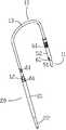
- Figure 1is a perspective view of the present invention.
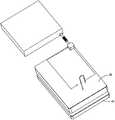
- Figure 2is a schematic perspective view of the working state of the present invention.
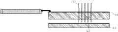
- Figure 3is a schematic cross-sectional view showing the working state of the present invention.
- a test probe of a detecting deviceincludes a needle cover 10 and a probe 20, wherein the needle cover 10 includes a first connecting end 11, a second connecting end 12, and a connecting wire 13, The connection The wire 13 is flexibly connected between the first connecting end 11 and the second connecting end 12, and the probe 20 is inserted on the second connecting end 12.
- the first connection end 11is soldered to the test PCB board 30 and forms a first signal connection area at the location.
- a signal connection areais further disposed on the test PCB board 30. Since the connection wire 13 is flexibly connected between the first connection end 11 and the second connection end 12, when the probe 20 is plugged in When the second connecting end 12 is on, the probe 20 can be inserted into the test PCB board 30 from other signal connecting areas over a long distance and a long span, thereby completing testing of the functional modules on the test board 40 under the test PCB board 30. jobs.
- the first connecting end 11includes a first post pin 51 and a sleeve 52 that is inserted into the lower end of the sleeve 52.
- One end of the connecting wire 13is inserted into the upper end portion of the sleeve 52.
- the second connecting end 12is connected to the other end of the connecting wire 13, and the second connecting end 12 is a column pin.
- the probe 20includes a needle sleeve 21 and a needle 22, wherein the needle 22 is inserted into a lower end portion of the needle sleeve 21, and the second connection end 12 is inserted at an upper end portion of the needle sleeve 21.
- the connection position of the second connecting end 12 and the needle sleeve 21is respectively provided with a latching position 61, so that the respective portions are tightly connected.
Landscapes
- Physics & Mathematics (AREA)
- General Physics & Mathematics (AREA)
- Measuring Leads Or Probes (AREA)
Abstract
Description
Translated fromChinese本发明涉及一种测试探针,特别是指一种包括针套以及探针,其中,该针套包括第一连接端、第二连接端以及连接导线,该连接导线柔性连接在该第一连接端与该第二连接端之间的测试探针。The present invention relates to a test probe, and more particularly to a needle cover and a probe, wherein the needle cover includes a first connection end, a second connection end, and a connecting wire, and the connecting wire is flexibly connected to the first connection A test probe between the end and the second connection.
目前各种数码数字产品已经很普遍的被适用在了人们的生产、生活中了,就一般的数码数字产品而言,其内部一般都设置有多种电子功能模块,在具体工作的时候,若干电子功能模块通电工作以使相关产品能够实现特定的功能,比如,移动手机中一般包括有信号接收模块、信号发射模块、控制模块等等,而在具体实践中,数码数字产品中各个模块的工作状态、产品质量往往能够决定整体产品的产品品质,在生产制造的过程中对相关功能模块进行测试就成为了保障产品质量的有效手段。At present, various digital and digital products have been widely used in people's production and life. As far as general digital digital products are concerned, various electronic functional modules are generally installed inside. In specific work, several The electronic function module is energized to enable the related products to implement specific functions. For example, the mobile phone generally includes a signal receiving module, a signal transmitting module, a control module, etc., and in specific practice, the work of each module in the digital digital product The state and product quality can often determine the product quality of the whole product. Testing the relevant functional modules in the process of manufacturing has become an effective means to ensure product quality.
就目前市面上出现的测试功能模块的治具而言其一般包括测试板以及测试电路板,在工作的时候,需要将被检测的模块放置在测试板中,测试电路板上焊接有固定测试探针,当测试探针接触测试板上对应位置后被检测的模块的信号通过测试电路板传送到测试仪器中以完成测试,但是这种测试治具在具体使用的时候还存在着诸多的缺点现在分述如下:首先,其同一根测试探针无法实现转接多种测试信号,其次,其针套较长,针套先焊接在PCB板上时,焊锡渗入到针套里面,堵塞了针套,导致探针插入的时候无法到底,导致探针高低不平,在针套焊锡固定后,无法灵活转接到PCB板上其他位置的针点,测试探针的密集导致了PCB板位置空间的不足以及电子走线空间的不足,而此是为现有技术的主要缺点。As far as the fixtures of the test function modules appearing on the market currently, the test board and the test circuit board are generally included. When working, the module to be tested needs to be placed in the test board, and the test circuit board is soldered with a fixed test probe. The needle, when the test probe contacts the corresponding position on the test board, the signal of the detected module is transmitted to the test instrument through the test circuit board to complete the test, but the test fixture has many shortcomings in the specific use. The description is as follows: First, the same test probe cannot be used.Now, a variety of test signals are transferred. Secondly, the needle sleeve is long. When the needle sleeve is first welded on the PCB board, the solder penetrates into the needle sleeve and blocks the needle sleeve, which causes the probe to be inserted into the end, resulting in the probe. Uneven, after the needle sleeve solder is fixed, it cannot be flexibly transferred to the pin point at other positions on the PCB. The intensive test probe leads to the shortage of the PCB board space and the shortage of the electronic wiring space. There are major drawbacks to the technology.
发明内容Summary of the invention
本发明提供一种检测装置的测试探针,其探针部分能够自由长距离大跨度移动,从而支持多个点为的测试工作,方便测试人员检测,而此为本发明的主要目的。The invention provides a test probe of a detecting device, wherein the probe portion can move freely over a long distance and a large span, thereby supporting a plurality of test operations for the tester, which is the main purpose of the present invention.
本发明所采取的技术方案是:一种检测装置的测试探针,其包括针套以及探针,其中,该针套包括第一连接端、第二连接端以及连接导线,该连接导线柔性连接在该第一连接端与该第二连接端之间,该探针插接在该第二连接端上,在具体实施的时候,该第一连接端焊接在测试PCB板上,并在该位置形成第一信号连接区域,在该测试PCB板上还设置有其他信号连接区域,由于该连接导线是柔性连接在该第一连接端与该第二连接端之间的,所以当该探针插接在该第二连接端上的时候,该探针能够长距离大跨度的从其他信号连接区域处插入该测试PCB板,从而完成对该测试PCB板下方测试板上功能模块的测试工作。The technical solution adopted by the present invention is: a test probe of a detecting device, comprising a needle sleeve and a probe, wherein the needle sleeve comprises a first connecting end, a second connecting end and a connecting wire, and the connecting wire is flexibly connected Between the first connection end and the second connection end, the probe is inserted on the second connection end. In a specific implementation, the first connection end is soldered on the test PCB board, and at the position Forming a first signal connection region, and another signal connection region is further disposed on the test PCB. Since the connection wire is flexibly connected between the first connection end and the second connection end, when the probe is inserted When connected to the second connection end, the probe can be inserted into the test PCB board from other signal connection areas over a long distance and a long span, thereby completing the test of the function module on the test board under the test PCB board.
该第一连接端包括第一柱子针以及套筒,该第一柱子针插设在该套筒下端部,该连接导线一端插设在该套筒的上端部,该第二连接端连接在该连接导线的另外一端,该第二连接端为一柱子针,该探针包括针套以及针头,其中,该针头插设在该针套的下端部,该第二连接端插设在该针套的上端部,在具体实施的时候,该第一柱子针与该套筒的连接位置、该连接导线与该套筒的连接位置、该第二连接端与该连接导线的连接位置、该第二连接端与该针套的连接位置分别设置有卡位,从而使各个部分紧密连接。The first connecting end includes a first post pin and a sleeve, the first post pin is inserted at a lower end of the sleeve, and one end of the connecting wire is inserted at an upper end of the sleeve, and the second connecting end is connected to the Connecting the other end of the wire, the second connecting end is a column needle, the probe includes a needle sleeve and a needle, whereina needle is inserted in a lower end portion of the needle sleeve, and the second connecting end is inserted in an upper end portion of the needle sleeve. In a specific implementation, a connection position of the first column needle and the sleeve, the connecting wire and the The connecting position of the sleeve, the connecting position of the second connecting end and the connecting wire, and the connecting position of the second connecting end and the needle sleeve are respectively provided with a latching position, so that the respective portions are tightly connected.
本发明的有益效果为:本发明的的针套分两部分,其中一部分带软线连接,可以自由与另外一部分针套连接,PCB板上的焊锡位置点位置可以自由选择位置,使同一根测试探针能够实现转接多种测试信号,本发明能够完全杜绝焊锡渗漏的问题,因为本发明中,针套并无内孔从而避免渗锡情况的发生,本发明的针套与PCB板焊锡处没有渗透孔的结构,另外本发明能够给电子线路布局走线提供充足的空间,因为本发明中,PCB板焊锡位置可以自由选择位置,灵活转接到PCB板上其他位置针点。The beneficial effects of the invention are as follows: the needle sleeve of the invention is divided into two parts, wherein a part of the needle sleeve is connected with a soft wire, and can be freely connected with another part of the needle sleeve, and the position of the soldering position on the PCB board can be freely selected to make the same test. The probe can realize the transfer of a plurality of test signals, and the invention can completely eliminate the problem of solder leakage, because in the present invention, the needle sleeve has no inner hole to avoid the occurrence of tin-plating, and the needle sleeve and the PCB board of the present invention are soldered. The structure has no perforation holes, and the present invention can provide sufficient space for the electronic circuit layout traces. Because of the present invention, the soldering position of the PCB board can be freely selected and flexibly transferred to other pin points on the PCB.
图1为本发明的立体示意图。Figure 1 is a perspective view of the present invention.
图2为本发明的工作状态的立体示意图。Figure 2 is a schematic perspective view of the working state of the present invention.
图3为本发明的工作状态的剖面结构示意图。Figure 3 is a schematic cross-sectional view showing the working state of the present invention.
如图1至3所示,一种检测装置的测试探针,其包括针套10以及探针20,其中,该针套10包括第一连接端11、第二连接端12以及连接导线13,该连接导线13柔性连接在该第一连接端11与该第二连接端12之间,该探针20插接在该第二连接端12上。As shown in FIGS. 1 to 3, a test probe of a detecting device includes a
在具体实施的时候,该第一连接端11焊接在测试PCB板30上,并在该位置形成第一信号连接区域。In a specific implementation, the
在该测试PCB板30上还设置有其他信号连接区域,由于该连接导线13是柔性连接在该第一连接端11与该第二连接端12之间的,所以当该探针20插接在该第二连接端12上的时候,该探针20能够长距离大跨度的从其他信号连接区域处插入该测试PCB板30,从而完成对该测试PCB板30下方测试板40上功能模块的测试工作。Further, a signal connection area is further disposed on the
该第一连接端11包括第一柱子针51以及套筒52,该第一柱子针51插设在该套筒52下端部。The first connecting
该连接导线13一端插设在该套筒52的上端部。One end of the connecting
该第二连接端12连接在该连接导线13的另外一端,该第二连接端12为一柱子针。The second connecting
该探针20包括针套21以及针头22,其中,该针头22插设在该针套21的下端部,该第二连接端12插设在该针套21的上端部。The
在具体实施的时候,该第一柱子针51与该套筒52的连接位置、该连接导线13与该套筒52的连接位置、该第二连接端12与该连接导线13的连接位置、该第二连接端12与该针套21的连接位置分别设置有卡位61,从而使各个部分紧密连接。In the specific implementation, the connection position of the
Claims (5)
Translated fromChinesePriority Applications (2)
| Application Number | Priority Date | Filing Date | Title |
|---|---|---|---|
| PCT/CN2016/076760WO2017156779A1 (en) | 2016-03-18 | 2016-03-18 | Test probe of detection apparatus |
| CN201680040155.5ACN108139430A (en) | 2016-03-18 | 2016-03-18 | A kind of test probe of detection device |
Applications Claiming Priority (1)
| Application Number | Priority Date | Filing Date | Title |
|---|---|---|---|
| PCT/CN2016/076760WO2017156779A1 (en) | 2016-03-18 | 2016-03-18 | Test probe of detection apparatus |
Publications (1)
| Publication Number | Publication Date |
|---|---|
| WO2017156779A1true WO2017156779A1 (en) | 2017-09-21 |
Family
ID=59851310
Family Applications (1)
| Application Number | Title | Priority Date | Filing Date |
|---|---|---|---|
| PCT/CN2016/076760CeasedWO2017156779A1 (en) | 2016-03-18 | 2016-03-18 | Test probe of detection apparatus |
Country Status (2)
| Country | Link |
|---|---|
| CN (1) | CN108139430A (en) |
| WO (1) | WO2017156779A1 (en) |
Cited By (2)
| Publication number | Priority date | Publication date | Assignee | Title |
|---|---|---|---|---|
| CN112485565A (en)* | 2020-11-17 | 2021-03-12 | 乐凯特科技铜陵有限公司 | PCB function test device |
| CN116699204A (en)* | 2023-07-13 | 2023-09-05 | 渭南木王智能科技股份有限公司 | Curved double-ended double-action semiconductor test probe |
Citations (6)
| Publication number | Priority date | Publication date | Assignee | Title |
|---|---|---|---|---|
| US4414506A (en)* | 1980-12-30 | 1983-11-08 | Kelley Jack M | Electrical circuit test probe |
| WO2006002163A2 (en)* | 2004-06-21 | 2006-01-05 | William Wayne Maxwell | Method and apparatus for magnetically achieving electrical continuity |
| CN102985833A (en)* | 2010-06-01 | 2013-03-20 | Nts有限公司 | Probe for inspecting electronic component |
| CN204101604U (en)* | 2014-05-27 | 2015-01-14 | 深圳市策维科技有限公司 | A kind of test probe |
| CN204188665U (en)* | 2014-05-27 | 2015-03-04 | 深圳市策维科技有限公司 | A kind of test probe assembly |
| CN204330832U (en)* | 2014-05-27 | 2015-05-13 | 深圳市策维科技有限公司 | A kind of test probe assembly |
Family Cites Families (4)
| Publication number | Priority date | Publication date | Assignee | Title |
|---|---|---|---|---|
| CN201503443U (en)* | 2009-09-30 | 2010-06-09 | 襄樊启创机电科技开发有限公司 | Low-impedance probe |
| CN204205177U (en)* | 2014-11-20 | 2015-03-11 | 深圳市百通先科技有限公司 | A kind of test VGA connector |
| CN105141256B (en)* | 2015-08-20 | 2017-10-27 | 浙江艾能聚光伏科技股份有限公司 | A kind of solar battery sheet tests apparatus test device |
| CN204832273U (en)* | 2015-08-26 | 2015-12-02 | 钟晓华 | Test probes |
- 2016
- 2016-03-18CNCN201680040155.5Apatent/CN108139430A/enactivePending
- 2016-03-18WOPCT/CN2016/076760patent/WO2017156779A1/ennot_activeCeased
Patent Citations (6)
| Publication number | Priority date | Publication date | Assignee | Title |
|---|---|---|---|---|
| US4414506A (en)* | 1980-12-30 | 1983-11-08 | Kelley Jack M | Electrical circuit test probe |
| WO2006002163A2 (en)* | 2004-06-21 | 2006-01-05 | William Wayne Maxwell | Method and apparatus for magnetically achieving electrical continuity |
| CN102985833A (en)* | 2010-06-01 | 2013-03-20 | Nts有限公司 | Probe for inspecting electronic component |
| CN204101604U (en)* | 2014-05-27 | 2015-01-14 | 深圳市策维科技有限公司 | A kind of test probe |
| CN204188665U (en)* | 2014-05-27 | 2015-03-04 | 深圳市策维科技有限公司 | A kind of test probe assembly |
| CN204330832U (en)* | 2014-05-27 | 2015-05-13 | 深圳市策维科技有限公司 | A kind of test probe assembly |
Cited By (3)
| Publication number | Priority date | Publication date | Assignee | Title |
|---|---|---|---|---|
| CN112485565A (en)* | 2020-11-17 | 2021-03-12 | 乐凯特科技铜陵有限公司 | PCB function test device |
| CN112485565B (en)* | 2020-11-17 | 2022-05-03 | 乐凯特科技铜陵有限公司 | PCB function test device |
| CN116699204A (en)* | 2023-07-13 | 2023-09-05 | 渭南木王智能科技股份有限公司 | Curved double-ended double-action semiconductor test probe |
Also Published As
| Publication number | Publication date |
|---|---|
| CN108139430A (en) | 2018-06-08 |
Similar Documents
| Publication | Publication Date | Title |
|---|---|---|
| CN212967612U (en) | Wafer detection system and wafer detection equipment | |
| US20150168454A1 (en) | Probe module | |
| TW202113381A (en) | Testing device for testing chip | |
| WO2017156779A1 (en) | Test probe of detection apparatus | |
| US10101362B2 (en) | Probe module with high stability | |
| CN107850625B (en) | Radio frequency detection device | |
| CN106535467A (en) | An easy-to-locate stamp hole PCB board | |
| US20090002002A1 (en) | Electrical Testing System | |
| TWI503554B (en) | Probe card and manufacturing method thereof | |
| CN106226675A (en) | Pcb board opens short-circuit detecting frock | |
| CN206330995U (en) | Improved structure of wafer test needle seat | |
| CN106771831B (en) | Automatic detection mechanism for connectors with various pin heights | |
| CN203894282U (en) | Signal switching structure of probe type detection device | |
| KR101350793B1 (en) | Jig for testing open/short of printed circuit board | |
| CN104270884B (en) | A kind of printed circuit board (PCB) and intelligent terminal | |
| TWI385391B (en) | Testing apparatus providing high efficiency and high accuracy | |
| CN221351666U (en) | Testing device of printed circuit board and electronic equipment | |
| CN113359005B (en) | Clamp and method for testing pin points of PCBA (printed circuit board assembly) | |
| KR100950446B1 (en) | Space transformer with PCC and probe card including the same | |
| CN101308162A (en) | Piercing type probe and method for testing packaging body by using same | |
| KR100654492B1 (en) | Seesaw probe unit with inspection socket suitable for slide contact | |
| KR102044185B1 (en) | Circuit board or program test system | |
| CN110470971A (en) | A kind of SPI measuring fixture and method for measurement | |
| TWM575865U (en) | Test fixture adapter structure | |
| TWM564253U (en) | Probe inspection device with capacitance effect |
Legal Events
| Date | Code | Title | Description |
|---|---|---|---|
| NENP | Non-entry into the national phase | Ref country code:DE | |
| 121 | Ep: the epo has been informed by wipo that ep was designated in this application | Ref document number:16893944 Country of ref document:EP Kind code of ref document:A1 | |
| 122 | Ep: pct application non-entry in european phase | Ref document number:16893944 Country of ref document:EP Kind code of ref document:A1 |