WO2017140118A1 - Array camera module, molded photosensitive component and circuit board component of same, manufacturing method therefor, and electronic device - Google Patents
Array camera module, molded photosensitive component and circuit board component of same, manufacturing method therefor, and electronic deviceDownload PDFInfo
- Publication number
- WO2017140118A1 WO2017140118A1PCT/CN2016/103250CN2016103250WWO2017140118A1WO 2017140118 A1WO2017140118 A1WO 2017140118A1CN 2016103250 WCN2016103250 WCN 2016103250WWO 2017140118 A1WO2017140118 A1WO 2017140118A1
- Authority
- WO
- WIPO (PCT)
- Prior art keywords
- circuit board
- camera module
- photosensitive
- array camera
- wiring board
- Prior art date
- Legal status (The legal status is an assumption and is not a legal conclusion. Google has not performed a legal analysis and makes no representation as to the accuracy of the status listed.)
- Ceased
Links
Images


Classifications
- G—PHYSICS
- G03—PHOTOGRAPHY; CINEMATOGRAPHY; ANALOGOUS TECHNIQUES USING WAVES OTHER THAN OPTICAL WAVES; ELECTROGRAPHY; HOLOGRAPHY
- G03B—APPARATUS OR ARRANGEMENTS FOR TAKING PHOTOGRAPHS OR FOR PROJECTING OR VIEWING THEM; APPARATUS OR ARRANGEMENTS EMPLOYING ANALOGOUS TECHNIQUES USING WAVES OTHER THAN OPTICAL WAVES; ACCESSORIES THEREFOR
- G03B17/00—Details of cameras or camera bodies; Accessories therefor
- G03B17/02—Bodies
- G03B17/12—Bodies with means for supporting objectives, supplementary lenses, filters, masks, or turrets
- G—PHYSICS
- G03—PHOTOGRAPHY; CINEMATOGRAPHY; ANALOGOUS TECHNIQUES USING WAVES OTHER THAN OPTICAL WAVES; ELECTROGRAPHY; HOLOGRAPHY
- G03B—APPARATUS OR ARRANGEMENTS FOR TAKING PHOTOGRAPHS OR FOR PROJECTING OR VIEWING THEM; APPARATUS OR ARRANGEMENTS EMPLOYING ANALOGOUS TECHNIQUES USING WAVES OTHER THAN OPTICAL WAVES; ACCESSORIES THEREFOR
- G03B17/00—Details of cameras or camera bodies; Accessories therefor
- G03B17/02—Bodies
- G—PHYSICS
- G03—PHOTOGRAPHY; CINEMATOGRAPHY; ANALOGOUS TECHNIQUES USING WAVES OTHER THAN OPTICAL WAVES; ELECTROGRAPHY; HOLOGRAPHY
- G03B—APPARATUS OR ARRANGEMENTS FOR TAKING PHOTOGRAPHS OR FOR PROJECTING OR VIEWING THEM; APPARATUS OR ARRANGEMENTS EMPLOYING ANALOGOUS TECHNIQUES USING WAVES OTHER THAN OPTICAL WAVES; ACCESSORIES THEREFOR
- G03B19/00—Cameras
- G03B19/02—Still-picture cameras
- G03B19/023—Multi-image cameras
- H—ELECTRICITY
- H04—ELECTRIC COMMUNICATION TECHNIQUE
- H04N—PICTORIAL COMMUNICATION, e.g. TELEVISION
- H04N23/00—Cameras or camera modules comprising electronic image sensors; Control thereof
- H04N23/45—Cameras or camera modules comprising electronic image sensors; Control thereof for generating image signals from two or more image sensors being of different type or operating in different modes, e.g. with a CMOS sensor for moving images in combination with a charge-coupled device [CCD] for still images
- H—ELECTRICITY
- H04—ELECTRIC COMMUNICATION TECHNIQUE
- H04N—PICTORIAL COMMUNICATION, e.g. TELEVISION
- H04N23/00—Cameras or camera modules comprising electronic image sensors; Control thereof
- H04N23/50—Constructional details
- H04N23/55—Optical parts specially adapted for electronic image sensors; Mounting thereof
- H—ELECTRICITY
- H10—SEMICONDUCTOR DEVICES; ELECTRIC SOLID-STATE DEVICES NOT OTHERWISE PROVIDED FOR
- H10F—INORGANIC SEMICONDUCTOR DEVICES SENSITIVE TO INFRARED RADIATION, LIGHT, ELECTROMAGNETIC RADIATION OF SHORTER WAVELENGTH OR CORPUSCULAR RADIATION
- H10F39/00—Integrated devices, or assemblies of multiple devices, comprising at least one element covered by group H10F30/00, e.g. radiation detectors comprising photodiode arrays
- H10F39/80—Constructional details of image sensors
- H10F39/804—Containers or encapsulations
- F—MECHANICAL ENGINEERING; LIGHTING; HEATING; WEAPONS; BLASTING
- F16—ENGINEERING ELEMENTS AND UNITS; GENERAL MEASURES FOR PRODUCING AND MAINTAINING EFFECTIVE FUNCTIONING OF MACHINES OR INSTALLATIONS; THERMAL INSULATION IN GENERAL
- F16M—FRAMES, CASINGS OR BEDS OF ENGINES, MACHINES OR APPARATUS, NOT SPECIFIC TO ENGINES, MACHINES OR APPARATUS PROVIDED FOR ELSEWHERE; STANDS; SUPPORTS
- F16M11/00—Stands or trestles as supports for apparatus or articles placed thereon ; Stands for scientific apparatus such as gravitational force meters
- F16M11/02—Heads
- F16M11/04—Means for attachment of apparatus; Means allowing adjustment of the apparatus relatively to the stand
- F16M11/041—Allowing quick release of the apparatus
- F—MECHANICAL ENGINEERING; LIGHTING; HEATING; WEAPONS; BLASTING
- F16—ENGINEERING ELEMENTS AND UNITS; GENERAL MEASURES FOR PRODUCING AND MAINTAINING EFFECTIVE FUNCTIONING OF MACHINES OR INSTALLATIONS; THERMAL INSULATION IN GENERAL
- F16M—FRAMES, CASINGS OR BEDS OF ENGINES, MACHINES OR APPARATUS, NOT SPECIFIC TO ENGINES, MACHINES OR APPARATUS PROVIDED FOR ELSEWHERE; STANDS; SUPPORTS
- F16M11/00—Stands or trestles as supports for apparatus or articles placed thereon ; Stands for scientific apparatus such as gravitational force meters
- F16M11/02—Heads
- F16M11/04—Means for attachment of apparatus; Means allowing adjustment of the apparatus relatively to the stand
- F16M11/06—Means for attachment of apparatus; Means allowing adjustment of the apparatus relatively to the stand allowing pivoting
- F16M11/10—Means for attachment of apparatus; Means allowing adjustment of the apparatus relatively to the stand allowing pivoting around a horizontal axis
- F—MECHANICAL ENGINEERING; LIGHTING; HEATING; WEAPONS; BLASTING
- F16—ENGINEERING ELEMENTS AND UNITS; GENERAL MEASURES FOR PRODUCING AND MAINTAINING EFFECTIVE FUNCTIONING OF MACHINES OR INSTALLATIONS; THERMAL INSULATION IN GENERAL
- F16M—FRAMES, CASINGS OR BEDS OF ENGINES, MACHINES OR APPARATUS, NOT SPECIFIC TO ENGINES, MACHINES OR APPARATUS PROVIDED FOR ELSEWHERE; STANDS; SUPPORTS
- F16M13/00—Other supports for positioning apparatus or articles; Means for steadying hand-held apparatus or articles
- G—PHYSICS
- G03—PHOTOGRAPHY; CINEMATOGRAPHY; ANALOGOUS TECHNIQUES USING WAVES OTHER THAN OPTICAL WAVES; ELECTROGRAPHY; HOLOGRAPHY
- G03B—APPARATUS OR ARRANGEMENTS FOR TAKING PHOTOGRAPHS OR FOR PROJECTING OR VIEWING THEM; APPARATUS OR ARRANGEMENTS EMPLOYING ANALOGOUS TECHNIQUES USING WAVES OTHER THAN OPTICAL WAVES; ACCESSORIES THEREFOR
- G03B17/00—Details of cameras or camera bodies; Accessories therefor
- G03B17/56—Accessories
- H—ELECTRICITY
- H10—SEMICONDUCTOR DEVICES; ELECTRIC SOLID-STATE DEVICES NOT OTHERWISE PROVIDED FOR
- H10F—INORGANIC SEMICONDUCTOR DEVICES SENSITIVE TO INFRARED RADIATION, LIGHT, ELECTROMAGNETIC RADIATION OF SHORTER WAVELENGTH OR CORPUSCULAR RADIATION
- H10F39/00—Integrated devices, or assemblies of multiple devices, comprising at least one element covered by group H10F30/00, e.g. radiation detectors comprising photodiode arrays
- H10F39/80—Constructional details of image sensors
- H10F39/806—Optical elements or arrangements associated with the image sensors
Definitions
- the present inventionrelates to the field of camera modules, and further relates to an array camera module and a molded photosensitive member thereof, a circuit board assembly and a manufacturing method thereof, and an electronic device.
- a camera module with more than one lenssuch as a dual-lens camera module.
- the dual-lens camera moduleprovides a way of simulating the human eye structure, and the dual-lens camera module is in 3D shooting. With scanning, gesture position recognition, color fidelity, fast focus, panoramic deep shooting, background blur shooting and many other aspects have better performance than single-lens camera module, therefore, the camera module with more than one lens is the future The important direction of the development of the camera module industry.
- the dual-lens camera moduleobtains images from two locations by using two imaging modules with spatial differences, and then separately photographs the two imaging modules according to the image synthesis method.
- the final image of the multi-lens camera moduleis obtained. It can be understood that, in this process, the consistency of the image effects such as the resolution, shading, and color of each imaging module of the multi-lens camera module, and the deviation values in the horizontal, vertical, and longitudinal directions are measured. An important indicator of the imaging quality of the dual lens camera module.
- FIG. 1Aillustrates a prior art dual lens camera module including a circuit board 10P, two mirror mounts 20P, two imaging modules 30P, and a bracket 40P.
- Each of the imaging modules 30Pincludes a motor lens assembly 31P. .
- Each of the mirror mounts 20Pis separately located on the same side of the wiring board 10P, and each of the mirror mounts 20P is connected together by the wiring board 10P, and each of the motor lens assemblies 31P is disposed at each The lens holder 20P is supported by each of the lens holders 20P, and the holder 40P is wrapped around the outside of each of the motor lens assemblies 31P.
- the lens holder 20Pmay also be a unitary structure, that is, each of the motor lens assemblies 31P may be disposed on the lens holder 20P. different positions.
- each of the lens holders 20Pis separately mounted on the circuit board 10P, thereby causing each The size, position, and the like between the mirror holders 20P are difficult to control, so that the consistency of parameters such as size and position between each of the two-lens camera module brackets is poor.
- each of the lens holders 20Pis independent, and each of the lens holders 20P is only passed through the circuit board 10P.
- the circuit board 10Psince the circuit board 10P usually selects a PCB circuit board, so that the circuit board 10P itself is relatively soft and easily deformed, at this time, the overall rigidity of the dual lens camera module is difficult to ensure, when the double lens
- Such a structureis liable to cause relative dimensional instability, positional tolerance, and each of the various components of the imaging module 30P, such as the motor lens assembly 31P, during use after the camera module is assembled.
- the optical axis of the imaging module 30Pis easily deviated from the preset position and the like. Once any of these conditions occur, the imaging quality of the dual-lens camera module, such as image synthesis, may not be brought to the final imaging effect. Control factors or larger adverse effects.
- the outer side of the 31Pwraps the bracket 40P, and it is necessary to fill the glue between the motor lens assembly 31P and the bracket 40P, resulting in a further increase in the size of the dual lens camera module.
- the assembly of the multi-lens camera moduleis based on a conventional COB (Chip On Board) process
- the circuit board 10Pusually has a protruding circuit device 11P, and a photosensitive chip 12P is mounted on the circuit board.
- the photosensitive chip 12Pis usually connected to the wiring board 10P through a gold wire 121P, and the gold wire 121P is generally curved and protruded from the wiring board main body, and therefore, the protruding circuit device 11P and The gold wire 121P also brings some disadvantages to the assembly of the camera module.
- the circuit device 11P and the gold wire 121Pare directly exposed to the surface of the circuit board 10P, so that in the subsequent assembly process, for example, the process of attaching the lens holder 20P and soldering the motor lens assembly 31P is inevitable.
- the solder resist, dust, and the like at the time of solderingare likely to adhere to the circuit device 11P, and the circuit device 11P and the photo sensor chip 12P are located in a space in which the mutual contact is made, so that dust contaminants are easily affected.
- the photosensitive chip 12Psuch an effect may cause undesirable phenomena such as black spots on the assembled camera module, and the product yield is lowered.
- the lens holder 20Pis located outside the circuit device 11P. Therefore, when the lens holder 20P and the circuit board 10P are mounted, a certain reservation between the lens holder 20P and the circuit device 11P is required.
- the safety distance and the safety distanceneed to be reserved in the horizontal direction and the upward direction, which increases the thickness of the camera module to a certain extent, making it difficult to reduce the thickness.
- the molding of a multi-camera relative to the molding of a single camerainvolves coordination problems between a plurality of camera modules, and the optical axes are required to be uniform between the plurality of lenses, and the optical axes of the plurality of lenses based on the conventional COB process are Consistency is hard to secure.
- the overall size of the multi-camera moduleis relatively large, which is more sensitive to the strength and flatness of the circuit board, so the thickness of the circuit board is large.
- An object of the present inventionis to provide an array camera module and a molded photosensitive member thereof, a circuit board assembly and a manufacturing method thereof, and an electronic device, wherein the circuit board assembly includes a joint package portion and a circuit board portion, and the connection The body package portion is packaged and formed on the circuit board portion, and the body package portion is adapted to correspond to a plurality of optical lenses.
- An object of the present inventionis to provide an array camera module and a molded photosensitive member thereof, a circuit board assembly and a manufacturing method thereof, and an electronic device, wherein the circuit board assembly includes a circuit board and at least one electronic component, the electronic component The device protrudes from the circuit board, and the electronic component is covered by the joint package so as not to be directly exposed to the outside.
- An object of the present inventionis to provide an array camera module and a molded photosensitive member thereof, a circuit board assembly and a manufacturing method thereof, and an electronic device, wherein the electronic component is covered by the joint package portion, thereby There is no need to reserve a safety distance between the component and the connected package portion. In this way, the size of the array camera module can be further reduced, so that the array camera module can be further developed in a lighter and thinner direction. .
- An object of the present inventionis to provide an array camera module and a molded photosensitive member thereof, a circuit board assembly and a manufacturing method thereof, and an electronic device, wherein the electronic component is covered by the joint package portion, thereby The connected package portion isolates the adjacent electronic components to avoid mutual interference between the adjacent electronic components, thereby ensuring imaging quality of the array camera module.
- An object of the present inventionis to provide an array camera module and a molded photosensitive member thereof, a circuit board assembly and a manufacturing method thereof, and an electronic device, wherein the electronic component is covered by the joint package portion, thereby even adjacent The distance between the electronic components is further reduced, and the connected package portion can also ensure that adjacent electronic components do not interfere with each other, so that the circuit board can be mounted on a limited area.
- a large size and a greater number of the electronic componentsare used to improve the imaging quality of the array camera module.
- An object of the present inventionis to provide an array camera module and a molded photosensitive member thereof, a circuit board assembly and a manufacturing method thereof, and an electronic device, wherein the electronic component is covered by the joint package portion, thereby The joint encapsulation portion isolates the electronic component from the air to prevent oxidation of the metal portion of the electronic component due to prolonged contact with air, thereby ensuring stability and reliability of the array camera module.
- An object of the present inventionis to provide an array camera module, a molded photosensitive member thereof, a circuit board assembly, and a manufacturing method thereof.
- An electronic devicewherein the array camera module includes a plurality of photosensitive elements, and the connected package surrounds an outer side of each of the photosensitive elements.
- An object of the present inventionis to provide an array camera module and a molded photosensitive member thereof, a circuit board assembly and a manufacturing method thereof, and an electronic device, wherein the joint package portion includes a filter mounting portion suitable for mounting a plurality of filters Light components, thus eliminating the need for additional separate support components.
- An object of the present inventionis to provide an array camera module, a molded photosensitive member thereof, a circuit board assembly and a manufacturing method thereof, and an electronic device, wherein the circuit board has a plurality of inner grooves, and each of the photosensitive members is disposed at In the inner groove, in order to reduce the relative height of the photosensitive element and the circuit board, even the surface of the photosensitive element and the surface of the circuit board are in the same plane, thereby reducing the joint The height requirements of the package.
- An object of the present inventionis to provide an array camera module and a molded photosensitive member thereof, a circuit board assembly and a manufacturing method thereof, and an electronic device, wherein the circuit board has a plurality of vias and a plurality of outer grooves, the outer grooves In communication with the passage, the outer groove is adapted to flip mount the photosensitive element.
- An object of the present inventionis to provide an array camera module, a molded photosensitive member thereof, a circuit board assembly and a manufacturing method thereof, and an electronic device, wherein the circuit board portion includes a reinforcing layer, and the reinforcing laminated layer is disposed on the The bottom of the circuit board to enhance the structural strength and heat dissipation performance of the circuit board.
- An object of the present inventionis to provide an array camera module, a molded photosensitive member thereof, a circuit board assembly and a manufacturing method thereof, and an electronic device, wherein the circuit board has at least one reinforcing hole, and the connected package portion is extended during molding The reinforcing holes are entered and held in the reinforcing holes after molding, thereby enhancing the structural strength of the circuit board.
- An object of the present inventionis to provide an array camera module and a molded photosensitive member thereof, a circuit board assembly and a manufacturing method thereof, and an electronic device, wherein the connected package portion includes a lens mounting portion adapted to mount a plurality of optical lenses. Thereby providing a mounting position for the optical lens.
- An object of the present inventionis to provide an array camera module and a molded photosensitive member thereof, a circuit board assembly and a manufacturing method thereof, and an electronic device, wherein the joint package portion is integrally combined with the circuit board during molding, thereby There is no need to reserve a position of filling glue between the connected package portion and the circuit board to further reduce the height dimension of the array camera module.
- An object of the present inventionis to provide an array camera module and a molded photosensitive member thereof, a circuit board assembly and a manufacturing method thereof, and an electronic device, wherein the joint package portion is integrally combined with the circuit board during molding, thereby being fabricated
- the joint package portionis integrally combined with the circuit board during molding, thereby being fabricated
- An object of the present inventionis to provide an array camera module and a molded photosensitive member thereof, a circuit board assembly and a manufacturing method thereof, and an electronic device, wherein the joint package portion and the circuit board are integrally combined so as to be on the circuit board After the component is formed, the connected package and the circuit board have better flatness, which is beneficial to improving the product yield of the array camera module and improving the imaging quality of the array camera module.
- An object of the present inventionis to provide an array camera module and a molded photosensitive member thereof, a circuit board assembly and a manufacturing method thereof, and an electronic device, wherein the joint package portion forms a molded base, wherein the molded base
- the top surfaceforms at least one blocking protrusion for preventing connection of the driver or the lens barrel and the mounting body when assembling a driver or a lens barrel to the top surface of the molding base
- the glue of the top surface of the molded baseenters the light window of the molded base to contaminate the photosensitive path of the photosensitive element, thereby facilitating the improvement of the product yield of the array camera module and the improvement of the array imaging.
- the imaging quality of the moduleis to provide an array camera module and a molded photosensitive member thereof, a circuit board assembly and a manufacturing method thereof, and an electronic device, wherein the joint package portion forms a molded base, wherein the molded base
- the top surfaceforms at least one blocking protrusion for preventing connection of the driver or the lens barrel and the mounting
- the inventionprovides a circuit board assembly of an array camera module, comprising:
- circuit board portionincludes a circuit board for electrically connecting at least two photosensitive elements of the array camera module
- a one-piece package portionwherein the joint package portion is integrally packaged on the circuit board of the circuit board portion.
- the conjoined package portionforms at least two light windows, each of the light windows being opposite to each of the photosensitive elements to provide a light path of the photosensitive element.
- the top end of the connected package portionis planar for mounting a support member, an optical lens, a driver or a filter element of the array camera module.
- the top end of the connected packagehas at least two mounting slots, and each of the mounting slots is connected to the corresponding light window for respectively mounting a support member of the array camera module, Filter element, optical lens or driver.
- the connected package portionincludes a covering portion, a filter element mounting portion and an optical lens mounting portion, and the filter element mounting portion and the optical lens mounting portion are sequentially
- the covering sectionis upwardly molded and extended, and the inside is stepped to facilitate mounting of the filter element and the optical lens of the array camera module.
- the filter element mounting sectionhas at least two mounting slots, each of the mounting slots being connected to the corresponding light window to form the stepped first step to facilitate mounting a filter element
- the optical lens mounting sectionhas at least two optical lens mounting slots, each of the optical lens mounting slots being connected to the corresponding light window to form the second step of the stepped shape to facilitate mounting the array The optical lens of the camera module.
- the optical lens mounting sectionhas at least two optical lens inner walls, and each of the optical lens inner wall surfaces is flat to be adapted to mount the optical lens without threads.
- the circuit board portionincludes at least one electronic component, the electronic component protrudes from the circuit board, and the connected package portion covers the electronic component to enable The electronic components are not directly exposed to the outside.
- the electronic componentselects a combination of one or more of a resistor, a capacitor, a diode, a triode, a potentiometer, a relay, and a processor.
- the circuit board portionincludes a reinforcement layer, and the reinforcement laminate layer is disposed at the bottom of the circuit board to enhance the structural strength of the circuit board.
- the reinforcing layeris a metal plate to enhance heat dissipation performance of the circuit board portion.
- the circuit board portionincludes a shielding layer that wraps the circuit board and the joint package portion to enhance electromagnetic interference resistance of the circuit board assembly.
- the shielding layeris a metal plate or a metal mesh.
- the wiring boardhas at least one reinforcing hole, and the connected package portion extends into the reinforcing hole to enhance the structural strength of the circuit board.
- the reinforcing holesare in the shape of a groove.
- the reinforcing holesare perforated such that the molding material of the joint package portion is in sufficient contact with the wiring board and is easy to manufacture.
- the wiring boardhas at least two passages adapted to be mounted to the wiring board from the back side of the wiring board.
- the passageis stepped to provide a stable mounting position for the photosensitive element.
- the material of the wiring boardmay be selected from a combination: a soft and hard bonding board, a ceramic substrate, a PCB hard board or an FPC.
- the material of the joint packageis selected from the group consisting of one or more of epoxy, nylon, LCP or PP.
- the circuit board assemblyincludes at least two motor connection structures, the motor connection structure includes at least one connection line, the connection line is disposed on the joint package portion, and is electrically connected to the
- the circuit boardhas a motor connection end exposed in the joint package portion for facilitating connection of a motor pin.
- the circuit board assemblyincludes at least two motor connection structures, each of the motor connections
- the structureincludes at least one connecting line and at least one lead slot, the connecting line is disposed on the connected package portion and electrically connected to the circuit board, and the lead slot is disposed in the connected package
- the upper end portion, the connecting wirehas a motor connecting end, and the motor connecting end is exposed on the bottom wall of the slot, so as to be electrically connected to the motor connecting end when a motor pin is inserted into the pin slot .
- the circuit board assemblyincludes at least two motor connection structures, each of the motor connection structures having at least one lead slot and at least one circuit contact, the circuit contacts being electrically connected to the circuit board,
- the lead slotis disposed in the connected package portion, and extends from the circuit board to a top end of the connected package portion, and the circuit contact is exposed in the lead slot to facilitate a motor pin When plugged into the pin slot, it is electrically connected to the circuit contact.
- the circuit board assemblyincludes at least two motor connection structures, each of the motor connection structures includes at least one engraving line, and the engraving line is disposed at the conjoined package portion, electrically connected to the A circuit board to electrically connect a motor pin.
- the engraving lineis disposed in the joint package portion by laser molding.
- the present inventionfurther provides a method of manufacturing a circuit board assembly of an array camera module, comprising the steps of: integrally packaging a package portion on a circuit board.
- the manufacturing methodcomprises the step of forming at least two light windows to the conjoined package.
- the manufacturing methodincludes the step of coating an electronic component protruding from the wiring board through the joint package.
- the manufacturing methodincludes the step of forming at least two mounting grooves at the top end of the connected package portion to facilitate mounting of a support member, a filter element, a driver or an optical lens.
- the manufacturing methodincludes the steps of extending the connected package portion upward and forming a two-step stepped structure inside each of the light windows to facilitate mounting of the filter element or the optical lens.
- the manufacturing methodincludes the step of providing a threaded structure on an inner wall of the light window of the joint package portion to facilitate mounting of the threaded optical lens.
- the manufacturing methodincludes the steps of: providing at least one groove-shaped reinforcing hole on the circuit board, and extending the connected package portion into the reinforcing hole.
- the manufacturing methodincludes the steps of: providing at least one perforated reinforcing hole on the circuit board and extending the connected package portion into the reinforcing hole.
- the manufacturing methodincludes the step of attaching a reinforcement layer to the bottom layer of the circuit board to enhance the structural strength of the circuit board.
- the manufacturing methodincludes the steps of: coating a shielding layer on the wiring board and the joint package portion to enhance electromagnetic interference resistance of the circuit board assembly.
- the manufacturing methodincludes the steps of: embedding a plurality of connecting lines to the connected package, and electrically connecting the connecting lines to facilitate connection of a driver.
- the manufacturing methodincludes the steps of: providing a plurality of pin slots to an upper end of the conjoined package portion, and causing a motor connection end of the connection line to be exposed to the pin slot.
- the manufacturing methodincludes the steps of: providing a plurality of circuit contacts to the circuit board, and providing corresponding pin slots to the package portion such that the circuit contacts are exposed
- the pin slotis configured to electrically connect the motor pin to the circuit contact when the motor pin is inserted into the pin slot.
- the manufacturing methodincludes the steps of: providing a plurality of engraving lines to the conjoined package, the engraving lines being electrically connected to the circuit board to facilitate electrically connecting a driver, respectively.
- the engraving lineis disposed in the joint package portion by laser molding.
- the joint package portionis integrally formed on the circuit board by an injection molding or molding process.
- the present inventionfurther provides an array camera module, including:
- a circuit board assemblywherein the circuit board assembly comprises:
- circuit board portionfor electrically connecting at least two photosensitive elements of the array camera module
- the connected package portionis integrally packaged in the circuit board portion.
- At least two optical lensesAt least two optical lenses
- each of the optical lensesis located in a corresponding photosensitive path of the photosensitive elements, and each of the photosensitive elements is electrically connected to the circuit board assembly.
- the array camera moduleincludes at least one support member, the support member is mounted on the circuit board assembly, and the array camera module includes at least two filter elements, each of the filters A light element is mounted to the support.
- the array camera modulecomprises at least two drivers, each of the optical lenses being mounted to a corresponding one of the drivers, each of the drivers being mounted on the circuit board assembly.
- the array camera moduleincludes at least two filter elements, each of the filter elements being mounted to the circuit board assembly.
- the present inventionfurther provides an array camera module, including:
- At least two optical lensesAt least two optical lenses.
- a molded photosensitive memberwherein the molded photosensitive member further comprises:
- At least two photosensitive elementsAt least two photosensitive elements
- each of the photosensitive elementsis electrically connected to the circuit board
- a molded basewherein the molded base has at least two light windows, and the molded base is integrally coupled with an edge region of the circuit board such that each of the photosensitive elements corresponds to each The light window, wherein each of the optical lenses is disposed on a photosensitive path of each of the photosensitive elements, respectively, for each of the photosensitive elements and each of the optical lenses by each of the optical windows Provide a light path.
- the array camera modulefurther includes at least one filter element, wherein each of the filter elements is respectively held between the optical lens and the photosensitive element.
- each of the filter elementsis separately assembled to a top surface of the molding base such that each of the filter elements is held in each of the optical lenses and each Between the photosensitive elements.
- each of the filter elementsis separately assembled to a lens housing of each of the optical lenses such that each of the filter elements is held in each of the optical lenses and each Between the photosensitive elements.
- the array camera modulefurther includes at least one frame-shaped support member, wherein each of the filter elements is respectively assembled to each of the support members, and each of the support members is respectively The top surface of the molded base is assembled such that each of the filter elements is held between each of the optical lenses and each of the photosensitive elements.
- a top surface of the molded baseforms at least one groove, and each of the grooves is respectively connected to each of the light windows, wherein each of the filter elements is separately accommodated In each of the grooves.
- the surface of the molded baseforms at least one groove, and each of the grooves is respectively connected to each of the light windows, wherein each of the support members is respectively accommodated in each The grooves.
- the molded photosensitive memberfurther includes at least one set of leads, wherein both ends of each of the leads are respectively connected to a chip connector of each of the photosensitive elements and a wiring of the wiring board A board connector such that each of the photosensitive member and the wiring board is turned on.
- the molded photosensitive memberfurther includes at least one electronic component, wherein each of the electronic components is respectively mounted on the wiring board, and the molded base covers at least One of the electronic components.
- the molded basecovers all of the electronic components.
- the molded basefurther includes a substrate, wherein the substrate is overlappedly disposed on the wiring board to keep the wiring board flat by the substrate.
- the circuit boardhas at least one first reinforcing space, and a part of the molded base is formed in each of the first reinforcing spaces of the circuit board to enable the The molded base and the circuit board are integrated.
- the substratehas at least one second reinforcing space, each of the second reinforcing spaces respectively corresponding to each of the first reinforcing spaces of the wiring board, wherein the molding a portion of the pedestal is simultaneously formed on the circuit board Each of the first reinforcing space and each of the second reinforcing spaces of the substrate to integrate the molded base, the wiring board and the substrate.
- the substratecomprises a substrate body and at least two conductive bodies, each of the conductive bodies integrally extending integrally with the substrate body, wherein the circuit board has at least two channels, wherein Substrate bodies are overlappedly disposed on the circuit board body such that each of the conductive bodies is respectively held in each of the channels of the wiring board, wherein each of the photosensitive elements is electrically coupled to each of the electrodes Subject contact.
- each of the conductive bodiesprotrudes from a surface of the wiring board, wherein each of the photosensitive members is attached to each of the conductive bodies.
- the wiring boardhas at least one accommodating space, and each of the photosensitive members is accommodated in each of the accommodating spaces.
- the number of the accommodation spaces of the wiring boardis smaller than the number of the photosensitive elements, so that at least one of the photosensitive elements is accommodated in the accommodation space, and the other photosensitive elements are Mounted on the chip mounting area of the circuit board.
- the accommodation spaceis a receiving groove or a through hole.
- At least one of the photosensitive elementshas a small-sized photosensitive area, and the other photosensitive element has a large-sized photosensitive area.
- the wiring boardhas at least one accommodating space in which the photosensitive member having a small-sized photosensitive area is accommodated in the accommodating space, and the photosensitive member having a large-sized photosensitive area is accommodated in The accommodation space is either attached to the surface of the circuit board.
- the array camera modulefurther includes at least two drivers, wherein each of the optical lenses is separately assembled to each of the drivers, and each of the drivers is separately assembled to the molding a susceptor to each of the optical lenses being held in a photosensitive path of each of the photosensitive elements by each of the drivers.
- the array camera modulefurther includes at least two lens barrels, wherein each of the optical lenses is respectively assembled to each of the lens barrels, and each of the lens barrels is assembled in the same a top surface of the molded base, or each of the barrels integrally extending integrally with a top surface of the molded base, or at least one of the barrels being assembled to a top surface of the molded base And the other lens barrel integrally extends from a top surface of the molding base to each of the optical lenses being respectively held in a photosensitive path of each of the photosensitive elements by each of the lens barrels .
- the array camera modulefurther includes at least one driver and at least one lens barrel, wherein each of the optical lenses is respectively assembled to each of the driver and each of the lens barrels, wherein Each of the drivers is separately assembled to a top surface of the molding base, and each of the barrels is respectively assembled or integrally extended to a top surface of the molding base to each of The driver and each of the barrels each hold a photosensitive path of each of the photosensitive elements.
- a middle portion of a top surface of the molding baseforms at least one blocking protrusion to partition a top surface of the molding base into an inner surface and an outer side by the blocking protrusion a surface, wherein the driver is assembled to the outer side surface of the module base, and the blocking protrusion prevents glue disposed between the driver and the outer side surface from entering the inner side surface.
- the array camera modulefurther includes a bracket, wherein the bracket has at least two installation spaces, and each of the drivers is respectively mounted to each of the installation spaces of the bracket.
- a filleris filled between the outer wall of the driver and the inner wall of the bracket.
- the filleris glue
- the present inventionfurther provides an electronic device comprising:
- At least one array of camera moduleswherein the array camera module is disposed on the electronic device body for acquiring images, wherein the array camera module includes:
- At least two optical lensesAt least two optical lenses.
- a molded photosensitive memberwherein the molded photosensitive member further comprises:
- At least two photosensitive elementsAt least two photosensitive elements
- each of the photosensitive elementsis electrically connected to the circuit board
- a molded basewherein the molded base has at least two light windows, and the molded base is integrally coupled with an edge region of the circuit board such that each of the photosensitive elements corresponds to each The light window, wherein each of the optical lenses is disposed on a photosensitive path of each of the photosensitive elements, respectively, for each of the photosensitive elements and each of the optical lenses by each of the optical windows Provide a light path.
- the length direction of the array camera moduleis consistent with the width direction of the electronic device body, and the array camera module is disposed at a corner or a middle portion of the electronic device body.
- the length direction of the array camera moduleis consistent with the length direction of the electronic device body, and the array camera module is disposed at a corner or a middle portion of the electronic device body.
- the present inventionfurther provides a molded photosensitive member comprising:
- At least two photosensitive elementsAt least two photosensitive elements
- each of the photosensitive elementsis electrically connected to the circuit board
- molded basewherein the molded base has at least two light windows, and the molded base is integrally coupled with an edge region of the circuit board such that each of the photosensitive elements corresponds to each The light window.
- the molded photosensitive memberfurther includes at least one set of leads, wherein both ends of each of the leads are respectively connected to a chip connector of each of the photosensitive elements and a wiring of the wiring board A board connector such that each of the photosensitive member and the wiring board is turned on.
- the wiring boardhas at least one accommodating space, and each of the photosensitive members is accommodated in the accommodating space.
- At least one of the photosensitive elementshas a small-sized photosensitive area, and the other photosensitive element has a large-sized photosensitive area.
- the photosensitive member having a small-sized photosensitive regionis accommodated in the accommodating space, and the photosensitive member having a large-sized photosensitive region is accommodated in the accommodating space or is attached to the The surface of the board.
- the accommodation spaceis a receiving groove or a through hole.
- the molded basefurther includes a substrate, wherein the substrate is overlappedly disposed on the wiring board to keep the wiring board flat by the substrate.
- the circuit boardhas at least one first reinforcing space, and a part of the molded base is formed in each of the first reinforcing spaces of the circuit board to enable the The molded base and the circuit board are integrated.
- the substratehas at least one second reinforcing space, each of the second reinforcing spaces respectively corresponding to each of the first reinforcing spaces of the wiring board, wherein the molding A portion of the pedestal is simultaneously formed in each of the first reinforcing spaces of the wiring board and each of the second reinforcing spaces of the substrate to make the molded pedestal, the wiring board, and
- the substratesare integrated into one body.
- the substratecomprises a substrate body and at least two conductive bodies, each of the conductive bodies integrally extending integrally with the substrate body, wherein the circuit board has at least two channels, wherein Substrate bodies are overlappedly disposed on the substrate body such that each of the conductive bodies is respectively held in each of the channels of the wiring board, wherein each of the photosensitive elements is associated with each of the conductive bodies contact.
- each of the conductive bodiesprotrudes from a surface of the wiring board, wherein each of the photosensitive members is attached to each of the conductive bodies.
- the top surface of the molded baseforms a recess.
- the top surface of the molded baseforms at least one blocking protrusion to divide the top surface of the molded base into an inner side surface and an outer side surface by the blocking protrusion.
- the present inventionfurther provides a method of manufacturing a molded photosensitive member, wherein the manufacturing method comprises the steps of:
- the step (c)is preceded by the step (b) to first electrically connect each of the photosensitive elements and the wiring board, and then form and the line by a molding process.
- the step (b)further comprises the steps of:
- the covering A filmis located between the pressing surface of the upper mold and the wiring board.
- FIGS. 1A and 1Bare schematic cross-sectional views of a prior art dual lens camera module, respectively.
- FIG. 2Ais a cross-sectional view of an array camera module and its circuit board assembly in accordance with a first preferred embodiment of the present invention.
- FIG. 2Bis a cross-sectional view of another array camera module and its circuit board in accordance with a first preferred embodiment of the present invention.
- 3Ais a schematic view showing a manufacturing process of a wiring board assembly according to an embodiment of the first preferred embodiment of the present invention.
- Fig. 3Bis a schematic view showing a manufacturing process of a wiring board assembly according to another embodiment of the first preferred embodiment of the present invention.
- FIG. 4is a schematic view showing a method of manufacturing a circuit board assembly in accordance with a first preferred embodiment of the present invention.
- 5A, 5B and 5Care different embodiments of a motor connection structure of a molded wiring assembly in accordance with a first preferred embodiment of the present invention.
- FIG. 6is a schematic diagram of another array camera module in accordance with a first preferred embodiment of the present invention.
- Figure 7is a cross-sectional view of an array camera module and its circuit board assembly in accordance with a second preferred embodiment of the present invention.
- Figure 8is a cross-sectional view of an array camera module and its circuit board assembly in accordance with a third preferred embodiment of the present invention.
- Figure 9is a cross-sectional view showing an array camera module and its circuit board assembly in accordance with a fourth preferred embodiment of the present invention.
- Figure 10is a cross-sectional view of an array camera module and its circuit board assembly in accordance with a fifth preferred embodiment of the present invention.
- Figure 11is a cross-sectional view of an array camera module and its circuit board assembly in accordance with a sixth preferred embodiment of the present invention.
- Figure 12is a cross-sectional view of an array camera module and its circuit board assembly in accordance with a seventh preferred embodiment of the present invention.
- Figure 13Ais a cross-sectional view of an array camera module and its circuit board assembly in accordance with an eighth preferred embodiment of the present invention.
- Figure 13Bis a cross-sectional view of an array camera module and its circuit board assembly in accordance with a ninth preferred embodiment of the present invention.
- FIG. 14is a cross-sectional view of an array camera module and its circuit board assembly in accordance with a tenth preferred embodiment of the present invention.
- FIG. 15Ais a perspective, cross-sectional view showing one of manufacturing steps of an array camera module according to another preferred embodiment of the present invention.
- FIG. 15Ais a perspective, cross-sectional view showing one of manufacturing steps of an array camera module according to another preferred embodiment of the present invention.
- 15Bis a perspective, cross-sectional view showing the second manufacturing step of the array camera module according to another preferred embodiment of the present invention.
- 15Cis a perspective, cross-sectional view showing the third manufacturing step of the array camera module according to another preferred embodiment of the present invention.
- 15Dis a perspective, cross-sectional view showing the fourth manufacturing step of the array camera module according to another preferred embodiment of the present invention.
- 15Eis a perspective, cross-sectional view showing the fifth manufacturing step of the array camera module according to another preferred embodiment of the present invention.
- 15Fis a perspective, cross-sectional view showing the sixth manufacturing step of the array camera module according to another preferred embodiment of the present invention.
- 15Gis a perspective, cross-sectional view showing the seventh manufacturing step of the array camera module according to another preferred embodiment of the present invention.
- 15His a perspective, cross-sectional view showing the eighth manufacturing step of the array camera module according to another preferred embodiment of the present invention.
- FIG. 16is a perspective, cross-sectional view showing a modified embodiment of an array camera module according to the above preferred embodiment of the present invention.
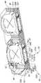
- FIG. 17is a perspective view of the array camera module according to the above preferred embodiment of the present invention.
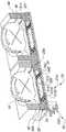
- FIG. 18is a perspective view showing a first modified embodiment of the array camera module according to the above preferred embodiment of the present invention.
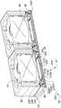
- FIG. 19is a perspective cross-sectional view showing a second modified embodiment of the array camera module according to the above preferred embodiment of the present invention.
- FIG. 20is a perspective, cross-sectional view showing a third modified embodiment of the array camera module according to the above preferred embodiment of the present invention.
- Figure 21is a perspective, cross-sectional view showing a fourth modified embodiment of the array camera module according to the above preferred embodiment of the present invention.
- FIG. 22is a perspective, cross-sectional view showing a fifth modified embodiment of the array camera module according to the above preferred embodiment of the present invention.
- FIG. 23is a perspective cross-sectional view showing a sixth modified embodiment of the array camera module according to the above preferred embodiment of the present invention.
- Figure 24is a perspective, cross-sectional view showing a seventh modified embodiment of the array camera module according to the above preferred embodiment of the present invention.
- Figure 25is a perspective, cross-sectional view showing an eighth modified embodiment of the array camera module according to the above preferred embodiment of the present invention.
- FIG. 26is a perspective, cross-sectional view showing a ninth modified embodiment of the array camera module according to the above preferred embodiment of the present invention.
- FIG. 27is a perspective, cross-sectional view showing a tenth modified embodiment of the array camera module according to the above preferred embodiment of the present invention.
- FIG. 28is a perspective cross-sectional view showing an eleventh modified embodiment of the array camera module according to the above preferred embodiment of the present invention.
- 29is a perspective cross-sectional view showing a twelfth modified embodiment of the array camera module according to the above preferred embodiment of the present invention.
- FIG. 30is a perspective, cross-sectional view showing a thirteenth modified embodiment of the array camera module according to the above preferred embodiment of the present invention.
- Figure 31is a perspective, cross-sectional view showing a fourteenth modified embodiment of the array camera module according to the above preferred embodiment of the present invention.
- FIG. 32is a perspective cross-sectional view showing a fifteenth modified embodiment of the array camera module according to the above preferred embodiment of the present invention.
- FIG. 33is a perspective, cross-sectional view showing a sixteenth modified embodiment of the array camera module according to the above preferred embodiment of the present invention.
- FIG. 34is a perspective, cross-sectional view showing a seventeenth modified embodiment of the array camera module according to the above preferred embodiment of the present invention.
- 35is a perspective cross-sectional view showing an eighteenth modified embodiment of the array camera module according to the above preferred embodiment of the present invention.
- Figure 36is a perspective cross-sectional view showing a nineteenth modified embodiment of the array camera module according to the above preferred embodiment of the present invention.
- FIG. 37is a perspective cross-sectional view showing a twentieth modified embodiment of the array camera module according to the above preferred embodiment of the present invention.
- FIG. 38is a perspective cross-sectional view showing a twenty-first modified embodiment of the array camera module according to the above preferred embodiment of the present invention.
- Figure 39is a block diagram showing the electronic device with the array camera module of the above preferred embodiment of the present invention.
- 40A to 40Care schematic views of an electronic device with the array camera module, respectively.
- the array camera modulecan be applied to various electronic devices to assist a user to capture an image of an object or a person through the array camera module.
- the array camera modulecan be used to photograph an object or a character.
- Image datasuch as images or videos.
- the array camera modulecan be applied to a mobile electronic device, for example, the mobile electronic device can be, but not limited to, a mobile phone, a tablet computer, an MP3/4/5, a personal digital assistant, an e-book, a notebook computer, Digital cameras, etc.
- the array camera module of the present inventionwill be described in the following description as an example of an array camera module that is implemented as a dual lens.
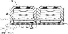
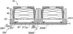
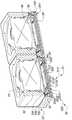
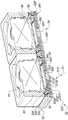
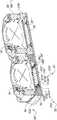
- the array camera moduleincludes a circuit board assembly 220, two optical lenses 10, and two photosensitive elements 21.
- the array camera module comprising the two optical lenses 10is taken as an example for illustration, and other implementations of the present invention.
- the number of the optical lens 10 and the photosensitive element 21may be more, such as three or more. It should be understood by those skilled in the art that the number is not the limitation of the array camera module of the present invention. .
- each of the photosensitive elements 21is respectively electrically connected to the circuit board assembly 220, and each of the optical lenses 10 is held at an upper portion of the circuit board assembly 220, and each of the optical lenses 10 is located corresponding to The circuit board assembly 220 may be coupled to the electronic device in a photosensitive path of each of the photosensitive elements 21 in position. It will be understood by those skilled in the art that one of the optical lens 10 and one of the photosensitive elements 21 can cooperate to form an imaging system for capturing an image.
- the reflected lightenters the inside of the array camera module after passing through the optical lens 10 to be subsequently received by the photosensitive element 21 for photoelectric conversion, in other words
- the photosensitive element 21can convert an optical signal into an electrical signal, and the electrical signal can be transmitted to the electronic device through the circuit board assembly 220, thereby generating an image related to the photographic subject on the electronic device .
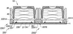
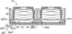
- the circuit board assembly 220includes a connected package portion 2201 and a circuit board portion 2202.
- the connected package portion 2201is integrally and packagedly connected to the circuit board portion 2202, such as being moldedly connected to the circuit board portion. 2202. More specifically, the joint package portion 2201 is molded and connected to the wiring board portion 2202 by molding (Molding On Board, MOB). In other words, the connected package portion 2201 and the wiring board portion 2202 are integrally coupled.
- the circuit board portion 2202includes a circuit board 22, and each of the photosensitive elements 21 is electrically connected to the circuit board 22, and the connected package portion 2201 and the circuit board 22 are integrally combined.
- the connected package portion 2201forms two light windows 231, wherein the connected package portions 2201 are respectively surrounded by the outer sides of the photosensitive elements 21, and each of the light windows 231 respectively provides the optical lenses 10 and corresponding places.
- the light path of the photosensitive element 21is described. That is, each of the photosensitive elements 21 is provided on the wiring board 22 at a position corresponding to each of the optical windows 231.
- the connected package portion 2201 integrally formed with the circuit board 22may be formed first, and then pasted.
- the photosensitive member 21is mounted to the wiring board 22 such that the photosensitive member 21 and the wiring board 22 are turned on.
- the photosensitive element 21may be first attached to the circuit board 22, and the photosensitive element 21 and the circuit board 22 may be electrically connected, and then formed with the circuit board 22.
- the connected package portion 2201is integrally coupled.
- the joint encapsulation portion 2201includes a connecting body 22011 and two outer ring bodies 22012.
- the connecting body 22011is integrally molded and integrally connected between the two outer ring bodies 22012, and separates the two outer ring bodies 22012.
- Two adjacent portions, wherein each of the outer ring bodies 22012 respectively forms one of the light windows 231, and the two photosensitive elements 21are located on both sides of the connecting body 22011, so as to be suitable for being used for assembly.
- Array camera moduleIt is worth mentioning that the connecting body 22011 is a common part of the two optical lenses 10, that is, when the optical lens 10 is mounted, each of the optical lenses 10 occupies a portion corresponding to the connecting body 22011.
- the connecting body 22011 of the joint encapsulation portion 2201 and each of the outer ring bodies 22012may be integrally coupled to the circuit board 22 by a molding process, wherein each of the outer rings The body 22012 is integrally coupled to the outer edge of the circuit board 22, and the connector 22011 and the middle portion of the circuit board 22 are integrally coupled.
- the connecting body 22011 integrally coupled with the middle portion of the circuit board 22forms a reinforcing rib for reinforcing the rigidity of the circuit board 22, thereby preventing the circuit board 22 from being deformed, and
- the outer ring body 22012 integrally joined to the outer edge of the circuit board 22can reinforce the rigidity of the outer edge of the circuit board 22, that is, the joint package portion 2201 can function to enhance the hardness of the circuit board 22. .
- the circuit board portion 2202includes a connection line (not shown) and at least one electronic component 26.
- the connection lineis preset on the circuit board 22, and the electronic component 26 is electrically connected to the connection line and the photosensitive element 21, thereby conducting the electronic component 26 and the ground by the connection line.
- the photosensitive element 21is described such that the electronic component 26 participates in the photosensitive operation of the photosensitive element 21.
- the electronic component 26can be, for example but not limited to, a resistor, a capacitor, a diode, a tertiary tube, a potentiometer, a relay, a driver, a processor, and the like.
- each of the electronic components 26corresponds to each of the photosensitive elements 21 to facilitate the operation of each of the photosensitive elements 21.
- the connected package portion 2201can cover the electronic component 26 inside, so that the electronic component 26 is not directly exposed to the space, more specifically, is not exposed.
- the electronic component 26is present in a manner such as a container, thereby preventing dust and debris from staying in the electronic component 26 . , contaminating the photosensitive element 21.
- the electronic component 26is protruded from the circuit board 22 as an example.
- the electronic component 26is embedded in the circuit board 22, and Without protruding from the circuit board 22, those skilled in the art will appreciate that the structure, type, and location of the electronic components 26 are not limiting of the present invention.
- the electronic components 26may be protruded between the two photosensitive elements 21, which may be covered by the connecting body 22011, so that no additional need for the lens holder in the conventional array module is required.
- the installation spaceis such that the size of the array camera module of the present invention is reduced.
- the encapsulation portion 2201envelops the electronic component 26 has the advantages of protecting the electronic component 26 and the corresponding camera module, but those skilled in the art should understand that
- the connected package portion 2201is not limited to covering the electronic component 26 . That is, in other embodiments of the present invention, the connected package portion 2201 may be directly molded to the circuit board 22 of the electronic component 26 without protruding, or may be molded in the Different positions such as the outer side and the periphery of the electronic component 26 are provided.
- the connected package portion 2201is convexly surrounding the outer side of the photosensitive element 21, and in particular, the connected package portion 2201 is integrally closed and connected. It has a good sealing property, so that when each of the optical lenses 10 is mounted on the connected package portion 2201, each of the photosensitive elements 21 is sealed inside to form a corresponding closed inner space.
- a conventional circuit boardcan be used as the wiring board 22 of the present invention for molding on the surface of the wiring board 22.
- the SMT processSurface Mount Technology surface mount process
- the latter circuit board 22is integrally packaged, such as a molded package, to form the joint package portion 2201, or the joint package portion 2201 is formed by a molding process commonly used in semiconductor packages.
- each of the photosensitive elements 21is attached to the wiring board 22, and then the photosensitive elements 21 are electrically connected to the wiring board 22, for example, by a gold wire.
- the circuit board 22can be selected, for example, but not limited to, a soft and hard bonding board, a ceramic substrate (without a soft board), a PCB hard board (without a soft board), and the like.
- the manner in which the connected package portion 2201 is formedmay be selected, for example, but not limited to, an injection molding process, a molding process, and the like.
- the material of the joint encapsulation portion 2201can be selected, for example, but not limited to, nylon, LCP (Liquid Crystal Polymer), PP (Polypropylene, polypropylene), etc., and the molding process can be selected. Made of epoxy resin. It should be understood by those skilled in the art that the foregoing alternatives and the materials that can be selected are merely illustrative of the embodiments of the invention and are not intended to be limiting.
- the process of manufacturing the circuit board assembly 220may be performed by performing an SMT process on the circuit board 22, and then mounting the photosensitive elements 21 on the circuit board 22, And electrically connecting each of the photosensitive elements 21 and the circuit board 22, such as a gold wire electrical connection, and then integrally packaging the circuit board 22, such as a molded package, by insert molding.
- the joint package portion 2201 or the joint package portion 2201is formed by a molding process commonly used in a semiconductor package. It will be understood by those skilled in the art that the order of manufacture of the circuit board assembly 220 is not a limitation of the present invention.
- each of the optical lenses 10is mounted on the connected package portion 2201 of the circuit board assembly 220, so that the connected package portion 2201 is equivalent to the function of the bracket in the conventional camera module.
- the optical lens 10is provided with a support and fixed position, but the assembly is different from the conventional COB process.
- the bracket of the camera module of the conventional COB processis fixed to the circuit board in a pasting manner, and the connected package portion 2201 is fixed to the circuit board 22 by molding (Molding On Board, MOB), It is necessary to attach a fixing process which has better connection stability with respect to the pasting fixing and controllability of the process, and in the connected package portion 27 and the electrons mounted on the wiring board 22 There is no need to reserve a safety distance between the components 26, so that the thickness of the array camera module is reduced; on the other hand, the connected package portion 2201 is wrapped around the electronic component 26, so that the conventional The bracket function and the electronic component 26 can be spatially overlapped, and there is no need to reserve a safe distance around the circuit device like a conventional camera module, so that the height of the connected package portion 2201 having the bracket function can be set.
- moldingManufacturing On Board, MOB
- the space in which the thickness of the camera module can be reducedis further provided.
- the joint encapsulation portion 2201replaces the conventional bracket, avoiding the tilt error caused by the bracket during the sticking assembly, and reducing the cumulative tolerance of the assembly of the array camera module.
- the shape of the connected package portion 2201can be further determined, for example, extending inwardly at the position of the electronic component 26 to form a protruding portion, thereby increasing the connected package portion 2201.
- the conjoined package portions 22011extend uniformly to form a relatively regular shape with a small width. It will be understood by those skilled in the art that the specific shape of the conjoined package portion 2201 is not a limitation of the present invention.
- the connected package portion 2201includes a covering portion 22013 and a filter element mounting portion 22014, and the filter element mounting portion 22014 is integrally molded and integrally connected to the covering portion 22013, the covering portion 22013 is molded and connected to the circuit board 22 for coating the electronic component 26.
- the filter element mounting section 22014is used to mount two filter elements 40, which may be implemented as, but not limited to, an infrared cut filter (IRCF).
- IRCFinfrared cut filter
- each of the filter elements 40 of the array camera moduleis mounted on the filter element mounting section 22014, such that The filter element 40 is located on the photosensitive path of the corresponding photosensitive element 21 and does not require the provision of an additional filter element 40 mounting bracket.
- the joint encapsulation portion 2201has the function of a conventional bracket here, but based on the advantage of the molding process, the top of the filter element mounting section 22014 can be made to have a good process by means of a mold process.
- the flatnessis such that the filter element 40 is mounted flat, which is also superior to the conventional camera module.
- the filter element mounting section 22014forms at least one mounting groove 220141.
- the filter element mounting section 22014forms two of the mounting slots 220141, and each of the mounting slots 220141 is respectively connected to Corresponding to the light window 231, wherein each of the mounting slots 220141 provides sufficient installation space for the filter element 40, such that The filter element 40 does not protrude from the top surface of the filter element mounting section 22014.
- the mounting portion 220141is disposed at the upper end of the connected package portion 2201, so that each of the filter elements 40 is stably mounted on the connected package portion 2201, and does not protrude from the connection.
- the mounting groove 220141can be used to mount the filter element 40, while in other implementations of the invention, the mounting groove 220141 can be used to mount the device
- the mounting groove 220141is not a limitation of the present invention.
- the photosensitive member 21is connected to the wiring board 22 via at least one lead 24, and is electrically connected to the connecting line.
- the leads 24can be implemented, for example, but not limited to, gold wires, copper wires, aluminum wires, silver wires.
- the leads 24 of the photosensitive element 21may be attached to the circuit board 22 by conventional COB means, such as, but not limited to, soldering. That is to say, the connection of the photosensitive element 21 and the circuit board 22 can make full use of the existing mature connection technology to reduce the cost of the improved technology, fully utilize the traditional process and equipment, and avoid waste of resources.
- the wire bonding direction of the lead wires 24is also not limited.
- the wire bonding direction of the wire wires 24may be from the photosensitive member 21 to the circuit board 22, or from the circuit board 22 to the photosensitive device. Element 21.
- connection of the photosensitive element 21 to the circuit board 22can also be achieved by any other connection means of the inventive object of the present invention, and the present invention does not Restricted.
- each of the photosensitive elements 21is disposed on an upper surface of the wiring board 22, and the connected package portion 2201 surrounds an outer side of the photosensitive element 21.
- different manufacturing sequencesmay be selected. For example, but not limited to, in one embodiment, two of the photosensitive elements 21 may be first mounted on the circuit board 22, and then Outside the photosensitive element 21, the wiring board 22 is molded to form the connected package portion 2201, and the electronic component 26 protruding from the wiring board 22 is covered inside.
- the connected package portion 2201may be molded on the circuit board 22, and the electronic component 26 protruding from the circuit board 22 may be packaged.
- the photosensitive element 21is mounted on the wiring board 22 so that the photosensitive element 21 is located inside the connected package portion 2201.
- an array camera modulecomposed of two optical lenses 10 is taken as an example for description.
- the array camera modulecan be implemented in one manner, and the advantages of the molding process are utilized. Providing a uniform mounting environment for the two filter elements 40 and the two optical lenses 10, so that the array camera module can obtain better optical performance.
- the array camera modulemay further include two or more optical lenses 10, and correspondingly, the circuit board assembly 220 forms two or more light windows 231, which are in the art. It should be understood by those skilled in the art that the number of optical lenses 10 is not a limitation of the present invention.
- each of the optical lenses 10may be directly connected to the connected package portion 2201 of the circuit board assembly 220. That is, in this embodiment, the optical lens 10 is a fixed-focus lens assembly, that is, the focal length of the optical lens 10 may not be freely adjusted, as will be understood by those skilled in the art, as described in the present invention.
- the optical lens 10can be directly connected to the connected package portion 2201, including the case where the optical lens 10 is connected to the connected body through a casing.
- the array camera moduleincludes at least one driver 30, and each of the drivers 30 is mounted on the connected package portion 2201.
- the optical lens 10The driver 30 can be drivingly coupled such that the driver 30 can drive the optical lens 10 to move along the photosensitive path of the photosensitive element 21 to adjust the focal length of the optical lens 10. That is, in this embodiment, the optical lens 10 is a moving focus optical lens assembly, that is, the focal length of the optical lens 10 can be adjusted, for example, when the user uses the array camera module to shoot images, The photographing effect is adjusted by adjusting the focal length of the optical lens 10.
- the type of the driver 30is not limited as long as it can drive the optical lens 10 to move along the photosensitive path of the photosensitive element 21, for example, the driver 30 may be, but not limited to, a voice coil motor.
- the connected package portion 2201can be used to support the mounting of each of the filter elements 40, each of the optical lenses 10 or each of the drivers 30, with a conventional The function of the bracket, and based on the advantage of molding, the joint encapsulation portion 2201 can control the flatness and consistency of the joint encapsulation portion by means of a mold, thereby Each of the filter elements 40 of the array camera module, each of the optical lenses 10 and each of the drivers 30 provide a flat and consistent mounting environment, thereby making it easier to ensure the consistency of the optical axes of the lenses. Traditional array camera modules are not easily accessible.
- the joint encapsulation portion 2201is integrally molded and molded on the circuit board 22, which enhances the structural strength of the circuit board 22, and thus is relatively conventional COB-based array camera module.
- the circuit board 22 of the inventive array camera modulecan achieve a smaller thickness and can meet the requirements of each lens and each motor.
- the joint encapsulation portion 2201can reduce the distance between the optical lenses 10, thereby further reducing the lateral length and width dimensions of the array camera module.
- the circuit board assembly 220includes at least two motor connection structures 2203 for respectively connecting the two drivers 30 of the array camera module.
- Each of the drivers 30has at least one motor pin 31.
- Each of the motor connection structures 2203includes at least one first connection line 22031, and each of the first connection lines 22031 is for electrically connecting the driver 30 and the circuit board 22.
- Each of the first connecting lines 22031is electrically connected to the circuit board 22.
- each of the first connection lines 22031is electrically connected to a connection circuit of the circuit board 22.
- the first connection line 22031is disposed on the connected package portion 2201 and extends to a top end of the connected package portion 2201.
- the first connecting wire 22031includes a first motor connecting end 220311, wherein the first motor connecting end 220311 is exposed at a top end of the connected package portion 2201 for subsequent connection for electrically connecting the driver 30.
- Motor pin 31It should be noted that the first connection line 22031 may be disposed in an embedded manner when the connected package portion 2201 is formed. In the conventional connection method, components such as a drive motor are connected to the circuit board by providing separate wires, and the manufacturing process is relatively complicated, and the manner of embedding the first connecting wire 22031 in the molding of the present invention is It can replace the traditional motor welding and other processes, and make the circuit connection more stable.
- the first connecting line 22031is a wire embedded in the inside of the connected package portion 2201.
- the motor pin 31may be connected to the first motor connection end 220311 through an anisotropic conductive film, or may be connected to the first motor connection end 220311 by soldering.
- the lower end portion of the first connection line 22031is electrically connected to the connection circuit of the circuit board 22, and then after the connected package portion 2201 is formed.
- the main body portion of the first connection end 22031is wrapped inside the conjoined package portion 2201, and the upper end portion of the first connection end 22031 is formed on the top surface of the conjoined package portion 2201.
- the first motor connection end 220311is described.
- the buried position of the first connecting line 22031 and the position of the first motor connecting end 220311 of the first connecting line 22031 displayed in the connected package portion 2201can be set as needed, for example.
- the first motor connection end 220311 of the first connection line 22031may be disposed at a periphery of the connected package portion 2201, that is, a top of the connected package portion 2201.
- the first motor connection end 220311can be disposed in the inner circumference of the conjoined package portion 2201, that is, the installation slot 220141 of the conjoined package portion 2201.
- the bottom surfacethereby providing a different mounting position for the drive 30.
- the first motor connection end 220311is disposed on a peripheral top surface of the conjoined package portion 2201 when the driver 30 is When it is required to be mounted to the mounting groove 220141, the first motor connecting end 220311 is disposed on the inner circumference of the connected package portion 2201, that is, the bottom surface of the mounting groove 220141.
- each of the photosensitive elements 21may be attached to the wiring board 22, and then the connected body may be molded in the MOB manner on the wiring board 22.
- the package portion 2201, and the first connection line 22031may be disposed inside the joint package portion 2201 in a buried manner during molding, and the first connection line 22031 is electrically connected to the circuit board 22, and
- the first motor connection end 220311 of the first connection line 22031is displayed on the top end of the connected package portion 2201 so as to be connected to the motor pin 31 of the driver 30.
- each of the motor pins 31 of the driver 30is connected to the first connecting line 22031 by soldering.
- a first motor connection end 220311, such that the driver 30 is electrically connected to the circuit board 22, and a separate wire is required to connect the driver 30 and the circuit board 22, and the said driver 30is The length of the motor pin 31 can be reduced.
- Each of the motor connection structures 2203has at least one first lead slot 22032 for receiving the motor pin 31 of the driver 30 of the array camera module.
- the first lead slot 22032is disposed at an upper end of the connected package portion 2201 , that is, the top portion of the connected package portion 2201 may form the first lead slot 22032 of the motor connection structure 2203 .
- the motor connection structure 2203includes at least one second connection line 22033 for electrically connecting the driver 30 and the circuit board 22.
- the second connecting line 22033is disposed on the connected package portion 2201 and extends upward to the bottom wall of the first lead slot 22032 of the connected package portion 2201.
- the second connecting wire 22033includes a second motor connecting end 220331, wherein the second motor connecting end 220331 is exposed on the bottom wall of the first pin slot 22032 of the connected package portion 2201 for The motor pin 31 of the driver 30 is electrically connected.
- the second motor connection end 220331can be implemented as a pad.
- the second connecting line 22033can be implemented as a wire embedded in the inside of the connected package portion 2201.
- the photosensitive element 21is first mounted on the wiring board 22, and then the interconnected package is molded in the MOB manner on the wiring board 22.
- a portion 2201, and presets the first lead slot 22032 of a predetermined length, and the second connection line 22033may be embedded in a manner of molding, and the second connection line 22033 is electrically connected to the line a plate 22, and the second motor connection end 220331 of the second connection line 22033 is displayed on the bottom wall of the first pin slot 22032 of the conjoined package portion 2201 to facilitate connection to the The motor pin 31 of the driver 30.
- each of the motor pins 31 of the driver 30is inserted into the first lead slot 22032, and is connected by soldering.
- the motor pins 31 of the driver 30can be stably connected to prevent the externally unnecessary unnecessary touch of the motor pins 31.
- the second connecting line 22033can be implemented as a wire embedded in the inside of the connected package portion 2201.
- Each of the motor connection structures 2203has at least one second lead slot 22034, and the second lead slot 22034 is configured to receive the motor pin 31 of the driver 30 of the array camera module, ie, The outer sidewall of the package portion 2201 may form the second lead slot 22034.
- the motor connection structure 2203includes at least one circuit contact 22035 that is preset to the circuit board 22 and electrically connected to the connection line of the circuit board 22. Further, each of the second lead slots 22034 extends from the top end of the connected package portion 2201 to the circuit board 22, and the circuit contacts 22035 correspond to the second lead slots 22034.
- the motor pin 31is adapted to be inserted and held in the second lead slot 22034 and may be soldered to the circuit contact 22035 to turn on the driver 30 and the The circuit board 22 is described.
- each of the circuit contacts 22035is preset on the circuit board 22, thereby mounting the photosensitive element 21 and the electronic component 26, and then on the circuit board. 22, molding the connected package portion 2201 in a MOB manner, and presetting the second lead slot 22034 of a predetermined length, and causing the circuit contact 22035 to be displayed through the second pin slot 22034, In order to be connected to the motor pin 31 of the driver 30.
- each of the motor pins 31 of the driver 30is inserted and held in the second lead slot 22034, and is soldered.
- the circuitis connected to the circuit contact 22035 on the circuit board 22 such that the driver 30 is electrically connected to the circuit board 22, and the motor pins 31 of the driver 30 can be stably connected to prevent external The motor pin 31 is touched as necessary.
- the motor connection structure 2203includes an engraving line 22036 for electrically connecting the connection line on the circuit board 22, the photosensitive element 21, and a motor.
- the engraving line 22036may be disposed by laser plating (LDS) and then plated with metal to form the conjoined package portion 2201.
- LDSlaser plating
- componentssuch as a drive motor are connected to the circuit board by providing separate wires, and the manufacturing process It is relatively complicated, and the manner in which the engraving line 22036 is provided during the molding of the present invention can replace the conventional motor welding process and the like, and makes the circuit connection more stable.
- the engraving line 22036may be formed by forming the engraving groove in the encapsulation portion 2201, and then arranging the circuit in the engraving groove by electroplating.
- the manner in which the driver 30 of the array camera module is connected to the connected packageis described by taking the connection manner of the motor connection structure 2203 as an example.
- the manner of the first connection line 22031, and in other embodiments of the present invention, the connection manner of the driver 30can also be combined with the connection manner corresponding to FIG. 5A, FIG. 5B, and FIG. 5C.
- a lead slot 22032is connected to the second connection line 22033, the second lead slot 22034, and the circuit contact 22035.
- the driver 30can be coupled to the circuit board assembly 220 in a conventional manner, such as by soldering. It will be understood by those skilled in the art that the manner in which the driver 30 and the circuit board assembly 220 are connected is not a limitation of the present invention.
- an array camera module and a circuit board assembly 220 thereofincludes a circuit board 22A.
- the circuit board 22Ahas two inner recesses 224A, and each of the photosensitive elements 21 is disposed in the corresponding inner recess 224A.
- the photosensitive member 21is disposed in the inner recess 224A, and accommodates the photosensitive member 21 in the inner recess 224A, so that the photosensitive member The element 21 does not significantly protrude from the upper surface of the wiring board 22A, so that the height of the photosensitive element 21 relative to the connected package portion 2201 is lowered, thereby reducing the photosensitive element 21 to the connected package portion.
- the 2201 height limitprovides the possibility of further height reduction.
- the photosensitive member 21is connected to the wiring board 22 through the lead wires 24, and is electrically connected to the connection line.
- the leads 24can be implemented, for example, but not limited to, gold wires, copper wires, aluminum wires, silver wires. That is, the photosensitive member 21 and the lead 24 are both located in the inner groove 224A of the wiring board 22A.
- the inner recess 224Aneeds to be disposed on the circuit board 22A. That is, the inner groove 224A is opened on a conventional wiring board to be adapted to accommodate the mounting of the photosensitive member 21.
- Figure 8is a cross-sectional view of an array camera module and its circuit board assembly in accordance with a third preferred embodiment of the present invention.
- the circuit board assembly 220includes a circuit board 22B having two vias 225B, and a lower portion of each of the vias 225B is adapted to mount the photosensitive element 21.
- Each of the vias 225Bcauses the upper and lower sides of the wiring board 22B to communicate, so that when the photosensitive element 21 is mounted on the back side of the wiring board 22B and the photosensitive area is mounted on the wiring board 22B, The photosensitive area of the photosensitive element 21 is capable of receiving light entering by the optical lens 10.
- the circuit board 22has two outer recesses 226B, and each of the outer recesses 226B communicates with the corresponding passage 225B to provide a mounting position of the photosensitive element 21.
- the outer surface of the photosensitive member 21 and the surface of the wiring board 22Bare coincident and are located on the same plane, thereby securing the circuit board assembly 220. Surface flatness.
- the passage 225Bis stepped to facilitate mounting of the photosensitive member 21, providing a stable mounting position for the photosensitive member 21, and exposing its photosensitive region to the inner space.
- a chip mounting method different from the conventional onethat is, a flip chip (FC) is provided.
- the photosensitive member 21is attached to the wiring board 22B from the back surface direction of the wiring board 22B instead of being required from the front surface of the wiring board 22B, that is, from above the wiring board 22B as in the above embodiment.
- the photosensitive region of the photosensitive element 21is mounted on the wiring board 22B upward.
- the structure and the mounting mannerare such that the photosensitive element 21 and the connected package portion 2201 are relatively independent, and the mounting of the photosensitive element 21 is not affected by the connected package portion 2201, and the connected package portion
- the molding of 2201has a small influence on the photosensitive member 21.
- the photosensitive element 21is embedded on the outer side surface of the circuit board 22B and does not protrude from the inner side surface of the circuit board 22B, so that a larger space is left inside the circuit board 22B, so that The height of the connected package portion 2201 is not limited by the height of the photosensitive member 21, so that the connected package portion 2201 can reach a smaller height.
- the filter element 40is mounted on the upper end of the via 225B. That is, the filter element 40 does not need to be mounted on the connected package portion 2201, thereby reducing the back focus of the array camera module and reducing the height of the camera module.
- the filter element 40can be embodied as an infrared cut filter IRCF.
- FIG. 9is a cross-sectional view of an array camera module and its circuit board assembly 220 in accordance with a fourth preferred embodiment of the present invention.
- the circuit board assembly 220includes a reinforcement layer 2204C laminatedly coupled to the bottom layer of the circuit board 22 to enhance the structural strength of the circuit board 22. That is, the reinforcing layer 2204C is placed on the bottom layer of the connecting portion 2201 and the region where the photosensitive element 21 is located on the circuit board 22, so that the circuit board 22 stably and reliably supports the connection.
- the body package portion 2201 and the light receiving element 21are laminatedly coupled to the bottom layer of the circuit board 22 to enhance the structural strength of the circuit board 22. That is, the reinforcing layer 2204C is placed on the bottom layer of the connecting portion 2201 and the region where the photosensitive element 21 is located on the circuit board 22, so that the circuit board 22 stably and reliably supports the connection.
- the reinforcing layer 2204Cis a metal plate attached to the bottom layer of the circuit board 22 to increase the structural strength of the circuit board 22, and on the other hand, increase the heat dissipation of the circuit board assembly 220. The performance can effectively dissipate the heat generated by the photosensitive element 21.
- the circuit board 22can adopt an FPC (Flex Print Circuit), and the rigidity of the circuit board 22 through the reinforcing layer 2204C enables the FPC with good bending performance to be The load bearing requirements of the circuit board assembly 220 are met. That is to say, the circuit board 22 can be selected from a wider range, such as a PCB (Printed Circuit Board), an FPC, an R-FPC (Rigid-Flex PCB, a soft and hard bonded board).
- the structural strength of the circuit board 22is increased by the reinforcing layer 2204B and the heat dissipation performance is improved, so that the thickness of the circuit board 22 can be reduced, so that the height of the circuit board assembly is further reduced, and assembled by the same.
- the height of the camera moduleis reduced.
- Figure 10is a cross-sectional view of the array camera module and its circuit board assembly 220 in accordance with a fifth preferred embodiment of the present invention.
- the circuit board 22Dhas at least one reinforcing hole 227D, and the connected body package 2201 extends into the reinforcing hole 227D, thereby enhancing the structural strength of the circuit board 22D.
- the position of the reinforcing hole 227Dcan be selected as needed, and is set according to the structural strength requirement of the circuit board 22D, such as a symmetrical structure.
- the structural strength of the circuit board 22Dis enhanced by the arrangement of the reinforcing holes 227D, so that the thickness of the circuit board 22D can be reduced, the thickness of the camera module assembled by the same can be reduced, and the circuit board can be improved.
- the heat dissipation performance of the assembly 220is provided.
- the reinforcing holes 227Dare groove-shaped, that is, the reinforcing holes 227D are blind holes, so that when the circuit board assembly 220 is manufactured, the molding material of the joint packaging portion 2201 does not The leakage hole 227D leaks out.
- FIG 11is a cross-sectional view of the array camera module and its circuit board assembly 220 in accordance with a sixth preferred embodiment of the present invention.
- the circuit board 22Ehas at least one reinforcing hole 227E, and the connected package portion 2201 extends into the reinforcing hole 227E, thereby enhancing the structural strength of the circuit board 22E.
- the position of the reinforcing hole 227Ecan be selected as needed, and according to the structural strength requirement of the circuit board 22E, such as a symmetrical structure.
- the structural strength of the circuit board 22Eis enhanced by the arrangement of the reinforcing holes 227E, so that the thickness of the circuit board 22E can be reduced, the thickness of the camera module assembled therefrom can be reduced, and the circuit board can be improved.
- the heat dissipation performance of the assembly 220can be selected as needed, and according to the structural strength requirement of the circuit board 22E, such as a symmetrical structure.
- the reinforcing hole 227Eis a through hole, that is, the reinforcing hole 227E passes through the circuit board 22E so that both sides of the circuit board 22E communicate, thereby manufacturing the circuit board assembly.
- the molding material of the joint encapsulation portion 2201is sufficiently combined with the wiring board 22E to form a more firm composite material structure, and the perforations are easier to manufacture than the groove-like structure.
- Figure 12is a cross-sectional view of the array camera module and its circuit board assembly 220 in accordance with a seventh preferred embodiment of the present invention.
- the connected package portion 2201Fincludes a covering portion 22013F, a filter element mounting portion 22014F and a lens mounting portion 22015F, the filter element mounting portion 22014F and the lens mounting.
- the segment 22015Fis integrally molded and connected to the cladding segment 22013F in turn, the cladding segment 22013F is molded and connected to the circuit board 22, and the cladding segment 22013F is used to cover the electronic component 26 and The lead 24 is.
- the filter element mounting section 22014Fis used to mount the filter element 40, that is, when the circuit board assembly 220 is used to assemble the array camera module, the array camera module A filter element 40 is mounted to the filter element mounting section 22014F such that the filter element 40 is located on the photosensitive path of the photosensitive element 21, and it is not necessary to provide an additional mounting member for the filter element 40. That is to say, the joint encapsulation portion 2201F has the function of a conventional bracket here, but based on the advantage of the molding process, the top of the filter element mounting section 22014F can be made to have a good process by means of a mold process. The flatness is such that the filter element 40 is mounted flat, which is also superior to the conventional camera module.
- the lens mounting section 22015Fis used to mount the optical lens 10, that is, when the circuit board assembly 220 is used to assemble the array camera module, the optical lens 10 is mounted on the connected body
- the lens mounting section of the encapsulation portion 2201Fis mounted inside the lens mount section 22015F to facilitate providing a stable mounting position for the optical lens 10.
- the filter element mounting portion 22014Fhas two mounting slots 220141F, and the mounting slots 220141F communicate with the corresponding light window 231F to provide sufficient installation space for each of the filter elements 40, so that each of the described The filter element 40 is stably mounted.
- the lens mounting section 22015Fhas two lens mounting slots 220151F, and each of the lens mounting slots 220151F communicates with the corresponding light window 231F to provide sufficient installation space for each of the optical lenses 10.
- the filter element mounting section 22014F and the lens mounting section 22015Fintegrally extend upwardly, and internally form a stepped structure to provide a support fixing position for the filter element 40 and the optical lens 10, respectively. There is thus no need to provide additional components to mount the filter element 40 and the optical lens 10.
- the lens mounting section 22015Fhas two lens inner walls 220152F, and each of the lens inner walls 220152F has a closed annular shape, which is suitable for the optical lens 10 to provide installation space. It is worth mentioning that each of the lens inner walls 220152F of the lens mounting portion 220152F has a flat surface, so as to be suitable for mounting the unthreaded optical lens 10 to form a fixed focus module. In particular, the optical lens 10 can be fixed to the lens mounting section 22015F by bonding.
- the circuit board assembly 220 and the array camera moduleare in accordance with an eighth preferred embodiment of the present invention.
- the circuit board assembly 220includes a shielding layer 2205 that wraps the circuit board 22 and the connected package portion 2201 so as to enhance the circuit board 22 At the same time as the structural strength, the electromagnetic interference resistance of the circuit board assembly 220 is enhanced.
- the filter element 40is not assembled to the molding base 23, but the filter element 40 is assembled to the optical lens 10 to be in the optical lens.
- the filter element 40is held between the photosensitive element 21 and the optical lens 10 while being held in the photosensitive path of the photosensitive element 21. That is, in the process of assembling the array camera module, the filter element 40 needs to be assembled to the optical lens 10, and then the optical lens 10 is kept in the photosensitive element 21. path.
- the filters The number of the light elements 40may also be one, so that the filter elements 40 are simultaneously assembled to the plurality of the optical lenses 10.
- the array camera module and its circuit board assembly 220are in accordance with a tenth preferred embodiment of the present invention.
- the array camera moduleincludes at least one support member 70 for mounting each of the filter elements 40, each of the optical lenses 10 or each of the drivers 30.
- the support member 70is mounted to the joint package portion 2201, and each of the filter elements 40 is mounted to the support member 70, and each of the drivers 30 is mounted to the Support 70.
- the specific shape of the support member 70can be set as needed, such as providing a boss to facilitate mounting of each of the filters.
- the support member 70 shownmay be a one-piece bracket, that is, a plurality of the filter elements 40 may be mounted at a time, or a single bracket, that is, one of the filter elements 40 may be mounted.
- the support member 70is preferably a joint bracket. It will be understood by those skilled in the art that the specific shape of the support member 70 is not a limitation of the present invention.
- FIG. 15A to 15H of the accompanying drawings of the present inventiona manufacturing process of an array camera module and an array camera module according to another preferred embodiment of the present invention is illustrated, wherein the array camera module includes At least two optical lenses 10' and a molded photosensitive member 20', wherein the molded photosensitive member 20' further includes at least two photosensitive elements 21', a wiring board 22', a molding base 23', and at least two groups Lead 24'.
- the body package portion 2201corresponds to the molded base 23' in the array camera module of this embodiment of the present invention.
- Each of the photosensitive elements 21'includes a set of chip connectors 211', a photosensitive region 212', and a non-photosensitive region 213', wherein the photosensitive regions 212' and the non-sensitive regions 213' are integrally formed.
- the photosensitive area 212'is located in the middle of the photosensitive element 21'
- the non-sensitive area 213'is located outside the photosensitive element 21'
- the non-sensitive area 213'is around the photosensitive area 212'.
- the chip connector 211'is disposed in the non-photosensitive area 213'.
- the circuit board 22'includes at least two sets of circuit board connectors 221', at least two flat chip mounting areas 222', and an edge area 223', wherein the edge areas 223' and each of the chips
- the mounting area 222'is integrally formed, and the edge area 223' is located around each of the chip mounting areas 222', and the board connector 221' is disposed in the edge area 223'.
- Each of the leads 24'has a chip connection end 241' and a circuit board connection end 242', wherein the lead wire 24' is bent between the chip connection end 241' and the circuit board connection end 242'. Extend the ground.
- Each of the photosensitive elements 21'is respectively attached to each of the chip mounting regions 222' of the wiring board 22', wherein the chip connection end 241' of the leads 24' is connected to the The chip connector 211' of the photosensitive member 21', the circuit board connection end 242' of the lead 24' is connected to the circuit board connector 221' of the circuit board 22', the molding The pedestal 23' is integrally bonded at least to the edge region 223' of the wiring board 22' to form the molded photosensitive member 20', wherein each of the optical lenses 10' is respectively disposed on the mold The photosensitive path of each of the photosensitive elements 21' of the photosensitive photosensitive member 20'. Light reflected by the object enters the interior of the array camera module from each of the optical lenses 10' to be subsequently received and photoelectrically converted by the photosensitive region 212' of each of the photosensitive elements 21', thereby Get an image associated with the object.
- the chip connector 211 ′ of the photosensitive element 21 ′ and the circuit board connector 221 ′ of the circuit board 22 ′may respectively be a lands That is, the chip connector 211' of the photosensitive element 21' and the circuit board connector 221' of the wiring board 22' may be in the shape of a disk for the said lead 24'
- the chip connection end 241'is connected to the chip connector 211' of the photosensitive element 21' and the said board connection end 242' of the lead 24' is connected to the circuit board 22' a circuit board connector 221'
- the chip connector 211' of the photosensitive element 21' and the circuit board connector of the circuit board 22' 221'may be respectively spherical, for example, solder paste or other solder material is spotted on the non-photosensitive region 213' of the photosensitive element 21' and the edge region 223' of the wiring board 22' to form a
- the chip connector 211' of the photosensitive element 21' and the circuit board connector 221' of the circuit board 22'do not constitute the present invention.
- a limitation of content and rangethat is, in other examples, the chip connector 211' of the photosensitive element 21' and the circuit board connector 221' of the circuit board 22' may have other such Illustrated shape.
- the non-photosensitive region 213' of the photosensitive element 21'further has a chip inner portion 2131', a chip connecting portion 2132', and a chip outer portion 2133', wherein the chip connector 211' is disposed on the a chip connecting portion 2132', the chip inner portion 2131' is circumferentially surrounding the photosensitive region 212', and both sides of the chip connecting portion 2132' respectively extend and are connected to the chip inner portion 2131' and the chip outer portion 2132. That is, in the present invention, the region of the non-photosensitive region 213' from the position where the chip connector 211' is disposed to the edge position of the photosensitive region 212' is defined as the chip inner portion 2131.
- the area of the non-photosensitive area 213' where the chip connector 211' is disposedis defined as the chip connection portion 2132', and the non-photosensitive area 213' is set from the chip connector 211
- a region of the position to the outer edge of the photosensitive member 21'is defined as the chip outer portion 2133'.
- the photosensitive member 21'is, in order from the inside of the photosensitive member 21', the photosensitive region 212', the chip inner portion 2131', the chip connecting portion 2132', and the like from the inside to the outside.
- the chip outer portion 2133'is, in order from the inside of the photosensitive member 21', the photosensitive region 212', the chip inner portion 2131', the chip connecting portion 2132', and the like from the inside to the outside.
- the edge region 223' of the circuit board 22'further has a circuit board inner portion 2231', a line a board connecting portion 2232' and a circuit board outer portion 2233', wherein the circuit board connecting member 221' is disposed on the circuit board connecting portion 2232', and the circuit board inner portion 2231' surrounds the chip mounting portion
- One side of the circuit board connecting portion 2232'extends and is connected to the circuit board inner side portion 2231' and the circuit board outer side portion 2233'.
- the edge position of the edge region 223' from the position where the board connecting member 221' is disposed to the edge portion of the chip mounting region 222'is defined as the inner side portion of the wiring board 2231'
- the area of the edge area 223' where the circuit board connector 221' is disposedis defined as the circuit board connection portion 2232'
- the edge area 223'is connected from the circuit board to which the board is disposed
- the area of the member 221' to the outer edge of the wiring board 22'is defined as the outer side portion 2233' of the wiring board.
- the circuit board 22'is an integrated circuit board.
- each of the chip mounting areas 222'are symmetrically respectively.
- the two ends of the circuit board 22'are disposed such that the circuit board 22' forms a symmetrical structure.
- the type of the lead 24 ′is not limited in the array camera module of the present invention.
- the lead 24 ′may be implemented as a gold wire, that is, by a gold wire.
- the methodcan connect the photosensitive element 21' and the circuit board 22' together, so that after the optical signal is converted into an electrical signal by the photosensitive area 212' of the photosensitive element 21', the electrical signal It can be further transferred to the wiring board 22' through the lead 24'.
- the lead 24 ′can also be implemented as any silver wire, copper wire or the like to enable the electrical signal to be implemented. The material is transferred between the photosensitive element 21' and the wiring board 22'.
- the array camera modulecan be a fixed focus camera module, or a zoom camera module, or a zoom camera module.
- the array camera modulecan be under the premise of being controlled by the height dimension. The ability to have auto focus and optical zoom to improve the image quality of the array camera module.
- the array camera modulefurther includes at least two drivers 30', wherein each of the optical lenses 10'
- each of the drivers 30'is assembled to each of the drivers 30', and each of the drivers 30' is assembled to a top surface of the molded base 23', so that each of the optical lenses 10' is held separately
- the photosensitive path of each of the photosensitive elements 21' of the molded photosensitive member 20'is described.
- Each of the drivers 30'is electrically connected to the circuit board 22', respectively, to transmit power and control signals to each of the drivers 30' after the circuit board 22', each of the drivers 30'
- Each of the optical lenses 10'can be driven to move back and forth along the photosensitive path of each of the photosensitive elements 21', thereby adjusting the focal length of the array camera module. That is, the optical lens 10' can be drivingly disposed to the driver 30'.
- the type of the driver 30'is not limited in the array camera module of the present invention.
- the driver 30'may be implemented as any such as a voice coil motor.
- the array camera modulefurther includes at least one filter element 40'.
- the array camera modulemay include one of the filter elements 40', wherein the filter element 40' is assembled to the top of the molded base 23' The surface is such that different positions of the filter element 40' correspond to the photosensitive paths of each of the photosensitive elements 21', respectively.
- the array camera modulemay include at least two of the filter elements 40', wherein each of the filter elements 40' is assembled to the molded base 23', respectively.
- each of the filter elements 40'respectively corresponds to a photosensitive path of each of the photosensitive elements 21', that is, each of the photosensitive elements 21', each of the array camera modules
- the filter element 40' and each of the optical lenses 10'have a one-to-one correspondence.
- the filter element 40'When the array camera module is used, light reflected by the object enters the interior of the array camera module from the optical lens 10', and can be filtered by the filter element 40'.
- the photosensitive element 21'receives and performs photoelectric conversion. That is, the filter element 40' can filter stray light, such as the infrared portion, in the light reflected by the object from the optical lens 10' into the array camera module, in such a manner, Able to improve the array camera module Imaging quality.
- the filter element 40'may be directly assembled to the top surface of the molded base 23', or may be assembled by first assembling the filter element 40' to a support member. The components are assembled on the top surface of the molded base 23'. In this way, the size of the filter element 40' can be reduced to reduce the manufacturing cost of the array camera module.
- the filter elements 40'can be implemented in different types, for example, the filter elements 40' can be implemented as infrared A cut filter, a full transmissive spectral filter, and other filters or a combination of multiple filters, for example, the filter element 40' can be implemented as an infrared cut filter and a full transmissive filter. a combination of the infrared cut filter and the full transmissive spectral filter can be switched to be selectively located on the photosensitive path of the photosensitive element 21', for example, in an environment where light is sufficient during daylight hours.
- the infrared cut filtercan be switched to the photosensitive path of the photosensitive element 21 ′ to filter the object entering the array camera module by the infrared cut filter. Infrared rays in the reflected light, when the array camera module is used in a dark environment such as at night, the full-transmission spectral filter can be switched to the photosensitive path of the photosensitive element 21' to allow Infrared part of the light into the camera module of the array is reflected by the object in transmission.
- a set of electronic components 26' of the molded photosensitive member 20'are first mounted on the surface by a process such as SMT (Surface Mount Technology).
- SMTSurface Mount Technology
- each of the electronic components 26'is attached to the outer side portion 2233' of the edge region 223'.
- the electronic component 26'can be mounted on the middle of the circuit board 22' as needed. It can be understood that the electronic component 26' is not mounted on the circuit board 22'.
- the chip mounting area 222'is provided.
- the circuit board 22' with the electronic component 26'is placed in a molding die 100' to form the module base by a molding process by the molding die 100'.
- Block 23'the molding die 100' includes an upper die 101' and a lower die 102', wherein at least one of the upper die 101' and the lower die 102' can be moved to make the molding die The 100' can be clamped and drafted.
- the upper mold 101' and the lower mold 102'are clamped, at least one molding space 103' is formed between the upper mold 101' and the lower mold 102', wherein the circuit board 22'
- the edge region 223' and the middle portion of the wiring board 22'correspond to the molding space 103', respectively.
- each of the electronic components 26' mounted on the wiring board 22'may be located in the molding space 103'. .
- a fluid molding materialis added into the molding space 103' such that the molding material fills the molding space 103' and covers each of the electronic components 26', thereby
- the molding materialis consolidated in the molding space 103' to form the molding base 23' integrally coupled with the wiring board 22' and each of the electronic components 26', with reference to FIG. 15D, wherein
- the molded base 23'not only covers each of the electronic components 26' to prevent each of the electronic components 26' from coming into contact with outside air, but the molded base 23' is also capable of isolating adjacent
- the electronic component 26'prevents the mutual interference between adjacent electronic components 26'. It will be understood by those skilled in the art that the distance between adjacent electronic components 26' can be further reduced to mount a greater number of the electronic components 26 on the limited area of the circuit board 22'. In this way, the imaging quality of the array camera module can be further improved.
- the molding die 100'further includes a cover film 104', wherein the cover film 104' is overlappedly disposed on the pressing surface 1011' of the upper mold 101', such that When the upper mold 101' and the lower mold 102' are subjected to a mold clamping operation, the pressing surface 1011' of the upper mold 101' is not in direct contact with the wiring board 22', but passes through the cover film.
- 104'provides a cushioning function to prevent the impact force generated when the upper mold 101' and the lower mold 102' are clamped from directly acting on the circuit board 22' to cause deformation of the circuit board 22', thereby protecting The circuit board 22 is.
- the cover film 104'can increase the sealing property of the pressing surface 1011' of the upper mold 101' and the surface of the wiring board 22' to prevent the molding during the molding process. Material flows from the molding space 103' to the chip mounting area 222' of the circuit board 22' to ensure the flatness of the chip mounting area 222' of the circuit board 22'.
- the cover film 104'can be easily drafted, wherein the upper mold After the 101' and the lower mold 102' are subjected to a draft operation, the molded base 23', the wiring board 22', and the electronic component 26 such as the one shown in FIG. 15E can be obtained. '.
- the light window 231' of the molding base 23'is integrally formed, wherein the chip mounting area 222 of the circuit board 22' is formed.
- the light windows 231' of the molded base 23'correspond to each other to provide a light path for the optical lens 10' and the photosensitive element 21' by the light window 231'.
- the top surface of the module base 23'may also form at least one inner surface 232' and an outer surface 233', wherein the inner surface 232' is for mounting the filter element 40'.
- the outer side surface 233'is for mounting the driver 30'.
- the inner side surface 232' of the molded base 23'is located at a lower plane than the outer side surface 233', such that the inner side surface 232' of the molded base 23'
- the outer side surface 233'has a height difference to form a groove 234' of the molded base 23', and the filter element 40' attached to the inner side surface 233' is accommodated in the In such a manner, in the groove 234', the height dimension of the array camera module can be reduced.
- the top surface of the molded base 23'further forms at least one blocking protrusion 235', wherein each of the blocking protrusions 235' is formed on the inner side surface 232' of the molded base 23', respectively.
- the blocking protrusion 235'is used to protect the photosensitive element 21' by means of a channel that blocks light and contaminants from entering. path.
- each of the photosensitive elements 21'is attached to each of the chip mounting regions 222' of the wiring board 22', and the photosensitive member 21 is passed through the leads 24'.
- the molded photosensitive member 20'is formed, wherein each of the photosensitive elements 21' corresponds to each of the light windows 231', respectively.
- each of the filter elements 40'is respectively attached to the inner side surface 232' of the module base 23' such that each of the filter elements 40' is respectively held at The photosensitive member 21' is on the photosensitive path.
- each of the filter elements 40'respectively encloses each of the molded bases 23'
- the light window 231'is described.
- each of the optical lenses 10'is separately assembled to each of the drivers 30', and each of the drivers 30' is separately assembled to the molding by glue or other equivalent embodiment.
- the outer surface 234' of the pedestal 23'is such that the optical lens 10' is held in the photosensitive path of the photosensitive element 21', thereby producing the array camera module.
- the blocking protrusion 235'can block the driver 30' and the molding base. Glue between the outer side surface 234' of 23' enters the light window 231', thereby preventing the photosensitive path of the filter element 40' and the photosensitive element 21' from being contaminated to enhance the array imaging mode Group product yield.
- the array camera moduleaccording to a variant embodiment of the above preferred embodiment of the present invention further includes a bracket 50', wherein the bracket 50' has at least two mounting spaces 51' And each of the installation spaces 51' is respectively communicated with the two sides of the bracket 50', that is, each of the installation spaces 51' may respectively form one passage.
- Each of the drivers 30'is mounted to each of the mounting spaces 51' of the bracket 50' to ensure that each of the drivers 30' is maintained in a stable state by the bracket 50', thereby ensuring The coaxiality of each of the optical lenses 10' assembled to each of the drivers 30' is increased and the intensity of the array camera module is increased to further improve the imaging quality of the array camera module.
- each of the drivers 30'is mounted to each of the mounting spaces 51' of the bracket 50', between the inner walls of the brackets 50' of the outer casing of each of the drivers 30' Some filler is filled so that each of the drivers 30' does not sway after being mounted to each of the mounting spaces 51' of the bracket 50'. More preferably, the filler filled between the outer casing of each of the actuators 30' and the inner wall of the bracket 50' may be glue.
- the array camera moduleis implemented as a dual lens camera module as an example in the following description of the present invention, the features and advantages of the array camera module of the present invention are further clarified. It can be understood by those skilled in the art that in a modified embodiment of the array camera module of the present invention shown in FIG. 18, the array camera module may also include more of the optical lenses. 10'.
- FIG. 19shows a second modified embodiment of the array camera module.
- the array camera moduleincludes two of the circuit boards 22'.
- Each of the circuit boards 22'includes a chip mounting area 222' and an edge area 223', wherein each of the photosensitive elements 21' is mounted on each of the circuit boards 22, respectively.
- the chip mounting area 222' of the mold base 232' of the molded base 23' and each of the molded bases 23' when the molding process is performed to form the molded base 23'At least a portion of the edge region 223' of the wiring board 22' is integrally joined. That is, in this embodiment of the array camera module of the present invention, the circuit board 22' is a split type circuit board.
- Figure 20shows a third variant embodiment of the array camera module, wherein the array camera module comprises at least one lens barrel 60' and at least one of the driver 30', wherein the lens barrel 60' Integrally extending over the top surface of the molded base 23', the driver 30' is assembled to the top surface of the molded base 23', and the lens barrel 60' and the driver 30' are respectively It is used to assemble the optical lens 10', and preferably, the lens barrel 60' and the molded base 23' are integrally molded by a molding process.
- the array camera moduleincludes one of the driver 30' and one of the lens barrels 60'.
- the array camera moduleincludes at least one of the lens barrel 60' and at least one of the drivers 30', wherein the lens barrel 60 'and the driver 30' are respectively assembled to the top surface of the molded base 23', and each of the optical lenses 10' is assembled to the lens barrel 60' and the driver 30', respectively, to The optical lens 10' is held in a photosensitive path of the photosensitive member 21'.
- the lens barrel 60'is shown as an unthreaded lens barrel in Fig. 21, it will be understood by those skilled in the art that the lens barrel 60' can also be implemented as a threaded thread.
- the lens barrelis such that the lens barrel 60' and the optical lens 10' can be assembled to the lens barrel 60' by screwing.
- FIG. 22shows a fifth modified embodiment of the array camera module, wherein the array camera module includes at least two of the lens barrels 60', wherein each of the lens barrels 60' is integrally formed Extending on a top surface of the base base 23, each of the optical lenses 10' is assembled to each of the lens barrels 60', respectively, preferably each of the lens barrels 60' and the mold
- the plastic base 23'is integrally molded by a molding process.
- Figure 23shows a sixth modified embodiment of the array camera module, wherein the array camera module includes at least two of the lens barrels 60', wherein after the molded photosensitive member 20' is formed Each of the lens barrels 60' is assembled at a different position on a top surface of the molding base 23', and each of the optical lenses 10' is assembled to each of the lens barrels 60', respectively. Each of the optical lenses 10' is held in a photosensitive path of each of the photosensitive elements 10, respectively.
- the lens barrel 60'may be a threaded lens barrel or an unthreaded lens barrel, and the present invention is not limited in convenience.
- the array camera module shown in FIG. 24is merely exemplary descriptions.
- the array camera module shown in FIG. 24is referred to.
- at least one of the lens barrels 60'may be integrally molded with the molding base 23' by a molding process, and the other lens barrel 60' may be assembled to the mold.
- the top surface of the plastic base 23'may be integrally molded with the molding base 23' by a molding process, and the other of the lens barrels 60 'Can be assembled to the top surface of the molded base 23' to facilitate focusing.
- Figure 25shows an eighth modified embodiment of the array camera module, wherein the circuit board 22' has at least one receiving space 228', and the photosensitive element 21' is housed in the circuit board 22' In the accommodating space 228' to reduce the height difference between the upper surface of the photosensitive element 21' and the upper surface of the wiring board 22', even the upper surface of the photosensitive element 21' and the wiring board The upper surface of 22' is in the same plane. In this way, the height dimension of the array camera module can be reduced, so that the array camera module is particularly suitable for being applied to electronic devices that are thin and thin.
- the accommodation space 228'may be a receiving groove.
- the receiving space 228' of the circuit board 22'may also be a through hole to further reduce the array imaging mode. The height dimension of the group.
- FIG. 27shows a tenth modified embodiment of the array camera module, wherein the accommodation of the circuit board 22 is empty.
- the number of the spaces 228'may be less than the number of the photosensitive elements 21', for example, in this specific example, the wiring board 22' may have only one of the accommodation spaces 228', wherein one of the photosensitive elements 21' is Mounted on the surface of the circuit board 22', another of the photosensitive elements 21' may be held in the receiving space 228' of the wiring board so that the upper surfaces of the two photosensitive elements 21' are not Located in the same plane, the two imaging systems of the array camera module can have different focal length ranges.
- the receiving space 228'is implemented as a through hole as an example in FIG. 27, those skilled in the art can understand that in other examples, the receiving space 228' is also It can be implemented as a groove.
- FIG. 28shows an eleventh modified embodiment of the array camera module, wherein the size of each of the photosensitive elements 21' of the array camera module and the specifications of each of the optical lenses 10' It is also possible to be inconsistent.
- one of the photosensitive members 21'is relatively large in size, and the other of the photosensitive members 21' is relatively small in size and is held in the photosensitive member 21 of a larger size.
- the optical lens 10' of the 'is a wide-angle optical lens, and the optical lens 10' held by the photosensitive element 21' of a smaller size is a telephoto optical lens. In this manner, the array can be image-captured.
- the modulehas better imaging results.
- Figure 29shows a twelfth modified embodiment of the array camera module, wherein the larger size of the photosensitive element 21' can be mounted on the surface of the circuit board 22', a smaller size
- the photosensitive element 21'may be held in the accommodation space 228' of the wiring board 22' such that the photosensitive element 21' of a smaller size and the photosensitive element 21' being matched are implemented
- An imaging system formed for the optical lens of a telephoto optical lenshas a longer focal length to provide the array camera module with better far focus imaging capability.
- Figure 30shows a thirteenth variant embodiment of the array camera module, wherein the array camera module may also have only one of the filter elements 40', wherein the filter element 40' is Disassembled to the molded base 23' and after each of the optical lenses 10' is held in the photosensitive path of each of the photosensitive elements 21', each of the optical lenses 10' corresponds to the filter Different positions of the light elements 40', so that the light entering the array camera module from each of the optical lenses 10' is filtered by different positions of the filter element 40', and then by the photosensitive element 21 'Receive and perform photoelectric conversion for imaging.
- Figure 31shows a fourteenth variant embodiment of the array camera module, wherein the array camera module further comprises at least one support member 70', wherein in this specific example, the support member 70'
- the number, the number of the filter elements 40', and the number of the optical lenses 10'are identical, wherein each of the filter elements 40' is assembled to each of the support members 70', each of which Support members 70' are respectively assembled to the molding base 23' such that each of the filter elements 40' is held in a photosensitive path of the photosensitive member 21', respectively, by which manner The size of the filter element 40' is described, thereby reducing the manufacturing cost of the array camera module.
- FIG. 32shows a fifteenth modified embodiment of the array camera module, wherein the array camera module may also include only one of the support members 70', wherein the filter element 40' is assembled.
- the support member 70', and the support member 70'is assembled to the molded base 23' and is held in each of the photosensitive elements 21' in each of the optical lenses 10' After the photosensitive path, each of the optical lenses 10' corresponds to a different position of the filter element 40'.
- FIG. 33shows a sixteenth modified embodiment of the array camera module, wherein the driver 30' of the array camera module is an integrated driver, that is, each of the optical lenses 10' is respectively Assembled in the same driver 30', after the driver 30' is assembled to the molded base 23', each of the optical lenses 10' is held in each of the photosensitive elements 21' Photosensitive path.
- the array camera module of the present inventionadopts the integrated driver 30 ′, which not only improves the assembly efficiency of the array camera module, but also further reduces the array camera module.
- the size of the array camera moduleis more compact, so that the array camera module is particularly suitable for electronic devices that are thin and thin.
- the molded base 23'can also function to reinforce the circuit board 22' after being integrally integrated with the circuit board 22', that is, the molded base 23' may form a reinforcing portion 28', wherein the reinforcing portion 28' can cover the electronic component 26', such that, on the one hand, the reinforcing portion 28' can isolate adjacent electronic components Device 26' and isolating the electronic component 26' and air.
- the electronic component 26'can prevent the reinforcing portion 28' from being detached from the circuit board 22' to ensure the array camera module. Reliability and stability during assembly and when used.
- Figure 34shows a seventeenth variant embodiment of the array camera module, wherein the circuit board 22' has at least one first reinforcing space 229', wherein after the reinforcing portion 28' is formed A portion of the reinforcing portion 28' extends to and remains in the first reinforcing space 229' to more reliably bond the reinforcing portion 28' and the wiring board 22'.
- the first reinforcing space 229'may be a through hole or a blind hole, although an example in which the first reinforcing space 229' is implemented as a through hole is shown in FIG. It is not intended to limit the scope and scope of the invention.
- 35shows an eighteenth modified embodiment of the array camera module, wherein the molded photosensitive member 20' further includes a substrate 29', wherein the substrate 29' is overlappedly disposed on the
- the circuit board 22'is further reinforced by the substrate 29' to maintain the circuit board 22' flat. It can be understood that the circuit board 22' can select a thinner circuit board to reduce the thickness of the array camera module, thereby making the array camera module light and thin.
- the substrate 29'may be made of a metal material or an alloy material, for example, the aluminum material may be worth the substrate 29', and the substrate 29' of the metal material or alloy material can not only keep the circuit board 22' It is flat, and can also help the circuit board 22' to dissipate heat, so as to ensure that the temperature of the array camera module is not too high when used, thereby ensuring the reliability of the array camera module.
- the substrate 29'has at least one second reinforcing space 291', wherein the first complement of the circuit board 22' after the substrate 29' is overlappedly disposed on the circuit board 22'
- the strong space 229' and the second reinforcing space 291' of the substrate 29'correspond to each other such that the molding material can enter the second reinforcing space 291 via the first reinforcing space 229'. ', so that after the molding material is consolidated in the first reinforcing space 229' and the second reinforcing space 291', a unit integrally formed with the wiring board 22' and the substrate 29' is formed.
- the reinforcing portion 28'is described. It can be understood that the second reinforcing space 291' may be a through hole or a blind hole.
- Figure 36shows a nineteenth variant embodiment of the array camera module, wherein the substrate 29' further comprises a substrate body 292' and at least two conductive bodies 293', each of the conductive bodies 293'
- the base plate 292'is respectively spaced apart and integrally extended from each other
- the circuit board 22'has at least two channels 300', wherein each of the photosensitive elements 21' is respectively mounted on the circuit board At 22', each of the channels 300' corresponds to each of the photosensitive elements 21'.
- the substrate main body 292'is overlappedly disposed on the wiring board 21' such that each of the conductive bodies 293' is inserted and held by each of the channels 300' of the wiring board 22', respectively, and Each of the photosensitive elements 21' is brought into contact with each of the conductive bodies 293', respectively, to generate the photosensitive elements 13' during operation by the conductive body 293' and the base body 292' The heat is quickly conducted out, thereby improving the heat dissipation capability of the array camera module.
- the circuit board 22' of the array camera modulecan be selected to have a thinner flexible circuit board to reduce the height dimension of the array camera module.
- the array camera modulemay also include at least two optical lenses 10', one of the molded photosensitive members 20', and at least An additional photosensitive member 21", each of said additional photosensitive members 21" being assembled to said wiring board 22' of said molded photosensitive member 20', each of said optical lenses 10' being disposed in said mold Forming the photosensitive path of each of the photosensitive elements 21' and each of the additional photosensitive elements 21' of the photosensitive photosensitive member 20' to form the array camera module.
- the array camera modulefurther includes at least one additional a bracket 270" and at least one additional driver 30" or at least one additional lens barrel 60", wherein each of the additional brackets 27" is assembled to the circuit board 22' of the molded photosensitive member 20', respectively
- the additional drive 30" or each of the attached The lens barrels 60"are respectively assembled to the circuit board 22', and each of the optical lenses 10' is assembled to the driver 30' or the lens barrel 60' or the additional driver 30" or the The lens barrel 60" is attached such that each of the optical lenses 10' is held by a photosensitive path of each of the photosensitive elements 21' and each of the additional photosensitive elements 21' of the molded photosensitive member 20', respectively .
- the additional photosensitive element 21"may not be attached to the circuit board 22' of the molded photosensitive member 20', but an additional circuit board 22" is provided by the array camera module to It is attached to each of the additional photosensitive elements 21".
- the present inventionfurther provides an electronic device with an array camera module, wherein the electronic device with the array camera module includes an electronic device body 200 and at least one array of images. And a module, wherein each of the array camera modules is disposed on the electronic device body 200 for acquiring graphics.
- the position of the array camera module disposed on the electronic device body 200may be unlimited.
- the array camera modulemay be along the electronic device body 200.
- the width directionis disposed at a corner of the electronic device body 200, and in the example illustrated in FIG. 40C, the array camera module may also be disposed along the length direction of the electronic device body 200.
- the middle portion of the electronic device body 200is described.
Landscapes
- Engineering & Computer Science (AREA)
- Physics & Mathematics (AREA)
- General Physics & Mathematics (AREA)
- Multimedia (AREA)
- Signal Processing (AREA)
- Human Computer Interaction (AREA)
- General Engineering & Computer Science (AREA)
- Mechanical Engineering (AREA)
- Studio Devices (AREA)
- Transforming Light Signals Into Electric Signals (AREA)
- Camera Bodies And Camera Details Or Accessories (AREA)
- Lens Barrels (AREA)
- Cameras In General (AREA)
- Shielding Devices Or Components To Electric Or Magnetic Fields (AREA)
- Structure Of Printed Boards (AREA)
Abstract
Description
Translated fromChinese本发明涉及摄像模组领域,更进一步,涉及一阵列摄像模组及其模塑感光组件、线路板组件和制造方法以及电子设备。The present invention relates to the field of camera modules, and further relates to an array camera module and a molded photosensitive member thereof, a circuit board assembly and a manufacturing method thereof, and an electronic device.
目前,大多数的电子产品都日趋集成更多的功能,这一趋势使得跨界的产品层出不穷,例如手机已经由最初的通信设备被高度集成后形成一个集通信、摄像、上网、导航等多样化、立体化功能为一体到达移动电子设备。At present, most of the electronic products are increasingly integrating more functions. This trend has led to the emergence of cross-border products. For example, mobile phones have been highly integrated by the original communication devices to form a set of communication, video, Internet, navigation and other diversification. The three-dimensional function is integrated into the mobile electronic device.
然而,目前被配置于移动电子设备的摄像模组大多是单镜头摄像模组,这种单镜头摄像模组无论是在拍摄是影像质量还是效果上都已经无法满足使用者对于移动电子设备多功能的应用需求。However, most of the camera modules currently deployed in mobile electronic devices are single-lens camera modules. This single-lens camera module cannot meet the user's versatility for mobile electronic devices in terms of image quality or effect. Application requirements.
已经出现并且日趋流行的是拥有超过一个镜头的摄像模组,例如双镜头摄像模组,双镜头摄像模组提供了模仿人的双眼结构的拍摄方式,并且这种双镜头摄像模组在3D拍摄与扫描、手势位置识别、色彩逼真度、快速对焦、全景深拍摄、背景虚化拍摄等诸多方面都有着比单镜头摄像模组更优秀的表现,因此,拥有超过一个镜头的摄像模组是今后摄像模组行业的发展的重要方向。在利用双镜头摄像模组拍摄影像的过程中,双镜头摄像模组利用具有空间位置差异的两个成像模组分别从两个位置获得影像,然后根据图像合成方法对两个成像模组分别拍摄的影像合成之后,得到多镜头摄像模组的最终影像。可以理解的是,在这个过程中,多镜头摄像模组的每个成像模组的解像力、遮光、色彩等影像效果的一致性,以及在水平、垂直、纵向三个方向的偏差值,是衡量双镜头摄像模组的成像品质的重要指标。What has emerged and is becoming more and more popular is a camera module with more than one lens, such as a dual-lens camera module. The dual-lens camera module provides a way of simulating the human eye structure, and the dual-lens camera module is in 3D shooting. With scanning, gesture position recognition, color fidelity, fast focus, panoramic deep shooting, background blur shooting and many other aspects have better performance than single-lens camera module, therefore, the camera module with more than one lens is the future The important direction of the development of the camera module industry. In the process of capturing images by using the dual-lens camera module, the dual-lens camera module obtains images from two locations by using two imaging modules with spatial differences, and then separately photographs the two imaging modules according to the image synthesis method. After the image is synthesized, the final image of the multi-lens camera module is obtained. It can be understood that, in this process, the consistency of the image effects such as the resolution, shading, and color of each imaging module of the multi-lens camera module, and the deviation values in the horizontal, vertical, and longitudinal directions are measured. An important indicator of the imaging quality of the dual lens camera module.
然而,目前阶段制造、组装双镜头摄像模组的工艺和双镜头摄像模组的结构都远远无法保证双镜头摄像模组的成像品质。图1A示出了现有技术的双镜头摄像模组,其包括一线路板10P、两镜座20P、两成像模块30P以及一支架40P,每个所述成像模块30P分别包括一个马达镜头组件31P。每个所述镜座20P单独地位于所述线路板10P的同侧,并且每个所述镜座20P通过所述线路板10P连接在一起,每个所述马达镜头组件31P分别设置在每个所述镜座20P上,以被每个所述镜座20P支撑,所述支架40P包裹在每个所述马达镜头组件31P的外部。在图1B示出的现有技术的双镜头摄像模组中,所述镜座20P也可以是一体式的结构,即,每个所述马达镜头组件31P可以被设置于所述镜座20P的不同位置。可以理解的是,从现有技术的所述双镜头摄像模组的组装工艺来看,每个所述镜座20P是被单独地贴装在所述线路板10P上,从而会导致每个所述镜座20P之间的尺寸、位置等较难管控,以至于使得每个所述双镜头摄像模组支架之间的尺寸、位置等参数的一致性较差。从现有技术的所述双镜头摄像模组的结构来看,在图1A的示例中,每个所述镜座20P分别独立,并且每个所述镜座20P仅通过所述线路板10P进行连接,由于所述线路板10P通常选用PCB线路板,从而使得线路板10P的本身较为柔软而易于变形,这时,所述双镜头摄像模组的整体的刚性度难以保证,当所述双镜头摄像模组被组装完成之后的使用过程中,这样的结构容易导致所述成像模块30P的各个元件,例如所述马达镜头组件31P之间的相对尺寸不稳定、位置公差大,并且每个所述成像模块30P的光轴容易偏离预设的位置等问题的发生,一旦这些情况中的任何一个出现,都会给所述双镜头摄像模组的成像质量,例如影像合成等最终的成像效果带来不可控因素或者较大不利影响。另外,在每个所述马达镜头组件31P的外侧包裹所述支架40P,并且需要在所述马达镜头组件31P和所述支架40P之间填充胶水,导致所述双镜头摄像模组的尺寸被进一步增大。However, the current process of manufacturing and assembling the dual-lens camera module and the structure of the dual-lens camera module are far from guaranteeing the imaging quality of the dual-lens camera module. FIG. 1A illustrates a prior art dual lens camera module including a circuit board 10P, two
此外,多镜头摄像模组的组装是基于传统的COB(Chip On Board芯片封装)工艺,所述线路板10P上通常具有凸出的电路器件11P,并且所述线路板上安装一感光芯片12P,所述感光芯片12P通常通过金线121P连接于所述线路板10P,而所述金线121P通常呈弧形的凸出与所述线路板主体,因此,这些凸出的所述电路器件11P和所述金线121P对于摄像模组的组装也带来一些不利因素。In addition, the assembly of the multi-lens camera module is based on a conventional COB (Chip On Board) process, the circuit board 10P usually has a
所述电路器件11P以及所述金线121P直接暴露于所述线路板10P的表面,因此在后续组装的过程中,比如粘贴所述镜座20P、焊接所述马达镜头组件31P等过程,不可避免的会受到影响,焊接时的阻焊剂、灰尘等容易黏着于所述电路器件11P,而所述电路器件11P与所述感光芯片12P位于相互连通的一个空间内,因此灰尘污染物很容易影响所述感光芯片12P,这样的影响可能造成组装后的摄像模组存在乌黑点等不良现象,降低了产品良率。The
其次,所述镜座20P位于所述电路器件11P的外侧,因此在安装所述镜座20P和所述线路板10P时,需要在所述镜座20P和所述电路器件11P之间预留一定的安全距离,且在水平方向以及向上的方向都需要预留安全距离,这在一定程度上增大了摄像模组厚度的需求量,使其厚度难以降低。Secondly, the
此外,对于多摄像头的模塑相对单摄像头的模塑,涉及多个摄像模组之间的协调问题,多个镜头之间要求光轴一致,而基于传统的COB工艺的多个镜头光轴的一致性较难得到保障。且多摄像头模组整体体积较大,对线路板的强度和平整度更加敏感,因此线路板的厚度较大。In addition, the molding of a multi-camera relative to the molding of a single camera involves coordination problems between a plurality of camera modules, and the optical axes are required to be uniform between the plurality of lenses, and the optical axes of the plurality of lenses based on the conventional COB process are Consistency is hard to secure. Moreover, the overall size of the multi-camera module is relatively large, which is more sensitive to the strength and flatness of the circuit board, so the thickness of the circuit board is large.
发明内容Summary of the invention
本发明的一个目的在于提供一阵列摄像模组及其模塑感光组件、线路板组件和制造方法以及电子设备,其中所述线路板组件包括一连体封装部和一线路板部,所述连体封装部封装成型于所述线路板部,所述连体封装部适于对应多个光学镜头。An object of the present invention is to provide an array camera module and a molded photosensitive member thereof, a circuit board assembly and a manufacturing method thereof, and an electronic device, wherein the circuit board assembly includes a joint package portion and a circuit board portion, and the connection The body package portion is packaged and formed on the circuit board portion, and the body package portion is adapted to correspond to a plurality of optical lenses.
本发明的一个目的在于提供一阵列摄像模组及其模塑感光组件、线路板组件和制造方法以及电子设备,其中所述线路板组件包括一线路板和至少一电子元器件,所述电子元器件凸出于所述线路板,所述电子元器件被所述连体封装部包覆,从而不会直接暴露于外部。An object of the present invention is to provide an array camera module and a molded photosensitive member thereof, a circuit board assembly and a manufacturing method thereof, and an electronic device, wherein the circuit board assembly includes a circuit board and at least one electronic component, the electronic component The device protrudes from the circuit board, and the electronic component is covered by the joint package so as not to be directly exposed to the outside.
本发明的一个目的在于提供一阵列摄像模组及其模塑感光组件、线路板组件和制造方法以及电子设备,其中所述电子元器件被所述连体封装部包覆,从而在所述电子元器件和所述连体封装部之间不需要预留安全距离,通过这样的方式,能够进一步减少所述阵列摄像模组的尺寸,以使所述阵列摄像模组进一步向轻薄化的方向发展。An object of the present invention is to provide an array camera module and a molded photosensitive member thereof, a circuit board assembly and a manufacturing method thereof, and an electronic device, wherein the electronic component is covered by the joint package portion, thereby There is no need to reserve a safety distance between the component and the connected package portion. In this way, the size of the array camera module can be further reduced, so that the array camera module can be further developed in a lighter and thinner direction. .
本发明的一个目的在于提供一阵列摄像模组及其模塑感光组件、线路板组件和制造方法以及电子设备,其中所述电子元器件被所述连体封装部包覆,从而藉由所述连体封装部隔离相邻所述电子元器件,以避免相邻所述电子元器件出现相互干扰的现象,进而保证所述阵列摄像模组的成像品质。An object of the present invention is to provide an array camera module and a molded photosensitive member thereof, a circuit board assembly and a manufacturing method thereof, and an electronic device, wherein the electronic component is covered by the joint package portion, thereby The connected package portion isolates the adjacent electronic components to avoid mutual interference between the adjacent electronic components, thereby ensuring imaging quality of the array camera module.
本发明的一个目的在于提供一阵列摄像模组及其模塑感光组件、线路板组件和制造方法以及电子设备,其中所述电子元器件被所述连体封装部包覆,从而即便是相邻所述电子元器件的距离被进一步缩小,所述连体封装部也能够保证相邻所述电子元器件不会出现相互干扰的现象,从而在有限面积的所述线路板上能够被贴装更大尺寸和更多数量的所述电子元器件,以提高所述阵列摄像模组的成像品质。An object of the present invention is to provide an array camera module and a molded photosensitive member thereof, a circuit board assembly and a manufacturing method thereof, and an electronic device, wherein the electronic component is covered by the joint package portion, thereby even adjacent The distance between the electronic components is further reduced, and the connected package portion can also ensure that adjacent electronic components do not interfere with each other, so that the circuit board can be mounted on a limited area. A large size and a greater number of the electronic components are used to improve the imaging quality of the array camera module.
本发明的一个目的在于提供一阵列摄像模组及其模塑感光组件、线路板组件和制造方法以及电子设备,其中所述电子元器件被所述连体封装部包覆,从而藉由所述连体封装部使所述电子元器件和空气隔离,以避免所述电子元器件的金属部分因长时间接触空气而出现氧化的现象,进而确保所述阵列摄像模组的稳定性和可靠性。An object of the present invention is to provide an array camera module and a molded photosensitive member thereof, a circuit board assembly and a manufacturing method thereof, and an electronic device, wherein the electronic component is covered by the joint package portion, thereby The joint encapsulation portion isolates the electronic component from the air to prevent oxidation of the metal portion of the electronic component due to prolonged contact with air, thereby ensuring stability and reliability of the array camera module.
本发明的一个目的在于提供一阵列摄像模组及其模塑感光组件、线路板组件和制造方法以及电子设备,其中所述阵列摄像模组包括多个感光元件,所述连体封装部围绕于各所述感光元件的外侧。An object of the present invention is to provide an array camera module, a molded photosensitive member thereof, a circuit board assembly, and a manufacturing method thereof.An electronic device, wherein the array camera module includes a plurality of photosensitive elements, and the connected package surrounds an outer side of each of the photosensitive elements.
本发明的一个目的在于提供一阵列摄像模组及其模塑感光组件、线路板组件和制造方法以及电子设备,其中所述连体封装部包括一滤光片安装段,适于安装多个滤光元件,从而不需要额外独立的支撑部件。An object of the present invention is to provide an array camera module and a molded photosensitive member thereof, a circuit board assembly and a manufacturing method thereof, and an electronic device, wherein the joint package portion includes a filter mounting portion suitable for mounting a plurality of filters Light components, thus eliminating the need for additional separate support components.
本发明的一个目的在于提供一阵列摄像模组及其模塑感光组件、线路板组件和制造方法以及电子设备,其中所述线路板具有多个内凹槽,各所述感光元件被设置于所述内凹槽内,以便于降低所述感光元件与所述线路板的相对高度,甚至使所述感光元件的表面和所述线路板的表面处于同一个平面内,从而降低对所述连体封装部的高度要求。An object of the present invention is to provide an array camera module, a molded photosensitive member thereof, a circuit board assembly and a manufacturing method thereof, and an electronic device, wherein the circuit board has a plurality of inner grooves, and each of the photosensitive members is disposed at In the inner groove, in order to reduce the relative height of the photosensitive element and the circuit board, even the surface of the photosensitive element and the surface of the circuit board are in the same plane, thereby reducing the joint The height requirements of the package.
本发明的一个目的在于提供一阵列摄像模组及其模塑感光组件、线路板组件和制造方法以及电子设备,其中所述线路板具有多个通路和多个外凹槽,所述外凹槽连通于所述通路,所述外凹槽适于倒装地安装所述感光元件。An object of the present invention is to provide an array camera module and a molded photosensitive member thereof, a circuit board assembly and a manufacturing method thereof, and an electronic device, wherein the circuit board has a plurality of vias and a plurality of outer grooves, the outer grooves In communication with the passage, the outer groove is adapted to flip mount the photosensitive element.
本发明的一个目的在于提供一阵列摄像模组及其模塑感光组件、线路板组件和制造方法以及电子设备,其中所述线路板部包括一加固层,所述加固层叠层地设置于所述线路板底部,以增强所述线路板的结构强度和散热性能。An object of the present invention is to provide an array camera module, a molded photosensitive member thereof, a circuit board assembly and a manufacturing method thereof, and an electronic device, wherein the circuit board portion includes a reinforcing layer, and the reinforcing laminated layer is disposed on the The bottom of the circuit board to enhance the structural strength and heat dissipation performance of the circuit board.
本发明的一个目的在于提供一阵列摄像模组及其模塑感光组件、线路板组件和制造方法以及电子设备,其中所述线路板具有至少一加固孔,所述连体封装部在成型时延伸进入所述加固孔和在成型后保持在所述加固孔,从而增强所述线路板的结构强度。An object of the present invention is to provide an array camera module, a molded photosensitive member thereof, a circuit board assembly and a manufacturing method thereof, and an electronic device, wherein the circuit board has at least one reinforcing hole, and the connected package portion is extended during molding The reinforcing holes are entered and held in the reinforcing holes after molding, thereby enhancing the structural strength of the circuit board.
本发明的一个目的在于提供一阵列摄像模组及其模塑感光组件、线路板组件和制造方法以及电子设备,其中所述连体封装部包括一镜头安装段,适于安装多个光学镜头,从而为所述光学镜头提供安装位置。An object of the present invention is to provide an array camera module and a molded photosensitive member thereof, a circuit board assembly and a manufacturing method thereof, and an electronic device, wherein the connected package portion includes a lens mounting portion adapted to mount a plurality of optical lenses. Thereby providing a mounting position for the optical lens.
本发明的一个目的在于提供一阵列摄像模组及其模塑感光组件、线路板组件和制造方法以及电子设备,其中所述连体封装部在成型时和所述线路板一体结合,从而在所述连体封装部和所述线路板之间不需要预留填充胶水的位置,以进一步降低所述阵列摄像模组的高度尺寸。An object of the present invention is to provide an array camera module and a molded photosensitive member thereof, a circuit board assembly and a manufacturing method thereof, and an electronic device, wherein the joint package portion is integrally combined with the circuit board during molding, thereby There is no need to reserve a position of filling glue between the connected package portion and the circuit board to further reduce the height dimension of the array camera module.
本发明的一个目的在于提供一阵列摄像模组及其模塑感光组件、线路板组件和制造方法以及电子设备,其中所述连体封装部在成型时和所述线路板一体结合,从而在制作所述阵列摄像模组的过程中,不需要在所述线路板上设置胶水,以减少封装所述阵列摄像模组的工序,从而提高所述阵列摄像模组的生产效率和降低所述阵列摄像模组的成本。An object of the present invention is to provide an array camera module and a molded photosensitive member thereof, a circuit board assembly and a manufacturing method thereof, and an electronic device, wherein the joint package portion is integrally combined with the circuit board during molding, thereby being fabricated In the process of the array camera module, there is no need to provide glue on the circuit board to reduce the process of packaging the array camera module, thereby improving the production efficiency of the array camera module and reducing the array camera. The cost of the module.
本发明的一个目的在于提供一阵列摄像模组及其模塑感光组件、线路板组件和制造方法以及电子设备,其中所述连体封装部在成型时和所述线路板一体结合,从而在制作所述阵列摄像模组的过程中,不需要在所述线路板上设置胶水,更不需要担心呈流体状的胶水会污染所述线路板的用于贴装所述感光元件的芯片贴装区域,以在所述感光元件被贴装于所述线路板之后,确保所述感光元件的平整度。An object of the present invention is to provide an array camera module and a molded photosensitive member thereof, a circuit board assembly and a manufacturing method thereof, and an electronic device, wherein the joint package portion is integrally combined with the circuit board during molding, thereby being fabricated In the process of the array camera module, there is no need to provide glue on the circuit board, and there is no need to worry that the fluid glue may contaminate the chip mounting area of the circuit board for mounting the photosensitive element. To ensure the flatness of the photosensitive member after the photosensitive member is attached to the wiring board.
本发明的一个目的在于提供一阵列摄像模组及其模塑感光组件、线路板组件和制造方法以及电子设备,其中所述连体封装部和所述线路板一体结合,从而在所述线路板组件成型后,所述连体封装部和所述线路板具有更好的平整度,以有利于提高所述阵列摄像模组的产品良率和改善所述阵列摄像模组的成像品质。An object of the present invention is to provide an array camera module and a molded photosensitive member thereof, a circuit board assembly and a manufacturing method thereof, and an electronic device, wherein the joint package portion and the circuit board are integrally combined so as to be on the circuit board After the component is formed, the connected package and the circuit board have better flatness, which is beneficial to improving the product yield of the array camera module and improving the imaging quality of the array camera module.
本发明的一个目的在于提供一阵列摄像模组及其模塑感光组件、线路板组件和制造方法以及电子设备,其中所述连体封装部形成一模塑基座,其中所述模塑基座的顶表面形成至少一阻挡突起,所述阻挡突起用于阻止在将一驱动器或者一镜筒组装于所述模塑基座的顶表面时,用于连接所述驱动器或者所述镜筒和所述模塑基座的顶表面的胶水进入所述模塑基座的光窗而污染所述感光元件的感光路径,从而有利于提高所述阵列摄像模组的产品良率和改善所述阵列摄像模组的成像品质。An object of the present invention is to provide an array camera module and a molded photosensitive member thereof, a circuit board assembly and a manufacturing method thereof, and an electronic device, wherein the joint package portion forms a molded base, wherein the molded base The top surface forms at least one blocking protrusion for preventing connection of the driver or the lens barrel and the mounting body when assembling a driver or a lens barrel to the top surface of the molding base The glue of the top surface of the molded base enters the light window of the molded base to contaminate the photosensitive path of the photosensitive element, thereby facilitating the improvement of the product yield of the array camera module and the improvement of the array imaging. The imaging quality of the module.
依本发明的一个方面,本发明提供一阵列摄像模组的线路板组件,其包括:According to an aspect of the invention, the invention provides a circuit board assembly of an array camera module, comprising:
一线路板部,其中所述线路板部包括一线路板,其用于电性连接所述阵列摄像模组的至少两感光元件;和a circuit board portion, wherein the circuit board portion includes a circuit board for electrically connecting at least two photosensitive elements of the array camera module; and
一连体封装部,其中所述连体封装部一体封装于所述线路板部的所述线路板。A one-piece package portion, wherein the joint package portion is integrally packaged on the circuit board of the circuit board portion.
根据本发明的一个实施例,所述连体封装部形成至少两光窗,各所述光窗与各所述感光元件相对,以提供所述感光元件光线通路。According to an embodiment of the invention, the conjoined package portion forms at least two light windows, each of the light windows being opposite to each of the photosensitive elements to provide a light path of the photosensitive element.
根据本发明的一个实施例,所述连体封装部顶端呈平面状,以用于安装所述阵列摄像模组的支持件、光学镜头、驱动器或滤光元件。According to an embodiment of the invention, the top end of the connected package portion is planar for mounting a support member, an optical lens, a driver or a filter element of the array camera module.
根据本发明的一个实施例,所述连体封装部顶端具有至少两安装槽,各所述安装槽连通于对应的所述光窗,以分别用于安装所述阵列摄像模组的支持件、滤光元件、光学镜头或驱动器。According to an embodiment of the present invention, the top end of the connected package has at least two mounting slots, and each of the mounting slots is connected to the corresponding light window for respectively mounting a support member of the array camera module, Filter element, optical lens or driver.
根据本发明的一个实施例,所述连体封装部包括一包覆段、一滤光元件安装段和一光学镜头安装段,所述滤光元件安装段和所述光学镜头安装段依次由所述包覆段向上模塑延伸,且内部呈台阶状,以便于安装所述阵列摄像模组的滤光元件和光学镜头。According to an embodiment of the present invention, the connected package portion includes a covering portion, a filter element mounting portion and an optical lens mounting portion, and the filter element mounting portion and the optical lens mounting portion are sequentially The covering section is upwardly molded and extended, and the inside is stepped to facilitate mounting of the filter element and the optical lens of the array camera module.
根据本发明的一个实施例,所述滤光元件安装段具有至少两安装槽,各所述安装槽连通于对应的所述光窗,形成所述台阶状的第一阶,以便于安装所述滤光元件,所述光学镜头安装段具有至少两光学镜头安装槽,各所述光学镜头安装槽连通于对应的所述光窗,形成所述台阶状的第二阶,以便于安装所述阵列摄像模组的所述光学镜头。According to an embodiment of the invention, the filter element mounting section has at least two mounting slots, each of the mounting slots being connected to the corresponding light window to form the stepped first step to facilitate mounting a filter element, the optical lens mounting section has at least two optical lens mounting slots, each of the optical lens mounting slots being connected to the corresponding light window to form the second step of the stepped shape to facilitate mounting the array The optical lens of the camera module.
根据本发明的一个实施例,所述光学镜头安装段具有至少两光学镜头内壁,各所述光学镜头内壁表面平整,以适于安装无螺纹的所述光学镜头。According to an embodiment of the invention, the optical lens mounting section has at least two optical lens inner walls, and each of the optical lens inner wall surfaces is flat to be adapted to mount the optical lens without threads.
根据本发明的一个实施例,所述线路板部包括至少一电子元器件,所述电子元器件凸出于所述线路板,所述连体封装部包覆所述电子元器件,以使得所述电子元器件不会直接暴露于外部。According to an embodiment of the present invention, the circuit board portion includes at least one electronic component, the electronic component protrudes from the circuit board, and the connected package portion covers the electronic component to enable The electronic components are not directly exposed to the outside.
根据本发明的一个实施例,所述电子元器件选择组合:电阻、电容、二极管、三级管、电位器、继电器和处理器中的其中一种或多种。According to an embodiment of the invention, the electronic component selects a combination of one or more of a resistor, a capacitor, a diode, a triode, a potentiometer, a relay, and a processor.
根据本发明的一个实施例,所述线路板部包括一加固层,所述加固层叠层设置于所述线路板底部,以增强所述线路板的结构强度。According to an embodiment of the invention, the circuit board portion includes a reinforcement layer, and the reinforcement laminate layer is disposed at the bottom of the circuit board to enhance the structural strength of the circuit board.
根据本发明的一个实施例,所述加固层为金属板,以增强所述线路板部的散热性能。According to an embodiment of the invention, the reinforcing layer is a metal plate to enhance heat dissipation performance of the circuit board portion.
根据本发明的一个实施例,所述线路板部包括一屏蔽层,所述屏蔽层包裹所述线路板和所述连体封装部,以增强所述线路板组件的抗电磁干扰性能。According to an embodiment of the present invention, the circuit board portion includes a shielding layer that wraps the circuit board and the joint package portion to enhance electromagnetic interference resistance of the circuit board assembly.
根据本发明的一个实施例,所述屏蔽层为金属板或金属网。According to an embodiment of the invention, the shielding layer is a metal plate or a metal mesh.
根据本发明的一个实施例,线路板具有至少一加固孔,所述连体封装部延伸进入所述加固孔,以便于增强所述线路板的结构强度。According to an embodiment of the invention, the wiring board has at least one reinforcing hole, and the connected package portion extends into the reinforcing hole to enhance the structural strength of the circuit board.
根据本发明的一个实施例,所述加固孔为凹槽状。According to an embodiment of the invention, the reinforcing holes are in the shape of a groove.
根据本发明的一个实施例,所述加固孔为穿孔,以使得所述连体封装部的模塑材料与所述线路板充分接触,且易于制造。According to an embodiment of the present invention, the reinforcing holes are perforated such that the molding material of the joint package portion is in sufficient contact with the wiring board and is easy to manufacture.
根据本发明的一个实施例,线路板具有至少两通路,适于各所述感光元件从所述线路板背面方向安装于所述线路板。According to an embodiment of the present invention, the wiring board has at least two passages adapted to be mounted to the wiring board from the back side of the wiring board.
根据本发明的一个实施例,所述通路呈台阶状,以便于为所述感光元件提供稳定的安装位置。According to an embodiment of the invention, the passage is stepped to provide a stable mounting position for the photosensitive element.
根据本发明的一个实施例,所述线路板的材料可以选自组合:软硬结合板、陶瓷基板、PCB硬板或FPC。According to an embodiment of the invention, the material of the wiring board may be selected from a combination: a soft and hard bonding board, a ceramic substrate, a PCB hard board or an FPC.
根据本发明的一个实施例,所述连体封装部的材料选自组合:环氧树脂、尼龙、LCP或PP中的一种或多种。According to an embodiment of the invention, the material of the joint package is selected from the group consisting of one or more of epoxy, nylon, LCP or PP.
根据本发明的一个实施例,所述线路板组件包括至少两马达连接结构,所述马达连接结构包括至少一连接线,所述连接线设置于所述连体封装部,且电连接于所述线路板,所述连接线具有一马达连接端,显露于所述连体封装部,以便于连接一马达引脚。According to an embodiment of the present invention, the circuit board assembly includes at least two motor connection structures, the motor connection structure includes at least one connection line, the connection line is disposed on the joint package portion, and is electrically connected to the The circuit board has a motor connection end exposed in the joint package portion for facilitating connection of a motor pin.
根据本发明的一个实施例,其中所述线路板组件包括至少两马达连接结构,各所述马达连接结构包括至少一连接线和具有至少一引脚槽,所述连接线被设置于所述连体封装部,且电连接于所述线路板,所述引脚槽被设置于所述连体封装部上端部,所述连接线具有一马达连接端,所述马达连接端显露于所述槽底壁,以便于一马达引脚插接于所述引脚槽时电连接于所述马达连接端。According to an embodiment of the present invention, wherein the circuit board assembly includes at least two motor connection structures, each of the motor connectionsThe structure includes at least one connecting line and at least one lead slot, the connecting line is disposed on the connected package portion and electrically connected to the circuit board, and the lead slot is disposed in the connected package The upper end portion, the connecting wire has a motor connecting end, and the motor connecting end is exposed on the bottom wall of the slot, so as to be electrically connected to the motor connecting end when a motor pin is inserted into the pin slot .
根据本发明的一个实施例,所述线路板组件包括至少两马达连接结构,各所述马达连接结构具有至少一引脚槽和至少一电路接点,所述电路接点电连接于所述线路板,所述引脚槽被设置于所述连体封装部,由所述线路板延伸至所述连体封装部的顶端,且所述电路接点显露于所述引脚槽,以便于一马达引脚插接于所述引脚槽时电连接于所述电路接点。According to an embodiment of the invention, the circuit board assembly includes at least two motor connection structures, each of the motor connection structures having at least one lead slot and at least one circuit contact, the circuit contacts being electrically connected to the circuit board, The lead slot is disposed in the connected package portion, and extends from the circuit board to a top end of the connected package portion, and the circuit contact is exposed in the lead slot to facilitate a motor pin When plugged into the pin slot, it is electrically connected to the circuit contact.
根据本发明的一个实施例,所述线路板组件包括至少两马达连接结构,各所述马达连接结构包括至少一雕刻线路,所述雕刻线路设置于所述连体封装部,电连接于所述线路板,以便于电连接一马达引脚。According to an embodiment of the present invention, the circuit board assembly includes at least two motor connection structures, each of the motor connection structures includes at least one engraving line, and the engraving line is disposed at the conjoined package portion, electrically connected to the A circuit board to electrically connect a motor pin.
根据本发明的一个实施例,所述雕刻线路以激光成型的方式设置于所述连体封装部。According to an embodiment of the invention, the engraving line is disposed in the joint package portion by laser molding.
依本发明的另一个方面,本发明进一步提供一阵列摄像模组的线路板组件的制造方法,其包括步骤:在一线路板上一体封装成型一连体封装部。According to another aspect of the present invention, the present invention further provides a method of manufacturing a circuit board assembly of an array camera module, comprising the steps of: integrally packaging a package portion on a circuit board.
根据本发明的一个实施例,所述制造方法包括步骤:形成至少两光窗至所述连体封装部。According to an embodiment of the invention, the manufacturing method comprises the step of forming at least two light windows to the conjoined package.
根据本发明的一个实施例,所述制造方法包括步骤:通过所述连体封装部包覆凸出于所述线路板的电子元器件。According to an embodiment of the present invention, the manufacturing method includes the step of coating an electronic component protruding from the wiring board through the joint package.
根据本发明的一个实施例,所述制造方法包括步骤:在所述连体封装部顶端形成至少两安装槽,以便于安装支持件、滤光元件、驱动器或光学镜头。According to an embodiment of the invention, the manufacturing method includes the step of forming at least two mounting grooves at the top end of the connected package portion to facilitate mounting of a support member, a filter element, a driver or an optical lens.
根据本发明的一个实施例,所述制造方法包括步骤:向上延伸所述连体封装部,且使得各所光窗内部形成两阶台阶状结构,以便于安装滤光元件或光学镜头。According to an embodiment of the present invention, the manufacturing method includes the steps of extending the connected package portion upward and forming a two-step stepped structure inside each of the light windows to facilitate mounting of the filter element or the optical lens.
根据本发明的一个实施例,所述制造方法包括步骤:在所述连体封装部的所述光窗的内壁设置螺纹结构,以便于安装带螺纹的光学镜头。According to an embodiment of the present invention, the manufacturing method includes the step of providing a threaded structure on an inner wall of the light window of the joint package portion to facilitate mounting of the threaded optical lens.
根据本发明的一个实施例,所述制造方法包括步骤:在所述线路板上设置至少一凹槽状加固孔,并使所述连体封装部延伸进入所述加固孔。According to an embodiment of the invention, the manufacturing method includes the steps of: providing at least one groove-shaped reinforcing hole on the circuit board, and extending the connected package portion into the reinforcing hole.
根据本发明的一个实施例,所述制造方法包括步骤:在所述线路板上设置至少一穿孔状加固孔,并使所述连体封装部延伸进入所述加固孔。According to an embodiment of the invention, the manufacturing method includes the steps of: providing at least one perforated reinforcing hole on the circuit board and extending the connected package portion into the reinforcing hole.
根据本发明的一个实施例,所述制造方法包括步骤:在所述线路板底层贴附一加固层,以增强所述线路板的结构强度。According to an embodiment of the invention, the manufacturing method includes the step of attaching a reinforcement layer to the bottom layer of the circuit board to enhance the structural strength of the circuit board.
根据本发明的一个实施例,所述制造方法包括步骤:在所述线路板和所述连体封装部包覆一屏蔽层,以增强所述线路板组件的抗电磁干扰性能。According to an embodiment of the present invention, the manufacturing method includes the steps of: coating a shielding layer on the wiring board and the joint package portion to enhance electromagnetic interference resistance of the circuit board assembly.
根据本发明的一个实施例,所述制造方法包括步骤:埋设多个连接线至所述连体封装部,且使得所述连接线电连接所述线路板,以便于分别连接一驱动器。According to an embodiment of the present invention, the manufacturing method includes the steps of: embedding a plurality of connecting lines to the connected package, and electrically connecting the connecting lines to facilitate connection of a driver.
根据本发明的一个实施例,所述制造方法包括步骤:设置多个引脚槽至所述连体封装部上端,且使得所述连接线的马达连接端显露于所述引脚槽。According to an embodiment of the present invention, the manufacturing method includes the steps of: providing a plurality of pin slots to an upper end of the conjoined package portion, and causing a motor connection end of the connection line to be exposed to the pin slot.
根据本发明的一个实施例,所述制造方法包括步骤:设置多个电路接点至所述线路板,并设置相对应的引脚槽至所述连体封装部,使得所述电路接点显露于所述引脚槽,以便于马达引脚插入所述引脚槽时电连接于所述电路接点。According to an embodiment of the present invention, the manufacturing method includes the steps of: providing a plurality of circuit contacts to the circuit board, and providing corresponding pin slots to the package portion such that the circuit contacts are exposed The pin slot is configured to electrically connect the motor pin to the circuit contact when the motor pin is inserted into the pin slot.
根据本发明的一个实施例,所述制造方法包括步骤:设置多个雕刻线路至所述连体封装部,所述雕刻线路电连接于所述线路板,以便于分别电连接一驱动器。According to an embodiment of the invention, the manufacturing method includes the steps of: providing a plurality of engraving lines to the conjoined package, the engraving lines being electrically connected to the circuit board to facilitate electrically connecting a driver, respectively.
根据本发明的一个实施例,所述雕刻线路以激光成型的方式设置于所述连体封装部。According to an embodiment of the invention, the engraving line is disposed in the joint package portion by laser molding.
根据本发明的一个实施例,所述连体封装部通过注塑或模压工艺一体形成于所述线路板。According to an embodiment of the invention, the joint package portion is integrally formed on the circuit board by an injection molding or molding process.
依本发明的另一个方面,本发明进一步提供一阵列摄像模组,其包括:According to another aspect of the present invention, the present invention further provides an array camera module, including:
一线路板组件,其中所述线路板组件包括:A circuit board assembly, wherein the circuit board assembly comprises:
一线路板部,其用于电性连接所述阵列摄像模组的至少两感光元件;和a circuit board portion for electrically connecting at least two photosensitive elements of the array camera module; and
一连体封装部;所述连体封装部一体封装于所述线路板部。a connected package portion; the connected package portion is integrally packaged in the circuit board portion.
至少两光学镜头;以及At least two optical lenses;
至少两感光元件;各所述光学镜头位于对应的所述感光元件的感光路径,各所述感光元件电连接于所述线路板组件。At least two photosensitive elements; each of the optical lenses is located in a corresponding photosensitive path of the photosensitive elements, and each of the photosensitive elements is electrically connected to the circuit board assembly.
根据本发明的一个实施例,所述阵列摄像模组包括至少一支持件,所述支持件被安装于所述线路板组件,所述阵列摄像模组包括至少两滤光元件,各所述滤光元件被安装于所述支持件。According to an embodiment of the invention, the array camera module includes at least one support member, the support member is mounted on the circuit board assembly, and the array camera module includes at least two filter elements, each of the filters A light element is mounted to the support.
根据本发明的一个实施例,所述阵列摄像模组包括至少两驱动器,各所述光学镜头被安装于对应的所述驱动器,各所述驱动器被安装于所述线路板组件上。According to an embodiment of the invention, the array camera module comprises at least two drivers, each of the optical lenses being mounted to a corresponding one of the drivers, each of the drivers being mounted on the circuit board assembly.
根据本发明的一个实施例,所述阵列摄像模组包括至少两滤光元件,各所述滤光元件被安装于所述线路板组件。According to an embodiment of the invention, the array camera module includes at least two filter elements, each of the filter elements being mounted to the circuit board assembly.
依本发明的另一个方面,本发明进一步提供一阵列摄像模组,其包括:According to another aspect of the present invention, the present invention further provides an array camera module, including:
至少两光学镜头;和At least two optical lenses; and
一模塑感光组件,其中所述模塑感光组件进一步包括:A molded photosensitive member, wherein the molded photosensitive member further comprises:
至少两感光元件;At least two photosensitive elements;
一线路板,其中每个所述感光元件分别被导通地连接于所述线路板;以及a circuit board, wherein each of the photosensitive elements is electrically connected to the circuit board;
一模塑基座,其中所述模塑基座具有至少两光窗,并且所述模塑基座与所述线路板的边缘区域一体结合,以使每个所述感光元件分别对应于每个所述光窗,其中每个所述光学镜头分别被设置于每个所述感光元件的感光路径,以藉由每个所述光窗分别为每个所述感光元件和每个所述光学镜头提供一光线通路。a molded base, wherein the molded base has at least two light windows, and the molded base is integrally coupled with an edge region of the circuit board such that each of the photosensitive elements corresponds to each The light window, wherein each of the optical lenses is disposed on a photosensitive path of each of the photosensitive elements, respectively, for each of the photosensitive elements and each of the optical lenses by each of the optical windows Provide a light path.
根据本发明的一个实施例,所述阵列摄像模组进一步包括至少一滤光元件,其中每个所述滤光元件分别被保持在所述光学镜头和所述感光元件之间。According to an embodiment of the invention, the array camera module further includes at least one filter element, wherein each of the filter elements is respectively held between the optical lens and the photosensitive element.
根据本发明的一个实施例,每个所述滤光元件分别被组装于所述模塑基座的顶表面,以使每个所述滤光元件分别被保持在每个所述光学镜头和每个所述感光元件之间。According to an embodiment of the present invention, each of the filter elements is separately assembled to a top surface of the molding base such that each of the filter elements is held in each of the optical lenses and each Between the photosensitive elements.
根据本发明的一个实施例,每个所述滤光元件分别被组装于每个所述光学镜头的镜头壳,以使每个所述滤光元件分别被保持在每个所述光学镜头和每个所述感光元件之间。According to an embodiment of the present invention, each of the filter elements is separately assembled to a lens housing of each of the optical lenses such that each of the filter elements is held in each of the optical lenses and each Between the photosensitive elements.
根据本发明的一个实施例,所述阵列摄像模组进一步包括至少一框形的支持件,其中每个所述滤光元件分别被组装于每个所述支持件,每个所述支持件分别被组装于所述模塑基座的顶表面,以使每个所述滤光元件分别被保持在每个所述光学镜头和每个所述感光元件之间。According to an embodiment of the present invention, the array camera module further includes at least one frame-shaped support member, wherein each of the filter elements is respectively assembled to each of the support members, and each of the support members is respectively The top surface of the molded base is assembled such that each of the filter elements is held between each of the optical lenses and each of the photosensitive elements.
根据本发明的一个实施例,所述模塑基座的顶表面形成至少一凹槽,每个所述凹槽分别连通于每个所述光窗,其中每个所述滤光元件分别被容纳于每个所述凹槽。According to an embodiment of the present invention, a top surface of the molded base forms at least one groove, and each of the grooves is respectively connected to each of the light windows, wherein each of the filter elements is separately accommodated In each of the grooves.
根据本发明的一个实施例,所述模塑基座的表面形成至少一凹槽,每个所述凹槽分别连通于每个所述光窗,其中每个所述支持件分别被容纳于每个所述凹槽。According to an embodiment of the present invention, the surface of the molded base forms at least one groove, and each of the grooves is respectively connected to each of the light windows, wherein each of the support members is respectively accommodated in each The grooves.
根据本发明的一个实施例,所述模塑感光组件进一步包括至少一组引线,其中每个所述引线的两端分别连通于每个所述感光元件的芯片连接件和所述线路板的线路板连接件,以使每个所述感光元件和所述线路板被导通。According to an embodiment of the present invention, the molded photosensitive member further includes at least one set of leads, wherein both ends of each of the leads are respectively connected to a chip connector of each of the photosensitive elements and a wiring of the wiring board A board connector such that each of the photosensitive member and the wiring board is turned on.
根据本发明的一个实施例,所述模塑感光组件进一步包括至少一电子元器件,其中每个所述电子元器件分别被贴装于所述线路板,并且所述模塑基座包覆至少一个所述电子元器件。According to an embodiment of the present invention, the molded photosensitive member further includes at least one electronic component, wherein each of the electronic components is respectively mounted on the wiring board, and the molded base covers at least One of the electronic components.
根据本发明的一个实施例,所述模塑基座包覆全部的所述电子元器件。According to an embodiment of the invention, the molded base covers all of the electronic components.
根据本发明的一个实施例,所述模塑基座进一步包括一基板,其中所述基板被重叠地设置于所述线路板,以藉由所述基板使所述线路板保持平整。According to an embodiment of the present invention, the molded base further includes a substrate, wherein the substrate is overlappedly disposed on the wiring board to keep the wiring board flat by the substrate.
根据本发明的一个实施例,所述线路板具有至少一第一补强空间,所述模塑基座的一部分形成于所述线路板的每个所述第一补强空间,以使所述模塑基座和所述线路板结合为一体。According to an embodiment of the present invention, the circuit board has at least one first reinforcing space, and a part of the molded base is formed in each of the first reinforcing spaces of the circuit board to enable the The molded base and the circuit board are integrated.
根据本发明的一个实施例,所述基板具有至少一第二补强空间,每个所述第二补强空间分别对应于所述线路板的每个第一补强空间,其中所述模塑基座的一部分同时形成于所述线路板的每个所述第一补强空间和所述基板的每个所述第二补强空间,以使所述模塑基座、所述线路板和所述基板结合为一体。According to an embodiment of the present invention, the substrate has at least one second reinforcing space, each of the second reinforcing spaces respectively corresponding to each of the first reinforcing spaces of the wiring board, wherein the molding a portion of the pedestal is simultaneously formed on the circuit boardEach of the first reinforcing space and each of the second reinforcing spaces of the substrate to integrate the molded base, the wiring board and the substrate.
根据本发明的一个实施例,所述基板包括一基板主体和至少两传导主体,每个所述传导主体分别一体地延伸于所述基板主体,其中所述线路板具有至少两通道,其中所述基板主体被重叠地设置于所述线路板主体,以使每个所述传导主体分别被保持在所述线路板的每个所述通道,其中每个所述感光元件分别与每个所述传导主体接触。According to an embodiment of the invention, the substrate comprises a substrate body and at least two conductive bodies, each of the conductive bodies integrally extending integrally with the substrate body, wherein the circuit board has at least two channels, wherein Substrate bodies are overlappedly disposed on the circuit board body such that each of the conductive bodies is respectively held in each of the channels of the wiring board, wherein each of the photosensitive elements is electrically coupled to each of the electrodes Subject contact.
根据本发明的一个实施例,每个所述传导主体分别突出于所述线路板的表面,其中每个所述感光元件分别被贴装于每个所述传导主体。According to an embodiment of the present invention, each of the conductive bodies protrudes from a surface of the wiring board, wherein each of the photosensitive members is attached to each of the conductive bodies.
根据本发明的一个实施例,所述线路板具有至少一容纳空间,每个所述感光元件分别被容纳于每个所述容纳空间。According to an embodiment of the present invention, the wiring board has at least one accommodating space, and each of the photosensitive members is accommodated in each of the accommodating spaces.
根据本发明的一个实施例,所述线路板的所述容纳空间的数量少于所述感光元件的数量,以使至少一个所述感光元件被容纳于所述容纳空间,另外的所述感光元件被贴装于所述线路板的芯片贴装区域。According to an embodiment of the present invention, the number of the accommodation spaces of the wiring board is smaller than the number of the photosensitive elements, so that at least one of the photosensitive elements is accommodated in the accommodation space, and the other photosensitive elements are Mounted on the chip mounting area of the circuit board.
根据本发明的一个实施例,所述容纳空间是容纳槽或者通孔。According to an embodiment of the invention, the accommodation space is a receiving groove or a through hole.
根据本发明的一个实施例,至少一个所述感光元件具有小尺寸感光区域,另外的所述感光元件具有大尺寸感光区域。According to an embodiment of the invention, at least one of the photosensitive elements has a small-sized photosensitive area, and the other photosensitive element has a large-sized photosensitive area.
根据本发明的一个实施例,所述线路板具有至少一容纳空间,其中具有小尺寸感光区域的所述感光元件被容纳于所述容纳空间,具有大尺寸感光区域的所述感光元件被容纳于所述容纳空间或者被贴装于所述线路板的表面。According to an embodiment of the present invention, the wiring board has at least one accommodating space in which the photosensitive member having a small-sized photosensitive area is accommodated in the accommodating space, and the photosensitive member having a large-sized photosensitive area is accommodated in The accommodation space is either attached to the surface of the circuit board.
根据本发明的一个实施例,所述阵列摄像模组进一步包括至少两驱动器,其中每个所述光学镜头分别被组装于每个所述驱动器,每个所述驱动器分别被组装于所述模塑基座,以藉由每个所述驱动器使每个所述光学镜头分别被保持在每个所述感光元件的感光路径。According to an embodiment of the present invention, the array camera module further includes at least two drivers, wherein each of the optical lenses is separately assembled to each of the drivers, and each of the drivers is separately assembled to the molding a susceptor to each of the optical lenses being held in a photosensitive path of each of the photosensitive elements by each of the drivers.
根据本发明的一个实施例,所述阵列摄像模组进一步包括至少两镜筒,其中每个所述光学镜头分别被组装于每个所述镜筒,每个所述镜筒分别被组装于所述模塑基座的顶表面,或者每个所述镜筒分别一体地延伸于所述模塑基座的顶表面,或者至少一个所述镜筒被组装于所述模塑基座的顶表面,另外的所述镜筒一体地延伸于所述模塑基座的顶表面,以藉由每个所述镜筒使每个所述光学镜头分别被保持在每个所述感光元件的感光路径。According to an embodiment of the present invention, the array camera module further includes at least two lens barrels, wherein each of the optical lenses is respectively assembled to each of the lens barrels, and each of the lens barrels is assembled in the same a top surface of the molded base, or each of the barrels integrally extending integrally with a top surface of the molded base, or at least one of the barrels being assembled to a top surface of the molded base And the other lens barrel integrally extends from a top surface of the molding base to each of the optical lenses being respectively held in a photosensitive path of each of the photosensitive elements by each of the lens barrels .
根据本发明的一个实施例,所述阵列摄像模组进一步包括至少一驱动器和至少一镜筒,其中每个所述光学镜头分别被组装于每个所述驱动器和每个所述镜筒,其中每个所述驱动器分别被组装于所述模塑基座的顶表面,每个所述镜筒分别被组装于或者一体地延伸于所述模塑基座的顶表面,以藉由每个所述驱动器和每个所述镜筒使每个所述光学镜头分别被保持在每个所述感光元件的感光路径。According to an embodiment of the present invention, the array camera module further includes at least one driver and at least one lens barrel, wherein each of the optical lenses is respectively assembled to each of the driver and each of the lens barrels, wherein Each of the drivers is separately assembled to a top surface of the molding base, and each of the barrels is respectively assembled or integrally extended to a top surface of the molding base to each of The driver and each of the barrels each hold a photosensitive path of each of the photosensitive elements.
根据本发明的一个实施例,所述模塑基座的顶表面的中部形成至少一阻挡突起,以藉由所述阻挡突起将所述模塑基座的顶表面分隔为一内侧表面和一外侧表面,其中所述驱动器被组装于所述模组基座的所述外侧表面,并且所述阻挡突起阻止被设置在所述驱动器和所述外侧表面之间的胶水进入所述内侧表面。According to an embodiment of the present invention, a middle portion of a top surface of the molding base forms at least one blocking protrusion to partition a top surface of the molding base into an inner surface and an outer side by the blocking protrusion a surface, wherein the driver is assembled to the outer side surface of the module base, and the blocking protrusion prevents glue disposed between the driver and the outer side surface from entering the inner side surface.
根据本发明的一个实施例,所述阵列摄像模组进一步包括一支架,其中所述支架具有至少两安装空间,每个所述驱动器分别被安装于所述支架的每个所述安装空间。According to an embodiment of the invention, the array camera module further includes a bracket, wherein the bracket has at least two installation spaces, and each of the drivers is respectively mounted to each of the installation spaces of the bracket.
根据本发明的一个实施例,在所述驱动器的外壁和所述支架的内壁之间填充一填充物。According to an embodiment of the invention, a filler is filled between the outer wall of the driver and the inner wall of the bracket.
根据本发明的一个实施例,所述填充物是胶水。According to an embodiment of the invention, the filler is glue.
依本发明的另一个方面,本发明进一步提供一电子设备,其包括:According to another aspect of the present invention, the present invention further provides an electronic device comprising:
一电子设备本体;和An electronic device body; and
至少一阵列摄像模组,其中所述阵列摄像模组被设置于所述电子设备本体,以用于获取图像,其中所述阵列摄像模组包括:At least one array of camera modules, wherein the array camera module is disposed on the electronic device body for acquiring images, wherein the array camera module includes:
至少两光学镜头;和At least two optical lenses; and
一模塑感光组件,其中所述模塑感光组件进一步包括:A molded photosensitive member, wherein the molded photosensitive member further comprises:
至少两感光元件;At least two photosensitive elements;
一线路板,其中每个所述感光元件分别被导通地连接于所述线路板;以及a circuit board, wherein each of the photosensitive elements is electrically connected to the circuit board;
一模塑基座,其中所述模塑基座具有至少两光窗,并且所述模塑基座与所述线路板的边缘区域一体结合,以使每个所述感光元件分别对应于每个所述光窗,其中每个所述光学镜头分别被设置于每个所述感光元件的感光路径,以藉由每个所述光窗分别为每个所述感光元件和每个所述光学镜头提供一光线通路。a molded base, wherein the molded base has at least two light windows, and the molded base is integrally coupled with an edge region of the circuit board such that each of the photosensitive elements corresponds to each The light window, wherein each of the optical lenses is disposed on a photosensitive path of each of the photosensitive elements, respectively, for each of the photosensitive elements and each of the optical lenses by each of the optical windows Provide a light path.
根据本发明的一个实施例,所述阵列摄像模组的长度方向和所述电子设备本体的宽度方向一致,并且所述阵列摄像模组被设置于所述电子设备本体的转角处或者中部。According to an embodiment of the invention, the length direction of the array camera module is consistent with the width direction of the electronic device body, and the array camera module is disposed at a corner or a middle portion of the electronic device body.
根据本发明的一个实施例,所述阵列摄像模组的长度方向和所述电子设备本体的长度方向一致,并且所述阵列摄像模组被设置于所述电子设备本体的转角处或者中部。According to an embodiment of the invention, the length direction of the array camera module is consistent with the length direction of the electronic device body, and the array camera module is disposed at a corner or a middle portion of the electronic device body.
依本发明的另一个方面,本发明进一步提供一模塑感光组件,其包括:According to another aspect of the present invention, the present invention further provides a molded photosensitive member comprising:
至少两感光元件;At least two photosensitive elements;
一线路板,其中每个所述感光元件分别被导通地连接于所述线路板;以及a circuit board, wherein each of the photosensitive elements is electrically connected to the circuit board;
一模塑基座,其中所述模塑基座具有至少两光窗,并且所述模塑基座与所述线路板的边缘区域一体结合,以使每个所述感光元件分别对应于每个所述光窗。a molded base, wherein the molded base has at least two light windows, and the molded base is integrally coupled with an edge region of the circuit board such that each of the photosensitive elements corresponds to each The light window.
根据本发明的一个实施例,所述模塑感光组件进一步包括至少一组引线,其中每个所述引线的两端分别连通于每个所述感光元件的芯片连接件和所述线路板的线路板连接件,以使每个所述感光元件和所述线路板被导通。According to an embodiment of the present invention, the molded photosensitive member further includes at least one set of leads, wherein both ends of each of the leads are respectively connected to a chip connector of each of the photosensitive elements and a wiring of the wiring board A board connector such that each of the photosensitive member and the wiring board is turned on.
根据本发明的一个实施例,所述线路板具有至少一容纳空间,每个感光元件分别被容纳于所述容纳空间。According to an embodiment of the present invention, the wiring board has at least one accommodating space, and each of the photosensitive members is accommodated in the accommodating space.
根据本发明的一个实施例,至少一个所述感光元件具有小尺寸感光区域,另外的所述感光元件具有大尺寸感光区域。According to an embodiment of the invention, at least one of the photosensitive elements has a small-sized photosensitive area, and the other photosensitive element has a large-sized photosensitive area.
根据本发明的一个实施例,具有小尺寸感光区域的所述感光元件被容纳于所述容纳空间,具有大尺寸感光区域的所述感光元件被容纳于所述容纳空间或者被贴装于所述线路板的表面。According to an embodiment of the present invention, the photosensitive member having a small-sized photosensitive region is accommodated in the accommodating space, and the photosensitive member having a large-sized photosensitive region is accommodated in the accommodating space or is attached to the The surface of the board.
根据本发明的一个实施例,所述容纳空间是容纳槽或者通孔。According to an embodiment of the invention, the accommodation space is a receiving groove or a through hole.
根据本发明的一个实施例,所述模塑基座进一步包括一基板,其中所述基板被重叠地设置于所述线路板,以藉由所述基板使所述线路板保持平整。According to an embodiment of the present invention, the molded base further includes a substrate, wherein the substrate is overlappedly disposed on the wiring board to keep the wiring board flat by the substrate.
根据本发明的一个实施例,所述线路板具有至少一第一补强空间,所述模塑基座的一部分形成于所述线路板的每个所述第一补强空间,以使所述模塑基座和所述线路板结合为一体。According to an embodiment of the present invention, the circuit board has at least one first reinforcing space, and a part of the molded base is formed in each of the first reinforcing spaces of the circuit board to enable the The molded base and the circuit board are integrated.
根据本发明的一个实施例,所述基板具有至少一第二补强空间,每个所述第二补强空间分别对应于所述线路板的每个第一补强空间,其中所述模塑基座的一部分同时形成于所述线路板的每个所述第一补强空间和所述基板的每个所述第二补强空间,以使所述模塑基座、所述线路板和所述基板结合为一体。According to an embodiment of the present invention, the substrate has at least one second reinforcing space, each of the second reinforcing spaces respectively corresponding to each of the first reinforcing spaces of the wiring board, wherein the molding A portion of the pedestal is simultaneously formed in each of the first reinforcing spaces of the wiring board and each of the second reinforcing spaces of the substrate to make the molded pedestal, the wiring board, and The substrates are integrated into one body.
根据本发明的一个实施例,所述基板包括一基板主体和至少两传导主体,每个所述传导主体分别一体地延伸于所述基板主体,其中所述线路板具有至少两通道,其中所述基板主体被重叠地设置于所述基板主体,以使每个所述传导主体分别被保持在所述线路板的每个所述通道,其中每个所述感光元件分别与每个所述传导主体接触。According to an embodiment of the invention, the substrate comprises a substrate body and at least two conductive bodies, each of the conductive bodies integrally extending integrally with the substrate body, wherein the circuit board has at least two channels, wherein Substrate bodies are overlappedly disposed on the substrate body such that each of the conductive bodies is respectively held in each of the channels of the wiring board, wherein each of the photosensitive elements is associated with each of the conductive bodies contact.
根据本发明的一个实施例,每个所述传导主体分别突出于所述线路板的表面,其中每个所述感光元件分别被贴装于每个所述传导主体。According to an embodiment of the present invention, each of the conductive bodies protrudes from a surface of the wiring board, wherein each of the photosensitive members is attached to each of the conductive bodies.
根据本发明的一个实施例,所述模塑基座的顶表面形成一凹槽。According to an embodiment of the invention, the top surface of the molded base forms a recess.
根据本发明的一个实施例,所述模塑基座的顶表面形成至少一阻挡突起,以藉由所述阻挡突起将所述模塑基座的顶表面分隔为一内侧表面和一外侧表面。According to an embodiment of the present invention, the top surface of the molded base forms at least one blocking protrusion to divide the top surface of the molded base into an inner side surface and an outer side surface by the blocking protrusion.
依本发明的另一个方面,本发明进一步提供一模塑感光组件的制造方法,其中所述制造方法包括如下步骤:According to another aspect of the present invention, the present invention further provides a method of manufacturing a molded photosensitive member, wherein the manufacturing method comprises the steps of:
(a)将至少一电子元器件贴装于一线路板;(a) mounting at least one electronic component on a circuit board;
(b)通过模塑工艺形成与所述线路板一体结合的一模塑基座和形成所述模塑基座的至少一光窗,其中所述模塑基座包覆至少一个所述电子元器件;以及(b) forming a molded base integrally formed with the wiring board and at least one light window forming the molded base by a molding process, wherein the molded base covers at least one of the electronic elements Device;
(c)将每个感光元件分别导通地连接于所述线路板,其中每个所述感光元件分别对应于每个所述光窗。(c) electrically connecting each of the photosensitive members to the wiring board, wherein each of the photosensitive members corresponds to each of the light windows.
根据本发明的一个实施例,所述步骤(c)在所述步骤(b)之前,从而先导通地连接每个所述感光元件和所述线路板,再通过模塑工艺形成与所述线路板一体结合且具有光窗的所述模塑基座,其中在所述模塑基座形成后,每个所述感光元件分别对应于每个所述光窗。According to an embodiment of the present invention, the step (c) is preceded by the step (b) to first electrically connect each of the photosensitive elements and the wiring board, and then form and the line by a molding process. The molded base in which the sheets are integrally joined and has a light window, wherein after the molded base is formed, each of the photosensitive members respectively corresponds to each of the light windows.
根据本发明的一个实施例,在所述步骤(b)中进一步包括步骤:According to an embodiment of the invention, the step (b) further comprises the steps of:
(b.1)将带有所述电子元器件的所述线路板放置于一成型模具;(b.1) placing the circuit board with the electronic component in a molding die;
(b.2)对所述成型模具的一上模具和一下模具进行合模操作,以使所述线路板的边缘区域和中部分别对应于形成在所述上模具和所述下模具之间的一成型空间;以及(b.2) performing a mold clamping operation on an upper mold and a lower mold of the molding die such that an edge region and a middle portion of the wiring board respectively correspond to a gap formed between the upper mold and the lower mold a molding space;
(b.3)向所述成型空间加入流体状的成型材料,以在所述成型材料固结后形成所述模塑基座和所述模塑基座的每个所述光窗。(b.3) adding a fluid molding material to the molding space to form each of the molding windows and the molding window of the molding base after the molding material is consolidated.
根据本发明的一个实施例,在所述步骤(b.2)之前,在所述上模具的压合面重叠地设置一覆盖膜,以在所述步骤(b.2)中,所述覆盖膜位于所述上模具的所述压合面和所述线路板之间。According to an embodiment of the present invention, before the step (b.2), a cover film is overlapped on the pressing surface of the upper mold, in the step (b.2), the covering A film is located between the pressing surface of the upper mold and the wiring board.
图1A和图1B分别是现有技术双镜头摄像模组的剖示示意图。1A and 1B are schematic cross-sectional views of a prior art dual lens camera module, respectively.
图2A是根据本发明的第一个优选实施例的阵列摄像模组及其线路板组件的剖示图。2A is a cross-sectional view of an array camera module and its circuit board assembly in accordance with a first preferred embodiment of the present invention.
图2B是根据本发明的第一个优选实施例的另一阵列摄像模组及其线路板剖示图。2B is a cross-sectional view of another array camera module and its circuit board in accordance with a first preferred embodiment of the present invention.
图3A是根据本发明的第一个优选实施例的一个实施方式的线路板组件的制造过程示意图。3A is a schematic view showing a manufacturing process of a wiring board assembly according to an embodiment of the first preferred embodiment of the present invention.
图3B是根据本发明的第一个优选实施例的另一个实施方式的线路板组件的制造过程示意图。Fig. 3B is a schematic view showing a manufacturing process of a wiring board assembly according to another embodiment of the first preferred embodiment of the present invention.
图4是根据本发明的第一个优选实施例的线路板组件制造方法示意图。4 is a schematic view showing a method of manufacturing a circuit board assembly in accordance with a first preferred embodiment of the present invention.
图5A、5B和5C是根据本发明的第一个优选实施例的模塑线路组件的马达连接结构的不同实施例。5A, 5B and 5C are different embodiments of a motor connection structure of a molded wiring assembly in accordance with a first preferred embodiment of the present invention.
图6是根据本发明的第一个优选实施例的另一阵列摄像模组示意图。6 is a schematic diagram of another array camera module in accordance with a first preferred embodiment of the present invention.
图7是根据本发明的第二个优选实施例的阵列摄像模组及其线路板组件的剖示图。Figure 7 is a cross-sectional view of an array camera module and its circuit board assembly in accordance with a second preferred embodiment of the present invention.
图8是根据本发明的第三个优选实施例的阵列摄像模组及其线路板组件的剖示图。Figure 8 is a cross-sectional view of an array camera module and its circuit board assembly in accordance with a third preferred embodiment of the present invention.
图9是根据本发明的第四个优选实施例的阵列摄像模组及其线路板组件的剖示图。Figure 9 is a cross-sectional view showing an array camera module and its circuit board assembly in accordance with a fourth preferred embodiment of the present invention.
图10是根据本发明的第五个优选实施例的阵列摄像模组及其线路板组件的剖示图。Figure 10 is a cross-sectional view of an array camera module and its circuit board assembly in accordance with a fifth preferred embodiment of the present invention.
图11是根据本发明的第六个优选实施例的阵列摄像模组及其线路板组件的剖示图。Figure 11 is a cross-sectional view of an array camera module and its circuit board assembly in accordance with a sixth preferred embodiment of the present invention.
图12是根据本发明的第七个优选实施例的阵列摄像模组及其线路板组件的剖示图。Figure 12 is a cross-sectional view of an array camera module and its circuit board assembly in accordance with a seventh preferred embodiment of the present invention.
图13A是根据本发明的第八个优选实施例的阵列摄像模组及其线路板组件的剖示图。Figure 13A is a cross-sectional view of an array camera module and its circuit board assembly in accordance with an eighth preferred embodiment of the present invention.
图13B是根据本发明的第九个优选实施例的阵列摄像模组及其线路板组件的剖视图。Figure 13B is a cross-sectional view of an array camera module and its circuit board assembly in accordance with a ninth preferred embodiment of the present invention.
图14是根据本发明的第十个优选实施例的阵列摄像模组及其线路板组件的剖视图。图15A是根据本发明的另一较佳实施例的阵列摄像模组的制造步骤之一的立体剖视示意图。Figure 14 is a cross-sectional view of an array camera module and its circuit board assembly in accordance with a tenth preferred embodiment of the present invention. FIG. 15A is a perspective, cross-sectional view showing one of manufacturing steps of an array camera module according to another preferred embodiment of the present invention. FIG.
图15B是根据本发明的另一较佳实施例的阵列摄像模组的制造步骤之二的立体剖视示意图。15B is a perspective, cross-sectional view showing the second manufacturing step of the array camera module according to another preferred embodiment of the present invention.
图15C是根据本发明的另一较佳实施例的阵列摄像模组的制造步骤之三的立体剖视示意图。15C is a perspective, cross-sectional view showing the third manufacturing step of the array camera module according to another preferred embodiment of the present invention.
图15D是根据本发明的另一较佳实施例的阵列摄像模组的制造步骤之四的立体剖视示意图。15D is a perspective, cross-sectional view showing the fourth manufacturing step of the array camera module according to another preferred embodiment of the present invention.
图15E是根据本发明的另一较佳实施例的阵列摄像模组的制造步骤之五的立体剖视示意图。15E is a perspective, cross-sectional view showing the fifth manufacturing step of the array camera module according to another preferred embodiment of the present invention.
图15F是根据本发明的另一较佳实施例的阵列摄像模组的制造步骤之六的立体剖视示意图。15F is a perspective, cross-sectional view showing the sixth manufacturing step of the array camera module according to another preferred embodiment of the present invention.
图15G是根据本发明的另一较佳实施例的阵列摄像模组的制造步骤之七的立体剖视示意图。15G is a perspective, cross-sectional view showing the seventh manufacturing step of the array camera module according to another preferred embodiment of the present invention.
图15H是根据本发明的另一较佳实施例的阵列摄像模组的制造步骤之八的立体剖视示意图。15H is a perspective, cross-sectional view showing the eighth manufacturing step of the array camera module according to another preferred embodiment of the present invention.
图16是根据本发明的上述较佳实施例的阵列摄像模组的一个变形实施方式的立体剖视示意图。FIG. 16 is a perspective, cross-sectional view showing a modified embodiment of an array camera module according to the above preferred embodiment of the present invention.
图17是依本发明的上述较佳实施例的所述阵列摄像模组的立体示意图。FIG. 17 is a perspective view of the array camera module according to the above preferred embodiment of the present invention.
图18是依本发明的上述较佳实施例的所述阵列摄像模组的第一个变形实施方式的立体示意图。FIG. 18 is a perspective view showing a first modified embodiment of the array camera module according to the above preferred embodiment of the present invention.
图19是依本发明的上述较佳实施例的所述阵列摄像模组的第二个变形实施方式的立体剖视示意图。19 is a perspective cross-sectional view showing a second modified embodiment of the array camera module according to the above preferred embodiment of the present invention.
图20是依本发明的上述较佳实施例的所述阵列摄像模组的第三个变形实施方式的立体剖视示意图。FIG. 20 is a perspective, cross-sectional view showing a third modified embodiment of the array camera module according to the above preferred embodiment of the present invention.
图21是依本发明的上述较佳实施例的所述阵列摄像模组的第四个变形实施方式的立体剖视示意图。Figure 21 is a perspective, cross-sectional view showing a fourth modified embodiment of the array camera module according to the above preferred embodiment of the present invention.
图22是依本发明的上述较佳实施例的所述阵列摄像模组的第五个变形实施方式的立体剖视示意图。FIG. 22 is a perspective, cross-sectional view showing a fifth modified embodiment of the array camera module according to the above preferred embodiment of the present invention.
图23是依本发明的上述较佳实施例的所述阵列摄像模组的第六个变形实施方式的立体剖视示意图。23 is a perspective cross-sectional view showing a sixth modified embodiment of the array camera module according to the above preferred embodiment of the present invention.
图24是依本发明的上述较佳实施例的所述阵列摄像模组的第七个变形实施方式的立体剖视示意图。Figure 24 is a perspective, cross-sectional view showing a seventh modified embodiment of the array camera module according to the above preferred embodiment of the present invention.
图25是依本发明的上述较佳实施例的所述阵列摄像模组的第八个变形实施方式的立体剖视示意图。Figure 25 is a perspective, cross-sectional view showing an eighth modified embodiment of the array camera module according to the above preferred embodiment of the present invention.
图26是依本发明的上述较佳实施例的所述阵列摄像模组的第九个变形实施方式的立体剖视示意图。FIG. 26 is a perspective, cross-sectional view showing a ninth modified embodiment of the array camera module according to the above preferred embodiment of the present invention.
图27是依本发明的上述较佳实施例的所述阵列摄像模组的第十个变形实施方式的立体剖视示意图。FIG. 27 is a perspective, cross-sectional view showing a tenth modified embodiment of the array camera module according to the above preferred embodiment of the present invention.
图28是依本发明的上述较佳实施例的所述阵列摄像模组的第十一个变形实施方式的立体剖视示意图。28 is a perspective cross-sectional view showing an eleventh modified embodiment of the array camera module according to the above preferred embodiment of the present invention.
图29是依本发明的上述较佳实施例的所述阵列摄像模组的第十二个变形实施方式的立体剖视示意图。29 is a perspective cross-sectional view showing a twelfth modified embodiment of the array camera module according to the above preferred embodiment of the present invention.
图30是依本发明的上述较佳实施例的所述阵列摄像模组的第十三个变形实施方式的立体剖视示意图。FIG. 30 is a perspective, cross-sectional view showing a thirteenth modified embodiment of the array camera module according to the above preferred embodiment of the present invention.
图31是依本发明的上述较佳实施例的所述阵列摄像模组的第十四个变形实施方式的立体剖视示意图。Figure 31 is a perspective, cross-sectional view showing a fourteenth modified embodiment of the array camera module according to the above preferred embodiment of the present invention.
图32是依本发明的上述较佳实施例的所述阵列摄像模组的第十五个变形实施方式的立体剖视示意图。32 is a perspective cross-sectional view showing a fifteenth modified embodiment of the array camera module according to the above preferred embodiment of the present invention.
图33是依本发明的上述较佳实施例的所述阵列摄像模组的第十六个变形实施方式的立体剖视示意图。FIG. 33 is a perspective, cross-sectional view showing a sixteenth modified embodiment of the array camera module according to the above preferred embodiment of the present invention.
图34是依本发明的上述较佳实施例的所述阵列摄像模组的第十七个变形实施方式的立体剖视示意图。FIG. 34 is a perspective, cross-sectional view showing a seventeenth modified embodiment of the array camera module according to the above preferred embodiment of the present invention.
图35是依本发明的上述较佳实施例的所述阵列摄像模组的第十八个变形实施方式的立体剖视示意图。35 is a perspective cross-sectional view showing an eighteenth modified embodiment of the array camera module according to the above preferred embodiment of the present invention.
图36是依本发明的上述较佳实施例的所述阵列摄像模组的第十九个变形实施方式的立体剖视示意图。Figure 36 is a perspective cross-sectional view showing a nineteenth modified embodiment of the array camera module according to the above preferred embodiment of the present invention.
图37是依本发明的上述较佳实施例的所述阵列摄像模组的第二十个变形实施方式的立体剖视示意图。37 is a perspective cross-sectional view showing a twentieth modified embodiment of the array camera module according to the above preferred embodiment of the present invention.
图38是依本发明的上述较佳实施例的所述阵列摄像模组的第二十一个变形实施方式的立体剖视示意图。38 is a perspective cross-sectional view showing a twenty-first modified embodiment of the array camera module according to the above preferred embodiment of the present invention.
图39是带有本发明的上述较佳实施例的所述阵列摄像模组的电子设备的框图示意图。Figure 39 is a block diagram showing the electronic device with the array camera module of the above preferred embodiment of the present invention.
图40A至图40C分别是带有所述阵列摄像模组的电子设备的示意图。40A to 40C are schematic views of an electronic device with the array camera module, respectively.
以下描述用于揭露本发明以使本领域技术人员能够实现本发明。以下描述中的优选实施例只作为举例,本领域技术人员可以想到其他显而易见的变型。在以下描述中界定的本发明的基本原理可以应用于其他实施方案、变形方案、改进方案、等同方案以及没有背离本发明的精神和范围的其他技术方案。The following description is presented to disclose the invention to enable those skilled in the art to practice the invention. The preferred embodiments in the following description are by way of example only, and other obvious variations will occur to those skilled in the art. The basic principles of the invention as defined in the following description may be applied to other embodiments, modifications, improvements, equivalents, and other embodiments without departing from the spirit and scope of the invention.
本领域技术人员应理解的是,在本发明的揭露中,术语“纵向”、“横向”、“上”、“下”、“前”、“后”、“左”、“右”、“竖直”、“水平”、“顶”、“底”“内”、“外”等指示的方位或位置关系是基于附图所示的方位或位置关系,其仅是为了便于描述本发明和简化描述,而不是指示或暗示所指的装置或元件必须具有特定的方位、以特定的方位构造和操作,因此上述术语不能理解为对本发明的限制。It should be understood by those skilled in the art that in the disclosure of the present invention, the terms "longitudinal", "transverse", "upper", "lower", "front", "back", "left", "right", " The orientation or positional relationship of the indications of "upright", "horizontal", "top", "bottom", "inside", "outside", etc. is based on the orientation or positional relationship shown in the drawings, which is merely for convenience of description of the present invention and The above description of the invention is not to be construed as a limitation of the invention.
如图2A至图4是根据本发明的第一个优选实施例的阵列摄像模组及其线路板组件。所述阵列摄像模组可以被应用于各种电子设备,以辅助使用者可以通过所述阵列摄像模组拍摄物体或人物的影像,例如所述阵列摄像模组可以被用于拍摄物体或者人物的图像或者视频等影像资料。优选地,所述阵列摄像模组可以被应用于一移动电子设备,例如所述移动电子设备可以是但不限于手机、平板电脑、MP3/4/5、个人数字助理、电子书、笔记本电脑、数码相机等。2A through 4 illustrate an array camera module and a circuit board assembly thereof according to a first preferred embodiment of the present invention. The array camera module can be applied to various electronic devices to assist a user to capture an image of an object or a person through the array camera module. For example, the array camera module can be used to photograph an object or a character. Image data such as images or videos. Preferably, the array camera module can be applied to a mobile electronic device, for example, the mobile electronic device can be, but not limited to, a mobile phone, a tablet computer, an MP3/4/5, a personal digital assistant, an e-book, a notebook computer, Digital cameras, etc.
如图2A至图4所示,本发明的所述阵列摄像模组在接下来的描述以其被实施为一双镜头的阵列摄像模组为例阐述本发明的内容和优势。所述阵列摄像模组包括一线路板组件220、两光学镜头10和两感光元件21。As shown in FIG. 2A to FIG. 4, the array camera module of the present invention will be described in the following description as an example of an array camera module that is implemented as a dual lens. The array camera module includes a
值得一提的是,为了方便揭露本发明,在本发明的这个实施例中,以两个所述光学镜头10构成的所述阵列摄像模组为例来进行说明,而在本发明的其他实施例中,所述光学镜头10和所述感光元件21的数量可以为更多个,如三个以上,本领域的技术人员应当理解的是,其数量并不是本发明的阵列摄像模组的限制。It is to be noted that, in order to facilitate the disclosure of the present invention, in the embodiment of the present invention, the array camera module comprising the two
进一步,每个所述感光元件21分别被导通于所述线路板组件220,每个所述光学镜头10被保持在所述线路板组件220的上部,且每个所述光学镜头10位于对应位置的每个所述感光元件21的感光路径,所述线路板组件220可以被耦接至所述电子设备。本领域的技术人员应当理解的是,一个所述光学镜头10和一个所述感光元件21可以相互配合以形成一个成像系统,以用于拍摄影像。具体地,被拍摄对象,如物体或人物,反射的光线在通过所述光学镜头10之后会进入所述阵列摄像模组的内部,以在后续被所述感光元件21接收以进行光电转化,换言之,所述感光元件21可以将光信号转化为电信号,并且所述电信号能够通过所述线路板组件220被传送至所述电子设备,从而在所述电子设备上生成与拍摄对象相关的影像。Further, each of the
所述线路板组件220包括一连体封装部2201和一线路板部2202,所述连体封装部2201一体封装地连接于所述线路板部2202,如模塑地连接于所述线路板部2202。更具体地,所述连体封装部2201通过模塑于线路板的方式(Molding On Board,MOB)模塑连接于所述线路板部2202。换言之,所述连体封装部2201和所述线路板部2202一体地结合。The
所述线路板部2202包括一线路板22,各所述感光元件21分别被导通地连接于所述线路板22,所述连体封装部2201和所述线路板22一体地结合,并且所述连体封装部2201形成两光窗231,其中所述连体封装部2201分别围绕于各所述感光元件21外侧,并且各所述光窗231分别提供各所述光学镜头10与对应的所述感光元件21的光线通路。也就是说,各所述感光元件21被设置于各所述光窗231所对应位置的线路板22。The
在一个实施例中,可以先形成与所述线路板22一体结合的所述连体封装部2201,然后再贴装所述感光元件21至所述线路板22,以使所述感光元件21和所述线路板22被导通。在另一个实施例中,也可以先将所述感光元件21贴装至所述线路板22,并使所述感光元件21和所述线路板22导通,然后再形成与所述线路板22一体结合的所述连体封装部2201。In one embodiment, the
所述连体封装部2201包括一连接体22011和两外环体22012,所述连接体22011模塑一体地连接于所述两外环体22012之间,并且将两所述外环体22012分隔为相邻的两部分,其中每个所述外环体22012分别形成一个所述光窗231,两所述感光元件21位于所述连接体22011的两侧,从而适于被用于组装形成所述阵列摄像模组。值得一提的是,所述连接体22011为两所述光学镜头10的公共部分,即在安装所述光学镜头10时,各所述光学镜头10各自占用所述连接体22011对应的部分。The
值得一提的是,所述连体封装部2201的所述连接体22011和每个所述外环体22012可以通过模塑工艺一体地结合于所述线路板22,其中每个所述外环体22012分别和所述线路板22的外边沿一体地结合,所述连接体22011和所述线路板22的中部一体地结合。可以理解的是,与所述线路板22的中部一体结合的所述连接体22011形成一个加强筋以用于加强所述线路板22的刚性,从而防止所述线路板22出现变形,与所述线路板22的外边沿一体结合的所述外环体22012能够加强所述线路板22的外边沿的刚性,即,所述连体封装部2201能够起到增强所述线路板22的硬度的作用。It is worth mentioning that the connecting
所述线路板部2202包括一连接线路(图中未示出)和至少一电子元器件26。所述连接线路预设于所述线路板22,所述电子元器件26电连接于所述连接线路以及所述感光元件21,从而藉由所述连接线路导通所述电子元器件26和所述感光元件21,以使所述电子元器件26参与所述感光元件21的感光工作过程。所述电子元器件26可以是,举例地但不限于,电阻、电容、二极管、三级管、电位器、继电器、驱动器、处理器等。The
在本发明的这个实施例中,各所述电子元器件26对应各所述感光元件21,以便于配合各所述感光元件21的工作。In this embodiment of the invention, each of the
值得一提的是,所述连体封装部2201可以将所述电子元器件26包覆于内部,因此使得所述电子元器件26不会直接暴露于空间内,更具体地说,不会暴露于与所述感光元件21相通的封闭环境中,不同于传统的摄像模组中所述电子元器件26的存在方式,如阻容器件,从而防止灰尘、杂物停留于所述电子元器件26,污染感光元件21。在这个实施例中,以所述电子元器件26凸出所述线路板22为例进行说明,在发明的其他实施例中,所述电子元器件26被埋设于所述线路板22内部,而不凸出于所述线路板22,本领域的技术人员应当理解的是,所述电子元器件26的结构、类型和设置位置并不是本发明的限制。可以理解的是,两个所述感光元件21之间可以具有凸起的所述电子元器件26,其可以被所述连接体22011包覆,这样不需要传统阵列模组中需要镜座的额外的安装空间,从而使本发明的所述阵列摄像模组的尺寸减小。It is worth mentioning that the
值得一提的是,所述连体封装部2201包覆所述电子元器件26具有保护所述电子元器件26的优势以及相应的摄像模组方面的优势,但是本领域技术人员应当理解的是,所述连体封装部2201不限于包覆所述电子元器件26。也就是说,在本发明的其它实施例中,所述连体封装部2201可以直接模塑于没有凸出的所述电子元器件26的所述线路板22,也可以是模塑于所述电子元器件26的外侧、周围等不同位置。It is worth mentioning that the
值得一提的是,在本发明的一实施例中,所述连体封装部2201凸起地围绕于所述感光元件21外侧,特别地,所述连体封装部2201一体地闭合连接,使其具有良好的密封性,从而当各所述光学镜头10被安装于所述连体封装部2201时,各所述感光元件21分别被密封于内部,形成各自对应的封闭内空间。It is to be noted that, in an embodiment of the invention, the
参照图3A至图4,具体地,在制造所述线路板组件220时,可以在一传统的线路板作为本发明的所述线路板22,在所述线路板22表面进行模塑。比如,在一实施例中,可以用注塑机,通过嵌入成型(insert molding)工艺将进行SMT工艺(Surface Mount Technology表面贴装工艺)后的所述线路板22进行一体封装,比如模塑封装,形成所述连体封装部2201,或通过半导体封装中常用的模压工艺形成所述连体封装部2201。进一步,将各所述感光元件21贴装于所述线路板22,继而将各所述感光元件21与所述线路板22进行电连接,比如打金线电连接。所述线路板22可以选择为,举例地但不限于,软硬结合板、陶瓷基板(不带软板)、PCB硬板(不带软板)等。所述连体封装部2201形成的方式可以选择为,举例地但不限于,注塑工艺、模压工艺等。所述连体封装部2201可以选择的材料为,举例地但不限于,注塑工艺可以选择尼龙、LCP(Liquid Crystal Polymer,液晶高分子聚合物)、PP(Polypropylene,聚丙烯)等,模压工艺可以采用环氧树脂。本领域技术人员应当理解的是,前述可以选择的制造方式以及可以选择的材料,仅作为举例说明本发明的可以实施的方式,并不是本发明的限制。Referring to Figures 3A through 4, in particular, in the manufacture of the
在本发明的其他实施例中,制造所述线路板组件220的过程还可以是,先对所述线路板22进行SMT工艺,进而将各所述感光元件21贴装于所述线路板22,并且将各所述感光元件21与所述线路板22进行电连接,比如打金线电连接,继而将对所述线路板22进行一体封装,比如模塑封装,通过嵌入成型的方式形成所述连体封装部2201,或通过半导体封装中常用的模压工艺形成所述连体封装部2201。本领域的技术人员应当理解的是,所述线路板组件220的制造顺序并不是本发明的限制。In another embodiment of the present invention, the process of manufacturing the
还值得一提的是,各所述光学镜头10被安装于所述线路板组件220的所述连体封装部2201,从而所述连体封装部2201相当于传统摄像模组中的支架的功能,为所述光学镜头10提供支撑、固定位置,但是组装却不同于传统COB工艺过程。传统COB工艺的摄像模组的支架以粘贴的方式固定于线路板,而所述连体封装部2201通过模塑于线路板的方式(Molding On Board,MOB)固定于所述线路板22,不需要粘贴固定过程,模塑方式相对于粘贴固定具有更好的连接稳定性以及工艺过程的可控性,且在所述连体封装部27与被贴装于所述线路板22的所述电子元器件26之间不需要预留安全距离,因此使得所述阵列摄像模组的厚度得以减小;另一方面,所述连体封装部2201包覆于所述电子元器件26,使得传统的支架功能和所述电子元器件26可以在空间上重叠设置,不需要像传统摄像模组,在电路器件周围预留安全距离,从而使得具有支架功能的所述连体封装部2201的高度可以设置在较小的范围,从而进一步提供了摄像模组厚度可以减小的空间。此外,所述连体封装部2201代替传统的支架,避免了支架在粘贴组装时带来的倾斜误差,减小了所述阵列摄像模组组装的累积公差。It is also worth mentioning that each of the
还值得一提的是,所述连体封装部2201的形状可以更加需要确定,比如在所述电子元器件26所在位置向内延伸,形成一凸出部,从而增加所述连体封装部2201对应的宽度,而在没有所述电子元器件26的位置,所述连体封装部22011一致地延伸,形成比较规则的形状,且宽度较小。本领域的技术人员应当理解的是,所述连体封装部2201的具体形状并不是本发明的限制。It is also worth mentioning that the shape of the connected
进一步,所述连体封装部2201包括一包覆段22013和一滤光元件安装段22014,所述滤光元件安装段22014模塑地一体连接于所述包覆段22013,所述包覆段22013模塑连接于所述线路板22,用于包覆所述电子元器件26。所述滤光元件安装段22014用于安装两滤光元件40,所述滤光元件40可以被实施为但不限于红外截止滤光片(IRCF)。Further, the
也就是说,当所述线路板组件220被用于组装所述阵列摄像模组时,所述阵列摄像模组的各所述滤光元件40被安装于所述滤光元件安装段22014,使得所述滤光元件40位于对应的所述感光元件21的感光路径上,且不需要提供额外的滤光元件40安装支架。也就是说,所述连体封装部2201在此处具有传统支架的功能,但是基于模塑工艺的优势,所述滤光元件安装段22014顶部可以借助模具化的工艺方式,使其具有良好的平整性,从而使得所述滤光元件40平整地被安装,这一点也是优于传统的摄像模组。That is, when the
更进一步,所述滤光元件安装段22014形成至少一安装槽220141,例如在这个示例中,所述滤光元件安装段22014形成两个所述安装槽220141,各所述安装槽220141分别连通于对应的所述光窗231,其中各所述安装槽220141分别为所述滤光元件40提供充足的安装空间,使得所述滤光元件40不会凸出于滤光元件安装段22014的顶表面。也就是说,所述连体封装部2201上端设置两所述安装槽220141,从而将各所述滤光元件40稳定的安装于所述连体封装部2201,且不会凸出于所述连体封装部2201的顶端。Further, the filter
值得一提的是,在本发明的这个实施例中,所述安装槽220141可以用于安装所述滤光元件40,而在本发明的其他实施中,所述安装槽220141可以用来安装所述阵列摄像模组的马达或镜头等部件,本领域的技术人员应当理解的是,所述安装槽220141的用途并不是本发明的限制。It is worth mentioning that in this embodiment of the invention, the mounting
根据本发明的这个实施例,所述感光元件21通过至少一引线24连接于所述线路板22,并且电连接于所述连接线路。所述引线24可以被实施为,举例地但不限于,金线、铜线、铝线、银线。特别地,所述感光元件21的所述引线24可以通过传统的COB方式连接于所述线路板22,举例地但不限于,焊接的方式。也就是说,所述感光元件21与所述线路板22的连接可充分利用已有的成熟连接技术,以降低改进技术的成本,对传统的工艺和设备进行充分利用,避免资源浪费。另外,所述引线24的打线方向也不受限制,例如所述引线24的打线方向可以从所述感光元件21至所述线路板22,也可以从所述线路板22至所述感光元件21。当然,本领域的技术人员应当可以理解的是,所述感光元件21与所述线路板22的连接也可以通过其它任何能够实现的本发明的发明目的的连接方式实现,本发明在这方面不受限制。According to this embodiment of the invention, the
值得一提的是,在本发明个的这个实施例中,各所述感光元件21被设置于所述线路板22的上表面,所述连体封装部2201围绕于所述感光元件21的外侧,在制造所述线路板组件220时,可以选择不同制造顺序,举例地但不限于,在一种实施方式中,可以先在所述线路板22上安装两所述感光元件21,而后在各所述感光元件21外侧,所述线路板22上模塑形成所述连体封装部2201,并且将凸出于所述线路板22的所述电子元器件26包覆于其内部。而在本发明的另一种实施方式中,可以先在所述线路板22上模塑形成所述连体封装部2201,并且将凸出于所述线路板22的所述电子元器件26包覆于其内部,继而将所述感光元件21安装于所述线路板22,使所述感光元件21位于所述连体封装部2201的内侧。It is to be noted that, in this embodiment of the invention, each of the
在本发明的这个实施例中,以两个所述光学镜头10的构成的阵列摄像模组为例进行说明,所述阵列摄像模组可以被实施的一种方式,且借助模塑工艺的优势,为两所述滤光元件40和两所述光学镜头10提供一致的安装环境,从而使得所述阵列摄像模组获得更优的光学性能。在本发明的其他实施例中,所述阵列摄像模组还可以包括两个以上的所述光学镜头10,相应地,所述线路板组件220形成两个以上的光窗231,本领域的技术人员应当理解的是,所述光学镜头10的数量不是本发明的限制。In this embodiment of the present invention, an array camera module composed of two
参照图6,在本发明的一个较佳的实施方式中,每个所述光学镜头10可以被直接连接于所述线路板组件220的所述连体封装部2201。也就是说,在这个实施方式中,所述光学镜头10是定焦镜头组件,即所述光学镜头10的焦距不可以被自由地调整,本领域的技术人员可以理解的是,本发明所描述的所述光学镜头10可以被直接连接于所述连体封装部2201,包括所述光学镜头10通过一个壳体连接于所述连体的情况。而在本发明的较佳的实施方式中,参照图2B,所述阵列摄像模组包括至少一驱动器30,每个所述驱动器30被安装于所述连体封装部2201,所述光学镜头10可被驱动地连接于所述驱动器30,从而所述驱动器30可以驱动所述光学镜头10沿着所述感光元件21的感光路径运动,以调整所述光学镜头10的焦距。也就是说,在这个实施方式中,所述光学镜头10是动焦光学镜头组件,即所述光学镜头10的焦距可以被调整,例如使用者在使用所述阵列摄像模组拍摄影像时,可以通过调整所述光学镜头10的焦距来调整拍摄效果。Referring to FIG. 6, in a preferred embodiment of the present invention, each of the
所述驱动器30的类型不受限制,其只要能够驱动所述光学镜头10沿着所述感光元件21的感光路径移动即可,例如所述驱动器30可以是但不限于音圈马达。The type of the
值得一提的是,根据本发明的这个优选实施例,所述连体封装部2201可以用来支撑安装各所述滤光元件40、各所述光学镜头10或各所述驱动器30,具有传统支架的功能,而基于模塑的优势,所述连体封装部2201可以借助模具来控制所述连体封装部的平整性和一致性,从而为所述阵列摄像模组的各所述滤光元件40、各所述光学镜头10和各所述驱动器30提供平整的且一致的安装环境,从而更容易保证各镜头光轴的一致性,这一点是传统的阵列摄像模组不容易达到的。It is worth mentioning that, according to this preferred embodiment of the present invention, the
还值得一提的是,所述连体封装部2201一体地连体模塑成型于线路板22,增强了所述线路板22的结构强度,因此相对传统的COB方式的阵列摄像模组,本发明的阵列摄像模组的所述线路板22可以达到更小的厚度,且能够满足各镜头和各马达强度要求。另一方面,所述连体封装部2201可以使得各所述光学镜头10之间的距离减小,因此进一步减小所述阵列摄像模组的横向长宽尺寸。It is also worth mentioning that the
进一步,如图3A,根据本发明的这个优选实施例,所述线路板组件220包括至少两马达连接结构2203,分别用于连接所述阵列摄像模组的两个所述驱动器30。各所述驱动器30分别具有至少一马达引脚31。各所述马达连接结构2203包括至少一第一连接线22031,各所述第一连接线22031用于电连接所述驱动器30和所述线路板22。各所述第一连接线22031电连接于线路板22。进一步,各所述第一连接线22031电连接于所述线路板22的连接电路。所述第一连接线22031被设置于所述连体封装部2201,并且延伸至所述连体封装部2201的顶端。所述第一连接线22031包括一第一马达连接端220311,其中所述第一马达连接端220311显露于所述连体封装部2201的顶端,以在后续用于电连接所述驱动器30的所述马达引脚31。值得一提的是,所述第一连接线22031可以在形成所述连体封装部2201时埋设方式设置。在传统的连接方式中,诸如驱动马达等部件都是通过设置单独的导线来连接于线路板,制造工艺相对复杂,而在本发明的这种模塑时埋设所述第一连接线22031的方式可以取代传统的马达焊接等工艺过程,并且使得电路连接更加稳定。特别地,在本发明的一实施中,所述第一连接线22031为一导线,被埋设于所述连体封装部2201内部。举例地,所述马达引脚31可以通过异方性导电胶膜连接于所述第一马达连接端220311,也可以通过焊接的方式连接于所述第一马达连接端220311。Further, as shown in FIG. 3A, in accordance with this preferred embodiment of the present invention, the
也就是说,在所述连体封装部2201形成之前,先将所述第一连接线22031的下端部电连接于所述线路板22的连接电路,然后在所述连体封装部2201形成后,使所述第一连接端22031的主体部分被包裹在所述连体封装部2201的内部,并且使所述第一连接端22031的上端部在所述连体封装部2201的顶表面形成所述第一马达连接端220311。That is, before the formation of the connected
值得一提的是,所述第一连接线22031的埋设位置以及所述第一连接线22031的所述第一马达连接端220311在所述连体封装部2201显示的位置可以根据需要设置,比如,在本发明的一实施例中,所述第一连接线22031的所述第一马达连接端220311可以被设置于所述连体封装部2201的外围,即所述连体封装部2201的顶表面,而在本发明的另一实施例中,所述第一马达连接端220311可以被设置于所述连体封装部2201的内围,即所述连体封装部2201的所述安装槽220141底面,从而可以提供所述驱动器30不同的安装位置。换句话说,当所述驱动器30需要安装至所述连体封装部2201的顶部时,所述第一马达连接端220311设置于所述连体封装部2201的外围顶表面,当所述驱动器30需要安装至所述安装槽220141时,所述第一马达连接端220311设置于所述连体封装部2201的内围,即所述安装槽220141底面。It is to be noted that the buried position of the first connecting
也就是说,在制造所述线路板组件220时,可以先贴装各所述感光元件21至所述线路板22,而后在所述线路板22上以MOB的方式模塑形成所述连体封装部2201,且在模塑时可以以埋设方式在所述连体封装部2201内部设置所述第一连接线22031,并且使得所述第一连接线22031电连接于所述线路板22,且使得所述第一连接线22031的所述第一马达连接端220311显示于所述连体封装部2201的顶端,以便于连接于所述驱动器30的所述马达引脚31。举例地,在所述线路板组件220被用于组装所述阵列摄像模塑时,所述驱动器30的各所述马达引脚31通过焊接的方式连接于所述第一连接线22031的所述第一马达连接端220311,从而使得所述驱动器30电连接于所述线路板22,且需要设置单独的导线将所述驱动器30和所述线路板22连接,且使得所述驱动器30的所述马达引脚31的长度可以减小。That is, when the
参照图5A是根据本发明的上述优选实施例的所述马达连接结构的一等效实施例。各所述马达连接结构2203具有至少一第一引脚槽22032,所述第一引脚槽22032用于容纳所述阵列摄像模组的所述驱动器30的所述马达引脚31。所述第一引脚槽22032被设置于所述连体封装部2201上端,即,所述连体封装部2201的顶部可以形成所述马达连接结构2203的所述第一引脚槽22032。所述马达连接结构2203包括至少一第二连接线22033,各所述第二连接线22033用于电连接所述驱动器30和所述线路板22。所述第二连接线22033被设置于所述连体封装部2201,并且向上延伸至所述连体封装部2201的所述第一引脚槽22032的槽底壁。所述第二连接线22033包括一第二马达连接端220331,其中所述第二马达连接端220331显露于所述连体封装部2201的所述第一引脚槽22032的槽底壁,用于电连接所述驱动器30的所述马达引脚31。特别地,在一种实施方式中,所述第二马达连接端220331可以被实施为一焊盘。所述第二连接线22033可以被实施为一导线,被埋设于所述连体封装部2201内部。Referring to Figure 5A, an equivalent embodiment of the motor connection structure in accordance with the above-described preferred embodiment of the present invention. Each of the
也就是说,在制造所述线路板组件220时,先贴装所述感光元件21于所述线路板22,而后在所述线路板22上,以MOB的方式模塑形成所述连体封装部2201,并且预设预定长度的所述第一引脚槽22032,且在模塑时可以埋设方式设置所述第二连接线22033,并且使得所述第二连接线22033电连接于所述线路板22,且使得所述第二连接线22033的所述第二马达连接端220331显示于所述连体封装部2201的所述第一引脚槽22032的槽底壁,以便于连接于所述驱动器30的所述马达引脚31。举例地,在所述线路板组件220被用于组装所述摄像模塑时,所述驱动器30的各所述马达引脚31插入所述第一引脚槽22032,且通过焊接的方式连接于所述第二连接线22033的所述第二马达连接端220331,从而使得所述驱动器30电连接于所述线路板22,且需要设置单独的导线将所述驱动器30和所述线路板22连接,且使得所述驱动器30的所述马达引脚31的可以稳定地连接,防止外部不需要的必要地碰触所述马达引脚31。特别地,所述第二连接线22033可以被实施为一导线,被埋设于所述连体封装部2201内部。That is, in the manufacture of the
参照附图3B和图5B,是根据本发明的上述优选实施例的马达连接结构的另一等效实施例。各所述马达连接结构2203具有至少一第二引脚槽22034,所述第二引脚槽22034用于容纳所述阵列摄像模组的所述驱动器30的所述马达引脚31,即,所述连体封装部2201的外侧壁可以形成所述第二引脚槽22034。所述马达连接结构2203包括至少一电路接点22035,所述电路接点22035预设于所述线路板22,并且电连接于所述线路板22的所述连接线路。更进一步,各所述第二引脚槽22034由所述连体封装部2201的顶端延伸至所述线路板22,并且使得所述电路接点22035对应于所述第二引脚槽22034。在一种实施例方式中,所述马达引脚31适于插入和被保持在所述第二引脚槽22034,并且可以与所述电路接点22035焊接连接,以导通所述驱动器30和所述线路板22。Referring to Figures 3B and 5B, there is shown another alternative embodiment of a motor connection structure in accordance with the above-described preferred embodiment of the present invention. Each of the
也就是说,在制造所述线路板组件220时,在所述线路板22上预设各所述电路接点22035,进而贴装所述感光元件21和电子元器件26,而后在所述线路板22上,以MOB的方式模塑所述连体封装部2201,并且预设预定长度的所述第二引脚槽22034,且使得所述电路接点22035通过所述第二引脚槽22034显示,以便于连接于所述驱动器30的所述马达引脚31。举例地,在所述线路板组件220被用于组装所述摄像模塑时,所述驱动器30的各所述马达引脚31插入和保持在所述第二引脚槽22034,且通过焊接的方式连接于线路板22上的所述电路接点22035,从而使得所述驱动器30电连接于所述线路板22,且使得所述驱动器30的所述马达引脚31可以稳定地连接,防止外部不必要地碰触所述马达引脚31。That is, when the
参照图5C,是根据本发明的上述优选实施里马达连接结构的另一等效实施例。所述马达连接结构2203包括一雕刻线路22036,所述雕刻线路22036用于电连接所述线路板22上的所述连接线路、所述感光元件21以及马达等部件。举例地但不限于,所述雕刻线路22036可以通过激光成型(Laser Direct Structuring,LDS)后镀上金属的方式在形成所述连体封装部2201时设置。在传统的连接方式中,诸如驱动马达等部件都是通过设置单独的导线来连接于线路板,制造工艺相对复杂,而在本发明的这种模塑时设置所述雕刻线路22036的方式可以取代传统的马达焊接等工艺过程,并且使得电路连接更加稳定。更具体地,所述雕刻线路22036的形成过程可以是,现在所述连体封装部2201设置雕刻槽,而后在所述雕刻槽内以电镀的方式设置电路。Referring to Figure 5C, there is shown another alternative embodiment of the motor attachment structure in accordance with the above preferred embodiment of the present invention. The
在本发明的第一个实施例中,所述阵列摄像模组的所述驱动器30连接于所述连体封装的方式以所述马达连接结构2203的连接方式为例进行说明,如所述采用所述第一连接线22031的方式,而在本发明的其他实施例中,所述驱动器30的连接方式还可以和图5A、图5B以及图5C对应的连接方式进行结合,如采用所述第一引脚槽22032与所述第二连接线22033、所述第二引脚槽22034和所述电路接点22035。而在本发明的一实施例中,参照图2A,所述驱动器30可以通过传统的方式连接于所述线路板组件220,比如通过焊接的方式。本领域的技术人员应当理解的是,所述驱动器30和所述线路板组件220的连接方式并不是本发明限制。In the first embodiment of the present invention, the manner in which the
如图7所示,是根据本发明的第二个优选实施例的阵列摄像模组及其线路板组件220。与上述优选实施例不同是,所述线路板组件220包括一线路板22A。所述线路板22A具有两内凹槽224A,各所述感光元件21被设置于对应的所述内凹槽224A内。不同于上述实施例中的所述线路板组件220,所述感光元件21被设置于所述内凹槽224A内,并将所述感光元件21容纳于所述内凹槽224A,使得所述感光元件21不会明显凸出于所述线路板22A的上表面,使得所述感光元件21相对所述连体封装部2201的高度降低,从而减小所述感光元件21对所述连体封装部2201的高度限制,提供进一步降低高度的可能性。As shown in FIG. 7, an array camera module and a
进一步,所述感光元件21通过所述引线24连接于所述线路板22,并且电连接于所述连接线路。所述引线24可以被实施为,举例地但不限于,金线、铜线、铝线、银线。也就是说,所述感光元件21和所述引线24都位于所述线路板22A的所述内凹槽224A内。在一实施例中,在制造所述线路板组件220时,需要先在所述线路板22A上设置所述内凹槽224A。也就是说,在传统的线路板上开所述内凹槽224A,使其适于容纳安装所述感光元件21。Further, the
图8是根据本发明的第三个优选实施例的阵列摄像模组及其线路板组件的剖示图。Figure 8 is a cross-sectional view of an array camera module and its circuit board assembly in accordance with a third preferred embodiment of the present invention.
不同于上述优选实施例的是,所述线路板组件220包括一线路板22B,所述线路板22B具有两通路225B,各所述通路225B的下部适于安装所述感光元件21。各所述通路225B使得所述线路板22B上下两侧相连通,从而当所述感光元件21由所述线路板22B的背面、并且感光区域朝上地安装于所述线路板22B时,所述感光元件21的感光区域能够接收到由所述光学镜头10进入的光线。Unlike the preferred embodiment described above, the
更进一步,所述线路板22具有两外凹槽226B,各所述外凹槽226B连通于对应的所述通路225B,提供所述感光元件21的安装位置。特别地,当所述感光元件21被安装于所述外凹槽226B时,所述感光元件21的外表面和所述线路板22B的表面一致,位于同一平面,从而保证所述线路板组件220的表面平整性。Further, the
在本发明的这个实施例中,所述通路225B呈台阶状,从而便于安装所述感光元件21,为所述感光元件21提供稳定的安装位置,并使其感光区域展现于内空间。In this embodiment of the invention, the
值得一提的是,在本发明的这个实施例中,提供一种不同于传统的芯片安装方式,即,芯片倒装方式(Flip Chip,FC)。将所述感光元件21从所述线路板22B的背面方向安装于所述线路板22B,而不是像上述实施例中需要从所述线路板22B的正面,即,从所述线路板22B的上方,且所述感光元件21的感光区域朝上地安装于所述线路板22B。这样的结构以及安装方式,使得所述感光元件21和所述连体封装部2201相对独立,所述感光元件21的安装不会受到所述连体封装部2201的影响,所述连体封装部2201的模塑成型对所述感光元件21的影响也较小。此外,所述感光元件21嵌于所述线路板22B的外侧面,且不会凸出于所述线路板22B的内侧面,从而使得所述线路板22B内侧留出更大的空间,使得所述连体封装部2201的高度不会受到所述感光元件21的高度限制,使得所述连体封装部2201能够达到更小的高度。It is worth mentioning that in this embodiment of the invention, a chip mounting method different from the conventional one, that is, a flip chip (FC) is provided. The
值得一提的是,在本发明的其它实施例中,所述通路225B的上端安装所述滤光元件40,也就是说,不需要将所述滤光元件40安装于所述连体封装部2201,从而减小所述阵列摄像模组的后焦距,减小所述摄像模组的高度。特别地,所述滤光元件40可以被实施例为红外截止滤光片IRCF。It should be noted that in other embodiments of the present invention, the
图9是根据本发明的第四个优选实施例的阵列摄像模组及其线路板组件220的剖示图。9 is a cross-sectional view of an array camera module and its
所述线路板组件220包括一加固层2204C,所述加固层2204C叠层地连接于所述线路板22底层,以便于加强所述线路板22的结构强度。也就是说,在所述线路板22上所述连体封装部2201以及所述感光元件21所在的区域底层贴装所述加固层2204C,从而使得所述线路板22稳定可靠地支撑所述连体封装部2201和所述感光元件21。The
进一步,所述加固层2204C为一金属板,所述金属板贴附于所述线路板22的底层,增加所述线路板22的结构强度,另一方面,增加所述线路板组件220的散热性能,能有效散失所述感光元件21发出的热量。Further, the reinforcing
值得一提的是,所述线路板22可以采用FPC(Flex Print Circuit,挠性印制电路板),而通过所述加固层2204C所述线路板22的刚性,使得具有良好弯曲性能的FPC能够满足所述线路板组件220的承载要求。也就是说,所述线路板22的可选择范围更加广泛,例如PCB(Printed Circuit Board,刚性印制电路板),FPC,R-FPC(Rigid-Flex PCB,软硬结合板)。通过所述加固层2204B增加所述线路板22的结构强度并且提高散热性能,从而可以减小所述线路板22的厚度,使得所述线路板组件的高度进一步减小,以及由其组装得到的摄像模组的高度减小。It is worth mentioning that the
图10是根据本发明的第五个优选实施例的所述阵列摄像模组及其线路板组件220的剖示图。Figure 10 is a cross-sectional view of the array camera module and its
不同于上述优选实施例的是,所述线路板22D具有至少一加固孔227D,所述连体封装部2201延伸进入所述加固孔227D内,从而增强所述线路板22D的结构强度。Different from the above preferred embodiment, the
所述加固孔227D的位置可以根据需要选择,以及根据所述线路板22D的结构强度需求来设置,比如呈对称的结构。借由所述加固孔227D的设置使得所述线路板22D的结构强度增强,从而可以减小所述线路板22D的厚度,减小由其组装的摄像模组的厚度,且提高所述线路板组件220的散热性能。The position of the reinforcing
值得一提的是,所述加固孔227D为凹槽状,即,所述加固孔227D是盲孔,从而制造所述线路板组件220时,所述连体封装部2201的模塑材料不会由所述加固孔227D漏出。It is to be noted that the reinforcing
图11是根据本发明的第六个优选实施例的所述阵列摄像模组及其线路板组件220的剖示图。11 is a cross-sectional view of the array camera module and its
不同于上述优选实施例的是,所述线路板22E具有至少一加固孔227E,所述连体封装部2201延伸进入所述加固孔227E内,从而增强所述线路板22E的结构强度。Different from the above preferred embodiment, the
所述加固孔227E的位置可以根据需要选择,以及根据所述线路板22E的结构强度需求来设置,比如呈对称的结构。借由所述加固孔227E的设置使得所述线路板22E的结构强度增强,从而可以减小所述线路板22E的厚度,减小由其组装的摄像模组的厚度,且提高所述线路板组件220的散热性能。The position of the reinforcing
值得一提的是,所述加固孔227E为穿孔,也就是说,所述加固孔227E穿过所述线路板22E的,使得所述线路板22E的两侧连通,从而制造所述线路板组件220时,所述连体封装部2201的模塑材料充分地与所述线路板22E结合,形成更加牢固的复合材料结构,且相对所述凹槽状的结构,所述穿孔更容易加工制造。It is worth mentioning that the reinforcing
图12是根据本发明的第七个优选实施例的所述阵列摄像模组及其线路板组件220的剖示图。Figure 12 is a cross-sectional view of the array camera module and its
不同于上述优选实施例的是,所述连体封装部2201F包括一包覆段22013F、一滤光元件安装段22014F和一镜头安装段22015F,所述滤光元件安装段22014F和所述镜头安装段22015F依次一体地模塑连接于所述包覆段22013F,所述包覆段22013F模塑连接于所述线路板22,且所述包覆段22013F用于包覆所述电子元器件26和所述引线24。所述滤光元件安装段22014F用于安装所述滤光元件40,也就是说,当所述线路板组件220被用于组装所述阵列摄像模组时,所述阵列摄像模组的所述滤光元件40被安装于所述滤光元件安装段22014F,使得所述滤光元件40位于所述感光元件21的感光路径上,且不需要提供额外的所述滤光元件40安装支架。也就是说,所述连体封装部2201F在此处具有传统支架的功能,但是基于模塑工艺的优势,所述滤光元件安装段22014F顶部可以借助模具化的工艺方式,使其具有良好的平整性,从而使得所述滤光元件40平整地被安装,这一点也是优于传统的摄像模组。所述镜头安装段22015F用于安装所述光学镜头10,也就是说,当所述线路板组件220被用于组装所述阵列摄像模组时,所述光学镜头10被安装于所述连体封装部2201F的所述镜头安装段镜头安装段22015F内侧,以便于为所述光学镜头10提供稳定的安装位置。Different from the above preferred embodiment, the
更进一步,所述滤光元件安装段22014F具有两安装槽220141F,所述安装槽220141F连通于对应的所述光窗231F,为各所述滤光元件40提供充足的安装空间,使得各所述滤光元件40稳定安装。所述镜头安装段22015F具有两镜头安装槽220151F,各所述镜头安装槽220151F连通于对应的所述光窗231F,分别为各所述光学镜头10提供充足的安装空间。Further, the filter
换句话说,所述滤光元件安装段22014F和所述镜头安装段22015F一体地向上延伸,且内部形成台阶状结构,分别为所述滤光元件40和所述光学镜头10提供支撑固定位置,从而不需要提供额外的部件来安装所述滤光元件40和所述光学镜头10。In other words, the filter
所述镜头安装段22015F具有两镜头内壁220152F,各所述镜头内壁220152F分别呈闭合环形,适于光学镜头10提供安装空间。值得一提的是,所述镜头安装段220152F的各所述镜头内壁220152F表面平整,从而适于安装无螺纹的所述光学镜头10,形成定焦模组。特别地,所述光学镜头10可以通过粘接的方式固定于所述镜头安装段22015F。The
参照图13A,是根据本发明的第八个优选实施例的所述线路板组件220和所述阵列摄像模组。不同于上述优选实施例的是,所述线路板组件220包括一屏蔽层2205,所述屏蔽层2205包裹所述线路板22和所述连体封装部2201,从而在增强所述线路板22的结构强度的同时,增强所述线路板组件220的抗电磁干扰能力。Referring to Figure 13A, the
参考图13B,根据本发明的第九个优选实施例的所述阵列摄像模组及其线路板组件220。不同于上述优选实施例的是,所述滤光元件40没有被组装于所述模塑基座23,而是将所述滤光元件40组装于所述光学镜头10,以在所述光学镜头10被保持在所述感光元件21的感光路径时,所述滤光元件40被保持在所述感光元件21和所述光学镜头10之间。也就是说,在组装所述阵列摄像模组的过程中,需要先将所述滤光元件40组装于所述光学镜头10,然后再使所述光学镜头10保持在所述感光元件21的感光路径。Referring to Figure 13B, the array camera module and its
本领域的技术人员可以理解的是,尽管在附图13B示出的示例中,所述光学镜头10的数量和所述滤光元件40的数量一一对应,在其他的示例中,所述滤光元件40的数量也可也是一个,从而使所述滤光元件40同时被组装于多个所述光学镜头10。It will be understood by those skilled in the art that although in the example shown in FIG. 13B, the number of the
参照图14,根据本发明的第十个优选实施例的所述阵列摄像模组及其线路板组件220。不同于上述优选实施例的是,所述阵列摄像模组包括至少一支持件70,用于安装各所述滤光元件40、各所述光学镜头10或各所述驱动器30。根据本发明的这个实施例,所述支持件70被安装于所述连体封装部2201,各所述滤光元件40被安装于所述支持件70,各所述驱动器30被安装于所述支持件70。所述支持件70的具体形状可以根据需要设置,比如设置凸台,以便于安装各所述滤光片。所示支持件70可以是一连体支架,也就是说,可以一次安装多个所述滤光元件40,也可以是单体支架,也就是安装一个所述滤光元件40。在本发明的这个实施例中,所述支持件70优选为连体支架。本领域的技术人员应当理解的是,所述支持件70的具体形状并不是本发明的限制。Referring to Figure 14, the array camera module and its
参考本发明的说明书附图之图15A至图15H,依本发明的另一较佳实施例的阵列摄像模组和所述阵列摄像模组的制造过程被阐明,其中所述阵列摄像模组包括至少两光学镜头10’和一模塑感光组件20’,其中所述模塑感光组件20’进一步包括至少两感光元件21’、一线路板22’、一模塑基座23’以及至少两组引线24’。值得一提的是,在附图2A至附图14中示出的所述连体封装部2201相当于在本发明的这个实施例的所述阵列摄像模组中的所述模塑基座23’。Referring to Figures 15A to 15H of the accompanying drawings of the present invention, a manufacturing process of an array camera module and an array camera module according to another preferred embodiment of the present invention is illustrated, wherein the array camera module includes At least two
每个所述感光元件21’分别包括一组芯片连接件211’、一感光区域212’以及一非感光区域213’,其中所述感光区域212’和所述非感光区域213’一体地成型,并且所述感光区域212’位于所述感光元件21’的中部,所述非感光区域213’位于所述感光元件21’的外部,并且所述非感光区域213’围绕所述感光区域212’一周,所述芯片连接件211’被设置于所述非感光区域213’。Each of the photosensitive elements 21' includes a set of chip connectors 211', a photosensitive region 212', and a non-photosensitive region 213', wherein the photosensitive regions 212' and the non-sensitive regions 213' are integrally formed. And the photosensitive area 212' is located in the middle of the photosensitive element 21', the non-sensitive area 213' is located outside the photosensitive element 21', and the non-sensitive area 213' is around the photosensitive area 212'. The chip connector 211' is disposed in the non-photosensitive area 213'.
相应地,所述线路板22’包括至少两组线路板连接件221’、至少两平整的芯片贴装区域222’以及一边缘区域223’,其中所述边缘区域223’和每个所述芯片贴装区域222’一体地成型,并且所述边缘区域223’位于每个所述芯片贴装区域222’的周围,所述线路板连接件221’被设置于所述边缘区域223’。Correspondingly, the
每个所述引线24’分别具有一芯片连接端241’和一线路板连接端242’,其中所述引线24’在所述芯片连接端241’和所述线路板连接端242’之间弯曲地延伸。Each of the leads 24' has a chip connection end 241' and a circuit board connection end 242', wherein the lead wire 24' is bent between the chip connection end 241' and the circuit board connection end 242'. Extend the ground.
每个所述感光元件21’分别被贴装于所述线路板22’的每个所述芯片贴装区域222’,其中所述引线24’的所述芯片连接端241’被连接于所述感光元件21’的所述芯片连接件211’,所述引线24’的所述线路板连接端242’被连接于所述线路板22’的所述线路板连接件221’,所述模塑基座23’至少与所述线路板22’的所述边缘区域223’一体地结合,以形成所述模塑感光组件20’,其中每个所述光学镜头10’分别被设置于所述模塑感光组件20’的每个所述感光元件21’的感光路径。被物体反射的光线自每个所述光学镜头10’进入所述阵列摄像模组的内部,以在后续被每个所述感光元件21’的所述感光区域212’接收和进行光电转化,从而得到与物体相关联的影像。Each of the photosensitive elements 21' is respectively attached to each of the chip mounting regions 222' of the
在本发明的所述阵列摄像模组的一个示例中,所述感光元件21’的所述芯片连接件211’和所述线路板22’的所述线路板连接件221’分别可以是连接盘,即,所述感光元件21’的所述芯片连接件211’和所述线路板22’的所述线路板连接件221’可以呈盘状,以用于使所述引线24’的所述芯片连接端241’被连接于所述感光元件21’的所述芯片连接件211’和使所述引线24’的所述线路板连接端242’被连接于所述线路板22’的所述线路板连接件221’在本发明的所述阵列摄像模组的另一个示例中,所述感光元件21’的所述芯片连接件211’和所述线路板22’的所述线路板连接件221’可以分别呈球状,例如将锡膏或者其他焊接材料点在所述感光元件21’的所述非感光区域213’和所述线路板22’的所述边缘区域223’,以分别形成所述感光元件21’的所述芯片连接件211’和所述线路板22’的所述线路板连接件221’。尽管如此,本领域的技术人员应该可以理解的是,所述感光元件21’的所述芯片连接件211’和所述线路板22’的所述线路板连接件221’并不构成对本发明的内容和范围的限制,即,在其他的示例中,所述感光元件21’的所述芯片连接件211’和所述线路板22’的所述线路板连接件221’也可以具有其他上述未例举的形状。In an example of the array camera module of the present invention, the
所述感光元件21’的所述非感光区域213’进一步具有一芯片内侧部2131’、一芯片连接部2132’以及一芯片外侧部2133’,其中所述芯片连接件211’被设置于所述芯片连接部2132’,所述芯片内侧部2131’围绕所述感光区域212’一周,所述芯片连接部2132’的两侧分别延伸并连接于所述芯片内侧部2131’和所述芯片外侧部2132。也就是说,在本发明中,将所述非感光区域213’的从被设置所述芯片连接件211’的位置到所述感光区域212’的边缘位置的区域定义为所述芯片内侧部2131’,将所述非感光区域213’的被设置所述芯片连接件211’的区域定义为所述芯片连接部2132’,将所述非感光区域213’的从被设置所述芯片连接件211’的位置到所述感光元件21’的外边沿的区域定义为所述芯片外侧部2133’。换言之,从所述感光元件21’的俯视角度来看,所述感光元件21’从内到外依次是所述感光区域212’、所述芯片内侧部2131’、所述芯片连接部2132’以及所述芯片外侧部2133’。The non-photosensitive region 213' of the photosensitive element 21' further has a chip inner portion 2131', a chip connecting portion 2132', and a chip outer portion 2133', wherein the chip connector 211' is disposed on the a chip connecting portion 2132', the chip inner portion 2131' is circumferentially surrounding the photosensitive region 212', and both sides of the chip connecting portion 2132' respectively extend and are connected to the chip inner portion 2131' and the chip
类似地,所述线路板22’的所述边缘区域223’进一步具有一线路板内侧部2231’、一线路板连接部2232’以及一线路板外侧部2233’,其中所述线路板连接件221’被设置于所述线路板连接部2232’,所述线路板内侧部2231’围绕所述芯片贴装区域222’一周,所述线路板连接部2232’的两侧分别延伸并连接于所述线路板内侧部2231’和所述线路板外侧部2233’。也就是说,在本发明中,将所述边缘区域223’的从被设置所述线路板连接件221’的位置到所述芯片贴装区域222’的边缘位置定义为所述线路板内侧部2231’,将所述边缘区域223’的被设置所述线路板连接件221’的区域定义为所述线路板连接部2232’,将所述边缘区域223’的从被设置所述线路板连接件221’的位置到所述线路板22’的外边沿的区域定义为所述线路板外侧部2233’。值得一提的是,在本发明的所述阵列摄像模组的这个实施例中,所述线路板22’是一体式线路板,优选地,每个所述芯片贴装区域222’分别对称地设置于所述线路板22’的两端,从而使所述线路板22’形成对称式结构。Similarly, the
另外,所述引线24’的类型在本发明的所述阵列摄像模组中不受限制,例如在一个具体示例中,所述引线24’可以被实施为金线,即,通过打金线的方式能够将所述感光元件21’和所述线路板22’连接在一起,从而在所述感光元件21’的所述感光区域212’将所述光信号转化后电信号后,所述电信号能够通过所述引线24’被进一步传输至所述线路板22’。本领域的技术人员可以理解的是,在本发明的所述阵列摄像模组的其他示例中,所述引线24’也可以被实施为银线、铜线等任何能够实现所述电信号在所述感光元件21’和所述线路板22’之间传输的材料制成。In addition, the type of the lead 24 ′ is not limited in the array camera module of the present invention. For example, in one specific example, the
所述阵列摄像模组可以是一个定焦摄像模组,也可以是一个动焦摄像模组,也可以是一个变焦摄像模组,例如所述阵列摄像模组可以在被控制高度尺寸的前提下具备自动对焦和光学变焦的能力,以提高所述阵列摄像模组的成像品质。The array camera module can be a fixed focus camera module, or a zoom camera module, or a zoom camera module. For example, the array camera module can be under the premise of being controlled by the height dimension. The ability to have auto focus and optical zoom to improve the image quality of the array camera module.
具体地,在附图15A至附图15H中示出的所述阵列摄像模组的这个示例中,所述阵列摄像模组进一步包括至少两个驱动器30’,其中每个所述光学镜头10’分别被组装于每个所述驱动器30’,每个所述驱动器30’分别被组装于所述模塑基座23’的顶表面,以使每个所述光学镜头10’分别被保持在所述模塑感光组件20’的每个所述感光元件21’的感光路径上。每个所述驱动器30’分别被电连接于所述线路板22’,以在所述线路板22’将电能和控制信号传输至每个所述驱动器30’后,每个所述驱动器30’能够分别驱动每个所述光学镜头10’沿着每个所述感光元件21’的感光路径来回移动,从而调整所述阵列摄像模组的焦距。也就是说,所述光学镜头10’可被驱动地设置于所述驱动器30’。Specifically, in this example of the array camera module shown in FIGS. 15A to 15H, the array camera module further includes at least two
值得一提的是,所述驱动器30’的类型在本发明的所述阵列摄像模组中不受限制,例如在一个具体示例中,所述驱动器30’可以被实施为诸如音圈马达等任何能够驱动所述光学镜头10’沿着所述感光元件21’的感光路径产生移位的驱动器,其中所述驱动器30’能够接收电能和控制信号以处于工作状态。It is worth mentioning that the type of the
进一步参考附图15A至附图15H,所述阵列摄像模组进一步包括至少一滤光元件40’。例如在本发明的一个说明性的示例中,所述阵列摄像模组可以包括一个所述滤光元件40’,其中所述滤光元件40’被组装于所述模塑基座23’的顶表面,以使所述滤光元件40’的不同位置分别对应于每个所述感光元件21’的感光路径。在另一个说明性的示例中,所述阵列摄像模组可以包括至少两个所述滤光元件40’,其中每个所述滤光元件40’分别被组装于所述模塑基座23’的顶表面,以使每个所述滤光元件40’分别对应于每个所述感光元件21’的感光路径,即,所述阵列摄像模组的每个所述感光元件21’、每个所述滤光元件40’和每个所述光学镜头10’分别是一一对应的关系。With further reference to Figures 15A through 15H, the array camera module further includes at least one
在所述阵列摄像模组被使用时,被物体反射的光线自所述光学镜头10’进入所述阵列摄像模组的内部,并藉由所述滤光元件40’过滤后才能够被所述感光元件21’接收和进行光电转化。也就是说,所述滤光元件40’能够过滤自所述光学镜头10’进入所述阵列摄像模组内部的被物体反射的光线中的杂光,例如所述红外线部分,通过这样的方式,能够改善所述阵列摄像模组的成像品质。When the array camera module is used, light reflected by the object enters the interior of the array camera module from the
另外,所述滤光元件40’可以被直接组装于所述模塑基座23’的顶表面,也可以通过先将所述滤光元件40’组装于一个支持件,然后再将所述支持件组装于所述模塑基座23’的顶表面,通过这样的方式,能够减少所述滤光元件40’的尺寸,以降低所述阵列摄像模组的制造成本。In addition, the
本领域的技术人员可以理解的是,在所述阵列摄像模组的不同示例中,所述滤光元件40’能够被实施为不同的类型,例如所述滤光元件40’能够被实施为红外截止滤光片、全透光谱滤光片以及其他的滤光片或者多个滤光片的组合,例如所述滤光元件40’能够被实施为红外截止滤光片和全透光谱滤光片的组合,即所述红外截止滤光片和所述全透光谱滤光片能够被切换以选择性地位于所述感光元件21’的感光路径上,例如在白天等光线较为充足的环境下使用所述阵列摄像模组时,可以将所述红外截止滤光片切换至所述感光元件21’的感光路径,以藉由所述红外截止滤光片过滤进入所述阵列摄像模组的被物体反射的光线中的红外线,当夜晚等光线较暗的环境中使用所述阵列摄像模组时,可以将所述全透光谱滤光片切换至所述感光元件21’的感光路径,以允许进入所述阵列摄像模组的被物体反射的光线中的红外线部分透过。It will be understood by those skilled in the art that in different examples of the array camera module, the
在制造所述阵列摄像模组的过程中,参考附图15A,先将所述模塑感光组件20’的一组电子元器件26’通过诸如SMT(Surface Mount Technology)工艺被贴装于所述线路板22’的所述边缘区域223’。优选地,每个所述电子元器件26’被贴装于所述边缘区域223’的所述线路板外侧部2233’。尽管如此,根据需要也可以将所述电子元器件26’贴装于所述线路板22’的中部,可以理解的是,所述电子元器件26’没有被贴装于所述线路板22’的所述芯片贴装区域222’。In the process of manufacturing the array camera module, referring to FIG. 15A, a set of
参考附图15B,将带有所述电子元器件26’的所述线路板22’放置于一成型模具100’,以藉由所述成型模具100’进行模塑工艺而形成所述模组基座23’。具体地说,所述成型模具100’包括一上模具101’和一下模具102’,其中所述上模具101’和所述下模具102’中至少一个模具可以被移动,以使所述成型模具100’能够被进行合模和拔模操作。当所述上模具101’和所述下模具102’被合模时,在所述上模具101’和所述下模具102’之间形成至少一成型空间103’,其中所述线路板22’的所述边缘区域223’和所述线路板22’的中部分别对应于所述成型空间103’。优选地,在所述成型模具100’的所述成型空间103’形成后,被贴装于所述线路板22’的每个所述电子元器件26’可以均位于所述成型空间103’中。Referring to FIG. 15B, the
在附图15C中,将流体状的成型材料加入所述成型空间103’内,以使所述成型材料填充所述成型空间103’并包覆每个所述电子元器件26’,从而当所述成型材料在所述成型空间103’内固结后形成与所述线路板22’和每个所述电子元器件26’一体结合的所述模塑基座23’,参考附图15D,其中所述模塑基座23’不仅包覆每个所述电子元器件26’以阻止每个所述电子元器件26’和外部空气接触,而且所述模塑基座23’还能够隔离相邻的所述电子元器件26’,从而避免相邻所述电子元器件26’之间出现相互干扰的不良现象。本领域的技术人员可以理解的是,相邻所述电子元器件26’的距离可以被进一步缩小,以在有限面积的所述线路板22’上贴装更多数量的所述电子元器件26’,通过这样的方式,能够进一步改善所述阵列摄像模组的成像品质。In Fig. 15C, a fluid molding material is added into the molding space 103' such that the molding material fills the molding space 103' and covers each of the
值得一提的是,所述成型模具100’进一步包括一覆盖膜104’,其中所述覆盖膜104’被重叠地设置在所述上模具101’的压合面1011’,这样,在所述上模具101’和所述下模具102’被进行合模操作时,所述上模具101’的所述压合面1011’没有和所述线路板22’直接接触,而是通过所述覆盖膜104’提供缓冲作用,以避免所述上模具101’和所述下模具102’被合模时产生的冲击力直接作用于所述线路板22’而引起所述线路板22’变形,从而保护所述线路板22。另外,所述覆盖膜104’能够增加所述上模具101’的所述压合面1011’和所述线路板22’的表面的密封性,以在进行模塑工艺时,能够阻止所述成型材料从所述成型空间103’流向所述线路板22’的所述芯片贴装区域222’,以保证所述线路板22’的所述芯片贴装区域222’的平整性。另外,在所述模塑基座23’固结成型后,所述覆盖膜104’能够方便拔模,其中当所述上模具101’和所述下模具102’被执行拔模操作后,可以得到诸如附图15E示出的一体结合的所述模塑基座23’、所述线路板22’和所述电子元器件26’。值得一提的是,在所述模塑基座23’成型时,所述模塑基座23’的光窗231’一体地形成,其中所述线路板22’的所述芯片贴装区域222’和所述模塑基座23’的所述光窗231’相互对应,以在后续藉由所述光窗231’为所述光学镜头10’和所述感光元件21’提供一光线通路。It is worth mentioning that the molding die 100' further includes a
另外,所述模组基座23’的顶表面也可以形成至少一内侧表面232’和一外侧表面233’,其中所述内侧表面232’用于贴装所述滤光元件40’,所述外侧表面233’用于贴装所述驱动器30’。优选地,所述模塑基座23’的所述内侧表面232’所在的平面低于所述外侧表面233’所在的平面,从而使所述模塑基座23’的所述内侧表面232’和所述外侧表面233’具有高度差,以形成所述模塑基座23’的一凹槽234’,被贴装于所述内侧表面233’的所述滤光元件40’被容纳于所述凹槽234’内,通过这样的方式,能够降低所述阵列摄像模组的高度尺寸。In addition, the top surface of the
进一步地,所述模塑基座23’的顶表面进一步形成至少一阻挡突起235’,其中每个所述阻挡突起235’分别形成于所述模塑基座23’的所述内侧表面232’和所述外侧表面233’的连接处,以在后续组装所述驱动器30’时,所述阻挡突起235’通过阻挡光线和污染物进入的通道的方式用于保护所述感光元件21’的感光路径。Further, the top surface of the molded
参考附图15F,将每个所述感光元件21’分别贴装于所述线路板22’的每个所述芯片贴装区域222’,并且通过所述所引线24’将所述感光元件21’和所述线路板22’导通地连接之后,形成所述模塑感光组件20’,其中每个所述感光元件21’分别对应于每个所述光窗231’。Referring to FIG. 15F, each of the photosensitive elements 21' is attached to each of the chip mounting regions 222' of the
参考附图15G,将每个所述滤光元件40’分别贴装于所述模组基座23’的所述内侧表面232’,以使每个所述滤光元件40’分别被保持在所述感光元件21’的感光路径上。优选地,在每个所述滤光元件40’分别被组装于所述模塑基座23’之后,每个所述滤光元件40’分别封闭所述模塑基座23’的每个所述光窗231’。Referring to FIG. 15G, each of the
参考附图15H,将每个所述光学镜头10’分别组装于每个所述驱动器30’,并且通过胶水或者其他等效的实施方式将每个所述驱动器30’分别组装于所述模塑基座23’的所述外侧表面234’,以使所述光学镜头10’被保持在所述感光元件21’的感光路径,从而制得所述阵列摄像模组。Referring to Figure 15H, each of the
值得一提的是,在组装所述驱动器30’至所述模塑基座23’的顶表面的过程中,所述阻挡突起235’能够阻止位于所述驱动器30’和所述模塑基座23’的所述外侧表面234’之间的胶水进入所述光窗231’,从而防止所述滤光元件40’和所述感光元件21’的感光路径被污染,以提高所述阵列摄像模组的产品良率。It is worth mentioning that during the assembly of the
参考附图16和附图17,依本发明的上述较佳实施例的一个变形实施方式的所述阵列摄像模组进一步包括一支架50’,其中所述支架50’具有至少两安装空间51’,并且每个所述安装空间51’分别连通于所述支架50’的两个侧部,即,每个所述安装空间51’可以分别形成一个通道。每个所述驱动器30’分别被安装于所述支架50’的每个所述安装空间51’,以通过所述支架50’使每个所述驱动器30’被保持在稳定的状态,从而保证被组装于每个所述驱动器30’的每个所述光学镜头10’的同轴度并提高所述阵列摄像模组的强度,以进一步提高所述阵列摄像模组的成像品质。Referring to FIG. 16 and FIG. 17, the array camera module according to a variant embodiment of the above preferred embodiment of the present invention further includes a
优选地,在每个所述驱动器30’分别被安装于所述支架50’的每个所述安装空间51’后,在每个所述驱动器30’的外壳所述支架50’的内壁之间填充一些填充物,以使每个所述驱动器30’在被安装于所述支架50’的每个所述安装空间51’后不会出现晃动的情况。更优选地,被填充在每个所述驱动器30’的外壳和所述支架50’的内壁之间的填充物可以是胶水。Preferably, after each of the
参考附图15A至图17,尽管在本发明接下来的描述中以所述阵列摄像模组被实施为双镜头摄像模组为例,进一步阐明本发明的所述阵列摄像模组的特征和优势,本领域的技术人员可以理解的是,在附图18示出的本发明的所述阵列摄像模组的一个变形实施方式中,所述阵列摄像模组也可以包括更多的所述光学镜头10’。Referring to FIG. 15A to FIG. 17, although the array camera module is implemented as a dual lens camera module as an example in the following description of the present invention, the features and advantages of the array camera module of the present invention are further clarified. It can be understood by those skilled in the art that in a modified embodiment of the array camera module of the present invention shown in FIG. 18, the array camera module may also include more of the optical lenses. 10'.
附图19示出了所述阵列摄像模组的第二个变形实施方式,与本发明的上述较佳实施例的实施方式不同,所述阵列摄像模组包括两个所述线路板22’,其中每个所述线路板22’分别包括一个所述芯片贴装区域222’和一个所述边缘区域223’,其中每个所述感光元件21’分别被贴装于每个所述线路板22’的所述芯片贴装区域222’,其中在进行模塑工艺以形成所述模塑基座23’时,所述模塑基座23’的所述模塑主体232’与每个所述线路板22’的所述边缘区域223’的至少一部分一体结合。也就是说,在本发明的所述阵列摄像模组的这个实施例中,所述线路板22’是分体式线路板。FIG. 19 shows a second modified embodiment of the array camera module. Unlike the embodiment of the preferred embodiment of the present invention, the array camera module includes two of the
附图20示出了所述阵列摄像模组的第三个变形实施方式,其中所述阵列摄像模组包括至少一镜筒60’和至少一个所述驱动器30’,其中所述镜筒60’一体地延伸于所述模塑基座23’的顶表面,所述驱动器30’被组装于所述模塑基座23’的顶表面,并且所述镜筒60’和所述驱动器30’分别被用于组装所述光学镜头10’,优选地,所述镜筒60’和所述模塑基座23’藉由模塑工艺一体地模塑成型。例如当所述阵列摄像模组被实施为双镜头摄像模组时,所述阵列摄像模组包括一个所述驱动器30’和一个所述镜筒60’。Figure 20 shows a third variant embodiment of the array camera module, wherein the array camera module comprises at least one
图21示出了所述阵列摄像模组的第四个变形实施方式,其中所述阵列摄像模组包括至少一个所述镜筒60’和至少一个所述驱动器30’,其中所述镜筒60’和所述驱动器30’分别被组装于所述模塑基座23’的顶表面,并且每个所述光学镜头10’分别被组装于所述镜筒60’和所述驱动器30’,以使所述光学镜头10’被保持在所述感光元件21’的感光路径。值得一提的是,尽管在附图21中示出了所述镜筒60’是无螺纹镜筒,本领域的技术人员可以理解的是,所述镜筒60’也可以被实施为带螺纹镜筒,以使所述镜筒60’和所述光学镜头10’能够通过螺接的方式,使所述光学镜头10’被组装于所述镜筒60’。21 shows a fourth modified embodiment of the array camera module, wherein the array camera module includes at least one of the
附图22示出了所述阵列摄像模组的第五个变形实施方式,其中所述阵列摄像模组包括至少两个所述镜筒60’,其中每个所述镜筒60’分别一体地延伸于所述基座基座23的顶表面,每个所述光学镜头10’分别被组装于每个所述镜筒60’,优选地,每个所述镜筒60’分别和所述模塑基座23’藉由模塑工艺一体地模塑成型。FIG. 22 shows a fifth modified embodiment of the array camera module, wherein the array camera module includes at least two of the lens barrels 60', wherein each of the lens barrels 60' is integrally formed Extending on a top surface of the
附图23示出了所述阵列摄像模组的第六个变形实施方式,其中所述阵列摄像模组包括至少两个所述镜筒60’,其中在所述模塑感光组件20’成型之后,每个所述镜筒60’分别被组装于所述模塑基座23’的顶表面的不同位置,每个所述光学镜头10’分别被组装于每个所述镜筒60’,以使每个所述光学镜头10’分别被保持在每个所述感光元件10的感光路径。值得一提的是,所述镜筒60’可以是带螺纹的镜筒,也可以是无螺纹镜筒,本发明在这方便不受限制。Figure 23 shows a sixth modified embodiment of the array camera module, wherein the array camera module includes at least two of the lens barrels 60', wherein after the molded photosensitive member 20' is formed Each of the lens barrels 60' is assembled at a different position on a top surface of the
另外,附图22和附图23分别示出的所述阵列摄像模组的两个实施例仅为举例性的描述,在其他的示例中,参考附图24示出的所述阵列摄像模组的第七个变形实施方式,至少一个所述镜筒60’可以与所述模塑基座23’藉由模塑工艺一体地成型,另外的所述镜筒60’可以被组装于所述模塑基座23’的顶表面。例如当所述阵列摄像模组被实施为双镜头摄像模组时,一个所述镜筒60’可以与所述模塑基座23’通过模塑工艺一体地成型,另一个所述镜筒60’可以被组装于所述模塑基座23’的顶表面,以便于进行调焦。In addition, two embodiments of the array camera module respectively shown in FIG. 22 and FIG. 23 are merely exemplary descriptions. In other examples, the array camera module shown in FIG. 24 is referred to. In a seventh modified embodiment, at least one of the lens barrels 60' may be integrally molded with the
附图25示出了所述阵列摄像模组的第八个变形实施方式,其中所述线路板22’具有至少一容纳空间228’,所述感光元件21’被容纳于所述线路板22’的所述容纳空间228’内,以降低所述感光元件21’的上表面和所述线路板22’的上表面的高度差,甚至使所述感光元件21’的上表面和所述线路板22’的上表面处于同一个平面,通过这样的方式,能够降低所述阵列摄像模组的高度尺寸,以使所述阵列摄像模组特别适于被应用于追求轻薄化的电子设备。值得一提的是,所述容纳空间228’可以是一个容纳槽。在附图26示出的所述阵列摄像模组的第九个变形实施方式中,所述线路板22’的所述容纳空间228’也可以是一个通孔,以进一步降低所述阵列摄像模组的高度尺寸。Figure 25 shows an eighth modified embodiment of the array camera module, wherein the
附图27示出了所述阵列摄像模组的第十个变形实施方式,其中所述线路板22的所述容纳空间228’的数量可以少于所述感光元件21’的数量,例如在这个具体示例中,所述线路板22’可以仅具有一个所述容纳空间228’,其中一个所述感光元件21’被贴装于所述线路板22’的表面,另一个所述感光元件21’可以被保持在所述线路板的所述容纳空间228’,以使两个所述感光元件21’的上表面没有位于同一个平面内,从而可以使所述阵列摄像模组的两个成像系统具有不同的焦距范围。FIG. 27 shows a tenth modified embodiment of the array camera module, wherein the accommodation of the
值得一提的是,尽管在附图27中以所述容纳空间228’被实施为通孔为例,本领域的技术人员可以理解的是,在其他的示例中,所述容纳空间228’也可以被实施为凹槽。It is worth mentioning that although the receiving space 228' is implemented as a through hole as an example in FIG. 27, those skilled in the art can understand that in other examples, the receiving space 228' is also It can be implemented as a groove.
附图28示出了所述阵列摄像模组的第十一个变形实施方式,其中所述阵列摄像模组的每个所述感光元件21’的尺寸和每个所述光学镜头10’的规格也可以不一致,例如在这个具体实施例中,一个所述感光元件21’的尺寸比较大,另一个所述感光元件21’的尺寸比较小,并且被保持在较大尺寸的所述感光元件21’的所述光学镜头10’是广角光学镜头,被保持在较小尺寸的所述感光元件21’的所述光学镜头10’是长焦光学镜头,通过这样的方式,能够使所述阵列摄像模组具有更佳的成像效果。FIG. 28 shows an eleventh modified embodiment of the array camera module, wherein the size of each of the photosensitive elements 21' of the array camera module and the specifications of each of the
附图29示出了所述阵列摄像模组的第十二个变形实施方式,其中较大尺寸的所述感光元件21’可以被贴装于所述线路板22’的表面,较小尺寸的所述感光元件21’可以被保持在所述线路板22’的所述容纳空间228’内,以使较小尺寸的所述感光元件21’和被搭配在所述感光元件21’的被实施为长焦光学镜头的所述光学镜头形成的成像系统具有更长的焦距,以使所述阵列摄像模组具有更佳的远焦成像能力。Figure 29 shows a twelfth modified embodiment of the array camera module, wherein the larger size of the photosensitive element 21' can be mounted on the surface of the
附图30示出了所述阵列摄像模组第十三个变形实施方式,其中所述阵列摄像模组也可以仅具有一个所述滤光元件40’,其中在所述滤光元件40’被组装于所述模塑基座23’且在每个所述光学镜头10’被保持在每个所述感光元件21’的感光路径之后,每个所述光学镜头10’分别对应于所述滤光元件40’的不同位置,以使自每个所述光学镜头10’进入所述阵列摄像模组的光线在被所述滤光元件40’的不同位置过滤后,再被所述感光元件21’接收和进行光电转化而成像。Figure 30 shows a thirteenth variant embodiment of the array camera module, wherein the array camera module may also have only one of the
附图31示出了所述阵列摄像模组的第十四个变形实施方式,其中所述阵列摄像模组进一步包括至少一支持件70’,其中在这个具体示例中,所述支持件70’的数量、所述滤光元件40’的数量和所述光学镜头10’的数量一致,其中每个所述滤光元件40’分别被组装于每个所述支持件70’,每个所述支持件70’分别被组装于所述模塑基座23’,以使每个所述滤光元件40’分别被保持在所述感光元件21’的感光路径,通过这样的方式,能够减少所述滤光元件40’的尺寸,从而降低所述阵列摄像模组的制造成本。Figure 31 shows a fourteenth variant embodiment of the array camera module, wherein the array camera module further comprises at least one support member 70', wherein in this specific example, the support member 70' The number, the number of the
附图32示出了所述阵列摄像模组的第十五个变形实施方式,其中所述阵列摄像模组也可以仅包括一个所述支持件70’,其中所述滤光元件40’被组装于所述支持件70’,并且在所述支持件70’被组装于所述模塑基座23’且在每个所述光学镜头10’分别被保持在每个所述感光元件21’的感光路径之后,每个所述光学镜头10’分别对应于所述滤光元件40’的不同位置。FIG. 32 shows a fifteenth modified embodiment of the array camera module, wherein the array camera module may also include only one of the support members 70', wherein the
附图33示出了所述阵列摄像模组的第十六个变形实施方式,其中所述阵列摄像模组的所述驱动器30’是一体式驱动器,即每个所述光学镜头10’分别被组装于同一个所述驱动器30’,以在所述驱动器30’被组装于所述模塑基座23’后,每个所述光学镜头10’分别被保持在每个所述感光元件21’的感光路径。本发明的所述阵列摄像模组在这个实施例中采用一体式的所述驱动器30’的方式,不仅能够提高所述阵列摄像模组的组装效率,而且还能够进一步减少所述阵列摄像模组的尺寸,以使所述阵列摄像模组的结构更加紧凑,从而使得所述阵列摄像模组特别适用于追求轻薄化的电子设备。FIG. 33 shows a sixteenth modified embodiment of the array camera module, wherein the
值得一提的是,所述模塑基座23’在和所述线路板22’一体地结合之后,也能够起到补强所述线路板22’的作用,即,所述模塑基座23’可以形成一个补强部28’,其中所述补强部28’能够包覆所述电子元器件26’,这样,一方面,所述补强部28’能够隔离相邻所述电子元器件26’以及隔离所述电子元器件26’和空气,另一方面,所述电子元器件26’能够防止所述补强部28’从线路板22’上脱离,以确保所述阵列摄像模组在被组装的过程中和在被使用时的可靠性和稳定性。It is worth mentioning that the molded
附图34示出了所述阵列摄像模组的第十七个变形实施方式,其中所述线路板22’具有至少一第一补强空间229’,其中在所述补强部28’形成后,所述补强部28’的一部分延伸至和保持在所述第一补强空间229’,以使所述补强部28’和所述线路板22’更可靠地结合在一起。值得一提的是,所述第一补强空间229’可以是通孔也可以是盲孔,尽管在附图34中示出了所述第一补强空间229’被实施为通孔的示例,其并不构成对本发明的内容和范围的限制。Figure 34 shows a seventeenth variant embodiment of the array camera module, wherein the
附图35示出了所述阵列摄像模组的第十八个变形实施方式,其中所述模塑感光组件20’进一步包括一基板29’,其中所述基板29’被重叠地设置于所述线路板22’,以藉由所述基板29’进一步补强所述线路板22’,从而使所述线路板22’保持平整。可以理解的是,所述线路板22’可以选择尺寸更薄的线路板,以降低所述阵列摄像模组的厚度,从而使所述阵列摄像模组轻薄化。35 shows an eighteenth modified embodiment of the array camera module, wherein the molded photosensitive member 20' further includes a substrate 29', wherein the substrate 29' is overlappedly disposed on the
优选地,所述基板29’可以由金属材料或者合金材料制成,例如铝材可以值得所述基板29’,金属材料或者合金材料的所述基板29’不仅能够使所述线路板22’保持平整,而且还能够帮助所述线路板22’散热,以保证所述阵列摄像模组在被使用时温度不会过高,从而确保所述阵列摄像模组的可靠性。Preferably, the substrate 29' may be made of a metal material or an alloy material, for example, the aluminum material may be worth the substrate 29', and the substrate 29' of the metal material or alloy material can not only keep the
进一步地,所述基板29’具有至少一第二补强空间291’,其中在所述基板29’重叠地设置于所述线路板22’之后,所述线路板22’的所述第一补强空间229’和所述基板29’的所述第二补强空间291’相互对应,以使所述成型材料能够经由所述第一补强空间229’进入到所述第二补强空间291’,从而在所述成型材料在所述第一补强空间229’和所述第二补强空间291’固结后,形成与所述线路板22’和所述基板29’一体结合的所述补强部28’。可以理解的是,所述第二补强空间291’可以是通孔,也可以是盲孔。Further, the substrate 29' has at least one second reinforcing space 291', wherein the first complement of the
附图36示出了所述阵列摄像模组的第十九个变形实施方式,其中所述基板29’进一步包括一基板主体292’和至少两传导主体293’,每个所述传导主体293’分别被相互间隔地且一体地延伸于所述基座主体292’,所述线路板22’具有至少两通道300’,其中在每个所述感光元件21’分别被贴装于所述线路板22’时,每个所述通道300’分别对应于每个所述感光元件21’。所述基板主体292’重叠地设置于所述线路板21’,以使每个所述传导主体293’分别被插入和被保持在所述线路板22’的每个所述通道300’,并且使每个所述感光元件21’分别和每个所述传导主体293’接触,以藉由所述传导主体293’和所述基座主体292’将所述感光元件13’在工作时产生的热量快速地传导出去,从而提高所述阵列摄像模组的散热能力。Figure 36 shows a nineteenth variant embodiment of the array camera module, wherein the substrate 29' further comprises a substrate body 292' and at least two conductive bodies 293', each of the conductive bodies 293' The base plate 292' is respectively spaced apart and integrally extended from each other, and the
附图37示出了所述阵列摄像模组的第二十个变形实施方式,其中所述感光元件21’也可以没有被贴装于所述线路板22’,而是使被保持在所述通道300’的所述传导主体293’突出于所述线路板22’,以将所述感光元件21’贴装于所述传导主体293’,并且使所述感光元件21’和所述线路板22’被导通,通过这样的方式,所述感光元件21’的平整度不再需要所述线路板22’来保持,从而所述阵列摄像模组的所述线路板22’的刚性要求能够被进一步降低,进而使所述阵列摄像模组的所述线路板22’可以被选择厚度更薄的可挠性线路板,以降低所述阵列摄像模组的高度尺寸。37 shows a twentieth modified embodiment of the array camera module, wherein the photosensitive element 21' may not be attached to the
附图38示出了所述阵列摄像模组的第二十一个变形实施方式,所述阵列摄像模组也可以包括至少两个光学镜头10’、一个所述模塑感光组件20’和至少一个附加感光元件21”,每个所述附加感光元件21”被组装于所述模塑感光组件20’的所述线路板22’,每个所述光学镜头10’分别被设置于所述模塑感光组件20’的每个所述感光元件21’和每个所述附加感光元件21”的感光路径,以形成所述阵列摄像模组。另外,所述阵列摄像模组进一步包括至少一附加支架270”和至少一附加驱动器30”或者至少一附加镜筒60”,其中每个所述附加支架27”分别被组装于所述模塑感光组件20’的所述线路板22’,每个所述附加驱动器30”或者每个所述附加镜筒60”分别被组装于所述线路板22’,每个所述光学镜头10’分别被组装于所述驱动器30’或者所述镜筒60’或者所述附加驱动器30”或者所述附加镜筒60”,以使每个所述光学镜头10’分别被保持在所述模塑感光组件20’的每个所述感光元件21’和每个所述附加感光元件21”的感光路径。另外,所述附加感光元件21”也可以没有被贴装于所述模塑感光组件20’的所述线路板22’,而是由所述阵列摄像模组提供一个附加线路板22”,以供被贴装于每个所述附加感光元件21”。38 shows a twenty-first modified embodiment of the array camera module, which may also include at least two
依本发明的另一个方面,参考附图39,本发明进一步提供一带有阵列摄像模组的电子设备,其中所述带有阵列摄像模组的电子设备包括一电子设备本体200和至少一阵列摄像模组,其中每个所述阵列摄像模组分别被设置于所述电子设备本体200,以用于获取图形。另外,所述阵列摄像模组被设置于所述电子设备本体200的位置可以不受限制,例如在附图40A和图40B中,所述阵列摄像模组可以沿着所述电子设备本体200的宽度方向被设置于所述电子设备本体200的转角处,而在附图40C示出的这个示例中,所述阵列摄像模组也可以沿着所述电子设备本体200的长度方向被设置于所述电子设备本体200的中部。According to another aspect of the present invention, the present invention further provides an electronic device with an array camera module, wherein the electronic device with the array camera module includes an
本领域的技术人员应理解,上述描述及附图中所示的本发明的实施例只作为举例而并不限制本发明。本发明的目的已经完整并有效地实现。本发明的功能及结构原理已在实施例中展示和说明,在没有背离所述原理下,本发明的实施方式可以有任何变形或修改。Those skilled in the art should understand that the embodiments of the present invention described in the above description and the accompanying drawings are only by way of illustration and not limitation. The object of the invention has been achieved completely and efficiently. The present invention has been shown and described with respect to the embodiments of the present invention, and the embodiments of the present invention may be modified or modified without departing from the principles.
Claims (92)
Translated fromChinesePriority Applications (12)
| Application Number | Priority Date | Filing Date | Title |
|---|---|---|---|
| JP2018542703AJP7005505B2 (en) | 2016-02-18 | 2016-10-25 | Manufacturing methods for array imaging modules and molded photosensitive assemblies, circuit board assemblies, and their electronic devices. |
| US15/317,118US10197890B2 (en) | 2016-02-18 | 2016-10-25 | Array imaging module and molded photosensitive assembly, circuit board assembly and manufacturing methods thereof for electronic device |
| KR1020207019624AKR102195988B1 (en) | 2016-02-18 | 2016-10-25 | Array imaging module and molded photosensitive assembly, cirduit board assembly and manufacturing method thereof for electronic device |
| CN201680082094.9ACN108702431A (en) | 2016-02-18 | 2016-10-25 | Array camera module and its molding photosensory assembly, circuit board module and manufacturing method and electronic equipment |
| KR1020187026153AKR102134529B1 (en) | 2016-02-18 | 2016-10-25 | Array imaging module and molded photosensitive assembly, circuit board assembly and method for manufacturing the same for electronic devices |
| EP16890345.8AEP3419276B1 (en) | 2016-02-18 | 2016-10-25 | Array camera module, molded photosensitive component and circuit board component of same, manufacturing method therefor, and electronic device |
| KR1020207036744AKR102320911B1 (en) | 2016-02-18 | 2016-10-25 | Array imaging module and molded photosensitive assembly, cirduit board assembly and manufacturing method thereof for electronic device |
| US15/460,207US9955055B2 (en) | 2016-02-18 | 2017-03-15 | Array imaging module and molded photosensitive assembly, circuit board assembly and manufacturing methods thereof for electronic device |
| US15/460,221US9894772B2 (en) | 2016-02-18 | 2017-03-15 | Manufacturing method of molded photosensitive assembly for electronic device |
| US15/460,216US9781324B2 (en) | 2016-02-18 | 2017-03-15 | Array imaging module and molded photosensitive assembly, circuit board assembly and manufacturing methods thereof for electronic device |
| US15/460,213US10630876B2 (en) | 2016-02-18 | 2017-03-15 | Array imaging module and molded photosensitive assembly, circuit board assembly and manufacturing methods thereof for electronic device |
| US16/157,082US10670946B2 (en) | 2016-02-18 | 2018-10-10 | Array imaging module and molded photosensitive assembly, circuit board assembly and manufacturing methods thereof for electronic device |
Applications Claiming Priority (8)
| Application Number | Priority Date | Filing Date | Title |
|---|---|---|---|
| CN2016100914897 | 2016-02-18 | ||
| CN201610091489.7ACN105611134B (en) | 2016-02-18 | 2016-02-18 | Camera module based on molding process, molded circuit board assembly and manufacturing method thereof |
| CN201620200264.6UCN205430411U (en) | 2016-03-15 | 2016-03-15 | Array camera module and its circuit board assembly |
| CN2016101483380 | 2016-03-15 | ||
| CN2016202002646 | 2016-03-15 | ||
| CN201610148338.0ACN105744131B (en) | 2016-03-15 | 2016-03-15 | Array camera module and its circuit board module and manufacturing method |
| CN201610214411.XACN105763780A (en) | 2016-04-07 | 2016-04-07 | Photosensitive device with reinforced circuit board, array camera module and manufacturing method thereof |
| CN201610214411.X | 2016-04-07 |
Related Child Applications (6)
| Application Number | Title | Priority Date | Filing Date |
|---|---|---|---|
| US15/317,118A-371-Of-InternationalUS10197890B2 (en) | 2016-02-18 | 2016-10-25 | Array imaging module and molded photosensitive assembly, circuit board assembly and manufacturing methods thereof for electronic device |
| US15/460,216ContinuationUS9781324B2 (en) | 2016-02-18 | 2017-03-15 | Array imaging module and molded photosensitive assembly, circuit board assembly and manufacturing methods thereof for electronic device |
| US15/460,213ContinuationUS10630876B2 (en) | 2016-02-18 | 2017-03-15 | Array imaging module and molded photosensitive assembly, circuit board assembly and manufacturing methods thereof for electronic device |
| US15/460,207ContinuationUS9955055B2 (en) | 2016-02-18 | 2017-03-15 | Array imaging module and molded photosensitive assembly, circuit board assembly and manufacturing methods thereof for electronic device |
| US15/460,221ContinuationUS9894772B2 (en) | 2016-02-18 | 2017-03-15 | Manufacturing method of molded photosensitive assembly for electronic device |
| US16/157,082DivisionUS10670946B2 (en) | 2016-02-18 | 2018-10-10 | Array imaging module and molded photosensitive assembly, circuit board assembly and manufacturing methods thereof for electronic device |
Publications (1)
| Publication Number | Publication Date |
|---|---|
| WO2017140118A1true WO2017140118A1 (en) | 2017-08-24 |
Family
ID=59625576
Family Applications (1)
| Application Number | Title | Priority Date | Filing Date |
|---|---|---|---|
| PCT/CN2016/103250CeasedWO2017140118A1 (en) | 2016-02-18 | 2016-10-25 | Array camera module, molded photosensitive component and circuit board component of same, manufacturing method therefor, and electronic device |
Country Status (5)
| Country | Link |
|---|---|
| US (3) | US10197890B2 (en) |
| EP (1) | EP3419276B1 (en) |
| JP (1) | JP7005505B2 (en) |
| KR (3) | KR102134529B1 (en) |
| WO (1) | WO2017140118A1 (en) |
Cited By (2)
| Publication number | Priority date | Publication date | Assignee | Title |
|---|---|---|---|---|
| KR102044132B1 (en)* | 2018-09-12 | 2019-11-13 | 주식회사 엠씨넥스 | Multi camera able to selectively exchange one of the PCBs |
| CN111048538A (en)* | 2018-10-11 | 2020-04-21 | 意法半导体(R&D)有限公司 | Electronic device including chip provided with optical sensor |
Families Citing this family (17)
| Publication number | Priority date | Publication date | Assignee | Title |
|---|---|---|---|---|
| KR102134529B1 (en)* | 2016-02-18 | 2020-07-15 | 닝보 써니 오포테크 코., 엘티디. | Array imaging module and molded photosensitive assembly, circuit board assembly and method for manufacturing the same for electronic devices |
| KR102335306B1 (en)* | 2016-03-12 | 2021-12-03 | 닝보 써니 오포테크 코., 엘티디. | Array Imaging Module and Molded Photensitive Assembly and Manufacturing Method Thereof for Electronic Device |
| US11205670B2 (en)* | 2016-04-15 | 2021-12-21 | Teledyne Digital Imaging, Inc. | Alignment of multiple image dice in package |
| CN107466159B (en) | 2016-06-06 | 2022-07-19 | 宁波舜宇光电信息有限公司 | Molded circuit board of camera module and its manufacturing equipment and manufacturing method |
| CN107466160B (en) | 2016-06-06 | 2022-04-29 | 宁波舜宇光电信息有限公司 | Equipment and method for manufacturing molded circuit board of camera module |
| US10659664B2 (en)* | 2016-08-01 | 2020-05-19 | Ningbo Sunny Opotech Co., Ltd. | Camera module and molded circuit board assembly and manufacturing method thereof |
| US10412285B2 (en)* | 2017-01-09 | 2019-09-10 | Tdk Taiwan Corp. | Lens driving mechanism |
| TWM558922U (en)* | 2017-05-11 | 2018-04-21 | Powergate Optical Inc | Dynamic coil anti-magnetic closed loop auto focus imaging module |
| CN110753486B (en)* | 2018-07-24 | 2024-02-20 | 广东美的制冷设备有限公司 | High-integration intelligent power module and air conditioner |
| CN110868507B (en)* | 2018-08-27 | 2024-12-10 | 宁波舜宇光电信息有限公司 | Electronic device with floodlight and assembly method thereof |
| EP3989531A4 (en)* | 2019-08-01 | 2022-07-27 | Ningbo Sunny Opotech Co., Ltd. | Photosensitive assembly, image capture module, and fabrication method therefor |
| CN112399031B (en)* | 2019-08-12 | 2022-07-26 | 三赢科技(深圳)有限公司 | Camera device and mobile terminal |
| TWI730639B (en) | 2020-02-25 | 2021-06-11 | 大立光電股份有限公司 | Imaging lens module and electronic device |
| CN116250244A (en)* | 2020-10-14 | 2023-06-09 | Lg伊诺特有限公司 | Camera device |
| KR20220049871A (en)* | 2020-10-15 | 2022-04-22 | 삼성전자주식회사 | camera module and electronic device having the same |
| CN115580672B (en)* | 2022-09-30 | 2024-12-24 | 维沃移动通信有限公司 | Electronic devices |
| CN117915166A (en)* | 2022-10-09 | 2024-04-19 | 信扬科技(佛山)有限公司 | Lens module and electronic device |
Citations (9)
| Publication number | Priority date | Publication date | Assignee | Title |
|---|---|---|---|---|
| US20100238327A1 (en)* | 2009-03-19 | 2010-09-23 | Griffith John D | Dual Sensor Camera |
| CN103037150A (en)* | 2012-11-29 | 2013-04-10 | 信利光电(汕尾)有限公司 | Camera-shooting module |
| JP2013174784A (en)* | 2012-02-27 | 2013-09-05 | Ricoh Co Ltd | Camera module, assembling method of the same, manufacturing method of lens array and mold |
| CN204807890U (en)* | 2015-06-25 | 2015-11-25 | 南昌欧菲光电技术有限公司 | Dual camera module |
| CN105187697A (en)* | 2015-08-04 | 2015-12-23 | 宁波舜宇光电信息有限公司 | Multi-lens camera module one-piece bracket, multi-lens camera module and application of multi-lens camera module |
| CN204993579U (en)* | 2015-08-04 | 2016-01-20 | 宁波舜宇光电信息有限公司 | Many camera lenses module disjunctor support and many camera lenses module of making a video recording of making a video recording |
| CN105611134A (en)* | 2016-02-18 | 2016-05-25 | 宁波舜宇光电信息有限公司 | Camera module based on molding process, molded circuit board assembly and manufacturing method thereof |
| CN105744131A (en)* | 2016-03-15 | 2016-07-06 | 宁波舜宇光电信息有限公司 | Array photographing module, circuit board assembly of the array photographing module and manufacturing method of the circuit board assembly of the array photographing module |
| CN205430411U (en)* | 2016-03-15 | 2016-08-03 | 宁波舜宇光电信息有限公司 | Array camera module and its circuit board assembly |
Family Cites Families (50)
| Publication number | Priority date | Publication date | Assignee | Title |
|---|---|---|---|---|
| JP3553405B2 (en)* | 1999-03-03 | 2004-08-11 | ローム株式会社 | Chip type electronic components |
| KR100381841B1 (en)* | 2001-04-02 | 2003-04-26 | 앰코 테크놀로지 코리아 주식회사 | semiconductor package and its manufacturing method |
| JP4143304B2 (en)* | 2002-01-24 | 2008-09-03 | 富士通株式会社 | Manufacturing method of camera module |
| JP3955487B2 (en)* | 2002-03-19 | 2007-08-08 | 松下電器産業株式会社 | Method for mounting integrated circuit element |
| JP2005094637A (en)* | 2003-09-19 | 2005-04-07 | Fuji Photo Film Co Ltd | Imaging module, and portable telephone using the same |
| US7276393B2 (en)* | 2004-08-26 | 2007-10-02 | Micron Technology, Inc. | Microelectronic imaging units and methods of manufacturing microelectronic imaging units |
| US7298969B2 (en)* | 2004-12-01 | 2007-11-20 | Elbex Video Limited | Housing with camera and illuminator for fence and security observation |
| US20070210246A1 (en)* | 2005-04-14 | 2007-09-13 | Amkor Technology, Inc. | Stacked image sensor optical module and fabrication method |
| KR100766353B1 (en)* | 2006-03-20 | 2007-10-15 | 후지쯔 가부시끼가이샤 | Camera module |
| US8092102B2 (en)* | 2006-05-31 | 2012-01-10 | Flextronics Ap Llc | Camera module with premolded lens housing and method of manufacture |
| JP4340698B2 (en)* | 2007-04-27 | 2009-10-07 | シャープ株式会社 | Optical unit, solid-state imaging device including the same, and electronic apparatus |
| CN101308238A (en)* | 2007-05-15 | 2008-11-19 | 佛山普立华科技有限公司 | camera module |
| CN101359080B (en)* | 2007-08-01 | 2011-02-02 | 鸿富锦精密工业(深圳)有限公司 | Camera module |
| CN101359081B (en)* | 2007-08-03 | 2010-09-29 | 鸿富锦精密工业(深圳)有限公司 | camera module |
| US7964945B2 (en)* | 2007-09-28 | 2011-06-21 | Samsung Electro-Mechanics Co., Ltd. | Glass cap molding package, manufacturing method thereof and camera module |
| US20090256222A1 (en)* | 2008-04-14 | 2009-10-15 | Impac Technology Co., Ltd. | Packaging method of image sensing device |
| KR20100037950A (en)* | 2008-10-02 | 2010-04-12 | 삼성전기주식회사 | Wafer level packaging image sensor module having a lens actuator and the mathod of manufacturing the same |
| KR100983045B1 (en)* | 2008-12-18 | 2010-09-17 | 삼성전기주식회사 | Camera module and manufacturing method thereof |
| KR20110002266A (en)* | 2009-07-01 | 2011-01-07 | 삼성테크윈 주식회사 | Imaging module |
| TWI398949B (en)* | 2009-07-29 | 2013-06-11 | Kingpak Tech Inc | Image-forming image sensor package structure manufacturing method and package structure |
| CN102111536A (en)* | 2009-12-24 | 2011-06-29 | 鸿富锦精密工业(深圳)有限公司 | Monitoring device |
| TWI425825B (en)* | 2009-12-31 | 2014-02-01 | Kingpak Tech Inc | Adjustable focus image sensor package structure |
| TWI425597B (en)* | 2009-12-31 | 2014-02-01 | Kingpak Tech Inc | Image sensor package structure with black colloid |
| JP5934109B2 (en)* | 2010-01-11 | 2016-06-15 | フレクストロニクス エイピー エルエルシーFlextronics Ap,Llc | Camera module with molded tape flip chip imaging device mounting and manufacturing method |
| KR101159807B1 (en)* | 2010-05-07 | 2012-06-26 | (주) 엔지온 | Chip Scale Package of Image Sensor and Manufacturing Method Thereof |
| KR20120094668A (en)* | 2011-02-17 | 2012-08-27 | 삼성전기주식회사 | Stereo camera and a fabricating method the same |
| CN103636189B (en)* | 2011-06-29 | 2018-06-05 | Lg伊诺特有限公司 | camera module |
| WO2013006811A1 (en)* | 2011-07-06 | 2013-01-10 | Flextronics Ap, Llc | Camera module with magnetic shielding and method of manufacture |
| US9229096B2 (en)* | 2011-07-27 | 2016-01-05 | Semiconductor Components Industries, Llc | Time-of-flight imaging systems |
| KR101848871B1 (en)* | 2011-08-03 | 2018-04-13 | 엘지전자 주식회사 | Mobile terminal |
| JP5701785B2 (en)* | 2012-02-03 | 2015-04-15 | 株式会社東芝 | The camera module |
| KR102059169B1 (en)* | 2012-07-30 | 2019-12-24 | 엘지이노텍 주식회사 | Camera Module |
| KR102047373B1 (en)* | 2012-07-30 | 2019-11-21 | 엘지이노텍 주식회사 | Camera Module |
| CN103582286B (en)* | 2012-08-02 | 2017-12-26 | 鸿富锦精密工业(深圳)有限公司 | Circuit board assemblies and camera module |
| TWI502733B (en)* | 2012-11-02 | 2015-10-01 | 環旭電子股份有限公司 | Electronic package module and method of manufacturing the same |
| CN103973943A (en)* | 2013-01-31 | 2014-08-06 | 鸿富锦精密工业(深圳)有限公司 | Double-camera module |
| DE102013202170B4 (en)* | 2013-02-11 | 2023-03-09 | Robert Bosch Gmbh | Optical sensor chip device and corresponding manufacturing method |
| US9241097B1 (en)* | 2013-09-27 | 2016-01-19 | Amazon Technologies, Inc. | Camera module including image sensor die in molded cavity substrate |
| WO2015057364A1 (en)* | 2013-10-16 | 2015-04-23 | Ticona Llc | Polymer composition for use in a compact camera module |
| US9258467B2 (en)* | 2013-11-19 | 2016-02-09 | Stmicroelectronics Pte Ltd. | Camera module |
| SG11201606706WA (en)* | 2014-02-18 | 2016-09-29 | Heptagon Micro Optics Pte Ltd | Optical modules including customizable spacers for focal length adjustment and/or reduction of tilt, and fabrication of the optical modules |
| JP2015176984A (en)* | 2014-03-14 | 2015-10-05 | 株式会社東芝 | Printed wiring board |
| CN109616489A (en)* | 2014-06-27 | 2019-04-12 | 意法半导体研发(深圳)有限公司 | Camera module and method of manufacturing the same |
| JP6690157B2 (en)* | 2014-11-27 | 2020-04-28 | ソニー株式会社 | Camera module, camera module manufacturing method, imaging device, and electronic apparatus |
| US9973669B2 (en)* | 2015-08-28 | 2018-05-15 | Apple Inc. | Dual overmolded reconstructed camera module |
| US10264188B2 (en)* | 2015-09-30 | 2019-04-16 | Apple Inc. | Mobile zoom using multiple optical image stabilization cameras |
| KR102134529B1 (en)* | 2016-02-18 | 2020-07-15 | 닝보 써니 오포테크 코., 엘티디. | Array imaging module and molded photosensitive assembly, circuit board assembly and method for manufacturing the same for electronic devices |
| US9894772B2 (en)* | 2016-02-18 | 2018-02-13 | Ningbo Sunny Opotech Co., Ltd. | Manufacturing method of molded photosensitive assembly for electronic device |
| US10750071B2 (en)* | 2016-03-12 | 2020-08-18 | Ningbo Sunny Opotech Co., Ltd. | Camera module with lens array arrangement, circuit board assembly, and image sensor and manufacturing method thereof |
| KR102335306B1 (en)* | 2016-03-12 | 2021-12-03 | 닝보 써니 오포테크 코., 엘티디. | Array Imaging Module and Molded Photensitive Assembly and Manufacturing Method Thereof for Electronic Device |
- 2016
- 2016-10-25KRKR1020187026153Apatent/KR102134529B1/ennot_activeExpired - Fee Related
- 2016-10-25KRKR1020207036744Apatent/KR102320911B1/ennot_activeExpired - Fee Related
- 2016-10-25KRKR1020207019624Apatent/KR102195988B1/enactiveActive
- 2016-10-25WOPCT/CN2016/103250patent/WO2017140118A1/ennot_activeCeased
- 2016-10-25EPEP16890345.8Apatent/EP3419276B1/enactiveActive
- 2016-10-25USUS15/317,118patent/US10197890B2/enactiveActive
- 2016-10-25JPJP2018542703Apatent/JP7005505B2/enactiveActive
- 2018
- 2018-10-10USUS16/157,082patent/US10670946B2/enactiveActive
- 2020
- 2020-04-22USUS16/855,988patent/US11163216B2/enactiveActive
Patent Citations (9)
| Publication number | Priority date | Publication date | Assignee | Title |
|---|---|---|---|---|
| US20100238327A1 (en)* | 2009-03-19 | 2010-09-23 | Griffith John D | Dual Sensor Camera |
| JP2013174784A (en)* | 2012-02-27 | 2013-09-05 | Ricoh Co Ltd | Camera module, assembling method of the same, manufacturing method of lens array and mold |
| CN103037150A (en)* | 2012-11-29 | 2013-04-10 | 信利光电(汕尾)有限公司 | Camera-shooting module |
| CN204807890U (en)* | 2015-06-25 | 2015-11-25 | 南昌欧菲光电技术有限公司 | Dual camera module |
| CN105187697A (en)* | 2015-08-04 | 2015-12-23 | 宁波舜宇光电信息有限公司 | Multi-lens camera module one-piece bracket, multi-lens camera module and application of multi-lens camera module |
| CN204993579U (en)* | 2015-08-04 | 2016-01-20 | 宁波舜宇光电信息有限公司 | Many camera lenses module disjunctor support and many camera lenses module of making a video recording of making a video recording |
| CN105611134A (en)* | 2016-02-18 | 2016-05-25 | 宁波舜宇光电信息有限公司 | Camera module based on molding process, molded circuit board assembly and manufacturing method thereof |
| CN105744131A (en)* | 2016-03-15 | 2016-07-06 | 宁波舜宇光电信息有限公司 | Array photographing module, circuit board assembly of the array photographing module and manufacturing method of the circuit board assembly of the array photographing module |
| CN205430411U (en)* | 2016-03-15 | 2016-08-03 | 宁波舜宇光电信息有限公司 | Array camera module and its circuit board assembly |
Non-Patent Citations (1)
| Title |
|---|
| See also references ofEP3419276A4* |
Cited By (2)
| Publication number | Priority date | Publication date | Assignee | Title |
|---|---|---|---|---|
| KR102044132B1 (en)* | 2018-09-12 | 2019-11-13 | 주식회사 엠씨넥스 | Multi camera able to selectively exchange one of the PCBs |
| CN111048538A (en)* | 2018-10-11 | 2020-04-21 | 意法半导体(R&D)有限公司 | Electronic device including chip provided with optical sensor |
Also Published As
| Publication number | Publication date |
|---|---|
| US20210055629A1 (en) | 2021-02-25 |
| KR20200085932A (en) | 2020-07-15 |
| KR20200145847A (en) | 2020-12-30 |
| KR20180114116A (en) | 2018-10-17 |
| US20190041727A1 (en) | 2019-02-07 |
| JP2019513313A (en) | 2019-05-23 |
| US11163216B2 (en) | 2021-11-02 |
| US20180113378A1 (en) | 2018-04-26 |
| JP7005505B2 (en) | 2022-01-21 |
| US10670946B2 (en) | 2020-06-02 |
| EP3419276B1 (en) | 2025-06-25 |
| EP3419276A4 (en) | 2019-09-18 |
| US10197890B2 (en) | 2019-02-05 |
| EP3419276A1 (en) | 2018-12-26 |
| KR102320911B1 (en) | 2021-11-02 |
| KR102195988B1 (en) | 2020-12-29 |
| KR102134529B1 (en) | 2020-07-15 |
Similar Documents
| Publication | Publication Date | Title |
|---|---|---|
| US11743569B2 (en) | Camera module and array camera module with circuit board unit and photosensitive unit and manufacturing method thereof | |
| TWI657306B (en) | Array camera module and molded photosensitive component thereof, circuit board assembly and manufacturing method, and electronic device | |
| WO2017140118A1 (en) | Array camera module, molded photosensitive component and circuit board component of same, manufacturing method therefor, and electronic device | |
| TWI703715B (en) | Array camera module, molded photosensitive element and manufacturing method thereof, and electronic equipment | |
| US9894772B2 (en) | Manufacturing method of molded photosensitive assembly for electronic device | |
| CN206212113U (en) | Array camera module and double camera modules and its circuit board module and electronic equipment | |
| US9781324B2 (en) | Array imaging module and molded photosensitive assembly, circuit board assembly and manufacturing methods thereof for electronic device | |
| US10192914B2 (en) | Camera module and array camera module with circuit board unit and photosensitive unit and manufacturing method thereof | |
| US10630876B2 (en) | Array imaging module and molded photosensitive assembly, circuit board assembly and manufacturing methods thereof for electronic device | |
| US9955055B2 (en) | Array imaging module and molded photosensitive assembly, circuit board assembly and manufacturing methods thereof for electronic device |
Legal Events
| Date | Code | Title | Description |
|---|---|---|---|
| WWE | Wipo information: entry into national phase | Ref document number:15317118 Country of ref document:US | |
| 121 | Ep: the epo has been informed by wipo that ep was designated in this application | Ref document number:16890345 Country of ref document:EP Kind code of ref document:A1 | |
| ENP | Entry into the national phase | Ref document number:2018542703 Country of ref document:JP Kind code of ref document:A | |
| NENP | Non-entry into the national phase | Ref country code:DE | |
| WWE | Wipo information: entry into national phase | Ref document number:1020187026153 Country of ref document:KR | |
| WWE | Wipo information: entry into national phase | Ref document number:2016890345 Country of ref document:EP | |
| ENP | Entry into the national phase | Ref document number:2016890345 Country of ref document:EP Effective date:20180918 | |
| WWG | Wipo information: grant in national office | Ref document number:2016890345 Country of ref document:EP |