WO2017069072A1 - Video signal line drive circuit and display device provided with same - Google Patents
Video signal line drive circuit and display device provided with sameDownload PDFInfo
- Publication number
- WO2017069072A1 WO2017069072A1PCT/JP2016/080644JP2016080644WWO2017069072A1WO 2017069072 A1WO2017069072 A1WO 2017069072A1JP 2016080644 WJP2016080644 WJP 2016080644WWO 2017069072 A1WO2017069072 A1WO 2017069072A1
- Authority
- WO
- WIPO (PCT)
- Prior art keywords
- video signal
- bias current
- data voltage
- output amplifier
- signal line
- Prior art date
- Legal status (The legal status is an assumption and is not a legal conclusion. Google has not performed a legal analysis and makes no representation as to the accuracy of the status listed.)
- Ceased
Links
Images


Classifications
- G—PHYSICS
- G09—EDUCATION; CRYPTOGRAPHY; DISPLAY; ADVERTISING; SEALS
- G09G—ARRANGEMENTS OR CIRCUITS FOR CONTROL OF INDICATING DEVICES USING STATIC MEANS TO PRESENT VARIABLE INFORMATION
- G09G3/00—Control arrangements or circuits, of interest only in connection with visual indicators other than cathode-ray tubes
- G09G3/20—Control arrangements or circuits, of interest only in connection with visual indicators other than cathode-ray tubes for presentation of an assembly of a number of characters, e.g. a page, by composing the assembly by combination of individual elements arranged in a matrix no fixed position being assigned to or needed to be assigned to the individual characters or partial characters
- G09G3/34—Control arrangements or circuits, of interest only in connection with visual indicators other than cathode-ray tubes for presentation of an assembly of a number of characters, e.g. a page, by composing the assembly by combination of individual elements arranged in a matrix no fixed position being assigned to or needed to be assigned to the individual characters or partial characters by control of light from an independent source
- G09G3/36—Control arrangements or circuits, of interest only in connection with visual indicators other than cathode-ray tubes for presentation of an assembly of a number of characters, e.g. a page, by composing the assembly by combination of individual elements arranged in a matrix no fixed position being assigned to or needed to be assigned to the individual characters or partial characters by control of light from an independent source using liquid crystals
- G09G3/3611—Control of matrices with row and column drivers
- G09G3/3648—Control of matrices with row and column drivers using an active matrix
- G—PHYSICS
- G09—EDUCATION; CRYPTOGRAPHY; DISPLAY; ADVERTISING; SEALS
- G09G—ARRANGEMENTS OR CIRCUITS FOR CONTROL OF INDICATING DEVICES USING STATIC MEANS TO PRESENT VARIABLE INFORMATION
- G09G3/00—Control arrangements or circuits, of interest only in connection with visual indicators other than cathode-ray tubes
- G09G3/20—Control arrangements or circuits, of interest only in connection with visual indicators other than cathode-ray tubes for presentation of an assembly of a number of characters, e.g. a page, by composing the assembly by combination of individual elements arranged in a matrix no fixed position being assigned to or needed to be assigned to the individual characters or partial characters
- G09G3/34—Control arrangements or circuits, of interest only in connection with visual indicators other than cathode-ray tubes for presentation of an assembly of a number of characters, e.g. a page, by composing the assembly by combination of individual elements arranged in a matrix no fixed position being assigned to or needed to be assigned to the individual characters or partial characters by control of light from an independent source
- G09G3/36—Control arrangements or circuits, of interest only in connection with visual indicators other than cathode-ray tubes for presentation of an assembly of a number of characters, e.g. a page, by composing the assembly by combination of individual elements arranged in a matrix no fixed position being assigned to or needed to be assigned to the individual characters or partial characters by control of light from an independent source using liquid crystals
- G09G3/3611—Control of matrices with row and column drivers
- G09G3/3685—Details of drivers for data electrodes
- G09G3/3688—Details of drivers for data electrodes suitable for active matrices only
- G—PHYSICS
- G09—EDUCATION; CRYPTOGRAPHY; DISPLAY; ADVERTISING; SEALS
- G09G—ARRANGEMENTS OR CIRCUITS FOR CONTROL OF INDICATING DEVICES USING STATIC MEANS TO PRESENT VARIABLE INFORMATION
- G09G3/00—Control arrangements or circuits, of interest only in connection with visual indicators other than cathode-ray tubes
- G09G3/20—Control arrangements or circuits, of interest only in connection with visual indicators other than cathode-ray tubes for presentation of an assembly of a number of characters, e.g. a page, by composing the assembly by combination of individual elements arranged in a matrix no fixed position being assigned to or needed to be assigned to the individual characters or partial characters
- G09G3/34—Control arrangements or circuits, of interest only in connection with visual indicators other than cathode-ray tubes for presentation of an assembly of a number of characters, e.g. a page, by composing the assembly by combination of individual elements arranged in a matrix no fixed position being assigned to or needed to be assigned to the individual characters or partial characters by control of light from an independent source
- G09G3/36—Control arrangements or circuits, of interest only in connection with visual indicators other than cathode-ray tubes for presentation of an assembly of a number of characters, e.g. a page, by composing the assembly by combination of individual elements arranged in a matrix no fixed position being assigned to or needed to be assigned to the individual characters or partial characters by control of light from an independent source using liquid crystals
- G09G3/3611—Control of matrices with row and column drivers
- G09G3/3685—Details of drivers for data electrodes
- G—PHYSICS
- G09—EDUCATION; CRYPTOGRAPHY; DISPLAY; ADVERTISING; SEALS
- G09G—ARRANGEMENTS OR CIRCUITS FOR CONTROL OF INDICATING DEVICES USING STATIC MEANS TO PRESENT VARIABLE INFORMATION
- G09G2310/00—Command of the display device
- G09G2310/02—Addressing, scanning or driving the display screen or processing steps related thereto
- G09G2310/0264—Details of driving circuits
- G09G2310/0289—Details of voltage level shifters arranged for use in a driving circuit
- G—PHYSICS
- G09—EDUCATION; CRYPTOGRAPHY; DISPLAY; ADVERTISING; SEALS
- G09G—ARRANGEMENTS OR CIRCUITS FOR CONTROL OF INDICATING DEVICES USING STATIC MEANS TO PRESENT VARIABLE INFORMATION
- G09G2310/00—Command of the display device
- G09G2310/02—Addressing, scanning or driving the display screen or processing steps related thereto
- G09G2310/0264—Details of driving circuits
- G09G2310/0291—Details of output amplifiers or buffers arranged for use in a driving circuit
- G—PHYSICS
- G09—EDUCATION; CRYPTOGRAPHY; DISPLAY; ADVERTISING; SEALS
- G09G—ARRANGEMENTS OR CIRCUITS FOR CONTROL OF INDICATING DEVICES USING STATIC MEANS TO PRESENT VARIABLE INFORMATION
- G09G2320/00—Control of display operating conditions
- G09G2320/02—Improving the quality of display appearance
- G09G2320/0233—Improving the luminance or brightness uniformity across the screen
- G—PHYSICS
- G09—EDUCATION; CRYPTOGRAPHY; DISPLAY; ADVERTISING; SEALS
- G09G—ARRANGEMENTS OR CIRCUITS FOR CONTROL OF INDICATING DEVICES USING STATIC MEANS TO PRESENT VARIABLE INFORMATION
- G09G2320/00—Control of display operating conditions
- G09G2320/06—Adjustment of display parameters
- G09G2320/0613—The adjustment depending on the type of the information to be displayed
- G—PHYSICS
- G09—EDUCATION; CRYPTOGRAPHY; DISPLAY; ADVERTISING; SEALS
- G09G—ARRANGEMENTS OR CIRCUITS FOR CONTROL OF INDICATING DEVICES USING STATIC MEANS TO PRESENT VARIABLE INFORMATION
- G09G2380/00—Specific applications
- G09G2380/10—Automotive applications
Definitions
- the present inventionrelates to a display device, and more particularly to a video signal line driving circuit that drives a video signal line of a display device having a display panel having a shape other than a rectangle.
- a liquid crystal display devicegenerally includes a liquid crystal panel composed of two insulating glass substrates facing each other.
- One glass substrateis called an array substrate, and the other glass substrate is called a counter substrate.
- TFTsthin film transistors
- pixel electrodesare formed on the array substrate, and counter electrodes and color filters are formed on the counter substrate.
- Such a conventional general liquid crystal panelhas a rectangular display section (display area).
- the display unitincludes a plurality of source bus lines (video signal lines), a plurality of gate bus lines (scanning signal lines), and intersections of the plurality of source bus lines and the plurality of gate bus lines. A plurality of corresponding pixel forming portions are formed.
- a gate electrodeis connected to a gate bus line passing through a corresponding intersection and a source electrode is connected to a source bus line passing through the intersection, and a drain electrode of the TFT is connected.
- a drain electrode of the TFTis connected.
- the pixel electrode, the counter electrode and the auxiliary capacitance electrodeprovided in common in the plurality of pixel forming portions, the liquid crystal capacitance formed by the pixel electrode and the counter electrode, and the pixel electrode and the auxiliary capacitance electrode Auxiliary capacity to be included.
- the liquid crystal capacitor and the auxiliary capacitorconstitute a pixel capacitor.
- the pixel capacitanceis determined based on the data voltage (video signal) received by the source electrode of the TFT from the source bus line when the gate electrode of each TFT receives an active scanning signal from the gate bus line. Charging is performed. In this way, by charging the pixel capacitors in the plurality of pixel formation portions, a desired image is displayed on the display portion.
- a conventional general liquid crystal panelhas a rectangular display section (display area).
- a liquid crystal display device having a display portion having a shape other than a rectanglesuch as a liquid crystal display device for watches and a liquid crystal display device for in-vehicle use, has been promoted.
- a display device that includes a display unit having a shape other than a rectangle and that has a display panel that has a shape other than a rectangleis also referred to as “atypical display”.
- the target display imageis a so-called “solid image” (an image in which the entire display unit has the same color and the same gradation), but the actual display image is an image (vertical gradation) (horizontal gradation). Image with gradation gradually changing in the direction).
- solid imagean image in which the entire display unit has the same color and the same gradation
- horizontal gradationhorizontal gradation
- Image with gradation gradually changing in the directionSuch an abnormal display will be described with reference to FIGS. 19 and 20.
- FIG. 19is a diagram schematically showing a source bus line, a display unit, and a source driver in an atypical display having a circular display unit.
- the length of the source bus linediffers depending on the position.
- the length of the source bus line denoted by reference numeral 91the source bus line disposed at the end of the display portion
- the source bus line denoted by reference numeral 92of the display portion
- the length of the source bus line (disposed near the center)is relatively long.
- each source bus lineis connected to the above-described pixel formation portion.
- the source bus line denoted by reference numeral 91is connected to a relatively small number of pixel forming portions
- the source bus line denoted by reference numeral 92is connected to a relatively large number of pixel forming portions.
- the load on the source bus line denoted by reference numeral 91is relatively small
- the load on the source bus line denoted by reference numeral 92is relatively large. Therefore, for example, the signal waveform of the data voltage changes in the source bus line denoted by reference numeral 91 as indicated by the reference numeral Va in FIG. 20, whereas the signal waveform of data voltage changes in the source bus line denoted by the reference numeral 92. Changes as indicated by the symbol Vb in FIG.
- the source bus line arranged near the center of the display unithas a longer data voltage settling time (time until the voltage value falls within the allowable range of the target value) (ie, the response speed is slower). It is understood. This difference in the settling time of the data voltage causes a difference in the charging rate depending on the position (lateral position), resulting in an image called vertical gradation (although the target display image is a solid image) Is displayed. That is, an abnormal display occurs.
- the present inventionprovides a source driver that can suppress the occurrence of abnormal display due to “difference in the settling time of a data voltage (applied to the source bus line)” depending on the position of the source bus line (video signal line).
- An objectis to provide a video signal line driving circuit) and a display device including the same.
- a first aspect of the present inventionis a video signal line driving circuit for driving a video signal line, A data voltage generator for generating a data voltage corresponding to the display gradation; The number of output amplifiers equal to the number of the video signal lines for outputting the data voltage to the video signal lines; A storage unit for storing a control value for adjusting a settling time of the output of the data voltage from the output amplifier; And a bias current control unit that controls the magnitude of the bias current of the output amplifier based on a control value stored in the storage unit.
- the storage unitstores the number of control values equal to the number of the video signal lines
- the bias current control unitcontrols the magnitude of the bias current of the corresponding output amplifier based on a corresponding control value among a plurality of control values stored in the storage unit for each video signal line. It is characterized by that.
- a third aspect of the present inventionis a display device, A display panel having video signal lines and a video signal line driving circuit according to a second aspect of the present invention are provided.
- the display panelhas a non-rectangular shape
- the control valueis stored in the storage unit so that the bias current control unit increases the magnitude of the bias current for an output amplifier corresponding to a video signal line having a longer length.
- the display panelhas a circular shape.
- a sixth aspect of the present inventionis the fourth aspect of the present invention, It is for in-vehicle use.
- the display panelhas a rectangular shape,
- the output amplifiercorresponding to the video signal line having a lower charging rate when it is assumed that the same data voltage is applied to all the video signal lines without controlling the magnitude of the bias current of the output amplifier.
- the control valueis stored in the storage unit such that the magnitude of the bias current is increased by the current control unit.
- An eighth aspect of the present inventionis a video signal line driving method by a video signal line driving circuit having a number of output amplifiers equal to the number of video signal lines, A data voltage generation step for generating a data voltage corresponding to the display gradation; A data voltage output step of outputting the data voltage from the output amplifier to the video signal line; A bias current control step of controlling the magnitude of the bias current of the output amplifier based on a predetermined control value for adjusting the settling time of the output of the data voltage from the output amplifier.
- the video signal line driving circuitstores a control value for adjusting the settling time of the output of the data voltage from the output amplifier in addition to the conventional components.
- a bias current control unitthat controls the magnitude of the bias current of the output amplifier based on the control value stored in the storage unit.
- the control valueis suitably stored in the storage unit in consideration of the load of each video signal line, so that the difference in the settling time of the output of the data voltage from the output amplifier among the plurality of video signal lines. So that the bias current of each output amplifier is controlled.
- the charging rateis made uniform throughout the display unit, and the occurrence of abnormal display (display of an image called vertical gradation) is suppressed.
- a video signal line driving circuitcapable of suppressing the occurrence of abnormal display due to the “difference in settling time of the data voltage (applied to the video signal line)” depending on the position of the video signal line is realized. .
- the magnitude of the bias current of the corresponding output amplifieris controlled for each video signal line. For this reason, the occurrence of abnormal display (display of an image called vertical gradation) is effectively suppressed.
- a video signalcapable of suppressing the occurrence of an abnormal display due to the “difference in settling time of the data voltage (applied to the video signal line)” depending on the position of the video signal line.
- a display device including a line driving circuitis realized.
- a control valueis stored in the storage unit so that a larger bias current flows through an output amplifier corresponding to a video signal line having a larger load. Is done. For this reason, the difference in the settling time of the output of the data voltage from the output amplifier between the plurality of video signal lines is reduced.
- the charging rateis made uniform throughout the display unit, and the occurrence of abnormal display (display of an image called vertical gradation) is suppressed.
- the same effect as in the fourth aspect of the present inventioncan be obtained.
- the same effect as the fourth aspect of the present inventioncan be obtained in the in-vehicle display device.
- a larger biasis applied to an output amplifier corresponding to a video signal line having a lower charging rate when the magnitude of the bias current is not controlled.
- the control valueis stored in the storage unit so that a current flows.
- the same effect as in the first aspect of the present inventioncan be achieved in the video signal line driving method.
- the said embodimentit is a figure which shows the structural example of the differential amplifier contained in an operational amplifier.
- itis a circuit diagram which shows an example about the structure of the whole operational amplifier.
- itis an example of the signal waveform figure of a data voltage when the magnitude
- itis an example of the signal waveform figure of a data voltage when the magnitude
- itit is a figure for demonstrating the difference in the length by the position of a source bus line.
- itis a figure for demonstrating control of the magnitude
- FIG. 2is a block diagram showing the overall configuration of the liquid crystal display device according to one embodiment of the present invention.
- the liquid crystal display deviceincludes a power supply 100, a display control circuit 200, a source driver (video signal line drive circuit) 300, and a liquid crystal panel 400.
- the liquid crystal panel 400includes a display unit (display area) 410 that displays an image.
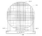
- 2is a block diagram, the liquid crystal panel 400 and the display unit 410 are shown as rectangles. However, in the liquid crystal display device according to this embodiment, the shapes of the liquid crystal panel 400 and the display unit 410 are circular. . That is, the liquid crystal display device according to the present embodiment is an atypical display.
- FIG. 3is a diagram for explaining the display unit 410 in the present embodiment.
- the display unit 410includes a plurality (j) of source bus lines (video signal lines) SL (1) to SL (j) and a plurality (i) of gate bus lines (i). Scanning signal lines GL (1) to GL (i) are arranged. For example, j is 1920 and i is 1080. Further, in the region in the display portion 410, a pixel formation portion for forming pixels is provided in the vicinity of the intersection of the source bus line SL and the gate bus line GL.
- FIG. 4is a circuit diagram showing a configuration of the pixel forming unit 4.
- the pixel forming unit 4includes a TFT (thin film transistor) 41 having a gate electrode connected to a gate bus line GL passing through a corresponding intersection and a source electrode connected to a source bus line SL passing through the intersection.
- a capacitor 43 and an auxiliary capacitor 44 formed by the pixel electrode 42 and the auxiliary capacitor electrode 46are included.
- the liquid crystal capacitor 43 and the auxiliary capacitor 44constitute a pixel capacitor 47. Note that the configuration of the pixel formation portion 4 is not limited to the configuration shown in FIG. For example, a configuration in which the auxiliary capacitor 44 and the auxiliary capacitor electrode 46 are not provided may be employed.
- an oxide TFT(a thin film transistor having an oxide semiconductor layer) is employed.
- the oxide semiconductor layerincludes, for example, an In—Ga—Zn—O-based semiconductor such as indium gallium zinc oxide.
- the In—Ga—Zn—O-based semiconductoris a ternary oxide of In, Ga, and Zn. Note that TFTs other than oxide TFTs can be used as the TFTs 41 in the pixel formation portion 4.
- a gate driver (scanning signal line drive circuit) 500 for driving the gate bus line GLis formed in the display unit 410 as shown in FIG.
- the gate driversince the gate driver is provided in the frame region (outside the display portion), the scanning signal is given from the frame region into the display portion.
- a scanning signalis output from the gate driver 500 provided in the display unit 410. Since such a configuration is adopted, there is no need to form a circuit or wiring for driving the gate bus line GL in the frame region, and it is possible to realize a deformed display as in this embodiment. Yes.
- the power supply 100supplies a predetermined power supply voltage to the display control circuit 200, the source driver 300, and the liquid crystal panel 400 (more specifically, the gate driver 500 in the liquid crystal panel 400).
- the display control circuit 200receives an image signal DAT and a timing signal group TG such as a horizontal synchronization signal and a vertical synchronization signal sent from the outside, and receives a digital video signal DV and a source start pulse for controlling image display on the display unit 410.
- a signal SSP, a source clock signal SCK, a latch strobe signal LS, a gate start pulse signal GSP, and a gate clock signal GCKare output.
- the source driver 300receives the digital video signal DV, the source start pulse signal SSP, the source clock signal SCK, and the latch strobe signal LS output from the display control circuit 200, and data corresponding to the display gradation indicated by the digital video signal DV. Voltages V (1) to V (j) are applied to the source bus lines SL (1) to SL (j) (see FIG. 3). A detailed description of the source driver 300 will be described later.
- the gate driver 500Based on the gate start pulse signal GSP and the gate clock signal GCK output from the display control circuit 200, the gate driver 500 applies 1 to the active scanning signal to each of the gate bus lines GL (1) to GL (i). The vertical scanning period is repeated as a cycle.
- the data voltage Vis applied to the source bus lines SL (1) to SL (j) and the scanning signal is applied to the gate bus lines GL (1) to GL (i).
- An image based on the image signal DAT sent from the outsideis displayed on the display unit 410.
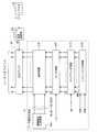
- FIG. 1is a block diagram showing a detailed configuration of the source driver 300 in the present embodiment.
- the source driver 300includes a data voltage generation unit 31, an output amplifier 32, a register (storage unit) 33, and a bias current control unit 34.
- the data voltage generation unit 31includes a shift register 310 circuit, a sampling circuit 312, a latch circuit 314, a gradation voltage generation circuit 316, and a selection circuit 318.
- a source start pulse signal SSP and a source clock signal SCKare input to the shift register circuit 310.
- the shift register circuit 310sequentially transfers pulses included in the source start pulse signal SSP from the input end to the output end based on the source clock signal SCK.
- the sampling pulse SMP corresponding to each source bus line SL (1) to SL (j)is sequentially output from the shift register circuit 310, and the sampling pulse SMP is sequentially input to the sampling circuit 312.
- the sampling circuit 312samples the digital video signal DV sent from the display control circuit 200 at the timing of the sampling pulse SMP outputted from the shift register circuit 310, and outputs it as an internal image signal d.
- the latch circuit 314takes in the internal image signal d output from the sampling circuit 312 at the pulse timing of the latch strobe signal LS and outputs it.
- the gradation voltage generation circuit 316generates a voltage (gradation voltage) corresponding to each gradation level based on a plurality of reference voltages supplied from the power supply 100, and outputs them as a gradation voltage group. For example, voltages (gradation voltages) Vk (0) to Vk (255) corresponding to 256 gradation levels are output from the gradation voltage generation circuit 316 as a gradation voltage group.
- the selection circuit 318selects one of the gradation voltage groups output from the gradation voltage generation circuit 316 based on the internal image signal d output from the latch circuit 314, and outputs the selected voltage. To do.
- the output amplifier 32performs impedance conversion on the voltage output from the selection circuit 318 and outputs the converted voltage as the data voltage V to the source bus line SL.
- the bias current control unit 34controls the magnitude of the bias current of the output amplifier 32.
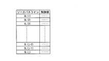
- a control value C for adjusting the settling time of the output of the data voltage V from the output amplifier 32is stored in advance.
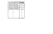
- the register 33stores a control value C for each source bus line SL, as shown in FIG.
- the present inventionis not limited to this, and when the settling time may be adjusted for each of the plurality of source bus lines SL, the register 33 has a plurality of sources as shown in FIG.
- a control value Cmay be stored for each bus line SL.
- the bias current control unit 34outputs a bias current control signal SC for each source bus line SL based on the control value C stored in the register 33.
- the bias current control signal SCcontrols the magnitude of the bias current of the output amplifier 32 for each source bus line SL.
- the output amplifier 32includes an operational amplifier 320.
- the non-inverting input terminal of the operational amplifier 320is supplied with the voltage (grayscale voltage) Vin output from the selection circuit 318 (see FIG. 1) in the data voltage generation unit 31.
- An output from the operational amplifier 320is given to the inverting input terminal of the operational amplifier 320. That is, negative feedback is applied to the operational amplifier 320.
- the output from the operational amplifier 320is given to the source bus line SL as the data voltage V.
- the output amplifier 32 in the present embodimentis a voltage follower circuit.
- the operational amplifier 320includes, for example, a differential amplifier 321 configured as shown in FIG.
- the differential amplifier 321includes a variable constant current source 322 that can control the magnitude of the constant current flowing through the circuit.
- the magnitude of the constant current supplied to the circuit by the variable constant current source 322is controlled by a bias current control signal SC provided from the bias current control unit 34 (see FIG. 1).
- SCbias current control signal
- FIG. 10An example of the overall configuration of the operational amplifier 320 is shown in FIG. 10, for example.
- bias current control unit 34is realized by a D / A converter capable of outputting eight levels of voltage. Further, it is assumed that the magnitude of the bias current is controlled within a range of 20% to 150% with reference to 0.15 mA.
- a 3-bit valueis stored in advance as a control value C according to the target bias current.
- the control value C stored in the register 33is given to the D / A converter (bias current control unit 34).
- the D / A converterhas eight levels of voltage (“bias current magnitude: 20%” to “bias current magnitude: 150” in accordance with the 3-bit value that is the control value C stored in the register 33. Any one of the eight voltages corresponding to% "is output as the bias current control signal SC.
- the voltage (bias current control signal SC) output from the D / A converteris applied to a variable constant current source 322 (see FIG. 9) in the output amplifier 32.
- the magnitude of the constant currentis controlled in the output amplifier 32, and the magnitude of the bias current changes according to the magnitude of the constant current.
- the signal waveform of the data voltage Vchanges as shown in FIG.
- the signal waveform of the data voltage Vchanges as shown in FIG.
- the settling time T3(see FIG. 12) when the magnitude of the bias current is set to 100% is the magnitude of the bias current. Is set shorter than the settling time T1 (see FIG. 11).
- the settling time T4(see FIG. 12) when the magnitude of the bias current is set to 100% is the magnitude of the bias current.
- the settling time T2when set to 40% is shorter.
- the settling time of the data voltage Vis shortened as the value of the bias current of the output amplifier 32 is increased.
- the source bus line SLbis longer than the source bus line SLa, and the source bus line SLc is longer than the source bus line SLb.
- the length of the source bus line SLis longer as the arrangement position is closer to the center of the display unit 410. Therefore, the load on the source bus line SL increases as the position of the source bus line SL is closer to the center of the display unit 410.
- a larger bias currentflows in the output amplifier 32 corresponding to the source bus line SL (that is, the source bus line SL having a large load) disposed near the center of the display unit 410.
- the magnitude of the bias currentis controlled.
- the control value Cis stored in advance in the register 33 so that a larger bias current flows through the output amplifier 32 corresponding to the source bus line SL disposed near the center of the display unit 410.
- the magnitude of the bias currentis 20% and is provided in the center of the display unit 410.
- the control value Cis stored in advance in the register 33 so that the magnitude of the bias current becomes 150%.
- the settling time of the output of the data voltage V from the output amplifier 32approaches a certain time regardless of the load on the source bus line SL.
- the difference in charging rate depending on the position(the position in the horizontal direction of the display unit 410) is suppressed, and the charging rate is uniform throughout the display unit 410.
- the source driver 300includes a register 33 that stores the control value C for adjusting the settling time of the output of the data voltage V from the output amplifier 32, and the control value stored in the register 33.
- a bias current control unit 34 for controlling the magnitude of the bias current of the output amplifier 32 based on Cis provided.
- the control value Cis stored in the register 33 in advance so that a larger bias current flows through the output amplifier 32 corresponding to the source bus line SL having a larger load. Thereby, the difference in the settling time of the data voltage V between the plurality of source bus lines SL is reduced.
- the charging rateis made uniform throughout the display unit 410, and the occurrence of abnormal display (display of an image called vertical gradation) is suppressed.
- the occurrence of an abnormal displaydue to “the difference in the settling time of the data voltage V (applied to the source bus line SL)” depending on the position of the source bus line SL.
- Source driver 300 and a liquid crystal display device including the source driver 300are realized.
- the charge ratecan be made uniform by uniformly increasing the magnitude of the bias current of all the output amplifiers 32 regardless of the magnitude of the load on the source bus line SL.
- the magnitude of the bias currentaccording to the magnitude of the load on the source bus line SL, the effect of reducing power consumption can be obtained.
- the liquid crystal panel 400 and the display unit 410have a circular shape.
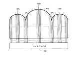
- the shapes of the liquid crystal panel 400 and the display unit 410are not particularly limited. Accordingly, an example in which the present invention is applied to an in-vehicle liquid crystal display device will be described as a first modification.
- FIG. 15is a front view of an in-vehicle liquid crystal display device according to this modification. From the appearance shown in FIG. 15, it is understood that the length of the source bus line varies depending on the position.
- the register 33is controlled in advance so that a larger bias current flows in the output amplifier 32 corresponding to the source bus line SL having a larger load (the source bus line SL having a longer length).
- the value Cis stored.
- the charging rateis uniform in the entire display unit 410, and the occurrence of abnormal display (display of an image called vertical gradation) is suppressed.
- the liquid crystal display deviceis assumed to be an atypical display, but the present invention is not limited to this.
- An example in which the present invention is applied to a liquid crystal display device having a general rectangular display unitwill be described as a second modification.
- FIG. 17is a block diagram showing an overall configuration of a liquid crystal display device according to this modification. Unlike the above embodiment (FIG. 2), the gate driver 500 is provided outside the liquid crystal panel 400. Note that the gate driver 500 may be provided in a region outside the display unit 410 in the liquid crystal panel 400. The operation of each component shown in FIG. 17 is the same as that in the above embodiment.
- FIG. 18shows only the source driver 300 and the display unit 410 among the components shown in FIG.
- the luminance of the region denoted by reference numeral 71 in FIG. 18is lower than the luminance of the other regions.
- the output corresponding to the source bus line SL in the region denoted by reference numeral 71rather than the output amplifier 32 corresponding to the source bus line SL in the region other than the region denoted by reference numeral 71.
- a control value Cis stored in advance in the register 33 so that a larger bias current flows in the amplifier 32.
- the magnitude of the bias currentis 100% and other than the region denoted by reference numeral 71.
- the control value Cis stored in advance in the register 33 so that the magnitude of the bias current is 60% in the output amplifier 32 corresponding to the source bus line SL in the region.
- the charge rateis lowered when the data voltage V of the same magnitude is applied to all the source bus lines SL without controlling the magnitude of the bias current of the output amplifier 32.
- the control value Cis stored in the register 33 so that the bias current control unit 34 increases the magnitude of the bias current for the output amplifier 32 corresponding to the bus line SL.
- the present inventioncan also be applied to the case where the gate driver 500 is formed in the frame area in the atypical display.
Landscapes
- Engineering & Computer Science (AREA)
- Chemical & Material Sciences (AREA)
- Crystallography & Structural Chemistry (AREA)
- Physics & Mathematics (AREA)
- Computer Hardware Design (AREA)
- General Physics & Mathematics (AREA)
- Theoretical Computer Science (AREA)
- Control Of Indicators Other Than Cathode Ray Tubes (AREA)
Abstract
Description
Translated fromJapanese本発明は、表示装置に関し、より詳しくは、特に矩形以外の形状の表示パネルを有する表示装置の映像信号線を駆動する映像信号線駆動回路に関する。The present invention relates to a display device, and more particularly to a video signal line driving circuit that drives a video signal line of a display device having a display panel having a shape other than a rectangle.
液晶表示装置は、一般に、互いに対向する2枚の絶縁性のガラス基板からなる液晶パネルを備えている。一方のガラス基板はアレイ基板と呼ばれており、他方のガラス基板は対向基板と呼ばれている。アレイ基板にはTFT(薄膜トランジスタ)や画素電極などが形成され、対向基板には対向電極やカラーフィルタなどが形成されている。このような従来の一般的な液晶パネルは、矩形の表示部(表示領域)を有している。表示部には、複数本のソースバスライン(映像信号線)と、複数本のゲートバスライン(走査信号線)と、それら複数本のソースバスラインと複数本のゲートバスラインとの交差点にそれぞれ対応して設けられた複数個の画素形成部とが形成されている。各画素形成部には、対応する交差点を通過するゲートバスラインにゲート電極が接続されると共に当該交差点を通過するソースバスラインにソース電極が接続されたTFTと、そのTFTのドレイン電極に接続された画素電極と、上記複数個の画素形成部に共通的に設けられた対向電極および補助容量電極と、画素電極と対向電極とによって形成される液晶容量と、画素電極と補助容量電極とによって形成される補助容量とが含まれている。液晶容量と補助容量とによって画素容量が構成されている。以上のような構成において、各TFTのゲート電極がゲートバスラインからアクティブな走査信号を受けたときに当該TFTのソース電極がソースバスラインから受けるデータ電圧(映像信号)に基づいて、画素容量の充電が行われる。このようにして上記複数個の画素形成部内の画素容量の充電が行われることにより、表示部に所望の画像が表示される。A liquid crystal display device generally includes a liquid crystal panel composed of two insulating glass substrates facing each other. One glass substrate is called an array substrate, and the other glass substrate is called a counter substrate. TFTs (thin film transistors) and pixel electrodes are formed on the array substrate, and counter electrodes and color filters are formed on the counter substrate. Such a conventional general liquid crystal panel has a rectangular display section (display area). The display unit includes a plurality of source bus lines (video signal lines), a plurality of gate bus lines (scanning signal lines), and intersections of the plurality of source bus lines and the plurality of gate bus lines. A plurality of corresponding pixel forming portions are formed. In each pixel formation portion, a gate electrode is connected to a gate bus line passing through a corresponding intersection and a source electrode is connected to a source bus line passing through the intersection, and a drain electrode of the TFT is connected. Formed by the pixel electrode, the counter electrode and the auxiliary capacitance electrode provided in common in the plurality of pixel forming portions, the liquid crystal capacitance formed by the pixel electrode and the counter electrode, and the pixel electrode and the auxiliary capacitance electrode Auxiliary capacity to be included. The liquid crystal capacitor and the auxiliary capacitor constitute a pixel capacitor. In the configuration as described above, the pixel capacitance is determined based on the data voltage (video signal) received by the source electrode of the TFT from the source bus line when the gate electrode of each TFT receives an active scanning signal from the gate bus line. Charging is performed. In this way, by charging the pixel capacitors in the plurality of pixel formation portions, a desired image is displayed on the display portion.
上述のような液晶表示装置において、例えばバックライトを構成する光源の配置に起因して、輝度むらが生じることがある。そこで、従来より、輝度むらの発生を抑制するために、目標とする表示階調に対応するデータ電圧に補正を施して、補正後のデータ電圧をソースバスラインに印加することが行われている。このような補正を行う液晶表示装置の発明は、例えば日本の特開2008-70404号公報に開示されている。In the above-described liquid crystal display device, uneven brightness may occur due to, for example, the arrangement of the light sources constituting the backlight. Therefore, conventionally, in order to suppress the occurrence of luminance unevenness, correction is performed on the data voltage corresponding to the target display gradation, and the corrected data voltage is applied to the source bus line. . An invention of a liquid crystal display device that performs such correction is disclosed, for example, in Japanese Unexamined Patent Publication No. 2008-70404.
上述したように、従来の一般的な液晶パネルは、矩形の表示部(表示領域)を有していた。ところが、近年、時計用途の液晶表示装置や車載用途の液晶表示装置など、矩形以外の形状の表示部を備えた液晶表示装置の開発が進められている。なお、以下においては、矩形以外の形状の表示部を備えた表示装置であって表示パネルの外形も矩形以外の形状である表示装置のことを「異型ディスプレイ」という。As described above, a conventional general liquid crystal panel has a rectangular display section (display area). However, in recent years, development of a liquid crystal display device having a display portion having a shape other than a rectangle, such as a liquid crystal display device for watches and a liquid crystal display device for in-vehicle use, has been promoted. In the following description, a display device that includes a display unit having a shape other than a rectangle and that has a display panel that has a shape other than a rectangle is also referred to as “atypical display”.
ところで、異型ディスプレイにおいて、目標とする表示画像がいわゆる「ベタ画像」(表示部全体が同一色で同一階調である画像)であるにもかかわらず実際の表示画像が縦グラデーションと呼ばれる画像(横方向に徐々に階調が変化する画像)となることがある。このような異常表示について、図19および図20を参照しつつ説明する。By the way, in a variant display, the target display image is a so-called “solid image” (an image in which the entire display unit has the same color and the same gradation), but the actual display image is an image (vertical gradation) (horizontal gradation). Image with gradation gradually changing in the direction). Such an abnormal display will be described with reference to FIGS. 19 and 20.
図19は、円形の表示部を有する異型ディスプレイにおけるソースバスライン,表示部,およびソースドライバを模式的に示した図である。図19から把握されるように、この異型ディスプレイにおいては、ソースバスラインの長さが位置によって異なっている。例えば、符号91を付したソースバスライン(表示部の端部に配設されたソースバスライン)の長さは相対的に短いのに対して、符号92を付したソースバスライン(表示部の中央部に近い位置に配設されたソースバスライン)の長さは相対的に長い。また、表示部内の領域において、各ソースバスラインは上述した画素形成部に接続されている。すなわち、符号91を付したソースバスラインは比較的少数の画素形成部に接続されているのに対して、符号92を付したソースバスラインは比較的多数の画素形成部に接続されている。以上より、符号91を付したソースバスラインの負荷は相対的に小さく、符号92を付したソースバスラインの負荷は相対的に大きい。このため、例えば、符号91を付したソースバスラインではデータ電圧の信号波形が図20で符号Vaで示すように変化するのに対して、符号92を付したソースバスラインではデータ電圧の信号波形が図20で符号Vbで示すように変化する。FIG. 19 is a diagram schematically showing a source bus line, a display unit, and a source driver in an atypical display having a circular display unit. As can be seen from FIG. 19, in this atypical display, the length of the source bus line differs depending on the position. For example, the length of the source bus line denoted by reference numeral 91 (the source bus line disposed at the end of the display portion) is relatively short, whereas the source bus line denoted by reference numeral 92 (of the display portion) The length of the source bus line (disposed near the center) is relatively long. Further, in the region within the display portion, each source bus line is connected to the above-described pixel formation portion. That is, the source bus line denoted by
図20より、表示部の中央部に近い位置に配設されたソースバスラインほどデータ電圧のセトリング時間(電圧値が目標値の許容範囲に収まるまでの時間)が長い(すなわち応答速度が遅い)ことが把握される。データ電圧のセトリング時間のこのような違いが位置(横方向の位置)による充電率の違いを引き起こし、その結果、(目標とする表示画像がベタ画像であるにもかかわらず)縦グラデーションと呼ばれる画像が表示される。すなわち、異常表示が発生する。As shown in FIG. 20, the source bus line arranged near the center of the display unit has a longer data voltage settling time (time until the voltage value falls within the allowable range of the target value) (ie, the response speed is slower). It is understood. This difference in the settling time of the data voltage causes a difference in the charging rate depending on the position (lateral position), resulting in an image called vertical gradation (although the target display image is a solid image) Is displayed. That is, an abnormal display occurs.
そこで本発明は、ソースバスライン(映像信号線)の位置による「(ソースバスラインに印加される)データ電圧のセトリング時間の違い」に起因する異常表示の発生を抑制することのできるソースドライバ(映像信号線駆動回路)およびそれを備えた表示装置を提供することを目的とする。Therefore, the present invention provides a source driver that can suppress the occurrence of abnormal display due to “difference in the settling time of a data voltage (applied to the source bus line)” depending on the position of the source bus line (video signal line). An object is to provide a video signal line driving circuit) and a display device including the same.
本発明の第1の局面は、映像信号線を駆動するための映像信号線駆動回路であって、
表示階調に対応するデータ電圧を生成するデータ電圧生成部と、
前記映像信号線に前記データ電圧を出力する、前記映像信号線の本数に等しい数の出力アンプと、
前記出力アンプからの前記データ電圧の出力のセトリング時間を調整するための制御値を格納する記憶部と、
前記記憶部に格納されている制御値に基づいて前記出力アンプのバイアス電流の大きさを制御するバイアス電流制御部と
を備えることを特徴とする。A first aspect of the present invention is a video signal line driving circuit for driving a video signal line,
A data voltage generator for generating a data voltage corresponding to the display gradation;
The number of output amplifiers equal to the number of the video signal lines for outputting the data voltage to the video signal lines;
A storage unit for storing a control value for adjusting a settling time of the output of the data voltage from the output amplifier;
And a bias current control unit that controls the magnitude of the bias current of the output amplifier based on a control value stored in the storage unit.
本発明の第2の局面は、本発明の第1の局面において、
前記記憶部は、前記映像信号線の本数に等しい数の前記制御値を格納し、
前記バイアス電流制御部は、各映像信号線毎に、前記記憶部に格納されている複数の制御値のうちの対応する制御値に基づいて、対応する出力アンプのバイアス電流の大きさを制御することを特徴とする。According to a second aspect of the present invention, in the first aspect of the present invention,
The storage unit stores the number of control values equal to the number of the video signal lines,
The bias current control unit controls the magnitude of the bias current of the corresponding output amplifier based on a corresponding control value among a plurality of control values stored in the storage unit for each video signal line. It is characterized by that.
本発明の第3の局面は、表示装置であって、
映像信号線を有する表示パネルと、本発明の第2の局面に係る映像信号線駆動回路とを備えたことを特徴とする。A third aspect of the present invention is a display device,
A display panel having video signal lines and a video signal line driving circuit according to a second aspect of the present invention are provided.
本発明の第4の局面は、本発明の第3の局面において、
前記表示パネルの形状は、非矩形であって、
長さの長い映像信号線に対応する出力アンプほど前記バイアス電流制御部によってバイアス電流の大きさが大きくされるように、前記記憶部に前記制御値が格納されていることを特徴とする。According to a fourth aspect of the present invention, in the third aspect of the present invention,
The display panel has a non-rectangular shape,
The control value is stored in the storage unit so that the bias current control unit increases the magnitude of the bias current for an output amplifier corresponding to a video signal line having a longer length.
本発明の第5の局面は、本発明の第4の局面において、
前記表示パネルの形状は、円形であることを特徴とする。According to a fifth aspect of the present invention, in the fourth aspect of the present invention,
The display panel has a circular shape.
本発明の第6の局面は、本発明の第4の局面において、
車載用であることを特徴とする。A sixth aspect of the present invention is the fourth aspect of the present invention,
It is for in-vehicle use.
本発明の第7の局面は、本発明の第4の局面において、
前記表示パネルの形状は、矩形であって、
前記出力アンプのバイアス電流の大きさを制御することなく全ての映像信号線に同じ大きさのデータ電圧を印加したと仮定したときに充電率が低くなる映像信号線に対応する出力アンプほど前記バイアス電流制御部によってバイアス電流の大きさが大きくされるように、前記記憶部に前記制御値が格納されていることを特徴とする。According to a seventh aspect of the present invention, in the fourth aspect of the present invention,
The display panel has a rectangular shape,
The output amplifier corresponding to the video signal line having a lower charging rate when it is assumed that the same data voltage is applied to all the video signal lines without controlling the magnitude of the bias current of the output amplifier. The control value is stored in the storage unit such that the magnitude of the bias current is increased by the current control unit.
本発明の第8の局面は、映像信号線の本数に等しい数の出力アンプを有する映像信号線駆動回路による映像信号線の駆動方法であって、
表示階調に対応するデータ電圧を生成するデータ電圧生成ステップと、
前記出力アンプから前記映像信号線に前記データ電圧を出力するデータ電圧出力ステップと、
前記出力アンプからの前記データ電圧の出力のセトリング時間を調整するために予め定められている制御値に基づいて、前記出力アンプのバイアス電流の大きさを制御するバイアス電流制御ステップと
を含むことを特徴とする。An eighth aspect of the present invention is a video signal line driving method by a video signal line driving circuit having a number of output amplifiers equal to the number of video signal lines,
A data voltage generation step for generating a data voltage corresponding to the display gradation;
A data voltage output step of outputting the data voltage from the output amplifier to the video signal line;
A bias current control step of controlling the magnitude of the bias current of the output amplifier based on a predetermined control value for adjusting the settling time of the output of the data voltage from the output amplifier. Features.
本発明の第1の局面によれば、映像信号線駆動回路には、従来の構成要素に加えて、出力アンプからのデータ電圧の出力のセトリング時間を調整するための制御値を格納する記憶部と、記憶部に格納されている制御値に基づいて出力アンプのバイアス電流の大きさを制御するバイアス電流制御部とが設けられている。このため、各映像信号線の負荷を考慮して記憶部に好適に制御値を格納しておくことによって、複数本の映像信号線間での出力アンプからのデータ電圧の出力のセトリング時間の差が小さくなるように、各出力アンプのバイアス電流の大きさが制御される。これにより、この映像信号線駆動回路を備えた表示装置において、表示部全体で充電率が均一化し、異常表示(縦グラデーションと呼ばれる画像の表示)の発生が抑制される。このように、映像信号線の位置による「(映像信号線に印加される)データ電圧のセトリング時間の違い」に起因する異常表示の発生を抑制することのできる映像信号線駆動回路が実現される。According to the first aspect of the present invention, the video signal line driving circuit stores a control value for adjusting the settling time of the output of the data voltage from the output amplifier in addition to the conventional components. And a bias current control unit that controls the magnitude of the bias current of the output amplifier based on the control value stored in the storage unit. For this reason, the control value is suitably stored in the storage unit in consideration of the load of each video signal line, so that the difference in the settling time of the output of the data voltage from the output amplifier among the plurality of video signal lines. So that the bias current of each output amplifier is controlled. As a result, in the display device including the video signal line driving circuit, the charging rate is made uniform throughout the display unit, and the occurrence of abnormal display (display of an image called vertical gradation) is suppressed. In this manner, a video signal line driving circuit capable of suppressing the occurrence of abnormal display due to the “difference in settling time of the data voltage (applied to the video signal line)” depending on the position of the video signal line is realized. .
本発明の第2の局面によれば、各映像信号線毎に、対応する出力アンプのバイアス電流の大きさが制御される。このため、異常表示(縦グラデーションと呼ばれる画像の表示)の発生が効果的に抑制される。According to the second aspect of the present invention, the magnitude of the bias current of the corresponding output amplifier is controlled for each video signal line. For this reason, the occurrence of abnormal display (display of an image called vertical gradation) is effectively suppressed.
本発明の第3の局面によれば、映像信号線の位置による「(映像信号線に印加される)データ電圧のセトリング時間の違い」に起因する異常表示の発生を抑制することのできる映像信号線駆動回路を備えた表示装置が実現される。According to the third aspect of the present invention, a video signal capable of suppressing the occurrence of an abnormal display due to the “difference in settling time of the data voltage (applied to the video signal line)” depending on the position of the video signal line. A display device including a line driving circuit is realized.
本発明の第4の局面によれば、非矩形の表示パネルを備えた表示装置において、負荷の大きい映像信号線に対応する出力アンプほど大きなバイアス電流が流れるように、記憶部に制御値が格納される。このため、複数本の映像信号線間での出力アンプからのデータ電圧の出力のセトリング時間の差が小さくなる。これにより、非矩形の表示パネルを備えた表示装置において、表示部全体で充電率が均一化し、異常表示(縦グラデーションと呼ばれる画像の表示)の発生が抑制される。According to the fourth aspect of the present invention, in a display device including a non-rectangular display panel, a control value is stored in the storage unit so that a larger bias current flows through an output amplifier corresponding to a video signal line having a larger load. Is done. For this reason, the difference in the settling time of the output of the data voltage from the output amplifier between the plurality of video signal lines is reduced. As a result, in a display device including a non-rectangular display panel, the charging rate is made uniform throughout the display unit, and the occurrence of abnormal display (display of an image called vertical gradation) is suppressed.
本発明の第5の局面によれば、円形の表示パネルを有する表示装置において、本発明の第4の局面と同様の効果が得られる。According to the fifth aspect of the present invention, in a display device having a circular display panel, the same effect as in the fourth aspect of the present invention can be obtained.
本発明の第6の局面によれば、車載用の表示装置において、本発明の第4の局面と同様の効果が得られる。According to the sixth aspect of the present invention, the same effect as the fourth aspect of the present invention can be obtained in the in-vehicle display device.
本発明の第7の局面によれば、矩形の表示パネルを備えた表示装置において、バイアス電流の大きさを制御しなかった場合に充電率が低くなる映像信号線に対応する出力アンプほど大きなバイアス電流が流れるように、記憶部に制御値が格納される。これにより、矩形の表示パネルを備えた表示装置において、輝度むらの発生が抑制される。According to the seventh aspect of the present invention, in a display device having a rectangular display panel, a larger bias is applied to an output amplifier corresponding to a video signal line having a lower charging rate when the magnitude of the bias current is not controlled. The control value is stored in the storage unit so that a current flows. Thereby, in the display device including the rectangular display panel, the occurrence of uneven brightness is suppressed.
本発明の第8の局面によれば、本発明の第1の局面と同様の効果を映像信号線の駆動方法において奏することができる。According to the eighth aspect of the present invention, the same effect as in the first aspect of the present invention can be achieved in the video signal line driving method.
以下、添付図面を参照しつつ、本発明の一実施形態について説明する。Hereinafter, an embodiment of the present invention will be described with reference to the accompanying drawings.
<1.全体構成および動作概要>
図2は、本発明の一実施形態に係る液晶表示装置の全体構成を示すブロック図である。図2に示すように、この液晶表示装置は、電源100と表示制御回路200とソースドライバ(映像信号線駆動回路)300と液晶パネル400とを備えている。液晶パネル400には、画像を表示する表示部(表示領域)410が含まれている。なお、図2はブロック図であるため液晶パネル400および表示部410を矩形で図示しているが、本実施形態に係る液晶表示装置においては、液晶パネル400および表示部410の形状は円形である。すなわち、本実施形態に係る液晶表示装置は異型ディスプレイである。<1. Overall configuration and operation overview>
FIG. 2 is a block diagram showing the overall configuration of the liquid crystal display device according to one embodiment of the present invention. As shown in FIG. 2, the liquid crystal display device includes a
図3は、本実施形態における表示部410について説明するための図である。表示部410には、図3に示すように、複数本(j本)のソースバスライン(映像信号線)SL(1)~SL(j)と、複数本(i本)のゲートバスライン(走査信号線)GL(1)~GL(i)とが配設されている。例えば、jは1920であり、iは1080である。また、表示部410内の領域において、ソースバスラインSLとゲートバスラインGLとの交差点の近傍には、画素を形成する画素形成部が設けられている。FIG. 3 is a diagram for explaining the
図4は、画素形成部4の構成を示す回路図である。画素形成部4には、対応する交差点を通過するゲートバスラインGLにゲート電極が接続されると共に当該交差点を通過するソースバスラインSLにソース電極が接続されたTFT(薄膜トランジスタ)41と、そのTFT41のドレイン電極に接続された画素電極42と、上記複数個の画素形成部4に共通的に設けられた対向電極45および補助容量電極46と、画素電極42と対向電極45とによって形成される液晶容量43と、画素電極42と補助容量電極46とによって形成される補助容量44とが含まれている。液晶容量43と補助容量44とによって画素容量47が構成されている。なお、画素形成部4の構成は図4に示す構成には限定されない。例えば、補助容量44および補助容量電極46が設けられていない構成を採用することもできる。FIG. 4 is a circuit diagram showing a configuration of the
画素形成部4内のTFT41については、典型的には、酸化物TFT(酸化物半導体層を有する薄膜トランジスタ)が採用される。酸化物半導体層は、例えば、酸化インジウムガリウム亜鉛などのIn-Ga-Zn-O系の半導体を含んでいる。In-Ga-Zn-O系の半導体は、In、Ga、Znの三元系酸化物である。なお、画素形成部4内のTFT41として、酸化物TFT以外のTFTを使用することもできる。For the
また、本実施形態においては、ゲートバスラインGLを駆動するゲートドライバ(走査信号線駆動回路)500が、図5に示すように表示部410内に形成されている。従来、ゲートドライバは額縁領域(表示部の外側)に設けられていたため、走査信号は額縁領域から表示部内へと与えられていた。これに対して、本実施形態においては、表示部410内に設けられたゲートドライバ500から走査信号が出力される。このような構成が採用されているので、ゲートバスラインGLを駆動するための回路や配線を額縁領域に形成する必要がなくなり、本実施形態のような異形ディスプレイを実現することが可能となっている。In this embodiment, a gate driver (scanning signal line drive circuit) 500 for driving the gate bus line GL is formed in the
以下、図2,図5に示す構成要素の動作概要について説明する。電源100は、表示制御回路200とソースドライバ300と液晶パネル400(より詳しくは、液晶パネル400内のゲートドライバ500)とに所定の電源電圧を供給する。表示制御回路200は、外部から送られる画像信号DATおよび水平同期信号や垂直同期信号などのタイミング信号群TGを受け取り、デジタル映像信号DVと、表示部410における画像表示を制御するためのソーススタートパルス信号SSP,ソースクロック信号SCK,ラッチストローブ信号LS,ゲートスタートパルス信号GSP,およびゲートクロック信号GCKとを出力する。Hereinafter, the operation outline of the components shown in FIGS. 2 and 5 will be described. The
ソースドライバ300は、表示制御回路200から出力されるデジタル映像信号DV,ソーススタートパルス信号SSP,ソースクロック信号SCK,およびラッチストローブ信号LSを受け取り、デジタル映像信号DVの示す表示階調に対応するデータ電圧V(1)~V(j)をソースバスラインSL(1)~SL(j)に印加する(図3参照)。なお、ソースドライバ300についての詳しい説明は後述する。The
ゲートドライバ500は、表示制御回路200から出力されるゲートスタートパルス信号GSPおよびゲートクロック信号GCKに基づいて、アクティブな走査信号の各ゲートバスラインGL(1)~GL(i)への印加を1垂直走査期間を周期として繰り返す。Based on the gate start pulse signal GSP and the gate clock signal GCK output from the
以上のようにして、各ソースバスラインSL(1)~SL(j)にデータ電圧Vが印加され、各ゲートバスラインGL(1)~GL(i)に走査信号が印加されることにより、外部から送られた画像信号DATに基づく画像が表示部410に表示される。As described above, the data voltage V is applied to the source bus lines SL (1) to SL (j) and the scanning signal is applied to the gate bus lines GL (1) to GL (i). An image based on the image signal DAT sent from the outside is displayed on the
<2.ソースドライバの構成および動作>
次に、本実施形態におけるソースドライバ300について詳しく説明する。<2. Configuration and operation of source driver>
Next, the
<2.1 ソースドライバの全体構成>
図1は、本実施形態におけるソースドライバ300の詳細な構成を示すブロック図である。図1に示すように、ソースドライバ300は、データ電圧生成部31と出力アンプ32とレジスタ(記憶部)33とバイアス電流制御部34とによって構成されている。データ電圧生成部31には、シフトレジスタ310回路とサンプリング回路312とラッチ回路314と階調電圧生成回路316と選択回路318とが含まれている。<2.1 Overall configuration of source driver>
FIG. 1 is a block diagram showing a detailed configuration of the
シフトレジスタ回路310にはソーススタートパルス信号SSPとソースクロック信号SCKとが入力される。シフトレジスタ回路310は、ソースクロック信号SCKに基づいて、ソーススタートパルス信号SSPに含まれるパルスを入力端から出力端へと順次に転送する。このパルスの転送に応じてシフトレジスタ回路310から各ソースバスラインSL(1)~SL(j)に対応するサンプリングパルスSMPが順次に出力され、当該サンプリングパルスSMPはサンプリング回路312に順次に入力される。A source start pulse signal SSP and a source clock signal SCK are input to the
サンプリング回路312は、表示制御回路200から送られるデジタル映像信号DVをシフトレジスタ回路310から出力されるサンプリングパルスSMPのタイミングでサンプリングし、それを内部画像信号dとして出力する。ラッチ回路314は、サンプリング回路312から出力される内部画像信号dをラッチストローブ信号LSのパルスのタイミングで取り込み、それを出力する。The
階調電圧生成回路316は、電源100から与えられる複数個の基準電圧に基づき、各階調レベルに対応する電圧(階調電圧)を生成し、それらを階調電圧群として出力する。例えば、256の階調レベルに対応する電圧(階調電圧)Vk(0)~Vk(255)が、階調電圧群として階調電圧生成回路316から出力される。The gradation
選択回路318は、ラッチ回路314から出力される内部画像信号dに基づき、階調電圧生成回路316から出力される階調電圧群のうちのいずれかの電圧を選択し、その選択した電圧を出力する。出力アンプ32は、選択回路318から出力された電圧にインピーダンス変換を施して、変換後の電圧をデータ電圧VとしてソースバスラインSLに出力する。その際、後述するように、出力アンプ32のバイアス電流の大きさがバイアス電流制御部34によって制御される。The
レジスタ33には、予め、出力アンプ32からのデータ電圧Vの出力のセトリング時間を調整するための制御値Cが格納される。本実施形態においては、レジスタ33には、図6に示すように、1本のソースバスラインSL毎に制御値Cが格納される。但し、本発明はこれに限定されず、セトリング時間の調整が複数本のソースバスラインSL毎に行われても良い場合には、レジスタ33には、図7に示すように、複数本のソースバスラインSL毎に制御値Cが格納されても良い。In the
バイアス電流制御部34は、ソースバスラインSL毎に、レジスタ33に格納されている制御値Cに基づいて、バイアス電流制御信号SCを出力する。このバイアス電流制御信号SCによって、ソースバスラインSL毎に、出力アンプ32のバイアス電流の大きさが制御される。The bias
<2.2 出力アンプの構成>
次に、図8~図10を参照しつつ、1本のソースバスラインSLに対応する出力アンプ32の構成について説明する。図8に示すように、出力アンプ32はオペアンプ320を含んでいる。オペアンプ320の非反転入力端子には、データ電圧生成部31内の選択回路318(図1参照)から出力された電圧(階調電圧)Vinが与えられる。オペアンプ320の反転入力端子には、当該オペアンプ320からの出力が与えられる。すなわち、このオペアンプ320には負帰還がかかる。また、オペアンプ320からの出力は、データ電圧VとしてソースバスラインSLに与えられる。以上のように、本実施形態における出力アンプ32は、ボルテージフォロワ回路である。<2.2 Configuration of output amplifier>
Next, the configuration of the
オペアンプ320には、例えば図9に示すような構成の差動増幅器321が含まれている。差動増幅器321には、回路に流れる定電流の大きさを制御することのできる可変定電流源322が含まれている。この可変定電流源322が回路内に供給する定電流の大きさは、バイアス電流制御部34(図1参照)から与えられるバイアス電流制御信号SCによって制御される。このようにして差動増幅器321内を流れる定電流の大きさが制御されることによって、出力アンプ32のバイアス電流の大きさが変化する。なお、オペアンプ320の全体の構成についての一例を示すと、例えば、図10のような構成になっている。The
<3.出力アンプのバイアス電流の制御の具体例>
次に、出力アンプ32のバイアス電流の制御について、より具体的に説明する。なお、ここでは、バイアス電流制御部34が8段階の電圧を出力することのできるD/A変換器によって実現されているものと仮定する。また、バイアス電流の大きさは、0.15mAを基準にして20%~150%の範囲内で制御されるものと仮定する。<3. Specific example of output amplifier bias current control>
Next, the control of the bias current of the
レジスタ33には、目標とするバイアス電流の大きさに応じて、予め3ビットの値を制御値Cとして格納しておく。レジスタ33に格納された制御値Cは、D/A変換器(バイアス電流制御部34)に与えられる。D/A変換器は、レジスタ33に格納された制御値Cである3ビットの値に応じて、8段階の電圧(“バイアス電流の大きさ:20%”~“バイアス電流の大きさ:150%”に対応する8個の電圧)のうちのいずれかをバイアス電流制御信号SCとして出力する。D/A変換器から出力された電圧(バイアス電流制御信号SC)は、出力アンプ32内の可変定電流源322(図9参照)に与えられる。これにより、出力アンプ32内において、定電流の大きさが制御され、定電流の大きさに応じてバイアス電流の大きさが変化する。In the
ところで、或るソースバスラインSLに着目すると、出力アンプ32のバイアス電流の大きさを40%に定めたときにはデータ電圧Vの信号波形は図11に示すように変化し、出力アンプ32のバイアス電流の大きさを100%に定めたときにはデータ電圧Vの信号波形は図12に示すように変化する。ここで、データ電圧Vの極性が負極性から正極性に変化する場合に着目すると、バイアス電流の大きさを100%に定めたときのセトリング時間T3(図12参照)は、バイアス電流の大きさを40%に定めたときのセトリング時間T1(図11参照)よりも短くなっている。また、データ電圧Vの極性が正極性から負極性に変化する場合に着目すると、バイアス電流の大きさを100%に定めたときのセトリング時間T4(図12参照)は、バイアス電流の大きさを40%に定めたときのセトリング時間T2(図11参照)よりも短くなっている。このように、出力アンプ32のバイアス電流の値を大きくするほどデータ電圧Vのセトリング時間が短くなる。By the way, focusing on a certain source bus line SL, when the magnitude of the bias current of the
また、例えば図13に示すソースバスラインに関し、ソースバスラインSLbはソースバスラインSLaよりも長く、ソースバスラインSLcはソースバスラインSLbよりも長い。このように、ソースバスラインSLの長さは、その配設位置が表示部410の中央部に近いほど長くなっている。従って、ソースバスラインSLの負荷は、その配設位置が表示部410の中央部に近いほど大きくなっている。For example, regarding the source bus line shown in FIG. 13, the source bus line SLb is longer than the source bus line SLa, and the source bus line SLc is longer than the source bus line SLb. As described above, the length of the source bus line SL is longer as the arrangement position is closer to the center of the
そこで、本実施形態においては、表示部410の中央部に近い位置に配設されたソースバスラインSL(すなわち負荷の大きいソースバスラインSL)に対応する出力アンプ32ほど大きなバイアス電流が流れるように、バイアス電流の大きさが制御される。換言すれば、表示部410の中央部に近い位置に配設されたソースバスラインSLに対応する出力アンプ32ほど大きなバイアス電流が流れるように、予めレジスタ33に制御値Cが格納される。例えば、図14に示すように、表示部410の端部に配設されたソースバスラインSLに対応する出力アンプ32ではバイアス電流の大きさが20%となり、表示部410の中央部に配設されたソースバスラインSLに対応する出力アンプ32ではバイアス電流の大きさが150%となるように、予めレジスタ33に制御値Cが格納される。これにより、ソースバスラインSLの負荷の大きさに関わらず、出力アンプ32からのデータ電圧Vの出力のセトリング時間が一定の時間に近づく。その結果、位置(表示部410の横方向の位置)による充電率の違いの発生が抑制され、表示部410全体で充電率が均一化する。Therefore, in the present embodiment, a larger bias current flows in the
<4.効果>
本実施形態によれば、ソースドライバ300には、出力アンプ32からのデータ電圧Vの出力のセトリング時間を調整するための制御値Cを格納するレジスタ33と、レジスタ33に格納されている制御値Cに基づいて出力アンプ32のバイアス電流の大きさを制御するバイアス電流制御部34とが設けられている。このような構成において、レジスタ33には、負荷の大きいソースバスラインSLに対応する出力アンプ32ほど大きなバイアス電流が流れるように予め制御値Cが格納される。これにより、複数本のソースバスラインSL間でのデータ電圧Vのセトリング時間の差が小さくなる。その結果、表示部410全体で充電率が均一化し、異常表示(縦グラデーションと呼ばれる画像の表示)の発生が抑制される。以上のように、本実施形態によれば、ソースバスラインSLの位置による「(ソースバスラインSLに印加される)データ電圧Vのセトリング時間の違い」に起因する異常表示の発生を抑制することのできるソースドライバ300および当該ソースドライバ300を備えた液晶表示装置が実現される。<4. Effect>
According to the present embodiment, the
なお、ソースバスラインSLの負荷の大きさに関わらず全ての出力アンプ32のバイアス電流の大きさを一律に大きくすることによって充電率の均一化を図ることも可能であるが、本実施形態のようにソースバスラインSLの負荷の大きさに応じてバイアス電流の大きさを制御することによって低消費電力化の効果も得られる。Note that the charge rate can be made uniform by uniformly increasing the magnitude of the bias current of all the
<5.変形例>
<5.1 第1の変形例>
上記実施形態においては、液晶パネル400および表示部410の形状は円形であった。しかしながら、液晶パネル400および表示部410の形状については特に限定されない。そこで、車載用の液晶表示装置に本発明を適用した例を第1の変形例として説明する。<5. Modification>
<5.1 First Modification>
In the above embodiment, the
図15は、本変形例に係る車載用の液晶表示装置の正面図である。図15に示す外観から、位置によってソースバスラインの長さが異なることが把握される。本変形例においては、例えば図16に示すように負荷の大きいソースバスラインSL(長さの長いソースバスラインSL)に対応する出力アンプ32ほど大きなバイアス電流が流れるように、予めレジスタ33に制御値Cが格納される。これにより、上記実施形態と同様、表示部410全体で充電率が均一化し、異常表示(縦グラデーションと呼ばれる画像の表示)の発生が抑制される。FIG. 15 is a front view of an in-vehicle liquid crystal display device according to this modification. From the appearance shown in FIG. 15, it is understood that the length of the source bus line varies depending on the position. In this modification, for example, as shown in FIG. 16, the
<5.2 第2の変形例>
また、上記実施形態においては液晶表示装置が異型ディスプレイであることを前提にしていたが、本発明はこれに限定されない。そこで、一般的な矩形の表示部を有する液晶表示装置に本発明を適用した例を第2の変形例として説明する。<5.2 Second Modification>
In the above embodiment, the liquid crystal display device is assumed to be an atypical display, but the present invention is not limited to this. An example in which the present invention is applied to a liquid crystal display device having a general rectangular display unit will be described as a second modification.
図17は、本変形例に係る液晶表示装置の全体構成を示すブロック図である。上記実施形態(図2)とは異なり、液晶パネル400の外部にゲートドライバ500が設けられている。なお、液晶パネル400内の表示部410外の領域にゲートドライバ500が設けられていても良い。図17に示す各構成要素の動作については、上記実施形態と同様である。FIG. 17 is a block diagram showing an overall configuration of a liquid crystal display device according to this modification. Unlike the above embodiment (FIG. 2), the
図18には、図17に示した構成要素のうちのソースドライバ300および表示部410のみを示している。ここで、出力アンプ32のバイアス電流の大きさを制御することなくいわゆるベタ画像の表示を行うと、図18で符号71を付した領域の輝度がそれ以外の領域の輝度よりも低くなると仮定する。このような場合、本変形例においては、符号71を付した領域以外の領域内のソースバスラインSLに対応する出力アンプ32よりも符号71を付した領域内のソースバスラインSLに対応する出力アンプ32の方が大きなバイアス電流が流れるように、予めレジスタ33に制御値Cが格納される。一例を挙げると、図18に示すように、符号71を付した領域内のソースバスラインSLに対応する出力アンプ32ではバイアス電流の大きさが100%となり、かつ、符号71を付した領域以外の領域内のソースバスラインSLに対応する出力アンプ32ではバイアス電流の大きさが60%となるように、予めレジスタ33に制御値Cが格納される。このように、本変形例においては、仮に出力アンプ32のバイアス電流の大きさを制御することなく全てのソースバスラインSLに同じ大きさのデータ電圧Vを印加したときに充電率が低くなるソースバスラインSLに対応する出力アンプ32ほどバイアス電流制御部34によってバイアス電流の大きさが大きくされるように、レジスタ33に制御値Cが格納される。これにより、一般的な矩形の表示部410を有する液晶表示装置において、輝度むらの発生が抑制される。FIG. 18 shows only the
なお、異型ディスプレイにおいてゲートドライバ500が額縁領域に形成されている場合にも本発明を適用することができる。It should be noted that the present invention can also be applied to the case where the
<6.その他>
本願は、2015年10月23日に出願された「映像信号線駆動回路およびそれを備える表示装置」という名称の日本出願2015-208591号に基づく優先権を主張する出願であり、この日本出願の内容は、引用することによって本願の中に含まれる。<6. Other>
The present application is an application claiming priority based on Japanese application No. 2015-208591 entitled “Video signal line driving circuit and display device including the same” filed on October 23, 2015. The contents are hereby incorporated by reference.
31…データ電圧生成部
32…出力アンプ
33…レジスタ
34…バイアス電流制御部
200…表示制御回路
300…ソースドライバ(映像信号線駆動回路)
320…オペアンプ
321…差動増幅器
322…可変定電流源
400…液晶パネル
410…表示部
500…ゲートドライバ(走査信号線駆動回路)
GL(1)~GL(i)…ゲートバスライン
SL(1)~SL(j)…ソースバスライン
SC…バイアス電流制御信号
C…制御値DESCRIPTION OF
320 ...
GL (1) to GL (i) ... Gate bus line SL (1) to SL (j) ... Source bus line SC ... Bias current control signal C ... Control value
Claims (8)
Translated fromJapanese表示階調に対応するデータ電圧を生成するデータ電圧生成部と、
前記映像信号線に前記データ電圧を出力する、前記映像信号線の本数に等しい数の出力アンプと、
前記出力アンプからの前記データ電圧の出力のセトリング時間を調整するための制御値を格納する記憶部と、
前記記憶部に格納されている制御値に基づいて前記出力アンプのバイアス電流の大きさを制御するバイアス電流制御部と
を備えることを特徴とする、映像信号線駆動回路。A video signal line driving circuit for driving a video signal line,
A data voltage generator for generating a data voltage corresponding to the display gradation;
The number of output amplifiers equal to the number of the video signal lines for outputting the data voltage to the video signal lines;
A storage unit for storing a control value for adjusting a settling time of the output of the data voltage from the output amplifier;
A video signal line drive circuit comprising: a bias current control unit that controls a magnitude of a bias current of the output amplifier based on a control value stored in the storage unit.
前記バイアス電流制御部は、各映像信号線毎に、前記記憶部に格納されている複数の制御値のうちの対応する制御値に基づいて、対応する出力アンプのバイアス電流の大きさを制御することを特徴とする、請求項1に記載の映像信号線駆動回路。The storage unit stores the number of control values equal to the number of the video signal lines,
The bias current control unit controls the magnitude of the bias current of the corresponding output amplifier based on a corresponding control value among a plurality of control values stored in the storage unit for each video signal line. The video signal line driving circuit according to claim 1, wherein:
長さの長い映像信号線に対応する出力アンプほど前記バイアス電流制御部によってバイアス電流の大きさが大きくされるように、前記記憶部に前記制御値が格納されていることを特徴とする、請求項3に記載の表示装置。The display panel has a non-rectangular shape,
The control value is stored in the storage unit so that a bias current of the output amplifier corresponding to a video signal line having a longer length is increased by the bias current control unit. Item 4. The display device according to Item 3.
前記出力アンプのバイアス電流の大きさを制御することなく全ての映像信号線に同じ大きさのデータ電圧を印加したと仮定したときに充電率が低くなる映像信号線に対応する出力アンプほど前記バイアス電流制御部によってバイアス電流の大きさが大きくされるように、前記記憶部に前記制御値が格納されていることを特徴とする、請求項4に記載の表示装置。The display panel has a rectangular shape,
The output amplifier corresponding to the video signal line having a lower charging rate when it is assumed that the same data voltage is applied to all the video signal lines without controlling the magnitude of the bias current of the output amplifier. The display device according to claim 4, wherein the control value is stored in the storage unit so that the magnitude of the bias current is increased by the current control unit.
表示階調に対応するデータ電圧を生成するデータ電圧生成ステップと、
前記出力アンプから前記映像信号線に前記データ電圧を出力するデータ電圧出力ステップと、
前記出力アンプからの前記データ電圧の出力のセトリング時間を調整するために予め定められている制御値に基づいて、前記出力アンプのバイアス電流の大きさを制御するバイアス電流制御ステップと
を含むことを特徴とする、駆動方法。A video signal line driving method by a video signal line drive circuit having a number of output amplifiers equal to the number of video signal lines,
A data voltage generation step for generating a data voltage corresponding to the display gradation;
A data voltage output step of outputting the data voltage from the output amplifier to the video signal line;
A bias current control step of controlling the magnitude of the bias current of the output amplifier based on a predetermined control value for adjusting the settling time of the output of the data voltage from the output amplifier. A driving method, which is characterized.
Priority Applications (1)
| Application Number | Priority Date | Filing Date | Title |
|---|---|---|---|
| US15/769,407US20180308443A1 (en) | 2015-10-23 | 2016-10-17 | Video signal line drive circuit and display device provided with same |
Applications Claiming Priority (2)
| Application Number | Priority Date | Filing Date | Title |
|---|---|---|---|
| JP2015208591 | 2015-10-23 | ||
| JP2015-208591 | 2015-10-23 |
Publications (1)
| Publication Number | Publication Date |
|---|---|
| WO2017069072A1true WO2017069072A1 (en) | 2017-04-27 |
Family
ID=58557042
Family Applications (1)
| Application Number | Title | Priority Date | Filing Date |
|---|---|---|---|
| PCT/JP2016/080644CeasedWO2017069072A1 (en) | 2015-10-23 | 2016-10-17 | Video signal line drive circuit and display device provided with same |
Country Status (2)
| Country | Link |
|---|---|
| US (1) | US20180308443A1 (en) |
| WO (1) | WO2017069072A1 (en) |
Families Citing this family (5)
| Publication number | Priority date | Publication date | Assignee | Title |
|---|---|---|---|---|
| KR102527844B1 (en)* | 2018-07-16 | 2023-05-03 | 삼성디스플레이 주식회사 | Power voltage generating circuit and display apparatus having the same |
| CN111435588B (en)* | 2019-01-15 | 2022-05-13 | 深圳通锐微电子技术有限公司 | Drive circuit and display device |
| WO2021029622A1 (en)* | 2019-08-09 | 2021-02-18 | 주식회사 실리콘웍스 | Source driver controlling bias current |
| KR102783441B1 (en)* | 2020-12-28 | 2025-03-19 | 엘지디스플레이 주식회사 | Low-Power Driving Display Device and Driving Method of the same |
| US11862070B2 (en)* | 2021-03-30 | 2024-01-02 | LAPIS Technology Co., Ltd. | Source driver and display device |
Citations (6)
| Publication number | Priority date | Publication date | Assignee | Title |
|---|---|---|---|---|
| JP2005295240A (en)* | 2004-03-31 | 2005-10-20 | Sharp Corp | Digital-analog converter circuit |
| JP2008096818A (en)* | 2006-10-13 | 2008-04-24 | Nec Lcd Technologies Ltd | Display device |
| WO2009054166A1 (en)* | 2007-10-24 | 2009-04-30 | Sharp Kabushiki Kaisha | Display panel and display |
| JP2011061343A (en)* | 2009-09-08 | 2011-03-24 | Renesas Electronics Corp | Drive device and display device |
| JP2014197179A (en)* | 2013-03-05 | 2014-10-16 | 株式会社半導体エネルギー研究所 | Display unit and electronic apparatus |
| JP2015169690A (en)* | 2014-03-05 | 2015-09-28 | ラピスセミコンダクタ株式会社 | Drive device for display device |
Family Cites Families (2)
| Publication number | Priority date | Publication date | Assignee | Title |
|---|---|---|---|---|
| US5283477A (en)* | 1989-08-31 | 1994-02-01 | Sharp Kabushiki Kaisha | Common driver circuit |
| JP3135810B2 (en)* | 1995-01-31 | 2001-02-19 | シャープ株式会社 | Image display device |
- 2016
- 2016-10-17WOPCT/JP2016/080644patent/WO2017069072A1/ennot_activeCeased
- 2016-10-17USUS15/769,407patent/US20180308443A1/ennot_activeAbandoned
Patent Citations (6)
| Publication number | Priority date | Publication date | Assignee | Title |
|---|---|---|---|---|
| JP2005295240A (en)* | 2004-03-31 | 2005-10-20 | Sharp Corp | Digital-analog converter circuit |
| JP2008096818A (en)* | 2006-10-13 | 2008-04-24 | Nec Lcd Technologies Ltd | Display device |
| WO2009054166A1 (en)* | 2007-10-24 | 2009-04-30 | Sharp Kabushiki Kaisha | Display panel and display |
| JP2011061343A (en)* | 2009-09-08 | 2011-03-24 | Renesas Electronics Corp | Drive device and display device |
| JP2014197179A (en)* | 2013-03-05 | 2014-10-16 | 株式会社半導体エネルギー研究所 | Display unit and electronic apparatus |
| JP2015169690A (en)* | 2014-03-05 | 2015-09-28 | ラピスセミコンダクタ株式会社 | Drive device for display device |
Also Published As
| Publication number | Publication date |
|---|---|
| US20180308443A1 (en) | 2018-10-25 |
Similar Documents
| Publication | Publication Date | Title |
|---|---|---|
| US8781059B2 (en) | Shift register | |
| US9865217B2 (en) | Method of driving display panel and display apparatus | |
| CN105404033B (en) | Liquid crystal display device | |
| CN101884062B (en) | Display device and method for driving display device | |
| JP5719103B2 (en) | Display device | |
| CN101587700B (en) | Liquid crystal display and method for driving liquid crystal display | |
| CN103544927B (en) | Display drive circuit, display device and display drive method | |
| US20120120044A1 (en) | Liquid crystal display device and method for driving the same | |
| WO2017069072A1 (en) | Video signal line drive circuit and display device provided with same | |
| KR20110111864A (en) | Method of driving display panel and display device for performing same | |
| WO2010087051A1 (en) | Display device and display device driving method | |
| US9852707B2 (en) | Display apparatus | |
| WO2018030226A1 (en) | Display device | |
| US10062332B2 (en) | Display apparatus and a method of driving the same | |
| KR102050850B1 (en) | Method of driving display panel and display apparatus for performing the same | |
| US9530384B2 (en) | Display device that compensates for changes in driving frequency and drive method thereof | |
| US9159292B2 (en) | Display panel and display apparatus having the same | |
| KR20160035154A (en) | Liquid crystal display device and driving method thereof | |
| US20160140927A1 (en) | Liquid crystal display device and driving method thereof | |
| KR20080002564A (en) | Pixel Voltage Distortion Prevention Circuit of LCD | |
| KR101263509B1 (en) | Liquid crystal display device and driving method thereof | |
| US20130321367A1 (en) | Display device | |
| KR101186018B1 (en) | LCD and drive method thereof | |
| WO2015128904A1 (en) | Display device and manufacturing method therefor | |
| US10803825B2 (en) | Display device and drive method therefor |
Legal Events
| Date | Code | Title | Description |
|---|---|---|---|
| 121 | Ep: the epo has been informed by wipo that ep was designated in this application | Ref document number:16857387 Country of ref document:EP Kind code of ref document:A1 | |
| WWE | Wipo information: entry into national phase | Ref document number:15769407 Country of ref document:US | |
| NENP | Non-entry into the national phase | Ref country code:DE | |
| 122 | Ep: pct application non-entry in european phase | Ref document number:16857387 Country of ref document:EP Kind code of ref document:A1 | |
| NENP | Non-entry into the national phase | Ref country code:JP |